JP3164276U - Semiconductor light emitting device - Google Patents
Semiconductor light emitting deviceDownload PDFInfo
- Publication number
- JP3164276U JP3164276UJP2010006109UJP2010006109UJP3164276UJP 3164276 UJP3164276 UJP 3164276UJP 2010006109 UJP2010006109 UJP 2010006109UJP 2010006109 UJP2010006109 UJP 2010006109UJP 3164276 UJP3164276 UJP 3164276U
- Authority
- JP
- Japan
- Prior art keywords
- light emitting
- semiconductor light
- ceramic substrate
- emitting device
- electrode
- Prior art date
- Legal status (The legal status is an assumption and is not a legal conclusion. Google has not performed a legal analysis and makes no representation as to the accuracy of the status listed.)
- Expired - Fee Related
Links
Images


Abstract
Translated fromJapaneseDescription
Translated fromJapanese本発明は、半導体発光装置に関し、特にセラミックス基板上に半導体発光素子が実装された半導体発光装置に関する。 The present invention relates to a semiconductor light emitting device, and more particularly to a semiconductor light emitting device in which a semiconductor light emitting element is mounted on a ceramic substrate.
特許文献1の発光装置には、セラミックスの基板にねじによって他の装置へ固定するための取り付け部を有することが開示されている。 The light emitting device disclosed in
複数のグリーンシートを積層し焼成して形成されるセラミックス基板は、基板材料と各層に設けられた配線パターンの材料との熱膨張係数差による応力がかかることで反りを有する。また、反りを有するセラミックス基板上に、半導体発光素子を実装し、ねじによって他の装置に取り付けると、ねじ部に負荷がかかり、セラミックス基板にねじ部を起点とするクラックが発生しやすくなる。
そこで本願では、セラミックス基板のクラックの発生を抑制することを目的とする。A ceramic substrate formed by laminating and firing a plurality of green sheets has a warp due to stress due to a difference in thermal expansion coefficient between the substrate material and the wiring pattern material provided in each layer. Further, when a semiconductor light emitting element is mounted on a warped ceramic substrate and attached to another device by screws, a load is applied to the screw portion, and cracks starting from the screw portion are likely to occur in the ceramic substrate.
Therefore, an object of the present application is to suppress the occurrence of cracks in the ceramic substrate.
一実施形態の半導体発光装置は、上下方向に開放された取り付け用のねじ穴を備え表面に電極が形成されたセラミックス基板と、該セラミックス基板の表面に前記電極と電気的に接続された半導体発光素子とを有する半導体発光装置において、前記セラミックス基板の裏面に、前記複数のねじ穴の周囲に前記電極と電気的に分離された金属膜が形成されるものである。 According to one embodiment, a semiconductor light emitting device includes a ceramic substrate having a mounting screw hole opened in a vertical direction and having an electrode formed on a surface thereof, and a semiconductor light emitting device electrically connected to the electrode on the surface of the ceramic substrate. In a semiconductor light emitting device having an element, a metal film electrically separated from the electrodes is formed around the plurality of screw holes on the back surface of the ceramic substrate.
本願の半導体発光装置によれば、セラミックス基板のクラックの発生を抑制することができる。 According to the semiconductor light emitting device of the present application, generation of cracks in the ceramic substrate can be suppressed.
以下に、図面を参照しながら実施形態を説明する。ただし、以下に示す形態は、本発明の技術思想を具体化するための半導体発光装置を例示するものであって、本発明が、これらに限定されるものではない。 Embodiments will be described below with reference to the drawings. However, the form shown below illustrates the semiconductor light-emitting device for embodying the technical idea of the present invention, and the present invention is not limited to these.
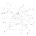
図1は半導体発光装置の斜視図であり、図2は半導体発光装置を発光面側から見た平面図であり、図3は図2中のX1−X1における断面図であり、図4は半導体発光装置をセラミックス基板の裏面側から見た平面図である。 1 is a perspective view of a semiconductor light emitting device, FIG. 2 is a plan view of the semiconductor light emitting device viewed from the light emitting surface side, FIG. 3 is a cross-sectional view taken along line X1-X1 in FIG. 2, and FIG. It is the top view which looked at the light-emitting device from the back surface side of the ceramic substrate.
図1に示す半導体発光装置1は、ねじ穴8A及び8Bが設けられているセラミックス基板5上に、半導体発光素子2と電極9A及び9Bとを備えている。また、セラミックス基板の裏面には金属膜7が設けられている。また、セラミックス基板上の半導体発光素子2の周囲には、枠体6が設けられ、枠体内には封止部材13が充填されている。なお、説明の便宜上、図1及び図2では封止部材13を透過させて図示している。 The semiconductor
以下、実施形態の各構成について説明する。
(セラミックス基板)
セラミックス基板5は、半導体発光素子2を配置するためのものである。その形状やサイズは特に限定されず、半導体発光素子2の数や配列間隔等、半導体発光装置の用途に応じて適宜選択することができる。セラミックス基板の形状としては、例えば図1に示すように、角部を面取りした略矩形で平板状に形成することができる。矩形の他には円形、楕円形等が挙げられる。また、セラミックス基板の厚みは、0.5〜2.0μm程度であることが好ましい。
セラミックス基板5は白色系の部材であることが好ましく、具体的な材料としては、酸化アルミニウム、窒化アルミニウム等が挙げられる。また、酸化アルミニウムにガラス系材料を加えたいわゆる低温焼結セラミックスを用いてもよい。このような材料で形成されることによって、複数の半導体発光素子を実装した場合にも放熱性を良好にすることができるため好ましい。
また、セラミックス基板はその表面及び内部に配線パターン(図示しない)を備えており、半導体発光素子は配線パターンを介して素子同士あるいは電極と電気的に接続されている。Hereinafter, each configuration of the embodiment will be described.
(Ceramic substrate)
The ceramic substrate 5 is for arranging the semiconductor light emitting element 2. The shape and size are not particularly limited, and can be appropriately selected according to the use of the semiconductor light emitting device, such as the number and arrangement interval of the semiconductor light emitting elements 2. As the shape of the ceramic substrate, for example, as shown in FIG. 1, it can be formed into a flat plate with a substantially rectangular shape with chamfered corners. Besides a rectangle, a circle, an ellipse, etc. are mentioned. The thickness of the ceramic substrate is preferably about 0.5 to 2.0 μm.
The ceramic substrate 5 is preferably a white member, and specific examples include aluminum oxide and aluminum nitride. Moreover, you may use what is called low-temperature sintering ceramics which added the glass-type material to the aluminum oxide. Forming with such a material is preferable because heat dissipation can be improved even when a plurality of semiconductor light emitting elements are mounted.
Moreover, the ceramic substrate is provided with a wiring pattern (not shown) on the surface and inside thereof, and the semiconductor light emitting element is electrically connected to the elements or electrodes via the wiring pattern.
セラミックス基板は、焼成前の母材であるグリーンシート段階での加工により種々の形状をとるように形成することができる。セラミックス基板を得る方法としてはまず、焼成前のグリーンシートに、所望の配線パターンや後述するねじ穴が得られるように貫通孔や溝部等の加工を施し、場合によっては多層に貼り合わせる。次に、タングステン、モリブデン、銀、銅などの金属を樹脂バインダーに含有させたペースト状の材料を用いて、スクリーン印刷などの方法により配線パターンを形成する。このように加工された母材を焼成することにより、セラミックス基板5を得ることができる。 The ceramic substrate can be formed to take various shapes by processing at the green sheet stage which is a base material before firing. As a method for obtaining a ceramic substrate, first, a green sheet before firing is processed such as through holes and grooves so as to obtain a desired wiring pattern and a screw hole to be described later, and in some cases, the green sheets are laminated in multiple layers. Next, a wiring pattern is formed by a method such as screen printing using a paste-like material in which a metal such as tungsten, molybdenum, silver, or copper is contained in a resin binder. The ceramic substrate 5 can be obtained by firing the base material thus processed.
(ねじ穴)
セラミックス基板に設けられるねじ穴は、照明装置等の器具に取り付けるために設けられるものであり、セラミックス基板の上下方向に開放されている。形状としては、図1に示すような円形が挙げられる。ねじ穴は円形には限定されず、セラミックス基板の端部とねじ穴の間の基板材料が除去されることによってねじ穴の一部が開放されたような形状の切り欠きを設けてもよい。セラミックス基板はねじにより固定されるか、あるいは裏面にねじ穴形状に対応する突起部を有するようなカバー部材で押さえ込むことによって器具に固定してもよい。
ねじ穴は、半導体発光装置を器具に取り付けた際の安定性の観点から複数設けられていることが好ましい。また、ねじ穴の形成される位置は、セラミックス基板の角部近傍であることが好ましい。その配置の一例としては、図1に示すような略矩形状のセラミックス基板において、対角線上に形成されるものであり、このような配置とすることで、少ない数のねじでセラミックス基板を固定することができるので、ねじ穴を起点とするクラックの発生を抑制することができる。
またねじ穴の大きさは、固定するためのねじの大きさ、あるいはセラミックス基板の大きさに応じて適宜選択することができる。具体的には、2.2〜3.5mm程度の直径のものが挙げられる。(Screw hole)
The screw hole provided in the ceramic substrate is provided to attach to a fixture such as a lighting device, and is open in the vertical direction of the ceramic substrate. Examples of the shape include a circle as shown in FIG. The screw hole is not limited to a circle, and a notch having a shape in which a part of the screw hole is opened by removing the substrate material between the end of the ceramic substrate and the screw hole may be provided. The ceramic substrate may be fixed to the instrument by fixing with a screw or by pressing with a cover member having a protrusion corresponding to the screw hole shape on the back surface.
It is preferable that a plurality of screw holes are provided from the viewpoint of stability when the semiconductor light emitting device is attached to the instrument. Further, the position where the screw hole is formed is preferably in the vicinity of the corner of the ceramic substrate. As an example of the arrangement, a substantially rectangular ceramic substrate as shown in FIG. 1 is formed on a diagonal line. With such an arrangement, the ceramic substrate is fixed with a small number of screws. Therefore, the generation of cracks starting from the screw holes can be suppressed.
The size of the screw hole can be appropriately selected according to the size of the screw for fixing or the size of the ceramic substrate. Specifically, the thing of a diameter of about 2.2-3.5 mm is mentioned.
(金属膜)
本実施形態の半導体発光装置は、セラミックス基板の裏面の少なくともねじ穴の周囲に電極と電気的に分離された金属膜7が設けられている。これによって、ねじ穴を起点とするクラックの発生を抑制することができる。
上述したように、セラミックス基板は、主材料であるセラミックスと、配線パターンである金属材料を含んで構成される。セラミックスと金属材料では、異なる熱膨張係数を有するため、グリーンシートの貼り合わせや焼成工程などを経ることで反りを持った状態となる。内部の配線パターンやグリーンシートの積層数等により表面側あるいは裏面側が凹むいずれかの反りを持ったセラミックス基板を用いた半導体発光装置をねじ等により固定しようとすると、ねじ穴の周囲を起点としてセラミックス基板にクラックが発生する。
そこで、本実施形態の半導体発光装置のように、少なくとも基板裏面のねじ穴の周囲に電極と電気的に分離された金属膜を設けておくことで、固定時にセラミックス基板と取り付け部の間で緩衝材の役割を果たす。あるいはねじ穴の周囲のセラミックス基板を補強する機能を果たす。そうすると、器具への固定時にねじ穴の周辺部が加圧されセラミックス基板へ負荷がかかることを軽減でき、セラミックス基板のクラックの発生を抑制することができる。(Metal film)
In the semiconductor light emitting device of this embodiment, a
As described above, the ceramic substrate includes a ceramic material as a main material and a metal material as a wiring pattern. Since ceramics and metal materials have different thermal expansion coefficients, they are warped by being subjected to green sheet bonding and firing processes. If you try to fix a semiconductor light emitting device using a ceramic substrate with a warp that is recessed either on the front side or the back side depending on the internal wiring pattern, the number of green sheets, etc. Cracks occur on the substrate.
Therefore, as in the semiconductor light emitting device of this embodiment, by providing a metal film that is electrically separated from the electrode at least around the screw hole on the back surface of the substrate, a buffer is provided between the ceramic substrate and the mounting portion during fixing. Play the role of wood. Alternatively, it functions to reinforce the ceramic substrate around the screw hole. If it does so, the peripheral part of a screw hole will be pressurized at the time of fixing to an instrument, it can reduce that a load is applied to a ceramic substrate, and generation | occurrence | production of the crack of a ceramic substrate can be suppressed.
金属膜の膜厚としては、10〜30μm程度であることが好ましい。この程度の膜厚とすることでより効果的にクラックの発生を抑制することができる。また、器具取り付け時の加圧によって、金属膜をセラミックス基板の反りに沿って変形させることができ、金属膜と器具の取り付け面との接触面積を増加させることができ、放熱性を向上させることができる。
金属膜の材料としては、器具への固定によるねじ穴の周囲にかかる負荷を好適に緩和することのできる材料であることが好ましく、具体的には、Ag、Cu、W、Mo、Au、Ni等が挙げられる。このような金属を用いることにより、効果的にクラックの発生を抑制することができる。あるいは、Ag、CuW又はMo上に、AuめっきやNiめっきからなる金属膜を形成してもよい。The thickness of the metal film is preferably about 10 to 30 μm. The occurrence of cracks can be more effectively suppressed by setting the film thickness to this extent. In addition, the metal film can be deformed along the warp of the ceramic substrate by pressurization at the time of mounting the device, the contact area between the metal film and the mounting surface of the device can be increased, and heat dissipation is improved. Can do.
The material of the metal film is preferably a material that can suitably reduce the load applied to the periphery of the screw hole due to fixation to the instrument. Specifically, Ag, Cu, W, Mo, Au, Ni Etc. By using such a metal, the occurrence of cracks can be effectively suppressed. Alternatively, a metal film made of Au plating or Ni plating may be formed on Ag, CuW or Mo.
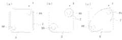
金属膜のパターンとしては、基板裏面において少なくともねじ穴の周囲を囲むように連続して形成されることが好ましい。具体的には、ねじ穴の端部から少なくとも1mm以上の大きさでねじ穴の周囲を取り囲むことが好ましい。金属膜のパターンについて図4に例示する。金属膜の形状は、例えば図4(a)に示すようなねじ穴の形状の開口部を有する矩形でもいいし、図4(b)に示すようなねじ穴の形状の開口部を有する円形でもいいし、図4(c)に示すようなねじ穴の形状の開口部を有する楕円形でもいい。もちろんこれらの形状に限定されず、セラミックス基板や発光領域及びねじ穴等の形状に応じて任意に形状を決定することができる。図4(a)または(c)のように、後述する発光領域に対応するセラミックス基板の裏面に金属膜を形成することで、半導体発光装置の放熱性を向上させることができ好ましい。また、半導体発光装置の放熱性を向上させる観点からは、ねじ穴形状の開口部を有する基板形状のパターンで形成されることが好ましい。 The metal film pattern is preferably formed continuously so as to surround at least the periphery of the screw hole on the back surface of the substrate. Specifically, it is preferable to surround the periphery of the screw hole with a size of at least 1 mm from the end of the screw hole. The metal film pattern is illustrated in FIG. The shape of the metal film may be, for example, a rectangle having an opening in the shape of a screw hole as shown in FIG. 4A or a circle having an opening in the shape of a screw hole as shown in FIG. It may be oval having an opening in the shape of a screw hole as shown in FIG. Of course, it is not limited to these shapes, and the shape can be arbitrarily determined according to the shape of the ceramic substrate, the light emitting region, the screw hole, and the like. As shown in FIG. 4 (a) or (c), it is preferable to form a metal film on the back surface of the ceramic substrate corresponding to the light emitting region to be described later, thereby improving the heat dissipation of the semiconductor light emitting device. Further, from the viewpoint of improving the heat dissipation of the semiconductor light emitting device, it is preferably formed with a substrate-shaped pattern having a screw hole-shaped opening.
このような金属膜は、例えばめっき法を用いて形成することができる。電解めっきまたは無電解めっきで形成されることが好ましい。 Such a metal film can be formed by using, for example, a plating method. It is preferably formed by electrolytic plating or electroless plating.
(半導体発光素子)
半導体発光素子2は、電圧を印加することで自発光するものであり、セラミックス基板5上に複数配置されることが好ましい。本実施形態の半導体発光素子2の一例としては、半導体材料として窒化物半導体が用いられ、平面視が矩形状であり、一方の表面にp電極及びn電極が設けられているものである。
また、半導体発光素子は、p電極及びn電極をセラミックス基板の表面に設けられた配線パターンと接触させるようにフェイスダウンで実装されている。本実施形態では、複数の半導体発光素子2は各電極の向きを揃えてセラミックス基板上に配列され、円状に配置されている。そして、半導体発光素子2は、基板表面及び内部に設けられた配線パターンにより電気的に接続され、接続回路の正極端と負極端はそれぞれ正極側電極9A、負極側電極9Bに電気的に接続される。なお、半導体発光素子2は公知のダイボンディング方法によりセラミックス基板に実装することができる。
また、半導体発光素子2を、上面にp電極及びn電極が設けられるようにフェイスアップ実装し、素子同士や素子と電極とをワイヤ(例えば、Au,Ag、Cu、Pt、Al等の金属線)で接続することもできる。また、両面にp電極、n電極がそれぞれ設けられた対向電極構造の素子を用いることもできる。(Semiconductor light emitting device)
The semiconductor light emitting element 2 emits light by applying a voltage, and a plurality of the semiconductor light emitting elements 2 are preferably arranged on the ceramic substrate 5. As an example of the semiconductor light emitting device 2 of the present embodiment, a nitride semiconductor is used as a semiconductor material, the planar view is rectangular, and a p electrode and an n electrode are provided on one surface.
Further, the semiconductor light emitting device is mounted face down so that the p electrode and the n electrode are brought into contact with a wiring pattern provided on the surface of the ceramic substrate. In the present embodiment, the plurality of semiconductor light emitting elements 2 are arranged on a ceramic substrate with their respective electrodes aligned and arranged in a circle. The semiconductor light emitting element 2 is electrically connected by a wiring pattern provided on the substrate surface and inside, and the positive end and the negative end of the connection circuit are electrically connected to the
Further, the semiconductor light emitting element 2 is mounted face-up so that a p-electrode and an n-electrode are provided on the upper surface, and the elements or elements and electrodes are connected to each other with a wire (for example, a metal wire such as Au, Ag, Cu, Pt, Al). ) Can also be connected. An element having a counter electrode structure in which a p-electrode and an n-electrode are provided on both sides can also be used.
本実施形態では、セラミックス基板の表面に枠体6が形成されており、この枠体に区画される領域内に半導体発光素子が配置され発光領域となっている。図1では、セラミックス基板5の中央にほぼ真円形の領域として発光領域が充てられている。本実施形態では、発光領域のサイズは特に限定されず、半導体発光素子2の数や配列間隔等、目的および用途に応じて適宜選択することができる。また、半導体発光素子2からの光の反射効率を高める目的で発光領域内に反射膜を形成し、この反射膜の形成領域を発光領域に充ててもよい。 In the present embodiment, a frame 6 is formed on the surface of the ceramic substrate, and a semiconductor light emitting element is arranged in a region partitioned by the frame to form a light emitting region. In FIG. 1, a light emitting region is filled as a substantially circular region at the center of the ceramic substrate 5. In the present embodiment, the size of the light emitting region is not particularly limited, and can be appropriately selected according to the purpose and application, such as the number and arrangement interval of the semiconductor light emitting elements 2. In addition, for the purpose of increasing the reflection efficiency of light from the semiconductor light emitting element 2, a reflective film may be formed in the light emitting region, and this reflective film forming region may be used for the light emitting region.
(電極)
本実施形態の半導体発光装置は、半導体発光素子と電気的に接続された電極9A及び9Bが導電性のワイヤ(図示しない)によって外部電源と接続される。
電極9A及び9Bは、例えば図1に示すようにセラミックス基板の対角部近傍に形成することができる。
電極9A及び9Bは例えばめっきにより形成され、材質としてはAuであることが好ましい。勿論、めっき以外の方法、例えば導体ペーストを塗布して焼成する方法でも差し支えない。なお、符合10は電極9Aが正極であることを示すアノードマーク、符合11は電極9Bが負極であることを示すカソードマークであり、これらもめっき等により形成される。(electrode)
In the semiconductor light emitting device of this embodiment, the
The
The
その他の構成について説明する。
実施形態の半導体発光装置には、セラミックス基板上に枠体6が形成されていてもよい。枠体6は、発光領域を囲むように環状に形成され、半導体発光素子2からの光を透過又は反射する。枠体の形状は環状のみならず、半導体発光素子2の数や配列間隔等、目的および用途に応じて任意の形状を適宜選択することができる。
枠体6としては、絶縁材料を用いることが好ましく、光の透過に優れた透明の材料が好ましい。また、枠体6は、ある程度の強度を確保するために、熱硬化性樹脂、熱可塑性樹脂等を用いることができる。より具体的には、フェノール樹脂、エポキシ樹脂、BTレジンや、PPAやシリコーン樹脂などが挙げられる。
また、枠体としては、光の反射率に優れた白色系の材料を用いてもよい。上記した母体となる樹脂に、半導体発光素子2からの光を吸収しにくく、かつ母体となる樹脂に対する屈折率差の大きい反射部材(例えばTiO2、Al2O3、ZrO2、MgO)等の粉末を分散することで効率良く光を反射させる構造としてもよい。Other configurations will be described.
In the semiconductor light emitting device of the embodiment, the frame body 6 may be formed on a ceramic substrate. The frame 6 is formed in an annular shape so as to surround the light emitting region, and transmits or reflects light from the semiconductor light emitting element 2. The shape of the frame is not limited to an annular shape, and any shape can be appropriately selected according to the purpose and application such as the number of semiconductor light emitting elements 2 and the arrangement interval.
As the frame 6, an insulating material is preferably used, and a transparent material excellent in light transmission is preferable. The frame 6 can be made of a thermosetting resin, a thermoplastic resin, or the like in order to ensure a certain level of strength. More specifically, a phenol resin, an epoxy resin, a BT resin, PPA, a silicone resin, etc. are mentioned.
Further, as the frame, a white material having excellent light reflectance may be used. Reflective members (for example, TiO2 , Al2 O3 , ZrO2 , MgO) that are difficult to absorb the light from the semiconductor light emitting element 2 and have a large refractive index difference with respect to the base resin are contained in the above-described base resin. It is good also as a structure which reflects light efficiently by disperse | distributing powder.
枠体6は、発光領域を囲む形状に成形した部材をセラミックス基板に接着して形成することができる。例えば公知の透光性材料のシートを所望の形状にくり抜き、セラミックス基板上に貼り付けることで設けることができる。あるいは、ディスペンサにより吐出、形成された後、硬化処理をすることで形成することもできる。 The frame body 6 can be formed by adhering a member molded in a shape surrounding the light emitting region to the ceramic substrate. For example, it can be provided by cutting a sheet of a known light-transmitting material into a desired shape and sticking it on a ceramic substrate. Or it can also form by performing a hardening process after discharging and forming with a dispenser.
また、発光領域は封止部材13によって封止されていてもよい。封止部材13は、半導体発光素子2等を塵芥、水分、外力等から保護するための部材である。封止部材13は、セラミックス基板5上において、枠体6により囲った発光領域内に樹脂を充填することで形成される。封止部材13の材料は、半導体発光素子2からの光を透過可能な透光性を有するものであり、具体的な材料としてはシリコーン樹脂、エポキシ樹脂、ユリア樹脂等が挙げられる。また、封止部材13は、このような材料に加えて着色剤、光拡散剤、フィラー、蛍光剤等を含有させることもできる。 In addition, the light emitting region may be sealed with the sealing
また、発光領域の中心に矩形状の保護素子3が配置されていてもよい。保護素子3は過大な電圧印加による素子破壊や性能劣化から半導体発光素子2を保護するためのものであり、セラミックス基板表面に設けられた配線パターンにより接続されている。 Moreover, the
以下に、実施例の窒化物半導体発光素子について説明する。なお、本願は以下の実施例に限定されるものではない。
(実施例1)
図1に示したような窒化物半導体発光装置1は、以下のようにして製造することができる。
まず、一辺が約1.7cmの正方形で、角部が面取りされている低温焼結セラミックスからなるセラミックス基板5を準備する。セラミックス基板は、対角に配置される1組の角部の近傍に直径2.7mmの貫通孔8A及び8Bをねじ穴として有している。基板表面のもう1組の角部の近傍には、Auで形成された一対の電極9A及び9Bを有する。また、基板の表面には半導体発光素子2及び保護素子3を実装するための配線パターンを有している。このセラミックス基板の裏面に、電解めっき法により、図4(a)に示すようなねじ穴形状の開口部を有する基板形状のパターンでAgとAuめっきからなる金属膜7を20μmの膜厚で形成する。
次に、セラミックス基板の中央に保護素子3を、保護素子の周囲を囲むように半導体発光素子2を円状に6個配列し実装する。続いて、基板表面にシリコーン樹脂からなる枠体6を形成し、発光領域に蛍光体を含有する樹脂を封止部材13として充填して半導体発光装置1を得る。
得られた半導体発光装置をねじを用いて器具に実装したところ、セラミックス基板のクラックの発生は起こらず固定することができる。The nitride semiconductor light emitting device of the example will be described below. In addition, this application is not limited to a following example.
Example 1
The nitride semiconductor
First, a ceramic substrate 5 made of a low-temperature sintered ceramic having a square of about 1.7 cm on one side and chamfered corners is prepared. The ceramic substrate has through
Next, the
When the obtained semiconductor light emitting device is mounted on an instrument using screws, the ceramic substrate can be fixed without causing cracks.
また、比較のため、基板裏面に金属膜7を形成していない以外は同様の半導体発光装置を作製する。それについて同様に実装したところ、セラミックス基板にクラックが発生することが確認される。 For comparison, a similar semiconductor light emitting device is manufactured except that the
本発明は、各種表示装置、照明器具、ディスプレイ、液晶ディスプレイのバックライト光源、さらには、ファクシミリ、コピー機、スキャナ等における画像読取装置、プロジェクタ装置など広範囲の用途に利用することができる。 The present invention can be used in a wide range of applications such as various display devices, lighting fixtures, displays, backlight light sources for liquid crystal displays, and image reading devices and projector devices in facsimiles, copiers, scanners, and the like.
1 発光装置
2 半導体発光素子
3 保護素子
5 基板
6 枠体
7 金属膜
8A、8B ねじ穴
9A 正極側電極
9B 負極側電極DESCRIPTION OF
Claims (4)
Translated fromJapanese前記セラミックス基板の裏面に、前記複数のねじ穴の周囲に前記電極と電気的に分離された金属膜が形成される半導体発光装置。In a semiconductor light emitting device having a ceramic substrate having a screw hole for mounting opened in the vertical direction and having an electrode formed on the surface, and a semiconductor light emitting element electrically connected to the electrode on the surface of the ceramic substrate,
A semiconductor light emitting device in which a metal film electrically separated from the electrode is formed around the plurality of screw holes on the back surface of the ceramic substrate.
Priority Applications (1)
| Application Number | Priority Date | Filing Date | Title |
|---|---|---|---|
| JP2010006109UJP3164276U (en) | 2010-09-10 | 2010-09-10 | Semiconductor light emitting device |
Applications Claiming Priority (1)
| Application Number | Priority Date | Filing Date | Title |
|---|---|---|---|
| JP2010006109UJP3164276U (en) | 2010-09-10 | 2010-09-10 | Semiconductor light emitting device |
Publications (1)
| Publication Number | Publication Date |
|---|---|
| JP3164276Utrue JP3164276U (en) | 2010-11-18 |
Family
ID=54875684
Family Applications (1)
| Application Number | Title | Priority Date | Filing Date |
|---|---|---|---|
| JP2010006109UExpired - Fee RelatedJP3164276U (en) | 2010-09-10 | 2010-09-10 | Semiconductor light emitting device |
Country Status (1)
| Country | Link |
|---|---|
| JP (1) | JP3164276U (en) |
Cited By (4)
| Publication number | Priority date | Publication date | Assignee | Title |
|---|---|---|---|---|
| JP2013118285A (en)* | 2011-12-02 | 2013-06-13 | Hitachi Appliances Inc | Light emitting diode module and lighting apparatus using the same |
| WO2013125539A1 (en) | 2012-02-20 | 2013-08-29 | シャープ株式会社 | Light emission device and illumination device |
| JP2018113479A (en)* | 2018-04-04 | 2018-07-19 | ローム株式会社 | Light-emitting element module |
| JP2019053879A (en)* | 2017-09-14 | 2019-04-04 | アイリスオーヤマ株式会社 | Light source module and lighting device |
- 2010
- 2010-09-10JPJP2010006109Upatent/JP3164276U/ennot_activeExpired - Fee Related
Cited By (4)
| Publication number | Priority date | Publication date | Assignee | Title |
|---|---|---|---|---|
| JP2013118285A (en)* | 2011-12-02 | 2013-06-13 | Hitachi Appliances Inc | Light emitting diode module and lighting apparatus using the same |
| WO2013125539A1 (en) | 2012-02-20 | 2013-08-29 | シャープ株式会社 | Light emission device and illumination device |
| JP2019053879A (en)* | 2017-09-14 | 2019-04-04 | アイリスオーヤマ株式会社 | Light source module and lighting device |
| JP2018113479A (en)* | 2018-04-04 | 2018-07-19 | ローム株式会社 | Light-emitting element module |
Similar Documents
| Publication | Publication Date | Title |
|---|---|---|
| JP5742353B2 (en) | Light emitting element substrate and light emitting device | |
| JP6107136B2 (en) | LIGHT EMITTING DEVICE PACKAGE, LIGHT EMITTING DEVICE INCLUDING THE SAME, AND LIGHTING DEVICE EQUIPPED WITH THE LIGHT EMITTING DEVICE | |
| JP5753446B2 (en) | Manufacturing method of semiconductor light emitting device | |
| CN101944565B (en) | Light emitting device and method for manufacturing same | |
| JP2011054736A (en) | Light-emitting device, plane light source, and liquid crystal display device | |
| JP2006005290A (en) | Light emitting diode | |
| JP2012216808A (en) | Luminous body flexible substrate and luminous body device | |
| TW200828635A (en) | Light emitting device, its manufacturing method and its mounted substrate | |
| JP2012114284A (en) | Led module and illuminating device | |
| JP2011228653A (en) | Substrate for light-emitting element and light-emitting device | |
| JP2012113919A (en) | Lighting device | |
| JP2014187081A (en) | Light-emitting device | |
| JP2014022491A (en) | Semiconductor light-emitting device and manufacturing method of the same | |
| JP3164276U (en) | Semiconductor light emitting device | |
| JP2008198782A (en) | Light-emitting device | |
| JP2016063121A (en) | Light emitting device | |
| JP5347681B2 (en) | Light emitting device | |
| JP6224449B2 (en) | Light-emitting element mounting substrate and light-emitting device including the same | |
| JP2014078695A (en) | Luminescence device | |
| JP2008160032A (en) | Light emitting device | |
| JP2005243738A (en) | Light emitting element storage package and light emitting device | |
| JP6010891B2 (en) | Semiconductor device | |
| JP2010283063A (en) | Light emitting device and light emitting module | |
| JP2008147512A (en) | Light-emitting device and manufacturing method thereof | |
| JP2015138902A (en) | Light-emitting device |
Legal Events
| Date | Code | Title | Description |
|---|---|---|---|
| R150 | Certificate of patent or registration of utility model | Ref document number:3164276 Country of ref document:JP Free format text:JAPANESE INTERMEDIATE CODE: R150 Free format text:JAPANESE INTERMEDIATE CODE: R150 | |
| FPAY | Renewal fee payment (event date is renewal date of database) | Free format text:PAYMENT UNTIL: 20131027 Year of fee payment:3 | |
| FPAY | Renewal fee payment (event date is renewal date of database) | Free format text:PAYMENT UNTIL: 20131027 Year of fee payment:3 | |
| R250 | Receipt of annual fees | Free format text:JAPANESE INTERMEDIATE CODE: R250 | |
| R250 | Receipt of annual fees | Free format text:JAPANESE INTERMEDIATE CODE: R250 | |
| R250 | Receipt of annual fees | Free format text:JAPANESE INTERMEDIATE CODE: R250 | |
| R250 | Receipt of annual fees | Free format text:JAPANESE INTERMEDIATE CODE: R250 | |
| R250 | Receipt of annual fees | Free format text:JAPANESE INTERMEDIATE CODE: R250 | |
| R250 | Receipt of annual fees | Free format text:JAPANESE INTERMEDIATE CODE: R250 | |
| LAPS | Cancellation because of no payment of annual fees |