JP3152611U - Touch panel capacitor sensing structure - Google Patents
Touch panel capacitor sensing structureDownload PDFInfo
- Publication number
- JP3152611U JP3152611UJP2009003462UJP2009003462UJP3152611UJP 3152611 UJP3152611 UJP 3152611UJP 2009003462 UJP2009003462 UJP 2009003462UJP 2009003462 UJP2009003462 UJP 2009003462UJP 3152611 UJP3152611 UJP 3152611U
- Authority
- JP
- Japan
- Prior art keywords
- sensitive
- axis
- capacitor
- touch panel
- stitch
- Prior art date
- Legal status (The legal status is an assumption and is not a legal conclusion. Google has not performed a legal analysis and makes no representation as to the accuracy of the status listed.)
- Expired - Fee Related
Links
Images


Landscapes
- Position Input By Displaying (AREA)
Abstract
Translated fromJapaneseDescription
Translated fromJapanese本考案はタッチパネルのキャパシター感知構造に関し、特にノイズキャパシター値を低下させることができ、しかも透過率均一性を向上させることができるタッチパネルのキャパシター感知構造に関する。 The present invention relates to a capacitor sensing structure of a touch panel, and more particularly, to a capacitor sensing structure of a touch panel capable of reducing a noise capacitor value and improving transmittance uniformity.
キャパシター式タッチパネルは、使用者の指或いは導体がパネル上にタッチした瞬間にキャパシター効果を発生し、キャパシター値の変化に基づき指或いは導体の位置を確定し、これにより信号入力の目的を達成するものである。キャパシター式タッチパネルは、指を用いて入力を行なうことができるため、入力操作が利便で、しかもその入力操作には、圧力を加える必要がないため、パネルが繰り返し応力を受けることにより変形し損壊するという欠点が存在しない。また、その構造は簡単で、部品は少なく、歩留まりも高いため、大量生産に適しコストを引き下げることができる。よって、通信、コンピューター、民生用電子製品などに幅広く応用されている。 A capacitor-type touch panel generates a capacitor effect at the moment when a user's finger or conductor touches the panel, and determines the position of the finger or conductor based on the change in the capacitor value, thereby achieving the purpose of signal input. It is. Capacitor-type touch panels can be input using a finger, so that the input operation is convenient, and it is not necessary to apply pressure to the input operation, so the panel is deformed and damaged due to repeated stress. There is no shortcoming. In addition, since the structure is simple, the number of parts is small, and the yield is high, it is possible to reduce the cost suitable for mass production. Therefore, it is widely applied to communications, computers, consumer electronic products, etc.
従来のタッチパネルのキャパシター感知構造は、複数のX軸感応ステッチとY軸感応ステッチを備える。X、Y軸ステッチ上には、相互に連接する多数のキャパシター感応ユニットをそれぞれ設置する。各X軸ステッチとY軸ステッチとは、相互に交差した絶縁設置を呈し、これによりX、Y軸ステッチ上の各キャパシター感応ユニットはおおよそ碁盤の目の状の排列を呈し、タッチパネルの作動区域内に敷設する。通常、X軸感応ステッチとY軸感応ステッチとは、酸化インジウムスズ(Indium Tin Oxide、ITO)などの透明導電薄膜を採用し、エッチングプロセスを利用し、不要な部分を除去し各キャパシター感応ユニットを区分する。これにより、X軸感応ステッチとY軸感応ステッチ上の各キャパシター感応ユニットは、相互の間に適当な幅の間隙を備え、絶縁設置の目的を達成する。これら、キャパシター感応ユニットの区画、設置において、間隙の幅が小さ過ぎる時には、EMI、或いは干渉キャパシター値がしばしば出現する。こうなると、キャパシター感応信号の感度と精度は低下してしまう。しかし、間隙の幅を拡大すると、これらキャパシター感応ユニットの設置部位と非設置部位(空洞部位ともいう)は、透過率(transmittance)が異なるため、パネルを透過する光線の屈折が不均一になる。この結果、スクリーン影像が変形し、ぼやけ、歪むという問題が生じる。 The capacitor sensing structure of the conventional touch panel includes a plurality of X-axis sensitive stitches and a Y-axis sensitive stitch. On the X and Y axis stitches, a large number of capacitor sensitive units connected to each other are installed. Each X-axis stitch and Y-axis stitch exhibit insulation installation crossing each other, so that each capacitor-sensitive unit on the X- and Y-axis stitches has an approximately grid-like arrangement and is within the operating area of the touch panel. Lay in. Normally, X-axis sensitive stitches and Y-axis sensitive stitches use a transparent conductive thin film such as Indium Tin Oxide (ITO), and use an etching process to remove unnecessary parts and use each capacitor sensitive unit. Break down. Accordingly, each capacitor sensitive unit on the X-axis sensitive stitch and the Y-axis sensitive stitch has an appropriate width gap between each other, thereby achieving the purpose of insulation installation. When the gap width is too small in the section and installation of these capacitor sensitive units, EMI or interference capacitor values often appear. This will reduce the sensitivity and accuracy of the capacitor sensitive signal. However, when the width of the gap is increased, the installed part and the non-installed part (also referred to as a cavity part) of these capacitor sensitive units have different transmittances, so that the refraction of the light transmitted through the panel becomes non-uniform. As a result, there arises a problem that the screen image is deformed, blurred and distorted.
本考案の目的は、キャパシター感応ユニットの設置間隙中に、相同の透過率或いは透過率の差異値が6%以下の透過率を備えるダミーパターンを補填し、これにより、空洞部分の比率を大幅に引き下げ、キャパシター感知構造の外観の平坦度と透過率の均一性を向上させ、タッチパネル底部の表示スクリーンの影像がぼやけ、歪むという問題を改善することができ、またキャパシター感応ユニットの設置間隙を広げ、これによりノイズキャパシター値を低下させることができるタッチパネルのキャパシター感知構造を提供することである。 The purpose of the present invention is to supplement a dummy pattern having a transmittance of a homologous transmittance or a transmittance difference value of 6% or less in the gap between the capacitor sensitive units, thereby greatly increasing the ratio of the cavity portion. Lowering, improving the flatness and uniformity of the appearance of the capacitor sensing structure, improving the problem of blurring and distorting the image of the display screen at the bottom of the touch panel, and widening the installation gap of the capacitor sensitive unit, Accordingly, a capacitor sensing structure of a touch panel that can reduce a noise capacitor value is provided.
本考案は下記のタッチパネルのキャパシター感知構造を提供する。
タッチパネルのキャパシター感知構造は、複数の透明なX軸感応ステッチとY軸感応ステッチを備え、
該X、Y軸感応ステッチ上には、相互に連接する多数のキャパシター感応ユニットをそれぞれ設置し、
該X軸感応ステッチと該Y軸感応ステッチは、相互に交差し、絶縁状に設置し、これにより該X、Y軸感応ステッチ上の各キャパシター感応ユニットは、おおよそ碁盤の目状の排列を呈し、タッチパネル上の作動区域内に敷設され、
該各キャパシター感応ユニットの設置間隙中には、相同の透過率或いは透過率の差異値が6%以下のダミーパターン(Dummy Pattern)を敷設して絶縁し、該キャパシター感知構造の透過率の均一度を向上させ、影像がぼやけ、歪むという欠点を改善することができ、
同時に、透過率の均一性を減損しないという状況で、キャパシター感応ユニットの設置間隙を広げ、ノイズキャパシター値を低下させることができ、
該ダミーパターンは、該X軸感応ステッチ及び該Y軸感応ステッチと同一層の平面上に設置され、それらはすべて相同材質の材料を採用することが望ましく、その材料とは、酸化インジウムスズ(ITO) 、ポリエチレンジオキシチオフェン(PEDOT)などの透明導電薄膜で、
よって、該キャパシター感応層へのエッチングプロセスにおいて、一度に設置を完成することができるため、加工手順と生産コストを拡大させることはなく、
該ダミーパターンは、該X軸感応ユニット及び該Y軸感応ユニットの縁と、連接しない間隔をそれぞれ保持し、相互に絶縁を呈し、通常その間隔は、約50μm以下で、
タッチパネルのキャパシター感知構造は、底基板と上パネルを備え、該2枚の板間には、キャパシター感応層を設置し、接着層により、該2枚の板を重ねて接着し1枚の板体とし、
タッチパネルの作動区域内において、該キャパシター感応層は、多数の感応ユニットを備え、該各感応ユニット間は、相互に間隔距離を隔て、交差状に敷設し、該感応ユニットの設置間隙中には、相同の透過率或いは透過率の差異値が6%以下のダミーパターンを敷設して絶縁し、
こうして外観の平坦度と透過率の均一度を向上させることができ、
該感応ユニットは、三角形、或いは長方形、或いは他の幾何学形状の面積を呈する。The present invention provides a capacitor sensing structure of a touch panel as follows.
Capacitor sensing structure of touch panel has multiple transparent X-axis sensitive stitches and Y-axis sensitive stitches,
On the X and Y axis sensitive stitches, a number of capacitor sensitive units connected to each other are installed,
The X-axis sensitive stitch and the Y-axis sensitive stitch cross each other and are installed in an insulating manner, so that each capacitor-sensitive unit on the X and Y-axis sensitive stitch exhibits a roughly grid-like arrangement. Laid in the working area on the touch panel,
In the gap between the capacitor sensing units, a dummy pattern (Dummy Pattern) having a homologous transmittance or a transmittance difference value of 6% or less is laid and insulated, and the uniformity of the transmittance of the capacitor sensing structure Can improve the defect that the image is blurred and distorted,
At the same time, in the situation where the transmittance uniformity is not impaired, the installation gap of the capacitor sensitive unit can be widened, and the noise capacitor value can be lowered.
The dummy pattern is installed on the same layer plane as the X-axis sensitive stitch and the Y-axis sensitive stitch, and it is preferable that all of them adopt a material of the same material, which is indium tin oxide (ITO). ), Transparent conductive thin film such as polyethylenedioxythiophene (PEDOT)
Therefore, in the etching process to the capacitor sensitive layer, since the installation can be completed at once, without increasing the processing procedure and production cost,
The dummy patterns hold the gaps that are not connected to the edges of the X-axis sensitive unit and the Y-axis sensitive unit, respectively, and insulate each other. Usually, the gap is about 50 μm or less,
The capacitor sensing structure of the touch panel includes a bottom substrate and an upper panel, and a capacitor sensitive layer is installed between the two plates, and the two plates are laminated and bonded together by an adhesive layer. age,
In the operating area of the touch panel, the capacitor sensitive layer includes a number of sensitive units, and each sensitive unit is laid in an intersecting manner with a distance from each other. In the installation gap of the sensitive units, Insulate by laying dummy pattern with homogenous transmittance or transmittance difference value of 6% or less,
In this way, the flatness of the appearance and the uniformity of the transmittance can be improved,
The sensitive unit exhibits an area of triangle, rectangle, or other geometric shape.
本考案タッチパネルのキャパシター感知構造は、キャパシター感応ユニットの設置間隙中に、相同の透過率或いは透過率の差異値が6%以下の透過率を備えるダミーパターンを補填し、これにより、空洞部分の比率を大幅に引き下げ、キャパシター感知構造の外観の平坦度と透過率の均一性を向上させ、タッチパネル底部の表示スクリーンの影像がぼやけ、歪むという問題を改善することができ、またキャパシター感応ユニットの設置間隙を広げ、これによりノイズキャパシター値を低下させることができる。 The capacitor sensing structure of the touch panel of the present invention compensates for a dummy pattern having a transmittance of a homologous transmittance or a transmittance difference value of 6% or less in the gap between the capacitor-sensitive units, and thereby the ratio of the cavity portion. Can significantly reduce the appearance of the capacitor sensing structure, improve the uniformity of the flatness and transmittance of the capacitor sensing structure, and improve the problem that the image on the bottom of the touch panel is blurred and distorted. This can reduce the noise capacitor value.
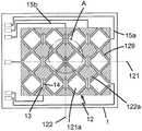
図1、2、3に示すように、本考案タッチパネルのキャパシター感知構造は、底基板1、上パネル2を備える。底基板1或いは上パネル2の表面上には、キャパシター感応層12を備え、接着層3により、底基板1と上パネル2を接着して1枚の板体とする。底基板1と上パネル2は、高い透過率を備える絶縁性薄層ガラス板材で、接着層3は、絶縁性の透明UV接着剤である。 As shown in FIGS. 1, 2, and 3, the capacitor sensing structure of the touch panel of the present invention includes a bottom substrate 1 and an upper panel 2. A capacitor
上パネル2の表面周縁には、金属スパッタリングが形成するカラーフレームカバー21を設置する。これにより、底基板1に設置する金属導電線15a、15bを遮蔽する。底基板1の上表面には、キャパシター感応層12、隔絶層13、ジャンパー導電層14を設置する。キャパシター感応層12は、酸化インジウムスズ材質の透明導電薄膜で、多数の透明X軸ステッチ121と多数の透明Y軸ステッチ122を備える。
X軸ステッチ121は、X軸方向に等距離で敷設し、しかも相互に平行に排列し、Y軸ステッチ122は、Y軸方向に等距離で敷設し、しかも相互に平行に排列する。しかも、X軸ステッチ121とY軸ステッチ122は、碁盤の目式に交差して設置する。各X軸ステッチ121上の各感応ユニット121aは、相互に連通し、各Y軸ステッチ122上の各感応ユニット122aは、相互に連通せず、間隔を開けて排列する。しかも、各X軸ステッチ121とY軸ステッチ122の一端を、底基板1縁の金属導電線15a、15bに電気的に連接し、信号出力端子(図示なし)に連接する。これにより、感応層12上のX軸ステッチ121とY軸ステッチ122の感応信号は、信号出力端子により、後続の信号処理回路に伝送される。A
The
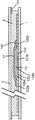
隔絶層13は、複数の絶縁遮蔽面を備え、透過率が高く、しかも誘電係数が約3で、厚さが約1.5μmのポリエステル薄膜材料を使用する。絶縁遮蔽面の遮蔽面積は、少なくとも、Y軸ステッチ122上の、相互に隣接して排列する感応ユニット122a間を通過するX軸ステッチ部分121bを十分覆うことができる面積である。ジャンパー導電層14は、Y軸線方向に沿って設置する複数の導電線を設置する。各導電線は、線径が15μm以下の不透明な金属導体を使用する。しかも、導電線両端縁には、導電線本体より接触面積が大きい電気接続部141を備える。導電線は、隔絶層13の絶縁遮蔽面の上表面に設置され、しかも導電線両端の電気接続部141は、絶縁遮蔽面の外へと伸ばされる。 The
キャパシター感応層12、隔絶層13、ジャンパー導電層14を組み合わせる時には、各隔絶層13の絶縁遮蔽面は、Y軸ステッチ122上の2個の相互に隣接して排列する感応ユニット122aの間に対応設置し、これにより、2個の相互に隣接して排列する感応ユニットの間のX軸ステッチ部分121bを通過し、絶縁して覆う。各ジャンパー導電層14の動電線両端の電気接続部141は、ちょうどY軸ステッチ122上の2個の相互に隣接する感応ユニット122aにそれぞれ電気的に連接し、各Y軸ステッチ122上の各感応ユニット122aは、相互に通電する。こうして、キャパシター感知構造を構成する。本考案実施例中において、キャパシター感応層12上のX軸感応ユニット121aとY軸感応ユニット122aとの設置間隙中にはさらに、ダミーパターン129を補填する。これにより、ダミーパターン129は、X軸感応ユニット121aとY軸感応ユニット122aの縁と間隔129aを保持し、連接しない。通常、間隔129aは約20μm〜50μmである。ダミーパターン129は、X軸感応ユニット121a及びY軸感応ユニット122aと相同の材質、つまり酸化インジウムスズ材質の透明導電薄膜であることが望ましい。こうして、キャパシター感応層12は、より均一な透過率を備える。 When combining the capacitor
上記のように構成するキャパシター感知構造は、X軸ステッチ121と金属導電線15aとの間に、等価キャパシターを形成し、及びY軸ステッチ122と金属導電線15bとの間にも、等価キャパシターを形成する。よって、指或いは導体がタッチパネル表面に接触或いはタッチパネル表面でスライドすると、信号処理回路は、キャパシターの変化により、指或いは導体の接触位置を判断することができる。このように、本考案のタッチパネルは、透明度が高い板体を備えるため、電子製品の表示スクリーン前に配置することができる。これにより、使用者は、スクリーン画面上の指示に従い、指でパネルの必要な位置に軽く触れるだけで、便利に入力操作を行うことができる。 In the capacitor sensing structure configured as described above, an equivalent capacitor is formed between the
前記実施例のキャパシター感知構造は、X軸方向とY軸方向の感応ステッチを、同一層平面上、すなわち同一のキャパシター感応層12に設置する。これにより、各感応ステッチの敷設位置は正確となり、しかも各X軸、Y軸感応ユニット121a、122aの設置間隙中に、ダミーパターン129を補填する。こうして、キャパシター感応層12上の空洞部分の比率を大幅に低下させることができ、外観の平坦度とタッチパネルの透過率の均一性を向上させ、影像がぼやけ、歪むという欠点を改善することができる。ダミーパターン129の設置を利用し、キャパシター感応層12の空洞部分の比率を増加させずに、X軸感応ユニット121aとY軸感応ユニット122aとの間の設置間隙を拡大することができ、これによりノイズキャパシター値低下の目的を達成する。また、前記のように、ダミーパターン129とX軸感応ユニット121a及びY軸感応ユニット122aは、相同の材料を採用し、しかも同一のキャパシター感応層12上に形成する。よって、キャパシター感応層12へのエッチングプロセスにおいて、一度に設置を完成することができるため、加工手順と生産コストを拡大させることはない。 In the capacitor sensing structure of the embodiment, sensitive stitches in the X-axis direction and the Y-axis direction are installed on the same layer plane, that is, on the same capacitor-
図4、5に示すように、本考案第二実施例のタッチパネルのキャパシター感知構造は、前記の第一実施例とほぼ相同である。本考案第二実施例のタッチパネルのキャパシター感知構造は、底基板4、上パネル5を備える。2枚の板の間には、キャパシター感応層42を設置し、接着層6により、2枚の板を接着して1枚の板体とする。本実施例と、前記の第一実施例との差異は、キャパシター感応層42の設置にある。キャパシター感応層42は、底基板4の上表面に設置する。キャパシター感応層42は、酸化インジウムスズ材質の透明導電薄膜で、やや三角形の面積を呈する多数の感知ユニット42aを備える。これにより、各感知ユニット42a間は、相互に等間隔を隔て、交差状に配置される(図4参照)。次に、各感知ユニット42aの一端は、底基板4縁に設置する金属導電線42bに、それぞれ電気的に連接し、信号出力端子(図示なし)に連接する。これにより、各感知ユニット42aの感応信号は、信号出力端子を経て、後続の信号処理回路へと伝送される。 As shown in FIGS. 4 and 5, the capacitor sensing structure of the touch panel of the second embodiment of the present invention is almost the same as that of the first embodiment. The touch panel capacitor sensing structure according to the second embodiment of the present invention includes a
この他、感知ユニット42aの設置間隙中には、ダミーパターン49を補填する。ダミーパターン49は、2個の相互に隣接する感知ユニット42aの縁と、間隔49aをそれぞれ保持し、相互に連接することはない。通常、間隔49aは、約20μm〜50μmである。ダミーパターン49は、各感応ユニット42aと相同の材質、つまり酸化インジウムスズ材質の透明導電薄膜であることが望ましい。こうして、キャパシター感応層42は、より均一な透過率を備え、外観の平坦度とタッチパネルの透過率の均一性を向上させ、影像がぼやけ、歪むという欠点を改善することができる。 In addition, a
上記の本考案名称と内容は、本考案技術内容の説明に用いたのみで、本考案を限定するものではなく、本考案の精神に基づく等価応用或いは変化が可能である。例えば、ダミーパターン129が従来のキャパシター感知構造に応用される時には、X軸ステッチ121とY軸ステッチ122は、それぞれ異なるキャパシター感応層上に設置され、しかも2個のキャパシター感応層の間は、絶縁層により絶縁され、よって、ダミーパターン129は、X軸ステッチ121或いはY軸ステッチ122の感応ユニット121a、122aの周縁部位に敷設され、また、ダミーパターン129は、絶縁層上に敷設され、X軸感応ユニット121aとY軸感応ユニット122aの組合せ間隙の部位に対応するなどが可能である。 The above-mentioned names and contents of the present invention are merely used for explaining the technical contents of the present invention, and are not intended to limit the present invention. Equivalent applications or changes based on the spirit of the present invention are possible. For example, when the
1 底基板
12 キャパシター感応層
121 X軸ステッチ
121a X軸感応ユニット
121b X軸ステッチ部分
122 Y軸ステッチ
122a Y軸感応ユニット
129 ダミーパターン
129a 間隔
13 隔絶層
14 ジャンパー導電層
141 電気接続部
15a、15b 金属導電線
2 上パネル
21 カラーフレームカバー
3 接着層
4 底基板
42 キャパシター感応層
42a 感知ユニット
49 ダミーパターン
5 上パネル
6 接着層DESCRIPTION OF SYMBOLS 1
Claims (10)
Translated fromJapanese前記X、Y軸感応ステッチ上には、相互に連接する多数のキャパシター感応ユニットをそれぞれ設置し、
前記X軸感応ステッチと前記Y軸感応ステッチは、相互に交差し、絶縁状に設置し、これにより前記X、Y軸感応ステッチ上の各キャパシター感応ユニットは、おおよそ碁盤の目状の排列を呈し、タッチパネル上の作動区域内に敷設され、
前記各キャパシター感応ユニットの設置間隙中には、相同の透過率或いは透過率の差異値が6%以下のダミーパターンを敷設して絶縁することを特徴とするタッチパネルのキャパシター感知構造。With multiple transparent X-axis sensitive stitches and Y-axis sensitive stitches,
On the X and Y axis sensitive stitches, a number of capacitor sensitive units connected to each other are installed,
The X-axis sensitive stitch and the Y-axis sensitive stitch cross each other and are installed in an insulating manner, so that each capacitor-sensitive unit on the X- and Y-axis sensitive stitches has an approximately grid-like arrangement. Laid in the working area on the touch panel,
A capacitor sensing structure for a touch panel, wherein a dummy pattern having a homologous transmittance or a transmittance difference value of 6% or less is laid and insulated in the gap between the capacitor-sensitive units.
タッチパネルの作動区域内において、前記キャパシター感応層は、多数の感応ユニットを備え、前記各感応ユニット間は、相互に間隔距離を隔てて、交差状に敷設し、前記感応ユニットの設置間隙中には、相同の透過率或いは透過率の差異値が6%以下のダミーパターンを敷設して絶縁することを特徴とするタッチパネルのキャパシター感知構造。A bottom substrate and an upper panel are provided, a capacitor sensitive layer is installed between the two plates, and the two plates are laminated and bonded together by an adhesive layer to form one plate body,
In the operation area of the touch panel, the capacitor sensitive layer includes a number of sensitive units, and the sensitive units are laid in an intersecting manner with a distance from each other, and in the installation gap of the sensitive units. A touch panel capacitor sensing structure, wherein a dummy pattern having a homologous transmittance or a transmittance difference value of 6% or less is laid and insulated.
Priority Applications (1)
| Application Number | Priority Date | Filing Date | Title |
|---|---|---|---|
| JP2009003462UJP3152611U (en) | 2009-05-26 | 2009-05-26 | Touch panel capacitor sensing structure |
Applications Claiming Priority (1)
| Application Number | Priority Date | Filing Date | Title |
|---|---|---|---|
| JP2009003462UJP3152611U (en) | 2009-05-26 | 2009-05-26 | Touch panel capacitor sensing structure |
Publications (1)
| Publication Number | Publication Date |
|---|---|
| JP3152611Utrue JP3152611U (en) | 2009-08-06 |
Family
ID=54856918
Family Applications (1)
| Application Number | Title | Priority Date | Filing Date |
|---|---|---|---|
| JP2009003462UExpired - Fee RelatedJP3152611U (en) | 2009-05-26 | 2009-05-26 | Touch panel capacitor sensing structure |
Country Status (1)
| Country | Link |
|---|---|
| JP (1) | JP3152611U (en) |
Cited By (7)
| Publication number | Priority date | Publication date | Assignee | Title |
|---|---|---|---|---|
| WO2011081112A1 (en)* | 2009-12-28 | 2011-07-07 | 京セラ株式会社 | Input device and display device provided with same |
| JP2012079134A (en)* | 2010-10-01 | 2012-04-19 | Optrex Corp | Touch panel |
| JP2012128826A (en)* | 2010-12-14 | 2012-07-05 | Samsung Mobile Display Co Ltd | Touch screen panel and method for manufacturing the same |
| JP2013508876A (en)* | 2009-10-28 | 2013-03-07 | エーティーラブ・インコーポレーテッド | Input device and method for detecting contact position of the device |
| CN103246406A (en)* | 2012-02-02 | 2013-08-14 | 群康科技(深圳)有限公司 | Touch control panel and touch control display device including same |
| EP2541381B1 (en)* | 2010-02-24 | 2017-09-06 | Kyocera Corporation | Input device, display device, and portable terminal |
| CN107704135A (en)* | 2017-10-12 | 2018-02-16 | 京东方科技集团股份有限公司 | A kind of contact panel and preparation method thereof, touch control display apparatus |
- 2009
- 2009-05-26JPJP2009003462Upatent/JP3152611U/ennot_activeExpired - Fee Related
Cited By (18)
| Publication number | Priority date | Publication date | Assignee | Title |
|---|---|---|---|---|
| JP2013508876A (en)* | 2009-10-28 | 2013-03-07 | エーティーラブ・インコーポレーテッド | Input device and method for detecting contact position of the device |
| US9182857B2 (en) | 2009-12-28 | 2015-11-10 | Kyocera Corporation | Input device and display device provided with same |
| JP2012033196A (en)* | 2009-12-28 | 2012-02-16 | Kyocera Corp | Input device and display device equipped with the same |
| JP4902023B2 (en)* | 2009-12-28 | 2012-03-21 | 京セラ株式会社 | Input device and display device having the same |
| WO2011081112A1 (en)* | 2009-12-28 | 2011-07-07 | 京セラ株式会社 | Input device and display device provided with same |
| CN102713799B (en)* | 2009-12-28 | 2015-11-25 | 京瓷株式会社 | Input media and possess its display device |
| CN102713799A (en)* | 2009-12-28 | 2012-10-03 | 京瓷株式会社 | Input device and display device provided with same |
| EP2541381B1 (en)* | 2010-02-24 | 2017-09-06 | Kyocera Corporation | Input device, display device, and portable terminal |
| CN102446047A (en)* | 2010-10-01 | 2012-05-09 | 奥博特瑞克斯株式会社 | Touch panel |
| US8581123B2 (en)* | 2010-10-01 | 2013-11-12 | Optrex Corporation | Touch panel |
| CN102446047B (en)* | 2010-10-01 | 2016-01-27 | 奥博特瑞克斯株式会社 | Touch-screen |
| JP2012079134A (en)* | 2010-10-01 | 2012-04-19 | Optrex Corp | Touch panel |
| EP2466432A3 (en)* | 2010-12-14 | 2013-12-04 | Samsung Display Co., Ltd. | Touch screen panel and fabrication method thereof |
| US8922505B2 (en) | 2010-12-14 | 2014-12-30 | Samsung Display Co., Ltd. | Touch screen panel and fabrication method thereof |
| JP2012128826A (en)* | 2010-12-14 | 2012-07-05 | Samsung Mobile Display Co Ltd | Touch screen panel and method for manufacturing the same |
| CN103246406A (en)* | 2012-02-02 | 2013-08-14 | 群康科技(深圳)有限公司 | Touch control panel and touch control display device including same |
| CN107704135A (en)* | 2017-10-12 | 2018-02-16 | 京东方科技集团股份有限公司 | A kind of contact panel and preparation method thereof, touch control display apparatus |
| US10928940B2 (en) | 2017-10-12 | 2021-02-23 | Boe Technology Group Co., Ltd. | Touch panel, method for manufacturing the same, and touch display device |
Similar Documents
| Publication | Publication Date | Title |
|---|---|---|
| US9817501B2 (en) | Touch display panel and manufacturing method thereof | |
| TWI559192B (en) | Touch display device and drivinig method thereof | |
| KR102015937B1 (en) | In-cell touch liquid crystal panel and its array substrate | |
| CN104793792B (en) | Light-transmission type input unit | |
| CN106610749B (en) | Touch display device and driving method thereof | |
| CN103197784B (en) | Contact panel and preparation method thereof | |
| US9086766B2 (en) | Touch panel and touch display panel | |
| CN101620490B (en) | Display unit with touch screen | |
| CN103353818B (en) | A kind of capacitive touch screen and display device | |
| JP3152611U (en) | Touch panel capacitor sensing structure | |
| US20110134075A1 (en) | Touch panel, display, and electronic device | |
| US20100309160A1 (en) | Capacitive sensing assembly of touch panel | |
| CN108255361B (en) | Touch display panel, driving method thereof and touch display device | |
| CN110502152B (en) | Touch panel, touch display panel and touch display device | |
| TW201516779A (en) | Touch panel | |
| TWI485599B (en) | Touch component and flat panel display | |
| TWM455916U (en) | Touch sensing screen | |
| CN201489506U (en) | Capacitive touch panel | |
| JP7007258B2 (en) | Touch screen, display device and touch panel | |
| CN107390914A (en) | Contact panel and display device | |
| CN206991268U (en) | Contact panel and display device | |
| JP6562720B2 (en) | Touch screen, touch panel, display device and electronic device | |
| TWI531950B (en) | Display panel | |
| TWM359752U (en) | Improved capacitor sensing structure of touch panel | |
| CN110275650A (en) | Touch induction device, touch-control display panel and touch-control display panel motherboard |
Legal Events
| Date | Code | Title | Description |
|---|---|---|---|
| R150 | Certificate of patent or registration of utility model | Free format text:JAPANESE INTERMEDIATE CODE: R150 | |
| FPAY | Renewal fee payment (event date is renewal date of database) | Free format text:PAYMENT UNTIL: 20120715 Year of fee payment:3 | |
| LAPS | Cancellation because of no payment of annual fees |