JP2025518583A - Highly conformal metal etching in high aspect ratio semiconductor features - Google Patents
Highly conformal metal etching in high aspect ratio semiconductor featuresDownload PDFInfo
- Publication number
- JP2025518583A JP2025518583AJP2024569256AJP2024569256AJP2025518583AJP 2025518583 AJP2025518583 AJP 2025518583AJP 2024569256 AJP2024569256 AJP 2024569256AJP 2024569256 AJP2024569256 AJP 2024569256AJP 2025518583 AJP2025518583 AJP 2025518583A
- Authority
- JP
- Japan
- Prior art keywords
- molybdenum
- liner
- plasma
- semiconductor processing
- precursor
- Prior art date
- Legal status (The legal status is an assumption and is not a legal conclusion. Google has not performed a legal analysis and makes no representation as to the accuracy of the status listed.)
- Pending
Links
Images


Classifications
- H—ELECTRICITY
- H01—ELECTRIC ELEMENTS
- H01L—SEMICONDUCTOR DEVICES NOT COVERED BY CLASS H10
- H01L21/00—Processes or apparatus adapted for the manufacture or treatment of semiconductor or solid state devices or of parts thereof
- H01L21/02—Manufacture or treatment of semiconductor devices or of parts thereof
- H01L21/02104—Forming layers
- H01L21/02107—Forming insulating materials on a substrate
- H01L21/02109—Forming insulating materials on a substrate characterised by the type of layer, e.g. type of material, porous/non-porous, pre-cursors, mixtures or laminates
- H01L21/02112—Forming insulating materials on a substrate characterised by the type of layer, e.g. type of material, porous/non-porous, pre-cursors, mixtures or laminates characterised by the material of the layer
- H01L21/02172—Forming insulating materials on a substrate characterised by the type of layer, e.g. type of material, porous/non-porous, pre-cursors, mixtures or laminates characterised by the material of the layer the material containing at least one metal element, e.g. metal oxides, metal nitrides, metal oxynitrides or metal carbides
- H01L21/02175—Forming insulating materials on a substrate characterised by the type of layer, e.g. type of material, porous/non-porous, pre-cursors, mixtures or laminates characterised by the material of the layer the material containing at least one metal element, e.g. metal oxides, metal nitrides, metal oxynitrides or metal carbides characterised by the metal
- H—ELECTRICITY
- H01—ELECTRIC ELEMENTS
- H01L—SEMICONDUCTOR DEVICES NOT COVERED BY CLASS H10
- H01L21/00—Processes or apparatus adapted for the manufacture or treatment of semiconductor or solid state devices or of parts thereof
- H01L21/02—Manufacture or treatment of semiconductor devices or of parts thereof
- H01L21/02104—Forming layers
- H01L21/02107—Forming insulating materials on a substrate
- H01L21/02225—Forming insulating materials on a substrate characterised by the process for the formation of the insulating layer
- H01L21/02227—Forming insulating materials on a substrate characterised by the process for the formation of the insulating layer formation by a process other than a deposition process
- H01L21/0223—Forming insulating materials on a substrate characterised by the process for the formation of the insulating layer formation by a process other than a deposition process formation by oxidation, e.g. oxidation of the substrate
- H01L21/02244—Forming insulating materials on a substrate characterised by the process for the formation of the insulating layer formation by a process other than a deposition process formation by oxidation, e.g. oxidation of the substrate of a metallic layer
- H—ELECTRICITY
- H01—ELECTRIC ELEMENTS
- H01L—SEMICONDUCTOR DEVICES NOT COVERED BY CLASS H10
- H01L21/00—Processes or apparatus adapted for the manufacture or treatment of semiconductor or solid state devices or of parts thereof
- H01L21/02—Manufacture or treatment of semiconductor devices or of parts thereof
- H01L21/04—Manufacture or treatment of semiconductor devices or of parts thereof the devices having potential barriers, e.g. a PN junction, depletion layer or carrier concentration layer
- H01L21/18—Manufacture or treatment of semiconductor devices or of parts thereof the devices having potential barriers, e.g. a PN junction, depletion layer or carrier concentration layer the devices having semiconductor bodies comprising elements of Group IV of the Periodic Table or AIIIBV compounds with or without impurities, e.g. doping materials
- H01L21/30—Treatment of semiconductor bodies using processes or apparatus not provided for in groups H01L21/20 - H01L21/26
- H01L21/31—Treatment of semiconductor bodies using processes or apparatus not provided for in groups H01L21/20 - H01L21/26 to form insulating layers thereon, e.g. for masking or by using photolithographic techniques; After treatment of these layers; Selection of materials for these layers
- H01L21/3105—After-treatment
- H01L21/311—Etching the insulating layers by chemical or physical means
- H01L21/31105—Etching inorganic layers
- H01L21/31111—Etching inorganic layers by chemical means
- H01L21/31116—Etching inorganic layers by chemical means by dry-etching
- H01L21/31122—Etching inorganic layers by chemical means by dry-etching of layers not containing Si, e.g. PZT, Al2O3
- H—ELECTRICITY
- H01—ELECTRIC ELEMENTS
- H01L—SEMICONDUCTOR DEVICES NOT COVERED BY CLASS H10
- H01L21/00—Processes or apparatus adapted for the manufacture or treatment of semiconductor or solid state devices or of parts thereof
- H01L21/02—Manufacture or treatment of semiconductor devices or of parts thereof
- H01L21/04—Manufacture or treatment of semiconductor devices or of parts thereof the devices having potential barriers, e.g. a PN junction, depletion layer or carrier concentration layer
- H01L21/18—Manufacture or treatment of semiconductor devices or of parts thereof the devices having potential barriers, e.g. a PN junction, depletion layer or carrier concentration layer the devices having semiconductor bodies comprising elements of Group IV of the Periodic Table or AIIIBV compounds with or without impurities, e.g. doping materials
- H01L21/30—Treatment of semiconductor bodies using processes or apparatus not provided for in groups H01L21/20 - H01L21/26
- H01L21/31—Treatment of semiconductor bodies using processes or apparatus not provided for in groups H01L21/20 - H01L21/26 to form insulating layers thereon, e.g. for masking or by using photolithographic techniques; After treatment of these layers; Selection of materials for these layers
- H01L21/3205—Deposition of non-insulating-, e.g. conductive- or resistive-, layers on insulating layers; After-treatment of these layers
- H01L21/321—After treatment
- H01L21/3213—Physical or chemical etching of the layers, e.g. to produce a patterned layer from a pre-deposited extensive layer
- H01L21/32133—Physical or chemical etching of the layers, e.g. to produce a patterned layer from a pre-deposited extensive layer by chemical means only
- H01L21/32135—Physical or chemical etching of the layers, e.g. to produce a patterned layer from a pre-deposited extensive layer by chemical means only by vapour etching only
- H01L21/32136—Physical or chemical etching of the layers, e.g. to produce a patterned layer from a pre-deposited extensive layer by chemical means only by vapour etching only using plasmas
- H—ELECTRICITY
- H01—ELECTRIC ELEMENTS
- H01L—SEMICONDUCTOR DEVICES NOT COVERED BY CLASS H10
- H01L21/00—Processes or apparatus adapted for the manufacture or treatment of semiconductor or solid state devices or of parts thereof
- H01L21/67—Apparatus specially adapted for handling semiconductor or electric solid state devices during manufacture or treatment thereof; Apparatus specially adapted for handling wafers during manufacture or treatment of semiconductor or electric solid state devices or components ; Apparatus not specifically provided for elsewhere
- H01L21/67005—Apparatus not specifically provided for elsewhere
- H01L21/67011—Apparatus for manufacture or treatment
- H01L21/67155—Apparatus for manufacturing or treating in a plurality of work-stations
- H01L21/67161—Apparatus for manufacturing or treating in a plurality of work-stations characterized by the layout of the process chambers
- H01L21/67167—Apparatus for manufacturing or treating in a plurality of work-stations characterized by the layout of the process chambers surrounding a central transfer chamber
- H—ELECTRICITY
- H10—SEMICONDUCTOR DEVICES; ELECTRIC SOLID-STATE DEVICES NOT OTHERWISE PROVIDED FOR
- H10D—INORGANIC ELECTRIC SEMICONDUCTOR DEVICES
- H10D30/00—Field-effect transistors [FET]
- H10D30/60—Insulated-gate field-effect transistors [IGFET]
- H10D30/67—Thin-film transistors [TFT]
- H10D30/6729—Thin-film transistors [TFT] characterised by the electrodes
- H10D30/673—Thin-film transistors [TFT] characterised by the electrodes characterised by the shapes, relative sizes or dispositions of the gate electrodes
- H10D30/6735—Thin-film transistors [TFT] characterised by the electrodes characterised by the shapes, relative sizes or dispositions of the gate electrodes having gates fully surrounding the channels, e.g. gate-all-around
- H—ELECTRICITY
- H10—SEMICONDUCTOR DEVICES; ELECTRIC SOLID-STATE DEVICES NOT OTHERWISE PROVIDED FOR
- H10D—INORGANIC ELECTRIC SEMICONDUCTOR DEVICES
- H10D30/00—Field-effect transistors [FET]
- H10D30/60—Insulated-gate field-effect transistors [IGFET]
- H10D30/67—Thin-film transistors [TFT]
- H10D30/6729—Thin-film transistors [TFT] characterised by the electrodes
- H10D30/6737—Thin-film transistors [TFT] characterised by the electrodes characterised by the electrode materials
- H10D30/6739—Conductor-insulator-semiconductor electrodes
- H—ELECTRICITY
- H10—SEMICONDUCTOR DEVICES; ELECTRIC SOLID-STATE DEVICES NOT OTHERWISE PROVIDED FOR
- H10D—INORGANIC ELECTRIC SEMICONDUCTOR DEVICES
- H10D64/00—Electrodes of devices having potential barriers
- H10D64/60—Electrodes characterised by their materials
- H10D64/66—Electrodes having a conductor capacitively coupled to a semiconductor by an insulator, e.g. MIS electrodes
- H10D64/665—Electrodes having a conductor capacitively coupled to a semiconductor by an insulator, e.g. MIS electrodes the conductor comprising a layer of elemental metal contacting the insulator, e.g. tungsten or molybdenum
- H—ELECTRICITY
- H10—SEMICONDUCTOR DEVICES; ELECTRIC SOLID-STATE DEVICES NOT OTHERWISE PROVIDED FOR
- H10B—ELECTRONIC MEMORY DEVICES
- H10B43/00—EEPROM devices comprising charge-trapping gate insulators
- H10B43/20—EEPROM devices comprising charge-trapping gate insulators characterised by three-dimensional arrangements, e.g. with cells on different height levels
- H10B43/23—EEPROM devices comprising charge-trapping gate insulators characterised by three-dimensional arrangements, e.g. with cells on different height levels with source and drain on different levels, e.g. with sloping channels
- H10B43/27—EEPROM devices comprising charge-trapping gate insulators characterised by three-dimensional arrangements, e.g. with cells on different height levels with source and drain on different levels, e.g. with sloping channels the channels comprising vertical portions, e.g. U-shaped channels
Landscapes
- Engineering & Computer Science (AREA)
- Physics & Mathematics (AREA)
- Condensed Matter Physics & Semiconductors (AREA)
- General Physics & Mathematics (AREA)
- Manufacturing & Machinery (AREA)
- Computer Hardware Design (AREA)
- Microelectronics & Electronic Packaging (AREA)
- Power Engineering (AREA)
- Chemical & Material Sciences (AREA)
- General Chemical & Material Sciences (AREA)
- Chemical Kinetics & Catalysis (AREA)
- Inorganic Chemistry (AREA)
- Plasma & Fusion (AREA)
- Drying Of Semiconductors (AREA)
- Semiconductor Memories (AREA)
- Non-Volatile Memory (AREA)
Abstract
Translated fromJapanese
Description
Translated fromJapanese 関連出願の相互参照
[0001]本出願は、2022年5月27日出願の米国特許出願第17/827,356号の利益を主張するものであり、その開示内容を全て、参照により本明細書に援用する。 CROSS-REFERENCE TO RELATED APPLICATIONS [0001] This application claims the benefit of U.S. patent application Ser. No. 17/827,356, filed May 27, 2022, the entire disclosure of which is incorporated herein by reference.
[0002]本技術は、半導体プロセス及び機器に関する。より具体的には、本技術は、垂直構造におけるモリブデンの横方向エッチングに関する。[0002] The present technology relates to semiconductor processes and devices. More specifically, the present technology relates to lateral etching of molybdenum in vertical structures.
[0003]集積回路は、基板表面上に複雑にパターニングされた材料層を形成するプロセスによって可能になる。基板上にパターニングされた材料を形成するには、露出した材料を除去するための制御された方法が必要である。化学エッチングは、フォトレジスト中のパターンを下層に転写すること、層を薄くすること、又は表面に既に存在する特徴の横方向寸法を薄くすることを含む、様々な目的のために使用される。多くの場合、ある材料を他の材料よりも速くエッチングして、例えばパターン転写プロセスを容易にするエッチングプロセスが所望される。このようなエッチングプロセスは、第1の材料に対して選択的であると言われる。材料、回路、及びプロセスが多様化した結果、様々な材料に対して選択性を有するエッチングプロセスが開発されてきた。[0003] Integrated circuits are made possible by processes that form intricately patterned layers of materials on a substrate surface. Forming patterned materials on a substrate requires a controlled method for removing exposed material. Chemical etching is used for a variety of purposes, including transferring a pattern in photoresist to an underlying layer, thinning a layer, or thinning the lateral dimensions of features already present on a surface. Often, it is desirable for an etching process to etch one material faster than another, for example to facilitate the pattern transfer process. Such an etching process is said to be selective to the first material. As a result of the diversity of materials, circuits, and processes, etching processes have been developed that are selective to a variety of materials.
[0004]エッチングプロセスは、プロセスで使用される材料に基づいて湿式又は乾式と称され得る。湿式HFエッチングは、他の誘電体及び材料よりも酸化ケイ素を優先的に除去する。しかしながら、湿式プロセスは、幾つかの制約されたトレンチを貫通することが困難な場合があり、またある時には残存材料を変形させる場合もある。基板処理領域内で形成された局所プラズマで生成される乾式エッチングは、より制約の多いトレンチを貫通することができ、壊れやすい残存構造の変形も少ない。しかし、局所プラズマは、放電時に電気アークを発生させるため、基板に損傷を与える可能性がある。[0004] Etch processes can be referred to as wet or dry based on the materials used in the process. Wet HF etches preferentially remove silicon oxide over other dielectrics and materials. However, wet processes can have difficulty penetrating some constrained trenches and can sometimes deform the remaining material. Dry etches, which are produced with a localized plasma formed within the substrate processing region, can penetrate more constrained trenches and cause less deformation of the delicate remaining structures. However, the localized plasma can cause electrical arcs when discharged, which can damage the substrate.
[0005]したがって、高品質のデバイス及び構造を製造するために使用できる改良されたシステム及び方法が必要とされている。これら及び他のニーズは、本技術によって対処される。[0005] Thus, there is a need for improved systems and methods that can be used to manufacture high quality devices and structures. These and other needs are addressed by the present technology.
[0006]例示的な半導体処理方法は、酸素含有前駆体を半導体処理チャンバに供給することを含み得る。基板が、半導体処理チャンバ内に位置決めされ得る。基板は、カラム間に形成されたトレンチと、カラムの少なくとも1つに形成された複数の凹部内のモリブデン含有金属領域とを含み得る。モリブデン含有金属領域の少なくとも2つは、トレンチの側壁の少なくとも一部に形成されたモリブデン含有第1ライナによって接続されていてよい。本方法は、半導体処理チャンバにおいて酸素含有前駆体のプラズマを形成することを含み得る。本方法は、モリブデン含有第1ライナを酸素含有前駆体のプラズマ廃水と接触させることを含み得る。接触により、モリブデン含有第1ライナにモリブデンの酸化部分が形成され得る。本方法は、ハロゲン化前駆体を半導体処理チャンバに供給することを含み得る。本方法は、モリブデンの酸化部分をハロゲン化前駆体のプラズマ廃水と接触させることを含み得る。接触により、モリブデンの酸化部分がトレンチの側壁から除去され得る。[0006] An exemplary semiconductor processing method may include providing an oxygen-containing precursor to a semiconductor processing chamber. A substrate may be positioned within the semiconductor processing chamber. The substrate may include trenches formed between columns and molybdenum-containing metal regions within a plurality of recesses formed in at least one of the columns. At least two of the molybdenum-containing metal regions may be connected by a molybdenum-containing first liner formed on at least a portion of a sidewall of the trench. The method may include forming a plasma of an oxygen-containing precursor in the semiconductor processing chamber. The method may include contacting the molybdenum-containing first liner with an effluent of the oxygen-containing precursor plasma. The contacting may form an oxidized portion of molybdenum on the molybdenum-containing first liner. The method may include providing a halogenated precursor to the semiconductor processing chamber. The method may include contacting the oxidized portion of molybdenum with an effluent of the halogenated precursor plasma. The contacting may remove the oxidized portion of molybdenum from the sidewall of the trench.
[0007]幾つかの実施形態では、酸素含有前駆体は、オゾンであってよい、又はオゾンを含み得る。酸素含有前駆体のプラズマは、約2000W以下のプラズマ出力で形成され得る。モリブデンの酸化部分は、約100Å以下の厚さであることを特徴とし得る。ハロゲン化前駆体は、フッ素含有前駆体であってよい、又はフッ素含有前駆体を含み得る。フッ素含有前駆体は、六フッ化タングステンであってよい、又は六フッ化タングステンを含み得る。モリブデンの酸化部分を形成することにより、トレンチの側壁に沿って形成された酸化モリブデンの層が生成され得る。トレンチの上部領域に近接する酸化モリブデンの層の厚さは、トレンチの下部領域に近接する酸化モリブデンの層とは厚さが約30%以下だけ異なっていてよい。基板は更に、モリブデン含有金属領域及びモリブデン含有第1ライナに隣接して配置された第2ライナを含み得る。本方法は更に、フッ素含有前駆体を半導体処理チャンバに供給することと、フッ素含有プラズマ廃水を生成するために、フッ素含有前駆体のプラズマを形成することと、第2ライナのフッ化部分を形成するために、第2ライナをフッ素含有プラズマ廃水と接触させることと、塩素含有前駆体を半導体処理チャンバに供給することと、塩素含有プラズマ廃水を生成するために、塩素含有前駆体のプラズマを形成することと、第2ライナのフッ化部分を塩素含有プラズマ廃水と接触させることとを含み得る。接触により、第2ライナのフッ化部分が除去され得る。モリブデン含有第1ライナを酸素含有前駆体のプラズマ廃水と接触させることと、モリブデンの酸化部分をハロゲン化前駆体のプラズマ廃水と接触させることとは、少なくとも2回繰り返され得る。[0007] In some embodiments, the oxygen-containing precursor may be or may include ozone. The plasma of the oxygen-containing precursor may be formed at a plasma power of about 2000 W or less. The oxidized portion of the molybdenum may be characterized as being about 100 Å or less in thickness. The halogenated precursor may be or may include a fluorine-containing precursor. The fluorine-containing precursor may be or may include tungsten hexafluoride. The formation of the oxidized portion of the molybdenum may produce a layer of molybdenum oxide formed along the sidewall of the trench. The thickness of the layer of molybdenum oxide adjacent to the upper region of the trench may differ in thickness by about 30% or less from the layer of molybdenum oxide adjacent to the lower region of the trench. The substrate may further include a second liner disposed adjacent to the molybdenum-containing metal region and the molybdenum-containing first liner. The method may further include providing a fluorine-containing precursor to the semiconductor processing chamber, forming a plasma of the fluorine-containing precursor to generate a fluorine-containing plasma effluent, contacting the second liner with the fluorine-containing plasma effluent to form a fluorinated portion of the second liner, providing a chlorine-containing precursor to the semiconductor processing chamber, forming a plasma of the chlorine-containing precursor to generate a chlorine-containing plasma effluent, and contacting the fluorinated portion of the second liner with the chlorine-containing plasma effluent. The contacting may remove the fluorinated portion of the second liner. The contacting of the molybdenum-containing first liner with the plasma effluent of the oxygen-containing precursor and the contacting of the oxidized portion of the molybdenum with the plasma effluent of the halogenated precursor may be repeated at least twice.
[0008]本技術の幾つかの実施形態は、半導体処理方法を包含する。本方法は、i)酸素含有前駆体のプラズマ廃水を形成することを含み得る。本方法は、ii)トレンチの少なくとも1つのカラムによって画定された複数の凹部内に配置された少なくとも2つのモリブデン含有金属領域を接続しているモリブデン含有第1ライナを、酸素含有前駆体のプラズマ廃水と接触させることを含み得る。接触により、モリブデン含有第1ライナにモリブデンの酸化部分が形成され得る。本方法は、iii)フッ素含有前駆体のプラズマ廃水を形成することを含み得る。本方法は、iv)モリブデンの酸化部分をフッ素含有前駆体のプラズマ廃水と接触させることを含み得る。接触により、モリブデンの酸化部分が除去され得る。[0008] Some embodiments of the present technology include a semiconductor processing method. The method may include i) forming an oxygen-containing precursor plasma effluent. The method may include ii) contacting a molybdenum-containing first liner connecting at least two molybdenum-containing metal regions disposed within a plurality of recesses defined by at least one column of trenches with the oxygen-containing precursor plasma effluent. The contacting may form oxidized molybdenum moieties on the molybdenum-containing first liner. The method may include iii) forming a fluorine-containing precursor plasma effluent. The method may include iv) contacting the oxidized molybdenum moieties with the fluorine-containing precursor plasma effluent. The contacting may remove the oxidized molybdenum moieties.
[0009]幾つかの実施形態では、工程i)からiv)は少なくとも2回繰り返され得る。酸素含有前駆体は、オゾンであってよい、又はオゾンを含み得る。フッ素含有前駆体は、六フッ化タングステンであってよい、又は六フッ化タングステンを含み得る。工程i)及びii)の間、温度は約200℃から約600℃に維持され得る。工程i)及びii)の間、圧力は約20Torr以下に維持され得る。本方法は、モリブデンの酸化部分をフッ素含有前駆体のプラズマ廃水と接触させる前に、温度、圧力、又はその両方を調整することを含み得る。第2ライナは、モリブデン含有金属領域及びモリブデン含有第1ライナに隣接して配置され得る。本方法は更に、フッ素含有プラズマ廃水を生成するために、フッ素含有前駆体のプラズマを形成することを含み得る。フッ素含有前駆体は、三フッ化窒素であってよい、又は三フッ化窒素を含み得る。本方法は更に、第2ライナのフッ化部分を形成するために、第2ライナをフッ素含有プラズマ廃水と接触させることと、塩素含有プラズマ廃水を生成するために、塩素含有前駆体のプラズマを形成することとを含み得る。塩素含有前駆体は、三塩化ホウ素であってよい、又は三塩化ホウ素を含み得る。本方法は更に、第2ライナのフッ化部分を塩素含有プラズマ廃水と接触させることを含み得る。接触により、第2ライナのフッ化部分が除去され得る。第2ライナは、酸素含有材料、窒素含有材料、又は酸素-窒素含有材料であってよい、又は酸素含有材料、窒素含有材料、又は酸素-窒素含有材料を含み得る。[0009] In some embodiments, steps i) through iv) may be repeated at least two times. The oxygen-containing precursor may be or may include ozone. The fluorine-containing precursor may be or may include tungsten hexafluoride. During steps i) and ii), the temperature may be maintained at about 200° C. to about 600° C. During steps i) and ii), the pressure may be maintained at about 20 Torr or less. The method may include adjusting the temperature, the pressure, or both before contacting the oxidized portion of the molybdenum with the fluorine-containing precursor plasma effluent. The second liner may be disposed adjacent to the molybdenum-containing metal region and the molybdenum-containing first liner. The method may further include forming a plasma of the fluorine-containing precursor to generate a fluorine-containing plasma effluent. The fluorine-containing precursor may be or may include nitrogen trifluoride. The method may further include contacting the second liner with a fluorine-containing plasma effluent to form a fluorinated portion of the second liner, and forming a plasma of a chlorine-containing precursor to produce a chlorine-containing plasma effluent. The chlorine-containing precursor may be or may include boron trichloride. The method may further include contacting the fluorinated portion of the second liner with the chlorine-containing plasma effluent. The contact may remove the fluorinated portion of the second liner. The second liner may be or may include an oxygen-containing material, a nitrogen-containing material, or an oxygen-nitrogen-containing material.
[0010]本技術の幾つかの実施形態は、半導体構造を包含する。構造は基板を含み得る。構造は、基板を覆うシリコン含有材料を含み得る。基板は、カラム間に形成されたトレンチを含み得る。少なくとも1つのカラムは複数の凹部を画定し得る。構造は、少なくとも1つのカラムに沿って複数の凹部内に延在するライナを含み得る。構造は、複数の凹部内に形成されたモリブデン含有金属領域を含み得る。モリブデン含有金属領域は、ライナによって部分的に取り囲まれていてよい。トレンチの上部領域に近接する凹部内のモリブデン含有金属領域の厚さは、トレンチの下部領域に近接する凹部内のモリブデン含有金属領域と厚さが約30%以下だけ異なっていてよい。[0010] Some embodiments of the present technology include a semiconductor structure. The structure may include a substrate. The structure may include a silicon-containing material overlying the substrate. The substrate may include a trench formed between columns. At least one column may define a plurality of recesses. The structure may include a liner extending along at least one column and into the plurality of recesses. The structure may include a molybdenum-containing metal region formed in the plurality of recesses. The molybdenum-containing metal region may be partially surrounded by the liner. A thickness of the molybdenum-containing metal region in the recess adjacent an upper region of the trench may differ in thickness from a molybdenum-containing metal region in the recess adjacent a lower region of the trench by about 30% or less.
[0011]幾つかの実施形態では、トレンチは、約5μm以上の深さであることを特徴とし得る。モリブデン含有金属領域は、ライナによって3つの側面が取り囲まれていてよい。1つの凹部内のモリブデン含有金属領域は、残りの複数の凹部のモリブデン材料から分離されていてよい。[0011] In some embodiments, the trenches may be characterized as being about 5 μm or greater in depth. The molybdenum-containing metal region may be surrounded on three sides by a liner. The molybdenum-containing metal region in one recess may be isolated from the molybdenum material of the remaining recesses.
[0012]上記技術は、従来のシステム及び技術に優る多数の利点を提供し得る。例えば、本プロセスは、トレンチ内部のモリブデン含有金属の上部から底部までの均一なエッチングを提供し得る。これらの実施形態及び他の実施形態を、それらの多くの利点及び特徴とともに、以下の説明及び添付の図と併せてより詳細に説明する。[0012] The above techniques may provide numerous advantages over conventional systems and techniques. For example, the process may provide uniform etching of the molybdenum-containing metal within the trench from top to bottom. These and other embodiments, along with their many advantages and features, are described in more detail in conjunction with the following description and accompanying figures.
[0013]明細書の残りの部分及び図面を参照することによって、開示された技術の性質及び利点を更に理解することができる。[0013] A further understanding of the nature and advantages of the disclosed technology can be obtained by reference to the remaining portions of the specification and the drawings.
[0022]幾つかの図面は概略図として含まれている。図は例示するためのものであり、縮尺が明記されていない限り、縮尺通りとみなすべきではないことを理解されたい。更に、概略図として、図は理解を助けるために提供されるものであり、現実的な表現と比較して、全ての態様又は情報を含まない場合があり、例示のために誇張された材料を含む場合がある。[0022] Some figures are included as schematics. It should be understood that the figures are for illustrative purposes and should not be considered to scale unless scale is specifically stated. Additionally, as schematics, the figures are provided to aid in understanding and may not include all aspects or information as compared to realistic representations and may include exaggerated material for illustrative purposes.
[0023]添付の図では、同様の構成要素及び/又は特徴には、同じ参照ラベルが付いている場合がある。更に、同じ種類の様々な構成要素は、参照ラベルの後に類似の構成要素を区別する文字を付けることで区別され得る。本明細書で第1の参照ラベルのみを使用した場合、その説明は、文字に関係なく、同じ第1の参照ラベルを有する類似の構成要素のいずれか1つに適用可能である。[0023] In the accompanying figures, similar components and/or features may have the same reference label. Additionally, various components of the same type may be distinguished by following the reference label with a letter that distinguishes the similar components. When only a first reference label is used herein, the description is applicable to any one of the similar components having the same first reference label, regardless of the letter.
[0024]モバイルコンピューティング及びデータセンターの需要の増加により、大容量で高性能なNANDフラッシュ技術の必要性が引き続き高まっている。平面NANDが実用的なスケーリングの限界に近づいているため、3D NANDがメモリデバイス用の2D NANDに取って代わりつつある。3D NAND構造の製造には、2種類以上の材料の交互層を堆積させる必要がある。例えば、幾つかの構造では、他の組み合わせの中でも、積層の総厚が最大数ミクロンである、酸化ケイ素とシリコンの交互層、又は酸化ケイ素と窒化ケイ素の交互層、又は酸化ケイ素とモリブデンの交互層が使用され得る。これらの積層は、トレンチ又はコンタクトホールにエッチングされ得る。更に、これら2つの交互材料の一方、又は少なくともその一部をトレンチから選択的にエッチングしてメモリセルを形成することができる。例えば、酸化ケイ素とシリコン、酸化ケイ素と窒化ケイ素、又は酸化ケイ素とモリブデンの交互層において、少なくとも部分的に除去する必要があるそれぞれの材料は、シリコン、窒化ケイ素、又はモリブデンである。積層を形成する際に、酸化ケイ素とモリブデンの間に形成される酸化アルミニウム、酸化ハフニウム、窒化チタン、窒化タンタル、又は窒化ハフニウムのライナ等のライナ材料を用いた場合は、ライナも除去する必要があり得る。[0024] The increasing demand for mobile computing and data centers continues to drive the need for high capacity and high performance NAND flash technology. As planar NAND approaches its practical scaling limits, 3D NAND is replacing 2D NAND for memory devices. The fabrication of 3D NAND structures requires the deposition of alternating layers of two or more materials. For example, some structures may use alternating layers of silicon oxide and silicon, or alternating layers of silicon oxide and silicon nitride, or alternating layers of silicon oxide and molybdenum, among other combinations, with a total stack thickness of up to several microns. These stacks may be etched into trenches or contact holes. Furthermore, one of these two alternating materials, or at least a portion of it, may be selectively etched from the trench to form memory cells. For example, in the alternating layers of silicon oxide and silicon, silicon oxide and silicon nitride, or silicon oxide and molybdenum, the respective materials that need to be at least partially removed are silicon, silicon nitride, or molybdenum. If a liner material was used in forming the stack, such as an aluminum oxide, hafnium oxide, titanium nitride, tantalum nitride, or hafnium nitride liner formed between silicon oxide and molybdenum, the liner may also need to be removed.
[0025]2D NANDから3D NANDへの移行では、メモリセルを形成するためのエッチング工程等の多くのプロセス工程が垂直工程から水平工程に変更される。更に、3D NAND構造は、形成されるセルの数が増加するにつれて、トレンチ、コンタクトホール、及び他の構造のアスペクト比が高くなり、時には劇的に高くなる。トレンチのアスペクト比が高い(10:1超)ため、一般的な課題として、上述のモリブデン及びライナ材料等の材料を特徴内の上部から底部まで均一にエッチングすることが含まれる。このような用途には、従来から湿式法が使用されているが、湿式エッチングでは、必要又は所望以上に材料がエッチングされる可能性がある。例えば、湿式エッチングは、各層を著しくエッチングし、各層を他のメモリホールまでほぼ完全にエッチングする可能性があり、これにより、セル層を適切又は所望の位置に配置することがより困難になり、構造が弱まり変形が引き起こされる可能性がある。更に、構造のサイズが縮小し続けると、湿式エッチングに使用される流体の表面張力によって、パターンの崩壊又は固着の問題が発生する可能性がある。[0025] In the transition from 2D NAND to 3D NAND, many process steps, such as etching steps to form memory cells, are changed from vertical to horizontal. Furthermore, 3D NAND structures have higher, sometimes dramatically higher, aspect ratios for trenches, contact holes, and other structures as the number of cells formed increases. Due to the high aspect ratios of trenches (greater than 10:1), common challenges include uniformly etching materials, such as the molybdenum and liner materials mentioned above, from top to bottom within the feature. Wet methods are traditionally used for such applications, but wet etching can etch more material than necessary or desired. For example, wet etching can significantly etch each layer, almost completely etching each layer to the other memory holes, which can make it more difficult to place the cell layers in the proper or desired location and can weaken the structure and cause deformation. Furthermore, as the size of the structures continues to decrease, the surface tension of the fluids used in wet etching can cause pattern collapse or sticking issues.
[0026]従来のプラズマ乾式エッチングも、これらの用途のために検討されてきた。プラズマエッチングは異方性及び指向性であり得るため、トレンチの上部及び底部の材料を除去するために使用することができるが、メモリホールの側壁を均一に凹ませることは困難な場合がある。プラズマ乾式エッチングを湿式エッチングと組み合わせて、一方が上部と底部をエッチングし、他方が側壁をエッチングすることができる。しかし、この場合、2つの工程が必要となり、処理時間とコストが増加する。[0026] Conventional plasma dry etching has also been considered for these applications. Because plasma etching can be anisotropic and directional, it can be used to remove material at the top and bottom of the trench, but it can be difficult to uniformly recess the sidewalls of the memory hole. Plasma dry etching can be combined with wet etching, one to etch the top and bottom and the other to etch the sidewalls. However, this requires two steps, increasing processing time and cost.
[0027]本技術は、高アスペクト比のトレンチ内部のモリブデン含有金属及び/又はライナ材料の上部から底部までの均一なエッチングを可能にする乾式エッチングプロセスを実行することによって、これらの問題を克服する。モリブデン含有金属を酸化させることにより、トレンチの上部から底部まで実質的に均一な厚さの酸化物層を形成することができる。その後、ハロゲン化前駆体を供給して、先の酸化工程により酸化した層のみを選択的にエッチングすることにより、トレンチ内部の上部から底部までモリブデン含有金属の均一なエッチングを達成することができる。同様に、ライナ材料をフッ素で処理することにより、トレンチの上部から底部まで実質的に均一な厚さのフッ化層を形成することができる。その後、塩素前駆体を供給して、先の酸化工程によって酸化した層のみを選択的にエッチングすることにより、トレンチ内部の上部から底部までのライナ材料の均一なエッチングを達成することができる。[0027] The present technology overcomes these problems by implementing a dry etching process that allows for uniform etching of the molybdenum-containing metal and/or liner material inside high aspect ratio trenches from top to bottom. By oxidizing the molybdenum-containing metal, an oxide layer of substantially uniform thickness can be formed from the top to bottom of the trench. A halogenated precursor can then be provided to selectively etch only the layer oxidized by the previous oxidation step, thereby achieving uniform etching of the molybdenum-containing metal from top to bottom inside the trench. Similarly, by treating the liner material with fluorine, a fluoride layer of substantially uniform thickness can be formed from the top to bottom of the trench. A chlorine precursor can then be provided to selectively etch only the layer oxidized by the previous oxidation step, thereby achieving uniform etching of the liner material from top to bottom inside the trench.
[0028]残りの開示は、開示された技術を用いた特定のエッチングプロセスを常に特定するが、システム及び方法は、記載したチャンバで行われ得るような堆積及び洗浄プロセスにも等しく適用可能であることが容易に理解されるであろう。従って、本技術は、エッチングプロセス又はチャンバのみでの使用に限定されると考えるべきではない。更に、例示的なチャンバを本技術の基礎を提供するために記載したが、本技術は、記載の工程を可能にし得る事実上あらゆる半導体処理チャンバに適用され得ることを理解されたい。[0028] Although the remaining disclosure will always identify a particular etching process using the disclosed technology, it will be readily understood that the systems and methods are equally applicable to deposition and cleaning processes such as may be performed in the described chambers. Thus, the technology should not be considered limited to use with only etching processes or chambers. Additionally, while an exemplary chamber has been described to provide a foundation for the technology, it should be understood that the technology may be applied to virtually any semiconductor processing chamber capable of enabling the steps described.
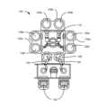
[0029]図1は、実施形態に係る堆積、エッチング、焼成、及び硬化チャンバの処理システム100の一実施形態を示す上面図である。図において、一対の前方開口型統一ポッド(FOUP)102が、ロボットアーム104によって受け入れられ、タンデムセクション109a~cに位置決めされた基板処理チャンバ108a~fのうちの1つの内部に配置される前に低圧保持エリア106内に配置される、様々なサイズの基板を供給する。第2のロボットアーム110が、基板ウエハを保持エリア106から基板処理チャンバ108a~fに往復輸送するのに使用される。各基板処理チャンバ108a~fは、周期的層堆積(CLD)、原子層堆積(ALD)、化学気相堆積(CVD)、物理的気相堆積(PVD)、エッチング、前洗浄、ガス抜き、配向、及び他の基板プロセスに加えて、本明細書に記載の乾式エッチングプロセスを含む多数の基板処理工程を実行するために装備され得る。[0029] FIG. 1 is a top view of one embodiment of a deposition, etch, bake, and cure
[0030]基板処理チャンバ108a~fは、基板ウエハ上に誘電体膜又は金属膜を堆積させる、基板ウエハ上の誘電体膜又は金属膜をアニールする、硬化させる及び/又はエッチングするための1又は複数のシステム構成要素を含み得る。1つの構成では、2つの対の処理チャンバ、例えば、108c~d及び108e~fが、基板上に材料を堆積させるために使用され得、第3の対の処理チャンバ、例えば、108a~bが、堆積させた材料をエッチングするために使用され得る。別の構成では、3対のチャンバすべて、例えば、108a~fが、基板上の誘電体膜又は金属膜をエッチングするように構成され得る。記載のプロセスのいずれか1又は複数は、異なる実施形態で示す製造システムとは別のチャンバ(複数可)で実施され得る。誘電体膜用の堆積、エッチング、アニール、及び硬化チャンバの追加の構成もシステム100により想定されることが理解されよう。[0030] The
[0031]図2Aは、処理チャンバ内に仕切られたプラズマ生成領域を有する例示的なプロセスチャンバシステム200を示す断面図である。例えば、窒化チタン、窒化タンタル、モリブデン、タングステン、銅、コバルト、シリコン、ポリシリコン、酸化ケイ素、窒化ケイ素、酸窒化ケイ素、酸炭化ケイ素等の膜エッチング中に、プロセスガスが、ガス入口アセンブリ205を通して第1のプラズマ領域215に供給され得る。遠隔プラズマシステム(RPS)201が、オプションでシステムに含まれていてよく、次いでガス入口アセンブリ205を通って移動する第1のガスを処理し得る。ガス入口アセンブリ205は、2つ以上の個別のガス供給チャネルを含んでいてよく、第2のチャネル(図示せず)は、RPS201が含まれる場合、RPS201を迂回し得る。2A is a cross-sectional view of an exemplary
[0032]冷却プレート203、フェースプレート217、イオンサプレッサ223、シャワーヘッド225、及びその上に配置された基板255を有するペデスタル265が図示されており、各々が実施形態に従って含まれ得る。ペデスタル265は、基板の温度を制御するために、熱交換流体が流れ、処理工程中に基板又はウエハを加熱及び/又は冷却するように動作し得る熱交換チャネルを有していてよい。アルミニウム、セラミック、又はそれらの組み合わせを含み得る、ペデスタル265のウエハ支持プラッタは、埋設された抵抗加熱素子を使用して、約100℃以下から約600℃以上等の比較的高い温度を達成するために、抵抗加熱され得る。[0032] Shown are a cooling
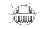
[0033]フェースプレート217は、ピラミッド型、円錐型、又は幅の狭い上部が幅の広い底部まで拡大する他の同様の構造であってよい。フェースプレート217は更に、図示のように平坦であってよく、プロセスガスを分配するために使用される複数の貫通チャネルを含む。プラズマ生成ガス及び/又はプラズマ励起種は、RPS201の使用に応じて、第1のプラズマ領域215内へのより均一な送達のために、フェースプレート217の、図2Bに示す複数の穴を通過し得る。[0033] The
[0034]例示的な構成は、ガス/種がフェースプレート217の穴を通って第1のプラズマ領域215内に流れるように、フェースプレート217によって第1のプラズマ領域215から仕切られたガス供給領域258内に開口したガス入口アセンブリ205を含み得る。構造的及び動作的特徴は、第1のプラズマ領域215からガス供給領域258、ガス入口アセンブリ205、及び流体供給システム210内に戻るプラズマの著しい逆流を防止するように選択され得る。フェースプレート217、又はチャンバの導電性上部、及びシャワーヘッド225は、特徴の間に位置し且つシャワーヘッド225及び/又はイオンサプレッサ223に対してフェースプレート217に交流電位が印加されることを可能にする絶縁リング220と共に図示されている。絶縁リング220は、フェースプレート217とシャワーヘッド225及び/又はイオンサプレッサ223との間に位置決めされていてよく、容量結合プラズマ(CCP)が第1のプラズマ領域に形成されることを可能にする。バッフル(図示せず)が更に、第1のプラズマ領域215に位置していてよく、又は他の方法でガス入口アセンブリ205に結合されていてよく、ガス入口アセンブリ205を通る領域内への流体の流れに影響を与えることができる。[0034] An exemplary configuration may include a
[0035]イオンサプレッサ223は、帯電していない中性種又はラジカル種がイオンサプレッサ223を通過してサプレッサとシャワーヘッドとの間の活性化されたガス送達領域内へ到達することを可能にしながら、イオン荷電種の第1のプラズマ領域215の外への移動を抑制するように構成された、構造全体にわたって複数の開孔を画定するプレート又は他の形状寸法を含み得る。実施形態では、イオンサプレッサ223は、様々な開孔構成を有する多孔プレートを含み得る。これらの帯電していない種は、反応性の低いキャリアガスと共に開孔を通って輸送される反応性の高い種を含み得る。上述したように、孔を通るイオン種の移動は低減し、場合によっては完全に抑制され得る。イオンサプレッサ223を通過するイオン種の量を制御することで、下にあるウエハ基板と接触する混合ガスに対する制御を有利に向上させることができ、その結果、混合ガスの堆積及び/又はエッチング特性の制御を向上させることができる。例えば、混合ガスのイオン濃度の調整により、そのエッチング選択性、例えば、SiNx:SiOxエッチング比、Si:SiOxエッチング比等を大幅に変更することができる。堆積が行われる代替の実施形態では、誘電体材料の共形堆積と流動性堆積のバランスをシフトさせることもできる。[0035] The
[0036]イオンサプレッサ223の複数の開孔は、イオンサプレッサ223を通る活性化ガス、すなわちイオン種、ラジカル種、及び/又は中性種の通過を制御するように構成され得る。例えば、孔のアスペクト比、又は孔の長さに対する孔の直径、及び/又は孔の形状寸法は、イオンサプレッサ223を通過する活性化ガス中のイオン荷電種の流れが低減するように制御され得る。イオンサプレッサ223の孔は、プラズマ励起領域215に面するテーパ部分と、シャワーヘッド225に面する円筒部分とを含み得る。円筒部分は、シャワーヘッド225へ送られるイオン種の流れを制御するような形状及び寸法にすることができる。調整可能な電気バイアスも、サプレッサを通るイオン種の流れを制御する追加手段として、イオンサプレッサ223に印加され得る。[0036] The multiple apertures of the
[0037]イオンサプレッサ223は、プラズマ生成領域から基板に移動するイオン荷電種の量を低減させる又は除去するように機能し得る。帯電していない中性種及びラジカル種は、イオンサプレッサの開口部を通過して基板と反応し得る。基板を取り囲む反応領域におけるイオン荷電種の完全な除去は、実施形態では行われない場合があることに留意すべきである。ある場合には、イオン種は、エッチング及び/又は堆積プロセスを実行するために基板に到達することが意図される。このような場合、イオンサプレッサは、プロセスを支援するレベルで反応領域内のイオン種の濃度を制御する助けとなり得る。[0037] The
[0038]シャワーヘッド225をイオンサプレッサ223と組み合わせることで、第1のプラズマ領域215に存在するプラズマが基板処理領域233内のガスを直接励起することを回避することができる一方で、励起された種がチャンバプラズマ領域215から基板処理領域233内に移動することを可能にすることができる。このようにして、チャンバは、プラズマがエッチングされる基板255に接触するのを防止するように構成され得る。これにより、生成されたプラズマが直接接触すると、損傷を受ける、転位する、又は他の方法で歪む可能性がある、基板上にパターニングされた様々な複雑な構造及び膜を有利に保護することができる。更に、プラズマを基板に接触させる、又は基板レベルに近づけると、酸化種のエッチング速度が上昇する可能性がある。したがって、材料の露出領域が酸化物である場合、プラズマを基板から離して維持することにより、この材料を更に保護することができる。[0038] The
[0039]処理システムは更に、フェースプレート217、イオンサプレッサ223、シャワーヘッド225、及び/又はペデスタル265に電力を供給して、第1のプラズマ領域215又は基板処理領域233にプラズマを生成するために、処理チャンバに電気的に結合された電源240を含み得る。電源は、実行されるプロセスに応じて調整可能な量の電力をチャンバに送達するように構成され得る。このような構成は、実行されるプロセスにおいて調整可能なプラズマを使用することを可能にし得る。オン又はオフの機能が付与されることが多い遠隔プラズマユニットとは異なり、調整可能なプラズマは、プラズマ領域215に特定の量の電力を送達するように構成され得る。この結果、前駆体を特定の方法で解離させて、これらの前駆体によって生成されるエッチングプロファイルを向上させることができるような特定のプラズマ特性を開発することが可能になり得る。[0039] The processing system may further include a
[0040]プラズマは、シャワーヘッド225の上方のチャンバプラズマ領域215又はシャワーヘッド225の下方の基板処理領域233のいずれかで点火され得る。例えばフッ素含有前駆体又は他の前駆体の流入からラジカル前駆体を生成するために、チャンバプラズマ領域215にプラズマが存在していてよい。典型的には無線周波数(RF)範囲の交流電圧を、フェースプレート217等の処理チャンバの導電性上部とシャワーヘッド225及び/又はイオンサプレッサ223との間に印加して、堆積中にチャンバプラズマ領域215においてプラズマを点火することができる。RF電源は、13.56MHzの高いRF周波数を生成し得るが、他の周波数を単独で又は13.56MHzの周波数と組み合わせて生成することもできる。[0040] A plasma can be ignited in either the
[0041]図2Bは、フェースプレート217を介した処理ガス分配に影響を及ぼす特徴を示す詳細図253である。図2A及び図2Bに示すように、フェースプレート217、冷却プレート203、及びガス入口アセンブリ205が交差して、ガス入口アセンブリ205から処理ガスが送達され得るガス供給領域258を画定している。ガスは、ガス供給領域258を充填し、フェースプレート217の開孔259を通って第1のプラズマ領域215に流れることができる。開孔259は、実質的に一方向に流れを導くように構成することができ、これにより、プロセスガスが基板処理領域233に流入し得るが、フェースプレート217を横断した後にガス供給領域258内に逆流するのを部分的に又は完全に防止することができる。2B is a
[0042]処理チャンバセクション200で使用するためのシャワーヘッド225等のガス分配アセンブリは、デュアルチャネルシャワーヘッド(DCSH)と称することができ、図3に記載の実施形態で追加的に詳述される。デュアルチャネルシャワーヘッドは、基板処理領域233の外側においてエッチング液を分離して、処理領域内に送達される前のチャンバ構成要素及び互いとの相互作用を制限することができるエッチングプロセスを提供することができる。[0042] A gas distribution assembly such as the
[0043]シャワーヘッド225は、上部プレート214及び下部プレート216を含み得る。プレートは、互いに結合されてプレート間に領域218を画定し得る。プレートは、上部プレート及び下部プレートを通る第1の流体チャネル219、及び下部プレート216を通る第2の流体チャネル221を提供するように結合されていてよい。形成されたチャネルは、第2の流体チャネル221のみを介して下部プレート216を通る領域218からの流体アクセスを提供するように構成されていてよく、第1の流体チャネル219は、プレートと第2の流体チャネル221との間の領域218から流体的に分離されていてよい。領域218は、シャワーヘッド225の側面を通って流体アクセス可能であってよい。[0043] The
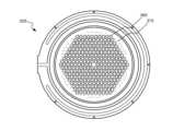
[0044]図3は、実施形態に係る処理チャンバと共に使用するためのシャワーヘッド325の底面図である。シャワーヘッド325は、図2Aに示すシャワーヘッド225に対応し得る。第1の流体チャネル219の図示である貫通孔365は、シャワーヘッド225を通る前駆体の流れを制御し、影響を与えるために、複数の形状及び構成を有していてよい。第2の流体チャネル221の図示である小孔375は、貫通孔365の中でもシャワーヘッドの表面上に実質的に均等に分布していてよく、他の構成よりもシャワーヘッドを出るときの前駆体のより均等な混合を得るのに役立ち得る。3 is a bottom view of a
[0045]前述したチャンバは、エッチング方法を含む例示的な方法を実行するために使用され得る。本技術の実施形態に係る方法400における例示的な工程を示す図4を参照する。方法400の第1の工程の前に、基板を1又は複数の方法で処理することができる。例えば、基板上にインターポリ誘電体(IPD)層を形成することができる。IPD層は、任意の数の材料を含んでいてよく、プレースホルダ材料と誘電体材料との交互の層を含んでいてよい。実施形態では、誘電体材料は酸化ケイ素であってよい、又は酸化ケイ素を含んでいてよく、プレースホルダ材料は窒化ケイ素であってよい、又は窒化ケイ素を含んでいてよい。1又は複数のトレンチ又はメモリホールが、積層されたIPD層を貫通して形成されていてよく、3D NAND構造に更に処理されるために、トレンチがIPD層を縦列に分割していてよい。例えば、プレースホルダ材料の層又はその少なくとも一部を除去して、縦列の側壁に沿って横方向凹部を形成することができる。次に、横方向凹部をゲート誘電体でライニングし、ゲート金属で充填して3D NANDのゲート構造を形成することができる。実施形態では、ゲート誘電体は、酸化アルミニウムであってよい、又は酸化アルミニウムを含んでいてよく、ゲート金属は、モリブデン、タングステン、コバルト、又は任意の他の導電性材料であってよい、又はこれらを含んでいてよい。[0045] The chambers described above may be used to perform exemplary methods, including etching methods. See FIG. 4, which illustrates exemplary steps in a
[0046]ゲート金属とゲート誘電体との間、及び/又はゲート金属とIPD層の誘電体材料との間に、ゲート金属バリアを形成することもできる。ゲート金属バリアは、ハフニウム、チタン、タンタル、酸化アルミニウム、酸化ハフニウム、窒化ハフニウム、窒化チタン、窒化タンタル等の金属、金属酸化物、又は金属窒化物であってよい、又はそれらを含んでいてよい。通常、ゲート金属は、IPD層の誘電体材料の層間に介在する金属領域を形成するために、トレンチ内及びトレンチの側壁に沿って形成された横方向凹部内に上部から底部まで堆積され得る。堆積中、ゲート金属を横方向凹部の外側にも堆積させて、トレンチの側壁の一部をライニングし、金属領域を接続することができる。このようなライニング又は接続金属は、金属領域を互いに分離するように除去して、セル間のクロストーク又は短絡を防止することができる。工程の一部又は全部は、前述したように、トレンチの側壁をライニングしている接続金属を除去するために方法400の工程が実行される1又は複数のチャンバを含み得るチャンバ又はシステムツールで実行することができる、又は同じシステムツール上の異なるチャンバで実行することができる。[0046] A gate metal barrier may also be formed between the gate metal and the gate dielectric and/or between the gate metal and the dielectric material of the IPD layer. The gate metal barrier may be or may include a metal, metal oxide, or metal nitride, such as hafnium, titanium, tantalum, aluminum oxide, hafnium oxide, hafnium nitride, titanium nitride, tantalum nitride, etc. Typically, the gate metal may be deposited from top to bottom in the trench and in the lateral recesses formed along the sidewalls of the trench to form metal regions interposed between the layers of dielectric material of the IPD layer. During deposition, the gate metal may also be deposited outside the lateral recesses to line a portion of the sidewalls of the trench and connect the metal regions. Such lining or connecting metal may be removed to separate the metal regions from each other to prevent crosstalk or shorts between cells. Some or all of the steps may be performed in a chamber or system tool, which may include one or more chambers in which steps of
[0047]次に、方法400の工程を、図5A~図5Dの概略図と併せて説明する。図5Aは、3D NAND構造の製造において更に開発される処理された構造500の一部を図示している。処理された構造500は、基板515を覆う積層の隣接する垂直カラム510間に形成された1又は複数のトレンチ505(1つのみ図示)を含み得る。積層は、誘電体層と、各メモリセルのゲート構造を形成するために誘電体層間に介在する金属層又は金属領域とを含み得る。誘電体層は、図5Aに示すように、酸化ケイ素層520等の酸化物層を含み得る。金属領域は、図5Aに示すように、モリブデン領域525等のモリブデン領域を含み得る。モリブデン領域525は、プレースホルダ材料の層又はその一部を除去することによって形成された横方向凹部527にモリブデンを堆積させることによって形成され得る。モリブデン領域525を形成するときに、モリブデンをまた、トレンチ505の上部530、底部535、及び側壁540に沿って堆積させることができ、モリブデン領域525の2つ以上を接続することができる。処理された構造500は、ゲート金属バリア及びゲート誘電体等の1又は複数のバリア材料又はライナ材料を更に含んでいてよく、これらをまとめて又は個別に第2ライナと称することができる。ゲート金属バリアは、図5Aに示すように、酸化物又は窒化物バリア545(例えば、酸化アルミニウム、酸化ハフニウム、窒化チタン、窒化タンタル、窒化ハフニウム等)等の、酸化物、窒化物、又は酸素-窒素バリアを含み得る。第2ライナとも称される酸化物又は窒化物バリアを、モリブデン含有金属領域及び/又はモリブデン含有第1ライナに隣接して配置することができる。ゲート誘電体は、図5Aに示すように、ゲート誘電体550(例えば、酸化アルミニウム)等の酸化アルミニウムゲート誘電体を含み得る。酸化物又は窒化物バリア545は、金属含有酸化物又は窒化物材料であってよい。処理された構造500は、酸化物又は窒化物バリア545及びゲート誘電体550の一方のみを含み得ることが想定される。[0047] The steps of
[0048]図5Aに4層の誘電体材料及び4層の金属のみを図示したが、処理された構造500は、最大約10以上、約15以上、約20以上、約25以上、約30以上、約35以上、約40以上、約45以上、約50以上、約55以上、約60以上、約65以上、約70以上、約80以上、約90以上、約100以上、又はそれ以上の材料の層等の、各材料の任意の数の層を含み得る。これにより、数百ナノメートル、又は数十ナノメートル、又はそれ未満の幅を有し、その高さが数ミクロン、又は数十ミクロン、又はそれを超えるトレンチが形成され得る。その結果、トレンチのアスペクト比又は高さと幅の比は、20:1超、50:1超、75:1超、100:1超、又はそれを超えるものとなり得る。実施形態では、トレンチは、約200nm以下、又はそれ未満の幅、及び/又は約5ミクロン以上の深さを特徴とし得る。上述したように、トレンチの底部及び/又は側壁に形成されたモリブデン含有材料は、モリブデン領域を互いから分離するために除去され得る。トレンチのアスペクト比が高いため、従来の乾式エッチング法では、上部と底部の充填比が1:1とも言われる、トレンチの上部から底部までのモリブデン金属を均一にエッチングすることは困難である。以下により詳細に説明するように、本技術の幾つかの実施形態に係る方法400は、上部から底部までの充填を改善し、トレンチ内部のモリブデン金属の実質的に均一なエッチングを実現することができる。[0048] Although only four layers of dielectric material and four layers of metal are illustrated in FIG. 5A, the processed
[0049]図5Bに示すように、方法400は、トレンチ505の上部530、底部535、及び/又は側壁540上に形成されたモリブデン含有第1ライナを最初に酸化させて、トレンチ505の内部及び上部に酸化モリブデン555を形成することを含み得る。幾つかの実施形態では、モリブデンを酸化させるために、基板515を、図2Aを参照して上述した処理チャンバシステム200の基板処理領域233等の、半導体処理チャンバの処理領域内に位置決めし得る。処理領域内に位置決めしたら、方法400を、工程405において、酸素含有前駆体を半導体処理チャンバの遠隔プラズマ領域に供給することによって開始することができる。遠隔プラズマ領域は、処理領域に流体的に結合していてよいが、基板515上の露出した構造又は材料に損傷を与える可能性のある基板レベルでのプラズマを制限するために物理的に仕切られていてよい。幾つかの実施形態では、遠隔プラズマ領域は、上述したRPS201等の、半導体処理チャンバへの入口に流体的に結合された遠隔プラズマシステム(RPS)を含み得る。幾つかの実施形態では、遠隔プラズマ領域は、フェースプレート217とシャワーヘッド225及び/又はイオンサプレッサ223とを容量結合させることによって形成された第1のプラズマ領域215等の容量結合プラズマ(CCP)領域を含んでいてよく、CCP領域は、シャワーヘッド225及び/又はイオンサプレッサ223等のその電極の1つによって処理領域から物理的に分離されていてよい。方法400は更に、工程410において酸素含有プラズマ廃水を生成するために、酸素含有前駆体のプラズマを形成することと、工程415において酸素含有プラズマ廃水を処理領域に供給することとを含み得る。工程420において、酸化モリブデン555をトレンチ505の内部及び上部に形成するために、モリブデン領域525を接続しているモリブデンを、図5Bに示すように、酸化させることができる。[0049] As shown in FIG. 5B, the
[0050]酸素含有前駆体は、様々な流体を含んでいてよく、原子酸素、分子酸素(O2)、N2O、NO、NO2、CO2、オゾン(O3)、又は同様に酸化工程を実行することができる任意の他の酸素含有前駆体のうちの1又は複数を含み得る。酸素含有前駆体は、少なくとも1000sccmの速度で供給することができ、実施形態では、約2000sccm以上、約3000sccm以上、約4000sccm以上、約5000sccm以上、約6000sccm以上、約7000sccm以上、約8000sccm以上、約9000sccm以上、又はそれを超える速度で供給することができる。幾つかの実施形態では、酸素含有前駆体の流れはパルス状であってよい。酸素含有前駆体の流れは、実施形態では、約60秒以下の時間にわたってパルス化されていてよく、約55秒以下の時間、約50秒以下の時間、約45秒以下の時間、約40秒以下の時間、約35秒以下の時間、約30秒以下の時間、約25秒以下の時間、約20秒以下の時間、約15秒以下の時間、約10秒以下の時間、約5秒以下の時間にわたってパルス化されていてよい。 [0050] The oxygen-containing precursor may comprise a variety of fluids and may include one or more of atomic oxygen, molecular oxygen (O2 ),N2O , NO,NO2 ,CO2 , ozone (O3 ), or any other oxygen-containing precursor that can similarly perform an oxidation process. The oxygen-containing precursor may be delivered at a rate of at least 1000 sccm, and in embodiments, at a rate of about 2000 sccm or more, about 3000 sccm or more, about 4000 sccm or more, about 5000 sccm or more, about 6000 sccm or more, about 7000 sccm or more, about 8000 sccm or more, about 9000 sccm or more, or more. In some embodiments, the flow of the oxygen-containing precursor may be pulsed. The flow of the oxygen-containing precursor, in embodiments, may be pulsed for a time period of about 60 seconds or less, about 55 seconds or less, about 50 seconds or less, about 45 seconds or less, about 40 seconds or less, about 35 seconds or less, about 30 seconds or less, about 25 seconds or less, about 20 seconds or less, about 15 seconds or less, about 10 seconds or less, or about 5 seconds or less.
[0051]酸素含有前駆体が流れている間、酸素含有前駆体の流量は、モリブデン領域を接続しているモリブデンを完全に酸化させるために、トレンチの上部から底部まで十分な酸素、又は十分な酸素を超える酸素が存在し得るように、比較的高いレベルに維持され得る。幾つかの実施形態では、十分な酸素を供給することにより、トレンチ内部に形成される酸化モリブデン層の厚さの均一性を更に向上させることができる。この均一性は一部には、適切な又は清浄なモリブデン表面で生じる初期の急速な酸化によって生じる可能性がある。具体的には、方法400は、モリブデンがトレンチ内部に堆積した後、大気に曝露される前に実行することができる。適切なモリブデン表面の酸化速度は、十分な酸素供給があれば十分急速なものとなり、トレンチの底部に近接するモリブデンを、トレンチの上部に近接する酸化したモリブデンの厚さと実質的に同じであり得る厚さまでほぼ同時に酸化させることができる。酸化が金属の表面に浸透するにつれて、酸化速度は劇的に低下する可能性があり、幾つかの実施形態では、チャンバ条件において最小限の酸化しか継続し得ない又はそれ以上の酸化が継続し得ない飽和深さに達する可能性がある。したがって、トレンチの上部に近接した位置での滞留時間が長いにもかかわらず、トレンチの底部等の、プラズマ廃水の初期接触から離れたところに位置する金属を、トレンチの上部と同様又は実質的に同様の深さまで酸化させることができる。[0051] During the flow of the oxygen-containing precursor, the flow rate of the oxygen-containing precursor may be maintained at a relatively high level so that there may be enough oxygen, or more than enough oxygen, from the top to the bottom of the trench to completely oxidize the molybdenum connecting the molybdenum regions. In some embodiments, providing sufficient oxygen may further improve the uniformity of the thickness of the molybdenum oxide layer formed inside the trench. This uniformity may occur in part due to the initial rapid oxidation that occurs on a good or clean molybdenum surface. In particular, the
[0052]幾つかの実施形態では、初期の急速酸化は、酸化プロセスが遅くなる前に、約10Å以上、約15Å以上、約20Å以上、約25Å以上、約30Å以上、約35Å以上、約40Å以上、約50Å以上、約60Å以上、約70Å以上、約80Å以上、約90Å以上、約100Å以上、又はそれを超える厚さを有する酸化モリブデン層を生成し得る。幾つかの実施形態では、処理条件を調整することにより、初期の急速酸化によって、約100Å以下、約90Å以下、約80Å以下、約70Å以下、約60Å以下、約50Å以下、約40Å以下、又はそれ未満の厚さを有する酸化モリブデン層が生成され得る。トレンチの上部領域に近接する酸化モリブデン層の厚さは、実施形態では、トレンチの下部領域に近接する酸化モリブデン層の厚さとは、約30%以下、約25%以下、約20%以下、約15%以下、約10%以下、約5%以下、約3%以下、約1%以下、又はそれ未満だけ異なっていてよい。したがって、図5Bに示すように、約1.3:1以下、約1.25:1以下、約1.2:1以下、約1.15:1以下、約1.1:1以下、約1.05:1以下、又は実質的もしくは本質的に1:1の比率のモリブデン酸化の上部と底部の充填比が、方法400を用いて達成され得る。初期の急速酸化を考慮すると、酸素含有前駆体の流れは、約15分以下、約10分以下、約5分以下、約3分以下、約2分以下、約90秒以下、約60秒以下、約50秒以下、約40秒以下、約30秒以下、約25秒以下、約20秒以下、約15秒以下、約10秒以下、約5秒以下、又はそれ未満の時間にわたって維持され得る。幾つかの実施形態では、十分な酸化を促進するために、酸素含有前駆体の流れは、約5秒以上、約10秒以上、約30秒以上、約1分以上、約5分以上、約10分以上、約15分以上、又はそれを超える時間にわたって維持され得る。したがって、幾つかの実施形態では、酸素含有前駆体の流れは、約5秒から約15分、約30秒から約10分、約1分から約5分、又は任意の他の適切な時間にわたって維持され得る。[0052] In some embodiments, the initial rapid oxidation may produce a molybdenum oxide layer having a thickness of about 10 Å or more, about 15 Å or more, about 20 Å or more, about 25 Å or more, about 30 Å or more, about 35 Å or more, about 40 Å or more, about 50 Å or more, about 60 Å or more, about 70 Å or more, about 80 Å or more, about 90 Å or more, about 100 Å or more, or more, before the oxidation process slows. In some embodiments, by adjusting the process conditions, the initial rapid oxidation may produce a molybdenum oxide layer having a thickness of about 100 Å or less, about 90 Å or less, about 80 Å or less, about 70 Å or less, about 60 Å or less, about 50 Å or less, about 40 Å or less, or less. The thickness of the molybdenum oxide layer proximate the upper region of the trench may, in embodiments, differ from the thickness of the molybdenum oxide layer proximate the lower region of the trench by about 30% or less, about 25% or less, about 20% or less, about 15% or less, about 10% or less, about 5% or less, about 3% or less, about 1% or less, or less. Thus, as shown in FIG. 5B, top to bottom molybdenum oxide fill ratios of about 1.3:1 or less, about 1.25:1 or less, about 1.2:1 or less, about 1.15:1 or less, about 1.1:1 or less, about 1.05:1 or less, or a ratio of substantially or essentially 1:1 may be achieved using
[0053]酸素含有前駆体はまた、窒素、ヘリウム、アルゴン、又は他の希ガス、不活性ガス、又は有用な前駆体を含み得る、任意の数のキャリアガスを含み得る。キャリアガスは、トレンチ内部の酸素含有前駆体の均一な分布を向上させるために使用され得、これにより、酸化工程420のための上部から底部の充填が更に向上し得る。幾つかの実施形態では、キャリアガスの流量は、酸素含有前駆体の流量の約50%以下に維持され得る、又は酸素含有前駆体の流量の約40%以下、約30%以下、約20%以下、約10%以下、約5%以下、約3%以下、又は約1%以下、又はそれ未満であってよい。酸素含有前駆体の成分の組成及び/又はそれぞれの流量を調整することにより、トレンチ内部の酸素含有プラズマ廃水の均一な送達が達成され得、それにより、トレンチの上部から底部までのモリブデン酸化の均一性が更に改善される。[0053] The oxygen-containing precursor may also include any number of carrier gases, which may include nitrogen, helium, argon, or other noble gases, inert gases, or useful precursors. The carrier gas may be used to improve uniform distribution of the oxygen-containing precursor inside the trench, which may further improve top-to-bottom filling for the
[0054]プラズマ出力、工程温度、工程圧力等の他のプロセス条件も、トレンチの上部から底部までのモリブデン酸化の均一性に影響を与える可能性がある。酸素含有プラズマが遠隔プラズマシステムにおいて形成され得る実施形態では、プラズマ出力は、酸素含有前駆体の解離を促進するために、約2000W以下であってよく、約1500W以下、約1000W以下、約750W以下、約500W以下、約250W以下、又はそれ未満であってよい。酸素含有プラズマが半導体処理チャンバの容量結合プラズマ(CCP)領域で形成され得る実施形態では、基板上の構造への損傷を防止するように、より低いプラズマ出力が用いられ得る。CCP領域におけるプラズマ出力は、少なくとも50Wであってよく、実施形態では、約100W以上、約150W以上、約200W以上、約250W以上、約300W以上、約350W以上、約400W以上、約450W以上、約500W以上、又はそれを超えるものであってよい。CCP領域におけるプラズマ出力は、約2500W以下であってよく、約2000W以下、約1500W以下、約1000W以下、約750W以下、約500W以下、約250W以下、又はそれ未満であってよい。[0054] Other process conditions such as plasma power, process temperature, process pressure, etc. may also affect the uniformity of molybdenum oxidation from the top to the bottom of the trench. In embodiments where the oxygen-containing plasma may be formed in a remote plasma system, the plasma power may be about 2000 W or less, about 1500 W or less, about 1000 W or less, about 750 W or less, about 500 W or less, about 250 W or less, or less, to promote dissociation of the oxygen-containing precursor. In embodiments where the oxygen-containing plasma may be formed in a capacitively coupled plasma (CCP) region of a semiconductor processing chamber, lower plasma power may be used to prevent damage to structures on the substrate. The plasma power in the CCP region may be at least 50 W, and in embodiments may be about 100 W or more, about 150 W or more, about 200 W or more, about 250 W or more, about 300 W or more, about 350 W or more, about 400 W or more, about 450 W or more, about 500 W or more, or more. The plasma power in the CCP region may be about 2500 W or less, about 2000 W or less, about 1500 W or less, about 1000 W or less, about 750 W or less, about 500 W or less, about 250 W or less, or less.
[0055]急速酸化を促進し、それによって上部から底部までの充填を改善するために、処理チャンバ内又は基板レベルの温度は、実施形態では約200℃から約600℃に維持され得る。温度は、約200℃以上に維持され得、約250℃以上、約300℃以上、約350℃以上、約400℃以上、約450℃以上、約500℃以上、約550℃以上、約600℃以上、又はそれより高く維持され得る。酸化工程420中に維持され得る温度が高いほど、モリブデンはより速く酸化し得、酸化モリブデン層の厚さはより均一であり得る。酸化工程420中、処理チャンバ内の圧力は、実施形態では、約20Torr以下に維持され得る。圧力は、約15Torr以下に維持され得、約10Torr以下、約5Torr以下、約4Torr以下、約3Torr以下、約2Torr以下、約1Torr以下、約100mTorr以下又はそれ未満に維持され得る。実施形態では、圧力は約500mTorrから約10Torrに維持され得る。処理チャンバ内部の圧力を比較的低く維持することにより、酸素含有プラズマ廃水のトレンチ内への分配が促進され、その結果、上述したように、上部から底部まで均一な酸化がもたらされ得る。[0055] To promote rapid oxidation and thereby improve top-to-bottom filling, the temperature in the process chamber or at the substrate level may be maintained at about 200°C to about 600°C in embodiments. The temperature may be maintained at about 200°C or higher, about 250°C or higher, about 300°C or higher, about 350°C or higher, about 400°C or higher, about 450°C or higher, about 500°C or higher, about 550°C or higher, about 600°C or higher, or higher. The higher the temperature that may be maintained during the
[0056]図4に、酸素含有プラズマを用いてモリブデン及び/又はライナ材料を酸化させることを図示したが、非プラズマプロセスを用いることもできる。したがって、幾つかの実施形態では、方法400の工程410及び415は省略することができる。原子酸素、分子酸素(O2)、オゾン(O3)、又は他の酸素含有前駆体のうちの1又は複数等の酸素含有前駆体を処理領域に供給して、モリブデン及び/又はライナ材料を酸化させることができる。モリブデン及び/又はライナ材料を酸化させるために分子酸素が用いられ得る実施形態では、処理チャンバ内又は基板レベルの温度は、約250℃から約600℃に維持され得る。温度は、約250℃以上に維持され得、約300℃以上、約350℃以上、約400℃以上、約450℃以上、約500℃以上、約550℃以上、約600℃以上、又はそれより高く維持され得る。モリブデン及び/又はライナ材料の酸化にオゾンが用いられ得る実施形態では、オゾンは、処理チャンバの入口に流体的に結合され得るオゾン発生器を使用して生成され得る。 [0056] Although Figure 4 illustrates the use of an oxygen-containing plasma to oxidize the molybdenum and/or liner material, non-plasma processes can also be used. Thus, in some embodiments,
[0057]幾つかの実施形態では、酸素含有前駆体の十分な供給及び適切な工程条件下で、トレンチ505の側壁に形成された実質的に全てのモリブデン含有第1ライナを酸化させることができ、図5Cに示すように、トレンチ505の横方向凹部527内部のモリブデン領域525の一部も酸化させることができる。横方向凹部527内部のモリブデンをわずかにエッチングすることにより、方法400の後続の工程において酸化したモリブデンを除去する際に、モリブデン領域525を確実に分離させることができる。図5Cにも示すように、酸化工程420中、酸化物又は窒化物バリア545が窒化物を含む場合、酸化物又は窒化物バリア545の酸化モリブデン555に接触する部分も酸化して、窒化物バリア560の酸化部分が形成され得る。[0057] In some embodiments, with a sufficient supply of oxygen-containing precursor and appropriate process conditions, substantially all of the molybdenum-containing first liner formed on the sidewall of
[0058]幾つかの実施形態では、トレンチ505の側壁540の少なくとも一部上に形成されたモリブデン含有第1ライナが、モリブデン領域525の一部と共に酸化したら、酸素含有前駆体の流れを停止することによって酸化工程420を一時停止することができる。実施形態では、残留プラズマ廃水は、工程425の前にパージされ得る。工程425において、ハロゲン化前駆体を処理領域に供給することができる。ハロゲン化前駆体は、酸化モリブデン及び/又はライナ材料と相互作用し得る金属ハロゲン化物又は他のハロゲン含有前駆体を含み得る。実施形態では、ハロゲン化前駆体は、塩素含有前駆体又はフッ素含有前駆体であってよい、又は塩素含有前駆体又はフッ素含有前駆体を含み得る。ハロゲン化前駆体は、五塩化タングステン等の塩化タングステン、及び/又は六フッ化タングステン等のフッ化タングステンを含み得る。工程430において、ハロゲン化前駆体は、酸化モリブデン555を修飾し、相互作用して、揮発性物質を形成することができ、次いで、チャンバから除去され得る。ハロゲン化前駆体と酸化モリブデン555から形成された揮発性物質には、オキシ塩化モリブデン及び/又はオキシフッ化モリブデンが含まれる場合がある。酸化モリブデン555がハロゲン化前駆体によって除去されると、上述したように酸化され得る下層の酸化物又は窒化物バリア545が露出し得る。酸化物又は窒化物バリア545の露出部分は、最初に酸化されることなくハロゲン化前駆体と相互作用し得るが、酸化物又は窒化物バリア545が酸化して窒化物バリア560の酸化部分が形成されると、エッチング速度が向上し得る。[0058] In some embodiments, the
[0059]ハロゲン化前駆体によるライナ材料の酸化部分のエッチング速度は、ハロゲン化前駆体によるライナ材料の非酸化部分のエッチング速度の少なくとも約2倍、約3倍、約4倍、約5倍、約6倍、約7倍、約8倍、又はそれを超えるものであり得る。ハロゲン化前駆体及び窒化物バリア560の酸化部分から形成される揮発性物質は、金属オキシ塩化物、金属オキシフッ化物、金属四塩化物等の金属塩化物、及び/又は金属四フッ化物等の金属フッ化物を含み得る。ハロゲン化前駆体は、工程425中に、約15秒から約5分の時間にわたって送達され得る。ハロゲン化前駆体の送達は、酸化モリブデン555及び/又は窒化物バリア560の酸化部分の完全な除去を確実にするために、実施形態では、少なくとも約30秒、1分、1.5分、2分、2.5分、3分、3.5分、4分、4.5分、5分、又はそれより長く継続することができる。図5Dに示すように、酸化モリブデン555及び/又は窒化物バリア560の酸化部分は、エッチング工程430の完了時に除去することができ、モリブデン領域525を互いから分離させることができる。[0059] The etch rate of the oxidized portion of the liner material by the halogenated precursor may be at least about 2 times, about 3 times, about 4 times, about 5 times, about 6 times, about 7 times, about 8 times, or more than the etch rate of the non-oxidized portion of the liner material by the halogenated precursor. The volatiles formed from the halogenated precursor and the oxidized portion of the
[0060]エッチング工程430において、酸化モリブデン555及び窒化物バリア560の酸化部分を、モリブデン領域525、モリブデン領域525とゲート誘電体550との間に介在する酸化物又は窒化物バリア545、及びゲート誘電体550を含む、基板上の他の材料及び構造に対して選択的に除去することができる。特定の理論に束縛されるものではないが、ゲート誘電体中の酸素と金属との間の結合が、ゲート誘電体中の酸素とモリブデンとの間の結合及び/又は酸素と金属との間の結合よりも強い場合があるため、また一部において、反応性生成物がある場合には、エッチング工程430の工程条件下で実質的に不揮発性であり得る金属フッ化物及び/又は金属オキシフッ化物を含む場合があるため、ハロゲン化前駆体によってゲート誘電体550がエッチングされない場合がある。図5Dには明示的に図示していないが、方法400は、酸化モリブデン555及び窒化物バリア560の酸化部分を、酸化ケイ素層520等の酸化ケイ素に対して、及びメモリセルの電荷トラップ層を形成する可能性のある窒化ケイ素に対して、選択的に除去することもできる。[0060] In the
[0061]ハロゲン化前駆体が、酸化モリブデン555及び/又は窒化物バリア560の酸化部分のみを選択的にエッチングすることができ、酸化工程420により、上述したように、実質的に均一な上部から底部までの充填がもたらされ得るため、エッチング工程430もまた、実質的に均一な上部から底部までの充填をもたらすことができる。トレンチの上部領域に近接するモリブデン層のエッチングされた厚さは、実施形態では、方法400によってエッチングされたトレンチの下部領域に近接するモリブデン層のエッチングされた厚さとは、約30%以下、約25%以下、約20%以下、約15%以下、約10%以下、約5%以下、約3%以下、約1%以下、又はそれ未満だけ異なっていてよい。したがって、約1.3:1以下、約1.25:1以下、約1.2:1以下、約1.15:1以下、約1.1:1以下、約1.05:1以下、又は実質的もしくは本質的に1:1の比率のモリブデンエッチングの上部と底部の充填比が、方法400を用いて達成され得る。このような上部から底部までの均一な充填により、トレンチ505の横方向凹部527内部のモリブデン領域525の過剰エッチングを防止又は制限することができ、トレンチ505の側壁540及び/又は底部535に堆積し得るモリブデンの完全な除去を促進して、モリブデン領域525を互いから確実に分離させることができる。[0061] Because the halogenated precursor can selectively etch only the oxidized portions of the
[0062]更に、エッチング液としてハロゲン化前駆体を使用することで、それが提供し得る等方性エッチングにより、上部から底部までの充填が更に改善され得る。指向性が付与されて酸化モリブデン555及び/又はトレンチ505の側壁540をライニングする窒化物バリア560の酸化部分を横方向にエッチングすることが困難になる可能性がある従来の反応性イオンエッチングと比較して、ハロゲン化前駆体は、トレンチ505の内部で酸化モリブデン555及び/又は窒化物バリア560の酸化部分と実質的に均一に反応することができ、その結果、トレンチ505の内部で酸化モリブデン555及び/又は窒化物バリア560の酸化部分が実質的に等方的にエッチングされる。このような均一性は、処理チャンバ内の圧力を、約10Torr以上、約15Torr以上、約20Torr以上、約25Torr以上、約30Torr以上、約35Torr以上、約40Torr以上、約45Torr以上、約50Torr以上、約55Torr以上、約60Torr以上、約70Torr以上、約80Torr以上、約90Torr以上、約100Torr以上、又はそれを超えて維持することによって促進され得る。処理チャンバ内の圧力をより高くすることにより、ハロゲン化前駆体の平均自由行程を減少させることができ、ハロゲン化前駆体の無方向性の流れを達成し、それによってトレンチ内の等方性エッチングを達成することができる。あるいは、幾つかの実施形態では、エッチング工程430中、処理チャンバ内の圧力は、約100Torr以下、約90Torr以下、約80Torr以下、約70Torr以下、約60Torr以下、約55Torr以下、約50Torr以下、約45Torr以下、約40Torr以下、約35Torr以下、約30Torr以下、約25Torr以下、約20Torr以下、約15Torr以下、約10Torr以下、約5Torr以下、約1Torr以下、又はそれ未満に維持され得る。したがって、幾つかの実施形態では、方法400は更に、酸化工程とエッチング工程との間で処理チャンバ内の工程条件(例えば、温度、圧力、その両方等)を調整することを含み得る。例えば、幾つかの実施形態では、圧力は、酸化中、約5Torr以下から約10Torr以上の圧力まで調整され得る。前述した圧力又は範囲のいずれかを、2つの工程中に同様に使用することができる。[0062] Additionally, the use of a halogenated precursor as the etchant may further improve top-to-bottom filling due to the isotropic etching it may provide. Compared to conventional reactive ion etching, which may be directional and may make it difficult to laterally etch the
[0063]上述したように、均一な酸化を促進するために、方法400の酸化工程420中、処理チャンバ内又は基板レベルで比較的高い温度が維持され得る。幾つかの実施形態では、エッチング工程430中、処理チャンバ内又は基板レベルで比較的低い温度が維持され得る。ハロゲン化前駆体を用いて形成される副生成物の揮発性が高いため、効果的なエッチングを達成するために高い温度を必要としない場合がある。更に、比較的低い温度は、上述したフッ化アルミニウム等の、形成される可能性のある不揮発性又は揮発性の低い副生成物の表面移動を制限又は防止することもできる。エッチング工程430中、処理チャンバ内又は基板レベルの温度は、約250℃から約400℃に維持され得る。幾つかの実施形態では、温度は、約400℃以下に維持され得、実施形態では、約350℃以下、約300℃以下、約250℃以下、又はそれ以下に維持され得る。幾つかの実施形態では、反応速度を高めるために、比較的高い温度が、エッチング工程430中に処理チャンバ内又は基板レベルで維持され得る。幾つかの実施形態では、エッチング工程430中に処理チャンバ内又は基板レベルで維持される温度は、酸化工程420中に処理チャンバ内又は基板レベルで維持される温度と同様であってよい、又はそれより高くてよい。したがって、エッチング工程430中、処理チャンバ内又は基板レベルの温度は、約400℃以上、約450℃以上、約500℃以上、約550℃以上、約600℃以上、又はそれを超えて維持され得る。[0063] As discussed above, a relatively high temperature may be maintained in the process chamber or at the substrate level during the
[0064]酸化工程420及びエッチング工程430中、処理チャンバ内又は基板レベルで異なる温度を維持する幾つかの方法があり得る。酸化工程420が一時停止され得る場合、工程425においてハロゲン化前駆体の流れを開始する前に、処理チャンバ内又は基板レベルの温度を所望のレベルまで低下又は上昇させることができる。代替的又は追加的に、幾つかの実施形態では、酸化工程420中、基板を、基板レベルで比較的高い温度を達成するように処理チャンバ内部の加熱源の近くに位置決めすることができ、酸化工程420に続いて、基板を、エッチング工程430のために基板レベルの温度を下げるように加熱源から遠ざけることができる。例えば、幾つかの実施形態では、シャワーヘッド225は、ヒータを含み得る、又は加熱されるように構成され得る。酸化工程中、基板は、基板及び工程温度を上昇させるためにシャワーヘッドに近接して位置決めされていてよく、基板は、加熱源から第1の距離に位置決めされ得る。酸化工程に続いて、基板を、加熱効果を低減させるために、ペデスタルの高さを低くすること等によって、シャワーヘッドから加熱源から第2の距離まで平行移動させることができる。次いで、基板が移動されると、第1の温度よりも低い第2の温度でエッチング工程が実行され得る。エッチング工程430が酸化工程420よりも高い温度で実行され得る幾つかの実施形態では、基板は、酸化工程420中、基板レベルで比較的低い温度を達成するように、処理チャンバ内部の加熱源から更に遠くに位置決めすることができ、酸化工程420に続いて、エッチング工程430のために基板レベルの温度を上昇させるように、基板を加熱源の近くに移動させることができる。[0064] There may be several ways to maintain different temperatures in the process chamber or at the substrate level during the
[0065]更に他の実施形態では、酸化工程420、ならびに酸素含有プラズマ廃水を生成するための工程405及びオプションの工程410、415は、エッチング工程430を開始するために工程425においてハロゲン化前駆体が供給され得るチャンバとは別のチャンバで実行され得る。酸化工程420及びエッチング工程430のためにそれぞれ異なる温度に維持された2つのチャンバを用いることは、一方のチャンバから他方のチャンバへ基板を輸送するための余分な時間を伴う可能性がある。しかし、各チャンバ内部の温度調整が不要であり得るために処理時間を節約することができ、1サイクルで十分な酸化が確保されるため、全体の処理時間を短縮することができる。[0065] In yet another embodiment, the
[0066]幾つかの実施形態では、トレンチの側壁の少なくとも一部に形成されたモリブデン含有第1ライナの厚さに応じて、方法400は、横方向凹部の外側のモリブデンの完全な酸化及び除去を促進してモリブデン領域が互いから確実に分離されるように、サイクルで実行され得る。図4に示すように、方法400は、酸化工程405~420及びエッチング工程425~430を繰り返すことを含み得る。上述したように、処理条件によっては、適切な又は清浄なモリブデンの最初の急速な酸化により、酸化プロセスが遅くなる前に、約10Åから約400Å以上の厚さを有する酸化モリブデン層が生成され得る。処理効率を向上させるために、最初の急速な酸化の後にモリブデンの酸化を一時停止して、酸化したモリブデンの除去を開始することができる。モリブデンの除去後、酸素含有前駆体の流れを再開して、方法400の別のサイクルを開始することができる。幾つかの実施形態では、トレンチの側壁の少なくとも一部に形成されたモリブデン含有第1ライナの完全な除去を達成するために、酸化及び除去工程を3サイクル、4サイクル、5サイクル、又はそれ以上等の2サイクル以上実行することができる。[0066] In some embodiments, depending on the thickness of the molybdenum-containing first liner formed on at least a portion of the trench sidewalls, the
[0067]本技術の実施形態に係る別の方法600の例示的な工程を示す図6を参照する。方法600の工程はまた、図5A~図5Dの処理された構造500と同様の処理された構造700を示す図7A~図7Dに概略的に示されている。方法600は、方法400の工程405~430と同様の工程605~630を含み得る。幾つかの実施形態では、方法600は、工程605において、酸素含有前駆体を半導体処理チャンバの遠隔プラズマ領域に供給することを含み得る。遠隔プラズマ領域は、処理領域と流体的に結合された遠隔プラズマシステム(RPS)であってよい、又は方法400を参照して上述したように、容量結合プラズマ(CCP)領域を含み得る。方法600は更に、工程610において酸素含有プラズマ廃水を生成するために、酸素含有前駆体のプラズマを形成することと、工程615において酸素含有プラズマ廃水を処理領域に供給することとを含み得る。工程620において、酸素含有プラズマ廃水は、図7Bに示すように、トレンチ705の内部及び上部に酸化モリブデン755を形成するために、モリブデン領域725を接続しているモリブデンと接触し、酸化させ得る。酸素含有前駆体は、様々な流体を含んでいてよく、原子酸素、分子酸素(O2)、N2O、NO、NO2、CO2、オゾン(O3)、又は同様に酸化工程を実行可能な任意の他の酸素含有前駆体のうちの1又は複数を含み得る。 [0067] Reference is made to Figure 6, which illustrates exemplary steps of another
[0068]図6に、酸素含有プラズマを用いてモリブデンを酸化させることを図示したが、方法600は、モリブデンを酸化させるためにプラズマ廃水を供給する代わりに、分子酸素(O2)、オゾン(O3)、又は他の酸素含有前駆体を処理領域に供給することを含み得る。モリブデンを酸化させるために分子酸素が用い得る実施形態では、処理チャンバ内又は基板レベルの温度は、約250℃から約600℃に維持され得る。モリブデンを酸化させるためにオゾンを用い得る実施形態では、オゾンは、処理チャンバの入口に流体的に結合され得るオゾン発生器を用いて生成され得る。 6 illustrates the use of an oxygen-containing plasma to oxidize molybdenum, but instead of supplying plasma effluent to oxidize molybdenum,
[0069]残留プラズマ廃水は、工程625の前にパージされ得る。工程625において、ハロゲン化前駆体が処理領域に供給され得る。ハロゲン化前駆体は、金属ハロゲン化物又は酸化モリブデンと相互作用し得る他のハロゲン含有前駆体を含み得る。金属ハロゲン化物は、五塩化タングステン等の塩化タングステン、及び/又は六フッ化タングステン等のフッ化タングステンを含み得る。工程630において、ハロゲン化前駆体は、酸化モリブデン755を修飾し、相互作用して、揮発性物質を形成することができ、次いで、チャンバから除去され得る。ハロゲン化前駆体及び酸化モリブデン755から形成される揮発性物質は、オキシ塩化モリブデン及び/又はオキシフッ化モリブデンを含み得る。[0069] Residual plasma effluent may be purged prior to step 625. In
[0070]方法600は、方法600において酸化物又は窒化物バリア745等のゲート金属バリアが、図7Bに示すように酸化し得ないように、又は少なくとも完全には酸化し得ないように工程条件が調整され得るという点で、方法400と異なっていてよい。したがって、酸化モリブデン755をエッチングするためのエッチング工程630が完了すると、酸化物又は窒化物バリア745はエッチングされていない可能性があり、図7Cに示すようにその一部が露出し得る。残留プラズマ廃水は、工程635の前にパージされ得る。酸化物又は窒化物バリア745の露出部分を除去するために、方法600は、工程635において、フッ素含有前駆体及びオプションの水素含有前駆体を処理チャンバの遠隔プラズマ領域に供給することを含み得る。ここでも、遠隔プラズマ領域は、処理領域に流体的に結合された遠隔プラズマシステム(RPS)であってよい、又は上述したように、容量結合プラズマ(CCP)領域を含み得る。方法600は更に、工程640において、工程645において処理領域に供給され得るフッ素含有プラズマ廃水及びオプションの水素含有プラズマ廃水を生成するために、フッ素含有前駆体及びオプションの水素含有前駆体のプラズマを形成することを含み得る。フッ素含有前駆体のプラズマ廃水及びオプションの水素含有前駆体のプラズマ廃水は、酸化物又は窒化物バリア745のフッ化部分を形成し得る。[0070]
[0071]フッ素含有前駆体は、原子フッ素、二原子フッ素、三フッ化窒素、四フッ化炭素、フッ化水素、二フッ化キセノン、及び半導体処理に用いられる又は有用な他の様々なフッ素含有前駆体の群から選択される少なくとも1つの前駆体を含み得る。方法600において用いられる例示的なフッ素含有前駆体は、三フッ化窒素を含み得る。フッ素の他の供給源を、三フッ化窒素と共に、又は三フッ化窒素の代替として使用することができる。水素含有前駆体は、二原子水素、炭化水素、水、過酸化水素、又は水素を含み得る他の材料を含み得る。前駆体はまた、窒素、ヘリウム、アルゴン、又は他の希ガス、不活性ガス、又は有用な前駆体を含み得る、任意の数のキャリアガスを含み得る。[0071] The fluorine-containing precursor may include at least one precursor selected from the group of atomic fluorine, diatomic fluorine, nitrogen trifluoride, carbon tetrafluoride, hydrogen fluoride, xenon difluoride, and various other fluorine-containing precursors used or useful in semiconductor processing. An exemplary fluorine-containing precursor used in the
[0072]残留プラズマ廃水は、工程650の前にパージされ得る。酸化物又は窒化物バリア745のフッ化部分を形成した後、方法600は、工程650において、塩素含有前駆体を処理チャンバの遠隔プラズマ領域に供給することを含み得る。方法600は、オプションの工程655において、工程660で処理領域に供給され得る塩素含有プラズマ廃水を生成するために、塩素含有前駆体のプラズマを形成することを更に含み得る。実施形態では、幾つかの塩素含有前駆体を熱エッチングで使用し得るため、方法600は、塩素含有前駆体のプラズマを形成することを含んでいない場合がある。塩素含有前駆体は、原子塩素、二原子塩素、三塩化ホウ素、及び半導体処理に使用される又は半導体処理に有用な他の様々な塩素含有前駆体の群から選択される少なくとも1つの前駆体を含み得る。方法600において使用される例示的な塩素含有前駆体は、三塩化ホウ素を含み得る。他の塩素源は、三塩化ホウ素と組み合わせて、又は三塩化ホウ素の代替として使用され得る。前駆体はまた、窒素、ヘリウム、アルゴン、又は他の希ガス、不活性ガス、又は有用な前駆体を含み得る、任意の数のキャリアガスを含み得る。[0072] Residual plasma effluent may be purged prior to step 650. After forming the fluorinated portion of the oxide or
[0073]工程665において、塩素含有前駆体のプラズマ廃水が酸化物又は窒化物バリア745のフッ化部分と相互作用して揮発性の副生成物を形成し、それによって、図7Dに示すように、酸化物又は窒化物バリア745のフッ化部分が除去され得る。工程665により、モリブデン及び/又は酸化モリブデンの上の第2ライナが選択的にエッチングされ得る。処理チャンバの温度及び/又は圧力は、酸化物又は窒化物バリア745の露出部分の除去を促進するために、モリブデンの酸化工程において用いられる温度及び/又は圧力と同様に維持され得る。他の実施形態では、バリア材料の除去中の工程温度及び/又は圧力は、酸化モリブデンの除去中の工程温度及び/又は圧力と同様であってよい。[0073] In
[0074]実施形態では、フッ素含有前駆体、水素含有前駆体、又は塩素含有前駆体のいずれか1つは、遠隔プラズマ領域を迂回して、処理チャンバの追加の領域に供給され得る。例えば、フッ素含有前駆体は、フッ素含有プラズマ廃水を生成するために遠隔プラズマ領域を通して供給され得るが、水素含有前駆体は、遠隔プラズマ領域を迂回し得る。水素含有前駆体は、チャンバの上部の迂回路によって遠隔プラズマ領域を迂回し得る、又は、図2Aのシャワーヘッド225等のシャワーヘッド内の領域へのアクセスを提供するポート等を介してチャンバの別の領域内に供給され得る。水素含有前駆体は次に処理領域に供給され、そこでフッ素含有プラズマ廃水と混合又は相互作用する。[0074] In embodiments, any one of the fluorine-containing precursor, hydrogen-containing precursor, or chlorine-containing precursor may be delivered to an additional region of the processing chamber, bypassing the remote plasma region. For example, the fluorine-containing precursor may be delivered through the remote plasma region to generate fluorine-containing plasma effluent, while the hydrogen-containing precursor may bypass the remote plasma region. The hydrogen-containing precursor may bypass the remote plasma region by a bypass at the top of the chamber, or may be delivered into another region of the chamber, such as through a port that provides access to a region within a showerhead, such as
[0075]幾つかの実施形態では、トレンチの側壁の少なくとも一部に形成されたモリブデン含有第1ライナの厚さ、及び/又は酸化物もしくは窒化物バリア745の厚さに応じて、横方向凹部の外側のモリブデン及び/又は酸化物もしくは窒化物バリア745の完全な酸化及び除去を促進してモリブデン領域を互いから確実に分離させるために、方法600をサイクルで実行することができる。図6に示すように、方法600は、工程665~635と同様に、酸化工程605~620及びエッチング工程625~630を繰り返すことを含み得る。処理条件によっては、適切な又は清浄なモリブデンの初期の急速酸化により、酸化プロセスが遅くなる前に、約10Åから約400Å以上の厚さを有する酸化モリブデン層が生成される場合がある。処理効率を向上させるために、初期の急速酸化の後にモリブデンの酸化を一時停止し、酸化したモリブデンの除去を開始することができる。モリブデンの除去後、酸素含有前駆体の流れを再開して、方法600の別のサイクルを開始することができる。幾つかの実施形態では、トレンチの側壁の少なくとも一部に形成されたモリブデン含有第1ライナの完全な除去を達成するために、酸化及び除去工程の2つ以上のサイクル、例えば、3サイクル、4サイクル、5サイクル、又はそれ以上のサイクルを実行することができる。ライナ材料の除去についても同様であり得る。[0075] In some embodiments, depending on the thickness of the molybdenum-containing first liner formed on at least a portion of the trench sidewalls and/or the thickness of the oxide or
[0076]工程665に続いて、モリブデン含有金属領域は、ライナ材料によって部分的に取り囲まれていてよく、例えばライナ材料によって3つの側面が取り囲まれていてよい。更に、各凹部内のモリブデン含有材料は、残りの複数の凹部内のモリブデン含有材料から分離されていてよい。[0076] Following
[0077]これまでの明細では、本技術の様々な実施形態の理解が得られるように、説明の目的で、多数の詳細を記載してきた。しかし、当業者であれば、これらの詳細の一部を省略して、又は追加の詳細を加えて、特定の実施形態を実施することができることは明らかであろう。[0077] In the foregoing specification, for purposes of explanation, numerous details have been set forth to provide an understanding of various embodiments of the present technology. However, it will be apparent to one of ordinary skill in the art that certain embodiments may be practiced without some of these details or with additional details.
[0078]幾つかの実施形態を開示したが、実施形態の主旨から逸脱することなく、様々な修正、代替構造、及び同等物を使用できることが当業者によって認識されるであろう。さらに、本技術を不必要に曖昧にすることを避けるために、幾つかの周知のプロセス及び要素は説明していない。したがって、上記の明細を、本技術の範囲を限定するものと解釈すべきではない。さらに、方法又はプロセスは、順次又は段階的に説明され得るが、工程は、同時に、又は列挙されたものとは異なる順序で実行され得ることが理解されるべきである。[0078] Although several embodiments have been disclosed, those skilled in the art will recognize that various modifications, alternative structures, and equivalents may be used without departing from the spirit of the embodiments. Moreover, some well-known processes and elements have not been described to avoid unnecessarily obscuring the present technology. Thus, the above specification should not be construed as limiting the scope of the present technology. Furthermore, while a method or process may be described sequentially or stepwise, it should be understood that the steps may be performed simultaneously or in an order different from that listed.
[0079]値の範囲が提供される場合、文脈が明確に別段の指示をしていない限り、その範囲の上限と下限との間の、下限の単位の最小部分までの各介在値もまた、具体的に開示されることを理解されたい。いずれかの記載された値又は記載された範囲の記載されていない介在値と、その記載された範囲の他のいずれかの記載された値又は介在値との間のいかなるより狭い範囲も含まれる。これらのより小さい範囲の上限と下限は、独立して範囲に含まれる又は除外される場合があり、より小さい範囲に一方の限界値、又は両方の限界値が含まれる、又はどちらの限界値も含まれない各範囲も、記載された範囲におけるいずれかの具体的に除外された限界値に従って、本技術内に含まれる。記載された範囲に限界値の一方又は両方が含まれる場合、それら含まれる限界値の一方又は両方を除外する範囲も含まれる。[0079] Where a range of values is provided, it is understood that each intervening value between the upper and lower limits of that range, to the smallest fraction of the unit of the lower limit, is also specifically disclosed, unless the context clearly dictates otherwise. Any narrower range between any stated value or unstated intervening value in a stated range and any other stated or intervening value in that stated range is included. The upper and lower limits of these smaller ranges may be independently included or excluded, and each range in which either or both limits are included in the smaller ranges is also included within the technology, subject to any specifically excluded limits in the stated range. When one or both limits are included in a stated range, ranges excluding one or both of those included limits are also included.
[0080]本明細書及び添付の特許請求の範囲で使用される場合、単数形「a」、「an」、及び「the」は、文脈が明確に別段の指示をしない限り、複数形の参照を含む。したがって、例えば、「前駆体」への言及は、複数の上記前駆体を含み、「層」への言及は、当業者に公知の1又は複数の層及びその等価物への言及等を含む。[0080] As used herein and in the appended claims, the singular forms "a," "an," and "the" include plural references unless the context clearly dictates otherwise. Thus, for example, a reference to a "precursor" includes a plurality of such precursors, a reference to a "layer" includes a reference to one or more layers and equivalents thereof known to those skilled in the art, and so forth.
[0081]また、本明細書及び以下の特許請求の範囲で使用する場合、「含む、備える(comprise)」、「含む、備える(comprising)」、「含む(contain)」、「含む(containing)」、「含む(include)」、及び「含む(including)」という用語は、記載された特徴、整数、構成要素、又は工程の存在を指定するものであるが、1又は複数の他の特徴、整数、構成要素、工程、動作、又は群の存在又は追加を排除するものではない。[0081] Additionally, as used herein and in the claims that follow, the terms "comprise," "comprising," "contain," "containing," "including," "include," and "including" specify the presence of stated features, integers, components, or steps, but do not exclude the presence or addition of one or more other features, integers, components, steps, operations, or groups.
Claims (20)
Translated fromJapanese酸素含有前駆体を半導体処理チャンバに供給することであって、基板が前記半導体処理チャンバ内に位置決めされ、前記基板は、
カラム間に形成されたトレンチと、
前記カラムの少なくとも1つに形成された複数の凹部内のモリブデン含有金属領域であって、前記モリブデン含有金属領域の少なくとも2つは、前記トレンチの側壁の少なくとも一部に形成されたモリブデン含有第1ライナによって接続されている、モリブデン含有金属領域と
を含む、酸素含有前駆体を半導体処理チャンバに供給することと、
前記半導体処理チャンバにおいて前記酸素含有前駆体のプラズマを形成することと、
前記モリブデン含有第1ライナを前記酸素含有前駆体のプラズマ廃水と接触させることであって、接触により、前記モリブデン含有第1ライナにモリブデンの酸化部分が形成される、前記モリブデン含有第1ライナを前記酸素含有前駆体のプラズマ廃水と接触させることと、
ハロゲン化前駆体を前記半導体処理チャンバに供給することと、
前記モリブデンの酸化部分を前記ハロゲン化前駆体のプラズマ廃水と接触させることであって、接触により、前記モリブデンの酸化部分が前記トレンチの側壁から除去される、前記モリブデンの酸化部分を前記ハロゲン化前駆体のプラズマ廃水と接触させることと
を含む方法。 1. A semiconductor processing method comprising:
providing an oxygen-containing precursor to a semiconductor processing chamber, the substrate being positioned within the semiconductor processing chamber, the substrate comprising:
a trench formed between the columns;
supplying an oxygen-containing precursor to a semiconductor processing chamber, the molybdenum-containing metal region comprising a molybdenum-containing first liner formed on at least a portion of a sidewall of the trench; and
forming a plasma of the oxygen-containing precursor in the semiconductor processing chamber;
contacting the molybdenum-containing first liner with the oxygen-containing precursor plasma effluent, whereby oxidized molybdenum portions are formed on the molybdenum-containing first liner;
providing a halogenated precursor to the semiconductor processing chamber;
and contacting the oxidized portion of the molybdenum with the halogenated precursor plasma effluent, whereby the oxidized portion of the molybdenum is removed from the sidewalls of the trench.
フッ素含有前駆体を前記半導体処理チャンバに供給することと、
フッ素含有プラズマ廃水を生成するために、前記フッ素含有前駆体のプラズマを形成することと、
前記第2ライナのフッ化部分を形成するために、前記第2ライナを前記フッ素含有プラズマ廃水と接触させることと、
塩素含有前駆体を前記半導体処理チャンバに供給することと、
塩素含有プラズマ廃水を生成するために、前記塩素含有前駆体のプラズマを形成することと、
前記第2ライナのフッ化部分を前記塩素含有プラズマ廃水と接触させることであって、接触により、前記第2ライナのフッ化部分が除去される、前記第2ライナのフッ化部分を前記塩素含有プラズマ廃水と接触させることと
を含む、請求項1に記載の半導体処理方法。 The substrate further includes a second liner disposed adjacent the molybdenum-containing metallic region and the molybdenum-containing first liner, and the method further includes:
providing a fluorine-containing precursor to the semiconductor processing chamber;
forming a plasma of the fluorine-containing precursor to produce a fluorine-containing plasma effluent;
contacting the second liner with the fluorine-containing plasma effluent to form a fluorinated portion of the second liner;
providing a chlorine-containing precursor to the semiconductor processing chamber;
forming a plasma of the chlorine-containing precursor to produce a chlorine-containing plasma effluent;
2. The semiconductor processing method of claim 1, comprising contacting the fluorinated portion of the second liner with the chlorine-containing plasma effluent, whereby the fluorinated portion of the second liner is removed.
i)酸素含有前駆体のプラズマ廃水を形成することと、
ii)トレンチの少なくとも1つのカラムによって画定された複数の凹部内に配置された少なくとも2つのモリブデン含有金属領域を接続しているモリブデン含有第1ライナを、前記酸素含有前駆体のプラズマ廃水と接触させることであって、接触により、前記モリブデン含有第1ライナにモリブデンの酸化部分が形成される、トレンチの少なくとも1つのカラムによって画定された複数の凹部内に配置された少なくとも2つのモリブデン含有金属領域を接続しているモリブデン含有第1ライナを、前記酸素含有前駆体のプラズマ廃水と接触させることと、
iii)フッ素含有前駆体のプラズマ廃水を形成することと、
iv)前記モリブデンの酸化部分を前記フッ素含有前駆体のプラズマ廃水と接触させることであって、接触により、前記モリブデンの酸化部分が除去される、前記モリブデンの酸化部分を前記フッ素含有前駆体のプラズマ廃水と接触させることと
を含む方法。 1. A semiconductor processing method comprising:
i) forming a plasma effluent of an oxygen-containing precursor;
ii) contacting a molybdenum-containing first liner connecting at least two molybdenum-containing metal regions disposed within a plurality of recesses defined by at least one column of trenches with the oxygen-containing precursor plasma effluent, whereby oxidized portions of molybdenum are formed in the molybdenum-containing first liner;
iii) forming a plasma effluent of a fluorine-containing precursor;
iv) contacting the oxidized portion of the molybdenum with the fluorine-containing precursor plasma effluent, whereby the oxidized portion of the molybdenum is removed.
前記フッ素含有前駆体は六フッ化タングステンを含む、
請求項10に記載の半導体処理方法。 the oxygen-containing precursor comprises ozone;
The fluorine-containing precursor comprises tungsten hexafluoride;
11. The semiconductor processing method of claim 10.
を更に含む、請求項10に記載の半導体処理方法。 11. The semiconductor processing method of claim 10, further comprising adjusting the temperature, pressure, or both prior to contacting the oxidized portion of the molybdenum with the fluorine-containing precursor plasma effluent.
フッ素含有プラズマ廃水を生成するために、前記フッ素含有前駆体のプラズマを形成することであって、前記フッ素含有前駆体は三フッ化窒素を含む、フッ素含有プラズマ廃水を生成するために、前記フッ素含有前駆体のプラズマを形成することと、
前記第2ライナのフッ化部分を形成するために、前記第2ライナを前記フッ素含有プラズマ廃水と接触させることと、
塩素含有プラズマ廃水を生成するために、塩素含有前駆体のプラズマを形成することであって、前記塩素含有前駆体は三塩化ホウ素を含む、塩素含有プラズマ廃水を生成するために、塩素含有前駆体のプラズマを形成することと、
前記第2ライナのフッ化部分を前記塩素含有プラズマ廃水と接触させることであって、接触により、前記第2ライナのフッ化部分が除去される、前記第2ライナのフッ化部分を前記塩素含有プラズマ廃水と接触させることと
を含む、請求項10に記載の半導体処理方法。 and a second liner disposed adjacent the molybdenum-containing metallic region and the molybdenum-containing first liner, the method further comprising:
forming a plasma of the fluorine-containing precursor to produce a fluorine-containing plasma effluent, the fluorine-containing precursor comprising nitrogen trifluoride;
contacting the second liner with the fluorine-containing plasma effluent to form a fluorinated portion of the second liner;
forming a plasma of a chlorine-containing precursor to produce a chlorine-containing plasma effluent, the chlorine-containing precursor comprising boron trichloride;
11. The semiconductor processing method of claim 10, comprising contacting the fluorinated portion of the second liner with the chlorine-containing plasma effluent, whereby the fluorinated portion of the second liner is removed.
基板と、
前記基板を覆うシリコン含有材料であって、前記基板はカラム間に形成されたトレンチを含み、少なくとも1つのカラムは複数の凹部を画定する、シリコン含有材料と、
前記少なくとも1つのカラムに沿って前記複数の凹部内に延在するライナと、
前記複数の凹部内に形成されたモリブデン含有金属領域であって、モリブデン含有金属領域は前記ライナによって部分的に取り囲まれており、前記トレンチの上部領域に近接する凹部内の前記モリブデン含有金属領域の厚さは、前記トレンチの下部領域に近接する凹部内の前記モリブデン含有金属領域と厚さが約30%以下だけ異なる、モリブデン含有金属領域と
を備える、半導体構造。 1. A semiconductor structure comprising:
A substrate;
a silicon-containing material overlying the substrate, the substrate including trenches formed between columns, at least one column defining a plurality of recesses;
a liner extending along the at least one column and into the plurality of recesses;
a molybdenum-containing metal region formed in the plurality of recesses, the molybdenum-containing metal region being partially surrounded by the liner, and a thickness of the molybdenum-containing metal region in the recesses adjacent an upper region of the trench differs in thickness from the molybdenum-containing metal region in the recesses adjacent a lower region of the trench by no more than about 30%.
1つの凹部の前記モリブデン含有金属領域は、残りの複数の凹部のモリブデン材料から分離されている、
請求項18に記載の半導体構造。 the molybdenum-containing metal region is surrounded on three sides by the liner;
the molybdenum-containing metal region of one recess is isolated from the molybdenum material of the remaining recesses;
20. The semiconductor structure of claim 18.
Applications Claiming Priority (3)
| Application Number | Priority Date | Filing Date | Title |
|---|---|---|---|
| US17/827,356 | 2022-05-27 | ||
| US17/827,356US20230386830A1 (en) | 2022-05-27 | 2022-05-27 | Highly conformal metal etch in high aspect ratio semiconductor features |
| PCT/US2022/045927WO2023229628A1 (en) | 2022-05-27 | 2022-10-06 | Highly conformal metal etch in high aspect ratio semiconductor features |
Publications (1)
| Publication Number | Publication Date |
|---|---|
| JP2025518583Atrue JP2025518583A (en) | 2025-06-17 |
Family
ID=88876645
Family Applications (1)
| Application Number | Title | Priority Date | Filing Date |
|---|---|---|---|
| JP2024569256APendingJP2025518583A (en) | 2022-05-27 | 2022-10-06 | Highly conformal metal etching in high aspect ratio semiconductor features |
Country Status (6)
| Country | Link |
|---|---|
| US (1) | US20230386830A1 (en) |
| JP (1) | JP2025518583A (en) |
| KR (1) | KR20250016254A (en) |
| CN (1) | CN119256392A (en) |
| TW (1) | TW202347465A (en) |
| WO (1) | WO2023229628A1 (en) |
Family Cites Families (7)
| Publication number | Priority date | Publication date | Assignee | Title |
|---|---|---|---|---|
| US6844267B1 (en)* | 1997-10-22 | 2005-01-18 | Interuniversitair Micro-Elektronica Centrum | Anisotropic etching of organic-containing insulating layers |
| US9449843B1 (en)* | 2015-06-09 | 2016-09-20 | Applied Materials, Inc. | Selectively etching metals and metal nitrides conformally |
| US10854426B2 (en)* | 2018-01-08 | 2020-12-01 | Applied Materials, Inc. | Metal recess for semiconductor structures |
| US10720334B2 (en)* | 2018-07-20 | 2020-07-21 | Asm Ip Holding B.V. | Selective cyclic dry etching process of dielectric materials using plasma modification |
| US10720337B2 (en)* | 2018-07-20 | 2020-07-21 | Asm Ip Holding B.V. | Pre-cleaning for etching of dielectric materials |
| US11121002B2 (en)* | 2018-10-24 | 2021-09-14 | Applied Materials, Inc. | Systems and methods for etching metals and metal derivatives |
| KR102801535B1 (en)* | 2019-04-29 | 2025-04-25 | 램 리써치 코포레이션 | Atomic layer etching for subtractive metal etching |
- 2022
- 2022-05-27USUS17/827,356patent/US20230386830A1/enactivePending
- 2022-10-06WOPCT/US2022/045927patent/WO2023229628A1/ennot_activeCeased
- 2022-10-06KRKR1020247042551Apatent/KR20250016254A/enactivePending
- 2022-10-06CNCN202280096492.1Apatent/CN119256392A/enactivePending
- 2022-10-06JPJP2024569256Apatent/JP2025518583A/enactivePending
- 2022-10-14TWTW111138995Apatent/TW202347465A/enunknown
Also Published As
| Publication number | Publication date |
|---|---|
| KR20250016254A (en) | 2025-02-03 |
| CN119256392A (en) | 2025-01-03 |
| TW202347465A (en) | 2023-12-01 |
| WO2023229628A1 (en) | 2023-11-30 |
| US20230386830A1 (en) | 2023-11-30 |
Similar Documents
| Publication | Publication Date | Title |
|---|---|---|
| US10861676B2 (en) | Metal recess for semiconductor structures | |
| TW201826383A (en) | SELECTIVE SiN LATERAL RECESS | |
| JP7746283B2 (en) | Systems and methods for aluminum-containing film removal | |
| JP7401593B2 (en) | Systems and methods for forming voids | |
| JP7524343B2 (en) | Systems and methods for selective metal compound removal - Patents.com | |
| KR102802912B1 (en) | Isotropic silicon nitride removal | |
| US10283324B1 (en) | Oxygen treatment for nitride etching | |
| JP7503650B2 (en) | Systems and methods for tungsten-containing film removal | |
| JP7483933B2 (en) | Systems and methods for nitride-containing film removal - Patents.com | |
| JP7625725B2 (en) | Metal Etching in High Aspect Ratio Features | |
| TWI837885B (en) | Metal deposition and etch in high aspect-ratio features | |
| JP2025518583A (en) | Highly conformal metal etching in high aspect ratio semiconductor features | |
| US20250293046A1 (en) | Prime step for metal etch in high aspect-ratio features | |
| JP2025533361A (en) | Isotropic Silicon Nitride Removal | |
| JP2024527376A (en) | Selective removal of transition metal nitride materials | |
| KR20250086701A (en) | Isotropic silicon nitride removal | |
| TW202449911A (en) | Treatments to improve etched silicon-and-germanium-containing material surface roughness |
Legal Events
| Date | Code | Title | Description |
|---|---|---|---|
| A621 | Written request for application examination | Free format text:JAPANESE INTERMEDIATE CODE: A621 Effective date:20250115 |