JP2025510659A - Continuous multianalyte sensor system. - Google Patents
Continuous multianalyte sensor system.Download PDFInfo
- Publication number
- JP2025510659A JP2025510659AJP2024555195AJP2024555195AJP2025510659AJP 2025510659 AJP2025510659 AJP 2025510659AJP 2024555195 AJP2024555195 AJP 2024555195AJP 2024555195 AJP2024555195 AJP 2024555195AJP 2025510659 AJP2025510659 AJP 2025510659A
- Authority
- JP
- Japan
- Prior art keywords
- sensor
- electrode
- substrate
- analyte sensor
- analyte
- Prior art date
- Legal status (The legal status is an assumption and is not a legal conclusion. Google has not performed a legal analysis and makes no representation as to the accuracy of the status listed.)
- Pending
Links
- 239000012491analyteSubstances0.000claimsabstractdescription659
- 239000000758substrateSubstances0.000claimsabstractdescription455
- 239000012528membraneSubstances0.000claimsdescription122
- 238000000034methodMethods0.000claimsdescription107
- WQZGKKKJIJFFOK-GASJEMHNSA-NGlucoseNatural productsOC[C@H]1OC(O)[C@H](O)[C@@H](O)[C@@H]1OWQZGKKKJIJFFOK-GASJEMHNSA-N0.000claimsdescription69
- 239000008103glucoseSubstances0.000claimsdescription68
- 238000004891communicationMethods0.000claimsdescription50
- 239000000463materialSubstances0.000claimsdescription50
- 238000004519manufacturing processMethods0.000claimsdescription46
- 102000004190EnzymesHuman genes0.000claimsdescription43
- 108090000790EnzymesProteins0.000claimsdescription43
- 238000005259measurementMethods0.000claimsdescription42
- 239000004020conductorSubstances0.000claimsdescription37
- 230000008878couplingEffects0.000claimsdescription25
- 238000010168coupling processMethods0.000claimsdescription25
- 238000005859coupling reactionMethods0.000claimsdescription25
- 239000011810insulating materialSubstances0.000claimsdescription22
- 238000000151depositionMethods0.000claimsdescription21
- 238000003780insertionMethods0.000claimsdescription15
- 230000037431insertionEffects0.000claimsdescription15
- 239000003990capacitorSubstances0.000claimsdescription13
- 230000004044responseEffects0.000claimsdescription12
- JVTAAEKCZFNVCJ-UHFFFAOYSA-MLactateChemical compoundCC(O)C([O-])=OJVTAAEKCZFNVCJ-UHFFFAOYSA-M0.000claimsdescription11
- 230000003750conditioning effectEffects0.000claimsdescription9
- 238000006243chemical reactionMethods0.000claimsdescription8
- 238000007650screen-printingMethods0.000claimsdescription7
- 238000007764slot die coatingMethods0.000claimsdescription7
- 230000005540biological transmissionEffects0.000claimsdescription6
- 239000007767bonding agentSubstances0.000claimsdescription6
- 239000002555ionophoreSubstances0.000claimsdescription6
- 230000000236ionophoric effectEffects0.000claimsdescription6
- 150000002500ionsChemical class0.000claimsdescription6
- 238000007639printingMethods0.000claimsdescription6
- 238000009713electroplatingMethods0.000claimsdescription5
- 239000007779soft materialSubstances0.000claimsdescription3
- 239000012779reinforcing materialSubstances0.000claimsdescription2
- 238000005096rolling processMethods0.000claimsdescription2
- 238000010030laminatingMethods0.000claims1
- 238000012544monitoring processMethods0.000abstractdescription11
- 230000036541healthEffects0.000abstractdescription7
- 230000008901benefitEffects0.000abstractdescription5
- 239000010410layerSubstances0.000description280
- 239000000306componentSubstances0.000description55
- 229940088598enzymeDrugs0.000description33
- 229920000642polymerPolymers0.000description33
- BASFCYQUMIYNBI-UHFFFAOYSA-NplatinumChemical compound[Pt]BASFCYQUMIYNBI-UHFFFAOYSA-N0.000description32
- 229940079593drugDrugs0.000description24
- 239000003814drugSubstances0.000description24
- 230000002093peripheral effectEffects0.000description23
- 230000000712assemblyEffects0.000description21
- 238000000429assemblyMethods0.000description21
- NOESYZHRGYRDHS-UHFFFAOYSA-NinsulinChemical compoundN1C(=O)C(NC(=O)C(CCC(N)=O)NC(=O)C(CCC(O)=O)NC(=O)C(C(C)C)NC(=O)C(NC(=O)CN)C(C)CC)CSSCC(C(NC(CO)C(=O)NC(CC(C)C)C(=O)NC(CC=2C=CC(O)=CC=2)C(=O)NC(CCC(N)=O)C(=O)NC(CC(C)C)C(=O)NC(CCC(O)=O)C(=O)NC(CC(N)=O)C(=O)NC(CC=2C=CC(O)=CC=2)C(=O)NC(CSSCC(NC(=O)C(C(C)C)NC(=O)C(CC(C)C)NC(=O)C(CC=2C=CC(O)=CC=2)NC(=O)C(CC(C)C)NC(=O)C(C)NC(=O)C(CCC(O)=O)NC(=O)C(C(C)C)NC(=O)C(CC(C)C)NC(=O)C(CC=2NC=NC=2)NC(=O)C(CO)NC(=O)CNC2=O)C(=O)NCC(=O)NC(CCC(O)=O)C(=O)NC(CCCNC(N)=N)C(=O)NCC(=O)NC(CC=3C=CC=CC=3)C(=O)NC(CC=3C=CC=CC=3)C(=O)NC(CC=3C=CC(O)=CC=3)C(=O)NC(C(C)O)C(=O)N3C(CCC3)C(=O)NC(CCCCN)C(=O)NC(C)C(O)=O)C(=O)NC(CC(N)=O)C(O)=O)=O)NC(=O)C(C(C)CC)NC(=O)C(CO)NC(=O)C(C(C)O)NC(=O)C1CSSCC2NC(=O)C(CC(C)C)NC(=O)C(NC(=O)C(CCC(N)=O)NC(=O)C(CC(N)=O)NC(=O)C(NC(=O)C(N)CC=1C=CC=CC=1)C(C)C)CC1=CN=CN1NOESYZHRGYRDHS-UHFFFAOYSA-N0.000description20
- 229910052697platinumInorganic materials0.000description18
- 229920000307polymer substratePolymers0.000description16
- 230000008569processEffects0.000description16
- -1but not limited toSubstances0.000description15
- MHAJPDPJQMAIIY-UHFFFAOYSA-NHydrogen peroxideChemical compoundOOMHAJPDPJQMAIIY-UHFFFAOYSA-N0.000description13
- 210000004369bloodAnatomy0.000description13
- 239000008280bloodSubstances0.000description13
- 238000000576coating methodMethods0.000description13
- 238000013461designMethods0.000description13
- 239000000203mixtureSubstances0.000description13
- 239000000126substanceSubstances0.000description13
- 210000004027cellAnatomy0.000description12
- 239000000976inkSubstances0.000description12
- 229920002120photoresistant polymerPolymers0.000description12
- 229910052799carbonInorganic materials0.000description11
- 230000015556catabolic processEffects0.000description11
- 238000006731degradation reactionMethods0.000description11
- 102000004877InsulinHuman genes0.000description10
- 108090001061InsulinProteins0.000description10
- QVGXLLKOCUKJST-UHFFFAOYSA-Natomic oxygenChemical compound[O]QVGXLLKOCUKJST-UHFFFAOYSA-N0.000description10
- 238000003487electrochemical reactionMethods0.000description10
- 229910052737goldInorganic materials0.000description10
- 239000010931goldSubstances0.000description10
- 229940125396insulinDrugs0.000description10
- 229910052751metalInorganic materials0.000description10
- 239000002184metalSubstances0.000description10
- 229910052760oxygenInorganic materials0.000description10
- 239000001301oxygenSubstances0.000description10
- 230000002829reductive effectEffects0.000description10
- BQCADISMDOOEFD-UHFFFAOYSA-NSilverChemical compound[Ag]BQCADISMDOOEFD-UHFFFAOYSA-N0.000description9
- 239000000853adhesiveSubstances0.000description9
- 230000001070adhesive effectEffects0.000description9
- HKZLPVFGJNLROG-UHFFFAOYSA-Msilver monochlorideChemical compound[Cl-].[Ag+]HKZLPVFGJNLROG-UHFFFAOYSA-M0.000description9
- 229910021607Silver chlorideInorganic materials0.000description8
- 239000011248coating agentSubstances0.000description8
- 230000008021depositionEffects0.000description8
- 239000012212insulatorSubstances0.000description8
- 230000007246mechanismEffects0.000description8
- 229910052709silverInorganic materials0.000description8
- 239000004332silverSubstances0.000description8
- 238000001514detection methodMethods0.000description7
- 230000007613environmental effectEffects0.000description7
- 238000001125extrusionMethods0.000description7
- PCHJSUWPFVWCPO-UHFFFAOYSA-NgoldChemical compound[Au]PCHJSUWPFVWCPO-UHFFFAOYSA-N0.000description7
- 241000894007speciesSpecies0.000description7
- OKTJSMMVPCPJKN-UHFFFAOYSA-NCarbonChemical compound[C]OKTJSMMVPCPJKN-UHFFFAOYSA-N0.000description6
- WQZGKKKJIJFFOK-VFUOTHLCSA-Nbeta-D-glucoseChemical compoundOC[C@H]1O[C@@H](O)[C@H](O)[C@@H](O)[C@@H]1OWQZGKKKJIJFFOK-VFUOTHLCSA-N0.000description6
- 238000013500data storageMethods0.000description6
- 230000000694effectsEffects0.000description6
- 210000003722extracellular fluidAnatomy0.000description6
- 238000002513implantationMethods0.000description6
- 238000003475laminationMethods0.000description6
- 229920002635polyurethanePolymers0.000description6
- 239000004814polyurethaneSubstances0.000description6
- 230000029058respiratory gaseous exchangeEffects0.000description6
- 210000001519tissueAnatomy0.000description6
- ZPUCINDJVBIVPJ-LJISPDSOSA-NcocaineChemical compoundO([C@H]1C[C@@H]2CC[C@@H](N2C)[C@H]1C(=O)OC)C(=O)C1=CC=CC=C1ZPUCINDJVBIVPJ-LJISPDSOSA-N0.000description5
- 238000010586diagramMethods0.000description5
- 230000001965increasing effectEffects0.000description5
- 238000012545processingMethods0.000description5
- 238000007789sealingMethods0.000description5
- CFFZDZCDUFSOFZ-UHFFFAOYSA-N3,4-Dihydroxy-phenylacetic acidChemical compoundOC(=O)CC1=CC=C(O)C(O)=C1CFFZDZCDUFSOFZ-UHFFFAOYSA-N0.000description4
- 239000012790adhesive layerSubstances0.000description4
- 239000012867bioactive agentSubstances0.000description4
- 230000001413cellular effectEffects0.000description4
- 230000007423decreaseEffects0.000description4
- 229920001971elastomerPolymers0.000description4
- 239000000806elastomerSubstances0.000description4
- 210000003743erythrocyteAnatomy0.000description4
- 235000019420glucose oxidaseNutrition0.000description4
- 238000003306harvestingMethods0.000description4
- QRMZSPFSDQBLIX-UHFFFAOYSA-Nhomovanillic acidChemical compoundCOC1=CC(CC(O)=O)=CC=C1OQRMZSPFSDQBLIX-UHFFFAOYSA-N0.000description4
- 230000001976improved effectEffects0.000description4
- 238000001727in vivoMethods0.000description4
- 230000002452interceptive effectEffects0.000description4
- 238000000608laser ablationMethods0.000description4
- 230000003287optical effectEffects0.000description4
- QZAYGJVTTNCVMB-UHFFFAOYSA-NserotoninChemical compoundC1=C(O)C=C2C(CCN)=CNC2=C1QZAYGJVTTNCVMB-UHFFFAOYSA-N0.000description4
- 238000005507sprayingMethods0.000description4
- 239000003351stiffenerSubstances0.000description4
- XUIIKFGFIJCVMT-GFCCVEGCSA-ND-thyroxineChemical compoundIC1=CC(C[C@@H](N)C(O)=O)=CC(I)=C1OC1=CC(I)=C(O)C(I)=C1XUIIKFGFIJCVMT-GFCCVEGCSA-N0.000description3
- 239000004593EpoxySubstances0.000description3
- LFQSCWFLJHTTHZ-UHFFFAOYSA-NEthanolChemical compoundCCOLFQSCWFLJHTTHZ-UHFFFAOYSA-N0.000description3
- PEDCQBHIVMGVHV-UHFFFAOYSA-NGlycerineChemical compoundOCC(O)COPEDCQBHIVMGVHV-UHFFFAOYSA-N0.000description3
- 241000700721Hepatitis B virusSpecies0.000description3
- 241000713772Human immunodeficiency virus 1Species0.000description3
- 229920000106Liquid crystal polymerPolymers0.000description3
- 239000004977Liquid-crystal polymers (LCPs)Substances0.000description3
- 239000004642PolyimideSubstances0.000description3
- AUYYCJSJGJYCDS-LBPRGKRZSA-NThyrolarChemical compoundIC1=CC(C[C@H](N)C(O)=O)=CC(I)=C1OC1=CC=C(O)C(I)=C1AUYYCJSJGJYCDS-LBPRGKRZSA-N0.000description3
- 238000005513bias potentialMethods0.000description3
- 239000013060biological fluidSubstances0.000description3
- 239000011247coating layerSubstances0.000description3
- 239000000356contaminantSubstances0.000description3
- 238000011161developmentMethods0.000description3
- 206010012601diabetes mellitusDiseases0.000description3
- 238000007598dipping methodMethods0.000description3
- 239000007772electrode materialSubstances0.000description3
- 229920005570flexible polymerPolymers0.000description3
- 239000011888foilSubstances0.000description3
- 238000007654immersionMethods0.000description3
- 230000028709inflammatory responseEffects0.000description3
- 230000000873masking effectEffects0.000description3
- 229920001721polyimidePolymers0.000description3
- 229920006254polymer filmPolymers0.000description3
- 229920001296polysiloxanePolymers0.000description3
- 239000000047productSubstances0.000description3
- 239000000523sampleSubstances0.000description3
- 239000002356single layerSubstances0.000description3
- 229910000679solderInorganic materials0.000description3
- 238000003860storageMethods0.000description3
- 239000003826tabletSubstances0.000description3
- XUIIKFGFIJCVMT-UHFFFAOYSA-Nthyroxine-binding globulinNatural productsIC1=CC(CC([NH3+])C([O-])=O)=CC(I)=C1OC1=CC(I)=C(O)C(I)=C1XUIIKFGFIJCVMT-UHFFFAOYSA-N0.000description3
- 230000032258transportEffects0.000description3
- 229940035722triiodothyronineDrugs0.000description3
- VCGRFBXVSFAGGA-UHFFFAOYSA-N(1,1-dioxo-1,4-thiazinan-4-yl)-[6-[[3-(4-fluorophenyl)-5-methyl-1,2-oxazol-4-yl]methoxy]pyridin-3-yl]methanoneChemical compoundCC=1ON=C(C=2C=CC(F)=CC=2)C=1COC(N=C1)=CC=C1C(=O)N1CCS(=O)(=O)CC1VCGRFBXVSFAGGA-UHFFFAOYSA-N0.000description2
- KWTSXDURSIMDCE-QMMMGPOBSA-N(S)-amphetamineChemical compoundC[C@H](N)CC1=CC=CC=C1KWTSXDURSIMDCE-QMMMGPOBSA-N0.000description2
- HZCBWYNLGPIQRK-LBPRGKRZSA-N3,3',5'-triiodo-L-thyronineChemical compoundIC1=CC(C[C@H]([NH3+])C([O-])=O)=CC=C1OC1=CC(I)=C(O)C(I)=C1HZCBWYNLGPIQRK-LBPRGKRZSA-N0.000description2
- DIVQKHQLANKJQO-UHFFFAOYSA-N3-methoxytyramineChemical compoundCOC1=CC(CCN)=CC=C1ODIVQKHQLANKJQO-UHFFFAOYSA-N0.000description2
- KVCQTKNUUQOELD-UHFFFAOYSA-N4-amino-n-[1-(3-chloro-2-fluoroanilino)-6-methylisoquinolin-5-yl]thieno[3,2-d]pyrimidine-7-carboxamideChemical compoundN=1C=CC2=C(NC(=O)C=3C4=NC=NC(N)=C4SC=3)C(C)=CC=C2C=1NC1=CC=CC(Cl)=C1FKVCQTKNUUQOELD-UHFFFAOYSA-N0.000description2
- DUUGKQCEGZLZNO-UHFFFAOYSA-N5-hydroxyindoleacetic acidChemical compoundC1=C(O)C=C2C(CC(=O)O)=CNC2=C1DUUGKQCEGZLZNO-UHFFFAOYSA-N0.000description2
- 1080100297316-phosphogluconolactonaseProteins0.000description2
- 1021000311266-phosphogluconolactonaseHuman genes0.000description2
- RZVAJINKPMORJF-UHFFFAOYSA-NAcetaminophenChemical compoundCC(=O)NC1=CC=C(O)C=C1RZVAJINKPMORJF-UHFFFAOYSA-N0.000description2
- 102000004452ArginaseHuman genes0.000description2
- 108700024123ArginasesProteins0.000description2
- 244000025254Cannabis sativaSpecies0.000description2
- 235000012766Cannabis sativa ssp. sativa var. sativaNutrition0.000description2
- 235000012765Cannabis sativa ssp. sativa var. spontaneaNutrition0.000description2
- RYGMFSIKBFXOCR-UHFFFAOYSA-NCopperChemical compound[Cu]RYGMFSIKBFXOCR-UHFFFAOYSA-N0.000description2
- 102000004420Creatine KinaseHuman genes0.000description2
- 108010042126Creatine kinaseProteins0.000description2
- MYMOFIZGZYHOMD-UHFFFAOYSA-NDioxygenChemical compoundO=OMYMOFIZGZYHOMD-UHFFFAOYSA-N0.000description2
- 206010013801Duchenne Muscular DystrophyDiseases0.000description2
- 239000004366Glucose oxidaseSubstances0.000description2
- 108010015776Glucose oxidaseProteins0.000description2
- 108010018962Glucosephosphate DehydrogenaseProteins0.000description2
- NTYJJOPFIAHURM-UHFFFAOYSA-NHistamineChemical compoundNCCC1=CN=CN1NTYJJOPFIAHURM-UHFFFAOYSA-N0.000description2
- XADCESSVHJOZHK-UHFFFAOYSA-NMeperidineChemical compoundC=1C=CC=CC=1C1(C(=O)OCC)CCN(C)CC1XADCESSVHJOZHK-UHFFFAOYSA-N0.000description2
- NPPQSCRMBWNHMW-UHFFFAOYSA-NMeprobamateChemical compoundNC(=O)OCC(C)(CCC)COC(N)=ONPPQSCRMBWNHMW-UHFFFAOYSA-N0.000description2
- 244000294411Mirabilis expansaSpecies0.000description2
- 235000015429Mirabilis expansaNutrition0.000description2
- PXHVJJICTQNCMI-UHFFFAOYSA-NNickelChemical compound[Ni]PXHVJJICTQNCMI-UHFFFAOYSA-N0.000description2
- GQPLMRYTRLFLPF-UHFFFAOYSA-NNitrous OxideChemical compound[O-][N+]#NGQPLMRYTRLFLPF-UHFFFAOYSA-N0.000description2
- BRUQQQPBMZOVGD-XFKAJCMBSA-NOxycodoneChemical compoundO=C([C@@H]1O2)CC[C@@]3(O)[C@H]4CC5=CC=C(OC)C2=C5[C@@]13CCN4CBRUQQQPBMZOVGD-XFKAJCMBSA-N0.000description2
- 229920000144PEDOT:PSSPolymers0.000description2
- 239000002033PVDF binderSubstances0.000description2
- KDLHZDBZIXYQEI-UHFFFAOYSA-NPalladiumChemical compound[Pd]KDLHZDBZIXYQEI-UHFFFAOYSA-N0.000description2
- 239000004696Poly ether ether ketoneSubstances0.000description2
- 239000004743PolypropyleneSubstances0.000description2
- RJKFOVLPORLFTN-LEKSSAKUSA-NProgesteroneChemical compoundC1CC2=CC(=O)CC[C@]2(C)[C@@H]2[C@@H]1[C@@H]1CC[C@H](C(=O)C)[C@@]1(C)CC2RJKFOVLPORLFTN-LEKSSAKUSA-N0.000description2
- LOUPRKONTZGTKE-WZBLMQSHSA-NQuinineChemical compoundC([C@H]([C@H](C1)C=C)C2)C[N@@]1[C@@H]2[C@H](O)C1=CC=NC2=CC=C(OC)C=C21LOUPRKONTZGTKE-WZBLMQSHSA-N0.000description2
- XUIMIQQOPSSXEZ-UHFFFAOYSA-NSiliconChemical compound[Si]XUIMIQQOPSSXEZ-UHFFFAOYSA-N0.000description2
- RTAQQCXQSZGOHL-UHFFFAOYSA-NTitaniumChemical compound[Ti]RTAQQCXQSZGOHL-UHFFFAOYSA-N0.000description2
- XSQUKJJJFZCRTK-UHFFFAOYSA-NUreaChemical compoundNC(N)=OXSQUKJJJFZCRTK-UHFFFAOYSA-N0.000description2
- 238000002679ablationMethods0.000description2
- 238000009825accumulationMethods0.000description2
- 239000002313adhesive filmSubstances0.000description2
- 229940025084amphetamineDrugs0.000description2
- 238000004458analytical methodMethods0.000description2
- 239000000427antigenSubstances0.000description2
- 102000036639antigensHuman genes0.000description2
- 108091007433antigensProteins0.000description2
- 238000013459approachMethods0.000description2
- 230000002457bidirectional effectEffects0.000description2
- 230000036772blood pressureEffects0.000description2
- 210000001124body fluidAnatomy0.000description2
- UORVGPXVDQYIDP-UHFFFAOYSA-NboraneChemical compoundBUORVGPXVDQYIDP-UHFFFAOYSA-N0.000description2
- 239000006227byproductSubstances0.000description2
- 238000006555catalytic reactionMethods0.000description2
- HVYWMOMLDIMFJA-DPAQBDIFSA-NcholesterolChemical compoundC1C=C2C[C@@H](O)CC[C@]2(C)[C@@H]2[C@@H]1[C@@H]1CC[C@H]([C@H](C)CCCC(C)C)[C@@]1(C)CC2HVYWMOMLDIMFJA-DPAQBDIFSA-N0.000description2
- 229960003920cocaineDrugs0.000description2
- OROGSEYTTFOCAN-DNJOTXNNSA-NcodeineChemical compoundC([C@H]1[C@H](N(CC[C@@]112)C)C3)=C[C@H](O)[C@@H]1OC1=C2C3=CC=C1OCOROGSEYTTFOCAN-DNJOTXNNSA-N0.000description2
- 239000011370conductive nanoparticleSubstances0.000description2
- 229920001577copolymerPolymers0.000description2
- 229910052802copperInorganic materials0.000description2
- 239000010949copperSubstances0.000description2
- DDRJAANPRJIHGJ-UHFFFAOYSA-NcreatinineChemical compoundCN1CC(=O)NC1=NDDRJAANPRJIHGJ-UHFFFAOYSA-N0.000description2
- 230000007547defectEffects0.000description2
- 238000003618dip coatingMethods0.000description2
- VYFYYTLLBUKUHU-UHFFFAOYSA-NdopamineChemical compoundNCCC1=CC=C(O)C(O)=C1VYFYYTLLBUKUHU-UHFFFAOYSA-N0.000description2
- 238000004070electrodepositionMethods0.000description2
- 238000005516engineering processMethods0.000description2
- 230000002255enzymatic effectEffects0.000description2
- 229960002428fentanylDrugs0.000description2
- PJMPHNIQZUBGLI-UHFFFAOYSA-NfentanylChemical compoundC=1C=CC=CC=1N(C(=O)CC)C(CC1)CCN1CCC1=CC=CC=C1PJMPHNIQZUBGLI-UHFFFAOYSA-N0.000description2
- 239000012530fluidSubstances0.000description2
- 238000009472formulationMethods0.000description2
- 229940116332glucose oxidaseDrugs0.000description2
- 230000006377glucose transportEffects0.000description2
- 229940088597hormoneDrugs0.000description2
- 239000005556hormoneSubstances0.000description2
- JYGXADMDTFJGBT-VWUMJDOOSA-NhydrocortisoneChemical compoundO=C1CC[C@]2(C)[C@H]3[C@@H](O)C[C@](C)([C@@](CC4)(O)C(=O)CO)[C@@H]4[C@@H]3CCC2=C1JYGXADMDTFJGBT-VWUMJDOOSA-N0.000description2
- 239000000017hydrogelSubstances0.000description2
- 230000028993immune responseEffects0.000description2
- 238000007373indentationMethods0.000description2
- 238000007641inkjet printingMethods0.000description2
- 229940127560insulin penDrugs0.000description2
- 230000003993interactionEffects0.000description2
- 239000011159matrix materialSubstances0.000description2
- RHCSKNNOAZULRK-UHFFFAOYSA-NmescalineChemical compoundCOC1=CC(CCN)=CC(OC)=C1OCRHCSKNNOAZULRK-UHFFFAOYSA-N0.000description2
- 230000002503metabolic effectEffects0.000description2
- 239000002207metaboliteSubstances0.000description2
- 150000002739metalsChemical class0.000description2
- 229960001252methamphetamineDrugs0.000description2
- MYWUZJCMWCOHBA-VIFPVBQESA-NmethamphetamineChemical compoundCN[C@@H](C)CC1=CC=CC=C1MYWUZJCMWCOHBA-VIFPVBQESA-N0.000description2
- 235000013536misoNutrition0.000description2
- 230000000116mitigating effectEffects0.000description2
- 238000012806monitoring deviceMethods0.000description2
- BQJCRHHNABKAKU-KBQPJGBKSA-NmorphineChemical compoundO([C@H]1[C@H](C=C[C@H]23)O)C4=C5[C@@]12CCN(C)[C@@H]3CC5=CC=C4OBQJCRHHNABKAKU-KBQPJGBKSA-N0.000description2
- 239000004081narcotic agentSubstances0.000description2
- 230000003647oxidationEffects0.000description2
- 238000007254oxidation reactionMethods0.000description2
- 229960000482pethidineDrugs0.000description2
- 239000008194pharmaceutical compositionSubstances0.000description2
- JTJMJGYZQZDUJJ-UHFFFAOYSA-NphencyclidineChemical compoundC1CCCCN1C1(C=2C=CC=CC=2)CCCCC1JTJMJGYZQZDUJJ-UHFFFAOYSA-N0.000description2
- 229950010883phencyclidineDrugs0.000description2
- 238000000206photolithographyMethods0.000description2
- 238000007747platingMethods0.000description2
- 229920003229poly(methyl methacrylate)Polymers0.000description2
- 229920001707polybutylene terephthalatePolymers0.000description2
- 229920002530polyetherether ketonePolymers0.000description2
- 229920000139polyethylene terephthalatePolymers0.000description2
- 239000005020polyethylene terephthalateSubstances0.000description2
- 239000004926polymethyl methacrylateSubstances0.000description2
- 229920001155polypropylenePolymers0.000description2
- 229920002981polyvinylidene fluoridePolymers0.000description2
- PAHGJZDQXIOYTH-UHFFFAOYSA-Npristanic acidChemical compoundCC(C)CCCC(C)CCCC(C)CCCC(C)C(O)=OPAHGJZDQXIOYTH-UHFFFAOYSA-N0.000description2
- 239000000376reactantSubstances0.000description2
- 238000005070samplingMethods0.000description2
- 230000035945sensitivityEffects0.000description2
- 229910052710siliconInorganic materials0.000description2
- 239000010703siliconSubstances0.000description2
- XGVXKJKTISMIOW-ZDUSSCGKSA-NsimurosertibChemical compoundN1N=CC(C=2SC=3C(=O)NC(=NC=3C=2)[C@H]2N3CCC(CC3)C2)=C1CXGVXKJKTISMIOW-ZDUSSCGKSA-N0.000description2
- 239000007921spraySubstances0.000description2
- ZFXYFBGIUFBOJW-UHFFFAOYSA-NtheophyllineChemical compoundO=C1N(C)C(=O)N(C)C2=C1NC=N2ZFXYFBGIUFBOJW-UHFFFAOYSA-N0.000description2
- 229940034208thyroxineDrugs0.000description2
- 230000000451tissue damageEffects0.000description2
- 231100000827tissue damageToxicity0.000description2
- 239000010936titaniumSubstances0.000description2
- 229910052719titaniumInorganic materials0.000description2
- 230000026683transductionEffects0.000description2
- 238000010361transductionMethods0.000description2
- 238000012546transferMethods0.000description2
- XEEQGYMUWCZPDN-DOMZBBRYSA-N(-)-(11S,2'R)-erythro-mefloquineChemical compoundC([C@@H]1[C@@H](O)C=2C3=CC=CC(=C3N=C(C=2)C(F)(F)F)C(F)(F)F)CCCN1XEEQGYMUWCZPDN-DOMZBBRYSA-N0.000description1
- SNICXCGAKADSCV-JTQLQIEISA-N(-)-NicotineChemical compoundCN1CCC[C@H]1C1=CC=CN=C1SNICXCGAKADSCV-JTQLQIEISA-N0.000description1
- SFLSHLFXELFNJZ-QMMMGPOBSA-N(-)-norepinephrineChemical compoundNC[C@H](O)C1=CC=C(O)C(O)=C1SFLSHLFXELFNJZ-QMMMGPOBSA-N0.000description1
- RLCKHJSFHOZMDR-UHFFFAOYSA-N(3R, 7R, 11R)-1-Phytanoid acidNatural productsCC(C)CCCC(C)CCCC(C)CCCC(C)CC(O)=ORLCKHJSFHOZMDR-UHFFFAOYSA-N0.000description1
- RUDATBOHQWOJDD-UHFFFAOYSA-N(3beta,5beta,7alpha)-3,7-Dihydroxycholan-24-oic acidNatural productsOC1CC2CC(O)CCC2(C)C2C1C1CCC(C(CCC(O)=O)C)C1(C)CC2RUDATBOHQWOJDD-UHFFFAOYSA-N0.000description1
- PHIQHXFUZVPYII-ZCFIWIBFSA-N(R)-carnitineChemical compoundC[N+](C)(C)C[C@H](O)CC([O-])=OPHIQHXFUZVPYII-ZCFIWIBFSA-N0.000description1
- WHTVZRBIWZFKQO-AWEZNQCLSA-N(S)-chloroquineChemical compoundClC1=CC=C2C(N[C@@H](C)CCCN(CC)CC)=CC=NC2=C1WHTVZRBIWZFKQO-AWEZNQCLSA-N0.000description1
- FPIPGXGPPPQFEQ-UHFFFAOYSA-N13-cis retinolNatural productsOCC=C(C)C=CC=C(C)C=CC1=C(C)CCCC1(C)CFPIPGXGPPPQFEQ-UHFFFAOYSA-N0.000description1
- QNLDTXPVZPRSAM-UHFFFAOYSA-N17146-95-1Chemical compoundCC(O)C(O)=O.C1C2=CC=C(O)C=C2C2(C)C(C)C1N(CC=C(C)C)CC2QNLDTXPVZPRSAM-UHFFFAOYSA-N0.000description1
- UYVVLXVBEQAATF-WAIVXGPNSA-N1b-Hydroxycholic acidChemical compoundC([C@H]1C[C@H]2O)[C@H](O)C[C@@H](O)[C@]1(C)[C@@H]1[C@@H]2[C@@H]2CC[C@H]([C@@H](CCC(O)=O)C)[C@@]2(C)[C@@H](O)C1UYVVLXVBEQAATF-WAIVXGPNSA-N0.000description1
- LCZBQMKVFQNSJR-UJPCIWJBSA-N21-deoxycortisolChemical compoundC1CC2=CC(=O)CC[C@]2(C)[C@@H]2[C@@H]1[C@@H]1CC[C@@](C(=O)C)(O)[C@@]1(C)C[C@@H]2OLCZBQMKVFQNSJR-UJPCIWJBSA-N0.000description1
- SHXWCVYOXRDMCX-UHFFFAOYSA-N3,4-methylenedioxymethamphetamineChemical compoundCNC(C)CC1=CC=C2OCOC2=C1SHXWCVYOXRDMCX-UHFFFAOYSA-N0.000description1
- RLCKHJSFHOZMDR-PWCSWUJKSA-N3,7R,11R,15-tetramethyl-hexadecanoic acidChemical compoundCC(C)CCC[C@@H](C)CCC[C@@H](C)CCCC(C)CC(O)=ORLCKHJSFHOZMDR-PWCSWUJKSA-N0.000description1
- HCDMJFOHIXMBOV-UHFFFAOYSA-N3-(2,6-difluoro-3,5-dimethoxyphenyl)-1-ethyl-8-(morpholin-4-ylmethyl)-4,7-dihydropyrrolo[4,5]pyrido[1,2-d]pyrimidin-2-oneChemical compoundC=1C2=C3N(CC)C(=O)N(C=4C(=C(OC)C=C(OC)C=4F)F)CC3=CN=C2NC=1CN1CCOCC1HCDMJFOHIXMBOV-UHFFFAOYSA-N0.000description1
- WHBMMWSBFZVSSR-UHFFFAOYSA-N3-hydroxybutyric acidChemical compoundCC(O)CC(O)=OWHBMMWSBFZVSSR-UHFFFAOYSA-N0.000description1
- WYEPBHZLDUPIOD-UHFFFAOYSA-N4,6-dioxoheptanoic acidChemical compoundCC(=O)CC(=O)CCC(O)=OWYEPBHZLDUPIOD-UHFFFAOYSA-N0.000description1
- 1017101693365'-deoxyadenosine deaminaseProteins0.000description1
- RVWZUOPFHTYIEO-UHFFFAOYSA-N5-hydroxyindoleacetic acidNatural productsC1=C(O)C=C2C(C(=O)O)=CNC2=C1RVWZUOPFHTYIEO-UHFFFAOYSA-N0.000description1
- 2390000033105-hydroxyindoleacetic acidSubstances0.000description1
- CYJRNFFLTBEQSQ-UHFFFAOYSA-N8-(3-methyl-1-benzothiophen-5-yl)-N-(4-methylsulfonylpyridin-3-yl)quinoxalin-6-amineChemical compoundCS(=O)(=O)C1=C(C=NC=C1)NC=1C=C2N=CC=NC2=C(C=1)C=1C=CC2=C(C(=CS2)C)C=1CYJRNFFLTBEQSQ-UHFFFAOYSA-N0.000description1
- 108010024223Adenine phosphoribosyltransferaseProteins0.000description1
- 102100029457Adenine phosphoribosyltransferaseHuman genes0.000description1
- 102100036664Adenosine deaminaseHuman genes0.000description1
- 108010088751AlbuminsProteins0.000description1
- 102000009027AlbuminsHuman genes0.000description1
- 102000007698Alcohol dehydrogenaseHuman genes0.000description1
- 108010021809Alcohol dehydrogenaseProteins0.000description1
- RLFWWDJHLFCNIJ-UHFFFAOYSA-NAminoantipyrineNatural productsCN1C(C)=C(N)C(=O)N1C1=CC=CC=C1RLFWWDJHLFCNIJ-UHFFFAOYSA-N0.000description1
- 239000004475ArginineSubstances0.000description1
- CIWBSHSKHKDKBQ-JLAZNSOCSA-NAscorbic acidNatural productsOC[C@H](O)[C@H]1OC(=O)C(O)=C1OCIWBSHSKHKDKBQ-JLAZNSOCSA-N0.000description1
- 208000012657Atopic diseaseDiseases0.000description1
- 201000006935Becker muscular dystrophyDiseases0.000description1
- KZFBHCCLJSAHBQ-UHFFFAOYSA-NBenzoylecgonineNatural productsCN1C2CCC1C(C(C2)OC(=C)c3ccccc3)C(=O)OKZFBHCCLJSAHBQ-UHFFFAOYSA-N0.000description1
- 108010039206BiotinidaseProteins0.000description1
- 102100026044BiotinidaseHuman genes0.000description1
- JQJPBYFTQAANLE-UHFFFAOYSA-NButyl nitriteChemical compoundCCCCON=OJQJPBYFTQAANLE-UHFFFAOYSA-N0.000description1
- 108010074051C-Reactive ProteinProteins0.000description1
- 102100032752C-reactive proteinHuman genes0.000description1
- KSFOVUSSGSKXFI-GAQDCDSVSA-NCC1=C/2NC(\C=C3/N=C(/C=C4\N\C(=C/C5=N/C(=C\2)/C(C=C)=C5C)C(C=C)=C4C)C(C)=C3CCC(O)=O)=C1CCC(O)=OChemical compoundCC1=C/2NC(\C=C3/N=C(/C=C4\N\C(=C/C5=N/C(=C\2)/C(C=C)=C5C)C(C=C)=C4C)C(C)=C3CCC(O)=O)=C1CCC(O)=OKSFOVUSSGSKXFI-GAQDCDSVSA-N0.000description1
- 108010033547Carbonic Anhydrase IProteins0.000description1
- 102100025518Carbonic anhydrase 1Human genes0.000description1
- 108010075016CeruloplasminProteins0.000description1
- 102100023321CeruloplasminHuman genes0.000description1
- 241000242722CestodaSpecies0.000description1
- VEXZGXHMUGYJMC-UHFFFAOYSA-MChloride anionChemical compound[Cl-]VEXZGXHMUGYJMC-UHFFFAOYSA-M0.000description1
- 102000003914CholinesterasesHuman genes0.000description1
- 108090000322CholinesterasesProteins0.000description1
- 235000001258Cinchona calisayaNutrition0.000description1
- 229930105110Cyclosporin ANatural products0.000description1
- PMATZTZNYRCHOR-CGLBZJNRSA-NCyclosporin AChemical compoundCC[C@@H]1NC(=O)[C@H]([C@H](O)[C@H](C)C\C=C\C)N(C)C(=O)[C@H](C(C)C)N(C)C(=O)[C@H](CC(C)C)N(C)C(=O)[C@H](CC(C)C)N(C)C(=O)[C@@H](C)NC(=O)[C@H](C)NC(=O)[C@H](CC(C)C)N(C)C(=O)[C@H](C(C)C)NC(=O)[C@H](CC(C)C)N(C)C(=O)CN(C)C1=OPMATZTZNYRCHOR-CGLBZJNRSA-N0.000description1
- 108010036949CyclosporineProteins0.000description1
- 201000003883Cystic fibrosisDiseases0.000description1
- 108010071840Cytosol nonspecific dipeptidaseProteins0.000description1
- HEBKCHPVOIAQTA-QWWZWVQMSA-ND-arabinitolChemical classOC[C@@H](O)C(O)[C@H](O)COHEBKCHPVOIAQTA-QWWZWVQMSA-N0.000description1
- LHQIJBMDNUYRAM-AWFVSMACSA-ND-erythro-biopterinChemical compoundN1=C(N)NC(=O)C2=NC([C@H](O)[C@H](O)C)=CN=C21LHQIJBMDNUYRAM-AWFVSMACSA-N0.000description1
- VVNCNSJFMMFHPL-VKHMYHEASA-ND-penicillamineChemical compoundCC(C)(S)[C@@H](N)C(O)=OVVNCNSJFMMFHPL-VKHMYHEASA-N0.000description1
- 241000725619Dengue virusSpecies0.000description1
- MCYUUUTUAAGOOT-UHFFFAOYSA-NDesethylchloroquineChemical compoundClC1=CC=C2C(NC(C)CCCNCC)=CC=NC2=C1MCYUUUTUAAGOOT-UHFFFAOYSA-N0.000description1
- 108010028196Dihydropteridine ReductaseProteins0.000description1
- 102100022317Dihydropteridine reductaseHuman genes0.000description1
- 241000709661EnterovirusSpecies0.000description1
- 241000991587Enterovirus CSpecies0.000description1
- 206010015946Eye irritationDiseases0.000description1
- 208000005422Foreign-Body reactionDiseases0.000description1
- 102100029115FumarylacetoacetaseHuman genes0.000description1
- CEAZRRDELHUEMR-URQXQFDESA-NGentamicinChemical compoundO1[C@H](C(C)NC)CC[C@@H](N)[C@H]1O[C@H]1[C@H](O)[C@@H](O[C@@H]2[C@@H]([C@@H](NC)[C@@](C)(O)CO2)O)[C@H](N)C[C@@H]1NCEAZRRDELHUEMR-URQXQFDESA-N0.000description1
- 229930182566GentamicinNatural products0.000description1
- 102000006587Glutathione peroxidaseHuman genes0.000description1
- 108700016172Glutathione peroxidasesProteins0.000description1
- 102000017011Glycated Hemoglobin AHuman genes0.000description1
- 108010014663Glycated Hemoglobin AProteins0.000description1
- 108010007979Glycocholic AcidProteins0.000description1
- FOHHNHSLJDZUGQ-VWLOTQADSA-NHalofantrineChemical compoundFC(F)(F)C1=CC=C2C([C@@H](O)CCN(CCCC)CCCC)=CC3=C(Cl)C=C(Cl)C=C3C2=C1FOHHNHSLJDZUGQ-VWLOTQADSA-N0.000description1
- 239000004866HashishSubstances0.000description1
- 241000590002Helicobacter pyloriSpecies0.000description1
- 108010085682Hemoglobin AProteins0.000description1
- 102000007513Hemoglobin AHuman genes0.000description1
- 108010085686Hemoglobin CProteins0.000description1
- 108010068323Hemoglobin EProteins0.000description1
- 108091005880Hemoglobin FProteins0.000description1
- 108010054147HemoglobinsProteins0.000description1
- 102000001554HemoglobinsHuman genes0.000description1
- 208000032087Hereditary Leber Optic AtrophyDiseases0.000description1
- GVGLGOZIDCSQPN-PVHGPHFFSA-NHeroinChemical compoundO([C@H]1[C@H](C=C[C@H]23)OC(C)=O)C4=C5[C@@]12CCN(C)[C@@H]3CC5=CC=C4OC(C)=OGVGLGOZIDCSQPN-PVHGPHFFSA-N0.000description1
- 102000016871Hexosaminidase AHuman genes0.000description1
- 108010053317Hexosaminidase AProteins0.000description1
- 241000714260Human T-lymphotropic virus 1Species0.000description1
- 241000701024Human betaherpesvirus 5Species0.000description1
- 108010056651Hydroxymethylbilane synthaseProteins0.000description1
- 208000013016HypoglycemiaDiseases0.000description1
- 108010091358Hypoxanthine PhosphoribosyltransferaseProteins0.000description1
- 102000018251Hypoxanthine PhosphoribosyltransferaseHuman genes0.000description1
- DGAQECJNVWCQMB-PUAWFVPOSA-MIlexoside XXIXChemical compoundC[C@@H]1CC[C@@]2(CC[C@@]3(C(=CC[C@H]4[C@]3(CC[C@@H]5[C@@]4(CC[C@@H](C5(C)C)OS(=O)(=O)[O-])C)C)[C@@H]2[C@]1(C)O)C)C(=O)O[C@H]6[C@@H]([C@H]([C@@H]([C@H](O6)CO)O)O)O.[Na+]DGAQECJNVWCQMB-PUAWFVPOSA-M0.000description1
- 108090000723Insulin-Like Growth Factor IProteins0.000description1
- 102100037852Insulin-like growth factor IHuman genes0.000description1
- 108010044467IsoenzymesProteins0.000description1
- ZAGRKAFMISFKIO-UHFFFAOYSA-NIsolysergic acidNatural productsC1=CC(C2=CC(CN(C2C2)C)C(O)=O)=C3C2=CNC3=C1ZAGRKAFMISFKIO-UHFFFAOYSA-N0.000description1
- LHQIJBMDNUYRAM-UHFFFAOYSA-NL-erythro-BiopterinNatural productsN1=C(N)NC(=O)C2=NC(C(O)C(O)C)=CN=C21LHQIJBMDNUYRAM-UHFFFAOYSA-N0.000description1
- FFFHZYDWPBMWHY-VKHMYHEASA-NL-homocysteineChemical compoundOC(=O)[C@@H](N)CCSFFFHZYDWPBMWHY-VKHMYHEASA-N0.000description1
- COLNVLDHVKWLRT-QMMMGPOBSA-NL-phenylalanineChemical compoundOC(=O)[C@@H](N)CC1=CC=CC=C1COLNVLDHVKWLRT-QMMMGPOBSA-N0.000description1
- QIVBCDIJIAJPQS-VIFPVBQESA-NL-tryptophaneChemical compoundC1=CC=C2C(C[C@H](N)C(O)=O)=CNC2=C1QIVBCDIJIAJPQS-VIFPVBQESA-N0.000description1
- OUYCCCASQSFEME-QMMMGPOBSA-NL-tyrosineChemical compoundOC(=O)[C@@H](N)CC1=CC=C(O)C=C1OUYCCCASQSFEME-QMMMGPOBSA-N0.000description1
- 201000000639Leber hereditary optic neuropathyDiseases0.000description1
- 241000222727Leishmania donovaniSpecies0.000description1
- 206010024238LeptospirosisDiseases0.000description1
- 102000004895LipoproteinsHuman genes0.000description1
- 108090001030LipoproteinsProteins0.000description1
- 241000883511Lophophora williamsiiSpecies0.000description1
- 241000124008MammaliaSpecies0.000description1
- 201000005505MeaslesDiseases0.000description1
- JEYCTXHKTXCGPB-UHFFFAOYSA-NMethaqualoneChemical compoundCC1=CC=CC=C1N1C(=O)C2=CC=CC=C2N=C1CJEYCTXHKTXCGPB-UHFFFAOYSA-N0.000description1
- 208000005647MumpsDiseases0.000description1
- 102000016943MuramidaseHuman genes0.000description1
- 108010014251MuramidaseProteins0.000description1
- 241000186362Mycobacterium lepraeSpecies0.000description1
- 241000202934Mycoplasma pneumoniaeSpecies0.000description1
- 102100030856MyoglobinHuman genes0.000description1
- 108010062374MyoglobinProteins0.000description1
- 108010062010N-Acetylmuramoyl-L-alanine AmidaseProteins0.000description1
- AYCPARAPKDAOEN-LJQANCHMSA-NN-[(1S)-2-(dimethylamino)-1-phenylethyl]-6,6-dimethyl-3-[(2-methyl-4-thieno[3,2-d]pyrimidinyl)amino]-1,4-dihydropyrrolo[3,4-c]pyrazole-5-carboxamideChemical compoundC1([C@H](NC(=O)N2C(C=3NN=C(NC=4C=5SC=CC=5N=C(C)N=4)C=3C2)(C)C)CN(C)C)=CC=CC=C1AYCPARAPKDAOEN-LJQANCHMSA-N0.000description1
- 241000243985Onchocerca volvulusSpecies0.000description1
- 239000008896OpiumSubstances0.000description1
- 206010053159Organ failureDiseases0.000description1
- 229910019142PO4Inorganic materials0.000description1
- 102000019280Pancreatic lipasesHuman genes0.000description1
- 108050006759Pancreatic lipasesProteins0.000description1
- 208000002606Paramyxoviridae InfectionsDiseases0.000description1
- CXOFVDLJLONNDW-UHFFFAOYSA-NPhenytoinChemical compoundN1C(=O)NC(=O)C1(C=1C=CC=CC=1)C1=CC=CC=C1CXOFVDLJLONNDW-UHFFFAOYSA-N0.000description1
- 241000224016PlasmodiumSpecies0.000description1
- 241000223810Plasmodium vivaxSpecies0.000description1
- 229920003171Poly (ethylene oxide)Polymers0.000description1
- 239000004698PolyethyleneSubstances0.000description1
- 102100034391Porphobilinogen deaminaseHuman genes0.000description1
- ZLMJMSJWJFRBEC-UHFFFAOYSA-NPotassiumChemical compound[K]ZLMJMSJWJFRBEC-UHFFFAOYSA-N0.000description1
- CZWCKYRVOZZJNM-UHFFFAOYSA-NPrasterone sodium sulfateNatural productsC1C(OS(O)(=O)=O)CCC2(C)C3CCC(C)(C(CC4)=O)C4C3CC=C21CZWCKYRVOZZJNM-UHFFFAOYSA-N0.000description1
- 101710101148Probable 6-oxopurine nucleoside phosphorylaseProteins0.000description1
- 102000003946ProlactinHuman genes0.000description1
- 108010057464ProlactinProteins0.000description1
- 241000589517Pseudomonas aeruginosaSpecies0.000description1
- QVDSEJDULKLHCG-UHFFFAOYSA-NPsilocybineNatural productsC1=CC(OP(O)(O)=O)=C2C(CCN(C)C)=CNC2=C1QVDSEJDULKLHCG-UHFFFAOYSA-N0.000description1
- 102000030764Purine-nucleoside phosphorylaseHuman genes0.000description1
- 241000725643Respiratory syncytial virusSpecies0.000description1
- URWAJWIAIPFPJE-UHFFFAOYSA-NRickamicinNatural productsO1CC(O)(C)C(NC)C(O)C1OC1C(O)C(OC2C(CC=C(CN)O2)N)C(N)CC1NURWAJWIAIPFPJE-UHFFFAOYSA-N0.000description1
- 241000606701RickettsiaSpecies0.000description1
- 241000242680Schistosoma mansoniSpecies0.000description1
- BUGBHKTXTAQXES-UHFFFAOYSA-NSeleniumChemical compound[Se]BUGBHKTXTAQXES-UHFFFAOYSA-N0.000description1
- 108010016797Sickle HemoglobinProteins0.000description1
- 229930192786SisomicinNatural products0.000description1
- 206010040880Skin irritationDiseases0.000description1
- 241000701093Suid alphaherpesvirus 1Species0.000description1
- PJSFRIWCGOHTNF-UHFFFAOYSA-NSulphormetoxinChemical compoundCOC1=NC=NC(NS(=O)(=O)C=2C=CC(N)=CC=2)=C1OCPJSFRIWCGOHTNF-UHFFFAOYSA-N0.000description1
- CYQFCXCEBYINGO-UHFFFAOYSA-NTHCNatural productsC1=C(C)CCC2C(C)(C)OC3=CC(CCCCC)=CC(O)=C3C21CYQFCXCEBYINGO-UHFFFAOYSA-N0.000description1
- 102000011923ThyrotropinHuman genes0.000description1
- 108010061174ThyrotropinProteins0.000description1
- 102000002248Thyroxine-Binding GlobulinHuman genes0.000description1
- 108010000259Thyroxine-Binding GlobulinProteins0.000description1
- 241000223997Toxoplasma gondiiSpecies0.000description1
- 102000004338TransferrinHuman genes0.000description1
- 108090000901TransferrinProteins0.000description1
- 241000589884Treponema pallidumSpecies0.000description1
- 241000223109Trypanosoma cruziSpecies0.000description1
- 241000223097Trypanosoma rangeliSpecies0.000description1
- 102000004142TrypsinHuman genes0.000description1
- 108090000631TrypsinProteins0.000description1
- QIVBCDIJIAJPQS-UHFFFAOYSA-NTryptophanNatural productsC1=CC=C2C(CC(N)C(O)=O)=CNC2=C1QIVBCDIJIAJPQS-UHFFFAOYSA-N0.000description1
- 102100021436UDP-glucose 4-epimeraseHuman genes0.000description1
- 108010075202UDP-glucose 4-epimeraseProteins0.000description1
- 108010058532UTP-hexose-1-phosphate uridylyltransferaseProteins0.000description1
- 102000006321UTP-hexose-1-phosphate uridylyltransferaseHuman genes0.000description1
- LEHOTFFKMJEONL-UHFFFAOYSA-NUric AcidChemical compoundN1C(=O)NC(=O)C2=C1NC(=O)N2LEHOTFFKMJEONL-UHFFFAOYSA-N0.000description1
- TVWHNULVHGKJHS-UHFFFAOYSA-NUric acidNatural productsN1C(=O)NC(=O)C2NC(=O)NC21TVWHNULVHGKJHS-UHFFFAOYSA-N0.000description1
- 241000711975Vesicular stomatitis virusSpecies0.000description1
- 241000700605VirusesSpecies0.000description1
- FPIPGXGPPPQFEQ-BOOMUCAASA-NVitamin ANatural productsOC/C=C(/C)\C=C\C=C(\C)/C=C/C1=C(C)CCCC1(C)CFPIPGXGPPPQFEQ-BOOMUCAASA-N0.000description1
- 208000027418Wounds and injuryDiseases0.000description1
- 241000244005Wuchereria bancroftiSpecies0.000description1
- 102100039662Xaa-Pro dipeptidaseHuman genes0.000description1
- 241000710772Yellow fever virusSpecies0.000description1
- 230000021736acetylationEffects0.000description1
- 238000006640acetylation reactionMethods0.000description1
- 230000002411adverseEffects0.000description1
- FPIPGXGPPPQFEQ-OVSJKPMPSA-Nall-trans-retinolChemical compoundOC\C=C(/C)\C=C\C=C(/C)\C=C\C1=C(C)CCCC1(C)CFPIPGXGPPPQFEQ-OVSJKPMPSA-N0.000description1
- 229910045601alloyInorganic materials0.000description1
- 239000000956alloySubstances0.000description1
- 108010050122alpha 1-AntitrypsinProteins0.000description1
- 102000015395alpha 1-AntitrypsinHuman genes0.000description1
- 229940024142alpha 1-antitrypsinDrugs0.000description1
- 108010026331alpha-FetoproteinsProteins0.000description1
- 102000013529alpha-FetoproteinsHuman genes0.000description1
- 229920005603alternating copolymerPolymers0.000description1
- 229910052782aluminiumInorganic materials0.000description1
- XAGFODPZIPBFFR-UHFFFAOYSA-NaluminiumChemical compound[Al]XAGFODPZIPBFFR-UHFFFAOYSA-N0.000description1
- 150000001413amino acidsChemical class0.000description1
- 229960003116amyl nitriteDrugs0.000description1
- 239000003263anabolic agentSubstances0.000description1
- 229940070021anabolic steroidsDrugs0.000description1
- 210000003423ankleAnatomy0.000description1
- 230000003460anti-nuclearEffects0.000description1
- 239000000935antidepressant agentSubstances0.000description1
- 229940005513antidepressantsDrugs0.000description1
- VEQOALNAAJBPNY-UHFFFAOYSA-NantipyrineChemical compoundCN1C(C)=CC(=O)N1C1=CC=CC=C1VEQOALNAAJBPNY-UHFFFAOYSA-N0.000description1
- ODKSFYDXXFIFQN-UHFFFAOYSA-NarginineNatural productsOC(=O)C(N)CCCNC(N)=NODKSFYDXXFIFQN-UHFFFAOYSA-N0.000description1
- 238000013473artificial intelligenceMethods0.000description1
- 235000010323ascorbic acidNutrition0.000description1
- 229960005070ascorbic acidDrugs0.000description1
- 239000011668ascorbic acidSubstances0.000description1
- 229940125717barbiturateDrugs0.000description1
- 210000002457barrier cellAnatomy0.000description1
- 239000010953base metalSubstances0.000description1
- 238000005452bendingMethods0.000description1
- 230000009286beneficial effectEffects0.000description1
- ANFSNXAXVLRZCG-RSAXXLAASA-Nbenzphetamine hydrochlorideChemical compound[Cl-].C([C@H](C)[NH+](C)CC=1C=CC=CC=1)C1=CC=CC=C1ANFSNXAXVLRZCG-RSAXXLAASA-N0.000description1
- 208000005980beta thalassemiaDiseases0.000description1
- 229920001400block copolymerPolymers0.000description1
- 229910000085boraneInorganic materials0.000description1
- 239000004202carbamideSubstances0.000description1
- 239000011852carbon nanoparticleSubstances0.000description1
- 239000002041carbon nanotubeSubstances0.000description1
- 229910021393carbon nanotubeInorganic materials0.000description1
- 229960004203carnitineDrugs0.000description1
- 238000004113cell cultureMethods0.000description1
- 210000001175cerebrospinal fluidAnatomy0.000description1
- 230000008859changeEffects0.000description1
- 239000013043chemical agentSubstances0.000description1
- 239000007795chemical reaction productSubstances0.000description1
- RUDATBOHQWOJDD-BSWAIDMHSA-Nchenodeoxycholic acidChemical compoundC([C@H]1C[C@H]2O)[C@H](O)CC[C@]1(C)[C@@H]1[C@@H]2[C@@H]2CC[C@H]([C@@H](CCC(O)=O)C)[C@@]2(C)CC1RUDATBOHQWOJDD-BSWAIDMHSA-N0.000description1
- 229960001091chenodeoxycholic acidDrugs0.000description1
- ANTSCNMPPGJYLG-UHFFFAOYSA-NchlordiazepoxideChemical compoundO=N=1CC(NC)=NC2=CC=C(Cl)C=C2C=1C1=CC=CC=C1ANTSCNMPPGJYLG-UHFFFAOYSA-N0.000description1
- 229960003677chloroquineDrugs0.000description1
- WHTVZRBIWZFKQO-UHFFFAOYSA-NchloroquineNatural productsClC1=CC=C2C(NC(C)CCCN(CC)CC)=CC=NC2=C1WHTVZRBIWZFKQO-UHFFFAOYSA-N0.000description1
- 235000012000cholesterolNutrition0.000description1
- 229940048961cholinesteraseDrugs0.000description1
- LOUPRKONTZGTKE-UHFFFAOYSA-NcinchonineNatural productsC1C(C(C2)C=C)CCN2C1C(O)C1=CC=NC2=CC=C(OC)C=C21LOUPRKONTZGTKE-UHFFFAOYSA-N0.000description1
- 229960004126codeineDrugs0.000description1
- 150000001875compoundsChemical class0.000description1
- 238000004590computer programMethods0.000description1
- 239000000470constituentSubstances0.000description1
- 238000010276constructionMethods0.000description1
- 239000002872contrast mediaSubstances0.000description1
- 239000008358core componentSubstances0.000description1
- 239000012792core layerSubstances0.000description1
- 229940109239creatinineDrugs0.000description1
- 238000005520cutting processMethods0.000description1
- 125000004122cyclic groupChemical group0.000description1
- 238000013016dampingMethods0.000description1
- 230000002950deficientEffects0.000description1
- CZWCKYRVOZZJNM-USOAJAOKSA-Ndehydroepiandrosterone sulfateChemical compoundC1[C@@H](OS(O)(=O)=O)CC[C@]2(C)[C@H]3CC[C@](C)(C(CC4)=O)[C@@H]4[C@@H]3CC=C21CZWCKYRVOZZJNM-USOAJAOKSA-N0.000description1
- CYQFCXCEBYINGO-IAGOWNOFSA-Ndelta1-THCChemical compoundC1=C(C)CC[C@H]2C(C)(C)OC3=CC(CCCCC)=CC(O)=C3[C@@H]21CYQFCXCEBYINGO-IAGOWNOFSA-N0.000description1
- QMQBBUPJKANITL-MYXGOWFTSA-Ndextropropoxyphene hydrochlorideChemical compound[H+].[Cl-].C([C@](OC(=O)CC)([C@H](C)CN(C)C)C=1C=CC=CC=1)C1=CC=CC=C1QMQBBUPJKANITL-MYXGOWFTSA-N0.000description1
- 229960002069diamorphineDrugs0.000description1
- AAOVKJBEBIDNHE-UHFFFAOYSA-NdiazepamChemical compoundN=1CC(=O)N(C)C2=CC=C(Cl)C=C2C=1C1=CC=CC=C1AAOVKJBEBIDNHE-UHFFFAOYSA-N0.000description1
- 229920000359diblock copolymerPolymers0.000description1
- 229940120144didrexDrugs0.000description1
- 238000007607die coating methodMethods0.000description1
- 239000003989dielectric materialSubstances0.000description1
- 235000014113dietary fatty acidsNutrition0.000description1
- HYPPXZBJBPSRLK-UHFFFAOYSA-NdiphenoxylateChemical compoundC1CC(C(=O)OCC)(C=2C=CC=CC=2)CCN1CCC(C#N)(C=1C=CC=CC=1)C1=CC=CC=C1HYPPXZBJBPSRLK-UHFFFAOYSA-N0.000description1
- 206010013023diphtheriaDiseases0.000description1
- 229960001188diphtheria antitoxinDrugs0.000description1
- 229960003638dopamineDrugs0.000description1
- 208000008576dracunculiasisDiseases0.000description1
- 229960004242dronabinolDrugs0.000description1
- 238000012377drug deliveryMethods0.000description1
- GVGYEFKIHJTNQZ-RFQIPJPRSA-Necgonine benzoateChemical compoundO([C@@H]1[C@@H]([C@H]2CC[C@@H](C1)N2C)C(O)=O)C(=O)C1=CC=CC=C1GVGYEFKIHJTNQZ-RFQIPJPRSA-N0.000description1
- 239000012777electrically insulating materialSubstances0.000description1
- 239000003792electrolyteSubstances0.000description1
- 239000003822epoxy resinSubstances0.000description1
- 231100000013eye irritationToxicity0.000description1
- 239000003925fatSubstances0.000description1
- 235000019197fatsNutrition0.000description1
- 229930195729fatty acidNatural products0.000description1
- 239000000194fatty acidSubstances0.000description1
- 150000004665fatty acidsChemical class0.000description1
- 239000011152fibreglassSubstances0.000description1
- NBVXSUQYWXRMNV-UHFFFAOYSA-NfluoromethaneChemical compoundFCNBVXSUQYWXRMNV-UHFFFAOYSA-N0.000description1
- 230000004907fluxEffects0.000description1
- 108010022687fumarylacetoacetaseProteins0.000description1
- 230000006870functionEffects0.000description1
- 229930182830galactoseNatural products0.000description1
- 229960002518gentamicinDrugs0.000description1
- 201000006592giardiasisDiseases0.000description1
- 239000011521glassSubstances0.000description1
- RWSXRVCMGQZWBV-WDSKDSINSA-NglutathioneChemical compoundOC(=O)[C@@H](N)CCC(=O)N[C@@H](CS)C(=O)NCC(O)=ORWSXRVCMGQZWBV-WDSKDSINSA-N0.000description1
- RFDAIACWWDREDC-FRVQLJSFSA-Nglycocholic acidChemical compoundC([C@H]1C[C@H]2O)[C@H](O)CC[C@]1(C)[C@@H]1[C@@H]2[C@@H]2CC[C@H]([C@@H](CCC(=O)NCC(O)=O)C)[C@@]2(C)[C@@H](O)C1RFDAIACWWDREDC-FRVQLJSFSA-N0.000description1
- 229920000578graft copolymerPolymers0.000description1
- 238000009499grossingMethods0.000description1
- 239000000380hallucinogenSubstances0.000description1
- 229960003242halofantrineDrugs0.000description1
- 230000003862health statusEffects0.000description1
- 229940037467helicobacter pyloriDrugs0.000description1
- 108010047389hemoglobin DProteins0.000description1
- 229960001340histamineDrugs0.000description1
- HNDVDQJCIGZPNO-UHFFFAOYSA-NhistidineNatural productsOC(=O)C(N)CC1=CN=CN1HNDVDQJCIGZPNO-UHFFFAOYSA-N0.000description1
- 229920001519homopolymerPolymers0.000description1
- 229940084986human chorionic gonadotropinDrugs0.000description1
- 229930195733hydrocarbonNatural products0.000description1
- 150000002430hydrocarbonsChemical class0.000description1
- OROGSEYTTFOCAN-UHFFFAOYSA-NhydrocodoneNatural productsC1C(N(CCC234)C)C2C=CC(O)C3OC2=C4C1=CC=C2OCOROGSEYTTFOCAN-UHFFFAOYSA-N0.000description1
- 229960000890hydrocortisoneDrugs0.000description1
- JUMYIBMBTDDLNG-OJERSXHUSA-Nhydron;methyl (2r)-2-phenyl-2-[(2r)-piperidin-2-yl]acetate;chlorideChemical compoundCl.C([C@@H]1[C@H](C(=O)OC)C=2C=CC=CC=2)CCCN1JUMYIBMBTDDLNG-OJERSXHUSA-N0.000description1
- 201000001421hyperglycemiaDiseases0.000description1
- 230000002218hypoglycaemic effectEffects0.000description1
- 238000003384imaging methodMethods0.000description1
- 230000000899immune system responseEffects0.000description1
- 230000000984immunochemical effectEffects0.000description1
- 239000007943implantSubstances0.000description1
- 230000006872improvementEffects0.000description1
- 230000001939inductive effectEffects0.000description1
- 230000008595infiltrationEffects0.000description1
- 238000001764infiltrationMethods0.000description1
- 230000001788irregularEffects0.000description1
- 238000005304joiningMethods0.000description1
- 150000002576ketonesChemical class0.000description1
- TYQCGQRIZGCHNB-JLAZNSOCSA-Nl-ascorbic acidChemical compoundOC[C@H](O)[C@H]1OC(O)=C(O)C1=OTYQCGQRIZGCHNB-JLAZNSOCSA-N0.000description1
- 238000003698laser cuttingMethods0.000description1
- 238000007648laser printingMethods0.000description1
- 210000000265leukocyteAnatomy0.000description1
- 230000000670limiting effectEffects0.000description1
- 229940087973lomotilDrugs0.000description1
- 230000007774longtermEffects0.000description1
- 210000004072lungAnatomy0.000description1
- 230000001926lymphatic effectEffects0.000description1
- ZAGRKAFMISFKIO-QMTHXVAHSA-Nlysergic acidChemical compoundC1=CC(C2=C[C@H](CN([C@@H]2C2)C)C(O)=O)=C3C2=CNC3=C1ZAGRKAFMISFKIO-QMTHXVAHSA-N0.000description1
- 229960000274lysozymeDrugs0.000description1
- 239000004325lysozymeSubstances0.000description1
- 235000010335lysozymeNutrition0.000description1
- 210000002540macrophageAnatomy0.000description1
- 240000004308marijuanaSpecies0.000description1
- 238000013178mathematical modelMethods0.000description1
- 238000000691measurement methodMethods0.000description1
- 229960001962mefloquineDrugs0.000description1
- 238000001465metallisationMethods0.000description1
- 229960002803methaqualoneDrugs0.000description1
- 229960005181morphineDrugs0.000description1
- 208000010805mumps infectious diseaseDiseases0.000description1
- FYHCHSNOXWVJJT-UHFFFAOYSA-Nn-debutylhalofantrineChemical compoundFC(F)(F)C1=CC=C2C(C(O)CCNCCCC)=CC3=C(Cl)C=C(Cl)C=C3C2=C1FYHCHSNOXWVJJT-UHFFFAOYSA-N0.000description1
- CSDTZUBPSYWZDX-UHFFFAOYSA-Nn-pentyl nitriteChemical compoundCCCCCON=OCSDTZUBPSYWZDX-UHFFFAOYSA-N0.000description1
- 229960000808netilmicinDrugs0.000description1
- ZBGPYVZLYBDXKO-HILBYHGXSA-NnetilmycinChemical compoundO([C@@H]1[C@@H](N)C[C@H]([C@@H]([C@H]1O)O[C@@H]1[C@]([C@H](NC)[C@@H](O)CO1)(C)O)NCC)[C@H]1OC(CN)=CC[C@H]1NZBGPYVZLYBDXKO-HILBYHGXSA-N0.000description1
- 230000001722neurochemical effectEffects0.000description1
- 229910052759nickelInorganic materials0.000description1
- 229960002715nicotineDrugs0.000description1
- SNICXCGAKADSCV-UHFFFAOYSA-NnicotineNatural productsCN1CCCC1C1=CC=CN=C1SNICXCGAKADSCV-UHFFFAOYSA-N0.000description1
- 239000001272nitrous oxideSubstances0.000description1
- SFLSHLFXELFNJZ-UHFFFAOYSA-NnorepinephrineNatural productsNCC(O)C1=CC=C(O)C(O)=C1SFLSHLFXELFNJZ-UHFFFAOYSA-N0.000description1
- 229960002748norepinephrineDrugs0.000description1
- 235000016709nutritionNutrition0.000description1
- 229960001027opiumDrugs0.000description1
- ADIMAYPTOBDMTL-UHFFFAOYSA-NoxazepamChemical compoundC12=CC(Cl)=CC=C2NC(=O)C(O)N=C1C1=CC=CC=C1ADIMAYPTOBDMTL-UHFFFAOYSA-N0.000description1
- 238000007649pad printingMethods0.000description1
- 229910052763palladiumInorganic materials0.000description1
- 229940116369pancreatic lipaseDrugs0.000description1
- 229960005489paracetamolDrugs0.000description1
- 238000000059patterningMethods0.000description1
- 229960001639penicillamineDrugs0.000description1
- 229940011043percocetDrugs0.000description1
- 229960005222phenazoneDrugs0.000description1
- DDBREPKUVSBGFI-UHFFFAOYSA-NphenobarbitalChemical compoundC=1C=CC=CC=1C1(CC)C(=O)NC(=O)NC1=ODDBREPKUVSBGFI-UHFFFAOYSA-N0.000description1
- 229960002695phenobarbitalDrugs0.000description1
- COLNVLDHVKWLRT-UHFFFAOYSA-NphenylalanineNatural productsOC(=O)C(N)CC1=CC=CC=C1COLNVLDHVKWLRT-UHFFFAOYSA-N0.000description1
- 229960002036phenytoinDrugs0.000description1
- 239000010452phosphateSubstances0.000description1
- 229920002492poly(sulfone)Polymers0.000description1
- 229920000767polyanilinePolymers0.000description1
- 239000004417polycarbonateSubstances0.000description1
- 229920000515polycarbonatePolymers0.000description1
- 229920000647polyepoxidePolymers0.000description1
- 229920000728polyesterPolymers0.000description1
- 229920000573polyethylenePolymers0.000description1
- 229920000098polyolefinPolymers0.000description1
- 229920001451polypropylene glycolPolymers0.000description1
- 229920001343polytetrafluoroethylenePolymers0.000description1
- 239000004810polytetrafluoroethyleneSubstances0.000description1
- 239000004800polyvinyl chlorideSubstances0.000description1
- 150000004032porphyrinsChemical class0.000description1
- 230000000291postprandial effectEffects0.000description1
- 229910052700potassiumInorganic materials0.000description1
- 239000011591potassiumSubstances0.000description1
- 229950009829prasterone sulfateDrugs0.000description1
- 239000010970precious metalSubstances0.000description1
- 230000002028prematureEffects0.000description1
- 239000000186progesteroneSubstances0.000description1
- 229960003387progesteroneDrugs0.000description1
- 229940097325prolactinDrugs0.000description1
- 108010066823proline dipeptidaseProteins0.000description1
- 235000018102proteinsNutrition0.000description1
- 102000004169proteins and genesHuman genes0.000description1
- 108090000623proteins and genesProteins0.000description1
- 229950003776protoporphyrinDrugs0.000description1
- 210000001243pseudopodiaAnatomy0.000description1
- QKTAAWLCLHMUTJ-UHFFFAOYSA-NpsilocybinChemical compoundC1C=CC(OP(O)(O)=O)=C2C(CCN(C)C)=CN=C21QKTAAWLCLHMUTJ-UHFFFAOYSA-N0.000description1
- 229960000948quinineDrugs0.000description1
- 229920005604random copolymerPolymers0.000description1
- 230000009467reductionEffects0.000description1
- 229940099204ritalinDrugs0.000description1
- 201000005404rubellaDiseases0.000description1
- 108010093322s-formylglutathione hydrolaseProteins0.000description1
- 102000028528s-formylglutathione hydrolaseHuman genes0.000description1
- 150000003839saltsChemical class0.000description1
- 206010039766scrub typhusDiseases0.000description1
- 229910052711seleniumInorganic materials0.000description1
- 239000011669seleniumSubstances0.000description1
- 239000011540sensing materialSubstances0.000description1
- 238000000926separation methodMethods0.000description1
- 210000002966serumAnatomy0.000description1
- 230000008054signal transmissionEffects0.000description1
- 229960005456sisomicinDrugs0.000description1
- URWAJWIAIPFPJE-YFMIWBNJSA-NsisomycinChemical compoundO1C[C@@](O)(C)[C@H](NC)[C@@H](O)[C@H]1O[C@@H]1[C@@H](O)[C@H](O[C@@H]2[C@@H](CC=C(CN)O2)N)[C@@H](N)C[C@H]1NURWAJWIAIPFPJE-YFMIWBNJSA-N0.000description1
- 230000036556skin irritationEffects0.000description1
- 231100000475skin irritationToxicity0.000description1
- 231100000430skin reactionToxicity0.000description1
- 150000003384small moleculesChemical class0.000description1
- 229910052708sodiumInorganic materials0.000description1
- 239000011734sodiumSubstances0.000description1
- 235000002639sodium chlorideNutrition0.000description1
- 239000007787solidSubstances0.000description1
- 238000004544sputter depositionMethods0.000description1
- 239000000021stimulantSubstances0.000description1
- 238000007920subcutaneous administrationMethods0.000description1
- 235000000346sugarNutrition0.000description1
- 150000008163sugarsChemical class0.000description1
- 229960004673sulfadoxineDrugs0.000description1
- 230000008093supporting effectEffects0.000description1
- 210000004243sweatAnatomy0.000description1
- 230000009885systemic effectEffects0.000description1
- 229940066690talwinDrugs0.000description1
- 229920001897terpolymerPolymers0.000description1
- 238000012360testing methodMethods0.000description1
- 229960005367tetanus antitoxinDrugs0.000description1
- 229960000278theophyllineDrugs0.000description1
- 238000002560therapeutic procedureMethods0.000description1
- 230000005676thermoelectric effectEffects0.000description1
- 229960000874thyrotropinDrugs0.000description1
- 230000001748thyrotropinEffects0.000description1
- 239000011573trace mineralSubstances0.000description1
- 235000013619trace mineralNutrition0.000description1
- 239000003204tranquilizing agentSubstances0.000description1
- 230000002936tranquilizing effectEffects0.000description1
- LOIYMIARKYCTBW-OWOJBTEDSA-Ntrans-urocanic acidChemical compoundOC(=O)\C=C\C1=CNC=N1LOIYMIARKYCTBW-OWOJBTEDSA-N0.000description1
- LOIYMIARKYCTBW-UHFFFAOYSA-Ntrans-urocanic acidNatural productsOC(=O)C=CC1=CNC=N1LOIYMIARKYCTBW-UHFFFAOYSA-N0.000description1
- 239000012581transferrinSubstances0.000description1
- 230000007704transitionEffects0.000description1
- 229920000428triblock copolymerPolymers0.000description1
- 230000004102tricarboxylic acid cycleEffects0.000description1
- 239000012588trypsinSubstances0.000description1
- OUYCCCASQSFEME-UHFFFAOYSA-NtyrosineNatural productsOC(=O)C(N)CC1=CC=C(O)C=C1OUYCCCASQSFEME-UHFFFAOYSA-N0.000description1
- 238000002604ultrasonographyMethods0.000description1
- 241000701161unidentified adenovirusSpecies0.000description1
- 241001529453unidentified herpesvirusSpecies0.000description1
- 241000712461unidentified influenza virusSpecies0.000description1
- 229940116269uric acidDrugs0.000description1
- 210000002700urineAnatomy0.000description1
- 229940072690valiumDrugs0.000description1
- 230000000007visual effectEffects0.000description1
- 239000011782vitaminSubstances0.000description1
- 229940088594vitaminDrugs0.000description1
- 229930003231vitaminNatural products0.000description1
- 235000013343vitaminNutrition0.000description1
- 235000019155vitamin ANutrition0.000description1
- 239000011719vitamin ASubstances0.000description1
- 229940045997vitamin aDrugs0.000description1
- 229940051021yellow-fever virusDrugs0.000description1
- FUTVBRXUIKZACV-UHFFFAOYSA-Jzinc;3-[18-(2-carboxylatoethyl)-8,13-bis(ethenyl)-3,7,12,17-tetramethylporphyrin-21,24-diid-2-yl]propanoateChemical compound[Zn+2].[N-]1C2=C(C)C(CCC([O-])=O)=C1C=C([N-]1)C(CCC([O-])=O)=C(C)C1=CC(C(C)=C1C=C)=NC1=CC(C(C)=C1C=C)=NC1=C2FUTVBRXUIKZACV-UHFFFAOYSA-J0.000description1
Images


Classifications
- A—HUMAN NECESSITIES
- A61—MEDICAL OR VETERINARY SCIENCE; HYGIENE
- A61B—DIAGNOSIS; SURGERY; IDENTIFICATION
- A61B5/00—Measuring for diagnostic purposes; Identification of persons
- A61B5/145—Measuring characteristics of blood in vivo, e.g. gas concentration or pH-value ; Measuring characteristics of body fluids or tissues, e.g. interstitial fluid or cerebral tissue
- A61B5/14532—Measuring characteristics of blood in vivo, e.g. gas concentration or pH-value ; Measuring characteristics of body fluids or tissues, e.g. interstitial fluid or cerebral tissue for measuring glucose, e.g. by tissue impedance measurement
- A—HUMAN NECESSITIES
- A61—MEDICAL OR VETERINARY SCIENCE; HYGIENE
- A61B—DIAGNOSIS; SURGERY; IDENTIFICATION
- A61B5/00—Measuring for diagnostic purposes; Identification of persons
- A61B5/145—Measuring characteristics of blood in vivo, e.g. gas concentration or pH-value ; Measuring characteristics of body fluids or tissues, e.g. interstitial fluid or cerebral tissue
- A61B5/14546—Measuring characteristics of blood in vivo, e.g. gas concentration or pH-value ; Measuring characteristics of body fluids or tissues, e.g. interstitial fluid or cerebral tissue for measuring analytes not otherwise provided for, e.g. ions, cytochromes
- A—HUMAN NECESSITIES
- A61—MEDICAL OR VETERINARY SCIENCE; HYGIENE
- A61B—DIAGNOSIS; SURGERY; IDENTIFICATION
- A61B5/00—Measuring for diagnostic purposes; Identification of persons
- A61B5/145—Measuring characteristics of blood in vivo, e.g. gas concentration or pH-value ; Measuring characteristics of body fluids or tissues, e.g. interstitial fluid or cerebral tissue
- A61B5/1468—Measuring characteristics of blood in vivo, e.g. gas concentration or pH-value ; Measuring characteristics of body fluids or tissues, e.g. interstitial fluid or cerebral tissue using chemical or electrochemical methods, e.g. by polarographic means
- A61B5/1486—Measuring characteristics of blood in vivo, e.g. gas concentration or pH-value ; Measuring characteristics of body fluids or tissues, e.g. interstitial fluid or cerebral tissue using chemical or electrochemical methods, e.g. by polarographic means using enzyme electrodes, e.g. with immobilised oxidase
- A—HUMAN NECESSITIES
- A61—MEDICAL OR VETERINARY SCIENCE; HYGIENE
- A61B—DIAGNOSIS; SURGERY; IDENTIFICATION
- A61B5/00—Measuring for diagnostic purposes; Identification of persons
- A61B5/68—Arrangements of detecting, measuring or recording means, e.g. sensors, in relation to patient
- A61B5/6846—Arrangements of detecting, measuring or recording means, e.g. sensors, in relation to patient specially adapted to be brought in contact with an internal body part, i.e. invasive
- A61B5/6847—Arrangements of detecting, measuring or recording means, e.g. sensors, in relation to patient specially adapted to be brought in contact with an internal body part, i.e. invasive mounted on an invasive device
- A61B5/6848—Needles
- A—HUMAN NECESSITIES
- A61—MEDICAL OR VETERINARY SCIENCE; HYGIENE
- A61B—DIAGNOSIS; SURGERY; IDENTIFICATION
- A61B2562/00—Details of sensors; Constructional details of sensor housings or probes; Accessories for sensors
- A61B2562/04—Arrangements of multiple sensors of the same type
- A61B2562/043—Arrangements of multiple sensors of the same type in a linear array
- A—HUMAN NECESSITIES
- A61—MEDICAL OR VETERINARY SCIENCE; HYGIENE
- A61B—DIAGNOSIS; SURGERY; IDENTIFICATION
- A61B2562/00—Details of sensors; Constructional details of sensor housings or probes; Accessories for sensors
- A61B2562/12—Manufacturing methods specially adapted for producing sensors for in-vivo measurements
- A61B2562/125—Manufacturing methods specially adapted for producing sensors for in-vivo measurements characterised by the manufacture of electrodes
Landscapes
- Health & Medical Sciences (AREA)
- Life Sciences & Earth Sciences (AREA)
- Physics & Mathematics (AREA)
- Medical Informatics (AREA)
- Surgery (AREA)
- Biophysics (AREA)
- Pathology (AREA)
- Engineering & Computer Science (AREA)
- Biomedical Technology (AREA)
- Heart & Thoracic Surgery (AREA)
- Veterinary Medicine (AREA)
- Molecular Biology (AREA)
- Public Health (AREA)
- Animal Behavior & Ethology (AREA)
- General Health & Medical Sciences (AREA)
- Optics & Photonics (AREA)
- Emergency Medicine (AREA)
- Chemical & Material Sciences (AREA)
- Chemical Kinetics & Catalysis (AREA)
- General Chemical & Material Sciences (AREA)
- Measurement Of The Respiration, Hearing Ability, Form, And Blood Characteristics Of Living Organisms (AREA)
Abstract
Translated fromJapanese
Description
Translated fromJapanese (関連出願の相互参照)
本出願は、2022年3月18日に出願された「CONTINUOUS ANALYTE SENSOR SYSTEMS」と題する米国特許出願第63/321538号の優先権を主張し、2022年9月2日に出願された「CONTINUOUS MULTI-ANALYTE SENSOR DEVICES AND METHODS」と題する米国特許出願第63/403,568号の優先権を主張し、2022年9月2日に出願された「DEVICES AND METHODS FOR MEASURING AN ELECTROPHYSIOLOGICAL SIGNAL AND/OR A CONCENTRATION OF A TARGET ANALYTE IN A BIOLOGICAL FLUID IN VIVO」と題する米国特許出願第63/403,582号の優先権を主張し、2023年3月16日に出願された「CONTINUOUS MULTI-ANALYTE SENSOR SYSTEMS」と題する米国特許出願第63/490,589号の優先権を主張し、これらの全ては、その全体が参照により本明細書に組み込まれる。 CROSS-REFERENCE TO RELATED APPLICATIONS
This application claims priority to U.S. patent application Ser. No. 63/321,538, filed March 18, 2022, entitled “CONTINUOUS ANALYTE SENSOR SYSTEMS,” and U.S. patent application Ser. No. 63/403,568, filed September 2, 2022, entitled “CONTINUOUS MULTI-ANALYTE SENSOR DEVICES AND METHODS,” and U.S. patent application Ser. No. 63/403,568, filed September 2, 2022, entitled “DEVICES AND METHODS FOR MEASURING AN ELECTROPHYSIOLOGICAL SIGNAL AND/OR A CONCENTRATION No. 63/403,582, entitled "CONTINUOUS MULTI-ANALYTE SENSOR SYSTEMS," filed March 16, 2023, which claims priority to U.S. patent application Ser. No. 63/490,589, entitled "CONTINUOUS MULTI-ANALYTE SENSOR SYSTEMS," filed March 16, 2023, all of which are incorporated by reference in their entireties.
(発明の分野)
本開発は、概して、分析物センサなどの医療デバイスに関し、より具体的には、限定するものではないが、分析物センサのためのアーキテクチャ及び製造技法に関する。 FIELD OF THEINVENTION
The present development relates generally to medical devices such as analyte sensors, and more particularly, but not exclusively, to architectures and manufacturing techniques for analyte sensors.
様々なシステムは、対象(単数又は複数)における1つ以上の分析物レベルをモニタリングするために使用され得る。これらのレベルは、対象の現在の健康の様々な態様を判定するために、並びに代謝状態などの状態の発生及びモニタリングを含む、健康の将来の状態を予測するために、モニタリング及び分析され得る。したがって、対象における分析物レベルの正確なモニタリングを安全に、確実に、かつ効果的に提供することができる改善された分析物モニタリングシステムが必要とされている。Various systems can be used to monitor one or more analyte levels in a subject or subjects. These levels can be monitored and analyzed to determine various aspects of the subject's current health, as well as to predict future states of health, including the occurrence and monitoring of conditions such as metabolic states. Thus, there is a need for improved analyte monitoring systems that can safely, reliably, and effectively provide accurate monitoring of analyte levels in a subject.
この「背景技術」は、後に続く「発明の概要」及び「発明を実施するための形態」の簡単な背景を紹介するために提供されている。この「背景技術」は、特許請求された主題の範囲を判定する助けとなることを意図したものではなく、また、特許請求された主題を、上で提示された不利点又は問題のいずれか又は全てを解決する実装形態に限定するものとみなすものでもない。This Background is provided to introduce a brief context for the Summary and Detailed Description that follow. This Background is not intended to aid in determining the scope of the claimed subject matter, nor should it be deemed to limit the claimed subject matter to implementations that solve any or all of the disadvantages or problems presented above.
本開示は、糖尿病患者に有用な連続グルコースセンサなどの分析物センサを製造及び使用する様々なアーキテクチャ及び方法を提供する。分析物センサは、例えば、糖尿病患者の血中グルコース値をモニタリングするために使用することができる。本明細書において考察されるように、そのような分析物センサアーキテクチャは、平面及び同軸構造を含むことができる。The present disclosure provides various architectures and methods for manufacturing and using analyte sensors, such as continuous glucose sensors, useful for diabetic patients. The analyte sensors can be used, for example, to monitor blood glucose levels in diabetic patients. As discussed herein, such analyte sensor architectures can include planar and coaxial structures.
実施例では、分析物センサは、近位部分と遠位部分との間に延在する基板と、第1の電極と、第2の電極と、第1の電極と第2の電極との間の絶縁層と、を含むことができる。基板は、平面状とすることができる。第1の電極は、作用電極とすることができる。第1の電極及び第2の電極は、各々、基板に実質的に平行とすることができ、第1の電極及び第2の電極は、各々平面状とすることができる。絶縁層は、平面状とすることができる。第1の電極は、第2の電極よりも、基板の遠位部分に向かって更に延在することができる。In an embodiment, the analyte sensor can include a substrate extending between a proximal portion and a distal portion, a first electrode, a second electrode, and an insulating layer between the first electrode and the second electrode. The substrate can be planar. The first electrode can be a working electrode. The first electrode and the second electrode can each be substantially parallel to the substrate, and the first electrode and the second electrode can each be planar. The insulating layer can be planar. The first electrode can extend further toward the distal portion of the substrate than the second electrode.
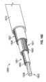
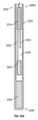
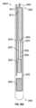
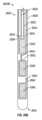
実施例では、分析物センサは、近位部分と遠位部分との間に延在する基板と、近位部分と遠位部分との間で基板に沿って延在する第1の電極と、近位部分と遠位部分との間で基板に沿って延在する第2の電極と、第1の電極及び第2の電極を電気的に分離する絶縁部分と、を含むことができる。基板は、半径が増加する複数の同心円によって囲まれた中心軸を有する円筒形部材を含むことができる。同心円は、基板の断面によって可視であることができる。第1の電極は、作用電極とすることができる。第1及び第2の電極は、各々、複数の同心円のうちの1つと整列させることができ、第1の電極は、第2の電極よりも、基板の遠位部分に向かって更に延在することができる。In an embodiment, the analyte sensor can include a substrate extending between a proximal portion and a distal portion, a first electrode extending along the substrate between the proximal portion and the distal portion, a second electrode extending along the substrate between the proximal portion and the distal portion, and an insulating portion electrically isolating the first and second electrodes. The substrate can include a cylindrical member having a central axis surrounded by a plurality of concentric circles of increasing radius. The concentric circles can be visible through a cross section of the substrate. The first electrode can be a working electrode. The first and second electrodes can each be aligned with one of the plurality of concentric circles, and the first electrode can extend further toward the distal portion of the substrate than the second electrode.
実施例では、分析物センサを作製する方法は、1つ以上の絶縁層及び1つ以上の導電層を交互に整列させることと、1つ以上の絶縁層及び1つ以上の導電層を一緒に層化させることと、1つ以上の絶縁層の一部分を選択的に除去することによって、少なくとも2つの電極を露出させることと、を含むことができる。In an embodiment, a method of fabricating an analyte sensor can include aligning one or more insulating layers and one or more conductive layers in an alternating manner, layering the one or more insulating layers and the one or more conductive layers together, and selectively removing portions of the one or more insulating layers to expose at least two electrodes.
実施例では、分析物センサを作製する方法は、基板及び分析物センサを生成するために少なくとも2つの電極ワイヤを円筒形状に同時押出することであって、少なくとも2つの電極の各々が円筒形状内の異なる同心円と整列させる、同時押出すること、生成された分析物センサを複数の個々の分析物センサに単体化することと、少なくとも2つの電極の感知領域を露出させるために個々の分析物センサの各々の上の基板材料の所定の一部分を選択的に除去することと、含むことができる。In an embodiment, a method of making an analyte sensor can include co-extruding at least two electrode wires into a cylindrical shape to produce a substrate and an analyte sensor, where each of the at least two electrodes are aligned with a different concentric circle within the cylindrical shape, singulating the produced analyte sensor into a plurality of individual analyte sensors, and selectively removing a predetermined portion of the substrate material on each of the individual analyte sensors to expose a sensing region of the at least two electrodes.
実施例では、連続分析物センサは、第1の側と、第1の側とは反対の第2の側と、を有する基板であって、平面状である、基板と、基板上の第1の作用電極と、基板上の第2の作用電極と、基板上の参照電極であって、第1の作用電極、第2の作用電極、及び参照電極が、各々平面電極であり、第1の作用電極、第2の作用電極、又は参照電極のうちの少なくとも2つが、基板の第1の側にあり、任意の残りの平面電極が、基板の第2の側にあり、第1の作用電極、第2の作用電極、及び参照電極のうちの少なくとも2つが、互いに同一平面上にある、参照電極と、第1の側と第2の側との間で基板を通って延在する相互接続であって、参照電極、第1の作用電極、又は第2の作用電極のうちの1つと電気的に連通する、相互接続と、を含むことができる。In an embodiment, the continuous analyte sensor can include a substrate having a first side and a second side opposite the first side, the substrate being planar; a first working electrode on the substrate; a second working electrode on the substrate; a reference electrode on the substrate, the first working electrode, the second working electrode, and the reference electrode each being a planar electrode, at least two of the first working electrode, the second working electrode, or the reference electrode being on the first side of the substrate and any remaining planar electrodes being on the second side of the substrate, at least two of the first working electrode, the second working electrode, and the reference electrode being coplanar with one another; and an interconnect extending through the substrate between the first side and the second side, the interconnect being in electrical communication with one of the reference electrode, the first working electrode, or the second working electrode.
実施例では、センサは、第1の側と、第1の側とは反対の第2の側と、を有する基板であって、平面状である、基板と、基板上の第1のセンサシステムであって、第1のセンサシステムが、第1のタイプの測定値を収集するように構成された連続分析物センサであり、第1のセンサシステムが、作用電極と、基板上の参照電極であって、作用電極及び参照電極が、各々平面電極である、参照電極と、少なくとも1つの作用電極の上に延在する少なくとも1つの分析物感知膜と、を備える、第1のセンサシステムと、基板上の第2のセンサシステムであって、第2のセンサシステムが、第1のタイプの測定値とは異なる第2のタイプの測定値を収集するように構成されている、第2のセンサシステムと、を含むことができる。In an embodiment, the sensor may include a substrate having a first side and a second side opposite the first side, the substrate being planar; a first sensor system on the substrate, the first sensor system being a continuous analyte sensor configured to collect a first type of measurement, the first sensor system comprising a working electrode, a reference electrode on the substrate, the working electrode and the reference electrode each being a planar electrode, and at least one analyte sensing membrane extending over the at least one working electrode; and a second sensor system on the substrate, the second sensor system being configured to collect a second type of measurement different from the first type of measurement.
実施例では、連続分析物センサは、接合部分によって接続された遠位部分及び近位部分を有する平面基板であって、遠位部分及び近位部分が、70~110度の角度で接合部分を介して接続されている、平面基板と、基板の遠位部分上の第1の電極及び近位部分上の第1の接続パッドであって、第1の電極及び第1の接続パッドが、接合部分を通ってルーティングされた第1のトレースを通して電気的に結合される、第1の電極及び第1の接続パッドと、基板の遠位部分上の第2の電極及び近位部分上の第2の接続パッドであって、第2の電極及び第2の接続パッドが、接合部分を通ってルーティングされた第2のトレースを通して電気的に結合される、第2の電極及び第2の接続パッドと、第1の電極及び第2の電極のうちの1つ以上の上に延在する少なくとも1つの分析物感知膜と、を含むことができる。In an embodiment, the continuous analyte sensor may include a planar substrate having a distal portion and a proximal portion connected by a junction, the distal portion and the proximal portion being connected via the junction at an angle between 70 and 110 degrees; a first electrode on the distal portion of the substrate and a first connection pad on the proximal portion, the first electrode and the first connection pad being electrically coupled through a first trace routed through the junction; a second electrode on the distal portion of the substrate and a second connection pad on the proximal portion, the second electrode and the second connection pad being electrically coupled through a second trace routed through the junction; and at least one analyte sensing membrane extending over one or more of the first and second electrodes.
実施例では、平面分析物センサを作製する方法は、第1の絶縁材料、第1の導電材料、及び第2の導電材料を基板の第1の側に層化することと、第1の絶縁材料の一部分を選択的に除去することによって、第1の電極を形成するように第1の導電材料の一部を露出させることと、第1の絶縁材料の一部分を選択的に除去することによって、第2の電極を形成するように第2の導電材料の一部を露出させることと、第1の側と反対の基板の第2の側に第2の絶縁材料及び第3の導電材料を層化することと、第3の絶縁材料の一部分を選択的に除去することによって、第3の電極を形成するように第3の導電材料の一部を露出させることと、第1の電極、第2の電極、又は第3の電極のうちの2つの上に分析物感知膜を堆積させることと、を含むことができる。In an embodiment, a method of making a planar analyte sensor may include layering a first insulating material, a first conductive material, and a second conductive material on a first side of a substrate, selectively removing a portion of the first insulating material to expose a portion of the first conductive material to form a first electrode, selectively removing a portion of the first insulating material to expose a portion of the second conductive material to form a second electrode, layering a second insulating material and a third conductive material on a second side of the substrate opposite the first side, selectively removing a portion of the third insulating material to expose a portion of the third conductive material to form a third electrode, and depositing an analyte sensing film on two of the first electrode, the second electrode, or the third electrode.
実施例では、複数の分析物センサを作製する方法は、基板材料シートから複数のセンサ基板を生成することであって、複数のセンサ基板の各々が、基板材料シート上に整列される、生成することと、複数のセンサ基板の各々に作用電極及び参照電極を形成することと、複数のセンサ基板の各々の上の作用電極の各々の上に分析物感知膜を適用することと、を含むことができる。In an embodiment, a method of making a plurality of analyte sensors can include generating a plurality of sensor substrates from a sheet of substrate material, where each of the plurality of sensor substrates is aligned on the sheet of substrate material, forming a working electrode and a reference electrode on each of the plurality of sensor substrates, and applying an analyte sensing membrane on each of the working electrodes on each of the plurality of sensor substrates.
実施例では、分析物センサを作製する方法は、複数の絶縁層及び複数の導電層を交互に整列させることと、複数の絶縁層及び複数の導電層を一緒に積層することと、複数の絶縁層の一部分を選択的に除去することによって、少なくとも2つの電極を露出させることと、を含むことができる。In an embodiment, a method of fabricating an analyte sensor can include aligning a plurality of insulating layers and a plurality of conductive layers in an alternating manner, stacking the plurality of insulating layers and the plurality of conductive layers together, and selectively removing portions of the plurality of insulating layers to expose at least two electrodes.
実施例では、分析物センサは、センサ基板と、センサ基板に機械的に結合された第1の電極と、センサ基板に機械的に結合され、第1の電極に電気的に結合された第1の電極トレースと、センサ基板に機械的に結合された第2の電極と、センサ基板に機械的に結合され、第1の電極に電気的に結合された第2の電極トレースと、センサ基板に機械的に結合され、第1の電極トレースに電気的に結合され、第2の電極トレースに電気的に結合されたアナログフロントエンド(analog front end、AFE)回路と、を含むことができる。In an embodiment, the analyte sensor may include a sensor substrate, a first electrode mechanically coupled to the sensor substrate, a first electrode trace mechanically coupled to the sensor substrate and electrically coupled to the first electrode, a second electrode mechanically coupled to the sensor substrate, a second electrode trace mechanically coupled to the sensor substrate and electrically coupled to the first electrode, and an analog front end (AFE) circuit mechanically coupled to the sensor substrate, electrically coupled to the first electrode trace, and electrically coupled to the second electrode trace.
実施例では、分析物センサシステムは、分析物センサであって、分析物センサが、センサ基板と、センサ基板に機械的に結合された第1の電極と、センサ基板に機械的に結合され、第1の電極に電気的に結合された第1の電極トレースと、センサ基板に機械的に結合された第2の電極と、センサ基板に機械的に結合され、第1の電極に電気的に結合された第2の電極トレースと、センサ基板に機械的に結合され、第1の電極トレースに電気的に結合され、第2の電極トレースに電気的に結合されたアナログフロントエンド(AFE)回路と、を備える、分析物センサと、センサ電子機器アセンブリと、アナログフロントエンド回路をセンサ電子機器アセンブリに電気的に結合するコネクタと、を含むことができる。In an embodiment, the analyte sensor system may include an analyte sensor comprising a sensor substrate, a first electrode mechanically coupled to the sensor substrate, a first electrode trace mechanically coupled to the sensor substrate and electrically coupled to the first electrode, a second electrode mechanically coupled to the sensor substrate, a second electrode trace mechanically coupled to the sensor substrate and electrically coupled to the first electrode, and an analog front-end (AFE) circuit mechanically coupled to the sensor substrate, electrically coupled to the first electrode trace, and electrically coupled to the second electrode trace, a sensor electronics assembly, and a connector electrically coupling the analog front-end circuit to the sensor electronics assembly.
必ずしも縮尺通りに描画されていない図面では、同様の数字は、異なる図において同様の構成要素を説明することができる。異なる文字の接尾辞を有する同様の数字は、同様の構成要素の異なる事例を表し得る。図面は、限定ではなく実施例として、本文書に考察されている様々な実施形態を概して例解する。
本開示は、とりわけ、より正確で再現可能な分析物モニタリング結果のための平面及び円筒形の両方のアーキテクチャ及び製造方法を含む分析物センサを説明する。設計は、単一センサ上で2つ以上の分析物の感知を可能にするために、複数の感知表面を含むことができる。いくつかの場合では、複数のコーティング層は、分析物センサの適切な機能を確実にするために使用することができる。分析物センサは、高速及び高スループットプロセスに従順であることができ、効率的かつ柔軟な電子機器製造方法を可能にすることができる。The present disclosure describes, among other things, analyte sensors including both planar and cylindrical architectures and manufacturing methods for more accurate and reproducible analyte monitoring results. Designs can include multiple sensing surfaces to enable sensing of two or more analytes on a single sensor. In some cases, multiple coating layers can be used to ensure proper functioning of the analyte sensor. The analyte sensors can be amenable to high speed and high throughput processes, allowing for efficient and flexible electronics manufacturing methods.
本明細書において説明される例示的な分析物センサは、体液中のグルコースなどの分析物の濃度を測定するために、ホストの体液と接触して置くことができる。他の実施例では、本明細書において考察される2つ以上の分析物は、グルコースの代わりに、又はグルコースに加えてモニタリングされ得る。いくつかの実施例では、分析物センサをホストの皮膚下に皮下挿入し、それによって、皮膚下の間質液と接触させて置き、間質液中の分析物の濃度を測定する。The exemplary analyte sensors described herein can be placed in contact with a bodily fluid of a host to measure the concentration of an analyte, such as glucose, in the bodily fluid. In other examples, two or more analytes discussed herein can be monitored instead of or in addition to glucose. In some examples, the analyte sensor is inserted subcutaneously under the skin of the host, thereby placing it in contact with interstitial fluid under the skin to measure the concentration of an analyte in the interstitial fluid.
分析物センサが1つ以上の分析物に露出されると、信号が生成され、測定される。一実施例では、信号は、分析物センサと分析物との間の電気化学反応を介して生成される。この電気化学反応は、分析物センサに、分析物濃度を示す生センサ信号を生成させることができる。いくつかの実施例では、分析物センサは、作用電極(working electrode、WE)及び参照電極(reference electrode、RE)を含むことができる。他の実施例では、分析物センサは、対電極(counter electrode、CE)も含むことができる。1つ以上の分析物の存在下では、電気化学反応は、作用電極と対電極との間に電流を流すことができ、生センサ信号は、電流に基づくことができる。存在する場合、参照電極は、安定した参照電位を提供することができ、非常にわずかな電流を伝導することができる。いくつかの場合では、電位差測定は、電流測定を介して得られるそのような測定値に加えて、使用することができる。When the analyte sensor is exposed to one or more analytes, a signal is generated and measured. In one embodiment, the signal is generated via an electrochemical reaction between the analyte sensor and the analyte. This electrochemical reaction can cause the analyte sensor to generate a raw sensor signal indicative of the analyte concentration. In some embodiments, the analyte sensor can include a working electrode (WE) and a reference electrode (RE). In other embodiments, the analyte sensor can also include a counter electrode (CE). In the presence of one or more analytes, the electrochemical reaction can cause a current to flow between the working electrode and the counter electrode, and the raw sensor signal can be based on the current. If present, the reference electrode can provide a stable reference potential and can conduct a very small current. In some cases, potentiometric measurements can be used in addition to such measurements obtained via amperometric measurements.
例示的な2電極構成では、対電極は、省略することができる。この場合、分析物センサと分析物との間の電気化学反応は、作用電極と参照電極との間に形成される電流を生じさせることができる。したがって、参照電極は、3電極構成における対電極のように電流を伝導することができ、かつ安定した参照電位を提供することができる。2電極構成における参照電極は、時折、対参照電極と称され得る。本明細書では、参照電極という用語は、例示的な電極構成に応じて、3電極構成の参照電極、2電極構成の対参照電極、又は他の構成における同様の電極を指すために使用することができる。In the exemplary two-electrode configuration, the counter electrode can be omitted. In this case, the electrochemical reaction between the analyte sensor and the analyte can result in a current being formed between the working electrode and the reference electrode. Thus, the reference electrode can conduct current like the counter electrode in a three-electrode configuration and provide a stable reference potential. The reference electrode in a two-electrode configuration can sometimes be referred to as a counter reference electrode. As used herein, the term reference electrode can be used to refer to the reference electrode in a three-electrode configuration, the counter reference electrode in a two-electrode configuration, or a similar electrode in other configurations, depending on the exemplary electrode configuration.
使用時には、センサ電子機器は、作用電極と参照(例えば、対参照)電極との間にバイアス電位を印加することができる。2電極構成では、印加されたバイアスは、分析物と分析物センサとの間の電気化学反応を促進することができ、作用電極と参照(例えば、対参照)電極との間に電流を生じさせる。電流は、生センサ信号の全て又は一部を構成することができる。バイアス電位は、正又は負であり得、モニタリングされる1つ以上の分析物に応じて、正の値と負の値との間で、又は別様に値の中及び間でトグルされ得る。In use, the sensor electronics can apply a bias potential between the working electrode and a reference (e.g., counter-reference) electrode. In a two-electrode configuration, the applied bias can promote an electrochemical reaction between the analyte and the analyte sensor, resulting in a current between the working electrode and the reference (e.g., counter-reference) electrode. The current can constitute all or a portion of the raw sensor signal. The bias potential can be positive or negative and can be toggled between positive and negative values or otherwise in and between values depending on one or more analytes being monitored.
多くの分析物センサは、現在、単一分析物の検出のために製造されており、したがって、潜在的に、複数の分析物を同時に検出及びモニタリングするために、複数のセンサ又は複数のシステムさえも必要とする。いくつかの実施例では、センサのアーキテクチャは、モニタリングすることができる分析物のタイプ又は数に関連付けられる。したがって、本明細書において考察されるようないくつかの実施例では、センサアーキテクチャは、2つ以上の分析物を同時に、又は重複若しくはトグル様式で検出及びモニタリングするように構成することができる。したがって、単一センサ上で複数の分析物を検出するための連続モニタリングセンサの改善された機能性及び拡張された使用が有用であることができる。同様に、いくつかの実施例では、例えば、サービスが十分に提供されていないコミュニティを含むヘルスケアコミュニティのニーズを満たすことができるように、迅速かつ費用効果的に生成することができるセンサアーキテクチャを有することが望ましくあり得る。Many analyte sensors are currently manufactured for the detection of a single analyte, thus potentially requiring multiple sensors or even multiple systems to simultaneously detect and monitor multiple analytes. In some examples, the architecture of the sensor is related to the type or number of analytes that can be monitored. Thus, in some examples as discussed herein, the sensor architecture can be configured to detect and monitor two or more analytes simultaneously, or in an overlapping or toggle manner. Thus, improved functionality and expanded use of continuous monitoring sensors to detect multiple analytes on a single sensor can be useful. Similarly, in some examples, it may be desirable to have a sensor architecture that can be produced quickly and cost-effectively so that the needs of the health care community, including underserved communities, can be met.
考察される本明細書では、2つの異なるクラスの分析物センサアーキテクチャ、すなわち平面構成及び同軸構成について考察される。これらのアーキテクチャの各々は、以前のワイヤベースのアーキテクチャと比較して複数の利点を潜在的に提供することができる。Two different classes of analyte sensor architectures are considered herein: planar and coaxial. Each of these architectures can potentially offer multiple advantages over previous wire-based architectures.
例えば、平面ベースの分析物センサは、依然として柔軟な幾何学形状を提供しながら、生成のためにスケールアップすることができる。具体的には、平面構成は、シートツーシート又はリールツーリール製造方法などの高速で、高スループットプロセスに従順であることができる。そのような可撓性電子製造方法は、フォトリソグラフィ、めっき、又はインクジェット印刷若しくはスクリーン印刷などの高精細印刷方法を含むことができる。平面アーキテクチャは、追加的に、多分析物感知を可能にすることができる。For example, planar-based analyte sensors can be scaled up for production while still providing flexible geometries. In particular, planar configurations can be amenable to fast, high-throughput processes, such as sheet-to-sheet or reel-to-reel manufacturing methods. Such flexible electronic manufacturing methods can include photolithography, plating, or high-definition printing methods, such as inkjet printing or screen printing. Planar architectures can additionally enable multi-analyte sensing.
同軸ベースの分析物センサは、複数の感知表面を組み込むことができ、単一センサ上で2つ以上の分析物の効率的な感知を可能にする。また、同軸又は円筒形センサの生成は、押出及びコーティング(例えば、個別分注、スプレーコーティング、又は浸漬コーティング)によって生成を達成することができるので、容易にスケーリングすることができる。これらの方法は、費用効果及び時間効果が高く、安全で、信頼性が高く、効果的な連続分析物及び連続多分析物モニタリングデバイスの迅速な生成を可能にすることができる。本明細書において考察されるセンサアーキテクチャを採用する連続分析物モニタリングシステムは、センサの着用時間の増加、慣らし時間の短縮、精度の改善、ドリフトの減少、並びに患者の快適さの増加、及び是正措置又は予防措置を含む薬学的レジメン又は他の健康若しくは栄養計画への潜在的な伸展性(compliance)の増加を可能にし得る。Coaxial-based analyte sensors can incorporate multiple sensing surfaces, allowing for efficient sensing of two or more analytes on a single sensor. Also, production of coaxial or cylindrical sensors can be easily scaled, as production can be accomplished by extrusion and coating (e.g., individual dispensing, spray coating, or dip coating). These methods can enable rapid production of continuous analyte and continuous multi-analyte monitoring devices that are cost-effective and time-effective, safe, reliable, and effective. Continuous analyte monitoring systems employing the sensor architectures discussed herein can enable increased sensor wear time, reduced break-in time, improved accuracy, reduced drift, and increased patient comfort and potential compliance with pharmaceutical regimens or other health or nutritional plans, including corrective or preventative measures.
定義
本明細書で使用される場合、「分析物測定デバイス」、「バイオセンサ」、「センサ」、「感知領域」、及び「感知機構」という用語及び句は、広義の用語及び句であり、当業者に対するその通常の、かつ慣例的な意味が与えられるものであり(かつ特別な、又はカスタマイズされた意味に限定されるものではなく)、特定の分析物又は分析物の組み合わせの検出又はそれに関連付けられる信号の変換を担う分析物モニタリングデバイスのエリアを指すが、これに限定されない。一実施例では、そのようなデバイスは、変換(検出)要素と組み合わされた生物学的認識要素を使用して、特定の定量的、半定量的、定性的、半定性的分析情報を提供することが可能である。 DEFINITIONS As used herein, the terms and phrases "analyte measuring device,""biosensor,""sensor,""sensingarea," and "sensing mechanism" are broad terms and phrases that are to be given their ordinary and customary meaning to one of skill in the art (and are not to be limited to any special or customized meaning) and refer to, but are not limited to, an area of an analyte monitoring device that is responsible for the detection of, or the transduction of a signal associated with, a particular analyte or combination of analytes. In one embodiment, such devices are capable of providing specific quantitative, semi-quantitative, qualitative, or semi-qualitative analytical information using a biological recognition element combined with a transduction (detection) element.
本明細書で使用される場合、「約」という用語は、値又は範囲におけるある程度の変動性、例えば、記載された値又は記載された範囲の限界の10%以内、5%以内、又は1%以内を許容することができ、正確に記載された値又は範囲を含む。本明細書で使用される場合、「実質的に」という用語は、少なくとも約50%、60%、70%、80%、90%、95%、96%、97%、98%、99%、99.5%、99.9%、99.99%、又は少なくとも約99.999%以上、又は100%のような大多数又は大部分を指す。本明細書で使用される場合、「実質的に含まない」という用語は、存在する材料の量が、材料を含む組成物の材料特性に影響しないように、材料を有しないか、又は取るに足らない量を有することを意味することができ、組成物の約0重量%~約5重量%が、材料であり、又は約0重量%~約1重量%、又は約5重量%以下、又は約4.5重量%以下、4、3.5、3、2.5、2、1.5、1、0.9、0.8、0.7、0.6、0.5、0.4、0.3、0.2、0.1、0.01、又は約0.001重量%以下、又は約0重量%である。As used herein, the term "about" may allow for some variability in a value or range, e.g., within 10%, within 5%, or within 1% of a stated value or the limits of a stated range, and includes the precisely stated value or range. As used herein, the term "substantially" refers to a majority or majority, such as at least about 50%, 60%, 70%, 80%, 90%, 95%, 96%, 97%, 98%, 99%, 99.5%, 99.9%, 99.99%, or at least about 99.999% or more, or 100%. As used herein, the term "substantially free" can mean having no or an insignificant amount of the material such that the amount of the material present does not affect the material properties of the composition including the material, and about 0% to about 5% by weight of the composition is the material, or about 0% to about 1% by weight, or about 5% by weight or less, or about 4.5% by weight or less, 4, 3.5, 3, 2.5, 2, 1.5, 1, 0.9, 0.8, 0.7, 0.6, 0.5, 0.4, 0.3, 0.2, 0.1, 0.01, or about 0.001% by weight or less, or about 0% by weight.
本明細書で使用される場合、「粘着する」及び「付着する」という用語は、広義の用語であり、当業者に対するその通常の、かつ慣例的な意味が与えられるものであり(かつ特別な、又はカスタマイズされた意味に限定されるものではなく)、例えば、接着、結合、把持、相互透過、又は融合によって、保持、接合、又は固着することを指すが、これに限定されない。As used herein, the terms "adhere" and "attach" are broad terms and are to be given their ordinary and customary meaning to one of ordinary skill in the art (and are not to be limited to any special or customized meaning), including, but not limited to, holding, joining, or fastening, for example, by adhesion, bonding, grasping, interpenetrating, or fusing.
本明細書で使用される場合、「分析物」という用語は、広義の用語であり、当業者に対するその通常の、かつ慣例的な意味が与えられるものであり(かつ特別な、又はカスタマイズされた意味に限定されるものではなく)、分析することができる生体液(例えば、血液、間質液、汗、脳脊髄液、リンパ液、又は尿)中の物質又は化学成分を指すが、これに限定されない。分析物には、自然発生物質、人工物質、代謝物、及び/又は反応生成物が含まれ得る。いくつかの実施例では、感知領域、デバイス、及び方法による測定のための分析物は、グルコースである。しかしながら、以下を含むが、これらに限定されない、他の分析物も企図される:カルボキシプロトロンビン;アシルカルニチン;アデニンホスホリボシルトランスフェラーゼ;アデノシンデアミナーゼ;アルブミン;α-フェトプロテイン;アミノ酸プロファイル(アルギニン(クレブス回路)、ヒスチジン/ウロカニン酸、ホモシステイン、フェニルアラニン/チロシン、トリプトファン);アンドレノステンジオン;アンチピリン;アラビニトールエナンチオマー;アルギナーゼ;ベンゾイルエクゴニン(コカイン);ビオチニダーゼ;ビオプテリン;c-反応性タンパク質;カルニチン;カルノシナーゼ;CD4;セルロプラスミン;ケノデオキシコール酸;クロロキン;コレステロール;コリンエステラーゼ;コンジュゲートされた1-βヒドロキシ-コール酸;コルチゾール;クレアチニン、クレアチンキナーゼ;クレアチンキナーゼMMイソ酵素;シクロスポリンA;d-ペニシラミン;脱エチルクロロキン;硫酸デヒドロエピアンドロステロン;DNA(アセチル化多型、アルコールデヒドロゲナーゼ、アルファ1-アンチトリプシン、嚢胞性線維症、デュシェンヌ/ベッカー型筋ジストロフィー、グルコース-6-リン酸デヒドロゲナーゼ、ヘモグロビンA、ヘモグロビンS、ヘモグロビンC、ヘモグロビンD、ヘモグロビンE、ヘモグロビンF、D-パンジャブ、ベータ-サラセミア、B型肝炎ウイルス、HCMV、HIV-1、HTLV-1、レーベル遺伝性視神経症、MCAD、RNA、PKU、三日熱マラリア原虫、21-デオキシコルチゾール);デスブチルハロファントリン;ジヒドロプテリジンレダクターゼ;ジフテリア/破傷風抗毒素;赤血球アルギナーゼ;赤血球プロトポルフィリン;エステラーゼD;脂肪酸/アシルグリシン;遊離β-ヒト絨毛性ゴナドトロピン;遊離赤血球ポルフィリン;遊離サイロキシン(free thyroxine、FT4);遊離トリヨードサイロニン(free tri-iodothyronine、FT3);フマリルアセトアセターゼ;ガラクトース/gal-1-リン酸塩;ガラクトース-1-リン酸ウリジルトランスフェラーゼ;ゲンタミシン;グルコース-6-リン酸デヒドロゲナーゼ;グルタチオン;グルタチオンペリオキシダーゼ;グリセロール、グリココール酸;グリコシル化ヘモグロビン;ハロファントリン;ヘモグロビン変異体;ヘキソサミニダーゼA;ヒト赤血球カルボニックアンヒドラーゼI;17-α-ヒドロキシプロゲステロン;ヒポキサンチンホスホリボシルトランスフェラーゼ;免疫反応性トリプシン;ベータ-ヒドロキシ酪酸;ケトン;ラクテート;鉛;リポタンパク質((a)、B/A-1、β);リゾチーム;メフロキン;ネチルマイシン;フェノバルビトン;フェニトイン;フィタン酸/プリスタン酸;カリウム(若しくは他の血液電解質)、プロゲステロン;プロラクチン;プロリダーゼ;プリンヌクレオシドホスホリラーゼ;キニーネ;リバーストリヨードサイロニン(reverse tri-iodothyronine、rT3);セレン;血清膵臓リパーゼ;シソマイシン;ナトリウム、ソマトメジンC;特異抗体(アデノウイルス、抗核抗体、反ゼータ抗体、アルボウイルス、仮性狂犬病ウイルス、デング熱ウイルス、メジナ虫、単包条虫、赤痢アメーバ、エンテロウイルス、ジアルジア鞭毛虫、ヘリコバクターピロリ、B型肝炎ウイルス、ヘルペスウイルス、HIV-1、IgE(アトピー性疾患)、インフルエンザウイルス、ドノバンリーシュマニア、レプトスピラ菌、はしか/流行性耳下腺炎/風疹、らい菌、肺炎マイコプラズマ、ミオグロビン、回旋糸状虫、パラインフルエンザウイルス、マラリア原虫、ポリオウイルス、緑膿菌、呼吸器合胞体ウイルス、リケッチア(恙虫病)、マンソン住血吸虫、トキソプラズマ、梅毒トレポネーマ、クルーズトリパノソーマ/ランジェリ、水疱性口内炎ウイルス、バンクロフト糸状虫、黄熱ウイルス);特異性抗原(B型肝炎ウイルス、HIV-1);スクシニルアセトン;スルファドキシン;テオフィリン;チロトロピン(TSH);チロキシン(T4);チロキシン結合グロブリン;微量元素;トランスフェリン;UDP-ガラクトース-4-エピメラーゼ;尿素;ウロポルフィリノーゲンIシンターゼ;ビタミンA;白血球;及び亜鉛プロトポルフィリン。血液又は間質液中に天然に存在する塩、糖、タンパク質、脂肪、ビタミン、及びホルモンもまた、特定の実施例では分析物を構成することができる。分析物は、生物学的流体、例えば、代謝産物、ホルモン、抗原、抗体などの中に天然に存在し得る。代替的に、分析物は体内に導入され得る。例えば、画像化のための造影剤、放射性同位体、化学薬剤、フッ化炭素ベースの合成血液、又は薬物若しくは薬学的組成物であり、これらとしては、インスリン;エタノール;大麻(マリファナ、テトラヒドロカンナビノール、ハシシ);吸入剤(亜酸化窒素、亜硝酸アミル、亜硝酸ブチル、クロロ炭化水素、炭化水素);コカイン(クラックコカイン);刺激薬(アンフェタミン、メタンフェタミン、リタリン、シルルト、プレルジン、ディドレックス、プレステート、ボラニル、サンドレックス、プレギン);抗うつ剤(バルビツール剤、メタカロン、ヴァリウム、リブリウム、ミルタウン、セラックス、エクワニル、トランキシーンなどの精神安定剤);幻覚剤(フェンシクリジン、リゼルギン酸、メスカリン、ペヨーテ、プシロシビン);麻薬(ヘロイン、コデイン、モルヒネ、アヘン、メペリジン、パーコセット、ペルコダン、タシオネックス、フェンタニル、ダルボン、タルウィン、ロモティル);合成麻薬(フェンタニル、メペリジン、アンフェタミン、メタンフェタミン、及びフェンシクリジンの類似体、例えば、エクスタシー);アナボリックステロイド;並びにニコチンが挙げられるが、これらに限定されない。薬物及び薬学的組成物の代謝生成物もまた、企図される分析物である。例えば、アスコルビン酸、尿酸、ドーパミン、ノルアドレナリン、3-メトキシチラミン(3-methoxytyramine、3MT)、3,4-ジヒドロキシフェニル酢酸(3,4-dihydroxyphenylacetic acid、DOPAC)、ホモバニリン酸(homovanillic acid、HVA)、5-ヒドロキシトリプタミン(5-hydroxytryptamine、5HT)、5-ヒドロキシインドール酢酸(5-hydroxyindoleacetic acid、FHIAA)、及びヒスタミンなどの、神経化学物質及び体内で生成される他の化学物質などの分析物もまた、分析することができる。As used herein, the term "analyte" is a broad term and is given its ordinary and customary meaning to one of ordinary skill in the art (and is not limited to any special or customized meaning) and refers to, but is not limited to, a substance or chemical constituent in a biological fluid (e.g., blood, interstitial fluid, sweat, cerebrospinal fluid, lymphatic fluid, or urine) that can be analyzed. Analytes can include naturally occurring substances, man-made substances, metabolites, and/or reaction products. In some examples, the analyte for measurement by the sensing regions, devices, and methods is glucose. However, other analytes are contemplated, including, but not limited to: carboxyprothrombin; acylcarnitines; adenine phosphoribosyltransferase; adenosine deaminase; albumin; α-fetoprotein; amino acid profile (arginine (Krebs cycle), histidine/urocanic acid, homocysteine, phenylalanine/tyrosine, tryptophan); andrenostenedione; antipyrine; arabinitol enantiomers; arginase; benzoylecgonine (cocaine); biotinidase; biopterin; c-reactive protein; carnitine; carnosinase; CD4; ceruloplasmin; chenodeoxycholic acid; chloroquine; cholesterol; cholinesterase; conjugated 1-β hydroxy-cholic acid; cortisol; creatinine, creatine kinase; creatine kinase MM isoenzyme; cyclosporine A ;d-Penicillamine;Desethylchloroquine;Dehydroepiandrosterone sulfate;DNA (acetylation polymorphism, alcohol dehydrogenase, alpha 1-antitrypsin, cystic fibrosis, Duchenne/Becker muscular dystrophy, glucose-6-phosphate dehydrogenase, hemoglobin A, hemoglobin S, hemoglobin C, hemoglobin D, hemoglobin E, hemoglobin F, D-Punjab, beta-thalassemia, hepatitis B virus , HCMV, HIV-1, HTLV-1, Leber's hereditary optic neuropathy, MCAD, RNA, PKU, Plasmodium vivax, 21-deoxycortisol); desbutylhalofantrine; dihydropteridine reductase; diphtheria/tetanus antitoxin; erythrocyte arginase; erythrocyte protoporphyrin; esterase D; fatty acids/acylglycines; free β-human chorionic gonadotropin; free erythrocyte porphyrin; free thyroxine (FT4); free triiodothyronine (free tri-iodothyronine, FT3); fumarylacetoacetase; galactose/gal-1-phosphate; galactose-1-phosphate uridyltransferase; gentamicin; glucose-6-phosphate dehydrogenase; glutathione; glutathione peroxidase; glycerol, glycocholate; glycosylated hemoglobin; halofantrine; hemoglobin mutants; hexosaminidase A; human erythrocyte carbonic anhydrase I; 17-α-hydroxyproline Gesterone; hypoxanthine phosphoribosyltransferase; immunoreactive trypsin; beta-hydroxybutyrate; ketones; lactate; lead; lipoproteins ((a), B/A-1, β); lysozyme; mefloquine; netilmicin; phenobarbitone; phenytoin; phytanic acid/pristanic acid; potassium (or other blood electrolytes); progesterone; prolactin; prolidase; purine nucleoside phosphorylase; quinine; reverse triiodothyronine tri-iodothyronine, rT3); selenium; serum pancreatic lipase; sisomicin; sodium; somatomedin C; specific antibodies (adenovirus, antinuclear antibody, anti-zeta antibody, arbovirus, pseudorabies virus, dengue virus, dracunculiasis, tapeworm, ameba granulosus, enterovirus, giardiasis, Helicobacter pylori, hepatitis B virus, herpes virus, HIV-1, IgE (atopic disease), influenza virus, leishmania donovani, leptospirosis, measles/mumps/rubella, mycobacterium leprae, mycoplasma pneumoniae, myoglobin, onchocerca volvulus, parainfluenza virus) , Plasmodium, poliovirus, Pseudomonas aeruginosa, respiratory syncytial virus, Rickettsia (tsutsugamushi disease), Schistosoma mansoni, Toxoplasma gondii, Treponema pallidum, Trypanosoma cruzi/rangeli, Vesicular stomatitis virus, Wuchereria bancrofti, Yellow fever virus); specific antigens (Hepatitis B virus, HIV-1); succinylacetone; sulfadoxine; theophylline; thyrotropin (TSH); thyroxine (T4); thyroxine-binding globulin; trace elements; transferrin; UDP-galactose-4-epimerase; urea; uroporphyrinogen I synthase; vitamin A; white blood cells; and zinc protoporphyrin. Salts, sugars, proteins, fats, vitamins, and hormones naturally occurring in blood or interstitial fluids can also constitute analytes in certain embodiments. Analytes can be naturally occurring in biological fluids, such as metabolites, hormones, antigens, antibodies, and the like. Alternatively, the analyte may be introduced into the body, for example a contrast agent for imaging, a radioisotope, a chemical agent, a fluorocarbon-based synthetic blood, or a drug or pharmaceutical composition, including, but not limited to, insulin; ethanol; cannabis (marijuana, tetrahydrocannabinol, hashish); inhalants (nitrous oxide, amyl nitrite, butyl nitrite, chlorohydrocarbons, hydrocarbons); cocaine (crack cocaine); stimulants (amphetamine, methamphetamine, ritalin, silurt, preludine, didrex, prestate, borane, sandrex, pregin); antidepressants (barbiturates, methaqualone, valium); , tranquilizers such as librium, miltown, serax, equanil, tranxine, etc.); hallucinogens (phencyclidine, lysergic acid, mescaline, peyote, psilocybin); narcotics (heroin, codeine, morphine, opium, meperidine, percocet, percodan, tasionex, fentanyl, darvon, talwin, lomotil); synthetic narcotics (fentanyl, meperidine, amphetamine, methamphetamine, and analogs of phencyclidine, e.g., ecstasy); anabolic steroids; and nicotine. Metabolic products of drugs and pharmaceutical compositions are also contemplated analytes. Analytes such as neurochemicals and other chemicals produced in the body, such as ascorbic acid, uric acid, dopamine, noradrenaline, 3-methoxytyramine (3MT), 3,4-dihydroxyphenylacetic acid (DOPAC), homovanillic acid (HVA), 5-hydroxytryptamine (5HT), 5-hydroxyindoleacetic acid (FHIAA), and histamine, can also be analyzed.
本明細書で使用される場合、「生物活性剤」という用語は、広義の用語であり、当業者に対するその通常の、かつ慣例的な意味が与えられるものであり(かつ特別な、又はカスタマイズされた意味に限定されるものではなく)、生体組織に対して効果を有するか、又は生体組織からの応答を誘発する任意の物質を指すが、これに限定されない。As used herein, the term "bioactive agent" is a broad term and is to be given its ordinary and customary meaning to one of ordinary skill in the art (and is not to be limited to any special or customized meaning) and refers to, but is not limited to, any substance that has an effect on or elicits a response from living tissue.
本明細書で互換的に使用される場合、「生体界面膜」及び「生体界面層」及び「生体界面/薬物放出膜」及び「生体界面/薬物放出層」という句は、広義の句であり、当業者に対するその通常の、かつ慣例的な意味が与えられるものであり(かつ特別な、又はカスタマイズされた意味に限定されるものではなく)、ホスト組織と埋め込み型デバイスとの間の界面として機能する透過性膜又は層を指すが、これに限定されない。As used interchangeably herein, the phrases "biointerface membrane" and "biointerface layer" and "biointerface/drug-releasing membrane" and "biointerface/drug-releasing layer" are broad phrases that are to be given their ordinary and customary meaning to those of skill in the art (and are not to be limited to any special or customized meaning) and refer to, but are not limited to, a permeable membrane or layer that serves as an interface between a host tissue and an implantable device.
本明細書で使用される場合、「バリア細胞層」という句は、広義の用語であり、当業者に対するその通常の、かつ慣例的な意味が与えられるものであり(かつ特別な、又はカスタマイズされた意味に限定されるものではなく)、埋め込み可能なデバイスへの分子及び他の物質の輸送を実質的に遮断する細胞(例えば、マクロファージ及び異物巨細胞)の凝集性単層を形成する異物反応の一部を指すが、これに限定されない。As used herein, the phrase "barrier cell layer" is a broad term that is to be given its ordinary and customary meaning to one of skill in the art (and is not to be limited to any special or customized meaning) and refers, without limitation, to the portion of the foreign body reaction that forms a cohesive monolayer of cells (e.g., macrophages and foreign body giant cells) that substantially blocks the transport of molecules and other substances into the implantable device.
本明細書で使用される場合、「生体安定性」という用語は、広義の用語であり、当業者に対するその通常の、かつ慣例的な意味が与えられるものであり(かつ特別な、又はカスタマイズされた意味に限定されるものではなく)、インビボで遭遇するプロセスによる分解に対して相対的に抵抗性の材料を指すが、これに限定されない。As used herein, the term "biostable" is a broad term and is to be given its ordinary and customary meaning to those of skill in the art (and is not to be limited to any special or customized meaning), and refers to, but is not limited to, materials that are relatively resistant to degradation by processes encountered in vivo.
本明細書で使用される場合、「生体再吸収性」又は「生体吸収性」という用語は、広義の用語であり、当業者に対するその通常の、かつ慣習的な意味が与えられるものであり(かつ特別な、又はカスタマイズされた意味に限定されるものではなく)、生体系において吸収することができる又は物質を失う可能性がある材料を指すが、これに限定されない。As used herein, the term "bioresorbable" or "bioabsorbable" is a broad term and is to be given its ordinary and customary meaning to one of ordinary skill in the art (and is not to be limited to any special or customized meaning) and refers to, but is not limited to, materials that can be absorbed or lose substances in a biological system.
本明細書で使用される場合、「細胞突起」という句は、広義の用語であり、当業者に対するその通常の、かつ慣例的な意味が与えられるものであり(かつ特別な、又はカスタマイズされた意味に限定されるものではなく)、細胞の仮足を指すが、これに限定されない。As used herein, the phrase "cell process" is a broad term and is to be given its ordinary and customary meaning to one of skill in the art (and is not to be limited to any special or customized meaning), and refers to, but is not limited to, the pseudopodia of cells.
本明細書で使用される場合、「細胞付着」という句は、広義の用語であり、当業者に対するその通常の、かつ慣例的な意味が与えられるものであり(かつ特別な、又はカスタマイズされた意味に限定されるものではなく)、分子レベルでの材料への細胞及び/若しくは細胞突起の粘着、並びに/又はマイクロポーラス材料表面若しくはマクロポーラス材料表面への細胞及び/若しくは細胞突起の付着を指すが、これに限定されない。多孔性表面への細胞付着を促進する先行技術において使用される材料の一実施例は、Millipore(Bedford,Mass)によって市販されており、かつBraukerらの米国特許第5,741,330号において説明されているような、BIOPORE(商標)細胞培養支持体である。As used herein, the phrase "cell attachment" is a broad term and is given its ordinary and customary meaning to one of skill in the art (and is not limited to any special or customized meaning), and refers to, but is not limited to, the adhesion of cells and/or cell processes to a material at a molecular level and/or the attachment of cells and/or cell processes to a microporous or macroporous material surface. One example of a material used in the prior art that promotes cell attachment to a porous surface is the BIOPORE™ cell culture support, as marketed by Millipore (Bedford, Mass.) and described in U.S. Patent No. 5,741,330 to Brauker et al.
本明細書で使用される場合、「連続的」という用語は、広義の用語であり、当業者に対するその通常の、かつ慣例的な意味が与えられるものであり(かつ特別な、又はカスタマイズされた意味に限定されるものではなく)、中断されない又は切れ目ない部分、ドメイン、コーティング、又は層を指すが、これに限定されない。As used herein, the term "continuous" is a broad term and is to be given its ordinary and customary meaning to one of ordinary skill in the art (and is not to be limited to any special or customized meaning) and refers to, but is not limited to, an uninterrupted or unbroken portion, domain, coating, or layer.
本明細書で使用される場合、「共連続」という用語は、広義の用語であり、当業者に対するその通常の、かつ慣例的な意味が与えられるものであり(かつ特別な、又はカスタマイズされた意味に限定されるものではなく)、膜の両面の間に三次元の切れ目のない曲線を引くことができる、中実部分又は空洞を指すが、これに限定されない。As used herein, the term "co-continuous" is a broad term and is to be given its ordinary and customary meaning to one of ordinary skill in the art (and is not to be limited to any special or customized meaning), and refers to, but is not limited to, a solid portion or cavity that allows for a three-dimensional unbroken curve to be drawn between the two sides of the membrane.
本明細書で使用される場合、「同軸」という用語は、円形、楕円形、三角形、多角形、又は他の断面を有するように構成することができるコアの周りの共有軸に沿って整列された要素を有するセンサアーキテクチャを含むように広く解釈されるべきであり、そのような要素は、電極、絶縁層、又はコア電極若しくはコアポリマーワイヤなどのコア層の周りに円周方向に位置決めすることができる他の要素を含むことができる。As used herein, the term "coaxial" should be interpreted broadly to include sensor architectures having elements aligned along a shared axis about a core that may be configured to have a circular, elliptical, triangular, polygonal, or other cross-section, and such elements may include electrodes, insulating layers, or other elements that may be positioned circumferentially about a core layer, such as a core electrode or core polymer wire.
連続分析物センサの更なる実施例は、例えば、Simpsonらの米国特許第8,828,201号、Simpsonらの米国特許第9,131,885号、Simpsonらの米国特許第9,237,864号、及びSimpsonらの米国特許第9,763,608号に見出すことができ、これらの各々は、その全体が本明細書中に参考として組み込まれる。Further examples of continuous analyte sensors can be found, for example, in U.S. Pat. No. 8,828,201 to Simpson et al., U.S. Pat. No. 9,131,885 to Simpson et al., U.S. Pat. No. 9,237,864 to Simpson et al., and U.S. Pat. No. 9,763,608 to Simpson et al., each of which is incorporated herein by reference in its entirety.
本明細書で使用される場合、「連続分析物感知」という句は、広義の句であり、当業者に対するその通常の、かつ慣例的な意味が与えられるものであり(かつ特別な、又はカスタマイズされた意味に限定されるものではなく)、分析物濃度のモニタリングが、連続的に、継続的に、及び/又は断続的に(しかし定期的に)実施される期間、例えば、約5秒以下から約10分以上、好ましくは、約10、15、20、25、30、35、40、45、50、55、又は60秒から約1.25、1.50、1.75、2.00、2.25、2.50、2.75、3.00、3.25、3.50、3.75、4.00、4.25、4.50、4.75、5.00、5.25、5.50、5.75、6.00、6.25、6.50、6.75、7.00、7.25、7.50、7.75、8.00、8.25、8.50、8.75、9.00、9.25、9.50又は9.75分ごとを指すが、これに限定されない。As used herein, the phrase "continuous analyte sensing" is a broad phrase and is to be given its ordinary and customary meaning to one of ordinary skill in the art (and is not to be limited to any special or customized meaning) and refers to a period of time during which monitoring of analyte concentration is performed continuously, continuously, and/or intermittently (but periodically), e.g., from about 5 seconds or less to about 10 minutes or more, preferably about 10, 15, 20, 25, 30, 35, 40, 45, 50, 60, 70, 80, 90, 100, 110, 120, 130, 140, 150, 160, 170, 180, 190, 210, 220, 230, 240, 250, 260, 270, 280, 290, 300, 310, 320, 330, 340, 350, 360, 370, 380, 390, 400, 410, 420, 430, 440, 450, 460, 470, 480, 490, 500, 510, 520, 530, 540, 550, 560, 570, 580, 590, 600, 610, 620, 630, 640, 650, 660, 670, 680, 690, 700, 710, 720, 730, 740, 750, 760, 770, 780, 790, 800, This includes, but is not limited to, every 55 or 60 seconds to about 1.25, 1.50, 1.75, 2.00, 2.25, 2.50, 2.75, 3.00, 3.25, 3.50, 3.75, 4.00, 4.25, 4.50, 4.75, 5.00, 5.25, 5.50, 5.75, 6.00, 6.25, 6.50, 6.75, 7.00, 7.25, 7.50, 7.75, 8.00, 8.25, 8.50, 8.75, 9.00, 9.25, 9.50 or 9.75 minutes.
本明細書で使用される場合、「同一平面上(co-planar)」又は「同一平面上(coplanar)」という用語は、基板上の2つ以上の電極又は他の構成要素を指すことができ、これらの2つ以上の電極又は他の構成要素は、実質的に同じ平面内に存在する。As used herein, the terms "co-planar" or "coplanar" can refer to two or more electrodes or other components on a substrate, where the two or more electrodes or other components lie in substantially the same plane.
本明細書で使用される場合、「結合された」という用語は、電気的に、機械的に、熱的に、動作可能に、化学的に、又は別様に付着されることのうちの少なくとも1つであるように構成される、2つ以上のシステム要素又は構成要素を指し得る。As used herein, the term "coupled" may refer to two or more system elements or components that are configured to be at least one of electrically, mechanically, thermally, operatively, chemically, or otherwise attached.
本明細書で使用される場合、「取り外し可能に結合された」という用語は、結合された要素又は構成要素のうちのいずれも損傷することなく、電気的に、機械的に、熱的に、動作可能に、化学的に、若しくは別様に付着され、取り外されるように構成されるか、又はそのように構成されている、2つ以上のシステム要素又は構成要素を指し得る。As used herein, the term "removably coupled" may refer to two or more system elements or components that are configured or adapted to be electrically, mechanically, thermally, operatively, chemically, or otherwise attached and detached without damaging any of the coupled elements or components.
本明細書で使用される場合、「永久的に結合された」という用語は、電気的に、機械的に、熱的に、動作可能に、化学的に、又は別様に付着されるように構成されるか又は付着されているが、結合された要素又は構成要素のうちの少なくとも1つを損傷することなく結合解除することができない、2つ以上のシステム要素又は構成要素を指し得る。As used herein, the term "permanently coupled" may refer to two or more system elements or components that are configured or attached electrically, mechanically, thermally, operatively, chemically, or otherwise attached, but cannot be uncoupled without damaging at least one of the coupled elements or components.
本明細書で使用される場合、「画定された縁部」という句は、広義の句であり、当業者に対するその通常の、かつ慣例的な意味が与えられるものであり(かつ特別な、又はカスタマイズされた意味に限定されるものではなく)、層、ドメイン、コーティング、又は部分の間の突然の、別個の縁部又は境界を指すが、これに限定されない。「画定された縁部」は、層、ドメイン、コーティング、又は部分の間の漸進的な遷移とは対照的である。As used herein, the phrase "defined edge" is a broad phrase and is given its ordinary and customary meaning to one of ordinary skill in the art (and is not limited to any special or customized meaning) and refers to, but is not limited to, an abrupt, distinct edge or boundary between layers, domains, coatings, or portions. A "defined edge" is in contrast to a gradual transition between layers, domains, coatings, or portions.
本明細書で使用される場合、「不連続な」という用語は、広義の用語であり、当業者に対するその通常の、かつ慣例的な意味が与えられるものであり(かつ特別な、又はカスタマイズされた意味に限定されるものではなく)、切断された、中断された、又は分離された部分、層、コーティング、又はドメインを指すが、これに限定されない。As used herein, the term "discontinuous" is a broad term and is to be given its ordinary and customary meaning to one of ordinary skill in the art (and is not to be limited to any special or customized meaning) and refers to, but is not limited to, cut, interrupted, or separated portions, layers, coatings, or domains.
本明細書で使用される場合、「遠位」という用語は、広義の用語であり、当業者に対するその通常の、かつ慣例的な意味が与えられるものであり(かつ特別な、又はカスタマイズされた意味に限定されるものではなく)、原点又は付着点などの参照点から相対的に遠くに離間された領域を指すが、これに限定されない。As used herein, the term "distal" is a broad term and is to be given its ordinary and customary meaning to one of ordinary skill in the art (and is not to be limited to any special or customized meaning), and refers to, but is not limited to, an area that is relatively far away from a reference point such as an origin or attachment point.
本明細書で使用される場合、「ドメイン」という用語は、広義語であり、当業者に対するその通常の、かつ慣例的な意味が与えられるものであり(かつ特別な、又はカスタマイズされた意味に限定されるものではなく)、層、均一若しくは不均一勾配(例えば、膜の異方性領域)、又は膜の一部分であり得る膜システムの領域を指すが、これに限定されない。本明細書において考察されるドメインは、単一層として、2つ以上の層として、二重層の対として、又はそれらの組み合わせとして形成することができる。本明細書で使用される場合、「ドリフト」という用語は、広義の用語であり、当業者に対するその通常の、かつ慣例的な意味が与えられるものであり(かつ特別な、又はカスタマイズされた意味に限定されるものではなく)、ホスト全身分析物濃度の変化とは無関係である、経時的な信号の漸進的な増加又は減少を指すが、これに限定されない。例えば、ホスト食後グルコース濃度などである。理論に束縛されることを望むものではないが、ドリフトは、例えば、センサを取り囲み、FBCを形成する細胞浸潤による、センサへのグルコース輸送の局所的減少の結果であり得ると考えられる。また、不十分な量の間質液が、センサを取り囲んでおり、これは、例えば、センサへの低減された酸素及び/又はグルコース輸送をもたらすと考えられる。局所的な間質液の増加は、ドリフトを減速又は低減させ、したがって、センサ性能を改善し得る。ドリフトはまた、ピコアンペア範囲の電気信号とともに生じることができるノイズ若しくは他の異常を補償するために使用されるセンサ電子機器又はアルゴリズムモデルの結果であり得る。As used herein, the term "domain" is a broad term and is given its ordinary and customary meaning to one skilled in the art (and is not limited to any special or customized meaning) and refers to, but is not limited to, a region of a membrane system that may be a layer, a uniform or non-uniform gradient (e.g., an anisotropic region of a membrane), or a portion of a membrane. The domains discussed herein can be formed as a single layer, as two or more layers, as a pair of bilayers, or as combinations thereof. As used herein, the term "drift" is a broad term and is given its ordinary and customary meaning to one skilled in the art (and is not limited to any special or customized meaning) and refers to, but is not limited to, a gradual increase or decrease in a signal over time that is independent of changes in host systemic analyte concentration, such as, for example, host postprandial glucose concentration. Without wishing to be bound by theory, it is believed that drift may be the result of a local decrease in glucose transport to the sensor, for example, due to cellular infiltration surrounding the sensor and forming an FBC. It is also believed that an insufficient amount of interstitial fluid surrounds the sensor, which may result in, for example, reduced oxygen and/or glucose transport to the sensor. Increasing local interstitial fluid may slow or reduce drift, thus improving sensor performance. Drift may also be the result of sensor electronics or algorithmic models used to compensate for noise or other anomalies that can occur with electrical signals in the picoamp range.
本明細書で互換的に使用される場合、「薬物放出膜」及び「薬物放出層」という句は、各々広義の句であり、当業者に対するその通常の、かつ慣例的な意味が与えられるものであり(かつ特別な、又はカスタマイズされた意味に限定されるものではなく)、1つ以上の生物活性剤に対して透過性である透過性又は半透過性膜を指すが、これに限定されない。一実施例では、「薬物放出膜」及び「薬物放出層」は、2つ以上のドメインから構成され得、典型的には数ミクロン以上の厚さである。一実施例では、薬物放出層及び/又は薬物放出膜は、生体界面層及び/又は生体界面膜と実質的に同じである。薬物放出層及び膜の実施例は、参照によりその全体が本明細書に組み込まれる、2022年3月17日に出願された「DRUG RELEASING MEMBRANE FOR ANALYTE SENSOR」と題される係属中の米国特許出願公開第2022-0296867号、並びに参照によりその全体が本明細書に組み込まれる、2022年3月17日に出願された「DRUG RELEASING MEMBRANE FOR ANALYTE SENSOR」と題される係属中の米国特許出願第17/945585号に見出され得る。As used interchangeably herein, the phrases "drug release membrane" and "drug release layer" are each broad phrases given their ordinary and customary meaning to one of skill in the art (and are not limited to any special or customized meaning) and refer to, but are not limited to, a permeable or semi-permeable membrane that is permeable to one or more bioactive agents. In one embodiment, the "drug release membrane" and "drug release layer" may be composed of two or more domains and are typically several microns or more thick. In one embodiment, the drug release layer and/or drug release membrane are substantially the same as the biointerface layer and/or biointerface membrane. Examples of drug release layers and membranes can be found in pending U.S. Patent Application Publication No. 2022-0296867, entitled "DRUG RELEASING MEMBRANE FOR ANALYTE SENSOR," filed March 17, 2022, which is incorporated herein by reference in its entirety, and pending U.S. Patent Application No. 17/945,585, entitled "DRUG RELEASING MEMBRANE FOR ANALYTE SENSOR," filed March 17, 2022, which is incorporated herein by reference in its entirety.
本明細書で使用される場合、「電気化学反応性表面」という用語は、広義の用語であり、当業者に対するその通常の、かつ慣例的な意味が与えられるものであり(かつ特別な、又はカスタマイズされた意味に限定されるものではなく)、電気化学反応が起こる電極の表面を指すが、これに限定されない。作用電極では、酸化還元種は、分析物の酵素触媒反応によって生成され、分析物の濃度を判定するために使用される測定可能な電子電流を作り出すことができる。作用電極のいくつかの実施例では、検出される分析物の反応によって生成される酸化可能な種は、測定可能な電子電流を作り出すことができる。例えば、グルコースの検出では、グルコースオキシダーゼは、副産物として過酸化水素(H2O2)を生成する。H2O2は、作用電極の表面と反応して、2つのプロトン(2H+)、2つの電子(2e-)、及び1つの酸素分子(O2)を生成し、これが、検出される電子電流を生成する。対電極では、還元可能な種、例えば、O2が電極表面で還元されて、作用電極によって生成される電流を均衡化する。As used herein, the term "electrochemically reactive surface" is a broad term and is to be given its ordinary and customary meaning to one of ordinary skill in the art (and is not to be limited to any special or customized meaning) and refers to, but is not limited to, the surface of an electrode at which an electrochemical reaction occurs. At the working electrode, redox species are generated by an enzyme-catalyzed reaction of an analyte and can produce a measurable electronic current that is used to determine the concentration of the analyte. At some examples of working electrodes, oxidizable species generated by the reaction of an analyte to be detected can produce a measurable electronic current. For example, in the detection of glucose, glucose oxidase produces hydrogen peroxide (H2O2) as a by-product. H2O2 reacts with the surface of the working electrode to produce two protons (2H+), two electrons (2e-), and one oxygen molecule (O2), which produces the electronic current that is detected. At the counter electrode, reducible species, e.g., O2, are reduced at the electrode surface to balance the current produced by the working electrode.
本明細書で使用される場合、「ホスト」という用語は、広義の用語であり、その通常の、かつ慣例的な意味が当業者に示されるものであり(かつ特別な、又はカスタマイズされた意味に限定されるものではなく)、哺乳類、好ましくは、ヒトを指すが、これらに限定されない。As used herein, the term "host" is a broad term having its ordinary and customary meaning given to those of skill in the art (and is not limited to any special or customized meaning), and refers to, but is not limited to, a mammal, preferably a human.
本明細書で使用される場合、「干渉物質」及び「干渉種」という用語は、広義の用語であり、当業者に対するその通常の、かつ慣例的な意味が与えられるものであり(かつ特別な、又はカスタマイズされた意味に限定されるものではなく)、センサにおける関心対象の分析物の測定に干渉して、分析物測定を正確に表さない信号を生成する効果及び/又は種を指すが、これに限定されない。電気化学センサの一実施例では、干渉種は、測定される分析物と重複する酸化電位を有する化合物である。As used herein, the terms "interfering substance" and "interfering species" are broad terms and are to be given their ordinary and customary meaning to one of ordinary skill in the art (and are not to be limited to any special or customized meaning) and refer to, but are not limited to, effects and/or species that interfere with the measurement of an analyte of interest in a sensor, producing a signal that does not accurately represent the analyte measurement. In one embodiment of an electrochemical sensor, an interfering species is a compound that has an oxidation potential that overlaps with the analyte being measured.
「インビボ」という用語は、限定されないが、ホストの生体内への挿入及び/又は生体内での存在に適合されたデバイス(例えば、センサ)の一部を指す。The term "in vivo" refers, without limitation, to a portion of a device (e.g., a sensor) that is adapted for insertion into and/or presence within a host's living body.
「エクスビボ」という用語は、ホストの生体の外側に留まる及び/又は存在するように適合されたデバイス(例えば、センサ)の一部を指す。The term "ex vivo" refers to a portion of a device (e.g., a sensor) that is adapted to reside and/or exist outside the host organism.
本明細書で使用される場合、「膜システム」という句は、広義の句であり、当業者に対するその通常の、かつ慣例的な意味が与えられるものであり(かつ特別な、又はカスタマイズされた意味に限定されるものではなく)、2つ以上のドメインから構成することができ、典型的には厚さ数ミクロン以上の材料から構成され、酸素に対して透過性であり、任意選択的に、例えば、グルコース又は別の分析物に対して透過性である透過性又は半透過性膜を指すが、これに限定されない。一実施例では、膜システムは、グルコースと酸素との間で反応が起こることを可能にし、それによってグルコース濃度を測定することができる、固定化グルコースオキシダーゼ酵素を含む。本明細書で使用される場合、「ノイズ」という用語は、広義語であり、その通常の意味で使用され、分析物濃度とは無関係であり、センサ性能の低下をもたらし得る、センサ又はセンサ電子機器によって検出される信号を含むが、これに限定されない。あるタイプのノイズは、センサ挿入後の数時間(例えば、約2~約24時間)の間に観察される。最初の24時間後、ノイズは、消失又は減少し得るが、いくつかのホストでは、ノイズは、約3~4日間存続し得る。いくつかの場合では、ノイズは、予測モデリング、人工知能、及び/又はアルゴリズム手段を使用して低減することができる。他の場合では、ノイズは、少なくとも1つの生物活性剤を有する薬物放出層を使用するなど、埋め込まれたセンサの存在に関連付けられた免疫応答因子に対処することによって低減することができる。例えば、本開示のような1つ以上の例示的なバイオセンサのノイズは、判定され、次いで定性的又は定量的に比較することができる。例として、固定サンプリング間隔(ピコアンペア(pA単位)で生信号時系列を取得することは、生信号時系列の平滑化されたバージョンは、例えば、三次ローパスデジタルチェビシェフタイプIIフィルタを適用することによって取得することができる。他の平滑化アルゴリズムを使用することもできる。各サンプリング間隔で、pA単位の絶対差を計算して、平滑化された時系列を提供することができる。この平滑化された時系列は、pA/mg/dLの単位のグルコース感受性時系列を使用して、mg/dLの単位(「ノイズ」の単位)に変換することができ、グルコース感受性時系列は、生信号と参照血中グルコース測定値(例えば、血中グルコース計から得られる)との間の数学モデルを使用して導出される。任意選択的に、時系列は、所望に応じて、例えば、時間又は日ごとに集約することができる。本開示の薬物放出層及び1つ以上の生物活性剤を有する異なる例示的バイオセンサ間の対応する時系列の比較は、ノイズの改善の定性的又は定量的判定を提供する。As used herein, the phrase "membrane system" is a broad phrase and is given its ordinary and customary meaning to one of ordinary skill in the art (and is not limited to any special or customized meaning) and refers to, but is not limited to, a permeable or semi-permeable membrane that may be composed of two or more domains, is typically composed of a material several microns thick or more, and is permeable to oxygen and, optionally, for example, to glucose or another analyte. In one example, the membrane system includes an immobilized glucose oxidase enzyme that allows a reaction to occur between glucose and oxygen, thereby allowing glucose concentration to be measured. As used herein, the term "noise" is a broad term and is used in its ordinary sense, including, but not limited to, a signal detected by the sensor or sensor electronics that is independent of analyte concentration and may result in degradation of sensor performance. One type of noise is observed for several hours (e.g., about 2 to about 24 hours) after sensor insertion. After the first 24 hours, the noise may disappear or decrease, but in some hosts, the noise may persist for about 3 to 4 days. In some cases, the noise may be reduced using predictive modeling, artificial intelligence, and/or algorithmic means. In other cases, noise can be reduced by addressing immune response factors associated with the presence of an implanted sensor, such as by using a drug-releasing layer having at least one bioactive agent. For example, the noise of one or more exemplary biosensors as disclosed herein can be determined and then compared qualitatively or quantitatively. As an example, a raw signal time series may be obtained at a fixed sampling interval (in picoamps (pA)). A smoothed version of the raw signal time series may be obtained, for example, by applying a third order low pass digital Chebyshev Type II filter. Other smoothing algorithms may also be used. At each sampling interval, the absolute difference in pA may be calculated to provide a smoothed time series. This smoothed time series may be converted to units of mg/dL (units of "noise") using the glucose sensitivity time series in units of pA/mg/dL, which is derived using a mathematical model between the raw signal and a reference blood glucose measurement (e.g., obtained from a blood glucose meter). Optionally, the time series may be aggregated, for example, by hour or day, as desired. Comparison of corresponding time series between different exemplary biosensors having a drug releasing layer and one or more bioactive agents of the present disclosure provides a qualitative or quantitative determination of the noise improvement.
本明細書で使用される場合、「動作可能に接続される」、「動作可能に結合される」、及び「動作可能に連結される」という用語は、広義の用語であり、当業者に対するその通常の、かつ慣習的な意味が与えられるものであり(かつ特別な、又はカスタマイズされた意味に限定されるものではなく)、構成要素同士の間の信号の伝送を容易にする様式で別の構成要素に連結される1つ以上の成分を指すが、これに限定されない。例えば、1つ以上の電極を使用して、試料内の分析物を検出し、その情報を信号に変換することができ、次いで、信号を、電子回路に伝送することができる。この実施例では、電極は、電子回路に「動作可能に連結されて」いる。As used herein, the terms "operably connected," "operably coupled," and "operably linked" are broad terms and are to be given their ordinary and customary meaning to one of ordinary skill in the art (and are not to be limited to any special or customized meaning), and refer to, but are not limited to, one or more components that are linked to another component in a manner that facilitates the transmission of a signal between the components. For example, one or more electrodes can be used to detect an analyte in a sample and convert that information into a signal, which can then be transmitted to an electronic circuit. In this example, the electrodes are "operably linked" to the electronic circuit.
「任意的な」又は「任意選択的に」という用語は、その後に説明される事象又は状況が起こり得る又は起こり得ないこと、並びにその説明が、その事象又は状況が起こる場合及び起こらない場合の事例を含むことを意味する。The term "optionally" or "optionally" means that the subsequently described event or circumstance may or may not occur, and that the description includes instances when the event or circumstance occurs and when it does not occur.
本明細書で使用される場合、「平面」という用語は、第1の側及び第2の側を含む基板と、基板の1つ以上の側に配設された複数の要素と、を有する、センサアーキテクチャを説明するために広く解釈されるべきであり、要素は、電気的に又は別様に結合される場合又はされない場合があり、要素は、回路として動作するように構成された導電層若しくは絶縁層又は要素を含むことができる。平面電極は、例えば、概して平坦な又は水平な表面を有する。As used herein, the term "planar" should be broadly construed to describe a sensor architecture having a substrate including a first side and a second side, and a plurality of elements disposed on one or more sides of the substrate, which may or may not be electrically or otherwise coupled, and which may include conductive or insulating layers or elements configured to operate as a circuit. A planar electrode, for example, has a generally flat or horizontal surface.
本明細書で使用される場合、「近位」という用語は、広義の用語であり、当業者に対するその通常の、かつ慣例的な意味が与えられるものであり(かつ特別な、又はカスタマイズされた意味に限定されるものではなく)、特定の参照点と比較した様々な要素間の空間的関係を指すが、これに限定されない。例えば、デバイスのいくつかの実施例は、生体界面層及び酵素層を有する膜システムを含む。センサが参照点であるとみなされ、酵素層が生体界面層よりもセンサの近くに位置決めされる場合、酵素層は、生体界面層よりもセンサにより近位である。As used herein, the term "proximal" is a broad term and is to be given its ordinary and customary meaning to one of ordinary skill in the art (and is not to be limited to any special or customized meaning), and refers to, but is not limited to, the spatial relationship between various elements compared to a particular reference point. For example, some examples of devices include a membrane system having a biointerface layer and an enzyme layer. If the sensor is considered to be the reference point and the enzyme layer is positioned closer to the sensor than the biointerface layer, then the enzyme layer is more proximal to the sensor than the biointerface layer.
本明細書で使用される場合、「プロセッサモジュール」及び「マイクロプロセッサ」という句及び用語は、広義の用語であり、その通常の、かつ慣例的な意味が当業者に与えられるものであり(かつ特別な、又はカスタマイズされた意味に限定されるものではなく)、コンピュータを駆動する基本命令に応答して処理する論理回路を使用して算術又は論理演算を実施するように設計されたコンピュータシステム、ステートマシン、プロセッサなどを指すが、これらに限定されない。本明細書で使用される場合、「半連続的」という用語は、広義の用語であり、当業者に対するその通常の、かつ慣例的な意味が与えられるものであり(かつ特別な、又はカスタマイズされた意味に限定されるものではなく)、1つ以上の連続的及び非連続的な部分、コーティング、ドメイン、又は層を含む部分、コーティング、ドメイン、又は層を指すが、これに限定されない。例えば、感知領域の周りに配置されるが感知領域については配置されないコーティングは、「半連続」である。As used herein, the phrases and terms "processor module" and "microprocessor" are broad terms and are to be given their ordinary and customary meaning to those skilled in the art (and are not to be limited to any special or customized meaning) to refer to, but are not limited to, computer systems, state machines, processors, and the like, designed to perform arithmetic or logical operations using logic circuits that respond to and process basic instructions that drive a computer. As used herein, the term "semi-continuous" is broad terms and are to be given their ordinary and customary meaning to those skilled in the art (and are not to be limited to any special or customized meaning) to refer to, but are not limited to, a portion, coating, domain, or layer that includes one or more continuous and non-continuous portions, coatings, domains, or layers. For example, a coating that is disposed around but not disposed over a sensing area is "semi-continuous."
本明細書で使用される場合、「感知膜」という用語は、広義の用語であり、当業者に対するその通常の、かつ慣例的な意味が与えられるものであり(かつ特別な、又はカスタマイズされた意味に限定されるものではなく)、膜システム内に1つ以上のドメインを含むことができ、数ミクロン以上の厚さを有する材料から構成され、関心対象の分析物を判定することにおいて用いられる反応物質及び/又は共反応物質に対して透過性である透過性又は半透過性膜を指すが、これに限定されない。例として、感知膜は、グルコース及び酸素との電気化学反応を触媒してグルコース濃度の測定を可能にする固定化グルコースオキシダーゼ酵素を含むことができる。As used herein, the term "sensing membrane" is a broad term and is to be given its ordinary and customary meaning to one of skill in the art (and is not to be limited to any special or customized meaning), and refers, without limitation, to a permeable or semi-permeable membrane that may include one or more domains within a membrane system, is constructed of a material having a thickness of several microns or more, and is permeable to reactants and/or co-reactants used in determining an analyte of interest. By way of example, the sensing membrane may include immobilized glucose oxidase enzyme that catalyzes an electrochemical reaction with glucose and oxygen to allow for the measurement of glucose concentration.
分析物センサシステム
図1は、2つ以上の分析物を連続的にモニタリングするように構成された分析物センサシステム102を含む環境100の一実施例を示す図である。分析物センサシステム102は、ヒトの患者とすることができるホスト101に結合させることができる。いくつかの場合では、ホストは、分析物のモニタリングを有用にする一時的若しくは永続的な糖尿病状態、又は他の健康状態に供され得る。分析物センサシステム102は、1つ以上の分析物を検出するように構成された分析物センサ104を含むことができる。いくつかの実施例では、分析物センサ104は、ホスト101内のグルコース濃度を測定するように構成されたグルコースセンサを含むことができる。分析物センサ104は、ホスト101で、任意の好適な方法で分析物に露出させることができる。いくつかの場合では、分析物センサ104は、ホスト101の皮膚下に完全に埋め込み可能とすることができる。他の実施例では、分析物センサ104は、ホスト101の身体に着用可能とすることができる。また、いくつかの実施例では、分析物センサ104は、経皮的デバイス(例えば、ホストの皮膚下又は皮膚中に少なくとも部分的に存在している分析物センサ104などのセンサを含むデバイス)とすることができる。 Analyte Sensor System FIG. 1 illustrates an example of an environment 100 including an analyte sensor system 102 configured to continuously monitor two or more analytes. The analyte sensor system 102 can be coupled to a host 101, which can be a human patient. In some cases, the host can be subject to a temporary or permanent diabetic condition or other health condition that makes monitoring of the analytes useful. The analyte sensor system 102 can include an analyte sensor 104 configured to detect one or more analytes. In some examples, the analyte sensor 104 can include a glucose sensor configured to measure a glucose concentration within the host 101. The analyte sensor 104 can be exposed to the analytes at the host 101 in any suitable manner. In some cases, the analyte sensor 104 can be fully implantable under the skin of the host 101. In other examples, the analyte sensor 104 can be wearable on the body of the host 101. Additionally, in some examples, analyte sensor 104 may be a transcutaneous device (e.g., a device that includes a sensor, such as analyte sensor 104, that resides at least partially under or in the skin of a host).
実施例では、検出されるグルコースは、D-グルコースとすることができる。しかし、グルコースの任意の立体異性体又は立体異性体のブレンド、並びに開鎖型、環状型、又はこれらの混合のいかなるグルコースも検出することが可能である。図1の実施例では、分析物センサシステム102はまた、センサ電子機器106を含むことができる。いくつかの実施例では、センサ電子機器106及び分析物センサ104は、単一の統合されたパッケージで提供することができる。他の実施例では、分析物センサ104及びセンサ電子機器106は、別個の構成要素又はモジュールとして提供することができる。例えば、分析物センサシステム102は、分析物センサ104、センサ104をホストに付着されるための構成要素(例えば、粘着パッド)、及び/又は、図2に示されるセンサ電子機器106の一部又は全てを含むセンサ電子機器ユニットを受容するように構成された装着構造を含むことができる、使い捨ての(例えば、単回使用の)センサ取り付けユニットを含むことができる。センサ電子機器ユニットは、再利用可能であり得る。In an embodiment, the glucose detected can be D-glucose. However, any stereoisomer or blend of stereoisomers of glucose, as well as any glucose in open chain, cyclic, or mixtures thereof, can be detected. In the embodiment of FIG. 1, the analyte sensor system 102 can also include sensor electronics 106. In some embodiments, the sensor electronics 106 and the analyte sensor 104 can be provided in a single integrated package. In other embodiments, the analyte sensor 104 and the sensor electronics 106 can be provided as separate components or modules. For example, the analyte sensor system 102 can include a disposable (e.g., single-use) sensor attachment unit, which can include the analyte sensor 104, components for attaching the sensor 104 to a host (e.g., an adhesive pad), and/or a mounting structure configured to receive a sensor electronics unit including some or all of the sensor electronics 106 shown in FIG. 2. The sensor electronics unit can be reusable.
分析物センサ104は、侵襲的、最小侵襲的、又は非侵襲的な感知技法(例えば、光学的に励起された蛍光、マイクロニードル、グルコースの経皮モニタリング)を含む様々な方法を使用して、ホスト101内の分析物の濃度を示す生センサ信号を提供することができる。生センサ信号は、分析物濃度の有用な値(例えば、推定血中グルコース濃度レベル)を、ホスト又は世話人(例えば、親、親戚、保護者、教師、医師、看護師、又はホスト101の健康状態に関心を有する任意の他の個人)などのユーザに提供するために使用される、較正及び/又はフィルタリングされた分析物濃度データに変換することができる。The analyte sensor 104 can provide a raw sensor signal indicative of the concentration of the analyte in the host 101 using a variety of methods, including invasive, minimally invasive, or non-invasive sensing techniques (e.g., optically stimulated fluorescence, microneedle, transdermal monitoring of glucose). The raw sensor signal can be converted into calibrated and/or filtered analyte concentration data that is used to provide a useful value of the analyte concentration (e.g., an estimated blood glucose concentration level) to a user, such as the host or a caretaker (e.g., a parent, relative, guardian, teacher, doctor, nurse, or any other individual interested in the health status of the host 101).
いくつかの実施例では、分析物センサ104は、連続グルコースセンサを含むことができる。連続グルコースセンサは、皮下、経皮(例えば、経皮的)、若しくは血管内デバイスであることができるか、又はそれを含むことができる。いくつかの場合では、そのようなセンサ又はデバイスは、反復的に(例えば、定期的又は断続的に)センサデータを分析することができる。グルコースセンサは、酵素法、化学法、物理法、電気化学法、分光測光法、旋光分析法、熱量測定法、イオン泳動法、放射分析法、免疫化学法などを含む、任意のグルコース測定法を使用することができる。In some examples, the analyte sensor 104 can include a continuous glucose sensor. The continuous glucose sensor can be or can include a subcutaneous, transdermal (e.g., transdermal), or intravascular device. In some cases, such a sensor or device can analyze the sensor data repeatedly (e.g., periodically or intermittently). The glucose sensor can use any glucose measurement method, including enzymatic, chemical, physical, electrochemical, spectrophotometric, polarimetric, calorimetric, iontophoretic, radiometric, immunochemical, etc.
環境100はまた、第2の医療デバイス108を含むことができる。第2の医療デバイス108は、インスリンポンプ又はインスリンペンなどの薬物送達デバイスであることができるか、又はそれを含むことができる。いくつかの実施例では、医療デバイス108は、別の分析物センサ、心拍数センサ、呼吸センサ、モーションセンサ(例えば、加速度計)、姿勢センサ(例えば、3軸加速度計)、音響センサ(例えば、周囲の音又は体内の音を取り込むため)、酸素センサ、温度センサ、及び他のものなどの1つ以上のセンサを含むことができる。医療デバイス108は、例えば、腕時計、眼鏡、コンタクトレンズ、パッチ、リストバンド、アンクルバンド、若しくは別の着用可能なアイテムに着用可能とすることができるか、又はハンドヘルドデバイス(例えば、スマートフォン)に組み込むことができる。いくつかの実施例では、医療デバイス108は、例えば、分析物レベル(例えば、グルコース、乳酸、インスリン、又は他の物質)、心拍数、呼吸(例えば、インピーダンスを使用して)、活動(例えば、加速度計を使用して)、姿勢(例えば、加速度計を使用して)、ガルバニック皮膚反応、組織液レベル(例えば、インピーダンス又は圧力を使用して)のうちの1つ以上を検出することができるマルチセンサパッチを含むことができる。The environment 100 can also include a second medical device 108. The second medical device 108 can be or can include a drug delivery device, such as an insulin pump or an insulin pen. In some examples, the medical device 108 can include one or more sensors, such as another analyte sensor, a heart rate sensor, a respiration sensor, a motion sensor (e.g., an accelerometer), a posture sensor (e.g., a three-axis accelerometer), an acoustic sensor (e.g., to capture ambient or internal sounds), an oxygen sensor, a temperature sensor, and others. The medical device 108 can be, for example, wearable in a watch, glasses, contact lenses, a patch, a wristband, an ankle band, or another wearable item, or can be incorporated into a handheld device (e.g., a smartphone). In some examples, the medical device 108 may include a multi-sensor patch capable of detecting, for example, one or more of an analyte level (e.g., glucose, lactate, insulin, or other substance), heart rate, respiration (e.g., using impedance), activity (e.g., using an accelerometer), posture (e.g., using an accelerometer), galvanic skin response, and tissue fluid levels (e.g., using impedance or pressure).
いくつかの実施例では、分析物センサシステム102及び第2の医療デバイス108は、互いに通信する。分析物センサシステム102と医療デバイス108との間の通信は、任意の好適な有線接続を介して、及び/又は無線通信信号110を介して行うことができる。例えば、分析物センサシステム102は、無線周波数(例えば、ブルートゥース、医療インプラント通信システム(Medical Implant Communication System、MICS)、Wi-Fi、近距離無線通信(near field communication、NFC)、無線周波数識別(radio frequency identification、RFID)、Zigbee、Z-Waveなどの通信プロトコル)、光学的(例えば、赤外線)、音波的(例えば、超音波)、又はセルラープロトコル(例えば、Code Division Multiple Access(CDMA)又はGlobal System for Mobiles(GSM))、又は有線接続(例えば、シリアル、パラレルなど)を介して通信するように構成することができる。In some examples, the analyte sensor system 102 and the second medical device 108 communicate with each other. The communication between the analyte sensor system 102 and the medical device 108 can occur via any suitable wired connection and/or via wireless communication signals 110. For example, the analyte sensor system 102 can be configured to communicate via radio frequency (e.g., communication protocols such as Bluetooth, Medical Implant Communication System (MICS), Wi-Fi, near field communication (NFC), radio frequency identification (RFID), Zigbee, Z-Wave, etc.), optical (e.g., infrared), sonic (e.g., ultrasound), or cellular protocols (e.g., Code Division Multiple Access (CDMA) or Global System for Mobiles (GSM)), or wired connections (e.g., serial, parallel, etc.).
いくつかの実施例では、環境100はまた、ウェアラブルセンサ130も含むことができる。ウェアラブルセンサ130は、センサ回路(例えば、グルコース濃度又は他の分析物濃度を検出するように構成されたセンサ回路)、及び、例えば、NFC回路であることができる通信回路を含むことができる。いくつかの実施例では、ウェアラブルセンサ130からの情報は、例えば、ユーザデバイス132がウェアラブルセンサ130の近くに置かれたときに、ウェアラブルセンサの通信回路を介してウェアラブルセンサ130と通信するように構成されている、スマートフォンなどのユーザデバイス132を用いて、ウェアラブルセンサ130から取り出すことができる。例えば、ウェアラブルセンサ130上でユーザデバイス132をスワイプすると、NFC又は他の好適な無線通信を使用して、ウェアラブルセンサ130からセンサデータを取り出すことができる。NFC通信を使用することにより、ウェアラブルセンサ130による電力消費を低減することができ、これは、ウェアラブルセンサ130内の電源(例えば、バッテリ若しくはキャパシタ)のサイズを低減するか、又は電源の使用可能な寿命を延ばすことができる。いくつかの実施例では、ウェアラブルセンサ130は、示されているように、上腕部に着用可能であることができる。いくつかの実施例では、ウェアラブルセンサ130は、追加的又は代替的に、患者の上部胴体(例えば、心臓の上又は肺の上)にあることができ、これにより、例えば、心拍数、呼吸、又は姿勢の検出を容易にすることができる。ウェアラブルセンサ136はまた、下半身(例えば、脚)にあることができる。In some examples, the environment 100 can also include a wearable sensor 130. The wearable sensor 130 can include a sensor circuit (e.g., a sensor circuit configured to detect a glucose concentration or other analyte concentration) and a communication circuit, which can be, for example, an NFC circuit. In some examples, information from the wearable sensor 130 can be retrieved from the wearable sensor 130 using a user device 132, such as a smartphone, configured to communicate with the wearable sensor 130 via the communication circuit of the wearable sensor when the user device 132 is placed near the wearable sensor 130. For example, swiping the user device 132 over the wearable sensor 130 can retrieve sensor data from the wearable sensor 130 using NFC or other suitable wireless communication. Using NFC communication can reduce power consumption by the wearable sensor 130, which can reduce the size of a power source (e.g., a battery or capacitor) in the wearable sensor 130 or extend the usable life of the power source. In some examples, the wearable sensor 130 can be wearable on the upper arm, as shown. In some examples, the wearable sensor 130 can additionally or alternatively be on the patient's upper torso (e.g., over the heart or over the lungs), which can facilitate detection of, for example, heart rate, respiration, or posture. The wearable sensor 136 can also be on the lower body (e.g., the legs).
いくつかの実施例では、センサのアレイ又はネットワークを患者に関連付けることができる。例えば、分析物センサシステム102、医療デバイス108、腕時計などのウェアラブルデバイス120、及び追加のウェアラブルセンサ130のうちの1つ以上は、有線又は無線(例えば、ブルートゥース、MICS、NFC、又は上で説明される他の選択肢のいずれかの)通信を介して互いに通信することができる。追加のウェアラブルセンサ130は、医療デバイス108に関して上で説明される実施例のうちのいずれかであることができる。ホスト101上の分析物センサシステム102、医療デバイス108、及び追加のウェアラブルセンサ130は、例解及び説明のために提供され、必ずしも縮尺の通りに描画されていない。In some examples, an array or network of sensors can be associated with a patient. For example, one or more of the analyte sensor system 102, the medical device 108, the wearable device 120, such as a wristwatch, and the additional wearable sensor 130 can communicate with each other via wired or wireless (e.g., Bluetooth, MICS, NFC, or any of the other options described above) communication. The additional wearable sensor 130 can be any of the examples described above with respect to the medical device 108. The analyte sensor system 102, the medical device 108, and the additional wearable sensor 130 on the host 101 are provided for illustration and explanation and are not necessarily drawn to scale.
また、環境100は、1つ以上のコンピューティングデバイス、例えば、ハンドヘルドスマートデバイス(例えば、スマートデバイス)112、タブレット114、スマートペン116(例えば、処理及び通信機能を備えたインスリン送達ペン)、コンピュータ118、腕時計などのウェアラブルデバイス120、又は周辺医療デバイス122(DexComから入手可能な特許品のユーザデバイスなどの特許品のデバイスとすることができる)も含むことができ、これらのうちのいずれも、無線通信信号110を介して分析物センサシステム102と通信することができ、またネットワーク124を介してサーバシステム(例えば、リモートデータセンタ)又はリモート端末128と通信して、技術サポートスタッフメンバ又は臨床医などのリモートユーザ(図示せず)との通信を容易にすることもできる。The environment 100 may also include one or more computing devices, such as a handheld smart device (e.g., a smart device) 112, a
ウェアラブルデバイス120は、活動センサ、心拍数モニタ(例えば、光ベースのセンサ若しくは電極ベースのセンサ)、呼吸センサ(例えば、音響ベースのセンサ若しくは電極ベースのセンサ)、位置センサ(例えば、GPS)、又は他のセンサを含むことができる。The wearable device 120 may include an activity sensor, a heart rate monitor (e.g., an optical or electrode-based sensor), a respiration sensor (e.g., an acoustic or electrode-based sensor), a location sensor (e.g., GPS), or other sensors.
いくつかの実施例では、環境100は、サーバシステム126を含むことができる。サーバシステム126は、1つ以上のサーバコンピューティングデバイスなど、1つ以上のコンピューティングデバイスを含み得る。いくつかの実施例では、サーバシステム126は、分析物センサシステム102からの分析物データ及び/又は複数の他のデバイスからの分析物又は他のデータを収集するために使用され、収集されたデータに対して分析を実施し、グルコース値に対する普遍的又は個別のモデルを生成又は適用し、そのような分析、モデル、又はそれに基づく情報を環境100内の1つ以上のデバイスに通信して戻す。いくつかの実施例では、サーバシステム126は、本明細書において説明されるように、ホスト間及び/又はホスト内のブレークインデータを収集して、1つ以上のブレークイン特性を生成する。In some examples, the environment 100 can include a server system 126. The server system 126 can include one or more computing devices, such as one or more server computing devices. In some examples, the server system 126 is used to collect analyte data from the analyte sensor system 102 and/or analyte or other data from multiple other devices, perform analysis on the collected data, generate or apply a universal or individualized model for glucose values, and communicate such analysis, model, or information based thereon back to one or more devices in the environment 100. In some examples, the server system 126 collects inter-host and/or intra-host break-in data to generate one or more break-in characteristics, as described herein.
環境100はまた、分析物センサシステム102、ネットワーク124、サーバシステム126、医療デバイス108、又は上で説明される周辺デバイスのいずれかのうちの1つ以上を通信可能に結合するために使用される無線アクセスポイント(wireless access point、WAP)138も含むことができる。例えば、WAP138は、環境100内でWi-Fi及び/又はセルラー接続を提供することができる。また、環境100のデバイス間では、NFC又はブルートゥースなどの他の通信プロトコルを使用することもできる。The environment 100 may also include a wireless access point (WAP) 138 that is used to communicatively couple one or more of the analyte sensor system 102, the network 124, the server system 126, the medical device 108, or any of the peripheral devices described above. For example, the WAP 138 may provide Wi-Fi and/or cellular connectivity within the environment 100. Other communication protocols, such as NFC or Bluetooth, may also be used between devices in the environment 100.
図2は、図1の分析物センサシステム102を含む医療デバイスシステム200の一実施例を示す図である。図2の実施例では、分析物センサシステム102は、センサ電子機器106と、センサ装着ユニット290と、を含むことができる。図2に示される実施例では、センサ装着ユニット290は、分析物センサ104と、バッテリ292と、を含むことができる。いくつかの実施例では、センサ装着ユニット290は、交換可能とすることができ、センサ電子機器106は、例えば、バッテリが繰り返し接続及び接続解除されたときのパワーアップ若しくはパワーダウンプロセスの繰り返し実行を回避するために、又はバッテリの取り外し若しくは交換に関連付けられたノイズ信号の処理を回避するために、デバウンス回路(例えば、ヒステリシス又は遅延を有するゲート)を含むことができる。センサ電子機器106は、2つ以上の分析物を連続的にモニタリングするように構成することができる。2つ以上の分析物は、例えば、低血糖、高血糖、又は臓器不全の初期段階などの有害な健康事象を予測及び予防するために、連続的に若しくは交互に又は他のパターンでモニタリングすることができる。2 illustrates an example of a medical device system 200 including the analyte sensor system 102 of FIG. 1. In the example of FIG. 2, the analyte sensor system 102 can include the sensor electronics 106 and a sensor mounting unit 290. In the example shown in FIG. 2, the sensor mounting unit 290 can include the analyte sensor 104 and a battery 292. In some examples, the sensor mounting unit 290 can be replaceable, and the sensor electronics 106 can include a debounce circuit (e.g., a gate with hysteresis or delay) to avoid repeated power-up or power-down processes when the battery is repeatedly connected and disconnected, or to avoid processing noise signals associated with removing or replacing the battery. The sensor electronics 106 can be configured to continuously monitor two or more analytes. The two or more analytes can be monitored continuously or alternately or in other patterns, for example, to predict and prevent adverse health events such as hypoglycemia, hyperglycemia, or early stages of organ failure.
センサ電子機器106は、生センサ信号などのセンサ情報を処理して、対応する分析物濃度値を生成するように構成された電子部品を含むことができる。センサ電子機器106は、例えば、生センサ信号の処理及び較正に関連付けられた予想アルゴリズムを含む、連続分析物センサデータの測定、処理、保存、又は通信に関連する電子回路を含むことができる。センサ電子機器106は、グルコースセンサを介して分析物の値の測定を可能にするハードウェア、ファームウェア、及び/又はソフトウェアを含むことができる。電子部品は、プリント回路基板(printed circuit board、PCB)などに固定することができ、様々な形態を採ることができる。例えば、電子構成要素は、特定用途向け集積回路(Application-Specific Integrated Circuit、ASIC)などの集積回路(integrated circuit、IC)、マイクロコントローラ、及び/又はプロセッサの形態を採ることができる。The sensor electronics 106 may include electronic components configured to process sensor information, such as a raw sensor signal, to generate a corresponding analyte concentration value. The sensor electronics 106 may include electronic circuitry associated with measuring, processing, storing, or communicating continuous analyte sensor data, including, for example, predictive algorithms associated with processing and calibrating the raw sensor signal. The sensor electronics 106 may include hardware, firmware, and/or software that enables the measurement of analyte values via the glucose sensor. The electronic components may be affixed to a printed circuit board (PCB), or the like, and may take a variety of forms. For example, the electronic components may take the form of an integrated circuit (IC), such as an application-specific integrated circuit (ASIC), a microcontroller, and/or a processor.
図2の実施例では、センサ電子機器106は、分析物センサ104に結合されており、分析物センサ104を使用して、分析物センサの読み取り値を反復的に得るように構成されている、測定回路202(例えば、ポテンショスタット)を含むことができる。例えば、測定回路202は、作用電極と対電極又は参照(例えば、対参照)電極との間の分析物センサ104における電流の流れを示す生センサ信号を、連続的又は反復的に測定することができる。センサ電子機器106は、測定回路202と分析物センサ104との間の接続をゲート制御するために使用することができるゲート回路294を含むことができる。例えば、分析物センサ104は、蓄積期間にわたって電荷を蓄積することができる。蓄積期間の後、ゲート回路294を開放し、測定回路202が蓄積された電荷を測定できるようにする。分析物センサ104をゲート制御することは、より大きい信号対ノイズ比又は対干渉比を作り出すことによって、センサシステム102の性能を改善することができる(例えば、分析物反応からの電荷は蓄積されるが、グルコースセンサの近くのアセトアミノフェンの存在などの干渉源は蓄積されないか、又は分析物反応からの電荷よりも少なく蓄積されるため)。In the example of FIG. 2, the sensor electronics 106 can include a measurement circuit 202 (e.g., a potentiostat) coupled to the analyte sensor 104 and configured to repeatedly obtain analyte sensor readings using the analyte sensor 104. For example, the measurement circuit 202 can continuously or repeatedly measure a raw sensor signal indicative of current flow in the analyte sensor 104 between a working electrode and a counter or reference (e.g., counter-reference) electrode. The sensor electronics 106 can include a gating circuit 294 that can be used to gate a connection between the measurement circuit 202 and the analyte sensor 104. For example, the analyte sensor 104 can accumulate charge over an accumulation period. After the accumulation period, the gating circuit 294 is opened to allow the measurement circuit 202 to measure the accumulated charge. Gating the analyte sensor 104 can improve the performance of the sensor system 102 by creating a greater signal-to-noise or interference ratio (e.g., because charge from the analyte reaction accumulates, but interference sources such as the presence of acetaminophen near the glucose sensor do not accumulate or accumulate less than the charge from the analyte reaction).
センサ電子機器106はまた、プロセッサ204も含むことができる。プロセッサ204は、メモリ208から命令206を取り出し、命令206を実行して、分析物センサシステム102における様々な動作を制御するように構成されている。例えば、プロセッサ204は、測定回路202のポテンショスタットを介して分析物センサ104へのバイアス電位の適用を制御し、分析物センサ104からの生センサ信号を解釈し、かつ/又は環境要因を補償するようにプログラムすることができる。プロセッサ204はまた、データ記憶メモリ210に情報を保存することができるか、又はデータ記憶メモリ210から情報を取り出すことができる。様々な実施例では、データ記憶メモリ210は、メモリ208と統合させることができ、又は不揮発性メモリ回路(例えば、フラッシュRAM)などの別個のメモリ回路とすることができる。The sensor electronics 106 can also include a processor 204. The processor 204 is configured to retrieve instructions 206 from the memory 208 and execute the instructions 206 to control various operations in the analyte sensor system 102. For example, the processor 204 can be programmed to control the application of a bias potential to the analyte sensor 104 via a potentiostat in the measurement circuit 202, interpret a raw sensor signal from the analyte sensor 104, and/or compensate for environmental factors. The processor 204 can also store information in or retrieve information from the data storage memory 210. In various embodiments, the data storage memory 210 can be integrated with the memory 208 or can be a separate memory circuit, such as a non-volatile memory circuit (e.g., flash RAM).
センサ電子機器106はまた、プロセッサ204に結合され得るセンサ212も含むことができる。センサ212は、温度センサ、加速度計、又は別の好適なセンサとすることができる。センサ電子機器106はまた、キャパシタ又はバッテリ214などの電源も含むことができ、この電源は、センサ電子機器106に統合することができるか、又は取り外し可能とすることができるか、又は別個の電子機器ユニットの一部とすることができる。バッテリ214(又は他の電力貯蔵構成要素、例えば、キャパシタ)は、任意選択的に、有線又は無線(例えば、誘導又は超音波)の再充電システム216を介して再充電可能とすることができる。再充電システム216は、エネルギーを収集することができ、外部源又はオンボード源からエネルギーを受容することができ、又は体熱(例えば、熱電効果)からエネルギーを収集することができる。様々な実施例では、再充電回路は、トリボ電気充電回路、圧電充電回路、RF充電回路、光充電回路、超音波充電回路、熱充電回路、熱収集回路、又は通信回路からエネルギーを収集する回路を含むことができる。いくつかの実施例では、再充電回路は、交換可能なバッテリ(例えば、ベース構成要素とともに供給されるバッテリ)から供給される電力を用いて、充電式バッテリを再充電することができる。The sensor electronics 106 may also include a sensor 212 that may be coupled to the processor 204. The sensor 212 may be a temperature sensor, an accelerometer, or another suitable sensor. The sensor electronics 106 may also include a power source, such as a capacitor or battery 214, which may be integrated into the sensor electronics 106, may be removable, or may be part of a separate electronics unit. The battery 214 (or other power storage component, e.g., a capacitor) may optionally be rechargeable via a wired or wireless (e.g., inductive or ultrasonic) recharging system 216. The recharging system 216 may harvest energy, may receive energy from an external or on-board source, or may harvest energy from body heat (e.g., thermoelectric effect). In various embodiments, the recharging circuit may include a circuit that harvests energy from a triboelectric charging circuit, a piezoelectric charging circuit, an RF charging circuit, an optical charging circuit, an ultrasonic charging circuit, a thermal charging circuit, a thermal harvesting circuit, or a communication circuit. In some embodiments, the recharging circuitry can recharge the rechargeable battery using power provided by a replaceable battery (e.g., a battery provided with the base component).
センサ電子機器106はまた、センサ電子機器ユニット(図示)、又は、センサ装着ユニット290内に1つ以上のスーパーキャパシタも含むことができる。例えば、スーパーキャパシタは、バッテリ214の寿命を延長させるために、非常に一貫した方法でバッテリ214からエネルギーを引き出すことを可能にすることができる。バッテリ214は、スーパーキャパシタが通信回路又はプロセッサ204にエネルギーを供給した後に、スーパーキャパシタを再充電することができ、その結果、スーパーキャパシタは、後続の高負荷期間中にエネルギーを供給するように準備される。いくつかの実施例では、スーパーキャパシタは、バッテリ214と並列に構成することができる。デバイスは、バッテリ214とは対照的に、スーパーキャパシタから優先的にエネルギーを引き出すように構成することができる。いくつかの実施例では、スーパーキャパシタは、短期貯蔵のために充電式バッテリからエネルギーを受容し、長期貯蔵のために充電式バッテリにエネルギーを転送するように構成することができる。The sensor electronics 106 may also include one or more supercapacitors in the sensor electronics unit (as shown) or in the sensor mounting unit 290. For example, the supercapacitor may allow energy to be drawn from the battery 214 in a very consistent manner to extend the life of the battery 214. The battery 214 may recharge the supercapacitor after it has provided energy to the communications circuitry or processor 204, so that the supercapacitor is ready to provide energy during a subsequent period of high load. In some examples, the supercapacitor may be configured in parallel with the battery 214. The device may be configured to preferentially draw energy from the supercapacitor as opposed to the battery 214. In some examples, the supercapacitor may be configured to accept energy from a rechargeable battery for short-term storage and transfer energy to the rechargeable battery for long-term storage.
スーパーキャパシタは、高負荷期間中のバッテリ214の負担を軽減することで、バッテリ214の動作寿命を延長させることができる。いくつかの実施例では、スーパーキャパシタは、高負荷事象中に、バッテリの負担を少なくとも10%除去する。いくつかの実施例では、スーパーキャパシタは、高負荷事象中に、バッテリの負担を少なくとも20%除去する。いくつかの実施例では、スーパーキャパシタは、高負荷事象中に、バッテリの負担を少なくとも30%除去する。いくつかの実施例では、スーパーキャパシタは、高負荷事象中に、バッテリの負担を少なくとも50%除去する。The supercapacitor can extend the operating life of the battery 214 by reducing strain on the battery 214 during periods of high load. In some embodiments, the supercapacitor removes at least 10% of the strain on the battery during a high load event. In some embodiments, the supercapacitor removes at least 20% of the strain on the battery during a high load event. In some embodiments, the supercapacitor removes at least 30% of the strain on the battery during a high load event. In some embodiments, the supercapacitor removes at least 50% of the strain on the battery during a high load event.
センサ電子機器106はまた、無線通信回路218も含むことができ、この無線通信回路は、例えば、アンテナに動作可能に結合された無線トランシーバを含むことができる。無線通信回路218は、プロセッサ204に動作可能に結合させることができ、インスリンポンプ又はスマートインスリンペンなどの1つ以上の周辺デバイス又は他の医療デバイスと無線通信するように構成することができる。The sensor electronics 106 may also include wireless communication circuitry 218, which may include, for example, a wireless transceiver operably coupled to an antenna. The wireless communication circuitry 218 may be operably coupled to the processor 204 and may be configured to wirelessly communicate with one or more peripheral devices or other medical devices, such as an insulin pump or a smart insulin pen.
図2の実施例では、医療デバイスシステム200は、任意選択的な周辺デバイス250も含むことができる。周辺デバイス250は、例えば、ウェアラブルデバイス120などのウェアラブルデバイス(例えば、活動モニタ)など、任意の好適なユーザコンピューティングデバイスとすることができる。他の実施例では、周辺デバイス250は、図1に示されるハンドヘルドスマートデバイス(例えば、スマートフォン、若しくはDexcomから入手可能な特許品のハンドヘルドデバイスなどの他のデバイス)、タブレット114、スマートペン116、又は専用コンピュータ118とすることができる。いくつかの場合では、医療デバイスシステム200は、ウェアラブルスマート技術を含むようなモノのインターネットに組み込むことができる。そのようなウェアラブルスマート技術は、例えば、腕時計、ベルト、ネックレス、イヤリング、ブレスレット、ヘッドホン、イヤホン、又は他の着用可能なアイテムを含むことができる。In the example of FIG. 2, the medical device system 200 can also include an optional peripheral device 250. The peripheral device 250 can be any suitable user computing device, such as, for example, a wearable device (e.g., an activity monitor) such as the wearable device 120. In other examples, the peripheral device 250 can be a handheld smart device (e.g., a smartphone or other device such as a proprietary handheld device available from Dexcom), a
周辺デバイス250は、UI252、メモリ回路254、プロセッサ256、無線通信回路258、センサ260、又はそれらの任意の組み合わせを含むことができる。周辺デバイス250は、必ずしも図2に示される全ての構成要素を含むとは限らない可能性がある。周辺デバイス250はまた、バッテリなどの電源も含むことができ。The peripheral device 250 may include a UI 252, a memory circuit 254, a processor 256, a wireless communication circuit 258, a sensor 260, or any combination thereof. The peripheral device 250 may not necessarily include all of the components shown in FIG. 2. The peripheral device 250 may also include a power source, such as a battery.
UI252は、周辺デバイス250の任意の好適な入力/出力デバイス、例えば、タッチスクリーンインターフェース、マイクロフォン(例えば、音声コマンドを受信するため)、又はスピーカ、振動回路、又はそれらの任意の組み合わせなどを使用して、例えば、提供することができる。UI252は、ホスト又は別のユーザから情報(例えば、命令、グルコース値)を受信することができる。UI252はまた、例えば、UI252でUI要素を表示することによって、ホスト又は他のユーザに情報を配信することもできる。例えば、UI要素は、グルコース又は他の分析物の濃度値、グルコース又は他の分析物のトレンド、グルコース又は他の分析物のアラートなどを示すことができる。トレンドは、矢印、グラフ、チャートなどのUI要素で示すことができる。The UI 252 can be provided, for example, using any suitable input/output device of the peripheral device 250, such as a touch screen interface, a microphone (e.g., for receiving voice commands), or a speaker, a vibrating circuit, or any combination thereof. The UI 252 can receive information (e.g., instructions, glucose values) from a host or another user. The UI 252 can also deliver information to the host or other user, for example, by displaying UI elements on the UI 252. For example, the UI elements can show glucose or other analyte concentration values, glucose or other analyte trends, glucose or other analyte alerts, etc. Trends can be shown with UI elements such as arrows, graphs, charts, etc.
プロセッサ256は、UI252を介して、ユーザに情報を提示するか、又はユーザからの入力を受信するように構成することができる。プロセッサ256はまた、通信情報(例えば、ペアリング情報若しくはデータセンタのアクセス情報)、ユーザ情報、センサデータ、又はトレンドなどの情報を、メモリ回路254に記憶し、取り出すように構成することができる。無線通信回路258は、本明細書において説明される無線プロトコルのいずれかなどの無線プロトコルを介して通信するように構成されたトランシーバ及びアンテナを含むことができる。センサ260は、例えば、加速度計、温度センサ、位置センサ、生体センサ、又は血中グルコースセンサ、血圧センサ、心拍数センサ、呼吸センサ、又は別の生理的センサを含むことができる。The processor 256 can be configured to present information to or receive input from a user via the UI 252. The processor 256 can also be configured to store and retrieve information, such as communication information (e.g., pairing information or data center access information), user information, sensor data, or trends, in the memory circuit 254. The wireless communication circuit 258 can include a transceiver and antenna configured to communicate via a wireless protocol, such as any of the wireless protocols described herein. The sensors 260 can include, for example, an accelerometer, a temperature sensor, a position sensor, a biosensor, or a blood glucose sensor, a blood pressure sensor, a heart rate sensor, a respiration sensor, or another physiological sensor.
周辺デバイス250は、センサ電子機器106によって伝送することができるセンサ情報を受信及び表示するように構成することができる(例えば、それぞれの基本設定に基づいて表示デバイスに伝送されるカスタマイズされたデータパッケージにおいて)。センサ情報(例えば、血中グルコース濃度レベル)又はアラート又は通知(例えば、「高グルコースレベル」、「低グルコースレベル」又は「低下率アラート」)は、UI252を介して(例えば、視覚的表示、音、又は振動を介して)通信することができる。いくつかの実施例では、周辺デバイス250は、センサ電子機器106から通信されたセンサ情報を表示するか、又は別様に通信するように構成することができる(例えば、それぞれの表示デバイスに伝送されるデータパッケージにおいて)。例えば、周辺デバイス250は、処理されたデータ(例えば、生センサデータを処理することによって判定することができる推定分析物濃度値)を伝送することができ、その結果、データを受信するデバイスは、使用可能な情報(推定分析物濃度値など)を判定するためにデータを更に処理することを必要とされ得ない。他の実施例では、周辺デバイス250は、受信した情報を処理又は解釈することができる(例えば、グルコース値又はグルコーストレンドに基づいてアラートを発するために)。様々な実施例では、周辺デバイス250は、センサ電子機器106から直接、又はネットワーク上で(例えば、センサ電子機器106から、又はセンサ電子機器106に通信可能に結合されているデバイスから情報を受信するセルラー又はWi-Fiネットワークを介して)情報を受信することができる。The peripheral devices 250 can be configured to receive and display sensor information that may be transmitted by the sensor electronics 106 (e.g., in a customized data package transmitted to a display device based on respective preferences). The sensor information (e.g., blood glucose concentration level) or alerts or notifications (e.g., “high glucose level”, “low glucose level”, or “decline rate alert”) can be communicated via the UI 252 (e.g., via a visual display, sound, or vibration). In some examples, the peripheral devices 250 can be configured to display or otherwise communicate the sensor information communicated from the sensor electronics 106 (e.g., in a data package transmitted to a respective display device). For example, the peripheral devices 250 can transmit processed data (e.g., estimated analyte concentration values that may be determined by processing raw sensor data), such that the device receiving the data may not be required to further process the data to determine usable information (such as estimated analyte concentration values). In other examples, the peripheral devices 250 can process or interpret the received information (e.g., to issue an alert based on glucose values or glucose trends). In various embodiments, the peripheral device 250 can receive information directly from the sensor electronics 106 or over a network (e.g., via a cellular or Wi-Fi network that receives information from the sensor electronics 106 or from a device communicatively coupled to the sensor electronics 106).
図2の実施例では、医療デバイスシステム200は、任意選択的な医療デバイス270を含むことができる。例えば、医療デバイス270は、周辺デバイス250に加えて、又は、その代わりに使用することができる。医療デバイス270は、例えば、図1に示される医療デバイス108、周辺医療デバイス122、ウェアラブルデバイス120、ウェアラブルセンサ130、又はウェアラブルセンサ136を含む、任意の好適なタイプの医療又は他のコンピューティングデバイスとすることができるか、又はそれを含むことができ。医療デバイス270は、UI272、メモリ回路274、プロセッサ276、無線通信回路278、センサ280、治療回路282、又はそれらの任意の組み合わせを含むことができる。In the example of FIG. 2, the medical device system 200 can include an optional medical device 270. For example, the medical device 270 can be used in addition to or instead of the peripheral device 250. The medical device 270 can be or include any suitable type of medical or other computing device, including, for example, the medical device 108, the peripheral medical device 122, the wearable device 120, the wearable sensor 130, or the wearable sensor 136 shown in FIG. 1. The medical device 270 can include a UI 272, a memory circuit 274, a processor 276, a wireless communication circuit 278, a sensor 280, a therapy circuit 282, or any combination thereof.
UI252と同様に、UI272は、医療デバイス270の任意の好適な入力/出力デバイス、例えば、タッチスクリーンインターフェース、マイクロフォン、又はスピーカ、振動回路、又はそれらの任意の組み合わせなどを使用して提供することができる。UI272は、ホスト又は別のユーザから情報(例えば、グルコース値、アラート設定、キャリブレーションコーディング)を受信することができる。UI272はまた、例えば、UI252でUI要素を表示することによって、ホスト又は他のユーザに情報を配信することもできる。例えば、UI要素は、グルコース又は他の分析物の濃度値、グルコース又は他の分析物のトレンド、グルコース又は他の分析物のアラートなどを示すことができる。トレンドは、矢印、グラフ、チャートなどのUI要素で示すことができる。Similar to UI 252, UI 272 can be provided using any suitable input/output device of medical device 270, such as a touch screen interface, a microphone or speaker, a vibrating circuit, or any combination thereof. UI 272 can receive information (e.g., glucose values, alert settings, calibration coding) from a host or another user. UI 272 can also deliver information to a host or other user, such as by displaying UI elements on UI 252. For example, UI elements can show glucose or other analyte concentration values, glucose or other analyte trends, glucose or other analyte alerts, etc. Trends can be shown with UI elements such as arrows, graphs, charts, etc.
プロセッサ276は、UI272を介して、ユーザに情報を提示するか、又はユーザからの入力を受信するように構成することができる。プロセッサ276はまた、通信情報(例えば、ペアリング情報若しくはデータセンタのアクセス情報)、ユーザ情報、センサデータ、又はトレンドなどの情報を、メモリ回路274に記憶し、取り出すように構成することができる。無線通信回路278は、本明細書において説明される無線プロトコルのいずれかなどの無線プロトコルを介して通信するように構成されたトランシーバ及びアンテナを含むことができる。The processor 276 can be configured to present information to or receive input from a user via the UI 272. The processor 276 can also be configured to store and retrieve information, such as communication information (e.g., pairing information or data center access information), user information, sensor data, or trends, in the memory circuit 274. The wireless communication circuit 278 can include a transceiver and antenna configured to communicate via a wireless protocol, such as any of the wireless protocols described herein.
センサ280は、例えば、加速度計、温度センサ、位置センサ、生体センサ、又は血中グルコースセンサ、血圧センサ、心拍数センサ、呼吸センサ、又は別の生理的センサを含むことができる。医療デバイス270は、図2の実施例では、1つのセンサ280のみが示されているが、2つ以上のセンサ(又はメモリ若しくは他の構成要素)を含むことができる。様々な実施例では、医療デバイス270は、スマートハンドヘルドグルコースセンサ(例えば、血中グルコース計)、薬剤ポンプ(例えば、インスリンポンプ)、又は他の生理的センサデバイス、治療デバイス、又はそれらの組み合わせとすることができる。Sensor 280 may include, for example, an accelerometer, a temperature sensor, a position sensor, a biosensor, or a blood glucose sensor, a blood pressure sensor, a heart rate sensor, a respiration sensor, or another physiological sensor. Medical device 270 may include two or more sensors (or memory or other components), although only one sensor 280 is shown in the example of FIG. 2. In various examples, medical device 270 may be a smart handheld glucose sensor (e.g., a blood glucose meter), a drug pump (e.g., an insulin pump), or other physiological sensor device, treatment device, or a combination thereof.
医療デバイス270がインスリンポンプを含むことができる実施例では、ポンプ及び分析物センサシステム102は、双方向通信することができる(例えば、ポンプが分析物伝送プロトコルに変更を要求することができる、例えば、データポイントを要求することができるか、若しくはより頻繁なスケジュールでデータを要求することができる)、又は、ポンプ及び分析物センサシステム102は、一方向通信を使用して通信することができる(例えば、ポンプが分析物センサシステムから分析物濃度レベルの情報を受信することができる)。一方向通信では、グルコース値は、事前に共有されたキーで暗号化され得る、広告メッセージに組み込むことができる。双方向通信では、ポンプは、値を要求することができ、分析物センサシステム102は、ポンプからの要求に応答して、その値を共有し得るか又は得て共有することができ、これらの通信のいずれか又は全ては、1つ以上の事前に共有されたキーを使用して暗号化することができる。インスリンポンプは、様々な理由のうちの1つ以上のために、ポンプへの一方向通信を使用して、分析物センサシステム102から伝送された分析物(例えば、グルコース)の値を受信及び追跡することができる。例えば、インスリンポンプは、閾値を下回る又は上回るグルコース値に基づいて、インスリン投与を中断又は起動することができる。In examples where the medical device 270 may include an insulin pump, the pump and the analyte sensor system 102 may communicate bidirectionally (e.g., the pump may request a change to the analyte transmission protocol, e.g., may request data points or may request data on a more frequent schedule), or the pump and the analyte sensor system 102 may communicate using one-way communication (e.g., the pump may receive analyte concentration level information from the analyte sensor system). In one-way communication, the glucose value may be incorporated into an advertising message, which may be encrypted with a pre-shared key. In two-way communication, the pump may request a value, and the analyte sensor system 102 may share or obtain and share the value in response to a request from the pump, and any or all of these communications may be encrypted using one or more pre-shared keys. The insulin pump may receive and track analyte (e.g., glucose) values transmitted from the analyte sensor system 102 using one-way communication to the pump for one or more of a variety of reasons. For example, the insulin pump may suspend or activate insulin administration based on glucose values below or above a threshold.
いくつかの実施例では、医療デバイスシステム200は、それぞれが分析物センサシステム102から直接又は間接的に情報を受信する2つ以上の周辺デバイス及び/又は医療デバイスを含むことができる。表示デバイスによってユーザインターフェースが異なるため、データパッケージの内容(例えば、表示されるデータの量、フォーマット、及び/又はタイプ、アラームなど)を、特定のデバイスごとにカスタマイズすることができる(例えば、製造業者及び/又はエンドユーザが異なるようにプログラムすることができる)。例えば、ここで図1の実施例を参照すると、複数の異なる周辺デバイスは、センサセッション中にセンサ電子機器106(例えば、連続分析物センサ104に物理的に接続された皮膚上のセンサ電子機器106など)と直接無線通信して、表示可能なセンサ情報に関連する複数の異なるタイプ及び/若しくはレベルの表示及び/若しくは機能を有効にすることができるか、又は、分析物センサシステム102のバッテリ電力を節約することができ、1つ以上の指定されたデバイスは、分析物センサシステム102と通信して、情報を直接又はサーバシステム(例えば、ネットワークに接続されたデータセンタ)126を介して他のデバイスに中継(すなわち、共有)することができる。In some examples, the medical device system 200 can include two or more peripheral devices and/or medical devices, each of which receives information directly or indirectly from the analyte sensor system 102. Because different display devices have different user interfaces, the content of the data package (e.g., the amount, format, and/or type of data displayed, alarms, etc.) can be customized (e.g., programmed differently by the manufacturer and/or end user) for each particular device. For example, referring now to the example of FIG. 1, multiple different peripheral devices can wirelessly communicate directly with the sensor electronics 106 (e.g., on-skin sensor electronics 106 physically connected to the continuous analyte sensor 104, etc.) during a sensor session to enable multiple different types and/or levels of display and/or functionality related to the displayable sensor information or to conserve battery power of the analyte sensor system 102, and one or more designated devices can communicate with the analyte sensor system 102 to relay (i.e., share) information to other devices, either directly or via a server system (e.g., a networked data center) 126.
分析物センサ膜
図3Aは、ホストに埋め込むことができる例示的な分析物センサ334を示す側面図である。装着ユニット314は、粘着パッド308を用いてホストの皮膚に粘着することができる。粘着パッド308は、伸長可能な材料から形成することができ、粘着剤を使用して、皮膚に取り外し可能に付着させることができる。電子機器ユニット318は、装着ユニット314と機械的に結合することができる。いくつかの実施例では、電子機器ユニット318及び装着ユニット314は、図1及び図2に示されるセンサ電子機器106及びセンサ装着ユニット290と同様の方法で配設されている。いくつかの場合では、分析物センサ334は、別個の装着ユニットを含まない。いくつかの場合では、分析物センサ334は、統合されたパッケージとすることができる。分析物センサ334は、同軸センサ構成であり得る。他の実施例では、分析物センサ334は、平面構成であり得る。 Analyte Sensor Membrane FIG. 3A is a side view illustrating an exemplary analyte sensor 334 that can be implanted in a host. The mounting unit 314 can be adhered to the skin of the host using an adhesive pad 308. The adhesive pad 308 can be formed of a stretchable material and can be removably attached to the skin using an adhesive. The electronics unit 318 can be mechanically coupled to the mounting unit 314. In some examples, the electronics unit 318 and the mounting unit 314 are arranged in a manner similar to the sensor electronics 106 and the sensor mounting unit 290 shown in FIGS. 1 and 2. In some cases, the analyte sensor 334 does not include a separate mounting unit. In some cases, the analyte sensor 334 can be an integrated package. The analyte sensor 334 can be a coaxial sensor configuration. In other examples, the analyte sensor 334 can be a planar configuration.
図3Bは、センサが同軸構成として構成されているときの、切断線B-Bに沿った図3Aのセンサの断面図である。図3Bは、感知膜によって取り囲まれた少なくとも作用電極338の露出された電気活性表面を示す。一般に、本開示の感知膜は、複数のドメイン又は層、例えば、干渉ドメイン344、酵素ドメイン346、及び抵抗ドメイン348を含み、以下でより詳細に、及び/又は本明細書において引用される同時係属中の米国特許出願において説明されているように、電極ドメイン、細胞不透過性ドメイン(図示せず)、酸素ドメイン(図示せず)、薬物放出膜370、及び/又は生体界面膜(図示せず)などの追加のドメインを含むことができる。しかしながら、例えば、より少ない又は追加のドメインを含むことによって、他のセンサのために修正された感知膜は、本開示の範囲内であることが理解される。3B is a cross-sectional view of the sensor of FIG. 3A along section line B-B when the sensor is configured in a coaxial configuration. FIG. 3B shows the exposed electroactive surface of at least the working
図3Cには、センサの平面バージョンの断面図が示されている。図3Cは、感知膜によって取り囲まれた少なくとも作用電極380の露出された電気活性表面を示す。図3Bに示される円形センサと同様に、平面バージョンは、複数の層又はドメインを有する感知膜を含むことができる。例えば、平面バージョンは、干渉ドメイン382、酵素ドメイン384、及び抵抗ドメイン386を、ドメインの他のバリエーション(例えば、上で考察されるような薬物放出膜388)に加えて含み得る。A cross-sectional view of a planar version of the sensor is shown in FIG. 3C. FIG. 3C shows the exposed electroactive surface of at least the working
いくつかの実施例では、感知膜の1つ以上のドメインは、シリコーン、ポリテトラフルオロエチレン、エチレンテトラフルオロエチレン共重合体、ポリオレフィン、ポリエステル、ポリカーボネート、生体安定性ポリテトラフルオロエチレン、ホモポリマー、コポリマー、ポリウレタンのターポリマー、ポリプロピレン(polypropylene、PP)、ポリ塩化ビニル(polyvinylchloride、PVC)、ポリフッ化ビニリデン(polyvinylidene fluoride、PVDF)、ポリブチレンテレフタレート(polybutylene terephthalate、PBT)、ポリメチルメタクリレート(polymethylmethacrylate、PMMA)、ポリエーテルエーテルケトン(polyether ether ketone、PEEK)、ポリウレタン、セルロース系ポリマー、ポリ(エチレンオキシド)、ポリ(プロピレンオキシド)、並びにこれらのコポリマー及びブレンド、ポリスルホン、並びにこれらのブロックコポリマー(例えば、ジブロック、トリブロック、交互、ランダム、及びグラフトコポリマーなど)などの材料から形成されている。参照によりその全体が本明細書に組み込まれる、同時係属中の米国特許出願第10/838,912号は、本開示のセンサに適用することができる生体界面並びに感知膜構成及び材料を説明する。In some embodiments, one or more domains of the sensing membrane are formed from materials such as silicone, polytetrafluoroethylene, ethylene tetrafluoroethylene copolymers, polyolefins, polyesters, polycarbonates, biostable polytetrafluoroethylene, homopolymers, copolymers, terpolymers of polyurethane, polypropylene (PP), polyvinylchloride (PVC), polyvinylidene fluoride (PVDF), polybutylene terephthalate (PBT), polymethylmethacrylate (PMMA), polyether ether ketone (PEEK), polyurethanes, cellulosic polymers, poly(ethylene oxide), poly(propylene oxide), and copolymers and blends thereof, polysulfones, and block copolymers thereof (e.g., diblock, triblock, alternating, random, and graft copolymers, etc.). Co-pending U.S. Patent Application No. 10/838,912, which is incorporated herein by reference in its entirety, describes biological interfaces and sensing membrane configurations and materials that may be applied to the sensors of the present disclosure.
感知膜は、公知の薄フィルム又は厚フィルム技法(例えば、スプレー、電着、浸漬など)を用いて、電極材料の電気活性表面上に堆積させることができる。作用電極を取り囲む感知膜は、参照電極などを取り囲む感知膜と同じ構造である必要はないことに留意されたい。例えば、作用電極上に堆積された酵素ドメインは、必ずしも参照電極及び/又は対電極上に堆積される必要はない。実施例に応じて、電極を含むセンサコア、及び/又は膜システムは、様々な様式で形成され得る。本明細書において考察されるセンサ、膜システム、及びセンサシステムを形成する方法の実施例は、参照によりその全体が本明細書に組み込まれる、Boockらの現在係属中の米国特許出願第16/452,364号に見出され得る。The sensing membrane can be deposited on the electroactive surface of the electrode material using known thin or thick film techniques (e.g., spraying, electrodeposition, dipping, etc.). Note that the sensing membrane surrounding the working electrode need not be of the same structure as the sensing membrane surrounding the reference electrode, etc. For example, an enzyme domain deposited on the working electrode does not necessarily have to be deposited on the reference electrode and/or counter electrode. Depending on the embodiment, the sensor core including the electrodes and/or the membrane system can be formed in a variety of ways. Examples of sensors, membrane systems, and methods of forming the sensor systems discussed herein can be found in currently pending U.S. patent application Ser. No. 16/452,364 to Buck et al., which is incorporated herein by reference in its entirety.
例解された実施例では、センサは、酵素ベースの電気化学センサであり、作用電極338は、グルコースの酵素触媒反応によって生成される生成物(過酸化水素を含むがこれに限定されない)を測定する。いくつかの場合では、酸素センサなどの非酵素ベースのセンサを使用することができる。検出される生成物は、上でより詳細に説明されるように、かつ当業者によって理解されるように、測定可能な電子電流を作り出す(例えば、グルコースオキシダーゼを利用するグルコースの検出は、副産物として過酸化水素を生成し、H2O2は、作用電極の表面と反応して、2つのプロトン(2H+)、2つの電子(2e-)、及び1つの酸素分子(O2)を生成し、これは、検出される電子電流を生成する)。好ましくは、1つ以上のポテンショスタットは、作用電極の電気活性表面での電気化学反応をモニタリングするために用いられる。ポテンショスタットは、定電位を作用電極及びその関連する参照電極に印加して、作用電極で生成される電流を判定する。作用電極338で生成される(及び回路を通って対電極に流れる)電流は、作用電極に拡散するH2O2の量に実質的に比例する。出力信号は、典型的には、例えば、ホストにおける測定された分析物濃度の有用な値をホスト又は医師に提供するために使用される生データストリームである。In the illustrated embodiment, the sensor is an enzyme-based electrochemical sensor, and the working
本開示のシステム及び方法から利益を得ることができるいくつかの代替的な分析物センサは、例えば、Wardらの第5,711,861号、Vachonらの米国特許第6,642,015号、Sayらの米国特許第6,654,625号、Sayらの米国特許第6,565,509号、Hellerの米国特許第6,514,718号、Essenpreisらの米国特許第6,465,066号、Offenbacherらの米国特許第6,214,185号、Cunninghamらの米国特許第5,310,469号、Shafferらの米国特許第5,683,562号、Bonnecazeらの米国特許第6,579,690号、Sayらの米国特許第6,484,046号、Colvinらの米国特許第6,512,939号、Mastrototaroらの米国特許第6,424,847号、Mastrototaroらの米国特許第6,424,847号を含む。上記特許の全ては、参照によりその全体が本明細書に組み込まれ、全ての適用可能な分析物センサを包括するものではないが、一般に、開示される実施例は、様々な分析物センサ構成に適用可能であることを理解されたい。Some alternative analyte sensors that can benefit from the systems and methods of the present disclosure are described, for example, in U.S. Pat. No. 5,711,861 to Ward et al., U.S. Pat. No. 6,642,015 to Vachon et al., U.S. Pat. No. 6,654,625 to Say et al., U.S. Pat. No. 6,565,509 to Say et al., U.S. Pat. No. 6,514,718 to Heller, U.S. Pat. No. 6,465,066 to Essenpreis et al., U.S. Pat. No. 6,465,066 to Offenbacher et al., and U.S. Pat. No. 6,214,185 to Cunningham et al., U.S. Pat. No. 5,310,469 to Cunningham et al., U.S. Pat. No. 5,683,562 to Shaffer et al., U.S. Pat. No. 6,579,690 to Bonnecaze et al., U.S. Pat. No. 6,484,046 to Say et al., U.S. Pat. No. 6,512,939 to Colvin et al., U.S. Pat. No. 6,424,847 to Mastrototaro et al., U.S. Pat. No. 6,424,847 to Mastrototaro et al. All of the above patents are incorporated herein by reference in their entirety and are not intended to be exhaustive of all applicable analyte sensors, but it should be understood that in general, the disclosed embodiments are applicable to a variety of analyte sensor configurations.
図3Cは、図3Aのセンサの切断線C-Cに沿った断面図であり、複数のドメイン又は層、例えば、干渉ドメイン344、酵素ドメイン346、及び抵抗ドメイン348を含む感知膜によって取り囲まれた少なくとも作用電極338の露出していない電気活性表面を示し、以下でより詳細に説明されるように、電極ドメイン、細胞不透過性ドメイン(図示せず)、酸素ドメイン(図示せず)、薬物放出膜370、及び/又は生体界面膜368(図示せず)などの追加のドメイン/膜を含むことができる。図3Cに示されるように、薬物放出膜370は、作用電極338表面に隣接して位置決めされ、作用電極338、又は感知膜332の複数のドメイン若しくは層、例えば、干渉ドメイン344、酵素ドメイン346、及び抵抗ドメイン348を覆わない。一実施例では、薬物放出膜370は、分析物センサ334の遠位端337に位置決めされている。別の実施例では、薬物放出膜370は、作用電極338の電気活性部分にまたがり、作用電極338に関連付けられた感知膜332を覆わない。3C is a cross-sectional view of the sensor of FIG. 3A along section line C-C, showing the unexposed electroactive surface of at least the working
図3A~図3Cは、実施例における円形又は同軸センサの断面を描示する。同様の膜を、図4A~図8Fを参照して以下に考察されるような例示的な平面分析物センサに適用することができる。例示的な平面分析物センサにおける感知膜は、図3A~図3Cを参照して考察された膜と同じ又は同様の構成要素を含有することができる。FIGS. 3A-3C depict cross-sections of circular or coaxial sensors in embodiments. Similar membranes can be applied to exemplary planar analyte sensors as discussed below with reference to FIGS. 4A-8F. The sensing membrane in the exemplary planar analyte sensor can contain the same or similar components as the membrane discussed with reference to FIGS. 3A-3C.
平面分析物センサ
図4A~図8Fは、平面分析物センサの概略図を描示する。本明細書において考察される平面分析物センサの各々は、1つ以上の分析物の濃度を測定するように構成することができる。平面分析物センサは、容易に製造することができ、再現可能な結果を作り出すことができる。平面分析物センサは、少なくとも1つの分析物を、いくつかの実施例では、2つ以上の分析物を連続的にモニタリングすることを含めて、モニタリングするように構成することができる。平面分析物センサは、異なるように構成することができ、それらの電極レイアウトの幾何形状に基づいて説明され得る。センサタイプは、片面又は両面レイアウトを含むことができる。片面レイアウトでは、電極は、導電性トレースとすることができ、同一平面配設、積み重ね配設、又は千鳥配設とすることができる。両面レイアウトでは、電極は、同一平面配設(各基板側に沿った単一層内の共有平面に沿って整列される)、積み重ね配設(基板側に垂直な共有平面に沿って整列される)、又は千鳥配設(平面又は軸に沿って、又はそれを上回ってオフセットされる)、並びにコネクタパッドがセンサの片側にある配設、又はコネクタパッドがセンサの両側にある配設とすることができる。 Planar Analyte Sensors FIGS. 4A-8F depict schematic diagrams of planar analyte sensors. Each of the planar analyte sensors discussed herein can be configured to measure the concentration of one or more analytes. Planar analyte sensors can be easily manufactured and can produce reproducible results. Planar analyte sensors can be configured to monitor at least one analyte, including sequentially monitoring two or more analytes in some examples. Planar analyte sensors can be configured differently and can be described based on the geometry of their electrode layout. Sensor types can include single-sided or double-sided layouts. In single-sided layouts, the electrodes can be conductive traces and can be in a coplanar arrangement, a stacked arrangement, or a staggered arrangement. In double-sided layouts, the electrodes can be in a coplanar arrangement (aligned along a shared plane in a single layer along each substrate side), a stacked arrangement (aligned along a shared plane perpendicular to the substrate sides), or a staggered arrangement (offset along or above a plane or axis), as well as an arrangement with connector pads on one side of the sensor, or an arrangement with connector pads on both sides of the sensor.
図4A~図4Gは、実施例による、片面同一平面分析物センサアセンブリ400を例解する。センサアセンブリは、第1の端部412及び第2の端部414を有することができる。センサアセンブリ400は、基板410、導電性トレース421、コネクタパッド422、作用電極424、対電極426、絶縁体430、及び参照電極440を含むことができる。センサアセンブリ400では、片面平面構成が使用される。センサアセンブリ400では、作用電極(WE)424、対電極(CE)426、及び参照電極(RE)440を有する3電極センサが示されている。センサアセンブリ400では、電極は、同一平面上にある。1つ以上の実装形態では、片面同一平面分析物センサアセンブリ400又は本明細書において考察されるような他のセンサアセンブリのアンダーレイ構成は、参照電極(例えば、440)又は対電極(例えば、426)のうちの1つ以上が、皮下に展開されるのではなく、センサアセンブリ400又は本明細書において考察されるような他のセンサアセンブリから離れて、体外の位置に(例えば、ウェアラブル120又は本明細書において考察されるような他のウェアラブルデバイスの一部として)移動されることを可能にし得る。これは、追加の作用電極のために、及び/又は追加の分析物を検出するために、片面同一平面分析物センサアセンブリ400又は他のセンサアセンブリが展開される、ホスト内(例えば、センサアセンブリ400が挿入される創傷ポケット内)の空間を解放するという利点を有する。4A-4G illustrate a single-sided, coplanar
更に、参照電極(440)及び対電極(426)を含むように、ウェアラブル120又は本明細書において考察される他のウェアラブルデバイスを構成することによって、それらの電極が外部に展開されるように、体内に挿入される材料の量が制限される。結果として、ホストの異物応答、例えば、ホストの免疫系の応答は、低減され得る。1つ以上の構成では、例えば、参照電極(440)は、塩化銀(AgCl)を含むか、又は別様に塩化銀(AgCl)から形成され得る。しかしながら、いくつかのホストは、塩化銀に関する感受性の問題を有し得る。したがって、本明細書において考察されるセンサアセンブリのインビボ部分の一部として参照電極(440)を組み込むのではなく、参照電極(440)を含むようにウェアラブル120又は本明細書において考察される他のウェアラブルデバイスを構成することは、眼及び/又は皮膚の刺激を低減させるなど、そのようなホストの免疫応答を低減させ得る。Furthermore, by configuring the wearable 120 or other wearable devices discussed herein to include a reference electrode (440) and a counter electrode (426), the amount of material inserted into the body so that the electrodes are deployed externally is limited. As a result, the host's foreign body response, e.g., the host's immune system response, may be reduced. In one or more configurations, for example, the reference electrode (440) may include or be otherwise formed from silver chloride (AgCl). However, some hosts may have sensitivity issues with silver chloride. Thus, configuring the wearable 120 or other wearable devices discussed herein to include a reference electrode (440), rather than incorporating the reference electrode (440) as part of the in vivo portion of the sensor assembly discussed herein, may reduce such host's immune response, such as reducing eye and/or skin irritation.
図4A~図4Dは、生成されるセンサアセンブリ400の上面概略図を描示する。図4E~図4Gは、センサアセンブリ400の長さに沿った様々な点におけるセンサアセンブリ400の断面概略図を描示する。Figures 4A-4D depict top schematic views of the resulting
センサアセンブリ400は、第1の端部412と第2の端部414との間に延在することができ、第1の端部412から第2の端部414まで測定されるとき、その長さに沿って実質的に平面状とすることができる。第1の端部412は、例えば、センサアセンブリ400で検出された信号を解釈するためのリーダ、コンピュータ、又は他の構成要素へのセンサアセンブリ400の電気的接続を可能にするためなどの接続端部とすることができる。第1の端部412は、1つ以上の接続パッド422を収容することができる。The
第2の端部414は、例えば、グルコース又は他の分析物を検出するためなど、患者との接続又は患者への埋め込みのための感知端部とすることができる。第2の端部414は、電極424、426、及び440を収容することができる。第2の端部414は、センサアセンブリ400の埋め込み可能部分とすることができる。コネクタパッド422を有するセンサの第1の端部412は、センサアセンブリ400の近位端とすることができる。感知電極を含有するセンサの埋め込み可能部分を有する第2の端部414は、センサアセンブリ400の遠位端とすることができる。The
図4Aに示されるように、基板410は、第1の端部412と第2の端部414との間に延在することができる。基板410は、相対的に平面状の材料とすることができ、例えば、基板410は、他の構成要素を収容するための薄い可撓性層とすることができる。いくつかの場合では、基板410は、液晶ポリマー(liquid crystal polymer、LCP)、ポリイミド(polyimide、PI)、ポリエチレンテレフタレート(polyethylene terephthalate、PET)、それらの組み合わせ、又は同様のポリマーフィルムなどのポリマーフィルムとすることができる。基板410は、約75~100μmの厚さなど、約25~約450μmの厚さを有することができる。いくつかの実施例では、約40μm~約80μmの基板厚さが使用され得る。As shown in FIG. 4A, the
導電性トレース421、コネクタパッド422、作用電極424、及び対電極426は、基板上に構築された導電層420で作製することができる。コネクタパッド422は、アセンブリ400の第1の端部412上に、又はそこに位置することができ、センサアセンブリ400の電気的接続を可能にする。作用電極424及び対電極426は、患者環境における分析物の埋め込み及び感知のために、アセンブリ400の第2の端部414において露出される感知電極とすることができる。導電性トレース421は、電極424、426をコネクタパッド422に接続することができる。The conductive traces 421,
図4Bに示されるように、導電層420は、導電性トレース421、コネクタパッド422、作用電極424、及び対電極426を単一平面又は層にある状態で、基板410上に構築することができる。導電層420は、例えば、チタン/金/白金又は白金/金/白金のスパッタリングされた金属層などの、スパッタリングされた金属で作製することができる。この場合、作用電極424などの関連する感知表面は、電気的接続及び感知のために露出される白金を有することができる。参照電極440は、ベース金属パッド上に堆積させることができ、追加の導電性トレースを介して接続することができる。As shown in FIG. 4B, the
いくつかの実施例では、導電層420は、金又は白金などの単一導体から形成される。他の実施例では、導電層420は、金及び白金で覆われた薄いパラジウム層など、2つ以上の材料から形成することができる。組成、幾何形状、及び露出される導体表面は、製造方法、所望の機械的特性、及び感知化学の要件に依存し得る。例えば、ベース導電材料は、銀などのより安価な材料によって形成することができ、これは、活性感知表面のために戦略的位置において白金によって覆われる。いくつかの場合では、金は、ベース導体としてめっきすることができ、これは、機械的堅牢性と過酸化水素を感知するための活性感知表面との両方を提供するために白金で覆うことができる。In some embodiments, the
作用電極424、対電極426、コネクタパッド422、及び導電性トレース421を含む導電層420は、めっき、スパッタリング、又は印刷などの様々な技法によって形成することができる。導電層のパターン化の構造を形成するために、標準的なフォトリソグラフィ技法、レーザアブレーション、又は印刷(例えば、インクジェット又はスクリーン印刷)が使用することができる。The
特定の電極名称がサポート文書に示されているが、サイズ、形状、及び電極同一性は、判定されるべき特定の分析物などの特定の使用事例に応じて変更することができることが理解されるべきである。センサの一般的なサイズ及び形状は、近位端(コネクタ端)で3mm~4mm幅であり、狭い埋め込み可能な遠位端において300~500μm幅である。センサの全長は、着用具/挿入具の要件に依存するが、概して15mm~25mmである。Specific electrode designations are shown in the supporting documentation, but it should be understood that size, shape, and electrode identity can vary depending on the specific use case, such as the specific analyte to be determined. Typical size and shape of the sensor is 3mm-4mm wide at the proximal end (connector end) and 300-500μm wide at the narrow implantable distal end. Overall length of the sensor is generally 15mm-25mm depending on wearer/inserter requirements.
図4Cに示されるように、絶縁体430は、所望に応じて導電層420の上部に層化させることができる。絶縁材料は、「はんだマスク」、「誘電体」、又は「絶縁体」と称され得る。これらの材料は、導電性トレースを試料マトリックス及び環境へ露出させることから保護するために、並びに感知電極面積を画定することによって測定の精度及び信頼性を改善するために使用することができる。開口部431は、参照電極440の後の堆積のために作製することができる。As shown in FIG. 4C, an
ここで、絶縁体430は、導電性トレース421を保護し、参照電極440のための開口部431に加えて、コネクタパッド422及び電極424、426のための開口部を画定するために、導電層の上部に堆積された電気絶縁材料で作製することができる。絶縁体430は、例えば、はんだマスクの薄層とすることができる。Here, the
図4Dに示されるように、参照電極440材料は、絶縁体430内の指定された参照電極開口部の上に堆積させることができる。参照電極440の材料は、例えば、銀/塩化銀配合物とすることができる。それは、指定された感知電極パッド上に堆積させることができる。この参照電極材料は、スクリーン印刷などの印刷技法によって、又はジェットバルブ分注装置などの個別分注によって堆積させることができる。As shown in FIG. 4D, the
図4E~図4Gは、アセンブリの本体に沿った様々な点におけるアセンブリ400の断面を描示する。図4Eは、アセンブリ400の中央部分における、図4Dの切断線E-Eにおける断面を示す。アセンブリ400のこの部分において、導電性トレース421は、絶縁体430と基板410との間で見ることができる。図4Fは、アセンブリ400の第2の端部414の近くの、図4Dの切断線F-Fにおける断面を示す。アセンブリ400のこの部分において、参照電極440は、導電性トレース421の上部で見ることができる。図4Gは、第2の端部414の近くのアセンブリの切断線G-Gにおける断面を描示する。ここで、作用電極424を見ることができる。アセンブリ400は、電極424、426、440のための片面同一平面配設である。FIGS. 4E-4G depict cross sections of the
図5A~図5Kは、実施例による、片面積み重ね分析物センサアセンブリ500を例解する。センサアセンブリ500はアセンブリ400と同様であるが、アセンブリ500の積み重ねバージョンは、基板の上部に複数の絶縁層及び電極層を含む。センサアセンブリ500は、別途記述されている場合を除き、上で考察されたアセンブリ400の構成要素と同様の構成要素を含むことができる。5A-5K illustrate a single-sided stacked
図5A~図5Gは、アセンブリ500の様々な層の概略上面図を描示する。図5H~図5Kは、センサアセンブリ500全体の概略断面図を描示する。Figures 5A-5G depict schematic top views of the various layers of
センサアセンブリ500は、第1の端部512及び第2の端部514を有することができる。センサアセンブリ500は、基板510、導電層516、517、518、導電性トレース520、521、522、コネクタパッド523、524、525、作用電極526、対電極527、絶縁層530、532、534、及び参照電極540を含むことができる。センサアセンブリ500では、片面積み重ね構成が使用される。センサアセンブリ500では、作用電極(WE)526、対電極(CE)527、及び参照電極(RE)540を有する3電極センサが示されている。センサアセンブリ500では、電極は、積み重ねられるか、又は互い違いにされ、z軸に沿って互いから幾何学的にオフセットされる。The
センサアセンブリ500では、上で考察された同一平面配設の代わりに、複数の導電層516、517、518及び絶縁層530、532、534が積み重ねられる。導電層516、517、518は、電極526、527、540及びコネクタパッド523、524、525の指定された露出のために互い違いにすることができる。In the
図5Bに示されるように、第1の導電層516は、第1の導電性トレース520、第1の感知電極526、及び第1のコネクタパッド524を形成するように、基板510上に堆積させることができる。図5Cに示されるように、第1の絶縁層530は、第1の感知電極526及び第1のコネクタパッド524が露出されたまま、第1の導電性トレース520の上部に堆積させることができる。実施例では、ポリマー基板510上の第1の導電層516は、導電性インクから印刷することができる。いくつかの実施例では、第1の導電層516、又は本明細書において考察される他の導電層、炭素導電性インクは、バイオセンサ用途での使用に好適であり得る。他の実施例では、貴金属を含む他のインクは、図5A~図5Kで考察された層を含む、本明細書において考察される1つ以上の導電層を形成するように使用され得る。As shown in FIG. 5B, a first
図5Dでは、第2の導電層517は、第2の導電性トレース521、第2の感知電極527、及び第2のコネクタパッド525を形成するように、第1の絶縁層530の上に堆積させることができる。第2の導電層517は、第1の導電層516に使用されるのと同じ又は異なる導電性インク、例えば、バイオセンサ用途に好適な白金インクから印刷することができる。第2の絶縁層532は、第2の感知電極527及び第2のコネクタパッド525のための開口部591、593を残して、第2の導電層517の上に堆積させることができる。In FIG. 5D, a second
いくつかの場合では、このプロセスは、追加の感知電極並びに導電材料及び絶縁材料の対応する層を形成するように、繰り返すことができる。アセンブリ500では、第3の導電層518及び第3の絶縁層534が図5F及び図5Gにおいて追加されている。実施例では、第3の導電層518は、参照電極540を形成するように、第2の絶縁層532の上部に堆積された銀/塩化銀インクで作製することができる。しかしながら、追加の層は、所望に応じて追加することができる。In some cases, this process can be repeated to form additional sensing electrodes and corresponding layers of conductive and insulating materials. In
図5H、図5I、及び図5Jは、その長さに沿った様々な点におけるアセンブリ500の断面図を描示する。図5Hでは、第1の端部512と第2の端部514との間、導電性トレース520、521、522、及び散在する絶縁層530、532、534のより近い断面図を見ることができる。更に、アセンブリ500の長さに沿って、電極526、527を有するアセンブリ500の断面図を図5Iにおいて見ることができる。図5Jの断面図は、更に第2の端部514に向かっている。Figures 5H, 5I, and 5J depict cross-sectional views of the
図5Kは、アセンブリ500の第2の端部514の側面図を描示する。図5Kの図は、アセンブリ500の感知端部を示し、そのような積み重ね配設の階段状断面を例解するのに役立つ。上で言及された図と同様に、図5Kの図は、電極526、527、540が第2の端部514から離れて様々な長さで露出されるように、電極526、527、540が積み重ねられ、絶縁層530、531、532とともに散在する基板510を描示する。5K depicts a side view of the
図6A~図6Eは、実施例による、両面同一平面非接続分析物センサアセンブリ600を例解する。センサアセンブリ600はアセンブリ400と同様であるが、センサアセンブリ600の両面バージョンは、基板上に2つの面を含む。センサアセンブリ600は、別途記述されている場合を除き、上で考察されたアセンブリ400の構成要素と同様の構成要素を含むことができる。6A-6E illustrate a double-sided coplanar non-connected analyte sensor assembly 600, according to an embodiment. Sensor assembly 600 is similar to
図6A~図6Bは、センサアセンブリ600の対向する側の概略上面図を描示する。図6C~図6Eは、センサアセンブリ600全体の概略断面図を描示する。Figures 6A-6B depict schematic top views of opposing sides of the sensor assembly 600. Figures 6C-6E depict schematic cross-sectional views of the entire sensor assembly 600.
センサアセンブリ600は、第1の端部612及び第2の端部614に加えて、第1の側602及び第1の側の反対の第2の側604を有することができる。センサアセンブリ600は、基板610、導電性トレース620、621、コネクタパッド622、623、作用電極624、625、対電極626、絶縁層630、632、及び参照電極640を含むことができる。センサアセンブリ600では、両面平面構成が使用される。センサアセンブリ600では、2つの作用電極(WE)624、625、対電極(CE)626、及び参照電極(RE)640を有する多電極センサが示されている。センサアセンブリ600では、電極は、同一平面上にある。センサアセンブリ600は、接続されていない変形例である。The sensor assembly 600 can have a
センサアセンブリ600では、基板610の両側602、604に構造が形成することができる。例えば、コネクタパッド622、623は、それぞれ、対向する側602、604に形成することができる。これは、センサアセンブリ600の両側から感知電子機器への接続を可能にすることができる。同様に、導電性トレース620、621は、センサアセンブリ600の両側602、604に形成することができる。各個々の側602、604で、導電性トレース620、621は、互いに同一平面上にあることができる。In the sensor assembly 600, structures can be formed on both
はんだマスク又は他の絶縁材料などの絶縁層630、632は、導電性トレース620、621を含む導電層の上に堆積させることができる。開口部は、作用電極624、625及び対電極626を形成するように、絶縁層630、632において形成することができる。開口部は、参照電極640のために残すことができる。銀/塩化銀などの参照電極材料は、参照電極640のための指定された感知面上に堆積させることができる。絶縁材料は、エポキシ、ポリイミド、ポリウレタン、ポリエチレン、又は他の材料若しくは材料の組み合わせを含むことができる。An insulating
図6A~図6Eに例解されるように、両面センサアセンブリ600は、第1の作用電極624、第2の作用電極625、対電極626、及び参照電極640を含むことができる。いくつかの場合では、そのような両面センサは、より多くの又はより少ない電極を含有することができる。例えば、両面センサは、単一作用電極及び参照電極を含むことができる。As illustrated in FIGS. 6A-6E, a double-sided sensor assembly 600 can include a first working
図6C~図6Eは、センサアセンブリ600の断面を描示する。図6Cに示されるのは、切断線C-Cに沿った断面であり、基板610は、2つの絶縁層630、632の間に位置している。基板610は、例えば、約50ミクロンの厚さとすることができる。導電性トレース620、621を見ることができる。第1の側602では、3つの導電性トレース620は、センサアセンブリ600の長さに沿って延在し、各々がコネクタパッド622に接続している。第2の側604の導電性トレース621は、コネクタパッド623に接続することができる。Figures 6C-6E depict a cross section of the sensor assembly 600. Shown in Figure 6C is a cross section along section line CC, where the
図6Dでは、断面は、切断線D-Dに沿って取られている。参照電極640は、この時点で見ることができる。図6Eでは、断面は、切断線E-Eに沿って取られ、作用電極624、625の両方は、センサアセンブリ600の対向する側602、604に見ることができる。In FIG. 6D, a cross section is taken along section line D-D. The
図7A~図7Eは、実施例による、両面同一平面接続分析物センサアセンブリ700を例解する。センサアセンブリ700はアセンブリ400と同様であるが、アセンブリ700の両面バージョンは、基板上に2つの面を含む。センサアセンブリ700は、別途記述されている場合を除き、上で考察されたアセンブリ400の構成要素と同様の構成要素を含むことができる。7A-7E illustrate a double-sided flush-connected analyte sensor assembly 700, according to an embodiment. Sensor assembly 700 is similar to
図7A~図7Bは、アセンブリ700の対向する側の概略上面図を描示する。図7C~図7Eは、センサアセンブリ700全体の概略断面図を描示する。いくつかの場合では、センサアセンブリ700は、面取り端部、丸みを帯びた端部、平坦な端部、又は他の適した形状を含むことができる。Figures 7A-7B depict schematic top views of opposing sides of the assembly 700. Figures 7C-7E depict schematic cross-sectional views of the entire sensor assembly 700. In some cases, the sensor assembly 700 can include chamfered ends, rounded ends, flat ends, or other suitable shapes.
センサアセンブリ700は、第1の端部712及び第2の端部714に加えて、第1の側702及び第1の側の反対の第2の側704を有することができる。センサアセンブリ700は、基板710、導電性トレース720、721、コネクタパッド722、作用電極724、725、対電極726、絶縁層730、732、及び参照電極740を含むことができる。センサアセンブリ700では、両面平面構成が使用される。センサアセンブリ700では、2つの作用電極(WE)724、725、対電極(CE)726、及び参照電極(RE)740を有する多電極センサが示されている。センサアセンブリ700では、電極は、同一平面上にある。アセンブリ700は、同一平面上の接続された変形である。The sensor assembly 700 can have a
センサアセンブリ700では、基板710は、2つの側702、704の間に位置しており、これらの側は、いくつかの同一平面上の構成要素を各々収容することができる。例えば、同一平面上の導電性トレース720は、第1の側702にあることができ、第2の導電性トレース721は、第2の側704にあることができる。各側702、704は、絶縁層730、732によって覆うことができる。絶縁層730、732は、電極724、725、726、及び参照電極740のための領域を画定することができる。In the sensor assembly 700, the
アセンブリ700はまた、センサアセンブリ700の両側702、704間の電気接続を提供することができるビアを含むことができる。ビアを含むことは、センサの単一側702のコネクタパッド722を通して感知電子機器への接続、並びに新しい場所への配線トレースを可能にし、可撓性幾何学形状が使用されることを可能にすることができる。ビアは、炭素、黒鉛状炭素、Pt、又はPtとC、AuとCを含む組み合わせを含む、本明細書において考察される様々な導電材料から形成することができる。いくつかの実施例では、アセンブリ又は本明細書において考察されるような他のアセンブリの側702、704の間にビアを形成する導電材料は、導電性ナノ粒子を更に含む場合又は含まない場合がある。The assembly 700 may also include vias that can provide electrical connections between the two
図7A~図7Eに示されるように、アセンブリ700は、第1の側702にあり、ビア及びトレースによって第2の側704の電極725、740に電気的に結合させることができる、4つのコネクタパッド722を含むことができる。いくつかの場合では、WE、RE、及びCEは、コネクタパッド722に対してセンサアセンブリ700の反対側に置くことができる。いくつかの場合では、アセンブリ700に示されるように、第1の作用電極724及び対電極726は、センサの第1の側702に位置することができる一方、第2の作用電極725及び参照電極740は、センサの他方の側704に位置することができる。感知電子機器に接続するためのコネクタパッド722が片側のみに配置されているので、ビアは、センサアセンブリ700の両側702、704のトレースとパッドとの間の電気的接触を確立するために使用することができる。As shown in Figures 7A-7E, the assembly 700 can include four
センサアセンブリ800はアセンブリ700と同様であるが、アセンブリ800の両面バージョンは、基板上に2つの面を含む。センサアセンブリ800は、別途記述されている場合を除き、上で考察されたアセンブリ500の構成要素と同様の構成要素を含むことができる。Sensor assembly 800 is similar to assembly 700, except that a double-sided version of assembly 800 includes two sides on a substrate. Sensor assembly 800 can include components similar to those of
センサアセンブリ800は、第1の端部812及び第2の端部814に加えて、第1の側802及び第1の側の反対の第2の側804を有することができる。センサアセンブリ800は、基板810、導電性トレース820、821、コネクタパッド822、作用電極824、825、対電極826、絶縁層830、832、及び参照電極840を含むことができる。センサアセンブリ800では、両面積み重ね構成が使用される。センサアセンブリ800では、2つの作用電極(WE)824、825、対電極(CE)826、及び参照電極(RE)840を有する多電極センサが示されている。センサアセンブリ800では、電極は、互い違いにされる。The sensor assembly 800 can have a
センサアセンブリ800は、上記のアセンブリ400と同様であるが、2つの側を有する。図8A~図8Fは、実施例による、両面接続分析物センサアセンブリ800を例解する。図8A~図8Cは、第1の側802の様々な層を描示し、図8D~図8Fは、第2の側804の様々な層を描示する。Sensor assembly 800 is similar to
図8Aは、第1の側802の基板810を描示する。図8Bは、コネクタパッド822、導電性トレース820、第1の作用電極824、及び対電極826を形成するための、基板上への導電層の堆積を描示する。図8Cは、第1の側802への絶縁層830の堆積を描示する。Figure 8A illustrates a
図8Dは、第2の側804の基板810を描示する。図8Eは、導電性トレース821及び第2の作用電極825を形成するための基板上への導電層の堆積を描示する。図8Eは、第2の絶縁層832及び参照電極840の構築を描示する。Figure 8D depicts the
図9~図14は、上で考察されたセンサアセンブリ500~800などの平面センサアセンブリを製造する方法の様々な実施例を示す。Figures 9-14 show various examples of methods for manufacturing planar sensor assemblies, such as sensor assemblies 500-800 discussed above.
図9は、実施例による、同一平面分析物センサアセンブリを作製するためのシステム900の概略図を例解する。システム900は、層スプール910、912、914、916、積層ツール920、レーザスカイビングステーション930、電気めっき浴940、及び輪転グラビア950を含む様々な構成要素を使用することができる。他の実施例では、本明細書において考察される電極は、ステーション930におけるレーザスカイビングに続く微量分注動作(ここでは図示せず)を介して形成され得る。この実施例では、微量分注動作に続いて、本明細書において考察されるようなレーザ単体化が行われ得る。9 illustrates a schematic diagram of a system 900 for fabricating a coplanar analyte sensor assembly, according to an embodiment. The system 900 can use various components including layer spools 910, 912, 914, 916, a lamination tool 920, a laser skiving station 930, an electroplating bath 940, and a rotogravure 950. In another embodiment, the electrodes discussed herein can be formed via a microdispensing operation (not shown here) followed by laser skiving at station 930. In this embodiment, the microdispensing operation can be followed by laser singulation as discussed herein.
図9の実施例では、構成要素は、左から右に移動し得る。生成は、連続的かつスケーラブルであることができる。In the example of FIG. 9, the components can move from left to right. The generation can be continuous and scalable.
最初に、層スプール910、912、914、916が、システム900に供給される。第1のスプール910は、上で考察された薄いポリマー基板などの基材を含むことができる。第2のスプール912は、例えば、第1の導電層、第1の絶縁層、及び接着剤を含むことができる。第3のスプール914は、第2の導電層、第2の絶縁層、及び接着剤を含むことができる。第4のスプール916は、第3の導電層、第3の絶縁層、及び接着剤を含むことができる。Initially, layer spools 910, 912, 914, 916 are provided to the system 900. The first spool 910 can include a substrate, such as the thin polymer substrate discussed above. The second spool 912 can include, for example, a first conductive layer, a first insulating layer, and an adhesive. The third spool 914 can include a second conductive layer, a second insulating layer, and an adhesive. The fourth spool 916 can include a third conductive layer, a third insulating layer, and an adhesive.
スプール910、912、914、916は、導電層と絶縁層とが交互になるように整列させることができる。スプール910、912、914、916は、システム900内及び積層ツール920内に供給することができ、そこで、層は、生成ラインを通して供給される複数の層を有する平面シートを生成するように、一緒に積層させることができる。いくつかの実施例では、積層動作を介して形成される導電層は、薄い金属箔を使用して形成され得る。本明細書において考察される薄い金属箔は、用途及び積層動作を実施するために用いられる機器に応じて、厚さにおいて変わり得る。薄い金属箔は、ニッケル、チタン、金、白金、又はそれらの合金若しくは組み合わせを含み得る。他の実施例では、本明細書において考察される積層動作を介して形成される導電層は、薄いポリマー層上に堆積された導電材料を含み得る。実施例に応じて、導電材料は、カーボンナノチューブ若しくはナノ粒子、ポリアニリン、又はポリ(3,4-エチレンジオキシチオフェン)ポリスチレンスルホネート(poly(3,4-ethylenedioxythiophene)polystyrene sulfonate、PEDOT:PSS)を含み得る。The spools 910, 912, 914, 916 can be aligned so that the conductive layers alternate with the insulating layers. The spools 910, 912, 914, 916 can be fed into the system 900 and into the lamination tool 920, where the layers can be laminated together to produce a planar sheet having multiple layers fed through the production line. In some examples, the conductive layer formed through the lamination operation can be formed using a thin metal foil. The thin metal foils discussed herein can vary in thickness depending on the application and the equipment used to perform the lamination operation. The thin metal foils can include nickel, titanium, gold, platinum, or alloys or combinations thereof. In other examples, the conductive layer formed through the lamination operation discussed herein can include a conductive material deposited on a thin polymer layer. Depending on the embodiment, the conductive material may include carbon nanotubes or nanoparticles, polyaniline, or poly(3,4-ethylenedioxythiophene) polystyrene sulfonate (PEDOT:PSS).
他の実施例では、第3のスプール914は、第2の導電層、第2の絶縁層、及び接着剤に加えて、又はその代わりに、第1のスプール910の基板と同じ組成及び厚さである場合若しくはそうではない場合がある別の基板を含む。In other embodiments, the third spool 914 includes another substrate in addition to or in place of the second conductive layer, the second insulating layer, and the adhesive, which may or may not be of the same composition and thickness as the substrate of the first spool 910.
平面シートは、生成ラインに沿ってレーザスカイビングステーション930へと続くことができ、そこで、1つ以上のレーザは、センサ内の接触パッド及び電極を開放するために使用することができる。追加的に、平面シートは、個々のセンサアセンブリを生成するように、切断及び単体化される(例えば、単体化動作が実施される)ことができる。The planar sheet can continue along the production line to a laser skiving station 930, where one or more lasers can be used to open the contact pads and electrodes in the sensors. Additionally, the planar sheet can be cut and singulated (e.g., a singulation operation is performed) to produce individual sensor assemblies.
任意選択的に、個別化されたセンサアセンブリは、電極金属化について可能にするために電気めっき浴940に通すことができる。いくつかの場合では、個別化されたセンサアセンブリは、参照電極堆積を可能にするために、輪転グラビア950に通すことができる。いくつかの場合では、個別分注方法又はスロットダイコーティングは、上記の代わりに、又は上記に加えて、使用することができる。Optionally, the singulated sensor assembly can be passed through an electroplating bath 940 to allow for electrode metallization. In some cases, the singulated sensor assembly can be passed through a rotogravure 950 to allow for reference electrode deposition. In some cases, a separate dispense method or slot die coating can be used instead of or in addition to the above.
図10A及び図10Bは、実施例による、多層同一平面分析物センサアセンブリを作製する方法を例解する。図10Aに示されるように、複数の個々のセンサアセンブリ1000は、図9を参照して上で考察された方法などによって、シート1001の生成ライン上で一緒に生成される。シート1001は、生成ラインに沿って移動させることができ、個々のセンサアセンブリ1000は、スカイビング又は他の切断方法などによって分離させることができる。10A and 10B illustrate a method of making a multi-layer coplanar analyte sensor assembly, according to an embodiment. As shown in FIG. 10A, a plurality of
図11A~図11Cは、実施例による、同一平面分析物センサアセンブリ1100を作製する方法を例解する。図11Aに示されるように、基板1110上で、電極1124、1126、及び1140は、絶縁層1130、1132、1133と交互に、積み重ね内に層化させることができる。層は、例えば、一緒に積層させることができる。11A-11C illustrate a method of making a coplanar
図11Bに示されるように、複数のセンサアセンブリは、アセンブリラインに沿って移動する供給平面シート1101上にあり得る。ここで、個々のセンサアセンブリ電極は、開放することができ、電着は、所望に応じて行うことができる(1105)。個々のアセンブリは、レーザスカイビングなどによって分離させることができる。As shown in FIG. 11B, multiple sensor assemblies may be on a
図11Cに示されるように、完成した個々のアセンブリ1100は、互いの上部に積み重ねられ、絶縁層1130、1132、1134によって分離された、第1の電極1124、第2の電極1126、及び第3の電極1140を含むことができる。アセンブリ1100は、基板1110によって収容することができる。As shown in FIG. 11C, a completed
図12は、実施例による、同一平面分析物センサアセンブリを作製する方法1200を例解する。動作1210において、基板1206、第1の接着層1204、及び第1の電極1202は、一緒に積層させることができる。次に、1220において、電極は、レーザスカイビングなどによって露出させることができる。動作1230において、第2の絶縁層は、最上層とともに、第1の電極1202上に適用及び積層させることができる。アセンブリは、電極1226を露出させるために、動作1240において、更にスカイブすることができる。Figure 12 illustrates a method 1200 of making a coplanar analyte sensor assembly, according to an embodiment. In
図13は、実施例による、同一平面分析物センサアセンブリを作製する方法1300を例解する。方法1300では、電極1302は、接着層1304及び基板層1306とともに層化及び積層することができる(動作1350)。方法1200とは対照的に、動作1350は、より多くの層で一度に全て行うことができる。次いで、ステップ1360において、電極は、材料のスカイビング又は他の具体的な除去を通してなどで、露出させることができる。13 illustrates a method 1300 of making a coplanar analyte sensor assembly, according to an embodiment. In method 1300,
図14A~図14Dは、実施例による、スカイビング同一平面分析物センサアセンブリを作製する方法を例解する。図14Aに示される平面シート1401は、上で考察された方法のいずれかによって生成することができる。平面シート1401は、複数のセンサアセンブリ1400を収容することができる。これらは、スカイビング又は他の分離方法などによって、個々のアセンブリ1400に分離させることができる。14A-14D illustrate a method of making a skived coplanar analyte sensor assembly, according to an embodiment. The
図14B~図14Dに示されるように、個々のセンサアセンブリ1400は、各々第1の端部1412及び第2の端部1414を含むことができる。第1の端部1412において、様々なコネクタパッド1422は、電気的接続を可能にするために、スカイビングなどによって開放することができる。同様に、第2の端部において、電極1424、1426、及び1440は、感知を可能にするために、スカイビングなどによって開放することができる。As shown in Figures 14B-14D, each individual sensor assembly 1400 can include a
同軸分析物センサ
図15A~図20Bは、例示的な同軸センサアセンブリを描示する。これらの実施例の各々について、センサ基板は、円筒形とすることができ、少なくとも部分的に1つ以上の押出動作を通して製造することができる。複数のコーティング層は、センサ自体の適切な機能を可能にするために、感知領域においてこれらのセンサとともに使用することができる。いくつかの場合では、選択的感知化学物質は、感知領域をコーティングするために使用することができる。これらの化学物質は、高度に荷電した小分子からの干渉を防止するためなどの、例えば、酵素、媒介剤、又は層を含むことができる。そのような層は、センサへの分析物のフラックスを制限することもできる。以下でより詳細に考察されるように、これらの層は、個別分注、スプレーコーティング、浸漬コーティング、又は他の方法などの様々な方法を使用して適用することができる。様々な電極構成は、本明細書において考察され得る。 Coaxial Analyte Sensors FIGS. 15A-20B depict exemplary coaxial sensor assemblies. For each of these examples, the sensor substrate can be cylindrical and can be manufactured at least in part through one or more extrusion operations. Multiple coating layers can be used with these sensors in the sensing region to enable proper functioning of the sensor itself. In some cases, selective sensing chemicals can be used to coat the sensing region. These chemicals can include, for example, enzymes, mediators, or layers, such as to prevent interference from highly charged small molecules. Such layers can also limit the flux of analytes to the sensor. As discussed in more detail below, these layers can be applied using a variety of methods, such as individual dispensing, spray coating, dip coating, or other methods. Various electrode configurations can be discussed herein.
以下に考察される同軸センサアセンブリの各々は、いくつかの場合では、約100マイクロメートル(micrometer、μm)~約300マイクロメートルの直径を有することができる。いくつかの場合では、より狭い直径が使用することができる。いくつかの場合では、より広い直径が使用することができる。センサアセンブリは、所望の埋め込み/挿入深さ及び特定のセンサ接続に応じて、様々な長さとすることができる。同軸センサアセンブリは、例えば、2電極構成又は3電極構成を含むことができる。センサ基板は、コーティング層の適用の前に個々のセンサに単体化することができる。実施例では、同軸センサアセンブリは、半径が増加する複数の同心円によって囲まれた中心軸を有する円筒形部材を含む基板を含むことができ、同心円は、基板の断面によって可視である。いくつかの場合では、電極は、同心円に沿って延在する円筒形シェルを含むことができる。いくつかの場合では、電極は、非ゼロ角度だけ互いからオフセットされた複数の同心円のうちの1つに沿って延在するワイヤを含むことができる。いくつかの場合では、電極は、互いに入れ子にすることができる。Each of the coaxial sensor assemblies discussed below may have a diameter of about 100 micrometers (μm) to about 300 micrometers in some cases. In some cases, narrower diameters may be used. In some cases, wider diameters may be used. The sensor assemblies may be of various lengths depending on the desired embedment/insertion depth and the particular sensor connections. The coaxial sensor assemblies may include, for example, a two-electrode configuration or a three-electrode configuration. The sensor substrate may be singulated into individual sensors prior to application of the coating layer. In an embodiment, the coaxial sensor assembly may include a substrate including a cylindrical member having a central axis surrounded by a plurality of concentric circles of increasing radius, the concentric circles being visible through a cross section of the substrate. In some cases, the electrodes may include cylindrical shells extending along the concentric circles. In some cases, the electrodes may include wires extending along one of the plurality of concentric circles offset from one another by a non-zero angle. In some cases, the electrodes may be nested within one another.
図15A~図15Dは、実施例による、同軸分析物センサアセンブリ1500を例解する。センサアセンブリ1500は、基板1510、第1の電極1520、第2の電極1530、第3の電極1540、及び第4の電極1550を含むことができる。一実施例では、電極(1520、1530、1540、1550)は、対電極1520、参照電極1530、第1の作用電極1540、及び第2の作用電極1550として構成され得る。別の実施例では、電極(1520、1530、1540、1550)は、参照電極1520、対電極1530、第1の作用電極1540、及び第2の作用電極1550として構成され得る。15A-15D illustrate a coaxial
センサアセンブリ1500は、第1の端部1502から第2の端部まで延在することができる。第1の端部1502は、その中の分析物を感知するために患者に埋め込むためなどの感知端部とすることができる。第2の端部は、電気接続用とすることができる。The
基板1510は、ポリウレタン又は別の好適な絶縁マトリックスなどの絶縁ポリマーとすることができる。基板1510は、第1の端部1502から第2の端部まで延在し、各々が電極のうちの1つに対応する複数のワイヤを収容することができる。対電極1520、参照電極1530、第1の作用電極1540、及び第2の作用電極1550の各々は、絶縁ポリマー基板1510内に埋め込むことができる。The
電極1520、1530、1540、1550は、電気化学感知に好適な導電材料、例えば、白金、金、銀、銀、又は塩化物被覆銀の円形ワイヤで作製することができる。ワイヤは、ポリマー基板1510に沿って横方向に延在することができる。電極1520、1530、1540、1550は、それぞれ、分析物を感知するためにアセンブリ1500が患者に接続されたときに、電気的接続及び感知のための感知領域1521、1531、1541、1551を有することができる。アセンブリ1500では、電極1520、1530、1540、1550は、特定の使用のために所望に応じて、作用電極、対電極、及び参照電極となるように変更又は改変することができる。The
図15A~図15Dの実施例では、様々なワイヤは、ポリマー基板1510内の中心軸Aの周りにパターン化することができる。いくつかの場合では、パターンは、所望に応じて、同心円、特定の軸、螺旋パターン、又は他のパターンの周りに整列させることができる。電極1520、1530、1540、1550のワイヤは、電極1520、1530、1540、1550が露出されるときに配向にとらわれない接続を可能にするような方法で、同軸にパターン化することができる。図15Bに示されるように、様々なタイプの電極は、それぞれ、同心円B、C、D、及びEと整列され、断面で見たときに偽螺旋を形成することができる。In the embodiment of Figures 15A-15D, the various wires can be patterned around a central axis A within the
センサアセンブリ1500は、好適な導電材料を基板の絶縁ポリマーと同時押出することによって作製することができる。電極1520、1530、1540、1550、感知領域1521、1531、1541、1551を形成するために、絶縁材料(及び導電材料)は、特定の電極を露出させるために、選択的領域において除去することができ、感知領域1521、1531、1541、1551を示すことができる。露出された感知領域1521、1531、1541、1551は、図15C及び図15Dにおいて見ることができる。材料は、例えば、レーザアブレーションによって、電極1520、1530、1540、1550の感知領域を露出させるために除去することができる。アセンブリ1500では、階段状構造は、電極1520、1530、1540、1550のための感知領域を露出させるために使用することができる。いくつかの場合では、感知先端は、円錐形などの追加の形状を採ることができる。いくつかの場合では、電極1520、1530、1540、1550の配設は、電極の位置が異なるように変更することができる。The
図16A~図16Dは、実施例による、絶縁ポリマー内に半径方向ワイヤを有する同軸分析物センサアセンブリ1600を例解する。センサアセンブリ1600は、ポリマー基板1610、第1の電極1620、第2の電極1630、第3の電極1640、及び第4の電極1650を含むことができる。一実施例では、電極(1620、1630、1640、1650)は、対電極1620、参照電極1630、第1の作用電極1640、及び第2の作用電極1650として構成され得る。別の実施例では、電極(1620、1630、1640、1650)は、参照電極1620、対電極1630、第1の作用電極1640、及び第2の作用電極1650として構成され得る。センサアセンブリ1600は、第1の端部1602から第2の端部まで延在することができる。第1の端部1602は、その中の分析物を感知するために患者に埋め込むためなどの感知端部とすることができる。第2の端部は、電気接続用とすることができる。アセンブリ1600の構成要素は、別途記述されている場合を除き、上で考察されたアセンブリ1500の構成要素と同様とすることができる。16A-16D illustrate a coaxial
アセンブリ1600では、参照電極1630は、中心軸Aに沿って延在することができる。参照電極1630は、アセンブリ1600の中心部分として機能することができる。参照電極1630は、アセンブリのコアとして押出された単一ワイヤを含むことができる。作用電極1640、1650、及び対電極1620は、コア参照電極1630の周りにパターン化された複数のワイヤを依然として含有することができる。電極1620、1630、1640、1650は、それぞれ、分析物を感知するためにアセンブリ1600が患者に接続されたときに、電気的接続及び感知のための感知領域1621、1631、1641、1651を有することができる。In the
ここで、コア参照電極1630は、絶縁ポリマー基板1610に、作用電極1640、1650、及び対電極1620とともに同時押出することができる。コア参照電極1630は、例えば、塩化銀被覆銀ワイヤとすることができる。作用電極1640、1650及び対電極1620は、例えば、白金又は他の導電材料で作製することができる。いくつかの実施例では、本明細書において考察される導電層を形成するように使用される1つ以上の材料は、1つ以上のタイプの導電性ナノ粒子を含むことができる。作用電極1640、1650、及び対電極1620は、同心円B、C、及びDに沿ってなど、コア参照電極1630の周囲に弧状に配設することができる。これは、例えば、図16A及び16Bの断面において見ることができる。Here, the
アセンブリ1500と同様に、感知領域1621、1631、1641、及び1651は、選択された領域において絶縁基板1610を除去することによって露出させることができる。材料は、例えばレーザアブレーションによって除去することができる。感知領域1621、1631、1641、及び1651は、図16C及び16Dにおいて見ることができる。アセンブリ1600に示されるように、感知領域1621、1631、1641、及び1651は、階段状構造で形成することができる。いくつかの場合では、他のパターン化が使用することができ、及び/又は様々な電極の位置を変えることができる。Similar to
図17A~図17Dは、実施例による、絶縁ポリマー基板1710内に半径方向ワイヤ電極を有する同軸分析物センサアセンブリ1700を例解する。センサアセンブリ1700は、ポリマー基板1710、第1の電極1720、第2の電極1730、第3の電極1740、及び第4の電極1750を含むことができる。同軸分析物センサアセンブリ1700の一実施例では、電極(1720、1730、1740、1750)は、参照電極1720、対電極1730、第1の作用電極1740、及び第2の作用電極1750として構成され得る。別の実施例では、電極(1720、1730、1740、1750)は、対電極1720、参照電極1730、第1の作用電極1740、及び第2の作用電極1750として構成され得る。電極1720、1730、1740、1750は、それぞれ、分析物を感知するためにアセンブリ1700が患者に接続されたときに、電気的接続及び感知のための感知領域1721、1731、1741、1751を有することができる。センサアセンブリ1700は、第1の端部1702から第2の端部まで延在することができる。第1の端部1702は、その中の分析物を感知するために患者に埋め込むためなどの感知端部とすることができる。第2の端部は、電気接続用とすることができる。アセンブリ1500の構成要素は、別途記述されている場合を除き、上で考察されたアセンブリ1500の構成要素と同様とすることができる。17A-17D illustrate a coaxial
アセンブリ1700では、対電極1720は、他の電極1730、1740、1750の押出成形とは異なるように形成することができる。コア参照電極1720及び作用電極1740、1750は、アセンブリ1500及び1600を参照して上で考察されたように、押出成形によって作製することができる。しかしながら、対電極1720は、同時押出電極1730、1740、1750及び基板1710の上に導電性配合物などで絶縁ポリマー基板1710をコーティングすることによって作製することができる。コーティングは、例えば、ダイコーティング、スプレーコーティング、パッド印刷、堆積、又は他の方法によって行うことができる。In the
感知領域1731、1741、1751を形成するために、絶縁ポリマー基板1710の選択的部分は、レーザアブレーションなどによって除去することができる。これは、階段状に、又は円錐形状などの他の形状で行うことができる。電極の配設は、追加的に、変更することができる。To form the
図18は、実施例による、フォトレジスト絶縁ポリマー内に埋め込まれたワイヤを含む同軸分析物センサアセンブリ1800を例解する。アセンブリ1800は、フォトレジスト部分1812を有するフォトレジスト絶縁ポリマー基板1810と、ワイヤ電極1820と、を含むことができる。図18に示されているのは、押出動作1830、UV露光動作1840、レジスト現像動作1850、及び個別化動作1860を含む動作によって個々のセンサアセンブリ1801を作製する方法である。生成中、UV光1870及びスライシングツール1880は、使用することができる。この概念では、電気化学感知に好適なワイヤ電極1820は、絶縁層を形成するようにポジ型フォトレジストとともに同時押出することができる。18 illustrates a coaxial
図18の左側から開始して、フォトレジスト絶縁ポリマー基板1810は、動作1830において、ワイヤ電極1820とともに同時押出することができる。フォトレジスト絶縁ポリマー基板1810は、1つ以上のフォトレジスト部分1812を含有することができる。押出後、UV光1870は、フォトレジスト部分1812を露出させ、ワイヤ電極1820を取り囲む材料の所定の部分を除去するために、使用することができる。この場合、ワイヤ電極1820を有する押出成形されたフォトレジスト材料は、感知電極領域1822及び接触領域1824を画定するために、特定の位置でUV光に露出させることができる。Starting from the left side of FIG. 18, a photoresist insulating
次いで、露出された電極領域1822は、現像され、レジストを硬化させるためのハードベークなどで、硬化させることができる(動作1850)。次いで、個々のアセンブリ1821は、個々のセンサを生成するように、機械的スライシングツール1880でスライスすることができる。The exposed
図19A及び図19Bは、実施例による、ポリマーコアを含む同軸分析物センサアセンブリ1900を例解する。センサアセンブリ1900は、ポリマーコア1910、導電層1920、1930、絶縁誘電体層1940、及び導電層1950を含むことができる。導電層1920、1930は、それぞれ、電極としての電気接続及び感知のための感知領域1921、1931を有することができる。センサアセンブリ1900は、第1の端部1902から第2の端部1904まで延在することができる。第1の端部1902は、その中の分析物を感知するために患者に埋め込むためなどの感知端部とすることができる。第2の端部1904は、電気接続用とすることができる。19A and 19B illustrate a coaxial
アセンブリ1900では、ポリマーコア1910は、例えば、アセンブリ1900の中心軸に沿って延在する、LCPポリマーなどの可撓性ポリマーコアとすることができる。ここで、可撓性ポリマーコア1910は、絶縁誘電体層1940によって分離されたいくつかの導電層1920、1930でコーティングすることができる。アセンブリ1900は、参照電極を形成する銀/塩化銀コーティングなどの導電層1950によって外部からコーティングすることができる。ポリマーコア1910は、分析物センサアセンブリ1900の可撓性及び全体的な組織伸展性を可能にすることができる。In the
例えば、可撓性ポリマーコア1910は、スクリーン印刷白金インクなどの電気化学感知に好適な導電性インクでコーティングすることができる。次いで、導体被覆ポリマーコア1901は、ポリウレタンなどの絶縁誘電体層1940でコーティングすることができる。第2の導電層1930は、絶縁誘電体層1940の上部にコーティングされ、続いて絶縁誘電体層1940の別の層をコーティングすることができる。このプロセスは、導体及び絶縁誘電体の交互の層を構築するために繰り返すことができ、最終的な導電層1950で終了することができる。For example, the
導電層1920、1930は、電極を形成することができ、所望の電極接触子は、レーザなどによる材料の選択的アブレーションによって形成することができる。導電層1920、1930は、黒鉛状炭素などの電気化学感知に好適な金属又は他の導電材料とすることができる。導電層1920、1930は、各層に対して同じ又は異なる組成、例えば、全てPt、Pt及びC、Au及びC、又はこれらの組み合わせを有することができる。導電層1950は、Ag/AgClから形成することができる。実施例では、アセンブリ1900の積み重ねは、直径約50μmのコア1910、厚さ約5μmの導電層、厚さ約25μmの絶縁層、及び厚さ約25μmの参照電極を有することができ、直径約280μmのセンサが得られる。いくつかの実施例では、コア1910は、1つ以上のポリマーから形成される。The
図20A及び図20Bは、実施例による、ワイヤコアを含む同軸分析物センサアセンブリ2000を例解する。アセンブリ2000は、ポリマー又は他の材料から形成され得るコア2010と、第1の導電層2020と、第2の導電層2030と、絶縁層2040と、参照電極層2050と、を含むことができる。アセンブリは、第1の端部2002と第2の端部2004との間に延在することができる。20A and 20B illustrate a coaxial
アセンブリ2000では、コア2010は、アセンブリの長さに沿って延在することができ、ワイヤコア2010は、ポリウレタン又は他の絶縁材料などの絶縁誘電体層2011でコーティングすることができる。コア2010は、電気化学感知材料で作製することができる。第1の導電層2020は、絶縁誘電体層2011の上部にコーティングされ、続いて絶縁誘電体層2011の別の層をコーティングすることができる。そのようなコーティングは、絶縁材料と導体材料の交互の層を形成するように、所望に応じて交互にすることができる。最終電極は、最も外側の導電層2050とすることができる。In the
上記のアセンブリ1900と同様に、感知電極及び電極接触子は、図20Bに示されるような選択的アブレーションによって形成することができる。ワイヤコア2010及び導電層2020、2030は、黒鉛状炭素などの電気化学感知に好適な金属又は他の導電材料とすることができる。ワイヤコア及び導電層は、各層に対して同じ又は異なる組成、例えば、全てPt、Pt及びC、Au及びC、又はこれらの組み合わせを有することができる。参照電極は、Ag/AgClから形成することができる。実施例では、コア2010は、約50μmの直径とすることができ、絶縁層2040は、約25μmの厚さとすることができ、導電層は、約5μmの厚さとすることができる。例示的な分析物センサアセンブリ1900及び2000では、材料の柔軟な組み合わせは、コア構成要素をコーティングするときに使用することができる。As with the
図21A及び図21Bは、実施例による、両面積み重ね平面分析物センサを例解する。アセンブリ2100は、基板2110、第1の電極2120、絶縁層2130、第2の電極2140、及び第3の電極2150を含むことができる。上で考察されたアセンブリ500と同様に、アセンブリ2100は、アセンブリ2100の感知端部が階段状の断面を有するように積み重ねることができる。21A and 21B illustrate a double-sided stacked planar analyte sensor, according to an embodiment. The
センサアセンブリ2100では、作用電極(WE)2120、対電極(CE)2131、及び参照電極(RE)2140を有する3電極センサが示されている。センサアセンブリ2100では、電極は、積み重ねられるか又は互い違いにされ、z軸に沿って互いから幾何学的にオフセットされる。センサアセンブリ2100では、上で考察された同一平面配設の代わりに、複数の導電層及び絶縁層が積み重ねられる。導電層は、電極2120、2131、及び2140の指定された露出のために互い違いにすることができる。アセンブリ2100では、作用電極2120は、2つの作用電極を可能にするように、アセンブリ2100の両側に積み重ねることができる。In the
同一平面両面分析物センサ
図22A~図28Cを参照して本明細書において考察されるのは、互いに対して同一平面上に位置する複数の電極を有する両面平面センサのいくつかの実施例である。これらの実施例はまた、しばしば、1つ以上の相互接続を通して平面基板を通して接続される。ここに示されるのは、様々な電極を有するセンサの遠位部分である。 Coplanar Double-Sided Analyte Sensors Discussed herein with reference to Figures 22A-28C are several examples of double-sided planar sensors having multiple electrodes located coplanar with respect to one another. These examples are also often connected through a planar substrate through one or more interconnects. Shown here is a distal portion of the sensor with various electrodes.
例えば、連続分析物センサは、第1の側及び第2の対向する側を有する基板を含むことができる。1つ以上の電極は、基板のいずれかの側に位置することができる。電極は、例えば、様々な量及び構成における、作用電極、参照電極、又は対電極を含むことができる。2つ以上の電極が基板の単一側にある場合、それらの電極は、実質的に互いに同一平面上にある。電極の各々は、概して、電極から延在する1つ以上の電気トレースを有する。電気トレースは、電気接続パッド又はポイントまで延在することができる。いくつかの場合では、これらのトレースは、様々な相互接続に沿って、基板の第1の側から基板の第2の側に移動することができる。For example, a continuous analyte sensor can include a substrate having a first side and a second opposing side. One or more electrodes can be located on either side of the substrate. The electrodes can include, for example, working, reference, or counter electrodes in various quantities and configurations. When two or more electrodes are on a single side of the substrate, the electrodes are substantially coplanar with one another. Each of the electrodes generally has one or more electrical traces extending from the electrode. The electrical traces can extend to electrical connection pads or points. In some cases, these traces can travel from the first side of the substrate to the second side of the substrate along various interconnects.
例えば、図22A及び図22Bは、両面同一平面分析物センサ2200を例解する。両面同一平面分析物センサ2200は、第1の側2200Aと、第1の側2200Aの反対の第2の側2200Bと、を有することができる。両面同一平面分析物センサ2200は、近位部分2202及び遠位部分2204を有する基板2205を含むことができる。第1の側2200Aの基板2205上に位置するのは、参照電極トレース2212に関連付けられた第1の参照電極2210、及び作用電極トレース2222に関連付けられた第1の作用電極2220とすることができる。第2の側2200Bの基板2205上に位置するのは、対電極トレース2232に関連付けられた対電極2230、参照電極トレース2242及び相互接続2244に関連付けられた第2の作用電極2240、作用電極トレース2252に関連付けられた第2の参照電極2250、並びに作用電極トレース2262及び相互接続2264に関連付けられた第3の作用電極2260とすることができる。22A and 22B, for example, illustrate a double-sided coplanar analyte sensor 2200. The double-sided coplanar analyte sensor 2200 can have a
図22Aは、両面同一平面分析物センサ2200の第1の側2200Aを描示する。ここで、第1の作用電極2220及び第1の参照電極2210は、基板2205上で互いに対して同一平面上に位置する。第1の作用電極2220は、第1の参照電極2210の遠位にある。いくつかの実施例では、第1の参照電極2210及び第1の作用電極2220の配置は、第1の参照電極2210がより遠位になるように切り替えることができる。22A depicts a
図22Bは、両面同一平面分析物センサ2200の第2の側2200Bを描示する。ここで、対電極2230、第2の作用電極2240、第2の参照電極2250及び第3の作用電極2260は、基板2205上に互いに同一平面上に配置されている。第3の作用電極2260は、他の電極の遠位にあることができる。FIG. 22B depicts a
上で考察されたように、1つ以上の分析物の存在下では、電気化学反応は、作用電極と任意の対電極との間に電流を流すことができ、生センサ信号は、電流に基づくことができる。存在する場合、参照電極は、安定した参照電位を提供することができ、非常にわずかな電流を伝導することができる。電極からのいかなる信号も、両面同一平面分析物センサ2300におけるトレース及び相互接続を通じて伝達することができる。As discussed above, in the presence of one or more analytes, an electrochemical reaction can cause a current to flow between the working electrode and any counter electrode, and the raw sensor signal can be based on the current. If present, a reference electrode can provide a stable reference potential and can conduct very little current. Any signals from the electrodes can be transmitted through traces and interconnects in the double-sided
様々な電極は、積み重ねられるのとは対照的に、互いに同一平面上にあることができる。電極を同一平面上に配置することによって、センサの全体的な厚さは、積み重ね電極設計と比較して低減される。より薄いセンサは、展開中及び着用中のユーザの快適性を改善し得る。別の利点は、同一平面電極アーキテクチャが膜堆積の容易性を促進することである。様々な電極は、基板2205に沿って長手方向に整列させることができる。対応する電極の各々に関連付けられた様々な電気トレース2212、2222、2232、2242、2252、及び2262は、電極のための電気接続を提供することができる。例えば、作用電極トレース2262及び2242は、作用電極2260及び2240をコネクタパッド又はポイントに電気的に結合することができるように、より遠位に配置された関連付けられた作用電極(それぞれ、2260及び2240)から近位部分2202に向かって基板2205の長さを下って延びることができる。これらのトレースが基板のこの側で他の電極と交差することを回避するために、トレースは、所望に応じて、第2の側2200Bから第1の側2200Aまで基板を通って延びることができる。The various electrodes can be flush with one another, as opposed to being stacked. By arranging the electrodes on a same plane, the overall thickness of the sensor is reduced compared to a stacked electrode design. A thinner sensor can improve user comfort during deployment and wear. Another advantage is that the flush electrode architecture facilitates ease of film deposition. The various electrodes can be aligned longitudinally along the
例えば、第3の作用電極2260から開始して、関連付けられた作用電極トレース2262は、第3の作用電極2260から相互接続2264まで近位に延びることができる。相互接続2264において、関連付けられた作用電極トレース2262は、第2の側2200Bから第1の側2200Aまで基板を通って延びることができる。これは、関連付けられた作用電極トレース2262が、第2の参照電極2250、第2の作用電極2240、又は対電極2230などの第2の側2200Bの他の電極を通して延びることなく、コネクタ又は接続パッドに向かって、基板の長さに沿って近位に延び続けることを可能にすることができる。For example, starting with the
同様に、第2の作用電極2240から開始して、関連付けられた作用電極トレース2242は、第2の作用電極2240から相互接続2244へ、基板2205の第1の側2200Aを通って延びることができる。これは、トレースが、対電極2230を妨害することなく、第2の作用電極2240から近位に延びることを可能にすることができる。Similarly, starting from the
平面基板2205の両面を通り、両面に沿ってトレースをルーティングするためのそのような相互接続の使用は、両面同一平面分析物センサ2200自体の空間を節約し、その上の電極の周囲のより薄いマージンを可能にすることができる。The use of such interconnects to route traces through and along both sides of the
図23A~図23Dは、実施例による、両面同一平面分析物センサ2300を例解する。両面同一平面分析物センサ2300は、互いとは反対の第1の側2300A及び第2の側2300Bを有することができる。両面同一平面分析物センサ2300は、近位部分2302及び遠位部分2304を有する基板2305を含むことができる。23A-23D illustrate a double-sided
図23Aは、第1の側2300Aの上面図を描示する。図23Bは、第2の側2300Bの上面図を描示する。図23Cは、両面同一平面分析物センサ2300の側面図を描示し、その上の電極が互いに同一平面上にあることを示す。図23Dは、様々な電極、トレース、及び相互接続を視覚化するために、基板2305を伴わない両面同一平面分析物センサ2300の図を描示する。FIG. 23A depicts a top view of the
第1の側2300Aの基板2305上に位置するのは、第1の参照電極2310、参照電極トレース2322及びに相互接続2324に関連付けられた第2の参照電極2320、並びに対電極トレース2332に関連付けられた対電極2330とすることができる。第1の参照電極2310、第2の参照電極2320、及び対電極2330は、互いに対して同一平面上に位置することができる。Located on the
第1の参照電極2310及び第2の参照電極2320は、同様又は異なるサイズとすることができる。対電極2330は、規則的又は不規則的な形状とすることができる。実施例では、対電極2330は、参照電極2320及び2310の遠位にあることができる。The
第2の側2300Bの基板2305上に位置するのは、作用電極トレース2342に関連付けられた第1の作用電極2340、作用電極トレース2352及び相互接続2354、2356に関連付けられた第2の作用電極2350、並びに作用電極トレース2362及び相互接続2364、2366に関連付けられた第3の作用電極2360とすることができる。ここで、3つの作用電極2340、2350、及び2360は全て、基板2305の同じ側にあることができ、互いに対して全て同一平面上にあることができる。作用電極2340、2350、及び2360は、大体同じサイズとすることができ、互いに等しく離間することができる。Located on the
第2の作用電極2350に関連付けられたトレース2352は、第1の相互接続2354まで、基板2305の第2の側2300Bに沿って近位に延びることができ、その時点で、電気接続は、基板2305を通って第1の側2300Aまで進むことができ、関連付けられた作用電極トレース2352は、基板2305に沿って近位に延び続けることができる。第2の相互接続2356において、電気的接続は、基板2305を通って第2の側2300Bに戻ることができ、そこで、関連付けられた作用電極トレース2352は、第2の作用電極2350の接続パッドへの電気的接続を可能にするために近位に延び続けることができる。これは、関連付けられた作用電極トレース2352が基板2305上の他のトレース及び電極と交差することを回避するのに役立つことができる。The
同様に、第3の作用電極2360に関連付けられた作用電極トレース2362は、第1の相互接続2364を通って第1の側2300Aに延び、次いで相互接続2366を通って第2の側2300Bに戻ることができる。Similarly, the working
図24A及び図24Bは、実施例による、両面同一平面分析物センサ2400を例解する。両面同一平面分析物センサ2400は、互いとは反対の第1の側2400A及び第2の側2400Bを有することができる。両面同一平面分析物センサ2400は、近位部分2402及び遠位部分2404を有する基板2405を含むことができる。24A and 24B illustrate a double-sided coplanar analyte sensor 2400, according to an embodiment. The double-sided coplanar analyte sensor 2400 can have a first side 2400A and a
図24Aは、第1の側2400A上の基板2405の上面図を描示する。図24Bは、第2の側2400B上の基板2405の上面図を描示する。FIG. 24A depicts a top view of
第1の側2400Aの基板2405上に位置するのは、参照電極トレース2412に関連付けられた第1の参照電極2410、参照電極トレース2422及び相互接続2424に関連付けられた第2の参照電極2420、並びに対電極トレース2432に関連付けられた対電極2430とすることができる。対電極2410、第1の参照電極2420、及び第2の参照電極2430は、互いに同一平面上にあることができる。第1の参照電極2420及び第2の参照電極2430は、同じ又は異なるサイズとすることができる。対電極2430は、不規則な形状とすることができ、参照電極2410及び2420と比較して最も遠位にあることができる。Located on the
第2の側2400Bの基板2405上に位置するのは、作用電極トレース2442に関連付けられた第1の作用電極2440、作用電極トレース2452及び相互接続2454、2456に関連付けられた第2の作用電極2450、並びに作用電極トレース2462及び相互接続2464に関連付けられた第3の作用電極2460とすることができる。Located on the
先の実施例と同様に、様々な電極に関連付けられたトレースは、相互接続の使用を通じて基板の2つの面の間でルーティングさせることができる。これは、基板のいずれかの側にある他の同一平面電極上でトレースが交差することを回避することを助けることができる。As with the previous embodiment, the traces associated with the various electrodes can be routed between the two sides of the substrate through the use of interconnects. This can help to avoid traces crossing over other co-planar electrodes on either side of the substrate.
図25A~図25Eは、実施例による、両面同一平面分析物センサ2500を例解する。両面同一平面分析物センサ2500は、互いとは反対の第1の側2500A及び第2の側2500Bを有することができる。両面同一平面分析物センサ2500は、近位部分2502及び遠位部分2504を有する基板2505を含むことができる。25A-25E illustrate a double-sided
図25Aは、基板2505の第1の側2500Aの上面図を描示し、図25Bは、基板2505の第2の側2500Bの上面図を描示する。図25Cは、様々な電極、トレース、及び相互接続を見るために、基板2505を伴わない両面同一平面分析物センサ2500の図を描示する。図25Dは、基板2505を含む両面同一平面分析物センサ2500の側面図を描示する。FIG. 25A depicts a top view of a
第1の側2500Aの基板2505上に位置するのは、対電極2510、参照電極トレース2522及びに相互接続2524に関連付けられた第1の参照電極2520、並びに参照電極トレース2532に関連付けられた第2の参照電極2530とすることができる。Located on the
対電極2510、第1の参照電極2520、及び第2の参照電極2530は、互いに同一平面上にあることができる。第1の参照電極2520及び第2の参照電極2530は、同じ又は異なるサイズとすることができる。対電極2510は、相対的に矩形とすることができ、又は所望に応じてテーパ状縁若しくは代替的な形状を有することができる。図25Eは、異なる形状を有する対電極2510を有する両面同一平面分析物センサ2500のバージョンを描示する。The
第2の側2500Bの基板2505上に位置するのは、作用電極トレース2542に関連付けられた第1の作用電極2540、作用電極トレース2552及び相互接続2554、2556に関連付けられた第2の作用電極2550、並びに作用電極トレース2562及び相互接続2564に関連付けられた第3の作用電極2560とすることができる。Located on the
先の実施例と同様に、様々な電極に関連付けられたトレースは、相互接続の使用を通じて基板の2つの面の間でルーティングさせることができる。これは、基板のいずれかの側にある他の同一平面電極上でトレースが交差することを回避することを助けることができる。As with the previous embodiment, the traces associated with the various electrodes can be routed between the two sides of the substrate through the use of interconnects. This can help to avoid traces crossing over other co-planar electrodes on either side of the substrate.
図26A~図26Cは、実施例による、両面同一平面分析物センサを例解する。両面同一平面分析物センサ2600は、互いとは反対の第1の側2600A及び第2の側2600Bを有することができる。両面同一平面分析物センサ2600は、近位部分2602及び遠位部分2604を有する基板2605を含むことができる。26A-26C illustrate a double-sided coplanar analyte sensor, according to an embodiment. The double-sided
図26Aは、第1の側2600Aの両面同一平面分析物センサ2600の上面図を描示し、図26Bは、第2の側2600Bの両面同一平面分析物センサ2600の上面図を描示する。図26Cは、両面同一平面分析物センサ2600の側面図を描示する。FIG. 26A depicts a top view of the double-sided
第1の側2600Aの基板2605上に位置するのは、対電極トレース2612に関連付けられた対電極2610、参照電極トレース2622及びに相互接続2624に関連付けられた第1の参照電極2620、並びに参照電極トレース2632及び相互接続2634に関連付けられた第2の参照電極2630とすることができる。Located on the
対電極2610、第1の参照電極2620、及び第2の参照電極2630は、互いに同一平面上にあることができる。第1の参照電極2620及び第2の参照電極2630は、同じ又は異なるサイズとすることができる。The
第2の側2500Bの基板2605上に位置するのは、作用電極トレース2642及び相互接続2644に関連付けられた第1の作用電極2640、作用電極トレース2652及び相互接続2654、2656に関連付けられた第2の作用電極2650、並びに作用電極トレース2662及び相互接続2664に関連付けられた第3の作用電極2660とすることができる。両面同一平面分析物センサ2600では、作用電極2640、2650、及び2660は、等しいが低減された間隔をそれらの間に有することができる。Located on the
先の実施例と同様に、様々な電極に関連付けられたトレースは、相互接続の使用を通じて基板の2つの面の間でルーティングさせることができる。これは、基板のいずれかの側にある他の同一平面電極上でトレースが交差することを回避することを助けることができる。As with the previous embodiment, the traces associated with the various electrodes can be routed between the two sides of the substrate through the use of interconnects. This can help to avoid traces crossing over other co-planar electrodes on either side of the substrate.
図27A~図27Dは、実施例による、両面同一平面分析物センサ2700を例解する。両面同一平面分析物センサ2700は、互いとは反対の第1の側2700A及び第2の側2700Bを有することができる。両面同一平面分析物センサ2700は、近位部分2702及び遠位部分2704を有する基板2705を含むことができる。27A-27D illustrate a double-sided
図27Aは、基板2705の第1の側2700Aの両面同一平面分析物センサ2700の上面図を描示する。図27Cは、基板2705の第2の側2700Bの両面同一平面分析物センサ2700の上面図を描示する。図27Bは、両面同一平面分析物センサ2700の側面図を描示する。図27Dは、様々な電極、トレース、及び相互接続を見るために、基板2705を有する両面同一平面分析物センサ2700の図を示す。FIG. 27A depicts a top view of the double-sided
第1の側2700Aの基板2705上に位置するのは、参照電極トレース2712に関連付けられた第1の参照電極2710、及び参照電極トレース2722に関連付けられた第2の作用電極2720とすることができる。第1の参照電極2710及び第2の参照電極2720は、互いに同一平面上にあることができる。第1の参照電極2710及び第2の参照電極2720は、同様又は異なるサイズとすることができる。Located on the
第2の側2700Bの基板2705上に位置するのは、対電極トレース2732に関連付けられた対電極2730、参照電極トレース2742に関連付けられた第1の作用電極2740、作用電極トレース2752及び相互作用2754に関連付けられた第2の参照電極2750、並びに作用電極トレース2762及び相互接続2764に関連付けられた第3の作用電極2760とすることができる。Located on the
先の実施例と同様に、様々な電極に関連付けられたトレースは、相互接続の使用を通じて基板の2つの面の間でルーティングさせることができる。これは、基板のいずれかの側にある他の同一平面電極上でトレースが交差することを回避することを助けることができる。As with the previous embodiment, the traces associated with the various electrodes can be routed between the two sides of the substrate through the use of interconnects. This can help to avoid traces crossing over other co-planar electrodes on either side of the substrate.
両面同一平面分析物センサ2700では、作用電極2740、2750、2760を有する基板2705の第2の側2700Bに対電極2730を有することは、1つ以上の参照電極2710、2720の面積を増加させるためのより多くの余地を可能にすることができる。In a double-sided
図28A~図28Cは、実施例による、両面同一平面分析物センサ2800を例解する。両面同一平面分析物センサ2800は、互いとは反対の第1の側2800A及び第2の側2800Bを有することができる。両面同一平面分析物センサ2800は、近位部分2802及び遠位部分2804を有する基板2805を含むことができる。28A-28C illustrate a double-sided
図28Aは、基板2805の第1の側2800Aの両面同一平面分析物センサ2800の上面図を描示する。図28Cは、基板2805の第2の側2800Bの両面同一平面分析物センサ2800の上面図を描示する。図28Bは、両面同一平面分析物センサ2700の側面図を描示する。FIG. 28A depicts a top view of the double-sided
第1の側2800Aの基板2805上に位置するのは、参照電極トレース2812に関連付けられた第1の参照電極2810、参照電極トレース2822及び相互接続2824に関連付けられた第2の参照電極2820、並びに対電極トレース2832に関連付けられた対電極2830とすることができる。ここで、対電極2830は、第1の参照電極2810及び第2の参照電極2820の両方の遠位にあることができる。Located on the
第2の側2800Bの基板2805上に位置するのは、作用電極トレース2842に関連付けられた第1の作用電極2840、作用電極トレース2852及び相互接続2854、2856に関連付けられた第2の作用電極2850、並びに作用電極トレース2862及び相互接続2864に関連付けられた第3の作用電極2860とすることができる。Located on the
先の実施例と同様に、様々な電極に関連付けられたトレースは、相互接続の使用を通じて基板の2つの面の間でルーティングさせることができる。これは、基板のいずれかの側にある他の同一平面電極上でトレースが交差することを回避することを助けることができる。As with the previous embodiment, the traces associated with the various electrodes can be routed between the two sides of the substrate through the use of interconnects. This can help to avoid traces crossing over other co-planar electrodes on either side of the substrate.
図22A~図28Cを参照して描示及び考察された平面センサ電極レイアウトの様々な構成は全て、基板を通る相互接続を有する同一平の面両面構成を含む。これらのレイアウトは、より小さい全体空間を維持しながら、様々な作用電極、対電極、及び参照電極、並びにそれらの関連付けられたトレースの効果的な位置決めを可能にする。The various configurations of planar sensor electrode layouts depicted and discussed with reference to Figures 22A-28C all include flush two-sided configurations with interconnects through the substrate. These layouts allow for effective positioning of the various working, counter, and reference electrodes and their associated traces while maintaining a smaller overall space.
センサ先端構成
本明細書において考察される平面分析物センサなどの分析物センサの先端部分は、しばしば、そのような経皮センサの挿入中に使用される。多くの場合、炎症反応は、そのような挿入後に起こる可能性がある。図29~図34を参照して示され、考察されるのは、挿入後の炎症反応を低減するためのセンサ先端設計の実施例である。例えば、これらの設計の多くは、挿入中の組織損傷の量の低減を可能にする。 Sensor Tip Configurations A tip portion of an analyte sensor, such as the planar analyte sensors discussed herein, is often used during insertion of such a transcutaneous sensor. Often, an inflammatory response can occur following such insertion. Shown and discussed with reference to Figures 29-34 are examples of sensor tip designs for reducing inflammatory responses following insertion. For example, many of these designs allow for a reduced amount of tissue damage during insertion.
図29は、実施例による、先端部分2906を有するセンサ2900を例解する。センサ2900は、遠位部分2902と近位部分2904との間に延在する基板2905を有することができる。センサ2900は、穿孔2908を有する先端部分2906を含むことができる。穿孔2908は、組織損傷及び炎症反応を低減するためなど、挿入中に先端部分2906がより可撓性又は柔軟性が高いことを可能にすることができる。29 illustrates a sensor 2900 having a
図30は、実施例による、先端部分3006を有するセンサ3000を例解する。センサ3000は、遠位部分3002と近位部分3004との間に延在する基板3005を有することができる。センサ3000は、軟質材料で作製された先端部分3006を含むことができる。先端部分3006は、センサ3000の残りの部分が作製される材料よりも柔らかい品質を有する材料で作製することができる。例えば、先端部分3006は、例えば、ヒドロゲル、又はシリコーンなどのエラストマーで作製することができる。実施例では、先端部分3006は、基板3005材料の硬度計測定値よりも小さい硬度計測定値を有する材料で作製することができる。FIG. 30 illustrates a sensor 3000 having a
図31は、実施例による、先端部分3106を有するセンサ3100を例解する。センサ3100は、遠位部分3102と近位部分3104との間に延在する基板3105を有することができる。センサ3100は、基板3105の遠位部分3102に固設されたキャップを有する先端部分3106を含むことができる。先端部分3106は、例えば、丸みを帯びることができ、基板3105の遠位端を少なくとも部分的に覆うことができる。キャップは、例えば、ヒドロゲル、又はシリコーンなどのエラストマーで作製することができる。実施例では、先端部分3106は、遠位部分3102をそのような材料に浸漬することによって形成されるキャップとすることができる。FIG. 31 illustrates a sensor 3100 having a
図32は、実施例による、先端部分3206を有するセンサ3200を例解する。センサ3200は、遠位部分3202と近位部分3204との間に延在する基板3205を有することができる。センサ3200は、挿入中に穿孔力に対する減衰を提供するように屈曲可能な先端部分3206を含むことができる。先端部分3206は、それが作製される材料によって、又は基板3205の残りの部分に対してより可撓性の先端部分3206を可能にする先細部分又は窪み部分を有することなどによって、その形状の仮想によって、屈曲可能である可能性がある。32 illustrates a sensor 3200 having a
図33は、実施例による、先端部分3306を有するセンサ3300を例解する。センサ3300は、遠位部分3302と近位部分3304との間に延在する基板3305を有することができる。センサ3300は、先端部分3306を含むことができ、これは、拡大図で示されている。この実施例では、先端部分3306は、基板3305とのモノリシック部品とすることができる。先端部分3306は、円形、楕円形、又は正方形のパターンなどで、穿孔3308することができる。穿孔は、その上により多くの可撓性を付与するために、先端部分3306に沿って規則的な密度であることができる。33 illustrates a
図34は、実施例による、先端部分3406を有するセンサ3400を例解する。センサ3400は、遠位部分3402と近位部分3404との間に延在する基板3405を有することができる。センサ3400は、先端部分3406を含むことができる。この実施例では、先端部分3406は、基板3405とのモノリシック部品とすることができる。先端部分3406は、丸みを帯びた部分3407及び2つの窪み3408を含むことができる。2つの窪み3408は、丸みを帯びた部分3407が挿入中に前後に移動することを可能にし、可撓性を可能にすることができる。34 illustrates a
電流測定及び電位差測定組み合わせセンサ
いくつかの場合では、2つ以上のセンサタイプは、平面センサ上に含めることができる。言い換えれば、複数のタイプのセンサは、同じ平面基板に統合することができる。例えば、平面基板は、両方とも平面基板上に統合される、第1のセンサシステム及び第2のセンサシステムを収容することができる。いくつかの場合では、第1のセンサシステム及び第2のセンサシステムは、平面基板の同じ側に位置することができる。いくつかの場合では、第1のセンサシステム及び第2のセンサシステムは、平面基板の対向する側に位置することができる。いくつかの場合では、第1のセンサシステム及び第2のセンサシステムの一方又は両方は、基板を横断して延在し、基板の両側に構成要素を有することができる。 Combined Amperometric and Potentiometric Sensors In some cases, more than one sensor type can be included on a planar sensor. In other words, multiple types of sensors can be integrated on the same planar substrate. For example, a planar substrate can accommodate a first sensor system and a second sensor system, both integrated on the planar substrate. In some cases, the first sensor system and the second sensor system can be located on the same side of the planar substrate. In some cases, the first sensor system and the second sensor system can be located on opposite sides of the planar substrate. In some cases, one or both of the first sensor system and the second sensor system can extend across the substrate and have components on both sides of the substrate.
第1のセンサシステム又は第2のセンサシステムのうちの1つは、例えば、図22A~図28Cを参照して上で考察されたものなどの連続分析物センサとすることができる。そのようなセンサシステムは、例えば、作用電極、参照電極、及び少なくとも1つの分析物感知膜を含むことができる。One of the first sensor system or the second sensor system can be, for example, a continuous analyte sensor such as those discussed above with reference to Figures 22A-28C. Such a sensor system can include, for example, a working electrode, a reference electrode, and at least one analyte sensing membrane.
第1のセンサシステムは、第1のタイプの測定を行うように構成されたセンサシステムとすることができる。第2のセンサシステムは、第1のタイプの測定とは異なる第2のタイプの測定を行うように構成されたセンサシステムとすることができる。The first sensor system may be a sensor system configured to perform a first type of measurement. The second sensor system may be a sensor system configured to perform a second type of measurement that is different from the first type of measurement.
例えば、センサシステムのうちの1つは、上で考察されたもののような電流測定センサとすることができる。電流測定センサは、参照電極と作用電極との間に印加される電位の使用を通じて電気活性種の酸化又は還元を引き起こす。電流測定センサを用いて、結果として生じる電流を測定することができる。そのような電流測定センサは、グルコースと酸素又は固定化酸化還元媒介剤との反応によって生成される電流を測定することによって、間質グルコース値を推定することができる。電流測定センサの実施例は、2022年9月2日に出願された「CONTINUOUS MULTI-ANALYTE SENSOR DEVICES AND METHODS」と題する米国特許出願第63/403,568号に見出することができ、これは、その全体が参照により本明細書に組み込まれる。For example, one of the sensor systems can be an amperometric sensor, such as those discussed above. An amperometric sensor causes the oxidation or reduction of an electroactive species through the use of a potential applied between a reference electrode and a working electrode. The amperometric sensor can be used to measure the resulting current. Such an amperometric sensor can estimate interstitial glucose levels by measuring the current generated by the reaction of glucose with oxygen or an immobilized redox mediator. Examples of amperometric sensors can be found in U.S. Patent Application No. 63/403,568, entitled "CONTINUOUS MULTI-ANALYTE SENSOR DEVICES AND METHODS," filed September 2, 2022, which is incorporated herein by reference in its entirety.
実施例では、他のセンサは、電位差測定センサ又は導電率センサなどの異なるタイプの電気化学センサとすることができる。例えば、他のセンサシステムは、電位差測定センサとすることができる。そのようなセンサシステムでは、次いで、電極又は膜電位を測定することができる。例えば、センサ測定値は、2つの電極間の電位差に基づいて得ることができる。比較すると、導電率センサを用いて、一連の周波数での導電率の測定を行うことができる。電位差測定センサの実施例は、2022年9月2日に出願された「DEVICES AND METHODS FOR MEASURING AN ELECTROPHYSIOLOGICAL SIGNAL AND/OR A CONCENTRATION OF A TARGET ANALYTE IN A BIOLOGICAL FLUID IN VIVO」と題する米国特許出願第63/403,582号に見出することができ、これは、その全体が参照により本明細書に組み込まれる。In an embodiment, the other sensor can be a different type of electrochemical sensor, such as a potentiometric sensor or a conductivity sensor. For example, the other sensor system can be a potentiometric sensor. In such a sensor system, an electrode or membrane potential can then be measured. For example, a sensor measurement can be obtained based on the potential difference between two electrodes. In comparison, a conductivity sensor can be used to make measurements of conductivity at a range of frequencies. Examples of potentiometric sensors can be found in U.S. Patent Application No. 63/403,582, entitled "DEVICES AND METHODS FOR MEASURING AN ELECTROPHYSIOLOGICAL SIGNAL AND/OR A CONCENTRATION OF A TARGET ANALYTE IN A BIOLOGICAL FLUID IN VIVO," filed September 2, 2022, which is incorporated herein by reference in its entirety.
例示的な電位差測定センサシステムでは、センサシステムは、基板上に配置された第1の電極と、基板上に配置され、第1の電極に又は第1の電極内に標的イオンを選択的に輸送するように構成されたイオノフォアと、基板上に配置された第2の電極と、を含むことができる。この場合、電位差測定センサシステムは、センサ電子機器を更に含むことができる。そのようなセンサ電子機器は、電流応答に対応する第1の信号を生成することであって、電流応答が、第1の分析物の濃度に対応する作用電極での反応に少なくとも部分的に基づく、生成することと、起電力に対応する第2の信号を生成することであって、起電力が、イオノフォアが第2の分析物の濃度に対応する標的イオンを第1の電極に輸送することに応答して第1の電極と第2の電極との間に生成される電位差に少なくとも部分的に基づいて、生成することと、を行うように構成することができる。In an exemplary potentiometric sensor system, the sensor system can include a first electrode disposed on a substrate, an ionophore disposed on the substrate and configured to selectively transport target ions to or into the first electrode, and a second electrode disposed on the substrate. In this case, the potentiometric sensor system can further include sensor electronics. Such sensor electronics can be configured to generate a first signal corresponding to a current response, the current response based at least in part on a reaction at the working electrode corresponding to a concentration of a first analyte, and generate a second signal corresponding to an electromotive force, the electromotive force based at least in part on a potential difference generated between the first electrode and the second electrode in response to the ionophore transporting target ions corresponding to a concentration of a second analyte to the first electrode.
いくつかの場合では、第2のセンサシステムは、非電気化学センサとすることができる。例えば、加速度計又は血中酸素濃度センサなど、異なるタイプのセンサは、全て一緒に基板上に統合することができる。いくつかの場合では、第1のセンサシステム及び第2のセンサシステムは、異なるタイプの測定に加えて、異なる分析物を対象とすることができる。In some cases, the second sensor system can be a non-electrochemical sensor. For example, different types of sensors, such as an accelerometer or a blood oxygen level sensor, can all be integrated together on the substrate. In some cases, the first sensor system and the second sensor system can target different analytes in addition to different types of measurements.
いくつかの場合では、第3のセンサシステムは、平面基板に統合することができる。この場合、第3のセンサシステムは、異なるタイプのセンサとすることができ、又は第1若しくは第2のセンサシステムのいずれかと同じタイプのセンサとすることができる。In some cases, a third sensor system can be integrated into the planar substrate. In this case, the third sensor system can be a different type of sensor or can be the same type of sensor as either the first or second sensor systems.
L字型アーキテクチャを有するセンサ
図35A~図36は、基板自体が遠位部分と近位部分とを接続する屈曲部又は角度を含有する、全体的にL字形を有する例示的なセンサアーキテクチャを描示する。L字型アーキテクチャは、挿入及び検出能に有益であることができる。このようにして、L字型アーキテクチャは、別様に真っ直ぐなセンサを曲げることに起因する任意のバイアス力を低減又は排除する。 Sensors with L-Shaped Architecture Figures 35A-36 depict an exemplary sensor architecture having an overall L-shape, where the substrate itself contains a bend or angle connecting the distal and proximal portions. The L-shaped architecture can be beneficial for insertion and detectability. In this way, the L-shaped architecture reduces or eliminates any bias forces that would result from bending an otherwise straight sensor.
図35A及び図35Bは、実施例による、L字型センサ3500を例解する。図35Aは、第1の構成3500AにおけるL字型センサ3500を描示し、図35Bは、第2の構成3500BにおけるL字型センサ3500を描示する。35A and 35B illustrate an L-shaped sensor 3500, according to an embodiment. FIG. 35A depicts the L-shaped sensor 3500 in a
L字型センサ3500は、遠位部分3510及び近位部分3520を有する平面基板を含むことができる。遠位部分3510及び近位部分3520は、接合部分3515によって一緒に接合することができる。接合部分3515は、遠位部分3510と近位部分3520とを大体垂直な角度で接続することができる。遠位部分3510及び近位部分3520は、ほぼ同じ長さとするか、又は異なる長さとすることができる。The L-shaped sensor 3500 can include a planar substrate having a
遠位部分3510は、電極3512を含むことができる。作用電極、参照電極、及び対電極などの、様々な数の機能電極は、遠位部分3510上にあることができる。例示的な電極レイアウトは、上で図22A~図28Cを参照して図示及び考察される。1つ以上の分析物感知膜は、所望に応じて電極3512上に延在することができる。The
近位部分3520は、接続パッド3532を収容する接続領域を含むことができる。接続パッド3532は、接合部分3515を通るトレースを通って延びている電極3512に電気的に接続させることができる。接合部分3515を通ってルーティングされたトレースは、可撓性プリント回路を曲げる必要なく、そのようにすることができる。近位部分3520は、遠位部分3510よりも大きい幅を有することができる。The
第1の構成3500Aの近位部分3520は、折り畳まれた構成で示されている。第2の構成3500Bの近位部分3520は、折り畳まれていない構成で示されている。第2の構成3500Bの点線に沿って折り曲げることは、ホスト接続パッド3532が伝送機プリント回路基板アセンブリに平行であることを可能にすることができる。いくつかの場合では、折り畳まれた部分3530は、1つ以上の相互接続を含有することができる。The
図36は、実施例による、L字型センサ3600を例解する。L字型センサ3600は、接合部分3615によって接続された遠位部分3610及び近位部分3620を含むことができる。FIG. 36 illustrates an L-shaped
遠位部分3610は、第1の電極3612及び第2の電極3614を含むことができ、これらは、例えば、作用電極、参照電極、対電極、又はこれらの組み合わせとすることができる。追加の電極は、基板の対向する側にあり得る。電極3612、3614は、接合部分3615を通って延びるトレース3618を通して電気的に接続させることができる。The
近位部分3620は、トレース3618を通して電極3612、3614(及び基板の反対側の任意の電極)に電気的に結合された接続パッド3625を含むことができる。いくつかの場合では、L字型センサ3600は、近位部分3620上に補強材3630を含むことができる。補強材3630は、L字型センサ3600に機械的及び構造的支持を提供することができる。追加的に、1つ以上の機能的構成要素は、補強材3630によって支持されるなど、近位部分3620上にあることができる。The
立方体状アーキテクチャを有するセンサ
図37A~図39Dは、事実上立方体状である例示的なセンサアーキテクチャを描示する。そのようなセンサアーキテクチャは、多分析物感知及び電極の小型化にふさわしくあり得る。追加的に、電流測定センサは、参照電極に対して所望さる空間によって制限することができる。立方体状センサの場合では、そのような参照電極のために様々な立方体状形表面上に追加の余地がある。 Sensors with Cubic Architectures Figures 37A-39D depict exemplary sensor architectures that are cubic in nature. Such sensor architectures may be amenable to multi-analyte sensing and electrode miniaturization. Additionally, amperometric sensors may be limited by the space desired for a reference electrode. In the case of cubic sensors, there is additional room on the various cubic surfaces for such a reference electrode.
図37A~図37Dは、参照電極及び対電極が立方体状形状因子の側面上にある、多分析物感知のための幾何形状を描示する。これは、平面形状における各電極に利用可能な表面積が小さいことと、参照電極及び対電極のサイズが小さくかつ制限的であり得るという事実と、に起因して、行うことができる。この概念では、立方体の側面の全て又はいくつかを基準インクでコーティングすることができ、2つのより大きい表面を、その上部に酵素層が適用された電極インクでコーティングすることができる。このアプローチは、反応性表面を最大化することができる。ここで、電極は、1つの平面(前部)、2つの平面(前部及び後部)、又は3~5つの平面(立方体状設計における前部及び後部及び側部)のいずれかにおいて、互いに隣接して置くことができる。センサは、トレース及び電極を有するPCBベースの材料とすることができる。Figures 37A-37D depict a geometry for multi-analyte sensing where the reference and counter electrodes are on the sides of a cubic form factor. This can be done due to the small surface area available for each electrode in a planar geometry and the fact that the size of the reference and counter electrodes can be small and limiting. In this concept, all or some of the sides of the cube can be coated with reference ink and the two larger surfaces can be coated with electrode ink with an enzyme layer applied on top of it. This approach can maximize the reactive surface. Here, the electrodes can be placed next to each other in either one plane (front), two planes (front and back), or three to five planes (front and back and sides in a cubic design). The sensor can be a PCB-based material with traces and electrodes.
図37A~図37Dは、実施例による、立方体状センサ3700を例解する。図37A及び図37Bは、立方体状センサ3700の正面図を描示する。図37C及び図37Dは、立方体状センサ3700の背面図を描示する。立方体状センサ3700は、基板3705、第1の作用電極3710、第2の作用電極3720、参照電極3730、第3の作用電極3740、及び第4の作用電極3750を含むことができる。37A-37D illustrate a
基板3705は、事実上、6つの側面を有する立方体状とすることができる。作用電極3710、3720、3740、3750の各々は、基板3705の主面のうちの1つの上にあることができる。比較すると、参照電極3730は、立方体状基板3705の小さい方の側の1つに位置することができる。図38は、実施例による、回路基板3850に動作可能に接続されたそのような立方体状センサ3800を例解する。The
作用電極3710、3720、3740、3750の各々は、その上に膜を含むことができる。異なるタイプの酵素層は、複数のタイプの分析物を検出するためなど、所望に応じて作用電極の各々で使用することができる。いくつかの場合では、立方体状センサのストリングは、互いに接続されて使用することができる。Each of the working
図39A~図39Dは、実施例による、立方体状センサを作製する方法を描示する。調製されるとき、作用電極上へのそのような酵素層の適用後、立方体状センサ3700は、次いで、堆積又は浸漬を通してなど、可変抵抗層でコーティングすることができる。ここに示されているのは、2つの酵素層、次いで抵抗層を浸漬する例示的なプロセスである。本プロセスは、最初に上方作用電極をコーティングする(図39A)ために第1のステップにおけるマスキングシートの適用を活用し、次いで、第2の酵素層並びに抵抗層を浸漬する(図39B)ために浸漬長さパラメータ制御を活用することができる。39A-39D depict a method of making a cubic sensor, according to an embodiment. As prepared, after application of such an enzyme layer on the working electrode, the
いくつかの場合では、両方のより多くの層は、浸漬パラメータを途中で変更することによって、追加される(図39C)ことができる。いくつかの場合では、作用電極のための酵素層及び抵抗層を生成する代替的な方法が使用することができる。例えば、それらは、スプレーコーティングすることができる。酵素層及び抵抗層の追加を容易にするために、センサは、以下の図に描示されるように、相互接続された形状因子で提供することができる。In some cases, more layers of both can be added by changing the immersion parameters along the way (FIG. 39C). In some cases, alternative methods of producing the enzyme and resistance layers for the working electrode can be used. For example, they can be spray coated. To facilitate the addition of the enzyme and resistance layers, the sensor can be provided in an interconnected form factor, as depicted in the following figure.
様々なアプローチは、基板の側に基準インクをコーティングし、参照電極を生成するように、使用することができる。例えば、より大きい表面は、ポリマーのマスキング層で覆うことができる一方、センサ全体は、基準インクでスプレーされ又は堆積され、次いで、マスキング層は、作用電極用の膜及び抵抗層を追加するために除去される。参照電極はまた、立方体の側面及び先端で消耗するようにスプレーコーティングすることができる。Various approaches can be used to coat the reference ink on the side of the substrate and create the reference electrode. For example, the entire sensor is sprayed or deposited with the reference ink, while the larger surface can be covered with a masking layer of polymer, and then the masking layer is removed to add the membrane and resistive layer for the working electrode. The reference electrode can also be spray coated to be worn on the sides and tip of the cube.
ウェアラブル及び伝送機に電気的接続を適用するために、ピンは、各拡張電極に接続させることができる。全てのポリマー膜が適用された後、センサは、次いで、レーザ切断又は同様の方法を使用して、個々のセンサに切断される(図39D)。A pin can be connected to each extended electrode to apply electrical connections to the wearable and transmitter. After all the polymer films have been applied, the sensor is then cut into individual sensors using laser cutting or a similar method (Figure 39D).
多分析物センサ及び膜を製造する方法
本明細書において考察されるセンサは、様々な方法で作製された、上で考察されたものなどの膜を含むことができる。いくつかの場合では、膜は、分析物としてのグルコースを標的とすることができる。いくつかの場合では、膜は、グルコース及び乳酸塩のような追加の分析物などの2つ以上の分析物を標的とすることができる。多分析物膜が使用される場合、膜は、様々な分析物の検出を補助するために、1つより多くのタイプの酵素層を含有し得る。いくつかの場合では、そのような膜は、2つ以上の作用電極にわたって延在し得る。いくつかの場合では、異なる酵素層を有する異なる膜は、個々の作用電極が特定の分析物を標的とするように、異なる作用電極上に生成することができる。 Methods of Making Multi-Analyte Sensors and Membranes The sensors discussed herein can include membranes, such as those discussed above, made in a variety of ways. In some cases, the membrane can target glucose as an analyte. In some cases, the membrane can target two or more analytes, such as glucose and an additional analyte like lactate. When a multi-analyte membrane is used, the membrane can contain more than one type of enzyme layer to aid in the detection of various analytes. In some cases, such a membrane can extend across two or more working electrodes. In some cases, different membranes with different enzyme layers can be produced on different working electrodes, such that each working electrode targets a specific analyte.
図40は、実施例による、平面分析物センサ膜を作製する方法を描示するフロー図を描示する。上で考察されたように、様々な方法は、センサ基板及び電極を生成するように活用することができる。同様に、多種多様な方法は、グルコース又は乳酸などの分析物の電流測定(又は他の電気化学)感知に使用される膜を生成するように、活用することができる。FIG. 40 illustrates a flow diagram depicting a method of making a planar analyte sensor membrane, according to an embodiment. As discussed above, a variety of methods can be utilized to produce sensor substrates and electrodes. Similarly, a wide variety of methods can be utilized to produce membranes used for amperometric (or other electrochemical) sensing of analytes such as glucose or lactate.
例えば、膜は、電極上に堆積させることができるか、又は電極と同時に形成することができる。いくつかの場合では、ジェットバルブ分注は、そのような膜を生成するように使用することができる。いくつかの場合では、スロットダイコーティングは、そのような膜を生成するように使用することができる。いくつかの場合では、浸漬は、そのような膜を生成するように使用することができる。いくつかの場合では、個別分注は、そのような膜を生成するように使用することができる。いくつかの場合では、酵素層(enzymatic layer、EZL)は、層として堆積される。いくつかの場合では、膜は、1つ以上の分析物感受性酵素を含有するなど、2つ以上のEZLを含み得る。いくつかの場合では、そのような層は、グルコース、乳酸塩、又は他の分析物などの複数の分析物を検出することができる。そのようなEZLは、しばしば、電極領域上に堆積される中間層(intermediate layer、IL)の上部に層化させることができる。IL及び第1のEZLの後、追加のEZL層は、堆積され得る。最後に、抵抗層(resistant layer、RL)は、堆積され得る。For example, the membrane can be deposited on the electrode or formed simultaneously with the electrode. In some cases, jet valve dispensing can be used to produce such membranes. In some cases, slot die coating can be used to produce such membranes. In some cases, dipping can be used to produce such membranes. In some cases, individual dispensing can be used to produce such membranes. In some cases, an enzymatic layer (EZL) is deposited as a layer. In some cases, the membrane can include two or more EZLs, such as containing one or more analyte-sensitive enzymes. In some cases, such layers can detect multiple analytes, such as glucose, lactate, or other analytes. Such EZLs can often be layered on top of an intermediate layer (IL) that is deposited on the electrode region. After the IL and the first EZL, additional EZL layers can be deposited. Finally, a resistant layer (RL) can be deposited.
図40に描示される方法4000は、そのような膜を生成するスロットダイ膜方法を描示する。ここで、膜は、図の左から右に移動しながら、多数のセンサ基板上に同時に生成される。まず、ステップ4010において、整列されたセンサ基板は、受容される。ここで、第1の共通ILは、スロットダイコーティングによって堆積される。この共通のILは、膜形成される全ての電極に共通である。
次に、ステップ4020において、EZL層は、共通ILの上部に生成される。ここで、図40の例解では、グルコース感受性EZLは、中央電極に適用される一方、異なるEZL(例えば、異なる分析物を対象とする)は、上方及び下方電極上に堆積される。この後、ステップ4030において、抵抗層は、EZL層の上部に堆積される。再び、中間電極は、グルコースを対象とするRLでコーティングされる一方、上部電極及び下部電極は、異なる分析物を対象とするRLでコーティングされる。このようにして、多数の平面センサは、複数の分析物を標的とする電極を有して、同時に調製される。Next, in
デジタルセンサ
本明細書において説明される様々な実施例では、本明細書において説明される分析物センサのいずれかなどの分析物センサは、センサ電子機器106などのセンサ電子機器に電気的に結合される。分析物センサの電極における電気化学反応は、本明細書において説明されるように、分析物センサに、それぞれの電極における分析物濃度を示すアナログ信号を生成させる。本明細書において説明されるように、アナログ信号は、ピコアンペア範囲の電流であることができる。いくつかの配設では、アナログ信号は、1つ以上の銅又は他の金属接触子を備えるコネクタなどのコネクタを介して、分析物センサからセンサ電子機器に提供される。 Digital Sensors In various examples described herein, an analyte sensor, such as any of the analyte sensors described herein, is electrically coupled to sensor electronics, such as sensor electronics 106. Electrochemical reactions at the electrodes of the analyte sensor, as described herein, cause the analyte sensor to generate an analog signal indicative of the analyte concentration at the respective electrodes. As described herein, the analog signal can be a current in the picoamp range. In some arrangements, the analog signal is provided from the analyte sensor to the sensor electronics via a connector, such as a connector comprising one or more copper or other metal contacts.
しかしながら、コネクタを介してアナログ信号を通過させることは、特定の課題につながり得る。例えば、分析物センサ及びセンサ電子機器は、ホストの皮膚又はその近くに存在し得る。その環境では、水分並びに他の汚染物質は、存在し得る。ホストにおける水分、汚染物質、及び他の環境要因は、コネクタにわたって伝送されるアナログ信号に干渉し得る。また、いくつかの分析物センサでは、分析物センサによって生成されるアナログ信号は、相対的に低い大きさを有し得る。これは、分析物回路によって生成されるアナログ信号を、分析物センサとセンサ電子機器との間のコネクタにおいて生じ得るノイズ、干渉、及び他の信号劣化の影響を受けやすくし得る。However, passing an analog signal through a connector can lead to certain challenges. For example, the analyte sensor and sensor electronics may reside on or near the skin of the host. In that environment, moisture as well as other contaminants may be present. Moisture, contaminants, and other environmental factors in the host may interfere with the analog signal transmitted across the connector. Also, in some analyte sensors, the analog signal generated by the analyte sensor may have a relatively low magnitude. This may make the analog signal generated by the analyte circuitry susceptible to noise, interference, and other signal degradation that may occur in the connector between the analyte sensor and the sensor electronics.
これらの懸念は、分析物センサシステムにコスト及び/又は複雑さを追加し得る。例えば、コネクタを封止すること、又はセンサアセンブリを封止することさえも含めて、コネクタを可能な限り堅牢にすることが望ましくあり得る。例えば、コネクタは、変形を回避するのに十分な構造強度を有する筐体内に位置決めされ得、水分がコネクタの電気接触子に達することを防止するために、ガスケット又は他の好適な封止機構を含み得る。いくつかの実施例では、コネクタは、接触子間の電気的結合を維持する傾向があるばねに機械的に結合される接触子を含むことができる。しかしながら、これらの軽減手段であっても、コネクタにおける信号劣化に完全に対処し得ない。コネクタを介してアナログ信号を通過させることから生じるノイズは、依然として、分析物センサシステムの性能を劣化させ、及び/又は早期故障につながり得る。These concerns may add cost and/or complexity to an analyte sensor system. For example, it may be desirable to make the connector as robust as possible, including sealing the connector or even sealing the sensor assembly. For example, the connector may be positioned within a housing that has sufficient structural strength to avoid deformation and may include a gasket or other suitable sealing mechanism to prevent moisture from reaching the electrical contacts of the connector. In some examples, the connector may include contacts that are mechanically coupled to springs that tend to maintain an electrical coupling between the contacts. However, even these mitigation measures may not fully address signal degradation in the connector. Noise resulting from passing an analog signal through a connector may still degrade the performance of the analyte sensor system and/or lead to premature failure.
本明細書において説明される様々な実施例は、基板に機械的及び電気的に結合されたアナログフロントエンド回路を有する基板を備える分析物センサを利用することによって、これら及び他の課題に対処する。基板は、分析物センサの1つ以上の電極に電気的に結合され、また、アナログフロントエンド回路に電気的に結合される、1つ以上のトレースを備え得る。いくつかの実施例では、アナログフロントエンド回路の基板への機械的結合は、アナログフロントエンド回路と1つ以上のトレースとの間の接続を遮蔽し、それによって、それらの接続を水分、汚染物質、及び他の環境条件から保護する。Various embodiments described herein address these and other challenges by utilizing an analyte sensor that includes a substrate having an analog front-end circuitry mechanically and electrically coupled to the substrate. The substrate may include one or more traces that are electrically coupled to one or more electrodes of the analyte sensor and also electrically coupled to the analog front-end circuitry. In some embodiments, the mechanical coupling of the analog front-end circuitry to the substrate shields the connections between the analog front-end circuitry and the one or more traces, thereby protecting those connections from moisture, contaminants, and other environmental conditions.
アナログフロントエンド回路は、分析物センサから受信したアナログ信号を調整するための様々なサブ回路を備え得る。いくつかの実施例では、アナログフロントエンド回路は、アナログ信号をデジタル信号に変換するためのアナログ-デジタル変換器を備え得る。デジタル信号は、1つ以上の銅又は他の金属接触子を備えるコネクタなどのコネクタを介して、センサ電子機器に提供され得る。コネクタは、信号チェーンにおいてアナログフロントエンド回路の後にあるので、コネクタにわたって伝送される信号は、(アナログフロントエンド回路においてアナログ-デジタル変換器によって生成される)デジタルであることができる。デジタル信号は、アナログ信号ほどノイズ及び他の信号劣化の影響を受けにくい場合があるので、この配設は、コネクタに関連付けられたノイズの懸念を緩和し得る。The analog front-end circuit may include various sub-circuits for conditioning the analog signal received from the analyte sensor. In some embodiments, the analog front-end circuit may include an analog-to-digital converter for converting the analog signal to a digital signal. The digital signal may be provided to the sensor electronics via a connector, such as a connector that includes one or more copper or other metal contacts. Because the connector is after the analog front-end circuit in the signal chain, the signal transmitted across the connector can be digital (generated by an analog-to-digital converter in the analog front-end circuit). This arrangement may alleviate noise concerns associated with the connector, since digital signals may not be as susceptible to noise and other signal degradation as analog signals.
いくつかの実施例では、較正チェックは、例えば製造中に分析物センサに適用される。較正チェックは、少なくとも部分的に、分析物センサ内の任意の製造欠陥を検出するために適用され得る。分析物センサに対して検出された製造欠陥が、分析物センサを使用に不適なものにする場合、欠陥のあるセンサは、廃棄され得る。様々な実施例では、アナログフロントエンド回路を分析物センサの基板に機械的に結合することは、較正チェック中にセンサが廃棄されるリスクを低減し得る。例えば、較正チェックの失敗のある部分は、分析物センサ自体と1つ以上の試験プローブとの間のアナログセンサ信号の劣化に起因し得る。アナログフロントエンド回路が分析物センサの基板に機械的及び電気的に結合される、本明細書において説明されるもののような配設では、較正チェックは、アナログフロントエンド回路によって生成される1つ以上のデジタル信号を使用して実施され得る。デジタル信号は、水分及び/又は他の環境要因の存在における劣化を受けにくい場合があるので、これは、信号劣化による較正チェックの失敗の数を低減し、したがって、製造中に廃棄される分析物センサの総数を低減し得る。In some examples, a calibration check is applied to the analyte sensor, for example, during manufacturing. The calibration check may be applied, at least in part, to detect any manufacturing defects in the analyte sensor. If a manufacturing defect detected for the analyte sensor renders the analyte sensor unsuitable for use, the defective sensor may be discarded. In various examples, mechanically coupling the analog front-end circuitry to the substrate of the analyte sensor may reduce the risk of the sensor being discarded during the calibration check. For example, some portion of the calibration check failure may be due to degradation of the analog sensor signal between the analyte sensor itself and one or more test probes. In an arrangement such as that described herein, where the analog front-end circuitry is mechanically and electrically coupled to the substrate of the analyte sensor, the calibration check may be performed using one or more digital signals generated by the analog front-end circuitry. Because digital signals may be less susceptible to degradation in the presence of moisture and/or other environmental factors, this may reduce the number of calibration check failures due to signal degradation and therefore the total number of analyte sensors that are discarded during manufacturing.
図41は、コネクタ4130を介してセンサ電子機器4106に電気的に結合された分析物センサ4104を含む分析物センサシステム4100の一実施例を示す図である。分析物センサ4104は、アナログフロントエンド回路4126を備え得る。したがって、コネクタ4130を介してセンサ電子機器4106に通過される生センサ信号は、アナログ信号ではなくデジタル信号であり得る。本明細書において説明されるように、これは、水分及び/又は他の環境条件によるコネクタ4130にわたる信号劣化を低減し得る。いくつかの実施例では、コネクタ4130は、アナログフロントエンド回路4126に電気的に結合された1つ以上のセンサ側接触子と、センサ電子機器4106に電気的に結合された1つ以上の電子機器側接触子と、を備える。1つ以上のセンサ側接触子及び1つ以上の電子機器側接触子は、アナログフロントエンド回路4126をセンサ電子機器4106に電気的に結合するために、互いに物理的に接触し得る。41 illustrates an example of an analyte sensor system 4100 including an analyte sensor 4104 electrically coupled to the sensor electronics 4106 via a connector 4130. The analyte sensor 4104 may include an analog front-end circuit 4126. Thus, the raw sensor signal passed to the sensor electronics 4106 via the connector 4130 may be a digital signal rather than an analog signal. As described herein, this may reduce signal degradation across the connector 4130 due to moisture and/or other environmental conditions. In some examples, the connector 4130 includes one or more sensor-side contacts electrically coupled to the analog front-end circuit 4126 and one or more electronics-side contacts electrically coupled to the sensor electronics 4106. The one or more sensor-side contacts and the one or more electronics-side contacts may be in physical contact with each other to electrically couple the analog front-end circuit 4126 to the sensor electronics 4106.
分析物センサ4104は、本明細書において説明されるように、1つ以上の電気信号を生成する電極4121、4122、4124を備え得る。電極4121、4122、4124は、任意の好適な方法で配設され得る。いくつかの実施例では、分析物センサ4104は、作用電極、対電極、及び参照電極を備える3電極配設に従って構成され得る。他の実施例では、分析物センサ4104は、作用電極及び参照/対電極を備える2電極構成に従って配設され得る。また、いくつかの実施例では、分析物センサ4104が2つ以上の作用電極を備え得ることが理解されよう。本明細書において説明されるように、異なる作用電極は、異なる分析物の濃度を示す電気信号を生成するように構成され得る。The analyte sensor 4104 may include electrodes 4121, 4122, 4124 that generate one or more electrical signals as described herein. The electrodes 4121, 4122, 4124 may be arranged in any suitable manner. In some examples, the analyte sensor 4104 may be configured according to a three-electrode arrangement including a working electrode, a counter electrode, and a reference electrode. In other examples, the analyte sensor 4104 may be arranged according to a two-electrode configuration including a working electrode and a reference/counter electrode. It will also be appreciated that in some examples, the analyte sensor 4104 may include two or more working electrodes. As described herein, different working electrodes may be configured to generate electrical signals indicative of different analyte concentrations.
分析物センサ4104は、センサ基板4120を備え得る。センサ基板4120は、例えば、本明細書において説明されるように、平面基板であり得る。任意の好適な材料は、平面基板について使用され得る。いくつかの実施例では、平面基板は、例えば、全米電気機器製造業者協会(National Electrical Manufacturers Association、NEMA)によって公表されたFR4規格などの好適な規格を満たし得るガラス繊維強化エポキシ樹脂から構築され得る。いくつかの実施例では、センサ基板4120の全部又は一部は、例えば、本明細書において説明の基板410と同様のような可撓性基板である。電極4121、4122、4124は、いくつかの実施例では、例えば、本明細書において説明されるように、センサ基板4120に接合され得る。センサ基板4120はまた、その上に堆積される導電性トレース4132を備え得る。導電性トレース4132は、様々な電極4121、4122、4124をアナログフロントエンド回路4126に電気的に結合し得る。The analyte sensor 4104 may include a sensor substrate 4120. The sensor substrate 4120 may be a planar substrate, for example, as described herein. Any suitable material may be used for the planar substrate. In some examples, the planar substrate may be constructed from a fiberglass reinforced epoxy resin that may meet a suitable standard, such as, for example, the FR4 standard promulgated by the National Electrical Manufacturers Association (NEMA). In some examples, all or a portion of the sensor substrate 4120 is a flexible substrate, for example, similar to the
アナログフロントエンド回路4126は、例えば、ゲート回路294と同様のゲート回路4194、測定回路202と同様の測定回路4102などのような様々な信号調整回路を備え得る。例えば、測定回路4102は、本明細書において説明される測定回路202と同様のポテンショスタットであり得、及び/又はそれを含み得る。アナログフロントエンド回路4126はまた、アナログ-デジタル変換器4128を備え得る。アナログ/デジタル変換器4128は、アナログ信号を受信し、アナログ信号をデジタル信号に変換し得る。アナログ-デジタル変換器4128によって生成されたデジタル信号は、コネクタ4130を介してセンサ電子機器4106に提供され得る。The analog front-end circuitry 4126 may include various signal conditioning circuits, such as, for example, a gating circuit 4194 similar to the gating circuitry 294, a measurement circuit 4102 similar to the measurement circuitry 202, and the like. For example, the measurement circuitry 4102 may be and/or include a potentiostat similar to the measurement circuitry 202 described herein. The analog front-end circuitry 4126 may also include an analog-to-digital converter 4128. The analog-to-digital converter 4128 may receive an analog signal and convert the analog signal to a digital signal. The digital signal generated by the analog-to-digital converter 4128 may be provided to the sensor electronics 4106 via a connector 4130.
センサ電子機器4106は、例えば、図2において説明されたセンサ電子機器106の構成要素と同様の様々な構成要素を含み得る。例えば、センサ電子機器4106は、プロセッサ204と同様のプロセッサ4105、メモリ208と同様のメモリ4108、命令206と同様の命令4107、データストレージ210と同様であり得るデータストレージ4110、センサ212と同様の1つ以上のセンサ4112、バッテリ214と同様のバッテリ4114、無線通信回路218と同様の無線通信回路4118などを含み得る。いくつかの実施例では、センサ電子機器4106が、図41に示されない様々な他の構成要素を含み得、及び/又は図41に示されるいくつかの構成要素を省略し得ることが理解されよう。いくつかの実施例では、センサ電子機器4106は、周辺デバイス250などの1つ以上の周辺デバイス、及び/又は医療デバイス270などの1つ以上の医療デバイスと通信し得る。41. The sensor electronics 4106 may include various components similar to the components of the sensor electronics 106 described in FIG. 2, for example. For example, the sensor electronics 4106 may include a processor 4105 similar to the processor 204, a memory 4108 similar to the memory 208, instructions 4107 similar to the instructions 206, data storage 4110 which may be similar to the data storage 210, one or more sensors 4112 similar to the sensors 212, a battery 4114 similar to the battery 214, wireless communication circuitry 4118 similar to the wireless communication circuitry 218, etc. It will be understood that in some examples, the sensor electronics 4106 may include various other components not shown in FIG. 41 and/or omit some components shown in FIG. 41. In some examples, the sensor electronics 4106 may communicate with one or more peripheral devices, such as the peripheral device 250, and/or one or more medical devices, such as the medical device 270.
アナログフロントエンド回路4126は、任意の好適な方法で配設及びパッケージ化され得る。いくつかの実施例では、アナログフロントエンド回路4126は、様々な構成要素がその上に位置決めされた基板を含むアナログフロントエンドチップを備え得る。例えば、基板は、アナログフロントエンド回路4126の構成要素の一部又は全部がシリコンウェハ上に製作されたシリコンウェハであり得るか、又はそれを含み得る。シリコンウェハは、任意の好適な筐体内にパッケージ化され得る。また、いくつかの実施例では、アナログフロントエンド回路4126は、アナログフロントエンド回路4126の様々な構成要素がその上に接続されたFR4又は同様の基板を備え得る。いくつかの実施例では、アナログフロントエンド回路4126は、市販のアナログフロントエンド回路チップであるか、又はそれを含み得る。The analog front-end circuitry 4126 may be arranged and packaged in any suitable manner. In some embodiments, the analog front-end circuitry 4126 may comprise an analog front-end chip including a substrate on which various components are positioned. For example, the substrate may be or may include a silicon wafer on which some or all of the components of the analog front-end circuitry 4126 are fabricated. The silicon wafer may be packaged in any suitable enclosure. Also, in some embodiments, the analog front-end circuitry 4126 may comprise an FR4 or similar substrate on which various components of the analog front-end circuitry 4126 are connected. In some embodiments, the analog front-end circuitry 4126 may be or may include a commercially available analog front-end circuit chip.
アナログフロントエンド回路4126の様々な入力及び出力は、ピン、パッド、及び/又は同様のものとして配設された導電性接触子を備え得る。アナログフロントエンド回路4126は、任意の好適な方法でセンサ基板4120に機械的及び電気的に結合され得る。例えば、アナログフロントエンド回路4126は、センサ基板4120に表面装着され得る。表面装着は、アナログフロントエンド回路4126の接触子と、センサ基板4120上に形成された対応する接触子との間の電気的接続を行うこと、を含み得る。電気的接続は、例えば、アルミニウムウェッジ接合、ワイヤ接合、アンダーフィルなどを含む任意の好適な技法を使用して行われ得る。いくつかの実施例では、電気的接続を生成するための技法は、アナログフロントエンド回路4126をセンサ基板4120に機械的に結合し得る。また、いくつかの実施例では、アナログフロントエンド回路4126は、電気接続によって提供される機械的結合に加えた、又はその代わりである機構を使用してセンサ基板4120に機械的に結合され得る。例えば、非導電性エポキシなどの接合剤は、アナログフロントエンド回路4126をセンサ基板4120に機械的に結合するために使用され得る。The various inputs and outputs of the analog front-end circuitry 4126 may comprise conductive contacts arranged as pins, pads, and/or the like. The analog front-end circuitry 4126 may be mechanically and electrically coupled to the sensor substrate 4120 in any suitable manner. For example, the analog front-end circuitry 4126 may be surface mounted to the sensor substrate 4120. Surface mounting may include making electrical connections between contacts of the analog front-end circuitry 4126 and corresponding contacts formed on the sensor substrate 4120. The electrical connections may be made using any suitable technique including, for example, aluminum wedge bonding, wire bonding, underfill, and the like. In some embodiments, the technique for creating the electrical connections may mechanically couple the analog front-end circuitry 4126 to the sensor substrate 4120. Also, in some embodiments, the analog front-end circuitry 4126 may be mechanically coupled to the sensor substrate 4120 using mechanisms in addition to or in lieu of the mechanical coupling provided by the electrical connections. For example, a bonding agent such as a non-conductive epoxy may be used to mechanically couple the analog front-end circuitry 4126 to the sensor substrate 4120.
図42は、アナログフロントエンド回路4126の1つの例示的な配設を示す図である。図42の実施例では、アナログフロントエンド回路4126は、アナログフロントエンドチップ4202及び追加の構成要素4208を備える。アナログフロントエンドチップ4202は、様々な入力及び出力を備える。例えば、アナログフロントエンドチップ4202の入力及び出力は、ピン、表面装着パッド、及び/又は任意の他の好適なコネクタ配設として実装される。アナログフロントエンドチップ4202への例示的な入力は、入力電圧(VDD)、レギュレータ入力(REG)、及び接地(GND)を含む。Figure 42 illustrates one exemplary arrangement of the analog front-end circuitry 4126. In the embodiment of Figure 42, the analog front-end circuitry 4126 includes an analog front-end chip 4202 and additional components 4208. The analog front-end chip 4202 includes various inputs and outputs. For example, the inputs and outputs of the analog front-end chip 4202 are implemented as pins, surface mount pads, and/or any other suitable connector arrangement. Exemplary inputs to the analog front-end chip 4202 include an input voltage (VDD), a regulator input (REG), and ground (GND).
図42の実施例では、アナログフロントエンドチップ4202は、センサ電子機器4106とインターフェースするための様々な入力及び出力を備える。いくつかの実施例では、センサ電子機器4106とインターフェースするための入力及び出力は、デジタル入力及び出力である。これらは、例えば、クロック入力(CLK)、割込み線(INTB1)、及び様々なデータ入力/出力(例えば、D1、D2、...、DN)を含み得る。クロック入力は、センサ電子機器4106によって(例えば、プロセッサ4105によって、及び/又はそのために)生成されたクロック信号を受信し得る。割込み線は、プロセッサ4105などのセンサ電子機器4106の1つ以上のプロセッサにおいて1つ以上の割込みをトリガするために、アナログフロントエンドチップ4202によって使用され得る。データ入力/出力は、センサ電子機器4106にデータを提供するように、及び/又はセンサ電子機器4106からデータを受信するように配設され得る。いくつかの実施例では、データ入力/出力は、双方向データ転送のために配設され得、例えば、MOSI入力/出力とMISO入力/出力とを含み得る。いくつかの実施例では、アナログフロントエンドチップ4202からセンサ電子機器4106に伝送されるデータは、MISO入力/出力において提供され得、センサ電子機器4106からアナログフロントエンドチップ4202に伝送されるデータは、MOSI入力/出力を介して伝送され得る。In the embodiment of FIG. 42, the analog front-end chip 4202 includes various inputs and outputs for interfacing with the sensor electronics 4106. In some embodiments, the inputs and outputs for interfacing with the sensor electronics 4106 are digital inputs and outputs. These may include, for example, a clock input (CLK), an interrupt line (INTB1), and various data inputs/outputs (e.g., D1, D2, . . ., DN). The clock input may receive a clock signal generated by the sensor electronics 4106 (e.g., by and/or for the processor 4105). The interrupt lines may be used by the analog front-end chip 4202 to trigger one or more interrupts in one or more processors of the sensor electronics 4106, such as the processor 4105. The data inputs/outputs may be arranged to provide data to the sensor electronics 4106 and/or receive data from the sensor electronics 4106. In some embodiments, the data input/output may be arranged for bidirectional data transfer and may include, for example, a MOSI input/output and a MISO input/output. In some embodiments, data transmitted from the analog front-end chip 4202 to the sensor electronics 4106 may be provided at a MISO input/output, and data transmitted from the sensor electronics 4106 to the analog front-end chip 4202 may be transmitted via a MOSI input/output.
センサ電子機器4106と通信するアナログフロントエンドチップ4202の入力及び出力は、コネクタ4130に電気的に結合され得、コネクタ4130を介してセンサ電子機器4106へ、及び/又はそこから通過させ得る。本明細書において説明されるように、アナログフロントエンド回路4126によってコネクタ4130を介してセンサ電子機器4106に提供される生センサ信号は、デジタル信号であり得、したがって、コネクタ4130における信号劣化を軽減する。The inputs and outputs of the analog front-end chip 4202, which communicate with the sensor electronics 4106, may be electrically coupled to the connector 4130 and may be passed to and/or from the sensor electronics 4106 via the connector 4130. As described herein, the raw sensor signal provided by the analog front-end circuitry 4126 to the sensor electronics 4106 via the connector 4130 may be a digital signal, thus mitigating signal degradation at the connector 4130.
図42はまた、電極4121、4122、4124とインターフェースするためのアナログフロントエンドチップ4202の入力及び出力を示す。電極4121、4122、4124とインターフェースするための入力及び出力は、アナログ入力及び出力であり得る。すなわち、例えば、電極4121、4122、4124とインターフェースするための入力及び出力において通過される信号は、アナログ信号であり得る。図42の実施例では、これらは、参照電極入力/出力(RE)、対電極入力/出力(CE)、第1の作用電極入力/出力(WE1)、及び第2の作用電極入力/出力(WE2)を含む。電極4121、4122、4124とインターフェースするためのアナログフロントエンド回路4126の入力及び出力が、例えば、分析物センサ4104に含まれる電極に応じて変化し得ることが理解されよう。また、様々な実施例では、アナログフロントエンドチップ4202は、説明された入力/出力を介して様々な電極から入力を受信し得る。例えば、本明細書において説明されるように、作用電極によって提供される電流は、分析物センサ4104における分析物濃度を示し得る。また、いくつかの実施例では、アナログフロントエンド回路4126は、電極のうちの1つ以上にバイアス信号を提供し得る。FIG. 42 also shows the inputs and outputs of the analog front-end chip 4202 for interfacing with the electrodes 4121, 4122, 4124. The inputs and outputs for interfacing with the electrodes 4121, 4122, 4124 may be analog inputs and outputs. That is, for example, the signals passed through the inputs and outputs for interfacing with the electrodes 4121, 4122, 4124 may be analog signals. In the example of FIG. 42, these include a reference electrode input/output (RE), a counter electrode input/output (CE), a first working electrode input/output (WE1), and a second working electrode input/output (WE2). It will be understood that the inputs and outputs of the analog front-end circuit 4126 for interfacing with the electrodes 4121, 4122, 4124 may vary depending on, for example, the electrodes included in the analyte sensor 4104. Also, in various examples, the analog front-end chip 4202 may receive inputs from various electrodes via the inputs/outputs described. For example, as described herein, the current provided by the working electrode may be indicative of the analyte concentration in the analyte sensor 4104. In some examples, the analog front-end circuitry 4126 may also provide a bias signal to one or more of the electrodes.
図42はまた、アナログフロントエンドチップ4202の外側にあるアナログフロントエンド構成要素4208を示す。これらは、例えば、接地とアナログフロントエンドチップ4202のレギュレータピンとの間に電気的に結合されたキャパシタC1を含む。また、キャパシタC2及びC3は、図示されるように、アナログフロントエンドチップ4202の入力電圧VDDと入力電圧ピンVDDとの間に電気的に結合される。キャパシタC1、C2、C3は、アナログフロントエンドチップ4202の電圧線及び接地線に電力調整を提供し得る。様々な実施例では、アナログフロントエンドチップ4202などのアナログフロントエンドチップの外部に電力調整キャパシタ及び/又は他の構成要素の様々な異なる構成があり得ることが理解されよう。いくつかの実施例では、電力調整キャパシタは、印刷又は任意の他の好適な技法を利用して、センサ基板4120上に製作され得る。様々なキャパシタと、アナログフロントエンドチップ4202の対応する入力/出力と、入力電圧VDDとの間の接続は、本明細書において説明されるように、センサ基板4120上に製作されたトレースによって提供され得る。42 also shows analog front-end components 4208 that are external to the analog front-end chip 4202. These include, for example, a capacitor C1 electrically coupled between ground and a regulator pin of the analog front-end chip 4202. Capacitors C2 and C3 are also electrically coupled between the input voltage VDD and the input voltage pin VDD of the analog front-end chip 4202 as shown. The capacitors C1, C2, C3 may provide power conditioning to the voltage and ground lines of the analog front-end chip 4202. It will be appreciated that in various embodiments there may be various different configurations of power conditioning capacitors and/or other components external to an analog front-end chip such as the analog front-end chip 4202. In some embodiments, the power conditioning capacitors may be fabricated on the sensor substrate 4120 using printing or any other suitable technique. The connections between the various capacitors and the corresponding inputs/outputs of the analog front-end chip 4202 and the input voltage VDD may be provided by traces fabricated on the sensor substrate 4120 as described herein.
図43は、アナログフロントエンド回路4326を備える分析物センサシステム4300の1つの例示的な配設を示す図である。図43の実施例では、分析物センサシステム4300は、同軸状に配設された電極サブアセンブリ4306を備える。例えば、電極サブアセンブリ4306の電極は、例えば、図3B、図3C、図15A~図15D、図16A~図16D、図17A~図17D、図18、図19A、図19B、図20A、及び図20Bに関して含む本明細書において説明される配設などの任意の好適な配設であり得る。電極サブアセンブリ4306の電極は、センサ基板4320のコネクタ4302及び4304に電気的に結合され得る。コネクタ4302及び4304は、例えば、型打ちされた金属タイプのコネクタを含む任意の好適なコネクタであり得る。トレース(図43には図示せず)は、本明細書において説明されるように、電極サブアセンブリ4306の電極をアナログフロントエンド回路4326に電気的に結合し得る。FIG. 43 illustrates one exemplary arrangement of an
図44は、分析物センサシステム4300の別の例示的な配設を示す図である。図44の実施例は、コネクタ部分4308を含む。この実施例では、コネクタ部分4308は、ゼロ挿入力(zero insertion force、ZIF)コネクタの一部分を表し得る。コネクタ部分4308は、アナログフロントエンド回路4326をセンサ電子機器4106に結合するために、コネクタ4130などのコネクタと結合され得る。例えば、センサ基板4320は、センサ電子機器4106とインターフェースするアナログフロントエンド回路4326の入力/出力に電気的に結合されたトレースを備え得る。44 illustrates another exemplary arrangement of an
図45は、アナログフロントエンド回路4526を備える分析物センサシステム4500の別の例示的な配設を示す図である。図45の実施例では、分析物センサシステム4500は、センサ基板4520上に製作された電極を有する電極サブアセンブリ4506を備える。例えば、電極サブアセンブリ4506の電極は、例えば、図4A~図4G、図5A~図5K、図6A~図6E、図7A~図7I、図8A~図8F、図9、図10A及び図10B、図11A~図11C、図12、図13、図14A~図14D、図21A、図21B、図22A及び図22B、図23A~図23D、図24A及び図24B、図25A~図25E、図26A~図26C、図27A~図27D、図28A~図28C、図29~図34、図35A及び図35B、図36、図37A~図37D、並びに図38~図40に関して本明細書において説明されたものを含む任意の好適な方法で配設され得る。トレース(図45には図示せず)は、本明細書において説明されるように、電極サブアセンブリ4506の電極をアナログフロントエンド回路4526に電気的に結合し得る。45 illustrates another exemplary arrangement of an
図45の実施例では、アナログフロントエンド回路4526は、筐体4510内に位置決めされ得る。筐体4510は、アナログフロントエンド回路4526及び/又はセンサ基板4520に機械的に結合される。任意の好適な機械的結合が使用され得る。いくつかの実施例では、筐体4510は、センサ基板4420にスナップ嵌めされる。また、いくつかの実施例では、筐体4510は、好適なエポキシなどの接合剤を使用してセンサ基板4520に接合される。また、いくつかの実施例では、筐体4510は、センサ基板上に成形され得る。図46は、センサ基板4520上に成形される筐体4510’を備える分析物センサシステム4500の実施例を示す図である。様々な実施例では、本明細書において説明されるように、筐体4510、4510’は、様々な電極とアナログフロントエンド回路4426との間のアナログ接続を、信号劣化につながり得る水分及び他の環境条件から遮蔽し得る。In the example of FIG. 45, the analog front-
図47は、分析物センサシステム4500の別の実施例を示す図である。図47の実施例では、アナログフロントエンド回路4526は、センサ基板4520から取り外されて示されている。センサ基板4520は、本明細書において説明されるように、センサ電子機器4106へのコネクタ4130とインターフェース接続するためのコネクタ部分4508を備える。センサ基板4520はまた、パッド4512を備える。パッド4512は、アナログフロントエンド回路4526の入力/出力とインターフェースするように配設される。例えば、アナログフロントエンド回路4526は、電極サブコマンドのそれぞれの電極に電気的に結合され得、焦点は、パッド4512を介してアセンブリ4506にとって非作業者になる。また、例えば、パッドのいくつかは、それぞれの電極から延びるトレースに電気的に結合され得る。いくつかの実施例では、アナログフロントエンド回路4526はまた、パッド4512を介してコネクタ部分4508に電気的に結合され得る。例えば、センサ基板4520は、パッド4512のうちの1つ以上をコネクタ部分4508のそれぞれのパッドに接続する1つ以上のトレースを備え得る。FIG. 47 illustrates another embodiment of the
本明細書において説明されるように、センサ基板に結合されたアナログフロントエンド回路を含む配設では、アナログフロントエンド回路を含むセンサ基板は、任意の好適な方法でセンサ電子機器に電気的に結合され得る。例えば、分析物センサとセンサ電子機器との間のコネクタ(例えば、コネクタ4130)は、分析物センサに電気的に結合されるコネクタ部分及びセンサ電子機器に電気的に結合されるコネクタ部分を用いて実装され得る。例えば、図44及び図47は、分析物センサ(例えば、センサ基板)をセンサ電子機器に電気的に結合するためにZIFコネクタが使用される配設を示す。分析物センサのコネクタ部分4308及び4508は、センサ電子機器における対応するコネクタ部分に電気的及び機械的に結合されるように構成され得る。In an arrangement including an analog front-end circuit coupled to a sensor substrate as described herein, the sensor substrate including the analog front-end circuit may be electrically coupled to the sensor electronics in any suitable manner. For example, a connector between the analyte sensor and the sensor electronics (e.g., connector 4130) may be implemented with a connector portion electrically coupled to the analyte sensor and a connector portion electrically coupled to the sensor electronics. For example, FIGS. 44 and 47 show an arrangement in which a ZIF connector is used to electrically couple the analyte sensor (e.g., the sensor substrate) to the sensor electronics. The
アナログフロントエンド回路がセンサ電子機器106の一部である図2に関して説明されたものなどの配設の配設では、及びアナログフロントエンド回路4126が分析物センサ4104上に位置決めされている図41に示されるものと同様の配設では、分析物センサ104、4104からセンサ電子機器106、4106に信号を通過させることは、課題となる可能性がある。例えば、分析物センサ104、4104とセンサ電子機器106、4106との間の接続は、漏出、水分、及びノイズに影響を及ぼす他の要因に敏感であり得る。センサ電子機器106、4106と分析物センサ104、4104との間の接続が物理的接触を含むとき、そのような接続(例えば、コネクタ4130)が気密であることが望ましくあり得る。接触ベースのハーメチックコネクタは、かさばり、生成するためのコストが高くなり得る。この課題は、本明細書において説明されるように、アナログフロントエンド回路4126を104のための分析物センサに配置することによって対処され得、これは、アナログ信号の代わりにデジタル信号がコネクタ4130にわたって通過されることをもたらし得るためである。しかしながら、いくつかの実施例では、分析物センサシステムの性能は、非接触接続を利用することによって更に改善され得る。例えば、分析物センサ4104は、非接触接続(例えば、無線接続)を利用してセンサ電子機器4106に動作可能に結合(例えば、電気的に結合)され得る。In arrangements such as that described with respect to FIG. 2 where the analog front-end circuitry is part of the sensor electronics 106, and in arrangements similar to that shown in FIG. 41 where the analog front-end circuitry 4126 is positioned on the analyte sensor 4104, passing a signal from the analyte sensor 104, 4104 to the sensor electronics 106, 4106 can be a challenge. For example, the connection between the analyte sensor 104, 4104 and the sensor electronics 106, 4106 can be sensitive to leakage, moisture, and other factors that affect noise. When the connection between the sensor electronics 106, 4106 and the analyte sensor 104, 4104 includes physical contact, it may be desirable for such a connection (e.g., connector 4130) to be airtight. Contact-based hermetic connectors can be bulky and expensive to produce. This challenge may be addressed by placing an analog front-end circuit 4126 on the analyte sensor for 104, as described herein, which may result in a digital signal being passed across the connector 4130 instead of an analog signal. However, in some examples, the performance of the analyte sensor system may be further improved by utilizing a non-contact connection. For example, the analyte sensor 4104 may be operably coupled (e.g., electrically coupled) to the sensor electronics 4106 utilizing a non-contact connection (e.g., a wireless connection).
図48は、非接触コネクタ4802を介してセンサ電子機器4106に電気的に結合された分析物センサ4104を含む分析物センサシステム4800の一実施例を示す図である。図48の実施例では、分析物センサ4104及びセンサ電子機器4106は、図41に示されるものと同様の方法で配設される。例えば、図41及び図48に示されるように、アナログフロントエンド回路4126は、センサ基板4120上に位置決めされる。48 illustrates an embodiment of an analyte sensor system 4800 including an analyte sensor 4104 electrically coupled to sensor electronics 4106 via a contactless connector 4802. In the embodiment of FIG. 48, the analyte sensor 4104 and sensor electronics 4106 are arranged in a manner similar to that shown in FIG. 41. For example, as shown in FIG. 41 and FIG. 48, the analog front-end circuitry 4126 is positioned on the sensor substrate 4120.
非接触コネクタ4802は、任意の好適なタイプの非接触コネクタであり得る。例えば、非接触コネクタ4802は、センサ側要素4804及び電子機器側要素4806を備え得る。センサ側要素4804は、例えば、アナログフロントエンド回路4126などを介して、センサ4104に電気的に結合され得る。電子機器側要素4806は、センサ電子機器4106に電気的に結合され得る。センサ側要素4804及び電子機器側要素4806は、センサ側要素4804と電子機器側要素4806との間の無線通信を容易にするために、互いに実質的に近接して位置決めされ得る。いくつかの実施例では、センサ側要素4804及び電子機器側要素4806は、互いに近位に近接し得、センサ側要素4804及び電子機器側要素4806が物理的に接触することなく互いに誘導結合されるように、センサシステム4800内に位置決めされ得る、1つ以上のコイル、アンテナ、又は他の同様の要素を備え得る。センサシステム4800とセンサ側要素4804との間の通信を生じさせるために、他のアンテナ設計が実装され得ることが企図される。The contactless connector 4802 may be any suitable type of contactless connector. For example, the contactless connector 4802 may include a sensor side element 4804 and an electronics side element 4806. The sensor side element 4804 may be electrically coupled to the sensor 4104, such as via the analog front-end circuitry 4126. The electronics side element 4806 may be electrically coupled to the sensor electronics 4106. The sensor side element 4804 and the electronics side element 4806 may be positioned substantially proximate to each other to facilitate wireless communication between the sensor side element 4804 and the electronics side element 4806. In some examples, the sensor side element 4804 and the electronics side element 4806 may include one or more coils, antennas, or other similar elements that may be positioned within the sensor system 4800 such that the sensor side element 4804 and the electronics side element 4806 are in close proximity to each other and inductively coupled to each other without physical contact. It is contemplated that other antenna designs may be implemented to effect communication between the sensor system 4800 and the sensor side element 4804.
センサ側要素4804及び電子機器側要素4806を互いに実質的に近接して位置決めすることは、センサ側要素4804及び電子機器側要素4806を互いに近接させることと、2つの要素4804、4806を整列させることと、を含み得る。例えば、センサ側要素4804及び電子機器側要素4806は、要素4804、4806が互いに実質的に重なり合い、電力及び/又はデータ信号が一方の要素4804、4806から無線で伝送され、他方の要素4804、4806によって受信され得るように互いに十分に近接して置かれるときに、無線接続を生成するように位置決めされ得る。センサ側要素4804と伝送機側要素4806とが整列されると、電力及び/又はデータは、非接触コネクタ4802にわたって伝送され得る。Positioning the sensor-side element 4804 and the electronics-side element 4806 substantially proximate to each other may include bringing the sensor-side element 4804 and the electronics-side element 4806 proximate to each other and aligning the two elements 4804, 4806. For example, the sensor-side element 4804 and the electronics-side element 4806 may be positioned to generate a wireless connection when the elements 4804, 4806 substantially overlap each other and are placed sufficiently proximate to each other such that power and/or data signals may be wirelessly transmitted from one element 4804, 4806 and received by the other element 4804, 4806. When the sensor-side element 4804 and the transmitter-side element 4806 are aligned, power and/or data may be transmitted across the non-contact connector 4802.
非接触コネクタ4802は、アナログフロントエンド回路4126とセンサ電子機器4106との間のデータ信号(例えば、一方向又は双方向)及び電力の伝送を容易にし得る。データ信号は、処理済み又は未処理データを含み得る。一実施例では、アナログフロントエンド回路4126のデジタル出力は、例えば、アナログ-デジタル変換器4128によって生成されるようなものである。データ信号はまた、例えば、クロック信号、割込み信号、及び/又は同様のものを含み得る。電力は、例えば、バッテリ4114から非接触コネクタ4802を介して伝送され得る。いくつかの実施例では、分析物センサ4104の電力要件は、相対的に小さくなり得る。いくつかの場合では、非接触コネクタ4802のセンサ側要素4804と電子機器側要素4806との間の距離は、10mm未満、より好ましくは5mm未満、更により好ましくは1mm未満など、小さくなり得る。電力は、常時供給され得、又はいくつかの場合では必要に応じて供給され得る。いくつかの実施例では、非接触コネクタ4802は、無線周波数ID(Radio Frequency ID、RFID)通信又は近距離通信などの短距離通信のために動作するように構成され得ることが企図される。そのような実施例では、好適な動作周波数(例えば、13.56MHz、433MHz、860~960MHz)は、そのような動作のために選択され得る。図48の実施例では、アナログフロントエンド回路4126は、分析物センサ4104に位置決めされ、非接触コネクタ4802にわたる信号は、デジタルである。様々な実施例では、非接触コネクタ4802などの非接触コネクタは、図2に示される配設と同様に、アナログフロントエンド回路4126の構成要素がセンサ電子機器4106に位置決めされ、非接触コネクタ4802にわたる信号が(全体的又は部分的に)アナログである配設において使用され得ることが理解されよう。The contactless connector 4802 may facilitate the transmission of data signals (e.g., unidirectional or bidirectional) and power between the analog front-end circuitry 4126 and the sensor electronics 4106. The data signals may include processed or unprocessed data. In one embodiment, the digital output of the analog front-end circuitry 4126 may be, for example, as generated by the analog-to-digital converter 4128. The data signals may also include, for example, clock signals, interrupt signals, and/or the like. Power may be transmitted, for example, from the battery 4114 via the contactless connector 4802. In some embodiments, the power requirements of the analyte sensor 4104 may be relatively small. In some cases, the distance between the sensor-side element 4804 and the electronics-side element 4806 of the contactless connector 4802 may be small, such as less than 10 mm, more preferably less than 5 mm, and even more preferably less than 1 mm. Power may be provided continuously, or in some cases may be provided on an as-needed basis. It is contemplated that in some embodiments, the contactless connector 4802 may be configured to operate for short-range communications, such as Radio Frequency ID (RFID) communications or near-field communications. In such embodiments, a suitable operating frequency (e.g., 13.56 MHz, 433 MHz, 860-960 MHz) may be selected for such operation. In the embodiment of FIG. 48, the analog front-end circuitry 4126 is positioned at the analyte sensor 4104, and the signal across the contactless connector 4802 is digital. It will be appreciated that in various embodiments, contactless connectors such as the contactless connector 4802 may be used in arrangements in which components of the analog front-end circuitry 4126 are positioned at the sensor electronics 4106, and the signal across the contactless connector 4802 is analog (in whole or in part), similar to the arrangement shown in FIG. 2.
図49は、その上にコイル5004が位置決めされたセンサ基板5020を備える分析物センサシステム5000の1つの配設を示す図である。コイル5004は、いくつかの実施例では、コイルの形状、又は電子機器側要素に誘導結合するための他の好適な形状でセンサ基板5020上に位置決めされたトレースを備える。図50の実施例では、アナログフロントエンド回路5026はまた、本明細書において説明されるように、センサ基板5020上に位置決めされる。図49の配設では、アナログセンサ5006は、センサ基板5020上に位置決めされる。この実施例では、分析物センサ5006は、切れ目5008を介してセンサ基板5020の残りの部分から分離される。分析物センサ5006は、本明細書において説明されるように、ホストへの挿入を容易にするために、センサ基板5020の残りの部分を下方へ曲げるように構成され得る。49 illustrates one arrangement of an
図50は、センサ電子機器5010を含む分析物センサシステム5000の別の配設を示す図である。図示のように、センサ電子機器5010は、センサ側コイル5004に誘導結合されるように位置決めされた電子機器側コイル5022を含む。図50の実施例では、センサ電子機器5010は、バッテリ5024と、例えば、本明細書において説明されるセンサ電子機器構成要素のうちのいずれかを含み得る、他の構成要素5012と、を備える。アナログフロントエンド回路5026もまた、示されている。更に、図50は、ホストの組織5030に挿入されたセンサ基板5020の残りの部分に対して遠位に曲げられた分析物センサ5006を例解する。50 is a diagram illustrating another arrangement of an
様々な実施例では、図48~図50に示される非接触コネクタ配設は、センサ電子機器と分析物センサとの間の気密性の必要性を除去し得、それによって、ノイズ性能を改善し、サイズ及び潜在的にコストを低減する。いくつかの実施例では、図48~図50に示される配設のような非接触コネクタ配設は、再利用可能伝送機とともに実装することができる。再利用可能伝送機配設では、センサ電子機器の全部又は一部は、図3Aに示される電子機器ユニット318などの筐体又はハウジング内に位置決めされる。伝送機筐体又はハウジングは、分析物センサの複数の実施例とともに再利用され得る。例えば、1つの分析物センサとのセンサセッションが終了すると、伝送機筐体又はハウジング(センサ電子機器を含む)は、分析物センサから除去され、その後、新しいセンサセッションのために新しい分析物センサに機械的及び電気的に結合され得る。古いセンサは、いくつかの実施例では、使い捨てである。In various embodiments, the contactless connector arrangements shown in FIGS. 48-50 may eliminate the need for air tightness between the sensor electronics and the analyte sensor, thereby improving noise performance and reducing size and potentially cost. In some embodiments, contactless connector arrangements such as those shown in FIGS. 48-50 may be implemented with a reusable transmitter. In a reusable transmitter arrangement, all or part of the sensor electronics are positioned within an enclosure or housing, such as the electronics unit 318 shown in FIG. 3A. The transmitter enclosure or housing may be reused with multiple embodiments of the analyte sensor. For example, once a sensor session with one analyte sensor is completed, the transmitter enclosure or housing (including the sensor electronics) may be removed from the analyte sensor and then mechanically and electrically coupled to a new analyte sensor for a new sensor session. The old sensor is disposable, in some embodiments.
いくつかの実施例では、104のための分析物センサ及びセンサ電子機器4106は、非接触コネクタ4802の作成時に動作を開始するように構成され得る。例えば、センサ側要素4804及び電子機器側要素4806が非接触コネクタ4802を作成するように位置決めされると、センサ電子機器4106は、104のために分析物センサに電力を伝送し始め得る。同様に、非接触コネクタ4802が作成されると、分析物センサ4104は、センサ信号をセンサ電子機器4106に送信し始め得る。いくつかの実施例では、非接触コネクタ4802の作成は、再利用可能伝送機筐体が分析物センサ104に機械的に結合されるときに行われ、したがって、非接触コネクタ4802を作成するためにセンサ側要素4804及び電子機器側要素4806を位置決めする。In some examples, the analyte sensor and sensor electronics 4106 for 104 may be configured to begin operation upon creation of the contactless connector 4802. For example, the sensor electronics 4106 may begin transmitting power to the analyte sensor for 104 once the sensor side element 4804 and the electronics side element 4806 are positioned to create the contactless connector 4802. Similarly, the analyte sensor 4104 may begin transmitting a sensor signal to the sensor electronics 4106 once the contactless connector 4802 is created. In some examples, creation of the contactless connector 4802 occurs when the reusable transmitter housing is mechanically coupled to the analyte sensor 104, thus positioning the sensor side element 4804 and the electronics side element 4806 to create the contactless connector 4802.
図48~図50に関して説明されるように、再利用可能伝送機及び使い捨て分析物センサを有する配設における非接触コネクタの使用は、いくつかの実施例では、両方の部品のためにより単純かつ安価な設計をもたらすことができる。例えば、別個の電気的及び機械的結合機構の代わりに、そのような配設は、センサ側要素4804及び電子機器側要素4806も整列させる機械的結合配設を使用し得る。As described with respect to Figures 48-50, the use of non-contact connectors in an arrangement having a reusable transmitter and a disposable analyte sensor can, in some embodiments, result in a simpler and less expensive design for both components. For example, instead of separate electrical and mechanical coupling mechanisms, such an arrangement can use a mechanical coupling arrangement that also aligns the sensor side element 4804 and the electronics side element 4806.
いくつかの実施例では、センサ電子機器は、センサ電子基板上に作製され得る。センサ電子機器基板は、側面荷重コネクタ部分を備え得る。側面荷重コネクタ部分は、例えば、本明細書において説明されるコネクタ部分4308、4508のうちの1つのような、分析物センサコネクタ部分を受容し得る。In some examples, the sensor electronics can be fabricated on a sensor electronics board. The sensor electronics board can include a side load connector portion. The side load connector portion can receive an analyte sensor connector portion, such as, for example, one of the
いくつかの実施例では、分析物センサにおけるコネクタ部分は、複数のピンを備え得、センサ電子機器におけるコネクタ部分は、複数のレセプタクルを備え得る。分析物センサは、分析物センサとセンサ電子機器との電気的及び機械的結合を生成するようにピンがレセプタクル内に機械的に受容されるように、位置決めされ得る。いくつかの配設では、ピンは、鋭い端部を備え得る。レセプタクルは、導電性エラストマーを含み得る。分析物センサからのコネクタ部分は、ピンの鋭い端部を導電性エラストマーに押し込むことによって、センサ電子機器からのコネクタ部分に結合され得る。In some examples, the connector portion on the analyte sensor may include a plurality of pins and the connector portion on the sensor electronics may include a plurality of receptacles. The analyte sensor may be positioned such that the pins are mechanically received within the receptacles to create an electrical and mechanical coupling between the analyte sensor and the sensor electronics. In some arrangements, the pins may include sharp ends. The receptacles may include a conductive elastomer. The connector portion from the analyte sensor may be coupled to the connector portion from the sensor electronics by forcing the sharp ends of the pins into the conductive elastomer.
いくつかの実施例では、分析物センサのコネクタ部分及び/又はセンサ電子機器のコネクタ部分は、可撓性ケーブルを備える。可撓性ケーブルは、ワイヤから作製され得、及び/又は可撓性基板上に印刷され得る。2つのコネクタ部分が接合されるとき、可撓性ケーブルは、センサ電子機器に対する分析物センサの位置決めを容易にし得る。In some examples, the connector portion of the analyte sensor and/or the connector portion of the sensor electronics comprises a flexible cable. The flexible cable may be made from wire and/or may be printed on a flexible substrate. When the two connector portions are joined, the flexible cable may facilitate positioning of the analyte sensor relative to the sensor electronics.
いくつかの実施例では、分析物センサのコネクタ部分は、1つ以上の導電性タブを備え得る。センサ電子機器のコネクタ部分は、対応する導電性タブを有し得る。それぞれの導電性タブは、機械的に弾性であるように配設され得る。分析物センサ及び/又はセンサ電子機器は、追加的に、スナップ機構を備え得る。分析物センサの導電性タブがセンサ電子機器の導電性タブと接触させられるとき、それぞれのタブは、スナップ機構が係合して分析物センサ及びセンサ電子機器を機械的に結合された位置に保持するまで、抵抗を提供し得る。分析物センサとセンサ電子機器との間の電気的結合は、導電性タブ間の接触によって提供され得る。In some examples, the connector portion of the analyte sensor may include one or more conductive tabs. The connector portion of the sensor electronics may have a corresponding conductive tab. Each conductive tab may be arranged to be mechanically resilient. The analyte sensor and/or the sensor electronics may additionally include a snap mechanism. When a conductive tab of the analyte sensor is brought into contact with a conductive tab of the sensor electronics, each tab may provide resistance until the snap mechanism engages to hold the analyte sensor and the sensor electronics in a mechanically coupled position. Electrical coupling between the analyte sensor and the sensor electronics may be provided by contact between the conductive tabs.
いくつかの実施例では、分析物センサのコネクタ部分及び/又はセンサ電子機器のコネクタ部分は、ガスケット又は他の同様の封止機構を備える。2つのコネクタ部分が接触させられるとき、ガスケット又は他の同様の密閉機構は、水分及び/又は他の環境要因から接続を保護するために係合され得る。In some embodiments, the connector portion of the analyte sensor and/or the connector portion of the sensor electronics include a gasket or other similar sealing mechanism. When the two connector portions are brought into contact, the gasket or other similar sealing mechanism can be engaged to protect the connection from moisture and/or other environmental factors.
いくつかの実施例では、分析物センサのコネクタ部分及び/又はコネクタ部分センサ電子機器は、導電性接着フィルムを備え得る。2つのコネクタ部分が互いに機械的に接触させられるとき、導電性接着フィルムは、コネクタ部分を機械的かつ電気的に結合し得る。In some embodiments, the connector portion of the analyte sensor and/or the connector portion sensor electronics may include a conductive adhesive film. When the two connector portions are brought into mechanical contact with one another, the conductive adhesive film may mechanically and electrically couple the connector portions.
様々な注記及び実施例
実施例1は、連続分析物センサであって、第1の側と、第1の側とは反対の第2の側と、を有する基板であって、平面状である、基板と、基板上の第1の作用電極と、基板上の第2の作用電極と、基板上の参照電極であって、第1の作用電極、第2の作用電極、及び参照電極が、各々平面電極であり、第1の作用電極、第2の作用電極、又は参照電極のうちの少なくとも2つが、基板の第1の側にあり、任意の残りの平面電極が、基板の第2の側にあり、第1の作用電極、第2の作用電極、及び参照電極のうちの少なくとも2つが、互いに同一平面上にある、参照電極と、第1の側と第2の側との間で基板を通って延在する相互接続であって、参照電極、第1の作用電極、又は第2の作用電極のうちの1つと電気的に連通する、相互接続と、を備える、連続分析物センサである。 Various Notes and Examples Example 1 is a continuous analyte sensor comprising: a substrate having a first side and a second side opposite the first side, the substrate being planar; a first working electrode on the substrate; a second working electrode on the substrate; a reference electrode on the substrate, wherein the first working electrode, the second working electrode, and the reference electrode are each planar electrodes, at least two of the first working electrode, the second working electrode, or the reference electrode are on the first side of the substrate and any remaining planar electrodes are on the second side of the substrate, and at least two of the first working electrode, the second working electrode, and the reference electrode are coplanar with one another; and an interconnect extending through the substrate between the first side and the second side, the interconnect in electrical communication with one of the reference electrode, the first working electrode, or the second working electrode.
実施例2において、実施例1の主題は、任意選択的に、第1の作用電極及び第2の作用電極が、基板の第1の側にあり、参照電極が基板の第2の側にあることを含む。In Example 2, the subject matter of Example 1 optionally includes a first working electrode and a second working electrode on a first side of the substrate and a reference electrode on a second side of the substrate.
実施例3において、実施例2の主題は、任意選択的に、第1の作用電極及び第2の作用電極が、互いに同一平面上にあることを含む。In Example 3, the subject matter of Example 2 optionally includes the first working electrode and the second working electrode being coplanar with one another.
実施例4において、実施例1~3のいずれか1つ以上の主題は、任意選択的に、第1の作用電極及び参照電極が、基板の第1の側にあり、第2の参照電極が、基板の第2の側にあることを含む。In Example 4, the subject matter of any one or more of Examples 1-3 optionally includes a first working electrode and a reference electrode on a first side of the substrate and a second reference electrode on a second side of the substrate.
実施例5において、実施例4の主題は、任意選択的に、第1の作用電極及び参照電極が、互いに同一平面上にあることを含む。In Example 5, the subject matter of Example 4 optionally includes the first working electrode and the reference electrode being coplanar with one another.
実施例6において、実施例1~5のいずれか1つ以上の主題は、任意選択的に、第1の作用電極が、基板上で第2の作用電極から遠位に離間することを含む。In Example 6, the subject matter of any one or more of Examples 1-5 optionally includes the first working electrode being spaced distally from the second working electrode on the substrate.
実施例7において、実施例1~6のいずれか1つ以上の主題は、任意選択的に、第1の作用電極及び第2の作用電極が、ほぼ等しい表面積を各々有することを含む。In Example 7, the subject matter of any one or more of Examples 1-6 optionally includes the first working electrode and the second working electrode each having a substantially equal surface area.
実施例8において、実施例1~7のいずれか1つ以上の主題は、任意選択的に、参照電極が、第1の作用電極及び第2の作用電極のいずれかの表面積に対して、より小さい表面積を有することを含む。In Example 8, the subject matter of any one or more of Examples 1-7 optionally includes the reference electrode having a smaller surface area relative to the surface area of either the first working electrode or the second working electrode.
実施例9において、実施例1~8のいずれか1つ以上の主題は、任意選択的に、第2の参照電極を含む。In Example 9, any one or more of the subject matter of Examples 1-8 optionally includes a second reference electrode.
実施例10において、実施例9の主題は、任意選択的に、第1の作用電極及び第2の作用電極が、基板の第1の側にあり、第1の参照電極及び第2の参照電極が、基板の第2の側にあることを含む。In Example 10, the subject matter of Example 9 optionally includes the first working electrode and the second working electrode being on a first side of the substrate and the first reference electrode and the second reference electrode being on a second side of the substrate.
実施例11において、実施例1~10のいずれか1つ以上の主題は、任意選択的に、第1の参照電極が、第2の参照電極の表面積に対して、より小さい表面積を有することを含む。In Example 11, the subject matter of any one or more of Examples 1-10 optionally includes the first reference electrode having a smaller surface area relative to the surface area of the second reference electrode.
実施例12において、実施例1~11のいずれか1つ以上の主題は、任意選択的に、第3の作用電極を含み、第3の作用電極が、第1の作用電極、第2の作用電極、又は参照電極のうちの少なくとも1つと同一平面上にある。In Example 12, the subject matter of any one or more of Examples 1-11 optionally includes a third working electrode, the third working electrode being coplanar with at least one of the first working electrode, the second working electrode, or the reference electrode.
実施例13において、実施例12の主題は、任意選択的に、第1の作用電極、第2の作用電極、及び第3の作用電極が、基板の第1の側にあることを含む。In Example 13, the subject matter of Example 12 optionally includes the first working electrode, the second working electrode, and the third working electrode being on a first side of the substrate.
実施例14において、実施例13の主題は、任意選択的に、第1の作用電極が、基板上で第2の作用電極から第1の距離だけ離間しており、第2の作用電極が、基板上で第3の作用電極から第2の距離だけ離間していることを含む。In Example 14, the subject matter of Example 13 optionally includes the first working electrode being spaced a first distance from the second working electrode on the substrate, and the second working electrode being spaced a second distance from the third working electrode on the substrate.
実施例15において、実施例14の主題は、任意選択的に、第1の距離及び第2の距離が、ほぼ等しいことを含む。In Example 15, the subject matter of Example 14 optionally includes the first distance and the second distance being approximately equal.
実施例16において、実施例12~15のいずれか1つ以上の主題は、任意選択的に、第1の作用電極及び第2の作用電極が、基板の第1の側にあり、第3の作用電極が、基板の第2の側にあることを含む。In Example 16, the subject matter of any one or more of Examples 12-15 optionally includes a first working electrode and a second working electrode on a first side of a substrate and a third working electrode on a second side of the substrate.
実施例17において、実施例12~16のいずれか1つ以上の主題は、任意選択的に、第1の作用電極、第2の作用電極、及び第3の作用電極が、ほぼ等しい表面積を各々有することを含む。In Example 17, the subject matter of any one or more of Examples 12-16 optionally includes the first working electrode, the second working electrode, and the third working electrode each having a substantially equal surface area.
実施例18において、実施例1~17のいずれか1つ以上の主題は、任意選択的に、第1の対電極を含み、第1の対電極が、平面電極である。In Example 18, the subject matter of any one or more of Examples 1-17 optionally includes a first counter electrode, the first counter electrode being a planar electrode.
実施例19において、実施例18の主題は、任意選択的に、第1の対電極が、第1の作用電極、第2の作用電極、又は参照電極のうちの少なくとも1つと同一平面上にあることを含む。In Example 19, the subject matter of Example 18 optionally includes the first counter electrode being coplanar with at least one of the first working electrode, the second working electrode, or the reference electrode.
実施例20において、実施例18~19のいずれか1つ以上の主題は、任意選択的に、第1の作用電極及び第2の作用電極が、基板の第1の側にあり、参照電極及び対電極が、基板の第2の側にあることを含む。In Example 20, the subject matter of any one or more of Examples 18-19 optionally includes a first working electrode and a second working electrode on a first side of the substrate, and a reference electrode and a counter electrode on a second side of the substrate.
実施例21において、実施例20の主題は、任意選択的に、対電極が、基板上の参照電極から遠位に離間することを含む。In Example 21, the subject matter of Example 20 optionally includes a counter electrode spaced distally from a reference electrode on the substrate.
実施例22において、実施例18~21のいずれか1つ以上の主題は、任意選択的に、対電極が、参照電極よりも大きい表面積を有することを含む。In Example 22, the subject matter of any one or more of Examples 18-21 optionally includes the counter electrode having a larger surface area than the reference electrode.
実施例23において、実施例18~22のいずれか1つ以上の主題は、任意選択的に、第2の対電極を含み、第1の対電極及び第2の対電極が、各々平面電極である。In Example 23, the subject matter of any one or more of Examples 18-22 optionally includes a second counter electrode, and the first counter electrode and the second counter electrode are each planar electrodes.
実施例24において、実施例1~23のいずれか1つ以上の主題は、任意選択的に、第1の作用電極、第2の作用電極、及び参照電極が、基板に沿って長手方向に整列されることを含む。In Example 24, the subject matter of any one or more of Examples 1-23 optionally includes the first working electrode, the second working electrode, and the reference electrode being aligned longitudinally along the substrate.
実施例25において、実施例1~24のいずれか1つ以上の主題は、任意選択的に、第1の作用電極及び第2の作用電極のうちの1つ以上の上に延在する少なくとも1つの分析物感知膜を含む。In Example 25, the subject matter of any one or more of Examples 1-24 optionally includes at least one analyte sensing membrane extending over one or more of the first working electrode and the second working electrode.
実施例26において、実施例25の主題は、任意選択的に、グルコースを感知するように構成された酵素層を備える少なくとも1つの分析物感知膜を備えることを含む。In Example 26, the subject matter of Example 25 optionally includes providing at least one analyte sensing membrane with an enzyme layer configured to sense glucose.
実施例27において、実施例25~26のいずれか1つ以上の主題は、任意選択的に、少なくとも1つの分析物感知膜が、乳酸塩を感知するように構成された酵素層を備えることを含む。In Example 27, the subject matter of any one or more of Examples 25-26 optionally includes at least one analyte sensing membrane comprising an enzyme layer configured to sense lactate.
実施例28において、実施例25~27のいずれか1つ以上の主題は、任意選択的に、少なくとも1つの分析物感知膜が、2つ以上の分析物を感知するように構成されていることを含む。In Example 28, the subject matter of any one or more of Examples 25-27 optionally includes at least one analyte sensing membrane configured to sense two or more analytes.
実施例29において、実施例1~28のいずれか1つ以上の主題は、任意選択的に、第1の作用電極、第2の作用電極、及び参照電極の各々が、基板上に境界を有することを含む。In Example 29, the subject matter of any one or more of Examples 1-28 optionally includes each of the first working electrode, the second working electrode, and the reference electrode having a boundary on the substrate.
実施例30において、実施例1~29のいずれか1つ以上の主題は、任意選択的に、基板が、第1の作用電極、第2の作用電極、及び参照電極から遠位に延在する先端部分を備えることを含む。In Example 30, the subject matter of any one or more of Examples 1-29 optionally includes the substrate having a tip portion extending distally from the first working electrode, the second working electrode, and the reference electrode.
実施例31において、実施例30の主題は、任意選択的に、基板が、第1の作用電極、第2の作用電極、及び参照電極を含まない基板の先端部分を更に備えることを含む。In Example 31, the subject matter of Example 30 optionally includes the substrate further comprising a tip portion of the substrate that does not include the first working electrode, the second working electrode, and the reference electrode.
実施例32において、実施例30~31のいずれか1つ以上の主題は、任意選択的に、先端部分が、穿孔されていることを含む。In Example 32, the subject matter of any one or more of Examples 30-31 optionally includes a tip portion that is perforated.
実施例33において、実施例30~32のいずれか1つ以上の主題は、任意選択的に、先端部分が、丸みを帯びていることを含む。In Example 33, the subject matter of any one or more of Examples 30-32 optionally includes a tip portion that is rounded.
実施例34において、実施例30~33のいずれか1つ以上の主題は、任意選択的に、先端部分が、軟質材料を含むことを含む。In Example 34, the subject matter of any one or more of Examples 30-33 optionally includes the tip portion comprising a soft material.
実施例35において、実施例30~34のいずれか1つ以上の主題は、任意選択的に、先端部分が、遠位端で基板に固設されたキャップを備えることを含む。In Example 35, the subject matter of any one or more of Examples 30-34 optionally includes a tip portion having a cap secured to the substrate at a distal end.
実施例36において、実施例30~35のいずれか1つ以上の主題は、任意選択的に、先端部分が、屈曲可能であることを含む。In Example 36, any one or more of the subject matter of Examples 30-35 optionally includes a tip portion that is bendable.
実施例37において、実施例36の主題は、任意選択的に、先端部分が、窪みと、丸みを帯びた部分と、を備え、丸みを帯びた部分が、窪みから遠位に離間することを含む。In Example 37, the subject matter of Example 36 optionally includes the tip portion comprising a recess and a rounded portion, the rounded portion being spaced distally from the recess.
実施例38は、第1の側と、第1の側とは反対の第2の側と、を有する基板であって、平面状である、基板と、基板上の第1のセンサシステムであって、第1のセンサシステムが、第1のタイプの測定値を収集するように構成された連続分析物センサであり、第1のセンサシステムが、作用電極と、基板上の参照電極であって、作用電極及び参照電極が、各々平面電極である、参照電極と、少なくとも1つの作用電極の上に延在する少なくとも1つの分析物感知膜と、を備える、第1のセンサシステムと、基板上の第2のセンサシステムであって、第2のセンサシステムが、第1のタイプの測定値とは異なる第2のタイプの測定値を収集するように構成されている、第2のセンサシステムと、を備える、センサである。Example 38 is a sensor comprising: a substrate having a first side and a second side opposite the first side, the substrate being planar; a first sensor system on the substrate, the first sensor system being a continuous analyte sensor configured to collect a first type of measurement, the first sensor system comprising a working electrode, a reference electrode on the substrate, the working electrode and the reference electrode each being a planar electrode, and at least one analyte sensing membrane extending over the at least one working electrode; and a second sensor system on the substrate, the second sensor system being configured to collect a second type of measurement different from the first type of measurement.
実施例39において、実施例38の主題は、任意選択的に、第1のセンサシステムが、電流測定センサを備えることを含む。In Example 39, the subject matter of Example 38 optionally includes the first sensor system comprising a current measuring sensor.
実施例40において、実施例39の主題は、任意選択的に、第2のセンサシステムが、電位差測定センサを備えることを含む。In Example 40, the subject matter of Example 39 optionally includes the second sensor system comprising a potentiometric sensor.
実施例41において、実施例40の主題は、任意選択的に、第2のセンサシステムが、基板上に配置された第1の電極と、基板上に配置され、第1の電極に又は第1の電極内に標的イオンを選択的に輸送するように構成されたイオノフォアと、基板上に配置された第2の電極と、を備えることを含む。In Example 41, the subject matter of Example 40 optionally includes the second sensor system comprising a first electrode disposed on a substrate, an ionophore disposed on the substrate and configured to selectively transport target ions to or within the first electrode, and a second electrode disposed on the substrate.
実施例42において、実施例41の主題は、任意選択的に、センサ電子機器であって、電流応答に対応する第1の信号を生成することであって、電流応答が、第1の分析物の濃度に対応する作用電極での反応に少なくとも部分的に基づく、生成することと、起電力に対応する第2の信号を生成することであって、起電力が、イオノフォアが第2の分析物の濃度に対応する標的イオンを第1の電極に輸送することに応答して第1の電極と第2の電極との間に生成される電位差に少なくとも部分的に基づいて、生成することと、を行うように構成された、センサ電子機器を含む。In Example 42, the subject matter of Example 41 optionally includes sensor electronics configured to generate a first signal corresponding to a current response, the current response being based at least in part on a reaction at the working electrode corresponding to a concentration of a first analyte, and generate a second signal corresponding to an electromotive force, the electromotive force being based at least in part on a potential difference generated between the first electrode and the second electrode in response to the ionophore transporting a target ion corresponding to a concentration of a second analyte to the first electrode.
実施例43において、実施例41~42のいずれか1つ以上の主題は、任意選択的に、第2のセンサシステムの第1の電極が、基板の第1の側にあり、第2のセンサシステムの第2の電極が、基板の第2の側にあることを含む。In Example 43, the subject matter of any one or more of Examples 41-42 optionally includes a first electrode of the second sensor system being on a first side of the substrate and a second electrode of the second sensor system being on a second side of the substrate.
実施例44において、実施例41~43のいずれか1つ以上の主題は、任意選択的に、第1のセンサシステムが、基板の第1の側にあり、第2のセンサシステムが、基板の第2の側にあることを含む。In Example 44, the subject matter of any one or more of Examples 41-43 optionally includes the first sensor system being on a first side of the substrate and the second sensor system being on a second side of the substrate.
実施例45において、実施例41~44のいずれか1つ以上の主題は、任意選択的に、第1のセンサシステム及び第2のセンサシステムが、両方とも基板の第1の側にあることを含む。In Example 45, the subject matter of any one or more of Examples 41-44 optionally includes that the first sensor system and the second sensor system are both on the first side of the substrate.
実施例46において、実施例38~45のいずれか1つ以上の主題は、任意選択的に、第3のセンサシステムを含む。In Example 46, any one or more of the subject matter of Examples 38-45 optionally includes a third sensor system.
実施例47において、実施例46の主題は、任意選択的に、第3のセンサシステムが、第1及び第2のタイプの測定値とは異なる第3のタイプの測定値を収集するように構成されていることを含む。In Example 47, the subject matter of Example 46 optionally includes the third sensor system being configured to collect a third type of measurement different from the first and second types of measurements.
実施例48において、実施例46~47のいずれか1つ以上の主題は、任意選択的に、第1のセンサシステム及び第3のセンサシステムが、電流測定センサであることを含む。In Example 48, the subject matter of any one or more of Examples 46-47 optionally includes the first sensor system and the third sensor system being amperometric sensors.
実施例49において、実施例46~48のいずれか1つ以上の主題は、任意選択的に、第2のセンサシステム及び第3のセンサシステムが、電位差測定センサであることを含む。In Example 49, the subject matter of any one or more of Examples 46-48 optionally includes the second sensor system and the third sensor system being potentiometric sensors.
実施例50において、実施例38~49のいずれか1つ以上の主題は、任意選択的に、第1のセンサシステムが、少なくとも2つの作用電極を備えることを含む。In Example 50, the subject matter of any one or more of Examples 38-49 optionally includes the first sensor system having at least two working electrodes.
実施例51において、実施例38~50のいずれか1つ以上の主題は、任意選択的に、第1のセンサシステムが、少なくとも3つの作用電極を備えることを含む。In Example 51, the subject matter of any one or more of Examples 38-50 optionally includes the first sensor system having at least three working electrodes.
実施例52において、実施例38~51のいずれか1つ以上の主題は、任意選択的に、第1のセンサシステムが、対電極を更に備えることを含む。In Example 52, the subject matter of any one or more of Examples 38 to 51 optionally includes the first sensor system further comprising a counter electrode.
実施例53において、実施例38~52のいずれか1つ以上の主題は、任意選択的に、第1のセンサシステムが、2つの対電極を更に備えることを含む。In Example 53, the subject matter of any one or more of Examples 38-52 optionally includes the first sensor system further comprising two counter electrodes.
実施例54において、実施例38~53のいずれか1つ以上の主題は、任意選択的に、第1のセンサシステムが、第2の参照電極を更に備えることを含む。In Example 54, the subject matter of any one or more of Examples 38-53 optionally includes the first sensor system further comprising a second reference electrode.
実施例55において、実施例38~54のいずれか1つ以上の主題は、任意選択的に、基板の第1の側と基板の第2の側との間に延在する少なくとも1つの相互接続を含み、少なくとも1つの相互接続が、参照電極又は作用電極のうちの1つと電気的に連通する。In Example 55, the subject matter of any one or more of Examples 38-54 optionally includes at least one interconnect extending between the first side of the substrate and the second side of the substrate, the at least one interconnect in electrical communication with one of the reference electrode or the working electrode.
実施例56において、実施例38~55のいずれか1つ以上の主題は、任意選択的に、作用電極及び参照電極が、互いに同一平面上にあることを含む。In Example 56, the subject matter of any one or more of Examples 38-55 optionally includes the working electrode and the reference electrode being coplanar with one another.
実施例57において、実施例38~56のいずれか1つ以上の主題は、任意選択的に、作用電極が、基板の第1の側にあり、参照電極が、基板の第2の側にあることを含む。In Example 57, the subject matter of any one or more of Examples 38-56 optionally includes a working electrode on a first side of the substrate and a reference electrode on a second side of the substrate.
実施例58において、実施例38~57のいずれか1つ以上の主題は、任意選択的に、作用電極及び参照電極が、基板の第1の側にあることを含む。In Example 58, the subject matter of any one or more of Examples 38-57 optionally includes the working electrode and the reference electrode being on a first side of the substrate.
実施例59は、連続分析物センサであって、接合部分によって接続された遠位部分及び近位部分を有する平面基板であって、遠位部分及び近位部分が、70~110度の角度で接合部分を介して接続されている、平面基板と、基板の遠位部分上の第1の電極及び近位部分上の第1の接続パッドであって、第1の電極及び第1の接続パッドが、接合部分を通ってルーティングされた第1のトレースを通して電気的に結合される、第1の電極及び第1の接続パッドと、基板の遠位部分上の第2の電極及び近位部分上の第2の接続パッドであって、第2の電極及び第2の接続パッドが、接合部分を通ってルーティングされた第2のトレースを通して電気的に結合される、第2の電極及び第2の接続パッドと、第1の電極及び第2の電極のうちの1つ以上の上に延在する少なくとも1つの分析物感知膜と、を備える、連続分析物センサである。Example 59 is a continuous analyte sensor comprising: a planar substrate having a distal portion and a proximal portion connected by a junction, the distal portion and the proximal portion being connected through the junction at an angle of 70 to 110 degrees; a first electrode on the distal portion of the substrate and a first connection pad on the proximal portion, the first electrode and the first connection pad being electrically coupled through a first trace routed through the junction; a second electrode on the distal portion of the substrate and a second connection pad on the proximal portion, the second electrode and the second connection pad being electrically coupled through a second trace routed through the junction; and at least one analyte sensing membrane extending over one or more of the first and second electrodes.
実施例60において、実施例59の主題は、任意選択的に、近位部分が、遠位部分の幅よりも大きい幅を有することを含む。In Example 60, the subject matter of Example 59 optionally includes the proximal portion having a width greater than the width of the distal portion.
実施例61において、実施例59~60のいずれか1つ以上の主題は、任意選択的に、近位部分及び遠位部分が、ほぼ同じ長さであることを含む。In Example 61, the subject matter of any one or more of Examples 59-60 optionally includes the proximal portion and the distal portion being approximately the same length.
実施例62において、実施例59~61のいずれか1つ以上の主題は、任意選択的に、近位部分が、第1の平面部分と、第1の平面部分の上部に折り畳まれた第2の平面部分と、を有する、折り畳まれた部分を備えることを含む。In Example 62, the subject matter of any one or more of Examples 59-61 optionally includes the proximal portion comprising a folded portion having a first planar portion and a second planar portion folded over the top of the first planar portion.
実施例63において、実施例62の主題は、任意選択的に、第1の接続パッド及び第2のパッドが、折り畳まれた部分上にあることを含む。In Example 63, the subject matter of Example 62 optionally includes the first connection pad and the second connection pad being on the folded portion.
実施例64において、実施例62~63のいずれか1つ以上の主題は、任意選択的に、折り畳まれた部分が、折り畳まれた部分の各側の間に延在する相互接続を備え、相互接続が、第1の接続パッド又は第2の接続パッドのうちの1つと電気的に連通することを含む。In Example 64, the subject matter of any one or more of Examples 62-63 optionally includes the folded portion including an interconnect extending between each side of the folded portion, the interconnect being in electrical communication with one of the first connection pad or the second connection pad.
実施例65において、実施例59~64のいずれか1つ以上の主題は、任意選択的に、近位部分が、補強材を更に備えることを含む。In Example 65, the subject matter of any one or more of Examples 59-64 optionally includes the proximal portion further comprising a reinforcing material.
実施例66において、実施例59~65のいずれか1つ以上の主題は、任意選択的に、遠位部分上に1つ以上の追加の電気要素を含む。In Example 66, the subject matter of any one or more of Examples 59-65 optionally includes one or more additional electrical elements on the distal portion.
実施例67において、実施例59~66のいずれか1つ以上の主題は、任意選択的に、第1のトレース及び第2のトレースが、接合部分を通ってルーティングされることを含む。In Example 67, the subject matter of any one or more of Examples 59-66 optionally includes the first trace and the second trace being routed through the interface portion.
実施例68において、実施例59~67のいずれか1つ以上の主題は、任意選択的に、第1の電極及び第2の電極が、平面電極であることを含む。In Example 68, the subject matter of any one or more of Examples 59-67 optionally includes the first electrode and the second electrode being planar electrodes.
実施例69において、実施例59~68のいずれか1つ以上の主題は、任意選択的に、第1の電極又は第2の電極のうちの1つが、作用電極であることを含む。In Example 69, the subject matter of any one or more of Examples 59-68 optionally includes one of the first electrode or the second electrode being a working electrode.
実施例70において、実施例59~69のいずれか1つ以上の主題は、任意選択的に、第1の電極又は第2の電極のうちの1つが、参照電極であることを含む。In Example 70, the subject matter of any one or more of Examples 59-69 optionally includes one of the first electrode or the second electrode being a reference electrode.
実施例71において、実施例59~70のいずれか1つ以上の主題は、任意選択的に、遠位部分上に第3の電極を含む。In Example 71, the subject matter of any one or more of Examples 59-70 optionally includes a third electrode on the distal portion.
実施例72において、実施例71の主題は、任意選択的に、第3の電極が、作用電極、参照電極、又は対電極を備えることを含む。In Example 72, the subject matter of Example 71 optionally includes the third electrode comprising a working electrode, a reference electrode, or a counter electrode.
実施例73において、実施例59~72のいずれか1つ以上の主題は、任意選択的に、第1の電極が、遠位部分の第1の側にあり、第2の電極が、第1の側とは反対の遠位部分の第2の側にあることを含む。In Example 73, the subject matter of any one or more of Examples 59-72 optionally includes a first electrode on a first side of the distal portion and a second electrode on a second side of the distal portion opposite the first side.
実施例74において、実施例59~73のいずれか1つ以上の主題は、任意選択的に、第1の電極及び第2の電極が、互いに同一平面上にあることを含む。In Example 74, the subject matter of any one or more of Examples 59-73 optionally includes the first electrode and the second electrode being coplanar with one another.
実施例75において、実施例59~74のいずれか1つ以上の主題は、任意選択的に、少なくとも1つの分析物感知膜が、グルコースを感知するように構成された酵素層を備えることを含む。In Example 75, the subject matter of any one or more of Examples 59-74 optionally includes at least one analyte sensing membrane comprising an enzyme layer configured to sense glucose.
実施例76において、実施例59~75のいずれか1つ以上の主題は、任意選択的に、少なくとも1つの分析物感知膜が、乳酸塩を感知するように構成された酵素層を備えることを含む。In Example 76, the subject matter of any one or more of Examples 59-75 optionally includes at least one analyte sensing membrane comprising an enzyme layer configured to sense lactate.
実施例77において、実施例59~76のいずれか1つ以上の主題は、任意選択的に、第3の電極を備え、第1の電極及び第3の電極が、作用電極であり、少なくとも1つの分析物感知膜が、2つ以上の分析物を感知するように構成された1つ以上の酵素層を備える。In Example 77, the subject matter of any one or more of Examples 59-76 optionally includes a third electrode, the first electrode and the third electrode being working electrodes, and at least one analyte sensing membrane includes one or more enzyme layers configured to sense two or more analytes.
実施例78において、実施例59~77のいずれか1つ以上の主題は、任意選択的に、平面基板が、第1の電極及び第2の電極の遠位に先端部分を備えることを含む。In Example 78, the subject matter of any one or more of Examples 59-77 optionally includes the planar substrate having a tip portion distal to the first electrode and the second electrode.
実施例79は、平面分析物センサを作製する方法であって、方法が、第1の絶縁材料、第1の導電材料、及び第2の導電材料を基板の第1の側に層化することと、第1の絶縁材料の一部分を選択的に除去することによって、第1の電極を形成するように第1の導電材料の一部を露出させることと、第1の絶縁材料の一部分を選択的に除去することによって、第2の電極を形成するように第2の導電材料の一部を露出させることと、第1の側と反対の基板の第2の側に第2の絶縁材料及び第3の導電材料を層化することと、第3の絶縁材料の一部分を選択的に除去することによって、第3の電極を形成するように第3の導電材料の一部を露出させることと、第1の電極、第2の電極、又は第3の電極のうちの2つの上に分析物感知膜を堆積させることと、を含む、方法である。Example 79 is a method of making a planar analyte sensor, the method including: layering a first insulating material, a first conductive material, and a second conductive material on a first side of a substrate; selectively removing a portion of the first insulating material to expose a portion of the first conductive material to form a first electrode; selectively removing a portion of the first insulating material to expose a portion of the second conductive material to form a second electrode; layering a second insulating material and a third conductive material on a second side of the substrate opposite the first side; selectively removing a portion of the third insulating material to expose a portion of the third conductive material to form a third electrode; and depositing an analyte sensing film on two of the first electrode, the second electrode, or the third electrode.
実施例80において、実施例79の主題は、任意選択的に、分析物感知膜を堆積させることが、分析物感知膜をジェットバルブ分注することを含むことを含む。In Example 80, the subject matter of Example 79 optionally includes depositing the analyte sensing membrane comprising jet valve dispensing the analyte sensing membrane.
実施例81において、実施例79~80のいずれか1つ以上の主題は、任意選択的に、分析物感知膜を堆積させることが、スロットダイコーティングすることを含むことを含む。In Example 81, the subject matter of any one or more of Examples 79-80 optionally includes where depositing the analyte sensing membrane includes slot die coating.
実施例82において、実施例79~81のいずれか1つ以上の主題は、任意選択的に、分析物感知膜を堆積させることが、スクリーン印刷することを含むことを含む。In Example 82, the subject matter of any one or more of Examples 79-81 optionally includes where depositing the analyte sensing membrane includes screen printing.
実施例83において、実施例79~82のいずれか1つ以上の主題は、任意選択的に、分析物感知膜を堆積させることが、1つ以上の分析物感受性酵素を含有する酵素層を有する多層膜を堆積させることを含むことを含む。In Example 83, the subject matter of any one or more of Examples 79-82 optionally includes depositing the analyte sensing membrane includes depositing a multi-layer membrane having an enzyme layer containing one or more analyte-sensitive enzymes.
実施例84において、実施例83の主題は、任意選択的に、1つ以上の分析物感受性酵素を含有する追加の酵素層を含む。In Example 84, the subject matter of Example 83 optionally includes an additional enzyme layer containing one or more analyte-sensitive enzymes.
実施例85において、実施例83~84のいずれか1つ以上の主題は、任意選択的に、酵素層が、グルコースを検出するように構成されていることを含む。In Example 85, the subject matter of any one or more of Examples 83-84 optionally includes the enzyme layer being configured to detect glucose.
実施例86において、実施例83~85のいずれか1つ以上の主題は、任意選択的に、中間層が、乳酸塩を検出するように構成されていることを含む。In Example 86, the subject matter of any one or more of Examples 83-85 optionally includes the intermediate layer being configured to detect lactate.
実施例87において、実施例79~86のいずれか1つ以上の主題は、任意選択的に、第1の側から第2の側まで基板を通る相互接続を作製することを含み、相互接続が、第1の電極、第2の電極、又は第3の電極のうちの1つと電気的に連通する。In Example 87, the subject matter of any one or more of Examples 79-86 optionally includes creating an interconnect through the substrate from the first side to the second side, the interconnect in electrical communication with one of the first electrode, the second electrode, or the third electrode.
実施例88は、複数の分析物センサを作製する方法であって、方法が、基板材料シートから複数のセンサ基板を生成することであって、複数のセンサ基板の各々が、基板材料シート上に整列される、生成することと、複数のセンサ基板の各々に作用電極及び参照電極を形成することと、複数のセンサ基板の各々の上の作用電極の各々の上に分析物感知膜を適用することと、を含む、方法である。Example 88 is a method of making a plurality of analyte sensors, the method including: generating a plurality of sensor substrates from a sheet of substrate material, each of the plurality of sensor substrates being aligned on the sheet of substrate material; forming a working electrode and a reference electrode on each of the plurality of sensor substrates; and applying an analyte sensing membrane on each of the working electrodes on each of the plurality of sensor substrates.
実施例89において、実施例88の主題は、任意選択的に、分析物感知膜を適用することが、ジェットバルブ分注することを含むことを含む。In Example 89, the subject matter of Example 88 optionally includes where applying the analyte sensing membrane includes jet valve dispensing.
実施例90において、実施例88~89のいずれか1つ以上の主題は、任意選択的に、分析物感知膜を適用することが、スロットダイコーティングすることを含むことを含む。In Example 90, the subject matter of any one or more of Examples 88-89 optionally includes where applying the analyte sensing membrane includes slot die coating.
実施例91において、実施例88~90のいずれか1つ以上の主題は、任意選択的に、分析物感知膜を適用することが、スクリーン印刷することを含むことを含む。In Example 91, the subject matter of any one or more of Examples 88-90 optionally includes where applying the analyte sensing membrane includes screen printing.
実施例92において、実施例88~91のいずれか1つ以上の主題は、任意選択的に、基板材料シートから分析物センサを単体化することを含む。In Example 92, the subject matter of any one or more of Examples 88-91 optionally includes singulating the analyte sensor from the sheet of substrate material.
実施例93は、分析物センサを作製する方法であって、方法が、複数の絶縁層と複数の導電層とを交互に整列させることと、複数の絶縁層及び複数の導電層を一緒に積層することと、複数の絶縁層の一部分を選択的に除去することによって、少なくとも2つの電極を露出させることと、を含む、方法である。Example 93 is a method of making an analyte sensor, the method including aligning alternating insulating layers and conductive layers, stacking the insulating layers and conductive layers together, and selectively removing portions of the insulating layers to expose at least two electrodes.
実施例94において、実施例93の主題は、任意選択的に、少なくとも2つの電極を電気めっきすることを含む。In Example 94, the subject matter of Example 93 optionally includes electroplating at least two electrodes.
実施例95において、実施例93~94のいずれか1つ以上の主題は、任意選択的に、参照電極を形成するように少なくとも2つの電極のうちの1つを輪転グラビア印刷することを含む。In Example 95, the subject matter of any one or more of Examples 93-94 optionally includes rotogravure printing one of the at least two electrodes to form a reference electrode.
実施例96において、実施例93~95のいずれか1つ以上の主題は、任意選択的に、少なくとも2つの電極を露出させることが、レーザスカイビングすることを含むことを含む。In Example 96, the subject matter of any one or more of Examples 93-95 optionally includes exposing at least two electrodes by laser skiving.
実施例97において、実施例93~96のいずれか1つ以上の主題は、任意選択的に、複数の絶縁層及び複数の導電層から分析物センサを単体化することを含む。In Example 97, the subject matter of any one or more of Examples 93-96 optionally includes singulating the analyte sensor from the multiple insulating layers and the multiple conductive layers.
実施例98において、実施例93~97のいずれか1つ以上の主題は、任意選択的に、方法が、ロールツーロール法であることを含む。In Example 98, the subject matter of any one or more of Examples 93-97 optionally includes the method being a roll-to-roll method.
実施例99は、分析物センサであって、センサ基板と、センサ基板に機械的に結合された第1の電極と、センサ基板に機械的に結合され、第1の電極に電気的に結合された第1の電極トレースと、センサ基板に機械的に結合された第2の電極と、センサ基板に機械的に結合され、第1の電極に電気的に結合された第2の電極トレースと、センサ基板に機械的に結合され、第1の電極トレースに電気的に結合され、第2の電極トレースに電気的に結合されたアナログフロントエンド(AFE)回路と、を備える、分析物センサである。Example 99 is an analyte sensor comprising a sensor substrate, a first electrode mechanically coupled to the sensor substrate, a first electrode trace mechanically coupled to the sensor substrate and electrically coupled to the first electrode, a second electrode mechanically coupled to the sensor substrate, a second electrode trace mechanically coupled to the sensor substrate and electrically coupled to the first electrode, and an analog front-end (AFE) circuit mechanically coupled to the sensor substrate, electrically coupled to the first electrode trace, and electrically coupled to the second electrode trace.
実施例100において、実施例99の主題は、任意選択的に、AFE回路が、AFE基板を備え、AFE基板が、センサ基板に機械的に結合されることを含む。In Example 100, the subject matter of Example 99 optionally includes the AFE circuit comprising an AFE substrate, the AFE substrate being mechanically coupled to the sensor substrate.
実施例101において、実施例99~100のいずれか1つ以上の主題は、任意選択的に、AFE回路が、第1の電極及び第2の電極によって生成されたアナログ電気信号をデジタル信号に変換するように電気的に結合されたアナログ-デジタル変換器を備えることを含む。In Example 101, the subject matter of any one or more of Examples 99-100 optionally includes the AFE circuitry comprising an analog-to-digital converter electrically coupled to convert an analog electrical signal generated by the first electrode and the second electrode to a digital signal.
実施例102において、実施例101の主題は、任意選択的に、分析物センサをセンサ電子機器アセンブリに結合するための出力コネクタを含み、AFE回路が、第1の電極トレースに電気的に結合された第1のアナログ入力と、第2の電極トレースに電気的に結合された第2のアナログ入力と、出力コネクタに電気的に結合された少なくとも1つのデジタル出力と、を備える。In Example 102, the subject matter of Example 101 optionally includes an output connector for coupling the analyte sensor to a sensor electronics assembly, the AFE circuit having a first analog input electrically coupled to the first electrode trace, a second analog input electrically coupled to the second electrode trace, and at least one digital output electrically coupled to the output connector.
実施例103において、実施例102の主題は、任意選択的に、第1のアナログ入力及び第2のアナログ入力が、AFE回路の第1の側に位置決めされ、AFE回路の第1の側が、センサ基板に接合されることを含む。In Example 103, the subject matter of Example 102 optionally includes the first analog input and the second analog input being positioned on a first side of the AFE circuit, and the first side of the AFE circuit being bonded to the sensor substrate.
実施例104において、実施例99~103のいずれか1つ以上の主題は、任意選択的に、AFE回路が、電力入力部を備え、分析物センサが、センサ基板に結合され、電力入力部に電気的に接続された第1の電力調整キャパシタを更に備えることを含む。In Example 104, the subject matter of any one or more of Examples 99-103 optionally includes the AFE circuit comprising a power input, and the analyte sensor further comprising a first power conditioning capacitor coupled to the sensor substrate and electrically connected to the power input.
実施例105において、実施例99~104のいずれか1つ以上の主題は、任意選択的に、センサ基板に機械的に結合された筐体を含み、AFE回路が、筐体内に位置決めされる。In Example 105, the subject matter of any one or more of Examples 99-104 optionally includes a housing mechanically coupled to the sensor substrate, with the AFE circuitry positioned within the housing.
実施例106において、実施例105の主題は、任意選択的に、筐体が、接合剤を使用してセンサ基板に接合されることを含む。In Example 106, the subject matter of Example 105 optionally includes the housing being bonded to the sensor substrate using a bonding agent.
実施例107において、実施例105~106のいずれか1つ以上の主題は、任意選択的に、筐体が、センサ基板上に成形されることを含む。In Example 107, the subject matter of any one or more of Examples 105-106 optionally includes a housing molded onto the sensor substrate.
実施例108は、分析物センサシステムであって、分析物センサであって、分析物センサが、センサ基板と、センサ基板に機械的に結合された第1の電極と、センサ基板に機械的に結合され、第1の電極に電気的に結合された第1の電極トレースと、センサ基板に機械的に結合された第2の電極と、センサ基板に機械的に結合され、第1の電極に電気的に結合された第2の電極トレースと、センサ基板に機械的に結合され、第1の電極トレースに電気的に結合され、第2の電極トレースに電気的に結合されたアナログフロントエンド(AFE)回路と、を備える、分析物センサと、センサ電子機器アセンブリと、アナログフロントエンド回路をセンサ電子機器アセンブリに電気的に結合するコネクタと、を備える、分析物センサシステムである。Example 108 is an analyte sensor system comprising an analyte sensor, the analyte sensor comprising a sensor substrate, a first electrode mechanically coupled to the sensor substrate, a first electrode trace mechanically coupled to the sensor substrate and electrically coupled to the first electrode, a second electrode mechanically coupled to the sensor substrate, a second electrode trace mechanically coupled to the sensor substrate and electrically coupled to the first electrode, and an analog front-end (AFE) circuit mechanically coupled to the sensor substrate, electrically coupled to the first electrode trace, and electrically coupled to the second electrode trace, the analyte sensor system comprising an analyte sensor, a sensor electronics assembly, and a connector electrically coupling the analog front-end circuit to the sensor electronics assembly.
実施例109において、実施例108の主題は、任意選択的に、コネクタが、ゼロ挿入力(ZIF)コネクタであることを含む。In Example 109, the subject matter of Example 108 optionally includes the connector being a zero insertion force (ZIF) connector.
実施例110において、実施例108~109のいずれか1つ以上の主題は、任意選択的に、センサ電子機器アセンブリが、コネクタにわたってAFEから少なくとも1つのデジタル信号を受信することを含む。In Example 110, the subject matter of any one or more of Examples 108-109 optionally includes the sensor electronics assembly receiving at least one digital signal from the AFE across the connector.
実施例111において、実施例108~110のいずれか1つ以上の主題は、任意選択的に、AFE回路が、AFE基板を備え、AFE基板が、センサ基板に機械的に結合されることを含む。In Example 111, the subject matter of any one or more of Examples 108-110 optionally includes the AFE circuit comprising an AFE substrate, the AFE substrate being mechanically coupled to the sensor substrate.
実施例112において、実施例108~111のいずれか1つ以上の主題は、任意選択的に、AFE回路が、第1の電極及び第2の電極によって生成されたアナログ電気信号をデジタル信号に変換するように電気的に結合されたアナログ-デジタル変換器を備えることを含む。In Example 112, the subject matter of any one or more of Examples 108-111 optionally includes the AFE circuitry comprising an analog-to-digital converter electrically coupled to convert an analog electrical signal generated by the first electrode and the second electrode to a digital signal.
実施例113において、実施例112の主題は、任意選択的に、分析物センサをセンサ電子機器アセンブリに結合するための出力コネクタを含み、AFE回路が、第1の電極トレースに電気的に結合された第1のアナログ入力と、第2の電極トレースに電気的に結合された第2のアナログ入力と、出力コネクタに電気的に結合された少なくとも1つのデジタル出力と、を備える。In Example 113, the subject matter of Example 112 optionally includes an output connector for coupling the analyte sensor to the sensor electronics assembly, the AFE circuit having a first analog input electrically coupled to the first electrode trace, a second analog input electrically coupled to the second electrode trace, and at least one digital output electrically coupled to the output connector.
実施例114において、実施例113の主題は、任意選択的に、第1のアナログ入力及び第2のアナログ入力が、AFE回路の第1の側に位置決めされ、AFE回路の第1の側が、センサ基板に接合されることを含む。In Example 114, the subject matter of Example 113 optionally includes the first analog input and the second analog input being positioned on a first side of the AFE circuit, and the first side of the AFE circuit being bonded to the sensor substrate.
実施例115において、実施例108~114のいずれか1つ以上の主題は、任意選択的に、AFE回路が、電力入力部を備え、分析物センサが、センサ基板に結合され、電力入力部に電気的に接続された第1の電力調整キャパシタを更に備えることを含む。In Example 115, the subject matter of any one or more of Examples 108-114 optionally includes the AFE circuit comprising a power input, and the analyte sensor further comprising a first power conditioning capacitor coupled to the sensor substrate and electrically connected to the power input.
実施例116において、実施例108~115のいずれか1つ以上の主題は、任意選択的に、センサ基板に機械的に結合された筐体を含み、AFE回路が、筐体内に位置決めされる。In Example 116, the subject matter of any one or more of Examples 108-115 optionally includes a housing mechanically coupled to the sensor substrate, with the AFE circuitry positioned within the housing.
実施例117において、実施例116の主題は、任意選択的に、筐体が、接合剤を使用してセンサ基板に接合されることを含む。In Example 117, the subject matter of Example 116 optionally includes the housing being bonded to the sensor substrate using a bonding agent.
実施例118において、実施例116~117のいずれか1つ以上の主題は、任意選択的に、筐体が、センサ基板上に成形されることを含む。In Example 118, the subject matter of any one or more of Examples 116-117 optionally includes a housing molded onto the sensor substrate.
実施例119において、実施例108~118のいずれか1つ以上の主題は、任意選択的に、コネクタが、センサ側接触子と、電子機器側接触子と、を備え、センサ側接触子及び電子機器側接触子が、アナログフロントエンド回路をセンサ電子機器アセンブリに電気的に結合するように、互いに物理的に接触することを含む。In Example 119, the subject matter of any one or more of Examples 108-118 optionally includes the connector comprising a sensor-side contact and an electronics-side contact, the sensor-side contact and the electronics-side contact being in physical contact with each other to electrically couple the analog front-end circuitry to the sensor electronics assembly.
実施例120において、実施例108~119のいずれか1つ以上の主題は、任意選択的に、コネクタが、非接触コネクタであることを含む。In Example 120, the subject matter of any one or more of Examples 108-119 optionally includes the connector being a non-contact connector.
実施例121において、実施例120の主題は、任意選択的に、コネクタが、センサ側要素と、電子機器側要素と、を備え、センサ側要素及び電子機器側要素が、センサ側要素及び電子機器側要素を誘導結合するように位置決めされることを含む。In Example 121, the subject matter of Example 120 optionally includes the connector comprising a sensor side element and an electronics side element, the sensor side element and the electronics side element being positioned to inductively couple the sensor side element and the electronics side element.
実施例122において、実施例120~121のいずれか1つ以上の主題は、任意選択的に、分析物センサが、非接触コネクタを介してセンサ電子機器から電力を受容するように構成されていることを含む。In Example 122, the subject matter of any one or more of Examples 120-121 optionally includes the analyte sensor being configured to receive power from the sensor electronics via a non-contact connector.
実施例123は、分析物センサからセンサ電子機器にデータを提供する方法であって、非接触コネクタのセンサ側要素及び非接触コネクタの電子機器側要素を、センサ側要素と電子機器側要素との間に無線接続を生成するように、位置決めすることと、無線接続を介して、センサ電子機器から分析物センサに電力を伝送することと、無線接続を介して、分析物センサからセンサ電子機器にデータ信号を伝送することと、を含む、方法である。Example 123 is a method of providing data from an analyte sensor to sensor electronics, the method including positioning a sensor side element of a non-contact connector and an electronics side element of the non-contact connector to create a wireless connection between the sensor side element and the electronics side element, transmitting power from the sensor electronics to the analyte sensor via the wireless connection, and transmitting a data signal from the analyte sensor to the sensor electronics via the wireless connection.
実施例124において、実施例123の主題は、任意選択的に、センサ電子機器が、電子機器ユニット筐体内に位置決めされ、方法が、電子機器ユニット筐体を分析物センサに機械的に結合することであって、センサ電子機器から分析物センサへの電力の伝送が、機械的結合に応答する、結合すること、を更に含むことを含む。In Example 124, the subject matter of Example 123 optionally includes the sensor electronics being positioned within the electronics unit housing, and the method further including mechanically coupling the electronics unit housing to the analyte sensor, the transmission of power from the sensor electronics to the analyte sensor being responsive to the mechanical coupling.
実施例125において、実施例123~124のいずれか1つ以上の主題は、任意選択的に、センサ電子機器が、電子機器ユニット筐体内に位置決めされ、方法が、電子機器ユニット筐体を分析物センサに機械的に結合することであって、センサ電子機器から分析物センサへのデータ信号の伝送が、機械的結合に応答する、結合すること、を更に含むことを含む。In Example 125, the subject matter of any one or more of Examples 123-124 optionally includes where the sensor electronics are positioned within the electronics unit housing, and the method further includes mechanically coupling the electronics unit housing to the analyte sensor, where transmission of the data signal from the sensor electronics to the analyte sensor is responsive to the mechanical coupling.
実施例126において、実施例123~125のいずれか1つ以上の主題は、任意選択的に、データ信号が、デジタル信号であることを含む。In Example 126, the subject matter of any one or more of Examples 123-125 optionally includes the data signal being a digital signal.
実施例127において、実施例123~126のいずれか1つ以上の主題は、任意選択的に、データ信号が、アナログ信号であることを含む。In Example 127, the subject matter of any one or more of Examples 123-126 optionally includes the data signal being an analog signal.
上の発明を実施するための形態は、発明を実施するための形態の一部を構成する添付の図面への参照を含むことができる。図面は、例解として、本発明を実施することができる具体的な実施形態を示している。これらの実施形態は、本明細書では「実施例」とも称される。そのような実施例は、図示又は説明される要素加えた要素を含み得る。しかしながら、本主題はまた、図示又は説明されるそれらの要素のみが提供される実施例を企図する。更に、本主題は、特定の実施例(又はその1つ以上の態様)に関して、又は本明細書に図示若しくは説明される他の実施例(若しくはその1つ以上の態様)に関して、図示若しくは説明されるそれらの要素(若しくはその1つ以上の態様)の任意の組み合わせ又は順列を使用する実施例も企図している。The above detailed description may include reference to the accompanying drawings, which form a part of the detailed description. The drawings show, by way of illustration, specific embodiments in which the invention may be practiced. These embodiments are also referred to herein as "examples." Such examples may include elements in addition to those shown or described. However, the present subject matter also contemplates examples in which only those elements shown or described are provided. Moreover, the present subject matter also contemplates examples using any combination or permutation of those elements (or one or more aspects thereof) shown or described with respect to a particular example (or one or more aspects thereof), or with respect to other examples (or one or more aspects thereof) shown or described herein.
本文書と参照することにより組み込まれるいずれかの文書との間で使用法が一致しない場合、本文書の使用法が優先される。In the event of a conflict of usage between this document and any document incorporated by reference, the usage in this document takes precedence.
本文書では、「a」又は「an」という用語は、特許文書で一般的であるように、「少なくとも1つ」又は「1つ以上」の他の事例又は使用法とは無関係に、1つ、又は2つ以上を含むように使用される。本文書では、「又は」という用語は、別途示されていない限り、「A又はB」には「AであるがBではない」、「BであるがAではない」、「A及びB」を含むことができるように、非排他的なものを指すために使用されている。本文書では、「含む(including)」及び「ここで/式中(in which)」という用語は、それぞれの用語の平易な英語の同等語である「含む(comprising)」及び「ここで/式中(wherein)」として使用される。また、以下の請求項において、「含む(including)」及び「含む(comprising)」という用語は、オープンエンドであり、すなわち、ある請求項において、かかる用語の後に記載されたものに加えて要素を含むことができるシステム、デバイス、物品、組成物、配合物、又はプロセスは、依然としてその請求項の範囲に含まれるものとみなされる。更に、以下の請求項において、「第1」、「第2」、及び「第3」などの用語は、単に標識として使用されており、その対象に数値的な要件を課すことを意図するものではない。In this document, the terms "a" or "an" are used to include one or more, as is common in patent documents, regardless of other instances or usages of "at least one" or "one or more". In this document, the term "or" is used to refer to a non-exclusive, such that "A or B" can include "A but not B", "B but not A", "A and B", unless otherwise indicated. In this document, the terms "including" and "in which" are used as the plain English equivalents of the respective terms "comprising" and "wherein". Also, in the following claims, the terms "including" and "comprising" are open-ended, i.e., a system, device, article, composition, formulation, or process that can include elements in addition to those listed after such terms in a claim is still considered to be within the scope of that claim. Moreover, in the following claims, the terms "first," "second," and "third," etc., are used merely as labels and are not intended to impose numerical requirements on their objects.
本明細書において説明されている方法の実施例は、少なくとも部分的には機械又はコンピュータで実装することができる。いくつかの実施例は、上記の実施例において説明される方法を遂行するように電子デバイスを構成するように動作可能な命令でコード化されたコンピュータ可読媒体又は機械可読媒体を含むことができる。そのような方法の実装形態は、マイクロコード、アセンブリ言語コード、高級言語コードなどのコードを含むことができる。そのようなコードは、様々な方法を実施するためのコンピュータ可読な命令を含むことができる。コードは、コンピュータプログラム製品の一部を形成することができる。更に、実施例では、コードは、実行中又は他の時間などに、1つ以上の揮発性、非一時的、又は不揮発性の有形コンピュータ可読媒体に有形的に記憶することができる。これらの有形コンピュータ可読媒体の例としては、ハードディスク、リムーバブル磁気ディスク、リムーバブル光ディスク(例えば、コンパクトディスク及びデジタルビデオディスク)、磁気カセット、メモリカード又はスティック、ランダムアクセスメモリ(random access memory、RAM)、読み取り専用メモリ(read only memory、ROM)などを挙げることができるが、これらに限定されない。The method embodiments described herein may be at least partially machine or computer implemented. Some embodiments may include a computer readable medium or machine readable medium encoded with instructions operable to configure an electronic device to perform the methods described in the above embodiments. Such method implementations may include code, such as microcode, assembly language code, high level language code, etc. Such code may include computer readable instructions for performing various methods. The code may form part of a computer program product. Furthermore, in embodiments, the code may be tangibly stored on one or more volatile, non-transitory, or non-volatile tangible computer readable media, such as during execution or at other times. Examples of these tangible computer readable media may include, but are not limited to, hard disks, removable magnetic disks, removable optical disks (e.g., compact disks and digital video disks), magnetic cassettes, memory cards or sticks, random access memory (RAM), read only memory (ROM), etc.
上の説明は、例解的であることを意図したものであり、制限的なものではない。例えば、上で説明された実施例(又はその1つ以上の態様)は、互いに組み合わせて使用することができる。上の説明を検討する際の当業者によるものなど、他の実施形態を使用することができる。「要約」は、読者が技術的開示の性質を迅速に把握できるように提供されている。これは、請求項の範囲若しくは趣旨を解釈又は限定するために使用されるものではないことを理解した上で提出されている。また、上記の「発明を実施するための形態」では、様々な特徴を一緒にグループ化して、本開示を合理化することができる。これは、請求されていない開示された特徴がいずれの請求項にも不可欠であることを意図するものとして解釈されるべきではない。むしろ、本発明の主題は、特定の開示された実施形態の全ての特徴よりも少ない特徴において存在することができる。したがって、以下の請求項は、実施例又は実施形態として「発明を実施するための形態」に組み込まれており、各請求項は別個の実施形態として独立しており、そのような実施形態は、様々な組み合わせ又は順列で互いに組み合わせることができることが企図される。本発明の範囲は、添付の請求項を、そのような請求項が権利を有する均等物の全範囲と併せて参照して判定されるべきである。The above description is intended to be illustrative, not restrictive. For example, the above described embodiments (or one or more aspects thereof) can be used in combination with each other. Other embodiments can be used, such as those by those of ordinary skill in the art upon reviewing the above description. The Abstract is provided to enable the reader to quickly grasp the nature of the technical disclosure. It is submitted with the understanding that it will not be used to interpret or limit the scope or spirit of the claims. Also, in the above Detailed Description, various features may be grouped together to streamline the disclosure. This should not be construed as intending that any unclaimed disclosed feature is essential to any claim. Rather, the subject matter of the invention may reside in less than all features of a particular disclosed embodiment. Thus, the following claims are incorporated into the Detailed Description as examples or embodiments, with each claim standing on its own as a separate embodiment, and it is contemplated that such embodiments can be combined with each other in various combinations or permutations. The scope of the invention should be determined with reference to the appended claims, along with the full scope of equivalents to which such claims are entitled.
100 環境
101 ホスト
102 センサシステム
104 分析物センサ
106 センサ電子機器
108 医療デバイス
110 無線通信信号
112 ハンドヘルドスマートデバイス
114 タブレット
116 スマートペン
118 コンピュータ
120 ウェアラブルデバイス
122 周辺医療デバイス
124 ネットワーク
126 サーバシステム
128 リモート端末
130 ウェアラブルセンサ
132 ユーザデバイス
136 ウェアラブルセンサ
200 医療デバイスシステム
202 測定回路
204 プロセッサ
206 命令
208 メモリ
210 データストレージ
212 センサ
214 バッテリ
216 再充電システム
218 無線通信回路
250 周辺デバイス
254 メモリ回路
256 プロセッサ
258 無線通信回路
260 センサ
270 医療デバイス
274 メモリ回路
276 プロセッサ
278 無線通信回路
280 センサ
282 治療回路
290 センサ装着ユニット
292 バッテリ
294 ゲート回路
308 粘着パッド
314 装着ユニット
318 電子機器ユニット
332 感知膜
334 分析物センサ
337 遠位端
338 作用電極
344 干渉ドメイン
346 酵素ドメイン
348 抵抗ドメイン
368 生体界面膜
370 薬物放出膜
380 作用電極
382 干渉ドメイン
384 酵素ドメイン
386 抵抗ドメイン
388 薬物放出膜
400 アセンブリ
410 基板
412 第1の端部
414 第2の端部
420 導電層
421 導電性トレース
422 コネクタパッド
424 作用電極
426 対電極
430 絶縁体
431 開口部
440 参照電極
500 センサアセンブリ
510 基板
512 第1の端部
514 第2の端部
516 第1の導電層
517 第2の導電層
518 第3の導電層
520 第1の導電性トレース
521 第2の導電性トレース
522 導電性トレース
523 コネクタパッド
524 第1のコネクタパッド
525 第2のコネクタパッド
526 作用電極
527 対電極
530 第1の絶縁層
531 絶縁層
532 第2の絶縁層
534 第3の絶縁層
540 参照電極
591 開口部
593 開口部
600 センサアセンブリ
602 第1の側
604 第2の側
610 基板
612 第1の端部
614 第2の端部
620 導電性トレース
621 導電性トレース
622 コネクタパッド
623 コネクタパッド
624 作用電極
625 作用電極
626 対電極
630 絶縁層
632 絶縁層
640 参照電極
700 センサアセンブリ
702 第1の側
704 第2の側
710 基板
712 第1の端部
714 第2の端部
720 導電性トレース
721 第2の導電性トレース
722 コネクタパッド
724 第1の作用電極
725 第2の作用電極
726 対電極
730 絶縁層
732 絶縁層
740 参照電極
800 センサアセンブリ
802 第1の側
804 第2の側
810 基板
812 第1の端部
814 第2の端部
820 導電性トレース
821 導電性トレース
822 コネクタパッド
824 第1の作用電極
825 第2の作用電極
826 対電極
830 絶縁層
832 第2の絶縁層
840 参照電極
900 システム
910 第1のスプール
912 第2のスプール
914 第3のスプール
916 第4のスプール
920 積層ツール
930 レーザスカイビングステーション
940 電気めっき浴
950 輪転グラビア
1000 センサアセンブリ
1001 シート
1100 アセンブリ
1101 供給平面シート
1110 基板
1124 第1の電極
1126 第2の電極
1130 絶縁層
1132 絶縁層
1133 絶縁層
1134 絶縁層
1140 第3の電極
1200 方法
1202 第1の電極
1204 第1の接着層
1206 基板
1210 動作
1226 電極
1230 動作
1240 動作
1300 方法
1302 電極
1304 接着層
1306 基板層
1350 動作
1360 ステップ
1400 センサアセンブリ
1401 平面シート
1412 第1の端部
1414 第2の端部
1422 コネクタパッド
1424 電極
1426 電極
1500 センサアセンブリ
1502 第1の端部
1510 基板
1520 第1の電極
1521 感知領域
1530 第2の電極
1531 感知領域
1540 第3の電極
1541 感知領域
1550 第4の電極
1551 感知領域
1600 センサアセンブリ
1602 第1の端部
1610 ポリマー基板
1620 第1の電極
1621 感知領域
1630 第2の電極
1631 感知領域
1640 第3の電極
1641 感知領域
1650 第4の電極
1651 感知領域
1700 センサアセンブリ
1702 第1の端部
1710 基板
1720 第1の電極
1721 感知領域
1730 第2の電極
1731 感知領域
1740 第3の電極
1750 第4の電極
1751 感知領域
1801 センサアセンブリ
1810 フォトレジスト絶縁ポリマー基板
1812 フォトレジスト部分
1820 ワイヤ電極
1821 アセンブリ
1822 感知電極領域
1824 接触領域
1830 押出動作
1840 UV露光動作
1850 レジスト現像動作
1860 個別化動作
1870 UV光
1880 スライシングツール
1900 センサアセンブリ
1901 導体被覆ポリマーコア
1902 第1の端部
1904 第2の端部
1910 ポリマーコア
1920 導電層
1921 感知領域
1930 導電層
1931 感知領域
1940 絶縁誘電体層
1950 導電層
2000 分析物センサアセンブリ
2002 第1の端部
2004 第2の端部
2010 コア
2011 絶縁誘電体層
2020 第1の導電層
2030 第2の導電層
2040 絶縁層
2050 参照電極層
2100 センサアセンブリ
2110 基板
2120 第1の電極
2130 絶縁層
2131 電極
2140 第2の電極
2150 第3の電極
2200 両面同一平面分析物センサ
2200A 第1の側
2200B 第2の側
2202 近位部分
2204 遠位部分
2205 基板
2210 第1の参照電極
2212 参照電極トレース
2220 第1の作用電極
2222 作用電極トレース
2230 対電極
2232 対電極トレース
2240 第2の作用電極
2242 参照電極トレース
2244 相互接続
2250 第2の参照電極
2252 作用電極トレース
2260 第3の作用電極
2262 作用電極トレース
2264 相互接続
2300 両面同一平面分析物センサ
2300A 第1の側
2300B 第2の側
2302 近位部分
2304 遠位部分
2305 基板
2310 第1の参照電極
2320 第2の参照電極
2322 参照電極トレース
2324 相互接続
2330 対電極
2332 対電極トレース
2340 第1の作用電極
2342 作用電極トレース
2350 第2の作用電極
2352 作用電極トレース
2354 第1の相互接続
2356 第2の相互接続
2360 第3の作用電極
2362 作用電極トレース
2364 第1の相互接続
2366 相互接続
2400 両面同一平面分析物センサ
2400A 第1の側
2400B 第2の側
2402 近位部分
2404 遠位部分
2405 基板
2410 第1の参照電極
2412 参照電極トレース
2420 参照電極
2422 参照電極トレース
2424 相互接続
2430 対電極
2432 対電極トレース
2440 第1の作用電極
2442 作用電極トレース
2450 第2の作用電極
2452 作用電極トレース
2454 相互接続
2456 相互接続
2460 第3の作用電極
2462 作用電極トレース
2464 相互接続
2500 両面同一平面分析物センサ
2500A 第1の側
2500B 第2の側
2502 近位部分
2504 遠位部分
2505 基板
2510 対電極
2520 第1の参照電極
2522 参照電極トレース
2524 相互接続
2530 第2の参照電極
2532 参照電極トレース
2540 第1の作用電極
2542 作用電極トレース
2550 第2の作用電極
2552 作用電極トレース
2554 相互接続
2556 相互接続
2560 第3の作用電極
2562 作用電極トレース
2564 相互接続
2600 両面同一平面分析物センサ
2600A 第1の側
2600B 第2の側
2602 近位部分
2604 遠位部分
2605 基板
2610 対電極
2612 対電極トレース
2620 第1の参照電極
2622 参照電極トレース
2624 相互接続
2630 第2の参照電極
2632 参照電極トレース
2634 相互接続
2640 第1の作用電極
2642 作用電極トレース
2644 相互接続
2650 第2の作用電極
2652 作用電極トレース
2654 相互接続
2656 相互接続
2660 第3の作用電極
2662 作用電極トレース
2664 相互接続
2700 両面同一平面分析物センサ
2700A 第1の側
2700B 第2の側
2702 近位部分
2704 遠位部分
2705 基板
2710 第1の参照電極
2712 参照電極トレース
2720 第2の作用電極
2722 参照電極トレース
2730 対電極
2732 対電極トレース
2740 第1の作用電極
2742 参照電極トレース
2750 第2の参照電極
2752 作用電極トレース
2754 相互作用
2760 第3の作用電極
2762 作用電極トレース
2764 相互接続
2800 両面同一平面分析物センサ
2800A 第1の側
2800B 第2の側
2802 近位部分
2804 遠位部分
2805 基板
2810 第1の参照電極
2812 参照電極トレース
2820 第2の参照電極
2822 参照電極トレース
2824 相互接続
2830 対電極
2832 対電極トレース
2840 第1の作用電極
2842 作用電極トレース
2850 第2の作用電極
2852 作用電極トレース
2854 相互接続
2856 相互接続
2860 第3の作用電極
2862 作用電極トレース
2864 相互接続
2900 センサ
2902 遠位部分
2904 近位部分
2905 基板
2906 先端部分
2908 穿孔
3000 センサ
3002 遠位部分
3004 近位部分
3005 基板
3006 先端部分
3100 センサ
3102 遠位部分
3104 近位部分
3105 基板
3106 先端部分
3200 センサ
3202 遠位部分
3204 近位部分
3205 基板
3206 先端部分
3300 センサ
3302 遠位部分
3304 近位部分
3305 基板
3306 先端部分
3308 穿孔
3400 センサ
3402 遠位部分
3404 近位部分
3405 基板
3406 先端部分
3407 部分
3500 L字型センサ
3500A 第1の構成
3500B 第2の構成
3510 遠位部分
3512 電極
3515 接合部分
3520 近位部分
3530 部分
3532 接続パッド
3600 L字型センサ
3610 遠位部分
3612 第1の電極
3614 第2の電極
3615 接合部分
3618 トレース
3620 近位部分
3625 接続パッド
3630 補強材
3700 立方体状センサ
3705 基板
3710 第1の作用電極
3720 第2の作用電極
3730 参照電極
3740 第3の作用電極
3750 第4の作用電極
3800 立方体状センサ
3850 回路基板
4000 方法
4010 ステップ
4020 ステップ
4030 ステップ
4100 分析物センサシステム
4102 測定回路
4104 分析物センサ
4105 プロセッサ
4106 センサ電子機器
4107 命令
4108 メモリ
4110 データストレージ
4112 センサ
4114 バッテリ
4118 無線通信回路
4120 センサ基板
4121 電極
4122 電極
4124 電極
4126 アナログフロントエンド回路
4128 デジタル変換器
4130 コネクタ
4132 導電性トレース
4194 ゲート回路
4202 アナログフロントエンドチップ
4208 構成要素
4300 分析物センサシステム
4302 コネクタ
4304 コネクタ
4306 電極サブアセンブリ
4308 コネクタ部分
4320 センサ基板
4326 アナログフロントエンド回路
4420 センサ基板
4426 アナログフロントエンド回路
4500 分析物センサシステム
4506 電極サブアセンブリ
4508 コネクタ部分
4510 筐体
4510’ 筐体
4512 パッド
4520 センサ基板
4526 アナログフロントエンド回路
4800 分析物センサシステム
4802 非接触コネクタ
4804 センサ側要素
4806 電子機器側要素
5000 分析物センサシステム
5004 コイル
5006 アナログセンサ
5008 切れ目
5010 センサ電子機器
5012 構成要素
5020 センサ基板
5022 電子機器側コイル
5024 バッテリ
5026 アナログフロントエンド回路
5030 組織100 Environment 101 Host 102 Sensor system 104 Analyte sensor 106 Sensor electronics 108 Medical device 110 Wireless communication signal 112 Handheld smart device 114 Tablet 116 Smart pen 118 Computer 120 Wearable device 122 Peripheral medical device 124 Network 126 Server system 128 Remote terminal 130 Wearable sensor 132 User device 136 Wearable sensor 200 Medical device system 202 Measurement circuit 204 Processor 206 Instructions 208 Memory 210 Data storage 212 Sensor 214 Battery 216 Recharging system 218 Wireless communication circuit 250 Peripheral device 254 Memory circuit 256 Processor 258 Wireless communication circuit 260 Sensor 270 Medical device 274 Memory circuit 276 Processor 278 Wireless communication circuit 280 Sensor 282 Treatment circuit 290 3A and 3B, a sensor mounting unit 292, a battery 294, a gate circuit 308, an adhesive pad 314, a mounting unit 318, an electronics unit 332, a sensing membrane 334, an analyte sensor 337, a distal end 338, a working electrode 344, an interference domain 346, an enzyme domain 348, a resistance domain 368, a biointerface membrane 370, a drug-releasing membrane 380, a working electrode 382, an interference domain 384, an enzyme domain 386, a resistance domain 388, a drug-releasing membrane 400, an assembly 410, a substrate 412, a first end 414, a second end 420, a conductive layer 421, a conductive trace 422, a connector pad 424, a working electrode 426, a counter electrode 430, an insulator 431, an opening 440, a reference electrode 500, a sensor assembly 510, a substrate 512, a first end 514, a second end 516, a first conductive layer 517, a second conductive layer 518, a third conductive layer 520 1st conductive trace 521 2nd conductive trace 522 3rd conductive trace 526 4th insulating layer 531 532 6th insulating layer 534 7th insulating layer 540 8th insulating layer 540 9th insulating layer 540 10th insulating layer 540 11th insulating layer 540 12th insulating layer 540 13th insulating layer 540 14th insulating layer 540 15th insulating layer 540 16th insulating layer 540 17th insulating layer 540 18th insulating layer 540 19th insulating layer 540 20th insulating layer 540 21st insulating layer 540 22nd insulating layer 540 23rd insulating layer 540 24th insulating layer 540 25th insulating layer 540 26th insulating layer 540 27th insulating layer 540 28th insulating layer 540 29th insulating layer 540 30th insulating layer 540 31st insulating layer 540 32nd insulating layer 540 33rd insulating layer 540 34th insulating layer 540 35th insulating layer 540 36th insulating layer 540 37th insulating layer 540 38th insulating layer 540 39th insulating layer 540 41st insulating layer 540 42nd insulating layer 540 43rd insulating layer 540 44th insulating layer 540 45th insulating layer 540 55th insulating layer 540 56th insulating layer 540 57th insulating layer 540 58th insulating layer 540 59th insulating layer 590 590 590 590 590 590 590 590 590 59 2nd conductive trace 722 connector pad 724 first working electrode 725 second working electrode 726 counter electrode 730 insulating layer 732 insulating layer 740 reference electrode 800 sensor assembly 802 first side 804 second side 810 substrate 812 first end 814 second end 820 conductive trace 821 conductive trace 822 connector pad 824 first working electrode 825 second working electrode 826 counter electrode 830 insulating layer 832 second insulating layer 840 reference electrode 900 system 910 first spool 912 second spool 914 third spool 916 fourth spool 920 lamination tool 930 laser skiving station 940 electroplating bath 950 rotogravure 1000 sensor assembly 1001 sheet 1100 assembly 1101 supply planar sheet 1110 substrate 1124 first electrode 1126 second electrode 1130 insulating layer 1132 insulating layer 1133 insulating layer 1134 insulating layer 1140 third electrode 1200 method 1202 first electrode 1204 first adhesive layer 1206 substrate 1210 operation 1226 electrode 1230 operation 1240 operation 1300 method 1302 electrode 1304 adhesive layer 1306 substrate layer 1350 operation 1360 step 1400 sensor assembly 1401 planar sheet 1412 first end 1414 second end 1422 connector pad 1424 electrode 1426 electrode 1500 sensor assembly 1502 first end 1510 substrate 1520 first electrode 1521 sensing area 1530 second electrode 1531 sensing area 1540 third electrode 1541 sensing area 1550 fourth electrode 1551 sensing area 1600 sensor assembly 1602 first end 1610 polymer substrate 1620 first electrode 1621 sensing area 1630 second electrode 1631 sensing area 1640 third electrode 1641 sensing area 1650 fourth electrode 1651 sensing area 1700 sensor assembly 1702 first end 1710 substrate 1720 first electrode 1721 sensing area 1730 second electrode 1731 sensing area 1740 third electrode 1750 fourth electrode 1751 sensing area 1801 sensor assembly 1810 photoresist insulating polymer substrate 1812 photoresist portion 1820 wire electrode 1821 assembly 1822 sensing electrode area 1824 contact area 1830 extrusion operation 1840 UV exposure operation 1850 resist development operation 1860 singulation operation 1870 UV light 1880 slicing tool 1900 sensor assembly 1901 conductor coated polymer core 1902 first end 1904 second end 1910 polymer core 1920 conductive layer 1921 sensing area 1930 conductive layer 1931 sensing area 1940 insulating dielectric layer 1950 conductive layer 2000 analyte sensor assembly 2002 first end 2004 second end 2010 core 2011 insulating dielectric layer 2020 first conductive layer 2030 second conductive layer 2040 insulating layer 2050 reference electrode layer 2100 sensor assembly 2110 substrate 2120 first electrode 2130 insulating layer 2131 electrode 2140 second electrode 2150 Third electrode 2200 Double-sided coplanar analyte sensor 2200A First side 2200B Second side 2202 Proximal portion 2204 Distal portion 2205 Substrate 2210 First reference electrode 2212 Reference electrode trace 2220 First working electrode 2222 Working electrode trace 2230 Counter electrode 2232 Counter electrode trace 2240 Second working electrode 2242 Reference electrode trace 2244 Interconnect 2250 Second reference electrode 2252 Working electrode trace 2260 Third working electrode 2262 Working electrode trace 2264 Interconnect 2300 Double-sided coplanar analyte sensor 2300A First side 2300B Second side 2302 Proximal portion 2304 Distal portion 2305 Substrate 2310 First reference electrode 2320 Second reference electrode 2322 Reference electrode trace 2324 Interconnect 2330 Counter electrode 2332 Counter electrode trace 2340 First working electrode 2342 Working electrode trace 2350 Second working electrode 2352 Working electrode trace 2354 First interconnect 2356 Second interconnect 2360 Third working electrode 2362 Working electrode trace 2364 First interconnect 2366 Interconnect 2400 Double-sided coplanar analyte sensor 2400A First side 2400B Second side 2402 Proximal portion 2404 Distal portion 2405 Substrate 2410 First reference electrode 2412 Reference electrode trace 2420 Reference electrode 2422 Reference electrode trace 2424 Interconnect 2430 Counter electrode 2432 Counter electrode trace 2440 First working electrode 2442 Working electrode trace 2450 Second working electrode 2452 Working electrode trace 2454 Interconnect 2456 Interconnect 2460 Third working electrode 2462 Working electrode trace 2464 Interconnect 2500 Double-sided coplanar analyte sensor 2500A First side 2500B Second side 2502 Proximal portion 2504 Distal portion 2505 Substrate 2510 Counter electrode 2520 First reference electrode 2522 Reference electrode trace 2524 Interconnect 2530 Second reference electrode 2532 Reference electrode trace 2540 First working electrode 2542 Working electrode trace 2550 Second working electrode 2552 Working electrode trace 2554 Interconnect 2556 Interconnect 2560 Third working electrode 2562 Working electrode trace 2564 Interconnect 2600 Double-sided coplanar analyte sensor 2600A First side 2600B Second side 2602 Proximal portion 2604 Distal portion 2605 Substrate 2610 Counter electrode 2612 Counter electrode trace 2620 First reference electrode 2622 Reference electrode trace 2624 Interconnect 2630 Second reference electrode 2632 Reference electrode trace 2634 Interconnect 2640 First working electrode 2642 Working electrode trace 2644 Interconnect 2650 Second working electrode 2652 Working electrode trace 2654 Interconnect 2656 Interconnect 2660 Third working electrode 2662 Working electrode trace 2664 Interconnect 2700 Double-sided coplanar analyte sensor 2700A First side 2700B Second side 2702 Proximal portion 2704 Distal portion 2705 Substrate 2710 First reference electrode 2712 Reference electrode trace 2720 Second working electrode 2722 Reference electrode trace 2730 Counter electrode 2732 Counter electrode trace 2740 First working electrode 2742 Reference electrode trace 2750 Second reference electrode 2752 Working electrode trace 2754 Interaction 2760 Third working electrode 2762 Working electrode trace 2764 Interconnect 2800 Double-sided coplanar analyte sensor 2800A First side 2800B Second side 2802 Proximal portion 2804 Distal portion 2805 Substrate 2810 First reference electrode 2812 Reference electrode trace 2820 Second reference electrode 2822 Reference electrode trace 2824 Interconnect 2830 Counter electrode 2832 Counter electrode trace 2840 First working electrode 2842 Working electrode trace 2850 Second working electrode 2852 Working electrode trace 2854 Interconnect 2856 Interconnect 2860 Third working electrode 2862 Working electrode trace 2864 Interconnect 2900 Sensor 2902 Distal portion 2904 Proximal portion 2905 Substrate 2906 Tip portion 2908 Perforation 3000 Sensor 3002 Distal portion 3004 Proximal portion 3005 Substrate 3006 Tip portion 3100 Sensor 3102 Distal portion 3104 Proximal portion 3105 Substrate 3106 Tip portion 3200 Sensor 3202 Distal portion 3204 Proximal portion 3205 Substrate 3206 Tip portion 3300 Sensor 3302 Distal portion 3304 Proximal portion 3305 Substrate 3306 Tip portion 3308 Perforation 3400 Sensor 3402 Distal portion 3404 Proximal portion 3405 Substrate 3406 Tip portion 3407 Part 3500 L-shaped sensor 3500A First configuration 3500B Second configuration 3510 Distal portion 3512 Electrode 3515 Interface portion 3520 Proximal portion 3530 Part 3532 Connection pad 3600 L-shaped sensor 3610 Distal portion 3612 First electrode 3614 Second electrode 3615 Interface portion 3618 Trace 3620 Proximal portion 3625 Connection pad 3630 Stiffener 3700 Cuboid sensor 3705 Substrate 3710 First working electrode 3720 Second working electrode 3730 Reference electrode 3740 Third working electrode 3750 Fourth working electrode 3800 Cuboid sensor 3850 Circuit board 4000 Method 4010 Step 4020 Step 4030 Step 4100 Analyte sensor system 4102 Measurement circuitry 4104 Analyte sensor 4105 Processor 4106 Sensor electronics 4107 Instructions 4108 Memory 4110 Data storage 4112 Sensor 4114 Battery 4118 Wireless communication circuitry 4120 Sensor board 4121 Electrodes 4122 Electrodes 4124 Electrodes 4126 Analog front-end circuitry 4128 Digital converter 4130 Connector 4132 Conductive traces 4194 Gate circuitry 4202 Analog front-end chip 4208 Component 4300 Analyte sensor system 4302 Connector 4304 Connector 4306 Electrode subassembly 4308 Connector portion 4320 Sensor board 4326 Analog front-end circuitry 4420 Sensor board 4426 Analog front-end circuitry 4500 Analyte sensor system 4506 Electrode subassembly 4508 Connector portion 4510 Housing 4510' Housing 4512 Pad 4520 Sensor board 4526 Analog front-end circuit 4800 Analyte sensor system 4802 Contactless connector 4804 Sensor side element 4806 Electronics side element 5000 Analyte sensor system 5004 Coil 5006 Analog sensor 5008 Gap 5010 Sensor electronics 5012 Component 5020 Sensor board 5022 Electronics side coil 5024 Battery 5026 Analog front-end circuit 5030 Tissue
Claims (127)
Translated fromJapanese第1の側と、前記第1の側とは反対の第2の側と、を有する基板であって、平面状である、基板と、
前記基板上の第1の作用電極と、
前記基板上の第2の作用電極と、
前記基板上の参照電極であって、前記第1の作用電極、前記第2の作用電極、及び前記参照電極が、各々平面電極であり、
前記第1の作用電極、前記第2の作用電極、又は前記参照電極のうちの少なくとも2つが、前記基板の前記第1の側にあり、任意の残りの平面電極が、前記基板の前記第2の側にあり、
前記第1の作用電極、前記第2の作用電極、及び前記参照電極のうちの前記少なくとも2つが、互いに同一平面上にある、参照電極と、
前記第1の側と前記第2の側との間で前記基板を通って延在する相互接続であって、前記参照電極、前記第1の作用電極、又は前記第2の作用電極のうちの1つと電気的に連通する、相互接続と、を備える、連続分析物センサ。 1. A continuous analyte sensor comprising:
a substrate having a first side and a second side opposite the first side, the substrate being planar;
a first working electrode on the substrate;
a second working electrode on the substrate; and
a reference electrode on the substrate, wherein the first working electrode, the second working electrode, and the reference electrode are each a planar electrode;
at least two of the first working electrode, the second working electrode, or the reference electrode are on the first side of the substrate, and any remaining planar electrodes are on the second side of the substrate;
a reference electrode, wherein the at least two of the first working electrode, the second working electrode, and the reference electrode are coplanar with one another;
an interconnect extending through the substrate between the first side and the second side, the interconnect being in electrical communication with one of the reference electrode, the first working electrode, or the second working electrode.
第1の側と、前記第1の側とは反対の第2の側と、を有する基板であって、平面状である、基板と、
前記基板上の第1のセンサシステムであって、前記第1のセンサシステムが、第1のタイプの測定値を収集するように構成された連続分析物センサであり、前記第1のセンサシステムが、
作用電極と、
前記基板上の参照電極であって、前記作用電極及び前記参照電極が、各々平面電極である、参照電極と、
前記少なくとも1つの作用電極の上に延在する少なくとも1つの分析物感知膜と、を備える、第1のセンサシステムと、
前記基板上の第2のセンサシステムであって、前記第2のセンサシステムが、前記第1のタイプの測定値とは異なる第2のタイプの測定値を収集するように構成されている、第2のセンサシステムと、を備える、センサ。 A sensor comprising:
a substrate having a first side and a second side opposite the first side, the substrate being planar;
a first sensor system on the substrate, the first sensor system being a continuous analyte sensor configured to collect a first type of measurement, the first sensor system comprising:
A working electrode;
a reference electrode on the substrate, the working electrode and the reference electrode each being a planar electrode;
a first sensor system comprising: at least one analyte sensing membrane extending over the at least one working electrode;
a second sensor system on the substrate, the second sensor system configured to collect a second type of measurement that is different from the first type of measurement.
前記基板上に配置された第1の電極と、
前記基板上に配置され、前記第1の電極に又は前記第1の電極内に標的イオンを選択的に輸送するように構成されたイオノフォアと、
前記基板上に配置された第2の電極と、を備える、請求項40に記載のセンサ。 the second sensor system being
a first electrode disposed on the substrate;
an ionophore disposed on the substrate and configured to selectively transport target ions to or within the first electrode;
a second electrode disposed on the substrate.
電流応答に対応する第1の信号を生成することであって、前記電流応答が、第1の分析物の濃度に対応する前記作用電極での反応に少なくとも部分的に基づく、生成することと、
起電力に対応する第2の信号を生成することであって、前記起電力が、前記イオノフォアが第2の分析物の濃度に対応する前記標的イオンを前記第1の電極に輸送することに応答して前記第1の電極と前記第2の電極との間に生成される電位差に少なくとも部分的に基づいて、生成することと、を行うように構成された、センサ電子機器を更に備える、請求項41に記載のセンサ。 A sensor electronic device, comprising:
generating a first signal corresponding to a current response, the current response based at least in part on a reaction at the working electrode corresponding to a concentration of a first analyte;
42. The sensor of claim 41, further comprising sensor electronics configured to generate a second signal corresponding to an electromotive force, the electromotive force being based at least in part on a potential difference generated between the first electrode and the second electrode in response to the ionophore transporting the target ion corresponding to a concentration of a second analyte to the first electrode.
接合部分によって接続された遠位部分及び近位部分を有する平面基板であって、前記遠位部分及び前記近位部分が、70~110度の角度で前記接合部分を介して接続されている、平面基板と、
前記基板の前記遠位部分上の第1の電極及び前記近位部分上の第1の接続パッドであって、前記第1の電極及び前記第1の接続パッドが、前記接合部分を通ってルーティングされた第1のトレースを通して電気的に結合される、第1の電極及び第1の接続パッドと、
前記基板の前記遠位部分上の第2の電極及び前記近位部分上の第2の接続パッドであって、前記第2の電極及び前記第2の接続パッドが、前記接合部分を通ってルーティングされた第2のトレースを通して電気的に結合される、第2の電極及び第2の接続パッドと、
前記第1の電極及び前記第2の電極のうちの1つ以上の上に延在する少なくとも1つの分析物感知膜と、を備える、連続分析物センサ。 1. A continuous analyte sensor comprising:
a planar substrate having a distal portion and a proximal portion connected by a junction, the distal portion and the proximal portion being connected via the junction at an angle between 70 and 110 degrees;
a first electrode on the distal portion and a first connection pad on the proximal portion of the substrate, the first electrode and the first connection pad being electrically coupled through a first trace routed through the interface portion;
a second electrode on the distal portion and a second connection pad on the proximal portion of the substrate, the second electrode and the second connection pad being electrically coupled through a second trace routed through the interface portion;
at least one analyte sensing membrane extending over one or more of the first electrode and the second electrode.
前記少なくとも1つの分析物感知膜が、2つ以上の分析物を感知するように構成された1つ以上の酵素層を備える、請求項59~76のいずれか一項に記載の分析物感知システム。 a third electrode, the first electrode and the third electrode being working electrodes;
77. The analyte sensing system of any one of claims 59 to 76, wherein the at least one analyte sensing membrane comprises one or more enzyme layers configured to sense two or more analytes.
第1の絶縁材料、第1の導電材料、及び第2の導電材料を基板の第1の側に層化することと、
前記第1の絶縁材料の一部分を選択的に除去することによって、第1の電極を形成するように第1の導電材料の一部を露出させることと、
前記第1の絶縁材料の一部分を選択的に除去することによって、第2の電極を形成するように前記第2の導電材料の一部を露出させることと、
前記第1の側と反対の前記基板の第2の側に第2の絶縁材料及び第3の導電材料を層化することと、
前記第3の絶縁材料の一部分を選択的に除去することによって、第3の電極を形成するように前記第3の導電材料の一部を露出させることと、
前記第1の電極、前記第2の電極、又は前記第3の電極のうちの2つの上に分析物感知膜を堆積させることと、を含む、方法。 1. A method of making a planar analyte sensor, the method comprising:
layering a first insulating material, a first conductive material, and a second conductive material on a first side of a substrate;
selectively removing portions of the first insulating material to expose portions of a first conductive material to form a first electrode;
selectively removing portions of the first insulating material to expose portions of the second conductive material to form a second electrode;
layering a second insulating material and a third conductive material on a second side of the substrate opposite the first side;
selectively removing portions of the third insulating material to expose portions of the third conductive material to form a third electrode;
and depositing an analyte sensing membrane on two of the first electrode, the second electrode, or the third electrode.
基板材料シートから複数のセンサ基板を生成することであって、前記複数のセンサ基板の各々が、前記基板材料シート上に整列される、生成することと、
前記複数のセンサ基板の各々に作用電極及び参照電極を形成することと、
前記複数のセンサ基板の各々の上の前記作用電極の各々の上に分析物感知膜を適用することと、を含む、方法。 1. A method of making a plurality of analyte sensors, the method comprising:
producing a plurality of sensor substrates from a sheet of substrate material, each of the plurality of sensor substrates being aligned on the sheet of substrate material;
forming a working electrode and a reference electrode on each of the plurality of sensor substrates;
and applying an analyte sensing membrane over each of the working electrodes on each of the plurality of sensor substrates.
複数の絶縁層及び複数の導電層を交互に整列させることと、
前記複数の絶縁層及び前記複数の導電層を一緒に積層することと、
前記複数の絶縁層の一部分を選択的に除去することによって、少なくとも2つの電極を露出させることと、を含む、方法。 1. A method of making an analyte sensor, the method comprising:
aligning a plurality of insulating layers and a plurality of conductive layers in an alternating manner;
laminating the insulating layers and the conductive layers together;
and exposing at least two electrodes by selectively removing portions of the plurality of insulating layers.
センサ基板と、
前記センサ基板に機械的に結合された第1の電極と、
前記センサ基板に機械的に結合され、前記第1の電極に電気的に結合された第1の電極トレースと、
前記センサ基板に機械的に結合された第2の電極と、
前記センサ基板に機械的に結合され、前記第1の電極に電気的に結合された第2の電極トレースと、
前記センサ基板に機械的に結合され、前記第1の電極トレースに電気的に結合され、前記第2の電極トレースに電気的に結合されたアナログフロントエンド(AFE)回路と、を備える、分析物センサ。 1. An analyte sensor comprising:
A sensor substrate;
a first electrode mechanically coupled to the sensor substrate;
a first electrode trace mechanically coupled to the sensor substrate and electrically coupled to the first electrode;
a second electrode mechanically coupled to the sensor substrate;
a second electrode trace mechanically coupled to the sensor substrate and electrically coupled to the first electrode;
an analog front-end (AFE) circuit mechanically coupled to the sensor substrate, electrically coupled to the first electrode trace, and electrically coupled to the second electrode trace.
前記第1の電極トレースに電気的に結合された第1のアナログ入力と、
前記第2の電極トレースに電気的に結合された第2のアナログ入力と、
出力コネクタに電気的に結合された少なくとも1つのデジタル出力と、を備える、請求項101に記載の分析物センサ。 an output connector for coupling the analyte sensor to a sensor electronics assembly, the AFE circuit further comprising:
a first analog input electrically coupled to the first electrode trace;
a second analog input electrically coupled to the second electrode trace;
102. The analyte sensor of claim 101, comprising: at least one digital output electrically coupled to the output connector.
分析物センサであって、前記分析物センサが、
センサ基板と、
前記センサ基板に機械的に結合された第1の電極と、
前記センサ基板に機械的に結合され、前記第1の電極に電気的に結合された第1の電極トレースと、
前記センサ基板に機械的に結合された第2の電極と、
前記センサ基板に機械的に結合され、前記第1の電極に電気的に結合された第2の電極トレースと、
前記センサ基板に機械的に結合され、前記第1の電極トレースに電気的に結合され、前記第2の電極トレースに電気的に結合されたアナログフロントエンド(AFE)回路と、を備える、分析物センサと、
センサ電子機器アセンブリと、
前記アナログフロントエンド回路を前記センサ電子機器アセンブリに電気的に結合するコネクタと、を備える、分析物センサシステム。 1. An analyte sensor system comprising:
1. An analyte sensor, comprising:
A sensor substrate;
a first electrode mechanically coupled to the sensor substrate;
a first electrode trace mechanically coupled to the sensor substrate and electrically coupled to the first electrode;
a second electrode mechanically coupled to the sensor substrate;
a second electrode trace mechanically coupled to the sensor substrate and electrically coupled to the first electrode;
an analyte sensor comprising: an analog front-end (AFE) circuit mechanically coupled to the sensor substrate, electrically coupled to the first electrode traces, and electrically coupled to the second electrode traces;
a sensor electronics assembly;
a connector electrically coupling the analog front end circuitry to the sensor electronics assembly.
前記第1の電極トレースに電気的に結合された第1のアナログ入力と、
前記第2の電極トレースに電気的に結合された第2のアナログ入力と、
出力コネクタに電気的に結合された少なくとも1つのデジタル出力と、を備える、請求項112に記載の分析物センサシステム。 an output connector for coupling the analyte sensor to a sensor electronics assembly, the AFE circuit further comprising:
a first analog input electrically coupled to the first electrode trace;
a second analog input electrically coupled to the second electrode trace;
113. The analyte sensor system of claim 112, comprising: at least one digital output electrically coupled to the output connector.
非接触コネクタのセンサ側要素及び前記非接触コネクタの電子機器側要素を、前記センサ側要素と前記電子機器側要素との間に無線接続を生成するように、位置決めすることと、
前記無線接続を介して、前記センサ電子機器から前記分析物センサに電力を伝送することと、
前記無線接続を介して、前記分析物センサから前記センサ電子機器にデータ信号を伝送することと、を含む、方法。 1. A method for providing data from an analyte sensor to sensor electronics, comprising:
Positioning a sensor-side element of a contactless connector and an electronics-side element of the contactless connector to create a wireless connection between the sensor-side element and the electronics-side element;
transmitting power from the sensor electronics to the analyte sensor via the wireless connection;
transmitting a data signal from the analyte sensor to the sensor electronics via the wireless connection.
前記電子機器ユニット筐体を前記分析物センサに機械的に結合することであって、前記センサ電子機器から前記分析物センサへの電力の前記伝送が、前記機械的結合に応答する、結合すること、を更に含む、請求項123に記載の方法。 The sensor electronics are positioned within an electronics unit housing, and the method comprises:
124. The method of claim 123, further comprising mechanically coupling the electronics unit housing to the analyte sensor, wherein the transmission of power from the sensor electronics to the analyte sensor is responsive to the mechanical coupling.
前記電子機器ユニット筐体を前記分析物センサに機械的に結合することであって、前記センサ電子機器から前記分析物センサへの前記データ信号の前記伝送が、前記機械的結合に応答する、結合すること、を更に含む、請求項123に記載の方法。 The sensor electronics are positioned within an electronics unit housing, and the method comprises:
124. The method of claim 123, further comprising mechanically coupling the electronics unit housing to the analyte sensor, wherein the transmission of the data signal from the sensor electronics to the analyte sensor is responsive to the mechanical coupling.
Applications Claiming Priority (9)
| Application Number | Priority Date | Filing Date | Title |
|---|---|---|---|
| US202263321538P | 2022-03-18 | 2022-03-18 | |
| US63/321,538 | 2022-03-18 | ||
| US202263403582P | 2022-09-02 | 2022-09-02 | |
| US202263403568P | 2022-09-02 | 2022-09-02 | |
| US63/403,582 | 2022-09-02 | ||
| US63/403,568 | 2022-09-02 | ||
| US202363490589P | 2023-03-16 | 2023-03-16 | |
| US63/490,589 | 2023-03-16 | ||
| PCT/US2023/015550WO2023177896A1 (en) | 2022-03-18 | 2023-03-17 | Continuous multi-analyte sensor systems |
Publications (1)
| Publication Number | Publication Date |
|---|---|
| JP2025510659Atrue JP2025510659A (en) | 2025-04-15 |
Family
ID=86006705
Family Applications (1)
| Application Number | Title | Priority Date | Filing Date |
|---|---|---|---|
| JP2024555195APendingJP2025510659A (en) | 2022-03-18 | 2023-03-17 | Continuous multianalyte sensor system. |
Country Status (5)
| Country | Link |
|---|---|
| US (1) | US20230293060A1 (en) |
| EP (1) | EP4493059A1 (en) |
| JP (1) | JP2025510659A (en) |
| AU (1) | AU2023233602A1 (en) |
| WO (1) | WO2023177896A1 (en) |
Cited By (1)
| Publication number | Priority date | Publication date | Assignee | Title |
|---|---|---|---|---|
| JP2025093889A (en)* | 2023-12-12 | 2025-06-24 | 超極生技股▲分▼有限公司 | Invasive multielectrode electrochemical sensors |
Families Citing this family (2)
| Publication number | Priority date | Publication date | Assignee | Title |
|---|---|---|---|---|
| JP7293217B2 (en)* | 2017-10-30 | 2023-06-19 | デックスコム・インコーポレーテッド | Diabetes Management Partner Interface for Wireless Communication of Analyte Data |
| WO2025137324A1 (en)* | 2023-12-19 | 2025-06-26 | Probiusdx, Inc. | Providing an environmental access/sampling port to a semiconductor die |
Family Cites Families (20)
| Publication number | Priority date | Publication date | Assignee | Title |
|---|---|---|---|---|
| ATE138256T1 (en) | 1990-10-31 | 1996-06-15 | Baxter Int | IMPLANT MATERIAL THAT ALLOWS VASCULARIZATION |
| US5593852A (en) | 1993-12-02 | 1997-01-14 | Heller; Adam | Subcutaneous glucose electrode |
| US5310469A (en) | 1991-12-31 | 1994-05-10 | Abbott Laboratories | Biosensor with a membrane containing biologically active material |
| AT402452B (en) | 1994-09-14 | 1997-05-26 | Avl Verbrennungskraft Messtech | PLANAR SENSOR FOR DETECTING A CHEMICAL PARAMETER OF A SAMPLE |
| US5711861A (en) | 1995-11-22 | 1998-01-27 | Ward; W. Kenneth | Device for monitoring changes in analyte concentration |
| AT404992B (en) | 1997-04-17 | 1999-04-26 | Avl List Gmbh | SENSOR FOR DETERMINING AN ENZYME SUBSTRATE |
| US6081736A (en) | 1997-10-20 | 2000-06-27 | Alfred E. Mann Foundation | Implantable enzyme-based monitoring systems adapted for long term use |
| US6579690B1 (en) | 1997-12-05 | 2003-06-17 | Therasense, Inc. | Blood analyte monitoring through subcutaneous measurement |
| US6134461A (en) | 1998-03-04 | 2000-10-17 | E. Heller & Company | Electrochemical analyte |
| US6175752B1 (en) | 1998-04-30 | 2001-01-16 | Therasense, Inc. | Analyte monitoring device and methods of use |
| US6424847B1 (en) | 1999-02-25 | 2002-07-23 | Medtronic Minimed, Inc. | Glucose monitor calibration methods |
| US6465066B1 (en) | 1999-05-11 | 2002-10-15 | The Coca-Cola Company | Packaged potable liquid and packaging for potable liquid |
| EP1192269A2 (en) | 1999-06-18 | 2002-04-03 | Therasense, Inc. | MASS TRANSPORT LIMITED i IN VIVO /i ANALYTE SENSOR |
| US6642015B2 (en) | 2000-12-29 | 2003-11-04 | Minimed Inc. | Hydrophilic polymeric material for coating biosensors |
| US8986208B2 (en)* | 2008-09-30 | 2015-03-24 | Abbott Diabetes Care Inc. | Analyte sensor sensitivity attenuation mitigation |
| EP2448486B1 (en) | 2009-07-02 | 2021-08-25 | Dexcom, Inc. | Analyte sensors and methods of manufacturing same |
| DK3689237T3 (en)* | 2009-07-23 | 2021-08-16 | Abbott Diabetes Care Inc | Method of preparation and system for continuous analyte measurement |
| US20210022651A1 (en)* | 2018-03-23 | 2021-01-28 | The Regents Of The University Of California | Three-dimensional microfluidic actuation and sensing wearable device for in-situ biofluid processing and analysis |
| WO2021138473A1 (en)* | 2020-01-03 | 2021-07-08 | Abbott Diabetes Care Inc. | Sensor array systems and methods for detecting multiple analytes |
| WO2022197982A1 (en) | 2021-03-19 | 2022-09-22 | Dexcom, Inc. | Drug releasing membrane for analyte sensor |
- 2023
- 2023-03-17JPJP2024555195Apatent/JP2025510659A/enactivePending
- 2023-03-17USUS18/185,843patent/US20230293060A1/enactivePending
- 2023-03-17WOPCT/US2023/015550patent/WO2023177896A1/ennot_activeCeased
- 2023-03-17AUAU2023233602Apatent/AU2023233602A1/enactivePending
- 2023-03-17EPEP23716959.4Apatent/EP4493059A1/enactivePending
Cited By (2)
| Publication number | Priority date | Publication date | Assignee | Title |
|---|---|---|---|---|
| JP2025093889A (en)* | 2023-12-12 | 2025-06-24 | 超極生技股▲分▼有限公司 | Invasive multielectrode electrochemical sensors |
| JP7733948B2 (en) | 2023-12-12 | 2025-09-04 | 超極生技股▲分▼有限公司 | Invasive multielectrode electrochemical sensors |
Also Published As
| Publication number | Publication date |
|---|---|
| WO2023177896A1 (en) | 2023-09-21 |
| EP4493059A1 (en) | 2025-01-22 |
| AU2023233602A1 (en) | 2024-10-03 |
| US20230293060A1 (en) | 2023-09-21 |
Similar Documents
| Publication | Publication Date | Title |
|---|---|---|
| JP7612782B2 (en) | Pre-connected analyte sensors | |
| US12144615B2 (en) | Preconnected analyte sensors | |
| US11160926B1 (en) | Pre-connected analyte sensors | |
| US11331022B2 (en) | Pre-connected analyte sensors | |
| US20230293060A1 (en) | Continuous multi-analyte sensor systems | |
| US20210307695A1 (en) | Pre-connected analyte sensors | |
| US20230301553A1 (en) | Continuous analyte monitoring sensor systems and methods of using the same | |
| US20240306956A1 (en) | Continuous multi-analyte sensor systems | |
| JP7754720B2 (en) | Pre-connected analyte sensors | |
| CN118871033A (en) | Continuous Analyte Monitoring Sensor Systems |