JP2025501497A - Atomic Layer Deposition Pulse Sequence Engineering for Enhanced Conformality of Low-Temperature Precursors - Google Patents
Atomic Layer Deposition Pulse Sequence Engineering for Enhanced Conformality of Low-Temperature PrecursorsDownload PDFInfo
- Publication number
- JP2025501497A JP2025501497AJP2024535620AJP2024535620AJP2025501497AJP 2025501497 AJP2025501497 AJP 2025501497AJP 2024535620 AJP2024535620 AJP 2024535620AJP 2024535620 AJP2024535620 AJP 2024535620AJP 2025501497 AJP2025501497 AJP 2025501497A
- Authority
- JP
- Japan
- Prior art keywords
- substrate
- temperature
- pressure
- precursor
- chamber
- Prior art date
- Legal status (The legal status is an assumption and is not a legal conclusion. Google has not performed a legal analysis and makes no representation as to the accuracy of the status listed.)
- Pending
Links
- 239000002243precursorSubstances0.000titleclaimsabstractdescription96
- 238000000231atomic layer depositionMethods0.000titleclaimsabstractdescription64
- 238000001208nuclear magnetic resonance pulse sequenceMethods0.000title1
- 238000000034methodMethods0.000claimsabstractdescription243
- 230000008569processEffects0.000claimsabstractdescription179
- 238000000151depositionMethods0.000claimsabstractdescription32
- 238000005979thermal decomposition reactionMethods0.000claimsabstractdescription27
- 239000000758substrateSubstances0.000claimsdescription160
- 239000007789gasSubstances0.000claimsdescription89
- 239000000376reactantSubstances0.000claimsdescription84
- 238000010926purgeMethods0.000claimsdescription62
- NJPPVKZQTLUDBO-UHFFFAOYSA-NnovaluronChemical compoundC1=C(Cl)C(OC(F)(F)C(OC(F)(F)F)F)=CC=C1NC(=O)NC(=O)C1=C(F)C=CC=C1FNJPPVKZQTLUDBO-UHFFFAOYSA-N0.000claimsdescription42
- 229910052710siliconInorganic materials0.000claimsdescription27
- XUIMIQQOPSSXEZ-UHFFFAOYSA-NSiliconChemical group[Si]XUIMIQQOPSSXEZ-UHFFFAOYSA-N0.000claimsdescription26
- 239000010703siliconSubstances0.000claimsdescription25
- 239000011261inert gasSubstances0.000claimsdescription20
- QJGQUHMNIGDVPM-UHFFFAOYSA-Nnitrogen groupChemical group[N]QJGQUHMNIGDVPM-UHFFFAOYSA-N0.000claimsdescription19
- 230000002829reductive effectEffects0.000claimsdescription16
- 229910052581Si3N4Inorganic materials0.000claimsdescription15
- HQVNEWCFYHHQES-UHFFFAOYSA-Nsilicon nitrideChemical compoundN12[Si]34N5[Si]62N3[Si]51N64HQVNEWCFYHHQES-UHFFFAOYSA-N0.000claimsdescription15
- 238000000197pyrolysisMethods0.000claimsdescription14
- QVGXLLKOCUKJST-UHFFFAOYSA-Natomic oxygenChemical compound[O]QVGXLLKOCUKJST-UHFFFAOYSA-N0.000claimsdescription12
- 239000001301oxygenSubstances0.000claimsdescription12
- 229910052760oxygenInorganic materials0.000claimsdescription12
- 229910052799carbonInorganic materials0.000claimsdescription11
- OKTJSMMVPCPJKN-UHFFFAOYSA-NCarbonChemical group[C]OKTJSMMVPCPJKN-UHFFFAOYSA-N0.000claimsdescription10
- 210000002381plasmaAnatomy0.000description68
- 239000010408filmSubstances0.000description61
- 238000012545processingMethods0.000description44
- 235000012431wafersNutrition0.000description40
- 230000008021depositionEffects0.000description26
- -1N2Substances0.000description19
- 238000005229chemical vapour depositionMethods0.000description19
- 239000007788liquidSubstances0.000description19
- 239000010410layerSubstances0.000description18
- 238000004519manufacturing processMethods0.000description18
- QGZKDVFQNNGYKY-UHFFFAOYSA-NAmmoniaChemical compoundNQGZKDVFQNNGYKY-UHFFFAOYSA-N0.000description15
- 238000006243chemical reactionMethods0.000description15
- 238000012546transferMethods0.000description15
- 150000003254radicalsChemical class0.000description14
- 238000005137deposition processMethods0.000description13
- JJWKPURADFRFRB-UHFFFAOYSA-Ncarbonyl sulfideChemical compoundO=C=SJJWKPURADFRFRB-UHFFFAOYSA-N0.000description12
- 238000010586diagramMethods0.000description12
- 238000002156mixingMethods0.000description11
- 230000008016vaporizationEffects0.000description11
- 239000001257hydrogenSubstances0.000description10
- 229910052739hydrogenInorganic materials0.000description10
- 239000004065semiconductorSubstances0.000description10
- 238000009834vaporizationMethods0.000description9
- XKRFYHLGVUSROY-UHFFFAOYSA-NArgonChemical compound[Ar]XKRFYHLGVUSROY-UHFFFAOYSA-N0.000description8
- MWUXSHHQAYIFBG-UHFFFAOYSA-NNitric oxideChemical compoundO=[N]MWUXSHHQAYIFBG-UHFFFAOYSA-N0.000description8
- IJGRMHOSHXDMSA-UHFFFAOYSA-NAtomic nitrogenChemical compoundN#NIJGRMHOSHXDMSA-UHFFFAOYSA-N0.000description7
- UFHFLCQGNIYNRP-UHFFFAOYSA-NHydrogenChemical compound[H][H]UFHFLCQGNIYNRP-UHFFFAOYSA-N0.000description7
- 239000012159carrier gasSubstances0.000description7
- 238000001816coolingMethods0.000description7
- 239000011135tinSubstances0.000description7
- GQPLMRYTRLFLPF-UHFFFAOYSA-NNitrous OxideChemical compound[O-][N+]#NGQPLMRYTRLFLPF-UHFFFAOYSA-N0.000description6
- ZWWCURLKEXEFQT-UHFFFAOYSA-Ndinitrogen pentaoxideChemical compound[O-][N+](=O)O[N+]([O-])=OZWWCURLKEXEFQT-UHFFFAOYSA-N0.000description6
- WFPZPJSADLPSON-UHFFFAOYSA-Ndinitrogen tetraoxideChemical compound[O-][N+](=O)[N+]([O-])=OWFPZPJSADLPSON-UHFFFAOYSA-N0.000description6
- LZDSILRDTDCIQT-UHFFFAOYSA-Ndinitrogen trioxideChemical compound[O-][N+](=O)N=OLZDSILRDTDCIQT-UHFFFAOYSA-N0.000description6
- 239000000463materialSubstances0.000description6
- 229910052751metalInorganic materials0.000description6
- 239000002184metalSubstances0.000description6
- 239000000203mixtureSubstances0.000description6
- 229910000069nitrogen hydrideInorganic materials0.000description6
- 229910052721tungstenInorganic materials0.000description6
- QGJOPFRUJISHPQ-UHFFFAOYSA-NCarbon disulfideChemical compoundS=C=SQGJOPFRUJISHPQ-UHFFFAOYSA-N0.000description5
- UGFAIRIUMAVXCW-UHFFFAOYSA-NCarbon monoxideChemical compound[O+]#[C-]UGFAIRIUMAVXCW-UHFFFAOYSA-N0.000description5
- 229910002091carbon monoxideInorganic materials0.000description5
- 238000004140cleaningMethods0.000description5
- KPUWHANPEXNPJT-UHFFFAOYSA-NdisiloxaneChemical class[SiH3]O[SiH3]KPUWHANPEXNPJT-UHFFFAOYSA-N0.000description5
- 230000000694effectsEffects0.000description5
- 238000010438heat treatmentMethods0.000description5
- 230000000670limiting effectEffects0.000description5
- 230000001404mediated effectEffects0.000description5
- 230000036961partial effectEffects0.000description5
- FZHAPNGMFPVSLP-UHFFFAOYSA-NsilanamineChemical class[SiH3]NFZHAPNGMFPVSLP-UHFFFAOYSA-N0.000description5
- CURLTUGMZLYLDI-UHFFFAOYSA-NCarbon dioxideChemical compoundO=C=OCURLTUGMZLYLDI-UHFFFAOYSA-N0.000description4
- ROSDSFDQCJNGOL-UHFFFAOYSA-NDimethylamineChemical compoundCNCROSDSFDQCJNGOL-UHFFFAOYSA-N0.000description4
- WSFSSNUMVMOOMR-UHFFFAOYSA-NFormaldehydeChemical compoundO=CWSFSSNUMVMOOMR-UHFFFAOYSA-N0.000description4
- BAVYZALUXZFZLV-UHFFFAOYSA-NMethylamineChemical compoundNCBAVYZALUXZFZLV-UHFFFAOYSA-N0.000description4
- VYPSYNLAJGMNEJ-UHFFFAOYSA-NSilicium dioxideChemical compoundO=[Si]=OVYPSYNLAJGMNEJ-UHFFFAOYSA-N0.000description4
- RAHZWNYVWXNFOC-UHFFFAOYSA-NSulphur dioxideChemical compoundO=S=ORAHZWNYVWXNFOC-UHFFFAOYSA-N0.000description4
- 150000001412aminesChemical class0.000description4
- 229910052786argonInorganic materials0.000description4
- 230000008859changeEffects0.000description4
- 150000001875compoundsChemical class0.000description4
- MROCJMGDEKINLD-UHFFFAOYSA-NdichlorosilaneChemical compoundCl[SiH2]ClMROCJMGDEKINLD-UHFFFAOYSA-N0.000description4
- 238000009826distributionMethods0.000description4
- 238000011065in-situ storageMethods0.000description4
- 239000003112inhibitorSubstances0.000description4
- 229910052757nitrogenInorganic materials0.000description4
- JCXJVPUVTGWSNB-UHFFFAOYSA-Nnitrogen dioxideInorganic materialsO=[N]=OJCXJVPUVTGWSNB-UHFFFAOYSA-N0.000description4
- 229920006395saturated elastomerPolymers0.000description4
- 238000001179sorption measurementMethods0.000description4
- 239000000126substanceSubstances0.000description4
- ZOKXTWBITQBERF-UHFFFAOYSA-NMolybdenumChemical compound[Mo]ZOKXTWBITQBERF-UHFFFAOYSA-N0.000description3
- PAYRUJLWNCNPSJ-UHFFFAOYSA-NN-phenyl amineNatural productsNC1=CC=CC=C1PAYRUJLWNCNPSJ-UHFFFAOYSA-N0.000description3
- GTDPSWPPOUPBNX-UHFFFAOYSA-Nac1mqpvaChemical compoundCC12C(=O)OC(=O)C1(C)C1(C)C2(C)C(=O)OC1=OGTDPSWPPOUPBNX-UHFFFAOYSA-N0.000description3
- 125000003277amino groupChemical group0.000description3
- 238000001636atomic emission spectroscopyMethods0.000description3
- KOPOQZFJUQMUML-UHFFFAOYSA-NchlorosilaneChemical compoundCl[SiH3]KOPOQZFJUQMUML-UHFFFAOYSA-N0.000description3
- 238000004891communicationMethods0.000description3
- UAOMVDZJSHZZME-UHFFFAOYSA-NdiisopropylamineChemical compoundCC(C)NC(C)CUAOMVDZJSHZZME-UHFFFAOYSA-N0.000description3
- DWCMDRNGBIZOQL-UHFFFAOYSA-Ndimethylazanide;zirconium(4+)Chemical compound[Zr+4].C[N-]C.C[N-]C.C[N-]C.C[N-]CDWCMDRNGBIZOQL-UHFFFAOYSA-N0.000description3
- 239000001307heliumSubstances0.000description3
- 229910052734heliumInorganic materials0.000description3
- SWQJXJOGLNCZEY-UHFFFAOYSA-Nhelium atomChemical compound[He]SWQJXJOGLNCZEY-UHFFFAOYSA-N0.000description3
- 229930195733hydrocarbonNatural products0.000description3
- 150000002430hydrocarbonsChemical class0.000description3
- 150000002431hydrogenChemical class0.000description3
- 238000005259measurementMethods0.000description3
- 229910052750molybdenumInorganic materials0.000description3
- 239000011733molybdenumSubstances0.000description3
- 125000004433nitrogen atomChemical groupN*0.000description3
- 125000002924primary amino groupChemical group[H]N([H])*0.000description3
- 238000003860storageMethods0.000description3
- 229910052718tinInorganic materials0.000description3
- WFKWXMTUELFFGS-UHFFFAOYSA-NtungstenChemical compound[W]WFKWXMTUELFFGS-UHFFFAOYSA-N0.000description3
- 239000010937tungstenSubstances0.000description3
- 238000011144upstream manufacturingMethods0.000description3
- 239000006200vaporizerSubstances0.000description3
- WZJUBBHODHNQPW-UHFFFAOYSA-N2,4,6,8-tetramethyl-1,3,5,7,2$l^{3},4$l^{3},6$l^{3},8$l^{3}-tetraoxatetrasilocaneChemical compoundC[Si]1O[Si](C)O[Si](C)O[Si](C)O1WZJUBBHODHNQPW-UHFFFAOYSA-N0.000description2
- MGWGWNFMUOTEHG-UHFFFAOYSA-N4-(3,5-dimethylphenyl)-1,3-thiazol-2-amineChemical compoundCC1=CC(C)=CC(C=2N=C(N)SC=2)=C1MGWGWNFMUOTEHG-UHFFFAOYSA-N0.000description2
- 239000005046ChlorosilaneSubstances0.000description2
- QUSNBJAOOMFDIB-UHFFFAOYSA-NEthylamineChemical compoundCCNQUSNBJAOOMFDIB-UHFFFAOYSA-N0.000description2
- OAKJQQAXSVQMHS-UHFFFAOYSA-NHydrazineChemical compoundNNOAKJQQAXSVQMHS-UHFFFAOYSA-N0.000description2
- JUJWROOIHBZHMG-UHFFFAOYSA-NPyridineChemical compoundC1=CC=NC=C1JUJWROOIHBZHMG-UHFFFAOYSA-N0.000description2
- NINIDFKCEFEMDL-UHFFFAOYSA-NSulfurChemical compound[S]NINIDFKCEFEMDL-UHFFFAOYSA-N0.000description2
- ATJFFYVFTNAWJD-UHFFFAOYSA-NTinChemical compound[Sn]ATJFFYVFTNAWJD-UHFFFAOYSA-N0.000description2
- QCWXUUIWCKQGHC-UHFFFAOYSA-NZirconiumChemical compound[Zr]QCWXUUIWCKQGHC-UHFFFAOYSA-N0.000description2
- 125000000217alkyl groupChemical group0.000description2
- 229910052782aluminiumInorganic materials0.000description2
- XAGFODPZIPBFFR-UHFFFAOYSA-NaluminiumChemical compound[Al]XAGFODPZIPBFFR-UHFFFAOYSA-N0.000description2
- 229910021529ammoniaInorganic materials0.000description2
- 125000003118aryl groupChemical group0.000description2
- 125000004429atomChemical group0.000description2
- 230000004888barrier functionEffects0.000description2
- WGQKYBSKWIADBV-UHFFFAOYSA-NbenzylamineChemical compoundNCC1=CC=CC=C1WGQKYBSKWIADBV-UHFFFAOYSA-N0.000description2
- XDRPDDZWXGILRT-FDGPNNRMSA-Lbis[[(z)-4-oxopent-2-en-2-yl]oxy]tinChemical compound[Sn+2].C\C([O-])=C\C(C)=O.C\C([O-])=C\C(C)=OXDRPDDZWXGILRT-FDGPNNRMSA-L0.000description2
- 229910002092carbon dioxideInorganic materials0.000description2
- NQZFAUXPNWSLBI-UHFFFAOYSA-Ncarbon monoxide;rutheniumChemical group[Ru].[Ru].[Ru].[O+]#[C-].[O+]#[C-].[O+]#[C-].[O+]#[C-].[O+]#[C-].[O+]#[C-].[O+]#[C-].[O+]#[C-].[O+]#[C-].[O+]#[C-].[O+]#[C-].[O+]#[C-]NQZFAUXPNWSLBI-UHFFFAOYSA-N0.000description2
- FQNHWXHRAUXLFU-UHFFFAOYSA-Ncarbon monoxide;tungstenChemical group[W].[O+]#[C-].[O+]#[C-].[O+]#[C-].[O+]#[C-].[O+]#[C-].[O+]#[C-]FQNHWXHRAUXLFU-UHFFFAOYSA-N0.000description2
- 239000000460chlorineSubstances0.000description2
- 238000004590computer programMethods0.000description2
- GAURFLBIDLSLQU-UHFFFAOYSA-Ndiethoxy(methyl)siliconChemical compoundCCO[Si](C)OCCGAURFLBIDLSLQU-UHFFFAOYSA-N0.000description2
- NBBQQQJUOYRZCA-UHFFFAOYSA-NdiethoxymethylsilaneChemical compoundCCOC([SiH3])OCCNBBQQQJUOYRZCA-UHFFFAOYSA-N0.000description2
- ZXPDYFSTVHQQOI-UHFFFAOYSA-NdiethoxysilaneChemical compoundCCO[SiH2]OCCZXPDYFSTVHQQOI-UHFFFAOYSA-N0.000description2
- 238000009792diffusion processMethods0.000description2
- PKTOVQRKCNPVKY-UHFFFAOYSA-Ndimethoxy(methyl)siliconChemical compoundCO[Si](C)OCPKTOVQRKCNPVKY-UHFFFAOYSA-N0.000description2
- USIUVYZYUHIAEV-UHFFFAOYSA-Ndiphenyl etherChemical compoundC=1C=CC=CC=1OC1=CC=CC=C1USIUVYZYUHIAEV-UHFFFAOYSA-N0.000description2
- 238000005538encapsulationMethods0.000description2
- KCWYOFZQRFCIIE-UHFFFAOYSA-NethylsilaneChemical compoundCC[SiH3]KCWYOFZQRFCIIE-UHFFFAOYSA-N0.000description2
- 239000012530fluidSubstances0.000description2
- 235000019256formaldehydeNutrition0.000description2
- 230000005283ground stateEffects0.000description2
- 125000000623heterocyclic groupChemical group0.000description2
- 239000012212insulatorSubstances0.000description2
- BMFVGAAISNGQNM-UHFFFAOYSA-NisopentylamineChemical compoundCC(C)CCNBMFVGAAISNGQNM-UHFFFAOYSA-N0.000description2
- 230000007246mechanismEffects0.000description2
- 150000002739metalsChemical class0.000description2
- VYIRVGYSUZPNLF-UHFFFAOYSA-Nn-(tert-butylamino)silyl-2-methylpropan-2-amineChemical compoundCC(C)(C)N[SiH2]NC(C)(C)CVYIRVGYSUZPNLF-UHFFFAOYSA-N0.000description2
- 239000001272nitrous oxideSubstances0.000description2
- NFHFRUOZVGFOOS-UHFFFAOYSA-Npalladium;triphenylphosphaneChemical compound[Pd].C1=CC=CC=C1P(C=1C=CC=CC=1)C1=CC=CC=C1.C1=CC=CC=C1P(C=1C=CC=CC=1)C1=CC=CC=C1.C1=CC=CC=C1P(C=1C=CC=CC=1)C1=CC=CC=C1.C1=CC=CC=C1P(C=1C=CC=CC=1)C1=CC=CC=C1NFHFRUOZVGFOOS-UHFFFAOYSA-N0.000description2
- 239000002245particleSubstances0.000description2
- 238000005240physical vapour depositionMethods0.000description2
- 238000000678plasma activationMethods0.000description2
- 239000011253protective coatingSubstances0.000description2
- 238000012552reviewMethods0.000description2
- 150000004756silanesChemical class0.000description2
- 229910052814silicon oxideInorganic materials0.000description2
- 125000006850spacer groupChemical group0.000description2
- 229910052717sulfurInorganic materials0.000description2
- 239000011593sulfurSubstances0.000description2
- QQQSFSZALRVCSZ-UHFFFAOYSA-NtriethoxysilaneChemical compoundCCO[SiH](OCC)OCCQQQSFSZALRVCSZ-UHFFFAOYSA-N0.000description2
- GETQZCLCWQTVFV-UHFFFAOYSA-NtrimethylamineChemical compoundCN(C)CGETQZCLCWQTVFV-UHFFFAOYSA-N0.000description2
- 229910052724xenonInorganic materials0.000description2
- FHNFHKCVQCLJFQ-UHFFFAOYSA-Nxenon atomChemical compound[Xe]FHNFHKCVQCLJFQ-UHFFFAOYSA-N0.000description2
- 229910052726zirconiumInorganic materials0.000description2
- MPSWEEFADDBCJY-UHFFFAOYSA-N(2-methylpropan-2-yl)oxy-silylsilaneChemical compoundCC(C)(C)O[SiH2][SiH3]MPSWEEFADDBCJY-UHFFFAOYSA-N0.000description1
- MAUMSNABMVEOGP-UHFFFAOYSA-N(methyl-$l^{2}-azanyl)methaneChemical compoundC[N]CMAUMSNABMVEOGP-UHFFFAOYSA-N0.000description1
- JZKAJIFHBZJCAI-UHFFFAOYSA-N1,2-ditert-butylhydrazineChemical compoundCC(C)(C)NNC(C)(C)CJZKAJIFHBZJCAI-UHFFFAOYSA-N0.000description1
- LQWNPVJGPXPVNV-UHFFFAOYSA-N1,4,2,3,5,6-dioxatetrasilinaneChemical compoundO1[SiH2][SiH2]O[SiH2][SiH2]1LQWNPVJGPXPVNV-UHFFFAOYSA-N0.000description1
- BEEYLGLWYXWFAG-UHFFFAOYSA-N2-aminosilyl-2-methylpropaneChemical compoundCC(C)(C)[SiH2]NBEEYLGLWYXWFAG-UHFFFAOYSA-N0.000description1
- MAYUMUDTQDNZBD-UHFFFAOYSA-N2-chloroethylsilaneChemical compound[SiH3]CCClMAYUMUDTQDNZBD-UHFFFAOYSA-N0.000description1
- OFYFURKXMHQOGG-UHFFFAOYSA-J2-ethylhexanoate;zirconium(4+)Chemical compound[Zr+4].CCCCC(CC)C([O-])=O.CCCCC(CC)C([O-])=O.CCCCC(CC)C([O-])=O.CCCCC(CC)C([O-])=OOFYFURKXMHQOGG-UHFFFAOYSA-J0.000description1
- LPBQIUQQXJVKHU-UHFFFAOYSA-N2-methyl-N-silyloxysilylpropan-2-amineChemical compoundC(C)(C)(C)N[SiH2]O[SiH3]LPBQIUQQXJVKHU-UHFFFAOYSA-N0.000description1
- VUGMARFZKDASCX-UHFFFAOYSA-N2-methyl-N-silylpropan-2-amineChemical compoundCC(C)(C)N[SiH3]VUGMARFZKDASCX-UHFFFAOYSA-N0.000description1
- GELMWIVBBPAMIO-UHFFFAOYSA-N2-methylbutan-2-amineChemical compoundCCC(C)(C)NGELMWIVBBPAMIO-UHFFFAOYSA-N0.000description1
- MNTMWHBQGOKGDD-UHFFFAOYSA-N3-methylbutylsilaneChemical compoundCC(C)CC[SiH3]MNTMWHBQGOKGDD-UHFFFAOYSA-N0.000description1
- MDEPHASUWSOTHG-UHFFFAOYSA-NC(C)(C)N([Si](O[Si](C)(C)C)(C)C)C(C)CChemical compoundC(C)(C)N([Si](O[Si](C)(C)C)(C)C)C(C)CMDEPHASUWSOTHG-UHFFFAOYSA-N0.000description1
- AAGLSJTXOGBQKO-UHFFFAOYSA-NC(C)(CC)N([Si](O[Si](C)(C)C)(C)C)C(C)CCChemical compoundC(C)(CC)N([Si](O[Si](C)(C)C)(C)C)C(C)CCAAGLSJTXOGBQKO-UHFFFAOYSA-N0.000description1
- PEYWKNBZRIRJHT-UHFFFAOYSA-NC(C)N([SiH2]O[SiH3])CCChemical compoundC(C)N([SiH2]O[SiH3])CCPEYWKNBZRIRJHT-UHFFFAOYSA-N0.000description1
- WJBLZBSMZTYOQH-UHFFFAOYSA-NC(CC)C1(C=CC=C1)[Mo]Chemical compoundC(CC)C1(C=CC=C1)[Mo]WJBLZBSMZTYOQH-UHFFFAOYSA-N0.000description1
- FJVPRUNMUOEFSU-UHFFFAOYSA-LC(CCC)C1(C=CC=C1)[W](C1(C=CC=C1)CCCC)(I)IChemical compoundC(CCC)C1(C=CC=C1)[W](C1(C=CC=C1)CCCC)(I)IFJVPRUNMUOEFSU-UHFFFAOYSA-L0.000description1
- CSKSYFFRZCALAP-UHFFFAOYSA-NC1(C=CC=C1)[Mo+]Chemical compoundC1(C=CC=C1)[Mo+]CSKSYFFRZCALAP-UHFFFAOYSA-N0.000description1
- RARUKDQVKUYICA-UHFFFAOYSA-NCC(C)(C)N[Si](C)(C)O[SiH3]Chemical compoundCC(C)(C)N[Si](C)(C)O[SiH3]RARUKDQVKUYICA-UHFFFAOYSA-N0.000description1
- SJPFZRACRCONRE-UHFFFAOYSA-NCC(C)(C)N[W](NC(C)(C)C)(=NC(C)(C)C)=NC(C)(C)CChemical compoundCC(C)(C)N[W](NC(C)(C)C)(=NC(C)(C)C)=NC(C)(C)CSJPFZRACRCONRE-UHFFFAOYSA-N0.000description1
- BPVZRVWGBHTLMM-UHFFFAOYSA-NCC(C)N(C(C)C)[Si](C)(C)O[SiH3]Chemical compoundCC(C)N(C(C)C)[Si](C)(C)O[SiH3]BPVZRVWGBHTLMM-UHFFFAOYSA-N0.000description1
- IBUYGOMEXIMZQF-UHFFFAOYSA-NCCC(C)N(C(C)CC)[Si](C)(C)O[SiH3]Chemical compoundCCC(C)N(C(C)CC)[Si](C)(C)O[SiH3]IBUYGOMEXIMZQF-UHFFFAOYSA-N0.000description1
- MNRQLPNEXGGWPU-UHFFFAOYSA-NCCCCN(CCCC)[SiH2]O[SiH3]Chemical compoundCCCCN(CCCC)[SiH2]O[SiH3]MNRQLPNEXGGWPU-UHFFFAOYSA-N0.000description1
- OYRLAWIXLZXXOX-UHFFFAOYSA-NCCCCN(CCCC)[Si](C)(C)O[SiH3]Chemical compoundCCCCN(CCCC)[Si](C)(C)O[SiH3]OYRLAWIXLZXXOX-UHFFFAOYSA-N0.000description1
- QBNHROHJUPLHAB-UHFFFAOYSA-NCCCN(CCC)[SiH2]O[SiH3]Chemical compoundCCCN(CCC)[SiH2]O[SiH3]QBNHROHJUPLHAB-UHFFFAOYSA-N0.000description1
- FOYWTUPTUHEKJS-UHFFFAOYSA-NCCN(CC)[Si](C)(C)O[SiH3]Chemical compoundCCN(CC)[Si](C)(C)O[SiH3]FOYWTUPTUHEKJS-UHFFFAOYSA-N0.000description1
- DDCAFLLWWCSYTJ-UHFFFAOYSA-NCN([SiH2]O[SiH3])CChemical compoundCN([SiH2]O[SiH3])CDDCAFLLWWCSYTJ-UHFFFAOYSA-N0.000description1
- DTXDADXPMMBMSN-UHFFFAOYSA-NC[Si](C)(N1CCCCC1)O[SiH3]Chemical compoundC[Si](C)(N1CCCCC1)O[SiH3]DTXDADXPMMBMSN-UHFFFAOYSA-N0.000description1
- ZAMOUSCENKQFHK-UHFFFAOYSA-NChlorine atomChemical compound[Cl]ZAMOUSCENKQFHK-UHFFFAOYSA-N0.000description1
- HTJDQJBWANPRPF-UHFFFAOYSA-NCyclopropylamineChemical compoundNC1CC1HTJDQJBWANPRPF-UHFFFAOYSA-N0.000description1
- RWSOTUBLDIXVET-UHFFFAOYSA-NDihydrogen sulfideChemical compoundSRWSOTUBLDIXVET-UHFFFAOYSA-N0.000description1
- AVXURJPOCDRRFD-UHFFFAOYSA-NHydroxylamineChemical compoundONAVXURJPOCDRRFD-UHFFFAOYSA-N0.000description1
- DBYCZDRUUYHXEF-UHFFFAOYSA-NN-[dimethyl(silyloxy)silyl]-N-methylmethanamineChemical compoundC[Si](O[SiH3])(N(C)C)CDBYCZDRUUYHXEF-UHFFFAOYSA-N0.000description1
- SFLARCZJKUXPCE-UHFFFAOYSA-NN-butan-2-yl-N-silylbutan-2-amineChemical compoundCCC(C)N([SiH3])C(C)CCSFLARCZJKUXPCE-UHFFFAOYSA-N0.000description1
- ZPMYDSQTWPGRMS-UHFFFAOYSA-NN-butan-2-yl-N-silyloxysilylbutan-2-amineChemical compoundC(C)(CC)N([SiH2]O[SiH3])C(C)CCZPMYDSQTWPGRMS-UHFFFAOYSA-N0.000description1
- YONGRYCGTBLADJ-UHFFFAOYSA-NN-propan-2-yl-N-silyloxysilylpropan-2-amineChemical compoundC(C)(C)N([SiH2]O[SiH3])C(C)CYONGRYCGTBLADJ-UHFFFAOYSA-N0.000description1
- BIVNKSDKIFWKFA-UHFFFAOYSA-NN-propan-2-yl-N-silylpropan-2-amineChemical compoundCC(C)N([SiH3])C(C)CBIVNKSDKIFWKFA-UHFFFAOYSA-N0.000description1
- WVGZBBJAZPJKCD-UHFFFAOYSA-NN1(CCCCC1)[Si](O[Si](C)(C)C)(C)CChemical compoundN1(CCCCC1)[Si](O[Si](C)(C)C)(C)CWVGZBBJAZPJKCD-UHFFFAOYSA-N0.000description1
- CBENFWSGALASAD-UHFFFAOYSA-NOzoneChemical compound[O-][O+]=OCBENFWSGALASAD-UHFFFAOYSA-N0.000description1
- KJTLSVCANCCWHF-UHFFFAOYSA-NRutheniumChemical compound[Ru]KJTLSVCANCCWHF-UHFFFAOYSA-N0.000description1
- 229910003828SiH3Inorganic materials0.000description1
- BLRPTPMANUNPDV-UHFFFAOYSA-NSilaneChemical compound[SiH4]BLRPTPMANUNPDV-UHFFFAOYSA-N0.000description1
- 229910002808Si–O–SiInorganic materials0.000description1
- 239000007983Tris bufferSubstances0.000description1
- XMIJDTGORVPYLW-UHFFFAOYSA-N[SiH2]Chemical compound[SiH2]XMIJDTGORVPYLW-UHFFFAOYSA-N0.000description1
- YRAXLXRSBOUPSG-UHFFFAOYSA-N[SiH3]O[SiH2]N1CCCCC1Chemical compound[SiH3]O[SiH2]N1CCCCC1YRAXLXRSBOUPSG-UHFFFAOYSA-N0.000description1
- 125000001931aliphatic groupChemical group0.000description1
- 238000003491arrayMethods0.000description1
- JWQGTYYULKOZJU-UHFFFAOYSA-Nazane;carbon monoxide;tungstenChemical groupN.N.N.[W].[O+]#[C-].[O+]#[C-].[O+]#[C-]JWQGTYYULKOZJU-UHFFFAOYSA-N0.000description1
- 230000008901benefitEffects0.000description1
- UZHYHBPCAGKHGZ-UHFFFAOYSA-Nbicyclo[2.2.1]hepta-2,5-diene;carbon monoxide;molybdenumChemical compound[Mo].[O+]#[C-].[O+]#[C-].[O+]#[C-].[O+]#[C-].C1=CC2C=CC1C2UZHYHBPCAGKHGZ-UHFFFAOYSA-N0.000description1
- 230000015572biosynthetic processEffects0.000description1
- LUXIMSHPDKSEDK-UHFFFAOYSA-Nbis(disilanyl)silaneChemical compound[SiH3][SiH2][SiH2][SiH2][SiH3]LUXIMSHPDKSEDK-UHFFFAOYSA-N0.000description1
- GADSHBHCKVKXLO-UHFFFAOYSA-Nbis(disilanylsilyl)silaneChemical compound[SiH3][SiH2][SiH2][SiH2][SiH2][SiH2][SiH3]GADSHBHCKVKXLO-UHFFFAOYSA-N0.000description1
- PPJPTAQKIFHZQU-UHFFFAOYSA-Nbis(tert-butylimino)tungsten;dimethylazanideChemical compoundC[N-]C.C[N-]C.CC(C)(C)N=[W]=NC(C)(C)CPPJPTAQKIFHZQU-UHFFFAOYSA-N0.000description1
- WLNIUEYAQZRJFS-UHFFFAOYSA-Nbis[bis(trimethylsilyl)amino]tinChemical compoundC[Si](C)(C)N([Si](C)(C)C)[Sn]N([Si](C)(C)C)[Si](C)(C)CWLNIUEYAQZRJFS-UHFFFAOYSA-N0.000description1
- VQPFDLRNOCQMSN-UHFFFAOYSA-NbromosilaneChemical compoundBr[SiH3]VQPFDLRNOCQMSN-UHFFFAOYSA-N0.000description1
- AUOLYXZHVVMFPD-UHFFFAOYSA-Nbutan-2-yl(chloro)silaneChemical compoundCCC(C)[SiH2]ClAUOLYXZHVVMFPD-UHFFFAOYSA-N0.000description1
- VBLDUBUUQYXSCG-UHFFFAOYSA-Nbutan-2-ylsilaneChemical compoundCCC(C)[SiH3]VBLDUBUUQYXSCG-UHFFFAOYSA-N0.000description1
- 239000006227byproductSubstances0.000description1
- 238000004422calculation algorithmMethods0.000description1
- KDKNVCQXFIBDBD-UHFFFAOYSA-Ncarbanide;1,2,3,4,5-pentamethylcyclopentane;zirconium(2+)Chemical compound[CH3-].[CH3-].[Zr+2].C[C]1[C](C)[C](C)[C](C)[C]1C.C[C]1[C](C)[C](C)[C](C)[C]1CKDKNVCQXFIBDBD-UHFFFAOYSA-N0.000description1
- 239000001569carbon dioxideSubstances0.000description1
- URZAVABIRGHJEB-XRGHXPOKSA-Ncarbon monoxide;(1z,5z)-cycloocta-1,5-diene;tungstenChemical compound[W].[O+]#[C-].[O+]#[C-].[O+]#[C-].[O+]#[C-].C\1C\C=C/CC\C=C/1URZAVABIRGHJEB-XRGHXPOKSA-N0.000description1
- 230000015556catabolic processEffects0.000description1
- 239000003054catalystSubstances0.000description1
- 239000003638chemical reducing agentSubstances0.000description1
- 229910052801chlorineInorganic materials0.000description1
- CRIVIYPBVUGWSC-UHFFFAOYSA-Nchloro(propan-2-yl)silaneChemical compoundCC(C)[SiH2]ClCRIVIYPBVUGWSC-UHFFFAOYSA-N0.000description1
- KIGALSBMRYYLFJ-UHFFFAOYSA-Nchloro-(2,3-dimethylbutan-2-yl)-dimethylsilaneChemical compoundCC(C)C(C)(C)[Si](C)(C)ClKIGALSBMRYYLFJ-UHFFFAOYSA-N0.000description1
- YGHUUVGIRWMJGE-UHFFFAOYSA-NchlorodimethylsilaneChemical compoundC[SiH](C)ClYGHUUVGIRWMJGE-UHFFFAOYSA-N0.000description1
- AZFVLHQDIIJLJG-UHFFFAOYSA-NchloromethylsilaneChemical compound[SiH3]CClAZFVLHQDIIJLJG-UHFFFAOYSA-N0.000description1
- SLLGVCUQYRMELA-UHFFFAOYSA-NchlorosiliconChemical compoundCl[Si]SLLGVCUQYRMELA-UHFFFAOYSA-N0.000description1
- 230000003750conditioning effectEffects0.000description1
- 239000000356contaminantSubstances0.000description1
- 238000011109contaminationMethods0.000description1
- 239000000112cooling gasSubstances0.000description1
- 230000008878couplingEffects0.000description1
- 238000010168coupling processMethods0.000description1
- 238000005859coupling reactionMethods0.000description1
- 125000004122cyclic groupChemical group0.000description1
- KZZKOVLJUKWSKX-UHFFFAOYSA-NcyclobutanamineChemical compoundNC1CCC1KZZKOVLJUKWSKX-UHFFFAOYSA-N0.000description1
- YHGGQZOFJGJAMR-UHFFFAOYSA-Ncyclopenta-1,3-diene rutheniumChemical compoundC1=CC=CC1.C1=CC=CC1.[Ru]YHGGQZOFJGJAMR-UHFFFAOYSA-N0.000description1
- YQZUTDPJTAZPQJ-UHFFFAOYSA-Lcyclopentane;dichloromolybdenumChemical compoundCl[Mo]Cl.[CH]1[CH][CH][CH][CH]1.[CH]1[CH][CH][CH][CH]1YQZUTDPJTAZPQJ-UHFFFAOYSA-L0.000description1
- GXMZHFAZTNJTEW-UHFFFAOYSA-Lcyclopentane;dichlorotungstenChemical compoundCl[W]Cl.[CH]1[CH][CH][CH][CH]1.[CH]1[CH][CH][CH][CH]1GXMZHFAZTNJTEW-UHFFFAOYSA-L0.000description1
- KDVZBNPPVXLQIL-UHFFFAOYSA-Ncyclopentane;tungsten(2+)Chemical compound[W+2].[CH]1[CH][CH][CH][CH]1.[CH]1[CH][CH][CH][CH]1KDVZBNPPVXLQIL-UHFFFAOYSA-N0.000description1
- UFYRWFCDYKWHJS-UHFFFAOYSA-Ncyclopentane;zirconium(2+)Chemical compound[Zr+2].[CH]1[CH][CH][CH][CH]1.[CH]1[CH][CH][CH][CH]1UFYRWFCDYKWHJS-UHFFFAOYSA-N0.000description1
- 238000000354decomposition reactionMethods0.000description1
- 230000007423decreaseEffects0.000description1
- JGZUJELGSMSOID-UHFFFAOYSA-Ndialuminum;dimethylazanideChemical compoundCN(C)[Al](N(C)C)N(C)C.CN(C)[Al](N(C)C)N(C)CJGZUJELGSMSOID-UHFFFAOYSA-N0.000description1
- UWGIJJRGSGDBFJ-UHFFFAOYSA-NdichloromethylsilaneChemical compound[SiH3]C(Cl)ClUWGIJJRGSGDBFJ-UHFFFAOYSA-N0.000description1
- GOVWJRDDHRBJRW-UHFFFAOYSA-Ndiethylazanide;zirconium(4+)Chemical compound[Zr+4].CC[N-]CC.CC[N-]CC.CC[N-]CC.CC[N-]CCGOVWJRDDHRBJRW-UHFFFAOYSA-N0.000description1
- UCXUKTLCVSGCNR-UHFFFAOYSA-NdiethylsilaneChemical compoundCC[SiH2]CCUCXUKTLCVSGCNR-UHFFFAOYSA-N0.000description1
- 229940043279diisopropylamineDrugs0.000description1
- 238000010790dilutionMethods0.000description1
- 239000012895dilutionSubstances0.000description1
- XYYQWMDBQFSCPB-UHFFFAOYSA-NdimethoxymethylsilaneChemical compoundCOC([SiH3])OCXYYQWMDBQFSCPB-UHFFFAOYSA-N0.000description1
- YQGOWXYZDLJBFL-UHFFFAOYSA-NdimethoxysilaneChemical compoundCO[SiH2]OCYQGOWXYZDLJBFL-UHFFFAOYSA-N0.000description1
- UBHZUDXTHNMNLD-UHFFFAOYSA-NdimethylsilaneChemical compoundC[SiH2]CUBHZUDXTHNMNLD-UHFFFAOYSA-N0.000description1
- PZPGRFITIJYNEJ-UHFFFAOYSA-NdisilaneChemical compound[SiH3][SiH3]PZPGRFITIJYNEJ-UHFFFAOYSA-N0.000description1
- LICVGLCXGGVLPA-UHFFFAOYSA-Ndisilanyl(disilanylsilyl)silaneChemical compound[SiH3][SiH2][SiH2][SiH2][SiH2][SiH3]LICVGLCXGGVLPA-UHFFFAOYSA-N0.000description1
- OGWXFZNXPZTBST-UHFFFAOYSA-Nditert-butyl(chloro)silaneChemical compoundCC(C)(C)[SiH](Cl)C(C)(C)COGWXFZNXPZTBST-UHFFFAOYSA-N0.000description1
- LFLMSLJSSVNEJH-UHFFFAOYSA-Nditert-butyl(silyl)silaneChemical compoundCC(C)(C)[SiH]([SiH3])C(C)(C)CLFLMSLJSSVNEJH-UHFFFAOYSA-N0.000description1
- JTGAUXSVQKWNHO-UHFFFAOYSA-Nditert-butylsiliconChemical compoundCC(C)(C)[Si]C(C)(C)CJTGAUXSVQKWNHO-UHFFFAOYSA-N0.000description1
- 230000009977dual effectEffects0.000description1
- 238000005530etchingMethods0.000description1
- 125000001495ethyl groupChemical group[H]C([H])([H])C([H])([H])*0.000description1
- SRLSISLWUNZOOB-UHFFFAOYSA-Nethyl(methyl)azanide;zirconium(4+)Chemical compound[Zr+4].CC[N-]C.CC[N-]C.CC[N-]C.CC[N-]CSRLSISLWUNZOOB-UHFFFAOYSA-N0.000description1
- VLTZUJBHIUUHIK-UHFFFAOYSA-Nethylcyclopentane;rutheniumChemical compound[Ru].CC[C]1[CH][CH][CH][CH]1.CC[C]1[CH][CH][CH][CH]1VLTZUJBHIUUHIK-UHFFFAOYSA-N0.000description1
- 238000001704evaporationMethods0.000description1
- 230000008020evaporationEffects0.000description1
- XPBBUZJBQWWFFJ-UHFFFAOYSA-NfluorosilaneChemical compound[SiH3]FXPBBUZJBQWWFFJ-UHFFFAOYSA-N0.000description1
- 238000011010flushing procedureMethods0.000description1
- 230000004907fluxEffects0.000description1
- 239000003574free electronSubstances0.000description1
- 229910052732germaniumInorganic materials0.000description1
- GNPVGFCGXDBREM-UHFFFAOYSA-Ngermanium atomChemical compound[Ge]GNPVGFCGXDBREM-UHFFFAOYSA-N0.000description1
- 229910052736halogenInorganic materials0.000description1
- 125000005843halogen groupChemical group0.000description1
- 150000002367halogensChemical class0.000description1
- QOGHHHRYUUFDHI-UHFFFAOYSA-NheptasilepaneChemical compound[SiH2]1[SiH2][SiH2][SiH2][SiH2][SiH2][SiH2]1QOGHHHRYUUFDHI-UHFFFAOYSA-N0.000description1
- 125000001072heteroaryl groupChemical group0.000description1
- 125000005842heteroatomChemical group0.000description1
- 150000002391heterocyclic compoundsChemical class0.000description1
- GCOJIFYUTTYXOF-UHFFFAOYSA-NhexasilinaneChemical compound[SiH2]1[SiH2][SiH2][SiH2][SiH2][SiH2]1GCOJIFYUTTYXOF-UHFFFAOYSA-N0.000description1
- 150000004678hydridesChemical class0.000description1
- 239000012535impuritySubstances0.000description1
- 238000002347injectionMethods0.000description1
- 239000007924injectionSubstances0.000description1
- IDIOJRGTRFRIJL-UHFFFAOYSA-NiodosilaneChemical compoundI[SiH3]IDIOJRGTRFRIJL-UHFFFAOYSA-N0.000description1
- 238000010849ion bombardmentMethods0.000description1
- 238000005468ion implantationMethods0.000description1
- JJWLVOIRVHMVIS-UHFFFAOYSA-NisopropylamineChemical compoundCC(C)NJJWLVOIRVHMVIS-UHFFFAOYSA-N0.000description1
- 229910052743kryptonInorganic materials0.000description1
- DNNSSWSSYDEUBZ-UHFFFAOYSA-Nkrypton atomChemical compound[Kr]DNNSSWSSYDEUBZ-UHFFFAOYSA-N0.000description1
- 238000011068loading methodMethods0.000description1
- 239000012528membraneSubstances0.000description1
- IFVRUKGTKXWWQF-UHFFFAOYSA-NmethylaminosiliconChemical compoundCN[Si]IFVRUKGTKXWWQF-UHFFFAOYSA-N0.000description1
- UIUXUFNYAYAMOE-UHFFFAOYSA-NmethylsilaneChemical compound[SiH3]CUIUXUFNYAYAMOE-UHFFFAOYSA-N0.000description1
- 238000012986modificationMethods0.000description1
- 230000004048modificationEffects0.000description1
- 238000012544monitoring processMethods0.000description1
- ULWOJODHECIZAU-UHFFFAOYSA-Nn,n-diethylpropan-2-amineChemical compoundCCN(CC)C(C)CULWOJODHECIZAU-UHFFFAOYSA-N0.000description1
- QVYBUIWYOJKQBB-UHFFFAOYSA-Nn-[dimethyl(trimethylsilyloxy)silyl]-n-ethylethanamineChemical compoundCCN(CC)[Si](C)(C)O[Si](C)(C)CQVYBUIWYOJKQBB-UHFFFAOYSA-N0.000description1
- WHXTVQNIFGXMSB-UHFFFAOYSA-Nn-methyl-n-[tris(dimethylamino)stannyl]methanamineChemical compoundCN(C)[Sn](N(C)C)(N(C)C)N(C)CWHXTVQNIFGXMSB-UHFFFAOYSA-N0.000description1
- CATWEXRJGNBIJD-UHFFFAOYSA-Nn-tert-butyl-2-methylpropan-2-amineChemical compoundCC(C)(C)NC(C)(C)CCATWEXRJGNBIJD-UHFFFAOYSA-N0.000description1
- XWESXZZECGOXDQ-UHFFFAOYSA-Nn-tert-butylhydroxylamineChemical compoundCC(C)(C)NOXWESXZZECGOXDQ-UHFFFAOYSA-N0.000description1
- 229910052754neonInorganic materials0.000description1
- GKAOGPIIYCISHV-UHFFFAOYSA-Nneon atomChemical compound[Ne]GKAOGPIIYCISHV-UHFFFAOYSA-N0.000description1
- 150000002831nitrogen free-radicalsChemical class0.000description1
- 125000005474octanoate groupChemical group0.000description1
- ZGTXAJUQIAYLOM-UHFFFAOYSA-NoctasilocaneChemical compound[SiH2]1[SiH2][SiH2][SiH2][SiH2][SiH2][SiH2][SiH2]1ZGTXAJUQIAYLOM-UHFFFAOYSA-N0.000description1
- 150000001282organosilanesChemical class0.000description1
- CVLHDNLPWKYNNR-UHFFFAOYSA-NpentasilolaneChemical compound[SiH2]1[SiH2][SiH2][SiH2][SiH2]1CVLHDNLPWKYNNR-UHFFFAOYSA-N0.000description1
- 238000007747platingMethods0.000description1
- 238000005498polishingMethods0.000description1
- 229920000548poly(silane) polymerPolymers0.000description1
- 238000011112process operationMethods0.000description1
- DNAJDTIOMGISDS-UHFFFAOYSA-Nprop-2-enylsilaneChemical compound[SiH3]CC=CDNAJDTIOMGISDS-UHFFFAOYSA-N0.000description1
- YYVGYULIMDRZMJ-UHFFFAOYSA-Npropan-2-ylsilaneChemical compoundCC(C)[SiH3]YYVGYULIMDRZMJ-UHFFFAOYSA-N0.000description1
- 230000001681protective effectEffects0.000description1
- UMJSCPRVCHMLSP-UHFFFAOYSA-NpyridineNatural productsCOC1=CC=CN=C1UMJSCPRVCHMLSP-UHFFFAOYSA-N0.000description1
- 230000009467reductionEffects0.000description1
- 230000004044responseEffects0.000description1
- 230000000284resting effectEffects0.000description1
- 229910052707rutheniumInorganic materials0.000description1
- 239000000523sampleSubstances0.000description1
- BHRZNVHARXXAHW-UHFFFAOYSA-Nsec-butylamineChemical compoundCCC(C)NBHRZNVHARXXAHW-UHFFFAOYSA-N0.000description1
- 238000004904shorteningMethods0.000description1
- 229910000077silaneInorganic materials0.000description1
- 235000012239silicon dioxideNutrition0.000description1
- 239000000377silicon dioxideSubstances0.000description1
- 239000012686silicon precursorSubstances0.000description1
- FDNAPBUWERUEDA-UHFFFAOYSA-Nsilicon tetrachlorideChemical compoundCl[Si](Cl)(Cl)ClFDNAPBUWERUEDA-UHFFFAOYSA-N0.000description1
- OLRJXMHANKMLTD-UHFFFAOYSA-NsilylChemical compound[SiH3]OLRJXMHANKMLTD-UHFFFAOYSA-N0.000description1
- 239000002356single layerSubstances0.000description1
- 230000006641stabilisationEffects0.000description1
- 238000011105stabilizationMethods0.000description1
- 230000000087stabilizing effectEffects0.000description1
- XTQHKBHJIVJGKJ-UHFFFAOYSA-Nsulfur monoxideChemical compoundS=OXTQHKBHJIVJGKJ-UHFFFAOYSA-N0.000description1
- 238000006557surface reactionMethods0.000description1
- LFKDJXLFVYVEFG-UHFFFAOYSA-Ntert-butyl carbamateChemical compoundCC(C)(C)OC(N)=OLFKDJXLFVYVEFG-UHFFFAOYSA-N0.000description1
- UTYRQCFTOYUATF-UHFFFAOYSA-Ntert-butyl(chloro)silaneChemical compoundCC(C)(C)[SiH2]ClUTYRQCFTOYUATF-UHFFFAOYSA-N0.000description1
- IPGXXWZOPBFRIZ-UHFFFAOYSA-Ntert-butyl(silyl)silaneChemical compoundCC(C)(C)[SiH2][SiH3]IPGXXWZOPBFRIZ-UHFFFAOYSA-N0.000description1
- YBRBMKDOPFTVDT-UHFFFAOYSA-Ntert-butylamineChemical compoundCC(C)(C)NYBRBMKDOPFTVDT-UHFFFAOYSA-N0.000description1
- BCNZYOJHNLTNEZ-UHFFFAOYSA-Ntert-butyldimethylsilyl chlorideChemical compoundCC(C)(C)[Si](C)(C)ClBCNZYOJHNLTNEZ-UHFFFAOYSA-N0.000description1
- KNSVRQSOPKYFJN-UHFFFAOYSA-Ntert-butylsiliconChemical compoundCC(C)(C)[Si]KNSVRQSOPKYFJN-UHFFFAOYSA-N0.000description1
- QIMILRIEUVPAMG-UHFFFAOYSA-Ntert-butylsilyl carbamateChemical compoundC(N)(O[SiH2]C(C)(C)C)=OQIMILRIEUVPAMG-UHFFFAOYSA-N0.000description1
- MZIYQMVHASXABC-UHFFFAOYSA-Ntetrakis(ethenyl)stannaneChemical compoundC=C[Sn](C=C)(C=C)C=CMZIYQMVHASXABC-UHFFFAOYSA-N0.000description1
- XJPKDRJZNZMJQM-UHFFFAOYSA-Ntetrakis(prop-2-enyl)stannaneChemical compoundC=CC[Sn](CC=C)(CC=C)CC=CXJPKDRJZNZMJQM-UHFFFAOYSA-N0.000description1
- VXKWYPOMXBVZSJ-UHFFFAOYSA-NtetramethyltinChemical compoundC[Sn](C)(C)CVXKWYPOMXBVZSJ-UHFFFAOYSA-N0.000description1
- 239000010409thin filmSubstances0.000description1
- 238000000427thin-film depositionMethods0.000description1
- ZDHXKXAHOVTTAH-UHFFFAOYSA-NtrichlorosilaneChemical compoundCl[SiH](Cl)ClZDHXKXAHOVTTAH-UHFFFAOYSA-N0.000description1
- 239000005052trichlorosilaneSubstances0.000description1
- MCULRUJILOGHCJ-UHFFFAOYSA-NtriisobutylaluminiumChemical compoundCC(C)C[Al](CC(C)C)CC(C)CMCULRUJILOGHCJ-UHFFFAOYSA-N0.000description1
- YUYCVXFAYWRXLS-UHFFFAOYSA-NtrimethoxysilaneChemical compoundCO[SiH](OC)OCYUYCVXFAYWRXLS-UHFFFAOYSA-N0.000description1
- QYYZHXHYNLXWAW-UHFFFAOYSA-Ntrimethyl(2-phenylethynyl)stannaneChemical compoundC[Sn](C)(C)C#CC1=CC=CC=C1QYYZHXHYNLXWAW-UHFFFAOYSA-N0.000description1
- COHOGNZHAUOXPA-UHFFFAOYSA-Ntrimethyl(phenyl)stannaneChemical compoundC[Sn](C)(C)C1=CC=CC=C1COHOGNZHAUOXPA-UHFFFAOYSA-N0.000description1
- JLTRXTDYQLMHGR-UHFFFAOYSA-NtrimethylaluminiumChemical compoundC[Al](C)CJLTRXTDYQLMHGR-UHFFFAOYSA-N0.000description1
- PQDJYEQOELDLCP-UHFFFAOYSA-NtrimethylsilaneChemical compoundC[SiH](C)CPQDJYEQOELDLCP-UHFFFAOYSA-N0.000description1
- UAPQJVJCJITJET-UHFFFAOYSA-NtriphenyltinChemical compoundC1=CC=CC=C1[Sn](C=1C=CC=CC=1)C1=CC=CC=C1.C1=CC=CC=C1[Sn](C=1C=CC=CC=1)C1=CC=CC=C1UAPQJVJCJITJET-UHFFFAOYSA-N0.000description1
- VOSJXMPCFODQAR-UHFFFAOYSA-Ntrisilylamine groupChemical group[SiH3]N([SiH3])[SiH3]VOSJXMPCFODQAR-UHFFFAOYSA-N0.000description1
- YFGRPIXHCIXTLM-UHFFFAOYSA-Ntungsten(4+)Chemical compound[W+4]YFGRPIXHCIXTLM-UHFFFAOYSA-N0.000description1
- XLYOFNOQVPJJNP-UHFFFAOYSA-NwaterSubstancesOXLYOFNOQVPJJNP-UHFFFAOYSA-N0.000description1
- GBNDTYKAOXLLID-UHFFFAOYSA-Nzirconium(4+) ionChemical compound[Zr+4]GBNDTYKAOXLLID-UHFFFAOYSA-N0.000description1
Images


Classifications
- C—CHEMISTRY; METALLURGY
- C23—COATING METALLIC MATERIAL; COATING MATERIAL WITH METALLIC MATERIAL; CHEMICAL SURFACE TREATMENT; DIFFUSION TREATMENT OF METALLIC MATERIAL; COATING BY VACUUM EVAPORATION, BY SPUTTERING, BY ION IMPLANTATION OR BY CHEMICAL VAPOUR DEPOSITION, IN GENERAL; INHIBITING CORROSION OF METALLIC MATERIAL OR INCRUSTATION IN GENERAL
- C23C—COATING METALLIC MATERIAL; COATING MATERIAL WITH METALLIC MATERIAL; SURFACE TREATMENT OF METALLIC MATERIAL BY DIFFUSION INTO THE SURFACE, BY CHEMICAL CONVERSION OR SUBSTITUTION; COATING BY VACUUM EVAPORATION, BY SPUTTERING, BY ION IMPLANTATION OR BY CHEMICAL VAPOUR DEPOSITION, IN GENERAL
- C23C16/00—Chemical coating by decomposition of gaseous compounds, without leaving reaction products of surface material in the coating, i.e. chemical vapour deposition [CVD] processes
- C23C16/44—Chemical coating by decomposition of gaseous compounds, without leaving reaction products of surface material in the coating, i.e. chemical vapour deposition [CVD] processes characterised by the method of coating
- C23C16/455—Chemical coating by decomposition of gaseous compounds, without leaving reaction products of surface material in the coating, i.e. chemical vapour deposition [CVD] processes characterised by the method of coating characterised by the method used for introducing gases into reaction chamber or for modifying gas flows in reaction chamber
- C23C16/45523—Pulsed gas flow or change of composition over time
- C23C16/45525—Atomic layer deposition [ALD]
- C23C16/45527—Atomic layer deposition [ALD] characterized by the ALD cycle, e.g. different flows or temperatures during half-reactions, unusual pulsing sequence, use of precursor mixtures or auxiliary reactants or activations
- H—ELECTRICITY
- H01—ELECTRIC ELEMENTS
- H01L—SEMICONDUCTOR DEVICES NOT COVERED BY CLASS H10
- H01L21/00—Processes or apparatus adapted for the manufacture or treatment of semiconductor or solid state devices or of parts thereof
- H01L21/02—Manufacture or treatment of semiconductor devices or of parts thereof
- H01L21/02104—Forming layers
- H01L21/02107—Forming insulating materials on a substrate
- H01L21/02225—Forming insulating materials on a substrate characterised by the process for the formation of the insulating layer
- H01L21/0226—Forming insulating materials on a substrate characterised by the process for the formation of the insulating layer formation by a deposition process
- H01L21/02263—Forming insulating materials on a substrate characterised by the process for the formation of the insulating layer formation by a deposition process deposition from the gas or vapour phase
- H01L21/02271—Forming insulating materials on a substrate characterised by the process for the formation of the insulating layer formation by a deposition process deposition from the gas or vapour phase deposition by decomposition or reaction of gaseous or vapour phase compounds, i.e. chemical vapour deposition
- H01L21/0228—Forming insulating materials on a substrate characterised by the process for the formation of the insulating layer formation by a deposition process deposition from the gas or vapour phase deposition by decomposition or reaction of gaseous or vapour phase compounds, i.e. chemical vapour deposition deposition by cyclic CVD, e.g. ALD, ALE, pulsed CVD
- C—CHEMISTRY; METALLURGY
- C23—COATING METALLIC MATERIAL; COATING MATERIAL WITH METALLIC MATERIAL; CHEMICAL SURFACE TREATMENT; DIFFUSION TREATMENT OF METALLIC MATERIAL; COATING BY VACUUM EVAPORATION, BY SPUTTERING, BY ION IMPLANTATION OR BY CHEMICAL VAPOUR DEPOSITION, IN GENERAL; INHIBITING CORROSION OF METALLIC MATERIAL OR INCRUSTATION IN GENERAL
- C23C—COATING METALLIC MATERIAL; COATING MATERIAL WITH METALLIC MATERIAL; SURFACE TREATMENT OF METALLIC MATERIAL BY DIFFUSION INTO THE SURFACE, BY CHEMICAL CONVERSION OR SUBSTITUTION; COATING BY VACUUM EVAPORATION, BY SPUTTERING, BY ION IMPLANTATION OR BY CHEMICAL VAPOUR DEPOSITION, IN GENERAL
- C23C16/00—Chemical coating by decomposition of gaseous compounds, without leaving reaction products of surface material in the coating, i.e. chemical vapour deposition [CVD] processes
- C23C16/04—Coating on selected surface areas, e.g. using masks
- C23C16/045—Coating cavities or hollow spaces, e.g. interior of tubes; Infiltration of porous substrates
- C—CHEMISTRY; METALLURGY
- C23—COATING METALLIC MATERIAL; COATING MATERIAL WITH METALLIC MATERIAL; CHEMICAL SURFACE TREATMENT; DIFFUSION TREATMENT OF METALLIC MATERIAL; COATING BY VACUUM EVAPORATION, BY SPUTTERING, BY ION IMPLANTATION OR BY CHEMICAL VAPOUR DEPOSITION, IN GENERAL; INHIBITING CORROSION OF METALLIC MATERIAL OR INCRUSTATION IN GENERAL
- C23C—COATING METALLIC MATERIAL; COATING MATERIAL WITH METALLIC MATERIAL; SURFACE TREATMENT OF METALLIC MATERIAL BY DIFFUSION INTO THE SURFACE, BY CHEMICAL CONVERSION OR SUBSTITUTION; COATING BY VACUUM EVAPORATION, BY SPUTTERING, BY ION IMPLANTATION OR BY CHEMICAL VAPOUR DEPOSITION, IN GENERAL
- C23C16/00—Chemical coating by decomposition of gaseous compounds, without leaving reaction products of surface material in the coating, i.e. chemical vapour deposition [CVD] processes
- C23C16/22—Chemical coating by decomposition of gaseous compounds, without leaving reaction products of surface material in the coating, i.e. chemical vapour deposition [CVD] processes characterised by the deposition of inorganic material, other than metallic material
- C23C16/30—Deposition of compounds, mixtures or solid solutions, e.g. borides, carbides, nitrides
- C23C16/34—Nitrides
- C23C16/345—Silicon nitride
- C—CHEMISTRY; METALLURGY
- C23—COATING METALLIC MATERIAL; COATING MATERIAL WITH METALLIC MATERIAL; CHEMICAL SURFACE TREATMENT; DIFFUSION TREATMENT OF METALLIC MATERIAL; COATING BY VACUUM EVAPORATION, BY SPUTTERING, BY ION IMPLANTATION OR BY CHEMICAL VAPOUR DEPOSITION, IN GENERAL; INHIBITING CORROSION OF METALLIC MATERIAL OR INCRUSTATION IN GENERAL
- C23C—COATING METALLIC MATERIAL; COATING MATERIAL WITH METALLIC MATERIAL; SURFACE TREATMENT OF METALLIC MATERIAL BY DIFFUSION INTO THE SURFACE, BY CHEMICAL CONVERSION OR SUBSTITUTION; COATING BY VACUUM EVAPORATION, BY SPUTTERING, BY ION IMPLANTATION OR BY CHEMICAL VAPOUR DEPOSITION, IN GENERAL
- C23C16/00—Chemical coating by decomposition of gaseous compounds, without leaving reaction products of surface material in the coating, i.e. chemical vapour deposition [CVD] processes
- C23C16/44—Chemical coating by decomposition of gaseous compounds, without leaving reaction products of surface material in the coating, i.e. chemical vapour deposition [CVD] processes characterised by the method of coating
- C23C16/4401—Means for minimising impurities, e.g. dust, moisture or residual gas, in the reaction chamber
- C23C16/4408—Means for minimising impurities, e.g. dust, moisture or residual gas, in the reaction chamber by purging residual gases from the reaction chamber or gas lines
- C—CHEMISTRY; METALLURGY
- C23—COATING METALLIC MATERIAL; COATING MATERIAL WITH METALLIC MATERIAL; CHEMICAL SURFACE TREATMENT; DIFFUSION TREATMENT OF METALLIC MATERIAL; COATING BY VACUUM EVAPORATION, BY SPUTTERING, BY ION IMPLANTATION OR BY CHEMICAL VAPOUR DEPOSITION, IN GENERAL; INHIBITING CORROSION OF METALLIC MATERIAL OR INCRUSTATION IN GENERAL
- C23C—COATING METALLIC MATERIAL; COATING MATERIAL WITH METALLIC MATERIAL; SURFACE TREATMENT OF METALLIC MATERIAL BY DIFFUSION INTO THE SURFACE, BY CHEMICAL CONVERSION OR SUBSTITUTION; COATING BY VACUUM EVAPORATION, BY SPUTTERING, BY ION IMPLANTATION OR BY CHEMICAL VAPOUR DEPOSITION, IN GENERAL
- C23C16/00—Chemical coating by decomposition of gaseous compounds, without leaving reaction products of surface material in the coating, i.e. chemical vapour deposition [CVD] processes
- C23C16/44—Chemical coating by decomposition of gaseous compounds, without leaving reaction products of surface material in the coating, i.e. chemical vapour deposition [CVD] processes characterised by the method of coating
- C23C16/455—Chemical coating by decomposition of gaseous compounds, without leaving reaction products of surface material in the coating, i.e. chemical vapour deposition [CVD] processes characterised by the method of coating characterised by the method used for introducing gases into reaction chamber or for modifying gas flows in reaction chamber
- C23C16/45523—Pulsed gas flow or change of composition over time
- C23C16/45525—Atomic layer deposition [ALD]
- C23C16/45527—Atomic layer deposition [ALD] characterized by the ALD cycle, e.g. different flows or temperatures during half-reactions, unusual pulsing sequence, use of precursor mixtures or auxiliary reactants or activations
- C23C16/45536—Use of plasma, radiation or electromagnetic fields
- C23C16/45542—Plasma being used non-continuously during the ALD reactions
- C—CHEMISTRY; METALLURGY
- C23—COATING METALLIC MATERIAL; COATING MATERIAL WITH METALLIC MATERIAL; CHEMICAL SURFACE TREATMENT; DIFFUSION TREATMENT OF METALLIC MATERIAL; COATING BY VACUUM EVAPORATION, BY SPUTTERING, BY ION IMPLANTATION OR BY CHEMICAL VAPOUR DEPOSITION, IN GENERAL; INHIBITING CORROSION OF METALLIC MATERIAL OR INCRUSTATION IN GENERAL
- C23C—COATING METALLIC MATERIAL; COATING MATERIAL WITH METALLIC MATERIAL; SURFACE TREATMENT OF METALLIC MATERIAL BY DIFFUSION INTO THE SURFACE, BY CHEMICAL CONVERSION OR SUBSTITUTION; COATING BY VACUUM EVAPORATION, BY SPUTTERING, BY ION IMPLANTATION OR BY CHEMICAL VAPOUR DEPOSITION, IN GENERAL
- C23C16/00—Chemical coating by decomposition of gaseous compounds, without leaving reaction products of surface material in the coating, i.e. chemical vapour deposition [CVD] processes
- C23C16/44—Chemical coating by decomposition of gaseous compounds, without leaving reaction products of surface material in the coating, i.e. chemical vapour deposition [CVD] processes characterised by the method of coating
- C23C16/455—Chemical coating by decomposition of gaseous compounds, without leaving reaction products of surface material in the coating, i.e. chemical vapour deposition [CVD] processes characterised by the method of coating characterised by the method used for introducing gases into reaction chamber or for modifying gas flows in reaction chamber
- C23C16/45523—Pulsed gas flow or change of composition over time
- C23C16/45525—Atomic layer deposition [ALD]
- C23C16/45553—Atomic layer deposition [ALD] characterized by the use of precursors specially adapted for ALD
- C—CHEMISTRY; METALLURGY
- C23—COATING METALLIC MATERIAL; COATING MATERIAL WITH METALLIC MATERIAL; CHEMICAL SURFACE TREATMENT; DIFFUSION TREATMENT OF METALLIC MATERIAL; COATING BY VACUUM EVAPORATION, BY SPUTTERING, BY ION IMPLANTATION OR BY CHEMICAL VAPOUR DEPOSITION, IN GENERAL; INHIBITING CORROSION OF METALLIC MATERIAL OR INCRUSTATION IN GENERAL
- C23C—COATING METALLIC MATERIAL; COATING MATERIAL WITH METALLIC MATERIAL; SURFACE TREATMENT OF METALLIC MATERIAL BY DIFFUSION INTO THE SURFACE, BY CHEMICAL CONVERSION OR SUBSTITUTION; COATING BY VACUUM EVAPORATION, BY SPUTTERING, BY ION IMPLANTATION OR BY CHEMICAL VAPOUR DEPOSITION, IN GENERAL
- C23C16/00—Chemical coating by decomposition of gaseous compounds, without leaving reaction products of surface material in the coating, i.e. chemical vapour deposition [CVD] processes
- C23C16/44—Chemical coating by decomposition of gaseous compounds, without leaving reaction products of surface material in the coating, i.e. chemical vapour deposition [CVD] processes characterised by the method of coating
- C23C16/52—Controlling or regulating the coating process
- H—ELECTRICITY
- H01—ELECTRIC ELEMENTS
- H01L—SEMICONDUCTOR DEVICES NOT COVERED BY CLASS H10
- H01L21/00—Processes or apparatus adapted for the manufacture or treatment of semiconductor or solid state devices or of parts thereof
- H01L21/02—Manufacture or treatment of semiconductor devices or of parts thereof
- H01L21/02104—Forming layers
- H01L21/02107—Forming insulating materials on a substrate
- H01L21/02109—Forming insulating materials on a substrate characterised by the type of layer, e.g. type of material, porous/non-porous, pre-cursors, mixtures or laminates
- H01L21/02112—Forming insulating materials on a substrate characterised by the type of layer, e.g. type of material, porous/non-porous, pre-cursors, mixtures or laminates characterised by the material of the layer
- H01L21/02123—Forming insulating materials on a substrate characterised by the type of layer, e.g. type of material, porous/non-porous, pre-cursors, mixtures or laminates characterised by the material of the layer the material containing silicon
- H01L21/0217—Forming insulating materials on a substrate characterised by the type of layer, e.g. type of material, porous/non-porous, pre-cursors, mixtures or laminates characterised by the material of the layer the material containing silicon the material being a silicon nitride not containing oxygen, e.g. SixNy or SixByNz
- H—ELECTRICITY
- H01—ELECTRIC ELEMENTS
- H01L—SEMICONDUCTOR DEVICES NOT COVERED BY CLASS H10
- H01L21/00—Processes or apparatus adapted for the manufacture or treatment of semiconductor or solid state devices or of parts thereof
- H01L21/67—Apparatus specially adapted for handling semiconductor or electric solid state devices during manufacture or treatment thereof; Apparatus specially adapted for handling wafers during manufacture or treatment of semiconductor or electric solid state devices or components ; Apparatus not specifically provided for elsewhere
- H01L21/67005—Apparatus not specifically provided for elsewhere
- H01L21/67011—Apparatus for manufacture or treatment
- H01L21/67155—Apparatus for manufacturing or treating in a plurality of work-stations
- H01L21/67161—Apparatus for manufacturing or treating in a plurality of work-stations characterized by the layout of the process chambers
- H01L21/67167—Apparatus for manufacturing or treating in a plurality of work-stations characterized by the layout of the process chambers surrounding a central transfer chamber
- H—ELECTRICITY
- H01—ELECTRIC ELEMENTS
- H01L—SEMICONDUCTOR DEVICES NOT COVERED BY CLASS H10
- H01L21/00—Processes or apparatus adapted for the manufacture or treatment of semiconductor or solid state devices or of parts thereof
- H01L21/67—Apparatus specially adapted for handling semiconductor or electric solid state devices during manufacture or treatment thereof; Apparatus specially adapted for handling wafers during manufacture or treatment of semiconductor or electric solid state devices or components ; Apparatus not specifically provided for elsewhere
- H01L21/67005—Apparatus not specifically provided for elsewhere
- H01L21/67011—Apparatus for manufacture or treatment
- H01L21/67155—Apparatus for manufacturing or treating in a plurality of work-stations
- H01L21/67207—Apparatus for manufacturing or treating in a plurality of work-stations comprising a chamber adapted to a particular process
Landscapes
- Chemical & Material Sciences (AREA)
- Engineering & Computer Science (AREA)
- Chemical Kinetics & Catalysis (AREA)
- Metallurgy (AREA)
- General Chemical & Material Sciences (AREA)
- Organic Chemistry (AREA)
- Mechanical Engineering (AREA)
- Materials Engineering (AREA)
- Physics & Mathematics (AREA)
- Condensed Matter Physics & Semiconductors (AREA)
- General Physics & Mathematics (AREA)
- Manufacturing & Machinery (AREA)
- Power Engineering (AREA)
- Microelectronics & Electronic Packaging (AREA)
- Computer Hardware Design (AREA)
- Plasma & Fusion (AREA)
- Electromagnetism (AREA)
- Inorganic Chemistry (AREA)
- Chemical Vapour Deposition (AREA)
- Formation Of Insulating Films (AREA)
Abstract
Translated fromJapaneseDescription
Translated fromJapanese[参照による援用]
PCT出願願書が、本願の一部として本明細書と同時に提出される。同時に提出されたPCT出願願書で特定され、本願が利益または優先権を主張する各出願は、参照によりその全体があらゆる目的で本明細書に組み込まれる。[Incorporated by reference]
A PCT application is being filed contemporaneously herewith as a part of this application. Each application identified in the contemporaneously filed PCT application to which this application claims benefit or priority is hereby incorporated by reference in its entirety for all purposes.
半導体デバイスの製造は、窒化ケイ素膜の堆積を含み得る。窒化ケイ素薄膜は、独自の物理的、化学的、および機械的特性を有するため、多種多様な用途に使用されている。例えば、窒化ケイ素膜は、拡散バリア、ゲート絶縁物、側壁スペーサ、封止層、トランジスタの歪み膜等に使用され得る。The fabrication of semiconductor devices can include the deposition of silicon nitride films. Silicon nitride thin films have unique physical, chemical, and mechanical properties that make them useful in a wide variety of applications. For example, silicon nitride films can be used as diffusion barriers, gate insulators, sidewall spacers, encapsulation layers, transistor strain membranes, and more.
本明細書にて提供される背景技術の説明は、本開示の内容を概ね提示することを目的とする。この背景技術のセクションで説明される範囲内における、現時点で名前を挙げられている発明者らによる研究、ならびに出願の時点で先行技術として別途みなされ得ない説明の態様は、明示または暗示を問わず、本開示に対抗する先行技術として認められない。The background art description provided herein is intended to provide a general overview of the contents of the present disclosure. Work by the currently named inventors within the scope of what is described in this background art section, as well as aspects of the description that may not otherwise be considered prior art at the time of filing, are not admitted, expressly or impliedly, as prior art against the present disclosure.
本明細書では、膜を堆積させる方法およびシステムを開示する。本明細書の実施形態の一態様では、膜を堆積させる方法が提供され、この方法は、プロセスチャンバ内に基板を用意することと、原子層堆積(ALD)プロセスを1サイクルまたは複数サイクル実施することとを含み、ALDプロセスの1サイクルまたは複数サイクルのそれぞれが、基板を前駆体に曝すことであって、(a)の少なくとも一部の間、基板が第1の温度にあり、第1の温度が前駆体の熱分解温度よりも低いことと、基板を1つまたは複数の反応剤に曝すことであって、(b)の少なくとも一部の間、基板が熱分解温度よりも高い第2の温度にあることとを含む。いくつかの実施形態では、(b)の間、プロセスチャンバは第1の圧力にあり、方法は(a)の前に、(c)基板をパージガスに曝すことであって、(c)の間、プロセスチャンバが第1の圧力よりも低い第2の圧力にあることをさらに含む。いくつかの実施形態では、(c)の間、基板の温度は、第2の温度から第1の温度まで低下する。いくつかの実施形態では、第1の圧力は少なくとも約5Torrであり、第2の圧力は約1Torr未満である。いくつかの実施形態では、第2の圧力は、約0.1Torr未満である。いくつかの実施形態では、(a)の間、プロセスチャンバは第3の圧力にあり、第3の圧力は第1の圧力よりも低い。Disclosed herein are methods and systems for depositing a film. In one aspect of the embodiments herein, a method for depositing a film is provided, the method including providing a substrate in a process chamber and performing one or more cycles of an atomic layer deposition (ALD) process, each of the one or more cycles of the ALD process including exposing the substrate to a precursor, the substrate being at a first temperature during at least a portion of (a), the first temperature being lower than a thermal decomposition temperature of the precursor, and exposing the substrate to one or more reactants, the substrate being at a second temperature higher than the thermal decomposition temperature during at least a portion of (b). In some embodiments, during (b), the process chamber is at a first pressure, and the method further includes, prior to (a), (c) exposing the substrate to a purge gas, the process chamber being at a second pressure lower than the first pressure during (c). In some embodiments, during (c), the temperature of the substrate is reduced from the second temperature to the first temperature. In some embodiments, the first pressure is at least about 5 Torr and the second pressure is less than about 1 Torr. In some embodiments, the second pressure is less than about 0.1 Torr. In some embodiments, during (a), the process chamber is at a third pressure, the third pressure being less than the first pressure.
いくつかの実施形態では、パージガスは、不活性ガスを含む。いくつかの実施形態では、パージガスは、H2を含む。いくつかの実施形態では、(c)の持続時間は、少なくとも約5秒である。いくつかの実施形態では、第2の温度は、少なくとも約600℃である。いくつかの実施形態では、熱分解温度は、約500℃から約600℃の間である。いくつかの実施形態では、(b)は、プラズマの存在下で行われる。いくつかの実施形態では、プラズマの電力は、少なくとも約5000Wである。いくつかの実施形態では、前駆体は、ケイ素含有前駆体である。いくつかの実施形態では、前駆体は、炭素含有前駆体である。いくつかの実施形態では、1つまたは複数の反応剤は、窒素含有反応剤を含む。いくつかの実施形態では、1つまたは複数の反応剤は、酸素含有反応剤を含む。いくつかの実施形態では、ALDプロセスにより、コンフォーマルな膜が形成される。いくつかの実施形態では、コンフォーマルな膜は、窒化ケイ素膜である。いくつかの実施形態では、基板は、少なくとも約30:1のアスペクト比を有するフィーチャを含む。いくつかの実施形態では、プロセスチャンバは、台座を含み、台座の温度は、(a)の間、第2の温度程度である。本開示の実施形態のこれらおよび他の特徴は、関連する図面を参照して以下に詳述される。 In some embodiments, the purge gas comprises an inert gas. In some embodiments, the purge gas comprisesH2 . In some embodiments, the duration of (c) is at least about 5 seconds. In some embodiments, the second temperature is at least about 600°C. In some embodiments, the pyrolysis temperature is between about 500°C and about 600°C. In some embodiments, (b) is performed in the presence of a plasma. In some embodiments, the power of the plasma is at least about 5000 W. In some embodiments, the precursor is a silicon-containing precursor. In some embodiments, the precursor is a carbon-containing precursor. In some embodiments, the one or more reactants include a nitrogen-containing reactant. In some embodiments, the one or more reactants include an oxygen-containing reactant. In some embodiments, the ALD process forms a conformal film. In some embodiments, the conformal film is a silicon nitride film. In some embodiments, the substrate includes features having an aspect ratio of at least about 30:1. In some embodiments, the process chamber includes a pedestal, and the temperature of the pedestal is about the second temperature during (a). These and other features of embodiments of the present disclosure are described in detail below with reference to the associated drawings.
半導体の製造プロセスは、窒化ケイ素材料の堆積を伴うことが多い。一例では、窒化ケイ素が、半導体デバイスの製造において、拡散バリア、ゲート絶縁物、側壁スペーサ、ライナー、トランジスタの歪み膜、エッチング停止層、および封止層として使用されてもよい。コンフォーマルな窒化ケイ素層を、他の用途に使用してもよい。例えば、窒化ケイ素を、メモリ構造の製造中に使用してもよい。Semiconductor manufacturing processes often involve the deposition of silicon nitride materials. In one example, silicon nitride may be used as a diffusion barrier, gate insulator, sidewall spacer, liner, transistor strain film, etch stop layer, and encapsulation layer in the manufacture of semiconductor devices. Conformal silicon nitride layers may also be used for other applications. For example, silicon nitride may be used during the manufacture of memory structures.
本開示は、原子層堆積(ALD)プロセスを用いて高温で膜を堆積させる方法に関する。典型的には、ALDサイクルには、少なくとも1つの反応剤を基板表面に送り、吸着させてから、吸着させた反応剤を1つまたは複数の反応剤と反応させて、膜の層を形成する動作を含む。例として、窒化ケイ素堆積サイクルは、(i)ケイ素含有前駆体の送出/吸着、(ii)チャンバからのケイ素前駆体のパージ、(iii)窒素含有反応剤または窒素含有ガスの送出、および(iv)チャンバからの窒素含有反応剤のパージの動作を含んでもよい。The present disclosure relates to a method for depositing a film at high temperatures using an atomic layer deposition (ALD) process. Typically, an ALD cycle includes the operations of delivering and adsorbing at least one reactant to a substrate surface, and then reacting the adsorbed reactant with one or more reactants to form a layer of a film. As an example, a silicon nitride deposition cycle may include the operations of (i) delivery/adsorption of a silicon-containing precursor, (ii) purging the silicon precursor from the chamber, (iii) delivery of a nitrogen-containing reactant or nitrogen-containing gas, and (iv) purging the nitrogen-containing reactant from the chamber.
化学気相堆積(CVD)技術とは異なり、ALDプロセスでは、表面を介在させた堆積反応を用いて、層ごとに膜を堆積させる。ALDプロセスの一例では、ある総数の表面活性サイトを含む基板表面は、基板を収容するように構成されたチャンバに提供される投与量の、ケイ素含有前駆体など、第1の前駆体の気相分布に曝される。この第1の前駆体の分子は、第1の前駆体の化学吸着種および/または物理吸着分子を含む、基板表面に吸着される。なお、本明細書に記載するように、化合物が基板表面に吸着されるとき、吸着層は、化合物、ならびに化合物の誘導体を含んでもよいことを理解されたい。例えば、ケイ素含有前駆体の吸着層は、ケイ素含有前駆体に加えて、ケイ素含有前駆体の誘導体を含んでもよい。この動作は、第1の前駆体の単層または部分層のみが基板表面を飽和させる点で、表面媒介されてもよい。第1の前駆体の投与後に、気相に残存する第1の前駆体の大部分または全てを除去するために、チャンバを排気して、吸着種の大部分または吸着種のみを残存させる。いくつかの実施態様では、チャンバを完全に排気しなくてもよい。例えば、気相中の第1の前駆体の部分圧が反応を緩和させるのに十分なほど低くなるように、チャンバを排気してもよい。窒素含有反応剤など、反応剤をチャンバに導入し、これらの分子の一部を表面に吸着した第1の前駆体と反応させる。いくつかのプロセスでは、反応剤は、吸着した第1の前駆体と直ちに反応する。いくつかの実施形態では、反応剤がチャンバに導入されるときに、プラズマが点火される。次に、チャンバを再び排気して、結合していない第2の反応剤分子を除去してもよい。上述したように、いくつかの実施形態では、チャンバを完全に排気しなくてもよい。追加のALDサイクルを用いて、膜厚を厚くしてもよい。Unlike chemical vapor deposition (CVD) techniques, ALD processes use surface-mediated deposition reactions to deposit films layer by layer. In one example of an ALD process, a substrate surface containing a total number of surface active sites is exposed to a gas-phase distribution of a first precursor, such as a silicon-containing precursor, in a dose provided to a chamber configured to accommodate the substrate. Molecules of the first precursor are adsorbed on the substrate surface, including chemisorbed species and/or physisorbed molecules of the first precursor. It should be understood that when a compound is adsorbed on the substrate surface, as described herein, the adsorbed layer may include the compound as well as derivatives of the compound. For example, an adsorbed layer of a silicon-containing precursor may include a derivative of the silicon-containing precursor in addition to the silicon-containing precursor. This operation may be surface-mediated in that only a monolayer or partial layer of the first precursor saturates the substrate surface. After the dose of the first precursor, the chamber is evacuated to remove most or all of the first precursor remaining in the gas phase, leaving most or only the adsorbed species. In some implementations, the chamber may not be fully evacuated. For example, the chamber may be evacuated so that the partial pressure of the first precursor in the gas phase is low enough to moderate the reaction. A reactant, such as a nitrogen-containing reactant, is introduced into the chamber and some of these molecules react with the first precursor adsorbed on the surface. In some processes, the reactant reacts immediately with the adsorbed first precursor. In some embodiments, a plasma is ignited when the reactant is introduced into the chamber. The chamber may then be evacuated again to remove unbound second reactant molecules. As mentioned above, in some embodiments, the chamber may not be fully evacuated. Additional ALD cycles may be used to increase the film thickness.
一般的に、より高い温度(例えば、600℃よりも高い)で膜を堆積させると、より良い膜質になる。より高い温度で堆積された膜は、典型的には、より低い温度で堆積された膜に比べ、不純物が少なく、密度が高く、ウェットエッチング速度が低く、リーク電流が少なく、破壊電圧が高い。いくつかの実施形態では、低温で堆積させた膜を、より高い温度でアニールすることにより、膜特性を向上させてもよい。しかし、原子層堆積(ALD)などの表面媒介堆積プロセスでは、このようなより高い温度で前駆体が熱的に分解する(熱分解を受ける)場合がある。これは、ALDプロセスに化学気相堆積(CVD)成分を加え得るため、望ましくない。Generally, films deposited at higher temperatures (e.g., greater than 600° C.) result in better film quality. Films deposited at higher temperatures typically have fewer impurities, higher density, lower wet etch rates, lower leakage currents, and higher breakdown voltages than films deposited at lower temperatures. In some embodiments, films deposited at lower temperatures may be annealed at higher temperatures to improve film properties. However, in surface-mediated deposition processes such as atomic layer deposition (ALD), precursors may thermally decompose (subject to pyrolysis) at these higher temperatures, which is undesirable since it may add a chemical vapor deposition (CVD) component to the ALD process.
熱分解は、不活性ガスの存在下を含む、触媒の有無にかかわらず起こる場合があり、上昇温度によって、前駆体の化学結合が切断される。ALDの状況下では、そうでなければ基板表面に吸着し、飽和するいくつかの前駆体が、前駆体の熱分解温度を超えて分解する場合がある。この熱分解により、前駆体の追加分子が、分解された前駆体に吸着し得るため、ALDの飽和メカニズムが妨げられる場合がある。実際には、ケイ素含有前駆体の熱分解温度を超えると、ケイ素含有前駆体を送出/吸着するためのALDサイクルの初期ステップにおいて、ケイ素膜の堆積を生じさせる化学気相堆積成分が存在する場合がある。熱分解により、前駆体のさらなる吸着を制限する基に対する化学結合が切断される場合があり、これにより前駆体のさらなる吸着/分解が可能になる。例えば、ジクロロシラン(DCS)等のケイ素含有前駆体は、熱分解を受けて、ケイ素-塩素結合が切断される場合があり、これにより追加のDCSが吸着(およびその後に熱分解)し、その結果、塩素汚染物質を有するケイ素膜が堆積する可能性がある。Thermal decomposition may occur with or without a catalyst, including in the presence of an inert gas, and the elevated temperature breaks the chemical bonds of the precursor. In the context of ALD, some precursors that would otherwise adsorb and saturate the substrate surface may decompose above the thermal decomposition temperature of the precursor. This thermal decomposition may prevent the saturation mechanism of ALD, since additional molecules of the precursor may adsorb to the decomposed precursor. In fact, when the thermal decomposition temperature of a silicon-containing precursor is exceeded, there may be a chemical vapor deposition component that causes the deposition of a silicon film in the initial step of the ALD cycle to deliver/adsorb the silicon-containing precursor. Thermal decomposition may break chemical bonds to groups that limit further adsorption of the precursor, thereby allowing further adsorption/decomposition of the precursor. For example, a silicon-containing precursor such as dichlorosilane (DCS) may undergo thermal decomposition to break silicon-chlorine bonds, which may allow the adsorption (and subsequent thermal decomposition) of additional DCS, resulting in the deposition of a silicon film with chlorine contaminants.
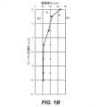
図1Aは、膜が堆積され得る基板フィーチャを示す。いくつかの実施態様では、膜は、深さと幅とを有するフィーチャに堆積可能であり、深さと幅のアスペクト比は、約30:1である。堆積された膜は、側壁に堆積されたその厚みによって特徴付けられ、フィーチャの上部およびフィーチャの底部での堆積された厚みを比較することで、コンフォーマル性の測定を実施できる。Figure 1A shows a substrate feature onto which a film may be deposited. In some implementations, the film may be deposited into a feature having a depth and width, with the aspect ratio of the depth to the width being approximately 30:1. The deposited film is characterized by its thickness deposited on the sidewalls, and a conformality measurement can be performed by comparing the deposited thickness at the top of the feature and the bottom of the feature.
図1Bは、ケイ素含有前駆体としてBTBAS(ビス(t-ブチルアミノ)シラン)を用いて堆積した膜を示す。膜301を、BTBASの熱分解温度(約550℃である)を超える温度における熱ALDプロセスを用いて堆積させた。膜302を、熱分解温度よりも低い温度における熱ALDプロセスを用いて堆積させた。図1Bに示すように、膜302はコンフォーマルであるが、膜301はフィーチャの上部付近に追加の堆積を有し、コンフォーマル性が100%から約30%に低下しており、望ましくない。膜301におけるフィーチャの上部の過剰な堆積は、BTBASの熱分解に起因するものであり、その結果、表面媒介されていないCVD成分が生じる。Figure 1B shows films deposited using BTBAS (bis(t-butylamino)silane) as the silicon-containing precursor. Film 301 was deposited using a thermal ALD process at a temperature above the thermal decomposition temperature of BTBAS, which is about 550°
このCVD成分に対処するため、原子層堆積(ALD)プロセスは、基板を反応剤に曝す変換プロセスよりも低い温度で前駆体を送ってもよい。具体的には、前駆体送出動作の間、基板の温度を前駆体の熱分解温度よりも低くし、次に基板の温度を、前駆体を反応剤と反応させる後続の動作の間、熱分解温度よりも高くしてもよい。いくつかの実施形態では、堆積層が、窒化ケイ素膜である。しかし、本明細書に記載の技術は、処理動作の温度よりも低い熱分解温度を有する、他の前駆体、例えば、炭素含有前駆体またはケイ素含有前駆体と共に使用してもよい。To address this CVD component, atomic layer deposition (ALD) processes may deliver precursors at lower temperatures than conversion processes that expose the substrate to reactants. Specifically, the temperature of the substrate may be lower than the thermal decomposition temperature of the precursor during the precursor delivery operation, and then the temperature of the substrate may be higher than the thermal decomposition temperature during a subsequent operation that reacts the precursor with the reactant. In some embodiments, the deposition layer is a silicon nitride film. However, the techniques described herein may be used with other precursors, e.g., carbon-containing precursors or silicon-containing precursors, that have thermal decomposition temperatures lower than the temperatures of the processing operations.
いくつかの実施形態では、ALDプロセスが、処理動作中に基板が載置される台座を有するプロセスチャンバ内で実施されてもよい。台座は、処理動作中の基板の温度を、例えば、600℃以上まで上昇させるように制御可能な加熱要素を含んでもよい。基板の温度を低下させるために、加熱要素の温度を下げることもできるが、このタイプの冷却は遅すぎるため、スループットの点で許容できない。In some embodiments, the ALD process may be performed in a process chamber having a pedestal on which the substrate rests during processing operations. The pedestal may include a heating element that is controllable to raise the temperature of the substrate during processing operations, for example to 600° C. or higher. To reduce the temperature of the substrate, the temperature of the heating element may be reduced, but this type of cooling may be too slow to be acceptable in terms of throughput.
許容可能な時間制約内で基板を冷却するために、いくつかの実施形態では、パージガスを流しながら、プロセスチャンバの圧力を下げる。プロセスチャンバの圧力を下げることにより、台座がより高い温度に維持されていたとしても、基板の温度を直ちに低下させ得る。理論に縛られるものではないが、プロセスチャンバの圧力を下げることにより、ウエハに真空冷却効果が生じ得る。ウエハの真空冷却は、パージガスを流しながら実施してもよい。プロセスチャンバの圧力と、低下した圧力においてパージガスを流す持続時間に基づいて、前駆体送出ステップに先立って基板の温度を調整してもよい。ウエハを前駆体の熱分解温度よりも低く冷却することで、後続の前駆体送出ステップで熱分解を生じさせずに基板の表面を飽和させ得るため、結果として、CVD成分を有しない表面媒介ステップとなる。その後、反応剤を送る前に、ウエハの温度を上昇させてもよい。パージガスは、任意の不活性ガス、例えば、N2、アルゴン、ヘリウム、キセノン等を含んでもよい。いくつかの実施形態では、H2が、不活性ガスと共に流されてもよい。水素を共に流すことにより、温度低下の速度を上昇させてもよい。 In order to cool the substrate within acceptable time constraints, in some embodiments, the process chamber pressure is reduced while the purge gas is flowing. Reducing the process chamber pressure may immediately reduce the temperature of the substrate even if the pedestal is maintained at a higher temperature. Without being bound by theory, reducing the process chamber pressure may create a vacuum cooling effect on the wafer. Vacuum cooling of the wafer may be performed while the purge gas is flowing. The temperature of the substrate may be adjusted prior to the precursor delivery step based on the process chamber pressure and the duration of the purge gas flow at the reduced pressure. Cooling the wafer below the precursor thermal decomposition temperature may saturate the substrate surface without thermal decomposition in the subsequent precursor delivery step, resulting in a surface-mediated step without a CVD component. The wafer temperature may then be increased before reactant delivery. The purge gas may include any inert gas, such asN2 , argon, helium, xenon, etc. In some embodiments,H2 may be flowed along with the inert gas. Co-flowing with hydrogen may increase the rate of temperature reduction.
図2は、本明細書の様々な実施形態によるALDプロセスのフローチャートを提供する。図2は、ALDサイクルの様々な動作の圧力および温度についてのタイミング図を提供する、図3を参照して理解されてもよい。ALD「サイクル」という概念は、本明細書の様々な実施形態の議論に関連する。通常、1サイクルは、表面堆積反応を1回実施するために用いられる動作の最小限のセットである。1サイクルの結果、基板表面に少なくとも部分的な窒化ケイ素膜層が形成される。典型的には、ALDサイクルは、少なくとも1つの反応剤を基板表面に送り、吸着させてから、吸着させた反応剤を1つまたは複数の反応剤と反応させて、膜の部分層を形成する動作を含む。このサイクルは、反応剤または副生成物の1つを掃除し、かつ/または堆積した部分的な膜を加工するなどの特定の補助的動作を含んでもよい。通常、1サイクルは、固有の一連の動作の1つの過程を含む。ALDサイクルをn回繰り返して、膜厚を厚くしてもよい。2 provides a flow chart of an ALD process according to various embodiments herein. FIG. 2 may be understood with reference to FIG. 3, which provides a timing diagram for pressure and temperature for various operations of an ALD cycle. The concept of an ALD "cycle" is relevant to the discussion of various embodiments herein. Typically, a cycle is a minimum set of operations used to perform one surface deposition reaction. A cycle results in the formation of at least a partial silicon nitride film layer on the substrate surface. Typically, an ALD cycle includes operations of delivering and adsorbing at least one reactant to the substrate surface, and then reacting the adsorbed reactant with one or more reactants to form a partial layer of the film. The cycle may include certain auxiliary operations, such as cleaning one of the reactants or by-products and/or processing the deposited partial film. Typically, a cycle includes one course of a unique series of operations. An ALD cycle may be repeated n times to increase the film thickness.
膜は、任意の有用な基板の上に提供できる。基板は、シリコンウエハ、例えば、200mmウエハ、300mmウエハ、または450mmウエハであってもよく、その上に堆積された誘電体、導電体、または半導電体材料など、材料の1つまたは複数の層を有するウエハを含む。基板は、本明細書に記載するように、高アスペクト比(HAR)構造など、構造を含み得る。The film can be provided on any useful substrate. The substrate can be a silicon wafer, e.g., a 200 mm wafer, a 300 mm wafer, or a 450 mm wafer, including a wafer having one or more layers of material, such as a dielectric, conductive, or semiconductive material, deposited thereon. The substrate can include structures, such as high aspect ratio (HAR) structures, as described herein.
基板は、ビアまたはコンタクトホールなどの「フィーチャ」を有してもよく、この「フィーチャ」は、狭く、かつ/または内側に凹んだ開口、フィーチャ内の狭窄、および高アスペクト比のうちの1つまたは複数を特徴としてもよい。フィーチャは、上述した層の1つまたは複数に形成されてもよい。フィーチャの一例は、半導体基板または基板上の層における穴またはビアである。いくつかの実施形態では、フィーチャが、少なくとも約2:1、少なくとも約4:1、少なくとも約6:1、少なくとも約10:1、またはそれ以上のアスペクト比を有してもよい。フィーチャはまた、開口付近の寸法、例えば、約10nmから500nm、例えば約25nmから約300nmの間の開口直径または線幅を有してもよい。本開示の方法は、約150nm未満の開口を有するフィーチャを含む基板上で実施されてもよい。フィーチャのビアまたはトレンチを、未充填フィーチャまたはフィーチャと称してもよい。底部、閉端、またはフィーチャの内部からフィーチャ開口に向けて狭まった、内側に凹んだプロファイルを有し得るフィーチャである。The substrate may have a "feature", such as a via or contact hole, which may be characterized by one or more of a narrow and/or inwardly recessed opening, a constriction within the feature, and a high aspect ratio. The feature may be formed in one or more of the layers described above. An example of a feature is a hole or via in a semiconductor substrate or a layer on the substrate. In some embodiments, the feature may have an aspect ratio of at least about 2:1, at least about 4:1, at least about 6:1, at least about 10:1, or more. The feature may also have a dimension near the opening, e.g., an opening diameter or line width between about 10 nm and 500 nm, e.g., about 25 nm and about 300 nm. The methods of the present disclosure may be performed on a substrate including a feature with an opening of less than about 150 nm. The via or trench of the feature may be referred to as an unfilled feature or feature. A feature may have an inwardly recessed profile that narrows from the bottom, closed end, or interior of the feature toward the feature opening.
本明細書のいずれの方法においても、初期動作は、プロセスチャンバに基板を用意することを含み得る。プロセスチャンバは、約10mTorrから約30Torrの間、または約1から3Torrの間、または約0.5から22Torrの間のチャンバ圧力に設定されてもよい。チャンバ圧力は、本明細書に記載するように、ALDプロセスの動作中に変更してもよい。In any of the methods herein, the initial operations may include preparing a substrate in a process chamber. The process chamber may be set to a chamber pressure of between about 10 mTorr and about 30 Torr, or between about 1 and 3 Torr, or between about 0.5 and 22 Torr. The chamber pressure may be varied during operation of the ALD process as described herein.
基板は、約25℃から約900℃の間、または約500℃から約700℃の間の基板温度に加熱されてもよい。本明細書で使用される場合、基板温度は基板の温度を指し、基板の温度は、基板を保持する台座に設定される温度とは異なってもよく、いくつかの実施形態では、台座上のプロセスチャンバに設けられるときに基板を所望の基板温度に、基板を処理するのに先だって加熱してもよいと理解されるであろう。台座の温度は本明細書に記載するように、動作の間中ずっと同じであってもよいが、基板温度は、本明細書に記載するように、ALDプロセスの動作の間に変更してもよい。The substrate may be heated to a substrate temperature between about 25° C. and about 900° C., or between about 500° C. and about 700° C. As used herein, substrate temperature refers to the temperature of the substrate, and it will be understood that the temperature of the substrate may be different than the temperature set on the pedestal that holds the substrate, and in some embodiments, the substrate may be heated to a desired substrate temperature when placed in the process chamber on the pedestal prior to processing the substrate. The temperature of the pedestal may be the same throughout operation as described herein, while the substrate temperature may be changed during operation of the ALD process as described herein.
図2に戻ると、動作200では、基板をプロセスチャンバに設ける。いくつかの実施形態では、基板を、基板を支持するプロセスチャンバ内の台座の温度になるまで加熱してもよい。台座の温度は、第1の温度、すなわち、例えば、約550℃よりも高く、約600℃よりも高く、約650℃よりも高く、約700℃よりも高く、約550℃から約700℃の間であってもよい。いくつかの実施形態では、第1の温度が、基板に送られる前駆体の熱分解温度よりも高い。いくつかの実施形態では、動作200の間、プロセスチャンバの圧力が、少なくとも約1Torr、少なくとも約5Torr、または少なくとも約10Torrである。Returning to FIG. 2, in
動作210では、基板を低圧でパージガスに曝す。いくつかの実施形態では、低圧は、動作200におけるプロセスチャンバの圧力よりも低い任意の圧力であってもよい。いくつかの実施形態では、低圧が、約1Torr未満、約0.5Torr未満、約0.1Torr未満、または約10mTorr未満であってもよい。動作210の持続時間は、前駆体の熱分解温度に基づいていてもよい。通常、低圧パージの持続時間が長いほど、基板の温度がさらに低下する。いくつかの実施形態では、低圧パージの持続時間が、少なくとも約1秒、少なくとも約5秒、少なくとも約10秒、少なくとも約20秒、少なくとも約30秒、または約1秒から約30秒の間であってもよい。いくつかの実施形態では、動作210の持続時間は、基板温度が熱分解温度よりも低くなるのに要する時間に基づく。動作210の終了時、基板は、第2の温度であってもよく、第2の温度は、第1の温度よりも低い。いくつかの実施形態では、第2の温度が、送られる前駆体の熱分解温度よりも低い。いくつかの実施形態では、動作210の間、基板の温度が、少なくとも約50℃、少なくとも約70℃、少なくとも約100℃、少なくとも約150℃、または約50℃から約150℃の間だけ低下する。In
パージガスを、約1000sccmから約40000sccmの間(例えば、約100から2000sccm)の流量で、基板を収容するチャンバに流すことができる。いくつかの実施形態では、パージガスが、その熱伝導率に基づいて選択されてもよいし、またはより高い熱伝導率を有する他のガスと共に流されてもよい。より高い熱伝導率のガスは、パージ動作中により多くの熱エネルギーを吸収することにより、チャンバの冷却の速度を上昇させる。水素ガスおよびヘリウムガスは、アルゴンまたはN2などの他の不活性ガスに比べて、熱伝導率が高い(300Kで約0.182および0.151W/mK)ことで知られる。いくつかの実施形態では、パージガスが、H2と共に流されてもよい。水素を不活性ガスと共に流すことにより、不活性ガスのみを流すのと比べ、動作210中に基板温度のより急速な低下を引き起こしてもよく、これにより、基板を前駆体の熱分解温度よりも低くするのに必要な動作210の持続時間が短くなることで、スループットが向上する。 The purge gas may be flowed into the chamber housing the substrate at a flow rate between about 1000 sccm and about 40000 sccm (e.g., about 100 to 2000 sccm). In some embodiments, the purge gas may be selected based on its thermal conductivity or may be flowed with other gases having higher thermal conductivity. Gases with higher thermal conductivity increase the rate of cooling of the chamber by absorbing more heat energy during the purge operation. Hydrogen and helium gases are known to have higher thermal conductivity (about 0.182 and 0.151 W/mK at 300 K) compared to other inert gases such as argon orN2 . In some embodiments, the purge gas may be flowed withH2 . Flowing hydrogen with the inert gas may cause a more rapid drop in the substrate temperature during
動作220では、基板を前駆体に曝す。前駆体は、基板の表面に吸着する。前駆体は、ケイ素含有前駆体、炭素含有前駆体、または他の前駆体であってもよい。基板の温度は、動作220の少なくとも一部の間、第2の温度であってもよい。いくつかの実施形態では、基板の温度が、動作220の間中ずっと、第2の温度程度である。いくつかの実施形態では、基板の温度が動作220の開始時に第2の温度程度であり、基板の温度が動作220の間に上昇する。いくつかの実施形態では、基板が、複数の前駆体に曝されてもよい。そのような実施形態では、各前駆体が、異なる熱分解温度を有してもよく、この場合第2の温度は、最も低い熱分解温度に基づく。いくつかの実施形態では、第2の温度が、複数の前駆体の熱分解温度の間であってもよい。In
いくつかの実施形態では、前駆体が、約100sccmから約5000sccmの間(例えば、約100から約2000sccm)の流量で、基板を収容するチャンバに流される。前駆体を、任意の有用な期間(例えば、約0.1から10秒)および任意の有用な圧力(例えば、約1から25Torr)で流すことができる。In some embodiments, the precursors are flowed into a chamber containing a substrate at a flow rate between about 100 sccm and about 5000 sccm (e.g., about 100 to about 2000 sccm). The precursors can be flowed for any useful period of time (e.g., about 0.1 to 10 seconds) and at any useful pressure (e.g., about 1 to 25 Torr).
動作220の間、不活性ガスを前駆体と共に流してもよい。不活性ガスは、窒素(N2)、アルゴン(Ar)、またはその他の本明細書で挙げられたものであってもよい。不活性ガスは、プロセスチャンバの圧力および/または温度制御、液体反応剤の蒸発、反応剤のより迅速な送出をアシストするために、かつ/またはプロセスチャンバおよび/またはプロセスチャンバ配管からプロセスガスを除去するためのパージガスとして提供されてもよい。いくつかの実施形態では、不活性ガスが、約100sccmから約5000sccmの間(例えば、約500から約2000sccm)の流量で、基板を収容するチャンバに流される。不活性ガスを前駆体と共に流すことにより、動作中の圧力が安定するだけではなく、前駆体の希釈ができる。 During
いくつかの実施形態では、動作220が、動作210よりも高いプロセスチャンバ圧力、例えば、200中のプロセスチャンバの圧力で実施されてもよい。他の実施形態では、プロセスチャンバの圧力が、動作200および210中の加圧間の第3の圧力であってもよい。この第3の圧力は、動作220中、基板の温度を前駆体の熱分解温度よりも低い第2の温度に維持することに基づいてもよい。いくつかの実施形態では、第3の圧力が、約1Torr、または約1Torrから約10Torrの間であってもよい。In some embodiments,
動作230では、プロセスチャンバを任意選択でパージして、基板表面に吸着しなかった前駆体分子を除去する。いくつかの実施形態では、プロセスチャンバの圧力を動作230の間に上昇させて、後続の変換動作(240)のために基板の温度を上昇させ易くする。In
チャンバをパージすることは、パージガスまたはスイープガスを流すことを含み、パージガスまたはスイープガスは、他の動作に使用されるキャリアガスであってもよいし、または異なるガスであってもよい。いくつかの実施形態では、パージが、チャンバを排気することを伴ってもよい。パージガスの例としては、アルゴン(Ar)、窒素(N2)、水素(H2)、ヘリウム(He)、酸素(O2)、クリプトン(Kr)、キセノン(Xe)、ネオン(Ne)、およびこれらの組み合わせが挙げられる。様々な実施形態において、パージガスが、不活性ガスである。パージガスは、1つまたは複数のガスを含んでもよい。いくつかの実施形態では、動作230が、プロセスチャンバを排気するための1つまたは複数の排気副段階を含んでもよい。あるいは、いくつかの実施形態でが、動作230を省略してもよいことが理解されるであろう。動作230は、約0秒から約60秒の間、例えば約0.01秒など、任意の適切な持続時間を有してもよい。いくつかの実施形態では、1つまたは複数のパージガスの流量を増加させることにより、動作230の持続時間を短縮してもよい。例えば、パージガス流量は、様々な反応剤の熱力学的特性、および/またはプロセスチャンバならびに/もしくはプロセスチャンバ配管の幾何学的特性に従って、動作230の持続時間を修正するために調節されてもよい。非限定的な一例では、パージガス流量を調整することにより、パージ段階の持続時間を調節してもよい。これにより、堆積サイクルタイムが短縮され、基板のスループットが向上され得る。パージ後、前駆体分子は、基板表面に吸着したままである。 Purging the chamber includes flowing a purge or sweep gas, which may be a carrier gas used in other operations or may be a different gas. In some embodiments, purging may involve evacuating the chamber. Examples of purge gases include argon (Ar), nitrogen (N2 ), hydrogen (H2 ), helium (He), oxygen (O2 ), krypton (Kr), xenon (Xe), neon (Ne), and combinations thereof. In various embodiments, the purge gas is an inert gas. The purge gas may include one or more gases. In some embodiments,
パージガスを、約1000sccmから約40000sccmの間(例えば、約100から2000sccm)の流量で、基板を収容するプロセスチャンバに流すことができる。パージガスを、任意の有用な期間(例えば、約0.1から10秒)および任意の有用な圧力(例えば、約0.5から25Torr)で流すことができる。The purge gas can be flowed into the process chamber containing the substrate at a flow rate between about 1000 sccm and about 40,000 sccm (e.g., about 100 to 2000 sccm). The purge gas can be flowed for any useful period of time (e.g., about 0.1 to 10 seconds) and at any useful pressure (e.g., about 0.5 to 25 Torr).
動作240では、基板をプラズマの有無にかかわらず、反応剤ガスに曝し、吸着した前駆体と反応させて、膜を形成する。様々な実施形態において、反応剤ガスが、窒素含有反応剤または酸素含有反応剤を含む、1つまたは複数の反応剤を含んでもよい。窒素含有反応剤または酸素含有反応剤を、約1000sccmから約40000sccmの間(例えば、約2000から10000sccm)の流量で、基板を収容するプロセスチャンバに流すことができる。反応剤を、任意の有用な期間(例えば、約0.5から40秒)および任意の有用な圧力(例えば、約1から25Torr)で流すことができる。いくつかの実施形態では、動作240中のプロセスチャンバの圧力が、少なくとも約5Torrまたは少なくとも約10Torrである。動作240中のプロセスチャンバの圧力は、動作240中の基板の温度をより高く維持するために、動作210または220と比較して高くてもよい。いくつかの実施形態では、動作240が、1つまたは複数の反応剤を吸着された前駆体と反応させるための熱変換動作であってもよい。In
反応剤ガスは、プッシュガスまたはキャリアガスと共に使用できる。プッシュガスまたはキャリアガスは、本明細書に記載のものなど、不活性ガスであってもよい。プッシュガスまたはキャリアガスを、約100sccmから約5000sccmの間(例えば、約500から2000sccm)の流量で、基板を収容するチャンバに流すことができる。プッシュガスまたはキャリアガスは、任意の有用な期間(例えば、約0.5から40秒)および任意の有用な圧力(例えば、約1から25Torr)で流すことができる。The reactant gas may be used with a push gas or carrier gas. The push gas or carrier gas may be an inert gas, such as those described herein. The push gas or carrier gas may be flowed into the chamber housing the substrate at a flow rate of between about 100 sccm and about 5000 sccm (e.g., about 500 to 2000 sccm). The push gas or carrier gas may be flowed for any useful period of time (e.g., about 0.5 to 40 seconds) and at any useful pressure (e.g., about 1 to 25 Torr).
さらに他の実施形態では、反応剤が、還元ガスと共に流されることをさらに含み得る。非限定的な還元ガスとしては、水素(H2)を含み得る。非限定的な一例では、動作120は、窒素含有反応剤(例えば、NH3またはN2)、還元ガス(例えば、H2)、および任意選択で不活性ガス(例えば、N2)を含む。還元ガスを、約0sccmから約10000sccmの間(例えば、約0から5000sccm)の流量で、基板を収容するチャンバに流すことができる。還元ガスを、任意の有用な期間(例えば、約0.5から40秒)および任意の有用な圧力(例えば、約1から25Torr)で流すことができる。 In yet another embodiment, the reactant may further include being flowed with a reducing gas. A non-limiting reducing gas may include hydrogen (H2 ). In one non-limiting example, operation 120 includes a nitrogen-containing reactant (e.g.,NH3 orN2 ), a reducing gas (e.g., H2), and optionally an inert gas (e.g.,N2 ). The reducing gas may be flowed into the chamber housing the substrate at a flow rate between about 0 sccm and about 10,000sccm (e.g., about 0 to 5,000 sccm). The reducing gas may be flowed for any useful period of time (e.g., about 0.5 to 40 seconds) and at any useful pressure (e.g., about 1 to 25 Torr).
いくつかの実施形態では、動作240が、基板をエネルギー性の種(例えば、ラジカル種)に曝すことを含んでもよい。様々な実施形態において、ラジカル種が、ソースガスから生成され、ソースガスは、例えば、酸素および/または窒素原子を含む。さらに他の実施形態では、ソースガスが、還元ガスと共に流されることをさらに含み得る。いくつかの実施形態では、ラジカル種が、NH*ラジカル種またはNR*ラジカル種であり、この場合Rは、H、脂肪族、芳香族、ヘテロ脂肪族、またはヘテロ芳香族である。NH*ラジカル種は、NH3、N2/NH3、またはN2/H2プラズマを用いるなど、任意の有用な方法で生成できる。プラズマ生成中、任意の有用なプロセス条件を変更でき、ここで条件は、圧力、ガス比混合物、およびプラズマ電力(例えば、より高い電力は、より高いラジカルフラックスを提供できる)を含み得る。 In some embodiments,
SiN膜を堆積させるための他のラジカル種は、元素窒素ラジカル、アンモニアラジカル、およびアミンラジカルを含み得る。アミンラジカルの例としては、メチルアミン、ジメチルアミン、およびアニリンのラジカルが挙げられるが、これらに限定されない。いくつかの実施形態では、すべてまたは実質的にすべてのラジカルが、基底状態にある可能性があり、例えば、基板に隣接するラジカルの少なくとも約90%または95%が基底状態にある。いくつかの実施形態では、以下でさらに詳述するように、ラジカル種をリモートプラズマ源によって生成できる。Other radical species for depositing SiN films may include elemental nitrogen radicals, ammonia radicals, and amine radicals. Examples of amine radicals include, but are not limited to, methylamine, dimethylamine, and aniline radicals. In some embodiments, all or substantially all radicals may be in the ground state, e.g., at least about 90% or 95% of the radicals adjacent to the substrate are in the ground state. In some embodiments, the radical species may be generated by a remote plasma source, as described in more detail below.
特定の実施形態では、ラジカル種が、N2とNH3との組み合わせ、またはN2とH2との組み合わせから形成されたプラズマを用いて形成される。理解されるように、プラズマは、窒素含有反応剤のみ、または窒素含有反応剤と還元ガス(例えば、水素またはH2など)との組み合わせによって形成できる。さらに、窒素含有反応剤と共に不活性ガスを採用できる。プラズマを、約0sccmから約10000sccmの間(例えば、約0から5000sccm)の流量で、基板を収容するチャンバに移送できる。還元ガスを、任意の有用な期間(例えば、約0.5から40秒)および任意の有用な圧力(例えば、約0.5から25Torr)で流すことができる。 In certain embodiments, radical species are formed using a plasma formed from a combination ofN2 andNH3 or a combination ofN2 andH2 . As will be appreciated, the plasma can be formed with only the nitrogen-containing reactant or a combination of the nitrogen-containing reactant and a reducing gas (e.g., hydrogen orH2 , etc.). Additionally, an inert gas can be employed with the nitrogen-containing reactant. The plasma can be delivered to a chamber housing the substrate at a flow rate between about 0 sccm and about 10,000 sccm (e.g., about 0 to 5,000 sccm). The reducing gas can be flowed for any useful period of time (e.g., about 0.5 to 40 seconds) and at any useful pressure (e.g., about 0.5 to 25 Torr).
一実施形態では、プラズマは、第1の窒素含有反応剤(例えば、約20から500sccmの流量を有する)、不活性ガス(例えば、約1000から40000sccmの流量を有する)、および還元ガス(例えば、約0から200sccmの流量を有する)の存在下で形成される。特定の実施形態では、プラズマが、NH3を含む第1の窒素含有反応剤(例えば、約50から250sccmの流量を有する)、N2を含む不活性ガス(例えば、約5000から25000sccmの流量を有する)、およびH2を含む還元ガス(例えば、約0から100sccmの流量を有する)の存在下で形成される。 In one embodiment, the plasma is formed in the presence of a first nitrogen-containing reactant (e.g., having a flow rate of about 20 to 500 sccm), an inert gas (e.g., having a flow rate of about 1000 to 40000 sccm), and a reducing gas (e.g., having a flow rate of about 0 to 200 sccm). In a particular embodiment, the plasma is formed in the presence of a first nitrogen-containing reactant comprisingNH3 (e.g., having a flow rate of about 50 to 250 sccm), an inert gas comprisingN2 (e.g., having a flow rate of about 5000 to 25000 sccm), and a reducing gas comprisingH2 (e.g., having a flow rate of about 0 to 100 sccm).
プラズマ電力は、300mmのウエハ表面積あたり約75Wから約12000Wの間である。プラズマは、リモートで(例えば、リモートプラズマ発生器においてなど)生成されてもよいし、または基板を収容するチャンバ内で直接生成されてもよい(すなわち、その場で(in situ))。その場のプラズマは、約0.2122W/cm2から約2.122W/cm2の間の基板面積あたりの電力で点火されてもよい。例えば、4枚の300mmウエハを処理するチャンバでは、電力が約600Wから約6000Wの範囲であってもよい。ALDプロセス用のプラズマは、2枚の容量結合プレートを使用してガスに無線周波数(RF)場を適用することによって生成されてもよい。RF場によってプレート間のガスがイオン化されることで、プラズマが点火され、プラズマ放電領域において自由電子が生成される。これらの電子は、RF場によって加速され、気相反応分子と衝突する場合がある。これらの電子が反応分子と衝突することで、堆積プロセスに加わるラジカル種を形成する場合がある。 The plasma power is between about 75 W and about 12000 W per 300 mm wafer surface area. The plasma may be generated remotely (e.g., in a remote plasma generator) or directly in the chamber housing the substrate (i.e., in situ). The in situ plasma may be ignited with a power between about 0.2122 W/cm2 and about 2.122 W/cm2 per substrate area. For example, in a chamber processing four 300 mm wafers, the power may range from about 600 W to about 6000 W. The plasma for the ALD process may be generated by applying a radio frequency (RF) field to the gas using two capacitively coupled plates. The RF field ionizes the gas between the plates, igniting the plasma and generating free electrons in the plasma discharge region. These electrons may be accelerated by the RF field and collide with gas-phase reactant molecules. These collisions with the reactant molecules may form radical species that participate in the deposition process.
動作240中、RF場は任意の適切な電極を介して結合されてもよいことが理解されるであろう。電極の非限定的な例としては、プロセスガス分配シャワーヘッドおよび基板支持台座が挙げられる。ALDプロセス用のプラズマは、RF場をガスに容量結合させること以外の1つまたは複数の適切な方法によって形成されてもよいことが理解されるであろう。いくつかの実施形態では、プラズマがリモートプラズマであり、窒素含有反応剤または酸素含有反応剤またはソースガスがステーションの上流にあるリモートプラズマ発生器において点火されてから、基板が収容されているステーションに移送される。It will be appreciated that during
動作210~240を、膜、例えば、酸化ケイ素膜または窒化ケイ素膜を所望の厚さに堆積するのに十分なサイクルで繰り返してもよい。任意の適切な数の堆積サイクルをALDプロセスに含めて、所望の膜厚を堆積させてもよい。例えば、約20から約40回の堆積サイクルを実施して、本開示の実施形態を用いて基板上に窒化ケイ素膜を堆積させてもよい。Operations 210-240 may be repeated for a number of cycles sufficient to deposit a film, e.g., a silicon oxide or silicon nitride film, to a desired thickness. Any suitable number of deposition cycles may be included in an ALD process to deposit a desired film thickness. For example, about 20 to about 40 deposition cycles may be performed to deposit a silicon nitride film on a substrate using embodiments of the present disclosure.
図3は、本明細書の実施形態による様々なALDサイクルの温度および圧力の例示的なタイミング図を示す。図310~図340はそれぞれ、異なるセットのALDサイクルに対応する。図310は、典型的な等圧ALDプロセスを示し、投与、パージ、変換、およびパージの各ステップが同じ圧力で実施される。図320~図340は、図2のフローチャートに対応する様々な低圧パージALDプロセスを示す。図310では、投与段階310Aは、本明細書に記載するように、前駆体に基板を曝すことを指す。変換段階310Cは、本明細書に記載するように、反応剤に基板を曝すことを指す。パージ段階310Bおよび310Dは、いかなる前駆体または反応剤も使用せずにパージガスに基板を曝すことを指す。図310では、両方のパージ段階が、同じ圧力で実施される。いくつかの実施形態では、パージ段階が、本明細書に記載の低圧パージ動作(特に、投与動作前のパージ動作)であってもよいが、パージ動作のいくつかは低圧パージ動作でなくてもよい。FIG. 3 illustrates an exemplary timing diagram of temperature and pressure for various ALD cycles according to embodiments herein. Each of FIGS. 310-340 corresponds to a different set of ALD cycles. FIG. 310 illustrates a typical isobaric ALD process, where the dosing, purging, converting, and purging steps are performed at the same pressure. FIGS. 320-340 illustrate various low-pressure purge ALD processes corresponding to the flow chart of FIG. 2. In FIG. 310,
時間/温度図には、段階310A~Dに対応する段階が表示されている。特に、「パージ(D)」と表示された左端の段階は、パージ段階310D~340Dに対応する。ALDは周期的なプロセスであるため、パージ段階310D~340Dは、投与段階310A~340Aの前に実施されてもよい。The time/temperature diagram shows steps corresponding to
図310は、すべての動作が同じプロセスチャンバ圧力、例えば、10Torrで実施される等圧ALDプロセスを示す。基板は、それに対応して同じ温度、例えば610℃を維持してもよく、そのため投与段階中にCVD成分を有する場合があるが、これは望ましくない。基板の温度とプロセスチャンバの圧力は、ALDサイクルのどの段階中にも変化しない。Diagram 310 shows an isobaric ALD process in which all operations are performed at the same process chamber pressure, e.g., 10 Torr. The substrate may correspondingly be maintained at the same temperature, e.g., 610° C., so that it may have a CVD component during the dose phase, which is undesirable. The substrate temperature and process chamber pressure do not change during any phase of the ALD cycle.
図320~図340は、ALDサイクルの1つまたは複数の段階の圧力をどのように低下させれば、投与段階の少なくとも一部の間に基板の温度を低下させ得るかを示す。図320では、パージ段階320Dが低圧で実施される一方、投与段階320A、パージ段階320B、および変換段階320Cは、より高い圧力で実施される。いくつかの実施形態では、パージ段階320Dが、約1Torr未満、約0.5Torr未満、約0.1Torr未満、または約10mTorr未満の圧力で実施されてもよい。いくつかの実施形態では、段階320A~Cが、少なくとも約1Torr、少なくとも約5Torr、または少なくとも約10Torrの圧力で実施されてもよい。温度チャートに示すように、パージ段階320Dの間、基板の温度は、約610℃から約520℃まで低下する。その後の投与段階320Aでは、プロセスチャンバの圧力が上昇するにつれて、例えば、ウエハを支持する台座と均衡するまで基板の温度が上昇し、ウエハが約610℃になってもよい。パージ段階320Bおよび変換段階320Cは、このウエハ温度およびプロセスチャンバ圧力で実施されてもよい。このサイクルを繰り返すことで、各投与前パージ段階を低圧とし、その後の投与段階の基板の温度を低下させてもよい。320-340 illustrate how the pressure of one or more stages of an ALD cycle can be reduced to reduce the temperature of the substrate during at least a portion of the dose stage. In FIG. 320, the
図330は、本明細書の実施形態によるALDサイクル段階の別の例を示す。図330では、パージ段階330Dが、パージ段階320Dと同じであってもよい。また、投与段階330Aは、低圧で実施されてもよい。とりわけ、投与段階330Aの間のチャンバ圧力が、パージ段階330Dの間のチャンバ圧力よりも高くてもよい。投与段階330Aの間のチャンバ圧力は、基板の温度を低下または上昇させることではなく、基板の温度を維持することに基づいてもよい。温度図に示すように、投与段階330Aの間、基板の温度は、実質的に同じままである。他の実施形態では、基板の温度が、投与段階330Aの間に上昇してもよいが、チャンバ圧力が低下しなかったときよりも遅い速度、例えば、投与段階320Aの間よりも遅い速度である。投与段階330Aの間のプロセスチャンバ圧力は、パージ段階320Dの間のプロセスチャンバの圧力と、段階320B~Cの間のプロセスチャンバの圧力との間であってもよい。いくつかの実施形態では、段階330Aの間の圧力が、少なくとも約1Torr、約1Torr、または約1Torrから約10Torrの間であってもよい。330 illustrates another example of ALD cycle stages according to embodiments herein. In FIG. 330,
基板温度は、投与段階330Aの間は低いままであるため、変換段階330Cに先立つパージ段階330Bの間に、基板の温度が上昇してもよい。高い基板温度で変換段階を実施させることが望ましいため、パージ段階330Bは、ウエハの温度が台座と熱平衡の高温、例えば、約610℃まで上昇させ得るのに十分な持続時間実施されてもよい。Because the substrate temperature remains low during the
図340は、本明細書の実施形態によるALDサイクル段階の別の例を示す。段階340A、340B、および340Dは、図330と同じプロセスチャンバ圧力下(図示のように、または代替として図320と同じプロセス条件で)で実施されてもよい。変換段階340Cは、変換中の基板の温度をさらに上昇させるために、プラズマの存在下で実施してもよい。より高い電力、例えば、少なくとも約2000W、少なくとも約3000W、少なくとも約5000W、または少なくとも約6000Wでプラズマを点火することによって、基板温度を、例えば、約640℃までさらに上昇させてもよい。いくつかの実施形態では、プラズマに給電する電極への電力は、その後、パージ段階340Dの間に減少/除去されてもよく、これにより、基板の温度を、低い基板温度での後続の投与ステップに先だって低下させてもよい。Figure 340 illustrates another example of ALD cycle stages according to embodiments herein.
とりわけ、図320~図340のそれぞれにおける基板の温度が変化するが、この温度変化は、プロセスチャンバ内の加熱要素(例えば台座)のいずれかを変化させるのではなく、プロセスチャンバの圧力を変化させた結果である。圧力を変化させることによる基板の冷却は、加熱要素に送られる電力を調節するよりも効果的かつ効率的である場合があり、その結果、基板が前駆体の熱分解温度よりも高い温度で反応剤に曝される後続の変換ステップとは異なる基板温度で前駆体が基板の表面に吸着され得るALDプロセスとなる。Notably, the temperature of the substrate in each of Figs. 320-340 changes, but this temperature change is the result of changing the pressure of the process chamber rather than changing any of the heating elements (e.g., the pedestal) within the process chamber. Cooling the substrate by changing the pressure can be more effective and efficient than adjusting the power sent to the heating elements, resulting in an ALD process in which the precursors may be adsorbed onto the surface of the substrate at a different substrate temperature than the subsequent conversion step in which the substrate is exposed to reactants at a temperature above the thermal decomposition temperature of the precursor.
本明細書に記載のプロセスを、ケイ素含有膜、炭素含有膜、金属膜、またはその他の誘電体膜を含む、様々な膜を堆積させるために用いてもよい。いくつかの実施形態では、本明細書に記載のプロセスに従って堆積された膜が、酸化ケイ素膜、窒化ケイ素膜、または酸窒化ケイ素膜であってもよい。特に、本明細書に記載のプロセスは、基板の表面に吸着される前駆体が、吸着された前駆体が反応剤に曝される変換ステップの温度よりも低い熱分解温度を有する場合に、膜を堆積させるために用いてもよい。一例では、この方法により、コンフォーマルなSiN膜を提供でき、SiN膜は、高アスペクト比(HAR)構造上に堆積される。一実施形態では、(幅に対する奥行きの)アスペクト比が約30:1以上である。ALDプロセスの後、得られた膜は、コンフォーマルな膜(例えば、100%のステップカバレッジを有する)となり得る。The processes described herein may be used to deposit a variety of films, including silicon-containing films, carbon-containing films, metal films, or other dielectric films. In some embodiments, the films deposited according to the processes described herein may be silicon oxide, silicon nitride, or silicon oxynitride films. In particular, the processes described herein may be used to deposit films where the precursor adsorbed on the surface of the substrate has a pyrolysis temperature lower than the temperature of the conversion step in which the adsorbed precursor is exposed to a reactant. In one example, the method can provide a conformal SiN film, which is deposited on a high aspect ratio (HAR) structure. In one embodiment, the aspect ratio (depth to width) is about 30:1 or greater. After the ALD process, the resulting film can be a conformal film (e.g., with 100% step coverage).
いくつかの実施形態では、本明細書の方法により、側壁に堆積された膜の成長速度が上がる。より低温の前駆体曝露プロセスにより、基板をより高温で前駆体に曝すプロセスと比較して、成長速度を向上させ得る。したがって、いくつかの実施形態では、本明細書に記載の低温投与および高温変換プロセスにより、膜の成長速度を向上させ、スループットを改善し得る。In some embodiments, the methods herein increase the growth rate of films deposited on the sidewalls. A lower temperature precursor exposure process can increase the growth rate compared to processes in which the substrate is exposed to the precursor at a higher temperature. Thus, in some embodiments, the low temperature dosing and high temperature conversion process described herein can increase the film growth rate and improve throughput.
ケイ素含有膜を堆積させるために、1つまたは複数のケイ素含有前駆体を使用してもよい。本開示の実施形態に従った使用に適したケイ素含有前駆体としては、ポリシラン(H3Si-(SiH2)n-SiH3)が挙げられ、この場合n≧0である。シランの例としては、シラン(SiH4)、ジシラン(Si2H6)、およびメチルシラン、エチルシラン、イソプロピルシラン、t-ブチルシラン、ジメチルシラン、ジエチルシラン、ジ-t-ブチルシラン、アリルシラン、sec-ブチルシラン、テキシルシラン、イソアミルシラン、t-ブチルジシラン、ジ-t-ブチルジシランなどの有機シランが挙げられる。 To deposit a silicon-containing film, one or more silicon-containing precursors may be used. Silicon-containing precursors suitable for use according to embodiments of the present disclosure include polysilanes (H3 Si—(SiH2 )n —SiH3 ), where n≧0. Examples of silanes include silane (SiH4 ), disilane (Si2 H6 ), and organosilanes such as methylsilane, ethylsilane, isopropylsilane, t-butylsilane, dimethylsilane, diethylsilane, di-t-butylsilane, allylsilane, sec-butylsilane, thexylsilane, isoamylsilane, t-butyldisilane, and di-t-butyldisilane.
ハロシランは、少なくとも1つのハロゲン基を含み、水素および/または炭素基を含んでもよいし、含まなくてもよい。ハロシランの例としては、ヨードシラン、ブロモシラン、クロロシラン、およびフルオロシランが挙げられる。具体的なクロロシランは、テトラクロロシラン、トリクロロシラン、ジクロロシラン、モノクロロシラン、クロロアリルシラン、クロロメチルシラン、ジクロロメチルシラン、クロロジメチルシラン、クロロエチルシラン、t-ブチルクロロシラン、ジ-t-ブチルクロロシラン、クロロイソプロピルシラン、クロロ-sec-ブチルシラン、t-ブチルジメチルクロロシラン、テキシルジメチルクロロシラン等である。Halosilanes contain at least one halogen group and may or may not contain hydrogen and/or carbon groups. Examples of halosilanes include iodosilane, bromosilane, chlorosilane, and fluorosilane. Specific chlorosilanes include tetrachlorosilane, trichlorosilane, dichlorosilane, monochlorosilane, chloroallylsilane, chloromethylsilane, dichloromethylsilane, chlorodimethylsilane, chloroethylsilane, t-butylchlorosilane, di-t-butylchlorosilane, chloroisopropylsilane, chloro-sec-butylsilane, t-butyldimethylchlorosilane, thexyldimethylchlorosilane, and the like.
アミノシランは、ケイ素原子に結合した少なくとも1つの窒素原子を含むが、水素、酸素、ハロゲン、および炭素も含有してもよい。アミノシランの例としては、モノ-、ジ-、トリ-およびテトラ-アミノシラン(それぞれ、H3Si(NH2)、H2Si(NH2)2、HSi(NH2)3、およびSi(NH2)4)、ならびに置換モノ-、ジ-、トリ-およびテトラ-アミノシラン、例えば、t-ブチルアミノシラン、メチルアミノシラン、tert-ブチルシラナミン、ビス(tert-ブチルアミノ)シラン(SiH2(NHC(CH3)3)2(BTBAS))、tert-ブチルシリルカルバメート、SiH(CH3)-(N(CH3)2)2、SiHCl(N(CH3)2)2、(Si(CH3)2NH)3、ジイソプロピルアミノシラン(DIPAS)、ジ-sec-ブチルアミノシラン(DSBAS)、SiH2[N(CH2CH3)2]2(BDEAS)等である。アミノシランのさらなる例としては、トリシリルアミン(N(SiH3))である。いくつかの実施形態では、中心のSi原子に結合した2つ以上のアミン基を有するアミノシランを使用してもよい。これらは、単一のアミン基のみが結合したアミノシランよりも損傷を減らす結果となり得る。 Aminosilanes contain at least one nitrogen atom bonded to a silicon atom, but may also contain hydrogen, oxygen, halogens, and carbon. Examples of aminosilanes include mono-, di-, tri-, and tetra-aminosilanes (H3 Si(NH2 ), H2 Si(NH2 )2 , HSi(NH2 )3 , and Si(NH2 )4 , respectively), as well as substituted mono-, di-, tri-, and tetra-aminosilanes, such as t-butylaminosilane, methylaminosilane, tert-butylsilanamine, bis(tert-butylamino)silane (SiH2 (NHC(CH3 )3 )2 (BTBAS)), tert-butylsilylcarbamate, SiH(CH3 )-(N(CH3 )2 )2 , SiHCl(N(CH3 )2 )2 , (Si(CH3 )2 NH)3 . , diisopropylaminosilane (DIPAS), di-sec-butylaminosilane (DSBAS),SiH2 [N(CH2CH3 )2 ]2 (BDEAS), etc. A further example of an aminosilane istrisilylamine (N(SiH3 )). In some embodiments, aminosilanes with two or more amine groups attached to a central Si atom may be used. These may result in less damage than aminosilanes with only a single amine group attached.
ケイ素含有前駆体のさらなる例としては、トリメチルシラン(3MS)、エチルシラン、ブタシラン、ペンタシラン、オクタシラン、ヘプタシラン、ヘキサシラン、シクロブタシラン、シクロヘプタシラン、シクロヘキサシラン、シクロオクタシラン、シクロペンタシラン、1,4-ジオキサ2,3,5,6-テトラシラシクロヘキサン、ジエトキシメチルシラン(DEMS)、ジエトキシシラン(DES)、ジメトキシメチルシラン、ジメトキシシラン(DMOS)、メチルジエトキシシラン(MDES)、メチルジメトキシシラン(MDMS)、オクタメトキシドデカシロキサン(OMODDS)、tert-ブトキシジシラン、テトラメチルシクロテトラシロキサン(TMCTS)、テトラオキシメチルシクロテトラシロキサン(TOMCTS)、トリエトキシシラン(TES)、トリエトキシシロキサン(TRIES)、およびトリメトキシシラン(TMSまたはTriMOS)が挙げられる。Further examples of silicon-containing precursors include trimethylsilane (3MS), ethylsilane, butasilane, pentasilane, octasilane, heptasilane, hexasilane, cyclobutasilane, cycloheptasilane, cyclohexasilane, cyclooctasilane, cyclopentasilane, 1,4-dioxa-2,3,5,6-tetrasilacyclohexane, diethoxymethylsilane (DEMS), diethoxysilane (DES), dimethoxymethylsilane, dimethoxysilane Examples of such silanes include diphenyl ether (DMOS), methyldiethoxysilane (MDES), methyldimethoxysilane (MDMS), octamethoxydodecasiloxane (OMODDS), tert-butoxydisilane, tetramethylcyclotetrasiloxane (TMCTS), tetraoxymethylcyclotetrasiloxane (TOMCTS), triethoxysilane (TES), triethoxysiloxane (TRIES), and trimethoxysilane (TMS or TriMOS).
いくつかの実施態様では、ケイ素含有前駆体が、シロキサンまたはアミノ基含有シロキサンを含んでもよい。いくつかの実施形態では、本明細書で使用されるシロキサンが、X(R1)aSi-O-Si(R2)bYの式を有してもよく、ここで、aおよびbは0から2の整数であり、XおよびYは、独立してHまたはNR3R4とすることができ、R1、R2、R3、およびR4はそれぞれ、水素、非分岐アルキル、分枝アルキル、飽和複素環基、不飽和複素環基、またはそれらの組み合わせである。いくつかの実施形態では、少なくとも1つのXまたはYがNR3R4である場合、R3およびR4は、それぞれが結合している原子と一緒になって、飽和複素環化合物を形成する。いくつかの実施形態では、ケイ素含有前駆体が、ペンタメチル化アミノ基含有シロキサン、またはジメチル化アミノ基含有シロキサンである。アミノ基含有シロキサンの例としては、1-ジエチルアミノ1,1,3,3,3,-ペンタメチルジシロキサン、1-ジイソプロピルアミノ-1,1,3,3,3,-ペンタメチルジシロキサン、1ジプロピルアミノ-1,1,3,3,3,-ペンタメチルジシロキサン、1-ジ-n-ブチルアミノ-1,1,3,3,3,-ペンタメチルジシロキサン、1-ジ-sec-ブチルアミノ-1,1,3,3,3,-ペンタメチルジシロキサン、1-N-メチルエチルアミノ-1,1,3,3,3,-ペンタメチルジシロキサン、1-N-メチルプロピルアミノ-1,1,3,3,3,-ペンタメチルジシロキサン、1N-メチルブチルアミノ-1,1,3,3,3,-ペンタメチルジシロキサン、1-t-ブチルアミノ-1,1,3,3,3,-ペンタメチルジシロキサン、1-ピペリジノ-1,1,3,3,3,-ペンタメチルジシロキサン、1-ジメチルアミノ-1,1-ジメチルジシロキサン、1-ジエチルアミノ-1,1-ジメチルジシロキサン、1-ジイソプロピルアミノ-1,1-ジメチルジシロキサン、1-ジプロピルアミノ-1,1-ジメチルジシロキサン、1-ジ-n-ブチルアミノ-1,1-ジメチルジシロキサン、1-ジ-sec-ブチルアミノ-1,1-ジメチルジシロキサン、1-N-メチルエチルアミノ-1,1-ジメチルジシロキサン、1-N-メチルプロピルアミノ-1,1-ジメチルジシロキサン、e1-N-メチルブチルアミノ-1,1-ジメチルジシロキサン、1ピペリジノ-1,1-ジメチルジシロキサン、1-t-ブチルアミノ-1,1-ジメチルジシロキサン、1-ジメチルアミノ-ジシロキサン、1-ジエチルアミノ-ジシロキサン、1-ジイソプロピルアミノ-ジシロキサン、1-ジプロピルアミノ-ジシロキサン、1-ジ-n-ブチルアミノ-ジシロキサン、1-ジ-sec-ブチルアミノ-ジシロキサン、1-Nメチルエチルアミノ-ジシロキサン、1-N-メチルプロピルアミノ-ジシロキサン、1-N-メチルブチルアミノ-ジシロキサン、1-ピペリジノ-ジシロキサン、1-t-ブチルアミノジシロキサン、および1-ジメチルアミノ-1,1,5,5,5,-ペンタメチルジシロキサンが挙げられる。 In some embodiments, the silicon-containing precursor may include a siloxane or an amino-containing siloxane. In some embodiments, the siloxane used herein may have the formula X(R1 )a Si—O—Si(R2 )b Y, where a and b are integers from 0 to 2, and X and Y may be independently H or NR3 R4 , where
堆積された膜が酸素を含む場合、酸素含有反応剤を使用してもよい。酸素含有反応剤の例としては、酸素(O2)、オゾン(O3)、亜酸化窒素(N2O)、一酸化窒素(NO)、二酸化窒素(NO2)、三酸化二窒素(N2O3)、四酸化二窒素(N2O4)、五酸化二窒素(N2O5)、一酸化炭素(CO)、二酸化炭素(CO2)、酸化硫黄(SO)、二酸化硫黄(SO2)、酸素含有炭化水素(CxHyOz)、水(H2O)、ホルムアルデヒド(CH2O)、硫化カルボニル(COS)、これらの混合物などが挙げられる。 If the deposited film contains oxygen, an oxygen-containing reactant may be used, examples of which include oxygen (O2 ), ozone (O3 ), nitrous oxide(N2O ),nitric oxide (NO), nitrogen dioxide (NO2 ), dinitrogen trioxide (N2O3 ), dinitrogen tetroxide (N2O4 ), dinitrogen pentoxide (N2O5 ), carbon monoxide (CO), carbon dioxide (CO2 ), sulfur oxide (SO), sulfur dioxide (SO2 ), oxygen-containing hydrocarbons (CxHyOz ), water (H2O ), formaldehyde (CH2O ), carbonyl sulfide (COS ), mixturesthereof , and the like.
堆積された膜が窒素を含む場合、窒素含有反応剤を使用してもよい。窒素含有反応剤は、少なくとも1つの窒素を含む。例えば、窒素(N2)、アンモニア(NH3)、ヒドラジン(N2H4)、アミン(例えば、炭素を含むアミン)、例えば、メチルアミン(CH5N)、ジメチルアミン((CH3)2NH)、エチルアミン(C2H5NH2)、イソプロピルアミン(C3H9N)、t-ブチルアミン(C4H11N)、ジ-t-ブチルアミン(C8H19N)、シクロプロピルアミン(C3H5NH2)、sec-ブチルアミン(C4H11N)、シクロブチルアミン(C4H7NH2)、イソアミルアミン(C5H13N)、2-メチルブタン-2-アミン(C5H13N)、トリメチルアミン(C3H9N)、ジイソプロピルアミン(C6H15N)、ジエチルイソプロピルアミン(C7H17N)、ジ-t-ブチルヒドラジン(C8H20N2)、ならびにアニリン、ピリジン、およびベンジルアミンなどの芳香族含有アミンを含む。アミンは、第一級、第二級、第三級、または第四級(例えば、テトラアルキルアンモニウム化合物)であってもよい。窒素含有反応剤は、窒素以外のヘテロ原子を含有し得る。例えば、ヒドロキシルアミン、t-ブチルオキシカルボニルアミン、およびN-t-ブチルヒドロキシルアミンは、窒素含有反応剤である。他の例としては、亜酸化窒素(N2O)、一酸化窒素(NO)、二酸化窒素(NO2)、三酸化二窒素(N2O3)、四酸化二窒素(N2O4)、および/または五酸化二窒素(N2O5)などのNxOy化合物を含有する。 If the deposited film contains nitrogen, a nitrogen-containing reactant may be used. The nitrogen-containing reactant contains at least one nitrogen atom. For example, nitrogen (N2 ), ammonia (NH3 ), hydrazine (N2 H4 ), amines (e.g., amines containing carbon), such as methylamine (CH5 N), dimethylamine ((CH3 )2 NH), ethylamine (C2 H5 NH2 ), isopropylamine (C3 H9 N), t-butylamine (C4 H11 N), di-t-butylamine (C8 H19 N), cyclopropylamine (C3 H5 NH2 ), sec-butylamine (C4 H11 N), cyclobutylamine (C4 H7 NH2 ), isoamylamine (C5 H13 N), 2-methylbutan-2-amine (C5 H13 N), trimethylamine (C3 H9 N), diisopropylamine (C6 H15N ), diethylisopropylamine (C7 H17 N), di-t-butylhydrazine (C8 H20 N2 ), and aromatic-containing amines such as aniline, pyridine, and benzylamine. The amines may be primary, secondary, tertiary, or quaternary (e.g., tetraalkylammonium compounds). The nitrogen-containing reactants may contain heteroatoms other than nitrogen. For example, hydroxylamine, t-butyloxycarbonylamine, and N-t-butylhydroxylamine are nitrogen-containing reactants. Other examples include N x O y compounds such as nitrous oxide (N2 O), nitric oxide (NO), nitrogen dioxide (NO2 ), dinitrogen trioxide (N2 O3 ), dinitrogen tetroxide (N2 O4 ), and/ordinitrogenpentoxide (N2 O5 ).
保護膜が炭素を含む場合、炭素含有反応剤を使用してもよい。炭素含有反応剤の例としては、炭化水素(CxHy)酸素含有炭化水素(CxHyOz)、硫化カルボニル(COS)、二硫化炭素(CS2)、フルオロカーボン(CxFy)、ハイドロフルオロカーボン(CxHyFz)等が挙げられるが、これらに限定されない。 If the protective coating contains carbon, a carbon-containing reactant may be used, including, butnot limited to, hydrocarbons (CxHy ), oxygen-containing hydrocarbons (CxHyOz ), carbonyl sulfide (COS ), carbon disulfide (CS2 ), fluorocarbons(CxFy ),hydrofluorocarbons (CxHyFz ), and the like.
保護膜が硫黄を含む場合、硫黄含有反応剤を使用してもよい。硫黄含有反応剤の例としては、硫化水素(H2S)、硫化カルボニル(COS)等が挙げられるが、これらに限定されない。 When the protective film contains sulfur, a sulfur-containing reactant may be used, examples of which include, but are not limited to, hydrogen sulfide (H2S ), carbonyl sulfide (COS), and the like.
保護膜が金属を含む場合は、金属含有反応剤を使用してもよい。金属の例としては、タングステン、スズ、およびモリブデンが挙げられるが、これらに限定されない。If the protective coating contains a metal, a metal-containing reactant may be used. Examples of metals include, but are not limited to, tungsten, tin, and molybdenum.
例示的なタングステン含有反応剤としては、ビス(ブチルシクロペンタジエニル)タングステン(IV)ジヨウ化物(C18H26I2W)、ビス(tert-ブチルイミノ)ビス(tert-ブチルアミノ)タングステン((C4H9NH)2W(C4H9N)2)、ビス(tert-ブチルイミノ)ビス(ジメチルアミノ)タングステン(VI)(((CH3)3CN)2W(N(CH3)2)2)、ビス(シクロペンタジエニル)タングステン(IV)二塩化物(C10H10Cl2W)、ビス(シクロペンタジエニル)タングステン(IV)二無水物(C10H12W)、ビス(イソプロピルシクロペンタジエニル)タングステン(IV)二無水物((C5H4CH(CH3)2)2WH2)、シクロペンタジエニルタングステン(II)トリカルボニル水素化物(C8H6O3W)、テトラカルボニル(1,5-シクロオクタジエン)タングステン(0)(C12H12O4W)、トリアムミネタングステン(IV)トリカルボニル((NH3)3W(CO)3)、タングステンヘキサカルボニル(W(CO)6)等が挙げられるが、これらに限定されない。 Exemplary tungsten-containing reactants include bis(butylcyclopentadienyl)tungsten(IV) diiodide (C18H26I2W ), bis(tert-butylimino)bis(tert-butylamino)tungsten ((C4H9NH )2W(C4H9N )2 ), bis(tert-butylimino)bis (dimethylamino)tungsten(VI) (((CH3 )3CN)2W (N (CH3 )2)2 ),bis (cyclopentadienyl)tungsten(IV) dichloride (C10H10Cl2W ), bis(cyclopentadienyl )tungsten(IV)dianhydride (C10H12 Examples of suitable tungsten hexacarbonyl compoundsinclude, but are not limited to, tungsten(IV) dianhydride ((C5H4CH(CH3 )2 )2WH2 ), cyclopentadienyltungsten(II ) tricarbonyl hydride(C8H6O3W ), tetracarbonyl(1,5-cyclooctadiene)tungsten(0 ) (C12H12O4W ), triamminetungsten(IV) tricarbonyl ((NH3 )3W (CO )3 ), and tungsten hexacarbonyl (W(CO)6) .
例示的なスズ含有反応剤としては、ビス[ビス(トリメチルシリル)アミノ]スズ(II)([[(CH3)3Si]2N]2Sn)、ヘキサフェニルジスズ(IV)([(C6H5)3Sn]2)、テトラアリルスズ((H2C=CHCH2)4Sn)、テトラキス(ジエチルアミド)スズ(IV)([(C2H5)2N]4Sn)、テトラキス(ジメチルアミド)スズ(IV)([(CH3)2N]4Sn)、テトラメチルスズ(Sn(CH3)4)、テトラビニルスズ(Sn(CH=CH2)4)、スズ(II)アセチルアセトナート(C10H14O4Sn)、トリメチル(フェニルエチニル)スズ(C6H5C≡CSn(CH3)3)、トリメチル(フェニル)スズ(C6H5Sn(CH3)3)等が挙げられるが、これらに限定されない。 Exemplary tin-containing reactants include bis[bis(trimethylsilyl)amino]tin(II) ([[(CH3 )3Si ]2N ]2Sn), hexaphenylditin(IV) ([(C6H5)3Sn ]2 ), tetraallyltin ((H2C=CHCH2 )4Sn ),tetrakis (diethylamido)tin(IV) ([(C2H5 )2N]4Sn),tetrakis (dimethylamido)tin (IV ) ([(CH3 )2N ]4Sn ), tetramethyltin (Sn(CH3 )4 ), tetravinyltin (Sn(CH=CH2)4), tin(II) acetylacetonate( C10H14O4), and tin(II)acetylacetonate (C10H14O4). Sn), trimethyl(phenylethynyl)tin (C6 H5 C≡CSn(CH3 )3 ), trimethyl(phenyl)tin (C6 H5 Sn(CH3 )3 ), and the like, but are not limited thereto.
例示的なモリブデン含有反応剤としては、(ビシクロ[2.2.1]ヘプタ-2,5-ジエン)テトラカルボニルモリブデン(0)(C11H8MoO4)、ビス(シクロペンタジエニル)モリブデン(IV)二塩化物(C10H10Cl2Mo)、シクロペンタジエニルモリブデン(II)トリカルボニル(C16H10Mo2O6)、モリブデンヘキサカルボニル(Mo(CO)6)、(プロピルシクロペンタジエニル)モリブデン(I)トリカルボニル(C22H22Mo2O6)等が挙げられるが、これらに限定されない。 Exemplary molybdenum-containing reactants include, but are not limited to, (bicyclo[2.2.1]hepta-2,5-diene)tetracarbonylmolybdenum(0) (C11 H8 MoO4 ), bis(cyclopentadienyl)molybdenum(IV) dichloride (C10 H10 Cl2 Mo), cyclopentadienylmolybdenum(II) tricarbonyl (C16 H10 Mo2 O6 ), molybdenum hexacarbonyl (Mo(CO)6 ), (propylcyclopentadienyl)molybdenum(I) tricarbonyl (C22 H22 Mo2 O6 ), and the like.
例示的なルテニウム含有反応剤としては、ビス(シクロペンタジエニル)ルテニウム(II)(C10H10Ru)、ビス(エチルシクロペンタジエニル)ルテニウム(II)(C7H9RuC7H9)、トリルテニウムドデカカルボニル(Ru3(CO)12)等が挙げられるが、これらに限定されない。 Exemplary ruthenium-containing reactants include, butare not limited to, bis(cyclopentadienyl)ruthenium(II ) (C10H10Ru ), bis(ethylcyclopentadienyl)ruthenium(II) (C7H9RuC7H9), triruthenium dodecacarbonyl (Ru3(CO)12),andthe like.
例示的なアルミニウム含有反応剤としては、アルミニウムトリス(2,2,6,6-テトラメチル-3,5-ヘプタンジオネート)(Al(OCC(CH3)3CHCOC(CH3)3)3)、トリイソブチルアルミニウム([(CH3)2CHCH2]3Al)、トリメチルアルミニウム((CH3)3Al)、トリス(ジメチルアミド)アルミニウム(III)(Al(N(CH3)2)3)等が挙げられるが、これらに限定されない。 Exemplary aluminum-containing reactants include, but are not limited to, aluminum tris(2,2,6,6-tetramethyl-3,5-heptanedionate) (Al(OCC(CH3 )3CHCOC (CH3 )3 )3 ), triisobutylaluminum ([(CH3 )2CHCH2 ]3Al ), trimethylaluminum ((CH3 )3Al ), tris(dimethylamido)aluminum(III) (Al(N (CH3 )2 )3 ), and the like.
例示的なジルコニウム含有反応剤としては、ビス(シクロペンタジエニル)ジルコニウム(IV)二無水物(C10H12Zr)、ビス(メチル-η5-シクロペンタジエニル)メトキシメチルジルコニウム(Zr(CH3C5H4)2CH3OCH3)、ジメチルビス(ペンタメチルシクロペンタジエニル)ジルコニウム(IV)(C22H36Zr)、テトラキス(ジエチルアミド)ジルコニウム(IV)([(C2H5)2N]4Zr)、テトラキス(ジメチルアミド)ジルコニウム(IV)([(CH3)2N]4Zr)、テトラキス(ジメチルアミド)ジルコニウム(IV)([(CH3)2N]4Zr)、テトラキス(エチルメチルアミド)ジルコニウム(IV)(Zr(NCH3C2H5)4)、ジルコニウム(IV)ジブトキシド(ビス-2,4-ペンタンジオネート)(C18H32O6Zr)、ジルコニウム(IV)2-エチルヘキサノエート(Zr(C8H15O2)4)、ジルコニウムテトラキス(2,2,6,6-テトラメチル-3,5-ヘプタンジオネート)(Zr(OCC(CH3)3CHCOC(CH3)3)4)等が挙げられるが、これらに限定されない。 Exemplary zirconium-containing reactants include bis(cyclopentadienyl)zirconium(IV) dianhydride (C10H12Zr ), bis(methyl-η5 -cyclopentadienyl)methoxymethylzirconium (Zr(CH3C5H4)2CH3OCH3 ), dimethylbis(pentamethylcyclopentadienyl)zirconium(IV ) (C22H36Zr ), tetrakis(diethylamido)zirconium(IV ) ([ (C2H5)2N ]4Zr ), tetrakis(dimethylamido)zirconium(IV ) ([ (CH3)2N]4Zr ), tetrakis(dimethylamido)zirconium(IV) ([(CH3 )2N ]4Zr ), and tetrakis(dimethylamido)zirconium(IV) ([(CH3 )2N ]4Zr ).Zr ),tetrakis (ethylmethylamido)zirconium(IV) (Zr(NCH3C2H5 )4 ), zirconium(IV) dibutoxide(bis -2,4-pentanedionate) (C18H32O6Zr), zirconium(IV) 2-ethylhexanoate( Zr(C8H15O2 )4 ), zirconium tetrakis(2,2,6,6-tetramethyl-3,5 -heptanedionate)( Zr(OCC(CH3 )3CHCOC (CH3 )3 )4 ), and the like, but are not limited to these.
図4Aおよび図4Bは、前駆体の熱分解温度を特定する例示的な方法を示す。その他の方法は、当業者に周知であってもよい。図4Aでは、基板の温度は、実質的に一定に保たれ、基板を反応剤に曝さずに、前駆体/パージ段階が繰り返し行われる。基板が反応剤に曝されていないため、追加の前駆体曝露段階を行ったとしても、表面がすでに飽和してているため堆積が生じない。したがって、図4Aに示すように、約550℃では堆積速度(DR)がゼロに近いが、これは前駆体の熱分解温度未満であるためであり、前駆体をさらに曝露させても膜成長は生じない。比較すると、600℃または650℃では顕著な堆積速度があり、反応剤の非存在下で膜成長を生じさせているCVD成分を示している。様々な温度で前駆体/パージサイクルを繰り返して行うことにより、前駆体の熱分解温度を特定してもよい。4A and 4B show exemplary methods for identifying the thermal decomposition temperature of the precursor. Other methods may be known to those skilled in the art. In FIG. 4A, the temperature of the substrate is held substantially constant and the precursor/purge steps are repeated without exposing the substrate to a reactant. Because the substrate is not exposed to a reactant, additional precursor exposure steps will not result in deposition because the surface is already saturated. Thus, as shown in FIG. 4A, at about 550° C., the deposition rate (DR) is close to zero because this is below the thermal decomposition temperature of the precursor, and further exposure to the precursor will not result in film growth. In comparison, there is a significant deposition rate at 600° C. or 650° C., indicating a CVD component causing film growth in the absence of a reactant. The thermal decomposition temperature of the precursor may be identified by performing repeated precursor/purge cycles at various temperatures.
図4Bは、熱分解温度を特定する別の方法を示す。図4Bは、時間/堆積速度チャートを示し、線451、452、および453のそれぞれが異なる温度に対応している。基板の前駆体への投与/曝露時間を増やすことは、表面が飽和するため、堆積速度への影響を減少させる効果を有するはずである。表面が前駆体によって十分に飽和すると、曝露時間を追加しても堆積速度は上昇しないはずである。しかし、線451からわかるように、曝露時間を追加すると、堆積速度が直線的に上昇するが、これはCVD成分を示す。具体的には、CVD成分は、線451の直線部分の勾配、すなわち約0.5秒から3秒の間として測定されてもよい。基板の温度を変化させることにより、熱分解温度は、直線の勾配が減少する温度、例えば、負の二次導関数に基づいて特定されてもよい。Figure 4B shows another way to determine the pyrolysis temperature. Figure 4B shows a time/deposition rate chart with
装置
図5は、いずれかがプラズマ励起され得る原子層堆積(ALD)および/または化学気相堆積(CVD)を用いて材料を堆積するために使用され得るプロセスステーション500の実施形態を概略的に示す。簡略化のため、プロセスステーション500は、低圧環境を維持するためのプロセスチャンバ本体502を有するスタンドアローンのプロセスステーションとして示されている。しかし、複数のプロセスステーション500が共通のプロセスツール環境に含まれてもよいことが理解されるであろう。さらに、いくつかの実施形態では、以下で詳述されるものを含む、プロセスステーション500の1つまたは複数のハードウェアパラメータを、1つまたは複数のコンピュータコントローラによってプログラム的に調節してもよいことが理解されるであろう。Apparatus Figure 5 illustrates generally an embodiment of a
プロセスステーション500は、プロセスガスを分配シャワーヘッド506へ送るための反応剤送出システム501と流体的に連通する。反応剤送出システム501は、シャワーヘッド506へ送るためのプロセスガスを混合および/または調整するための混合容器504を含む。1つまたは複数の混合容器入口弁520により、混合容器504へのプロセスガスの導入を制御してもよい。同様に、シャワーヘッド入口弁505により、シャワーヘッド506へのプロセスガスの導入を制御してもよい。いくつかの実施形態では、阻害剤または他のガスが、チャンバ本体502に直接送られてもよい。1つまたは複数の混合容器入口弁720により、混合容器504へのプロセスガスの導入を制御してもよい。これらの弁は、プロセスガス、阻害ガス、またはキャリアガスが様々な動作の間に調整され得るかに応じて制御されてもよい。いくつかの実施形態では、阻害ガスが、阻害液体を使用し、加熱された気化器を使用して気化させることによって生成されてもよい。The
例として、図5の実施形態は、混合容器504に供給される液体反応剤を気化させるための気化ポイント503を含む。いくつかの実施形態では、気化ポイント503が、加熱された気化器であってもよい。そのような気化器から生成された反応剤蒸気が、下流の送出配管において凝縮される場合がある。凝縮された反応剤に、親和性のないガスが曝されることにより、小粒子が生成される場合がある。これらの小粒子には、配管を詰まらせ、弁の動作を妨げ、基板を汚染する等の可能性がある。このような問題に対処するためのいくつかの方法は、残留反応剤を除去するための送出配管の掃除および/または排気を伴う。しかし、送出配管の掃除により、プロセスステーションのサイクルタイムが増加し、プロセスステーションのスループットが低下する場合がある。したがって、いくつかの実施形態では、気化ポイント503の下流の送出配管がヒートトレースされてもよい。いくつかの例では、混合容器504も、ヒートトレースされてよい。1つの非限定的な例では、気化ポイント503の下流の配管は、混合容器504において約100℃から約150℃まで増加する温度プロファイルを有する。5 includes a
いくつかの実施形態では、反応剤液が、液体インジェクタにおいて気化されてもよい。例えば、液体インジェクタは、液体反応剤のパルスを混合容器の上流のキャリアガス流内に注入してもよい。あるシナリオでは、液体インジェクタは、液体をより高い圧力からより低い圧力に勢いよく流すことによって反応剤を気化させてもよい。別のシナリオでは、液体インジェクタが、液体を霧化して分散した微小液滴にし、その後で、加熱された送出配管内で気化させてもよい。より小さな液滴はより大きな液滴よりも速く気化し、液体の注入と完全な気化との間の遅延を減少させることが理解されるであろう。より速い気化は、気化ポイント503から下流の配管の長さを短くし得る。あるシナリオでは、液体インジェクタが、混合容器504に直接取り付けられてもよい。別のシナリオでは、液体インジェクタが、シャワーヘッド506に直接取り付けられてもよい。In some embodiments, the reactant liquid may be vaporized in a liquid injector. For example, the liquid injector may inject a pulse of liquid reactant into the carrier gas stream upstream of the mixing vessel. In one scenario, the liquid injector may vaporize the reactant by flushing the liquid from a higher pressure to a lower pressure. In another scenario, the liquid injector may atomize the liquid into dispersed microdroplets that are then vaporized in a heated delivery tubing. It will be appreciated that smaller droplets vaporize faster than larger droplets, reducing the delay between injection of the liquid and complete vaporization. Faster vaporization may reduce the length of tubing downstream from the
いくつかの実施形態では、気化ポイント503の上流にある液体流コントローラ(LFC)が、気化およびプロセスステーション500への送出のための液体の質量流量を制御するために設けられてもよい。例えば、液体流コントローラは、LFCの下流に位置する熱式質量流量計(MFM)を含んでもよい。LFCのプランジャー弁が次に、MFMと電気的に連通している比例・積分・微分(PID)コントローラが提供するフィードバック制御信号に応答して調節されてもよい。しかし、フィードバック制御を用いて液体流を安定させるには、1秒以上かかる場合がある。これにより、液体反応剤を投与する時間が長くなる場合がある。したがって、いくつかの実施形態では、LFCが、フィードバック制御モードと直接制御モードとの間で動的に切り替えられてもよい。いくつかの実施形態では、LFCおよびPIDコントローラのセンスチューブを無効にすることによって、フィードバック制御モードから直接制御モードへ動的に切り替えられてもよい。In some embodiments, a liquid flow controller (LFC) upstream of the
シャワーヘッド506は、基板512に向かってプロセスガスを分配する。図5に示す実施形態では、基板512は、シャワーヘッド506の下に位置し、台座508の上に置かれた状態で図示されている。シャワーヘッド506は任意の適切な形状を有してもよく、基板512にプロセスガスを分配するための任意の適切な数および配置のポートを有してもよいことが理解されるであろう。The
いくつかの実施形態では、微小容積部分507が、シャワーヘッド506の下に位置する。プロセスステーションの全体容積ではなく微小容積部分内でALDおよび/またはCVDを実施することにより、反応剤の曝露および掃除時間を短縮したり、プロセス条件(例えば、圧力、温度等)を変更するための時間を短縮したり、またはプロセスステーションのロボティクスのプロセスガスへの曝露を制限する等が可能になる。微小容積部分のサイズの例としては、0.1リットルから2リットルの間の容積が挙げられるが、これらに限定されない。この微小容積部分は、生産性のスループットにも影響を与える。サイクルあたりの堆積速度が低下する一方で、サイクルタイムも同時に短縮される。場合によっては、後者の効果は、所与の目標膜厚のモジュールの全体のスループットを向上させるのに十分なほど劇的である。In some embodiments, a micro-volume 507 is located below the
いくつかの実施形態では、基板512を微小容積部分507に露出させ、かつ/または微小容積部分507の容積を変化させるために、台座508を上昇または下降させてもよい。例えば、基板移送段階では、基板512を台座508上に設置できるように、台座508を下降させてもよい。堆積プロセス段階の間に、基板512を微小容積部分507内に位置決めするために、台座508を上昇させてもよい。いくつかの実施形態では、堆積プロセス中に、微小容積部分507が、基板512とともに台座508の一部をも完全に囲み、高フローインピーダンスの領域を形成してもよい。In some embodiments, the
任意選択で、台座508を、微小容積部分507内の、プロセス圧力、反応剤濃度等を調整するために、堆積プロセスの一部の間に下降および/または上昇させてもよい。プロセスチャンバ本体502が堆積プロセス中に基準圧力に留まる1つのシナリオでは、台座508を下降させることにより、微小容積部分507を排気できるようにしてもよい。プロセスチャンバの容積に対する微小容積部分の比率の例としては、1:600から1:10の間の容積比が挙げられるが、これに限定されない。いくつかの実施形態では、台座の高さが適切なコンピュータコントローラによってプログラム的に調節されてもよいことが理解されるであろう。Optionally, the
別のシナリオでは、台座508の高さを調節することにより、堆積プロセスに含まれるプラズマ活性化および/または加工サイクル中にプラズマ密度を変化させ得るようにしてもよい。堆積プロセス段階の最後に、台座508を別の基板移送段階の間に下降させて、台座508から基板512を除去できるようにしてもよい。In another scenario, the height of the
本明細書に記載の微小容積部分の変形例は、高さの調節が可能な台座を参照しているが、いくつかの実施形態では、シャワーヘッド506の位置を台座508に対して調節して、微小容積部分507の容積を変化させてもよいことが理解されるだろう。さらに、台座508および/またはシャワーヘッド506の垂直位置を、本開示の範囲内の任意の適切な機構によって変化させてもよいことが理解されるであろう。いくつかの実施形態では、台座508は、基板512の向きを回転させるための回転軸を含んでもよい。いくつかの実施形態では、これらの調節例の1つまたは複数を、1つまたは複数の適切なコンピュータコントローラによってプログラム的に実施してもよいことが理解されるであろう。While the micro-volume variations described herein refer to a height-adjustable pedestal, it will be appreciated that in some embodiments, the position of the
シャワーヘッド506および台座508は、プラズマに給電するためにRF電源514および整合ネットワーク516と電気的に連通する。いくつかの実施形態では、プラズマエネルギーが、プロセスステーション圧力、ガス濃度、RF源電力、RF源周波数、およびプラズマ電力パルスタイミングのうちの1つまたは複数を制御することによって制御されてもよい。例えば、RF電源514および整合ネットワーク516は、所望の組成のラジカル種を有するプラズマを形成するために、任意の適切な電力で動作されてもよい。適切な電力の例は、上記に含まれる。同様に、RF電源514は、任意の適切な周波数のRF電力を提供してもよい。いくつかの実施形態では、RF電源514は、高周波RF電源および低周波RF電源を互いに独立して制御するように構成されてもよい。低周波RF周波数の例としては、50kHzから500kHzの間の周波数が挙げられるが、これに限定されない。高周波RF周波数の例としては、1.8MHzから2.45GHzの間の周波数が挙げられるが、これに限定されない。任意の適切なパラメータを離散的または連続的に調整して、表面反応のためのプラズマエネルギーを提供してもよいことが理解されるであろう。1つの非限定的な例では、プラズマ電力が、連続的に電力が供給されるプラズマと比較して、基板表面に対するイオン衝撃を軽減するために断続的にパルス出力されてもよい。The
いくつかの実施形態では、プラズマを、1つまたは複数のプラズマモニタによってその場で監視してもよい。1つのシナリオでは、プラズマ電力を、1つまたは複数の電圧、電流センサ(例えば、VIプローブ)によって監視してもよい。別のシナリオでは、プラズマ密度および/またはプロセスガス濃度を、1つまたは複数の発光分光センサ(OES)によって測定してもよい。いくつかの実施形態では、1つまたは複数のプラズマパラメータを、そのようなその場のプラズマモニタからの測定値に基づいてプログラム的に調節してもよい。例えば、OESセンサを、プラズマ電力のプログラム制御を提供するためのフィードバックループにおいて使用してもよい。いくつかの実施形態では、他のモニタを使用して、プラズマおよび他のプロセス特徴を監視してもよいことが理解されるであろう。そのようなモニタとしては、赤外線(IR)モニタ、音響モニタ、および圧力変換器が挙げられるが、これらに限定されない。In some embodiments, the plasma may be monitored in-situ by one or more plasma monitors. In one scenario, the plasma power may be monitored by one or more voltage, current sensors (e.g., VI probes). In another scenario, the plasma density and/or process gas concentrations may be measured by one or more optical emission spectroscopy sensors (OES). In some embodiments, one or more plasma parameters may be programmatically adjusted based on measurements from such in-situ plasma monitors. For example, OES sensors may be used in a feedback loop to provide programmatic control of the plasma power. It will be appreciated that in some embodiments, other monitors may be used to monitor the plasma and other process characteristics. Such monitors include, but are not limited to, infrared (IR) monitors, acoustic monitors, and pressure transducers.
いくつかの実施形態では、プラズマは、入力/出力制御(IOC)シーケンス命令を介して制御されてもよい。一例では、プラズマプロセス段階のプラズマ条件を設定するための命令は、堆積プロセスレシピの対応するプラズマ活性化レシピ段階に含まれてもよい。場合によっては、プロセスレシピ段階を連続して配置して、堆積プロセス段階のためのすべての命令がそのプロセス段階と同時に実行されるようにしてもよい。いくつかの実施形態では、1つまたは複数のプラズマパラメータを設定するための命令が、プラズマプロセス段階に先行するレシピ段階に含まれてもよい。例えば、第1のレシピ段階は、不活性ガスおよび/または反応剤ガスの流量を設定するための命令、プラズマ発生器に電力設定ポイントを設定するための命令、および第1のレシピ段階のための時間遅延命令を含んでもよい。続く第2のレシピ段階は、プラズマ発生器を有効化するための命令、および第2のレシピ段階のための時間遅延命令を含んでもよい。第3のレシピ段階は、プラズマ発生器を無効化するための命令、および第3のレシピ段階のための時間遅延命令を含んでもよい。これらのレシピ段階は本開示の範囲内の任意の適切な方法においてさらに細分化および/または反復されてもよいことが理解されるであろう。In some embodiments, the plasma may be controlled via input/output control (IOC) sequence instructions. In one example, instructions for setting the plasma conditions for a plasma process stage may be included in a corresponding plasma activation recipe stage of a deposition process recipe. In some cases, the process recipe stages may be arranged in sequence such that all instructions for a deposition process stage are executed simultaneously with that process stage. In some embodiments, instructions for setting one or more plasma parameters may be included in a recipe stage preceding a plasma process stage. For example, a first recipe stage may include instructions for setting the flow rate of an inert gas and/or a reactant gas, instructions for setting a power set point on a plasma generator, and a time delay instruction for the first recipe stage. A subsequent second recipe stage may include instructions for enabling the plasma generator, and a time delay instruction for the second recipe stage. A third recipe stage may include instructions for disabling the plasma generator, and a time delay instruction for the third recipe stage. It will be understood that these recipe stages may be further subdivided and/or repeated in any suitable manner within the scope of the present disclosure.
いくつかの堆積プロセスでは、プラズマ打撃が、数秒以上の持続時間のオーダーで持続する。特定の実施態様では、より短いプラズマ打撃を用いてもよい。これらは、10msから1秒のオーダーであってもよく、典型的には、約20から80msであり、50msが具体例である。このような非常に短いRFプラズマ打撃では、極めて迅速なプラズマの安定化が求められる。これを実現するために、プラズマ発生器は、周波数を変動可能としつつ、インピーダンス整合器を特定の電圧に予め設定するように構成されてもよい。従来、高周波プラズマは、約13.56MHzのRF周波数で発生する。本明細書に開示の様々な実施形態において、周波数が、この標準値とは異なる値に変動可能である。インピーダンス整合器を所定の電圧に固定しながら周波数が変動することを許容することで、プラズマは、より迅速に安定化でき、その結果は、いくつかの種類の堆積サイクルに関連付けられた非常に短いプラズマ打撃を用いるときに重要となり得る。In some deposition processes, the plasma strikes last on the order of a few seconds or more in duration. In certain implementations, shorter plasma strikes may be used. These may be on the order of 10 ms to 1 second, typically about 20 to 80 ms, with 50 ms being a specific example. Such very short RF plasma strikes require very fast stabilization of the plasma. To achieve this, the plasma generator may be configured to preset the impedance matcher to a specific voltage while allowing the frequency to vary. Conventionally, RF plasmas are generated at an RF frequency of about 13.56 MHz. In various embodiments disclosed herein, the frequency can be varied to values different from this standard value. By allowing the frequency to vary while fixing the impedance matcher at a predetermined voltage, the plasma can be stabilized more quickly, which can be important when using very short plasma strikes associated with some types of deposition cycles.
いくつかの実施形態では、台座508が、ヒータ510を介して温度制御されてもよい。いくつかの実施形態では、ヒータ510が、プロセスチャンバ内の圧力変化の結果としてALDサイクル中に基板温度が変化するにもかかわらず、本明細書に記載するようにALDサイクル中に単一の温度に設定されてもよい。さらに、いくつかの実施形態では、プロセスステーション500の圧力制御が、バタフライ弁518によって提供されてもよい。図5の実施形態に示すように、バタフライ弁518は、下流真空ポンプ(図示せず)によって提供される真空をスロットルで調整する。しかし、いくつかの実施形態では、プロセスステーション500の圧力制御を、プロセスステーション500に導入される1つまたは複数のガスの流量を変化させることによって調節してもよい。In some embodiments, the
図6は、特定の実施形態に従って薄膜堆積プロセスを実行するのに適した処理システムのブロック図である。システム600は、移送モジュール603を含む。移送モジュール603は、クリーンな、加圧環境を提供し、様々なリアクタモジュール間を移動する際に処理される基板の汚染のリスクを最小限にする。移送モジュール603には、2つのマルチステーションリアクタ609および610が取り付けられており、各リアクタは、特定の実施形態に従って原子層堆積(ALD)および/または化学気相堆積(CVD)を実施可能である。リアクタ609および610は、本開示の実施形態に従って動作を順次または非順次に実施し得る複数のステーション611、613、615、および617を含んでもよい。ステーションは、加熱された台座または基板支持体、1つまたは複数のガス入口またはシャワーヘッドまたは分散プレートを含んでもよい。6 is a block diagram of a processing system suitable for performing a thin film deposition process according to certain embodiments.
また、移送モジュール603には、プラズマまたは化学(非プラズマ)前洗浄、あるいは本開示の方法に関連して説明した任意の他のプロセスを実施可能な1つまたは複数のシングルまたはマルチステーションモジュール607が搭載されてもよい。モジュール607は、場合によっては、例えば、堆積プロセス用に基板を準備するための様々な加工に使用されてもよい。また、モジュール607は、エッチングまたは研磨などの様々な他のプロセスを実施するように設計/構成されてもよい。また、システム600は、処理の前後にウエハが保管される、1つまたは複数のウエハソースモジュール601を含む。大気移送チャンバ619内の大気ロボット(図示せず)が、まずウエハをソースモジュール601からロードロック621に取り出してもよい。移送モジュール603内のウエハ移送デバイス(通常はロボットアームユニット)が、ロードロック621から移送モジュール603に搭載されたモジュール間へウエハを移動させる。The
様々な実施形態において、堆積中のプロセス条件を制御するために、システムコントローラ629が採用される。コントローラ629は、典型的には、1つまたは複数のメモリデバイスと1つまたは複数のプロセッサとを含むことになる。プロセッサは、CPUまたはコンピュータ、アナログおよび/またはデジタル入力/出力接続部、ステッピングモータコントローラボード等を含んでもよい。In various embodiments, a
コントローラは、堆積装置の全ての活動を制御してもよい。システムコントローラ629は、タイミング、ガスの混合、チャンバ圧力、チャンバ温度、ウエハ温度、無線周波数(RF)電力レベル、ウエハチャックまたは台座位置、および特定のプロセスの他のパラメータを制御するための命令のセットを含む、システム制御ソフトウェアを実行する。コントローラ629に関連付けられたメモリデバイスに格納された他のコンピュータプログラムを、いくつかの実施形態に採用してもよい。The controller may control all activity of the deposition apparatus. The
典型的には、コントローラ629に関連づけられたユーザインターフェースが存在することになる。ユーザインターフェースは、ディスプレイスクリーン、装置および/またはプロセス条件のグラフィックソフトウェアディスプレイ、ならびにポインティングデバイス、キーボード、タッチスクリーン、マイク等のユーザ入力デバイスを含んでもよい。Typically, there will be a user interface associated with the
システム制御ロジックは、任意の適切な方法で構成されてもよい。一般的に、ロジックは、ハードウェアおよび/またはソフトウェアに設計または構成できる。駆動回路を制御するための命令は、ハードコードされていても、ソフトウェアとして提供されてもよい。命令は、「プログラミング」によって提供されてもよい。このようなプログラミングは、デジタル信号プロセッサ、特定用途向け集積回路、および特定のアルゴリズムがハードウェアとして実装されたその他のデバイスにハードコードされたロジックを含む、任意の形式のロジックを含むものと理解される。また、プログラミングは、汎用プロセッサ上で実行され得るソフトウェアまたはファームウェア命令を含むものと理解される。システム制御ソフトウェアは、任意の適切なコンピュータ可読プログラミング言語でコード化されてもよい。The system control logic may be configured in any suitable manner. In general, logic may be designed or configured in hardware and/or software. Instructions for controlling the drive circuitry may be hard-coded or provided as software. Instructions may be provided by "programming." Such programming is understood to include any form of logic, including logic hard-coded into digital signal processors, application specific integrated circuits, and other devices in which particular algorithms are implemented as hardware. Programming is also understood to include software or firmware instructions that may be executed on a general purpose processor. The system control software may be coded in any suitable computer readable programming language.
プロセスシーケンスにおけるゲルマニウム含有還元剤パルス、水素流、タングステン含有前駆体パルス、および他のプロセスを制御するためのコンピュータプログラムコードは、任意の従来のコンピュータ可読プログラミング言語、例えば、アセンブリ言語、C、C++、Pascal、Fortran等で記述可能である。コンパイルされたオブジェクトコードまたはスクリプトは、プロセッサによって実行され、プログラム内で特定されたタスクを実施する。また、示唆したように、プログラムコードが、ハードコードされていてもよい。The computer program code for controlling the germanium-containing reducing agent pulses, hydrogen flow, tungsten-containing precursor pulses, and other processes in the process sequence can be written in any conventional computer-readable programming language, such as assembly language, C, C++, Pascal, Fortran, etc. The compiled object code or script is executed by the processor to perform the tasks specified in the program. Also, as suggested, the program code may be hard-coded.
コントローラパラメータは、例えば、プロセスガス組成および流量、温度、圧力、冷却ガス圧力、基板温度、ならびにチャンバ壁面温度など、プロセス条件に関する。これらのパラメータは、レシピの形でユーザに提供され、ユーザインターフェースを利用して入力されてもよい。プロセスを監視するための信号が、システムコントローラ629のアナログおよび/またはデジタル入力接続部によって提供されてもよい。プロセスを制御するための信号は、堆積装置600のアナログおよびデジタル出力接続部に出力される。The controller parameters relate to process conditions, such as, for example, process gas composition and flow rates, temperature, pressure, cooling gas pressure, substrate temperature, and chamber wall temperature. These parameters may be provided to a user in the form of a recipe and entered using a user interface. Signals for monitoring the process may be provided by analog and/or digital input connections of the
システムソフトウェアは、多くの様々な方法で設計または構成されてもよい。例えば、様々なチャンバ構成要素サブルーチンまたは制御オブジェクトを記述して、本開示の実施形態に従って堆積プロセス(および、場合によっては、他のプロセス)を実行するのに必要なチャンバ構成要素の動作を制御してもよい。この目的のためのプログラムまたはプログラムの一部の例としては、基板位置決めコード、プロセスガス制御コード、圧力制御コード、およびヒータ制御コードが挙げられる。The system software may be designed or configured in many different ways. For example, various chamber component subroutines or control objects may be written to control the operation of chamber components necessary to perform deposition processes (and possibly other processes) in accordance with embodiments of the present disclosure. Examples of programs or portions of programs for this purpose include substrate positioning code, process gas control code, pressure control code, and heater control code.
いくつかの実施態様では、コントローラ629は、上述の例の一部であり得る、システムの一部である。このようなシステムは、1つもしくは複数の処理ツール、1つもしくは複数のチャンバ、1つもしくは複数の処理用プラットフォーム、および/または特定の処理部品(ウエハ台座、ガスフローシステム等)を含む、半導体処理機器を含み得る。これらのシステムは、半導体ウエハまたは基板の処理前、処理中、および処理後のシステムの動作を制御するための電子機器と一体化されてもよい。この電子機器を、1つまたは複数のシステムの各種部品または副部品を制御し得る、「コントローラ」と呼んでもよい。コントローラ629は、処理要件および/またはシステムの種類に応じて、処理ガスの送出、温度設定(例えば、加熱および/または冷却)、圧力設定、真空設定、電力設定、一部のシステムにおける無線周波数(RF)発生器の設定、RF整合回路の設定、周波数設定、流量設定、流体送出設定、位置および動作設定、ツール内外へのウエハの移送、ならびに、特定のシステムに接続または結合される他の移送ツールおよび/またはロードロック内外へのウエハの移送を含む、本明細書に開示のいずれかのプロセスを制御するようにプログラムされていてもよい。In some implementations, the
大まかに言えば、コントローラは、例えば、命令を受信し、命令を出し、動作を制御し、クリーニング動作を可能とし、エンドポイント測定等を可能にする各種集積回路、ロジック、メモリ、および/またはソフトウェアを有する電子機器として定義されてもよい。集積回路は、プログラム命令を格納するファームウェアの形態のチップ、デジタル信号プロセッサ(DSPs)、特定用途向け集積回路(ASICs)として定義されたチップ、および/またはプログラム命令(例えば、ソフトウェア)を実行する1つもしくは複数のマイクロプロセッサまたはマイクロコントローラを含んでもよい。プログラム命令は、様々な個別設定(またはプログラムファイル)の形でコントローラに伝達される命令であって、半導体ウエハ上もしくは半導体ウエハ用に、またはシステムに対して特定のプロセスを実行する動作パラメータを定めるものであってもよい。動作パラメータは、いくつかの実施形態では、1つまたは複数の層、材料、金属、酸化物、ケイ素、二酸化ケイ素、表面、回路、および/またはウエハのダイの製造中に1つまたは複数の処理プロセスを達成するためにプロセスエンジニアによって定められるレシピの一部であってもよい。Broadly speaking, a controller may be defined as an electronic device having various integrated circuits, logic, memory, and/or software that, for example, receive instructions, issue instructions, control operations, enable cleaning operations, enable endpoint measurements, and the like. Integrated circuits may include chips in the form of firmware that store program instructions, digital signal processors (DSPs), chips defined as application specific integrated circuits (ASICs), and/or one or more microprocessors or microcontrollers that execute program instructions (e.g., software). Program instructions may be instructions communicated to the controller in the form of various personalized settings (or program files) that define operational parameters for performing a particular process on or for a semiconductor wafer or for a system. The operational parameters may, in some embodiments, be part of a recipe defined by a process engineer to accomplish one or more processing processes during the manufacture of one or more layers, materials, metals, oxides, silicon, silicon dioxide, surfaces, circuits, and/or dies of a wafer.
コントローラは、いくつかの実施態様では、システムに統合されているか、結合されているか、そうでなければシステムにネットワーク接続されているか、それらの組み合わせであるコンピュータの一部であるか、コンピュータに結合されていてもよい。例えば、コントローラは、「クラウド」内、または、ウエハ処理のリモートアクセスを可能とする、ファブホストコンピュータシステムのすべてもしくは一部であってもよい。このコンピュータは、システムへのリモートアクセスを可能とすることで、製造動作の現在の進行を監視し、過去の製造動作の履歴を検証し、複数の製造動作からトレンドまたはパフォーマンスメトリクスを検証することで、現在の処理のパラメータを変更し、現在の処理に続く処理工程を設定し、または新しいプロセスを開始してもよい。いくつかの例では、リモートコンピュータ(例えば、サーバ)が、ローカルネットワークまたはインターネットを含み得る、ネットワークを通じてシステムにプロセスレシピを提供できる。リモートコンピュータは、パラメータおよび/または設定の入力またはプログラミングを可能とするユーザインターフェースを含んでもよく、パラメータおよび/または設定は次に、リモートコンピュータからシステムに伝達される。いくつかの例では、コントローラは、1つまたは複数の動作中に実施される各処理ステップのパラメータを特定する、データの形式で命令を受信する。このパラメータは実施されるプロセスの種類、およびコントローラが結合または制御するように構成されるツールの種類に特有のものであってもよいことを理解されたい。したがって、上述の通り、コントローラは、互いにネットワーク接続され、本明細書に記載のプロセスおよび制御など、共通の目的に向かって働く1つまたは複数の別個のコントローラを含めることなどにより、分散されてもよい。そのような目的のために分散されたコントローラの例としては、チャンバ上のプロセスを制御するために組み合わされて、リモート配置(プラットフォームレベルで、またはリモートコンピュータの一部としてなど)された1つまたは複数の集積回路と通信するチャンバ上の1つまたは複数の集積回路が挙げられる。The controller may be part of or coupled to a computer that is integrated, coupled, or otherwise networked to the system, or a combination thereof, in some embodiments. For example, the controller may be all or part of a fab host computer system in the "cloud" or that allows remote access of wafer processing. The computer may allow remote access to the system to monitor the current progress of a manufacturing operation, review the history of past manufacturing operations, review trends or performance metrics from multiple manufacturing operations, modify parameters of a current process, set up processing steps following a current process, or initiate a new process. In some examples, a remote computer (e.g., a server) may provide a process recipe to the system over a network, which may include a local network or the Internet. The remote computer may include a user interface that allows for entry or programming of parameters and/or settings, which are then communicated from the remote computer to the system. In some examples, the controller receives instructions in the form of data that specify parameters for each processing step to be performed during one or more operations. It should be understood that the parameters may be specific to the type of process being performed and the type of tool to which the controller is configured to be coupled or controlled. Thus, as described above, the controller may be distributed, such as by including one or more separate controllers that are networked together and work toward a common purpose, such as the processes and controls described herein. Examples of controllers distributed for such purposes include one or more integrated circuits on the chamber that communicate with one or more integrated circuits located remotely (e.g., at the platform level or as part of a remote computer) combined to control the process on the chamber.
限定されないが、例示的なシステムは、プラズマエッチングチャンバまたはモジュール、堆積チャンバまたはモジュール、スピンリンスチャンバまたはモジュール、金属めっきチャンバまたはモジュール、クリーンチャンバまたはモジュール、ベベルエッジエッチングチャンバまたはモジュール、物理気相堆積(PVD)チャンバまたはモジュール、化学気相堆積(CVD)チャンバまたはモジュール、原子層堆積(ALD)チャンバまたはモジュール、原子層エッチング(ALE)チャンバまたはモジュール、イオン注入チャンバまたはモジュール、トラックチャンバまたはモジュール、および半導体ウエハの組立および/または製造に関連づけられるか、または使用され得る他の任意の半導体処理システムを含んでもよい。Exemplary systems may include, without limitation, a plasma etch chamber or module, a deposition chamber or module, a spin rinse chamber or module, a metal plating chamber or module, a clean chamber or module, a bevel edge etch chamber or module, a physical vapor deposition (PVD) chamber or module, a chemical vapor deposition (CVD) chamber or module, an atomic layer deposition (ALD) chamber or module, an atomic layer etch (ALE) chamber or module, an ion implantation chamber or module, a track chamber or module, and any other semiconductor processing system that may be associated with or used in the assembly and/or manufacture of semiconductor wafers.
上述のように、ツールによって実施される1つまたは複数のプロセスステップに応じて、コントローラは、1つまたは複数の他のツール回路またはモジュール、他のツール部品、クラスタツール、他のツールインターフェース、隣接ツール、近隣ツール、工場全体に配置されたツール、メインコンピュータ、他のコントローラ、またはウエハの容器をツール位置および/または半導体製造工場内のロードポート内外に移送する材料搬送に使用されるツールの1つまたは複数と通信してもよい。As described above, depending on the process step or steps being performed by the tool, the controller may communicate with one or more other tool circuits or modules, other tool components, cluster tools, other tool interfaces, adjacent tools, nearby tools, tools located throughout the factory, a main computer, other controllers, or one or more of the tools used in material transport to transport containers of wafers into and out of tool locations and/or load ports within a semiconductor manufacturing factory.
複数のプロセスステーションが、マルチステーション処理ツールの実施形態の概略図を表す、図7に示すような、マルチステーション処理ツール環境に含まれてもよいと理解されてもよい。処理装置700は、複数の製造プロセスステーションを含む集積回路製造チャンバ763を採用し、製造プロセスステーションのそれぞれは、特定のプロセスステーションにおいて、台座など、ウエハホルダに保持された基板に対する処理動作を実施するために使用されてもよい。図7の実施形態では、集積回路製造チャンバ763が、4つのプロセスステーション751、752、753、および754を有して図示されている。他の類似のマルチステーション処理装置は、実装と、例えば、所望のレベルの並列ウエハ処理、サイズ/スペースの制約、コストの制約等に応じて、より多いか、または少ないプロセスステーションを有してもよい。また、図7には、システムコントローラ790の制御下で動作してもよく、基板をローディングポート780からのウエハカセット(図7に図示せず)から集積回路製造チャンバ763内、およびプロセスステーション751、752、753、および754の1つに移動させるよう構成された、基板ハンドラロボット775が示されている。It may be understood that multiple process stations may be included in a multi-station processing tool environment, such as that shown in FIG. 7, which depicts a schematic diagram of an embodiment of a multi-station processing tool.
図7は、処理装置700のプロセス条件およびハードウェア状態を制御するために採用されたシステムコントローラ790の実施形態も示している。システムコントローラ790は、本明細書に記載するように、1つまたは複数のメモリデバイスと、1つまたは複数の大容量記憶デバイスと、1つまたは複数のプロセッサとを含んでもよい。FIG. 7 also illustrates an embodiment of a system controller 790 employed to control the process conditions and hardware states of the
RFサブシステム795は、RF電力を生成して、無線周波数入力ポート767を介して集積回路製造チャンバ763に伝達してもよい。特定の実施形態では、集積回路製造チャンバ763が、無線周波数入力ポート767に加えて入力ポートを含んでもよい(図7では不図示の追加の入力ポート)。したがって、集積回路製造チャンバ763は、8つのRF入力ポートを利用してもよい。特定の実施形態では、集積回路製造チャンバ763のプロセスステーション751~754はそれぞれ、第1および第2の入力ポートを利用してもよく、第1の入力ポートは第1の周波数を有する信号を伝達してもよく、第2の入力ポートは第2の周波数を有する信号を伝達してもよい。二重周波数を使用することにより、プラズマ特性が強化され得る。The
上述したように、1つまたは複数のプロセスステーションが、マルチステーション処理ツールに含まれてもよい。図8は、一方または両方がリモートプラズマ源を構成し得るインバウンドロードロック802およびアウトバウンドロードロック804を有するマルチステーション処理ツール800の実施形態の概略図を示す。ロボット806は、大気圧において、ポッド808を通して搬送されたカセットから大気ポートを介してインバウンドロードロック802内に基板またはウエハを移動させるように構成される。基板は、ロボット806によってインバウンドロードロック802内の台座812上に載置され、大気ポートが閉じられ、ロードロックがポンプダウンされる。インバウンドロードロック802がリモートプラズマ源を含む場合、基板は、処理チャンバ814内に導入されるのに先だってロードロック内でリモートプラズマ加工に曝されてもよい。さらに、基板は、例えば、水分および吸着ガスを除去するために、インバウンドロードロック802内でも加熱されてもよい。次に、処理チャンバ814へのチャンバ搬送ポート816が開かれ、別のロボット890が基板を処理のためにリアクタ内に示した第1のステーションの台座上のリアクタ内に載置する。図9に示す実施形態はロードロックを含むが、いくつかの実施形態では、基板がプロセスステーション内へ直接提供されてもよいことが理解されるであろう。様々な実施形態において、ソークガスは、基板がロボット806によって台座812上に載置されるときにステーションに導入される。As mentioned above, one or more process stations may be included in a multi-station processing tool. FIG. 8 shows a schematic diagram of an embodiment of a
図示の処理チャンバ814は、図8に示した実施形態において1から4の番号が付された、4つの処理ステーションを含む。各ステーションは、加熱された台座(ステーション1については818で示される)およびガスライン入口を有する。各プロセスステーションがいくつかの実施形態において、異なる目的または複数の目的を有してもよいことが理解されるであろう。例えば、いくつかの実施形態では、プロセスステーションが、ALDプロセスモードとPEALDプロセスモードとの間で切り替え可能であってもよい。追加として、または代替として、いくつかの実施形態では、処理チャンバ814が、ALDプロセスステーションとプラズマ励起ALDプロセスステーションとの1つまたは複数の一致したペアを含んでもよい。図示の処理チャンバ814は4つのステーションを含むが、本開示による処理チャンバは、任意の適切な数のステーションを有してもよいことが理解されるであろう。例えば、いくつかの実施形態では、処理チャンバが5つ以上のステーションを有してもよいが、他の実施形態では、処理チャンバが3つ以下のステーションを有してもよい。The illustrated processing chamber 814 includes four processing stations, numbered 1 through 4 in the embodiment shown in FIG. 8. Each station has a heated pedestal (shown at 818 for station 1) and a gas line inlet. It will be appreciated that each processing station may have a different or multiple purpose in some embodiments. For example, in some embodiments, the processing station may be switchable between ALD and PEALD process modes. Additionally or alternatively, in some embodiments, the processing chamber 814 may include one or more matched pairs of ALD and plasma enhanced ALD process stations. Although the illustrated processing chamber 814 includes four stations, it will be appreciated that a processing chamber according to the present disclosure may have any suitable number of stations. For example, in some embodiments, the processing chamber may have five or more stations, while in other embodiments, the processing chamber may have three or fewer stations.
図8は、処理チャンバ814内で基板を移送するためのウエハハンドリングシステム890の実施形態を示す。いくつかの実施形態では、ウエハハンドリングシステム890は、様々なプロセスステーション間および/またはプロセスステーションとロードロックとの間で基板を移送してもよい。任意の適切なウエハハンドリングシステムを採用してもよいことが理解されるであろう。非限定的な例としては、ウエハカルーセルおよびウエハハンドリングロボットが挙げられる。図9は、プロセスツール800のプロセス条件およびハードウェア状態を制御するために採用されたシステムコントローラ850の実施形態も示している。システムコントローラ850は、1つまたは複数のメモリデバイス856と、1つまたは複数の大容量記憶デバイス854と、1つまたは複数のプロセッサ852とを含んでもよい。プロセッサ852は、CPUまたはコンピュータ、アナログおよび/またはデジタル入力/出力接続部、ステッピングモータコントローラボード等を含んでもよい。いくつかの実施形態では、システムコントローラ850が、本明細書に記載の動作を実施するための機械可読命令を含む。8 illustrates an embodiment of a
いくつかの実施形態では、システムコントローラ850が、プロセスツール800の活動を制御する。システムコントローラ850は、大容量記憶装置854に格納され、メモリデバイス856内にロードされ、プロセッサ852上で実行されるシステム制御ソフトウェア858を実行する。あるいは、制御ロジックが、システムコントローラ850にハードコードされてもよい。これらの目的のために、特定用途向け集積回路、プログラマブルロジックデバイス(例えば、フィールドプログラマブルゲートアレイ、つまりFPGAs)等が使用されてもよい。以下の議論において、「ソフトウェア」または「コード」が使用される場合、機能的に比較可能なハードコードされたロジックがその代わりに使用されてもよい。システム制御ソフトウェア858は、タイミング、ガスの混合、ガス流の量、チャンバおよび/またはステーションの圧力、チャンバおよび/またはステーションの温度、基板温度、目標電力レベル、RF電力レベル、基板台座、チャックおよび/またはサセプタの位置、ならびにプロセスツール800によって実施される特定のプロセスの他のパラメータを制御するための命令を含んでもよい。システム制御ソフトウェア858は、任意の適切な方法で構成されてもよい。例えば、様々なプロセスツール構成要素サブルーチンまたは制御オブジェクトを記述して、様々なプロセスツールプロセスを実行するために使用されるプロセスツール構成要素の動作を制御してもよい。システム制御ソフトウェア858は、任意の適切なコンピュータ可読プログラミング言語でコード化されてもよい。In some embodiments, a
結論
前述の実施形態は、理解を明確にするためにある程度詳細に説明されているが、添付の特許請求の範囲の範囲内で特定の変更および修正が実施され得ることは明らかであろう。本明細書に開示の実施形態は、これらの具体的な詳細の一部または全てが欠けていても実践され得る。他の例では、本開示の実施形態を不必要に曖昧にしないように、周知のプロセス動作を詳細には説明していない。さらに、本開示の実施形態は特定の実施形態と併せて説明されるが、特定の実施形態は、本開示の実施形態を限定することを意図していないと理解されるであろう。本実施形態のプロセス、システム、および装置を実現する多くの代替方法が存在することに留意されたい。したがって、本実施形態は例示であって制限的なものではないと考えられ、本実施形態は本明細書に示された詳細に限定されるものではない。Conclusion Although the foregoing embodiments have been described in some detail for clarity of understanding, it will be apparent that certain changes and modifications may be implemented within the scope of the appended claims. The embodiments disclosed herein may be practiced even without some or all of these specific details. In other instances, well-known process operations have not been described in detail so as not to unnecessarily obscure the embodiments of the present disclosure. Furthermore, although the embodiments of the present disclosure are described in conjunction with specific embodiments, it will be understood that the specific embodiments are not intended to limit the embodiments of the present disclosure. It should be noted that there are many alternative ways of implementing the processes, systems, and apparatus of the present embodiments. Thus, the present embodiments are considered to be illustrative and not restrictive, and the present embodiments are not limited to the details set forth herein.
Claims (21)
Translated fromJapaneseプロセスチャンバ内に基板を用意することと、
1サイクルまたは複数サイクルの原子層堆積(ALD)プロセスを実施することと
を含み、
前記1サイクルまたは複数サイクルの前記ALDプロセスのそれぞれが、
(a)前記基板を前駆体に曝すことであって、前記(a)の少なくとも一部の間、前記基板が第1の温度にあり、前記第1の温度が前記前駆体の熱分解温度よりも低いことと、
(b)前記基板を1つまたは複数の反応剤に曝すことであって、前記(b)の少なくとも一部の間、前記基板が前記熱分解温度よりも高い第2の温度にあることと
を含む、方法。 1. A method of depositing a film, the method comprising:
Providing a substrate in a process chamber;
performing one or more cycles of an atomic layer deposition (ALD) process;
Each of the one or more cycles of the ALD process comprises:
(a) exposing the substrate to a precursor, wherein during at least a portion of (a), the substrate is at a first temperature, the first temperature being less than a thermal decomposition temperature of the precursor;
(b) exposing the substrate to one or more reactants, wherein the substrate is at a second temperature, higher than the pyrolysis temperature, during at least a portion of (b).
前記(b)の間、前記プロセスチャンバは第1の圧力にあり、前記方法は、前記(a)の前に、
(c)前記基板をパージガスに曝すことであって、前記(c)の間、前記プロセスチャンバが前記第1の圧力よりも低い第2の圧力にあることをさらに含む、方法。 2. The method of claim 1 ,
During (b), the process chamber is at a first pressure, and the method further comprises, prior to (a),
(c) exposing the substrate to a purge gas, wherein during (c), the process chamber is at a second pressure lower than the first pressure.
前記(c)の間、前記基板の温度は、前記第2の温度から前記第1の温度まで低下する、方法。 3. The method of claim 2,
A method according to claim 1, wherein during (c), the temperature of the substrate is reduced from the second temperature to the first temperature.
前記(c)の持続時間は、少なくとも約5秒である、方法。 3. The method of claim 2,
The duration of (c) is at least about 5 seconds.
前記第1の圧力は少なくとも約5Torrであり、前記第2の圧力は約1Torr未満である、方法。 3. The method of claim 2,
The method, wherein the first pressure is at least about 5 Torr and the second pressure is less than about 1 Torr.
前記第2の圧力は、約0.1Torr未満である、方法。 6. The method of claim 5,
The method, wherein the second pressure is less than about 0.1 Torr.
前記(a)の間、前記プロセスチャンバは第3の圧力にあり、前記第3の圧力は、前記第1の圧力よりも低い、方法。 3. The method of claim 2,
The method of claim 1, wherein during (a), the process chamber is at a third pressure, the third pressure being less than the first pressure.
前記パージガスは、不活性ガスを含む、方法。 3. The method of claim 2,
The method, wherein the purge gas comprises an inert gas.
前記パージガスは、H2を含む、方法。 3. The method of claim 2,
The method, wherein the purge gas comprisesH2 .
前記第2の温度は、少なくとも約600℃である、方法。 The method according to any one of claims 1 to 9,
The method, wherein the second temperature is at least about 600°C.
前記熱分解温度は、約500℃から約600℃の間である、方法。 The method according to any one of claims 1 to 9,
The method, wherein the pyrolysis temperature is between about 500°C and about 600°C.
前記(b)は、プラズマの存在下で実施される、方法。 The method according to any one of claims 1 to 9,
The method, wherein (b) is carried out in the presence of a plasma.
前記プラズマの電力は、少なくとも約5000Wである、方法。 13. The method of claim 12,
The method, wherein the power of the plasma is at least about 5000 W.
前記前駆体は、ケイ素含有前駆体である、方法。 The method according to any one of claims 1 to 9,
The method, wherein the precursor is a silicon-containing precursor.
前記前駆体は、炭素含有前駆体である、方法。 The method according to any one of claims 1 to 9,
The method, wherein the precursor is a carbon-containing precursor.
前記1つまたは複数の反応剤は、窒素含有反応剤を含む、方法。 The method according to any one of claims 1 to 9,
The method, wherein the one or more reactants comprises a nitrogen-containing reactant.
前記1つまたは複数の反応剤は、酸素含有反応剤を含む、方法。 The method according to any one of claims 1 to 9,
The method, wherein the one or more reactants comprises an oxygen-containing reactant.
前記ALDプロセスにより、コンフォーマルな膜が形成される、方法。 The method according to any one of claims 1 to 9,
The method wherein the ALD process forms a conformal film.
前記コンフォーマルな膜は、窒化ケイ素膜である、方法。 20. The method of claim 18,
The method, wherein the conformal film is a silicon nitride film.
前記基板は、少なくとも約30:1のアスペクト比を有するフィーチャを含む、方法。 The method according to any one of claims 1 to 9,
The method, wherein the substrate includes features having an aspect ratio of at least about 30:1.
前記プロセスチャンバは台座を含み、前記台座の温度は、前記(a)の間、前記第2の温度程度である、方法。 The method according to any one of claims 1 to 9,
The method of claim 1, wherein the process chamber includes a pedestal, and the temperature of the pedestal is about the second temperature during (a).
Applications Claiming Priority (3)
| Application Number | Priority Date | Filing Date | Title |
|---|---|---|---|
| US202163265694P | 2021-12-17 | 2021-12-17 | |
| US63/265,694 | 2021-12-17 | ||
| PCT/US2022/053014WO2023114401A1 (en) | 2021-12-17 | 2022-12-15 | Atomic layer deposition pulse sequence engineering for improved conformality for low temperature precursors |
Publications (1)
| Publication Number | Publication Date |
|---|---|
| JP2025501497Atrue JP2025501497A (en) | 2025-01-22 |
Family
ID=86773457
Family Applications (1)
| Application Number | Title | Priority Date | Filing Date |
|---|---|---|---|
| JP2024535620APendingJP2025501497A (en) | 2021-12-17 | 2022-12-15 | Atomic Layer Deposition Pulse Sequence Engineering for Enhanced Conformality of Low-Temperature Precursors |
Country Status (6)
| Country | Link |
|---|---|
| US (1) | US20250054751A1 (en) |
| JP (1) | JP2025501497A (en) |
| KR (1) | KR20240127378A (en) |
| CN (1) | CN118414450A (en) |
| TW (1) | TW202340510A (en) |
| WO (1) | WO2023114401A1 (en) |
Families Citing this family (2)
| Publication number | Priority date | Publication date | Assignee | Title |
|---|---|---|---|---|
| CN115735261A (en) | 2020-07-28 | 2023-03-03 | 朗姆研究公司 | Impurity reduction in silicon-containing films |
| CN117737705B (en)* | 2023-12-22 | 2025-02-25 | 大连恒坤新材料有限公司 | Film forming method of silicon oxide film |
Family Cites Families (5)
| Publication number | Priority date | Publication date | Assignee | Title |
|---|---|---|---|---|
| US6878402B2 (en)* | 2000-12-06 | 2005-04-12 | Novellus Systems, Inc. | Method and apparatus for improved temperature control in atomic layer deposition |
| JP4803578B2 (en)* | 2005-12-08 | 2011-10-26 | 東京エレクトロン株式会社 | Deposition method |
| US10655221B2 (en)* | 2017-02-09 | 2020-05-19 | Asm Ip Holding B.V. | Method for depositing oxide film by thermal ALD and PEALD |
| KR102697922B1 (en)* | 2019-01-09 | 2024-08-22 | 삼성전자주식회사 | Apparatus for atomic layer deposition and method for forming thin film using the same |
| CN114207184A (en)* | 2019-08-06 | 2022-03-18 | 朗姆研究公司 | Thermal Atomic Layer Deposition of Silicon-Containing Films |
- 2022
- 2022-12-15KRKR1020247023687Apatent/KR20240127378A/enactivePending
- 2022-12-15JPJP2024535620Apatent/JP2025501497A/enactivePending
- 2022-12-15USUS18/720,153patent/US20250054751A1/enactivePending
- 2022-12-15TWTW111148172Apatent/TW202340510A/enunknown
- 2022-12-15CNCN202280083491.3Apatent/CN118414450A/enactivePending
- 2022-12-15WOPCT/US2022/053014patent/WO2023114401A1/ennot_activeCeased
Also Published As
| Publication number | Publication date |
|---|---|
| CN118414450A (en) | 2024-07-30 |
| TW202340510A (en) | 2023-10-16 |
| WO2023114401A1 (en) | 2023-06-22 |
| KR20240127378A (en) | 2024-08-22 |
| US20250054751A1 (en) | 2025-02-13 |
Similar Documents
| Publication | Publication Date | Title |
|---|---|---|
| KR102694640B1 (en) | Chamber undercoat preparation method for low temperature ald films | |
| KR102810577B1 (en) | Nitride film formed by plasma-enhanced and thermal atomic layer deposition process | |
| KR102757602B1 (en) | Selective inhibition in atomic layer deposition of silicon-containing films | |
| KR20240167753A (en) | Ultrathin atomic layer deposition film accuracy thickness control | |
| JP7738008B2 (en) | Preventing losses during atomic layer deposition | |
| US20250054751A1 (en) | Ald pulse sequence engineering for improved conformality for low temp precursors | |
| US20250014893A1 (en) | Atomic layer deposition seam reduction | |
| US20250062118A1 (en) | High pressure plasma inhibition | |
| WO2021113257A1 (en) | In-situ pecvd cap layer | |
| US20250154644A1 (en) | High pressure inert oxidation and in-situ annealing process to improve film seam quality and wer | |
| TW202418351A (en) | Surface inhibition atomic layer deposition | |
| US20250285858A1 (en) | Single wafer reactor, low temperature, thermal silicon nitride deposition | |
| US20250054752A1 (en) | Method to smooth sidewall roughness and maintain reentrant structures during dielectric gap fill | |
| US20250250666A1 (en) | Lateral gap fill | |
| WO2024091844A1 (en) | Fluorine reduction is silicon-containing films | |
| WO2024254272A1 (en) | Methods to provide void free trench fill for logic and memory applications | |
| TW202436660A (en) | A robust icefill method to provide void free trench fill for logic and memory applications |