JP2025061029A - Display device - Google Patents
Display deviceDownload PDFInfo
- Publication number
- JP2025061029A JP2025061029AJP2025001847AJP2025001847AJP2025061029AJP 2025061029 AJP2025061029 AJP 2025061029AJP 2025001847 AJP2025001847 AJP 2025001847AJP 2025001847 AJP2025001847 AJP 2025001847AJP 2025061029 AJP2025061029 AJP 2025061029A
- Authority
- JP
- Japan
- Prior art keywords
- transistor
- film
- electrode
- voltage
- period
- Prior art date
- Legal status (The legal status is an assumption and is not a legal conclusion. Google has not performed a legal analysis and makes no representation as to the accuracy of the status listed.)
- Pending
Links
Images


Classifications
- G—PHYSICS
- G09—EDUCATION; CRYPTOGRAPHY; DISPLAY; ADVERTISING; SEALS
- G09G—ARRANGEMENTS OR CIRCUITS FOR CONTROL OF INDICATING DEVICES USING STATIC MEANS TO PRESENT VARIABLE INFORMATION
- G09G3/00—Control arrangements or circuits, of interest only in connection with visual indicators other than cathode-ray tubes
- G09G3/20—Control arrangements or circuits, of interest only in connection with visual indicators other than cathode-ray tubes for presentation of an assembly of a number of characters, e.g. a page, by composing the assembly by combination of individual elements arranged in a matrix no fixed position being assigned to or needed to be assigned to the individual characters or partial characters
- G09G3/22—Control arrangements or circuits, of interest only in connection with visual indicators other than cathode-ray tubes for presentation of an assembly of a number of characters, e.g. a page, by composing the assembly by combination of individual elements arranged in a matrix no fixed position being assigned to or needed to be assigned to the individual characters or partial characters using controlled light sources
- G09G3/30—Control arrangements or circuits, of interest only in connection with visual indicators other than cathode-ray tubes for presentation of an assembly of a number of characters, e.g. a page, by composing the assembly by combination of individual elements arranged in a matrix no fixed position being assigned to or needed to be assigned to the individual characters or partial characters using controlled light sources using electroluminescent panels
- G09G3/32—Control arrangements or circuits, of interest only in connection with visual indicators other than cathode-ray tubes for presentation of an assembly of a number of characters, e.g. a page, by composing the assembly by combination of individual elements arranged in a matrix no fixed position being assigned to or needed to be assigned to the individual characters or partial characters using controlled light sources using electroluminescent panels semiconductive, e.g. using light-emitting diodes [LED]
- G09G3/3208—Control arrangements or circuits, of interest only in connection with visual indicators other than cathode-ray tubes for presentation of an assembly of a number of characters, e.g. a page, by composing the assembly by combination of individual elements arranged in a matrix no fixed position being assigned to or needed to be assigned to the individual characters or partial characters using controlled light sources using electroluminescent panels semiconductive, e.g. using light-emitting diodes [LED] organic, e.g. using organic light-emitting diodes [OLED]
- G09G3/3275—Details of drivers for data electrodes
- G09G3/3283—Details of drivers for data electrodes in which the data driver supplies a variable data current for setting the current through, or the voltage across, the light-emitting elements
- H—ELECTRICITY
- H10—SEMICONDUCTOR DEVICES; ELECTRIC SOLID-STATE DEVICES NOT OTHERWISE PROVIDED FOR
- H10D—INORGANIC ELECTRIC SEMICONDUCTOR DEVICES
- H10D30/00—Field-effect transistors [FET]
- H10D30/60—Insulated-gate field-effect transistors [IGFET]
- H10D30/67—Thin-film transistors [TFT]
- H10D30/674—Thin-film transistors [TFT] characterised by the active materials
- H10D30/6755—Oxide semiconductors, e.g. zinc oxide, copper aluminium oxide or cadmium stannate
- H—ELECTRICITY
- H10—SEMICONDUCTOR DEVICES; ELECTRIC SOLID-STATE DEVICES NOT OTHERWISE PROVIDED FOR
- H10D—INORGANIC ELECTRIC SEMICONDUCTOR DEVICES
- H10D86/00—Integrated devices formed in or on insulating or conducting substrates, e.g. formed in silicon-on-insulator [SOI] substrates or on stainless steel or glass substrates
- H10D86/40—Integrated devices formed in or on insulating or conducting substrates, e.g. formed in silicon-on-insulator [SOI] substrates or on stainless steel or glass substrates characterised by multiple TFTs
- H10D86/421—Integrated devices formed in or on insulating or conducting substrates, e.g. formed in silicon-on-insulator [SOI] substrates or on stainless steel or glass substrates characterised by multiple TFTs having a particular composition, shape or crystalline structure of the active layer
- H10D86/423—Integrated devices formed in or on insulating or conducting substrates, e.g. formed in silicon-on-insulator [SOI] substrates or on stainless steel or glass substrates characterised by multiple TFTs having a particular composition, shape or crystalline structure of the active layer comprising semiconductor materials not belonging to the Group IV, e.g. InGaZnO
- H—ELECTRICITY
- H10—SEMICONDUCTOR DEVICES; ELECTRIC SOLID-STATE DEVICES NOT OTHERWISE PROVIDED FOR
- H10D—INORGANIC ELECTRIC SEMICONDUCTOR DEVICES
- H10D86/00—Integrated devices formed in or on insulating or conducting substrates, e.g. formed in silicon-on-insulator [SOI] substrates or on stainless steel or glass substrates
- H10D86/40—Integrated devices formed in or on insulating or conducting substrates, e.g. formed in silicon-on-insulator [SOI] substrates or on stainless steel or glass substrates characterised by multiple TFTs
- H10D86/441—Interconnections, e.g. scanning lines
- H—ELECTRICITY
- H10—SEMICONDUCTOR DEVICES; ELECTRIC SOLID-STATE DEVICES NOT OTHERWISE PROVIDED FOR
- H10D—INORGANIC ELECTRIC SEMICONDUCTOR DEVICES
- H10D86/00—Integrated devices formed in or on insulating or conducting substrates, e.g. formed in silicon-on-insulator [SOI] substrates or on stainless steel or glass substrates
- H10D86/40—Integrated devices formed in or on insulating or conducting substrates, e.g. formed in silicon-on-insulator [SOI] substrates or on stainless steel or glass substrates characterised by multiple TFTs
- H10D86/481—Integrated devices formed in or on insulating or conducting substrates, e.g. formed in silicon-on-insulator [SOI] substrates or on stainless steel or glass substrates characterised by multiple TFTs integrated with passive devices, e.g. auxiliary capacitors
- H—ELECTRICITY
- H10—SEMICONDUCTOR DEVICES; ELECTRIC SOLID-STATE DEVICES NOT OTHERWISE PROVIDED FOR
- H10D—INORGANIC ELECTRIC SEMICONDUCTOR DEVICES
- H10D86/00—Integrated devices formed in or on insulating or conducting substrates, e.g. formed in silicon-on-insulator [SOI] substrates or on stainless steel or glass substrates
- H10D86/40—Integrated devices formed in or on insulating or conducting substrates, e.g. formed in silicon-on-insulator [SOI] substrates or on stainless steel or glass substrates characterised by multiple TFTs
- H10D86/60—Integrated devices formed in or on insulating or conducting substrates, e.g. formed in silicon-on-insulator [SOI] substrates or on stainless steel or glass substrates characterised by multiple TFTs wherein the TFTs are in active matrices
- G—PHYSICS
- G09—EDUCATION; CRYPTOGRAPHY; DISPLAY; ADVERTISING; SEALS
- G09G—ARRANGEMENTS OR CIRCUITS FOR CONTROL OF INDICATING DEVICES USING STATIC MEANS TO PRESENT VARIABLE INFORMATION
- G09G2300/00—Aspects of the constitution of display devices
- G09G2300/04—Structural and physical details of display devices
- G09G2300/0421—Structural details of the set of electrodes
- G09G2300/0426—Layout of electrodes and connections
- G—PHYSICS
- G09—EDUCATION; CRYPTOGRAPHY; DISPLAY; ADVERTISING; SEALS
- G09G—ARRANGEMENTS OR CIRCUITS FOR CONTROL OF INDICATING DEVICES USING STATIC MEANS TO PRESENT VARIABLE INFORMATION
- G09G2300/00—Aspects of the constitution of display devices
- G09G2300/08—Active matrix structure, i.e. with use of active elements, inclusive of non-linear two terminal elements, in the pixels together with light emitting or modulating elements
- G09G2300/0809—Several active elements per pixel in active matrix panels
- G09G2300/0819—Several active elements per pixel in active matrix panels used for counteracting undesired variations, e.g. feedback or autozeroing
- G—PHYSICS
- G09—EDUCATION; CRYPTOGRAPHY; DISPLAY; ADVERTISING; SEALS
- G09G—ARRANGEMENTS OR CIRCUITS FOR CONTROL OF INDICATING DEVICES USING STATIC MEANS TO PRESENT VARIABLE INFORMATION
- G09G2300/00—Aspects of the constitution of display devices
- G09G2300/08—Active matrix structure, i.e. with use of active elements, inclusive of non-linear two terminal elements, in the pixels together with light emitting or modulating elements
- G09G2300/0809—Several active elements per pixel in active matrix panels
- G09G2300/0842—Several active elements per pixel in active matrix panels forming a memory circuit, e.g. a dynamic memory with one capacitor
- G—PHYSICS
- G09—EDUCATION; CRYPTOGRAPHY; DISPLAY; ADVERTISING; SEALS
- G09G—ARRANGEMENTS OR CIRCUITS FOR CONTROL OF INDICATING DEVICES USING STATIC MEANS TO PRESENT VARIABLE INFORMATION
- G09G2310/00—Command of the display device
- G09G2310/06—Details of flat display driving waveforms
- G—PHYSICS
- G09—EDUCATION; CRYPTOGRAPHY; DISPLAY; ADVERTISING; SEALS
- G09G—ARRANGEMENTS OR CIRCUITS FOR CONTROL OF INDICATING DEVICES USING STATIC MEANS TO PRESENT VARIABLE INFORMATION
- G09G2320/00—Control of display operating conditions
- G09G2320/02—Improving the quality of display appearance
- G09G2320/0233—Improving the luminance or brightness uniformity across the screen
- G—PHYSICS
- G09—EDUCATION; CRYPTOGRAPHY; DISPLAY; ADVERTISING; SEALS
- G09G—ARRANGEMENTS OR CIRCUITS FOR CONTROL OF INDICATING DEVICES USING STATIC MEANS TO PRESENT VARIABLE INFORMATION
- G09G2320/00—Control of display operating conditions
- G09G2320/02—Improving the quality of display appearance
- G09G2320/0247—Flicker reduction other than flicker reduction circuits used for single beam cathode-ray tubes
- G—PHYSICS
- G09—EDUCATION; CRYPTOGRAPHY; DISPLAY; ADVERTISING; SEALS
- G09G—ARRANGEMENTS OR CIRCUITS FOR CONTROL OF INDICATING DEVICES USING STATIC MEANS TO PRESENT VARIABLE INFORMATION
- G09G2320/00—Control of display operating conditions
- G09G2320/04—Maintaining the quality of display appearance
- G09G2320/043—Preventing or counteracting the effects of ageing
- G09G2320/045—Compensation of drifts in the characteristics of light emitting or modulating elements
Landscapes
- Engineering & Computer Science (AREA)
- Physics & Mathematics (AREA)
- Computer Hardware Design (AREA)
- General Physics & Mathematics (AREA)
- Theoretical Computer Science (AREA)
- Control Of Indicators Other Than Cathode Ray Tubes (AREA)
- Control Of El Displays (AREA)
- Electroluminescent Light Sources (AREA)
- Devices For Indicating Variable Information By Combining Individual Elements (AREA)
- Thin Film Transistor (AREA)
- Led Device Packages (AREA)
- Led Devices (AREA)
Abstract
Description
Translated fromJapanese本発明の一態様は、表示装置、および電子機器に関する。One aspect of the present invention relates to a display device and an electronic device.
なお本発明の一態様は、上記の技術分野に限定されない。本明細書等で開示する発明の技
術分野は、物、方法、または、製造方法に関するものである。または、本発明の一態様は
、プロセス、マシン、マニュファクチャ、または、組成物(コンポジション・オブ・マタ
ー)に関するものである。そのため、より具体的に本明細書で開示する本発明の一態様の
技術分野としては、半導体装置、表示装置、発光装置、蓄電装置、撮像装置、記憶装置、
それらの駆動方法、または、それらの製造方法、を一例として挙げることができる。Note that one embodiment of the present invention is not limited to the above technical field. The technical field of the invention disclosed in this specification and the like relates to an object, a method, or a manufacturing method. Alternatively, one embodiment of the present invention relates to a process, a machine, manufacture, or a composition of matter. Therefore, more specifically, the technical field of one embodiment of the present invention disclosed in this specification includes a semiconductor device, a display device, a light-emitting device, a power storage device, an imaging device, a memory device,
The driving method thereof or the manufacturing method thereof can be given as an example.
エレクトロルミネッセンス(Electroluminescence:EL)素子(以
下、EL素子)に代表される発光素子を備えた表示装置の開発が活発である。2. Description of the Related Art Display devices including light-emitting elements, such as electroluminescence (EL) elements (hereinafter, referred to as EL elements), have been actively developed.
例えば、特許文献1乃至4には、1つの画素に2つのトランジスタと、少なくとも一つの
キャパシタを備えた2T-1C構造の回路構成が開示されている。For example,
上述したように、表示装置が有する回路構成には、多数の構成が存在する。それぞれの構
成には一長一短があり、状況に応じて適当な構成が選択される。従って、新規な構成の表
示装置等が提案できれば、選択の自由度を向上させることにつながる。As described above, there are many circuit configurations that display devices have. Each configuration has its advantages and disadvantages, and an appropriate configuration is selected depending on the situation. Therefore, if a display device or the like with a new configuration could be proposed, it would lead to an improvement in the freedom of selection.
本発明の一態様は、新規な表示装置、新規な表示装置の駆動方法等を提供することを課題
の一とする。An object of one embodiment of the present invention is to provide a novel display device, a driving method for the novel display device, or the like.
また特許文献1乃至4の2T-1Cの画素では、トランジスタに電流を流すことでゲート
-ソース間に保持した電圧を調整し、移動度補正機能を実現している。トランジスタに電
流を流す構成は、発光素子に電流を流すための配線(電流供給線)の電位を高くすること
で実現している。しかしながら、補正を行う期間において電流供給線の電位を高くすると
、意図しない発光素子の発光といった虞がある。In addition, in the 2T-1C pixels of
そこで本発明の一態様は、補正を行う期間において意図しない発光素子の発光を抑制でき
る、新規な構成の半導体装置等を提供することを課題の一とする。In view of the above, an object of one embodiment of the present invention is to provide a semiconductor device or the like with a novel structure that can suppress unintended light emission from a light-emitting element during a period in which correction is performed.
なお本発明の一態様の課題は、上記列挙した課題に限定されない。上記列挙した課題は、
他の課題の存在を妨げるものではない。なお他の課題は、以下の記載で述べる、本項目で
言及していない課題である。本項目で言及していない課題は、当業者であれば明細書また
は図面等の記載から導き出せるものであり、これらの記載から適宜抽出することができる
。なお、本発明の一態様は、上記列挙した記載、および/または他の課題のうち、少なく
とも一つの課題を解決するものである。Note that the problems of one embodiment of the present invention are not limited to the problems listed above.
This does not preclude the existence of other problems. The other problems are problems not mentioned in this section, which will be described below. Problems not mentioned in this section can be derived by a person skilled in the art from the description in the specification or drawings, and can be appropriately extracted from these descriptions. One embodiment of the present invention solves at least one of the problems listed above and/or other problems.
本発明の一態様は、第1のスイッチと、トランジスタと、キャパシタと、発光素子と、を
有する画素と、第2のスイッチの一方の端子に電気的に接続された配線と、を有する表示
装置であって、キャパシタの第1の電極は、トランジスタのゲートに電気的に接続され、
キャパシタの第2の電極は、トランジスタのソースまたはドレインの一方と、発光素子の
第1の電極と、に電気的に接続され、トランジスタのソースまたはドレインの他方は、第
2のスイッチの他方の端子に電気的に接続され、配線は、発光素子に電流を供給する機能
を有し、第1のスイッチは、オンにすることで、トランジスタのゲートにデータ電圧を与
える機能を有し、第2のスイッチは、トランジスタのゲートにデータ電圧が与えられる期
間でオフにすることで、トランジスタのソースまたはドレインの他方を電気的に浮遊状態
にする機能を有する表示装置である。One embodiment of the present invention is a display device including a pixel having a first switch, a transistor, a capacitor, and a light-emitting element, and a wiring electrically connected to one terminal of the second switch, in which a first electrode of the capacitor is electrically connected to a gate of the transistor,
A display device in which the second electrode of the capacitor is electrically connected to one of the source or drain of the transistor and the first electrode of the light-emitting element, the other of the source or drain of the transistor is electrically connected to the other terminal of the second switch, the wiring has a function of supplying a current to the light-emitting element, the first switch has a function of applying a data voltage to the gate of the transistor by being turned on, and the second switch has a function of putting the other of the source or drain of the transistor into an electrically floating state by being turned off during a period in which the data voltage is applied to the gate of the transistor.
本発明の一態様において、トランジスタは、チャネル形成領域に酸化物半導体を有するト
ランジスタである表示装置が好ましい。In one embodiment of the present invention, the transistor is preferably a transistor including an oxide semiconductor in a channel formation region.
本発明の一態様は、第1のスイッチと、トランジスタと、キャパシタと、発光素子と、を
有する画素と、第2のスイッチの一方の端子に電気的に接続された配線と、を有し、キャ
パシタの第1の電極は、トランジスタのゲートに電気的に接続され、キャパシタの第2の
電極は、トランジスタのソースまたはドレインの一方と、発光素子の第1の電極と、に電
気的に接続され、トランジスタのソースまたはドレインの他方は、第2のスイッチの他方
の端子に電気的に接続され、配線は、発光素子に電流を供給する機能を有する、表示装置
の駆動方法であって、第1乃至第3の期間を有し、第1の期間は、トランジスタの閾値電
圧をキャパシタに保持させる期間であり、第2の期間は、閾値電圧にデータ電圧に相当す
る電圧が加わった電圧をキャパシタに保持させる期間であり、第3の期間は、発光素子を
発光させる期間であり、第2の期間では、第2のスイッチをオフにすることでトランジス
タのソース又はドレインの他方を電気的に浮遊状態とする表示装置の駆動方法である。One embodiment of the present invention is a method for driving a display device including a pixel having a first switch, a transistor, a capacitor, and a light-emitting element, and a wiring electrically connected to one terminal of a second switch, in which a first electrode of the capacitor is electrically connected to a gate of the transistor, a second electrode of the capacitor is electrically connected to one of a source or a drain of the transistor and the first electrode of the light-emitting element, the other of the source or the drain of the transistor is electrically connected to the other terminal of the second switch, and the wiring has a function of supplying a current to the light-emitting element, the method having first to third periods, in which the first period is a period for causing the capacitor to hold a threshold voltage of the transistor, the second period is a period for causing the capacitor to hold a voltage obtained by adding a voltage corresponding to a data voltage to the threshold voltage, and the third period is a period for causing the light-emitting element to emit light, and in the second period, the second switch is turned off to bring the other of the source or the drain of the transistor into an electrically floating state.
本発明の一態様は、第1のスイッチと、トランジスタと、キャパシタと、発光素子と、を
有する画素と、第2のスイッチの一方の端子に電気的に接続された配線と、を有し、キャ
パシタの第1の電極は、トランジスタのゲートに電気的に接続され、キャパシタの第2の
電極は、トランジスタのソースまたはドレインの一方と、発光素子の第1の電極と、に電
気的に接続され、トランジスタのソースまたはドレインの他方は、第2のスイッチの他方
の端子に電気的に接続され、配線は、発光素子に電流を供給する機能を有する、表示装置
の駆動方法であって、第1乃至第3の期間を有し、第1の期間は、トランジスタの閾値電
圧を、キャパシタに保持させる期間であり、第2の期間は、閾値電圧にデータ電圧に相当
する電圧が加わった電圧をキャパシタに保持させる期間であり、第3の期間は、発光素子
を発光させる期間であり、第1の期間では、第2のスイッチをオンにすることでトランジ
スタのソース又はドレインの他方の電位を発光素子の第2の電極に与えられる電位よりも
小さい電位とし、第2の期間では、第2のスイッチをオフにすることでトランジスタのソ
ース又はドレインの他方の電位を電気的に浮遊状態とする表示装置の駆動方法である。One embodiment of the present invention is a method for driving a display device including a pixel having a first switch, a transistor, a capacitor, and a light-emitting element, and a wiring electrically connected to one terminal of a second switch, in which a first electrode of the capacitor is electrically connected to a gate of the transistor, a second electrode of the capacitor is electrically connected to one of a source or a drain of the transistor and a first electrode of the light-emitting element, and the other of the source or the drain of the transistor is electrically connected to the other terminal of the second switch. The wiring has a function of supplying a current to the light-emitting element, a first period for holding the threshold voltage of the transistor in the capacitor, a second period for holding a voltage obtained by adding a voltage corresponding to a data voltage to the threshold voltage in the capacitor, and a third period for causing a light-emitting element to emit light. In the first period, the second switch is turned on to set the potential of the other of the source or drain of the transistor to a potential lower than a potential applied to the second electrode of the light-emitting element, and in the second period, the second switch is turned off to bring the potential of the other of the source or drain of the transistor into an electrically floating state.
本発明の一態様において、第3の期間では、第2のスイッチをオンにすることでトランジ
スタのソース又はドレインの他方の電位を発光素子の第2の電極に与えられる電位よりも
大きい電位とする表示装置の駆動方法が好ましい。In one embodiment of the present invention, a method for driving a display device is preferably such that, in the third period, the second switch is turned on to set the potential of the other of the source and the drain of the transistor to a potential higher than a potential applied to the second electrode of the light-emitting element.
なおその他の本発明の一態様については、以下で述べる実施の形態における説明、および
図面に記載されている。Other aspects of the present invention will be described in the following embodiment and in the drawings.
本発明の一態様は、新規な表示装置等を提供することができる。One aspect of the present invention is to provide a novel display device, etc.
または、本発明の一態様は、補正を行う期間において意図しない発光素子の発光を抑制で
きる、新規な構成の表示装置等を提供することができる。Alternatively, one embodiment of the present invention can provide a display device or the like with a novel structure in which unintended light emission from a light-emitting element can be suppressed during a period in which correction is performed.
なお本発明の一態様の効果は、上記列挙した効果に限定されない。上記列挙した効果は、
他の効果の存在を妨げるものではない。なお他の効果は、以下の記載で述べる、本項目で
言及していない効果である。本項目で言及していない効果は、当業者であれば明細書また
は図面等の記載から導き出せるものであり、これらの記載から適宜抽出することができる
。なお、本発明の一態様は、上記列挙した効果、および/または他の効果のうち、少なく
とも一つの効果を有するものである。従って本発明の一態様は、場合によっては、上記列
挙した効果を有さない場合もある。Note that the effects of one embodiment of the present invention are not limited to the effects listed above.
This does not preclude the existence of other effects. The other effects are effects not mentioned in this section, which will be described below. Effects not mentioned in this section can be derived by a person skilled in the art from the description in the specification or drawings, and can be appropriately extracted from these descriptions. Note that one embodiment of the present invention has at least one of the effects listed above and/or other effects. Therefore, one embodiment of the present invention may not have the effects listed above in some cases.
以下、実施の形態について図面を参照しながら説明する。但し、実施の形態は多くの異な
る態様で実施することが可能であり、趣旨およびその範囲から逸脱することなくその形態
および詳細を様々に変更し得ることは当業者であれば容易に理解される。従って、本発明
は、以下の実施の形態の記載内容に限定して解釈されるものではない。Hereinafter, the embodiments will be described with reference to the drawings. However, it will be easily understood by those skilled in the art that the embodiments can be implemented in many different ways, and that the modes and details can be changed in various ways without departing from the spirit and scope of the present invention. Therefore, the present invention should not be interpreted as being limited to the description of the following embodiments.
なお本明細書等において、「第1」、「第2」、「第3」という序数詞は、構成要素の混
同を避けるために付したものである。従って、構成要素の数を限定するものではない。ま
た、構成要素の順序を限定するものではない。また例えば、本明細書等の実施の形態の一
において「第1」に言及された構成要素が、他の実施の形態、あるいは特許請求の範囲に
おいて「第2」に言及された構成要素とすることもありうる。また例えば、本明細書等の
実施の形態の一において「第1」に言及された構成要素を、他の実施の形態、あるいは特
許請求の範囲において省略することもありうる。In this specification, the ordinal numbers "first,""second," and "third" are used to avoid confusion between components. Therefore, they do not limit the number of components. Furthermore, they do not limit the order of the components. For example, a component referred to as "first" in one embodiment of this specification may be a component referred to as "second" in another embodiment or in the claims. For example, a component referred to as "first" in one embodiment of this specification may be omitted in another embodiment or in the claims.
なお図面において、同一の要素または同様な機能を有する要素、同一の材質の要素、ある
いは同時に形成される要素等には同一の符号を付す場合があり、その繰り返しの説明は省
略する場合がある。In the drawings, the same elements or elements having similar functions, elements made of the same material, or elements formed at the same time may be given the same reference numerals, and repeated description thereof may be omitted.
(実施の形態1)
本発明の一態様の表示装置の構成について、図1乃至図23を用いて説明する。(Embodiment 1)
A structure of a display device according to one embodiment of the present invention will be described with reference to FIGS.
<画素について>
まず表示装置が有する画素について説明する。<About pixels>
First, the pixels of the display device will be described.
本実施の形態で説明する画素は、一例として、表示される画像に悪影響を与える、トラン
ジスタの閾値電圧のばらつきを補正する機能を有する。The pixel described in this embodiment has a function of correcting variations in threshold voltage of a transistor, which adversely affect a displayed image, as an example.
閾値電圧のばらつきを補正する機構の一例は、簡単には次のとおりである。まず、前の期
間に書き込んだ、表示させたい階調に対応するデータ電圧を初期化する。言い換えると、
トランジスタがオン状態(導通状態)となるように設定する。その後、閾値電圧または、
閾値電圧に応じた大きさを有する電圧をキャパシタに保持させる。その後、キャパシタに
保持させた閾値電圧に、表示させたい階調に対応するデータ電圧に応じた電圧を加える。
その後、閾値電圧にデータ電圧を加えた電圧に応じて発光素子に電流を流す。このように
することで、発光素子に流れる電流へのトランジスタの閾値電圧の影響を低減することが
できる。Briefly, an example of a mechanism for correcting the variation in the threshold voltage is as follows: First, the data voltage written in the previous period and corresponding to the gray scale to be displayed is initialized.
Set the transistor to be in the on state (conducting state). Then, set the threshold voltage or
A voltage having a magnitude corresponding to the threshold voltage is held in the capacitor, and then a voltage corresponding to a data voltage corresponding to the gray scale to be displayed is added to the threshold voltage held in the capacitor.
Thereafter, a current is passed through the light emitting element according to a voltage obtained by adding the data voltage to the threshold voltage, thereby reducing the effect of the threshold voltage of the transistor on the current passing through the light emitting element.
上述の諸動作は、言い換えれば、例えば、初期化期間、閾値電圧補正期間、データ電圧書
き込み期間、および発光期間に分けることができる。いずれの期間でも画素を選択して、
ゲート線、データ線、電流供給線の各配線の電圧を切り替えて、画素に所定の電圧を与え
る場合が多い。In other words, the above-mentioned operations can be divided into, for example, an initialization period, a threshold voltage correction period, a data voltage writing period, and a light emission period. In each period, a pixel is selected,
In many cases, a predetermined voltage is applied to a pixel by switching the voltage of each of the gate lines, data lines, and current supply lines.
本実施の形態の一態様では、一例としては、データ電圧書き込み期間において、電流供給
線を電気的に浮遊状態(フローティング)とする構成とする。または、電流供給線と、電
流供給線に電圧などを供給する機能を有する回路との間を、非導通状態とする。そして、
そのような状態において、データ電圧を与える構成とする。本実施形態の構成では、発光
素子に電流を流すために設けられる電流供給線を、所定の期間にフローティングとするた
めに、一例として、電流供給線と画素が有するトランジスタの間にスイッチを設ける。そ
してデータ電圧書き込み期間において、スイッチをオフ状態(非導通状態)とし、当該期
間での電気的な浮遊状態を実現する構成とする。このようにすることで、トランジスタの
状態に関わらず、発光素子のアノードの電位が上昇することを抑制することができる。そ
のため、意図しない発光素子の発光を抑制することができる。In one embodiment of this embodiment, for example, the current supply line is set to an electrically floating state (floating) during a data voltage writing period. Alternatively, a non-conductive state is set between the current supply line and a circuit having a function of supplying a voltage or the like to the current supply line.
In such a state, the data voltage is applied. In the configuration of this embodiment, in order to make the current supply line provided for passing a current to the light-emitting element floating for a predetermined period, as an example, a switch is provided between the current supply line and the transistor of the pixel. Then, in the data voltage writing period, the switch is turned off (non-conducting state), and an electrically floating state is realized for that period. In this way, it is possible to suppress the potential of the anode of the light-emitting element from increasing regardless of the state of the transistor. Therefore, it is possible to suppress unintended light emission of the light-emitting element.
次に画素の回路構成の一例について説明する。Next, we will explain an example of a pixel circuit configuration.
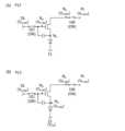
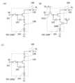
図1(A)には、本発明の一態様である表示装置の画素100を示す。画素100(図中
、PIXと図示)は、スイッチ101、トランジスタ102、キャパシタ103、および
発光素子104を有する。また図1(A)には、電流供給線PLと画素100の間にスイ
ッチ106を有する。つまり、一例としては、スイッチ106は、画素100の外側に設
けられている。なお、表示装置においては、画素は、複数個設けられている。画素100
は、複数個の画素のうちで、1個を取り出して示したものに相当する。FIG 1A shows a
corresponds to one pixel selected from among a plurality of pixels.
図1(A)では、トランジスタ102のゲートをノードNGとして示している。また図1
(A)では、トランジスタ102と発光素子104との間のノードをノードNSとして示
している。また図1(A)では、トランジスタ102とスイッチ106との間のノードを
ノードNDとして示している。なお、トランジスタ102は、駆動用トランジスタという
場合がある。In FIG. 1A, the gate of the
1A, a node between the
スイッチ101の一方の端子は、一例としては、データ線DLに接続される。スイッチ1
01の他方の端子は、一例としては、ノードNGに接続される。なおスイッチ101は、
第1のスイッチという場合がある。または、スイッチ101は、選択用スイッチという場
合もある。One terminal of the
The other terminal of the
The
データ線DLは、一例としては、初期化期間および閾値電圧補正期間において、初期化電
圧を与える(または伝える)機能を有する配線である。またデータ線DLは、一例として
は、データ電圧書き込み期間において、画素100にデータ電圧(又は映像信号電圧、ビ
デオ信号などともいう)を与える(または伝える)機能を有する配線である。または、デ
ータ線DLは、一例としては、画素100にプリチャージ電圧を与える(または伝える)
機能を有する配線である。ただし、データ線DLの機能は、これらに限定されない。した
がって、データ線DLは、単に配線、または第1の配線という場合がある。The data line DL is, for example, a wiring having a function of providing (or transmitting) an initialization voltage during an initialization period and a threshold voltage correction period. Also, for example, the data line DL is a wiring having a function of providing (or transmitting) a data voltage (also called a video signal voltage, video signal, etc.) to the
However, the functions of the data line DL are not limited to these. Therefore, the data line DL may be simply called a wiring or a first wiring.
データ線DLに与えるデータ電圧は、発光素子104を所望の階調値で発光させるための
電圧である。データ電圧は、VDATAで表す場合がある。The data voltage applied to the data line DL is a voltage for causing the
データ線DLに与える初期化電圧は、キャパシタ103の両端の電圧を初期化するための
機能を有する電圧である。または、その初期化電圧は、トランジスタ102がオン状態と
なるようにするための電圧である。初期化電圧は、VG-INIで表す場合がある。The initialization voltage applied to the data line DL is a voltage that has a function of initializing the voltage across the
トランジスタ102のゲートは、ノードNGに接続される。トランジスタ102のソース
またはドレインの一方は、ノードNSに接続される。トランジスタ102のソースまたは
ドレインの他方は、ノードNDに接続される。なお、トランジスタのソースとドレインと
は、電位に応じて入れ替わる。したがって、例えば発光期間においては、電流供給線PL
の電位は、陰極線CLの電位よりも高いため、その場合には、トランジスタ102のソー
スが、ノードNSに接続されている、ということが出来る。なお以下の説明においてトラ
ンジスタ102は、nチャネル型であると説明する。また以下の説明においては、一例と
して、トランジスタ102の閾値電圧をVTHとして表す。The gate of the
Since the potential of the node N-S is higher than the potential of the cathode line CL, in this case, it can be said that the source of the
スイッチ106の他方の端子は、一例としては、電流供給線PLに接続される。なおスイ
ッチ106は、第1のスイッチ、または、第2のスイッチという場合がある。The other terminal of the
電流供給線PLは、例えば、初期化期間において、キャパシタ103の両端の電圧を初期
化するための初期化電圧を与える機能を有する配線である。または、電流供給線PLは、
初期化期間において、ノードNSの電圧を初期化するための初期化電圧を与える機能を有
する配線である。また、電流供給線PLは、閾値電圧補正期間において、トランジスタ1
02のゲート-ソース間の電圧(VGSという場合がある)に従って電流を流すための電
圧を与える(または伝える)機能を有する配線である。また、電流供給線PLは、例えば
、発光期間において、トランジスタ102のVGSに従って発光素子104に電流を流す
ための電圧を与える機能を有する配線である。ただし、電流供給線PLの機能は、これら
に限定されない。したがって、電流供給線PLは、単に配線、または、第1の配線などと
いう場合がある。The current supply line PL is, for example, a wiring having a function of applying an initialization voltage for initializing the voltage across the
The current supply line PL is a wiring having a function of applying an initialization voltage for initializing the voltage of the node NS during the initialization period.
The current supply line PL is a wiring having a function of applying (or transmitting) a voltage for causing a current to flow in accordance with a gate-source voltage (sometimes referred to asVGS ) of the
電流供給線PLに与える初期化電圧は、キャパシタ103の両端の電圧を初期化するため
の電圧である。または、その初期化電圧は、トランジスタ102がオン状態となるように
するための電圧である。初期化電圧は、VP-INIで表す場合がある。なお、VP-I
NIとVG-INIとは、一例としては、異なる電圧である。ただし、状況に応じて、同
じ電圧となる場合もある。The initialization voltage applied to the current supply line PL is a voltage for initializing the voltage across the
NI and VG-INI are, for example, different voltages, although they may be the same voltage depending on the situation.
電流供給線PLに与える、トランジスタ102のVGSに従って電流を流すための電圧は
、一例としては、発光素子104を発光させるため、およびキャパシタ103の両端の電
極に保持される電圧をトランジスタ102の閾値電圧にするため、の電圧である。トラン
ジスタ102のVGSに従って電流を流すための電圧は、VP-EMIで表す場合がある
。The voltage applied to the current supply line PL for causing a current to flow in accordance with theVGS of the
なお、発光素子104を発光させる場合と、トランジスタ102の閾値電圧を取得する場
合とにおいて、電流供給線PLの電圧の大きさは、異なっていてもよい。ただし、発光素
子104を発光させる場合と、トランジスタ102の閾値電圧を取得する場合とにおいて
、電流供給線PLの電圧の大きさを同じとする場合、電圧を供給する回路の構成を簡単に
することが出来るため、より望ましい。Note that the magnitude of the voltage of the current supply line PL may be different when the
陰極線CLに与える電圧は、VCSで表す場合がある。ただし、陰極線CLの機能は、こ
れらに限定されない。したがって、陰極線CLは、単に配線、または、第1の配線などと
いう場合がある。The voltage applied to the cathode lines CL may be represented asVCS . However, the function of the cathode lines CL is not limited to this. Therefore, the cathode lines CL may be simply referred to as wiring or first wiring.
キャパシタ103の一方の電極は、ノードNGに接続される。キャパシタ103の他方の
電極は、ノードNSに接続される。One electrode of the
発光素子104の一方の電極は、ノードNSに接続される。発光素子104の他方の電極
は、陰極線CLに接続される。陰極線CLには、VCSが与えられる。なお、キャパシタ
103は、トランジスタ102のゲート容量(寄生容量)を利用することにより、省略す
ることも可能である。その場合の画素100Iの回路図の例を、図2に示す。One electrode of the
<画素の動作>
次いで、図1(A)の画素100の動作の一例について説明する。<Pixel operation>
Next, an example of the operation of the
図1(B)には、画素100の動作を説明するタイミングチャートの一例を示す。また、
図3乃至図5では、図1(B)に付した各期間における、各配線の電圧、スイッチの動作
、ノードの電圧を表す回路図を示す。FIG. 1B shows an example of a timing chart illustrating the operation of the
3 to 5 show circuit diagrams showing the voltages of the wirings, the operation of the switches, and the voltages of the nodes in the respective periods shown in FIG. 1B.
図1(B)のタイミングチャートは、発光期間P11、初期化期間P12、初期化完了期
間P13、閾値電圧補正期間P14、および、データ電圧書き込み期間P15に分けて示
している。初期化期間P12および初期化完了期間P13は、上述した初期化期間に対応
する。1B is divided into a light emitting period P11, an initialization period P12, an initialization completion period P13, a threshold voltage correction period P14, and a data voltage writing period P15. The initialization period P12 and the initialization completion period P13 correspond to the initialization period described above.
なお、発光期間P11、初期化期間P12、初期化完了期間P13、閾値電圧補正期間P
14、および、データ電圧書き込み期間P15が設けられている場合の例を示すが、本発
明の一態様は、これに限定されない。例えば、本発明の一態様は、これらの期間以外の期
間が設けられていてもよい。または、例えば、本発明の一態様は、これらの期間のうちの
少なくとも一つの期間が設けられていなくてもよい。例えば、トランジスタ102がオン
状態になっている場合には、必ずしも、初期化期間P12を設けなくてもよい。The light emission period P11, the initialization period P12, the initialization completion period P13, and the threshold voltage correction period P
14 and a data voltage writing period P15 are provided, but one embodiment of the present invention is not limited thereto. For example, in one embodiment of the present invention, periods other than these periods may be provided. Or, for example, in one embodiment of the present invention, at least one of these periods does not necessarily have to be provided. For example, when the
図1(B)のタイミングチャートは、上記期間におけるノードND、陰極線CL、ノード
NG、ノードNSの電圧の変化の一例を表している。また図1(B)中では、各配線およ
びノードが取り得るVP-EMI、VDATA、VCS、VG-INI、VP-INIの
大小関係の一例を縦軸を電圧として図示している。また図1(B)中では、トランジスタ
102の閾値電圧であるVTH、キャパシタ103の両端の電極に保持される電圧VCP
、発光素子104の両端の電極に印加される電圧VELを図示している。また図1(B)
中では、一例として、スイッチ101及びスイッチ106のオンまたはオフの状態を表し
ている。なお図1(B)の説明では、トランジスタ102はノーマリオン、すなわち閾値
電圧VTHが負であるとして説明をする。なお、この場合には、トランジスタ102がノ
ーマリオンであっても、ノーマリオフであっても、正常に動作させることが出来る。The timing chart in Fig. 1B shows an example of the changes in voltage of the node ND , the cathode line CL, the node NG , and the node NS during the above period. Fig. 1B also shows an example of the relationship in magnitude between VP-EMI , VDATA , VCS , VG-INI , and VP-INI that each wiring and node can have, with the vertical axis representing voltage. Fig. 1B also shows VTH , which is the threshold voltage of the
1B shows a voltageVEL applied to the electrodes at both ends of the light-emitting
1B, the on or off state of the
なお図1(B)では、同じタイミングの場合であっても、あるいは同じ電位の場合であっ
ても、配線およびノードの電圧の変化の視認性を確保するため、位置を少しずらして付し
ている。そのため、各電圧の大小関係、タイミングの前後は必ずしも図示した通りではな
い場合がある。In Fig. 1B, even if the timing is the same or the potential is the same, the positions are shifted slightly in order to ensure visibility of the voltage changes of the wiring and nodes. Therefore, the magnitude relationship of each voltage and the timing may not be as shown in the figure.
まず初期化期間P12では、前の発光期間P11にトランジスタ102のゲートに保持さ
れた電圧を初期化する動作を行う。または、トランジスタ102がオン状態となるように
する動作を行う。または、ノードNSの電圧を初期化する動作を行う。したがって、既に
トランジスタ102がオン状態である場合には、必ずしも、初期化期間P12を設けなく
てもよい。まず例えば、ノードNGの電圧はVG-INIであり、スイッチ101がオン
状態である。ノードNGの電圧が低下するのに合わせて、容量結合により、ノードNSの
電圧も低下する。また初期化期間P12以降、陰極線CLの電圧はVCSで変化しない。
ただし、状況に応じて、陰極線CLの電圧を変化させてもよい。初期化期間P12の動作
によって、ノードNGの電圧はVG-INIとなる。初期化期間P12による各配線、各
ノードの電圧は、図3(A)に図示するようになる。なお、初期化期間P12において、
スイッチ106は、オフ状態であってもよい。First, in the initialization period P12, an operation is performed to initialize the voltage held at the gate of the
However, the voltage of the cathode line CL may be changed depending on the situation. The voltage of the nodeNG becomesVG-INI due to the operation of the initialization period P12. The voltages of the wirings and nodes during the initialization period P12 are as shown in FIG. 3A. Note that, during the initialization period P12,
The
なお、初期化期間P12における動作について述べたが、本発明の一態様は、これに限定
されない。例えば、本発明の一態様は、初期化期間P12において、様々な動作を行って
もよい。したがって、初期化期間P12は、単に期間、または、第1の期間などという場
合がある。Note that, although the operation in the initialization period P12 has been described, one embodiment of the present invention is not limited thereto. For example, in one embodiment of the present invention, various operations may be performed in the initialization period P12. Therefore, the initialization period P12 may be simply referred to as a period or a first period.
次いで初期化完了期間P13では、ノードNSに保持された電圧を初期化する動作を行う
。まず例えば、電流供給線PLの電圧はVP-INIであり、スイッチ106はオン状態
である。ノードNDの電圧が低下するのに合わせてトランジスタ102に電流が流れ、ノ
ードNSの電圧がさらに低下する。初期化完了期間P13の動作によって、ノードNSの
電圧はVP-INIとなる。初期化完了期間P13による各配線、各ノードの電圧は、図
3(B)に図示するようになる。Next, during the initialization completion period P13, an operation is performed to initialize the voltage held at node NS. First, for example, the voltage of the current supply line PL is VP-INI , and the
なお電圧VP-INIは、一例としては、VCSより小さくしておく。このようにするこ
とで、発光素子104には電流が流れないようにすることができる。また電圧VG-IN
Iは、VP-INIより大きくしておく。このようにすることで、トランジスタ102に
電流が流れ、初期化をすることができる。ただし、トランジスタ102の閾値電圧の大き
さによっては、ノードNSの電圧は、ノードNGの電圧よりも、高くなっていても、トラ
ンジスタ102に電流が流れる場合がある。そのため、そのような場合には、ノードNS
の電圧は、ノードNGの電圧よりも、高くなっていてもよい。なお、初期化完了期間P1
3において、スイッチ101は、オフ状態であってもよい。In addition, the voltage VP-INI is set to be smaller than VCS , for example. In this way, it is possible to prevent a current from flowing through the
I is set to be larger than VP-INI . In this way, a current flows through the
The voltage of the node NG may be higher than the voltage of the nodeNG .
In 3, the
なお、初期化完了期間P13における動作について述べたが、本発明の一態様は、これに
限定されない。例えば、本発明の一態様は、初期化完了期間P13において、様々な動作
を行ってもよい。したがって、初期化完了期間P13は、単に期間、または、第1の期間
などという場合がある。Note that, although the operations in the initialization completion period P13 have been described, one embodiment of the present invention is not limited thereto. For example, one embodiment of the present invention may perform various operations in the initialization completion period P13. Therefore, the initialization completion period P13 may be simply referred to as a period, a first period, or the like.
次いで閾値電圧補正期間P14では、キャパシタ103の両端の電極にVTHまたは、V
THに応じた電圧を保持させるため、トランジスタ102に電流を流し、ノードNSの電
圧を上昇させる動作を行う。なお、トランジスタ102の特性のばらつきが小さい場合、
または、動画を表示している場合などのようにトランジスタ102の特性のばらつきの影
響が出にくい場合には、必ずしも、トランジスタ102の閾値電圧を取得しなくてもよい
。したがって、状況に応じて、閾値電圧補正期間P13を設けなくてもよい。まず、電流
供給線PLの電圧はVP-EMIであり、スイッチ101及びスイッチ106はオン状態
である。ノードNDの電圧が上昇することでトランジスタ102に電流が流れ、ノードN
Sの電圧が上昇し、キャパシタ103に蓄積されている電荷が放電される。またスイッチ
101はオン状態のため、ノードNGの電圧は変化しない。ノードNSの電圧の上昇は、
トランジスタ102のVGSがVTHとなることでトランジスタ102を流れる電流が小
さくなって電流が止まるため、止まる。つまりノードNSの電圧は、電圧(VG-INI
-VTH)となる。そして、キャパシタ103には、電圧(VTH)が蓄積される。つま
り、トランジスタ102のVTHを取得できたこととなる。このとき、トランジスタ10
2がノーマリオンの場合には、ノードNSの電圧は、ノードNGの電圧よりも、高くなっ
ていることとなる。ノードNSの電圧は、電圧(VG-INI-VTH)となっているが
、VTHは負の値なので、実際のノードNSの電圧は、ノードNGの電圧よりも、高くな
っていることとなる。言い換えると、このような動作を行うことにより、トランジスタ1
02がノーマリオンであっても、適切に、閾値電圧を取得することができる。閾値電圧補
正期間P14による各配線、各ノードの電圧は、図4(A)に図示するようになる。なお
、この期間において、電流供給線PLの電圧は、VP-EMIでなくてもよい。例えば、
電流供給線PLの電圧は、電圧が上昇した後のノードNSの電圧よりも、高い電圧となっ
ていればよい。Next, in the threshold voltage correction period P14,VTH or V
In order to hold a voltage corresponding toTH , a current is passed through the
Alternatively, when the effect of variations in the characteristics of the
The voltage at nodeNS rises, and the charge stored in the
When theVGS of the
Then, the voltage (VTH ) is stored in the
When
Even if P102 is normally on, the threshold voltage can be appropriately acquired. The voltages of the wirings and nodes during the threshold voltage correction period P14 are as shown in FIG. 4A. Note that during this period, the voltage of the current supply line PL does not have to be VP-EMI . For example,
It is sufficient that the voltage of the current supply line PL is higher than the voltage of the nodeNS after the voltage has increased.
なお、ここでは、トランジスタ102のVGSがVTHとなるとしたが、必ずしも、VG
SがVTHとなるまで、キャパシタ103に蓄積されている電荷を放電しなくてもよい。
例えば、トランジスタ102のVGSがVTHに概ね近い大きさになったときに、閾値電
圧を取得動作を終了してもよい。その場合には、トランジスタ102のVTHに応じた大
きさの電圧を取得できたこととなる。Note that, although theVGS of the
The charge stored in the
For example, the threshold voltage acquisition operation may be terminated when theVGS of the
なお、閾値電圧補正期間P14における動作について述べたが、本発明の一態様は、これ
に限定されない。例えば、本発明の一態様は、閾値電圧補正期間P14において、様々な
動作を行ってもよい。したがって、閾値電圧補正期間P14は、単に期間、または、第1
の期間などという場合がある。Although the operation in the threshold voltage correction period P14 has been described, one aspect of the present invention is not limited to this. For example, one aspect of the present invention may perform various operations in the threshold voltage correction period P14. Therefore, the threshold voltage correction period P14 may simply be a period or a first
It may also be referred to as a period of time.
次いでデータ電圧書き込み期間P15は、データ線DLにVDATAを与える。そして、
スイッチ101はオン状態である。ノードNGの電圧は、VG-INIからVDATAに
変化する。また、スイッチ101をオフ状態である。したがって、ノードNDは、電気的
に浮遊状態(フローティング)となる。ノードNSの電圧は、ノードNGの電圧の変化に
従って、キャパシタ103の容量結合に応じて変化する。Next, in a data voltage write period P15,VDATA is applied to the data line DL.
The
ここでキャパシタ103の電圧をVCPとする。またキャパシタ103のキャパシタンス
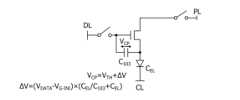
をC103とする。また発光素子104のキャパシタンスをCELとする。図6には、各
素子の電圧、キャパシタンスを図示している。キャパシタの両端の電極に保持される電圧
VCPは、容量結合によってVTH+ΔVとなる。ΔVは、ノードNGの電圧の変化分(
VDATA-VG-INI)と、キャパシタ103と発光素子104のキャパシタンスの
比(CEL/(C103+CEL))との積で表すことができる。Here, the voltage of the
It can be expressed as the product of VDATA −VG-INI and the capacitance ratio (CEL /(C103 +CEL )) of the
すなわちデータ電圧入力期間P15においてノードNSの電圧は(VDATA-VCP)
に上昇するものの、発光素子104のキャパシタンスCELを大きくすることで、この上
昇を抑えることができる。また、ノードNSの電圧が上昇しても、データ電圧書き込み期
間P15ではノードNDを電気的に浮遊状態としている。そのため、電流供給線PLから
トランジスタ102を介して発光素子104に向けて電流が流れないため、発光素子10
4の意図しない発光を抑制することができる。データ電圧入力期間P15による各配線、
各ノードの電圧は、図4(B)に図示するようになる。That is, in the data voltage input period P15, the voltage of the node NS is (VDATA -VCP ).
However, this increase can be suppressed by increasing the capacitanceCEL of the
Unintended light emission of the
The voltage at each node becomes as shown in FIG.
なお、データ電圧書き込み期間P15における動作について述べたが、本発明の一態様は
、これに限定されない。例えば、本発明の一態様は、データ電圧書き込み期間P15にお
いて、様々な動作を行ってもよい。したがって、データ電圧書き込み期間P15は、単に
期間、または、第1の期間などという場合がある。Although the operation in the data voltage writing period P15 has been described, one aspect of the present invention is not limited to this. For example, one aspect of the present invention may perform various operations in the data voltage writing period P15. Therefore, the data voltage writing period P15 may be simply referred to as a period or a first period.
本実施の形態の構成では、データ電圧書き込み期間P15において、スイッチ106がオ
フ状態であり、ノードNDは電気的に浮遊状態である。そのため、データ電圧書き込み期
間におけるノードNSの電圧の変化を抑制することができる。そして、発光素子104の
発光を抑制することができる。仮に、データ電圧書き込み期間P15の長さが長かったと
しても、ノードNDは電気的に浮遊状態であるため、ノードNSの電圧の変化を抑制する
ことができる。In the configuration of this embodiment, in the data voltage write period P15, the
仮に、データ電圧書き込み期間P15において、スイッチ106がオン状態である場合に
は、電流供給線PLからトランジスタ102を介してノードNSに向けて電流が流れる。
その結果、ノードNSの電位が上昇していく。そして仮に、データ電圧書き込み期間P1
5の長さが長かった場合には、ノードNSの電位がさらに上昇し、最終的には、キャパシ
タ103の電圧は、VTHとなる。そして、トランジスタ102がオフ状態となる。その
結果、供給されたVDATAが消失してしまうことになってしまう。以上のことから、デ
ータ電圧書き込み期間P15において、スイッチ106がオフ状態であることが望ましい
。ただし、本発明の一態様は、これに限定されない。If the
As a result, the potential of the node NS rises.
If the length of the data voltage writing period P15 is long, the potential of the node NS further increases, and the voltage of the
次いで発光期間P11は、電流供給線PLの電圧はVP-EMIであり、スイッチ106
はオン状態であり、スイッチ101はオフ状態である。ノードNDに電圧が供給され、ノ
ードNGがフローティング状態であることでトランジスタ102に電流が流れ、ノードN
Sの電圧が上昇する。また、ノードNGがフローティング状態であるため、ノードNSの
電圧の上昇につれてノードNGの電圧も上昇する。トランジスタのVGSはデータ電圧書
き込み期間で設定されたVCPを保持する。VCPはVTHにVDATAを含む項が加わ
った電圧である。そのため、発光素子104には、VTHの大きさに依存せず、VDAT
Aに応じた電流を流すことができる。つまり、VTHのばらつきの影響を低減できたこと
となる。なおノードNSは、VCSからVELだけ高い電圧(VEL+VCS)となる。
また、ノードNGは、(VCS+VEL)からVCPだけ高い電圧(VCP+VCS+V
EL)となる。発光期間P11による各配線、各ノードの電圧は、図5に図示するように
なる。Next, during the light emission period P11, the voltage of the current supply line PL is VP-EMI , and the
The node N−1 is in an on state, and the
The voltage of nodeNG rises. Also, since nodeNG is in a floating state, the voltage of nodeNG rises as the voltage of nodeNS rises. TheVGS of the transistor holdsVCP set in the data voltage write period.VCP is a voltage obtained by adding a term includingVDATA toVTH . Therefore, the
A current corresponding toA can flow. In other words, the influence of the variation in VTH can be reduced. The voltage of the node NS becomes (VEL +VCS ), which is higher than VCS by VEL .
The nodeNG is ata voltage(V CP+ VCS +V
EL ). The voltages of the wirings and nodes during the light emission period P11 are as shown in FIG.
なお、発光期間P11における動作について述べたが、本発明の一態様は、これに限定さ
れない。例えば、本発明の一態様は、発光期間P11において、様々な動作を行ってもよ
い。したがって、発光期間P11は、単に期間、または、第1の期間などという場合があ
る。Note that, although the operation in the light-emitting period P11 has been described, one embodiment of the present invention is not limited thereto. For example, one embodiment of the present invention may perform various operations in the light-emitting period P11. Therefore, the light-emitting period P11 may be simply referred to as a period or a first period.
以上説明した本発明の一態様における構成では、トランジスタ102のソース又はドレイ
ンのうち、電流供給線PLがある側にスイッチを設ける。そして、データ電圧書き込み期
間において、該スイッチをオフにすることで画素100と電流供給線PLとを電気的に切
り離し、画素100に電流を供給する配線を電気的に浮遊状態とする。このようにするこ
とで、発光素子のアノード側にあるノードNSの電圧の上昇を抑制し、データ電圧書き込
み期間での意図しない発光を抑制することができる。ただし、本発明の一態様は、これに
限定されない。In the above-described configuration of one embodiment of the present invention, a switch is provided on the side of the source or drain of the
<画素の変形例><Pixel transformation>
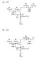
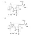
次いで図1(A)で図示した画素の回路構成の変形例について説明する。Next, we will explain a modified example of the circuit configuration of the pixel shown in Figure 1 (A).
図1(A)の画素100が有するスイッチ101及びスイッチ106は、例えばトランジ
スタを適用することができる。この場合の回路図を図7に示す。図7に示す画素100A
は、図1(A)のスイッチ101に代わって、トランジスタ101Aを有する。なおトラ
ンジスタ101Aのオンまたはオフは、ゲート線GLに与える電位によって制御すること
ができる。したがって、トランジスタ101Aは、選択用トランジスタと呼ぶ場合がある
。The
1A includes a
また図7では、スイッチ106に代わってトランジスタ106Aを図示している。なおト
ランジスタ106Aのオンまたはオフは、電源制御線PENに与える電位によって制御す
ることができる。7, a
トランジスタ101A及びトランジスタ106Aは、一例としては、チャネル形成領域に
酸化物半導体を有するトランジスタ(OSトランジスタ)であることが好ましい。OSト
ランジスタは、オフ電流を低くすることができる。そのため、スイッチとして機能するト
ランジスタ101Aをオフにすることで、ノードNGの電位の変動を小さくできる。また
、スイッチとして機能するトランジスタ106Aをオフにすることで、ノードNDの電位
の変動を小さくできる。あるいはトランジスタ101A及びトランジスタ106Aは、チ
ャネル形成領域にシリコンを有するトランジスタ(Siトランジスタ)であってもよい。
なお、トランジスタ102も同様に、チャネル形成領域に酸化物半導体を有するトランジ
スタ(OSトランジスタ)であることが好ましい。ただし、本発明の一態様は、これに限
定されない。例えば、トランジスタ102は、チャネル形成領域にシリコンを有するトラ
ンジスタ(Siトランジスタ)であってもよい。Siトランジスタにおけるチャネル形成
領域は、多結晶シリコンであってもよいし、アモルファスシリコンであってもよいし、単
結晶シリコンであってもよい。For example, the
Note that the
図1(A)の画素100は、一例としては、発光素子104に並列にキャパシタを有する
ことが好ましい。この場合の回路図を図8(A)に示す。図8(A)に示す画素100B
は、図1(A)の構成に加えて、キャパシタ105を有する。As an example, the
has a
上述した本発明の一態様では、キャパシタ103と発光素子104のキャパシタンスの比
を利用する。キャパシタ103のキャパシタンスが、発光素子104のキャパシタンスに
比べて大きいと、データ電圧入力期間P15の動作でノードNSの電位が上昇しすぎて発
光素子が発光する虞がある。従って別途、キャパシタ105を設けることが好ましい。な
お図8(A)の構成の場合、配線数を増やすことなくキャパシタを作製できるため好適で
ある。In one embodiment of the present invention described above, the ratio of the capacitances of the
またキャパシタ105は、別途容量線を設けて作製してもよい。この場合の回路図を図8
(B)に示す。図8(B)に示す画素100Cは、図8(A)の構成に加えて、容量線C
SLに一方の電極が接続されたキャパシタ105を有する。The
The
The
図8(B)の構成は、配線数が増えるものの、発光素子104の陰極をトランジスタ10
2の電極層に接続する等の複雑な工程を経ることなく作製することができるため、容易に
作製することが可能である。In the configuration of FIG. 8B, although the number of wirings increases, the cathode of the
Since the present invention can be easily manufactured without going through complicated steps such as connecting the second electrode layer to the first electrode layer.
図9(A)には、図7の画素100Aを変形した画素100Dを図示している。画素10
0Dは、スイッチとして機能するトランジスタとしてバックゲートを有するトランジスタ
101Bとしている。なおトランジスタ106Aも、トランジスタ101Bと同様の構成
とすることが可能である。FIG. 9A illustrates a
0D is a
図9(B)には、図7の画素100Aを変形した画素100Eを図示している。画素10
0Eは、スイッチとして機能するトランジスタとしてトランジスタを直列に接続したトラ
ンジスタ101Cとしている。なおトランジスタ106Aも、トランジスタ101Cと同
様の構成とすることが可能である。FIG. 9B illustrates a
0E is a
図10(A)には、図7の画素100Aを変形した画素100Fを図示している。画素1
00Fは、トランジスタ102としてバックゲートを有し、上下のゲートで同じ電位を与
えるトランジスタ102Dとしている。FIG. 10A illustrates a
In 00F, the
図10(B)には、図7の画素100Aを変形した画素100Gを図示している。画素1
00Gは、トランジスタ102としてバックゲートを有し、上下のゲートで異なる電位を
与えるトランジスタ102Eとしている。バックゲート側には電圧VBGを与え、トラン
ジスタ102Eの閾値電圧を制御することができる。FIG. 10B illustrates a
00G is a
図10(C)には、図7の画素100Aを変形した画素100Hを図示している。画素1
00Hは、トランジスタ102としてバックゲートを有し、上下のゲートで異なる電位を
与えるトランジスタ102Fとしている。バックゲート側にはノードNSの電圧を与えて
いる。FIG. 10C illustrates a
00H is a
なお、図1(A)の画素100でトランジスタ102は、nチャネル型の場合について述
べたが、本発明の一態様は、これに限定されない。図11の画素100Jでは、図1(A
)とは異なる構成を示している。図11では、トランジスタ102の代わりに、pチャネ
ル型のトランジスタ102pを有している。Note that although the
11, a p-
なお、トランジスタ102は、スイッチ106を介して、電流供給線PLと接続されてい
るが、本発明の一態様は、これに限定されない。例えば、図12(A)の画素100Kで
は、図1(A)とは異なる構成を示している。図12(A)では、トランジスタ102と
、スイッチ106Aを介して電流供給線PL_A、スイッチ106Bを介して電流供給線
PL_B、スイッチ106Cを介して電流供給線PL_Cとが、それぞれ別々に接続され
ている。電流供給線PL_A、PL_B、PL_Cに異なる電圧としてVP-EMI、V
CS、VP-INIを与え、スイッチ106A、106B、106Cのオンオフを制御す
ることにより、トランジスタ102に供給される電圧の大きさを制御することができる。
このようにスイッチを設けることにより、電流供給線PL_A、PL_B,PL_Cの電
位を変化させずに、同様の動作を実現することが可能となる。Note that the
The magnitude of the voltage supplied to the
By providing the switches in this manner, it becomes possible to realize a similar operation without changing the potentials of the current supply lines PL_A, PL_B, and PL_C.
なお図12(A)の画素100Kでは、電流供給線PL_A、PL_B、PL_Cに異な
る電圧を与える構成としたが、一定の電圧を与える配線と、電圧を切り替えて与える配線
とを分けて設ける構成としてもよい。この場合の画素の回路図を図12(B)に示す。図
12(B)の画素100Lでは、トランジスタ102と、スイッチ106Dを介して電流
供給線PL_D、スイッチ106Eを介して電流供給線PL_Eとが、それぞれ別々に接
続されている。電流供給線PL_DにVP-EMI、電流供給線PL_EにVCSまたは
VP-INIを与え、スイッチ106D、106Eのオンオフを制御することにより、ト
ランジスタ102に供給される電圧の大きさを制御することができる。In the
なお、図13(A)の画素100Mでは、図1(A)とは異なる構成を示している。図1
3(A)では、ノードNSは、スイッチ107を介して、配線ILと接続されている。配
線ILは、初期化電圧VP-INIを与える。このスイッチ107を少なくとも初期化期
間P12においてオン状態とすることにより、電流供給線PLの電圧を下げなくても、ノ
ードNSの電圧を低い電圧に制御することが出来る。なお、初期化期間P12以外の期間
においては、スイッチ107がオフ状態となっていることが望ましい。ただし、本発明の
一態様は、これに限定されない。Note that the
In FIG. 3(A), the node NS is connected to the wiring IL through a
なお図13(A)の画素100Mでにおけるスイッチ101、107は、トランジスタに
置き換えることができる。この場合の画素の回路図を図13(B)に示す。図13(B)
の画素100Nでは、トランジスタ101A、トランジスタ107Aを有する。トランジ
スタ101Aは、ゲート線GL_Aによって制御することができる。トランジスタ107
Aは、ゲート線GL_Bによって制御することができる。The
The
A can be controlled by the gate line GL_B.
図14(A)の画素100Oでは、図1(A)とは異なる構成を示している。図14(A
)では、ノードNSと、発光素子104との間に、スイッチ108が設けられていてもよ
い。このスイッチ108を、例えば、発光期間P11以外の少なくとも一つの期間におい
てオフ状態とし、少なくとも発光期間P11においてオン状態としてもよい。例えば、ス
イッチ108は、データ電圧書き込み期間P15においてオン状態としてもよい。これに
より、発光素子104が、意図せず発光してしまうことを抑制することができる。なお、
データ電圧入力期間P15においても、このスイッチがオン状態となっていてもよい。The pixel 100O in FIG. 14A has a different configuration from that in FIG.
), a
This switch may be in the on state also during the data voltage input period P15.
なお図14(A)の画素100Oでにおけるスイッチ101、108は、トランジスタに
置き換えることができる。この場合の画素の回路図を図14(B)に示す。図14(B)
の画素100Pでは、トランジスタ101A、トランジスタ108Aを有する。トランジ
スタ101Aは、ゲート線GL_Aによって制御することができる。トランジスタ108
Aは、ゲート線GL_Cによって制御することができる。The
The
A can be controlled by the gate line GL_C.
図14(C)の画素100Qでは、図14(A)とは異なる構成を示している。図14(
C)では、ノードNSと、発光素子104との間ではなく、トランジスタ102とスイッ
チ106との間に、スイッチ108が設けられている。このようにすることで、画素ごと
にスイッチの制御を行うことができる。The
In C), a
図15(A)の画素100Rでは、図1(A)とは異なる構成を示している。図15(A
)では、トランジスタ102と、電流供給線PLとの間に、スイッチ106Dと、回路1
09A及びスイッチ106Eを設けている。回路109Aは、電流供給線PLの電圧をノ
ードNDに与える際に、波形をなまらせる機能を有する回路である。なお回路109Aは
、画素100Rの中に設けられていてもよいし、画素100Rの外に設けられていてもよ
い。The
) a
The
回路109Aは、スイッチ106D、106Eのオン状態を変更することにより、機能す
る場合と、機能させない場合とを切り替えるようにすることが好ましい。例えば、回路1
09Aを機能させたい場合には、ノードNDでの波形をなまらせたい場合である。このよ
うな場合としては、例えば、発光期間P11がある。発光期間P11では、発光期間P1
1に移行する場合に、図15(B)に図示するように、スイッチ106D、106Eのオ
ン状態を変更し、ノードNDの電圧の波形をなまらせることにより、輝度の変化を滑らか
にすることができる。そのため表示装置の使用時において、目がまぶしく感じることを低
減できたり、ちらつきを感じることを低減できたりする可能性が期待される。よって、目
にやさしく、目が疲れにくくなる可能性が期待される。It is preferable that the
When it is desired to make the waveform at the node ND smooth, the output of the output of the nodeND should be smoothed. An example of such a case is the light emission period P11.
15B, the ON state of the
回路109Aは、例えば図16(A)に示すように抵抗素子でとしてもよい。あるいは、
図16(B)に示すようにダイオードで構成してもよい。あるいは、図16(C)に示す
ようにダイオード接続されたトランジスタで構成してもよい。The
It may be configured with a diode as shown in Fig. 16(B), or may be configured with a diode-connected transistor as shown in Fig. 16(C).
なお回路109Aは、図16(D)に示すように、機能させたい場合スイッチ106Dを
オフ状態とし、機能させたくない場合スイッチ106Dをオン状態とする構成としてもよ
い。また回路109Aは、図16(E)に示すように、抵抗素子とキャパシタを組み合わ
せた回路としてもよい。Note that the
なお、図12乃至図15などの回路を、それぞれ組み合わせた回路を構成することも可能
である。例えば、図12(A)と図13(A)とを組み合わせた場合の画素100Sを図
17(A)に示す。同様に、図12(A)と図14(A)を組み合わせた場合の画素10
0Tを図17(B)に示す。同様に、図12(A)と図13(A)と図14(A)とを組
み合わせた場合の画素100Uを図17(C)に示す。このように、適宜組み合わせた回
路を構成することも可能である。12 to 15 may be combined to form a circuit. For example, FIG. 17A shows a
0T is shown in Fig. 17(B). Similarly, Fig. 17(C) shows a
以上説明したように本発明の一態様は様々な変形例を適用することができる。As explained above, various modifications can be made to one aspect of the present invention.
<表示装置のブロック図>
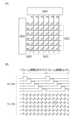
次いで図1(A)で図示した画素を適用しうる表示装置のブロック図の一例について説明
する。<Block diagram of display device>
Next, an example of a block diagram of a display device to which the pixel shown in FIG. 1A can be applied will be described.
図18には、表示装置のブロック図の一例として、ゲート線側駆動回路110、データ線
側駆動回路120、電流供給線制御回路130、および画素100を有する画素部140
を図示している。FIG. 18 shows an example of a block diagram of a display device, which includes a gate line
is illustrated.
画素部140において、複数の画素100は、x-y方向にマトリクス状に設けられてい
る。画素部140では、X方向に、ゲート線側駆動回路110に接続されたゲート線GL
1乃至GLm(mは自然数)を設ける。ゲート線GL1乃至GLmは、それぞれ、各画素
100と接続されている。例えば、図7におけるゲート線GLは、ゲート線側駆動回路1
10に接続される。また画素部140では、Y方向に、データ線側駆動回路120に接続
されたデータ線DL1乃至DLn(nは自然数)を、設ける。データ線DL1乃至DLn
は、それぞれ、各画素100と接続されている。例えば、図7におけるデータ線DLは、
データ線側駆動回路120に接続される。In the
Gate lines GL1 to GLm (m is a natural number) are provided. The gate lines GL1 to GLm are connected to the
10. In the
are connected to the
The data line
電流供給線PLは、図18に示すようにX方向に、電流供給線制御回路130に接続され
た電流供給線PL1乃至PLmを、各画素100に接続されるように設けることができる
。例えば、図7などにおけるノードNDは、電流供給線制御回路130に接続される。18, the current supply lines PL can be provided in the X direction, with current supply lines PL1 to PLm connected to a current supply
電流供給線制御回路130は、電流供給線PL1乃至PLmを1行づつ走査することがで
きる。また電流供給線制御回路130は、電源制御線P1EN乃至PmENによって各行
のスイッチのオンまたはオフを制御することができる。電源制御線P1EN乃至PmEN
は、電流供給線PL1乃至PLmに設けられるスイッチを1行毎にオフにし、電気的に浮
遊状態とすることができる。電流供給線PL1乃至PLmに設けられるスイッチは、例え
ば、図1などにおけるスイッチ106に相当する。The current supply
can turn off the switches provided in the current supply lines PL1 to PLm row by row, and put them in an electrically floating state. The switches provided in the current supply lines PL1 to PLm correspond to, for example, the
なお図19には、ゲート線GL1乃至GLm、電流供給線PL1乃至PLm、および電源
制御線P1EN乃至PmENによって制御されるスイッチの状態を、1行ずつ走査する動
作のタイミングチャートを示す。FIG. 19 shows a timing chart of an operation for scanning the states of the switches controlled by the gate lines GL1 to GLm, the current supply lines PL1 to PLm, and the power supply control lines P1EN to PmEN , one row at a time.
<画素の動作の変形例>
次いで、図1(A)で図示した画素100の動作の変形例について説明する。<Modifications of pixel operation>
Next, a modification of the operation of the
図20(A)には、図1(A)と同じ画素100の回路図を示す。また、図20(B)に
は、図1(B)とは異なる、画素100の動作の変形例を説明するタイミングチャートを
示す。また、図21乃至図23では、図20(B)に付した各期間における、各配線の電
圧、スイッチの動作、ノードの電圧を表す回路図を示す。Fig. 20A shows a circuit diagram of the
なお図20(B)の説明では、図1(B)とは異なり、トランジスタ102はノーマリオ
フ、すなわち閾値電圧VTHが正であるとして説明をする。以下、図1(B)とは異なる
点について詳述し、同様の点については、上記説明を援用し、省略して記載する場合があ
る。20B, unlike FIG 1B, the
図20(B)のタイミングチャートは、発光期間P21、初期化期間P22、初期化完了
期間P23、閾値電圧補正期間P24、および、データ電圧書き込み期間P25に分けて
示している。初期化期間P22および初期化完了期間P23は、上述した初期化期間に対
応する。20B is divided into a light emitting period P21, an initialization period P22, an initialization completion period P23, a threshold voltage correction period P24, and a data voltage writing period P25. The initialization period P22 and the initialization completion period P23 correspond to the initialization period described above.
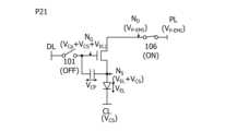
図20(B)のタイミングチャートは、下記期間におけるノードND、陰極線CL、ノー
ドNG、ノードNSの電圧の変化の一例を表している。また図20(B)中では、各配線
およびノードが取り得るVP-EMI、VDATA、VCS、VP-INIの大小関係を
縦軸を電圧として図示している。また図20(B)中では、トランジスタ102の閾値電
圧であるVTH、キャパシタ103の両端の電極に保持される電圧VCP、発光素子10
4の両端の電極に印加される電圧VELを図示している。また図20(B)中では、スイ
ッチ101及びスイッチ106のオンまたはオフの状態を表している。The timing chart in Fig. 20B shows an example of changes in voltage at the node ND , the cathode line CL, the node NG , and the node NS during the following period. Also in Fig. 20B, the vertical axis shows the magnitude relationship between VP-EMI , VDATA , VCS , and VP-INI that each wiring and node can have. Also in Fig. 20B, VTH which is the threshold voltage of the
20B shows the voltageVEL applied to the electrodes at both ends of the
まず初期化期間P22では、前の発光期間P21にトランジスタ102のゲートに保持さ
れた電圧を初期化する動作を行う。初期化期間P12と異なる点として、データ線DLを
VCSとする。また、ノードNGはVCSとなる。初期化期間P22による各配線、各ノ
ードの電圧は、図21(A)に図示するようになる。First, in the initialization period P22, an operation is performed to initialize the voltage held at the gate of the
次いで初期化完了期間P23では、ノードNSに保持された電圧を初期化する動作を行う
。初期化完了期間P23と異なる点として、電流供給線PLの電圧はVP-INIである
。ノードNGのVCSは、VP-INIよりも大きい。そのため、トランジスタ102が
オン状態となり、ノードNSの電圧が低下し、ノードNSがVP-INIとなる。初期化
完了期間P23による各配線、各ノードの電圧は、図21(B)に図示するようになる。Next, in the initialization completion period P23, an operation is performed to initialize the voltage held at
次いで閾値電圧補正期間P24では、キャパシタ103の両端の電極にVTHを保持させ
るため、トランジスタ102に電流を流し、ノードNSの電圧を上昇させる動作を行う。
閾値電圧補正期間P24の動作の異なる点として、データ線DLをVCSとする。また、
ノードNGはVCSとなる。電流供給線PLの電圧はVCSとする。電流供給線PLがV
CSとなることで、ノードNSの電圧が上昇する。ノードNSの電圧の上昇は、トランジ
スタ102のVGSがVTHとなることでトランジスタ102を流れる電流が小さくなっ
て、電流が止まる。つまりノードNSの電圧は、電圧(VCS-VTH)となる。なお図
20(B)でノードNSの電圧の上昇は、ノードNGの電圧よりVTHだけ低い電圧で止
まる。これは、トランジスタ102がノーマリーオフのためである。閾値電圧補正期間P
24による各配線、各ノードの電圧は、図22(A)に図示するようになる。Next, in a threshold voltage correction period P24, in order to holdVTH at both ends of the electrodes of the
A difference in the operation of the threshold voltage correction period P24 is that the data line DL is set toVCS .
The node NG is set to VCS . The voltage of the current supply line PL is set to VCS . When the current supply line PL is V
CS , the voltage at node NS rises. The rise in the voltage at node NS occurs when VGS of
The voltages of the wirings and nodes in accordance with 24 are as shown in FIG.
次いでデータ電圧書き込み期間P25は、データ線DLはVDATAであり、スイッチ1
01はオン状態とする。また、スイッチ106はオフ状態である。このときノードNDは
、電気的に浮遊状態(フローティング)となる。データ電圧書き込み期間P25の動作は
、データ電圧書き込み期間P15と同じである。なお図20(B)でノードNSの電圧の
上昇は、ノードNSの電圧が図1(B)のときより小さいため、VCSより小さい電圧の
上昇にとどまる。これは、トランジスタ102がノーマリーオフのためである。この場合
、ノードNSの電圧によって発光素子104は発光しない。データ電圧書き込み期間P2
5による各配線、各ノードの電圧は、図22(B)に図示するようになる。Next, in the data voltage write period P25, the data line DL isVDATA , and the
20B, the voltage of node NS is lower than that in FIG. 1B, and therefore the voltage rise of node N S remains at a level lower than V CS . This is because the
The voltages of the wiring and nodes in accordance with 5 are as shown in FIG.
次いで発光期間P21は、電流供給線PLの電圧がVP-EMIである。発光期間P21
の動作は、発光期間P11と同じである。発光期間P21による各配線、各ノードの電圧
は、図23に図示するようになる。Next, in the light emission period P21, the voltage of the current supply line PL is VP-EMI .
The operation of the light emitting period P21 is the same as that of the light emitting period P11. The voltages of the wirings and nodes during the light emitting period P21 are as shown in FIG.
以上説明した本発明の一態様における構成では、トランジスタ102の閾値電圧の正負に
関わらず、閾値電圧の取得にかける時間を長くすることができる。また、発光素子のアノ
ード側にあるノードNSの電圧の上昇を抑制し、データ電圧書き込み期間での意図しない
発光を抑制することができる。In the above-described structure of one embodiment of the present invention, the time required to acquire the threshold voltage can be increased regardless of whether the threshold voltage of the
なお、本実施の形態において、本発明の一態様について述べた。または、他の実施の形態
において、本発明の一態様について述べる。ただし、本発明の一態様は、これらに限定さ
れない。つまり、本実施の形態および他の実施の形態では、様々な発明の態様が記載され
ているため、本発明の一態様は、特定の態様に限定されない。例えば、本発明の一態様と
して、トランジスタの閾値電圧のばらつきを補正した場合の例を示したが、本発明の一態
様は、これに限定されない。例えば、場合によっては、または、状況に応じて、本発明の
一態様では、別の特性のばらつきの補正を行ってもよい。または例えば、場合によっては
、または、状況に応じて、本発明の一態様では、トランジスタの閾値電圧のばらつきを補
正しなくてもよい。Note that one embodiment of the present invention has been described in this embodiment. Alternatively, one embodiment of the present invention will be described in another embodiment. However, one embodiment of the present invention is not limited to these. That is, since various aspects of the invention are described in this embodiment and other embodiments, one embodiment of the present invention is not limited to a specific aspect. For example, although an example in which the variation in the threshold voltage of a transistor is corrected has been described as one embodiment of the present invention, one embodiment of the present invention is not limited to this. For example, in some cases or depending on the situation, in one embodiment of the present invention, the variation in another characteristic may be corrected. Or, for example, in some cases or depending on the situation, in one embodiment of the present invention, the variation in the threshold voltage of a transistor may not be corrected.
(実施の形態2)
本実施の形態では、上記実施の形態で説明した画素のトランジスタに適用可能な、チャネ
ル形成領域が酸化物半導体膜で形成されているトランジスタ(OSトランジスタ)、およ
びチャネル形成領域がシリコンで形成されているトランジスタ(Siトランジスタ)、を
一例に挙げて説明する。(Embodiment 2)
In this embodiment, a transistor whose channel formation region is formed using an oxide semiconductor film (OS transistor) and a transistor whose channel formation region is formed using silicon (Si transistor), which can be used as the pixel transistor described in the above embodiment, will be described as an example.
<トランジスタの構成例1>
まずチャネル形成領域が酸化物半導体膜で形成されているトランジスタ(OSトランジス
タ)について説明する。<Transistor Configuration Example 1>
First, a transistor in which a channel formation region is formed using an oxide semiconductor film (OS transistor) will be described.
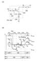
図24(A)、図24(B)および図24(C)に、デバイス構造の異なる3つのトラン
ジスタ(TA1、TA2、TB1)の上面図(レイアウト図)と、それぞれの回路記号を
示す。図25は、トランジスタ(TA1、TA2、TB1)の断面図である。トランジス
タTA1のa1-a2線およびb1-b2線による断面図、トランジスタTA2のa3-
a4線およびb3-b4線による断面図、ならびにトランジスタTB1のa5-a6線、
b5-b6線による断面図を、図25(A)、図25(B)に示す。これらトランジスタ
のチャネル長方向の断面構造が、図25(A)に示され、同チャネル幅方向の断面構造が
図25(B)に示されている。24A, 24B, and 24C show top views (layout diagrams) of three transistors (TA1, TA2, and TB1) with different device structures and their respective circuit symbols. FIG. 25 shows cross-sectional views of the transistors (TA1, TA2, and TB1). A cross-sectional view of the transistor TA1 taken along the a1-a2 line and the b1-b2 line, a cross-sectional view of the transistor TA2 taken along the a3-
Cross-sectional views taken along lines a4 and b3-b4, and lines a5-a6 of transistor TB1;
The cross-sectional views taken along the line b5-b6 are shown in Fig. 25(A) and Fig. 25(B). The cross-sectional structures of these transistors in the channel length direction are shown in Fig. 25(A), and the cross-sectional structures in the channel width direction are shown in Fig. 25(B).
図25(A)、図25(B)に示すように、トランジスタ(TA1、TA2、TB1)は
、同一絶縁表面上に集積されており、これらのトランジスタは、同一の作製工程で作成す
ることが可能である。なお、ここでは、デバイス構造の明瞭化のため、各トランジスタの
ゲート(G)、ソース(S)、およびドレイン(D)への電位や電源の供給するための配
線との電気的な接続は省略している。As shown in Figures 25A and 25B, the transistors (TA1, TA2, and TB1) are integrated on the same insulating surface, and these transistors can be fabricated in the same fabrication process. Note that, in order to clarify the device structure, electrical connections to wiring for supplying potential and power to the gate (G), source (S), and drain (D) of each transistor are omitted here.
トランジスタTA1(図24(A))、トランジスタTA2(図24(B))は、ゲート
(G)とバックゲート(BG)を有するトランジスタである。ゲート(G)およびバック
ゲート(BG)は、いずれか一方が第1のゲートに相当し、他方が第2のゲートに相当す
る。トランジスタTA1、トランジスタTA2はバックゲートをゲートに接続した構造と
している。トランジスタTB1(図24(C))は、BGを有さないトランジスタである
。図25に示すように、これらのトランジスタ(TA1、TA2、TB1)は、基板30
に形成されている。以下、図24、図25を参照して、これらのトランジスタの構成を説
明する。Transistor TA1 (FIG. 24A) and transistor TA2 (FIG. 24B) are transistors having a gate (G) and a back gate (BG). One of the gate (G) and the back gate (BG) corresponds to a first gate, and the other corresponds to a second gate. Transistor TA1 and transistor TA2 have a structure in which the back gate is connected to the gate. Transistor TB1 (FIG. 24C) is a transistor that does not have a BG. As shown in FIG. 25, these transistors (TA1, TA2, TB1) are formed on a
The configuration of these transistors will be described below with reference to FIGS.
[トランジスタTA1]
トランジスタTA1は、ゲート電極GE1、ソース電極SE1、ドレイン電極DE1、バ
ックゲート電極BGE1、および酸化物半導体膜OS1を有する。[Transistor TA1]
The transistor TA1 includes a gate electrode GE1, a source electrode SE1, a drain electrode DE1, a backgate electrode BGE1, and an oxide semiconductor film OS1.
以下の説明において、トランジスタTA1をTA1と呼ぶ、バックゲートをBGと呼ぶ、
酸化物半導体膜OS1をOS1や膜OS1と呼ぶなど、素子や素子の構成要素を省略して
呼ぶ場合がある。また、信号、電位、回路などについても同様に省略する場合がある。In the following description, the transistor TA1 is referred to as TA1, and the back gate is referred to as BG.
An element or a component of an element may be abbreviated to OS1 or OS1 film, for example, by referring to the oxide semiconductor film OS1. Signals, potentials, circuits, and the like may also be abbreviated in the same manner.
また、本実施の形態では、OSトランジスタのチャネル長は、ソース電極とドレイン電極
間の距離とする。また、OSトランジスタのチャネル幅は、酸化物半導体膜とゲート電極
が重なる領域でのソース電極またはドレイン電極の幅とする。トランジスタTA1のチャ
ネル長は、La1であり、チャネル幅はWa1である。In this embodiment, the channel length of an OS transistor is the distance between a source electrode and a drain electrode. The channel width of an OS transistor is the width of the source electrode or the drain electrode in a region where the oxide semiconductor film overlaps with the gate electrode. The channel length of transistor TA1 is La1, and the channel width is Wa1.
膜OS1は、絶縁膜34を介して電極GE1と重なっている。膜OS1の上面および側面
に接して一対の電極(SE1、DE1)が形成されている。図24(A)に示すように、
膜OS1は、電極GE1および一対の電極(SE1、DE1)と重ならない部分を有して
いる。膜OS1は、チャネル長方向の長さがチャネル長La1よりも長く、かつチャネル
幅方向の長さがチャネル幅Wa1よりも長い。The film OS1 overlaps with the electrode GE1 via the insulating
The film OS1 has a portion that does not overlap with the electrode GE1 and the pair of electrodes (SE1, DE1). The length of the film OS1 in the channel length direction is longer than the channel length La1, and the length of the film OS1 in the channel width direction is longer than the channel width Wa1.
膜OS1、電極GE1、電極SE1および電極DE1を覆って、絶縁膜35、絶縁膜36
が形成されている。絶縁膜36上に電極BGE1が形成されている。電極BGE1は、膜
OS1および電極GE1と重なるように設けられている。ここでは、一例として、電極G
E1と同じ形状で、同じ位置に配置されるように電極BGE1を設けている。電極BGE
1は、絶縁膜34絶縁膜35および絶縁膜36を貫通する開口CG1において、電極GE
1に接している。この構造により、トランジスタTA1のゲートとバックゲートが電気的
に接続される。The insulating
An electrode BGE1 is formed on the insulating
The electrode BGE1 is provided so as to have the same shape and be located in the same position as the electrode BGE1.
1 is an opening CG1 penetrating the insulating
1. With this structure, the gate and backgate of transistor TA1 are electrically connected.
バックゲート電極BGE1をゲート電極GE1に接続することで、トランジスタTA1の
オン電流を増加させることができる。バックゲート電極BGE1を設けることで、トラン
ジスタTA1の強度を向上させることができる。基板30の曲げ等の変形に対して、電極
BGE1が補強部材となってトランジスタTA1を壊れにくくすることができる。By connecting the back gate electrode BGE1 to the gate electrode GE1, the on-current of the transistor TA1 can be increased. By providing the back gate electrode BGE1, the strength of the transistor TA1 can be improved. The electrode BGE1 acts as a reinforcing member to make the transistor TA1 less likely to break when the
チャネル形成領域を含む膜OS1は多層構造であり、ここでは、一例として3つの酸化物
半導体膜(31、32、33)でなる3層構造としている。膜OS1を構成する酸化物半
導体膜は、少なくとも1つ同じ金属元素を含む金属酸化物膜であることが好ましく、In
を含むことが特に好ましい。トランジスタの半導体膜を構成することが可能なInを含む
金属酸化物としては、In-Ga酸化物膜、In-M-Zn酸化物膜(MはAl、Ga、
Y、Zr、La、Ce、またはNd)が代表的である。また、このような金属酸化物膜に
他の元素や材料を添加した膜を用いることもできる。The film OS1 including the channel formation region has a multi-layer structure, and here, as an example, a three-layer structure including three oxide semiconductor films (31, 32, and 33). The oxide semiconductor films constituting the film OS1 are preferably metal oxide films containing at least one of the same metal element, and preferably In
Examples of metal oxides containing In that can form a semiconductor film of a transistor include an In-Ga oxide film and an In-M-Zn oxide film (wherein M is Al, Ga,
Representative examples of the metal oxide film include Y, Zr, La, Ce, and Nd. Films in which other elements or materials are added to such metal oxide films can also be used.
『32』は、トランジスタTA1のチャネル形成領域を構成する膜である。また、『33
』は、後述するトランジスタTA2およびトランジスタTB1のチャネル形成領域を構成
する膜でもある。そのため、トランジスタTA2およびトランジスタTB1に要求される
電気的特性(例えば、電界効果移動度、しきい値電圧など)に応じて、適切な組成の酸化
物半導体膜を用いればよい。例えば、『32』にチャネルが形成されるように、酸化物半
導体膜31-33の主成分である金属元素の組成を調節することが好ましい。"32" is a film that constitutes the channel forming region of the transistor TA1.
"32" also constitutes a channel formation region of a transistor TA2 and a transistor TB1, which will be described later. Therefore, an oxide semiconductor film having an appropriate composition may be used depending on the electrical characteristics (e.g., field-effect mobility, threshold voltage, etc.) required for the transistor TA2 and the transistor TB1. For example, it is preferable to adjust the composition of a metal element that is a main component of the oxide semiconductor films 31-33 so that a channel is formed at "32".
トランジスタTA1において、『32』にチャネルが形成されるようにすることで、チャ
ネル形成領域が絶縁膜34、35に接しないようにすることができる。また、酸化物半導
体膜31-33を少なくとも1つ同じ金属元素を含む金属酸化物膜とすることで、『32
』と『31』の界面、および『32』と『33』の界面において、界面散乱が起こりにく
くすることができる。これにより、トランジスタTA1の電界効果移動度をトランジスタ
TA2やトランジスタTB1よりも高くすることができる、また、オン状態でのドレイン
電流(オン電流)を増加させることができる。In the transistor TA1, by forming a channel in the region “32”, the channel formation region can be prevented from being in contact with the insulating
It is possible to make it difficult for interface scattering to occur at the interface between "31" and "32" and at the interface between "33" and "33". This makes it possible to make the field effect mobility of transistor TA1 higher than that of transistor TA2 and transistor TB1, and also to increase the drain current (on-current) in the on-state.
[トランジスタTA2]
トランジスタTA2は、ゲート電極GE2、ソース電極SE2、ドレイン電極DE2、バ
ックゲート電極BGE2、および酸化物半導体膜OS2を有する。電極BGE2は、絶縁
膜34乃至絶縁膜36を貫通する開口CG2において電極GE2に接している。トランジ
スタTA2は、トランジスタTA1の変形例であり、膜OS2が酸化物半導体膜33でな
る単層構造である点でトランジスタTA1と異なり、その他については同様である。ここ
では、トランジスタTA2のチャネル長La2、チャネル幅Wa2は、トランジスタTA
1のチャネル長La1、チャネル幅Wa1と等しくなるようにしている。[Transistor TA2]
The transistor TA2 has a gate electrode GE2, a source electrode SE2, a drain electrode DE2, a backgate electrode BGE2, and an oxide semiconductor film OS2. The electrode BGE2 is in contact with the electrode GE2 through an opening CG2 penetrating the insulating
The channel length La1 and the channel width Wa1 of the first transistor are set to be equal to those of the first transistor.
[トランジスタTB1]
トランジスタTB1は、ゲート電極GE3、ソース電極SE3、ドレイン電極DE3およ
び酸化物半導体膜OS3を有する。トランジスタTB1は、トランジスタTA2の変形例
である。トランジスタTA2と同様に、膜OS3が酸化物半導体膜33でなる単層構造で
ある。トランジスタTA2とは、バックゲート電極を有していない点で異なる。また、膜
OS3および電極(GE3、SE3、DE3)のレイアウトが異なる。図24(C)に示
すように、膜OS3は、電極GE3と重なっていない領域は、電極SE3または電極DE
3の何れかと重なっている。そのため、トランジスタTB1のチャネル幅Wb1は、膜O
S3の幅で決定されている。チャネル長Lb1は、トランジスタTA2と同様、電極SE
3と電極DE3間の距離で決定され、ここでは、トランジスタTA2のチャネル長La2
よりも長くしている。[Transistor TB1]
The transistor TB1 has a gate electrode GE3, a source electrode SE3, a drain electrode DE3, and an oxide semiconductor film OS3. The transistor TB1 is a modified example of the transistor TA2. Like the transistor TA2, the film OS3 has a single-layer structure made of an
3. Therefore, the channel width Wb1 of the transistor TB1 is
The channel length Lb1 is determined by the width of the electrode SE, like the transistor TA2.
3 and the electrode DE3, and here, the channel length La2 of the transistor TA2
It's longer than that.
[絶縁膜]
絶縁膜34、絶縁膜35および絶縁膜36は、基板30のトランジスタ(TA1、TA2
、TB1)が形成される領域全体に形成される膜である。絶縁膜34、絶縁膜35、およ
び絶縁膜36は、単層あるいは複数層の絶縁膜で形成される。絶縁膜34は、トランジス
タ(TA1、TA2、TB1)のゲート絶縁膜を構成する膜である。また、絶縁膜35お
よび絶縁膜36は、トランジスタ(TA1、TA2、TB1)のバックチャネル側のゲー
ト絶縁膜を構成する膜である。また、最上面の絶縁膜36は、基板30に形成されるトラ
ンジスタの保護膜として機能するような材料で形成することが好ましい。絶縁膜36は適
宜設ければよい。3層目の電極BGE1と2層目の電極(SE1、DE1)を絶縁するた
めに、これらの間に少なくとも1層絶縁膜が存在していればよい。[Insulating film]
The insulating
, TB1) are formed. The insulating
絶縁膜34乃至絶縁膜36は、単層の絶縁膜で、または2層以上の多層の絶縁膜で形成す
ることができる。これら絶縁膜34乃至絶縁膜36を構成する絶縁膜としては、酸化アル
ミニウム、酸化マグネシウム、酸化シリコン、酸化窒化シリコン、窒化酸化シリコン、窒
化シリコン、酸化ガリウム、酸化ゲルマニウム、酸化イットリウム、酸化ジルコニウム、
酸化ランタン、酸化ネオジム、酸化ハフニウムおよび酸化タンタル等でなる膜があげられ
る。また、これらの絶縁膜は、スパッタリング法、CVD法、MBE法、ALD法または
PLD法を用いて形成することができる。The insulating
Examples of the insulating film include films made of lanthanum oxide, neodymium oxide, hafnium oxide, tantalum oxide, etc. Furthermore, these insulating films can be formed by using a sputtering method, a CVD method, an MBE method, an ALD method, or a PLD method.
[酸化物半導体膜]
ここでは、OSトランジスタの半導体膜を構成する酸化物半導体膜について説明する。膜
OS1にように半導体膜を多層構造とする場合、これらを構成する酸化物半導体膜は、少
なくとも1つ同じ金属元素を含む金属酸化物膜であることが好ましく、Inを含むことが
好ましい。[Oxide Semiconductor Film]
Here, an oxide semiconductor film that constitutes a semiconductor film of an OS transistor is described. When a semiconductor film has a multilayer structure like the film OS1, the oxide semiconductor films that constitute the multilayer structure are preferably metal oxide films that contain at least one of the same metal element, and preferably contain In.
例えば、『31』がIn-Ga酸化物膜の場合、Inの原子数比をGaの原子数比よりも
小さくする。In-M-Zn酸化物膜(MはAl、Ga、Y、Zr、La、Ce、または
Nd)の場合、Inの原子数比をMの原子数比よりも小さくする。この場合、Znの原子
数比が最も大きくなるようにすることができる。For example, when "31" is an In-Ga oxide film, the atomic ratio of In is made smaller than the atomic ratio of Ga. When it is an In-M-Zn oxide film (M is Al, Ga, Y, Zr, La, Ce, or Nd), the atomic ratio of In is made smaller than the atomic ratio of M. In this case, it is possible to make the atomic ratio of Zn the largest.
例えば、『32』がIn-Ga酸化物膜の場合、Inの原子数比をGaの原子数比よりも
大きくする。In-M-Zn酸化物膜の場合、Inの原子数比をMの原子数比よりも大き
くする。In-M-Zn酸化物膜では、Inの原子数比がMおよびZnの原子数比よりも
大きくすることが好ましい。For example, when "32" is an In-Ga oxide film, the atomic ratio of In is made larger than the atomic ratio of Ga. When it is an In-M-Zn oxide film, the atomic ratio of In is made larger than the atomic ratio of M. In the In-M-Zn oxide film, it is preferable that the atomic ratio of In is made larger than the atomic ratios of M and Zn.
例えば、『33』がIn-Ga酸化物膜の場合、Inの原子数比をGaの原子数比と同じ
にする、または小さくする。In-M-Zn酸化物膜の場合、Inの原子数比をMの原子
数比と同じにする。この場合、Znの原子数比が、InおよびMよりも大きくすることが
できる。ここでは、『33』は、後述するトランジスタTA2、トランジスタTB1のチ
ャネル形成領域を構成する膜でもある。For example, when "33" is an In--Ga oxide film, the atomic ratio of In is made the same as or smaller than the atomic ratio of Ga. When it is an In-M-Zn oxide film, the atomic ratio of In is made the same as the atomic ratio of M. In this case, the atomic ratio of Zn can be made larger than those of In and M. Here, "33" is also a film that constitutes the channel formation regions of transistors TA2 and TB1, which will be described later.
酸化物半導体膜31乃至酸化物半導体膜33の原子数比は、スパッタリング法で成膜する
場合は、ターゲットの構成材料の原子数比等を調節することで可能である。また、CVD
法で成膜する場合は、原料ガスの流量比などを調節することで可能である。以下、酸化物
半導体膜31乃至酸化物半導体膜33として、スパッタリング法でIn-M-Zn酸化物
膜を形成する場合を例に、成膜に使用されるターゲットについて述べる。これらの膜を成
膜するために、In-M-Zn酸化物でなるターゲットが用いられる。The atomic ratio of the
When the
『31』のターゲットの金属元素の原子数比をIn:M:Zn=x1:y1:z1とする
と、x1/y1は、1/6以上1未満であることが好ましい。また、z1/y1は、1/
3以上6以下、さらには1以上6以下であることが好ましい。If the atomic ratio of the metal elements of the target "31" is In:M:Zn=x1:y1:z1, it is preferable that x1/y1 is 1/6 or more and less than 1. Also, z1/y1 is 1/
It is preferably 3 or more and 6 or less, and more preferably 1 or more and 6 or less.
ターゲットの金属元素の原子数比の代表例としては、In:M:Zn=1:3:2、In
:M:Zn=1:3:4、In:M:Zn=1:3:6、In:M:Zn=1:3:8、
In:M:Zn=1:4:4、In:M:Zn=1:4:5、In:M:Zn=1:4:
6、In:M:Zn=1:4:7、In:M:Zn=1:4:8、In:M:Zn=1:
5:5、In:M:Zn=1:5:6、In:M:Zn=1:5:7、In:M:Zn=
1:5:8、In:M:Zn=1:6:8等がある。Representative examples of the atomic ratio of the metal elements in the target are In:M:Zn=1:3:2, In
:M:Zn=1:3:4, In:M:Zn=1:3:6, In:M:Zn=1:3:8,
In:M:Zn=1:4:4, In:M:Zn=1:4:5, In:M:Zn=1:4:
6, In:M:Zn=1:4:7, In:M:Zn=1:4:8, In:M:Zn=1:
5:5, In:M:Zn=1:5:6, In:M:Zn=1:5:7, In:M:Zn=
Examples include In:M:Zn = 1:5:8, In:M:Zn = 1:6:8, etc.
『32』のターゲットの金属元素の原子数比をIn:M:Zn=x2:y2:z2とする
と、x2/y2は、1より大きく6以下であることが好ましい。また、z2/y2は1よ
り大きく6以下であることが好ましい。ターゲットの金属元素の原子数比の代表例として
は、In:M:Zn=2:1:1.5、In:M:Zn=2:1:2.3、In:M:Z
n=2:1:3、In:M:Zn=3:1:2、In:M:Zn=3:1:3、In:M
:Zn=3:1:4等がある。If the atomic ratio of the metal elements of the target "32" is In:M:Zn = x2:y2:z2, then x2/y2 is preferably greater than 1 and equal to or less than 6. Also, z2/y2 is preferably greater than 1 and equal to or less than 6. Representative examples of atomic ratios of the metal elements of the target include In:M:Zn = 2:1:1.5, In:M:Zn = 2:1:2.3, In:M:Z
n=2:1:3, In:M:Zn=3:1:2, In:M:Zn=3:1:3, In:M
:Zn = 3:1:4, etc.
『33』のターゲットの金属元素の原子数比をIn:M:Zn=x3:y3:z3とする
と、x3/y3は、1/6以上1以下であることが好ましい。また、z3/y3は、1/
3以上6以下、さらには1以上6以下であることが好ましい。ターゲットの金属元素の原
子数比の代表例としては、In:M:Zn=1:1:1、In:M:Zn=1:1:1.
2、In:M:Zn=1:3:2、In:M:Zn=1:3:4、In:M:Zn=1:
3:6、In:M:Zn=1:3:8、In:M:Zn=1:4:4、In:M:Zn=
1:4:5、In:M:Zn=1:4:6、In:M:Zn=1:4:7、In:M:Z
n=1:4:8、In:M:Zn=1:5:5、In:M:Zn=1:5:6、In:M
:Zn=1:5:7、In:M:Zn=1:5:8、In:M:Zn=1:6:8等があ
る。If the atomic ratio of the metal elements of the target “33” is In:M:Zn=x3:y3:z3, it is preferable that x3/y3 is 1/6 or more and 1 or less. Also, z3/y3 is 1/
It is preferably 3 or more and 6 or less, and more preferably 1 or more and 6 or less. Representative examples of the atomic ratio of the metal elements in the target include In:M:Zn=1:1:1, In:M:Zn=1:1:1.
2, In:M:Zn=1:3:2, In:M:Zn=1:3:4, In:M:Zn=1:
3:6, In:M:Zn=1:3:8, In:M:Zn=1:4:4, In:M:Zn=
1:4:5, In:M:Zn=1:4:6, In:M:Zn=1:4:7, In:M:Z
n=1:4:8, In:M:Zn=1:5:5, In:M:Zn=1:5:6, In:M
:Zn=1:5:7, In:M:Zn=1:5:8, In:M:Zn=1:6:8, etc.
In-M-Zn酸化物膜の成膜用ターゲットにおいて、金属元素の原子数比をIn:M:
Zn=x:y:zとした場合、1≦z/y≦6とすることで、In-M-Zn酸化物膜と
してCAAC-OS膜が形成されやすくなるため好ましい。なお、CAAC-OS膜につ
いては後述する。In the target for forming the In-M-Zn oxide film, the atomic ratio of metal elements is In:M:
When Zn=x:y:z, it is preferable that 1≦z/y≦6 be satisfied, because a CAAC-OS film is easily formed as an In-M-Zn oxide film.
酸化物半導体膜31乃至酸化物半導体膜33としては、キャリア密度の低い酸化物半導体
膜を用いる。例えば、酸化物半導体膜31乃至酸化物半導体膜33として、キャリア密度
が1×10¹⁷個/cm3以下、好ましくは1×1015個/cm3以下、さらに好まし
くは1×10¹³個/cm3以下の酸化物半導体膜を用いる。特に、酸化物半導体膜31
乃至酸化物半導体膜33として、キャリア密度が、8×10¹¹個/cm3未満、より好
ましくは1×10¹¹個/cm3未満、さらに好ましくは1×1010個/cm3未満で
あり、且つ、1×10⁻⁹個/cm3以上の酸化物半導体膜を用いることが好ましい。As the
For the
酸化物半導体膜31乃至酸化物半導体膜33として、不純物濃度が低く、欠陥準位密度の
低い酸化物半導体膜を用いることで、さらに優れた電気的特性を有するトランジスタを作
製することができる。ここでは、不純物濃度が低く、欠陥準位密度の低い(酸素欠損の少
ない)ことを高純度真性または実質的に高純度真性とよぶ。高純度真性または実質的に高
純度真性である酸化物半導体は、キャリア発生源が少ないため、キャリア密度を低くする
ことができる場合がある。従って、当該酸化物半導体膜にチャネル領域が形成されるトラ
ンジスタは、しきい値電圧がマイナスとなる電気的特性(ノーマリオンともいう。)にな
ることが少ない。また、高純度真性または実質的に高純度真性である酸化物半導体膜は、
欠陥準位密度が低いため、トラップ準位密度も低くなる場合がある。また、高純度真性ま
たは実質的に高純度真性である酸化物半導体膜は、オフ電流が著しく小さく、チャネル幅
が1×106μmでチャネル長Lが10μmの素子であっても、ソース電極とドレイン電
極間の電圧(ドレイン電圧)が1Vから10Vの範囲において、オフ電流が、半導体パラ
メータアナライザの測定限界以下、すなわち1×10-13A以下という特性を得ること
ができる。従って、当該酸化物半導体膜にチャネル領域が形成されるトランジスタは、電
気的特性の変動が小さく、信頼性の高いトランジスタとなる。不純物としては、水素、窒
素、アルカリ金属、またはアルカリ土類金属等がある。By using an oxide semiconductor film with a low impurity concentration and a low density of defect states as the
Since the density of defect states is low, the density of trap states may also be low. In addition, a highly pure intrinsic or substantially highly pure intrinsic oxide semiconductor film has a significantly small off-current, and even in an element having a channel width of 1×106 μm and a channel length L of 10 μm, the off-current is equal to or less than the measurement limit of a semiconductor parameter analyzer, that is, 1×10⁻¹³ A or less, when the voltage between the source electrode and the drain electrode (drain voltage) is in the range of 1 V to 10 V. Therefore, a transistor in which a channel region is formed in the oxide semiconductor film has small fluctuations in electrical characteristics and is highly reliable. Examples of impurities include hydrogen, nitrogen, an alkali metal, and an alkaline earth metal.
酸化物半導体膜に含まれる水素は金属原子と結合する酸素と反応して水になると共に、酸
素が脱離した格子(または酸素が脱離した部分)に酸素欠損が形成される。当該酸素欠損
に水素が入ることで、キャリアである電子が生成される場合がある。また、水素の一部が
金属原子と結合する酸素と結合することで、キャリアである電子を生成する場合がある。
従って、水素が含まれている酸化物半導体を用いたトランジスタはノーマリオン特性とな
りやすい。Hydrogen contained in the oxide semiconductor film reacts with oxygen bonded to metal atoms to form water, and oxygen vacancies are formed in the lattice from which oxygen has been removed (or in the portion from which oxygen has been removed). When hydrogen enters the oxygen vacancies, electrons serving as carriers may be generated. When part of the hydrogen bonds with oxygen bonded to metal atoms, electrons serving as carriers may be generated.
Therefore, a transistor including an oxide semiconductor containing hydrogen tends to have normally-on characteristics.
このため、酸化物半導体膜31乃至酸化物半導体膜33は酸素欠損と共に、水素ができる
限り低減されていることが好ましい。具体的には、酸化物半導体膜31乃至酸化物半導体
膜33において、二次イオン質量分析法(SIMS:Secondary Ion Ma
ss Spectrometry)により得られる水素濃度を、5×10¹⁹atoms
/cm3以下、より好ましくは1×1019atoms/cm3以下、5×1018at
oms/cm3未満、好ましくは1×1018atoms/cm3以下、より好ましくは
5×10¹⁷atoms/cm3以下、さらに好ましくは1×1016atoms/cm
3以下とする。For this reason, it is preferable that the
The hydrogen concentration obtained by SS Spectrometry was set to 5×10¹⁹ atoms.
/cm3 or less, more preferably 1×10¹⁹ atoms/cm3 or less, 5×10¹⁸ atoms /
less than 1×10¹⁸ atoms/cm3 , preferably 1×10 18 atoms/cm3 or less, more preferably 5×10¹⁷ atoms/cm3 or less, and even more preferably 1×10¹⁶ atoms/cm
The number must be3 or less.
酸化物半導体膜31乃至酸化物半導体膜33に第14族元素の一つであるシリコンや炭素
が含まれると、膜中の酸素欠損が増加し、これらの膜がn型化してしまう。このため、酸
化物半導体膜31乃至酸化物半導体膜33におけるシリコンや炭素の濃度(二次イオン質
量分析法により得られる濃度)を、2×10¹⁸atoms/cm3以下、好ましくは2
×1017atoms/cm3以下とする。When the
×1017 atoms/cm3 or less.
また、酸化物半導体膜31乃至酸化物半導体膜33において、二次イオン質量分析法によ
り得られるアルカリ金属またはアルカリ土類金属の濃度を、1×10¹⁸atoms/c
m3以下、好ましくは2×10¹⁶atoms/cm3以下にする。アルカリ金属および
アルカリ土類金属は、酸化物半導体と結合するとキャリアを生成する場合があり、トラン
ジスタのオフ電流が増大してしまうことがある。このため、酸化物半導体膜31乃至酸化
物半導体膜33のアルカリ金属またはアルカリ土類金属の濃度を低減することが好ましい
。In the
The concentration of the alkali metal or alkaline earth metal is preferably 2×10¹⁶ atoms/cm 3or less. When an alkali metal or an alkaline earth metal is bonded to an oxide semiconductor, carriers may be generated, which may increase the off-state current of a transistor. For this reason, it is preferable to reduce the concentration of the alkali metal or alkaline earth metal in the
酸化物半導体膜31乃至酸化物半導体膜33に窒素が含まれていると、キャリアである電
子が生じ、キャリア密度が増加し、n型化しやすい。そのため窒素が含まれている酸化物
半導体を用いたトランジスタはノーマリオン特性となりやすいので、酸化物半導体膜31
乃至酸化物半導体膜33の窒素含有量はできる限り低減されていることが好ましい、例え
ば、二次イオン質量分析法により得られる窒素濃度を5×10¹⁸atoms/cm3以
下にすることが好ましい。When the
The nitrogen content in the
以上、酸化物半導体膜31乃至酸化物半導体膜33について述べたが、これらに限られず
、必要とするトランジスタの半導体特性および電気的特性(電界効果移動度、しきい値電
圧等)に応じて適切な組成の酸化物半導体膜を用いればよい。また、必要とするトランジ
スタの半導体特性および電気的特性を得るために、酸化物半導体膜31乃至酸化物半導体
膜33のキャリア密度や不純物濃度、欠陥密度、金属元素と酸素の原子数比、原子間距離
、密度等を適切なものとすることが好ましい。The
トランジスタTA1は、GaまたはM(MはAl、Ga、Y、Zr、La、Ce、または
Nd)の原子数比よりもInの原子数比が大きい酸化物半導体膜32でチャネルが形成さ
れるため、電界効果移動度を高くすることができる。代表的には、その電界効果移動度は
、10cm2/Vsより大きく60cm2/Vs未満、好ましくは15cm2/Vs以上
50cm2/Vs未満である。そのため、アクティブマトリクス型表示装置の回路にトラ
ンジスタTA1を用いる場合は、高速動作が要求される駆動回路に好適である。The transistor TA1 can have a high field-effect mobility because a channel is formed in the
また、トランジスタTA1は、遮光された領域に、設けることが好ましい。また高い電界
効果移動度を有するトランジスタTA1を駆動回路に設けることで、駆動周波数を高くす
ることができるため、より高精細な表示装置を実現することができる。The transistor TA1 is preferably provided in a light-shielded region. By providing the transistor TA1 having high field-effect mobility in a driver circuit, the drive frequency can be increased, thereby achieving a display device with higher resolution.
チャネル形成領域が酸化物半導体膜33で形成されるトランジスタTA2、TB1は、ト
ランジスタTA1よりも電界効果移動度が低く、その大きさは、3cm2/Vs以上10
cm2/Vs以下程度である。トランジスタTA2、TB1は、酸化物半導体膜32を有
していないため、トランジスタTA1よりも光によって劣化しにくく、光照射によるオフ
電流の増大量が少ない。そのため、チャネル形成領域が酸化物半導体膜33で形成される
トランジスタTA2、TB1は光が照射されるような画素部に好適である。The transistors TA2 and TB1, whose channel formation regions are formed of the
The transistors TA2 and TB1 do not have the
トランジスタTA1は、酸化物半導体膜32を有しないトランジスタTA2と比較して、
光が照射されるとオフ状態における電流が増大しやすい。トランジスタTA1が画素部の
ように遮光が十分できない画素部よりも光の影響が少ない周辺駆動回路に適している理由
の1つである。また、もちろん、トランジスタTA2、TB1のような構成のトランジス
タも、駆動回路に設けることが可能である。The transistor TA1 has the following characteristics in comparison with the transistor TA2 that does not include the oxide semiconductor film 32:
When exposed to light, the current in the off state tends to increase. This is one of the reasons why the transistor TA1 is suitable for a peripheral driver circuit that is less affected by light than a pixel section that cannot be sufficiently shielded from light. Of course, transistors with configurations like the transistors TA2 and TB1 can also be provided in the driver circuit.
以上、トランジスタ(TA1、TA2、TB1)と酸化物半導体膜31乃至酸化物半導体
膜33について述べたが、これらに限られず、必要とするトランジスタの半導体特性およ
び電気的特性に応じて、トランジスタの構成を変更すればよい。例えば、バックゲート電
極の有無、酸化物半導体膜の積層構造、酸化物半導体膜、ゲート電極、ソース電極および
ドレイン電極の形状や配置等を適宜変更することができる。Although the transistors (TA1, TA2, and TB1) and the
[酸化物半導体の構造]
次に、酸化物半導体の構造について説明する。[Oxide Semiconductor Structure]
Next, the structure of the oxide semiconductor will be described.
なお本明細書において、「平行」とは、二つの直線が-10°以上10°以下の角度で配
置されている状態をいう。したがって、-5°以上5°以下の場合も含まれる。また、「
略平行」とは、二つの直線が-30°以上30°以下の角度で配置されている状態をいう
。また、「垂直」とは、二つの直線が80°以上100°以下の角度で配置されている状
態をいう。したがって、85°以上95°以下の場合も含まれる。また、「略垂直」とは
、二つの直線が60°以上120°以下の角度で配置されている状態をいう。In this specification, "parallel" refers to a state in which two straight lines are arranged at an angle of -10° or more and 10° or less. Therefore, the angle also includes the case of an angle of -5° or more and 5° or less.
"Substantially parallel" refers to a state in which two straight lines are arranged at an angle of -30° or more and 30° or less. "Perpendicular" refers to a state in which two straight lines are arranged at an angle of 80° or more and 100° or less. Therefore, it also includes cases in which the angle is 85° or more and 95° or less. "Substantially perpendicular" refers to a state in which two straight lines are arranged at an angle of 60° or more and 120° or less.
また、本明細書において、結晶が三方晶または菱面体晶である場合、六方晶系として表す
。In addition, in this specification, when the crystal is a trigonal or rhombohedral crystal, it is referred to as a hexagonal crystal system.
酸化物半導体膜は、非単結晶酸化物半導体膜と単結晶酸化物半導体膜とに分けられる。ま
たは、酸化物半導体は、例えば、結晶性酸化物半導体と非晶質酸化物半導体とに分けられ
る。Oxide semiconductor films are classified into non-single-crystal oxide semiconductor films and single-crystal oxide semiconductor films, or into, for example, crystalline oxide semiconductors and amorphous oxide semiconductors.
なお、非単結晶酸化物半導体としては、CAAC-OS(C Axis Aligned
Crystalline Oxide Semiconductor)、多結晶酸化物
半導体、微結晶酸化物半導体、非晶質酸化物半導体などがある。また、結晶性酸化物半導
体としては、単結晶酸化物半導体、CAAC-OS、多結晶酸化物半導体、微結晶酸化物
半導体などがある。Note that the non-single-crystal oxide semiconductor can be a CAAC-OS (C Axis Aligned
Examples of crystalline oxide semiconductors include single-crystal oxide semiconductors, CAAC-OS, polycrystalline oxide semiconductors, microcrystalline oxide semiconductors, and amorphous oxide semiconductors. Examples of crystalline oxide semiconductors include single-crystal oxide semiconductors, CAAC-OS, polycrystalline oxide semiconductors, and microcrystalline oxide semiconductors.
まずは、CAAC-OS膜について説明する。First, we will explain the CAAC-OS film.
CAAC-OS膜は、c軸配向した複数の結晶部を有する酸化物半導体膜の一つである。The CAAC-OS film is one of the oxide semiconductor films that has multiple crystal parts aligned along the c-axis.
透過型電子顕微鏡(TEM:Transmission Electron Micro
scope)によって、CAAC-OS膜の明視野像および回折パターンの複合解析像(
高分解能TEM像ともいう。)を観察することで複数の結晶部を確認することができる。
一方、高分解能TEM像によっても明確な結晶部同士の境界、即ち結晶粒界(グレインバ
ウンダリーともいう。)を確認することができない。そのため、CAAC-OS膜は、結
晶粒界に起因する電子移動度の低下が起こりにくいといえる。Transmission Electron Microscope (TEM)
A composite analysis image (
By observing the TEM image (also called a high-resolution TEM image), multiple crystal regions can be confirmed.
On the other hand, a clear boundary between crystal parts, that is, a grain boundary, cannot be confirmed even in a high-resolution TEM image. Therefore, it can be said that a decrease in electron mobility due to grain boundaries is unlikely to occur in the CAAC-OS film.
試料面と略平行な方向から、CAAC-OS膜の断面の高分解能TEM像を観察すると、
結晶部において、金属原子が層状に配列していることを確認できる。金属原子の各層は、
CAAC-OS膜の膜を形成する面(被形成面ともいう。)または上面の凹凸を反映した
形状であり、CAAC-OS膜の被形成面または上面と平行に配列する。When a high-resolution TEM image of a cross section of the CAAC-OS film is observed from a direction approximately parallel to the sample surface,
It can be seen that the metal atoms are arranged in layers in the crystal part. Each layer of metal atoms is
The shape of the CAAC-OS film reflects the unevenness of a surface on which the CAAC-OS film is formed (also referred to as a surface on which the CAAC-OS film is formed) or a top surface thereof, and the CAAC-OS film is arranged in parallel to the surface on which the CAAC-OS film is formed or the top surface thereof.
一方、試料面と略垂直な方向から、CAAC-OS膜の平面の高分解能TEM像を観察す
ると、結晶部において、金属原子が三角形状または六角形状に配列していることを確認で
きる。しかしながら、異なる結晶部間で、金属原子の配列に規則性は見られない。On the other hand, when a high-resolution TEM image of a planar surface of a CAAC-OS film is observed from a direction substantially perpendicular to the sample surface, it can be seen that metal atoms are arranged in a triangular or hexagonal shape in the crystal parts, but no regularity is observed in the arrangement of metal atoms between different crystal parts.
CAAC-OS膜に対し、X線回折(XRD:X-Ray Diffraction)装
置を用いて構造解析を行うと、例えばInGaZnO4の結晶を有するCAAC-OS膜
のout-of-plane法による解析では、回折角(2θ)が31°近傍にピークが
現れる場合がある。このピークは、InGaZnO4の結晶の(009)面に帰属される
ことから、CAAC-OS膜の結晶がc軸配向性を有し、c軸が被形成面または上面に略
垂直な方向を向いていることが確認できる。When a CAAC-OS film is subjected to structural analysis using an X-ray diffraction (XRD) apparatus, for example, in an out-of-plane analysis of a CAAC-OS film having InGaZnO4 crystals, a peak may appear at a diffraction angle (2θ) of about 31°. This peak is attributed to the (009) plane of the InGaZnO4 crystals, and therefore it can be confirmed that the crystals of the CAAC-OS film have c-axis orientation, and the c-axis faces a direction approximately perpendicular to the surface on which the CAAC-OS film is formed or the top surface.
なお、InGaZnO4の結晶を有するCAAC-OS膜のout-of-plane法
による解析では、2θが31°近傍のピークの他に、2θが36°近傍にもピークが現れ
る場合がある。2θが36°近傍のピークは、CAAC-OS膜中の一部に、c軸配向性
を有さない結晶が含まれることを示している。CAAC-OS膜は、2θが31°近傍に
ピークを示し、2θが36°近傍にピークを示さないことが好ましい。In addition, in an out-of-plane analysis of a CAAC-OS film containing InGaZnO4 crystals, a peak may appear at 2θ near 36° in addition to the peak at 2θ near 31°. The peak at 2θ near 36° indicates that crystals without c-axis orientation are contained in part of the CAAC-OS film. It is preferable that the CAAC-OS film shows a peak at 2θ near 31° and does not show a peak at 2θ near 36°.
CAAC-OS膜は、不純物濃度の低い酸化物半導体膜である。不純物は、水素、炭素、
シリコン、遷移金属元素などの酸化物半導体膜の主成分以外の元素である。特に、シリコ
ンなどの、酸化物半導体膜を構成する金属元素よりも酸素との結合力の強い元素は、酸化
物半導体膜から酸素を奪うことで酸化物半導体膜の原子配列を乱し、結晶性を低下させる
要因となる。また、鉄やニッケルなどの重金属、アルゴン、二酸化炭素などは、原子半径
(または分子半径)が大きいため、酸化物半導体膜内部に含まれると、酸化物半導体膜の
原子配列を乱し、結晶性を低下させる要因となる。なお、酸化物半導体膜に含まれる不純
物は、キャリアトラップやキャリア発生源となる場合がある。The CAAC-OS film is an oxide semiconductor film with a low concentration of impurities.
These are elements other than the main components of the oxide semiconductor film, such as silicon and transition metal elements. In particular, elements such as silicon that bond more strongly with oxygen than metal elements constituting the oxide semiconductor film take oxygen from the oxide semiconductor film, thereby disrupting the atomic arrangement of the oxide semiconductor film and causing a decrease in crystallinity. Heavy metals such as iron and nickel, argon, and carbon dioxide have a large atomic radius (or molecular radius), and therefore, when contained inside the oxide semiconductor film, they disrupt the atomic arrangement of the oxide semiconductor film and cause a decrease in crystallinity. Note that impurities contained in the oxide semiconductor film may become carrier traps or carrier generation sources.
また、CAAC-OS膜は、欠陥準位密度の低い酸化物半導体膜である。例えば、酸化物
半導体膜中の酸素欠損は、キャリアトラップとなることや、水素を捕獲することによって
キャリア発生源となることがある。The CAAC-OS film is an oxide semiconductor film with a low density of defect states. For example, oxygen vacancies in the oxide semiconductor film can become carrier traps or can trap hydrogen and become a carrier generation source.
不純物濃度が低く、欠陥準位密度が低い(酸素欠損の少ない)ことを、高純度真性または
実質的に高純度真性と呼ぶ。高純度真性または実質的に高純度真性である酸化物半導体膜
は、キャリア発生源が少ないため、キャリア密度を低くすることができる。したがって、
当該酸化物半導体膜を用いたトランジスタは、しきい値電圧がマイナスとなる電気特性(
ノーマリーオンともいう。)になることが少ない。また、高純度真性または実質的に高純
度真性である酸化物半導体膜は、キャリアトラップが少ない。そのため、当該酸化物半導
体膜を用いたトランジスタは、電気特性の変動が小さく、信頼性の高いトランジスタとな
る。なお、酸化物半導体膜のキャリアトラップに捕獲された電荷は、放出するまでに要す
る時間が長く、あたかも固定電荷のように振る舞うことがある。そのため、不純物濃度が
高く、欠陥準位密度が高い酸化物半導体膜を用いたトランジスタは、電気特性が不安定と
なる場合がある。An oxide semiconductor film having a low impurity concentration and a low density of defect states (few oxygen vacancies) is called a highly pure intrinsic film or a substantially highly pure intrinsic film. An oxide semiconductor film that is highly pure intrinsic or substantially highly pure intrinsic can have a low carrier density because it has a small number of carrier generation sources.
The transistor including the oxide semiconductor film has electrical characteristics in which the threshold voltage is negative (
The oxide semiconductor film is also called normally-on. In addition, a highly-purified intrinsic or substantially highly-purified intrinsic oxide semiconductor film has few carrier traps. Therefore, a transistor using the oxide semiconductor film has small fluctuations in electrical characteristics and is highly reliable. Note that charges trapped in carrier traps in the oxide semiconductor film take a long time to be released and may behave as if they are fixed charges. Therefore, a transistor using an oxide semiconductor film with a high impurity concentration and a high density of defect states may have unstable electrical characteristics.
また、CAAC-OS膜を用いたトランジスタは、可視光や紫外光の照射による電気特性
の変動が小さい。Furthermore, in a transistor using a CAAC-OS film, change in electrical characteristics due to irradiation with visible light or ultraviolet light is small.
次に、微結晶酸化物半導体膜について説明する。Next, the microcrystalline oxide semiconductor film will be described.
微結晶酸化物半導体膜は、高分解能TEM像において、結晶部を確認することのできる領
域と、明確な結晶部を確認することのできない領域と、を有する。微結晶酸化物半導体膜
に含まれる結晶部は、1nm以上100nm以下、または1nm以上10nm以下の大き
さであることが多い。特に、1nm以上10nm以下、または1nm以上3nm以下の微
結晶であるナノ結晶(nc:nanocrystal)を有する酸化物半導体膜を、nc
-OS(nanocrystalline Oxide Semiconductor)
膜と呼ぶ。また、nc-OS膜は、例えば、高分解能TEM像では、結晶粒界を明確に確
認できない場合がある。The microcrystalline oxide semiconductor film has a region where a crystal part can be confirmed in a high-resolution TEM image and a region where a clear crystal part cannot be confirmed. The crystal parts contained in the microcrystalline oxide semiconductor film often have a size of 1 nm to 100 nm, or 1 nm to 10 nm. In particular, an oxide semiconductor film having nanocrystals (nc), which are microcrystals having a size of 1 nm to 10 nm, or 1 nm to 3 nm, is referred to as nc
-OS (nanocrystalline oxide semiconductor)
In the nc-OS film, the grain boundaries may not be clearly identified in a high-resolution TEM image, for example.
nc-OS膜は、微小な領域(例えば、1nm以上10nm以下の領域、特に1nm以上
3nm以下の領域)において原子配列に周期性を有する。また、nc-OS膜は、異なる
結晶部間で結晶方位に規則性が見られない。そのため、膜全体で配向性が見られない。し
たがって、nc-OS膜は、分析方法によっては、非晶質酸化物半導体膜と区別が付かな
い場合がある。例えば、nc-OS膜に対し、結晶部よりも大きい径のX線を用いるXR
D装置を用いて構造解析を行うと、out-of-plane法による解析では、結晶面
を示すピークが検出されない。また、nc-OS膜に対し、結晶部よりも大きいプローブ
径(例えば50nm以上)の電子線を用いる電子回折(制限視野電子回折ともいう。)を
行うと、ハローパターンのような回折パターンが観測される。一方、nc-OS膜に対し
、結晶部の大きさと近いか結晶部より小さいプローブ径の電子線を用いるナノビーム電子
回折を行うと、スポットが観測される。また、nc-OS膜に対しナノビーム電子回折を
行うと、円を描くように(リング状に)輝度の高い領域が観測される場合がある。また、
nc-OS膜に対しナノビーム電子回折を行うと、リング状の領域内に複数のスポットが
観測される場合がある。The nc-OS film has periodic atomic arrangement in a microscopic region (for example, a region of 1 nm to 10 nm, particularly a region of 1 nm to 3 nm). In addition, the nc-OS film has no regularity in crystal orientation between different crystal parts. Therefore, no orientation is observed in the entire film. Therefore, the nc-OS film may be indistinguishable from an amorphous oxide semiconductor film depending on the analysis method. For example, when an X-ray having a diameter larger than that of a crystal part is used for the nc-OS film, the nc-OS film is subjected to X-ray diffraction (XRD) to obtain a crystal orientation pattern of the nc-OS film.
When a structural analysis is performed using a .D apparatus, no peak indicating a crystal plane is detected in the out-of-plane analysis. When an nc-OS film is subjected to electron diffraction (also referred to as selected area electron diffraction) using an electron beam with a probe diameter larger than the crystal part (for example, 50 nm or more), a diffraction pattern like a halo pattern is observed. On the other hand, when an nc-OS film is subjected to nanobeam electron diffraction using an electron beam with a probe diameter close to or smaller than the size of the crystal part, a spot is observed. When an nc-OS film is subjected to nanobeam electron diffraction, a region of high brightness that draws a circle (ring shape) is sometimes observed. Also,
When nanobeam electron diffraction is performed on the nc-OS film, a plurality of spots are observed within a ring-shaped region in some cases.
nc-OS膜は、非晶質酸化物半導体膜よりも規則性の高い酸化物半導体膜である。その
ため、nc-OS膜は、非晶質酸化物半導体膜よりも欠陥準位密度が低くなる。ただし、
nc-OS膜は、異なる結晶部間で結晶方位に規則性が見られない。そのため、nc-O
S膜は、CAAC-OS膜と比べて欠陥準位密度が高くなる。The nc-OS film is an oxide semiconductor film with higher regularity than an amorphous oxide semiconductor film. Therefore, the nc-OS film has a lower density of defect states than an amorphous oxide semiconductor film.
In the nc-OS film, there is no regularity in the crystal orientation between different crystal parts.
The S film has a higher density of defect states than the CAAC-OS film.
次に、非晶質酸化物半導体膜について説明する。Next, we will explain the amorphous oxide semiconductor film.
非晶質酸化物半導体膜は、膜中における原子配列が不規則であり、結晶部を有さない酸化
物半導体膜である。石英のような無定形状態を有する酸化物半導体膜が一例である。An amorphous oxide semiconductor film is an oxide semiconductor film in which the atomic arrangement in the film is irregular and which does not have a crystal part, such as an oxide semiconductor film having an amorphous state like quartz.
非晶質酸化物半導体膜は、高分解能TEM像において結晶部を確認することができない。In amorphous oxide semiconductor films, no crystalline parts can be seen in high-resolution TEM images.
非晶質酸化物半導体膜に対し、XRD装置を用いた構造解析を行うと、out-of-p
lane法による解析では、結晶面を示すピークが検出されない。また、非晶質酸化物半
導体膜に対し、電子回折を行うと、ハローパターンが観測される。また、非晶質酸化物半
導体膜に対し、ナノビーム電子回折を行うと、スポットが観測されず、ハローパターンが
観測される。When the structure of the amorphous oxide semiconductor film is analyzed using an XRD device, out-of-phase
In the analysis by the Lane method, no peak indicating a crystal plane is detected. In addition, when electron diffraction is performed on the amorphous oxide semiconductor film, a halo pattern is observed. In addition, when nanobeam electron diffraction is performed on the amorphous oxide semiconductor film, no spots are observed, but a halo pattern is observed.
なお、酸化物半導体膜は、nc-OS膜と非晶質酸化物半導体膜との間の物性を示す構造
を有する場合がある。そのような構造を有する酸化物半導体膜を、特に非晶質ライク酸化
物半導体(a-like OS:amorphous-like Oxide Semi
conductor)膜と呼ぶ。Note that the oxide semiconductor film may have a structure that shows physical properties between an nc-OS film and an amorphous oxide semiconductor film. An oxide semiconductor film having such a structure is particularly referred to as an amorphous-like oxide semiconductor (a-like OS).
The electrode is called a "conductor film."
a-like OS膜は、高分解能TEM像において鬆(ボイドともいう。)が観察され
る場合がある。また、高分解能TEM像において、明確に結晶部を確認することのできる
領域と、結晶部を確認することのできない領域と、を有する。a-like OS膜は、
TEMによる観察程度の微量な電子照射によって、結晶化が起こり、結晶部の成長が見ら
れる場合がある。一方、良質なnc-OS膜であれば、TEMによる観察程度の微量な電
子照射による結晶化はほとんど見られない。In the a-like OS film, voids may be observed in a high-resolution TEM image. The high-resolution TEM image includes a region where a crystal part can be clearly identified and a region where a crystal part cannot be identified.
In some cases, crystallization occurs due to a small amount of electron irradiation, which is observed in TEM observation, and growth of crystalline parts is observed. On the other hand, in a high-quality nc-OS film, crystallization due to a small amount of electron irradiation, which is observed in TEM observation, is hardly observed.
なお、a-like OS膜およびnc-OS膜の結晶部の大きさの計測は、高分解能T
EM像を用いて行うことができる。例えば、InGaZnO4の結晶は層状構造を有し、
In-O層の間に、Ga-Zn-O層を2層有する。InGaZnO4の結晶の単位格子
は、In-O層を3層有し、またGa-Zn-O層を6層有する、計9層がc軸方向に層
状に重なった構造を有する。よって、これらの近接する層同士の間隔は、(009)面の
格子面間隔(d値ともいう。)と同程度であり、結晶構造解析からその値は0.29nm
と求められている。そのため、高分解能TEM像における格子縞に着目し、格子縞の間隔
が0.28nm以上0.30nm以下である箇所においては、それぞれの格子縞がInG
aZnO4の結晶のa-b面に対応する。The size of the crystal parts of the a-like OS film and the nc-OS film was measured using a high-resolution T
This can be done using EM images. For example,InGaZnO4 crystals have a layered structure,
Two Ga-Zn-O layers are placed between the In-O layers. The unit lattice of the InGaZnO4 crystal has a structure in which a total of nine layers, including three In-O layers and six Ga-Zn-O layers, are stacked in the c-axis direction. Therefore, the distance between these adjacent layers is approximately the same as the lattice spacing (also called the d value) of the (009) plane, and the value is 0.29 nm from crystal structure analysis.
Therefore, by focusing on the lattice fringes in the high-resolution TEM image, it is possible to determine that in the area where the spacing between the lattice fringes is 0.28 nm or more and 0.30 nm or less, each lattice fringe is InG
This corresponds to the ab plane of theaZnO4 crystal.
また、酸化物半導体膜は、構造ごとに密度が異なる場合がある。例えば、ある酸化物半導
体膜の組成がわかれば、該組成と同じ組成における単結晶の密度と比較することにより、
その酸化物半導体膜の構造を推定することができる。例えば、単結晶の密度に対し、a-
like OS膜の密度は78.6%以上92.3%未満となる。また、例えば、単結晶
の密度に対し、nc-OS膜の密度およびCAAC-OS膜の密度は92.3%以上10
0%未満となる。なお、単結晶の密度に対し密度が78%未満となる酸化物半導体膜は、
成膜すること自体が困難である。In addition, the density of an oxide semiconductor film may differ depending on the structure. For example, when the composition of a certain oxide semiconductor film is known, the density of the oxide semiconductor film can be determined by comparing it with the density of a single crystal having the same composition.
The structure of the oxide semiconductor film can be estimated.
The density of the like-OS film is 78.6% or more and less than 92.3%. For example, the density of the nc-OS film and the CAAC-OS film is 92.3% or more and less than 10% with respect to the density of a single crystal.
Note that an oxide semiconductor film having a density of less than 78% of the density of a single crystal is
The film formation itself is difficult.
上記について、具体例を用いて説明する。例えば、In:Ga:Zn=1:1:1[原子
数比]を満たす酸化物半導体膜において、菱面体晶構造を有する単結晶InGaZnO4
の密度は6.357g/cm3となる。よって、例えば、In:Ga:Zn=1:1:1
[原子数比]を満たす酸化物半導体膜において、a-like OS膜の密度は5.0g
/cm3以上5.9g/cm3未満となる。また、例えば、In:Ga:Zn=1:1:
1[原子数比]を満たす酸化物半導体膜において、nc-OS膜の密度およびCAAC-
OS膜の密度は5.9g/cm3以上6.3g/cm3未満となる。The above will be described using a specific example. For example, in an oxide semiconductor film that satisfies the atomic ratio of In:Ga:Zn=1:1:1, single crystal InGaZnO4 having a rhombohedral crystal structure is
The density ofIn is 6.357 g/cm3. Therefore, for example, In:Ga:Zn=1:1:1
In the oxide semiconductor film that satisfies the [atomic ratio], the density of the a-like OS film is 5.0 g
/cm3 or more and less than 5.9 g/cm3. For example, In:Ga:Zn=1:1:
In the oxide semiconductor film that satisfies the atomic ratio of 1, the density of the nc-OS film and the CAAC-
The density of the OS film is greater than or equal to 5.9 g/cm3 and less than 6.3 g/cm3 .
なお、同じ組成の単結晶が存在しない場合がある。その場合、任意の割合で組成の異なる
単結晶を組み合わせることにより、所望の組成の単結晶に相当する密度を算出することが
できる。所望の組成の単結晶の密度は、組成の異なる単結晶を組み合わせる割合に対して
、加重平均を用いて算出すればよい。ただし、密度は、可能な限り少ない種類の単結晶を
組み合わせて算出することが好ましい。There may be cases where single crystals of the same composition do not exist. In such cases, the density corresponding to a single crystal of a desired composition can be calculated by combining single crystals of different compositions in any ratio. The density of a single crystal of a desired composition may be calculated using a weighted average of the ratio of the single crystals of different compositions combined. However, it is preferable to calculate the density by combining as few types of single crystals as possible.
なお、酸化物半導体膜は、例えば、非晶質酸化物半導体膜、a-like OS膜、微結
晶酸化物半導体膜、CAAC-OS膜のうち、二種以上を有する積層膜であってもよい。Note that the oxide semiconductor film may be a stacked film including two or more of an amorphous oxide semiconductor film, an a-like OS film, a microcrystalline oxide semiconductor film, and a CAAC-OS film, for example.
以上説明したようにOSトランジスタは、極めて優れたオフ電流特性を実現できる。As described above, OS transistors can achieve extremely excellent off-state current characteristics.
[基板30]
基板30としては、様々な基板を用いることができ、特定のものに限定されることはない
。基板30の一例としては、半導体基板(例えば単結晶基板またはシリコン基板)、SO
I基板、ガラス基板、石英基板、プラスチック基板、金属基板、ステンレス・スチル基板
、ステンレス・スチル・ホイルを有する基板、タングステン基板、タングステン・ホイル
を有する基板、可撓性基板、貼り合わせフィルム、繊維状の材料を含む紙、または基材フ
ィルムなどがある。ガラス基板の一例としては、バリウムホウケイ酸ガラス、アルミノホ
ウケイ酸ガラス、またはソーダライムガラスなどがある。可撓性基板、貼り合わせフィル
ム、基材フィルムなどの一例としては、以下のものがあげられる。例えば、ポリエチレン
テレフタレート(PET)、ポリエチレンナフタレート(PEN)、ポリエーテルサルフ
ォン(PES)に代表されるプラスチックがある。または、一例としては、アクリル等の
合成樹脂などがある。または、一例としては、ポリプロピレン、ポリエステル、ポリフッ
化ビニル、またはポリ塩化ビニルなどがある。または、一例としては、ポリアミド、ポリ
イミド、アラミド、エポキシ、無機蒸着フィルム、または紙類などがある。特に、半導体
基板、単結晶基板、またはSOI基板などを用いてトランジスタを製造することによって
、特性、サイズ、または形状などのばらつきが少なく、電流能力が高く、サイズの小さい
トランジスタを製造することができる。このようなトランジスタによって回路を構成する
と、回路の低消費電力化、または回路の高集積化を図ることができる。[Substrate 30]
Various substrates can be used as the
Examples of the substrate include an I substrate, a glass substrate, a quartz substrate, a plastic substrate, a metal substrate, a stainless steel substrate, a substrate having a stainless steel foil, a tungsten substrate, a substrate having a tungsten foil, a flexible substrate, a laminated film, a paper containing a fibrous material, or a base film. Examples of the glass substrate include barium borosilicate glass, aluminoborosilicate glass, or soda lime glass. Examples of the flexible substrate, the laminated film, the base film, or the like include the following. For example, there are plastics represented by polyethylene terephthalate (PET), polyethylene naphthalate (PEN), and polyethersulfone (PES). As an example, there are synthetic resins such as acrylic. As an example, there are polypropylene, polyester, polyvinyl fluoride, or polyvinyl chloride. As an example, there are polyamide, polyimide, aramid, epoxy, inorganic vapor deposition film, or paper. In particular, by manufacturing transistors using a semiconductor substrate, a single crystal substrate, an SOI substrate, etc., it is possible to manufacture transistors that have small variations in characteristics, size, shape, etc., high current capability, and small size. By configuring a circuit using such transistors, it is possible to reduce the power consumption of the circuit or to increase the integration density of the circuit.
ゲート電極(GE1、GE2、GE3)を形成する前に、基板30上に下地絶縁膜を形成
してもよい。下地絶縁膜としては、酸化シリコン、酸化窒化シリコン、窒化シリコン、窒
化酸化シリコン、酸化ガリウム、酸化ハフニウム、酸化イットリウム、酸化アルミニウム
、酸化窒化アルミニウム等がある。なお、下地絶縁膜として、窒化シリコン、酸化ガリウ
ム、酸化ハフニウム、酸化イットリウム、酸化アルミニウム等を用いることで、基板30
から不純物(代表的にはアルカリ金属、水、水素等)が酸化物半導体膜(OS1-OS3
)への拡散を抑制することができる。Before forming the gate electrodes (GE1, GE2, GE3), a base insulating film may be formed on the
Impurities (typically, alkali metal, water, hydrogen, or the like) are removed from the oxide semiconductor film (OS1-OS3
) can be suppressed.
[ゲート電極(GE1、GE2、GE3)]
ゲート電極(GE1、GE2、GE3)は、単層の導電膜、または2つ以上の導電膜が積
層された多層構造の膜である。ゲート電極(GE1、GE2、GE3)として形成される
導電膜は、アルミニウム、クロム、銅、タンタル、チタン、モリブデン、タングステンか
ら選ばれた金属元素、または上述した金属元素を成分とする合金か、上述した金属元素を
組み合わせた合金等を用いて形成することができる。また、マンガン、ジルコニウムのい
ずれか一または複数から選択された金属元素を用いてもよい。また、アルミニウムに、チ
タン、タンタル、タングステン、モリブデン、クロム、ネオジム、スカンジウムから選ば
れた一または複数を組み合わせた合金膜、もしくは窒化膜を用いてもよい。また、インジ
ウム錫酸化物、酸化タングステンを含むインジウム酸化物、酸化タングステンを含むイン
ジウム亜鉛酸化物、酸化チタンを含むインジウム酸化物、酸化チタンを含むインジウム錫
酸化物、インジウム亜鉛酸化物、酸化シリコンを含むインジウム錫酸化物等の透光性を有
する導電性材料を適用することもできる。[Gate electrodes (GE1, GE2, GE3)]
The gate electrodes (GE1, GE2, GE3) are single-layer conductive films or multilayer films in which two or more conductive films are stacked. The conductive films formed as the gate electrodes (GE1, GE2, GE3) can be formed using a metal element selected from aluminum, chromium, copper, tantalum, titanium, molybdenum, and tungsten, or an alloy containing the above-mentioned metal element as a component, or an alloy combining the above-mentioned metal elements. A metal element selected from any one or more of manganese and zirconium may also be used. An alloy film combining one or more selected from titanium, tantalum, tungsten, molybdenum, chromium, neodymium, and scandium with aluminum, or a nitride film may also be used. A conductive material having light transmitting properties, such as indium tin oxide, indium oxide containing tungsten oxide, indium zinc oxide containing tungsten oxide, indium oxide containing titanium oxide, indium tin oxide containing titanium oxide, indium zinc oxide, and indium tin oxide containing silicon oxide, can also be applied.
例えば、ゲート電極(GE1、GE2、GE3)として、シリコンを含むアルミニウム膜
を形成することができる。ゲート電極(GE1、GE2、GE3)を2層構造とする場合
は、例えば、アルミニウム膜上にチタン膜を形成する、窒化チタン膜上にチタン膜を形成
する、窒化チタン膜上にタングステン膜を形成する、窒化タンタル膜または窒化タングス
テン膜上にタングステン膜を形成すればよい。また、ゲート電極(GE1、GE2、GE
3)を3層構造とする場合は、例えば、チタン膜と、そのチタン膜上にアルミニウム膜を
積層し、さらにその上にチタン膜を形成すればよい。For example, an aluminum film containing silicon can be formed as the gate electrodes (GE1, GE2, GE3). When the gate electrodes (GE1, GE2, GE3) have a two-layer structure, for example, a titanium film may be formed on an aluminum film, a titanium film may be formed on a titanium nitride film, a tungsten film may be formed on a titanium nitride film, or a tungsten film may be formed on a tantalum nitride film or a tungsten nitride film.
When 3) is to have a three-layer structure, for example, a titanium film may be formed, an aluminum film may be laminated on the titanium film, and a titanium film may be further formed on the aluminum film.
スパッタリング法、真空蒸着法、パルスレーザー堆積(PLD)法、熱CVD法等により
ゲート電極(GE1、GE2、GE3)を形成する。The gate electrodes (GE1, GE2, GE3) are formed by a method such as sputtering, vacuum deposition, pulsed laser deposition (PLD), or thermal CVD.
なお、タングステン膜はALDを利用する成膜装置により成膜することができる。この場
合には、WF6ガスとB2H6ガスを順次繰り返し導入して初期タングステン膜を形成し
、その後、WF6ガスとH2ガスを用いてタングステン膜を形成する。なお、B2H6ガ
スに代えてSiH4ガスを用いてもよい。The tungsten film can be formed by afilm forming apparatus using ALD. In this case,WF6 gas andB2H6 gas are repeatedly introduced in sequence to form an initial tungsten film, and thenWF6 gas andH2 gas are used to formthe tungsten film.SiH4 gas may be used instead ofB2H6 gas.
ゲート電極GE1-GE3の形成は、上記形成方法の他に、電解メッキ法、印刷法、イン
クジェット法等で行うことが可能である。The gate electrodes GE1-GE3 can be formed by the above-mentioned method, as well as by electrolytic plating, printing, ink-jet printing, or the like.
[絶縁膜34(ゲート絶縁膜)]
ゲート電極GE1-GE3を覆って、絶縁膜34を形成する。絶縁膜34は、単層の絶縁
膜あるいは2層以上の多層構造の絶縁膜である。絶縁膜34として形成される絶縁膜は、
酸化物絶縁膜、窒化物絶縁膜、酸化窒化絶縁膜、および窒化酸化絶縁膜等が挙げられる。
なお、本明細書において、酸化窒化物とは、窒素より酸素の含有量が多い材料であり、窒
化酸化物とは酸素より窒素の含有量が多い材料とする。[Insulating film 34 (gate insulating film)]
An insulating
Examples of the insulating film include an oxide insulating film, a nitride insulating film, an oxynitride insulating film, and a nitride oxide insulating film.
In this specification, an oxynitride is a material having a higher oxygen content than nitrogen, and a nitride oxide is a material having a higher nitrogen content than oxygen.
絶縁膜34として形成される絶縁膜としては、例えば、酸化シリコン、酸化窒化シリコン
、窒化酸化シリコン、窒化シリコン、酸化アルミニウム、酸化ハフニウム、酸化ガリウム
またはGa-Zn系金属酸化物などでなる絶縁膜を形成することができる。また、このよ
うな絶縁膜として、ハフニウムシリケート(HfSiOx)、窒素が添加されたハフニウ
ムシリケート(HfSixOyNz)、窒素が添加されたハフニウムアルミネート(Hf
AlxOyNz)、酸化ハフニウム、酸化イットリウムなどのhigh-k材料でなる膜
を形成することができる。high-k材料を用いることでトランジスタのゲートリーク
を低減できる。The insulating film formed as the insulating
It is possible to form a film made of a high-k material such as Alx Oy Nz , hafnium oxide, yttrium oxide, etc. By using a high-k material, it is possible to reduce gate leakage of a transistor.
絶縁膜34はゲート絶縁膜を構成する膜であるため、酸化物半導体膜(OS1、OS2、
OS3)とゲート絶縁膜との界面特性を向上させるため、絶縁膜34においてこれらの層
(OS1、OS2、OS3)と接する領域は酸化物絶縁膜あるいは酸化窒化絶縁膜で形成
することが好ましい。例えば、絶縁膜34の最上層の膜は、酸化シリコン膜あるいは酸化
窒化シリコン膜とすればよい。The insulating
In order to improve the interface characteristics between the layers (OS1, OS2, and OS3) and the gate insulating film, the region of the insulating
絶縁膜34の厚さは、例えば5nm以上400nm以下とすればよい。その厚さは、好ま
しくは10nm以上300nm以下であり、より好ましくは50nm以上250nm以下
である。The thickness of the insulating
スパッタリング法で酸化物半導体膜(OS1、OS2、OS3)を形成する場合、プラズ
マを発生させるための電源装置は、RF電源装置、AC電源装置、DC電源装置等を適宜
用いることができる。When the oxide semiconductor films (OS1, OS2, and OS3) are formed by a sputtering method, an RF power supply, an AC power supply, a DC power supply, or the like can be used as appropriate as a power supply for generating plasma.
スパッタリングガスは、希ガス(代表的にはアルゴン)雰囲気、酸素雰囲気、希ガスおよ
び酸素の混合ガスを適宜用いる。なお、希ガスおよび酸素の混合ガスの場合、希ガスに対
して酸素のガス比を高めることが好ましい。The sputtering gas may be a rare gas (typically argon) atmosphere, an oxygen atmosphere, or a mixed gas of rare gas and oxygen. In the case of a mixed gas of rare gas and oxygen, it is preferable to increase the gas ratio of oxygen to rare gas.
また、ターゲットは、形成する酸化物半導体膜(OS1、OS2、OS3)の組成にあわ
せて、適宜選択すればよい。Further, a target may be appropriately selected depending on the composition of the oxide semiconductor film (OS1, OS2, or OS3) to be formed.
なお、酸化物半導体膜(OS1、OS2、OS3)の形成にスパッタリング法を用いる場
合、基板温度を150℃以上750℃以下、好ましくは150℃以上450℃以下、さら
に好ましくは200℃以上350℃以下とすることで、酸化物半導体膜31-32として
、CAAC-OS膜を形成することができる。When a sputtering method is used to form the oxide semiconductor films (OS1, OS2, and OS3), the substrate temperature is set to 150° C. or higher and 750° C. or lower, preferably 150° C. or higher and 450° C. or lower, further preferably 200° C. or higher and 350° C. or lower, so that a CAAC-OS film can be formed as the
また、CAAC-OS膜を成膜するために、以下の条件を適用することが好ましい。In addition, it is preferable to apply the following conditions to form a CAAC-OS film.
成膜時の不純物混入を抑制することで、不純物によって結晶状態が崩れることを抑制でき
る。例えば、成膜室内に存在する不純物濃度(水素、水、二酸化炭素および窒素など)を
低減すればよい。また、成膜ガス中の不純物濃度を低減すればよい。具体的には、露点が
-80℃以下、好ましくは-100℃以下である成膜ガスを用いる。By suppressing the inclusion of impurities during film formation, it is possible to suppress the destruction of the crystal state due to impurities. For example, the concentration of impurities (hydrogen, water, carbon dioxide, nitrogen, etc.) present in the film formation chamber may be reduced. Also, the concentration of impurities in the film formation gas may be reduced. Specifically, a film formation gas having a dew point of -80°C or less, preferably -100°C or less, may be used.
また、成膜ガス中の酸素割合を高め、電力を最適化することで成膜時のプラズマダメージ
を軽減すると好ましい。成膜ガス中の酸素割合は、30体積%以上が好ましく、100体
積%がより好ましい。In addition, it is preferable to reduce plasma damage during film formation by increasing the oxygen ratio in the film formation gas and optimizing the power. The oxygen ratio in the film formation gas is preferably 30 volume % or more, and more preferably 100 volume %.
酸化物半導体膜を加熱しながら成膜することで、あるいは酸化物半導体膜を形成した後、
加熱処理を行うことで、酸化物半導体膜の水素濃度を2×10²⁰atoms/cm3以
下、好ましくは5×10¹⁹atoms/cm3以下、より好ましくは1×1019at
oms/cm3以下、5×1018atoms/cm3未満、好ましくは1×1018a
toms/cm3以下、より好ましくは5×1017atoms/cm3以下、さらに好
ましくは1×10¹⁶atoms/cm3以下とすることができる。The oxide semiconductor film is formed while being heated, or after the oxide semiconductor film is formed,
By the heat treatment, the hydrogen concentration in the oxide semiconductor film can be reduced to 2×10²⁰ atoms/cm3 or less, preferably 5×10¹⁹ atoms/
ms/cm3 or less, less than 5×10¹⁸ atoms/cm3 , preferably 1×10¹⁸ a
The concentration can be set to 1×10¹⁷ atoms/cm3 or less, more preferably 5×10 17 atoms/cm3 or less, and further preferably 1×10¹⁶ atoms/cm3 or less.
なお、加熱処理は、350℃より高く650℃以下、好ましくは450℃以上600℃以
下で行うことで、後述するCAAC化率が、70%以上100%未満、好ましくは80%
以上100%未満、好ましくは90%以上100%未満、より好ましくは95%以上98
%以下である酸化物半導体膜を得ることができる。また、水素、水等の含有量が低減され
た酸化物半導体膜を得ることが可能である。すなわち、不純物濃度が低く、欠陥準位密度
の低い酸化物半導体膜を形成することができる。The heat treatment is performed at a temperature higher than 350° C. and lower than 650° C., preferably at 450° C. or higher and 600° C. or lower, so that the CAAC conversion rate described later is 70% or higher and lower than 100%, preferably 80%.
or more and less than 100%, preferably 90% or more and less than 100%, more preferably 95% or more and less than 98%.
% or less. In addition, it is possible to obtain an oxide semiconductor film with a reduced content of hydrogen, water, and the like. That is, an oxide semiconductor film with a low impurity concentration and a low density of defect states can be formed.
ALDを利用する成膜装置により酸化物半導体膜を形成することができる。例えばInG
aZnOX(X>0)膜を成膜する場合には、In(CH3)3ガスとO3ガスを順次繰
り返し導入してInO2層を形成し、その後、Ga(CH3)3ガスとO3ガスを用いて
GaO層を形成し、更にその後Zn(CH3)2ガスとO3ガスを用いてZnO層を形成
する。なお、これらの層の順番はこの例に限らない。また、これらのガスを混ぜてInG
aO2層やInZnO2層、GaInO層、ZnInO層、GaZnO層などの混合化合
物層を形成してもよい。なお、O3ガスに変えてAr等の不活性ガスでバブリングしたH
2Oガスを用いてもよいが、Hを含まないO3ガスを用いる方が好ましい。また、In(
CH3)3ガスにかえて、In(C2H5)3ガスを用いてもよい。また、Ga(CH3
)3ガスにかえて、Ga(C2H5)3ガスを用いてもよい。また、Zn(CH3)2ガ
スを用いてもよい。An oxide semiconductor film can be formed by a film formation apparatus using ALD. For example, InG
When forming aZnOx (X>0) film, In(CH3 )3 gas andO3 gas are introduced repeatedly in sequence to form anInO2 layer, then Ga(CH3 )3 gas andO3 gas are used to form a GaO layer, and then Zn(CH3 )2 gas andO3 gas are used to form a ZnO layer. Note that the order of these layers is not limited to this example. Also, these gases may be mixed to form an InGaO layer.
Alternatively, a mixed compound layer such asanInZnO2 layer, a GaInO layer, a ZnInO layer, or a GaZnO layermay be formed.
2 O gas may be used, but it is preferable to useO3 gas that does not contain H.
Instead of the Ga(CH3 )3 gas, In(C2 H5 )3 gas may be used.
Instead of Ga(C2 H5 )3 gas, Ga(C 2 H 5 )3 gas may be used, or Zn(CH3 )2 gas may be used.
酸化物半導体膜32、および酸化物半導体膜33は、トランジスタのチャネルが形成され
る膜であり、その膜厚を3nm以上200nm以下とすることができる。それらの厚さは
、好ましくは3nm以上100nm以下であり、さらに好ましくは30nm以上50nm
以下である。酸化物半導体膜31の膜厚は例えば、3nm以上100nm以下とすること
ができ、好ましくは3nm以上30nm以下であり、より好ましくは3nm以上15nm
以下である。酸化物半導体膜31は、酸化物半導体膜32、酸化物半導体膜33よりも薄
く形成することが好ましい。The
The thickness of the
The
ここでは、酸化物半導体膜31、32、33として、In-Ga-Zn膜をスパッタリン
グ法で成膜する。これらの成膜に用いられるターゲットの金属元素の原子数比(In:G
a:Zn)は、例えば、酸化物半導体膜31は1:3:6であり、酸化物半導体膜32は
3:1:2であり、酸化物半導体膜33は、1:1:1.2または1:1:1とすること
ができる。また、酸化物半導体膜31、32、33の厚さは、それぞれ、5nm、35n
m、35nmとすることができる。Here, the
The ratio of the
m, 35 nm.
[ソース電極、ドレイン電極]
電極(SE1、DE1、SE2、DE2、SE3、DE3)はゲート電極(GE1、GE
2、GE3)と同様に形成することができる。[Source electrode, drain electrode]
The electrodes (SE1, DE1, SE2, DE2, SE3, DE3) are gate electrodes (GE1, GE
2, GE3).
例えば、厚さ50nmの銅-マンガン合金膜、厚さ400nmの銅膜、および厚さ100
nmの銅-マンガン合金膜の順に、これらの膜をスパッタリング法により積層することで
、3層構造の電極(SE1、DE1、SE2、DE2、SE3、DE3)を形成すること
ができる。For example, a copper-manganese alloy film having a thickness of 50 nm, a copper film having a thickness of 400 nm, and a copper film having a thickness of 100
By laminating these films by sputtering in this order, a three-layered electrode (SE1, DE1, SE2, DE2, SE3, and DE3) can be formed.
発光装置の駆動回路などに用いられるトランジスタのように、高速で動作させるトランジ
スタには、トランジスタ(TA1、TA2)、あるいはトランジスタ(TA3、TA4、
TC1)のように、チャネル長を短くすることが好ましい。このようなトランジスタのチ
ャネル長は、2.5μm未満とすることが好ましい。例えば、2.2μm以下とすればよ
い。本実施の形態のトランジスタでは、チャネル長はソース電極とドレイン電極間の距離
で決定されるため、チャネル長の最小値は、電極(SE1、DE1、SE2、DE2、S
E3、DE3)となる導電膜を加工する精度で制約される。本実施の形態のトランジスタ
では、例えば、チャネル長は0.5μm以上、あるいは1.0μm以上とすることができ
る。Transistors that operate at high speed, such as transistors used in driving circuits of light-emitting devices, include transistors (TA1, TA2) or transistors (TA3, TA4,
It is preferable to shorten the channel length, such as in the case of the transistor (SE1, DE1, SE2, DE2, STC1). The channel length of such a transistor is preferably less than 2.5 μm. For example, it may be 2.2 μm or less. In the transistor of this embodiment, the channel length is determined by the distance between the source electrode and the drain electrode, so the minimum value of the channel length is determined by the distance between the electrodes (SE1, DE1, SE2, DE2, STC1).
In the transistor of this embodiment, the channel length can be set to, for example, 0.5 μm or more, or 1.0 μm or more.
[絶縁膜35、36]
例えば、『35』としては、2層構造の絶縁膜を形成することができる。ここでは、『3
5』の1層目の膜を絶縁膜35aと呼び、2層目の膜を絶縁膜35bと呼ぶことにする。[Insulating
For example, a two-layer insulating film can be formed as "35".
The first layer of the film of ".5" is called insulating film 35a, and the second layer is called insulating film 35b.
絶縁膜35aとしては、例えば酸化シリコンなどでなる酸化物絶縁膜、あるいは窒素を含
み、且つ欠陥量の少ない酸化物絶縁膜を形成することができる。窒素を含み、且つ欠陥量
の少ない酸化物絶縁膜の代表例としては、酸化窒化シリコン膜、酸化窒化アルミニウム膜
等がある。The insulating film 35a may be an oxide insulating film made of, for example, silicon oxide or an oxide insulating film containing nitrogen and having few defects. Typical examples of the oxide insulating film containing nitrogen and having few defects include a silicon oxynitride film and an aluminum oxynitride film.
欠陥の少ない酸化物絶縁膜は、100K以下のESRで測定して得られたスペクトルにお
いてg値が2.037以上2.039以下の第1のシグナル、g値が2.001以上2.
003以下の第2のシグナル、およびg値が1.964以上1.966以下の第3のシグ
ナルが観測される。なお、第1のシグナルおよび第2のシグナルのスプリット幅、並びに
第2のシグナルおよび第3のシグナルのスプリット幅は、XバンドのESR測定において
約5mTである。また、g値が2.037以上2.039以下の第1のシグナル、g値が
2.001以上2.003以下の第2のシグナル、およびg値が1.964以上1.96
6以下である第3のシグナルのスピンの密度の合計が1×10¹⁸spins/cm3未
満であり、代表的には1×10¹⁷spins/cm3以上1×1018spins/c
m3未満である。An oxide insulating film with few defects has a first signal with a g value of 2.037 or more and 2.039 or less, a second signal with a g value of 2.001 or more and 2.002 or less in a spectrum obtained by ESR measurement at 100K or less, and a third signal with a g value of 2.001 or more and 2.003 or less.
A second signal having a g value of 2.037 or more and 2.039 or less, a second signal having a g value of 2.001 or more and 2.003 or less, and a third signal having a g value of 1.964 or more and 1.966 or less are observed. The split width of the first signal and the second signal, and the split width of the second signal and the third signal are about 5 mT in X-band ESR measurement.
The sum of the spin densities of the third signals having a spin density of 6 or less is less than 1×10¹⁸ spins/cm3 , typically 1×10¹⁷ spins/cm3 or more and 1×10¹⁸ spins/
m3 or less.
なお、100K以下のESRスペクトルにおいてg値が2.037以上2.039以下の
第1シグナル、g値が2.001以上2.003以下の第2のシグナル、およびg値が1
.964以上1.966以下の第3のシグナルは、窒素酸化物(NOx、xは0以上2以
下、好ましくは1以上2以下)起因のシグナルに相当する。窒素酸化物の代表例としては
、一酸化窒素、二酸化窒素等がある。即ち、g値が2.037以上2.039以下の第1
のシグナル、g値が2.001以上2.003以下の第2のシグナル、およびg値が1.
964以上1.966以下である第3のシグナルのスピンの密度の合計が少ないほど、酸
化物絶縁膜に含まれる窒素酸化物の含有量が少ないといえる。In the ESR spectrum at 100K or less, a first signal having a g value of 2.037 to 2.039, a second signal having a g value of 2.001 to 2.003, and a third signal having a g value of 1
The third signal having a g value of 2.037 to 2.039 corresponds to a signal caused by nitrogen oxides (NOx, x is 0 to 2, preferably 1 to 2). Representative examples of nitrogen oxides include nitrogen monoxide and nitrogen dioxide.
a second signal having a g value of 2.001 to 2.003, and a third signal having a g value of 1.
It can be said that the smaller the total spin density of the third signal is from 964 to 1.966, the smaller the content of nitrogen oxide in the oxide insulating film.
絶縁膜35aが、窒素酸化物の含有量が少ない膜であることで、絶縁膜35aと層(OS
1、OS2、OS3)との界面におけるキャリアのトラップを低減することが可能である
。この結果、トランジスタのしきい値電圧のシフトを低減することが可能であり、トラン
ジスタの電気的特性の変動を低減することができる。Since the insulating film 35a contains a small amount of nitrogen oxide, the insulating film 35a and the layer (OS
In this case, it is possible to reduce carrier traps at the interface with the silicon oxide (OS1, OS2, or OS3). As a result, a shift in the threshold voltage of the transistor can be reduced, and fluctuations in the electrical characteristics of the transistor can be reduced.
また、トランジスタの信頼性向上のため、絶縁膜35aは、SIMS(Secondar
y Ion Mass Spectrometry)で測定される窒素濃度が6×10²
0/cm3以下であることが好ましい。それは、トランジスタの作製工程中に絶縁膜35
aにおいて、窒素酸化物が生成されにくくなるからである。In order to improve the reliability of the transistor, the insulating film 35a is formed by SIMS (Secondary Induction Mass Spectroscopy).
The nitrogen concentration measured by ion mass spectrometry was 6×10
0 /cm3 or less. This is because the insulating
This is because nitrogen oxides are less likely to be produced in a.
絶縁膜35aとして、窒素を含み、且つ欠陥量の少ない酸化物絶縁膜の一例として、CV
D法により酸化窒化シリコン膜を形成することができる。この場合、原料ガスとしては、
シリコンを含む堆積性気体および酸化性気体を用いることが好ましい。シリコンを含む堆
積性気体の代表例としては、シラン、ジシラン、トリシラン、フッ化シラン等がある。酸
化性気体としては、一酸化二窒素、二酸化窒素等がある。As an example of the insulating film 35a, an oxide insulating film containing nitrogen and having a small amount of defects is
A silicon oxynitride film can be formed by the D method. In this case, the source gas is
It is preferable to use a deposition gas containing silicon and an oxidizing gas. Representative examples of deposition gas containing silicon include silane, disilane, trisilane, silane fluoride, etc. Examples of oxidizing gas include dinitrogen monoxide and nitrogen dioxide.
また、堆積性気体の流量に対して酸化性気体の流量を20倍より大きく100倍未満、好
ましくは40倍以上80倍以下とし、処理室内の圧力を100Pa未満、好ましくは50
Pa以下とするCVD法を用いることで、絶縁膜35aとして、窒素を含み、且つ欠陥量
の少ない酸化物絶縁膜を形成することができる。The flow rate of the oxidizing gas is set to be more than 20 times and less than 100 times, preferably 40 times or more and 80 times or less, relative to the flow rate of the deposition gas. The pressure in the processing chamber is set to be less than 100 Pa, preferably 50
By using a CVD method at a pressure of 0.1 Pa or less, an oxide insulating film containing nitrogen and having few defects can be formed as the insulating film 35a.
絶縁膜35bとして、例えば、化学量論的組成を満たす酸素よりも多くの酸素を含む酸化
物絶縁膜を用いて形成することができる。化学量論的組成を満たす酸素よりも多くの酸素
を含む酸化物絶縁膜は、加熱により酸素の一部が脱離する。化学量論的組成を満たす酸素
よりも多くの酸素を含む酸化物絶縁膜は、TDS分析にて、酸素原子に換算しての酸素の
脱離量が1.0×10¹⁸atoms/cm3以上、好ましくは3.0×1020ato
ms/cm3以上である酸化物絶縁膜である。なお、上記TDS分析時における膜の表面
温度としては100℃以上700℃以下、または100℃以上500℃以下の範囲が好ま
しい。The insulating film 35b can be formed using, for example, an oxide insulating film containing more oxygen than the stoichiometric composition. When the oxide insulating film containing more oxygen than the stoichiometric composition is heated, some of the oxygen is released. When the oxide insulating film containing more oxygen than the stoichiometric composition is heated, the amount of released oxygen, calculated as oxygen atoms, is 1.0×10¹⁸ atoms/
The oxide insulating film has a resistivity of ms/cm3 or more. The surface temperature of the film during the TDS analysis is preferably in the range of 100° C. or more and 700° C. or less, or 100° C. or more and 500° C. or less.
絶縁膜35bとしては、厚さが30nm以上500nm以下、好ましくは50nm以上4
00nm以下の、酸化シリコン、酸化窒化シリコン等を用いることができる。絶縁膜35
bとして、化学量論的組成を満たす酸素よりも多くの酸素を含む酸化物絶縁膜を用いて形
成する場合、化学量論的組成を満たす酸素よりも多くの酸素を含む酸化物絶縁膜として酸
化窒化シリコン膜をCVD法を用いて形成することができる。The insulating film 35b has a thickness of 30 nm to 500 nm, preferably 50 nm to 400 nm.
The insulating
When b is formed using an oxide insulating film containing more oxygen than the stoichiometric composition, a silicon oxynitride film can be formed by a CVD method as the oxide insulating film containing more oxygen than the stoichiometric composition.
絶縁膜35bとして、酸化シリコン膜または酸化窒化シリコン膜を形成する場合、次のよ
うな条件で成膜を行うことができる。プラズマCVD装置の真空排気された処理室内に載
置された基板を180℃以上280℃以下、さらに好ましくは200℃以上240℃以下
に保持し、処理室に原料ガスを導入して処理室内における圧力を100Pa以上250P
a以下、さらに好ましくは100Pa以上200Pa以下とし、処理室内に設けられる電
極に0.17W/cm2以上0.5W/cm2以下、さらに好ましくは0.25W/cm
2以上0.35W/cm2以下の高周波電力を供給する。When a silicon oxide film or a silicon oxynitride film is formed as the insulating film 35b, the film can be formed under the following conditions: A substrate placed in an evacuated processing chamber of a plasma CVD apparatus is maintained at 180° C. to 280° C., more preferably 200° C. to 240° C., and a source gas is introduced into the processing chamber to maintain the pressure in the processing chamber at 100 Pa to 250 Pa.
a or less, more preferably 100 Pa or more and 200 Pa or less, and the electrode provided in the processing chamber is provided with a pressure of 0.17 W/cm2 or more and 0.5 W/cm2 orless , more preferably 0.25 W/cm
A high frequency power of2 or more and 0.35 W/cm2 or less is supplied.
絶縁膜36としては、少なくとも、水素および酸素のブロッキング効果を有する膜を用い
る。さらに、好ましくは、酸素、水素、水、アルカリ金属、アルカリ土類金属等のブロッ
キング効果を有する。代表的には、窒化シリコンなどの窒化物絶縁膜を形成すればよい。
窒化シリコン膜の他、窒化酸化シリコン膜、窒化アルミニウム膜、窒化酸化アルミニウム
膜等も用いることができる。The insulating
In addition to the silicon nitride film, a silicon nitride oxide film, an aluminum nitride film, an aluminum nitride oxide film, or the like can also be used.
また、絶縁膜36を構成する膜として酸素、水素、水等に対してブロッキング効果を有す
る酸化物絶縁膜を設けてもよい。このような酸化物絶縁膜としては、酸化アルミニウム、
酸化窒化アルミニウム、酸化ガリウム、酸化窒化ガリウム、酸化イットリウム、酸化窒化
イットリウム、酸化ハフニウム、酸化窒化ハフニウム等がある。As a film constituting the insulating
Examples of the oxide include aluminum oxide, gallium oxide, gallium oxide nitride, yttrium oxide, yttrium oxynitride, hafnium oxide, and hafnium oxynitride.
また、絶縁膜36の厚さは50nm以上300nm以下とすればよく、好ましくは100
nm以上200nm以下である。酸素、水素、水等に対してブロッキング効果を有する絶
縁膜36を形成することで、酸化物半導体膜31乃至酸化物半導体膜33から外部への酸
素の拡散を防ぎ、また外部から酸化物半導体膜31乃至酸化物半導体膜33への水素、水
等の侵入を防ぐことができる。The thickness of the insulating
By forming the insulating
絶縁膜36としてプラズマCVD法により窒化シリコン膜を形成する場合、シリコンを含
む堆積性気体、窒素、およびアンモニアを原料ガスとして用いることが好ましい。これら
の原料ガスを用いることで、プラズマ中でアンモニアが解離し、活性種が発生する。当該
活性種が、シリコンを含む堆積性気体に含まれるシリコンおよび水素の結合、および窒素
の三重結合を切断する。この結果、シリコンおよび窒素の結合が促進され、シリコンおよ
び水素の結合が少なく、欠陥が少なく、緻密な窒化シリコン膜を形成することができる。
一方、原料ガスにおいて、窒素に対するアンモニアの量が多いと、シリコンを含む堆積性
気体および窒素それぞれの分解が進まず、シリコンおよび水素結合が残存してしまい、欠
陥が増大した、且つ粗な窒化シリコン膜が形成されてしまう。これらのため、原料ガスに
おいて、アンモニアに対する窒素の流量比を5以上50以下、好ましくは10以上50以
下とすることが好ましい。When a silicon nitride film is formed as the insulating
On the other hand, if the amount of ammonia relative to nitrogen in the source gas is large, the decomposition of the silicon-containing deposition gas and nitrogen does not proceed, silicon and hydrogen bonds remain, and a silicon nitride film with increased defects and a rough structure is formed. For these reasons, it is preferable to set the flow rate ratio of nitrogen to ammonia in the source gas to 5 to 50, preferably 10 to 50.
絶縁膜35を形成した後、加熱処理を行ってもよい。該加熱処理の温度は、代表的には、
150℃以上基板歪み点未満、好ましくは200℃以上450℃以下、更に好ましくは3
00℃以上450℃以下とする。当該加熱処理により、絶縁膜35の2層目を構成する酸
化物絶縁膜に含まれる酸素を、酸化物半導体膜31乃至酸化物半導体膜33に移動させて
、これらに含まれる酸素欠損を低減することができる。加熱処理は、例えば、窒素および
酸素を含む混合ガス雰囲気で、加熱温度350℃、加熱時間1時間とすればよい。After the insulating
150° C. or higher and lower than the substrate distortion point, preferably 200° C. or higher and 450° C. or lower, more preferably 3
The heat treatment is performed at a temperature of 350° C. or higher and 450° C. or lower. By the heat treatment, oxygen contained in the oxide insulating film which constitutes the second layer of the insulating
また、絶縁膜36を形成した後、酸化物半導体膜31乃至酸化物半導体膜33から水素等
を放出させることを目的として加熱処理を行ってもよい。この加熱処理は、例えば、窒素
および酸素を含む混合ガス雰囲気で、加熱温度350℃、加熱時間1時間とすればよい。After the insulating
[バックゲート電極]
バックゲート電極(BGE1、BGE2)はゲート電極(GE1、GE2、GE3)と同
様に形成することができる。[Backgate electrode]
The back gate electrodes (BGE1, BGE2) can be formed in the same manner as the gate electrodes (GE1, GE2, GE3).
以下、トランジスタのいくつかの他の構成例を示す。Below are some other examples of transistor configurations.
(トランジスタTA3、TA4)
図26(A)、図26(B)に、それぞれ、トランジスタTA3、トランジスタTA4の
上面図(レイアウト図)と、その回路記号を示す。図27(A)、図27(B)に、トラ
ンジスタTA3のa7-a8線およびb7-b8線による断面図、並びにトランジスタT
A4のa9-a10線およびb9-b10線による断面図を示す。(Transistors TA3, TA4)
26A and 26B are top views (layout diagrams) of the transistors TA3 and TA4, respectively, and their circuit symbols.
A cross-sectional view taken along lines a9-a10 and b9-b10 of A4 is shown.
トランジスタTA3は、ゲート電極GE4、酸化物半導体膜OS4、ソース電極SE4、
ドレイン電極DE4、およびバックゲート電極BGE4を有する。トランジスタTA3は
、トランジスタTA1の変形例であり、電極BGE4が、2つの開口CG4、CG5にお
いて、電極GE4と接している点がトランジスタTA1と異なり、他はトランジスタTA
1と同様である。図27(B)に示すように、チャネル幅方向で、膜OS4が電極GE4
と電極BGE4で囲まれており、トランジスタTA3の強度をより向上させることができ
る。The transistor TA3 includes a gate electrode GE4, an oxide semiconductor film OS4, a source electrode SE4,
The transistor TA3 has a drain electrode DE4 and a back gate electrode BGE4. The transistor TA3 is a modified example of the transistor TA1, and is different from the transistor TA1 in that the electrode BGE4 is in contact with the electrode GE4 at two openings CG4 and CG5.
As shown in FIG. 27B, the film OS4 is disposed between the electrode GE4 and the gate electrode GE4 in the channel width direction.
, and is surrounded by electrodes BGE4, which can further improve the strength of the transistor TA3.
トランジスタTA4は、ゲート電極GE5、酸化物半導体膜OS5、ソース電極SE5、
ドレイン電極DE5、およびバックゲート電極BGE5を有する。トランジスタTA4は
、トランジスタTA2の変形例であり、電極BGE5を電極GE5と接続せず、電極BG
E5を電極GE5に異なる信号や電位を入力可能としている。例えば、電極GE5にトラ
ンジスタTA4の導通状態を制御する信号を入力し、電極BGE5にトランジスタTA4
のしきい値電圧を補正するような信号や電位を入力することが可能である。The transistor TA4 includes a gate electrode GE5, an oxide semiconductor film OS5, a source electrode SE5,
The transistor TA4 has a drain electrode DE5 and a back gate electrode BGE5. The transistor TA4 is a modification of the transistor TA2, in which the electrode BGE5 is not connected to the electrode GE5.
For example, a signal for controlling the conductive state of the transistor TA4 is input to the electrode GE5, and a signal for controlling the conductive state of the transistor TA4 is input to the electrode BGE5.
It is possible to input a signal or potential that corrects the threshold voltage of the transistor.
(トランジスタTC1、TB2、TD1)
図28(A)、図28(B)、図28(C)に、それぞれ、トランジスタTC1、トラン
ジスタTB2、およびトランジスタTD1の上面図(レイアウト図)と、その回路記号を
示す。図29(A)、図29(B)に、トランジスタTC1のa11-a12線およびb
11b12線による断面図、トランジスタTB2のa13-a14線およびb13-b1
4線による断面図、並びにトランジスタTD1のa15-a16線およびb15-b16
線による断面図を示す。(Transistors TC1, TB2, TD1)
28A, 28B, and 28C are top views (layout diagrams) of the transistors TC1, TB2, and TD1, respectively, and their circuit symbols.
11b12 line, a13-a14 line and b13-b1 line of transistor TB2
A cross-sectional view taken along
A cross-sectional view along a line is shown.
トランジスタTC1は、ゲート電極GE6、酸化物半導体膜OS6、ソース電極SE6、
ドレイン電極DE6、およびバックゲート電極BGE6を有する。電極BGE6は開口C
G6において電極GE6に接している。トランジスタTC1は、トランジスタTA1の変
形例であり、膜OS6が2層構造としている。膜OS6は、『32』と『33』とでなる
。トランジスタTC1もトランジスタTA1と同様に、チャネル形成領域が『32』で構
成されるトランジスタである。そのため、トランジスタTC1も、トランジスタTA1と
同程度に高い電界効果移動のトランジスタであり、代表的には、電界効果移動度が10c
m2/Vsより大きく60cm2/Vs未満、好ましくは15cm2/Vs以上50cm
2/Vs未満のトランジスタである。よって、トランジスタTC1もトランジスタTA1
と同様に、駆動回路のような高速動作させるトランジスタに好適である。The transistor TC1 includes a gate electrode GE6, an oxide semiconductor film OS6, a source electrode SE6,
The drain electrode DE6 and the back gate electrode BGE6 are provided.
G6 is in contact with the electrode GE6. The transistor TC1 is a modified example of the transistor TA1, and the film OS6 has a two-layer structure. The film OS6 is composed of "32" and "33". The transistor TC1 is also a transistor whose channel formation region is composed of "32" like the transistor TA1. Therefore, the transistor TC1 is also a transistor with a high field effect mobility like the transistor TA1, and typically has a field effect mobility of 10 c
m2 /Vs or more and less than 60 cm2 /Vs, preferably 15 cm2 /Vs or more and 50 cm
2 /Vs. Therefore, the transistor TC1 and the transistor TA1
Similarly, the present invention is suitable for transistors that are operated at high speeds, such as in driving circuits.
トランジスタTB2は、ゲート電極GE7、酸化物半導体膜OS7、ソース電極SE7、
ドレイン電極DE7、およびバックゲート電極BGE7を有する。電極BGE7は開口C
G7において電極GE7に接している。トランジスタTB2は、トランジスタTB1の変
形例であり、電極BGE7を有する点でトランジスタTB2と異なる。トランジスタTB
2は、電極GE7と接続された電極BGE7を有しているため、トランジスタTB1より
もオン電流が高く、また機械的な強度が向上されている。The transistor TB2 includes a gate electrode GE7, an oxide semiconductor film OS7, a source electrode SE7,
The drain electrode DE7 and the back gate electrode BGE7 are provided.
The transistor TB2 is a modified example of the transistor TB1, and differs from the transistor TB2 in that it has an electrode BGE7.
Since the
トランジスタTD1は、ゲート電極GE8、酸化物半導体膜OS8、ソース電極SE8、
およびドレイン電極DE8を有する。トランジスタTD1は、トランジスタTB1の変形
例であり、膜OS8全体が電極GE8に重なっており、電極GE8の端部の外側にある部
分を有していない。このように、トランジスタTD1は、膜OS8がトランジスタTB1
よりも光に曝されにくい構造となっているため、画素部のトランジスタに好適である。The transistor TD1 includes a gate electrode GE8, an oxide semiconductor film OS8, a source electrode SE8,
and a drain electrode DE8. The transistor TD1 is a modification of the transistor TB1, in which the entire film OS8 overlaps the electrode GE8 and does not have a portion outside the edge of the electrode GE8. In this way, the transistor TD1 has a film OS8 similar to that of the transistor TB1.
Since the
なお、トランジスタTA1、トランジスタTA2およびトランジスタTB1を構成する膜
(絶縁膜、酸化物半導体膜、金属酸化物膜、導電膜等)は、スパッタリング法、化学気相
堆積(CVD)法、真空蒸着法、パルスレーザー堆積(PLD)法を用いて形成すること
ができる。あるいは、塗布法や印刷法で形成することができる。成膜方法としては、スパ
ッタリング法、プラズマ化学気相堆積(PECVD)法が代表的であるが、熱CVD法で
もよい。熱CVD法の例として、MOCVD(有機金属化学堆積)法やALD(原子層成
膜)法を使ってもよい。Films (insulating film, oxide semiconductor film, metal oxide film, conductive film, etc.) constituting the transistors TA1, TA2, and TB1 can be formed by sputtering, chemical vapor deposition (CVD), vacuum evaporation, or pulsed laser deposition (PLD). Alternatively, they can be formed by coating or printing. Representative film formation methods include sputtering and plasma enhanced chemical vapor deposition (PECVD), but thermal CVD may also be used. Examples of thermal CVD methods include metal-organic chemical vapor deposition (MOCVD) and atomic layer deposition (ALD).
熱CVD法は、チャンバー内を大気圧または減圧下とし、原料ガスと酸化剤を同時にチャ
ンバー内に送り、基板近傍または基板上で反応させて基板上に堆積させることで成膜を行
う。このように、熱CVD法は、プラズマを発生させない成膜方法であるため、プラズマ
ダメージにより欠陥が生成されることが無いという利点を有する。In the thermal CVD method, the pressure in the chamber is set to atmospheric pressure or reduced pressure, and a source gas and an oxidizing agent are simultaneously fed into the chamber, and the gas and the oxidizing agent are reacted near or on the substrate to deposit the film on the substrate. In this way, the thermal CVD method is a film formation method that does not generate plasma, and therefore has the advantage that defects due to plasma damage are not generated.
また、ALD法は、チャンバー内を大気圧または減圧下とし、反応のための原料ガスが順
次にチャンバーに導入され、そのガス導入の順序を繰り返すことで成膜を行う。例えば、
それぞれのスイッチングバルブ(高速バルブともよぶ)を切り替えて2種類以上の原料ガ
スを順番にチャンバーに供給し、複数種の原料ガスが混ざらないように第1の原料ガスと
同時またはその後に不活性ガス(アルゴン、或いは窒素など)などを導入し、第2の原料
ガスを導入する。なお、同時に不活性ガスを導入する場合には、不活性ガスはキャリアガ
スとなり、また、第2の原料ガスの導入時にも同時に不活性ガスを導入してもよい。また
、不活性ガスを導入する代わりに真空排気によって第1の原料ガスを排出した後、第2の
原料ガスを導入してもよい。第1の原料ガスが基板の表面に吸着して第1の単原子層を成
膜し、後から導入される第2の原料ガスと反応して、第2の単原子層が第1の単原子層上
に積層されて薄膜が形成される。In the ALD method, the pressure inside the chamber is set to atmospheric pressure or reduced pressure, and source gases for reaction are sequentially introduced into the chamber, and the order of gas introduction is repeated to form a film. For example,
Two or more kinds of source gases are supplied to the chamber in sequence by switching each switching valve (also called high-speed valve), and an inert gas (argon, nitrogen, etc.) is introduced simultaneously with or after the first source gas so that the multiple source gases are not mixed, and then the second source gas is introduced. When the inert gas is introduced simultaneously, the inert gas serves as a carrier gas, and the inert gas may be introduced simultaneously with the introduction of the second source gas. Alternatively, instead of introducing the inert gas, the first source gas may be exhausted by vacuum evacuation, and then the second source gas may be introduced. The first source gas is adsorbed on the surface of the substrate to form a first monoatomic layer, and reacts with the second source gas introduced later, so that the second monoatomic layer is stacked on the first monoatomic layer to form a thin film.
このガス導入順序を制御しつつ所望の厚さになるまで複数回繰り返すことで、段差被覆性
に優れた薄膜を形成することができる。薄膜の厚さは、ガス導入順序を繰り返す回数によ
って調節することができるため、精密な膜厚調節が可能であり、微細なトランジスタを作
製する場合に適している。By controlling the gas introduction sequence and repeating the process several times until the desired thickness is achieved, a thin film with excellent step coverage can be formed. The thickness of the thin film can be adjusted by the number of times the gas introduction sequence is repeated, allowing precise film thickness adjustment, which is suitable for the production of fine transistors.
<トランジスタの構成例2>
本発明の一態様にかかる表示装置に用いられるトランジスタは、非晶質、微結晶、多結晶
または単結晶である、シリコンまたはゲルマニウムなどの半導体膜または半導体基板に、
チャネル形成領域を有していても良い。シリコンの薄膜を用いてトランジスタを形成する
場合、当該薄膜には、プラズマCVD法などの気相成長法若しくはスパッタリング法で作
製された非晶質シリコン、非晶質シリコンをレーザーアニールなどの処理により結晶化さ
せた多結晶シリコン、単結晶シリコンウェハに水素イオン等を注入して表層部を剥離した
単結晶シリコンなどを用いることができる。<Transistor Configuration Example 2>
The transistor used in the display device according to one embodiment of the present invention is a semiconductor film or a semiconductor substrate of amorphous, microcrystalline, polycrystalline, or single crystal silicon or germanium,
In the case where a transistor is formed using a silicon thin film, the thin film can be made of amorphous silicon manufactured by a vapor phase growth method such as a plasma CVD method or a sputtering method, polycrystalline silicon obtained by crystallizing amorphous silicon by a process such as laser annealing, or single crystal silicon obtained by injecting hydrogen ions or the like into a single crystal silicon wafer to peel off a surface layer thereof.
図30(A)、(B)に、本発明の一態様にかかる表示装置に用いることができる、薄膜
のシリコン膜を用いたトランジスタの断面図を例示する。図30(A)、(B)では、n
チャネル型のトランジスタ70と、pチャネル型のトランジスタ71とを示す。30A and 30B are cross-sectional views of a transistor including a thin silicon film, which can be used in a display device according to one embodiment of the present invention.
2, a n-
トランジスタ70は、絶縁表面を有する基板72上に、ゲートとして機能する導電膜73
と、導電膜73上の絶縁膜74と、絶縁膜74を間に介して導電膜73と重畳する半導体
膜75と、半導体膜75上の絶縁膜76と、絶縁膜76を間に介して半導体膜75と重畳
し、なおかつゲートとして機能する導電膜77aおよび導電膜77bと、導電膜77aお
よび導電膜77b上の絶縁膜78と、絶縁膜78上の絶縁膜79と、絶縁膜78および絶
縁膜79に設けられた開口において半導体膜75に電気的に接続され、なおかつソースま
たはドレインとして機能する導電膜80および導電膜81とを有する。The
an insulating
導電膜77bは、チャネル長方向の長さが導電膜77aよりも短く、導電膜77aおよび
導電膜77bは、絶縁膜76側から順に積層されている。また、半導体膜75は、導電膜
77bと重畳する位置にチャネル形成領域82と、チャネル形成領域82を間に挟むよう
に位置する一対のLDD(Light Doped Drain)領域83と、チャネル
形成領域82、LDD領域83を間に挟むように位置する一対の不純物領域84とを有す
る。一対の不純物領域84はソース領域またはドレイン領域として機能する。また、LD
D領域83、および不純物領域84は、n型の導電型を半導体膜75に付与する不純物元
素、例えば、リン(P)、ヒ素(As)等が添加されている。The
The
また、トランジスタ71は、絶縁表面を有する基板72上に、ゲートとして機能する導電
膜85と、導電膜85上の絶縁膜74と、絶縁膜74を間に介して導電膜85と重畳する
半導体膜86と、半導体膜86上の絶縁膜76と、絶縁膜76を間に介して半導体膜86
と重畳し、なおかつゲートとして機能する導電膜87aおよび導電膜87bと、導電膜8
7aおよび導電膜87b上の絶縁膜78と、絶縁膜78上の絶縁膜79と、絶縁膜78お
よび絶縁膜79に設けられた開口において半導体膜86に電気的に接続され、なおかつソ
ースまたはドレインとして機能する導電膜88および導電膜89とを有する。In addition, the
A
7a and the
導電膜87bは、チャネル長方向の長さが導電膜87aよりも短く、導電膜87aおよび
導電膜87bは、絶縁膜76側から順に積層されている。また、半導体膜75は、導電膜
87bと重畳する位置にチャネル形成領域90と、チャネル形成領域90を間に挟むよう
に位置する一対の不純物領域91とを有する。一対の不純物領域91はソース領域または
ドレイン領域として機能する。また、不純物領域91は、p型の導電型を半導体膜86に
付与する不純物元素、例えば、ボロン(B)、アルミニウム(Al)、ガリウム(Ga)
等が添加されている。The
etc. have been added.
なお、半導体膜75または半導体膜86は、様々な技術により結晶化しても良い。様々な
結晶化方法として、レーザ光を用いたレーザ結晶化法、触媒元素を用いる結晶化法がある
。或いは、触媒元素を用いる結晶化法とレーザ結晶化法とを組み合わせて用いることもで
きる。また、基板72として石英のような耐熱性に優れている基板を用いる場合、電熱炉
を使用した熱結晶化方法、赤外光を用いたランプアニール結晶化法、触媒元素を用いる結
晶化法、950℃程度の高温アニールを組み合わせた結晶化法を用いても良い。The
なお図30(A)では、ゲートとして機能する導電膜77a、77bと、バックゲート電
極として機能する導電膜73を有する構成を示しているが、他の構成でもよい。例えば、
図30(B)に図示するように、バックゲート電極として機能する導電膜73を省略して
もよい。また、図30(A)では、ゲートとして機能する導電膜87a、87bと、バッ
クゲート電極として機能する導電膜73を有する構成を示しているが、他の構成でもよい
。例えば、図30(B)に図示するように、バックゲート電極として機能する導電膜85
を省略してもよい。なお図30(B)の構造は、OSトランジスタに適用可能である。Note that although the structure in which the
As shown in Fig. 30B, the
Note that the structure in FIG 30B can be applied to an OS transistor.
また、図51(A)には、図30(A)に示すnチャネル型のトランジスタ70に対応す
る、トランジスタ70Aの上面図を示す。図51(B)は、トランジスタ70Aのチャネ
ル長方向を表すL1-L2線による断面図である。図51(C)は、トランジスタ70A
のチャネル幅方向を表すW1-W2線による断面図である。51A is a top view of a
1 is a cross-sectional view taken along line W1-W2, which represents the channel width direction.
図51(A)では、導電膜77、導電膜73、半導体膜75、導電膜80、導電膜81、
開口93、開口94、開口95および開口96を示している。導電膜77は、ゲートとし
て機能する。導電膜73はバックゲートとして機能する。図51(A)での説明において
、同じ符号を付した構成の詳細については、図30(A)での説明と同様であるため、こ
こでは省略する。開口93、94は、半導体膜75と、導電膜80、導電膜81とを接続
するための開口である。開口95、96は、導電膜77と、導電膜73と電気的に接続す
るための開口である。In FIG. 51A, a
51A,
図51(B)では、基板72上に、導電膜73と、絶縁膜74と、絶縁膜74を間に介し
て導電膜73と重畳する半導体膜75と、半導体膜75上の絶縁膜76と、絶縁膜76を
間に介して半導体膜75と重畳し、なおかつゲートとして機能する導電膜77aおよび導
電膜77bと、導電膜77aおよび導電膜77b上の絶縁膜78と、絶縁膜78上の絶縁
膜79と、絶縁膜78および絶縁膜79に設けられた開口93、94において半導体膜7
5に電気的に接続され、なおかつソースまたはドレインとして機能する導電膜80および
導電膜81とが設けられている。半導体膜75は、チャネル形成領域82と、LDD領域
83と、チャネル形成領域82と、不純物領域84とを有する。図51(B)での説明に
おいて、同じ符号を付した構成の詳細については、図30(A)での説明と同様であるた
め、ここでは省略する。51B , a
5 and a
図51(C)では、基板72上に、導電膜73と、絶縁膜74と、チャネル形成領域82
と、絶縁膜76と、開口95、96において導電膜73に電気的に接続された導電膜77
aおよび導電膜77bと、導電膜77aおよび導電膜77b上の絶縁膜78と、絶縁膜7
8上の絶縁膜79とが設けられている。図51(C)での説明において、同じ符号を付し
た構成の詳細については、図30(A)での説明と同様であるため、ここでは省略する。In FIG. 51C, a
, an insulating
a and a
51C, the details of the components denoted by the same reference numerals are the same as those in the description of FIG 30A, and therefore will be omitted here.
図51(A)乃至(C)に示す上面図及び断面図の構成では、ゲートである導電膜77、
導電膜77と電気的に接続されたバックゲートである導電膜73によって、半導体膜75
のチャネル形成領域82のチャネル幅方向を電気的に取り囲む構造としている。つまり当
該構造は、チャネル形成領域の上面、下面及び側面から、チャネル形成領域を包み込む構
造とすることができる。そのため、オン電流を高めることができ、チャネル幅方向のサイ
ズ縮小を図ることができる。また、チャネル形成領域を導電膜で取り囲む構成とするため
、チャネル形成領域の遮光を容易に行うことができ、チャネル形成領域に意図しない光が
照射されることによる光励起を抑制することができる。In the top view and cross-sectional views shown in FIGS. 51A to 51C, a
The
The conductive film is configured to electrically surround the
また図51(A)乃至(C)に示す上面図及び断面図の構成では、半導体層75における
W1-W2方向での側端部における意図しない導電性の上昇による導通状態を抑制するこ
とができる。また半導体層75内に添加した不純物元素の分布ばらつきの影響を小さくす
ることができる。51A to 51C, it is possible to suppress a conductive state due to an unintended increase in conductivity at the side end portion in the W1-W2 direction of the
また図51(A)乃至(C)に示す上面図及び断面図の構成では、ゲートとバックゲート
とを電気的に接続する構成としたが、別々の電圧とする構成も有効である。当該構成は、
特にnチャネル型のみで構成する回路とする際に有効である。つまり、バックゲートに電
圧を印加することでトランジスタの閾値電圧を制御できるため、閾値電圧の異なるトラン
ジスタでED-MOSでインバータ回路などのロジック回路を構成することができる。こ
のようなロジック回路を、画素を駆動するための駆動回路に適用することで駆動回路が占
める面積を縮小することができるため、表示装置の狭額縁化を実現することができる。ま
た、バックゲートの電圧をトランジスタがオフになるような電圧にすることで、トランジ
スタをオフ状態にした際のオフ電流をより小さくすることができる。そのため、表示装置
のリフレッシュレートを大きくしても、書き込んだ電圧を保持し続けさせることができる
。そのため、書き込み回数を少なくすることによる表示装置の低消費電力化を見込むこと
ができる。In addition, in the top view and cross-sectional views shown in Figures 51A to 51C, the gate and the back gate are electrically connected to each other, but a structure in which they are supplied with different voltages is also effective.
This is particularly effective when forming a circuit consisting of only n-channel transistors. In other words, since the threshold voltage of the transistor can be controlled by applying a voltage to the back gate, a logic circuit such as an inverter circuit can be formed by ED-MOS transistors having different threshold voltages. By applying such a logic circuit to a driver circuit for driving pixels, the area occupied by the driver circuit can be reduced, and a narrower frame of the display device can be realized. In addition, by setting the back gate voltage to a voltage that turns off the transistor, the off current when the transistor is turned off can be made smaller. Therefore, even if the refresh rate of the display device is increased, the written voltage can be kept held. Therefore, it is possible to expect a reduction in power consumption of the display device by reducing the number of times writing is performed.
なお図51(A)乃至(C)に示す上面図及び断面図は、一例であり他の構成とすること
もできる。例えば、図52(A)乃至(C)に図51(A)乃至(C)とは異なる上面図
及び断面図を示す。Note that the top views and cross-sectional views shown in Figures 51A to 51C are just examples and other configurations may be used. For example, Figures 52A to 52C show top views and cross-sectional views different from those shown in Figures 51A to 51C.
図52(A)乃至(C)に示す構成が、図51(A)乃至(C)に示す構成と異なる点は
、ゲートとなる導電層77を単層で形成している点にある。また開口95,96の位置を
、よりチャネル形成領域82側に近づけた点にある。このようにすることで、チャネル形
成領域の上面、下面及び側面から、チャネル形成領域に向けて電界をかけやすくすること
ができる。また、当該構成としても、図51(A)乃至(C)と同様の効果を奏すること
ができる。52A to 52C differ from the configuration shown in FIGS. 51A to 51C in that the
また別の構成として、図53(A)乃至(C)に図51(A)乃至(C)、及び図52(
A)乃至(C)とは異なる上面図及び断面図を示す。As another configuration, FIGS. 53(A) to 53(C) are shown in FIGS.
1A to 1C show different top views and cross-sectional views.
図53(A)乃至(C)に示す構成が、図51(A)乃至(C)、及び図52(A)乃至
(C)に示す構成と異なる点は、バックゲートとなる導電層73を導電膜73aおよび導
電膜73bで構成し、導電膜73bを導電膜73aで取り囲む構造としている点にある。
当該構成としても、図51(A)乃至(C)と同様の効果を奏することができる。The structure shown in Figures 53(A) to (C) differs from the structures shown in Figures 51(A) to (C) and Figures 52(A) to (C) in that the
This configuration can also provide the same effects as those in Figures 51 (A) to (C).
加えて図53(A)乃至(C)の構成では、導電膜73bに可動性の元素(例えば、銅(
Cu))を用いた場合においても、可動性の元素が半導体層75に進入し半導体層75が
劣化することを防止できる。In addition, in the configuration of FIGS. 53A to 53C, the conductive film 73b contains a mobile element (e.g., copper (
Even when Cu) is used, it is possible to prevent mobile elements from entering the
なお配線の被形成面にある、バリア膜として機能する導電膜73aの材料としては、高融
点材料であるタングステン(W)、モリブデン(Mo)、クロム(Cr)、チタン(Ti
)、タンタル(Ta)のいずれか、あるいはその合金(例えば、W‐Mo、Mo‐Cr、
Ta‐Mo)、あるいはその窒化物(例えば、窒化タングステン(WNx)、窒化チタン
(TiNx)、窒化タンタル(TaNx)、TiSiNx)等を用いることができる。形
成方法としてはスパッタ法、CVD法等を用いることができる。また導電膜73bの材料
としては、銅(Cu)が好ましいが、低抵抗材料であれば特に限られない。例えば、銀(
Ag)、アルミニウム(Al)、金(Au)、及びそれらの合金等を用いることもできる
。導電膜73bを形成する方法としてはスパッタ法が好ましいが、レジストマスク102
にダメージを与えない条件を選択することで、CVD法を用いることもできる。The conductive film 73a on the surface on which the wiring is to be formed and functions as a barrier film is made of high melting point materials such as tungsten (W), molybdenum (Mo), chromium (Cr), titanium (Ti), etc.
), tantalum (Ta), or their alloys (e.g., W-Mo, Mo-Cr,
The conductive film 73b may be made of, for example, tungsten nitride (WNx), titanium nitride (TiNx), tantalum nitride (TaNx), TiSiNx, or its nitride. The conductive film 73b may be formed by sputtering, CVD, or the like. The conductive film 73b may be made of, for example, copper (Cu), but may be made of any low-resistance material. For example, silver (
Alternatively, the conductive film 73b may be formed using a sputtering method.
A CVD method can also be used by selecting conditions that do not damage the substrate.
<トランジスタを画素に適用したレイアウト>
次いで図31乃至図35では、上記トランジスタを適用できる画素の上面図およびその断
面図の一例について説明する。<Layout in which transistors are applied to pixels>
Next, examples of a top view and a cross-sectional view of a pixel to which the above transistor can be used will be described with reference to FIGS.
[上面図1について]
図31(A)には、図8(B)で図示した画素100Cに対応する上面図の一例を示す。
また図31(B)には、画素100Cに積層して設ける発光素子104について、図31
(A)と分けて示したものである。[About top view 1]
FIG. 31A shows an example of a top view corresponding to the
FIG. 31B shows a light-emitting
It is shown separately from (A).
図31(A)に示す上面図では、トランジスタ101A、トランジスタ102、キャパシ
タ103、キャパシタ105を図示している。また、図31(A)に示す上面図では、ゲ
ート線GL、データ線DL、電流供給線PL、容量線CSLを図示している。また、図3
1(A)に示す上面図では、開口CH1、開口CH2を図示している。The top view of FIG. 31A illustrates a
In the top view shown in FIG. 1(A), an opening CH1 and an opening CH2 are illustrated.
図31(B)に示す上面図では、発光素子のアノード側電極として機能する電極PE、隔
壁層RLを図示している。また発光層、発光素子のカソード側の電極として機能する電極
は、省略しているが、隔壁層RLの開口に設けられる。なお電極PE、発光層、発光素子
のカソード側の電極として機能する電極が重なる領域を発光素子104として図示してい
る。31B shows an electrode PE and a partition layer RL that function as an anode electrode of the light-emitting element. Although the light-emitting layer and the electrode that function as a cathode electrode of the light-emitting element are omitted, they are provided in the opening of the partition layer RL. The region where the electrode PE, the light-emitting layer, and the electrode that functions as the cathode electrode of the light-emitting element overlap is shown as a light-emitting
図31(A)、(B)に示す上面図に付した一点鎖線A-A´、一点鎖線B-B´、およ
び一点鎖線C-C´の断面模式図について、図32(A)乃至(C)に示す。32A to 32C are schematic cross-sectional views taken along dashed dotted lines AA', BB', and CC' in the top views shown in FIGS. 31A and 31B.
図32(A)乃至(C)では、基板301、絶縁膜303、ゲート電極305、絶縁膜3
07、半導体膜309、電極311、絶縁膜313、絶縁膜315、絶縁膜317、電極
PE、隔壁層RL、発光層323、電極325、開口CH1、開口CH2を図示している
。32A to 32C, a
07, the
絶縁膜303は、下地膜としての機能を有する。絶縁膜307は、ゲート絶縁膜としての
機能を有する。電極311は、ソース電極およびドレイン電極としての機能を有する。絶
縁膜317は平坦化膜としての機能を有する。電極PEは、反射電極としての機能を有し
ていてもよい。なおトランジスタを構成する構成の詳細は、上述したトランジスタの構成
例1を参照すればよい。The insulating
開口CH1は、絶縁膜303に設けられる。開口CH1は、ゲート電極305が設けられ
る層と、電極311が設けられる層とを接続するための開口である。開口CH2は、絶縁
膜313、絶縁膜315、および絶縁膜317に設けられる。開口CH2は、電極PEが
設けられる層と、電極311が設けられる層とを接続するための開口である。The opening CH1 is provided in the insulating
なお半導体膜の大きさは、発光素子が発光する色毎に異ならせる構成としてもよい。例え
ば、図33(A)では、赤色を発光する画素100C_R、緑色を発光する画素100C
_G、青色を発光する画素100C_Bを図示している。赤色を発光する画素100C_
Rはトランジスタ102Rを有する。緑色を発光する画素100C_Gはトランジスタ1
02Gを有する。青色を発光する画素100C_Bはトランジスタ102Rを有する。そ
の他の構成は、画素ごとに同じでもよいし、異ならせてもよい。The size of the semiconductor film may be different for each color emitted by the light emitting element. For example, in FIG. 33A, a pixel 100C_R that emits red light and a pixel 100C_R that emits green light may be different from each other.
100C_G, and 100C_B, which emits blue light. 100C_G, and 100C_B, which emits red light.
The pixel 100C_G that emits green light has a
The pixel 100C_B that emits blue light has a
トランジスタ102R、トランジスタ102G、およびトランジスタ102Bでは、電極
間の距離L1、L2、L3を異ならせる構成とする。このようにすることで、発光素子に
流れる電流を各色で調整することができる。その結果、表示品位に優れた表示装置とする
ことができる。The
なおキャパシタ103とキャパシタ105のキャパシタンスは、発光素子が発光する色毎
に、大きさの比を異ならせる構成としてもよい。例えば、図33(B)では、図33(A
)と同様に、赤色を発光する画素100C_R、緑色を発光する画素100C_G、青色
を発光する画素100C_Bを図示している。The capacitance ratio of the
), a pixel 100C_R that emits red light, a pixel 100C_G that emits green light, and a pixel 100C_B that emits blue light are illustrated.
赤色を発光する画素100C_Rは、ゲート電極305が設けられる層と、電極311が
設けられる層とが重なって設けられるキャパシタC103Rを有する。また赤色を発光す
る画素100C_Rは、ゲート電極305が設けられる層と、電極311が設けられる層
とが重なって設けられるキャパシタC105Rを有する。同様に、緑色を発光する画素1
00C_Gは、キャパシタC103GおよびキャパシタC105Gを有する。同様に、青
色を発光する画素100C_Bは、キャパシタC103BおよびキャパシタC105Bを
有する。The pixel 100C_R that emits red light has a capacitor C103R in which a layer in which a
Pixel 100C_G has a capacitor C103G and a capacitor C105G . Similarly, pixel 100C_B that emits blue light has a capacitor C103B and a capacitor C105B .
図33(B)に示すように、キャパシタC103RとキャパシタC105Rの面積の比は
、キャパシタC103GとキャパシタC105Gの面積の比、およびキャパシタC103
BとキャパシタC105Bの面積の比と異ならせることが好ましい。このようにすること
で、データ電圧書き込み期間でキャパシタンスの比によって変化する発光素子のアノード
側の電位の上昇を各色で調整することができる。その結果、表示品位に優れた表示装置と
することができる。As shown in FIG. 33B, the area ratio of the capacitor C103R to the capacitor C105R is the area ratio of the capacitor C103G to the capacitor C105G , and the area ratio of the capacitor C103
It is preferable to set the area ratio of the capacitor C105B to be different from that of the
[上面図3について]
図34(A)には、図8(A)で図示した画素100Bに対応する上面図の一例を示す。
また図34(B)には、画素100Bに積層して設ける発光素子104について、図34
(A)と分けて示したものである。[About top view 3]
FIG. 34A shows an example of a top view corresponding to the
FIG. 34B shows a light-emitting
It is shown separately from (A).
図34(A)に示す上面図では、トランジスタ101A、トランジスタ102、キャパシ
タ103、キャパシタ105を図示している。また、図34(A)に示す上面図では、ゲ
ート線GL、データ線DL、電流供給線PLを図示している。また、図34(A)に示す
上面図では、開口CH1、開口CH2、開口CH3、開口CH4を図示している。The top view in Fig. 34A illustrates a
図34(B)に示す上面図では、発光素子のアノード側電極として機能する電極PE、隔
壁層RLを図示している。また発光層、発光素子のカソード側の電極として機能する電極
は、省略しているが、電極PEと重なる隔壁層RLの開口に設けられる。なお電極PE、
発光層、発光素子のカソード側の電極として機能する電極が重なる領域を発光素子104
として図示している。また図34(B)に示す上面図では、隔壁層RLに設けられる開口
を開口CH5として図示している。34B shows an electrode PE and a partition layer RL that function as an anode electrode of the light-emitting element. Although the light-emitting layer and an electrode that function as a cathode electrode of the light-emitting element are omitted, they are provided in an opening of the partition layer RL that overlaps with the electrode PE.
The region where the light-emitting layer and the electrode that functions as the cathode electrode of the light-emitting element overlap is called the light-emitting
34B, an opening provided in the partition layer RL is illustrated as an opening CH5.
図34(A)、(B)に示す上面図に付した一点鎖線A-A´、一点鎖線B-B´、およ
び一点鎖線C-C´の断面模式図について、図35(A)乃至(C)に示す。35A to 35C are schematic cross-sectional views taken along dashed dotted lines AA', BB', and CC' in the top views shown in FIGS. 34A and 34B.
図35(A)乃至(C)では、基板301、絶縁膜303、ゲート電極305、絶縁膜3
07、半導体膜309、電極311、絶縁膜313、絶縁膜315、絶縁膜317、電極
PE、電極319、隔壁層RL、発光層323、電極325、開口CH1、開口CH2、
開口CH3、開口CH4、開口CH5を図示している。35A to 35C, a
07,
Openings CH3, CH4 and CH5 are shown.
絶縁膜303は、下地膜としての機能を有する。絶縁膜307は、ゲート絶縁膜としての
機能を有する。電極311は、ソース電極およびドレイン電極としての機能を有する。絶
縁膜317は平坦化膜としての機能を有する。電極PEは、反射電極としての機能を有し
ていてもよい。なおトランジスタを構成する構成の詳細は、上述したトランジスタの構成
例1を参照すればよい。The insulating
開口CH1は、絶縁膜303に設けられる。開口CH1は、ゲート電極305が設けられ
る層と、電極311が設けられる層とを接続するための開口である。開口CH2は、絶縁
膜313、絶縁膜315、および絶縁膜317に設けられる。開口CH2は、電極PEが
設けられる層と、電極311が設けられる層とを接続するための開口である。開口CH3
は、絶縁膜303に設けられる。開口CH1は、ゲート電極305が設けられる層と、電
極311が設けられる層とを接続するための開口である。開口CH4は、絶縁膜313、
絶縁膜315、および絶縁膜317に設けられる。開口CH4は、電極PEが設けられる
層と、電極311が設けられる層とを接続するための開口である。開口CH5は、隔壁層
RLに設けられる。開口CH5は、電極PEが設けられる層と、電極325が設けられる
層とを接続するための開口である。The opening CH1 is provided in the insulating
The opening CH1 is an opening for connecting a layer in which the
The opening CH4 is provided in the insulating
なお図34、図35に示す上面図および断面模式図の構成において、半導体膜の大きさは
、図33(A)と同様に、発光素子が発光する色毎に異ならせる構成としてもよい。また
、図34、図35に示す上面図および断面模式図の構成において、キャパシタ103およ
び105の面積の比は、図33(B)と同様に、発光素子が発光する色毎に異ならせる構
成としてもよい。In the top view and schematic cross-sectional views shown in Fig. 34 and 35, the size of the semiconductor film may be different for each color emitted by the light-emitting element, as in Fig. 33A. Also, in the top view and schematic cross-sectional views shown in Fig. 34 and 35, the area ratio of the
(実施の形態3)
本実施の形態では、表示装置の作製方法の一例について図36乃至図38を用いて説明す
る。特に本実施の形態では、可撓性を有する表示装置の作製方法について説明する。(Embodiment 3)
In this embodiment mode, an example of a manufacturing method of a display device will be described with reference to Fig. 36 to Fig. 38. In particular, in this embodiment mode, a manufacturing method of a flexible display device will be described.
<表示装置の作製方法1>
まず、基板462上に絶縁膜420を形成し、絶縁膜420上に第1の素子層410を形
成する(図36(A)参照)。第1の素子層410には、半導体素子が設けられている。
或いは、第1の素子層410には、半導体素子に加え、表示素子、または画素電極などの
表示素子の一部が設けられていても良い。<Display
First, an insulating
Alternatively, in the
基板462としては、少なくとも、後の熱処理に耐えうる程度の耐熱性を有している必要
がある。例えば、ガラス基板、セラミック基板、石英基板、サファイア基板等を、基板4
62として用いてもよい。The
It may also be used as 62.
基板462にガラス基板を用いる場合、基板462と絶縁膜420との間に、酸化シリコ
ン膜、酸化窒化珪素膜、窒化珪素膜、窒化酸化シリコン膜等の絶縁膜を形成すると、ガラ
ス基板からの汚染を防止でき、好ましい。When a glass substrate is used as the
絶縁膜420には、例えば、エポキシ樹脂、アラミド樹脂、アクリル樹脂、ポリイミド樹
脂、ポリアミド樹脂、ポリアミドイミド樹脂等の有機樹脂膜を用いることができる。中で
もポリイミド樹脂を用いると耐熱性が高いため好ましい。絶縁膜420として、例えば、
ポリイミド樹脂を用いる場合、該ポリイミド樹脂の膜厚は、3nm以上20μm以下、好
ましくは500nm以上2μm以下である。絶縁膜420として、ポリイミド樹脂を用い
る場合、スピンコート法、ディップコート法、ドクターブレード法等により形成すること
ができる。例えば、絶縁膜420としてポリイミド樹脂を用いる場合、ドクターブレード
法により、当該ポリイミド樹脂を用いた膜の一部を除去することで、所望の厚さを有する
絶縁膜420を得ることができる。For the insulating
When a polyimide resin is used, the film thickness of the polyimide resin is 3 nm to 20 μm, preferably 500 nm to 2 μm. When a polyimide resin is used as the insulating
なお、第1の素子層410は、その作製工程における温度が室温以上300℃以下である
と好ましい。例えば、第1の素子層410に含まれる、無機材料を用いた絶縁膜または導
電膜は、成膜温度が150℃以上300℃以下、さらには200℃以上270℃以下で形
成されることが好ましい。また、第1の素子層410に含まれる、有機樹脂材料を用いた
絶縁膜等は、成膜温度が室温以上100℃以下で形成されると好ましい。Note that the temperature in the manufacturing process of the
また、第1の素子層410に含まれるトランジスタの酸化物半導体膜には、前述したCA
AC-OSを用いることが好ましい。当該トランジスタの酸化物半導体膜にCAAC-O
Sを用いると、例えば、表示装置400を折り曲げる際に、チャネル形成領域にクラック
等が入りづらく、曲げに対する耐性を高めることが可能となる。In addition, the oxide semiconductor film of the transistor included in the
It is preferable to use AC-OS for the oxide semiconductor film of the transistor.
If S is used, for example, when the display device 400 is bent, cracks or the like are less likely to occur in the channel formation region, and it is possible to increase resistance to bending.
また、第1の素子層410に含まれる導電膜として、酸化シリコンを添加したインジウム
錫酸化物を用いると、表示装置400を折り曲げる際に、当該導電膜にクラック等が入り
づらくなるため、好ましい。In addition, it is preferable to use indium tin oxide to which silicon oxide is added as the conductive film included in the
次に、第1の素子層410と、仮支持基板466とを、剥離用接着剤464を用いて接着
し、基板462から絶縁膜420と第1の素子層410を剥離する。これにより、絶縁膜
420と第1の素子層410は、仮支持基板466側に設けられる(図36(B)参照)
。Next, the
.
仮支持基板466としては、ガラス基板、石英基板、サファイア基板、セラミック基板、
金属基板などを用いることができる。また、本実施の形態の処理温度に耐えうる耐熱性を
有するプラスチック基板を用いてもよいし、フィルムのような可撓性基板を用いてもよい
。The
A metal substrate or the like can be used. A plastic substrate having heat resistance capable of withstanding the processing temperature of this embodiment mode may be used, or a flexible substrate such as a film may be used.
剥離用接着剤464としては、水や溶媒に可溶なものや、紫外線などの照射により可塑化
させることが可能であるもののように、必要時に仮支持基板466と素子層410とを化
学的もしくは物理的に分離することが可能な接着剤を用いる。As the peeling adhesive 464, an adhesive that can chemically or physically separate the
なお、仮支持基板466への転置工程は、様々な方法を適宜用いることができる。例えば
、基板462の絶縁膜420が形成されていない側、すなわち図36(B)に示す下方側
より絶縁膜420にレーザ光468を照射することで、絶縁膜420を脆弱化させること
で基板462と絶縁膜420を剥離することができる。また、上記レーザ光468の照射
エネルギー密度を調整することで、基板462と絶縁膜420の密着性が高い領域と、基
板462と絶縁膜420の密着性が低い領域を作り分けてから剥離してもよい。Note that the transfer step to the
なお、本実施の形態においては、基板462と絶縁膜420の界面で剥離する方法につい
て例示したが、これに限定されない。例えば、絶縁膜420と第1の素子層410との界
面で剥離してもよい。Note that, although the method of peeling off at the interface between the
また、基板462と絶縁膜420との界面に液体を浸透させて基板462から絶縁膜42
0を剥離してもよい。または、絶縁膜420と第1の素子層410との界面に液体を浸透
させて絶縁膜420から第1の素子層410を剥離してもよい。上記液体としては、例え
ば、水、極性溶媒等を用いることができる。絶縁膜420を剥離する界面、具体的には基
板462と絶縁膜420との界面または絶縁膜420と第1の素子層410との界面に液
体を浸透させることによって、第1の素子層410に与えられる剥離に伴い発生する静電
気等の影響を抑制することができる。In addition, the liquid is allowed to penetrate into the interface between the
0 may be peeled off. Alternatively, a liquid may be permeated into the interface between the insulating
次に、接着層418を用いて、絶縁膜420に第1の基板401を接着させる(図36(
C)参照)。Next, the
See C).
次に、剥離用接着剤464を溶解または可塑化させて、第1の素子層410から剥離用接
着剤464および仮支持基板466を取り外す(図36(D)参照)。Next, the peeling adhesive 464 is dissolved or plasticized, and the peeling adhesive 464 and the
なお、第1の素子層410の表面が露出するように剥離用接着剤464を水や溶媒などで
除去すると好ましい。It is preferable to remove the peeling adhesive 464 with water, a solvent, or the like so that the surface of the
以上により、第1の基板401上に第1の素子層410を作製することができる。By the above steps, the
次に、図36(A)乃至図36(D)に示す工程と同様の形成方法により、第2の基板4
05と、第2の基板405上の接着層412と、接着層412上の絶縁膜440と、第2
の素子層411と、を形成する(図37(A)参照)。Next, the
05, an
Then, an
第2の素子層411が有する絶縁膜440としては、絶縁膜420と同様の材料、ここで
は有機樹脂を用いて形成することができる。The insulating
次に、第1の素子層410と第2の素子層411の間に、封止層432を充填し、第1の
素子層410と第2の素子層411と、を貼り合わせる(図37(B)参照)。Next, a
封止層432により、例えば、固体封止させることができる。ただし、封止層432とし
ては、可撓性を有する構成が好ましい。封止層432としては、例えば、ガラスフリット
などのガラス材料や、二液混合型の樹脂などの常温で硬化する硬化樹脂、光硬化性の樹脂
、熱硬化性の樹脂などの樹脂材料を用いることができる。For example, solid sealing can be achieved by the
以上により、表示装置400を作製することができる。By the above steps, the display device 400 can be manufactured.
<表示装置の作製方法2>
次いで、本発明の一態様にかかる表示装置400の別の作製方法について、図38を用い
て説明する。なお、図38では、絶縁膜420および絶縁膜440として無機絶縁膜を用
いる構成について説明する。<Display
Next, another method for manufacturing the display device 400 according to one embodiment of the present invention will be described with reference to Fig. 38. Note that in Fig. 38, a structure in which inorganic insulating films are used as the insulating
まず、基板462上に剥離層463を形成する。次に、剥離層463上に絶縁膜420を
形成し、絶縁膜420上に第1の素子層410を形成する(図38(A)参照)。First, a
剥離層463としては、例えば、タングステン、モリブデン、チタン、タンタル、ニオブ
、ニッケル、コバルト、ジルコニウム、亜鉛、ルテニウム、ロジウム、パラジウム、オス
ミウム、イリジウム、シリコンから選択された元素、該元素を含む合金材料、または該元
素を含む化合物材料を含み、単層または積層された構造を用いることができる。また、シ
リコンを含む層の場合、該シリコンを含む層の結晶構造としては、非晶質、微結晶、多結
晶、単結晶のいずれでもよい。The
剥離層463は、スパッタリング法、PECVD法、塗布法、印刷法等により形成できる
。なお、塗布法は、スピンコーティング法、液滴吐出法、ディスペンス法を含む。The
剥離層463が単層構造の場合、タングステン、モリブデン、またはタングステンとモリ
ブデンの混合物を含む層を形成することが好ましい。また、タングステンの酸化物もしく
は酸化窒化物を含む層、モリブデンの酸化物もしくは酸化窒化物を含む層、またはタング
ステンとモリブデンの混合物の酸化物もしくは酸化窒化物を含む層を形成してもよい。な
お、タングステンとモリブデンの混合物とは、例えば、タングステンとモリブデンの合金
に相当する。When the
また、剥離層463として、タングステンを含む層とタングステンの酸化物を含む層の積
層構造を形成する場合、タングステンを含む層を形成し、その上層に酸化物で形成される
絶縁層を形成することで、タングステン層と絶縁層との界面に、タングステンの酸化物を
含む層が形成されることを活用してもよい。また、タングステンを含む層の表面を、熱酸
化処理、酸素プラズマ処理、亜酸化窒素(N2O)プラズマ処理、オゾン水等の酸化力の
強い溶液での処理等を行ってタングステンの酸化物を含む層を形成してもよい。またプラ
ズマ処理や加熱処理は、酸素、窒素、亜酸化窒素単独、あるいは該ガスとその他のガスと
の混合気体雰囲気下で行ってもよい。上記プラズマ処理や加熱処理により、剥離層463
の表面状態を変えることにより、剥離層463と後に形成される絶縁膜420との密着性
を制御することが可能である。In addition, when forming a laminated structure of a layer containing tungsten and a layer containing tungsten oxide as the
By changing the surface state of the
絶縁膜420には、例えば、酸化シリコン膜、窒化珪素膜、酸化窒化珪素膜、窒化酸化シ
リコン膜、酸化アルミニウム膜などの透湿性の低い無機絶縁膜を用いることができる。上
記無機絶縁膜は、例えば、スパッタリング法、PECVD法等を用いて形成することがで
きる。For example, an inorganic insulating film having low moisture permeability, such as a silicon oxide film, a silicon nitride film, a silicon oxynitride film, a silicon nitride oxide film, or an aluminum oxide film, can be used for the insulating
次に、第1の素子層410と、仮支持基板466とを、剥離用接着剤464を用いて接着
し、剥離層463から絶縁膜420と第1の素子層410を剥離する。これにより、絶縁
膜420と第1の素子層410は、仮支持基板466側に設けられる(図38(B)参照
)。Next, the
なお、仮支持基板466への転置工程は、様々な方法を適宜用いることができる。例えば
、剥離層463と絶縁膜420との界面に金属酸化膜を含む層を形成した場合は、該金属
酸化膜を結晶化により脆弱化して、剥離層463から絶縁膜420を剥離することができ
る。また、剥離層463をタングステン膜で形成した場合は、アンモニア水と過酸化水素
水の混合溶液によりタングステン膜をエッチングしながら剥離を行ってもよい。Note that various methods can be appropriately used for the transfer step to the
また、剥離層463と絶縁膜420との界面に液体を浸透させて剥離層463から絶縁膜
420を剥離してもよい。上記液体としては、例えば、水、極性溶媒等を用いることがで
きる。絶縁膜420を剥離する界面、具体的には剥離層463と絶縁膜420との界面に
液体を浸透させることによって、第1の素子層410に与えられる剥離に伴い発生する静
電気等の影響を抑制することができる。Alternatively, the insulating
次に、絶縁膜420に接着層418を用いて第1の基板401を接着する(図38(C)
参照)。Next, the
reference).
次に、剥離用接着剤464を溶解または可塑化させて、第1の素子層410から剥離用接
着剤464と仮支持基板466を取り除く(図38(D)参照)。Next, the peeling adhesive 464 is dissolved or plasticized, and the peeling adhesive 464 and the
なお、第1の素子層410の表面が露出するように剥離用接着剤464を水や溶媒などで
除去すると好ましい。It is preferable to remove the peeling adhesive 464 with water, a solvent, or the like so that the surface of the
以上により、第1の基板401上に第1の素子層410を作製することができる。By the above steps, the
次に、図38(A)乃至図38(D)に示す工程と同様の形成方法により、第2の基板4
05と、第2の基板405上の接着層412と、接着層412上の絶縁膜440と、第2
の素子層411と、を形成する。その後、第1の素子層410と第2の素子層411の間
に、封止層432を充填し、第1の素子層410と第2の素子層411と、を貼り合わせ
る。Next, the
05, an
Then, a
最後に、接続電極360に異方性導電膜380とFPC408を貼り付ける。必要があれ
ばICチップなどを実装させてもよい。Finally, the anisotropic conductive film 380 and the FPC 408 are attached to the connection electrodes 360. If necessary, an IC chip or the like may be mounted.
以上により、表示装置400を作製することができる。By the above steps, the display device 400 can be manufactured.
(実施の形態4)
本実施の形態においては、本発明の一態様の表示装置、および該表示装置に入力装置を
取り付けた電子機器について、図39乃至図44を用いて説明を行う。(Embodiment 4)
In this embodiment, a display device of one embodiment of the present invention and an electronic device in which an input device is attached to the display device will be described with reference to FIGS.
<タッチパネルに関する説明>
なお、本実施の形態において、電子機器の一例として、表示装置と、入力装置とを合わ
せたタッチパネル2000について説明する。また、入力装置の一例として、タッチセン
サを用いる場合について説明する。<Touch panel explanation>
In this embodiment, a
図39(A)(B)は、タッチパネル2000の斜視図である。なお、図39(A)(
B)において、明瞭化のため、タッチパネル2000の代表的な構成要素を示す。 39(A) and (B) are perspective views of the
In B), representative components of
タッチパネル2000は、表示装置2501とタッチセンサ2595とを有する(図3
9(B)参照)。また、タッチパネル2000は、基板2510、基板2570、および
基板2590を有する。なお、基板2510、基板2570、および基板2590はいず
れも可撓性を有する。ただし、基板2510、基板2570、および基板2590のいず
れか一つまたは全てが可撓性を有さない構成としてもよい。 The
9(B)). The
表示装置2501は、基板2510上に複数の画素および該画素に信号を供給すること
ができる複数の配線2511を有する。複数の配線2511は、基板2510の外周部に
まで引き回され、その一部が端子2519を構成している。端子2519はFPC250
9(1)と電気的に接続する。 The
9(1).
基板2590は、タッチセンサ2595と、タッチセンサ2595と電気的に接続する
複数の配線2598とを有する。複数の配線2598は、基板2590の外周部に引き回
され、その一部は端子を構成する。そして、該端子はFPC2509(2)と電気的に接
続される。なお、図39(B)では明瞭化のため、基板2590の裏面側(基板2510
と対向する面側)に設けられるタッチセンサ2595の電極や配線等を実線で示している
。 The
Electrodes, wiring, etc. of the
タッチセンサ2595として、例えば静電容量方式のタッチセンサを適用できる。静電
容量方式としては、表面型静電容量方式、投影型静電容量方式等がある。 For example, a capacitive touch sensor can be used as the
投影型静電容量方式としては、主に駆動方式の違いから自己容量方式、相互容量方式な
どがある。相互容量方式を用いると同時多点検出が可能となるため好ましい。 The projected capacitive type is classified into a self-capacitance type, a mutual capacitance type, etc., mainly depending on the driving method. The mutual capacitance type is preferable because it enables simultaneous multi-point detection.
なお、図39(B)に示すタッチセンサ2595は、投影型静電容量方式のタッチセン
サを適用した構成である。 Note that the
なお、タッチセンサ2595には、指等の検知対象の近接または接触を検知することが
できる、様々なセンサを適用することができる。 Note that the
投影型静電容量方式のタッチセンサ2595は、電極2591と電極2592とを有す
る。電極2591は、複数の配線2598のいずれかと電気的に接続し、電極2592は
複数の配線2598の他のいずれかと電気的に接続する。 The projected
電極2592は、図39(A)(B)に示すように、一方向に繰り返し配置された複数
の四辺形が角部で接続される形状を有する。 As shown in Figures 39(A) and (B) , the
電極2591は四辺形であり、電極2592が延在する方向と交差する方向に繰り返し
配置されている。 The
配線2594は、電極2592を挟む二つの電極2591と電気的に接続する。このと
き、電極2592と配線2594の交差部の面積ができるだけ小さくなる形状が好ましい
。これにより、電極が設けられていない領域の面積を低減でき、透過率のバラツキを低減
できる。その結果、タッチセンサ2595を透過する光の輝度のバラツキを低減すること
ができる。 The
なお、電極2591および電極2592の形状はこれに限定されず、様々な形状を取り
うる。例えば、複数の電極2591をできるだけ隙間が生じないように配置し、絶縁層を
介して電極2592を、電極2591と重ならない領域ができるように離間して複数設け
る構成としてもよい。このとき、隣接する2つの電極2592の間に、これらとは電気的
に絶縁されたダミー電極を設けると、透過率の異なる領域の面積を低減できるため好まし
い。 The shapes of the
なお、電極2591、電極2592、配線2598などの導電膜、つまり、タッチパネ
ルを構成する配線や電極に用いることのできる材料として、酸化インジウム、酸化錫、酸
化亜鉛等を有する透明導電膜(例えば、ITOなど)が挙げられる。また、タッチパネル
を構成する配線や電極に用いることのできる材料として、例えば、抵抗値が低い方が好ま
しい。一例として、銀、銅、アルミニウム、カーボンナノチューブ、グラフェン、ハロゲ
ン化金属(ハロゲン化銀など)などを用いてもよい。さらに、非常に細くした(例えば、
直径が数ナノメール)複数の導電体を用いて構成されるような金属ナノワイヤを用いても
よい。または、導電体を網目状にした金属メッシュを用いてもよい。一例としては、Ag
ナノワイヤ、Cuナノワイヤ、Alナノワイヤ、Agメッシュ、Cuメッシュ、Alメッ
シュなどを用いてもよい。例えば、タッチパネルを構成する配線や電極にAgナノワイヤ
を用いる場合、可視光において透過率を89%以上、シート抵抗値を40Ω/cm2以上
100Ω/cm2以下とすることができる。また、上述したタッチパネルを構成する配線
や電極に用いることのできる材料の一例である、金属ナノワイヤ、金属メッシュ、カーボ
ンナノチューブ、グラフェンなどは、可視光において透過率が高いため、表示素子に用い
る電極(例えば、画素電極または共通電極など)として用いてもよい。 In addition, examples of materials that can be used for conductive films such as
Metal nanowires having a diameter of several nanometers and made of a plurality of conductors may be used. Alternatively, a metal mesh made of a mesh of conductors may be used.
Nanowires, Cu nanowires, Al nanowires, Ag mesh, Cu mesh, Al mesh, etc. may be used. For example, when Ag nanowires are used for the wiring and electrodes constituting the touch panel, the transmittance in visible light can be 89% or more, and the sheet resistance value can be 40 Ω/cm2 or more and 100 Ω/cm2 or less. In addition, metal nanowires, metal meshes, carbon nanotubes, graphene, etc., which are examples of materials that can be used for the wiring and electrodes constituting the above-mentioned touch panel, have high transmittance in visible light, so they may be used as electrodes (for example, pixel electrodes or common electrodes) used in display elements.
<表示装置に関する説明>
次に、図40(A)、(B)を用いて、表示装置2501の詳細について説明する。図
40(A)、(B)は、図39(B)に示す一点鎖線X1-X2間の断面図に相当する。<Explanation regarding the display device>
Next, the
表示装置2501は、マトリクス状に配置された複数の画素を有する。該画素は表示素
子と、該表示素子を駆動する画素回路とを有する。 The
なお、図40(A)に示す断面図では、白色の光を射出するEL素子を表示素子として適
用する場合について図示しているが、EL素子はこれに限定されない。例えば、図40(
B)に図示するように、隣接する画素毎に射出する光の色が異なるように、発光色が異な
るEL素子を画素毎に塗り分ける構成とすることもできる。以下の説明では、白色の光を
射出するEL素子を表示素子として適用する場合を一例として挙げて説明する。In the cross-sectional view shown in FIG. 40A, an EL element that emits white light is used as a display element, but the EL element is not limited to this.
As shown in FIG. 1B, it is also possible to adopt a configuration in which EL elements emitting different luminescent colors are painted for each pixel so that the color of light emitted by each adjacent pixel is different. In the following explanation, an example will be given in which EL elements emitting white light are used as display elements.
基板2510および基板2570としては、例えば、水蒸気の透過率が10-5g/(
m2・day)以下、好ましくは10-6g/(m2・day)以下である可撓性を有す
る材料を好適に用いることができる。または、基板2510の熱膨張率と、基板2570
の熱膨張率とが、およそ等しい材料を用いると好適である。例えば、線膨張率が1×10
-3/K以下、好ましくは5×10-5/K以下、より好ましくは1×10-5/K以下
である材料を好適に用いることができる。 The
A material having flexibility of 10−6 g/(m2 ·day) or less, preferably 10 −6 g/(m2 ·day) or less can be preferably used.
For example, a material with a linear expansion coefficient of 1×10
Materials having a resistivity of−3 /K or less, preferably 5×10⁻⁵ /K or less, and more preferably 1×10⁻⁵ /K or less can be suitably used.
なお、基板2510は、EL素子への不純物の拡散を防ぐ絶縁層2510aと、可撓性
基板2510bと、絶縁層2510aおよび可撓性基板2510bを貼り合わせる接着層
2510cと、を有する積層体である。また、基板2570は、EL素子への不純物の拡
散を防ぐ絶縁層2570aと、可撓性基板2570bと、絶縁層2570aおよび可撓性
基板2570bを貼り合わせる接着層2570cと、を有する積層体である。 The
接着層2510cおよび接着層2570cとしては、例えば、ポリエステル、ポリオレ
フィン、ポリアミド(ナイロン、アラミド等)、ポリイミド、ポリカーボネート、ポリウ
レタン、アクリル樹脂、エポキシ樹脂、もしくはシロキサン結合を有する樹脂含む材料を
用いることができる。 For
また、基板2510と基板2570との間に封止層2560を有する。封止層2560
は、空気より大きい屈折率を有すると好ましい。また、図40(A)に示すように、封止
層2560側に光を取り出す場合は、封止層2560は光学素子を兼ねることができる。 In addition, a
It is preferable that the refractive index of the material be greater than that of air. In addition, as shown in Fig. 40A, when light is extracted to the
また、封止層2560の外周部にシール材を形成してもよい。当該シール材を用いるこ
とにより、基板2510、基板2570、封止層2560、およびシール材で囲まれた領
域にEL素子2550を有する構成とすることができる。なお、封止層2560として、
不活性気体(窒素やアルゴン等)を充填してもよい。また、当該不活性気体内に、乾燥材
を設けて、水分等を吸着させる構成としてもよい。また、上述のシール材としては、例え
ば、エポキシ系樹脂やガラスフリットを用いるのが好ましい。また、シール材に用いる材
料としては、水分や酸素を透過しない材料を用いると好適である。 A sealant may be formed on the outer periphery of the
An inert gas (nitrogen, argon, etc.) may be filled. A desiccant may be provided in the inert gas to adsorb moisture and the like. As the above-mentioned sealing material, it is preferable to use, for example, an epoxy resin or glass frit. As the material used for the sealing material, it is preferable to use a material that does not transmit moisture or oxygen.
また、図40(A)に示す表示装置2501は、画素2505を有する。また、画素2
505は、発光モジュール2580と、EL素子2550と、EL素子2550に電力を
供給することができるトランジスタ2502tと、を有する。なお、トランジスタ250
2tは、画素回路の一部として機能する。 The
505 includes a light-emitting
2t functions as a part of the pixel circuit.
また、発光モジュール2580は、EL素子2550と、着色層2567とを有する。
また、EL素子2550は、下部電極と、上部電極と、下部電極と上部電極との間にEL
層とを有する。 The
The
The layer.
また、封止層2560が光を取り出す側に設けられている場合、封止層2560は、E
L素子2550と着色層2567に接する。なお着色層2567は、発光色が異なるEL
素子を画素毎に塗り分けた場合、図40(B)に図示するように省略することも可能であ
る。 In addition, when the
The
When the elements are colored differently for each pixel, they may be omitted as shown in FIG.
着色層2567は、EL素子2550と重なる位置にある。これにより、EL素子25
50が発する光の一部は着色層2567を透過して、図中に示す矢印の方向の発光モジュ
ール2580の外部に射出される。 The
A part of the light emitted by 50 passes through the
また、表示装置2501には、光を射出する方向に遮光層2568が設けられる。遮光
層2568は、着色層2567を囲むように設けられている。 Further, a light-
着色層2567としては、特定の波長帯域の光を透過する機能を有していればよく、例
えば、赤色の波長帯域の光を透過するカラーフィルタ、緑色の波長帯域の光を透過するカ
ラーフィルタ、青色の波長帯域の光を透過するカラーフィルタ、黄色の波長帯域の光を透
過するカラーフィルタなどを用いることができる。各カラーフィルタは、様々な材料を用
いて、印刷法、インクジェット法、フォトリソグラフィ技術を用いたエッチング方法など
で形成することができる。 The
また、表示装置2501には、絶縁層2521が設けられる。絶縁層2521はトラン
ジスタ2502t等を覆う。なお、絶縁層2521は、画素回路に起因する凹凸を平坦化
するための機能を有する。また、絶縁層2521に不純物の拡散を抑制できる機能を付与
してもよい。これにより、不純物の拡散によるトランジスタ2502t等の信頼性の低下
を抑制できる。 Further, the
また、EL素子2550は、絶縁層2521の上方に形成される。また、EL素子25
50が有する下部電極には、該下部電極の端部に重なる隔壁2528が設けられる。なお
、基板2510と、基板2570との間隔を制御するスペーサを、隔壁2528上に形成
してもよい。 The
A
また、ゲート線駆動回路2504は、トランジスタ2503tと、容量素子2503c
とを有する。なお、駆動回路を画素回路と同一の工程で同一基板上に形成することができ
る。 The gate
Note that the driver circuit can be formed in the same process and over the same substrate as the pixel circuit.
また、基板2510上には、信号を供給することができる配線2511が設けられる。
また、配線2511上には、端子2519が設けられる。また、端子2519には、FP
C2509(1)が電気的に接続される。また、FPC2509(1)は、ビデオ信号、
クロック信号、スタート信号、リセット信号等を供給する機能を有する。なお、FPC2
509(1)にはプリント配線基板(PWB)が取り付けられていても良い。 In addition, a
A terminal 2519 is provided on the
C2509(1) is electrically connected to the FPC2509(1).
It has the function of supplying a clock signal, a start signal, a reset signal, etc.
509(1) may have a printed wiring board (PWB) attached.
なお、トランジスタ2502tおよびトランジスタ2503tのいずれか一方または双
方に先の実施の形態に示すトランジスタを適用すればよい。本実施の形態で用いるトラン
ジスタは、高純度化し結晶性が高い酸化物半導体膜を有する。該トランジスタは、オフ状
態における電流値(オフ電流値)を低くすることができる。よって、画像信号等の電気信
号の保持時間を長くすることができ、電源オン状態では書き込み間隔も長く設定できる。
よって、リフレッシュ動作の頻度を少なくすることができるため、消費電力を抑制する効
果を奏する。なお、リフレッシュ動作の詳細については、後述する。 Note that the transistor described in the above embodiment may be used as either or both of the
This reduces the frequency of refresh operations, which has the effect of reducing power consumption. Details of the refresh operations will be described later.
また、本実施の形態で用いるトランジスタは、比較的高い電界効果移動度が得られるた
め、高速駆動が可能である。例えば、このような高速駆動が可能なトランジスタを表示装
置2501に用いることで、画素回路のスイッチングトランジスタと、駆動回路に使用す
るドライバトランジスタを同一基板上に形成することができる。すなわち、別途駆動回路
として、シリコンウェハ等により形成された半導体装置を用いる必要がないため、半導体
装置の部品点数を削減することができる。また、画素回路においても、高速駆動が可能な
トランジスタを用いることで、高画質な画像を提供することができる。 In addition, the transistor used in this embodiment mode can achieve high-speed operation because it has a relatively high field-effect mobility. For example, by using such a transistor capable of high-speed operation in the
<タッチセンサに関する説明>
次に、図41を用いて、タッチセンサ2595の詳細について説明する。図41は、図
39(B)に示す一点鎖線X3-X4間の断面図に相当する。<Explanation about touch sensor>
Next, the
タッチセンサ2595は、基板2590上に千鳥状に配置された電極2591および電
極2592と、電極2591および電極2592を覆う絶縁層2593と、隣り合う電極
2591を電気的に接続する配線2594とを有する。 The
電極2591および電極2592は、透光性を有する導電材料を用いて形成する。透光
性を有する導電性材料としては、酸化インジウム、インジウム錫酸化物、インジウム亜鉛
酸化物、酸化亜鉛、ガリウムを添加した酸化亜鉛などの導電性酸化物を用いることができ
る。なお、グラフェンを含む膜を用いることもできる。グラフェンを含む膜は、例えば膜
状に形成された酸化グラフェンを含む膜を還元して形成することができる。還元する方法
としては、熱を加える方法等を挙げることができる。 The
例えば、透光性を有する導電性材料を基板2590上にスパッタリング法により成膜し
た後、フォトリソグラフィ法等の様々なパターニング技術により、不要な部分を除去して
、電極2591および電極2592を形成することができる。 For example, after a light-transmitting conductive material is formed on the
また、絶縁層2593に用いる材料としては、例えば、アクリル、エポキシなどの樹脂
、シロキサン結合を有する樹脂の他、酸化シリコン、酸化窒化シリコン、酸化アルミニウ
ムなどの無機絶縁材料を用いることもできる。 In addition, examples of materials used for the insulating
また、電極2591に達する開口が絶縁層2593に設けられ、配線2594が隣接す
る電極2591と電気的に接続する。透光性の導電性材料は、タッチパネルの開口率を高
めることができるため、配線2594に好適に用いることができる。また、電極2591
および電極2592より導電性の高い材料は、電気抵抗を低減できるため配線2594に
好適に用いることができる。 In addition, an opening reaching the
A material having a higher conductivity than the
電極2592は、一方向に延在し、複数の電極2592がストライプ状に設けられてい
る。また、配線2594は電極2592と交差して設けられている。 The
一対の電極2591が1つの電極2592を挟んで設けられる。また、配線2594は
一対の電極2591を電気的に接続している。 A pair of
なお、複数の電極2591は、1つの電極2592と必ずしも直交する方向に配置され
る必要はなく、0度を超えて90度未満の角度をなすように配置されてもよい。 In addition, the
また、配線2598は、電極2591または電極2592と電気的に接続される。また
、配線2598の一部は、端子として機能する。配線2598としては、例えば、アルミ
ニウム、金、白金、銀、ニッケル、チタン、タングステン、クロム、モリブデン、鉄、コ
バルト、銅、またはパラジウム等の金属材料や、該金属材料を含む合金材料を用いること
ができる。 The
なお、絶縁層2593および配線2594を覆う絶縁層を設けて、タッチセンサ259
5を保護してもよい。 In addition, an insulating layer is provided to cover the insulating
5 may be protected.
また、接続層2599は、配線2598とFPC2509(2)を電気的に接続させる
。 In addition, the
接続層2599としては、異方性導電フィルム(ACF:Anisotropic C
onductive Film)や、異方性導電ペースト(ACP:Anisotrop
ic Conductive Paste)などを用いることができる。 The
Conductive Film) and Anisotropic Conductive Paste (ACP)
ic Conductive Paste) can be used.
<タッチパネルに関する説明>
次に、図42(A)を用いて、タッチパネル2000の詳細について説明する。図42
(A)は、34(A)に示す一点鎖線X5-X6間の断面図に相当する。<Touch panel explanation>
Next, details of the
34(A) corresponds to a cross-sectional view taken along dashed line X5-X6 shown in 34(A).
図42(A)に示すタッチパネル2000は、図40(A)で説明した表示装置250
1と、図41で説明したタッチセンサ2595と、を貼り合わせた構成である。 The
41. The
また、図42(A)に示すタッチパネル2000は、図40(A)で説明した構成の他
、接着層2597と、反射防止層2569と、を有する。 In addition to the components described in FIG. 40A, the
接着層2597は、配線2594と接して設けられる。なお、接着層2597は、タッ
チセンサ2595が表示装置2501に重なるように、基板2590を基板2570に貼
り合わせている。また、接着層2597は、透光性を有すると好ましい。また、接着層2
597としては、熱硬化性樹脂、または紫外線硬化樹脂を用いることができる。例えば、
アクリル系樹脂、ウレタン系樹脂、エポキシ系樹脂、またはシロキサン系樹脂を用いるこ
とができる。 The
The material 597 may be a thermosetting resin or an ultraviolet curing resin. For example,
An acrylic resin, a urethane resin, an epoxy resin, or a siloxane resin can be used.
反射防止層2569は、画素に重なる位置に設けられる。反射防止層2569として、
例えば円偏光板を用いることができる。 The
For example, a circular polarizer can be used.
次に、図42(A)に示す構成と異なる構成のタッチパネルについて、図42(B)を
用いて説明する。 Next, a touch panel having a different structure from that shown in FIG. 42A will be described with reference to FIG.
図42(B)は、タッチパネル2001の断面図である。図42(B)に示すタッチパ
ネル2001は、図42(A)に示すタッチパネル2000と、表示装置2501に対す
るタッチセンサ2595の位置が異なる。ここでは異なる構成について詳細に説明し、同
様の構成を用いることができる部分は、タッチパネル2000の説明を援用する。 Fig. 42B is a cross-sectional view of the
着色層2567は、EL素子2550の下方に位置する。また、図42(B)に示すE
L素子2550は、トランジスタ2502tが設けられている側に光を射出する。これに
より、EL素子2550が発する光の一部は、着色層2567を透過して、図中に示す矢
印の方向の発光モジュール2580の外部に射出される。 The
The
また、タッチセンサ2595は、表示装置2501の基板2510側に設けられている
。 In addition, the
接着層2597は、基板2510と基板2590の間にあり、表示装置2501とタッ
チセンサ2595を貼り合わせる。 The
図42(A)(B)に示すように、発光素子から射出される光は、基板2510および
基板2570のいずれか一方または双方を通して射出されればよい。 As shown in FIGS. 42A and 42B, light emitted from a light-emitting element may be emitted through one or both of a
<タッチパネルの駆動方法に関する説明>
次に、タッチパネルの駆動方法の一例について、図43を用いて説明を行う。<Explanation about the touch panel driving method>
Next, an example of a method for driving a touch panel will be described with reference to FIG.
図43(A)は、相互容量方式のタッチセンサの構成を示すブロック図である。図43
(A)では、パルス電圧出力回路2601、電流検出回路2602を示している。なお、
図43(A)では、パルス電圧が与えられる電極2621をX1-X6として、電流の変
化を検知する電極2622をY1-Y6として、それぞれ6本の配線で例示している。ま
た、図43(A)は、電極2621と、電極2622とが重畳することで形成される容量
2603を示している。なお、電極2621と電極2622とはその機能を互いに置き換
えてもよい。 Fig. 43A is a block diagram showing the configuration of a mutual capacitance type touch sensor.
26A shows a pulse
In Fig. 43A, an
パルス電圧出力回路2601は、X1-X6の配線に順にパルスを印加するための回路
である。X1-X6の配線にパルス電圧が印加されることで、容量2603を形成する電
極2621と電極2622との間に電界が生じる。この電極間に生じる電界が遮蔽等によ
り容量2603の相互容量に変化を生じさせることを利用して、被検知体の近接、または
接触を検出することができる。 The pulse
電流検出回路2602は、容量2603での相互容量の変化による、Y1~Y6の配線
での電流の変化を検出するための回路である。Y1-Y6の配線では、被検知体の近接、
または接触がないと検出される電流値に変化はないが、検出する被検知体の近接、または
接触により相互容量が減少する場合には電流値が減少する変化を検出する。なお電流の検
出は、積分回路等を用いて行えばよい。 The
Alternatively, if there is no contact, there is no change in the detected current value, but if the mutual capacitance decreases due to the proximity or contact of the object to be detected, a change in the current value that decreases is detected. Note that the current can be detected using an integrating circuit or the like.
次に、図43(B)には、図43(A)で示す相互容量方式のタッチセンサにおける入
出力波形のタイミングチャートを示す。図43(B)では、1フレーム期間で各行列での
被検知体の検出を行うものとする。また図43(B)では、被検知体を検出しない場合(
非タッチ)と被検知体を検出する場合(タッチ)との2つの場合について示している。な
おY1-Y6の配線については、検出される電流値に対応する電圧値とした波形を示して
いる。 Next, FIG. 43B shows a timing chart of input/output waveforms in the mutual capacitance touch sensor shown in FIG. 43A. In FIG. 43B, detection of a detection target is performed in each row and column in one frame period. Also, in FIG. 43B, when a detection target is not detected (
The diagram shows two cases: when an object is detected (untouched) and when an object is detected (touched). For the wiring Y1-Y6, the waveforms are shown as voltage values corresponding to the detected current values.
X1-X6の配線には、順にパルス電圧が与えられ、該パルス電圧にしたがってY1-
Y6の配線での波形が変化する。被検知体の近接または接触がない場合には、X1-X6
の配線の電圧の変化に応じてY1-Y6の波形が一様に変化する。一方、被検知体が近接
または接触する箇所では、電流値が減少するため、これに対応する電圧値の波形も変化す
る。 A pulse voltage is applied to the wires X1-X6 in sequence, and the
The waveform on the Y6 wire changes. When there is no proximity or contact of the object to be detected, X1-X6
The waveforms of Y1-Y6 change uniformly in response to changes in the voltage of the wirings Y1-Y6. On the other hand, at a location where the object to be detected approaches or comes into contact with the object, the current value decreases, and the waveform of the voltage value corresponding to this also changes.
このように、相互容量の変化を検出することにより、被検知体の近接または接触を検知
することができる。 In this way, by detecting the change in mutual capacitance, the proximity or contact of the object to be sensed can be detected.
<センサ回路に関する説明>
また、図43(A)ではタッチセンサとして配線の交差部に容量2603のみを設ける
パッシブ型のタッチセンサの構成を示したが、トランジスタと容量とを有するアクティブ
型のタッチセンサとしてもよい。アクティブ型のタッチセンサに含まれるセンサ回路の一
例を図44に示す。<Sensor circuit description>
43A shows a configuration of a passive touch sensor in which only the
図44に示すセンサ回路は、容量2603と、トランジスタ2611と、トランジスタ
2612と、トランジスタ2613とを有する。 The sensor circuit shown in FIG. 44 includes a
トランジスタ2613はゲートに信号G2が与えられ、ソースまたはドレインの一方に
電圧VRESが与えられ、他方が容量2603の一方の電極およびトランジスタ2611
のゲートと電気的に接続する。トランジスタ2611は、ソースまたはドレインの一方が
トランジスタ2612のソースまたはドレインの一方と電気的に接続し、他方に電圧VS
Sが与えられる。トランジスタ2612は、ゲートに信号G1が与えられ、ソースまたは
ドレインの他方が配線MLと電気的に接続する。容量2603の他方の電極には電圧VS
Sが与えられる。 A signal G2 is applied to the gate of the
The
A signal G1 is applied to the gate of the
S is given.
次に、図44に示すセンサ回路の動作について説明する。まず、信号G2としてトラン
ジスタ2613をオン状態とする電位が与えられることで、トランジスタ2611のゲー
トが接続されるノードnに電圧VRESに対応した電位が与えられる。次に、信号G2と
してトランジスタ2613をオフ状態とする電位が与えられることで、ノードnの電位が
保持される。 44 will be described. First, a potential that turns on the
続いて、指等の被検知体の近接または接触により、容量2603の相互容量が変化する
ことに伴い、ノードnの電位がVRESから変化する。 Subsequently, when a detection object such as a finger approaches or touches the
読み出し動作は、信号G1にトランジスタ2612をオン状態とする電位を与える。ノ
ードnの電位に応じてトランジスタ2611に流れる電流、すなわち配線MLに流れる電
流が変化する。この電流を検出することにより、被検知体の近接または接触を検出するこ
とができる。 In the read operation, a potential that turns on the
トランジスタ2611、トランジスタ2612、およびトランジスタ2613に先の実
施の形態に示すトランジスタを適用することができる。とくにトランジスタ2613に先
の実施の形態に示すトランジスタを適用することにより、ノードnの電位を長期間に亘っ
て保持することが可能となり、ノードnにVRESを供給しなおす動作(リフレッシュ動
作)の頻度を減らすことができる。 The transistors described in the above embodiments can be applied to the
(実施の形態5)
本実施の形態においては、本発明の一態様の表示装置がとりうる表示方法について、図
45乃至図48を用いて説明を行う。(Embodiment 5)
In this embodiment, a display method that can be adopted by a display device of one embodiment of the present invention will be described with reference to FIGS.
なお、本発明の一態様の表示装置は、情報処理部、演算部、記憶部、表示部、および入
力部等を有していてもよい。 Note that the display device of one embodiment of the present invention may include an information processing unit, a calculation unit, a storage unit, a display unit, an input unit, and the like.
また、本発明の一態様の表示装置において、同一画像(静止画像)を連続して表示する
場合、同一画像の信号を書き込む回数(リフレッシュするともいう)を低減することで、
消費電力の低減を図ることができる。なお、リフレッシュを行う頻度をリフレッシュレー
ト(走査周波数、垂直同期周波数ともいう)という。以下では、リフレッシュレートを低
減し、目の疲労が少ない表示装置について説明する。 In addition, in the case of continuously displaying the same image (still image) in the display device of one embodiment of the present invention, the number of times a signal for the same image is written (also referred to as refreshing) can be reduced.
This allows for a reduction in power consumption. The frequency at which refreshing is performed is called the refresh rate (also called the scanning frequency or vertical synchronization frequency). Below, a display device that reduces the refresh rate and reduces eye fatigue will be described.
目の疲労には、神経系の疲労と、筋肉系の疲労の2種類がある。神経系の疲労は、表示
装置の発光、点滅画面を、長時間見続けることで、その明るさが眼の網膜や神経、脳を刺
激して疲れさせるものである。筋肉系の疲労は、ピント調節のときに使用する毛様体の筋
肉を酷使することにより疲れさせるものである。 There are two types of eye fatigue: nervous fatigue and muscular fatigue. Nervous fatigue occurs when the brightness of a display device, which emits light or blinks, stimulates the retina, nerves, and brain, causing fatigue. Muscular fatigue occurs when the ciliary muscles used for focusing are overworked, causing fatigue.
図45(A)に、従来の表示装置の表示を表す模式図を示す。図45(A)に示すよう
に、従来の表示装置では、1秒間に60回の画像の書き換えが行われている。このような
画面を長時間見続けることにより、使用者の眼の網膜や神経、脳を刺激して眼の疲労が引
き起こされるおそれがあった。 Fig. 45(A) is a schematic diagram showing the display of a conventional display device. As shown in Fig. 45(A), in the conventional display device, the image is rewritten 60 times per second. Looking at such a screen for a long time may stimulate the retina, nerves, and brain of the user's eyes, causing eye fatigue.
本発明の一態様の表示装置においては、表示装置の画素部に、酸化物半導体を用いたト
ランジスタ、例えば、CAAC-OSを用いたトランジスタを適用する。当該トランジス
タのオフ電流は、極めて小さい。従って、表示装置のリフレッシュレートを下げても、表
示装置の輝度の維持が可能となる。 In a display device according to one embodiment of the present invention, a transistor including an oxide semiconductor, for example, a transistor including CAAC-OS, is used in a pixel portion of the display device. The off-state current of the transistor is extremely small. Therefore, even if the refresh rate of the display device is reduced, the luminance of the display device can be maintained.
つまり、図45(B)に示すように、例えば、5秒間に1回の画像の書き換えが可能と
なるため、極力長い時間同じ映像を見ることが可能となり、使用者に視認される画面のち
らつきが低減される。これにより、使用者の眼の網膜や神経、脳の刺激が低減され、神経
系の疲労が軽減される。 That is, as shown in Fig. 45(B), for example, an image can be rewritten once every five seconds, so that the same image can be viewed for as long as possible, and flickering of the screen that is visually perceived by the user is reduced. This reduces stimulation of the retina, nerves, and brain of the user, and alleviates fatigue of the nervous system.
また、図46(A)に示すように、1画素のサイズが大きい場合(例えば精細度が15
0ppi未満の場合)、表示装置に表示された文字はぼやけてしまう。表示装置に表示さ
れたぼやけた文字を長時間見続けると、毛様体の筋肉が、絶えずピントを合わせようと動
いているにもかかわらず、ピントが合わせづらい状態が続くことになり、目に負担をかけ
てしまうおそれがある。 Also, as shown in FIG. 46A, when the size of one pixel is large (for example, when the resolution is 15
When the resolution is less than 100 ppi, the characters displayed on the display device become blurred. If you continue to look at blurred characters displayed on a display device for a long time, your ciliary muscles will be constantly working to focus on the image, but you will continue to have difficulty focusing on the image, which can put strain on your eyes.
これに対し、図46(B)に示すように、本発明の一態様に係る表示装置では、1画素
のサイズが小さく高精細な表示が可能となるため、緻密で滑らかな表示とすることができ
る。これにより、毛様体の筋肉が、ピントを合わせやすくなるため、使用者の筋肉系の疲
労が軽減される。表示装置の解像度を150ppi以上、好ましくは200ppi以上、
さらに好ましくは300ppi以上とすることにより、使用者の筋肉系の疲労を効果的に
低減することができる。 In contrast, as shown in FIG. 46B, the display device according to one embodiment of the present invention can display a detailed and smooth image because the size of one pixel is small and high-definition display is possible. This makes it easier for the ciliary muscles to focus, reducing fatigue in the user's muscular system. The resolution of the display device is set to 150 ppi or more, preferably 200 ppi or more,
More preferably, the density is set to 300 ppi or more, whereby fatigue of the user's muscular system can be effectively reduced.
なお、目の疲労を定量的に測定する方法が検討されている。例えば、神経系の疲労の評
価指標としては、臨界融合周波数(CFF:Critical Flicker(Fus
ion) Frequency)などが知られている。また、筋肉系の疲労の評価指標と
しては、調節時間や調節近点距離などが知られている。 Methods for quantitatively measuring eye fatigue are being considered. For example, the Critical Flicker Frequency (CFF) is used as an index for evaluating nervous system fatigue.
Known indices for evaluating fatigue of the muscular system include accommodation time and accommodation near point distance.
そのほか、目の疲労を評価する方法として、脳波測定、サーモグラフィ法、瞬きの回数
の測定、涙液量の評価、瞳孔の収縮反応速度の評価や、自覚症状を調査するためのアンケ
ート等がある。 Other methods for assessing eye fatigue include electroencephalography, thermography, measuring the number of blinks, evaluating tear volume, evaluating the pupil contraction reaction speed, and questionnaires to investigate subjective symptoms.
例えば、上記の様々な方法により、本発明の一態様の表示装置の駆動方法を評価するこ
とができる。 For example, the method for driving the display device of one embodiment of the present invention can be evaluated by the various methods described above.
<表示装置の表示方法>
ここで、本発明の一態様の表示装置の表示方法について、図47を用いて説明する。<Display method of the display device>
Here, a display method of a display device of one embodiment of the present invention will be described with reference to FIGS.
[イメージ情報の表示例]
以下では、2つの異なるイメージ情報を含む画像を移動させて表示する例について示す
。[Image information display example]
In the following, an example will be shown in which an image including two different image information is displayed while being moved.
図47(A)には、表示部450にウィンドウ451と、ウィンドウ451に表示され
た静止画像である第1の画像452aが表示されている例を示している。 FIG. 47A shows an example in which a
このとき、第1のリフレッシュレートで表示を行っていることが好ましい。なお、第1
のリフレッシュレートとしては、1.16×10⁻⁵Hz(1日に約1回の頻度)以上1
Hz以下、または2.78×10⁻⁴Hz(1時間に約1回の頻度)以上0.5Hz以下
、または1.67×10⁻²Hz(1分間に約1回の頻度)以上0.1Hz以下とするこ
とができる。 At this time, it is preferable that the display is performed at the first refresh rate.
The refresh rate should be 1.16×10⁻⁵ Hz (approximately once a day) or higher.
Hz or less, or from 2.78×10⁻⁴ Hz (a frequency of about once per hour) to 0.5 Hz or less, or from 1.67×10⁻² Hz (a frequency of about once per minute) to 0.1 Hz or less.
このように、第1のリフレッシュレートを極めて小さい値に設定し、画面の書き換えの
頻度を低減することで、実質的にちらつきを生じない表示を実現でき、より効果的に使用
者の目の疲労を低減することができる。 In this way, by setting the first refresh rate to an extremely small value and reducing the frequency with which the screen is rewritten, a display that is substantially flicker-free can be achieved, and eye fatigue of the user can be more effectively reduced.
なお、ウィンドウ451は、例えば画像表示アプリケーションソフトを実行することに
より表示され、画像を表示する表示領域を含む。 The
また、ウィンドウ451の下部には、異なるイメージ情報に表示を切り替えるためのボ
タン453を有する。使用者がボタン453を選択する操作を行うことにより、画像を移
動させる命令を表示装置の情報処理部に与えることができる。 Also, a
なお、使用者の操作方法は入力手段に応じて設定すればよい。例えば入力手段として表
示部450に重ねて設けられたタッチパネルを用いる場合には、指やスタイラス等により
ボタン453をタッチする操作や、画像をスライドさせるようなジェスチャ入力を行うこ
とにより操作することができる。ジェスチャ入力や音声入力を用いる場合には、必ずしも
ボタン453を表示しなくてもよい。 The operation method of the user may be set according to the input means. For example, when a touch panel provided over the
画像を移動させる命令を表示装置の情報処理部が受け取ると、ウィンドウ451内に表
示された画像の移動が開始される(図47(B))。 When the information processing unit of the display device receives a command to move the image, movement of the image displayed in
なお、図47(A)の時点で第1のリフレッシュレートで表示を行っていた場合には、
画像の移動の前に、リフレッシュレートを第2のリフレッシュレートに変更すると好まし
い。第2のリフレッシュレートは、動画像の表示を行うために必要な値である。例えば、
第2のリフレッシュレートは、30Hz以上960Hz以下、好ましくは60Hz以上9
60Hz以下、より好ましくは75Hz以上960Hz以下、より好ましくは120Hz
以上960Hz以下、より好ましくは240Hz以上960Hz以下とすることができる
。 If the display is performed at the first refresh rate at the time of FIG.
Before the image is moved, the refresh rate is preferably changed to a second refresh rate, which is a value required for displaying a moving image. For example,
The second refresh rate is 30 Hz to 960 Hz, preferably 60 Hz to 960 Hz.
60 Hz or less, more preferably 75 Hz to 960 Hz, more preferably 120 Hz
The frequency may be set to 240 Hz or more and 960 Hz or less, and more preferably, 240 Hz or more and 960 Hz or less.
第2のリフレッシュレートを、第1のリフレッシュレートよりも高い値に設定すること
により、動画像をより滑らかに自然に表示することができる。また書き換えに伴うちらつ
き(フリッカともいう)が使用者に視認されることが抑制されるため、使用者の目の疲労
を低減できる。 By setting the second refresh rate to a value higher than the first refresh rate, moving images can be displayed more smoothly and naturally.Furthermore, flickering caused by redrawing is suppressed from being visually recognized by the user, thereby reducing eye fatigue of the user.
このとき、ウィンドウ451内に表示される画像は、第1の画像452aと、次に表示
すべき第2の画像452bとが結合された画像である。ウィンドウ451内には、この結
合された画像が一方向(ここでは左方向)に移動するように、一部の領域が表示される。 At this time, the image displayed in the
また、結合された画像の移動と共に、ウィンドウ451内に表示された画像の輝度が初
期(図47(A)の時点)の輝度に比べて段階的に低下する。 As the combined image moves, the brightness of the image displayed in
図47(C)は、ウィンドウ451内に表示された画像が、所定座標に到達した時点を
示している。したがって、この時点でウィンドウ451内に表示された画像の輝度が最も
低い。 47C shows the time when the image displayed in the
なお、図47(C)では、所定座標として、第1の画像452aと第2の画像452b
のそれぞれが、半分ずつ表示されている座標としたが、これに限られず、使用者が自由に
設定可能とすることが好ましい。 In FIG. 47C, the
However, the present invention is not limited to this and it is preferable that the user can freely set the coordinates.
例えば、画像の初期座標から最終座標までの距離に対する、初期座標からの距離の比が
0より大きく、1未満である座標を所定座標に設定すればよい。 For example, the ratio of the distance from the initial coordinate to the distance from the initial coordinate to the final coordinate of the image is greater than 0 and less than 1, and the predetermined coordinate may be set.
また、画像が所定座標に達した時の輝度についても、使用者が自由に設定可能とするこ
とが好ましい。例えば、画像が所定座標に達した時の輝度の、初期の輝度に対する比が0
以上1未満、好ましくは0以上0.8以下、より好ましくは0以上0.5以下などに設定
すればよい。 It is also preferable that the brightness when the image reaches a predetermined coordinate can be freely set by the user. For example, the ratio of the brightness when the image reaches a predetermined coordinate to the initial brightness can be set to 0.
The value may be set to 0 or more and less than 1, preferably 0 or more and 0.8 or less, and more preferably 0 or more and 0.5 or less.
続いて、ウィンドウ451内には、結合された画像が移動しながら輝度が段階的に上昇
するように表示される(図47(D)。 Next, the combined image is displayed in
図47(E)は、結合された画像の座標が最終座標に達した時点を示している。ウィン
ドウ451内には、第2の画像452bのみが、初期の輝度と等しい輝度で表示されてい
る。 Figure 47(E) shows the point in time when the coordinates of the combined image have reached their final coordinates: in the
なお、画像の移動が完了した後に、リフレッシュレートを第2のリフレッシュレートか
ら、第1のリフレッシュレートに変更することが好ましい。 After the movement of the image is completed, it is preferable to change the refresh rate from the second refresh rate to the first refresh rate.
このような表示を行うことにより、画像の移動を使用者が目で追ったとしても、該画像
の輝度が低減されているため、使用者の目の疲労を低減することができる。したがって、
このような駆動方法を用いることにより、目にやさしい表示を実現できる。 By performing such a display, even if the user follows the movement of the image with his/her eyes, the luminance of the image is reduced, so that eye fatigue of the user can be reduced.
By using such a driving method, a display that is easy on the eyes can be realized.
[文書情報の表示例]
次に、表示ウィンドウの大きさよりも大きな文書情報をスクロールさせて表示する例に
ついて説明する。[Example of document information display]
Next, an example of scrolling and displaying document information larger than the size of the display window will be described.
図48(A)には、表示部450にウィンドウ455と、ウィンドウ455に表示され
た静止画像である文書情報456の一部が表示されている例を示している。 FIG. 48A shows an example in which a
このとき、上記の第1のリフレッシュレートで表示を行っていることが好ましい。At this time, it is preferable that the display is performed at the first refresh rate described above.
ウィンドウ455は、例えば文書表示アプリケーションソフト、文書作成アプリケーシ
ョンソフトなどを実行することにより表示され、文書情報を表示する表示領域を含む。 The
文書情報456は、その画像の大きさがウィンドウ455の表示領域よりも縦方向に大
きい。したがってウィンドウ455には、その一部の領域のみが表示されている。また、
図48(A)に示すように、ウィンドウ455は、文書情報456のどの領域が表示され
ているかを示すスクロールバー457を備えていてもよい。 The image size of the
As shown in FIG. 48A, the
入力部により画像を移動させる命令(ここでは、スクロール命令ともいう)が表示装置
に与えられると、文書情報456の移動が開始される(図48(B))。また、表示され
る画像の輝度が段階的に低下する。 When a command to move the image (also referred to here as a scroll command) is given to the display device by the input unit, the
なお、図48(A)の時点で第1のリフレッシュレートで表示を行っていた場合には、
文書情報456の移動の前に、リフレッシュレートを第2のリフレッシュレートに変更す
ると好ましい。 If the display is performed at the first refresh rate at the time of FIG.
Prior to the movement of
ここでは、ウィンドウ455内に表示される画像の輝度だけでなく、表示部450に表
示される画像全体の輝度が低下する様子を示している。 Here, the state in which not only the brightness of the image displayed in the
図48(C)は、文書情報456の座標が所定座標に達した時点を示している。このと
き、表示部450に表示される画像全体の輝度は最も低くなる。 48C shows the time when the coordinates of the
続いて、ウィンドウ455内には、文書情報456が移動しながら表示される(図48
(D))。このとき、表示部450に表示される画像全体の輝度は段階的に上昇する。 Next,
At this time, the brightness of the entire image displayed on the
図48(E)は、文書情報456の座標が最終座標に達した時点を示している。ウィン
ドウ455内には、文書情報456の初期に表示された領域とは異なる領域が、初期の輝
度と等しい輝度で表示される。 48(E) shows the time when the coordinates of
なお、文書情報456の移動が完了した後に、リフレッシュレートを第1のリフレッシ
ュレートに変更することが好ましい。 It is preferable to change the refresh rate to the first refresh rate after the movement of the
このような表示を行うことにより、画像の移動を使用者が目で追ったとしても、該画像
の輝度が低減されているため、使用者の目の疲労を低減することができる。したがって、
このような駆動方法を用いることにより、目にやさしい表示を実現できる。 By performing such a display, even if the user follows the movement of the image with his/her eyes, the luminance of the image is reduced, so that eye fatigue of the user can be reduced.
By using such a driving method, a display that is easy on the eyes can be realized.
特に、文書情報などのコントラストの高い表示は、使用者の目の疲労がより顕著になる
ため、文書情報の表示にこのような駆動方法を適用することはより好ましい。 In particular, displaying high contrast information such as text information can cause significant eye fatigue for the user, and therefore it is more preferable to apply such a driving method to displaying text information.
(実施の形態6)
本実施の形態では、上記実施の形態で説明した画素を有する表示装置の外観、および表示
装置を具備する電子機器の一例について説明する。(Embodiment 6)
In this embodiment mode, an example of the appearance of a display device having the pixel described in the above embodiment mode and an example of an electronic device including the display device will be described.
<表示装置の外観>
図49(A)は、表示装置の外観の一例を示す、斜視図である。図49(A)に示す表示
装置は、パネル1601と、コントローラ、電源回路、画像処理回路、画像メモリ、CP
Uなどが設けられた回路基板1602と、接続部1603とを有している。パネル160
1は、画素が複数設けられた画素部1604と、複数の画素を行ごとに選択する駆動回路
1605と、選択された行内の画素へのデータ電圧の入力を制御する駆動回路1606と
を有する。<Appearance of the display device>
49A is a perspective view showing an example of the appearance of a display device. The display device shown in FIG. 49A includes a
The panel 160 includes a
The liquid
回路基板1602から、接続部1603を介して、各種信号と、電源の電位とが、パネル
1601に入力される。接続部1603には、FPC(Flexible Printe
d Circuit)などを用いることができる。FPCにチップを実装したものをCO
Fテープと呼び、COFテープを用いると、より小さい面積でより高密度の実装を行うこ
とができる。また、接続部1603にCOFテープを用いる場合、回路基板1602内の
一部の回路、或いはパネル1601が有する駆動回路1605や駆動回路1606の一部
などを別途用意したチップに形成しておき、COF(Chip On Film)法を用
いて当該チップをCOFテープに接続しておいても良い。Various signals and a power supply potential are input to the
The FPC with the chip mounted on it can be used as a CO
This is called COF tape, and the use of COF tape allows for higher density mounting in a smaller area. When using COF tape for the
また、COFテープ1607を用いた表示装置の外観の一例を示す斜視図を図49(B)
に示す。FIG. 49B is a perspective view showing an example of the appearance of a display device using the COF tape 1607.
As shown in.
チップ1608は、バンプなどの端子を表面に有する半導体ベアチップ(IC、LSIな
ど)である。さらに、COFテープ1607に、CR部品も実装でき、回路基板1602
の面積縮小も図れる。フレキシブル基板の配線パターンは、実装するチップの端子に対応
して複数形成される。チップ1608は、ボンダー装置などにより、配線パターンを有す
るフレキシブル基板上に位置決めして配置し、熱圧着することによって実装される。The chip 1608 is a semiconductor bare chip (IC, LSI, etc.) having terminals such as bumps on its surface. Furthermore, CR parts can also be mounted on the COF tape 1607, and the
The area of the flexible substrate can be reduced. A plurality of wiring patterns are formed on the flexible substrate in correspondence with the terminals of the chip to be mounted. The chip 1608 is positioned and placed on the flexible substrate having the wiring patterns by a bonder device or the like, and is mounted by thermocompression bonding.
図49(B)には一つのチップ1608を実装した一つのCOFテープ1607の例を示
したが特に限定されない。1つのCOFテープ1607の片面または両面に複数列のチッ
プを実装することができるが、コスト削減のためには、実装するチップ数を少なくするた
め一列とすることが好ましく、さらに好ましくは1個とすることが望ましい。49B shows an example of one COF tape 1607 on which one chip 1608 is mounted, but this is not particularly limited. Although multiple rows of chips can be mounted on one or both sides of one COF tape 1607, in order to reduce costs, it is preferable to mount one row of chips to reduce the number of chips to be mounted, and more preferably, it is preferable to mount only one chip.
<電子機器の構成例>
次いで、表示装置を備えた電子機器について説明する。<Examples of electronic device configurations>
Next, an electronic device equipped with a display device will be described.
本発明の一態様に係る表示装置は、表示装置、ノート型パーソナルコンピュータ、記録媒
体を備えた画像再生装置(代表的にはDVD:Digital Versatile D
isc等の記録媒体を再生し、その画像を表示しうるディスプレイを有する装置)に用い
ることができる。その他に、本発明の一態様に係る表示装置を用いることができる電子機
器として、携帯電話、携帯型ゲーム機、携帯情報端末、電子書籍、ビデオカメラ、デジタ
ルスチルカメラなどのカメラ、ゴーグル型ディスプレイ(ヘッドマウントディスプレイ)
、ナビゲーションシステム、音響再生装置(カーオーディオ、デジタルオーディオプレイ
ヤー等)、複写機、ファクシミリ、プリンター、プリンター複合機、現金自動預け入れ払
い機(ATM)、自動販売機などが挙げられる。これら電子機器の具体例を図50に示す
。A display device according to an embodiment of the present invention is a display device, a notebook personal computer, and an image reproducing device including a recording medium (typically, a DVD: Digital Versatile DVD).
Other examples of electronic devices that can use the display device according to one embodiment of the present invention include mobile phones, portable game consoles, portable information terminals, e-books, cameras such as video cameras and digital still cameras, and goggle-type displays (head-mounted displays).
, navigation systems, audio playback devices (car audio, digital audio players, etc.), copiers, facsimiles, printers, printer-combination machines, automated teller machines (ATMs), vending machines, etc. Specific examples of these electronic devices are shown in FIG.
図50(A)は表示装置であり、筐体5001、表示部5002、支持台5003等を有
する。本発明の一態様に係る表示装置は、表示部5002に用いることができる。なお、
表示装置には、パーソナルコンピュータ用、TV放送受信用、広告表示用などの全ての情
報表示用表示装置が含まれる。50A illustrates a display device including a
The display device includes all display devices for displaying information, such as those for personal computers, those for receiving TV broadcasts, and those for displaying advertisements.
図50(B)は携帯情報端末であり、筐体5101、表示部5102、操作キー5103
等を有する。本発明の一態様に係る表示装置は、表示部5102に用いることができる。FIG. 50B shows a portable information terminal, which includes a
The display device according to one embodiment of the present invention can be used for the
図50(C)は表示装置であり、曲面を有する筐体5701、表示部5702等を有する
。本発明の一態様に係る表示装置に可撓性を有する基板を用いることで、曲面を有する筐
体5701に支持された表示部5702に、当該表示装置を用いることができ、フレキシ
ブルかつ軽くて使い勝手の良い表示装置を提供することができる。50C shows a display device including a
図50(D)は携帯型ゲーム機であり、筐体5301、筐体5302、表示部5303、
表示部5304、マイクロホン5305、スピーカー5306、操作キー5307、スタ
イラス5308等を有する。本発明の一態様に係る表示装置は、表示部5303または表
示部5304に用いることができる。表示部5303または表示部5304に本発明の一
態様に係る表示装置を用いることで、ユーザーの使用感に優れ、品質の低下が起こりにく
い携帯型ゲーム機を提供することができる。なお、図50(D)に示した携帯型ゲーム機
は、2つの表示部5303と表示部5304とを有しているが、携帯型ゲーム機が有する
表示部の数は、これに限定されない。FIG. 50D shows a portable game machine, which includes a
The
図50(E)は電子書籍であり、筐体5601、表示部5602等を有する。本発明の一
態様に係る表示装置は、表示部5602に用いることができる。そして、可撓性を有する
基板を用いることで、表示装置に可撓性を持たせることができるので、フレキシブルかつ
軽くて使い勝手の良い電子書籍を提供することができる。50E shows an e-book reader which includes a
図50(F)は携帯電話であり、筐体5901に、表示部5902、マイク5907、ス
ピーカー5904、カメラ5903、外部接続部5906、操作用のボタン5905が設
けられている。表示部5902に、本発明の一態様に係る表示装置を用いることできる。
また、本発明の一態様に係る表示装置を、可撓性を有する基板に形成した場合、図50(
F)に示すような曲面を有する表示部5902に当該表示装置を適用することが可能であ
る。50F shows a mobile phone, in which a
In addition, when a display device according to one embodiment of the present invention is formed on a flexible substrate,
The display device can be applied to a
(本明細書等の記載に関する付記)
以上の実施の形態、および実施の形態における各構成の説明について、以下に付記する。(Additional notes regarding the present specification, etc.)
The above embodiment and each configuration in the embodiment will be described below with additional notes.
<実施の形態で述べた本発明の一態様に関する付記>
各実施の形態に示す構成は、他の実施の形態に示す構成と適宜組み合わせて、本発明の一
態様とすることができる。また、1つの実施の形態の中に、複数の構成例が示される場合
は、互い構成例を適宜組み合わせることが可能である。<Additional Notes on One Aspect of the Present Invention Described in the Embodiments>
The configurations shown in each embodiment can be combined with the configurations shown in other embodiments as appropriate to form one aspect of the present invention. In addition, when multiple configuration examples are shown in one embodiment, the configuration examples can be combined with each other as appropriate.
なお、ある一つの実施の形態の中で述べる内容(一部の内容でもよい)は、その実施の形
態で述べる別の内容(一部の内容でもよい)、および/または、一つ若しくは複数の別の
実施の形態で述べる内容(一部の内容でもよい)に対して、適用、組み合わせ、または置
き換えなどを行うことが出来る。In addition, the content (or a part of the content) described in one embodiment can be applied to, combined with, or replaced with another content (or a part of the content) described in that embodiment and/or the content (or a part of the content) described in one or more other embodiments.
なお、実施の形態の中で述べる内容とは、各々の実施の形態において、様々な図を用いて
述べる内容、または明細書に記載される文章を用いて述べる内容のことである。The contents described in the embodiments refer to contents described in each embodiment using various figures or contents described using text in the specification.
なお、ある一つの実施の形態において述べる図(一部でもよい)は、その図の別の部分、
その実施の形態において述べる別の図(一部でもよい)、および/または、一つ若しくは
複数の別の実施の形態において述べる図(一部でもよい)に対して、組み合わせることに
より、さらに多くの図を構成させることが出来る。In addition, a figure (or a part thereof) described in one embodiment may be different from another part of the figure,
Further figures can be formed by combining with another figure (which may be a part) described in that embodiment and/or with a figure (which may be a part) described in one or more other embodiments.
また、各実施の形態において本発明の一態様を説明したが、本発明の一態様はこれらに限
定されない。例えば、本発明の一態様として実施の形態2では、トランジスタ102など
のトランジスタのチャネル形成領域が、酸化物半導体あるいはシリコンを有する場合の例
を示したが、本発明の一態様は、これに限定されない。場合によっては、または、状況に
応じて、本発明の一態様における様々なトランジスタ、トランジスタのチャネル形成領域
、または、トランジスタのソースドレイン領域などは、様々な半導体を有していてもよい
。例えば、シリコン、ゲルマニウム、シリコンゲルマニウム、炭化シリコン、ガリウムヒ
素、アルミニウムガリウムヒ素、インジウムリン、窒化ガリウム、または、有機半導体な
どの少なくとも一つを有していてもよい。Although one aspect of the present invention has been described in each embodiment, the aspect of the present invention is not limited thereto. For example, in the
<図面を説明する記載に関する付記>
本明細書等において、「上に」、「下に」などの配置を示す語句は、構成同士の位置関係
を、図面を参照して説明するために、便宜上用いている。構成同士の位置関係は、各構成
を描写する方向に応じて適宜変化する。そのため、配置を示す語句は、明細書で説明した
記載に限定されず、状況に応じて適切に言い換えることができる。<Notes regarding the description of the drawings>
In this specification, terms indicating an arrangement such as "above" and "below" are used for convenience in order to explain the positional relationship between components with reference to the drawings. The positional relationship between components changes as appropriate depending on the direction in which each component is depicted. Therefore, terms indicating an arrangement are not limited to the descriptions explained in the specification, and can be rephrased appropriately depending on the situation.
また、「上」や「下」の用語は、構成要素の位置関係が直上または直下で、かつ、直接接
していることを限定するものではない。例えば、「絶縁層A上の電極B」の表現であれば
、絶縁層Aの上に電極Bが直接接して形成されている必要はなく、絶縁層Aと電極Bとの
間に他の構成要素を含むものを除外しない。Furthermore, the terms "above" and "below" do not limit the positional relationship of components to being directly above or below and in direct contact with each other. For example, the expression "electrode B on insulating layer A" does not require that electrode B be formed in direct contact with insulating layer A, and does not exclude the inclusion of other components between insulating layer A and electrode B.
また本明細書等において、ブロック図では、構成要素を機能毎に分類し、互いに独立した
ブロックとして示している。しかしながら実際の回路等においては、構成要素を機能毎に
切り分けることが難しく、一つの回路に複数の機能が係わる場合や、複数の回路にわたっ
て一つの機能が関わる場合があり得る。そのため、ブロック図のブロックは、明細書で説
明した構成要素に限定されず、状況に応じて適切に言い換えることができる。In addition, in the present specification and the like, in the block diagrams, the components are classified by function and shown as mutually independent blocks. However, in actual circuits and the like, it is difficult to separate the components by function, and there may be cases where one circuit is involved in multiple functions, or where one function is involved across multiple circuits. Therefore, the blocks in the block diagrams are not limited to the components described in the specification, and may be rephrased appropriately according to the situation.
また、図面において、大きさ、層の厚さ、または領域は、説明の便宜上任意の大きさに示
したものである。よって、必ずしもそのスケールに限定されない。なお図面は明確性を期
すために模式的に示したものであり、図面に示す形状または値などに限定されない。例え
ば、ノイズによる信号、電圧、若しくは電流のばらつき、または、タイミングのずれによ
る信号、電圧、若しくは電流のばらつきなどを含むことが可能である。In addition, in the drawings, the size, layer thickness, or region are shown at an arbitrary size for convenience of explanation. Therefore, they are not necessarily limited to the scale. Note that the drawings are shown diagrammatically for clarity, and are not limited to the shapes or values shown in the drawings. For example, it is possible to include variations in signals, voltages, or currents due to noise, or variations in signals, voltages, or currents due to timing deviations.
また、図面において、上面図(平面図、レイアウト図ともいう)や斜視図などにおいて、
図面の明確性を期すために、一部の構成要素の記載を省略している場合がある。In addition, in the drawings, in top views (also called plan views or layout views) and perspective views,
In order to clarify the drawings, some components may be omitted.
<言い換え可能な記載に関する付記>
本明細書等において、トランジスタの接続関係を説明する際、ソースとドレインとの一方
を、「ソースまたはドレインの一方」(または第1電極、または第1端子)と表記し、ソ
ースとドレインとの他方を「ソースまたはドレインの他方」(または第2電極、または第
2端子)と表記している。これは、トランジスタのソースとドレインは、トランジスタの
構造または動作条件等によって変わるためである。なおトランジスタのソースとドレイン
の呼称については、ソース(ドレイン)端子や、ソース(ドレイン)電極等、状況に応じ
て適切に言い換えることができる。<Notes on possible alternative descriptions>
In this specification and the like, when describing the connection relationship of a transistor, one of the source and drain is expressed as "one of the source or drain" (or first electrode, or first terminal), and the other of the source and drain is expressed as "the other of the source or drain" (or second electrode, or second terminal). This is because the source and drain of a transistor change depending on the structure or operating conditions of the transistor. The source and drain of a transistor can be appropriately referred to as source (drain) terminal, source (drain) electrode, or the like depending on the situation.
また、本明細書等において「電極」や「配線」の用語は、これらの構成要素を機能的に限
定するものではない。例えば、「電極」は「配線」の一部として用いられることがあり、
その逆もまた同様である。さらに、「電極」や「配線」の用語は、複数の「電極」や「配
線」が一体となって形成されている場合なども含む。In addition, the terms "electrode" and "wiring" used in this specification and the like do not limit the functions of these components. For example, an "electrode" may be used as a part of a "wiring",
Furthermore, the terms "electrode" and "wiring" include cases where a plurality of "electrodes" or "wirings" are integrally formed.
また、本明細書等において、電圧と電位は、適宜言い換えることができる。電圧は、基準
となる電位からの電位差のことであり、例えば基準となる電位をグラウンド電圧(接地電
圧)とすると、電圧を電位に言い換えることができる。グラウンド電位は必ずしも0Vを
意味するとは限らない。なお電位は相対的なものであり、基準となる電位によっては、配
線等に与える電位を変化させる場合がある。In addition, in this specification and the like, the terms voltage and potential can be appropriately interchanged. Voltage refers to a potential difference from a reference potential, and if the reference potential is a ground voltage (earth voltage), for example, voltage can be interchanged with potential. Ground potential does not necessarily mean 0 V. Note that potential is relative, and the potential applied to wiring, etc. may be changed depending on the reference potential.
なお本明細書等において、「膜」、「層」などの語句は、場合によっては、または、状況
に応じて、互いに入れ替えることが可能である。例えば、「導電層」という用語を、「導
電膜」という用語に変更することが可能な場合がある。または、例えば、「絶縁膜」とい
う用語を、「絶縁層」という用語に変更することが可能な場合がある。In this specification and the like, the terms "film" and "layer" can be interchanged depending on the circumstances. For example, the term "conductive layer" can be changed to the term "conductive film". Or, for example, the term "insulating film" can be changed to the term "insulating layer".
なお本明細書等において、1つの画素に2つのトランジスタおよび一つの容量素子を備え
た2T-1C構造の回路構成を示しているが、本実施の形態はこれに限定されない。1つ
の画素に3つ以上のトランジスタおよび3つ以上の容量素子を有する回路構成とすること
もでき、別途の配線がさらに形成されて、多様な回路構成としてもよい。In this specification and the like, a circuit configuration of a 2T-1C structure in which one pixel has two transistors and one capacitance element is shown, but the present embodiment is not limited to this. A circuit configuration in which one pixel has three or more transistors and three or more capacitance elements may also be used, and various circuit configurations may be used by further forming separate wiring.
<語句の定義に関する付記>
以下では、上記実施の形態中で言及しなかった語句の定義について説明する。<Notes on definitions of terms>
The following provides definitions of terms not mentioned in the above embodiments.
[スイッチについて]
本明細書等において、スイッチとは、導通状態(オン状態)、または、非導通状態(オフ
状態)になり、電流を流すか流さないかを制御する機能を有するものをいう。または、ス
イッチとは、電流を流す経路を選択して切り替える機能を有するものをいう。[About the switch]
In this specification and the like, a switch refers to a device that has a function of controlling whether a current flows or not by being in a conductive state (on state) or a non-conductive state (off state), or a device that has a function of selecting and switching a path for a current to flow.
一例としては、電気的スイッチまたは機械的なスイッチなどを用いることができる。つま
り、スイッチは、電流を制御できるものであればよく、特定のものに限定されない。As an example, an electrical switch or a mechanical switch can be used. In other words, the switch is not limited to a specific one as long as it can control the current.
電気的なスイッチの一例としては、トランジスタ(例えば、バイポーラトランジスタ、M
OSトランジスタなど)、ダイオード(例えば、PNダイオード、PINダイオード、シ
ョットキーダイオード、MIM(Metal Insulator Metal)ダイオ
ード、MIS(Metal Insulator Semiconductor)ダイオ
ード、ダイオード接続のトランジスタなど)、またはこれらを組み合わせた論理回路など
がある。An example of an electrical switch is a transistor (e.g., a bipolar transistor, M
and an OS transistor), a diode (for example, a PN diode, a PIN diode, a Schottky diode, a metal insulator metal (MIM) diode, a metal insulator semiconductor (MIS) diode, a diode-connected transistor, or the like), or a logic circuit that combines these.
なお、スイッチとしてトランジスタを用いる場合、トランジスタの「導通状態」とは、ト
ランジスタのソースとドレインが電気的に短絡されているとみなせる状態をいう。また、
トランジスタの「非導通状態」とは、トランジスタのソースとドレインが電気的に遮断さ
れているとみなせる状態をいう。なおトランジスタを単なるスイッチとして動作させる場
合には、トランジスタの極性(導電型)は特に限定されない。When a transistor is used as a switch, the "on state" of the transistor refers to a state in which the source and drain of the transistor can be regarded as being electrically short-circuited.
The "off state" of a transistor means a state in which the source and drain of the transistor are considered to be electrically disconnected. Note that when a transistor is operated simply as a switch, the polarity (conductivity type) of the transistor is not particularly limited.
機械的なスイッチの一例としては、デジタルマイクロミラーデバイス(DMD)のように
、MEMS(マイクロ・エレクトロ・メカニカル・システム)技術を用いたスイッチがあ
る。そのスイッチは、機械的に動かすことが可能な電極を有し、その電極が動くことによ
って、導通と非導通とを制御して動作する。An example of a mechanical switch is a switch using MEMS (microelectromechanical system) technology, such as a digital micromirror device (DMD). The switch has an electrode that can be mechanically moved, and operates by controlling conduction and non-conduction by the movement of the electrode.
[チャネル長について]
本明細書等において、チャネル長とは、例えば、トランジスタの上面図において、半導体
(またはトランジスタがオン状態のときに半導体の中で電流の流れる部分)とゲートとが
重なる領域、またはチャネルが形成される領域における、ソースとドレインとの間の距離
をいう。[Channel length]
In this specification, the channel length refers to, for example, in a top view of a transistor, a region where a semiconductor (or a portion in the semiconductor through which current flows when the transistor is on) and a gate overlap, or a distance between the source and drain in a region where a channel is formed.
なお、一つのトランジスタにおいて、チャネル長が全ての領域で同じ値をとるとは限らな
い。即ち、一つのトランジスタのチャネル長は、一つの値に定まらない場合がある。その
ため、本明細書では、チャネル長は、チャネルの形成される領域における、いずれか一の
値、最大値、最小値または平均値とする。Note that the channel length of one transistor does not necessarily have the same value in all regions. That is, the channel length of one transistor may not be determined to one value. Therefore, in this specification, the channel length is defined as any one value, maximum value, minimum value, or average value in the region where the channel is formed.
[チャネル幅について]
本明細書等において、チャネル幅とは、例えば、半導体(またはトランジスタがオン状態
のときに半導体の中で電流の流れる部分)とゲート電極とが重なる領域、またはチャネル
が形成される領域における、ソースとドレインとが向かい合っている部分の長さをいう。[Channel width]
In this specification, the channel width refers to, for example, the length of a region where a semiconductor (or a portion in the semiconductor through which current flows when the transistor is on) and a gate electrode overlap, or a portion where a channel is formed, where a source and a drain face each other.
なお、一つのトランジスタにおいて、チャネル幅がすべての領域で同じ値をとるとは限ら
ない。即ち、一つのトランジスタのチャネル幅は、一つの値に定まらない場合がある。そ
のため、本明細書では、チャネル幅は、チャネルの形成される領域における、いずれか一
の値、最大値、最小値または平均値とする。Note that the channel width of one transistor does not necessarily have the same value in all regions. That is, the channel width of one transistor may not be determined to one value. Therefore, in this specification, the channel width is defined as any one value, maximum value, minimum value, or average value in the region where the channel is formed.
なお、トランジスタの構造によっては、実際にチャネルの形成される領域におけるチャネ
ル幅(以下、実効的なチャネル幅と呼ぶ。)と、トランジスタの上面図において示される
チャネル幅(以下、見かけ上のチャネル幅と呼ぶ。)と、が異なる場合がある。例えば、
立体的な構造を有するトランジスタでは、実効的なチャネル幅が、トランジスタの上面図
において示される見かけ上のチャネル幅よりも大きくなり、その影響が無視できなくなる
場合がある。例えば、微細かつ立体的な構造を有するトランジスタでは、半導体の側面に
形成されるチャネル領域の割合が大きくなる場合がある。その場合は、上面図において示
される見かけ上のチャネル幅よりも、実際にチャネルの形成される実効的なチャネル幅の
方が大きくなる。Depending on the structure of a transistor, the channel width in a region where a channel is actually formed (hereinafter referred to as an effective channel width) may differ from the channel width shown in a top view of the transistor (hereinafter referred to as an apparent channel width).
In a transistor having a three-dimensional structure, the effective channel width may be larger than the apparent channel width shown in a top view of the transistor, and the influence of this may not be negligible. For example, in a transistor having a fine and three-dimensional structure, the proportion of the channel region formed on the side surface of the semiconductor may be large. In this case, the effective channel width where the channel is actually formed is larger than the apparent channel width shown in the top view.
ところで、立体的な構造を有するトランジスタにおいては、実効的なチャネル幅の、実測
による見積もりが困難となる場合がある。例えば、設計値から実効的なチャネル幅を見積
もるためには、半導体の形状が既知という仮定が必要である。したがって、半導体の形状
が正確にわからない場合には、実効的なチャネル幅を正確に測定することは困難である。However, in a transistor having a three-dimensional structure, it may be difficult to estimate the effective channel width by actual measurement. For example, in order to estimate the effective channel width from a design value, it is necessary to assume that the shape of the semiconductor is known. Therefore, if the shape of the semiconductor is not known accurately, it is difficult to accurately measure the effective channel width.
そこで、本明細書では、トランジスタの上面図において、半導体とゲート電極とが重なる
領域における、ソースとドレインとが向かい合っている部分の長さである見かけ上のチャ
ネル幅を、「囲い込みチャネル幅(SCW:Surrounded Channel W
idth)」と呼ぶ場合がある。また、本明細書では、単にチャネル幅と記載した場合に
は、囲い込みチャネル幅または見かけ上のチャネル幅を指す場合がある。または、本明細
書では、単にチャネル幅と記載した場合には、実効的なチャネル幅を指す場合がある。な
お、チャネル長、チャネル幅、実効的なチャネル幅、見かけ上のチャネル幅、囲い込みチ
ャネル幅などは、断面TEM像などを取得して、その画像を解析することなどによって、
値を決定することができる。Therefore, in this specification, the apparent channel width, which is the length of the portion where the source and drain face each other in the region where the semiconductor and the gate electrode overlap in a top view of a transistor, is referred to as the "surrounded channel width (SCW)".
In this specification, when simply referred to as a channel width, it may refer to a surrounded channel width or an apparent channel width. In addition, in this specification, when simply referred to as a channel width, it may refer to an effective channel width. Note that the channel length, channel width, effective channel width, apparent channel width, surrounded channel width, etc. can be determined by acquiring a cross-sectional TEM image or the like and analyzing the image, etc.
A value can be determined.
なお、トランジスタの電界効果移動度や、チャネル幅当たりの電流値などを計算して求め
る場合、囲い込みチャネル幅を用いて計算する場合がある。その場合には、実効的なチャ
ネル幅を用いて計算する場合とは異なる値をとる場合がある。In addition, when calculating the field effect mobility of a transistor, the current value per channel width, and the like, the calculation may be performed using the enclosed channel width. In that case, the calculated value may be different from the value calculated using the effective channel width.
[画素について]
本明細書等において、画素とは、例えば、明るさを制御できる要素一つ分を示すものとす
る。よって、一例としては、一画素とは、一つの色要素を示すものとし、その色要素一つ
で明るさを表現する。従って、そのときは、R(赤)G(緑)B(青)の色要素からなる
カラー表示装置の場合には、画像の最小単位は、Rの画素とGの画素とBの画素との三画
素から構成されるものとする。[About pixels]
In this specification, a pixel refers to, for example, one element whose brightness can be controlled. Therefore, as an example, one pixel refers to one color element, and the brightness is expressed by that one color element. In this case, in the case of a color display device consisting of the color elements R (red), G (green), and B (blue), the minimum unit of an image is composed of three pixels: an R pixel, a G pixel, and a B pixel.
なお、色要素は、三色に限定されず、それ以上でもよく、例えば、RGBW(Wは白)や
、RGBに、イエロー、シアン、マゼンタを追加したものなどがある。The color elements are not limited to three colors, but may be more than three, for example, RGBW (W is white) or RGB plus yellow, cyan, and magenta.
[表示素子について]
本明細書等において、発光素子104などの表示素子とは、電気的作用または磁気的作用
により、コントラスト、輝度、反射率、透過率などが変化する表示媒体を有するものであ
る。表示素子の一例としては、EL(エレクトロルミネッセンス)素子、LEDチップ(
白色LEDチップ、赤色LEDチップ、緑色LEDチップ、青色LEDチップなど)、ト
ランジスタ(電流に応じて発光するトランジスタ)、電子放出素子、カーボンナノチュー
ブを用いた表示素子、液晶素子、電子インク、エレクトロウェッティング素子、電気泳動
素子、プラズマディスプレイ(PDP)、MEMS(マイクロ・エレクトロ・メカニカル
・システム)を用いた表示素子(例えば、グレーティングライトバルブ(GLV)、デジ
タルマイクロミラーデバイス(DMD)、DMS(デジタル・マイクロ・シャッター)、
MIRASOL(登録商標)、IMOD(インターフェアレンス・モジュレーション)素
子、シャッター方式のMEMS表示素子、光干渉方式のMEMS表示素子、圧電セラミッ
クディスプレイなど)、カーボンナノチューブ、、または、量子ドットなど、がある。E
L素子を用いた表示装置の一例としては、ELディスプレイなどがある。電子放出素子を
用いた表示装置の一例としては、フィールドエミッションディスプレイ(FED)又はS
ED方式平面型ディスプレイ(SED:Surface-conduction Ele
ctron-emitter Display)などがある。液晶素子を用いた表示装置
の一例としては、液晶ディスプレイ(透過型液晶ディスプレイ、半透過型液晶ディスプレ
イ、反射型液晶ディスプレイ、直視型液晶ディスプレイ、投射型液晶ディスプレイ)など
がある。電子インク、電子粉流体(登録商標)、又は電気泳動素子を用いた表示装置の一
例としては、電子ペーパーなどがある。量子ドットを各画素に用いた表示装置の一例とし
ては、量子ドットディスプレイなどがある。なお、量子ドットは、表示素子としてではな
く、バックライトの一部に設けてもよい。量子ドットを用いることにより、色純度の高い
表示を行うことができる。なお、半透過型液晶ディスプレイや反射型液晶ディスプレイを
実現する場合には、画素電極の一部、または、全部が、反射電極としての機能を有するよ
うにすればよい。例えば、画素電極の一部、または、全部が、アルミニウム、銀、などを
有するようにすればよい。さらに、その場合、反射電極の下に、SRAMなどの記憶回路
を設けることも可能である。これにより、さらに、消費電力を低減することができる。な
お、LEDチップを用いる場合、LEDチップの電極や窒化物半導体の下に、グラフェン
やグラファイトを配置してもよい。グラフェンやグラファイトは、複数の層を重ねて、多
層膜としてもよい。このように、グラフェンやグラファイトを設けることにより、その上
に、窒化物半導体、例えば、結晶を有するn型GaN半導体層などを容易に成膜すること
ができる。さらに、その上に、結晶を有するp型GaN半導体層などを設けて、LEDチ
ップを構成することができる。なお、グラフェンやグラファイトと、結晶を有するn型G
aN半導体層との間に、AlN層を設けてもよい。なお、LEDチップが有するGaN半
導体層は、MOCVDで成膜してもよい。ただし、グラフェンを設けることにより、LE
Dチップが有するGaN半導体層は、スパッタ法で成膜することも可能である。また、M
EMS(マイクロ・エレクトロ・メカニカル・システム)を用いた表示素子においては、
表示素子が封止されている空間(例えば、表示素子が配置されている素子基板と、素子基
板に対向して配置されている対向基板との間)に、乾燥剤を配置してもよい。乾燥剤を配
置することにより、MEMSなどが水分によって動きにくくなることや、劣化しやすくな
ることを防止することができる。[Display element]
In this specification, a display element such as the light-emitting
white LED chip, red LED chip, green LED chip, blue LED chip, etc.), transistors (transistors that emit light in response to electric current), electron emission elements, display elements using carbon nanotubes, liquid crystal elements, electronic ink, electrowetting elements, electrophoretic elements, plasma displays (PDPs), display elements using MEMS (microelectromechanical systems) (e.g., grating light valves (GLVs), digital micromirror devices (DMDs), digital microshutters (DMSs),
Examples of the display device include MIRASOL (registered trademark), IMOD (interference modulation) elements, shutter-type MEMS display elements, optical interference-type MEMS display elements, piezoelectric ceramic displays, etc.), carbon nanotubes, or quantum dots.
An example of a display device using an electron emission element is an EL display. An example of a display device using an electron emission element is a field emission display (FED) or an S
ED type flat panel display (SED: Surface-conduction Ele
Examples of display devices using liquid crystal elements include liquid crystal displays (transmissive liquid crystal displays, semi-transmissive liquid crystal displays, reflective liquid crystal displays, direct-view liquid crystal displays, and projection liquid crystal displays). Examples of display devices using electronic ink, electronic liquid powder (registered trademark), or electrophoretic elements include electronic paper. Examples of display devices using quantum dots in each pixel include quantum dot displays. Note that quantum dots may be provided in a part of the backlight, not as display elements. By using quantum dots, it is possible to perform display with high color purity. Note that, when realizing a semi-transmissive liquid crystal display or a reflective liquid crystal display, a part or all of the pixel electrodes may have a function as a reflective electrode. For example, a part or all of the pixel electrodes may have aluminum, silver, or the like. In addition, in that case, it is also possible to provide a memory circuit such as an SRAM under the reflective electrode. This can further reduce power consumption. Note that, when an LED chip is used, graphene or graphite may be placed under the electrode of the LED chip or the nitride semiconductor. Graphene or graphite may be formed into a multilayer film by stacking multiple layers. By providing graphene or graphite in this way, a nitride semiconductor, for example, an n-type GaN semiconductor layer having crystals, can be easily formed thereon. Furthermore, a p-type GaN semiconductor layer having crystals can be provided thereon to configure an LED chip. Note that, when graphene or graphite and an n-type GaN semiconductor layer having crystals are combined,
An AlN layer may be provided between the GaN semiconductor layer and the GaN semiconductor layer. The GaN semiconductor layer of the LED chip may be formed by MOCVD. However, by providing graphene,
The GaN semiconductor layer of the M chip can also be formed by sputtering.
In display elements using EMS (microelectromechanical systems),
A desiccant may be disposed in the space in which the display element is sealed (for example, between the element substrate on which the display element is disposed and the opposing substrate disposed opposite the element substrate). By disposing the desiccant, it is possible to prevent the MEMS and the like from becoming difficult to move due to moisture and from being easily deteriorated.
[接続について]
本明細書等において、AとBとが接続されている、とは、AとBとが直接接続されている
ものの他、電気的に接続されているものを含むものとする。ここで、AとBとが電気的に
接続されているとは、AとBとの間で、何らかの電気的作用を有する対象物が存在すると
き、AとBとの電気信号の授受を可能とするものをいう。[About connection]
In this specification, "A and B are connected" includes not only a direct connection between A and B, but also an electrical connection between A and B. Here, "A and B are electrically connected" means that an object having some electrical effect exists between A and B, which enables transmission and reception of electrical signals between A and B.
トランジスタのソース(または第1の端子など)が、Z1を介して(または介さず)、X
と電気的に接続され、トランジスタのドレイン(または第2の端子など)が、Z2を介し
て(または介さず)、Yと電気的に接続されている場合や、トランジスタのソース(また
は第1の端子など)が、Z1の一部と直接的に接続され、Z1の別の一部がXと直接的に
接続され、トランジスタのドレイン(または第2の端子など)が、Z2の一部と直接的に
接続され、Z2の別の一部がYと直接的に接続されている場合では、以下のように表現す
ることが出来る。The source (or first terminal, etc.) of the transistor is connected to X
and the drain (or the second terminal, etc.) of the transistor is electrically connected to Y via (or without) Z2, or the source (or the first terminal, etc.) of the transistor is directly connected to a part of Z1, another part of Z1 is directly connected to X, the drain (or the second terminal, etc.) of the transistor is directly connected to a part of Z2, and another part of Z2 is directly connected to Y, the following can be expressed:
例えば、「XとYとトランジスタのソース(または第1の端子など)とドレイン(または
第2の端子など)とは、互いに電気的に接続されており、X、トランジスタのソース(ま
たは第1の端子など)、トランジスタのドレイン(または第2の端子など)、Yの順序で
電気的に接続されている。」と表現することができる。または、「トランジスタのソース
(または第1の端子など)は、Xと電気的に接続され、トランジスタのドレイン(または
第2の端子など)はYと電気的に接続され、X、トランジスタのソース(または第1の端
子など)、トランジスタのドレイン(または第2の端子など)、Yは、この順序で電気的
に接続されている」と表現することができる。または、「Xは、トランジスタのソース(
または第1の端子など)とドレイン(または第2の端子など)とを介して、Yと電気的に
接続され、X、トランジスタのソース(または第1の端子など)、トランジスタのドレイ
ン(または第2の端子など)、Yは、この接続順序で設けられている」と表現することが
できる。これらの例と同様な表現方法を用いて、回路構成における接続の順序について規
定することにより、トランジスタのソース(または第1の端子など)と、ドレイン(また
は第2の端子など)とを、区別して、技術的範囲を決定することができる。For example, it can be expressed as "X, Y, and the source (or first terminal, etc.) and drain (or second terminal, etc.) of the transistor are electrically connected to each other, and are electrically connected in the order of X, the source (or first terminal, etc.) of the transistor, the drain (or second terminal, etc.) of the transistor, and Y." Or, it can be expressed as "The source (or first terminal, etc.) of the transistor is electrically connected to X, the drain (or second terminal, etc.) of the transistor is electrically connected to Y, and X, the source (or first terminal, etc.) of the transistor, the drain (or second terminal, etc.) of the transistor, and Y are electrically connected in this order." Or, it can be expressed as "X is the source (
or a first terminal, etc.) and a drain (or a second terminal, etc.) of the transistor, and X, the source (or a first terminal, etc.) of the transistor, the drain (or a second terminal, etc.) of the transistor, and Y are provided in this connection order." By specifying the order of connections in a circuit configuration using an expression method similar to these examples, the source (or a first terminal, etc.) and the drain (or a second terminal, etc.) of the transistor can be distinguished and the technical scope can be determined.
または、別の表現方法として、例えば、「トランジスタのソース(または第1の端子など
)は、少なくとも第1の接続経路を介して、Xと電気的に接続され、前記第1の接続経路
は、第2の接続経路を有しておらず、前記第2の接続経路は、トランジスタを介した、ト
ランジスタのソース(または第1の端子など)とトランジスタのドレイン(または第2の
端子など)との間の経路であり、前記第1の接続経路は、Z1を介した経路であり、トラ
ンジスタのドレイン(または第2の端子など)は、少なくとも第3の接続経路を介して、
Yと電気的に接続され、前記第3の接続経路は、前記第2の接続経路を有しておらず、前
記第3の接続経路は、Z2を介した経路である。」と表現することができる。または、「
トランジスタのソース(または第1の端子など)は、少なくとも第1の接続経路によって
、Z1を介して、Xと電気的に接続され、前記第1の接続経路は、第2の接続経路を有し
ておらず、前記第2の接続経路は、トランジスタを介した接続経路を有し、トランジスタ
のドレイン(または第2の端子など)は、少なくとも第3の接続経路によって、Z2を介
して、Yと電気的に接続され、前記第3の接続経路は、前記第2の接続経路を有していな
い。」と表現することができる。または、「トランジスタのソース(または第1の端子な
ど)は、少なくとも第1の電気的パスによって、Z1を介して、Xと電気的に接続され、
前記第1の電気的パスは、第2の電気的パスを有しておらず、前記第2の電気的パスは、
トランジスタのソース(または第1の端子など)からトランジスタのドレイン(または第
2の端子など)への電気的パスであり、トランジスタのドレイン(または第2の端子など
)は、少なくとも第3の電気的パスによって、Z2を介して、Yと電気的に接続され、前
記第3の電気的パスは、第4の電気的パスを有しておらず、前記第4の電気的パスは、ト
ランジスタのドレイン(または第2の端子など)からトランジスタのソース(または第1
の端子など)への電気的パスである。」と表現することができる。これらの例と同様な表
現方法を用いて、回路構成における接続経路について規定することにより、トランジスタ
のソース(または第1の端子など)と、ドレイン(または第2の端子など)とを、区別し
て、技術的範囲を決定することができる。Alternatively, as another way of expressing it, for example, "the source (or a first terminal, etc.) of the transistor is electrically connected to X via at least a first connection path, the first connection path does not have a second connection path, the second connection path is a path between the source (or a first terminal, etc.) of the transistor and the drain (or a second terminal, etc.) of the transistor via a transistor, the first connection path is a path via Z1, and the drain (or a second terminal, etc.) of the transistor is electrically connected to X via at least a third connection path,
Y, the third connection path does not include the second connection path, and the third connection path is a path via Z2." or
The transistor source (or first terminal, etc.) is electrically connected to X via Z1 by at least a first connection path, the first connection path does not have a second connection path, the second connection path has a connection path via a transistor, the transistor drain (or second terminal, etc.) is electrically connected to Y via Z2 by at least a third connection path, the third connection path does not have the second connection path. " Or, "The transistor source (or first terminal, etc.) is electrically connected to X via Z1 by at least a first electrical path,
The first electrical path does not have a second electrical path, and the second electrical path is
an electrical path from a source (or a first terminal, etc.) of a transistor to a drain (or a second terminal, etc.) of the transistor, the drain (or the second terminal, etc.) of the transistor being electrically connected to Y via Z2 by at least a third electrical path, the third electrical path not having a fourth electrical path, the fourth electrical path being from a drain (or a second terminal, etc.) of the transistor to a source (or a first terminal, etc.) of the transistor
By defining the connection paths in the circuit configuration using expressions similar to these examples, the source (or first terminal, etc.) and the drain (or second terminal, etc.) of a transistor can be distinguished to determine the technical scope.
なお、これらの表現方法は、一例であり、これらの表現方法に限定されない。ここで、X
、Y、Z1、Z2は、対象物(例えば、装置、素子、回路、配線、電極、端子、導電膜、
層、など)であるとする。Note that these expression methods are merely examples, and the present invention is not limited to these expression methods.
, Y, Z1, and Z2 are objects (e.g., devices, elements, circuits, wiring, electrodes, terminals, conductive films,
layer, etc.).
BGE1 バックゲート電極
BGE2 バックゲート電極
BGE4 バックゲート電極
BGE5 バックゲート電極
BGE6 バックゲート電極
BGE7 バックゲート電極
CG1 開口
CG2 開口
CG4 開口
CG6 開口
CG7 開口
CH1 開口
CH2 開口
CH3 開口
CH4 開口
CH5 開口
DE1 ドレイン電極
DE2 ドレイン電極
DE3 ドレイン電極
DE4 ドレイン電極
DE5 ドレイン電極
DE6 ドレイン電極
DE7 ドレイン電極
DE8 ドレイン電極
DL1 データ線
DLn データ線
G1 信号
G2 信号
GE1 ゲート電極
GE2 ゲート電極
GE3 ゲート電極
GE4 ゲート電極
GE5 ゲート電極
GE6 ゲート電極
GE7 ゲート電極
GE8 ゲート電極
GL1 ゲート線
GLm ゲート線
OS1 酸化物半導体膜
OS2 酸化物半導体膜
OS3 酸化物半導体膜
OS4 酸化物半導体膜
OS5 酸化物半導体膜
OS6 酸化物半導体膜
OS7 酸化物半導体膜
OS8 酸化物半導体膜
P11 発光期間
P12 初期化期間
P13 初期化完了期間
P14 閾値電圧補正期間
P15 データ電圧入力期間
P16 データ電圧入力完了期間
P21 発光期間
P22 初期化期間
P23 初期化完了期間
P24 閾値電圧補正期間
P25 データ電圧入力期間
P26 データ電圧入力完了期間
PL1 電流供給線
PLm 電流供給線
SE1 ソース電極
SE2 ソース電極
SE3 ソース電極
SE4 ソース電極
SE5 ソース電極
SE6 ソース電極
SE7 ソース電極
SE8 ソース電極
TA1 トランジスタ
TA2 トランジスタ
TA3 トランジスタ
TA4 トランジスタ
TB1 トランジスタ
TB2 トランジスタ
TC1 トランジスタ
TD1 トランジスタ
30 基板
31 酸化物半導体膜
32 酸化物半導体膜
33 酸化物半導体膜
34 絶縁膜
35 絶縁膜
35a 絶縁膜
35b 絶縁膜
36 絶縁膜
70 トランジスタ
71 トランジスタ
72 基板
73 導電膜
73a 導電膜
73b 導電膜
74 絶縁膜
75 半導体膜
76 絶縁膜
77a 導電膜
77b 導電膜
78 絶縁膜
79 絶縁膜
80 導電膜
81 導電膜
82 チャネル形成領域
83 LDD領域
84 不純物領域
85 導電膜
86 半導体膜
87a 導電膜
87b 導電膜
88 導電膜
89 導電膜
90 チャネル形成領域
91 不純物領域
93 開口
94 開口
95 開口
96 開口
100 画素
100A 画素
100B 画素
100C 画素
100C_B 画素
100C_G 画素
100C_R 画素
100D 画素
100E 画素
100F 画素
100G 画素
100H 画素
101 スイッチ
101A トランジスタ
101B トランジスタ
101C トランジスタ
102 トランジスタ
102B トランジスタ
102D トランジスタ
102E トランジスタ
102F トランジスタ
102G トランジスタ
102R トランジスタ
103 キャパシタ
104 発光素子
105 キャパシタ
106 スイッチ
106_1 スイッチ
106_2 スイッチ
106A トランジスタ
106B スイッチ
106C スイッチ
106D スイッチ
106E スイッチ
107 スイッチ
107A トランジスタ
108 スイッチ
108A トランジスタ
109A 回路
110 ゲート線側駆動回路
120 データ線側駆動回路
130 電流供給線制御回路
133 抵抗素子
140 画素部
301 基板
303 絶縁膜
305 ゲート電極
307 絶縁膜
309 半導体膜
311 電極
313 絶縁膜
315 絶縁膜
317 絶縁膜
319 電極
323 発光層
325 電極
360 接続電極
380 異方性導電膜
400 表示装置
401 基板
405 基板
408 FPC
410 素子層
411 素子層
412 接着層
418 接着層
420 絶縁膜
432 封止層
440 絶縁膜
450 表示部
451 ウィンドウ
452a 画像
452b 画像
453 ボタン
455 ウィンドウ
456 文書情報
457 スクロールバー
462 基板
463 剥離層
464 剥離用接着剤
466 仮支持基板
468 レーザ光
1601 パネル
1602 回路基板
1603 接続部
1604 画素部
1605 駆動回路
1606 駆動回路
1607 COFテープ
1608 チップ
2000 タッチパネル
2001 タッチパネル
2501 表示装置
2502t トランジスタ
2503c 容量素子
2503t トランジスタ
2504 ゲート線駆動回路
2505 画素
2509 FPC
2510 基板
2510a 絶縁層
2510b 可撓性基板
2510c 接着層
2511 配線
2519 端子
2521 絶縁層
2528 隔壁
2550 EL素子
2560 封止層
2567 着色層
2568 遮光層
2569 反射防止層
2570 基板
2570a 絶縁層
2570b 可撓性基板
2570c 接着層
2580 発光モジュール
2590 基板
2591 電極
2592 電極
2593 絶縁層
2594 配線
2595 タッチセンサ
2597 接着層
2598 配線
2599 接続層
2601 パルス電圧出力回路
2602 電流検出回路
2603 容量
2611 トランジスタ
2612 トランジスタ
2613 トランジスタ
2621 電極
2622 電極
5001 筐体
5002 表示部
5003 支持台
5101 筐体
5102 表示部
5103 操作キー
5301 筐体
5302 筐体
5303 表示部
5304 表示部
5305 マイクロホン
5306 スピーカー
5307 操作キー
5308 スタイラス
5601 筐体
5602 表示部
5701 筐体
5702 表示部
5901 筐体
5902 表示部
5903 カメラ
5904 スピーカー
5905 ボタン
5906 外部接続部
5907 マイクBGE1 Backgate electrode BGE2 Backgate electrode BGE4 Backgate electrode BGE5 Backgate electrode BGE6 Backgate electrode BGE7 Backgate electrode CG1 Opening CG2 Opening CG4 Opening CG6 Opening CG7 Opening CH1 Opening CH2 Opening CH3 Opening CH4 Opening CH5 Opening DE1 Drain electrode DE2 Drain electrode DE3 Drain electrode DE4 Drain electrode DE5 Drain electrode DE6 Drain electrode DE7 Drain electrode DE8 Drain electrode DL1 Data line DLn Data line G1 Signal G2 Signal GE1 Gate electrode GE2 Gate electrode GE3 Gate electrode GE4 Gate electrode GE5 Gate electrode GE6 Gate electrode GE7 Gate electrode GE8 Gate electrode GL1 Gate line GLm Gate line OS1 Oxide semiconductor film OS2 Oxide semiconductor film OS3 Oxide semiconductor film OS4 Oxide semiconductor film OS5 Oxide semiconductor film OS6 Oxide semiconductor film OS7 Oxide semiconductor film OS8 Oxide semiconductor film P11 Light-emitting period P12 Initialization period P13 Initialization completion period P14 Threshold voltage correction period P15 Data voltage input period P16 Data voltage input completion period P21 Light-emitting period P22 Initialization period P23 Initialization completion period P24 Threshold voltage correction period P25 Data voltage input period P26 Data voltage input completion period PL1 Current supply line PLm Current supply line SE1 Source electrode SE2 Source electrode SE3 Source electrode SE4 Source electrode SE5 Source electrode SE6 Source electrode SE7 Source electrode SE8 Source electrode TA1 Transistor TA2 Transistor TA3 Transistor TA4 Transistor TB1 Transistor TB2 Transistor TC1 Transistor TD1 Transistor 30 Substrate 31 Oxide semiconductor film 32 Oxide semiconductor film 33 Oxide semiconductor film 34 Insulating film 35 Insulating film 35a Insulating film 35b Insulating film 36 Insulating film 70 Transistor 71 Transistor 72 Substrate 73 Conductive film 73a Conductive film 73b Conductive film 74 Insulating film 75 Semiconductor film 76 Insulating film 77a Conductive film 77b Conductive film 78 Insulating film 79 Insulating film 80 Conductive film 81 Conductive film 82 Channel formation region 83 LDD region 84 Impurity region 85 Conductive film 86 Semiconductor film 87a Conductive film 87b Conductive film 88 Conductive film 89 Conductive film 90 Channel formation region 91 Impurity region 93 Opening 94 Opening 95 Opening 96 Opening 100 Pixel 100A Pixel 100B Pixel 100C Pixel 100C_B Pixel 100C_G Pixel 100C_R Pixel 100D Pixel 100E Pixel 100F Pixel 100G Pixel 100H Pixel 101 Switch 101A Transistor 101B Transistor 101C Transistor 102 Transistor 102B, Transistor 102D, Transistor 102E, Transistor 102F, Transistor 102G, Transistor 102R, Transistor 103, Capacitor 104, Light-emitting element 105, Capacitor 106, Switch 106_1, Switch 106_2, Switch 106A, Transistor 106B, Switch 106C, Switch 106D, Switch 106E, Switch 107, Switch 107A, Transistor 108, Switch 108A, Transistor 109A, Circuit 110, Gate line side driving circuit 120, Data line side driving circuit 130, Current supply line control circuit 133, Resistance element 140, Pixel portion 301, Substrate 303, Insulating film 305, Gate electrode 307, Insulating film 309, Semiconductor film 311, Electrode 313, Insulating film 315, Insulating film 317, Insulating film 319, Electrode 323, Light-emitting layer 325, Electrode 360, Connection electrode 380, Anisotropic conductive film 400 Display device 401 Substrate 405 Substrate 408 FPC
410
2510
Claims (2)
Translated fromJapanese前記画素の外側に設けられた第2のスイッチと、を有する表示装置であって、
前記キャパシタの第1の電極は、前記トランジスタのゲートと、前記第1のスイッチの一方の端子と、に電気的に接続され、
前記キャパシタの第2の電極は、前記トランジスタのソースまたはドレインの一方と、前記発光素子の第1の電極と、に電気的に接続され、
前記第1のスイッチの他方の端子は、データ線と電気的に接続され、
前記トランジスタのソースまたはドレインの他方は、前記第2のスイッチの一方の端子と電気的に接続され、
前記第2のスイッチの他方の端子は、電流供給線と電気的に接続され、
第1の期間と、前記第1の期間後の第2の期間と、前記第2の期間後の第3の期間と、前記第3の期間後の第4の期間と、を有し、
前記第1の期間は、前記第1のスイッチがオフ、前記第2のスイッチがオンであり、
前記第2の期間は、前記第1のスイッチがオン、前記第2のスイッチがオンであり、
前記第3の期間は、前記第1のスイッチがオン、前記第2のスイッチがオフであり、
前記第4の期間は、前記第1のスイッチがオフ、前記第2のスイッチがオンである表示装置。 a pixel having a first switch, a transistor, a capacitor, and a light emitting element;
a second switch provided outside the pixel,
a first electrode of the capacitor electrically connected to a gate of the transistor and to one terminal of the first switch;
a second electrode of the capacitor is electrically connected to one of the source and the drain of the transistor and a first electrode of the light-emitting element;
the other terminal of the first switch is electrically connected to a data line;
the other of the source and the drain of the transistor is electrically connected to one terminal of the second switch;
the other terminal of the second switch is electrically connected to a current supply line;
a first period, a second period after the first period, a third period after the second period, and a fourth period after the third period;
during the first period, the first switch is off and the second switch is on;
during the second period, the first switch is on and the second switch is on;
during the third period, the first switch is on and the second switch is off;
The display device, in the fourth period, the first switch is off and the second switch is on.
前記画素の外側に設けられた第2のスイッチと、を有する表示装置であって、
前記キャパシタの第1の電極は、前記トランジスタのゲートと、前記第1のスイッチの一方の端子と、に電気的に接続され、
前記キャパシタの第2の電極は、前記トランジスタのソースまたはドレインの一方と、前記発光素子の第1の電極と、に電気的に接続され、
前記第1のスイッチの他方の端子は、データ線と電気的に接続され、
前記トランジスタのソースまたはドレインの他方は、前記第2のスイッチの一方の端子と電気的に接続され、
前記第2のスイッチの他方の端子は、電流供給線と電気的に接続され、
前記トランジスタは、チャネル形成領域に酸化物半導体膜を有し、
第1の期間と、前記第1の期間後の第2の期間と、前記第2の期間後の第3の期間と、前記第3の期間後の第4の期間と、を有し、
前記第1の期間は、前記第1のスイッチがオフ、前記第2のスイッチがオンであり、
前記第2の期間は、前記第1のスイッチがオン、前記第2のスイッチがオンであり、
前記第3の期間は、前記第1のスイッチがオン、前記第2のスイッチがオフであり、
前記第4の期間は、前記第1のスイッチがオフ、前記第2のスイッチがオンである表示装置。
a pixel having a first switch, a transistor, a capacitor, and a light emitting element;
a second switch provided outside the pixel,
a first electrode of the capacitor electrically connected to a gate of the transistor and to one terminal of the first switch;
a second electrode of the capacitor is electrically connected to one of the source and the drain of the transistor and a first electrode of the light-emitting element;
the other terminal of the first switch is electrically connected to a data line;
the other of the source and the drain of the transistor is electrically connected to one terminal of the second switch;
the other terminal of the second switch is electrically connected to a current supply line;
the transistor includes an oxide semiconductor film in a channel formation region,
a first period, a second period after the first period, a third period after the second period, and a fourth period after the third period;
during the first period, the first switch is off and the second switch is on;
during the second period, the first switch is on and the second switch is on;
during the third period, the first switch is on and the second switch is off;
The display device, in the fourth period, the first switch is off and the second switch is on.
Applications Claiming Priority (4)
| Application Number | Priority Date | Filing Date | Title |
|---|---|---|---|
| JP2015083860 | 2015-04-16 | ||
| JP2015083860 | 2015-04-16 | ||
| JP2021129665AJP2021184105A (en) | 2015-04-16 | 2021-08-06 | Display device |
| JP2023079439AJP2023099223A (en) | 2015-04-16 | 2023-05-12 | Display device |
Related Parent Applications (1)
| Application Number | Title | Priority Date | Filing Date |
|---|---|---|---|
| JP2023079439ADivisionJP2023099223A (en) | 2015-04-16 | 2023-05-12 | Display device |
Publications (1)
| Publication Number | Publication Date |
|---|---|
| JP2025061029Atrue JP2025061029A (en) | 2025-04-10 |
Family
ID=57128448
Family Applications (4)
| Application Number | Title | Priority Date | Filing Date |
|---|---|---|---|
| JP2016078926AWithdrawnJP2016206659A (en) | 2015-04-16 | 2016-04-11 | Display device, electronic device, and method for driving display device |
| JP2021129665AWithdrawnJP2021184105A (en) | 2015-04-16 | 2021-08-06 | Display device |
| JP2023079439AWithdrawnJP2023099223A (en) | 2015-04-16 | 2023-05-12 | Display device |
| JP2025001847APendingJP2025061029A (en) | 2015-04-16 | 2025-01-06 | Display device |
Family Applications Before (3)
| Application Number | Title | Priority Date | Filing Date |
|---|---|---|---|
| JP2016078926AWithdrawnJP2016206659A (en) | 2015-04-16 | 2016-04-11 | Display device, electronic device, and method for driving display device |
| JP2021129665AWithdrawnJP2021184105A (en) | 2015-04-16 | 2021-08-06 | Display device |
| JP2023079439AWithdrawnJP2023099223A (en) | 2015-04-16 | 2023-05-12 | Display device |
Country Status (2)
| Country | Link |
|---|---|
| US (1) | US9916791B2 (en) |
| JP (4) | JP2016206659A (en) |
Families Citing this family (6)
| Publication number | Priority date | Publication date | Assignee | Title |
|---|---|---|---|---|
| US10339855B2 (en) | 2016-08-30 | 2019-07-02 | Apple, Inc. | Device and method for improved LED driving |
| WO2019092540A1 (en)* | 2017-11-09 | 2019-05-16 | Semiconductor Energy Laboratory Co., Ltd. | Semiconductor device, display device, and electronic device |
| JP7246365B2 (en)* | 2018-03-06 | 2023-03-27 | 株式会社半導体エネルギー研究所 | Displays and electronics |
| JP7446995B2 (en)* | 2018-06-06 | 2024-03-11 | 株式会社半導体エネルギー研究所 | display device |
| CN114335028B (en)* | 2018-08-10 | 2025-07-29 | 友达光电股份有限公司 | Display device |
| CN114822408B (en)* | 2022-05-31 | 2023-10-10 | 昆山国显光电有限公司 | Electronic tag, driving method thereof and picture updating system of electronic tag |
Family Cites Families (141)
| Publication number | Priority date | Publication date | Assignee | Title |
|---|---|---|---|---|
| JPS60198861A (en) | 1984-03-23 | 1985-10-08 | Fujitsu Ltd | Thin film transistor |
| JPH0244256B2 (en) | 1987-01-28 | 1990-10-03 | Kagaku Gijutsucho Mukizaishitsu Kenkyushocho | INGAZN2O5DESHIMESARERUROTSUHOSHOKEINOSOJOKOZOOJUSURUKAGOBUTSUOYOBISONOSEIZOHO |
| JPS63210023A (en) | 1987-02-24 | 1988-08-31 | Natl Inst For Res In Inorg Mater | Compound having a hexagonal layered structure represented by InGaZn↓4O↓7 and its manufacturing method |
| JPH0244258B2 (en) | 1987-02-24 | 1990-10-03 | Kagaku Gijutsucho Mukizaishitsu Kenkyushocho | INGAZN3O6DESHIMESARERUROTSUHOSHOKEINOSOJOKOZOOJUSURUKAGOBUTSUOYOBISONOSEIZOHO |
| JPH0244260B2 (en) | 1987-02-24 | 1990-10-03 | Kagaku Gijutsucho Mukizaishitsu Kenkyushocho | INGAZN5O8DESHIMESARERUROTSUHOSHOKEINOSOJOKOZOOJUSURUKAGOBUTSUOYOBISONOSEIZOHO |
| JPH0244262B2 (en) | 1987-02-27 | 1990-10-03 | Kagaku Gijutsucho Mukizaishitsu Kenkyushocho | INGAZN6O9DESHIMESARERUROTSUHOSHOKEINOSOJOKOZOOJUSURUKAGOBUTSUOYOBISONOSEIZOHO |
| JPH0244263B2 (en) | 1987-04-22 | 1990-10-03 | Kagaku Gijutsucho Mukizaishitsu Kenkyushocho | INGAZN7O10DESHIMESARERUROTSUHOSHOKEINOSOJOKOZOOJUSURUKAGOBUTSUOYOBISONOSEIZOHO |
| JPH05251705A (en) | 1992-03-04 | 1993-09-28 | Fuji Xerox Co Ltd | Thin-film transistor |
| JP3479375B2 (en) | 1995-03-27 | 2003-12-15 | 科学技術振興事業団 | Metal oxide semiconductor device in which a pn junction is formed with a thin film transistor made of a metal oxide semiconductor such as cuprous oxide, and methods for manufacturing the same |
| KR100394896B1 (en) | 1995-08-03 | 2003-11-28 | 코닌클리케 필립스 일렉트로닉스 엔.브이. | A semiconductor device including a transparent switching element |
| JP3625598B2 (en) | 1995-12-30 | 2005-03-02 | 三星電子株式会社 | Manufacturing method of liquid crystal display device |
| JP4170454B2 (en) | 1998-07-24 | 2008-10-22 | Hoya株式会社 | Article having transparent conductive oxide thin film and method for producing the same |
| JP2000150861A (en) | 1998-11-16 | 2000-05-30 | Tdk Corp | Oxide thin film |
| JP3276930B2 (en) | 1998-11-17 | 2002-04-22 | 科学技術振興事業団 | Transistor and semiconductor device |
| JP2000347622A (en)* | 1999-06-07 | 2000-12-15 | Casio Comput Co Ltd | Display device and driving method thereof |
| TW460731B (en) | 1999-09-03 | 2001-10-21 | Ind Tech Res Inst | Electrode structure and production method of wide viewing angle LCD |
| US6580094B1 (en) | 1999-10-29 | 2003-06-17 | Semiconductor Energy Laboratory Co., Ltd. | Electro luminescence display device |
| JP4089858B2 (en) | 2000-09-01 | 2008-05-28 | 国立大学法人東北大学 | Semiconductor device |
| KR20020038482A (en) | 2000-11-15 | 2002-05-23 | 모리시타 요이찌 | Thin film transistor array, method for producing the same, and display panel using the same |
| JP3997731B2 (en) | 2001-03-19 | 2007-10-24 | 富士ゼロックス株式会社 | Method for forming a crystalline semiconductor thin film on a substrate |
| JP2002289859A (en) | 2001-03-23 | 2002-10-04 | Minolta Co Ltd | Thin film transistor |
| TWI300947B (en) | 2001-07-12 | 2008-09-11 | Semiconductor Energy Lab | Display device using electron source elements and method of driving same |
| TWI221268B (en) | 2001-09-07 | 2004-09-21 | Semiconductor Energy Lab | Light emitting device and method of driving the same |
| JP4090716B2 (en) | 2001-09-10 | 2008-05-28 | 雅司 川崎 | Thin film transistor and matrix display device |
| JP3925839B2 (en) | 2001-09-10 | 2007-06-06 | シャープ株式会社 | Semiconductor memory device and test method thereof |
| US7365713B2 (en) | 2001-10-24 | 2008-04-29 | Semiconductor Energy Laboratory Co., Ltd. | Semiconductor device and driving method thereof |
| US7456810B2 (en) | 2001-10-26 | 2008-11-25 | Semiconductor Energy Laboratory Co., Ltd. | Light-emitting device and driving method thereof |
| WO2003040441A1 (en) | 2001-11-05 | 2003-05-15 | Japan Science And Technology Agency | Natural superlattice homologous single crystal thin film, method for preparation thereof, and device using said single crystal thin film |
| JP4164562B2 (en) | 2002-09-11 | 2008-10-15 | 独立行政法人科学技術振興機構 | Transparent thin film field effect transistor using homologous thin film as active layer |
| JP4485119B2 (en)* | 2001-11-13 | 2010-06-16 | 株式会社半導体エネルギー研究所 | Display device |
| JP4083486B2 (en) | 2002-02-21 | 2008-04-30 | 独立行政法人科学技術振興機構 | Method for producing LnCuO (S, Se, Te) single crystal thin film |
| JP2003263129A (en)* | 2002-03-07 | 2003-09-19 | Sanyo Electric Co Ltd | Display device |
| CN1445821A (en) | 2002-03-15 | 2003-10-01 | 三洋电机株式会社 | Forming method of ZnO film and ZnO semiconductor layer, semiconductor element and manufacturing method thereof |
| JP3933591B2 (en) | 2002-03-26 | 2007-06-20 | 淳二 城戸 | Organic electroluminescent device |
| US7339187B2 (en) | 2002-05-21 | 2008-03-04 | State Of Oregon Acting By And Through The Oregon State Board Of Higher Education On Behalf Of Oregon State University | Transistor structures |
| JP2004022625A (en) | 2002-06-13 | 2004-01-22 | Murata Mfg Co Ltd | Semiconductor device and method of manufacturing the semiconductor device |
| US7105868B2 (en) | 2002-06-24 | 2006-09-12 | Cermet, Inc. | High-electron mobility transistor with zinc oxide |
| US7067843B2 (en) | 2002-10-11 | 2006-06-27 | E. I. Du Pont De Nemours And Company | Transparent oxide semiconductor thin film transistors |
| JP4166105B2 (en) | 2003-03-06 | 2008-10-15 | シャープ株式会社 | Semiconductor device and manufacturing method thereof |
| JP2004273732A (en) | 2003-03-07 | 2004-09-30 | Sharp Corp | Active matrix substrate and manufacturing method thereof |
| JP4108633B2 (en) | 2003-06-20 | 2008-06-25 | シャープ株式会社 | THIN FILM TRANSISTOR, MANUFACTURING METHOD THEREOF, AND ELECTRONIC DEVICE |
| US7262463B2 (en) | 2003-07-25 | 2007-08-28 | Hewlett-Packard Development Company, L.P. | Transistor including a deposited channel region having a doped portion |
| US7145174B2 (en) | 2004-03-12 | 2006-12-05 | Hewlett-Packard Development Company, Lp. | Semiconductor device |
| CN1998087B (en) | 2004-03-12 | 2014-12-31 | 独立行政法人科学技术振兴机构 | Amorphous oxide and thin film transistor |
| US7297977B2 (en) | 2004-03-12 | 2007-11-20 | Hewlett-Packard Development Company, L.P. | Semiconductor device |
| US7282782B2 (en) | 2004-03-12 | 2007-10-16 | Hewlett-Packard Development Company, L.P. | Combined binary oxide semiconductor device |
| US20050205880A1 (en) | 2004-03-19 | 2005-09-22 | Aya Anzai | Display device and electronic appliance |
| US7211825B2 (en) | 2004-06-14 | 2007-05-01 | Yi-Chi Shih | Indium oxide-based thin film transistors and circuits |
| US7332742B2 (en) | 2004-06-29 | 2008-02-19 | Semiconductor Energy Laboratory Co., Ltd. | Display device and electronic apparatus |
| US7046225B2 (en)* | 2004-08-06 | 2006-05-16 | Chen-Jean Chou | Light emitting device display circuit and drive method thereof |
| JP2006100760A (en) | 2004-09-02 | 2006-04-13 | Casio Comput Co Ltd | Thin film transistor and manufacturing method thereof |
| US7285501B2 (en) | 2004-09-17 | 2007-10-23 | Hewlett-Packard Development Company, L.P. | Method of forming a solution processed device |
| US7298084B2 (en) | 2004-11-02 | 2007-11-20 | 3M Innovative Properties Company | Methods and displays utilizing integrated zinc oxide row and column drivers in conjunction with organic light emitting diodes |
| US7791072B2 (en) | 2004-11-10 | 2010-09-07 | Canon Kabushiki Kaisha | Display |
| EP2453481B1 (en) | 2004-11-10 | 2017-01-11 | Canon Kabushiki Kaisha | Field effect transistor with amorphous oxide |
| US7829444B2 (en) | 2004-11-10 | 2010-11-09 | Canon Kabushiki Kaisha | Field effect transistor manufacturing method |
| US7453065B2 (en) | 2004-11-10 | 2008-11-18 | Canon Kabushiki Kaisha | Sensor and image pickup device |
| AU2005302964B2 (en) | 2004-11-10 | 2010-11-04 | Canon Kabushiki Kaisha | Field effect transistor employing an amorphous oxide |
| US7863611B2 (en) | 2004-11-10 | 2011-01-04 | Canon Kabushiki Kaisha | Integrated circuits utilizing amorphous oxides |
| KR100953596B1 (en) | 2004-11-10 | 2010-04-21 | 캐논 가부시끼가이샤 | Light emitting device |
| CA2490858A1 (en) | 2004-12-07 | 2006-06-07 | Ignis Innovation Inc. | Driving method for compensated voltage-programming of amoled displays |
| US9799246B2 (en)* | 2011-05-20 | 2017-10-24 | Ignis Innovation Inc. | System and methods for extraction of threshold and mobility parameters in AMOLED displays |
| US7579224B2 (en) | 2005-01-21 | 2009-08-25 | Semiconductor Energy Laboratory Co., Ltd. | Method for manufacturing a thin film semiconductor device |
| TWI505473B (en) | 2005-01-28 | 2015-10-21 | Semiconductor Energy Lab | Semiconductor device, electronic device, and method of manufacturing semiconductor device |
| TWI445178B (en) | 2005-01-28 | 2014-07-11 | Semiconductor Energy Lab | Semiconductor device, electronic device, and method of manufacturing semiconductor device |
| JP4923410B2 (en)* | 2005-02-02 | 2012-04-25 | ソニー株式会社 | Pixel circuit and display device |
| US7858451B2 (en) | 2005-02-03 | 2010-12-28 | Semiconductor Energy Laboratory Co., Ltd. | Electronic device, semiconductor device and manufacturing method thereof |
| US7948171B2 (en) | 2005-02-18 | 2011-05-24 | Semiconductor Energy Laboratory Co., Ltd. | Light emitting device |
| US20060197092A1 (en) | 2005-03-03 | 2006-09-07 | Randy Hoffman | System and method for forming conductive material on a substrate |
| US8681077B2 (en) | 2005-03-18 | 2014-03-25 | Semiconductor Energy Laboratory Co., Ltd. | Semiconductor device, and display device, driving method and electronic apparatus thereof |
| US7544967B2 (en) | 2005-03-28 | 2009-06-09 | Massachusetts Institute Of Technology | Low voltage flexible organic/transparent transistor for selective gas sensing, photodetecting and CMOS device applications |
| US7645478B2 (en) | 2005-03-31 | 2010-01-12 | 3M Innovative Properties Company | Methods of making displays |
| US8300031B2 (en) | 2005-04-20 | 2012-10-30 | Semiconductor Energy Laboratory Co., Ltd. | Semiconductor device comprising transistor having gate and drain connected through a current-voltage conversion element |
| JP4752331B2 (en)* | 2005-05-25 | 2011-08-17 | セイコーエプソン株式会社 | Light emitting device, driving method and driving circuit thereof, and electronic apparatus |
| JP2006344849A (en) | 2005-06-10 | 2006-12-21 | Casio Comput Co Ltd | Thin film transistor |
| US7402506B2 (en) | 2005-06-16 | 2008-07-22 | Eastman Kodak Company | Methods of making thin film transistors comprising zinc-oxide-based semiconductor materials and transistors made thereby |
| US7691666B2 (en) | 2005-06-16 | 2010-04-06 | Eastman Kodak Company | Methods of making thin film transistors comprising zinc-oxide-based semiconductor materials and transistors made thereby |
| US7507618B2 (en) | 2005-06-27 | 2009-03-24 | 3M Innovative Properties Company | Method for making electronic devices using metal oxide nanoparticles |
| KR100711890B1 (en) | 2005-07-28 | 2007-04-25 | 삼성에스디아이 주식회사 | OLED display and manufacturing method thereof |
| JP2007059128A (en) | 2005-08-23 | 2007-03-08 | Canon Inc | Organic EL display device and manufacturing method thereof |
| JP4850457B2 (en) | 2005-09-06 | 2012-01-11 | キヤノン株式会社 | Thin film transistor and thin film diode |
| JP4280736B2 (en) | 2005-09-06 | 2009-06-17 | キヤノン株式会社 | Semiconductor element |
| JP2007073705A (en) | 2005-09-06 | 2007-03-22 | Canon Inc | Oxide semiconductor channel thin film transistor and method for manufacturing the same |
| JP5116225B2 (en) | 2005-09-06 | 2013-01-09 | キヤノン株式会社 | Manufacturing method of oxide semiconductor device |
| EP1770788A3 (en) | 2005-09-29 | 2011-09-21 | Semiconductor Energy Laboratory Co., Ltd. | Semiconductor device having oxide semiconductor layer and manufacturing method thereof |
| JP5037808B2 (en) | 2005-10-20 | 2012-10-03 | キヤノン株式会社 | Field effect transistor using amorphous oxide, and display device using the transistor |
| CN101577231B (en) | 2005-11-15 | 2013-01-02 | 株式会社半导体能源研究所 | Semiconductor device and method of manufacturing the same |
| TWI292281B (en) | 2005-12-29 | 2008-01-01 | Ind Tech Res Inst | Pixel structure of active organic light emitting diode and method of fabricating the same |
| US7867636B2 (en) | 2006-01-11 | 2011-01-11 | Murata Manufacturing Co., Ltd. | Transparent conductive film and method for manufacturing the same |
| US9165505B2 (en) | 2006-01-13 | 2015-10-20 | Semiconductor Energy Laboratory Co., Ltd. | Display device and electoric device having the same |
| JP4977478B2 (en) | 2006-01-21 | 2012-07-18 | 三星電子株式会社 | ZnO film and method of manufacturing TFT using the same |
| US7576394B2 (en) | 2006-02-02 | 2009-08-18 | Kochi Industrial Promotion Center | Thin film transistor including low resistance conductive thin films and manufacturing method thereof |
| US7977169B2 (en) | 2006-02-15 | 2011-07-12 | Kochi Industrial Promotion Center | Semiconductor device including active layer made of zinc oxide with controlled orientations and manufacturing method thereof |
| KR20070101595A (en) | 2006-04-11 | 2007-10-17 | 삼성전자주식회사 | ZnO TFT |
| US20070252928A1 (en) | 2006-04-28 | 2007-11-01 | Toppan Printing Co., Ltd. | Structure, transmission type liquid crystal display, reflection type display and manufacturing method thereof |
| JP4240059B2 (en) | 2006-05-22 | 2009-03-18 | ソニー株式会社 | Display device and driving method thereof |
| JP5028033B2 (en) | 2006-06-13 | 2012-09-19 | キヤノン株式会社 | Oxide semiconductor film dry etching method |
| JP4203773B2 (en) | 2006-08-01 | 2009-01-07 | ソニー株式会社 | Display device |
| JP4203772B2 (en) | 2006-08-01 | 2009-01-07 | ソニー株式会社 | Display device and driving method thereof |
| JP4281765B2 (en)* | 2006-08-09 | 2009-06-17 | セイコーエプソン株式会社 | Active matrix light emitting device, electronic device, and pixel driving method for active matrix light emitting device |
| JP4999400B2 (en) | 2006-08-09 | 2012-08-15 | キヤノン株式会社 | Oxide semiconductor film dry etching method |
| JP4609797B2 (en) | 2006-08-09 | 2011-01-12 | Nec液晶テクノロジー株式会社 | Thin film device and manufacturing method thereof |
| JP4332545B2 (en) | 2006-09-15 | 2009-09-16 | キヤノン株式会社 | Field effect transistor and manufacturing method thereof |
| JP5164357B2 (en) | 2006-09-27 | 2013-03-21 | キヤノン株式会社 | Semiconductor device and manufacturing method of semiconductor device |
| JP4274219B2 (en) | 2006-09-27 | 2009-06-03 | セイコーエプソン株式会社 | Electronic devices, organic electroluminescence devices, organic thin film semiconductor devices |
| US7622371B2 (en) | 2006-10-10 | 2009-11-24 | Hewlett-Packard Development Company, L.P. | Fused nanocrystal thin film semiconductor and method |
| US7772021B2 (en) | 2006-11-29 | 2010-08-10 | Samsung Electronics Co., Ltd. | Flat panel displays comprising a thin-film transistor having a semiconductive oxide in its channel and methods of fabricating the same for use in flat panel displays |
| JP2008140684A (en) | 2006-12-04 | 2008-06-19 | Toppan Printing Co Ltd | Color EL display and manufacturing method thereof |
| KR101303578B1 (en) | 2007-01-05 | 2013-09-09 | 삼성전자주식회사 | Etching method of thin film |
| US8207063B2 (en) | 2007-01-26 | 2012-06-26 | Eastman Kodak Company | Process for atomic layer deposition |
| JP4300490B2 (en)* | 2007-02-21 | 2009-07-22 | ソニー株式会社 | Display device, driving method thereof, and electronic apparatus |
| JP4300492B2 (en)* | 2007-03-13 | 2009-07-22 | ソニー株式会社 | Display device |
| KR100851215B1 (en) | 2007-03-14 | 2008-08-07 | 삼성에스디아이 주식회사 | Thin film transistor and organic light emitting display device using same |
| JP2008233122A (en)* | 2007-03-16 | 2008-10-02 | Sony Corp | Display device, driving method of display device, and electronic equipment |
| JP4293262B2 (en) | 2007-04-09 | 2009-07-08 | ソニー株式会社 | Display device, display device driving method, and electronic apparatus |
| US7795613B2 (en) | 2007-04-17 | 2010-09-14 | Toppan Printing Co., Ltd. | Structure with transistor |
| KR101325053B1 (en) | 2007-04-18 | 2013-11-05 | 삼성디스플레이 주식회사 | Thin film transistor substrate and manufacturing method thereof |
| KR20080094300A (en) | 2007-04-19 | 2008-10-23 | 삼성전자주식회사 | Thin film transistors and methods of manufacturing the same and flat panel displays comprising thin film transistors |
| KR101334181B1 (en) | 2007-04-20 | 2013-11-28 | 삼성전자주식회사 | Thin Film Transistor having selectively crystallized channel layer and method of manufacturing the same |
| CN101663762B (en) | 2007-04-25 | 2011-09-21 | 佳能株式会社 | Oxynitride semiconductor |
| KR101345376B1 (en) | 2007-05-29 | 2013-12-24 | 삼성전자주식회사 | Fabrication method of ZnO family Thin film transistor |
| JP5023906B2 (en) | 2007-09-12 | 2012-09-12 | ソニー株式会社 | Display device and driving method of display device |
| US8202365B2 (en) | 2007-12-17 | 2012-06-19 | Fujifilm Corporation | Process for producing oriented inorganic crystalline film, and semiconductor device using the oriented inorganic crystalline film |
| JP5217500B2 (en) | 2008-02-28 | 2013-06-19 | ソニー株式会社 | EL display panel module, EL display panel, integrated circuit device, electronic apparatus, and drive control method |
| US8207918B2 (en)* | 2008-06-11 | 2012-06-26 | Hitachi Displays, Ltd. | Image display device having a set period during which a step signal is supplied at different levels to provide a uniform display |
| JP2010026209A (en)* | 2008-07-18 | 2010-02-04 | Fujifilm Corp | Display device |
| JP5287024B2 (en)* | 2008-08-18 | 2013-09-11 | セイコーエプソン株式会社 | Pixel circuit driving method, light emitting device, and electronic apparatus |
| JP4623179B2 (en) | 2008-09-18 | 2011-02-02 | ソニー株式会社 | Thin film transistor and manufacturing method thereof |
| JP5451280B2 (en) | 2008-10-09 | 2014-03-26 | キヤノン株式会社 | Wurtzite crystal growth substrate, manufacturing method thereof, and semiconductor device |
| JP2011008161A (en)* | 2009-06-29 | 2011-01-13 | Seiko Epson Corp | Light emitting device and electronic equipment, method of driving pixel circuit |
| CN102044212B (en)* | 2009-10-21 | 2013-03-20 | 京东方科技集团股份有限公司 | Voltage driving pixel circuit, driving method thereof and organic lighting emitting display (OLED) |
| KR101074811B1 (en)* | 2010-01-05 | 2011-10-19 | 삼성모바일디스플레이주식회사 | Pixel circuit, organic light emitting display, and driving method thereof |
| CN102222468A (en)* | 2011-06-23 | 2011-10-19 | 华南理工大学 | Alternating-current pixel driving circuit and method for active organic light-emitting diode (OLED) display |
| JP5680218B2 (en)* | 2011-11-17 | 2015-03-04 | シャープ株式会社 | Display device and driving method thereof |
| JP5939135B2 (en)* | 2012-07-31 | 2016-06-22 | ソニー株式会社 | Display device, driving circuit, driving method, and electronic apparatus |
| JP5365734B2 (en) | 2012-11-08 | 2013-12-11 | ソニー株式会社 | Display device |
| JP5541351B2 (en) | 2012-12-26 | 2014-07-09 | ソニー株式会社 | Display device |
| CN103354077B (en)* | 2013-05-31 | 2017-02-08 | 上海和辉光电有限公司 | Pixel drive circuit and display panel |
| JP2015102793A (en)* | 2013-11-27 | 2015-06-04 | 株式会社ジャパンディスプレイ | Display device and method for driving display device |
| KR102344782B1 (en) | 2014-06-13 | 2021-12-28 | 가부시키가이샤 한도오따이 에네루기 켄큐쇼 | Input device and input/output device |
| JP2016177280A (en) | 2015-03-18 | 2016-10-06 | 株式会社半導体エネルギー研究所 | Display device, electronic device, and driving method of display device |
- 2016
- 2016-04-11JPJP2016078926Apatent/JP2016206659A/ennot_activeWithdrawn
- 2016-04-11USUS15/095,552patent/US9916791B2/enactiveActive
- 2021
- 2021-08-06JPJP2021129665Apatent/JP2021184105A/ennot_activeWithdrawn
- 2023
- 2023-05-12JPJP2023079439Apatent/JP2023099223A/ennot_activeWithdrawn
- 2025
- 2025-01-06JPJP2025001847Apatent/JP2025061029A/enactivePending
Also Published As
| Publication number | Publication date |
|---|---|
| US9916791B2 (en) | 2018-03-13 |
| US20160307518A1 (en) | 2016-10-20 |
| JP2021184105A (en) | 2021-12-02 |
| JP2023099223A (en) | 2023-07-11 |
| JP2016206659A (en) | 2016-12-08 |
Similar Documents
| Publication | Publication Date | Title |
|---|---|---|
| JP7668414B2 (en) | Display device | |
| JP7741922B2 (en) | Semiconductor Devices | |
| US12068335B2 (en) | Light-emitting device | |
| JP2025061029A (en) | Display device | |
| JP2020204780A (en) | Driving method for display device | |
| US10115631B2 (en) | Semiconductor device | |
| JP2022180409A (en) | semiconductor equipment | |
| JP2017010000A (en) | Display device | |
| JP7254998B2 (en) | Display device | |
| US9390665B2 (en) | Display device | |
| JP7344707B2 (en) | Method for manufacturing semiconductor devices | |
| JP7599859B2 (en) | Semiconductor Device | |
| JP7462087B2 (en) | Semiconductor Device | |
| JP2025138825A (en) | Light-emitting device |
Legal Events
| Date | Code | Title | Description |
|---|---|---|---|
| A621 | Written request for application examination | Free format text:JAPANESE INTERMEDIATE CODE: A621 Effective date:20250115 |