JP2025059911A - Semiconductor Device - Google Patents
Semiconductor DeviceDownload PDFInfo
- Publication number
- JP2025059911A JP2025059911AJP2023170308AJP2023170308AJP2025059911AJP 2025059911 AJP2025059911 AJP 2025059911AJP 2023170308 AJP2023170308 AJP 2023170308AJP 2023170308 AJP2023170308 AJP 2023170308AJP 2025059911 AJP2025059911 AJP 2025059911A
- Authority
- JP
- Japan
- Prior art keywords
- layer
- conductive layer
- oxide semiconductor
- semiconductor device
- contact hole
- Prior art date
- Legal status (The legal status is an assumption and is not a legal conclusion. Google has not performed a legal analysis and makes no representation as to the accuracy of the status listed.)
- Pending
Links
Images


Classifications
- H—ELECTRICITY
- H10—SEMICONDUCTOR DEVICES; ELECTRIC SOLID-STATE DEVICES NOT OTHERWISE PROVIDED FOR
- H10D—INORGANIC ELECTRIC SEMICONDUCTOR DEVICES
- H10D86/00—Integrated devices formed in or on insulating or conducting substrates, e.g. formed in silicon-on-insulator [SOI] substrates or on stainless steel or glass substrates
- H10D86/40—Integrated devices formed in or on insulating or conducting substrates, e.g. formed in silicon-on-insulator [SOI] substrates or on stainless steel or glass substrates characterised by multiple TFTs
- H10D86/421—Integrated devices formed in or on insulating or conducting substrates, e.g. formed in silicon-on-insulator [SOI] substrates or on stainless steel or glass substrates characterised by multiple TFTs having a particular composition, shape or crystalline structure of the active layer
- H10D86/423—Integrated devices formed in or on insulating or conducting substrates, e.g. formed in silicon-on-insulator [SOI] substrates or on stainless steel or glass substrates characterised by multiple TFTs having a particular composition, shape or crystalline structure of the active layer comprising semiconductor materials not belonging to the Group IV, e.g. InGaZnO
- H—ELECTRICITY
- H10—SEMICONDUCTOR DEVICES; ELECTRIC SOLID-STATE DEVICES NOT OTHERWISE PROVIDED FOR
- H10D—INORGANIC ELECTRIC SEMICONDUCTOR DEVICES
- H10D30/00—Field-effect transistors [FET]
- H10D30/60—Insulated-gate field-effect transistors [IGFET]
- H10D30/67—Thin-film transistors [TFT]
- H10D30/674—Thin-film transistors [TFT] characterised by the active materials
- H10D30/6755—Oxide semiconductors, e.g. zinc oxide, copper aluminium oxide or cadmium stannate
- H—ELECTRICITY
- H01—ELECTRIC ELEMENTS
- H01L—SEMICONDUCTOR DEVICES NOT COVERED BY CLASS H10
- H01L21/00—Processes or apparatus adapted for the manufacture or treatment of semiconductor or solid state devices or of parts thereof
- H01L21/02—Manufacture or treatment of semiconductor devices or of parts thereof
- H01L21/04—Manufacture or treatment of semiconductor devices or of parts thereof the devices having potential barriers, e.g. a PN junction, depletion layer or carrier concentration layer
- H01L21/34—Manufacture or treatment of semiconductor devices or of parts thereof the devices having potential barriers, e.g. a PN junction, depletion layer or carrier concentration layer the devices having semiconductor bodies not provided for in groups H01L21/18, H10D48/04 and H10D48/07, with or without impurities, e.g. doping materials
- H01L21/46—Treatment of semiconductor bodies using processes or apparatus not provided for in groups H01L21/428
- H01L21/461—Treatment of semiconductor bodies using processes or apparatus not provided for in groups H01L21/428 to change their surface-physical characteristics or shape, e.g. etching, polishing, cutting
- H—ELECTRICITY
- H01—ELECTRIC ELEMENTS
- H01L—SEMICONDUCTOR DEVICES NOT COVERED BY CLASS H10
- H01L21/00—Processes or apparatus adapted for the manufacture or treatment of semiconductor or solid state devices or of parts thereof
- H01L21/02—Manufacture or treatment of semiconductor devices or of parts thereof
- H01L21/04—Manufacture or treatment of semiconductor devices or of parts thereof the devices having potential barriers, e.g. a PN junction, depletion layer or carrier concentration layer
- H01L21/34—Manufacture or treatment of semiconductor devices or of parts thereof the devices having potential barriers, e.g. a PN junction, depletion layer or carrier concentration layer the devices having semiconductor bodies not provided for in groups H01L21/18, H10D48/04 and H10D48/07, with or without impurities, e.g. doping materials
- H01L21/46—Treatment of semiconductor bodies using processes or apparatus not provided for in groups H01L21/428
- H01L21/477—Thermal treatment for modifying the properties of semiconductor bodies, e.g. annealing, sintering
- H—ELECTRICITY
- H10—SEMICONDUCTOR DEVICES; ELECTRIC SOLID-STATE DEVICES NOT OTHERWISE PROVIDED FOR
- H10D—INORGANIC ELECTRIC SEMICONDUCTOR DEVICES
- H10D30/00—Field-effect transistors [FET]
- H10D30/60—Insulated-gate field-effect transistors [IGFET]
- H10D30/67—Thin-film transistors [TFT]
- H10D30/6729—Thin-film transistors [TFT] characterised by the electrodes
- H10D30/673—Thin-film transistors [TFT] characterised by the electrodes characterised by the shapes, relative sizes or dispositions of the gate electrodes
- H—ELECTRICITY
- H10—SEMICONDUCTOR DEVICES; ELECTRIC SOLID-STATE DEVICES NOT OTHERWISE PROVIDED FOR
- H10D—INORGANIC ELECTRIC SEMICONDUCTOR DEVICES
- H10D30/00—Field-effect transistors [FET]
- H10D30/60—Insulated-gate field-effect transistors [IGFET]
- H10D30/67—Thin-film transistors [TFT]
- H10D30/6757—Thin-film transistors [TFT] characterised by the structure of the channel, e.g. transverse or longitudinal shape or doping profile
- H—ELECTRICITY
- H10—SEMICONDUCTOR DEVICES; ELECTRIC SOLID-STATE DEVICES NOT OTHERWISE PROVIDED FOR
- H10D—INORGANIC ELECTRIC SEMICONDUCTOR DEVICES
- H10D86/00—Integrated devices formed in or on insulating or conducting substrates, e.g. formed in silicon-on-insulator [SOI] substrates or on stainless steel or glass substrates
- H10D86/40—Integrated devices formed in or on insulating or conducting substrates, e.g. formed in silicon-on-insulator [SOI] substrates or on stainless steel or glass substrates characterised by multiple TFTs
- H10D86/60—Integrated devices formed in or on insulating or conducting substrates, e.g. formed in silicon-on-insulator [SOI] substrates or on stainless steel or glass substrates characterised by multiple TFTs wherein the TFTs are in active matrices
- H—ELECTRICITY
- H10—SEMICONDUCTOR DEVICES; ELECTRIC SOLID-STATE DEVICES NOT OTHERWISE PROVIDED FOR
- H10D—INORGANIC ELECTRIC SEMICONDUCTOR DEVICES
- H10D99/00—Subject matter not provided for in other groups of this subclass
Landscapes
- Engineering & Computer Science (AREA)
- Physics & Mathematics (AREA)
- Condensed Matter Physics & Semiconductors (AREA)
- General Physics & Mathematics (AREA)
- Manufacturing & Machinery (AREA)
- Computer Hardware Design (AREA)
- Microelectronics & Electronic Packaging (AREA)
- Power Engineering (AREA)
- Thin Film Transistor (AREA)
- Internal Circuitry In Semiconductor Integrated Circuit Devices (AREA)
Abstract
Description
Translated fromJapanese本発明の一実施形態は、多結晶構造を有する酸化物半導体を用いる半導体装置に関する。One embodiment of the present invention relates to a semiconductor device that uses an oxide semiconductor having a polycrystalline structure.
近年、アモルファスシリコン、低温ポリシリコン、および単結晶シリコンなどを用いたシリコン半導体膜に替わり、酸化物半導体膜を含む半導体装置の開発が進められている(例えば、特許文献1~特許文献6参照)。このような酸化物半導体膜を含む半導体装置は、アモルファスシリコン膜を含む半導体装置と同様に、単純な構造かつ低温プロセスで形成することができる。また、酸化物半導体膜を含む半導体装置は、アモルファスシリコン膜を含む半導体装置よりも高い電界効果移動度を有することが知られている。In recent years, semiconductor devices including oxide semiconductor films have been developed in place of silicon semiconductor films using amorphous silicon, low-temperature polysilicon, and single crystal silicon (see, for example,
半導体装置は、高い電界効果移動度を有するだけでなく、高い信頼性を有することも必要である。本発明の一実施形態は、高い信頼性を有する半導体装置を提供することを目的の一つとする。A semiconductor device needs to have not only high field effect mobility, but also high reliability. One of the objectives of one embodiment of the present invention is to provide a semiconductor device with high reliability.
本発明の一実施形態に係る半導体装置は、不純物元素を含有する不純物領域を含む、多結晶構造を有する酸化物半導体層と、酸化物半導体層の上のゲート電極と、酸化物半導体層とゲート電極との間の絶縁層と、絶縁層を貫通し、不純物領域を露出する第1のコンタクトホールと、少なくとも絶縁層を貫通し、第1のコンタクトホールの深さよりも大きい深さを有する第2のコンタクトホールと、第1のコンタクトホールおよび第2のコンタクトホールを介して、不純物領域と第2のコンタクトホールによって露出される層とを電気的に接続する接続配線と、を含み、接続配線は、第1の導電層および第1の導電層の上の第2の導電層を含み、第1の導電層のうちの第2の導電層から露出される部分は、不純物元素を含む。A semiconductor device according to one embodiment of the present invention includes an oxide semiconductor layer having a polycrystalline structure including an impurity region containing an impurity element, a gate electrode on the oxide semiconductor layer, an insulating layer between the oxide semiconductor layer and the gate electrode, a first contact hole penetrating the insulating layer and exposing the impurity region, a second contact hole penetrating at least the insulating layer and having a depth greater than that of the first contact hole, and a connection wiring electrically connecting the impurity region and a layer exposed by the second contact hole via the first contact hole and the second contact hole, the connection wiring including a first conductive layer and a second conductive layer on the first conductive layer, and a portion of the first conductive layer exposed from the second conductive layer containing the impurity element.
以下に、本発明の実施形態について、図面を参照しつつ説明する。以下の開示はあくまで一例にすぎない。当業者が、発明の主旨を保ちつつ、実施形態の構成を適宜変更することによって容易に想到し得る構成は、当然に本発明の範囲に含有される。説明をより明確にするため、図面は実際の態様に比べ、構成要素の幅、膜厚、および形状等について模式的に表される場合がある。しかし、図示された形状はあくまで一例であって、本発明の解釈を限定しない。本明細書と各図において、既出の図に関して前述した構成要素と同様の構成要素には、同一の符号を付して、詳細な説明を適宜省略することがある。The following describes an embodiment of the present invention with reference to the drawings. The following disclosure is merely an example. Configurations that a person skilled in the art can easily come up with by appropriately modifying the configuration of the embodiment while maintaining the gist of the invention are naturally included in the scope of the present invention. To make the explanation clearer, the drawings may show the width, film thickness, shape, etc. of components more clearly than the actual form. However, the shapes shown are merely examples and do not limit the interpretation of the present invention. In this specification and each figure, components similar to those described above with respect to the previous figures are given the same reference numerals, and detailed explanations may be omitted as appropriate.
本明細書等において、基板から酸化物半導体層に向かう方向を「上」または「上方」という。逆に、酸化物半導体層から基板に向かう方向を「下」または「下方」という。このように、説明の便宜上、上方または下方という語句を用いて説明するが、基板と酸化物半導体層との上下関係が図示と反対の向きに配置されてもよい。また、「基板上の酸化物半導体層」という表現は、基板と酸化物半導体層との上下関係を説明しているに過ぎず、基板と酸化物半導体層との間に他の部材が配置されていてもよい。上方または下方は、複数の層が積層された構造における積層順を意味するものであり、半導体装置の上方の画素電極と表現する場合、平面視において、半導体装置と画素電極とが重畳しない位置関係であってもよい。一方、半導体装置の鉛直上方の画素電極と表現する場合は、平面視において、半導体装置と画素電極とが重畳する位置関係を意味する。なお、平面視とは、基板の表面に対して、垂直な方向から見ることをいう。In this specification, the direction from the substrate to the oxide semiconductor layer is referred to as "upper" or "upper". Conversely, the direction from the oxide semiconductor layer to the substrate is referred to as "lower" or "lower". Thus, for convenience of explanation, the terms "upper" and "lower" are used in the explanation, but the vertical relationship between the substrate and the oxide semiconductor layer may be arranged in the opposite direction to that shown in the figure. In addition, the expression "oxide semiconductor layer on the substrate" merely describes the vertical relationship between the substrate and the oxide semiconductor layer, and other members may be arranged between the substrate and the oxide semiconductor layer. "Upper" and "lower" refer to the order of stacking in a structure in which multiple layers are stacked, and when referring to a pixel electrode above the semiconductor device, the semiconductor device and the pixel electrode may not overlap in a planar view. On the other hand, when referring to a pixel electrode vertically above the semiconductor device, the semiconductor device and the pixel electrode may overlap in a planar view. Note that a planar view refers to a view from a direction perpendicular to the surface of the substrate.
本明細書等において、「αはA、BまたはCを含む」、「αはA、BおよびCのいずれかを含む」、「αはA、BおよびCからなる群から選択される一つを含む」、といった表現は、特に明示が無い限り、αがA~Cの複数の組み合わせを含む場合を排除しない。さらに、これらの表現は、αが他の構成要素を含む場合も排除しない。In this specification, expressions such as "α includes A, B, or C," "α includes any of A, B, and C," and "α includes one selected from the group consisting of A, B, and C" do not exclude cases where α includes multiple combinations of A through C, unless otherwise specified. Furthermore, these expressions do not exclude cases where α includes other components.
本明細書等において、「半導体装置」とは、半導体特性を利用することで機能しうる装置全般をいう。トランジスタおよび半導体回路は、半導体装置の一形態に含まれる。以下に示す実施形態の半導体装置は、例えば、表示装置、マイクロプロセッサ(Micro-Processing Unit:MPU)などの集積回路(Integrated Circuit:IC)、またはメモリ回路に用いられるトランジスタであってもよい。In this specification, the term "semiconductor device" refers to any device that can function by utilizing semiconductor characteristics. Transistors and semiconductor circuits are included in one form of semiconductor device. The semiconductor device in the embodiment shown below may be, for example, a display device, an integrated circuit (IC) such as a microprocessor (Micro-Processing Unit: MPU), or a transistor used in a memory circuit.
本明細書等において、「表示装置」とは、電気光学層を用いて映像を表示する構造体を指す。例えば、表示装置という用語は、電気光学層を含む表示パネルを指す場合もあり、または表示セルに対して他の光学部材(例えば、偏光部材、バックライト、タッチパネル等)を装着した構造体を指す場合もある。「電気光学層」には、技術的な矛盾が生じない限り、液晶層、エレクトロルミネセンス(EL)層、エレクトロクロミック(EC)層、電気泳動層が含まれ得る。In this specification, the term "display device" refers to a structure that displays an image using an electro-optical layer. For example, the term display device may refer to a display panel that includes an electro-optical layer, or may refer to a structure in which other optical components (e.g., polarizing components, backlight, touch panel, etc.) are attached to a display cell. The term "electro-optical layer" may include a liquid crystal layer, an electroluminescent (EL) layer, an electrochromic (EC) layer, and an electrophoretic layer, unless a technical contradiction occurs.
本明細書等において、「膜」という用語と、「層」という用語とは、場合により、互いに入れ替えることができる。In this specification, the terms "film" and "layer" may be used interchangeably.
なお、以下の各実施形態は、技術的な矛盾を生じない限り、互いに組み合わせることができる。The following embodiments can be combined with each other as long as no technical contradiction occurs.
<第1実施形態>
図1~図7を参照して、本発明の一実施形態に係る半導体装置1について説明する。First Embodiment
A
[1.半導体装置1の構成]
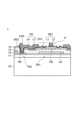
図1は、本発明の一実施形態に係る半導体装置1の構成を示す模式的な断面図である。[1. Configuration of Semiconductor Device 1]
FIG. 1 is a schematic cross-sectional view showing the configuration of a
図1に示すように、半導体装置1は、基板10の上に、第1のトランジスタTR1および第2のトランジスタTR2を備える。また、半導体装置1は、第1のトランジスタTR1および第2のトランジスタTR2に共通して設けられる絶縁する絶縁層11~絶縁層14を含む。As shown in FIG. 1, the
第1のトランジスタTR1は、絶縁層11、絶縁層12、遮光層LS、絶縁層13、酸化物半導体層OS、絶縁層14、およびゲート電極GE1を含む。絶縁層11は、基板10の上に設けられている。絶縁層12は、絶縁層11の上に設けられている。遮光層LSは、絶縁層12の上に設けられている。絶縁層13は、遮光層LSの上面および端面を覆い、絶縁層12の上に設けられている。酸化物半導体層OSは、絶縁層13の上に設けられている。絶縁層14は、酸化物半導体層OSの上面および端面を覆い、絶縁層13の上に設けられている。ゲート電極GE1は、酸化物半導体層OSと重畳し、絶縁層14の上に設けられている。第1のトランジスタTR1において、絶縁層11および絶縁層12は下地絶縁層として機能し、絶縁層13は層間絶縁層として機能し、絶縁層14はゲート絶縁層として機能する。ゲート電極GE1は、ゲート線と電気的に接続された電極である。なお、酸化物半導体層OSの詳細な構成については後述する。The first transistor TR1 includes an
第2のトランジスタTR2は、絶縁層11、シリコン半導体層SS、絶縁層12、ゲート電極GE2、絶縁層13、および絶縁層14を含む。絶縁層11は、基板10の上に設けられている。シリコン半導体層SSは、絶縁層11の上に設けられている。絶縁層12は、シリコン半導体層SSの上面および端面を覆い、絶縁層11の上に設けられている。ゲート電極GE2は、シリコン半導体層SSと重畳し、絶縁層12の上に設けられている。絶縁層13は、ゲート電極GE2の上面および端面を覆い、絶縁層12の上に設けられている。絶縁層14は、絶縁層13の上に設けられている。第2のトランジスタTR2において、絶縁層11は下地絶縁層として機能し、絶縁層12はゲート絶縁層として機能し、絶縁層13および絶縁層14は、層間絶縁層として機能する。ゲート電極GE2は、ゲート線と電気的に接続された電極である。シリコン半導体層SSとして、例えば、多結晶シリコン半導体が用いられるが、これに限られない。シリコン半導体層SSとして、その他のシリコン系半導体を用いることもできる。The second transistor TR2 includes an
第1のトランジスタTR1と第2のトランジスタTR2とは、接続配線CNを介して電気的に接続されている。具体的には、接続配線CNは、第1のトランジスタTR1の酸化物半導体層OSと第2のトランジスタTR2とを直接電気的に接続している。接続配線CNは、第1のトランジスタTR1のソース電極およびドレイン電極の一方として機能する。また、接続配線CNは、第2のトランジスタTR2のソース電極およびドレイン電極の一方としても機能する。なお、図1では、第2のトランジスタTR2のソース電極およびドレイン電極の他方の図示を省略する。The first transistor TR1 and the second transistor TR2 are electrically connected via a connection wiring CN. Specifically, the connection wiring CN directly electrically connects the oxide semiconductor layer OS of the first transistor TR1 and the second transistor TR2. The connection wiring CN functions as one of the source electrode and drain electrode of the first transistor TR1. The connection wiring CN also functions as one of the source electrode and drain electrode of the second transistor TR2. Note that in FIG. 1, the other of the source electrode and drain electrode of the second transistor TR2 is omitted from the illustration.
基板10は、半導体装置1を構成する各層を支持することができる。例えば、基板10として、ガラス基板、石英基板、またはサファイア基板などの透光性を有する剛性基板を用いることができる。また、基板10として、シリコン基板などの透光性を有しない剛性基板を用いることもできる。また、基板10として、ポリイミド樹脂基板、アクリル樹脂基板、シロキサン樹脂基板、またはフッ素樹脂基板などの透光性を有する可撓性基板を用いることができる。基板10の耐熱性を向上させるために、上記の可撓性基板に不純物を導入してもよい。The
遮光層LSは、基板10側から入射する光を反射し、または吸収することができる。換言すると、遮光層LSは、酸化物半導体層OSに入射する光を遮蔽することができる。遮光層LSは、ゲート電極GE2と同一の層で形成される。すなわち、遮光層LSは、ゲート電極GE2と同一の材料によって形成される。例えば、遮光層LSおよびゲート電極GE2として、アルミニウム(Al)、銅(Cu)、チタン(Ti)、モリブデン(Mo)、もしくはタングステン(W)などの金属、またはこれらの合金もしくはこれらの化合物などを用いることができる。遮光層LSは、単層構造を有していてもよく、積層構造を有していてもよい。The light shielding layer LS can reflect or absorb light incident from the
絶縁層11~絶縁層14の各々として、例えば、酸化シリコン(SiOx)、酸化窒化シリコン(SiOxNy)、酸化アルミニウム(AlOx)、もしくは酸化窒化アルミニウム(AlOxNy)などの酸化物、または窒化シリコン(SiNx)、窒化酸化シリコン(SiNxOy)、窒化アルミニウム(AlNx)、もしくは窒化酸化アルミニウム(AlNxOy)などの窒化物を用いることができる。絶縁層11~絶縁層14の各々は、単層構造を有していてもよく、積層構造を有していてもよい。 Each of the insulating
ここで、酸化窒化シリコン(SiOxNy)および酸化窒化アルミニウム(AlOxNy)は、それぞれ、酸素(O)よりも少ない比率(x>y)の窒素(N)を含有する酸化物である。また、窒化酸化シリコン(SiNxOy)および窒化酸化アルミニウム(AlNxOy)は、窒素よりも少ない比率(x>y)の酸素を含有する窒化物である。なお、説明の便宜上、酸化シリコン(SiOx)および酸化窒化シリコン(SiOxNy)を単に「酸化シリコン」といい、窒化シリコン(SiNx)および窒化酸化シリコン(SiNxOy)を単に「窒化シリコン」という場合がある。同様に、酸化アルミニウム(AlOx)および酸化窒化アルミニウム(AlOxNy)を単に「酸化アルミニウム」といい、窒化アルミニウム(AlNx)および窒化酸化アルミニウム(AlNxOy)を単に「窒化アルミニウム」という場合がある。 Here, silicon oxynitride (SiOx Ny ) and aluminum oxynitride (AlOx Ny ) are oxides containing nitrogen (N) at a ratio (x>y) smaller than that of oxygen (O). Silicon nitride oxide (SiNx Oy ) and aluminum nitride oxide (AlNx Oy ) are nitrides containing oxygen at a ratio (x>y) smaller than that of nitrogen. For convenience of explanation, silicon oxide (SiOx ) and silicon oxynitride (SiOx Ny ) may be simply referred to as "silicon oxide", and silicon nitride (SiNx ) and silicon nitride oxide (SiNx Oy ) may be simply referred to as "silicon nitride". Similarly, aluminum oxide (AlOx ) and aluminum oxynitride (AlOx Ny ) may be simply referred to as "aluminum oxide," and aluminum nitride (AlNx ) and aluminum nitride oxide (AlNx Oy ) may be simply referred to as "aluminum nitride."
酸化物半導体層OSと接する絶縁層13および絶縁層14は、酸化物を含むことが好ましい。酸化物半導体層OSが酸化物と接すると、熱処理によって酸化物から酸化物半導体層OSに酸素を供給することができる。例えば、絶縁層13は、窒化シリコンおよび窒化シリコンの上の酸化シリコンを含む積層構造を有していてもよい。また、絶縁層14は、酸化シリコンの単層構造を有していてもよい。The insulating
ゲート電極GE1は、接続配線CNと同一の層で形成される。すなわち、ゲート電極GE1は、接続配線CNと同一の材料によって形成される。ゲート電極GE1および接続配線CNの各々は、積層構造を有する。具体的には、ゲート電極GE1は、第1の導電層L1および第1の導電層L1の上の第2の導電層L2を含む積層構造を有する。また、接続配線CNは、第3の導電層L3および第3の導電層L3の上の第4の導電層を含む積層構造を有する。第1の導電層L1は第3の導電層L3と同一の層で形成され、第2の導電層L2は第4の導電層L4と同一の層で形成される。The gate electrode GE1 is formed in the same layer as the connection wiring CN. That is, the gate electrode GE1 is formed of the same material as the connection wiring CN. Each of the gate electrode GE1 and the connection wiring CN has a laminated structure. Specifically, the gate electrode GE1 has a laminated structure including a first conductive layer L1 and a second conductive layer L2 on the first conductive layer L1. The connection wiring CN has a laminated structure including a third conductive layer L3 and a fourth conductive layer on the third conductive layer L3. The first conductive layer L1 is formed in the same layer as the third conductive layer L3, and the second conductive layer L2 is formed in the same layer as the fourth conductive layer L4.
第1のトランジスタTR1のチャネル長方向(第1のトランジスタTR1のソース電極からドレイン電極に向かう方向またはドレイン電極からソース電極に向かう方向)において、第1の導電層L1の幅は、第2の導電層L2の幅よりも大きい。そのため、平面視において、第1の導電層L1は、第2の導電層L2から露出された部分を含む。また、第1の導電層L1の膜厚t1は、第2の導電層L2の膜厚t2よりも小さい(t1<t2)。第2の導電層L2の膜厚t2は、第1の導電層L1の膜厚t1の3倍以上である。例えば、膜厚t1は約30nmであり、膜厚t2は約100nmである。In the channel length direction of the first transistor TR1 (the direction from the source electrode to the drain electrode of the first transistor TR1 or the direction from the drain electrode to the source electrode), the width of the first conductive layer L1 is greater than the width of the second conductive layer L2. Therefore, in a planar view, the first conductive layer L1 includes a portion exposed from the second conductive layer L2. In addition, the thickness t1 of the first conductive layer L1 is smaller than the thickness t2 of the second conductive layer L2 (t1<t2). The thickness t2 of the second conductive layer L2 is three times or more the thickness t1 of the first conductive layer L1. For example, the thickness t1 is about 30 nm, and the thickness t2 is about 100 nm.
第1の導電層L1は、第2の導電層L2とは異なる材料によって形成されている。第1の導電層L1および第2の導電層L2の各々の材料の選定に際しては、第1の導電層L1を形成する材料の密度が、第2の導電層L2を形成する材料の密度より小さいことが好ましい。第1の導電層L1および第2の導電層L2として、ゲート電極GE2と同様の材料を用いることができる。例えば、第1の導電層L1は、チタン(Ti)およびアルミニウム(Al)の少なくとも1つを含み、第2の導電層L2の材料は、モリブデン(Mo)およびタングステン(W)の少なくとも1つを含む。但し、第1の導電層L1は酸化物半導体層OSと接するため、第1の導電層L1は酸化されにくい材料を含むことが好ましい。例えば、第1の導電層L1は、チタンの単層構造、またはチタンおよびチタンの上のアルミニウムを含む積層構造を有することが好ましい。The first conductive layer L1 is formed of a material different from the second conductive layer L2. When selecting the materials of the first conductive layer L1 and the second conductive layer L2, it is preferable that the density of the material forming the first conductive layer L1 is smaller than the density of the material forming the second conductive layer L2. The first conductive layer L1 and the second conductive layer L2 can be made of the same material as the gate electrode GE2. For example, the first conductive layer L1 contains at least one of titanium (Ti) and aluminum (Al), and the material of the second conductive layer L2 contains at least one of molybdenum (Mo) and tungsten (W). However, since the first conductive layer L1 is in contact with the oxide semiconductor layer OS, it is preferable that the first conductive layer L1 contains a material that is not easily oxidized. For example, the first conductive layer L1 preferably has a single layer structure of titanium, or a laminate structure containing titanium and aluminum on titanium.
第1のトランジスタTR1では、絶縁層14を貫通し、酸化物半導体層OSの一部が露出される第1のコンタクトホールCH1が設けられている。また、第2のトランジスタTR2では、絶縁層12~絶縁層14を貫通し、シリコン半導体層SSの一部が露出される第2のコンタクトホールCH2が設けられている。第2のコンタクトホールCH2の深さは、第1のコンタクトホールCH1の深さよりも大きい。接続配線CNは、第1のコンタクトホールCH1および第2のコンタクトホールCH2を介して、酸化物半導体層OSとシリコン半導体層SSとを電気的に接続する。The first transistor TR1 has a first contact hole CH1 that penetrates the insulating
上述したように、接続配線CNは、第1の導電層L1と同一の層で形成される第3の導電層L3および第2の導電層L2と同一の層で形成される第4の導電層を含む。そのため、第3の導電層L3の膜厚t3は、第4の導電層L4の膜厚t4よりも小さい(t3<t4)。第4の導電層L4の膜厚t4は、第3の導電層L3の膜厚t3の3倍以上である。例えば、膜厚t3は約30nmであり、膜厚t4は約100nmである。As described above, the connection wiring CN includes a third conductive layer L3 formed in the same layer as the first conductive layer L1 and a fourth conductive layer formed in the same layer as the second conductive layer L2. Therefore, the thickness t3 of the third conductive layer L3 is smaller than the thickness t4 of the fourth conductive layer L4 (t3<t4). The thickness t4 of the fourth conductive layer L4 is three or more times the thickness t3 of the third conductive layer L3. For example, the thickness t3 is about 30 nm, and the thickness t4 is about 100 nm.
第3の導電層L3は、第1のコンタクトホールCH1および第2のコンタクトホールCH2を覆うように、第1のコンタクトホールCH1から第2のコンタクトホールCH2まで延在している。第3の導電層L3は、第1のコンタクトホールCH1を介して酸化物半導体層OSと接し、かつ、第2のコンタクトホールCH2を介してシリコン半導体層SSと接している。The third conductive layer L3 extends from the first contact hole CH1 to the second contact hole CH2 so as to cover the first contact hole CH1 and the second contact hole CH2. The third conductive layer L3 contacts the oxide semiconductor layer OS through the first contact hole CH1 and contacts the silicon semiconductor layer SS through the second contact hole CH2.
第4の導電層L4は、第2のコンタクトホールCH2と重畳するが、第1のコンタクトホールCH1と重畳しない。すなわち、接続配線CNは、第3の導電層L3の一部が第4の導電層L4から露出されている。第4の導電層L4から露出された第3の導電層の一部が、第1のコンタクトホールCH1を介して酸化物半導体層OSと接している。The fourth conductive layer L4 overlaps the second contact hole CH2 but does not overlap the first contact hole CH1. That is, in the connection wiring CN, a portion of the third conductive layer L3 is exposed from the fourth conductive layer L4. The portion of the third conductive layer exposed from the fourth conductive layer L4 contacts the oxide semiconductor layer OS via the first contact hole CH1.
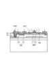
ここで、図2を参照して、接続配線CNと酸化物半導体層との電気的接続について説明する。Here, referring to FIG. 2, the electrical connection between the connection wiring CN and the oxide semiconductor layer will be described.
図2は、本発明の一実施形態に係る半導体装置1の構成を示す模式的な拡大断面図である。具体的には、図2は、図1中の領域Aを拡大した断面図である。Figure 2 is a schematic enlarged cross-sectional view showing the configuration of a
酸化物半導体層OSは、チャネル領域OS_1およびチャネル領域と隣接する不純物領域OS_2を含む。チャネル領域OS_1は、半導体の性質を有する。そのため、ゲート電極GE1に電圧が印加されると、チャネル領域OS_1には電流パスとなるチャネルが形成される。不純物領域OS_2は不純物元素を含み、導体の性質を有する。そのため、不純物領域OS_2のキャリア濃度は、チャネル領域OS_1のキャリア濃度よりも大きい。換言すると、チャネル領域OS_1は、不純物領域OS_2よりも高い電気抵抗率(または低い電気伝導度)を有する。例えば、不純物領域OS_2のシート抵抗は、1000Ω/sq.以下であり、好ましくは500Ω/sq.以下であり、さらに好ましくは250Ω/sq.以下である。なお、不純物領域OS_2は、ソース領域またはドレイン領域と呼ばれる場合がある。The oxide semiconductor layer OS includes a channel region OS_1 and an impurity region OS_2 adjacent to the channel region. The channel region OS_1 has semiconductor properties. Therefore, when a voltage is applied to the gate electrode GE1, a channel that serves as a current path is formed in the channel region OS_1. The impurity region OS_2 contains an impurity element and has conductor properties. Therefore, the carrier concentration of the impurity region OS_2 is higher than the carrier concentration of the channel region OS_1. In other words, the channel region OS_1 has a higher electrical resistivity (or a lower electrical conductivity) than the impurity region OS_2. For example, the sheet resistance of the impurity region OS_2 is 1000 Ω/sq. or less, preferably 500 Ω/sq. or less, and more preferably 250 Ω/sq. or less. The impurity region OS_2 may be called a source region or a drain region.
不純物領域OS_2に含まれる不純物元素は、例えば、ホウ素(B)またはリン(P)であるが、これに限られない。詳細は後述するが、酸化物半導体層OSに不純物元素を注入することにより、不純物元素を含む不純物領域OS_2を形成することができる。酸化物半導体層OSの不純物領域OS_2では、より多くの不純物元素を含むことができる。これは、不純物領域OS_2中により多くの酸素欠陥が存在し、不純物領域OS_2が十分に大きなキャリア濃度を有することを意味する。そのため、不純物領域OS_2の抵抗は、十分に低い。The impurity element contained in the impurity region OS_2 is, for example, boron (B) or phosphorus (P), but is not limited thereto. As will be described in detail later, the impurity region OS_2 containing the impurity element can be formed by injecting the impurity element into the oxide semiconductor layer OS. The impurity region OS_2 of the oxide semiconductor layer OS can contain a larger amount of impurity elements. This means that there are more oxygen defects in the impurity region OS_2, and the impurity region OS_2 has a sufficiently large carrier concentration. Therefore, the resistance of the impurity region OS_2 is sufficiently low.
チャネル領域OS_1と不純物領域OS_2との境界は、第2の導電層L2の端部と略一致する。すなわち、不純物領域OS_2の端部は、第1の導電層L1のうちの第2の導電層L2から露出されている部分と重畳する。The boundary between the channel region OS_1 and the impurity region OS_2 approximately coincides with the end of the second conductive layer L2. In other words, the end of the impurity region OS_2 overlaps with the portion of the first conductive layer L1 that is exposed from the second conductive layer L2.
第3の導電層L3は、第1のコンタクトホールCH1を介して、不純物領域OS_2と接する。不純物領域OS_2の抵抗は十分に低いため、第3の導電層L3と不純物領域OS_2との電気的接続はオーミック接触となる。The third conductive layer L3 contacts the impurity region OS_2 through the first contact hole CH1. Because the resistance of the impurity region OS_2 is sufficiently low, the electrical connection between the third conductive layer L3 and the impurity region OS_2 is an ohmic contact.
[2.酸化物半導体層OSの構成]
[2-1.酸化物半導体層OSの組成]
酸化物半導体層OSとして、インジウム(In)を含む2以上の金属元素を含む酸化物半導体が用いられる。インジウム以外の金属元素として、ガリウム(Ga)、亜鉛(Zn)、アルミニウム(Al)、ハフニウム(Hf)、イットリウム(Y)、ジルコニウム(Zr)、およびランタノイドが用いられる。[2. Configuration of Oxide Semiconductor Layer OS]
[2-1. Composition of Oxide Semiconductor Layer OS]
The oxide semiconductor layer OS is formed using an oxide semiconductor containing two or more metal elements including indium (In). Examples of the metal elements other than indium include gallium (Ga), zinc (Zn), aluminum (Al), hafnium (Hf), yttrium (Y), zirconium (Zr), and a lanthanoid.
酸化物半導体層OSは、透光性を有し、複数の結晶粒を含む多結晶構造を有する。酸化物半導体層OSが多結晶構造を有するためには、全金属元素に対するインジウムの比率が原子比率で50%以上である酸化物半導体が用いられることが好ましい。インジウムの比率が大きくなると、酸化物半導体層OSが結晶化しやすくなる。また、インジウム以外の金属元素として、ガリウムを含むことが好ましい。ガリウムは、インジウムと同じ第13族元素に属する。そのため、酸化物半導体層OSの結晶性がガリウムによって阻害されることがほとんどない。The oxide semiconductor layer OS has a polycrystalline structure that is light-transmitting and includes a plurality of crystal grains. In order for the oxide semiconductor layer OS to have a polycrystalline structure, it is preferable to use an oxide semiconductor in which the ratio of indium to all metal elements is 50% or more in atomic ratio. When the ratio of indium is large, the oxide semiconductor layer OS is more likely to crystallize. In addition, it is preferable to include gallium as a metal element other than indium. Gallium belongs to the
上述したように、酸化物半導体層OSは、チャネル領域OS_1および不純物領域OS_2を含むが、チャネル領域OS_1だけでなく、不純物領域OS_2も多結晶構造を有する場合がある。この場合、チャネル領域OS_1の結晶構造は、不純物領域OS_2の結晶構造と同一である。As described above, the oxide semiconductor layer OS includes a channel region OS_1 and an impurity region OS_2, and not only the channel region OS_1 but also the impurity region OS_2 may have a polycrystalline structure. In this case, the crystal structure of the channel region OS_1 is the same as the crystal structure of the impurity region OS_2.
詳細は後述するが、酸化物半導体層OSは、従来の多結晶構造を有する酸化物半導体とは異なる性質を有する。そのため、酸化物半導体層OSに含まれる酸化物半導体を従来の多結晶構造を有する酸化物半導体と区別するため、以下では、酸化物半導体層OSに含まれる酸化物半導体をPoly-OS(Poly-crystalline Oxide Semiconductor)と称して説明する。Although the details will be described later, the oxide semiconductor layer OS has properties different from those of conventional oxide semiconductors having a polycrystalline structure. Therefore, in order to distinguish the oxide semiconductor contained in the oxide semiconductor layer OS from conventional oxide semiconductors having a polycrystalline structure, the oxide semiconductor contained in the oxide semiconductor layer OS will be referred to as Poly-OS (Poly-crystalline Oxide Semiconductor) in the following description.
酸化物半導体層OSに含まれるPoly-OSは、スパッタリングおよび熱処理を用いて形成することができる。ここで、酸化物半導体層OSの形成方法について説明する。The Poly-OS contained in the oxide semiconductor layer OS can be formed by sputtering and heat treatment. Here, a method for forming the oxide semiconductor layer OS will be described.
まず、スパッタリングによって酸化物半導体膜を成膜する。成膜された酸化物半導体膜は、アモルファス構造を有する。ここで、アモルファス構造とは、長距離秩序構造が存在せず、周期的な結晶格子の配列が見られない構造をいう。例えば、X線回折(X-ray Diffraction:XRD)法を用いてアモルファス構造を有する酸化物半導体膜を観察すると、回折パターンにおいて結晶構造に基づく特定のピークが得られない。なお、アモルファス構造を有する酸化物半導体膜は、微小領域において短距離秩序構造を有する場合がある。しかしながら、このような酸化物半導体膜は、Poly-OSの特性を示さないため、アモルファス構造を有する酸化物半導体膜として分類することができる。First, an oxide semiconductor film is formed by sputtering. The formed oxide semiconductor film has an amorphous structure. Here, the amorphous structure refers to a structure in which there is no long-range order structure and no periodic crystal lattice arrangement is observed. For example, when an oxide semiconductor film having an amorphous structure is observed using X-ray diffraction (XRD), no specific peak based on the crystal structure is obtained in the diffraction pattern. Note that an oxide semiconductor film having an amorphous structure may have a short-range order structure in a microscopic region. However, such an oxide semiconductor film does not exhibit the characteristics of Poly-OS, and therefore can be classified as an oxide semiconductor film having an amorphous structure.
アモルファス構造を有する酸化物半導体膜は、低温で成膜される。例えば、酸化物半導体膜が成膜される基板の温度は、150℃以下、好ましくは100℃以下、さらに好ましくは50℃以下である。基板の温度が高いと、成膜される酸化物半導体中で微結晶が生成されやすい。また、成膜中のチャンバ内の酸素分圧は、1%以上10%以下、好ましくは1%以上5%以下、さらに好ましくは2%以上4%以下である。酸素分圧が高いと、酸化物半導体に含まれる過剰な酸素によって、酸化物半導体膜中で微結晶が生成されてしまう。一方、酸素分圧が1%未満の条件では、酸化物半導体膜中の酸素の組成が不均一となり、微結晶が多く含まれる酸化物半導体膜、または熱処理を行っても結晶化しない酸化物半導体膜が成膜される。An oxide semiconductor film having an amorphous structure is formed at a low temperature. For example, the temperature of the substrate on which the oxide semiconductor film is formed is 150° C. or less, preferably 100° C. or less, and more preferably 50° C. or less. If the substrate temperature is high, microcrystals are likely to be generated in the oxide semiconductor film being formed. In addition, the oxygen partial pressure in the chamber during film formation is 1% to 10%, preferably 1% to 5%, and more preferably 2% to 4%. If the oxygen partial pressure is high, microcrystals are generated in the oxide semiconductor film due to the excess oxygen contained in the oxide semiconductor. On the other hand, under conditions where the oxygen partial pressure is less than 1%, the oxygen composition in the oxide semiconductor film becomes non-uniform, and an oxide semiconductor film containing many microcrystals or an oxide semiconductor film that does not crystallize even when heat treatment is performed is formed.
次に、スパッタリングによって成膜された酸化物半導体膜に対して熱処理を行う。熱処理は大気中で行われるが、熱処理の雰囲気はこれに限られない。熱処理の温度は、300℃以上500℃以下であり、好ましくは350℃以上450℃以下である。また、熱処理の時間は、15分以上120分以下であり、好ましくは30分以上60分以下である。熱処理を行うことにより、アモルファス構造を有する酸化物半導体膜が結晶化され、Poly-OSを含む酸化物半導体層OSが形成される。Next, the oxide semiconductor film formed by sputtering is subjected to heat treatment. The heat treatment is performed in air, but the atmosphere is not limited to this. The temperature of the heat treatment is 300° C. or more and 500° C. or less, and preferably 350° C. or more and 450° C. or less. The time of the heat treatment is 15 minutes or more and 120 minutes or less, and preferably 30 minutes or more and 60 minutes or less. By performing the heat treatment, the oxide semiconductor film having an amorphous structure is crystallized, and an oxide semiconductor layer OS containing Poly-OS is formed.
酸化物半導体層OSの組成は、スパッタリングターゲットの組成と略一致する。そのため、酸化物半導体層OSの金属元素の組成は、スパッタリングターゲットの金属元素の組成に基づき特定することができる。また、XRD法を用いて、酸化物半導体層OSの組成を特定してもよい。具体的には、XRD法から取得された酸化物半導体層OSの結晶構造および格子定数に基づき、酸化物半導体層OSの金属元素の組成を特定することができる。さらに、酸化物半導体層OSの金属元素の組成は、蛍光X線分析または電子プローブマイクロアナライザ(Electron Probe Micro Analyzer:EPMA)分析などを用いて特定することもできる。なお、酸化物半導体層OSに含まれる酸素は、スパッタリングのプロセス条件などにより変化するため、この限りではない。The composition of the oxide semiconductor layer OS is approximately equal to the composition of the sputtering target. Therefore, the composition of the metal elements of the oxide semiconductor layer OS can be specified based on the composition of the metal elements of the sputtering target. The composition of the oxide semiconductor layer OS may also be specified using an XRD method. Specifically, the composition of the metal elements of the oxide semiconductor layer OS can be specified based on the crystal structure and lattice constant of the oxide semiconductor layer OS obtained by the XRD method. Furthermore, the composition of the metal elements of the oxide semiconductor layer OS can also be specified using X-ray fluorescence analysis or electron probe micro analyzer (EPMA) analysis. Note that the oxygen contained in the oxide semiconductor layer OS is not limited to this because it changes depending on the process conditions of sputtering.
[2-2.酸化物半導体層OSの特性]
続いて、Poly-OSを含む酸化物半導体層OSの特性について説明する。[2-2. Characteristics of Oxide Semiconductor Layer OS]
Next, characteristics of the oxide semiconductor layer OS including Poly-OS will be described.
酸化物半導体層OSは、優れたエッチング耐性を有する。具体的には、酸化物半導体層OSは、ウェットエッチング用のエッチング液を用いてエッチングされるときのエッチングレートが非常に小さい。これは、酸化物半導体層OSがエッチング液によってほとんどエッチングされないことを意味する。40℃において主成分としてリン酸を含むエッチング液(以下、「混酸エッチング溶液」という。)を用いて酸化物半導体層OSをエッチングしたときのエッチングレートは、3nm/min未満、2nm/min未満、または1nm/min未満である。混酸エッチング溶液中におけるリン酸の割合は、50%以上、60%以上、または70%以上である。混酸エッチング溶液には、リン酸以外に、酢酸および硝酸が含まれていてもよい。なお、Poly-OSを含まない酸化物半導体膜、例えば、熱処理が行われる前のアモルファス構造を有する酸化物半導体膜では、40℃において混酸エッチング溶液を用いて酸化物半導体膜をエッチングしたときのエッチングレートは、100nm/min以上である。また、室温において0.5%フッ酸溶液を用いて酸化物半導体層OSをエッチングしたときのエッチングレートは、5nm/min未満、4nm/min未満、または3nm/min未満である。なお、Poly-OSを含まない酸化物半導体膜では、室温において0.5%フッ酸溶液を用いて酸化物半導体膜をエッチングしたときのエッチングレートは、15nm/min以上である。ここで、「40℃」は、40±5℃の範囲を含み、エッチング液の温度であってもよく、エッチング液の設定温度であってもよい。また、「室温」とは、25±5℃をいう。The oxide semiconductor layer OS has excellent etching resistance. Specifically, the etching rate of the oxide semiconductor layer OS is very small when the oxide semiconductor layer OS is etched using an etching solution for wet etching. This means that the oxide semiconductor layer OS is hardly etched by the etching solution. The etching rate when the oxide semiconductor layer OS is etched using an etching solution containing phosphoric acid as a main component at 40° C. (hereinafter referred to as a "mixed acid etching solution") is less than 3 nm/min, less than 2 nm/min, or less than 1 nm/min. The ratio of phosphoric acid in the mixed acid etching solution is 50% or more, 60% or more, or 70% or more. The mixed acid etching solution may contain acetic acid and nitric acid in addition to phosphoric acid. Note that, in an oxide semiconductor film that does not contain Poly-OS, for example, an oxide semiconductor film having an amorphous structure before heat treatment, the etching rate when the oxide semiconductor film is etched using a mixed acid etching solution at 40° C. is 100 nm/min or more. Furthermore, the etching rate when the oxide semiconductor layer OS is etched using a 0.5% hydrofluoric acid solution at room temperature is less than 5 nm/min, less than 4 nm/min, or less than 3 nm/min. Note that, in an oxide semiconductor film that does not contain Poly-OS, the etching rate when the oxide semiconductor film is etched using a 0.5% hydrofluoric acid solution at room temperature is 15 nm/min or more. Here, "40°C" includes a range of 40±5°C, and may be the temperature of the etching solution or the set temperature of the etching solution. Furthermore, "room temperature" refers to 25±5°C.
酸化物半導体層OSの一実施例を表1に示す。表1には、作製された各サンプルにおける混酸エッチング溶液(混酸エッチング溶液におけるリン酸の割合が65%であるナサ工業株式会社製「混酸 AT-2F」)および0.5%フッ酸溶液に対するエッチングレートが示されている。また、各サンプルをエッチングするとき、混酸エッチング溶液の温度は40℃であり、および0.5%フッ酸溶液の温度は室温(22℃)であった。表1において、サンプル1はPoly-OSを含む酸化物半導体層OSであり、サンプル2は熱処理する前のアモルファス構造を有する酸化物半導体膜であり、サンプル3はインジウムの比率が50%未満である酸化インジウムガリウム亜鉛(IGZO)を含む酸化物半導体膜である。An example of the oxide semiconductor layer OS is shown in Table 1. Table 1 shows the etching rates of each prepared sample with respect to a mixed acid etching solution ("Mixed Acid AT-2F" manufactured by Nasa Industries Co., Ltd., in which the ratio of phosphoric acid in the mixed acid etching solution is 65%) and a 0.5% hydrofluoric acid solution. When each sample was etched, the temperature of the mixed acid etching solution was 40°C, and the temperature of the 0.5% hydrofluoric acid solution was room temperature (22°C). In Table 1,

表1に示すように、サンプル1(Poly-OSを含む酸化物半導体層OS)は、混酸エッチング溶液を用いてほとんどエッチングされず、0.5%フッ酸溶液を用いてもせいぜい2nm/minしかエッチングされない。サンプル1は、サンプル2(熱処理前のアモルファス構造を有する酸化物半導体膜)よりも、混酸エッチング溶液で1/100以下、0.5%フッ酸溶液で約1/10以下のエッチングレートを有する。また、サンプル1は、サンプル3(インジウムの比率が50%未満であるIGZOを含む酸化物半導体膜)よりも、混酸エッチング溶液で1/100以下のエッチングレートを有する。すなわち、サンプル1は、サンプル2およびサンプル3よりも大幅にエッチング耐性に優れる。As shown in Table 1, Sample 1 (oxide semiconductor layer OS containing Poly-OS) is hardly etched using a mixed acid etching solution, and even when using a 0.5% hydrofluoric acid solution, it is etched at most 2 nm/min.
このようなPoly-OSを含む酸化物半導体層OSの優れたエッチング耐性は、500℃以下のプロセスで作製される従来の多結晶構造を有する酸化物半導体では得られない特性である。Poly-OSを含む酸化物半導体層OSの優れたエッチング耐性については、詳細なメカニズムは不明であるが、Poly-OSが従来とは異なる多結晶構造を有していると考えられる。Such excellent etching resistance of the oxide semiconductor layer OS containing Poly-OS is a property that cannot be obtained with oxide semiconductors having a conventional polycrystalline structure that are produced by a process at 500° C. or less. Although the detailed mechanism of the excellent etching resistance of the oxide semiconductor layer OS containing Poly-OS is unclear, it is believed that Poly-OS has a polycrystalline structure that differs from conventional structures.
上述したように、Poly-OSを含む酸化物半導体層OSは、エッチング液に対するエッチングレートが非常に小さい。そのため、酸化物半導体層OSのパターニングは非常に困難である。そこで、島状の酸化物半導体層OSを形成する場合には、熱処理を行う前のアモルファス構造を有する酸化物半導体膜を島状にパターニングし、その後、熱処理を行って結晶化する。これにより、Poly-OSを含む島状の酸化物半導体層OSを形成することができる。As described above, the oxide semiconductor layer OS containing Poly-OS has a very small etching rate with respect to the etching solution. Therefore, patterning of the oxide semiconductor layer OS is very difficult. Therefore, when forming an island-shaped oxide semiconductor layer OS, an oxide semiconductor film having an amorphous structure before heat treatment is patterned into an island shape, and then heat treatment is performed to crystallize it. In this way, an island-shaped oxide semiconductor layer OS containing Poly-OS can be formed.
[3.半導体装置1の製造方法]
図3~図6を参照して、半導体装置1の製造方法について説明する。[3. Manufacturing method of semiconductor device 1]
A method for manufacturing the
図3~図6の各々は、本発明の一実施形態に係る半導体装置1の製造方法を示す模式的な断面図である。Each of Figures 3 to 6 is a schematic cross-sectional view showing a manufacturing method of a
まず、図3に示すように、基板10上に、絶縁層11、シリコン半導体層SS、絶縁層12、ゲート電極GE2および遮光層LS、絶縁層13、酸化物半導体層OS、ならびに絶縁層14を順次形成する。First, as shown in FIG. 3, an insulating
シリコン半導体層SSの形成では、ゲート電極GE1をマスクとしてシリコン半導体層SSに不純物を注入する。このとき、注入される不純物元素は、nチャネル型の場合にはリン(P)であり、pチャネル型の場合にはホウ素(B)である。酸化物半導体層OSの形成では、スパッタリングにより成膜された酸化物半導体膜のパターニング後に、OSアニールを行う。OSアニールを行うことにより、Poly-OSを含む酸化物半導体層OSが形成される。When forming the silicon semiconductor layer SS, impurities are implanted into the silicon semiconductor layer SS using the gate electrode GE1 as a mask. The implanted impurity element is phosphorus (P) in the case of an n-channel type, and boron (B) in the case of a p-channel type. When forming the oxide semiconductor layer OS, OS annealing is performed after patterning the oxide semiconductor film formed by sputtering. By performing OS annealing, an oxide semiconductor layer OS containing Poly-OS is formed.
また、絶縁層14を形成した後に、絶縁層14を貫通する第1のコンタクトホールCH1および絶縁層12~絶縁層14を貫通する第2のコンタクトホールCH2を形成する。第1のコンタクトホールCH1では、酸化物半導体層OSの一部が露出され、第2のコンタクトホールCH2では、シリコン半導体層SSの一部が露出される。After forming the insulating
次に、図4に示すように、絶縁層14の上に金属膜を成膜した後に、当該金属膜をパ
ターニングすることで、ゲート電極GE2の第1の導電層L1および接続配線CNの第3の導電層L3を形成する。第3の導電層L3は、第1のコンタクトホールCH1において酸化物半導体層OSと接し、第2のコンタクトホールCH2においてシリコン半導体層SSと接する。第1の導電層L1は、酸化物半導体層OSと重畳し、第3の導電層L3から離間している。 4, a metal film is formed on the insulating
次に、図5に示すように、第1の導電層L1および第3の導電層の上に金属膜を成膜した後に、当該金属膜をパターニングすることで、ゲート電極GE1の第2の導電層L2および接続配線CNの第4の導電層L4を形成する。第4の導電層L4は、第2のコンタクトホールCH2と重畳するが、第1のコンタクトホールCH1と重畳しない。第2の導電層L2は、酸化物半導体層OSと重畳し、第4の導電層L4から離間している。Next, as shown in FIG. 5, a metal film is formed on the first conductive layer L1 and the third conductive layer, and then the metal film is patterned to form the second conductive layer L2 of the gate electrode GE1 and the fourth conductive layer L4 of the connection wiring CN. The fourth conductive layer L4 overlaps the second contact hole CH2 but does not overlap the first contact hole CH1. The second conductive layer L2 overlaps the oxide semiconductor layer OS and is separated from the fourth conductive layer L4.
次に、図6に示すように、ゲート電極GE1をマスクとして酸化物半導体層OSにイオン注入を行う。例えば、イオン注入により、不純物元素としてホウ素(B)を酸化物半導体層OSに注入する。なお、ホウ素の代わりに、リン(P)などの他の不純物元素を酸化物半導体層OSに注入してもよい。Next, as shown in FIG. 6, ions are implanted into the oxide semiconductor layer OS using the gate electrode GE1 as a mask. For example, boron (B) is implanted as an impurity element into the oxide semiconductor layer OS by ion implantation. Note that instead of boron, other impurity elements such as phosphorus (P) may be implanted into the oxide semiconductor layer OS.
イオン注入に際しては、比較的密度が高く、かつ、比較的膜厚が大きい第2の導電層L2および第4の導電層L4は、不純物元素の注入を阻止する能力が高い。このため、第2の導電層L2および第4の導電層L4と重畳する領域には、不純物元素がほとんど注入されない。一方で、第1の導電層L1および第3の導電層L3は、比較的密度が低く、かつ、膜厚が小さい。そのため、第2の導電層L2と重畳しない第1の導電層L1の部分および第4の導電層L4と重畳しない第3の導電層の部分では、不純物元素が通過しやすい。したがって、第2の導電層L2および第4の導電層L4と重畳しない領域に、不純物元素が注入される。これにより、酸化物半導体層OSのうちの、第2の導電層L2と重畳しない領域に不純物元素が注入され、低抵抗化された不純物領域OS_2が形成される。また、酸化物半導体層OSのうちの、第2の導電層L2と重畳する領域に不純物元素は注入されず、チャネル領域OS_1が形成される。上述したように、第1の導電層L1のうちの第2の導電層L2から露出された部分では不純物元素が通過するが、当該部分に不純物元素が含まれていてもよい。同様に、第3の導電層L3のうちの第4の導電層L4から露出された部分でも不純物元素が通過するが、当該部分に不純物元素が含まれていてもよい。During ion implantation, the second conductive layer L2 and the fourth conductive layer L4, which have a relatively high density and a relatively large thickness, have a high ability to block the implantation of impurity elements. Therefore, the impurity elements are hardly implanted into the region overlapping with the second conductive layer L2 and the fourth conductive layer L4. On the other hand, the first conductive layer L1 and the third conductive layer L3 have a relatively low density and a small thickness. Therefore, the impurity elements easily pass through the part of the first conductive layer L1 that does not overlap with the second conductive layer L2 and the part of the third conductive layer that does not overlap with the fourth conductive layer L4. Therefore, the impurity elements are implanted into the region that does not overlap with the second conductive layer L2 and the fourth conductive layer L4. As a result, the impurity elements are implanted into the region of the oxide semiconductor layer OS that does not overlap with the second conductive layer L2, and a low-resistance impurity region OS_2 is formed. Furthermore, the impurity element is not injected into the region of the oxide semiconductor layer OS that overlaps with the second conductive layer L2, and a channel region OS_1 is formed. As described above, the impurity element passes through the portion of the first conductive layer L1 that is exposed from the second conductive layer L2, but the impurity element may be included in that portion. Similarly, the impurity element passes through the portion of the third conductive layer L3 that is exposed from the fourth conductive layer L4, but the impurity element may be included in that portion.
上述したように、第2のトランジスタTR2がnチャネル型の場合には、シリコン半導体層SSに注入される不純物元素はリンである。すなわち、シリコン半導体層SSに含まれる不純物元素(リン)は、酸化物半導体層OSに注入される不純物元素(ホウ素)と異なる。この場合、シリコン半導体層SSに、酸化物半導体層OSに注入される不純物元素(ホウ素)が注入されないように保護する必要がある。このため、第2のコンタクトホールCH2において第3の導電層L3の上に第4の導電層L4が形成され、酸化物半導体層OSに注入される不純物元素(ホウ素)がシリコン半導体層SSに注入されることを防止する。As described above, when the second transistor TR2 is an n-channel type, the impurity element implanted into the silicon semiconductor layer SS is phosphorus. That is, the impurity element (phosphorus) contained in the silicon semiconductor layer SS is different from the impurity element (boron) implanted into the oxide semiconductor layer OS. In this case, it is necessary to protect the silicon semiconductor layer SS from the impurity element (boron) implanted into the oxide semiconductor layer OS. For this reason, a fourth conductive layer L4 is formed on the third conductive layer L3 in the second contact hole CH2, and the impurity element (boron) implanted into the oxide semiconductor layer OS is prevented from being implanted into the silicon semiconductor layer SS.
また、第2のトランジスタTR2がpチャネル型の場合には、シリコン半導体層SSに注入される不純物元素はホウ素である。酸化物半導体層OSに注入される不純物元素がリンである場合、シリコン半導体層SSに含まれる不純物元素(ホウ素)は、酸化物半導体層OSに注入される不純物元素(リン)と異なる。この場合も同様に、第2のコンタクトホールCH2において第3の導電層L3の上に第4の導電層L4が形成され、酸化物半導体層OSに注入される不純物元素(リン)がシリコン半導体層SSに注入されることを防止する。When the second transistor TR2 is a p-channel type, the impurity element implanted into the silicon semiconductor layer SS is boron. When the impurity element implanted into the oxide semiconductor layer OS is phosphorus, the impurity element (boron) contained in the silicon semiconductor layer SS is different from the impurity element (phosphorus) implanted into the oxide semiconductor layer OS. In this case as well, a fourth conductive layer L4 is formed on the third conductive layer L3 in the second contact hole CH2, and prevents the impurity element (phosphorus) implanted into the oxide semiconductor layer OS from being implanted into the silicon semiconductor layer SS.
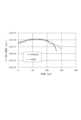
図7は、酸化物半導体層OSに注入されるホウ素の濃度プロファイルを示すシミュレーションの結果である。図7のグラフの横軸および横軸は、それぞれ、表面からの距離およびホウ素の濃度を表す。また、図7には、酸化物半導体層OSに含まれるPoly-OSの濃度プロファイル(図7中の実線)だけでなく、従来例として酸化インジウムガリウム亜鉛(IGZO)の濃度プロファイル(図7中の点線)も示されている。Figure 7 shows the results of a simulation showing the concentration profile of boron implanted into the oxide semiconductor layer OS. The horizontal and vertical axes of the graph in Figure 7 represent the distance from the surface and the boron concentration, respectively. Figure 7 also shows not only the concentration profile of Poly-OS contained in the oxide semiconductor layer OS (solid line in Figure 7), but also the concentration profile of indium gallium zinc oxide (IGZO) as a conventional example (dotted line in Figure 7).
シミュレーションは、SILVACO社製「VICTORY PROCESS」を用い、加速電圧30keVおよびドーズ量1×1013cm-2の条件で行われた。また、上述したように、Poly-OSは、インジウムを多く含み、密度が高い。そのため、シミュレーションでは、Poly-OSおよびIGZOの密度を、それぞれ、7.179g/cm3および6.1g/cm3として計算した。 The simulation was performed using a "VICTORY PROCESS" manufactured by SILVACO Corporation, under conditions of an acceleration voltage of 30 keV and a dose of 1×1013 cm-2 . As described above, Poly-OS contains a large amount of indium and has a high density. Therefore, in the simulation, the densities of Poly-OS and IGZO were calculated to be 7.179 g/cm3 and 6.1 g/cm3 , respectively.
図7に示されるように、Poly-OSにおけるホウ素が注入される距離は、IGZOにおけるホウ素が注入される距離よりも小さい。すなわち、IGZOと比較して、Poly-OSは、表面からの遠く離れた位置までホウ素が注入されない。これは、注入されたホウ素がPoly-OS中に留まりやすいことを意味する。換言すると、Poly-OSは、注入される不純物元素に対して高い阻止能を有する。そのため、不純物元素はPoly-OSを含む酸化物半導体層OSを通過することなく、酸化物半導体層OSは、より多くの不純物元素を含むことができる。その結果、不純物領域OS_2ではより多くの酸素欠陥が生成され、不純物領域OS_2を十分に低抵抗化することができる。As shown in FIG. 7, the distance into which boron is implanted in Poly-OS is smaller than the distance into which boron is implanted in IGZO. That is, compared to IGZO, boron is not implanted into Poly-OS to a position far from the surface. This means that the implanted boron is likely to remain in Poly-OS. In other words, Poly-OS has a high blocking ability for the implanted impurity element. Therefore, the impurity element does not pass through the oxide semiconductor layer OS containing Poly-OS, and the oxide semiconductor layer OS can contain a larger amount of impurity element. As a result, more oxygen defects are generated in the impurity region OS_2, and the resistance of the impurity region OS_2 can be sufficiently reduced.
半導体装置1では、第1の導電層L1および第3の導電層L3を介して、酸化物半導体層OSに不純物元素を注入するため、イオン注入における加速電圧を上昇させる場合がある。この場合、不純物元素に対する阻止能が顕著に現れる。具体的には、不純物元素がIGZOを含む従来の酸化物半導体層を通過する場合であっても、Poly-OSを含む酸化物半導体層OSでは、不純物元素が酸化物半導体層OS中に留まる。したがって、半導体装置1では、第1の導電層L1および第3の導電層L3と重畳する不純物領域OS_2が、十分に低抵抗化される。In the
以上説明したように、半導体装置1では、酸化物半導体層OSとシリコン半導体層SSとを直接電気的に接続する接続配線CNは、薄い膜厚を有する第3の導電層L3および厚い膜厚を有する第4の導電層L4を含む積層構造を有する。しかしながら、第4の導電層L4は、第3の導電層L3が酸化物半導体層OSと接する第1のコンタクトホールCH1と重畳して形成されていない。As described above, in the
本実施形態と異なり、第1のコンタクトホールCH1と重畳して厚い膜厚を有する接続配線が形成されている場合において不純物元素のイオン注入が行われると、ゲート電極と接続配線との間の間隙からのみ不純物元素が注入されることになる。この場合、不純物元素を含む不純物領域は、第1のコンタクトホールCH1と重畳しない。そのため、接続配線と酸化物半導体層との電気的接続がオーミック接触とならず、第2のトランジスタTR2は所望の性能を有しない。また、接続配線と酸化物半導体層との電気的接続が安定しないため、第2のトランジスタTR2の信頼性が低下する。Unlike the present embodiment, when ion implantation of an impurity element is performed in a case where a thick connection wiring is formed overlapping the first contact hole CH1, the impurity element is only implanted through the gap between the gate electrode and the connection wiring. In this case, the impurity region containing the impurity element does not overlap the first contact hole CH1. Therefore, the electrical connection between the connection wiring and the oxide semiconductor layer does not form an ohmic contact, and the second transistor TR2 does not have the desired performance. In addition, the electrical connection between the connection wiring and the oxide semiconductor layer is not stable, so the reliability of the second transistor TR2 is reduced.
一方、本実施形態によれば、第3の導電層L3を介して酸化物半導体層OSに不純物元素が注入されることにより、第1のコンタクトホールCH1と重畳して不純物領域OS_2を形成することができる。したがって、接続配線CNと酸化物半導体層との電気的接続がオーミック接触となり、第2のトランジスタTR2は所望の性能を有する。また、接続配線CNと酸化物半導体層OSとの電気的接続が安定するため、第2のトランジスタTR2は高い信頼性を有する。On the other hand, according to this embodiment, an impurity element is injected into the oxide semiconductor layer OS through the third conductive layer L3, so that the impurity region OS_2 can be formed by overlapping with the first contact hole CH1. Therefore, the electrical connection between the connection wiring CN and the oxide semiconductor layer is ohmic contact, and the second transistor TR2 has the desired performance. In addition, since the electrical connection between the connection wiring CN and the oxide semiconductor layer OS is stable, the second transistor TR2 has high reliability.
また、第3の導電層L3とシリコン半導体層SSとが接する第1のコンタクトホールCH1には、第4の導電層L4が形成されている。そのため、シリコン半導体層SSに含まれる不純物と、酸化物半導体層OSに注入される不純物とが異なっていても、酸化物半導体層OSに注入される不純物元素がシリコン半導体層SSに注入されることを防止することができる。これにより、シリコン半導体層SSと接続配線CNとのコンタクト抵抗の増大が抑制される。したがって、第2のトランジスタTR2の駆動能力の低下も抑制することができる。さらに、シリコン半導体層SSへの不所望な不純物元素の注入を抑制するための別途の工程が不要であり、製造コストの増加が抑制される。In addition, a fourth conductive layer L4 is formed in the first contact hole CH1 where the third conductive layer L3 and the silicon semiconductor layer SS are in contact. Therefore, even if the impurity contained in the silicon semiconductor layer SS is different from the impurity injected into the oxide semiconductor layer OS, the impurity element injected into the oxide semiconductor layer OS can be prevented from being injected into the silicon semiconductor layer SS. This suppresses an increase in the contact resistance between the silicon semiconductor layer SS and the connection wiring CN. Therefore, a decrease in the driving capability of the second transistor TR2 can also be suppressed. Furthermore, a separate process for suppressing the injection of undesired impurity elements into the silicon semiconductor layer SS is not required, and an increase in manufacturing costs is suppressed.
なお、本実施形態では、酸化物半導体層OSの不純物領域OS_2がシリコン半導体層SSと電気的に接続される構成について説明したが、酸化物半導体層OSの不純物領域OS_2が配線などの金属層と電気的に接続される構成も可能である。In this embodiment, the configuration in which the impurity region OS_2 of the oxide semiconductor layer OS is electrically connected to the silicon semiconductor layer SS has been described, but a configuration in which the impurity region OS_2 of the oxide semiconductor layer OS is electrically connected to a metal layer such as wiring is also possible.
<変形例1>
図8を参照して、本実施形態の変形例を説明する。なお、以下では、上述した構成と同様の構成についての説明を省略する場合がある。<
A modified example of this embodiment will be described with reference to Fig. 8. Note that in the following, description of the same configuration as the above-mentioned configuration may be omitted.
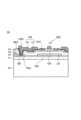
図8は、本発明の一実施形態の変形例に係る半導体装置1Aの構成を示す模式的な断面図である。Figure 8 is a schematic cross-sectional view showing the configuration of a
図8に示す半導体装置1Aは、半導体装置1と比較して、第4の導電層L4の構成が相違している。第4の導電層L4が接する第3の導電層L3は、上述した構成と同様の構成を有する。すなわち、第3の導電層L3は、第2のコンタクトホールCH2を介してシリコン半導体層SSと接し、かつ、第1のコンタクトホールCH1を介して酸化物半導体層OSと接している。また、第3の導電層L3は、第1のコンタクトホールCH1において酸化物半導体層OSと接する位置からゲート電極GE1に向かって延在する延在部EXを含む。The
第4の導電層L4は、第1のコンタクトホールCH1と第2のコンタクトホールCH2との間に形成されている。第4の導電層L4は、第2のコンタクトホールCH2だけでなく、第1のコンタクトホールCH1においても第3の導電層L3と接する。但し、第4の導電層L4は、延在部EXには形成されていない。すなわち、第4の導電層L4の第1のトランジスタTR1側における端面は、第1のコンタクトホールCH1と重畳する。The fourth conductive layer L4 is formed between the first contact hole CH1 and the second contact hole CH2. The fourth conductive layer L4 contacts the third conductive layer L3 not only at the second contact hole CH2 but also at the first contact hole CH1. However, the fourth conductive layer L4 is not formed in the extension portion EX. In other words, the end surface of the fourth conductive layer L4 on the first transistor TR1 side overlaps with the first contact hole CH1.
半導体装置1Aでは、酸化物半導体層OSのうちの、第1のコンタクトホールCH1と重畳する領域への不純物元素の注入が抑制される。しかしながら、第3の導電層L3が酸素を吸収しやすい材料である場合、当該領域に第3の導電層L3が接することで、当該領域の酸素が吸収され、酸素欠陥が生成される。これにより、チャネル領域OS_1と隣接して十分に低抵抗されたソース領域またはドレイン領域が形成される。In the
半導体装置1Aにおいても、延在部EXには第4の導電層L4が形成されていないため、半導体装置1と同様の効果が得られる。In the
<変形例2>
図9を参照して、本実施形態の別の変形例を説明する。なお、以下では、上述した構成と同様の構成についての説明を省略する場合がある。<
Another modified example of this embodiment will be described with reference to Fig. 9. Note that in the following, description of the same configuration as the above-mentioned configuration may be omitted.
図9は、本発明の一実施形態の別の変形例に係る半導体装置1Bの構成を示す模式的な断面図である。Figure 9 is a schematic cross-sectional view showing the configuration of a
図9に示す半導体装置1Bは、半導体装置1と比較して、ゲート電極GE1の構成が相違している。半導体装置1Bのゲート電極GE1では、第2の導電層L2が、第1の導電層L1の上面および端面を覆うように形成されている。チャネル方向において、第2の導電層L2の幅は、第1の導電層L1の幅よりも大きい。また、第2の導電層L2および第4の導電層L4は、第1のコンタクトホールCH1と重畳しないように形成されている。The
半導体装置1Bにおいても、接続配線CNが、第1のコンタクトホールCH1を介して酸化物半導体層OSと接する状態で、酸化物半導体層OSに不純物元素を注入することができる。その結果、第1のコンタクトホールCH1と重畳し、かつ、チャネル領域OS_1と隣接して、十分に低抵抗化された不純物領域OS_2を形成することができる。したがって、半導体装置1Bにおいても、半導体装置1と同様の効果が得られる。In the
<変形例3>
図10を参照して、本実施形態の別の変形例を説明する。なお、以下では、上述した構成と同様の構成についての説明を省略する場合がある。<Modification 3>
Another modified example of this embodiment will be described with reference to Fig. 10. Note that in the following, description of the same configuration as the above-mentioned configuration may be omitted.
図10は、本発明の一実施形態の変形例に係る半導体装置1Cの構成を示す模式的な断面図である。Figure 10 is a schematic cross-sectional view showing the configuration of a
図10に示す半導体装置1Cは、半導体装置1と比較して、ゲート電極GE1の構成が相違している。半導体装置1Cのゲート電極GE1では、第2の導電層L2は形成されているが、第1の導電層L1は形成されていない。すなわち、第2の導電層L2は、絶縁層14と接している。また、第2の導電層L2および第4の導電層L4は、第1のコンタクトホールCH1と重畳しないように形成されている。The
半導体装置1Cにおいても、接続配線CNが、第1のコンタクトホールCH1を介して酸化物半導体層OSと接する状態で、酸化物半導体層OSに不純物元素を注入することができる。その結果、第1のコンタクトホールCH1と重畳し、かつ、チャネル領域OS_1と隣接して、十分に低抵抗化された不純物領域OS_2を形成することができる。したがって、半導体装置1Cにおいても、半導体装置1と同様の効果が得られる。In the
<変形例4>
図11を参照して、本実施形態の別の変形例を説明する。なお、以下では、上述した構成と同様の構成についての説明を省略する場合がある。<Modification 4>
Another modified example of this embodiment will be described with reference to Fig. 11. Note that in the following, description of the same configuration as the above-mentioned configuration may be omitted.
図11は、本発明の一実施形態の変形例に係る半導体装置1Dの構成を示す模式的な断面図である。Figure 11 is a schematic cross-sectional view showing the configuration of a
図10に示す半導体装置1Dは、半導体装置1と比較して、金属酸化物層MOを含む。すなわち、半導体装置1Dでは、酸化物半導体層OSの下に、酸化物半導体層OSと接する金属酸化物層MOが設けられている。金属酸化物層MOの端面は、酸化物半導体層OSの端面と略一致している。絶縁層14は、金属酸化物層MOの端面ならびに酸化物半導体層OSの上面および端面を覆い、絶縁層13の上に設けられている。Compared to the
金属酸化物層MOは、酸化物半導体層OSの結晶性を向上させるバッファー層と機能することができる。結晶性が向上した酸化物半導体層OSを含む第1のトランジスタTR1では、電界効果移動度がさらに向上する。The metal oxide layer MO can function as a buffer layer that improves the crystallinity of the oxide semiconductor layer OS. The first transistor TR1 including the oxide semiconductor layer OS with improved crystallinity further improves the field effect mobility.
金属酸化物層MOとして、アルミニウムを主成分とする金属酸化物が用いられる。金属酸化物層MOに含まれるアルミニウムの比率は、金属酸化物層MO全体の5%以上70%以下、10%以上60%以下、または30%以上50%以下であってもよい。上記比率は、質量比であってもよく、重量比であってもよい。A metal oxide containing aluminum as a main component is used as the metal oxide layer MO. The ratio of aluminum contained in the metal oxide layer MO may be 5% to 70%, 10% to 60%, or 30% to 50% of the entire metal oxide layer MO. The above ratio may be a mass ratio or a weight ratio.
金属酸化物層MOの膜厚は、1nm以上10nm以下、好ましくは1nm以上5nm以下である。金属酸化物層MOとして、酸化アルミニウムが用いられることが好ましい。酸化アルミニウムは、酸素または水素などのガスに対する高いバリア性を有する。ここで、バリア性とは、酸素または水素などのガスの透過を抑制する機能をいう。The thickness of the metal oxide layer MO is 1 nm or more and 10 nm or less, preferably 1 nm or more and 5 nm or less. It is preferable to use aluminum oxide as the metal oxide layer MO. Aluminum oxide has high barrier properties against gases such as oxygen and hydrogen. Here, barrier properties refer to the function of suppressing the permeation of gases such as oxygen and hydrogen.
なお、金属酸化物層MOとして、アルミニウム以外の金属を主成分とする金属酸化物が用いられてもよい。例えば、金属酸化物層MOとして、酸化インジウムスズ(ITO)、酸化インジウム亜鉛(IZO)、または酸化インジウムガリウム亜鉛(IGZO)などを用いることができる。Note that the metal oxide layer MO may be made of a metal oxide mainly composed of a metal other than aluminum. For example, the metal oxide layer MO may be made of indium tin oxide (ITO), indium zinc oxide (IZO), or indium gallium zinc oxide (IGZO).
金属酸化物層MOは、スパッタリング法または原子層堆積法(ALD法)を用いて成膜することができる。また、金属酸化物層MOは、酸化物半導体層OSをマスクとしてパターニングすることができる。上述したように、Poly-OSを含む酸化物半導体層140は、優れたエッチング耐性を有する。そのため、金属酸化物層MOのパターニングにおいて、金属酸化物層MOがエッチングされるときでも、マスクとして用いられる酸化物半導体層140はエッチングされない。半導体装置1Dでは、金属酸化物層MOの形成において、酸化物半導体層OSをマスクとして用いることができるため、フォトリソグラフィー工程を省略することができる。The metal oxide layer MO can be formed by sputtering or atomic layer deposition (ALD). The metal oxide layer MO can be patterned using the oxide semiconductor layer OS as a mask. As described above, the oxide semiconductor layer 140 including Poly-OS has excellent etching resistance. Therefore, even when the metal oxide layer MO is etched in patterning the metal oxide layer MO, the oxide semiconductor layer 140 used as a mask is not etched. In the
半導体装置1Dにおいても、接続配線CNが、第1のコンタクトホールCH1を介して酸化物半導体層OSと接する状態で、酸化物半導体層OSに不純物元素を注入することができる。その結果、第1のコンタクトホールCH1と重畳し、かつ、チャネル領域OS_1と隣接して、十分に低抵抗化された不純物領域OS_2を形成することができる。したがって、半導体装置1Dにおいても、半導体装置1と同様の効果が得られる。また、半導体装置1Dでは、金属酸化物層MOをバッファー層としてPoy-OSが形成されるため、Poly-OSを含む酸化物半導体層OSの結晶性が向上し、結果として、第1のトランジスタTR1は、さらに高い電界効果移動度を有する。In the
<第2実施形態>
図12を参照して、本発明の一実施形態に係る半導体装置2について説明する。なお、以下では、第1実施形態の構成と同様の構成についての説明を省略する場合がある。Second Embodiment
A
図12は、本発明の一実施形態に係る半導体装置2の構成を示す模式的な断面図である。Figure 12 is a schematic cross-sectional view showing the configuration of a
図12に示す半導体装置2は、半導体装置1と比較して、接続配線CNの構成が相違している。半導体装置2の接続配線CNでは、第4の導電層L4が、第1のコンタクトホールCH1と第2のコンタクトホールCH2との間において第3の導電層L3の上に形成され、第1のコンタクトホールCH1内および第2のコンタクトホールCH2内に形成されていない。すなわち、第4の導電層L4の端面は、第1のコンタクトホールCH1および第2のコンタクトホールCH2と重畳しない。この場合において、イオン注入が行われると、酸化物半導体層OS中だけでなく、シリコン半導体層SS中にも不純物元素が注入される。しかしながら、半導体装置2では、シリコン半導体層SSに含まれる不純物元素が、酸化物半導体層OSに注入される不純物元素と同じである。具体的には、シリコン半導体層SSに含まれる不純物元素および酸化物半導体層OSに注入される不純物元素がともにリンである場合、またはシリコン半導体層SSに含まれる不純物元素および酸化物半導体層OSに注入される不純物元素がともにホウ素である場合である。そのため、酸化物半導体層OSに不純物元素を注入するときに、シリコン半導体層SSに当該不純物が注入されても、第1のトランジスタTR1の性能劣化を引き起こすことはない。The
なお、第2の導電層L2および第4の導電層L4は、第1のコンタクトホールCH1と重畳しないように形成されている。The second conductive layer L2 and the fourth conductive layer L4 are formed so as not to overlap the first contact hole CH1.
半導体装置2においても、接続配線CNが、第1のコンタクトホールCH1を介して酸化物半導体層OSと接する状態で、酸化物半導体層OSに不純物元素を注入することができる。その結果、第1のコンタクトホールCH1と重畳し、かつ、チャネル領域OS_1と隣接して、十分に低抵抗化された不純物領域OS_2を形成することができる。したがって、半導体装置2においても、半導体装置1と同様の効果が得られる。In the
本発明の実施形態として上述した各実施形態は、相互に矛盾しない限りにおいて、適宜組み合わせて実施することができる。また、各実施形態を基にして、当業者が適宜構成要素の追加、削除、もしくは設計変更を行ったもの、または工程の追加、省略、もしくは条件変更を行ったものも、本発明の要旨を備えている限り、本発明の範囲に含まれる。The above-described embodiments of the present invention may be combined as appropriate to the extent that they are not mutually inconsistent. Furthermore, if a person skilled in the art adds or removes components or modifies the design based on each embodiment, or adds or omits steps or modifies conditions, these are also included in the scope of the present invention as long as they include the gist of the present invention.
上述した各実施形態の態様によりもたらされる作用効果とは異なる他の作用効果であっても、本明細書の記載から明らかなもの、または当業者において容易に予測し得るものについては、当然に本発明によりもたらされるものと解される。Even if there are other effects and advantages different from those brought about by the aspects of each of the above-mentioned embodiments, if they are clear from the description in this specification or can be easily predicted by a person skilled in the art, they are naturally understood to be brought about by the present invention.
1、1A、1B、1C、1D、2:半導体装置、 10:基板、 11、12、13、14:絶縁層、 CH1:第1のコンタクトホール、 CH2:第2のコンタクトホール、 CN:接続配線、 EX:延在部、 GE1、GE2:ゲート電極、 L1:第1の導電層、 L2:第2の導電層、 L3:第3の導電層、 L4:第4の導電層、 LS:遮光層、 MO:金属酸化物層、 OS:酸化物半導体層、 OS_1:チャネル領域、 OS_2:不純物領域、 SS:シリコン半導体層、 TR1:第1のトランジスタ、 TR2:第2のトランジスタ1, 1A, 1B, 1C, 1D, 2: semiconductor device, 10: substrate, 11, 12, 13, 14: insulating layer, CH1: first contact hole, CH2: second contact hole, CN: connection wiring, EX: extension, GE1, GE2: gate electrode, L1: first conductive layer, L2: second conductive layer, L3: third conductive layer, L4: fourth conductive layer, LS: light shielding layer, MO: metal oxide layer, OS: oxide semiconductor layer, OS_1: channel region, OS_2: impurity region, SS: silicon semiconductor layer, TR1: first transistor, TR2: second transistor
Claims (16)
Translated fromJapanese前記酸化物半導体層の上のゲート電極と、
前記酸化物半導体層と前記ゲート電極との間の絶縁層と、
前記絶縁層を貫通し、前記不純物領域を露出する第1のコンタクトホールと、
少なくとも前記絶縁層を貫通し、前記第1のコンタクトホールの深さよりも大きい深さを有する第2のコンタクトホールと、
前記第1のコンタクトホールおよび前記第2のコンタクトホールを介して、前記不純物領域と前記第2のコンタクトホールによって露出される層とを電気的に接続する接続配線と、を含み、
前記接続配線は、第1の導電層および前記第1の導電層の上の第2の導電層を含み、
前記第1の導電層のうちの前記第2の導電層から露出される部分は、前記不純物元素を含む、半導体装置。 an oxide semiconductor layer having a polycrystalline structure including an impurity region containing an impurity element;
a gate electrode on the oxide semiconductor layer;
an insulating layer between the oxide semiconductor layer and the gate electrode;
a first contact hole penetrating the insulating layer and exposing the impurity region;
a second contact hole penetrating at least the insulating layer and having a depth greater than a depth of the first contact hole;
a connection wiring electrically connecting the impurity region and a layer exposed by the second contact hole through the first contact hole and the second contact hole;
the connection wiring includes a first conductive layer and a second conductive layer on the first conductive layer;
a portion of the first conductive layer exposed from the second conductive layer containing the impurity element.
前記ゲート電極は、前記第2の導電層と同一の層で形成される第3の導電層を含み、
前記チャネル領域と前記不純物領域との境界は、前記第3の導電層の端部と略一致する、請求項1に記載の半導体装置。 the oxide semiconductor layer further includes a channel region adjacent to the impurity region and having a higher electrical resistivity than the impurity region;
the gate electrode includes a third conductive layer formed of the same layer as the second conductive layer;
2. The semiconductor device according to claim 1, wherein a boundary between said channel region and said impurity region approximately coincides with an end of said third conductive layer.
前記40℃において前記エッチング液を用いて前記酸化物半導体膜をエッチングしたときのエッチングレートは、100nm/min以上である、請求項11に記載の半導体装置。 the oxide semiconductor layer is formed by performing a heat treatment on an oxide semiconductor film having an amorphous structure;
The semiconductor device according to claim 11 , wherein an etching rate when the oxide semiconductor film is etched with the etching solution at 40° C. is 100 nm/min or more.
前記複数の金属元素のうちの1つは、インジウムであり、
前記複数の金属元素に対する前記インジウムの原子比率は、50%以上である、請求項1に記載の半導体装置。 the oxide semiconductor layer contains a plurality of metal elements,
one of the metal elements is indium;
The semiconductor device according to claim 1 , wherein an atomic ratio of said indium to said plurality of metal elements is 50% or more.
Priority Applications (5)
| Application Number | Priority Date | Filing Date | Title |
|---|---|---|---|
| JP2023170308AJP2025059911A (en) | 2023-09-29 | 2023-09-29 | Semiconductor Device |
| KR1020240129587AKR20250047887A (en) | 2023-09-29 | 2024-09-25 | Semiconductor device |
| US18/895,479US20250113543A1 (en) | 2023-09-29 | 2024-09-25 | Semiconductor device |
| TW113136913ATW202515351A (en) | 2023-09-29 | 2024-09-27 | Semiconductor Devices |
| CN202411357136.8ACN119767782A (en) | 2023-09-29 | 2024-09-27 | Semiconductor devices |
Applications Claiming Priority (1)
| Application Number | Priority Date | Filing Date | Title |
|---|---|---|---|
| JP2023170308AJP2025059911A (en) | 2023-09-29 | 2023-09-29 | Semiconductor Device |
Publications (1)
| Publication Number | Publication Date |
|---|---|
| JP2025059911Atrue JP2025059911A (en) | 2025-04-10 |
Family
ID=95155993
Family Applications (1)
| Application Number | Title | Priority Date | Filing Date |
|---|---|---|---|
| JP2023170308APendingJP2025059911A (en) | 2023-09-29 | 2023-09-29 | Semiconductor Device |
Country Status (5)
| Country | Link |
|---|---|
| US (1) | US20250113543A1 (en) |
| JP (1) | JP2025059911A (en) |
| KR (1) | KR20250047887A (en) |
| CN (1) | CN119767782A (en) |
| TW (1) | TW202515351A (en) |
Family Cites Families (6)
| Publication number | Priority date | Publication date | Assignee | Title |
|---|---|---|---|---|
| US8871565B2 (en) | 2010-09-13 | 2014-10-28 | Semiconductor Energy Laboratory Co., Ltd. | Method for manufacturing semiconductor device |
| WO2014021442A1 (en) | 2012-08-03 | 2014-02-06 | Semiconductor Energy Laboratory Co., Ltd. | Oxide semiconductor stacked film and semiconductor device |
| TWI799011B (en) | 2012-09-14 | 2023-04-11 | 日商半導體能源研究所股份有限公司 | Semiconductor device and method for fabricating the same |
| KR102220279B1 (en) | 2012-10-19 | 2021-02-24 | 가부시키가이샤 한도오따이 에네루기 켄큐쇼 | Method for forming multilayer film including oxide semiconductor film and method for manufacturing semiconductor device |
| US9425217B2 (en) | 2013-09-23 | 2016-08-23 | Semiconductor Energy Laboratory Co., Ltd. | Semiconductor device |
| CN109121438B (en) | 2016-02-12 | 2022-02-18 | 株式会社半导体能源研究所 | Semiconductor device and display device including the same |
- 2023
- 2023-09-29JPJP2023170308Apatent/JP2025059911A/enactivePending
- 2024
- 2024-09-25USUS18/895,479patent/US20250113543A1/enactivePending
- 2024-09-25KRKR1020240129587Apatent/KR20250047887A/enactivePending
- 2024-09-27CNCN202411357136.8Apatent/CN119767782A/enactivePending
- 2024-09-27TWTW113136913Apatent/TW202515351A/enunknown
Also Published As
| Publication number | Publication date |
|---|---|
| KR20250047887A (en) | 2025-04-07 |
| CN119767782A (en) | 2025-04-04 |
| US20250113543A1 (en) | 2025-04-03 |
| TW202515351A (en) | 2025-04-01 |
Similar Documents
| Publication | Publication Date | Title |
|---|---|---|
| JP2025059911A (en) | Semiconductor Device | |
| US20240113228A1 (en) | Semiconductor device and method for manufacturing semiconductor device | |
| US20240312999A1 (en) | Semiconductor device | |
| US20240113227A1 (en) | Semiconductor device | |
| KR102803695B1 (en) | Semiconductor device | |
| US20250113546A1 (en) | Semiconductor device | |
| TWI858841B (en) | Multilayer structure and thin film transistor | |
| WO2024190115A1 (en) | Semiconductor device and production method therefor | |
| WO2024190116A1 (en) | Semiconductor device and production method for same | |
| JP2025059498A (en) | Semiconductor Device | |
| JP2025140590A (en) | Semiconductor Devices | |
| JP2025059551A (en) | Semiconductor Device | |
| TW202412323A (en) | Semiconductor device | |
| CN118891736A (en) | Semiconductor device with a semiconductor device having a plurality of semiconductor chips | |
| WO2024190449A1 (en) | Semiconductor device | |
| JP2025128517A (en) | Semiconductor Devices | |
| JP2025059540A (en) | Semiconductor device and display device | |
| JP2024051551A5 (en) | ||
| JP2024121394A (en) | Semiconductor Device | |
| JP2024121234A (en) | Electronic device and method for manufacturing same |
Legal Events
| Date | Code | Title | Description |
|---|---|---|---|
| A711 | Notification of change in applicant | Free format text:JAPANESE INTERMEDIATE CODE: A711 Effective date:20250609 |