JP2025024087A - Semiconductor Device - Google Patents
Semiconductor DeviceDownload PDFInfo
- Publication number
- JP2025024087A JP2025024087AJP2024198207AJP2024198207AJP2025024087AJP 2025024087 AJP2025024087 AJP 2025024087AJP 2024198207 AJP2024198207 AJP 2024198207AJP 2024198207 AJP2024198207 AJP 2024198207AJP 2025024087 AJP2025024087 AJP 2025024087A
- Authority
- JP
- Japan
- Prior art keywords
- layer
- thin film
- film transistor
- oxide semiconductor
- oxide
- Prior art date
- Legal status (The legal status is an assumption and is not a legal conclusion. Google has not performed a legal analysis and makes no representation as to the accuracy of the status listed.)
- Pending
Links
Images


Classifications
- H—ELECTRICITY
- H10—SEMICONDUCTOR DEVICES; ELECTRIC SOLID-STATE DEVICES NOT OTHERWISE PROVIDED FOR
- H10D—INORGANIC ELECTRIC SEMICONDUCTOR DEVICES
- H10D30/00—Field-effect transistors [FET]
- H10D30/60—Insulated-gate field-effect transistors [IGFET]
- H10D30/67—Thin-film transistors [TFT]
- H10D30/674—Thin-film transistors [TFT] characterised by the active materials
- H10D30/6755—Oxide semiconductors, e.g. zinc oxide, copper aluminium oxide or cadmium stannate
- H—ELECTRICITY
- H10—SEMICONDUCTOR DEVICES; ELECTRIC SOLID-STATE DEVICES NOT OTHERWISE PROVIDED FOR
- H10D—INORGANIC ELECTRIC SEMICONDUCTOR DEVICES
- H10D30/00—Field-effect transistors [FET]
- H10D30/60—Insulated-gate field-effect transistors [IGFET]
- H10D30/67—Thin-film transistors [TFT]
- H10D30/6757—Thin-film transistors [TFT] characterised by the structure of the channel, e.g. transverse or longitudinal shape or doping profile
- H—ELECTRICITY
- H10—SEMICONDUCTOR DEVICES; ELECTRIC SOLID-STATE DEVICES NOT OTHERWISE PROVIDED FOR
- H10D—INORGANIC ELECTRIC SEMICONDUCTOR DEVICES
- H10D62/00—Semiconductor bodies, or regions thereof, of devices having potential barriers
- H10D62/10—Shapes, relative sizes or dispositions of the regions of the semiconductor bodies; Shapes of the semiconductor bodies
- H—ELECTRICITY
- H10—SEMICONDUCTOR DEVICES; ELECTRIC SOLID-STATE DEVICES NOT OTHERWISE PROVIDED FOR
- H10D—INORGANIC ELECTRIC SEMICONDUCTOR DEVICES
- H10D86/00—Integrated devices formed in or on insulating or conducting substrates, e.g. formed in silicon-on-insulator [SOI] substrates or on stainless steel or glass substrates
- H10D86/40—Integrated devices formed in or on insulating or conducting substrates, e.g. formed in silicon-on-insulator [SOI] substrates or on stainless steel or glass substrates characterised by multiple TFTs
- H10D86/421—Integrated devices formed in or on insulating or conducting substrates, e.g. formed in silicon-on-insulator [SOI] substrates or on stainless steel or glass substrates characterised by multiple TFTs having a particular composition, shape or crystalline structure of the active layer
- H10D86/423—Integrated devices formed in or on insulating or conducting substrates, e.g. formed in silicon-on-insulator [SOI] substrates or on stainless steel or glass substrates characterised by multiple TFTs having a particular composition, shape or crystalline structure of the active layer comprising semiconductor materials not belonging to the Group IV, e.g. InGaZnO
- H—ELECTRICITY
- H10—SEMICONDUCTOR DEVICES; ELECTRIC SOLID-STATE DEVICES NOT OTHERWISE PROVIDED FOR
- H10D—INORGANIC ELECTRIC SEMICONDUCTOR DEVICES
- H10D86/00—Integrated devices formed in or on insulating or conducting substrates, e.g. formed in silicon-on-insulator [SOI] substrates or on stainless steel or glass substrates
- H10D86/40—Integrated devices formed in or on insulating or conducting substrates, e.g. formed in silicon-on-insulator [SOI] substrates or on stainless steel or glass substrates characterised by multiple TFTs
- H10D86/60—Integrated devices formed in or on insulating or conducting substrates, e.g. formed in silicon-on-insulator [SOI] substrates or on stainless steel or glass substrates characterised by multiple TFTs wherein the TFTs are in active matrices
- H—ELECTRICITY
- H10—SEMICONDUCTOR DEVICES; ELECTRIC SOLID-STATE DEVICES NOT OTHERWISE PROVIDED FOR
- H10D—INORGANIC ELECTRIC SEMICONDUCTOR DEVICES
- H10D89/00—Aspects of integrated devices not covered by groups H10D84/00 - H10D88/00
- H10D89/10—Integrated device layouts
- H—ELECTRICITY
- H01—ELECTRIC ELEMENTS
- H01L—SEMICONDUCTOR DEVICES NOT COVERED BY CLASS H10
- H01L22/00—Testing or measuring during manufacture or treatment; Reliability measurements, i.e. testing of parts without further processing to modify the parts as such; Structural arrangements therefor
- H01L22/30—Structural arrangements specially adapted for testing or measuring during manufacture or treatment, or specially adapted for reliability measurements
- H01L22/34—Circuits for electrically characterising or monitoring manufacturing processes, e. g. whole test die, wafers filled with test structures, on-board-devices incorporated on each die, process control monitors or pad structures thereof, devices in scribe line
- H—ELECTRICITY
- H01—ELECTRIC ELEMENTS
- H01L—SEMICONDUCTOR DEVICES NOT COVERED BY CLASS H10
- H01L2924/00—Indexing scheme for arrangements or methods for connecting or disconnecting semiconductor or solid-state bodies as covered by H01L24/00
- H01L2924/0001—Technical content checked by a classifier
- H01L2924/0002—Not covered by any one of groups H01L24/00, H01L24/00 and H01L2224/00
Landscapes
- Engineering & Computer Science (AREA)
- Manufacturing & Machinery (AREA)
- Automation & Control Theory (AREA)
- Computer Hardware Design (AREA)
- Microelectronics & Electronic Packaging (AREA)
- Power Engineering (AREA)
- Thin Film Transistor (AREA)
- General Engineering & Computer Science (AREA)
- Electroluminescent Light Sources (AREA)
- Devices For Indicating Variable Information By Combining Individual Elements (AREA)
- Liquid Crystal (AREA)
- Optical Filters (AREA)
- Logic Circuits (AREA)
- Semiconductor Integrated Circuits (AREA)
- Metal-Oxide And Bipolar Metal-Oxide Semiconductor Integrated Circuits (AREA)
- Design And Manufacture Of Integrated Circuits (AREA)
- Dram (AREA)
Abstract
Description
Translated fromJapanese 本発明の一形態は、酸化物半導体を用いた電界効果型トランジスタを有する論理回路に
関する。また、該論理回路を有する半導体装置に関する。 One embodiment of the present invention relates to a logic circuit including a field-effect transistor using an oxide semiconductor, and also to a semiconductor device including the logic circuit.
なお、本明細書において、半導体装置とは、半導体特性を利用することで機能しうる装
置全般を指し、電気光学装置、半導体回路及び電気機器は全て半導体装置である。 In this specification, the term "semiconductor device" refers to any device that can function by utilizing semiconductor characteristics, and electro-optical devices, semiconductor circuits, and electrical equipment are all classified as semiconductor devices.
絶縁表面を有する基板上に形成された半導体薄膜を用いて薄膜トランジスタ(TFT)
を構成する技術が注目されている。薄膜トランジスタは液晶テレビに代表されるような表
示装置に用いられている。薄膜トランジスタに適用可能な半導体薄膜としてシリコン系半
導体材料が公知であるが、その他の材料として酸化物半導体が注目されている。 Thin film transistors (TFTs) are made using semiconductor thin films formed on substrates with insulating surfaces.
Thin film transistors are used in display devices such as liquid crystal televisions. Silicon-based semiconductor materials are well known as semiconductor thin films that can be used in thin film transistors, but oxide semiconductors are also attracting attention as other materials.
酸化物半導体の材料としては、酸化亜鉛又は酸化亜鉛を成分とするものが知られている
。そして、電子キャリア密度が1018/cm3未満である非晶質酸化物(酸化物半導体
)からなるもので形成された薄膜トランジスタが開示されている(特許文献1乃至3)。 Zinc oxide or a material containing zinc oxide is known as an oxide semiconductor material. Thin film transistors formed of an amorphous oxide (oxide semiconductor) having an electron carrier density of less than10 /cm have been disclosed (
しかしながら、酸化物半導体は薄膜形成工程において化学量論的組成からのずれが生じ
てしまう。例えば、酸素の過不足によって酸化物半導体の電気伝導度が変化してしまう。
また、酸化物半導体の薄膜形成中に混入する水素が酸素(O)-水素(H)結合を形成し
て電子供与体となり、電気伝導度を変化させる要因となる。さらにO-Hは極性分子なの
で、酸化物半導体によって作製される薄膜トランジスタのような能動デバイスに対して特
性の変動要因となる。 However, the oxide semiconductor may have a deviation from the stoichiometric composition during the thin film formation process. For example, the electrical conductivity of the oxide semiconductor may change due to an excess or deficiency of oxygen.
In addition, hydrogen that is mixed in during the formation of oxide semiconductor thin films forms oxygen (O)-hydrogen (H) bonds and becomes an electron donor, which causes changes in electrical conductivity. Furthermore, because O-H is a polar molecule, it causes fluctuations in the characteristics of active devices such as thin film transistors made of oxide semiconductors.
電子キャリア密度が1018/cm3未満としても、酸化物半導体においては実質的に
はn型であり、前記特許文献に開示される薄膜トランジスタのオン・オフ比は103しか
得られていない。このような薄膜トランジスタのオン・オフ比が低い理由はオフ電流が高
いことによるものである。 Even if the electron carrier density is less than 1018 /cm3 , the oxide semiconductor is substantially n-type, and the thin film transistor disclosed in the above-mentioned patent document has an on/off ratio of only 103. The reason why the on/off ratio of such a thin film transistor is low is because the off current is high.
オン・オフ比はスイッチとしての特性を表す指標であり、オン・オフ比が低い薄膜トラ
ンジスタによって構成される回路は、回路動作が不安定になる。また、オフ電流が高いこ
とにより、無駄に電流が流れ消費電力が増加するという問題がある。 The on/off ratio is an index that represents the characteristics of a switch, and circuits composed of thin-film transistors with a low on/off ratio tend to be unstable. In addition, a high off current causes unnecessary current to flow, resulting in increased power consumption.
上述した課題に鑑み、本発明の一形態は、酸化物半導体を用いて形成された薄膜トラン
ジスタによって構成される論理回路の誤動作を低減することを課題の一とする。 In view of the above-described problems, an object of one embodiment of the present invention is to reduce malfunction of a logic circuit including a thin film transistor formed using an oxide semiconductor.
また、本発明の一態様は、酸化物半導体を用いて形成された薄膜トランジスタによって
構成される論理回路の消費電力を低減することを課題の一とする。 Another object of one embodiment of the present invention is to reduce power consumption of a logic circuit including a thin film transistor formed using an oxide semiconductor.
本発明の一形態は、酸化物半導体中で電子供与体(ドナー)となり得る不純物(水素又
は水など)を除去することで、真性又は実質的に真性な半導体であって、シリコン半導体
よりもエネルギーギャップが大きい酸化物半導体でチャネル形成領域が形成される薄膜ト
ランジスタによって論理回路を構成するものである。 One embodiment of the present invention is to form a logic circuit using thin film transistors in which a channel formation region is formed using an oxide semiconductor that is an intrinsic or substantially intrinsic semiconductor and has a larger energy gap than a silicon semiconductor, by removing impurities (such as hydrogen or water) that can serve as an electron donor (donor) in an oxide semiconductor.
具体的には、酸化物半導体に含まれる水素が5×10¹⁹/cm3以下、好ましくは5
×1018/cm3以下、より好ましくは5×1017/cm3以下として、酸化物半導
体に含まれる水素若しくはOH結合を除去し、キャリア密度を5×10¹⁴/cm3以下
、好ましくは5×10¹²/cm3以下とした酸化物半導体でチャネル形成領域が形成さ
れる薄膜トランジスタによって論理回路が構成されるものである。 Specifically, the hydrogen concentration in the oxide semiconductor is 5×10¹⁹ /cm3 or less, preferably 5×10 19 /cm 3 or less.
A logic circuit isconfigured using thin film transistors in which a channel formation region is formed using an oxide semiconductor having a carrier density of 5×10¹⁴ /cm3 orless , preferably 5×10¹² /cm3 or less, by removing hydrogen or OH bonds contained in the oxide semiconductor and setting the carrier density to 5×10 14 /cm 3 or less, preferably 5×10¹² /cm3 or less.
当該酸化物半導体のエネルギーギャップは、2eV以上、好ましくは2.5eV以上、
より好ましくは3eV以上として、ドナーを形成する水素等の不純物を極力低減し、キャ
リア密度を1×10¹⁴/cm3以下、好ましくは1×1012/cm3以下となるよう
にする。 The energy gap of the oxide semiconductor is 2 eV or more, preferably 2.5 eV or more.
More preferably, it is set to 3 eV or more, impurities such as hydrogen that form donors are reduced as much as possible, and the carrier density is set to 1×10¹⁴ /cm3 or less, preferably 1×10¹² /cm3 or less.
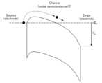
このように高純度化された酸化物半導体は、薄膜トランジスタのチャネル形成領域に用
いることで、チャネル幅が10mmの場合でさえも、ドレイン電圧が1V及び10Vの場
合において、ゲート電圧が-5Vから-20Vの範囲において、ドレイン電流は1×10
-13[A]以下となるように作用する。 By using such a highly purified oxide semiconductor in the channel formation region of a thin film transistor, even when the channel width is 10 mm, the drain current is 1×10 or less in the gate voltage range of −5 V to −20 V when the drain voltage is 1 V or 10 V.
It acts to keep the valueat -13 [A] or less.
すなわち、本発明の一態様は、薄膜トランジスタと、薄膜トランジスタがオフすること
によって、一方の端子が電気的に接続されたノードの電位が浮遊状態となる容量素子と、
を有し、薄膜トランジスタのチャネル形成領域は、水素濃度が5×10¹⁹(atoms
/cm3)以下の酸化物半導体によって構成されることを特徴とする論理回路である。 That is, one embodiment of the present invention is a thin film transistor, a capacitor having one terminal electrically connected to a node in a floating state when the thin film transistor is turned off,
The channel formation region of the thin film transistor has a hydrogen concentration of 5×10¹⁹ (atoms
The logic circuit is formed using an oxide semiconductor having a conductivity of 0.1 to 1.0 vol./cm3 or less.
なお、本明細書において、濃度は二次イオン質量分析法(Secondary Ion
Mass Spectrometry。以下、SIMSともいう。)によるものである
。ただし、他の計測法が挙げられている場合など、特に記載がある場合にはこの限りでは
ない。 In this specification, the concentration is measured by secondary ion mass spectrometry.
The measurement is performed by SIMS (Single Integral Mass Spectrometry). However, this does not apply if there is a special description, such as when other measurement methods are listed.
また、上記の論理回路を有する半導体装置も本発明の一態様である。A semiconductor device having the above-mentioned logic circuit is also an aspect of the present invention.
本発明の一態様の論理回路は、チャネル形成領域が酸化物半導体によって構成された薄
膜トランジスタと、該薄膜トランジスタがオフすることによって、一方の端子の電位が浮
遊状態となる容量素子とを有する。該酸化物半導体は、水素濃度が低減された酸化物半導
体である。具体的には、当該酸化物半導体の水素濃度は、5×10¹⁹(atoms/c
m3)以下である。また、当該酸化物半導体は、無電界中においては、絶縁体又は絶縁体
に近い半導体(実質的には絶縁体)として機能する。そのため、当該薄膜トランジスタの
オフ電流を低減することができる。これにより、当該容量素子に蓄積された電荷の当該薄
膜トランジスタを介したリークを抑制することができる。その結果、当該論理回路の誤動
作を防止することができる。また、当該容量素子の一方の端子の電位が浮遊状態にある期
間を長くすることもできる。別言すると、当該容量素子への情報の再書き込み(リフレッ
シュともいう)の頻度を低減することができる。 A logic circuit according to one embodiment of the present invention includes a thin film transistor in which a channel formation region is formed using an oxide semiconductor, and a capacitor in which the potential of one terminal is set to a floating state when the thin film transistor is turned off. The oxide semiconductor has a reduced hydrogen concentration. Specifically, the hydrogen concentration of the oxide semiconductor is 5×10¹⁹ (atoms/cm
m3 or less. In addition, the oxide semiconductor functions as an insulator or a semiconductor close to an insulator (effectively an insulator) in the absence of an electric field. Therefore, the off-current of the thin film transistor can be reduced. This can suppress leakage of charge stored in the capacitor through the thin film transistor. As a result, malfunction of the logic circuit can be prevented. In addition, the period during which the potential of one terminal of the capacitor is in a floating state can be lengthened. In other words, the frequency of rewriting (also referred to as refreshing) of data to the capacitor can be reduced.
また、当該薄膜トランジスタのオフ電流を低減することにより当該論理回路内に流れる
無駄な電流を低減することができる。これにより、当該論理回路の消費電力を低減するこ
とができる。 Furthermore, by reducing the off-state current of the thin film transistor, unnecessary current flowing in the logic circuit can be reduced, leading to a reduction in power consumption of the logic circuit.
以下では、本発明の実施の形態について図面を用いて詳細に説明する。ただし、本発明
は以下の説明に限定されず、本発明の趣旨およびその範囲から逸脱することなくその形態
および詳細を様々に変更し得ることは、当業者であれば容易に理解される。したがって、
本発明は以下に示す実施の形態の記載内容に限定して解釈されるものではない。 Hereinafter, the embodiments of the present invention will be described in detail with reference to the drawings. However, the present invention is not limited to the following description, and it will be easily understood by those skilled in the art that the form and details of the present invention can be modified in various ways without departing from the spirit and scope of the present invention. Therefore,
The present invention should not be construed as being limited to the description of the following embodiments.
なお、トランジスタのソース端子及びドレイン端子は、トランジスタの構造や動作条件
等によって替わるため、いずれがソース端子又はドレイン端子であるかを特定することが
困難である。そこで、本明細書においては、ソース端子及びドレイン端子の一方を第1端
子、ソース端子及びドレイン端子の他方を第2端子と表記し、区別することとする。 In addition, since the source terminal and the drain terminal of a transistor change depending on the structure, operating conditions, etc. of the transistor, it is difficult to specify which is the source terminal and which is the drain terminal. Therefore, in this specification, one of the source terminal and the drain terminal is referred to as a first terminal, and the other of the source terminal and the drain terminal is referred to as a second terminal to distinguish them.
また、各実施の形態の図面等において示す各構成の、大きさ、層の厚さ、又は領域は、
明瞭化のために誇張されて表記している場合がある。よって、必ずしもそのスケールに限
定されない。また、本明細書にて用いる「第1」、「第2」、「第3」などの序数は、構
成要素の混同を避けるために付したものであり、数的に限定するものではないことを付記
する。 In addition, the size, layer thickness, or area of each component shown in the drawings of each embodiment may differ from the actual size, layer thickness, or area shown in the drawings of each embodiment.
In some cases, the figures are exaggerated for clarity. Therefore, the figures are not necessarily limited to the scale. In addition, ordinal numbers such as "first,""second," and "third" used in this specification are given to avoid confusion of components, and are not intended to limit the numbers.
(実施の形態1)
本実施の形態では、論理回路の一例について説明する。具体的には、チャネル形成領域
が酸化物半導体によって構成される薄膜トランジスタを有するインバータの一例について
図1及び図2を用いて説明する。(Embodiment 1)
In this embodiment, an example of a logic circuit will be described. Specifically, an example of an inverter including a thin film transistor whose channel formation region is formed using an oxide semiconductor will be described with reference to FIGS.
図1(A)は、本実施の形態のインバータの一例を示す回路図である。図1(A)に示
したインバータは、薄膜トランジスタ11乃至薄膜トランジスタ14と、容量素子15と
を有する。ここでは、薄膜トランジスタ11は、デプレッション型トランジスタであり、
薄膜トランジスタ12乃至薄膜トランジスタ14はエンハンスメント型トランジスタであ
るとする。なお、本明細書においては、nチャネル型であり且つしきい値電圧が正の場合
は、エンハンスメント型トランジスタと呼び、nチャネル型であり且つしきい値電圧が負
の場合は、デプレッション型トランジスタと呼ぶこととする。 1A is a circuit diagram illustrating an example of an inverter according to this embodiment. The inverter illustrated in FIG. 1A includes
The
薄膜トランジスタ11は、第1端子が高電源電位(VDD)を供給する配線(以下、高
電源電位線ともいう)に電気的に接続される。 A first terminal of the
薄膜トランジスタ12は、ゲート端子が入力信号(IN)を供給する配線(以下、入力
信号線ともいう)に電気的に接続され、第1端子が薄膜トランジスタ11のゲート端子及
び第2端子に電気的に接続される。 The
薄膜トランジスタ13は、ゲート端子がパルス信号(PS)を供給する配線(以下、パ
ルス信号線ともいう)に電気的に接続され、第1端子が薄膜トランジスタ12の第2端子
に電気的に接続され、第2端子が低電源電位(VSS)を供給する配線(以下、低電源電
位線ともいう)に電気的に接続される。 The
薄膜トランジスタ14は、ゲート端子がパルス信号線に電気的に接続され、第1端子が
薄膜トランジスタ11のゲート端子及び第2端子並びに薄膜トランジスタ12の第1端子
に電気的に接続され、第2端子が出力信号を出力する配線(以下、出力信号線ともいう)
に電気的に接続される。 The
is electrically connected to
容量素子15は、一方の端子が薄膜トランジスタ14の第2端子及び出力信号線に電気
的に接続され、他方の端子が低電源電位線に電気的に接続される。 The
なお、薄膜トランジスタ11は、第1端子が高電源電位線に電気的に接続され、ゲート
端子と第2端子が電気的に接続されたデプレッション型トランジスタである。つまり、薄
膜トランジスタ11は、期間によらずオン状態を維持する。別言すると、薄膜トランジス
タ11は、抵抗素子として利用されている。 The
また、本明細書において、高電源電位(VDD)及び低電源電位(VSS)とは、それ
ぞれを比較したときに高電源電位(VDD)が低電源電位(VSS)より高くなればどの
ような電位であってもよい。例えば、低電源電位(VSS)として、接地電位又は0Vな
どを適用し、高電源電位(VDD)として、任意の正電位を適用することなどができる。 In this specification, the high power supply potential (VDD) and the low power supply potential (VSS) may be any potential as long as the high power supply potential (VDD) is higher than the low power supply potential (VSS) when compared with each other. For example, the low power supply potential (VSS) may be a ground potential or 0 V, and the high power supply potential (VDD) may be any positive potential.
次いで、図1(A)に示した回路の動作について、図1(B)に示すタイミングチャー
トを参照しながら説明する。なお、図1(B)では、便宜上、薄膜トランジスタ11のゲ
ート端子及び第2端子、薄膜トランジスタ12の第1端子並びに薄膜トランジスタ14の
第1端子が電気的に接続するノードをノードAとして説明する。 Next, the operation of the circuit shown in Fig. 1A will be described with reference to the timing chart shown in Fig. 1B. For convenience, in Fig. 1B, a node to which the gate terminal and the second terminal of the
期間T1において、入力信号(IN)及びパルス信号(PS)の電位がハイレベルに増
加する。そのため、薄膜トランジスタ12、薄膜トランジスタ13、薄膜トランジスタ1
4がオンする。これにより、ノードA及び容量素子の一方の端子が低電源電位線に電気的
に接続する。つまり、ノードAの電位及びインバータの出力信号(OUT)がロウレベル
に低下する。また、容量素子15には、電荷が蓄積されない。 In the period T1, the potentials of the input signal (IN) and the pulse signal (PS) are increased to a high level.
4 is turned on. As a result, the node A and one terminal of the capacitance element are electrically connected to the low power supply potential line. That is, the potential of the node A and the output signal (OUT) of the inverter are lowered to a low level. Furthermore, no charge is stored in the
期間T2において、パルス信号(PS)の電位がロウレベルに低下する。そのため、薄
膜トランジスタ13及び薄膜トランジスタ14がオフする。薄膜トランジスタ13のオフ
に伴い、ノードAの電位がハイレベルに増加する。また、薄膜トランジスタ14のオフに
伴い、容量素子15の一方の端子の電位は浮遊状態となる。そのため、インバータの出力
信号(OUT)はロウレベルに維持される。 In period T2, the potential of the pulse signal (PS) drops to a low level. As a result, the
期間T3において、入力信号(IN)の電位がロウレベルに低下し、パルス信号(PS
)の電位がハイレベルに増加する。そのため、薄膜トランジスタ12がオフし、薄膜トラ
ンジスタ13及び薄膜トランジスタ14がオンする。これにより、ノードA及び容量素子
15の一方の端子が、薄膜トランジスタ11を介して高電源電位線に電気的に接続する。
つまり、ノードAの電位及びインバータの出力信号(OUT)がハイレベルに増加する。
また、容量素子15の一方の端子には、正電荷が蓄積される。 In a period T3, the potential of the input signal (IN) falls to a low level, and the pulse signal (PS
) increases to a high level. As a result, the
That is, the potential of the node A and the output signal (OUT) of the inverter increase to a high level.
Moreover, a positive charge is stored in one terminal of the
本実施の形態のインバータが有する複数の薄膜トランジスタは、チャネル形成領域が酸
化物半導体によって構成される。該酸化物半導体は、水素濃度が低減された酸化物半導体
である。具体的には、当該酸化物半導体の水素濃度は、5×10¹⁹(atoms/cm
3)以下であり、無電界中においては、絶縁体又は絶縁体に近い半導体(実質的には絶縁
体)として機能する。そのため、当該酸化物半導体によってチャネル形成領域が構成され
る薄膜トランジスタのオフ電流を低減することができる。これにより、当該薄膜トランジ
スタを介した電荷のリークを抑制することができる。 In the inverter of this embodiment, a channel formation region of each of the thin film transistors is formed using an oxide semiconductor. The oxide semiconductor has a reduced hydrogen concentration. Specifically, the hydrogen concentration of the oxide semiconductor is 5×10¹⁹ (atoms/cm
3 ) or less, and in the absence of an electric field, the oxide semiconductor functions as an insulator or a semiconductor close to an insulator (effectively an insulator). Therefore, the off-state current of a thin film transistor in which a channel formation region is formed of the oxide semiconductor can be reduced. This makes it possible to suppress leakage of electric charge through the thin film transistor.
例えば、薄膜トランジスタ14のチャネル形成領域が当該酸化物半導体によって構成さ
れることによって、容量素子15の一方の端子の電位が浮遊状態にある期間(期間T2)
における電位の変化量(期間T2における電位の増加など)を低減することができる。こ
れにより、当該インバータの誤動作を防止することができる。また、容量素子15の一方
の端子の電位が浮遊状態にある期間を長くすることもできる。別言すると、容量素子15
への情報の再書き込み(リフレッシュともいう)の頻度を低減することができる。 For example, the channel formation region of the
This can reduce the amount of change in potential (such as an increase in potential in period T2) in the
This reduces the frequency with which information needs to be rewritten (also called refreshed) to the memory.
また、薄膜トランジスタ13のチャネル形成領域が当該酸化物半導体によって構成され
ることによって、入力信号(IN)の電位がハイレベルであり且つパルス信号(PS)の
電位がロウレベルである期間(期間T2)に高電源電位線から低電源電位線に流れる貫通
電流を低減することができる。これにより、当該インバータの消費電力を低減することが
できる。 Furthermore, since the channel formation region of the
なお、本実施の形態のインバータは、図1(A)に示したインバータに限定されない。
以下に、図1(C)を参照しながら、図1(A)に示したインバータと異なるインバータ
の一例について説明する。 Note that the inverter of this embodiment mode is not limited to the inverter shown in FIG.
Hereinafter, an example of an inverter different from the inverter shown in FIG. 1A will be described with reference to FIG.
図1(C)に示すインバータは、薄膜トランジスタ21乃至薄膜トランジスタ24と、
容量素子25とを有する。ここでは、薄膜トランジスタ21は、デプレッション型トラン
ジスタであり、薄膜トランジスタ22乃至薄膜トランジスタ24はエンハンスメント型ト
ランジスタであるとする。 The inverter shown in FIG. 1C includes
and a
薄膜トランジスタ21は、第1端子が高電源電位線に電気的に接続される。The first terminal of the
薄膜トランジスタ22は、ゲート端子がパルス信号線に電気的に接続され、第1端子が
薄膜トランジスタ21のゲート端子及び第2端子に電気的に接続される。 The
薄膜トランジスタ23は、ゲート端子が入力信号線に電気的に接続され、第1端子が薄
膜トランジスタ22の第2端子に電気的に接続され、第2端子が低電源電位線に電気的に
接続される。 The
薄膜トランジスタ24は、ゲート端子がパルス信号線に電気的に接続され、第1端子が
薄膜トランジスタ22の第2端子及び薄膜トランジスタ23の第1端子に電気的に接続さ
れ、第2端子が出力信号線に電気的に接続される。 The thin-
容量素子25は、一方の端子が薄膜トランジスタ24の第2端子及び出力信号線に電気
的に接続され、他方の端子が低電源電位線に電気的に接続される。 The
端的に言うと、図1(C)に示すインバータは、図1(A)に示した薄膜トランジスタ
13を薄膜トランジスタ22に置換した回路である。 In short, the inverter shown in FIG. 1C is a circuit in which the
次いで、図1(C)に示した回路の動作について、図1(D)に示すタイミングチャー
トを参照しながら説明する。なお、図1(D)では、便宜上、薄膜トランジスタ22の第
2端子、薄膜トランジスタ23の第1端子及び薄膜トランジスタ24の第1端子が電気的
に接続するノードをノードBとして説明する。 Next, the operation of the circuit shown in Fig. 1C will be described with reference to a timing chart shown in Fig. 1D. Note that in Fig. 1D, for convenience, a node to which the second terminal of the
期間T4において、入力信号(IN)及びパルス信号(PS)の電位がハイレベルに増
加する。そのため、薄膜トランジスタ22、薄膜トランジスタ23、薄膜トランジスタ2
4がオンする。これにより、ノードB及び容量素子25の一方の端子が低電源電位線に電
気的に接続する。つまり、ノードBの電位及びインバータの出力信号(OUT)がロウレ
ベルに低下する。また、容量素子25には、電荷が蓄積されない。 In the period T4, the potentials of the input signal (IN) and the pulse signal (PS) are increased to a high level.
4 is turned on. As a result, the node B and one terminal of the
期間T5において、パルス信号(PS)の電位がロウレベルに低下する。そのため、薄
膜トランジスタ22及び薄膜トランジスタ24がオフする。薄膜トランジスタ24のオフ
に伴い、容量素子25の一方の端子の電位は浮遊状態となる。そのため、インバータの出
力信号(OUT)はロウレベルに維持される。なお、ノードBの電位は、ロウレベルであ
る。 In period T5, the potential of the pulse signal (PS) drops to a low level. Therefore, the
期間T6において、入力信号(IN)の電位がロウレベルに低下し、パルス信号(PS
)の電位がハイレベルに増加する。そのため、薄膜トランジスタ23がオフし、薄膜トラ
ンジスタ22及び薄膜トランジスタ24がオンする。これにより、ノードB及び容量素子
25の一方の端子が、薄膜トランジスタ21を介して高電源電位線に電気的に接続する。
つまり、ノードBの電位及びインバータの出力信号(OUT)がハイレベルに増加する。
また、容量素子25の一方の端子には、正電荷が蓄積される。 In a period T6, the potential of the input signal (IN) falls to a low level, and the pulse signal (PS
) increases to a high level. As a result, the
That is, the potential of the node B and the output signal (OUT) of the inverter increase to a high level.
Moreover, a positive charge is stored in one terminal of the
図1(C)に示したインバータが有する複数の薄膜トランジスタは、チャネル形成領域
が酸化物半導体によって構成される。該酸化物半導体は、水素濃度が低減された酸化物半
導体である。具体的には、当該酸化物半導体の水素濃度は、5×10¹⁹(atoms/
cm3)以下であり、無電界中においては、絶縁体又は絶縁体に近い半導体(実質的には
絶縁体)として機能する。そのため、当該酸化物半導体によってチャネル形成領域が構成
される薄膜トランジスタのオフ電流を低減することができる。これにより、当該薄膜トラ
ンジスタを介した電荷のリークを抑制することができる。 In the plurality of thin film transistors included in the inverter illustrated in FIG. 1C, channel formation regions are formed using an oxide semiconductor. The oxide semiconductor is an oxide semiconductor in which the hydrogen concentration is reduced. Specifically, the hydrogen concentration of the oxide semiconductor is 5×10¹⁹ (atoms/
cm3 or less, and functions as an insulator or a semiconductor close to an insulator (effectively an insulator) in the absence of an electric field. Therefore, the off-state current of a thin film transistor in which a channel formation region is formed of the oxide semiconductor can be reduced. This makes it possible to suppress charge leakage through the thin film transistor.
例えば、薄膜トランジスタ24のチャネル形成領域が当該酸化物半導体によって構成さ
れることによって、容量素子25の一方の端子の電位が浮遊状態にある期間における電位
の変化量を低減することができる。これにより、当該インバータの誤動作を防止すること
ができる。また、ノードBが浮遊状態にある期間を長くすることもできる。別言すると、
容量素子25への情報の再書き込み(リフレッシュともいう)の頻度を低減することがで
きる。 For example, by forming a channel formation region of the
The frequency of rewriting (also called refreshing) information to the
また、薄膜トランジスタ22のチャネル形成領域が当該酸化物半導体によって構成され
ることによって、入力信号(IN)の電位がハイレベルであり且つパルス信号(PS)の
電位がロウレベルである期間(期間T5)に高電源電位線から低電源電位線に流れる貫通
電流を低減することができる。これにより、当該インバータの消費電力を低減することが
できる。 Furthermore, since the channel formation region of the
また、上述したインバータでは、高電源電位線に電気的に接続する薄膜トランジスタに
デプレション型トランジスタを適用したが、当該薄膜トランジスタをエンハンスメント型
トランジスタとすることもできる。図2(A)には、図1(A)に示したインバータが有
する薄膜トランジスタ11をエンハンスメント型トランジスタである薄膜トランジスタ3
1に置換した図を示す。同様に、図2(B)には、図1(C)に示したインバータが有す
る薄膜トランジスタ21をエンハンスメント型トランジスタである薄膜トランジスタ41
に置換した図を示す。なお、薄膜トランジスタ31及び薄膜トランジスタ41は、ゲート
端子及び第1端子が高電源電位線に電気的に接続される。 In the above-mentioned inverter, a depletion type transistor is applied to the thin film transistor electrically connected to the high power supply potential line, but the thin film transistor can also be an enhancement type transistor.
2B shows a diagram in which the
In addition, the
また、上述したインバータでは、容量素子を有する構成について示したが、当該容量素
子がなくても、当該インバータは機能し得る。図2(C)には、図2(A)に示したイン
バータから容量素子15を削除した図を示す。同様に、図2(D)には、図2(B)に示
したインバータから容量素子25を削除した図を示す。 Although the inverter described above has a configuration including a capacitance element, the inverter can function without the capacitance element. Fig. 2C shows a diagram in which the
本実施の形態は、他の実施の形態と適宜組み合わせて実施することが可能である。This embodiment can be implemented in combination with other embodiments as appropriate.
(実施の形態2)
本実施の形態では、論理回路の一例について説明する。具体的には、実施の形態1に示
したインバータを有するシフトレジスタの一例について、図3及び図4を用いて説明する
。(Embodiment 2)
In this embodiment, an example of a logic circuit will be described. Specifically, an example of a shift register including the inverter described in
本実施の形態のシフトレジスタは、複数のパルス出力回路と、該複数のパルス出力回路
の奇数番目に電気的に接続された、第1のクロック信号(CK1)を供給する配線(以下
、第1のクロック信号線ともいう)と、該複数のパルス出力回路の偶数番目に電気的に接
続された、第2のクロック信号(CK2)を供給する配線(以下、第2のクロック信号線
ともいう)と、を有する。さらに、各パルス出力回路の入力端子は、スタートパルス信号
(SP)を供給する配線(以下、スタートパルス線ともいう)又は前段のパルス出力回路
の出力端子に電気的に接続される。 The shift register of this embodiment includes a plurality of pulse output circuits, a wiring (hereinafter also referred to as a first clock signal line) electrically connected to the odd-numbered ones of the plurality of pulse output circuits and supplying a first clock signal (CK1), and a wiring (hereinafter also referred to as a second clock signal line) electrically connected to the even-numbered ones of the plurality of pulse output circuits and supplying a second clock signal (CK2). Furthermore, the input terminal of each pulse output circuit is electrically connected to a wiring (hereinafter also referred to as a start pulse line) that supplies a start pulse signal (SP) or an output terminal of a previous pulse output circuit.
パルス出力回路の具体的な回路構成例について図3(A)を参照しながら説明する。な
お、図3(A)では、パルス出力回路110、120、130を図示している。 A specific example of the circuit configuration of the pulse output circuit will be described with reference to Fig. 3A. In Fig. 3A,
パルス出力回路110は、薄膜トランジスタ101乃至薄膜トランジスタ104と、容
量素子105とを有する。ここでは、薄膜トランジスタ101は、デプレッション型トラ
ンジスタであり、薄膜トランジスタ102乃至薄膜トランジスタ104はエンハンスメン
ト型トランジスタであるとする。 The
薄膜トランジスタ101は、第1端子が高電源電位線に電気的に接続される。The first terminal of the
薄膜トランジスタ102は、ゲート端子がスタートパルス線に電気的に接続され、第1
端子が薄膜トランジスタ101のゲート端子及び第2端子に電気的に接続される。 The
The terminal is electrically connected to the gate terminal and the second terminal of the
薄膜トランジスタ103は、ゲート端子が第1のクロック信号線に電気的に接続され、
第1端子が薄膜トランジスタ102の第2端子に電気的に接続され、第2端子が低電源電
位線に電気的に接続される。 The
The first terminal is electrically connected to the second terminal of the
薄膜トランジスタ104は、ゲート端子が第1のクロック信号線に電気的に接続され、
第1端子が薄膜トランジスタ101のゲート端子及び第2端子並びに薄膜トランジスタ1
02の第1端子に電気的に接続される。 The
The first terminal is the gate terminal of the
02.
容量素子105は、一方の端子が薄膜トランジスタ104の第2端子に電気的に接続さ
れ、他方の端子が低電源電位線に電気的に接続される。 One terminal of the
すなわち、図3(A)に示したパルス出力回路110は、図1(A)に示したインバー
タによって構成される。 That is, the
なお、単にパルス出力回路110の入力端子または出力端子と記す場合、該入力端子は
、スタートパルス信号(SP)又は前段のパルス出力回路の出力信号が入力される端子を
指し、該出力端子は、後段のパルス入力端子に対して信号を出力する端子を指すこととす
る。つまり、ここでは、薄膜トランジスタ102のゲート端子がパルス出力回路の入力端
子と電気的に接続され、薄膜トランジスタ104の第2端子及び容量素子105の一方の
端子が出力端子に電気的に接続されている。また、当該出力端子及び当該入力端子に該当
するものがない場合は、薄膜トランジスタ102のゲート端子がパルス出力回路の入力端
子であり、薄膜トランジスタ104の第2端子及び容量素子105の一方の端子が出力端
子であると表現することができる。 When simply referring to an input terminal or an output terminal of the
パルス出力回路120の具体的な回路構成は、パルス出力回路110と同じであるため
、ここでは前述の説明を援用することとする。ただし、パルス出力回路120においては
、入力端子がパルス出力回路110の出力端子に電気的に接続される点及びパルス出力回
路110において第1のクロック信号(CK1)が入力されていた端子に第2のクロック
信号(CK2)が入力される点がパルス出力回路110とは異なる。 The specific circuit configuration of the
パルス出力回路120以降に設けられたパルス出力回路の回路構成もパルス出力回路1
10及びパルス出力回路120と同じである。そのため、ここでは前述の説明を援用する
こととする。また、上記したように、奇数番目に設けられたパルス出力回路は、第1のク
ロック信号線に電気的に接続され、偶数番目に設けられたパルス出力回路は、第2のクロ
ック信号線に電気的に接続される。 The circuit configuration of the pulse output circuits provided after the
10 and
次いで、図3(A)に示した回路の動作について、図3(B)に示すタイミングチャー
トを参照しながら説明する。なお、図3(B)では、便宜上、図3(A)中の回路の特定
のノードにC~Gの符号を付し、当該各ノードの電位の変化を参照しながら説明する。 Next, the operation of the circuit shown in Fig. 3A will be described with reference to the timing chart shown in Fig. 3B. Note that in Fig. 3B, for convenience, specific nodes in the circuit in Fig. 3A are labeled with symbols C to G, and the description will be given with reference to the change in potential of each of the nodes.
期間t1において、スタートパルス信号(SP)の電位がハイレベルに増加する。その
ため、薄膜トランジスタ102がオンする。また、薄膜トランジスタ101は、ゲート端
子と第2端子が電気的に接続されたデプレッション型トランジスタである。つまり、薄膜
トランジスタ101は、期間によらずオン状態を維持する。別言すると、薄膜トランジス
タ101は、抵抗素子として利用されている。 In period t1, the potential of the start pulse signal (SP) increases to a high level. As a result, the
期間t2において、スタートパルス信号(SP)の電位がハイレベルを維持する。その
ため、薄膜トランジスタ102がオン状態を維持する。 In the period t2, the potential of the start pulse signal (SP) is maintained at a high level, so that the
期間t3において、第1のクロック信号(CK1)の電位がハイレベルに増加する。そ
のため、薄膜トランジスタ103及び薄膜トランジスタ104がオンする。また、スター
トパルス信号(SP)の電位がハイレベルを維持する。そのため、薄膜トランジスタ10
2はオン状態を維持する。これにより、ノードC及びノードDが低電源電位線に電気的に
接続する。つまり、ノードC及びノードDの電位がロウレベルに低下する。 In a period t3, the potential of the first clock signal (CK1) increases to a high level. Therefore, the
2 maintains the on state. As a result, the nodes C and D are electrically connected to the low power supply potential line. That is, the potentials of the nodes C and D fall to a low level.
期間t4において、第1のクロック信号(CK1)の電位がロウレベルに低下する。そ
のため、薄膜トランジスタ103及び薄膜トランジスタ104がオフする。これにより、
ノードCは、薄膜トランジスタ101を介して、高電源電位線に電気的に接続され、ノー
ドDは、浮遊状態になる。つまり、ノードCの電位はハイレベルに増加し、ノードDの電
位はロウレベルを維持する。 In a period t4, the potential of the first clock signal (CK1) falls to a low level. As a result, the
The node C is electrically connected to the high power supply potential line through the
期間t5において、スタートパルス信号(SP)の電位がロウレベルに低下する。その
ため、薄膜トランジスタ102がオフする。また、第2のクロック信号(CK2)の電位
がハイレベルに増加する。そのため、薄膜トランジスタ113及び薄膜トランジスタ11
4がオンする。これにより、ノードFは、薄膜トランジスタ111を介して、高電源電位
線に電気的に接続される。つまり、ノードFの電位がハイレベルに増加する。これにより
、薄膜トランジスタ122がオンする。 In a period t5, the potential of the start pulse signal (SP) falls to a low level. As a result, the
4 is turned on. As a result, the node F is electrically connected to the high power supply potential line through the
期間t6において、第2のクロック信号(CK2)の電位がロウレベルに低下する。そ
のため、薄膜トランジスタ113及び薄膜トランジスタ114がオフする。これにより、
ノードFは、浮遊状態になる。つまり、ノードE及びノードFの電位は、ハイレベルを維
持する。 In a period t6, the potential of the second clock signal (CK2) falls to a low level. As a result, the
The node F is in a floating state, that is, the potentials of the nodes E and F are maintained at a high level.
期間t7において、第1のクロック信号(CK1)の電位がハイレベルに増加する。そ
のため、薄膜トランジスタ103、薄膜トランジスタ104、薄膜トランジスタ123及
び薄膜トランジスタ124がオンする。薄膜トランジスタ104のオンに伴い、ノードD
は、薄膜トランジスタ101を介して、高電源電位線に電気的に接続される。つまり、ノ
ードDの電位はハイレベルに増加する。これにより、薄膜トランジスタ112がオンする
。また、ノードFの電位はハイレベルを維持する。そのため、薄膜トランジスタ122は
オン状態を維持する。これにより、ノードGは、低電源電位線に電気的に接続される。つ
まり、ノードGの電位がロウレベルに低下する。 In a period t7, the potential of the first clock signal (CK1) increases to a high level. Therefore, the
is electrically connected to the high power supply potential line through the
期間t8において、第1のクロック信号(CK1)の電位がロウレベルに低下する。そ
のため、薄膜トランジスタ103、薄膜トランジスタ104、薄膜トランジスタ123及
び薄膜トランジスタ124がオフする。薄膜トランジスタ104のオフに伴い、ノードC
は、薄膜トランジスタ101を介して、高電源電位線に電気的に接続され、ノードDは、
浮遊状態になる。そのため、ノードC及びノードDの電位がハイレベルを維持する。また
、薄膜トランジスタ123のオフに伴い、ノードGは、薄膜トランジスタ121を介して
、高電源電位線に電気的に接続される。つまり、ノードGの電位がハイレベルに増加する
。 In a period t8, the potential of the first clock signal (CK1) falls to a low level. Therefore, the
is electrically connected to a high power supply potential line via a
The node G is in a floating state. Therefore, the potentials of the nodes C and D are maintained at a high level. In addition, as the
期間t9において、第2のクロック信号(CK2)の電位がハイレベルに増加する。そ
のため、薄膜トランジスタ113及び薄膜トランジスタ114がオンする。また、ノード
Dの電位はハイレベルを維持している。そのため、薄膜トランジスタ112がオン状態を
維持する。これにより、ノードE及びノードFは、低電源電位線に電気的に接続される。
つまり、ノードE及びノードFの電位がロウレベルに低下する。そのため、薄膜トランジ
スタ122がオフする。また、スタートパルス(SP)の電位が再度ハイレベルに増加す
る。なお、当該期間以降におけるスタートパルス(SP)の電位の増加に伴う動作は、期
間t1以降における動作と同じである。そのため、ここでは、前述の説明を援用すること
とする。 In period t9, the potential of the second clock signal (CK2) increases to a high level. Therefore, the
That is, the potentials of the nodes E and F are lowered to a low level. Therefore, the
期間t10において、第2のクロック信号(CK2)の電位がロウレベルに低下する。
そのため、薄膜トランジスタ113及び薄膜トランジスタ114がオフする。これにより
、ノードFは、浮遊状態になる。つまり、ノードFの電位がロウレベルを維持する。また
、ノードEは、薄膜トランジスタ111を介して、高電源電位線に電気的に接続される。
つまり、ノードEの電位がハイレベルに増加する。 In a period t10, the potential of the second clock signal (CK2) falls to a low level.
Therefore, the
That is, the potential of the node E increases to a high level.
期間t10以降の動作については、上述した動作の繰り返しとなる。そのため、ここで
は前述の説明を援用することとする。 The operations after the period t10 are a repetition of the above-mentioned operations, and therefore the above description will be used here.
なお、各パルス出力回路が有する容量素子(容量素子105、115、125など)は
、各パルス出力回路の出力信号を保持するために設けられる。 Note that the capacitance elements (
本実施の形態のシフトレジスタが有する複数の薄膜トランジスタは、チャネル形成領域
が酸化物半導体によって構成される。該酸化物半導体は、水素濃度が低減された酸化物半
導体である。具体的には、当該酸化物半導体の水素濃度は、5×10¹⁹(atoms/
cm3)以下であり、無電界中においては、絶縁体又は絶縁体に近い半導体(実質的には
絶縁体)として機能する。そのため、当該酸化物半導体によってチャネル形成領域が構成
される薄膜トランジスタのオフ電流を低減することができる。これにより、当該薄膜トラ
ンジスタを介した電荷のリークを抑制することができる。 In each of the thin film transistors included in the shift register of this embodiment, a channel formation region is formed using an oxide semiconductor. The oxide semiconductor is an oxide semiconductor in which the hydrogen concentration is reduced. Specifically, the hydrogen concentration of the oxide semiconductor is 5×10¹⁹ (atoms/
cm3 or less, and functions as an insulator or a semiconductor close to an insulator (effectively an insulator) in the absence of an electric field. Therefore, the off-state current of a thin film transistor in which a channel formation region is formed of the oxide semiconductor can be reduced. This makes it possible to suppress charge leakage through the thin film transistor.
例えば、薄膜トランジスタ104のチャネル形成領域が当該酸化物半導体によって構成
されることによって、ノードDが浮遊状態にある期間(期間t4~期間t6など)におけ
るノードDの電位の変化量(期間t4~期間t6における電位の増加など)を低減するこ
とができる。これにより、当該シフトレジスタの誤動作を防止することができる。また、
ノードDが浮遊状態にある期間を長くすることもできる。別言すると、容量素子105へ
の情報の再書き込み(リフレッシュともいう)の頻度を低減することができる。 For example, when the channel formation region of the
It is also possible to lengthen the period in which the node D is in a floating state. In other words, the frequency of rewriting (also called refreshing) data to the
また、薄膜トランジスタ103のチャネル形成領域が当該酸化物半導体によって構成さ
れることによって、スタートパルス(SP)の電位がハイレベルであり且つ第1のクロッ
ク信号(CK1)の電位がロウレベルである期間(期間t1、期間t2、期間t4など)
に高電源電位線から低電源電位線に流れる貫通電流を低減することができる。これにより
、当該シフトレジスタの消費電力を低減することができる。 In addition, since the channel formation region of the
Therefore, it is possible to reduce a through current flowing from a high power supply potential line to a low power supply potential line, thereby reducing the power consumption of the shift register.
なお、本実施の形態のシフトレジスタは、図3(A)に示したシフトレジスタに限定さ
れない。以下に、図4を参照しながら、図3のシフトレジスタと異なるシフトレジスタの
一例について説明する。 Note that the shift register of this embodiment is not limited to the shift register shown in Fig. 3A. Hereinafter, an example of a shift register different from the shift register shown in Fig. 3 will be described with reference to Fig. 4.
図4(A)に示すシフトレジスタは、パルス出力回路210乃至パルス出力回路230
を有する。パルス出力回路210は、薄膜トランジスタ201乃至薄膜トランジスタ20
4と、容量素子205とを有する。ここでは、薄膜トランジスタ201は、デプレッショ
ン型トランジスタであり、薄膜トランジスタ202乃至薄膜トランジスタ204はエンハ
ンスメント型トランジスタであるとする。 The shift register shown in FIG. 4A includes the
The
4 and a
薄膜トランジスタ201は、第1端子が高電源電位線に電気的に接続される。The first terminal of the
薄膜トランジスタ202は、ゲート端子が第1のクロック信号線に電気的に接続され、
第1端子が薄膜トランジスタ201のゲート端子及び第2端子に電気的に接続される。 The
The first terminal is electrically connected to the gate terminal and the second terminal of the
薄膜トランジスタ203は、ゲート端子がスタートパルス線に電気的に接続され、第1
端子が薄膜トランジスタ202の第2端子に電気的に接続され、第2端子が低電源電位線
に電気的に接続される。 The
The terminal is electrically connected to the second terminal of the
薄膜トランジスタ204は、ゲート端子が第1のクロック信号線に電気的に接続され、
第1端子が薄膜トランジスタ202の第2端子及び薄膜トランジスタ203の第1端子に
電気的に接続される。 The
The first terminal is electrically connected to the second terminal of the
容量素子205は、一方の端子が薄膜トランジスタ204の第2端子に電気的に接続さ
れ、他方の端子が低電源電位線に電気的に接続される。 One terminal of the
端的に言うと、図4(A)に示すパルス出力回路210は、図3(A)に示したパルス
出力回路110が有する薄膜トランジスタ103を薄膜トランジスタ202に置換した回
路である。 In short, the
図4(B)には、図4(A)に示した回路の動作を表すタイミングチャートを示す。な
お、図4(B)では、便宜上、図4(A)中の回路の特定のノードにH~Lの符号を付し
、当該各ノードの電位の変化を参照しながら説明する。 Fig. 4B shows a timing chart illustrating the operation of the circuit shown in Fig. 4A. For convenience, in Fig. 4B, specific nodes of the circuit in Fig. 4A are labeled with symbols H to L, and the description will be given with reference to the change in potential of each node.
期間t11において、スタートパルス信号(SP)の電位がハイレベルに増加する。そ
のため、薄膜トランジスタ203がオンする。これにより、ノードHが低電源電位線に電
気的に接続する。つまり、ノードHの電位がロウレベルに低下する。 In a period t11, the potential of the start pulse signal (SP) increases to a high level. Therefore, the
期間t12において、スタートパルス信号(SP)の電位がハイレベルを維持する。つ
まり、ノードHの電位がロウレベルを維持する。 In a period t12, the potential of the start pulse signal (SP) is maintained at a high level, that is, the potential of the node H is maintained at a low level.
期間t13において、第1のクロック信号(CK1)の電位がハイレベルに増加する。
そのため、薄膜トランジスタ202及び薄膜トランジスタ204がオンする。また、スタ
ートパルス信号(SP)の電位がハイレベルを維持する。そのため、薄膜トランジスタ2
03はオン状態を維持する。これにより、ノードIが低電源電位線に電気的に接続する。
つまり、ノードIの電位がロウレベルに低下する。 In a period t13, the potential of the first clock signal (CK1) increases to a high level.
Therefore, the
03 remains on, so that the node I is electrically connected to the low power supply potential line.
That is, the potential of the node I drops to a low level.
期間t14において、第1のクロック信号(CK1)の電位がロウレベルに低下する。
そのため、薄膜トランジスタ202及び薄膜トランジスタ204がオフする。これにより
、ノードIは、浮遊状態になる。そのため、ノードIの電位がロウレベルを維持する。 In a period t14, the potential of the first clock signal (CK1) falls to a low level.
As a result, the
期間t15において、スタートパルス信号(SP)の電位がロウレベルに低下する。そ
のため、薄膜トランジスタ203がオフする。これにより、ノードHは、浮遊状態になる
。そのため、ノードHの電位がロウレベルを維持する。また、第2のクロック信号(CK
2)の電位がハイレベルに増加する。そのため、薄膜トランジスタ212及び薄膜トラン
ジスタ214がオンする。これにより、ノードJ及びノードKは、薄膜トランジスタ21
1を介して、高電源電位線に電気的に接続される。つまり、ノードJ及びノードKの電位
がハイレベルに増加する。そのため、薄膜トランジスタ223がオンする。これにより、
ノードLは、低電源電位線に電気的に接続される。つまり、ノードLの電位がロウレベル
に低下する。 In a period t15, the potential of the start pulse signal (SP) falls to a low level. Therefore, the
2) increases to a high level. As a result, the
1, the potentials of the nodes J and K are increased to a high level. This turns on the
The node L is electrically connected to the low power supply line, that is, the potential of the node L drops to a low level.
期間t16において、第2のクロック信号(CK2)の電位がロウレベルに低下する。
そのため、薄膜トランジスタ212及び薄膜トランジスタ214がオフする。これにより
、ノードJ及びノードKは、浮遊状態になる。そのため、ノードJ及びノードKの電位は
、ハイレベルを維持し、ノードLの電位はロウレベルを維持する。 In a period t16, the potential of the second clock signal (CK2) falls to a low level.
Therefore, the
期間t17において、第1のクロック信号(CK1)の電位がハイレベルに増加する。
そのため、薄膜トランジスタ202、薄膜トランジスタ204、薄膜トランジスタ222
及び薄膜トランジスタ224がオンする。薄膜トランジスタ202及び薄膜トランジスタ
204のオンに伴い、ノードH及びノードIは、薄膜トランジスタ201を介して、高電
源電位線に電気的に接続される。つまり、ノードH及びノードIの電位はハイレベルに増
加する。そのため、薄膜トランジスタ213がオンする。これにより、ノードJは、低電
源電位線に電気的に接続される。つまり、ノードJの電位がロウレベルに低下する。 In a period t17, the potential of the first clock signal (CK1) increases to a high level.
Therefore, the
and the
期間t18において、第1のクロック信号(CK1)の電位がロウレベルに低下する。
そのため、薄膜トランジスタ202、薄膜トランジスタ204、薄膜トランジスタ222
及び薄膜トランジスタ224がオフする。薄膜トランジスタ202及び薄膜トランジスタ
204のオフに伴い、ノードH及びノードIは、浮遊状態になる。そのため、ノードH及
びノードIの電位がハイレベルを維持する。 In a period t18, the potential of the first clock signal (CK1) falls to a low level.
Therefore, the
As a result of the
期間t19において、第2のクロック信号(CK2)の電位がハイレベルに増加する。
そのため、薄膜トランジスタ212及び薄膜トランジスタ214がオンする。また、ノー
ドIの電位はハイレベルを維持している。そのため、薄膜トランジスタ213がオン状態
を維持する。これにより、ノードJ及びノードKは、低電源電位線に電気的に接続される
。つまり、ノードJの電位がロウレベルを維持し、ノードKの電位がロウレベルに低下す
る。そのため、薄膜トランジスタ223がオフする。これにより、ノードLが低電源電位
線に電気的に接続される。つまり、ノードLの電位がロウレベルを維持する。また、スタ
ートパルス(SP)の電位が再度ハイレベルに増加する。なお、当該期間以降におけるス
タートパルス(SP)の電位の増加に伴う動作は、期間t11以降における動作と同じで
ある。そのため、ここでは、前述の説明を援用することとする。 In a period t19, the potential of the second clock signal (CK2) increases to a high level.
Therefore, the
期間t20において、第2のクロック信号(CK2)の電位がロウレベルに低下する。
そのため、薄膜トランジスタ212及び薄膜トランジスタ214がオフする。これにより
、ノードJ及びノードKは、浮遊状態になる。その結果、ノードJ及びノードKの電位が
ロウレベルを維持する。 In a period t20, the potential of the second clock signal (CK2) falls to a low level.
Therefore, the
期間t20以降の動作については、上述した動作の繰り返しとなる。そのため、ここで
は前述の説明を援用することとする。 The operations after the period t20 are a repetition of the above-mentioned operations, and therefore the above description will be used here.
なお、各パルス出力回路が有する容量素子(容量素子205、215、225など)は
、各パルス出力回路の出力信号を保持するために設けられる。 Note that the capacitance elements (
図4に示したシフトレジスタが有する複数の薄膜トランジスタは、チャネル形成領域が
酸化物半導体によって構成される。該酸化物半導体は、水素濃度が低減された酸化物半導
体である。具体的には、当該酸化物半導体の水素濃度は、5×10¹⁹(atoms/c
m3)以下であり、無電界中においては、絶縁体又は絶縁体に近い半導体(実質的には絶
縁体)として機能する。そのため、当該酸化物半導体によってチャネル形成領域が構成さ
れる薄膜トランジスタのオフ電流を低減することができる。これにより、当該薄膜トラン
ジスタを介した電荷のリークを抑制することができる。 In the thin film transistors included in the shift register illustrated in FIG. 4, the channel formation region is formed using an oxide semiconductor. The oxide semiconductor is an oxide semiconductor in which the hydrogen concentration is reduced. Specifically, the hydrogen concentration of the oxide semiconductor is 5×10¹⁹ (atoms/cm
m3 or less, and functions as an insulator or a semiconductor close to an insulator (effectively an insulator) in the absence of an electric field. Therefore, the off-state current of a thin film transistor in which a channel formation region is formed of the oxide semiconductor can be reduced. This makes it possible to suppress charge leakage through the thin film transistor.
例えば、薄膜トランジスタ204のチャネル形成領域が当該酸化物半導体によって構成
されることによって、ノードIが浮遊状態にある期間(期間t11、期間t12、期間t
14~期間t16、期間t18~期間t20など)における電位の変化量(期間t11、
期間t12、期間t19、期間t20などにおける電位の低下)を低減することができる
。これにより、当該シフトレジスタの誤動作を防止することができる。また、ノードIが
浮遊状態にある期間を長くすることもできる。別言すると、容量素子205への情報の再
書き込み(リフレッシュともいう)の頻度を低減することができる。 For example, when the channel formation region of the
The amount of change in potential during periods t11, t14 to t16, t18 to t20, etc.
It is possible to reduce the potential drop during the periods t12, t19, t20, and the like. This can prevent malfunction of the shift register. In addition, it is possible to lengthen the period in which the node I is in a floating state. In other words, the frequency of rewriting (also referred to as refreshing) data to the
また、薄膜トランジスタ202のチャネル形成領域が当該酸化物半導体によって構成さ
れることによって、スタートパルス(SP)の電位がハイレベルであり且つ第1のクロッ
ク信号(CK1)の電位がロウレベルである期間(期間t11、期間t12、期間t14
~期間t16、期間t18~期間t20など)に高電源電位線から低電源電位線に流れる
貫通電流を低減することができる。これにより、当該シフトレジスタの消費電力を低減す
ることができる。 In addition, since the channel formation region of the
It is possible to reduce a through current flowing from the high power supply line to the low power supply line during periods t11 to t16, t18 to t20, etc., thereby reducing the power consumption of the shift register.
また、上述したシフトレジスタでは、高電源電位線に電気的に接続する薄膜トランジス
タにデプレション型トランジスタを適用したが、当該薄膜トランジスタをエンハンスメン
ト型トランジスタとすることもできる。すなわち、図2(A)及び図2(B)に示したイ
ンバータを本実施の形態のパルス出力回路として適用することが可能である。 In the above-described shift register, a depletion type transistor is applied to the thin film transistor electrically connected to the high power supply potential line, but the thin film transistor can be an enhancement type transistor. That is, the inverters shown in FIG. 2A and FIG. 2B can be applied as the pulse output circuit of this embodiment.
また、上述したシフトレジスタでは、各パルス出力回路が容量素子を有する構成につい
て示したが、当該容量素子がなくても、当該シフトレジスタは機能し得る。すなわち、図
2(C)及び図2(D)に示したインバータを本実施の形態のパルス出力回路として適用
することが可能である。 In the above-described shift register, each pulse output circuit has a capacitance element, but the shift register can function without the capacitance element. That is, the inverters shown in FIG. 2C and FIG. 2D can be applied as the pulse output circuit of this embodiment.
本実施の形態は、他の実施の形態と適宜組み合わせて実施することが可能である。This embodiment can be implemented in combination with other embodiments as appropriate.
(実施の形態3)
本実施の形態では、実施の形態1又は2に示した論理回路が有する薄膜トランジスタの
一例について示す。(Embodiment 3)
In this embodiment mode, an example of a thin film transistor included in the logic circuit described in
本実施の形態の薄膜トランジスタ及びその作製方法の一形態を、図5及び図6を用いて
説明する。 One mode of a thin film transistor and a manufacturing method thereof in this embodiment mode will be described with reference to FIGS.
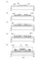
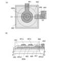
図5(A)、(B)に薄膜トランジスタの平面及び断面構造の一例を示す。図5(A)
、(B)に示す薄膜トランジスタ410は、トップゲート構造の薄膜トランジスタの一つ
である。 5A and 5B show an example of a planar structure and a cross-sectional structure of a thin film transistor.
A
図5(A)はトップゲート構造の薄膜トランジスタ410の平面図であり、図5(B)
は図5(A)の線C1-C2における断面図である。 FIG. 5A is a plan view of a
5A is a cross-sectional view taken along line C1-C2 of FIG.
薄膜トランジスタ410は、絶縁表面を有する基板400上に、絶縁層407、酸化物
半導体層412、ソース電極層又はドレイン電極層415a、及びソース電極層又はドレ
イン電極層415b、ゲート絶縁層402、ゲート電極層411を含み、ソース電極層又
はドレイン電極層415a、ソース電極層又はドレイン電極層415bにそれぞれ配線層
414a、配線層414bが接して設けられ電気的に接続している。 The
また、薄膜トランジスタ410はシングルゲート構造の薄膜トランジスタを用いて説明
したが、必要に応じて、チャネル形成領域を複数有するマルチゲート構造の薄膜トランジ
スタも形成することができる。 Although the
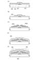
以下、図6(A)乃至(E)を用い、基板400上に薄膜トランジスタ410を作製す
る工程を説明する。 Hereinafter, a process for manufacturing a
絶縁表面を有する基板400に使用することができる基板に大きな制限はないが、少な
くとも、後の加熱処理に耐えうる程度の耐熱性を有していることが必要となる。バリウム
ホウケイ酸ガラスやアルミノホウケイ酸ガラスなどのガラス基板を用いることができる。 Although there is no particular limitation on the substrate that can be used for the
また、ガラス基板としては、後の加熱処理の温度が高い場合には、歪み点が730℃以
上のものを用いると良い。また、ガラス基板には、例えば、アルミノシリケートガラス、
アルミノホウケイ酸ガラス、バリウムホウケイ酸ガラスなどのガラス材料が用いられてい
る。一般に、酸化ホウ素(B2O3)と比較して酸化バリウム(BaO)を多く含ませる
ことで、より実用的な耐熱ガラスが得られる。このため、B2O3よりBaOを多く含む
ガラス基板を用いることが好ましい。 In addition, when the temperature of the subsequent heat treatment is high, it is preferable to use a glass substrate having a distortion point of 730° C. or higher. In addition, the glass substrate may be made of, for example, aluminosilicate glass,
Glass materials such as aluminoborosilicate glass and barium borosilicate glass are used. In general, more practical heat-resistant glass can be obtained by including more barium oxide (BaO) than boron oxide (B2 O3 ). For this reason, it is preferable to use a glass substrate that includes more BaO than B2 O3 .
なお、上記のガラス基板に代えて、セラミック基板、石英基板、サファイア基板などの
絶縁体でなる基板を用いても良い。他にも、結晶化ガラスなどを用いることができる。ま
た、プラスチック基板等も適宜用いることができる。 Instead of the glass substrate, a substrate made of an insulating material such as a ceramic substrate, a quartz substrate, or a sapphire substrate may be used. In addition, crystallized glass may be used. Furthermore, a plastic substrate may be used as appropriate.
まず、絶縁表面を有する基板400上に下地膜となる絶縁層407を形成する。酸化物
半導体層と接する絶縁層407は、酸化シリコン層、酸化窒化シリコン層、酸化アルミニ
ウム層、または酸化窒化アルミニウム層などの酸化物絶縁層を用いると好ましい。絶縁層
407の成膜方法としては、プラズマCVD法又はスパッタリング法等を用いることがで
きるが、絶縁層407中に水素が多量に含まれないようにするためには、スパッタリング
法で絶縁層407を成膜することが好ましい。 First, an insulating
本実施の形態では、絶縁層407として、スパッタリング法により酸化シリコン層を成
膜する。基板400を処理室へ搬送し、水素及び水分が除去された高純度酸素を含むスパ
ッタガスを導入しシリコン半導体のターゲットを用いて、基板400に絶縁層407とし
て、酸化シリコン層を成膜する。また基板400は室温でもよいし、加熱されていてもよ
い。 In this embodiment, a silicon oxide layer is formed by a sputtering method as the insulating
例えば、石英(好ましくは合成石英)をターゲットとして用い、基板温度108℃、基
板とターゲットの間との距離(T-S間距離)を60mm、圧力0.4Pa、高周波電源
電力1.5kW、酸素及びアルゴン(酸素流量25sccm:アルゴン流量25sccm
=1:1)雰囲気下でRFスパッタリング法により酸化シリコン層を成膜する。膜厚は1
00nmとする。なお、石英(好ましくは合成石英)に代えてシリコンターゲットを酸化
シリコン層を成膜するためのターゲットとして用いることができる。なお、スパッタガス
として酸素又は、酸素及びアルゴンの混合ガスを用いている。 For example, quartz (preferably synthetic quartz) is used as a target, the substrate temperature is 108° C., the distance between the substrate and the target (T-S distance) is 60 mm, the pressure is 0.4 Pa, the high frequency power source power is 1.5 kW, and oxygen and argon (
A silicon oxide layer is formed by RF sputtering in a 1:1 atmosphere.
The thickness of the silicon oxide layer is set to 00 nm. Note that a silicon target can be used instead of quartz (preferably synthetic quartz) as a target for forming the silicon oxide layer. Note that oxygen or a mixed gas of oxygen and argon is used as a sputtering gas.
この場合において、処理室内の残留水分を除去しつつ絶縁層407を成膜することが好
ましい。絶縁層407に水素、水酸基又は水分が含まれないようにするためである。 In this case, it is preferable to form the insulating
処理室内の残留水分を除去するためには、吸着型の真空ポンプを用いることが好ましい
。例えば、クライオポンプ、イオンポンプ、チタンサブリメーションポンプを用いること
が好ましい。また、排気手段としては、ターボポンプにコールドトラップを取り付けたも
のであってもよい。クライオポンプを用いて排気した成膜室は、例えば、水素原子や、水
(H2O)など水素原子を含む化合物等が排気されるため、当該成膜室で成膜し絶縁層4
07に含まれる不純物の濃度を低減できる。 In order to remove the residual moisture in the processing chamber, it is preferable to use an adsorption type vacuum pump. For example, it is preferable to use a cryopump, an ion pump, or a titanium sublimation pump. Also, the exhaust means may be a turbo pump equipped with a cold trap. When the deposition chamber is evacuated using a cryopump, hydrogen atoms and compounds containing hydrogen atoms such as water (H2 O) are exhausted, so that the insulating layer 4 formed in the deposition chamber is not easily degraded.
The concentration of impurities contained in 07 can be reduced.
絶縁層407を成膜する際に用いるスパッタガスは水素、水、水酸基又は水素化物など
の不純物が、濃度ppm程度、濃度ppb程度まで除去された高純度ガスを用いることが
好ましい。 It is preferable that a high-purity gas from which impurities such as hydrogen, water, a hydroxyl group, or hydride have been removed to a concentration of about ppm or ppb be used as a sputtering gas for forming the insulating
スパッタリング法にはスパッタ用電源に高周波電源を用いるRFスパッタリング法、直
流電源を用いるDCスパッタリング法、さらにパルス的にバイアスを与えるパルスDCス
パッタリング法がある。RFスパッタリング法は主に絶縁膜を成膜する場合に用いられ、
DCスパッタリング法は主に金属膜を成膜する場合に用いられる。 There are three types of sputtering methods: RF sputtering, which uses a high-frequency power source as the sputtering power source; DC sputtering, which uses a direct current power source; and pulsed DC sputtering, which applies a pulsed bias. RF sputtering is mainly used when forming insulating films.
The DC sputtering method is mainly used when forming a metal film.
また、材料の異なるターゲットを複数設置できる多元スパッタ装置もある。多元スパッ
タ装置は、同一チャンバーで異なる材料膜を積層成膜することも、同一チャンバーで複数
種類の材料を同時に放電させて成膜することもできる。 There are also multi-target sputtering devices that can accommodate multiple targets of different materials. Multi-target sputtering devices can deposit layers of different materials in the same chamber, or deposit films by discharging multiple types of materials simultaneously in the same chamber.
また、チャンバー内部に磁石機構を備えたマグネトロンスパッタリング法を用いるスパ
ッタ装置や、グロー放電を使わずマイクロ波を用いて発生させたプラズマを用いるECR
スパッタリング法を用いるスパッタ装置がある。 Also, there are sputtering devices using a magnetron sputtering method equipped with a magnet mechanism inside the chamber, and ECR devices using plasma generated by microwaves without using glow discharge.
There is a sputtering device that uses the sputtering method.
また、スパッタリング法を用いる成膜方法として、成膜中にターゲット物質とスパッタ
ガス成分とを化学反応させてそれらの化合物薄膜を形成するリアクティブスパッタリング
法や、成膜中に基板にも電圧をかけるバイアススパッタリング法もある。 Other examples of film formation methods using sputtering include reactive sputtering, in which a target material and sputtering gas components are chemically reacted with each other during film formation to form a compound thin film, and bias sputtering, in which a voltage is also applied to the substrate during film formation.
また、絶縁層407は積層構造でもよく、例えば、基板400側から窒化シリコン層、
窒化酸化シリコン層、窒化アルミニウム層、又は窒化酸化アルミニウム層などの窒化物絶
縁層と、上記酸化物絶縁層との積層構造としてもよい。 The insulating
A stacked structure of a nitride insulating layer such as a silicon nitride oxide layer, an aluminum nitride layer, or an aluminum nitride oxide layer and the above oxide insulating layer may be used.
例えば、水素及び水分が除去された高純度窒素を含むスパッタガスを導入しシリコンタ
ーゲットを用いて、酸化シリコン層と基板との間に窒化シリコン層を成膜する。この場合
においても、酸化シリコン層と同様に、処理室内の残留水分を除去しつつ窒化シリコン層
を成膜することが好ましい。 For example, a silicon nitride layer is formed between a silicon oxide layer and a substrate by introducing a sputtering gas containing high-purity nitrogen from which hydrogen and moisture have been removed and using a silicon target. In this case, it is also preferable to form the silicon nitride layer while removing moisture remaining in the processing chamber, as in the case of the silicon oxide layer.
窒化シリコン層を形成する場合も、成膜時に基板を加熱してもよい。When forming a silicon nitride layer, the substrate may also be heated during deposition.
絶縁層407として窒化シリコン層と酸化シリコン層とを積層する場合、窒化シリコン
層と酸化シリコン層を同じ処理室において、共通のシリコンターゲットを用いて成膜する
ことができる。先に窒素を含むスパッタガスを導入して、処理室内に装着されたシリコン
ターゲットを用いて窒化シリコン層を形成し、次にスパッタガスを酸素を含むスパッタガ
スに切り替えて同じシリコンターゲットを用いて酸化シリコン層を成膜する。窒化シリコ
ン層と酸化シリコン層とを大気に曝露せずに連続して形成することができるため、窒化シ
リコン層表面に水素や水分などの不純物が吸着することを防止することができる。 When a silicon nitride layer and a silicon oxide layer are stacked as the insulating
次いで、絶縁層407上に、膜厚2nm以上200nm以下の酸化物半導体膜を形成す
る。 Next, an oxide semiconductor film is formed over the insulating
また、酸化物半導体層に水素、水酸基及び水分がなるべく含まれないようにするために
、成膜の前処理として、スパッタリング装置の予備加熱室で絶縁層407が形成された基
板400を予備加熱し、基板400に吸着した水素、水分などの不純物を脱離し排気する
ことが好ましい。なお、予備加熱室に設ける排気手段はクライオポンプが好ましい。なお
、この予備加熱の処理は省略することもできる。またこの予備加熱は、後に形成するゲー
ト絶縁層402の成膜前の基板400に行ってもよいし、後に形成するソース電極層又は
ドレイン電極層415a及びソース電極層又はドレイン電極層415bまで形成した基板
400にも同様に行ってもよい。 In order to prevent hydrogen, hydroxyl groups, and moisture from being contained in the oxide semiconductor layer as much as possible, it is preferable to preheat the
なお、酸化物半導体層をスパッタリング法により成膜する前に、アルゴンガスを導入し
た状態でプラズマを発生させて逆スパッタを行い、絶縁層407の表面に付着しているゴ
ミを除去することが好ましい。逆スパッタとは、ターゲット側に電圧を印加せずに、アル
ゴン雰囲気下で基板側に高周波電源を用いて電圧を印加して基板上にプラズマを形成して
表面を改質する方法である。なお、アルゴン雰囲気に代えて窒素、ヘリウム、酸素などを
用いてもよい。 Note that before forming the oxide semiconductor layer by a sputtering method, it is preferable to perform reverse sputtering by generating plasma in a state where argon gas is introduced, and remove dust attached to the surface of the insulating
酸化物半導体層はスパッタリング法により成膜する。酸化物半導体層は、In-Ga-
Zn-O系、In-Sn-Zn-O系、In-Al-Zn-O系、Sn-Ga-Zn-O
系、Al-Ga-Zn-O系、Sn-Al-Zn-O系、In-Zn-O系、Sn-Zn
-O系、Al-Zn-O系、In-O系、Sn-O系、Zn-O系の酸化物半導体層を用
いる。本実施の形態では、酸化物半導体層をIn-Ga-Zn-O系金属酸化物ターゲッ
トを用いてスパッタリング法により成膜する。また、酸化物半導体層は、希ガス(代表的
にはアルゴン)雰囲気下、酸素雰囲気下、又は希ガス(代表的にはアルゴン)及び酸素雰
囲気下においてスパッタリング法により形成することができる。また、スパッタリング法
を用いる場合、SiO2を2重量%以上10重量%以下含むターゲットを用いて成膜を行
ってもよい。 The oxide semiconductor layer is formed by a sputtering method.
Zn-O series, In-Sn-Zn-O series, In-Al-Zn-O series, Sn-Ga-Zn-O
system, Al-Ga-Zn-O system, Sn-Al-Zn-O system, In-Zn-O system, Sn-Zn
In the present embodiment, an In—Ga—Zn—O-based, Al—Zn—O-based, In—O-based, Sn—O-based, or Zn—O-based oxide semiconductor layer is used. In this embodiment, the oxide semiconductor layer is formed by a sputtering method using an In—Ga—Zn—O-based metal oxide target. The oxide semiconductor layer can be formed by a sputtering method in a rare gas (typically argon) atmosphere, an oxygen atmosphere, or an atmosphere of rare gas (typically argon) and oxygen. When a sputtering method is used, the film may be formed using a target containing SiO2 in an amount of 2 wt % to 10 wt %.
酸化物半導体層を、成膜する際に用いるスパッタガスは水素、水、水酸基又は水素化物
などの不純物が、濃度ppm程度、濃度ppb程度まで除去された高純度ガスを用いるこ
とが好ましい。 It is preferable that a high-purity gas in which impurities such as hydrogen, water, a hydroxyl group, or hydride are removed to a concentration of about ppm or ppb be used as a sputtering gas used for forming the oxide semiconductor layer.
酸化物半導体層をスパッタリング法で作製するためのターゲットとして、酸化亜鉛を主
成分とする金属酸化物のターゲットを用いることができる。また、金属酸化物のターゲッ
トの他の例としては、In、Ga、及びZnを含む金属酸化物ターゲット(組成比として
、In2O3:Ga2O3:ZnO=1:1:1[mol]、In:Ga:Zn=1:1
:0.5[atom])を用いることができる。また、In、Ga、及びZnを含む金属
酸化物ターゲットとして、In:Ga:Zn=1:1:1[atom]、又はIn:Ga
:Zn=1:1:2[atom]の組成比を有するターゲットを用いることもできる。金
属酸化物ターゲットの充填率は90%以上100%以下、好ましくは95%以上99.9
%である。充填率の高い金属酸化物ターゲットを用いることにより、成膜した酸化物半導
体層は緻密な膜となる。 As a target for forming an oxide semiconductor layer by a sputtering method, a metal oxide target containing zinc oxide as a main component can be used. Another example of the metal oxide target is a metal oxide target containing In, Ga, and Zn (composition ratio: In2 O3 :Ga2 O3 :ZnO=1:1:1 [mol], In:Ga:Zn=1:1
As a metal oxide target containing In, Ga, and Zn, a metal oxide target containing In:Ga:Zn=1:1:1 [atom] or In:Ga
A target having a composition ratio of Zn=1:1:2 [atom] may also be used. The filling rate of the metal oxide target is 90% or more and 100% or less, preferably 95% or more and 99.9% or less.
%. By using a metal oxide target with a high filling rate, the oxide semiconductor layer formed becomes a dense film.
酸化物半導体層は、減圧状態に保持された処理室内に基板を保持し、処理室内の残留水
分を除去しつつ水素及び水分が除去されたスパッタガスを導入し、金属酸化物をターゲッ
トとして基板400上に酸化物半導体層を成膜する。処理室内の残留水分を除去するため
には、吸着型の真空ポンプを用いることが好ましい。例えば、クライオポンプ、イオンポ
ンプ、チタンサブリメーションポンプを用いることが好ましい。また、排気手段としては
、ターボポンプにコールドトラップを加えたものであってもよい。クライオポンプを用い
て排気した成膜室は、例えば、水素原子、水(H2O)など水素原子を含む化合物(より
好ましくは炭素原子を含む化合物も)等が排気されるため、当該成膜室で成膜した酸化物
半導体層に含まれる不純物の濃度を低減できる。また、酸化物半導体層成膜時に基板を加
熱してもよい。 The oxide semiconductor layer is formed on the
成膜条件の一例としては、基板温度室温、基板とターゲットの間との距離を60mm、
圧力0.4Pa、直流(DC)電源電力0.5kW、酸素及びアルゴン(酸素流量15s
ccm:アルゴン流量30sccm)雰囲気下の条件が適用される。なお、パルス直流(
DC)電源を用いると、成膜時に発生する粉状物質(パーティクル、ゴミともいう)が軽
減でき、膜厚分布も均一となるために好ましい。酸化物半導体層は好ましくは5nm以上
30nm以下とする。なお、適用する酸化物半導体材料により適切な厚みは異なり、材料
に応じて適宜厚みを選択すればよい。 An example of the film formation conditions is as follows: the substrate temperature is room temperature, the distance between the substrate and the target is 60 mm,
Pressure: 0.4 Pa, DC power: 0.5 kW, oxygen and argon (oxygen flow rate: 15 s
ccm: argon flow rate 30 sccm) atmosphere is applied.
The use of a DC (direct current) power supply is preferable because it can reduce powdery substances (also called particles or dust) generated during film formation and can provide a uniform film thickness distribution. The oxide semiconductor layer is preferably 5 nm to 30 nm in thickness. The appropriate thickness varies depending on the oxide semiconductor material used, and the thickness may be appropriately selected depending on the material.
次いで、酸化物半導体層を第1のフォトリソグラフィ工程により島状の酸化物半導体層
412に加工する(図6(A)参照)。また、島状の酸化物半導体層412を形成するた
めのレジストマスクをインクジェット法で形成してもよい。レジストマスクをインクジェ
ット法で形成するとフォトマスクを使用しないため、製造コストを低減できる。 Next, the oxide semiconductor layer is processed into an island-shaped
なお、ここでの酸化物半導体層のエッチングは、ドライエッチングでもウェットエッチ
ングでもよく、両方を用いてもよい。 Note that the etching of the oxide semiconductor layer here may be dry etching or wet etching, or may be both.
ドライエッチングに用いるエッチングガスとしては、塩素を含むガス(塩素系ガス、例
えば塩素(Cl2)、塩化硼素(BCl3)、塩化珪素(SiCl4)、四塩化炭素(C
Cl4)など)が好ましい。 The etching gas used in the dry etching is a gas containing chlorine (a chlorine-based gas, for example, chlorine (Cl2 ), boron chloride (BCl3 ), silicon chloride (SiCl4 ), carbon tetrachloride (C
Cl4 ) and the like are preferred.
また、フッ素を含むガス(フッ素系ガス、例えば四弗化炭素(CF4)、弗化硫黄(S
F6)、弗化窒素(NF3)、トリフルオロメタン(CHF3)など)、臭化水素(HB
r)、酸素(O2)、これらのガスにヘリウム(He)やアルゴン(Ar)などの希ガス
を添加したガス、などを用いることができる。 In addition, gases containing fluorine (fluorine-based gases, for example, carbon tetrafluoride (CF4 ), sulfur fluoride (S
F6 ), nitrogen fluoride (NF3 ), trifluoromethane (CHF3 ), etc.), hydrogen bromide (HB
r), oxygen (O2 ), or a gas obtained by adding a rare gas such as helium (He) or argon (Ar) to these gases, etc. can be used.
ドライエッチング法としては、平行平板型RIE(Reactive Ion Etc
hing)法や、ICP(Inductively Coupled Plasma:誘
導結合型プラズマ)エッチング法を用いることができる。所望の加工形状にエッチングで
きるように、エッチング条件(コイル型の電極に印加される電力量、基板側の電極に印加
される電力量、基板側の電極温度等)を適宜調節する。 As a dry etching method, parallel plate type RIE (Reactive Ion Etc.
In order to etch into a desired shape, the etching conditions (such as the amount of power applied to the coil-shaped electrode, the amount of power applied to the electrode on the substrate side, and the temperature of the electrode on the substrate side) are appropriately adjusted.
ウェットエッチングに用いるエッチング液としては、燐酸と酢酸と硝酸を混ぜた溶液な
どを用いることができる。また、ITO07N(関東化学社製)を用いてもよい。 The etching solution used for the wet etching may be a mixture of phosphoric acid, acetic acid, and nitric acid, or ITO07N (manufactured by Kanto Chemical Co., Ltd.).
また、ウェットエッチング後のエッチング液はエッチングされた材料とともに洗浄によ
って除去される。その除去された材料を含むエッチング液の廃液を精製し、含まれる材料
を再利用してもよい。当該エッチング後の廃液から酸化物半導体層に含まれるインジウム
等の材料を回収して再利用することにより、資源を有効活用し低コスト化することができ
る。 In addition, the etching solution after the wet etching is removed by washing together with the etched materials. The waste liquid of the etching solution containing the removed materials may be refined and the contained materials may be reused. By recovering and reusing materials such as indium contained in the oxide semiconductor layer from the waste liquid after the etching, resources can be effectively utilized and costs can be reduced.
所望の加工形状にエッチングできるように、材料に合わせてエッチング条件(エッチン
グ液、エッチング時間、温度等)を適宜調節する。 The etching conditions (etching solution, etching time, temperature, etc.) are appropriately adjusted according to the material so that the desired processed shape can be etched.
本実施の形態では、エッチング液として燐酸と酢酸と硝酸を混ぜた溶液を用いたウェッ
トエッチング法により、酸化物半導体層を島状の酸化物半導体層412に加工する。 In this embodiment, the oxide semiconductor layer is processed into an island-shaped
本実施の形態では、酸化物半導体層412に、第1の加熱処理を行う。第1の加熱処理
の温度は、400℃以上750℃以下、好ましくは400℃以上基板の歪み点未満とする
。ここでは、加熱処理装置の一つである電気炉に基板を導入し、酸化物半導体層に対して
窒素雰囲気下450℃において1時間の加熱処理を行った後、当該基板を大気にさらすこ
となく、酸化物半導体層への水や水素の混入を防ぐ。この第1の加熱処理によって酸化物
半導体層412の脱水化または脱水素化を行うことができる。 In this embodiment, a first heat treatment is performed on the
なお、加熱処理装置は電気炉に限られず、抵抗発熱体などの発熱体からの熱伝導または
熱輻射によって、被処理物を加熱する装置を用いてもよい。例えば、GRTA(Gas
Rapid Thermal Anneal)装置、LRTA(Lamp Rapid
Thermal Anneal)装置等のRTA(Rapid Thermal Ann
eal)装置を用いることができる。LRTA装置は、ハロゲンランプ、メタルハライド
ランプ、キセノンアークランプ、カーボンアークランプ、高圧ナトリウムランプ、高圧水
銀ランプなどのランプから発する光(電磁波)の輻射により、被処理物を加熱する装置で
ある。GRTA装置は、高温のガスを用いて加熱処理を行う装置である。当該高温のガス
としては、アルゴンなどの希ガス、または窒素のような、加熱処理によって被処理物とほ
とんど反応しない不活性気体が用いられる。 The heat treatment device is not limited to an electric furnace, and a device that heats the workpiece by heat conduction or heat radiation from a heating element such as a resistance heating element may be used.
Rapid Thermal Anneal) device, LRTA (Lamp Rapid
RTA (Rapid Thermal Anneal) equipment, etc.
A LRTA apparatus can be used. The LRTA apparatus is an apparatus that heats the workpiece by radiating light (electromagnetic waves) emitted from a lamp such as a halogen lamp, a metal halide lamp, a xenon arc lamp, a carbon arc lamp, a high-pressure sodium lamp, or a high-pressure mercury lamp. The GRTA apparatus is an apparatus that performs heat treatment using a high-temperature gas. As the high-temperature gas, a rare gas such as argon or an inert gas such as nitrogen that hardly reacts with the workpiece during heat treatment is used.
例えば、第1の加熱処理として、650℃~700℃の高温に加熱した不活性ガス中に
基板を移動させて入れ、数分間加熱した後、基板を移動させて高温に加熱した不活性ガス
中から出すGRTAを行ってもよい。GRTAを用いると短時間での高温加熱処理が可能
となる。 For example, as the first heat treatment, GRTA may be performed in which the substrate is moved into an inert gas heated to a high temperature of 650° C. to 700° C., heated for several minutes, and then moved out of the inert gas heated to the high temperature. Use of GRTA enables high-temperature heat treatment in a short time.
なお、第1の加熱処理においては、窒素、またはヘリウム、ネオン、アルゴン等の希ガ
スに、水、水素などが含まれないことが好ましい。または、加熱処理装置に導入する窒素
、またはヘリウム、ネオン、アルゴン等の希ガスの純度を、6N(99.9999%)以
上、好ましくは7N(99.99999%)以上、(即ち不純物濃度を1ppm以下、好
ましくは0.1ppm以下)とすることが好ましい。 In the first heat treatment, it is preferable that nitrogen or a rare gas such as helium, neon, or argon does not contain water, hydrogen, etc. Alternatively, it is preferable that the purity of nitrogen or a rare gas such as helium, neon, or argon introduced into the heat treatment device is 6N (99.9999%) or more, preferably 7N (99.99999%) or more (i.e., the impurity concentration is 1 ppm or less, preferably 0.1 ppm or less).
また、第1の加熱処理の条件、または酸化物半導体層412の材料によっては、酸化物
半導体層が結晶化し、微結晶膜または多結晶膜となる場合もある。例えば、結晶化率が9
0%以上、または80%以上の微結晶の酸化物半導体層となる場合もある。また、第1の
加熱処理の条件、または酸化物半導体層412の材料によっては、結晶成分を含まない非
晶質の酸化物半導体層となる場合もある。また、非晶質の酸化物半導体の中に微結晶部(
粒径1nm以上20nm以下(代表的には2nm以上4nm以下))が混在する酸化物半
導体層となる場合もある。 Depending on the conditions of the first heat treatment or the material of the
In some cases, the
In some cases, the oxide semiconductor layer may have a mixture of grain sizes of 1 nm to 20 nm (typically, 2 nm to 4 nm).
また、第1の加熱処理は、島状の酸化物半導体層412に加工する前の酸化物半導体層
に行うこともできる。その場合には、第1の加熱処理後に、加熱装置から基板を取り出し
、フォトリソグラフィ工程を行う。 The first heat treatment can also be performed on the oxide semiconductor layer before it is processed into the island-shaped
酸化物半導体層に対する脱水化、脱水素化の効果を奏する加熱処理は、酸化物半導体層
成膜後、酸化物半導体層412上にソース電極層及びドレイン電極層を積層させた後、ソ
ース電極層及びドレイン電極層上にゲート絶縁層を形成した後、のいずれで行っても良い
。 The heat treatment which has an effect of dehydrating or dehydrogenating the oxide semiconductor layer may be performed after the oxide semiconductor layer is formed, after the source electrode layer and the drain electrode layer are stacked over the
次いで、絶縁層407及び酸化物半導体層412上に、導電層を成膜する。導電層をス
パッタリング法や真空蒸着法で成膜すればよい。導電層の材料としては、Al、Cr、C
u、Ta、Ti、Mo、Wからから選ばれた元素、または上述した元素を成分とする合金
等が挙げられる。また、マンガン、マグネシウム、ジルコニウム、ベリリウム、トリウム
のいずれか一または複数から選択された材料を用いてもよい。また、導電層は、単層構造
でも、2層以上の積層構造としてもよい。例えば、シリコンを含むアルミニウム層の単層
構造、アルミニウム層上にチタン層を積層する2層構造、Ti層と、そのTi層上に重ね
てアルミニウム層を積層し、さらにその上にTi層を成膜する3層構造などが挙げられる
。また、Alに、チタン(Ti)、タンタル(Ta)、タングステン(W)、モリブデン
(Mo)、クロム(Cr)、Nd(ネオジム)、Sc(スカンジウム)から選ばれた元素
を単数もしくは複数組み合わせた層又はそれらの合金層もしくは窒化層を用いてもよい。 Next, a conductive layer is formed over the insulating
Examples of the conductive layer include an element selected from u, Ta, Ti, Mo, and W, or an alloy containing the above-mentioned elements. In addition, a material selected from any one or more of manganese, magnesium, zirconium, beryllium, and thorium may be used. In addition, the conductive layer may have a single layer structure or a laminated structure of two or more layers. For example, a single layer structure of an aluminum layer containing silicon, a two-layer structure in which a titanium layer is laminated on an aluminum layer, and a three-layer structure in which a Ti layer is laminated on an aluminum layer and a Ti layer is further formed on the Ti layer, etc. may be used. In addition, a layer in which a single or multiple elements selected from titanium (Ti), tantalum (Ta), tungsten (W), molybdenum (Mo), chromium (Cr), Nd (neodymium), and Sc (scandium) are combined with Al, or an alloy layer or nitride layer thereof may be used.
第2のフォトリソグラフィ工程により導電層上にレジストマスクを形成し、選択的にエ
ッチングを行ってソース電極層又はドレイン電極層415a、ソース電極層又はドレイン
電極層415bを形成した後、レジストマスクを除去する(図6(B)参照)。なお、形
成されたソース電極層、ドレイン電極層の端部はテーパ形状であると、上に積層するゲー
ト絶縁層の被覆性が向上するため好ましい。 A resist mask is formed over the conductive layer by a second photolithography process, and selective etching is performed to form the source or drain
本実施の形態ではソース電極層又はドレイン電極層415a、ソース電極層又はドレイ
ン電極層415bとしてスパッタリング法により膜厚150nmのチタン層を形成する。 In this embodiment mode, a titanium layer with a thickness of 150 nm is formed by a sputtering method as the source or drain
なお、導電膜のエッチングの際に、酸化物半導体層412が除去されて、その下の絶縁
層407が露出しないようにそれぞれの材料及びエッチング条件を適宜調節する。 Note that the materials and etching conditions are appropriately adjusted so that the
本実施の形態では、導電膜としてTi層を用いて、酸化物半導体層412にはIn-G
a-Zn-O系酸化物半導体を用いて、エッチャントとしてアンモニア過水(アンモニア
、水、過酸化水素水の混合液)を用いる。 In this embodiment, a Ti layer is used as the conductive film, and an In-G
An a-Zn-O based oxide semiconductor is used, and an ammonia hydrogen peroxide mixture (a mixture of ammonia, water, and hydrogen peroxide) is used as an etchant.
なお、第2のフォトリソグラフィ工程では、酸化物半導体層412は一部のみがエッチ
ングされ、溝部(凹部)を有する酸化物半導体層となることもある。また、ソース電極層
又はドレイン電極層415a、ソース電極層又はドレイン電極層415bを形成するため
のレジストマスクをインクジェット法で形成してもよい。レジストマスクをインクジェッ
ト法で形成するとフォトマスクを使用しないため、製造コストを低減できる。 Note that in the second photolithography step, the
第2のフォトリソグラフィ工程でのレジストマスク形成時の露光には、紫外線やKrF
レーザ光やArFレーザ光を用いる。酸化物半導体層412上で隣り合うソース電極層の
下端部とドレイン電極層の下端部との間隔幅によって後に形成される薄膜トランジスタの
チャネル長Lが決定される。なお、チャネル長L=25nm未満の露光を行う場合には、
数nm~数10nmと極めて波長が短い超紫外線(Extreme Ultraviol
et)を用いて第2のフォトリソグラフィ工程でのレジストマスク形成時の露光を行う。
超紫外線による露光においては、解像度が高く焦点深度も大きい。従って、後に形成され
る薄膜トランジスタのチャネル長Lを10nm以上1000nm以下とすることも可能で
あり、回路の動作速度を高速化でき、さらにオフ電流値が極めて小さくすることができる
ため、低消費電力化も図ることができる。 The exposure for forming the resist mask in the second photolithography process is performed using ultraviolet light or KrF
Laser light or ArF laser light is used. The channel length L of a thin film transistor to be formed later is determined by the gap width between the bottom end of the source electrode layer and the bottom end of the drain electrode layer adjacent to each other on the
Extreme ultraviolet rays have extremely short wavelengths of several nm to several tens of nm.
et) is used to perform exposure when forming a resist mask in the second photolithography process.
In the case of exposure to extreme ultraviolet light, the resolution is high and the focal depth is large, so that the channel length L of the thin film transistor formed later can be set to 10 nm or more and 1000 nm or less, the operating speed of the circuit can be increased, and further, the off-current value can be made extremely small, so that the power consumption can be reduced.
次いで、絶縁層407、酸化物半導体層412、ソース電極層又はドレイン電極層41
5a、ソース電極層又はドレイン電極層415b上にゲート絶縁層402を形成する(図
6(C)参照)。 Next, the insulating
5a, a
ゲート絶縁層402は、プラズマCVD法又はスパッタリング法等を用いて、酸化シリ
コン層、窒化シリコン層、酸化窒化シリコン層、窒化酸化シリコン層、又は酸化アルミニ
ウム層の単層又は積層を適用することができる。なお、ゲート絶縁層402中に水素が多
量に含まれないようにするためには、スパッタリング法でゲート絶縁層402を成膜する
ことが好ましい。スパッタリング法により酸化シリコン層を成膜する場合には、ターゲッ
トとしてシリコンターゲット又は石英ターゲットを用い、スパッタガスとして酸素又は、
酸素及びアルゴンの混合ガスを用いる。 The
A mixture of oxygen and argon gas is used.
ゲート絶縁層402は、ソース電極層又はドレイン電極層415a、ソース電極層又は
ドレイン電極層415b側から酸化シリコン層と窒化シリコン層を積層した構造とするこ
ともできる。例えば、第1のゲート絶縁層として膜厚5nm以上300nm以下の酸化シ
リコン層(SiOx(x>0))を形成し、第1のゲート絶縁層上に第2のゲート絶縁層
としてスパッタリング法により膜厚50nm以上200nm以下の窒化シリコン層(Si
Ny(y>0))を積層して、膜厚100nmのゲート絶縁層としてもよい。本実施の形
態では、圧力0.4Pa、高周波電源電力1.5kW、酸素及びアルゴン(酸素流量25
sccm:アルゴン流量25sccm=1:1)雰囲気下でRFスパッタリング法により
膜厚100nmの酸化シリコン層を形成する。 The
Ny (y>0) may be laminated to form a gate insulating layer with a thickness of 100 nm. In this embodiment, the pressure is 0.4 Pa, the high frequency power is 1.5 kW, and oxygen and argon (
A silicon oxide layer having a thickness of 100 nm is formed by RF sputtering in an atmosphere of argon (
次いで、第3のフォトリソグラフィ工程によりレジストマスクを形成し、選択的にエッ
チングを行ってゲート絶縁層402の一部を除去して、ソース電極層又はドレイン電極層
415a、ソース電極層又はドレイン電極層415bに達する開口421a、421bを
形成する(図6(D)参照)。 Next, a resist mask is formed by a third photolithography process, and parts of the
次に、ゲート絶縁層402、及び開口421a、421b上に導電層を成膜した後、第
4のフォトリソグラフィ工程によりゲート電極層411、配線層414a、414bを形
成する。なお、レジストマスクをインクジェット法で形成してもよい。レジストマスクを
インクジェット法で形成するとフォトマスクを使用しないため、製造コストを低減できる
。 Next, a conductive layer is formed over the
また、ゲート電極層411、配線層414a、414bは、モリブデン、チタン、クロ
ム、タンタル、タングステン、アルミニウム、銅、ネオジム、スカンジウム等の金属材料
又はこれらを主成分とする合金材料を用いて、単層で又は積層して形成することができる
。 The
例えば、ゲート電極層411、配線層414a、414bの2層の積層構造としては、
アルミニウム層上にモリブデン層が積層された2層の積層構造、または銅層上にモリブデ
ン層を積層した2層構造、または銅層上に窒化チタン層若しくは窒化タンタル層を積層し
た2層構造、窒化チタン層とモリブデン層とを積層した2層構造とすることが好ましい。
3層の積層構造としては、タングステン層または窒化タングステン層と、アルミニウムと
シリコンの合金層またはアルミニウムとチタンの合金層と、窒化チタン層またはチタン層
とを積層した積層とすることが好ましい。なお、透光性を有する導電層を用いてゲート電
極層を形成することもできる。透光性を有する導電層としては、透光性導電性酸化物等を
その例に挙げることができる。 For example, a two-layer laminate structure of the
A two-layer structure in which a molybdenum layer is laminated on an aluminum layer, or a two-layer structure in which a molybdenum layer is laminated on a copper layer, or a two-layer structure in which a titanium nitride layer or a tantalum nitride layer is laminated on a copper layer, or a two-layer structure in which a titanium nitride layer and a molybdenum layer are laminated is preferable.
The three-layer stack structure is preferably a stack of a tungsten layer or a tungsten nitride layer, an alloy layer of aluminum and silicon or an alloy layer of aluminum and titanium, and a titanium nitride layer or a titanium layer. Note that the gate electrode layer can also be formed using a conductive layer having light-transmitting properties. Examples of the conductive layer having light-transmitting properties include a conductive oxide having light-transmitting properties.
本実施の形態ではゲート電極層411、配線層414a、414bとしてスパッタリン
グ法により膜厚150nmのチタン層を形成する。 In this embodiment mode, a titanium layer having a thickness of 150 nm is formed by sputtering as the
次いで、不活性ガス雰囲気下、または酸素ガス雰囲気下で第2の加熱処理(好ましくは
200℃以上400℃以下、例えば250℃以上350℃以下)を行う。本実施の形態で
は、窒素雰囲気下で250℃、1時間の第2の加熱処理を行う。また、第2の加熱処理は
、薄膜トランジスタ410上に保護絶縁層や平坦化絶縁層を形成してから行ってもよい。 Next, a second heat treatment (preferably at 200° C. to 400° C., for example, at 250° C. to 350° C.) is performed in an inert gas atmosphere or an oxygen gas atmosphere. In this embodiment, the second heat treatment is performed at 250° C. for 1 hour in a nitrogen atmosphere. The second heat treatment may be performed after a protective insulating layer or a planarization insulating layer is formed over the
さらに大気中、100℃以上200℃以下、1時間以上30時間以下での加熱処理を行
ってもよい。この加熱処理は一定の加熱温度を保持して加熱してもよいし、室温から、1
00℃以上200℃以下の加熱温度への昇温と、加熱温度から室温までの降温を複数回く
りかえして行ってもよい。また、この加熱処理を減圧下で行ってもよい。減圧下で加熱処
理を行うと、加熱時間を短縮することができる。 Further, a heat treatment may be performed in the atmosphere at 100° C. to 200° C. for 1 hour to 30 hours. This heat treatment may be performed by maintaining a constant heating temperature, or by heating from room temperature to 1
The heating temperature may be increased to a temperature of 00° C. or more and 200° C. or less and then decreased from the heating temperature to room temperature several times. This heating treatment may be performed under reduced pressure. When the heating treatment is performed under reduced pressure, the heating time can be shortened.
以上の工程で、水素、水分、水素化物、水酸化物の濃度が低減された酸化物半導体層4
12を有する薄膜トランジスタ410を作製することができる(図6(E)参照)。薄膜
トランジスタ410は、実施の形態1及び2に示した論理回路を構成する薄膜トランジス
タとして適用することができる。 Through the above steps, the oxide semiconductor layer 4 is formed with reduced concentrations of hydrogen, moisture, hydrides, and hydroxides.
The
また、薄膜トランジスタ410上に保護絶縁層や、平坦化のための平坦化絶縁層を設け
てもよい。例えば、保護絶縁層として酸化シリコン層、窒化シリコン層、酸化窒化シリコ
ン層、窒化酸化シリコン層、若しくは酸化アルミニウム層の単層又は積層を適用すること
ができる。 Further, a protective insulating layer or a planarization insulating layer for planarization may be provided over the
また、図示しないが、平坦化絶縁層としては、ポリイミド、アクリル樹脂、ベンゾシク
ロブテン系樹脂、ポリアミド、エポキシ樹脂等の、耐熱性を有する有機材料を用いること
ができる。また上記有機材料の他に、低誘電率材料(low-k材料)、シロキサン系樹
脂、PSG(リンガラス)、BPSG(リンボロンガラス)等を用いることができる。な
お、これらの材料で形成される絶縁層を複数積層させることで、平坦化絶縁層を形成して
もよい。 Although not shown, the planarizing insulating layer may be made of heat-resistant organic materials such as polyimide, acrylic resin, benzocyclobutene resin, polyamide, and epoxy resin. In addition to the above organic materials, low-dielectric constant materials (low-k materials), siloxane resin, PSG (phosphorus glass), BPSG (borophosphorus glass), and the like may be used. The planarizing insulating layer may be formed by stacking a plurality of insulating layers made of these materials.
なお、シロキサン系樹脂とは、シロキサン系材料を出発材料として形成されたSi-O
-Si結合を含む樹脂に相当する。シロキサン系樹脂は置換基としては有機基(例えばア
ルキル基やアリール基)やフルオロ基を用いても良い。また、有機基はフルオロ基を有し
ていても良い。 The siloxane-based resin is a Si—O compound formed using a siloxane-based material as a starting material.
This corresponds to a resin containing a -Si bond. The siloxane resin may have an organic group (such as an alkyl group or an aryl group) or a fluoro group as a substituent. The organic group may have a fluoro group.
平坦化絶縁層の成膜法は、特に限定されず、その材料に応じて、スパッタ法、SOG法
、スピンコート、ディップ、スプレー塗布、液滴吐出法(インクジェット法、スクリーン
印刷、オフセット印刷等)、ドクターナイフ、ロールコーター、カーテンコーター、ナイ
フコーター等を用いることができる。 The method for forming the planarizing insulating layer is not particularly limited, and depending on the material, a sputtering method, an SOG method, a spin coating method, a dip coating method, a spray coating method, a droplet ejection method (an inkjet method, a screen printing method, an offset printing method, etc.), a doctor knife, a roll coater, a curtain coater, a knife coater, etc. can be used.
上記のように酸化物半導体層を成膜する際に、反応雰囲気中の残留水分を除去すること
で、該酸化物半導体層中の水素及び水素化物の濃度を低減することができる。それにより
酸化物半導体層の安定化を図ることができる。 When the oxide semiconductor layer is formed as described above, the concentrations of hydrogen and hydride in the oxide semiconductor layer can be reduced by removing moisture remaining in a reaction atmosphere, thereby stabilizing the oxide semiconductor layer.
上述した薄膜トランジスタを実施の形態1及び2に示した論理回路に適用することによ
って、安定な電気特性を有し信頼性の高い論理回路を提供することができる。 By applying the above-described thin film transistor to the logic circuits shown in
本実施の形態は、他の実施の形態と適宜組み合わせて実施することが可能である。This embodiment can be implemented in combination with other embodiments as appropriate.
(実施の形態4)
本実施の形態では、実施の形態1又は2に示した論理回路が有する薄膜トランジスタの
一例について示す。なお、実施の形態3と同一部分又は同様な機能を有する部分、及び工
程は、実施の形態3と同様とすればよく、その繰り返しの説明は省略する。また同じ箇所
の詳細な説明も省略する。(Embodiment 4)
In this embodiment mode, an example of a thin film transistor included in the logic circuit shown in
本実施の形態の薄膜トランジスタ及びその作製方法の一形態を、図7及び図8を用いて
説明する。 One mode of a thin film transistor and a manufacturing method thereof in this embodiment mode will be described with reference to FIGS.
図7(A)、(B)に薄膜トランジスタの平面及び断面構造の一例を示す。図7(A)
、(B)に示す薄膜トランジスタ460は、トップゲート構造の薄膜トランジスタの一つ
である。 7A and 7B show an example of a planar structure and a cross-sectional structure of a thin film transistor.
A
図7(A)はトップゲート構造の薄膜トランジスタ460の平面図であり、図7(B)
は図7(A)の線D1-D2における断面図である。 FIG. 7A is a plan view of a
7A is a cross-sectional view taken along line D1-D2 of FIG.
薄膜トランジスタ460は、絶縁表面を有する基板450上に、絶縁層457、ソース
電極層又はドレイン電極層465a(465a1、465a2)、酸化物半導体層462
、ソース電極層又はドレイン電極層465b、配線層468、ゲート絶縁層452、ゲー
ト電極層461(461a、461b)を含み、ソース電極層又はドレイン電極層465
a(465a1、465a2)は配線層468を介して配線層464と電気的に接続して
いる。また、図示していないが、ソース電極層又はドレイン電極層465bもゲート絶縁
層452に設けられた開口において配線層と電気的に接続する。 The
, a source or drain
a (465a1 and 465a2) are electrically connected to the
以下、図8(A)乃至(E)を用い、基板450上に薄膜トランジスタ460を作製す
る工程を説明する。 Hereinafter, a process for manufacturing a
まず、絶縁表面を有する基板450上に下地膜となる絶縁層457を形成する。First, an insulating
本実施の形態では、絶縁層457として、スパッタリング法により酸化シリコン層を成
膜する。基板450を処理室へ搬送し、水素及び水分が除去された高純度酸素を含むスパ
ッタガスを導入しシリコンターゲット又は石英(好ましくは合成石英)を用いて、基板4
50に絶縁層457として、酸化シリコン層を成膜する。なお、スパッタガスとして酸素
又は、酸素及びアルゴンの混合ガスを用いる。 In this embodiment mode, a silicon oxide layer is formed by sputtering as the insulating
A silicon oxide layer is formed on the substrate 50 as an insulating
例えば、スパッタガスの純度が6Nであり、石英(好ましくは合成石英)を用い、基板
温度108℃、基板とターゲットの間との距離(T-S間距離)を60mm、圧力0.4
Pa、高周波電源電力1.5kW、酸素及びアルゴン(酸素流量25sccm:アルゴン
流量25sccm=1:1)雰囲気下でRFスパッタリング法により酸化シリコン層を成
膜する。膜厚は100nmとする。なお、石英(好ましくは合成石英)に代えてシリコン
ターゲットを酸化シリコン層を成膜するためのターゲットとして用いることができる。 For example, the purity of the sputtering gas is 6N, quartz (preferably synthetic quartz) is used, the substrate temperature is 108° C., the distance between the substrate and the target (T-S distance) is 60 mm, and the pressure is 0.4
A silicon oxide layer is formed by RF sputtering under an atmosphere of oxygen and argon (
この場合において、処理室内の残留水分を除去しつつ絶縁層457を成膜することが好
ましい。絶縁層457に水素、水酸基又は水分が含まれないようにするためである。クラ
イオポンプを用いて排気した成膜室は、例えば、水素原子や、水(H2O)など水素原子
を含む化合物等が排気されるため、当該成膜室で成膜し絶縁層457に含まれる不純物の
濃度を低減できる。 In this case, it is preferable to form the insulating
絶縁層457を成膜する際に用いるスパッタガスは水素、水、水酸基又は水素化物など
の不純物が、濃度ppm程度、濃度ppb程度まで除去された高純度ガスを用いることが
好ましい。 It is preferable that a high-purity gas from which impurities such as hydrogen, water, a hydroxyl group, or hydride have been removed to a concentration of about ppm or ppb be used as a sputtering gas for forming the insulating
また、絶縁層457は積層構造でもよく、例えば、基板450側から窒化シリコン層、
窒化酸化シリコン層、窒化アルミニウム層、窒化酸化アルミニウム層などの窒化物絶縁層
と、上記酸化物絶縁層との積層構造としてもよい。 The insulating
A stacked structure of a nitride insulating layer such as a silicon nitride oxide layer, an aluminum nitride layer, or an aluminum nitride oxide layer and the above oxide insulating layer may be used.
例えば、水素及び水分が除去された高純度窒素を含むスパッタガスを導入しシリコンタ
ーゲットを用いて、酸化シリコン層と基板との間に窒化シリコン層を成膜する。この場合
においても、酸化シリコン層と同様に、処理室内の残留水分を除去しつつ窒化シリコン層
を成膜することが好ましい。 For example, a silicon nitride layer is formed between a silicon oxide layer and a substrate by introducing a sputtering gas containing high-purity nitrogen from which hydrogen and moisture have been removed and using a silicon target. In this case, it is also preferable to form the silicon nitride layer while removing moisture remaining in the processing chamber, as in the case of the silicon oxide layer.
次いで、絶縁層457上に、導電層を成膜し、第1のフォトリソグラフィ工程により導
電層上にレジストマスクを形成し、選択的にエッチングを行ってソース電極層又はドレイ
ン電極層465a1、465a2を形成した後、レジストマスクを除去する(図8(A)
参照)。ソース電極層又はドレイン電極層465a1、465a2は断面図では分断され
て示されているが、連続した層である。なお、形成されたソース電極層、ドレイン電極層
の端部はテーパ形状であると、上に積層するゲート絶縁層の被覆性が向上するため好まし
い。 Next, a conductive layer is formed over the insulating
(See FIG. 13.) The source and drain electrode layers 465a1 and 465a2 are shown divided in the cross-sectional view, but are continuous layers. Note that it is preferable that the ends of the source and drain electrode layers formed have a tapered shape because this improves coverage with a gate insulating layer to be stacked thereon.
ソース電極層又はドレイン電極層465a1、465a2の材料としては、Al、Cr
、Cu、Ta、Ti、Mo、Wからから選ばれた元素、または上述した元素を成分とする
合金等が挙げられる。また、マンガン、マグネシウム、ジルコニウム、ベリリウム、トリ
ウムから選択されたいずれか一または複数を用いてもよい。また、金属導電層は、単層構
造でも、2層以上の積層構造としてもよい。例えば、シリコンを含むアルミニウム層の単
層構造、アルミニウム層上にチタン層を積層する2層構造、Ti層と、そのTi層上に重
ねてアルミニウム層を積層し、さらにその上にTi層を成膜する3層構造などが挙げられ
る。また、Alに、チタン(Ti)、タンタル(Ta)、タングステン(W)、モリブデ
ン(Mo)、クロム(Cr)、Nd(ネオジム)、Sc(スカンジウム)から選ばれた元
素を単数、又は複数組み合わせた層、合金層、もしくは窒化層を用いてもよい。 The source electrode layer or drain electrode layer 465a1, 465a2 may be made of Al, Cr, or
, Cu, Ta, Ti, Mo, W, or an alloy containing the above-mentioned elements. In addition, any one or more selected from manganese, magnesium, zirconium, beryllium, and thorium may be used. In addition, the metal conductive layer may be a single layer structure or a laminated structure of two or more layers. For example, a single layer structure of an aluminum layer containing silicon, a two-layer structure in which a titanium layer is laminated on an aluminum layer, a three-layer structure in which a Ti layer is laminated on an aluminum layer and a Ti layer is further formed on the Ti layer, and the like may be used. In addition, a layer, an alloy layer, or a nitride layer in which a single or multiple combinations of elements selected from titanium (Ti), tantalum (Ta), tungsten (W), molybdenum (Mo), chromium (Cr), Nd (neodymium), and Sc (scandium) are used for Al.
本実施の形態ではソース電極層又はドレイン電極層465a1、465a2としてスパ
ッタリング法により膜厚150nmのチタン層を成膜する。 In this embodiment mode, a titanium layer having a thickness of 150 nm is formed by sputtering as the source and drain electrode layers 465a1 and 465a2.
次いで、絶縁層457及びソース電極層又はドレイン電極層465a1、465a2上
に、膜厚2nm以上200nm以下の酸化物半導体層を成膜する。 Next, an oxide semiconductor layer with a thickness of 2 nm to 200 nm is formed over the insulating
次に酸化物半導体層を第2のフォトリソグラフィ工程により島状の酸化物半導体層46
2に加工する(図8(B)参照)。本実施の形態では、酸化物半導体層をIn-Ga-Z
n-O系金属酸化物ターゲットを用いてスパッタリング法により成膜する。 Next, the oxide semiconductor layer is formed into an island-shaped oxide semiconductor layer 46 by a second photolithography process.
2 (see FIG. 8B). In this embodiment, the oxide semiconductor layer is
The film is formed by sputtering using an nO-based metal oxide target.
酸化物半導体層は、減圧状態に保持された処理室内に基板を保持し、処理室内の残留水
分を除去しつつ水素及び水分が除去されたスパッタガスを導入し、金属酸化物をターゲッ
トとして基板450上に酸化物半導体層を成膜する。処理室内の残留水分を除去するため
には、吸着型の真空ポンプを用いることが好ましい。例えば、クライオポンプ、イオンポ
ンプ、チタンサブリメーションポンプを用いることが好ましい。また、排気手段としては
、ターボポンプにコールドトラップを加えたものであってもよい。クライオポンプを用い
て排気した成膜室は、例えば、水素原子、水(H2O)など水素原子を含む化合物(より
好ましくは炭素原子を含む化合物も)等が排気されるため、当該成膜室で成膜した酸化物
半導体層に含まれる不純物の濃度を低減できる。また、酸化物半導体層成膜時に基板を加
熱してもよい。 The oxide semiconductor layer is formed on the
酸化物半導体層を、成膜する際に用いるスパッタガスは水素、水、水酸基又は水素化物
などの不純物が、濃度ppm程度、濃度ppb程度まで除去された高純度ガスを用いるこ
とが好ましい。 It is preferable that a high-purity gas in which impurities such as hydrogen, water, a hydroxyl group, or hydride are removed to a concentration of about ppm or ppb be used as a sputtering gas used for forming the oxide semiconductor layer.
成膜条件の一例としては、基板温度室温、基板とターゲットの間との距離を60mm、
圧力0.4Pa、直流(DC)電源電力0.5kW、酸素及びアルゴン(酸素流量15s
ccm:アルゴン流量30sccm)雰囲気下の条件が適用される。なお、パルス直流(
DC)電源を用いると、成膜時に発生する粉状物質(パーティクル、ゴミともいう)が軽
減でき、膜厚分布も均一となるために好ましい。酸化物半導体層は好ましくは5nm以上
30nm以下とする。なお、適用する酸化物半導体材料により適切な厚みは異なり、材料
に応じて適宜厚みを選択すればよい。 An example of the film formation conditions is as follows: the substrate temperature is room temperature, the distance between the substrate and the target is 60 mm,
Pressure: 0.4 Pa, DC power: 0.5 kW, oxygen and argon (oxygen flow rate: 15 s
ccm: argon flow rate 30 sccm) atmosphere is applied.
The use of a DC (direct current) power supply is preferable because it can reduce powdery substances (also called particles or dust) generated during film formation and can provide a uniform film thickness distribution. The oxide semiconductor layer is preferably 5 nm to 30 nm in thickness. The appropriate thickness varies depending on the oxide semiconductor material used, and the thickness may be appropriately selected depending on the material.
本実施の形態では、エッチング液として燐酸と酢酸と硝酸を混ぜた溶液を用いたウェッ
トエッチング法により、酸化物半導体層を島状の酸化物半導体層462に加工する。 In this embodiment, the oxide semiconductor layer is processed into the island-shaped
本実施の形態では、酸化物半導体層462に、第1の加熱処理を行う。第1の加熱処理
の温度は、400℃以上750℃以下、好ましくは400℃以上基板の歪み点未満とする
。ここでは、加熱処理装置の一つである電気炉に基板を導入し、酸化物半導体層に対して
窒素雰囲気下450℃において1時間の加熱処理を行った後、大気に触れることなく、酸
化物半導体層への水や水素の混入を防ぎ、酸化物半導体層を得る。この第1の加熱処理に
よって酸化物半導体層462の脱水化または脱水素化を行うことができる。 In this embodiment, the
なお、加熱処理装置は電気炉に限られず、抵抗発熱体などの発熱体からの熱伝導または
熱輻射によって、被処理物を加熱する装置を備えていてもよい。例えば、GRTA(Ga
s Rapid Thermal Anneal)装置、LRTA(Lamp Rapi
d Thermal Anneal)装置等のRTA(Rapid Thermal A
nneal)装置を用いることができる。例えば、第1の加熱処理として、650℃~7
00℃の高温に加熱した不活性ガス中に基板を移動させて入れ、数分間加熱した後、基板
を移動させて高温に加熱した不活性ガス中から出すGRTAを行ってもよい。GRTAを
用いると短時間での高温加熱処理が可能となる。 The heat treatment device is not limited to an electric furnace, and may include a device for heating the workpiece by thermal conduction or thermal radiation from a heating element such as a resistance heating element.
s Rapid Thermal Anneal) device, LRTA (Lamp Rapi
d. Thermal Annealing (RTA) equipment
For example, the first heat treatment may be performed at a temperature of 650° C. to 7
Alternatively, GRTA may be performed in which the substrate is moved into an inert gas heated to a high temperature of 00° C., heated for several minutes, and then moved out of the inert gas heated to a high temperature. Use of GRTA makes it possible to perform high-temperature heat treatment in a short period of time.
なお、第1の加熱処理においては、窒素、またはヘリウム、ネオン、アルゴン等の希ガ
スに、水、水素などが含まれないことが好ましい。または、加熱処理装置に導入する窒素
、またはヘリウム、ネオン、アルゴン等の希ガスの純度を、6N(99.9999%)以
上、好ましくは7N(99.99999%)以上、(即ち不純物濃度を1ppm以下、好
ましくは0.1ppm以下)とすることが好ましい。 In the first heat treatment, it is preferable that nitrogen or a rare gas such as helium, neon, or argon does not contain water, hydrogen, etc. Alternatively, it is preferable that the purity of nitrogen or a rare gas such as helium, neon, or argon introduced into the heat treatment device is 6N (99.9999%) or more, preferably 7N (99.99999%) or more (i.e., the impurity concentration is 1 ppm or less, preferably 0.1 ppm or less).
また、第1の加熱処理の条件、または酸化物半導体層の材料によっては、酸化物半導体
層が結晶化し、微結晶層または多結晶層となる場合もある。 Depending on the conditions of the first heat treatment or the material of the oxide semiconductor layer, the oxide semiconductor layer might be crystallized and become a microcrystalline layer or a polycrystalline layer.
また、酸化物半導体層の第1の加熱処理は、島状の酸化物半導体層に加工する前の酸化
物半導体層に行うこともできる。その場合には、第1の加熱処理後に、加熱装置から基板
を取り出し、フォトリソグラフィ工程を行う。 The first heat treatment can be performed on the oxide semiconductor layer before it is processed into an island-shaped oxide semiconductor layer. In that case, after the first heat treatment, the substrate is taken out of the heating apparatus and a photolithography step is performed.
酸化物半導体層に対する脱水化、脱水素化の効果を奏する加熱処理は、酸化物半導体層
成膜後、酸化物半導体層上にさらにソース電極層及びドレイン電極層を積層させた後、ソ
ース電極層及びドレイン電極層上にゲート絶縁層を形成した後、のいずれで行っても良い
。 The heat treatment which has an effect of dehydrating or dehydrogenating the oxide semiconductor layer may be performed after the oxide semiconductor layer is formed, after a source electrode layer and a drain electrode layer are further stacked over the oxide semiconductor layer, or after a gate insulating layer is formed over the source electrode layer and the drain electrode layer.
次いで、絶縁層457及び酸化物半導体層462上に、導電層を成膜し、第3のフォト
リソグラフィ工程により導電層上にレジストマスクを形成し、選択的にエッチングを行っ
てソース電極層又はドレイン電極層465b、配線層468を形成した後、レジストマス
クを除去する(図8(C)参照)。ソース電極層又はドレイン電極層465b、配線層4
68はソース電極層又はドレイン電極層465a1、465a2と同様な材料及び工程で
形成すればよい。 Next, a conductive layer is formed over the insulating
The electrode layer 68 may be formed using a material and process similar to those of the source and drain electrode layers 465a1 and 465a2.
本実施の形態ではソース電極層又はドレイン電極層465b、配線層468としてスパ
ッタリング法により膜厚150nmのチタン層を形成する。本実施の形態は、ソース電極
層又はドレイン電極層465a1、465a2とソース電極層又はドレイン電極層465
bに同じチタン層を用いる例のため、ソース電極層又はドレイン電極層465a1、46
5a2とソース電極層又はドレイン電極層465bとはエッチングにおいて選択比がとれ
ない。よって、ソース電極層又はドレイン電極層465a1、465a2が、ソース電極
層又はドレイン電極層465bのエッチング時にエッチングされないように、酸化物半導
体層462に覆われないソース電極層又はドレイン電極層465a2上に配線層468を
設けている。ソース電極層又はドレイン電極層465a1、465a2とソース電極層又
はドレイン電極層465bとにエッチング工程において高い選択比を有する異なる材料を
用いる場合には、エッチング時にソース電極層又はドレイン電極層465a2を保護する
配線層468は必ずしも設けなくてもよい。 In this embodiment mode, a titanium layer having a thickness of 150 nm is formed by sputtering as the source or drain
For example, the same titanium layer is used for the source electrode layer 465a1 and the drain electrode layer 46b.
A selectivity cannot be obtained between the source or drain electrode layer 465a1 and the source or drain
なお、導電膜のエッチングの際に、酸化物半導体層462が除去されないようにそれぞ
れの材料及びエッチング条件を適宜調節する。 Note that the materials and etching conditions are appropriately adjusted so that the
本実施の形態では、導電膜としてTi層を用いて、酸化物半導体層462にはIn-G
a-Zn-O系酸化物半導体を用いて、エッチャントとしてアンモニア過水(アンモニア
、水、過酸化水素水の混合液)を用いる。 In this embodiment, a Ti layer is used as the conductive film, and an In-GaAs layer is used as the
An a-Zn-O based oxide semiconductor is used, and an ammonia hydrogen peroxide mixture (a mixture of ammonia, water, and hydrogen peroxide) is used as an etchant.
なお、第3のフォトリソグラフィ工程では、酸化物半導体層462の一部がエッチング
され、溝部(凹部)を有する酸化物半導体層となることもある。また、ソース電極層又は
ドレイン電極層465b、配線層468を形成するためのレジストマスクをインクジェッ
ト法で形成してもよい。レジストマスクをインクジェット法で形成するとフォトマスクを
使用しないため、製造コストを低減できる。 Note that in the third photolithography step, part of the
次いで、絶縁層457、酸化物半導体層462、ソース電極層又はドレイン電極層46
5a1、465a2、ソース電極層又はドレイン電極層465b、及び配線層468上に
ゲート絶縁層452を形成する。 Next, the insulating
A
ゲート絶縁層452は、プラズマCVD法又はスパッタリング法等を用いて、酸化シリ
コン層、窒化シリコン層、酸化窒化シリコン層、窒化酸化シリコン層、又は酸化アルミニ
ウム層の単層又は積層を適用することができる。なお、ゲート絶縁層452中に水素が多
量に含まれないようにするためには、スパッタリング法でゲート絶縁層452を成膜する
ことが好ましい。スパッタリング法により酸化シリコン層を成膜する場合には、ターゲッ
トとしてシリコンターゲット又は石英ターゲットを用い、スパッタガスとして酸素又は、
酸素及びアルゴンの混合ガスを用いる。 The
A mixture of oxygen and argon gas is used.
ゲート絶縁層452は、ソース電極層又はドレイン電極層465a1、465a2、ソ
ース電極層又はドレイン電極層465b側から酸化シリコン層と窒化シリコン層を積層し
た構造とすることもできる。本実施の形態では、圧力0.4Pa、高周波電源電力1.5
kW、酸素及びアルゴン(酸素流量25sccm:アルゴン流量25sccm=1:1)
雰囲気下でRFスパッタリング法によりスパッタリング法により膜厚100nmの酸化シ
リコン層を形成する。 The
kW, oxygen and argon (
A silicon oxide layer having a thickness of 100 nm is formed by RF sputtering in a SiO 2 atmosphere.
次いで、第4のフォトリソグラフィ工程によりレジストマスクを形成し、選択的にエッ
チングを行ってゲート絶縁層452の一部を除去して、配線層468に達する開口423
を形成する(図8(D)参照)。図示しないが開口423の形成時にソース電極層又はド
レイン電極層465bに達する開口を形成してもよい。本実施の形態では、ソース電極層
又はドレイン電極層465bへの開口はさらに層間絶縁層を積層した後に形成し、電気的
に接続する配線層を開口に形成する例とする。 Next, a resist mask is formed by a fourth photolithography process, and a part of the
(see FIG. 8D ). Although not shown, an opening reaching the source or drain
次に、ゲート絶縁層452、及び開口423上に導電層を成膜した後、第5のフォトリ
ソグラフィ工程によりゲート電極層461(461a、461b)、配線層464を形成
する。なお、レジストマスクをインクジェット法で形成してもよい。レジストマスクをイ
ンクジェット法で形成するとフォトマスクを使用しないため、製造コストを低減できる。 Next, a conductive layer is formed over the
また、ゲート電極層461(461a、461b)、配線層464は、モリブデン、チ
タン、クロム、タンタル、タングステン、アルミニウム、銅、ネオジム、スカンジウム等
の金属材料又はこれらを主成分とする合金材料の単層又は積層を適用することができる。 The gate electrode layer 461 (461a, 461b) and the
本実施の形態ではゲート電極層461(461a、461b)、配線層464としてス
パッタリング法により膜厚150nmのチタン層を成膜する。 In this embodiment mode, a titanium layer having a thickness of 150 nm is formed by sputtering as the gate electrode layer 461 (461a and 461b) and the
次いで、不活性ガス雰囲気下、または酸素ガス雰囲気下で第2の加熱処理(好ましくは
200℃以上400℃以下、例えば250℃以上350℃以下)を行う。本実施の形態で
は、窒素雰囲気下で250℃、1時間の第2の加熱処理を行う。また、第2の加熱処理は
、薄膜トランジスタ460上に保護絶縁層や平坦化絶縁層を形成してから行ってもよい。 Next, second heat treatment (preferably at 200° C. to 400° C., for example, at 250° C. to 350° C.) is performed in an inert gas atmosphere or an oxygen gas atmosphere. In this embodiment, the second heat treatment is performed at 250° C. for 1 hour in a nitrogen atmosphere. The second heat treatment may be performed after a protective insulating layer or a planarization insulating layer is formed over the
さらに大気中、100℃以上200℃以下、1時間以上30時間以下での加熱処理を行
ってもよい。この加熱処理は一定の加熱温度を保持して加熱してもよいし、室温から、1
00℃以上200℃以下の加熱温度への昇温と、加熱温度から室温までの降温を複数回く
りかえして行ってもよい。また、この加熱処理を減圧下で行ってもよい。減圧下で加熱処
理を行うと、加熱時間を短縮することができる。 Further, a heat treatment may be performed in the atmosphere at 100° C. to 200° C. for 1 hour to 30 hours. This heat treatment may be performed by maintaining a constant heating temperature, or by heating from room temperature to 1
The heating temperature may be increased to a temperature of 00° C. or more and 200° C. or less and then decreased from the heating temperature to room temperature several times. This heating treatment may be performed under reduced pressure. When the heating treatment is performed under reduced pressure, the heating time can be shortened.
以上の工程で、水素、水分、水素化物、水酸化物の濃度が低減された酸化物半導体層4
62を有する薄膜トランジスタ460を形成することができる(図8(E)参照)。 Through the above steps, the oxide semiconductor layer 4 is formed with reduced concentrations of hydrogen, moisture, hydrides, and hydroxides.
A
また、薄膜トランジスタ460上に保護絶縁層や、平坦化のための平坦化絶縁層を設け
てもよい。なお、図示しないが、ゲート絶縁層452、保護絶縁層や平坦化絶縁層にソー
ス電極層又はドレイン電極層465bに達する開口を形成し、その開口に、ソース電極層
又はドレイン電極層465bと電気的に接続する配線層を形成する。 Further, a protective insulating layer or a planarization insulating layer for planarization may be provided over the
上記のように酸化物半導体膜を成膜する際に、反応雰囲気中の残留水分を除去すること
で、該酸化物半導体膜中の水素及び水素化物の濃度を低減することができる。それにより
酸化物半導体膜の安定化を図ることができる。 When the oxide semiconductor film is formed as described above, the concentrations of hydrogen and hydride in the oxide semiconductor film can be reduced by removing moisture remaining in a reaction atmosphere, thereby stabilizing the oxide semiconductor film.
上述した薄膜トランジスタを実施の形態1及び2に示した論理回路に適用することによ
って、安定な電気特性を有し信頼性の高い論理回路を提供することができる。 By applying the above-described thin film transistor to the logic circuits shown in
本実施の形態は、他の実施の形態と適宜組み合わせて実施することが可能である。This embodiment can be implemented in combination with other embodiments as appropriate.
(実施の形態5)
本実施の形態では、実施の形態1又は2に示した論理回路が有する薄膜トランジスタの
一例について示す。なお、実施の形態3又は4と同一部分又は同様な機能を有する部分、
及び工程は、実施の形態3又は4と同様とすればよく、その繰り返しの説明は省略する。
また同じ箇所の詳細な説明も省略する。(Embodiment 5)
In this embodiment mode, an example of a thin film transistor included in the logic circuit described in
The steps may be similar to those in the third or fourth embodiment, and a repeated description thereof will be omitted.
Further, detailed explanations of the same parts will be omitted.
本実施の形態の薄膜トランジスタを、図9を用いて説明する。The thin-film transistor of this embodiment is described with reference to FIG.
図9(A)、(B)に薄膜トランジスタの断面構造の一例を示す。図9(A)、(B)
に示す薄膜トランジスタ425、426は、酸化物半導体層を導電層とゲート電極層とで
挟んだ構造の薄膜トランジスタの一つである。 9A and 9B show an example of a cross-sectional structure of a thin film transistor.
また、図9(A)、(B)において、基板はシリコン基板を用いており、シリコン基板
420上に設けられた絶縁層422上に薄膜トランジスタ425、426がそれぞれ設け
られている。 9A and 9B, a silicon substrate is used as a substrate, and
図9(A)において、シリコン基板420に設けられた絶縁層422と絶縁層407と
の間に少なくとも酸化物半導体層412全体と重なるように導電層427が設けられてい
る。 In FIG. 9A , a
なお、図9(B)は、絶縁層422と絶縁層407との間の導電層が、導電層424の
ようにエッチングにより加工され、酸化物半導体層412の少なくともチャネル形成領域
を含む一部と重なる例である。 Note that FIG. 9B illustrates an example in which a conductive layer between the insulating
導電層427、424は後工程で行われる加熱処理温度に耐えられる金属材料であれば
よく、チタン(Ti)、タンタル(Ta)、タングステン(W)、モリブデン(Mo)、
クロム(Cr)、Nd(ネオジム)、スカンジウム(Sc)から選ばれた元素、または上
述した元素を成分とする合金、または上述した元素を成分とする窒化物などを用いること
ができる。また、単層構造でも積層構造でもよく、例えばタングステン層単層、又は窒化
タングステン層とタングステン層との積層構造などを用いることができる。 The
An element selected from chromium (Cr), Nd (neodymium), and scandium (Sc), or an alloy containing the above-mentioned element, or a nitride containing the above-mentioned element, etc. may be used. In addition, a single-layer structure or a multilayer structure may be used, for example, a single tungsten layer, or a multilayer structure of a tungsten nitride layer and a tungsten layer, etc. may be used.
また、導電層427、424は、電位が薄膜トランジスタ425、426のゲート電極
層411と同じでもよいし、異なっていても良く、第2のゲート電極層として機能させる
こともできる。また、導電層427、424の電位がGND、0Vという固定電位であっ
てもよい。 The
導電層427、424によって、薄膜トランジスタ425、426の電気特性を制御す
ることができる。 The
本実施の形態は、他の実施の形態と適宜組み合わせて実施することが可能である。This embodiment can be implemented in combination with other embodiments as appropriate.
(実施の形態6)
本実施の形態では、実施の形態1又は2に示した論理回路が有する薄膜トランジスタの
一例について示す。(Embodiment 6)
In this embodiment mode, an example of a thin film transistor included in the logic circuit described in
本実施の形態の薄膜トランジスタ及びその作製方法の一形態を、図10を用いて説明す
る。 One mode of a thin film transistor and a manufacturing method thereof in this embodiment mode will be described with reference to FIGS.
図10(E)に薄膜トランジスタの断面構造の一例を示す。図10(E)に示す薄膜ト
ランジスタ390は、ボトムゲート構造の一つであり逆スタガ型薄膜トランジスタともい
う。 An example of a cross-sectional structure of a thin film transistor is shown in Fig. 10E. A
また、薄膜トランジスタ390はシングルゲート構造の薄膜トランジスタを用いて説明
するが、必要に応じて、チャネル形成領域を複数有するマルチゲート構造の薄膜トランジ
スタも形成することができる。 Although the
以下、図10(A)乃至(E)を用い、基板394上に薄膜トランジスタ390を作製
する工程を説明する。 Hereinafter, a process for manufacturing a
まず、絶縁表面を有する基板394上に導電層を成膜した後、第1のフォトリソグラフ
ィ工程によりゲート電極層391を形成する。形成されたゲート電極層391の端部はテ
ーパ形状であると、上に積層するゲート絶縁層の被覆性が向上するため好ましい。なお、
レジストマスクをインクジェット法で形成してもよい。レジストマスクをインクジェット
法で形成するとフォトマスクを使用しないため、製造コストを低減できる。 First, a conductive layer is formed over a
The resist mask may be formed by an inkjet method, which does not require a photomask and therefore reduces manufacturing costs.
絶縁表面を有する基板394に使用することができる基板に大きな制限はないが、少な
くとも、後の加熱処理に耐えうる程度の耐熱性を有していることが必要となる。例えば、
基板394としてバリウムホウケイ酸ガラスやアルミノホウケイ酸ガラスなどのガラス基
板を用いることができる。 There is no particular limitation on the substrate that can be used for the
The
また、ガラス基板としては、後の加熱処理の温度が高い場合には、歪み点が730℃以
上のものを用いると良い。また、ガラス基板には、例えば、アルミノシリケートガラス、
アルミノホウケイ酸ガラス、バリウムホウケイ酸ガラスなどのガラス材料が用いられてい
る。なお、一般に、酸化ホウ素(B2O3)と比較して酸化バリウム(BaO)を多く含
ませることで、より実用的な耐熱ガラスが得られる。このため、B2O3よりBaOを多
く含むガラス基板を用いることが好ましい。 In addition, when the temperature of the subsequent heat treatment is high, it is preferable to use a glass substrate having a distortion point of 730° C. or higher. In addition, the glass substrate may be made of, for example, aluminosilicate glass,
Glass materials such as aluminoborosilicate glass and barium borosilicate glass are used. Generally, more practical heat-resistant glass can be obtained by including more barium oxide (BaO) than boron oxide (B2 O3 ). For this reason, it is preferable to use a glass substrate that includes more BaO than B2 O3 .
なお、上記のガラス基板に代えて、セラミック基板、石英基板、サファイア基板などの
絶縁体でなる基板を用いても良い。他にも、結晶化ガラス基板などを用いることができる
。また、プラスチック基板等も適宜用いることができる。 Instead of the glass substrate, a substrate made of an insulating material such as a ceramic substrate, a quartz substrate, or a sapphire substrate may be used. In addition, a crystallized glass substrate or the like may be used. A plastic substrate or the like may also be used as appropriate.
下地層となる絶縁層を基板394とゲート電極層391との間に設けてもよい。下地層
は、基板394からの不純物元素の拡散を防止する機能があり、窒化シリコン層、酸化シ
リコン層、窒化酸化シリコン層、又は酸化窒化シリコン層から選ばれた一又は複数の膜に
よる積層構造により形成することができる。 An insulating layer serving as a base layer may be provided between the
また、ゲート電極層391は、モリブデン、チタン、クロム、タンタル、タングステン
、アルミニウム、銅、ネオジム、スカンジウム等の金属材料又はこれらを主成分とする合
金材料の単層又は積層を適用することができる。 The
例えば、ゲート電極層391の2層の積層構造としては、アルミニウム層上にモリブデ
ン層が積層された2層の積層構造、銅層上にモリブデン層が積層された2層構造、銅層上
に窒化チタン層若しくは窒化タンタル層が積層された2層構造、窒化チタン層とモリブデ
ン層とが積層された2層構造、又は窒化タングステン層とタングステン層とが積層された
2層構造とすることが好ましい。3層の積層構造としては、タングステン層または窒化タ
ングステン層と、アルミニウムとシリコンの合金層またはアルミニウムとチタンの合金層
と、窒化チタン層またはチタン層とを積層した積層とすることが好ましい。なお、透光性
を有する導電層を用いてゲート電極層を形成することもできる。透光性を有する導電層と
しては、透光性導電性酸化物等をその例に挙げることができる。 For example, the two-layer stack structure of the
次いで、ゲート電極層391上にゲート絶縁層397を形成する。Next, a
ゲート絶縁層397は、プラズマCVD法又はスパッタリング法等を用いて、酸化シリ
コン層、窒化シリコン層、酸化窒化シリコン層、窒化酸化シリコン層、又は酸化アルミニ
ウム層の単層又は積層を適用することができる。なお、ゲート絶縁層397中に水素が多
量に含まれないようにするためには、スパッタリング法でゲート絶縁層397を成膜する
ことが好ましい。スパッタリング法により酸化シリコン層を成膜する場合には、ターゲッ
トとしてシリコンターゲット又は石英ターゲットを用い、スパッタガスとして酸素又は、
酸素及びアルゴンの混合ガスを用いて行う。 The
This is carried out using a mixture of oxygen and argon gas.
ゲート絶縁層397は、ゲート電極層391側から窒化シリコン層と酸化シリコン層を
積層した構造とすることもできる。例えば、第1のゲート絶縁層としてスパッタリング法
により膜厚50nm以上200nm以下の窒化シリコン層(SiNy(y>0))を形成
し、第1のゲート絶縁層上に第2のゲート絶縁層として膜厚5nm以上300nm以下の
酸化シリコン層(SiOx(x>0))を積層して、膜厚100nmのゲート絶縁層とす
る。 The
また、ゲート絶縁層397、後に形成する酸化物半導体層393に水素、水酸基及び水
分がなるべく含まれないようにするために、成膜の前処理として、スパッタリング装置の
予備加熱室でゲート電極層391が形成された基板394、又はゲート絶縁層397まで
が形成された基板394を予備加熱し、基板394に吸着した水素、水分などの不純物を
脱離し排気することが好ましい。なお、予備加熱の温度としては、100℃以上400℃
以下好ましくは150℃以上300℃以下である。なお、予備加熱室に設ける排気手段は
クライオポンプが好ましい。なお、この予備加熱の処理は省略することもできる。またこ
の予備加熱は、後に形成する酸化物絶縁層396の成膜前に行ってもよいし、後に形成す
るソース電極層395a及びドレイン電極層395bまで形成した基板394にも同様に
行ってもよい。 In order to prevent hydrogen, hydroxyl groups, and moisture from being contained in the
The temperature is preferably 150° C. or higher and 300° C. or lower. Note that a cryopump is preferably used as an exhaust means in the preheating chamber. Note that this preheating treatment can be omitted. This preheating may be performed before the formation of the
次いで、ゲート絶縁層397上に、膜厚2nm以上200nm以下の酸化物半導体層3
93を形成する(図10(A)参照)。 Next, an oxide semiconductor layer 3 having a thickness of 2 nm to 200 nm is formed on the
93 is formed (see FIG. 10(A)).
なお、酸化物半導体層393をスパッタリング法により成膜する前に、アルゴンガスを
導入した状態でプラズマを発生させて逆スパッタを行い、ゲート絶縁層397の表面に付
着しているゴミを除去することが好ましい。逆スパッタとは、ターゲット側に電圧を印加
せずに、アルゴン雰囲気下で基板側にRF電源を用いて電圧を印加して基板にプラズマを
形成して表面を改質する方法である。なお、アルゴン雰囲気に代えて窒素、ヘリウム、酸
素などを用いてもよい。 Note that before the
酸化物半導体層393はスパッタリング法により成膜する。酸化物半導体層393は、
In-Ga-Zn-O系、In-Sn-Zn-O系、In-Al-Zn-O系、Sn-G
a-Zn-O系、Al-Ga-Zn-O系、Sn-Al-Zn-O系、In-Zn-O系
、Sn-Zn-O系、Al-Zn-O系、In-O系、Sn-O系、Zn-O系の酸化物
半導体を用いる。本実施の形態では、酸化物半導体層393をIn-Ga-Zn-O系金
属酸化物ターゲットを用いてスパッタリング法により成膜する。また、酸化物半導体層3
93は、希ガス(代表的にはアルゴン)雰囲気下、酸素雰囲気下、又は希ガス(代表的に
はアルゴン)及び酸素混合雰囲気下においてスパッタリング法により成膜することができ
る。また、スパッタリング法を用いる場合、SiO2を2重量%以上10重量%以下含む
ターゲットを用いて成膜を行ってもよい。 The
In-Ga-Zn-O system, In-Sn-Zn-O system, In-Al-Zn-O system, Sn-G
The
The film 93 can be formed by sputtering in a rare gas (typically argon) atmosphere, an oxygen atmosphere, or a mixed atmosphere of a rare gas (typically argon) and oxygen. When using a sputtering method, the film may be formed using a target containing 2 wt % to 10 wt % of SiO2 .
酸化物半導体層393をスパッタリング法で成膜するためのターゲットとして、酸化亜
鉛を主成分とする金属酸化物のターゲットを用いることができる。また、金属酸化物のタ
ーゲットの他の例としては、In、Ga、及びZnを含む酸化物半導体ターゲット(組成
比として、In2O3:Ga2O3:ZnO=1:1:1[mol]、In:Ga:Zn
=1:1:0.5[atom])を用いることができる。また、In、Ga、及びZnを
含む金属酸化物ターゲットとして、In:Ga:Zn=1:1:1[atom]、又はI
n:Ga:Zn=1:1:2[atom]の組成比を有するターゲットを用いることもで
きる。金属酸化物ターゲットの充填率は90%以上100%以下、好ましくは95%以上
99.9%である。充填率の高い金属酸化物ターゲットを用いることにより、成膜した酸
化物半導体層は緻密な膜となる。 A metal oxide target containing zinc oxide as a main component can be used as a target for forming the
As a metal oxide target containing In, Ga, and Zn, a target having In:Ga:Zn=1:1:1 [atom] or a target having I
A target having a composition ratio of n:Ga:Zn=1:1:2 [atom] can also be used. The filling rate of the metal oxide target is 90% to 100%, preferably 95% to 99.9%. By using a metal oxide target with a high filling rate, the oxide semiconductor layer formed becomes a dense film.
減圧状態に保持された処理室内に基板を保持し、基板を室温又は400℃未満の温度に
加熱する。そして、処理室内の残留水分を除去しつつ水素及び水分が除去されたスパッタ
ガスを導入し、金属酸化物をターゲットとして基板394上に酸化物半導体層393を成
膜する。処理室内の残留水分を除去するためには、吸着型の真空ポンプを用いることが好
ましい。例えば、クライオポンプ、イオンポンプ、チタンサブリメーションポンプを用い
ることが好ましい。また、排気手段としては、ターボポンプにコールドトラップを加えた
ものであってもよい。クライオポンプを用いて排気した成膜室は、例えば、水素原子、水
(H2O)など水素原子を含む化合物(より好ましくは炭素原子を含む化合物も)等が排
気されるため、当該成膜室で成膜した酸化物半導体層に含まれる不純物の濃度を低減でき
る。また、クライオポンプにより処理室内に残留する水分を除去しながらスパッタ成膜を
行うことで、酸化物半導体層393を成膜する際の基板温度は室温から400℃未満とす
ることができる。 The substrate is held in a process chamber kept in a reduced pressure state, and the substrate is heated to room temperature or a temperature lower than 400° C. Then, a sputtering gas from which hydrogen and moisture have been removed is introduced while removing moisture remaining in the process chamber, and an
成膜条件の一例としては、基板とターゲットの間との距離を100mm、圧力0.6P
a、直流(DC)電源電力0.5kW、酸素(酸素流量比率100%)雰囲気下の条件が
適用される。なお、パルス直流(DC)電源を用いると、成膜時に発生する粉状物質(パ
ーティクル、ゴミともいう)が軽減でき、膜厚分布も均一となるために好ましい。酸化物
半導体層は好ましくは5nm以上30nm以下とする。なお、適用する酸化物半導体材料
により適切な厚みは異なり、材料に応じて適宜厚みを選択すればよい。 As an example of the film formation conditions, the distance between the substrate and the target is 100 mm, and the pressure is 0.6 P.
The conditions are: a, a direct current (DC) power supply power of 0.5 kW, and an oxygen (oxygen flow rate ratio of 100%) atmosphere. Note that using a pulsed direct current (DC) power supply is preferable because it can reduce powdery substances (also called particles or dust) generated during film formation and can provide a uniform film thickness distribution. The oxide semiconductor layer is preferably 5 nm to 30 nm. Note that the appropriate thickness varies depending on the oxide semiconductor material used, and the thickness may be appropriately selected depending on the material.
スパッタリング法にはスパッタ用電源に高周波電源を用いるRFスパッタリング法、直
流電源を用いるDCスパッタリング法、さらにパルス的にバイアスを与えるパルスDCス
パッタリング法がある。RFスパッタリング法は主に絶縁膜を成膜する場合に用いられ、
DCスパッタリング法は主に金属膜を成膜する場合に用いられる。 There are three types of sputtering methods: RF sputtering, which uses a high-frequency power source as the sputtering power source; DC sputtering, which uses a direct current power source; and pulsed DC sputtering, which applies a pulsed bias. RF sputtering is mainly used when forming insulating films.
The DC sputtering method is mainly used when forming a metal film.
また、材料の異なるターゲットを複数設置できる多元スパッタ装置もある。多元スパッ
タ装置は、同一チャンバーで異なる材料膜を積層成膜することも、同一チャンバーで複数
種類の材料を同時に放電させて成膜することもできる。 There are also multi-target sputtering devices that can accommodate multiple targets of different materials. Multi-target sputtering devices can deposit layers of different materials in the same chamber, or deposit films by discharging multiple types of materials simultaneously in the same chamber.
また、チャンバー内部に磁石機構を備えたマグネトロンスパッタリング法を用いるスパ
ッタ装置や、グロー放電を使わずマイクロ波を用いて発生させたプラズマを用いるECR
スパッタリング法を用いるスパッタ装置がある。 Also, there are sputtering devices using a magnetron sputtering method equipped with a magnet mechanism inside the chamber, and ECR devices using plasma generated by microwaves without using glow discharge.
There is a sputtering device that uses the sputtering method.
また、スパッタリング法を用いる成膜方法として、成膜中にターゲット物質とスパッタ
ガス成分とを化学反応させてそれらの化合物薄膜を形成するリアクティブスパッタリング
法や、成膜中に基板にも電圧をかけるバイアススパッタリング法もある。 Other examples of film formation methods using sputtering include reactive sputtering, in which a target material and sputtering gas components are chemically reacted with each other during film formation to form a compound thin film, and bias sputtering, in which a voltage is also applied to the substrate during film formation.
次いで、酸化物半導体層393を第2のフォトリソグラフィ工程により島状の酸化物半
導体層399に加工する(図10(B)参照)。また、島状の酸化物半導体層399を形
成するためのレジストマスクをインクジェット法で形成してもよい。レジストマスクをイ
ンクジェット法で形成するとフォトマスクを使用しないため、製造コストを低減できる。 Next, the
また、ゲート絶縁層397にコンタクトホールを形成する場合、その工程は酸化物半導
体層399の形成時に行うことができる。 In the case where a contact hole is formed in the
なお、ここでの酸化物半導体層393のエッチングは、ドライエッチングでもウェット
エッチングでもよく、両方を用いてもよい。 Note that the etching of the
ドライエッチングに用いるエッチングガスとしては、塩素を含むガス(塩素系ガス、例
えば塩素(Cl2)、塩化硼素(BCl3)、塩化珪素(SiCl4)、四塩化炭素(C
Cl4)など)が好ましい。 The etching gas used in the dry etching is a gas containing chlorine (a chlorine-based gas, for example, chlorine (Cl2 ), boron chloride (BCl3 ), silicon chloride (SiCl4 ), carbon tetrachloride (C
Cl4 ) and the like are preferred.
また、フッ素を含むガス(フッ素系ガス、例えば四弗化炭素(CF4)、弗化硫黄(S
F6)、弗化窒素(NF3)、トリフルオロメタン(CHF3)など)、臭化水素(HB
r)、酸素(O2)、これらのガスにヘリウム(He)やアルゴン(Ar)などの希ガス
を添加したガス、などを用いることができる。 In addition, gases containing fluorine (fluorine-based gases, for example, carbon tetrafluoride (CF4 ), sulfur fluoride (S
F6 ), nitrogen fluoride (NF3 ), trifluoromethane (CHF3 ), etc.), hydrogen bromide (HB
r), oxygen (O2 ), or a gas obtained by adding a rare gas such as helium (He) or argon (Ar) to these gases, etc. can be used.
ドライエッチング法としては、平行平板型RIE(Reactive Ion Etc
hing)法や、ICP(Inductively Coupled Plasma:誘
導結合型プラズマ)エッチング法を用いることができる。所望の加工形状にエッチングで
きるように、エッチング条件(コイル型の電極に印加される電力量、基板側の電極に印加
される電力量、基板側の電極温度等)を適宜調節する。 As a dry etching method, parallel plate type RIE (Reactive Ion Etc.
In order to etch into a desired shape, the etching conditions (such as the amount of power applied to the coil-shaped electrode, the amount of power applied to the electrode on the substrate side, and the temperature of the electrode on the substrate side) are appropriately adjusted.
ウェットエッチングに用いるエッチング液としては、燐酸と酢酸と硝酸を混ぜた溶液な
どを用いることができる。また、ITO07N(関東化学社製)を用いてもよい。 The etching solution used for the wet etching may be a mixture of phosphoric acid, acetic acid, and nitric acid, or ITO07N (manufactured by Kanto Chemical Co., Ltd.).
また、ウェットエッチング後のエッチング液はエッチングされた材料とともに洗浄によ
って除去される。その除去された材料を含むエッチング液の廃液を精製し、含まれる材料
を再利用してもよい。当該エッチング後の廃液から酸化物半導体層に含まれるインジウム
等の材料を回収して再利用することにより、資源を有効活用し低コスト化することができ
る。 In addition, the etching solution after the wet etching is removed by washing together with the etched materials. The waste liquid of the etching solution containing the removed materials may be refined and the contained materials may be reused. By recovering and reusing materials such as indium contained in the oxide semiconductor layer from the waste liquid after the etching, resources can be effectively utilized and costs can be reduced.
所望の加工形状にエッチングできるように、材料に合わせてエッチング条件(エッチン
グ液、エッチング時間、温度等)を適宜調節する。 The etching conditions (etching solution, etching time, temperature, etc.) are appropriately adjusted according to the material so that the desired processed shape can be etched.
なお、次工程の導電層を成膜する前に逆スパッタを行い、酸化物半導体層399及びゲ
ート絶縁層397の表面に付着しているレジスト残渣などを除去することが好ましい。 Note that before a conductive layer is formed in the next step, reverse sputtering is preferably performed to remove resist residues and the like attached to surfaces of the
次いで、ゲート絶縁層397、及び酸化物半導体層399上に、導電層を成膜する。導
電層は、スパッタリング法や真空蒸着法で成膜すればよい。導電層の材料としては、Al
、Cr、Cu、Ta、Ti、Mo、Wからから選ばれた元素、または上述した元素を成分
とする合金等が挙げられる。また、マンガン、マグネシウム、ジルコニウム、ベリリウム
、トリウムのいずれか一または複数から選択された材料を用いてもよい。また、金属導電
層は、単層構造でも、2層以上の積層構造としてもよい。例えば、シリコンを含むアルミ
ニウム層の単層構造、アルミニウム層上にチタン層を積層する2層構造、Ti層と、その
Ti層上に重ねてアルミニウム層を積層し、さらにその上にTi層を成膜する3層構造な
どが挙げられる。また、Alに、チタン(Ti)、タンタル(Ta)、タングステン(W
)、モリブデン(Mo)、クロム(Cr)、ネオジム(Nd)、スカンジウム(Sc)か
ら選ばれた元素を単数、又は複数組み合わせた層、合金層、もしくは窒化層を用いてもよ
い。 Next, a conductive layer is formed over the
, Cr, Cu, Ta, Ti, Mo, W, or an alloy containing the above-mentioned elements as a component. Also, a material selected from one or more of manganese, magnesium, zirconium, beryllium, and thorium may be used. Also, the metal conductive layer may have a single layer structure or a laminated structure of two or more layers. For example, a single layer structure of an aluminum layer containing silicon, a two-layer structure in which a titanium layer is laminated on an aluminum layer, and a three-layer structure in which a Ti layer is laminated on top of an aluminum layer, and a Ti layer is further formed on top of that, may be used. Also, titanium (Ti), tantalum (Ta), tungsten (W) and the like may be added to Al.
Alternatively, a layer of a single element selected from the group consisting of molybdenum (Mo), chromium (Cr), neodymium (Nd), and scandium (Sc), or a layer of a combination of a plurality of elements, an alloy layer, or a nitride layer may be used.
第3のフォトリソグラフィ工程により導電層上にレジストマスクを形成し、選択的にエ
ッチングを行ってソース電極層395a、ドレイン電極層395bを形成した後、レジス
トマスクを除去する(図10(C)参照)。 A resist mask is formed over the conductive layer by a third photolithography process, and the conductive layer is selectively etched to form a
第3のフォトリソグラフィ工程でのレジストマスク形成時の露光には、紫外線やKrF
レーザ光やArFレーザ光を用いる。酸化物半導体層399上で隣り合うソース電極層の
下端部とドレイン電極層の下端部との間隔幅によって後に形成される薄膜トランジスタの
チャネル長Lが決定される。なお、チャネル長L=25nm未満の露光を行う場合には、
数nm~数10nmと極めて波長が短い超紫外線(Extreme Ultraviol
et)を用いて第3のフォトリソグラフィ工程でのレジストマスク形成時の露光を行う。
超紫外線による露光においては、解像度が高く焦点深度も大きい。従って、後に形成され
る薄膜トランジスタのチャネル長Lを10nm以上1000nm以下とすることも可能で
あり、回路の動作速度を高速化でき、さらにオフ電流値が極めて小さくすることができる
ため、低消費電力化も図ることができる。 The exposure for forming the resist mask in the third photolithography process is performed using ultraviolet light or KrF
Laser light or ArF laser light is used. The channel length L of a thin film transistor to be formed later is determined by the gap width between the bottom end of the source electrode layer and the bottom end of the drain electrode layer adjacent to each other on the
Extreme ultraviolet rays have extremely short wavelengths of several nm to several tens of nm.
et) is used to perform exposure when forming a resist mask in the third photolithography process.
In the case of exposure to extreme ultraviolet light, the resolution is high and the focal depth is large, so that the channel length L of the thin film transistor formed later can be set to 10 nm or more and 1000 nm or less, the operating speed of the circuit can be increased, and further, the off-current value can be made extremely small, so that the power consumption can be reduced.
なお、導電層のエッチングの際に、酸化物半導体層399は除去されないようにそれぞ
れの材料及びエッチング条件を適宜調節する。 Note that the materials and etching conditions are appropriately adjusted so that the
本実施の形態では、導電膜としてTi層を用いて、酸化物半導体層399にはIn-G
a-Zn-O系酸化物半導体を用いて、エッチャントとしてアンモニア過水(アンモニア
、水、過酸化水素水の混合液)を用いる。 In this embodiment, a Ti layer is used as the conductive film, and an In-GaAs layer is used as the
An a-Zn-O based oxide semiconductor is used, and an ammonia hydrogen peroxide mixture (a mixture of ammonia, water, and hydrogen peroxide) is used as an etchant.
なお、第3のフォトリソグラフィ工程では、酸化物半導体層399は一部のみがエッチ
ングされ、溝部(凹部)を有する酸化物半導体層となることもある。また、ソース電極層
395a、ドレイン電極層395bを形成するためのレジストマスクをインクジェット法
で形成してもよい。レジストマスクをインクジェット法で形成するとフォトマスクを使用
しないため、製造コストを低減できる。 Note that in the third photolithography step, the
また、フォトリソグラフィ工程で用いるフォトマスク数及び工程数を削減するため、透
過した光が複数の強度となる露光マスクである多階調マスクによって形成されたレジスト
マスクを用いてエッチング工程を行ってもよい。多階調マスクを用いて形成したレジスト
マスクは複数の膜厚を有する形状となり、エッチングを行うことでさらに形状を変形する
ことができるため、異なるパターンに加工する複数のエッチング工程に用いることができ
る。よって、一枚の多階調マスクによって、少なくとも二種類以上の異なるパターンに対
応するレジストマスクを形成することができる。よって露光マスク数を削減することがで
き、対応するフォトリソグラフィ工程も削減できるため、工程の簡略化が可能となる。 In addition, in order to reduce the number of photomasks and steps used in the photolithography process, an etching process may be performed using a resist mask formed by a multi-tone mask, which is an exposure mask that transmits light with multiple intensities. The resist mask formed using the multi-tone mask has a shape with multiple film thicknesses, and the shape can be further deformed by etching, so that it can be used in multiple etching processes to process different patterns. Therefore, a single multi-tone mask can form resist masks corresponding to at least two or more different patterns. Therefore, the number of exposure masks can be reduced, and the corresponding photolithography steps can also be reduced, making it possible to simplify the process.
N2O、N2、またはArなどのガスを用いたプラズマ処理によって露出している酸化
物半導体層の表面に付着した吸着水などを除去してもよい。また、酸素とアルゴンの混合
ガスを用いてプラズマ処理を行ってもよい。 Adsorbed water or the like attached to the exposed surface of the oxide semiconductor layer may be removed by plasma treatment using a gas such as N2 O, N2 , or Ar. Alternatively, the plasma treatment may be performed using a mixed gas of oxygen and argon.
プラズマ処理を行った場合、大気に触れることなく、酸化物半導体層の一部に接する保
護絶縁層として酸化物絶縁層396を形成する(図10(D)参照)。本実施の形態では
、酸化物半導体層399がソース電極層395a、ドレイン電極層395bと重ならない
領域において、酸化物半導体層399と酸化物絶縁層396とが接するように形成する。 When plasma treatment is performed, an
本実施の形態では、酸化物絶縁層396として、島状の酸化物半導体層399、ソース
電極層395a、ドレイン電極層395bまで形成された基板394を室温又は100℃
未満の温度に加熱し、水素及び水分が除去された高純度酸素を含むスパッタガスを導入し
シリコンターゲットを用いて、欠陥を含む酸化シリコン層を成膜する。 In this embodiment, the
The substrate is heated to a temperature below 1000° C., a sputtering gas containing high-purity oxygen from which hydrogen and moisture have been removed is introduced, and a silicon oxide layer containing defects is formed using a silicon target.
例えば、スパッタガスの純度が6Nであり、ボロンがドープされたシリコンターゲット
(抵抗値0.01Ω・cm)を用い、基板とターゲットの間との距離(T-S間距離)を
89mm、圧力0.4Pa、直流(DC)電源電力6kW、酸素(酸素流量比率100%
)雰囲気下でパルスDCスパッタリング法により酸化シリコン層を成膜する。膜厚は30
0nmとする。なお、シリコンターゲットに代えて石英(好ましくは合成石英)を酸化シ
リコン層を成膜するためのターゲットとして用いることができる。なお、スパッタガスと
して酸素又は、酸素及びアルゴンの混合ガスを用いて行う。 For example, the purity of the sputtering gas is 6N, a boron-doped silicon target (resistance value 0.01 Ω·cm) is used, the distance between the substrate and the target (T-S distance) is 89 mm, the pressure is 0.4 Pa, the direct current (DC) power supply power is 6 kW, and oxygen (oxygen flow rate ratio 100%) is 100%.
A silicon oxide layer is formed by pulse DC sputtering in a 300 .mu.m atmosphere.
The thickness of the silicon oxide layer is set to 0 nm. Instead of a silicon target, quartz (preferably synthetic quartz) can be used as a target for forming the silicon oxide layer. Oxygen or a mixed gas of oxygen and argon is used as a sputtering gas.
この場合において、処理室内の残留水分を除去しつつ酸化物絶縁層396を成膜するこ
とが好ましい。酸化物半導体層399及び酸化物絶縁層396に水素、水酸基又は水分が
含まれないようにするためである。 In this case, the
処理室内の残留水分を除去するためには、吸着型の真空ポンプを用いることが好ましい
。例えば、クライオポンプ、イオンポンプ、チタンサブリメーションポンプを用いること
が好ましい。また、排気手段としては、ターボポンプにコールドトラップを加えたもので
あってもよい。クライオポンプを用いて排気した成膜室は、例えば、水素原子や、水(H
2O)など水素原子を含む化合物を含む化合物等が排気されるため、当該成膜室で成膜し
た酸化物絶縁層396に含まれる不純物の濃度を低減できる。 In order to remove the residual moisture in the processing chamber, it is preferable to use an adsorption type vacuum pump. For example, it is preferable to use a cryopump, an ion pump, or a titanium sublimation pump. Also, the exhaust means may be a turbo pump with a cold trap added. The deposition chamber evacuated using a cryopump is filled with, for example, hydrogen atoms, water (H
Since compounds containing hydrogen atoms, such asSiO2O , are exhausted, the impurity concentration in the
なお、酸化物絶縁層396として、酸化シリコン層に代えて、酸化窒化シリコン層、酸
化アルミニウム層、または酸化窒化アルミニウム層などを用いることもできる。 Note that as the
さらに、酸化物絶縁層396と酸化物半導体層399とを接した状態で100℃乃至4
00℃で加熱処理を行ってもよい。本実施の形態における酸化物絶縁層396は欠陥を多
く含むため、この加熱処理によって酸化物半導体層399中に含まれる水素、水分、水酸
基又は水素化物などの不純物を酸化物絶縁層396に拡散させ、酸化物半導体層399中
に含まれる該不純物をより低減させることができる。 Further, the
Heat treatment may be performed at 00° C. Since the
以上の工程で、水素、水分、水酸基又は水素化物の濃度が低減された酸化物半導体層3
92を有する薄膜トランジスタ390を形成することができる(図10(E)参照)。 Through the above steps, the oxide semiconductor layer 3 in which the concentration of hydrogen, moisture, hydroxyl groups, or hydrides is reduced is obtained.
A
上記のように酸化物半導体層を成膜するに際し、反応雰囲気中の残留水分を除去するこ
とで、該酸化物半導体層中の水素及び水素化物の濃度を低減することができる。それによ
り酸化物半導体層の安定化を図ることができる。 When the oxide semiconductor layer is formed as described above, the concentrations of hydrogen and hydride in the oxide semiconductor layer can be reduced by removing moisture remaining in a reaction atmosphere, thereby stabilizing the oxide semiconductor layer.
酸化物絶縁層上に保護絶縁層を設けてもよい。本実施の形態では、保護絶縁層398を
酸化物絶縁層396上に形成する。保護絶縁層398としては、窒化シリコン層、窒化酸
化シリコン層、窒化アルミニウム層、又は窒化酸化アルミニウム層などを用いる。 A protective insulating layer may be provided over the oxide insulating layer. In this embodiment, a protective
保護絶縁層398として、酸化物絶縁層396まで形成された基板394を100℃~
400℃の温度に加熱し、水素及び水分が除去された高純度窒素を含むスパッタガスを導
入しシリコンターゲットを用いて窒化シリコン層を成膜する。この場合においても、酸化
物絶縁層396と同様に、処理室内の残留水分を除去しつつ保護絶縁層398を成膜する
ことが好ましい。 The
A silicon nitride layer is formed by heating to a temperature of 400° C., introducing a sputtering gas containing high-purity nitrogen from which hydrogen and moisture have been removed, and using a silicon target. In this case, as in the case of the
保護絶縁層398を形成する場合、保護絶縁層398の成膜時に100℃~400℃に
基板394を加熱することで、酸化物半導体層中に含まれる水素若しくは水分を酸化物絶
縁層に拡散させることができる。この場合上記酸化物絶縁層396の形成後に加熱処理を
行わなくてもよい。 In the case where the protective insulating
酸化物絶縁層396として酸化シリコン層を形成し、保護絶縁層398として窒化シリ
コン層を積層する場合、酸化シリコン層と窒化シリコン層を同じ処理室において、共通の
シリコンターゲットを用いて成膜することができる。先に酸素を含むスパッタガスを導入
して、処理室内に装着されたシリコンターゲットを用いて酸化シリコン層を形成し、次に
スパッタガスを窒素を含むスパッタガスに切り替えて同じシリコンターゲットを用いて窒
化シリコン層を成膜する。酸化シリコン層と窒化シリコン層とを大気に曝露せずに連続し
て形成することができるため、酸化シリコン層表面に水素や水分などの不純物が吸着する
ことを防止することができる。この場合、酸化物絶縁層396として酸化シリコン層を形
成し、保護絶縁層398として窒化シリコン層を積層した後、酸化物半導体層中に含まれ
る水素若しくは水分を酸化物絶縁層に拡散させるための加熱処理(温度100℃乃至40
0℃)を行うとよい。 When a silicon oxide layer is formed as the
0°C).
保護絶縁層の形成後、さらに大気中、100℃以上200℃以下、1時間以上30時間
以下での加熱処理を行ってもよい。この加熱処理は一定の加熱温度を保持して加熱しても
よいし、室温から、100℃以上200℃以下の加熱温度への昇温と、加熱温度から室温
までの降温を複数回くりかえして行ってもよい。また、この加熱処理を、酸化物絶縁層の
形成前に、減圧下で行ってもよい。減圧下で加熱処理を行うと、加熱時間を短縮すること
ができる。この加熱処理によって、ノーマリーオフとなる薄膜トランジスタを得ることが
できる。よって半導体装置の信頼性を向上できる。 After the protective insulating layer is formed, heat treatment may be performed in the air at 100° C. to 200° C. for 1 hour to 30 hours. This heat treatment may be performed while maintaining a constant heating temperature, or may be performed by repeatedly increasing the temperature from room temperature to 100° C. to 200° C. and decreasing the temperature from the heating temperature to room temperature multiple times. This heat treatment may be performed under reduced pressure before the oxide insulating layer is formed. When the heat treatment is performed under reduced pressure, the heating time can be shortened. By this heat treatment, a normally-off thin film transistor can be obtained. Therefore, the reliability of the semiconductor device can be improved.
また、ゲート絶縁層上にチャネル形成領域とする酸化物半導体層を成膜するに際し、反
応雰囲気中の残留水分を除去することで、該酸化物半導体層中の水素及び水素化物の濃度
を低減することができる。 Furthermore, when an oxide semiconductor layer to be used as a channel formation region is formed over a gate insulating layer, the concentrations of hydrogen and hydride in the oxide semiconductor layer can be reduced by removing moisture remaining in a reaction atmosphere.
上記の工程は、液晶表示パネル、エレクトロルミネセンス表示パネル、電子インクを用
いた表示装置などのバックプレーン(薄膜トランジスタが形成された基板)の製造に用い
ることができる。上記の工程は、400℃以下の温度で行われるため、厚さが1mm以下
で、一辺が1mを超えるガラス基板を用いる製造工程にも適用することができる。また、
400℃以下の処理温度で全ての工程を行うことができるので、表示パネルを製造するた
めに多大なエネルギーを消費しないで済む。 The above process can be used to manufacture backplanes (substrates on which thin film transistors are formed) for liquid crystal display panels, electroluminescent display panels, displays using electronic ink, etc. The above process is carried out at a temperature of 400° C. or less, and can therefore also be applied to manufacturing processes using glass substrates with a thickness of 1 mm or less and a side length of more than 1 m.
Since all the steps can be performed at a processing temperature of 400° C. or less, a large amount of energy is not consumed to manufacture the display panel.
上述した薄膜トランジスタを実施の形態1及び2に示した論理回路に適用することによ
って、安定な電気特性を有し信頼性の高い論理回路を提供することができる。 By applying the above-described thin film transistor to the logic circuits shown in
本実施の形態は、他の実施の形態と適宜組み合わせて実施することが可能である。This embodiment can be implemented in combination with other embodiments as appropriate.
(実施の形態7)
本実施の形態では、実施の形態1又は2に示した論理回路が有する薄膜トランジスタの
一例について示す。(Seventh embodiment)
In this embodiment mode, an example of a thin film transistor included in the logic circuit described in
本実施の形態の薄膜トランジスタ及びその作製方法の一形態を図11を用いて説明する
。 A thin film transistor and a manufacturing method thereof according to this embodiment will be described with reference to FIGS.
図11に薄膜トランジスタの断面構造の一例を示す。図11(D)に示す薄膜トランジ
スタ310は、ボトムゲート構造の一つであり逆スタガ型薄膜トランジスタともいう。 An example of a cross-sectional structure of a thin film transistor is shown in Fig. 11. A
また、薄膜トランジスタ310はシングルゲート構造の薄膜トランジスタを用いて説明
したが、必要に応じて、チャネル形成領域を複数有するマルチゲート構造の薄膜トランジ
スタも形成することができる。 Although the
以下、図11(A)乃至(E)を用い、基板300上に薄膜トランジスタ310を作製
する工程を説明する。 Hereinafter, a process for manufacturing a
まず、絶縁表面を有する基板300上に導電層を形成した後、第1のフォトリソグラフ
ィ工程によりゲート電極層311を形成する。なお、レジストマスクをインクジェット法
で形成してもよい。レジストマスクをインクジェット法で形成するとフォトマスクを使用
しないため、製造コストを低減できる。 First, a conductive layer is formed over a
絶縁表面を有する基板300に使用することができる基板に大きな制限はないが、少な
くとも、後の加熱処理に耐えうる程度の耐熱性を有していることが必要となる。バリウム
ホウケイ酸ガラスやアルミノホウケイ酸ガラスなどのガラス基板を用いることができる。 There is no particular limitation on the substrate that can be used for the
また、ガラス基板としては、後の加熱処理の温度が高い場合には、歪み点が730℃以
上のものを用いると良い。また、ガラス基板には、例えば、アルミノシリケートガラス、
アルミノホウケイ酸ガラス、バリウムホウケイ酸ガラスなどのガラス材料が用いられてい
る。なお、一般に、酸化ホウ素(B2O3)と比較して酸化バリウム(BaO)を多く含
ませることで、より実用的な耐熱ガラスが得られる。このため、B2O3よりBaOを多
く含むガラス基板を用いることが好ましい In addition, when the temperature of the subsequent heat treatment is high, it is preferable to use a glass substrate having a distortion point of 730° C. or higher. In addition, the glass substrate may be made of, for example, aluminosilicate glass,
Glass materials such as aluminoborosilicate glass and barium borosilicate glass are used. Generally, more practical heat-resistant glass can be obtained by including more barium oxide (BaO) than boron oxide (B2 O3 ). For this reason, it is preferable to use a glass substrate that includes more BaO than B2 O3 .
なお、上記のガラス基板に代えて、セラミック基板、石英基板、サファイア基板などの
絶縁体でなる基板を用いても良い。他にも、結晶化ガラス基板などを用いることができる
。 Instead of the above glass substrate, a substrate made of an insulating material such as a ceramic substrate, a quartz substrate, a sapphire substrate, etc. In addition, a crystallized glass substrate, etc. may be used.
下地層となる絶縁層を基板300とゲート電極層311との間に設けてもよい。下地層
は、基板300からの不純物元素の拡散を防止する機能があり、窒化珪素層、酸化珪素層
、窒化酸化珪素層、又は酸化窒化珪素層から選ばれた一又は複数の層による積層構造によ
り形成することができる。 An insulating layer serving as a base layer may be provided between the
また、ゲート電極層311は、モリブデン、チタン、クロム、タンタル、タングステン
、アルミニウム、銅、ネオジム、スカンジウム等の金属材料又はこれらを主成分とする合
金材料の単層又は積層を適用することができる。 The
例えば、ゲート電極層311の2層の積層構造としては、アルミニウム層上にモリブデ
ン層が積層された2層の積層構造、銅層上にモリブデン層が積層された2層の積層構造、
銅層上に窒化チタン層若しくは窒化タンタルが積層された2層の積層構造、窒化チタン層
とモリブデン層との2層の積層構造、又は窒化タングステン層とタングステン層との2層
の積層構造とすることが好ましい。3層の積層構造としては、タングステン層または窒化
タングステンと、アルミニウムと珪素の合金層またはアルミニウムとチタンの合金層と、
窒化チタン層またはチタン層とを積層した積層とすることが好ましい。 For example, the two-layered structure of the
A two-layered structure in which a titanium nitride layer or a tantalum nitride layer is laminated on a copper layer, a two-layered structure of a titanium nitride layer and a molybdenum layer, or a two-layered structure of a tungsten nitride layer and a tungsten layer is preferable. A three-layered structure is a tungsten layer or a tungsten nitride layer, an aluminum-silicon alloy layer or an aluminum-titanium alloy layer, and
It is preferable to form a laminate including a titanium nitride layer or a titanium layer.
次いで、ゲート電極層311上にゲート絶縁層302を形成する。Next, a
ゲート絶縁層302は、プラズマCVD法又はスパッタリング法等を用いて、酸化珪素
層、窒化珪素層、酸化窒化珪素層、窒化酸化珪素層、又は酸化アルミニウム層の単層又は
積層を適用することができる。例えば、成膜ガスとして、SiH4、酸素及び窒素を用い
てプラズマCVD法により酸化窒化珪素層を形成すればよい。ゲート絶縁層302の膜厚
は、100nm以上500nm以下とし、積層の場合は、例えば、膜厚50nm以上20
0nm以下の第1のゲート絶縁層と、第1のゲート絶縁層上に膜厚5nm以上300nm
以下の第2のゲート絶縁層の積層とする。 The
A first gate insulating layer having a thickness of 0 nm or less, and a second gate insulating layer having a thickness of 5 nm to 300 nm on the first gate insulating layer.
The second gate insulating layer has the following laminate structure.
本実施の形態では、ゲート絶縁層302としてプラズマCVD法により膜厚100nm
以下の酸化窒化珪素層を形成する。 In this embodiment, the
The following silicon oxynitride layers are formed:
次いで、ゲート絶縁層302上に、膜厚2nm以上200nm以下の酸化物半導体層3
30を形成する。 Next, an oxide semiconductor layer 3 having a thickness of 2 nm to 200 nm is formed on the
Form 30.
なお、酸化物半導体層330をスパッタ法により成膜する前に、アルゴンガスを導入し
た状態でプラズマを発生させて逆スパッタを行い、ゲート絶縁層302の表面に付着して
いるゴミを除去することが好ましい。なお、アルゴン雰囲気に代えて窒素、ヘリウム、酸
素などを用いてもよい。 Note that before the
酸化物半導体層330は、In-Ga-Zn-O系、In-Sn-Zn-O系、In-
Al-Zn-O系、Sn-Ga-Zn-O系、Al-Ga-Zn-O系、Sn-Al-Z
n-O系、In-Zn-O系、Sn-Zn-O系、Al-Zn-O系、In-O系、Sn
-O系、Zn-O系の酸化物半導体を用いる。本実施の形態では、酸化物半導体層330
としてIn-Ga-Zn-O系金属酸化物ターゲットを用いてスパッタ法により成膜する
。この段階での断面図が図11(A)に相当する。また、酸化物半導体層330は、希ガ
ス(代表的にはアルゴン)雰囲気下、酸素雰囲気下、又は希ガス(代表的にはアルゴン)
及び酸素混合雰囲気下においてスパッタ法により成膜することができる。また、スパッタ
リング法を用いる場合、SiO2を2重量%以上10重量%以下含むターゲットを用いて
成膜を行ってもよい。 The
Al-Zn-O system, Sn-Ga-Zn-O system, Al-Ga-Zn-O system, Sn-Al-Z
n-O series, In-Zn-O series, Sn-Zn-O series, Al-Zn-O series, In-O series, Sn
In this embodiment, the
The
The film can be formed by sputtering in a mixed atmosphere of SiO 2 and oxygen. When the sputtering method is used, the film may be formed by using a target containing SiO2 in an amount of 2% by weight to 10% by weight.
酸化物半導体層330をスパッタリング法で成膜するためのターゲットとして、酸化亜
鉛を主成分とする金属酸化物のターゲットを用いることができる。また、金属酸化物のタ
ーゲットの他の例としては、In、Ga、及びZnを含む金属酸化物ターゲット(組成比
として、In2O3:Ga2O3:ZnO=1:1:1[mol]、In:Ga:Zn=
1:1:0.5[atom])を用いることができる。また、In、Ga、及びZnを含
む金属酸化物ターゲットとして、In:Ga:Zn=1:1:1[atom]、又はIn
:Ga:Zn=1:1:2[atom]の組成比を有するターゲットを用いることもでき
る。金属酸化物ターゲットの充填率は90%以上100%以下、好ましくは95%以上9
9.9%である。充填率の高い金属酸化物ターゲットを用いることにより、成膜した酸化
物半導体層は緻密な膜となる。 A metal oxide target containing zinc oxide as a main component can be used as a target for forming the
As a metal oxide target containing In, Ga, and Zn, a target having a composition of In:Ga:Zn=1:1:1 [atom] or In
A target having a composition ratio of Ga:Zn=1:1:2 [atom] may also be used. The filling rate of the metal oxide target is 90% or more and 100% or less, preferably 95% or more and 96% or less.
By using a metal oxide target with a high filling rate, the oxide semiconductor layer formed becomes a dense film.
酸化物半導体層330を、成膜する際に用いるスパッタガスは水素、水、水酸基又は水
素化物などの不純物が、濃度ppm程度、濃度ppb程度まで除去された高純度ガスを用
いることが好ましい。 The sputtering gas used for forming the
減圧状態に保持された処理室内に基板を保持し、基板温度を100℃以上600℃以下
好ましくは200℃以上400℃以下とする。基板を加熱しながら成膜することにより、
成膜した酸化物半導体層に含まれる不純物濃度を低減することができる。また、スパッタ
リングによる損傷が軽減される。そして、処理室内の残留水分を除去しつつ水素及び水分
が除去されたスパッタガスを導入し、金属酸化物をターゲットとして基板300上に酸化
物半導体層330を成膜する。処理室内の残留水分を除去するためには、吸着型の真空ポ
ンプを用いることが好ましい。例えば、クライオポンプ、イオンポンプ、チタンサブリメ
ーションポンプを用いることが好ましい。また、排気手段としては、ターボポンプにコー
ルドトラップを加えたものであってもよい。クライオポンプを用いて排気した成膜室は、
例えば、水素原子、水(H2O)など水素原子を含む化合物(より好ましくは炭素原子を
含む化合物も)等が排気されるため、当該成膜室で成膜した酸化物半導体層に含まれる不
純物の濃度を低減できる。 The substrate is held in a treatment chamber maintained in a reduced pressure state, and the substrate temperature is set to 100° C. to 600° C., preferably 200° C. to 400° C. By forming a film while heating the substrate,
The impurity concentration in the formed oxide semiconductor layer can be reduced. Furthermore, damage caused by sputtering is reduced. Then, a sputtering gas from which hydrogen and moisture have been removed is introduced while removing residual moisture in the treatment chamber, and the
For example, hydrogen atoms, compounds containing hydrogen atoms such as water (H2 O) (preferably compounds containing carbon atoms) and the like are exhausted, so that the concentration of impurities contained in the oxide semiconductor layer formed in the deposition chamber can be reduced.
成膜条件の一例としては、基板とターゲットの間との距離を100mm、圧力0.6P
a、直流(DC)電源電力0.5kW、酸素(酸素流量比率100%)雰囲気下の条件が
適用される。なお、パルス直流(DC)電源を用いると、成膜時に発生する粉状物質(パ
ーティクル、ゴミともいう)が軽減でき、膜厚分布も均一となるために好ましい。酸化物
半導体層は好ましくは5nm以上30nm以下とする。なお、適用する酸化物半導体材料
により適切な厚みは異なり、材料に応じて適宜厚みを選択すればよい。 As an example of the film formation conditions, the distance between the substrate and the target is 100 mm, and the pressure is 0.6 P.
The conditions are: a, a direct current (DC) power supply power of 0.5 kW, and an oxygen (oxygen flow rate ratio of 100%) atmosphere. Note that using a pulsed direct current (DC) power supply is preferable because it can reduce powdery substances (also called particles or dust) generated during film formation and can provide a uniform film thickness distribution. The oxide semiconductor layer is preferably 5 nm to 30 nm. Note that the appropriate thickness varies depending on the oxide semiconductor material used, and the thickness may be appropriately selected depending on the material.
次いで、酸化物半導体層330を第2のフォトリソグラフィ工程により島状の酸化物半
導体層に加工する。また、島状の酸化物半導体層を形成するためのレジストマスクをイン
クジェット法で形成してもよい。レジストマスクをインクジェット法で形成するとフォト
マスクを使用しないため、製造コストを低減できる。 Next, the
次いで、酸化物半導体層に第1の加熱処理を行う。この第1の加熱処理によって酸化物
半導体層の脱水化または脱水素化を行うことができる。第1の加熱処理の温度は、400
℃以上750℃以下、好ましくは400℃以上基板の歪み点未満とする。ここでは、加熱
処理装置の一つである電気炉に基板を導入し、酸化物半導体層に対して窒素雰囲気下45
0℃において1時間の加熱処理を行った後、大気に触れることなく、酸化物半導体層への
水や水素の混入を防ぎ、酸化物半導体層331を得る(図11(B)参照)。 Next, the oxide semiconductor layer is subjected to a first heat treatment. The first heat treatment can be used to dehydrate or dehydrogenate the oxide semiconductor layer.
C. or higher and 750.degree. C. or lower, preferably 400.degree. C. or higher and lower than the distortion point of the substrate. Here, the substrate is introduced into an electric furnace which is one of heat treatment apparatuses, and the oxide semiconductor layer is heated for 45.degree. C. under a nitrogen atmosphere.
After heat treatment at 0° C. for 1 hour, the oxide semiconductor layer is prevented from being exposed to air and from being contaminated by water or hydrogen, and an
なお、加熱処理装置は電気炉に限られず、抵抗発熱体などの発熱体からの熱伝導または
熱輻射によって、被処理物を加熱する装置を備えていてもよい。例えば、GRTA(Ga
s Rapid Thermal Anneal)装置、LRTA(Lamp Rapi
d Thermal Anneal)装置等のRTA(Rapid Thermal A
nneal)装置を用いることができる。LRTA装置は、ハロゲンランプ、メタルハラ
イドランプ、キセノンアークランプ、カーボンアークランプ、高圧ナトリウムランプ、高
圧水銀ランプなどのランプから発する光(電磁波)の輻射により、被処理物を加熱する装
置である。GRTA装置は、高温のガスを用いて加熱処理を行う装置である。気体には、
アルゴンなどの希ガス、または窒素のような、加熱処理によって被処理物と反応しない不
活性気体が用いられる。 The heat treatment device is not limited to an electric furnace, and may include a device for heating the workpiece by thermal conduction or thermal radiation from a heating element such as a resistance heating element.
s Rapid Thermal Anneal) device, LRTA (Lamp Rapi
d. Thermal Annealing (RTA) equipment
A LRTA apparatus is an apparatus that heats the workpiece by radiating light (electromagnetic waves) emitted from a lamp such as a halogen lamp, a metal halide lamp, a xenon arc lamp, a carbon arc lamp, a high-pressure sodium lamp, or a high-pressure mercury lamp. A GRTA apparatus is an apparatus that performs heat treatment using a high-temperature gas. The gas may be,
An inert gas that does not react with an object to be treated by heat treatment, such as a rare gas such as argon or nitrogen, is used.
例えば、第1の加熱処理として、650℃~700℃の高温に加熱した不活性ガス中に
基板を移動させて入れ、数分間加熱した後、基板を移動させて高温に加熱した不活性ガス
中から出すGRTAを行ってもよい。GRTAを用いると短時間での高温加熱処理が可能
となる。 For example, as the first heat treatment, GRTA may be performed in which the substrate is moved into an inert gas heated to a high temperature of 650° C. to 700° C., heated for several minutes, and then moved out of the inert gas heated to the high temperature. Use of GRTA enables high-temperature heat treatment in a short time.
なお、第1の加熱処理においては、窒素、またはヘリウム、ネオン、アルゴン等の希ガ
スに、水、水素などが含まれないことが好ましい。または、加熱処理装置に導入する窒素
、またはヘリウム、ネオン、アルゴン等の希ガスの純度を、6N(99.9999%)以
上、好ましくは7N(99.99999%)以上、(即ち不純物濃度を1ppm以下、好
ましくは0.1ppm以下)とすることが好ましい。 In the first heat treatment, it is preferable that nitrogen or a rare gas such as helium, neon, or argon does not contain water, hydrogen, etc. Alternatively, it is preferable that the purity of nitrogen or a rare gas such as helium, neon, or argon introduced into the heat treatment device is 6N (99.9999%) or more, preferably 7N (99.99999%) or more (i.e., the impurity concentration is 1 ppm or less, preferably 0.1 ppm or less).
また、第1の加熱処理の条件、または酸化物半導体層の材料によっては、酸化物半導体
層が結晶化し、微結晶または多結晶となる場合もある。例えば、結晶化率が90%以上、
または80%以上の微結晶の酸化物半導体層となる場合もある。また、第1の加熱処理の
条件、または酸化物半導体層の材料によっては、結晶成分を含まない非晶質の酸化物半導
体層となる場合もある。また、非晶質の酸化物半導体の中に微結晶部(粒径1nm以上2
0nm以下(代表的には2nm以上4nm以下))が混在する酸化物半導体層となる場合
もある。 Depending on the conditions of the first heat treatment or the material of the oxide semiconductor layer, the oxide semiconductor layer may be crystallized to become microcrystalline or polycrystalline.
In some cases, the oxide semiconductor layer is microcrystalline or 80% or more. In some cases, the oxide semiconductor layer is amorphous and does not contain crystalline components, depending on the conditions of the first heat treatment or the material of the oxide semiconductor layer.
In some cases, the oxide semiconductor layer may have a thickness of 0 nm or less (typically, 2 nm or more and 4 nm or less).
また、酸化物半導体層の第1の加熱処理は、島状の酸化物半導体層に加工する前の酸化
物半導体層330に行うこともできる。その場合には、第1の加熱処理後に、加熱装置か
ら基板を取り出し、フォトリソグラフィ工程を行う。 The first heat treatment can also be performed on the
酸化物半導体層に対する脱水化、脱水素化の効果を奏する加熱処理は、酸化物半導体層
成膜後、酸化物半導体層上にソース電極層及びドレイン電極層を積層させた後、ソース電
極層及びドレイン電極層上に保護絶縁層を形成した後、のいずれで行っても良い。 The heat treatment which has an effect of dehydrating or dehydrogenating the oxide semiconductor layer may be performed after the oxide semiconductor layer is formed, after the source electrode layer and the drain electrode layer are stacked over the oxide semiconductor layer, or after a protective insulating layer is formed over the source electrode layer and the drain electrode layer.
また、ゲート絶縁層302にコンタクトホールを形成する場合、その工程は酸化物半導
体層に脱水化または脱水素化処理を行う前でも行った後に行ってもよい。 In the case where a contact hole is formed in the
なお、ここでの酸化物半導体膜のエッチングは、ウェットエッチングに限定されずドラ
イエッチングを用いてもよい。 Note that the etching of the oxide semiconductor film here is not limited to wet etching and may be dry etching.
所望の加工形状にエッチングできるように、材料に合わせてエッチング条件(エッチン
グ液、エッチング時間、温度等)を適宜調節する。 The etching conditions (etching solution, etching time, temperature, etc.) are appropriately adjusted according to the material so that the desired processed shape can be etched.
次いで、ゲート絶縁層302、及び酸化物半導体層331上に、導電層を成膜する。導
電層は、スパッタ法や真空蒸着法によって成膜すればよい。導電層の材料としては、Al
、Cr、Cu、Ta、Ti、Mo、Wからから選ばれた元素、または上述した元素を成分
とする合金か、上述した元素を組み合わせた合金層等が挙げられる。また、マンガン、マ
グネシウム、ジルコニウム、ベリリウム、トリウムのいずれか一または複数から選択され
た材料を用いてもよい。また、導電層は、単層構造でも、2層以上の積層構造としてもよ
い。例えば、シリコンを含むアルミニウム層の単層構造、アルミニウム層上にチタン層が
積層された2層構造、Ti層と、そのTi層上に重ねてアルミニウム層を積層し、さらに
その上にTi層が成膜された3層構造などが挙げられる。また、Alに、チタン(Ti)
、タンタル(Ta)、タングステン(W)、モリブデン(Mo)、クロム(Cr)、Nd
(ネオジム)、Sc(スカンジウム)から選ばれた元素を単数、又は複数組み合わせた層
、合金層、もしくは窒化層を用いてもよい。 Next, a conductive layer is formed over the
, Cr, Cu, Ta, Ti, Mo, W, or an alloy containing the above elements as a component, or an alloy layer of a combination of the above elements. Also, a material selected from any one or more of manganese, magnesium, zirconium, beryllium, and thorium may be used. Also, the conductive layer may have a single layer structure or a laminated structure of two or more layers. For example, a single layer structure of an aluminum layer containing silicon, a two-layer structure in which a titanium layer is laminated on an aluminum layer, a three-layer structure in which a Ti layer is laminated on an aluminum layer over the Ti layer, and a Ti layer is further formed on the aluminum layer, and the like may be used. Also, titanium (Ti) may be added to Al.
, Tantalum (Ta), Tungsten (W), Molybdenum (Mo), Chromium (Cr), Nd
Alternatively, a layer containing a single element selected from the group consisting of neodymium (Ne) and scandium (Sc), or a layer containing a combination of a plurality of elements, an alloy layer, or a nitride layer may be used.
導電層成膜後に加熱処理を行う場合には、この加熱処理に耐える耐熱性を導電層に持た
せることが好ましい。 When a heat treatment is performed after the conductive layer is formed, it is preferable that the conductive layer has heat resistance sufficient to withstand this heat treatment.
第3のフォトリソグラフィ工程により導電層上にレジストマスクを形成し、選択的にエ
ッチングを行ってソース電極層315a、ドレイン電極層315bを形成した後、レジス
トマスクを除去する(図11(C)参照)。 A resist mask is formed over the conductive layer by a third photolithography process, and the conductive layer is selectively etched to form a
第3のフォトリソグラフィ工程でのレジストマスク形成時の露光には、紫外線やKrF
レーザ光やArFレーザ光を用いる。酸化物半導体層331上で隣り合うソース電極層の
下端部とドレイン電極層の下端部との間隔幅によって後に形成される薄膜トランジスタの
チャネル長Lが決定される。なお、チャネル長L=25nm未満の露光を行う場合には、
数nm~数10nmと極めて波長が短い超紫外線(Extreme Ultraviol
et)を用いて第3のフォトリソグラフィ工程でのレジストマスク形成時の露光を行う。
超紫外線による露光においては、解像度が高く焦点深度も大きい。従って、後に形成され
る薄膜トランジスタのチャネル長Lを10nm以上1000nm以下とすることも可能で
あり、回路の動作速度を高速化でき、さらにオフ電流値が極めて小さくすることができる
ため、低消費電力化も図ることができる。 The exposure for forming the resist mask in the third photolithography process is performed using ultraviolet light or KrF
Laser light or ArF laser light is used. The channel length L of a thin film transistor to be formed later is determined by the gap width between the bottom end of the source electrode layer and the bottom end of the drain electrode layer adjacent to each other on the
Extreme ultraviolet rays have extremely short wavelengths of several nm to several tens of nm.
et) is used to perform exposure when forming a resist mask in the third photolithography process.
In the case of exposure to extreme ultraviolet light, the resolution is high and the focal depth is large, so that the channel length L of the thin film transistor formed later can be set to 10 nm or more and 1000 nm or less, the operating speed of the circuit can be increased, and further, the off-current value can be made extremely small, so that the power consumption can be reduced.
なお、導電層のエッチングの際に、酸化物半導体層331は除去されないようにそれぞ
れの材料及びエッチング条件を適宜調節する。 Note that the materials and etching conditions are appropriately adjusted so that the
本実施の形態では、導電層としてTi層を用いて、酸化物半導体層331にはIn-G
a-Zn-O系酸化物半導体を用いて、エッチャントとしてアンモニア過水(アンモニア
、水、過酸化水素水の混合液)を用いる。 In this embodiment, a Ti layer is used as the conductive layer, and an In-GaAs layer is used as the
An a-Zn-O based oxide semiconductor is used, and an ammonia hydrogen peroxide mixture (a mixture of ammonia, water, and hydrogen peroxide) is used as an etchant.
なお、第3のフォトリソグラフィ工程では、酸化物半導体層331は一部のみがエッチ
ングされ、溝部(凹部)を有する酸化物半導体層となることもある。また、ソース電極層
315a、ドレイン電極層315bを形成するためのレジストマスクをインクジェット法
で形成してもよい。レジストマスクをインクジェット法で形成するとフォトマスクを使用
しないため、製造コストを低減できる。 Note that in the third photolithography step, the
また、酸化物半導体層とソース電極層及びドレイン電極層の間に、酸化物導電層を形成
してもよい。酸化物導電層とソース電極層及びドレイン電極層を形成するための金属層は
、連続成膜が可能である。酸化物導電層はソース領域及びドレイン領域として機能しうる
。 Further, an oxide conductive layer may be formed between the oxide semiconductor layer and the source and drain electrode layers. The oxide conductive layer and a metal layer for forming the source and drain electrode layers can be successively formed. The oxide conductive layer can function as the source and drain regions.
ソース領域及びドレイン領域として、酸化物導電層を酸化物半導体層とソース電極層及
びドレイン電極層との間に設けることで、ソース領域及びドレイン領域の低抵抗化を図る
ことができ、トランジスタを高速動作させることができる。 By providing an oxide conductive layer between the oxide semiconductor layer and the source electrode layer and the drain electrode layer as the source region and the drain region, the resistance of the source region and the drain region can be reduced and the transistor can operate at high speed.
また、フォトリソグラフィ工程で用いるフォトマスク数及び工程数を削減するため、透
過した光が複数の強度となる露光マスクである多階調マスクによって形成されたレジスト
マスクを用いてエッチング工程を行ってもよい。多階調マスクを用いて形成したレジスト
マスクは複数の膜厚を有する形状となり、エッチングを行うことでさらに形状を変形する
ことができるため、異なるパターンに加工する複数のエッチング工程に用いることができ
る。よって、一枚の多階調マスクによって、少なくとも二種類以上の異なるパターンに対
応するレジストマスクを形成することができる。よってマスク数を削減することができ、
対応するフォトリソグラフィ工程も削減できるため、工程の簡略化が可能となる。 Furthermore, in order to reduce the number of photomasks and steps used in the photolithography process, the etching process may be performed using a resist mask formed by a multi-tone mask, which is an exposure mask through which transmitted light has multiple intensities. A resist mask formed using a multi-tone mask has a shape with multiple film thicknesses, and the shape can be further deformed by etching, so that it can be used in multiple etching processes to process into different patterns. Thus, a single multi-tone mask can be used to form resist masks corresponding to at least two or more different patterns. This allows the number of masks to be reduced,
The corresponding photolithography process can also be eliminated, making it possible to simplify the process.
次いで、N2O、N2、またはArなどのガスを用いたプラズマ処理を行う。このプラ
ズマ処理によって露出している酸化物半導体層の表面に付着した吸着水などを除去する。
また、酸素とアルゴンの混合ガスを用いてプラズマ処理を行ってもよい。 Next, plasma treatment is performed using a gas such as N2 O, N2 , or Ar, to remove adsorbed water and the like attached to the exposed surface of the oxide semiconductor layer.
Alternatively, a plasma treatment may be performed using a mixed gas of oxygen and argon.
プラズマ処理を行った後、大気に触れることなく、酸化物半導体層の一部に接する保護
絶縁層となる酸化物絶縁層316を形成する。 After the plasma treatment, an
酸化物絶縁層316は、少なくとも1nm以上の膜厚とし、スパッタ法など、酸化物絶
縁層316に水、水素等の不純物を混入させない方法を適宜用いて成膜することができる
。酸化物絶縁層316に水素が含まれると、その水素の酸化物半導体層への侵入、又は水
素による酸化物半導体層中の酸素の引き抜き、が生じ酸化物半導体層のバックチャネルが
低抵抗化(N型化)してしまい、寄生チャネルが形成されるおそれがある。よって、酸化
物絶縁層316はできるだけ水素を含まない層になるように、成膜方法に水素を用いない
ことが重要である。 The
本実施の形態では、酸化物絶縁層316として膜厚200nmの酸化珪素層をスパッタ
法を用いて成膜する。成膜時の基板温度は、室温以上300℃以下とすればよく、本実施
の形態では100℃とする。酸化珪素層のスパッタ法による成膜は、希ガス(代表的には
アルゴン)雰囲気下、酸素雰囲気下、または希ガス(代表的にはアルゴン)及び酸素雰囲
気下において行うことができる。また、ターゲットとして酸化珪素ターゲットまたは珪素
ターゲットを用いることができる。例えば、珪素ターゲットを用いて、酸素、及び窒素雰
囲気下でスパッタ法により酸化珪素層を形成することができる。酸素欠乏状態となり低抵
抗化、即ちN型化した酸化物半導体層に接して形成され酸化物絶縁層316は、水分、水
素イオン、OH-などの不純物を含まず、これらが外部から侵入することをブロックする
無機絶縁層を用い、代表的には酸化シリコン層、酸化窒化シリコン層、酸化アルミニウム
層、または酸化窒化アルミニウム層などを用いる。 In this embodiment, a silicon oxide layer having a thickness of 200 nm is formed as the
この場合において、処理室内の残留水分を除去しつつ酸化物絶縁層316を成膜するこ
とが好ましい。酸化物半導体層331及び酸化物絶縁層316に水素、水酸基又は水分が
含まれないようにするためである。 In this case, the
処理室内の残留水分を除去するためには、吸着型の真空ポンプを用いることが好ましい
。例えば、クライオポンプ、イオンポンプ、チタンサブリメーションポンプを用いること
が好ましい。また、排気手段としては、ターボポンプにコールドトラップを加えたもので
あってもよい。クライオポンプを用いて排気した成膜室は、例えば、水素原子や、水(H
2O)など水素原子を含む化合物等が排気されるため、当該成膜室で成膜した酸化物絶縁
層316に含まれる不純物の濃度を低減できる。 In order to remove the residual moisture in the processing chamber, it is preferable to use an adsorption type vacuum pump. For example, it is preferable to use a cryopump, an ion pump, or a titanium sublimation pump. Also, the exhaust means may be a turbo pump with a cold trap added. The deposition chamber evacuated using a cryopump is filled with, for example, hydrogen atoms, water (H
Since compounds containing hydrogen atoms, such asfluorine-2O , are exhausted, the impurity concentration in the
酸化物絶縁層316を成膜する際に用いるスパッタガスは水素、水、水酸基又は水素化
物などの不純物が、濃度ppm程度、濃度ppb程度まで除去された高純度ガスを用いる
ことが好ましい。 It is preferable that a high-purity gas from which impurities such as hydrogen, water, a hydroxyl group, or hydride are removed to a concentration of about ppm or ppb be used as a sputtering gas used for forming the
次いで、不活性ガス雰囲気下、または酸素ガス雰囲気下で第2の加熱処理(好ましくは
200℃以上400℃以下、例えば250℃以上350℃以下)を行う。例えば、窒素雰
囲気下で250℃、1時間の第2の加熱処理を行う。第2の加熱処理を行うと、酸化物半
導体層の一部(チャネル形成領域)が酸化物絶縁層316と接した状態で加熱される。 Next, second heat treatment (preferably at 200° C. to 400° C., for example, at 250° C. to 350° C.) is performed in an inert gas atmosphere or an oxygen gas atmosphere. For example, the second heat treatment is performed at 250° C. for 1 hour in a nitrogen atmosphere. When the second heat treatment is performed, part of the oxide semiconductor layer (a channel formation region) is heated in a state of being in contact with the
以上の工程を経ることによって、成膜後の酸化物半導体層に対して脱水化または脱水素
化のための加熱処理を行うと同時に酸化物半導体層が低抵抗化、即ちN型化する。その後
、酸化物半導体層に接する酸化物絶縁層を成膜することにより酸化物半導体層の一部を選
択的に酸素過剰な状態とする。その結果、ゲート電極層311と重なるチャネル形成領域
313はI型となる。この時、少なくともチャネル形成領域313に比べてキャリア密度
が高く、ソース電極層315aに重なる高抵抗ソース領域314aと、少なくともチャネ
ル形成領域313に比べてキャリア密度が高く、ドレイン電極層315bに重なる高抵抗
ドレイン領域314bとが自己整合的に形成される。以上の工程で薄膜トランジスタ31
0が形成される(図11(D)参照)。 Through the above steps, the oxide semiconductor layer after deposition is subjected to heat treatment for dehydration or dehydrogenation, and at the same time, the oxide semiconductor layer is made low-resistance, that is, N-type. Then, an oxide insulating layer is formed in contact with the oxide semiconductor layer, so that a part of the oxide semiconductor layer is selectively made into an oxygen-excess state. As a result, the
0 is formed (see FIG. 11(D)).
さらに大気中、100℃以上200℃以下、1時間以上30時間以下での加熱処理を行
ってもよい。本実施の形態では150℃で10時間加熱処理を行う。この加熱処理は一定
の加熱温度を保持して加熱してもよいし、室温から、100℃以上200℃以下の加熱温
度への昇温と、加熱温度から室温までの降温を複数回くりかえして行ってもよい。また、
この加熱処理を、酸化物絶縁層の形成前に、減圧下で行ってもよい。減圧下で加熱処理を
行うと、加熱時間を短縮することができる。この加熱処理によって、酸化物半導体層から
酸化物絶縁層中に水素がとりこまれ、ノーマリーオフとなる薄膜トランジスタを得ること
ができる。よって半導体装置の信頼性を向上できる。また、酸化物絶縁層に欠陥を多く含
む酸化シリコン層を用いると、この加熱処理によって酸化物半導体層中に含まれる水素、
水分、水酸基又は水素化物などの不純物を酸化物絶縁層に拡散させ、酸化物半導体層中に
含まれる該不純物をより低減させる効果を奏する。 Further, heat treatment may be performed in the atmosphere at 100° C. to 200° C. for 1 hour to 30 hours. In this embodiment, heat treatment is performed at 150° C. for 10 hours. This heat treatment may be performed by maintaining a constant heating temperature, or by repeatedly increasing the temperature from room temperature to a heating temperature of 100° C. to 200° C. and then decreasing the temperature from the heating temperature to room temperature.
This heat treatment may be performed under reduced pressure before the formation of the oxide insulating layer. When the heat treatment is performed under reduced pressure, the heating time can be shortened. By this heat treatment, hydrogen is taken into the oxide insulating layer from the oxide semiconductor layer, and a normally-off thin film transistor can be obtained. Thus, the reliability of the semiconductor device can be improved. Furthermore, when a silicon oxide layer containing many defects is used for the oxide insulating layer, hydrogen and
This has the effect of diffusing impurities such as moisture, a hydroxyl group, or hydride into the oxide insulating layer and further reducing the impurities contained in the oxide semiconductor layer.
なお、ドレイン電極層315b(及びソース電極層315a)と重畳した酸化物半導体
層において高抵抗ドレイン領域314b(及び高抵抗ソース領域314a)を形成するこ
とにより、薄膜トランジスタの信頼性の向上を図ることができる。具体的には、高抵抗ド
レイン領域314bを形成することで、ドレイン電極層315bから高抵抗ドレイン領域
314b、チャネル形成領域313にかけて、導電性を段階的に変化させうるような構造
とすることができる。そのため、ドレイン電極層315bに高電源電位VDDを供給する
配線に接続して動作させる場合、ゲート電極層311とドレイン電極層315bとの間に
高電圧が印加されても高抵抗ドレイン領域がバッファとなり局所的な電界集中が生じにく
く、トランジスタの耐圧を向上させた構成とすることができる。 Note that by forming the high-
また、酸化物半導体層における高抵抗ソース領域又は高抵抗ドレイン領域は、酸化物半
導体層の膜厚が15nm以下と薄い場合は膜厚方向全体にわたって形成されるが、酸化物
半導体層の膜厚が30nm以上50nm以下とより厚い場合は、酸化物半導体層の一部、
ソース電極層又はドレイン電極層と接する領域及びその近傍が低抵抗化し高抵抗ソース領
域又は高抵抗ドレイン領域が形成され、酸化物半導体層においてゲート絶縁膜に近い領域
はI型とすることもできる。 In addition, the high-resistance source region or the high-resistance drain region in the oxide semiconductor layer is formed over the entire thickness direction when the oxide semiconductor layer has a thickness as thin as 15 nm or less. However, when the oxide semiconductor layer has a thickness as thick as 30 nm or more and 50 nm or less, the high-resistance source region or the high-resistance drain region is formed over a part of the oxide semiconductor layer,
A region in contact with the source electrode layer or the drain electrode layer and its vicinity have low resistance to form a high-resistance source region or a high-resistance drain region, and a region in the oxide semiconductor layer close to the gate insulating film can be made i-type.
酸化物絶縁層316上にさらに保護絶縁層を形成してもよい。例えば、RFスパッタ法
を用いて窒化珪素層を形成する。RFスパッタ法は、量産性がよいため、保護絶縁層の成
膜方法として好ましい。保護絶縁層は、水分、水素イオン、OH-などの不純物を含まず
、これらが外部から侵入することをブロックする無機絶縁層を用い、窒化シリコン層、窒
化アルミニウム層、窒化酸化シリコン層、窒化酸化アルミニウム層などを用いる。本実施
の形態では、保護絶縁層として保護絶縁層303を、窒化シリコン層を用いて形成する(
図11(E)参照)。 A protective insulating layer may be further formed over the
See Figure 11(E).
本実施の形態では、酸化物絶縁層316まで形成された基板300を100℃~400
℃の温度に加熱し、水素及び水分が除去された高純度窒素を含むスパッタガスを導入しシ
リコンターゲットを用いて、保護絶縁層303として窒化シリコン層を成膜する。この場
合においても、酸化物絶縁層316と同様に、処理室内の残留水分を除去しつつ保護絶縁
層303を成膜することが好ましい。 In this embodiment, the
The process is performed by heating the substrate to a temperature of ° C., introducing a sputtering gas containing high-purity nitrogen from which hydrogen and moisture have been removed, and depositing a silicon nitride layer as the protective insulating
図示しないが、保護絶縁層303上に平坦化のための平坦化絶縁層を設けてもよい。Although not shown, a planarizing insulating layer for planarization may be provided on the protective insulating
上述した薄膜トランジスタを実施の形態1及び2に示した論理回路に適用することによ
って、安定な電気特性を有し信頼性の高い論理回路を提供することができる。 By applying the above-described thin film transistor to the logic circuits shown in
本実施の形態は、他の実施の形態と適宜組み合わせて実施することが可能である。This embodiment can be implemented in combination with other embodiments as appropriate.
(実施の形態8)
本実施の形態では、実施の形態1又は2に示した論理回路が有する薄膜トランジスタの
一例について示す。(Embodiment 8)
In this embodiment mode, an example of a thin film transistor included in the logic circuit described in
本実施の形態の薄膜トランジスタ及びその作製方法の一形態を、図12を用いて説明す
る。 One mode of a thin film transistor and a manufacturing method thereof in this embodiment mode will be described with reference to FIGS.
図12(D)に薄膜トランジスタの断面構造の一例を示す。図12(D)に示す薄膜ト
ランジスタ360は、チャネル保護型(チャネルストップ型ともいう)と呼ばれるボトム
ゲート構造の一つであり逆スタガ型薄膜トランジスタともいう。 An example of a cross-sectional structure of a thin film transistor is shown in Fig. 12D. A
また、薄膜トランジスタ360はシングルゲート構造の薄膜トランジスタを用いて説明
するが、必要に応じて、チャネル形成領域を複数有するマルチゲート構造の薄膜トランジ
スタも形成することができる。 Although the
以下、図12(A)乃至(D)を用い、基板320上に薄膜トランジスタ360を作製
する工程を説明する。 Hereinafter, a process for manufacturing a
まず、絶縁表面を有する基板320上に導電層を成膜した後、第1のフォトリソグラフ
ィ工程によりゲート電極層361を形成する。なお、レジストマスクをインクジェット法
で形成してもよい。レジストマスクをインクジェット法で形成するとフォトマスクを使用
しないため、製造コストを低減できる。 First, a conductive layer is formed over a
また、ゲート電極層361は、モリブデン、チタン、クロム、タンタル、タングステン
、アルミニウム、銅、ネオジム、スカンジウム等の金属材料又はこれらを主成分とする合
金材料の単層又は積層を適用することができる。 The
次いで、ゲート電極層361上にゲート絶縁層322を形成する。Next, a
本実施の形態では、ゲート絶縁層322としてプラズマCVD法により膜厚100nm
以下の酸化窒化珪素層を形成する。 In this embodiment, the
The following silicon oxynitride layers are formed:
次いで、ゲート絶縁層322上に、膜厚2nm以上200nm以下の酸化物半導体層を
形成し、第2のフォトリソグラフィ工程により島状の酸化物半導体層に加工する。本実施
の形態では、酸化物半導体層はIn-Ga-Zn-O系金属酸化物ターゲットを用いてス
パッタ法により成膜する。 Next, an oxide semiconductor layer with a thickness of 2 nm to 200 nm is formed over the
この場合において、処理室内の残留水分を除去しつつ酸化物半導体層を成膜することが
好ましい。酸化物半導体層に水素、水酸基又は水分が含まれないようにするためである。 In this case, the oxide semiconductor layer is preferably formed while removing moisture remaining in the treatment chamber, in order to prevent hydrogen, a hydroxyl group, or moisture from being contained in the oxide semiconductor layer.
処理室内の残留水分を除去するためには、吸着型の真空ポンプを用いることが好ましい
。例えば、クライオポンプ、イオンポンプ、チタンサブリメーションポンプを用いること
が好ましい。また、排気手段としては、ターボポンプにコールドトラップを加えたもので
あってもよい。クライオポンプを用いて排気した成膜室は、例えば、水素原子や、水(H
2O)など水素原子を含む化合物等が排気されるため、当該成膜室で成膜した酸化物半導
体層に含まれる不純物の濃度を低減できる。 In order to remove the residual moisture in the processing chamber, it is preferable to use an adsorption type vacuum pump. For example, it is preferable to use a cryopump, an ion pump, or a titanium sublimation pump. Also, the exhaust means may be a turbo pump with a cold trap added. The deposition chamber evacuated using a cryopump is filled with, for example, hydrogen atoms, water (H
Since compounds containing hydrogen atoms, such as hydrogen fluoride(H2O ), are exhausted, the concentration of impurities contained in the oxide semiconductor layer formed in the deposition chamber can be reduced.
酸化物半導体層を、成膜する際に用いるスパッタガスは水素、水、水酸基又は水素化物
などの不純物が、濃度ppm程度、濃度ppb程度まで除去された高純度ガスを用いるこ
とが好ましい。 It is preferable that a high-purity gas in which impurities such as hydrogen, water, a hydroxyl group, or hydride are removed to a concentration of about ppm or ppb be used as a sputtering gas used for forming the oxide semiconductor layer.
次いで、酸化物半導体層の脱水化または脱水素化を行う。脱水化または脱水素化を行う
第1の加熱処理の温度は、400℃以上750℃以下、好ましくは400℃以上基板の歪
み点未満とする。ここでは、加熱処理装置の一つである電気炉に基板を導入し、酸化物半
導体層に対して窒素雰囲気下450℃において1時間の加熱処理を行った後、大気に触れ
ることなく、酸化物半導体層への水や水素の混入を防ぎ、酸化物半導体層332を得る(
図12(A)参照)。 Next, the oxide semiconductor layer is dehydrated or dehydrogenated. The temperature of the first heat treatment for dehydration or dehydrogenation is 400° C. or higher and 750° C. or lower, preferably 400° C. or higher and lower than the distortion point of the substrate. Here, the substrate is introduced into an electric furnace, which is one of heat treatment apparatuses, and the oxide semiconductor layer is subjected to heat treatment at 450° C. for one hour in a nitrogen atmosphere. Then, the
See Figure 12(A).
次いで、N2O、N2、またはArなどのガスを用いたプラズマ処理を行う。このプラ
ズマ処理によって露出している酸化物半導体層の表面に付着した吸着水などを除去する。
また、酸素とアルゴンの混合ガスを用いてプラズマ処理を行ってもよい。 Next, plasma treatment is performed using a gas such as N2 O, N2 , or Ar, to remove adsorbed water and the like attached to the exposed surface of the oxide semiconductor layer.
Alternatively, a plasma treatment may be performed using a mixed gas of oxygen and argon.
次いで、ゲート絶縁層322、及び酸化物半導体層332上に、酸化物絶縁層を成膜し
た後、第3のフォトリソグラフィ工程によりレジストマスクを形成し、選択的にエッチン
グを行って酸化物絶縁層366を形成した後、レジストマスクを除去する。 Next, an oxide insulating layer is formed over the
本実施の形態では、酸化物絶縁層366として膜厚200nmの酸化珪素層をスパッタ
法を用いて成膜する。成膜時の基板温度は、室温以上300℃以下とすればよく、本実施
の形態では100℃とする。酸化珪素層のスパッタ法による成膜は、希ガス(代表的には
アルゴン)雰囲気下、酸素雰囲気下、または希ガス(代表的にはアルゴン)及び酸素混合
雰囲気下において行うことができる。また、ターゲットとして酸化珪素ターゲットまたは
珪素ターゲットを用いることができる。例えば、珪素ターゲットを用いて、酸素、及び窒
素雰囲気下でスパッタ法により酸化珪素を形成することができる。 In this embodiment, a silicon oxide layer with a thickness of 200 nm is formed as the
この場合において、処理室内の残留水分を除去しつつ酸化物絶縁層366を成膜するこ
とが好ましい。酸化物半導体層332及び酸化物絶縁層366に水素、水酸基又は水分が
含まれないようにするためである。 In this case, the
処理室内の残留水分を除去するためには、吸着型の真空ポンプを用いることが好ましい
。例えば、クライオポンプ、イオンポンプ、チタンサブリメーションポンプを用いること
が好ましい。また、排気手段としては、ターボポンプにコールドトラップを加えたもので
あってもよい。クライオポンプを用いて排気した成膜室は、例えば、水素原子や、水(H
2O)など水素原子を含む化合物等が排気されるため、当該成膜室で成膜した酸化物絶縁
層366に含まれる不純物の濃度を低減できる。 In order to remove the residual moisture in the processing chamber, it is preferable to use an adsorption type vacuum pump. For example, it is preferable to use a cryopump, an ion pump, or a titanium sublimation pump. Also, the exhaust means may be a turbo pump with a cold trap added. The deposition chamber evacuated using a cryopump is filled with, for example, hydrogen atoms, water (H
Since compounds containing hydrogen atoms, such as hydrogen fluoride (H 2 O), are exhausted, the impurity concentration in the
酸化物絶縁層366を成膜する際に用いるスパッタガスは水素、水、水酸基又は水素化
物などの不純物が、濃度ppm程度、濃度ppb程度まで除去された高純度ガスを用いる
ことが好ましい。 It is preferable that a high-purity gas from which impurities such as hydrogen, water, a hydroxyl group, or hydride are removed to a concentration of about ppm or ppb be used as a sputtering gas used for forming the
次いで、不活性ガス雰囲気下、または酸素ガス雰囲気下で第2の加熱処理(好ましくは
200℃以上400℃以下、例えば250℃以上350℃以下)を行ってもよい。例えば
、窒素雰囲気下で250℃、1時間の第2の加熱処理を行う。第2の加熱処理を行うと、
酸化物半導体層の一部(チャネル形成領域)が酸化物絶縁層366と接した状態で加熱さ
れる。 Next, a second heat treatment (preferably at 200° C. to 400° C., e.g., at 250° C. to 350° C.) may be performed in an inert gas atmosphere or an oxygen gas atmosphere. For example, the second heat treatment is performed at 250° C. for 1 hour in a nitrogen atmosphere. When the second heat treatment is performed,
Part of the oxide semiconductor layer (a channel formation region) is heated in a state in contact with the
本実施の形態は、さらに酸化物絶縁層366が設けられ一部が露出している酸化物半導
体層332を、窒素、不活性ガス雰囲気下、又は減圧下で加熱処理を行う。酸化物絶縁層
366によって覆われていない露出された酸化物半導体層332の領域を、窒素、不活性
ガス雰囲気下、又は減圧下で加熱処理を行うことで、低抵抗化することができる。例えば
、窒素雰囲気下で250℃、1時間の加熱処理を行う。 In this embodiment, the
酸化物絶縁層366が設けられた酸化物半導体層332に対する窒素雰囲気下の加熱処
理によって、酸化物半導体層332の露出領域は低抵抗化し、抵抗の異なる領域(図12
(B)においては斜線領域及び白地領域で示す)を有する酸化物半導体層362となる。 By the heat treatment in a nitrogen atmosphere on the
In FIG. 4B, an
次いで、ゲート絶縁層322、酸化物半導体層362、及び酸化物絶縁層366上に、
導電層を成膜した後、第4のフォトリソグラフィ工程によりレジストマスクを形成し、選
択的にエッチングを行ってソース電極層365a、ドレイン電極層365bを形成した後
、レジストマスクを除去する(図12(C)参照)。 Next, a
After the conductive layer is formed, a resist mask is formed by a fourth photolithography process, and selective etching is performed to form the
ソース電極層365a、ドレイン電極層365bの材料としては、Al、Cr、Cu、
Ta、Ti、Mo、Wからから選ばれた元素、または上述した元素を成分とする合金等が
挙げられる。また、金属導電層は、単層構造でも、2層以上の積層構造としてもよい。 The
Examples of the metal conductive layer include an element selected from Ta, Ti, Mo, and W, and an alloy containing the above-mentioned elements. The metal conductive layer may have a single layer structure or a laminated structure of two or more layers.
以上の工程を経ることによって、成膜後の酸化物半導体層に対して脱水化または脱水素
化のための加熱処理を行うと同時に酸素欠乏状態となり低抵抗化、即ちN型化する。その
後、酸化物半導体層に接する酸化物絶縁層を成膜することにより、酸化物半導体層の一部
を選択的に酸素過剰な状態とする。その結果、ゲート電極層361と重なるチャネル形成
領域363は、I型となる。この時、少なくともチャネル形成領域363に比べてキャリ
ア密度が高く、ソース電極層365aに重なる高抵抗ソース領域364aと、少なくとも
チャネル形成領域363に比べてキャリア密度が高く、ドレイン電極層365bに重なる
高抵抗ドレイン領域364bとが自己整合的に形成される。以上の工程で薄膜トランジス
タ360が作製される。 Through the above steps, the oxide semiconductor layer after the film formation is subjected to heat treatment for dehydration or dehydrogenation, and at the same time, the oxide semiconductor layer becomes oxygen-deficient and has low resistance, that is, becomes n-type. Then, an oxide insulating layer is formed in contact with the oxide semiconductor layer, so that a part of the oxide semiconductor layer is selectively made to have an oxygen-excessive state. As a result, the
さらに大気中、100℃以上200℃以下、1時間以上30時間以下での加熱処理を行
ってもよい。本実施の形態では150℃で10時間加熱処理を行う。この加熱処理は一定
の加熱温度を保持して加熱してもよいし、室温から、100℃以上200℃以下の加熱温
度への昇温と、加熱温度から室温までの降温を複数回くりかえして行ってもよい。また、
この加熱処理を、酸化物絶縁層の形成前に、減圧下で行ってもよい。減圧下で加熱処理を
行うと、加熱時間を短縮することができる。この加熱処理によって、酸化物半導体層から
酸化物絶縁層中に水素がとりこまれ、ノーマリーオフとなる薄膜トランジスタを得ること
ができる。よって半導体装置の信頼性を向上できる。 Further, heat treatment may be performed in the atmosphere at 100° C. to 200° C. for 1 hour to 30 hours. In this embodiment, heat treatment is performed at 150° C. for 10 hours. This heat treatment may be performed by maintaining a constant heating temperature, or by repeatedly increasing the temperature from room temperature to a heating temperature of 100° C. to 200° C. and then decreasing the temperature from the heating temperature to room temperature.
This heat treatment may be performed under reduced pressure before the formation of the oxide insulating layer. When the heat treatment is performed under reduced pressure, the heating time can be shortened. By this heat treatment, hydrogen is taken into the oxide insulating layer from the oxide semiconductor layer, and a normally-off thin film transistor can be obtained. Therefore, the reliability of the semiconductor device can be improved.
なお、ドレイン電極層365b(及びソース電極層365a)と重畳した酸化物半導体
層において高抵抗ドレイン領域364b(及び高抵抗ソース領域364a)を形成するこ
とにより、薄膜トランジスタの信頼性の向上を図ることができる。具体的には、高抵抗ド
レイン領域364bを形成することで、ドレイン電極層から高抵抗ドレイン領域364b
、チャネル形成領域363にかけて、導電性を段階的に変化させうるような構造とするこ
とができる。そのため、ドレイン電極層365bに高電源電位VDDを供給する配線に接
続して動作させる場合、ゲート電極層361とドレイン電極層365bとの間に高電圧が
印加されても高抵抗ドレイン領域がバッファとなり局所的な電界集中が生じにくく、トラ
ンジスタの耐圧を向上させた構成とすることができる。 Note that by forming the high-
It is possible to provide a structure in which the conductivity can be changed stepwise from the
ソース電極層365a、ドレイン電極層365b、酸化物絶縁層366上に保護絶縁層
323を形成する。本実施の形態では、保護絶縁層323を、窒化珪素層を用いて形成す
る(図12(D)参照)。 A protective insulating
なお、ソース電極層365a、ドレイン電極層365b、酸化物絶縁層366上にさら
に酸化物絶縁層を形成し、該酸化物絶縁層上に保護絶縁層323を積層してもよい。 Note that an oxide insulating layer may be further formed over the
上述した薄膜トランジスタを実施の形態1及び2に示した論理回路に適用することによ
って、安定な電気特性を有し信頼性の高い論理回路を提供することができる。 By applying the above-described thin film transistor to the logic circuits shown in
本実施の形態は、他の実施の形態と適宜組み合わせて実施することが可能である。This embodiment can be implemented in combination with other embodiments as appropriate.
(実施の形態9)
本実施の形態では、実施の形態1又は2に示した論理回路が有する薄膜トランジスタの
一例について示す。(Embodiment 9)
In this embodiment mode, an example of a thin film transistor included in the logic circuit described in
本実施の形態の薄膜トランジスタ及びその作製方法の一形態を、図13を用いて説明す
る。 One mode of a thin film transistor and a manufacturing method thereof in this embodiment mode will be described with reference to FIGS.
なお、図13(D)に示す薄膜トランジスタ350はシングルゲート構造の薄膜トラン
ジスタであるが、必要に応じて、チャネル形成領域を複数有するマルチゲート構造の薄膜
トランジスタも形成することができる。 Note that although the
以下、図13(A)乃至(D)を用い、基板340上に薄膜トランジスタ350を作製
する工程を説明する。 Hereinafter, a process for manufacturing a
まず、絶縁表面を有する基板340上に導電層を成膜した後、第1のフォトリソグラフ
ィ工程によりゲート電極層351を形成する。本実施の形態では、ゲート電極層351と
して、膜厚150nmのタングステン層を、スパッタ法を用いて成膜する。 First, a conductive layer is formed over a
次いで、ゲート電極層351上にゲート絶縁層342を形成する。本実施の形態では、
ゲート絶縁層342としてプラズマCVD法により膜厚100nm以下の酸化窒化珪素層
を成膜する。 Next, a
As the
次いで、ゲート絶縁層342上に、導電層を成膜し、第2のフォトリソグラフィ工程に
より導電層上にレジストマスクを形成し、選択的にエッチングを行ってソース電極層35
5a、ドレイン電極層355bを形成した後、レジストマスクを除去する(図13(A)
参照)。 Next, a conductive layer is formed over the
5a, after forming the
reference).
次に、酸化物半導体層345を形成する(図13(B)参照)。本実施の形態では、酸
化物半導体層345をIn-Ga-Zn-O系金属酸化物ターゲットを用いてスパッタ法
により成膜する。酸化物半導体層345を第3のフォトリソグラフィ工程により島状の酸
化物半導体層に加工する。 Next, an
この場合において、処理室内の残留水分を除去しつつ酸化物半導体層345を成膜する
ことが好ましい。酸化物半導体層345に水素、水酸基又は水分が含まれないようにする
ためである。 In this case, the
処理室内の残留水分を除去するためには、吸着型の真空ポンプを用いることが好ましい
。例えば、クライオポンプ、イオンポンプ、チタンサブリメーションポンプを用いること
が好ましい。また、排気手段としては、ターボポンプにコールドトラップを加えたもので
あってもよい。クライオポンプを用いて排気した成膜室は、例えば、水素原子や、水(H
2O)など水素原子を含む化合物等が排気されるため、当該成膜室で成膜した酸化物半導
体層345に含まれる不純物の濃度を低減できる。 In order to remove the residual moisture in the processing chamber, it is preferable to use an adsorption type vacuum pump. For example, it is preferable to use a cryopump, an ion pump, or a titanium sublimation pump. Also, the exhaust means may be a turbo pump with a cold trap added. The deposition chamber evacuated using a cryopump is filled with, for example, hydrogen atoms, water (H
Since compounds containing hydrogen atoms, such as hydrogen fluoride(H2O ), are exhausted, the concentration of impurities contained in the
酸化物半導体層345を成膜する際に用いるスパッタガスは水素、水、水酸基又は水素
化物などの不純物が、濃度ppm程度、濃度ppb程度まで除去された高純度ガスを用い
ることが好ましい。 It is preferable that a high-purity gas from which impurities such as hydrogen, water, a hydroxyl group, or hydride are removed to a concentration of about ppm or ppb be used as a sputtering gas for forming the
次いで、酸化物半導体層の脱水化または脱水素化を行う。脱水化または脱水素化を行う
第1の加熱処理の温度は、400℃以上750℃以下、好ましくは400℃以上基板の歪
み点未満とする。ここでは、加熱処理装置の一つである電気炉に基板を導入し、酸化物半
導体層に対して窒素雰囲気下450℃において1時間の加熱処理を行った後、大気に触れ
ることなく、酸化物半導体層への水や水素の混入を防ぎ、酸化物半導体層346を得る(
図13(C)参照)。 Next, the oxide semiconductor layer is dehydrated or dehydrogenated. The temperature of the first heat treatment for dehydration or dehydrogenation is 400° C. or higher and 750° C. or lower, preferably 400° C. or higher and lower than the distortion point of the substrate. Here, the substrate is introduced into an electric furnace, which is one of heat treatment apparatuses, and the oxide semiconductor layer is subjected to heat treatment at 450° C. for one hour in a nitrogen atmosphere. Then, the
See Figure 13(C).
また、第1の加熱処理として、650℃~700℃の高温に加熱した不活性ガス中に基
板を移動させて入れ、数分間加熱した後、基板を移動させて高温に加熱した不活性ガス中
から出すGRTAを行ってもよい。GRTAを用いると短時間での高温加熱処理が可能と
なる。 Alternatively, the first heat treatment may be GRTA, in which the substrate is moved into an inert gas heated to a high temperature of 650° C. to 700° C., heated for several minutes, and then moved out of the inert gas heated to the high temperature. The use of GRTA enables high-temperature heat treatment in a short time.
次いで、酸化物半導体層346に接する保護絶縁層となる酸化物絶縁層356を形成す
る。 Next, an
酸化物絶縁層356は、少なくとも1nm以上の膜厚とし、スパッタ法など、酸化物絶
縁層356に水、水素等の不純物を混入させない方法を適宜用いて成膜することができる
。酸化物絶縁層356に水素が含まれると、その水素の酸化物半導体層への侵入、又は水
素による酸化物半導体層中の酸素の引き抜き、が生じ酸化物半導体層のバックチャネルが
低抵抗化(N型化)してしまい、寄生チャネルが形成されるおそれがある。よって、酸化
物絶縁層356はできるだけ水素を含まない層になるように、成膜方法に水素を用いない
ことが重要である。 The
本実施の形態では、酸化物絶縁層356として膜厚200nmの酸化珪素層をスパッタ
法を用いて成膜する。成膜時の基板温度は、室温以上300℃以下とすればよく、本実施
の形態では100℃とする。酸化珪素層のスパッタ法による成膜は、希ガス(代表的には
アルゴン)雰囲気下、酸素雰囲気下、または希ガス(代表的にはアルゴン)及び酸素混合
雰囲気下において行うことができる。また、ターゲットとして酸化珪素ターゲットまたは
珪素ターゲットを用いることができる。例えば、珪素ターゲットを用いて、酸素、及び窒
素雰囲気下でスパッタ法により酸化珪素層を成膜することができる。酸素欠乏状態となり
低抵抗化した酸化物半導体層に接して形成する酸化物絶縁層356は、水分、水素イオン
、OH-などの不純物を含まず、これらが外部から侵入することをブロックする無機絶縁
層を用い、代表的には酸化シリコン層、酸化窒化シリコン層、酸化アルミニウム層、また
は酸化窒化アルミニウム層などを用いる。 In this embodiment, a silicon oxide layer with a thickness of 200 nm is formed as the
この場合において、処理室内の残留水分を除去しつつ酸化物絶縁層356を成膜するこ
とが好ましい。酸化物半導体層346及び酸化物絶縁層356に水素、水酸基又は水分が
含まれないようにするためである。 In this case, the
処理室内の残留水分を除去するためには、吸着型の真空ポンプを用いることが好ましい
。例えば、クライオポンプ、イオンポンプ、チタンサブリメーションポンプを用いること
が好ましい。また、排気手段としては、ターボポンプにコールドトラップを加えたもので
あってもよい。クライオポンプを用いて排気した成膜室は、例えば、水素原子や、水(H
2O)など水素原子を含む化合物等が排気されるため、当該成膜室で成膜した酸化物絶縁
層356に含まれる不純物の濃度を低減できる。 In order to remove the residual moisture in the processing chamber, it is preferable to use an adsorption type vacuum pump. For example, it is preferable to use a cryopump, an ion pump, or a titanium sublimation pump. Also, the exhaust means may be a turbo pump with a cold trap added. The deposition chamber evacuated using a cryopump is filled with, for example, hydrogen atoms, water (H
Since compounds containing hydrogen atoms, such asSiO2O , are exhausted, the impurity concentration in the
酸化物絶縁層356を成膜する際に用いるスパッタガスは水素、水、水酸基又は水素化
物などの不純物が、濃度ppm程度、濃度ppb程度まで除去された高純度ガスを用いる
ことが好ましい。 It is preferable that a high-purity gas from which impurities such as hydrogen, water, a hydroxyl group, or hydride are removed to a concentration of about ppm or ppb be used as a sputtering gas used for forming the
次いで、不活性ガス雰囲気下、または酸素ガス雰囲気下で第2の加熱処理(好ましくは
200℃以上400℃以下、例えば250℃以上350℃以下)を行う。例えば、窒素雰
囲気下で250℃、1時間の第2の加熱処理を行う。第2の加熱処理を行うと、酸化物半
導体層の一部(チャネル形成領域)が酸化物絶縁層356と接した状態で加熱される。 Next, second heat treatment (preferably at 200° C. to 400° C., for example, at 250° C. to 350° C.) is performed in an inert gas atmosphere or an oxygen gas atmosphere. For example, the second heat treatment is performed at 250° C. for 1 hour in a nitrogen atmosphere. When the second heat treatment is performed, part of the oxide semiconductor layer (a channel formation region) is heated in a state of being in contact with the
以上の工程を経ることによって、脱水化または脱水素化と同時に酸素欠乏状態となり低
抵抗化していた酸化物半導体層を酸素過剰な状態とする。その結果、高抵抗なI型の酸化
物半導体層352が形成される。以上の工程で薄膜トランジスタ350が形成される。 Through the above steps, the oxide semiconductor layer, which has been in an oxygen-deficient state and has low resistance due to dehydration or dehydrogenation, is made to be in an oxygen-excessive state, thereby forming a high-resistance I-type
さらに大気中、100℃以上200℃以下、1時間以上30時間以下での加熱処理を行
ってもよい。本実施の形態では150℃で10時間加熱処理を行う。この加熱処理は一定
の加熱温度を保持して加熱してもよいし、室温から、100℃以上200℃以下の加熱温
度への昇温と、加熱温度から室温までの降温を複数回くりかえして行ってもよい。また、
この加熱処理を減圧下で行ってもよい。減圧下で加熱処理を行うと、加熱時間を短縮する
ことができる。この加熱処理によって、酸化物半導体層から酸化物絶縁層中に水素がとり
こまれ、ノーマリーオフとなる薄膜トランジスタを得ることができる。よって半導体装置
の信頼性を向上できる。 Further, heat treatment may be performed in the atmosphere at 100° C. to 200° C. for 1 hour to 30 hours. In this embodiment, heat treatment is performed at 150° C. for 10 hours. This heat treatment may be performed by maintaining a constant heating temperature, or by repeatedly increasing the temperature from room temperature to a heating temperature of 100° C. to 200° C. and then decreasing the temperature from the heating temperature to room temperature.
This heat treatment may be performed under reduced pressure. When the heat treatment is performed under reduced pressure, the heating time can be shortened. By this heat treatment, hydrogen is taken into the oxide insulating layer from the oxide semiconductor layer, and a normally-off thin film transistor can be obtained. Therefore, the reliability of the semiconductor device can be improved.
酸化物絶縁層356上にさらに保護絶縁層343を形成してもよい。例えば、RFスパ
ッタ法を用いて窒化珪素層を形成する。本実施の形態では、保護絶縁層343として、窒
化珪素層を用いて形成する(図13(D)参照)。 A protective insulating
図示しないが、保護絶縁層343上に平坦化のための平坦化絶縁層を設けてもよい。Although not shown, a planarizing insulating layer for planarization may be provided on the protective insulating
上述した薄膜トランジスタを実施の形態1及び2に示した論理回路に適用することによ
って、安定な電気特性を有し信頼性の高い論理回路を提供することができる。 By applying the above-described thin film transistor to the logic circuits shown in
本実施の形態は、他の実施の形態と適宜組み合わせて実施することが可能である。This embodiment can be implemented in combination with other embodiments as appropriate.
(実施の形態10)
本実施の形態では、実施の形態1又は2に示した論理回路が有する薄膜トランジスタの
一例について示す。(Embodiment 10)
In this embodiment mode, an example of a thin film transistor included in the logic circuit described in
本実施の形態では、薄膜トランジスタの作製工程の一部が実施の形態7と異なる例を図
14に示す。図14は、図11と工程が一部異なる点以外は同じであるため、同じ箇所に
は同じ符号を用い、同じ箇所の詳細な説明は省略する。 In this embodiment mode, an example in which a manufacturing process of a thin film transistor is partly different from that in Embodiment Mode 7 is shown in Fig. 14. Fig. 14 is the same as Fig. 11 except for a part of the process, and therefore the same reference numerals are used for the same parts, and detailed description of the same parts is omitted.
実施の形態7に従って、基板370上にゲート電極層381を形成し、第1のゲート絶
縁層372a、第2のゲート絶縁層372bを積層する。本実施の形態では、ゲート絶縁
層を2層構造とし、第1のゲート絶縁層372aに窒化物絶縁層を、第2のゲート絶縁層
372bに酸化物絶縁層を用いる。 According to the seventh embodiment, a
酸化絶縁層としては、酸化シリコン層、酸化窒化シリコン層、または酸化アルミニウム
層、又は酸化窒化アルミニウム層などを用いることができる。また、窒化絶縁層としては
、窒化シリコン層、窒化酸化シリコン層、窒化アルミニウム層、又は窒化酸化アルミニウ
ム層などを用いることができる。 As the oxide insulating layer, a silicon oxide layer, a silicon oxynitride layer, an aluminum oxide layer, an aluminum oxynitride layer, or the like can be used. As the nitride insulating layer, a silicon nitride layer, a silicon nitride oxide layer, an aluminum nitride layer, an aluminum nitride oxide layer, or the like can be used.
本実施の形態では、ゲート電極層381側から窒化シリコン層と酸化シリコン層とを積
層した構造とする。第1のゲート絶縁層372aとしてスパッタリング法により膜厚50
nm以上200nm以下(本実施の形態では50nm)の窒化シリコン層(SiNy(y
>0))を成膜し、第1のゲート絶縁層372a上に第2のゲート絶縁層372bとして
膜厚5nm以上300nm以下(本実施の形態では100nm)の酸化シリコン層(Si
Ox(x>0))を積層して、のゲート絶縁層とする。 In this embodiment mode, a silicon nitride layer and a silicon oxide layer are stacked from the
A silicon nitride layer (SiNy (y
On the first
Ox (x>0) is laminated to form a gate insulating layer.
次に、酸化物半導体層の形成を行い、酸化物半導体層をフォトリソグラフィ工程により
島状の酸化物半導体層に加工する。本実施の形態では、酸化物半導体層をIn-Ga-Z
n-O系金属酸化物ターゲットを用いてスパッタ法により成膜する。 Next, an oxide semiconductor layer is formed and processed into an island-shaped oxide semiconductor layer by a photolithography process.
The film is formed by sputtering using an nO-based metal oxide target.
この場合において、処理室内の残留水分を除去しつつ酸化物半導体層を成膜することが
好ましい。酸化物半導体層に水素、水酸基又は水分が含まれないようにするためである。 In this case, the oxide semiconductor layer is preferably formed while removing moisture remaining in the treatment chamber, in order to prevent hydrogen, a hydroxyl group, or moisture from being contained in the oxide semiconductor layer.
処理室内の残留水分を除去するためには、吸着型の真空ポンプを用いることが好ましい
。例えば、クライオポンプ、イオンポンプ、チタンサブリメーションポンプを用いること
が好ましい。また、排気手段としては、ターボポンプにコールドトラップを加えたもので
あってもよい。クライオポンプを用いて排気した成膜室は、例えば、水素原子や、水(H
2O)など水素原子を含む化合物等が排気されるため、当該成膜室で成膜した酸化物半導
体層に含まれる不純物の濃度を低減できる。 In order to remove the residual moisture in the processing chamber, it is preferable to use an adsorption type vacuum pump. For example, it is preferable to use a cryopump, an ion pump, or a titanium sublimation pump. Also, the exhaust means may be a turbo pump with a cold trap added. The deposition chamber evacuated using a cryopump is filled with, for example, hydrogen atoms, water (H
Since compounds containing hydrogen atoms, such as hydrogen fluoride(H2O ), are exhausted, the concentration of impurities contained in the oxide semiconductor layer formed in the deposition chamber can be reduced.
酸化物半導体層を成膜する際に用いるスパッタガスは水素、水、水酸基又は水素化物な
どの不純物が、濃度ppm程度、濃度ppb程度まで除去された高純度ガスを用いること
が好ましい。 It is preferable that a high-purity gas from which impurities such as hydrogen, water, a hydroxyl group, or a hydride have been removed to a concentration of about ppm or ppb be used as a sputtering gas for forming the oxide semiconductor layer.
次いで、酸化物半導体層の脱水化または脱水素化を行う。脱水化または脱水素化を行う
第1の加熱処理の温度は、400℃以上750℃以下、好ましくは425℃以上とする。
なお、425℃以上であれば加熱処理時間は1時間以下でよいが、425℃未満であれば
加熱処理時間は、1時間よりも長時間行うこととする。ここでは、加熱処理装置の一つで
ある電気炉に基板を導入し、酸化物半導体層に対して窒素雰囲気下において加熱処理を行
った後、大気に触れることなく、酸化物半導体層への水や水素の混入を防ぎ、酸化物半導
体層を得る。その後、同じ炉に高純度の酸素ガス、高純度のN2Oガス、又は超乾燥エア
(露点が-40℃以下、好ましくは-60℃以下)を導入して冷却を行う。酸素ガスまた
はN2Oガスに、水、水素などが含まれないことが好ましい。または、加熱処理装置に導
入する酸素ガスまたはN2Oガスの純度を、6N(99.9999%)以上、好ましくは
7N(99.99999%)以上、(即ち酸素ガスまたはN2Oガス中の不純物濃度を1
ppm以下、好ましくは0.1ppm以下)とすることが好ましい。 Next, the oxide semiconductor layer is dehydrated or dehydrogenated. The temperature of the first heat treatment for dehydration or dehydrogenation is 400° C. or higher and 750° C. or lower, preferably 425° C. or higher.
Note that if the temperature is 425° C. or higher, the heat treatment time may be 1 hour or less, whereas if the temperature is lower than 425° C., the heat treatment time is longer than 1 hour. Here, the substrate is introduced into an electric furnace, which is one of heat treatment apparatuses, and the oxide semiconductor layer is subjected to heat treatment in a nitrogen atmosphere. Then, the oxide semiconductor layer is obtained without exposure to air and preventing water or hydrogen from being mixed into the oxide semiconductor layer. Then, high-purity oxygen gas, high-purity N2 O gas, or ultra-dry air (dew point is −40° C. or lower, preferably −60° C. or lower) is introduced into the same furnace for cooling. It is preferable that the oxygen gas or N2 O gas does not contain water, hydrogen, or the like. Alternatively, the purity of the oxygen gas or N2 O gas introduced into the heat treatment apparatus is set to 6N (99.9999%) or higher, preferably 7N (99.99999%) or higher (i.e., the impurity concentration in the oxygen gas or N2 O gas is set to 100% or higher).
It is preferable to set the concentration of the EDTA to 0.1 ppm or less, preferably 0.1 ppm or less.
なお、加熱処理装置は電気炉に限られず、例えば、GRTA(Gas Rapid T
hermal Anneal)装置、LRTA(Lamp Rapid Thermal
Anneal)装置等のRTA(Rapid Thermal Anneal)装置を
用いることができる。LRTA装置は、ハロゲンランプ、メタルハライドランプ、キセノ
ンアークランプ、カーボンアークランプ、高圧ナトリウムランプ、高圧水銀ランプなどの
ランプから発する光(電磁波)の輻射により、被処理物を加熱する装置である。また、L
RTA装置、ランプだけでなく、抵抗発熱体などの発熱体からの熱伝導または熱輻射によ
って、被処理物を加熱する装置を用いてもよい。GRTAとは高温のガスを用いて加熱処
理を行う方法である。ガスには、アルゴンなどの希ガス、または窒素のような、加熱処理
によって被処理物とほとんど反応しない不活性気体が用いられる。RTA法を用いて、6
00℃~750℃で数分間加熱処理を行ってもよい。 The heat treatment device is not limited to an electric furnace, and may be, for example, a GRTA (Gas Rapid Transient Atomic Heating) device.
thermal annealing) device, LRTA (Lamp Rapid Thermal
An RTA (Rapid Thermal Anneal) apparatus such as a LRTA apparatus can be used. An LRTA apparatus is an apparatus that heats an object to be treated by radiating light (electromagnetic waves) emitted from a lamp such as a halogen lamp, a metal halide lamp, a xenon arc lamp, a carbon arc lamp, a high-pressure sodium lamp, or a high-pressure mercury lamp.
In addition to the RTA apparatus, a device that heats the workpiece by heat conduction or heat radiation from a heating element such as a resistance heating element may be used. GRTA is a method of performing heat treatment using a high-temperature gas. The gas used is an inert gas such as a rare gas such as argon or nitrogen that hardly reacts with the workpiece during heat treatment. Using the RTA method, 6
Heat treatment may be performed at 00° C. to 750° C. for several minutes.
また、脱水化または脱水素化を行う第1の加熱処理後に200℃以上400℃以下、好
ましくは200℃以上300℃以下の温度で酸素ガスまたはN2Oガス雰囲気下での加熱
処理を行ってもよい。 After the first heat treatment for dehydration or dehydrogenation, a heat treatment may be performed at a temperature of 200° C. to 400° C., preferably 200° C. to 300° C., in an oxygen gas or N2 O gas atmosphere.
また、酸化物半導体層の第1の加熱処理は、島状の酸化物半導体層に加工する前の酸化
物半導体層に行うこともできる。その場合には、第1の加熱処理後に、加熱装置から基板
を取り出し、フォトリソグラフィ工程を行う。 The first heat treatment can be performed on the oxide semiconductor layer before it is processed into an island-shaped oxide semiconductor layer. In that case, after the first heat treatment, the substrate is taken out of the heating apparatus and a photolithography step is performed.
以上の工程を経ることによって酸化物半導体層全体を酸素過剰な状態とすることで、I
型化、即ち高抵抗化させる。よって、全体がI型化した酸化物半導体層382を得る。 By carrying out the above steps, the entire oxide semiconductor layer is made into an oxygen-excess state, and thus I
As a result, the entire
次いで、酸化物半導体層382上に導電層を形成する。さらに、該導電層上にフォトリ
ソグラフィ工程によりレジストマスクを形成し、選択的にエッチングを行ってソース電極
層385a、ドレイン電極層385bを形成し、スパッタ法で酸化物絶縁層386を成膜
する。 Next, a conductive layer is formed over the
この場合において、処理室内の残留水分を除去しつつ酸化物絶縁層386を成膜するこ
とが好ましい。酸化物半導体層382及び酸化物絶縁層386に水素、水酸基又は水分が
含まれないようにするためである。 In this case, the
処理室内の残留水分を除去するためには、吸着型の真空ポンプを用いることが好ましい
。例えば、クライオポンプ、イオンポンプ、チタンサブリメーションポンプを用いること
が好ましい。また、排気手段としては、ターボポンプにコールドトラップを加えたもので
あってもよい。クライオポンプを用いて排気した成膜室は、例えば、水素原子や、水(H
2O)など水素原子を含む化合物等が排気されるため、当該成膜室で成膜した酸化物絶縁
層386に含まれる不純物の濃度を低減できる。 In order to remove the residual moisture in the processing chamber, it is preferable to use an adsorption type vacuum pump. For example, it is preferable to use a cryopump, an ion pump, or a titanium sublimation pump. Also, the exhaust means may be a turbo pump with a cold trap added. The deposition chamber evacuated using a cryopump is filled with, for example, hydrogen atoms, water (H
Since compounds containing hydrogen atoms, such as hydrogen fluoride (H 2 O), are exhausted, the impurity concentration in the
酸化物絶縁層386を成膜する際に用いるスパッタガスは水素、水、水酸基又は水素化
物などの不純物が、濃度ppm程度、濃度ppb程度まで除去された高純度ガスを用いる
ことが好ましい。 It is preferable that a high-purity gas from which impurities such as hydrogen, water, a hydroxyl group, or hydride are removed to a concentration of about ppm or ppb be used as a sputtering gas used for forming the
以上の工程で、薄膜トランジスタ380を作製することができる。Through the above steps,
次いで、薄膜トランジスタの電気的特性のばらつきを軽減するため、不活性ガス雰囲気
下、または窒素ガス雰囲気下で加熱処理(好ましくは150℃以上350℃未満)を行っ
てもよい。例えば、窒素雰囲気下で250℃、1時間の加熱処理を行う。 Next, in order to reduce variations in electrical characteristics of the thin film transistors, heat treatment (preferably at 150° C. or higher and lower than 350° C.) may be performed in an inert gas atmosphere or a nitrogen gas atmosphere. For example, heat treatment is performed at 250° C. for 1 hour in a nitrogen atmosphere.
また、大気中、100℃以上200℃以下、1時間以上30時間以下での加熱処理を行
ってもよい。本実施の形態では150℃で10時間加熱処理を行う。この加熱処理は一定
の加熱温度を保持して加熱してもよいし、室温から、100℃以上200℃以下の加熱温
度への昇温と、加熱温度から室温までの降温を複数回くりかえして行ってもよい。また、
この加熱処理を減圧下で行ってもよい。減圧下で加熱処理を行うと、加熱時間を短縮する
ことができる。この加熱処理によって、酸化物半導体層から酸化物絶縁層中に水素がとり
こまれ、ノーマリーオフとなる薄膜トランジスタを得ることができる。よって半導体装置
の信頼性を向上できる。 Alternatively, heat treatment may be performed in the atmosphere at 100° C. to 200° C. for 1 hour to 30 hours. In this embodiment, heat treatment is performed at 150° C. for 10 hours. This heat treatment may be performed by maintaining a constant heating temperature, or by repeatedly increasing the temperature from room temperature to a heating temperature of 100° C. to 200° C. and then decreasing the temperature from the heating temperature to room temperature.
This heat treatment may be performed under reduced pressure. When the heat treatment is performed under reduced pressure, the heating time can be shortened. By this heat treatment, hydrogen is taken into the oxide insulating layer from the oxide semiconductor layer, and a normally-off thin film transistor can be obtained. Therefore, the reliability of the semiconductor device can be improved.
酸化物絶縁層386上に保護絶縁層373を形成する。本実施の形態では、保護絶縁層
373として、スパッタリング法を用いて膜厚100nmの窒化珪素層を形成する。 A protective insulating
窒化物絶縁層からなる保護絶縁層373及び第1のゲート絶縁層372aは、水分や、
水素や、水素化物、水酸化物などの不純物を含まず、これらが外部から侵入することをブ
ロックする効果がある。 The protective
It does not contain impurities such as hydrogen, hydrides, or hydroxides, and has the effect of blocking these from entering from the outside.
従って、保護絶縁層373形成後の製造プロセスにおいて、外部からの水分などの不純
物の侵入を防ぐことができる。また、半導体装置、例えば液晶表示装置としてデバイスが
完成した後にも長期的に、外部からの水分などの不純物の侵入を防ぐことができデバイス
の長期信頼性を向上することができる。 Therefore, it is possible to prevent the intrusion of impurities such as moisture from the outside during the manufacturing process after the formation of the protective insulating
また、窒化物絶縁層からなる保護絶縁層373と、第1のゲート絶縁層372aとの間
に設けられる絶縁層を除去し、保護絶縁層373と、第1のゲート絶縁層372aとが接
する構造としてもよい。 Alternatively, an insulating layer provided between the protective insulating
従って、酸化物半導体層中の水分や、水素や、水素化物、水酸化物などの不純物を究極
にまで低減し、かつ該不純物の混入を防止し、酸化物半導体層中の不純物濃度を低く維持
することができる。 Therefore, impurities such as moisture, hydrogen, hydrides, and hydroxides in the oxide semiconductor layer can be reduced to an extremely low level and the inclusion of the impurities can be prevented, so that the impurity concentration in the oxide semiconductor layer can be kept low.
図示しないが、保護絶縁層373上に平坦化のための平坦化絶縁層を設けてもよい。Although not shown, a planarizing insulating layer for planarization may be provided on the protective insulating
上述した薄膜トランジスタを実施の形態1及び2に示した論理回路に適用することによ
って、安定な電気特性を有し信頼性の高い論理回路を提供することができる。 By applying the above-described thin film transistor to the logic circuits shown in
本実施の形態は、他の実施の形態と適宜組み合わせて実施することが可能である。This embodiment can be implemented in combination with other embodiments as appropriate.
(実施の形態11)
本実施の形態では、実施の形態1又は2に示した論理回路を有する半導体装置の一例に
ついて説明する。具体的には、駆動回路が実施の形態1又は2に示した論理回路を有する
液晶表示パネルの外観及び断面について、図15を用いて説明する。図15(A)、(C
)は、薄膜トランジスタ4010、4011、及び液晶素子4013を、第1の基板40
01と、第2の基板4006との間にシール材4005によって封止した、パネルの平面
図であり、図15(B)は、図15(A)または図15(C)のM-Nにおける断面図に
相当する。(Embodiment 11)
In this embodiment, an example of a semiconductor device including the logic circuit described in
) is a
15B is a plan view of a panel in which a
第1の基板4001上に設けられた画素部4002と、走査線駆動回路4004とを囲
むようにして、シール材4005が設けられている。また、画素部4002と、走査線駆
動回路4004の上に第2の基板4006が設けられている。よって画素部4002と、
走査線駆動回路4004とは、第1の基板4001とシール材4005と第2の基板40
06とによって、液晶層4008と共に封止されている。また第1の基板4001上のシ
ール材4005によって囲まれている領域とは異なる領域に、別途用意された基板上に単
結晶半導体膜又は多結晶半導体膜で形成された信号線駆動回路4003が実装されている
。 A
The scanning
4006, the
なお、別途形成した駆動回路の接続方法は、特に限定されるものではなく、COG法、
ワイヤボンディング法、或いはTAB法などを用いることができる。図15(A)は、C
OG法により信号線駆動回路4003を実装する例であり、図15(C)は、TAB法に
より信号線駆動回路4003を実装する例である。 The method for connecting the separately formed drive circuit is not particularly limited, and may be a COG method,
A wire bonding method, a TAB method, or the like can be used.
FIG. 15C is an example in which the signal
また、第1の基板4001上に設けられた画素部4002と、走査線駆動回路4004
は、薄膜トランジスタを複数有しており、図15(B)では、画素部4002に含まれる
薄膜トランジスタ4010と、走査線駆動回路4004に含まれる薄膜トランジスタ40
11とを例示している。薄膜トランジスタ4010、4011上には絶縁層4041、4
042、4021が設けられている。 A
15B, a
The
042, 4021 are provided.
薄膜トランジスタ4010、4011は、実施の形態3乃至10に示した薄膜トランジ
スタのいずれか一を適宜用いることができ、同様な工程及び材料で形成することができる
。薄膜トランジスタ4010、4011の酸化物半導体層は水素や水が低減されている。
従って、薄膜トランジスタ4010、4011は信頼性の高い薄膜トランジスタである。
本実施の形態において、薄膜トランジスタ4010、4011はnチャネル型薄膜トラン
ジスタである。 The
Therefore, the
In this embodiment mode, the
絶縁層4021上において、薄膜トランジスタ4011の酸化物半導体層のチャネル形
成領域と重なる位置に導電層4040が設けられている。導電層4040を酸化物半導体
層のチャネル形成領域と重なる位置に設けることによって、BT試験前後における薄膜ト
ランジスタ4011のしきい値電圧の変化量を低減することができる。また、導電層40
40は、電位が薄膜トランジスタ4011のゲート電極層と同じでもよいし、異なってい
ても良く、第2のゲート電極層として機能させることもできる。また、導電層4040の
電位がGND、0V、或いはフローティング状態であってもよい。なお、当該導電層40
40はなくてもよい。 A
The
40 is not necessary.
また、液晶素子4013が有する画素電極層4030は、薄膜トランジスタ4010の
ソース電極層又はドレイン電極層と電気的に接続されている。そして液晶素子4013の
対向電極層4031は第2の基板4006上に形成されている。画素電極層4030と対
向電極層4031と液晶層4008とが重なっている部分が、液晶素子4013に相当す
る。なお、画素電極層4030、対向電極層4031はそれぞれ配向膜として機能する絶
縁層4032、4033が設けられ、絶縁層4032、4033を介して液晶層4008
を挟持している。 A
is held in place.
なお、第1の基板4001、第2の基板4006としては、透光性基板を用いることが
でき、ガラス、セラミックス、プラスチックを用いることができる。プラスチックとして
は、FRP(Fiberglass-Reinforced Plastics)板、P
VF(ポリビニルフルオライド)フィルム、ポリエステルフィルム、またはアクリル樹脂
フィルムを用いることができる。 Note that a light-transmitting substrate can be used as the
A VF (polyvinyl fluoride) film, a polyester film, or an acrylic resin film can be used.
また、4035は絶縁膜を選択的にエッチングすることで得られる柱状のスペーサであ
り、画素電極層4030と対向電極層4031との間の距離(セルギャップ)を制御する
ために設けられている。なお球状のスペーサを用いていても良い。また、対向電極層40
31は、薄膜トランジスタ4010と同一基板上に設けられる共通電位線と電気的に接続
される。共通接続部を用いて、一対の基板間に配置される導電性粒子を介して対向電極層
4031と共通電位線とを電気的に接続することができる。なお、導電性粒子はシール材
4005に含有される。 Further, 4035 denotes a columnar spacer obtained by selectively etching an insulating film, and is provided to control the distance (cell gap) between the
The
また、配向膜を用いないブルー相を示す液晶を用いてもよい。ブルー相は液晶相の一つ
であり、コレステリック液晶を昇温していくと、コレステリック相から等方相へ転移する
直前に発現する相である。ブルー相は狭い温度範囲でしか発現しないため、温度範囲を改
善するために5重量%以上のカイラル剤を混合させた液晶組成物を用いて液晶層4008
に用いる。ブルー相を示す液晶とカイラル剤とを含む液晶組成物は、応答速度が1mse
c以下と短く、光学的等方性であるため配向処理が不要であり、視野角依存性が小さい。
また配向膜を設けなくてもよいのでラビング処理も不要となるため、ラビング処理によっ
て引き起こされる静電破壊を防止することができ、作製工程中の液晶表示装置の不良や破
損を軽減することができる。よって液晶表示装置の生産性を向上させることが可能となる
。特に、酸化物半導体層を用いる薄膜トランジスタは、静電気の影響により薄膜トランジ
スタの電気的な特性が著しく変動して設計範囲を逸脱する恐れがある。よって酸化物半導
体層を用いる薄膜トランジスタを有する液晶表示装置にブルー相の液晶材料を用いること
はより効果的である。 Alternatively, liquid crystals exhibiting a blue phase without using an alignment film may be used. The blue phase is one of the liquid crystal phases, and is a phase that appears immediately before the cholesteric phase transitions to an isotropic phase when the temperature of cholesteric liquid crystal is increased. Since the blue phase appears only in a narrow temperature range, the
The liquid crystal composition containing the liquid crystal exhibiting the blue phase and the chiral agent has a response speed of 1 msec.
c or less, it is optically isotropic so that alignment treatment is not required, and it has small viewing angle dependency.
Furthermore, since an alignment film is not required, a rubbing process is also unnecessary, so that electrostatic breakdown caused by the rubbing process can be prevented, and defects and damage to the liquid crystal display device during the manufacturing process can be reduced. This makes it possible to improve the productivity of the liquid crystal display device. In particular, in a thin film transistor using an oxide semiconductor layer, the electrical characteristics of the thin film transistor may significantly vary due to the influence of static electricity, and may deviate from the design range. Therefore, it is more effective to use a blue phase liquid crystal material in a liquid crystal display device having a thin film transistor using an oxide semiconductor layer.
なお、透過型液晶表示装置の他に、半透過型液晶表示装置でも適用できる。In addition to transmissive LCD devices, the technology can also be applied to semi-transmissive LCD devices.
また、液晶表示装置では、基板の外側(視認側)に偏光板を設け、内側に着色層、表示
素子に用いる電極層という順に設ける例を示すが、偏光板は基板の内側に設けてもよい。
また、偏光板と着色層の積層構造も本実施の形態に限定されず、偏光板及び着色層の材料
や作製工程条件によって適宜設定すればよい。また、表示部以外にブラックマトリクスと
して機能する遮光膜を設けてもよい。 In addition, in the liquid crystal display device, a polarizing plate is provided on the outer side (viewing side) of the substrate, and a colored layer and an electrode layer used for the display element are provided on the inner side in this order. However, the polarizing plate may be provided on the inner side of the substrate.
The laminated structure of the polarizing plate and the coloring layer is not limited to that of the embodiment, and may be appropriately set depending on the materials of the polarizing plate and the coloring layer and the manufacturing process conditions. In addition, a light-shielding film functioning as a black matrix may be provided in addition to the display portion.
薄膜トランジスタ4011、4010上には、酸化物半導体層に接して絶縁層4041
が形成されている。絶縁層4041は上記実施の形態で示した酸化物絶縁層と同様な材料
及び方法で形成すればよい。ここでは、絶縁層4041として、スパッタリング法により
酸化シリコン層を形成する。また、絶縁層4041上に接して絶縁層4042を形成する
。また、絶縁層4042としては、例えば窒化シリコン層を用いることができる。また、
絶縁層4042上には薄膜トランジスタ起因の表面凹凸を低減するため平坦化絶縁層とし
て機能する絶縁層4021が設けられる構成となっている。 An insulating
The insulating
An insulating
また、平坦化絶縁層として絶縁層4021を形成する。絶縁層4021としては、ポリ
イミド、アクリル、ベンゾシクロブテン、ポリアミド、エポキシ等の、耐熱性を有する有
機材料を用いることができる。また上記有機材料の他に、低誘電率材料(low-k材料
)、シロキサン系樹脂、PSG(リンガラス)、BPSG(リンボロンガラス)等を用い
ることができる。なお、これらの材料で形成される絶縁層を複数積層させることで、絶縁
層4021を形成してもよい。 In addition, an insulating
絶縁層4021の形成法は、特に限定されず、その材料に応じて、スパッタリング法、
SOG法、スピンコート、ディップ、スプレー塗布、液滴吐出法(インクジェット法、ス
クリーン印刷、オフセット印刷等)、ドクターナイフ、ロールコーター、カーテンコータ
ー、ナイフコーター等を用いることができる。絶縁層4021の焼成工程と半導体層のア
ニールを兼ねることで効率よく半導体装置を作製することが可能となる。 The method for forming the insulating
It is possible to use an SOG method, spin coating, dipping, spray coating, a droplet discharging method (such as an inkjet method, screen printing, or offset printing), a doctor knife, a roll coater, a curtain coater, a knife coater, etc. By combining the baking process of the insulating
画素電極層4030、対向電極層4031は、インジウム錫酸化物(ITO)、酸化イ
ンジウムに酸化亜鉛(ZnO)を混合したIZO(indium zinc oxide
)、酸化インジウムに酸化珪素(SiO2)を混合した導電材料、有機インジウム、有機
スズ、酸化タングステンを含むインジウム酸化物、酸化タングステンを含むインジウム亜
鉛酸化物、酸化チタンを含むインジウム酸化物、酸化チタンを含むインジウム錫酸化物、
などの透光性を有する導電性材料を用いることができる。または反射型の液晶表示装置に
おいて、透光性を有する必要がない、または反射性を有する必要がある場合は、タングス
テン(W)、モリブデン(Mo)、ジルコニウム(Zr)、ハフニウム(Hf)、バナジ
ウム(V)、ニオブ(Nb)、タンタル(Ta)、クロム(Cr)、コバルト(Co)、
ニッケル(Ni)、チタン(Ti)、白金(Pt)、アルミニウム(Al)、銅(Cu)
、銀(Ag)等の金属、又はその合金、若しくはその金属窒化物から一つ、又は複数種を
用いて形成することができる。 The
), a conductive material in which indium oxide is mixed with silicon oxide (SiO2 ), organic indium, organic tin, indium oxide containing tungsten oxide, indium zinc oxide containing tungsten oxide, indium oxide containing titanium oxide, indium tin oxide containing titanium oxide,
Alternatively, in a reflective liquid crystal display device, when it is not necessary to have light transmitting properties or when it is necessary to have reflectivity, tungsten (W), molybdenum (Mo), zirconium (Zr), hafnium (Hf), vanadium (V), niobium (Nb), tantalum (Ta), chromium (Cr), cobalt (Co),
Nickel (Ni), titanium (Ti), platinum (Pt), aluminum (Al), copper (Cu)
The
また、画素電極層4030、対向電極層4031として、導電性高分子(導電性ポリマ
ーともいう)を含む導電性組成物を用いて形成することができる。導電性組成物を用いて
形成した画素電極は、シート抵抗が10000Ω/□以下、波長550nmにおける透光
率が70%以上であることが好ましい。また、導電性組成物に含まれる導電性高分子の抵
抗率が0.1Ω・cm以下であることが好ましい。 The
導電性高分子としては、いわゆるπ電子共役系導電性高分子が用いることができる。例
えば、ポリアニリンまたはその誘導体、ポリピロールまたはその誘導体、ポリチオフェン
またはその誘導体、若しくはこれらの2種以上の共重合体などがあげられる。 As the conductive polymer, a so-called π-electron conjugated conductive polymer can be used, such as polyaniline or a derivative thereof, polypyrrole or a derivative thereof, polythiophene or a derivative thereof, or a copolymer of two or more of these.
また、別途形成された信号線駆動回路4003と、走査線駆動回路4004または画素
部4002に与えられる各種信号及び電位は、FPC4018から供給されている。 Various signals and potentials applied to a signal
接続端子電極4015が、液晶素子4013が有する画素電極層4030と同じ導電膜
から形成され、端子電極4016は、薄膜トランジスタ4010、4011のソース電極
層及びドレイン電極層と同じ導電膜で形成されている。 The
接続端子電極4015は、FPC4018が有する端子と、異方性導電膜4019を介
して電気的に接続されている。 The
また、図15においては、信号線駆動回路4003を別途形成し、第1の基板4001
に実装している例を示しているがこの構成に限定されない。走査線駆動回路を別途形成し
て実装しても良いし、信号線駆動回路の一部または走査線駆動回路の一部のみを別途形成
して実装しても良い。 In addition, in FIG. 15, a signal
In the example shown, the display device is mounted on the display panel 100 in the display panel 100. The display panel 100 may be ...
また、ブラックマトリクス(遮光層)、偏光部材、位相差部材、反射防止部材などの光
学部材(光学基板)などは適宜設ける。例えば、偏光基板及び位相差基板による円偏光を
用いてもよい。また、光源としてバックライト、サイドライトなどを用いてもよい。 In addition, optical members (optical substrates) such as a black matrix (light-shielding layer), a polarizing member, a retardation member, and an anti-reflection member are appropriately provided. For example, circularly polarized light produced by a polarizing substrate and a retardation substrate may be used. In addition, a backlight, a sidelight, or the like may be used as a light source.
アクティブマトリクス型の液晶表示装置においては、マトリクス状に配置された画素電
極を駆動することによって、画面上に表示パターンが形成される。詳しくは選択された画
素電極と該画素電極に対応する対向電極との間に電圧が印加されることによって、画素電
極と対向電極との間に配置された液晶層の光学変調が行われ、この光学変調が表示パター
ンとして観察者に認識される。 In an active matrix liquid crystal display device, a display pattern is formed on the screen by driving pixel electrodes arranged in a matrix. More specifically, a voltage is applied between a selected pixel electrode and a counter electrode corresponding to the pixel electrode, whereby optical modulation of the liquid crystal layer arranged between the pixel electrode and the counter electrode is performed, and this optical modulation is recognized by an observer as a display pattern.
液晶表示装置の動画表示において、液晶分子自体の応答が遅いため、残像が生じる、ま
たは動画のぼけが生じるという問題がある。液晶表示装置の動画特性を改善するため、全
面黒表示を1フレームおきに行う、所謂、黒挿入と呼ばれる駆動技術がある。 In moving image display on a liquid crystal display device, the response of the liquid crystal molecules themselves is slow, which can cause problems such as afterimages or blurred moving images. In order to improve the moving image characteristics of a liquid crystal display device, there is a driving technique called black insertion, which displays a full black screen every other frame.
また、通常の垂直同期周波数を1.5倍若しくは2倍以上にすることで応答速度を改善
する、所謂、倍速駆動と呼ばれる駆動技術もある。 There is also a driving technique called double-speed driving, which improves the response speed by increasing the normal vertical synchronous frequency by 1.5 or 2 times or more.
また、液晶表示装置の動画特性を改善するため、バックライトとして複数のLED(発
光ダイオード)光源または複数のEL光源などを用いて面光源を構成し、面光源を構成し
ている各光源を独立して1フレーム期間内で間欠点灯駆動する駆動技術もある。面光源と
して、3種類以上のLEDを用いてもよいし、白色発光のLEDを用いてもよい。独立し
て複数のLEDを制御できるため、液晶層の光学変調の切り替えタイミングに合わせてL
EDの発光タイミングを同期させることもできる。この駆動技術は、LEDを部分的に消
灯することができるため、特に一画面を占める黒い表示領域の割合が多い映像表示の場合
には、消費電力の低減効果が図れる。 Also, in order to improve the moving image characteristics of a liquid crystal display device, there is a driving technology in which a surface light source is formed using a plurality of LED (light emitting diode) light sources or a plurality of EL light sources as a backlight, and each light source constituting the surface light source is independently driven to be intermittently lit within one frame period. As a surface light source, three or more types of LEDs may be used, or a white light emitting LED may be used. Since a plurality of LEDs can be controlled independently, the L is turned on and off in accordance with the switching timing of the optical modulation of the liquid crystal layer.
The timing of light emission of the ED can also be synchronized. This driving technology can partially turn off the LEDs, which can reduce power consumption, especially in the case of video displays that have a large proportion of black display areas occupying the entire screen.
これらの駆動技術を組み合わせることによって、液晶表示装置の動画特性などの表示特
性を従来よりも改善することができる。 By combining these driving techniques, it is possible to improve the display characteristics, such as the moving image characteristics, of a liquid crystal display device compared to the conventional art.
また、薄膜トランジスタは静電気などにより破壊されやすいため、さらに画素部または
駆動回路と同一基板上に保護回路を設けることが好ましい。保護回路は、酸化物半導体層
を用いた非線形素子を用いて構成することが好ましい。例えば、保護回路は画素部と、走
査線入力端子及び信号線入力端子との間に配設されている。本実施の形態では複数の保護
回路を配設して、走査線、信号線及び容量バス線に静電気等によりサージ電圧が印加され
、画素トランジスタなどが破壊されないように構成されている。そのため、保護回路には
サージ電圧が印加されたときに、共通配線に電荷を逃がすように構成する。また、保護回
路は、走査線に対して並列に配置された非線形素子によって構成されている。非線形素子
は、ダイオードのような二端子素子又はトランジスタのような三端子素子で構成される。
例えば、画素部の薄膜トランジスタと同じ工程で形成することも可能であり、例えばゲー
ト端子とドレイン端子を接続することによりダイオードと同様の特性を持たせることがで
きる。 In addition, since the thin film transistor is easily destroyed by static electricity or the like, it is preferable to further provide a protection circuit on the same substrate as the pixel section or the driver circuit. The protection circuit is preferably configured using a nonlinear element using an oxide semiconductor layer. For example, the protection circuit is disposed between the pixel section and the scanning line input terminal and the signal line input terminal. In this embodiment, a plurality of protection circuits are disposed so that a surge voltage due to static electricity or the like is applied to the scanning line, the signal line, and the capacitance bus line, and the pixel transistor or the like is not destroyed. Therefore, the protection circuit is configured to release electric charge to a common wiring when a surge voltage is applied to the protection circuit. In addition, the protection circuit is configured by a nonlinear element disposed in parallel with the scanning line. The nonlinear element is configured by a two-terminal element such as a diode or a three-terminal element such as a transistor.
For example, it may be formed in the same process as the thin film transistor of the pixel portion, and by connecting the gate terminal and the drain terminal, it may be possible to give the same characteristics as a diode.
また、液晶表示モジュールには、TN(Twisted Nematic)モード、I
PS(In-Plane-Switching)モード、FFS(Fringe Fie
ld Switching)モード、ASM(Axially Symmetric a
ligned Micro-cell)モード、OCB(Optically Comp
ensated Birefringence)モード、FLC(Ferroelect
ric Liquid Crystal)モード、AFLC(AntiFerroele
ctric Liquid Crystal)などを用いることができる。 The liquid crystal display module is also available in TN (Twisted Nematic) mode, I
PS (In-Plane-Switching) mode, FFS (Fringe Fie
ld Switching) mode, ASM (Axially Symmetric a)
ligated Micro-cell) mode, OCB (Optically Comp
Ensated Birefringence mode, FLC (Ferroelec
Liquid Crystal mode, AFLC (Anti Ferroele
For example, a crystalline liquid crystal can be used.
このように、本明細書に開示される半導体装置としては、特に限定されず、TN液晶、
OCB液晶、STN液晶、VA液晶、ECB型液晶、GH液晶、高分子分散型液晶、ディ
スコティック液晶などを用いることができるが、中でもノーマリーブラック型の液晶パネ
ル、例えば垂直配向(VA)モードを採用した透過型の液晶表示装置とすることが好まし
い。垂直配向モードとしては、いくつか挙げられるが、例えば、MVA(Multi-D
omain Vertical Alignment)モード、PVA(Pattern
ed Vertical Alignment)モード、ASVモードなどを用いること
ができる。 As described above, the semiconductor device disclosed in the present specification is not particularly limited, and may be any of a TN liquid crystal,
OCB liquid crystal, STN liquid crystal, VA liquid crystal, ECB type liquid crystal, GH liquid crystal, polymer dispersion type liquid crystal, discotic liquid crystal, etc. can be used, but among them, it is preferable to use a normally black type liquid crystal panel, for example, a transmissive liquid crystal display device that adopts a vertical alignment (VA) mode. There are several types of vertical alignment modes, but for example, MVA (Multi-D
Main Vertical Alignment mode, PVA (Pattern
ASV mode, ASV mode, etc. can be used.
また、VA型の液晶表示装置にも適用することができる。VA型の液晶表示装置とは、
液晶表示パネルの液晶分子の配列を制御する方式の一種である。VA型の液晶表示装置は
、電圧が印加されていないときにパネル面に対して液晶分子が垂直方向を向く方式である
。また、画素(ピクセル)をいくつかの領域(サブピクセル)に分け、それぞれ別の方向
に液晶分子を倒すよう工夫されているマルチドメイン化あるいはマルチドメイン設計とい
われる方法を用いることができる。 The present invention can also be applied to a VA-type liquid crystal display device. A VA-type liquid crystal display device is:
It is a type of method for controlling the alignment of liquid crystal molecules in a liquid crystal display panel. In a VA type liquid crystal display device, the liquid crystal molecules are oriented vertically to the panel surface when no voltage is applied. It is also possible to use a method called multi-domain or multi-domain design, in which a pixel is divided into several regions (sub-pixels) and the liquid crystal molecules are tilted in a different direction in each region.
本実施の形態は、他の実施の形態と適宜組み合わせて実施することが可能である。This embodiment can be implemented in combination with other embodiments as appropriate.
(実施の形態12)
本実施の形態では、実施の形態1又は2に示した論理回路を有する半導体装置の一例に
ついて説明する。具体的には、駆動回路が実施の形態1又は2に示した論理回路を有する
アクティブマトリクス型の発光表示装置を作製する一例を示す。なお、本実施の形態では
、エレクトロルミネッセンスを利用する発光素子を有する発光表示装置の一例について説
明する。(Embodiment 12)
This embodiment describes an example of a semiconductor device having the logic circuit described in
エレクトロルミネッセンスを利用する発光素子は、発光材料が有機化合物であるか、無
機化合物であるかによって区別され、一般的に、前者は有機EL素子、後者は無機EL素
子と呼ばれている。 Light-emitting elements that utilize electroluminescence are classified according to whether the light-emitting material is an organic compound or an inorganic compound. In general, the former are called organic EL elements and the latter are called inorganic EL elements.
有機EL素子は、発光素子に電圧を印加することにより、一対の電極から電子および正
孔がそれぞれ発光性の有機化合物を含む層に注入され、電流が流れる。そして、それらキ
ャリア(電子および正孔)が再結合することにより発光する。このようなメカニズムから
、このような発光素子は、電流励起型の発光素子と呼ばれる。 In an organic EL element, when a voltage is applied to a light-emitting element, electrons and holes are injected from a pair of electrodes into a layer containing a light-emitting organic compound, causing a current to flow. Then, the carriers (electrons and holes) recombine to emit light. Due to this mechanism, such a light-emitting element is called a current-excited light-emitting element.
無機EL素子は、その素子構成により、分散型無機EL素子と薄膜型無機EL素子とに
分類される。分散型無機EL素子は、発光材料の粒子をバインダ中に分散させた発光層を
有するものであり、発光メカニズムはドナー準位とアクセプター準位を利用するドナー-
アクセプター再結合型発光である。薄膜型無機EL素子は、発光層を誘電体層で挟み込み
、さらにそれを電極で挟んだ構造であり、発光メカニズムは金属イオンの内殻電子遷移を
利用する局在型発光である。なお、ここでは、発光素子として有機EL素子を用いて説明
する。 Inorganic EL elements are classified into dispersion-type inorganic EL elements and thin-film inorganic EL elements according to their element structure. Dispersion-type inorganic EL elements have a light-emitting layer in which particles of a light-emitting material are dispersed in a binder, and the light-emitting mechanism is a donor-electron junction that utilizes a donor level and an acceptor level.
It is an acceptor recombination type light emission. Thin-film inorganic EL elements have a structure in which a light-emitting layer is sandwiched between dielectric layers, which are further sandwiched between electrodes, and the light emission mechanism is a localized type light emission that utilizes the inner shell electron transition of metal ions. Note that, in this explanation, an organic EL element is used as the light-emitting element.
図16は、半導体装置の例としてデジタル時間階調駆動を適用可能な画素構成の一例を
示す図である。 FIG. 16 is a diagram showing an example of a pixel configuration to which digital time gray scale driving can be applied as an example of a semiconductor device.
デジタル時間階調駆動を適用可能な画素の構成及び画素の動作について説明する。ここ
では酸化物半導体層をチャネル形成領域に用いるnチャネル型のトランジスタを1つの画
素に2つ用いる例を示す。 The configuration and operation of a pixel to which digital time gray scale driving can be applied will be described below. Here, an example will be shown in which one pixel includes two n-channel transistors each having an oxide semiconductor layer in its channel formation region.
画素6400は、スイッチング用トランジスタ6401、駆動用トランジスタ6402
、発光素子6404及び容量素子6403を有している。スイッチング用トランジスタ6
401はゲートが走査線6406に接続され、第1の電極(ソース電極及びドレイン電極
の一方)が信号線6405に接続され、第2の電極(ソース電極及びドレイン電極の他方
)が駆動用トランジスタ6402のゲートに接続されている。駆動用トランジスタ640
2は、ゲートが容量素子6403を介して電源線6407に接続され、第1の電極が電源
線6407に接続され、第2の電極が発光素子6404の第1の電極(画素電極)に接続
されている。発光素子6404の第2の電極は共通電極に相当する。共通電極は、同一基
板上に形成される共通電位線6408と電気的に接続される。 The
The switching transistor 6
The gate of the driving
The gate of the light-emitting
なお、発光素子6404の第2の電極(共通電極)には低電源電位が設定されている。
なお、低電源電位とは、電源線6407に設定される高電源電位を基準にして低電源電位
<高電源電位を満たす電位であり、低電源電位としては例えばGND、0Vなどが設定さ
れていても良い。この高電源電位と低電源電位との電位差を発光素子6404に印加して
、発光素子6404に電流を流して発光素子6404を発光させるため、高電源電位と低
電源電位との電位差が発光素子6404の順方向電圧降下以上となるようにそれぞれの電
位を設定する。 It is to be noted that a low power supply potential is set to a second electrode (common electrode) of the
Note that the low power supply potential is a potential that satisfies the condition that the low power supply potential is less than the high power supply potential based on the high power supply potential set to the
なお、容量素子6403は駆動用トランジスタ6402のゲート容量を代用して省略す
ることも可能である。駆動用トランジスタ6402のゲート容量については、チャネル形
成領域とゲート電極との間で容量が形成されていてもよい。 Note that the
ここで、電圧入力電圧駆動方式の場合には、駆動用トランジスタ6402のゲートには
、駆動用トランジスタ6402が十分にオンするか、オフするかの二つの状態となるよう
なビデオ信号を入力する。つまり、駆動用トランジスタ6402は線形領域で動作させる
。駆動用トランジスタ6402は線形領域で動作させるため、電源線6407の電圧より
も高い電圧を駆動用トランジスタ6402のゲートにかける。なお、信号線6405には
、(電源線電圧+駆動用トランジスタ6402のVth)以上の電圧をかける。 In the case of a voltage input voltage driving method, a video signal is input to the gate of the driving
また、デジタル時間階調駆動に代えて、アナログ階調駆動を行う場合、信号の入力を異
ならせることで、図16と同じ画素構成を用いることができる。 Furthermore, when analog gray scale driving is performed instead of digital time gray scale driving, the same pixel configuration as that in FIG. 16 can be used by changing the signal input.
アナログ階調駆動を行う場合、駆動用トランジスタ6402のゲートに発光素子640
4の順方向電圧+駆動用トランジスタ6402のVth以上の電圧をかける。発光素子6
404の順方向電圧とは、所望の輝度とする場合の電圧を指している。なお、駆動用トラ
ンジスタ6402が飽和領域で動作するようなビデオ信号を入力することで、発光素子6
404に電流を流すことができる。駆動用トランジスタ6402を飽和領域で動作させる
ため、電源線6407の電位は、駆動用トランジスタ6402のゲート電位よりも高くす
る。ビデオ信号をアナログとすることで、発光素子6404にビデオ信号に応じた電流を
流し、アナログ階調駆動を行うことができる。 When analog gradation driving is performed, the light emitting element 640 is connected to the gate of the driving
A voltage equal to or higher than the forward voltage of the light-emitting
The forward voltage of 404 indicates a voltage for obtaining a desired luminance. Note that, by inputting a video signal that causes the driving
A current can be passed through the
なお、図16に示す画素構成は、これに限定されない。例えば、図16に示す画素に新
たにスイッチ、抵抗素子、容量素子、トランジスタ又は論理回路などを追加してもよい。 Note that the pixel configuration shown in Fig. 16 is not limited to this. For example, a switch, a resistor, a capacitor, a transistor, a logic circuit, or the like may be newly added to the pixel shown in Fig. 16.
次に、発光素子の構成について、図17を用いて説明する。ここでは、駆動用TFTが
n型の場合を例に挙げて、画素の断面構造について説明する。図17(A)、(B)、(
C)の半導体装置に用いられる駆動用TFT7001、7011、7021は、上記実施
の形態に示す薄膜トランジスタと同様に作製でき、酸化物半導体層を含む薄膜トランジス
タを用いる例を示す。 Next, the structure of the light-emitting element will be described with reference to FIG. 17. Here, the cross-sectional structure of a pixel will be described with reference to an example in which the driving TFT is an n-type TFT.
C)
発光素子は発光を取り出すために少なくとも陽極又は陰極の一方が透明であればよい。
そして、基板上に薄膜トランジスタ及び発光素子を形成し、基板とは逆側の面から発光を
取り出す上面射出構造や、基板側の面から発光を取り出す下面射出構造や、基板側及び基
板とは反対側の面から発光を取り出す両面射出構造の発光素子があり、画素構成はどの射
出構造の発光素子にも適用することができる。 The light emitting element only needs to have at least one of the anode and cathode transparent in order to extract light.
Then, thin film transistors and light-emitting elements are formed on a substrate, and light-emitting elements are available in a top emission structure in which light is emitted from the surface opposite the substrate, a bottom emission structure in which light is emitted from the surface on the substrate side, and a dual-sided emission structure in which light is emitted from both the substrate side and the surface opposite the substrate, and the pixel configuration can be applied to light-emitting elements of any emission structure.
下面射出構造の発光素子について図17(A)を用いて説明する。The light-emitting element with a bottom emission structure is explained using Figure 17 (A).
駆動用TFT7011がn型で、発光素子7012から発せられる光が第1の電極70
13側に射出する場合の、画素の断面図を示す。図17(A)では、駆動用TFT701
1のドレイン電極層と電気的に接続された透光性を有する導電層7017上に、発光素子
7012の第1の電極7013が形成されており、第1の電極7013上にEL層701
4、第2の電極7015が順に積層されている。 The driving
FIG. 17A shows a cross-sectional view of a pixel when light is emitted to the driving TFT 701.
A
4, and a
透光性を有する導電層7017としては、酸化タングステンを含むインジウム酸化物、
酸化タングステンを含むインジウム亜鉛酸化物、酸化チタンを含むインジウム酸化物、酸
化チタンを含むインジウム錫酸化物、インジウム錫酸化物、インジウム亜鉛酸化物、酸化
ケイ素を添加したインジウム錫酸化物などの透光性を有する導電層を用いることができる
。 The light-transmitting
A light-transmitting conductive layer such as indium zinc oxide containing tungsten oxide, indium oxide containing titanium oxide, indium tin oxide containing titanium oxide, indium tin oxide, indium zinc oxide, or indium tin oxide to which silicon oxide has been added can be used.
また、発光素子の第1の電極7013は様々な材料を用いることができる。例えば、第
1の電極7013を陰極として用いる場合には、仕事関数が小さい材料、具体的には、例
えば、LiやCs等のアルカリ金属、およびMg、Ca、Sr等のアルカリ土類金属、お
よびこれらを含む合金(Mg:Ag、Al:Liなど)の他、YbやEr等の希土類金属
等が好ましい。図17(A)では、第1の電極7013の膜厚は、光を透過する程度(好
ましくは、5nm~30nm程度)とする。例えば20nmの膜厚を有するアルミニウム
層を、第1の電極7013として用いる。 In addition, various materials can be used for the
なお、透光性を有する導電層とアルミニウム層を積層成膜した後、選択的にエッチング
して透光性を有する導電層7017と第1の電極7013を形成してもよく、この場合、
同じマスクを用いてエッチングすることができるため、好ましい。 Note that after a light-transmitting conductive layer and an aluminum layer are stacked, the light-transmitting
This is preferable since etching can be performed using the same mask.
また、第1の電極7013の周縁部は、隔壁7019で覆う。隔壁7019は、ポリイ
ミド、アクリル、ポリアミド、エポキシ等の有機樹脂膜、無機絶縁膜または有機ポリシロ
キサンを用いて形成する。隔壁7019は、特に感光性の樹脂材料を用い、第1の電極7
013上に開口部を形成し、その開口部の側壁が連続した曲率を持って形成される傾斜面
となるように形成することが好ましい。隔壁7019として感光性の樹脂材料を用いる場
合、レジストマスクを形成する工程を省略することができる。 The periphery of the
It is preferable to form an opening on the
また、第1の電極7013及び隔壁7019上に形成するEL層7014は、少なくと
も発光層を含めば良く、単数の層で構成されていても、複数の層が積層されるように構成
されていてもどちらでも良い。EL層7014が複数の層で構成されている場合、陰極と
して機能する第1の電極7013上に電子注入層、電子輸送層、発光層、ホール輸送層、
ホール注入層の順に積層する。なおこれらの層の内、発光層以外の層を全て設ける必要は
ない。 The
It is not necessary to provide all of these layers except for the light-emitting layer.
また、上記積層順に限定されず、第1の電極7013を陽極として機能させ、第1の電
極7013上にホール注入層、ホール輸送層、発光層、電子輸送層、電子注入層の順に積
層してもよい。ただし、消費電力を比較する場合、第1の電極7013を陰極として機能
させ、第1の電極7013上に電子注入層、電子輸送層、発光層、ホール輸送層、ホール
注入層の順に積層するほうが、駆動回路部の電圧上昇を抑制でき、消費電力を少なくでき
るため好ましい。 The stacking order is not limited to the above, and the
また、EL層7014上に形成する第2の電極7015としては、様々な材料を用いる
ことができる。例えば、第2の電極7015を陽極として用いる場合、仕事関数が大きい
材料、例えば、ZrN、Ti、W、Ni、Pt、Cr等や、ITO、IZO、ZnOなど
の透明導電性材料が好ましい。また、第2の電極7015上に遮蔽膜7016、例えば光
を遮光する金属、光を反射する金属等を用いる。本実施の形態では、第2の電極7015
としてITO膜を用い、遮蔽膜7016としてTi層を用いる。 In addition, various materials can be used for the
An ITO film is used as the
第1の電極7013及び第2の電極7015で、発光層を含むEL層7014を挟んで
いる領域が発光素子7012に相当する。図17(A)に示した素子構造の場合、発光素
子7012から発せられる光は、矢印で示すように第1の電極7013側に射出する。 A region where an
なお、図17(A)ではゲート電極層として透光性を有する導電層を用い、かつソース
電極層及びドレイン電極層に透光性を有するような薄膜を用いる例を示しており、発光素
子7012から発せられる光は、カラーフィルタ層7033を通過し、基板を通過して射
出させることができる。 Note that Figure 17 (A) shows an example in which a light-transmitting conductive layer is used as a gate electrode layer, and a light-transmitting thin film is used as a source electrode layer and a drain electrode layer. Light emitted from the light-emitting
カラーフィルタ層7033はインクジェット法などの液滴吐出法や、印刷法、フォトリ
ソグラフィ技術を用いたエッチング方法などでそれぞれ形成する。 The
また、カラーフィルタ層7033はオーバーコート層7034で覆われ、さらに保護絶
縁層7035によって覆う。なお、図17(A)ではオーバーコート層7034は薄い膜
厚で図示したが、オーバーコート層7034は、カラーフィルタ層7033に起因する凹
凸を平坦化する機能を有している。 The
また、平坦化絶縁層7036、絶縁層7032、及び絶縁層7031に形成され、且つ
、ドレイン電極層に達するコンタクトホールは、隔壁7019と重なる位置に配置する。 A contact hole which is formed in the
次に、両面射出構造の発光素子について、図17(B)を用いて説明する。Next, we will explain the light-emitting element with a dual-side emission structure using Figure 17 (B).
図17(B)では、駆動用TFT7021のドレイン電極層と電気的に接続された透光
性を有する導電層7027上に、発光素子7022の第1の電極7023が形成されてお
り、第1の電極7023上にEL層7024、第2の電極7025が順に積層されている
。 In Figure 17 (B), a
透光性を有する導電層7027としては、酸化タングステンを含むインジウム酸化物、
酸化タングステンを含むインジウム亜鉛酸化物、酸化チタンを含むインジウム酸化物、酸
化チタンを含むインジウム錫酸化物、インジウム錫酸化物、インジウム亜鉛酸化物、酸化
ケイ素を添加したインジウム錫酸化物などの透光性を有する導電層を用いることができる
。 The light-transmitting
A light-transmitting conductive layer such as indium zinc oxide containing tungsten oxide, indium oxide containing titanium oxide, indium tin oxide containing titanium oxide, indium tin oxide, indium zinc oxide, or indium tin oxide to which silicon oxide has been added can be used.
また、第1の電極7023は様々な材料を用いることができる。例えば、第1の電極7
023を陰極として用いる場合、仕事関数が小さい材料、具体的には、例えば、LiやC
s等のアルカリ金属、およびMg、Ca、Sr等のアルカリ土類金属、およびこれらを含
む合金(Mg:Ag、Al:Liなど)の他、YbやEr等の希土類金属等が好ましい。
本実施の形態では、第1の電極7023を陰極として用い、その膜厚は、光を透過する程
度(好ましくは、5nm~30nm程度)とする。例えば20nmの膜厚を有するアルミ
ニウム層を、陰極として用いる。 In addition, various materials can be used for the
When using 023 as a cathode, a material with a small work function, specifically, for example, Li or C
Preferable are alkali metals such as Al, alkaline earth metals such as Mg, Ca, Sr, and alloys containing these (Mg:Ag, Al:Li, etc.), as well as rare earth metals such as Yb and Er.
In this embodiment mode, the
なお、透光性を有する導電層とアルミニウム層を積層成膜した後、選択的にエッチング
して透光性を有する導電層7027と第1の電極7023を形成してもよく、この場合、
同じマスクを用いてエッチングすることができ、好ましい。 Note that after a light-transmitting conductive layer and an aluminum layer are stacked, the light-transmitting
It is preferable that the same mask be used for etching.
また、第1の電極7023の周縁部は、隔壁7029で覆う。隔壁7029は、ポリイ
ミド、アクリル、ポリアミド、エポキシ等の有機樹脂膜、無機絶縁膜または有機ポリシロ
キサンを用いて形成する。隔壁7029は、特に感光性の樹脂材料を用い、第1の電極7
023上に開口部を形成し、その開口部の側壁が連続した曲率を持って形成される傾斜面
となるように形成することが好ましい。隔壁7029として感光性の樹脂材料を用いる場
合、レジストマスクを形成する工程を省略することができる。 The periphery of the
It is preferable to form an opening on the
また、第1の電極7023及び隔壁7029上に形成するEL層7024は、発光層を
含めば良く、単数の層で構成されていても、複数の層が積層されるように構成されていて
もどちらでも良い。EL層7024が複数の層で構成されている場合、陰極として機能す
る第1の電極7023上に電子注入層、電子輸送層、発光層、ホール輸送層、ホール注入
層の順に積層する。なお、これらの層の内、発光層以外の層を全て設ける必要はない。 The
また、上記積層順に限定されず、第1の電極7023を陽極として用い、陽極上にホー
ル注入層、ホール輸送層、発光層、電子輸送層、電子注入層の順に積層してもよい。ただ
し、消費電力を比較する場合、第1の電極7023を陰極として用い、陰極上に電子注入
層、電子輸送層、発光層、ホール輸送層、ホール注入層の順に積層するほうが消費電力が
少ないため好ましい。 The stacking order is not limited to the above, and the
また、EL層7024上に形成する第2の電極7025としては、様々な材料を用いる
ことができる。例えば、第2の電極7025を陽極として用いる場合、仕事関数が大きい
材料、例えば、ITO、IZO、ZnOなどの透明導電性材料を好ましく用いることがで
きる。本実施の形態では、第2の電極7025を陽極として用い、酸化シリコンを含むI
TO層を形成する。 In addition, various materials can be used for the
A TO layer is formed.
第1の電極7023及び第2の電極7025で、発光層を含むEL層7024を挟んで
いる領域が発光素子7022に相当する。図17(B)に示した素子構造の場合、発光素
子7022から発せられる光は、矢印で示すように第2の電極7025側と第1の電極7
023側の両方に射出する。 A region where an
Eject to both sides 023.
なお、図17(B)ではゲート電極層として透光性を有する導電層を用い、かつソース
電極層及びドレイン電極層に透光性を有するような薄膜を用いる例を示しており、発光素
子7022から第1の電極7023側に発せられる光は、カラーフィルタ層7043を通
過し、基板を通過して射出させることができる。 Note that Figure 17 (B) shows an example in which a light-transmitting conductive layer is used as a gate electrode layer, and a light-transmitting thin film is used as a source electrode layer and a drain electrode layer. Light emitted from the light-emitting
カラーフィルタ層7043はインクジェット法などの液滴吐出法や、印刷法、フォトリ
ソグラフィ技術を用いたエッチング方法などでそれぞれ形成する。 The
また、カラーフィルタ層7043はオーバーコート層7044で覆われ、さらに保護絶
縁層7045によって覆う。 The
また、平坦化絶縁層7046、絶縁層7042、及び絶縁層7041に形成され、且つ
、ドレイン電極層に達するコンタクトホールは、隔壁7029と重なる位置に配置する。 A contact hole which is formed in the
ただし、両面射出構造の発光素子を用い、どちらの表示面もフルカラー表示とする場合
、第2の電極7025側からの光はカラーフィルタ層7043を通過しないため、別途カ
ラーフィルタ層を備えた封止基板を第2の電極7025上方に設けることが好ましい。 However, when a light-emitting element with a dual-side emission structure is used and both display surfaces are to be used for full-color display, it is preferable to provide a sealing substrate having a separate color filter layer above the
次に、上面射出構造の発光素子について、図17(C)を用いて説明する。Next, we will explain the light-emitting element with a top emission structure using Figure 17 (C).
図17(C)に、駆動用TFT7001がn型で、発光素子7002から発せられる光
が第2の電極7005側に抜ける場合の、画素の断面図を示す。図17(C)では、駆動
用TFT7001のドレイン電極層と第1の電極7003と接しており、駆動用TFT7
001と発光素子7002の第1の電極7003とを電気的に接続している。第1の電極
7003上にEL層7004、第2の電極7005が順に積層されている。 17C shows a cross-sectional view of a pixel in which the driving
7001 is electrically connected to a
また、第1の電極7003は様々な材料を用いることができる。例えば、第1の電極7
003を陰極として用いる場合、仕事関数が小さい材料、具体的には、例えば、LiやC
s等のアルカリ金属、およびMg、Ca、Sr等のアルカリ土類金属、およびこれらを含
む合金(Mg:Ag、Al:Liなど)の他、YbやEr等の希土類金属等が好ましい。 In addition, various materials can be used for the
When using 003 as a cathode, a material with a small work function, specifically, for example, Li or C
Preferable are alkali metals such as Al, alkaline earth metals such as Mg, Ca, Sr, and alloys containing these (Mg:Ag, Al:Li, etc.), as well as rare earth metals such as Yb and Er.
また、第1の電極7003の周縁部は、隔壁7009で覆う。隔壁7009は、ポリイ
ミド、アクリル、ポリアミド、エポキシ等の有機樹脂膜、無機絶縁膜または有機ポリシロ
キサンを用いて形成する。隔壁7009は、特に感光性の樹脂材料を用い、第1の電極7
003上に開口部を形成し、その開口部の側壁が連続した曲率を持って形成される傾斜面
となるように形成することが好ましい。隔壁7009として感光性の樹脂材料を用いる場
合、レジストマスクを形成する工程を省略することができる。 The periphery of the
It is preferable to form an opening on the
また、第1の電極7003及び隔壁7009上に形成するEL層7004は、少なくと
も発光層を含めば良く、単数の層で構成されていても、複数の層が積層されるように構成
されていてもどちらでも良い。EL層7004が複数の層で構成されている場合、陰極と
して用いる第1の電極7003上に電子注入層、電子輸送層、発光層、ホール輸送層、ホ
ール注入層の順に積層する。なおこれらの層の内、発光層以外の層を全て設ける必要はな
い。 The
また、上記積層順に限定されず、陽極として用いる第1の電極7003上にホール注入
層、ホール輸送層、発光層、電子輸送層、電子注入層の順に積層してもよい。 Furthermore, the order of lamination is not limited to the above, and a hole injection layer, a hole transport layer, a light emitting layer, an electron transport layer, and an electron injection layer may be laminated in this order on the
図17(C)ではTi層、アルミニウム層、Ti層の順に積層した積層膜上に、ホール
注入層、ホール輸送層、発光層、電子輸送層、電子注入層の順に積層し、その上にMg:
Ag合金薄膜とITOとの積層を形成する。 In FIG. 17C, a hole injection layer, a hole transport layer, a light emitting layer, an electron transport layer, and an electron injection layer are laminated in this order on a laminate film in which a Ti layer, an aluminum layer, and a Ti layer are laminated in this order, and Mg:
A laminate of an Ag alloy thin film and ITO is formed.
ただし、駆動用TFT7001がn型の場合、第1の電極7003上に電子注入層、電
子輸送層、発光層、ホール輸送層、ホール注入層の順に積層するほうが、駆動回路におけ
る電圧上昇を抑制することができ、消費電力を少なくできるため好ましい。 However, when the driving
第2の電極7005は光を透過する透光性を有する導電性材料を用いて形成し、例えば
酸化タングステンを含むインジウム酸化物、酸化タングステンを含むインジウム亜鉛酸化
物、酸化チタンを含むインジウム酸化物、酸化チタンを含むインジウム錫酸化物、インジ
ウム錫酸化物、インジウム亜鉛酸化物、酸化ケイ素を添加したインジウム錫酸化物などの
透光性を有する導電層を用いても良い。 The
第1の電極7003及び第2の電極7005で発光層を含むEL層7004を挟んでい
る領域が発光素子7002に相当する。図17(C)に示した画素の場合、発光素子70
02から発せられる光は、矢印で示すように第2の電極7005側に射出する。 A region where an
Light emitted from the
また、図17(C)において、駆動用TFT7001のドレイン電極層は、酸化シリコ
ン層7051、保護絶縁層7052、平坦化絶縁層7056、平坦化絶縁層7053、及
び絶縁層7055に設けられたコンタクトホールを介して第1の電極7003と電気的に
接続する。平坦化絶縁層7036、7046、7053、7056は、ポリイミド、アク
リル、ベンゾシクロブテン、ポリアミド、エポキシ等の樹脂材料を用いることができる。
また上記樹脂材料の他に、低誘電率材料(low-k材料)、シロキサン系樹脂、PSG
(リンガラス)、BPSG(リンボロンガラス)等を用いることができる。なお、これら
の材料で形成される絶縁層を複数積層させることで、平坦化絶縁層7036、7046、
7053、7056を形成してもよい。平坦化絶縁層7036、7046、7053、7
056の形成法は、特に限定されず、その材料に応じて、スパッタリング法、SOG法、
スピンコート、ディップ、スプレー塗布、液滴吐出法(インクジェット法、スクリーン印
刷、オフセット印刷等)、ドクターナイフ、ロールコーター、カーテンコーター、ナイフ
コーター等を用いることができる。 17C, the drain electrode layer of the driving
In addition to the above resin materials, low dielectric constant materials (low-k materials), siloxane-based resins, PSG
(phosphorus glass), BPSG (borophosphorus glass), or the like can be used. Note that by stacking a plurality of insulating layers made of these materials, the
The method for forming the 056 is not particularly limited, and may be a sputtering method, a SOG method, or the like, depending on the material.
Spin coating, dipping, spray coating, droplet discharging method (inkjet method, screen printing, offset printing, etc.), doctor knife, roll coater, curtain coater, knife coater, etc. can be used.
また、第1の電極7003と、隣り合う画素の第1の電極とを絶縁するために隔壁70
09を設ける。隔壁7009は、ポリイミド、アクリル、ポリアミド、エポキシ等の有機
樹脂膜、無機絶縁膜または有機ポリシロキサンを用いて形成する。隔壁7009は、特に
感光性の樹脂材料を用い、第1の電極7003上に開口部を形成し、その開口部の側壁が
連続した曲率を持って形成される傾斜面となるように形成することが好ましい。隔壁70
09として感光性の樹脂材料を用いる場合、レジストマスクを形成する工程を省略するこ
とができる。 In addition, a partition wall 70 is provided to insulate the
The
When a photosensitive resin material is used as the
また、図17(C)の構造においては、フルカラー表示を行う場合、例えば発光素子7
002として緑色発光素子とし、隣り合う一方の発光素子を赤色発光素子とし、もう一方
の発光素子を青色発光素子とする。また、3種類の発光素子だけでなく白色素子を加えた
4種類の発光素子でフルカラー表示ができる発光表示装置を作製してもよい。 In the structure of FIG. 17C, when a full-color display is performed, for example, the light-emitting element 7
In the example shown in FIG. 1, a light-emitting element 002 is a green light-emitting element, one adjacent light-emitting element is a red light-emitting element, and the other light-emitting element is a blue light-emitting element. In addition to the three types of light-emitting elements, a light-emitting display device capable of full color display may be manufactured using four types of light-emitting elements, including a white element.
また、図17(C)の構造においては、配置する複数の発光素子を全て白色発光素子と
して、発光素子7002上方にカラーフィルタなどを有する封止基板を配置する構成とし
、フルカラー表示ができる発光表示装置を作製してもよい。白色などの単色の発光を示す
材料を形成し、カラーフィルタや色変換層を組み合わせることによりフルカラー表示を行
うことができる。 17C, a light-emitting display device capable of full-color display may be manufactured by configuring all of the light-emitting elements to be white light-emitting elements and arranging a sealing substrate having a color filter or the like above the light-emitting
半導体装置に用いられる駆動用TFT7001、7011、7021としては、上記実
施の形態に示した薄膜トランジスタのいずれか一を適宜用いることができ、同様な工程及
び材料で形成することができる。駆動用TFT7001、7011、7021の酸化物半
導体層は水素や水が低減されている。従って、駆動用TFT7001、7011、702
1は信頼性の高い薄膜トランジスタである。 As the driving
1 is a highly reliable thin film transistor.
もちろん単色発光の表示を行ってもよい。例えば、白色発光を用いて照明装置を形成し
てもよいし、単色発光を用いてエリアカラータイプの発光装置を形成してもよい。 Of course, a single-color display may be performed. For example, a lighting device may be formed using white light, or a single-color light-emitting device may be formed using an area color type light-emitting device.
また、必要があれば、円偏光板などの偏光フィルムなどの光学フィルムを設けてもよい
。 If necessary, an optical film such as a polarizing film, eg, a circular polarizing plate, may be provided.
なお、ここでは、発光素子として有機EL素子について述べたが、発光素子として無機
EL素子を設けることも可能である。 Although the organic EL element has been described as the light-emitting element here, it is also possible to provide an inorganic EL element as the light-emitting element.
なお、発光素子の駆動を制御する薄膜トランジスタ(駆動用TFT)と発光素子が電気
的に接続されている例を示したが、駆動用TFTと発光素子との間に電流制御用TFTが
接続されている構成であってもよい。 Although an example has been shown in which a thin film transistor (driving TFT) that controls the driving of the light-emitting element is electrically connected to the light-emitting element, a configuration in which a current control TFT is connected between the driving TFT and the light-emitting element may also be used.
次に、発光表示パネル(発光パネルともいう)の外観及び断面について、図18を用い
て説明する。図18は、第1の基板上に形成された薄膜トランジスタ及び発光素子を、第
2の基板との間にシール材によって封止した、パネルの平面図であり、図18(B)は、
図18(A)のH-Iにおける断面図に相当する。 Next, the appearance and cross section of a light-emitting display panel (also referred to as a light-emitting panel) will be described with reference to Fig. 18. Fig. 18 is a plan view of a panel in which a thin film transistor and a light-emitting element formed over a first substrate are sealed between the first substrate and the second substrate by a sealant. Fig. 18B is a plan view of a panel in which a thin film transistor and a light-emitting element formed over a first substrate are sealed between the first substrate and the second substrate by a sealant.
This corresponds to a cross-sectional view taken along line HI in FIG.
第1の基板4501上に設けられた画素部4502、信号線駆動回路4503a、45
03b、及び走査線駆動回路4504a、4504bを囲むようにして、シール材450
5が設けられている。また画素部4502、信号線駆動回路4503a、4503b、及
び走査線駆動回路4504a、4504bの上に第2の基板4506が設けられている。
よって画素部4502、信号線駆動回路4503a、4503b、及び走査線駆動回路4
504a、4504bは、第1の基板4501とシール材4505と第2の基板4506
とによって、充填材4507と共に密封されている。このように外気に曝されないように
気密性が高く、脱ガスの少ない保護フィルム(貼り合わせフィルム、紫外線硬化樹脂フィ
ルム等)やカバー材でパッケージング(封入)することが好ましい。 A
A
In addition, a
Therefore, the
504a and 4504b are a
Thus, the semiconductor device is sealed together with the
また、第1の基板4501上に設けられた画素部4502、信号線駆動回路4503a
、4503b、及び走査線駆動回路4504a、4504bは、薄膜トランジスタを複数
有しており、図18(B)では、画素部4502に含まれる薄膜トランジスタ4510と
、信号線駆動回路4503aに含まれる薄膜トランジスタ4509とを例示している。 In addition, a
18B shows a
薄膜トランジスタ4509、4510は、上記実施の形態に示した薄膜トランジスタの
いずれか一を適宜用いることができ、同様な工程及び材料で形成することができる。薄膜
トランジスタ4509、4510の酸化物半導体層は水素や水が低減されている。従って
、薄膜トランジスタ4509、4510は信頼性の高い薄膜トランジスタである。 Any one of the thin film transistors described in the above embodiment modes can be used as the
なお、薄膜トランジスタ4509としては、薄膜トランジスタの酸化物半導体層のチャ
ネル形成領域と重なる位置に導電層を設けた構造とする。本実施の形態において、薄膜ト
ランジスタ4509、4510はnチャネル型薄膜トランジスタである。 Note that the
酸化シリコン層4542上において薄膜トランジスタ4509の酸化物半導体層のチャ
ネル形成領域と重なる位置に導電層4540が設けられている。導電層4540を酸化物
半導体層のチャネル形成領域と重なる位置に設けることによって、BT試験前後における
薄膜トランジスタ4509のしきい値電圧の変化量を低減することができる。また、導電
層4540は、電位が薄膜トランジスタ4509のゲート電極層と同じでもよいし、異な
っていても良く、第2のゲート電極層として機能させることもできる。また、導電層45
40の電位がGND、0V、或いはフローティング状態であってもよい。 A
The potential of 40 may be GND, 0 V, or may be in a floating state.
また、薄膜トランジスタ4510の酸化物半導体層を覆う酸化シリコン層4542が形
成されている。薄膜トランジスタ4510のソース電極層又はドレイン電極層は薄膜トラ
ンジスタ上に設けられた酸化シリコン層4542及び絶縁層4551に形成された開口に
おいて配線層4550と電気的に接続されている。配線層4550は第1の電極4517
と接して形成されており、薄膜トランジスタ4510と第1の電極4517とは配線層4
550を介して電気的に接続されている。 In addition, a
The
550.
発光素子4511の発光領域と重なるようにカラーフィルタ層4545が、絶縁層45
51上に形成される。 A
51.
また、カラーフィルタ層4545の表面凹凸を低減するため平坦化絶縁膜として機能す
るオーバーコート層4543で覆う構成となっている。 In order to reduce surface irregularities of the
また、オーバーコート層4543上に絶縁層4544が形成されている。絶縁層454
4としては、例えば窒化シリコン層をスパッタリング法で成膜すればよい。 In addition, an insulating
The film 4 may be, for example, a silicon nitride layer formed by sputtering.
また、4511は発光素子に相当し、発光素子4511が有する画素電極である第1の
電極4517は、薄膜トランジスタ4510のソース電極層またはドレイン電極層と配線
層4550を介して電気的に接続されている。なお発光素子4511の構成は、第1の電
極4517、電界発光層4512、第2の電極4513の積層構造であるが、示した構成
に限定されない。発光素子4511から取り出す光の方向などに合わせて、発光素子45
11の構成は適宜変えることができる。 Further, 4511 corresponds to a light-emitting element, and a
The configuration of 11 can be changed as appropriate.
隔壁4520は、有機樹脂膜、無機絶縁膜または有機ポリシロキサンを用いて形成する
。特に感光性の材料を用い、第1の電極4517上に開口部を形成し、その開口部の側壁
が連続した曲率を持って形成される傾斜面となるように形成することが好ましい。 The
電界発光層4512は、単数の層で構成されていても、複数の層が積層されるように構
成されていてもどちらでも良い。 The
発光素子4511に酸素、水素、水分、二酸化炭素等が侵入しないように、第2の電極
4513及び隔壁4520上に保護層を形成してもよい。保護層としては、窒化シリコン
層、窒化酸化シリコン層、DLC層等を形成することができる。 A protective layer may be formed over the
また、信号線駆動回路4503a、4503b、走査線駆動回路4504a、4504
b、または画素部4502に与えられる各種信号及び電位は、FPC4518a、451
8bから供給されている。 In addition, signal
Various signals and potentials applied to the
It is supplied from 8b.
接続端子電極4515が、発光素子4511が有する第1の電極4517と同じ導電層
から形成され、端子電極4516は、薄膜トランジスタ4509のソース電極層及びドレ
イン電極層と同じ導電層から形成されている。 The
接続端子電極4515は、FPC4518aが有する端子と、異方性導電層4519を
介して電気的に接続されている。 The
発光素子4511からの光の取り出し方向に位置する第2の基板は透光性でなければな
らない。その場合には、ガラス板、プラスチック板、ポリエステルフィルムまたはアクリ
ルフィルムのような透光性を有する材料を用いる。 The second substrate located in the direction in which light from the
また、充填材4507としては窒素やアルゴンなどの不活性な気体の他に、紫外線硬化
樹脂または熱硬化樹脂を用いることができ、PVC(ポリビニルクロライド)、アクリル
、ポリイミド、エポキシ樹脂、シリコーン樹脂、PVB(ポリビニルブチラル)またはE
VA(エチレンビニルアセテート)を用いることができる。例えば充填材として窒素を用
いればよい。 In addition, as the
VA (ethylene vinyl acetate) can be used. For example, nitrogen can be used as a filler.
また、必要であれば、発光素子の射出面に偏光板、又は円偏光板(楕円偏光板を含む)
、位相差板(λ/4板、λ/2板)などの光学フィルムを適宜設けてもよい。また、偏光
板又は円偏光板に反射防止膜を設けてもよい。例えば、表面の凹凸により反射光を拡散し
、映り込みを低減できるアンチグレア処理を施すことができる。 If necessary, a polarizing plate or a circular polarizing plate (including an elliptical polarizing plate) may be provided on the light-emitting surface of the light-emitting element.
Optical films such as retardation films (lambda/4 plates, lambda/2 plates) may be provided as appropriate. In addition, an anti-reflection film may be provided on the polarizing plate or the circular polarizing plate. For example, an anti-glare treatment may be applied to the polarizing plate or the circular polarizing plate, which can diffuse reflected light by using unevenness on the surface and reduce glare.
シール材は、スクリーン印刷法、インクジェット装置またはディスペンス装置を用いて
形成することができる。シール材は、代表的には可視光硬化性、紫外線硬化性または熱硬
化性の樹脂を含む材料を用いることができる。また、フィラーを含んでもよい。 The sealant can be formed by using a screen printing method, an inkjet device, or a dispensing device. The sealant can typically be made of a material containing a visible light curable, ultraviolet ray curable, or thermosetting resin. It may also contain a filler.
信号線駆動回路4503a、4503b、及び走査線駆動回路4504a、4504b
は、別途用意された基板上に単結晶半導体膜又は多結晶半導体膜によって形成された駆動
回路で実装されていてもよい。また、信号線駆動回路のみ、或いは一部、又は走査線駆動
回路のみ、或いは一部のみを別途形成して実装しても良く、図18の構成に限定されない
。 Signal
Alternatively, the signal line driver circuit or a part of the signal line driver circuit, or the scanning line driver circuit or a part of the scanning line driver circuit may be separately formed and mounted, and is not limited to the configuration shown in FIG.
以上の工程により、半導体装置として信頼性の高い発光表示装置(表示パネル)を作製
することができる。 Through the above steps, a highly reliable light-emitting display device (display panel) can be manufactured as a semiconductor device.
本実施の形態は、他の実施の形態と適宜組み合わせて実施することが可能である。This embodiment can be implemented in appropriate combination with other embodiments.
(実施の形態13)
本実施の形態では、実施の形態1又は2に示した論理回路を有する半導体装置の一例に
ついて説明する。具体的には、駆動回路が実施の形態1又は2に示した論理回路を有する
電子ペーパーの一例を示す。(Embodiment 13)
In this embodiment, an example of a semiconductor device including the logic circuit described in
図19は、アクティブマトリクス型の電子ペーパーを示す図である。電子ペーパーに用
いられる薄膜トランジスタ581としては、上記実施の形態に示した薄膜トランジスタの
いずれか一を適宜用いることができ、同様な工程及び材料で形成することができる。本実
施の形態では、薄膜トランジスタ581として実施の形態6に示した薄膜トランジスタを
適用する例を示す。薄膜トランジスタ581の酸化物半導体層は水素や水が低減されてい
る。従って、薄膜トランジスタ581は信頼性の高い薄膜トランジスタである。 19 is a diagram showing active matrix electronic paper. As a
図19の電子ペーパーは、ツイストボール表示方式を用いた表示装置の例である。ツイ
ストボール表示方式とは、白と黒に塗り分けられた球形粒子を表示素子に用い、電極層で
ある第1の電極層及び第2の電極層の間に配置し、第1の電極層及び第2の電極層に電位
差を生じさせての球形粒子の向きを制御することにより、表示を行う方式である。 The electronic paper in Fig. 19 is an example of a display device using a twisting ball display method. The twisting ball display method uses spherical particles painted black and white as display elements, and places the particles between a first electrode layer and a second electrode layer, which are electrode layers, and controls the orientation of the spherical particles by generating a potential difference between the first electrode layer and the second electrode layer to perform display.
基板580上に設けられた薄膜トランジスタ581はボトムゲート構造の薄膜トランジ
スタであり、ソース電極層又はドレイン電極層は、酸化シリコン層583、保護絶縁層5
84、絶縁層585に形成される開口において第1の電極層587と接して電気的に接続
されている。 A
84 is in contact with and electrically connected to a
第1の電極層587と第2の電極層588との間には黒色領域590a及び白色領域5
90bを有し、周りに液体で満たされているキャビティ594を含む球形粒子が設けられ
ており、球形粒子の周囲は樹脂等の充填材595で充填されている(図19参照)。本実
施の形態においては、第1の電極層587が画素電極に相当し、対向基板596に設けら
れる第2の電極層588が共通電極に相当する。 Between the
90b, and a spherical particle including a
また、ツイストボールの代わりに、電気泳動素子を用いることも可能である。透明な液
体と、正または負に帯電した白い微粒子と、白い微粒子と逆の極性に帯電した黒い微粒子
とを封入した直径10μm~200μm程度のマイクロカプセルを用いる。第1の電極層
と第2の電極層との間に設けられるマイクロカプセルは、第1の電極層と第2の電極層に
よって、電場が与えられると、白い微粒子と、黒い微粒子が互いに逆の方向に移動し、白
または黒を表示することができる。この原理を応用した表示素子が電気泳動表示素子であ
り、一般に電子ペーパーとよばれている。電気泳動表示素子は、液晶表示素子に比べて反
射率が高いため、補助ライトは不要であり、また消費電力が小さく、薄暗い場所でも表示
部を認識することが可能である。また、表示部に電源が供給されない場合であっても、一
度表示した像を保持することが可能であるため、電波発信源から表示機能付き半導体装置
(単に表示装置、又は表示装置を具備する半導体装置ともいう)を遠ざけた場合であって
も、表示された像を保存しておくことが可能となる。 Also, instead of the twist ball, an electrophoretic element can be used. A microcapsule with a diameter of about 10 μm to 200 μm is used, which contains a transparent liquid, white particles positively or negatively charged, and black particles charged with the opposite polarity to the white particles. When an electric field is applied by the first electrode layer and the second electrode layer to the microcapsule provided between the first electrode layer and the second electrode layer, the white particles and the black particles move in opposite directions to each other, and white or black can be displayed. A display element that applies this principle is an electrophoretic display element, which is generally called electronic paper. Since an electrophoretic display element has a higher reflectance than a liquid crystal display element, an auxiliary light is not required, and the power consumption is small, so that the display unit can be recognized even in a dimly lit place. Furthermore, even if power is not supplied to the display unit, it is possible to hold an image that has been displayed once, so that it is possible to store the displayed image even if the semiconductor device with a display function (also simply called a display device or a semiconductor device equipped with a display device) is moved away from the radio wave source.
本実施の形態の電子ペーパーは、駆動回路によって、当該ツイストボールに印加する電
圧を制御することによって、表示を行う反射型の表示装置である。 The electronic paper of this embodiment is a reflective display device that performs display by controlling the voltage applied to the twisting balls by a drive circuit.
本実施の形態は、他の実施の形態と適宜組み合わせて実施することが可能である。This embodiment can be implemented in combination with other embodiments as appropriate.
(実施の形態14)
本実施の形態では、実施の形態1又は2に示した論理回路を有する半導体装置の一例に
ついて説明する。具体的には、駆動回路が実施の形態1又は2に示した論理回路を有する
電子機器(遊技機も含む)の一例を示す。なお、電子機器としては、例えば、テレビジョ
ン装置(テレビ、またはテレビジョン受信機ともいう)、コンピュータ用などのモニタ、
デジタルカメラ、デジタルビデオカメラ、デジタルフォトフレーム、携帯電話機(携帯電
話、携帯電話装置ともいう)、携帯型ゲーム機、携帯情報端末、音響再生装置、パチンコ
機などの大型ゲーム機などが挙げられる。(Embodiment 14)
In this embodiment mode, an example of a semiconductor device including the logic circuit described in
Examples of such devices include digital cameras, digital video cameras, digital photo frames, mobile phones (also called mobile phones or mobile phone devices), portable game machines, personal digital assistants, audio playback devices, and large game machines such as pachinko machines.
図20(A)は、携帯電話機の一例を示している。携帯電話機1600は、筐体160
1に組み込まれた表示部1602の他、操作ボタン1603a、1603b、外部接続ポ
ート1604、スピーカ1605、マイク1606などを備えている。 FIG. 20A shows an example of a mobile phone. The
In addition to a
図20(A)に示す携帯電話機1600は、表示部1602を指などで触れることで、
情報を入力することができる。また、電話を掛ける、或いはメールを打つなどの操作は、
表示部1602を指などで触れることにより行うことができる。 In the
You can input information. You can also make calls or send e-mails.
This can be done by touching the
表示部1602の画面は主として3つのモードがある。第1は、画像の表示を主とする
表示モードであり、第2は、文字等の情報の入力を主とする入力モードである。第3は表
示モードと入力モードの2つのモードが混合した表示+入力モードである。 The screen of the
例えば、電話を掛ける、或いはメールを作成する場合は、表示部1602を文字の入力
を主とする文字入力モードとし、画面に表示させた文字の入力操作を行えばよい。この場
合、表示部1602の画面のほとんどにキーボードまたは番号ボタンを表示させることが
好ましい。 For example, when making a call or composing an e-mail, the
また、携帯電話機1600内部に、ジャイロ、加速度センサ等の傾きを検出するセンサ
を有する検出装置を設けることで、携帯電話機1600の向き(縦か横か)を判断して、
表示部1602の画面表示を自動的に切り替えるようにすることができる。 In addition, by providing a detection device having a sensor for detecting tilt, such as a gyro or acceleration sensor, inside the
The screen display on the
また、画面モードの切り替えは、表示部1602を触れること、又は筐体1601の操
作ボタン1603a、1603bの操作により行われる。また、表示部1602に表示さ
れる画像の種類によって切り替えるようにすることもできる。例えば、表示部に表示する
画像信号が動画のデータであれば表示モード、テキストデータであれば入力モードに切り
替える。 The screen mode can be switched by touching the
また、入力モードにおいて、表示部1602の光センサで検出される信号を検知し、表
示部1602のタッチ操作による入力が一定期間ない場合には、画面のモードを入力モー
ドから表示モードに切り替えるように制御してもよい。 In addition, in the input mode, a signal detected by an optical sensor of the
表示部1602は、イメージセンサとして機能させることもできる。例えば、表示部1
602に掌や指を触れることで、掌紋、指紋等を撮像することで、本人認証を行うことが
できる。また、表示部に近赤外光を発光するバックライトまたは近赤外光を発光するセン
シング用光源を用いれば、指静脈、掌静脈などを撮像することもできる。 The
By touching the palm or fingers to 602, palm prints, fingerprints, etc. can be captured, and identity authentication can be performed. In addition, by using a backlight that emits near-infrared light or a sensing light source that emits near-infrared light in the display unit, finger veins, palm veins, etc. can also be captured.
表示部1602には、上記実施の形態に示す半導体装置を適用することができ、例えば
画素のスイッチング素子として、上記他の実施の形態に示す薄膜トランジスタを複数配置
することができる。 The semiconductor device described in any of the above embodiment modes can be applied to the
図20(B)も携帯電話機の一例である。図20(B)を一例とした携帯型情報端末は
、複数の機能を備えることができる。例えば電話機能に加えて、コンピュータを内蔵し、
様々なデータ処理機能を備えることもできる。 FIG. 20B is also an example of a mobile phone. The mobile information terminal shown in FIG. 20B can have multiple functions. For example, in addition to a telephone function, it can have a built-in computer.
It can also be equipped with various data processing functions.
図20(B)に示す携帯型情報端末は、筐体1800及び筐体1801の二つの筐体で
構成されている。筐体1801には、表示パネル1802、スピーカ1803、マイクロ
フォン1804、ポインティングデバイス1806、カメラ用レンズ1807、外部接続
端子1808などを備え、筐体1800には、キーボード1810、外部メモリスロット
1811などを備えている。また、アンテナは筐体1801内部に内蔵されている。 20B is composed of two housings, a
また、表示パネル1802はタッチパネルを備えており、図20(B)には映像表示さ
れている複数の操作キー1805を点線で示している。 The
また、上記構成に加えて、非接触ICチップ、小型記録装置などを内蔵していてもよい
。 In addition to the above configuration, a non-contact IC chip, a small recording device, etc. may be built in.
表示パネル1802は、使用形態に応じて表示の方向が適宜変化する。また、表示パネ
ル1802と同一面上にカメラ用レンズ1807を備えているため、テレビ電話が可能で
ある。スピーカ1803及びマイクロフォン1804は音声通話に限らず、テレビ電話、
録音、再生などが可能である。さらに、筐体1800と筐体1801は、スライドし、図
20(B)のように展開している状態から重なり合った状態とすることができ、携帯に適
した小型化が可能である。 The display direction of the
The
外部接続端子1808はACアダプタ及びUSBケーブルなどの各種ケーブルと接続可
能であり、充電及びパーソナルコンピュータなどとのデータ通信が可能である。また、外
部メモリスロット1811に記録媒体を挿入し、より大量のデータ保存及び移動に対応で
きる。 The
また、上記機能に加えて、赤外線通信機能、テレビ受信機能などを備えたものであって
もよい。 In addition to the above functions, the device may also be equipped with an infrared communication function, a television receiving function, and the like.
図21(A)は、テレビジョン装置の一例を示している。テレビジョン装置9600は
、筐体9601に表示部9603が組み込まれている。表示部9603により、映像を表
示することが可能である。また、ここでは、スタンド9605により筐体9601を支持
した構成を示している。 21A shows an example of a television set. In the
テレビジョン装置9600の操作は、筐体9601が備える操作スイッチや、別体のリ
モコン操作機9610により行うことができる。リモコン操作機9610が備える操作キ
ー9609により、チャンネルや音量の操作を行うことができ、表示部9603に表示さ
れる映像を操作することができる。また、リモコン操作機9610に、当該リモコン操作
機9610から出力する情報を表示する表示部9607を設ける構成としてもよい。 The
なお、テレビジョン装置9600は、受信機やモデムなどを備えた構成とする。受信機
により一般のテレビ放送の受信を行うことができ、さらにモデムを介して有線または無線
による通信ネットワークに接続することにより、一方向(送信者から受信者)または双方
向(送信者と受信者間、あるいは受信者間同士など)の情報通信を行うことも可能である
。 The
表示部9603には、画素のスイッチング素子として、上記の実施の形態に示す薄膜ト
ランジスタを複数配置することができる。 In the
図21(B)は、デジタルフォトフレームの一例を示している。例えば、デジタルフォ
トフレーム9700は、筐体9701に表示部9703が組み込まれている。表示部97
03は、各種画像を表示することが可能であり、例えばデジタルカメラなどで撮影した画
像データを表示させることで、通常の写真立てと同様に機能させることができる。 FIG. 21B shows an example of a digital photo frame. For example, a
The
表示部9703には、画素のスイッチング素子として、上記の実施の形態に示す薄膜ト
ランジスタを複数配置することができる。 In the
なお、デジタルフォトフレーム9700は、操作部、外部接続用端子(USB端子、U
SBケーブルなどの各種ケーブルと接続可能な端子など)、記録媒体挿入部などを備える
構成とする。これらの構成は、表示部と同一面に組み込まれていてもよいが、側面や裏面
に備えるとデザイン性が向上するため好ましい。例えば、デジタルフォトフレームの記録
媒体挿入部に、デジタルカメラで撮影した画像データを記憶したメモリを挿入して画像デ
ータを取り込み、取り込んだ画像データを表示部9703に表示させることができる。 The
The digital photo frame is configured to include a terminal that can be connected to various cables such as an SB cable, a recording medium insertion portion, etc. These components may be incorporated on the same surface as the display portion, but it is preferable to provide them on the side or back side to improve the design. For example, a memory that stores image data captured by a digital camera can be inserted into the recording medium insertion portion of the digital photo frame to import the image data, and the imported image data can be displayed on the
また、デジタルフォトフレーム9700は、無線で情報を送受信できる構成としてもよ
い。無線により、所望の画像データを取り込み、表示させる構成とすることもできる。 The
図22は携帯型遊技機であり、筐体9881と筐体9891の2つの筐体で構成されて
おり、連結部9893により、開閉可能に連結されている。筐体9881には表示部98
82が組み込まれ、筐体9891には表示部9883が組み込まれている。 FIG. 22 shows a portable game machine, which is composed of two housings, a
82 is incorporated in the
表示部9883には、画素のスイッチング素子として、上記の実施の形態に示す薄膜ト
ランジスタを複数配置することができる。 In the
また、図22に示す携帯型遊技機は、その他、スピーカ部9884、記録媒体挿入部9
886、LEDランプ9890、入力手段(操作キー9885、接続端子9887、セン
サ9888(力、変位、位置、速度、加速度、角速度、回転数、距離、光、液、磁気、温
度、化学物質、音声、時間、硬度、電場、電流、電圧、電力、放射線、流量、湿度、傾度
、振動、におい又は赤外線を測定する機能を含むもの)、マイクロフォン9889)等を
備えている。もちろん、携帯型遊技機の構成は上述のものに限定されず、少なくとも本明
細書に開示する薄膜トランジスタを備えた構成であればよく、その他付属設備が適宜設け
られた構成とすることができる。図22に示す携帯型遊技機は、記録媒体に記録されてい
るプログラム又はデータを読み出して表示部に表示する機能や、他の携帯型遊技機と無線
通信を行って情報を共有する機能を有する。なお、図22に示す携帯型遊技機が有する機
能はこれに限定されず、様々な機能を有することができる。 In addition, the portable gaming machine shown in FIG. 22 also includes a
886,
以上のように、実施の形態1又は2に示した駆動回路は、上記のような様々な電子機器
の表示パネルに適用することができ、信頼性の高い電子機器を提供することができる。 As described above, the driver circuit described in
(実施の形態15)
本実施の形態では、実施の形態1又は2に示した論理回路を有する半導体装置の一例に
ついて説明する。具体的には、駆動回路が実施の形態1又は2に示した論理回路を有する
電子ペーパーは、情報を表示するものであればあらゆる分野の電子機器に用いることが可
能である。例えば、電子ペーパーを用いて、電子書籍(電子ブック)、ポスター、電車な
どの乗り物の車内広告、クレジットカード等の各種カードにおける表示等に適用すること
ができる。電子機器の一例を図23に示す。(Embodiment 15)
In this embodiment, an example of a semiconductor device having the logic circuit described in
図23は、電子書籍の一例を示している。例えば、電子書籍2700は、筐体2701
および筐体2703の2つの筐体で構成されている。筐体2701および筐体2703は
、軸部2711により一体とされており、該軸部2711を軸として開閉動作を行うこと
ができる。このような構成により、紙の書籍のような動作を行うことが可能となる。 FIG. 23 shows an example of an electronic book. For example, an
The book-type book is made up of two housings, a
筐体2701には表示部2705が組み込まれ、筐体2703には表示部2707が組
み込まれている。表示部2705および表示部2707は、続き画面を表示する構成とし
てもよいし、異なる画面を表示する構成としてもよい。異なる画面を表示する構成とする
ことで、例えば右側の表示部(図23では表示部2705)に文章を表示し、左側の表示
部(図23では表示部2707)に画像を表示することができる。 A
また、図23では、筐体2701に操作部などを備えた例を示している。例えば、筐体
2701において、電源2721、操作キー2723、スピーカ2725などを備えてい
る。操作キー2723により、頁を送ることができる。なお、筐体の表示部と同一面にキ
ーボードやポインティングデバイスなどを備える構成としてもよい。また、筐体の裏面や
側面に、外部接続用端子(イヤホン端子、USB端子、またはACアダプタおよびUSB
ケーブルなどの各種ケーブルと接続可能な端子など)、記録媒体挿入部などを備える構成
としてもよい。さらに、電子書籍2700は、電子辞書としての機能を持たせた構成とし
てもよい。 23 shows an example in which an operation unit and the like are provided on the
The
また、電子書籍2700は、無線で情報を送受信できる構成としてもよい。無線により
、電子書籍サーバから、所望の書籍データなどを購入し、ダウンロードする構成とするこ
とも可能である。 The
本実施の形態は、他の実施の形態と適宜組み合わせて実施することが可能である。This embodiment can be implemented in combination with other embodiments as appropriate.
(実施の形態16)
本発明の一形態は、酸化物半導体中でキャリアの供与体(ドナー又はアクセプタ)とな
り得る不純物を極めて少ないレベルにまで除去することで、真性又は実質的に真性な酸化
物半導体を作製し、当該酸化物半導体を薄膜トランジスタに適用するものである。(Embodiment 16)
One embodiment of the present invention is to manufacture an intrinsic or substantially intrinsic oxide semiconductor by removing impurities that can serve as carrier donors (donors or acceptors) in an oxide semiconductor to an extremely low level, and to apply the oxide semiconductor to a thin film transistor.
図24は、このようなトランジスタのソース-ドレイン間のバンド構造を示す図である
。高純度化が図られた酸化物半導体のフェルミ準位は、理想的な状態では禁制帯の中央に
位置している。 24 is a diagram showing the band structure between the source and drain of such a transistor. The Fermi level of a highly purified oxide semiconductor is ideally located in the center of the forbidden band.
この場合、仕事関数をφm、酸化物半導体の電子親和力をχとすると、φm=χであれ
ば、接合面において電極メタルのフェルミレベルと酸化物半導体の伝導帯のレベルが一致
する。この等式を境目として、右辺が大きい場合はオーミック接触となる。バンドギャッ
プ3.15eV、電子親和力4.3eV、真性状態(キャリア密度約1×10⁻⁷/cm
3)であると仮定し、ソース電極及びドレイン電極として仕事関数4.3eVのチタン(
Ti)を用いたときには、図24で示すように電子に対してショットキー障壁は形成され
ない。 In this case, if the work function is φm and the electron affinity of the oxide semiconductor is χ, then if φm =χ, the Fermi level of the electrode metal and the conduction band level of the oxide semiconductor will match at the junction surface. With this equation as the boundary, if the right-hand side is larger, it becomes an ohmic contact. The band gap is 3.15 eV, the electron affinity is 4.3 eV, and the intrinsic state (carrier density is about 1×10⁻⁷ /cm
3 ), and titanium (
When Ti) is used, no Schottky barrier is formed against electrons, as shown in FIG.
図25は酸化物半導体を用いたトランジスタにおいて、ドレイン側に正の電圧が印加さ
れた状態を示す図である。酸化物半導体はバンドギャップが広いため、高純度化され真性
若しくは実質的に真性な酸化物半導体の真性キャリア密度はゼロ又は限りなくゼロに近い
状態であるが、ソース-ドレイン間に電圧が印加されれば、ソース側からキャリア(電子
)が注入され、ドレイン側に流れ得ることが理解される。 25 is a diagram showing a state in which a positive voltage is applied to the drain side of a transistor using an oxide semiconductor. Since an oxide semiconductor has a wide band gap, the intrinsic carrier density of a highly purified intrinsic or substantially intrinsic oxide semiconductor is zero or extremely close to zero. However, it can be understood that when a voltage is applied between the source and drain, carriers (electrons) are injected from the source side and can flow to the drain side.
図26(A)はゲート電圧を正にしたときのMOS構造のエネルギーバンド図であり、
酸化物半導体を用いたトランジスタにおけるものを示している。この場合、高純度化され
た酸化物半導体には熱励起キャリアがほとんど存在しないことから、ゲート絶縁膜近傍に
もキャリアは蓄積されない。しかし、図25で示すように、ソース側から注入されたキャ
リア(電子)が伝搬することはできる。 FIG. 26A is an energy band diagram of a MOS structure when the gate voltage is positive;
This shows a transistor using an oxide semiconductor. In this case, since there are almost no thermally excited carriers in the highly purified oxide semiconductor, carriers are not accumulated in the vicinity of the gate insulating film. However, as shown in FIG. 25, carriers (electrons) injected from the source side can propagate.
図26(B)は、ゲート電圧を負にしたときのMOS構造のエネルギーバンド図であり
、酸化物半導体を用いたトランジスタにおけるものを示している。酸化物半導体中に少数
キャリア(正孔)はほとんど存在しないので、ゲート絶縁膜近傍にもキャリアは蓄積され
ない。このことは、オフ電流が小さいことを意味している。 26B is an energy band diagram of a MOS structure when the gate voltage is made negative, showing a transistor using an oxide semiconductor. Since there are almost no minority carriers (holes) in the oxide semiconductor, carriers are not accumulated near the gate insulating film. This means that the off-current is small.
なお、図27にシリコン半導体を用いた場合のトランジスタのバンド図を示す。シリコ
ン半導体のバンドギャップは1.12eVであり、真性キャリア密度は1.45×101
0/cm3(300K)である。室温においても熱励起キャリアが無視できず、温度に依
存してオフ電流が大きく変動することとなる。 27 shows a band diagram of a transistor using a silicon semiconductor. The band gap of a silicon semiconductor is 1.12 eV, and the intrinsic carrier density is 1.45×10
0 /cm3 (300 K). Thermally excited carriers cannot be ignored even at room temperature, and the off-current varies greatly depending on the temperature.
このように、単に、バンドギャップの広い酸化物半導体をトランジスタに適用するので
はなく、ドナーを形成する水素等の不純物を極力低減し、キャリア密度を1×10¹⁴/
cm3以下、好ましくは1×10¹²/cm3以下となるようにすることで、実用的な動
作温度で熱的に励起されるキャリアを排除して、ソース側から注入されるキャリアのみに
よってトランジスタを動作させることができる。それにより、オフ電流を1×10-13
[A]以下にまで下げると共に、温度変化によってオフ電流がほとんど変化しない極めて
安定に動作するトランジスタを得ることができる。 In this manner, instead of simply applying an oxide semiconductor with a wide band gap to a transistor, impurities such as hydrogen that form donors are reduced as much as possible and the carrier density is reduced to 1×10¹⁴ /
By setting the concentration to 1×10 12 /cm3 or less, preferably 1×10¹² /cm3or less , it is possible to eliminate carriers that are thermally excited at a practical operating temperature and operate the transistor only by carriers injected from the source side.
[A] or less, and a transistor that operates extremely stably with almost no change in off-current due to temperature change can be obtained.
(実施の形態17)
本実施の形態では、評価用素子(TEGとも呼ぶ)でのオフ電流の測定値について以下
に説明する。(Embodiment 17)
In this embodiment mode, a measurement value of an off-state current in an evaluation element (also referred to as a TEG) will be described below.
図28にL/W=3μm/50μmの薄膜トランジスタを200個並列に接続し、実効
的にはL/W=3μm/10000μmの薄膜トランジスタの初期特性を示す。また、上
面図を図29(A)に示し、その一部を拡大した上面図を図29(B)に示す。図29(
B)の点線で囲んだ領域がL/W=3μm/50μm、Lov=1.5μmの1段分の薄
膜トランジスタである。薄膜トランジスタの初期特性を測定するため、基板温度を室温と
し、ソース-ドレイン間電圧(以下、ドレイン電圧またはVdという)を10Vとし、ソ
ース-ゲート間電圧(以下、ゲート電圧またはVgという)を-20V~+20Vまで変
化させたときのソース-ドレイン電流(以下、ドレイン電流またはIdという)の変化特
性、すなわちVg-Id特性を測定した。なお、図28では、Vgを-20V~+5Vま
での範囲で示している。 FIG. 28 shows the initial characteristics of a thin film transistor in which 200 thin film transistors with L/W=3 μm/50 μm are connected in parallel, and the effective L/W=3 μm/10,000 μm. FIG. 29(A) shows a top view, and FIG. 29(B) shows an enlarged top view of a part of the thin film transistor.
The area enclosed by the dotted line in FIG. 28B) is one stage of a thin film transistor with L/W=3 μm/50 μm and Lov=1.5 μm. To measure the initial characteristics of the thin film transistor, the substrate temperature was set to room temperature, the source-drain voltage (hereinafter referred to as drain voltage or Vd) was set to 10 V, and the source-gate voltage (hereinafter referred to as gate voltage or Vg) was changed from -20 V to +20 V, and the change characteristics of the source-drain current (hereinafter referred to as drain current or Id), i.e., the Vg-Id characteristics, were measured. Note that in FIG. 28, Vg is shown in the range of -20 V to +5 V.
図28に示すようにチャネル幅Wが10000μmの薄膜トランジスタは、Vdが1V
及び10Vにおいてオフ電流は1×10-13[A]以下となっており、測定機(半導体
パラメータ・アナライザ、Agilent 4156C;Agilent社製)の分解能
(100fA)以下となっている。 As shown in FIG. 28, a thin film transistor having a channel width W of 10000 μm has a Vd of 1 V.
At 10 V and 10 V, the off-state current was 1×10⁻¹³ [A] or less, which was below the resolution (100 fA) of the measuring device (semiconductor parameter analyzer, Agilent 4156C; manufactured by Agilent).
測定した薄膜トランジスタの作製方法について説明する。We will explain how to fabricate the thin-film transistors that were measured.
まず、ガラス基板上に下地層として、CVD法により窒化珪素層を成膜し、窒化珪素層
上に酸化窒化珪素層を形成した。酸化窒化珪素層上にゲート電極層としてスパッタ法によ
りタングステン層を形成した。ここで、タングステン層を選択的にエッチングしてゲート
電極層を形成した。 First, a silicon nitride layer was formed as a base layer on a glass substrate by a CVD method, and a silicon oxynitride layer was formed on the silicon nitride layer. A tungsten layer was formed as a gate electrode layer on the silicon oxynitride layer by a sputtering method. The tungsten layer was selectively etched to form the gate electrode layer.
次に、ゲート電極層上にゲート絶縁層としてCVD法により厚さ100nmの酸化窒化
珪素層を形成した。 Next, a silicon oxynitride layer was formed as a gate insulating layer over the gate electrode layer by a CVD method to a thickness of 100 nm.
次に、ゲート絶縁層上に、スパッタ法によりIn-Ga-Zn-O系金属酸化物ターゲ
ット(モル数比で、In2O3:Ga2O3:ZnO=1:1:2)を用いて、厚さ50
nmの酸化物半導体層を形成した。ここで、酸化物半導体層を選択的にエッチングし、島
状の酸化物半導体層を形成した。 Next, a 50 mm thick film was formed on the gate insulating layer by sputtering using an In-Ga-Zn-O metal oxide target (In2 O3 :Ga2 O3 :ZnO=1:1:2 in molar ratio).
Here, the oxide semiconductor layer was selectively etched to form an island-shaped oxide semiconductor layer.
次に、酸化物半導体層をクリーンオーブンにて窒素雰囲気下、450℃、1時間の第1
の熱処理を行った。 Next, the oxide semiconductor layer was subjected to a first heating process in a clean oven under a nitrogen atmosphere at 450° C. for 1 hour.
The heat treatment was carried out.
次に、酸化物半導体層上にソース電極層及びドレイン電極層としてチタン層(厚さ15
0nm)をスパッタ法により成膜した。ここで、ソース電極層及びドレイン電極層を選択
的にエッチングし、1つの薄膜トランジスタのチャネル長Lが3μm、チャネル幅Wが5
0μmとし、200個を並列とすることで、実効的にL/W=3μm/10000μmと
なるようにした。 Next, a titanium layer (with a thickness of 15 mm) was formed on the oxide semiconductor layer as a source electrode layer and a drain electrode layer.
The source electrode layer and the drain electrode layer were selectively etched to form a thin film transistor having a channel length L of 3 μm and a channel width W of 50 μm.
0 μm, and 200 pieces are arranged in parallel, so that the effective L/W is 3 μm/10,000 μm.
次に、酸化物半導体層に接するように保護絶縁層としてリアクティブスパッタ法により
酸化珪素層を膜厚300nmで形成した。ここで、保護層である酸化珪素層を選択的にエ
ッチングし、ゲート電極層、ソース電極層及びドレイン電極層上に開口部を形成した。そ
の後、窒素雰囲気下、250℃で1時間、第2の熱処理を行った。 Next, a silicon oxide layer was formed as a protective insulating layer by a reactive sputtering method to a thickness of 300 nm so as to be in contact with the oxide semiconductor layer. The silicon oxide layer as the protective layer was selectively etched to form openings over the gate electrode layer, the source electrode layer, and the drain electrode layer. Then, a second heat treatment was performed at 250° C. for 1 hour in a nitrogen atmosphere.
そして、Vg-Id特性を測定する前に150℃、10時間の加熱を行った。Then, the device was heated at 150°C for 10 hours before measuring the Vg-Id characteristics.
以上の工程により、ボトムゲート型の薄膜トランジスタを作製した。By using the above process, a bottom-gate type thin-film transistor was fabricated.
図28に示すように薄膜トランジスタが、1×10-13[A]程度であるのは、上記
作製工程において酸化物半導体層中における水素濃度を十分に低減できたためである。酸
化物半導体層中の水素濃度は、5×10¹⁹(atoms/cm3)以下、好ましくは5
×1018(atoms/cm3)以下、さらに好ましくは5×1017(atoms/
cm3)以下とする。なお、酸化物半導体層中の水素濃度測定は、二次イオン質量分析法
(SIMS:Secondary Ion Mass Spectrometry)で行
う。 28, the thin film transistor has a current density of about 1×10⁻¹³ [A] because the hydrogen concentration in the oxide semiconductor layer can be sufficiently reduced inthe above manufacturing process.
x1018 (atoms/cm3 ) or less, and more preferably 5 x10¹⁷ (atoms/cm3) or less.
Note that the hydrogen concentration in theoxide semiconductor layer is measured by secondary ion mass spectrometry (SIMS).
また、In-Ga-Zn-O系酸化物半導体を用いる例を示したが、特に限定されず、
他の酸化物半導体材料、例えば、In-Sn-Zn-O系、Sn-Ga-Zn-O系、A
l-Ga-Zn-O系、Sn-Al-Zn-O系、In-Zn-O系、In-Sn-O系
、Sn-Zn-O系、Al-Zn-O系、In-O系、Sn-O系、Zn-O系などを用
いることができる。また、酸化物半導体材料として、AlOxを2.5~10wt%混入
したIn-Al-Zn-O系や、SiOxを2.5~10wt%混入したIn-Zn-O
系を用いることもできる。 Although an example using an In—Ga—Zn—O-based oxide semiconductor has been described, the present invention is not particularly limited thereto.
Other oxide semiconductor materials, for example, In—Sn—Zn—O, Sn—Ga—Zn—O,
In-Ga-Zn-O-based, Sn-Al-Zn-O-based, In-Zn-O-based, In-Sn-O-based, Sn-Zn-O-based, Al-Zn-O-based, In-O-based, Sn-O-based, Zn-O-based, etc. can be used as the oxide semiconductor material.
A system can also be used.
また、キャリア測定機で測定される酸化物半導体層のキャリア密度は、シリコンの真性
キャリア密度1.45×10¹⁰/cm3と同等、もしくはそれ以下であることが好まし
い、具体的には、5×10¹⁴/cm3以下、好ましくは5×1012/cm3以下であ
る。即ち、酸化物半導体層のキャリア密度は、限りなくゼロに近くすることができる。 The carrier density of the oxide semiconductor layer measured by a carrier measurement device is preferably equal to or lower than the intrinsic carrier density of silicon, which is 1.45×10¹⁰ /cm3 , specifically, 5×10¹⁴ /cm3 or lower, preferably 5×10¹² /cm3 or lower. That is, the carrier density of the oxide semiconductor layer can be made as close to zero as possible.
また、薄膜トランジスタのチャネル長Lを10nm以上1000nm以下とすることも
可能であり、回路の動作速度を高速化でき、オフ電流値が極めて小さいため、さらに低消
費電力化も図ることができる。 In addition, the channel length L of the thin film transistor can be set to 10 nm or more and 1000 nm or less, which enables the operation speed of the circuit to be increased and the off-current value to be extremely small, thereby enabling further reduction in power consumption.
また、薄膜トランジスタのオフ状態において、酸化物半導体層は絶縁体とみなして回路
設計を行うことができる。 Furthermore, when the thin film transistor is in an off state, the oxide semiconductor layer can be regarded as an insulator in circuit design.
続いて、本実施の形態で作製した薄膜トランジスタに対してオフ電流の温度特性を評価
した。温度特性は、薄膜トランジスタが使われる最終製品の耐環境性や、性能の維持など
を考慮する上で重要である。当然ながら、変化量が小さいほど好ましく、製品設計の自由
度が増す。 Next, the temperature characteristics of the off-current were evaluated for the thin film transistors fabricated in this embodiment. The temperature characteristics are important in consideration of the environmental resistance of the final product in which the thin film transistor is used, and the maintenance of performance. Naturally, the smaller the amount of change, the more preferable it is, and the greater the degree of freedom in product design.
温度特性は、恒温槽を用い、-30、0、25、40、60、80、100、及び12
0℃のそれぞれの温度で薄膜トランジスタを形成した基板を一定温度とし、ドレイン電圧
を6V、ゲート電圧を-20V~+20Vまで変化させてVg-Id特性を取得した。 The temperature characteristics are -30, 0, 25, 40, 60, 80, 100, and 12
The substrate on which the thin film transistor was formed was kept at a constant temperature of 0° C., the drain voltage was set to 6 V, and the gate voltage was changed from −20 V to +20 V to obtain the Vg-Id characteristics.
図30(A)に示すのは、上記それぞれの温度で測定したVg-Id特性を重ね書きし
たものであり、点線で囲むオフ電流の領域を拡大したものを図30(B)に示す。図中の
矢印で示す右端の曲線が-30℃、左端が120℃で取得した曲線で、その他の温度で取
得した曲線は、その間に位置する。オン電流の温度依存性はほとんど見られない。一方、
オフ電流は拡大図の図30(B)においても明らかであるように、ゲート電圧が-20V
近傍を除いて、全ての温度で測定機の分解能近傍の1×10-12[A]以下となってお
り、温度依存性も見えていない。すなわち、120℃の高温においても、オフ電流が1×
10-12[A]以下を維持しており、実効的なチャネル幅Wが10000μmであるこ
とを考慮すると、オフ電流が非常に小さいことがわかる。 Figure 30(A) shows the Vg-Id characteristics measured at each of the above temperatures, which are superimposed, and Figure 30(B) shows an enlarged view of the off-current region enclosed by the dotted line. The curve at the right end indicated by the arrow in the figure is a curve obtained at -30°C, and the curve at the left end is a curve obtained at 120°C, and the curves obtained at the other temperatures are located in between. Almost no temperature dependence of the on-current is observed. On the other hand,
As is clear from the enlarged view of FIG. 30B, the off-state current is
At all temperatures except for the vicinity of 1×10⁻¹² [A], which is close to the resolution of the measuring instrument, the off-current is below 1×10 −12 [A], and no temperature dependency is observed.
Considering that the effective channel width W is 10,000 μm, the off-current is maintained at 10−12 [A] or less, and that the off-current is very small.
高純度化された酸化物半導体(purified OS)を用いた薄膜トランジスタは
、オフ電流の温度依存性がほとんど現れない。これは、酸化物半導体のエネルギーギャッ
プが3eV以上であり、真性キャリアが極めて少ないことに起因する。また、ソース領域
及びドレイン領域は縮退した状態にあるのでやはり温度依存性が現れない要因となってい
る。薄膜トランジスタの動作は、縮退したソース領域から酸化物半導体に注入されたキャ
リアによるものがほとんどであり、キャリア密度の温度依存性がないことから上記特性(
オフ電流の温度依存性無し)を説明することができる。 A thin film transistor using a highly purified oxide semiconductor (purified OS) hardly exhibits temperature dependence of off-current. This is because the energy gap of the oxide semiconductor is 3 eV or more and the number of intrinsic carriers is extremely small. In addition, the source region and the drain region are in a degenerated state, which is also a factor of the absence of temperature dependence. The operation of a thin film transistor is mostly due to carriers injected from the degenerated source region into the oxide semiconductor, and the carrier density does not depend on temperature, so the above characteristic (
This can explain the lack of temperature dependence of the off-state current.
このようにオフ電流値が極めて小さい薄膜トランジスタを用いて、記憶回路(記憶素子
)などを作製した場合、オフ電流値が小さくほとんどリークがないため、記憶データを保
持する時間を長くすることができる。 When a memory circuit (memory element) or the like is manufactured using such a thin film transistor having an extremely small off-state current, the off-state current is small and there is almost no leakage, so that stored data can be held for a long time.
11 薄膜トランジスタ
12 薄膜トランジスタ
13 薄膜トランジスタ
14 薄膜トランジスタ
15 容量素子
21 薄膜トランジスタ
22 薄膜トランジスタ
23 薄膜トランジスタ
24 薄膜トランジスタ
25 容量素子
31 薄膜トランジスタ
41 薄膜トランジスタ
101 薄膜トランジスタ
102 薄膜トランジスタ
103 薄膜トランジスタ
104 薄膜トランジスタ
105 容量素子
110 パルス出力回路
111 薄膜トランジスタ
112 薄膜トランジスタ
113 薄膜トランジスタ
114 薄膜トランジスタ
115 容量素子
120 パルス出力回路
121 薄膜トランジスタ
122 薄膜トランジスタ
123 薄膜トランジスタ
124 薄膜トランジスタ
125 容量素子
130 パルス出力回路
201 薄膜トランジスタ
202 薄膜トランジスタ
203 薄膜トランジスタ
204 薄膜トランジスタ
205 容量素子
210 パルス出力回路
211 薄膜トランジスタ
212 薄膜トランジスタ
213 薄膜トランジスタ
214 薄膜トランジスタ
215 容量素子
220 パルス出力回路
221 薄膜トランジスタ
222 薄膜トランジスタ
223 薄膜トランジスタ
224 薄膜トランジスタ
225 容量素子
230 パルス出力回路
300 基板
302 ゲート絶縁層
303 保護絶縁層
310 薄膜トランジスタ
311 ゲート電極層
313 チャネル形成領域
314a 高抵抗ソース領域
314b 高抵抗ドレイン領域
315a ソース電極層
315b ドレイン電極層
316 酸化物絶縁層
320 基板
322 ゲート絶縁層
323 保護絶縁層
330 酸化物半導体層
331 酸化物半導体層
332 酸化物半導体層
340 基板
342 ゲート絶縁層
343 保護絶縁層
345 酸化物半導体層
346 酸化物半導体層
350 薄膜トランジスタ
351 ゲート電極層
352 酸化物半導体層
355a ソース電極層
355b ドレイン電極層
356 酸化物絶縁層
360 薄膜トランジスタ
361 ゲート電極層
362 酸化物半導体層
363 チャネル形成領域
364a 高抵抗ソース領域
364b 高抵抗ドレイン領域
365a ソース電極層
365b ドレイン電極層
366 酸化物絶縁層
370 基板
372a 第1のゲート絶縁層
372b 第2のゲート絶縁層
373 保護絶縁層
380 薄膜トランジスタ
381 ゲート電極層
382 酸化物半導体層
385a ソース電極層
385b ドレイン電極層
386 酸化物絶縁層
390 薄膜トランジスタ
391 ゲート電極層
392 酸化物半導体層
393 酸化物半導体層
394 基板
395a ソース電極層
395b ドレイン電極層
396 酸化物絶縁層
397 ゲート絶縁層
398 保護絶縁層
399 酸化物半導体層
400 基板
402 ゲート絶縁層
407 絶縁層
410 薄膜トランジスタ
411 ゲート電極層
412 酸化物半導体層
414a 配線層
414b 配線層
415a ソース電極層又はドレイン電極層
415b ソース電極層又はドレイン電極層
420 シリコン基板
421a 開口
421b 開口
422 絶縁層
423 開口
424 導電層
425 薄膜トランジスタ
426 薄膜トランジスタ
427 導電層
450 基板
452 ゲート絶縁層
457 絶縁層
460 薄膜トランジスタ
461 ゲート電極層
461a ゲート電極層
461b ゲート電極層
462 酸化物半導体層
464 配線層
465a ソース電極層又はドレイン電極層
465a1 ソース電極層又はドレイン電極層
465a2 ソース電極層又はドレイン電極層
465b ソース電極層又はドレイン電極層
468 配線層
580 基板
581 薄膜トランジスタ
583 酸化シリコン層
584 保護絶縁層
585 絶縁層
587 電極層
588 電極層
590a 黒色領域
590b 白色領域
594 キャビティ
595 充填材
596 対向基板
1600 携帯電話機
1601 筐体
1602 表示部
1603a 操作ボタン
1603b 操作ボタン
1604 外部接続ポート
1605 スピーカ
1606 マイク
1800 筐体
1801 筐体
1802 表示パネル
1803 スピーカ
1804 マイクロフォン
1805 操作キー
1806 ポインティングデバイス
1807 カメラ用レンズ
1808 外部接続端子
1810 キーボード
1811 外部メモリスロット
2700 電子書籍
2701 筐体
2703 筐体
2705 表示部
2707 表示部
2711 軸部
2721 電源
2723 操作キー
2725 スピーカ
4001 基板
4002 画素部
4003 信号線駆動回路
4004 走査線駆動回路
4005 シール材
4006 基板
4008 液晶層
4010 薄膜トランジスタ
4011 薄膜トランジスタ
4013 液晶素子
4015 接続端子電極
4016 端子電極
4018 FPC
4019 異方性導電膜
4021 絶縁層
4030 画素電極層
4031 対向電極層
4032 絶縁層
4033 絶縁層
4040 導電層
4041 絶縁層
4042 絶縁層
4501 基板
4502 画素部
4503a 信号線駆動回路
4503b 信号線駆動回路
4504a 走査線駆動回路
4504b 走査線駆動回路
4505 シール材
4506 基板
4507 充填材
4509 薄膜トランジスタ
4510 薄膜トランジスタ
4511 発光素子
4512 電界発光層
4513 電極
4515 接続端子電極
4516 端子電極
4517 電極
4518a FPC
4518b FPC
4519 異方性導電層
4520 隔壁
4540 導電層
4542 酸化シリコン層
4543 オーバーコート層
4544 絶縁層
4545 カラーフィルタ層
4550 配線層
4551 絶縁層
6400 画素
6401 スイッチング用トランジスタ
6402 駆動用トランジスタ
6403 容量素子
6404 発光素子
6405 信号線
6406 走査線
6407 電源線
6408 共通電位線
7001 駆動用TFT
7002 発光素子
7003 電極
7004 EL層
7005 電極
7009 隔壁
7011 駆動用TFT
7012 発光素子
7013 電極
7014 EL層
7015 電極
7016 遮蔽膜
7017 導電層
7019 隔壁
7021 駆動用TFT
7022 発光素子
7023 電極
7024 EL層
7025 電極
7026 電極
7027 導電層
7029 隔壁
7031 絶縁層
7032 絶縁層
7033 カラーフィルタ層
7034 オーバーコート層
7035 保護絶縁層
7036 平坦化絶縁層
7041 絶縁層
7042 絶縁層
7043 カラーフィルタ層
7044 オーバーコート層
7045 保護絶縁層
7046 平坦化絶縁層
7051 酸化シリコン層
7052 保護絶縁層
7053 平坦化絶縁層
7055 絶縁層
7056 平坦化絶縁層
9600 テレビジョン装置
9601 筐体
9603 表示部
9605 スタンド
9607 表示部
9609 操作キー
9610 リモコン操作機
9700 デジタルフォトフレーム
9701 筐体
9703 表示部
9881 筐体
9882 表示部
9883 表示部
9884 スピーカ部
9885 操作キー
9886 記録媒体挿入部
9887 接続端子
9888 センサ
9889 マイクロフォン
9890 LEDランプ
9891 筐体
9893 連結部11
4019 Anisotropic
4518b FPC
4519 Anisotropic
7002
7012
7022
Claims (1)
Translated fromJapanese前記薄膜トランジスタのチャネル形成領域は、水素濃度が5×10¹⁹(atoms/cm3)以下の酸化物半導体によって構成されることを特徴とする論理回路。 a thin film transistor that, when turned off, brings a potential of a node to which one of a first terminal and a second terminal is electrically connected into a floating state;
The logic circuit, wherein a channel formation region of the thin film transistor is formed using an oxide semiconductor having a hydrogen concentration of 5×10¹⁹ (atoms/cm3 ) or less.
Applications Claiming Priority (5)
| Application Number | Priority Date | Filing Date | Title |
|---|---|---|---|
| JP2009238914 | 2009-10-16 | ||
| JP2009238914 | 2009-10-16 | ||
| JP2020195944AJP7101743B2 (en) | 2009-10-16 | 2020-11-26 | Display device |
| JP2022108308AJP7308336B2 (en) | 2009-10-16 | 2022-07-05 | Display device |
| JP2023109110AJP2023139009A (en) | 2009-10-16 | 2023-07-03 | display device |
Related Parent Applications (1)
| Application Number | Title | Priority Date | Filing Date |
|---|---|---|---|
| JP2023109110ADivisionJP2023139009A (en) | 2009-10-16 | 2023-07-03 | display device |
Publications (1)
| Publication Number | Publication Date |
|---|---|
| JP2025024087Atrue JP2025024087A (en) | 2025-02-19 |
Family
ID=43876076
Family Applications (11)
| Application Number | Title | Priority Date | Filing Date |
|---|---|---|---|
| JP2010229576AWithdrawnJP2011103454A (en) | 2009-10-16 | 2010-10-12 | Logic circuit and semiconductor device |
| JP2013120648AExpired - Fee RelatedJP5734349B2 (en) | 2009-10-16 | 2013-06-07 | Method for manufacturing semiconductor device |
| JP2015082620AExpired - Fee RelatedJP6010177B2 (en) | 2009-10-16 | 2015-04-14 | Method for manufacturing semiconductor device |
| JP2016180623AExpired - Fee RelatedJP6216852B2 (en) | 2009-10-16 | 2016-09-15 | Display device |
| JP2017183272AExpired - Fee RelatedJP6371456B2 (en) | 2009-10-16 | 2017-09-25 | Semiconductor device |
| JP2018132035AActiveJP6581255B2 (en) | 2009-10-16 | 2018-07-12 | Display device |
| JP2019156482AActiveJP6802336B2 (en) | 2009-10-16 | 2019-08-29 | Display device |
| JP2020195944AActiveJP7101743B2 (en) | 2009-10-16 | 2020-11-26 | Display device |
| JP2022108308AActiveJP7308336B2 (en) | 2009-10-16 | 2022-07-05 | Display device |
| JP2023109110AWithdrawnJP2023139009A (en) | 2009-10-16 | 2023-07-03 | display device |
| JP2024198207APendingJP2025024087A (en) | 2009-10-16 | 2024-11-13 | Semiconductor Device |
Family Applications Before (10)
| Application Number | Title | Priority Date | Filing Date |
|---|---|---|---|
| JP2010229576AWithdrawnJP2011103454A (en) | 2009-10-16 | 2010-10-12 | Logic circuit and semiconductor device |
| JP2013120648AExpired - Fee RelatedJP5734349B2 (en) | 2009-10-16 | 2013-06-07 | Method for manufacturing semiconductor device |
| JP2015082620AExpired - Fee RelatedJP6010177B2 (en) | 2009-10-16 | 2015-04-14 | Method for manufacturing semiconductor device |
| JP2016180623AExpired - Fee RelatedJP6216852B2 (en) | 2009-10-16 | 2016-09-15 | Display device |
| JP2017183272AExpired - Fee RelatedJP6371456B2 (en) | 2009-10-16 | 2017-09-25 | Semiconductor device |
| JP2018132035AActiveJP6581255B2 (en) | 2009-10-16 | 2018-07-12 | Display device |
| JP2019156482AActiveJP6802336B2 (en) | 2009-10-16 | 2019-08-29 | Display device |
| JP2020195944AActiveJP7101743B2 (en) | 2009-10-16 | 2020-11-26 | Display device |
| JP2022108308AActiveJP7308336B2 (en) | 2009-10-16 | 2022-07-05 | Display device |
| JP2023109110AWithdrawnJP2023139009A (en) | 2009-10-16 | 2023-07-03 | display device |
Country Status (10)
| Country | Link |
|---|---|
| US (9) | US8400187B2 (en) |
| EP (1) | EP2489075A4 (en) |
| JP (11) | JP2011103454A (en) |
| KR (2) | KR101745747B1 (en) |
| CN (4) | CN110061144A (en) |
| IN (1) | IN2012DN01823A (en) |
| MY (1) | MY158956A (en) |
| SG (1) | SG178057A1 (en) |
| TW (4) | TWI429088B (en) |
| WO (1) | WO2011046025A1 (en) |
Families Citing this family (70)
| Publication number | Priority date | Publication date | Assignee | Title |
|---|---|---|---|---|
| KR101745747B1 (en) | 2009-10-16 | 2017-06-27 | 가부시키가이샤 한도오따이 에네루기 켄큐쇼 | Logic circuit and semiconductor device |
| KR101812683B1 (en)* | 2009-10-21 | 2017-12-27 | 가부시키가이샤 한도오따이 에네루기 켄큐쇼 | Method for manufacturing semiconductor device |
| CN105702688B (en) | 2009-10-21 | 2020-09-08 | 株式会社半导体能源研究所 | Liquid crystal display device and electronic apparatus including the same |
| CN107731931B (en) | 2009-10-21 | 2021-03-23 | 株式会社半导体能源研究所 | Display device and electronic equipment including display device |
| MY187143A (en)* | 2010-01-20 | 2021-09-03 | Semiconductor Energy Lab | Semiconductor device |
| KR102838177B1 (en) | 2010-02-26 | 2025-07-23 | 가부시키가이샤 한도오따이 에네루기 켄큐쇼 | Liquid crystal display device |
| US8624239B2 (en)* | 2010-05-20 | 2014-01-07 | Semiconductor Energy Laboratory Co., Ltd. | Semiconductor device |
| TWI621121B (en)* | 2011-01-05 | 2018-04-11 | 半導體能源研究所股份有限公司 | Storage component, storage device, and signal processing circuit |
| US9960278B2 (en)* | 2011-04-06 | 2018-05-01 | Yuhei Sato | Manufacturing method of semiconductor device |
| US8878174B2 (en) | 2011-04-15 | 2014-11-04 | Semiconductor Energy Laboratory Co., Ltd. | Semiconductor element, memory circuit, integrated circuit, and driving method of the integrated circuit |
| US8446171B2 (en) | 2011-04-29 | 2013-05-21 | Semiconductor Energy Laboratory Co., Ltd. | Signal processing unit |
| TWI568181B (en) | 2011-05-06 | 2017-01-21 | 半導體能源研究所股份有限公司 | Logic circuit and semiconductor device |
| WO2012153697A1 (en) | 2011-05-06 | 2012-11-15 | Semiconductor Energy Laboratory Co., Ltd. | Semiconductor memory device |
| TWI536502B (en) | 2011-05-13 | 2016-06-01 | 半導體能源研究所股份有限公司 | Memory circuit and electronic device |
| KR102093909B1 (en) | 2011-05-19 | 2020-03-26 | 가부시키가이샤 한도오따이 에네루기 켄큐쇼 | Circuit and method of driving the same |
| KR102081792B1 (en) | 2011-05-19 | 2020-02-26 | 가부시키가이샤 한도오따이 에네루기 켄큐쇼 | Arithmetic circuit and method of driving the same |
| US8581625B2 (en)* | 2011-05-19 | 2013-11-12 | Semiconductor Energy Laboratory Co., Ltd. | Programmable logic device |
| JP5951351B2 (en) | 2011-05-20 | 2016-07-13 | 株式会社半導体エネルギー研究所 | Adder and full adder |
| US9336845B2 (en) | 2011-05-20 | 2016-05-10 | Semiconductor Energy Laboratory Co., Ltd. | Register circuit including a volatile memory and a nonvolatile memory |
| US8508256B2 (en) | 2011-05-20 | 2013-08-13 | Semiconductor Energy Laboratory Co., Ltd. | Semiconductor integrated circuit |
| JP5912844B2 (en)* | 2011-05-31 | 2016-04-27 | 株式会社半導体エネルギー研究所 | Programmable logic device |
| US8736315B2 (en) | 2011-09-30 | 2014-05-27 | Semiconductor Energy Laboratory Co., Ltd. | Semiconductor device |
| JP6099372B2 (en) | 2011-12-05 | 2017-03-22 | 株式会社半導体エネルギー研究所 | Semiconductor device and electronic equipment |
| US10515956B2 (en) | 2012-03-01 | 2019-12-24 | Taiwan Semiconductor Manufacturing Company | Semiconductor devices having Fin Field Effect Transistor (FinFET) structures and manufacturing and design methods thereof |
| US9105744B2 (en)* | 2012-03-01 | 2015-08-11 | Taiwan Semiconductor Manufacturing Company, Ltd. | Semiconductor devices having inactive fin field effect transistor (FinFET) structures and manufacturing and design methods thereof |
| US9786793B2 (en)* | 2012-03-29 | 2017-10-10 | Semiconductor Energy Laboratory Co., Ltd. | Semiconductor device comprising oxide semiconductor layer including regions with different concentrations of resistance-reducing elements |
| JP6126419B2 (en) | 2012-04-30 | 2017-05-10 | 株式会社半導体エネルギー研究所 | Semiconductor devices, electronic equipment |
| US8658444B2 (en) | 2012-05-16 | 2014-02-25 | International Business Machines Corporation | Semiconductor active matrix on buried insulator |
| US9048265B2 (en) | 2012-05-31 | 2015-06-02 | Semiconductor Energy Laboratory Co., Ltd. | Method for manufacturing semiconductor device comprising oxide semiconductor layer |
| US9135182B2 (en) | 2012-06-01 | 2015-09-15 | Semiconductor Energy Laboratory Co., Ltd. | Central processing unit and driving method thereof |
| US20140027762A1 (en)* | 2012-07-27 | 2014-01-30 | Semiconductor Energy Laboratory Co. Ltd. | Semiconductor device |
| JP2014057296A (en)* | 2012-08-10 | 2014-03-27 | Semiconductor Energy Lab Co Ltd | Semiconductor device driving method |
| JP2014057298A (en) | 2012-08-10 | 2014-03-27 | Semiconductor Energy Lab Co Ltd | Semiconductor device driving method |
| TWI581404B (en) | 2012-08-10 | 2017-05-01 | 半導體能源研究所股份有限公司 | Semiconductor device and method of driving the same |
| DE112013006219T5 (en) | 2012-12-25 | 2015-09-24 | Semiconductor Energy Laboratory Co., Ltd. | Semiconductor device and its manufacturing method |
| JP6396671B2 (en) | 2013-04-26 | 2018-09-26 | 株式会社半導体エネルギー研究所 | Semiconductor device |
| JP6013397B2 (en)* | 2013-05-10 | 2016-10-25 | サムソン エレクトロ−メカニックス カンパニーリミテッド. | Touch sensor |
| US9575352B2 (en) | 2013-07-23 | 2017-02-21 | 3M Innovative Properties Company | Addressable switchable transparent display |
| KR102114751B1 (en)* | 2013-10-29 | 2020-05-26 | 엘지디스플레이 주식회사 | Integrated gate driver |
| KR102159684B1 (en)* | 2014-02-17 | 2020-09-25 | 삼성디스플레이 주식회사 | Thin film transistor |
| US9515661B2 (en)* | 2014-05-09 | 2016-12-06 | Semiconductor Energy Laboratory Co., Ltd. | Circuit, semiconductor device, and clock tree |
| US9722090B2 (en)* | 2014-06-23 | 2017-08-01 | Semiconductor Energy Laboratory Co., Ltd. | Semiconductor device including first gate oxide semiconductor film, and second gate |
| CN104241392B (en)* | 2014-07-14 | 2017-07-14 | 京东方科技集团股份有限公司 | A kind of thin film transistor (TFT) and preparation method thereof, display base plate and display device |
| JP2016111677A (en) | 2014-09-26 | 2016-06-20 | 株式会社半導体エネルギー研究所 | Semiconductor device, wireless sensor and electronic device |
| JP6615565B2 (en) | 2014-10-24 | 2019-12-04 | 株式会社半導体エネルギー研究所 | Semiconductor device |
| CN104599630B (en)* | 2014-12-16 | 2017-04-19 | 上海天马有机发光显示技术有限公司 | Driving circuit, lighting control circuit, display panel and display device |
| US9559682B2 (en)* | 2015-01-12 | 2017-01-31 | Infineon Technologies Ag | Protected switching element |
| US9633710B2 (en)* | 2015-01-23 | 2017-04-25 | Semiconductor Energy Laboratory Co., Ltd. | Method for operating semiconductor device |
| CN105097548A (en)* | 2015-06-23 | 2015-11-25 | 京东方科技集团股份有限公司 | Oxide thin film transistor, array substrate, and respective preparation method and display device |
| US11887537B2 (en)* | 2015-12-03 | 2024-01-30 | Innolux Corporation | Driving circuit of active-matrix organic light-emitting diode with hybrid transistors |
| JP2017117594A (en)* | 2015-12-22 | 2017-06-29 | 株式会社ジャパンディスプレイ | Organic EL display device |
| US10334196B2 (en) | 2016-01-25 | 2019-06-25 | Semiconductor Energy Laboratory Co., Ltd. | Semiconductor device |
| US10371129B2 (en)* | 2016-02-26 | 2019-08-06 | Semiconductor Energy Laboratory Co., Ltd. | Semiconductor device and sensor system |
| KR102420735B1 (en) | 2016-08-19 | 2022-07-14 | 가부시키가이샤 한도오따이 에네루기 켄큐쇼 | Power control method for semiconductor devices |
| CN108172625B (en)* | 2016-12-07 | 2020-09-29 | 清华大学 | Logic circuit |
| US10440298B2 (en)* | 2016-12-23 | 2019-10-08 | Bae Systems Information And Electronic Systems Integration Inc. | Extended dynamic range cis pixel achieving ultra-low noise |
| JP7106529B2 (en)* | 2017-05-03 | 2022-07-26 | 株式会社半導体エネルギー研究所 | semiconductor equipment |
| US10297290B1 (en) | 2017-12-29 | 2019-05-21 | Micron Technology, Inc. | Semiconductor devices, and related control logic assemblies, control logic devices, electronic systems, and methods |
| US10366983B2 (en) | 2017-12-29 | 2019-07-30 | Micron Technology, Inc. | Semiconductor devices including control logic structures, electronic systems, and related methods |
| US10340267B1 (en) | 2017-12-29 | 2019-07-02 | Micron Technology, Inc. | Semiconductor devices including control logic levels, and related memory devices, control logic assemblies, electronic systems, and methods |
| CN107958656B (en)* | 2018-01-08 | 2019-07-02 | 武汉华星光电技术有限公司 | GOA circuit |
| JP7000187B2 (en)* | 2018-02-08 | 2022-01-19 | エイブリック株式会社 | Reference voltage circuit and semiconductor device |
| US11831309B2 (en)* | 2018-04-20 | 2023-11-28 | Texas Instruments Incorporated | Stress reduction on stacked transistor circuits |
| CN112840568A (en)* | 2018-10-25 | 2021-05-25 | 株式会社半导体能源研究所 | Detection device, semiconductor device |
| US11211461B2 (en)* | 2018-12-28 | 2021-12-28 | Semiconductor Energy Laboratory Co., Ltd. | Semiconductor device and memory device |
| US10777153B1 (en)* | 2019-05-16 | 2020-09-15 | Himax Display, Inc. | Method for calculating pixel voltage for liquid crystal on silicon display device |
| US11379231B2 (en) | 2019-10-25 | 2022-07-05 | Semiconductor Energy Laboratory Co., Ltd. | Data processing system and operation method of data processing system |
| US11335552B2 (en)* | 2020-04-17 | 2022-05-17 | Taiwan Semiconductor Manufacturing Co., Ltd. | Structure and formation method of semiconductor device with oxide semiconductor channel |
| JP7550542B2 (en)* | 2020-06-09 | 2024-09-13 | 武漢天馬微電子有限公司 | Display device |
| WO2023189003A1 (en)* | 2022-03-30 | 2023-10-05 | 株式会社ジャパンディスプレイ | Thin film transistor and electronic device |
Citations (8)
| Publication number | Priority date | Publication date | Assignee | Title |
|---|---|---|---|---|
| JPH05323361A (en)* | 1991-04-26 | 1993-12-07 | Tonen Corp | Active matrix image display panel and manufacturing method thereof |
| JPH11119252A (en)* | 1997-10-16 | 1999-04-30 | Hitachi Ltd | Active matrix liquid crystal display |
| JP2002040486A (en)* | 2000-05-19 | 2002-02-06 | Seiko Epson Corp | Electro-optical device, method for manufacturing the same, and electronic apparatus |
| JP2007073311A (en)* | 2005-09-06 | 2007-03-22 | Canon Inc | Light emitting element |
| JP2007310049A (en)* | 2006-05-17 | 2007-11-29 | Sony Corp | Display device and manufacturing method thereof |
| JP2008085312A (en)* | 2006-08-30 | 2008-04-10 | Semiconductor Energy Lab Co Ltd | Method for manufacturing semiconductor device |
| JP2009033004A (en)* | 2007-07-30 | 2009-02-12 | Fujifilm Corp | Thin film element and manufacturing method thereof, semiconductor device |
| WO2009028452A1 (en)* | 2007-08-27 | 2009-03-05 | Konica Minolta Holdings, Inc. | Method for producing metal oxide semiconductor and thin film transistor using oxide semiconductor thin film produced by the method |
Family Cites Families (245)
| Publication number | Priority date | Publication date | Assignee | Title |
|---|---|---|---|---|
| JPS4959543A (en)* | 1972-10-05 | 1974-06-10 | ||
| JPS4968634A (en)* | 1972-11-06 | 1974-07-03 | ||
| JPS5091233A (en)* | 1973-12-11 | 1975-07-21 | ||
| JPS5717380B2 (en) | 1974-02-13 | 1982-04-10 | ||
| US3929558A (en) | 1974-03-11 | 1975-12-30 | Ontario Paper Co Ltd | Method of adding a soluble aluminum salt to chemically softened wood chips followed by mechanical refining |
| US4449224A (en) | 1980-12-29 | 1984-05-15 | Eliyahou Harari | Dynamic merged load logic (MLL) and merged load memory (MLM) |
| JPS57122562A (en) | 1981-01-22 | 1982-07-30 | Toshiba Corp | Semiconductor integrated circuit |
| JPS60198861A (en) | 1984-03-23 | 1985-10-08 | Fujitsu Ltd | Thin film transistor |
| JPH0244256B2 (en) | 1987-01-28 | 1990-10-03 | Kagaku Gijutsucho Mukizaishitsu Kenkyushocho | INGAZN2O5DESHIMESARERUROTSUHOSHOKEINOSOJOKOZOOJUSURUKAGOBUTSUOYOBISONOSEIZOHO |
| JPS63210023A (en) | 1987-02-24 | 1988-08-31 | Natl Inst For Res In Inorg Mater | Compound having a hexagonal layered structure represented by InGaZn↓4O↓7 and its manufacturing method |
| JPH0244260B2 (en) | 1987-02-24 | 1990-10-03 | Kagaku Gijutsucho Mukizaishitsu Kenkyushocho | INGAZN5O8DESHIMESARERUROTSUHOSHOKEINOSOJOKOZOOJUSURUKAGOBUTSUOYOBISONOSEIZOHO |
| JPH0244258B2 (en) | 1987-02-24 | 1990-10-03 | Kagaku Gijutsucho Mukizaishitsu Kenkyushocho | INGAZN3O6DESHIMESARERUROTSUHOSHOKEINOSOJOKOZOOJUSURUKAGOBUTSUOYOBISONOSEIZOHO |
| JPH0244262B2 (en) | 1987-02-27 | 1990-10-03 | Kagaku Gijutsucho Mukizaishitsu Kenkyushocho | INGAZN6O9DESHIMESARERUROTSUHOSHOKEINOSOJOKOZOOJUSURUKAGOBUTSUOYOBISONOSEIZOHO |
| JPH0244263B2 (en) | 1987-04-22 | 1990-10-03 | Kagaku Gijutsucho Mukizaishitsu Kenkyushocho | INGAZN7O10DESHIMESARERUROTSUHOSHOKEINOSOJOKOZOOJUSURUKAGOBUTSUOYOBISONOSEIZOHO |
| JPH0262797A (en)* | 1988-08-29 | 1990-03-02 | Matsushita Electric Ind Co Ltd | Dynamic type shift register |
| EP0445535B1 (en) | 1990-02-06 | 1995-02-01 | Sel Semiconductor Energy Laboratory Co., Ltd. | Method of forming an oxide film |
| JP2585118B2 (en) | 1990-02-06 | 1997-02-26 | 株式会社半導体エネルギー研究所 | Method for manufacturing thin film transistor |
| JPH05251705A (en) | 1992-03-04 | 1993-09-28 | Fuji Xerox Co Ltd | Thin-film transistor |
| US6242289B1 (en)* | 1995-09-08 | 2001-06-05 | Semiconductor Energy Laboratories Co., Ltd. | Method for producing semiconductor device |
| JP3364081B2 (en)* | 1995-02-16 | 2003-01-08 | 株式会社半導体エネルギー研究所 | Method for manufacturing semiconductor device |
| JP3479375B2 (en) | 1995-03-27 | 2003-12-15 | 科学技術振興事業団 | Metal oxide semiconductor device in which a pn junction is formed with a thin film transistor made of a metal oxide semiconductor such as cuprous oxide, and methods for manufacturing the same |
| KR100394896B1 (en) | 1995-08-03 | 2003-11-28 | 코닌클리케 필립스 일렉트로닉스 엔.브이. | A semiconductor device including a transparent switching element |
| US5847410A (en) | 1995-11-24 | 1998-12-08 | Semiconductor Energy Laboratory Co. | Semiconductor electro-optical device |
| JP3625598B2 (en) | 1995-12-30 | 2005-03-02 | 三星電子株式会社 | Manufacturing method of liquid crystal display device |
| TW374196B (en) | 1996-02-23 | 1999-11-11 | Semiconductor Energy Lab Co Ltd | Semiconductor thin film and method for manufacturing the same and semiconductor device and method for manufacturing the same |
| TW329558B (en) | 1996-09-20 | 1998-04-11 | Taiwan Semiconductor Mfg Co Ltd | The method & apparatus for manufacturing DRAM & SRAM on single semiconductor chip |
| KR100265692B1 (en)* | 1997-07-03 | 2000-09-15 | 윤덕용 | Non-volatile memory and non-volatile memory operation method using afm |
| JP4170454B2 (en) | 1998-07-24 | 2008-10-22 | Hoya株式会社 | Article having transparent conductive oxide thin film and method for producing the same |
| JP2000150861A (en) | 1998-11-16 | 2000-05-30 | Tdk Corp | Oxide thin film |
| JP3276930B2 (en) | 1998-11-17 | 2002-04-22 | 科学技術振興事業団 | Transistor and semiconductor device |
| EP1020839A3 (en)* | 1999-01-08 | 2002-11-27 | Sel Semiconductor Energy Laboratory Co., Ltd. | Semiconductor display device and driving circuit therefor |
| US6281552B1 (en) | 1999-03-23 | 2001-08-28 | Semiconductor Energy Laboratory Co., Ltd. | Thin film transistors having ldd regions |
| JP4801238B2 (en) | 1999-03-23 | 2011-10-26 | 株式会社半導体エネルギー研究所 | Method for manufacturing semiconductor device |
| US6346730B1 (en)* | 1999-04-06 | 2002-02-12 | Semiconductor Energy Laboratory Co., Ltd. | Liquid crystal display device having a pixel TFT formed in a display region and a drive circuit formed in the periphery of the display region on the same substrate |
| TW460731B (en) | 1999-09-03 | 2001-10-21 | Ind Tech Res Inst | Electrode structure and production method of wide viewing angle LCD |
| JP2001175198A (en) | 1999-12-14 | 2001-06-29 | Semiconductor Energy Lab Co Ltd | Semiconductor device and manufacturing method thereof |
| JP2001338990A (en) | 2000-05-26 | 2001-12-07 | Fujitsu Ltd | Semiconductor device |
| TWI245957B (en) | 2000-08-09 | 2005-12-21 | Hitachi Ltd | Active matrix display device |
| JP4884609B2 (en) | 2000-08-10 | 2012-02-29 | 株式会社半導体エネルギー研究所 | Display device, driving method thereof, and electronic apparatus |
| US6828950B2 (en) | 2000-08-10 | 2004-12-07 | Semiconductor Energy Laboratory Co., Ltd. | Display device and method of driving the same |
| JP4089858B2 (en) | 2000-09-01 | 2008-05-28 | 国立大学法人東北大学 | Semiconductor device |
| JP2002110551A (en)* | 2000-09-27 | 2002-04-12 | Yamanashiken Shokokai Rengokai | Method and apparatus for forming semiconductor thin film |
| JP3866070B2 (en)* | 2000-10-20 | 2007-01-10 | 株式会社 日立ディスプレイズ | Display device |
| KR20020038482A (en) | 2000-11-15 | 2002-05-23 | 모리시타 요이찌 | Thin film transistor array, method for producing the same, and display panel using the same |
| TW483117B (en) | 2001-03-07 | 2002-04-11 | United Microelectronics Corp | Memory structure with thin film transistors and the manufacturing method thereof |
| JP3997731B2 (en) | 2001-03-19 | 2007-10-24 | 富士ゼロックス株式会社 | Method for forming a crystalline semiconductor thin film on a substrate |
| JP2002289859A (en) | 2001-03-23 | 2002-10-04 | Minolta Co Ltd | Thin film transistor |
| JP2002368226A (en) | 2001-06-11 | 2002-12-20 | Sharp Corp | Semiconductor device, semiconductor storage device and manufacturing method thereof, and portable information device |
| JP4831895B2 (en) | 2001-08-03 | 2011-12-07 | 株式会社半導体エネルギー研究所 | Semiconductor device |
| US7218349B2 (en)* | 2001-08-09 | 2007-05-15 | Semiconductor Energy Laboratory Co., Ltd. | Semiconductor device |
| JP4090716B2 (en) | 2001-09-10 | 2008-05-28 | 雅司 川崎 | Thin film transistor and matrix display device |
| JP3925839B2 (en) | 2001-09-10 | 2007-06-06 | シャープ株式会社 | Semiconductor memory device and test method thereof |
| WO2003040441A1 (en) | 2001-11-05 | 2003-05-15 | Japan Science And Technology Agency | Natural superlattice homologous single crystal thin film, method for preparation thereof, and device using said single crystal thin film |
| JP4164562B2 (en) | 2002-09-11 | 2008-10-15 | 独立行政法人科学技術振興機構 | Transparent thin film field effect transistor using homologous thin film as active layer |
| JP4397555B2 (en)* | 2001-11-30 | 2010-01-13 | 株式会社半導体エネルギー研究所 | Semiconductor devices, electronic equipment |
| US6933520B2 (en) | 2002-02-13 | 2005-08-23 | Semiconductor Energy Laboratory Co., Ltd. | Light emitting device |
| JP4083486B2 (en) | 2002-02-21 | 2008-04-30 | 独立行政法人科学技術振興機構 | Method for producing LnCuO (S, Se, Te) single crystal thin film |
| CN1445821A (en) | 2002-03-15 | 2003-10-01 | 三洋电机株式会社 | Forming method of ZnO film and ZnO semiconductor layer, semiconductor element and manufacturing method thereof |
| JP3933591B2 (en) | 2002-03-26 | 2007-06-20 | 淳二 城戸 | Organic electroluminescent device |
| US7189992B2 (en) | 2002-05-21 | 2007-03-13 | State Of Oregon Acting By And Through The Oregon State Board Of Higher Education On Behalf Of Oregon State University | Transistor structures having a transparent channel |
| US7339187B2 (en) | 2002-05-21 | 2008-03-04 | State Of Oregon Acting By And Through The Oregon State Board Of Higher Education On Behalf Of Oregon State University | Transistor structures |
| JP2004022625A (en) | 2002-06-13 | 2004-01-22 | Murata Mfg Co Ltd | Semiconductor device and method of manufacturing the semiconductor device |
| JP2004022736A (en) | 2002-06-14 | 2004-01-22 | Nec Electronics Corp | Non-volatile latch circuit and semiconductor device |
| US7105868B2 (en) | 2002-06-24 | 2006-09-12 | Cermet, Inc. | High-electron mobility transistor with zinc oxide |
| TWI272641B (en)* | 2002-07-16 | 2007-02-01 | Semiconductor Energy Lab | Method of manufacturing a semiconductor device |
| JP2004079696A (en)* | 2002-08-14 | 2004-03-11 | Renesas Technology Corp | Semiconductor storage device |
| US7067843B2 (en) | 2002-10-11 | 2006-06-27 | E. I. Du Pont De Nemours And Company | Transparent oxide semiconductor thin film transistors |
| JP4052923B2 (en) | 2002-10-25 | 2008-02-27 | 株式会社ルネサステクノロジ | Semiconductor device |
| EP1445802A1 (en)* | 2003-02-06 | 2004-08-11 | Centre National De La Recherche Scientifique (Cnrs) | Transistor for active matrix display, a display unit comprising the said transistor and a method for producing said transistor |
| JP4166105B2 (en) | 2003-03-06 | 2008-10-15 | シャープ株式会社 | Semiconductor device and manufacturing method thereof |
| JP2004273732A (en) | 2003-03-07 | 2004-09-30 | Sharp Corp | Active matrix substrate and manufacturing method thereof |
| CN102709478B (en) | 2003-03-26 | 2016-08-17 | 株式会社半导体能源研究所 | Light-emitting device |
| JP4174737B2 (en) | 2003-03-26 | 2008-11-05 | 株式会社半導体エネルギー研究所 | Light emitting device and element substrate |
| JP2004303609A (en) | 2003-03-31 | 2004-10-28 | Tohoku Pioneer Corp | Organic el display for color display |
| CN1806322A (en)* | 2003-06-20 | 2006-07-19 | 夏普株式会社 | Semiconductor device, manufacturing method thereof, and electronic device |
| JP4108633B2 (en) | 2003-06-20 | 2008-06-25 | シャープ株式会社 | THIN FILM TRANSISTOR, MANUFACTURING METHOD THEREOF, AND ELECTRONIC DEVICE |
| JP4619050B2 (en) | 2003-06-30 | 2011-01-26 | 株式会社半導体エネルギー研究所 | Method for manufacturing display device |
| US7384862B2 (en) | 2003-06-30 | 2008-06-10 | Semiconductor Energy Laboratory Co., Ltd. | Method for fabricating semiconductor device and display device |
| US7262463B2 (en) | 2003-07-25 | 2007-08-28 | Hewlett-Packard Development Company, L.P. | Transistor including a deposited channel region having a doped portion |
| JP4877866B2 (en) | 2003-10-28 | 2012-02-15 | 株式会社半導体エネルギー研究所 | Method for manufacturing semiconductor device |
| CN1998087B (en) | 2004-03-12 | 2014-12-31 | 独立行政法人科学技术振兴机构 | Amorphous oxide and thin film transistor |
| US7145174B2 (en) | 2004-03-12 | 2006-12-05 | Hewlett-Packard Development Company, Lp. | Semiconductor device |
| US7282782B2 (en) | 2004-03-12 | 2007-10-16 | Hewlett-Packard Development Company, L.P. | Combined binary oxide semiconductor device |
| US7297977B2 (en) | 2004-03-12 | 2007-11-20 | Hewlett-Packard Development Company, L.P. | Semiconductor device |
| US7928937B2 (en)* | 2004-04-28 | 2011-04-19 | Semiconductor Energy Laboratory Co., Ltd. | Light emitting device |
| US7211825B2 (en) | 2004-06-14 | 2007-05-01 | Yi-Chi Shih | Indium oxide-based thin film transistors and circuits |
| JP2006005116A (en) | 2004-06-17 | 2006-01-05 | Casio Comput Co Ltd | Film forming method, semiconductor film, and laminated insulating film |
| WO2006013799A1 (en) | 2004-08-03 | 2006-02-09 | Semiconductor Energy Laboratory Co., Ltd. | Display device and method for driving the same |
| JP2006100760A (en) | 2004-09-02 | 2006-04-13 | Casio Comput Co Ltd | Thin film transistor and manufacturing method thereof |
| US7285501B2 (en) | 2004-09-17 | 2007-10-23 | Hewlett-Packard Development Company, L.P. | Method of forming a solution processed device |
| JP4610285B2 (en) | 2004-09-30 | 2011-01-12 | 株式会社半導体エネルギー研究所 | Method for manufacturing liquid crystal display device |
| JP4583878B2 (en) | 2004-10-29 | 2010-11-17 | 富士通セミコンダクター株式会社 | Manufacturing method of semiconductor device |
| US7298084B2 (en) | 2004-11-02 | 2007-11-20 | 3M Innovative Properties Company | Methods and displays utilizing integrated zinc oxide row and column drivers in conjunction with organic light emitting diodes |
| GB0424342D0 (en) | 2004-11-03 | 2004-12-08 | Avecia Ltd | Process and device |
| JP5118810B2 (en) | 2004-11-10 | 2013-01-16 | キヤノン株式会社 | Field effect transistor |
| JP5053537B2 (en) | 2004-11-10 | 2012-10-17 | キヤノン株式会社 | Semiconductor device using amorphous oxide |
| US7863611B2 (en)* | 2004-11-10 | 2011-01-04 | Canon Kabushiki Kaisha | Integrated circuits utilizing amorphous oxides |
| AU2005302964B2 (en) | 2004-11-10 | 2010-11-04 | Canon Kabushiki Kaisha | Field effect transistor employing an amorphous oxide |
| US7791072B2 (en) | 2004-11-10 | 2010-09-07 | Canon Kabushiki Kaisha | Display |
| US7453065B2 (en) | 2004-11-10 | 2008-11-18 | Canon Kabushiki Kaisha | Sensor and image pickup device |
| EP2453481B1 (en) | 2004-11-10 | 2017-01-11 | Canon Kabushiki Kaisha | Field effect transistor with amorphous oxide |
| JP5138163B2 (en) | 2004-11-10 | 2013-02-06 | キヤノン株式会社 | Field effect transistor |
| US7829444B2 (en)* | 2004-11-10 | 2010-11-09 | Canon Kabushiki Kaisha | Field effect transistor manufacturing method |
| JP5126729B2 (en) | 2004-11-10 | 2013-01-23 | キヤノン株式会社 | Image display device |
| JP5126730B2 (en) | 2004-11-10 | 2013-01-23 | キヤノン株式会社 | Method for manufacturing field effect transistor |
| KR100953596B1 (en) | 2004-11-10 | 2010-04-21 | 캐논 가부시끼가이샤 | Light emitting device |
| US20060118869A1 (en)* | 2004-12-03 | 2006-06-08 | Je-Hsiung Lan | Thin-film transistors and processes for forming the same |
| US7579224B2 (en) | 2005-01-21 | 2009-08-25 | Semiconductor Energy Laboratory Co., Ltd. | Method for manufacturing a thin film semiconductor device |
| TWI445178B (en) | 2005-01-28 | 2014-07-11 | Semiconductor Energy Lab | Semiconductor device, electronic device, and method of manufacturing semiconductor device |
| TWI505473B (en) | 2005-01-28 | 2015-10-21 | Semiconductor Energy Lab | Semiconductor device, electronic device, and method of manufacturing semiconductor device |
| US7858451B2 (en) | 2005-02-03 | 2010-12-28 | Semiconductor Energy Laboratory Co., Ltd. | Electronic device, semiconductor device and manufacturing method thereof |
| US7948171B2 (en) | 2005-02-18 | 2011-05-24 | Semiconductor Energy Laboratory Co., Ltd. | Light emitting device |
| US20060197092A1 (en) | 2005-03-03 | 2006-09-07 | Randy Hoffman | System and method for forming conductive material on a substrate |
| US8681077B2 (en) | 2005-03-18 | 2014-03-25 | Semiconductor Energy Laboratory Co., Ltd. | Semiconductor device, and display device, driving method and electronic apparatus thereof |
| US7544967B2 (en) | 2005-03-28 | 2009-06-09 | Massachusetts Institute Of Technology | Low voltage flexible organic/transparent transistor for selective gas sensing, photodetecting and CMOS device applications |
| US7645478B2 (en) | 2005-03-31 | 2010-01-12 | 3M Innovative Properties Company | Methods of making displays |
| US7888702B2 (en) | 2005-04-15 | 2011-02-15 | Semiconductor Energy Laboratory Co., Ltd. | Display device and manufacturing method of the display device |
| JP4817946B2 (en) | 2005-04-15 | 2011-11-16 | 株式会社半導体エネルギー研究所 | Method for manufacturing display device |
| US8300031B2 (en) | 2005-04-20 | 2012-10-30 | Semiconductor Energy Laboratory Co., Ltd. | Semiconductor device comprising transistor having gate and drain connected through a current-voltage conversion element |
| JP2006344849A (en) | 2005-06-10 | 2006-12-21 | Casio Comput Co Ltd | Thin film transistor |
| US7691666B2 (en) | 2005-06-16 | 2010-04-06 | Eastman Kodak Company | Methods of making thin film transistors comprising zinc-oxide-based semiconductor materials and transistors made thereby |
| US7402506B2 (en) | 2005-06-16 | 2008-07-22 | Eastman Kodak Company | Methods of making thin film transistors comprising zinc-oxide-based semiconductor materials and transistors made thereby |
| US7507618B2 (en) | 2005-06-27 | 2009-03-24 | 3M Innovative Properties Company | Method for making electronic devices using metal oxide nanoparticles |
| KR100711890B1 (en) | 2005-07-28 | 2007-04-25 | 삼성에스디아이 주식회사 | OLED display and manufacturing method thereof |
| JP4800700B2 (en) | 2005-08-01 | 2011-10-26 | ルネサスエレクトロニクス株式会社 | Semiconductor device and semiconductor integrated circuit using the same |
| KR101168729B1 (en)* | 2005-08-16 | 2012-07-26 | 삼성전자주식회사 | Wire and method for fabricating interconnection line and thin film transistor substrate and method for fabricating the same |
| JP2007059128A (en) | 2005-08-23 | 2007-03-08 | Canon Inc | Organic EL display device and manufacturing method thereof |
| CN101258607B (en)* | 2005-09-06 | 2011-01-05 | 佳能株式会社 | Field-effect transistor using amorphous oxide film as channel layer, method for manufacturing field-effect transistor using amorphous oxide film as channel layer, and method for manufacturing amorphous oxide film |
| JP4280736B2 (en) | 2005-09-06 | 2009-06-17 | キヤノン株式会社 | Semiconductor element |
| JP5116225B2 (en) | 2005-09-06 | 2013-01-09 | キヤノン株式会社 | Manufacturing method of oxide semiconductor device |
| JP4560502B2 (en) | 2005-09-06 | 2010-10-13 | キヤノン株式会社 | Field effect transistor |
| JP4850457B2 (en) | 2005-09-06 | 2012-01-11 | キヤノン株式会社 | Thin film transistor and thin film diode |
| JP2007073705A (en) | 2005-09-06 | 2007-03-22 | Canon Inc | Oxide semiconductor channel thin film transistor and method for manufacturing the same |
| DE102005046624B3 (en) | 2005-09-29 | 2007-03-22 | Atmel Germany Gmbh | Production of semiconductor arrangement with formation of conductive substrate, structural element region (SER) layer for insulating SER from substrate useful in semiconductor technology, e.g. in production of DMOS-field effect transistors |
| EP1770788A3 (en) | 2005-09-29 | 2011-09-21 | Semiconductor Energy Laboratory Co., Ltd. | Semiconductor device having oxide semiconductor layer and manufacturing method thereof |
| JP5078246B2 (en) | 2005-09-29 | 2012-11-21 | 株式会社半導体エネルギー研究所 | Semiconductor device and manufacturing method of semiconductor device |
| JP5064747B2 (en)* | 2005-09-29 | 2012-10-31 | 株式会社半導体エネルギー研究所 | Semiconductor device, electrophoretic display device, display module, electronic device, and method for manufacturing semiconductor device |
| JP5037808B2 (en) | 2005-10-20 | 2012-10-03 | キヤノン株式会社 | Field effect transistor using amorphous oxide, and display device using the transistor |
| JP2006126855A (en) | 2005-11-15 | 2006-05-18 | Semiconductor Energy Lab Co Ltd | Display device |
| CN101577231B (en) | 2005-11-15 | 2013-01-02 | 株式会社半导体能源研究所 | Semiconductor device and method of manufacturing the same |
| JP5395994B2 (en) | 2005-11-18 | 2014-01-22 | 出光興産株式会社 | Semiconductor thin film, manufacturing method thereof, and thin film transistor |
| WO2007058248A1 (en) | 2005-11-18 | 2007-05-24 | Idemitsu Kosan Co., Ltd. | Semiconductor thin film, method for producing same, and thin film transistor |
| TWI292281B (en) | 2005-12-29 | 2008-01-01 | Ind Tech Res Inst | Pixel structure of active organic light emitting diode and method of fabricating the same |
| US7867636B2 (en) | 2006-01-11 | 2011-01-11 | Murata Manufacturing Co., Ltd. | Transparent conductive film and method for manufacturing the same |
| US20070161165A1 (en)* | 2006-01-12 | 2007-07-12 | Toppoly Optoelectronics Corp. | Systems and methods involving thin film transistors |
| JP4977478B2 (en) | 2006-01-21 | 2012-07-18 | 三星電子株式会社 | ZnO film and method of manufacturing TFT using the same |
| US7576394B2 (en) | 2006-02-02 | 2009-08-18 | Kochi Industrial Promotion Center | Thin film transistor including low resistance conductive thin films and manufacturing method thereof |
| US7977169B2 (en) | 2006-02-15 | 2011-07-12 | Kochi Industrial Promotion Center | Semiconductor device including active layer made of zinc oxide with controlled orientations and manufacturing method thereof |
| JP4930704B2 (en)* | 2006-03-14 | 2012-05-16 | セイコーエプソン株式会社 | Organic electroluminescence device and electronic device |
| US7435633B2 (en) | 2006-03-14 | 2008-10-14 | Seiko Epson Corporation | Electroluminescence device, manufacturing method thereof, and electronic apparatus |
| JP5110803B2 (en) | 2006-03-17 | 2012-12-26 | キヤノン株式会社 | FIELD EFFECT TRANSISTOR USING OXIDE FILM FOR CHANNEL AND METHOD FOR MANUFACTURING THE SAME |
| KR20070101595A (en) | 2006-04-11 | 2007-10-17 | 삼성전자주식회사 | ZnO TFT |
| KR100785038B1 (en) | 2006-04-17 | 2007-12-12 | 삼성전자주식회사 | Amorphous ZnO based Thin Film Transistor |
| US20070252928A1 (en) | 2006-04-28 | 2007-11-01 | Toppan Printing Co., Ltd. | Structure, transmission type liquid crystal display, reflection type display and manufacturing method thereof |
| US7443202B2 (en)* | 2006-06-02 | 2008-10-28 | Semiconductor Energy Laboratory Co., Ltd. | Semiconductor device and electronic apparatus having the same |
| JP5028033B2 (en) | 2006-06-13 | 2012-09-19 | キヤノン株式会社 | Oxide semiconductor film dry etching method |
| JP4999400B2 (en) | 2006-08-09 | 2012-08-15 | キヤノン株式会社 | Oxide semiconductor film dry etching method |
| JP4609797B2 (en) | 2006-08-09 | 2011-01-12 | Nec液晶テクノロジー株式会社 | Thin film device and manufacturing method thereof |
| KR101346246B1 (en) | 2006-08-24 | 2013-12-31 | 가부시키가이샤 한도오따이 에네루기 켄큐쇼 | Method for manufacturing display device |
| JP2008053617A (en)* | 2006-08-28 | 2008-03-06 | Canon Inc | Current model creation method and electronic circuit |
| US7663165B2 (en) | 2006-08-31 | 2010-02-16 | Aptina Imaging Corporation | Transparent-channel thin-film transistor-based pixels for high-performance image sensors |
| WO2008029544A1 (en) | 2006-09-08 | 2008-03-13 | Sharp Kabushiki Kaisha | Semiconductor device, method for fabricating the same and electronic device |
| JP4332545B2 (en) | 2006-09-15 | 2009-09-16 | キヤノン株式会社 | Field effect transistor and manufacturing method thereof |
| JP4274219B2 (en) | 2006-09-27 | 2009-06-03 | セイコーエプソン株式会社 | Electronic devices, organic electroluminescence devices, organic thin film semiconductor devices |
| JP5164357B2 (en) | 2006-09-27 | 2013-03-21 | キヤノン株式会社 | Semiconductor device and manufacturing method of semiconductor device |
| JP4932415B2 (en) | 2006-09-29 | 2012-05-16 | 株式会社半導体エネルギー研究所 | Semiconductor device |
| US7507998B2 (en)* | 2006-09-29 | 2009-03-24 | Tpo Displays Corp. | System for displaying images and method for fabricating the same |
| US7622371B2 (en) | 2006-10-10 | 2009-11-24 | Hewlett-Packard Development Company, L.P. | Fused nanocrystal thin film semiconductor and method |
| WO2008044666A1 (en) | 2006-10-13 | 2008-04-17 | Semiconductor Energy Laboratory Co., Ltd. | Source line driver circuit and driving method |
| JP5116290B2 (en) | 2006-11-21 | 2013-01-09 | キヤノン株式会社 | Thin film transistor manufacturing method |
| US7772021B2 (en) | 2006-11-29 | 2010-08-10 | Samsung Electronics Co., Ltd. | Flat panel displays comprising a thin-film transistor having a semiconductive oxide in its channel and methods of fabricating the same for use in flat panel displays |
| JP2008140684A (en) | 2006-12-04 | 2008-06-19 | Toppan Printing Co Ltd | Color EL display and manufacturing method thereof |
| KR101303578B1 (en) | 2007-01-05 | 2013-09-09 | 삼성전자주식회사 | Etching method of thin film |
| US8207063B2 (en) | 2007-01-26 | 2012-06-26 | Eastman Kodak Company | Process for atomic layer deposition |
| KR101374891B1 (en)* | 2007-02-09 | 2014-03-25 | 삼성디스플레이 주식회사 | Display device |
| TW200838902A (en) | 2007-02-09 | 2008-10-01 | Teijin Ltd | Method for producing polylactic acid |
| US8436349B2 (en) | 2007-02-20 | 2013-05-07 | Canon Kabushiki Kaisha | Thin-film transistor fabrication process and display device |
| JP5196870B2 (en) | 2007-05-23 | 2013-05-15 | キヤノン株式会社 | Electronic device using oxide semiconductor and method for manufacturing the same |
| WO2008105347A1 (en)* | 2007-02-20 | 2008-09-04 | Canon Kabushiki Kaisha | Thin-film transistor fabrication process and display device |
| KR100858088B1 (en) | 2007-02-28 | 2008-09-10 | 삼성전자주식회사 | Thin film transistor and method of manufacturing the same |
| KR100851215B1 (en) | 2007-03-14 | 2008-08-07 | 삼성에스디아이 주식회사 | Thin film transistor and organic light emitting display device using same |
| WO2008117739A1 (en) | 2007-03-23 | 2008-10-02 | Idemitsu Kosan Co., Ltd. | Semiconductor device, polycrystalline semiconductor thin film, process for producing polycrystalline semiconductor thin film, field effect transistor, and process for producing field effect transistor |
| JP2008276212A (en) | 2007-04-05 | 2008-11-13 | Fujifilm Corp | Organic electroluminescence display |
| JP5197058B2 (en) | 2007-04-09 | 2013-05-15 | キヤノン株式会社 | Light emitting device and manufacturing method thereof |
| WO2008126879A1 (en) | 2007-04-09 | 2008-10-23 | Canon Kabushiki Kaisha | Light-emitting apparatus and production method thereof |
| US7795613B2 (en) | 2007-04-17 | 2010-09-14 | Toppan Printing Co., Ltd. | Structure with transistor |
| KR101325053B1 (en) | 2007-04-18 | 2013-11-05 | 삼성디스플레이 주식회사 | Thin film transistor substrate and manufacturing method thereof |
| KR20080094300A (en) | 2007-04-19 | 2008-10-23 | 삼성전자주식회사 | Thin film transistors and methods of manufacturing the same and flat panel displays comprising thin film transistors |
| KR101334181B1 (en) | 2007-04-20 | 2013-11-28 | 삼성전자주식회사 | Thin Film Transistor having selectively crystallized channel layer and method of manufacturing the same |
| CN101663762B (en) | 2007-04-25 | 2011-09-21 | 佳能株式会社 | Oxynitride semiconductor |
| CN103274608A (en) | 2007-05-07 | 2013-09-04 | 出光兴产株式会社 | Semiconductor thin film, method for producing semiconductor thin film, and semiconductor element |
| JPWO2008136505A1 (en) | 2007-05-08 | 2010-07-29 | 出光興産株式会社 | Semiconductor device, thin film transistor, and manufacturing method thereof |
| KR20080099084A (en) | 2007-05-08 | 2008-11-12 | 삼성전자주식회사 | Thin film transistor and method of manufacturing the same |
| JP5261979B2 (en) | 2007-05-16 | 2013-08-14 | 凸版印刷株式会社 | Image display device |
| KR101334182B1 (en)* | 2007-05-28 | 2013-11-28 | 삼성전자주식회사 | Fabrication method of ZnO family Thin film transistor |
| KR101345376B1 (en) | 2007-05-29 | 2013-12-24 | 삼성전자주식회사 | Fabrication method of ZnO family Thin film transistor |
| JP2008299928A (en) | 2007-05-30 | 2008-12-11 | Elpida Memory Inc | Semiconductor storage device |
| JP5242083B2 (en) | 2007-06-13 | 2013-07-24 | 出光興産株式会社 | Crystalline oxide semiconductor and thin film transistor using the same |
| JP2010530634A (en)* | 2007-06-19 | 2010-09-09 | サムスン エレクトロニクス カンパニー リミテッド | Oxide semiconductor and thin film transistor including the same |
| US7935964B2 (en) | 2007-06-19 | 2011-05-03 | Samsung Electronics Co., Ltd. | Oxide semiconductors and thin film transistors comprising the same |
| JP5388500B2 (en)* | 2007-08-30 | 2014-01-15 | 株式会社半導体エネルギー研究所 | Method for manufacturing semiconductor device |
| US8349671B2 (en) | 2007-09-03 | 2013-01-08 | Semiconductor Energy Laboratory Co., Ltd. | Methods for manufacturing thin film transistor and display device |
| JP4759598B2 (en) | 2007-09-28 | 2011-08-31 | キヤノン株式会社 | THIN FILM TRANSISTOR, MANUFACTURING METHOD THEREOF, AND DISPLAY DEVICE USING THE SAME |
| WO2009050916A1 (en) | 2007-10-19 | 2009-04-23 | Sharp Kabushiki Kaisha | Lighting installation, display and television receiver |
| JP2009099887A (en) | 2007-10-19 | 2009-05-07 | Hitachi Displays Ltd | Display device |
| JP5528667B2 (en) | 2007-11-28 | 2014-06-25 | ルネサスエレクトロニクス株式会社 | Semiconductor device and method for controlling semiconductor device |
| TWI481029B (en)* | 2007-12-03 | 2015-04-11 | 半導體能源研究所股份有限公司 | Semiconductor device |
| CN101897031B (en)* | 2007-12-13 | 2013-04-17 | 出光兴产株式会社 | Field-effect transistor using oxide semiconductor and manufacturing method thereof |
| US8202365B2 (en) | 2007-12-17 | 2012-06-19 | Fujifilm Corporation | Process for producing oriented inorganic crystalline film, and semiconductor device using the oriented inorganic crystalline film |
| US8461583B2 (en) | 2007-12-25 | 2013-06-11 | Idemitsu Kosan Co., Ltd. | Oxide semiconductor field effect transistor and method for manufacturing the same |
| JP5213458B2 (en) | 2008-01-08 | 2013-06-19 | キヤノン株式会社 | Amorphous oxide and field effect transistor |
| WO2009093625A1 (en) | 2008-01-23 | 2009-07-30 | Idemitsu Kosan Co., Ltd. | Field-effect transistor, method for manufacturing field-effect transistor, display device using field-effect transistor, and semiconductor device |
| JP5264197B2 (en) | 2008-01-23 | 2013-08-14 | キヤノン株式会社 | Thin film transistor |
| JP2009206508A (en) | 2008-01-31 | 2009-09-10 | Canon Inc | Thin film transistor and display |
| US8586979B2 (en)* | 2008-02-01 | 2013-11-19 | Samsung Electronics Co., Ltd. | Oxide semiconductor transistor and method of manufacturing the same |
| JP5191247B2 (en)* | 2008-02-06 | 2013-05-08 | 富士フイルム株式会社 | Thin film field effect transistor and display device using the same |
| JP4626659B2 (en) | 2008-03-13 | 2011-02-09 | ソニー株式会社 | Display device |
| KR101490112B1 (en) | 2008-03-28 | 2015-02-05 | 삼성전자주식회사 | Inverter and logic circuit comprising the same |
| KR100941843B1 (en)* | 2008-04-14 | 2010-02-11 | 삼성모바일디스플레이주식회사 | Inverter and display device having same |
| JP5704790B2 (en) | 2008-05-07 | 2015-04-22 | キヤノン株式会社 | Thin film transistor and display device |
| JP5319961B2 (en) | 2008-05-30 | 2013-10-16 | 富士フイルム株式会社 | Manufacturing method of semiconductor device |
| US8314765B2 (en)* | 2008-06-17 | 2012-11-20 | Semiconductor Energy Laboratory Co., Ltd. | Driver circuit, display device, and electronic device |
| KR101910451B1 (en)* | 2008-07-10 | 2018-10-22 | 가부시키가이샤 한도오따이 에네루기 켄큐쇼 | Light-emitting device and electronic device using the same |
| JP2010056541A (en) | 2008-07-31 | 2010-03-11 | Semiconductor Energy Lab Co Ltd | Semiconductor device and manufacturing method thereof |
| TWI491048B (en) | 2008-07-31 | 2015-07-01 | Semiconductor Energy Lab | Semiconductor device |
| TWI469354B (en) | 2008-07-31 | 2015-01-11 | Semiconductor Energy Lab | Semiconductor device and method of manufacturing same |
| JP5616038B2 (en) | 2008-07-31 | 2014-10-29 | 株式会社半導体エネルギー研究所 | Method for manufacturing semiconductor device |
| JP5525778B2 (en) | 2008-08-08 | 2014-06-18 | 株式会社半導体エネルギー研究所 | Semiconductor device |
| US8129718B2 (en)* | 2008-08-28 | 2012-03-06 | Canon Kabushiki Kaisha | Amorphous oxide semiconductor and thin film transistor using the same |
| US9082857B2 (en)* | 2008-09-01 | 2015-07-14 | Semiconductor Energy Laboratory Co., Ltd. | Semiconductor device comprising an oxide semiconductor layer |
| JP4623179B2 (en) | 2008-09-18 | 2011-02-02 | ソニー株式会社 | Thin film transistor and manufacturing method thereof |
| JP5451280B2 (en) | 2008-10-09 | 2014-03-26 | キヤノン株式会社 | Wurtzite crystal growth substrate, manufacturing method thereof, and semiconductor device |
| WO2011001881A1 (en) | 2009-06-30 | 2011-01-06 | Semiconductor Energy Laboratory Co., Ltd. | Method for manufacturing semiconductor device |
| WO2011007677A1 (en)* | 2009-07-17 | 2011-01-20 | Semiconductor Energy Laboratory Co., Ltd. | Semiconductor device and method for manufacturing the same |
| JP5663231B2 (en)* | 2009-08-07 | 2015-02-04 | 株式会社半導体エネルギー研究所 | Light emitting device |
| KR101745747B1 (en) | 2009-10-16 | 2017-06-27 | 가부시키가이샤 한도오따이 에네루기 켄큐쇼 | Logic circuit and semiconductor device |
| KR102462043B1 (en)* | 2009-10-16 | 2022-11-03 | 가부시키가이샤 한도오따이 에네루기 켄큐쇼 | Semiconductor device |
| KR101717460B1 (en) | 2009-10-16 | 2017-03-17 | 가부시키가이샤 한도오따이 에네루기 켄큐쇼 | Liquid crystal display device and electronic device including the liquid crystal display device |
| KR101772639B1 (en) | 2009-10-16 | 2017-08-29 | 가부시키가이샤 한도오따이 에네루기 켄큐쇼 | Semiconductor device |
| CN102687400B (en) | 2009-10-30 | 2016-08-24 | 株式会社半导体能源研究所 | Logic circuit and semiconductor device |
| KR101825345B1 (en) | 2009-11-28 | 2018-02-05 | 가부시키가이샤 한도오따이 에네루기 켄큐쇼 | Stacked oxide material, semiconductor device, and method for manufacturing the semiconductor device |
| WO2011068028A1 (en)* | 2009-12-04 | 2011-06-09 | Semiconductor Energy Laboratory Co., Ltd. | Semiconductor element, semiconductor device, and method for manufacturing the same |
| WO2011074408A1 (en)* | 2009-12-18 | 2011-06-23 | Semiconductor Energy Laboratory Co., Ltd. | Non-volatile latch circuit and logic circuit, and semiconductor device using the same |
| KR101773992B1 (en) | 2010-03-12 | 2017-09-01 | 가부시키가이샤 한도오따이 에네루기 켄큐쇼 | Semiconductor device |
| US8994439B2 (en)* | 2012-04-19 | 2015-03-31 | Semiconductor Energy Laboratory Co., Ltd. | Semiconductor device, image display device, storage device, and electronic device |
- 2010
- 2010-09-24KRKR1020127012536Apatent/KR101745747B1/enactiveActive
- 2010-09-24CNCN201811233695.2Apatent/CN110061144A/enactivePending
- 2010-09-24CNCN202110982134.8Apatent/CN113903796A/enactivePending
- 2010-09-24SGSG2012003760Apatent/SG178057A1/enunknown
- 2010-09-24KRKR1020177014882Apatent/KR101903918B1/enactiveActive
- 2010-09-24CNCN201510217808.XApatent/CN104992980B/enactiveActive
- 2010-09-24ININ1823DEN2012patent/IN2012DN01823A/enunknown
- 2010-09-24CNCN201080047701.0Apatent/CN102576738B/enactiveActive
- 2010-09-24WOPCT/JP2010/067195patent/WO2011046025A1/enactiveApplication Filing
- 2010-09-24EPEP10823293.5Apatent/EP2489075A4/ennot_activeWithdrawn
- 2010-09-24MYMYPI2012000358Apatent/MY158956A/enunknown
- 2010-10-08USUS12/901,057patent/US8400187B2/enactiveActive
- 2010-10-12JPJP2010229576Apatent/JP2011103454A/ennot_activeWithdrawn
- 2010-10-13TWTW099134889Apatent/TWI429088B/ennot_activeIP Right Cessation
- 2010-10-13TWTW104137890Apatent/TWI590467B/ennot_activeIP Right Cessation
- 2010-10-13TWTW102145351Apatent/TWI520350B/ennot_activeIP Right Cessation
- 2010-10-13TWTW106113111Apatent/TWI623107B/ennot_activeIP Right Cessation
- 2013
- 2013-03-18USUS13/845,424patent/US10211344B2/enactiveActive
- 2013-06-07JPJP2013120648Apatent/JP5734349B2/ennot_activeExpired - Fee Related
- 2015
- 2015-04-14JPJP2015082620Apatent/JP6010177B2/ennot_activeExpired - Fee Related
- 2015-11-09USUS14/936,305patent/US10490671B2/enactiveActive
- 2016
- 2016-09-15JPJP2016180623Apatent/JP6216852B2/ennot_activeExpired - Fee Related
- 2017
- 2017-09-25JPJP2017183272Apatent/JP6371456B2/ennot_activeExpired - Fee Related
- 2018
- 2018-07-12JPJP2018132035Apatent/JP6581255B2/enactiveActive
- 2019
- 2019-08-29USUS16/555,275patent/US10593810B2/enactiveActive
- 2019-08-29JPJP2019156482Apatent/JP6802336B2/enactiveActive
- 2020
- 2020-02-11USUS16/787,562patent/US10770597B2/enactiveActive
- 2020-07-02USUS16/919,441patent/US11302824B2/enactiveActive
- 2020-11-26JPJP2020195944Apatent/JP7101743B2/enactiveActive
- 2021
- 2021-12-30USUS17/565,771patent/US11742432B2/enactiveActive
- 2022
- 2022-07-05JPJP2022108308Apatent/JP7308336B2/enactiveActive
- 2023
- 2023-07-03JPJP2023109110Apatent/JP2023139009A/ennot_activeWithdrawn
- 2023-08-24USUS18/237,431patent/US12170338B2/enactiveActive
- 2024
- 2024-11-13JPJP2024198207Apatent/JP2025024087A/enactivePending
- 2024-12-09USUS18/973,522patent/US20250107154A1/enactivePending
Patent Citations (8)
| Publication number | Priority date | Publication date | Assignee | Title |
|---|---|---|---|---|
| JPH05323361A (en)* | 1991-04-26 | 1993-12-07 | Tonen Corp | Active matrix image display panel and manufacturing method thereof |
| JPH11119252A (en)* | 1997-10-16 | 1999-04-30 | Hitachi Ltd | Active matrix liquid crystal display |
| JP2002040486A (en)* | 2000-05-19 | 2002-02-06 | Seiko Epson Corp | Electro-optical device, method for manufacturing the same, and electronic apparatus |
| JP2007073311A (en)* | 2005-09-06 | 2007-03-22 | Canon Inc | Light emitting element |
| JP2007310049A (en)* | 2006-05-17 | 2007-11-29 | Sony Corp | Display device and manufacturing method thereof |
| JP2008085312A (en)* | 2006-08-30 | 2008-04-10 | Semiconductor Energy Lab Co Ltd | Method for manufacturing semiconductor device |
| JP2009033004A (en)* | 2007-07-30 | 2009-02-12 | Fujifilm Corp | Thin film element and manufacturing method thereof, semiconductor device |
| WO2009028452A1 (en)* | 2007-08-27 | 2009-03-05 | Konica Minolta Holdings, Inc. | Method for producing metal oxide semiconductor and thin film transistor using oxide semiconductor thin film produced by the method |
Also Published As
Similar Documents
| Publication | Publication Date | Title |
|---|---|---|
| JP2025024087A (en) | Semiconductor Device | |
| JP2024014950A (en) | semiconductor equipment | |
| JP6277228B2 (en) | Semiconductor device |
Legal Events
| Date | Code | Title | Description |
|---|---|---|---|
| A521 | Request for written amendment filed | Free format text:JAPANESE INTERMEDIATE CODE: A523 Effective date:20241213 | |
| A621 | Written request for application examination | Free format text:JAPANESE INTERMEDIATE CODE: A621 Effective date:20241213 | |
| A977 | Report on retrieval | Free format text:JAPANESE INTERMEDIATE CODE: A971007 Effective date:20250725 | |
| A131 | Notification of reasons for refusal | Free format text:JAPANESE INTERMEDIATE CODE: A131 Effective date:20250805 |