JP2025019073A - Semiconductor Device - Google Patents
Semiconductor DeviceDownload PDFInfo
- Publication number
- JP2025019073A JP2025019073AJP2024193695AJP2024193695AJP2025019073AJP 2025019073 AJP2025019073 AJP 2025019073AJP 2024193695 AJP2024193695 AJP 2024193695AJP 2024193695 AJP2024193695 AJP 2024193695AJP 2025019073 AJP2025019073 AJP 2025019073A
- Authority
- JP
- Japan
- Prior art keywords
- layer
- substrate
- transistor
- wiring
- film
- Prior art date
- Legal status (The legal status is an assumption and is not a legal conclusion. Google has not performed a legal analysis and makes no representation as to the accuracy of the status listed.)
- Granted
Links
Images


Classifications
- H—ELECTRICITY
- H10—SEMICONDUCTOR DEVICES; ELECTRIC SOLID-STATE DEVICES NOT OTHERWISE PROVIDED FOR
- H10D—INORGANIC ELECTRIC SEMICONDUCTOR DEVICES
- H10D86/00—Integrated devices formed in or on insulating or conducting substrates, e.g. formed in silicon-on-insulator [SOI] substrates or on stainless steel or glass substrates
- H10D86/01—Manufacture or treatment
- H10D86/021—Manufacture or treatment of multiple TFTs
- H10D86/0214—Manufacture or treatment of multiple TFTs using temporary substrates
- H—ELECTRICITY
- H10—SEMICONDUCTOR DEVICES; ELECTRIC SOLID-STATE DEVICES NOT OTHERWISE PROVIDED FOR
- H10D—INORGANIC ELECTRIC SEMICONDUCTOR DEVICES
- H10D86/00—Integrated devices formed in or on insulating or conducting substrates, e.g. formed in silicon-on-insulator [SOI] substrates or on stainless steel or glass substrates
- H10D86/01—Manufacture or treatment
- H10D86/021—Manufacture or treatment of multiple TFTs
- H10D86/0241—Manufacture or treatment of multiple TFTs using liquid deposition, e.g. printing
- H—ELECTRICITY
- H10—SEMICONDUCTOR DEVICES; ELECTRIC SOLID-STATE DEVICES NOT OTHERWISE PROVIDED FOR
- H10D—INORGANIC ELECTRIC SEMICONDUCTOR DEVICES
- H10D86/00—Integrated devices formed in or on insulating or conducting substrates, e.g. formed in silicon-on-insulator [SOI] substrates or on stainless steel or glass substrates
- H10D86/40—Integrated devices formed in or on insulating or conducting substrates, e.g. formed in silicon-on-insulator [SOI] substrates or on stainless steel or glass substrates characterised by multiple TFTs
- H10D86/471—Integrated devices formed in or on insulating or conducting substrates, e.g. formed in silicon-on-insulator [SOI] substrates or on stainless steel or glass substrates characterised by multiple TFTs having different architectures, e.g. having both top-gate and bottom-gate TFTs
- H—ELECTRICITY
- H10—SEMICONDUCTOR DEVICES; ELECTRIC SOLID-STATE DEVICES NOT OTHERWISE PROVIDED FOR
- H10D—INORGANIC ELECTRIC SEMICONDUCTOR DEVICES
- H10D86/00—Integrated devices formed in or on insulating or conducting substrates, e.g. formed in silicon-on-insulator [SOI] substrates or on stainless steel or glass substrates
- H10D86/40—Integrated devices formed in or on insulating or conducting substrates, e.g. formed in silicon-on-insulator [SOI] substrates or on stainless steel or glass substrates characterised by multiple TFTs
- H10D86/60—Integrated devices formed in or on insulating or conducting substrates, e.g. formed in silicon-on-insulator [SOI] substrates or on stainless steel or glass substrates characterised by multiple TFTs wherein the TFTs are in active matrices
Landscapes
- Thin Film Transistor (AREA)
- Electroluminescent Light Sources (AREA)
- Liquid Crystal (AREA)
- Metal-Oxide And Bipolar Metal-Oxide Semiconductor Integrated Circuits (AREA)
- Devices For Indicating Variable Information By Combining Individual Elements (AREA)
- Dram (AREA)
- Shift Register Type Memory (AREA)
Abstract
Description
Translated fromJapanese 本発明は、物、方法、または、物を生産する方法に関する。特に、表示装置または半導
体装置に関する。特に、単結晶をガラス基板に転写して形成された表示装置または半導体
装置に関する。 The present invention relates to an object, a method, or a method for producing an object, and in particular to a display device or a semiconductor device, particularly to a display device or a semiconductor device formed by transferring a single crystal onto a glass substrate.
近年、液晶表示装置、エレクトロルミネッセンス(EL)表示装置などのフラットパネ
ルディスプレイが注目を集めている。 In recent years, flat panel displays such as liquid crystal display devices and electroluminescence (EL) display devices have been attracting attention.
フラットパネルディスプレイの駆動方式としては、パッシブマトリクス方式とアクティ
ブマトリクス方式とがある。アクティブマトリクス方式は、パッシブマトリクス方式と比
較して、低消費電力化、高精細化、基板の大型化等が可能になるというメリットを有する
。 There are two driving methods for flat panel displays: passive matrix and active matrix. Compared to the passive matrix method, the active matrix method has the advantages of lower power consumption, higher resolution, and larger substrates.
パネルの外部に駆動回路を設ける構成においては、駆動回路として、単結晶シリコンを
用いたICを用いることが可能であるため、駆動回路の速度に起因した問題は生じない。
しかしながら、このようにICを設ける場合には、パネルとICを別々に用意する必要が
あること、パネルとICとの接続工程が必要であること等から、十分にコストを低減する
ことができなかった。 In a configuration in which the driving circuit is provided outside the panel, an IC using single crystal silicon can be used as the driving circuit, so that problems caused by the speed of the driving circuit do not occur.
However, when providing an IC in this manner, it is necessary to prepare the panel and the IC separately, and a process for connecting the panel and the IC is required, so that it is not possible to sufficiently reduce costs.
そこで、コスト低減等の観点から、画素部と駆動回路部を一体に形成する方法が用いら
れるようになった(例えば、特許文献1参照)。 Therefore, from the viewpoint of cost reduction and the like, a method of integrally forming a pixel section and a driving circuit section has come to be used (see, for example, Japanese Patent Application Laid-Open No. 2003-233663).
特許文献1に示す場合には、駆動回路の半導体層としては、画素部と同様に非晶質シリ
コンや微結晶シリコン、多結晶シリコンなどの非単結晶シリコンが用いられている。しか
しながら、非晶質シリコンはもとより、微結晶シリコンや多結晶シリコンを用いる場合で
あっても、その特性は単結晶シリコンを用いる場合には遠く及ばないという問題が存在す
る。特に、従来の駆動回路一体型のパネルに用いられる半導体層では、必要かつ十分な移
動度が得られておらず、駆動回路という高速動作が求められる半導体装置を作製するに当
たって大きな問題となっている。 In the case of
上記問題点に鑑み、本発明は、コストが低減された半導体装置を提供することを課題と
する。または、高速動作が可能な回路を設けた半導体装置を提供することを課題とする。
または、消費電力の少ない半導体装置を提供することを課題とする。 In view of the above problems, an object of the present invention is to provide a semiconductor device with reduced cost, or to provide a semiconductor device provided with a circuit capable of high-speed operation.
Another object is to provide a semiconductor device with low power consumption.
本発明では、単結晶基板から、シリコン層を分離(剥離)し、それをガラス基板に貼り
付ける(転写する)。または、単結晶基板をガラス基板に貼り付け、単結晶基板を分離す
ることによって、ガラス基板上にシリコン層を形成する。そして、シリコン層をアイラン
ド状に加工する。その後、再度、単結晶基板から、シリコン層を分離し、それをガラス基
板に貼り付ける。または、単結晶基板をガラス基板に貼り付け、単結晶基板を分離するこ
とによって、ガラス基板上にシリコン層を形成する。そして、再度、シリコン層をアイラ
ンド状に加工する。 In the present invention, a silicon layer is separated (peeled) from a single crystal substrate and attached (transferred) to a glass substrate. Alternatively, a single crystal substrate is attached to a glass substrate, and the single crystal substrate is separated to form a silicon layer on the glass substrate. The silicon layer is then processed into an island shape. Thereafter, the silicon layer is again separated from the single crystal substrate and attached to the glass substrate. Alternatively, a single crystal substrate is attached to a glass substrate, and the single crystal substrate is separated to form a silicon layer on the glass substrate. The silicon layer is then again processed into an island shape.
そして、それらのシリコン層を用いて、ガラス基板上にTFTを形成する。These silicon layers are then used to form TFTs on a glass substrate.
このとき、同時に、アモルファスシリコンまたはマイクロクリスタルシリコンを用いた
TFTも形成する。 At the same time, a TFT using amorphous silicon or microcrystalline silicon is also formed.
そして、これらのTFTにおいて、ゲート電極として機能する導電層やソース電極、ド
レイン電極として機能する導電層を共有し、同時に成膜する。これらにより、製造工程数
を削減することが出来る。 In these TFTs, the conductive layer functioning as the gate electrode and the conductive layers functioning as the source and drain electrodes are shared and formed at the same time, which makes it possible to reduce the number of manufacturing steps.
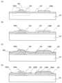
本発明は、絶縁基板の上方に第1の半導体層を有し、第1の半導体層の上方に第1の絶
縁層を有し、第1の絶縁層の上方に第1および第2の導電層を有し、第1および第2の導
電層の上方に第2の絶縁層を有し、第2の絶縁層の上方に第2の半導体層を有し、第2の
半導体層の上方に第3の導電層を有し、第2の絶縁層の上方に第4の導電層を有し、第3
および第4の導電層の上方に第3の絶縁層を有し、第3の絶縁層の上方に第5の導電層を
有し、第1の半導体層は、第1のトランジスタの活性層としての機能を有し、第2の半導
体層は、第2のトランジスタの活性層としての機能を有し、第1の半導体層と第2の半導
体層の特性が異なることを特徴としている。 The present invention relates to a semiconductor device having a first semiconductor layer above an insulating substrate, a first insulating layer above the first semiconductor layer, first and second conductive layers above the first insulating layer, a second insulating layer above the first and second conductive layers, a second semiconductor layer above the second insulating layer, a third conductive layer above the second semiconductor layer, a fourth conductive layer above the second insulating layer, and a third semiconductor layer above the third insulating layer.
and a third insulating layer above the fourth conductive layer, and a fifth conductive layer above the third insulating layer. The first semiconductor layer functions as an active layer of a first transistor, and the second semiconductor layer functions as an active layer of a second transistor, and the first semiconductor layer and the second semiconductor layer have different characteristics.
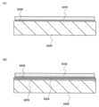
本発明は、前記構成において、第1の絶縁層は、前記第1のトランジスタのゲート絶縁
層としての機能を有し、第1の導電層は、第1のトランジスタのゲート電極としての機能
を有していることを特徴としている。 The present invention is characterized in that, in the above-mentioned structure, the first insulating layer has a function as a gate insulating layer of the first transistor, and the first conductive layer has a function as a gate electrode of the first transistor.
本発明は、前記構成において、第2の絶縁層は、第2のトランジスタのゲート絶縁層と
しての機能を有し、第2の導電層は、第2のトランジスタのゲート電極としての機能を有
していることを特徴としている。 The present invention is characterized in that, in the above-mentioned structure, the second insulating layer has a function as a gate insulating layer of the second transistor, and the second conductive layer has a function as a gate electrode of the second transistor.
本発明は、前記構成において、第5の導電層は、第3の絶縁層に設けられたコンタクト
ホールを介して、第4の導電層と電気的に接続されていることを特徴としている。 In the above-mentioned structure, the present invention is characterized in that the fifth conductive layer is electrically connected to the fourth conductive layer through a contact hole provided in the third insulating layer.
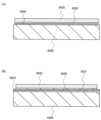
本発明は、前記構成において、第5の導電層は、第1の絶縁層、第2の絶縁層、第3の
絶縁層に設けられたコンタクトホールを介して、第1の半導体層と電気的に接続されてい
ることを特徴としている。 The present invention is characterized in that, in the above-mentioned configuration, the fifth conductive layer is electrically connected to the first semiconductor layer via contact holes provided in the first insulating layer, the second insulating layer, and the third insulating layer.
本発明は、前記構成において、第3の導電層は、第2の半導体層と電気的に接続されて
いることを特徴としている。 In the above-mentioned structure, the present invention is characterized in that the third conductive layer is electrically connected to the second semiconductor layer.
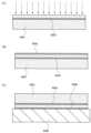
本発明は、前記構成において、第1の半導体層が結晶性を有していることを特徴として
いる。 The present invention is characterized in that in the above-mentioned structure, the first semiconductor layer has crystallinity.
本発明は、前記構成において、第2の半導体層がアモルファス半導体を有していること
を特徴としている。 The present invention, in the above-mentioned configuration, is characterized in that the second semiconductor layer comprises an amorphous semiconductor.
本発明は、前記構成において、第2の半導体層がマイクロクリスタル半導体を有してい
ることを特徴としている。 The present invention, in the above-mentioned configuration, is characterized in that the second semiconductor layer has a microcrystalline semiconductor.
なお、本明細書において、スイッチは、様々な形態のものを用いることができる。例と
しては、電気的スイッチや機械的なスイッチなどがある。つまり、電流の流れを制御でき
るものであればよく、特定のものに限定されない。例えば、スイッチとして、トランジス
タ(例えば、バイポーラトランジスタ、MOSトランジスタなど)、ダイオード(例えば
、PNダイオード、PINダイオード、ショットキーダイオード、MIM(Metal
Insulator Metal)ダイオード、MIS(Metal Insulato
r Semiconductor)ダイオード、ダイオード接続のトランジスタなど)、
サイリスタなどを用いることが出来る。または、これらを組み合わせた論理回路をスイッ
チとして用いることが出来る。 In this specification, various types of switches can be used. Examples include electrical switches and mechanical switches. In other words, any type that can control the flow of current is acceptable, and is not limited to a specific type. For example, the switch may be a transistor (e.g., bipolar transistor, MOS transistor, etc.), a diode (e.g., PN diode, PIN diode, Schottky diode, MIM (Metal) diode, etc.), or a combination of these.
Insulator Metal Diode, MIS (Metal Insulator
r Semiconductor) diode, diode-connected transistor, etc.
A thyristor or the like can be used. Alternatively, a logic circuit that combines these can be used as a switch.
機械的なスイッチの例としては、デジタルマイクロミラーデバイス(DMD)のように
、MEMS(マイクロ・エレクトロ・メカニカル・システム)技術を用いたスイッチがあ
る。そのスイッチは、機械的に動かすことが出来る電極を有し、その電極が動くことによ
って、接続と非接続とを制御して動作する。 An example of a mechanical switch is a switch using MEMS (microelectromechanical system) technology, such as a digital micromirror device (DMD). The switch has an electrode that can be mechanically moved, and operates by controlling connection and disconnection by the movement of the electrode.
スイッチとしてトランジスタを用いる場合、そのトランジスタは、単なるスイッチとし
て動作するため、トランジスタの極性(導電型)は特に限定されない。ただし、オフ電流
を抑えたい場合、オフ電流が少ない方の極性のトランジスタを用いることが望ましい。オ
フ電流が少ないトランジスタとしては、LDD領域を有するトランジスタやマルチゲート
構造を有するトランジスタ等がある。または、スイッチとして動作させるトランジスタの
ソース端子の電位が、低電位側電源(Vss、GND、0Vなど)の電位に近い状態で動
作する場合はNチャネル型トランジスタを用いることが望ましい。反対に、ソース端子の
電位が、高電位側電源(Vddなど)の電位に近い状態で動作する場合はPチャネル型ト
ランジスタを用いることが望ましい。なぜなら、Nチャネル型トランジスタではソース端
子が低電位側電源の電位に近い状態で動作するとき、Pチャネル型トランジスタではソー
ス端子が高電位側電源の電位に近い状態で動作するとき、ゲートとソースの間の電圧の絶
対値を大きくできるため、スイッチとして、より正確な動作を行うことができるからであ
る。ソースフォロワ動作をしてしまうことが少ないため、出力電圧の大きさが小さくなっ
てしまうことが少ないからである。 When a transistor is used as a switch, the transistor operates simply as a switch, so the polarity (conductivity type) of the transistor is not particularly limited. However, when it is desired to suppress the off-current, it is desirable to use a transistor with a polarity with a smaller off-current. Examples of transistors with a smaller off-current include transistors having an LDD region and transistors having a multi-gate structure. Alternatively, when the potential of the source terminal of a transistor operated as a switch operates in a state close to the potential of a low-potential power supply (Vss, GND, 0V, etc.), it is desirable to use an N-channel transistor. On the other hand, when the potential of the source terminal operates in a state close to the potential of a high-potential power supply (Vdd, etc.), it is desirable to use a P-channel transistor. This is because, when an N-channel transistor operates in a state close to the potential of a low-potential power supply, and when a P-channel transistor operates in a state close to the potential of a high-potential power supply, the absolute value of the voltage between the gate and the source can be increased, so that a more accurate operation as a switch can be performed. This is because the magnitude of the output voltage is less likely to be reduced because the source follower operation is less likely to occur.
なお、Nチャネル型トランジスタとPチャネル型トランジスタの両方を用いて、CMO
S型のスイッチをスイッチとして用いてもよい。CMOS型のスイッチにすると、Pチャ
ネル型トランジスタまたはNチャネル型トランジスタのどちらか一方のトランジスタが導
通すれば電流が流れるため、スイッチとして機能しやすくなる。例えば、スイッチへの入
力信号の電圧が高い場合でも、低い場合でも、適切に電圧を出力させることが出来る。さ
らに、スイッチをオンまたはオフさせるための信号の電圧振幅値を小さくすることが出来
るので、消費電力を小さくすることも出来る。 In addition, both N-channel and P-channel transistors are used to form a CMOS
An S-type switch may be used as the switch. If a CMOS type switch is used, a current flows if either a P-channel transistor or an N-channel transistor is conductive, so that the switch can function easily as a switch. For example, whether the voltage of the input signal to the switch is high or low, the switch can output an appropriate voltage. Furthermore, the voltage amplitude value of the signal for turning the switch on or off can be reduced, so that power consumption can be reduced.
なお、スイッチとしてトランジスタを用いる場合、スイッチは、入力端子(ソース端子
またはドレイン端子の一方)と、出力端子(ソース端子またはドレイン端子の他方)と、
導通を制御する端子(ゲート端子)とを有している。一方、スイッチとしてダイオードを
用いる場合、スイッチは、導通を制御する端子を有していない場合がある。そのため、ト
ランジスタよりもダイオードをスイッチとして用いた方が、端子を制御するための配線を
少なくすることが出来る。 In addition, when a transistor is used as a switch, the switch has an input terminal (one of the source terminal and the drain terminal), an output terminal (the other of the source terminal and the drain terminal),
A switch has a terminal (gate terminal) that controls conduction. On the other hand, when a diode is used as a switch, the switch may not have a terminal that controls conduction. Therefore, using a diode as a switch rather than a transistor can reduce the amount of wiring required to control the terminal.
なお、本明細書において、AとBとが接続されている、と明示的に記載する場合は、A
とBとが電気的に接続されている場合と、AとBとが機能的に接続されている場合と、A
とBとが直接接続されている場合とを含むものとする。ここで、A、Bは、対象物(例え
ば、装置、素子、回路、配線、電極、端子、導電膜、層、など)である。したがって、所
定の接続関係、例えば、図または文章に示された接続関係に限定されず、図または文章に
示された接続関係以外のものも含むものとする。 In this specification, when it is explicitly stated that A and B are connected,
When A and B are electrically connected, when A and B are functionally connected, and when A and B are electrically connected,
and B are directly connected. Here, A and B are objects (e.g., devices, elements, circuits, wiring, electrodes, terminals, conductive films, layers, etc.). Therefore, it is not limited to a specific connection relationship, for example, a connection relationship shown in a figure or text, but also includes connection relationships other than those shown in a figure or text.
例えば、AとBとが電気的に接続されている場合として、AとBとの電気的な接続を可
能とする素子(例えば、スイッチ、トランジスタ、容量素子、インダクタ、抵抗素子、ダ
イオードなど)が、AとBとの間に1個以上配置されていてもよい。あるいは、AとBと
が機能的に接続されている場合として、AとBとの機能的な接続を可能とする回路(例え
ば、論理回路(インバータ、NAND回路、NOR回路など)、信号変換回路(DA変換
回路、AD変換回路、ガンマ補正回路など)、電位レベル変換回路(電源回路(昇圧回路
、降圧回路など)、信号の電位レベルを変えるレベルシフタ回路など)、電圧源、電流源
、切り替え回路、増幅回路(信号振幅または電流量などを大きく出来る回路、オペアンプ
、差動増幅回路、ソースフォロワ回路、バッファ回路など)、信号生成回路、記憶回路、
制御回路など)が、AとBとの間に1個以上配置されていてもよい。あるいは、AとBと
が直接接続されている場合として、AとBとの間に他の素子や他の回路を挟まずに、Aと
Bとが直接接続されていてもよい。 For example, in the case where A and B are electrically connected, one or more elements (e.g., a switch, a transistor, a capacitance element, an inductor, a resistance element, a diode, etc.) that enable the electrical connection between A and B may be disposed between A and B. Alternatively, in the case where A and B are functionally connected, one or more circuits that enable the functional connection between A and B (e.g., a logic circuit (inverter, NAND circuit, NOR circuit, etc.), a signal conversion circuit (DA conversion circuit, AD conversion circuit, gamma correction circuit, etc.), a potential level conversion circuit (a power supply circuit (a step-up circuit, a step-down circuit, etc.), a level shifter circuit that changes the potential level of a signal, etc.), a voltage source, a current source, a switching circuit, an amplifier circuit (a circuit that can increase the signal amplitude or current amount, an operational amplifier, a differential amplifier circuit, a source follower circuit, a buffer circuit, etc.), a signal generation circuit, a memory circuit,
One or more elements, a control circuit, etc., may be disposed between A and B. Alternatively, in the case where A and B are directly connected, A and B may be directly connected without any other elements or circuits between A and B.
なお、AとBとが直接接続されている、と明示的に記載する場合は、AとBとが直接接
続されている場合(つまり、AとBとの間に他の素子や他の回路を間に介さずに接続され
ている場合)と、AとBとが電気的に接続されている場合(つまり、AとBとの間に別の
素子や別の回路を挟んで接続されている場合)とを含むものとする。 In addition, when it is explicitly stated that A and B are directly connected, this includes the case where A and B are directly connected (i.e., the case where A and B are connected without any other element or circuit between them) and the case where A and B are electrically connected (i.e., the case where A and B are connected with another element or circuit between them).
なお、AとBとが電気的に接続されている、と明示的に記載する場合は、AとBとが電
気的に接続されている場合(つまり、AとBとの間に別の素子や別の回路を挟んで接続さ
れている場合)と、AとBとが機能的に接続されている場合(つまり、AとBとの間に別
の回路を挟んで機能的に接続されている場合)と、AとBとが直接接続されている場合(
つまり、AとBとの間に別の素子や別の回路を挟まずに接続されている場合)とを含むも
のとする。つまり、電気的に接続されている、と明示的に記載する場合は、単に、接続さ
れている、とのみ明示的に記載されている場合と同じであるとする。 In addition, when it is explicitly stated that A and B are electrically connected, it means the following cases: when A and B are electrically connected (i.e., when A and B are connected with another element or circuit between them), when A and B are functionally connected (i.e., when A and B are functionally connected with another circuit between them), and when A and B are directly connected (
In other words, the term "electrically connected" includes the case where A and B are connected without any other element or circuit between them. In other words, when it is explicitly stated that A and B are electrically connected, it is the same as when it is explicitly stated that A and B are simply connected.
なお、本発明における表示素子、表示素子を有する装置である表示装置、発光素子、発
光素子を有する装置である発光装置は、様々な形態を用いることができ、また、様々な素
子を有することが出来る。例えば、表示素子、表示装置、発光素子または発光装置として
は、EL(エレクトロルミネッセンス)素子(有機物及び無機物を含むEL素子、有機E
L素子、無機EL素子)、電子放出素子、液晶素子、電子インク、電気泳動素子、グレー
ティングライトバルブ(GLV)、プラズマディスプレイ(PDP)、デジタルマイクロ
ミラーデバイス(DMD)、圧電セラミックディスプレイ、カーボンナノチューブ、など
、電気磁気的作用により、コントラスト、輝度、反射率、透過率などが変化する表示媒体
を用いることができる。なお、EL素子を用いた表示装置としてはELディスプレイ、電
子放出素子を用いた表示装置としてはフィールドエミッションディスプレイ(FED)や
SED方式平面型ディスプレイ(SED:Surface-conduction El
ectron-emitter Disply)など、液晶素子を用いた表示装置として
は液晶ディスプレイ(透過型液晶ディスプレイ、半透過型液晶ディスプレイ、反射型液晶
ディスプレイ、直視型液晶ディスプレイ、投射型液晶ディスプレイ)、電子インクや電気
泳動素子を用いた表示装置としては電子ペーパーがある。 The display element, the display device which is a device having a display element, the light-emitting element, and the light-emitting device which is a device having a light-emitting element in the present invention can be in various forms and can have various elements. For example, the display element, the display device, the light-emitting element, or the light-emitting device can be an EL (electroluminescence) element (an EL element including organic and inorganic materials, an organic EL
Display media whose contrast, brightness, reflectance, transmittance, etc. change due to electro-magnetic action can be used, such as EL elements, inorganic EL elements, electron-emitting elements, liquid crystal elements, electronic ink, electrophoretic elements, grating light valves (GLV), plasma displays (PDP), digital micromirror devices (DMD), piezoelectric ceramic displays, carbon nanotubes, etc. Examples of display devices using EL elements include EL displays, and examples of display devices using electron-emitting elements include field emission displays (FEDs) and SED-type flat displays (SEDs: Surface-conduction EL displays).
Examples of display devices using liquid crystal elements include liquid crystal displays (transmissive liquid crystal displays, semi-transmissive liquid crystal displays, reflective liquid crystal displays, direct-view liquid crystal displays, and projection liquid crystal displays), and examples of display devices using electronic ink or electrophoretic elements include electronic paper.
なお、EL素子とは、陽極と、陰極と、陽極と陰極との間に挟まれたEL層とを有する
素子である。なお、EL層としては、1重項励起子からの発光(蛍光)を利用するもの、
3重項励起子からの発光(燐光)を利用するもの、1重項励起子からの発光(蛍光)を利
用するものと3重項励起子からの発光(燐光)を利用するものとを含むもの、有機物によ
って形成されたもの、無機物によって形成されたもの、有機物によって形成されたものと
無機物によって形成されたものとを含むもの、高分子の材料、低分子の材料、高分子の材
料と低分子の材料とを含むものなどを用いることができる。ただし、これに限定されず、
EL素子として様々なものを用いることができる。 The EL element is an element having an anode, a cathode, and an EL layer sandwiched between the anode and the cathode. The EL layer may be one that utilizes light emission (fluorescence) from singlet excitons,
Examples of materials that can be used include those that utilize luminescence (phosphorescence) from triplet excitons, those that utilize luminescence (fluorescence) from singlet excitons and those that utilize luminescence (phosphorescence) from triplet excitons, those formed from organic substances, those formed from inorganic substances, those that include those formed from organic substances and those formed from inorganic substances, polymeric materials, low molecular weight materials, and those that include polymeric materials and low molecular weight materials. However, the present invention is not limited to these.
A variety of EL elements can be used.
なお、電子放出素子とは、先鋭な陰極に高電界を集中して電子を引き出す素子である。例
えば、電子放出素子として、スピント型、カーボンナノチューブ(CNT)型、金属―絶
縁体―金属を積層したMIM(Metal-Insulator-Metal)型、金属
―絶縁体―半導体を積層したMIS(Metal-Insulator-Semicon
ductor)型、MOS型、シリコン型、薄膜ダイオード型、ダイヤモンド型、表面伝
導エミッタSCD型、などを用いることができる。ただし、これに限定されず、電子放出
素子として様々なものを用いることができる。The electron-emitting element is an element that extracts electrons by concentrating a high electric field on a sharp cathode. For example, there are various types of electron-emitting elements, including Spindt type, carbon nanotube (CNT) type, MIM (Metal-Insulator-Metal) type in which a metal-insulator-metal layer is laminated, and MIS (Metal-Insulator-Semiconductor) type in which a metal-insulator-semiconductor layer is laminated.
Inductor type, MOS type, silicon type, thin film diode type, diamond type, surface conduction emitter SCD type, etc. can be used. However, the present invention is not limited to these, and various types can be used as the electron emitting element.
なお、液晶素子とは、液晶の光学的変調作用によって光の透過または非透過を制御する
素子であり、一対の電極、及び液晶により構成される。なお、液晶の光学的変調作用は、
液晶にかかる電界(横方向の電界、縦方向の電界又は斜め方向の電界を含む)によって制
御される。なお、液晶素子としては、ネマチック液晶、コレステリック液晶、スメクチッ
ク液晶、ディスコチック液晶、サーモトロピック液晶、ライオトロピック液晶、リオトロ
ピック液晶、低分子液晶、高分子液晶、強誘電液晶、反強誘電液晶、主鎖型液晶、側鎖型
高分子液晶、プラズマアドレス液晶(PDLC)、バナナ型液晶等が挙げられる。また、
液晶の駆動方式としては、TN(Twisted Nematic)モード、STN(S
uper Twisted Nematic)モード、IPS(In-Plane-Sw
itching)モード、FFS(Fringe Field Switching)モ
ード、MVA(Multi-domain Vertical Alignment)モ
ード、PVA(Patterned Vertical Alignment)モード、
ASV(Advanced Super View)モード、ASM(Axially
Symmetric aligned Micro-cell)モード、OCB(Opt
ical Compensated Birefringence)モード、ECB(E
lectrically Controlled Birefringence)モード
、FLC(Ferroelectric Liquid Crystal)モード、AF
LC(AntiFerroelectric Liquid Crystal)モード、
PDLC(Polymer Dispersed Liquid Crystal)モー
ド、ゲストホストモードなどを用いることができる。ただし、これに限定されず、液晶素
子及びその駆動方式として様々なものを用いることができる。 A liquid crystal element is an element that controls the transmission or non-transmission of light by the optical modulation action of liquid crystal, and is composed of a pair of electrodes and liquid crystal.
It is controlled by an electric field (including a horizontal electric field, a vertical electric field, or an oblique electric field) applied to the liquid crystal. Examples of liquid crystal elements include nematic liquid crystal, cholesteric liquid crystal, smectic liquid crystal, discotic liquid crystal, thermotropic liquid crystal, lyotropic liquid crystal, lyotropic liquid crystal, low molecular weight liquid crystal, polymer liquid crystal, ferroelectric liquid crystal, antiferroelectric liquid crystal, main chain type liquid crystal, side chain type polymer liquid crystal, plasma addressed liquid crystal (PDLC), banana type liquid crystal, etc.
The liquid crystal driving method is TN (Twisted Nematic) mode, STN (S
Upper Twisted Nematic mode, IPS (In-Plane-Sw
Fringe Field Switching (FFS) mode, Multi-domain Vertical Alignment (MVA) mode, Patterned Vertical Alignment (PVA) mode,
ASV (Advanced Super View) mode, ASM (Axially
Symmetric aligned Micro-cell mode, OCB (Opt
ECB (E
Electrically Controlled Birefringence) mode, FLC (Ferroelectric Liquid Crystal) mode, AF
LC (AntiFerroelectric Liquid Crystal) mode,
A polymer dispersed liquid crystal (PDLC) mode, a guest-host mode, etc., can be used. However, the present invention is not limited thereto, and various liquid crystal elements and driving methods thereof can be used.
なお、電子ペーパーとしては、光学異方性と染料分子配向のような分子により表示され
るもの、電気泳動、粒子移動、粒子回転、相変化のような粒子により表示されるもの、フ
ィルムの一端が移動することにより表示されるもの、分子の発色/相変化により表示され
るもの、分子の光吸収により表示されるもの、電子とホールが結合して自発光により表示
されるものなどのことをいう。例えば、電子ペーパーとして、マイクロカプセル型電気泳
動、水平移動型電気泳動、垂直移動型電気泳動、球状ツイストボール、磁気ツイストボー
ル、円柱ツイストボール方式、帯電トナー、電子粉流体、磁気泳動型、磁気感熱式、エレ
クトロウェッテイング、光散乱(透明/白濁変化)、コレステリック液晶/光導電層、コ
レステリック液晶、双安定性ネマチック液晶、強誘電性液晶、2色性色素・液晶分散型、
可動フィルム、ロイコ染料による発消色、フォトクロミック、エレクトロクロミック、エ
レクトロデポジション、フレキシブル有機ELなどを用いることができる。ただし、これ
に限定されず、電子ペーパーとして様々なものを用いることができる。ここで、マイクロ
カプセル型電気泳動を用いることによって、電気泳動方式の欠点である泳動粒子の凝集、
沈殿を解決することができる。電子粉流体は、高速応答性、高反射率、広視野角、低消費
電力、メモリー性などのメリットを有する。 Electronic paper includes those that are displayed by molecules such as optical anisotropy and dye molecule orientation, those that are displayed by particles such as electrophoresis, particle movement, particle rotation, and phase change, those that are displayed by moving one end of a film, those that are displayed by molecular coloring/phase change, those that are displayed by molecular light absorption, and those that are displayed by spontaneous light emission caused by the combination of electrons and holes. For example, electronic paper includes microcapsule type electrophoresis, horizontal movement type electrophoresis, vertical movement type electrophoresis, spherical twist ball, magnetic twist ball, cylindrical twist ball method, charged toner, electronic liquid powder, magnetic migration type, magnetic heat sensitive type, electrowetting, light scattering (transparent/opaque change), cholesteric liquid crystal/photoconductive layer, cholesteric liquid crystal, bistable nematic liquid crystal, ferroelectric liquid crystal, dichroic dye/liquid crystal dispersion type,
The electronic paper may be made of a movable film, a leuco dye for color development and fading, photochromic, electrochromic, electrodeposition, flexible organic EL, etc. However, it is not limited to these, and various types of electronic paper may be used. Here, by using microcapsule-type electrophoresis, the disadvantages of the electrophoretic method, such as aggregation of electrophoretic particles,
It can solve the problem of precipitation. Electronic liquid powder has the advantages of high speed response, high reflectance, wide viewing angle, low power consumption, and memory properties.
なお、プラズマディスプレイは、電極を表面に形成した基板と、電極及び微小な溝を表
面に形成し且つ溝内に蛍光体層を形成した基板とを狭い間隔で対向させて、希ガスを封入
した構造を有する。なお、電極間に電圧をかけることによって紫外線を発生させ、蛍光体
を光らせることで、表示を行うことができる。なお、プラズマディスプレイとしては、D
C型PDP、AC型PDPでもよい。ここで、プラズマディスプレイパネルとしては、A
SW(Address While Sustain)駆動、サブフレームをリセット期
間、アドレス期間、維持期間に分割するADS(Address Display Se
parated)駆動、CLEAR(High―Contrast, Low Ener
gy Address and Reduction of False Contou
r Sequence)駆動、ALIS(Alternate Lighting of
Surfaces)方式、TERES(Technology of Recipro
cal Sustainer)駆動などを用いることができる。ただし、これに限定され
ず、プラズマディスプレイとして様々なものを用いることができる。 A plasma display has a structure in which a substrate with electrodes formed on its surface and a substrate with electrodes and minute grooves formed on its surface and a phosphor layer formed in the grooves are placed facing each other at a narrow distance and filled with rare gas. By applying a voltage between the electrodes, ultraviolet light is generated, causing the phosphor to glow, and display can be performed.
The plasma display panel may be an A-type PDP or an AC-type PDP.
SW (Address While Sustain) drive, ADS (Address Display Set) that divides a subframe into a reset period, an address period, and a sustain period
paratized) drive, CLEAR (High-Contrast, Low Energy
gy Address and Reduction of False Contou
r Sequence) drive, ALIS (Alternate Lighting of
Surface) method, TERES (Technology of Recipro)
However, the present invention is not limited to this, and various types of plasma displays can be used.
なお、光源を必要とする表示装置、例えば、液晶ディスプレイ(透過型液晶ディスプレ
イ、半透過型液晶ディスプレイ、反射型液晶ディスプレイ、直視型液晶ディスプレイ、投
射型液晶ディスプレイ)、グレーティングライトバルブ(GLV)を用いた表示装置、デ
ジタルマイクロミラーデバイス(DMD)を用いた表示装置などの光源としては、エレク
トロルミネッセンス、冷陰極管、熱陰極管、LED、レーザー光源、水銀ランプなどを用
いることができる。ただし、これに限定されず、光源して様々なものを用いることができ
る。 In addition, as light sources for display devices that require a light source, such as liquid crystal displays (transmissive liquid crystal displays, semi-transmissive liquid crystal displays, reflective liquid crystal displays, direct-view liquid crystal displays, projection liquid crystal displays), display devices using grating light valves (GLVs), and display devices using digital micromirror devices (DMDs), electroluminescence, cold cathode tubes, hot cathode tubes, LEDs, laser light sources, mercury lamps, etc., can be used. However, the light source is not limited to these, and various other light sources can be used.
なお、トランジスタとして、様々な形態のトランジスタを用いることが出来る。よって
、用いるトランジスタの種類に限定はない。例えば、非晶質シリコン、多結晶シリコン、
微結晶(マイクロクリスタル、セミアモルファスとも言う)シリコンなどに代表される非
単結晶半導体膜を有する薄膜トランジスタ(TFT)などを用いることが出来る。TFT
を用いる場合、様々なメリットがある。例えば、単結晶シリコンの場合よりも低い温度で
製造できるため、製造コストの削減、又は製造装置の大型化を図ることができる。製造装
置を大きくできるため、大型基板上に製造できる。そのため、同時に多くの個数の表示装
置を製造できるため、低コストで製造できる。さらに、製造温度が低いため、耐熱性の弱
い基板を用いることができる。そのため、透明基板(光透過性を有する基板)上にトラン
ジスタを製造できる。そして、該基板上のトランジスタを用いて表示素子での光の透過を
制御することが出来る。あるいは、トランジスタの膜厚が薄いため、トランジスタを構成
する膜の一部は、光を透過させることが出来る。そのため、開口率を向上させることがで
きる。 Note that various types of transistors can be used as the transistor. Therefore, there is no limitation on the type of transistor to be used. For example, a transistor made of amorphous silicon, a transistor made of polycrystalline silicon,
A thin film transistor (TFT) having a non-single crystal semiconductor film, typically made of microcrystalline (also called semi-amorphous) silicon, can be used.
There are various advantages when using a transparent substrate. For example, since the display device can be manufactured at a lower temperature than the case of single crystal silicon, the manufacturing cost can be reduced or the manufacturing equipment can be enlarged. Since the manufacturing equipment can be enlarged, the display device can be manufactured on a large substrate. Therefore, since a large number of display devices can be manufactured at the same time, the display device can be manufactured at low cost. Furthermore, since the manufacturing temperature is low, a substrate with low heat resistance can be used. Therefore, a transistor can be manufactured on a transparent substrate (a substrate having optical transparency). Then, the transistor on the substrate can be used to control the transmission of light in the display element. Alternatively, since the film thickness of the transistor is thin, a part of the film constituting the transistor can transmit light. Therefore, the aperture ratio can be improved.
なお、多結晶シリコンを製造するときに、触媒(ニッケルなど)を用いることにより、
結晶性をさらに向上させ、電気特性のよいトランジスタを製造することが可能となる。そ
の結果、ゲートドライバ回路(走査線駆動回路)やソースドライバ回路(信号線駆動回路
)、信号処理回路(信号生成回路、ガンマ補正回路、DA変換回路など)を基板上に一体
形成することが出来る。 In addition, by using a catalyst (such as nickel) when producing polycrystalline silicon,
It is possible to further improve the crystallinity and manufacture transistors with good electrical characteristics. As a result, it is possible to integrally form a gate driver circuit (scanning line driver circuit), a source driver circuit (signal line driver circuit), and a signal processing circuit (signal generation circuit, gamma correction circuit, DA conversion circuit, etc.) on a substrate.
なお、微結晶シリコンを製造するときに、触媒(ニッケルなど)を用いることにより、
結晶性をさらに向上させ、電気特性のよいトランジスタを製造することが可能となる。こ
のとき、レーザー照射を行うことなく、熱処理を加えるだけで、結晶性を向上させること
ができる。その結果、ソースドライバ回路の一部(アナログスイッチなど)及びゲートド
ライバ回路(走査線駆動回路)を基板上に一体形成することが出来る。さらに、結晶化の
ためにレーザー照射を行わない場合は、シリコンの結晶性のムラを抑えることができる。
そのため、画質の向上した画像を表示することが出来る。 In addition, when producing microcrystalline silicon, a catalyst (such as nickel) is used,
It is possible to further improve the crystallinity and manufacture transistors with good electrical properties. In this case, the crystallinity can be improved by simply applying heat treatment without laser irradiation. As a result, a part of the source driver circuit (analog switch, etc.) and a gate driver circuit (scanning line driving circuit) can be integrally formed on the substrate. Furthermore, when laser irradiation is not performed for crystallization, unevenness in the crystallinity of silicon can be suppressed.
Therefore, an image with improved quality can be displayed.
ただし、触媒(ニッケルなど)を用いずに、多結晶シリコンや微結晶シリコンを製造す
ることは可能である。 However, it is possible to produce polycrystalline silicon or microcrystalline silicon without using a catalyst (such as nickel).
なお、シリコンの結晶性を、多結晶または微結晶などへと向上させることは、パネル全
体で行うことが望ましいが、それに限定されない。パネルの一部の領域のみにおいて、シ
リコンの結晶性を向上させてもよい。選択的に結晶性を向上させることは、レーザー光を
選択的に照射することなどにより可能である。例えば、画素以外の領域である周辺回路領
域にのみ、レーザー光を照射してもよい。または、ゲートドライバ回路、ソースドライバ
回路等の領域にのみ、レーザー光を照射してもよい。あるいは、ソースドライバ回路の一
部(例えば、アナログスイッチ)の領域にのみ、レーザー光を照射してもよい。その結果
、回路を高速に動作させる必要がある領域にのみ、シリコンの結晶化を向上させることが
できる。画素領域は、高速に動作させる必要性が低いため、結晶性が向上されなくても、
問題なく画素回路を動作させることが出来る。結晶性を向上させる領域が少なくて済むた
め、製造工程も短くすることが出来、スループットが向上し、製造コストを低減させるこ
とが出来る。また、必要とされる製造装置の数が少なくなるため、製造コストを低減させ
ることが出来る。 It is desirable to improve the crystallinity of silicon to polycrystalline or microcrystalline, etc., over the entire panel, but this is not limited to this. The crystallinity of silicon may be improved only in a part of the panel. Selective improvement of crystallinity is possible by selectively irradiating laser light, etc. For example, laser light may be irradiated only to the peripheral circuit region, which is an area other than the pixels. Alternatively, laser light may be irradiated only to the area of the gate driver circuit, source driver circuit, etc. Alternatively, laser light may be irradiated only to a part of the source driver circuit (e.g., analog switch). As a result, it is possible to improve the crystallinity of silicon only in the area where the circuit needs to operate at high speed. Since there is little need for high speed operation in the pixel area, it is possible to improve the crystallinity without improving the crystallinity.
The pixel circuit can be operated without any problems. Since the area for improving the crystallinity is small, the manufacturing process can be shortened, throughput can be improved, and manufacturing costs can be reduced. Furthermore, since the number of manufacturing devices required is reduced, manufacturing costs can be reduced.
または、半導体基板やSOI基板などを用いてトランジスタを形成することが出来る。
これらにより、特性やサイズや形状などのバラツキが少なく、電流供給能力が高く、サイ
ズの小さいトランジスタを製造することができる。これらのトランジスタを用いると、回
路の低消費電力化、又は回路の高集積化を図ることができる。 Alternatively, a transistor can be formed using a semiconductor substrate, an SOI substrate, or the like.
These features make it possible to manufacture transistors that have small characteristics, sizes, shapes, and other variations, and that have high current supply capabilities. The use of these transistors makes it possible to reduce the power consumption of circuits and to increase the integration density of circuits.
または、ZnO、a-InGaZnO、SiGe、GaAs、IZO、ITO、SnO
などの化合物半導体または酸化物半導体を有するトランジスタや、さらに、これらの化合
物半導体または酸化物半導体を薄膜化した薄膜トランジスタなどを用いることが出来る。
これらにより、製造温度を低くでき、例えば、室温でトランジスタを製造することが可能
となる。その結果、耐熱性の低い基板、例えばプラスチック基板やフィルム基板に直接ト
ランジスタを形成することが出来る。なお、これらの化合物半導体または酸化物半導体を
、トランジスタのチャネル部分に用いるだけでなく、それ以外の用途で用いることも出来
る。例えば、これらの化合物半導体または酸化物半導体を抵抗素子、画素電極、透明電極
として用いることができる。さらに、それらをトランジスタと同時に成膜又は形成できる
ため、コストを低減できる。 Or, ZnO, a-InGaZnO, SiGe, GaAs, IZO, ITO, SnO
A transistor having a compound semiconductor or an oxide semiconductor such as those mentioned above, or a thin film transistor in which such a compound semiconductor or oxide semiconductor is thinned can be used.
These features allow the manufacturing temperature to be lowered, and for example, transistors can be manufactured at room temperature. As a result, transistors can be formed directly on substrates with low heat resistance, such as plastic substrates and film substrates. These compound semiconductors or oxide semiconductors can be used not only for the channel portion of transistors, but also for other purposes. For example, these compound semiconductors or oxide semiconductors can be used as resistance elements, pixel electrodes, and transparent electrodes. Furthermore, they can be formed or deposited simultaneously with transistors, thereby reducing costs.
または、インクジェットや印刷法を用いて形成したトランジスタなどを用いることが出
来る。これらにより、室温で製造、低真空度で製造、又は大型基板上に製造することがで
きる。マスク(レチクル)を用いなくても製造することが可能となるため、トランジスタ
のレイアウトを容易に変更することが出来る。さらに、レジストを用いる必要がないので
、材料費が安くなり、工程数を削減できる。さらに、必要な部分にのみ膜を付けるため、
全面に成膜した後でエッチングする、という製法よりも、材料が無駄にならず、低コスト
にできる。 Alternatively, transistors formed using an inkjet or printing method can be used. These methods allow manufacturing at room temperature, at a low degree of vacuum, or on a large substrate. Since manufacturing is possible without using a mask (reticle), the layout of the transistors can be easily changed. Furthermore, since there is no need to use resist, material costs are reduced and the number of processes can be reduced. Furthermore, since the film is applied only to the necessary parts,
This method wastes less material and is less costly than a method in which a film is formed over the entire surface and then etched.
または、有機半導体やカーボンナノチューブを有するトランジスタ等を用いることがで
きる。これらにより、曲げることが可能な基板上にトランジスタを形成することが出来る
。そのため、有機半導体やカーボンナノチューブを有するトランジスタなどを用いた装置
は衝撃に強くできる。 Alternatively, a transistor having an organic semiconductor or a carbon nanotube can be used. This allows a transistor to be formed on a substrate that can be bent. Therefore, a device using a transistor having an organic semiconductor or a carbon nanotube can be made resistant to impact.
さらに、様々な構造のトランジスタを用いることができる。例えば、MOS型トランジ
スタ、接合型トランジスタ、バイポーラトランジスタなどをトランジスタとして用いるこ
とが出来る。MOS型トランジスタを用いることにより、トランジスタのサイズを小さく
することが出来る。よって、多数のトランジスタを搭載することができる。バイポーラト
ランジスタを用いることにより、大きな電流を流すことが出来る。よって、高速に回路を
動作させることができる。 Furthermore, transistors of various structures can be used. For example, MOS transistors, junction transistors, bipolar transistors, etc. can be used as transistors. By using MOS transistors, the size of the transistors can be reduced. Therefore, a large number of transistors can be mounted. By using bipolar transistors, a large current can be passed. Therefore, the circuit can operate at high speed.
なお、MOS型トランジスタ、バイポーラトランジスタなどを1つの基板に混在させて
形成してもよい。これにより、低消費電力、小型化、高速動作などを実現することが出来
る。 It is also possible to form a mixture of MOS transistors and bipolar transistors on one substrate, thereby achieving low power consumption, miniaturization, high speed operation, and the like.
その他、様々なトランジスタを用いることができる。Various other transistors can also be used.
なお、トランジスタは、様々な基板を用いて形成することが出来る。基板の種類は、特
定のものに限定されることはない。トランジスタが形成される基板としては、例えば、単
結晶基板、SOI基板、ガラス基板、石英基板、プラスチック基板、紙基板、セロファン
基板、石材基板、木材基板、布基板(天然繊維(絹、綿、麻)、合成繊維(ナイロン、ポ
リウレタン、ポリエステル)若しくは再生繊維(アセテート、キュプラ、レーヨン、再生
ポリエステル)などを含む)、皮革基板、ゴム基板、ステンレス・スチル基板、ステンレ
ス・スチル・ホイルを有する基板などを用いることが出来る。あるいは、人などの動物の
皮膚(表皮、真皮)又は皮下組織を基板として用いてもよい。または、ある基板を用いて
トランジスタを形成し、その後、別の基板にトランジスタを転置し、別の基板上にトラン
ジスタを配置してもよい。トランジスタが転置される基板としては、単結晶基板、SOI
基板、ガラス基板、石英基板、プラスチック基板、紙基板、セロファン基板、石材基板、
、木材基板、布基板(天然繊維(絹、綿、麻)、合成繊維(ナイロン、ポリウレタン、ポ
リエステル)若しくは再生繊維(アセテート、キュプラ、レーヨン、再生ポリエステル)
などを含む)、皮革基板、ゴム基板、ステンレス・スチル基板、ステンレス・スチル・ホ
イルを有する基板などを用いることができる。あるいは、人などの動物の皮膚(表皮、真
皮)又は皮下組織を基板として用いてもよい。または、ある基板を用いてトランジスタを
形成し、その基板を研磨して薄くしてもよい。研磨される基板としては、単結晶基板、S
OI基板、ガラス基板、石英基板、プラスチック基板、紙基板、セロファン基板、石材基
板、木材基板、布基板(天然繊維(絹、綿、麻)、合成繊維(ナイロン、ポリウレタン、
ポリエステル)若しくは再生繊維(アセテート、キュプラ、レーヨン、再生ポリエステル
)などを含む)、皮革基板、ゴム基板、ステンレス・スチル基板、ステンレス・スチル・
ホイルを有する基板などを用いることができる。あるいは、人などの動物の皮膚(表皮、
真皮)又は皮下組織を基板として用いてもよい。これらの基板を用いることにより、特性
のよいトランジスタの形成、消費電力の小さいトランジスタの形成、壊れにくい装置の製
造、耐熱性の付与、軽量化、又は薄型化を図ることができる。 The transistors can be formed using various substrates. The type of substrate is not limited to a specific one. As the substrate on which the transistors are formed, for example, a single crystal substrate, an SOI substrate, a glass substrate, a quartz substrate, a plastic substrate, a paper substrate, a cellophane substrate, a stone substrate, a wood substrate, a cloth substrate (including natural fibers (silk, cotton, hemp), synthetic fibers (nylon, polyurethane, polyester), or regenerated fibers (acetate, cupra, rayon, regenerated polyester), etc.), a leather substrate, a rubber substrate, a stainless steel substrate, a substrate having stainless steel foil, etc. may be used. Alternatively, the skin (epidermis, dermis) or subcutaneous tissue of an animal such as a human may be used as the substrate. Alternatively, a transistor may be formed using a certain substrate, and then the transistor may be transferred to another substrate, and the transistor may be disposed on the other substrate. As the substrate on which the transistors are transferred, a single crystal substrate, an SOI substrate, a quartz substrate, a plastic substrate, a stone substrate, a wood substrate, a cloth substrate (including natural fibers (silk, cotton, hemp), synthetic fibers (nylon, polyurethane, polyester), or regenerated fibers (acetate, cupra, rayon, regenerated polyester), etc.), a leather substrate, a rubber substrate, a stainless steel substrate, a substrate having stainless steel foil, etc. may be used. Alternatively, the skin (epidermis, dermis) or subcutaneous tissue of an animal such as a human may be used as the substrate. Alternatively, a transistor may be formed using a certain substrate, and then the transistor may be transferred to another substrate, and the transistor may be disposed on the other substrate.
Substrate, glass substrate, quartz substrate, plastic substrate, paper substrate, cellophane substrate, stone substrate,
, wood substrate, cloth substrate (natural fibers (silk, cotton, linen), synthetic fibers (nylon, polyurethane, polyester) or recycled fibers (acetate, cupra, rayon, recycled polyester)
The substrate may be a substrate made of a material such as a silicon substrate, a leather substrate, a rubber substrate, a stainless steel substrate, or a substrate having stainless steel foil. Alternatively, the skin (epidermis, dermis) or subcutaneous tissue of an animal such as a human may be used as the substrate. Alternatively, a transistor may be formed using a substrate, and the substrate may be polished to make it thinner. Substrates to be polished include single crystal substrates, S
OI substrate, glass substrate, quartz substrate, plastic substrate, paper substrate, cellophane substrate, stone substrate, wood substrate, cloth substrate (natural fibers (silk, cotton, hemp), synthetic fibers (nylon, polyurethane,
polyester) or regenerated fiber (including acetate, cupra, rayon, regenerated polyester), leather substrate, rubber substrate, stainless steel substrate, stainless steel
A substrate having a foil or the like can be used. Alternatively, the skin (epidermis,
The substrate may be a layer of the dermis or subcutaneous tissue. By using such a substrate, it is possible to form a transistor with good characteristics, a transistor with low power consumption, manufacture a device that is not easily broken, provide heat resistance, and reduce the weight or thickness of the device.
なお、トランジスタの構成は、様々な形態をとることができ、特定の構成に限定されな
い。例えば、ゲート電極が2個以上のマルチゲート構造を適用することができる。マルチ
ゲート構造にすると、チャネル領域が直列に接続されるため、複数のトランジスタが直列
に接続された構成となる。マルチゲート構造により、オフ電流の低減、トランジスタの耐
圧向上による信頼性の向上を図ることができる。あるいは、マルチゲート構造により、飽
和領域で動作する時に、ドレイン・ソース間電圧が変化しても、ドレイン・ソース間電流
があまり変化せず、傾きがフラットである電圧・電流特性にすることができる。傾きがフ
ラットである電圧・電流特性を利用すると、理想的な電流源回路や、非常に高い抵抗値を
もつ能動負荷を実現することが出来る。その結果、特性のよい差動回路やカレントミラー
回路を実現することが出来る。 The transistor configuration can take various forms and is not limited to a specific configuration. For example, a multi-gate structure with two or more gate electrodes can be applied. In the multi-gate structure, the channel regions are connected in series, resulting in a configuration in which multiple transistors are connected in series. The multi-gate structure can reduce the off-current and improve the transistor's withstand voltage, thereby improving reliability. Alternatively, the multi-gate structure can provide voltage-current characteristics with a flat slope, in which the drain-source current does not change much even if the drain-source voltage changes when operating in the saturation region. By utilizing voltage-current characteristics with a flat slope, an ideal current source circuit and an active load with a very high resistance value can be realized. As a result, a differential circuit or a current mirror circuit with good characteristics can be realized.
別の例として、チャネルの上下にゲート電極が配置されている構造を適用することがで
きる。チャネルの上下にゲート電極が配置されている構造にすることにより、チャネル領
域が増えるため、電流値の増加、又は空乏層ができやすくなることによるS値の低減を図
ることができる。チャネルの上下にゲート電極が配置される構成にすることにより、複数
のトランジスタが並列に接続されたような構成となる。 As another example, a structure in which gate electrodes are arranged above and below the channel can be applied. By adopting a structure in which gate electrodes are arranged above and below the channel, the channel region increases, so that it is possible to increase the current value or reduce the S value due to the tendency for a depletion layer to form. By adopting a structure in which gate electrodes are arranged above and below the channel, a structure in which multiple transistors are connected in parallel is achieved.
チャネル領域の上にゲート電極が配置されている構造、チャネル領域の下にゲート電極
が配置されている構造、正スタガ構造、逆スタガ構造、チャネル領域を複数の領域に分け
た構造、チャネル領域を並列に接続した構造、またはチャネル領域が直列に接続する構成
も適用できる。さらに、チャネル領域(もしくはその一部)にソース電極やドレイン電極
が重なっている構造も適用できる。チャネル領域(もしくはその一部)にソース電極やド
レイン電極が重なる構造にすることによって、チャネル領域の一部に電荷が溜まることに
より動作が不安定になることを防ぐことができる。あるいは、LDD領域を設けてもよい
。LDD領域を設けることにより、オフ電流の低減、又はトランジスタの耐圧向上による
信頼性の向上を図ることができる。あるいは、LDD領域を設けることにより、飽和領域
で動作する時に、ドレイン・ソース間電圧が変化しても、ドレイン・ソース間電流があま
り変化せず、傾きがフラットである電圧・電流特性にすることができる。 A structure in which a gate electrode is disposed above a channel region, a structure in which a gate electrode is disposed below a channel region, a positive staggered structure, an inverted staggered structure, a structure in which a channel region is divided into a plurality of regions, a structure in which channel regions are connected in parallel, or a structure in which channel regions are connected in series can also be applied. Furthermore, a structure in which a source electrode or a drain electrode overlaps a channel region (or a part thereof) can also be applied. By making a structure in which a source electrode or a drain electrode overlaps a channel region (or a part thereof), it is possible to prevent the operation from becoming unstable due to the accumulation of electric charge in a part of the channel region. Alternatively, an LDD region may be provided. By providing an LDD region, it is possible to reduce the off-current or improve the reliability by improving the breakdown voltage of the transistor. Alternatively, by providing an LDD region, it is possible to obtain a voltage-current characteristic in which the drain-source current does not change much even if the drain-source voltage changes when operating in the saturation region, and the slope is flat.
なお、トランジスタは、様々なタイプを用いることができ、様々な基板を用いて形成さ
せることができる。したがって、所定の機能を実現させるために必要な回路の全てが、同
一の基板に形成することも可能である。例えば、所定の機能を実現させるために必要な回
路の全てが、ガラス基板、プラスチック基板、単結晶基板、またはSOI基板などの様々
な基板を用いて形成することも可能である。所定の機能を実現させるために必要な回路の
全てが同じ基板を用いて形成されていることにより、部品点数の削減によるコストの低減
、又は回路部品との接続点数の低減による信頼性の向上を図ることができる。あるいは、
所定の機能を実現させるために必要な回路の一部が、ある基板に形成され、所定の機能を
実現させるために必要な回路の別の一部が、別の基板に形成されていることも可能である
。つまり、所定の機能を実現させるために必要な回路の全てが同じ基板を用いて形成され
ていなくてもよい。例えば、所定の機能を実現させるために必要な回路の一部は、ガラス
基板上にトランジスタにより形成され、所定の機能を実現させるために必要な回路の別の
一部は、単結晶基板に形成され、単結晶基板を用いて形成されたトランジスタで構成され
たICチップをCOG(Chip On Glass)でガラス基板に接続して、ガラス
基板上にそのICチップを配置することも可能である。あるいは、そのICチップをTA
B(Tape Automated Bonding)やプリント基板を用いてガラス基
板と接続することも可能である。このように、回路の一部が同じ基板に形成されているこ
とにより、部品点数の削減によるコストの低減、又は回路部品との接続点数の低減による
信頼性の向上を図ることができる。あるいは、駆動電圧が高い部分及び駆動周波数が高い
部分の回路は、消費電力が大きくなってしまうので、そのような部分の回路は同じ基板に
形成せず、そのかわりに、例えば、単結晶基板にその部分の回路を形成して、その回路で
構成されたICチップを用いるようにすれば、消費電力の増加を防ぐことができる。 It should be noted that various types of transistors can be used and can be formed using various substrates. Therefore, all of the circuits required to realize a specified function can be formed on the same substrate. For example, all of the circuits required to realize a specified function can be formed using various substrates such as a glass substrate, a plastic substrate, a single crystal substrate, or an SOI substrate. By forming all of the circuits required to realize a specified function using the same substrate, it is possible to reduce costs by reducing the number of components, or to improve reliability by reducing the number of connections with circuit components. Alternatively,
It is also possible that a part of the circuitry required to realize a predetermined function is formed on one substrate, and another part of the circuitry required to realize the predetermined function is formed on another substrate. In other words, all of the circuits required to realize the predetermined function do not have to be formed using the same substrate. For example, a part of the circuitry required to realize the predetermined function is formed by transistors on a glass substrate, and another part of the circuitry required to realize the predetermined function is formed on a single crystal substrate, and an IC chip made of transistors formed using the single crystal substrate is connected to the glass substrate by COG (Chip On Glass) and the IC chip is disposed on the glass substrate. Alternatively, the IC chip is formed by TA
It is also possible to connect the circuit board to the glass substrate using B (Tape Automated Bonding) or a printed circuit board. In this way, by forming a part of the circuit on the same substrate, it is possible to reduce the number of components and thereby reduce costs, or to improve reliability by reducing the number of connections with the circuit components. Alternatively, since the circuits of the parts with high driving voltages and parts with high driving frequencies consume large power, the circuits of such parts are not formed on the same substrate, but instead, for example, the circuits of those parts are formed on a single crystal substrate, and an IC chip composed of those circuits is used, thereby preventing an increase in power consumption.
なお、一画素とは、明るさを制御できる要素一つ分を示すものとする。よって、一例と
しては、一画素とは、一つの色要素を示すものとし、その色要素一つで明るさを表現する
。従って、そのときは、R(赤)G(緑)B(青)の色要素からなるカラー表示装置の場
合には、画像の最小単位は、Rの画素とGの画素とBの画素との三画素から構成されるも
のとする。なお、色要素は、三色に限定されず、三色以上を用いても良いし、RGB以外
の色を用いても良い。例えば、白色を加えて、RGBW(Wは白)としても可能である。
あるいは、RGBに、例えば、イエロー、シアン、マゼンタ、エメラルドグリーン、朱色
などを一色以上追加することも可能である。あるいは、例えば、RGBの中の少なくとも
一色に類似した色を、RGBに追加することも可能である。例えば、R、G、B1、B2
としてもよい。B1とB2とは、どちらも青色であるが、少し周波数が異なっている。同
様に、R1、R2、G、Bとすることも可能である。このような色要素を用いることによ
り、より実物に近い表示を行うことができる。このような色要素を用いることにより、消
費電力を低減することが出来る。別の例としては、一つの色要素について、複数の領域を
用いて明るさを制御する場合は、その領域一つ分を一画素とすることも可能である。よっ
て、一例として、面積階調を行う場合または副画素(サブ画素)を有している場合、一つ
の色要素につき、明るさを制御する領域が複数あり、その全体で階調を表現するが、明る
さを制御する領域の一つ分を一画素とすることも可能である。よって、その場合は、一つ
の色要素は、複数の画素で構成されることとなる。あるいは、明るさを制御する領域が一
つの色要素の中に複数あっても、それらをまとめて、一つの色要素を1画素としてもよい
。よって、その場合は、一つの色要素は、一つの画素で構成されることとなる。あるいは
、一つの色要素について、複数の領域を用いて明るさを制御する場合、画素によって、表
示に寄与する領域の大きさが異なっている場合がある。あるいは、一つの色要素につき複
数ある、明るさを制御する領域において、各々に供給する信号を僅かに異ならせるように
して、視野角を広げるようにしてもよい。つまり、一つの色要素について、複数個ある領
域が各々有する画素電極の電位が、各々異なっていることも可能である。その結果、液晶
分子に加わる電圧が各画素電極によって各々異なる。よって、視野角を広くすることが出
来る。 It should be noted that one pixel refers to one element whose brightness can be controlled. Thus, as an example, one pixel refers to one color element, and the brightness is expressed by this one color element. In this case, in the case of a color display device consisting of the color elements R (red), G (green), and B (blue), the minimum unit of an image is composed of three pixels, an R pixel, a G pixel, and a B pixel. It should be noted that the color elements are not limited to three colors, and three or more colors may be used, or colors other than RGB may be used. For example, it is also possible to add white, making it RGBW (W is white).
Alternatively, it is possible to add one or more colors such as yellow, cyan, magenta, emerald green, and vermilion to RGB. Alternatively, it is possible to add a color similar to at least one of the colors in RGB to RGB. For example, R, G, B1, B2
It may be set as follows. B1 and B2 are both blue, but have slightly different frequencies. Similarly, it is also possible to set R1, R2, G, and B. By using such color elements, it is possible to perform a display that is closer to the real thing. By using such color elements, it is possible to reduce power consumption. As another example, when the brightness of one color element is controlled using multiple regions, it is also possible to treat one of the regions as one pixel. Therefore, as an example, when performing area gradation or when having sub-pixels, there are multiple regions for controlling the brightness of one color element, and the gradation is expressed as a whole, but it is also possible to treat one region for controlling the brightness as one pixel. Therefore, in that case, one color element is composed of multiple pixels. Alternatively, even if there are multiple regions for controlling the brightness in one color element, they may be combined and one color element may be one pixel. Therefore, in that case, one color element is composed of one pixel. Alternatively, when the brightness of one color element is controlled using multiple regions, the size of the region contributing to the display may differ depending on the pixel. Alternatively, the viewing angle can be widened by slightly differentiating the signals supplied to the brightness control regions, each of which exists in multiple color elements. In other words, the potentials of the pixel electrodes in each of the multiple regions for one color element can be different. As a result, the voltages applied to the liquid crystal molecules differ for each pixel electrode. This makes it possible to widen the viewing angle.
なお、一画素(三色分)と明示的に記載する場合は、RとGとBの三画素分を一画素と
考える場合であるとする。一画素(一色分)と明示的に記載する場合は、一つの色要素に
つき、複数の領域がある場合、それらをまとめて一画素と考える場合であるとする。 In addition, when it is explicitly stated that one pixel (three colors) is used, it means that one pixel is considered to consist of three pixels of R, G, and B. When it is explicitly stated that one pixel (one color), it means that when there are multiple regions for one color element, all of them are considered to be one pixel.
なお、画素は、マトリクス状に配置(配列)されている場合がある。ここで、画素がマ
トリクスに配置(配列)されているとは、縦方向もしくは横方向において、画素が直線上
に並んで配置されている場合、又はギザギザな線上に配置されている場合を含む。よって
、例えば三色の色要素(例えばRGB)でフルカラー表示を行う場合に、ストライプ配置
されている場合、又は三つの色要素のドットがデルタ配置されている場合も含む。さらに
、ベイヤー配置されている場合も含む。なお、色要素は、三色に限定されず、それ以上で
もよく、例えば、RGBW(Wは白)、又はRGBに、イエロー、シアン、マゼンタなど
を一色以上追加したものなどがある。なお、色要素のドット毎にその表示領域の大きさが
異なっていてもよい。これにより、低消費電力化、又は表示素子の長寿命化を図ることが
できる。 In addition, the pixels may be arranged (distributed) in a matrix. Here, the arrangement (arrangement) of the pixels in a matrix includes the case where the pixels are arranged in a straight line in the vertical or horizontal direction, or the case where they are arranged in a jagged line. Therefore, for example, when performing full-color display with three color elements (for example, RGB), it includes the case where the pixels are arranged in stripes, or the case where the dots of the three color elements are arranged in delta. Furthermore, it also includes the case where the pixels are arranged in a Bayer arrangement. In addition, the color elements are not limited to three colors, and may be more than three colors, for example, RGBW (W is white), or RGB with one or more colors such as yellow, cyan, magenta, etc. added. In addition, the size of the display area may be different for each dot of the color elements. This can reduce power consumption or extend the life of the display element.
なお、画素に能動素子を有するアクティブマトリクス方式、または、画素に能動素子を
有しないパッシブマトリクス方式を用いることが出来る。 Note that an active matrix system in which pixels have active elements, or a passive matrix system in which pixels do not have active elements, can be used.
アクティブマトリクス方式では、能動素子(アクティブ素子、非線形素子)として、ト
ランジスタだけでなく、さまざまな能動素子(アクティブ素子、非線形素子)を用いるこ
とが出来る。例えば、MIM(Metal Insulator Metal)やTFD
(Thin Film Diode)などを用いることも可能である。これらの素子は、
製造工程が少ないため、製造コストの低減、又は歩留まりの向上を図ることができる。さ
らに、素子のサイズが小さいため、開口率を向上させることができ、低消費電力化や高輝
度化をはかることが出来る。 In the active matrix method, not only transistors but also various other active elements (non-linear elements) can be used as active elements. For example, MIM (Metal Insulator Metal) and TFD
It is also possible to use a thin film diode (Thin Film Diode) or the like.
Since the number of manufacturing steps is small, it is possible to reduce manufacturing costs and improve yields. Furthermore, since the size of the element is small, it is possible to improve the aperture ratio, thereby achieving low power consumption and high brightness.
なお、アクティブマトリクス方式以外のものとして、能動素子(アクティブ素子、非線
形素子)を用いないパッシブマトリクス型を用いることも可能である。能動素子(アクテ
ィブ素子、非線形素子)を用いないため、製造工程が少なく、製造コストの低減、又は歩
留まりの向上を図ることができる。能動素子(アクティブ素子、非線形素子)を用いない
ため、開口率を向上させることができ、低消費電力化や高輝度化をはかることが出来る。 As an alternative to the active matrix type, a passive matrix type that does not use active elements (active elements, nonlinear elements) can also be used. Since no active elements (active elements, nonlinear elements) are used, the number of manufacturing steps is reduced, and it is possible to reduce manufacturing costs and improve yields. Since no active elements (active elements, nonlinear elements) are used, it is possible to improve the aperture ratio, thereby achieving low power consumption and high brightness.
なお、トランジスタとは、ゲートと、ドレインと、ソースとを含む少なくとも三つの端
子を有する素子であり、ドレイン領域とソース領域の間にチャネル領域を有しており、ド
レイン領域とチャネル領域とソース領域とを介して電流を流すことが出来る。ここで、ソ
ースとドレインとは、トランジスタの構造や動作条件等によって変わるため、いずれがソ
ースまたはドレインであるかを限定することが困難である。そこで、本書類(明細書、特
許請求の範囲又は図面など)においては、ソース及びドレインとして機能する領域を、ソ
ースもしくはドレインと呼ばない場合がある。その場合、一例としては、それぞれを第1
端子、第2端子と表記する場合がある。あるいは、それぞれを第1の電極、第2の電極と
表記する場合がある。あるいは、ソース領域、ドレイン領域と表記する場合がある。 A transistor is an element having at least three terminals including a gate, a drain, and a source, and has a channel region between the drain region and the source region, allowing current to flow through the drain region, the channel region, and the source region. Here, the source and the drain vary depending on the structure and operating conditions of the transistor, and it is difficult to specify which is the source and which is the drain. Therefore, in this document (specification, claims, drawings, etc.), the regions that function as the source and the drain may not be called the source or the drain. In such cases, as an example, each may be called the first
They may be referred to as a terminal and a second terminal, a first electrode and a second electrode, or a source region and a drain region, respectively.
なお、トランジスタは、ベースとエミッタとコレクタとを含む少なくとも三つの端子を
有する素子であってもよい。この場合も同様に、エミッタとコレクタとを、第1端子、第
2端子と表記する場合がある。 The transistor may be an element having at least three terminals including a base, an emitter, and a collector. In this case, the emitter and the collector may be similarly referred to as a first terminal and a second terminal.
なお、ゲートとは、ゲート電極とゲート配線(ゲート線、ゲート信号線、走査線、走査
信号線等とも言う)とを含んだ全体、もしくは、それらの一部のことを言う。ゲート電極
とは、チャネル領域を形成する半導体と、ゲート絶縁膜を介してオーバーラップしている
部分の導電膜のことを言う。なお、ゲート電極の一部は、LDD(Lightly Do
ped Drain)領域またはソース領域(またはドレイン領域)と、ゲート絶縁膜を
介してオーバーラップしている場合もある。ゲート配線とは、各トランジスタのゲート電
極の間を接続するための配線、各画素の有するゲート電極の間を接続するための配線、又
はゲート電極と別の配線とを接続するための配線のことを言う。 The term "gate" refers to the whole including the gate electrode and the gate wiring (also called a gate line, gate signal line, scanning line, scanning signal line, etc.), or a part of them. The term "gate electrode" refers to a conductive film that overlaps the semiconductor forming the channel region with a gate insulating film interposed therebetween. A part of the gate electrode is called an LDD (Lightly Doped) film.
In some cases, the gate wiring may overlap with a gate-insulating film between the gate electrodes of the transistors, between the gate electrodes of the pixels, or between another wiring.
ただし、ゲート電極としても機能し、ゲート配線としても機能するような部分(領域、
導電膜、配線など)も存在する。そのような部分(領域、導電膜、配線など)は、ゲート
電極と呼んでも良いし、ゲート配線と呼んでも良い。つまり、ゲート電極とゲート配線と
が、明確に区別できないような領域も存在する。例えば、延伸して配置されているゲート
配線の一部とチャネル領域がオーバーラップしている場合、その部分(領域、導電膜、配
線など)はゲート配線として機能しているが、ゲート電極としても機能していることにな
る。よって、そのような部分(領域、導電膜、配線など)は、ゲート電極と呼んでも良い
し、ゲート配線と呼んでも良い。 However, there are some areas (regions,
In addition, there are also regions (regions, conductive films, wiring, etc.) that are not clearly distinguishable from each other. For example, when a part of the gate wiring that is extended and arranged overlaps with the channel region, the part (regions, conductive films, wiring, etc.) functions as a gate wiring, but also as a gate electrode. Therefore, such a part (regions, conductive films, wiring, etc.) may be called either a gate electrode or a gate wiring.
なお、ゲート電極と同じ材料で形成され、ゲート電極と同じ島(アイランド)を形成し
てつながっている部分(領域、導電膜、配線など)も、ゲート電極と呼んでも良い。同様
に、ゲート配線と同じ材料で形成され、ゲート配線と同じ島(アイランド)を形成してつ
ながっている部分(領域、導電膜、配線など)も、ゲート配線と呼んでも良い。このよう
な部分(領域、導電膜、配線など)は、厳密な意味では、チャネル領域とオーバーラップ
していない場合、又は別のゲート電極と接続させる機能を有していない場合がある。しか
し、製造時の仕様などの関係で、ゲート電極またはゲート配線と同じ材料で形成され、ゲ
ート電極またはゲート配線と同じ島(アイランド)を形成してつながっている部分(領域
、導電膜、配線など)がある。よって、そのような部分(領域、導電膜、配線など)もゲ
ート電極またはゲート配線と呼んでも良い。 In addition, a part (region, conductive film, wiring, etc.) formed of the same material as the gate electrode and connected to form the same island as the gate electrode may also be called a gate electrode. Similarly, a part (region, conductive film, wiring, etc.) formed of the same material as the gate wiring and connected to form the same island as the gate wiring may also be called a gate wiring. In the strict sense, such a part (region, conductive film, wiring, etc.) may not overlap with the channel region or may not have the function of connecting to another gate electrode. However, due to the relationship with the specifications at the time of manufacture, there is a part (region, conductive film, wiring, etc.) formed of the same material as the gate electrode or gate wiring and connected to form the same island as the gate electrode or gate wiring. Therefore, such a part (region, conductive film, wiring, etc.) may also be called a gate electrode or gate wiring.
なお、例えば、マルチゲートのトランジスタにおいて、1つのゲート電極と、別のゲー
ト電極とは、ゲート電極と同じ材料で形成された導電膜で接続される場合が多い。そのよ
うな部分(領域、導電膜、配線など)は、ゲート電極とゲート電極とを接続させるための
部分(領域、導電膜、配線など)であるため、ゲート配線と呼んでも良いが、マルチゲー
トのトランジスタを1つのトランジスタと見なすことも出来るため、ゲート電極と呼んで
も良い。つまり、ゲート電極またはゲート配線と同じ材料で形成され、ゲート電極または
ゲート配線と同じ島(アイランド)を形成してつながっている部分(領域、導電膜、配線
など)は、ゲート電極やゲート配線と呼んでも良い。さらに、例えば、ゲート電極とゲー
ト配線とを接続させている部分の導電膜であって、ゲート電極またはゲート配線とは異な
る材料で形成された導電膜も、ゲート電極と呼んでも良いし、ゲート配線と呼んでも良い
。 For example, in a multi-gate transistor, one gate electrode and another gate electrode are often connected by a conductive film formed of the same material as the gate electrode. Such a portion (region, conductive film, wiring, etc.) may be called a gate wiring because it is a portion (region, conductive film, wiring, etc.) for connecting the gate electrode and the gate electrode, but since the multi-gate transistor can also be regarded as one transistor, it may be called a gate electrode. In other words, a portion (region, conductive film, wiring, etc.) formed of the same material as the gate electrode or gate wiring and connected to form the same island as the gate electrode or gate wiring may be called a gate electrode or gate wiring. Furthermore, for example, a conductive film of a portion connecting the gate electrode and the gate wiring, which is formed of a material different from the gate electrode or gate wiring, may also be called a gate electrode or a gate wiring.
なお、ゲート端子とは、ゲート電極の部分(領域、導電膜、配線など)または、ゲート
電極と電気的に接続されている部分(領域、導電膜、配線など)について、その一部分の
ことを言う。 Note that the gate terminal refers to a part of a gate electrode (such as a region, a conductive film, or a wiring) or a part electrically connected to the gate electrode (such as a region, a conductive film, or a wiring).
なお、ある配線をゲート配線、ゲート線、ゲート信号線、走査線、走査信号線などと呼
ぶ場合、配線にトランジスタのゲートが接続されていない場合もある。この場合、ゲート
配線、ゲート線、ゲート信号線、走査線、走査信号線は、トランジスタのゲートと同じ層
で形成された配線、トランジスタのゲートと同じ材料で形成された配線またはトランジス
タのゲートと同時に成膜された配線を意味している場合がある。例としては、保持容量用
配線、電源線、基準電位供給配線などがある。 When a certain wiring is called a gate wiring, a gate line, a gate signal line, a scanning line, a scanning signal line, or the like, the wiring may not be connected to the gate of a transistor. In this case, the gate wiring, the gate line, the gate signal line, the scanning line, or the scanning signal line may mean a wiring formed in the same layer as the gate of a transistor, a wiring formed from the same material as the gate of a transistor, or a wiring formed at the same time as the gate of a transistor. Examples include a storage capacitor wiring, a power supply line, and a reference potential supply wiring.
なお、ソースとは、ソース領域とソース電極とソース配線(ソース線、ソース信号線、
データ線、データ信号線等とも言う)とを含んだ全体、もしくは、それらの一部のことを
言う。ソース領域とは、P型不純物(ボロンやガリウムなど)やN型不純物(リンやヒ素
など)が多く含まれる半導体領域のことを言う。従って、少しだけP型不純物やN型不純
物が含まれる領域、いわゆる、LDD(Lightly Doped Drain)領域
は、ソース領域には含まれない。ソース電極とは、ソース領域とは別の材料で形成され、
ソース領域と電気的に接続されて配置されている部分の導電層のことを言う。ただし、ソ
ース電極は、ソース領域も含んでソース電極と呼ぶこともある。ソース配線とは、各トラ
ンジスタのソース電極の間を接続するための配線、各画素の有するソース電極の間を接続
するための配線、又はソース電極と別の配線とを接続するための配線のことを言う。 The source includes a source region, a source electrode, and a source wiring (a source line, a source signal line,
The source region refers to the whole or a part of the semiconductor layer including the source electrode (also called the data line, data signal line, etc.). The source region refers to a semiconductor region that contains a large amount of P-type impurities (such as boron or gallium) or N-type impurities (such as phosphorus or arsenic). Therefore, regions that contain only small amounts of P-type or N-type impurities, so-called LDD (Lightly Doped Drain) regions, are not included in the source region. The source electrode is formed of a material different from the source region,
The source wiring refers to a conductive layer that is electrically connected to a source region. However, the source electrode may also be called a source electrode including the source region. The source wiring refers to a wiring for connecting the source electrodes of each transistor, a wiring for connecting the source electrodes of each pixel, or a wiring for connecting a source electrode to another wiring.
しかしながら、ソース電極としても機能し、ソース配線としても機能するような部分(
領域、導電膜、配線など)も存在する。そのような部分(領域、導電膜、配線など)は、
ソース電極と呼んでも良いし、ソース配線と呼んでも良い。つまり、ソース電極とソース
配線とが、明確に区別できないような領域も存在する。例えば、延伸して配置されている
ソース配線の一部とソース領域とがオーバーラップしている場合、その部分(領域、導電
膜、配線など)はソース配線として機能しているが、ソース電極としても機能しているこ
とになる。よって、そのような部分(領域、導電膜、配線など)は、ソース電極と呼んで
も良いし、ソース配線と呼んでも良い。 However, there is a portion that functions as both a source electrode and a source wiring (
There are also regions, conductive films, wiring, etc., in the form of such parts (regions, conductive films, wiring, etc.).
It may be called a source electrode or a source wiring. That is, there are regions in which the source electrode and the source wiring cannot be clearly distinguished. For example, when a part of the extended source wiring overlaps with the source region, the part (region, conductive film, wiring, etc.) functions as a source wiring, but also functions as a source electrode. Therefore, such a part (region, conductive film, wiring, etc.) may be called a source electrode or a source wiring.
なお、ソース電極と同じ材料で形成され、ソース電極と同じ島(アイランド)を形成し
てつながっている部分(領域、導電膜、配線など)や、ソース電極とソース電極とを接続
する部分(領域、導電膜、配線など)も、ソース電極と呼んでも良い。さらに、ソース領
域とオーバーラップしている部分も、ソース電極と呼んでも良い。同様に、ソース配線と
同じ材料で形成され、ソース配線と同じ島(アイランド)を形成してつながっている領域
も、ソース配線と呼んでも良い。このような部分(領域、導電膜、配線など)は、厳密な
意味では、別のソース電極と接続させる機能を有していない場合がある。しかし、製造時
の仕様などの関係で、ソース電極またはソース配線と同じ材料で形成され、ソース電極ま
たはソース配線とつながっている部分(領域、導電膜、配線など)がある。よって、その
ような部分(領域、導電膜、配線など)もソース電極またはソース配線と呼んでも良い。 In addition, a part (region, conductive film, wiring, etc.) formed of the same material as the source electrode and connected to the source electrode to form the same island (island) may also be called a source electrode, and a part (region, conductive film, wiring, etc.) connecting the source electrode and the source electrode may also be called a source electrode. Furthermore, a part overlapping with the source region may also be called a source electrode. Similarly, a region formed of the same material as the source wiring and connected to the source wiring to form the same island (island) may also be called a source wiring. In the strict sense, such a part (region, conductive film, wiring, etc.) may not have a function to connect to another source electrode. However, due to the relationship with the specifications at the time of manufacture, etc., there is a part (region, conductive film, wiring, etc.) formed of the same material as the source electrode or source wiring and connected to the source electrode or source wiring. Therefore, such a part (region, conductive film, wiring, etc.) may also be called a source electrode or source wiring.
なお、例えば、ソース電極とソース配線とを接続させている部分の導電膜であって、ソ
ース電極またはソース配線とは異なる材料で形成された導電膜も、ソース電極と呼んでも
良いし、ソース配線と呼んでも良い。 In addition, for example, a conductive film that connects a source electrode and a source wiring and is made of a material different from the source electrode or the source wiring may also be called a source electrode or a source wiring.
なお、ソース端子とは、ソース領域や、ソース電極や、ソース電極と電気的に接続され
ている部分(領域、導電膜、配線など)について、その一部分のことを言う。 The source terminal refers to a part of the source region, the source electrode, or a portion electrically connected to the source electrode (such as a region, a conductive film, or a wiring).
なお、ソース配線、ソース線、ソース信号線、データ線、データ信号線などと呼ぶ場合
、配線にトランジスタのソース(ドレイン)が接続されていない場合もある。この場合、
ソース配線、ソース線、ソース信号線、データ線、データ信号線は、トランジスタのソー
ス(ドレイン)と同じ層で形成された配線、トランジスタのソース(ドレイン)と同じ材
料で形成された配線またはトランジスタのソース(ドレイン)と同時に成膜された配線を
意味している場合がある。例としては、保持容量用配線、電源線、基準電位供給配線など
がある。 In addition, when referring to a source wiring, a source line, a source signal line, a data line, a data signal line, or the like, the source (drain) of a transistor may not be connected to the wiring. In this case,
The source wiring, source line, source signal line, data line, and data signal line may refer to wiring formed in the same layer as the source (drain) of a transistor, wiring formed of the same material as the source (drain) of a transistor, or wiring formed at the same time as the source (drain) of a transistor. Examples include storage capacitor wiring, power supply wiring, and reference potential supply wiring.
なお、ドレインについては、ソースと同様である。The drain is the same as the source.
なお、半導体装置とは半導体素子(トランジスタ、ダイオード、サイリスタなど)を含
む回路を有する装置のことをいう。さらに、半導体特性を利用することで機能しうる装置
全般を半導体装置と呼んでもよい。または、半導体材料を有する装置のことを半導体装置
と言う。 Note that a semiconductor device refers to a device having a circuit including a semiconductor element (such as a transistor, a diode, or a thyristor). Furthermore, any device that can function by utilizing semiconductor characteristics may be called a semiconductor device. Alternatively, a device having a semiconductor material is called a semiconductor device.
なお、表示素子とは、光学変調素子、液晶素子、発光素子、EL素子(有機EL素子、
無機EL素子又は有機物及び無機物を含むEL素子)、電子放出素子、電気泳動素子、放
電素子、光反射素子、光回折素子、デジタルマイクロミラーデバイス(DMD)、などの
ことを言う。ただし、これに限定されない。 The display element includes an optical modulation element, a liquid crystal element, a light emitting element, an EL element (organic EL element,
This refers to, but is not limited to, an inorganic EL element or an EL element containing organic and inorganic materials), an electron emission element, an electrophoretic element, a discharge element, an optical reflection element, an optical diffraction element, a digital micromirror device (DMD), etc.
なお、表示装置とは、表示素子を有する装置のことを言う。なお、表示装置は、表示素
子を含む複数の画素を含んでいても良い。なお、表示装置は、複数の画素を駆動させる周
辺駆動回路を含んでいても良い。なお、複数の画素を駆動させる周辺駆動回路は、複数の
画素と同一基板上に形成されてもよい。なお、表示装置は、ワイヤボンディングやバンプ
などによって基板上に配置された周辺駆動回路、いわゆる、チップオングラス(COG)
で接続されたICチップ、または、TABなどで接続されたICチップを含んでいても良
い。なお、表示装置は、ICチップ、抵抗素子、容量素子、インダクタ、トランジスタな
どが取り付けられたフレキシブルプリントサーキット(FPC)を含んでもよい。なお、
表示装置は、フレキシブルプリントサーキット(FPC)などを介して接続され、ICチ
ップ、抵抗素子、容量素子、インダクタ、トランジスタなどが取り付けられたプリント配
線基板(PWB)を含んでいても良い。なお、表示装置は、偏光板または位相差板などの
光学シートを含んでいても良い。なお、表示装置は、照明装置、筐体、音声入出力装置、
光センサなどを含んでいても良い。ここで、バックライトユニットのような照明装置は、
導光板、プリズムシート、拡散シート、反射シート、光源(LED、冷陰極管など)、冷
却装置(水冷式、空冷式)などを含んでいても良い。 The display device refers to a device having a display element. The display device may include a plurality of pixels including a display element. The display device may include a peripheral driver circuit for driving the plurality of pixels. The peripheral driver circuit for driving the plurality of pixels may be formed on the same substrate as the plurality of pixels. The display device may include a peripheral driver circuit arranged on a substrate by wire bonding, bumps, or the like, so-called chip-on-glass (COG)
The display device may include an IC chip connected by a bonding pad or an IC chip connected by a TAB or the like. The display device may include a flexible printed circuit (FPC) to which an IC chip, a resistive element, a capacitive element, an inductor, a transistor, etc. are attached.
The display device may include a printed wiring board (PWB) connected via a flexible printed circuit (FPC) or the like and having IC chips, resistive elements, capacitive elements, inductors, transistors, etc. attached thereto. The display device may also include optical sheets such as a polarizing plate or a retardation plate. The display device may also include a lighting device, a housing, an audio input/output device,
The backlight unit may include a light sensor.
It may include a light guide plate, a prism sheet, a diffusion sheet, a reflective sheet, a light source (LED, cold cathode fluorescent lamp, etc.), a cooling device (water-cooled type, air-cooled type), etc.
なお、照明装置は、バックライトユニット、導光板、プリズムシート、拡散シート、反
射シート、光源(LED、冷陰極管、熱陰極管など)、冷却装置などを有している装置の
ことをいう。 The lighting device refers to a device that includes a backlight unit, a light guide plate, a prism sheet, a diffusion sheet, a reflective sheet, a light source (LED, cold cathode tube, hot cathode tube, etc.), a cooling device, etc.
なお、発光装置とは、発光素子などを有している装置のことをいう。表示素子として発
光素子を有している場合は、発光装置は、表示装置の具体例の一つである。 Note that the light-emitting device refers to a device having a light-emitting element, etc. When a light-emitting element is used as a display element, the light-emitting device is a specific example of a display device.
なお、反射装置とは、光反射素子、光回折素子、光反射電極などを有している装置のこ
とをいう。 The reflecting device refers to a device having a light reflecting element, a light diffractive element, a light reflecting electrode, and the like.
なお、液晶表示装置とは、液晶素子を有している表示装置をいう。液晶表示装置には、
直視型、投写型、透過型、反射型、半透過型などがある。 Note that the liquid crystal display device refers to a display device having a liquid crystal element.
There are direct-view, projection, transmissive, reflective, and semi-transmissive types.
なお、駆動装置とは、半導体素子、電気回路、電子回路を有する装置のことを言う。例
えば、ソース信号線から画素内への信号の入力を制御するトランジスタ(選択用トランジ
スタ、スイッチング用トランジスタなどと呼ぶことがある)、画素電極に電圧または電流
を供給するトランジスタ、発光素子に電圧または電流を供給するトランジスタなどは、駆
動装置の一例である。さらに、ゲート信号線に信号を供給する回路(ゲートドライバ、ゲ
ート線駆動回路などと呼ぶことがある)、ソース信号線に信号を供給する回路(ソースド
ライバ、ソース線駆動回路などと呼ぶことがある)などは、駆動装置の一例である。 The driving device refers to a device having a semiconductor element, an electric circuit, and an electronic circuit. For example, a transistor that controls the input of a signal from a source signal line into a pixel (sometimes called a selection transistor, a switching transistor, etc.), a transistor that supplies a voltage or current to a pixel electrode, a transistor that supplies a voltage or current to a light-emitting element, etc. are examples of the driving device. Furthermore, a circuit that supplies a signal to a gate signal line (sometimes called a gate driver, a gate line driving circuit, etc.), a circuit that supplies a signal to a source signal line (sometimes called a source driver, a source line driving circuit, etc.), etc. are examples of the driving device.
なお、表示装置、半導体装置、照明装置、冷却装置、発光装置、反射装置、駆動装置な
どは、互いに重複して有している場合がある。例えば、表示装置が、半導体装置および発
光装置を有している場合がある。あるいは、半導体装置が、表示装置および駆動装置を有
している場合がある。 Note that a display device, a semiconductor device, a lighting device, a cooling device, a light-emitting device, a reflecting device, a driving device, and the like may overlap with one another. For example, a display device may include a semiconductor device and a light-emitting device. Alternatively, a semiconductor device may include a display device and a driving device.
なお、Aの上にBが形成されている、あるいは、A上にBが形成されている、と明示的
に記載する場合は、Aの上にBが直接接して形成されていることに限定されない。直接接
してはいない場合、つまり、AとBと間に別の対象物が介在する場合も含むものとする。
ここで、A、Bは、対象物(例えば、装置、素子、回路、配線、電極、端子、導電膜、層
、など)であるとする。 In addition, when it is explicitly stated that B is formed on A, or B is formed on A, it is not limited to B being formed directly on A. It also includes the case where B is not in direct contact with A, that is, the case where another object is interposed between A and B.
Here, A and B are assumed to be objects (for example, a device, an element, a circuit, a wiring, an electrode, a terminal, a conductive film, a layer, etc.).
従って例えば、層Aの上に(もしくは層A上に)、層Bが形成されている、と明示的に
記載されている場合は、層Aの上に直接接して層Bが形成されている場合と、層Aの上に
直接接して別の層(例えば層Cや層Dなど)が形成されていて、その上に直接接して層B
が形成されている場合とを含むものとする。なお、別の層(例えば層Cや層Dなど)は、
単層でもよいし、複層でもよい。 Therefore, for example, if it is explicitly stated that layer B is formed on layer A (or on layer A), this means that layer B may be formed directly on layer A, or another layer (e.g. layer C or layer D) may be formed directly on layer A, and layer B may be formed directly on top of that layer.
In addition, another layer (such as layer C or layer D) may be formed as follows:
It may be a single layer or a multi-layer.
さらに、Aの上方にBが形成されている、と明示的に記載されている場合についても同
様であり、Aの上にBが直接接していることに限定されず、AとBとの間に別の対象物が
介在する場合も含むものとする。従って例えば、層Aの上方に、層Bが形成されている、
という場合は、層Aの上に直接接して層Bが形成されている場合と、層Aの上に直接接し
て別の層(例えば層Cや層Dなど)が形成されていて、その上に直接接して層Bが形成さ
れている場合とを含むものとする。なお、別の層(例えば層Cや層Dなど)は、単層でも
よいし、複層でもよい。 The same applies to cases where it is explicitly stated that B is formed above A, and this does not necessarily mean that B is directly on top of A, but also includes cases where another object is present between A and B. Therefore, for example, if layer B is formed above layer A,
This includes cases where layer B is formed directly on layer A, and cases where another layer (e.g., layer C or layer D) is formed directly on layer A, and layer B is formed directly on the other layer. The other layer (e.g., layer C or layer D) may be a single layer or multiple layers.
なお、Aの上にBが直接接して形成されている、と明示的に記載する場合は、Aの上に
直接接してBが形成されている場合を含み、AとBと間に別の対象物が介在する場合は含
まないものとする。 In addition, when it is explicitly stated that B is formed directly on A, this includes the case where B is formed directly on A, and does not include the case where another object is interposed between A and B.
なお、Aの下にBが、あるいは、Aの下方にBが、の場合についても、同様である。The same applies when B is placed below A, or B is placed below A.
なお、明示的に単数として記載されているものについては、単数であることが望ましい
。ただし、これに限定されず、複数であることも可能である。同様に、明示的に複数とし
て記載されているものについては、複数であることが望ましい。ただし、これに限定され
ず、単数であることも可能である。 In addition, when something is explicitly described as singular, it is preferable that it is singular. However, this is not limited, and it is also possible to use plural. Similarly, when something is explicitly described as plural, it is preferable that it is plural. However, this is not limited, and it is also possible to use singular.
コストが低減された半導体装置を製造することが出来る。また、多機能な半導体装置を
製造することができる。または、高速動作が可能な回路を設けた半導体装置を製造するこ
とが出来る。または、消費電力の少ない半導体装置を製造することが出来る。または、製
造工程数が少なくなった半導体装置を製造することが出来る。 It is possible to manufacture a semiconductor device at reduced cost. It is also possible to manufacture a multi-function semiconductor device. It is also possible to manufacture a semiconductor device provided with a circuit capable of high-speed operation. It is also possible to manufacture a semiconductor device with low power consumption. It is also possible to manufacture a semiconductor device with a reduced number of manufacturing steps.
以下、本発明の実施の形態について図面を参照しながら説明する。但し、本発明は多く
の異なる態様で実施することが可能であり、本発明の趣旨及びその範囲から逸脱すること
なくその形態及び詳細を様々に変更し得ることは当業者であれば容易に理解される。従っ
て本実施の形態の記載内容に限定して解釈されるものではない。なお、以下に説明する本
発明の構成において、同様のものを指す符号は異なる図面間で共通の符号を用いて示し、
同一部分又は同様な機能を有する部分の詳細な説明は省略する。 Hereinafter, the embodiments of the present invention will be described with reference to the drawings. However, the present invention can be implemented in many different forms, and those skilled in the art will easily understand that the form and details can be changed in various ways without departing from the spirit and scope of the present invention. Therefore, the present invention should not be interpreted as being limited to the description of the present embodiment. In the configuration of the present invention described below, the same reference numerals are used to indicate similar objects in different drawings,
Detailed descriptions of identical parts or parts having similar functions will be omitted.
(第1の実施の形態)
半導体装置または表示装置において、それらの全てまたは一部は、単結晶基板から、シ
リコン層を分離(剥離)し、それをガラス基板に貼り付け(転写し)、ガラス基板上で形
成したTFT、または、単結晶基板をガラス基板に貼り付け、単結晶基板を分離する(は
がす)ことによって、ガラス基板上にシリコン層を形成し、ガラス基板上で形成されたT
FTを用いて構成されている。なお、単結晶基板から、シリコン層を分離し、それをガラ
ス基板に転写し、ガラス基板上で形成したTFT、または、単結晶基板をガラス基板に貼
り付け、単結晶基板をはがすことによって、単結晶基板の一部のシリコン層をガラス基板
に転写し、ガラス基板上で形成されたTFTは、以下、単結晶TFTと呼ぶ。(First embodiment)
In the semiconductor device or display device, all or a part of them are formed by separating (peeling) a silicon layer from a single crystal substrate, attaching (transferring) it to a glass substrate, and forming a TFT on the glass substrate, or by attaching a single crystal substrate to a glass substrate and separating (peeling) the single crystal substrate to form a silicon layer on the glass substrate, and forming a TFT on the glass substrate.
In the following, the following TFTs are called single crystal TFTs: a TFT formed on a glass substrate by separating a silicon layer from a single crystal substrate and transferring it to a glass substrate, or a TFT formed on a glass substrate by attaching a single crystal substrate to a glass substrate and peeling off the single crystal substrate to transfer a portion of the silicon layer of the single crystal substrate to the glass substrate.
そして、単結晶TFTと同時に、非単結晶のTFTも形成する。非単結晶の例としては
、非晶質半導体(アモルファス)、微結晶半導体(マイクロクリスタル半導体、セミアモ
ルファス半導体、ナノクリスタル半導体などとも呼ぶ)などがある。 Then, non-single crystal TFTs are formed at the same time as the single crystal TFTs. Examples of non-single crystal include non-crystalline semiconductors (amorphous) and microcrystalline semiconductors (also called microcrystalline semiconductors, semi-amorphous semiconductors, nanocrystalline semiconductors, etc.).
次に、図面を用いて、製造方法について述べる。Next, the manufacturing method will be described using drawings.
図1(A)に示すように、絶縁基板101は、ガラスなどに限定されず、さまざまなも
のを用いることが出来る。例えば、バリウムホウケイ酸ガラス、アルミノホウケイ酸ガラ
スなどのガラス基板、石英基板、セラミック基板又はステンレスを含む金属基板等を用い
ることができる。他にも、ポリエチレンテレフタレート(PET)、ポリエチレンナフタ
レート(PEN)、ポリエーテルサルフォン(PES)に代表されるプラスチック又はア
クリル等の可撓性を有する合成樹脂からなる基板を用いることも可能である。可撓性を有
する基板を用いることによって、折り曲げが可能である半導体装置を作製することが可能
となる。可撓性を有する基板であれば、基板の面積及び基板の形状に大きな制限はないた
め、絶縁基板101として、例えば、1辺が1メートル以上であって、矩形状のものを用
いれば、生産性を格段に向上させることができる。このような利点は、円形のシリコン基
板を用いる場合と比較すると、大きな優位点である。 As shown in FIG. 1A, the insulating
なお、絶縁基板101には、その表面などに、絶縁膜が配置されることが望ましい。そ
の絶縁膜は、下地膜として機能する。つまり、絶縁基板101の内部からNaなどのアル
カリ金属又はアルカリ土類金属が、半導体素子の特性に悪影響を及ぼすのを防ぐために設
ける。絶縁膜としては、酸化珪素(SiOx)、窒化珪素(SiNx)、酸化窒化珪素(
SiOxNy)(x>y)、窒化酸化珪素(SiNxOy)(x>y)等の酸素又は窒素
を有する絶縁膜の単層構造若しくはこれらの積層構造で設けることができる。例えば、絶
縁膜を2層構造で設ける場合、1層目の絶縁膜として窒化酸化珪素膜を設け、2層目の絶
縁膜として酸化窒化珪素膜を設けるとよい。別の例として、絶縁膜を3層構造で設ける場
合、1層目の絶縁膜として酸化窒化珪素膜を設け、2層目の絶縁膜として窒化酸化珪素膜
を設け、3層目の絶縁膜として酸化窒化珪素膜を設けるとよい。 It is preferable that an insulating film is disposed on the surface of the insulating
The insulating film may be provided in a single layer structure of an insulating film containing oxygen or nitrogen, such as silicon nitride oxide (SiOxNy) (x>y) or silicon nitride oxide (SiNxOy) (x>y), or in a laminate structure of these. For example, when the insulating film is provided in a two-layer structure, a silicon nitride oxide film may be provided as the first insulating film, and a silicon oxynitride film may be provided as the second insulating film. As another example, when the insulating film is provided in a three-layer structure, a silicon oxynitride film may be provided as the first insulating film, a silicon nitride oxide film may be provided as the second insulating film, and a silicon oxynitride film may be provided as the third insulating film.
ただし、これに限定されず、絶縁基板101の表面に絶縁膜を配置しないことも可能で
ある。 However, the present invention is not limited to this, and it is also possible not to provide an insulating film on the surface of insulating
そして、絶縁膜などが配置された絶縁基板101の上に、半導体層102を配置する。
半導体層102は、絶縁基板101の表面全体に配置されていてもよいし、絶縁基板10
1の一部に配置されていてもよい。半導体層102は、単結晶であることが望ましい。た
だし、これに限定されない。単結晶であれば、電流特性がよく、移動度も高いため、望ま
しい。 Then, a
The
The
なお、半導体層102の配置方法などについては、別の実施の形態において述べる。The method of arranging the
次に、図1(B)に示すように、半導体層102が所定の形状となるように、その不要
な部分をエッチングして取り除く。つまり、半導体層102をアイランド状に加工する。
つまり、半導体層102をパターニングする。 1B, unnecessary portions of the
That is, the
この半導体層102は、トランジスタの活性層として機能する。ただし、これに限定さ
れず、容量素子の電極、抵抗素子、ダイオードの活性層などとして機能させる場合もある
。 The
次に、図1(C)に示すように、半導体層102を覆うように、絶縁層103を配置す
る。絶縁層103は、CVD法、スパッタ法、熱酸化法、蒸着法、インクジェット法、印
刷法などを用いて配置される。絶縁層103は、ゲート絶縁膜としても機能する。または
、容量素子の絶縁体として機能する場合、層間膜として機能する場合もある。 1C, an insulating
絶縁層103は、シロキサン樹脂、酸化珪素(SiOx)、窒化珪素(SiNx)、酸
化窒化珪素(SiOxNy)(x>y)、窒化酸化珪素(SiNxOy)(x>y)、D
LC(ダイヤモンドライクカーボン)等の炭素を含む膜、あるいは、エポキシ、ポリイミ
ド、ポリアミド、ポリビニルフェノール、ベンゾシクロブテン、アクリル等の有機材料等
の単層、酸素又は窒素を有する絶縁膜の単層構造、若しくはこれらの積層構造で設けるこ
とができる。なお、シロキサン樹脂とは、Si-O-Si結合を含む樹脂に相当する。シ
ロキサンは、シリコン(Si)と酸素(O)との結合で骨格構造が構成される。置換基と
して、少なくとも水素を含む有機基(例えばアルキル基、芳香族炭化水素)が用いられる
。置換基として、フルオロ基を用いることもできる。あるいは、置換基として、少なくと
も水素を含む有機基と、フルオロ基とを用いてもよい。 The insulating
The insulating film may be a single layer of a carbon-containing film such as LC (diamond-like carbon), an organic material such as epoxy, polyimide, polyamide, polyvinylphenol, benzocyclobutene, or acrylic, a single layer structure of an insulating film containing oxygen or nitrogen, or a laminate structure of these. The siloxane resin corresponds to a resin containing Si-O-Si bonds. The skeletal structure of siloxane is composed of bonds between silicon (Si) and oxygen (O). An organic group containing at least hydrogen (e.g., an alkyl group, an aromatic hydrocarbon) is used as a substituent. A fluoro group may also be used as a substituent. Alternatively, an organic group containing at least hydrogen and a fluoro group may be used as a substituent.
ただし、半導体層102と接している部分の絶縁層103は、酸化珪素(SiOx)で
あることが望ましい。酸化珪素(SiOx)を用いることにより、電子がトラップされる
ことや、ヒステリシス効果があらわれることを防止できる。 However, it is preferable that the insulating
次に、図1(D)に示すように、絶縁層103を覆うように、導電層104を配置する
。導電層104は、CVD法、スパッタ法、熱酸化法、蒸着法、インクジェット法、印刷
法などを用いて配置される。 1D, a
次に、図2(A)に示すように、導電層104が所定の形状となるように、その不要な
部分をエッチングして取り除く。つまり、導電層104をアイランド状に加工する。つま
り、導電層104をパターニングする。その結果、ゲート電極104A、ゲート電極10
4Bが形成される。 Next, as shown in FIG. 2A, unnecessary portions of the
4B is formed.
ゲート電極104Aは、半導体層102および絶縁層103などと共に、トランジスタ
203を構成している。トランジスタ203は、ゲート電極104Aが半導体層102の
上部に配置されているため、トップゲート型のトランジスタとなる。 The
なお、トランジスタ203は、様々な構成をとることが出来る。例えば、トランジスタ
203は、シングルドレイントランジスタにすることが出来る。この場合、簡便な方法で
製造できるため、製造コストが低く、歩留まりを高く製造できる利点がある。ここで、半
導体層102は、不純物の濃度が異なる領域を有し、チャネル領域、ソース領域及びドレ
イン領域を有している。このように、不純物の量を制御することで、半導体層の抵抗率を
制御できる。ソース領域及びドレイン領域では、半導体層102と、それと接続される導
電膜との電気的な接続状態を、オーミック接続に近づけることができる。なお、不純物の
量の異なる半導体層を作り分ける方法としては、ゲート電極104Aをマスクとして半導
体層に不純物をドーピングする方法を用いることができる。 The
または、トランジスタ203では、ゲート電極104Aが一定以上のテーパ角を有する
ようにすることが出来る。この場合、簡便な方法で製造できるため、製造コストが低く、
歩留まりを高く製造できる利点がある。ここで、半導体層102は、不純物の濃度が異な
る領域を有し、チャネル領域、低濃度ドレイン(Lightly Doped Drai
n:LDD)領域、ソース領域及びドレイン領域を有している。このように、不純物の量
を制御することで、半導体層の抵抗率を制御できる。半導体層102と、それと接続され
る導電膜との電気的な接続状態を、オーミック接続に近づけることができる。LDD領域
を有するため、トランジスタ内部に高電界がかかりにくく、ホットキャリアによる素子の
劣化を抑制することができる。なお、不純物の量の異なる半導体層を作り分ける方法とし
ては、ゲート電極104Aをマスクとして半導体層に不純物をドーピングする方法を用い
ることができる。ゲート電極104Aが一定以上のテーパ角を有している場合は、ゲート
電極104Aを通過して半導体層にドーピングされる不純物の濃度に勾配を持たせること
ができ、簡便にLDD領域を形成することができる。 Alternatively, in the
The
The
または、トランジスタ203では、ゲート電極104Aが少なくとも2層で構成され、
下層のゲート電極が上層のゲート電極よりも長い形状を有するようにすることが出来る。
その場合、上層のゲート電極及び下層のゲート電極の形状を、帽子型と呼ぶことがある。
ゲート電極104Aの形状が帽子型であることによって、フォトマスクを追加することな
く、LDD領域を形成することができる。なお、LDD領域がゲート電極104Aと重な
っている構造を、特にGOLD構造(Gate Overlapped LDD)と呼ぶ
。なお、ゲート電極104Aの形状を帽子型とする方法としては、次のような方法を用い
てもよい。 Alternatively, in the
The lower gate electrode may have a longer shape than the upper gate electrode.
In this case, the shapes of the upper gate electrode and the lower gate electrode are sometimes called hat-shaped.
Since the
まず、ゲート電極104Aをパターニングする際に、ドライエッチングにより、下層の
ゲート電極及び上層のゲート電極をエッチングして側面に傾斜(テーパ)のある形状にす
る。続いて、異方性エッチングにより上層のゲート電極の傾斜を垂直に近くなるように加
工する。これにより、断面形状が帽子型のゲート電極が形成される。その後、2回、不純
物元素をドーピングすることによって、チャネル領域、LDD領域、ソース領域及びドレ
イン領域が形成される。 First, when patterning the
なお、ゲート電極104Aと重なっているLDD領域をLov領域、ゲート電極104
Aと重なっていないLDD領域をLoff領域と呼ぶことにする。ここで、Loff領域
はオフ電流値を抑える効果は高いが、ドレイン近傍の電界を緩和してホットキャリアによ
るオン電流値の劣化を防ぐ効果は低い。一方、Lov領域はドレイン近傍の電界を緩和し
、オン電流値の劣化の防止には有効であるが、オフ電流値を抑える効果は低い。よって、
種々の回路毎に、求められる特性に応じた構造のトランジスタを作製することが好ましい
。たとえば、半導体装置を表示装置として用いる場合、画素トランジスタは、オフ電流値
を抑えるために、Loff領域を有するトランジスタを用いることが好適である。一方、
周辺回路におけるトランジスタは、ドレイン近傍の電界を緩和し、オン電流値の劣化を防
止するために、Lov領域を有するトランジスタを用いることが好適である。 The LDD region overlapping the
The LDD region that does not overlap with A is called the Loff region. Here, the Loff region is highly effective in suppressing the off-current value, but is less effective in preventing the degradation of the on-current value due to hot carriers by relaxing the electric field near the drain. On the other hand, the Lov region relaxes the electric field near the drain and is effective in preventing the degradation of the on-current value, but is less effective in suppressing the off-current value. Therefore,
It is preferable to manufacture a transistor having a structure according to the characteristics required for each of various circuits. For example, when the semiconductor device is used as a display device, it is preferable to use a transistor having an Loff region as a pixel transistor in order to suppress the off-current value.
It is preferable to use a transistor having a Lov region for the transistor in the peripheral circuit in order to reduce the electric field near the drain and prevent deterioration of the on-current value.
または、トランジスタ203では、ゲート電極104Aの側面に接して、サイドウォー
ルを有するようにすることが出来る。サイドウォールを有することによって、サイドウォ
ールと重なる領域をLDD領域とすることができる。 Alternatively, the
または、トランジスタ203では、半導体層102にマスクを用いてドーピングするこ
とにより、LDD(Loff)領域を形成するようにすることが出来る。こうすることに
より、確実にLDD領域を形成することができ、トランジスタのオフ電流値を低減するこ
とができる。 Alternatively, in the
または、トランジスタ203では、半導体層にマスクを用いてドーピングすることによ
り、LDD(Lov)領域を形成するようにすることが出来る。こうすることにより、確
実にLDD領域を形成することができ、トランジスタのドレイン近傍の電界を緩和し、オ
ン電流値の劣化を低減することができる。 Alternatively, in the
なお、導電層104は、ゲート電極に限定されず、さまざまな機能を有する導電膜に加
工される。例えば、保持容量を形成するための配線、走査線を形成するための配線、回路
を接続するための配線など配線や電極など、様々な機能を有することが出来る。 Note that the
次に、図2(B)に示すように、ゲート電極104A、ゲート電極104Bを覆うよう
に、絶縁層201を配置する。絶縁層201は、CVD法、スパッタ法、熱酸化法、蒸着
法、インクジェット法、印刷法などを用いて配置される。絶縁層201は、ゲート絶縁膜
としても機能する。または、容量素子の絶縁体として機能、層間膜として機能する場合も
ある。 2B, an insulating
絶縁層201は、シロキサン樹脂、酸化珪素(SiOx)、窒化珪素(SiNx)、酸
化窒化珪素(SiOxNy)(x>y)、窒化酸化珪素(SiNxOy)(x>y)、D
LC(ダイヤモンドライクカーボン)等の炭素を含む膜、あるいは、エポキシ、ポリイミ
ド、ポリアミド、ポリビニルフェノール、ベンゾシクロブテン、アクリル等の有機材料等
の単層、酸素又は窒素を有する絶縁膜の単層構造、若しくはこれらの積層構造で設けるこ
とができる。なお、シロキサン樹脂とは、Si-O-Si結合を含む樹脂に相当する。シ
ロキサンは、シリコン(Si)と酸素(O)との結合で骨格構造が構成される。置換基と
して、少なくとも水素を含む有機基(例えばアルキル基、芳香族炭化水素)が用いられる
。置換基として、フルオロ基を用いることもできる。あるいは、置換基として、少なくと
も水素を含む有機基と、フルオロ基とを用いてもよい。 The insulating
The insulating film may be a single layer of a carbon-containing film such as LC (diamond-like carbon), an organic material such as epoxy, polyimide, polyamide, polyvinylphenol, benzocyclobutene, or acrylic, a single layer structure of an insulating film containing oxygen or nitrogen, or a laminate structure of these. The siloxane resin corresponds to a resin containing Si-O-Si bonds. The skeletal structure of siloxane is composed of bonds between silicon (Si) and oxygen (O). An organic group containing at least hydrogen (e.g., an alkyl group, an aromatic hydrocarbon) is used as a substituent. A fluoro group may also be used as a substituent. Alternatively, an organic group containing at least hydrogen and a fluoro group may be used as a substituent.
ただし、次に配置される半導体層202と接している部分の絶縁層201は、窒化珪素
(SiNx)であることが望ましい。半導体層202は、内部に水素を含む場合がある。
その場合、絶縁層201として窒化珪素(SiNx)を用いることにより、半導体層20
2が含む水素と絶縁層201が反応してしまうことを防止することが出来る。 However, it is desirable that the insulating
In this case, by using silicon nitride (SiNx) as the insulating
This can prevent hydrogen contained in the insulating
次に、図2(C)に示すように、絶縁層201を覆うように、半導体層202を配置す
る。半導体層202は、CVD法、スパッタ法、熱酸化法、蒸着法、インクジェット法、
印刷法などを用いて配置される。半導体層202は、少なくとも2層を有しており、真性
半導体の上に、不純物半導体が配置されている。 2C, a
The
半導体層202の結晶性は、非晶質(アモルファス)、微結晶(マイクロクリスタル、
セミアモルファス、ナノクリスタルなどとも呼ぶ)などであることが望ましい。 The crystallinity of the
It is preferable that the amorphous material be in a state where the amorphous state is a semi-amorphous state, a state where the amorphous state is a nano-crystal state, or the like.
次に、図2(D)に示すように、半導体層202が所定の形状となるように、その不要
な部分をエッチングして取り除く。つまり、半導体層202をアイランド状に加工する。
つまり、半導体層202をパターニングする。 2D, unnecessary portions of the
That is, the
この場合、パターニングされた半導体層として、半導体層202Aは、トランジスタの
活性層として機能する。ただし、これに限定されない。半導体層を層間膜として機能させ
ることも可能である。つまり、半導体層を配置することによって、配線の交差容量を低減
し、段差を減らすことによって、配線の断線を低減することも可能である。例えば、半導
体層202Bおよび半導体層202Cは、層間膜として機能する。 In this case, as a patterned semiconductor layer, the
次に、図3(A)に示すように、半導体層202A、半導体層202B、半導体層20
2Cを覆うように、導電層301を配置する。導電層301は、CVD法、スパッタ法、
熱酸化法、蒸着法、インクジェット法、印刷法などを用いて配置される。 Next, as shown in FIG. 3A, the
A
The deposition may be performed using a thermal oxidation method, a vapor deposition method, an inkjet method, a printing method, or the like.
なお、導電層104、導電層301は、単層の導電膜、又は二層、三層の導電膜の積層
構造とすることができる。導電層104の材料としては、導電膜を用いることができる。
たとえば、タンタル(Ta)、チタン(Ti)、モリブデン(Mo)、タングステン(W
)、クロム(Cr)、シリコン(Si)、アルミニウム(Al)、ニッケル(Ni)、炭
素(C)、タングステン(W)、白金(Pt)、銅(Cu)、タンタル(Ta)、金(A
u)、マンガン(Mn)などの元素の単体膜、あるいは、前記元素の窒化膜(代表的には
窒化タンタル膜、窒化タングステン膜、窒化チタン膜)、あるいは、前記元素を組み合わ
せた合金膜(代表的にはMo-W合金、Mo-Ta合金)、あるいは、前記元素のシリサ
イド膜(代表的にはタングステンシリサイド膜、チタンシリサイド膜)などを用いること
ができる。または、前記元素を複数含む合金として、C及びTiを含有したAl合金、N
iを含有したAl合金、C及びNiを含有したAl合金、C及びMnを含有したAl合金
等を用いることができる。なお、上述した単体膜、窒化膜、合金膜、シリサイド膜などは
、単層で用いてもよいし、積層して用いてもよい。例えば、積層構造で設ける場合、Al
をMo又はTiなどで挟み込んだ構造とすることができる。こうすることで、Alの熱や
化学反応に対する耐性を向上することができる。シリコンの場合は、導電性を高くするた
め、多くの不純物(P型不純物またはN型不純物)を含んでいることが望ましい。 Note that the
For example, tantalum (Ta), titanium (Ti), molybdenum (Mo), tungsten (W
), chromium (Cr), silicon (Si), aluminum (Al), nickel (Ni), carbon (C), tungsten (W), platinum (Pt), copper (Cu), tantalum (Ta), gold (A
Examples of the film that can be used include a film of a single element such as manganese (Mn), a nitride film of the element (typically a tantalum nitride film, a tungsten nitride film, or a titanium nitride film), an alloy film of a combination of the elements (typically a Mo-W alloy or a Mo-Ta alloy), or a silicide film of the element (typically a tungsten silicide film or a titanium silicide film). Alternatively, an alloy containing a plurality of the elements can be an Al alloy containing C and Ti, an N
Examples of the usable materials include an Al alloy containing Ni, an Al alloy containing C and Ni, and an Al alloy containing C and Mn. The above-mentioned single film, nitride film, alloy film, silicide film, etc. may be used as a single layer or may be used in a laminated structure. For example, when a laminated structure is provided,
The structure can be such that Al is sandwiched between Mo or Ti. This can improve the resistance of Al to heat and chemical reactions. In the case of silicon, it is desirable to include many impurities (P-type impurities or N-type impurities) to increase the conductivity.
次に、図3(B)に示すように、導電層301が所定の形状となるように、その不要な
部分をエッチングして取り除く。つまり、導電層301をアイランド状に加工する。つま
り、導電層301をパターニングする。その結果、導電層301A、導電層301B、導
電層301C、導電層301Dが形成される。導電層301A、導電層301B、導電層
301C、導電層301Dは、ソース電極、ドレイン電極、ソース信号線などとして機能
する。 3B, unnecessary portions of the
次に、図3(C)に示すように、半導体層202Aの一部をエッチングする。これによ
り、チャネル領域での不純物層を除去される。その結果、トランジスタ303が完成する
。トランジスタ303は、ゲート電極104Bが半導体層202Aの下部に配置されてい
るため、ボトムゲート型のトランジスタとなり、逆スタガ型のトランジスタでもある。ま
た、チャネル部分の半導体層がエッチングされているため、チャネルエッチ型である。 Next, as shown in FIG. 3C, a part of the
半導体層202Aは、非晶質(アモルファス)半導体、微結晶(マイクロクリスタル)
半導体、又はセミアモルファス半導体(SAS)で形成することができる。あるいは、多
結晶半導体層を用いても良い。SASは、非晶質と結晶構造(単結晶、多結晶を含む)の
中間的な構造を有し、自由エネルギー的に安定な第3の状態を有する半導体であって、短
距離秩序を持ち格子歪みを有する結晶質の領域を含んでいる。少なくとも膜中の一部の領
域には、0.5~20nmの結晶領域を観測することができ、珪素を主成分とする場合に
はラマンスペクトルが520cm-1よりも低波数側にシフトしている。X線回折では珪
素結晶格子に由来するとされる(111)、(220)の回折ピークが観測される。未結
合手(ダングリングボンド)を補償するものとして水素又はハロゲンを少なくとも1原子
%又はそれ以上含ませている。SASは、材料ガスをグロー放電分解(プラズマCVD)
して形成する。材料ガスとしては、SiH4、その他にもSi2H6、SiH2Cl2、
SiHCl3、SiCl4、SiF4などを用いることが可能である。あるいは、GeF
4を混合させても良い。この材料ガスをH2、あるいは、H2とHe、Ar、Kr、Ne
から選ばれた一種又は複数種の希ガス元素で希釈してもよい。希釈率は2~1000倍の
範囲。圧力は概略0.1Pa~133Paの範囲、電源周波数は1MHz~120MHz
、好ましくは13MHz~60MHz。基板加熱温度は300℃以下でよい。膜中の不純
物元素として、酸素、窒素、炭素などの大気成分の不純物は1×1020cm-1以下と
することが望ましく、特に、酸素濃度は5×10¹⁹/cm3以下、好ましくは1×10
19/cm3以下とする。ここでは、スパッタ法、LPCVD法、プラズマCVD法等を
用いてシリコン(Si)を主成分とする材料(例えばSixGe1-x等)で非晶質半導
体層を形成し、当該非晶質半導体層をレーザ結晶化法、RTA又はファーネスアニール炉
を用いる熱結晶化法、結晶化を助長する金属元素を用いる熱結晶化法などの結晶化法によ
り結晶化させる。 The
The film can be formed of a semiconductor or a semi-amorphous semiconductor (SAS). Alternatively, a polycrystalline semiconductor layer may be used. The SAS is a semiconductor having an intermediate structure between an amorphous and a crystalline structure (including single crystal and polycrystal), and has a third state that is stable in terms of free energy, and includes a crystalline region having a short-range order and lattice distortion. In at least a part of the film, a crystalline region of 0.5 to 20 nm can be observed, and when silicon is the main component, the Raman spectrum shifts to the low wave number side from 520 cm-1. In X-ray diffraction, diffraction peaks of (111) and (220) that are believed to be derived from the silicon crystal lattice are observed. At least 1 atomic % or more of hydrogen or halogen is contained as a compensation for dangling bonds. The SAS is formed by decomposing a material gas by glow discharge (plasma CVD)
The material gas is SiH4 , Si2 H6 , SiH2 Cl2 ,
It is possible to use SiHCl3 , SiCl4 , SiF4 , etc. Alternatively, GeF
The material gas may be H2 or H2and He, Ar, Kr, or Ne.
The dilution ratio is in the range of 2 to 1000 times. The pressure is in the range of approximately 0.1 Pa to 133 Pa, and the power frequency is in the range of 1 MHz to 120 MHz.
, preferably 13 MHz to 60 MHz. The substrate heating temperature may be 300° C. or less. As impurity elements in the film, impurities of atmospheric components such as oxygen, nitrogen, and carbon are desirably 1×1020 cm−1 or less. In particular, the oxygen concentration is desirably 5×10¹⁹ /cm3 or less, preferably 1×10
Here, an amorphous semiconductor layer is formed from a material (e.g., Six Ge1-x , etc.) containing silicon( Si) as a main component by using a sputtering method, an LPCVD method, a plasma CVD method, etc., and the amorphous semiconductor layer is crystallized by a crystallization method such as a laser crystallization method, a thermal crystallization method using an RTA or an annealing furnace, or a thermal crystallization method using a metal element that promotes crystallization.
次に、図4(A)に示すように、導電層301A、導電層301B、導電層301C、
導電層301Dを覆うように、絶縁層401を配置する。絶縁層401は、CVD法、ス
パッタ法、熱酸化法、蒸着法、インクジェット法、印刷法などを用いて配置される。絶縁
層401は、保護膜としても機能する。または、容量素子の絶縁体として機能、層間膜と
して機能する場合もある。 Next, as shown in FIG. 4A, a
An insulating
絶縁層401は、シロキサン樹脂、酸化珪素(SiOx)、窒化珪素(SiNx)、酸
化窒化珪素(SiOxNy)(x>y)、窒化酸化珪素(SiNxOy)(x>y)、D
LC(ダイヤモンドライクカーボン)等の炭素を含む膜、あるいは、エポキシ、ポリイミ
ド、ポリアミド、ポリビニルフェノール、ベンゾシクロブテン、アクリル等の有機材料等
の単層、酸素又は窒素を有する絶縁膜の単層構造、若しくはこれらの積層構造で設けるこ
とができる。なお、シロキサン樹脂とは、Si-O-Si結合を含む樹脂に相当する。シ
ロキサンは、シリコン(Si)と酸素(O)との結合で骨格構造が構成される。置換基と
して、少なくとも水素を含む有機基(例えばアルキル基、芳香族炭化水素)が用いられる
。置換基として、フルオロ基を用いることもできる。あるいは、置換基として、少なくと
も水素を含む有機基と、フルオロ基とを用いてもよい。 The insulating
The insulating film may be a single layer of a carbon-containing film such as LC (diamond-like carbon), an organic material such as epoxy, polyimide, polyamide, polyvinylphenol, benzocyclobutene, or acrylic, a single layer structure of an insulating film containing oxygen or nitrogen, or a laminate structure of these. The siloxane resin corresponds to a resin containing Si-O-Si bonds. The skeletal structure of siloxane is composed of bonds between silicon (Si) and oxygen (O). An organic group containing at least hydrogen (e.g., an alkyl group, an aromatic hydrocarbon) is used as a substituent. A fluoro group may also be used as a substituent. Alternatively, an organic group containing at least hydrogen and a fluoro group may be used as a substituent.
ただし、配置される半導体層202と接している部分の絶縁層401は、窒化珪素(S
iNx)であることが望ましい。半導体層202は、内部に水素を含む場合がある。その
場合、絶縁層401として窒化珪素(SiNx)を用いることにより、半導体層202が
含む水素と絶縁層401が反応してしまうことを防止することが出来る。 However, the insulating
The insulating
なお、絶縁層401は、窒化珪素(SiNx)を含むことが望ましい。窒化珪素(Si
Nx)は、不純物をブロックする機能を有している。そのため、トランジスタを不純物か
ら保護することが出来る。 The insulating
Nx ) has a function of blocking impurities, and therefore the transistor can be protected from impurities.
なお、絶縁層401は、有機膜を含むことが望ましい。これにより、絶縁層401の表
面を平坦にすることが出来る。絶縁層401の表面が平坦であると、その上に形成される
画素電極も平坦にすることが出来る。画素電極が平坦になると、表示素子を適切に作成す
ることが出来る。 It is preferable that the insulating
次に、図4(B)に示すように、コンタクトホールを形成する。コンタクトホールは、
ドライエッチング法、ウェットエッチング法などを用いて、材料をエッチングすることに
より形成する。なお、絶縁層401が有機膜を有し、その有機膜が感光性材料で出来てい
る場合は、成膜と同時に、コンタクトホールを形成することが出来る。そのため、コンタ
クトホール部分の材料をエッチングする必要がない。よって、工程を削減することが出来
る。コンタクトホール501A、コンタクトホール501B、コンタクトホール501E
は、絶縁層401がエッチングされて形成されている。コンタクトホール501C、コン
タクトホール501Dは、絶縁層401、絶縁層201および絶縁層103がエッチング
されて形成されている。 Next, as shown in FIG. 4B, a contact hole is formed.
The contact holes 501A, 501B, and 501E are formed by etching the material using a method such as dry etching or wet etching. If the insulating
are formed by etching the insulating
次に、図5に示すように、絶縁層401、コンタクトホール501A、コンタクトホー
ル501B、コンタクトホール501C、コンタクトホール501D、コンタクトホール
501Eを覆うように、導電層601を配置する。導電層601は、CVD法、スパッタ
法、熱酸化法、蒸着法、インクジェット法、印刷法などを用いて配置される。導電層60
1は、配線、画素電極、透明電極、反射電極などとして機能する。 5, a
The
なお、導電層601は、単層の導電膜、又は二層、三層の導電膜の積層構造とすること
ができる。さらに、導電層601は、光の透過率が高く、透明または透明に近い領域を有
していることが望ましい。これにより、透過領域の画素電極として機能させることが出来
る。また、導電層601は、光の反射率が高い領域を有していることが望ましい。これに
より、反射領域の画素電極として機能させることが出来る。 The
なお、導電層601は、ITO、IZO、ZnOなどを含む膜であることが望ましい。It is preferable that the
次に、図6に示すように、導電層601が所定の形状となるように、その不要な部分を
エッチングして取り除く。つまり、導電層601をアイランド状に加工する。つまり、導
電層601をパターニングする。 6, unnecessary portions of the
この場合、パターニングされた導電層として、導電層601Aは、画素電極として機能
する。ただし、これに限定されない。次に、導電層601B、および、導電層601Cは
、配線として機能する。導電層601Bは、導電層301Cと半導体層102とを接続さ
せる機能を有している。導電層601Cは、導電層301Dと半導体層102とを接続さ
せる機能を有している。 In this case, the
このあと、様々な表示素子に合わせて、様々な工程をへて、表示装置が完成する。例え
ば、配向膜を形成し、カラーフィルタを有する対向基板との間に液晶を配置する。または
、導電層601Aの上に、有機EL材料を配置し、その上に陰極を配置する。 After that, various processes are performed according to various display elements to complete the display device. For example, an alignment film is formed, and liquid crystal is arranged between the alignment film and an opposing substrate having a color filter. Alternatively, an organic EL material is arranged on the
なお、図4(B)において、コンタクトホールを形成し、その上に導電層を配置するこ
とによって、導電層301Cと半導体層102とを接続したが、図7に示すように、導電
層301Fと導電層104Cとを、コンタクトホール501Fおよびコンタクトホール5
01Gを介して、導電層601Dを用いて、接続することが出来る。なお、導電層301
Fは導電層301を用いて形成されており、導電層104Cは導電層104を用いて形成
されており、導電層601Dは導電層601を用いて形成されている。コンタクトホール
501Fおよびコンタクトホール501Gは、コンタクトホール501A、コンタクトホ
ール501B、コンタクトホール501C、コンタクトホール501Dなどと同時に形成
されている。 In FIG. 4B, the
The connection can be made by using the
The
なお、導電層301C、導電層301D、導電層301Fなどのように、下に半導体層
が配置されていてもよいし、図7に示すように、導電層301Eの下に、半導体層を配置
しなくてもよい。 It should be noted that a semiconductor layer may be disposed underneath, such as
なお、図2(D)、図3(A)、図3(B)、図3(C)では、半導体層202と導電
層301とは、別のマスク(レチクル)を用いて、パターニングしていたが、これに限定
されない。半導体層202と導電層301とを、ハーフトーンマスク、グレートーンマス
クなどを用いることにより、1枚のマスク(レチクル)でパターニングすることが可能で
ある。その場合の断面図を図8に示す。ハーフトーンマスク、グレートーンマスクなどを
用いているため、半導体層202Eは、導電層301A、導電層301Bよりも大きなサ
イズになる。つまり、導電層301A、導電層301Bの下には、必ず半導体層202E
が配置されているようになる。 2D, 3A, 3B, and 3C, the
are arranged in such a way that
なお、図6では、導電層601B、導電層601Cを介して、導電層301Cと半導体
層102とを接続し、導電層301Dと半導体層102とを接続し、図7では、導電層6
01Dを介して、導電層301Fと導電層104Cとを接続したが、これに限定されない
。別の導電膜を介するのではなく、コンタクトホールを形成することにより、直接接続す
ることも可能である。つまり、図2(B)の次の工程として、または、図2(D)の次の
工程として、絶縁層201、絶縁層103をエッチングすることにより、コンタクトホー
ルを形成することにより、導電層301を用いて形成された導電膜と、導電層104を用
いて形成された導電膜または半導体層102を用いて形成された半導体層とを直接接続す
ることが可能となる。その場合の例を図9に示す。図9では、導電層301を用いて形成
された導電層301Gと半導体層102とが、コンタクトホール901Aを介して、直接
接続されている。同様に、導電層301を用いて形成された導電層301Hと半導体層1
02とが、コンタクトホール901Bを介して、直接接続されている。そして、導電層6
01Eは、コンタクトホール501Hを介して、導電層301Hと直接接続されている。
なお、この場合、導電層301Hおよび導電層301Gについて、その下には、半導体層
を配置しないことが望ましい。なぜなら、半導体層102とコンタクトを取る場合、導電
層301Hおよび導電層301Gと半導体層102との間には、別の層がないほうが、望
ましいからである。 In FIG. 6, the
2B or 2D, the insulating
02 is directly connected to the conductive layer 6 through a
01E is directly connected to the
In this case, it is preferable that no semiconductor layer is disposed below the
なお、図6では、トランジスタ303は、チャネルエッチ型であるが、これに限定され
ない。チャネル保護型を用いることも可能である。その場合の例を図10に示す。チャネ
ル保護型では、半導体層を連続的に配置するのではなく、その間に、チャネル部のエッチ
ングを保護するための絶縁層1001を配置する。つまり、真性である半導体層1002
の上に絶縁層1001を配置し、その上に、半導体層1003Aおよび半導体層1003
Bを配置する。半導体層1003Aおよび半導体層1003Bには、不純物(N型または
P型)を含んでいる。 In FIG. 6, the
An insulating
The
なお、図10では、半導体層1002をパターニングし、その後で、半導体層1003
A、半導体層1003B、導電層301Aおよび導電層301Bを同時にパターニングし
ているが、これに限定されない。半導体層1002、半導体層1003A、半導体層10
03B、導電層301Aおよび導電層301Bを同時にパターニングすることも可能であ
る。その場合は、導電層301Aおよび導電層301Bの下には、必ず、半導体層100
2が配置されていることとなる。 In FIG. 10, the
The
It is also possible to simultaneously pattern the
2 is placed.
ここまで、トランジスタの構造及びトランジスタの作製方法について説明した。なお、
配線、電極、導電層、導電膜、端子、ビア、プラグなどは、アルミニウム(Al)、タン
タル(Ta)、チタン(Ti)、モリブデン(Mo)、タングステン(W)、ネオジム(
Nd)、クロム(Cr)、ニッケル(Ni)、白金(Pt)、金(Au)、銀(Ag)、
銅(Cu)、マグネシウム(Mg)、スカンジウム(Sc)、コバルト(Co)、亜鉛(
Zn)、ニオブ(Nb)、シリコン(Si)、リン(P)、ボロン(B)、ヒ素(As)
、ガリウム(Ga)、インジウム(In)、錫(Sn)、酸素(O)で構成された群から
選ばれた一つもしくは複数の元素、または、前記群から選ばれた一つもしくは複数の元素
を成分とする化合物、合金材料(例えば、インジウム錫酸化物(ITO)、インジウム亜
鉛酸化物(IZO)、酸化珪素を含むインジウム錫酸化物(ITSO)、酸化亜鉛(Zn
O)、酸化錫(SnO)、酸化錫カドミウム(CTO)、アルミニウムネオジム(Al-
Nd)、マグネシウム銀(Mg-Ag)、モリブデンニオブ(Mo-Nb)など)で形成
されることが望ましい。または、配線、電極、導電層、導電膜、端子などは、これらの化
合物を組み合わせた物質などを有して形成されることが望ましい。もしくは、前記群から
選ばれた一つもしくは複数の元素とシリコンの化合物(シリサイド)(例えば、アルミニ
ウムシリコン、モリブデンシリコン、ニッケルシリサイドなど)、前記群から選ばれた一
つもしくは複数の元素と窒素の化合物(例えば、窒化チタン、窒化タンタル、窒化モリブ
デン等)を有して形成されることが望ましい。 The structure of a transistor and a method for manufacturing a transistor have been described above.
Wiring, electrodes, conductive layers, conductive films, terminals, vias, plugs, etc. are made of aluminum (Al), tantalum (Ta), titanium (Ti), molybdenum (Mo), tungsten (W), neodymium (
Nd), chromium (Cr), nickel (Ni), platinum (Pt), gold (Au), silver (Ag),
Copper (Cu), magnesium (Mg), scandium (Sc), cobalt (Co), zinc (
Zn), niobium (Nb), silicon (Si), phosphorus (P), boron (B), arsenic (As)
, gallium (Ga), indium (In), tin (Sn), and oxygen (O), or a compound or alloy material containing one or more elements selected from the group consisting of indium tin oxide (ITO), indium zinc oxide (IZO), indium tin oxide containing silicon oxide (ITSO), zinc oxide (Zn
O), tin oxide (SnO), cadmium tin oxide (CTO), aluminum neodymium (Al-
It is preferable that the wiring, electrodes, conductive layers, conductive films, terminals, etc. are formed of a material that is a combination of these compounds. It is preferable that the wiring, electrodes, conductive layers, conductive films, terminals, etc. are formed of a compound (silicide) of one or more elements selected from the above group and silicon (e.g., aluminum silicon, molybdenum silicon, nickel silicide, etc.), or a compound of one or more elements selected from the above group and nitrogen (e.g., titanium nitride, tantalum nitride, molybdenum nitride, etc.).
なお、シリコン(Si)には、n型不純物(リンなど)またはp型不純物(ボロンなど
)を含んでいてもよい。シリコンが不純物を含むことにより、導電率が向上し、通常の導
体と同様な振る舞いをすることが可能となる。従って、配線、電極などとして利用しやす
くなる。 Silicon (Si) may contain n-type impurities (such as phosphorus) or p-type impurities (such as boron). When silicon contains impurities, its electrical conductivity improves and it can behave like a normal conductor. This makes it easier to use silicon as wiring, electrodes, etc.
なお、シリコンは、単結晶、多結晶(ポリシリコン)、微結晶(マイクロクリスタルシ
リコン)など、様々な結晶性を有するシリコンを用いることが出来る。あるいは、シリコ
ンは非晶質(アモルファスシリコン)などの結晶性を有さないシリコンを用いることが出
来る。単結晶シリコンまたは多結晶シリコンを用いることにより、配線、電極、導電層、
導電膜、端子などの抵抗を小さくすることが出来る。非晶質シリコンまたは微結晶シリコ
ンを用いることにより、簡単な工程で配線などを形成することが出来る。 Silicon having various crystallinity, such as single crystal, polycrystalline (polysilicon), and microcrystalline (microcrystal silicon), can be used. Alternatively, silicon having no crystallinity, such as amorphous silicon, can be used. By using single crystal silicon or polycrystalline silicon, wiring, electrodes, conductive layers,
It is possible to reduce the resistance of conductive films, terminals, etc. By using amorphous silicon or microcrystalline silicon, wiring and the like can be formed in a simple process.
なお、アルミニウムまたは銀は、導電率が高いため、信号遅延を低減することができる
。さらに、エッチングしやすいので、パターニングしやすく、微細加工を行うことが出来
る。 Aluminum and silver have high electrical conductivity, which can reduce signal delay. Furthermore, they are easy to etch, which makes them easy to pattern and allows fine processing.
なお、銅は、導電率が高いため、信号遅延を低減することが出来る。銅を用いる場合は
、密着性を向上させるため、積層構造にすることが望ましい。 Copper has high electrical conductivity and can therefore reduce signal delay. When using copper, it is desirable to use a laminated structure to improve adhesion.
なお、モリブデンまたはチタンは、酸化物半導体(ITO、IZOなど)またはシリコ
ンと接触しても、不良を起こさない、エッチングしやすい、耐熱性が高いなどの利点を有
するため、望ましい。 Molybdenum or titanium is preferable because it has advantages such as not causing defects even when in contact with an oxide semiconductor (ITO, IZO, etc.) or silicon, being easy to etch, and having high heat resistance.
なお、タングステンは、耐熱性が高いなどの利点を有するため、望ましい。Tungsten is desirable because it has advantages such as high heat resistance.
なお、ネオジムは、耐熱性が高いなどの利点を有するため、望ましい。特に、ネオジム
とアルミニウムとの合金にすると、耐熱性が向上し、アルミニウムがヒロックをおこしに
くくなる。 Neodymium is desirable because it has the advantage of being highly heat resistant, etc. In particular, when neodymium is alloyed with aluminum, the heat resistance is improved and aluminum is less likely to develop hillocks.
なお、シリコンは、トランジスタが有する半導体層と同時に形成できる、耐熱性が高い
などの利点を有するため、望ましい。 Silicon is preferable because it has advantages such as being able to be formed simultaneously with a semiconductor layer of a transistor and having high heat resistance.
なお、ITO、IZO、ITSO、酸化亜鉛(ZnO)、シリコン(Si)、酸化錫(
SnO)、酸化錫カドミウム(CTO)は、透光性を有しているため、光を透過させる部
分に用いることができる。たとえば、画素電極や共通電極として用いることができる。 In addition, ITO, IZO, ITSO, zinc oxide (ZnO), silicon (Si), tin oxide (
Since tin oxide (SnO) and cadmium tin oxide (CTO) are transparent, they can be used in light transmitting portions, for example, as pixel electrodes and common electrodes.
なお、IZOは、エッチングしやすく、加工しやすいため、望ましい。IZOは、エッ
チングしたときに、残渣が残ってしまう、ということも起こりにくい。したがって、画素
電極としてIZOを用いると、液晶素子や発光素子に不具合(ショート、配向乱れなど)
をもたらすことを低減出来る。 IZO is desirable because it is easy to etch and process. When IZO is etched, it is unlikely that residues will remain. Therefore, if IZO is used as a pixel electrode, there is a high possibility that defects (such as short circuits and alignment disorders) will occur in liquid crystal elements and light-emitting elements.
This can reduce the resulting
なお、配線、電極、導電層、導電膜、端子、ビア、プラグなどは、単層構造でもよいし
、多層構造になっていてもよい。単層構造にすることにより、配線、電極、導電層、導電
膜、端子などの製造工程を簡略化することができ、工程日数を少なくでき、コストを低減
することが出来る。あるいは、多層構造にすることにより、それぞれの材料のメリットを
生かしつつ、デメリットを低減させ、性能の良い配線、電極などを形成することが出来る
。たとえば、低抵抗材料(アルミニウムなど)を多層構造の中に含むことにより、配線の
低抵抗化を図ることができる。別の例として、低耐熱性の材料を、高耐熱性の材料で挟む
積層構造にすることにより、低耐熱性の材料の持つメリットを生かしつつ、配線、電極な
どの耐熱性を高くすることが出来る。例えば、アルミニウムを含む層を、モリブデン、チ
タン、ネオジムなどを含む層で挟む積層構造にすると望ましい。 In addition, the wiring, electrodes, conductive layers, conductive films, terminals, vias, plugs, etc. may have a single-layer structure or a multi-layer structure. By making them into a single-layer structure, the manufacturing process of wiring, electrodes, conductive layers, conductive films, terminals, etc. can be simplified, the number of process days can be reduced, and costs can be reduced. Alternatively, by making them into a multi-layer structure, it is possible to make use of the advantages of each material while reducing the disadvantages, and to form wiring, electrodes, etc. with good performance. For example, by including a low-resistance material (such as aluminum) in the multi-layer structure, it is possible to reduce the resistance of the wiring. As another example, by making a laminated structure in which a low-heat-resistant material is sandwiched between high-heat-resistant materials, it is possible to increase the heat resistance of wiring, electrodes, etc. while making use of the advantages of the low-heat-resistant material. For example, it is desirable to make a laminated structure in which a layer containing aluminum is sandwiched between layers containing molybdenum, titanium, neodymium, etc.
ここで、配線、電極など同士が直接接する場合、お互いに悪影響を及ぼすことがある。
例えば、一方の配線、電極などの材料が他方の配線、電極などの中に入っていって、性質
を変えてしまい、本来の目的を果たせなくなる。別の例として、高抵抗な部分を形成又は
製造するときに、問題が生じて、正常に製造できないことがある。そのような場合、積層
構造により反応しやすい材料を、反応しにくい材料で挟んだり、覆ったりするとよい。例
えば、ITOとアルミニウムとを接続させる場合は、ITOとアルミニウムとの間に、チ
タン、モリブデン、ネオジム合金を挟むことが望ましい。別の例として、シリコンとアル
ミニウムとを接続させる場合は、シリコンとアルミニウムとの間に、チタン、モリブデン
、ネオジム合金を挟むことが望ましい。 Here, when wiring, electrodes, etc. are in direct contact with each other, they may adversely affect each other.
For example, the material of one wiring, electrode, etc., may penetrate into the other wiring, electrode, etc., changing the properties and making it impossible to achieve the original purpose. As another example, when forming or manufacturing a high resistance part, a problem may occur and normal manufacturing may not be possible. In such a case, it is advisable to sandwich or cover a material that is easily reactive due to the laminated structure with a material that is less likely to react. For example, when connecting ITO and aluminum, it is desirable to sandwich titanium, molybdenum, or neodymium alloy between ITO and aluminum. As another example, when connecting silicon and aluminum, it is desirable to sandwich titanium, molybdenum, or neodymium alloy between silicon and aluminum.
なお、配線とは、導電体が配置されているものを言う。線状に長く設けられていても良
いし、短く配置されていてもよい。したがって、電極は、配線に含まれている。 The term "wiring" refers to an arrangement of conductors. The wiring may be long and linear, or may be short and linear. Therefore, electrodes are included in the wiring.
なお、配線、電極、導電層、導電膜、端子、ビア、プラグなどとして、カーボンナノチ
ューブを用いても良い。さらに、カーボンナノチューブは、透光性を有しているため、光
を透過させる部分に用いることができる。たとえば、画素電極や共通電極として用いるこ
とができる。 Carbon nanotubes may be used as wiring, electrodes, conductive layers, conductive films, terminals, vias, plugs, etc. Furthermore, carbon nanotubes have translucency and can be used in light transmitting portions, for example, as pixel electrodes and common electrodes.
これまでは、断面図を示したが、次に、レイアウト図の例を示す。トランジスタ203
が2つ配置されているレイアウト図を図11に示す。半導体層102AA、半導体層10
2BBの上にゲート電極104AAが配置され、トランジスタを形成する。第1電源線3
01AAと半導体層102AAとは、コンタクトホールを介して、導電層601AAを用
いて接続されている。同様に、第2電源線301CCと半導体層102BBとは、コンタ
クトホールを介して、導電層601CCを用いて接続されている。出力配線301BBは
、コンタクトホール501AAおよびコンタクトホール501BBを介して、導電層60
1BBを用いて、半導体層102AA及び半導体層102BBと接続されている。 So far, cross-sectional views have been shown, but next, examples of layout diagrams will be shown.
A layout diagram in which two semiconductor layers 102AA and 10
A gate electrode 104AA is disposed on the first power line 3BB to form a transistor.
The first power supply line 301AA and the semiconductor layer 102AA are connected to each other by a conductive layer 601AA through a contact hole. Similarly, the second power supply line 301CC and the semiconductor layer 102BB are connected to each other by a conductive layer 601CC through a contact hole. The output wiring 301BB is connected to the conductive layer 601AA through a contact hole 501AA and a contact hole 501BB.
The semiconductor layer 102AA and the semiconductor layer 102BB are connected using 1BB.
なお、図11に示した回路は、インバータ回路またはソースフォロワ回路として動作す
ることが出来る。 The circuit shown in FIG. 11 can operate as an inverter circuit or a source follower circuit.
このように、トランジスタ203を用いて構成される回路は、トランジスタの移動度が
高く、電流供給能力が高いため、駆動回路として用いることが望ましい。一方、トランジ
スタ303は、移動度が高くなく、また、大きい面積で製造可能であるため、画素回路と
して用いることが望ましい。 In this manner, a circuit including the
なお、本実施の形態において、様々な図を用いて述べてきたが、各々の図で述べた内容
(一部でもよい)は、別の図で述べた内容(一部でもよい)に対して、適用、組み合わせ
、又は置き換えなどを自由に行うことが出来る。さらに、これまでに述べた図において、
各々の部分に関して、別の部分を組み合わせることにより、さらに多くの図を構成させる
ことが出来る。 In this embodiment, various drawings have been used to describe the present invention, but the contents (or a part of them) described in each drawing can be freely applied, combined, or replaced with the contents (or a part of them) described in another drawing.
For each part, more figures can be constructed by combining other parts.
同様に、本実施の形態の各々の図で述べた内容(一部でもよい)は、別の実施の形態の
図で述べた内容(一部でもよい)対して、適用、組み合わせ、又は置き換えなどを自由に
行うことが出来る。さらに、本実施の形態の図において、各々の部分に関して、別の実施
の形態の部分を組み合わせることにより、さらに多くの図を構成させることが出来る。 Similarly, the contents (or even a part of them) described in each figure of this embodiment can be freely applied, combined, or replaced with the contents (or even a part of them) described in the figures of other embodiments. Furthermore, by combining each part of the figures of this embodiment with parts of other embodiments, even more figures can be configured.
なお、本実施の形態は、他の実施の形態で述べた内容(一部でもよい)を、具現化した
場合の一例、少し変形した場合の一例、一部を変更した場合の一例、改良した場合の一例
、詳細に述べた場合の一例、応用した場合の一例、関連がある部分についての一例などを
示している。したがって、他の実施の形態で述べた内容は、本実施の形態への適用、組み
合わせ、又は置き換えを自由に行うことができる。 This embodiment shows an example of the case where the contents described in the other embodiments (or even a part of them) are embodied, slightly modified, partially changed, improved, described in detail, applied, or related. Therefore, the contents described in the other embodiments can be freely applied to, combined with, or substituted for this embodiment.
(第2の実施の形態)
つぎに、単結晶TFTで用いる半導体層の配置方法について述べる。Second Embodiment
Next, a method for arranging the semiconductor layers used in the single crystal TFT will be described.
本発明に係るSOI基板を図12(A)(B)に示す。図12(A)においてベース基
板9200は絶縁表面を有する基板若しくは絶縁基板であり、アルミノシリケートガラス
、アルミノホウケイ酸ガラス、バリウムホウケイ酸ガラスのような電子工業用に使われる
各種ガラス基板が適用される。その他に石英ガラス、シリコンウエハーのような半導体基
板も適用可能である。SOI層9202は単結晶半導体であり、代表的には単結晶シリコ
ンが適用される。その他に、水素イオン注入剥離法を用いてシリコン又はゲルマニウムの
単結晶半導体基板又は多結晶半導体基板から分離可能された半導体層を適用することがで
きる。また、ガリウムヒ素やインジウムリンなどの化合物半導体を用いて形成した結晶性
半導体層を適用することもできる。 12A and 12B show an SOI substrate according to the present invention. In FIG. 12A, a
このようなベース基板9200とSOI層9202の間には、平滑面を有し親水性表面
を形成する接合層9204を設ける。この接合層9204として酸化シリコン膜が適して
いる。特に有機シランガスを用いて化学気相成長法により作製される酸化シリコン膜が好
ましい。有機シランガスとしては、珪酸エチル(TEOS:化学式Si(OC2H5)4
)、テトラメチルシラン(TMS)、テトラメチルシクロテトラシロキサン(TMCTS
)、オクタメチルシクロテトラシロキサン(OMCTS)、ヘキサメチルジシラザン(H
MDS)、トリエトキシシラン(SiH(OC2H5)3)、トリスジメチルアミノシラ
ン(SiH(N(CH3)2)3)等のシリコン含有化合物を用いることができる。 A
), tetramethylsilane (TMS), tetramethylcyclotetrasiloxane (TMCTS)
), octamethylcyclotetrasiloxane (OMCTS), hexamethyldisilazane (H
Examples of suitable silicon-containing compounds include tris(dimethylamino)silane (SiH(N(CH 3 ) 2 ) 3 ), triethoxysilane (SiH(OC2 H5 )3 ), and tris(dimethylamino)silane (SiH(N(CH3 )2 )3 ).
上記平滑面を有し親水性表面を形成する接合層9204は5nm乃至500nmの厚さ
で設けられる。この厚さであれば、被成膜表面の表面荒れを平滑化すると共に、当該膜の
成長表面の平滑性を確保することが可能である。また、ベース基板9200とSOI層9
202との歪みを緩和することができる。ベース基板9200にも同様の酸化シリコン膜
を設けておいても良い。すなわち、絶縁表面を有する基板若しくは絶縁性のベース基板9
200にSOI層9202を接合するに際し、接合を形成する面の一方若しくは双方に、
好ましくは有機シランを原材料として成膜した酸化シリコン膜でなる接合層9204設け
ることで強固な接合を形成することができる。 The
A similar silicon oxide film may be provided on the
When bonding the
Preferably, a strong bond can be formed by providing the
図12(B)はベース基板9200にバリア層9205と接合層9204を設けた構成
を示す。SOI層9202をベース基板9200に接合した場合に、ベース基板9200
として用いられるガラス基板からアルカリ金属若しくはアルカリ土類金属のような可動イ
オン不純物が拡散してSOI層9202が汚染されることを防ぐことができる。また、ベ
ース基板9200側の接合層9204は適宜設ければ良い。 12B shows a structure in which a
This can prevent mobile ion impurities such as alkali metal or alkaline earth metal from diffusing from a glass substrate used as a substrate to contaminate the
図13(A)はSOI層9202と接合層9204の間に窒素含有絶縁層9220を設
けた構成を示す。窒素含有絶縁層9220は窒化シリコン膜、窒化酸化シリコン膜若しく
は酸化窒化シリコン膜から選ばれた一又は複数の膜を積層して形成する。例えば、SOI
層9202側から酸化窒化シリコン膜、窒化酸化シリコン膜を積層して窒素含有絶縁層9
220とすることができる。接合層9204がベース基板9200と接合を形成するため
に設けるのに対し、窒素含有絶縁層9220は、可動イオンや水分等の不純物がSOI層
9202に拡散して汚染されることを防ぐために設けることが好ましい。 13A shows a structure in which a nitrogen-containing insulating
A silicon oxynitride film and a silicon nitride oxide film are laminated from the
The
なお、ここで、酸化窒化シリコンとは、その組成において、窒素よりも酸素の含有量が
多いものを示し、例えば、酸素が50原子%以上70原子%以下、窒素が0.5原子%以
上15原子%以下、珪素が25原子%以上35原子%以下、水素が0.1原子%以上10
原子%以下の範囲で含まれるものをいう。また、窒化酸化シリコンとは、その組成におい
て、酸素よりも窒素の含有量が多いものを示し、例えば、酸素が5原子%以上30原子%
以下、窒素が20原子%以上55原子%以下、珪素が25原子%以上35原子%以下、水
素が10原子%以上30原子%以下の範囲で含まれるものをいう。但し、上記範囲は、ラ
ザフォード後方散乱法(RBS:Rutherford Backscattering
Spectrometry)や、水素前方散乱法(HFS:Hydrogen For
ward Scattering)を用いて測定した場合のものである。また、構成元素
の含有比率の合計は、100原子%を超えない。 Note that silicon oxynitride herein refers to a material having a composition in which the oxygen content is greater than the nitrogen content, and for example, the oxygen content is 50 atomic % to 70 atomic %; the nitrogen content is 0.5 atomic % to 15 atomic %; the silicon content is 25 atomic % to 35 atomic %; and the hydrogen content is 0.1 atomic % to 10 atomic %.
Silicon nitride oxide refers to a material having a composition in which the nitrogen content is greater than the oxygen content, for example, 5 atomic % to 30 atomic %.
Hereinafter, the term "aluminum alloy" refers to a material containing nitrogen in the range of 20 atomic % to 55 atomic % inclusive, silicon in the range of 25 atomic % to 35 atomic % inclusive, and hydrogen in the range of 10 atomic % to 30 atomic % inclusive. However, the above ranges are determined by Rutherford Backscattering Spectroscopy (RBS)
Spectrometry and Hydrogen Forward Scattering (HFS)
The total content of the constituent elements does not exceed 100 atomic %.
図13(B)はベース基板9200に接合層9204を設けた構成である。ベース基板
9200と接合層9204との間にはバリア層9205が設けられていることが好ましい
。ベース基板9200として用いられるガラス基板からアルカリ金属若しくはアルカリ土
類金属のような可動イオン不純物が拡散してSOI層9202が汚染されることを防ぐた
めである。また、SOI層9202には酸化シリコン膜9221が形成されている。この
酸化シリコン膜9221が接合層9204と接合を形成し、ベース基板9200上にSO
I層を固定する。酸化シリコン膜9221は熱酸化により形成されたものが好ましい。ま
た、接合層9204と同様にTEOSを用いて化学気相成長法により成膜したものを適用
しても良い。また、酸化シリコン膜9221としてケミカルオキサイドを適用することも
できる。ケミカルオキサイドは、例えばオゾン含有水で半導体基板表面を処理することで
形成することができる。ケミカルオキサイドは半導体基板の表面の平坦性を反映して形成
されるので好ましい。 13B shows a structure in which a
The I layer is fixed. The
このようなSOI基板の製造方法について図14(A)乃至(C)と図15を参照して
説明する。 A method for manufacturing such an SOI substrate will be described with reference to FIGS.
図14(A)に示す半導体基板9201は清浄化されており、その表面から電界で加速
されたイオンを所定の深さに導入し、脆化層9203を形成する。イオンの照射及び導入
はベース基板に形成するSOI層の厚さを考慮して行われる。当該SOI層の厚さは5n
m乃至500nm、好ましくは10nm乃至200nmの厚さとする。イオンを導入する
際の加速電圧はこのような厚さを考慮して、イオンが半導体基板9201に導入されるよ
うにする。脆化層は水素、ヘリウム若しくはフッ素に代表されるハロゲンのイオンを導入
することで形成される。この場合、一又は複数の同一の原子から成る質量の異なるイオン
を用いることが好ましい。水素イオンを照射する場合には、H+、H2+、H3+イオン
を含ませると共に、H3+イオンの割合を高めておくことが好ましい。H3+イオンの割
合を高めておくと照射効率を高めることができ、照射時間を短縮することができる。この
ような構成とすることで、分離を容易に行うことができる。 A
The thickness of the
イオンを高ドーズ条件で照射する場合には、半導体基板9201の表面が粗くなってし
まう場合がある。そのためイオンが照射される表面に窒化シリコン膜若しくは窒化酸化シ
リコン膜などによりイオン照射に対する保護膜を50nm乃至200nmの厚さで設けて
おいても良い。 In the case of ion irradiation under high dose conditions, the surface of the
次に、図14(B)で示すようにベース基板と接合を形成する面に接合層9204とし
て酸化シリコン膜を形成する。酸化シリコン膜としては上述のように有機シランガスを用
いて化学気相成長法により作製される酸化シリコン膜が好ましい。その他に、シランガス
を用いて化学気相成長法により作製される酸化シリコン膜を適用することもできる。化学
気相成長法による成膜では、単結晶半導体基板に形成した脆化層9203から脱ガスが起
こらない温度として、例えば350℃以下の成膜温度が適用される。また、単結晶若しく
は多結晶半導体基板からSOI層を分離する熱処理は、成膜温度よりも高い熱処理温度が
適用される。 14B, a silicon oxide film is formed as a
図14(C)はベース基板9200と半導体基板9201の接合層9204が形成され
た面とを密接させ、この両者を接合させる態様を示す。接合を形成する面は、十分に清浄
化しておく。そして、ベース基板9200と接合層9204を密着させることにより接合
が形成される。この接合はファン・デル・ワールス力が作用しており、ベース基板920
0と半導体基板9201とを圧接することで水素結合により強固な接合を形成することが
可能である。 14C shows a mode in which the
By pressing the
良好な接合を形成するために、表面を活性化しておいても良い。例えば、接合を形成す
る面に原子ビーム若しくはイオンビームを照射する。原子ビーム若しくはイオンビームを
利用する場合には、アルゴン等の不活性ガス中性原子ビーム若しくは不活性ガスイオンビ
ームを用いることができる。その他に、プラズマ照射若しくはラジカル処理を行う。この
ような表面処理により200℃乃至400℃の温度であっても異種材料間の接合を形成す
ることが容易となる。 In order to form a good bond, the surface may be activated. For example, an atomic beam or an ion beam may be irradiated onto the surface on which the bond is to be formed. When an atomic beam or an ion beam is used, an inert gas neutral atom beam or an inert gas ion beam of argon or the like may be used. Alternatively, plasma irradiation or radical treatment may be performed. Such surface treatment makes it easy to form a bond between different materials even at temperatures of 200° C. to 400° C.
ベース基板9200と半導体基板9201を接合層9204を介して貼り合わせた後は
、加熱処理又は加圧処理を行うことが好ましい。加熱処理又は加圧処理を行うことで接合
強度を向上させることが可能となる。加熱処理の温度は、ベース基板9200の耐熱温度
以下であることが好ましい。加圧処理においては、接合面に垂直な方向に圧力が加わるよ
うに行い、ベース基板9200及び半導体基板9201の耐圧性を考慮して行う。 After the
図15において、ベース基板9200と半導体基板9201を貼り合わせた後、熱処理
を行い脆化層9203において半導体基板9201を分離する。熱処理の温度は接合層9
204の成膜温度以上、ベース基板9200の耐熱温度以下で行うことが好ましい。例え
ば、400℃乃至600℃の熱処理を行うことにより、脆化層9203に形成された微小
な空洞の堆積変化が起こり、脆化層9203に沿って分離(劈開)することが可能となる
。接合層9204はベース基板9200と接合しているので、ベース基板9200上には
半導体基板9201と同じ結晶性のSOI層9202が残存することとなる。 15, after a
It is preferable that the heat treatment is performed at a temperature equal to or higher than the deposition temperature of 204 and equal to or lower than the heat resistance temperature of the
図16はベース基板側に接合層を設けてSOI層を形成する工程を示す。図16(A)
は酸化シリコン膜9221が形成された半導体基板9201に電界で加速されたイオンを
所定の深さに導入し、脆化層9203を形成する工程を示している。水素、ヘリウム若し
くはフッ素に代表されるハロゲンのイオンの導入は図14(A)の場合と同様である。半
導体基板9201の表面に酸化シリコン膜9221を形成しておくことでイオン照射によ
って表面がダメージを受け、平坦性が損なわれるのを防ぐことができる。 16A shows a process of forming an SOI layer by providing a bonding layer on a base substrate side.
14A shows a process of introducing ions accelerated by an electric field to a predetermined depth into a
図16(B)は、バリア層9205及び接合層9204が形成されたベース基板920
0と半導体基板9201の酸化シリコン膜9221が形成された面を密着させて接合を形
成する工程を示している。ベース基板9200上の接合層9204と半導体基板9201
の酸化シリコン膜9221を密着させることにより接合が形成される。 FIG. 16B shows a base substrate 920 on which a
The
The
その後、図16(C)で示すように半導体基板9201を分離する。半導体基板を分離
する熱処理は図15の場合と同様にして行う。このようにして図13(B)で示すSOI
基板を得ることができる。 Thereafter, the
A substrate can be obtained.
このように、本形態によれば、ガラス基板等の耐熱温度が700℃以下のベース基板9
200でであっても接合部の接着力が強固なSOI層9202を得ることができる。ベー
ス基板9200として、アルミノシリケートガラス、アルミノホウケイ酸ガラス、バリウ
ムホウケイ酸ガラスの如き無アルカリガラスと呼ばれる電子工業用に使われる各種ガラス
基板を適用することが可能となる。すなわち、一辺が1メートルを超える基板上に単結晶
半導体層を形成することができる。このような大面積基板を使って液晶ディスプレイのよ
うな表示装置のみならず、半導体集積回路を製造することができる。 In this manner, according to the present embodiment, the base substrate 9 such as a glass substrate having a heat-resistant temperature of 700° C. or less is used.
Even if the
なお、半導体層の製造方法、配置方法は、これに限定されない。アモルファスシリコン
をCVD法などによって、絶縁基板に成膜し、レーザー(線状レーザー、連続固体発振レ
ーザーなど)を照射すること、または、熱を加えることなどにより、そのアモルファスシ
リコンを結晶化することにより、多結晶シリコンや微結晶シリコンを製造することも可能
である。 The manufacturing method and arrangement method of the semiconductor layer are not limited to the above. It is also possible to manufacture polycrystalline silicon or microcrystalline silicon by forming a film of amorphous silicon on an insulating substrate by a CVD method or the like, and crystallizing the amorphous silicon by irradiating it with a laser (linear laser, continuous solid-state oscillation laser, etc.) or by applying heat.
なお、本実施の形態において、様々な図を用いて述べてきたが、各々の図で述べた内容
(一部でもよい)は、別の図で述べた内容(一部でもよい)に対して、適用、組み合わせ
、又は置き換えなどを自由に行うことが出来る。さらに、これまでに述べた図において、
各々の部分に関して、別の部分を組み合わせることにより、さらに多くの図を構成させる
ことが出来る。 In this embodiment, various drawings have been used to describe the present invention, but the contents (or a part of them) described in each drawing can be freely applied, combined, or replaced with the contents (or a part of them) described in another drawing.
For each part, more figures can be constructed by combining other parts.
同様に、本実施の形態の各々の図で述べた内容(一部でもよい)は、別の実施の形態の
図で述べた内容(一部でもよい)に対して、適用、組み合わせ、又は置き換えなどを自由
に行うことが出来る。さらに、本実施の形態の図において、各々の部分に関して、別の実
施の形態の部分を組み合わせることにより、さらに多くの図を構成させることが出来る。
なお、本実施の形態は、他の実施の形態で述べた内容(一部でもよい)を、具現化した場
合の一例、少し変形した場合の一例、一部を変更した場合の一例、改良した場合の一例、
詳細に述べた場合の一例、応用した場合の一例、関連がある部分についての一例などを示
している。したがって、他の実施の形態で述べた内容は、本実施の形態への適用、組み合
わせ、又は置き換えを自由に行うことができる。 Similarly, the contents (or even a part of them) described in each figure of this embodiment can be freely applied, combined, or replaced with the contents (or even a part of them) described in the figures of other embodiments. Furthermore, by combining each part of the figures of this embodiment with parts of other embodiments, even more figures can be configured.
In addition, this embodiment is an example of a case where the contents (or a part thereof) described in the other embodiments are embodied, a slightly modified example, a partially changed example, an improved example,
The following describes an example of a detailed description, an example of an application, an example of a related part, etc. Therefore, the contents described in the other embodiments can be freely applied to, combined with, or substituted for this embodiment.
(第3の実施の形態)
本実施の形態においては、液晶パネルの周辺部について説明する。Third Embodiment
In this embodiment, the peripheral portion of the liquid crystal panel will be described.
図17は、エッジライト式と呼ばれるバックライトユニット5201と、液晶パネル5
207とを有している液晶表示装置の一例を示す。エッジライト式とは、バックライトユ
ニットの端部に光源を配置し、その光源の蛍光を発光面全体から放射する方式である。エ
ッジライト式のバックライトユニットは、薄型で省電力化を図ることができる。 FIG. 17 shows a
207. The edge-light type is a type in which a light source is disposed at the edge of the backlight unit, and the fluorescent light of the light source is emitted from the entire light-emitting surface. The edge-light type backlight unit is thin and can achieve power saving.
バックライトユニット5201は、拡散板5202、導光板5203、反射板5204
、ランプリフレクタ5205及び光源5206によって構成される。 The
, a
光源5206は必要に応じて発光する機能を有している。例えば、光源5206として
は冷陰極管、熱陰極管、発光ダイオード、無機EL又は有機ELなどが用いられる。 The
図18(A)、(B)、(C)及び(D)は、エッジライト式のバックライトユニット
の詳細な構成を示す図である。なお、拡散板、導光板及び反射板などはその説明を省略す
る。 18A, 18B, 18C, and 18D are diagrams showing the detailed configuration of an edge-light type backlight unit, in which explanations of a diffusion plate, a light guide plate, a reflector, and the like are omitted.
図18(A)に示すバックライトユニット5211は、光源として冷陰極管5213を
用いた構成である。そして、冷陰極管5213からの光を効率よく反射させるため、ラン
プリフレクタ5212が設けられている。このような構成は、冷陰極管からの輝度の強度
のため、大型表示装置に用いることが多い。 18A is a configuration using cold
図18(B)に示すバックライトユニット5221は、光源として発光ダイオード(L
ED)5223を用いた構成である。例えば、白色に発する発光ダイオード(LED)5
223は所定の間隔に配置される。そして、発光ダイオード(LED)5223からの光
を効率よく反射させるため、ランプリフレクタ5222が設けられている。 The
For example, a white light emitting diode (LED) 5223 is used.
The light emitting diodes (LEDs) 5223 are arranged at predetermined intervals. A
図18(C)に示すバックライトユニット5231は、光源として各色RGBの発光ダ
イオード(LED)5233、発光ダイオード(LED)5234、発光ダイオード(L
ED)5235を用いた構成である。各色RGBの発光ダイオード(LED)5233、
発光ダイオード(LED)5234、発光ダイオード(LED)5235は、それぞれ所
定の間隔に配置される。各色RGBの発光ダイオード(LED)5233、発光ダイオー
ド(LED)5234、発光ダイオード(LED)5235を用いることによって、色再
現性を高くすることができる。そして、発光ダイオードからの光を効率よく反射させるた
め、ランプリフレクタ5232が設けられている。 The
The configuration uses light emitting diodes (LEDs) 5235 for each color RGB.
The light emitting diodes (LED) 5234 and the light emitting diodes (LED) 5235 are arranged at a predetermined interval. By using the light emitting diodes (LED) 5233, the light emitting diodes (LED) 5234 and the light emitting diodes (LED) 5235 of the respective colors RGB, it is possible to improve color reproducibility. A
図18(D)に示すバックライトユニット5241は、光源として各色RGBの発光ダ
イオード(LED)5243、発光ダイオード(LED)5244、発光ダイオード(L
ED)5245を用いた構成である。例えば、各色RGBの発光ダイオード(LED)5
243、発光ダイオード(LED)5244、発光ダイオード(LED)5245のうち
発光強度の低い色(例えば緑)は複数配置されている。各色RGBの発光ダイオード(L
ED)5243、発光ダイオード(LED)5244、発光ダイオード(LED)524
5を用いることによって、色再現性を高くすることができる。そして、発光ダイオードか
らの光を効率よく反射させるため、ランプリフレクタ5242が設けられている。 The
For example, the light emitting diode (LED) 5245 for each color RGB is used.
Among the light emitting diodes (LEDs) 243, the light emitting diodes (LEDs) 5244, and the light emitting diodes (LEDs) 5245, a plurality of light emitting diodes (LEDs) having a low light emission intensity (e.g., green) are arranged.
ED) 5243, light emitting diode (LED) 5244, light emitting diode (LED) 524
By using the LED 5, it is possible to improve color reproducibility. A
図21は、直下型と呼ばれるバックライトユニットと、液晶パネルとを有する液晶表示
装置の一例を示す。直下式とは、発光面の直下に光源を配置することで、その光源の蛍光
を発光面全体から放射する方式である。直下式のバックライトユニットは、発光光量を効
率よく利用することができる。 Fig. 21 shows an example of a liquid crystal display device having a backlight unit called a direct type and a liquid crystal panel. The direct type is a method in which a light source is placed directly under the light-emitting surface, and the fluorescence of the light source is emitted from the entire light-emitting surface. The direct type backlight unit can efficiently utilize the amount of emitted light.
バックライトユニット5290は、拡散板5291、遮光板5292、ランプリフレク
タ5293、光源5294及び液晶パネル5295によって構成される。 The
光源5294は、必要に応じて発光する機能を有している。例えば、光源5294とし
ては、冷陰極管、熱陰極管、発光ダイオード、無機EL又は有機ELなどが用いられる。 The
図19は、偏光板(偏光フィルムともいう)の構成の一例を示す図である。Figure 19 shows an example of the configuration of a polarizing plate (also called a polarizing film).
偏光フィルム5250は、保護フィルム5251、基板フィルム5252、PVA偏光
フィルム5253、基板フィルム5254、粘着剤層5255及び離型フィルム5256
を有する。 The
has.
PVA偏光フィルム5253は、両側を基材となるフィルム(基板フィルム5252及
び基板フィルム5254)で挟むことで、信頼性を増すことができる。なお、PVA偏光
フィルム5253は、高透明性、高耐久性のトリアセチルロース(TAC)フィルムによ
って挟まれていてもよい。なお、基板フィルム及びTACフィルムは、PVA偏光フィル
ム5253が有する偏光子の保護層として機能する。 The reliability of the PVA
一方の基板フィルム(基板フィルム5254)には、液晶パネルのガラス基板に貼るた
めの粘着剤層5255が設けられている。なお、粘着剤層5255は、粘着剤を片側の基
板フィルム(基板フィルム5254)に塗布することで形成される。粘着剤層5255に
は、離型フィルム5256(セパレートフィルム)が備えられている。 One of the substrate films (substrate film 5254) is provided with an
他方の基板フィルム(基板フィルム5252)には、保護フィルム5251が備えられ
ている。 The other substrate film (substrate film 5252 ) is provided with a
なお、偏光フィルム5250表面に、ハードコート散乱層(アンチグレア層)が備えら
れていてもよい。ハードコート散乱層は、AG処理によって表面に微細な凹凸が形成され
ており、外光を散乱させる防眩機能を有するため、液晶パネルへの外光の映り込みを防ぐ
ことができる。表面反射を防ぐことができる。 In addition, a hard coat scattering layer (anti-glare layer) may be provided on the surface of the
なお、偏光フィルム5250表面に、複数の屈折率の異なる光学薄膜層を多層化(アン
チリフレクション処理、若しくはAR処理ともいう)してもよい。多層化された複数の屈
折率のことなる光学薄膜層は、光の干渉効果によって表面の反射率を低減することができ
る。 In addition, a plurality of optical thin film layers having different refractive indexes may be multi-layered (also called anti-reflection treatment or AR treatment) on the surface of the
図20は、液晶表示装置のシステムブロックの一例を示す図である。Figure 20 shows an example of a system block of a liquid crystal display device.
画素部5265には、信号線5269が信号線駆動回路5263から延伸して配置され
ている。画素部5265には、走査線5260が走査線駆動回路5264から延伸して配
置されている。そして、信号線5269と走査線5260との交差領域に、複数の画素が
マトリクス状に配置されている。なお、複数の画素それぞれはスイッチング素子を有して
いる。したがって、複数の画素それぞれに液晶分子の傾きを制御するための電圧を独立し
て入力することができる。このように各交差領域にスイッチング素子が設けられた構造を
アクティブマトリクス型と呼ぶ。ただし、このようなアクティブマトリクス型に限定され
ず、パッシブマトリクス型の構成でもよい。パッシブマトリクス型は、各画素にスイッチ
ング素子がないため、工程が簡便である。 In the pixel portion 5265, a signal line 5269 is arranged extending from a signal line driver circuit 5263. In the pixel portion 5265, a scanning line 5260 is arranged extending from a scanning
駆動回路部5268は、制御回路5262、信号線駆動回路5263及び走査線駆動回
路5264を有する。制御回路5262には映像信号5261が入力されている。制御回
路5262は、この映像信号5261に応じて、信号線駆動回路5263及び走査線駆動
回路5264を制御する。そのため、制御回路5262は、信号線駆動回路5263及び
走査線駆動回路5264に、それぞれ制御信号を入力する。そして、この制御信号に応じ
て、信号線駆動回路5263はビデオ信号を信号線5269に入力し、走査線駆動回路5
264は走査信号を走査線5260に入力する。そして、画素が有するスイッチング素子
が走査信号に応じて選択され、画素の画素電極にビデオ信号が入力される。 The driver circuit portion 5268 has a
264 inputs a scanning signal to a scanning line 5260. Then, a switching element of a pixel is selected in response to the scanning signal, and a video signal is input to a pixel electrode of the pixel.
なお、制御回路5262は、映像信号5261に応じて電源5267も制御している。
電源5267は、照明手段5266へ電力を供給する手段を有している。照明手段526
6としては、エッジライト式のバックライトユニット、又は直下型のバックライトユニッ
トを用いることができる。ただし、照明手段5266としては、フロントライトを用いて
もよい。フロントライトとは、画素部の前面側に取りつけ、全体を照らす発光体及び導光
体で構成された板状のライトユニットである。このような照明手段により、低消費電力で
、均等に画素部を照らすことができる。 The
The power supply 5267 includes a means for supplying power to the lighting means 5266.
An edge-light type backlight unit or a direct type backlight unit can be used as the illumination means 6. However, a front light may be used as the illumination means 5266. A front light is a plate-shaped light unit that is attached to the front side of the pixel section and is made up of a light emitter and a light guide to illuminate the entire pixel section. Such an illumination means can illuminate the pixel section evenly with low power consumption.
図20(B)に示すように走査線駆動回路5264は、シフトレジスタ5271、レベ
ルシフタ5272、バッファ5273として機能する回路を有する。シフトレジスタ52
71にはゲートスタートパルス(GSP)、ゲートクロック信号(GCK)等の信号が入
力される。 As shown in FIG. 20B, the scanning
Signals such as a gate start pulse (GSP) and a gate clock signal (GCK) are input to 71 .
図20(C)に示すように信号線駆動回路5263は、シフトレジスタ5281、第1
のラッチ5282、第2のラッチ5283、レベルシフタ5284、バッファ5285と
して機能する回路を有する。バッファ5285として機能する回路とは、弱い信号を増幅
させる機能を有する回路であり、オペアンプ等を有する。レベルシフタ5284には、ス
タートパルス(SSP)等の信号が、第1のラッチ5282にはビデオ信号等のデータ(
DATA)が入力される。第2のラッチ5283にはラッチ(LAT)信号を一時保持す
ることができ、一斉に画素部5265へ入力させる。これを線順次駆動と呼ぶ。そのため
、線順次駆動ではなく、点順次駆動を行う画素であれば、第2のラッチは不要とすること
ができる。 As shown in FIG. 20C, the signal line driver circuit 5263 includes a shift register 5281, a first
The first latch 5282, the second latch 5283, the level shifter 5284, and a circuit functioning as a buffer 5285. The circuit functioning as a buffer 5285 is a circuit having a function of amplifying a weak signal, and includes an operational amplifier or the like. The level shifter 5284 receives a signal such as a start pulse (SSP), and the first latch 5282 receives data such as a video signal (
A latch (LAT) signal is input to the second latch 5283. The second latch 5283 can temporarily hold a latch (LAT) signal, and inputs the signal to the pixel portion 5265 all at once. This is called line sequential driving. Therefore, if the pixel is driven by dot sequential driving rather than line sequential driving, the second latch is not necessary.
なお、本実施の形態において、液晶パネルは、様々なものを用いることができる。例え
ば、液晶パネルとして、2つの基板の間に液晶層が封止された構成を用いることができる
。一方の基板上には、トランジスタ、容量素子、画素電極又は配向膜などが形成されてい
る。なお、一方の基板の上面と反対側には、偏光板、位相差板又はプリズムシートが配置
されていてもよい。他方の基板上には、カラーフィルタ、ブラックマトリクス、対向電極
又は配向膜などが形成されている。なお、他方の基板の上面と反対側には、偏光板又は位
相差板が配置されていてもよい。なお、カラーフィルタ及びブラックマトリクスは、一方
の基板の上面に形成されてもよい。なお、一方の基板の上面側又はその反対側にスリット
(格子)を配置することで、3次元表示を行うことができる。 In this embodiment, various liquid crystal panels can be used. For example, a configuration in which a liquid crystal layer is sealed between two substrates can be used as the liquid crystal panel. A transistor, a capacitance element, a pixel electrode, an alignment film, or the like is formed on one substrate. A polarizing plate, a retardation plate, or a prism sheet may be arranged on the opposite side to the upper surface of the one substrate. A color filter, a black matrix, a counter electrode, an alignment film, or the like is formed on the other substrate. A polarizing plate or a retardation plate may be arranged on the opposite side to the upper surface of the other substrate. The color filter and the black matrix may be formed on the upper surface of one substrate. A slit (grating) may be arranged on the upper surface side or the opposite side of the one substrate to perform three-dimensional display.
なお、偏光板、位相差板及びプリズムシートをそれぞれ、2つの基板の間に配置するこ
とが可能である。あるいは、2つの基板のうちのいずれかと一体とすることが可能である
。 The polarizing plate, the retardation plate and the prism sheet may be disposed between the two substrates, or may be integrated with one of the two substrates.
なお、本実施の形態において、様々な図を用いて述べてきたが、各々の図で述べた内容
(一部でもよい)は、別の図で述べた内容(一部でもよい)に対して、適用、組み合わせ
、又は置き換えなどを自由に行うことが出来る。さらに、これまでに述べた図において、
各々の部分に関して、別の部分を組み合わせることにより、さらに多くの図を構成させる
ことが出来る。 In this embodiment, various drawings have been used to describe the present invention, but the contents (or a part of them) described in each drawing can be freely applied, combined, or replaced with the contents (or a part of them) described in another drawing.
For each part, more figures can be constructed by combining other parts.
同様に、本実施の形態の各々の図で述べた内容(一部でもよい)は、別の実施の形態の
図で述べた内容(一部でもよい)対して、適用、組み合わせ、又は置き換えなどを自由に
行うことが出来る。さらに、本実施の形態の図において、各々の部分に関して、別の実施
の形態の部分を組み合わせることにより、さらに多くの図を構成させることが出来る。 Similarly, the contents (or even a part of them) described in each figure of this embodiment can be freely applied, combined, or replaced with the contents (or even a part of them) described in the figures of other embodiments. Furthermore, by combining each part of the figures of this embodiment with parts of other embodiments, even more figures can be configured.
なお、本実施の形態は、他の実施の形態で述べた内容(一部でもよい)を、具現化した
場合の一例、少し変形した場合の一例、一部を変更した場合の一例、改良した場合の一例
、詳細に述べた場合の一例、応用した場合の一例、関連がある部分についての一例などを
示している。したがって、他の実施の形態で述べた内容は、本実施の形態への適用、組み
合わせ、又は置き換えを自由に行うことができる。 This embodiment shows an example of the case where the contents described in the other embodiments (or even a part of them) are embodied, slightly modified, partially changed, improved, described in detail, applied, or related. Therefore, the contents described in the other embodiments can be freely applied to, combined with, or substituted for this embodiment.
(第4の実施の形態)
本実施の形態においては、液晶表示装置に適用できる画素の構成及び画素の動作につい
て説明する。(Fourth embodiment)
In this embodiment mode, a structure and an operation of a pixel that can be applied to a liquid crystal display device will be described.
なお、本実施の形態において、液晶の動作モードとして、TN(Twisted Ne
matic)モード、IPS(In-Plane-Switching)モード、FFS
(Fringe Field Switching)モード、MVA(Multi-do
main Vertical Alignment)モード、PVA(Patterne
d Vertical Alignment)モード、ASM(Axially Sym
metric aligned Micro-cell)モード、OCB(Optica
l Compensated Birefringence)モード、FLC(Ferr
oelectric Liquid Crystal)モード、AFLC(AntiFe
rroelectric Liquid Crystal)モードなどを用いることがで
きる。 In this embodiment, the liquid crystal is operated in a Twisted Ne (TN) mode.
matic) mode, IPS (In-Plane-Switching) mode, FFS
(Fringe Field Switching) mode, MVA (Multi-do
main Vertical Alignment) mode, PVA (Pattern
d Vertical Alignment mode, ASM (Axially Sym
metric aligned Micro-cell) mode, OCB (Optica
Compensated Birefringence mode, FLC (Ferr
oelectric Liquid Crystal) mode, AFLC (AntiFe
A rfelectric liquid crystal mode or the like can be used.
図22(A)は、液晶表示装置に適用できる画素構成の一例を示す図である。Figure 22 (A) shows an example of a pixel configuration that can be applied to a liquid crystal display device.
画素5600は、トランジスタ5601、液晶素子5602及び容量素子5603を有
している。トランジスタ5601のゲートは配線5605に接続されている。トランジス
タ5601の第1端子は配線5604に接続されている。トランジスタ5601の第2端
子は液晶素子5602の第1電極及び容量素子5603の第1電極に接続される。液晶素
子5602の第2電極は対向電極5607に相当する。容量素子5603の第2の電極が
配線5606に接続されている。 The
配線5604は、信号線として機能する。配線5605は走査線として機能する。配線
5606は容量線として機能する。トランジスタ5601は、スイッチとして機能する。
容量素子5603は、保持容量として機能する。 The
The
トランジスタ5601はスイッチとして機能すればよく、トランジスタ5601の極性
はPチャネル型でもよいし、Nチャネル型でもよい。 The
図22(B)は、液晶表示装置に適用できる画素構成の一例を示す図である。特に、図
22(B)は、横電界モード(IPSモード、FFSモードを含む)に適した液晶表示装
置に適用できる画素構成の一例を示す図である。 Fig. 22B is a diagram showing an example of a pixel configuration that can be applied to a liquid crystal display device, particularly a liquid crystal display device suitable for a lateral electric field mode (including an IPS mode and an FFS mode).
画素5610は、トランジスタ5611、液晶素子5612及び容量素子5613を有
している。トランジスタ5611のゲートは配線5615に接続されている。トランジス
タ5611の第1端子は配線5614に接続されている。トランジスタ5611の第2端
子は液晶素子5612の第1電極及び容量素子5613の第1電極に接続される。液晶素
子5612の第2電極は配線5616と接続されている。容量素子5613の第2の電極
が配線5616に接続されている。 The
配線5614は、信号線として機能する。配線5615は走査線として機能する。配線
5616は容量線として機能する。トランジスタ5611は、スイッチとして機能する。
容量素子5613は、保持容量として機能する。 The
The
トランジスタ5611はスイッチとして機能すればよく、トランジスタ5611の極性
はPチャネル型でもよいし、Nチャネル型でもよい。 The
図23は、液晶表示装置に適用できる画素構成の一例を示す図である。特に、図23は
、配線数を減らして画素の開口率を大きくできる画素構成の一例である。 Fig. 23 is a diagram showing an example of a pixel configuration that can be applied to a liquid crystal display device. In particular, Fig. 23 shows an example of a pixel configuration that can reduce the number of wirings and increase the aperture ratio of the pixel.
図23は、同じ列方向に配置された二つの画素(画素5620及び画素5630)を示
す。例えば、画素5620がN行目に配置されている場合、画素5630はN+1行目に
配置されている。 23 shows two pixels (
画素5620は、トランジスタ5621、液晶素子5622及び容量素子5623を有
している。トランジスタ5621のゲートは配線5625に接続されている。トランジス
タ5621の第1端子は配線5624に接続されている。トランジスタ5621の第2端
子は液晶素子5622の第1電極及び容量素子5623の第1電極に接続される。液晶素
子5622の第2電極は対向電極5627に相当する。容量素子5623の第2電極は、
前行のトランジスタのゲートと同じ配線に接続されている。 The
It is connected to the same wiring as the gate of the transistor in the previous row.
画素5630は、トランジスタ5631、液晶素子5632及び容量素子5633を有
している。トランジスタ5631のゲートは配線5635に接続されている。トランジス
タ5631の第1端子は配線5624に接続されている。トランジスタ5631の第2端
子は液晶素子5632の第1電極及び容量素子5633の第1電極に接続される。液晶素
子5632の第2電極は対向電極5637に相当する。容量素子5633の第2電極は、
前行のトランジスタのゲートと同じ配線(配線5625)に接続されている。 The
The gate of the transistor in the previous row is connected to the same wiring (wiring 5625).
配線5624は、信号線として機能する。配線5625はN行目の走査線として機能す
る。そして、配線5625はN+1段目の容量線としても機能する。トランジスタ562
1は、スイッチとして機能する。容量素子5623は、保持容量として機能する。 The
The
配線5635はN+1行目の走査線として機能する。そして、配線5635はN+2段
目の容量線としても機能する。トランジスタ5631は、スイッチとして機能する。容量
素子5633は、保持容量として機能する。 The
トランジスタ5621及びトランジスタ5631はスイッチとして機能すればよく、ト
ランジスタ5621の極性及びトランジスタ5631の極性はPチャネル型でもよいし、
Nチャネル型でもよい。 The
It may be of an N-channel type.
図24は、液晶表示装置に適用できる画素構成の一例を示す図である。特に、図24は
、サブ画素を用いることで視野角を向上できる画素構成の一例である。 Fig. 24 is a diagram showing an example of a pixel configuration that can be applied to a liquid crystal display device. In particular, Fig. 24 shows an example of a pixel configuration that can improve the viewing angle by using sub-pixels.
画素5659は、サブ画素5640とサブ画素5650を有している。画素5659が
2つのサブ画素を有している場合について説明するが、画素5659は3つ以上のサブ画
素を有していてもよい。 The
サブ画素5640は、トランジスタ5641、液晶素子5642及び容量素子5643
を有している。トランジスタ5641のゲートは配線5645に接続されている。トラン
ジスタ5641の第1端子は配線5644に接続されている。トランジスタ5641の第
2端子は液晶素子5642の第1電極及び容量素子5643の第1電極に接続される。液
晶素子5642の第2電極は対向電極5647に相当する。容量素子5643の第2の電
極が配線5646に接続されている。 The sub-pixel 5640 includes a
A gate of the
サブ画素5650は、トランジスタ5651、液晶素子5652及び容量素子5653
を有している。トランジスタ5651のゲートは配線5655に接続されている。トラン
ジスタ5651の第1端子は配線5644に接続されている。トランジスタ5651の第
2端子は液晶素子5652の第1電極及び容量素子5653の第1電極に接続される。液
晶素子5652の第2電極は対向電極5657に相当する。容量素子5653の第2の電
極が配線5646に接続されている。 The sub-pixel 5650 includes a
A gate of the
配線5644は、信号線として機能する。配線5645は走査線として機能する。配線
5655は信号線として機能する。配線5646は容量線として機能する。トランジスタ
5641は、スイッチとして機能する。トランジスタ5651は、スイッチとして機能す
る。容量素子5643は、保持容量として機能する。容量素子5653は、保持容量とし
て機能する。 The
トランジスタ5641はスイッチとして機能すればよく、トランジスタ5641の極性
はPチャネル型でもよいし、Nチャネル型でもよい。トランジスタ5651はスイッチと
して機能すればよく、トランジスタ5651の極性はPチャネル型でもよいし、Nチャネ
ル型でもよい。 The
サブ画素5640に入力するビデオ信号は、サブ画素5650に入力するビデオ信号と
異なる値としてもよい。この場合、液晶素子5642の液晶分子の配向を液晶素子565
2の液晶分子の配向と異ならせることができるため、視野角を広くすることができる。 The video signal input to the sub-pixel 5640 may have a different value from the video signal input to the sub-pixel 5650. In this case, the alignment of the liquid crystal molecules of the
Since the orientation of the liquid crystal molecules in the first liquid crystal layer can be made different from that in the second liquid crystal layer, the viewing angle can be made wider.
なお、本実施の形態において、様々な図を用いて述べてきたが、各々の図で述べた内容
(一部でもよい)は、別の図で述べた内容(一部でもよい)に対して、適用、組み合わせ
、又は置き換えなどを自由に行うことが出来る。さらに、これまでに述べた図において、
各々の部分に関して、別の部分を組み合わせることにより、さらに多くの図を構成させる
ことが出来る。 In this embodiment, various drawings have been used to describe the present invention, but the contents (or a part of them) described in each drawing can be freely applied, combined, or replaced with the contents (or a part of them) described in another drawing.
For each part, more figures can be constructed by combining other parts.
同様に、本実施の形態の各々の図で述べた内容(一部でもよい)は、別の実施の形態の
図で述べた内容(一部でもよい)対して、適用、組み合わせ、又は置き換えなどを自由に
行うことが出来る。さらに、本実施の形態の図において、各々の部分に関して、別の実施
の形態の部分を組み合わせることにより、さらに多くの図を構成させることが出来る。 Similarly, the contents (or even a part of them) described in each figure of this embodiment can be freely applied, combined, or replaced with the contents (or even a part of them) described in the figures of other embodiments. Furthermore, by combining each part of the figures of this embodiment with parts of other embodiments, even more figures can be configured.
なお、本実施の形態は、他の実施の形態で述べた内容(一部でもよい)を、具現化した
場合の一例、少し変形した場合の一例、一部を変更した場合の一例、改良した場合の一例
、詳細に述べた場合の一例、応用した場合の一例、関連がある部分についての一例などを
示している。したがって、他の実施の形態で述べた内容は、本実施の形態への適用、組み
合わせ、又は置き換えを自由に行うことができる。 This embodiment shows an example of the case where the contents described in the other embodiments (or even a part of them) are embodied, slightly modified, partially changed, improved, described in detail, applied, or related. Therefore, the contents described in the other embodiments can be freely applied to, combined with, or substituted for this embodiment.
(第5の実施の形態)
本実施の形態においては、表示装置の画素構造について説明する。特に、有機EL素子
を用いた表示装置の画素構造について説明する。Fifth embodiment
In this embodiment, a pixel structure of a display device will be described, in particular, a pixel structure of a display device using an organic EL element will be described.
図25(A)は、1つの画素に2つのトランジスタを有する画素の上面図(レイアウト
図)の一例である。図25(B)は、図25(A)に示すX-X’の部分の断面図の一例
である。 Fig. 25A is an example of a top view (layout diagram) of a pixel having two transistors in one pixel, and Fig. 25B is an example of a cross-sectional view of a portion XX' shown in Fig. 25A.
図25(A)は、第1のトランジスタ6005、第1の配線6006、第2の配線60
07、第2のトランジスタ6008、第3の配線6011、対向電極6012、コンデン
サ6013、画素電極6015、隔壁6016、有機導電体膜6017、有機薄膜601
8及び基板6019を示している。なお、第1のトランジスタ6005はスイッチング用
トランジスタとして、第1の配線6006はゲート信号線として、第2の配線6007は
ソース信号線として、第2のトランジスタ6008は駆動用トランジスタとして、第3の
配線6011は電流供給線として、それぞれ用いられるのが好適である。 FIG. 25A shows a
07, a
6 shows a
第1のトランジスタ6005のゲート電極は、第1の配線6006と電気的に接続され
、第1のトランジスタ6005のソース電極及びドレイン電極の一方は、第2の配線60
07と電気的に接続され、第1のトランジスタ6005のソース電極及びドレイン電極の
他方は、第2のトランジスタ6008のゲート電極及びコンデンサ6013の一方の電極
と電気的に接続されている。なお、第1のトランジスタ6005のゲート電極は、複数の
ゲート電極によって構成されている。こうすることで、第1のトランジスタ6005のオ
フ状態におけるリーク電流を低減することができる。 A gate electrode of the
07, and the other of the source electrode and drain electrode of the
第2のトランジスタ6008のソース電極及びドレイン電極の一方は、第3の配線60
11と電気的に接続され、第2のトランジスタ6008のソース電極及びドレイン電極の
他方は、画素電極6015と電気的に接続されている。こうすることで、画素電極601
5に流れる電流を、第2のトランジスタ6008によって制御することができる。 One of the source electrode and the drain electrode of the
The other of the source electrode and the drain electrode of the
The current flowing through 5 can be controlled by the
画素電極6015上には、有機導電体膜6017が設けられ、さらに有機薄膜6018
(有機化合物層)が設けられている。有機薄膜6018(有機化合物層)上には、対向電
極6012が設けられている。なお、対向電極6012は、全ての画素で共通に接続され
るように、全体に形成されていてもよく、シャドーマスクなどを用いてパターン形成され
ていてもよい。 An organic
An organic thin film 6018 (organic compound layer) is provided on the organic thin film 6018 (organic compound layer). A
有機薄膜6018(有機化合物層)から発せられた光は、画素電極6015又は対向電
極6012のうちいずれかを透過して発せられる。 Light emitted from the organic thin film 6018 (organic compound layer) is transmitted through either the
図25(B)において、画素電極側、すなわちトランジスタ等が形成されている側に光
が発せられる場合を下面放射、対向電極側に光が発せられる場合を上面放射と呼ぶ。 In FIG. 25B, when light is emitted toward the pixel electrode side, that is, the side where the transistors and the like are formed, it is called bottom emission, and when light is emitted toward the opposing electrode side, it is called top emission.
下面放射の場合、画素電極6015は透明導電膜によって形成されるのが好適である。
逆に、上面放射の場合、対向電極6012は透明導電膜によって形成されるのが好適であ
る。 In the case of bottom emission, the
Conversely, in the case of top emission, the
カラー表示の発光装置においては、R,G,Bそれぞれの発光色を持つEL素子を塗り
分けても良いし、単色のEL素子を全体に塗り、カラーフィルタによってR,G,Bの発
光を得るようにしても良い。 In a light-emitting device for color display, EL elements having the respective luminescent colors R, G, and B may be painted separately, or the entire device may be painted with single-color EL elements and R, G, and B emission may be obtained by using color filters.
なお、図25に示した構成はあくまで一例であり、画素レイアウト、断面構成、EL素
子の電極の積層順等に関して、図25に示した構成以外にも、様々な構成をとることがで
きる。また、発光層は、図示した有機薄膜で構成される素子の他に、LEDのような結晶
性の素子、無機薄膜で構成される素子など、様々な素子を用いることができる。 It should be noted that the configuration shown in Fig. 25 is merely one example, and various configurations can be adopted with respect to the pixel layout, cross-sectional configuration, stacking order of electrodes of the EL element, etc., other than the configuration shown in Fig. 25. Also, for the light-emitting layer, in addition to the element constituted by the illustrated organic thin film, various elements can be used, such as a crystalline element such as an LED, an element constituted by an inorganic thin film, etc.
なお、本実施の形態において、様々な図を用いて述べてきたが、各々の図で述べた内容
(一部でもよい)は、別の図で述べた内容(一部でもよい)に対して、適用、組み合わせ
、又は置き換えなどを自由に行うことが出来る。さらに、これまでに述べた図において、
各々の部分に関して、別の部分を組み合わせることにより、さらに多くの図を構成させる
ことが出来る。 In this embodiment, various drawings have been used to describe the present invention, but the contents (or a part of them) described in each drawing can be freely applied, combined, or replaced with the contents (or a part of them) described in another drawing.
For each part, more figures can be constructed by combining other parts.
同様に、本実施の形態の各々の図で述べた内容(一部でもよい)は、別の実施の形態の
図で述べた内容(一部でもよい)対して、適用、組み合わせ、又は置き換えなどを自由に
行うことが出来る。さらに、本実施の形態の図において、各々の部分に関して、別の実施
の形態の部分を組み合わせることにより、さらに多くの図を構成させることが出来る。 Similarly, the contents (or even a part of them) described in each figure of this embodiment can be freely applied, combined, or replaced with the contents (or even a part of them) described in the figures of other embodiments. Furthermore, by combining each part of the figures of this embodiment with parts of other embodiments, even more figures can be configured.
なお、本実施の形態は、他の実施の形態で述べた内容(一部でもよい)を、具現化した
場合の一例、少し変形した場合の一例、一部を変更した場合の一例、改良した場合の一例
、詳細に述べた場合の一例、応用した場合の一例、関連がある部分についての一例などを
示している。したがって、他の実施の形態で述べた内容は、本実施の形態への適用、組み
合わせ、又は置き換えを自由に行うことができる。 This embodiment shows an example of the case where the contents described in the other embodiments (or even a part of them) are embodied, slightly modified, partially changed, improved, described in detail, applied, or related. Therefore, the contents described in the other embodiments can be freely applied to, combined with, or substituted for this embodiment.
(第6の実施の形態)
本実施の形態においては、電子機器の例について説明する。Sixth embodiment
In this embodiment, an example of an electronic device will be described.
図26は表示パネル9601と、回路基板9605を組み合わせた表示パネルモジュー
ルを示している。表示パネル9601は画素部9602、走査線駆動回路9603及び信
号線駆動回路9604を有している。回路基板9605には、例えば、コントロール回路
9606及び信号分割回路9607などが形成されている。表示パネル9601と回路基
板9605とは接続配線9608によって接続されている。接続配線にはFPC等を用い
ることができる。 26 shows a display panel module in which a
図27は、テレビ受像機の主要な構成を示すブロック図である。チューナ9611は映
像信号と音声信号を受信する。映像信号は、映像信号増幅回路9612と、映像信号増幅
回路9612から出力される信号を赤、緑、青の各色に対応した色信号に変換する映像信
号処理回路9613と、その映像信号を駆動回路の入力仕様に変換するためのコントロー
ル回路9622により処理される。コントロール回路9622は、走査線駆動回路962
4と信号線駆動回路9614にそれぞれ信号を出力する。そして、走査線駆動回路962
4と信号線駆動回路9614が表示パネル9621を駆動する。デジタル駆動する場合に
は、信号線側に信号分割回路9623を設け、入力デジタル信号をm個(mは正の整数)
に分割して供給する構成としても良い。 27 is a block diagram showing the main components of a television receiver. A
4 and the signal line driver circuit 9614.
4 and a signal line driver circuit 9614 drive the display panel 9621. In the case of digital driving, a
The amount of the liquid may be divided into two portions and supplied.
チューナ9611で受信した信号のうち、音声信号は音声信号増幅回路9615に送ら
れ、その出力は音声信号処理回路9616を経てスピーカ9617に供給される。制御回
路9618は受信局(受信周波数)及び音量の制御情報を入力部9619から受け、チュ
ーナ9611又は音声信号処理回路9616に信号を送出する。 Of the signals received by the
図27とは別の形態の表示パネルモジュールを組み込んだテレビ受像器について図28
(A)に示す。図28(A)において、筐体9631内に収められた表示画面9632は
、表示パネルモジュールで形成される。なお、スピーカ9633、入力手段(操作キー9
634、接続端子9635、センサ9636(力、変位、位置、速度、加速度、角速度、
回転数、距離、光、液、磁気、温度、化学物質、音声、時間、硬度、電場、電流、電圧、
電力、放射線、流量、湿度、傾度、振動、におい又は赤外線を測定する機能を含むもの)
、マイクロフォン9637)などが適宜備えられていてもよい。 FIG. 28 shows a television receiver incorporating a display panel module having a different configuration from that shown in FIG.
In FIG. 28A, a
634,
Rotation speed, distance, light, liquid, magnetism, temperature, chemicals, sound, time, hardness, electric field, current, voltage,
(including functions to measure power, radiation, flow rate, humidity, gradient, vibration, odor, or infrared rays)
, microphone 9637) may be provided as appropriate.
図28(B)に、ワイヤレスでディスプレイのみを持ち運び可能なテレビ受像器を示す
。このテレビ受像器には、表示部9643、スピーカ部9647、入力手段(操作キー9
646、接続端子9648、センサ9649(力、変位、位置、速度、加速度、角速度、
回転数、距離、光、液、磁気、温度、化学物質、音声、時間、硬度、電場、電流、電圧、
電力、放射線、流量、湿度、傾度、振動、におい又は赤外線を測定する機能を含むもの)
、マイクロフォン9641)などが適宜備えられている。筐体9642にはバッテリー及
び信号受信器が収められており、そのバッテリーで表示部9643、スピーカ部9647
、センサ9649及びマイクロフォン9641を駆動させる。バッテリーは充電器964
0で繰り返し充電が可能となっている。充電器9640は映像信号を送受信することが可
能で、その映像信号をディスプレイの信号受信器に送信することができる。図28(B)
に示す装置は、操作キー9646によって制御される。あるいは、図28(B)に示す装
置は、操作キー9646を操作することによって、充電器9640に信号を送ることが可
能である。つまり、映像音声双方向通信装置であってもよい。あるいは、図28(B)に
示す装置は、操作キー9646を操作することによって、充電器9640に信号を送り、
さらに充電器9640が送信できる信号を他の電子機器に受信させることによって、他の
電子機器の通信制御も可能である。つまり、汎用遠隔制御装置であってもよい。なお、本
実施の形態の各々の図で述べた内容(一部でもよい)を表示部9643に適用することが
できる。 FIG. 28B shows a television receiver in which only the display can be carried wirelessly. This television receiver includes a
646,
Rotation speed, distance, light, liquid, magnetism, temperature, chemicals, sound, time, hardness, electric field, current, voltage,
(including functions to measure power, radiation, flow rate, humidity, gradient, vibration, odor, or infrared rays)
The
, the
The
28(B) is controlled by an
Furthermore, by making the other electronic devices receive a signal that can be transmitted by the
次に、図29を参照して、携帯電話の構成例について説明する。Next, we will explain an example of the configuration of a mobile phone with reference to Figure 29.
表示パネル9662はハウジング9650に脱着自在に組み込まれる。ハウジング96
50は表示パネル9662のサイズに合わせて、形状又は寸法を適宜変更することができ
る。表示パネル9662を固定したハウジング9650はプリント基板9651に嵌入さ
れモジュールとして組み立てられる。 The display panel 9662 is detachably mounted in the housing 9650.
The shape or dimensions of the display panel 9662 can be changed as appropriate in accordance with the size of the display panel 9662. The housing 9650 to which the display panel 9662 is fixed is fitted into a printed circuit board 9651 and assembled as a module.
表示パネル9662はFPC9663を介してプリント基板9651に接続される。プ
リント基板9651には、スピーカ9652、マイクロフォン9653、送受信回路96
54、CPU、コントローラなどを含む信号処理回路9655及びセンサ9661(力、
変位、位置、速度、加速度、角速度、回転数、距離、光、液、磁気、温度、化学物質、音
声、時間、硬度、電場、電流、電圧、電力、放射線、流量、湿度、傾度、振動、におい又
は赤外線を測定する機能を含むもの)が形成されている。このようなモジュールと、操作
キー9656、バッテリー9657、アンテナ9660を組み合わせ、筐体9659に収
納する。表示パネル9662の画素部は筐体9659に形成された開口窓から視認できよ
うに配置する。 The display panel 9662 is connected to a printed circuit board 9651 via an
54, a signal processing circuit 9655 including a CPU, a controller, etc., and a sensor 9661 (force,
A module having a function of measuring displacement, position, speed, acceleration, angular speed, number of rotations, distance, light, liquid, magnetism, temperature, chemical substances, sound, time, hardness, electric field, current, voltage, power, radiation, flow rate, humidity, gradient, vibration, odor, or infrared rays is formed. Such a module is combined with an operation key 9656, a battery 9657, and an antenna 9660, and stored in a housing 9659. The pixel portion of the display panel 9662 is arranged so as to be visible through an opening window formed in the housing 9659.
表示パネル9662は、画素部と一部の周辺駆動回路(複数の駆動回路のうち動作周波
数の低い駆動回路)を基板上にトランジスタを用いて一体形成し、一部の周辺駆動回路(
複数の駆動回路のうち動作周波数の高い駆動回路)をICチップ上に形成し、そのICチ
ップをCOG(Chip On Glass)で表示パネル9662に実装しても良い。
あるいは、そのICチップをTAB(Tape Auto Bonding)又はプリン
ト基板を用いてガラス基板と接続してもよい。このような構成とすることで、表示装置の
低消費電力化を図り、携帯電話機の一回の充電による使用時間を長くすることができる。
携帯電話機の低コスト化を図ることができる。 The display panel 9662 has a pixel portion and a part of a peripheral driver circuit (a driver circuit having a low operating frequency among a plurality of driver circuits) formed integrally on a substrate using transistors.
A driver circuit having a high operating frequency among a plurality of driver circuits may be formed on an IC chip, and the IC chip may be mounted on the display panel 9662 by COG (Chip On Glass).
Alternatively, the IC chip may be connected to the glass substrate using TAB (Tape Automated Bonding) or a printed circuit board. With such a configuration, the power consumption of the display device can be reduced, and the usage time of the mobile phone on a single charge can be extended.
The cost of mobile phones can be reduced.
図29に示した携帯電話は、様々な情報(静止画、動画、テキスト画像など)を表示す
る機能を有する。カレンダー、日付又は時刻などを表示部に表示する機能を有する。表示
部に表示した情報を操作又は編集する機能を有する。様々なソフトウェア(プログラム)
によって処理を制御する機能を有する。無線通信機能を有する。無線通信機能を用いて他
の携帯電話、固定電話又は音声通信機器と通話する機能を有する。無線通信機能を用いて
様々なコンピュータネットワークに接続する機能を有する。無線通信機能を用いて様々な
データの送信又は受信を行う機能を有する。着信、データの受信、又はアラームに応じて
バイブレータが動作する機能を有する。着信、データの受信、又はアラームに応じて音が
発生する機能を有する。なお、図29に示した携帯電話が有する機能はこれに限定されず
、様々な機能を有することができる。 The mobile phone shown in FIG. 29 has a function to display various information (still images, videos, text images, etc.). It has a function to display a calendar, date, time, etc. on the display unit. It has a function to operate or edit the information displayed on the display unit. Various software (programs)
It has a function of controlling processing by. It has a wireless communication function. It has a function of making calls to other mobile phones, landlines, or voice communication devices using the wireless communication function. It has a function of connecting to various computer networks using the wireless communication function. It has a function of sending or receiving various data using the wireless communication function. It has a function of activating a vibrator in response to an incoming call, reception of data, or an alarm. It has a function of generating a sound in response to an incoming call, reception of data, or an alarm. Note that the functions of the mobile phone shown in Figure 29 are not limited to these, and it may have a variety of functions.
図30(A)はディスプレイであり、筐体9671、支持台9672、表示部9673
、スピーカ9677、LEDランプ9679、入力手段(接続端子9674、センサ96
75(力、変位、位置、速度、加速度、角速度、回転数、距離、光、液、磁気、温度、化
学物質、音声、時間、硬度、電場、電流、電圧、電力、放射線、流量、湿度、傾度、振動
、におい又は赤外線を測定する機能を含むもの)、マイクロフォン9676、操作キー9
678)等を含む。図30(A)に示すディスプレイは、様々な情報(静止画、動画、テ
キスト画像など)を表示部に表示する機能を有する。なお、図30(A)に示すディスプ
レイが有する機能はこれに限定されず、様々な機能を有することができる。 FIG. 30A shows a display, which includes a
,
75 (including functions for measuring force, displacement, position, speed, acceleration, angular velocity, rotation speed, distance, light, liquid, magnetism, temperature, chemical substances, sound, time, hardness, electric field, current, voltage, power, radiation, flow rate, humidity, gradient, vibration, odor, or infrared rays),
30A has a function of displaying various information (still images, moving images, text images, etc.) on a display unit. Note that the functions of the display shown in FIG. 30A are not limited to these, and the display can have various functions.
図30(B)はカメラであり、本体9691、表示部9692、シャッターボタン96
96、スピーカ9700、LEDランプ9701、入力手段(受像部9693、操作キー
9694、外部接続ポート9695、接続端子9697、センサ9698(力、変位、位
置、速度、加速度、角速度、回転数、距離、光、液、磁気、温度、化学物質、音声、時間
、硬度、電場、電流、電圧、電力、放射線、流量、湿度、傾度、振動、におい又は赤外線
を測定する機能を含むもの)、マイクロフォン9699)等を含む。図30(B)に示す
カメラは、静止画を撮影する機能を有する。動画を撮影する機能を有する。撮影した画像
(静止画、動画)を自動で補正する機能を有する。撮影した画像を記録媒体(外部又はデ
ジタルカメラに内蔵)に保存する機能を有する。撮影した画像を表示部に表示する機能を
有する。なお、図30(B)に示すカメラが有する機能はこれに限定されず、様々な機能
を有することができる。 FIG. 30B shows a camera having a
96, a
図30(C)はコンピュータであり、本体9711、筐体9712、表示部9713、
スピーカ9720、LEDランプ9721、リーダ/ライタ9722、入力手段(キーボ
ード9714、外部接続ポート9715、ポインティングデバイス9716、接続端子9
717、センサ9718(力、変位、位置、速度、加速度、角速度、回転数、距離、光、
液、磁気、温度、化学物質、音声、時間、硬度、電場、電流、電圧、電力、放射線、流量
、湿度、傾度、振動、におい又は赤外線を測定する機能を含むもの)、マイクロフォン9
719)等を含む。図30(C)に示すコンピュータは、様々な情報(静止画、動画、テ
キスト画像など)を表示部に表示する機能を有する。様々なソフトウェア(プログラム)
によって処理を制御する機能を有する。無線通信又は有線通信などの通信機能を有する。
通信機能を用いて様々なコンピュータネットワークに接続する機能を有する。通信機能を
用いて様々なデータの送信又は受信を行う機能を有する。なお、図30(C)に示すコン
ピュータが有する機能はこれに限定されず、様々な機能を有することができる。 FIG. 30C shows a computer, which includes a
717, Sensor 9718 (force, displacement, position, velocity, acceleration, angular velocity, rotation speed, distance, light,
(including functions to measure liquids, magnetism, temperature, chemicals, sound, time, hardness, electric field, current, voltage, power, radiation, flow rate, humidity, gradient, vibration, odor, or infrared rays), microphone 9
30C has a function of displaying various information (still images, moving images, text images, etc.) on a display unit.
It has a function of controlling processing by wireless communication or wired communication.
The computer has a function of connecting to various computer networks using a communication function. The computer has a function of transmitting or receiving various data using the communication function. Note that the functions of the computer shown in FIG. 30C are not limited to these, and the computer may have various functions.
図37(A)はモバイルコンピュータであり、本体9791、表示部9792、スイッ
チ9793、スピーカ9799、LEDランプ9800、入力手段(操作キー9794、
赤外線ポート9795、接続端子9796、センサ9797(力、変位、位置、速度、加
速度、角速度、回転数、距離、光、液、磁気、温度、化学物質、音声、時間、硬度、電場
、電流、電圧、電力、放射線、流量、湿度、傾度、振動、におい又は赤外線を測定する機
能を含むもの)、マイクロフォン9798)等を含む。図37(A)に示すモバイルコン
ピュータは、様々な情報(静止画、動画、テキスト画像など)を表示部に表示する機能を
有する。表示部にタッチパネルの機能を有する。カレンダー、日付又は時刻などを表示す
る機能を表示部に有する。様々なソフトウェア(プログラム)によって処理を制御する機
能を有する。無線通信機能を有する。無線通信機能を用いて様々なコンピュータネットワ
ークに接続する機能を有する。無線通信機能を用いて様々なデータの送信又は受信を行う
機能を有する。なお、図37(A)に示すモバイルコンピュータが有する機能はこれに限
定されず、様々な機能を有することができる。 FIG. 37A shows a mobile computer, which includes a
The mobile computer shown in FIG. 37A includes an
図37(B)は記録媒体を備えた携帯型の画像再生装置(たとえば、DVD再生装置)
であり、本体9811、筐体9812、表示部A9813、表示部B9814、スピーカ
部9817、LEDランプ9821、入力手段(記録媒体(DVD等)読み込み部981
5、操作キー9816、接続端子9818、センサ9819(力、変位、位置、速度、加
速度、角速度、回転数、距離、光、液、磁気、温度、化学物質、音声、時間、硬度、電場
、電流、電圧、電力、放射線、流量、湿度、傾度、振動、におい又は赤外線を測定する機
能を含むもの)、マイクロフォン9820)等を含む。表示部A9813は主として画像
情報を表示し、表示部B9814は主として文字情報を表示することができる。 FIG. 37B shows a portable image reproducing device (for example, a DVD reproducing device) equipped with a recording medium.
A
5, operation keys 9816, connection terminals 9818, sensors 9819 (including functions for measuring force, displacement, position, speed, acceleration, angular velocity, rotation speed, distance, light, liquid, magnetism, temperature, chemical substances, sound, time, hardness, electric field, current, voltage, power, radiation, flow rate, humidity, gradient, vibration, odor, or infrared light), microphone 9820), etc. The display unit A 9813 mainly displays image information, and the display unit B 9814 mainly displays text information.
図37(C)はゴーグル型ディスプレイであり、本体9031、表示部9032、イヤ
ホン9033、支持部9034、LEDランプ9039、スピーカ9038、入力手段(
接続端子9035、センサ9036(力、変位、位置、速度、加速度、角速度、回転数、
距離、光、液、磁気、温度、化学物質、音声、時間、硬度、電場、電流、電圧、電力、放
射線、流量、湿度、傾度、振動、におい又は赤外線を測定する機能を含むもの)、マイク
ロフォン9037)等を含む。図37(C)に示すゴーグル型ディスプレイは、外部から
取得した画像(静止画、動画、テキスト画像など)を表示部に表示する機能を有する。な
お、図37(C)に示すゴーグル型ディスプレイが有する機能はこれに限定されず、様々
な機能を有することができる。 FIG. 37C shows a goggle-type display, which includes a
The goggle-type display shown in Fig. 37C has a function of displaying an image (still image, video image, text image, etc.) acquired from the outside on the display unit. Note that the functions of the goggle-type display shown in Fig. 37C are not limited to these, and various functions can be included.
図38(A)は携帯型遊技機であり、筐体9851、表示部9852、スピーカ部98
53、記憶媒体挿入部9855、LEDランプ9859、入力手段(操作キー9854、
接続端子9856、センサ9857(力、変位、位置、速度、加速度、角速度、回転数、
距離、光、液、磁気、温度、化学物質、音声、時間、硬度、電場、電流、電圧、電力、放
射線、流量、湿度、傾度、振動、におい又は赤外線を測定する機能を含むもの)、マイク
ロフォン9858)等を含む。図38(A)に示す携帯型遊技機は、記録媒体に記録され
ているプログラム又はデータを読み出して表示部に表示する機能を有する。他の携帯型遊
技機と無線通信を行って情報を共有する機能を有する。なお、図38(A)に示す携帯型
遊技機が有する機能はこれに限定されず、様々な機能を有することができる。 FIG. 38A shows a portable game machine including a housing 9851, a
53, storage
38(A) includes a function to measure distance, light, liquid, magnetism, temperature, chemical substances, sound, time, hardness, electric field, current, voltage, power, radiation, flow rate, humidity, gradient, vibration, odor, or infrared rays), microphone 9858, etc. The portable gaming machine shown in FIG. 38(A) has a function to read out a program or data recorded in a recording medium and display it on a display unit. It has a function to share information by wirelessly communicating with other portable gaming machines. Note that the functions of the portable gaming machine shown in FIG. 38(A) are not limited to these, and it can have various functions.
図38(B)はテレビ受像機能付きデジタルカメラであり、本体9861、表示部98
62、スピーカ9864、シャッターボタン9865、LEDランプ9871、入力手段
(操作キー9863、受像部9866、アンテナ9867、接続端子9868、センサ9
869(力、変位、位置、速度、加速度、角速度、回転数、距離、光、液、磁気、温度、
化学物質、音声、時間、硬度、電場、電流、電圧、電力、放射線、流量、湿度、傾度、振
動、におい又は赤外線を測定する機能を含むもの)、マイクロフォン9870)等を含む
。図38(B)に示すテレビ受像機付きデジタルカメラは、静止画を撮影する機能を有す
る。動画を撮影する機能を有する。撮影した画像を自動で補正する機能を有する。アンテ
ナから様々な情報を取得する機能を有する。撮影した画像、又はアンテナから取得した情
報を保存する機能を有する。撮影した画像、又はアンテナから取得した情報を表示部に表
示する機能を有する。なお、図38(B)に示すテレビ受像機付きデジタルカメラが有す
る機能はこれに限定されず、様々な機能を有することができる。 FIG. 38B shows a digital camera with a television receiving function, which includes a
62,
869 (force, displacement, position, velocity, acceleration, angular velocity, rotation speed, distance, light, liquid, magnetism, temperature,
The digital camera with a television receiver shown in FIG. 38(B) has a function of taking still images. It has a function of taking videos. It has a function of automatically correcting the taken images. It has a function of acquiring various information from an antenna. It has a function of saving the taken images or the information acquired from the antenna. It has a function of displaying the taken images or the information acquired from the antenna on a display unit. Note that the functions of the digital camera with a television receiver shown in FIG. 38(B) are not limited to these, and it can have various functions.
図39は携帯型遊技機であり、筐体9881、第1表示部9882、第2表示部988
3、スピーカ部9884、記録媒体挿入部9886、LEDランプ9890、入力手段(
操作キー9885、接続端子9887、センサ9888(力、変位、位置、速度、加速度
、角速度、回転数、距離、光、液、磁気、温度、化学物質、音声、時間、硬度、電場、電
流、電圧、電力、放射線、流量、湿度、傾度、振動、におい又は赤外線を測定する機能を
含むもの)、マイクロフォン9889)等を含む。図39に示す携帯型遊技機は、記録媒
体に記録されているプログラム又はデータを読み出して表示部に表示する機能を有する。
他の携帯型遊技機と無線通信を行って情報を共有する機能を有する。なお、図39に示す
携帯型遊技機が有する機能はこれに限定されず、様々な機能を有することができる。 FIG. 39 shows a portable gaming machine having a housing 9881, a
3, speaker unit 9884, recording
It includes
It has a function of sharing information with other portable gaming machines through wireless communication. Note that the functions of the portable gaming machine shown in Fig. 39 are not limited to these, and the portable gaming machine may have various functions.
図30(A)乃至(C)、図37(A)乃至(C)、図38(A)乃至(C)、及び図
39に示したように、電子機器は、何らかの情報を表示するための表示部を有することを
特徴とする。電子機器は、消費電力が小さく、長時間の電池駆動が可能である。または、
作製方法が簡便であり、製造コストを低く抑えることができる。 As shown in Fig. 30 (A) to (C), Fig. 37 (A) to (C), Fig. 38 (A) to (C), and Fig. 39, the electronic device is characterized by having a display unit for displaying some information. The electronic device consumes little power and can be driven by a battery for a long time. Or,
The manufacturing method is simple, and the manufacturing costs can be kept low.
次に、半導体装置の応用例を説明する。Next, we will explain application examples of semiconductor devices.
図31に、半導体装置を、建造物と一体にして設けた例について示す。図31は、筐体
9730、表示部9731、操作部であるリモコン装置9732、スピーカ部9733等
を含む。半導体装置は、壁かけ型として建物と一体となっており、設置するスペースを広
く必要とすることなく設置可能である。 31 shows an example in which a semiconductor device is integrated with a building. Fig. 31 includes a
図32に、建造物内に半導体装置を、建造物と一体にして設けた別の例について示す。
表示パネル9741は、ユニットバス9742と一体に取り付けられており、入浴者は表
示パネル9741の視聴が可能になる。表示パネル9741は入浴者が操作することで情
報を表示する機能を有する。広告又は娯楽手段として利用できる機能を有する。 FIG. 32 shows another example in which a semiconductor device is provided inside a building as an integral part of the building.
The
なお、半導体装置は、図32で示したユニットバス9742の側壁だけではなく、様々
な場所に設置することができる。たとえば、鏡面の一部又は浴槽自体と一体にするなどと
してもよい。このとき、表示パネル9741の形状は、鏡面又は浴槽の形状に合わせたも
のとなっていてもよい。 Note that the semiconductor device can be installed in various places, not just the side wall of the
図33に、半導体装置を、建造物と一体にして設けた別の例について示す。表示パネル
9752は、柱状体9751の曲面に合わせて湾曲させて取り付けられている。なお、こ
こでは柱状体9751を電柱として説明する。 33 shows another example in which a semiconductor device is provided integrally with a building. A
図33に示す表示パネル9752は、人間の視点より高い位置に設けられている。電柱
のように屋外で林立している建造物に表示パネル9752を設置することで、不特定多数
の視認者に広告を行なうことができる。ここで、表示パネル9752は、外部からの制御
により、同じ画像を表示させること、及び瞬時に画像を切替えることが容易であるため、
極めて効率的な情報表示、及び広告効果が期待できる。表示パネル9752に自発光型の
表示素子を設けることで、夜間であっても、視認性の高い表示媒体として有用であるとい
える。電柱に設置することで、表示パネル9752の電力供給手段の確保が容易である。
災害発生時などの非常事態の際には、被災者に素早く正確な情報を伝達する手段ともなり
得る。 The
Extremely efficient information display and advertising effects can be expected. By providing the
In the event of a disaster or other emergency, it can also be used as a means of quickly conveying accurate information to victims.
なお、表示パネル9752としては、たとえば、フィルム状の基板に有機トランジスタ
などのスイッチング素子を設けて表示素子を駆動することにより画像の表示を行なう表示
パネルを用いることができる。 As the
なお、本実施の形態において、建造物として壁、柱状体、ユニットバスを例としたが、
本実施の形態はこれに限定されず、様々な建造物に半導体装置を設置することができる。 In this embodiment, a wall, a pillar, and a unit bath are used as examples of buildings.
The present embodiment is not limited to this, and the semiconductor device can be installed in various buildings.
次に、半導体装置を、移動体と一体にして設けた例について示す。Next, we will show an example in which a semiconductor device is integrated with a moving object.
図34は、半導体装置を、自動車と一体にして設けた例について示した図である。表示
パネル9762は、自動車の車体9761と一体に取り付けられており、車体の動作又は
車体内外から入力される情報をオンデマンドに表示することができる。なお、ナビゲーシ
ョン機能を有していてもよい。 34 is a diagram showing an example in which a semiconductor device is integrated with an automobile. A
なお、半導体装置は、図34で示した車体9761だけではなく、様々な場所に設置す
ることができる。たとえば、ガラス窓、ドア、ハンドル、シフトレバー、座席シート、ル
ームミラー等と一体にしてもよい。このとき、表示パネル9762の形状は、設置するも
のの形状に合わせたものとなっていてもよい。 The semiconductor device can be installed in various places, not just the
図35は、半導体装置を、列車車両と一体にして設けた例について示した図である。Figure 35 shows an example of a semiconductor device integrated into a train car.
図35(a)は、列車車両のドア9771のガラスに表示パネル9772を設けた例に
ついて示した図である。従来の紙による広告に比べて、広告切替えの際に必要となる人件
費がかからないという利点がある。表示パネル9772は、外部からの信号により表示部
で表示される画像の切り替えを瞬時に行なうことが可能であるため、たとえば、電車の乗
降客の客層が入れ替わる時間帯ごとに表示パネルの画像を切り替えることができ、より効
果的な広告効果が期待できる。 Fig. 35(a) is a diagram showing an example in which a
図35(b)は、列車車両のドア9771のガラスの他に、ガラス窓9773、及び天
井9774に表示パネル9772を設けた例について示した図である。このように、半導
体装置は、従来では設置が困難であった場所に容易に設置することが可能であるため、効
果的な広告効果を得ることができる。半導体装置は、外部からの信号により表示部で表示
される画像の切り替えを瞬時に行なうことが可能であるため、広告切替え時のコスト及び
時間が削減でき、より柔軟な広告の運用及び情報伝達が可能となる。 35(b) is a diagram showing an example in which a
なお、半導体装置は、図35で示したドア9771、ガラス窓9773、及び天井97
74だけではなく、様々な場所に設置することができる。たとえば、つり革、座席シート
、てすり、床等と一体にしてもよい。このとき、表示パネル9772の形状は、設置する
ものの形状に合わせたものとなっていてもよい。 The semiconductor device is attached to the
74, it may be installed in various places. For example, it may be integrated with a strap, a seat, a handrail, a floor, etc. In this case, the shape of the
図36は、半導体装置を、旅客用飛行機と一体にして設けた例について示した図である
。 FIG. 36 is a diagram showing an example in which a semiconductor device is provided integrally with a passenger airplane.
図36(a)は、旅客用飛行機の座席上部の天井9781に表示パネル9782を設け
たときの、使用時の形状について示した図である。表示パネル9782は、天井9781
とヒンジ部9783を介して一体に取り付けられており、ヒンジ部9783の伸縮により
乗客は表示パネル9782の視聴が可能になる。表示パネル9782は乗客が操作するこ
とで情報を表示する機能を有する。広告又は娯楽手段として利用できる機能を有する。図
36(b)に示すように、ヒンジ部を折り曲げて天井9781に格納することにより、離
着陸時の安全に配慮することができる。なお、緊急時に表示パネルの表示素子を点灯させ
ることで、情報伝達手段及び誘導灯としても利用可能である。 36A is a diagram showing the shape of a
and is attached integrally via a
なお、半導体装置は、図36で示した天井9781だけではなく、様々な場所に設置す
ることができる。たとえば、座席シート、座席テーブル、肘掛、窓等と一体にしてもよい
。多数の人が同時に視聴できる大型の表示パネルを、機体の壁に設置してもよい。このと
き、表示パネル9782の形状は、設置するものの形状に合わせたものとなっていてもよ
い。 Note that the semiconductor device can be installed in various places, not just the
なお、本実施の形態において、移動体としては電車車両本体、自動車車体、飛行機車体
について例示したがこれに限定されず、自動二輪車、自動四輪車(自動車、バス等を含む
)、電車(モノレール、鉄道等を含む)、船舶等、様々なものに設置することができる。
半導体装置は、外部からの信号により、移動体内における表示パネルの表示を瞬時に切り
替えることが可能であるため、移動体に半導体装置を設置することにより、移動体を不特
定多数の顧客を対象とした広告表示板、災害発生時の情報表示板、等の用途に用いること
が可能となる。 In this embodiment, examples of moving bodies are given of train carriages, automobile bodies, and airplane bodies, but the present invention is not limited to these and the device can be installed on a variety of moving bodies, such as motorcycles, automobiles, buses, etc., trains (including monorails, railways, etc.), ships, etc.
Since the semiconductor device can instantly switch the display on the display panel inside the vehicle in response to an external signal, by installing the semiconductor device in the vehicle, it becomes possible to use the vehicle as an advertising board targeting an unspecified number of customers, an information display board in the event of a disaster, and the like.
なお、本実施の形態において、様々な図を用いて述べてきたが、各々の図で述べた内容
(一部でもよい)は、別の図で述べた内容(一部でもよい)に対して、適用、組み合わせ
、又は置き換えなどを自由に行うことが出来る。さらに、これまでに述べた図において、
各々の部分に関して、別の部分を組み合わせることにより、さらに多くの図を構成させる
ことが出来る。 In this embodiment, various drawings have been used to describe the present invention, but the contents (or a part of them) described in each drawing can be freely applied, combined, or replaced with the contents (or a part of them) described in another drawing.
For each part, more figures can be constructed by combining other parts.
同様に、本実施の形態の各々の図で述べた内容(一部でもよい)は、別の実施の形態の
図で述べた内容(一部でもよい)対して、適用、組み合わせ、又は置き換えなどを自由に
行うことが出来る。さらに、本実施の形態の図において、各々の部分に関して、別の実施
の形態の部分を組み合わせることにより、さらに多くの図を構成させることが出来る。 Similarly, the contents (or even a part of them) described in each figure of this embodiment can be freely applied, combined, or replaced with the contents (or even a part of them) described in the figures of other embodiments. Furthermore, by combining each part of the figures of this embodiment with parts of other embodiments, even more figures can be configured.
なお、本実施の形態は、他の実施の形態で述べた内容(一部でもよい)を、具現化した
場合の一例、少し変形した場合の一例、一部を変更した場合の一例、改良した場合の一例
、詳細に述べた場合の一例、応用した場合の一例、関連がある部分についての一例などを
示している。したがって、他の実施の形態で述べた内容は、本実施の形態への適用、組み
合わせ、又は置き換えを自由に行うことができる。 This embodiment shows an example of the case where the contents described in the other embodiments (or even a part of them) are embodied, slightly modified, partially changed, improved, described in detail, applied, or related. Therefore, the contents described in the other embodiments can be freely applied to, combined with, or substituted for this embodiment.
101 絶縁基板
102 半導体層
102AA 半導体層
102BB 半導体層
103 絶縁層
104 導電層
104A ゲート電極
104B ゲート電極
104C 導電層
104AA ゲート電極
201 絶縁層
202 半導体層
202A 半導体層
202B 半導体層
202C 半導体層
202E 半導体層
203 トランジスタ
301 導電層
301A 導電層
301B 導電層
301C 導電層
301D 導電層
301E 導電層
301F 導電層
301G 導電層
301H 導電層
301AA 電源線
301BB 出力配線
301CC 電源線
303 トランジスタ
401 絶縁層
501A コンタクトホール
501B コンタクトホール
501C コンタクトホール
501D コンタクトホール
501E コンタクトホール
501F コンタクトホール
501G コンタクトホール
501H コンタクトホール
501AA コンタクトホール
501BB コンタクトホール
601 導電層
601A 導電層
601B 導電層
601C 導電層
601D 導電層
601E 導電層
601AA 導電層
601BB 導電層
601CC 導電層
901A コンタクトホール
901B コンタクトホール
1001 絶縁層
1002 半導体層
1003A 半導体層
1003B 半導体層
5201 バックライトユニット
5202 拡散板
5203 導光板
5204 反射板
5205 ランプリフレクタ
5206 光源
5207 液晶パネル
5211 バックライトユニット
5212 ランプリフレクタ
5213 冷陰極管
5221 バックライトユニット
5222 ランプリフレクタ
5223 発光ダイオード(LED)
5231 バックライトユニット
5232 ランプリフレクタ
5233 発光ダイオード(LED)
5234 発光ダイオード(LED)
5235 発光ダイオード(LED)
5241 バックライトユニット
5242 ランプリフレクタ
5243 発光ダイオード(LED)
5244 発光ダイオード(LED)
5245 発光ダイオード(LED)
5250 偏光フィルム
5251 保護フィルム
5252 基板フィルム
5253 PVA偏光フィルム
5254 基板フィルム
5255 粘着剤層
5256 離型フィルム
5261 映像信号
5262 制御回路
5263 信号線駆動回路
5264 走査線駆動回路
5265 画素部
5266 照明手段
5267 電源
5268 駆動回路部
5260 走査線
5269 信号線
5271 シフトレジスタ
5272 レベルシフタ
5273 バッファ
5281 シフトレジスタ
5282 ラッチ
5283 ラッチ
5284 レベルシフタ
5285 バッファ
5290 バックライトユニット
5291 拡散板
5292 遮光板
5293 ランプリフレクタ
5294 光源
5295 液晶パネル
5600 画素
5601 トランジスタ
5602 液晶素子
5603 容量素子
5604 配線
5605 配線
5606 配線
5607 対向電極
5610 画素
5611 トランジスタ
5612 液晶素子
5613 容量素子
5614 配線
5615 配線
5616 配線
5620 画素
5621 トランジスタ
5622 液晶素子
5623 容量素子
5624 配線
5625 配線
5627 対向電極
5630 画素
5631 トランジスタ
5632 液晶素子
5633 容量素子
5635 配線
5637 対向電極
5640 サブ画素
5641 トランジスタ
5642 液晶素子
5643 容量素子
5644 配線
5645 配線
5646 配線
5647 対向電極
5650 サブ画素
5651 トランジスタ
5652 液晶素子
5653 容量素子
5655 配線
5657 対向電極
5659 画素
6005 トランジスタ
6006 配線
6007 配線
6008 トランジスタ
6011 配線
6012 対向電極
6013 コンデンサ
6015 画素電極
6016 隔壁
6017 有機導電体膜
6018 有機薄膜
6019 基板
9031 本体
9032 表示部
9033 イヤホン
9034 支持部
9035 接続端子
9036 センサ
9037 マイクロフォン
9038 スピーカ
9039 LEDランプ
9200 ベース基板
9201 半導体基板
9202 SOI層
9203 脆化層
9204 接合層
9205 バリア層
9220 窒素含有絶縁層
9221 酸化シリコン膜
9601 表示パネル
9602 画素部
9603 走査線駆動回路
9604 信号線駆動回路
9605 回路基板
9606 コントロール回路
9607 信号分割回路
9608 接続配線
9611 チューナ
9612 映像信号増幅回路
9613 映像信号処理回路
9614 信号線駆動回路
9615 音声信号増幅回路
9616 音声信号処理回路
9617 スピーカ
9618 制御回路
9619 入力部
9621 表示パネル
9622 コントロール回路
9623 信号分割回路
9624 走査線駆動回路
9631 筐体
9632 表示画面
9633 スピーカ
9634 操作キー
9635 接続端子
9636 センサ
9637 マイクロフォン
9640 充電器
9642 筐体
9643 表示部
9646 操作キー
9647 スピーカ部
9648 接続端子
9649 センサ
9641 マイクロフォン
9662 表示パネル
9663 FPC
9650 ハウジング
9651 プリント基板
9652 スピーカ
9653 マイクロフォン
9654 送受信回路
9655 信号処理回路
9656 操作キー
9657 バッテリー
9659 筐体
9660 アンテナ
9661 センサ
9671 筐体
9672 支持台
9673 表示部
9674 接続端子
9675 センサ
9676 マイクロフォン
9677 スピーカ
9678 操作キー
9679 LEDランプ
9691 本体
9692 表示部
9693 受像部
9694 操作キー
9695 外部接続ポート
9696 シャッターボタン
9697 接続端子
9698 センサ
9699 マイクロフォン
9700 スピーカ
9701 LEDランプ
9711 本体
9712 筐体
9713 表示部
9714 入力手段(キーボード
9715 外部接続ポート
9716 ポインティングデバイス
9717 接続端子
9718 センサ
9719 マイクロフォン
9720 スピーカ
9721 LEDランプ
9722 リーダ/ライタ
9730 筐体
9731 表示部
9732 リモコン装置
9733 スピーカ部
9741 表示パネル
9742 ユニットバス
9751 柱状体
9752 表示パネル
9761 車体
9762 表示パネル
9771 ドア
9772 表示パネル
9773 ガラス窓
9774 天井
9781 天井
9782 表示パネル
9783 ヒンジ部
9791 本体
9792 表示部
9793 スイッチ
9794 入力手段(操作キー
9795 赤外線ポート
9796 接続端子
9797 センサ
9798 マイクロフォン
9799 スピーカ
9800 LEDランプ
9811 本体
9812 筐体
9813 表示部A
9814 表示部B
9815 部
9816 操作キー
9817 スピーカ部
9818 接続端子
9819 センサ
9820 マイクロフォン
9821 LEDランプ
9031 本体
9032 表示部
9033 イヤホン
9034 支持部
9035 接続端子
9036 センサ
9037 マイクロフォン
9038 スピーカ
9851 筐体
9852 表示部
9853 スピーカ部
9854 操作キー
9855 記憶媒体挿入部
9856 接続端子
9857 センサ
9858 マイクロフォン
9859 LEDランプ
9861 本体
9862 表示部
9863 操作キー
9864 スピーカ
9865 シャッターボタン
9866 受像部
9867 アンテナ
9868 接続端子
9869 センサ
9870 マイクロフォン
9871 LEDランプ
9881 筐体
9882 表示部
9883 表示部
9884 スピーカ部
9885 操作キー
9886 記録媒体挿入部
9887 接続端子
9888 センサ
9889 マイクロフォン
9890 LEDランプ101 Insulating
5231
5234 Light Emitting Diode (LED)
5235 Light Emitting Diode (LED)
5241
5244 Light Emitting Diode (LED)
5245 Light Emitting Diode (LED)
5250 Polarizing film 5251 Protective film 5252 Substrate film 5253 PVA polarizing film 5254 Substrate film 5255 Adhesive layer 5256 Release film 5261 Video signal 5262 Control circuit 5263 Signal line driving circuit 5264 Scanning line driving circuit 5265 Pixel section 5266 Illumination means 5267 Power supply 5268 Driving circuit section 5260 Scanning line 5269 Signal line 5271 Shift register 5272 Level shifter 5273 Buffer 5281 Shift register 5282 Latch 5283 Latch 5284 Level shifter 5285 Buffer 5290 Backlight unit 5291 Diffuser 5292 Light shielding plate 5293 Lamp reflector 5294 Light source 5295 Liquid crystal panel 5600 Pixel 5601 Transistor 5602 Liquid crystal element 5603 Capacitor 5604 Wiring 5605 Wiring 5606 Wiring 5607 Counter electrode 5610 Pixel 5611 Transistor 5612 Liquid crystal element 5613 Capacitor 5614 Wiring 5615 Wiring 5616 Wiring 5620 Pixel 5621 Transistor 5622 Liquid crystal element 5623 Capacitor 5624 Wiring 5625 Wiring 5627 Counter electrode 5630 Pixel 5631 Transistor 5632 Liquid crystal element 5633 Capacitor 5635 Wiring 5637 Counter electrode 5640 Sub-pixel 5641 Transistor 5642 Liquid crystal element 5643 Capacitor 5644 Wiring 5645 Wiring 5646 Wiring 5647 Counter electrode 5650 Sub-pixel 5651 Transistor 5652 Liquid crystal element 5653 Capacitor 5655 Wiring 5657 Counter electrode 5659 Pixel 6005 Transistor 6006 Wiring 6007 Wiring 6008 Transistor 6011 Wiring 6012 Counter electrode 6013 Capacitor 6015 Pixel electrode 6016 Partition wall 6017 Organic conductive film 6018 Organic thin film 6019 Substrate 9031 Main body 9032 Display section 9033 Earphone 9034 Support section 9035 Connection terminal 9036 Sensor 9037 Microphone 9038 Speaker 9039 LED lamp 9200 Base substrate 9201 Semiconductor substrate 9202 SOI layer 9203 Embrittlement layer 9204 Bonding layer 9205 Barrier layer 9220 Nitrogen-containing insulating layer 9221 Silicon oxide film 9601 Display panel 9602 Pixel section 9603 Scanning line driver circuit 9604 Signal line driver circuit 9605 Circuit board 9606 Control circuit 9607 Signal division circuit 9608 Connection wiring 9611 Tuner 9612 Video signal amplifier circuit 9613 Video signal processing circuit 9614 Signal line driver circuit 9615 Audio signal amplifier circuit 9616 Audio signal processing circuit 9617 Speaker 9618 Control circuit 9619 Input section 9621 Display panel 9622 Control circuit 9623 Signal division circuit 9624 Scanning line driver circuit 9631 Housing 9632 Display screen 9633 Speaker 9634 Operation keys 9635 Connection terminal 9636 Sensor 9637 Microphone 9640 Charger 9642 Housing 9643 Display section 9646 Operation keys 9647 Speaker section 9648 Connection terminal 9649 Sensor 9641 Microphone 9662 Display panel 9663 FPC
9650 Housing 9651 Printed circuit board 9652 Speaker 9653 Microphone 9654 Transmitting/receiving circuit 9655 Signal processing circuit 9656 Operation keys 9657 Battery 9659 Case 9660
9814 Display section B
9815 section 9816 operation keys 9817 speaker section 9818
Claims (1)
Translated fromJapanese前記第1の半導体層の上方に第1の絶縁層を有し、
前記第1の絶縁層の上方に、第1の導電層と第2の導電層とを有し、
前記第1の導電層の上方及び前記第2の導電層の上方に、第2の絶縁層を有し、
前記第2の絶縁層の上方に、第2の半導体層と第3の導電層とを有し、
前記第2の半導体層の上方に第4の導電層を有し、
前記第3の導電層の上方及び前記第4の導電層の上方に、第3の絶縁層を有し、
前記第3の絶縁層の上方に第5の導電層を有し、
前記第1の半導体層は、第1のトランジスタの活性層としての機能を有し、
前記第2の半導体層は、第2のトランジスタの活性層としての機能を有し、
前記第1の半導体層と前記第2の半導体層の特性は異なる、半導体装置。 A first semiconductor layer is provided above an insulating substrate;
A first insulating layer is provided above the first semiconductor layer;
a first conductive layer and a second conductive layer above the first insulating layer;
a second insulating layer above the first conductive layer and above the second conductive layer;
a second semiconductor layer and a third conductive layer above the second insulating layer;
a fourth conductive layer above the second semiconductor layer;
a third insulating layer above the third conductive layer and above the fourth conductive layer;
a fifth conductive layer above the third insulating layer;
the first semiconductor layer functions as an active layer of a first transistor;
the second semiconductor layer functions as an active layer of a second transistor;
The first semiconductor layer and the second semiconductor layer have different characteristics.
Applications Claiming Priority (5)
| Application Number | Priority Date | Filing Date | Title |
|---|---|---|---|
| JP2007173311 | 2007-06-29 | ||
| JP2007173311 | 2007-06-29 | ||
| JP2021205781AJP7129539B2 (en) | 2007-06-29 | 2021-12-20 | Display device |
| JP2022131735AJP7293473B2 (en) | 2007-06-29 | 2022-08-22 | Display device |
| JP2023094161AJP7584571B2 (en) | 2007-06-29 | 2023-06-07 | Display device |
Related Parent Applications (1)
| Application Number | Title | Priority Date | Filing Date |
|---|---|---|---|
| JP2023094161ADivisionJP7584571B2 (en) | 2007-06-29 | 2023-06-07 | Display device |
Publications (3)
| Publication Number | Publication Date |
|---|---|
| JP2025019073Atrue JP2025019073A (en) | 2025-02-06 |
| JP2025019073A5 JP2025019073A5 (en) | 2025-03-31 |
| JP7739574B2 JP7739574B2 (en) | 2025-09-16 |
Family
ID=40159950
Family Applications (15)
| Application Number | Title | Priority Date | Filing Date |
|---|---|---|---|
| JP2008168841AActiveJP5222636B2 (en) | 2007-06-29 | 2008-06-27 | Method for manufacturing semiconductor device |
| JP2010023770AExpired - Fee RelatedJP5292330B2 (en) | 2007-06-29 | 2010-02-05 | Semiconductor device |
| JP2013047801AExpired - Fee RelatedJP5684308B2 (en) | 2007-06-29 | 2013-03-11 | Semiconductor device |
| JP2015004652AWithdrawnJP2015111706A (en) | 2007-06-29 | 2015-01-14 | Semiconductor device |
| JP2016205626AWithdrawnJP2017034275A (en) | 2007-06-29 | 2016-10-20 | Display device |
| JP2018080320AActiveJP6642950B2 (en) | 2007-06-29 | 2018-04-19 | Display device |
| JP2019104399AActiveJP6756012B2 (en) | 2007-06-29 | 2019-06-04 | Display device |
| JP2020000039AActiveJP6756060B2 (en) | 2007-06-29 | 2020-01-05 | Display device |
| JP2020142549AWithdrawnJP2021005091A (en) | 2007-06-29 | 2020-08-26 | Display device |
| JP2020142676AActiveJP6838191B2 (en) | 2007-06-29 | 2020-08-26 | Display device |
| JP2021092972AActiveJP6978625B2 (en) | 2007-06-29 | 2021-06-02 | Display device |
| JP2021205781AActiveJP7129539B2 (en) | 2007-06-29 | 2021-12-20 | Display device |
| JP2022131735AActiveJP7293473B2 (en) | 2007-06-29 | 2022-08-22 | Display device |
| JP2023094161AActiveJP7584571B2 (en) | 2007-06-29 | 2023-06-07 | Display device |
| JP2024193695AActiveJP7739574B2 (en) | 2007-06-29 | 2024-11-05 | display device |
Family Applications Before (14)
| Application Number | Title | Priority Date | Filing Date |
|---|---|---|---|
| JP2008168841AActiveJP5222636B2 (en) | 2007-06-29 | 2008-06-27 | Method for manufacturing semiconductor device |
| JP2010023770AExpired - Fee RelatedJP5292330B2 (en) | 2007-06-29 | 2010-02-05 | Semiconductor device |
| JP2013047801AExpired - Fee RelatedJP5684308B2 (en) | 2007-06-29 | 2013-03-11 | Semiconductor device |
| JP2015004652AWithdrawnJP2015111706A (en) | 2007-06-29 | 2015-01-14 | Semiconductor device |
| JP2016205626AWithdrawnJP2017034275A (en) | 2007-06-29 | 2016-10-20 | Display device |
| JP2018080320AActiveJP6642950B2 (en) | 2007-06-29 | 2018-04-19 | Display device |
| JP2019104399AActiveJP6756012B2 (en) | 2007-06-29 | 2019-06-04 | Display device |
| JP2020000039AActiveJP6756060B2 (en) | 2007-06-29 | 2020-01-05 | Display device |
| JP2020142549AWithdrawnJP2021005091A (en) | 2007-06-29 | 2020-08-26 | Display device |
| JP2020142676AActiveJP6838191B2 (en) | 2007-06-29 | 2020-08-26 | Display device |
| JP2021092972AActiveJP6978625B2 (en) | 2007-06-29 | 2021-06-02 | Display device |
| JP2021205781AActiveJP7129539B2 (en) | 2007-06-29 | 2021-12-20 | Display device |
| JP2022131735AActiveJP7293473B2 (en) | 2007-06-29 | 2022-08-22 | Display device |
| JP2023094161AActiveJP7584571B2 (en) | 2007-06-29 | 2023-06-07 | Display device |
Country Status (4)
| Country | Link |
|---|---|
| US (7) | US8354674B2 (en) |
| JP (15) | JP5222636B2 (en) |
| CN (2) | CN102543865B (en) |
| TW (2) | TWI450364B (en) |
Families Citing this family (254)
| Publication number | Priority date | Publication date | Assignee | Title |
|---|---|---|---|---|
| US8354674B2 (en)* | 2007-06-29 | 2013-01-15 | Semiconductor Energy Laboratory Co., Ltd. | Semiconductor device wherein a property of a first semiconductor layer is different from a property of a second semiconductor layer |
| US8334537B2 (en)* | 2007-07-06 | 2012-12-18 | Semiconductor Energy Laboratory Co., Ltd. | Light-emitting device |
| TWI456663B (en) | 2007-07-20 | 2014-10-11 | Semiconductor Energy Lab | Display device manufacturing method |
| KR101484297B1 (en)* | 2007-08-31 | 2015-01-19 | 가부시키가이샤 한도오따이 에네루기 켄큐쇼 | Display device and method of manufacturing display device |
| CN101656769B (en)* | 2008-08-22 | 2012-10-10 | 清华大学 | Mobile telephone |
| TWI371223B (en)* | 2008-02-20 | 2012-08-21 | Chimei Innolux Corp | Organic light emitting display device and fabrications thereof and electronic device |
| TW201023341A (en)* | 2008-12-12 | 2010-06-16 | Ind Tech Res Inst | Integrated circuit structure |
| US8734547B2 (en) | 2008-12-30 | 2014-05-27 | Greatpoint Energy, Inc. | Processes for preparing a catalyzed carbonaceous particulate |
| US8174021B2 (en)* | 2009-02-06 | 2012-05-08 | Semiconductor Energy Laboratory Co., Ltd. | Semiconductor device and method of manufacturing the semiconductor device |
| US20120147448A1 (en)* | 2009-02-10 | 2012-06-14 | Applied Nanotech Holdings, Inc, | Electrochromic device |
| US8278657B2 (en)* | 2009-02-13 | 2012-10-02 | Semiconductor Energy Laboratory Co., Ltd. | Transistor, semiconductor device including the transistor, and manufacturing method of the transistor and the semiconductor device |
| US9047815B2 (en) | 2009-02-27 | 2015-06-02 | Semiconductor Energy Laboratory Co., Ltd. | Method for driving semiconductor device |
| TWI511288B (en)* | 2009-03-27 | 2015-12-01 | Semiconductor Energy Lab | Semiconductor device |
| KR101681884B1 (en)* | 2009-03-27 | 2016-12-05 | 가부시키가이샤 한도오따이 에네루기 켄큐쇼 | Semiconductor device, display device, and electronic appliance |
| EP2256814B1 (en) | 2009-05-29 | 2019-01-16 | Semiconductor Energy Laboratory Co, Ltd. | Oxide semiconductor device and method for manufacturing the same |
| KR102011616B1 (en) | 2009-06-30 | 2019-08-16 | 가부시키가이샤 한도오따이 에네루기 켄큐쇼 | Method for manufacturing semiconductor device |
| KR101732859B1 (en) | 2009-06-30 | 2017-05-04 | 가부시키가이샤 한도오따이 에네루기 켄큐쇼 | Method for manufacturing semiconductor device |
| WO2011001881A1 (en) | 2009-06-30 | 2011-01-06 | Semiconductor Energy Laboratory Co., Ltd. | Method for manufacturing semiconductor device |
| KR101791370B1 (en)* | 2009-07-10 | 2017-10-27 | 가부시키가이샤 한도오따이 에네루기 켄큐쇼 | Semiconductor device |
| KR102798889B1 (en)* | 2009-07-10 | 2025-04-23 | 가부시키가이샤 한도오따이 에네루기 켄큐쇼 | Method for manufacturing liquid crystal display device |
| KR101073301B1 (en) | 2009-07-15 | 2011-10-12 | 삼성모바일디스플레이주식회사 | Organic Light emitting Display device and fabrication method thereof |
| WO2011010542A1 (en)* | 2009-07-23 | 2011-01-27 | Semiconductor Energy Laboratory Co., Ltd. | Semiconductor device and method for manufacturing the same |
| KR102097932B1 (en)* | 2009-07-31 | 2020-04-06 | 가부시키가이샤 한도오따이 에네루기 켄큐쇼 | Semiconductor device and manufacturing method thereof |
| TWI596741B (en)* | 2009-08-07 | 2017-08-21 | 半導體能源研究所股份有限公司 | Semiconductor device and method of manufacturing same |
| TWI634642B (en)* | 2009-08-07 | 2018-09-01 | 半導體能源研究所股份有限公司 | Semiconductor device and method of manufacturing same |
| JP5672678B2 (en)* | 2009-08-21 | 2015-02-18 | Tdk株式会社 | Electronic component and manufacturing method thereof |
| US8115883B2 (en) | 2009-08-27 | 2012-02-14 | Semiconductor Energy Laboratory Co., Ltd. | Display device and method for manufacturing the same |
| KR101073542B1 (en)* | 2009-09-03 | 2011-10-17 | 삼성모바일디스플레이주식회사 | Organic light emitting diode display and method for manufacturing the same |
| CN102498570B (en) | 2009-09-04 | 2016-02-10 | 株式会社半导体能源研究所 | Light emitting device and manufacturing method thereof |
| KR101746198B1 (en) | 2009-09-04 | 2017-06-12 | 가부시키가이샤 한도오따이 에네루기 켄큐쇼 | Display device and electronic device |
| KR20120068772A (en)* | 2009-09-16 | 2012-06-27 | 가부시키가이샤 한도오따이 에네루기 켄큐쇼 | Light-emitting device and manufacturing method thereof |
| KR20230165355A (en)* | 2009-09-16 | 2023-12-05 | 가부시키가이샤 한도오따이 에네루기 켄큐쇼 | Display device |
| KR20190045396A (en)* | 2009-09-16 | 2019-05-02 | 가부시키가이샤 한도오따이 에네루기 켄큐쇼 | Transistor |
| CN102024410B (en) | 2009-09-16 | 2014-10-22 | 株式会社半导体能源研究所 | Semiconductor devices and electronic equipment |
| KR20120071398A (en)* | 2009-09-16 | 2012-07-02 | 가부시키가이샤 한도오따이 에네루기 켄큐쇼 | Semiconductor device and manufacturing method thereof |
| KR20220127372A (en) | 2009-09-24 | 2022-09-19 | 가부시키가이샤 한도오따이 에네루기 켄큐쇼 | Oxide semiconductor film and semiconductor device |
| WO2011037050A1 (en)* | 2009-09-24 | 2011-03-31 | Semiconductor Energy Laboratory Co., Ltd. | Semiconductor device and manufacturing method thereof |
| KR102219095B1 (en) | 2009-09-24 | 2021-02-23 | 가부시키가이샤 한도오따이 에네루기 켄큐쇼 | Semiconductor device and method for manufacturing the same |
| KR101843558B1 (en) | 2009-10-09 | 2018-03-30 | 가부시키가이샤 한도오따이 에네루기 켄큐쇼 | Shift register and display device and driving method thereof |
| KR101396096B1 (en) | 2009-10-09 | 2014-05-15 | 가부시키가이샤 한도오따이 에네루기 켄큐쇼 | Semiconductor device and manufacturing method thereof |
| KR101882350B1 (en) | 2009-10-09 | 2018-07-27 | 가부시키가이샤 한도오따이 에네루기 켄큐쇼 | Display device |
| KR101772639B1 (en)* | 2009-10-16 | 2017-08-29 | 가부시키가이샤 한도오따이 에네루기 켄큐쇼 | Semiconductor device |
| EP2491585B1 (en)* | 2009-10-21 | 2020-01-22 | Semiconductor Energy Laboratory Co. Ltd. | Semiconductor device |
| CN107731931B (en) | 2009-10-21 | 2021-03-23 | 株式会社半导体能源研究所 | Display device and electronic equipment including display device |
| CN105702688B (en)* | 2009-10-21 | 2020-09-08 | 株式会社半导体能源研究所 | Liquid crystal display device and electronic apparatus including the same |
| KR101490726B1 (en)* | 2009-10-21 | 2015-02-09 | 가부시키가이샤 한도오따이 에네루기 켄큐쇼 | Semiconductor device |
| SG10201406869QA (en)* | 2009-10-29 | 2014-12-30 | Semiconductor Energy Lab | Semiconductor device |
| IN2012DN03080A (en)* | 2009-10-30 | 2015-07-31 | Semiconductor Energy Lab | |
| CN102687400B (en)* | 2009-10-30 | 2016-08-24 | 株式会社半导体能源研究所 | Logic circuit and semiconductor device |
| KR102019239B1 (en)* | 2009-10-30 | 2019-09-06 | 가부시키가이샤 한도오따이 에네루기 켄큐쇼 | Semiconductor device |
| CN102576708B (en) | 2009-10-30 | 2015-09-23 | 株式会社半导体能源研究所 | Semiconductor device |
| KR101753927B1 (en) | 2009-11-06 | 2017-07-04 | 가부시키가이샤 한도오따이 에네루기 켄큐쇼 | Semiconductor device |
| WO2011055660A1 (en) | 2009-11-06 | 2011-05-12 | Semiconductor Energy Laboratory Co., Ltd. | Semiconductor device |
| KR102148664B1 (en)* | 2009-11-06 | 2020-08-28 | 가부시키가이샤 한도오따이 에네루기 켄큐쇼 | Semiconductor device and manufacturing method thereof |
| KR101893332B1 (en)* | 2009-11-13 | 2018-08-31 | 가부시키가이샤 한도오따이 에네루기 켄큐쇼 | Semiconductor device and driving method thereof |
| KR102329497B1 (en)* | 2009-11-13 | 2021-11-22 | 가부시키가이샤 한도오따이 에네루기 켄큐쇼 | Display device and electronic device including the same |
| KR20190124813A (en) | 2009-11-20 | 2019-11-05 | 가부시키가이샤 한도오따이 에네루기 켄큐쇼 | Semiconductor device |
| KR101829176B1 (en)* | 2009-11-20 | 2018-02-13 | 가부시키가이샤 한도오따이 에네루기 켄큐쇼 | Semiconductor device |
| CN104332177B (en)* | 2009-11-20 | 2018-05-08 | 株式会社半导体能源研究所 | Non-volatile latch circuit and logic circuit, and use its semiconductor devices |
| WO2011065183A1 (en)* | 2009-11-24 | 2011-06-03 | Semiconductor Energy Laboratory Co., Ltd. | Semiconductor device including memory cell |
| KR101802406B1 (en) | 2009-11-27 | 2017-11-28 | 가부시키가이샤 한도오따이 에네루기 켄큐쇼 | Semiconductor device and method for manufacturing the same |
| WO2011065258A1 (en)* | 2009-11-27 | 2011-06-03 | Semiconductor Energy Laboratory Co., Ltd. | Semiconductor device |
| KR102250803B1 (en) | 2009-12-04 | 2021-05-11 | 가부시키가이샤 한도오따이 에네루기 켄큐쇼 | Semiconductor device |
| KR102719739B1 (en) | 2009-12-04 | 2024-10-21 | 가부시키가이샤 한도오따이 에네루기 켄큐쇼 | Semiconductor device |
| KR101720072B1 (en) | 2009-12-11 | 2017-03-27 | 가부시키가이샤 한도오따이 에네루기 켄큐쇼 | Nonvolatile latch circuit and logic circuit, and semiconductor device using the same |
| JP5727204B2 (en) | 2009-12-11 | 2015-06-03 | 株式会社半導体エネルギー研究所 | Method for manufacturing semiconductor device |
| KR101894821B1 (en) | 2009-12-11 | 2018-09-05 | 가부시키가이샤 한도오따이 에네루기 켄큐쇼 | Semiconductor device |
| KR101481399B1 (en) | 2009-12-18 | 2015-01-14 | 가부시키가이샤 한도오따이 에네루기 켄큐쇼 | Semiconductor device |
| WO2011073044A1 (en)* | 2009-12-18 | 2011-06-23 | Basf Se | Metal oxide field effect transistors on a mechanically flexible polymer substrate having a dielectric that can be processed from solution at low temperatures |
| KR20250048807A (en) | 2009-12-25 | 2025-04-10 | 가부시키가이샤 한도오따이 에네루기 켄큐쇼 | Semiconductor device |
| CN103985760B (en) | 2009-12-25 | 2017-07-18 | 株式会社半导体能源研究所 | Semiconductor device |
| CN102656801B (en)* | 2009-12-25 | 2016-04-27 | 株式会社半导体能源研究所 | Memory device, semiconductor device and electronic device |
| EP2519969A4 (en) | 2009-12-28 | 2016-07-06 | Semiconductor Energy Lab | SEMICONDUCTOR DEVICE |
| CN105353551A (en)* | 2009-12-28 | 2016-02-24 | 株式会社半导体能源研究所 | Liquid crystal display device and electronic device |
| KR101762316B1 (en) | 2009-12-28 | 2017-07-27 | 가부시키가이샤 한도오따이 에네루기 켄큐쇼 | Semiconductor device |
| KR102198144B1 (en) | 2009-12-28 | 2021-01-04 | 가부시키가이샤 한도오따이 에네루기 켄큐쇼 | Memory device and semiconductor device |
| US8780629B2 (en)* | 2010-01-15 | 2014-07-15 | Semiconductor Energy Laboratory Co., Ltd. | Semiconductor device and driving method thereof |
| KR101798367B1 (en)* | 2010-01-15 | 2017-11-16 | 가부시키가이샤 한도오따이 에네루기 켄큐쇼 | Semiconductor device |
| US8415731B2 (en) | 2010-01-20 | 2013-04-09 | Semiconductor Energy Laboratory Co., Ltd. | Semiconductor storage device with integrated capacitor and having transistor overlapping sections |
| KR20180043383A (en) | 2010-01-22 | 2018-04-27 | 가부시키가이샤 한도오따이 에네루기 켄큐쇼 | Method for manufacturing semiconductor device |
| US8879010B2 (en)* | 2010-01-24 | 2014-11-04 | Semiconductor Energy Laboratory Co., Ltd. | Display device |
| KR101948707B1 (en)* | 2010-01-29 | 2019-02-15 | 가부시키가이샤 한도오따이 에네루기 켄큐쇼 | Semiconductor memory device |
| TWI444323B (en)* | 2010-02-03 | 2014-07-11 | Prime View Int Co Ltd | Driving memberand driving member array module |
| KR20180006507A (en) | 2010-02-05 | 2018-01-17 | 가부시키가이샤 한도오따이 에네루기 켄큐쇼 | Semiconductor device and method for manufacturing the same |
| WO2011096277A1 (en) | 2010-02-05 | 2011-08-11 | Semiconductor Energy Laboratory Co., Ltd. | Semiconductor device and method of driving semiconductor device |
| KR101921618B1 (en)* | 2010-02-05 | 2018-11-26 | 가부시키가이샤 한도오따이 에네루기 켄큐쇼 | Semiconductor device and method of driving semiconductor device |
| WO2011096270A1 (en)* | 2010-02-05 | 2011-08-11 | Semiconductor Energy Laboratory Co., Ltd. | Semiconductor device |
| WO2011096262A1 (en)* | 2010-02-05 | 2011-08-11 | Semiconductor Energy Laboratory Co., Ltd. | Semiconductor device |
| WO2011099389A1 (en) | 2010-02-12 | 2011-08-18 | Semiconductor Energy Laboratory Co., Ltd. | Semiconductor device and driving method of the same |
| KR101775180B1 (en)* | 2010-02-12 | 2017-09-05 | 가부시키가이샤 한도오따이 에네루기 켄큐쇼 | Semiconductor device and method for driving the same |
| KR101889285B1 (en)* | 2010-02-19 | 2018-08-20 | 가부시키가이샤 한도오따이 에네루기 켄큐쇼 | Semiconductor memory device, driving method thereof, and method for manufacturing semiconductor device |
| CN104617105B (en)* | 2010-02-19 | 2018-01-26 | 株式会社半导体能源研究所 | Semiconductor device |
| WO2011105310A1 (en) | 2010-02-26 | 2011-09-01 | Semiconductor Energy Laboratory Co., Ltd. | Semiconductor device |
| KR101838628B1 (en) | 2010-03-02 | 2018-03-14 | 가부시키가이샤 한도오따이 에네루기 켄큐쇼 | Pulse signal output circuit and shift register |
| WO2011108678A1 (en)* | 2010-03-02 | 2011-09-09 | Semiconductor Energy Laboratory Co., Ltd. | Pulse signal output circuit and shift register |
| KR101932909B1 (en) | 2010-03-04 | 2018-12-27 | 가부시키가이샤 한도오따이 에네루기 켄큐쇼 | Semiconductor memory device and semiconductor device |
| WO2011114866A1 (en) | 2010-03-17 | 2011-09-22 | Semiconductor Energy Laboratory Co., Ltd. | Memory device and semiconductor device |
| WO2011114905A1 (en) | 2010-03-19 | 2011-09-22 | Semiconductor Energy Laboratory Co., Ltd. | Semiconductor memory device |
| WO2011118741A1 (en)* | 2010-03-26 | 2011-09-29 | Semiconductor Energy Laboratory Co., Ltd. | Method for manufacturing semiconductor device |
| KR101884031B1 (en) | 2010-04-07 | 2018-07-31 | 가부시키가이샤 한도오따이 에네루기 켄큐쇼 | Semiconductor memory device |
| CN102884633B (en) | 2010-05-13 | 2013-11-13 | 夏普株式会社 | Circuit board and display device |
| TWI511236B (en) | 2010-05-14 | 2015-12-01 | Semiconductor Energy Lab | Semiconductor device |
| JP5923248B2 (en) | 2010-05-20 | 2016-05-24 | 株式会社半導体エネルギー研究所 | Semiconductor device |
| WO2011145468A1 (en) | 2010-05-21 | 2011-11-24 | Semiconductor Energy Laboratory Co., Ltd. | Memory device and semiconductor device |
| JP5852793B2 (en)* | 2010-05-21 | 2016-02-03 | 株式会社半導体エネルギー研究所 | Method for manufacturing liquid crystal display device |
| JP5714973B2 (en) | 2010-05-21 | 2015-05-07 | 株式会社半導体エネルギー研究所 | Semiconductor device |
| WO2012002186A1 (en) | 2010-07-02 | 2012-01-05 | Semiconductor Energy Laboratory Co., Ltd. | Semiconductor device |
| KR101830193B1 (en)* | 2010-07-02 | 2018-02-20 | 가부시키가이샤 한도오따이 에네루기 켄큐쇼 | Semiconductor device and manufacturing method thereof |
| US20120001179A1 (en)* | 2010-07-02 | 2012-01-05 | Semiconductor Energy Laboratory Co., Ltd. | Semiconductor device |
| CN102315245A (en)* | 2010-07-09 | 2012-01-11 | 卡西欧计算机株式会社 | Transistor configurations body and light-emitting device |
| WO2012008304A1 (en) | 2010-07-16 | 2012-01-19 | Semiconductor Energy Laboratory Co., Ltd. | Semiconductor device |
| WO2012014952A1 (en)* | 2010-07-27 | 2012-02-02 | Semiconductor Energy Laboratory Co., Ltd. | Semiconductor device and method of manufacturing the same |
| JP5846789B2 (en) | 2010-07-29 | 2016-01-20 | 株式会社半導体エネルギー研究所 | Semiconductor device |
| TWI438868B (en) | 2010-07-30 | 2014-05-21 | Au Optronics Corp | Complementary gold-oxygen semi-transistor and manufacturing method thereof |
| TWI555128B (en) | 2010-08-06 | 2016-10-21 | 半導體能源研究所股份有限公司 | Semiconductor device and driving method of semiconductor device |
| TWI524347B (en) | 2010-08-06 | 2016-03-01 | 半導體能源研究所股份有限公司 | Semiconductor device and method for driving semiconductor device |
| TWI688047B (en) | 2010-08-06 | 2020-03-11 | 半導體能源研究所股份有限公司 | Semiconductor device |
| KR101925159B1 (en)* | 2010-08-06 | 2018-12-04 | 가부시키가이샤 한도오따이 에네루기 켄큐쇼 | Semiconductor device |
| US8792284B2 (en) | 2010-08-06 | 2014-07-29 | Semiconductor Energy Laboratory Co., Ltd. | Oxide semiconductor memory device |
| US8422272B2 (en)* | 2010-08-06 | 2013-04-16 | Semiconductor Energy Laboratory Co., Ltd. | Semiconductor device and driving method thereof |
| US8508276B2 (en) | 2010-08-25 | 2013-08-13 | Semiconductor Energy Laboratory Co., Ltd. | Semiconductor device including latch circuit |
| US8854220B1 (en)* | 2010-08-30 | 2014-10-07 | Exelis, Inc. | Indicating desiccant in night vision goggles |
| US8593858B2 (en) | 2010-08-31 | 2013-11-26 | Semiconductor Energy Laboratory Co., Ltd. | Driving method of semiconductor device |
| US8634228B2 (en) | 2010-09-02 | 2014-01-21 | Semiconductor Energy Laboratory Co., Ltd. | Driving method of semiconductor device |
| KR101851817B1 (en) | 2010-09-03 | 2018-04-24 | 가부시키가이샤 한도오따이 에네루기 켄큐쇼 | Semiconductor device and driving method thereof |
| US8786815B2 (en) | 2010-09-07 | 2014-07-22 | Au Optronics Corporation | Driving circuit and display panel having the same |
| US8520426B2 (en) | 2010-09-08 | 2013-08-27 | Semiconductor Energy Laboratory Co., Ltd. | Method for driving semiconductor device |
| JP2012256821A (en) | 2010-09-13 | 2012-12-27 | Semiconductor Energy Lab Co Ltd | Memory device |
| US8871565B2 (en)* | 2010-09-13 | 2014-10-28 | Semiconductor Energy Laboratory Co., Ltd. | Method for manufacturing semiconductor device |
| TWI608486B (en) | 2010-09-13 | 2017-12-11 | 半導體能源研究所股份有限公司 | Semiconductor device |
| TWI670711B (en) | 2010-09-14 | 2019-09-01 | 日商半導體能源研究所股份有限公司 | Memory device and semiconductor device |
| TW201218367A (en) | 2010-09-14 | 2012-05-01 | Casio Computer Co Ltd | Transistor structure, manufacturing method of transistor structure, and light emitting apparatus |
| TWI574259B (en) | 2010-09-29 | 2017-03-11 | 半導體能源研究所股份有限公司 | Semiconductor memory device and driving method thereof |
| KR101952456B1 (en)* | 2010-10-29 | 2019-02-26 | 가부시키가이샤 한도오따이 에네루기 켄큐쇼 | Storage device |
| CN102466937B (en)* | 2010-10-29 | 2014-10-22 | 北京京东方光电科技有限公司 | Thin film transistor-liquid crystal display (TFT-LCD), and driving device and manufacture method thereof |
| KR101952733B1 (en)* | 2010-11-05 | 2019-02-27 | 가부시키가이샤 한도오따이 에네루기 켄큐쇼 | Semiconductor device |
| US8902637B2 (en)* | 2010-11-08 | 2014-12-02 | Semiconductor Energy Laboratory Co., Ltd. | Semiconductor memory device comprising inverting amplifier circuit and driving method thereof |
| CN103500712B (en) | 2010-12-03 | 2016-05-25 | 株式会社半导体能源研究所 | Semiconductor device |
| JP5908263B2 (en)* | 2010-12-03 | 2016-04-26 | 株式会社半導体エネルギー研究所 | DC-DC converter |
| KR101680768B1 (en)* | 2010-12-10 | 2016-11-29 | 삼성전자주식회사 | Transistor and electronic device including the same |
| JP2012142562A (en) | 2010-12-17 | 2012-07-26 | Semiconductor Energy Lab Co Ltd | Semiconductor memory device |
| JP5852874B2 (en) | 2010-12-28 | 2016-02-03 | 株式会社半導体エネルギー研究所 | Semiconductor device |
| JP5993141B2 (en) | 2010-12-28 | 2016-09-14 | 株式会社半導体エネルギー研究所 | Storage device |
| US8735892B2 (en) | 2010-12-28 | 2014-05-27 | Semiconductor Energy Laboratory Co., Ltd. | Semiconductor device using oxide semiconductor |
| JP2012151453A (en) | 2010-12-28 | 2012-08-09 | Semiconductor Energy Lab Co Ltd | Semiconductor device and driving method of the same |
| US9443984B2 (en)* | 2010-12-28 | 2016-09-13 | Semiconductor Energy Laboratory Co., Ltd. | Semiconductor device and manufacturing method thereof |
| TWI621121B (en) | 2011-01-05 | 2018-04-11 | 半導體能源研究所股份有限公司 | Storage component, storage device, and signal processing circuit |
| US8421071B2 (en) | 2011-01-13 | 2013-04-16 | Semiconductor Energy Laboratory Co., Ltd. | Memory device |
| KR102026718B1 (en) | 2011-01-14 | 2019-09-30 | 가부시키가이샤 한도오따이 에네루기 켄큐쇼 | Memory device, semiconductor device, and detecting method |
| JP5798933B2 (en)* | 2011-01-26 | 2015-10-21 | 株式会社半導体エネルギー研究所 | Signal processing circuit |
| KR102233959B1 (en)* | 2011-01-28 | 2021-03-29 | 가부시키가이샤 한도오따이 에네루기 켄큐쇼 | Method for manufacturing semiconductor device and semiconductor device |
| KR101899375B1 (en)* | 2011-01-28 | 2018-09-17 | 가부시키가이샤 한도오따이 에네루기 켄큐쇼 | Semiconductor device |
| US8629445B2 (en) | 2011-02-21 | 2014-01-14 | Semiconductor Energy Laboratory Co., Ltd. | Semiconductor device, manufacturing method thereof, and electronic appliance |
| TWI567735B (en) | 2011-03-31 | 2017-01-21 | 半導體能源研究所股份有限公司 | Memory circuit, memory unit, and signal processing circuit |
| JP6019329B2 (en)* | 2011-03-31 | 2016-11-02 | 株式会社Joled | Display device and electronic device |
| US8797788B2 (en) | 2011-04-22 | 2014-08-05 | Semiconductor Energy Laboratory Co., Ltd. | Semiconductor device |
| US8729545B2 (en) | 2011-04-28 | 2014-05-20 | Semiconductor Energy Laboratory Co., Ltd. | Semiconductor memory device |
| TWI743509B (en) | 2011-05-05 | 2021-10-21 | 日商半導體能源研究所股份有限公司 | Semiconductor device and method for manufacturing the same |
| US9443844B2 (en) | 2011-05-10 | 2016-09-13 | Semiconductor Energy Laboratory Co., Ltd. | Gain cell semiconductor memory device and driving method thereof |
| TWI422039B (en)* | 2011-05-11 | 2014-01-01 | Au Optronics Corp | Thin film transistor element and manufacturing method thereof |
| KR101849268B1 (en) | 2011-05-13 | 2018-04-18 | 한국전자통신연구원 | Highly stable thin film transistor under bias and illumination stress and fabrication method therof |
| KR102081792B1 (en) | 2011-05-19 | 2020-02-26 | 가부시키가이샤 한도오따이 에네루기 켄큐쇼 | Arithmetic circuit and method of driving the same |
| JP6013682B2 (en) | 2011-05-20 | 2016-10-25 | 株式会社半導体エネルギー研究所 | Driving method of semiconductor device |
| KR101851567B1 (en)* | 2011-07-04 | 2018-04-25 | 삼성전자주식회사 | Transistor, electronic device including transistor and manufacturing methods thereof |
| TWI464869B (en) | 2011-07-14 | 2014-12-11 | Au Optronics Corp | Semiconductor element and electroluminescent element and manufacturing method thereof |
| US8718224B2 (en) | 2011-08-05 | 2014-05-06 | Semiconductor Energy Laboratory Co., Ltd. | Pulse signal output circuit and shift register |
| TWI419336B (en) | 2011-08-26 | 2013-12-11 | Au Optronics Corp | Semiconductor component and manufacturing method thereof |
| US9252279B2 (en)* | 2011-08-31 | 2016-02-02 | Semiconductor Energy Laboratory Co., Ltd. | Semiconductor device and manufacturing method thereof |
| KR102504604B1 (en) | 2011-09-29 | 2023-02-27 | 가부시키가이샤 한도오따이 에네루기 켄큐쇼 | Semiconductor device |
| US9117916B2 (en) | 2011-10-13 | 2015-08-25 | Semiconductor Energy Laboratory Co., Ltd. | Semiconductor device comprising oxide semiconductor film |
| KR20130040706A (en) | 2011-10-14 | 2013-04-24 | 가부시키가이샤 한도오따이 에네루기 켄큐쇼 | Semiconductor device and method of manufacturing semiconductor device |
| WO2013054933A1 (en) | 2011-10-14 | 2013-04-18 | Semiconductor Energy Laboratory Co., Ltd. | Semiconductor device |
| US20130109124A1 (en)* | 2011-10-28 | 2013-05-02 | General Electric Company | Methods of making a transparent layer and a photovoltaic device |
| US8962386B2 (en)* | 2011-11-25 | 2015-02-24 | Semiconductor Energy Laboratory Co., Ltd. | Semiconductor device and method for manufacturing the same |
| US9076505B2 (en) | 2011-12-09 | 2015-07-07 | Semiconductor Energy Laboratory Co., Ltd. | Memory device |
| US10002968B2 (en) | 2011-12-14 | 2018-06-19 | Semiconductor Energy Laboratory Co., Ltd. | Semiconductor device and display device including the same |
| JP6041707B2 (en) | 2012-03-05 | 2016-12-14 | 株式会社半導体エネルギー研究所 | Latch circuit and semiconductor device |
| CN107340509B (en)* | 2012-03-09 | 2020-04-14 | 株式会社半导体能源研究所 | Driving method of semiconductor device |
| US9058892B2 (en) | 2012-03-14 | 2015-06-16 | Semiconductor Energy Laboratory Co., Ltd. | Semiconductor device and shift register |
| US9208849B2 (en) | 2012-04-12 | 2015-12-08 | Semiconductor Energy Laboratory Co., Ltd. | Semiconductor device and method for driving semiconductor device, and electronic device |
| KR20230004930A (en) | 2012-04-13 | 2023-01-06 | 가부시키가이샤 한도오따이 에네루기 켄큐쇼 | Semiconductor device |
| KR101925344B1 (en)* | 2012-05-10 | 2018-12-05 | 리쿠아비스타 비.브이. | Electro wetting display device |
| US8873308B2 (en) | 2012-06-29 | 2014-10-28 | Semiconductor Energy Laboratory Co., Ltd. | Signal processing circuit |
| KR101989001B1 (en) | 2012-09-07 | 2019-06-14 | 삼성디스플레이 주식회사 | Display device |
| TWI661553B (en) | 2012-11-16 | 2019-06-01 | 日商半導體能源研究所股份有限公司 | Semiconductor device |
| JP2014142986A (en) | 2012-12-26 | 2014-08-07 | Semiconductor Energy Lab Co Ltd | Semiconductor device |
| KR102222344B1 (en)* | 2013-05-02 | 2021-03-02 | 가부시키가이샤 한도오따이 에네루기 켄큐쇼 | Semiconductor device |
| JP2014239201A (en)* | 2013-05-08 | 2014-12-18 | ソニー株式会社 | Semiconductor device, antenna switch circuit, and wireless communication device |
| JP6516978B2 (en) | 2013-07-17 | 2019-05-22 | 株式会社半導体エネルギー研究所 | Semiconductor device |
| US9385158B2 (en)* | 2013-08-07 | 2016-07-05 | Pixart Imaging Inc. | Bipolar junction transistor pixel circuit, driving method thereof, and image sensor |
| JP6329843B2 (en) | 2013-08-19 | 2018-05-23 | 株式会社半導体エネルギー研究所 | Semiconductor device |
| US9818765B2 (en) | 2013-08-26 | 2017-11-14 | Apple Inc. | Displays with silicon and semiconducting oxide thin-film transistors |
| US9564478B2 (en)* | 2013-08-26 | 2017-02-07 | Apple Inc. | Liquid crystal displays with oxide-based thin-film transistors |
| KR102294507B1 (en)* | 2013-09-06 | 2021-08-30 | 가부시키가이샤 한도오따이 에네루기 켄큐쇼 | Semiconductor device |
| CN103471505B (en)* | 2013-09-16 | 2016-04-13 | 京东方科技集团股份有限公司 | The detection method of via hole and pick-up unit |
| JP6570817B2 (en) | 2013-09-23 | 2019-09-04 | 株式会社半導体エネルギー研究所 | Semiconductor device |
| JP2015084418A (en) | 2013-09-23 | 2015-04-30 | 株式会社半導体エネルギー研究所 | Semiconductor device |
| US9985055B2 (en)* | 2013-10-09 | 2018-05-29 | Sharp Kabushiki Kaisha | Semiconductor device and method for manufacturing same |
| US10163897B2 (en)* | 2013-11-15 | 2018-12-25 | Taiwan Semiconductor Manufacturing Co., Ltd. | Inter-level connection for multi-layer structures |
| WO2015097596A1 (en)* | 2013-12-26 | 2015-07-02 | Semiconductor Energy Laboratory Co., Ltd. | Semiconductor device |
| KR102345617B1 (en)* | 2014-01-13 | 2022-01-03 | 삼성디스플레이 주식회사 | Display panel |
| US9691799B2 (en) | 2014-02-24 | 2017-06-27 | Lg Display Co., Ltd. | Thin film transistor substrate and display using the same |
| US10985196B2 (en) | 2014-02-24 | 2021-04-20 | Lg Display Co., Ltd. | Thin film transistor substrate with intermediate insulating layer and display using the same |
| US9214508B2 (en) | 2014-02-24 | 2015-12-15 | Lg Display Co., Ltd. | Thin film transistor substrate with intermediate insulating layer and display using the same |
| US10186528B2 (en) | 2014-02-24 | 2019-01-22 | Lg Display Co., Ltd. | Thin film transistor substrate and display using the same |
| US9721973B2 (en) | 2014-02-24 | 2017-08-01 | Lg Display Co., Ltd. | Thin film transistor substrate and display using the same |
| US10325937B2 (en) | 2014-02-24 | 2019-06-18 | Lg Display Co., Ltd. | Thin film transistor substrate with intermediate insulating layer and display using the same |
| US10903246B2 (en) | 2014-02-24 | 2021-01-26 | Lg Display Co., Ltd. | Thin film transistor substrate and display using the same |
| US9881986B2 (en) | 2014-02-24 | 2018-01-30 | Lg Display Co., Ltd. | Thin film transistor substrate and display using the same |
| JP6560508B2 (en) | 2014-03-13 | 2019-08-14 | 株式会社半導体エネルギー研究所 | Semiconductor device |
| TWI539592B (en)* | 2014-05-22 | 2016-06-21 | 友達光電股份有限公司 | Pixel structure |
| TWI548067B (en)* | 2014-05-22 | 2016-09-01 | 友達光電股份有限公司 | Pixel structure |
| KR20150138026A (en) | 2014-05-29 | 2015-12-09 | 가부시키가이샤 한도오따이 에네루기 켄큐쇼 | Semiconductor device |
| CN110246850B (en)* | 2014-07-23 | 2022-12-02 | 索尼公司 | Display device |
| KR101658716B1 (en)* | 2014-12-31 | 2016-09-30 | 엘지디스플레이 주식회사 | Display device |
| US10522693B2 (en) | 2015-01-16 | 2019-12-31 | Semiconductor Energy Laboratory Co., Ltd. | Memory device and electronic device |
| KR102326170B1 (en)* | 2015-04-20 | 2021-11-17 | 엘지디스플레이 주식회사 | Thin Film Transistor Substrate And Method For Manufacturing The Same |
| JP2017022377A (en)* | 2015-07-14 | 2017-01-26 | 株式会社半導体エネルギー研究所 | Semiconductor device |
| US11733807B2 (en)* | 2015-09-25 | 2023-08-22 | Apple Inc. | Light sensing display |
| US9773787B2 (en) | 2015-11-03 | 2017-09-26 | Semiconductor Energy Laboratory Co., Ltd. | Semiconductor device, memory device, electronic device, or method for driving the semiconductor device |
| CN109196679B (en) | 2015-12-01 | 2021-06-08 | 株式会社半导体能源研究所 | Light-emitting element, light-emitting device, electronic equipment and lighting device |
| US9818344B2 (en) | 2015-12-04 | 2017-11-14 | Apple Inc. | Display with light-emitting diodes |
| KR20170073948A (en)* | 2015-12-21 | 2017-06-29 | 삼성전자주식회사 | flexible substrate structure and manufacturing method, and flexible display device using the same |
| SG10201701689UA (en) | 2016-03-18 | 2017-10-30 | Semiconductor Energy Lab | Semiconductor device, semiconductor wafer, and electronic device |
| KR20180107212A (en)* | 2016-03-25 | 2018-10-01 | 엔지케이 인슐레이터 엘티디 | Joining method |
| US10490116B2 (en) | 2016-07-06 | 2019-11-26 | Semiconductor Energy Laboratory Co., Ltd. | Semiconductor device, memory device, and display system |
| US9985082B2 (en)* | 2016-07-06 | 2018-05-29 | Lg Display Co., Ltd. | Organic light emitting display device comprising multi-type thin film transistor and method of manufacturing the same |
| KR102458660B1 (en) | 2016-08-03 | 2022-10-26 | 가부시키가이샤 한도오따이 에네루기 켄큐쇼 | Display device and electronic device |
| CN106298645B (en)* | 2016-08-17 | 2019-04-02 | 深圳市华星光电技术有限公司 | A kind of preparation method of TFT substrate |
| CN106229329A (en)* | 2016-08-22 | 2016-12-14 | 华南理工大学 | A kind of metal oxide thin-film transistor drives backboard and preparation method thereof |
| KR102768407B1 (en)* | 2016-08-29 | 2025-02-18 | 삼성디스플레이 주식회사 | Display apparatus and method of manufacturing the same |
| TWI729030B (en) | 2016-08-29 | 2021-06-01 | 日商半導體能源研究所股份有限公司 | Display device and control program |
| JP2018074076A (en)* | 2016-11-02 | 2018-05-10 | 株式会社ジャパンディスプレイ | Display device |
| KR102512925B1 (en) | 2016-11-23 | 2023-03-21 | 가부시키가이샤 한도오따이 에네루기 켄큐쇼 | Display devices, display modules, and electronic devices |
| JP6706570B2 (en) | 2016-12-05 | 2020-06-10 | 株式会社Joled | Semiconductor device, method of manufacturing semiconductor device, and display device |
| WO2018180617A1 (en) | 2017-03-27 | 2018-10-04 | シャープ株式会社 | Active matrix substrate, liquid crystal display device, and organic el display device |
| CN106952928B (en)* | 2017-03-30 | 2018-10-23 | 深圳市华星光电技术有限公司 | A kind of production method and TFT backplate of TFT backplate |
| CN107369651B (en)* | 2017-07-17 | 2020-03-27 | 京东方科技集团股份有限公司 | Complementary field effect transistor, preparation method thereof and pixel circuit |
| CN208722925U (en)* | 2018-08-16 | 2019-04-09 | 京东方科技集团股份有限公司 | A packaging structure of a display device and a display device |
| JP7193404B2 (en)* | 2019-03-29 | 2022-12-20 | 株式会社ジャパンディスプレイ | Display device |
| US10944027B2 (en)* | 2019-06-14 | 2021-03-09 | X Display Company Technology Limited | Pixel modules with controllers and light emitters |
| CN110690256B (en)* | 2019-08-29 | 2023-02-03 | 福建华佳彩有限公司 | Flexible TFT substrate and manufacturing method thereof |
| US11454053B2 (en)* | 2019-09-03 | 2022-09-27 | GM Global Technology Operations LLC | Multidirectional opening storage cover with invisible latch |
| TW202211195A (en) | 2020-08-12 | 2022-03-16 | 日商半導體能源研究所股份有限公司 | Display device, method for operating same, and electronic instrument |
| US12040333B2 (en) | 2020-08-27 | 2024-07-16 | Semiconductor Energy Laboratory Co., Ltd. | Semiconductor device, display device, and electronic device |
| US11891022B2 (en)* | 2020-10-12 | 2024-02-06 | Au Optronics Corporation | Raindrop sensor device and driving method thereof |
| US11984508B2 (en)* | 2021-02-24 | 2024-05-14 | Taiwan Semiconductor Manufacturing Company Limited | Thin film transistor including a compositionally-modulated active region and methods for forming the same |
| CN116802165A (en)* | 2021-03-25 | 2023-09-22 | 肖特股份有限公司 | Near-infrared transparent, visible light absorbing coatings and coated glass substrates |
| TWI773298B (en)* | 2021-05-05 | 2022-08-01 | 友達光電股份有限公司 | Manufacturing method of display device |
| CN113889520B (en)* | 2021-09-30 | 2025-05-13 | 视涯科技股份有限公司 | Display panel and display device |
| WO2023230922A1 (en)* | 2022-05-31 | 2023-12-07 | 京东方科技集团股份有限公司 | Display substrate and manufacturing method therefor, and display device |
| TWI819745B (en)* | 2022-08-11 | 2023-10-21 | 友達光電股份有限公司 | Near-eye display device and manufacturing method of the same |
| JP2025059498A (en) | 2023-09-29 | 2025-04-10 | 株式会社ジャパンディスプレイ | Semiconductor Device |
| WO2025142588A1 (en)* | 2023-12-27 | 2025-07-03 | 株式会社村田製作所 | Oscillator, production method for same, information processing device |
Citations (6)
| Publication number | Priority date | Publication date | Assignee | Title |
|---|---|---|---|---|
| JPH05299653A (en)* | 1991-04-05 | 1993-11-12 | Fuji Xerox Co Ltd | Semiconductor device and manufacturing method thereof |
| JPH0792500A (en)* | 1993-06-29 | 1995-04-07 | Toshiba Corp | Semiconductor device |
| JP2005276030A (en)* | 2004-03-26 | 2005-10-06 | Casio Comput Co Ltd | Image reading device |
| JP2007073701A (en)* | 2005-09-06 | 2007-03-22 | Canon Inc | Thin film transistor using amorphous oxide layer |
| JP2007073311A (en)* | 2005-09-06 | 2007-03-22 | Canon Inc | Light emitting element |
| JP2007157916A (en)* | 2005-12-02 | 2007-06-21 | Idemitsu Kosan Co Ltd | TFT substrate and manufacturing method of TFT substrate |
Family Cites Families (189)
| Publication number | Priority date | Publication date | Assignee | Title |
|---|---|---|---|---|
| JP2776820B2 (en)* | 1988-01-27 | 1998-07-16 | ソニー株式会社 | Method for manufacturing semiconductor device |
| JPH0442579A (en)* | 1990-06-08 | 1992-02-13 | Seiko Epson Corp | Thin film transistor and manufacturing method |
| US6067062A (en)* | 1990-09-05 | 2000-05-23 | Seiko Instruments Inc. | Light valve device |
| JP3071851B2 (en)* | 1991-03-25 | 2000-07-31 | 株式会社半導体エネルギー研究所 | Electro-optical device |
| FR2681472B1 (en) | 1991-09-18 | 1993-10-29 | Commissariat Energie Atomique | PROCESS FOR PRODUCING THIN FILMS OF SEMICONDUCTOR MATERIAL. |
| US5485019A (en)* | 1992-02-05 | 1996-01-16 | Semiconductor Energy Laboratory Co., Ltd. | Semiconductor device and method for forming the same |
| EP0566838A3 (en)* | 1992-02-21 | 1996-07-31 | Matsushita Electric Industrial Co Ltd | Manufacturing method of thin film transistor |
| US6964890B1 (en) | 1992-03-17 | 2005-11-15 | Semiconductor Energy Laboratory Co., Ltd. | Semiconductor device and method for forming the same |
| US5899709A (en)* | 1992-04-07 | 1999-05-04 | Semiconductor Energy Laboratory Co., Ltd. | Method for forming a semiconductor device using anodic oxidation |
| JP3320845B2 (en)* | 1992-07-06 | 2002-09-03 | 株式会社半導体エネルギー研究所 | Method for manufacturing semiconductor device |
| JPH06132532A (en)* | 1992-10-16 | 1994-05-13 | Matsushita Electron Corp | Semiconductor device |
| US5569936A (en) | 1993-03-12 | 1996-10-29 | Semiconductor Energy Laboratory Co., Ltd. | Semiconductor device employing crystallization catalyst |
| JPH07135324A (en)* | 1993-11-05 | 1995-05-23 | Semiconductor Energy Lab Co Ltd | Thin film semiconductor integrated circuit |
| TW299897U (en) | 1993-11-05 | 1997-03-01 | Semiconductor Energy Lab | A semiconductor integrated circuit |
| JP4801488B2 (en)* | 1993-11-22 | 2011-10-26 | 株式会社半導体エネルギー研究所 | Flip-flop circuit and static RAM using the same |
| JP3067949B2 (en) | 1994-06-15 | 2000-07-24 | シャープ株式会社 | Electronic device and liquid crystal display device |
| JP3442500B2 (en) | 1994-08-31 | 2003-09-02 | 株式会社半導体エネルギー研究所 | Method for manufacturing semiconductor circuit |
| KR100394896B1 (en) | 1995-08-03 | 2003-11-28 | 코닌클리케 필립스 일렉트로닉스 엔.브이. | A semiconductor device including a transparent switching element |
| JP3228399B2 (en)* | 1995-09-12 | 2001-11-12 | シャープ株式会社 | Liquid crystal display |
| JP3625598B2 (en) | 1995-12-30 | 2005-03-02 | 三星電子株式会社 | Manufacturing method of liquid crystal display device |
| JPH09236818A (en)* | 1996-03-01 | 1997-09-09 | Toshiba Electron Eng Corp | Thin film transistor array and method of manufacturing the same |
| US6288764B1 (en)* | 1996-06-25 | 2001-09-11 | Semiconductor Energy Laboratory Co., Ltd. | Display device or electronic device having liquid crystal display panel |
| JP4103968B2 (en) | 1996-09-18 | 2008-06-18 | 株式会社半導体エネルギー研究所 | Insulated gate type semiconductor device |
| JP3856901B2 (en)* | 1997-04-15 | 2006-12-13 | 株式会社半導体エネルギー研究所 | Display device |
| US6388652B1 (en) | 1997-08-20 | 2002-05-14 | Semiconductor Energy Laboratory Co., Ltd. | Electrooptical device |
| US6686623B2 (en) | 1997-11-18 | 2004-02-03 | Semiconductor Energy Laboratory Co., Ltd. | Nonvolatile memory and electronic apparatus |
| JP2000012864A (en) | 1998-06-22 | 2000-01-14 | Semiconductor Energy Lab Co Ltd | Method for manufacturing semiconductor device |
| JP4170454B2 (en) | 1998-07-24 | 2008-10-22 | Hoya株式会社 | Article having transparent conductive oxide thin film and method for producing the same |
| US6271101B1 (en) | 1998-07-29 | 2001-08-07 | Semiconductor Energy Laboratory Co., Ltd. | Process for production of SOI substrate and process for production of semiconductor device |
| JP4476390B2 (en) | 1998-09-04 | 2010-06-09 | 株式会社半導体エネルギー研究所 | Method for manufacturing semiconductor device |
| JP2000150861A (en) | 1998-11-16 | 2000-05-30 | Tdk Corp | Oxide thin film |
| JP3276930B2 (en) | 1998-11-17 | 2002-04-22 | 科学技術振興事業団 | Transistor and semiconductor device |
| US6506635B1 (en) | 1999-02-12 | 2003-01-14 | Semiconductor Energy Laboratory Co., Ltd. | Semiconductor device, and method of forming the same |
| US6380559B1 (en) | 1999-06-03 | 2002-04-30 | Samsung Electronics Co., Ltd. | Thin film transistor array substrate for a liquid crystal display |
| HK1041366B (en)* | 1999-08-02 | 2009-06-19 | Casio Computer Co., Ltd. | Photosensor and photosensor system |
| TW460731B (en) | 1999-09-03 | 2001-10-21 | Ind Tech Res Inst | Electrode structure and production method of wide viewing angle LCD |
| JP2001154218A (en)* | 1999-09-08 | 2001-06-08 | Matsushita Electric Ind Co Ltd | Display device and method of manufacturing the same |
| US6747638B2 (en)* | 2000-01-31 | 2004-06-08 | Semiconductor Energy Laboratory Co., Ltd. | Adhesion type area sensor and display device having adhesion type area sensor |
| US7517551B2 (en)* | 2000-05-12 | 2009-04-14 | Semiconductor Energy Laboratory Co., Ltd. | Method of manufacturing a light-emitting device |
| US6995753B2 (en)* | 2000-06-06 | 2006-02-07 | Semiconductor Energy Laboratory Co., Ltd. | Display device and method of manufacturing the same |
| JP4089858B2 (en) | 2000-09-01 | 2008-05-28 | 国立大学法人東北大学 | Semiconductor device |
| KR20020038482A (en) | 2000-11-15 | 2002-05-23 | 모리시타 요이찌 | Thin film transistor array, method for producing the same, and display panel using the same |
| JP3997731B2 (en) | 2001-03-19 | 2007-10-24 | 富士ゼロックス株式会社 | Method for forming a crystalline semiconductor thin film on a substrate |
| JP2002289859A (en) | 2001-03-23 | 2002-10-04 | Minolta Co Ltd | Thin film transistor |
| US7253032B2 (en)* | 2001-04-20 | 2007-08-07 | Semiconductor Energy Laboratory Co., Ltd. | Method of flattening a crystallized semiconductor film surface by using a plate |
| CN1170196C (en)* | 2001-06-04 | 2004-10-06 | 友达光电股份有限公司 | Method for manufacturing thin film transistor liquid crystal display |
| TW548860B (en)* | 2001-06-20 | 2003-08-21 | Semiconductor Energy Lab | Light emitting device and method of manufacturing the same |
| WO2003010804A1 (en)* | 2001-07-25 | 2003-02-06 | Seiko Epson Corporation | Method of producing semiconductor thin film, method of producing semiconductor device, semiconductor device, integrated circuit, electrooptical device and electronic apparatus |
| JP2003109773A (en)* | 2001-07-27 | 2003-04-11 | Semiconductor Energy Lab Co Ltd | Light emitting device, semiconductor device, and manufacturing method thereof |
| JP3925839B2 (en) | 2001-09-10 | 2007-06-06 | シャープ株式会社 | Semiconductor memory device and test method thereof |
| JP4090716B2 (en) | 2001-09-10 | 2008-05-28 | 雅司 川崎 | Thin film transistor and matrix display device |
| JP4634673B2 (en)* | 2001-09-26 | 2011-02-16 | シャープ株式会社 | Liquid crystal display device and manufacturing method thereof |
| WO2003040441A1 (en) | 2001-11-05 | 2003-05-15 | Japan Science And Technology Agency | Natural superlattice homologous single crystal thin film, method for preparation thereof, and device using said single crystal thin film |
| JP4164562B2 (en) | 2002-09-11 | 2008-10-15 | 独立行政法人科学技術振興機構 | Transparent thin film field effect transistor using homologous thin film as active layer |
| JP3962800B2 (en)* | 2001-11-29 | 2007-08-22 | Nec液晶テクノロジー株式会社 | Manufacturing method of liquid crystal display device |
| JP4245292B2 (en)* | 2001-12-06 | 2009-03-25 | シャープ株式会社 | Transistor array, active matrix substrate, display device, and method for manufacturing transistor array and active matrix substrate |
| JP4062254B2 (en)* | 2001-12-10 | 2008-03-19 | 三菱電機株式会社 | Reflective liquid crystal display |
| US7098069B2 (en)* | 2002-01-24 | 2006-08-29 | Semiconductor Energy Laboratory Co., Ltd. | Light emitting device, method of preparing the same and device for fabricating the same |
| JP4083486B2 (en) | 2002-02-21 | 2008-04-30 | 独立行政法人科学技術振興機構 | Method for producing LnCuO (S, Se, Te) single crystal thin film |
| KR100892945B1 (en)* | 2002-02-22 | 2009-04-09 | 삼성전자주식회사 | Active matrix organic light emitting display device and manufacturing method thereof |
| CN1445821A (en) | 2002-03-15 | 2003-10-01 | 三洋电机株式会社 | Forming method of ZnO film and ZnO semiconductor layer, semiconductor element and manufacturing method thereof |
| JP3933591B2 (en) | 2002-03-26 | 2007-06-20 | 淳二 城戸 | Organic electroluminescent device |
| US7119365B2 (en)* | 2002-03-26 | 2006-10-10 | Sharp Kabushiki Kaisha | Semiconductor device and manufacturing method thereof, SOI substrate and display device using the same, and manufacturing method of the SOI substrate |
| GB0210065D0 (en)* | 2002-05-02 | 2002-06-12 | Koninkl Philips Electronics Nv | Electronic devices comprising bottom gate tft's and their manufacture |
| US7339187B2 (en) | 2002-05-21 | 2008-03-04 | State Of Oregon Acting By And Through The Oregon State Board Of Higher Education On Behalf Of Oregon State University | Transistor structures |
| CN100369267C (en)* | 2002-05-22 | 2008-02-13 | 夏普株式会社 | Semiconductor device and display device using the same |
| JP2004022625A (en) | 2002-06-13 | 2004-01-22 | Murata Mfg Co Ltd | Semiconductor device and method of manufacturing the semiconductor device |
| US7105868B2 (en) | 2002-06-24 | 2006-09-12 | Cermet, Inc. | High-electron mobility transistor with zinc oxide |
| US6908797B2 (en) | 2002-07-09 | 2005-06-21 | Semiconductor Energy Laboratory Co., Ltd. | Method of manufacturing a semiconductor device |
| US7508034B2 (en) | 2002-09-25 | 2009-03-24 | Sharp Kabushiki Kaisha | Single-crystal silicon substrate, SOI substrate, semiconductor device, display device, and manufacturing method of semiconductor device |
| US7067843B2 (en) | 2002-10-11 | 2006-06-27 | E. I. Du Pont De Nemours And Company | Transparent oxide semiconductor thin film transistors |
| JP4175877B2 (en)* | 2002-11-29 | 2008-11-05 | 株式会社半導体エネルギー研究所 | Semiconductor device and manufacturing method thereof |
| JP4166105B2 (en) | 2003-03-06 | 2008-10-15 | シャープ株式会社 | Semiconductor device and manufacturing method thereof |
| JP2004273732A (en) | 2003-03-07 | 2004-09-30 | Sharp Corp | Active matrix substrate and manufacturing method thereof |
| JP2004317727A (en)* | 2003-04-15 | 2004-11-11 | Seiko Epson Corp | Shift register, data line driving circuit and scanning line driving circuit, electro-optical device, and electronic equipment |
| JP4108633B2 (en) | 2003-06-20 | 2008-06-25 | シャープ株式会社 | THIN FILM TRANSISTOR, MANUFACTURING METHOD THEREOF, AND ELECTRONIC DEVICE |
| US7262463B2 (en) | 2003-07-25 | 2007-08-28 | Hewlett-Packard Development Company, L.P. | Transistor including a deposited channel region having a doped portion |
| JP4483235B2 (en)* | 2003-09-01 | 2010-06-16 | カシオ計算機株式会社 | Transistor array substrate manufacturing method and transistor array substrate |
| US7760317B2 (en)* | 2003-10-14 | 2010-07-20 | Lg Display Co., Ltd. | Thin film transistor array substrate and fabricating method thereof, liquid crystal display using the same and fabricating method thereof, and method of inspecting liquid crystal display |
| KR100992126B1 (en)* | 2003-10-20 | 2010-11-04 | 삼성전자주식회사 | Thin film transistor array panel and manufacturing method thereof |
| JP4574158B2 (en)* | 2003-10-28 | 2010-11-04 | 株式会社半導体エネルギー研究所 | Semiconductor display device and manufacturing method thereof |
| KR100900404B1 (en)* | 2003-12-22 | 2009-06-02 | 엘지디스플레이 주식회사 | Manufacturing method of liquid crystal display device |
| JP4009759B2 (en)* | 2004-02-17 | 2007-11-21 | カシオ計算機株式会社 | Image processing apparatus and manufacturing method thereof |
| TWI255032B (en)* | 2004-01-29 | 2006-05-11 | Casio Computer Co Ltd | Transistor array and manufacturing method thereof image processing device |
| US7297977B2 (en) | 2004-03-12 | 2007-11-20 | Hewlett-Packard Development Company, L.P. | Semiconductor device |
| US7242039B2 (en)* | 2004-03-12 | 2007-07-10 | Hewlett-Packard Development Company, L.P. | Semiconductor device |
| US7282782B2 (en) | 2004-03-12 | 2007-10-16 | Hewlett-Packard Development Company, L.P. | Combined binary oxide semiconductor device |
| US7145174B2 (en) | 2004-03-12 | 2006-12-05 | Hewlett-Packard Development Company, Lp. | Semiconductor device |
| CN1998087B (en) | 2004-03-12 | 2014-12-31 | 独立行政法人科学技术振兴机构 | Amorphous oxide and thin film transistor |
| JP5008823B2 (en)* | 2004-03-19 | 2012-08-22 | シャープ株式会社 | Display device |
| US20050275018A1 (en) | 2004-06-10 | 2005-12-15 | Suresh Venkatesan | Semiconductor device with multiple semiconductor layers |
| US7211825B2 (en) | 2004-06-14 | 2007-05-01 | Yi-Chi Shih | Indium oxide-based thin film transistors and circuits |
| FR2873085B1 (en)* | 2004-07-19 | 2006-10-27 | Plastic Omnium Cie | MOTOR VEHICLE BUMPER SHIELD CONSISTING OF SKIN AND SKIN LINER AND METHOD FOR MOUNTING SUCH SHIELD ON THE CHASSIS OF A MOTOR VEHICLE |
| JP2006039272A (en)* | 2004-07-28 | 2006-02-09 | Sony Corp | Display device and manufacturing method therefor |
| JP2006079589A (en)* | 2004-08-05 | 2006-03-23 | Sanyo Electric Co Ltd | Touch panel |
| JP4997691B2 (en)* | 2004-08-25 | 2012-08-08 | カシオ計算機株式会社 | Thin film transistor panel and manufacturing method thereof |
| JP4872197B2 (en)* | 2004-08-25 | 2012-02-08 | カシオ計算機株式会社 | Thin film transistor panel and manufacturing method thereof |
| JP4872196B2 (en)* | 2004-08-25 | 2012-02-08 | カシオ計算機株式会社 | Thin film transistor panel and manufacturing method thereof |
| JP2006100760A (en) | 2004-09-02 | 2006-04-13 | Casio Comput Co Ltd | Thin film transistor and manufacturing method thereof |
| JP4286754B2 (en) | 2004-09-16 | 2009-07-01 | 株式会社半導体エネルギー研究所 | Method for manufacturing display device |
| US7285501B2 (en) | 2004-09-17 | 2007-10-23 | Hewlett-Packard Development Company, L.P. | Method of forming a solution processed device |
| US7298084B2 (en) | 2004-11-02 | 2007-11-20 | 3M Innovative Properties Company | Methods and displays utilizing integrated zinc oxide row and column drivers in conjunction with organic light emitting diodes |
| JP5053537B2 (en)* | 2004-11-10 | 2012-10-17 | キヤノン株式会社 | Semiconductor device using amorphous oxide |
| US7829444B2 (en) | 2004-11-10 | 2010-11-09 | Canon Kabushiki Kaisha | Field effect transistor manufacturing method |
| EP2453481B1 (en) | 2004-11-10 | 2017-01-11 | Canon Kabushiki Kaisha | Field effect transistor with amorphous oxide |
| KR100953596B1 (en) | 2004-11-10 | 2010-04-21 | 캐논 가부시끼가이샤 | Light emitting device |
| AU2005302964B2 (en) | 2004-11-10 | 2010-11-04 | Canon Kabushiki Kaisha | Field effect transistor employing an amorphous oxide |
| US7791072B2 (en) | 2004-11-10 | 2010-09-07 | Canon Kabushiki Kaisha | Display |
| US7863611B2 (en) | 2004-11-10 | 2011-01-04 | Canon Kabushiki Kaisha | Integrated circuits utilizing amorphous oxides |
| US7453065B2 (en) | 2004-11-10 | 2008-11-18 | Canon Kabushiki Kaisha | Sensor and image pickup device |
| US7579224B2 (en) | 2005-01-21 | 2009-08-25 | Semiconductor Energy Laboratory Co., Ltd. | Method for manufacturing a thin film semiconductor device |
| TWI505473B (en) | 2005-01-28 | 2015-10-21 | Semiconductor Energy Lab | Semiconductor device, electronic device, and method of manufacturing semiconductor device |
| TWI445178B (en) | 2005-01-28 | 2014-07-11 | Semiconductor Energy Lab | Semiconductor device, electronic device, and method of manufacturing semiconductor device |
| US7858451B2 (en) | 2005-02-03 | 2010-12-28 | Semiconductor Energy Laboratory Co., Ltd. | Electronic device, semiconductor device and manufacturing method thereof |
| US7948171B2 (en) | 2005-02-18 | 2011-05-24 | Semiconductor Energy Laboratory Co., Ltd. | Light emitting device |
| US20060197092A1 (en) | 2005-03-03 | 2006-09-07 | Randy Hoffman | System and method for forming conductive material on a substrate |
| US8681077B2 (en) | 2005-03-18 | 2014-03-25 | Semiconductor Energy Laboratory Co., Ltd. | Semiconductor device, and display device, driving method and electronic apparatus thereof |
| US7544967B2 (en) | 2005-03-28 | 2009-06-09 | Massachusetts Institute Of Technology | Low voltage flexible organic/transparent transistor for selective gas sensing, photodetecting and CMOS device applications |
| JP2006278621A (en)* | 2005-03-29 | 2006-10-12 | Toppan Printing Co Ltd | Method for manufacturing transistor logic circuit |
| US7645478B2 (en) | 2005-03-31 | 2010-01-12 | 3M Innovative Properties Company | Methods of making displays |
| JP5089072B2 (en)* | 2005-04-19 | 2012-12-05 | 株式会社半導体エネルギー研究所 | Semiconductor device |
| US7928938B2 (en)* | 2005-04-19 | 2011-04-19 | Semiconductor Energy Laboratory Co., Ltd. | Semiconductor device including memory circuit, display device and electronic apparatus |
| US8300031B2 (en) | 2005-04-20 | 2012-10-30 | Semiconductor Energy Laboratory Co., Ltd. | Semiconductor device comprising transistor having gate and drain connected through a current-voltage conversion element |
| WO2006117900A1 (en)* | 2005-04-26 | 2006-11-09 | Sharp Kabushiki Kaisha | Process for producing semiconductor device and semiconductor device |
| JP2006344849A (en) | 2005-06-10 | 2006-12-21 | Casio Comput Co Ltd | Thin film transistor |
| US7402506B2 (en) | 2005-06-16 | 2008-07-22 | Eastman Kodak Company | Methods of making thin film transistors comprising zinc-oxide-based semiconductor materials and transistors made thereby |
| US7691666B2 (en) | 2005-06-16 | 2010-04-06 | Eastman Kodak Company | Methods of making thin film transistors comprising zinc-oxide-based semiconductor materials and transistors made thereby |
| JP2007005462A (en) | 2005-06-22 | 2007-01-11 | Wakayama Univ | Thin film transistor and manufacturing method thereof |
| US7507618B2 (en) | 2005-06-27 | 2009-03-24 | 3M Innovative Properties Company | Method for making electronic devices using metal oxide nanoparticles |
| KR100711890B1 (en) | 2005-07-28 | 2007-04-25 | 삼성에스디아이 주식회사 | OLED display and manufacturing method thereof |
| JP2007059128A (en) | 2005-08-23 | 2007-03-08 | Canon Inc | Organic EL display device and manufacturing method thereof |
| FR2890236B1 (en)* | 2005-08-30 | 2007-11-30 | Commissariat Energie Atomique | PROCESS FOR MANUFACTURING AMORPHOUS SILICON THIN FILM CIRCUITS AND POLYCRYSTALLINE |
| JP4850457B2 (en) | 2005-09-06 | 2012-01-11 | キヤノン株式会社 | Thin film transistor and thin film diode |
| JP5116225B2 (en) | 2005-09-06 | 2013-01-09 | キヤノン株式会社 | Manufacturing method of oxide semiconductor device |
| JP2007073705A (en) | 2005-09-06 | 2007-03-22 | Canon Inc | Oxide semiconductor channel thin film transistor and method for manufacturing the same |
| JP4280736B2 (en) | 2005-09-06 | 2009-06-17 | キヤノン株式会社 | Semiconductor element |
| JP2007110064A (en)* | 2005-09-14 | 2007-04-26 | Ishikawajima Harima Heavy Ind Co Ltd | Laser annealing method and device thereof |
| JP2007079431A (en)* | 2005-09-16 | 2007-03-29 | Toshiba Matsushita Display Technology Co Ltd | Array substrate for display device, manufacturing method therefor, and display device using same |
| JP5057731B2 (en)* | 2005-09-16 | 2012-10-24 | 株式会社半導体エネルギー研究所 | Display device, module, and electronic device |
| JP5064747B2 (en)* | 2005-09-29 | 2012-10-31 | 株式会社半導体エネルギー研究所 | Semiconductor device, electrophoretic display device, display module, electronic device, and method for manufacturing semiconductor device |
| EP1770788A3 (en)* | 2005-09-29 | 2011-09-21 | Semiconductor Energy Laboratory Co., Ltd. | Semiconductor device having oxide semiconductor layer and manufacturing method thereof |
| JP5078246B2 (en)* | 2005-09-29 | 2012-11-21 | 株式会社半導体エネルギー研究所 | Semiconductor device and manufacturing method of semiconductor device |
| WO2007046290A1 (en) | 2005-10-18 | 2007-04-26 | Semiconductor Energy Laboratory Co., Ltd. | Semiconductor device and manufacturing method thereof |
| JP2007115807A (en)* | 2005-10-19 | 2007-05-10 | Toppan Printing Co Ltd | Transistor |
| JP5037808B2 (en) | 2005-10-20 | 2012-10-03 | キヤノン株式会社 | Field effect transistor using amorphous oxide, and display device using the transistor |
| JP2007123702A (en) | 2005-10-31 | 2007-05-17 | Toppan Printing Co Ltd | Thin film transistor and manufacturing method thereof |
| CN101577231B (en) | 2005-11-15 | 2013-01-02 | 株式会社半导体能源研究所 | Semiconductor device and method of manufacturing the same |
| JP5395994B2 (en)* | 2005-11-18 | 2014-01-22 | 出光興産株式会社 | Semiconductor thin film, manufacturing method thereof, and thin film transistor |
| TWI292281B (en) | 2005-12-29 | 2008-01-01 | Ind Tech Res Inst | Pixel structure of active organic light emitting diode and method of fabricating the same |
| US7867636B2 (en) | 2006-01-11 | 2011-01-11 | Murata Manufacturing Co., Ltd. | Transparent conductive film and method for manufacturing the same |
| JP4977478B2 (en) | 2006-01-21 | 2012-07-18 | 三星電子株式会社 | ZnO film and method of manufacturing TFT using the same |
| US7576394B2 (en) | 2006-02-02 | 2009-08-18 | Kochi Industrial Promotion Center | Thin film transistor including low resistance conductive thin films and manufacturing method thereof |
| US7977169B2 (en) | 2006-02-15 | 2011-07-12 | Kochi Industrial Promotion Center | Semiconductor device including active layer made of zinc oxide with controlled orientations and manufacturing method thereof |
| KR20070101595A (en) | 2006-04-11 | 2007-10-17 | 삼성전자주식회사 | ZnO TFT |
| US20070252928A1 (en) | 2006-04-28 | 2007-11-01 | Toppan Printing Co., Ltd. | Structure, transmission type liquid crystal display, reflection type display and manufacturing method thereof |
| JP5028033B2 (en) | 2006-06-13 | 2012-09-19 | キヤノン株式会社 | Oxide semiconductor film dry etching method |
| KR100878379B1 (en)* | 2006-07-12 | 2009-01-13 | 엡슨 이미징 디바이스 가부시키가이샤 | Liquid crystal display |
| JP4609797B2 (en) | 2006-08-09 | 2011-01-12 | Nec液晶テクノロジー株式会社 | Thin film device and manufacturing method thereof |
| JP4999400B2 (en) | 2006-08-09 | 2012-08-15 | キヤノン株式会社 | Oxide semiconductor film dry etching method |
| US7663165B2 (en)* | 2006-08-31 | 2010-02-16 | Aptina Imaging Corporation | Transparent-channel thin-film transistor-based pixels for high-performance image sensors |
| JP4332545B2 (en) | 2006-09-15 | 2009-09-16 | キヤノン株式会社 | Field effect transistor and manufacturing method thereof |
| JP5164357B2 (en) | 2006-09-27 | 2013-03-21 | キヤノン株式会社 | Semiconductor device and manufacturing method of semiconductor device |
| JP4274219B2 (en) | 2006-09-27 | 2009-06-03 | セイコーエプソン株式会社 | Electronic devices, organic electroluminescence devices, organic thin film semiconductor devices |
| US7622371B2 (en) | 2006-10-10 | 2009-11-24 | Hewlett-Packard Development Company, L.P. | Fused nanocrystal thin film semiconductor and method |
| US7772021B2 (en) | 2006-11-29 | 2010-08-10 | Samsung Electronics Co., Ltd. | Flat panel displays comprising a thin-film transistor having a semiconductive oxide in its channel and methods of fabricating the same for use in flat panel displays |
| JP2008140684A (en) | 2006-12-04 | 2008-06-19 | Toppan Printing Co Ltd | Color EL display and manufacturing method thereof |
| DE102007057089B4 (en)* | 2006-12-22 | 2010-04-29 | Lg Display Co., Ltd. | Liquid crystal display with photosensor and manufacturing method thereof |
| KR101303578B1 (en) | 2007-01-05 | 2013-09-09 | 삼성전자주식회사 | Etching method of thin film |
| US8207063B2 (en) | 2007-01-26 | 2012-06-26 | Eastman Kodak Company | Process for atomic layer deposition |
| JP4305533B2 (en)* | 2007-03-12 | 2009-07-29 | エプソンイメージングデバイス株式会社 | Display device |
| KR100851215B1 (en) | 2007-03-14 | 2008-08-07 | 삼성에스디아이 주식회사 | Thin film transistor and organic light emitting display device using same |
| US7795613B2 (en) | 2007-04-17 | 2010-09-14 | Toppan Printing Co., Ltd. | Structure with transistor |
| KR101325053B1 (en) | 2007-04-18 | 2013-11-05 | 삼성디스플레이 주식회사 | Thin film transistor substrate and manufacturing method thereof |
| KR20080094300A (en) | 2007-04-19 | 2008-10-23 | 삼성전자주식회사 | Thin film transistors and methods of manufacturing the same and flat panel displays comprising thin film transistors |
| KR101334181B1 (en) | 2007-04-20 | 2013-11-28 | 삼성전자주식회사 | Thin Film Transistor having selectively crystallized channel layer and method of manufacturing the same |
| CN101663762B (en) | 2007-04-25 | 2011-09-21 | 佳能株式会社 | Oxynitride semiconductor |
| KR101345376B1 (en) | 2007-05-29 | 2013-12-24 | 삼성전자주식회사 | Fabrication method of ZnO family Thin film transistor |
| US8354674B2 (en) | 2007-06-29 | 2013-01-15 | Semiconductor Energy Laboratory Co., Ltd. | Semiconductor device wherein a property of a first semiconductor layer is different from a property of a second semiconductor layer |
| TWI412125B (en)* | 2007-07-17 | 2013-10-11 | Creator Technology Bv | Method of manufacturing electronic components and electronic components |
| US8202365B2 (en) | 2007-12-17 | 2012-06-19 | Fujifilm Corporation | Process for producing oriented inorganic crystalline film, and semiconductor device using the oriented inorganic crystalline film |
| KR101048965B1 (en)* | 2009-01-22 | 2011-07-12 | 삼성모바일디스플레이주식회사 | Organic electroluminescent display |
| CN102870220B (en)* | 2010-04-30 | 2014-05-07 | 夏普株式会社 | Circuit board and display device |
| SG2014013833A (en)* | 2011-06-24 | 2014-10-30 | Sharp Kk | Display device and method for manufacturing same |
| US9985055B2 (en)* | 2013-10-09 | 2018-05-29 | Sharp Kabushiki Kaisha | Semiconductor device and method for manufacturing same |
| KR102235597B1 (en)* | 2014-02-19 | 2021-04-05 | 삼성디스플레이 주식회사 | Organic light emitting display device and manufacturing method thereof |
| US9881986B2 (en)* | 2014-02-24 | 2018-01-30 | Lg Display Co., Ltd. | Thin film transistor substrate and display using the same |
| KR102326170B1 (en)* | 2015-04-20 | 2021-11-17 | 엘지디스플레이 주식회사 | Thin Film Transistor Substrate And Method For Manufacturing The Same |
| JP2018170326A (en)* | 2017-03-29 | 2018-11-01 | 株式会社ジャパンディスプレイ | Display device |
| JP2018195632A (en)* | 2017-05-15 | 2018-12-06 | 株式会社ジャパンディスプレイ | Semiconductor device and display device |
- 2008
- 2008-06-13USUS12/213,036patent/US8354674B2/ennot_activeExpired - Fee Related
- 2008-06-24TWTW097123590Apatent/TWI450364B/enactive
- 2008-06-24TWTW101107331Apatent/TWI466235B/enactive
- 2008-06-27JPJP2008168841Apatent/JP5222636B2/enactiveActive
- 2008-06-30CNCN201210046774.9Apatent/CN102543865B/enactiveActive
- 2008-06-30CNCN2008101293911Apatent/CN101335273B/enactiveActive
- 2010
- 2010-02-05JPJP2010023770Apatent/JP5292330B2/ennot_activeExpired - Fee Related
- 2010-04-06USUS12/754,936patent/US20100193785A1/ennot_activeAbandoned
- 2013
- 2013-03-11JPJP2013047801Apatent/JP5684308B2/ennot_activeExpired - Fee Related
- 2015
- 2015-01-14JPJP2015004652Apatent/JP2015111706A/ennot_activeWithdrawn
- 2016
- 2016-10-20JPJP2016205626Apatent/JP2017034275A/ennot_activeWithdrawn
- 2018
- 2018-04-19JPJP2018080320Apatent/JP6642950B2/enactiveActive
- 2019
- 2019-01-03USUS16/239,008patent/US20190157314A1/ennot_activeAbandoned
- 2019-06-04JPJP2019104399Apatent/JP6756012B2/enactiveActive
- 2020
- 2020-01-05JPJP2020000039Apatent/JP6756060B2/enactiveActive
- 2020-08-26JPJP2020142549Apatent/JP2021005091A/ennot_activeWithdrawn
- 2020-08-26JPJP2020142676Apatent/JP6838191B2/enactiveActive
- 2021
- 2021-06-02JPJP2021092972Apatent/JP6978625B2/enactiveActive
- 2021-12-10USUS17/547,600patent/US20220102392A1/ennot_activeAbandoned
- 2021-12-10USUS17/547,603patent/US20220102393A1/ennot_activeAbandoned
- 2021-12-10USUS17/547,595patent/US20220102391A1/ennot_activeAbandoned
- 2021-12-20JPJP2021205781Apatent/JP7129539B2/enactiveActive
- 2022
- 2022-08-22JPJP2022131735Apatent/JP7293473B2/enactiveActive
- 2023
- 2023-06-07JPJP2023094161Apatent/JP7584571B2/enactiveActive
- 2024
- 2024-02-20USUS18/581,606patent/US20240213276A1/ennot_activeAbandoned
- 2024-11-05JPJP2024193695Apatent/JP7739574B2/enactiveActive
Patent Citations (6)
| Publication number | Priority date | Publication date | Assignee | Title |
|---|---|---|---|---|
| JPH05299653A (en)* | 1991-04-05 | 1993-11-12 | Fuji Xerox Co Ltd | Semiconductor device and manufacturing method thereof |
| JPH0792500A (en)* | 1993-06-29 | 1995-04-07 | Toshiba Corp | Semiconductor device |
| JP2005276030A (en)* | 2004-03-26 | 2005-10-06 | Casio Comput Co Ltd | Image reading device |
| JP2007073701A (en)* | 2005-09-06 | 2007-03-22 | Canon Inc | Thin film transistor using amorphous oxide layer |
| JP2007073311A (en)* | 2005-09-06 | 2007-03-22 | Canon Inc | Light emitting element |
| JP2007157916A (en)* | 2005-12-02 | 2007-06-21 | Idemitsu Kosan Co Ltd | TFT substrate and manufacturing method of TFT substrate |
Also Published As
Similar Documents
| Publication | Publication Date | Title |
|---|---|---|
| JP7584571B2 (en) | Display device | |
| JP7213848B2 (en) | semiconductor equipment | |
| JP6522189B2 (en) | Semiconductor device | |
| US20080284934A1 (en) | Liquid crystal display device | |
| JP5520437B2 (en) | Display device | |
| TW202318391A (en) | Display device and driving method thereof | |
| JP2009008890A (en) | Display device and electronic device |
Legal Events
| Date | Code | Title | Description |
|---|---|---|---|
| A621 | Written request for application examination | Free format text:JAPANESE INTERMEDIATE CODE: A621 Effective date:20241203 | |
| A521 | Request for written amendment filed | Free format text:JAPANESE INTERMEDIATE CODE: A523 Effective date:20250303 | |
| A521 | Request for written amendment filed | Free format text:JAPANESE INTERMEDIATE CODE: A523 Effective date:20250321 | |
| TRDD | Decision of grant or rejection written | ||
| A977 | Report on retrieval | Free format text:JAPANESE INTERMEDIATE CODE: A971007 Effective date:20250731 | |
| A01 | Written decision to grant a patent or to grant a registration (utility model) | Free format text:JAPANESE INTERMEDIATE CODE: A01 Effective date:20250805 | |
| A61 | First payment of annual fees (during grant procedure) | Free format text:JAPANESE INTERMEDIATE CODE: A61 Effective date:20250903 | |
| R150 | Certificate of patent or registration of utility model | Ref document number:7739574 Country of ref document:JP Free format text:JAPANESE INTERMEDIATE CODE: R150 |