JP2024534439A6 - Small Power Converter - Google Patents
Small Power ConverterDownload PDFInfo
- Publication number
- JP2024534439A6 JP2024534439A6JP2024516881AJP2024516881AJP2024534439A6JP 2024534439 A6JP2024534439 A6JP 2024534439A6JP 2024516881 AJP2024516881 AJP 2024516881AJP 2024516881 AJP2024516881 AJP 2024516881AJP 2024534439 A6JP2024534439 A6JP 2024534439A6
- Authority
- JP
- Japan
- Prior art keywords
- switch
- packaged
- die
- pcb
- terminal
- Prior art date
- Legal status (The legal status is an assumption and is not a legal conclusion. Google has not performed a legal analysis and makes no representation as to the accuracy of the status listed.)
- Pending
Links
- 229910052751metalInorganic materials0.000claimsabstractdescription153
- 239000002184metalSubstances0.000claimsabstractdescription151
- 239000004020conductorSubstances0.000claimsabstractdescription63
- 238000012546transferMethods0.000claimsdescription39
- 238000001514detection methodMethods0.000claimsdescription5
- 239000000758substrateSubstances0.000description341
- 239000012071phaseSubstances0.000description296
- 239000003990capacitorSubstances0.000description79
- 238000010586diagramMethods0.000description56
- 238000005245sinteringMethods0.000description46
- 238000005476solderingMethods0.000description43
- 239000000463materialSubstances0.000description41
- NJPPVKZQTLUDBO-UHFFFAOYSA-NnovaluronChemical compoundC1=C(Cl)C(OC(F)(F)C(OC(F)(F)F)F)=CC=C1NC(=O)NC(=O)C1=C(F)C=CC=C1FNJPPVKZQTLUDBO-UHFFFAOYSA-N0.000description40
- 239000010949copperSubstances0.000description37
- RYGMFSIKBFXOCR-UHFFFAOYSA-NCopperChemical compound[Cu]RYGMFSIKBFXOCR-UHFFFAOYSA-N0.000description36
- 229910052802copperInorganic materials0.000description36
- 238000000034methodMethods0.000description33
- 230000006870functionEffects0.000description32
- 238000002788crimpingMethods0.000description31
- 238000004804windingMethods0.000description27
- 230000008569processEffects0.000description25
- 230000000630rising effectEffects0.000description24
- 239000012809cooling fluidSubstances0.000description22
- 150000001875compoundsChemical class0.000description19
- 238000001816coolingMethods0.000description18
- 230000002441reversible effectEffects0.000description18
- 230000003071parasitic effectEffects0.000description14
- 229910052782aluminiumInorganic materials0.000description13
- XAGFODPZIPBFFR-UHFFFAOYSA-NaluminiumChemical compound[Al]XAGFODPZIPBFFR-UHFFFAOYSA-N0.000description13
- 239000012530fluidSubstances0.000description13
- 238000002955isolationMethods0.000description13
- 239000004033plasticSubstances0.000description13
- 239000002131composite materialSubstances0.000description11
- 238000001721transfer mouldingMethods0.000description11
- 239000000919ceramicSubstances0.000description10
- 239000010409thin filmSubstances0.000description10
- ZOKXTWBITQBERF-UHFFFAOYSA-NMolybdenumChemical compound[Mo]ZOKXTWBITQBERF-UHFFFAOYSA-N0.000description8
- BQCADISMDOOEFD-UHFFFAOYSA-NSilverChemical compound[Ag]BQCADISMDOOEFD-UHFFFAOYSA-N0.000description8
- 238000002048anodisation reactionMethods0.000description8
- PMHQVHHXPFUNSP-UHFFFAOYSA-Mcopper(1+);methylsulfanylmethane;bromideChemical compoundBr[Cu].CSCPMHQVHHXPFUNSP-UHFFFAOYSA-M0.000description8
- -1extrusionChemical compound0.000description8
- 238000002156mixingMethods0.000description8
- 229910052750molybdenumInorganic materials0.000description8
- 239000011733molybdenumSubstances0.000description8
- 229910052709silverInorganic materials0.000description8
- 239000004332silverSubstances0.000description8
- 238000013461designMethods0.000description7
- 239000003989dielectric materialSubstances0.000description7
- 238000000465mouldingMethods0.000description7
- 238000007745plasma electrolytic oxidation reactionMethods0.000description7
- 230000001939inductive effectEffects0.000description6
- 239000004065semiconductorSubstances0.000description6
- 230000008093supporting effectEffects0.000description6
- 2380000101463D printingMethods0.000description5
- 239000000853adhesiveSubstances0.000description5
- 230000001070adhesive effectEffects0.000description5
- 239000003822epoxy resinSubstances0.000description5
- 239000004519greaseSubstances0.000description5
- 239000007788liquidSubstances0.000description5
- 229920000647polyepoxidePolymers0.000description5
- PXHVJJICTQNCMI-UHFFFAOYSA-NNickelChemical compound[Ni]PXHVJJICTQNCMI-UHFFFAOYSA-N0.000description4
- QAOWNCQODCNURD-UHFFFAOYSA-NSulfuric acidChemical compoundOS(O)(=O)=OQAOWNCQODCNURD-UHFFFAOYSA-N0.000description4
- PNEYBMLMFCGWSK-UHFFFAOYSA-Naluminium oxideInorganic materials[O-2].[O-2].[O-2].[Al+3].[Al+3]PNEYBMLMFCGWSK-UHFFFAOYSA-N0.000description4
- 230000002457bidirectional effectEffects0.000description4
- 239000000872bufferSubstances0.000description4
- 239000003985ceramic capacitorSubstances0.000description4
- 239000003792electrolyteSubstances0.000description4
- 238000001125extrusionMethods0.000description4
- 239000010408filmSubstances0.000description4
- 230000003993interactionEffects0.000description4
- WABPQHHGFIMREM-OIOBTWANSA-Nlead-204Chemical compound[204Pb]WABPQHHGFIMREM-OIOBTWANSA-N0.000description4
- 238000004806packaging method and processMethods0.000description4
- 238000003825pressingMethods0.000description4
- 229910000679solderInorganic materials0.000description4
- 238000007743anodisingMethods0.000description3
- QVGXLLKOCUKJST-UHFFFAOYSA-Natomic oxygenChemical compound[O]QVGXLLKOCUKJST-UHFFFAOYSA-N0.000description3
- 229910052796boronInorganic materials0.000description3
- 238000005266castingMethods0.000description3
- 238000000576coating methodMethods0.000description3
- 238000004891communicationMethods0.000description3
- 239000012777electrically insulating materialSubstances0.000description3
- 238000000605extractionMethods0.000description3
- 230000001965increasing effectEffects0.000description3
- 239000007791liquid phaseSubstances0.000description3
- 150000002739metalsChemical class0.000description3
- 239000000203mixtureSubstances0.000description3
- 239000001301oxygenSubstances0.000description3
- 229910052760oxygenInorganic materials0.000description3
- 238000000926separation methodMethods0.000description3
- 239000000243solutionSubstances0.000description3
- 230000001052transient effectEffects0.000description3
- 238000003466weldingMethods0.000description3
- IJGRMHOSHXDMSA-UHFFFAOYSA-NAtomic nitrogenChemical compoundN#NIJGRMHOSHXDMSA-UHFFFAOYSA-N0.000description2
- 208000010392Bone FracturesDiseases0.000description2
- 206010017076FractureDiseases0.000description2
- UFHFLCQGNIYNRP-UHFFFAOYSA-NHydrogenChemical compound[H][H]UFHFLCQGNIYNRP-UHFFFAOYSA-N0.000description2
- 208000035795Hypocalcemic vitamin D-dependent ricketsDiseases0.000description2
- 230000003213activating effectEffects0.000description2
- 230000002411adverseEffects0.000description2
- 238000005219brazingMethods0.000description2
- 230000015556catabolic processEffects0.000description2
- 238000006243chemical reactionMethods0.000description2
- 239000011248coating agentSubstances0.000description2
- 238000012937correctionMethods0.000description2
- 230000001351cycling effectEffects0.000description2
- 230000003111delayed effectEffects0.000description2
- 229910003460diamondInorganic materials0.000description2
- 239000010432diamondSubstances0.000description2
- 230000000694effectsEffects0.000description2
- 238000005516engineering processMethods0.000description2
- 239000000446fuelSubstances0.000description2
- 230000017525heat dissipationEffects0.000description2
- 239000001257hydrogenSubstances0.000description2
- 229910052739hydrogenInorganic materials0.000description2
- 229910001338liquidmetalInorganic materials0.000description2
- 238000003754machiningMethods0.000description2
- 229910052759nickelInorganic materials0.000description2
- 239000012811non-conductive materialSubstances0.000description2
- 230000002093peripheral effectEffects0.000description2
- 238000012545processingMethods0.000description2
- 230000004044responseEffects0.000description2
- 239000007787solidSubstances0.000description2
- 238000005507sprayingMethods0.000description2
- 208000033584type 1 vitamin D-dependent ricketsDiseases0.000description2
- PIGFYZPCRLYGLF-UHFFFAOYSA-NAluminum nitrideChemical compound[Al]#NPIGFYZPCRLYGLF-UHFFFAOYSA-N0.000description1
- QPLDLSVMHZLSFG-UHFFFAOYSA-NCopper oxideChemical compound[Cu]=OQPLDLSVMHZLSFG-UHFFFAOYSA-N0.000description1
- FYYHWMGAXLPEAU-UHFFFAOYSA-NMagnesiumChemical compound[Mg]FYYHWMGAXLPEAU-UHFFFAOYSA-N0.000description1
- MXRIRQGCELJRSN-UHFFFAOYSA-NO.O.O.[Al]Chemical compoundO.O.O.[Al]MXRIRQGCELJRSN-UHFFFAOYSA-N0.000description1
- 229910052581Si3N4Inorganic materials0.000description1
- RTAQQCXQSZGOHL-UHFFFAOYSA-NTitaniumChemical compound[Ti]RTAQQCXQSZGOHL-UHFFFAOYSA-N0.000description1
- 102100023478Transcription cofactor vestigial-like protein 1Human genes0.000description1
- 101710176146Transcription cofactor vestigial-like protein 1Proteins0.000description1
- 102100023476Transcription cofactor vestigial-like protein 3Human genes0.000description1
- 101710176204Transcription cofactor vestigial-like protein 3Proteins0.000description1
- DBKNIEBLJMAJHX-UHFFFAOYSA-N[As]#BChemical compound[As]#BDBKNIEBLJMAJHX-UHFFFAOYSA-N0.000description1
- 238000009825accumulationMethods0.000description1
- 239000012670alkaline solutionSubstances0.000description1
- 230000005540biological transmissionEffects0.000description1
- 230000015572biosynthetic processEffects0.000description1
- 238000004364calculation methodMethods0.000description1
- 230000008859changeEffects0.000description1
- 238000005229chemical vapour depositionMethods0.000description1
- KRVSOGSZCMJSLX-UHFFFAOYSA-Lchromic acidSubstancesO[Cr](O)(=O)=OKRVSOGSZCMJSLX-UHFFFAOYSA-L0.000description1
- 238000010276constructionMethods0.000description1
- 229910052593corundumInorganic materials0.000description1
- 239000010431corundumSubstances0.000description1
- 230000006378damageEffects0.000description1
- 230000007547defectEffects0.000description1
- 238000006731degradation reactionMethods0.000description1
- 230000001934delayEffects0.000description1
- 238000000280densificationMethods0.000description1
- 230000001419dependent effectEffects0.000description1
- 238000001978electrochemical passivationMethods0.000description1
- 230000005496eutecticsEffects0.000description1
- 230000005669field effectEffects0.000description1
- 239000000945fillerSubstances0.000description1
- 238000010304firingMethods0.000description1
- 238000010285flame sprayingMethods0.000description1
- 238000009472formulationMethods0.000description1
- AWJWCTOOIBYHON-UHFFFAOYSA-Nfuro[3,4-b]pyrazine-5,7-dioneChemical compoundC1=CN=C2C(=O)OC(=O)C2=N1AWJWCTOOIBYHON-UHFFFAOYSA-N0.000description1
- 239000011521glassSubstances0.000description1
- 238000009499grossingMethods0.000description1
- 230000001976improved effectEffects0.000description1
- 230000006698inductionEffects0.000description1
- 239000004615ingredientSubstances0.000description1
- 238000003780insertionMethods0.000description1
- 230000037431insertionEffects0.000description1
- 238000005304joiningMethods0.000description1
- WABPQHHGFIMREM-BJUDXGSMSA-Nlead-206Chemical compound[206Pb]WABPQHHGFIMREM-BJUDXGSMSA-N0.000description1
- 239000004850liquid epoxy resins (LERs)Substances0.000description1
- 239000011777magnesiumSubstances0.000description1
- 229910052749magnesiumInorganic materials0.000description1
- 238000004519manufacturing processMethods0.000description1
- 238000002844meltingMethods0.000description1
- 230000008018meltingEffects0.000description1
- 239000007769metal materialSubstances0.000description1
- 229910044991metal oxideInorganic materials0.000description1
- 150000004706metal oxidesChemical class0.000description1
- 238000012544monitoring processMethods0.000description1
- 229910052757nitrogenInorganic materials0.000description1
- 239000012299nitrogen atmosphereSubstances0.000description1
- 150000007524organic acidsChemical class0.000description1
- 235000005985organic acidsNutrition0.000description1
- 230000003647oxidationEffects0.000description1
- 238000007254oxidation reactionMethods0.000description1
- TWNQGVIAIRXVLR-UHFFFAOYSA-Noxo(oxoalumanyloxy)alumaneChemical compoundO=[Al]O[Al]=OTWNQGVIAIRXVLR-UHFFFAOYSA-N0.000description1
- 238000007750plasma sprayingMethods0.000description1
- 229920000729poly(L-lysine) polymerPolymers0.000description1
- 229920003223poly(pyromellitimide-1,4-diphenyl ether)Polymers0.000description1
- 238000005096rolling processMethods0.000description1
- 229910052594sapphireInorganic materials0.000description1
- HQVNEWCFYHHQES-UHFFFAOYSA-Nsilicon nitrideChemical compoundN12[Si]34N5[Si]62N3[Si]51N64HQVNEWCFYHHQES-UHFFFAOYSA-N0.000description1
- 229910001220stainless steelInorganic materials0.000description1
- 239000010935stainless steelSubstances0.000description1
- 239000000126substanceSubstances0.000description1
- 238000004381surface treatmentMethods0.000description1
- 230000001360synchronised effectEffects0.000description1
- 230000008719thickeningEffects0.000description1
- 239000010936titaniumSubstances0.000description1
- 229910052719titaniumInorganic materials0.000description1
- 230000009466transformationEffects0.000description1
- 230000007704transitionEffects0.000description1
- WFKWXMTUELFFGS-UHFFFAOYSA-NtungstenChemical compound[W]WFKWXMTUELFFGS-UHFFFAOYSA-N0.000description1
- 229910052721tungstenInorganic materials0.000description1
- 239000010937tungstenSubstances0.000description1
- 238000005406washingMethods0.000description1
Images


Abstract
Translated fromJapanese
Description
Translated fromJapanese電力変換器は電力を変換する装置である。「インバータ」は、電力変換器の一種である。インバータは、直流(DC)電力を交流(AC)電力に変換する。「整流器」も、電力変換器の一種である。整流器は、交流電力を直流電力に変換する。DC/DCコンバータ(例えば、降圧、昇圧、または降圧/昇圧コンバータ)は、ある電圧レベルの直流電力を別の電圧レベルの直流電力に変換する。AC/ACコンバータ(例えば、可変周波数ドライブコントローラ)は、ある形式の交流電力を別の形式の交流電力に変換する。AC/ACコンバータの中には、整流器とインバータの間に電気的に接続されたDCリンクを含むものもあり、ある周波数の入力交流電力を別の周波数の出力交流電力に変換する。A power converter is a device that converts power. An "inverter" is a type of power converter. An inverter converts direct current (DC) power to alternating current (AC) power. A "rectifier" is another type of power converter. A rectifier converts AC power to DC power. A DC-DC converter (e.g., a step-down, step-up, or step-down/step-up converter) converts DC power at one voltage level to DC power at another voltage level. An AC-AC converter (e.g., a variable frequency drive controller) converts AC power in one form to AC power in another form. Some AC-AC converters include a DC link electrically connected between the rectifier and the inverter to convert input AC power at one frequency to output AC power at another frequency.
本技術は、添付の図面を参照することにより、よりよく理解され、その多数の目的、特徴、および利点が当業者に明らかになるであろう。The present technology may be better understood, and its numerous objects, features and advantages made apparent to those skilled in the art, by reference to the accompanying drawings.
異なる図における同じ参照記号の使用は、類似または同一の項目を示す。ほとんどの場合、テキスト内の参照記号の後に文字および/または数字が付されていないものは、その参照記号が付された図中の要素のいずれかまたはすべてを指す。例えば、参照記号「204」は204、204L、204H、204L-1等を指し、参照記号「204L」は204L、204L-1等を指す。The use of the same reference symbol in different figures indicates similar or identical items. In most cases, a reference symbol in the text without a letter and/or number following it refers to any or all of the elements in the figure to which the reference symbol is attached. For example, the reference symbol "204" refers to 204, 204L, 204H, 204L-1, etc., and the reference symbol "204L" refers to 204L, 204L-1, etc.
電力変換器には、インバータ、整流器などが含まれる。本開示は主にインバータおよび整流器を参照して説明するが、本開示はその他のタイプの電力変換器にも適用できることが理解されよう。Power converters include inverters, rectifiers, and the like. Although this disclosure will be described primarily with reference to inverters and rectifiers, it will be understood that this disclosure is also applicable to other types of power converters.
本開示のインバータおよび整流器は双方向性であってもよい。双方向インバータは、順方向で動作中に直流電力を交流電力に変換し、逆方向で動作中に交流電力を直流電力に変換することができる。同様に、双方向整流器は、順方向で動作中に交流電力を直流電力に変換し、逆方向で動作中に直流電力を交流電力に変換することができる。The inverters and rectifiers of the present disclosure may be bidirectional. A bidirectional inverter can convert DC power to AC power while operating in the forward direction and convert AC power to DC power while operating in the reverse direction. Similarly, a bidirectional rectifier can convert AC power to DC power while operating in the forward direction and convert DC power to AC power while operating in the reverse direction.
インバータと整流器の設計はさまざまである。例えば、インバータと整流器は、1つ、2つ、3つ、またはそれ以上の位相を有しても良い。一般に、各位相には、「ローサイドスイッチ」に電気的に接続した「ハイサイドスイッチ」が含まれる。スイッチは、オンになると(つまり、起動されると)電流を伝達する。Inverters and rectifiers come in a variety of designs. For example, inverters and rectifiers may have one, two, three, or more phases. Typically, each phase includes a "high-side switch" electrically connected to a "low-side switch." When the switch is turned on (i.e., activated), it carries current.
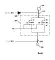
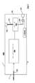
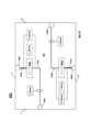
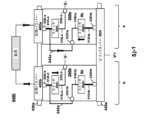
図1aは、バッテリからの直流電力を電動機で使用するための三相交流電力に変換するために使用することができる三相インバータ100の関連構成要素を示す。各位相には、ローサイドスイッチに接続されたハイサイドスイッチが含まれる。各ハイサイドスイッチは、ダイオードDHxと並列に接続された絶縁ゲートバイポーラトランジスタ(IGBT)のTHxを含み、各ローサイドスイッチは、ダイオードDLxと並列に接続されたIGBTのTLxを含む。Figure 1a shows the relevant components of a three-
ハイサイドIGBTのTH1~TH3は、それぞれ、ノードN1~N3を介して、ローサイドIGBTのTL1~TL3と直列に接続され、ノードN1~N3は、誘導素子Wa~Wcのそれぞれの端子に接続される。説明の便宜上、誘導素子Wa~Wcは、電気自動車(EV)の同期電動機または非同期電動機の固定子巻線の形態をとる。The high-side IGBTs TH1 to TH3 are connected in series with the low-side IGBTs TL1 to TL3 via nodes N1 to N3, respectively, and the nodes N1 to N3 are connected to the respective terminals of the inductive elements Wa to Wc. For ease of explanation, the inductive elements Wa to Wc take the form of stator windings of a synchronous or asynchronous motor of an electric vehicle (EV).
TH1~TH3のコレクタとDH1~DH3のカソードは互いに接続され、かつV+入力端子に接続されており、TL1~TL3のエミッタとダイオードDL1~DL3のアノードは互いに接続され、かつV-入力端子に接続される。直流電圧Vdcは、バッテリまたはその他の直流電源からV+入力端子とV-入力端子の間で受信される。The collectors of TH1 to TH3 and the cathodes of DH1 to DH3 are connected together and to the V+ input terminal, and the emitters of TL1 to TL3 and the anodes of diodes DL1 to DL3 are connected together and to the V- input terminal. A DC voltage Vdc is received between the V+ and V- input terminals from a battery or other DC power source.
ハイサイドIGBTのTH1~TH3およびローサイドIGBTのTL1~TL3は、それぞれゲートドライバH101~H103およびL101~L103を介してマイクロコントローラ110によって制御される。ゲートドライバは、デバイス(例えば、マイクロコントローラ)から低電力入力信号を受信して、パワートランジスタを起動するために必要な対応する高電力出力信号を生成する回路である。The high-side IGBTs TH1-TH3 and the low-side IGBTs TL1-TL3 are controlled by the
IGBTの制御は比較的簡単である。ハイサイドゲートドライバH101~H103およびローサイドゲートドライバL101~L103は、マイクロコントローラ110からドライバ制御信号(例えば、パルス幅変調信号PWM-H1~PWM-H3およびPWM-L1~PWM-L3)を受信する。ハイサイドゲートドライバH101~H103は、PWM-H1~PWM-H3信号がそれぞれアサートされたときに、高電力ゲート制御信号VgH1~VgH3をそれぞれアサートすることによって、ハイサイドIGBTのTH1~TH3をそれぞれ起動する。ローサイドゲートドライバL101~L103は、PWM-L1~PWM-L3信号がそれぞれアサートされたときに、高電力ゲート制御信号VgL1~VgL3をそれぞれアサートすることによって、ローサイドIGBTのTL1~TL3をそれぞれ起動する。IGBTのTH1~TH3およびTL1~TL3のそれぞれは、起動されると、接続した固定子巻線Wに、または接続した固定子巻線Wから、電流を伝達する。Control of the IGBTs is relatively simple. The high-side gate drivers H101-H103 and the low-side gate drivers L101-L103 receive driver control signals (e.g., pulse-width modulated signals PWM-H1-PWM-H3 and PWM-L1-PWM-L3) from the
ハイサイドIGBTとローサイドIGBTを協調して起動することにより、固定子巻線に流れる電流の方向を連続的かつ規則的に切り替えて、電流を巻線に流入または巻線から流出させることができる。図1bは、ゲート制御信号VgH1~VgH3およびVgL1~VgL3の例示的なタイミング図を示す。このタイミング図は、インバータ制御の基本的な理解を容易にするためにのみ提供される。実際には、より複雑なタイミングパターンがインバータの制御に使用される。By activating the high-side and low-side IGBTs in a coordinated manner, the direction of current through the stator winding can be switched continuously and regularly to allow current to flow into or out of the winding. Figure 1b shows an example timing diagram of the gate control signals VgH1-VgH3 and VgL1-VgL3. This timing diagram is provided only to facilitate a basic understanding of inverter control. In practice, more complex timing patterns are used to control the inverter.
マイクロコントローラ110は、それぞれPWM-H1~PWM-H3信号およびPWM-L1~PWM-L3信号を介してハイサイドIGBTのTH1~TH3およびローサイドIGBTのTL1~TL3を制御する。マイクロコントローラ110などのマイクロコントローラ、およびその他の同様のデータ処理デバイスには、中央処理ユニット(CPU)、CPU実行可能命令を格納するメモリ、並びにタイマーおよび入出力(I/O)ポートなどの周辺回路が含まれてもよい。マイクロコントローラ110は、メモリに格納されたCPU実行可能命令に基づいて、PWM-H1~PWM-H3信号およびPWM-L1~PWM-L3信号を生成する。ゲートドライバH101~H103は、PWM-H1~PWM-H3信号に基づいてVgH1~VgH3信号を生成し、ゲートドライバL101~L103は、PWM-L1~PWM-L3信号に基づいてVgL1~VgL3信号を生成する。マイクロコントローラ110は、メモリに格納された命令に従って、パルス幅変調(PWM)信号のデューティサイクルおよび/または周期を調整することができる。
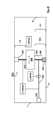
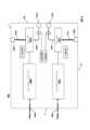
図1cは、配電網からの三相交流電力をEVバッテリ充電用の直流電力に変換するために使用することができる三相整流器150の関連構成要素を示す。インバータ100と整流器150は実質的に類似している。インバータ100と同様に、整流器150の各位相には、ローサイドスイッチに接続されたハイサイドスイッチが含まれる。各ハイサイドスイッチはダイオードDHxと並列に接続されたIGBTのTHxを含み、各ローサイドスイッチはダイオードDLxと並列に接続されたIGBTのTLxを含む。ハイサイドIGBTのTH1~TH3は、それぞれ、ノードN1~N3を介してローサイドIGBTのTL1~TL3と直列に接続され、ノードN1~N3はそれぞれ、誘導素子La~Lcのそれぞれの端子に接続される。説明の便宜上、誘導素子La~Lcは、LCLフィルタ162のインダクタの形態をとり、LCLフィルタ162は、三相交流電源164に結合される。1c shows the relevant components of a three-
TH1~TH3のコレクタとDH1~DH3のカソードは互いに接続しており、かつV+出力端子に接続され、TL1~TL3のエミッタとダイオードDL1~DL3のアノードは互いに接続しており、かつV-出力端子に接続される。The collectors of TH1 to TH3 and the cathodes of DH1 to DH3 are connected to each other and to the V+ output terminal, and the emitters of TL1 to TL3 and the anodes of diodes DL1 to DL3 are connected to each other and to the V- output terminal.
ハイサイドIGBTのTH1~TH3およびローサイドIGBTのTL1~TL3は、それぞれゲートドライバH101~H103およびL101~L103を介して整流器コントローラ160によって制御される。ハイサイドIGBTとローサイドIGBTを協調して起動することにより、整流器150は整流された直流電圧Vrdcを出力端子V+と出力端子V-に供給し、これらの出力端子は絶縁型DC/DCコンバータまたは本開示の1つ以上の態様を採用し得るその他のデバイスに接続することができる。図示しないが、出力端子V+と出力端子V-の間にフィルタを接続し、Vrdcが絶縁型DC/DCコンバータなどのその他のデバイスに供給される前にVrdcを平滑化することができる。The high-side IGBTs TH1-TH3 and the low-side IGBTs TL1-TL3 are controlled by the
インバータ100と整流器150は類似しているが、少なくとも1つの違いが存在する。整流器150は、ハイサイドIGBTのTH1~TH3およびローサイドIGBTのTL-1~TL-3の制御を、電源164によって提供される三相交流入力電力の周波数(例えば、60ヘルツ)に同期させるための位相同期回路(PLL)およびその他の構成要素を含み得るコントローラ160を含む。コントローラ160はまた、CPUと、インバータ100のマイクロコントローラ110のメモリに格納されたCPU実行可能命令とは実質的に異なり得るCPU実行可能命令を格納するメモリとを含んでもよい。マイクロコントローラ110と同様に、コントローラ160は、PWM-H1~PWM-H3信号およびPWM-L1~PWM-L3信号を生成する。ゲートドライバH101~H103は、PWM-H1~PWM-H3信号に基づいてVgH1~VgH3信号を生成し、ゲートドライバL101~L103は、PWM-L1~PWM-L3信号に基づいてVgL1~VgL3信号を生成する。コントローラ160は、PWM信号のデューティサイクルおよび/または周期を調整することができる。While
EV、DC急速充電ステーション、産業用機械(例えば、産業用ポンプ、ファン、コンプレッサなど)の可変周波数ドライブコントローラ、電動垂直離着陸(eVTOL)航空機などは、大型で重い電力変換器を採用している。電力密度(つまり、電力/体積)が高く、より小型で軽量な電力変換器が求められている。例えば、米国エネルギー省が一部公表した2017年10月の「Electrical and Electronics Technical Team (EETT) Roadmap」では、EV用インバータの2025年の電力密度の目標として100kW/Lが設定されている。2017年のEETT Roadmapには、「2025年のEETT研究開発目標を達成するためには、2015年のEETT研究開発技術目標と比較して電力密度を800%以上、および現在の路上技術と比較して450%、向上させる必要がある」と記載されている。EVs, DC fast charging stations, variable frequency drive controllers for industrial machines (e.g., industrial pumps, fans, compressors, etc.), electric vertical take-off and landing (eVTOL) aircraft, etc. employ large and heavy power converters. Smaller and lighter power converters with higher power density (i.e., power/volume) are required. For example, the U.S. Department of Energy's "Electrical and Electronics Technical Team (EETT) Roadmap" of October 2017 sets a power density target of 100 kW/L for EV inverters in 2025. The EETT Roadmap of 2017 states that "To achieve the EETT R&D goals in 2025, power density must be improved by more than 800% compared to the EETT R&D goals in 2015 and by 450% compared to current on-road technology."
「小型インバータ」および「小型整流器」を含む「小型変換器」を開示する。本開示は、主に小型インバータおよび小型整流器を参照して説明するが、本開示は、「小型DC/DCコンバータ」または「小型AC/ACコンバータ」などのその他のタイプの小型電力変換器に適用を見出すことができることが理解されよう。開示された小型インバータの電力密度は、上述の2017年EETT Roadmapに規定される100kW/Lの電力密度の目標を満たす、もしくはそれを超えるものである。Disclosed are "miniaturized converters" including "miniaturized inverters" and "miniaturized rectifiers." While the disclosure is described primarily with reference to miniaturized inverters and miniaturized rectifiers, it will be understood that the disclosure may find application to other types of miniaturized power converters, such as "miniaturized DC/DC converters" or "miniaturized AC/AC converters." The power density of the disclosed miniaturized inverters meets or exceeds the 100 kW/L power density target set forth in the 2017 EETT Roadmap mentioned above.
「スイッチモジュール」を開示する。スイッチモジュールには「パワースタック」が含まれる。パワースタックには、「ダイ基板」および「ダイクリップ」と呼ばれる金属導体に電気的および熱的に接続してそれらの間に挟まれた「スイッチ」が含まれる場合がある。スイッチには、1つ、2つ、またはそれ以上のパワートランジスタが含まれる。A "switch module" is disclosed. The switch module includes a "power stack." The power stack may include a "switch" sandwiched between and electrically and thermally connected to a metal conductor called a "die substrate" and a "die clip." The switch may include one, two, or more power transistors.
スイッチモジュールには、「スイッチコントローラ」も含まれる場合がある。スイッチコントローラは、それぞれのスイッチを制御する(すなわち、スイッチを起動または解除する)。起動されると、スイッチは2つの電流端子間で電流を伝達する。スイッチコントローラは、故障状態(例えば、電流端子間の電気的ショート)についてスイッチを監視するなどの、その他の機能を実行してもよい。スイッチモジュールは、抵抗器、コンデンサ、ダイオード、電流センサ回路、温度センサ回路、電圧センサ回路、電圧レギュレータなどの1つ以上の追加の構成要素を含むこともある。The switch module may also include a "switch controller." The switch controller controls the respective switch (i.e., activates or deactivates the switch). When activated, the switch transmits current between two current terminals. The switch controller may perform other functions, such as monitoring the switch for fault conditions (e.g., an electrical short between the current terminals). The switch module may also include one or more additional components, such as resistors, capacitors, diodes, current sensor circuits, temperature sensor circuits, voltage sensor circuits, voltage regulators, etc.
「パッケージ式スイッチモジュール」を開示する。パッケージ式スイッチモジュールは、1つ以上のスイッチモジュールを含んでもよい。パッケージ式スイッチモジュールは、本開示の小型インバータおよび小型整流器に使用することができるが、パッケージ式スイッチモジュールは、小型DC/DCコンバータまたは小型AC/ACコンバータなど、その他の様々な用途に使用できることが理解されよう。A "packaged switch module" is disclosed. The packaged switch module may include one or more switch modules. The packaged switch module may be used in the compact inverters and compact rectifiers of the present disclosure, but it will be understood that the packaged switch module may be used in a variety of other applications, such as a compact DC/DC converter or a compact AC/AC converter.
スイッチモジュールを1つだけ含むパッケージ式スイッチモジュールは、「パッケージ式スイッチ」と呼ばれる。A packaged switch module that contains only one switch module is called a "packaged switch."
2つのスイッチモジュールを含むパッケージ式スイッチモジュールは、「パッケージ式ハーフブリッジ」と呼ばれる。パッケージ式ハーフブリッジの内部では、スイッチが電気的に接続されている場合と接続されていない場合とがある。A packaged switch module that contains two switch modules is called a "packaged half-bridge." Inside a packaged half-bridge, the switches may or may not be electrically connected.
パッケージ式スイッチおよびパッケージ式ハーフブリッジPackaged switches and packaged half-bridges
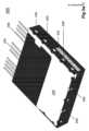
パッケージ式スイッチおよびパッケージ式ハーフブリッジは、基本的に6つの側(上面、底面、前面、背面、左側面、右側面)を有する立方体形状とすることができる。パッケージ式スイッチの中には、TO-247パッケージ式などの業界標準パッケージ式の態様に準拠するものもある。Packaged switches and packaged half-bridges can essentially be cube-shaped with six sides (top, bottom, front, back, left side, right side). Some packaged switches conform to industry standard packaging aspects such as TO-247 packaging.
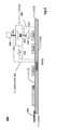
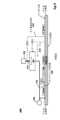
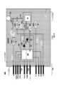
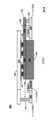
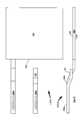
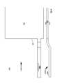
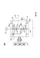
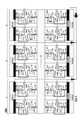
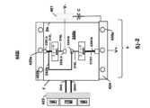
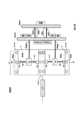
図2a-1および2a-2は、例示的なパッケージ式スイッチ200の等角投影図および逆等角投影図である。図2b-1および2b-2は、例示的なパッケージ式ハーフブリッジ250の等角投影図および逆等角投影図である。図2c-1および2c-2は、例示的なパッケージ式スイッチ211の等角投影図および逆等角投影図である。図2d-1および2d-2は、例示的なパッケージ式スイッチ247sの等角投影図および逆等角投影図である。図2e-1および2e-2は、例示的なパッケージ式スイッチ247dの等角投影図および逆等角投影図である。パッケージ式スイッチ247sおよび247dは、TO-247パッケージ式規格の1つ以上の態様に適合し得る例である。FIGS. 2a-1 and 2a-2 are isometric and reverse isometric views of an exemplary packaged
ケースCase
パッケージ式スイッチとパッケージ式ハーフブリッジはケースを有してもよい。図2a-1および2a-2は、例示的なケース202を有するパッケージ式スイッチ200を示す。図2b-1および2b-2は、例示的なケース252を有するパッケージ式ハーフブリッジ250を示す。図2c-1および2c-2は、例示的なケース238を有するパッケージ式スイッチ211を示す。図2d-1および2d-2は、例示的なケース248sを有するパッケージ式スイッチ247sを示す。図2e-1および2e-2は、例示的なケース248dを有するパッケージ式スイッチ247dを示す。The packaged switch and packaged half-bridge may have a case. Figures 2a-1 and 2a-2 show a packaged
ケースは、パワースタックなどのスイッチモジュールの構成要素を隔離、保護、および/または支持する。ケースはガラス、プラスチック、セラミックなどで作成することができる。説明の便宜上、ケースはエポキシ樹脂のようなモールドコンパウンドなどのプラスチック製であると仮定する。最近のモールドコンパウンドは、20種類もの原料を含む複雑な配合に進化している。モールドコンパウンドの熱伝導性を高めるために、アルミナなどの充填材を加えることができ、その結果、パワースタックまたはゲートドライバを含むスイッチモジュールの構成要素の冷却に役立つことがある。ケースは、トランスファー成形を含むさまざまなタイプのパッケージング技術のいずれかを使用して形成することができる。The case isolates, protects, and/or supports the components of the switch module, such as the power stack. The case can be made of glass, plastic, ceramic, etc. For ease of explanation, we will assume that the case is made of plastic, such as a molding compound like epoxy resin. Modern molding compounds have evolved into complex formulations containing as many as 20 different ingredients. Fillers such as alumina can be added to increase the thermal conductivity of the molding compound, which may then aid in cooling the components of the switch module, including the power stack or gate drivers. The case can be formed using any of a variety of types of packaging techniques, including transfer molding.
パッケージ式スイッチおよびパッケージ式ハーフブリッジは、小さなフォームファクタを有することができる。例えば、パッケージ式スイッチ200またはパッケージ式スイッチ211のケースの測定サイズは25×25×6mm、パッケージ式スイッチ247sおよび247dのケースの測定サイズは16×21×5mm、およびパッケージ式ハーフブリッジ250のケースの測定サイズは25×25×12mmとすることができる。本開示の多くのパッケージ式スイッチのケースのサイズ(例えば、25×25×6mm)および形状(例えば、立方体)は、実質的に類似していてもよい。同様に、本開示の多くのパッケージ式ハーフブリッジのケースのサイズ(例えば、25×25×12mm)および形状(例えば、立方体)は、実質的に類似していてもよい。図2a-1~図2e-2は、実質的に立方体形状であるケースを示す。図に示す形状以外の形状の方が、トランスファー成形に適している場合もある。例示したケースの外面は、ほとんどの実施形態において実質的に平坦である。パッケージ式スイッチまたはパッケージ式ハーフブリッジのサイズまたは形状は、本開示に図示されたものまたは記載されたものに限定されるべきではない。The packaged switches and packaged half bridges can have small form factors. For example, the case of packaged
スイッチモジュールSwitch module
トレースおよびリードTrace and lead
スイッチモジュールには、トレースおよび/またはリードが含まれる。トレースとリードは、2箇所を電気的に接続する、ある長さの金属で構成される導体である。トレースは平坦な表面を持ち、一般には、リジッドプリント回路基板(PCB)、フレキシブルPCB、ダイレクトボンド銅(DBC)基板などに形成される。リードは通常、トレースよりも薄い。リードは、トレース、ダイクリップ、ダイ基板などに取り付ける(例えば、はんだ付けする)ことができる。リードは、円筒形の「ピン」であることもあれば、正方形または矩形の断面を有することもできる。説明の便宜上、リードは正方形または矩形の断面を有する。リードは薄い金属板から機械加工することができる。The switch module includes traces and/or leads. Traces and leads are lengths of conductors of metal that electrically connect two points. Traces have flat surfaces and are typically formed on rigid printed circuit boards (PCBs), flexible PCBs, direct bond copper (DBC) boards, etc. Leads are typically thinner than traces. Leads may be attached (e.g., soldered) to traces, die clips, die substrates, etc. Leads may be cylindrical "pins" or may have a square or rectangular cross section. For purposes of illustration, leads have a square or rectangular cross section. Leads may be machined from a thin metal sheet.
DBC基板はセラミックタイル(一般にはアルミナ)で構成することができ、その両面に銅のシートが高温酸化プロセスによって接着される(銅と基板は、酸素を約30ppm含む窒素の雰囲気中で、注意深く制御された温度まで加熱することが可能であり、この条件下では、銅と酸素の共晶が形成されて、これが基板として使われる銅と酸化物の両方とうまく結合する)。上部の銅層は焼成前に事前に形成するか、またはPCB技術を使用して化学的にエッチングしてトレースを形成することが可能であるが、下部の銅層は通常は平面のままである。DBCは、スイッチモジュールに採用された場合、リジッドPCBよりも熱的に有利になる場合がある。例えば、スイッチコントローラによって発生した熱は、コントローラが搭載されたDBCを通して放散させることができる。The DBC substrate can consist of a ceramic tile (typically alumina) to which copper sheets are bonded on both sides by a high temperature oxidation process (the copper and substrate can be heated to a carefully controlled temperature in a nitrogen atmosphere containing about 30 ppm oxygen, under which a copper-oxygen eutectic forms that bonds well with both the copper and the oxide used as the substrate). The top copper layer can be preformed before firing or chemically etched using PCB techniques to form traces, while the bottom copper layer typically remains flat. DBCs, when employed in switch modules, can have thermal advantages over rigid PCBs. For example, heat generated by a switch controller can be dissipated through the DBC on which it is mounted.
PCBは、非導電性基板のシート層上および/またはシート層間に積層された金属の1つ以上の薄いシート層からエッチングすることができる平坦な導電性トレースを有する。非導電性基板層を通って延在する金属ビアは、異なるレベルでトレースを電気的に接続することができる。スイッチモジュールは、リジッドPCBを含んでもよいが、スイッチモジュールは、DBC基板またはその他の類似のデバイスで作成することができることが理解されよう。図2a-1~図2e-2には図示しないが、パッケージ式スイッチ200および211、ならびにパッケージ式ハーフブリッジ250は、スイッチモジュールの構成要素が搭載される1つ以上のリジッドPCBを含むが、代替的な実施形態においてDBCを使用できることが理解されよう。パッケージ式スイッチ247sおよび247dには、PCBまたはDBC基板がない。The PCB has flat conductive traces that may be etched from one or more thin sheet layers of metal laminated on and/or between sheet layers of a non-conductive substrate. Metal vias extending through the non-conductive substrate layers may electrically connect traces at different levels. The switch module may include a rigid PCB, although it will be understood that the switch module may be made with a DBC substrate or other similar device. Although not shown in Figures 2a-1-2e-2, the packaged
PCBのトレースは、信号(例えば、PWM信号、ゲート制御信号、シリアルペリフェラルインターフェース(SPI)信号など)または電圧(例えば、直流電源電圧)を伝達することができる。例えば、PCBのトレースは、スイッチモジュールの内部構成要素間(例えば、スイッチコントローラとスイッチ間)の電気接続、または内部構成要素(例えば、スイッチコントローラ)とスイッチモジュールの外部構成要素(例えば、マイクロコントローラ)と間の電気接続において、信号または電圧を伝達してもよい。The PCB traces may carry signals (e.g., PWM signals, gate control signals, Serial Peripheral Interface (SPI) signals, etc.) or voltages (e.g., DC power supply voltages). For example, the PCB traces may carry signals or voltages in electrical connections between internal components of the switch module (e.g., between a switch controller and a switch) or between an internal component (e.g., a switch controller) and an external component (e.g., a microcontroller) of the switch module.
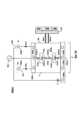
リードは信号または電源電圧を伝達することができる。図2a-1、2b-1、および2c-1に図示された例示的なパッケージ式スイッチおよびパッケージ式ハーフブリッジの各々は、リジッドPCBまたはDBC(図示せず)のそれぞれのトレースに取り付けられた(例えば、はんだ付けされた)端部を有する少なくとも1セットの「コネクタリード」(例えば、コネクタリード204および206)を有する。これらのコネクタリードは、図示のように、ケース202、252、238から横方向に延在する。これらのコネクタリードは、パッケージ式スイッチまたはパッケージ式ハーフブリッジの外部にある「コネクタ」の一部であってもよい。コネクタは、マイクロコントローラ、ゲートドライバ、および/またはその他の構成要素を含むことがある外部PCBに取り付けることができる。図2d-1および図2e-1に示す例示的なパッケージ式スイッチの各々は、3つのコネクタリード288のセットを有する。これらのコネクタリードは、図示のようにケース248sおよび248dから横方向に延在する。これらのコネクタリードは、パッケージ式スイッチの外部にあるコネクタの一部であってもよい。コネクタは、ゲートドライバ、電圧レギュレータおよび/またはその他の構成要素を含むことがある外部PCBに取り付けることができる。The leads can carry signals or power voltages. Each of the exemplary packaged switches and packaged half-bridges illustrated in FIGS. 2a-1, 2b-1, and 2c-1 has at least one set of "connector leads" (e.g., connector leads 204 and 206) that have ends attached (e.g., soldered) to respective traces on a rigid PCB or DBC (not shown). These connector leads extend laterally from the
コネクタリードは、スイッチモジュール内部の構成要素とスイッチモジュール外部の構成要素との間の電気接続において、電流、信号、または電圧を伝達することができる。たとえば、図2a-2のコネクタリード204は、制御PCB上のマイクロコントローラとパッケージ式スイッチ200内部の構成要素(たとえば、スイッチコントローラ)との間の電気接続において、低電力PWM信号を伝達することができ、一方で、コネクタリード206は、制御PCB上の電力管理集積回路(PMIC)とパッケージ式スイッチ200の内部の同一の内部構成要素または異なる構成要素との間の電気接続において、電源電圧を伝達することができる。パッケージ式ハーフブリッジ250(図2b-1~図2b-3)は、同様のコネクタリード204L、204H、206L、および206Hを有する。図2d-1および図2e-1は、コネクタリード288g、288s、および288dを示す。図2d-1および図2e-1には図示しないが、コネクタリード288g、288s、および288dは、それぞれ、パッケージ式スイッチ247sおよび247dの内部のスイッチの1つ以上のゲート、1つ以上の第1電流端子、および1つ以上の第2電流端子に電気的に接続される。コネクタリード288dおよび288sは、かなりの電流(例えば、400A)を伝達することができる。コネクタリード288は、図2d-1および図2e-1では同一平面上にある。代替的な実施形態において、1つ以上のコネクタリード288が異なる平面に含まれていてもよい。The connector leads can carry current, signals, or voltages in electrical connections between components internal to the switch module and components external to the switch module. For example,
パッケージ式スイッチおよびパッケージ式ハーフブリッジは、スイッチモジュールの構成要素(例えば、ゲートドライバとスイッチ)間の接続において信号(例えば、ゲート制御信号)または電圧を伝達する追加のリードまたは導体(例えば、ボンドワイヤ)を含んでもよい。例えば、スイッチモジュールは、ゲートドライバとスイッチ間の接続においてゲート信号を伝達する屈曲リードを含んでもよい。別の実施形態において、ゲートドライバとスイッチ間の接続においてゲート信号を伝達するために、フレキシブルPCBを使用することができる。Packaged switches and packaged half-bridges may include additional leads or conductors (e.g., bond wires) that carry signals (e.g., gate control signals) or voltages in the connections between the components of the switch module (e.g., the gate driver and the switch). For example, the switch module may include flex leads that carry gate signals in the connections between the gate driver and the switch. In another embodiment, a flexible PCB can be used to carry the gate signals in the connections between the gate driver and the switch.
パワースタックPower stack
スイッチモジュールにはパワースタックが含まれ、各パワースタックはダイ基板と呼ばれる第1金属導体とダイクリップと呼ばれる第2金属導体との間に取り付けられたスイッチを含む。ダイ基板とダイクリップについては、以下で詳しく説明する。説明の便宜上、スイッチモジュールはパワースタックを1つだけ有する。The switch module includes power stacks, each of which includes a switch mounted between a first metal conductor, called the die substrate, and a second metal conductor, called the die clip. The die substrate and die clip are described in more detail below. For ease of explanation, the switch module has only one power stack.
スイッチには、1つ以上のパワートランジスタ(たとえば、IGBT、金属酸化膜電界効果トランジスタ(MOSFET)など)が含まれる。パワートランジスタは、トランジスタが起動されたときに電流が流れる2つの電流端子(IGBTではコレクタとエミッタ、MOSFETではソースとドレインなど)と、制御端子またはゲート端子とを有する。ある実施形態において、スイッチ内の複数のパワートランジスタを並列に接続して、それらのゲートで共通の信号によって制御してもよく、あるいは別の実施形態において、スイッチ内の並列接続したパワートランジスタのゲートを独立した信号によって制御してもよい。The switch includes one or more power transistors (e.g., IGBTs, metal oxide field effect transistors (MOSFETs), etc.). A power transistor has two current terminals through which current flows when the transistor is activated (e.g., collector and emitter for an IGBT, source and drain for a MOSFET), and a control or gate terminal. In some embodiments, multiple power transistors in a switch may be connected in parallel and controlled at their gates by a common signal, or in other embodiments, the gates of parallel-connected power transistors in a switch may be controlled by independent signals.
パワートランジスタまたはパワーダイオードは、本開示の一実施形態において、垂直構造の半導体ダイである。これらのパワートランジスタのダイは、ダイの底面に実質的に平坦な第1電流端子(例えば、ドレインまたはエミッタ)を有し、ダイの上面に実質的に平坦な第2電流端子(例えば、ソースまたはコレクタ)および実質的に平坦なゲート端子を有するトレンチ状の構造を有する。これらの上面と底面は反対方向を向いている。垂直構造のパワーダイオードのカソードとアノードも同様に、ダイの反対向きの上面と底面に構成することができる。In one embodiment of the present disclosure, the power transistor or power diode is a vertically structured semiconductor die. These power transistor dies have a trench-like structure with a substantially planar first current terminal (e.g., drain or emitter) on the bottom surface of the die, a substantially planar second current terminal (e.g., source or collector) and a substantially planar gate terminal on the top surface of the die. The top and bottom surfaces face in opposite directions. The cathode and anode of a vertically structured power diode can be similarly configured on the opposite top and bottom surfaces of the die.
スイッチは、スイッチ内のパワートランジスタのサイズ(例えば、ゲートの幅および長さ)、タイプ(例えば、MOSFET)、半導体材料(例えば、GaN)、および個数(例えば、6個)に応じて、故障することなく高レベルの電流を伝達することができる。パワートランジスタは、高いスイッチング速度(例えば、SiのIGBTでは最大100kHz、SiCのMOSFETでは最大500kHz、GaNのMOSFETでは最大1.0GHzなど)で高レベルの電流を伝達することができる。パワートランジスタは、ヒートシンクまたはヒートシンクとしても機能するバスバーに熱的に接続および冷却されると、故障することなくより高いスイッチング速度でより大量の電流を伝達することができる。The switch can carry high levels of current without failure, depending on the size (e.g., gate width and length), type (e.g., MOSFET), semiconductor material (e.g., GaN), and number (e.g., six) of power transistors in the switch. The power transistors can carry high levels of current at high switching speeds (e.g., up to 100 kHz for Si IGBTs, up to 500 kHz for SiC MOSFETs, up to 1.0 GHz for GaN MOSFETs, etc.). When thermally connected and cooled by a heat sink or a bus bar that also acts as a heat sink, the power transistors can carry larger amounts of current at higher switching speeds without failure.
ダイ基板およびダイクリップDie substrates and die clips
スイッチは、ダイ基板とダイクリップの間に挟まれる。各スイッチトランジスタの第1電流端子(例えば、コレクタまたはドレイン)および第2電流端子(例えば、エミッタまたはソース)は、それぞれダイ基板およびダイクリップに接続(例えば、焼結、はんだ付け、ろう付けなど)される。スイッチ内の各トランジスタのゲートは、スイッチコントローラからの信号によって制御することができる。信号は、ワイヤ、リボン、リード、トレースなど、またはそれらの直列接続した組み合わせを含む電気接続によってゲートに伝達することができる。The switch is sandwiched between a die substrate and a die clip. A first current terminal (e.g., collector or drain) and a second current terminal (e.g., emitter or source) of each switch transistor are connected (e.g., sintered, soldered, brazed, etc.) to the die substrate and die clip, respectively. A gate of each transistor in the switch can be controlled by a signal from a switch controller. The signal can be conveyed to the gate by an electrical connection including a wire, ribbon, lead, trace, etc., or a series-connected combination thereof.
ダイ基板またはダイクリップは、熱伝導率が高く電気抵抗が低い層状または複合材料のシートから機械加工またはスタンピングすることができる。該シートは、銅(Cu)とモリブデン(Mo)の交互の層で構成してもよい。例えば、モリブデンの層を銅の層で挟んでもよい。銅の外層は熱伝導率が高く、効率よく熱を拡散する性質がある。銅層の間に挿入されたモリブデンの層は、シートの熱膨張係数を向上させることができる。シートは、外層(例えば、銅の外層(単数または複数))上に形成されたニッケルの層を含んでもよい。さらに、ニッケルの外層(単数または複数)上に追加の(例えば、明るい銀または鈍い(すなわち、艶消し)銀)層を形成(例えば、めっき)してもよい。追加的な(例えば艶消し銀)材料を含む層の表面に、スイッチなどのデバイスを取り付ける(例えば焼結する)ことができる。例えば、銀または銅の焼結ペースト、フィルム、またはプリフォームなどを用いて、層状または複合材料のシートにスイッチを焼結することができる。モリブデンと銅が交互配置された薄く平坦な例示的な層の厚さは、取り付けられた(例えば、焼結された)ときのデバイスとの電気的、熱的、および/または機械的接続を強化するように選択することができる。電気伝導性、熱伝導性、および熱膨張係数を変えた複合材料(銅とモリブデン、銅とタングステン、銅とダイヤモンドなどの混合物)のシートもまた、ダイ基板およびダイクリップを形成するために使用することができる。ダイ基板またはダイクリップは、2つの導電性および熱伝導性のワークピースを接合(例えば、焼結、はんだ付け、ろう付けなど)することによって形成することができる。ダイ基板またはダイクリップは、さらに別の実施形態において、金属または複合材料の3D印刷を使用して形成することができる。本開示のダイ基板およびダイクリップは、誘電体要素が存在しないものであるべきである。The die substrate or die clip can be machined or stamped from a sheet of layered or composite material with high thermal conductivity and low electrical resistance. The sheet can be composed of alternating layers of copper (Cu) and molybdenum (Mo). For example, a layer of molybdenum can be sandwiched between layers of copper. The copper outer layer has high thermal conductivity and efficiently spreads heat. A layer of molybdenum inserted between the copper layers can improve the thermal expansion coefficient of the sheet. The sheet can include a layer of nickel formed on the outer layer (e.g., the copper outer layer(s)). In addition, an additional (e.g., bright silver or dull (i.e., matte) silver) layer can be formed (e.g., plated) on the nickel outer layer(s). A device such as a switch can be attached (e.g., sintered) to the surface of the layer containing the additional (e.g., matte silver) material. For example, a switch can be sintered to the sheet of layered or composite material using a silver or copper sintering paste, film, or preform. The thickness of the exemplary thin, flat interleaved layers of molybdenum and copper can be selected to enhance electrical, thermal, and/or mechanical connection with the device when attached (e.g., sintered). Sheets of composite materials (mixtures of copper and molybdenum, copper and tungsten, copper and diamond, etc.) with altered electrical and thermal conductivity and thermal expansion coefficients can also be used to form the die substrate and die clip. The die substrate or die clip can be formed by joining (e.g., sintering, soldering, brazing, etc.) two electrically and thermally conductive workpieces. In yet another embodiment, the die substrate or die clip can be formed using 3D printing of metal or composite materials. The die substrate and die clip of the present disclosure should be free of dielectric elements.
ダイ基板およびダイクリップは、電流および/または熱を伝達することができる端子またはパッドを有する。ダイ基板は、パッケージ式スイッチまたはパッケージ式ハーフブリッジの内外に、相当な熱および電流を伝達できる少なくとも1つの端子を有する。ダイ基板は、相当な電流をパッケージ式スイッチまたはパッケージ式ハーフブリッジの内外に伝達することができる1つ以上のサイド端子を有してもよい。これらのサイド端子は、パッケージ式スイッチまたはパッケージ式ハーフブリッジからいくらかの熱を伝達することもあるが、主な目的は電流を伝達することである。The die substrate and die clip have terminals or pads capable of transferring current and/or heat. The die substrate has at least one terminal capable of transferring substantial heat and current into and out of the packaged switch or packaged half-bridge. The die substrate may have one or more side terminals capable of transferring substantial current into and out of the packaged switch or packaged half-bridge. These side terminals may also transfer some heat from the packaged switch or packaged half-bridge, but their primary purpose is to transfer current.
ダイクリップは、相当な電流が流れることができる端子を少なくとも1つ有する。ほとんどの場合、電流は該ダイクリップ端子を介してパッケージ式スイッチまたはパッケージ式ハーフブリッジの内外に伝達される。ダイクリップは、相当な熱がパッケージ式スイッチから伝達される追加の端子を有してもよい。さらにその他の実施形態において、ダイクリップはダイ基板と同様の構造を有し、相当な熱および電流をパッケージ式スイッチの内外に伝達することができる端子を含んでもよい。The die clip has at least one terminal through which a significant current can flow. In most cases, current is transferred in and out of the packaged switch or packaged half-bridge through the die clip terminal. The die clip may have additional terminals through which significant heat can be transferred from the packaged switch. In yet other embodiments, the die clip may have a structure similar to the die substrate and include terminals through which significant heat and current can be transferred in and out of the packaged switch.
ダイ基板端子、ダイ基板サイド端子、およびダイクリップ端子は、それらが含まれるパッケージ式スイッチまたはパッケージ式ハーフブリッジのケース表面と実質的に同一平面または共平面である実質的に平坦な表面を有してもよい。その他の実施形態において、ダイ基板端子、ダイ基板サイド端子、およびダイクリップ端子は、ケース表面と平行でケース表面より下に凹んだ平坦面を有していてもよく、あるいはケース表面と平行でケース表面よりも上に突出しているものであってもよい。いくつかのダイクリップ端子は、パッケージ式ハーフブリッジのケースから露出していなくてもよい。いくつかのダイ基板またはダイクリップ端子は、パッケージ式スイッチまたはパッケージ式ハーフブリッジのケース表面から垂直に延びるコネクタリード(例えば、図2d-1のコネクタリード288d)の形態をとってもよい。The die substrate terminals, die substrate side terminals, and die clip terminals may have substantially flat surfaces that are substantially flush or coplanar with the case surface of the packaged switch or packaged half bridge in which they are included. In other embodiments, the die substrate terminals, die substrate side terminals, and die clip terminals may have flat surfaces that are parallel to and recessed below the case surface, or parallel to and protruding above the case surface. Some die clip terminals may not be exposed from the case of the packaged half bridge. Some die substrate or die clip terminals may take the form of connector leads (e.g.,
図2a-1~図2e-2は、例示的なダイ基板端子230を示しており、相当な熱と相当な電流が、ダイ基板端子230を通して、それらが含まれるパッケージ式スイッチまたはパッケージ式ハーフブリッジの内外に伝達されることができる。FIGS. 2a-1 through 2e-2 show exemplary
図2a-1、図2a-2、図2b-1、図2b-2、図2c-1、および図2c-2は、例示的なダイクリップ端子232を示しており、相当な電流が、ダイクリップ端子232を通して、それらが含まれるパッケージ式スイッチまたはパッケージ式ハーフブリッジの内外に伝達されることができる。図2d-1は、例示的なダイクリップ端子(コネクタリード288d)を示しており、該ダイクリップ端子を通して、相当な電流がパッケージ式スイッチ247sの内外に伝達されることができる。図2c-2および図2e-2は、例示的なダイクリップ端子344を示しており、相当な熱および/または電流が、ダイクリップ端子344を通して、それらが含まれるパッケージ式スイッチから伝達されることができる。2a-1, 2a-2, 2b-1, 2b-2, 2c-1, and 2c-2 show exemplary
図2a-1、2b-1、および2c-1は、例示的なダイ基板サイド端子240を示す。一部の実施形態において、金属ストラップが、あるパワースタックのダイ基板を別のパワースタックのダイクリップに電気的に接続する。図2b-3は、ハイサイドダイクリップ端子232Hをローサイドダイ基板サイド端子240Lに電気的に接続する例示的な金属ストラップ242を示す。図2b-3は、金属ストラップ242がパッケージ式ハーフブリッジ250の外部にあることを示す。別の実施形態において、金属ストラップ242はパッケージ式ハーフブリッジの内部にあってもよい。Figures 2a-1, 2b-1, and 2c-1 show an exemplary die
ダイ基板端子、ダイ基板サイド端子、金属ストラップ、およびダイクリップ端子のサイズおよび形状は、図示されたものに限定されるべきではない。すなわち、金属ストラップおよび端子は、異なる形態、形状およびサイズを有してもよい。The sizes and shapes of the die substrate terminals, die substrate side terminals, metal straps, and die clip terminals should not be limited to those shown; that is, the metal straps and terminals may have different forms, shapes, and sizes.
図2a-1、図2c-1、図2d-1、および図2e-1は、それぞれ、パッケージ式スイッチ200、211、247s、および247dの実質的に平坦なケース表面と実質的に同一平面上にある矩形状の実質的に平坦な表面を有するダイ基板端子230を示す。図2a-1および図2c-1はまた、それぞれ、パッケージ式スイッチ200および211の実質的に平坦なケース表面と実質的に同一平面上にある実質的に平坦な表面を有するダイ基板サイド端子240を示す。図2a-1および図2c-1は、それぞれ、パッケージ式スイッチ200および211の実質的に平坦なケース表面と実質的に同一平面上にある、矩形状の実質的に平坦な表面を有するダイクリップ端子232を示す。図2a-1および図2c-1のパッケージ式スイッチの矩形状の実質的に平坦なダイクリップ端子232は、その背面から延在する矩形状の断面を有するコネクタリードと置き換えることができる。図2c-2および2e-2に示すように、パッケージ式スイッチ211および247dは、実質的に平坦な底部ケース表面と実質的に同一平面上にある矩形状の実質的に平坦な表面を有するダイクリップ端子344を有する。図2d-1および図2e-1は、パッケージ式スイッチ247sおよび247dのケースから横方向に延在する矩形状の断面を有するコネクタリードの形態をとるダイクリップ端子288dを示す。Figures 2a-1, 2c-1, 2d-1, and 2e-1 show die
図2b-1、図2b-2、および図2b-3は、パッケージ式ハーフブリッジ250の実質的に平坦なケース表面と実質的に同一平面上にある矩形状の実質的に平坦な表面を有するダイ基板端子230Lおよび230Hを示す。図2b-1、図2b-2、および図2b-3は、パッケージ式ハーフブリッジ250の実質的に平坦な表面と実質的に同一平面上にある矩形状の実質的に平坦なケースを有するダイクリップ端子232Lおよび232Hを示す。別の実施形態において、矩形状の実質的に平坦なダイクリップ端子232Lおよび232Hは、図2b-1、図2b-2および図2b-3のパッケージ式ハーフブリッジ250の背面から延在する矩形状の断面を有するコネクタリードと置き換えることができる。あるいは、図2b-2のパッケージ式ハーフブリッジの矩形状の実質的に平坦なダイクリップ端子232Lは、その背面から延びる矩形状の断面を有するコネクタリードに置き換えることもできる。図2b-1~図2b-3は、ハイサイドダイ基板のダイ基板サイド端子240Hとローサイドダイ基板のダイ基板サイド端子240Lを示しており、いずれもパッケージ式ハーフブリッジ250の実質的に平坦なケース表面と同一平面上にある実質的に平坦な表面を有する。2b-1, 2b-2, and 2b-3 show die
代替的な実施形態において、ダイ基板端子230、ダイクリップ端子232、ダイクリップ端子344、および/またはダイ基板サイド端子240の平坦面は、ケース202、211、または250などのケースの実質的に平坦な面を含む平面に平行であり、その上方または下方にある平面にあってもよい。In alternative embodiments, the planar surfaces of the
いくつかの実施形態において、電流は、ダイ基板端子を通ってパッケージ式スイッチまたはパッケージ式ハーフブリッジに入り、ダイクリップ端子を通って出ることができ、あるいは電流は、逆方向でパッケージ式スイッチまたはパッケージ式ハーフブリッジを通って流れることができる。説明すると、電流はダイ基板のダイ基板端子230を通ってパッケージ式スイッチ200、211、または247に入り、ダイ基板、起動されたスイッチ、およびダイクリップを通って流れ、ダイクリップのダイクリップ端子232、288d、または344を通ってパッケージ式スイッチ200、211、または247から出ることができ、あるいは電流は逆方向に流れることができる。電流は、ダイ基板のダイ基板サイド端子を通ってパッケージ式スイッチに入り、その後、同じダイ基板のダイ基板端子を通ってパッケージ式スイッチから出ることができ、あるいは電流は、パッケージ式スイッチを逆方向に流れることができる。例えば、電流は、ダイ基板のダイ基板サイド端子240を通ってパッケージ式スイッチ200または211に入り、ダイ基板を通って流れ、その後ダイ基板のダイ基板端子230を通ってパッケージ式スイッチ200または211から出ることができ、あるいは、電流は逆方向に流れることができる。In some embodiments, current can enter the packaged switch or packaged half-bridge through the die substrate terminal and exit through the die clip terminal, or current can flow through the packaged switch or packaged half-bridge in the reverse direction. Explained, current can enter the packaged
電流は、ハイサイドダイ基板のハイサイドダイ基板端子230Hを通って図2b-1のパッケージ式ハーフブリッジ250に入り、ハイサイドダイ基板、起動されたハイサイドスイッチ、およびハイサイドダイクリップを通って流れ、その後ハイサイドダイクリップのハイサイドダイクリップ端子232Hを通ってパッケージ式ハーフブリッジ250から出ることができ、あるいは電流は逆方向に流れることができる。電流は、ローサイドダイ基板のローサイドダイ基板端子230Lを通って図2b-2のパッケージ式ハーフブリッジ250に入り、ローサイドダイ基板、起動されたローサイドスイッチ、およびローサイドダイクリップを通って流れ、その後ローサイドダイクリップのローサイドダイクリップ端子232Lを通ってパッケージ式ハーフブリッジ250から出ることができ、あるいは電流は逆方向に流れることができる。図2b-3は金属ストラップ242を示す。電流は、ハイサイドダイ基板のハイサイドダイ基板端子230Hを通って図2b-3のパッケージ式ハーフブリッジ250に入り、ハイサイドダイ基板、起動されたハイサイドスイッチ、ハイサイドダイクリップ、ハイサイドダイクリップのハイサイドダイクリップ端子232H、ハイサイドダイクリップ端子232Hをローサイドダイ基板の1つ以上のローサイドダイ基板サイド端子240Lに電気的に接続する金属ストラップ242、該1つ以上のローサイドダイ基板サイド端子240L、およびローサイドダイ基板を通って流れ、その後ローサイドダイ基板のローサイドダイ基板端子230Lを通ってパッケージ式ハーフブリッジから出ることができ、あるいは電流は逆方向に流れることができる。Current can enter the packaged
ダイクリップ端子またはダイ基板端子は、外部のデバイス(例えば、金属ストラップ、位相バスバー、V+バスバー、V-バスバーなどであって、これらすべてについては以下でさらに詳しく説明する)の同様の形状の延長部と嵌合可能な1つ以上の凹部を含み、それらの間との電気的、熱的、および/または機械的接続を促進することができる。The die clip terminals or die substrate terminals may include one or more recesses that can mate with similarly shaped extensions of an external device (e.g., metal straps, phase busbars, V+ busbars, V- busbars, etc., all of which are described in more detail below) to facilitate electrical, thermal, and/or mechanical connections therebetween.
ダイ基板およびダイクリップは、それらが接続されたスイッチに、またはそれらが接続されたスイッチから、相当な電流および熱を伝達することができる。ダイ基板端子、ダイ基板サイド端子、およびダイクリップ端子は、相当な電流および/または熱を、パッケージ式スイッチまたはパッケージ式ハーフブリッジの内外に伝達することができる。例えば、ダイ基板は、V+バスバーなど、パッケージ式スイッチまたはパッケージ式ハーフブリッジの外部のデバイスに接続された、幅24mmおよび長さ11.2mmのダイ基板端子230を有することができる。このダイ基板は、接続されたスイッチと外部のデバイスとの間で400A以上の電流を伝達することができる。ダイクリップは、V-バスバーなど、パッケージ式スイッチまたはパッケージ式ハーフブリッジの外部のデバイスに接続することができる、幅6mmおよび長さ11mmのダイクリップ端子232を有することができる。このダイクリップは、接続されたスイッチと外部のデバイスとの間で400A以上の電流を伝達することができる。金属ストラップ(例えば、金属ストラップ242)は、ダイクリップとダイ基板との間に接続されると、400A以上の電流を伝達することができる。ダイクリップ端子288dは、400A以上の電流をパッケージ式スイッチの内外に伝達することができる。The die substrate and die clip can transfer significant current and heat to and from the switch to which they are connected. The die substrate terminals, die substrate side terminals, and die clip terminals can transfer significant current and/or heat into and out of the packaged switch or packaged half bridge. For example, the die substrate can have a
スイッチは、特に高いスイッチング速度で大電流を伝達する場合に、伝送損失とスイッチング損失により高温になることがある。ダイ基板は、その寸法によっては、そのダイ基板端子を通してパッケージ式スイッチまたはパッケージ式ハーフブリッジから大量の熱を伝達することができる。例えば、幅24mmおよび長さ11.2mmを有するダイ基板端子230は、ゼロから750W以上の熱を伝達することができる。言い換えれば、ダイ基板端子230は、10、20、50、100、300、750W、またはそれ以上の電力を伝達することができる。ダイ基板は厚くすることができ(例えば、ダイ基板端子とその接続されたスイッチの間で測定した場合、厚さ0.1mm~6.0mm)、厚ければ厚いほど、より大きな熱容量が得られるが、これは接続されたスイッチによって発生する熱の急激な増加を吸収するために重要である。ダイ基板は、その端子がヒートシンクまたはヒートシンクとしても機能するバスバーと熱的に接続される場合、パッケージ式スイッチまたはパッケージ式ハーフブリッジからより多くの熱を伝達することができる。Switches can get hot due to transmission and switching losses, especially when carrying large currents at high switching speeds. Depending on its dimensions, the die substrate can transfer a large amount of heat from the packaged switch or packaged half-bridge through its die substrate terminals. For example, a
ダイ基板と同様に、ダイクリップを厚くすることができ(例えば、スイッチに取り付けられた表面と反対向きの表面との間で測定した場合、0.1mm~8.0mmの厚さ)、厚ければ厚いほど、より大きな熱容量が得られる。上述の一実施形態において、ダイクリップは、パッケージ式スイッチの内外に電流を伝導するための第1端子と、パッケージ式スイッチの内外に熱および/または電流を伝導するための第2端子とを有してもよい。図2c-1および図2c-2のパッケージ式スイッチ211は、パッケージ式スイッチの内外に電流を伝導するためのダイクリップ端子232と、パッケージ式スイッチの内外に熱および/または電流を伝導するための第2端子344とを有する。図2e-1および図2e-2のパッケージ式スイッチ247dは、パッケージ式スイッチの内外に相当な電流および熱を伝導するためのダイクリップ端子344を有する。ダイ基板端子230の長さおよび幅と同様の長さおよび幅を有するパッケージ式スイッチ211および247dのダイクリップ端子344は、ゼロから750Wまたはそれ以上の熱を伝達することができる。言い換えれば、ダイクリップ端子344は、10、20、50、100、300、750Wまたはそれ以上の電力を伝達することができる。ダイクリップ端子344は、ヒートシンクまたはヒートシンクとしても機能するバスバーに熱的に接続された場合、パッケージ式スイッチからさらに大量の熱を伝達することができる。上述の別の実施形態において、ダイクリップは、高レベルの熱(例えば、10、20、50、100、300~750Wまたはそれ以上)および電流(例えば、400Aまたはそれ以上)を伝達するための単一の端子を有してもよい。該単一の端子は、ヒートシンクまたはヒートシンクとしても機能するバスバーに熱的に接続される場合、パッケージ式スイッチからさらに大量の熱を伝達することができる。Like the die substrate, the die clip can be thick (e.g., 0.1 mm to 8.0 mm thick, measured between the surface attached to the switch and the surface facing away from the switch), with the thicker die clip providing a greater thermal capacity. In one embodiment described above, the die clip may have a first terminal for conducting current into and out of the packaged switch and a second terminal for conducting heat and/or current into and out of the packaged switch. The packaged
図1aおよび図1cに戻ると、従来のインバータまたは整流器では、IGBTの電流端子との間で電流を伝達するために1本以上のボンドワイヤが使用されている。これらのボンドワイヤは、高速かつ大規模な温度サイクルを受けると故障しやすい。故障の原因は、ワイヤ自体またはワイヤと電流端子の間のボンド接続部における比較的高い電流密度と低い熱容量にある。温度サイクル中に、ワイヤまたはボンド接続部に亀裂または破断が生じることが多い。また、ボンドワイヤのリフトオフが発生することもある。一方、ダイクリップおよびダイ基板では電流密度は低く、熱容量は高い。スイッチ端子とダイクリップまたはダイ基板との間の接続部(例えば、焼結接合)では、電流密度が低くなる。その結果、故障が発生しにくくなる。ダイ基板およびダイクリップは、以下に説明するように、ボンドワイヤに比べて寄生パラメータが低いなどの追加の利点を提供する。寄生パラメータが低いと、パッケージ式スイッチおよびパッケージ式ハーフブリッジの動作面を強化することができる。Returning to Figures 1a and 1c, in a conventional inverter or rectifier, one or more bond wires are used to transfer current to and from the current terminals of the IGBTs. These bond wires are prone to failure when subjected to rapid and extensive temperature cycling. The cause of failure is a relatively high current density and low heat capacity in the wire itself or in the bond connection between the wire and the current terminal. Cracks or breaks often occur in the wire or the bond connection during temperature cycling. Lift-off of the bond wire may also occur. On the other hand, the die clip and die substrate have a low current density and a high heat capacity. The connection between the switch terminals and the die clip or die substrate (e.g., sintered bond) has a low current density. As a result, failure is less likely to occur. The die substrate and die clip offer additional advantages, such as lower parasitic parameters compared to bond wires, as explained below. The lower parasitic parameters can enhance the operational aspects of packaged switches and packaged half-bridges.
概して、一対の構成要素は、機械的、電気的、および/または熱的に接続、付着、接合などすることができる。接続、付着、または接合は、構成要素間で熱、電流、またはその両方を伝達することができる。一対の構成要素間の接続、付着または接合は、構成要素の表面が互いに接触するように直接的に行うことができる。直接接触は、クランプまたはボルトなどの機械的構造を用いて構成要素を互いに押し付ける(すなわち、「圧接」する)ことによって達成することができ、あるいは、一対の構成要素間の接続、付着、または接合は、電気伝導性および/または熱伝導性の材料(例えば、はんだ、銀、導電性接着剤、熱界面材料(TIM)など)、1つ以上の追加構成要素(例えば、ダイ基板、ダイクリップ、ワイヤ、リボン、リード、トレースなど)、または1つ以上の追加構成要素と電気伝導性および/または熱伝導性の接合材料などの組み合わせ、を介して間接的に行うことができる。In general, a pair of components can be mechanically, electrically, and/or thermally connected, attached, bonded, etc. The connection, attachment, or bonding can transfer heat, electrical current, or both between the components. The connection, attachment, or bonding between the pair of components can be directly made such that the surfaces of the components are in contact with each other. Direct contact can be achieved by pressing the components together (i.e., "pressing") using mechanical structures such as clamps or bolts, or the connection, attachment, or bonding between the pair of components can be indirectly made through an electrically and/or thermally conductive material (e.g., solder, silver, conductive adhesive, thermal interface material (TIM), etc.), one or more additional components (e.g., die substrate, die clip, wire, ribbon, leads, traces, etc.), or a combination of one or more additional components and an electrically and/or thermally conductive bonding material, etc.
構成要素を接続、付着、または接合するはんだなどの材料は、加熱されると、構成要素自体の膨張率と比較して異なる率で膨張する場合がある。構成要素と材料が加熱されると、異なる膨張率によって、構成要素を接続、付着、または接合する材料にクラックが発生することがある。クラックは、構成要素間の接続部、付着部、または接合部の電気伝導性および/または熱伝導性に悪影響を及ぼす可能性がある。理想的には、クラックまたはその他の欠陥の発生の可能性を減らすために、構成要素を接続、付着、または接合する、たとえば焼結体、導電性接着剤、またははんだの熱膨張係数(CTE)を構成要素のCTEにできるだけ近づけるべきである。Materials such as solder that connect, attach, or join components may expand at a different rate when heated compared to the rate of expansion of the components themselves. When the components and materials are heated, the different rates of expansion can cause cracks to form in the materials that connect, attach, or join the components. The cracks can adversely affect the electrical and/or thermal conductivity of the connection, attachment, or joint between the components. Ideally, the coefficient of thermal expansion (CTE) of the sintered body, conductive adhesive, or solder, for example, that connects, attaches, or joins the components, should be as close as possible to the CTE of the components to reduce the likelihood of cracks or other defects.
例示的なパッケージ式スイッチExample packaged switch
パッケージ式スイッチ200および201Packaged switches 200 and 201
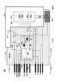
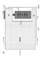
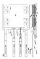
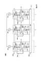
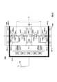
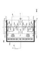
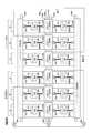
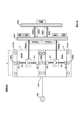
図2a-1および図2a-2を引き続き参照すると、図3a-1~図3a-3は、例示的なスイッチモジュール300を含むパッケージ式スイッチ200の準概略図である。パッケージ式スイッチ200は、スイッチモジュールの構成要素、それらの相互作用、およびそれらの相対位置をよりよく理解できるようにするために、図3a-1~図3a-3に透明なケース202と共に示す。With continued reference to Figures 2a-1 and 2a-2, Figures 3a-1 through 3a-3 are semi-schematic views of a packaged
図3a-1、図3a-2および図3a-3はそれぞれ、パッケージ式スイッチ200を上面、側面、および背面から見たときのスイッチモジュールの構成要素の相対位置を示す。スイッチモジュール300は、構成要素が搭載されて電気的に接続されることができるリジッドPCBを含む。Figures 3a-1, 3a-2 and 3a-3 respectively show the relative positions of the components of the switch module when the packaged
コネクタリード(例えば、204および206)は、スイッチモジュールがトランスファー成形プロセスまたはその他のプロセスでプラスチックに収容される前または後に、スイッチモジュールのリジッドPCB上のトレースに取り付けられてもよい。図2a-1~図2c-2に示すコネクタリードは、プラスチックケース202、252、および238の形成前に、リジッドPCBのトレースに取り付けられる。その他の実施形態において、リジッドPCBの前部におけるトレースの一部は、トランスファー成形プロセス中にシールドすることができる。その後、コネクタリードは、成形プロセス後にリジッドPCBの前部におけるトレースに取り付けられることができる。説明の便宜上、コネクタリードは、それらが取り付けられているスイッチモジュールの一部とみなす。The connector leads (e.g., 204 and 206) may be attached to traces on the rigid PCB of the switch module before or after the switch module is encased in plastic in a transfer molding process or other process. The connector leads shown in Figures 2a-1 through 2c-2 are attached to traces on the rigid PCB before the formation of the
図3a-1のスイッチモジュール300は、例示的なコネクタリードのセット314を含む。より詳細には、セット314は、コネクタリード204および206を含む11本のコネクタリードを含み、スイッチモジュールの構成要素と、マイクロコントローラまたはPMICなどのスイッチモジュールの外部の構成要素との間の信号および電圧の伝達に使用することができる。図示の実施形態において、セット314内のコネクタリードは同一平面上にあるが、本開示はこれに限定されるべきではないことが理解されよう。セット314内のコネクタリードの数は、11本に限定されるべきではない。スイッチモジュールの設計に応じて、より少ないまたはより多いコネクタリードを採用することができる。The
スイッチモジュール300は、コネクタリード204を介してマイクロコントローラまたは同様のプロセッサベースのデバイスから受信した低電力のPWM信号に基づいてスイッチ304を制御するスイッチコントローラ302を含む。スイッチ304は、ダイ基板312およびダイクリップ316に電気的かつ熱的に接続されて、それらの間に配置されており、それらをすべて図3a-1、3a-2、または3a-3に象徴的に示す。ダイ基板またはダイクリップは、パッケージ式スイッチまたはパッケージ式ハーフブリッジの内外に大電流(例えば、400Aまたはそれ以上)を伝達することができる。The
スイッチ304は熱を発生する。ダイ基板およびダイクリップは、パッケージ式スイッチまたはパッケージ式ハーフブリッジから熱を伝導することができる。ダイ基板312は、図3a-2および図3a-3を含む図において太い線で表されているが、これは、パッケージ式スイッチまたはパッケージ式ハーフブリッジからダイクリップ316よりもさらに大量の熱を伝導するように構成されていることを示すためである。The
スイッチモジュール300は、スイッチ304付近の温度を感知するための温度センサ回路T_Sense、スイッチ304によって伝達された電流を感知するための電流センサ回路I_Sense、およびスイッチ304全体の電圧を検出するための電圧検出回路V_Senseを備える。スイッチモジュールは、本開示の図に示すよりも少ないまたは多い構成要素を備えてもよい。例えば、スイッチモジュールは、センサ回路T_Sense、I_Sense、およびV_Senseのうちの1つ以上に供給電圧を提供する電圧レギュレータを含んでもよい。The
図3a-1、図3a-2、および図3a-3は、スイッチモジュールの構成要素の互いに対する相対的な位置関係を示す。スイッチコントローラ302は、図3a-2に見られるように、パッケージ式スイッチ200の前面Fの近傍に配置されており、一方でスイッチ304、ダイ基板312およびダイクリップ316からなるパワースタックは、パッケージ式スイッチ200の背面Bkの近傍に配置される。ダイ基板312、スイッチ304、およびダイクリップ316は、図3a-2および図3a-3に見られるように、上面Tと下面Bとの間に垂直に積み重ねられる。一義的には、第1構成要素と第2構成要素を積み重ねることは、第1構成要素と第2構成要素がそれぞれ、離れているが互いに平行な第1平面と第2平面に含まれることを意味する。第1平面内の第1構成要素は、第2平面内の第2構成要素の真上にあってもよく、あるいは、第2構成要素が第1構成要素の真下に位置しないように、第1構成要素が第1平面内で横方向にオフセットされていてもよい。Figures 3a-1, 3a-2, and 3a-3 show the relative positions of the components of the switch module with respect to each other. The
図解と理解を容易にするため、ダイ基板端子230をほとんどの図において正方形として表す。図によっては、ダイクリップ端子232を六角形または八角形として表す。図3a-1の上面図および図3a-3の背面図では、それぞれダイクリップ端子232を六角形として表す。図3a-2の側面図では、ダイクリップ端子232を八角形として表す。その他の図においても、同一のダイ基板端子およびダイクリップ端子の記号を使用する。For ease of illustration and understanding, the
ダイ基板端子230は、図3a-2および図3a-3において、パッケージ式スイッチ200の上面と同一平面上にあることを示すように配置されており、またダイクリップ端子232は、図3a-1および図3a-3において、パッケージ式スイッチ200の左側面と同一平面上にあることを示すように配置されている。ダイクリップ端子232は、図3a-2において中央に点を有して描かれており、電流がパッケージ式スイッチ200にその左側面を通って出入りすることを示す。The
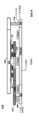
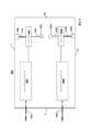
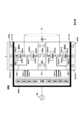
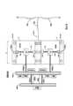
図3b-1、図3b-2および図3b-3は、別のパッケージ式スイッチ201の関連構成要素を示しており、これはパッケージ式スイッチ200と同様ではあるものの、ダイクリップ端子232が右側面と同一平面であることを示すように配置される。図3b-2のダイクリップ端子232は、電流がパッケージ式スイッチ201の右側面から出入りすることを示すために、中央の点なしで描かれている。ダイ基板端子またはダイクリップ端子は、パッケージ式ブリッジまたはパッケージ式ハーフブリッジのケース表面より下に凹んでいる平坦面を含んでいてもよく、あるいはダイ基板端子またはダイクリップ端子は、その他の実施形態において、パッケージ式ブリッジまたはパッケージ式ハーフブリッジのケース表面より上に突出している平坦面を含んでいてもよいことに再度留意されたい。Figures 3b-1, 3b-2 and 3b-3 show the relevant components of another packaged
例示的なスイッチコントローラ302
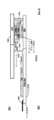
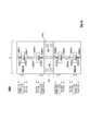
図3a-4は、本開示のほとんどのスイッチモジュールに採用することができる、例示的なスイッチコントローラ302の構成要素を示す概略図である。スイッチコントローラ302は、ゲートドライバ306、抵抗器R1およびR2、ならびにダイオード308および310を含む。スイッチコントローラの構成要素は、リジッドPCB上のトレースに電気的に接続されることができる。例えば、PCBのトレースは、スイッチ304の電流端子全体の電圧差(例えば、ドレイン電圧-ソース電圧、またはコレクタ電圧-エミッタ電圧)をゲートドライバ306に提供する電気経路の一部となり得る。この電圧差は、ゲートドライバ306がスイッチ304の故障状態を監視するために使用することができる。スイッチコントローラは、図3a-4に示す構成要素よりも少ないまたは多い構成要素を含んでもよい。Figures 3a-4 are schematic diagrams illustrating components of an
図3a-4にはスイッチ304が図示されているが、スイッチ304を挟むダイ基板とダイクリップは図示されていない。ダイオード308はダイ基板とゲートドライバ306の間に電気的に接続され、ゲートドライバ306はダイクリップに電気的に接続され、ゲートドライバ306の出力であるVgは抵抗器R1とR2を介してスイッチ304のゲートに電気的に接続される。In Figure 3a-4,
図1aおよび図1cのゲートドライバH101~H103およびL101~L103などの従来のインバータおよび整流器のゲートドライバは、制御PCBに搭載されて、それらが制御するパワートランジスタ(例えば、IGBTのTHx)からは遠隔に配置される。長い信号経路が、ゲート制御信号Vgを制御PCB上のゲートドライバからそれぞれのパワートランジスタに伝達する。これらの長い信号経路は、大きな寄生パラメータ(例えば、抵抗、インダクタンスおよび/またはキャパシタンス)を有し、これがスイッチング損失、消費電力、信号遅延を増加させ、および/またはスイッチング速度を低下させる可能性がある。また、長い信号経路で伝達される信号は、ノイズの影響を受けやすい。対照的に、ゲートドライバ306を含むスイッチコントローラ302(図3a-4)は、パッケージ式スイッチ(またはパッケージ式ハーフブリッジ)に収容されて、スイッチ304の近くに配置される。信号経路SP0は、10mmまたはそれ以下であってもよく、ゲートドライバ306の制御信号出力をスイッチ304のゲートに接続する。例えば、信号経路SPOは、9、7、5、3mm、またはそれ以下とすることができる。より短い信号経路は、寄生抵抗、寄生インダクタンス、寄生キャパシタンス、信号遅延、ノイズによる信号劣化、および/または上述の制御PCBに搭載されたゲートドライバに関連するその他の問題を低減する。ゲートドライバ306がスイッチ304に近接しているため、ゲートにおけるVgの立ち上がり時間と立ち下がり時間が短くなる可能性がある。ゲートドライバ306は、スイッチ304のゲートを駆動する際に消費する電力をより少なくすることができ、またゲートドライバ306はより迅速にゲートを駆動することができる。ゲートドライバ306はスイッチ304により近接しているため、制御PCB上の離れた位置に配置されたゲートドライバによって駆動されるスイッチの速度と比較すると、スイッチ304を切り替える速度はより速くなる可能性がある。Conventional inverter and rectifier gate drivers, such as gate drivers H101-H103 and L101-L103 in Figs. 1a and 1c, are mounted on a control PCB and located remotely from the power transistors (e.g., THx of an IGBT) that they control. Long signal paths carry the gate control signal Vg from the gate drivers on the control PCB to the respective power transistors. These long signal paths have large parasitic parameters (e.g., resistance, inductance, and/or capacitance) that can increase switching losses, power consumption, signal delays, and/or reduce switching speed. Also, signals carried on long signal paths are susceptible to noise. In contrast, the switch controller 302 (Figs. 3a-4), which includes the
例示的なスイッチ304
一般に、スイッチは、IGBT、MOSFET、JFET、BJTなどの1つ、2つ、またはそれ以上のパワートランジスタを含む。スイッチには、ダイオードなどの追加の構成要素が含まれることもある。スイッチ304のトランジスタおよび/または追加の構成要素は、Si、SiC、GaN、GaO、立方晶ヒ化ホウ素などの多くの異なるタイプの半導体材料のいずれか1つから作成することができる。スイッチ304のパワートランジスタは、異なるタイプとすることができる。例えば、スイッチ304は、1つ以上のSiCのMOSFET、および1つ以上のGaNのMOSFETを含んでもよく、これらはすべて並列に接続される、あるいはスイッチ304は、1つ以上のMOSFET、および1つ以上のIGBTを含んでもよく、これらはすべて並列に接続される。Typically, the switch includes one, two, or more power transistors, such as IGBTs, MOSFETs, JFETs, BJTs, etc. The switch may also include additional components, such as diodes. The transistors and/or additional components of the
図3a-5および図3a-6は、本開示のスイッチモジュールに採用することができる例示的なスイッチ304の概略図である。図3a-5において、スイッチ304は、パワーダイオードDと並列に接続したパワーIGBTを含む。コレクタcおよびダイオードのカソードは、多くの異なる取り付け技術(例えば、焼結、はんだ付け、過渡液相接合、導電性接着プロセスなど)のいずれか1つを使用してダイ基板(例えば、ダイ基板312)に取り付けられ、またエミッタeおよびダイオードのアノードは、多くの異なる取り付け技術のいずれか1つを使用してダイクリップ(例えば、ダイクリップ316)に取り付けられる。IGBTは1つのエミッタを有してもよいが、複数の実質的に平坦なエミッタ端子またはパッドを有する。エミッタ端子またはパッドの各々は、ダイクリップの対応する平坦面に取り付けることができる。IGBTは1つのコレクタを有してもよいが、複数の実質的に平坦なコレクタ端子またはパッドを有する。コレクタ端子またはパッドの各々は、ダイ基板の対応する平坦面に取り付けることができる。3a-5 and 3a-6 are schematic diagrams of an
図3a-6において、スイッチ304は、並列に結合されたパワーMOSFET(例えば、SiCのMOSFET、GaNのMOSFET、またはGaOなどのその他の材料から形成されたMOSFET)N1およびN2を備える。MOSFETのN1およびN2のドレインdは、ダイ基板(例えば、ダイ基板312)に取り付けられ(例えば、焼結、はんだ付け、過渡液相接合、導電性接着プロセスなど)、またソースsは、ダイクリップ(例えば、ダイクリップ316)に取り付けられる(例えば、焼結、はんだ付け、過渡液相接合など)。MOSFETは、1つのソースを有してもよいが、複数の実質的に平坦なソース端子またはパッドを有し、それらの各々は、ダイクリップの対応する平坦面に取り付けられ得る。MOSFETは1つのドレインを有してもよいが、実質的に平坦な複数のドレイン端子またはパッドを有する。ドレイン端子の各々は、ダイ基板の対応する平坦面に取り付けられることができる。スイッチ304の各ゲートgは、ゲートドライバ306からの大電流ゲート制御信号Vgによって制御される。3a-6, the
図3a-4~図3a-6を参照すると、ゲートドライバ306は、一実施形態において、マイクロコントローラから受信するPWM信号に基づいて、スイッチ304の1つ以上のトランジスタを制御する。ゲートドライバ306は、PWMがアサートされると、ゲート電圧Vgを介して1つ以上のトランジスタを起動する。別の実施形態において、ゲートドライバ306は、PWM信号に基づいてスイッチ304内の別々のトランジスタを独立して制御することができるマルチトランジスタゲートドライバの形態をとることができる。例えば、マルチトランジスタゲートドライバは、PWM信号の受信に応答して、図3a-6のスイッチ304のトランジスタN1およびN2のそれぞれのゲートを制御する意図的にずらしたゲート制御電圧V1gおよびV2g(図示せず)を生成することができる。この例では、V1gの立ち上がりエッジはV2gの立ち上がりエッジに先立つことができ、および/またはV1gの立ち下がりエッジはV2gの立ち下がりエッジに先立つことができ、あるいは、V1gの立ち上がりエッジはV2gの立ち上がりエッジに先立つことができ、および/またはV2gの立ち下がりエッジはV1gの立ち下がりエッジに先立つことができる。V2gはV1gを意図的に遅延させたものであってもよいし、またはその逆であってもよい。遅延信号は、V1gを入力としV2gを出力とする、またはその逆である、バッファまたは直列接続したバッファのセットなどのデバイスによって生成することができる。3a-4-3a-6, in one embodiment, the
例示的なリードおよびトレースExample lead and trace
例示的なPCBのトレースを、本開示の図に象徴的に示す。例示的なPCBのトレースは、スイッチモジュールの構成要素に電気的に接続される。例えば、図3a-4では、PCBのトレースはゲートドライバ306と抵抗器R1を接続する。トレースは、スイッチモジュールの構成要素(例えば、ゲートドライバ306)と、パッケージ式スイッチまたはパッケージ式ハーフブリッジの外部の構成要素(例えば、マイクロコントローラ)との間の電気接続にも使用することができる。スイッチモジュールの一部の構成要素は、リード、ワイヤ、トレース、金属リボン、またはその他の導体の直列の組み合わせを介して接続されてもよい。例えば、フレキシブルフラットケーブル(すなわち、フレキシブルPCB)のトレース、ボンドワイヤ、または屈曲リードが、電気接続抵抗器R2およびスイッチ304のゲートgに使用されてもよい。図3a-1では、説明の便宜上、いくつかのPCBのトレースは図示しない。Exemplary PCB traces are symbolically shown in the figures of this disclosure. Exemplary PCB traces are electrically connected to components of the switch module. For example, in FIG. 3a-4, the PCB traces connect the
1つ以上の個々のスイッチモジュールの構成要素(例えば、ゲートドライバ306、I_Sense、T_Sense、V_Senseなどのうちの1つ以上)は、パッケージ式デバイスの形態をとってもよい。パッケージ式デバイスは、スイッチモジュールのPCBのトレースに接続(例えば、はんだ付け)された独自のリードを有してもよい。例えば、ゲートドライバ306(図3a-4)は、パッケージ式半導体ダイの形態をとってもよい。パッケージ式ゲートドライバは、スイッチモジュールのPCBのトレースにはんだ付けされたリードを有することができる。I_Sense、V_SenseまたはT_Senseもまた、パッケージ式半導体ダイの形態をとってもよい。これらのパッケージ式デバイスもまた、スイッチモジュールのPCBのトレースに接続したリードを有してもよい。抵抗器R1およびR2、ならびにダイオード308および310は、スイッチモジュールのPCBのトレースに接続されたリードを備えるパッケージ式デバイスであり得る。あるいは、1つ以上の個々のスイッチモジュールの構成要素(たとえば、ゲートドライバ306、I_Sense、T_Sense、V_Senseなどのうちの1つ以上)は、スイッチモジュールのPCBのトレースにワイヤボンディングすることができるパッドを有するベア半導体ダイ(すなわち、パッケージ式ではない)の形態をとってもよい。本開示では、いくつかのスイッチモジュールの構成要素(例えば、ゲートドライバ306、I_Sense、T_Sense、および/またはV_Sense)は、スイッチモジュールのPCBに搭載されて、スイッチモジュールのPCBのトレースにワイヤボンディングされるパッドを有するベアダイの形態をとると推定されるが、本開示はこれに限定されるべきではないことが理解されよう。One or more of the individual switch module components (e.g., one or more of the
例示的なダイ基板およびダイクリップ端子Exemplary die substrate and die clip terminals
パワースタックは、ダイクリップとダイ基板との間でスイッチを電気的および熱的に接続することによって作成される。スイッチ内の各トランジスタの第1電流端子(たとえば、コレクタ、ドレインなど)は、銀、銅、またはその他の素材などの導電性の高い焼結材料の層を使用してダイ基板に焼結することができる。スイッチと接続されたダイ基板のダイ基板端子との間には、誘電体が存在しない。スイッチ内の各トランジスタの第2電流端子(たとえば、エミッタ、ソースなど)は、銀、銅、またはその他の素材などの導電性の高い焼結材料の層を介してダイクリップに焼結することができる。スイッチと接続されたダイクリップのダイクリップ端子との間には、誘電体が存在しない。したがって、パワースタックのダイ基板端子とダイクリップ端子との間に誘電体は存在しない。The power stack is created by electrically and thermally connecting the switches between the die clip and the die substrate. The first current terminal (e.g., collector, drain, etc.) of each transistor in the switch can be sintered to the die substrate using a layer of highly conductive sintered material such as silver, copper, or other material. There is no dielectric between the switch and the die substrate terminal of the connected die substrate. The second current terminal (e.g., emitter, source, etc.) of each transistor in the switch can be sintered to the die clip via a layer of highly conductive sintered material such as silver, copper, or other material. There is no dielectric between the switch and the die clip terminal of the connected die clip. Thus, there is no dielectric between the die substrate terminal and the die clip terminal of the power stack.
ダイ基板端子は、デバイスへの直接的または間接的な電気的および/または熱的接続のために構成される。ダイ基板端子は、ヒートシンク、バスバー、またはヒートシンクとしても機能するバスバーの表面に電気的および/または熱的に接続されることができる。例えば、ダイ基板端子は、「V+バスバー」に電気的および/または熱的に接続されることができ、該V+バスバーは、インバータシステムまたは整流器システムのV+端子に電気的に接続され、該V+端子は、バッテリ、燃料電池、DC/DCコンバータなどに電気的に接続されることができる。ダイ基板端子は、「V-バスバー」に電気的および/または熱的に接続されることができ、該V-バスバーは、インバータシステムまたは整流器システムのV-端子に電気的に接続され、該V-端子は、バッテリ、燃料電池、DC/DCコンバータなどに電気的に接続されることができる。ダイ基板端子は、「位相バスバー」とも呼ばれるACバスバーに電気的および/または熱的に接続されることができ、該ACバスバーは、インバータシステムまたは整流器システムのAC端子に電気的に接続され、該AC端子は、モータの固定子巻線Wの端子、フィルタのインダクタL、またはその他のデバイスに接続されることができる。一般に、バスバーは大電流(例えば400Aまたはそれ以上)を分配する金属素子である。バスバーまたはその要素の材料組成(たとえば、銅、アルミニウムなど)および断面サイズは、安全に伝達できる最大電流量とその寄生パラメータを決定する。断面積の広いバスバーは、寄生パラメータを低減することができる。バスバーは、それが使用される小型インバータまたは小型整流器システムの設計に応じて、多くの異なる構成のいずれかをとることができる。バスバーは複数の構成要素から組み立てられてもよい。The die substrate terminals are configured for direct or indirect electrical and/or thermal connection to the device. The die substrate terminals can be electrically and/or thermally connected to a heat sink, a bus bar, or a surface of a bus bar that also functions as a heat sink. For example, the die substrate terminals can be electrically and/or thermally connected to a "V+ bus bar" that is electrically connected to a V+ terminal of an inverter or rectifier system that can be electrically connected to a battery, fuel cell, DC/DC converter, etc. The die substrate terminals can be electrically and/or thermally connected to a "V- bus bar" that is electrically connected to a V- terminal of an inverter or rectifier system that can be electrically connected to a battery, fuel cell, DC/DC converter, etc. The die substrate terminals can be electrically and/or thermally connected to AC busbars, also called "phase busbars", which are electrically connected to AC terminals of an inverter or rectifier system, which can be connected to terminals of a stator winding W of a motor, an inductor L of a filter, or other devices. In general, busbars are metallic elements that distribute large currents (e.g., 400 A or more). The material composition (e.g., copper, aluminum, etc.) and cross-sectional size of the busbar or its elements determine the maximum amount of current that can be safely carried and its parasitic parameters. Busbars with large cross-sectional areas can reduce parasitic parameters. Busbars can take any of many different configurations depending on the design of the miniature inverter or miniature rectifier system in which it is used. Busbars may be assembled from multiple components.
ヒートシンクは、1つ以上のチャネルを有してもよく、該チャネルの各々は、以下でさらに詳しく説明するように、チューブを受容することができる。バスバーはヒートシンクとしても機能してもよく、該バスバーは1つ以上のチャネルを有してもよく、該チャネルの各々は、以下でさらに詳しく説明するように、チューブを受容することができる。チューブは、銅またはアルミニウムなどの導電性金属で形成することができる。金属チューブの内面および/または外面には、1層以上の熱伝導性誘電体を形成することができる。外側の誘電体は、金属チューブを受容するヒートシンクまたはバスバーから金属チューブを電気的に絶縁する。別の実施形態において、金属チューブとそれらを受容するヒートシンクまたはバスバーとの間に誘電体は存在しない。この代替的な実施形態において、金属チューブの外面は、それらを受容するヒートシンクまたはバスバーに電気的および熱的に接続される。チューブは、窒化アルミニウムなどのその他の熱伝導性および電気非伝導性材料から形成することができる。電気的非伝導性材料で形成されたチューブの外面の一部または全部に金属層を形成して、チューブからヒートシンクへの移行部からの熱伝導を改善することができる。The heat sink may have one or more channels, each of which may receive a tube, as described in more detail below. The busbar may also function as a heat sink, and the busbar may have one or more channels, each of which may receive a tube, as described in more detail below. The tube may be formed of a conductive metal, such as copper or aluminum. One or more layers of a thermally conductive dielectric may be formed on the inner and/or outer surface of the metal tube. The outer dielectric electrically insulates the metal tube from the heat sink or busbar that receives it. In another embodiment, there is no dielectric between the metal tube and the heat sink or busbar that receives them. In this alternative embodiment, the outer surface of the metal tube is electrically and thermally connected to the heat sink or busbar that receives it. The tube may be formed of other thermally and electrically non-conductive materials, such as aluminum nitride. A metal layer may be formed on some or all of the outer surface of the tube formed of an electrically non-conductive material to improve thermal conduction from the transition from the tube to the heat sink.
一般に、バスバーは全体的または部分的に、銅またはアルミニウムなどの導電性金属から作ることができ(例えば、押出成形、3D印刷など)、小型電力変換器の設計の違いに対応するために、異なる形状、サイズ、寸法(例えば、長さ、幅、高さなど)を有することができる。ヒートシンクまたはバスバーは、チューブの周囲にアルミニウム、銅、またはその他の材料を鋳造することによって形成することができる。鋳造は、液状金属を、意図する形状のネガ型(すなわち、立体的なネガ像)を含む鋳型に送り込むプロセスである。外側の誘電体層を有するチューブも有しないチューブも、液状金属が送られる前に金型に入れることができる。バスバーまたはヒートシンクは、外側の誘電体層有するまたは有しないチューブが2つの金属半割体の間に挿入された後に、それらを互いに取り付ける(例えば、はんだ付け、焼結など)ことによって形成することができる。2つの半割体は、押出成形、3D印刷、鋳造などによって形成することができる。半割体を取り付ける前に、サーマルペースト(サーマルコンパウンド、サーマルグリース、サーマルインターフェース材料(TIM)、サーマルゲル、ヒートペースト、ヒートシンクコンパウンド、ヒートシンクペースト、またはCPUグリースとも呼ばれる)の薄層をチューブに塗布して、チューブと結果として得られるヒートシンクまたはバスバーとの間の界面の空隙またはスペースをなくすことができる。さらに別の実施形態において、誘電体層を有するチューブが受容されたヒートシンクまたはバスバーを加熱して、ヒートシンクまたはバスバーの金属をリフローし、チューブの誘電体層とヒートシンクまたはバスバーとの間の界面の空隙またはスペースをなくすことができる。その他の実施形態において、金属チューブ上の誘電体層の一部または全部、または窒化アルミニウムチューブの一部または全部に金属の薄層を形成して、バスバーまたはヒートシンクとの熱的接続を促進することができる。金属の薄層はまた、窒化アルミニウムチューブの端部と金属マニホールドを互いに取り付ける(例えば、溶接する)際に、これらの間の密閉性を高めることができる。In general, busbars can be made in whole or in part from conductive metals such as copper or aluminum (e.g., extrusion, 3D printing, etc.) and can have different shapes, sizes, and dimensions (e.g., length, width, height, etc.) to accommodate different designs of miniature power converters. Heat sinks or busbars can be formed by casting aluminum, copper, or other material around a tube. Casting is the process of forcing liquid metal into a mold that contains a negative (i.e., a three-dimensional negative image) of the intended shape. Tubes with and without an outer dielectric layer can be placed in the mold before the liquid metal is fed. Busbars or heat sinks can be formed by inserting a tube with or without an outer dielectric layer between two metal halves that are then attached to each other (e.g., soldered, sintered, etc.). The two halves can be formed by extrusion, 3D printing, casting, etc. Prior to attachment of the halves, a thin layer of thermal paste (also called thermal compound, thermal grease, thermal interface material (TIM), thermal gel, heat paste, heat sink compound, heat sink paste, or CPU grease) can be applied to the tube to eliminate any voids or spaces at the interface between the tube and the resulting heat sink or busbar. In yet another embodiment, the heat sink or busbar receiving the tube with the dielectric layer can be heated to reflow the metal of the heat sink or busbar and eliminate any voids or spaces at the interface between the dielectric layer of the tube and the heat sink or busbar. In other embodiments, a thin layer of metal can be formed on some or all of the dielectric layer on the metal tube or on some or all of the aluminum nitride tube to facilitate thermal connection with the busbar or heat sink. The thin layer of metal can also enhance the seal between the ends of the aluminum nitride tube and the metal manifold when they are attached (e.g., welded) to each other.
ヒートシンクまたはヒートシンクとしても機能するバスバーは、ダイ基板端子またはダイクリップ端子に圧接、はんだ付け、焼結、または別の方法で接続されて、それらの間の電気的および熱的接続を確保することができる平坦面を含んでもよい。圧接接続により、上述のCTEの差に関連する問題を低減または解消することができる。The heat sink or busbar that also functions as a heat sink may include flat surfaces that can be pressure welded, soldered, sintered, or otherwise connected to the die substrate terminals or die clip terminals to ensure electrical and thermal connection therebetween. Pressure weld connections can reduce or eliminate problems associated with the CTE differences discussed above.
図2a-1および図2c-1を参照すると、例示的なダイ基板端子230は、パッケージ式スイッチ200および211のケース上面から露出している矩形状の平坦面を有する。図2b-1~図2b-3のパッケージ式ハーフブリッジ250は、同様のダイ基板端子230Hおよび230Lを有する。露出した端子230の寸法(例えば、幅および長さ)は、相当な電流および熱を伝達するように構成される。一実施形態において、ダイ基板端子230は、第1電流端子(例えば、コレクタ、ドレインなど)が焼結されるダイ基板312(図示せず)の少なくとも1つの平坦面と平行であるが、反対向き(すなわち、180度)である。ダイ基板は、パッケージ式スイッチまたはパッケージ式ハーフブリッジの左側面または右側面を通って延在する小さなサイド端子(例えば、図2b-1に示すサイド端子240)を有してもよい。電流は、これらのダイ基板のサイド端子を通ってパッケージ式スイッチまたはパッケージ式ハーフブリッジに出入りすることができる。金属ストラップは、あるパッケージ式スイッチ内のダイ基板のサイド端子を、別のパッケージ式スイッチ内のダイクリップ端子に電気的に接続することができる。金属サイドストラップは、パッケージ式ハーフブリッジ内のダイクリップ端子を電気的に接続することができる、あるいは金属ストラップは、パッケージ式ハーフブリッジ内の1つのスイッチモジュールのダイ基板のサイド端子を、パッケージ式ハーフブリッジ内の別のスイッチモジュールのダイクリップ端子に電気的に接続することができる。図2b-3は、パッケージ式スイッチ250内のダイクリップ端子232Hにサイド端子240Lを電気的に接続する、例示的な金属ストラップ242を示す。金属ストラップは、図2b-3の端子240Lと端子232Hなどの構成要素間で相当な電流(例えば、400A以上)を伝達するように構成されるべきである。2a-1 and 2c-1, the exemplary
ダイ基板に接続されることに加えて、スイッチ304は、1つ以上のダイクリップ端子を有するダイクリップに電気的および熱的に接続される。ダイクリップ端子は、パッケージ式スイッチまたはパッケージ式ハーフブリッジの外部のデバイスに直接または間接的に電気的および/または熱的に接続されるように構成することができる。ダイクリップ端子は、ヒートシンク、バスバー、またはヒートシンクとしても機能するバスバーの表面に電気的および/または熱的に接続されることができる。ダイクリップ端子(例えば、パッケージ式スイッチ200のダイクリップ端子232)は、V-バスバーに電気的および/または熱的に接続されることができる。ダイクリップ端子(例えば、図2c-2のパッケージ式スイッチ211のダイクリップ端子344)は、ヒートシンクとしても機能するバスバーに電気的および/または熱的に接続されることができる。ダイクリップ端子は、位相バスバーに電気的および/または熱的に接続されることができる。ダイクリップ端子は、図2b-3に示す金属ストラップ242などの金属ストラップに電気的に接続されることができる。In addition to being connected to the die substrate, the
図2a-1および図2c-1を参照すると、例示的なダイクリップ端子232の各々は、そのパッケージ式スイッチのケースを通して露出する矩形状の実質的に平坦な表面領域を有する。ダイクリップ端子232は、金属ストラップに電気的に接続されることができ、該金属ストラップは、ダイ基板のサイド端子に接続されることができる。図2b-1および図2b-2のパッケージ式ハーフブリッジ250は、同様のダイクリップ端子232Hおよび232Lを有する。露出した端子232の寸法(例えば、幅および長さ)は、相当な電流を伝達するように構成される。図2c-2および図2e-2の例示的なパッケージ式スイッチ211およびパッケージ式スイッチ247dのダイクリップはそれぞれ、熱を伝達できる追加の平面端子344を有する。Referring to Figs. 2a-1 and 2c-1, each of the exemplary
例示的なゲートドライバ306とその他のスイッチモジュールの構成要素
スイッチモジュールのゲートドライバは、マイクロコントローラまたは同様のプロセッサベースのデバイス(複数可)から信号を受信することができる。例えば、図3a-4のゲートドライバ306は、図1aを参照して説明したPWM信号のうちの1つなどの低電力PWMドライバ制御信号を受信することができる。さらに、ゲートドライバ306は、マイクロコントローラまたはその他のデバイスから低電力リセット信号を受信することができる。ゲートドライバ306は、アサートされたリセット信号を受信した後、高電流ゲート制御信号Vgをアサートすることによって、受信したパルス幅変調(PWM)信号のアサートに応じてスイッチ304を起動することができる。理想的には、ゲートドライバ306の出力とスイッチ304のゲート(複数可)との間の信号経路SP0の長さは、寄生インダクタンス、寄生キャパシタンス、ノイズなどによるゲート制御信号Vgへの悪影響を緩和するために、できるだけ短くすべきである。The gate driver of the switch module may receive a signal from a microcontroller or similar processor-based device(s). For example, the
ゲートドライバはまた、マイクロコントローラまたは同様のプロセッサベースのデバイスに信号を送信することができる。例えば、ゲートドライバ306は、スイッチ304を通る過剰な電流伝導またはスイッチ304が解除されているべきときのスイッチ304全体の異常に低い電圧などの障害が検出されたときに、スイッチ304を無効にし(すなわち、スイッチを解除状態に維持し)、Fault信号をアサートすることができる。マイクロコントローラまたは類似のプロセッサデバイスは、Fault信号を受信して処理することができる。I_Sense回路およびT_Sense回路などのその他のスイッチモジュールの構成要素は、スイッチ304を通る電流およびスイッチ304近傍(例えば、1~10mm以下)の温度を表す信号をそれぞれ送信することができる。T_Senseの信号出力は、T_Senseがスイッチに近いほど温度をより正確に表すことができる。電圧検出回路V_Senseが追加された場合も同様に、スイッチ304の電流端子全体の電圧を表す信号を送信することができる。マイクロコントローラまたは同様のプロセッサベースのデバイスは、これらの構成要素によって提供される信号を受信および処理することができる。例えば、マイクロコントローラは、温度を表す信号を第1閾値と比較して、第1閾値を超えた場合にゲートドライバ306に供給されるPWM制御信号の周波数またはデューティサイクルを変更することができ、あるいは、マイクロコントローラは、第1閾値を超えた場合にゲートドライバ306に供給されるPWM制御信号を連続的にデアサートすることができ、これにより、スイッチ304を連続的に解除状態にする。The gate driver can also send a signal to a microcontroller or similar processor-based device. For example, the
図3a-7は、ガルバーニ絶縁回路324を介して高電圧出力段322とデータ通信する低電圧入力段320を備える例示的なゲートドライバ306を示す。ガルバーニ絶縁は、2つ以上の回路が通信する必要があるが、それらの接地が異なる電位にある場合に使用される。ガルバーニ絶縁回路は、回路間の絶縁を達成するために、変圧器、コンデンサ、光カプラ、またはその他のデバイスを使用してもよい。説明の便宜上、ガルバーニ絶縁回路324は、ガルバーニ絶縁を実現するために変圧器を採用する。低電圧入力段320は、それぞれのPCBのトレースを介して第1電源電圧VDDIおよび第1接地GIを受けるように結合され、それぞれのPCBのトレースを介してPWM信号およびリセット信号を受ける論理回路330を含む。高電圧出力段322は、それぞれのPCBのトレースを介して第2電源電圧VDDO+、第3電源電圧VDDO-および第2接地GOを受けるように結合され、ガルバーニ絶縁回路324を介して論理回路330から制御信号を受ける論理回路332を含む。高電圧出力段322はまた、論理回路332からの出力信号によって制御されるバッファ340を含む。バッファ340は、絶縁回路324の制御信号出力がアサートされると、Vgをアサートする。その他のタイプのゲートドライバ306も考えられる。3a-7 show an
I_Senseは、スイッチ304を流れる電流などの電流の流れに比例した大きさの電圧信号Viを生成する。I_Senseは、一般にはスイッチ304を通る電流の流れ、特にダイクリップを通る電流の流れによって生じる磁界を測定する誘導電流センサを含んでもよい。誘導電流センサはスイッチ304から電気的に絶縁されている。例示のダイクリップ316は水平部分と垂直部分を含む。I_Sense回路は、ダイクリップ316の水平部分の狭窄部(図示せず)を通る電流の流れを測定することができる。I_Senseは、誘導電流センサの信号出力を、マイクロコントローラによるその後の使用のために調整する。T_Senseは、スイッチ304付近の温度と比例する大きさの電圧信号Vtを生成することができるサーミスタを含んでもよい。サーミスタは、抵抗値が温度に依存する抵抗器の一種であり、抵抗値と温度の関係は線形である。T_Senseは、マイクロコントローラで使用するためのサーミスタの信号出力を調整する。サーミスタはスイッチ304から電気的に絶縁されている。V_Senseは、スイッチの電流端子間の電圧に比例する電圧信号Vvを生成することができる。I_Sense generates a voltage signal Vi with a magnitude proportional to a current flow, such as the current through the
I_Sense、V_Sense、およびT_Sense回路からのアナログ信号Vi、Vv、およびVtは、それぞれマイクロコントローラに伝達され、その後デジタル同等物に変換されることができる。パッケージ式スイッチまたはパッケージ式ハーフブリッジの前面にあるコネクタリードを使用して、Vi、Vv、Vt、およびFault信号を含む信号を、スイッチモジュールのPCB上のそれぞれのスイッチモジュールの構成要素と、制御PCBに搭載されたマイクロコントローラとの間で伝達することができる。コネクタリードはまた、制御PCBとパッケージ式スイッチまたはパッケージ式ハーフブリッジとの間でその他の信号(例えば、PWMおよびリセット)および電圧(例えば、VDDI、VDDO+、GIなど)を伝達するために使用することもできる。The analog signals Vi, Vv, and Vt from the I_Sense, V_Sense, and T_Sense circuits, respectively, can be communicated to a microcontroller and then converted to their digital equivalents. Connector leads on the front of the packaged switch or packaged half-bridge can be used to communicate signals including the Vi, Vv, Vt, and Fault signals between the respective switch module components on the switch module PCB and the microcontroller mounted on the control PCB. The connector leads can also be used to communicate other signals (e.g., PWM and reset) and voltages (e.g., VDDI, VDDO+, GI, etc.) between the control PCB and the packaged switch or packaged half-bridge.
制御PCBボード上のマイクロコントローラは、メモリに格納された命令に従って、受信した信号(例えば、Fault、Vi、Vv、Vt)のデジタル等価物を処理することができる。マイクロコントローラは、Vi、Vv、Vtおよび/またはその他の信号のデジタル等価物に基づいて、ドライバ制御信号PWMのデューティサイクルおよび/または周期を調整することができる。The microcontroller on the control PCB board can process the digital equivalents of the received signals (e.g., Fault, Vi, Vv, Vt) according to instructions stored in memory. The microcontroller can adjust the duty cycle and/or period of the driver control signal PWM based on the digital equivalents of the Vi, Vv, Vt and/or other signals.
パッケージ式スイッチ200DPackaged
パッケージ式スイッチは、スイッチに加えてダイオードを含んでもよい。図3a-8および図3a-9は、スイッチ304と電気的に直列に接続されることができるダイオードを含む、例示的なパッケージ式スイッチ200Dの準概略図である。ダイオードは、外部の金属ストラップ(図示せず)を介してスイッチと電気的に直列に接続されることができる。The packaged switch may include a diode in addition to the switch. Figures 3a-8 and 3a-9 are semi-schematic diagrams of an exemplary packaged
パッケージ式スイッチ200Dは、スイッチモジュールの構成要素、それらの相互作用、およびそれらの相対位置をよりよく理解できるようにするために、図3a-8および図3a-9に透明なケースと共に示す。パッケージ式スイッチ200Dの寸法は、図2b-1~図2b-3に示すパッケージ式ハーフブリッジ250と実質的に同様であってもよい。The packaged
パッケージ式スイッチ200Dは、図3a-1に示すスイッチモジュール300の構成要素を含むスイッチモジュール300Dと、ダイクリップ316Lとダイ基板312Lとの間に取り付けられた(例えば、焼結された)1つ以上のダイオード269を有するダイオードスタックとを含む。The packaged
図3a-8および図3a-9は、それぞれ、パッケージ式スイッチ200Dを側面および背面から見たときの、スイッチモジュールの構成要素の相対位置を示す。スイッチモジュール300Dは、スイッチモジュールの構成要素とマイクロコントローラおよびPMICなどの外部構成要素との間で信号および電圧を伝達するためのコネクタリード(図3a-8にはコネクタリード204のみ図示)を含む。スイッチモジュール300Dは、マイクロコントローラまたは同様のプロセッサベースのデバイスから受信した低電力PWM信号および/またはその他の信号に基づいてスイッチ304を制御するスイッチコントローラ302を含む。スイッチ304は、ダイ基板312Hとダイクリップ316Hとに電気的および熱的に接続されて、それらの間に配置されており、これらのすべてを象徴的に示す。Figures 3a-8 and 3a-9 show the relative positions of the switch module components when viewing packaged
図3a-9に示すように、スイッチモジュール300Dは、スイッチ304付近の温度を検出するための温度センサ回路T_Sense、スイッチ304によって伝達された電流を検出するための電流センサ回路I_Sense、およびスイッチ304全体の電圧を検出するための電圧センサ回路V_Senseを含む。スイッチモジュールは、より少ないまたはより多くの構成要素を含んでもよい。As shown in Figures 3a-9,
図3a-8および図3a-9は、スイッチモジュールの構成要素の互いに対する相対的な位置関係を示す。スイッチコントローラ302は、図3a-8に見られるように、パッケージ式スイッチ200Dの前面Fおよび上面近傍に配置される。スイッチ304、ダイ基板312Hおよびダイクリップ316Hから構成されるパワースタックは、パッケージ式スイッチ200Dの上面Tおよび背面Bkの近傍に配置される。ダイ基板312H、スイッチ304、およびダイクリップ316Hは、図3a-8および図3a-9に見られるように、上面Tと底面Bとの間に垂直に積み重ねられる。ダイオード269、ダイクリップ316L、およびダイ基板312Lから構成されるダイオードスタックは、パッケージ式スイッチ200Dの底面Bおよび背面Bkの近傍に配置される。ダイ基板312L、ダイオード269、およびダイクリップ316Lは、図3a-8および図3a-9に見られるように、上面Tと底面Bとの間に垂直に積み重ねられる。パワースタックとダイオードスタックは、リジッドPCB(図示せず)の反対向きの面に搭載されることができる。パワースタック、ダイオードスタック、およびリジッドPCBは、上面Tと底面Bとの間に垂直に積み重ねられることができる。3a-8 and 3a-9 show the relative positions of the components of the switch module relative to each other. The
ダイ基板端子230Hおよび230Lは、図3a-8および図3a-9において、パッケージ式スイッチ200Dの上面および底面と同一平面であることを示すように配置される。ダイクリップ端子232Hおよび232Lは、図3a-8および図3a-9において、パッケージ式スイッチ200Dの左側面と同一平面であることを示すように配置される。Die
図3a-8および図3a-9は、スイッチ304から電気的に絶縁されたダイオード269を示す。図示しないが、ダイクリップ端子232Lと232Hを電気的に接続するための金属ストラップを、パッケージ式スイッチモジュール200Dのケースを形成する前または後に追加することができる。Figures 3a-8 and 3a-9 show the
図3a-8および図3a-9は、ダイクリップ316Lに取り付けられたダイオード269のアノードおよびダイ基板312Lに取り付けられたカソードを示す。パッケージ式スイッチ200Dの代替的な実施形態において、ダイオード269のカソードはダイクリップ316Lに取り付けられることができ、アノードはダイ基板312Lに取り付けられることができる。Figures 3a-8 and 3a-9 show the anode of
パッケージ式スイッチ203
パッケージ式スイッチ200および201は、スイッチ304の片側冷却を可能にする。図3c-1および図3c-2は、スイッチ304の両面冷却を可能にする別のパッケージ式スイッチ203の関連構成要素を示す準概略図である。パッケージ式スイッチ203は、パッケージ式スイッチ200と多くの点で類似しており、その多くの構成要素を含んでいる。パッケージ式スイッチ203は、スイッチモジュールを含み、該スイッチモジュールは、構成要素を搭載することができるリジッドPCBを含む。リジッドPCBは、スイッチ304の両面冷却を可能にするためにC字形であってもよい。C字形PCBの例は、本明細書で後述する。パッケージ式スイッチ203を、構成要素、それらの相互作用、およびスイッチモジュール内の相対的な配置をよりよく理解できるように、透明なケースと共に示す。Packaged switches 200 and 201 allow for single-sided cooling of
図3c-1および図3c-2は、それぞれ側面および背面から見たときのパッケージ式スイッチ203の構成要素の相対位置を示す。パッケージ式スイッチ203は、スイッチコントローラ302によって制御されるスイッチ304を含む。スイッチ304は、ダイ基板312と、ダイクリップ端子344を含むダイクリップ342との間に接続(例えば、焼結)されて配置される。言い換えれば、スイッチ304の第1電流端子および第2電流端子は、それぞれダイ基板312およびダイクリップ342に取り付けられている。Figures 3c-1 and 3c-2 show the relative positions of the components of the packaged
ダイ基板312と、ダイクリップ端子344を含むダイクリップ342とを象徴的に示す。ダイ基板312およびダイクリップ342はいずれも、相当な電流および相当な熱を伝達するように構成されていることを示すために太線で表す。ダイ基板312およびダイクリップ342は同様のものであり、それぞれ実質的に同様の端子230および344を有する。ダイクリップ342は、スイッチ304のエミッタ端子もしくはドレイン端子、またはそれらのパッドと係合するための台座(以下でより詳細に説明する)を必要とする場合がある。ダイクリップ342の高さHDCは、ダイクリップ端子344がパッケージ式スイッチ203の底面と実質的に同一平面になるように、ダイ基板312の高さHDSより大きくてもよい。ダイクリップ342およびその端子344の形状および形態は、ダイクリップ316およびその端子232(図3b-2および図3b-3)とは実質的に異なる。A
図3c-1および図3c-2は、特定の構成要素の互いに対する相対的な位置関係を示す。ダイ基板312、スイッチ304、およびダイクリップ342は、パッケージ式スイッチ203の上面Tと底面Bとの間に図示のように垂直に積み重ねられる。スイッチコントローラ302はパッケージ式スイッチ203の前面Fの近傍に配置され、スイッチ304は背面Bkの近傍に配置される。ダイ基板端子230は、図中、パッケージ式スイッチ203の上面と同一平面上にあることを示す位置に配置され、ダイクリップ端子344も同様に、底面と同一平面上にあることを示す位置に配置される。3c-1 and 3c-2 show the relative positioning of certain components with respect to one another. The
パッケージ式スイッチ205
図3d-1および図3d-2は、例示的なパッケージ式スイッチ205の関連構成要素を示す準概略図である。透明なケースと共に示すパッケージ式スイッチ205は、パッケージ式スイッチ200と同様であり、その多くの構成要素を含んでいる。パッケージ式スイッチ205は、スイッチモジュールを含んでもよく、該スイッチモジュールは、構成要素を搭載することができるリジッドPCBを含む。FIGS. 3d-1 and 3d-2 are semi-schematic diagrams showing relevant components of an exemplary packaged
図3d-1および図3d-2は、それぞれ側面および背面から見たときのパッケージ式スイッチ205の特定の構成要素の相対的な位置を示す。パッケージ式スイッチ200と同様に、パッケージ式スイッチ205は、スイッチコントローラ302によって制御されるスイッチ304を含む。スイッチ304は、ダイ基板312と、ダイクリップ端子232を含むダイクリップ346との間に接続(例えば、焼結)されている。より詳細には、スイッチ304の第1電流端子および第2電流端子は、それぞれダイ基板312およびダイクリップ346に接続される。ダイ基板312、ダイクリップ346およびそれらの端子を象徴的に示す。FIGS. 3d-1 and 3d-2 show the relative positions of certain components of packaged
図3d-1および図3d-2は、特定の構成要素の互いに対する相対的な位置関係を示す。ダイ基板312、スイッチ304、およびダイクリップ346は、パッケージ式スイッチ205の上面Tと下面Bの間に図示のように垂直に積み重ねられる。スイッチコントローラ302はパッケージ式スイッチ205の前面Fの近傍に配置され、スイッチ304は背面Bkの近傍に配置される。ダイ基板端子230は、パッケージ式スイッチ205の上面と同一平面であることを示すように配置され、ダイクリップ端子232は、図3d-1において、背面と同一平面であることを示すように配置される。別の実施形態において、ダイクリップ端子232は、背面Bkから横方向に延在するリードに置き換えられる。いずれの場合も、ダイクリップ346は、主に熱ではなく電流を伝達するように構成されていることを示すために、より細い線で表す。3d-1 and 3d-2 show the relative positioning of certain components with respect to each other. The
パッケージ式スイッチ211
図2c-1および図2c-2を参照すると、図3e-1および図3e-2は、例示的なパッケージ式スイッチ211のいくつかの構成要素を示す準概略図である。図3e-1および図3e-2は、それぞれ、透明なケースと共に示すパッケージ式スイッチ211を側面および背面から見たときのスイッチの構成要素の相対位置を示す。パッケージ式スイッチ203と同様に、パッケージ式スイッチ211はスイッチ304の両面冷却を可能にする。パッケージ式スイッチ211は、スイッチモジュールを含んでもよく、該スイッチモジュールは、構成要素を搭載することができるリジッドPCBを含む。With reference to Figures 2c-1 and 2c-2, Figures 3e-1 and 3e-2 are semi-schematic diagrams illustrating some components of an exemplary packaged
図3e-1および図3e-2は、それぞれ側面および背面から見たときのパッケージ式スイッチ211の特定の構成要素の相対的な位置を示す。パッケージ式スイッチ200と同様に、パッケージ式スイッチ211は、スイッチコントローラ302によって制御されるスイッチ304を含む。スイッチ304は、ダイ基板312と、2つのダイクリップ端子232および344を含むダイクリップ345との間に接続(例えば、焼結)される。スイッチ304の第1電流端子および第2電流端子は、それぞれダイ基板312およびダイクリップ345に焼結される。Figures 3e-1 and 3e-2 show the relative positions of certain components of packaged
ダイクリップ345ならびにその端子232および344を象徴的に示す。ダイクリップ345は、第1部分348および第2部分350と、図示のように第1部分および第2部分に対して垂直に延在する第3部分354とを含む。第3部分354は、主に電流を伝達するように構成されていることを示すために細い線で示し、第1部分348および第2部分350は、いずれも相当な電流および熱を伝達するように構成されていることを示すために太い線で示す。しかしながら、第2部分350は、電気的に絶縁されたヒートシンクなどの電気的に絶縁されたデバイスに接続される場合、熱のみを伝導する。図3e-2は、第3部分354を通して伝達された電流を検出するための電流センサ回路I_Senseを示す。The
図3e-1および図3e-2は、特定の構成要素の互いに対する相対的な位置関係を示す。ダイ基板312、スイッチ304、およびダイクリップ345は、パッケージ式スイッチ211の上面Tと下面Bの間に図示のように垂直に積み重ねらる。スイッチコントローラ302は、パッケージ式スイッチ211の前面Fの近傍に配置される。スイッチ304は背面Bkの近傍に配置される。ダイ基板端子230は、パッケージ式スイッチ211の上面と同一平面であることを示すように配置される。ダイクリップ端子232は、図3e-2において、左側面と同一平面であることを示すように配置され、ダイクリップ端子344は、底面と同一平面であることを示すように配置される。ダイクリップ345の高さHDCは、ダイクリップ端子344がパッケージ式スイッチ211の底面と実質的に同一平面になるように、ダイ基板312の高さHDSよりも大きくてもよい。別の実施形態において、ダイクリップ345は、背面Bkから横方向に延在するリードの形態をとる端子を有するダイクリップに置き換えられる。3e-1 and 3e-2 show the relative positioning of certain components with respect to each other. The
パッケージ式スイッチ209
図3f-1および図3f-2は、別のパッケージ式スイッチ209の特定の構成要素の相対的な位置を示す準概略図である。図3f-1および図3f-2は、それぞれ側面および背面から見たときの、透明なケースと共に示すパッケージ式スイッチ209の特定の構成要素の相対位置を示す。パッケージ式スイッチ211と209は実質的に類似している。ダイクリップ端子の位置が両者の大きな違いの一つである。パッケージ式スイッチ211のダイクリップ端子232は、左側面と同一平面上にあることを示すように配置され、パッケージ式スイッチ209のダイクリップ端子232は、図3f-2に示すように、右側面と同一平面上にある。Figures 3f-1 and 3f-2 are semi-schematic diagrams showing the relative positions of certain components of another packaged
例示的なスイッチモジュールExample switch module
パッケージ式スイッチまたはパッケージ式ハーフブリッジのスイッチモジュールの構成要素(例えば、ゲートドライバ306、抵抗器R1、ダイオード308、I_Sense回路、T_Sense回路、パワースタックなど)は、リジッドPCB上に搭載されて、リジッドPCB上のトレースによって電気的に接続されることができる。パッケージ式スイッチモジュール200および211は、スイッチモジュールがリジッドPCBに搭載される例である。その他のパッケージ式スイッチモジュールでは、リジッドPCBは採用されない。パッケージ式スイッチモジュール247sと247dは、リジッドPCBがない例である。一部のパッケージ式ハーフブリッジでは、ハイサイドスイッチモジュールおよびローサイドスイッチモジュールの構成要素は、別々のPCBに搭載されるか、あるいは同じPCBの反対側に搭載されてもよい。The packaged switch or packaged half-bridge switch module components (e.g.,
パワースタック(すなわち、ダイ基板とダイクリップの間に挟まれたスイッチ)は、金属ポスト、台座などの機械的構造を使用してスイッチモジュールのPCB上で支持されることができる。機械的構造は、パワースタックとPCBとの間にスペースを提供することができる。機械的構造は、支持を提供することに加えて、ダイクリップおよび/またはダイ基板を、PCB上のそれぞれのトレースに電気的に接続することができる。例えば、機械的支持構造の一端をダイ基板またはダイクリップに取り付け(例えば、はんだ付け)、他端をPCB上のトレースまたはパッドに取り付ける(例えば、はんだ付け)ことができる。The power stack (i.e., the switch sandwiched between the die substrate and the die clip) can be supported on the PCB of the switch module using mechanical structures such as metal posts, pedestals, etc. The mechanical structures can provide space between the power stack and the PCB. In addition to providing support, the mechanical structures can electrically connect the die clip and/or the die substrate to respective traces on the PCB. For example, one end of the mechanical support structure can be attached (e.g., soldered) to the die substrate or die clip and the other end can be attached (e.g., soldered) to a trace or pad on the PCB.
パワースタックをPCBに接続した後、機械的支持構造は、例えばトランスファー成形プロセスを使用して、パワースタックおよび搭載された構成要素を有するPCBが液体モールドコンパウンド(例えば、液体エポキシ樹脂)に実質的に収容される際に、パワースタックを所定の位置に保持することができる。液体モールドコンパウンドは、ダイ基板からダイクリップを分離するスペースに流れ込むことができる。モールドコンパウンドは、硬化後、パワースタックとPCBをしっかりと保持するためのさらなる構造的支持を提供する。硬化したモールドコンパウンドは誘電体であるため、ダイ基板とダイクリップの間にある程度の熱伝導性を与えることもできる。一部の実施形態において、パワースタックを含むスイッチモジュールの構成要素が搭載されたPCBの一部または全部はケースに収容されない。しかし、説明の便宜上、残りの開示では、特に断りのない限り、スイッチモジュールは実質的にプラスチックに収容されていると仮定する。After connecting the power stack to the PCB, the mechanical support structure can hold the power stack in place as the PCB with the power stack and mounted components is substantially encased in a liquid mold compound (e.g., liquid epoxy resin), for example using a transfer molding process. The liquid mold compound can flow into the space separating the die clip from the die substrate. After curing, the mold compound provides additional structural support to hold the power stack and PCB securely together. Because the cured mold compound is a dielectric, it can also provide some thermal conductivity between the die substrate and the die clip. In some embodiments, some or all of the PCB with the mounted components of the switch module, including the power stack, is not encased. However, for ease of explanation, the remainder of the disclosure will assume that the switch module is substantially encased in plastic unless otherwise noted.
スイッチモジュール300
図3g-1~図3g-3は、図3a-1~図3a-3のパッケージ式スイッチ200に採用できる例示的なスイッチモジュール300の関連構成要素を示す準概略図である。スイッチモジュール300の関連構成要素は、図3g-1~図3g-3において、それぞれ上面、側面及び背面から見たものとして示す。Figures 3g-1 to 3g-3 are semi-schematic diagrams illustrating relevant components of an
スイッチモジュール300はリジッドPCB214を含む。PCB214上には、象徴的に示す金属トレースが形成される。ゲートドライバ306、温度センサT_Sense、電流センサI_Sense、および電圧センサV_Senseを含むスイッチモジュール300の構成要素は、PCB214に搭載されて、PCB214上のトレースに電気的に接続される。V_Senseは、スイッチ304の電流端子間の電圧に基づいて電圧信号Vvを生成する。V_Senseへの入力電圧を低減するために、分圧器がPCB214に搭載されて、V_Senseと電流端子との間に電気的に接続されてもよい。The
スイッチモジュール300は、コネクタリード204および206を含むコネクタリードのセット314を含む。これらのコネクタリードの第1端部は、図3g-1および図3g-2に示すように、コネクタリードがPCB214から横方向に延在するように、それぞれのトレースに接続(例えば、はんだ付け)される。図3g-2は、コネクタリード204のみを示すが、コネクタリード204とセット314のその他のコネクタリードがどのようにPCB214から横方向に延在して、PCB214のトレースを含む平面と平行な平面に含まれるかを示す。コネクタリードの反対側の第2端部は、スイッチモジュール300が含まれるパッケージ式スイッチ(例えば、パッケージ式スイッチ200)またはパッケージ式ハーフブリッジ(例えば、パッケージ式ハーフブリッジ250)の外部にあるコネクタ(図示せず)に受容することができる。The
ゲートドライバ306は、PCB214の前面の近傍に取り付けられる。T_SenseとI_Senseは、PCB214と、ダイ基板312とダイクリップ316に挟まれたスイッチ304で構成されるパワースタックとの間に配置される。パワースタックはPCB214上で支持されて、背面近くに配置される。説明の便宜上、本実施形態においてスイッチ304は2つのSiCのMOSFETで構成される。The
スイッチモジュール300は、1つ以上のダイ基板支持体と、1つ以上のダイクリップ支持体とを含む。支持体はパワースタックをPCB214に固定する。支持体はパワースタックをPCB214の上にしっかりと保持する。1つ以上のダイ基板支持体がダイ基板312をPCB214に固定し、1つ以上のダイクリップ支持体がダイクリップ316をPCB214に固定する。支持体を、図3g-1~図3g-3に象徴的に示す。図3g-1~図3g-3は、単一のダイ基板支持体216と単一のダイクリップ支持体220を図示するが、追加のダイ基板支持体およびダイクリップ支持体を採用できることが理解されよう。The
スイッチモジュール300などのPCBベースのスイッチモジュールは、モールドコンパウンドなどのプラスチックに収容することができ、これによって、パワースタックとPCBとの間に追加の構造的支持を提供する。代替的な実施形態において、支持体が取り付けられたパワースタックは、PCBに搭載される前に、モールドコンパウンドに実質的に収容されてもよい。ダイクリップ支持体およびダイ基板支持体はケース材料から延在しており、支持体の端部を、PCB214を含むPCBのトレースに接続(例えば、はんだ付け)することができる。その後、搭載された構成要素を備えるPCBとケースに収容されたパワースタックとを、パワースタックをケースに入れるために使用したものとは別のタイプのモールドコンパウンド材料で一括してモールドコンパウンド材料に入れることができる。例えば、アルミナを含むモールドコンパウンドを使用してパワースタックをケースに収容し、アルミナを含まないモールドコンパウンドを使用して搭載された構成要素を備えるPCBとケース入りパワースタックとの組み合わせをケースに収容してもよい。代替的な実施形態において、スイッチモジュールはモールドコンパウンドに収容されない。さらに別の実施形態において、スイッチモジュールはコンフォーマルコーティングされた材料のみであってもよい。A PCB-based switch module such as
ダイクリップまたはダイ基板支持体はそれぞれ、円形、正方形、または矩形の断面形状を有することができるが、その他の断面形状も考えられる。支持体は、銅などの導電性金属から形成することができる。機械的支持を提供することに加えて、ダイ基板支持体216は、ダイ基板312、ゲートドライバ306、およびV_Senseの間の電気接続の一部となることができ、ダイクリップ支持体220は、ダイクリップ316、ゲートドライバ306、およびV_Senseの間の電気接続の一部となることができる。The die clip or die substrate support may each have a circular, square, or rectangular cross-sectional shape, although other cross-sectional shapes are contemplated. The supports may be formed from a conductive metal such as copper. In addition to providing mechanical support, the
支持体216または220はそれぞれ、両端間で横方向に延在してもよい。ダイ基板支持体216の一端は、PCB214上のトレースに接続(例えば、はんだ付け)された実質的に平坦な表面を含んでもよく、他端は、ダイ基板312に接続(例えば、はんだ付け、レーザー溶接など)された実質的に平坦な表面を含んでもよい。ダイ基板支持体216は、それが接続されたトレースから垂直に延在してもよい。ダイ基板支持体216は、ダイ基板312を支持することに加えて、スイッチ304のドレインにおける電圧であるVdrainを、ダイ基板支持体216が接続されたトレースを介してV_Senseおよびゲートドライバ306に供給する。ダイクリップ支持体220の一端は、PCB214上のトレースに接続(例えば、はんだ付け)された実質的に平坦な表面を含んでもよく、他端は、ダイクリップ316に接続(例えば、はんだ付け)された実質的に平坦な表面を含んでもよい。ダイクリップ支持体220は、それが接続されたトレースから垂直に延在してもよい。ダイクリップ支持体220は、ダイクリップ316を支持することに加えて、スイッチ304のソースの電圧であるVsourceを、V_Senseおよびゲートドライバ306に供給する。ダイ基板支持体216およびダイクリップ支持体220は、スイッチ304がダイ基板312およびダイクリップ316に接続(例えば、焼結)された後、ダイ基板支持体216およびダイクリップ支持体220がPCB214上のそれぞれのトレースに接続(例えば、はんだ付け)される前に、それぞれダイ基板312およびダイクリップ316に取り付けられてもよい。Each of the
支持体216および220は、PCB214とダイクリップ316との間にT_SenseおよびI_Senseを取り付けるために、ダイクリップ316とPCB214との間に十分な分離S(図3g-3を参照)を形成するために十分な長さであるべきである。T_Senseおよび/またはI_Senseがダイクリップ316に係合して支持する代替的な実施形態において、支持体216および220の数、またはその他の支持構造を、減らすかまたはなくすことができる。しかしながら、ダイクリップ316をT_Senseおよび/またはI_Senseの頂部にしっかりと取り付けるために、電気絶縁性の接着剤が必要となる場合がある。この代替的な実施形態において、V_Sense、ダイ基板、およびゲートドライバ306の間のダイオード308(図示せず)を介した電気接続を確立するために、ポスト、リード、ボンドワイヤなどの少なくとも1つの導体が必要な場合がある。V_Sense、ゲートドライバ306、およびダイクリップの間の電気接続を確立するために、ポスト、リード、またはボンドワイヤなどの少なくとも1つの導体が必要な場合がある。The
スイッチモジュール300はまた、ゲートリード218を含んでよく、ゲートリード218は、中間部分によって一体的に接続した2つの端部を含む平坦なリードの形態であってもよい。第1端部は、PCB214のトレースに接続され(例えば、はんだ付けされ)てもよく、該トレースは、抵抗器R1およびR2を介してゲートドライバ306の出力に接続される。第2端部は、ゲートリード218がダイ基板312から絶縁されるように、介在する電気絶縁材料を介してダイ基板312に接続されてもよい。ダイ基板312の反対向きの第2端部の平坦面は、1つ以上のワイヤを接着することができる領域を提供してもよい。1つ以上のボンドワイヤの他端は、スイッチ304のトランジスタのゲートに取り付けられることができる。スイッチ304は、複数のトランジスタを含んでもよい。ゲートリード218の第2端部は、ゲートリード218を複数のトランジスタのゲートに接続される複数のボンドワイヤを収容するように広げことができる。スイッチ304は、PCBのトレースを含む平面から垂直に分離された平面に含まれる。ゲートリード218の中間部分と端部との間の屈曲は、2つの平面間の分離に対応することができる。ゲートリード218は、スイッチ304がダイ基板312および/またはダイクリップ316に取り付けられる(例えば、焼結される)前または後に、ダイ基板312に取り付けられてもよい。あるいは、ゲートドライバ306をスイッチ304に電気的に接続するために、リードの代わりにフレキシブルPCBまたはボンドワイヤが使用されてもよい。マルチトランジスタのゲートドライバを採用する実施形態においては、第2ゲートリードを追加することができる。ゲートリード218および第2ゲートリードは、マルチトランジスタのゲートドライバによって供給されるゲート制御電圧Vg1およびVg2(図示せず)をそれぞれ伝達することができる。ゲートリード218および第2ゲートリードは、マルチトランジスタのゲートドライバのそれぞれの出力とスイッチ304のそれぞれのトランジスタのそれぞれのゲートとの間のそれぞれの電気経路中にあるべきである。第2ゲートリードは、上述したゲートリード218と同様であり得る。The
図3i-1~図3i-3は、それぞれ上面、側面、背面から見たときの、図3g-1~図3g-3に示す一実施形態のスイッチモジュール300を示す。このスイッチモジュール300は、金属製のポストまたは台座の形態をとる例示的な支持体216および220を含む。図3i-1~図3i-3はまた、上述のように複合材料または層状材料の薄いシート(例えば、0.1mm~2.0mm)から形成することができる例示的なダイ基板312および例示的なダイクリップ316を示す。図3i-1~図3i-3は、層状材料の薄いシートから形成される例示的なダイ基板312の上面図、側面図、および背面図を示す。図3i-1~図3i-3はまた、複合材料または層状材料の薄いシートから形成された例示的なダイクリップ316の上面図、側面図、および背面図を示す。一実施形態において、図3i-1~図3i-3に示すダイ基板312は、米国特許出願第17/191805号の図9a~9cに示すダイ基板312と実質的に同様の形状である。一実施形態において、図3i-1~図3i-3に示すダイクリップ316は、米国特許出願第17/191805号の図11a~11cおよび11eに示すダイクリップ316と実質的に同様の形状である。3i-1-3 show the
一対のSiCのMOSFETのN1およびN2からなるスイッチ304(図3i-3)は、例示的なダイ基板312と例示的なダイクリップ316との間に取り付けられる(例えば、焼結される)。ダイ基板312は、反対向きの実質的に平坦な表面を有する。SiCのMOSFETのN1およびN2のドレイン端子は、一方の表面に取り付けられる(例えば、焼結される)ことができ、ダイ基板312の反対向きの表面にはダイ基板端子230が含まれる。A switch 304 (FIG. 3i-3) consisting of a pair of SiC MOSFETs N1 and N2 is attached (e.g., sintered) between an
ダイクリップ316は、パンチプレスまたは同様の工具を使用して形成することができる台座1104を含む。台座1104は、均一な厚さを有するべきであり、図示のように、ダイクリップ316の表面から垂直に延びて、ダイクリップ316の厚さの半分以下の長さであり得る。台座1104の端面は、SiCのMOSFETのN1およびN2のソース端子に焼結することができる。台座1104の端面は実質的に平坦であって、形状(例えば、実質的に矩形)およびサイズ(例えば、1mm×4mm)はソース端子の表面と実質的に同様であるが、それよりもわずかに小さいべきである。これによって、台座1104が、ソース端子が占める領域の外側でSiCのMOSFETのN1およびN2に接触しないことが保証される。台座1104の端面が広いほど、SiCのMOSFETのN1およびN2に加えられる機械的応力がより均等に分散されるはずであり、それによって破壊のリスクが低減される。機械的応力の分散は、パッケージ式スイッチまたはパッケージ式ハーフブリッジがヒートシンク、バスバー、ヒートシンクとしても機能するバスバー、またはその他の構造に対して「プレスパック」される実施形態において重要であり得る。台座1104の端面のサイズと形状はまた、ダイクリップの代わりにボンドワイヤを使用した場合のように、ソース端子への狭い点接続を通る集中的な電流の流れによって望まないホットスポットが生じる可能性を低減する。さらに、台座1104の断面積(例えば、25mm2、16mm2、8mm2、6mm2、4mm2、2mm2、またはそれ以上またはそれ以下)は、特にボンドワイヤの寄生インダクタンスおよび寄生抵抗と比較した場合、寄生インダクタンスおよび寄生抵抗を低減する可能性がある。ダイクリップ316は、ダイクリップ端子232を形成する実質的に平坦な表面を含む。さらに、ダイクリップ316は、狭窄部1108を含み、その下にスイッチ304に流れるまたはスイッチ304から流れる電流を測定するためにI_Sense回路を配置することができる。 The
図3i-1~図3i-3を参照すると、例示的なスイッチモジュール300は、1つのダイ基板ポスト216、1つのダイクリップポスト220、および1つのゲートリード218を含む。説明の便宜上、リード218は図3i-3には図示しない。ポストはPCB214上のパワースタックを支持する。別の実施形態において、複数のダイ基板ポストがダイ基板312を支持し、複数のダイクリップポストがダイクリップ316を支持する。ポストの各々は、円形、正方形、または矩形の断面形状を有してもよく、その他の形状も考えられる。ポストは銅などの導電性金属で形成することができる。機械的支持を提供することに加えて、ダイ基板ポスト216は、一方の側のダイ基板312と、他方の側のV_Senseおよびゲートドライバ306との間の電気接続の一部であり、ダイクリップポスト220は、一方の側のダイクリップ316と、他方の側のゲートドライバ306およびV_Senseとの間の電気接続の一部である。Referring to Figures 3i-1 to 3i-3, an
例示的なポスト216またはポスト220の各々は、2つの端部の間で横方向に延在する。例示的なダイ基板ポスト216の一端は、PCB214上のトレースに接続(例えば、はんだ付け)された実質的に平坦な表面を含んでもよく、他端は、ダイ基板312に接続(例えば、はんだ付け)された実質的に平坦な表面を含んでもよい。例示的なダイ基板ポスト216は、それが接続されたトレースから垂直に延在してもよい。例示的なダイ基板ポスト216は、ダイ基板312を支持することに加えて、スイッチ304のドレインにおける電圧であるVdrainを、それが接続されたトレースを介してV_Senseおよびゲートドライバ306に供給する。例示的なダイクリップポスト220の一端は、PCB214上のトレースに接続(例えば、はんだ付け)された実質的に平坦な表面を含んでもよく、他端は、ダイクリップ316に接続(例えば、はんだ付け)された実質的に平坦な表面を含んでもよい。例示的なダイクリップポスト220は、それが接続されたトレースから垂直に延在していてもよい。例示的なダイクリップポスト220は、ダイクリップ316を支持することに加えて、スイッチ304のソースの電圧であるVsourceを、V_Senseおよびゲートドライバ306に供給する。Vsourceは、分圧器を介してV_Senseに供給されてもよい。例示的なダイ基板ポスト216および例示的なダイクリップポスト220は、スイッチ304がダイ基板312およびダイクリップ316に接続(例えば、焼結)された後、ダイ基板ポスト216およびダイクリップポスト220がPCB214上のそれぞれのトレースに接続(例えば、はんだ付け)される前に、それぞれダイ基板312およびダイクリップ316に取り付けられてもよい。Each of the
図3i-1および図3i-2の例示的なゲートリード218は、一体的に接続されてかつ互いに直交する第1延長部および第2延長部を有する薄い金属シートから形成することができる。ゲートリード218の第1延長部は、中間部分によって一体的に接続された2つの端部を含む。2つの直角ジョイントは、2つの端部を中間部分に接続する。第1端部は、PCB214のトレースに接続され(例えば、はんだ付けされ)てもよく、該トレースは、ゲートドライバ306の出力に接続される。第2端部は、第2延長部に接続され、該第2延長部は、電気絶縁材料(図示せず)を介してダイ基板312に接続される。ボンドワイヤBWは、ゲートリード218の第2延長部を、図中のMOSFETのN1のゲート(図示せず)に接続する。同様のボンドワイヤは、ゲートリード218の第2延長部を他方のMOSFETのN2のゲートに接続する。代替的な実施形態において、薄い金属シートから形成されたリジッドゲートリード218の代わりに、フレックスPCBをゲートドライバとゲートとの間の接続に使用することができる。3i-1 and 3i-2 may be formed from a thin metal sheet having first and second extensions that are integrally connected and perpendicular to each other. The first extension of the
スイッチモジュール303
図3h-1~図3h-3は、図3b-1~図3b-3のパッケージ式スイッチ201に採用することができる例示的なスイッチモジュール303を示す。図3h-1~図3h-3のスイッチモジュール303は、図3g-1~図3g-3に示すスイッチモジュール300と同様であるが、ダイクリップ端子232がリジッドPCB219の右側の近傍に配置されている。図3j-1~図3j-3は、図3h-1~図3h-3に示すスイッチモジュール303の実施形態を示す。図3j-1~図3j-3のスイッチモジュール303は、図3i-1~図3i-3のスイッチモジュール300と同様であるが、ダイクリップ端子232がリジッドPCB219の右側の近傍に配置されている。Figures 3h-1 to 3h-3 show an
スイッチモジュール305
スイッチモジュール300および303は、それらのスイッチ304の片側冷却を可能にする。図3k-1~図3k-4は、MOSFETのN1およびN2からなるスイッチ304の両面冷却を可能にする例示的なスイッチモジュール305を示す。スイッチモジュール305の構成要素は、リジッドPCB221上のトレースを介して互いに接続される。スイッチモジュール305は、図2c-1、図2c-2、図3e-1、および図3e-2に示すパッケージ式スイッチ211に使用することができる。
図3k-1~3k-4を参照すると、スイッチモジュール305は図3i-1~図3i-3に示すスイッチモジュール300と同様である。いくつかの重要な相違点が存在する。例えば、スイッチモジュール300のダイクリップ316は、2つのダイクリップ端子232および344を有する例示的なダイクリップ345に置き換えられる。PCB214は、スイッチ304の両面冷却に対応するためにC字形になっているPCB221に置き換えられる。さらに、T_SenseはPCB221に搭載されるが、スイッチ304の下には配置されていない。スイッチモジュール300と305の間には、さらなる違いが存在してもよい。Referring to Figures 3k-1 to 3k-4,
モジュール300と同様に、スイッチモジュール305は、PCB221上でパワースタックを支持する金属製のポストまたは台座の形態をとる支持体216および220を含む。パワースタックは、例示的なダイ基板312と例示的なダイクリップ345の間に挟まれたスイッチ304で構成される。Similar to
図3k-1~図3k-4は、例示的なダイ基板312および例示的なダイクリップ345の上面図、底面図、側面図および背面図である。例示的なダイ基板312は、複合材料または銅の層の間にモリブデンの層を含む層状材料の薄いシート(例えば、0.1mm~2.0mm)から形成することができる。一実施形態において、例示的なダイクリップ345は、銅またはその他の金属から作成された立方体形状部分350をダイクリップ316に取り付ける(例えば、焼結、はんだ付けなどを行う)ことによって形成することができる(例えば、図3j-1および図3j-2を参照)。より詳細には、立方体形状部分350の矩形状の実質的に平坦な表面を、MOSFETのN1およびN2から構成されるスイッチ304に取り付けられた表面と反対向きのダイクリップ316(図3j-1および図3j-2)の実質的に平坦な表面に取り付けることができる。立方体形状部分350の反対向きの平坦面は、ダイクリップ端子344を含む。別の実施形態において、ダイクリップ345は、銅などの金属の固形ワークピースから機械加工されるか、または3D印刷されてもよい。3k-1-3k-4 are top, bottom, side and rear views of an
一対のSiCのMOSFETのN1およびN2から構成されるスイッチ304は、例示的なダイ基板312と例示的なダイクリップ345との間に取り付けられる(例えば、焼結される)。ダイ基板312は、反対向きの実質的に平坦な表面を有する。SiCのMOSFETのN1およびN2のドレイン端子は、一方の表面に取り付けられる(例えば、焼結される)ことができ、ダイ基板312の反対向きの表面にはダイ基板端子230が含まれる。上述のように、パワースタックの各スイッチは、ダイクリップとダイ基板との間に並列接続した複数のトランジスタを含んでもよい。この並列接続により、スイッチが起動された時またはオンになった時に、スイッチを介してより大きな電流を伝達することができる。A
ダイクリップ345は、ダイクリップ端子232を形成する実質的に平坦な表面を含む。ダイクリップ345は、図示のように、ダイクリップ345の表面から垂直に延在する台座1104を含む。台座1104の端面は、SiCのMOSFETのN1およびN2のそれぞれのソース端子に焼結することができる。台座1104の端面は、実質的に平坦であって、形状(例えば、実質的に矩形)およびサイズ(例えば、2.5mm×4mm)はソース端子の表面と実質的に同様であるが、それよりもわずかに小さいべきである。これによって、台座1104が、ソース端子が占める領域の外側でSiCのMOSFETのN1およびN2に接触しないことが保証される。台座1104の端面が広いほど、SiCのMOSFETのN1およびN2に加えられる機械的応力がより均等に分散されるはずであり、それによって破壊のリスクが低減される。機械的応力の分散は、スイッチモジュール305を備えるパッケージ式スイッチまたはパッケージ式ハーフブリッジがバスバー、ヒートシンク、またはその他の構造体に押し付けられる実施形態において重要であり得る。台座1104の端面のサイズと形状はまた、ダイクリップの代わりにボンドワイヤを使用した場合のように、ソース端子への狭い点接続を通る集中的な電流の流れによって望まないホットスポットが生じる可能性を低減する。台座1104の幅広い断面積(例えば、25mm2、16mm2、8mm2、6mm2、4mm2、2mm2、またはそれ以上またはそれ以下)は、電流の流れの密度を低下させるため、特に台座1104を備えるダイクリップの代わりにボンドワイヤを使用した場合の寄生インダクタンスおよび抵抗と比較した場合、寄生インダクタンスおよび抵抗を低減できる可能性がある。さらに、台座1104の広い断面積と広い端面とにより、ダイクリップ345は、ダイクリップ端子344を介してパワースタックからさらに大量の熱を伝導することができる。ダイクリップ端子344がヒートシンクまたはヒートシンクとしても機能するバスバーに熱的に接続する場合、熱がパワースタックから伝導される速度を高めることができる。最後に、ダイクリップは、狭窄部1108を含み、その下にスイッチ304に流れる電流またはスイッチ304から流れる電流を測定するためにI_Sense回路を配置することができる。 The
スイッチモジュール305は、1つ以上のダイ基板ポスト、1つ以上のダイクリップポスト、およびゲートリードを含む。ポストは、PCB221の上方にパワースタックを支持することができる。一実施形態において、1つ以上のダイ基板ポストがダイ基板312を支持し、1つ以上のダイクリップポストがダイクリップ345を支持する。ポストの各々は、円形、正方形、または矩形の断面形状を有してもよいが、その他の形状も考えられる。ポストは、銅などの導電性金属から形成することができる。図3k-1~図3k-4を参照すると、例示的なスイッチモジュール305は、1つの例示的なダイ基板ポスト216、1つの例示的なダイクリップポスト220、および例示的なゲートリード218を含む。機械的支持を提供することに加えて、ダイ基板ポスト216は、一方の側のダイ基板312と、他方の側のV_Senseおよびゲートドライバ306との間の電気接続の一部であり、ダイクリップポスト220は、一方の側のダイクリップ345と、他方の側のゲートドライバ306およびV_Senseとの間の電気接続の一部である。The
例示的なポスト216またはポスト220はそれぞれ、2つの端部の間で横方向に延在する。ダイ基板ポスト216の一端は、PCB221上のトレースに接続(例えば、はんだ付け)された実質的に平坦な表面を含んでもよく、他端は、ダイ基板312に接続(例えば、はんだ付け)された実質的に平坦な表面を含んでもよい。ダイ基板ポスト216は、それが接続されたトレースから垂直に延在しても良い。ダイ基板ポスト216は、ダイ基板312を支持することに加えて、スイッチ304のドレインにおける電圧であるVdrainを、それが接続されたトレースを介してV_Senseおよびゲートドライバ306に供給する。ダイクリップポスト220の一端は、PCB221上のトレースに接続(例えば、はんだ付け)された実質的に平坦な表面を含んでもよく、他端は、ダイクリップ345に接続(例えば、はんだ付け)された実質的に平坦な表面を含んでもよい。ダイクリップポスト220は、それが接続されたトレースから垂直に延在しても良い。ダイクリップ345を支持することに加えて、ダイクリップポスト220は、スイッチ304のソースにおける電圧であるVsourceを、それが取り付けられているトレースを介してV_Senseおよびゲートドライバ306に供給する。ダイ基板ポスト216およびダイクリップポスト220は、スイッチ304がダイ基板312およびダイクリップ345に接続(例えば、焼結)された後、ダイ基板ポスト216およびダイクリップポスト220がPCB221上のそれぞれのトレースに接続(例えば、はんだ付け)される前に、それぞれダイ基板312およびダイクリップ316に取り付けられてもよい。Each of the
ポスト216および220は、I_SenseをPCB221と例示的なダイクリップ345の狭窄部1108との間に配置することができるように、ダイクリップ345とPCB221との間に十分な分離S(図3k-4)を形成するために十分な長さを有するべきである。
図3k-1~図3k-3の例示的なゲートリード218は、一体的に接続されて互いに垂直な第1延長部および第2延長部を有する薄い金属シートから形成することができる。第1延長部は、中間部分によって一体的に接続された2つの端部を含む。第1延長部は、2つの端部を中間部分に接続する2つの直角ジョイントを含む。第1端部は、PCB221のトレースに接続され(例えば、はんだ付けされ)てもよく、該トレースは、ゲートドライバ306の出力に接続される。第2端部は、第2延長部に接続され、第2延長部は、電気絶縁材料(図示せず)を介してダイ基板312に接続される。ボンドワイヤBWは、ゲートリード218の第2延長部を、図中のMOSFETのN1のゲート(図示せず)に接続する。同様のボンドワイヤが、ゲートリード218の第2延長部を他方のMOSFETのN2のゲートに接続する。3k-1-3k-3 may be formed from a thin metal sheet having first and second extensions that are integrally connected and perpendicular to each other. The first extension includes two ends that are integrally connected by a middle portion. The first extension includes two right angle joints that connect the two ends to the middle portion. The first end may be connected (e.g., soldered) to a trace on the
図3k-2に見られるように、PCB221は、ダイクリップ端子344がヒートシンクまたはヒートシンクとしても機能するバスバーに熱的および/または電気的に接続することができるように、パッケージ式スイッチ211などの、それが含まれるパッケージ式スイッチのケースを通してダイクリップ端子344を露出させながらパワースタックを支持する形状を有する。PCB221は、延長部222および224を含む。図示の実施形態において、例示的なダイクリップ支持体220は、延長部224上のトレースに接続される。As seen in FIG. 3k-2,
スイッチモジュール307
図3l-1~図3l-4は別のスイッチモジュール307を示し、これはスイッチモジュール305と同様であるが、ダイクリップ端子232がリジッドPCB223の右側近傍に配置される。スイッチモジュール307は、MOSFETのN1およびN2から構成されるスイッチ304の両面冷却を可能にする。スイッチモジュール307は、図3f-1および図3f-2のパッケージ式スイッチ209に使用することができる。Figures 3l-1 to 3l-4 show another
スイッチモジュール319および321
図3k-1~図3k-4、および図3l-1~図3l-4は、MOSFETのN1およびN2から構成されるスイッチ304を両面冷却するように構成されたスイッチモジュール305および307をそれぞれ示す。これらのスイッチモジュールは、ダイクリップ端子344を有する。パッケージ式スイッチを作成するためにケースに収容される場合、ダイクリップ端子344は、バスバーまたはヒートシンクに圧接できるようにプラスチックケースから突出していてもよい。Figures 3k-1 to 3k-4 and 3l-1 to 3l-4
図3m-1~図3m-4および図3n-1~図3n-4は、スイッチ304を両面冷却するように構成された代替スイッチモジュールを示す。図3m-1~図3m-4は、例示的なスイッチモジュール319の上面図、底面図、側面図および背面図を示し、図3n-1~図3n-4は、例示的なスイッチモジュール321の上面図、底面図、側面図および背面図を示す。Figures 3m-1-3m-4 and 3n-1-3n-4 show alternative switch modules configured to provide double-sided cooling for
スイッチモジュール319および321は、それぞれスイッチモジュール305および307と実質的に類似している。1つの大きな違いは、ダイクリップ345がダイクリップ316に置き換えられることであり、ダイクリップ316の各々は、バスバーまたはヒートシンクに電気的および熱的に接続可能なダイクリップ端子318を含む表面を含む。スイッチモジュール319および321は、例えばトランスファー成形を使用してプラスチックに収容され、ダイクリップ端子318がプラスチックケースの下に凹んでいるパッケージ式スイッチモジュールを作成することができる。バスバーまたはヒートシンクの台座は、プラスチックケースの開口部を通って延在することができるため、これらの台座の平坦面をダイクリップ端子318の対応する面に圧接、焼結、またはその他の手段で接続することができる。台座とダイクリップ端子318との接続により、スイッチ304と、接続されたヒートシンクまたはヒートシンクとしても機能するバスバーとの間に熱および/または電流が流れる。スイッチモジュール319および321がプラスチックケースに収容される前に、台座1104が打ち抜かれたときに形成されたダイクリップ316の凹部に、後述するように電気的および熱伝導性の材料を充填して、スイッチ304と、ダイクリップ316および端子318を介してスイッチが接続されたバスバーまたはヒートシンクとの間の熱および電流の流れを促進することができる。
図3i-1、図3j-1、図3k-1、図3l-1、図3m-1、および図3n-1にそれぞれ示すスイッチモジュール300、303、305、307、319、および321は、スイッチモジュールのPCB(たとえば、PCB214、219、221、および223)の前縁に平行なライン内でダイ基板とダイクリップの間に取り付けられた一対のトランジスタ(すなわち、図3i-3、図3j-3、図3k-4、図3l-4、図3m-4、および図3n-4に示すN1およびN2)を有する。代替的な実施形態において、一対のトランジスタを90度回転させて、一対のトランジスタがスイッチモジュールのPCBの左右の縁に平行な線上に配置されるように、ダイ基板とダイクリップとの間で焼結することができる。90度の回転に対応するために、スイッチモジュールの再構成が必要になる場合がある。例えば、ダイ基板およびダイクリップは、90度の回転に対応するために再構成が必要な場合がある。この再構成は、90度の回転に対応するためにダイ基板312およびダイクリップ316を広げることを含んでもよい。以下により詳細に説明するように、一対のトランジスタN1およびN2が熱的および電気的に接続されるバスバー内の冷却チューブは、スイッチモジュールのPCB214、219、221などの左右の縁に垂直に延在してもよいが、異なる平面内にある。したがって、トランジスタN1およびN2が配置されるラインも、バスバー内のチューブに対して垂直であるが、異なる平面内にある。
スイッチモジュール376
図2d-1および図2e-1にそれぞれ示すパッケージ式スイッチ247sおよび247dなどのいくつかのパッケージ式スイッチは、スイッチコントローラと、V_Sense、I_Sense、およびV_Senseなどのその他の特定の構成要素が存在しないスイッチモジュールを有する。図2d-1および図2e-1を引き続き参照しながら、図3p-1~図3p-11は、パッケージ式スイッチ247dまたは247sに採用することができる例示的なスイッチモジュールを形成するための構成要素のアセンブリを示す。Some packaged switches, such as packaged
図3p-1は、例示的なダイ基板360および例示的なコネクタリード288gの上面図および側面図を示し、これらはいずれも、複合材料または銅の薄い層の間にモリブデンの薄い層を含む層状材料の薄いシート(例えば、0.1mm~2.0mm)から形成(例えば、スタンピング、切断など)することができる。コネクタリード288dは、ダイ基板360に一体的に接続される。別の実施形態において、コネクタリード288sは、ダイ基板360に取り付ける(例えば、はんだ付けする)ことができる。ダイ基板360は、反対向きの実質的に平坦な表面を含み、その一方は362で示され、他方はダイ基板端子230を含む。一実施形態において、ダイ基板360は、幅ws=13.5mm、および長さls=16.5mmを有する。一実施形態において、ゲートコネクタリード288gは、幅wgl=1.2mm、および長さlgl=20mmを有する。コネクタリード288gは、図3p-1のコネクタリード288dと同一平面内に含まれる。コネクタリード288gとダイクリップ360の厚さはともに1.0mmであると推定される。コネクタリード288dと288gは、図3p-1において同様の形状である。図3p-2は、屈曲された後のコネクタリード288dと288gを示す。ボンドパッド361は、ボンドワイヤがコネクタリード288gをゲートリードに電気的に接続することができる表面領域を提供しており、これについては以下でより詳細に説明する。3p-1 shows top and side views of an
図3p-3は、例示的なスイッチ、ゲートリード364、ボンドワイヤ365、およびボンドワイヤ366が追加された後の図3p-2の構造を示す。例示的なスイッチは、平坦面362に取り付けられ、4つのトランジスタ(例えば、SiCのMOSFET)N1~N4を含むが、代替的な実施形態において、より少ないまたはより多いトランジスタを採用できることが理解されよう。各トランジスタN1~N4の第1電流端子(例えば、ドレイン)は、はんだ付け、ろう付け、焼結、またはその他の方法を用いてダイ基板360の表面362に取り付けられることができる。銅などの導電性金属で形成できる薄いゲートリード364もまた、電気絶縁層(図示せず)を介して表面362に取り付けられることができる。実質的に等しい長さのボンドワイヤ366は、ゲートリード364をN1~N4のそれぞれのゲート(図示せず)に電気的に接続する。代替的な実施形態において、複数セットの等しい長さのボンドワイヤがゲートリード364をそれぞれのゲートに接続し、各セットは2本以上のボンドワイヤを有する。コネクタリード288gは、ボンドワイヤ365を介してゲートリード364に電気的に接続されており、その一端はボンドパッド361に取り付けられる。代替的な実施形態において、複数のボンドワイヤ365は、ゲートリード364をボンドパッド361に接続する。3p-3 shows the structure of FIG. 3p-2 after an exemplary switch,
図3p-4は、ブリッジ368が追加された後の図3p-3の構造を示す。ブリッジ368は、トランジスタN1~N4およびダイクリップへの強力な焼結接合の形成に役立つ材料から形成することができる。ブリッジ368は、台座1104などの台座を含むことができる。台座1104の平坦な端部は、トランジスタN1~N4の第2電流端子(例えば、ソース)にはんだ付け、溶接、焼結、または別の方法を用いて取り付けられることができる。説明の便宜上、トランジスタN1~N4の各々は、一対の第2電流端子を有するが、トランジスタは、2つよりも少ないまたは多い電流端子を有してもよいことが理解されよう。台座1104の平坦な端部は、トランジスタN1~N4の第2電流端子との焼結接合を強化する材料でめっきすることができる。ブリッジ368は、以下により詳細に説明するように、ダイクリップに電気的および熱的に取り付ける(例えば、焼結する)ことができる。Figure 3p-4 shows the structure of Figure 3p-3 after a bridge 368 has been added. The bridge 368 can be formed from a material that aids in forming a strong sintered bond to the transistors N1-N4 and the die clip. The bridge 368 can include a pedestal, such as the
例示的なブリッジ368は、金属(例えば、銅)、複合材料、または層状材料(例えば、銅の層の間にモリブデンの層がはさまれたもの)の薄いシート(例えば、0.1mm~8.0mm)から形成(例えば、スタンピング、切断など)することができる。別の実施形態において、ブリッジ368は、3D印刷、押出成形などで形成することができる。台座1104は、パンチプレスまたはその他の工具を用いて形成することができる。パンチプレスの場合、残された空隙を電気伝導性および熱伝導性の材料で充填して、ダイクリップに取り付けることができる実質的に平坦な表面を形成することができる。あるいは、台座1104は、はんだ付け、ろう付け、焼結、またはその他の方法でブリッジ368に取り付けることができる。The exemplary bridge 368 may be formed (e.g., stamped, cut, etc.) from a thin sheet (e.g., 0.1 mm to 8.0 mm) of metal (e.g., copper), composite, or layered material (e.g., layers of molybdenum sandwiched between layers of copper). In another embodiment, the bridge 368 may be formed by 3D printing, extrusion, etc. The
台座1104は均一な厚さを有し、図示のようにブリッジ368の底面から垂直に延在するであり、その長さはブリッジ368の厚さの半分以下とすることができる。台座1104の端面は、トランジスタN1~N4のそれぞれの第2電流端子に焼結されることができる。台座1104の端面は、実質的に平坦であって、形状(例えば、実質的に矩形)およびサイズ(例えば、2.5mm×4mm)は、それらが電気的および熱的に取り付けられているそれぞれの第2電流端子の実質的に平坦な表面の形状およびサイズに実質的に類似しているが、それよりわずかに小さいべきである。これによって、台座1104は、第2電流端子が占める領域の外側でトランジスタN1~N4に接触しないことが保証される。また、台座1104の端面が広いほど、あらゆる機械的応力がより均等に分散されるはずであり、それによってトランジスタの破壊のリスクが低減される。The
図3p-5は、複合材料または層状材料の薄いシート(例えば、0.1mm~2.0mm)から形成(例えば、スタンピング、切断など)することができる例示的なダイクリップ372および例示的なコネクタリード288sの上面図および側面図を示す。コネクタリード288sは、ダイクリップ372に一体的に接続される。別の実施形態において、コネクタリード288sは、ダイクリップ372に取り付ける(たとえば、はんだ付けする)ことができる。図3p-6は、コネクタリード288sが屈曲された後のダイクリップ372を示す。ダイクリップ372は、反対向きの実質的に平坦な表面344および375を含む。表面344は、以下により詳細に説明するように、バスバーなどのデバイスに熱的および電気的に接続するように構成されたダイクリップ端子を画定する。一実施形態において、ダイクリップ372は、幅wdc=7mm、および長さldc=17mmを有する。Figure 3p-5 shows top and side views of an
図3p-7は、図3p-6の例示的なダイクリップ372がブリッジ368に取り付けられた後の、図3p-4に示す構造体(すなわち、スイッチモジュール376)の上面図および側面図を示す。具体的には、ダイクリップ372の平坦な表面375は、はんだ付け、溶接、焼結、またはその他の方法によってブリッジ368に取り付けることができる。表面375は、ブリッジ368との焼結接合を強化する材料でメッキされてもよい。Figure 3p-7 shows a top view and a side view of the structure shown in Figure 3p-4 (i.e., switch module 376) after the
ダイクリップ372がブリッジ368に取り付けられた後、例えばトランスファー成形を用いてスイッチモジュール376の周囲にケースを形成して、例えば図2d-1および2d-2に示すパッケージ式スイッチ247sを作成することができる。あるいは、スイッチモジュール376の周囲にケースを形成して、図2e-1および図2e-2に示すパッケージ式スイッチ247dを作成することができる。After the
図3p-4では、図3p-7に示すように、ダイクリップ372への電気的および熱的接続を可能にするために、図3p-3に示す構造にブリッジ368が追加される。別の実施形態において、ダイクリップ372への電気的および熱的接続を可能にするために、図3p-3に示す構造に台座を追加することができる。図3p-8は、金属(例えば、銅)、複合材料または層状材料で作られた台座1105が追加された後の図3p-3の構造を示す。図3p-8の台座1105は、高さがより高いことを除けば、図3p-4に示す台座1104と実質的に同様のサイズおよび構造であってもよい。台座1105の平坦な端部は、トランジスタN1~N4の第2電流端子(例えば、ソース)にはんだ付け、溶接、焼結、または別の方法を用いて取り付けることができる。台座1105の平坦な端部は、トランジスタN1~N4の第2電流端子との焼結接合を強化する材料でめっきすることができる。台座の反対向きの平坦な端部は、以下により詳細に説明するように、ダイクリップ372に電気的および熱的に取り付ける(例えば、焼結する)ことができる。台座1105の反対向きの端部は、ダイクリップ372への焼結接合を強化する材料でメッキすることができる。図3p-9は、図3p-6の例示的なダイクリップ372が台座1104に取り付けられた後の、図3p-8に示す構造体(すなわち、スイッチモジュール377)の上面図および側面図を示す。具体的には、ダイクリップ372の平坦な表面375は、はんだ付け、溶接、焼結、またはその他の方法で台座1105に取り付けることができる。表面375は、台座1105との焼結接合を強化する材料でメッキされもよい。In FIG. 3p-4, a bridge 368 is added to the structure shown in FIG. 3p-3 to allow electrical and thermal connection to the
図3p-3では、トランジスタN1~N4のゲートはゲートリード364に電気的に接続される。代替的な実施形態において、スイッチ内のトランジスタのゲートは別々のゲートリードに電気的に接続されることができる。図3p-10は、電気絶縁層(図示せず)を介して図3p-2のダイ基板360の表面362に取り付けられた一対のゲートリード364-1および364-2を示す。ゲートリード364-1および364-2は、ゲートリード364よりも細い。それ以外は、ゲートリード364-1および364-2は、実質的にゲートリード364と同様である。図3p-10はまた、それぞれボンドワイヤ365-1および365-2によってゲートリード364-1および364-2に電気的に接続された一対のコネクタリード288g-1および288g-2を示す。コネクタリード288-1および288-2は、実質的にコネクタリード288と同様である。実質的に等しい長さのボンドワイヤ366-1および366-2は、ゲートリード364-1をN1およびN2のそれぞれのゲート(図示せず)に電気的に接続する。実質的に等しい長さのボンドワイヤ366-3および366-4は、ゲートリード364-2をN3およびN4のそれぞれのゲート(図示せず)に電気的に接続する。ブリッジ368とダイクリップ372を図3p-10に示す構造に追加して、図3p-11に示すスイッチモジュール379を作成することができる。In FIG. 3p-3, the gates of transistors N1-N4 are electrically connected to
例示的なパッケージ式ハーフブリッジExample packaged half bridge
パッケージ式ハーフブリッジ250Packaged
一般に、パッケージ式ハーフブリッジは、スイッチモジュール300のペアなどの1セットのスイッチモジュールを含んでもよい。パッケージ式ハーフブリッジ内のペアは同一である必要はない。例えば、パッケージ式ハーフブリッジは、スイッチモジュール300とスイッチモジュール303を含んでもよい。In general, a packaged half-bridge may include a set of switch modules, such as a pair of
図2b-1~図2b-3を引き続き参照すると、図4a-1~図4a-3は、パッケージ式ハーフブリッジ250のいくつかの構成要素を示す準概略図である。パッケージ式スイッチ250は、スイッチモジュールの構成要素、それらの相互作用、およびそれらの相対的な配置をより良く理解できるように、図4a-1および図4a-2に透明なケース252と共に示す。図4a-1および図4a-2は、それぞれ、側面および背面から見たときのパッケージ式ハーフブリッジ250の特定の構成要素の相対位置を示す。With continued reference to Figures 2b-1-2b-3, Figures 4a-1-4a-3 are semi-schematic diagrams illustrating some components of packaged half-
パッケージ式ハーフブリッジ250は、図3a-1、図3g-1、または図3i-1の2つのスイッチモジュール300を含む。より詳細には、パッケージ式ハーフブリッジ250は、ハイサイドスイッチモジュール300Hとローサイドスイッチモジュール300Lを含む。スイッチモジュールは、パッケージ式ハーフブリッジ250の内部で互いに反対側を向いており、つまりハイサイドスイッチモジュール300Hは、ローサイドスイッチモジュール300Lに対して反転しており、その組み合わせが例えばトランスファー成形を用いてエポキシ樹脂などのモールドコンパウンドに実質的に収容される前に、その下に配置される。代替的な実施形態において、ハイサイドモジュール300Hの構成要素は、リジッドPCBの片側に設けられたトレースに接続され、ローサイドモジュール300Lの構成要素は、リジッドPCBの反対側に設けられたトレースに接続される。The packaged
図4a-1および図4a-2は、ハーフブリッジ250の特定の構成要素の互いに対する相対的な位置関係を示す。ダイ基板312、スイッチ304、およびダイクリップ316は、上面Tと底面Bとの間に図示のように垂直に積み重ねられる。スイッチコントローラ302も同様に、上面Tと底面Bとの間に図示のように垂直に積み重ねられる。スイッチコントローラ302は、パッケージ式ハーフブリッジ250の前面Fの近くに配置され、スイッチ304を含むパワースタックは、背面Bkの近くに配置される。ダイ基板端子230Lと230Hは、それぞれパッケージ式ハーフブリッジ250の上面と底面からアクセス可能であり、ダイクリップ端子232Hと232Lは、それぞれパッケージ式ハーフブリッジ250の左側面と右側面からアクセス可能である。ダイ基板端子230Lおよび230Hは、それぞれ上面Tおよび底面Bと同一平面であることを示すように図中に配置され、ダイクリップ端子232Lおよび232Hは、それぞれ右側面Rおよび左側面Lと同一平面であることを示すように図4a-2中に配置される。説明の便宜上、サイド端子242は図示しない。4a-1 and 4a-2 show the relative positions of certain components of the
ハイサイドスイッチ304Hは、ハイサイドダイ基板312Hに電気的および熱的に接続され、ハイサイドダイ基板312Hは、パッケージ式ハーフブリッジ250の外部のデバイスに電気的および/または熱的に接続するためのダイ基板端子230Hを有する。例えば、端子230Hは、V+バスバーに電気的および/または熱的に接続されることができる。ハイサイドスイッチ304Hはまた、ハイサイドダイクリップ316Hに電気的および熱的に接続され、ハイサイドダイクリップ316Hは、パッケージ式ハーフブリッジ250の外部のデバイスに電気的および/または熱的に接続するための端子232Hを有する。例えば、端子232Hは、C字形位相バスバーの表面に電気的および/または熱的に接続されることができる。ローサイドスイッチ304Lは、ローサイドダイ基板312Lに電気的および熱的に接続されており、ローサイドダイ基板312Lは、パッケージ式ハーフブリッジ250の外部のデバイスに電気的および/または熱的に接続するための端子230Lを有する。例えば、ローサイドダイ基板端子230Lは、ハイサイドダイクリップ端子232Hが接続するものと同一のC字形導体位相バスバーに電気的および/または熱的に接続されることができ、あるいはローサイドダイ基板端子230Lは、ヒートシンクに電気的および/または熱的に接続されることができる。ローサイドスイッチ304Lは、ダイクリップ316Lに電気的および熱的に接続され、ダイクリップ316Lは、パッケージ式ハーフブリッジ250の外部のデバイスに電気的および/または熱的に接続するための端子232Lを有する。例えば、端子232Lは、V-バスバーに電気的および/または熱的に接続されることができる。The high-
パッケージ式ハーフブリッジのハイサイドスイッチ304Hとローサイドスイッチ304Lは、図示された実施形態において実質的に同一であると推定される。別の実施形態において、スイッチ304Hおよび304Lは実質的に異なっていてもよい。例えば、ハイサイドスイッチ304Hは、1つ以上のMOSFETの形態をとってもよく、ローサイドスイッチ304Lは、1つ以上のJFETの形態をとってもよいが、あるいはその逆であってもよい。あるいは、ハイサイドスイッチ304Hは、1つ以上のSiCベースのトランジスタを含んでもよく、ローサイドスイッチ304Lは、1つ以上のGaNベースのトランジスタを含んでもよいが、あるいはその逆であってもよい。さらに別の実施形態において、ハイサイドスイッチ304Hに採用されるトランジスタの数は、ローサイドスイッチ304Lのトランジスタの数と異なっていてもよい。上述したハイサイドスイッチとローサイドスイッチの違いを組み合わせることも考えられる。例えば、ハイサイドスイッチ304Hは2つのSiCのMOSFETの形態をとってもよく、ローサイドスイッチ304Lは3つのSiのIGBTを含んでもよいが、あるいはその逆であってもよい。The high-
パッケージ式ハーフブリッジ251Packaged
図4b-1~図4b-3は、別のパッケージ式ハーフブリッジ251のいくつかの構成要素を示す準概略図である。図4b-1および図4b-2は、それぞれ、透明なケースを通して側面および背面から見たときのパッケージ式ハーフブリッジ251の特定の構成要素の相対位置を示す。図4b-3は、不透明なケースを備えるパッケージ式ハーフブリッジ251の上面図である。Figures 4b-1 to 4b-3 are semi-schematic diagrams showing some components of another packaged half-
ハーフブリッジ251は、パッケージ式ハーフブリッジ250と類似しているが、少なくとも1つの違いが存在する。パッケージ式ハーフブリッジ251は、図3g-1または3i-1のスイッチモジュール300と、図3h-1または3j-1のスイッチモジュール303とを含む。図4b-1および図4b-2は、それぞれ側面および背面から見たときのパッケージ式ハーフブリッジ251の特定の構成要素の相対位置を示す。図4b-2は、ローサイドダイクリップ端子232Lとハイサイドダイクリップ端子232Hが、左側面と同一平面になるように配置されていることを示す。
スイッチモジュール300および303は、パッケージ式ハーフブリッジ251の内部で互いに反対側を向いている。スイッチモジュール300は、その組み合わせが例えばトランスファー成形を用いてエポキシ樹脂などのモールドコンパウンドに実質的に収容される前に、スイッチモジュール303の下に配置される。代替的な実施形態において、スイッチモジュール300の構成要素はPCBの片側に設けられたトレースに接続され、スイッチモジュール303の構成要素はPCBの反対側に設けられたトレースに接続される。
パッケージ式ハーフブリッジ253Packaged
図4c-1~図4c-3は、別のパッケージ式ハーフブリッジ253のいくつかの構成要素を示す準概略図である。図4c-1及び図4c-2は、それぞれ側面および背面から見た、透明なケースを備えるパッケージ式ハーフブリッジ253の特定の構成要素の相対位置を示す。図4c-3は、不透明なケースを備えるパッケージ式ハーフブリッジ253の上面図である。Figures 4c-1 to 4c-3 are semi-schematic diagrams showing some components of another packaged half-
パッケージ式ハーフブリッジ253は、パッケージ式ハーフブリッジ250と同様であるが、スイッチモジュール300が図3h-1または図3j-1に示すスイッチモジュール303に置き換えられる。図4c-2は、ローサイドダイクリップ端子232Lが右側面と同一平面であることを示すように配置され、ハイサイドダイクリップ端子232Hが左側面と同一平面であることを示すように配置されていることを示す。The packaged
スイッチモジュールは、パッケージ式ハーフブリッジ253の内部で互いに反対側を向いている。つまり、ハイサイドスイッチモジュール303Hはローサイドスイッチモジュール303Lに対して反転しており、その組み合わせが例えばトランスファー成形を用いてエポキシ樹脂などのモールドコンパウンドに実質的に包含される前に、ローサイドスイッチモジュール303Lの下に配置される。代替的な実施形態において、ハイサイドモジュール303Hの構成要素はPCBの片側に設けられたトレースに接続され、ローサイドモジュール303Lの構成要素はPCBの反対側に設けられたトレースに接続される。The switch modules face away from each other within the packaged half-
パッケージ式ハーフブリッジ255Packaged
図4d-1~図4d-3は、パッケージ式ハーフブリッジ250に類似するさらに別のパッケージ式ハーフブリッジ255の準概略図である。図4d-1および図4d-2は、それぞれ、透明なケースを備えるパッケージ式ハーフブリッジ255の特定の構成要素の相対的な位置を示しており、側面および背面から見た場合を示す。図4d-3は、不透明なケースを備えるパッケージ式ハーフブリッジ255の上面図を示す。Figures 4d-1 to 4d-3 are semi-schematic diagrams of yet another packaged half-
パッケージ式ハーフブリッジ250および255は類似しているが、少なくとも1つの実質的な違いが存在する。つまり、パッケージ式ハーフブリッジ250のダイクリップ316Hおよび316Lは、スイッチ304Hおよび304Lに取り付けられた(例えば、焼結された)一体型ダイクリップ315によって置き換えられる。より詳細には、スイッチ304Hおよび304Lの第2電流端子は、一体型ダイクリップ315に焼結される。ダイクリップ315は、ダイクリップ316のダイクリップ端子232と実質的に同様の端子232を有する。ダイクリップ端子232は、図4d-2において、右側面と同一平面であることを示すように配置される。Although packaged half-
パッケージ式ハーフブリッジ255の全てのスイッチモジュールの構成要素は、一実施形態において、単一のPCB上に搭載されてもよい。例えば、スイッチコントローラ302Hは、PCBの片側のトレースに接続されてもよく、スイッチコントローラ302Lは、PCBの反対側に設けられたトレースに接続されてもよい。単一のPCBは、一体型ダイクリップ315を収容するために、図3n-2に示すPCB223のような形状にする必要がある場合がある。All switch module components of packaged
パッケージ式ハーフブリッジ259Packaged
図4e-1~図4e-3は、別のパッケージ式ハーフブリッジ259のいくつかの構成要素を示す準概略図である。図4e-1および図4e-2は、それぞれ、透明なケースを通して、側面および背面から見たときのパッケージ式ハーフブリッジ259の特定の構成要素の相対位置を示す。図4e-3は、不透明なケースを備えるパッケージ式ハーフブリッジ259の上面図を示す。Figures 4e-1 through 4e-3 are semi-schematic diagrams showing some components of another packaged half-
ハーフブリッジ259は、パッケージ式ハーフブリッジ250に類似しているが、少なくとも1つの実質的な違いが存在する。つまり、ダイクリップ316Lおよび316Hは、それぞれダイクリップ317Lおよび317Hに置き換えられる。図4e-1および図4e-2は、それぞれ側面および背面から見たときのパッケージ式ハーフブリッジ259の特定の構成要素の相対的な位置を示す。図4e-2は、ローサイドダイクリップ端子232Lとハイサイドダイクリップ端子232Hが、それぞれ左側面と右側面と同一平面であることを示すように配置されることを示す。ダイクリップ317および316は、多くの特徴において類似している。例えば、ダイクリップ316と同様に、ダイクリップ317は水平部分と垂直部分を含む。図4e-1は、ダイクリップ317の垂直部分のみを示す。ダイクリップ316と317の間には、少なくとも1つの実質的な違いが存在する。つまり、ダイクリップ317の水平部分は、反対向きのダイクリップ端子232と233の間に延在して配置される。ダイクリップ端子232と233はいずれも、パッケージ式ハーフブリッジ259のケースを通してアクセス可能である。ダイクリップ端子232と233は、図示のように、パッケージ式ハーフブリッジ259の反対向きの側面と同一平面である。ダイクリップ端子232および233は、形状およびサイズが類似していてもよく、パッケージ式ハーフブリッジ259へ、またはパッケージ式ハーフブリッジ259から、大電流を伝達するように構成される。
一実施形態において、T_SenseH、I_SenseH、およびスイッチコントローラ302Hは、パッケージ式ハーフブリッジ259内の第1PCBのトレースに接続されてもよく、T_SenseL、I_SenseL、およびスイッチコントローラ302Lは、第2PCBのトレースに接続されてもよい。代替的な実施形態において、T_SenseH、I_SenseH、およびスイッチコントローラ302Hは、PCBの片側に設けられたトレースに接続され、T_SenseL、I_SenseL、およびスイッチコントローラ302Lは、PCBの反対側に設けられたトレースに接続される。In one embodiment, T_SenseH, I_SenseH, and switch
パッケージ式ハーフブリッジ261Packaged
図4f-1および図4f-2は、さらに別のパッケージ式ハーフブリッジ261のいくつかの構成要素を示す準概略図である。図4f-1は、透明なケースを通して側面から見たときのパッケージ式ハーフブリッジ261の特定の構成要素の相対位置を示す。図4f-2は、不透明なケースを備えるパッケージ式ハーフブリッジ261の上面図を示す。Figures 4f-1 and 4f-2 are semi-schematic diagrams showing some components of yet another packaged half-
ハーフブリッジ261は、パッケージ式ハーフブリッジ250に類似しているが、ダイクリップ316Lと316Hがそれぞれダイクリップ347Lと347Hに置き換えられる。図4f-1は、側面から見たときのパッケージ式ハーフブリッジ261の特定の構成要素の相対的な位置を示す。図4f-1は、ローサイドダイクリップ端子232Lとハイサイドダイクリップ端子232Hが、背面と同一平面であることを示すように配置されることを示す。
T_SenseH、I_SenseH、およびスイッチコントローラ302Hは、第1PCBによって提供されたトレースに接続され、T_SenseL、I_SenseL、およびスイッチコントローラ302Lは、第2PCBによって提供されたトレースに接続される。別の実施形態において、T_SenseH、I_SenseH、およびスイッチコントローラ302Hは、PCBの片側に設けられたトレースに接続され、T_SenseL、I_SenseL、およびスイッチコントローラ302Lは、PCBの反対側に設けられたトレースに接続される。T_SenseH, I_SenseH, and switch
パッケージ式ハーフブリッジ250および253の実施形態Packaged half bridges 250 and 253 embodiments
図2b-1および図2b-2を引き続き参照すると、図4g-1および図4g-2は、例示的なPCBベースのパッケージ式ハーフブリッジ250のいくつかの構成要素を示す準概略図である。図4g-1および図4g-2は、透明なケースと共に図示されたパッケージ式ハーフブリッジ250をそれぞれ側面および背面から見たときの特定の構成要素の相対的な位置を示す。パッケージ式ハーフブリッジ250は、図3g-1~図3g-3の2つのスイッチモジュール300を含む。より詳細には、パッケージ式ハーフブリッジ250は、ハイサイドスイッチモジュール300Hとローサイドスイッチモジュール300Lとを含む。これらのスイッチモジュールは、パッケージ式ハーフブリッジ250の内部で互いに向き合う。つまり、ハイサイドスイッチモジュール300Hは、その組み合わせが例えばトランスファー成形を用いてエポキシ樹脂などのモールドコンパウンドに収容される前に反転されて、ローサイドスイッチモジュール300Lの下に配置される。With continued reference to Figs. 2b-1 and 2b-2, Figs. 4g-1 and 4g-2 are semi-schematic diagrams illustrating some components of an exemplary PCB-based packaged half-
図4g-1および図4g-2は、ハーフブリッジ250の特定の構成要素の互いに対する相対的な位置関係を示す。ダイ基板312、スイッチ304、およびダイクリップ316は、上面Tと底面Bとの間に図示のように垂直に積み重ねられる。ゲートドライバ306も同様に、上面Tと底面Bとの間に図示のように垂直に積み重ねられる。ゲートドライバ306は、パッケージ式ハーフブリッジ250の前面F付近に配置され、それぞれのスイッチ304を含むパワースタックは、背面Bk付近に配置される。ダイ基板端子230Lおよび230Hは、それぞれパッケージ式ハーフブリッジ250の上面Tと底面Bからアクセス可能であり、ダイクリップ端子232Lおよび232Hは、それぞれパッケージ式ハーフブリッジ250の左側面と右側面からアクセス可能である。ダイ基板端子230Lおよび230Hは、図中、それぞれ上面T面および下面B面と同一平面であることを示すように配置され、ダイクリップ端子232Lおよび232Hは、図4g-2において、それぞれ左側面および右側面と同一平面であることを示すように配置される。4g-1 and 4g-2 show the relative positioning of certain components of the
ハイサイドスイッチ304Hは、ハイサイドダイ基板312Hに電気的および熱的に接続され、ダイ基板312Hは、パッケージ式ハーフブリッジ250の外部のデバイスに電気的および/または熱的に接続するためのダイ基板端子230Hを有する。例えば、端子230Hは、V+バスバーに電気的および/または熱的に接続されることができる。ハイサイドスイッチ304Hはまた、ハイサイドダイクリップ316Hに電気的および熱的に接続されており、ハイサイドダイクリップ316Hは、パッケージ式ハーフブリッジ250の外部のデバイスに電気的および/または熱的に接続するための端子232Hを有する。例えば、端子232Hは、V-バスバーに電気的および/または熱的に接続されることができる。ローサイドスイッチ304Lは、ローサイドダイ基板312Lに電気的および熱的に接続されており、ローサイドダイ基板312Lは、パッケージ式ハーフブリッジ250の外部のデバイスに電気的および/または熱的に接続するための端子230Lを有する。例えば、ローサイドダイ基板端子230Lは、位相バスバーに電気的および/または熱的に接続されることができる。ローサイドスイッチ304Lは、ダイクリップ316Lに電気的および熱的に接続されており、ダイクリップ316Lは、パッケージ式ハーフブリッジ250の外部のデバイスに電気的および/または熱的に接続するための端子232Lを有する。例えば、端子232Lは、V-バスバーに電気的および/または熱的に接続されることができる。The high-
ハーフブリッジ250は、一対のPCB214LおよびPCB214Hを含む。PCB214LとPCB214Hの間に誘電体を挿入することができ、該誘電体は電気的に絶縁するテープ(例えば、カプトンテープ)の形態をとることができ、あるいは該誘電体はPCB214LとPCB214Hの互いに向き合う表面の一方または両方にスプレーすることができる。代替的な実施形態において、反対向きの表面にトレースを含む単一のPCB214を採用することができる。ハイサイドスイッチモジュール300Hの構成要素(例えば、ゲートドライバ306H、T_SenseH、I_SenseH、ダイ基板支持体216H、ダイクリップ支持体220Hなど)は、単一のPCB214の一方の側のトレースに電気的および機械的に接続され、ローサイドスイッチモジュール300Lの構成要素(例えば、ゲートドライバ306L、T_SenseL、I_SenseL、ダイ基板支持体216L、ダイクリップ支持体220Lなど)は、単一のPCB214の他方の側のトレースに電気的および機械的に接続される。この代替的な実施形態において、4層PCB(2×2層シナリオまたは1×4層シナリオのいずれか)を採用することができる。4層PCBのFR4誘電体は、異なる層上の信号間の電気的絶縁を提供することができる。
図4h-1および図4h-2は、スイッチモジュール303を採用するさらに別のパッケージ式PCBベースのハーフブリッジ253の概略図である。図4h-1および図4h-2は、それぞれ、側面および背面から見たときのパッケージ式ハーフブリッジ253の特定の構成要素の相対位置を示す。透明なケースを備えて示すパッケージ式ハーフブリッジ253は、パッケージ式ハーフブリッジ250に類似している。スイッチモジュール300の代わりに、パッケージ式ハーフブリッジ253は、図3j-1~図3j-3の一対のスイッチモジュール303を含む。図4h-2は、右側面と同一平面であることを示すように配置されたローサイドダイクリップ端子232Lと、左側面と同一平面であることを示すように配置されたハイサイドダイクリップ端子232Hを示す。Figures 4h-1 and 4h-2 are schematic diagrams of yet another packaged PCB-based
ハイサイドスイッチモジュール303Hの構成要素(例えば、ゲートドライバ306H、T_SenseH、I_SenseH、ダイ基板支持体216H、ダイクリップ支持体220Hなど)は、単一PCB214の一方の側のトレースに電気的および機械的に接続され、ローサイドスイッチモジュール303Lの構成要素(例えば、ゲートドライバ306L、T_SenseL、I_SenseL、ダイ基板支持体216L、ダイクリップ支持体220Lなど)は、単一PCB214の他方の側のトレースに電気的および機械的に接続される。この代替的な実施形態において、4層PCB(2×2層シナリオまたは1×4層シナリオのいずれか)を採用することができる。4層PCBのFR4誘電体は、異なる層上の信号間の電気的絶縁を提供することができる。The components of the high-
小型インバータシステムおよび小型整流器システムの例Examples of small inverter systems and small rectifier systems
小型インバータ400i
本開示の小型インバータシステムおよび小型整流器システムは、従来のインバータおよび整流器と比較して高い電力密度を有することができる。例えば、本開示の小型インバータシステムまたは小型整流器システムは、占有容積が1.0リットル以下でありながら、400kWまたはそれ以上のピーク電力を供給することができる。パッケージ式スイッチ、パッケージ式ハーフブリッジ、ヒートシンク、バスバーおよび/またはヒートシンクとしても機能するバスバーなどを積み重ねることで、体積が部分的に節約される。The compact inverter and rectifier systems of the present disclosure can have high power density compared to conventional inverters and rectifiers. For example, the compact inverter or rectifier systems of the present disclosure can provide 400 kW or more peak power while occupying a volume of 1.0 liter or less. Volume savings are achieved in part by stacking packaged switches, packaged half-bridges, heat sinks, bus bars and/or bus bars that also function as heat sinks.
図5a-1および図5a-2は、それぞれ側面および背面から見たときの例示的小型インバータ400iの準概略図である。小型インバータシステム400iは、図4a-1または図4g-1に示すようなパッケージ式ハーフブリッジ250を採用する。説明の便宜上、例示した小型インバータシステムおよび小型整流器システムでは、パッケージ式スイッチまたはパッケージ式ハーフブリッジは透明なプラスチックケースと共に図示する。パッケージ式スイッチまたはパッケージ式ハーフブリッジはゲートドライバおよびその他の構成要素を含むことができるが、例示のインバータおよび整流器の図には、説明の便宜上、パッケージ式スイッチまたはパッケージ式ハーフブリッジのパワースタック(すなわち、ダイクリップとダイ基板の間に挟まれたスイッチ)およびコネクタのみを示す。いくつかのパッケージ式スイッチのスイッチモジュールは、パワースタックとコネクタリード(例えば、図2e-1のコネクタリード288)のみを含むことが理解されよう。パワースタックを象徴的に示す。FIGS. 5a-1 and 5a-2 are semi-schematic diagrams of an example
一部の実施形態において、小型インバータまたは小型整流器は、スイッチコントローラおよびマルチトランジスタスイッチ304を備えるパッケージ式スイッチまたはパッケージ式ハーフブリッジを採用することができる。スイッチコントローラは、上述したゲートドライバ306などのゲートドライバ、またはその代わりに、例えば意図的にずらしたゲート制御電圧Vg1およびVg2を用いて別個のトランジスタを独立して制御できる、上述したマルチトランジスタゲートドライバを含んでもよい。In some embodiments, the compact inverter or compact rectifier may employ a packaged switch or packaged half-bridge that includes a switch controller and a
図5a-1を参照すると、小型インバータシステム400iは、a~cとして指定された3つの位相を有する。位相a~cは、それぞれ、位相バスバー402a~402cに電気的および熱的に接続されるダイ基板端子230Lを備えるパッケージ式ハーフブリッジ250a~250cを含み、位相バスバー402a~402cは、導電体を介して固定子巻線Wa~Wcにそれぞれ電気的に接続される端子を有する。Referring to FIG. 5a-1, the
位相バー402a~402cなどの位相バスバーは、それぞれ巻線Wa~Wcなどのデバイスと、それぞれのパッケージ式スイッチまたはパッケージ式ハーフブリッジ250a~250cなどのそれぞれのパッケージ式ハーフブリッジとの間で交流電流を伝導する。位相バスバーはまた、以下でさらに詳しく説明するように、ヒートシンクとしても機能することができる。一実施形態において、位相バスバー402は、高さ12mm、幅27mm、および長さ32mmを有してもよい。位相バスバーは、小型インバータまたは整流器システムの設計の違いに対応するために、異なる構成を有してもよい。図5a-1に示すように、パッケージ式スイッチまたはパッケージ式ハーフブリッジ250a~250cなどのパッケージ式ハーフブリッジのケースは、位相バスバー402a~402cなどのそれぞれのバスバーに熱的に接続されてもよい。The phase busbars, such as
小型整流器または小型インバータは、V+バスバー404などのバスバーを有することができ、以下により詳細に説明されるように、該バスバーはヒートシンクとしても機能する。図5a-1のダイ基板端子230Hなどのダイクリップ端子またはダイ基板端子は、V+バスバー404などのバスバーに電気的および熱的に接続されることができ、V+バスバー404は、バッテリまたはその他の直流電源などのデバイスに電気的に接続されることができるV+端子を有する。一実施形態において、V+バスバー404は、高さ12mm、幅27mm、および長さ103mmを有してもよい。V+バスバーは、小型インバータまたは整流器システムの設計の違いに対応するために、異なる構成を有してもよい。図5a-1に示すように、パッケージ式スイッチまたはパッケージ式ハーフブリッジ250などのパッケージ式ハーフブリッジのケースは、V+バスバー404などのV+バスバーに熱的に接続されてもよい。The compact rectifier or inverter may have a busbar, such as
図5a-1は、各位相のハーフブリッジ250、位相バー402、およびV+バスバー404の垂直方向の位置関係を示す。Figure 5a-1 shows the vertical positional relationship of the half bridges 250, phase bars 402, and
図5a-1の金属ストラップ242などの金属ストラップは、電気接続を形成する。図5a-1および2B-3の金属ストラップ242などの金属ストラップは、パッケージ式ハーフブリッジの外部に設けることができる。金属ストラップは、パッケージ式ハーフブリッジの内部に設けることができる。ほとんどの金属ストラップは、図5a-1などの図で象徴的に示す。図5a-1に示すものなどの金属ストラップ242は、ダイクリップ端子232Hなどの端子を、ローサイドダイ基板312Lのサイド端子などのサイド端子に電気的に接続することができる。ダイ基板サイド端子は、例示する小型インバータシステムおよび小型整流器システムには図示しない。しかし、例示的な金属ストラップ242に接続された例示的なダイ基板サイド端子240を図2b-3に示す。Metal straps, such as
図5a-1のローサイドダイクリップ端子232La~232Lcなどのダイクリップ端子は、V-端子を有するV-バスバー401(例えば、図5a-2を参照)などのバスバーに電気的に接続されることができ、該V-端子は、バッテリまたはその他のDC電圧源などのデバイスに電気的に接続されることができる。V-バスバー401を、図5a-1に象徴的に示す。図5a-2は、矩形の断面を有する例示的なV-バスバー401を示す。V-バスバーは、小型インバータシステムまたは小型整流器システムの設計の違いに対応するために、異なる構成を有してもよい。The die clip terminals, such as the low side die clip terminals 232La-232Lc in FIG. 5a-1, can be electrically connected to a bus bar, such as a V-bus bar 401 (see, e.g., FIG. 5a-2) having a V- terminal, which can be electrically connected to a device, such as a battery or other DC voltage source. The V-
DCリンクコンデンサCなどの1つ以上のDCリンクコンデンサが、V+バスバー404およびV-バスバー401などのV+バスバーとV-バスバーとの間に並列に電気的に接続されることができる。各DCリンクコンデンサは、薄膜コンデンサの形態をとることができ、あるいは、各DCリンクコンデンサは、並列に接続したセラミックコンデンサのアレイの形態をとってもよい。電解コンデンサを含む、その他のタイプのDCリンクコンデンサを使用することもできる。さらに別の実施形態において、DCリンクコンデンサは、並列に結合された複数タイプのコンデンサ(例えば、薄膜およびセラミック)を含んでもよい。DCリンクコンデンサは、電力変換器の動作中に高温になる可能性がある。一実施形態において、1つ以上のDCリンクコンデンサは、V+バスバー404などのバスバーに熱的に接続されてもよい。この熱的接続は、DCリンクコンデンサからの熱抽出を可能にする。One or more DC link capacitors, such as DC link capacitor C, may be electrically connected in parallel between a V+ busbar and a V- busbar, such as the
小型インバータの運転中にDCリンクコンデンサが故障し、V+バスバーとV-バスバーの間に電気的ショートが生じることがある。安全対策として、DCリンクコンデンサとV+バスバーまたはV-バスバーの間にヒューズを直列に追加してもよい。故障したDCリンクコンデンサ全体で電気的ショートが発生した場合、対応するヒューズが開いてV+バスバーとV-バスバー間のその後の電流の流れを防止する。During operation of a small inverter, a DC link capacitor may fail, causing an electrical short between the V+ and V- busbars. As a safety measure, fuses may be added in series between the DC link capacitor and the V+ or V- busbar. If an electrical short occurs across a failed DC link capacitor, the corresponding fuse will open and prevent further current flow between the V+ and V- busbars.
図5a-1は、ある瞬間にインバータシステム400iを通る電流の流れを表す電流記号を含む。より詳細には、図5a-1は、位相aの起動されたハイサイドスイッチ304Hを通る電流の流れを示し、その一方で位相bおよび位相cのローサイドスイッチ304Lが起動されてV-バスバー401を介してV-端子に電流を伝達する。この図では、その他のすべてスイッチは、解除状態にされる。Figure 5a-1 includes current symbols that represent the current flow through the
小型インバータ400iなどの小型整流器または小型インバータのいくつかの実施形態において、スイッチ304Hなどの1つのスイッチのトランジスタの数および/または種類は、スイッチ304Lなどの別のスイッチのトランジスタの数および/または種類と異なっていてもよい。説明の便宜上、インバータまたは整流器内のすべてのスイッチは、特に断りのない限り、同じ数および同じタイプのトランジスタを有すると推定される。In some embodiments of a compact rectifier or compact inverter, such as
図5a-1のダイ基板端子230La~230Lcなどの端子は、位相バー402a~402cなどのバスバーの対応する平坦面に圧接、はんだ付け、焼結、またはその他の手段によって接続されて、熱的および電気接続を確立することができる。図5a-1のダイ基板端子230Hの各々は、V+バスバー404の対応する平坦面に圧接、はんだ付け、焼結、またはその他の手段によって接続されて、その間の熱的および電気接続を確立することができる。Terminals such as die substrate terminals 230La-230Lc of FIG. 5a-1 can be connected by crimping, soldering, sintering, or other means to corresponding flat surfaces of bus bars such as
材料によって加熱時の膨張率は異なる。例えば、ダイ基板端子をバスバーに取り付けるために、はんだまたは銀焼結ペーストなどの材料を使用することができるが、CTE(熱膨張係数)の不一致により、加熱時に取り付け材料にクラックが入ることがある。機械構造(図5a-1または図5a-2には図示せず)は、ダイ基板端子230La~230Lcなどのダイ基板端子を、位相バスバー402a~402cなどのバスバーのそれぞれの平坦面に対して圧接することができる。同一のまたは異なる機械構造は、ダイ基板端子230Hなどのその他のダイ基板端子を、V+バスバー404などのバスバーの平坦面に圧接することができる。圧接により、CTEの不一致に関連する問題を低減または解消することができる。電気的および/または熱的な接続を最適化するために、互いに押圧される構成要素の表面は滑らかであることが理想的である。Different materials expand at different rates when heated. For example, materials such as solder or silver sinter paste can be used to attach the die substrate terminals to the busbars, but the mismatch in CTE (coefficient of thermal expansion) can cause the attachment material to crack when heated. A mechanical structure (not shown in FIG. 5a-1 or FIG. 5a-2) can press die substrate terminals, such as die substrate terminals 230La-230Lc, against the respective flat surfaces of the busbars, such as
様々な小型インバータシステムまたは小型整流器システムの図には示さないが、図5a-1に示すダイ基板端子230などの端子は、ヒートシンクまたはV+バスバー404などのバスバー上に形成された、またはそこから延在する、対応する台座の平坦面に電気的および/または熱的に接続されることができる。台座表面は、それが接続される端子と実質的に同様のサイズおよび形状とすることができる。熱および/または電流は、端子とそれが接続した台座との間で伝達することができる。必須ではないが、熱伝導性および/または電気伝導性のグリースまたはその他の材料の薄い層を、端子とそれが接続した台座表面との間に適用して、それらが互いに押圧されたときの熱伝導性および/または電気伝導性を高めることができる。Although not shown in the various miniature inverter or miniature rectifier system diagrams, a terminal, such as the
台座は、ヒートシンクまたはバスバーと、パッケージ式スイッチまたはパッケージ式ハーフブリッジのプラスチックケースとの間に空隙を作ってもよい。空隙は、ケースをヒートシンクまたはバスバーから電気的および熱的に絶縁することができる。いくつかの実施形態において、熱伝導性の構造は、各空隙を埋めて、たとえばゲートドライバ306によって生成された熱をヒートシンクまたはバスバーに伝達できる熱経路を作成することができる。例えば、セラミック基板を空隙に配置することができる。セラミック基板は、パッケージ式スイッチまたはパッケージ式ハーフブリッジからの熱をヒートシンクまたはバスバーに伝えることができる。セラミック基板の高さは、空隙の高さよりわずかに低くてもよい。インバータの製造時に、セラミック基板とヒートシンクまたはバスバーの間に熱伝導性の誘電体グリースまたは同様のTIMを塗布することで、高さの違いに対応してよりよい熱的接続を確保することができる。例えばゲートドライバ306によって発生した熱は、熱伝導グリースとセラミック基板を通してヒートシンクまたはバスバーに伝導されることができる。The pedestal may create an air gap between the heat sink or bus bar and the plastic case of the packaged switch or packaged half bridge. The air gap may electrically and thermally insulate the case from the heat sink or bus bar. In some embodiments, a thermally conductive structure may fill each air gap to create a thermal path that may transfer heat, for example, generated by the
図5a-1および図5a-2を参照すると、位相バスバー402a~402cおよびV+バスバー404などのバスバーは、電流を分配し、ヒートシンクとして機能することができる。一般に、ヒートシンクおよびヒートシンクとしても機能するバスバーには、冷却流体が流れる1つ以上のチャネルが含まれる。チャネルは、金属導管を保持することができ、金属導管は、冷却流体が流れる独自のチャネルを有する。バスバーまたはヒートシンクのチャネルは、断面が矩形または正方形にすることができる。これらのチャネルは断面が円形であり、それらが保持する導管も断面が円形であると推定されるが、本開示はこれに限定されるべきではないことが理解されよう。したがって、導管は丸みを帯びたチューブであるが、その他の形状(例えば、断面が正方形または矩形)のチューブも想定されることが理解されよう。パイプおよびチューブという用語は、本開示において互換的に使用することができる。Referring to Figs. 5a-1 and 5a-2, busbars such as
V+バスバー404および各位相バー402は、電気的に絶縁された冷却流体が流れるチューブを受容することができる3つのチャネル40を有する。より少ないまたはより多くのチャネルおよびチューブも想定される。図5a-2は、ヒートシンク402cおよびV+バスバー404の例示的なチャネル40を示す。伝熱量を高めるために、チャネル40は、図示するダイ基板端子230などのダイクリップまたはダイ基板端子と接触する表面の近くに配置することができる。チャネルは、ヒートシンクまたはヒートシンクとしても機能するバスバーの長軸と平行に延在する。代替的な実施形態において、チャネルは、ヒートシンクまたはヒートシンクとしても機能するバスバーの長軸に対して垂直に延在してもよい。残りの開示では、チャネルは、ヒートシンクまたはヒートシンクとしても機能するバスバーの長軸に対して平行に延在することを前提とするが、本開示はこれに限定されるべきではないことが理解されよう。The
例示的なチューブExample tube
チャネルは、銅、アルミニウム、窒化アルミニウム、またはその他の熱伝導性材料で作られたチューブを受容することができる。図5a-3~図5a-7は、それぞれ、チャネル40に受容することができる電気絶縁金属チューブ420a~420eの断面図である。例示的なチューブ420の各々は、チューブの外面を覆う誘電体材料422(例えば、酸化アルミニウム、窒化アルミニウム、窒化ケイ素、化学蒸着ダイヤモンドコーティングなど)の薄い層(例えば、0.05~1.0mm)を含む。チューブ420a~420eの外面は、円筒形チャネル40の表面に接触することができる。あるいは、図5a-3~図5a-7のチューブは、窒化アルミニウム(AlN)などの誘電体材料から形成することができる。誘電体材料から形成されたチューブには、電気絶縁層422を追加する必要はない。しかし、誘電体層422と同様またはより薄い金属の薄層を、窒化アルミニウムチューブまたは誘電体層で被覆された金属チューブの外壁表面の一部または全部に塗布することができる。The channel can receive tubes made of copper, aluminum, aluminum nitride, or other thermally conductive materials. FIGS. 5a-3-5a-7 are cross-sectional views of electrically insulating
チューブ420上の誘電体層422は、スイッチ304とチューブ内の流体との間の熱経路における唯一の誘電体であってもよい。別の実施形態において、誘電体の薄い層が金属チューブの内面を覆っている。この実施形態において、この層は、スイッチ304とチューブ内の流体との間の熱経路における唯一の誘電体であってもよい。さらに別の実施形態において、誘電体の薄い層が金属チューブの内壁と外壁の両方に塗布される。これらの2つの誘電体層は、スイッチ304とチューブ内の流体との間の熱経路における唯一の誘電体であってもよい。特に断りのない限り、金属チューブの外面のみが誘電体の薄い層で覆われる。誘電体層を持たない金属チューブは、小型インバータまたは小型整流器のいくつかの実施形態に採用することができる。The
誘電体層は、金属チューブ内の冷却流体を、チューブが受容されるヒートシンクまたはバスバーから電気的に絶縁する。層422の誘電体材料は、高い絶縁耐力(例えば、1~10kV)を有するべきである。誘電体層422は、図5a-3~図5a-7では0.2mmであると推定されるが、その他の実施形態において、より薄くてもまたは厚くてもよいことが理解されよう。誘電体層422の厚さおよび材料は、冷却流体への伝熱量に影響を与える。以下の表は、異なる材料および厚さの誘電体層422についての計算された伝熱量Wを含む。Wはk・A・(T1-T2)/dに比例し、kは熱伝導率、Aは面積、T1-T2=70は誘電体層全体の温度差、およびdはマイクロメートル単位の厚さを示す。伝熱量Wの計算では、誘電体全体に4kVの電圧がかかると仮定する。The dielectric layer electrically insulates the cooling fluid in the metal tube from the heat sink or bus bar in which the tube is received. The dielectric material of

誘電体層422は、チューブの外面に誘電体材料を噴霧(例えば、プラズマ噴霧または火炎噴霧)することによって形成することができる。あるいは、層422は、誘電体材料(例えば、TIM)中でチューブを圧延することによって形成することができる。別の実施形態において、誘電体層422は、チューブの外面および/または内表面上に成長させることができる。例えば、誘電体層422は、プラズマ電解酸化、またはII型もしくはIII型ハードコート陽極酸化プロセスを使用して、アルミニウムチューブ420a~420eの外面に成長させることができる。代替的な実施形態において、誘電体層は、例えば、プラズマ電解酸化、またはII型もしくはIII型ハードコート陽極酸化プロセスを使用して、アルミニウムチューブ420a~420eの内面および外面に成長させることができる。さらに別の実施形態において、誘電体層は、例えば、プラズマ電解酸化、またはII型もしくはIII型ハードコート陽極酸化プロセスを使用して、アルミニウムチューブ420a~420eの内面のみに成長させることができる。チューブは複数の誘電体層を有することができる。例えば、金属チューブの外面を陽極酸化した後で、誘電体材料(例えば、窒化アルミニウム)の薄層を金属チューブの外面に塗布することができる。1つの誘電体層を形成するため、または複数の誘電体層を形成するための、その他のプロセスも考えられる。The
陽極酸化は、金属部品の表面に自然酸化物層を生成または厚くするための電解不動態化プロセスである。陽極酸化では、金属部品の表面と金属内部に酸化物が約半分ずつ蓄積される。結果としてできた酸化皮膜は電気絶縁性である。酸化物層は、金属部品(例えばチューブ)の全部または一部が浮遊して露出している電解液、典型的には硫酸またはクロム酸に直流電流を流すことによって成長させることができる。金属部分はアノード(電解槽の正極)として機能する。電解液に電流が流れると、陰極(マイナス電極)で水素が、金属部分の表面で酸素が放出されて、酸化物が蓄積される。必要な電圧は、DC1~300Vの範囲である。硫酸および有機酸で形成される酸化皮膜を厚くするには、通常、より高い電圧が必要となる。陽極酸化電流は、陽極酸化される金属部分全体の面積によって変化し、通常は30~300A/m2の範囲である。電解液濃度、酸性度、溶液温度、および電流などの条件を制御することで、安定した酸化膜を形成することができる。より硬く、より厚い酸化物層は、より高い電圧と電流を使用して低温でより濃度の高い溶液によって生成される傾向がある。 Anodizing is an electrolytic passivation process for creating or thickening a native oxide layer on the surface of a metal part. In anodizing, approximately half of the oxide accumulates on the surface of the metal part and half in the metal. The resulting oxide film is electrically insulating. The oxide layer can be grown by passing a direct current through an electrolyte, typically sulfuric acid or chromic acid, in which all or part of the metal part (e.g. a tube) is suspended and exposed. The metal part acts as the anode (positive pole of the electrolytic cell). When a current is passed through the electrolyte, hydrogen is released at the cathode (negative electrode) and oxygen is released at the surface of the metal part, resulting in the accumulation of oxide. The voltage required ranges from 1 to 300 V DC. Higher voltages are usually required to thicken the oxide film formed by sulfuric acid and organic acids. The anodizing current varies with the total area of the metal part being anodized and typically ranges from 30 to 300 A/m2 . By controlling conditions such as electrolyte concentration, acidity, solution temperature, and current, a stable oxide film can be formed. Harder, thicker oxide layers tend to be produced by more concentrated solutions at lower temperatures using higher voltages and currents.
陽極酸化プロセスは、アルミニウムチューブの外面および/または内面に酸化物の誘電体層を成長させるために使用することができる。チューブはプロセスのアノードとして機能する。電流は、チューブの一部またはすべてが浮遊している電解浴溶液を通って流れ、カソード(負極)で水素を放出し、チューブの外側および/または表面で酸素を放出して、酸化物の蓄積を生成する。陽極酸化プロセスは、図5a-1のインバータ400iなどの整流器またはインバータに採用されるチューブ420a~420eなどのアルミニウムチューブの外面のみに誘電体層422などの誘電体層を成長させるために使用することができる。The anodization process can be used to grow a dielectric layer of oxide on the exterior and/or interior surfaces of aluminum tubes. The tubes act as the anodes in the process. Electric current flows through an electrolytic bath solution in which some or all of the tube is suspended, releasing hydrogen at the cathode (negative electrode) and oxygen on the exterior and/or surface of the tube to produce an oxide buildup. The anodization process can be used to grow a dielectric layer, such as
プラズマ電解酸化(PEO)は、金属チューブに絶縁層を成長させるためのもう一つの電気化学的表面処理プロセスである。陽極酸化と類似しているが、典型的には高い電位を使用するため放電が起こり、その結果生じるプラズマが酸化層の構造を変化させる。このプロセスは、アルミニウム、マグネシウム、およびチタンなどの金属製のチューブに、厚く(数百マイクロメートル)、大部分が結晶質の酸化皮膜を成長させるために使用することができる。コーティングは金属を酸化物に化学変換するものであって、元の金属表面から内側と外側の両方に成長する。アルミニウムのプラズマ電解酸化では、少なくとも200Vを印加する必要がある。これは局所的に、成長する酸化膜の絶縁破壊電位を超えて、放電が発生する。この放電は、高温高圧の条件下で局所的なプラズマ反応を引き起こし、成長する酸化物を変化させる。プロセスには、成長酸化物の溶融、メルトフロー、再凝固、焼結、および緻密化などが含まれる。最も重要な効果のひとつは、酸化物が部分的に非晶質アルミナから、より硬いコランダム(α-Al2O3)などの結晶形態に変化することである。コーティングされるチューブは、通常KOHなどの希アルカリ溶液からなる電解液の浴に浸される。これは電気化学セルの電極のひとつとなるように電気的に接続され、もう一方の電極は典型的にはステンレス鋼などの不活性材料から作られて、しばしば浴槽の壁そのものから構成される。これらの2つの電極間に200V以上の電位を印加することができる。より厚い酸化物層を形成するために、より高い電圧を使用することができる。Plasma electrolytic oxidation (PEO) is another electrochemical surface treatment process for growing insulating layers on metal tubes. It is similar to anodization, but typically uses a high potential, which creates an electrical discharge and the resulting plasma changes the structure of the oxide layer. This process can be used to grow thick (hundreds of micrometers), mostly crystalline oxide coatings on tubes made of metals such as aluminum, magnesium, and titanium. The coating is a chemical conversion of the metal to an oxide, which grows both inward and outward from the original metal surface. Plasma electrolytic oxidation of aluminum requires the application of at least 200 V, which locally exceeds the breakdown potential of the growing oxide, and a discharge occurs. This discharge causes local plasma reactions under conditions of high temperature and pressure, which change the growing oxide. The process includes melting, melt flow, resolidification, sintering, and densification of the growing oxide. One of the most important effects is the transformation of the oxide from partially amorphous alumina to a crystalline form such as the harder corundum (α-Al2O3). The tube to be coated is immersed in a bath of electrolyte, usually a dilute alkaline solution such as KOH. It is electrically connected to one of the electrodes of an electrochemical cell; the other electrode is typically made from an inert material such as stainless steel, and often consists of the bath wall itself. A potential of over 200 V can be applied between these two electrodes. Higher voltages can be used to form thicker oxide layers.
陽極酸化またはプラズマ電解酸化は、誘電体層422などの誘電体層を形成するためのその他の方法(例えば、チューブが挿入されるバスバーチャネル表面へのよりよい熱伝導性界面を確保するために平滑化が必要な場合があるチューブの外面に誘電体をスプレーする方法)と比較して、いくつかの利点を提供することができる。例えば、陽極酸化は、より機械的に堅牢な誘電体層を提供することができる。陽極酸化された誘電体層の外面は、その他の方法と比較してより平滑であり、誘電体の一方の側のヒートシンクまたはバスバーと他方の側のチューブとの間の伝熱量を増加させる可能性がある。Anodization or plasma electrolytic oxidation can provide several advantages over other methods for forming dielectric layers such as dielectric layer 422 (e.g., spraying the dielectric onto the outer surface of the tube, which may require smoothing to ensure a better thermally conductive interface to the busbar channel surface into which the tube is inserted). For example, anodization can provide a more mechanically robust dielectric layer. The outer surface of an anodized dielectric layer is smoother compared to other methods, potentially increasing the amount of heat transfer between the heat sink or busbar on one side of the dielectric and the tube on the other side.
チューブチャネルは、図5a-3~図5a-7に示すように、異なる断面形状を有することができる。各チューブは、冷却流体が流れる1つ以上の流路を含む。チューブ420aおよび420bは単一の流路を含み、チューブ420c、420dおよび420eは複数の流路を含む。The tube channels can have different cross-sectional shapes, as shown in Figures 5a-3 to 5a-7. Each tube contains one or more flow paths through which the cooling fluid flows.
チューブ420aは平滑な内壁を有する。代替的な実施形態において、チューブ420aは、ライフリング加工された内壁を有することができる。ライフリングは、流体の乱流または分子接触を生成または増加させる目的で、チューブの内面にらせん状の溝を機械加工するプロセスである。ライフリングは多くの場合、ライフリングが1回転するためにかかる距離を示すねじれ率で説明される。一実施形態において、ライフリング加工されたチューブ420aの内壁は、最大内径、最小内径、それぞれ等しい幅または不均等な幅を有する1つ以上のリブ、およびねじれ率を有する。
チューブ420bのチャネルは、小さな円筒形のサブチャネルのリングを備える「花」形であって、これらのサブチャネルは実質的に同じ断面を有し、リング内の円筒形サブチャネルの断面と比較して断面が大きくなり得る、中心に位置する円筒形サブチャネルと流体連通する。スポークサブチャネルは、リング内の各円筒形サブチャネルと中央に位置する円筒形サブチャネルとの間の流体連通を可能にする。各スポークサブチャネルは、多くの断面形状のうちのいずれか1つを有してもよい。図示の実施形態において、各スポークサブチャネルの断面は実質的に矩形であるが、正方形または円形の断面も考えられる。チューブ420cは、実質的に同様の寸法を有する複数の小さな円筒形チャネルを含む。チューブ420dはチューブ420bと420cのハイブリッドである。The channels of
チューブは、金属製であるか誘電体製であるかにかかわらず、3Dプリント技術または押出工程を用いて製造することができる。あるいは、チューブは、薄肉チューブと第2ピースまたはインナーピースとの2つのピースから構成することができる。インナーピースは、薄肉金属チューブまたは誘電体チューブの内径と等しいまたはわずかに大きい直径を有する中実円筒形材料(例えば、窒化アルミニウム、銅、アルミニウムなど)ロッドから機械加工することができる。図5a-8は、例示的なチューブと、機械加工前後の円筒形金属ロッドの断面図である。機械加工済ロッドを薄肉チューブに挿入して、チューブ420eを作成することができる。液体の乱流を増加させるためにロッドをひねる(例えば、端から端まで4分の1のねじり)ことができ、これにより液体への熱伝達が増加するはずである。機械加工された金属棒は、薄肉チューブに挿入する直前に、例えば液体窒素を使って冷却することができる。冷却されたロッドはチューブ内で温まりながら膨張し、これによって、機械加工された金属ロッドと薄肉チューブとの間に確実な圧接接続を形成する。The tube, whether metallic or dielectric, can be manufactured using 3D printing techniques or extrusion processes. Alternatively, the tube can be constructed of two pieces: a thin-walled tube and a second or inner piece. The inner piece can be machined from a solid cylindrical rod of material (e.g., aluminum nitride, copper, aluminum, etc.) with a diameter equal to or slightly larger than the inner diameter of the thin-walled metal or dielectric tube. Figures 5a-8 are cross-sectional views of an exemplary tube and a cylindrical metal rod before and after machining. The machined rod can be inserted into the thin-walled tube to create
誘電体層422は金属チューブ内の冷却流体を電気的に絶縁する。しかし、誘電体層422は、銅などの金属と比較すると、熱抵抗が高いとはいえ、チューブを流れる冷却流体に熱を伝達する。代替的な実施形態において、冷却流体とスイッチ304の間に誘電体(例えば層422)は存在しない。しかし、この代替的な実施形態において、冷却流体は誘電体であるべきである。The
バスバーまたはヒートシンク内のチューブの直径は、等しい必要はない。チューブ420a~420eの数、位置、および/または直径は、1つ以上の変数に依存する場合がある。例えば、チューブの数、位置、および/または直径は、チューブが含まれるバスバーまたはヒートシンクの所望の熱キャパシタンスに依存する場合がある。あるいは、チューブの数、位置、および/または直径は、スイッチ304と1つ以上のチューブ内の流体との間の所望の熱抵抗に依存する場合がある。あるいは、数、位置、および/または直径は、所望の熱抵抗に基づいて熱静電容量を最適化することに依存してもよいし、またはその逆であってもよい。The diameters of the tubes within a busbar or heat sink need not be equal. The number, position, and/or diameter of the
図5a-9および図5a-10はそれぞれ、チューブ420aが追加された図5a-1および図5a-2の小型インバータシステム400iを示す。位相バー402a~402cなどの位相バスバーは、互いに電気的に絶縁されることができるが、チューブ420aなどの共通に受容されたチューブによって互いに熱的に接続されることができる。図示しない代替的な実施形態において、第1流体混合チャンバを位相バー402aと402bとの間に配置することができ、第2流体混合チャンバを位相バー402bと402cとの間に配置することができる。第1混合チャンバは、位相バー402aに埋め込まれたそれぞれの第1チューブ420aに流体接続した入力と、位相バー402bに埋め込まれたそれぞれの第2チューブ420aに流体接続した出力とを有する。第1混合チャンバは、第1チューブ420aを介して位相バー402aから来る冷却流体を受け取って混合する。第1混合チャンバは混合液を第2チューブ420aに分配する。第2混合チャンバは、位相バー402bに埋め込まれたそれぞれの第2チューブ420aに流体接続した入力と、位相バー402cに埋め込まれたそれぞれの第3チューブ420aに流体接続した出力とを有する。第2混合チャンバは、第2チューブ420aを介して位相バー402bから来る冷却流体を受け取って混合する。第2混合チャンバは、混合液を第3チューブ420aに分配する。この代替的な実施形態において、位相バー402a~402cは共通のチューブ420aを共有しない。しかしながら、この代替的な実施形態は、それぞれの第2チューブ420aを介して位相バー402bに入る流体間の温度のばらつき、およびそれぞれの第3チューブ420aを介して位相バー402cに入る流体間の温度のばらつきを低減するはずである。5a-9 and 5a-10 respectively show the
図5a-2のインバータ400iなどの整流器またはインバータは、反対向きの面を有する制御PCB421などの制御PCBを含むことができる。制御PCB421などの制御PCBは、それぞれのセットのコネクタリードを介して、パッケージ式スイッチまたはパッケージ式ハーフブリッジ250などのパッケージ式ハーフブリッジに電気的に接続されることができる。図5a-2は、パッケージ式ハーフブリッジ250cに接続するそれぞれのセットのコネクタリード204Lおよび204Hのみを示す。図示しないが、コネクタリードの各セットは、それぞれのコネクタに受容されることができ、コネクタは、制御PCB421などの制御PCBの片側に搭載されて、その上のトレースに電気的に接続されることができる。パッケージ式ハーフブリッジに隣接する制御PCBの側は、その上のトレースに接続した追加の構成要素を有してもよい。マイクロコントローラまたはその他のプロセッサベースの制御ユニット、PMIC、またはその他のデバイスは、PCB421などのPCBの、パッケージ式ハーフブリッジの反対側を向く側のトレースに接続されることができる。マイクロコントローラおよびPMICは、PCB421などの制御PCBに形成されたトレースおよび金属ビア、コネクタ、並びにコネクタリードのセットからなる電気経路を介して、パッケージ式スイッチまたはパッケージ式ハーフブリッジ250などのパッケージ式ハーフブリッジに電気的に接続されることができる。PMICは、各スイッチモジュールにバイアス電圧を供給する。マイクロコントローラは、パッケージ式スイッチまたはパッケージ式ハーフブリッジ250などのパッケージ式ハーフブリッジにPWMおよびその他の信号を供給し、またはそこから信号を受信する。代替的な実施形態において、マイクロコントローラ、PMIC、およびその他のデバイスは、PCB421の両側に分散することができる。A rectifier or inverter, such as
小型整流器400r
パッケージ式スイッチおよびパッケージ式ハーフブリッジは、小型整流器に採用することができる。図5a-11は、背面から見たときの例示的な小型整流器システム400rの準概略図である。図5a-12は、側面から見たときの例示的な小型整流器システム400rの準概略図である。小型整流器400rは、図1cのLCLフィルタ162の誘導素子La~Lcなどの誘導素子に接続されることができ、誘導素子は、同じく図1cに示す三相交流電源164に結合される。説明の便宜上、LCLフィルタ162は本開示の小型整流器の図には示さない。しかしながら、交流電源φa~φcを、小型整流器への入力として示す。Packaged switches and packaged half-bridges can be employed in compact rectifiers. FIG. 5a-11 is a semi-schematic diagram of an exemplary
位相バスバー402a~402cは、交流電源φa~φcに電気的に接続される。整流器システム400rとインバータシステム400iは実質的に類似している。少なくとも1つの相違点が存在してもよい。整流器システム400rの制御PCB421に搭載されたマイクロコントローラは、インバータシステム400iの制御PCB421に搭載されたマイクロコントローラとは異なっていてもよく、あるいは整流器システム400rの制御PCB421に搭載されたマイクロコントローラのメモリに格納されたCPU実行可能命令は、インバータシステム400iの制御PCB421に搭載されたマイクロコントローラのメモリに格納されたCPU実行可能命令とは異なっていてもよい。整流器400rの制御PCBはまた、スイッチ304の制御を交流電源φa~φcによって提供される三相交流入力電圧の周波数(例えば、60ヘルツ)に同期させるための位相同期回路(PLL)およびその他の構成要素を含んでもよい。力率補正のために追加の構成要素を追加することも可能である。本開示の小型インバータは、整流器として逆動作することを可能にするPLLおよびその他のデバイスを含んでもよいことに留意すべきである。The
小型Vienna整流器400vrsmall vienna rectifier 400vr
図5a-13~図5a-15は、背面および側面から見たときの例示的な小型整流器400vrの準概略図である。小型整流器400vrは三相「Vienna」型整流器の一例である。小型整流器400vrは双方向での動作はできない。FIGS. 5a-13 through 5a-15 are semi-schematic views of an exemplary compact rectifier 400vr from rear and side views. The compact rectifier 400vr is an example of a three-phase "Vienna" style rectifier. The compact rectifier 400vr is not capable of bidirectional operation.
小型整流器400vrと小型整流器400rには類似点がある。しかし、いくつかの相違点も存在する。例えば、小型整流器システム400vrは、図4b-1に示すようなパッケージ式ハーフブリッジ251を採用しており、ハーフブリッジ251は、図3i-1および3j-1のスイッチモジュールを含んでもよい。図4d-1のパッケージ式ハーフブリッジ255も代替的な実施形態で使用することができる。小型整流器400vrと小型整流器400rの間にはその他の違いが存在してもよい。There are similarities between the compact rectifier 400vr and the
図5a-13を参照すると、小型整流器システム400vrは、a~cに指定された3つの位相を有する。位相a~cは、それぞれ位相バスバー402a~402cに電気的および熱的に接続されたダイ基板端子230Hを有するパッケージ式ハーフブリッジ251a~251cを含む。位相バスバー402a~402cは、それぞれ交流電源φa~φcに電気的に接続される。位相バスバー402a~402cは、それぞれ交流電源φa~φcとパッケージ式ハーフブリッジ251a~251cとの間で交流電流を伝導する。位相バスバー402a~402cは、ヒートシンクとしても機能する。一実施形態において、位相バスバー402は、高さ9mm、幅27mm、および長さ30mmを有してもよい。いくつかの実施形態において、パッケージ式ハーフブリッジ251a~251cのケースは、それぞれ位相バスバー402a~402cに熱的に接続されてもよい。Referring to Figs. 5a-13, the compact rectifier system 400vr has three phases designated a-c. The phases a-c include packaged
図5a-13を参照すると、図5a-14および図5a-15は整流器400vrの左側面図および右側面図である。これらの図はすべてバスバー404vrを示す。バスバー404vrは、高さ8mm、幅40mm、および長さ100mmを有してもよい。パッケージ式ハーフブリッジ251のケースは、バスバー404vrに熱的に接続されてもよい。図5a-1は、各位相のハーフブリッジ251、位相バー402、およびバスバー404vrの互いに対する垂直方向の位置関係を示す。Referring to FIG. 5a-13, FIG. 5a-14 and FIG. 5a-15 are left and right side views of the rectifier 400vr. All these views show the busbar 404vr. The busbar 404vr may have a height of 8 mm, a width of 40 mm, and a length of 100 mm. The case of the packaged
ダイ基板端子230Lは、バスバー404vrに電気的および熱的に接続される。コンデンサC-およびC+は、バスバー404vrに電気的に接続される。コンデンサC-およびC+はまた、バスバー404vrに熱的に接続されてもよい。一実施形態において、コンデンサC-およびC+の端子は、焼結、はんだ付け、圧接、またはその他の手段によってバスバー404vrに接続される。コンデンサC-およびC+の反対側の端子は、それぞれV-バス430およびV+バスバー431に電気的に接続される。バスバー430および431は、図5a-13には象徴的に示し、図5a-14および図5a-15には概略的に示す。図5a-14および図5a-15に見られるように、バスバー404Vrは、位相バスバー402よりも幅が広い。余分な幅は、コンデンサC-およびC+を設置することができる棚を形成する。The
図5a-14および図5a-15の側面図に見られるように、V-バスバー430およびV+バスバー431は矩形の断面を有する。バスバー430および431はそれぞれ、高さ10mm、幅15mm、および長さ100mmを有してもよい。別の実施形態において、バスバー430および431は、互いに異なる寸法を有してもよい。V-バスバー430およびV+バスバー431は、DC/DCコンバータなどのデバイスにDC電力を供給することができる端子を有する。V-バスバー430およびV+バスバー431は、ヒートシンクとしても機能する。図示の実施形態において、バスバー430およびバスバー431は、冷却流体が流れるチューブ420aを保持するチャネルを有する。代替的な実施形態において、バスバー430および/または431は、2つ以上の冷却チューブ420aを有してもよい。As seen in the side views of Figures 5a-14 and 5a-15, the V-
ダイオードDは、カソードとアノードを含む反対向きの平坦面を有する。ダイオードDは、それぞれの位相バスバー402に電気的および熱的に接続されてもよい。ダイオードD1はV-バスバー430に電気的および熱的に接続され、ダイオードD2はV+バスバー431に電気的および熱的に接続されてもよい。接続は直接的であってもよい。例えば、ダイオードD1aおよびD2aそれぞれのカソードおよびアノードは、バスバー402aに焼結、はんだ付け、またはその他の手段によって接続されてもよく、ダイオードD1bおよびD2bそれぞれのカソードおよびアノードは、位相バスバー402bに焼結、はんだ付け、またはその他の手段によって接続されてもよく、そしてダイオードD1cおよびD2cそれぞれのカソードおよびアノードは、位相バスバー402cに焼結、はんだ付け、またはその他の手段によって接続されてもよい。また、ダイオードD1およびD2のアノードおよびカソードはそれぞれ、焼結、はんだ付け、またはその他の手段によって、V-バスバー430およびV+バスバー431に接続されてもよい。あるいは、接続は間接的であってもよい。例えば、ダイオードDの各々は、それぞれ反対向きの平坦面を有するダイ基板などの一対の金属導体の間でそれらに接続(例えば、焼結、はんだ付け、またはその他の手段で接続)されることができる。ダイオードと接続された金属導体のサンドイッチ状の組み合わせは、隣接するバスバー(例えば、V-バスバー430および位相バスバー402c)の間でそれらに直接、焼結、はんだ付け、または別の手段で接続されることができる。この代替手段は、ダイオードが接続されている隣接するバスバー間の隙間を増大させる。Diodes D have oppositely facing planar faces including a cathode and an anode. Diodes D may be electrically and thermally connected to
象徴的に図示された金属ストラップ242は、パッケージ式ハーフブリッジ251の外部にあり、ハイサイドダイクリップ端子232Hをローサイドダイクリップ端子232Lに電気的に接続する。The symbolically illustrated
小型整流器400vrと小型整流器400rとの間には、さらなる相違が存在し得る。マイクロコントローラは、整流器システム400vrの制御PCB421に搭載され、整流器システム400rの制御PCB421に搭載されたマイクロコントローラとは異っていてもよく、あるいは整流器システム400vrのマイクロコントローラのメモリに格納されたCPU実行可能命令は、整流器システム400rのマイクロコントローラのメモリに格納されたCPU実行可能命令とは異なっていてもよい。整流器400vrおよび400rの制御PCB421は、交流電源φa~φcによって提供される三相交流入力電圧の周波数(例えば、60ヘルツ)にスイッチ304の制御を同期させるための位相同期回路(PLL)およびその他の構成要素を含んでもよい。力率補正のために追加の構成要素を追加してもよい。There may be further differences between the compact rectifier 400vr and the
小型インバータ406iおよび413i
図5b-1および図5b-2は、それぞれ背面および側面から見たときの別の小型インバータシステム406iの準概略図である。このインバータの位相a~cはそれぞれ、図4a-1または図4g-1に示すようなパッケージ式ハーフブリッジ250、図4c-1または図4h-1に示すようなパッケージ式ハーフブリッジ253、一対のヒートシンク508、および位相バスバーを含む。図5b-2は、位相cの例示的な位相バスバー510cの側面図である。小型インバータ406iの一実施形態において、パッケージ式ハーフブリッジ250のスイッチ304のトランジスタの数および/または種類は、パッケージ式ハーフブリッジ253のスイッチ304のトランジスタの数および/または種類と異なっていてもよい。説明の便宜上、インバータ406iのすべてのスイッチ304は、同じ数およびタイプのトランジスタを有すると推定する。5b-1 and 5b-2 are semi-schematic diagrams of another
小型インバータシステム406iは、ヒートシンクとしても機能するV+バスバー404を含む。V+バスバー404はV+端子を有し、該V+端子はバッテリまたはその他の直流電源に電気的に接続される。一実施形態において、V+バスバー404は、高さ16mm、幅29mm、および長さ100mmを有する。パッケージ式ハーフブリッジ250および253のケースは、V+バスバー404に熱的に接続されてもよい。The
各位相のパッケージ式ハーフブリッジ250および253、ヒートシンク508、およびV+バスバー415を、これらの構成要素の互いに対する垂直方向の位置関係を説明するために図5b-1に示す。The packaged
チューブを受容するチャネルが存在しない小型インバータシステム406iの位相バスバーは、例示的なC字形位相バスバー510cなどのC字形金属導体の形態をとることができる。位相bおよび位相aの位相バスバーの全体は図示しないが、位相バスバー510cとほぼ同一であるべきである。位相バスバー510cを含む各位相バスバーは、ベースに一体的に接続してベースから横方向に延在する金属延長部409を有する。The phase busbars of
ダイ基板端子230Lは、それぞれの延長部409の平坦面に圧接、はんだ付け、焼結、またはその他の手段で接続されて、それらの間の電気的および熱的接続を確立する。ダイ基板端子230Hはそれぞれ、V+バスバー415の対応する平坦面に圧接、はんだ付け、焼結、またはその他の手段によって接続されて、それらの間の電気的および熱的接続を確立する。The
位相バスバー510cなどのC字形位相バスバーは、固定子巻線Wa~Wcと位相a~cそれぞれのパッケージ式ハーフブリッジとの間にAC電流を伝導する。C字形位相バスバーはまた、ダイ基板端子230Lを延長部409の対応する平坦面に対してクランプする、および基板端子230HをV+バスバー415の対応する平坦面に対してクランプする、それぞれの構造の一部とすることもできる。図5b-3は、例示的なクランプ構造を示す。この実施形態において、延長部409はV-バスバーを越えて延長されており、図示のように誘電体ブロック439を配置できるスペースを間に提供する。ネジ付きボルト1620は、延長部409の端部を誘電体ブロック439に固定的に接続する。ネジ付きボルト1620を締め付けて、基板端子230Lを延長部409の対応する平坦面に対してクランプし、基板端子230HをV+バスバー415の対応する平坦面に対してクランプすることができる。C-shaped phase busbars, such as
小型インバータシステム406iは、金属ヒートシンク508を含み、金属ヒートシンク508は、一実施形態において、高さ8mm、幅29mm、および長さ30mmを有してもよい。図5b-1および図5b-2を参照すると、延長部409-1a~409-1cの平坦面は、それぞれ、金属ヒートシンク508-1a~508-1cの対応する平坦面に圧接、はんだ付け、焼結、またはその他の手段によって接続されて、それらの間の熱伝導性および電気伝導性を確立することができる。同様に、延長部409-2a~409-2cの平坦面は、それぞれ金属ヒートシンク508-2a~508-2cの対応する平坦面に圧接、はんだ付け、焼結、またはその他の手段によって接続されて、それらの間の熱伝導性および電気伝導性を確立することができる。金属ヒートシンク508をそれぞれの延長部409に圧接するために、ネジ付きボルト(図示せず)などの締結具を使用することができる。The
固定子巻線Wa~Wcと位相a~cのパッケージ式ハーフブリッジとの間それぞれに電流を伝導することに加えて、C字形位相バスバーは、ローサイドスイッチ304Lとそれぞれのヒートシンク508との間に熱を伝導する。より具体的には、各位相の延長部409-1および409-2は、接続したダイ基板端子230Lからそれぞれヒートシンク508-1および508-2へ熱を伝導する。パッケージ式ハーフブリッジ250および253のケースは、延長部409に熱的に接続されてもよい。In addition to conducting current between the stator windings Wa-Wc and the packaged half-bridges of phases a-c, respectively, the C-shaped phase busbars conduct heat between the low-
図5b-1および図5b-2を参照すると、象徴的に図示された金属ストラップ242は、パッケージ式ハーフブリッジ250および253の外部にあり、ハイサイドダイクリップ端子232Hをダイ基板312Lのローサイドダイ基板サイド端子(図5b-1には図示せず)に電気的に接続する。これらのストラップは、V+バスバー415からダイ基板端子230Lを介してC字形位相バスバーのそれぞれの金属延長部409への電流の流れを可能にする。Referring to Figures 5b-1 and 5b-2,
パッケージ式ハーフブリッジ250および253のローサイドダイクリップ端子232LはV-バスバーに電気的に接続され、該V-バスバーはバッテリまたはその他の直流電源に電気的に接続されるV-端子を有する。V-バスバーは、図5b-2および図5b-3に示すように、パッケージ式ハーフブリッジ250および253に隣接して配置される。1つ以上のDCリンクコンデンサCが、V+バスバーとV-バスバーとの間に並列に電気的に接続されることができる。一実施形態において、DCリンクコンデンサCはまた、V+バスバー415に熱的に接続されてもよい。The low side die
図5b-2は、ヒートシンク508-1c、508-2c、およびV+バスバー415内にある、冷却流体が流れることができる例示的なチャネル40を示す。図示の実施形態において、放熱を高めるために、ヒートシンク内のチャネルは、延長部409に接触する表面の近くに配置される。代替的な実施形態において、チャネルはその他の場所に配置されることができる。図5b-2は、2列のチャネル40を示す。代替的な実施形態において、V+バスバー415は、冷却流体が流れることができるチャネル40を1列のみ含んでもよい。FIG. 5b-2 shows
図5b-4および図5b-5は、それぞれ図5b-1および図5b-2の小型インバータシステム406iにチューブ420aを追加したものを示す。金属ヒートシンク508-1は互いに電気的に絶縁されているが、共通に受容されたチューブ420aによって互いに熱的に接続される。同様に、金属ヒートシンク508-2は互いに電気的に絶縁されているが、共通に受容されたチューブ420aによって互いに熱的に接続される。Figures 5b-4 and 5b-5 show the
図5b-6は、小型インバータシステム406iの位相aが受信したPWM信号とリセット信号を示す。図5b-6はまた、位相aからのFault出力、Vi出力、およびVt出力を示す。位相内の各パッケージ式ハーフブリッジ250または253は、マイクロコントローラまたはその他のプロセッサベースのデバイスによって生成されたPWM信号およびリセット信号の独立したセットによって制御することができる。マイクロコントローラは、メモリに格納されたプロセッサ実行可能命令に従って、PWM信号およびリセット信号の独立したセットを提供することができる。例えば、マイクロコントローラが各位相においてパッケージ式ハーフブリッジ250および253のハイサイドゲートドライバに提供するPWM信号は、意図的に時間をずらすことができる(例えば、PWM-H1aの立ち上がりエッジは、PWM-H2aの立ち上がりエッジより先行して、および/または、PWM-H1aの立ち下がりエッジは、PWM-H2aの立ち下がりエッジより先行する、あるいは、PWM-H1aの立ち上がりエッジは、PWM-H2aの立ち上がりエッジより先行して、および/または、PWM-H2aの立ち下がりエッジは、PWM-H1aの立ち下がりエッジより先行する)、また、各位相においてパッケージ式ハーフブリッジ250および253のローサイドゲートドライバに提供されるPWM信号は、意図的に時間をずらされてもよい(例えば、PWM-L1aの立ち上がりエッジはPWM-L2aの立ち上がりエッジより先行して、および/またはPWM-L1aの立ち下がりエッジはPWM-L2aの立ち下がりエッジより先行する、あるいは、PWM-L1aの立ち上がりエッジはPWM-L2aの立ち上がりエッジより先行して、および/またはPWM-L2aの立ち下がりエッジはPWM-L1aの立ち下がりエッジより先行する)。代替的な実施形態において、位相のパッケージ式ハーフブリッジ250および253のハイサイドゲートドライバは、マイクロコントローラからの第1ハイサイドPWM信号によって共通して制御されてもよく、パッケージ式ハーフブリッジ250および253のローサイドゲートドライバは、マイクロコントローラからの第1ローサイドPWM信号によって共通して制御されてもよい。Figure 5b-6 shows the PWM and reset signals received by phase a of the
図5c-1および図5c-2は、それぞれ背面および側面から見たときの別の小型インバータシステム413iの準概略図である。小型インバータ413iと図5b-1の小型インバータ406iは類似している。しかし、いくつかの相違点が存在する。例えば、小型インバータシステム413iのC字形位相バスバーは、小型インバータシステム406iのC字形位相バスバーよりもわずかに長い。図5c-2は、側面から見たときの位相cのC字形位相バスバー512cを示す。位相bおよび位相aの位相バスバーの全体は図示しないが、位相バスバー512cとほぼ同じ構造であるべきである。延長部409-1a~409-1cの平坦面は、それぞれ金属ヒートシンク508-1a~508-1cの対応する平坦面に圧接、はんだ付け、焼結、またはその他の手段で接続されて、それらの間の熱伝導性および電気伝導性を確立することができる。同様に、延長部409-2a~409-2cの平坦面は、それぞれ金属ヒートシンク508-2a~508-2cの対応する平坦面に圧接、はんだ付け、焼結、またはその他の手段で接続されて、それらの間の熱伝導性および電気伝導性を確立することができる。ダイ基板端子230Lは、それぞれのヒートシンク508の平坦面に圧接、はんだ付け、焼結、またはその他の手段で接続されて、それらの間の電気的および熱的接続を確立する。金属ヒートシンク508はまた、スイッチ304Lの冷却に加えて、延長部409とそれぞれのダイ基板端子230Lとの間に電流を伝導する。位相バスバー512cなどのC字形位相バスバーは、固定子巻線Wa~Wcと位相a~cのパッケージ式ハーフブリッジとの間に交流電流を伝導する。図示の実施形態において、C字形位相バスバーおよびそれぞれのヒートシンク508は、まとめて位相バスバーとみなすことができる。C字形位相バスバーはまた、ダイ基板端子230Lをヒートシンク508の対応する平坦面に対してクランプする、および基板端子230HをV+バスバー415の対応する平坦面に対してクランプする、それぞれの構造の一部とすることもできる。図5c-3は、例示的な構造を示す。この実施形態において、延長部409は、V-バスバーを越えて延長されており、図示のように誘電体ブロック439を間に配置できるスペースを提供する。ネジ付きボルト1620は、延長部409の端部を誘電体ブロック439に長期的に接続する。ネジ付きボルト1620は、基板端子230Lを延長部409の対応する表面に対して、および基板端子230HをV+バスバー415の対応する表面に対して、クランプするように締め付けることができる。パッケージ式ハーフブリッジ250および253のケースは、それぞれヒートシンク508-1および508-2に熱的に接続されてもよい。Figures 5c-1 and 5c-2 are semi-schematic views of another
図5b-1および図5c-1に戻ると、ある瞬間にインバータシステム406iおよび413iを通る電流の流れを表す電流記号が含まれる。より詳細には、各図は、位相aのスイッチ304H1および304L2が起動されてV+バスバー415から電流を伝導するとき、および位相bおよび位相cのすべてのスイッチ304L1および304H2が起動されてV-バスバーを介してV-に電流を伝導するときの、電流の流れを示す。これらの図では、その他のすべてのスイッチは、解除状態にされる。Returning to Figures 5b-1 and 5c-1, current symbols are included to represent the current flow through
図5b-2および図5c-2を参照すると、それぞれのインバータ406iおよび413iはまた、反対向きの面を有する制御PCB432を含む。制御PCB432は、図5b-1または図5c-1には図示しない。制御PCB432は、それぞれのセットのコネクタリードを介してパッケージ式ハーフブリッジ250および253に電気的に接続される。図5b-2および図5c-2は、制御PCB432をパッケージ式ハーフブリッジ250cおよび253cに接続するそれぞれのセットのコネクタリード204L1、204L2、204H1および204H2のみを示す。図示しないが、コネクタリードの各セットは、それぞれのコネクタに受容されることができ、該コネクタは、制御PCB432の側に搭載されて、その上のトレースに電気的に接続されることができる。構成要素はまた、パッケージ式ハーフブリッジに面するPCB432の側のトレースに接続されることができる。マイクロコントローラまたはその他のプロセッサベースの制御ユニット、PMICおよびその他のデバイスは、PCB432のパッケージ式ハーフブリッジの反対側を向くPCB432の側のトレースに接続されることができる。マイクロコントローラおよびPMICは、制御PCB432内に形成されたトレースおよび金属ビア、コネクタ、並びにコネクタリードからなる電気経路を介して、パッケージ式ハーフブリッジに電気的に接続されることができる。Referring to Figures 5b-2 and 5c-2, each
小型整流器406rおよび413r
図5b-7は、背面から見たときの例示的な小型整流器システム406rの準概略図である。図5B-8は、側面から見たときの小型整流器システム406rの準概略図である。位相バスバー512は、交流電源φa~φcに電気的に接続される。整流器システム406rとインバータシステム406iは実質的に類似している。整流器システム406rの制御PCBに搭載されたマイクロコントローラは、インバータシステム406iの制御PCBに搭載されたマイクロコントローラとは異なっていてもよく、あるいは整流器システム406rの制御PCBに搭載されたマイクロコントローラのメモリに格納されたCPU実行可能命令は、インバータシステム406iの制御PCBに搭載されたマイクロコントローラのメモリに格納されたCPU実行可能命令とは異なっていてもよい。5b-7 is a semi-schematic diagram of an exemplary
図5c-4は、背面から見たときの例示的な小型整流器システム413rの準概略図である。図5c-5は、側面から見たときの例示的な小型整流器システム413rの準概略図である。位相バスバー512は、交流電源φa~φcに電気的に接続される。整流器システム413rとインバータシステム413iは実質的に類似している。整流器システム413rの制御PCBに搭載されたマイクロコントローラは、インバータシステム413iの制御PCBに搭載されたマイクロコントローラとは異なっていてもよく、あるいは整流器システム413rの制御PCBに搭載されたマイクロコントローラのメモリに格納されたCPU実行可能命令は、インバータシステム413iの制御PCBに搭載されたマイクロコントローラのメモリに格納されたCPU実行可能命令とは異なっていてもよい。5c-4 is a semi-schematic diagram of an exemplary
整流器406rまたは整流器413rの制御PCBはまた、スイッチ304の制御を交流電源φa~φcによって提供される三相交流入力電圧の周波数(例えば、60ヘルツ)に同期させるための位相同期回路(PLL)およびその他の構成要素を含んでもよい。The control PCB of
小型インバータ408i
図5a-1、図5b-1、および図5c-1の例示的な小型インバータシステムの各位相は、1つまたは2つのパッケージ式ハーフブリッジを有する。小型インバータシステムは、これに限定されるべきではない。小型インバータシステムは、それぞれ3つ、4つ、またはそれ以上のパッケージ式スイッチまたはパッケージ式ハーフブリッジを備える各位相を有することができる。Each phase of the exemplary compact inverter systems of Figures 5a-1, 5b-1, and 5c-1 has one or two packaged half bridges. The compact inverter systems should not be limited in this respect. The compact inverter systems can have each phase with three, four, or more packaged switches or packaged half bridges.
図5d-1および図5d-2は、背面および側面から見たときのさらに別の小型インバータシステム408iの準概略図である。インバータシステム406iと408iは多くの点で類似している。しかし、実質的な違いが存在する。例えば、位相a~cはそれぞれ、4つのパッケージ式ハーフブリッジ、つまり2つのパッケージ式ハーフブリッジ250-1および250-2、一対のヒートシンク508、位相バスバー、および2つのパッケージ式ハーフブリッジ253-1および253-2を含む。小型インバータ408iの一実施形態において、パッケージ式ハーフブリッジ250-1および253-1のスイッチ304のトランジスタの数および/またはタイプは、パッケージ式ハーフブリッジ250-2および253-2のスイッチ304のトランジスタの数および/またはタイプと異なっていてもよい。説明の便宜上、インバータ408iのすべてのスイッチ304は、同じ数およびタイプのトランジスタを有すると推定される。5d-1 and 5d-2 are semi-schematic diagrams of yet another
小型インバータシステム408iは、ヒートシンクとしても機能するV+バスバー417を含む。V+バスバー417はV+端子を有し、該V+端子はバッテリまたはその他の直流電源に電気的に接続されることができる。一実施形態において、V+バスバー417は、高さ16mm、幅29mm、および長さ200mmを有する。パッケージ式ハーフブリッジ250および253のケースは、V+バスバー417に熱的に接続されてもよい。The
各位相のパッケージ式ハーフブリッジ250および253、ヒートシンク508、ならびにV+バスバー415を図5d-1および5d-2に示して、これらの構成要素の互いに対する位置関係を説明する。The packaged
小型インバータ406iの位相バスバーと同様に、小型インバータシステム408iの位相バスバーは、C字形金属導体の形態をとることができる。図5d-2は、位相cの例示的なC字形バスバー1604cを側面から示す。位相bおよび位相aの位相バスバーの全体は図示しないが、位相バスバー1604cとほぼ同じ構造であるべきである。Like the phase busbars of
位相バスバー1604cを含む各位相バスバーは、図5b-2に見られるように、ベースに一体的に接続されてベースから延在する金属製の延長部411を有する。小型インバータシステム408iのC字形位相バスバーの延長部411は、インバータシステム406iのC字形位相バスバーの延長部よりも幅が広い。Each phase bus bar, including
ダイ基板端子230Lは、それぞれの延長部411の平坦面に圧接、はんだ付け、焼結、またはその他の手段によって接続されて、それらの間の電気的および熱的接続を確立する。ダイ基板端子230Hの各々は、V+バスバー417の対応する平坦面に圧接、はんだ付け、焼結、またはその他の手段によって接続されて、それらの間の電気的および熱的接続を確立する。一実施形態において、V+バスバー417は、米国特許公開第2021/0367561号の図14aおよび図14bのV+バスバー417に実質的に類似している。The
位相バスバー1604cなどのC字形位相バスバーは、固定子巻線と位相a~cの各々のパッケージ式ハーフブリッジとの間で電流を伝導することができる。C字形位相バスバーは、ダイ基板端子230Lを延長部411の対応する平坦面に対してクランプする、および基板端子230HをV+バスバー417の対応する平坦面に対してクランプする、それぞれの構造の一部とすることもできる。図5d-3は、例示的な構造を示す。この実施形態において、延長部411は、V-バスバーを越えて延長されており、図示のように誘電体ブロック439を間に配置することができるスペースを提供する。ネジ付きボルト1620は、延長部411の端部を誘電体ブロック439に固定的に接続する。ネジ付きボルト1620は、基板端子230Lを延長部411の対応する表面に対して、および基板端子230HをV+バスバー417の対応する表面に対して、クランプするように締め付けることができる。一実施形態において、図5d-3のC字形位相バスバー1604は、米国特許公開第2021/0367561号の図16a-16CのC字形クランプ1604に実質的に似ているものの、端子1615を有していない。C-shaped phase busbars, such as
一実施形態において、小型インバータシステム408iは、金属ヒートシンク419を含み、金属ヒートシンク419は、高さ8mm、幅29mm、および長さ60mmを有してもよい。図5d-1および図5d-2を参照すると、延長部411-1a~411-1cの平坦面は、それぞれ金属ヒートシンク419-1a~419-1cの対応する平坦面に圧接、はんだ付け、焼結、またはその他の手段によって接続されて、それらの間の熱伝導性および電気伝導性を確立することができる。同様に、延長部411-2a~411-2cの平坦面は、それぞれ金属ヒートシンク419-2a~419-2cの対応する平坦面に圧接、はんだ付け、焼結、またはその他の手段によって接続されて、それらの間の熱伝導性および電気伝導性を確立することができる。金属ヒートシンク419をそれぞれの延長部411に圧接するために、ネジ付きボルトなどの締結具を使用することができる。一実施形態において、金属ヒートシンク419は、米国特許公開第2021/0367561号の図18a~18cの金属ヒートシンク419と実質的に同様である。In one embodiment, the
固定子巻線Wa~Wcと位相a~cのパッケージ式ハーフブリッジとの間でそれぞれ電流を伝導することに加えて、C字形位相バスバーは、ローサイドスイッチ304Lとそれぞれのヒートシンク419との間で熱を伝導する。パッケージ式ハーフブリッジ250と253のケースは、それぞれ延長部419-1および419-2に熱的に接続されてもよい。In addition to conducting current between stator windings Wa-Wc and packaged half bridges of phases a-c, respectively, the C-shaped phase busbars conduct heat between low-
図5d-1および図5d-2を参照すると、象徴的に図示された金属ストラップ242は、パッケージ式ハーフブリッジ250および253の外部にあり、ハイサイドダイクリップ端子232Hをダイ基板312Lのローサイドダイ基板サイド端子240L(図5d-1には図示せず)に電気的に接続する。これらのストラップは、V+バスバー417からダイ基板端子230Lを介してC字形位相バスバーのそれぞれの金属延長部411への電流の流れを可能にする。Referring to Figures 5d-1 and 5d-2,
パッケージ式ハーフブリッジ250および253のローサイドダイクリップ端子232Lは、V-端子を有するV-バスバーに電気的に接続されており、該V-端子は、バッテリまたはその他の直流電源に電気的に接続される。V-バスバーは、図5d-2に示すように、パッケージ式ハーフブリッジ250および253に隣接して配置される。図示しないが、1つ以上のDCリンクコンデンサCが、V+バスバーとV-バスバーとの間に並列に電気的に接続されることができる。一実施形態において、コンデンサCはまた、V+バスバー417に熱的に接続されてもよい。The low side die
図5d-2は、ヒートシンク419-1c、419-2c、およびV+バスバー417内の、冷却流体が流れることができる例示的なチャネル40を示す。放熱を促進するために、図示の実施形態において、ヒートシンク内のチャネルは、延長部411に接触する表面の近くに配置される。代替的な実施形態において、チャネルはその他の場所に配置することができる。FIG. 5d-2 shows
図5d-4および図5d-5は、チューブ420aを備える、それぞれ図5d-1および図5d-2の小型インバータシステム408iを示す。金属ヒートシンク419-1a~419-1cは、互いに電気的に絶縁されているが、共通に受容されたチューブ420aによって互いに熱的に接続される。金属ヒートシンク419-2a~419-2cは、互いに電気的に絶縁されているが、共通に受容されたチューブ420aによって互いに熱的に接続される。FIGS. 5d-4 and 5d-5 show the
図5d-2に戻ると、インバータ408iはまた、反対向きの面を有する制御PCB434を含む。制御PCB434は、それぞれのセットのコネクタリードを介してパッケージ式ハーフブリッジ250および253に電気的に接続される。図5d-2は、制御PCB434をパッケージ式ハーフブリッジ250c1および253c1に接続するコネクタリードのそれぞれのセットのコネクタリード204L1、204L2、204H1および204H2のみを示す。図示しないが、コネクタリードの各セットは、それぞれのコネクタに受容されることができ、該コネクタは、制御PCB434の側に搭載されて、その上のトレースに電気的に接続されることができる。追加の構成要素もまた、パッケージ式ハーフブリッジに面するPCB434の側のトレースに接続されることができる。マイクロコントローラまたはその他のプロセッサベースの制御ユニット、PMICおよびその他のデバイスは、パッケージ式ハーフブリッジの反対側を向くPCB434の側のトレースに接続される。マイクロコントローラおよびPMICは、制御PCB434に形成されたトレースおよび金属ビア、コネクタ、並びにコネクタリードからなる電気経路を介して、パッケージ式ハーフブリッジに電気的に接続されることができる。PMICは、パッケージ式ハーフブリッジのそれぞれのスイッチモジュールにバイアス電圧を供給する。Returning to FIG. 5d-2,
図5d-6は、位相aが受信したPWM信号とリセット信号を示す。図5d-6または、位相aからのFault出力、Vi出力、およびVt出力を示す。位相内の各パッケージ式ハーフブリッジ250または253は、マイクロコントローラまたはその他のプロセッサベースのデバイスによって生成された独立したセットのPWM信号およびリセット信号によって制御することができる。マイクロコントローラは、メモリに格納されたプロセッサ実行可能命令に従って、PWM信号およびリセット信号の独立したセットを提供することができる。例えば、各位相においてマイクロコントローラによってパッケージ式ハーフブリッジ250および253のハイサイドゲートドライバに供給されるPWM信号は、意図的に時間をずらすことができる(例えば、PWM-H1aの立ち上がりエッジはPWM-H2aの立ち上がりエッジより先行し、PWM-H2aの立ち上がりエッジはPWM-H3aの立ち上がりエッジより先行し、WM-H3aの立ち上がりエッジはPWM-H4aの立ち上がりエッジより先行する、および/または、PWM-H1aの立ち下がりエッジはPWM-H2aの立ち下がりエッジより先行し、PWM-H2aの立ち下がりエッジはPWM-H3aの立ち下がりエッジより先行し、PWM-H3aの立ち下がりエッジはPWM-H4aの立ち下がりエッジより先行する)、また各位相においてパッケージ式ハーフブリッジ250および253のローサイドゲートドライバに提供されるPWM信号は、意図的に時間をずらされてもよい(例えば、PWM-L1aの立ち上がりエッジはPWM-L2aの立ち上がりエッジより先行し、PWM-L2aの立ち上がりエッジはPWM-L3aの立ち上がりエッジより先行し、PWM-L3aの立ち上がりエッジはPWM-L4aの立ち上がりエッジより先行する、および/またはPWM-L1aの立ち下がりエッジはPWM-L2aの立ち下がりエッジより先行し、PWM-L2aの立ち下がりエッジはPWM-L3aの立ち下がりエッジより先行し、PWM-L3aの立ち下がりエッジよりはPWM-L4aの立ち下がりエッジより先行する)。代替的な実施形態において、パッケージ式ハーフブリッジ250-1および250-2、ならびにパッケージ式ハーフブリッジ253-1および253-2のハイサイドゲートドライバは、マイクロコントローラからの単一のハイサイドPWM-H信号によって制御されてもよく、パッケージ式ハーフブリッジ250-1および250-2、ならびにパッケージ式ハーフブリッジ253-1および253-2のローサイドゲートドライバは、マイクロコントローラからの単一のローサイドPWM-L信号によって制御されてもよい。さらに別の実施形態において、パッケージ式ハーフブリッジ250-1および250-2のハイサイドゲートドライバは、第1ハイサイドPWM-H信号によって制御されてもよく、パッケージ式ハーフブリッジ253-1および253-2のハイサイドゲートドライバは、第2ハイサイドPWM-Hによって制御され、これらの信号は意図的に時間をずらされていてもいなくてもよい。また、パッケージ式ハーフブリッジ250-1と250-2のローサイドゲートドライバは、第1ローサイドPWM-L信号によって制御されてもよく、パッケージ式ハーフブリッジ253-1と253-2のローサイドゲートドライバは、第2ローサイドPWM-L信号によって制御され、これらの信号は意図的に時間をずらされていてもいなくてもよい。Figure 5d-6 shows the PWM and reset signals received by phase a. Figure 5d-6 also shows the Fault, Vi, and Vt outputs from phase a. Each packaged
小型整流器408r
図5d-7は、背面から見たときの例示的な小型整流器システム408rの準概略図である。図5d-8は、側面から見たときの小型整流器システム408rの準概略図である。位相バスバー1604は交流電源φa~φcに電気的に接続される。整流器システム408rとインバータシステム408iは実質的に類似している。整流器システム408rの制御PCBに搭載されたマイクロコントローラは、インバータシステム408iの制御PCBに搭載されたマイクロコントローラとは異なっていてもよく、あるいは整流器システム408rの制御PCBに搭載されたマイクロコントローラのメモリに格納されたCPU実行可能命令は、インバータシステム408iの制御PCBに搭載されたマイクロコントローラのメモリに格納されたCPU実行可能命令とは異なっていてもよい。整流器4080rの制御PCBはまた、スイッチ304の制御を交流電源φa~φcによって提供される三相交流入力電圧の周波数(例えば、60ヘルツ)に同期させるための位相同期回路(PLL)およびその他の構成要素を含んでもよい。5d-7 is a semi-schematic diagram of an exemplary
小型インバータ410i
図5f-1および図5f-2は、図4b-1に示すパッケージ式ハーフブリッジ251を使用するさらに別の小型インバータシステム410iの背面図および側面図を示す準概略図であり、パッケージ式ハーフブリッジ251は、図3i-1および図3j-1のスイッチモジュールを含んでもよい。より具体的には、位相a~cは、それぞれパッケージ式ハーフブリッジ251a~251cと、それぞれ位相バスバーPBa~PBcとを含む。小型インバータシステム410iはまた、V+バスバー404eおよびV-バスバー412を含み、両者はいずれも、冷却流体が流れるチューブ420aを保持するチャネルを備えるヒートシンクとしても機能する。図5f-1は、ハーフブリッジ251、V+バスバー404E、およびV-バスバー412の互いに対する垂直方向の位置関係を示す。小型インバータ410iの代替的な実施形態において、パッケージ式ハーフブリッジ251を、図4f-1および図4f-2に示すパッケージ式ハーフブリッジ261に置き換えることができる。この代替的な実施形態において、すべてのダイクリップ端子232Hおよび232Lは同一平面内に含まれており、位相バスバーへの接続のためにインバータ410iの背面側でアクセス可能である。さらに別の実施形態において、パッケージ式ハーフブリッジ251を図4d-1のパッケージ式ハーフブリッジ255に置き換えることができる。5f-1 and 5f-2 are semi-schematic diagrams showing rear and side views of yet another
V+バスバー404EおよびV-バスバー412の寸法は、実質的に類似している。一実施形態において、V+バスバー404Eは、高さ8mm、幅29mm、および長さ120mmを有する。パッケージ式ハーフブリッジ251のケースは、V+バスバー404EおよびV-バスバー412に熱的に接続されてもよい。The dimensions of the
ローサイドダイ基板端子230Lおよびハイサイドダイ基板端子230Hは、それぞれ、V-バスバー412およびV+バスバー404Eの対応する平坦面に圧接、はんだ付け、焼結、またはその他の手段によって接続されて、それらの間の熱的および電気接続を確立する。The low side die
1つ以上のDCリンクコンデンサCが、V+バスバー404EとV-バスバー412との間に並列に電気的に接続されることができる。図示の実施形態において、V+バスバー404EとV-バスバー412との間に十分な分離があると仮定して、1つ以上のDCリンクコンデンサC1dcが、V+バスバー404EとV-バスバー412との間に電気的に接続されて、パッケージ式ハーフブリッジ251cと251bとの間に配置され、一方で、1つ以上のDCリンクコンデンサC2dcは、V+バスバー404EとV-バスバー412との間に電気的に接続されて、パッケージ式ハーフブリッジ251Bと251aとの間に配置される。この構成では、DCリンクコンデンサC1dcおよびC2dcはまた、V+バスバー404EおよびV-バスバー412の両方に熱的に接続されてもよく、あるいはDCリンクコンデンサC1dcおよびC2dcはまた、V+バスバー404EおよびV-バスバー412の一方のみに熱的に接続されてもよい。例えば、DCリンクコンデンサC1dcは、V+バスバー404EおよびV-バスバー412の両方に電気的に接続されて、V+バスバー404Eにのみ熱的に接続されてもよく、DCリンクコンデンサC2dcは、V+バスバー404EおよびV-バスバー412の両方に電気的に接続されて、V-バスバー412にのみ熱的に接続されてもよい。この熱的接続は、コンデンサC1dcおよびC2dcを冷却することができる。さらに別の実施形態において、コンデンサC1dcおよびC2dcは、V+バスバー404EとV-バス212との間にそれらの側において電気的にのみ接続される。この後の実施形態において、コンデンサC1dcおよびC2dcは、パッケージ式ハーフブリッジ251cおよび251bの間ならびにパッケージ式ハーフブリッジ251bおよび251aの間に配置されるのではなく、V+バスバー404EおよびV-バス412に隣接して配置することができる。One or more DC link capacitors C can be electrically connected in parallel between the
位相バスバーPBa~PBcは、図示のように、それぞれ位相a~位相cのダイクリップ端子232に電気的に接続される。位相バスバーPBa~PBcを、図5f-1に象徴的に示す。図5f-2は、金属で形成した例示的な位相バスバーPBaを示す。例示的な位相バスバーPBaは、矩形状を有し、第1端部および第2端部から延在する。第1端部はダイクリップ端子232に電気的に接続され、第2端部は巻線Waの端子に直接的または間接的に接続される。図示しないが、位相バスバーPBaは正方形の断面形状を有する。図5f-2は、インバータ410iの背面から延出するバスバーPBaを示す。代替的な実施形態において、位相バスバーPBa~PBcは、インバータ410iの前面から延出してもよい。この代替的な実施形態において、位相バスバーPBa~PBcは、PCB421のそれぞれの開口部を通って延在してもよい。この代替的な実施形態は、大きなフォームファクタの薄膜コンデンサをインバータ410iの背面に隣接して配置してV+バスバー404EとV-バスバー412との間に電気的に接続することができるスペースを提供する。この代替的な実施形態におけるコンデンサC1dcおよびC2dcは、より小さなフォームファクタのセラミックコンデンサの形態をとってもよい。The phase bus bars PBa-PBc are electrically connected to the
図5f-1は、ある瞬間にインバータシステム410iを通る電流の流れを表す電流記号を含む。より詳細には、図5f-1は、位相aのハイサイドスイッチ304Hが起動されて電流を伝導し、位相bおよび位相cのローサイドスイッチ304Lが起動されて電流を伝導するときの、インバータシステム410iを通る電流の流れを示す。その他のすべてのスイッチは、図中では解除状態にされている。重要なことは、起動されたスイッチがV+バスバー404またはV-バスバー412に熱的に接続されることである。Figure 5f-1 includes current symbols that represent the current flow through the
図5f-2に戻って、インバータ410iは、反対向きの面を有する制御PCB421を含む。制御PCB421は、コネクタリードのそれぞれのセットを介してパッケージ式ハーフブリッジ251に電気的に接続される。図5f-2は、制御PCB421をパッケージ式ハーフブリッジ251aに接続するそれぞれのセットのコネクタリード204Lおよび204Hのみを示す。図示しないが、コネクタリードの各セットは、それぞれのコネクタに受容することができ、該コネクタは、制御PCB421の側に搭載されて、その上のトレースに電気的に接続されることができる。追加の構成要素もまた、パッケージ式ハーフブリッジに面するPCB421の側のトレースに接続されることができる。マイクロコントローラまたはその他のプロセッサベースの制御ユニット、PMIC、またはその他のデバイスは、パッケージ式ハーフブリッジ251の反対側を向くPCB421の側のトレースに接続される。マイクロコントローラおよびPMICは、制御PCB421に形成されたトレースおよびビア、コネクタ、並びにコネクタリードのセットからなる電気経路を介して、パッケージ式ハーフブリッジ251に電気的に接続されることができる。PMICは、パッケージ式ハーフブリッジ250のそれぞれのスイッチモジュールにバイアス電圧を供給する。マイクロコントローラは、PWM信号およびその他の信号をパッケージ式ハーフブリッジ250に供給する、あるいはパッケージ式ハーフブリッジ250から信号を受信する。Returning to FIG. 5f-2,
小型整流器410r
図5f-3は、背面から見たときの例示的な小型整流器システム410rの準概略図である。図5f-4は、側面から見たときの例示的な小型整流器システム410rの準概略図である。位相バスバーPBa~PBcは交流電源φa~φcに電気的に接続される。整流器システム410rとインバータシステム410iは実質的に類似している。整流器システム410rの制御PCBに搭載されたマイクロコントローラは、インバータシステム410iの制御PCBに搭載されたマイクロコントローラとは異なっていてもよく、あるいは整流器システム410rの制御PCBに搭載されたマイクロコントローラのメモリに格納されたCPU実行可能命令は、インバータシステム410iの制御PCBに搭載されたマイクロコントローラのメモリに格納されたCPU実行可能命令とは異なっていてもよい。整流器410rの制御PCBはまた、スイッチ304の制御を交流電源φa~φcによって提供される三相交流入力電圧の周波数(例えば、60ヘルツ)に同期させるための位相同期回路(PLL)およびその他の構成要素を含んでもよい。5f-3 is a semi-schematic diagram of an exemplary
小型インバータ414i
図5h-1は、別の小型インバータシステム414iを示す準概略図である。位相a~cはそれぞれ、図3c-1に示すような4つのパッケージ式スイッチ203と、位相バスバー418a~418cとをそれぞれ含み、位相バスバー418a~418cは、V+バスバー417SとV-バスバー412Eとの間に挟まれており、V+バスバー417SとV-バスバー412Eはいずれも、チューブ420aを含むヒートシンクとしても機能する。図は、パッケージ式スイッチ203、V+バスバー417S、位相バスバー418、およびV-バスバー412Eの互いに対する垂直方向の位置関係を示す。Figure 5h-1 is a semi-schematic diagram of another
小型インバータシステム414iは、スイッチ304の両面冷却を提供する。一実施形態において、位相バスバー402は、高さ8mm、幅29mm、および長さ60mmを有してもよい。一実施形態において、V+バスバー417SおよびV-バスバー412Eはそれぞれ、高さ8mm、幅29mm、および長さ200mmを有してもよい。パッケージ式スイッチ203のケースは、V+バスバー417Sおよび位相バスバー418に熱的に接続されてもよく、あるいは位相バスバー418およびV-バスバー412Eに熱的に接続されてもよい。The
位相バスバー418-a~418-cは、それぞれ固定子巻線Wa~Wcに電気的に接続される。位相バスバー418-a~418-cは、互いに電気的に絶縁されているが、共通に受容されたチューブ420aによって互いに熱的に接続される。各位相のダイ基板端子230は、位相バスバー418の対応する平坦面に圧接、はんだ付け、焼結、またはその他の手段で接続されて、その間の熱的および電気接続を確立する。各位相のパッケージ式スイッチ203-1、203-2のダイクリップ端子344は、V+バスバー417Sの対応する平坦面に圧接、はんだ付け、焼結、またはその他の手段によって接続されて、その間の熱的および電気接続を確立する。各位相のパッケージ式スイッチ203-3および203-4のダイクリップ端子344は、V-バスバー412Eの対応する平坦面に圧接、はんだ付け、焼結、またはその他の手段によって接続されて、それらの間の熱的および電気接続を確立する。バスバー417S、412Eおよび418の各々は、冷却流体が流れるそれぞれのチューブ420aを保持するチャネルを含む。図示しないが、1つ以上のDCリンクコンデンサが、V+バスバー417SとV-バスバー412Eとの間に並列に電気的に接続されることができる。一実施形態において、DCリンクコンデンサは、V+バスバー417SまたはV-バスバー412Eに熱的に接続されてもよい。The phase bus bars 418-a to 418-c are electrically connected to the stator windings Wa to Wc, respectively. The phase bus bars 418-a to 418-c are electrically insulated from each other but thermally connected to each other by a commonly received
図5h-1は、ある瞬間にインバータシステム414iを通る電流の流れを表す電流記号を含む。より詳細には、図5h-1は、位相aのスイッチ203-1および203-2が起動されてV+バスバー417Sから電流を伝導する一方で、位相bおよび位相cのスイッチ203-3および203-4が起動されてV-バスバー412Eを介してV-に電流を伝導するときの、インバータシステム414iを通る電流の流れを示す。インバータ414iの代替的な実施形態において、パッケージ式スイッチ203を、図2e-1および図2e-2のパッケージ式スイッチ247dに置き換えることができる。FIG. 5h-1 includes current symbols representing the current flow through
小型整流器414r
図5h-2は、背面から見たときの例示的な小型整流器システム414rの準概略図である。位相バスバー418-a~418-cは、交流電源φa~φcに電気的に接続される。整流器システム414rとインバータシステム414iは実質的に類似している。整流器システム414rの制御PCBに搭載されたマイクロコントローラは、インバータシステム414iの制御PCBに搭載されたマイクロコントローラとは異なっていてもよく、あるいは整流器システム414rの制御PCBに搭載されたマイクロコントローラのメモリに格納されたCPU実行可能命令は、インバータシステム414iの制御PCBに搭載されたマイクロコントローラのメモリに格納されたCPU実行可能命令とは異なっていてもよい。整流器414rの制御PCBはまた、スイッチ304の制御を交流電源φa~φcによって提供される三相交流入力電圧の周波数(例えば、60ヘルツ)に同期させるための位相同期回路(PLL)およびその他の構成要素を含んでもよい。整流器414rの代替的な実施形態において、パッケージ式スイッチ203は、図2e-1および図2e-2のパッケージ式スイッチ247dと置き換えることができる。FIG. 5h-2 is a semi-schematic diagram of an exemplary
小型インバータ416i
図5i-1および図5i-2は、図3e-1に示すパッケージ式スイッチ211および図3f-1に示すパッケージ式スイッチ209を使用する別の小型インバータシステム416iの背面図および側面図をそれぞれ示す準概略図である。パッケージ式スイッチ211は、図3k-1のスイッチモジュール305または図3m-1のスイッチモジュール319を採用してもよく、パッケージ式スイッチ209は、図3l-1のスイッチモジュール307または図3n-1のスイッチモジュール321を採用してもよい。位相a~cはそれぞれ、2つのパッケージ式スイッチ211、2つのパッケージ式スイッチ209、2つの位相バスバーPB、およびヒートシンク418を含み、この組み合わせは、V+バスバー417SとV-バスバー412Eの間に挟まれており、V+バスバー417SとV-バスバー412Eはいずれも、チューブ420aを含むヒートシンクとしても機能する。図5i-1は、パッケージ式スイッチ211、パッケージ式スイッチ209、V+バスバー417S、位相バスバーPB、およびV-バスバー412Eの互いに対する垂直方向の位置関係を示す。5i-1 and 5i-2 are semi-schematic diagrams showing rear and side views, respectively, of another
小型インバータシステム416iは、スイッチ304の両面冷却を提供する。一実施形態において、ヒートシンク418は、高さ8mm、幅29mm、および長さ60mmを有してもよい。一実施形態において、V+バスバー417SおよびV-バスバー412Eはそれぞれ、高さ8mm、幅29mm、および長さ200mmを有してもよい。パッケージ式スイッチ209のケースは、V+バスバー417Sおよび/または位相バスバー418に熱的に接続されてもよく、パッケージ式スイッチ211は、V-バスバー412Eおよび/または位相バスバー418に熱的に接続されてもよい。The
各位相のダイクリップ端子344は、ヒートシンク418の対応する平坦面に圧接、はんだ付け、焼結、またはその他の手段で接続される。ヒートシンク418-a~418-cは互いに電気的に絶縁されているが、共通に受容されたチューブ420aによって互いに熱的に接続される。ヒートシンク418は電気的に絶縁されているため、電流はヒートシンク418を通って流れない。各位相において、パッケージ式スイッチ209のダイ基板端子230は、V+バスバー417Sの対応する平坦面に圧接、はんだ付け、焼結、またはその他の手段によって接続されて、その間の熱的および電気接続を確立し、パッケージ式スイッチ211の端子230は、V-バスバー412Eの対応する平坦面に圧接、はんだ付け、焼結、またはその他の手段によって接続されて、その間の熱的および電気接続を確立する。The
位相バスバーPBa1およびPBa2は固定子巻線Waに電気的に接続され、位相バスバーPBb1およびPBb2は固定子巻線Wbに電気的に接続され、位相バスバーPBc1およびPBc2は固定子巻線Wcに電気的に接続される。位相バスバーPBa1およびPBa2は、それぞれパッケージ式スイッチ209-a1および209-a2のダイクリップ端子232に電気的に接続され、位相バスバーPBb1およびPBb2は、それぞれパッケージ式スイッチ209-b1および209-b2のダイクリップ端子232に電気的に接続され、位相バスバーPBc1およびPBc2は、それぞれパッケージ式スイッチ209-c1および209-c2のダイクリップ端子232に電気的に接続される。図示しないが、1つ以上のDCリンクコンデンサが、V+バスバー417SとV-バスバー412Eとの間に並列に電気的に接続されることができる。一実施形態において、DCリンクコンデンサは、V+バスバー417SまたはV-バスバー412Eに熱的に接続されてもよい。Phase busbars PBa1 and PBa2 are electrically connected to the stator winding Wa, phase busbars PBb1 and PBb2 are electrically connected to the stator winding Wb, and phase busbars PBc1 and PBc2 are electrically connected to the stator winding Wc. Phase busbars PBa1 and PBa2 are electrically connected to die
各位相バスバーPB1およびPB2は、図5i-2に示す例示的なC字形位相バスバーPBa2のように、C字形金属導体の形態をとることができる。位相bおよび位相aの位相バスバーの全体は図示しないが、位相バスバーPBa2とほぼ同一であるべきである。図5i-2の位相バスバーPBa2を含む各位相バスバーは、ベースに一体的に接続してベースから横方向に延在する金属製の延長部を有する。延長部の遠位端は、各位相のダイクリップ端子232に電気的に接続される。例えば、位相バスバーPBa2の遠位端は、パッケージ式スイッチ211a2および209a2のダイクリップ端子232にそれぞれ電気的に接続される。代替的な実施形態において、位相バスバーPB1およびPB2の金属延長部は、インバータ416iの前面から延出してもよい。この代替的な実施形態において、位相バスバーPB1およびPB2の金属延長部は、PCB429のそれぞれの開口を通過してもよい。金属延長部の遠位端は、パッケージ式スイッチ207および209の反対側を向くPCB429の側に配置されるベースによって電気的に接続することができる。この代替的な実施形態は、大きなフォームファクタの薄膜コンデンサをインバータ416iの背面に隣接して配置してV+バスバー417とV-バスバー412Eとの間に電気的に接続することができるスペースを提供する。Each phase bus bar PB1 and PB2 may take the form of a C-shaped metal conductor, such as the exemplary C-shaped phase bus bar PBa2 shown in FIG. 5i-2. The phase bus bars for phase b and phase a are not shown in their entirety, but should be substantially identical to phase bus bar PBa2. Each phase bus bar, including phase bus bar PBa2 in FIG. 5i-2, has a metal extension integrally connected to the base and extending laterally therefrom. The distal ends of the extensions are electrically connected to the
図5i-1は、ある瞬間にインバータシステム416iを通る電流の流れを表す電流記号を含む。より詳細には、図5iは、位相bのパッケージ式スイッチ209のスイッチ304が起動されて電流を伝導する一方で、位相aおよび位相cのパッケージ式スイッチ211のスイッチ304が起動されてV-バスバー412を介してV-に電流を伝導するときの、インバータシステム416iを通る電流の流れを示す。Figure 5i-1 includes current symbols that represent the current flow through
図5i-2に戻って、インバータ416iは、反対向きの面を有する制御PCB429を含む。制御PCB429は、コネクタリードのそれぞれのセットを介してパッケージ式スイッチ211および209に電気的に接続される。図5i-2は、制御PCB429をパッケージ式スイッチ211a2および209a2に接続するそれぞれのセットのコネクタリード204のみを示す。図示しないが、コネクタリードの各セットは、それぞれのコネクタに受容されることができ、該コネクタは、制御PCB429の片側に搭載されて、その上のトレースに電気的に接続されることができる。その他の構成要素は、この側のトレースに接続されることができる。マイクロコントローラまたはその他のプロセッサベースの制御ユニット、PMIC、またはその他のデバイスは、パッケージ式スイッチ211および209の反対側を向くPCB429の側のトレースに接続される。マイクロコントローラおよびPMICは、制御PCB429に形成されたトレースおよびビア、コネクタ並びにコネクタリードからなる電気経路を介してパッケージ式スイッチ211および209に電気的に接続されることができる。PMICは、それぞれのパッケージ式スイッチ211および209にバイアス電圧を供給する。マイクロコントローラは、パッケージ式ハーフスイッチ211および209にPWM信号およびその他の信号を供給する、あるいはパッケージ式ハーフスイッチ211および209から信号を受信する。Returning to FIG. 5i-2,
小型整流器416r
図5i-3は、背面から見たときの例示的な小型整流器システム416rの準概略図である。図5i-4は、側面から見たときの例示的な小型整流器システム416rの準概略図である。位相バスバーPBa1~PBc2は交流電源φa~φcに電気的に接続される。整流器システム416rとインバータシステム416iは実質的に類似している。整流器システム416rの制御PCBに搭載されたマイクロコントローラは、インバータシステム416iの制御PCBに搭載されたマイクロコントローラとは異なっていてもよく、あるいは整流器システム416rの制御PCBに搭載されたマイクロコントローラのメモリに格納されたCPU実行可能命令は、インバータシステム416iの制御PCBに搭載されたマイクロコントローラのメモリに格納されたCPU実行可能命令とは異なっていてもよい。整流器416rの制御PCBはまた、スイッチ304の制御を交流電源φa~φcによって提供される三相交流入力電圧の周波数(例えば、60ヘルツ)に同期させるための位相同期回路(PLL)およびその他の構成要素を含んでもよい。Figure 5i-3 is a semi-schematic diagram of an exemplary
小型フルブリッジインバータSmall full-bridge inverter
上記の小型インバータシステムは、三相インバータシステムの例である。図5j-1および図5j-2は、それぞれ背面および側面から見たときの例示的な小型インバータシステム440iの準概略図である。小型インバータシステム440iは、aおよびbとして指定された2つの脚部を有する。脚部aおよびbは、それぞれ、位相バスバー402aおよび402bに接続されてそれらの間に配置されるパッケージ式ハーフブリッジ250aおよび250bと、V+バスバー424とを含み、これらはすべて、冷却流体が流れることができるそれぞれのチューブ420aを保持するチャネルを有するヒートシンクとしても機能する。図5j-1および図5j-2は、各脚部のパッケージ式ハーフブリッジ250、位相バスバー402、およびV+バスバー424が互いに対してどのように配置されているかを示す。The compact inverter system described above is an example of a three-phase inverter system. Figures 5j-1 and 5j-2 are semi-schematic diagrams of an exemplary
ダイ基板端子230Hは、V+バスバー424の対応する平坦面に圧接、はんだ付け、焼結、またはその他の手段で接続されて、その間の熱的および電気接続を確立する。ダイ基板端子230Laおよび230Lbは、それぞれ相脚バスバー524aおよび524bの対応する平坦面に圧接、はんだ付け、焼結、またはその他の手段で接続されて、それらの間の熱的および電気接続を確立する。
相脚バスバー524aおよび524bは、図5j-1に示すように、負荷(例えば、家庭の配電盤であって、該配電盤は、洗濯機、冷蔵庫、または動作のために交流電力を必要とするその他の装置に接続する)のそれぞれの端子に電気的に接続される。相脚バスバー524aおよび524bは、互いに電気的に絶縁されているが、熱的に接続される。相脚バスバー524aおよび524bは、それぞれのスイッチ304Lに対するヒートシンクとしても機能する。小型インバータ440iの出力を平滑化して、負荷へのより純粋な正弦波入力にするために、フィルタ(図示せず)を追加してもよい。The phase leg busbars 524a and 524b are electrically connected to the respective terminals of a load (e.g., a home electrical panel that connects to a washing machine, refrigerator, or other device that requires AC power to operate) as shown in FIG. 5j-1. The phase leg busbars 524a and 524b are electrically isolated from each other but thermally connected. The phase leg busbars 524a and 524b also act as heat sinks for the
図5j-2に戻ると、インバータ400iはまた、反対向きの面を有する制御PCB423を含む。制御PCB423は、コネクタリードのそれぞれのセットを介してパッケージ式ハーフブリッジ250に電気的に接続される。図5j-2は、制御PCB423をパッケージ式ハーフブリッジ250aに接続するそれぞれのセットのコネクタリード204Lおよび204Hのみを示す。図示しないが、コネクタリードの各セットは、それぞれのコネクタに受容されることができ、該コネクタは制御PCB423の片側に搭載されて、その上のトレースに電気的に接続されることができる。追加の構成要素は、その側のトレースに接続することができる。マイクロコントローラまたはその他のプロセッサベースの制御ユニット、PMIC、またはその他のデバイスは、パッケージ式ハーフブリッジ250の反対側を向くPCB423の側のトレースに接続される。マイクロコントローラおよびPMICは、制御PCB423に形成されたトレースおよび金属ビア、コネクタ並びにコネクタリードからなる電気経路を介して、パッケージ式ハーフブリッジ250に電気的に接続される。PMICは、パッケージ式ハーフブリッジ250のそれぞれのスイッチモジュールにバイアス電圧を供給する。マイクロコントローラは、パッケージ式ハーフブリッジ250にPWM信号およびその他の信号を供給する、あるいはパッケージ式ハーフブリッジ250から信号を受信する。Returning to FIG. 5j-2,
小型フルブリッジ整流器Small full-bridge rectifier
図5j-3は、背面から見たときの例示的なフルブリッジ整流器システム440rの準概略図である。図j-4は、側面から見たときの例示的なフルブリッジ整流器システム440rの準概略図である。相脚バスバー402aおよび402bは交流電源に電気的に接続される。整流器システム440rとインバータシステム440iは実質的に類似している。整流器システム440rの制御PCBに搭載されたマイクロコントローラは、インバータシステム440iの制御PCBに搭載されたマイクロコントローラとは異なっていてもよく、あるいは整流器システム440rの制御PCBに搭載されたマイクロコントローラのメモリに格納されたCPU実行可能命令は、インバータシステム440iの制御PCBに搭載されたマイクロコントローラのメモリに格納されたCPU実行可能命令とは異なっていてもよい。整流器440rの制御PCBはまた、スイッチ304の制御を交流入力電圧の周波数(例えば、60ヘルツ)に同期させるための位相同期回路(PLL)およびその他の構成要素を含んでもよい。5j-3 is a semi-schematic diagram of an exemplary full-
小型ハーフブリッジインバータSmall half-bridge inverter
図5k-1および図5k-2は、それぞれ背面および側面から見たときの例示的な単相ハーフブリッジインバータの準概略図である。ハーフブリッジインバータは、位相バスバー427とV+バスバー428にそれぞれ接続されてその間に配置されるパッケージ式ハーフブリッジ250を含み、位相バスバー427とV+バスバー428はいずれも、冷却流体が流れることができるそれぞれのチューブ420aを保持するチャネルを有するヒートシンクとしても機能する。ダイ基板端子v230Hは、V+バスバー428の対応する平坦面に圧接、はんだ付け、焼結、またはその他の手段で接続されて、その間の熱的および電気接続を確立する。V+バスバーはまた、ヒートシンクとしても機能する。ダイ基板端子230は、位相バスバー427の対応する平坦面に圧接、はんだ付け、焼結、またはその他の手段で接続されて、その間の熱的および電気接続を確立する。5k-1 and 5k-2 are semi-schematic diagrams of an exemplary single-phase half-bridge inverter from rear and side views, respectively. The half-bridge inverter includes a packaged half-
図5k-2に戻ると、単相インバータはまた、反対向きの面を有する制御PCB425を含む。制御PCB425は、それぞれのセットのコネクタリードを通してパッケージ式ハーフブリッジ250に電気的に接続される。図5j-2は、制御PCB425をパッケージ式ハーフブリッジ250に接続するそれぞれのセットのコネクタリード204Lおよび204Hのみを示す。図示しないが、コネクタリードの各セットは、それぞれのコネクタに受容されることができ、該コネクタは制御PCB425の片側に搭載されて、その上のトレースに電気的に接続されることができる。追加の構成要素は、その側のトレースに接続されることができる。マイクロコントローラまたはその他のプロセッサベースの制御ユニット、PMIC、またはその他のデバイスは、パッケージ式ハーフブリッジ250の反対側を向くPCB425の側のトレースに接続される。マイクロコントローラおよびPMICは、制御PCB425に形成されたトレースおよび金属ビア、コネクタ、並びにコネクタリードのセットからなる電気経路を介して、パッケージ式ハーフブリッジ250に電気的に接続される。PMICは、パッケージ式ハーフブリッジ250のそれぞれのスイッチモジュールにバイアス電圧を供給する。マイクロコントローラは、PWM信号およびその他の信号をパッケージ式ハーフブリッジ250に提供する、あるいはパッケージ式ハーフブリッジ250から信号を受信する。Returning to FIG. 5k-2, the single-phase inverter also includes a
スイッチトリラクタンスモータ用小型インバータシステム444iSmall inverter system for switched
上述の小型インバータは、非同期誘導モータなどの電動モータを駆動するために使用することができる。図5l-1および図5l-2は、スイッチトリラクタンスモータなどの別のタイプの電気モータを駆動するために使用することができるインバータ444iを示す。上記の三相インバータとは異なり、インバータ444iは、図示のように巻線Wa~Wcが接続される共通ノードNCに電気的に接続された追加のパッケージ式ハーフブリッジ250を含む。The compact inverters described above can be used to drive electric motors, such as asynchronous induction motors. Figures 5l-1 and 5l-2 show an
図5a-1のインバータ400iは、図5l-1に示すインバータ444iと同様である。図5l-1は、背面から見たときの例示的な小型インバータシステム444iの準概略図である。図5l-2は、側面から見たときの小型インバータシステム444iの準概略図である。The
小型インバータシステム444iは、図4a-1または図4g-1に示すようなパッケージ式ハーフブリッジ250を採用する。図5l-1を参照すると、小型インバータシステム444iは、a~dとして指定された4つの位相を有する。位相a~dはそれぞれ、位相バスバー402a~402dにそれぞれ電気的および熱的に接続されるダイ基板端子230Lを有するパッケージ式ハーフブリッジ250a~250dを含み、位相バスバー402a~402dはそれぞれ、導電体を介して固定子巻線Wa~Wcおよび共通ノードNCにそれぞれ電気的に接続される端子を有する。位相バスバー402a~402dは伝導する。位相バスバー402a~402dは、ヒートシンクとしても機能する。一実施形態において、位相バスバー402は、高さ8mm、幅29mm、および長さ30mmを有してもよい。いくつかの実施形態において、パッケージ式ハーフブリッジ250a~250dのケースは、それぞれ位相バスバー402a~402dに熱的に接続されてもよい。The
小型インバータシステムは、ヒートシンクとしても機能するV+バスバー446を備える。ダイ基板端子230Hは、V+入力端子を有するV+バスバー446に電気的および熱的に接続され、該V+入力端子は、バッテリまたはその他のDC電圧供給源に電気的に接続される。一実施形態において、V+バスバー446は、高さ8mm、幅29mm、および長さ130mmを有してもよい。いくつかの実施形態において、パッケージ式ハーフブリッジ250のケースは、V+バスバー446に熱的に接続されてもよい。The compact inverter system includes a
図5l-1は、各位相のハーフブリッジ250、位相バー402、およびV+バスバー446の互いに対する垂直方向の位置関係を示す。金属ストラップ242は、パッケージ式ハーフブリッジ250の外部にあり、ハイサイドダイクリップ端子232Hをローサイドダイ基板312Lのサイド端子に電気的に接続する。Figure 5l-1 shows the vertical relationship of each phase's
ローサイドダイクリップ端子232La~232Ldは、V-入力端子を有するV-バスバー448(例えば、図5l-2参照)に電気的に接続され、該V-入力端子は、バッテリまたはその他のDC電圧源に電気的に接続される。図5l-2は、矩形断面を有する例示的なV-バスバー448を示す。1つ以上のDCリンクコンデンサCが、V+バスバー446とV-バスバー448との間に並列に電気的に接続される。一実施形態において、1つ以上のDCリンクコンデンサはまた、V+バスバー446に熱的に接続されてもよい。The low side die clip terminals 232La-232Ld are electrically connected to a V- bus bar 448 (see, e.g., FIG. 5l-2) having a V- input terminal that is electrically connected to a battery or other DC voltage source. FIG. 5l-2 shows an exemplary V-
ダイ基板端子230La~230Ldは、それぞれ位相バスバー402a~402dの対応する平坦面に圧接、はんだ付け、焼結、またはその他の手段によって接続されて、それらの間の熱的および電気接続を確立する。ダイ基板端子230Hのそれぞれは、V+バスバー446の対応する平坦面に圧接、はんだ付け、焼結、またはその他の手段によって接続されて、それらの間の熱的および電気接続を確立する。The die substrate terminals 230La-230Ld are connected by crimping, soldering, sintering, or other means to corresponding flat surfaces of the
機械的構造(図5l-1または図5l-2には図示せず)により、ダイ基板端子230La~230Ldを位相バスバー402a~402dの平坦面にそれぞれ圧接し、ダイ基板端子230HをV+バスバー446の平坦面に圧接することができる。圧接により、CTEの不一致に関連する問題が軽減または解消されるはずである。電気的および/または熱的接続を最適化するために、圧接される構成要素の表面は平滑であることが理想的である。Mechanical structures (not shown in FIG. 5l-1 or 5l-2) allow die substrate terminals 230La-230Ld to be pressed against the flat surfaces of
図5l-2に戻ると、インバータ444iはまた、反対向きの面を有する制御PCB451を含む。制御PCB451は、それぞれのセットのコネクタリードを介してパッケージ式ハーフブリッジ250に電気的に接続される。図5l-2は、制御PCB451をパッケージ式ハーフブリッジ250dに接続するそれぞれのセットのコネクタリード204Lおよび204Hのみを示す。図示しないが、コネクタリードの各セットは、それぞれのコネクタに受容されることができ、該コネクタは、制御PCB451の片側に搭載されて、その上のトレースに電気的に接続することができる。追加の構成要素は、その側のトレースに接続することができる。マイクロコントローラまたはその他のプロセッサベースの制御ユニット、PMIC、またはその他のデバイスは、パッケージ式ハーフブリッジ250の反対側を向くPCB451の側のトレースに接続される。マイクロコントローラおよびPMICは、制御PCB451に形成されたトレースおよび金属ビア、コネクタ、並びにコネクタリードのセットからなる電気経路を介して、パッケージ式ハーフブリッジ250に電気的に接続される。PMICは、パッケージ式ハーフブリッジ250のそれぞれのスイッチモジュールにバイアス電圧を供給する。マイクロコントローラは、PWM信号およびその他の信号をパッケージ式ハーフブリッジ250に供給する、あるいはパッケージ式ハーフブリッジ250から信号を受信する。Returning to FIG. 5l-2,
小型3レベルインバータ452iSmall 3-
上述のインバータおよび整流器は、2レベル電力変換器の例である。本開示は、3レベル以上の電力変換器に応用できる。図5mは、本開示の一実施形態による例示的なダイオードクランプ式小型3レベルインバータ452iを示す。位相a~cは、それぞれパッケージ式スイッチ251a~251cと、それぞれ位相バスバー458a~458cとを含み、位相バスバー458a~458cは、V+バスバー454とV-バスバー456との間に挟まれている。位相バスバー418、V+バスバー454およびV-バスバー456は、チューブ420aを含むヒートシンクとしても機能する。図は、パッケージ式スイッチ251、V+バスバー454、位相バスバー458、およびV-バスバー456の互いに対する垂直方向の位置関係を示す。コンデンサC3HおよびC3Lは、図示のように、V+バスバー454とV-バスバー456との間に直列に電気的に接続される。コンデンサC3HおよびC3Lはまた、それぞれV+バスバー454およびV-バスバー456に熱的に接続されてもよい。金属ストラップ242は、各パッケージ式ハーフブリッジ251のダイクリップ端子232Hおよび232Lを電気的に接続する。コンデンサC3HおよびC3Lに電気的に接続する共通ノードNCもまた、図示のように、それぞれのクランピングダイオード260を介して金属ストラップ242に電気的に接続される。The inverter and rectifier described above are examples of two-level power converters. The present disclosure is applicable to three-level or higher power converters. FIG. 5m illustrates an exemplary diode-clamped compact three-
一実施形態において、位相バスバー402は、高さ8mm、幅29mm、および長さ30mmを有してもよい。一実施形態において、V+バスバー454およびV-バスバー456はそれぞれ、高さ8mm、幅29mm、および長さ100mmを有してもよい。パッケージ式ハーフブリッジ251のケースは、V+バスバー454および位相バスバー458に熱的に接続されてもよく、あるいは位相バスバー458およびV-バスバー456に熱的に接続されてもよい。In one embodiment, the
位相バスバー458-a~458-cは、互いに電気的に絶縁されているが、共通に受容されたチューブ420aによって互いに熱的に接続される。パッケージ式ハーフブリッジ252a-1~251c-1のダイ基板端子230Lは、それぞれ位相バスバー458-a~458-cの対応する平坦面に圧接、はんだ付け、焼結、またはその他の手段によって接続されて、それらの間の熱的および電気接続を確立する。パッケージ式ハーフブリッジ252a-1~251c-1のダイクリップ端子230Hは、それぞれV+バスバー454の対応する平坦面に圧接、はんだ付け、焼結、またはその他の手段によって接続されて、それらの間の熱的および電気接続を確立する。パッケージ式ハーフブリッジ252a-2~251c-2のダイ基板端子230Hは、それぞれ位相バスバー458-a~458-cの対応する平坦面に圧接、はんだ付け、焼結、またはその他の手段によって接続されて、それらの間の熱的および電気接続を確立する。パッケージ式ハーフブリッジ252a-2~251c-2のダイクリップ端子230Lは、それぞれV-バスバー456の対応する平坦面に圧接、はんだ付け、焼結、またはその他の手段によって接続されて、それらの間の熱的および電気接続を確立する。The phase bus bars 458-a to 458-c are electrically insulated from each other but thermally connected to each other by the commonly received
小型インバータ460i
上述した小型インバータおよび小型整流器は、スイッチコントローラを含むスイッチモジュールを備えるパッケージ式スイッチまたはパッケージ式ハーフブリッジを採用する。図5n-1および図5n-2は、それぞれ背面および側面から見たときの別の小型インバータシステム460iの関連する態様を示す準概略図である。インバータシステム460iは、a~cの3つの位相を含む。位相a~cはそれぞれ、位相バスバー418Tに接続した図2e-1に示すような2つのパッケージ式スイッチ247dを含み、この組み合わせはV+バスバー417TとV-バスバー412Tに挟まれている。図は、パッケージ式スイッチ247d、V+バスバー417T、位相バスバー418T、およびV-バスバー412Tの互いに対する垂直方向の位置関係を示す。一実施形態において、位相バスバー418Tは、高さ8mm、幅29mm、および長さ35mmを有しても良い。一実施形態において、V+バスバー417TおよびV-バスバー412Tはそれぞれ、高さ8mm、幅29mm、および長さ100mmを有してもよい。パッケージ式スイッチ247dは、図3p-7のスイッチモジュール376を採用してもよい。ブリッジ368は、図5n-1または図5n-2には図示しない。The compact inverters and compact rectifiers described above employ packaged switches or packaged half-bridges with switch modules including switch controllers. FIGS. 5n-1 and 5n-2 are semi-schematic diagrams showing relevant aspects of another
小型インバータシステム460iは、パッケージ式スイッチ247dのスイッチ304の両面冷却を可能にする。パッケージ式スイッチ247dのケースは、V+バスバー417Tおよび位相バスバー418Tに熱的に接続されてもよく、あるいは位相バスバー418TおよびV-バスバー412Tに熱的に接続されてもよい。The
位相バスバー418T-a~418T-cは、それぞれ固定子巻線Wa~Wcに電気的に接続される。位相バスバー418T-a~418T-cは、互いに電気的に絶縁されているが、共通に受容されたチューブ420aによって互いに熱的に接続される。各位相のパッケージ式スイッチ247dHのダイ基板端子230は、V+バスバー417Tの対応する平坦面に圧接、はんだ付け、焼結、またはその他の手段によって接続されて、それらの間の熱的および電気接続を確立する。各位相のパッケージ式スイッチ247dのダイクリップ端子344は、位相バスバー418Tの対応する平坦面に圧接、はんだ付け、焼結、またはその他の手段によって接続されて、それらの間の熱的および電気接続を確立する。各位相のパッケージ式スイッチ247dLのダイ基板端子230は、V-バスバー412Tの対応する平坦面に圧接、はんだ付け、焼結、またはその他の手段によって接続されて、それらの間の熱的および電気接続を確立する。バスバー417T、412Tおよび418Tはそれぞれ、冷却流体が流れるそれぞれのチューブ420aを保持するチャネルを含む。図示しないが、1つ以上のDCリンクコンデンサが、V+バスバー417TとV-バスバー412Tとの間に並列に電気的に接続されることができる。一実施形態において、DCリンクコンデンサは、V+バスバー417TまたはV-バスバー412Tに熱的に接続されてもよい。The phase bus bars 418T-a to 418T-c are electrically connected to the stator windings Wa to Wc, respectively. The phase bus bars 418T-a to 418T-c are electrically insulated from each other, but are thermally connected to each other by a commonly received
図5n-1は、ある瞬間にインバータシステム460iを通る電流の流れを表す電流記号を含む。より詳細には、図5n-1は、位相aのスイッチ247dHが起動されてV+バスバー417Tから電流を伝達し、位相bおよび位相cのスイッチ247dLが起動されてV-バスバー412Tを介してV-に電流を伝達するときの、インバータシステム460iを通る電流の流れを示す。その他のすべてのスイッチは、解除状態にされる。FIG. 5n-1 includes current symbols that represent the current flow through
図5n-2に戻って、インバータ460iは、反対向きの面を有する制御PCB462iと、反対向きの面を有するパワーPCB461iとを含む。構成要素は、PCB461iとPCB462iの各側のトレースに搭載されることができる。図5n-2は、パッケージ式スイッチ247dの反対向きの制御PCB462iの側に搭載されたMCUを示す。追加の構成要素は、PCB462iのこの側とパッケージ式スイッチ247dに面する側のトレースに搭載されることができる。バイアスは、制御PCB462iの反対側のトレースを接続することができる。図5n-2はまた、ゲートドライバ306、V_Sense回路、および位相cのそれぞれのパッケージ式スイッチ247d用のPMICを示し、これらはすべて、パワーPCB461iの側のトレースに搭載される。コネクタ、ダイオード、抵抗器などの追加の構成要素は、パワーPCB461iの側のトレースに搭載されることができる。バイアスは、パワーPCB46i1の反対側のトレースを接続することができる。Returning to FIG. 5n-2,
制御PCB462iは、コネクタリードのそれぞれのセット464を介してパワーPCB461iに電気的に接続される。図5n-2は、制御PCB462iをパワーPCB461iに接続する位相cのそれぞれのセット464のコネクタリード602のみを示す。制御PCB462iは、PCBのトレースおよびセット464のコネクタリードを含むそれぞれの導電経路を通して、パワーPCB461iに信号(例えば、PWM信号、リセット)を送信し、パワーPCB461iから信号(例えば、Fault、Vvなど)を受信する。The
図示しないが、コネクタリードの各セット464の端部は、互いに向き合うPCB461iおよびPCB462iのそれぞれの側のトレースに搭載されたそれぞれのコネクタに受容されることができる。図示されていない追加のコネクタは、パッケージ式スイッチ247dに面するパワーPCB461iの側のトレースに搭載されることができる。これらの追加のコネクタは、コネクタリード288のそれぞれのセットの端部を受容している。図5n-2は、位相cの各セットのコネクタリード288gのみを示す。Although not shown, the ends of each set of connector leads 464 can be received in respective connectors mounted to traces on each side of
図5n-2は、位相バスバー418Tcとインバータ460iの背面から延在する巻線Wcとの間の電気接続を示す。代替的な実施形態において、電気接続はインバータ460iの前面から延在してもよい。この代替的な実施形態において、電気接続は、PCB461iのそれぞれの開口部を通って延在してもよい。この代替的な実施形態は、大きなフォームファクタの薄膜コンデンサをインバータ460iの背面に隣接して配置してV+バスバー417TとV-バスバー412Tとの間に電気的に接続することができるスペースを提供する。FIG. 5n-2 shows the electrical connection between phase busbar 418Tc and winding Wc extending from the back of
図5n-1または図5n-2には図示しないが、1つ以上のDCリンクコンデンサが、V+バスバー417TとV-バスバー412Tとの間に電気的に接続されることができる。各DCリンクコンデンサは、薄膜コンデンサの形態をとることができ、あるいは各DCリンクコンデンサは、並列に結合されたセラミックコンデンサのアレイの形態をとってもよい。電解コンデンサを含むその他のタイプのDCリンクコンデンサを使用することもできる。さらに別の実施形態において、DCリンクコンデンサは、並列に結合された複数タイプのコンデンサ(例えば、薄膜およびセラミック)を含んでもよい。DCリンクコンデンサは、電力変換器の動作中に高温になる可能性がある。一実施形態において、1つ以上のDCリンクコンデンサはまた、V+バスバー417Tおよび/またはV-バスバー412Tなどのバスバーに熱的に接続されてもよい。この熱的接続は、DCリンクコンデンサからの熱抽出を可能にする。1つ以上のDCリンクコンデンサCは、インバータ460iなどの小型電力変換器の前面に隣接して配置されることができる。前面に隣接して配置される場合、位相バー418Ta~418Tcをそれぞれの巻線Wa~Wcに電気的に接続する導体は、PCB461iの開口部を通って延在することができる。しかしながら、説明の便宜上、図5n-2は、位相バー418Ta~418Tcをそれぞれの巻線Wa~Wcに電気的に接続する導体がインバータ460iの背面から延在していることを示す。Although not shown in FIG. 5n-1 or FIG. 5n-2, one or more DC link capacitors can be electrically connected between the
小型整流器460r
図5n-3は、背面から見たときの例示的な小型整流器システム460rの準概略図である。図5n-4は、側面から見たときの小型整流器システム460rの準概略図である。位相バスバー418Ta~418Tcは、交流電源φa~φcに電気的に接続される。整流器システム460rとインバータシステム460iは実質的に類似している。整流器システム460rの制御PCBrに搭載されたマイクロコントローラは、インバータシステム460iの制御PCB462iに搭載されたマイクロコントローラとは異なっていてもよく、あるいは整流器システム460rの制御PCB462rに搭載されたマイクロコントローラのメモリに格納されたCPU実行可能命令は、インバータシステム460iの制御PCB462iに搭載されたマイクロコントローラのメモリに格納されたCPU実行可能命令とは異なっていてもよい。整流器460rの制御PCB462rはまた、交流電源φa~φcによって提供される三相交流入力電圧の周波数(例えば、60ヘルツ)にスイッチ304の制御を同期させるための位相同期回路(PLL)およびその他の構成要素を含んでもよい。5n-3 is a semi-schematic diagram of an exemplary
小型フルブリッジインバータ460sfSmall full bridge inverter 460sf
単相インバータは、図2e-1に示すようなパッケージ式スイッチ247dを用いて作成することもできる。図5n-5および図5n-6は、それぞれ背面および側面から見たときの例示的な小型インバータシステム460sfの準概略図である。小型インバータシステム460sfは、aおよびbとして指定された2つの脚部を有する。各位相には、図2e-1に示すような2つのパッケージ式スイッチ247dが含まれ、これらは位相バスバー418Tに接続され、これらの組み合わせはV+バスバー417TsfおよびV-バスバー412Tsfに挟まれる。この図は、パッケージ式スイッチ247d、V+バスバー417Tsf、位相バスバー418T、およびV-バスバー412Tsfの互いに対する垂直方向の位置関係を示す。一実施形態において、V+バスバー417TsfおよびV-バスバー412Tsfはそれぞれ、高さ8mm、幅29mm、および長さ30mmを有してもよい。パッケージ式スイッチ247dは、図3p-7のスイッチモジュール376を採用してもよい。A single-phase inverter can also be made using packaged
小型インバータシステム460sfは、パッケージ式スイッチ247dのスイッチ304の両面冷却を可能にする。パッケージ式スイッチ247dのケースは、V+バスバー417Tsfと位相バスバー418Tに熱的に接続されてもよく、あるいは位相バスバー418TとV-バスバー412Tsfに熱的に接続されてもよい。The compact inverter system 460sf allows for double-sided cooling of the
位相バスバー418T-aおよび418T-bは、図示のように、負荷(例えば、変圧器の一次巻線)に電気的に接続される。位相バスバー418T-aおよび418T-bは、互いに電気的に絶縁されているが、共通に受容されたチューブ420aによって互いに熱的に接続される。各位相のパッケージ式スイッチ247dHのダイ基板端子230は、V+バスバー417Tsfの対応する平坦面に圧接、はんだ付け、焼結、またはその他の手段によって接続されて、その間の熱的および電気接続を確立する。各位相のパッケージ式スイッチ247dのダイクリップ端子344は、位相バスバー418Tの対応する平坦面に圧接、はんだ付け、焼結、またはその他の手段によって接続されて、その間の熱的および電気接続を確立する。各位相のパッケージ式スイッチ247dLのダイ基板端子230は、V-バスバー412Tsfの対応する平坦面に圧接、はんだ付け、焼結、またはその他の手段によって接続されて、その間の熱的および電気接続を確立する。バスバー417Tsf、412Tおよび418Tsfの各々は、冷却流体が流れるそれぞれのチューブ420aを保持するチャネルを含む。図示しないが、1つ以上のDCリンクコンデンサが、V+バスバー417TsfとV-バスバー412Tsfとの間に並列に電気的に接続されることができる。一実施形態において、DCリンクコンデンサは、V+バスバー417TsfまたはV-バスバー412Tsfに熱的に接続されてもよい。The phase bus bars 418T-a and 418T-b are electrically connected to a load (e.g., a primary winding of a transformer) as shown. The phase bus bars 418T-a and 418T-b are electrically insulated from one another but thermally connected to one another by a commonly received
図5n-5は、ある瞬間にインバータシステム460sfを流れる電流を表す電流記号を含む。より詳細には、図5n-5は、位相aのスイッチ247dHが起動されて、V+バスバー417Tsfから電流を伝導する一方で、位相bのスイッチ247dLが起動されて、V-バスバー412Tsfを介してV-に電流を伝導するときの、インバータシステム460iを通る電流の流れを示す。その他のすべてのスイッチは、解除状態にされる。FIG. 5n-5 includes current symbols representing the current flowing through inverter system 460sf at a given moment. More specifically, FIG. 5n-5 illustrates the current flow through
図5n-6において、インバータ460sfは、反対向きの面を有する制御PCB462sfと、反対向きの面を有するパワーPCB461sfとを含む。構成要素は、PCB461sfおよび462sfの各側のトレースに搭載することができる。図5n-6は、パッケージ式スイッチ247dの反対側を向く制御PCB462sfの側に搭載されたMCUを示す。追加の構成要素は、PCB462sfのこの側とパッケージ式スイッチ247dに向く側のトレースに搭載することができる。バイアスは、制御PCB462sfの反対側のトレースを接続することができる。図5n-6はまた、ゲートドライバ306、V_Sense回路、および位相aのそれぞれのパッケージ式スイッチ247dのためのPMICを示し、これらはすべて、パワーPCB461sfの側のトレースに搭載される。コネクタ、ダイオード、抵抗器などの追加の構成要素は、パワーの両側のトレースに搭載されることができる。バイアスは、パワーPCB461sfの反対側のトレースを接続することができる。In FIG. 5n-6, inverter 460sf includes control PCB 462sf with opposing faces and power PCB 461sf with opposing faces. Components can be mounted on traces on each side of PCB 461sf and 462sf. FIG. 5n-6 shows an MCU mounted on the side of control PCB 462sf facing away from packaged
制御PCB462sfは、コネクタリードのそれぞれのセット464を介してパワーPCB461sfに電気的に接続される。図5n-6は、制御PCB462sfをパワーPCB461sfに接続する位相aのそれぞれのセット464のコネクタリード602のみを示す。制御PCB462sfは、PCBのトレースおよびセット464のコネクタリードを含むそれぞれの導電経路を通して、パワーPCB461sfに信号(例えば、PWM信号、リセット)を送信し、パワーPCB461sfから信号(例えば、Fault、Vvなど)を受信する。The control PCB 462sf is electrically connected to the power PCB 461sf via a respective set of connector leads 464. Figures 5n-6 show only the connector leads 602 of each set 464 of phase a connecting the control PCB 462sf to the power PCB 461sf. The control PCB 462sf sends signals (e.g., PWM signals, reset) to and receives signals (e.g., Fault, Vv, etc.) from the power PCB 461sf through respective conductive paths including PCB traces and connector leads of set 464.
図示しないが、コネクタリードの各セット464の端部は、互いに向き合うPCB461sfおよびPCB462sfのそれぞれの側のトレースに搭載されたそれぞれのコネクタに受容されることができる。図示されていない追加のコネクタは、パッケージ式スイッチ247dに面するパワーPCB461sfの側のトレースに搭載されることができる。これらの追加のコネクタは、コネクタリード288のそれぞれのセットの端部を受容している。図5n-6には、位相aの各セットのコネクタリード288gのみを示す。Although not shown, the ends of each set of connector leads 464 may be received in respective connectors mounted to traces on each side of PCB 461sf and PCB 462sf that face each other. Additional connectors, not shown, may be mounted to traces on the side of power PCB 461sf that faces packaged
図5n-6は、位相バスバー418Taと負荷との間の電気接続を示す。代替的な実施形態において、該電気接続は、インバータ460sfの前面から延出してもよい。この代替的な実施形態において、該電気接続は、PCB461sfのそれぞれの開口部を通って延在してもよい。この代替的な実施形態は、大きなフォームファクタの薄膜コンデンサをインバータ460sfの背面に隣接して配置し、V+バスバー417TsfとV-バスバー412Tsfとの間に電気的に接続することができるスペースを提供する。Figures 5n-6 show the electrical connection between phase busbar 418Ta and the load. In an alternative embodiment, the electrical connection may extend from the front of inverter 460sf. In this alternative embodiment, the electrical connection may extend through respective openings in PCB 461sf. This alternative embodiment provides space for large form factor thin film capacitors to be placed adjacent the back of inverter 460sf and electrically connected between V+ busbar 417Tsf and V- busbar 412Tsf.
図5n-5または図5n-6には図示しないが、1つ以上のDCリンクコンデンサが、V+バスバー417TsfとV-バスバー412Tsfとの間に電気的に接続されることができる。各DCリンクコンデンサは、薄膜コンデンサの形態をとることができ、あるいは各DCリンクコンデンサは、並列に結合されたセラミックコンデンサのアレイの形態をとることができる。電解コンデンサを含むその他のタイプのDCリンクコンデンサを使用することもできる。さらに別の実施形態において、DCリンクコンデンサは、並列に結合された複数タイプのコンデンサ(例えば、薄膜およびセラミック)を含んでもよい。DCリンクコンデンサは、電力変換器の動作中に高温になる可能性がある。一実施形態において、1つ以上のDCリンクコンデンサはまた、V+バスバー417Tsfおよび/またはV-バスバー412Tsfなどのバスバーに熱的に接続されてもよい。この熱的接続は、DCリンクコンデンサからの熱抽出を可能にする。1つ以上のDCリンクコンデンサCは、インバータ460sfなどの小型電力変換器の前面に隣接して配置されることができる。前面に隣接して配置される場合、位相バー418Taと418Tを負荷に電気的に接続する導体は、PCB461sfの開口部を通って延在してもよい。しかしながら、説明の便宜上、図5n-6は、位相バー418Taと418Tを負荷に電気的に接続する導体がインバータ460sfの背面から延在することを示す。Although not shown in FIG. 5n-5 or FIG. 5n-6, one or more DC link capacitors can be electrically connected between the V+ busbar 417Tsf and the V- busbar 412Tsf. Each DC link capacitor can take the form of a thin film capacitor, or each DC link capacitor can take the form of an array of ceramic capacitors coupled in parallel. Other types of DC link capacitors, including electrolytic capacitors, can also be used. In yet another embodiment, the DC link capacitor may include multiple types of capacitors (e.g., thin film and ceramic) coupled in parallel. The DC link capacitors can become hot during operation of the power converter. In one embodiment, the one or more DC link capacitors may also be thermally connected to a busbar, such as the V+ busbar 417Tsf and/or the V- busbar 412Tsf. This thermal connection allows for heat extraction from the DC link capacitors. One or more DC link capacitors C can be located adjacent to the front of a small power converter, such as the inverter 460sf. If positioned adjacent to the front surface, the conductors electrically connecting the phase bars 418Ta and 418T to the load may extend through openings in the PCB 461sf. However, for ease of illustration, Figures 5n-6 show that the conductors electrically connecting the phase bars 418Ta and 418T to the load extend from the back surface of the inverter 460sf.
パッシブ小型整流器Passive small rectifier
前述の例示的な小型整流器は、パッケージ式スイッチまたはパッケージ式ハーフブリッジを採用する。これらの小型整流器は、アクティブデバイスの例である。パッシブ小型整流器も考えられる。パッシブ整流器はスイッチを用いない。むしろ、パッシブ整流器はダイオードを用いることができる。図5n-3および図5n-4に示す小型整流器460rは、パッケージ式スイッチ347dをダイオード(例えばトレンチダイオード)に置き換えることによって、パッシブ整流器に変換することができる。図5n-7は、図5n-3のパッケージ式スイッチ247dをそれぞれのダイオードDに置き換えた例を示す。ダイオードDLのアノードはV-バスバー412Tに電気的および熱的に接続され、ダイオードDLのカソードはそれぞれの位相バー418Tに電気的および熱的に接続される。ダイオードDHのカソードはV+バスバー417Tに電気的および熱的に接続され、ダイオードDLのアノードはそれぞれの位相バー418Tに電気的および熱的に接続される。アノードおよびカソードは、直接焼結、はんだ付け、または別の手段によってそれぞれのバスバーに接続されることができる。あるいは、各ダイオードDは、各々が反対向きの平坦面を有するダイ基板などの一対の金属導体に接続(例えば、焼結)されてその間に配置されることもできる。ダイオードと接続された金属導体のサンドイッチ状の組み合わせは、直接焼結、はんだ付け、または別の手段によって、隣接するバスバーにそれらの間で接続することができる。この代替案では、ダイオードが接続されている隣接するバスバー間の空隙が増大する。The exemplary compact rectifiers discussed above employ packaged switches or packaged half-bridges. These compact rectifiers are examples of active devices. Passive compact rectifiers are also contemplated. Passive rectifiers do not use switches. Rather, passive rectifiers may use diodes. The
その他の小型電力変換器Other small power converters
本開示の電力変換器は、共通のバスバーを介して統合されることができる。例えば、AC/ACコンバータは、小型インバータと整流器を共通のバスバーを介して統合することで作成することができる。AC/ACコンバータ(例えば、可変周波数ドライブコントローラ)は、ある形式の交流電力を別の形式の交流電力に変換する。AC/ACコンバータには、整流器とインバータに電気的に接続されたDCリンクを含むものもあり、ある周波数の入力交流電力を別の周波数の出力交流電力に変換する。小型整流器と小型インバータを共通のバスバーを介して統合して、小型可変周波数ドライブコントローラ(VFDC)を作成することができる。図5o-1~図5o-3は、共有バスバーを有する例示的なVFDC460vfdの背面図と側面図を示す。VFDC460vfdは、それぞれ共有V+バスバー417vfdおよびV-バスバー412vfdを介して、図5n-1および図5n-3のインバータ460iおよび整流器460rを統合する。インバータ部分および整流器部分のスイッチ304は、図示のように共有V+バスバーおよびV-バスバーに電気的および熱的に接続される。図示しないが、1つ以上のDCリンクコンデンサは、それぞれV+バスバー417vfdおよびV-バスバー412vfdの間に電気的に接続される。VFDC460vfdは、工業用ポンプまたは工業用コンプレッサなどの機械の電動モータの巻線Wa~Wbに接続されて図示されている。The power converters of the present disclosure can be integrated through a common busbar. For example, an AC/AC converter can be created by integrating a small inverter and a rectifier through a common busbar. An AC/AC converter (e.g., a variable frequency drive controller) converts one form of AC power to another form of AC power. Some AC/AC converters include a DC link electrically connected to the rectifier and inverter to convert input AC power of one frequency to output AC power of another frequency. A small rectifier and a small inverter can be integrated through a common busbar to create a small variable frequency drive controller (VFDC). Figures 5o-1 to 5o-3 show rear and side views of an exemplary VFDC 460vfd with a shared busbar. The VFDC 460vfd integrates the
本開示のその他の小型電力変換器は、同様の方法で共通のバスバーを介して統合されることができる。例えば、インバータ410iと整流器410rを統合して、共通の拡張V-バー412と共通の拡張V+バー404eとを有する小型電力変換器を作成することができ、あるいはインバータ406iと整流器406rを統合して、共通の拡張V+バスバー415を有する小型電力変換器を作成することができる。図5pは、図5n-1のインバータ460iと図5n-7のパッシブ整流器を、共通のDCバスバー412vfdおよび417vfdを介して統合して、VFDC460tpを作成したものを示す。図5qは、図5n-3の整流器460rと図5n-5のインバータ460sfを共通のDCバスバー417whおよび412whを介して統合して、例えば絶縁変圧器の巻線Wに電気的に接続される電力変換器460wh1を作成したものを示す。図5rは、図5n-7のパッシブ整流器と図5n-5のインバータ460sfを、共通のDCバスバー417whと412whを介して統合して、例えば絶縁変圧器の巻線Wに電気的に接続される電力変換器460wh2を作成したものを示す。Other compact power converters of the present disclosure can be integrated in a similar manner via a common busbar. For example,
上述したインバータ440iと整流器440rは変圧器によって接続して、絶縁型DC/DCコンバータを作成することができる。例えば、インバータ440iの出力端子を変圧器(図示せず)の一次側の各端子に電気的に接続し、変圧器の二次側の各端子を整流器440rの位相バー402aおよび402bに電気的に接続することができる。絶縁型DC/DCコンバータは、三相整流器などのその他の装置に接続されることができる。例えば、絶縁型DC/DCコンバータのインバータ440iのV-入力端子およびV+入力端子は、Vienna整流器400vrのV-出力端子およびV+出力端子に電気的に接続されることができ、この組み合わせをDC急速充電器に採用してもよい。The
本開示をいくつかの実施形態に関連して説明してきたが、本開示は、本明細書に記載の実施形態に限定されることを意図するものではない。Although the present disclosure has been described in connection with certain embodiments, the present disclosure is not intended to be limited to the embodiments described herein.
Claims (20)
Translated fromJapaneseトレースを備える第1プリント回路基板(PCB)と、
反対向きの第1表面および第2表面を備える第1金属導体と、
第1トランジスタであって、前記第1トランジスタが起動されたときに電流が間に伝達される第1端子および第2端子と、前記第1トランジスタを制御するための第1ゲート端子とを備える、第1トランジスタと、
を備える第1装置を備え、
前記第1端子は、前記第1表面に焼結される、および
前記第1ゲート端子は、前記トレースの第1トレースに電気的に接続される、
装置。 An apparatus comprising:
a first printed circuit board (PCB) having traces;
a first metallic conductor having opposed first and second surfaces;
a first transistor having a first terminal and a second terminal between which a current is transmitted when the first transistor is activated, and a first gate terminal for controlling the first transistor;
a first device comprising:
the first terminal is sintered to the first surface; and the first gate terminal is electrically connected to a first one of the traces.
Device.
請求項1に記載の装置。 the first transistor is configured to transmit a current of at least 1 ampere between the first terminal and the second terminal;
2. The apparatus of claim 1.
前記第2金属導体の前記第1表面は前記第2端子に焼結される、
請求項2に記載の装置。 the first device further comprises a second metallic conductor having opposed first and second surfaces;
the first surface of the second metallic conductor is sintered to the second terminal.
3. The apparatus of claim 2.
前記複数の第1ポストは、前記第2金属導体を前記第1PCB上で支持する、
請求項3に記載の装置。 the first device further comprising a plurality of first posts each connected to the second metallic conductor and the first PCB;
the first posts support the second metal conductors on the first PCB;
4. The apparatus of claim 3.
前記第1電流検出回路は、前記第1PCBと前記第2金属導体との間に配置されて、前記第1トランジスタによって伝達された電流を検出するように構成される、
請求項4に記載の装置。 The first device further includes a first current detection circuit mounted on the first PCB;
the first current detection circuit is disposed between the first PCB and the second metal conductor and configured to detect a current conducted by the first transistor;
5. The apparatus of claim 4.
前記信号出力端子は前記第1トレースに電気的に接続される、
請求項5に記載の装置。 The first device further includes a first gate driver mounted on the first PCB and having a signal output terminal,
the signal output terminal is electrically connected to the first trace;
6. The apparatus of claim 5.
前記第1信号入力は前記第1金属導体に電気的に接続され、
前記第2信号入力は前記第2金属導体に電気的に接続される、
請求項5に記載の装置。 the first gate driver has a first signal input and a second signal input;
the first signal input is electrically connected to the first metallic conductor;
the second signal input is electrically connected to the second metal conductor;
6. The apparatus of claim 5.
請求項7に記載の装置。 the first device further comprising a plurality of lead connectors electrically connected to respective traces of the first PCB;
8. The apparatus of claim 7.
前記第1金属導体の前記第2表面は、前記第1金属導体の前記第2表面が第1バスバーに電気的および熱的に接続されたときに、前記第1バスバーに電流および熱を伝達するように構成される、
請求項8に記載の装置。 the first device further comprises a case having a first opening exposing the second surface of the first metallic conductor;
the second surface of the first metallic conductor is configured to transfer electrical current and heat to the first busbar when the second surface of the first metallic conductor is electrically and thermally connected to the first busbar.
9. The apparatus of claim 8.
前記第2金属導体の前記第2表面は、前記第2金属導体の前記第2表面が前記第1バスバーに電気的および熱的に接続されたときに、第2バスバーに電流および熱を伝達するように構成される、
請求項9に記載の装置。 the case includes a second opening exposing the second surface of the second metal conductor;
the second surface of the second metallic conductor is configured to transfer electrical current and heat to a second busbar when the second surface of the second metallic conductor is electrically and thermally connected to the first busbar.
10. The apparatus of claim 9.
前記第2金属導体の前記第2表面に電気的および熱的に接続された前記第2バスバーと、をさらに備える、
請求項10に記載の装置。 the first bus bar electrically and thermally connected to the second surface of the first metallic conductor;
the second bus bar electrically and thermally connected to the second surface of the second metallic conductor.
11. The apparatus of claim 10.
反対向きの第1表面および第2表面を備える第3金属導体と、
第2トランジスタであって、前記第2トランジスタが起動されたときに電流が間に伝達される第1端子および第2端子と、前記第2トランジスタを制御するための第2ゲート端子とを備える、第2トランジスタと、
を備える第2装置をさらに備え、
前記第1トランジスタおよび前記第2トランジスタは、それぞれ第1平面および第2平面に配置され、
前記第1平面と前記第2平面は互いに平行であり、前記第1金属導体と前記第3金属導体との間に配置される、
請求項9に記載の装置。 a second PCB having traces;
a third metallic conductor having opposed first and second surfaces;
a second transistor having a first terminal and a second terminal between which a current is transferred when the second transistor is activated, and a second gate terminal for controlling the second transistor;
and a second device comprising:
the first transistor and the second transistor are disposed in a first plane and a second plane, respectively;
the first plane and the second plane are parallel to each other and are disposed between the first metal conductor and the third metal conductor;
10. The apparatus of claim 9.
前記第2ゲート端子は前記第2PCBのトレースの第1トレースに電気的に接続される、
請求項12に記載の装置。 the first terminal of a second transistor is sintered to the first surface of the third metallic conductor;
the second gate terminal is electrically connected to a first one of the traces of the second PCB;
13. The apparatus of claim 12.
前記第4金属導体の前記第1表面は、前記第2トランジスタの前記第2端子に焼結される、
請求項13に記載の装置。 the second device further comprises a fourth metallic conductor having opposed first and second surfaces;
the first surface of the fourth metallic conductor is sintered to the second terminal of the second transistor.
14. The apparatus of claim 13.
前記複数の第2ポストは、前記第4金属導体を前記第2PCB上で支持する、
請求項14に記載の装置。 the second device further comprising a plurality of second posts each connected to the fourth metallic conductor and the second PCB;
the plurality of second posts support the fourth metal conductor on the second PCB;
15. The apparatus of claim 14.
前記第2電流検出回路は、前記第2PCBと前記第4金属導体との間に配置されて、前記第2トランジスタによって伝達された電流を検出するように構成される、
請求項15に記載の装置。 the second device further includes a second current detection circuit mounted on the second PCB;
the second current detection circuit is disposed between the second PCB and the fourth metal conductor and configured to detect a current conducted by the second transistor.
16. The apparatus of claim 15.
請求項16に記載の装置。 the second device further comprising a plurality of lead connectors electrically connected to respective traces of the second PCB;
17. The apparatus of claim 16.
前記第3金属導体の前記第2表面は、前記第3金属導体の前記第2表面が第2バスバーに電気的および熱的に接続されたときに、前記第2バスバーに電流および熱を伝達するように構成される、
請求項17に記載の装置。 the case includes a second opening exposing the second surface of the third metallic conductor;
the second surface of the third metallic conductor is configured to transfer electrical current and heat to the second busbar when the second surface of the third metallic conductor is electrically and thermally connected to the second busbar.
20. The apparatus of claim 17.
前記第3金属導体の前記第2表面は、前記第3金属導体の前記第2表面が第2バスバーに電気的および熱的に接続されたときに、前記第2バスバーに電流および熱を伝達するように構成される、
請求項18に記載の装置。 the case includes a second opening exposing the second surface of the third metallic conductor;
the second surface of the third metallic conductor is configured to transfer electrical current and heat to the second busbar when the second surface of the third metallic conductor is electrically and thermally connected to the second busbar.
20. The apparatus of claim 18.
前記第2金属導体の前記第2端子は、前記第2金属導体の前記第2端子が第3バスバーに電気的に接続されたときに、前記第3バスバーに電流を伝達するように構成される、
請求項19に記載の装置。 the case includes a third opening and a fourth opening exposing a first terminal and a second terminal of the second metal conductor and the fourth metal conductor, respectively;
the second terminal of the second metallic conductor is configured to transmit current to the third bus bar when the second terminal of the second metallic conductor is electrically connected to the third bus bar.
20. The apparatus of claim 19.
Applications Claiming Priority (9)
| Application Number | Priority Date | Filing Date | Title |
|---|---|---|---|
| US202163244282P | 2021-09-15 | 2021-09-15 | |
| US63/244,282 | 2021-09-15 | ||
| US202163291091P | 2021-12-17 | 2021-12-17 | |
| US63/291,091 | 2021-12-17 | ||
| US202163291778P | 2021-12-20 | 2021-12-20 | |
| US63/291,778 | 2021-12-20 | ||
| US202263312580P | 2022-02-02 | 2022-02-02 | |
| US63/312,580 | 2022-02-22 | ||
| PCT/US2022/076487WO2023044384A1 (en) | 2021-09-15 | 2022-09-15 | Compact power converter |
Publications (2)
| Publication Number | Publication Date |
|---|---|
| JP2024534439A JP2024534439A (en) | 2024-09-20 |
| JP2024534439A6true JP2024534439A6 (en) | 2024-09-20 |
Family
ID=83598597
Family Applications (2)
| Application Number | Title | Priority Date | Filing Date |
|---|---|---|---|
| JP2024516881APendingJP2024534439A (en) | 2021-09-15 | 2022-09-15 | Small Power Converter |
| JP2024516858APendingJP2024534431A (en) | 2021-09-15 | 2022-09-15 | Air-cooled Power Converter |
Family Applications After (1)
| Application Number | Title | Priority Date | Filing Date |
|---|---|---|---|
| JP2024516858APendingJP2024534431A (en) | 2021-09-15 | 2022-09-15 | Air-cooled Power Converter |
Country Status (7)
| Country | Link |
|---|---|
| US (1) | US12316238B2 (en) |
| EP (2) | EP4402789A1 (en) |
| JP (2) | JP2024534439A (en) |
| KR (2) | KR20240058927A (en) |
| CN (1) | CN118370008A (en) |
| CA (2) | CA3232380A1 (en) |
| WO (2) | WO2023044384A1 (en) |
Families Citing this family (4)
| Publication number | Priority date | Publication date | Assignee | Title |
|---|---|---|---|---|
| US20230179110A1 (en)* | 2020-05-22 | 2023-06-08 | Marel Power Solutions, Inc. | Compact power converter |
| US12193202B2 (en)* | 2021-09-15 | 2025-01-07 | Marel Power Solutions, Inc. | Air cooled compact power systems |
| DE102021130926B4 (en)* | 2021-11-25 | 2025-08-14 | Dr. Ing. H.C. F. Porsche Aktiengesellschaft | Liquid-cooled power electronics unit |
| KR20250141724A (en)* | 2023-01-20 | 2025-09-29 | 마렐 파워 솔루션즈, 인코포레이티드 | Air-cooled compact power systems |
Family Cites Families (18)
| Publication number | Priority date | Publication date | Assignee | Title |
|---|---|---|---|---|
| US7916480B2 (en) | 2007-12-19 | 2011-03-29 | GM Global Technology Operations LLC | Busbar assembly with integrated cooling |
| EP2328172B1 (en)* | 2009-10-02 | 2019-06-26 | Abb Research Ltd. | A power-electronic arrangement |
| JP5489911B2 (en)* | 2010-08-18 | 2014-05-14 | 三菱電機株式会社 | Semiconductor power module |
| US8824145B2 (en) | 2012-06-08 | 2014-09-02 | Infineon Technologies Ag | Electric device package and method of making an electric device package |
| ES2908109T3 (en) | 2013-06-23 | 2022-04-27 | Celem Passive Components Ltd | Condenser and its manufacturing procedure |
| EP2887787A3 (en) | 2013-12-13 | 2015-08-19 | Hitachi, Ltd. | Cooling structure for heating element and power converter |
| JP6208326B2 (en) | 2014-03-10 | 2017-10-04 | 株式会社日立製作所 | Power conversion unit, power conversion device, and power conversion method |
| JP6300363B2 (en) | 2014-07-03 | 2018-03-28 | 株式会社日立製作所 | Power converter |
| DE112015004723T5 (en)* | 2014-10-14 | 2017-07-13 | Yazaki Corporation | SERVICE PLUG |
| EP3249685B1 (en) | 2016-05-24 | 2019-11-27 | Mitsubishi Electric R&D Centre Europe B.V. | System comprising at least one power module comprising at least one power die that is cooled by a liquid cooled busbar |
| GB2559180B (en)* | 2017-01-30 | 2020-09-09 | Yasa Ltd | Semiconductor cooling arrangement |
| GB2563186A (en)* | 2017-01-30 | 2018-12-12 | Yasa Motors Ltd | Semiconductor arrangement |
| US9799454B1 (en) | 2017-05-09 | 2017-10-24 | Celem Passive Components Ltd. | High power capacitor |
| EP3410478A1 (en) | 2017-05-29 | 2018-12-05 | Mitsubishi Electric R & D Centre Europe B.V. | Power module and method for manufacturing the power module |
| WO2018237199A1 (en) | 2017-06-22 | 2018-12-27 | Renesas Electronics America Inc. | SOLID TOP TERMINAL FOR DISCRETE FEED DEVICES |
| FR3071680B1 (en)* | 2017-09-28 | 2019-10-18 | Aciltek | COMPACT INVERTER AND MOTOR VEHICLE COMPRISING SUCH AN INVERTER |
| US11967899B2 (en)* | 2020-05-22 | 2024-04-23 | Marel Power Solutions | Fluid cooled inverter |
| JP2021189489A (en) | 2020-05-25 | 2021-12-13 | 株式会社村田製作所 | Bias circuit |
- 2022
- 2022-09-15USUS17/932,369patent/US12316238B2/enactiveActive
- 2022-09-15WOPCT/US2022/076487patent/WO2023044384A1/ennot_activeCeased
- 2022-09-15CACA3232380Apatent/CA3232380A1/enactivePending
- 2022-09-15CNCN202280075875.0Apatent/CN118370008A/enactivePending
- 2022-09-15KRKR1020247012252Apatent/KR20240058927A/enactivePending
- 2022-09-15JPJP2024516881Apatent/JP2024534439A/enactivePending
- 2022-09-15KRKR1020247012250Apatent/KR20240058926A/enactivePending
- 2022-09-15EPEP22786707.4Apatent/EP4402789A1/enactivePending
- 2022-09-15EPEP22786250.5Apatent/EP4403001A1/enactivePending
- 2022-09-15JPJP2024516858Apatent/JP2024534431A/enactivePending
- 2022-09-15WOPCT/US2022/076493patent/WO2023044387A1/ennot_activeCeased
- 2022-09-15CACA3231013Apatent/CA3231013A1/enactivePending
Similar Documents
| Publication | Publication Date | Title |
|---|---|---|
| JP2024534439A6 (en) | Small Power Converter | |
| JP2024534439A (en) | Small Power Converter | |
| EP3451520B1 (en) | Component structure, power module and power module assembly structure | |
| US7289329B2 (en) | Integration of planar transformer and/or planar inductor with power switches in power converter | |
| US8933553B2 (en) | Semiconductor unit | |
| US12193202B2 (en) | Air cooled compact power systems | |
| US20050128706A1 (en) | Power module with heat exchange | |
| CN1797765A (en) | Power module,Phase leg,And three-phase inverter | |
| US11967899B2 (en) | Fluid cooled inverter | |
| US20240203826A1 (en) | Liquid cooled compact power systems | |
| US20230179110A1 (en) | Compact power converter | |
| US11750090B2 (en) | Semiconductor device and power conversion device | |
| CN117334656B (en) | Low parasitic inductance high power density double-sided heat dissipation power module and preparation method thereof | |
| CN118235321A (en) | Compact power converter | |
| US20250089225A1 (en) | Air cooled compact power systems | |
| WO2024152050A1 (en) | Liquid cooled compact power systems | |
| WO2024155988A1 (en) | Air cooled compact power systems | |
| CN115836477A (en) | Compact Inverter System | |
| EP4154402A1 (en) | Compact inverter system | |
| CN114696570A (en) | Integrated module applied to medium-power frequency converter | |
| CN117895744A (en) | Integrated power module device for switching three-phase alternating current loop and motor system | |
| WO2023188016A1 (en) | Semiconductor module and power conversion device | |
| CN114679804A (en) | Integrated device applied to electromagnetic induction heating |