JP2024513304A - Contact structure for direct bonding - Google Patents
Contact structure for direct bondingDownload PDFInfo
- Publication number
- JP2024513304A JP2024513304AJP2023553418AJP2023553418AJP2024513304AJP 2024513304 AJP2024513304 AJP 2024513304AJP 2023553418 AJP2023553418 AJP 2023553418AJP 2023553418 AJP2023553418 AJP 2023553418AJP 2024513304 AJP2024513304 AJP 2024513304A
- Authority
- JP
- Japan
- Prior art keywords
- conductive
- less
- bonding
- contact structure
- feature
- Prior art date
- Legal status (The legal status is an assumption and is not a legal conclusion. Google has not performed a legal analysis and makes no representation as to the accuracy of the status listed.)
- Pending
Links
Images


Classifications
- H—ELECTRICITY
- H01—ELECTRIC ELEMENTS
- H01L—SEMICONDUCTOR DEVICES NOT COVERED BY CLASS H10
- H01L24/00—Arrangements for connecting or disconnecting semiconductor or solid-state bodies; Methods or apparatus related thereto
- H01L24/01—Means for bonding being attached to, or being formed on, the surface to be connected, e.g. chip-to-package, die-attach, "first-level" interconnects; Manufacturing methods related thereto
- H01L24/02—Bonding areas ; Manufacturing methods related thereto
- H01L24/07—Structure, shape, material or disposition of the bonding areas after the connecting process
- H01L24/08—Structure, shape, material or disposition of the bonding areas after the connecting process of an individual bonding area
- H—ELECTRICITY
- H01—ELECTRIC ELEMENTS
- H01L—SEMICONDUCTOR DEVICES NOT COVERED BY CLASS H10
- H01L24/00—Arrangements for connecting or disconnecting semiconductor or solid-state bodies; Methods or apparatus related thereto
- H01L24/01—Means for bonding being attached to, or being formed on, the surface to be connected, e.g. chip-to-package, die-attach, "first-level" interconnects; Manufacturing methods related thereto
- H01L24/02—Bonding areas ; Manufacturing methods related thereto
- H01L24/04—Structure, shape, material or disposition of the bonding areas prior to the connecting process
- H01L24/05—Structure, shape, material or disposition of the bonding areas prior to the connecting process of an individual bonding area
- H—ELECTRICITY
- H01—ELECTRIC ELEMENTS
- H01L—SEMICONDUCTOR DEVICES NOT COVERED BY CLASS H10
- H01L2224/00—Indexing scheme for arrangements for connecting or disconnecting semiconductor or solid-state bodies and methods related thereto as covered by H01L24/00
- H01L2224/01—Means for bonding being attached to, or being formed on, the surface to be connected, e.g. chip-to-package, die-attach, "first-level" interconnects; Manufacturing methods related thereto
- H01L2224/02—Bonding areas; Manufacturing methods related thereto
- H01L2224/03—Manufacturing methods
- H01L2224/03011—Involving a permanent auxiliary member, i.e. a member which is left at least partly in the finished device, e.g. coating, dummy feature
- H01L2224/03013—Involving a permanent auxiliary member, i.e. a member which is left at least partly in the finished device, e.g. coating, dummy feature for holding or confining the bonding area, e.g. solder flow barrier
- H—ELECTRICITY
- H01—ELECTRIC ELEMENTS
- H01L—SEMICONDUCTOR DEVICES NOT COVERED BY CLASS H10
- H01L2224/00—Indexing scheme for arrangements for connecting or disconnecting semiconductor or solid-state bodies and methods related thereto as covered by H01L24/00
- H01L2224/01—Means for bonding being attached to, or being formed on, the surface to be connected, e.g. chip-to-package, die-attach, "first-level" interconnects; Manufacturing methods related thereto
- H01L2224/02—Bonding areas; Manufacturing methods related thereto
- H01L2224/03—Manufacturing methods
- H01L2224/034—Manufacturing methods by blanket deposition of the material of the bonding area
- H01L2224/0346—Plating
- H01L2224/03462—Electroplating
- H—ELECTRICITY
- H01—ELECTRIC ELEMENTS
- H01L—SEMICONDUCTOR DEVICES NOT COVERED BY CLASS H10
- H01L2224/00—Indexing scheme for arrangements for connecting or disconnecting semiconductor or solid-state bodies and methods related thereto as covered by H01L24/00
- H01L2224/01—Means for bonding being attached to, or being formed on, the surface to be connected, e.g. chip-to-package, die-attach, "first-level" interconnects; Manufacturing methods related thereto
- H01L2224/02—Bonding areas; Manufacturing methods related thereto
- H01L2224/04—Structure, shape, material or disposition of the bonding areas prior to the connecting process
- H01L2224/05—Structure, shape, material or disposition of the bonding areas prior to the connecting process of an individual bonding area
- H01L2224/0554—External layer
- H01L2224/05541—Structure
- H01L2224/05547—Structure comprising a core and a coating
- H—ELECTRICITY
- H01—ELECTRIC ELEMENTS
- H01L—SEMICONDUCTOR DEVICES NOT COVERED BY CLASS H10
- H01L2224/00—Indexing scheme for arrangements for connecting or disconnecting semiconductor or solid-state bodies and methods related thereto as covered by H01L24/00
- H01L2224/01—Means for bonding being attached to, or being formed on, the surface to be connected, e.g. chip-to-package, die-attach, "first-level" interconnects; Manufacturing methods related thereto
- H01L2224/02—Bonding areas; Manufacturing methods related thereto
- H01L2224/04—Structure, shape, material or disposition of the bonding areas prior to the connecting process
- H01L2224/05—Structure, shape, material or disposition of the bonding areas prior to the connecting process of an individual bonding area
- H01L2224/0554—External layer
- H01L2224/0556—Disposition
- H01L2224/05569—Disposition the external layer being disposed on a redistribution layer on the semiconductor or solid-state body
- H—ELECTRICITY
- H01—ELECTRIC ELEMENTS
- H01L—SEMICONDUCTOR DEVICES NOT COVERED BY CLASS H10
- H01L2224/00—Indexing scheme for arrangements for connecting or disconnecting semiconductor or solid-state bodies and methods related thereto as covered by H01L24/00
- H01L2224/01—Means for bonding being attached to, or being formed on, the surface to be connected, e.g. chip-to-package, die-attach, "first-level" interconnects; Manufacturing methods related thereto
- H01L2224/02—Bonding areas; Manufacturing methods related thereto
- H01L2224/04—Structure, shape, material or disposition of the bonding areas prior to the connecting process
- H01L2224/05—Structure, shape, material or disposition of the bonding areas prior to the connecting process of an individual bonding area
- H01L2224/0554—External layer
- H01L2224/05599—Material
- H01L2224/056—Material with a principal constituent of the material being a metal or a metalloid, e.g. boron [B], silicon [Si], germanium [Ge], arsenic [As], antimony [Sb], tellurium [Te] and polonium [Po], and alloys thereof
- H01L2224/05638—Material with a principal constituent of the material being a metal or a metalloid, e.g. boron [B], silicon [Si], germanium [Ge], arsenic [As], antimony [Sb], tellurium [Te] and polonium [Po], and alloys thereof the principal constituent melting at a temperature of greater than or equal to 950°C and less than 1550°C
- H01L2224/05647—Copper [Cu] as principal constituent
- H—ELECTRICITY
- H01—ELECTRIC ELEMENTS
- H01L—SEMICONDUCTOR DEVICES NOT COVERED BY CLASS H10
- H01L2224/00—Indexing scheme for arrangements for connecting or disconnecting semiconductor or solid-state bodies and methods related thereto as covered by H01L24/00
- H01L2224/01—Means for bonding being attached to, or being formed on, the surface to be connected, e.g. chip-to-package, die-attach, "first-level" interconnects; Manufacturing methods related thereto
- H01L2224/02—Bonding areas; Manufacturing methods related thereto
- H01L2224/04—Structure, shape, material or disposition of the bonding areas prior to the connecting process
- H01L2224/05—Structure, shape, material or disposition of the bonding areas prior to the connecting process of an individual bonding area
- H01L2224/0554—External layer
- H01L2224/05599—Material
- H01L2224/05698—Material with a principal constituent of the material being a combination of two or more materials in the form of a matrix with a filler, i.e. being a hybrid material, e.g. segmented structures, foams
- H01L2224/05798—Fillers
- H01L2224/05999—Shape or distribution of the fillers
- H—ELECTRICITY
- H01—ELECTRIC ELEMENTS
- H01L—SEMICONDUCTOR DEVICES NOT COVERED BY CLASS H10
- H01L2224/00—Indexing scheme for arrangements for connecting or disconnecting semiconductor or solid-state bodies and methods related thereto as covered by H01L24/00
- H01L2224/01—Means for bonding being attached to, or being formed on, the surface to be connected, e.g. chip-to-package, die-attach, "first-level" interconnects; Manufacturing methods related thereto
- H01L2224/02—Bonding areas; Manufacturing methods related thereto
- H01L2224/07—Structure, shape, material or disposition of the bonding areas after the connecting process
- H01L2224/08—Structure, shape, material or disposition of the bonding areas after the connecting process of an individual bonding area
- H01L2224/081—Disposition
- H01L2224/0812—Disposition the bonding area connecting directly to another bonding area, i.e. connectorless bonding, e.g. bumpless bonding
- H01L2224/08121—Disposition the bonding area connecting directly to another bonding area, i.e. connectorless bonding, e.g. bumpless bonding the connected bonding areas being not aligned with respect to each other
- H—ELECTRICITY
- H01—ELECTRIC ELEMENTS
- H01L—SEMICONDUCTOR DEVICES NOT COVERED BY CLASS H10
- H01L2224/00—Indexing scheme for arrangements for connecting or disconnecting semiconductor or solid-state bodies and methods related thereto as covered by H01L24/00
- H01L2224/01—Means for bonding being attached to, or being formed on, the surface to be connected, e.g. chip-to-package, die-attach, "first-level" interconnects; Manufacturing methods related thereto
- H01L2224/02—Bonding areas; Manufacturing methods related thereto
- H01L2224/07—Structure, shape, material or disposition of the bonding areas after the connecting process
- H01L2224/08—Structure, shape, material or disposition of the bonding areas after the connecting process of an individual bonding area
- H01L2224/081—Disposition
- H01L2224/0812—Disposition the bonding area connecting directly to another bonding area, i.e. connectorless bonding, e.g. bumpless bonding
- H01L2224/08135—Disposition the bonding area connecting directly to another bonding area, i.e. connectorless bonding, e.g. bumpless bonding the bonding area connecting between different semiconductor or solid-state bodies, i.e. chip-to-chip
- H01L2224/08145—Disposition the bonding area connecting directly to another bonding area, i.e. connectorless bonding, e.g. bumpless bonding the bonding area connecting between different semiconductor or solid-state bodies, i.e. chip-to-chip the bodies being stacked
- H—ELECTRICITY
- H01—ELECTRIC ELEMENTS
- H01L—SEMICONDUCTOR DEVICES NOT COVERED BY CLASS H10
- H01L2224/00—Indexing scheme for arrangements for connecting or disconnecting semiconductor or solid-state bodies and methods related thereto as covered by H01L24/00
- H01L2224/01—Means for bonding being attached to, or being formed on, the surface to be connected, e.g. chip-to-package, die-attach, "first-level" interconnects; Manufacturing methods related thereto
- H01L2224/02—Bonding areas; Manufacturing methods related thereto
- H01L2224/07—Structure, shape, material or disposition of the bonding areas after the connecting process
- H01L2224/08—Structure, shape, material or disposition of the bonding areas after the connecting process of an individual bonding area
- H01L2224/081—Disposition
- H01L2224/0812—Disposition the bonding area connecting directly to another bonding area, i.e. connectorless bonding, e.g. bumpless bonding
- H01L2224/08151—Disposition the bonding area connecting directly to another bonding area, i.e. connectorless bonding, e.g. bumpless bonding the bonding area connecting between a semiconductor or solid-state body and an item not being a semiconductor or solid-state body, e.g. chip-to-substrate, chip-to-passive
- H01L2224/08221—Disposition the bonding area connecting directly to another bonding area, i.e. connectorless bonding, e.g. bumpless bonding the bonding area connecting between a semiconductor or solid-state body and an item not being a semiconductor or solid-state body, e.g. chip-to-substrate, chip-to-passive the body and the item being stacked
- H01L2224/08225—Disposition the bonding area connecting directly to another bonding area, i.e. connectorless bonding, e.g. bumpless bonding the bonding area connecting between a semiconductor or solid-state body and an item not being a semiconductor or solid-state body, e.g. chip-to-substrate, chip-to-passive the body and the item being stacked the item being non-metallic, e.g. insulating substrate with or without metallisation
- H—ELECTRICITY
- H01—ELECTRIC ELEMENTS
- H01L—SEMICONDUCTOR DEVICES NOT COVERED BY CLASS H10
- H01L2224/00—Indexing scheme for arrangements for connecting or disconnecting semiconductor or solid-state bodies and methods related thereto as covered by H01L24/00
- H01L2224/80—Methods for connecting semiconductor or other solid state bodies using means for bonding being attached to, or being formed on, the surface to be connected
- H01L2224/80001—Methods for connecting semiconductor or other solid state bodies using means for bonding being attached to, or being formed on, the surface to be connected by connecting a bonding area directly to another bonding area, i.e. connectorless bonding, e.g. bumpless bonding
- H01L2224/80009—Pre-treatment of the bonding area
- H01L2224/8003—Reshaping the bonding area in the bonding apparatus, e.g. flattening the bonding area
- H—ELECTRICITY
- H01—ELECTRIC ELEMENTS
- H01L—SEMICONDUCTOR DEVICES NOT COVERED BY CLASS H10
- H01L2224/00—Indexing scheme for arrangements for connecting or disconnecting semiconductor or solid-state bodies and methods related thereto as covered by H01L24/00
- H01L2224/80—Methods for connecting semiconductor or other solid state bodies using means for bonding being attached to, or being formed on, the surface to be connected
- H01L2224/80001—Methods for connecting semiconductor or other solid state bodies using means for bonding being attached to, or being formed on, the surface to be connected by connecting a bonding area directly to another bonding area, i.e. connectorless bonding, e.g. bumpless bonding
- H01L2224/80053—Bonding environment
- H01L2224/80095—Temperature settings
- H01L2224/80096—Transient conditions
- H01L2224/80097—Heating
- H—ELECTRICITY
- H01—ELECTRIC ELEMENTS
- H01L—SEMICONDUCTOR DEVICES NOT COVERED BY CLASS H10
- H01L2224/00—Indexing scheme for arrangements for connecting or disconnecting semiconductor or solid-state bodies and methods related thereto as covered by H01L24/00
- H01L2224/80—Methods for connecting semiconductor or other solid state bodies using means for bonding being attached to, or being formed on, the surface to be connected
- H01L2224/80001—Methods for connecting semiconductor or other solid state bodies using means for bonding being attached to, or being formed on, the surface to be connected by connecting a bonding area directly to another bonding area, i.e. connectorless bonding, e.g. bumpless bonding
- H01L2224/80053—Bonding environment
- H01L2224/80095—Temperature settings
- H01L2224/80099—Ambient temperature
- H—ELECTRICITY
- H01—ELECTRIC ELEMENTS
- H01L—SEMICONDUCTOR DEVICES NOT COVERED BY CLASS H10
- H01L2224/00—Indexing scheme for arrangements for connecting or disconnecting semiconductor or solid-state bodies and methods related thereto as covered by H01L24/00
- H01L2224/80—Methods for connecting semiconductor or other solid state bodies using means for bonding being attached to, or being formed on, the surface to be connected
- H01L2224/80001—Methods for connecting semiconductor or other solid state bodies using means for bonding being attached to, or being formed on, the surface to be connected by connecting a bonding area directly to another bonding area, i.e. connectorless bonding, e.g. bumpless bonding
- H01L2224/8034—Bonding interfaces of the bonding area
- H01L2224/80357—Bonding interfaces of the bonding area being flush with the surface
- H—ELECTRICITY
- H01—ELECTRIC ELEMENTS
- H01L—SEMICONDUCTOR DEVICES NOT COVERED BY CLASS H10
- H01L2224/00—Indexing scheme for arrangements for connecting or disconnecting semiconductor or solid-state bodies and methods related thereto as covered by H01L24/00
- H01L2224/80—Methods for connecting semiconductor or other solid state bodies using means for bonding being attached to, or being formed on, the surface to be connected
- H01L2224/80001—Methods for connecting semiconductor or other solid state bodies using means for bonding being attached to, or being formed on, the surface to be connected by connecting a bonding area directly to another bonding area, i.e. connectorless bonding, e.g. bumpless bonding
- H01L2224/808—Bonding techniques
- H01L2224/80801—Soldering or alloying
- H01L2224/8082—Diffusion bonding
- H01L2224/8083—Solid-solid interdiffusion
- H—ELECTRICITY
- H01—ELECTRIC ELEMENTS
- H01L—SEMICONDUCTOR DEVICES NOT COVERED BY CLASS H10
- H01L2224/00—Indexing scheme for arrangements for connecting or disconnecting semiconductor or solid-state bodies and methods related thereto as covered by H01L24/00
- H01L2224/80—Methods for connecting semiconductor or other solid state bodies using means for bonding being attached to, or being formed on, the surface to be connected
- H01L2224/80001—Methods for connecting semiconductor or other solid state bodies using means for bonding being attached to, or being formed on, the surface to be connected by connecting a bonding area directly to another bonding area, i.e. connectorless bonding, e.g. bumpless bonding
- H01L2224/808—Bonding techniques
- H01L2224/80894—Direct bonding, i.e. joining surfaces by means of intermolecular attracting interactions at their interfaces, e.g. covalent bonds, van der Waals forces
- H01L2224/80895—Direct bonding, i.e. joining surfaces by means of intermolecular attracting interactions at their interfaces, e.g. covalent bonds, van der Waals forces between electrically conductive surfaces, e.g. copper-copper direct bonding, surface activated bonding
- H—ELECTRICITY
- H01—ELECTRIC ELEMENTS
- H01L—SEMICONDUCTOR DEVICES NOT COVERED BY CLASS H10
- H01L2224/00—Indexing scheme for arrangements for connecting or disconnecting semiconductor or solid-state bodies and methods related thereto as covered by H01L24/00
- H01L2224/80—Methods for connecting semiconductor or other solid state bodies using means for bonding being attached to, or being formed on, the surface to be connected
- H01L2224/80001—Methods for connecting semiconductor or other solid state bodies using means for bonding being attached to, or being formed on, the surface to be connected by connecting a bonding area directly to another bonding area, i.e. connectorless bonding, e.g. bumpless bonding
- H01L2224/808—Bonding techniques
- H01L2224/80894—Direct bonding, i.e. joining surfaces by means of intermolecular attracting interactions at their interfaces, e.g. covalent bonds, van der Waals forces
- H01L2224/80896—Direct bonding, i.e. joining surfaces by means of intermolecular attracting interactions at their interfaces, e.g. covalent bonds, van der Waals forces between electrically insulating surfaces, e.g. oxide or nitride layers
- H—ELECTRICITY
- H01—ELECTRIC ELEMENTS
- H01L—SEMICONDUCTOR DEVICES NOT COVERED BY CLASS H10
- H01L2224/00—Indexing scheme for arrangements for connecting or disconnecting semiconductor or solid-state bodies and methods related thereto as covered by H01L24/00
- H01L2224/80—Methods for connecting semiconductor or other solid state bodies using means for bonding being attached to, or being formed on, the surface to be connected
- H01L2224/80001—Methods for connecting semiconductor or other solid state bodies using means for bonding being attached to, or being formed on, the surface to be connected by connecting a bonding area directly to another bonding area, i.e. connectorless bonding, e.g. bumpless bonding
- H01L2224/80905—Combinations of bonding methods provided for in at least two different groups from H01L2224/808 - H01L2224/80904
- H01L2224/80906—Specific sequence of method steps
- H—ELECTRICITY
- H01—ELECTRIC ELEMENTS
- H01L—SEMICONDUCTOR DEVICES NOT COVERED BY CLASS H10
- H01L2224/00—Indexing scheme for arrangements for connecting or disconnecting semiconductor or solid-state bodies and methods related thereto as covered by H01L24/00
- H01L2224/80—Methods for connecting semiconductor or other solid state bodies using means for bonding being attached to, or being formed on, the surface to be connected
- H01L2224/80001—Methods for connecting semiconductor or other solid state bodies using means for bonding being attached to, or being formed on, the surface to be connected by connecting a bonding area directly to another bonding area, i.e. connectorless bonding, e.g. bumpless bonding
- H01L2224/80909—Post-treatment of the bonding area
- H01L2224/80948—Thermal treatments, e.g. annealing, controlled cooling
- H—ELECTRICITY
- H01—ELECTRIC ELEMENTS
- H01L—SEMICONDUCTOR DEVICES NOT COVERED BY CLASS H10
- H01L24/00—Arrangements for connecting or disconnecting semiconductor or solid-state bodies; Methods or apparatus related thereto
- H01L24/01—Means for bonding being attached to, or being formed on, the surface to be connected, e.g. chip-to-package, die-attach, "first-level" interconnects; Manufacturing methods related thereto
- H01L24/02—Bonding areas ; Manufacturing methods related thereto
- H01L24/03—Manufacturing methods
- H—ELECTRICITY
- H01—ELECTRIC ELEMENTS
- H01L—SEMICONDUCTOR DEVICES NOT COVERED BY CLASS H10
- H01L24/00—Arrangements for connecting or disconnecting semiconductor or solid-state bodies; Methods or apparatus related thereto
- H01L24/80—Methods for connecting semiconductor or other solid state bodies using means for bonding being attached to, or being formed on, the surface to be connected
- H—ELECTRICITY
- H01—ELECTRIC ELEMENTS
- H01L—SEMICONDUCTOR DEVICES NOT COVERED BY CLASS H10
- H01L2924/00—Indexing scheme for arrangements or methods for connecting or disconnecting semiconductor or solid-state bodies as covered by H01L24/00
- H01L2924/30—Technical effects
- H01L2924/37—Effects of the manufacturing process
- H01L2924/37001—Yield
Landscapes
- Engineering & Computer Science (AREA)
- Computer Hardware Design (AREA)
- Microelectronics & Electronic Packaging (AREA)
- Power Engineering (AREA)
- Internal Circuitry In Semiconductor Integrated Circuit Devices (AREA)
- Connections Effected By Soldering, Adhesion, Or Permanent Deformation (AREA)
Abstract
Translated fromJapaneseDescription
Translated fromJapanese(関連出願の相互参照)
本出願は、2021年3月3日に出願された「直接接合のためのコンタクト構造」と題する米国特許仮出願第63/156290号に対する優先権を主張するものであり、その内容全体が引用により本明細書に組み込まれる。(Cross reference to related applications)
This application claims priority to U.S. Provisional Patent Application No. 63/156290, entitled "Contact Structures for Direct Bonding," filed March 3, 2021, the entire contents of which are incorporated by reference. Incorporated herein.
(技術分野)
本分野は、直接接合のためのコンタクト構造に関する。(Technical field)
The field relates to contact structures for direct bonding.
半導体ウェハなどの半導体素子は、積層されて、接着剤なしで互いに直接接合することができる。例えば、一部のハイブリッド直接接合構造では、素子の非導電性フィールド領域は、互いに直接接合することができ、また、対応する導電性コンタクト構造は互いに直接接合することができる。 Semiconductor devices, such as semiconductor wafers, can be stacked and bonded directly to each other without adhesives. For example, in some hybrid direct bond structures, non-conductive field regions of the elements can be directly bonded to each other, and corresponding conductive contact structures can be bonded directly to each other.
一部の適用例では、対向するコンタクトパッド間に信頼性の高い電気接続を作成することが困難な場合がある。従って、直接接合用の改善されたコンタクト構造に対する継続的な必要性が依然として存在する。 In some applications, it may be difficult to create reliable electrical connections between opposing contact pads. Therefore, there remains a continuing need for improved contact structures for direct bonding.
ここで、以下の図面を参照して特定の実施構成について説明するが、これらは、限定ではなく例証として提供される。 Particular implementations will now be described with reference to the following drawings, which are offered by way of illustration and not limitation.
本開示は、設計された金属粒子構造を用いて電子素子内の導電性パッドを直接接合する方法を記載する。このような粒設計は、直接ハイブリッド接合などの直接金属接合に有利とすることができる。例えば、2又は3以上の半導体素子(集積デバイスダイ、ウェハなど)を互いに積層又は接合して、接合構造を形成することができる。一方の素子の導電性コンタクトパッドは、別の素子の対応する導電性コンタクトパッドに電気接続することができる。何れかの適切な数の素子を接合構造内に積層することができる。本明細書に記載する方法及び接合パッド構造は、他の状況でも同様に有用とすることができる。 The present disclosure describes a method for directly bonding conductive pads within electronic devices using engineered metal particle structures. Such grain designs can be advantageous for direct metal joining, such as direct hybrid joining. For example, two or more semiconductor elements (integrated device die, wafers, etc.) can be stacked or bonded together to form a bonded structure. A conductive contact pad of one element can be electrically connected to a corresponding conductive contact pad of another element. Any suitable number of elements can be stacked into the junction structure. The methods and bond pad structures described herein may be useful in other situations as well.
一部の実施形態では、素子は接着剤なしで互いに直接接合される。様々な実施形態において、第1の素子の非導電性(例えば、半導体又は無機誘電体)材料は、接着剤なしで第2の素子の対応する非導電性(例えば、半導体又は無機誘電体)フィールド領域に直接接合することができる。様々な実施形態において、第1の素子の導電性領域(例えば、金属パッド又はコンタクト構造)は、接着剤なしで第2の素子の対応する導電性領域(例えば、金属パッド又はコンタクト構造)に直接接合することができる。非導電性材料は、第1の素子の非導電性接合領域又は接合層と呼ぶ場合がある。一部の実施形態では、第1の素子の非導電性材料は、少なくとも米国特許第9,564,414号;第9,391,143号;及び第10,434,749号において開示される直接接合技術を用いた接着剤なしの接合技術で第2の素子の対応する非導電性材料に直接接合することができ、これら特許の各々の内容全体は、あらゆる目的で引用により本明細書に組み込まれる。ハイブリッド接合の追加の例は、米国特許第11,056,390号全体にわたって見出すことができ、その内容全体は、あらゆる目的で引用により本明細書に組み込まれる。別の適用例では、接合構造において、第1の素子の非導電性材料は、第2の素子の導電性材料に直接接合することができるので、第1の素子の導電性材料は第2の素子の非導電性材料と密接に噛み合うようになる。直接接合に適した誘電体接合面又は材料には、酸化シリコン、窒化シリコン、又は酸窒化シリコンなどの無機誘電体が非限定的に含まれ、或いは炭化シリコン、酸炭窒化シリコン、低K誘電体材料、SICOH、炭窒化ケイ素又はダイヤモンド状炭素などの炭素、或いはダイヤモンド表面を含む材料を含めることができる。このような炭素含有セラミック材料は、炭素が含まれているにも拘わらず、無機と見なすことができる。 In some embodiments, the elements are joined directly to each other without adhesive. In various embodiments, the non-conductive (e.g., semiconductor or inorganic dielectric) material of the first element connects the corresponding non-conductive (e.g., semiconductor or inorganic dielectric) field of the second element without an adhesive. Can be bonded directly to the area. In various embodiments, a conductive region (e.g., a metal pad or contact structure) of a first element is directly attached to a corresponding conductive region (e.g., a metal pad or contact structure) of a second element without an adhesive. Can be joined. The non-conductive material may be referred to as a non-conductive bonding region or bonding layer of the first element. In some embodiments, the non-conductive material of the first element is a direct conductive material as disclosed in at least U.S. Pat. The entire contents of each of these patents are incorporated herein by reference for all purposes. It will be done. Additional examples of hybrid junctions can be found throughout US Pat. No. 11,056,390, the entire contents of which are incorporated herein by reference for all purposes. In another application, in a bonded structure, the non-conductive material of the first element can be bonded directly to the conductive material of the second element such that the conductive material of the first element is bonded directly to the conductive material of the second element. It becomes intimately interlocked with the non-conductive material of the element. Dielectric bonding surfaces or materials suitable for direct bonding include, but are not limited to, inorganic dielectrics such as silicon oxide, silicon nitride, or silicon oxynitride, or silicon carbide, silicon oxycarbonitride, and low-K dielectrics. Materials that include SICOH, carbon such as silicon carbonitride or diamond-like carbon, or diamond surfaces can be included. Such carbon-containing ceramic materials can be considered inorganic, even though they contain carbon.
様々な実施形態において、接着剤を介在させずに直接接合を形成することができる。例えば、半導体又は誘電体の接合面は、高い平滑度まで研磨することができる。接合面は、洗浄し、プラズマ及び/又はエッチャントに曝して、接合面を活性化させることができる。一部の実施形態では、活性化後又は活性化中に(例えばプラズマ及び/又はエッチングプロセス中に)、接合面を化学種で終端させることができる。理論に限定されることなく、一部の実施形態では、活性化プロセスを実行して、接合面の化学結合を切断することができ、終端プロセスは、直接接合中の結合エネルギを向上させる付加的な化学種を接合面に提供することができる。一部の実施形態では、活性化及び終端処理は、例えば、接合面を活性化して終端させるプラズマ又はウェットエッチャントなど、同じステップで提供される。別の実施形態では、接合面は、別個の処理で終端させて、直接接合のために付加的な化学種を提供することができる。様々な実施形態において、終端化学種は窒素を含むことができる。更に、一部の実施形態では、接合面をフッ素に曝すことができる。例えば、層及び/又は接合界面、特に誘電体接合界面の近くに、1又は2以上のフッ素ピークが存在することができる。このように、直接接合構造において、2つの非導電性材料間の接合界面は、より高い窒素含有量及び/又はフッ素ピークを接合界面に有する、極めて平滑な界面を含むことができる。活性化及び/又は終端処理の更なる例は、米国特許第9,564,414号;第9,391,143号;及び第10,434,749号全体にわたって見出すことができ、これら特許の各々の内容全体は、あらゆる目的で引用により本明細書に組み込まれる。 In various embodiments, a direct bond can be formed without an intervening adhesive. For example, semiconductor or dielectric interfaces can be polished to a high degree of smoothness. The bonding surface can be cleaned and exposed to a plasma and/or an etchant to activate the bonding surface. In some embodiments, the interface can be terminated with a chemical species after or during activation (eg, during a plasma and/or etch process). Without being limited by theory, in some embodiments, an activation process can be performed to break chemical bonds at the bonding surface, and a termination process can be an additional process that improves the bonding energy during direct bonding. chemical species can be provided to the interface. In some embodiments, activation and termination are provided in the same step, such as a plasma or wet etchant that activates and terminates the interface. In another embodiment, the bonding surface can be terminated in a separate process to provide additional species for direct bonding. In various embodiments, the terminating species can include nitrogen. Additionally, in some embodiments, the bonding surface can be exposed to fluorine. For example, one or more fluorine peaks may be present near layer and/or bond interfaces, particularly dielectric bond interfaces. Thus, in a direct bond structure, the bond interface between two non-conductive materials can include a very smooth interface with higher nitrogen content and/or fluorine peaks at the bond interface. Further examples of activation and/or termination can be found throughout U.S. Pat. No. 9,564,414; No. 9,391,143; , the entire contents of which are incorporated herein by reference for all purposes.
様々な実施形態において、第1の素子の導電性コンタクトパッドはまた、第2の素子の対応する導電性コンタクトパッドに直接接合することができる。例えば、直接ハイブリッド接合技術を用いて、上述のように用意された、共有結合的に直接接合した誘電体-誘電体間表面を含む接合界面に沿って導体-導体間直接接合を設けることができる。様々な実施形態において、導体-導体間(例えば、コンタクトパッド-コンタクトパッド間)の直接接合及び誘電体-誘電体間のハイブリッド接合は、少なくとも米国特許第9,716,033号及び第9,852,988号に開示される直接接合技術を用いて形成することができ、これらの各々の内容全体は、あらゆる目的で引用により本明細書に組み込まれる。本明細書に記載する接合構造は、非導電性領域の接合を伴わない直接金属接合、又は他の接合技術にも有用とすることができる。 In various embodiments, the conductive contact pads of the first element can also be bonded directly to corresponding conductive contact pads of the second element. For example, direct hybrid bonding techniques can be used to provide a direct conductor-to-conductor bond along a bonding interface that includes a covalently directly bonded dielectric-to-dielectric surface prepared as described above. . In various embodiments, direct conductor-to-conductor (e.g., contact pad-to-contact pad) and dielectric-to-dielectric hybrid bonds are described in at least US Pat. Nos. 9,716,033 and 9,852. , 988, each of which is incorporated by reference in its entirety for all purposes. The bonding structures described herein may also be useful for direct metal bonding without bonding non-conductive regions, or other bonding techniques.
一部の実施形態では、無機誘電体接合面を準備し、上述のように接着剤を介在させずに互いに直接接合することができる。導電性コンタクトパッド(非導電性誘電体のフィールド領域に囲まれることができる)はまた、接着剤を介在させずに互いに直接接合することができる。一部の実施形態では、それぞれのコンタクトパッドは、誘電体フィールド領域又は非導電性接合領域の外面(例えば、上面)の下方に、例えば、30nm未満、20nm未満、15nm未満、又は10nm未満だけ凹状にし、例えば、2nm~20nmの範囲、又は4nm~10nmの範囲で凹状にすることができる。誘電体材料の熱膨張係数(CTE)は、例えば0.1ppm/℃~5ppm/℃の範囲とすることができ、導電性材料のCTEは、6ppm/℃~40ppm/℃、又は8ppm/℃~30ppm/℃の範囲とすることができる。誘電体材料のCTEと導電性材料のCTEの差異により、その後の導電性材料の横方向膨張が抑制される。非導電性接合領域は、一部の実施形態では室温で接着剤なしで互いに直接接合させることができ、その後、接合された構造をアニールすることができる。アニールされると、コンタクトパッドは、非導電性接合領域に対して膨張して互いに接触し、金属-金属間の直接接合を形成することができる。有利には、カリフォルニア州サンノゼのXperi社から市販されているDirect Bond Interconnect、すなわちDBI(登録商標)などのハイブリッド接合技術を使用すると、直接接合界面にわたって接続された高密度のパッド(例えば、規則的な配列に関する小ピッチ又は微細ピッチ)が可能である。様々な実施形態では、導電性特徴(conductive feature)(例えば、コンタクトパッド)は銅を含むことができるが、他の金属も好適とすることができる。従って、本開示において導電性特徴の材料として銅を使用する場合、銅は導電性特徴の材料の一例であり、他の適切な金属を実施することもできる。 In some embodiments, inorganic dielectric bonding surfaces can be prepared and bonded directly to each other without an intervening adhesive as described above. Conductive contact pads (which can be surrounded by field regions of non-conductive dielectric) can also be bonded directly to each other without an intervening adhesive. In some embodiments, each contact pad is recessed, e.g., less than 30 nm, less than 20 nm, less than 15 nm, or less than 10 nm below the outer surface (e.g., top surface) of the dielectric field region or non-conductive junction region. For example, the concave shape can be in the range of 2 nm to 20 nm, or in the range of 4 nm to 10 nm. The coefficient of thermal expansion (CTE) of the dielectric material can range from 0.1 ppm/°C to 5 ppm/°C, for example, and the CTE of the conductive material can range from 6 ppm/°C to 40 ppm/°C, or from 8 ppm/°C to It can be in the range of 30 ppm/°C. The difference between the CTE of the dielectric material and the CTE of the conductive material suppresses subsequent lateral expansion of the conductive material. The non-conductive bonding regions can be bonded directly to each other without an adhesive at room temperature in some embodiments, and the bonded structure can then be annealed. When annealed, the contact pads can expand relative to the non-conductive bond region and contact each other to form a direct metal-to-metal bond. Advantageously, the use of hybrid bonding techniques such as Direct Bond Interconnect, or DBI®, commercially available from Xperi, Inc. of San Jose, Calif., utilizes a high density of pads (e.g., regular pads) connected across the direct bond interface. small pitch or fine pitch) is possible. In various embodiments, conductive features (eg, contact pads) may include copper, although other metals may also be suitable. Thus, when copper is used as the conductive feature material in this disclosure, copper is one example of a conductive feature material, and other suitable metals may also be implemented.
このように、直接接合プロセスでは、接着剤を介在させることなく、第1の素子を第2の素子に直接接合することができる。一部の構成では、第1の素子は、個片化された集積デバイスダイなどの個片化素子を含むことができる。他の構成では、第1の素子は、個片化されたときに複数の集積デバイスダイを形成する、複数の(例えば数十の、数百の、又はそれを超える)デバイス領域を含むキャリア又は基板(例えば、ウェハ)を含むことができる。同様に、第2の素子は、個片化された集積デバイスダイなどの個片化素子を含むことができる。他の構成では、第2の素子は、キャリア又は基板(例えば、ウェハ)を含むことができる。一部の実施形態では、個片化素子は、直接又は間接遷移型半導体材料を含むことができる。一部の実施形態では、異なるCTEを有する複数のダイは同じキャリア上に接合することができる。一部の実施形態では、接合されるダイの基板のCTEは、キャリアの基板のCTEと類似している。別の実施形態では、接合されるダイの基板のCTEは、キャリアの基板のCTEとは異なる。接合されるダイの間、又は接合されるダイとキャリアとの間のCTEの差は、1ppm/℃~70ppm/℃の範囲にあり、30ppm/℃未満、例えば、12ppm/℃未満とすることができる。 Thus, the direct bonding process allows a first element to be directly bonded to a second element without an intervening adhesive. In some configurations, the first element can include a singulated element, such as a singulated integrated device die. In other configurations, the first element is a carrier or carrier that includes a plurality (e.g., tens, hundreds, or more) of device regions that when singulated form a plurality of integrated device dies. A substrate (eg, a wafer) can be included. Similarly, the second element can include a singulated element, such as a singulated integrated device die. In other configurations, the second element can include a carrier or a substrate (eg, a wafer). In some embodiments, the singulation elements can include direct or indirect transition type semiconductor materials. In some embodiments, multiple dies with different CTEs can be bonded onto the same carrier. In some embodiments, the CTE of the substrate of the die to be bonded is similar to the CTE of the substrate of the carrier. In another embodiment, the CTE of the substrate of the die to be bonded is different from the CTE of the substrate of the carrier. The difference in CTE between the die to be bonded or between the die to be bonded and the carrier may be in the range of 1 ppm/°C to 70 ppm/°C, and may be less than 30 ppm/°C, such as less than 12 ppm/°C. can.
本明細書で説明するように、第1の素子と第2の素子は、接着剤なしで互いに直接接合させることができ、これは堆積プロセスとは異なる。従って、第1及び第2の素子は、非堆積型素子を含むことができる。更に、直接接合構造は、堆積された層とは異なり、接合界面に沿ってナノボイドが存在する欠陥領域を含む可能性がある。ナノボイドは、接合面の活性化(例えば、プラズマへの曝露)が原因で形成される場合がある。上記で説明されたように、接合界面は、活性化及び/又は最終化学処理プロセスに由来する物質の集中を含むことができる。例えば、活性化のために窒素プラズマを利用する実施形態では、接合界面に窒素ピークを形成することができる。活性化に酸素プラズマを利用する実施形態では、接合界面に酸素ピーク又は酸素富化層を形成することができる。一部の実施形態では、接合界面は、窒素終端シリコン、酸化シリコン、窒化シリコン、酸窒化シリコン、炭化シリコン、酸炭化シリコン、酸炭窒化シリコンなど、窒素で終端させた無機非導電性材料を含むことができる。従って、接合層の表面は、窒化シリコン、酸窒化シリコン、酸炭窒化シリコン、又は炭窒化シリコンを含むことができ、接合界面に存在する窒素のレベルは、直接接合の前の素子の少なくとも1つに関する窒素終端を表している。窒素含有誘電体を除いて、非導電性材料の窒素含有量は、通常、表面又は表面近傍でピークに達する勾配を有する。一部の実施形態では、窒素及び窒素関連部分は、接合界面に存在しないものとすることができる。本明細書で説明するように、直接接合は、ファンデルワールス結合よりも強い共有結合を含むことができる。接合層はまた、高い平滑度まで平坦化された研磨表面を含むことができる。 As described herein, the first element and the second element can be bonded directly to each other without an adhesive, which is different from a deposition process. Accordingly, the first and second elements may include non-deposited elements. Additionally, direct bonded structures, unlike deposited layers, may contain defective regions where nanovoids are present along the bonded interface. Nanovoids may form due to activation of the interface (eg, exposure to plasma). As explained above, the bonding interface can include a concentration of materials resulting from activation and/or final chemical treatment processes. For example, embodiments that utilize nitrogen plasma for activation can form a nitrogen peak at the bond interface. In embodiments that utilize oxygen plasma for activation, an oxygen peak or oxygen enriched layer can be formed at the bond interface. In some embodiments, the bonding interface comprises a nitrogen-terminated inorganic non-conductive material, such as nitrogen-terminated silicon, silicon oxide, silicon nitride, silicon oxynitride, silicon carbide, silicon oxycarbide, silicon oxycarbonitride. be able to. Thus, the surface of the bonding layer can include silicon nitride, silicon oxynitride, silicon oxycarbonitride, or silicon carbonitride, and the level of nitrogen present at the bonding interface is at least as high as that of the device prior to direct bonding. represents the nitrogen termination with respect to With the exception of nitrogen-containing dielectrics, the nitrogen content of non-conductive materials typically has a gradient that peaks at or near the surface. In some embodiments, nitrogen and nitrogen-related moieties may be absent from the bonding interface. As described herein, direct conjugation can include covalent bonds that are stronger than van der Waals bonds. The bonding layer can also include a polished surface that is planarized to a high degree of smoothness.
導電性特徴の粒径は、比較的低温で接合するという導電性特徴の傾向と、接合された導電性特徴間の接合強度とに影響を与える可能性がある。一般に、接合界面近傍の粒径は、導電性特徴の表面で(接合前の)又は導電性特徴の断面図で観察することができる。1つの目標は、対向する素子上の導電性特徴の粒界が互いに交差して、移動性、ひいては直接接合を促進できるようにすることであり、粒径は、接合される導電性特徴の横方向サイズに対して測定することができる。導電性特徴は、銅のコンタクトパッド又は線などの金属特徴を含むことができる。比較的小さな粒子を備えた導電性特徴は、エネルギ的に不安定である可能性があり、大きな粒子と比べて小さな粒子は、所与の等温アニール条件又は所与の時間のより低温に関して、遥かに低いサーマルバジェットでより大きな粒子に成長することができる。従って、比較的小さい粒径を有する導電性特徴は、最小限の加熱でも比較的高い接合強度で互いに接合することができ、比較的小さい粒径での直接接合の場合に、より低いアニール温度を達成することができる。比較的小さい粒径を備えたこのような導電性特徴間の接合強度は、所与のアニール温度に対して単結晶又は大粒径の導電性特徴間の接合強度よりも大きい。粒内及び/又は粒界にある過剰な不純物は、粒成長を妨げる又は阻害する可能性がある。 The particle size of the conductive features can affect the tendency of the conductive features to bond at relatively low temperatures and the bond strength between bonded conductive features. Generally, the grain size near the bonding interface can be observed at the surface of the conductive feature (prior to bonding) or in a cross-sectional view of the conductive feature. One goal is to allow the grain boundaries of conductive features on opposing elements to intersect with each other to promote mobility and thus direct bonding, with grain sizes lateral to the conductive features being bonded. Can be measured against directional size. The conductive features can include metal features such as copper contact pads or lines. Conductive features with relatively small particles can be energetically unstable, and compared to large particles, small particles have much lower performance for a given isothermal annealing condition or lower temperature for a given time. can grow into larger particles with a lower thermal budget. Therefore, conductive features with relatively small grain sizes can be bonded to each other with relatively high bond strengths even with minimal heating, and in the case of direct bonding with relatively small grain sizes, lower annealing temperatures are required. can be achieved. The bond strength between such conductive features with relatively small grain sizes is greater than the bond strength between single crystal or large grain size conductive features for a given annealing temperature. Excessive impurities within the grains and/or at the grain boundaries can impede or inhibit grain growth.
導電性特徴は、細粒銅めっき膜などの細粒金属めっき膜を含むことができる。細粒銅めっき膜は、50nm~500nmの平均粒径、例えば、10nm~500nmの範囲、10nm~300nmの範囲、10nm~150nmの範囲、10nm~100nmの範囲、10nm~75nmの範囲、又は10nm~50nmの範囲にある平均粒径を有する膜である。現在では、集積回路における標準的な配線工程の銅めっき膜は、1μm~10μmの範囲にある平均粒径を有する。導電性特徴内の粒数は、導電性特徴のフィーチャサイズに少なくとも部分的に依存する可能性がある。例えば、標準的な銅製導電性特徴のフィーチャサイズが0.5μmである場合、標準的な銅製導電性特徴は、接合界面に1~3個の粒子を含む。細粒金属導電性特徴のフィーチャサイズが0.5μmである場合、細粒金属導電性特徴は、0.5μmの標準的な銅製導電性特徴と比べて5~10倍大きな粒子を含むことができる。 The electrically conductive feature can include a fine-grained metal plating, such as a fine-grained copper plating. The fine grain copper plating film has an average particle size of 50 nm to 500 nm, for example, a range of 10 nm to 500 nm, a range of 10 nm to 300 nm, a range of 10 nm to 150 nm, a range of 10 nm to 100 nm, a range of 10 nm to 75 nm, or a range of 10 nm to 75 nm. The film has an average grain size in the range of 50 nm. Currently, copper plating films for standard interconnect processes in integrated circuits have average grain sizes in the range of 1 μm to 10 μm. The number of grains within the conductive feature can depend, at least in part, on the feature size of the conductive feature. For example, if the feature size of a standard copper conductive feature is 0.5 μm, the standard copper conductive feature will include 1-3 particles at the bond interface. If the feature size of the fine-grained metal conductive feature is 0.5 μm, the fine-grained metal conductive feature can contain particles that are 5 to 10 times larger than a standard copper conductive feature of 0.5 μm. .
導電性特徴の原子に関する最速拡散経路は、温度、微細構造の性質、微細構造欠陥、硬度、粒径、膜の不純物含有量、膜応力、界面密着性、原子の表面移動度などに依存する可能性がある。格子拡散は、例えば銅の場合、約2eVという最高の活性化エネルギを有することができる。粒界及び界面に沿う拡散の活性化エネルギは、格子拡散の活性化エネルギよりも大幅に低い(例えば、一例としてCuの場合に約0.7eV)。従って、一部の実施形態では、格子拡散は原子物質移動の最も遅い経路であり、粒界拡散は、原子物質移動の最も速い拡散経路とすることができる。また、銅のクリープに関する活性化エネルギは、粒界拡散の値と類似する可能性がある。更に、クリープ速度は粒径の3乗に反比例して変化する可能性がある。 The fastest diffusion path for atoms in conductive features can depend on temperature, microstructural properties, microstructural defects, hardness, grain size, film impurity content, film stress, interfacial adhesion, surface mobility of atoms, etc. There is sex. Lattice diffusion can have the highest activation energy of about 2 eV, for example in copper. The activation energy for diffusion along grain boundaries and interfaces is significantly lower than that for lattice diffusion (eg, about 0.7 eV for Cu as an example). Thus, in some embodiments, lattice diffusion may be the slowest path of atomic mass transfer and grain boundary diffusion may be the fastest diffusion path of atomic mass transfer. Also, the activation energy for copper creep can be similar to that of grain boundary diffusion. Furthermore, creep rate can vary inversely as the cube of grain size.
より小さな粒子は、その粒径の理由から、より大きな粒子よりも遥かに大きな粒界表面積を有することができる。小粒の導電性特徴の粒界表面積は、大粒の導電性特徴の粒界表面積と比べて10倍、50倍、250倍、又は1000倍を超える可能性がある。比較的小さい粒子を備えた導電性特徴は、比較的大きい又は粗い粒子を備えた導電性特徴よりも高いクリープ速度を有する可能性がある。高いクリープ速度は、低いクリープ速度と比較して、より高い接合傾向に寄与する可能性がある。比較的小さい粒子は、細粒と呼ぶことができる。例えば、10nm未満、50nm未満、100nm未満、300nm未満、又は500nm未満の最大幅を有する粒子を細粒として定めることができる。粗粒は通常、最大幅が1μm~2μm、又はこれを超えるものとすることができる。低い活性化エネルギで比較的大きな拡散経路に寄与することができる、細粒のより高いクリープ速度と細粒の比較的大きな粒界表面積は、最大寸法が5μm未満(例えば、1μm)の微細構造など、比較的小さな導電性特徴又は構造において特に有利であり、このことは、このような構造が、大きな粒子を有する導電性特徴を備えた構造と比較して、より低い温度で接合できることに起因する。本明細書に記載する実施形態の接合パッド、ビア(例えば、TSV)、トレース、又は基板貫通電極などの導電性特徴は、約0.01μm~25μm、約0.1μm~10μm、約0.5μm~8μm、約2μm~5μm、約1μm~3μm、又は約0.01μmから1μmの範囲にある最大横方向寸法を有することができる。比較的小さな接合パッドの一例は、例えば、約100μm2未満、50μm2未満、20μm2未満、10μm2未満及び2μm2未満である、接合界面での導電性特徴の露出領域全体又は接合される導電性領域を有することができる。 Smaller particles, because of their particle size, can have much greater grain boundary surface area than larger particles. The grain boundary surface area of small-grained conductive features can be greater than 10 times, 50 times, 250 times, or 1000 times greater than the grain boundary surface area of large-grained conductive features. Conductive features with relatively small particles may have a higher creep rate than conductive features with relatively large or coarse particles. A high creep rate may contribute to a higher tendency to bond compared to a low creep rate. Relatively small particles can be referred to as granules. For example, particles having a maximum width of less than 10 nm, less than 50 nm, less than 100 nm, less than 300 nm, or less than 500 nm can be defined as fines. Coarse grains can typically have a maximum width of 1 μm to 2 μm, or more. The higher creep rate of the fine grains and the relatively large grain boundary surface area of the fine grains, which can contribute to a relatively large diffusion path with low activation energy, may contribute to the formation of microstructures with maximum dimensions less than 5 μm (e.g., 1 μm). , is particularly advantageous in relatively small conductive features or structures, since such structures can be bonded at lower temperatures compared to structures with conductive features having large particles. . The conductive features, such as bond pads, vias (e.g., TSVs), traces, or through-substrate electrodes of embodiments described herein are about 0.01 μm to 25 μm, about 0.1 μm to 10 μm, about 0.5 μm It can have a maximum lateral dimension in the range of ~8 μm, about 2 μm to 5 μm, about 1 μm to 3 μm, or about 0.01 μm to 1 μm. An example of a relatively small bond pad is the entire exposed area of a conductive feature at the bond interface or the conductive material being bonded, for example less than about 100 μm2 , less than 50μm2 , less than 20 μm2 , less than 10 μm2 and less than 2
様々な実施形態において、コンタクトパッド間の金属-金属間接合は、導電性材料の粒子(例えば銅粒)が接合界面を横切って互いの中へ成長するように結合させることができる。一部の実施形態では、銅は、接合界面を横切る銅の拡散を向上させるために、(111)結晶面に沿って鉛直に配向した粒子を有することができる。しかしながら、一部の実施形態では、銅の他の結晶面をコンタクトパッド表面に対して鉛直に配向させることができる。非導電性接合界面は、接合されたコンタクトパッドの少なくとも一部分まで実質的に完全に延びることができるので、接合されたコンタクトパッド又はその近傍にある非導電性接合領域間には実質的にギャップが存在しない。細粒直接接合の相互接続を有する一部の実施形態では、極めて小さなボイドが接合界面に沿って、又は接合界面に近接して核生成を生じる可能性がある。接合された素子の導電性特徴に関する接合界面の又はそれに近い断面におけるボイドの幅は、例えば、断面幅の5%未満、1%未満、又は0.1%未満とすることができる。一部の実施形態では、コンタクトパッド(例えば、銅を含むことができる)の下に、バリア層を設けることができる。しかしながら、別の実施形態では、例えば、引用によりその全体があらゆる目的のために本明細書に組み込まれる米国特許第11,195,748号に記載されるように、コンタクトパッドの下にバリア層が存在しない場合がある。 In various embodiments, metal-to-metal bonds between contact pads can be bonded such that particles of conductive material (eg, copper grains) grow into each other across the bond interface. In some embodiments, the copper can have grains oriented vertically along the (111) crystal plane to enhance diffusion of the copper across the bond interface. However, in some embodiments, other crystal planes of the copper may be oriented perpendicular to the contact pad surface. The non-conductive bond interface can extend substantially completely to at least a portion of the bonded contact pads such that there is substantially no gap between the non-conductive bond regions at or near the bonded contact pads. not exist. In some embodiments with fine grain direct bond interconnects, very small voids can nucleate along or in close proximity to the bond interface. The width of the void at a cross-section at or near the bonding interface for conductive features of the bonded elements can be, for example, less than 5%, less than 1%, or less than 0.1% of the cross-sectional width. In some embodiments, a barrier layer can be provided below the contact pad (which can include copper, for example). However, in other embodiments, a barrier layer is provided below the contact pad, as described, for example, in U.S. Pat. No. 11,195,748, which is incorporated herein by reference in its entirety for all purposes. It may not exist.
金属-金属間の直接接合又はサーマルバジェットを形成するアニール温度及びアニール時間は、直接接合部品の製造において極めて重要である。理想的には、接合温度から室温まで冷却する際にCTEの不整合に関連する応力を最小限に抑えるため、極めて類似したCTE又はCTEの差が小さい素子を接合することが好ましい場合がある。接合された素子間の密着度が適切であると仮定すると、接合された素子内でのCTE関連の応力は、接合温度に比例し、接合構造内の個々の素子に関するCTEの差に比例する可能性がある。接合温度が高いほど、CTE関連の応力が大きくなる可能性がある。同様に、素子間でCTEの差が大きいほど、CTE関連の応力が大きくなる可能性がある。接合構造における高い応力は、接合された素子又は素子の積層にマイクロクラック、層間剥離、及び/又は大きな反りなどの欠陥を誘発する可能性があるため、望ましくない場合がある。非導電性接合面及び導電性接合領域をそれぞれに有する2つの素子を直接接合するために、対向する非導電性接合面は、例えば120℃未満の温度で接合することができる。対向する導電性接合領域は、250℃~450℃の範囲にある接合温度で接合させることができ、接合所要時間は、15分~6時間の範囲とすることができる。状況によって、接合時間は6時間を超える可能性がある。接合温度が高いと、適用例によっては接合時間が短くなる可能性がある。一般に、高い接合温度を使用するほど、接合構造に欠陥をもたらす可能性が高くなる。上述のことから、比較的低温で導体-導体間(例えば、金属-金属間)の接合を直接形成する方法が望ましい場合がある。 Annealing temperature and time to form a metal-to-metal direct bond or thermal budget are critical in the manufacture of direct bonded components. Ideally, it may be preferable to bond devices with very similar CTEs or small differences in CTEs to minimize stresses associated with CTE mismatches when cooling from the bonding temperature to room temperature. Assuming adequate adhesion between bonded elements, CTE-related stresses within the bonded elements can be proportional to bonding temperature and proportional to CTE differences for individual elements within the bonded structure. There is sex. Higher bonding temperatures can potentially increase CTE-related stresses. Similarly, the greater the difference in CTE between devices, the greater the CTE-related stress may be. High stresses in bonded structures may be undesirable because they can induce defects in the bonded devices or stacks of devices, such as microcracks, delamination, and/or large warpage. To directly bond two elements each having a non-conductive bonding surface and a conductive bonding region, opposing non-conductive bonding surfaces can be bonded at a temperature below 120<0>C, for example. Opposing conductive bond regions can be bonded at bonding temperatures ranging from 250° C. to 450° C., and bonding times may range from 15 minutes to 6 hours. Depending on the situation, bonding times can exceed 6 hours. Higher bonding temperatures can shorten bonding times depending on the application. Generally, the higher the bonding temperature used, the more likely it is to introduce defects in the bonded structure. In view of the above, methods of directly forming conductor-to-conductor (eg, metal-to-metal) bonds at relatively low temperatures may be desirable.
一部の実施形態では、素子間でCTE差のある2つの基板の直接接合において、サーマル(エネルギ)バジェットの消耗を最小限に抑えるために、アニール温度及び/又はアニール時間を低下させることが望ましい場合がある。本明細書に開示する様々な実施形態は、例えば、10nm~500nmの範囲、10nm~300nmの範囲、10nm~150nmの範囲、10nm~100nmの範囲、10nm~75nmの範囲、又は10nm~50nmの範囲にあるなど、平均粒径が500nm以下、350nm以下、300nm以下、又は50nm以下の微細な銅粒を有するコンタクト構造(例えば、銅コンタクトパッド)を作製することができる。導電性構造に細粒金属(例えば、細粒銅又はナノ銅)を使用すると、高いポテンシャルエネルギと高いクリープ速度を有利に提供することができるので、導体-導体間(例えば、銅-銅間)の直接接合接続部を作り出すアニールプロセスに使用可能なサーマルバジェットを低く抑えることができる。更に、ポテンシャルエネルギの増加により、銅-銅間の界面での相互拡散と強力な冶金的結合とを向上させることができる。細粒銅はまた、粗粒銅よりも粒径が小さいため、ウェハ全体にわたってより均一な接合前凹部を有することができる。パッドが粗粒銅で形成される場合、パッド内で異なる挙動を示し、研磨速度に影響を与える可能性があるので、細粒銅は、粗粒銅よりも凹部を均一に制御するのが容易とすることができる。その後のウェット及び/又はドライエッチング化学反応によって、ウェハ全体にわたる凹部サイズの均一性が実質的に損なわれることはなく、接合後の電気的歩留を向上させることができる。 In some embodiments, in direct bonding of two substrates with CTE differences between devices, it is desirable to reduce the annealing temperature and/or time to minimize consumption of the thermal (energy) budget. There are cases. Various embodiments disclosed herein include, for example, a range of 10 nm to 500 nm, a range of 10 nm to 300 nm, a range of 10 nm to 150 nm, a range of 10 nm to 100 nm, a range of 10 nm to 75 nm, or a range of 10 nm to 50 nm. A contact structure (for example, a copper contact pad) having fine copper grains having an average grain size of 500 nm or less, 350 nm or less, 300 nm or less, or 50 nm or less can be fabricated. The use of fine-grained metals (e.g., fine-grained copper or nano-copper) in the conductive structure can advantageously provide high potential energy and high creep rates, making it ideal for conductor-to-conductor (e.g., copper-to-copper) The thermal budget available for the annealing process to create direct bonded connections can be kept low. Additionally, the increased potential energy can improve interdiffusion and strong metallurgical bonding at the copper-copper interface. Fine-grained copper also has a smaller grain size than coarse-grained copper, so it can have more uniform pre-bond recesses across the wafer. If the pad is formed of coarse-grained copper, fine-grained copper is easier to uniformly control recesses than coarse-grained copper, as it behaves differently within the pad and can affect the polishing rate. It can be done. Subsequent wet and/or dry etch chemistries do not substantially compromise the uniformity of recess size across the wafer, which can improve electrical yield after bonding.
図1Aは、素子(第1の素子1)を形成する中間段階における構造の概略側断面図である。図1Bは、素子1の概略断面側面図である。図2は、第1の素子1及び第2の素子3を備えた接合構造2の概略側断面図である。一部の実施形態では、第1及び第2の素子1、3は、同じ又はほぼ同様の構造を有することができる。一部の実施形態では、第1及び第2の素子1、3は半導体素子を含むことができる。 FIG. 1A is a schematic side cross-sectional view of the structure at an intermediate stage of forming a device (first device 1). FIG. 1B is a schematic cross-sectional side view of the
第1の素子1は、キャリア10と、キャリア10上の絶縁層12と、絶縁層12上のメタライゼーション層14と、メタライゼーション層14上の接合層16とを含むことができる。一部の実施形態では、キャリア10は、デバイス領域を含む基板(例えば、ウェハ)を含むことができる。一部の実施形態では、キャリア10はデバイス層又はデバイス構造を含むことができる。一部の実施形態では、絶縁層12は、キャリア10上に堆積された酸化物層を含むことができる。酸化物層は、約0.3μmの厚さを有することができる。例えば、酸化物層の厚さは、0.1μm~20μm、又は0.1μm~10μmの範囲とすることができる。一部の実施形態では、絶縁層12は、埋め込まれた相互接続済みの導電性特徴(図示せず)を含む複数の誘電体層を含むことができる。絶縁層12の埋め込まれた導電性特徴は、メタライゼーション層14の導電性部分に接続させることができる。一部の実施形態では、絶縁層12は、メタライゼーション層14及び/又は接合層16を含む。一部の適用例では、絶縁層12の平らな上面が接合面を含むことができる。 The
メタライゼーション層14は、導電性部分18と非導電性部分20とを含むことができる。一部の実施形態では、メタライゼーション層14は、配線工程(BEOL)メタライゼーション層を含むことができる。一部の実施形態では、導電性部分18は、再配線層(RDL)として機能するために、メタライゼーション層14内で横方向に延びる導電性トレース及び/又は鉛直方向に延びる導電性ビアを含むことができる。導電性部分18は、銅(Cu)などの何れか適切な導電性材料を含むことができる。銅は、従来の銅めっきプロセスで形成することができる。一部の実施形態では、メタライゼーション層14は、接合層16内に形成されたキャビティ22の底面を画定することができる。
一部の実施形態では、接合層16は、非導電性領域24を画定することができる非導電性層と、キャビティ22内に配置されたバリア層26と、バリア層26を覆ってキャビティ22内に配置された導電性特徴28とを含むことができる。導電性特徴28は、もう1つの素子上にある対向するコンタクト構造に接触して電気接続するように構成されたコンタクト構造を含むことができる。導電性特徴28の厚さは、例えば0.3μm~6μmの範囲で、典型的には0.5μm~4μmの範囲で変わる可能性がある。同様に、導電性特徴28の幅は、例えば、0.3μm~60μm、0.5μm~40μm、又は0.5μm~20μmの範囲とすることができる。本明細書に記載するように、導電性特徴28は、コンタクトパッド、トレース、ビア、又はこれらの何れか適切な組み合わせを含むことができる。一部の実施形態では、ビアは基板貫通電極を含むことができる。接合面における基板貫通導電性特徴の幅は、例えば、1μm~50μm、2μm~30μm、又は2.5μm~15μmの範囲で変わる可能性がある。導電性特徴28とメタライゼーション層14を互いに電気接続することができる。一部の実施形態では、バリア層26を導電性特徴28とメタライゼーション層14との間に配置することができる。こうして、図示の実施形態では、導電性特徴28は、メタライゼーション層(BEOL層など)の上に配置されたコンタクトパッドを含む。他の構成では、導電性特徴28は、基板貫通電極又は素子貫通電極又はシリコン基板の場合のシリコン貫通ビアTSVにおけるように、素子を貫いて(又は大部分を貫いて)延びる導電性ビアを含むことができる。 In some embodiments,
非導電性領域24は誘電体層を含むことができる。一部の実施形態では、非導電性領域24は、異なる誘電体材料の複数の層を含むことができる。例えば、非導電性領域24は酸化シリコンを含むことができる。図1Aに示すように、非導電性領域24内にキャビティ22を形成することができる。キャビティ22は、非導電性領域24の厚さを少なくとも部分的に貫いて延びることができる。例えば、キャビティ22は、非導電性領域24の厚さを完全に貫いて延びることができる。
一部の実施形態では、バリア層26は、導電性特徴28の材料が非導電性領域24内へ拡散するのを防止又は低減する拡散バリア層を含むことができる。一部の実施形態では、バリア層26は、タンタル、チタン、コバルト、ニッケル又はタングステン、又は何れかの適切な化合物、或いはこれらの組み合わせを含むことができる。一部の実施形態では、バリア層26は多層構造を含むことができる。 In some embodiments,
一部の実施形態では、導電性特徴28は銅(Cu)を含むことができる。例えば、導電性特徴28は、細粒金属(例えば、細粒銅)を含むことができる。細粒金属又は接合パッドは、20nm未満、50nm未満、100nm未満、300nm未満、又は500nm未満の平均粒幅を有する微細構造を備えた金属特徴として定めることができる。例えば、細粒金属の最大幅は、微細構造内で10nm~500nmの範囲、10nm~300nmの範囲、20nm~500nmの範囲、20nm~300nmの範囲、20nm~100nm、20nm~50nm、50nm~500nm、50nm~300nm、又は100nm~300nmの範囲とすることができる。導電性特徴28内の粒径ばらつきは、導電性特徴28内の粒子の95%以上の中で約10%以内とすることができる。一部の実施形態では、導電性特徴28内の粒子の平均粒径は、100nm未満、300nm未満、又は500nm未満とすることができる。細粒金属の粒子は、最大幅が1μm~2μm又はこれを超える粒などの粗粒を含む粗粒金属よりも、著しく小さい場合がある。一部の実施形態では、細粒金属は、その堆積方法に起因して、粗粒金属よりも高い応力を有する可能性がある。細粒金属は、粗粒金属よりも高いポテンシャルエネルギを有することができる。 In some embodiments,
一部の実施形態では、導電性特徴28は、めっきによってキャビティ22内に設けることができる。導電性特徴28は、適切なめっき浴中で様々な高いめっき電流密度の下で堆積させることができる。例えば、めっき電流密度は、直流(DC)又はパルスめっき、或いはこれら2つの組み合わせにより、1mA/cm2~70mA/cm2、又は40mA/cm2~70mA/cm2の範囲とすることができる。例えば、1mA/cm2~70mA/cm2の範囲にある電流密度において、より低い電流密度では0.5秒~5秒の範囲にある時間、より高い電流密度では0.3秒~2秒の範囲にある時間、導電性特徴28を電気めっきすることができる。一部の実施形態では、導電性特徴28は、酸性銅浴又はホウフッ化銅浴、スルホン酸銅浴、又はピロリン酸銅めっき浴からの銅を被覆することによって形成できる金属皮膜を含むことができる。一部の実施形態では、酸性めっき浴は、0.1M~0.4Mの銅イオン、0.1M~1Mの酸(例えば、0.3M~0.6Mの有機酸又は無機酸)、及び30ppm~70ppmのハロゲン化物イオンを含むことができる。一部の実施形態では、導電性特徴28の粒径を小さくするために、めっきプロセスで微粒化剤を使用することができる。微粒化剤は、チオ尿素、チアジン(硫黄含有基)、オキサジン、又はオキサジン染料を含むことができる。めっきプロセスで使用される微粒化剤の濃度は、例えば、2mg/L~70mg/L、2mg/L~50mg/L、2mg/L~20mg/L、10mg/L~70mg/L、又は20mg/L~50mg/Lの範囲とすることができる。導電性特徴28のより小さい粒径には、より高濃度の微粒化剤を用意することができる。 In some embodiments,
細粒金属は、比較的高濃度の不純物(例えば、格子間不純物又は非格子間不純物)を含むことができる。不純物としては、例えば、硫黄、炭素、窒素、リンなどが挙げられる。典型的には、不純物の濃度は30ppmを超える、又は50ppmを超え、好ましくは5000ppm未満とすることができる。一部の実施形態では、比較的低濃度の不純物が望ましい場合がある。 Fine-grained metals can include relatively high concentrations of impurities (eg, interstitial or non-interstitial impurities). Examples of impurities include sulfur, carbon, nitrogen, and phosphorus. Typically, the concentration of impurities may be greater than 30 ppm, or greater than 50 ppm, preferably less than 5000 ppm. In some embodiments, relatively low concentrations of impurities may be desirable.
一部の実施形態では、導電性特徴28は構成成分を含むことができる。構成成分は、導電性特徴28における細粒の形成を促進するために、めっきプロセス中又はシード層の形成中に添加することができる添加剤である。一部の実施形態では、導電性特徴28内の細粒の平均粒径は、100nm未満、300nm未満、又は500nm未満とすることができる。構成成分は、ホウ素、インジウム、リン、ガリウム、ニッケル、コバルト、スズ、マンガン、チタン、バナジウム又はセレンを含むことができる。一部の実施形態では、導電性特徴28内の粒界における構成成分の量は、導電性特徴28の0.5%未満又は0.1%未満とすることができる。 In some embodiments,
一部の実施形態では、導電性特徴28は、例えば酸化シリコン、アルミニウム、又は酸化チタンなどの不活性材料のナノ粒子を含むことができ、これらを導電性特徴28の細粒金属内に一緒にめっきすることができる。不活性材料とは、400℃以下のアニール温度では導電性特徴28の細粒金属と主に合金を形成しない物質である。一部の実施形態では、不活性材料のナノ粒子の90%超、95%超、又は99%超は、導電性特徴28の細粒金属と合金を形成しない。ナノ粒子は、導電性特徴28の粒界に、並びに導電性特徴28の被覆金属の亜粒界に存在することができる。ナノ粒子は、約120℃未満の温度で導電性特徴28内の粒子の粒成長を抑制することができる。導電性特徴28内のナノ粒子の濃度を制御して、ナノ粒子が導電性特徴28の導電性を大きく変えないようにすることができる。例えば、ナノ粒子の濃度は、導電性特徴28の1%未満又は0.1%未満とすることができる。 In some embodiments,
一部の実施形態では、めっきは、例えば5℃~15℃、又は20℃未満などの低温で行うことができる。低温で形成される導電性特徴28は、室温で形成されるものよりも急速に成長する傾向があり得る。一部の実施形態では、低濃度不純物、例えば30ppm未満の不純物を含む、低温で形成された導電性特徴28を好ましくは10℃未満の低温で保管して粒成長を抑制することができ、低温で更に処理する(例えば、化学機械的研磨(CMP))ことができる。低温で形成された導電性特徴28は、例えばCMPプロセス後8時間以内又は4時間以内に、洗浄して接合することができる。 In some embodiments, plating can be performed at low temperatures, such as from 5°C to 15°C, or less than 20°C. Conductive features 28 formed at low temperatures may tend to grow more rapidly than those formed at room temperature. In some embodiments, low temperature formed
一部の実施形態では、本明細書に開示する何れかの適切なプロセスで金属をめっきした後、金属をアニールして、金属の微細構造を少なくとも部分的に安定化させることができ、これを粒回復プロセスと呼ぶことができる。アニールは、CMPプロセスの前に行うことができる。一部の実施形態では、80℃~150℃の範囲にある温度で金属をアニールすることができる。例えば、60~120分間、金属をアニールすることができる。 粒回復プロセスを引き起こすためのアニールプロセスの前後で、金属中の粒子の粒径は、一般に、安定化された金属の微細構造よりも小さい。粒径の予想される変化は、めっきしたままの粒径とアニールしたままの粒径との差が通常は50%を超え、更には100%を超えるような従来のBEOL又は実装用の銅と比べ、一般的に10%未満である。 In some embodiments, after plating the metal with any suitable process disclosed herein, the metal can be annealed to at least partially stabilize the metal's microstructure. It can be called a grain recovery process. Annealing can be performed before the CMP process. In some embodiments, the metal can be annealed at a temperature ranging from 80°C to 150°C. For example, the metal can be annealed for 60-120 minutes. Before and after the annealing process to cause the grain recovery process, the grain size of the particles in the metal is generally smaller than the stabilized metal microstructure. The expected change in grain size is similar to conventional BEOL or packaging copper where the difference between as-plated and as-annealed grain sizes is typically greater than 50% and even greater than 100%. In comparison, it is generally less than 10%.
図2に示すように、第1の素子1を第2の素子3に接合することができる。第2の素子3は、キャリア30と、キャリア30上の絶縁層32と、絶縁層32上のメタライゼーション層34と、メタライゼーション層34上の接合層36とを含むことができる。メタライゼーション層34は、導電性部分38と非導電性部分40とを含むことができる。接合層36は、非導電性領域44と、キャビティ42内に配置されたバリア層46と、バリア層46を覆ってキャビティ42内に配置された導電性特徴48とを含むことができる。 As shown in FIG. 2, the
一部の実施形態では、第1の素子1と第2の素子3は、接合界面49に沿って接着剤を介在させることなく、互いに直接接合させることができる。例えば、第1の素子1の導電性特徴(例えば、導電性特徴28)は、接着剤を介在させることなく、第2の素子3の対応する導電性特徴(例えば、導電性特徴48)に直接接合させることができ、第1の素子1の非導電性領域24は、接着剤を介在させることなく、第2の素子3の非導電性領域44に直接接合させることができる。例えば、一実施形態による接合プロセスは、室温で第1の素子1の非導電性領域24を第2の素子3の非導電性領域44に直接接合するステップと、例えば300℃以下、250℃以下、200℃以下、又は180℃以下の温度でアニールすることで導電性特徴28を導電性特徴48の方へ膨張させることによって導電性特徴28を導電性特徴48に直接接合するステップとを含むことができる。第1の素子1と第2の素子3は、室温、通常は18~40℃で互いに直接接合させることができる。例えば、導電性特徴28と導電性特徴48を接合するためのアニール温度は、120℃~250℃、120℃~200℃、又は120℃~180℃の範囲とすることができる。一部の実施形態では、第1の素子1の導電性特徴28及び/又は第2の素子3の導電性特徴48は凹部を含むことができ、非導電性領域24と非導電性領域44を接合する時に、これらの間にギャップが存在することができる。素子1、3を高温でアニールして、2つの対向する導電性特徴28と48の間に冶金的結合が形成された場合に、そのギャップ又は凹部を埋めることができる。 In some embodiments, the
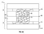
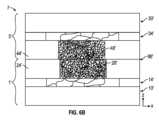
図3は、粗粒銅の粒50を示す、粗粒銅の概略上面図である。図4は、一実施形態による細粒銅の粒52を示す、細粒銅の概略上面図である。図3及び4の粗粒銅と細粒銅は両方とも、80℃~150℃の温度で120分間アニールされている。粗粒銅の平均粒径は0.5μm~3μmの範囲にあり、細粒銅の平均粒径は10nm~500nmの範囲とすることができる。図3に示すように、銅の粒内に双晶54が形成される場合がある。一部の実施形態では、細粒銅の粒52は、粒構造内(例えば、粒52の1又は2以上の粒内)にナノ双晶(図示せず)を含むことができる。一部の実施形態では、図1Bの導電性特徴28は、2つ以上の種類の微細構造を含むことができる。例えば、導電性特徴28の部分は、上部と、上部よりもメタライゼーション層18の近くに位置決めされた底部とを含むことができる(図6Dを参照)。一部の実施形態では、導電性特徴28の上部は、導電性特徴28の厚さの5%~70%の範囲の厚さを有する。一部の実施形態では、導電性特徴28の上部は、例えば50nm~500nmの範囲の厚さを有する。底部は、高度に配向した微細構造、例えばナノ双晶銅の微細構造を有する導電性特徴を含むことができる。上部は、導電性特徴28の接合面と、接合面と底部の間の導電性領域とを含むことができる。上部は、例えば細粒銅などの細粒金属を含むことができる。一部の実施形態では、導電性特徴28の底部は、例えば、粗粒を備えた従来のBEOL又は実装用の銅など、粗粒構造を有する材料を含むことができる。一部の実施形態では、底部は、純銅以外の別の材料、例えば、銅合金、ニッケル、コバルト、タングステン、アルミニウム、及びそれら各々の様々な合金を含むことができる。一部の適用例では、導電性特徴28の上部と底部の間にバリア層(図示せず)を配置することができる。バリア層は、上部と底部の微細構造の混合を防止する又は軽減することができる。 FIG. 3 is a schematic top view of coarse-grained
粒界及び界面に沿う拡散の活性化エネルギは、格子拡散の活性化エネルギよりも大幅に低い。大きな粒界表面積を備えた細粒微細構造の場合、金属-金属間接合において、粒界拡散経路が支配的である。また、細粒微細構造は一般的に、ナノ双晶銅、並びに粒径が著しく大きい従来の粗粒銅と比較して、高いクリープ速度を呈することができる。細粒銅における極めて速い拡散経路の著しく高い密度とより高いクリープ速度が、その低温接合傾向を説明する。直接接合される相互接続の接合面に細粒金属の微細構造が望ましいのは、この微細構造が低温接合傾向にあるからである。 The activation energy for diffusion along grain boundaries and interfaces is significantly lower than that for lattice diffusion. For fine-grained microstructures with large grain boundary surface areas, grain boundary diffusion paths dominate in metal-to-metal junctions. Also, fine-grained microstructures can generally exhibit higher creep rates compared to nanotwinned copper as well as conventional coarse-grained copper, which has significantly larger grain sizes. The significantly higher density of extremely fast diffusion paths and higher creep rates in fine-grained copper explain its low temperature bonding tendency. A fine-grained metal microstructure is desirable at the interface of directly bonded interconnects because this microstructure tends to bond at low temperatures.
図5は、細粒銅パッド(FG)及び従来の銅パッド(STD)に関する、温度と平均抵抗の関係を示すグラフである。平均抵抗は、対向する導電性特徴間の接触程度に関する指標を与えることができる;平均抵抗が低いほど、平均抵抗が高い場合と比較して接続が良好であることを意味し得る。このグラフは、細粒パッドが従来の銅パッドよりも低い温度で、抵抗に関する所望の値又は公称値に達することを示している。この結果は、細粒パッドが従来の銅パッドよりも低いアニール(接合)温度で別のパッドに接合可能であることを示している。 FIG. 5 is a graph showing the relationship between temperature and average resistance for fine grain copper pads (FG) and conventional copper pads (STD). The average resistance can provide an indication as to the degree of contact between opposing conductive features; a lower average resistance can mean a better connection compared to a higher average resistance. This graph shows that the fine grain pad reaches the desired or nominal value for resistance at a lower temperature than the conventional copper pad. This result indicates that the fine grain pad can be bonded to another pad at lower annealing (bonding) temperatures than traditional copper pads.
図6Aは、導電性特徴70、80(例えば、従来の銅パッド)を備えた接合構造4の概略側断面図である。接合構造は、第1の素子5と、接合界面86に沿って第1の素子5に接合される第2の素子6とを含む。第1の素子5は、導電性特徴70、非導電性領域72、及びメタライゼーション層74を含む。第2の素子6は、導電性特徴80、非導電性領域82、及びメタライゼーション層84を含む。導電性特徴70、80は、例えば1μm超の平均粒径を有する銅粒など、粗粒を含む。導電性特徴74、84は、従来の粗粒金属(例えば、粗粒銅)を含む。 FIG. 6A is a schematic side cross-sectional view of a bonding structure 4 with
接合構造4は、接合のために180℃を超える温度でアニールされている。アニール時間又は温度が増加するにつれて、接合界面86における金属-金属間(例えば、銅-銅間)の接合界面は、発達することができる。長時間アニールするほど、接合界面により多くの金属拡散(例えば、銅の拡散)が生じる。接合界面86はx方向に沿って延びることができ、x方向にほぼ垂直なz方向が、膜成長方向とすることができる。接合素子4の一部の実施形態では、接合界面86を遮る導電性特徴70、80の粒数は、その最大幅又は直径において11粒以下とすることができる。導電性特徴70、80の直径又は幅に応じて、接合界面で遮る粒の数は、8粒より少ない、又は更には5粒より少なくし得る。 The bonded structure 4 is annealed at a temperature above 180° C. for bonding. As the annealing time or temperature increases, the metal-to-metal (eg, copper-to-copper) bond interface at
図6Bは、一実施形態による接合構造7の概略側断面図である。特に断りのない限り、図6Bの構成要素は、図1A~2の同様の構成要素と同じ又はほぼ類似とすることができる。接合構造7は、第1の素子1’と、接合界面86’に沿って第1の素子1’に接合される第2の素子3’とを含むことができる。第1の素子1’は、導電性特徴28’、非導電性領域24’、メタライゼーション層14’、及びキャリア10’を含む。第2の素子3’は、導電性特徴48’、非導電性領域44’、メタライゼーション層34’、及びキャリア30’を含む。導電性特徴28’、48’は、細粒金属(例えば、細粒銅)を含むことができる。メタライゼーション層24’、34’は、従来の粗粒金属(例えば、粗粒銅)を含むことができる。接合構造7の一部の実施形態では、メタライゼーション層14’又は34’のうちの一方は、例えば細粒銅などの細粒金属を有する層を含むことができる。 FIG. 6B is a schematic side cross-sectional view of a joining
接合構造7は、接合のために180℃を超える温度でアニールされている。導電性特徴28’、48’を接合するためのアニールプロセスの前後で、導電性特徴28’、48’内の粒子の粒径は、ほぼ同様とすることができる。例えば、アニールプロセス後の導電性特徴28’、48’の平均粒径は、アニールされていない導電性特徴28’、48’の平均粒径の2倍を超えないものとすることができる。アニール時間及び/又は温度が増加するにつれて、接合界面86’における金属-金属間(例えば、銅-銅間)の接合界面は、発達することができる。十分な時間のアニールの後には、金属-金属間の接合界面により多くの金属拡散(例えば、銅の拡散)が生じる可能性がある。一部の実施形態では、接合界面86’はx方向に沿って延びるようにすることができ、x方向にほぼ垂直なz方向が、膜成長方向とすることができる。一部の実施形態では、接合構造7の細粒構造の結果として、直線横方向寸法において界面86’を遮る、接合された導電性特徴28’又は48’の粒数は、その最大幅又は直径において12粒より多くし得る。一部の実施形態では、界面86’を遮る粒数は、16粒より多く、又は20粒より多くし得る。
図6Cは、一実施形態による接合構造7’の概略側断面図である。特に断りのない限り、図6Cの構成要素は、図1A~2、6A及び6Bの同様の構成要素と同じ又はほぼ類似とすることができる。接合構造7’は、接合界面86’に沿って粗粒の導電性金属を含む従来の銅パッドなどの、従来型導電性特徴70に直接接合された導電性特徴28’を含む第1の素子1’を含むことができる。第1の素子1’は、導電性特徴28’、非導電性領域24’、メタライゼーション層14’、及びキャリア10’を含むことができる。素子5は、導電性特徴70、非導電性領域72、メタライゼーション層84、及びキャリア74を含むことができる。導電性特徴70は導電性特徴の一例であり、素子5は、何れかの適切な導電性特徴を含むことができる。導電性特徴28’は、細粒金属(例えば、細粒銅)を含むことができ、導電性特徴70は、粗粒金属(例えば、粗粒銅)を含むことができる。一部の実施形態では、従来型導電性特徴70の材料は、導電性特徴28’の材料に少なくとも部分的に基づいて選択することができる。例えば、従来型導電性特徴70の材料は、導電性特徴28’の材料と同じ又は類似した種類の金属を有するように選択することができる。メタライゼーション層14’、74は、従来の粗粒銅を含むことができる。他の種類の金属及び金属微細構造をメタライゼーション層14’、74に使用してもよい。接合構造7’の一部の実施形態では、メタライゼーション層14’又は74のうちの一方は、例えば細粒銅などの細粒導電性金属を有する層を含むことができる。 FIG. 6C is a schematic side cross-sectional view of a joining
接合構造7’は、接合のために(例えば、180℃の温度で)アニールされている。導電性特徴28’及び導電性パッド70における粒の粒径は、導電性特徴70’、80を接合するためのアニールプロセスの前後で異なる。アニール時間及び/又は温度が増加するにつれて、接合界面86''における金属-金属間(例えば、銅-銅間)の接合界面は、発達することができる。十分な時間のアニールの後には、噛み合う導電性特徴28’と導電性特徴70の接合界面により多くの金属拡散(例えば、銅の拡散)が生じる可能性がある。一部の実施形態では、接合界面86''はx方向に沿って延びることができ、x方向にほぼ垂直なz方向が、膜成長方向とすることができる。一部の実施形態では、接合界面86''の直径において接合界面86''の直線横方向寸法に測定される、第1の素子1’の第1の導電性特徴28’で遮る粒数は、接合界面86''で素子5の導電性特徴70で遮る粒数よりも10%以上多い。例えば、接合構造7’は、導電性特徴28’で界面86''を遮る21粒以上と、導電性特徴80で界面86''を遮る12粒以下とを含むことができる。一部の実施形態では、第1の素子1’の導電性特徴28で界面86''を遮る粒数は、素子5の導電性特徴80で接合界面86''を遮る粒数とは異なる。 The
図6Cは、一実施形態による接合構造7''の概略側断面図である。特に断りのない限り、図6Dの構成要素は、図1A~2、6A~6Cの同様の構成要素と同じか、又はほぼ類似とすることができる。接合構造7''は、接合構造7''の素子3''が導電性特徴48''内に細粒部分88と粗粒部分89を含むことを除いて、図6Aの接合構造7とほぼ同様とすることができる。図6Cは1つの細粒部分と1つの粗粒部分を示しているが、一部の実施形態では、複数の細粒部分及び/又は複数の粗粒部分が存在することができる。接合界面86'''のより近くに位置決めされた細粒部分88を上部と呼ぶことができ、メタライゼーション層34’に近い粗粒部分89を底部と呼ぶことができる。一部の実施形態では、導電性特徴48''の細粒部分88は、導電性特徴28の厚さTcfの5%~70%の範囲にある厚さTfgを有する。例えば、厚さTfgは、導電性特徴28の厚さTcfの5%~50%、5%~20%、10%~50%、又は10%~20%の範囲とすることができる。一部の実施形態では、細粒部分88の厚さTfgは、例えば50nm~500nmの範囲とすることができる。例えば、厚さTfgは、50nm~400nm、50nm~300nm、100nm~500nm、又は100~300nmの範囲とすることができる。 FIG. 6C is a schematic side cross-sectional view of a joining
図7A~7Cは、異なる種類の銅特徴に関するトップダウン電子後方散乱回折(EBSD)画像を示している。図7Aは、従来の又は粗粒の銅特徴に関するトップダウンEBSD画像である。図7Bは、ナノ双晶銅特徴のトップダウンEBSD画像である。図7Cは、一実施形態による細粒銅特徴のトップダウンEBSD画像である。図7A~7Cは、膜成長方向と同じ方向(例えば、図7A~7Cの画像で画像面に垂直)であるz方向(図6A~6Dを参照)に平行な粒配向を示す。例えば、粒子90は、z方向が粒子の<111>方位にほぼ平行であるような結晶方位を有し、粒子92は、z方向が粒子の<001>方位にほぼ平行であるような結晶方位を有し、そして粒子94は、z方向が粒子の<101>方位とほぼ平行となるような結晶方位を有する。図7Aは、異なる粒方位(例えば、<111>、<001>、及び<101>方位)を有する粗粒を備えた粗粒銅特徴の例示的な微細構造を示す。対照的に、図7Bは、ほとんど又は本質的に単一の金属粒方位(例えば、<111>方位)を含む、高度に配向した粒子を有するナノ双晶銅特徴の例示的な微細構造を示している。別の実施形態では、高度に配向した粒子は、<111>方位、<100>方位、<110>方位、或いは双晶微細構造及び/又は正方晶構造又は六方晶構造などの高配向性非立方晶構造のように、これらの組み合わせを有することができる。図7Cは、細粒銅特徴の例示的な微細構造を示す。微細構造は、典型的には100nm未満の粒径を備えた細粒を備え、細粒の様々な粒子は、<111>、<110>、<100>方位などの異なる粒方位を有することができる。図7Cの暗い領域は、電子後方散乱回折では検出されなかった方位を備えた粒子96である。 7A-7C show top-down electron backscatter diffraction (EBSD) images for different types of copper features. FIG. 7A is a top-down EBSD image of a conventional or coarse-grained copper feature. FIG. 7B is a top-down EBSD image of nanotwinned copper features. FIG. 7C is a top-down EBSD image of a fine-grained copper feature according to one embodiment. 7A-7C show grain orientation parallel to the z-direction (see FIGS. 6A-6D), which is the same direction as the film growth direction (eg, perpendicular to the image plane in the images of FIGS. 7A-7C). For example,
一態様では、接合構造が開示される。この接合構造は、第1の導電性特徴と第1の非導電性領域とを有する第1の素子を含むことができる。第1の導電性特徴は、500nm以下の平均粒径を有する細粒金属を備えた接合構造は、第2の導電性特徴と第2の非導電性領域とを含む第2の素子を含むことができる。第1の導電性特徴は、接着剤を介在させることなく第2の導電性特徴に直接接合され、第2の非導電性領域は、接着剤を介在させることなく第2の非導電性領域に直接接合される。 In one aspect, a bonding structure is disclosed. The junction structure can include a first element having a first conductive feature and a first non-conductive region. The first electrically conductive feature comprises a fine-grained metal having an average grain size of 500 nm or less, and the junction structure includes a second element that includes a second electrically conductive feature and a second non-conductive region. I can do it. The first electrically conductive feature is bonded directly to the second electrically conductive feature without any intervening adhesive, and the second electrically non-conductive region is bonded to the second electrically conductive region without any intervening adhesive. Directly joined.
一実施形態では、第1の導電性特徴は銅を含む。 In one embodiment, the first conductive feature includes copper.
一実施形態では、第1の導電性特徴の粒子は、500nm未満の最大粒径を有する。第1の導電性特徴の粒子は、350nm未満の最大粒径を有することができる。第1の導電性特徴の粒子は、50nm未満の最大粒径を有することができる。 In one embodiment, the particles of the first electrically conductive feature have a maximum particle size of less than 500 nm. The particles of the first electrically conductive feature can have a maximum particle size of less than 350 nm. The particles of the first electrically conductive feature can have a maximum particle size of less than 50 nm.
一実施形態では、第2の導電性特徴の粒子の平均粒径は500nm以下である。 In one embodiment, the particles of the second electrically conductive feature have an average particle size of 500 nm or less.
一実施形態では、第2の導電性特徴の粒子の平均粒径は1μmを超える。 In one embodiment, the particles of the second electrically conductive feature have an average particle size greater than 1 μm.
一実施形態では、第1の導電性特徴の細粒金属の平均粒径は350nm以下である。第1の導電性特徴の細粒金属の平均粒径は、10nm~300nmの範囲とすることができる。 In one embodiment, the fine-grained metal of the first conductive feature has an average grain size of 350 nm or less. The average grain size of the fine-grained metal of the first electrically conductive feature can range from 10 nm to 300 nm.
一実施形態では、第1の導電性特徴の粒子の95%超が、粒径ばらつきが10%未満である。 In one embodiment, more than 95% of the particles of the first electrically conductive feature have a particle size variation of less than 10%.
一実施形態では、第1の素子は、導電性部分を有するメタライゼーション層を更に備える。メタライゼーション層の導電性部分は、1μm~2μmの範囲の平均粒径を有する金属を含むことができる。 In one embodiment, the first element further comprises a metallization layer having a conductive portion. The conductive portion of the metallization layer may include metal having an average grain size in the range of 1 μm to 2 μm.
一実施形態では、第1の導電性特徴の細粒金属は、不活性材料のナノ粒子を含む。ナノ粒子の濃度は、第1の導電性特徴の1%未満とすることができる。ナノ粒子の濃度は、第1の導電性特徴の0.1%未満とすることができる。ナノ粒子は、酸化シリコン、アルミナ、及び酸化チタンのうちの1又は2以上を含むことができる。 In one embodiment, the fine-grained metal of the first conductive feature includes nanoparticles of inert material. The concentration of nanoparticles can be less than 1% of the first electrically conductive feature. The concentration of nanoparticles can be less than 0.1% of the first electrically conductive feature. The nanoparticles can include one or more of silicon oxide, alumina, and titanium oxide.
一実施形態では、細粒金属は構成成分を含む。 In one embodiment, the fine-grained metal includes constituents.
一態様では、接合構造が開示される。この接合構造は、第1の導電性特徴と第1の非導電性領域とを有する第1の素子を含むことができる。第1の導電性特徴は、構成成分を有する細粒金属を備えた接合構造は、第2の導電性特徴と第2の非導電性領域とを含む第2の素子を含むことができる。第1の導電性特徴は、接着剤を介在させることなく第2の導電性特徴に直接接合され、第2の非導電性領域は、接着剤を介在させることなく第2の非導電性領域に直接接合される。 In one aspect, a bonding structure is disclosed. The junction structure can include a first element having a first conductive feature and a first non-conductive region. The first electrically conductive feature can include a second element including a second electrically conductive feature and a second non-conductive region. The first electrically conductive feature is bonded directly to the second electrically conductive feature without any intervening adhesive, and the second electrically non-conductive region is bonded to the second electrically conductive region without any intervening adhesive. Directly joined.
一実施形態では、構成成分は、ホウ素、インジウム、リン、ガリウム、ニッケル、コバルト、スズ、マンガン、チタン、バナジウム及びセレンのうちの少なくとも1つを含む。第1の導電性特徴は、500nm以下の平均粒径を有する細粒金属を含むことができる。第1の導電性特徴の細粒金属の平均粒径は、10nm~300nmの範囲とすることができる。 In one embodiment, the components include at least one of boron, indium, phosphorous, gallium, nickel, cobalt, tin, manganese, titanium, vanadium, and selenium. The first electrically conductive feature can include a fine grained metal having an average grain size of 500 nm or less. The average grain size of the fine-grained metal of the first electrically conductive feature can range from 10 nm to 300 nm.
一態様では、相互接続構造が開示される。この相互接続構造は、接合面を含む素子を含むことができる。この素子は、導電性特徴と非導電性領域とを有する。導電性特徴は、非導電性領域に少なくとも部分的に埋め込まれる。導電性特徴は、底部と、底部の上に配置された上部とを含む。上部は、底部よりも素子の接合面の近くに位置決めされる。上部は、底部の平均粒径よりも小さい平均粒径を有する。上部の平均粒径は500nm以下である。 In one aspect, an interconnect structure is disclosed. The interconnect structure can include elements that include bonding surfaces. The device has electrically conductive features and non-conductive regions. The conductive features are at least partially embedded in the non-conductive regions. The conductive feature includes a bottom and a top disposed over the bottom. The top is positioned closer to the bonding surface of the element than the bottom. The top has a smaller average grain size than the bottom. The average grain size of the upper part is 500 nm or less.
一実施形態では、接合構造は、相互接続構造と第2の素子とを含む。 In one embodiment, the bond structure includes an interconnect structure and a second element.
一態様では、基板を形成する方法が開示される。この方法は、半導体素子の非導電性層にキャビティを設けるステップと、キャビティ内に導電性コンタクト構造を設けるステップと、非導電性層と導電性コンタクト構造を直接接合のために準備するステップとを含むことができる。導電性コンタクト構造は、500nm未満の平均粒径を含む細粒構造を有する。 In one aspect, a method of forming a substrate is disclosed. The method includes the steps of providing a cavity in a non-conductive layer of a semiconductor device, providing a conductive contact structure within the cavity, and preparing the non-conductive layer and the conductive contact structure for direct bonding. can be included. The conductive contact structure has a fine grained structure with an average grain size of less than 500 nm.
一実施形態では、導電性コンタクト構造は銅を含む。 In one embodiment, the conductive contact structure includes copper.
一実施形態では、平均粒径は350nm未満である。平均粒径は10nm~300nmの範囲とすることができる。 In one embodiment, the average particle size is less than 350 nm. The average particle size can range from 10 nm to 300 nm.
一実施形態では、導電性コンタクト構造を設けるステップは、0.5%未満の添加剤を有する銅電気めっき浴を設けるステップと、導電性コンタクト構造をキャビティ内に電気めっきするステップとを含む。添加剤は、ホウ素、インジウム、リン、ガリウム、ニッケル、コバルト、スズ、マンガン、チタン、バナジウム及びセレンのうちの1又は2以上を含む。 In one embodiment, providing the conductive contact structure includes providing a copper electroplating bath having less than 0.5% additive and electroplating the conductive contact structure into the cavity. The additive includes one or more of boron, indium, phosphorus, gallium, nickel, cobalt, tin, manganese, titanium, vanadium, and selenium.
一実施形態では、導電性コンタクト構造を設けるステップは、電気的に不活性なナノ粒子を内部に有する銅電気めっき浴を設けるステップを含む。電気的に不活性なナノ粒子は、酸化シリコン、アルミナ、及び酸化チタンのうちの1又は2以上を含むことができる。ナノ粒子の濃度は、1体積%未満とすることができる。ナノ粒子の濃度は、0.1体積%未満とすることができる。 In one embodiment, providing a conductive contact structure includes providing a copper electroplating bath having electrically inert nanoparticles therein. The electrically inert nanoparticles can include one or more of silicon oxide, alumina, and titanium oxide. The concentration of nanoparticles can be less than 1% by volume. The concentration of nanoparticles can be less than 0.1% by volume.
一実施形態では、導電性コンタクト構造の金属粒回復は、室温で及び120℃未満の温度で抑制される。 In one embodiment, metal grain recovery of the conductive contact structure is suppressed at room temperature and at temperatures below 120°C.
一実施形態では、導電性コンタクト構造を設けるステップは、30℃未満の温度でキャビティを電気めっきするステップを含む。本方法は、5℃~15℃の範囲の温度でキャビティを電気めっきするステップを更に含むことができる。本方法は更に、5℃~15℃の範囲の温度で非導電性層及び導電性コンタクト構造を化学機械的に研磨するステップを含むことができる。 In one embodiment, providing the conductive contact structure includes electroplating the cavity at a temperature below 30°C. The method can further include electroplating the cavity at a temperature in the range of 5°C to 15°C. The method can further include chemical-mechanically polishing the non-conductive layer and the conductive contact structure at a temperature in the range of 5°C to 15°C.
一実施形態では、本方法は、接着剤を介在させることなく、半導体素子の非導電性層を第2の半導体素子の第2の非導電性層に直接接合するステップを更に含む。本方法は、半導体素子及び第2の半導体素子をアニールして、導電性コンタクト構造を第2の半導体素子の第2の導電性コンタクト構造に接触させるステップを更に含むことができる。アニールは、300℃未満の温度で行うことができる。アニールは、250℃未満の温度で行うことができる。 In one embodiment, the method further includes bonding the non-conductive layer of the semiconductor element directly to the second non-conductive layer of the second semiconductor element without an intervening adhesive. The method may further include annealing the semiconductor device and the second semiconductor device to contact the conductive contact structure with the second conductive contact structure of the second semiconductor device. Annealing can be performed at temperatures below 300°C. Annealing can be performed at temperatures below 250°C.
一実施形態では、導電性コンタクト構造を設けるステップは、0.1mA/cm2~70mA/cm2の範囲の電流密度を使用してキャビティを電気めっきするステップを含む。 In one embodiment, providing the conductive contact structure includes electroplating the cavity using a current density in the range of 0.1 mA/cm2 to 70 mA/cm2 .
一実施形態では、導電性コンタクト構造を設けるステップは、0.1M~0.4Mの銅イオンと0.1M~1Mの酸とを有する電気めっき浴を設けるステップを含む。 In one embodiment, providing the conductive contact structure includes providing an electroplating bath having 0.1M to 0.4M copper ions and 0.1M to 1M acid.
一実施形態では、非導電性層を設けるステップは、集積回路デバイス上への堆積を含む。本方法は、細粒構造を有する導電性コンタクト構造でキャビティを埋める前に、キャビティの少なくとも側壁をバリア層で裏打ちするステップを更に含むことができる。 In one embodiment, providing the non-conductive layer includes depositing it on the integrated circuit device. The method can further include lining at least the sidewalls of the cavity with a barrier layer before filling the cavity with the conductive contact structure having a fine-grained structure.
一態様では、基板を形成する方法が開示される。この方法は、半導体素子の非導電性層にキャビティを設けるステップと、キャビティ内に導電性コンタクト構造を設けるステップと、非導電性層と導電性コンタクト構造を直接接合のために準備するステップとを含むことができる。導電性コンタクト構造は、細粒構造を有する。 In one aspect, a method of forming a substrate is disclosed. The method includes the steps of providing a cavity in a non-conductive layer of a semiconductor device, providing a conductive contact structure within the cavity, and preparing the non-conductive layer and the conductive contact structure for direct bonding. can be included. The conductive contact structure has a fine grained structure.
一実施形態では、導電性コンタクト構造は銅を含む。 In one embodiment, the conductive contact structure includes copper.
一実施形態では、導電性コンタクト構造の粒子の大部分は、500nm以下の粒径を有する。大部分の粒子は、350nm以下の粒径を有する。粒の大部分は、10nm~300nmの範囲の粒径を有する。 In one embodiment, the majority of the particles of the conductive contact structure have a particle size of 500 nm or less. Most particles have a particle size of 350 nm or less. The majority of the grains have a size ranging from 10 nm to 300 nm.
一実施形態では、導電性コンタクト構造の粒子の平均粒径は、500nm以下である。平均粒径は350nm以下とすることができる。平均粒径は10nm~300nmの範囲とすることができる。 In one embodiment, the particles of the conductive contact structure have an average particle size of 500 nm or less. The average particle size can be 350 nm or less. The average particle size can range from 10 nm to 300 nm.
一実施形態では、導電性コンタクト構造を設けるステップは、0.5%未満の添加剤を有する銅電気めっき浴を設けるステップと、導電性コンタクト構造をキャビティ内に電気めっきするステップとを含む。銅電気めっき浴は、0.1%未満の添加剤を含むことができる。添加剤は、ホウ素、インジウム、リン、ガリウム、ニッケル、コバルト、スズ、マンガン、チタン、バナジウム及びセレンのうちの1又は2以上を含むことができる。 In one embodiment, providing the conductive contact structure includes providing a copper electroplating bath having less than 0.5% additive and electroplating the conductive contact structure into the cavity. The copper electroplating bath can contain less than 0.1% additives. The additive may include one or more of boron, indium, phosphorus, gallium, nickel, cobalt, tin, manganese, titanium, vanadium, and selenium.
一実施形態では、導電性コンタクト構造を設けるステップは、電気的に不活性なナノ粒子を内部に有する銅電気めっき浴を設けるステップを含む。電気的に不活性なナノ粒子は、酸化シリコン、アルミナ、及び酸化チタンのうちの1又は2以上を含むことができる。ナノ粒子の濃度は、1体積%未満とすることができる。ナノ粒子の濃度は、0.1体積%未満とすることができる。 In one embodiment, providing a conductive contact structure includes providing a copper electroplating bath having electrically inert nanoparticles therein. The electrically inert nanoparticles can include one or more of silicon oxide, alumina, and titanium oxide. The concentration of nanoparticles can be less than 1% by volume. The concentration of nanoparticles can be less than 0.1% by volume.
一実施形態では、導電性コンタクト構造の金属粒回復は、室温で及び120℃未満の温度で抑制される。 In one embodiment, metal grain recovery of the conductive contact structure is suppressed at room temperature and at temperatures below 120°C.
一実施形態では、導電性コンタクト構造を設けるステップは、30℃未満の温度でキャビティを電気めっきするステップを含む。本方法は、5℃~15℃の範囲の温度でキャビティを電気めっきするステップを更に含むことができる。本方法は、5℃~15℃の範囲の温度で非導電性層及び導電性コンタクト構造を化学機械的に研磨するステップを更に含むことができる。 In one embodiment, providing the conductive contact structure includes electroplating the cavity at a temperature below 30°C. The method can further include electroplating the cavity at a temperature in the range of 5°C to 15°C. The method can further include chemical-mechanically polishing the non-conductive layer and the conductive contact structure at a temperature in the range of 5°C to 15°C.
一実施形態では、本方法は、接着剤を介在させることなく、半導体素子の非導電性層を第2の半導体素子の第2の非導電性層に直接接合するステップを更に含む。本方法は、半導体素子及び第2の半導体素子をアニールして、導電性コンタクト構造を第2の半導体素子の第2の導電性コンタクト構造に接触させるステップを更に含むことができる。アニールは、300℃未満の温度で行うことができる。アニールは、250℃未満の温度で行うことができる。 In one embodiment, the method further includes bonding the non-conductive layer of the semiconductor element directly to the second non-conductive layer of the second semiconductor element without an intervening adhesive. The method may further include annealing the semiconductor device and the second semiconductor device to contact the conductive contact structure with the second conductive contact structure of the second semiconductor device. Annealing can be performed at temperatures below 300°C. Annealing can be performed at temperatures below 250°C.
一実施形態では、導電性コンタクト構造を設けるステップは、0.1mA/cm2~70mA/cm2の範囲の電流密度を使用してキャビティを電気めっきするステップを含む。この電流密度は、40mA/cm2~70mA/cm2の範囲とすることができる。 In one embodiment, providing the conductive contact structure includes electroplating the cavity using a current density in the range of 0.1 mA/cm2 to 70 mA/cm2 . This current density can range from 40 mA/cm2 to 70 mA/cm2 .
一実施形態では、導電性コンタクト構造を設けるステップは、0.1M~0.4Mの銅イオンと0.1M~1Mの酸とを有する電気めっき浴を設けるステップを含む。電気めっき浴は、30ppm~70ppmの範囲のハロゲン化物イオンを有することができる。 In one embodiment, providing the conductive contact structure includes providing an electroplating bath having 0.1M to 0.4M copper ions and 0.1M to 1M acid. The electroplating bath can have halide ions ranging from 30 ppm to 70 ppm.
一実施形態では、非導電性層を設けるステップは、集積回路デバイス上への堆積を含む。本方法は、細粒構造を有する導電性コンタクト構造でキャビティを埋める前に、キャビティの少なくとも側壁をバリア層で裏打ちするステップを更に含むことができる。非導電性層を設けるステップは、集積回路デバイス上の再配線層への堆積を含むことができる。 In one embodiment, providing the non-conductive layer includes depositing it on the integrated circuit device. The method can further include lining at least the sidewalls of the cavity with a barrier layer before filling the cavity with the conductive contact structure having a fine-grained structure. Providing a non-conductive layer can include depositing a redistribution layer on an integrated circuit device.
一態様では、接合構造が開示される。この接合構造は、第1の導電性特徴と第1の非導電性領域とを有する第1の素子を含むことができる。本接合構造は、第2の導電性特徴と第2の非導電性領域とを含む第2の素子を含むことができる。第1の導電性特徴は、接着剤を介在させることなく第2の導電性特徴に直接接合され、それによって接合界面が形成される。接合界面の粒数は40を超える数である。第2の非導電性領域は、接着剤を介在させることなく第2の非導電性領域に直接接合される。 In one aspect, a bonding structure is disclosed. The junction structure can include a first element having a first conductive feature and a first non-conductive region. The junction structure can include a second element including a second conductive feature and a second non-conductive region. The first electrically conductive feature is bonded directly to the second electrically conductive feature without an intervening adhesive, thereby forming a bonding interface. The number of grains at the bonding interface exceeds 40. The second non-conductive region is bonded directly to the second non-conductive region without an intervening adhesive.
一実施形態では、第1の導電性特徴は、500nm以下の平均粒径を有する細粒金属を含む。 In one embodiment, the first conductive feature includes a fine grained metal having an average grain size of 500 nm or less.
一実施形態では、第1の導電性特徴は、約0.01μm~25μmの範囲の最大横方向寸法有する。第1の導電性特徴は、1μm未満の最大横方向寸法を有することができる。 In one embodiment, the first conductive feature has a maximum lateral dimension in the range of about 0.01 μm to 25 μm. The first electrically conductive feature can have a maximum lateral dimension of less than 1 μm.
一実施形態では、接合界面の全面積は約100μm2よりも小さい。接合界面の全面積は、2μm2より小さくし得る。 In one embodiment, the total area of the bond interface is less than about 100 μm2 . The total area of the bonding interface may be less than 2 μm2 .
文脈上明らかに他を意味しない限り、本明細書及び特許請求の範囲を通して、単語「備える(comprise)」、「備えている(comprising)」、「含む(include)」、「含んでいる(including)」などは、排他的又は網羅的な意味に対立するものとして、包括的な意味で、すなわち、「含むがこれに限定されない」という意味で解釈すべきである。本明細書で一般に使用する単語「繋がれる」とは、直接接続されるか、1又は2以上の中間要素を経由して接続されるかの何れかである2又は3以上の要素を指す。同様に、本明細書で一般に使用する単語「接続される」とは、直接接続されるか、1又は2以上の中間要素を介して接続されるかの何れかである2又は3以上の要素を指す。更に、単語「本明細書で」、「上記に」、「下記に」、並びに同様の取込みに関する単語は、本出願で使用する場合、全体として本出願を指し、本出願の何れか特定の部分には言及しないものとする。更に、本明細書で使用するように、第1の要素が第2の要素の「上に」又は「上方に」あると記述される場合、第1の要素は、第1及び第2の要素が直接接触するように、直接的に第2の要素の上に又は上方にあることができ、或いは第1の要素は、第1の要素と第2の要素の間に1又は2以上の要素が介在するように、間接的に第2の要素の上に又は上方とすることができる。文脈が許す限り、上記の詳細な説明において単数又は複数を用いる単語は、それぞれ複数又は単数をも包含することができる。2又は3以上の項目のリストに関連する単語「又は」は、その単語について以下の解釈の全てを網羅する:リスト中の項目の何れか、リスト中の項目の全て、並びにリスト中の項目の何れかの組み合わせ。 Unless the context clearly dictates otherwise, the words "comprise," "comprising," "include," and "including" are used throughout this specification and the claims. )" and the like should be construed in an inclusive sense, ie, "including but not limited to," as opposed to an exclusive or exhaustive sense. As used generally herein, the word "coupled" refers to two or more elements that are either directly connected or connected via one or more intermediate elements. Similarly, the word "connected," as used generally herein, refers to two or more elements that are either directly connected or connected through one or more intermediate elements. refers to Additionally, the words "herein," "above," "hereinafter," and similar incorporation words, when used in this application, refer to the application as a whole and do not refer to any particular portion of the application. shall not be mentioned. Additionally, as used herein, when a first element is described as being "on" or "above" a second element, the first element can be directly on or over the second element, such that the first element is in direct contact with the second element, or the first element has one or more elements between the first element and the second element. may be indirectly on or above the second element, such that the second element is interposed. Where the context permits, words in the above detailed description that use the singular or plural number may also include the plural or singular number, respectively. The word "or" in conjunction with a list of two or more items covers all of the following interpretations of the word: any of the items in the list, all of the items in the list, and any of the items in the list. any combination.
更に、本明細書で使用する条件付き用語、とりわけ、「できる(can)」、「できるだろう(could)」、「かもしれない(might)」、「してもよい(may)」、「例えば(e.g.)」、「例えば(for exaple)」「など(such as)」及び同様のものなどは、特に別段の記載がない限り、又は使用される文脈内で別様に理解されない限り、特定の実施形態が特定の特徴、要素及び/又は状態を含むのに対して他の実施形態は含まないことを伝達することが一般に意図されている。従って、このような条件付き用語は一般に、特徴、要素及び/又は状態が1又は2以上の実施形態に何らかの形で必要とされると示唆することを意図するものではない。 Additionally, conditional terms as used herein include, among others, "can," "could," "might," "may," " "for example", "for example", "such as" and the like shall not be understood otherwise unless specifically stated otherwise or within the context in which they are used. Insofar, it is generally intended to convey that a particular embodiment includes a particular feature, element, and/or condition whereas other embodiments do not. Thus, such conditional terminology is generally not intended to imply that a feature, element, and/or condition is required in any way by one or more embodiments.
特定の実施形態を説明したが、これらの実施形態は、例として提示したに過ぎず、開示の範囲を限定することは意図していない。実際、本明細書に記載した新規の装置、方法、及びシステムは、様々な他の形態で具体化することができ、更に、本開示の趣旨から逸脱することなく、本明細書に記載した方法及びシステムの形態において様々な省略、置換及び変更を行うことができる。例えば、ブロックを所与の配置で提示するが、代替実施形態では、異なる構成要素及び/又は回路トポロジを用いて同様の機能を果たすことができ、一部のブロックは、削除、移動、追加、細分化、結合、及び/又は修正が可能である。これらブロックの各々は、様々な異なる方法で実装することができる。上述の様々な実施形態の要素及び動作について、何れかの適切な組み合わせを行って、更なる実施形態を提供することができる。添付の特許請求の範囲及びその等価物は、本開示の範囲及び趣旨に属するような形態又は修正を網羅するように意図される。 Although particular embodiments have been described, these embodiments are offered by way of example only and are not intended to limit the scope of the disclosure. Indeed, the novel devices, methods, and systems described herein can be embodied in a variety of other forms and, further, in the methods described herein without departing from the spirit of this disclosure. Various omissions, substitutions, and changes can be made in the form of the system. For example, although blocks are presented in a given arrangement, alternative embodiments may perform similar functions using different components and/or circuit topologies, and some blocks may be removed, moved, added, Subdivision, combination and/or modification is possible. Each of these blocks can be implemented in a variety of different ways. The elements and acts of the various embodiments described above may be combined in any suitable combination to provide further embodiments. The appended claims and their equivalents are intended to cover such forms or modifications as fall within the scope and spirit of this disclosure.
Claims (80)
Translated fromJapanese第2の導電性特徴と第2の非導電性領域とを有する第2の素子と、
を備えた接合構造であって、
前記第1の導電性特徴は、接着剤を介在させることなく前記第2の導電性特徴に直接接合され、前記第2の非導電性領域は、接着剤を介在させることなく前記第2の非導電性領域に直接接合される、接合構造。 A first element having a first electrically conductive feature and a first non-conductive region, the first electrically conductive feature comprising a fine-grained metal having an average grain size of 500 nm or less. Motoko and
a second element having a second electrically conductive feature and a second non-conductive region;
A joint structure comprising:
The first conductive feature is bonded directly to the second conductive feature without an intervening adhesive, and the second non-conductive region is bonded to the second non-conductive feature without an intervening adhesive. A bonded structure that is bonded directly to a conductive area.
第2の導電性特徴と第2の非導電性領域とを有する第2の素子と、
を備えた接合構造であって、
前記第1の導電性特徴は、接着剤を介在させることなく前記第2の導電性特徴に直接接合され、前記第2の非導電性領域は、接着剤を介在させることなく前記第2の非導電性領域に直接接合される、接合構造。 a first element having a first electrically conductive feature and a first non-conductive region, the first electrically conductive feature comprising a fine-grained metal having a constituent;
a second element having a second electrically conductive feature and a second non-conductive region;
A joint structure comprising:
The first conductive feature is bonded directly to the second conductive feature without an intervening adhesive, and the second non-conductive region is bonded to the second non-conductive feature without an intervening adhesive. A bonded structure that is bonded directly to a conductive area.
前記素子は、導電性特徴と非導電性領域とを有し、前記導電性特徴は、前記非導電性領域に少なくとも部分的に埋め込まれ、前記導電性特徴は、底部と前記底部の上に配置された上部とを備え、前記上部は、前記素子の前記接合面のより近くに位置決めされ、前記上部は、前記底部の平均粒径よりも小さい平均粒径を有し、
前記上部の前記平均粒径は500nm以下である、
相互接続構造。 An interconnect structure comprising an element having a bonding surface, the interconnect structure comprising:
The element has an electrically conductive feature and a non-conductive region, the electrically conductive feature is at least partially embedded in the non-conductive region, and the electrically conductive feature is disposed on a bottom and on the bottom. a top portion positioned closer to the bonding surface of the element, the top portion having an average grain size smaller than the average grain size of the bottom portion;
the average particle size of the upper portion is 500 nm or less;
interconnected structure.
前記キャビティ内に導電性コンタクト構造を設けるステップであって、前記導電性コンタクト構造が、500nm未満の平均粒径を備えた細粒構造を有する、ステップと、
前記非導電性層と前記導電性コンタクト構造を直接接合のために準備するステップと、を含む、方法。 providing a cavity in the non-conductive layer of the semiconductor device;
providing an electrically conductive contact structure within the cavity, the electrically conductive contact structure having a fine-grained structure with an average grain size of less than 500 nm;
preparing the non-conductive layer and the conductive contact structure for direct bonding.
前記キャビティ内に導電性コンタクト構造を設けるステップであって、前記導電性コンタクト構造が細粒構造を有するステップと、
前記非導電性層と前記導電性コンタクト構造を直接接合のために準備するステップと、を含む方法。 providing a cavity in the non-conductive layer of the semiconductor device;
providing a conductive contact structure within the cavity, the conductive contact structure having a fine grained structure;
preparing the non-conductive layer and the conductive contact structure for direct bonding.
第2の導電性特徴と第2の非導電性領域とを有する第2の素子と、
を備えた接合構造であって、
前記第1の導電性特徴は、接着剤を介在させることなく前記第2の導電性特徴に直接接合されることにより接合界面が形成され、前記接合界面の粒子数は40を超える数であり、前記第2の非導電性領域は、接着剤を介在させることなく前記第2の非導電性領域に直接接合される、接合構造。 a first element having a first electrically conductive feature and a first non-conductive region;
a second element having a second electrically conductive feature and a second non-conductive region;
A joint structure comprising:
The first electrically conductive feature is directly bonded to the second electrically conductive feature without an intervening adhesive to form a bonding interface, and the number of particles at the bonding interface is greater than 40, The second non-conductive region is directly bonded to the second non-conductive region without intervening adhesive.
Applications Claiming Priority (5)
| Application Number | Priority Date | Filing Date | Title |
|---|---|---|---|
| US202163156290P | 2021-03-03 | 2021-03-03 | |
| US63/156,290 | 2021-03-03 | ||
| PCT/US2022/018574WO2022187402A1 (en) | 2021-03-03 | 2022-03-02 | Contact structures for direct bonding |
| US17/684,841US20220285303A1 (en) | 2021-03-03 | 2022-03-02 | Contact structures for direct bonding |
| US17/684,841 | 2022-03-02 |
Publications (2)
| Publication Number | Publication Date |
|---|---|
| JP2024513304Atrue JP2024513304A (en) | 2024-03-25 |
| JPWO2022187402A5 JPWO2022187402A5 (en) | 2025-03-11 |
Family
ID=83117308
Family Applications (1)
| Application Number | Title | Priority Date | Filing Date |
|---|---|---|---|
| JP2023553418APendingJP2024513304A (en) | 2021-03-03 | 2022-03-02 | Contact structure for direct bonding |
Country Status (7)
| Country | Link |
|---|---|
| US (1) | US20220285303A1 (en) |
| EP (1) | EP4302325A4 (en) |
| JP (1) | JP2024513304A (en) |
| KR (1) | KR20230153446A (en) |
| CN (1) | CN117256047A (en) |
| TW (1) | TW202238765A (en) |
| WO (1) | WO2022187402A1 (en) |
Families Citing this family (86)
| Publication number | Priority date | Publication date | Assignee | Title |
|---|---|---|---|---|
| US7109092B2 (en) | 2003-05-19 | 2006-09-19 | Ziptronix, Inc. | Method of room temperature covalent bonding |
| US8735219B2 (en) | 2012-08-30 | 2014-05-27 | Ziptronix, Inc. | Heterogeneous annealing method and device |
| US10886250B2 (en) | 2015-07-10 | 2021-01-05 | Invensas Corporation | Structures and methods for low temperature bonding using nanoparticles |
| US9953941B2 (en) | 2015-08-25 | 2018-04-24 | Invensas Bonding Technologies, Inc. | Conductive barrier direct hybrid bonding |
| US10204893B2 (en) | 2016-05-19 | 2019-02-12 | Invensas Bonding Technologies, Inc. | Stacked dies and methods for forming bonded structures |
| US11176450B2 (en) | 2017-08-03 | 2021-11-16 | Xcelsis Corporation | Three dimensional circuit implementing machine trained network |
| US10672663B2 (en) | 2016-10-07 | 2020-06-02 | Xcelsis Corporation | 3D chip sharing power circuit |
| US10580735B2 (en) | 2016-10-07 | 2020-03-03 | Xcelsis Corporation | Stacked IC structure with system level wiring on multiple sides of the IC die |
| TWI822659B (en) | 2016-10-27 | 2023-11-21 | 美商艾德亞半導體科技有限責任公司 | Structures and methods for low temperature bonding |
| US10002844B1 (en) | 2016-12-21 | 2018-06-19 | Invensas Bonding Technologies, Inc. | Bonded structures |
| US20180182665A1 (en) | 2016-12-28 | 2018-06-28 | Invensas Bonding Technologies, Inc. | Processed Substrate |
| CN117878055A (en) | 2016-12-28 | 2024-04-12 | 艾德亚半导体接合科技有限公司 | Stacking substrate processing |
| TWI837879B (en) | 2016-12-29 | 2024-04-01 | 美商艾德亞半導體接合科技有限公司 | Bonded structures with integrated passive component |
| WO2018169968A1 (en) | 2017-03-16 | 2018-09-20 | Invensas Corporation | Direct-bonded led arrays and applications |
| US10515913B2 (en) | 2017-03-17 | 2019-12-24 | Invensas Bonding Technologies, Inc. | Multi-metal contact structure |
| US10508030B2 (en) | 2017-03-21 | 2019-12-17 | Invensas Bonding Technologies, Inc. | Seal for microelectronic assembly |
| US10269756B2 (en) | 2017-04-21 | 2019-04-23 | Invensas Bonding Technologies, Inc. | Die processing |
| US10879212B2 (en) | 2017-05-11 | 2020-12-29 | Invensas Bonding Technologies, Inc. | Processed stacked dies |
| US10446441B2 (en) | 2017-06-05 | 2019-10-15 | Invensas Corporation | Flat metal features for microelectronics applications |
| US10217720B2 (en) | 2017-06-15 | 2019-02-26 | Invensas Corporation | Multi-chip modules formed using wafer-level processing of a reconstitute wafer |
| US10840205B2 (en) | 2017-09-24 | 2020-11-17 | Invensas Bonding Technologies, Inc. | Chemical mechanical polishing for hybrid bonding |
| US11031285B2 (en) | 2017-10-06 | 2021-06-08 | Invensas Bonding Technologies, Inc. | Diffusion barrier collar for interconnects |
| US11380597B2 (en) | 2017-12-22 | 2022-07-05 | Invensas Bonding Technologies, Inc. | Bonded structures |
| US10727219B2 (en) | 2018-02-15 | 2020-07-28 | Invensas Bonding Technologies, Inc. | Techniques for processing devices |
| US11169326B2 (en) | 2018-02-26 | 2021-11-09 | Invensas Bonding Technologies, Inc. | Integrated optical waveguides, direct-bonded waveguide interface joints, optical routing and interconnects |
| US11256004B2 (en) | 2018-03-20 | 2022-02-22 | Invensas Bonding Technologies, Inc. | Direct-bonded lamination for improved image clarity in optical devices |
| US10991804B2 (en) | 2018-03-29 | 2021-04-27 | Xcelsis Corporation | Transistor level interconnection methodologies utilizing 3D interconnects |
| US11056348B2 (en) | 2018-04-05 | 2021-07-06 | Invensas Bonding Technologies, Inc. | Bonding surfaces for microelectronics |
| US11244916B2 (en) | 2018-04-11 | 2022-02-08 | Invensas Bonding Technologies, Inc. | Low temperature bonded structures |
| US10790262B2 (en) | 2018-04-11 | 2020-09-29 | Invensas Bonding Technologies, Inc. | Low temperature bonded structures |
| US10964664B2 (en) | 2018-04-20 | 2021-03-30 | Invensas Bonding Technologies, Inc. | DBI to Si bonding for simplified handle wafer |
| US11004757B2 (en) | 2018-05-14 | 2021-05-11 | Invensas Bonding Technologies, Inc. | Bonded structures |
| US11276676B2 (en) | 2018-05-15 | 2022-03-15 | Invensas Bonding Technologies, Inc. | Stacked devices and methods of fabrication |
| US10923413B2 (en) | 2018-05-30 | 2021-02-16 | Xcelsis Corporation | Hard IP blocks with physically bidirectional passageways |
| KR20210009426A (en) | 2018-06-13 | 2021-01-26 | 인벤사스 본딩 테크놀로지스 인코포레이티드 | TV as a pad |
| US11393779B2 (en) | 2018-06-13 | 2022-07-19 | Invensas Bonding Technologies, Inc. | Large metal pads over TSV |
| US10910344B2 (en) | 2018-06-22 | 2021-02-02 | Xcelsis Corporation | Systems and methods for releveled bump planes for chiplets |
| WO2020010056A1 (en) | 2018-07-03 | 2020-01-09 | Invensas Bonding Technologies, Inc. | Techniques for joining dissimilar materials in microelectronics |
| US11462419B2 (en) | 2018-07-06 | 2022-10-04 | Invensas Bonding Technologies, Inc. | Microelectronic assemblies |
| US11158606B2 (en) | 2018-07-06 | 2021-10-26 | Invensas Bonding Technologies, Inc. | Molded direct bonded and interconnected stack |
| US12406959B2 (en) | 2018-07-26 | 2025-09-02 | Adeia Semiconductor Bonding Technologies Inc. | Post CMP processing for hybrid bonding |
| US11515291B2 (en) | 2018-08-28 | 2022-11-29 | Adeia Semiconductor Inc. | Integrated voltage regulator and passive components |
| US20200075533A1 (en) | 2018-08-29 | 2020-03-05 | Invensas Bonding Technologies, Inc. | Bond enhancement in microelectronics by trapping contaminants and arresting cracks during direct-bonding processes |
| US11011494B2 (en) | 2018-08-31 | 2021-05-18 | Invensas Bonding Technologies, Inc. | Layer structures for making direct metal-to-metal bonds at low temperatures in microelectronics |
| US11158573B2 (en) | 2018-10-22 | 2021-10-26 | Invensas Bonding Technologies, Inc. | Interconnect structures |
| US11244920B2 (en) | 2018-12-18 | 2022-02-08 | Invensas Bonding Technologies, Inc. | Method and structures for low temperature device bonding |
| CN113330557A (en) | 2019-01-14 | 2021-08-31 | 伊文萨思粘合技术公司 | Bonding structure |
| US11387202B2 (en) | 2019-03-01 | 2022-07-12 | Invensas Llc | Nanowire bonding interconnect for fine-pitch microelectronics |
| US11901281B2 (en) | 2019-03-11 | 2024-02-13 | Adeia Semiconductor Bonding Technologies Inc. | Bonded structures with integrated passive component |
| US10854578B2 (en) | 2019-03-29 | 2020-12-01 | Invensas Corporation | Diffused bitline replacement in stacked wafer memory |
| US11373963B2 (en) | 2019-04-12 | 2022-06-28 | Invensas Bonding Technologies, Inc. | Protective elements for bonded structures |
| US11205625B2 (en) | 2019-04-12 | 2021-12-21 | Invensas Bonding Technologies, Inc. | Wafer-level bonding of obstructive elements |
| US11355404B2 (en) | 2019-04-22 | 2022-06-07 | Invensas Bonding Technologies, Inc. | Mitigating surface damage of probe pads in preparation for direct bonding of a substrate |
| US11385278B2 (en) | 2019-05-23 | 2022-07-12 | Invensas Bonding Technologies, Inc. | Security circuitry for bonded structures |
| US12374641B2 (en) | 2019-06-12 | 2025-07-29 | Adeia Semiconductor Bonding Technologies Inc. | Sealed bonded structures and methods for forming the same |
| US11296053B2 (en) | 2019-06-26 | 2022-04-05 | Invensas Bonding Technologies, Inc. | Direct bonded stack structures for increased reliability and improved yield in microelectronics |
| US12080672B2 (en) | 2019-09-26 | 2024-09-03 | Adeia Semiconductor Bonding Technologies Inc. | Direct gang bonding methods including directly bonding first element to second element to form bonded structure without adhesive |
| US12113054B2 (en) | 2019-10-21 | 2024-10-08 | Adeia Semiconductor Technologies Llc | Non-volatile dynamic random access memory |
| US11862602B2 (en) | 2019-11-07 | 2024-01-02 | Adeia Semiconductor Technologies Llc | Scalable architecture for reduced cycles across SOC |
| US11762200B2 (en) | 2019-12-17 | 2023-09-19 | Adeia Semiconductor Bonding Technologies Inc. | Bonded optical devices |
| US11876076B2 (en) | 2019-12-20 | 2024-01-16 | Adeia Semiconductor Technologies Llc | Apparatus for non-volatile random access memory stacks |
| CN115088068A (en) | 2019-12-23 | 2022-09-20 | 伊文萨思粘合技术公司 | Electrical redundancy for bonded structures |
| US11721653B2 (en) | 2019-12-23 | 2023-08-08 | Adeia Semiconductor Bonding Technologies Inc. | Circuitry for electrical redundancy in bonded structures |
| WO2021188846A1 (en) | 2020-03-19 | 2021-09-23 | Invensas Bonding Technologies, Inc. | Dimension compensation control for directly bonded structures |
| US11742314B2 (en) | 2020-03-31 | 2023-08-29 | Adeia Semiconductor Bonding Technologies Inc. | Reliable hybrid bonded apparatus |
| WO2021236361A1 (en)* | 2020-05-19 | 2021-11-25 | Invensas Bonding Technologies, Inc. | Laterally unconfined structure |
| US11631647B2 (en) | 2020-06-30 | 2023-04-18 | Adeia Semiconductor Bonding Technologies Inc. | Integrated device packages with integrated device die and dummy element |
| US11728273B2 (en) | 2020-09-04 | 2023-08-15 | Adeia Semiconductor Bonding Technologies Inc. | Bonded structure with interconnect structure |
| US11764177B2 (en) | 2020-09-04 | 2023-09-19 | Adeia Semiconductor Bonding Technologies Inc. | Bonded structure with interconnect structure |
| US11264357B1 (en) | 2020-10-20 | 2022-03-01 | Invensas Corporation | Mixed exposure for large die |
| KR20230097121A (en) | 2020-10-29 | 2023-06-30 | 아데이아 세미컨덕터 본딩 테크놀로지스 인코포레이티드 | Direct bonding method and structure |
| JP2024501017A (en) | 2020-12-28 | 2024-01-10 | アデイア セミコンダクター ボンディング テクノロジーズ インコーポレイテッド | Structure with through-substrate via and method for forming the same |
| JP2024501559A (en) | 2020-12-30 | 2024-01-12 | アデイア セミコンダクター ボンディング テクノロジーズ インコーポレイテッド | Structures with conductive features and methods of forming the same |
| US12176321B2 (en)* | 2021-03-31 | 2024-12-24 | Taiwan Semiconductor Manufacturing Company, Ltd. | Semiconductor packages and method of forming the same |
| KR20240036698A (en) | 2021-08-02 | 2024-03-20 | 아데이아 세미컨덕터 본딩 테크놀로지스 인코포레이티드 | Protective semiconductor elements for combined structures |
| KR20230129742A (en)* | 2022-03-02 | 2023-09-11 | 삼성전자주식회사 | Semiconductor package |
| US12266622B2 (en)* | 2022-06-14 | 2025-04-01 | Nanya Technology Corporation | Method of manufacturing semiconductor structure having hybrid bonding pad |
| US12293982B2 (en)* | 2022-06-14 | 2025-05-06 | Nanya Technology Corporation | Semiconductor structure having hybrid bonding pad |
| US20240063152A1 (en)* | 2022-08-22 | 2024-02-22 | Micron Technology, Inc. | Hybrid bonding for semiconductor device assemblies |
| US20240128217A1 (en)* | 2022-10-14 | 2024-04-18 | Taiwan Semiconductor Manufacturing Company, Ltd. | Semiconductor device and manufacturing method thereof |
| TWI854373B (en)* | 2022-11-22 | 2024-09-01 | 樂鑫材料科技股份有限公司 | Backside metallization thin film structure and method for forming the same |
| US20240217210A1 (en)* | 2022-12-29 | 2024-07-04 | Adeia Semiconductor Bonding Technologies Inc. | Directly bonded metal structures having aluminum features and methods of preparing same |
| US20240222315A1 (en)* | 2022-12-29 | 2024-07-04 | Adeia Semiconductor Bonding Technologies Inc. | Directly bonded metal structures having aluminum features and methods of preparing same |
| US20240254645A1 (en)* | 2023-01-27 | 2024-08-01 | Applied Materials, Inc. | Low temperature hybrid bonding metallization |
| US12341083B2 (en) | 2023-02-08 | 2025-06-24 | Adeia Semiconductor Bonding Technologies Inc. | Electronic device cooling structures bonded to semiconductor elements |
| TWI853498B (en)* | 2023-03-20 | 2024-08-21 | 旺宏電子股份有限公司 | Bonding structure, semiconductor chip and fabricating method thereof |
Family Cites Families (17)
| Publication number | Priority date | Publication date | Assignee | Title |
|---|---|---|---|---|
| US5755859A (en)* | 1995-08-24 | 1998-05-26 | International Business Machines Corporation | Cobalt-tin alloys and their applications for devices, chip interconnections and packaging |
| US6984571B1 (en) | 1999-10-01 | 2006-01-10 | Ziptronix, Inc. | Three dimensional device integration method and integrated device |
| US6902987B1 (en) | 2000-02-16 | 2005-06-07 | Ziptronix, Inc. | Method for low temperature bonding and bonded structure |
| US7109092B2 (en) | 2003-05-19 | 2006-09-19 | Ziptronix, Inc. | Method of room temperature covalent bonding |
| US7485968B2 (en) | 2005-08-11 | 2009-02-03 | Ziptronix, Inc. | 3D IC method and device |
| US8609540B2 (en)* | 2011-06-20 | 2013-12-17 | Tessera, Inc. | Reliable packaging and interconnect structures |
| US9048283B2 (en) | 2012-06-05 | 2015-06-02 | Taiwan Semiconductor Manufacturing Company, Ltd. | Hybrid bonding systems and methods for semiconductor wafers |
| US9331038B2 (en)* | 2013-08-29 | 2016-05-03 | Taiwan Semiconductor Manufacturing Company Ltd. | Semiconductor interconnect structure |
| JP6165127B2 (en)* | 2014-12-22 | 2017-07-19 | 三菱重工工作機械株式会社 | Semiconductor device and manufacturing method of semiconductor device |
| US9741620B2 (en) | 2015-06-24 | 2017-08-22 | Invensas Corporation | Structures and methods for reliable packages |
| US10886250B2 (en)* | 2015-07-10 | 2021-01-05 | Invensas Corporation | Structures and methods for low temperature bonding using nanoparticles |
| US9728521B2 (en) | 2015-07-23 | 2017-08-08 | Taiwan Semiconductor Manufacturing Co., Ltd. | Hybrid bond using a copper alloy for yield improvement |
| US9852988B2 (en) | 2015-12-18 | 2017-12-26 | Invensas Bonding Technologies, Inc. | Increased contact alignment tolerance for direct bonding |
| US10446441B2 (en)* | 2017-06-05 | 2019-10-15 | Invensas Corporation | Flat metal features for microelectronics applications |
| US11195748B2 (en) | 2017-09-27 | 2021-12-07 | Invensas Corporation | Interconnect structures and methods for forming same |
| US11011494B2 (en)* | 2018-08-31 | 2021-05-18 | Invensas Bonding Technologies, Inc. | Layer structures for making direct metal-to-metal bonds at low temperatures in microelectronics |
| US11244920B2 (en)* | 2018-12-18 | 2022-02-08 | Invensas Bonding Technologies, Inc. | Method and structures for low temperature device bonding |
- 2022
- 2022-03-02KRKR1020237033687Apatent/KR20230153446A/enactivePending
- 2022-03-02CNCN202280030820.8Apatent/CN117256047A/enactivePending
- 2022-03-02WOPCT/US2022/018574patent/WO2022187402A1/ennot_activeCeased
- 2022-03-02JPJP2023553418Apatent/JP2024513304A/enactivePending
- 2022-03-02EPEP22764005.9Apatent/EP4302325A4/enactivePending
- 2022-03-02USUS17/684,841patent/US20220285303A1/enactivePending
- 2022-03-03TWTW111107795Apatent/TW202238765A/enunknown
Also Published As
| Publication number | Publication date |
|---|---|
| US20220285303A1 (en) | 2022-09-08 |
| EP4302325A4 (en) | 2025-01-15 |
| TW202238765A (en) | 2022-10-01 |
| EP4302325A1 (en) | 2024-01-10 |
| KR20230153446A (en) | 2023-11-06 |
| WO2022187402A1 (en) | 2022-09-09 |
| CN117256047A (en) | 2023-12-19 |
Similar Documents
| Publication | Publication Date | Title |
|---|---|---|
| JP2024513304A (en) | Contact structure for direct bonding | |
| US20240213191A1 (en) | Controlled grain growth for bonding and bonded structure with controlled grain growth | |
| US12154880B2 (en) | Method and structures for low temperature device bonding | |
| US12125784B2 (en) | Interconnect structures | |
| US20230343734A1 (en) | Expansion controlled structure for direct bonding and method of forming same | |
| US20230132632A1 (en) | Diffusion barriers and method of forming same | |
| TW202335054A (en) | Structure with conductive feature for direct bonding and method of forming same | |
| US20220246497A1 (en) | Structures with through-substrate vias and methods for forming the same | |
| TW202401505A (en) | Expansion control for bonding | |
| TW202341395A (en) | Interconnect structures | |
| CN116830256A (en) | Structure with through-substrate via and method of forming the same | |
| WO2021173788A1 (en) | Cu3sn via metallization in electrical devices for low-temperature 3d-integration | |
| WO2023122697A1 (en) | Controlled grain growth for bonding and bonded structure with controlled grain growth |
Legal Events
| Date | Code | Title | Description |
|---|---|---|---|
| A521 | Request for written amendment filed | Free format text:JAPANESE INTERMEDIATE CODE: A523 Effective date:20250303 | |
| A621 | Written request for application examination | Free format text:JAPANESE INTERMEDIATE CODE: A621 Effective date:20250303 |