JP2024502803A - Optical modules and electronic devices - Google Patents
Optical modules and electronic devicesDownload PDFInfo
- Publication number
- JP2024502803A JP2024502803AJP2023539925AJP2023539925AJP2024502803AJP 2024502803 AJP2024502803 AJP 2024502803AJP 2023539925 AJP2023539925 AJP 2023539925AJP 2023539925 AJP2023539925 AJP 2023539925AJP 2024502803 AJP2024502803 AJP 2024502803A
- Authority
- JP
- Japan
- Prior art keywords
- lens
- laminated
- optical module
- image side
- phase retarder
- Prior art date
- Legal status (The legal status is an assumption and is not a legal conclusion. Google has not performed a legal analysis and makes no representation as to the accuracy of the status listed.)
- Granted
Links
Images


Classifications
- G—PHYSICS
- G02—OPTICS
- G02B—OPTICAL ELEMENTS, SYSTEMS OR APPARATUS
- G02B25/00—Eyepieces; Magnifying glasses
- G02B25/001—Eyepieces
- G—PHYSICS
- G02—OPTICS
- G02B—OPTICAL ELEMENTS, SYSTEMS OR APPARATUS
- G02B27/00—Optical systems or apparatus not provided for by any of the groups G02B1/00 - G02B26/00, G02B30/00
- G02B27/01—Head-up displays
- G02B27/017—Head mounted
- G02B27/0172—Head mounted characterised by optical features
- G—PHYSICS
- G02—OPTICS
- G02B—OPTICAL ELEMENTS, SYSTEMS OR APPARATUS
- G02B27/00—Optical systems or apparatus not provided for by any of the groups G02B1/00 - G02B26/00, G02B30/00
- G02B27/01—Head-up displays
- G02B27/0149—Head-up displays characterised by mechanical features
- G02B2027/015—Head-up displays characterised by mechanical features involving arrangement aiming to get less bulky devices
- G—PHYSICS
- G02—OPTICS
- G02B—OPTICAL ELEMENTS, SYSTEMS OR APPARATUS
- G02B27/00—Optical systems or apparatus not provided for by any of the groups G02B1/00 - G02B26/00, G02B30/00
- G02B27/01—Head-up displays
- G02B27/017—Head mounted
- G02B2027/0178—Eyeglass type
Landscapes
- Physics & Mathematics (AREA)
- General Physics & Mathematics (AREA)
- Optics & Photonics (AREA)
- Polarising Elements (AREA)
- Eyeglasses (AREA)
Abstract
Translated fromJapanese
Description
Translated fromJapanese本願の実施形態は、光学技術の分野に、具体的には、光学モジュール及び電子デバイスに関係がある。 Embodiments of the present application relate to the field of optical technology, and specifically to optical modules and electronic devices.
いくつかの電子デバイスは、光学系を通じてディスプレイで画像ピクチャを拡大し、画像ピクチャを人間の目に屈折させることができ、それにより、人間の目は、使用中にユーザの没入経験を高めるように、各段された仮想画像を見ることができる。既存の電子デバイスの光学系は、通常、1つ以上のレンズを含み、ディスプレイによって発せられた画像ピクチャはレンズを通って人間の目に屈折される。より良い没入経験を実施するために、人間の目が観測できるピクチャは大きい方が優れている。従って、人間の目が観測できるピクチャのサイズを大きくするために、ディスプレイと人間の目との間の距離は、通常、大きくする必要があり、それにより、電子デバイスは、大きい厚さを有する必要がある。 Some electronic devices can magnify the image picture on the display through an optical system and refract the image picture to the human eye, so that the human eye enhances the user's immersive experience during use. , you can see the virtual images in each stage. The optical system of existing electronic devices typically includes one or more lenses through which the image picture emitted by the display is refracted to the human eye. To implement a better immersive experience, the larger the picture that the human eye can observe, the better. Therefore, in order to increase the size of the picture that the human eye can observe, the distance between the display and the human eye usually needs to be large, so that the electronic device needs to have a large thickness. There is.
本願は、光学レンズ及び光学レンズを含む電子デバイスを提供する。ユーザは、電子デバイスを使用することによって大きい表示ピクチャを観察することができ、電子デバイスは小さい厚さ及び軽い質量を有することができ、それにより、電子デバイスのボリュームは低減され、電子デバイスの携帯性は改善され、電子デバイスの搬送及び装用経験は改善される。 The present application provides an optical lens and an electronic device including the optical lens. The user can observe a large display picture by using the electronic device, and the electronic device can have a small thickness and light mass, thereby reducing the volume of the electronic device and making the electronic device portable. The handling and wearing experience of electronic devices is improved.
第1の態様に従って、本願は、光学モジュールを提供し、光学モジュールは、対象側から画像側まで順に配置されている複数のレンズを含み、各レンズは、互いに対向して配置されている対象側面及び画像側面を含み、対象側面は対象側に面し、画像側面は画像側面に面し、複数のレンズは少なくとも1つの積層レンズを含み、積層レンズの対象側面及び画像側面はいずれも曲面であり、光学モジュールは、直線偏光子、第1の1/4位相リターダ、部分的に透過し部分的に反射するフィルム、第2の1/4位相リターダ、及び反射偏光子を更に含み、直線偏光子、第1の1/4位相リターダ、部分的に透過し部分的に反射するフィルム、第2の1/4位相リターダ、及び反射偏光子は、対象側から画像側まで順に配置され、直線偏光子、第1の1/4位相リターダ、部分的に透過し部分的に反射するフィルム、第2の1/4位相リターダ、及び反射偏光子は、積層レンズの対象側面又は画像側面に積層される。 According to a first aspect, the present application provides an optical module, the optical module including a plurality of lenses arranged sequentially from the object side to the image side, each lens having a side surface of the object arranged opposite to each other. and an image side surface, the object side surface faces the object side, the image side surface faces the image side surface, the plurality of lenses includes at least one laminated lens, and the object side surface and the image side surface of the laminated lens are both curved surfaces. , the optical module further includes a linear polarizer, a first quarter-phase retarder, a partially transmissive and partially reflective film, a second quarter-phase retarder, and a reflective polarizer, the linear polarizer , a first quarter-phase retarder, a partially transmitting and partially reflecting film, a second quarter-phase retarder, and a reflective polarizer are arranged in order from the object side to the image side, and the linear polarizer , a first quarter-phase retarder, a partially transmissive and partially reflective film, a second quarter-phase retarder, and a reflective polarizer are laminated to the object or image side of the laminated lens.
本願の実施において、光学モジュールは、対象側から画像側まで順に配置される直線偏光子、第1の1/4位相リターダ、部分的に透過し部分的に反射するフィルム、第2の1/4位相リターダ、及び反射偏光子を含む。光学モジュール内で伝えられる光は、部分的に透過し部分的に反射するフィルムの表面及び反射偏光子の表面の両方で一度反射される。このようにして、光学モジュール内で伝えられる光は、部分的に透過し部分的に反射するフィルムと反射偏光子との間で二度折り返される。これは、光学モジュールの光学的効果が変わらないままであることを確かにしながら、光学モジュールの全長を低減することができ、それによって、電子デバイスの厚さ及び軽さを実現し、電子デバイスの装用及び搬送を容易にする。 In the implementation of the present application, the optical module includes a linear polarizer arranged in order from the object side to the image side, a first quarter-phase retarder, a partially transparent and partially reflective film, and a second quarter-phase retarder. Includes a phase retarder and a reflective polarizer. The light transmitted within the optical module is reflected once both at the surface of the partially transmitting and partially reflecting film and at the surface of the reflective polarizer. In this way, the light transmitted within the optical module is folded back twice between the partially transmitting and partially reflecting film and the reflective polarizer. This can reduce the overall length of the optical module while ensuring that the optical effect of the optical module remains unchanged, thereby realizing the thickness and lightness of the electronic device, and making sure that the optical effect of the optical module remains unchanged. Easy to wear and transport.
更に、本願のこの実施において、直線偏光子、第1の1/4位相リターダ、部分的に透過し部分的に反射するフィルム、第2の1/4位相リターダ、及び反射偏光子のうちの1つのダイアフラムは、対象側面又は積層レンズに積層されてよく、積層レンズの対象側面及び画像側面はいずれも曲面である。従って、ダイアフラム積層に特別に使用される平面レンズを追加で加えることも、又は積層を容易にするために平面としてレンズの表面を設計することも不要である。このようにして、光学モジュールのレンズの数及びレンズの厚さは低減することができ、一方、光学モジュールは優れた光学的効果を実現することができ、それによって、光学モジュールの軸上の厚さを低減し、光学モジュールの重さを低減し、電子デバイスの厚さを低減し、電子デバイスの重さを低減する。 Additionally, in this implementation of the present application, one of a linear polarizer, a first quarter-phase retarder, a partially transmissive and partially reflective film, a second quarter-phase retarder, and a reflective polarizer. The two diaphragms may be stacked on an object side or a laminated lens, and both the object side and the image side of the laminated lens are curved surfaces. Therefore, it is not necessary to add additional planar lenses specifically used for diaphragm stacking, or to design the surfaces of the lenses as flat to facilitate stacking. In this way, the number of lenses and the lens thickness of the optical module can be reduced, while the optical module can achieve excellent optical effects, thereby increasing the axial thickness of the optical module. reduce the thickness of the optical module, reduce the weight of the optical module, reduce the thickness of the electronic device, and reduce the weight of the electronic device.
いくつかの実施において、反射偏光子及び第2の1/4位相リターダは、画像側に向かって曲がり、hの有効開口を有する位置での反射偏光子の表面ベクトル高さはS1であり、hの有効開口を有する位置での第2の1/4位相リターダの表面ベクトル高さはS2であり、反射偏光子及び第2の1/4位相リターダは、S2-S1≦h/5という関係を満たす。これは、反射偏光子の曲率半径が第2の1/4位相リターダのそれよりも小さいこと、又は反射偏光子の曲率半径が第2の1/4位相リターダのそれよりもわずかにだけ大きいことを確かにし、それによって、光漏出を回避する。更に、第2の1/4位相リターダ及び第2の1/4位相リターダが、隣接したレンズの、隣接している対象側面及び画像側面に夫々積層される場合に、反射偏光子の曲率半径は第2の1/4位相リターダのそれよりも小さいか、又は反射偏光子の曲率半径は第2の1/4位相リターダのそれよりもわずかに大きいので、2つのレンズは可能な限り近くに配置することができ、2つのレンズの軸上のギャップは可能な限り小さくすることできることが確かにされ得、従って、光学モジュールの全長は低減される。 In some implementations, the reflective polarizer and the second quarter-phase retarder are curved toward the image side, and the surface vector height of the reflective polarizer at a position with an effective aperture of h is S1 and h The surface vector height of the second quarter-phase retarder at a position with an effective aperture of is S2, and the reflective polarizer and the second quarter-phase retarder have the relationship S2-S1≦h/5. Fulfill. This means that the radius of curvature of the reflective polarizer is smaller than that of the second quarter-phase retarder, or that the radius of curvature of the reflective polarizer is only slightly larger than that of the second quarter-phase retarder. , thereby avoiding light leakage. Further, when the second 1/4 phase retarder and the second 1/4 phase retarder are laminated to adjacent object and image sides of adjacent lenses, respectively, the radius of curvature of the reflective polarizer is The radius of curvature of the reflective polarizer is either smaller than that of the second quarter-phase retarder or slightly larger than that of the second quarter-phase retarder, so the two lenses are placed as close as possible. It can be ensured that the axial gap of the two lenses can be made as small as possible, thus reducing the overall length of the optical module.
いくつかの実施において、積層レンズの対象側面及び画像側面は、球面、非球面、又は1つの反曲を備えた自由曲面である。これは、ダイアフラムが積層レンズに積層される場合に、全てのポジションで積層レンズとダイアフラムとの間が適切にフィットし、積層レンズとダイアフラムとの間に空気泡などの問題がないことを確かにすることができる。 In some implementations, the object side and the image side of the layered lens are spherical, aspherical, or freeform with one curvature. This ensures that when the diaphragm is laminated to the laminated lens, there is a proper fit between the laminated lens and the diaphragm in all positions and that there are no issues such as air bubbles between the laminated lens and the diaphragm. can do.
いくつかの実施において、少なくとも2つの積層レンズが存在し、少なくとも2つの積層レンズは第1積層レンズ及び第2積層レンズを含み、第1積層レンズは、対象側から最も遠い積層レンズであり、第2積層レンズは、対象側に最も近い積層レンズである。これは、ダイアフラムが十分な積層位置を有することができることと、光学モジュールが優れた光学的効果を有することができることとを確かにすることができる。 In some implementations, there are at least two laminated lenses, the at least two laminated lenses include a first laminated lens and a second laminated lens, the first laminated lens being the laminated lens furthest from the subject side, and the first laminated lens being the laminated lens farthest from the subject side; The two-layer lens is the layer lens closest to the object side. This can ensure that the diaphragm can have sufficient stacking positions and the optical module can have good optical effects.
いくつかの実施において、反射偏光子は、第1積層レンズの画像側面に積層され、部分的に透過し部分的に反射するフィルムは、第2積層レンズの対象側面に積層される。 In some implementations, a reflective polarizer is laminated to the image side of the first laminated lens, and a partially transmitting and partially reflective film is laminated to the object side of the second laminated lens.
本願のこの実施において、部分的に透過し部分的に反射するフィルムと反射偏光子との間で光は折り返されるので、本願の光学モジュールは必要な光学的効果を実現することができ、光学モジュールの全長は小さくされ得る。従って、本願のこの実施において、反射偏光子は、第1積層レンズの画像側面に積層され、部分的に透過し部分的に反射するフィルムは、第2積層レンズの対象側面に積層され、それにより、反射偏光子と部分的に透過し部分的に反射するフィルムとの間の距離は可能な限り大きくされ得る。これは、反射偏光子と部分的に透過し部分的に反射するフィルムとの間の光の伝送経路を可能な限り延ばし、更には、光学モジュールが同じ光学的効果を実現することを可能にしながら光学モジュールの全長を短くする。 In this implementation of the present application, the light is folded back between the partially transmitting and partially reflecting film and the reflective polarizer, so that the optical module of the present application can realize the required optical effect, and the optical module The overall length of can be made smaller. Accordingly, in this implementation of the present application, a reflective polarizer is laminated to the image side of the first laminated lens, and a partially transmissive and partially reflective film is laminated to the object side of the second laminated lens, thereby , the distance between the reflective polarizer and the partially transmissive and partially reflective film can be made as large as possible. This extends the light transmission path between the reflective polarizer and the partially transparent and partially reflective film as much as possible, while still allowing the optical module to achieve the same optical effect. Shorten the total length of the optical module.
いくつかの実施において、第2の1/4位相リターダは、第1積層レンズの対象側面又は第2積層レンズの画像側面に積層される。 In some implementations, a second quarter-phase retarder is laminated to the object side of the first laminated lens or the image side of the second laminated lens.
いくつかの実施において、反射偏光子は、第1積層レンズの対象側面に積層され、部分的に透過し部分的に反射するフィルムは、第2積層レンズの対象側に積層され、第2の1/4位相リターダは、第2積層レンズの画像側面に積層される。 In some implementations, a reflective polarizer is laminated to the object side of a first laminated lens, and a partially transmissive and partially reflective film is laminated to the object side of a second laminated lens, and a reflective polarizer is laminated to the object side of a second laminated lens. A /4 phase retarder is laminated to the image side of the second laminated lens.
いくつかの実施において、複数のレンズは少なくとも1つの光学調整レンズを更に含み、光学調整レンズの対象側面又は画像側面は、複数の反曲を備えた自由曲面であり、光学調整レンズは、光学モジュールの光学的効果を調整するよう構成される。この実施において、光学モジュールに光学調整レンズを加えることは、光学モジュールの光学的効果を更に調整することができ、それにより、電子デバイスは、より良い結像効果を実現することができる。 In some implementations, the plurality of lenses further includes at least one optical adjustment lens, the object side or image side of the optical adjustment lens is a free-form surface with a plurality of curvatures, and the optical adjustment lens is connected to an optical module. configured to adjust the optical effects of. In this implementation, adding an optical adjustment lens to the optical module can further adjust the optical effect of the optical module, so that the electronic device can realize a better imaging effect.
いくつかの実施において、反射偏光子及び第2の1/4位相リターダは、異なる積層レンズに積層される。これは、レンズのある側に積層されている反射偏光子又は第2の1/4位相リターダが、反射偏光子又は第2の1/4位相リターダがレンズの他方の側に十分に積層されていないときに廃棄されるという問題を回避することができるので、製造コストを下げられる。 In some implementations, the reflective polarizer and the second quarter-phase retarder are stacked into different stacked lenses. This is because the reflective polarizer or second quarter-phase retarder is laminated to one side of the lens, and the reflective polarizer or second quarter-phase retarder is laminated to the other side of the lens. Since it is possible to avoid the problem of the product being discarded when it is not available, manufacturing costs can be reduced.
いくつかの実施において、光学モジュールの全長は30mm以下であり、光学モジュールの前記複数のレンズの質量は25g以下である。 In some implementations, the total length of the optical module is less than or equal to 30 mm, and the mass of the plurality of lenses of the optical module is less than or equal to 25 g.
いくつかの実施において、光学モジュールはディスプレイを更に含み、ディスプレイは、複数のレンズの対象側に位置する。ディスプレイによって発せられた光は、光学モジュールの複数のレンズ及びダイアフラムを使用することによって人間の目に伝えられ得る。 In some implementations, the optical module further includes a display located on the object side of the plurality of lenses. The light emitted by the display can be transmitted to the human eye by using the multiple lenses and diaphragms of the optical module.
第2の態様に従って、本願は、電子デバイスを更に提供する。電子デバイスは、ホルダーと、上記の光学モジュールとを含み、光学モジュールはホルダーに固定される。本願の光学モジュールは、光学モジュールの光学的効果が変わらないままであることを確かにしながら、光学モジュールの全長を低減することができ、それによって、光学モジュールを含む電子デバイスの厚さ及び軽さを実現し、電子デバイスの装用及び搬送を容易にする。 According to a second aspect, the present application further provides an electronic device. The electronic device includes a holder and the optical module described above, and the optical module is fixed to the holder. The optical module of the present application can reduce the overall length of the optical module while ensuring that the optical effect of the optical module remains unchanged, thereby reducing the thickness and lightness of the electronic device containing the optical module. This makes it easier to wear and transport electronic devices.
以下は、添付の図面を参照して本願の実施の技術的解決法について記載する。 The following describes technical solutions for implementing the present application with reference to the accompanying drawings.
理解を容易にするために、以下は、最初に、本願の技術用語について説明及び記載する。 For ease of understanding, the following will first explain and describe the technical terms of the present application.
光学モジュールの全長(total track length,TTL)は、光学モジュールの結像面からディスプレイの発光面までの全長である。 The total track length (TTL) of the optical module is the total length from the imaging surface of the optical module to the light emitting surface of the display.
光軸は、理想的なレンズ中心を垂直に通過する光線である。光軸に平行な光線が凸レンズを通過する場合に、理想的な凸レンズでは、全ての光線がレンズの後ろの一点に集まる。全ての光線が集まるこの点は焦点である。 The optical axis is a ray of light that passes perpendicularly through the center of an ideal lens. When light rays parallel to the optical axis pass through a convex lens, in an ideal convex lens, all the light rays converge at one point behind the lens. This point where all the rays of light converge is the focal point.
対象側は、レンズ群を境にして撮影対象が位置する側である。本願において、撮影対象はディスプレイであり、ディスプレイがある側が対象側である。 The object side is the side of the lens group on which the object to be photographed is located. In this application, the subject to be photographed is a display, and the side where the display is located is the subject side.
画像側は、レンズ群を境として撮影対象の画像が位置する側である。本願において、撮影対象の画像は観測側、つまり、人間の目が位置している観察側に位置する。 The image side is the side where the image to be photographed is located, with the lens group as a boundary. In the present application, the image to be photographed is located on the observation side, that is, on the observation side where the human eye is located.
対象側面は、対象側に面するレンズの表面である。 The object side is the surface of the lens facing the object side.
画像側面は、画像側に面するレンズの表面である。 The image side is the surface of the lens that faces the image side.
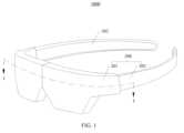
本願は、電子デバイスを提供し、ユーザは、電子デバイスを使用することによって仮想画像を観察することができる。本願のいくつかの実施において、電子デバイスは、拡張現実(Augmented Reality,略してAR)メガネ、仮想現実(Virtual Reality,略してVR)メガネ、又は他の画像表示デバイスであってよい。電子デバイスの形態は、メガネの形態、ヘルメットの形態、などであってよい。本願では、電子デバイスがメガネの形態をとる仮想現実メガネである例が記載のために使用される。 The present application provides an electronic device that allows a user to view virtual images by using the electronic device. In some implementations of the present application, the electronic device may be Augmented Reality (AR) glasses, Virtual Reality (VR) glasses, or other image display devices. The form of the electronic device may be in the form of glasses, in the form of a helmet, etc. In this application, an example is used for the description in which the electronic device is virtual reality glasses in the form of glasses.
図1及び図2を参照されたい。図1は、本願の実施に係る電子デバイス1000の構造の模式図である。図2は、I-Iに沿って切断された後の図1に示される電子デバイス1000の断面の模式図である。この実施において、電子デバイスは、目の形をした仮想現実メガネである。 Please refer to FIGS. 1 and 2. FIG. 1 is a schematic diagram of the structure of an
本願のこの実施の電子デバイス1000は、光学モジュール100、ホルダー200、及び画像伝送モジュール300を含む。画像伝送モジュール300及び光学モジュール100はいずれも、ホルダー200に収容されている。画像伝送モジュール300は、画像データを光学モジュール100に伝えるよう、光学モジュール100へ通信可能に接続されている。光学モジュール100は、受け取った画像データを表示し、表示したピクチャを人間の目に伝えることができ、それにより、人間の目は、電子デバイス1000によって再生されたピクチャを観察することができる。画像伝送モジュール300と光学モジュール100との間の通信接続は、ケーブル接続などの電気接続方式でのデータ伝送を含んでよく、あるいは、光学ケーブル接続又は無線伝送などのデータ伝送を実装することができる他の方式で実施されてもよい。画像伝送モジュール300と光学モジュール100との間の通信接続方式は、本願で特に制限されない。 The
この実施において、ホルダー200は、ホルダー本体201と、ホルダー本体201の2つの端部に接続されている2つのテンプル202とを含む。ホルダー本体201は、収容キャビティ203を含み、光学モジュール100及び画像伝送モジュール300は、ホルダー本体201の収容キャビティ203に収容される。本願の電子デバイス1000を使用する場合に、ユーザは、左/右耳に2つのテンプル202を別々に立てて、本願の電子デバイス1000を身につけることができる。この実施では、間隔をあけて配置された2つの光射出孔204が、収容キャビティ203のキャビティ壁に配置されている。2つの光射出孔204は、光学モジュール100によって発せられた光が収容キャビティ203から通過できるよう構成される。ユーザが本願の電子デバイス1000を身につける場合に、キャビティ壁にある2つの光射出孔204は、ユーザの両目に夫々対向し、それにより、2つの光射出孔204をとって発せられたピクチャは、ユーザの目に伝えられ得、ユーザは、電子デバイス1000によって再生されたピクチャを観察することができる。 In this implementation, the
本願のいくつかの他の実施において、電子デバイス1000は、代替的に、他の形態をとってもよく、異なる形態での電子デバイス1000のホルダー200の構造は異なる。これは本願で特に制限されない。例えば、いくつかの実施において、電子デバイス1000は、ヘルメット形態の仮想現実メガネであり、ホルダー200は、ヘルメット形態であり、ユーザの頭に装着され得る。 In some other implementations of the present application,
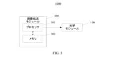
図2及び図3を一緒に参照されたい。図3は、本願に係る電子デバイス1000の機能モジュールのブロック図である。光学モジュール100及び画像伝送モジュール300はいずれも、電子デバイス1000の機能モジュールである。画像伝送モジュール300は、画像情報を処理及び伝送するよう構成され、光学モジュール100は、画像情報を表示するよう構成される。具体的に、本願のいくつかの実施において、画像伝送モジュール300はプロセッサ301を含む。プロセッサ301は、外部から取得された画像情報を処理し、次いで、処理した画像情報を表示のために光学モジュール100へ伝送することができる。 Please refer to FIGS. 2 and 3 together. FIG. 3 is a block diagram of functional modules of an
本願のいくつかの他の実施において、画像伝送モジュール300はメモリ302を更に含んでもよく、プロセッサ301によって処理された画像情報は、記憶のためにメモリ302に伝送され得る。画像が表示される必要があるとき、プロセッサ301は、メモリ302から画像情報を取得し、画像情報を表示のために光学モジュール100へ伝送する。 In some other implementations of the present application,
本願のいくつかの他の実施において、メモリ302は画像データを記憶してもよい。画像が表示される必要があるとき、プロセッサ301は、メモリ302から画像情報を取得し、画像情報を処理し、次いで、処理した画像情報を表示のために光学モジュール100へ伝送する。 In some other implementations of the present application,
本願のこの実施において、プロセッサ301は、画像処理チップ又はデジタル信号処理(digital signal processing,DSP)チップであってよい。これは本願で特に制限されない。 In this implementation of the present application,
本願のいくつかの実施において、電子デバイス1000は回路基板303を更に含む。プロセッサ301及びメモリ302はいずれも、回路基板303に配置されてよく、プロセッサ301とメモリ302との間の通信接続は、回路基板303上のケーブルを使用することによって実装される。 In some implementations of the present application,
図4を参照されたい。図4は、本願の第1の実施に係る光学モジュール100の構造の模式図である。本願のこの実施において、光学モジュール100は、レンズ群A、ディスプレイ20、及び異なるダイアフラムを含む。レンズ群Aは、対象側から画像側まで順に配置されている複数のレンズを含み、各レンズは、互いに対向して配置されている対象側面及び画像側面を含む。対象側面は対象側に面し、画像側面は画像側に面する。ディスプレイ20がレンズ群Aの対象側に位置し、レンズの対象側面はディスプレイ20に面し、レンズの画像側面はディスプレイ20から離れている。ディスプレイ20に表示される画像は、レンズ群Aによって結像された後にレンズ群Aの画像側に結像される。ユーザが本願のこの実施の電子デバイス1000を身につける場合に、ユーザの目はレンズ群Aの画像側に位置し、ディスプレイ20の表示ピクチャは、レンズ群Aのレンズによって屈折された後に人間の目の網膜位置で結像され、それにより、ユーザは、ディスプレイ20に表示された表示ピクチャを観察することができる。本願の他の実施では、光学モジュール100はレンズ群A及びダイアフラムしか含まなくてもよいことが理解され得る。 Please refer to FIG. 4. FIG. 4 is a schematic diagram of the structure of the
再び図2を参照されたい。本願において、電子デバイス1000はふた組の光学モジュール100を含む。光学モジュール100の各組は同じ構造を有し、光学モジュール100の各組はレンズ群A、ディスプレイ20、及び異なるダイアフラムを含む。ふた組の光学モジュール100のレンズ群Aの夫々は、1つの光射出孔304に配置される。代替的に、ふた組の光学モジュール100のレンズ群Aの夫々は1つの光射出孔304に対向し、それにより、レンズ群Aから発せられた光は、対応する光射出孔304から人間の目に入射する。本願において、ユーザが電子デバイス1000を身につける場合に、ユーザの左目及び右目は、光射出孔304から発せられた光を受けるよう、夫々1つの光射出孔304に対向する。言い換えれば、本願の電子デバイス1000のふた組の光学モジュール100によって伝送された光は、ユーザの左目及び右目によって夫々受光され得、それにより、ユーザは、両目を使用することによって、ディスプレイ20に表示されたピクチャを見ることができる。本願の実施において、ふた組の光学モジュール100のディスプレイ20は一体化された構造を持つ。本願の他の実施では、ふた組の光学モジュール100の夫々が独立したディスプレイ20を備えてもよいことが理解され得る。 Please refer to FIG. 2 again. In this application, the
本願では、ふた組の光学モジュール100のうちのひと組が、光学モジュール100の構造について具体的に記載するために一例として使用される。 In this application, one of the two sets of
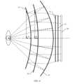
本願の実施において、レンズ群Aは複数のレンズを含む。複数のレンズは少なくとも1つの積層レンズを含む。本願において、積層レンズは、ダイアフラムが高品質で積層レンズの対象側面及び/又は画像側面に積層され得るレンズである。これは、ダイアフラムが積層レンズに積層される場合に、全てのポジションで積層レンズとダイアフラムとの間が適切にフィットし、積層レンズとダイアフラムとの間に空気泡などの問題がないことを確かにすることができる。更に、本願において、積層レンズの対象側面及び画像側面はいずれも曲面である。平面と比較して、曲面は、光伝送方向をより良く変化させることができ、光学収差をより良く低減することができる。従って、曲面は、平面と比較してより良い光学的効果を達成することができる。本願のダイアフラムの少なくとも一部は、積層レンズの対象側面又は画像側面に積層される。レンズの対象側面又は画像側面がダイアフラム積層のための平面として設計される解決法と比較して、本願の光学モジュール100は、より少ないレンズを使用してより良い光学的効果を実現することができ、それによって、光学モジュール100の全長(total track length,TTL)を低減し、電子デバイス1000の厚さを低減し、電子デバイス1000の体積及び重さを低減する。更に、本願のダイアフラムの少なくとも一部は積層レンズの対象側面又は画像側面に積層され得るので、ダイアフラム積層のために特別に使用される平面レンズを加えることと比較して、本願の光学モジュール100は、光学モジュール100のレンズの光屈折効果は影響を及ぼされないことを確かにしながら、光学モジュール100内のレンズの数を可能な限り減らすことができ、それによって、光学モジュール100の全長を低減し、電子デバイス1000の厚さを低減し、電子デバイス1000の体積及び重さを低減する。本願のいくつかの実施において、光学モジュール100の全長は30mm以下であり、光学モジュール100のレンズの質量は25g以下である。 In the implementation of this application, lens group A includes multiple lenses. The plurality of lenses includes at least one laminated lens. In this application, a laminated lens is a lens in which the diaphragm is of high quality and can be laminated to the object side and/or the image side of the laminated lens. This ensures that when the diaphragm is laminated to the laminated lens, there is a proper fit between the laminated lens and the diaphragm in all positions and that there are no issues such as air bubbles between the laminated lens and the diaphragm. can do. Furthermore, in the present application, both the object side surface and the image side surface of the laminated lens are curved surfaces. Compared with a flat surface, a curved surface can change the light transmission direction better and reduce optical aberrations better. Therefore, curved surfaces can achieve better optical effects compared to flat surfaces. At least a portion of the diaphragm of the present application is laminated to the object or image side of the laminated lens. Compared to solutions where the object side or image side of the lens is designed as a plane for diaphragm stacking, the
本願のいくつかの実施において、積層レンズの対象側面及び/又は画像側面は、球面、非球面、又は1つの反曲を備えた自由曲面であり、それにより、ダイアフラムは、高品質で積層レンズの対象側面及び/又は画像側面に積層され得る。1つの反曲を備えた自由曲面は、自由曲面がただ1つの反曲を有することを示す。例えば、1つの反曲を備えた自由曲面は、凹面又は凸面であってよく、あるいは、エッジが平面で中間領域が凹面又な凸面である自由曲面であってよい。1つの反曲を備えた自由曲面は、ダイアフラムの積層を容易にし、ダイアフラムがレンズに積層される場合にダイアフラムの積層品質を確保し、ダイアフラムがレンズに積層される場合に空気泡などの積層品質問題が起こることを防ぐことができる。 In some implementations of the present application, the object side and/or the image side of the laminated lens is a spherical surface, an aspherical surface, or a freeform surface with one recurvature, such that the diaphragm is of high quality and It can be laminated to the object side and/or the image side. A freeform surface with one recurvature indicates that the freeform surface has only one recurvature. For example, a freeform surface with one recurvature may be concave or convex, or it may be a freeform surface with flat edges and a concave or convex intermediate region. The free-form surface with one recurvature facilitates the lamination of the diaphragm, ensures the lamination quality of the diaphragm when the diaphragm is laminated to the lens, and prevents lamination quality such as air bubbles when the diaphragm is laminated to the lens. You can prevent problems from occurring.
例えば、図4に示される実施では、レンズ群Aは2つのレンズ:第1レンズ11及び第2レンズ12を含み、第1レンズ11は、第2レンズ12と比べて、ディスプレイ20から遠く離れている。第1レンズ11の対象側面は凸面であり、画像側面は、1つの反曲を備えた自由曲面である。第2レンズ12の対象側面は凸面であり、第2レンズの画像側面は、1つの反曲を備えた自由曲面である。従って、図4に示される実施では、第1レンズ11及び第2レンズ12は両方とも積層レンズであり、ダイアフラムは、第1レンズ11の対象側面又は画像側面に積層されるか、あるいは、第2レンズ12の対象側面又は画像側面に積層されてよい。従って、ダイアフラム積層のための平面レンズを加える必要がないので、光学モジュール内のレンズの数は減り、光学モジュールの全長及び重さは低減される。更に、この実施において、第1レンズ11の対象側面及び画像側面並びに第2レンズ12の対象側面及び画像側面は全て曲面であり、これは、優れた光学的効果を実現し、収差を低減するのにうまく機能することができる。レンズの対象側面又は画像側面がダイアフラム積層のために使用される平面として設計されることと比較して、この実施の光学モジュール100は、より良い光学的効果を実現することができる。代替的に、同じ光学的効果が実現される場合に、この実施では、光学モジュール100のレンズ厚さはより小さくされ得るので、光学モジュールの全長は低減される。本願の他の実施では、レンズ群Aはより多くのレンズを含んでもよいことが理解され得る。例えば、レンズ群Aは3つ、4つ、5つ又はそれ以上のレンズを含んでもよい。 For example, in the implementation shown in FIG. There is. The object side surface of the
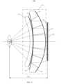
本願において、積層レンズの対象側面及び/又は画像側面が球面、非球面、又は1つの反曲を備えた自由曲面であるとは、積層レンズの対象側面及び/又は画像側面の有効な光伝送エリアBが球面、非球面、又は1つの反曲を備えた自由曲面であることを意味することが留意されるべきである。例えば、図5を参照されたい。図5は、本願のいくつか他の実施におけるレンズの断面の模式図である。この実施において、積層レンズのエッジは、指示及び固定のために主に使用されるフランジ101を更に含んでもよい。フランジ101によって囲まれたエリアは、積層レンズの実際の有効透過エリアBである。有効透過エリアBの対象側面又は画像側面は、球面、非球面、又は1つの反曲を備えた自由曲面である。ダイアフラムは、有効透過エリアBの対象側面又は画像側面に積層され得る。つまり、図5に示される実施のレンズも積層レンズである。 In this application, the expression that the object side surface and/or the image side surface of the laminated lens is a spherical surface, an aspheric surface, or a free-form surface with one recurvature means that the effective light transmission area of the object side surface and/or the image side surface of the laminated lens is It should be noted that B means a spherical surface, an aspherical surface, or a freeform surface with one inversion. For example, see FIG. FIG. 5 is a schematic diagram of a cross-section of a lens in some other implementations of the present application. In this implementation, the edge of the laminated lens may further include a
再び図4を参照されたい。本願の実施において、光学モジュール100の複数のダイアフラムが存在し、複数のダイアフラムは、直線偏光子31、第1の1/4位相リターダ32、部分的に透過し部分的に反射するフィルム33、第2の1/4位相リターダ34、及び反射偏光子35を含む。この実施において、直線偏光子31、第1の1/4位相リターダ32、部分的に透過し部分的に反射するフィルム33、第2の1/4位相リターダ34、及び反射偏光子35は、対象側から画像側まで順に配置される。つまり、直線偏光子31、第1の1/4位相リターダ32、部分的に透過し部分的に反射するフィルム33、第2の1/4位相リターダ34、及び反射偏光子35は、ディスプレイ20に近い側からディスプレイ20から遠い側まで順に配置される。この実施において、直線偏光子31、第1の1/4位相リターダ32、部分的に透過し部分的に反射するフィルム33、第2の1/4位相リターダ34、及び反射偏光子35のうちの1つ以上は、積層レンズの対象側面又は画像側面に積層されてよい。従って、ダイアフラム積層に特別に使用される平面レンズを追加で加えることも、又は積層を容易にするために平面としてレンズの表面を設計することも不要である。このようにして、光学モジュールのレンズの数及びレンズの厚さは低減することができ、一方、光学モジュールは優れた光学的効果を実現することができ、それによって、光学モジュールの軸上の厚さを低減し、光学モジュールの重さを低減し、電子デバイスの厚さを低減し、電子デバイスの重さを低減する。例えば、いくつかの実施において、直線偏光子31、第1の1/4位相リターダ32、部分的に透過し部分的に反射するフィルム33、第2の1/4位相リターダ34、及び反射偏光子35は全て積層レンズの対象側面又は画像側面に積層される。代替的に、いくつかの他の実施において、部分的に透過し部分的に反射するフィルム33、第2の1/4位相リターダ34、及び反射偏光子35のみが積層レンズの対象側面又は画像側面に積層される。代替的に、いくつかの実施において、反射偏光子35のみが積層レンズの対象側面又は画像側面に積層される。 Please refer to FIG. 4 again. In the implementation of the present application, there are multiple diaphragms of the
本願では、直線偏光子31、第1の1/4位相リターダ32、部分的に透過し部分的に反射するフィルム33、第2の1/4位相リターダ34、及び反射偏光子35のうちの少なくとも一部のダイアフラムは、積層レンズの対象側面又は画像側面に積層されることが留意されるべきである。言い換えれば、本願のいくつかの実施において、直線偏光子31、第1の1/4位相リターダ32、部分的に透過し部分的に反射するフィルム33、第2の1/4位相リターダ34、及び反射偏光子35は全て積層レンズの対象側面又は画像側面に積層されてもよい。本願のいくつかの実施において、直線偏光子31、第1の1/4位相リターダ32、部分的に透過し部分的に反射するフィルム33、第2の1/4位相リターダ34、及び反射偏光子35のうちのいくつかのダイアフラムは、積層レンズの対象側面又は画像側面に積層されてよく、残りのダイアフラムは、ディスプレイ20の表面、平面レンズの表面、又は他のレンズの表面に積層されてよい。 In the present application, at least one of a
本願の他の実施では、光学モジュール100は、他のタイプのダイアフラムを更に含んでもよく、ダイアフラムは、光学モジュール100の光学性能を更に向上させるよう、積層レンズの対象側面又は画像側面に積層されることが理解され得る。例えば、いくつかの実施において、光学モジュール100は、光フィルタリングフィルム、色フィルタリングフィルム、反射防止フィルム、光変換フィルム、などを更に含んでもよい。 In other implementations of the present application, the
本願のこの実施において、直線偏光子31は、自然光を直線偏光に変換することができ、第1の1/4位相リターダ32及び第2の1/4位相リターダ34は、直線偏光と楕円偏光との間の変換を実施するよう構成され得、部分的に透過し部分的に反射するフィルム33は、一部の光を透過し、一部の光を反射するよう構成され得る。本願のこの実施において、部分的に透過し部分的に反射するフィルム33の表面に照射された光の透過率及び反射率は、要件に基づいて調整されてよく、部分的に透過し部分的に反射するフィルム33の表面に照射された光の透過率及び反射率は、本願で制限されないことが留意されるべきである。例えば、本願のいくつかの実施において、部分的に透過し部分的に反射するフィルム33は、半反射・部分透過フィルムであってよく、部分的に透過し部分的に反射するフィルム33の表面に照射された光の50%が伝えられ、50%の光が反射される。代替的に、いくつかの実施において、部分的に透過し部分的に反射するフィルム33は、30%の光が伝えられ、70%の光が反射されることを可能にし得る。反射偏光子35の光伝達軸は、基本的に反射軸に対して垂直であり、偏光方向において光を反射するよう構成され得、反射された光の偏光方向に対して基本的に垂直である光が通過することを可能にする。 In this implementation of the present application, the
図6を参照されたい。図6は、本願の実施に係る光学モジュール100において光が各ダイアフラムを通って伝えられる場合の光軸の模式図である。具体的に、ディスプレイ20の表示ピクチャによって発せられた光は、まず直線偏光子31を通過して直線偏光状態の直線偏光となり、その後、第1の1/4位相リターダ32を通過し、直線偏光は、第1の1/4位相リターダ32を使用することによって楕円偏光に変換される。次いで、光は、部分的に透過し部分的に反射するフィルム33を通過し、一部の光は、部分的に透過し部分的に反射するフィルム33を通過して、第2の1/4位相リターダ34へ伝えられ、第2の1/4位相リターダ34は、部分的に透過し部分的に反射するフィルム33を通過した楕円偏光を直線偏光に変換し、直線偏光の部分は、反射偏光子35の反射軸に平行である。第2の1/4位相リターダ34を通過した直線偏光は、反射偏光子35へ伝えられて、反射偏光子35によって第2の1/4位相リターダ34へ反射される。反射偏光子35によって第2の1/4位相リターダ34によって反射された光は、第2の1/4位相リターダ34を通過した後に楕円偏光に変換され、その後に、部分的に透過し部分的に反射するフィルム33へ再び伝えられる。光の一部は、部分的に透過し部分的に反射するフィルム33の表面で反射され、その後に、第2の1/4位相リターダ34へ返される。第2の1/4位相リターダ34は、再び楕円偏光を直線偏光に変換し、直線偏光の偏光方向は、反射偏光子35のホモロジー軸に平行である。第2の1/4位相リターダ34を通過した後に反射偏光子35へ伝えられた光は、反射偏光子35を通過し、光学モジュール100を出て、人間の目に届き、それにより、人間の目は、ディスプレイ20の表示ピクチャを観察することができる。 Please refer to FIG. FIG. 6 is a schematic diagram of optical axes when light is transmitted through each diaphragm in the
本願の実施において、光は、部分的に透過し部分的に反射するフィルム33の表面及び反射偏光子35の表面の両方で一度反射される。このようにして、光学モジュール100内で伝えられる光は、部分的に透過し部分的に反射するフィルム33と反射偏光子35との間で二度折り返される。これは、光学モジュール100の全長を低減することができ、つまり、ディスプレイ20と人間の目との間の距離は縮めることができ、一方で、光学モジュール100の光学的効果が変わらないままであることを確かにすることができ、それによって、電子デバイス1000の厚さ及び軽さを実現し、電子デバイスの装用及び搬送を容易にする。 In the present implementation, the light is reflected once both at the surface of the partially transmitting and partially reflecting
再び図6を参照されたい。本願のこの実施において、反射偏光子35及び第2の1/4位相リターダ34はいずれも、画像側に向かって曲がる曲げシートである。この実施において、レンズ群Aの結像位置はユーザの網膜上である。従って、ユーザの目の位置はレンズ群Aの画像側である。従って、反射偏光子35及び第2の1/4位相リターダ34いずれも、ユーザの目に向かって曲がる湾曲したシートである。更に、いくつかの実施において、hの有効開口を有する位置での反射偏光子35の表面ベクトル高さはS1であり、hの有効開口を有する位置での第2の1/4位相リターダ34の表面ベクトル高さはS2であり、反射偏光子35及び第2の1/4位相リターダ34は、S2-S1≦h/5という関係を満たす。これは、反射偏光子35の曲率半径が第2の1/4位相リターダ34のそれよりも小さいこと、又は反射偏光子35の曲率半径が第2の1/4位相リターダ34のそれよりもわずかにのみ大きいことを確かにし、それによって、光漏出を回避する。更に、第2の1/4位相リターダ34及び第2の1/4位相リターダ34が、隣接したレンズの、隣接している対象側面及び画像側面に夫々積層される場合に、反射偏光子35の曲率半径は第2の1/4位相リターダ34のそれよりも小さいか、又は反射偏光子35の曲率半径は第2の1/4位相リターダ34のそれよりもわずかに大きいので、2つのレンズは可能な限り近くに配置することができ、2つのレンズの軸上のギャップは可能な限り小さくすることできることが確かにされ得、従って、光学モジュール100の全長は低減される。例えば、図4に示される実施において、反射偏光子35は、第1レンズ11の対象側面に積層され、第2の1/4位相リターダ34は、第2レンズ12の画像側面に積層される。反射偏光子35の曲率半径は第2の1/4位相リターダ34の曲率半径よりも小さいので、第1レンズ11と第2レンズ12との間の軸方向の距離は可能な限り小さくなり、それによって、光学モジュール100の全長を可能な限り小さくする。この実施において、光学モジュール100の全長は14mmである。 Please refer to FIG. 6 again. In this implementation of the present application, both
本願のこの実施において、複数の積層レンズは第1積層レンズ及び第2積層レンズを含む。第1積層レンズは、対象側から最も遠い積層レンズであり、第2積層レンズは、対象側に最も近い積層レンズである。この実施において、レンズ群Aの撮影対象はディスプレイ20である。従って、本願で記載される対象側は、ディスプレイ20が位置する側である。従って、第1積層レンズは、ディスプレイ20から最も遠い積層レンズであり、第2積層レンズは、ディスプレイ20に最も近い積層レンズである。例えば、図4に示される実施では、第1レンズ11及び第2レンズ12はいずれも積層レンズである。第1レンズ11は、図4に示される実施では光学モジュール100内にあり、ディスプレイ20から最も遠い積層レンズである。言い換えれば、第1レンズ11は、図4に示される実施での光学モジュール100の第1積層レンズである。第2レンズ12は、図4に示される実施では光学モジュール100内にあり、ディスプレイ20に最も近い積層レンズである。言い換えれば、第2レンズ12は、図4に示される実施での光学モジュール100の第2積層レンズである。 In this implementation of the present application, the plurality of laminated lenses includes a first laminated lens and a second laminated lens. The first laminated lens is the laminated lens furthest from the object side, and the second laminated lens is the laminated lens closest to the object side. In this implementation, the object to be photographed by the lens group A is the
本願のいくつかの実施において、反射偏光子35及び第2の1/4位相リターダ34は、異なる積層レンズに積層されてよい。実際の製品では、反射偏光子35及び第2の1/4位相リターダ34のコストは高いので、反射偏光子35及び第2の1/4位相リターダ34が異なる積層レンズに積層される場合に、積層レンズの他方の側への反射偏光子35又は第2の1/4位相リターダ34の積層不良によって引き起こされる、積層レンズの一方の側でのダイアフラムの無駄の問題は、回避することができる。このようにして、欠陥のあるダイアフラム積層によって引き起こされる製造コストの問題は解消され、それによって、光学モジュール100の製造コストは削減される。例えば、図4に示される実施において、反射偏光子35は第1レンズ11に積層され、第2の1/4位相リターダ34は第2レンズ12に積層される。 In some implementations of the present application,
本願のいくつかの実施において、反射偏光子35は、第1積層レンズの画像側面に積層され、部分的に透過し部分的に反射するフィルム33は、第2積層レンズの対象側面に積層される。本願のこの実施において、部分的に透過し部分的に反射するフィルム33と反射偏光子35との間で光は折り返されるので、本願の光学モジュール100は必要な光学的効果を実現することができ、光学モジュール100の全長は小さくされ得る。従って、本願のこの実施において、反射偏光子35は、第1積層レンズの画像側面に積層され、部分的に透過し部分的に反射するフィルム33は、第2積層レンズの対象側面に積層され、それにより、反射偏光子35と部分的に透過し部分的に反射するフィルム33との間の距離は可能な限り大きくされ得る。これは、反射偏光子35と部分的に透過し部分的に反射するフィルム33との間の光の伝送経路を可能な限り延ばし、更には、光学モジュール100が同じ光学的効果を実現することを可能にしながら光学モジュール100の全長を短くする。 In some implementations of the present application, a
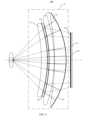
例えば、図7を参照されたい。図7は、本願の第2の実施に係る光学モジュール100の構造の模式図である。この実施において、光学モジュール100に含まれるレンズ群Aは、第1レンズ11及び第2レンズ12を含む。第1レンズ11は、第2レンズ12にと比べて、ディスプレイ20から遠く離れている。第1レンズ11の対象側面は凸面であり、画像側面は、1つの反曲を備えた自由曲面である。第2レンズ12の対象側面は凸面であり、第2レンズ12の画像側面は、1つの反曲を備えた自由曲面である。従って、図7に示される実施において、第1レンズ11及び第2レンズ12はいずれも積層レンズである。更に、この実施において、第1レンズ11は、図7に示される実施では光学モジュール100内にあり、ディスプレイ20から最も遠い積層レンズである。言い換えれば、第1レンズ11は、図7に示される実施での光学モジュール100の第1積層レンズである。第2レンズ12は、図7に示される実施では光学モジュール100内にあり、ディスプレイ20に最も近い積層レンズである。言い換えれば、第2レンズ12は、図7に示される実施での光学モジュール100の第2積層レンズである。この実施において、反射偏光子35は、第1積層レンズの画像側面に積層され、部分的に透過し部分的に反射するフィルム33は、第2積層レンズの対象側面に積層される。これは、光学モジュール100の全長を更に低減することができる。この実施において、光学モジュール100の全長は12mmである。 For example, see FIG. FIG. 7 is a schematic diagram of the structure of an
本願の他の実施では、反射偏光子35は、第1積層レンズの対象側面、又は他の積層レンズの対象側面若しくは画像側面に積層されることが理解され得る。部分的に透過し部分的に反射するフィルム33は、第2積層レンズの画像側面、又は他の積層レンズの対象側面若しくは画像側面に積層されてよい。 It can be appreciated that in other implementations of the present application, the
再び図4を参照されたい。本願のいくつかの実施において、積層レンズは、画像側に向かって曲がるレンズであってよく、つまり、積層レンズの対象側面及び画像側面の両方のエッジは、中央の位置と比べて画像側に向かって曲がっている。本願のこの実施において、積層レンズは、画像側に向かって曲がるレンズとして設計され、それにより、積層レンズの対象側での光が積層レンズを使用することによって画像側へ屈折されて伝えられた後、光はより良い収束効果を有することができる。ユーザが本願の電子デバイス1000を身につける場合に、ユーザの目はレンズ群Aの画像側に位置し、ディスプレイによって表示されたピクチャがレンズ群Aによって画像側に屈折されて伝えられる過程で、表示ピクチャによって発せられた光は収束される。従って、ユーザは、本願の電子デバイス1000を使用することによって大きい表示ピクチャを観察することができ、本願の電子デバイス1000は、優れた結像効果を有することができる。更に、積層レンズの対象側面及び画像側面の両方のエッジは、中央の位置と比べて画像側に向かって曲がっている。これは、光がレンズ群Aを通過するときに生成される収差を低減することができ、それにより、光学モジュール100はより良い光学的効果を実現することができる。 Please refer to FIG. 4 again. In some implementations of the present application, the laminated lens may be a lens that curves toward the image side, that is, the edges of both the object side and the image side of the laminated lens are tilted toward the image side compared to the central position. It's bent. In this implementation of the present application, the laminated lens is designed as a lens that bends towards the image side, so that after the light on the object side of the laminated lens is refracted and transmitted to the image side by using the laminated lens. , the light can have better focusing effect. When a user wears the
再び図4を参照されたい。本願のいくつかの実施形態で、直線偏光子31及び第1の1/4位相リターダ32は、ディスプレイ20に組み込まれてもよく、つまり、直線偏光子31、第1の1/4位相リターダ32、及びディスプレイ20は、ディスプレイ20の製造中に一体化される。これは、光学モジュール100の組み立てプロセスを簡単にし、更には、電子デバイス1000の組み立てプロセスを簡単にすることができる。具体的に、本願のいくつかの実施において、ディスプレイ20が製造される場合に、直線偏光子31及び第1の1/4位相リターダ32の両方がディスプレイ20の発光面に積層されてよく、それにより、直線偏光子31及び第1の1/4位相リターダ32はディスプレイ20に組み込まれる。光学モジュール100のその後の組み立てプロセスで、直線偏光子31及び第1の1/4位相リターダ32を組み込まれたディスプレイ20は、他のレンズと組み合わされる。本願のこの実施において、直線偏光子31及び第1の1/4位相リターダ32は、代替的に、他の方法でディスプレイ20に組み込まれてもよいことが理解され得る。詳細は本願で具体的に表示されない。例えば、いくつかの実施において、ディスプレイ20の発光面上に基板が直線偏光子31を形成するよう直接製造されてもよく、それにより、直線偏光子31はディスプレイ20に組み込まれる。 Please refer to FIG. 4 again. In some embodiments of the present application, the
本願のいくつかの実施において、レンズ群Aの複数のレンズは、光学調整レンズを更に含んでもよい。光学調整レンズは、光学モジュール100の光学的効果を調整するよう構成される。しかし、光学調整レンズの対象側面又は画像側面は、高品質でダイアフラムに積層され得ない。例えば、本願のいくつかの実施において、光学調整レンズの対象側面又は画像側面は、複数の反曲を備えた自由曲面を含んでもよい。複数の反曲を備えた自由曲面は、2つ以上の反曲を備えた自由曲面である。複数の反曲を備えた自由曲面は、高品質でダイアフラムに積層されることが容易ではなく、従って、光学調整レンズの対象側面又は画像側面は、高品質でレンズに積層され得ない。この実施において、レンズ群Aに光学調整レンズを加えることは、光学モジュール100の光学的効果を更に調整することができ、それにより、電子デバイス1000は、より良い結像効果を実現することができる。 In some implementations of the present application, the lenses of lens group A may further include optical adjustment lenses. The optical adjustment lens is configured to adjust the optical effect of the
例えば、図8及び図10を参照されたい。図8は、本願の第3の実施に係る光学モジュール100の構造の模式図であり、図10は、本願の第5の実施に係る光学モジュール100の構造の模式図である。 For example, see FIGS. 8 and 10. FIG. 8 is a schematic diagram of the structure of an
図8に示される実施の光学モジュール100は、3つのレンズ:第1レンズ11、第2レンズ、及び第3レンズ13を含む。第1レンズ11、第2レンズ12、及び第3レンズ13は、ディスプレイ20から遠ざかる方向からディスプレイ20に近づく方向に向かって配置されており、第1レンズ11、第2レンズ12、及び第3レンズ13は、同軸上に配置されている。第1レンズ11の対象側面は凸面であり、画像側面は、1つの反曲を備えた自由曲面である。第2レンズ12の対象側面は凸面であり、第2レンズ12の画像側面は、1つの反曲を備えた自由曲面である。第3レンズ13の対象側面及び画像側面はいずれも、2つの反曲を備えた自由曲面であり、第3レンズ13の断面はM字形である。従って、第1レンズ11及び第2レンズ12の対象側面及び画像側面はいずれも、ダイアフラム積層を容易にすることができる。具体的に言えば、第1レンズ11及び第2レンズ12は両方とも積層レンズであり、第3レンズ13の対象側面も画像側面もダイアフラム積層を促さない。つまり、この実施の第3レンズ13は、光学モジュール100を調整するよう構成された光学調整レンズである。 The implementation
図10に示される実施の光学モジュール100は、3つのレンズ:第1レンズ11、第2レンズ、及び第3レンズ13を含む。第1レンズ11、第2レンズ12、及び第3レンズ13は、ディスプレイ20から遠ざかる方向からディスプレイ20に近づく方向に向かって配置されており、第1レンズ11、第2レンズ12、及び第3レンズ13は、同軸上に配置されている。第1レンズ11の対象側面は凸面であり、画像側面は、1つの反曲を備えた自由曲面である。第2レンズ12の対象側面は凸面であり、第2レンズ12の画像側面は、1つの反曲を備えた自由曲面である。第3レンズ13の対象側面はいずれも、2つの反曲を備えた自由曲面であり、第3レンズ13の画像側面は平面である。従って、第1レンズ11及び第2レンズ12の対象側面及び画像側面はいずれも、ダイアフラム積層を容易にすることができる。具体的に言えば、第1レンズ11及び第2レンズ12は両方とも積層レンズであり、第3レンズ13の対象側面はダイアフラム積層を促さない。つまり、この実施の第3レンズ13は、光学モジュール100を調整するよう構成された光学調整レンズである。 The implementation
本願の他の実施では、光学調整レンズは他の形状であってもよく、あるいは、2つ以上の光学調整レンズが存在してもよいことが留意されるべきである。2つ以上の光学調整レンズは、光学調整レンズとディスプレイ20との間、第1積層レンズと第2積層レンズとの間、第2積層レンズと光学調整レンズとの間、又は第2積層レンズから離れている第1積層レンズの側の任意の位置に配置されてよい。 It should be noted that in other implementations of the present application, the optical adjustment lens may be of other shapes or there may be more than one optical adjustment lens. The two or more optical adjustment lenses are arranged between the optical adjustment lens and the
以下は、図4及び図7乃至図15を参照して、本願の実施のいくつかの具体的な、しかし非限定的な例について、更に詳細に記載する。 The following describes some specific, but non-limiting examples of implementation of the present application in further detail with reference to FIGS. 4 and 7-15.
図4を参照されたい。図4は、本願の第1の実施に係る光学モジュール100の構造の模式図である。この実施において、光学モジュール100のレンズ群Aは2つのレンズを含む。2つのレンズは夫々、第1レンズ11及び第2レンズ12である。第1レンズ11は、第2レンズ12と比べて、ディスプレイ20から離れており、第1レンズ11及び第2レンズ12は、同軸上に配置されている。第1レンズ11の対象側面は凸面であり、画像側面は、1つの反曲を備えた自由曲面である。第2レンズ12の対象側面は凸面であり、第2レンズ12の画像側面は、1つの反曲を備えた自由曲面である。従って、第1レンズ11及び第2レンズ12の対象側面及び画像側面はいずれも、ダイアフラム積層を容易にすることができ、つまり、第1レンズ11及び第2レンズ12は両方とも積層レンズである。第1レンズ11は、ディスプレイ20から最も遠い積層レンズである。つまり、第1レンズ11は、当該実施での光学モジュール100の第1積層レンズである。第2レンズ12は、ディスプレイ20に最も近い積層レンズである。つまり、第2レンズ12は、当該実施での光学モジュール100の第2積層レンズである。 Please refer to FIG. 4. FIG. 4 is a schematic diagram of the structure of the
本願の第1の実施での光学モジュール100の設計パラメータは、表1に示される。
光学瞳は、ユーザの瞳であり、光学瞳が位置している行の厚さの値は、ユーザが当該実施の電子デバイス1000を身につけている場合の第1レンズ11とユーザの瞳との間の距離を示す。 The optical pupil is the user's pupil, and the thickness value of the row where the optical pupil is located is based on the relationship between the
第1レンズS1は、第1レンズ11の画像側面を示す。第1レンズS1が位置している行の曲率半径の値は、第1レンズ11の画像側面の曲率半径を示す。第1レンズS1が位置している行の厚さの値は、第1レンズ11の画像側面から対象側面までの軸上の距離、つまり、第1レンズ11の軸上の厚さである。 The first lens S1 indicates the image side surface of the
第1レンズS2は、第1レンズ11の対象側面を示す。第1レンズS2が位置している行の曲率半径の値は、第1レンズ11の対象側面の曲率半径を示す。第1レンズS2が位置している行の厚さの値は、第1レンズ11の対象側面から第2レンズ12の画像側面までの軸上の距離である。 The first lens S2 indicates the target side surface of the
第2レンズS3は、第2レンズ12の画像側面を示す。第2レンズS3が位置している行の曲率半径の値は、第2レンズ12の画像側面の曲率半径を示す。第2レンズS3が位置している行の厚さの値は、第2レンズ12の画像側面から対象側面までの軸上の距離、つまり、第2レンズ12の軸上の厚さである。 The second lens S3 indicates the image side surface of the
第2レンズS4は、第2レンズ12の対象側面を示す。第2レンズS4が位置している行の曲率半径の値は、第2レンズ12の対象側面の曲率半径を示す。第2レンズS4が位置している行の厚さの値は、第2レンズ12の対象側面からディスプレイ20の表面までの軸上の距離である。 The second lens S4 indicates the target side surface of the
この実施において、光学モジュール100のダイアフラムは、直線偏光子31、第1の1/4位相リターダ32、部分的に透過し部分的に反射するフィルム33、第2の1/4位相リターダ34、及び反射偏光子35を含む。直線偏光子31、第1の1/4位相リターダ32、部分的に透過し部分的に反射するフィルム33、第2の1/4位相リターダ34、及び反射偏光子35は、ディスプレイ20に近い側からディスプレイ20から離れた側へ順に配置されている。具体的に、この実施において、直線偏光子31及び第1の1/4位相リターダ32は、ディスプレイ20の発光面に順に重ね合わされる。部分的に透過し部分的に反射するフィルム33は、第2レンズ12の対象側面に積層され、第2の1/4位相リターダ34は、第2レンズ12の画像側面に積層され、反射偏光子35は、第1レンズ11の対象側面に積層される。 In this implementation, the diaphragm of the
ディスプレイ20の表示ピクチャの光は、直線偏光子31及び第1の1/4位相リターダ32の通過に成功した後、第2レンズ12の画像側面に伝えられ、第2レンズ12の画像側面に照射された光の一部は、部分的に透過し部分的に反射するフィルム33を通過する。部分的に透過し部分的に反射するフィルム33を通過した光は、第2レンズ12及び第2の1/4位相リターダ34を順に通過し、第1レンズ11の対象側面に伝えられる。この場合に、第1レンズ11の対象側面に伝えられた光の偏光方向は、反射偏光子35の反射軸方向に平行である。第1レンズ11の対象側面に伝えられた光は、反射偏光子35によって反射され、反射された光は、第2の1/4位相リターダ34及び第2レンズ12を順に通過し、その後に、部分的に透過し部分的に反射するフィルム33に伝えられる。一部の光は、部分的に透過し部分的に反射するフィルム33によって反射される。この場合に、部分的に透過し部分的に反射するフィルム33によって反射された光の偏光方向は、反射偏光子35のホモロジー軸方向に平行であり、部分的に透過し部分的に反射するフィルム33によって反射された光は、第2レンズ12、第2の1/4位相リターダ34、反射偏光子35、及び第1レンズ11を順に通過し、人間の目に照射され得、それにより、ユーザは、ディスプレイ20に表示されているピクチャを観察することができる。 After the light of the displayed picture on the
この実施において、光は、反射偏光子35の表面及び部分的に透過し部分的に反射するフィルム33の表面の両方で一度反射され、それにより、光は、反射偏光子35と部分的に透過し部分的に反射するフィルム33との間で二度折り返される。従って、光学モジュール100の全長は、同じ光学的効果が達成される場合に、より小さい。更に、この実施において、直線偏光子31及び第1の1/4位相リターダ32は、ディスプレイ20の発光面上に順に重ね合わされている。部分的に透過し部分的に反射するフィルム33は、第2レンズ12の対象側面に積層され、第2の1/4位相リターダ34は、第2レンズ12の画像側面に積層され、反射偏光子35は、第1レンズ11の対象側面に積層されている。従って、ダイアフラム積層に特別に使用される平面レンズを加える必要はない。これは、レンズの数の増加を回避し、光学モジュール100の全長及び重さの増加を回避することができる。更に、第1レンズ11及び第2レンズの対象側面及び画像側面はいずれも曲面であり、第1レンズ11又は第2レンズ12の対象側面又は画像側面は、ダイアフラム積層を容易にするために平面として特別に設計されない。従って、これは、曲面を加えることによって光学収差を低減するという効果を達成し、必要な光学的効果を確かにしながら光学モジュール100のレンズの厚さを小さくしかつ全長を短縮することができる。更に、反射偏光子35及び第2の1/4位相リターダ34は、夫々異なる積層レンズに積層されている。これは、レンズのある側に積層されている反射偏光子35又は第2の1/4位相リターダ34が、反射偏光子35又は第2の1/4位相リターダ34がレンズの他方の側に十分に積層されていないときに廃棄されるという問題を回避することができるので、製造コストを下げられる。 In this implementation, the light is reflected once both at the surface of the
この実施形態の光学モジュール100は、上記のレンズの設計パラメータ及びダイアフラムの積層位置に基づいて取得され得る。この実施形態の光学モジュール100は、優れた光学的効果を達成し、短い全長及び軽い重さを有することができる。図11を参照されたい。図11は、第1の実施に係る光学モジュール100の光学性能の表現図である。図11において、横軸は空間周波数であり、単位はラインペア/mm(LP/mm)であり、縦軸は空間変調関数であり、現在の各ラインペア番号の局所的なコントラスト値に対応する。図中の実施は、当該実施における、光学モジュール100によって実行される結像の経線方向での空間周波数と空間変調関数との間の関係の曲線を示し、破線は、当該実施における、光学モジュール100によって実行される結像の円弧ベクトル方向での空間周波数と空間変調関数との間の関係の曲線を示す。図11からは、空間変調関数が0.3よりも大きいとき、当該実施の光学モジュール100の結像精細度は60lp/mmよりも大きく、つまり、当該実施の光学モジュールは高い精細度を有する、ことが分かる。更に、この実施において、光学レンズの全長は約14mmであり、レンズの重さは9gに満たない。従って、当該実施の光学モジュール100は、優れた光学的効果並びに小さい全長及び重さを有し、それにより、光学モジュール100を含む電子デバイス1000も、小さい厚さ及び軽い重さを有することができ、それによって、電子デバイス1000の携帯性及び装用経験を改善する。 The
図7を参照されたい。図7は、本願の第2の実施に係る光学モジュール100の構造の模式図である。この実施において、光学モジュール100のレンズ群Aは2つのレンズを含む。2つのレンズは夫々、第1レンズ11及び第2レンズ12である。第1レンズ11は、第2レンズ12と比べて、ディスプレイ20から離れており、第1レンズ11及び第2レンズ12は、同軸上に配置されている。第1レンズ11の対象側面は凸面であり、画像側面は、1つの反曲を備えた自由曲面である。第2レンズ12の対象側面は凸面であり、第2レンズ12の画像側面は、1つの反曲を備えた自由曲面である。従って、第1レンズ11及び第2レンズ12の対象側面及び画像側面はいずれも、ダイアフラム積層を容易にすることができ、つまり、第1レンズ11及び第2レンズ12は両方とも積層レンズである。第1レンズ11は、ディスプレイ20から最も遠い積層レンズである。つまり、第1レンズ11は、当該実施での光学モジュール100の第1積層レンズである。第2レンズ12は、ディスプレイ20に最も近い積層レンズである。つまり、第2レンズ12は、当該実施での光学モジュール100の第2積層レンズである。 Please refer to FIG. FIG. 7 is a schematic diagram of the structure of an
本願の第2の実施での光学モジュール100の設計パラメータは、表2に示される。
光学瞳は、ユーザの瞳であり、光学瞳が位置している行の厚さの値は、ユーザが当該実施の電子デバイス1000を身につけている場合の第1レンズ11とユーザの瞳との間の距離を示す。 The optical pupil is the user's pupil, and the thickness value of the row where the optical pupil is located is based on the relationship between the
第1レンズS1は、第1レンズ11の画像側面を示す。第1レンズS1が位置している行の曲率半径の値は、第1レンズ11の画像側面の曲率半径を示す。第1レンズS1が位置している行の厚さの値は、第1レンズ11の画像側面から対象側面までの軸上の距離、つまり、第1レンズ11の軸上の厚さである。 The first lens S1 indicates the image side surface of the
第1レンズS2は、第1レンズ11の対象側面を示す。第1レンズS2が位置している行の曲率半径の値は、第1レンズ11の対象側面の曲率半径を示す。第1レンズS2が位置している行の厚さの値は、第1レンズ11の対象側面から第2レンズ12の画像側面までの軸上の距離である。 The first lens S2 indicates the target side surface of the
第2レンズS3は、第2レンズ12の画像側面を示す。第2レンズS3が位置している行の曲率半径の値は、第2レンズ12の画像側面の曲率半径を示す。第2レンズS3が位置している行の厚さの値は、第2レンズ12の画像側面から対象側面までの軸上の距離、つまり、第2レンズ12の軸上の厚さである。 The second lens S3 indicates the image side surface of the
第2レンズS4は、第2レンズ12の対象側面を示す。第2レンズS4が位置している行の曲率半径の値は、第2レンズ12の対象側面の曲率半径を示す。第2レンズS4が位置している行の厚さの値は、第2レンズ12の対象側面からディスプレイ20の表面までの軸上の距離である。 The second lens S4 indicates the target side surface of the
この実施において、光学モジュール100のダイアフラムは、直線偏光子31、第1の1/4位相リターダ32、部分的に透過し部分的に反射するフィルム33、第2の1/4位相リターダ34、及び反射偏光子35を含む。直線偏光子31、第1の1/4位相リターダ32、部分的に透過し部分的に反射するフィルム33、第2の1/4位相リターダ34、及び反射偏光子35は、ディスプレイ20に近い側からディスプレイ20から離れた側へ順に配置されている。具体的に、この実施において、直線偏光子31及び第1の1/4位相リターダ32は、ディスプレイ20の発光面に順に重ね合わされる。部分的に透過し部分的に反射するフィルム33は、第2レンズ12の対象側面に積層され、第2の1/4位相リターダ34は、第1レンズ11の対象側面に積層され、反射偏光子35は、第1レンズ11の画像側面に積層される。 In this implementation, the diaphragm of the
ディスプレイ20の表示ピクチャの光は、直線偏光子31及び第1の1/4位相リターダ32の通過に成功した後、第2レンズ12の画像側面に伝えられ、第2レンズ12の画像側面に照射された光の一部は、部分的に透過し部分的に反射するフィルム33を通過する。部分的に透過し部分的に反射するフィルム33を通過した光は、第2レンズ12、第2の1/4位相リターダ34、及び第1レンズ11を順に通過し、第1レンズ11の画像側面に伝えられる。この場合に、第1レンズ11の画像側面に伝えられた光の偏光方向は、反射偏光子35の反射軸方向に平行である。第1レンズ11の画像側面に伝えられた光は、反射偏光子35によって反射され、反射された光は、第1レンズ11、第2の1/4位相リターダ34及び第2レンズ12を順に通過し、その後に、部分的に透過し部分的に反射するフィルム33に伝えられる。一部の光は、部分的に透過し部分的に反射するフィルム33によって反射される。この場合に、部分的に透過し部分的に反射するフィルム33によって反射された光の偏光方向は、反射偏光子35のホモロジー軸方向に平行であり、部分的に透過し部分的に反射するフィルム33によって反射された光は、第2レンズ12、第2の1/4位相リターダ34、第1レンズ11、及び反射偏光子35を順に通過し、人間の目に照射され得、それにより、ユーザは、ディスプレイ20に表示されているピクチャを観察することができる。 After the light of the displayed picture on the
この実施において、光は、反射偏光子35の表面及び部分的に透過し部分的に反射するフィルム33の表面の両方で一度反射され、それにより、光は、反射偏光子35と部分的に透過し部分的に反射するフィルム33との間で二度折り返される。従って、光学モジュール100の全長は、同じ光学的効果が達成される場合に、より小さい。更に、この実施において、反射偏光子35は、第1レンズ11の画像側面に積層され、第2の1/4位相リターダ34は、第2レンズ12の対象側面に積層されている。この場合に、反射偏光子35と第2の1/4位相リターダ34との間の距離は大きくされ得るので、反射偏光子35と第2の1/4位相リターダ34との間の光伝送光学経路は長くなり、それによって、光学モジュール100の全長を短縮する。直線偏光子31及び第1の1/4位相リターダ32は、ディスプレイ20の発光面上に順に重ね合わされている。部分的に透過し部分的に反射するフィルム33は、第2レンズ12の対象側面に積層され、第2の1/4位相リターダ34は、第2レンズ12の画像側面に積層され、反射偏光子35は、第1レンズ11の対象側面に積層されている。従って、ダイアフラム積層に特別に使用される平面レンズを加える必要はない。これは、レンズの数の増加を回避し、光学モジュール100の全長及び重さの増加を回避することができる。更に、第1レンズ11及び第2レンズの対象側面及び画像側面はいずれも曲面であり、第1レンズ11又は第2レンズ12の対象側面又は画像側面は、ダイアフラム積層を容易にするために平面として特別に設計されない。従って、これは、曲面を加えることによって光学収差を低減するという効果を達成し、必要な光学的効果を確かにしながら光学モジュール100のレンズの厚さを小さくしかつ全長を短縮することができる。 In this implementation, the light is reflected once both at the surface of the
この実施形態の光学モジュール100は、上記のレンズの設計パラメータ及びダイアフラムの積層位置に基づいて取得され得る。この実施形態の光学モジュール100は、優れた光学的効果を達成し、短い全長及び軽い重さを有することができる。図12を参照されたい。図12は、第2の実施に係る光学モジュール100の光学性能の表現図である。図12において、横軸は空間周波数であり、単位はラインペア/mm(LP/mm)であり、縦軸は空間変調関数であり、現在の各ラインペア番号の局所的なコントラスト値に対応する。図中の実施は、当該実施における、光学モジュール100によって実行される結像の経線方向での空間周波数と空間変調関数との間の関係の曲線を示し、破線は、当該実施における、光学モジュール100によって実行される結像の円弧ベクトル方向での空間周波数と空間変調関数との間の関係の曲線を示す。 The
図12からは、空間変調関数が0.3よりも大きいとき、当該実施の光学モジュール100の結像精細度は60lp/mmよりも大きく、つまり、当該実施の光学モジュールは高い精細度を有する、ことが分かる。更に、この実施において、光学レンズの全長は約12mmであり、レンズの重さは8gに満たない。従って、当該実施の光学モジュール100は、優れた光学的効果並びに小さい全長及び重さを有し、それにより、光学モジュール100を含む電子デバイス1000も、小さい厚さ及び軽い重さを有することができ、それによって、電子デバイス1000の携帯性及び装用経験を改善する。 From FIG. 12, when the spatial modulation function is greater than 0.3, the imaging definition of the
図8を参照されたい。図8は、本願の第3の実施に係る光学モジュール100の構造の模式図である。この実施において、光学モジュール100のレンズ群Aは3つのレンズを含む。3つのレンズは、第1レンズ11、第2レンズ12、及び第3レンズ13である。第1レンズ、第2レンズ、及び第3レンズ13は、ディスプレイ20から遠ざかる方向からディスプレイ20に近づく方向へ配置されており、第1レンズ11、第2レンズ12、及び第3レンズ13は、同軸上に配置されている。第1レンズ11の対象側面は凸面であり、画像側面は、1つの反曲を備えた自由曲面である。第2レンズ12の対象側面は凸面であり、第2レンズ12の画像側面は、1つの反曲を備えた自由曲面である。第3レンズの対象側面及び画像側面は両方とも、2つの反曲を備えた自由曲面であり、第3レンズの断面はM字形である。従って、第1レンズ11及び第2レンズ12の対象側面及び画像側面はいずれも、ダイアフラム積層を容易にすることができる。具体的に言えば、第1レンズ11及び第2レンズ12は両方とも積層レンズであり、第3レンズ13は、光学モジュール100を調整するよう構成された光学調整レンズである。第1レンズ11は、ディスプレイ20から最も遠い積層レンズである。つまり、第1レンズ11は、当該実施での光学モジュール100の第1積層レンズである。第2レンズ12は、ディスプレイ20に最も近い積層レンズである。つまり、第2レンズ12は、当該実施での光学モジュール100の第2積層レンズである。 Please refer to FIG. FIG. 8 is a schematic diagram of the structure of an
本願の第3の実施での光学モジュール100の設計パラメータは、表3に示される。
光学瞳は、ユーザの瞳であり、光学瞳が位置している行の厚さの値は、ユーザが当該実施の電子デバイス1000を身につけている場合の第1レンズ11とユーザの瞳との間の距離を示す。 The optical pupil is the user's pupil, and the thickness value of the row where the optical pupil is located is based on the relationship between the
第1レンズS1は、第1レンズ11の画像側面を示す。第1レンズS1が位置している行の曲率半径の値は、第1レンズ11の画像側面の曲率半径を示す。第1レンズS1が位置している行の厚さの値は、第1レンズ11の画像側面から対象側面までの軸上の距離、つまり、第1レンズ11の軸上の厚さである。 The first lens S1 indicates the image side surface of the
第1レンズS2は、第1レンズ11の対象側面を示す。第1レンズS2が位置している行の曲率半径の値は、第1レンズ11の対象側面の曲率半径を示す。第1レンズS2が位置している行の厚さの値は、第1レンズ11の対象側面から第2レンズ12の画像側面までの軸上の距離である。 The first lens S2 indicates the target side surface of the
第2レンズS3は、第2レンズ12の画像側面を示す。第2レンズS3が位置している行の曲率半径の値は、第2レンズ12の画像側面の曲率半径を示す。第2レンズS3が位置している行の厚さの値は、第2レンズ12の画像側面から対象側面までの軸上の距離、つまり、第2レンズ12の軸上の厚さである。 The second lens S3 indicates the image side surface of the
第2レンズS4は、第2レンズ12の対象側面を示す。第2レンズS4が位置している行の曲率半径の値は、第2レンズ12の対象側面の曲率半径を示す。第2レンズS4が位置している行の厚さの値は、第2レンズ12の対象側面から第3レンズ13の画像側面までの軸上の距離である。 The second lens S4 indicates the target side surface of the
第3レンズS5は、第3レンズ13の画像側面を示す。第3レンズS5が位置している行の曲率半径の値は、第3レンズ13の画像側面の曲率半径を示す。第3レンズS5が位置している行の厚さの値は、第3レンズ13の画像側面から対象側面までの軸上の距離、つまり、第3レンズ13の軸上の厚さである。 The third lens S5 indicates the image side surface of the
第3レンズS6は、第3レンズ13の対象側面を示す。第3レンズS6が位置している行の曲率半径の値は、第3レンズ13の対象側面の曲率半径を示す。第3レンズS6が位置している行の厚さの値は、第3レンズ13の対象側面からディスプレイ20の表面までの軸上の距離である。 The third lens S6 indicates the target side surface of the
この実施において、光学モジュール100のダイアフラムは、直線偏光子31、第1の1/4位相リターダ32、部分的に透過し部分的に反射するフィルム33、第2の1/4位相リターダ34、及び反射偏光子35を含む。直線偏光子31、第1の1/4位相リターダ32、部分的に透過し部分的に反射するフィルム33、第2の1/4位相リターダ34、及び反射偏光子35は、ディスプレイ20に近い側からディスプレイ20から離れた側へ順に配置されている。具体的に、この実施において、直線偏光子31及び第1の1/4位相リターダ32は、ディスプレイ20の発光面に順に重ね合わされる。部分的に透過し部分的に反射するフィルム33は、第2レンズ12の対象側面に積層され、第2の1/4位相リターダ34は、第2レンズ12の画像側面に積層され、反射偏光子35は、第1レンズ11の対象側面に積層される。 In this implementation, the diaphragm of the
ディスプレイ20の表示ピクチャの光は、直線偏光子31及び第1の1/4位相リターダ32の通過に成功した後、第2レンズ12の画像側面に伝えられ、第2レンズ12の画像側面に照射された光の一部は、部分的に透過し部分的に反射するフィルム33を通過する。部分的に透過し部分的に反射するフィルム33を通過した光は、第2レンズ12及び第2の1/4位相リターダ34を順に通過し、第1レンズ11の対象側面に伝えられる。この場合に、第1レンズ11の対象側面に伝えられた光の偏光方向は、反射偏光子35の反射軸方向に平行である。第1レンズ11の対象側面に伝えられた光は、反射偏光子35によって反射され、反射された光は、第2の1/4位相リターダ34及び第2レンズ12を順に通過し、その後に、部分的に透過し部分的に反射するフィルム33に伝えられる。一部の光は、部分的に透過し部分的に反射するフィルム33によって反射される。この場合に、部分的に透過し部分的に反射するフィルム33によって反射された光の偏光方向は、反射偏光子35のホモロジー軸方向に平行であり、部分的に透過し部分的に反射するフィルム33によって反射された光は、第2レンズ12、第2の1/4位相リターダ34、反射偏光子35、及び第1レンズ11を順に通過し、人間の目に照射され得、それにより、ユーザは、ディスプレイ20に表示されているピクチャを観察することができる。 After the light of the displayed picture on the
この実施において、光は、反射偏光子35の表面及び部分的に透過し部分的に反射するフィルム33の表面の両方で一度反射され、それにより、光は、反射偏光子35と部分的に透過し部分的に反射するフィルム33との間で二度折り返される。従って、光学モジュール100の全長は、同じ光学的効果が達成される場合に、より小さい。更に、この実施において、直線偏光子31及び第1の1/4位相リターダ32は、ディスプレイ20の発光面上に順に重ね合わされている。部分的に透過し部分的に反射するフィルム33は、第2レンズ12の対象側面に積層され、第2の1/4位相リターダ34は、第2レンズ12の画像側面に積層され、反射偏光子35は、第1レンズ11の対象側面に積層されている。従って、ダイアフラム積層に特別に使用される平面レンズを加える必要はない。これは、レンズの数の増加を回避し、光学モジュール100の全長及び重さの増加を回避することができる。更に、第1レンズ11及び第2レンズの対象側面及び画像側面はいずれも曲面であり、第1レンズ11又は第2レンズ12の対象側面又は画像側面は、ダイアフラム積層を容易にするために平面として特別に設計されない。従って、これは、曲面を加えることによって光学収差を低減するという効果を達成し、必要な光学的効果を確かにしながら光学モジュール100のレンズの厚さを小さくしかつ全長を短縮することができる。更に、反射偏光子35及び第2の1/4位相リターダ34は、夫々異なる積層レンズに積層されている。これは、レンズのある側に積層されている反射偏光子35又は第2の1/4位相リターダ34が、反射偏光子35又は第2の1/4位相リターダ34がレンズの他方の側に十分に積層されていないときに廃棄されるという問題を回避することができるので、製造コストを下げられる。 In this implementation, the light is reflected once both at the surface of the
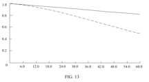
この実施形態の光学モジュール100は、上記のレンズの設計パラメータ及びダイアフラムの積層位置に基づいて取得され得る。この実施形態の光学モジュール100は、優れた光学的効果を達成し、短い全長及び軽い重さを有することができる。更に、第1の実施及び第2の実施と比較して、この実施の光学モジュール100のレンズ群Aは3つのレンズを含み、それにより、この実施の光学モジュール100は、より良い光学的効果を有することができる。図13を参照されたい。図13は、第3の実施に係る光学モジュール100の光学性能の表現図である。図13において、横軸は空間周波数であり、単位はラインペア/mm(LP/mm)であり、縦軸は空間変調関数であり、現在の各ラインペア番号の局所的なコントラスト値に対応する。図中の実施は、当該実施における、光学モジュール100によって実行される結像の経線方向での空間周波数と空間変調関数との間の関係の曲線を示し、破線は、当該実施における、光学モジュール100によって実行される結像の円弧ベクトル方向での空間周波数と空間変調関数との間の関係の曲線を示す。 The
図13からは、空間変調関数が0.3よりも大きいとき、当該実施の光学モジュール100の結像精細度は60lp/mmよりも大きく、この実施の光学モジュール100の精細度は、第1の実施の光学モジュール100のそれ及び第2の実施の光学モジュール100のそれよりも高い、ことが分かる。更に、この実施において、光学レンズの全長は約19mmであり、レンズの重さは23g未満であり、2つのプラスチックレンズの重さは12.5g未満である。従って、当該実施の光学モジュール100は、優れた光学的効果並びに小さい全長及び重さを有し、それにより、光学モジュール100を含む電子デバイス1000も、小さい厚さ及び軽い重さを有することができ、それによって、電子デバイス1000の携帯性及び装用経験を改善する。 From FIG. 13, when the spatial modulation function is larger than 0.3, the imaging definition of the
図9を参照されたい。図9は、本願の第4の実施に係る光学モジュール100の構造の模式図である。この実施において、光学モジュール100のレンズ群Aは3つのレンズを含む。3つのレンズは、第1レンズ11、第2レンズ12、及び第3レンズ13である。第1レンズ、第2レンズ、及び第3レンズ13は、ディスプレイ20から遠ざかる方向からディスプレイ20に近づく方向へ配置されており、第1レンズ11、第2レンズ12、及び第3レンズ13は、同軸上に配置されている。第1レンズ11の対象側面は凸面であり、画像側面は、1つの反曲を備えた自由曲面である。第2レンズ12の対象側面は凸面であり、第2レンズ12の画像側面は、1つの反曲を備えた自由曲面である。第3レンズの対象側面は凸面であり、第3レンズ13の画像側面は、1つの反曲を備えた自由曲面である。従って、第1レンズ11、第2レンズ12、及び第3レンズ13の対象側面及び画像側面はいずれも、ダイアフラム積層を容易にすることができ、つまり、第1レンズ11、第2レンズ12、及び第3レンズ13は積層レンズである。第1レンズ11は、ディスプレイ20から最も遠い積層レンズである。つまり、第1レンズ11は、当該実施での光学モジュール100の第1積層レンズである。第3レンズ13は、ディスプレイ20に最も近い積層レンズである。つまり、第3レンズ13は、当該実施での光学モジュール100の第2積層レンズである。 Please refer to FIG. FIG. 9 is a schematic diagram of the structure of an
本願の第4の実施での光学モジュール100の設計パラメータは、表4に示される。
光学瞳は、ユーザの瞳であり、光学瞳が位置している行の厚さの値は、ユーザが当該実施の電子デバイス1000を身につけている場合の第1レンズ11とユーザの瞳との間の距離を示す。 The optical pupil is the user's pupil, and the thickness value of the row where the optical pupil is located is based on the relationship between the
第1レンズS1は、第1レンズ11の画像側面を示す。第1レンズS1が位置している行の曲率半径の値は、第1レンズ11の画像側面の曲率半径を示す。第1レンズS1が位置している行の厚さの値は、第1レンズ11の画像側面から対象側面までの軸上の距離、つまり、第1レンズ11の軸上の厚さである。 The first lens S1 indicates the image side surface of the
第1レンズS2は、第1レンズ11の対象側面を示す。第1レンズS2が位置している行の曲率半径の値は、第1レンズ11の対象側面の曲率半径を示す。第1レンズS2が位置している行の厚さの値は、第1レンズ11の対象側面から第2レンズ12の画像側面までの軸上の距離である。 The first lens S2 indicates the target side surface of the
第2レンズS3は、第2レンズ12の画像側面を示す。第2レンズS3が位置している行の曲率半径の値は、第2レンズ12の画像側面の曲率半径を示す。第2レンズS3が位置している行の厚さの値は、第2レンズ12の画像側面から対象側面までの軸上の距離、つまり、第2レンズ12の軸上の厚さである。 The second lens S3 indicates the image side surface of the
第2レンズS4は、第2レンズ12の対象側面を示す。第2レンズS4が位置している行の曲率半径の値は、第2レンズ12の対象側面の曲率半径を示す。第2レンズS4が位置している行の厚さの値は、第2レンズ12の対象側面から第3レンズ13の画像側面までの軸上の距離である。 The second lens S4 indicates the target side surface of the
第3レンズS5は、第3レンズ13の画像側面を示す。第3レンズS5が位置している行の曲率半径の値は、第3レンズ13の画像側面の曲率半径を示す。第3レンズS5が位置している行の厚さの値は、第3レンズ13の画像側面から対象側面までの軸上の距離、つまり、第3レンズ13の軸上の厚さである。 The third lens S5 indicates the image side surface of the
第3レンズS6は、第3レンズ13の対象側面を示す。第3レンズS6が位置している行の曲率半径の値は、第3レンズ13の対象側面の曲率半径を示す。第3レンズS6が位置している行の厚さの値は、第3レンズ13の対象側面からディスプレイ20の表面までの軸上の距離である。 The third lens S6 indicates the target side surface of the
この実施において、光学モジュール100のダイアフラムは、直線偏光子31、第1の1/4位相リターダ32、部分的に透過し部分的に反射するフィルム33、第2の1/4位相リターダ34、及び反射偏光子35を含む。直線偏光子31、第1の1/4位相リターダ32、部分的に透過し部分的に反射するフィルム33、第2の1/4位相リターダ34、及び反射偏光子35は、ディスプレイ20に近い側からディスプレイ20から離れた側へ順に配置されている。具体的に、この実施において、直線偏光子31及び第1の1/4位相リターダ32は、ディスプレイ20の発光面に順に重ね合わされる。部分的に透過し部分的に反射するフィルム33は、第3レンズ13の対象側面に積層され、第2の1/4位相リターダ34は、第2レンズ12の画像側面に積層され、反射偏光子35は、第1レンズ11の対象側面に積層される。 In this implementation, the diaphragm of the
ディスプレイ20の表示ピクチャの光は、直線偏光子31及び第1の1/4位相リターダ32の通過に成功した後、第3レンズ13の画像側面に伝えられ、第3レンズ13の画像側面に照射された光の一部は、部分的に透過し部分的に反射するフィルム33を通過する。部分的に透過し部分的に反射するフィルム33を通過した光は、第3レンズ13、第2レンズ12及び第2の1/4位相リターダ34を順に通過し、第1レンズ11の対象側面に伝えられる。この場合に、第1レンズ11の対象側面に伝えられた光の偏光方向は、反射偏光子35の反射軸方向に平行である。第1レンズ11の対象側面に伝えられた光は、反射偏光子35によって反射され、反射された光は、第2の1/4位相リターダ34、第2レンズ12、及び第3レンズ13を順に通過し、その後に、部分的に透過し部分的に反射するフィルム33に伝えられる。一部の光は、部分的に透過し部分的に反射するフィルム33によって反射される。この場合に、部分的に透過し部分的に反射するフィルム33によって反射された光の偏光方向は、反射偏光子35のホモロジー軸方向に平行であり、部分的に透過し部分的に反射するフィルム33によって反射された光は、第3レンズ13、第2レンズ12、第2の1/4位相リターダ34、反射偏光子35、及び第1レンズ11を順に通過し、人間の目に照射され得、それにより、ユーザは、ディスプレイ20に表示されているピクチャを観察することができる。 After the light of the displayed picture on the
この実施において、光は、反射偏光子35の表面及び部分的に透過し部分的に反射するフィルム33の表面の両方で一度反射され、それにより、光は、反射偏光子35と部分的に透過し部分的に反射するフィルム33との間で二度折り返される。従って、光学モジュール100の全長は、同じ光学的効果が達成される場合に、より小さい。更に、この実施において、反射偏光子35は、第1レンズ11に積層され、部分的に透過し部分的に反射するフィルム33は第3レンズ13に積層されている。従って、反射偏光子35と部分的に透過し部分的に反射するフィルム33との間の距離は大きくなり、それにより、光は、反射偏光子35と部分的に透過し部分的に反射するフィルム33との間の長い距離を伝えられるので、同じ光学的効果を実現しながら光学モジュール100の全長を更に短くすることができる。この実施において、直線偏光子31及び第1の1/4位相リターダ32は、ディスプレイ20の発光面上に順に重ね合わされている。部分的に透過し部分的に反射するフィルム33は、第3レンズ13の対象側面に積層され、第2の1/4位相リターダ34は、第2レンズ12の画像側面に積層され、反射偏光子35は、第1レンズ11の対象側面に積層されている。従って、ダイアフラム積層に特別に使用される平面レンズを加える必要はない。これは、レンズの数の増加を回避し、光学モジュール100の全長及び重さの増加を回避することができる。更に、第1レンズ11、第2レンズ、及び第3レンズ13の対象側面及び画像側面はいずれも曲面であり、第1レンズ11、第2レンズ12、又は第3レンズ13の対象側面又は画像側面は、ダイアフラム積層を容易にするために平面として特別に設計されない。従って、これは、曲面を加えることによって光学収差を低減するという効果を達成し、必要な光学的効果を確かにしながら光学モジュール100のレンズの厚さを小さくしかつ全長を短縮することができる。更に、反射偏光子35及び第2の1/4位相リターダ34は、夫々異なる積層レンズに積層されている。これは、レンズのある側に積層されている反射偏光子35又は第2の1/4位相リターダ34が、反射偏光子35又は第2の1/4位相リターダ34がレンズの他方の側に十分に積層されていないときに廃棄されるという問題を回避することができるので、製造コストを下げられる。 In this implementation, the light is reflected once both at the surface of the
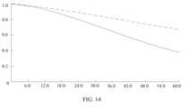
この実施形態の光学モジュール100は、上記のレンズの設計パラメータ及びダイアフラムの積層位置に基づいて取得され得る。この実施形態の光学モジュール100は、優れた光学的効果を達成し、短い全長及び軽い重さを有することができる。図14を参照されたい。図14は、第4の実施に係る光学モジュール100の光学性能の表現図である。図14において、横軸は空間周波数であり、単位はラインペア/mm(LP/mm)であり、縦軸は空間変調関数であり、現在の各ラインペア番号の局所的なコントラスト値に対応する。図中の実施は、当該実施における、光学モジュール100によって実行される結像の経線方向での空間周波数と空間変調関数との間の関係の曲線を示し、破線は、当該実施における、光学モジュール100によって実行される結像の円弧ベクトル方向での空間周波数と空間変調関数との間の関係の曲線を示す。 The
図14からは、空間変調関数が0.3よりも大きいとき、当該実施の光学モジュール100の結像精細度は60lp/mmよりも大きく、つまり、この実施形態の光学モジュール100は高い精細度を有する、ことが分かる。この実施形態の光学モジュール100は、優れた光学的効果並びに小さい全長及び重さを有し、それにより、光学モジュール100を含む電子デバイス1000も、小さい厚さ及び軽い重さを有することができ、それによって、電子デバイス1000の携帯性及び装用経験を改善する。 From FIG. 14, when the spatial modulation function is larger than 0.3, the imaging definition of the
図10を参照されたい。図10は、本願の第5の実施に係る光学モジュール100の構造の模式図である。この実施において、光学モジュール100のレンズ群Aは3つのレンズを含む。3つのレンズは、第1レンズ11、第2レンズ12、及び第3レンズ13である。第1レンズ、第2レンズ、及び第3レンズ13は、ディスプレイ20から遠ざかる方向からディスプレイ20に近づく方向へ配置されており、第1レンズ11、第2レンズ12、及び第3レンズ13は、同軸上に配置されている。第1レンズ11の対象側面は凸面であり、画像側面は、1つの反曲を備えた自由曲面である。第2レンズ12の対象側面は凸面であり、第2レンズ12の画像側面は、1つの反曲を備えた自由曲面である。第3レンズの対象側面は、2つの反曲を備えた自由曲面であり、第3レンズの画像側面は平面である。従って、第1レンズ11及び第2レンズ12の対象側面及び画像側面はいずれも、ダイアフラム積層を容易にすることができる。具体的に言えば、第1レンズ11及び第2レンズ12は両方とも積層レンズであり、第3レンズ13は、光調整に使用される光学調整レンズである。第1レンズ11は、ディスプレイ20から最も遠い積層レンズである。つまり、第1レンズ11は、当該実施での光学モジュール100の第1積層レンズである。第2レンズ12は、ディスプレイ20に最も近い積層レンズである。つまり、第2レンズ12は、当該実施での光学モジュール100の第2積層レンズである。 Please refer to FIG. FIG. 10 is a schematic diagram of the structure of an
本願の第5の実施での光学モジュール100の設計パラメータは、表5に示される。
光学瞳は、ユーザの瞳であり、光学瞳が位置している行の厚さの値は、ユーザが当該実施の電子デバイス1000を身につけている場合の第1レンズ11とユーザの瞳との間の距離を示す。 The optical pupil is the user's pupil, and the thickness value of the row where the optical pupil is located is based on the relationship between the
第1レンズS1は、第1レンズ11の画像側面を示す。第1レンズS1が位置している行の曲率半径の値は、第1レンズ11の画像側面の曲率半径を示す。第1レンズS1が位置している行の厚さの値は、第1レンズ11の画像側面から対象側面までの軸上の距離、つまり、第1レンズ11の軸上の厚さである。 The first lens S1 indicates the image side surface of the
第1レンズS2は、第1レンズ11の対象側面を示す。第1レンズS2が位置している行の曲率半径の値は、第1レンズ11の対象側面の曲率半径を示す。第1レンズS2が位置している行の厚さの値は、第1レンズ11の対象側面から第2レンズ12の画像側面までの軸上の距離である。 The first lens S2 indicates the target side surface of the
第2レンズS3は、第2レンズ12の画像側面を示す。第2レンズS3が位置している行の曲率半径の値は、第2レンズ12の画像側面の曲率半径を示す。第2レンズS3が位置している行の厚さの値は、第2レンズ12の画像側面から対象側面までの軸上の距離、つまり、第2レンズ12の軸上の厚さである。 The second lens S3 indicates the image side surface of the
第2レンズS4は、第2レンズ12の対象側面を示す。第2レンズS4が位置している行の曲率半径の値は、第2レンズ12の対象側面の曲率半径を示す。第2レンズS4が位置している行の厚さの値は、第2レンズ12の対象側面から第3レンズ13の画像側面までの軸上の距離である。 The second lens S4 indicates the target side surface of the
第3レンズS5は、第3レンズ13の画像側面を示す。第3レンズS5が位置している行の曲率半径の値は、第3レンズ13の画像側面の曲率半径を示す。第3レンズS5が位置している行の厚さの値は、第3レンズ13の画像側面から対象側面までの軸上の距離、つまり、第3レンズ13の軸上の厚さである。 The third lens S5 indicates the image side surface of the
第3レンズS6は、第3レンズ13の対象側面を示す。第3レンズS6が位置している行の曲率半径の値は、第3レンズ13の対象側面の曲率半径を示す。第3レンズS6が位置している行の厚さの値は、第3レンズ13の対象側面からディスプレイ20の表面までの軸上の距離である。 The third lens S6 indicates the target side surface of the
この実施において、光学モジュール100のダイアフラムは、直線偏光子31、第1の1/4位相リターダ32、部分的に透過し部分的に反射するフィルム33、第2の1/4位相リターダ34、及び反射偏光子35を含む。直線偏光子31、第1の1/4位相リターダ32、部分的に透過し部分的に反射するフィルム33、第2の1/4位相リターダ34、及び反射偏光子35は、ディスプレイ20に近い側からディスプレイ20から離れた側へ順に配置されている。具体的に、この実施において、直線偏光子31及び第1の1/4位相リターダ32は、ディスプレイ20の発光面に順に重ね合わされる。部分的に透過し部分的に反射するフィルム33は、第2レンズ12の対象側面に積層され、第2の1/4位相リターダ34は、第2レンズ12の画像側面に積層され、反射偏光子35は、第1レンズ11の対象側面に積層される。 In this implementation, the diaphragm of the
ディスプレイ20の表示ピクチャの光は、第3レンズ13、直線偏光子31及び第1の1/4位相リターダ32の通過に成功した後、第2レンズ12の画像側面に伝えられ、第2レンズ12の画像側面に照射された光の一部は、部分的に透過し部分的に反射するフィルム33を通過する。部分的に透過し部分的に反射するフィルム33を通過した光は、第2レンズ12及び第2の1/4位相リターダ34を順に通過し、第1レンズ11の対象側面に伝えられる。この場合に、第1レンズ11の対象側面に伝えられた光の偏光方向は、反射偏光子35の反射軸方向に平行である。第1レンズ11の対象側面に伝えられた光は、反射偏光子35によって反射され、反射された光は、第2の1/4位相リターダ34及び第2レンズ12を順に通過し、その後に、部分的に透過し部分的に反射するフィルム33に伝えられる。一部の光は、部分的に透過し部分的に反射するフィルム33によって反射される。この場合に、部分的に透過し部分的に反射するフィルム33によって反射された光の偏光方向は、反射偏光子35のホモロジー軸方向に平行であり、部分的に透過し部分的に反射するフィルム33によって反射された光は、第2レンズ12、第2の1/4位相リターダ34、反射偏光子35、及び第1レンズ11を順に通過し、人間の目に照射され得、それにより、ユーザは、ディスプレイ20に表示されているピクチャを観察することができる。 After the light of the displayed picture on the
この実施において、光は、反射偏光子35の表面及び部分的に透過し部分的に反射するフィルム33の表面の両方で一度反射され、それにより、光は、反射偏光子35と部分的に透過し部分的に反射するフィルム33との間で二度折り返される。従って、光学モジュール100の全長は、同じ光学的効果が達成される場合に、より小さい。更に、この実施において、直線偏光子31及び第1の1/4位相リターダ32は、ディスプレイ20の発光面上に順に重ね合わされている。部分的に透過し部分的に反射するフィルム33は、第2レンズ12の対象側面に積層され、第2の1/4位相リターダ34は、第2レンズ12の画像側面に積層され、反射偏光子35は、第1レンズ11の対象側面に積層されている。従って、ダイアフラム積層に特別に使用される平面レンズを加える必要はない。これは、レンズの数の増加を回避し、光学モジュール100の全長及び重さの増加を回避することができる。更に、部分的に透過し部分的に反射するフィルム33に積層されている第2レンズ12の対象側面と、反射偏光子35に積層されている第1レンズ11の対象側面とは両方とも曲面であり、第1レンズ11又は第2レンズ12の対象側面は、ダイアフラム積層を容易にするために平面として特別に設計されない。従って、これは、曲面を加えることによって光学収差を低減するという効果を達成し、必要な光学的効果を確かにしながら光学モジュール100のレンズの厚さを小さくしかつ全長を短縮することができる。更に、反射偏光子35及び第2の1/4位相リターダ34は、夫々異なる積層レンズに積層されている。これは、レンズのある側に積層されている反射偏光子35又は第2の1/4位相リターダ34が、反射偏光子35又は第2の1/4位相リターダ34がレンズの他方の側に十分に積層されていないときに廃棄されるという問題を回避することができるので、製造コストを下げられる。 In this implementation, the light is reflected once both at the surface of the
この実施形態の光学モジュール100は、上記のレンズの設計パラメータ及びダイアフラムの積層位置に基づいて取得され得る。この実施形態の光学モジュール100は、優れた光学的効果を達成し、短い全長及び軽い重さを有することができる。図15を参照されたい。図15は、第5の実施に係る光学モジュール100の光学性能の表現図である。図15において、横軸は空間周波数であり、単位はラインペア/mm(LP/mm)であり、縦軸は空間変調関数であり、現在の各ラインペア番号の局所的なコントラスト値に対応する。図中の実施は、当該実施における、光学モジュール100によって実行される結像の経線方向での空間周波数と空間変調関数との間の関係の曲線を示し、破線は、当該実施における、光学モジュール100によって実行される結像の円弧ベクトル方向での空間周波数と空間変調関数との間の関係の曲線を示す。 The
図15からは、空間変調関数が0.3よりも大きいとき、当該実施の光学モジュール100の結像精細度は60lp/mmよりも大きく、つまり、この実施形態の光学モジュール100は高い精細度を有する、ことが分かる。この実施の光学モジュール100は、優れた光学的効果並びに小さい全長及び重さを有し、それにより、光学モジュール100を含む電子デバイス1000も、小さい厚さ及び軽い重さを有することができ、それによって、電子デバイス1000の携帯性及び装用経験を改善する。 From FIG. 15, when the spatial modulation function is larger than 0.3, the imaging definition of the
本願では、直線偏光子31、第1の1/4位相リターダ32、部分的に透過し部分的に反射するフィルム33、第2の1/4位相リターダ34、及び反射偏光子35は、第1レンズ11の対象側面又は画像側面、第2レンズの対象側面又は画像側面、あるいは、ディスプレイ20の発光面に積層される。従って、ダイアフラム積層に特別に使用される平面レンズを加える必要はない。これは、レンズの数の増加を回避し、並びに光学モジュール100全長及び重さの増加を回避することができ、それによって、本願の光学モジュール100を含む電子デバイス1000はより薄くかつより軽くなり、電子デバイス1000は装着又は搬送しやすくなる。少なくとも一部にダイアフラムが積層されるレンズの対象側面及び画像側面はいずれも曲面であり、ダイアフラムが積層されるレンズの対象側面又は画像側面は、ダイアフラム積層を容易にするために平面として特別に設計されない。従って、これは、曲面を加えることによって光学収差を低減するという効果を達成し、レンズの厚さを低減し、更には、光学モジュール100の全長を短縮し、光学モジュール100の重さを低減することができる。 In the present application, the
上記の記載は、本願の具体的な実施に過ぎず、本願の保護範囲は、それらに制限されない。本願で開示されている技術的範囲内で当業者が容易に想到することができる如何なる変形又は置換も、本願の保護範囲内に入るべきである。従って、本願の保護範囲は、特許請求の範囲の保護範囲に従うべきである。 The above descriptions are only specific implementations of the present application, and the protection scope of the present application is not limited thereto. Any modification or substitution that can be easily thought of by a person skilled in the art within the technical scope disclosed in this application should fall within the protection scope of this application. Therefore, the protection scope of the present application should be subject to the protection scope of the claims.
本願は、2020年12月29日付けで「OPTICAL MODULE AND ELECTRONIC DEVICE」という発明の名称で中国国家知識産権局に出願された中国特許出願第202011613157.3号に対する優先権を主張するものであり、先の中国出願は、その全文を参照により本願に援用される。 This application claims priority to Chinese Patent Application No. 202011613157.3 filed with the State Intellectual Property Office of China on December 29, 2020 under the title of invention "OPTICAL MODULE AND ELECTRONIC DEVICE". , earlier Chinese application is hereby incorporated by reference in its entirety.
更に、本願のこの実施において、直線偏光子、第1の1/4位相リターダ、部分的に透過し部分的に反射するフィルム、第2の1/4位相リターダ、及び反射偏光子のうちの1つのダイアフラムは、積層レンズの対象側面又は画像側面に積層されてよく、積層レンズの対象側面及び画像側面はいずれも曲面である。従って、ダイアフラム積層に特別に使用される平面レンズを追加で加えることも、又は積層を容易にするために平面としてレンズの表面を設計することも不要である。このようにして、光学モジュールのレンズの数及びレンズの厚さは低減することができ、一方、光学モジュールは優れた光学的効果を実現することができ、それによって、光学モジュールの軸上の厚さを低減し、光学モジュールの重さを低減し、電子デバイスの厚さを低減し、電子デバイスの重さを低減する。Additionally, in this implementation of the present application, one of a linear polarizer, a first quarter-phase retarder, a partially transmissive and partially reflective film, a second quarter-phase retarder, and a reflective polarizer. The two diaphragms may be stacked on the object side orthe image sideof the laminated lens , and both the object side and the image side of the laminated lens are curved surfaces. Therefore, it is not necessary to add additional planar lenses specifically used for diaphragm stacking, or to design the surface of the lens as flat to facilitate stacking. In this way, the number of lenses and the lens thickness of the optical module can be reduced, while the optical module can achieve excellent optical effects, thereby increasing the axial thickness of the optical module. reduce the thickness of the optical module, reduce the thickness of the electronic device, reduce the weight of the electronic device.
いくつかの実施において、反射偏光子及び第2の1/4位相リターダは、画像側に向かって曲がり、hの有効開口を有する位置での反射偏光子の表面ベクトル高さはS1であり、hの有効開口を有する位置での第2の1/4位相リターダの表面ベクトル高さはS2であり、反射偏光子及び第2の1/4位相リターダは、S2-S1≦h/5という関係を満たす。これは、反射偏光子の曲率半径が第2の1/4位相リターダのそれよりも小さいこと、又は反射偏光子の曲率半径が第2の1/4位相リターダのそれよりもわずかにだけ大きいことを確かにし、それによって、光漏出を回避する。更に、反射偏光子及び第2の1/4位相リターダが、隣接したレンズの、隣接している対象側面及び画像側面に夫々積層される場合に、反射偏光子の曲率半径は第2の1/4位相リターダのそれよりも小さいか、又は反射偏光子の曲率半径は第2の1/4位相リターダのそれよりもわずかに大きいので、2つのレンズは可能な限り近くに配置することができ、2つのレンズの軸上のギャップは可能な限り小さくすることできることが確かにされ得、従って、光学モジュールの全長は低減される。In some implementations, the reflective polarizer and the second quarter-phase retarder are curved toward the image side, and the surface vector height of the reflective polarizer at a position with an effective aperture of h is S1 and h The surface vector height of the second quarter-phase retarder at a position with an effective aperture of is S2, and the reflective polarizer and the second quarter-phase retarder have the relationship S2-S1≦h/5. Fulfill. This means that the radius of curvature of the reflective polarizer is smaller than that of the second quarter-phase retarder, or that the radius of curvature of the reflective polarizer is only slightly larger than that of the second quarter-phase retarder. and thereby avoid light leakage. Further, whena reflective polarizer and a second quarter-phase retarder are laminated to adjacent object and image sides of adjacent lenses, respectively, the radius of curvature of the reflective polarizer is equal to the second quarter-phase retarder. The radius of curvature of the reflective polarizer is either smaller than that of the 4-phase retarder or slightly larger than that of the second 1/4-phase retarder, so that the two lenses can be placed as close as possible; It can be ensured that the axial gap of the two lenses can be made as small as possible, thus reducing the overall length of the optical module.
再び図2を参照されたい。本願において、電子デバイス1000はふた組の光学モジュール100を含む。光学モジュール100の各組は同じ構造を有し、光学モジュール100の各組はレンズ群A、ディスプレイ20、及び異なるダイアフラムを含む。ふた組の光学モジュール100のレンズ群Aの夫々は、1つの光射出孔204に配置される。代替的に、ふた組の光学モジュール100のレンズ群Aの夫々は1つの光射出孔204に対向し、それにより、レンズ群Aから発せられた光は、対応する光射出孔204から人間の目に入射する。本願において、ユーザが電子デバイス1000を身につける場合に、ユーザの左目及び右目は、光射出孔204から発せられた光を受けるよう、夫々1つの光射出孔204に対向する。言い換えれば、本願の電子デバイス1000のふた組の光学モジュール100によって伝送された光は、ユーザの左目及び右目によって夫々受光され得、それにより、ユーザは、両目を使用することによって、ディスプレイ20に表示されたピクチャを見ることができる。本願の実施において、ふた組の光学モジュール100のディスプレイ20は一体化された構造を持つ。本願の他の実施では、ふた組の光学モジュール100の夫々が独立したディスプレイ20を備えてもよいことが理解され得る。Please refer to FIG. 2 again. In this application, the
再び図6を参照されたい。本願のこの実施において、反射偏光子35及び第2の1/4位相リターダ34はいずれも、画像側に向かって曲がる曲げシートである。この実施において、レンズ群Aの結像位置はユーザの網膜上である。従って、ユーザの目の位置はレンズ群Aの画像側である。従って、反射偏光子35及び第2の1/4位相リターダ34いずれも、ユーザの目に向かって曲がる湾曲したシートである。更に、いくつかの実施において、hの有効開口を有する位置での反射偏光子35の表面ベクトル高さはS1であり、hの有効開口を有する位置での第2の1/4位相リターダ34の表面ベクトル高さはS2であり、反射偏光子35及び第2の1/4位相リターダ34は、S2-S1≦h/5という関係を満たす。これは、反射偏光子35の曲率半径が第2の1/4位相リターダ34のそれよりも小さいこと、又は反射偏光子35の曲率半径が第2の1/4位相リターダ34のそれよりもわずかにのみ大きいことを確かにし、それによって、光漏出を回避する。更に、反射偏光子35及び第2の1/4位相リターダ34が、隣接したレンズの、隣接している対象側面及び画像側面に夫々積層される場合に、反射偏光子35の曲率半径は第2の1/4位相リターダ34のそれよりも小さいか、又は反射偏光子35の曲率半径は第2の1/4位相リターダ34のそれよりもわずかに大きいので、2つのレンズは可能な限り近くに配置することができ、2つのレンズの軸上のギャップは可能な限り小さくすることできることが確かにされ得、従って、光学モジュール100の全長は低減される。例えば、図4に示される実施において、反射偏光子35は、第1レンズ11の対象側面に積層され、第2の1/4位相リターダ34は、第2レンズ12の画像側面に積層される。反射偏光子35の曲率半径は第2の1/4位相リターダ34の曲率半径よりも小さいので、第1レンズ11と第2レンズ12との間の軸方向の距離は可能な限り小さくなり、それによって、光学モジュール100の全長を可能な限り小さくする。この実施において、光学モジュール100の全長は14mmである。Please refer to FIG. 6 again. In this implementation of the present application, both
本願の第1の実施での光学モジュール100の設計パラメータは、表1に示される。
本願の第2の実施での光学モジュール100の設計パラメータは、表2に示される。
この実施において、光は、反射偏光子35の表面及び部分的に透過し部分的に反射するフィルム33の表面の両方で一度反射され、それにより、光は、反射偏光子35と部分的に透過し部分的に反射するフィルム33との間で二度折り返される。従って、光学モジュール100の全長は、同じ光学的効果が達成される場合に、より小さい。更に、この実施において、反射偏光子35は、第1レンズ11の画像側面に積層され、第2の1/4位相リターダ34は、第1レンズ11の対象側面に積層されている。この場合に、反射偏光子35と第2の1/4位相リターダ34との間の距離は大きくされ得るので、反射偏光子35と第2の1/4位相リターダ34との間の光伝送光学経路は長くなり、それによって、光学モジュール100の全長を短縮する。直線偏光子31及び第1の1/4位相リターダ32は、ディスプレイ20の発光面上に順に重ね合わされている。部分的に透過し部分的に反射するフィルム33は、第2レンズ12の対象側面に積層され、第2の1/4位相リターダ34は第1レンズ11の対象側面に積層され、反射偏光子35は、第1レンズ11の画像側面に積層されている。従って、ダイアフラム積層に特別に使用される平面レンズを加える必要はない。これは、レンズの数の増加を回避し、光学モジュール100の全長及び重さの増加を回避することができる。更に、第1レンズ11及び第2レンズの対象側面及び画像側面はいずれも曲面であり、第1レンズ11又は第2レンズ12の対象側面又は画像側面は、ダイアフラム積層を容易にするために平面として特別に設計されない。従って、これは、曲面を加えることによって光学収差を低減するという効果を達成し、必要な光学的効果を確かにしながら光学モジュール100のレンズの厚さを小さくしかつ全長を短縮することができる。In this implementation, the light is reflected once both at the surface of the
本願の第3の実施での光学モジュール100の設計パラメータは、表3に示される。
ディスプレイ20の表示ピクチャの光は、第3レンズ13、直線偏光子31及び第1の1/4位相リターダ32の通過に成功した後、第2レンズ12の画像側面に伝えられ、第2レンズ12の画像側面に照射された光の一部は、部分的に透過し部分的に反射するフィルム33を通過する。部分的に透過し部分的に反射するフィルム33を通過した光は、第2レンズ12及び第2の1/4位相リターダ34を順に通過し、第1レンズ11の対象側面に伝えられる。この場合に、第1レンズ11の対象側面に伝えられた光の偏光方向は、反射偏光子35の反射軸方向に平行である。第1レンズ11の対象側面に伝えられた光は、反射偏光子35によって反射され、反射された光は、第2の1/4位相リターダ34及び第2レンズ12を順に通過し、その後に、部分的に透過し部分的に反射するフィルム33に伝えられる。一部の光は、部分的に透過し部分的に反射するフィルム33によって反射される。この場合に、部分的に透過し部分的に反射するフィルム33によって反射された光の偏光方向は、反射偏光子35のホモロジー軸方向に平行であり、部分的に透過し部分的に反射するフィルム33によって反射された光は、第2レンズ12、第2の1/4位相リターダ34、反射偏光子35、及び第1レンズ11を順に通過し、人間の目に照射され得、それにより、ユーザは、ディスプレイ20に表示されているピクチャを観察することができる。After the light of the displayed picture on the
本願の第4の実施での光学モジュール100の設計パラメータは、表4に示される。
本願の第5の実施での光学モジュール100の設計パラメータは、表5に示される。
Claims (12)
Translated fromJapanese各レンズは、互いに対向して配置されている対象側面及び画像側面を有し、前記対象側面は対象側に面し、前記画像側面は画像側面に面し、前記複数のレンズは少なくとも1つの積層レンズを有し、前記積層レンズの対象側面及び画像側面はいずれも曲面であり、
前記光学モジュールは、直線偏光子、第1の1/4位相リターダ、部分的に透過し部分的に反射するフィルム、第2の1/4位相リターダ、及び反射偏光子を更に有し、
前記直線偏光子、前記第1の1/4位相リターダ、前記部分的に透過し部分的に反射するフィルム、前記第2の1/4位相リターダ、及び前記反射偏光子は、前記対象側から前記画像側まで順に配置され、前記直線偏光子、前記第1の1/4位相リターダ、前記部分的に透過し部分的に反射するフィルム、前記第2の1/4位相リターダ、及び前記反射偏光子は、前記積層レンズの前記対象側面又は前記画像側面に積層される、
光学モジュール。An optical module having a plurality of lenses arranged in order from an object side to an image side,
Each lens has an object side and an image side disposed opposite each other, the object side facing the object side, the image side facing the image side, and the plurality of lenses having at least one laminated layer. a lens, the object side surface and the image side surface of the laminated lens are both curved surfaces,
The optical module further includes a linear polarizer, a first quarter-phase retarder, a partially transmissive and partially reflective film, a second quarter-phase retarder, and a reflective polarizer;
The linear polarizer, the first quarter-phase retarder, the partially transmitting and partially reflecting film, the second quarter-phase retarder, and the reflective polarizer are configured to arranged in order up to the image side, the linear polarizer, the first quarter-phase retarder, the partially transmitting and partially reflecting film, the second quarter-phase retarder, and the reflective polarizer. is laminated on the object side surface or the image side surface of the laminated lens,
optical module.
請求項1に記載の光学モジュール。The reflective polarizer and the second quarter-phase retarder are curved toward the image side, and the surface vector height of the reflective polarizer at a position with an effective aperture of h is S1, and the surface vector height of the reflective polarizer at a position with an effective aperture of h is The surface vector height of the second quarter-phase retarder at the position having the aperture is S2, and the reflective polarizer and the second quarter-phase retarder have a relationship of S2-S1≦h/5. satisfy,
The optical module according to claim 1.
請求項1に記載の光学モジュール。The object side surface and the image side surface of the laminated lens are spherical surfaces, aspheric surfaces, or free-form surfaces with one recurvature,
The optical module according to claim 1.
請求項1に記載の光学モジュール。There are at least two laminated lenses, the at least two laminated lenses having a first laminated lens and a second laminated lens, the first laminated lens being the furthest laminated lens from the object side, and the second laminated lens The laminated lens is the laminated lens closest to the object side,
The optical module according to claim 1.
請求項4に記載の光学モジュール。The reflective polarizer is laminated to the image side of the first laminated lens, and the partially transparent and partially reflective film is laminated to the target side of the second laminated lens.
The optical module according to claim 4.
請求項5に記載の光学モジュール。The second 1/4 phase retarder is laminated on the object side surface of the first laminated lens or the image side surface of the second laminated lens.
The optical module according to claim 5.
請求項4に記載の光学モジュール。The reflective polarizer is laminated on the target side of the first laminated lens, and the partially transparent and partially reflective film is laminated on the target side of the second laminated lens, and the reflective polarizer is laminated on the target side of the first laminated lens. a quarter phase retarder is laminated on the image side surface of the second laminated lens;
The optical module according to claim 4.
請求項4乃至7のうちいずれか一項に記載の光学モジュール。The plurality of lenses further includes at least one optical adjustment lens, the object side surface or image side surface of the optical adjustment lens is a free-form surface with a plurality of recurves, and the optical adjustment lens is configured to configured to adjust the optical effect;
The optical module according to any one of claims 4 to 7.
請求項1に記載の光学モジュール。the reflective polarizer and the second quarter-phase retarder are stacked into different stacked lenses;
The optical module according to claim 1.
請求項1に記載の光学モジュール。The total length of the optical module is 30 mm or less, and the mass of the plurality of lenses of the optical module is 25 g or less.
The optical module according to claim 1.
請求項1に記載の光学モジュール。The optical module further includes a display, the display being located on the object side of the plurality of lenses.
The optical module according to claim 1.
請求項1乃至11のうちいずれか一項に記載の光学モジュールと
を有し、
前記光学モジュールは、前記ホルダーに固定される、
電子デバイス。holder and
The optical module according to any one of claims 1 to 11,
the optical module is fixed to the holder;
electronic device.
Applications Claiming Priority (3)
| Application Number | Priority Date | Filing Date | Title |
|---|---|---|---|
| CN202011613157.3ACN114690415A (en) | 2020-12-29 | 2020-12-29 | Optical module and electronic equipment |
| CN202011613157.3 | 2020-12-29 | ||
| PCT/CN2021/140698WO2022143369A1 (en) | 2020-12-29 | 2021-12-23 | Optical module and electronic device |
Publications (2)
| Publication Number | Publication Date |
|---|---|
| JP2024502803Atrue JP2024502803A (en) | 2024-01-23 |
| JP7582582B2 JP7582582B2 (en) | 2024-11-13 |
Family
ID=82132577
Family Applications (1)
| Application Number | Title | Priority Date | Filing Date |
|---|---|---|---|
| JP2023539925AActiveJP7582582B2 (en) | 2020-12-29 | 2021-12-23 | Optical module and electronic device |
Country Status (5)
| Country | Link |
|---|---|
| US (1) | US20240069328A1 (en) |
| EP (1) | EP4249989A4 (en) |
| JP (1) | JP7582582B2 (en) |
| CN (1) | CN114690415A (en) |
| WO (1) | WO2022143369A1 (en) |
Families Citing this family (10)
| Publication number | Priority date | Publication date | Assignee | Title |
|---|---|---|---|---|
| CN115421301B (en)* | 2022-07-29 | 2025-06-24 | 歌尔光学科技有限公司 | Optical module and head mounted display device |
| CN116755241A (en)* | 2023-05-05 | 2023-09-15 | 浙江舜宇光学有限公司 | Visual system and VR equipment comprising same |
| CN116594170A (en)* | 2023-05-23 | 2023-08-15 | 浙江舜宇光学有限公司 | Vision system and VR equipment including the vision system |
| CN116909005A (en)* | 2023-06-29 | 2023-10-20 | 歌尔光学科技有限公司 | Optical modules and head-mounted display devices |
| CN116893520A (en)* | 2023-08-04 | 2023-10-17 | 浙江舜宇光学有限公司 | virtual reality device |
| JP2025044445A (en)* | 2023-09-20 | 2025-04-02 | 日東電工株式会社 | Method for manufacturing retardation film, retardation film piece, retardation film set, or lens part or display system |
| JP2025044444A (en)* | 2023-09-20 | 2025-04-02 | 日東電工株式会社 | Method for manufacturing retardation film, retardation film set, lens unit, or display system |
| JP2025044446A (en)* | 2023-09-20 | 2025-04-02 | 日東電工株式会社 | Retardation film, retardation film set, or manufacturing method of lens part or display system |
| JP2025089794A (en)* | 2023-12-04 | 2025-06-16 | キヤノン株式会社 | Optical system and display device |
| WO2025141916A1 (en)* | 2023-12-25 | 2025-07-03 | ソニーグループ株式会社 | Optical system and display device |
Citations (9)
| Publication number | Priority date | Publication date | Assignee | Title |
|---|---|---|---|---|
| DE69720313T2 (en)* | 1996-04-24 | 2003-12-11 | Sharp Kk | Observation device for head-based display |
| JP2018500584A (en)* | 2015-09-03 | 2018-01-11 | スリーエム イノベイティブ プロパティズ カンパニー | Thermoformed multilayer reflective polarizer |
| CN109946837A (en)* | 2018-08-31 | 2019-06-28 | 华为技术有限公司 | an optical imaging system |
| JP2019526075A (en)* | 2016-08-02 | 2019-09-12 | アップル インコーポレイテッドApple Inc. | Optical system for head mounted display |
| CN110320668A (en)* | 2019-07-04 | 2019-10-11 | 歌尔股份有限公司 | Optical system and virtual reality device with it |
| US20190384070A1 (en)* | 2018-06-18 | 2019-12-19 | Facebook Technologies, Llc | Optical assembly with curved reflective polarizer for head mounted display |
| US20200096780A1 (en)* | 2016-12-20 | 2020-03-26 | 3M Innovative Properties Company | Optical system |
| JP2020510238A (en)* | 2017-03-08 | 2020-04-02 | スリーエム イノベイティブ プロパティズ カンパニー | Optical system |
| JP2020519964A (en)* | 2017-05-16 | 2020-07-02 | スリーエム イノベイティブ プロパティズ カンパニー | Optical system |
Family Cites Families (12)
| Publication number | Priority date | Publication date | Assignee | Title |
|---|---|---|---|---|
| CN205539752U (en)* | 2016-01-28 | 2016-08-31 | 深圳多哚新技术有限责任公司 | Short distance optical enlargement module and subassembly thereof |
| WO2017128187A1 (en)* | 2016-01-28 | 2017-08-03 | 深圳多哚新技术有限责任公司 | Short-distance optical amplifier module, amplification method and amplification system |
| CN107219637B (en)* | 2016-03-21 | 2024-09-10 | 深圳多哚新技术有限责任公司 | Short-distance optical amplification module, glasses, helmet and VR system |
| CN107045196B (en)* | 2017-02-08 | 2019-07-05 | 浙江舜宇光学有限公司 | Eyepiece and display device including the same |
| CN208156319U (en)* | 2018-05-03 | 2018-11-27 | 深圳创维新世界科技有限公司 | Optics module and system are amplified in short distance |
| CN208156310U (en)* | 2018-05-03 | 2018-11-27 | 深圳创维新世界科技有限公司 | Compact amplifies optics module and system |
| CN110308559A (en)* | 2019-06-28 | 2019-10-08 | 上海视涯信息科技有限公司 | A kind of virtual reality optics module and virtual reality device |
| TWM591624U (en)* | 2019-08-20 | 2020-03-01 | 雙瑩科技股份有限公司 | Short distance optical system |
| CN110646942A (en)* | 2019-09-29 | 2020-01-03 | 平行现实(杭州)科技有限公司 | Ultrathin optical amplification module and application thereof |
| CN211375190U (en)* | 2020-02-25 | 2020-08-28 | 深圳惠牛科技有限公司 | VR optical module and display device |
| CN111290132A (en)* | 2020-04-03 | 2020-06-16 | 江西微瑞光学有限公司 | Short-distance and high-lens-birefringence-tolerance optical imaging module |
| CN111766706A (en)* | 2020-06-19 | 2020-10-13 | 江西微瑞光学有限公司 | Short-distance and high-lens-birefringence-tolerance optical imaging module |
- 2020
- 2020-12-29CNCN202011613157.3Apatent/CN114690415A/enactivePending
- 2021
- 2021-12-23USUS18/259,545patent/US20240069328A1/enactivePending
- 2021-12-23JPJP2023539925Apatent/JP7582582B2/enactiveActive
- 2021-12-23EPEP21914106.6Apatent/EP4249989A4/enactivePending
- 2021-12-23WOPCT/CN2021/140698patent/WO2022143369A1/ennot_activeCeased
Patent Citations (9)
| Publication number | Priority date | Publication date | Assignee | Title |
|---|---|---|---|---|
| DE69720313T2 (en)* | 1996-04-24 | 2003-12-11 | Sharp Kk | Observation device for head-based display |
| JP2018500584A (en)* | 2015-09-03 | 2018-01-11 | スリーエム イノベイティブ プロパティズ カンパニー | Thermoformed multilayer reflective polarizer |
| JP2019526075A (en)* | 2016-08-02 | 2019-09-12 | アップル インコーポレイテッドApple Inc. | Optical system for head mounted display |
| US20200096780A1 (en)* | 2016-12-20 | 2020-03-26 | 3M Innovative Properties Company | Optical system |
| JP2020510238A (en)* | 2017-03-08 | 2020-04-02 | スリーエム イノベイティブ プロパティズ カンパニー | Optical system |
| JP2020519964A (en)* | 2017-05-16 | 2020-07-02 | スリーエム イノベイティブ プロパティズ カンパニー | Optical system |
| US20190384070A1 (en)* | 2018-06-18 | 2019-12-19 | Facebook Technologies, Llc | Optical assembly with curved reflective polarizer for head mounted display |
| CN109946837A (en)* | 2018-08-31 | 2019-06-28 | 华为技术有限公司 | an optical imaging system |
| CN110320668A (en)* | 2019-07-04 | 2019-10-11 | 歌尔股份有限公司 | Optical system and virtual reality device with it |
Also Published As
| Publication number | Publication date |
|---|---|
| EP4249989A4 (en) | 2024-05-29 |
| CN114690415A (en) | 2022-07-01 |
| EP4249989A1 (en) | 2023-09-27 |
| US20240069328A1 (en) | 2024-02-29 |
| WO2022143369A1 (en) | 2022-07-07 |
| JP7582582B2 (en) | 2024-11-13 |
Similar Documents
| Publication | Publication Date | Title |
|---|---|---|
| JP7582582B2 (en) | Optical module and electronic device | |
| CN113866982B (en) | Near-to-eye display optical module and VR display device | |
| JP4772204B2 (en) | Observation optical system | |
| JP2019505843A (en) | Wide-view personal display device | |
| WO2016160099A2 (en) | Display devices with reflectors | |
| CN114967135B (en) | Ultra-short throw eyepiece system | |
| CN113219665A (en) | Optical lens group, optical system and head-mounted display device | |
| CN118068563B (en) | Optical systems and display devices | |
| EP4160296A1 (en) | Augmented reality display device | |
| CN117706792B (en) | Optical system and head mounted display device | |
| CN117075337A (en) | Optical module and head-mounted display device | |
| CN116859562A (en) | Optical module and head-mounted display device | |
| CN119200241B (en) | Optical system and optical apparatus including the same | |
| CN115981002A (en) | Near-to-eye display module and wearable equipment | |
| WO2025055836A1 (en) | Optical system and head-mounted display device | |
| WO2025036219A1 (en) | Optical module and head-mounted display device | |
| CN115421302A (en) | Optical modules and head-mounted display devices | |
| CN221378385U (en) | Optical system and head-mounted display device | |
| CN217846785U (en) | Optical modules and head-mounted display devices | |
| WO2021068855A1 (en) | Display device module and head mounted display device | |
| WO2024244273A1 (en) | Optical module and head-mounted display device | |
| CN111487775A (en) | Binocular optical display system for multiplexing light source folding light path and wearable equipment | |
| CN117170102A (en) | Near-to-eye optical system and head-mounted display device | |
| CN116149065A (en) | Optical module and wearable equipment | |
| CN115963638A (en) | Near-eye display modules and wearable devices |
Legal Events
| Date | Code | Title | Description |
|---|---|---|---|
| A521 | Request for written amendment filed | Free format text:JAPANESE INTERMEDIATE CODE: A523 Effective date:20230807 | |
| A621 | Written request for application examination | Free format text:JAPANESE INTERMEDIATE CODE: A621 Effective date:20230807 | |
| A977 | Report on retrieval | Free format text:JAPANESE INTERMEDIATE CODE: A971007 Effective date:20240730 | |
| A131 | Notification of reasons for refusal | Free format text:JAPANESE INTERMEDIATE CODE: A131 Effective date:20240806 | |
| A521 | Request for written amendment filed | Free format text:JAPANESE INTERMEDIATE CODE: A523 Effective date:20240823 | |
| TRDD | Decision of grant or rejection written | ||
| A01 | Written decision to grant a patent or to grant a registration (utility model) | Free format text:JAPANESE INTERMEDIATE CODE: A01 Effective date:20241001 | |
| A61 | First payment of annual fees (during grant procedure) | Free format text:JAPANESE INTERMEDIATE CODE: A61 Effective date:20241016 | |
| R150 | Certificate of patent or registration of utility model | Ref document number:7582582 Country of ref document:JP Free format text:JAPANESE INTERMEDIATE CODE: R150 |