JP2024166957A - Nitride Semiconductor Devices - Google Patents
Nitride Semiconductor DevicesDownload PDFInfo
- Publication number
- JP2024166957A JP2024166957AJP2023083402AJP2023083402AJP2024166957AJP 2024166957 AJP2024166957 AJP 2024166957AJP 2023083402 AJP2023083402 AJP 2023083402AJP 2023083402 AJP2023083402 AJP 2023083402AJP 2024166957 AJP2024166957 AJP 2024166957A
- Authority
- JP
- Japan
- Prior art keywords
- layer
- nitride semiconductor
- substrate
- silicon carbide
- semiconductor device
- Prior art date
- Legal status (The legal status is an assumption and is not a legal conclusion. Google has not performed a legal analysis and makes no representation as to the accuracy of the status listed.)
- Pending
Links
Images


Landscapes
- Junction Field-Effect Transistors (AREA)
- Recrystallisation Techniques (AREA)
Abstract
Description
Translated fromJapanese本開示は、窒化物半導体デバイスに関する。This disclosure relates to nitride semiconductor devices.
GaNに代表される窒化物半導体は、バンドギャップが大きいワイドギャップ半導体であり、絶縁破壊電界が大きく、電子の飽和ドリフト速度がGaAsなどの化合物半導体またはSi半導体などに比べて大きいという特長を有している。例えば、GaNおよびAlNのバンドギャップはそれぞれ、室温で3.4eV、6.2eVである。このため、高出力化および/または高耐圧化に有利な窒化物半導体を用いたパワートランジスタの研究開発が現在活発に行われている。Nitride semiconductors, such as GaN, are wide-gap semiconductors with a large band gap, and have the advantages of a large dielectric breakdown field and a high electron saturation drift velocity compared to compound semiconductors such as GaAs or Si semiconductors. For example, the band gaps of GaN and AlN are 3.4 eV and 6.2 eV, respectively, at room temperature. For this reason, research and development of power transistors using nitride semiconductors, which are advantageous for achieving high output and/or high voltage resistance, is currently being actively conducted.
また、AlGaN/GaNヘテロ構造において、(0001)面上にて自発分極およびピエゾ分極によりヘテロ界面に高濃度の2次元電子ガス(2DEG:2 Dimensional Electron Gas)が生じ、アンドープ時においても1×1013cm-2以上のシートキャリア濃度が得られる特徴がある。例えば、特許文献1には、AlGaN/GaNヘテロ界面に発生した2次元電子ガスからなるチャネルをゲート電圧によって開閉することが可能なGaN系縦型トランジスタが開示されている。 Furthermore, in an AlGaN/GaN heterostructure, spontaneous polarization and piezoelectric polarization on the (0001) plane cause a high concentration of two-dimensional electron gas (2DEG) to be generated at the heterointerface, and a sheet carrier concentration of 1×1013 cm-2 or more can be obtained even in an undoped state. For example,
従来の窒化物半導体デバイスに対しては、基板の大口径化に改善の余地がある。There is room for improvement in increasing the diameter of the substrate compared to conventional nitride semiconductor devices.
そこで、本開示は、基板の大口径化が可能な窒化物半導体デバイスを提供する。Therefore, this disclosure provides a nitride semiconductor device that allows for a larger diameter substrate.
本開示の一態様に係る窒化物半導体デバイスは、基板と、前記基板の上方に設けられた第1の窒化物半導体層と、前記第1の窒化物半導体層の上方に設けられた第1のp型窒化物半導体層と、前記第1のp型窒化物半導体層の上方に設けられた第2の窒化物半導体層と、前記第2の窒化物半導体層および前記第1のp型窒化物半導体層を貫通し、前記第1の窒化物半導体層にまで達する第1の開口部と、前記第2の窒化物半導体層の上面および前記第1の開口部を覆うように下から順に設けられた電子走行層および電子供給層と、前記第1の開口部を覆うように前記電子供給層の上方に設けられたゲート電極と、前記ゲート電極から離れた位置に設けられたソース電極と、前記基板の下方に設けられたドレイン電極と、を備え、前記基板は、炭化ケイ素層と、前記炭化ケイ素層の上方に設けられた炭素層と、を含み、前記炭素層は、グラフェン層およびグラフェンバッファ層の少なくとも一方を含む。A nitride semiconductor device according to one aspect of the present disclosure includes a substrate, a first nitride semiconductor layer provided above the substrate, a first p-type nitride semiconductor layer provided above the first nitride semiconductor layer, a second nitride semiconductor layer provided above the first p-type nitride semiconductor layer, a first opening penetrating the second nitride semiconductor layer and the first p-type nitride semiconductor layer and reaching the first nitride semiconductor layer, an electron transit layer and an electron supply layer provided in this order from below to cover the upper surface of the second nitride semiconductor layer and the first opening, a gate electrode provided above the electron supply layer to cover the first opening, a source electrode provided at a position away from the gate electrode, and a drain electrode provided below the substrate, the substrate including a silicon carbide layer and a carbon layer provided above the silicon carbide layer, and the carbon layer including at least one of a graphene layer and a graphene buffer layer.
本開示の別の一態様に係る窒化物半導体デバイスは、基板と、前記基板の上方に設けられた第1の炭化ケイ素層と、前記第1の炭化ケイ素層の上面の少なくとも一部を露出させるように、前記第1の炭化ケイ素層の上方に設けられたp型の炭化ケイ素層と、グラフェン層またはグラフェンバッファ層の少なくとも一方を含み、前記p型の炭化ケイ素層の上方に設けられた炭素層と、前記第1の炭化ケイ素層および前記炭素層の上方に設けられた電子走行層と、前記電子走行層の上方に設けられた電子供給層と、前記電子供給層の上方に設けられたゲート電極と、前記ゲート電極から離れた位置に設けられたソース電極と、前記基板の下方に設けられたドレイン電極と、を備え、前記炭素層は、前記第1の炭化ケイ素層の一部を露出させる開口を有する。A nitride semiconductor device according to another aspect of the present disclosure includes a substrate, a first silicon carbide layer provided above the substrate, a p-type silicon carbide layer provided above the first silicon carbide layer so as to expose at least a portion of the upper surface of the first silicon carbide layer, and at least one of a graphene layer and a graphene buffer layer, and includes a carbon layer provided above the p-type silicon carbide layer, an electron transit layer provided above the first silicon carbide layer and the carbon layer, an electron supply layer provided above the electron transit layer, a gate electrode provided above the electron supply layer, a source electrode provided at a position away from the gate electrode, and a drain electrode provided below the substrate, and the carbon layer has an opening that exposes a portion of the first silicon carbide layer.
本開示によれば、基板の大口径化が可能な窒化物半導体デバイスを提供することが可能となる。This disclosure makes it possible to provide nitride semiconductor devices that allow for larger diameter substrates.
(本開示の基礎となった知見)
本発明者らは、従来の窒化物半導体デバイスに関し、以下の問題が生じることを見出した。 (Findings that formed the basis of this disclosure)
The present inventors have found that the following problems occur with conventional nitride semiconductor devices.
従来の窒化物半導体デバイスでは、導電性のGaN基板上にエピタキシャル成長させたn--GaNドリフト層等の窒化物半導体膜を利用して、トランジスタ構造を形成していた。しかし、GaN基板は、大口径化が困難であるため、基板サイズが制限されるという課題がある。これは、例えば、GaN基板を大口径化した場合には、オフ角のばらつきの影響を受けて信頼性が低下するためである。 In conventional nitride semiconductor devices, a transistor structure is formed by using a nitride semiconductor film such as an n- -GaN drift layer epitaxially grown on a conductive GaN substrate. However, since it is difficult to increase the diameter of a GaN substrate, there is a problem that the substrate size is limited. This is because, for example, when the diameter of a GaN substrate is increased, the reliability decreases due to the influence of the variation in the off-angle.
大口径化が可能な基板としては、Si基板またはSiC基板が知られている。Si基板へのGaNのエピタキシャル成長を行う技術が、特許文献2に開示されている。具体的には、特許文献2に開示された技術では、Si基板上の3C-SiC薄膜上に、AlNバッファ層を形成している。また、非特許文献1に開示されているように、6H-SiC基板上においても同様に、AlNバッファ層を形成することで、GaNのエピタキシャル成長が可能である。AlNをバッファ層として用いる理由は、表1に示す半導体材料の格子定数と熱膨張係数との関係によるものである。Si substrates and SiC substrates are known as substrates that can be made larger in diameter.

表1に示すように、SiCは、GaNに比べて熱膨張係数が小さいので成長温度から室温まで温度を下げると、GaNのエピタキシャル膜には大きな引張り応力がかかり、割れが発生する。GaNより熱膨張係数が大きく、SiCとの格子不整合が小さいAlNをバッファ層に用いることでGaNに圧縮応力を発生させることができるので、割れを防ぐことができる。As shown in Table 1, SiC has a smaller thermal expansion coefficient than GaN, so when the temperature is lowered from the growth temperature to room temperature, the GaN epitaxial film is subjected to a large tensile stress, causing cracks. By using AlN, which has a larger thermal expansion coefficient than GaN and a small lattice mismatch with SiC, as the buffer layer, compressive stress can be generated in the GaN, preventing cracks.
しかし、AlNバッファ層は高抵抗なので、電流を基板に対して垂直方向に流す縦型トランジスタには適用できない。そこで、AlNバッファ層を用いずに、大口径基板を利用して窒化物半導体デバイスを実現する技術が求められている。なお、大口径基板としては、例えば、直径が6インチを超えるSi基板またはSiC基板が知られているが、基板の直径はこれに限定されない。直径が6インチ未満の基板であっても、GaN基板の代わりにSi基板等を利用することで、低コスト化および信頼性の向上等が期待される。However, because the AlN buffer layer has high resistance, it cannot be applied to vertical transistors in which current flows perpendicular to the substrate. Therefore, there is a demand for technology that realizes nitride semiconductor devices using large-diameter substrates without using an AlN buffer layer. Note that, although Si substrates or SiC substrates with a diameter of more than 6 inches are known as large-diameter substrates, the diameter of the substrate is not limited to these. Even for substrates with a diameter of less than 6 inches, it is expected that costs will be reduced and reliability will be improved by using a Si substrate instead of a GaN substrate.
本開示の第1の態様に係る窒化物半導体デバイスは、基板と、前記基板の上方に設けられた第1の窒化物半導体層と、前記第1の窒化物半導体層の上方に設けられた第1のp型窒化物半導体層と、前記第1のp型窒化物半導体層の上方に設けられた第2の窒化物半導体層と、前記第2の窒化物半導体層および前記第1のp型窒化物半導体層を貫通し、前記第1の窒化物半導体層にまで達する第1の開口部と、前記第2の窒化物半導体層の上面および前記第1の開口部を覆うように下から順に設けられた電子走行層および電子供給層と、前記第1の開口部を覆うように前記電子供給層の上方に設けられたゲート電極と、前記ゲート電極から離れた位置に設けられたソース電極と、前記基板の下方に設けられたドレイン電極と、を備え、前記基板は、炭化ケイ素層と、前記炭化ケイ素層の上方に設けられた炭素層と、を含み、前記炭素層は、グラフェン層およびグラフェンバッファ層の少なくとも一方を含む。The nitride semiconductor device according to the first aspect of the present disclosure includes a substrate, a first nitride semiconductor layer provided above the substrate, a first p-type nitride semiconductor layer provided above the first nitride semiconductor layer, a second nitride semiconductor layer provided above the first p-type nitride semiconductor layer, a first opening penetrating the second nitride semiconductor layer and the first p-type nitride semiconductor layer and reaching the first nitride semiconductor layer, an electron transit layer and an electron supply layer provided in this order from below to cover the upper surface of the second nitride semiconductor layer and the first opening, a gate electrode provided above the electron supply layer to cover the first opening, a source electrode provided at a position away from the gate electrode, and a drain electrode provided below the substrate, the substrate including a silicon carbide layer and a carbon layer provided above the silicon carbide layer, and the carbon layer including at least one of a graphene layer and a graphene buffer layer.
このように、炭素層が設けられることにより、炭化ケイ素層と第1の窒化物半導体層との結合を弱めることができる。このため、AlNを設けることなく、結晶性が良好な第1の窒化物半導体層を形成することができる。このため、Si基板またはSiC基板等の既存の大口径基板を適用することができる。このように、本態様によれば、基板の大口径化が可能な窒化物半導体デバイスを実現することができる。In this way, by providing a carbon layer, the bond between the silicon carbide layer and the first nitride semiconductor layer can be weakened. Therefore, a first nitride semiconductor layer with good crystallinity can be formed without providing AlN. Therefore, existing large-diameter substrates such as Si substrates or SiC substrates can be applied. In this way, according to this aspect, a nitride semiconductor device that allows the substrate diameter to be increased can be realized.
また、本開示の第2の態様に係る窒化物半導体デバイスでは、第1の態様に係る窒化物半導体デバイスにおいて、前記炭素層は、前記炭化ケイ素層の一部を露出させる開口を有する。In addition, in the nitride semiconductor device according to the second aspect of the present disclosure, in the nitride semiconductor device according to the first aspect, the carbon layer has an opening that exposes a portion of the silicon carbide layer.
これにより、開口が設けられた部分では、炭化ケイ素層と第1の窒化物半導体層との結合が強くなる。よって、基板の剥離が抑制されるので、信頼性の高い窒化物半導体デバイスを実現することができる。This strengthens the bond between the silicon carbide layer and the first nitride semiconductor layer in the area where the opening is provided. This prevents the substrate from peeling off, resulting in a highly reliable nitride semiconductor device.
また、本開示の第3の態様に係る窒化物半導体デバイスでは、第2の態様に係る窒化物半導体デバイスにおいて、前記開口の平面視形状は、四角形である。In addition, in the nitride semiconductor device according to the third aspect of the present disclosure, the planar shape of the opening in the nitride semiconductor device according to the second aspect is a rectangle.
また、本開示の第4の態様に係る窒化物半導体デバイスでは、第2の態様に係る窒化物半導体デバイスにおいて、前記開口の平面視形状は、六角形である。In addition, in the nitride semiconductor device according to the fourth aspect of the present disclosure, the planar shape of the opening in the nitride semiconductor device according to the second aspect is hexagonal.
また、本開示の第5の態様に係る窒化物半導体デバイスでは、第2の態様に係る窒化物半導体デバイスにおいて、前記開口の平面視形状は、円形である。In addition, in the nitride semiconductor device according to the fifth aspect of the present disclosure, the planar shape of the opening in the nitride semiconductor device according to the second aspect is circular.
このように、炭素層に設ける開口の平面視形状には、特に限定されない。パターニング等によって形状および配置を所望の設計値に合わせることも可能であり、あるいは、レーザー照射等によってランダムに発生させた格子欠陥を開口として利用することができる。求められる仕様に適した手法で開口を形成することができるので、信頼性の高い、または、製造が容易な窒化物半導体デバイスを実現することができる。As described above, there is no particular limitation on the planar shape of the openings provided in the carbon layer. The shape and arrangement can be adjusted to the desired design values by patterning or the like, or lattice defects randomly generated by laser irradiation or the like can be used as the openings. Since the openings can be formed by a method suited to the required specifications, a highly reliable or easy-to-manufacture nitride semiconductor device can be realized.
また、本開示の第6の態様に係る窒化物半導体デバイスは、第1の態様から第5の態様のいずれか1つに係る窒化物半導体デバイスにおいて、前記電子供給層と前記ゲート電極との間に設けられた第2のp型窒化物半導体層を備える。The nitride semiconductor device according to the sixth aspect of the present disclosure is the nitride semiconductor device according to any one of the first to fifth aspects, further comprising a second p-type nitride semiconductor layer provided between the electron supply layer and the gate electrode.
これにより、ゲート電極の直下のキャリア濃度を低減することができ、トランジスタの閾値電圧を正側にシフトさせることができる。このため、本態様に係る窒化物半導体デバイスをノーマリオフ型のFETとして容易に実現することができる。This allows the carrier concentration directly below the gate electrode to be reduced, and the threshold voltage of the transistor to be shifted to the positive side. This makes it easy to realize the nitride semiconductor device according to this embodiment as a normally-off FET.
また、本開示の第7の態様に係る窒化物半導体デバイスでは、第6の態様に係る窒化物半導体デバイスにおいて、前記炭素層は、平面視において、前記第2のp型窒化物半導体層に重なる位置のみに設けられる。In addition, in the nitride semiconductor device according to the seventh aspect of the present disclosure, in the nitride semiconductor device according to the sixth aspect, the carbon layer is provided only at a position overlapping the second p-type nitride semiconductor layer in a plan view.
これにより、第1の窒化物半導体層のうち、ゲート電極とドレイン電極とに挟まれた部分に発生する転位を抑えることができる。このため、オフ時にゲート-ドレイン間を流れうるリーク電流を抑制することができる。This makes it possible to suppress dislocations that occur in the portion of the first nitride semiconductor layer that is sandwiched between the gate electrode and the drain electrode. This makes it possible to suppress leakage current that can flow between the gate and drain when the device is off.
また、本開示の第8の態様に係る窒化物半導体デバイスは、第1の態様から第7の態様のいずれか1つに係る窒化物半導体デバイスにおいて、前記ゲート電極から離れた位置で、前記電子供給層および前記電子走行層を貫通し、前記第1のp型窒化物半導体層にまで達する第2の開口部を備え、前記ソース電極は、前記第2の開口部を覆うように設けられている。The nitride semiconductor device according to the eighth aspect of the present disclosure is the nitride semiconductor device according to any one of the first to seventh aspects, further comprising a second opening that penetrates the electron supply layer and the electron transit layer at a position away from the gate electrode and reaches the first p-type nitride semiconductor layer, and the source electrode is provided so as to cover the second opening.
これにより、第2の開口部の側面で2次元電子ガスとソース電極とを直接接続することができるので、ソースコンタクト抵抗を低減することができる。This allows the two-dimensional electron gas to be directly connected to the source electrode on the side of the second opening, thereby reducing the source contact resistance.
また、本開示の第9の態様に係る窒化物半導体デバイスでは、第1の態様から第8の態様のいずれか1つに係る窒化物半導体デバイスにおいて、前記基板は、前記炭化ケイ素層より下方に位置するシリコン基板層を含み、前記ドレイン電極は、前記シリコン基板層の下面に設けられている。In addition, in the nitride semiconductor device according to the ninth aspect of the present disclosure, in the nitride semiconductor device according to any one of the first to eighth aspects, the substrate includes a silicon substrate layer located below the silicon carbide layer, and the drain electrode is provided on the lower surface of the silicon substrate layer.
これにより、安価で大口径化が容易なSi基板を利用することができる。This allows the use of inexpensive silicon substrates, which are easy to make larger in diameter.
また、本開示の第10の態様に係る窒化物半導体デバイスでは、第1の態様から第8の態様のいずれか1つに係る窒化物半導体デバイスにおいて、前記炭化ケイ素層は、六方晶炭化ケイ素基板層であり、前記ドレイン電極は、前記炭化ケイ素層の下面に設けられている。In addition, in the nitride semiconductor device according to the tenth aspect of the present disclosure, in the nitride semiconductor device according to any one of the first to eighth aspects, the silicon carbide layer is a hexagonal silicon carbide substrate layer, and the drain electrode is provided on the lower surface of the silicon carbide layer.
これにより、六方晶炭化ケイ素は、立方晶炭化ケイ素よりも移動度が高いので、オン抵抗の低抵抗化およびドレイン電流の大電流化を実現することができる。As a result, hexagonal silicon carbide has a higher mobility than cubic silicon carbide, making it possible to achieve a lower on-resistance and a larger drain current.
また、本開示の第11の態様に係る窒化物半導体デバイスでは、第1の態様から第8の態様のいずれか1つに係る窒化物半導体デバイスにおいて、前記炭化ケイ素層は、立方晶炭化ケイ素基板層であり、前記ドレイン電極は、前記炭化ケイ素層の下面に設けられている。In addition, in the nitride semiconductor device according to the eleventh aspect of the present disclosure, in the nitride semiconductor device according to any one of the first to eighth aspects, the silicon carbide layer is a cubic silicon carbide substrate layer, and the drain electrode is provided on the lower surface of the silicon carbide layer.
これにより、立方晶炭化ケイ素は、六方晶炭化ケイ素よりも熱伝導率が高いので、動作時に発生する熱を速やかに放散させることができる。このため、熱による誤動作の発生を抑制することができ、信頼性の高い窒化物半導体デバイスを実現することができる。As a result, cubic silicon carbide has a higher thermal conductivity than hexagonal silicon carbide, and is therefore able to quickly dissipate heat generated during operation. This makes it possible to suppress malfunctions caused by heat, resulting in a highly reliable nitride semiconductor device.
また、本開示の第12の態様に係る窒化物半導体デバイスでは、第1の態様から第8の態様のいずれか1つに係る窒化物半導体デバイスにおいて、前記基板は、前記炭化ケイ素層より下方に位置する六方晶炭化ケイ素基板層または立方晶炭化ケイ素基板層を含み、前記炭化ケイ素層の不純物濃度は、前記六方晶炭化ケイ素基板層または立方晶炭化ケイ素基板層の不純物濃度より低い。In addition, in the nitride semiconductor device according to the twelfth aspect of the present disclosure, in the nitride semiconductor device according to any one of the first to eighth aspects, the substrate includes a hexagonal silicon carbide substrate layer or a cubic silicon carbide substrate layer located below the silicon carbide layer, and the impurity concentration of the silicon carbide layer is lower than the impurity concentration of the hexagonal silicon carbide substrate layer or the cubic silicon carbide substrate layer.
これにより、基板の主面に平行な方向へ電流を拡散する目的で、炭素層を利用することができる。このため、ドレイン電流の大電流化を実現することができる。This allows the carbon layer to be used to diffuse the current in a direction parallel to the main surface of the substrate. This makes it possible to achieve a large drain current.
また、本開示の第13の態様に係る窒化物半導体デバイスは、基板と、前記基板の上方に設けられた第1の炭化ケイ素層と、前記第1の炭化ケイ素層の上面の少なくとも一部を露出させるように、前記第1の炭化ケイ素層の上方に設けられたp型の炭化ケイ素層と、グラフェン層またはグラフェンバッファ層の少なくとも一方を含み、前記p型の炭化ケイ素層の上方に設けられた炭素層と、前記第1の炭化ケイ素層および前記炭素層の上方に設けられた電子走行層と、前記電子走行層の上方に設けられた電子供給層と、前記電子供給層の上方に設けられたゲート電極と、前記ゲート電極から離れた位置に設けられたソース電極と、前記基板の下方に設けられたドレイン電極と、を備え、前記炭素層は、前記第1の炭化ケイ素層の一部を露出させる開口を有する。In addition, a nitride semiconductor device according to a thirteenth aspect of the present disclosure includes a substrate, a first silicon carbide layer provided above the substrate, a p-type silicon carbide layer provided above the first silicon carbide layer so as to expose at least a portion of the upper surface of the first silicon carbide layer, and at least one of a graphene layer and a graphene buffer layer, and includes a carbon layer provided above the p-type silicon carbide layer, an electron transit layer provided above the first silicon carbide layer and the carbon layer, an electron supply layer provided above the electron transit layer, a gate electrode provided above the electron supply layer, a source electrode provided at a position away from the gate electrode, and a drain electrode provided below the substrate, and the carbon layer has an opening that exposes a portion of the first silicon carbide layer.
これにより、炭素層が設けられることにより、炭化ケイ素層と第1の窒化物半導体層との結合を弱めることができる。このため、AlNを設けることなく、結晶性が良好な第1の窒化物半導体層を形成することができる。このため、Si基板またはSiC基板等の既存の大口径基板を適用することができる。このように、本態様によれば、基板の大口径化が可能な窒化物半導体デバイスを実現することができる。また、ゲート開口部を設けなくてよいので、製造工程を簡略化することができ、デバイスの信頼性も高めることができる。By providing the carbon layer, the bond between the silicon carbide layer and the first nitride semiconductor layer can be weakened. Therefore, a first nitride semiconductor layer with good crystallinity can be formed without providing AlN. Therefore, existing large-diameter substrates such as Si substrates or SiC substrates can be applied. In this way, according to this aspect, a nitride semiconductor device that allows the substrate diameter to be increased can be realized. In addition, since there is no need to provide a gate opening, the manufacturing process can be simplified and the reliability of the device can be improved.
また、本開示の第14の態様に係る窒化物半導体デバイスでは、第13の態様に係る窒化物半導体デバイスにおいて、前記ゲート電極は、前記基板の平面視において、前記開口に重なる位置に設けられている。In addition, in the nitride semiconductor device according to the fourteenth aspect of the present disclosure, in the nitride semiconductor device according to the thirteenth aspect, the gate electrode is provided at a position overlapping the opening in a plan view of the substrate.
また、本開示の第15の態様に係る窒化物半導体デバイスでは、第13の態様に係る窒化物半導体デバイスにおいて、前記ゲート電極は、前記基板の平面視において、前記p型の炭化ケイ素層に重なる位置に設けられている。In addition, in the nitride semiconductor device according to the fifteenth aspect of the present disclosure, in the nitride semiconductor device according to the thirteenth aspect, the gate electrode is provided at a position overlapping the p-type silicon carbide layer in a plan view of the substrate.
これにより、ゲート電極とドレイン電極との間にp型の炭化ケイ素層が配置されるので、ゲート-ドレイン間の寄生容量を小さくすることができる。このため、トランジスタ動作の高速化を実現することができる。As a result, a p-type silicon carbide layer is placed between the gate electrode and the drain electrode, which reduces the parasitic capacitance between the gate and drain. This makes it possible to achieve faster transistor operation.
また、本開示の第16の態様に係る窒化物半導体デバイスは、第13の態様から第15の態様のいずれか1つに係る窒化物半導体デバイスにおいて、前記電子供給層と前記ゲート電極との間に設けられたp型窒化物半導体層を備える。The nitride semiconductor device according to the sixteenth aspect of the present disclosure is a nitride semiconductor device according to any one of the thirteenth to fifteenth aspects, further comprising a p-type nitride semiconductor layer provided between the electron supply layer and the gate electrode.
これにより、ゲート電極の直下のキャリア濃度を低減することができ、トランジスタの閾値電圧を正側にシフトさせることができる。このため、本態様に係る窒化物半導体デバイスをノーマリオフ型のFETとして容易に実現することができる。This allows the carrier concentration directly below the gate electrode to be reduced, and the threshold voltage of the transistor to be shifted to the positive side. This makes it easy to realize the nitride semiconductor device according to this embodiment as a normally-off FET.
以下、本開示の実施の形態について、図面を参照しながら説明する。The following describes an embodiment of the present disclosure with reference to the drawings.
なお、以下で説明する実施の形態は、いずれも包括的または具体的な例を示すものである。以下の実施の形態で示される数値、形状、材料、構成要素の配置位置および接続形態、ステップの順序などは、一例であり、本開示を限定する主旨ではない。また、以下の実施の形態における構成要素のうち、独立請求項に記載されていない構成要素については、任意の構成要素として説明される。The embodiments described below are all comprehensive or specific examples. The numerical values, shapes, materials, position and connection of components, order of steps, etc. shown in the following embodiments are merely examples and are not intended to limit the present disclosure. Furthermore, among the components in the following embodiments, components that are not described in an independent claim are described as optional components.
また、各図は、模式図であり、必ずしも厳密に図示されたものではない。したがって、例えば、各図において縮尺などは必ずしも一致しない。また、各図において、実質的に同一の構成については同一の符号を付しており、重複する説明は省略または簡略化する。In addition, each figure is a schematic diagram and is not necessarily an exact illustration. Therefore, for example, the scales of each figure do not necessarily match. In addition, in each figure, the same reference numerals are used for substantially the same configuration, and duplicate explanations are omitted or simplified.
また、本明細書において、平行または直交などの要素間の関係性を示す用語、および、矩形または台形などの要素の形状を示す用語、ならびに、数値範囲は、厳格な意味のみを表す表現ではなく、実質的に同等な範囲、例えば数%程度の差異をも含むことを意味する表現である。In addition, in this specification, terms indicating the relationship between elements, such as parallel or perpendicular, terms indicating the shape of elements, such as rectangular or trapezoidal, and numerical ranges are not expressions that only express a strict meaning, but are expressions that include a substantially equivalent range, for example, a difference of about a few percent.
また、本明細書および図面において、x軸、y軸およびz軸は、三次元直交座標系の三軸を示している。x軸およびy軸はそれぞれ、基板の平面視形状が矩形である場合に、当該矩形の第1の辺、および、当該第1の辺に直交する第2の辺に平行な方向である。z軸は、基板の厚み方向である。なお、本明細書において、基板の「厚み方向」とは、基板の主面に垂直な方向のことをいう。厚み方向は、半導体層の積層方向と同じであり、「縦方向」とも記載される。また、基板の主面に平行な方向を「横方向」と記載する場合がある。In this specification and the drawings, the x-axis, y-axis, and z-axis refer to the three axes of a three-dimensional Cartesian coordinate system. When the planar shape of the substrate is rectangular, the x-axis and y-axis are directions parallel to a first side of the rectangle and a second side perpendicular to the first side. The z-axis is the thickness direction of the substrate. In this specification, the "thickness direction" of the substrate refers to the direction perpendicular to the main surface of the substrate. The thickness direction is the same as the stacking direction of the semiconductor layers, and is also referred to as the "vertical direction". The direction parallel to the main surface of the substrate may be referred to as the "horizontal direction".
また、基板に対してゲート電極およびソース電極が設けられた側(z軸の正側)を「上方」または「上側」とみなし、基板に対してドレイン電極が設けられた側(z軸の負側)を「下方」または「下側」とみなす。In addition, the side of the substrate on which the gate electrode and source electrode are provided (the positive side of the z-axis) is considered to be the "upper" or "upper side", and the side of the substrate on which the drain electrode is provided (the negative side of the z-axis) is considered to be the "lower" or "lower side".
なお、本明細書において、「上方」および「下方」という用語は、絶対的な空間認識における上方向(鉛直上方)および下方向(鉛直下方)を指すものではなく、積層構成における積層順を基に相対的な位置関係により規定される用語として用いる。また、「上方」および「下方」という用語は、2つの構成要素が互いに間隔を空けて配置されて2つの構成要素の間に別の構成要素が存在する場合のみならず、2つの構成要素が互いに密着して配置されて2つの構成要素が接する場合にも適用される。In this specification, the terms "above" and "below" do not refer to the upward (vertically upward) and downward (vertically downward) directions in an absolute spatial sense, but are used as terms defined by a relative positional relationship based on the stacking order in a stacked configuration. Furthermore, the terms "above" and "below" are not only used when two components are arranged with a gap between them and another component is present between them, but also when two components are arranged in close contact with each other and are in contact with each other.
また、本明細書において、「平面視」とは、特に断りのない限り、窒化物半導体デバイスの基板の主面に対して垂直な方向から見たとき、すなわち、基板の主面を正面から見たときのことをいう。In addition, in this specification, unless otherwise specified, "planar view" refers to a view perpendicular to the main surface of the substrate of the nitride semiconductor device, i.e., a view of the main surface of the substrate from the front.
また、本明細書において、「第1」、「第2」などの序数詞は、特に断りのない限り、構成要素の数または順序を意味するものではなく、同種の構成要素の混同を避け、区別する目的で用いられている。In addition, in this specification, ordinal numbers such as "first" and "second" do not refer to the number or order of components, unless otherwise specified, but are used for the purpose of avoiding confusion and distinguishing between components of the same type.
また、本明細書において、AlGaNとは、3元混晶AlxGa1-xN(0<x<1)のことを表す。以下、多元混晶はそれぞれの構成元素記号の配列、例えばAlInN、GaInN等でもって略記される。例えば、窒化物半導体の一例であるAlxGa1-x-yInyN(0<x<1、0<y<1、かつ、0<x+y<1)は、AlGaInNと略記される。 In this specification, AlGaN refers to ternary mixed crystal Alx Ga1-x N (0<x<1). Hereinafter, multi-element mixed crystals are abbreviated by the arrangement of the symbols of the respective constituent elements, for example, AlInN, GaInN, etc. For example, Alx Ga1-x-y Iny N (0<x<1, 0<y<1, and 0<x+y<1), which is an example of a nitride semiconductor, is abbreviated as AlGaInN.
(実施の形態1)
[構成]
まず、実施の形態1に係る窒化物半導体デバイスの構成について、図1を用いて説明する。 (Embodiment 1)
[composition]
First, the configuration of a nitride semiconductor device according to the first embodiment will be described with reference to FIG.
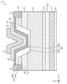
図1は、本実施の形態に係る窒化物半導体デバイス1の断面図である。図1では、半導体層および電極等の各構成要素に対して、断面を表す斜線の網掛けを付している。なお、電子走行層22内の2次元電子ガス26を模式的に表す破線の見やすさを考慮して、電子走行層22には斜線の網掛けを付していない。Figure 1 is a cross-sectional view of a
図1に示すように、本実施の形態に係る窒化物半導体デバイス1は、いわゆる縦型の電界効果トランジスタ(FET)である。具体的には、窒化物半導体デバイス1では、ドレイン電極36とソース電極34との間で、電流が基板10の主面に垂直な方向に流れる。As shown in FIG. 1, the
窒化物半導体デバイス1は、GaNおよびAlGaNなどの窒化物半導体を主成分として含む窒化物半導体層の積層構造を有するデバイスである。なお、「AがBを主成分として含む」とは、AにおけるBの含有率が50%以上であることを意味する。The
本実施の形態に係る窒化物半導体デバイス1は、ノーマリオフ型のFETである。窒化物半導体デバイス1では、例えば、ソース電極34が接地され(すなわち、電位が0V)、ドレイン電極36に正の電位が与えられている。ドレイン電極36に与えられる電位は、例えば100V以上1200V以下であるが、これに限らない。窒化物半導体デバイス1がオフ状態である場合には、ゲート電極32には0Vまたは負の電位(例えば-5V)が印加されている。窒化物半導体デバイス1がオン状態である場合には、ゲート電極32には正の電位(例えば+5V)が印加されている。なお、窒化物半導体デバイス1は、ノーマリオン型のFETであってもよい。The
図1に示すように、窒化物半導体デバイス1は、基板10と、ドリフト層14と、第1の下地層16と、第2の下地層18と、ゲート開口部20と、電子走行層22と、電子供給層24と、閾値調整層28と、ソース開口部30と、ゲート電極32と、ソース電極34と、ドレイン電極36と、を備える。電子走行層22と電子供給層24との界面には、チャネルとして機能する2次元電子ガス(2DEG)26が発生する。As shown in FIG. 1, the
以下では、窒化物半導体デバイス1が備える各構成要素の詳細について説明する。The following describes in detail each of the components of the
基板10は、シリコン基板層11と、炭化ケイ素層12と、炭素層13と、を含む。基板10の平面視形状は、例えば、矩形であるが、これに限定されない。The
シリコン基板層11は、炭化ケイ素層12よりも下方に位置する基板本体である。シリコン基板層11は、例えば、n+型のSi基板である。シリコン基板層11の上面の結晶面方位は、例えば(111)である。なお、n型およびp型は、半導体の導電型を示している。n+型とは、半導体にn型のドーパントが高濃度に添加された状態、いわゆるヘビードープを表している。また、n-型とは、半導体にn型のドーパントが低濃度に添加された状態、いわゆるライトドープを表している。n+型およびn-型はいずれも、n型の一例であり、それぞれを区別せずにn型と記載する場合がある。また、p+型およびp-型についても同様である。 The
炭化ケイ素層12は、シリコン基板層11の上方に設けられている。炭化ケイ素層12は、例えば、立方晶炭化ケイ素層であり、具体的には3C-SiCからなる層である。炭化ケイ素層12の上面の結晶面方位は、例えば、(111)である。炭化ケイ素層12の膜厚は、例えば100nm以下である。例えば、炭化ケイ素層12は、アンドープであるが、n型にドープされていてもよい。炭化ケイ素層12のドナー濃度は、例えば、1×1015cm-3以上、1×1017cm-3以下であるが、これに限定されない。 The
炭化ケイ素層12は、シリコン基板層11上への3C-SiC結晶のエピタキシャル成長によって形成される。エピタキシャル成長には、MBE(Molecular Beam Epitaxy)法、熱CVD(Chemical Vapor Deposition)法などの成長法が主に用いられている。The
3C-SiCの結晶成長には、1000℃以上の温度が必要である。結晶成長時にシリコン基板層11の表面からのSiの昇華を抑えるために、初期に低温にて、例えば、エチレン(C2H4)またはアセチレン(C2H2)などの炭化水素ガスを用いて、シリコン基板層11の上面に薄い炭化膜を形成する。その後、炭化水素およびシラン系の混合ガスを用いてエピタキシャル成長プロセスを行うのが一般的な形成手法である。シラン系ガスとしては、例えば、ジクロロシラン(SiH2Cl2)またはシラン(SiH4)などが使われる。また、炭化水素およびシラン系の混合ガスの代わりに、モノメチルシラン(CH3SiH3)を用いてもよい。3C-SiCの結晶成長時に窒素ガスなどを混入させて、n型の3C-SiCを形成してもよい。 The crystal growth of 3C-SiC requires a temperature of 1000° C. or higher. In order to suppress the sublimation of Si from the surface of the
炭素層13は、炭化ケイ素層12の上方に設けられている。炭素層13は、基板10の最上層に位置している。炭素層13は、グラフェン層およびグラフェンバッファ層の少なくとも一方を含む。本実施の形態では、炭素層13は、炭化ケイ素層12とドリフト層14との界面の全体に設けられている。炭素層13の詳細等については、後で説明する。The
ドリフト層14は、基板10の上方に設けられた第1の窒化物半導体層の一例である。ドリフト層14は、例えば、厚さが8μmのn-型のGaNからなる膜である。ドリフト層14のドナー濃度は、例えば1×1015cm-3以上1×1017cm-3以下であり、一例として1×1016cm-3である。また、ドリフト層14の炭素濃度(C濃度)は、例えば1×1015cm-3以上2×1017cm-3以下である。 The
ドリフト層14は、例えば、基板10の上面(主面)に接触して設けられている。ドリフト層14は、例えば、有機金属気相エピタキシャル成長(MOVPE:Metal Organic Vapor Phase Epitaxy)法、ハイドライド気相成長(HVPE:Hydride Vapor Phase Epitaxy)法などの結晶成長により、基板10の主面上に形成される。The
第1の下地層16は、ドリフト層14の上方に設けられた第1のp型窒化物半導体層の一例である。第1の下地層16は、例えば、厚さが400nmであり、キャリア濃度が1×1017cm-3であるp型のGaNからなる膜である。第1の下地層16は、ドリフト層14の上面に接触して設けられている。第1の下地層16は、例えば、MOVPE法、HVPE法などの結晶成長により、ドリフト層14上に形成される。 The
なお、第1の下地層16は、結晶成長で形成しているが、例えば、成膜したi-GaNへマグネシウム(Mg)を注入することで形成してもよい。さらに言えば、第1の下地層16は、p型の窒化物半導体層ではなく、鉄(Fe)またはホウ素(B)を注入するなどを行うことで得られる絶縁層であってもよい。The
第1の下地層16は、ブロック層とも呼ばれ、ソース電極34とドレイン電極36との間のリーク電流を抑制する。例えば、第1の下地層16とドリフト層14とで形成されるpn接合に対して逆方向電圧が印加された場合、具体的には、ソース電極34よりもドレイン電極36が高電位となった場合に、ドリフト層14に空乏層が延びる。これにより、窒化物半導体デバイス1の高耐圧化が可能である。本実施の形態では、オフ状態およびオン状態のいずれにおいても逆導通動作の場合を除いて、ソース電極34よりドレイン電極36が高電位となっている。このため、窒化物半導体デバイス1の高耐圧化が実現される。The
第2の下地層18は、第1の下地層16の上方に設けられた第2の窒化物半導体層の一例である。第2の下地層18は、第1の下地層16よりも抵抗が高い高抵抗層である。第2の下地層18は、例えば、厚さが200nmのアンドープGaN(i-GaN)からなる膜である。第2の下地層18は、第1の下地層16に接触して設けられている。例えば、第2の下地層18は、例えば、MOVPE法、HVPE法などの結晶成長により、第1の下地層16上に形成される。The
第2の下地層18については、アンドープの半導体層を想定しているが、絶縁層または半絶縁層でもよい。ここで“アンドープ”とは、GaNの極性をn型またはp型に変化させるSiまたはMg等のドーパントがドープされていないことを意味する。本実施の形態では、第2の下地層18には、炭素(C)がドープされていてもよい。例えば、第2の下地層18の炭素濃度は、第1の下地層16の炭素濃度より高い。The
例えば、第2の下地層18の炭素濃度は、3×1017cm-3以上であるが、1×1018cm-3以上であってもよい。このとき、n型不純物となるケイ素(Si)または酸素(O)の各濃度は、炭素濃度より低い。例えば、第2の下地層18のケイ素濃度または酸素濃度は、5×1016cm-3以下であるが、2×1016cm-3以下であってもよい。第2の下地層18および第1の下地層16に注入されるイオンの種類としては、半導体層を高抵抗化できるイオン種であれば、上記以外のイオン種でも同様の効果が得られる。 For example, the carbon concentration of the
また、第2の下地層18の上面には、第1の下地層16からMgなどのp型不純物が拡散するのを抑制するための層が設けられていてもよい。例えば、第2の下地層18上には、厚さが20nmのAlGaN層が設けられていてもよい。In addition, a layer for suppressing the diffusion of p-type impurities such as Mg from the
ゲート開口部20は、第2の下地層18および第1の下地層16を貫通して、ドリフト層14にまで達する第1の開口部の一例である。ゲート開口部20の底面20aは、ドリフト層14の上面の一部である。図1に示すように、底面20aは、第1の下地層16の下面より下側に位置している。なお、第1の下地層16の下面は、第1の下地層16とドリフト層14との界面に相当する。底面20aは、例えば、基板10の主面に平行である。窒化物半導体デバイス1のオン時のドレイン電流は、このゲート開口部20の底面20aを通じて流れる。The
本実施の形態では、ゲート開口部20は、基板10から遠ざかる程、開口面積が大きくなるよう形成されている。具体的には、ゲート開口部20の側面20bは、斜めに傾斜している。図1に示すように、ゲート開口部20の断面形状は、逆台形、より具体的には逆等脚台形である。In this embodiment, the
底面20aに対する側面20bの傾斜角は、例えば20°以上80°以下であるが、30°以上45°以下であってもよい。傾斜角が小さい程、側面20bがc面に近づくので、結晶再成長により側面20bに沿って形成される電子走行層22などの膜質を高めることができる。一方で、傾斜角が大きい程、ゲート開口部20が大きくなりすぎることが抑制され、窒化物半導体デバイス1の小型化が実現される。The inclination angle of the
ゲート開口部20は、基板10の主面上に、ドリフト層14、第1の下地層16および第2の下地層18をこの順で連続的な成膜により形成した後、部分的にドリフト層14を露出させるように、第2の下地層18および第1の下地層16の各々の一部を除去することで形成される。このとき、ドリフト層14の表層部分を所定の厚さ分、例えば300nm、除去することで、ゲート開口部20の底面20aは、第1の下地層16の下面よりも下方に形成される。The
第2の下地層18および第1の下地層16を除去する方法として、誘導結合プラズマエッチング(ICP)などのドライエッチングなどを用い、プロセスガスとして塩素系のガスを用いることが多い。The method of removing the
電子走行層22は、第2の下地層18の上面およびゲート開口部20を覆うように設けられた第1の再成長層の一例である。具体的には、電子走行層22の一部は、ゲート開口部20の底面20aおよび側面20bに沿って設けられ、電子走行層22の他の部分は、第2の下地層18の上面上に設けられている。電子走行層22は、例えば、厚さが150nmのアンドープGaNからなる膜である。なお、電子走行層22は、アンドープを想定しているが、一部Siドープなどでn型化されてもよい。The
電子走行層22は、ゲート開口部20の底面20aおよび側面20bにおいてドリフト層14に接触している。電子走行層22は、ゲート開口部20の側面20bにおいて、第1の下地層16および第2の下地層18の各々に接触している。さらに、電子走行層22は、第2の下地層18の上面に接触している。The
電子走行層22は、チャネル領域を有する。具体的には、電子走行層22と電子供給層24との界面の近傍には、チャネルとなる2次元電子ガス26が発生する。図1では、2次元電子ガス26が模式的に破線で図示されている。2次元電子ガス26は、電子走行層22と電子供給層24との界面に沿って、すなわち、ゲート開口部20の内面に沿って屈曲している。The
また、図1には示していないが、電子走行層22と電子供給層24との間に、厚さが1nm程度のAlN層が第2の再成長層として設けられている。これにより、合金散乱が抑制されてチャネル移動度が向上し、オン抵抗を低減することが可能になる。なお、AlN層は、必ずしも必要ではない。Although not shown in FIG. 1, an AlN layer with a thickness of about 1 nm is provided as a second regrown layer between the
電子供給層24は、第2の下地層18の上面およびゲート開口部20を覆うように設けられた第3の再成長層の一例である。電子走行層22と電子供給層24とは、基板10側からこの順で設けられている。電子供給層24は、例えば厚さが20nmのアンドープAlGaNからなる膜である。電子供給層24は、電子走行層22の上面に沿った形状でほぼ均一な厚さで形成されている。The
電子供給層24は、電子走行層22よりもバンドギャップが大きい。このため、電子供給層24と電子走行層22との間には、AlGaN/GaNのヘテロ界面が形成されている。電子供給層24は、電子走行層22に形成されるチャネル領域(2次元電子ガス26)への電子の供給を行う。The
閾値調整層28は、電子供給層24とゲート電極32との間に設けられた第2のp型窒化物半導体層の一例である。閾値調整層28は、例えば、厚さが100nmであり、キャリア濃度が1×1017cm-3であるp型のAlGaNからなる膜である。 The
閾値調整層28が設けられていることにより、チャネル部分のポテンシャルが持ち上がる。このため、トランジスタの閾値を増大させることができ、ノーマリオフ化が実現できる。By providing the
なお、閾値調整層28は設けられずに、ゲート電極32が電子供給層24に接触して設けられてもよい。また、例えば、閾値調整層28の代わりに、SiNまたはSiO2のような絶縁層がゲート電極32と電子供給層24との間に設けられてもよい。これにより、ゲート電流を抑制し、かつ、閾値を正方向にシフトさせノーマリオフ動作を実現することが可能になる。 The
電子走行層22、電子供給層24および閾値調整層28は、ゲート開口部20を形成した後に、結晶の再成長工程によって窒化物半導体膜を連続的に成膜し、所定形状にパターニングすることによって形成される。具体的には、電子走行層22の基になるアンドープGaN膜、電子供給層24の基になるアンドープAlGaN膜、および、閾値調整層28の基になるp型AlGaN膜を、MOVPE法またはHVPE法などによって連続的に成膜する。成膜後、p型AlGaN膜の一部を、アンドープAlGaN膜が露出するまでエッチングで除去することによって、閾値調整層28が形成される。さらに、アンドープAlGaN膜およびアンドープGaN膜の各々の一部と第2の下地層18の一部とを、第1の下地層16が露出するまで連続的にエッチングで除去する。これにより、第1の下地層16にまで達するソース開口部30が形成され、所定形状にパターニングされた電子供給層24および電子走行層22が形成される。The
ソース開口部30は、ゲート電極32から離れた位置で、電子供給層24および電子走行層22を貫通し、第1の下地層16にまで達する第2の開口部の一例である。本実施の形態では、ソース開口部30は、基板10の平面視において、ゲート開口部20および閾値調整層28のいずれからも離れた位置に設けられている。The
ソース開口部30の底面30aは、第1の下地層16の上面の一部である。図1では、底面30aが第2の下地層18と第1の下地層16との界面と面一になっているが、これに限定されない。底面30aは、第2の下地層18と第1の下地層16との界面より下方に位置していてもよい。すなわち、ソース開口部30は、第1の下地層16の表層部分を除去することで形成されていてもよい。底面30aは、例えば基板10の主面に平行である。The
また、図1に示すように、ソース開口部30は、基板10からの距離によらず開口面積が一定になるように形成されている。具体的には、ソース開口部30の側面30bは、底面30aに対して垂直である。つまり、ソース開口部30の断面視形状は、矩形である。As shown in FIG. 1, the source opening 30 is formed so that the opening area is constant regardless of the distance from the
あるいは、ソース開口部30は、基板10から遠ざかる程、開口面積が大きくなるように形成されていてもよい。具体的には、ソース開口部30の側面30bは、斜めに傾斜していてもよい。例えば、ソース開口部30の断面形状は、逆台形、より具体的には、逆等脚台形であってもよい。このとき、底面30aに対する側面30bの傾斜角は、例えば、30°以上60°以下の範囲であってもよい。側面30bが斜めに傾斜していることで、ソース電極34と電子走行層22(2次元電子ガス26)との接触面積が増えるので、オーミック接続が行われやすくなる。なお、2次元電子ガス26は、ソース開口部30の側面30bに露出し、露出部分でソース電極34に接続されている。Alternatively, the source opening 30 may be formed so that the opening area increases as it is farther from the
なお、ソース開口部30は、必ずしも必要ではない。ソース開口部30が設けられていることにより、チャネルとして機能する2次元電子ガス26とソース電極34とのオーミックコンタクト抵抗を低減することができる。また、第1の下地層16とソース電極34とを電気的に接続することができるので、第1の下地層16の電位を安定させて耐圧の向上等の効果を得ることができる。The
ゲート電極32は、電子供給層24の上方でゲート開口部20を覆うように設けられている。具体的には、ゲート電極32は、閾値調整層28の上面に接触して設けられている。The
ゲート電極32は、例えば、金属等の導電性の材料を用いて形成されている。例えば、ゲート電極32は、p型のGaN層に対してオーミック接触される材料を用いることができる。例えば、パラジウム(Pd)、ニッケル(Ni)系材料、タングステンシリサイド(WSi)、金(Au)などを用いることができる。The
ゲート電極32は、閾値調整層28の形成後、ソース開口部30の形成後、または、ソース電極34の形成後に、スパッタまたは蒸着などによって導電膜を成膜し、成膜した導電膜をパターニングすることにより形成される。The
ソース電極34は、ゲート電極32から離れた位置に設けられている。本実施の形態では、ソース電極34は、ソース開口部30を覆うように設けられている。具体的には、ソース電極34は、ソース開口部30を埋めるように、ソース開口部30の底面30aおよび側面30bに接触して設けられている。ソース電極34は、ソース開口部30の側面30bで2次元電子ガス26と直接接触している。これにより、ソース電極34と2次元電子ガス26とのコンタクト抵抗を低減することができる。なお、ソース電極34の一部は、電子供給層24の上面上に設けられていてもよい。The
ソース電極34は、金属などの導電性の材料を用いて形成されている。ソース電極34の材料としては、例えば、Ti/Al(Ti層とAl層との積層構造)など、熱処理することでn型のGaN層に対してオーミック接続される材料を用いることができる。ソース電極34は、例えば、スパッタまたは蒸着などによって成膜した導電膜をパターニングすることにより形成される。The
ドレイン電極36は、基板10の下方に設けられている。具体的には、ドレイン電極36は、基板10のシリコン基板層11の下面に設けられている。The
ドレイン電極36は、金属等の導電性材料を用いて形成されている。ドレイン電極36の材料としては、例えば、AuSb/Au等のn型のSiに対してオーミック接触される材料を用いることができる。ドレイン電極36は、例えば、スパッタまたは蒸着などによって形成される。The
[主な特徴的な構成]
続いて、本実施の形態に係る窒化物半導体デバイス1の主な特徴的な構成について説明する。 [Main characteristic configuration]
Next, a main characteristic configuration of the
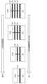
上述したように、窒化物半導体デバイス1では、基板10の最上層には炭素層13が設けられている。図2に示すように、炭素層13は、グラフェンバッファ層13aと、エピタキシャルグラフェン層13bと、を含む。図2は、SiC(炭化ケイ素層12)上のグラフェンバッファ層13aとエピタキシャルグラフェン層13bとを示す図である。As described above, in the
グラフェンバッファ層13aは、炭化ケイ素層12の最表面上に設けられた炭素原子層である。炭素原子の4つの結合手はそれぞれ、他の3つの炭素原子に結合し、残りの1つの結合手は、炭化ケイ素層12の最表面のシリコン原子に結合している。The
エピタキシャルグラフェン層13bは、炭化ケイ素層12の上方に設けられた炭素原子層である。複数の炭素原子は、平面内に配置されて、六角格子構造を形成している。図2では、エピタキシャルグラフェン層13bが1層設けられている例を示しているが、複数のエピタキシャルグラフェン層13bが積層されていてもよい。The
炭化ケイ素層12上への炭素層13の形成は、真空中およびArなどの不活性ガス雰囲気中での高温アニール処理によって行われる。高温アニール処理の温度は、Siの融点である1420℃以下の温度であり、例えば、1150℃以上1250℃以下である。図2に示すように、アニール時にSiC表面からSiが脱離し、残されたCがグラフェン層を形成する。1150℃のアニールでグラフェンバッファ層13aがSiC表面に形成される。さらに、1250℃でアニールすると、SiCの熱分解が進み、グラフェンバッファ層13aとSiCとの界面に新しいグラフェンバッファ層13aが形成される。そして先に形成されたグラフェンバッファ層13aが最表面に位置し、エピタキシャルグラフェン層13bとなる。このとき、エピタキシャルグラフェン層13bとグラフェンバッファ層13aとの界面にはファンデルワールス力のような弱い結合しか存在しない。一方、グラフェンバッファ層13aとSiCとの界面では、SiC最表面のSi原子とグラフェンバッファ層13aのC原子とが共有結合している。The
異種基板上へのヘテロ成長において、熱膨張係数の差および格子不整合で成長膜の結晶性が悪化し、割れが発生する原因は、ヘテロ界面に共有結合のような強い結合が存在するからである。強い結合が存在することで、本来の結晶構造から歪められ、膜厚の増加または成長温度の昇降温で歪みエネルギーが蓄積する。蓄積したエネルギーが臨界値を超えると、転位と呼ばれる結晶欠陥が発生する。In hetero growth on dissimilar substrates, the difference in thermal expansion coefficients and lattice mismatch can cause the crystallinity of the grown film to deteriorate, resulting in cracks. This is due to the presence of strong bonds, such as covalent bonds, at the hetero interface. The presence of strong bonds distorts the original crystal structure, and distortion energy accumulates as the film thickness increases or the growth temperature rises and falls. When the accumulated energy exceeds a critical value, a crystal defect called a dislocation occurs.
これに対して、図2に示すように、SiC上にグラフェンバッファ層13aまたはエピタキシャルグラフェン層13bを形成することで、SiC最表面のダングリングボンドは終端され、エピタキシャルグラフェン層13bまたはグラフェンバッファ層13a上に形成されるGaNとの間にはファンデルワールス力のような弱い結合しか存在しない。そのため、格子定数および熱膨張係数が異なっていても、GaN自身の結晶構造および格子定数をもってエピタキシャル成長することができる。これにより、GaNに代表される窒化物半導体膜の結晶性を高めることができる。In contrast, as shown in FIG. 2, by forming a
なお、エピタキシャルグラフェン層13bが3層以上になるとGaNの結晶性が急激に悪化する。これは、図3に示すように、SiC最表面ではダングリングボンドが終端されているが、エピタキシャルグラフェン層13b上のGaNは、SiCの弱い表面ポテンシャルを感じてエピタキシャル成長しているためである。When the
なお、図3は、エピタキシャルグラフェン層13bの層数とGaN膜の結晶性との関係を示す図である。図3では、層間に生じるファンデルワールス力を両矢印で模式的に表している。GaNの下地層として、エピタキシャルグラフェン層13bの層数が2層、1層、グラフェンバッファ層13aのみの順に層が薄くなると、SiCの表面ポテンシャルをGaN自身が強く感じることができる。このため、GaNの結晶性は向上する。Figure 3 shows the relationship between the number of epitaxial graphene layers 13b and the crystallinity of the GaN film. In Figure 3, the van der Waals forces occurring between the layers are diagrammatically represented by double-headed arrows. As the number of epitaxial graphene layers 13b as the underlayer for GaN becomes thinner in the order of two layers, one layer, and only the
以上のように、基板10の最表面に、グラフェンバッファ層13aおよびエピタキシャルグラフェン層13bの少なくとも一方を含む炭素層13を設けることによって、窒化物半導体膜とは異なる基板10上に、結晶性に優れた窒化物半導体膜を形成することができる。基板10としては、安価で大口径化が可能なSiまたはSiCからなる基板を利用することができるので、窒化物半導体デバイス1の基板10の大口径化が可能になる。As described above, by providing the
[閾値調整層およびゲート電極の端部の位置]
窒化物半導体デバイス1では、閾値調整層28の端部の位置に応じて、トランジスタの閾値を調整することができる。なお、閾値調整層28が設けられていない場合には、ゲート電極32の端部の位置に応じて、トランジスタの閾値を調整することができる。 [Positions of Ends of Threshold Adjustment Layer and Gate Electrode]
In the
具体的には、閾値調整層28の端部の位置をゲート開口部20の開口端(具体的には、側面20bの上端)よりも内側に配置する場合、トランジスタの閾値は、ゲート開口部20の側面20bに沿った部分、すなわち、電子走行層22の傾斜部のみで決まる。このような構成では、電子走行層22の平坦部、すなわち、第2の下地層18の上方に位置する部分のキャリア濃度を大きくすることができるため、オン抵抗を低減できる。Specifically, when the end of the
一方で、閾値調整層28の端部の位置をゲート開口部20の開口端よりも外側に配置する場合、トランジスタの閾値は、電子走行層22の傾斜部および平坦部のうち、閾値が大きい方で決まる。例えば、トランジスタの閾値を平坦部で決まるようにする場合は、傾斜部の閾値だけを小さく(具体的には、負に)する必要がある。この場合は、基板10の主面と平行な方向における電子走行層22の膜厚を、基板10の主面と垂直な方向における電子走行層22の膜厚よりも大きくする。これにより、p型の第1の下地層16と傾斜部の2次元電子ガス26(チャネル)との距離を、第1の下地層16と平坦部の2次元電子ガス26(チャネル)との距離よりも大きくすることができる。よって、傾斜部のチャネルに対する第1の下地層16からの空乏化の影響を、平坦部に比べて低減できるので、傾斜部のチャネルの閾値を選択的に小さくすることが可能になる。したがって、トランジスタの閾値を平坦部で決まるようにすることができる。On the other hand, when the end position of the
[電子走行層の膜厚]
窒化物半導体デバイス1では、電子走行層22の膜厚を、部位によって異ならせることにより、オン抵抗を低減させることができる。具体的には、基板10の主面に垂直な方向における電子走行層22の膜厚よりも、基板10の主面に平行な方向における電子走行層22の膜厚が大きい。なお、基板10の主面に平行な方向における電子走行層22の膜厚は、ゲート開口部20の上端と電子供給層24との間の、基板10の主面に平行な方向の距離である。 [Thickness of electron transport layer]
In the
本実施の形態では、上述したように、傾斜部の2次元電子ガス26と第1の下地層16との距離を遠ざけてキャリア濃度の低下を抑制できる。一般的に、縦型GaNの結晶成長は、GaN結晶のc面が基板10の主面と平行になるように行う。この場合、基板10の主面と平行な2次元電子ガス26に比べて、基板10の主面から傾いた2次元電子ガス26は、分極が小さくなるため、キャリア濃度が低下する。つまり、傾斜部の2次元電子ガス26は、平坦部の2次元電子ガス26に比べてキャリア濃度は低い。そのため、傾斜部の2次元電子ガス26は、平坦部の2次元電子ガス26に比べて、p型の第1の下地層16から延びる空乏層の狭窄効果を受けやすい。よって、傾斜部の2次元電子ガス26を第1の下地層16から遠ざけた方が、よりオン抵抗を低減できる。In this embodiment, as described above, the distance between the two-
一方、基板10の主面と垂直な方向の電子走行層22の厚さが厚いと、ソース電極34と第1の下地層16とをコンタクトするためのソース開口部30を設ける際に、平坦部における電子走行層22の厚さが薄い方が、ソース開口部30の深さを浅くすることができる。ソース開口部30の深さが浅い方がプロセス時間を短縮でき、後に形成するソース電極34のカバレッジも良好になる。これにより、プロセスを容易にしつつオン抵抗を低減することが可能になる。このように、電子走行層22の厚さは、基板10の主面に垂直な方向における膜厚よりも基板10の主面に平行な方向における膜厚が大きいことで、プロセスを容易にしつつオン抵抗を低減することが可能になる。On the other hand, if the thickness of the
(実施の形態2)
続いて、実施の形態2について説明する。 (Embodiment 2)
Next, a second embodiment will be described.
実施の形態2では、炭素層に開口が設けられている点が実施の形態1とは主として相違する。以下では、実施の形態1との相違点を中心に説明を行い、共通点の説明を省略または簡略化する。The main difference between the second embodiment and the first embodiment is that an opening is provided in the carbon layer. The following description will focus on the differences from the first embodiment, and the description of the commonalities will be omitted or simplified.
図4は、本実施の形態に係る窒化物半導体デバイス101の断面図である。図4に示すように、本実施の形態に係る窒化物半導体デバイス101は、図1に示した窒化物半導体デバイス1と比較して、基板10の代わりに基板110を備える点が相違する。基板110は、炭素層13の代わりに炭素層113を備える。Figure 4 is a cross-sectional view of a
図4に示すように、炭素層113は、炭化ケイ素層12の一部を露出させる開口113aを有する。言い換えると、炭素層113は、炭化ケイ素層12の上面の全体を覆うのではなく、炭化ケイ素層12の上面に対して部分的に設けられている。開口113aは、複数設けられているが、1つのみであってもよい。As shown in FIG. 4, the
図5Aおよび図5Bはそれぞれ、炭素層113の開口113aの形状の一例を示す平面図である。開口113aの平面視形状は、例えば、図5Aに示すように、四角形である。あるいは、開口113aの平面視形状は、六角形等の他の多角形、または、円形もしくは楕円形等であってもよい。また、図5Bに示すように、複数の開口113aの各々の平面視形状は、互いに異なっていてもよい。Figures 5A and 5B are plan views showing an example of the shape of the
開口113aは、例えば、レジストでパターニングしてからO2プラズマアッシングを用いて選択的にエッチングすることで形成される。これにより、所望の形状の開口113aを所望の位置に設けることができる。 The
あるいは、開口113aは、低エネルギーの希ガスイオンビーム照射およびN2プラズマ照射によって、ランダムに格子欠陥を導入することで形成されてもよい。ランダムに格子欠陥を導入した場合、図5Bに示すように、平面視形状が異なる複数の開口113aを容易に形成することができる。 Alternatively, the
炭素層113とGaNからなるドリフト層14との界面は、ファンデルワールス力のような弱い結合しか存在しないため、密着強度が弱い。窒化物半導体デバイス101は、パワートランジスタとして大電流でのスイッチング用途に用いられる場合があるので、炭素層113とドリフト層14との密着強度が弱いと、信頼性が損なわれるおそれがある。The interface between the
そこで、窒化物半導体デバイス101では、炭素層113が炭化ケイ素層12の上面に対して部分的に設けられている。すなわち、炭素層113は、炭化ケイ素層12の上面を露出させる開口113aを有する。炭素層113が設けられていない箇所、すなわち、開口113aには、炭化ケイ素層12の表面が剥き出しになっている。このため、開口113a内では、炭化ケイ素層12とドリフト層14との界面には共有結合のような強い結合が存在する。したがって、ドリフト層14と基板110との密着強度を高めることができ、窒化物半導体デバイス101の信頼性を高めることができる。Therefore, in the
なお、開口113a内では、ドリフト層14に転位(図面では点線で模式的に示している)が形成されるおそれはあるが、炭素層113上では良好なGaNが形成される。このため、密着強度の向上とGaNの良好な結晶性とを両立することができる。In the
[変形例]
図6は、本実施の形態の変形例に係る窒化物半導体デバイス102の断面図である。図6に示すように、本変形例に係る窒化物半導体デバイス102では、図4に示した窒化物半導体デバイス101と比較して、炭素層113の開口113aの位置が相違する。具体的には、開口113aは、平面視において、閾値調整層28に重ならないように設けられている。言い換えると、炭素層113は、平面視において、閾値調整層28に重なる位置のみに設けられる。 [Modification]
Fig. 6 is a cross-sectional view of a
オフ時にドレイン電極36に高い電圧が印加されると、閾値調整層28の下部および第1の下地層16の端部に電界が集中しやすい。したがって、ドリフト層14のうち、閾値調整層28および第1の下地層16の端部の下方に位置する部分には、オフリーク電流を抑制するために、高品質のエピタキシャル膜が求められる。When a high voltage is applied to the
本変形例に係る窒化物半導体デバイス102では、平面視において閾値調整層28に重なる位置に炭素層113が設けられている。このため、ドリフト層14のうち、平面視において閾値調整層28に重なる部分の結晶性を高めることができる。よって、オフリーク電流を十分に抑えることができる。In the
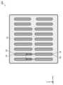
図7Aは、本変形例に係る窒化物半導体デバイス102の一例を示す平面図である。図7Bは、図7Aに示す窒化物半導体デバイス102が備える炭素層113の平面図である。図7Aに示すVI-VI線における断面が図6に示す断面に相当する。Figure 7A is a plan view showing an example of a
図7Aに示す例では、y軸方向に沿って延びる長尺なソース電極34が、x軸方向およびy軸方向の各々に並んで配置されている。ゲート電極32は、複数のソース電極34を個別に囲むように設けられている。具体的には、ゲート電極32は、複数のソース電極34にそれぞれ対応する複数の長尺状の開口が設けられた1枚の板状の電極である。平面視において、ゲート電極32と複数のソース電極34とはそれぞれ、距離を空けて設けられており、重複していない。閾値調整層28は、ゲート電極32と同様に、複数のソース電極34にそれぞれ対応する複数の長尺状の開口が設けられた1枚の板状の半導体層である。平面視において、閾値調整層28と複数のソース電極34とはそれぞれ、距離を空けて設けられており、重複していない。閾値調整層28に設けられた長尺状の開口は、ゲート電極32に設けられた長尺状の開口よりも一回り小さい。このため、平面視において、ゲート電極32に設けられた長尺状の開口から閾値調整層28の開口端部が露出した状態になる。7A, the
図7Aに示す窒化物半導体デバイス102は、図7Bに示す炭素層113を備える。図7Bに示す炭素層113には、複数の開口113aが設けられており、複数の開口113aの平面視形状は、閾値調整層28(またはゲート電極32)に設けられた長尺状の開口の平面視形状と同じである。また、複数の開口113aの位置は、閾値調整層28に設けられた長尺状の開口の位置と同じである。これにより、平面視において、ソース電極34に重なる位置には、炭素層113の開口113aが位置し、ゲート電極32および閾値調整層28に重なる位置には、炭素層113が設けられた構成を実現することができる。The
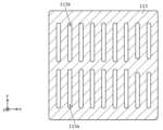
なお、複数のソース電極34の形状および配置は、これに限定されない。図8Aは、別の変形例に係る窒化物半導体デバイス103の断面図である。図8Bは、図8Aに示す窒化物半導体デバイス103が備える炭素層113の平面図である。図8Aに示すVI-VI線における断面が図6に示す断面に相当する。The shape and arrangement of the
図8Aに示す例では、平面視形状が正六角形のソース電極34が、面内で並んで配置されている。具体的には、複数のソース電極34は、充填配置された正三角形の各頂点に、ソース電極34の中心が位置するように配置されている。ゲート電極32は、複数のソース電極34を個別に囲むように設けられている。具体的には、ゲート電極32は、複数のソース電極34にそれぞれ対応する複数の正六角形の開口が設けられた1枚の板状の電極である。平面視において、ゲート電極32と複数のソース電極34とはそれぞれ、距離を空けて設けられており、重複していない。閾値調整層28は、ゲート電極32と同様に、複数のソース電極34にそれぞれ対応する複数の正六角形の開口が設けられた1枚の板状の半導体層である。平面視において、閾値調整層28と複数のソース電極34とはそれぞれ、距離を空けて設けられており、重複していない。閾値調整層28に設けられた正六角形の開口は、ゲート電極32に設けられた正六角形の開口よりも一回り小さい。このため、平面視において、ゲート電極32に設けられた正六角形の開口から閾値調整層28の開口端部が露出した状態になる。In the example shown in FIG. 8A, the
図8Aに示す窒化物半導体デバイス103は、図8Bに示す炭素層113を備える。図8Bに示す炭素層113には、複数の開口113aが設けられており、複数の開口113aの平面視形状は、閾値調整層28(またはゲート電極32)に設けられた正六角形の開口の平面視形状と同じである。また、複数の開口113aの位置は、閾値調整層28に設けられた正六角形の開口の位置と同じである。これにより、平面視において、ソース電極34に重なる位置には、炭素層113の開口113aが位置し、ゲート電極32および閾値調整層28に重なる位置には、炭素層113が設けられた構成を実現することができる。The
このように、炭素層113のパターニングは、作製する縦型トランジスタのレイアウトに合わせて、変更することができる。なお、炭素層113に設けられる開口113aの平面視形状は、ゲート電極32または閾値調整層28に設けられる平面視形状と同じでなくてもよい。In this way, the patterning of the
例えば、炭素層113は、閾値調整層28のうち、ゲート開口部20内に位置する底部と平面視で重なる位置に設けられており、ゲート開口部20の側面20bに沿った傾斜部、および、ゲート開口部20の上端に沿った上端部には重なっていなくてもよい。言い換えると、開口113aは、平面視において、閾値調整層28の一部、具体的には、閾値調整層28の傾斜部および上端部に重なる位置に設けられていてもよい。この場合であっても、ドリフト層14のうち、電界が集中しやすい閾値調整層28の底部とドレイン電極36との間の部分の結晶性が高まるため、リーク電流を抑制することができる。For example, the
(実施の形態3)
続いて、実施の形態3について説明する。 (Embodiment 3)
Next, a third embodiment will be described.
実施の形態3では、実施の形態1と比較して、基板がシリコン基板層の代わりに炭化ケイ素層を備える点が主として相違する。以下では、実施の形態1との相違点を中心に説明を行い、共通点の説明を省略または簡略化する。The third embodiment differs from the first embodiment mainly in that the substrate has a silicon carbide layer instead of a silicon substrate layer. The following description will focus on the differences from the first embodiment, and the description of the commonalities will be omitted or simplified.
図9は、本実施の形態に係る窒化物半導体デバイス201の断面図である。図9に示すように、本実施の形態の窒化物半導体デバイス201は、図1に示した窒化物半導体デバイス1と比較して、基板10の代わりに基板210を備える点が相違する。基板210は、SiC基板層211と、炭素層13と、を含む。Figure 9 is a cross-sectional view of a
SiC基板層211は、炭化ケイ素層の一例である。SiC基板層211は、六方晶炭化ケイ素基板層または立方晶炭化ケイ素基板層であり、具体的には、4H-SiC、6H-SiCまたは3C-SiCからなる基板本体である。SiC基板層211の下面にドレイン電極36が設けられている。SiC基板層211は、例えば、n+型のSiCからなり、一例として、厚さは100μmであり、ドナー濃度は1×1017cm-3以上1×1019cm-3以下である。 The
本実施の形態に係る窒化物半導体デバイス201では、六方晶または立方晶のSiC基板を用いることにより、放熱特性を高めたGaN縦型トランジスタを得ることができる。一般的に、SiCの熱伝導率は4.9W/cm・Kであり、Siの熱伝導率である1.5W/cm・Kより高い。そのため、大電力機器への応用の際、熱を効率的に放熱することができるため、トランジスタの損失を低減できる。In the
[変形例]
図10は、本実施の形態の変形例に係る窒化物半導体デバイス202の断面図である。図10に示すように、本変形例に係る窒化物半導体デバイス202では、図9に示した窒化物半導体デバイス201と比較して、基板210の代わりに基板210Aを備える点が相違する。基板210Aは、SiC基板層211と、ドリフト層212と、炭素層13と、を含む。 [Modification]
Fig. 10 is a cross-sectional view of a
本変形例では、ドリフト層212は、炭化ケイ素層の一例である。ドリフト層212は、SiC基板層211の上方に設けられている。ドリフト層212は、例えば、n-型のSiCからなる膜である。例えば、ドリフト層212のドナー濃度は、1×1015cm-3以上1×1017cm-3以下であり、厚さは7μmであるが、これに限定されない。例えば、ドリフト層212は、SiC基板層211の上面にエピタキシャル成長によって形成することができる。ドリフト層212の膜厚は、例えば、ドリフト層14の膜厚よりも薄い。これにより、炭素層13をゲート開口部20の底面20aに近づけて配置することができる。 In this modification, the
炭素層13は、高移動度特性を有するグラフェンバッファ層13aおよびエピタキシャルグラフェン層13bの少なくとも一方を含むので、電流拡散層として機能させることができる。本変形例では、炭素層13がゲート開口部20の底面20aに近いので、窒化物半導体デバイス202の広い範囲を電流経路に利用することができる。よって、窒化物半導体デバイス202の低オン抵抗特性を実現することができる。また、SiC基板層211と同様に、SiCからなるドリフト層212も高い熱伝導率を有するため、放熱特性を高めることができる。The
(実施の形態4)
続いて、実施の形態4について説明する。 (Embodiment 4)
Next, a fourth embodiment will be described.
実施の形態4では、実施の形態1と比較して、エッチングによって形成されるゲート開口部が設けられていない点が主として相違する。以下では、実施の形態1との相違点を中心に説明を行い、共通点の説明を省略または簡略化する。The main difference between embodiment 4 and
図11は、本実施の形態に係る窒化物半導体デバイス301の断面図である。図11に示すように、本実施の形態に係る窒化物半導体デバイス301は、基板310と、ドリフト層312と、ブロック層314と、炭素層313と、電子走行層22と、電子供給層24と、閾値調整層28と、ソース開口部30と、ゲート電極32と、ソース電極34と、ドレイン電極36と、を備える。電子走行層22と、電子供給層24と、閾値調整層28と、ソース開口部30と、ゲート電極32と、ソース電極34と、ドレイン電極36と、は、実施の形態1と実質的に同じである。Figure 11 is a cross-sectional view of a
基板310は、六方晶炭化ケイ素基板または立方晶炭化ケイ素基板であり、具体的には、4H-SiC、6H-SiCまたは3C-SiCからなる基板である。基板310は、例えば、n+型のSiCからなり、一例として、厚さは100μmであり、ドナー濃度は1×1017cm-3以上1×1019cm-3以下である。 The
ドリフト層312は、基板310の上方に設けられた第1の炭化ケイ素層の一例である。ドリフト層312は、例えば、n-型のSiCからなる膜である。ドリフト層312のドナー濃度は、1×1015cm-3以上1×1017cm-3以下であり、厚さは8μmであるが、これに限定されない。例えば、ドリフト層312は、基板310の上面にエピタキシャル成長によって形成することができる。 The
ブロック層314は、ドリフト層312の上面の少なくとも一部を露出させるように、ドリフト層312の上方に設けられたp型の炭化ケイ素層である。なお、ドリフト層312の上方とは、ドリフト層312の少なくとも一部よりも上方であることを意味する。The
本実施の形態では、ブロック層314は、基板310の上面にエピタキシャル成長によって形成されたn-型のSiC膜の表層部分の所定領域に、p型不純物をイオン注入することによって形成される。p型不純物が注入されていない部分が、ドリフト層312の上面になる。ブロック層314の上面とドリフト層312の上面とは、面一になる。 In this embodiment,
炭素層313は、ブロック層314の上方に設けられている。炭素層313は、実施の形態1に係る炭素層13と同様に、グラフェンバッファ層またはエピタキシャルグラフェン層の少なくとも一方を含む。The
本実施の形態では、炭素層313は、開口313aを有する。開口313aは、炭素層313とドリフト層312とが接触するのを防ぐために設けられている。これにより、ゲート電極32を挟んで配置された複数のソース電極34同士が炭素層313を介して電気的にショートするのを抑制することができる。なお、ゲート電極32は、基板310の平面視において、開口313aに重なる位置に設けられている。In this embodiment, the
開口313aを有する炭素層313は、実施の形態2と同様の手法で形成される。具体的には、ドリフト層312およびブロック層314の各々に対する高温アニール処理を行うことで、ドリフト層312およびブロック層314の最表面にグラフェンバッファ層および/またはエピタキシャルグラフェン層を形成した後、レジストを用いてパターニングし、O2プラズマアッシングによって選択的にエッチングすることにより、開口313aを有する炭素層313が形成される。
炭素層313が形成された後、GaNの再成長を行うことで、電子走行層22および電子供給層24を順に形成する。電子走行層22および電子供給層24はそれぞれ、ドリフト層312、ブロック層314および炭素層313を覆うように設けられている。なお、図11では、炭素層313の厚みを誇張して示しているが、炭素層313の厚みは、グラフェン数層分の厚みである。このため、電子走行層22および電子供給層24は、ほぼ均一な厚みで平坦な上面を有するように形成される。After the
本実施の形態では、炭素層313の開口313aでは、GaNからなる電子走行層22とSiCからなるドリフト層312とが接触している。このため、電子走行層22には、SiC(ドリフト層312)に起因する転位が発生するおそれがある。ただ、電子走行層22は、厚みが150nmと薄い場合が覆いため、転位の発生は抑制される。In this embodiment, the
また、本実施の形態では、ソース開口部30は、p型のブロック層314の少なくとも一部を露出させるように設けられる。例えば、図11に示すように、ソース開口部30の底面30aは、ブロック層314と炭素層313との界面と面一であるが、これに限らない。ソース開口部30の底面30aは、ブロック層314と炭素層313との界面よりも下方に位置していてもよい。これにより、ソース電極34は、p型のブロック層314に電気的に接続される。In the present embodiment, the source opening 30 is provided so as to expose at least a portion of the p-
本実施の形態によれば、熱伝導率の高いSiC基板を利用することができるので、窒化物半導体デバイス301の放熱性を高めることができる。また、縦型トランジスタの耐圧をn-型のSiCからなるドリフト層312とp型のSiCからなるブロック層314とのpn接合部分でもたせることができるので、アバランシェ耐量が向上する。一般的に、SiCはイオン注入で良質なp型を形成できるため、GaNよりもpn接合のアバランシェ耐量が大きい。したがって、アバランシェ降伏によるデバイス破壊を抑制することができる。 According to this embodiment, since a SiC substrate with high thermal conductivity can be used, the heat dissipation of the
[変形例]
図12は、本実施の形態の変形例に係る窒化物半導体デバイス302の断面図である。図12に示すように、本変形例に係る窒化物半導体デバイス302では、図11に示した窒化物半導体デバイス301と比較して、閾値調整層28およびゲート電極32の代わりに、閾値調整層328およびゲート電極332を備える点が相違する。 [Modification]
Fig. 12 is a cross-sectional view of a
閾値調整層328およびゲート電極332は、閾値調整層28およびゲート電極32とは、設けられる位置が異なる。具体的には、図12に示すように、閾値調整層328およびゲート電極332はそれぞれ、平面視においてp型のブロック層314に重なる位置に設けられている。閾値調整層328およびゲート電極332は、基板310の平面視において、炭素層313に重なる位置に設けられており、開口313aには重なっていない。The
このように、ゲート電極332とドレイン電極36との間には、p型のブロック層314が配置されているので、ゲート電極332とドレイン電極36とが対向する面積を実質的になくすことができる。これにより、ゲート-ドレイン間の寄生容量Cgdを大幅に削減することができる。帰還容量Crssは、ゲート-ドレイン間の寄生容量Cgdそのものであり、帰還容量Crssが大きいと、ゲートをオンにしてもドレイン電流の立ち上がりが遅く、オフの場合は立ち下がりが遅くなる。つまり、帰還容量Crss(寄生容量Cgd)を削減することで、スイッチング速度を向上できるので、高速スイッチングにより電力機器の小型化を実現できる。In this way, since the p-
なお、本実施の形態及び変形例において、電子供給層24とゲート電極32または332との間に設けられたp型窒化物半導体層の一例として、閾値調整層28または328が設けられているが、これに限らない。閾値調整層28または328が設けられずに、ゲート電極32または332が電子供給層24に接触して設けられていてもよい。あるいは、電子供給層24とゲート電極32または323との間には、SiNまたはSiO2のような絶縁層が設けられてもよい。 In the present embodiment and the modified example, the
(他の実施の形態)
以上、1つまたは複数の態様に係る窒化物半導体デバイスについて、実施の形態に基づいて説明したが、本開示は、これらの実施の形態に限定されるものではない。本開示の主旨を逸脱しない限り、当業者が思いつく各種変形を本実施の形態に施したもの、および、異なる実施の形態における構成要素を組み合わせて構築される形態も、本開示の範囲内に含まれる。 Other Embodiments
Although the nitride semiconductor device according to one or more aspects has been described based on the embodiments, the present disclosure is not limited to these embodiments. As long as it does not deviate from the gist of the present disclosure, various modifications conceivable by a person skilled in the art to the present embodiment and forms constructed by combining components of different embodiments are also included within the scope of the present disclosure.
例えば、炭素層13は、グラフェンバッファ層13aのみを含んでもよい。SiCに対する高温アニール処理を1150℃で行い、グラフェンバッファ層13aのみが形成された時点で高温アニール処理を終了してもよい。For example, the
あるいは、炭素層13は、グラフェンバッファ層13aを含まずに、1層または複数層のエピタキシャルグラフェン層13bのみを含んでもよい。例えば、基板10に含まれる炭化ケイ素層12の最上面の面方位が(110)または(001)などである場合、高温アニール処理を行うことで、グラフェンバッファ層13aが形成されずにエピタキシャルグラフェン層13bを形成することができる。Alternatively, the
また、例えば、ドリフト層14、212または312は、基板10側から上方に向かって徐々に不純物濃度(ドナー濃度)を低減させていくグレーデッド構造にしてもよい。なお、ドナー濃度の制御は、ドナーとなるSiで制御してもよいし、Siを補償するようなアクセプタとなる炭素で制御してもよい。あるいは、ドリフト層14、212または312は、不純物濃度が異なる複数の窒化物半導体層の積層構造を有してもよい。For example, the
また、上記の各実施の形態は、特許請求の範囲またはその均等の範囲において種々の変更、置き換え、付加、省略などを行うことができる。Furthermore, each of the above embodiments may be modified, substituted, added, omitted, etc. in various ways within the scope of the claims or their equivalents.
本開示に係る窒化物半導体デバイスは、例えば、xEVの主機インバータや車載充電器、パワーコンディショナーの汎用インバータ等の電源回路で用いられるパワートランジスタに利用することができる。The nitride semiconductor device according to the present disclosure can be used, for example, in power transistors used in power supply circuits such as the main inverter of an xEV, an on-board charger, and a general-purpose inverter of a power conditioner.
1、101、102、103、201、202、301、302 窒化物半導体デバイス
10、110、210、210A、310 基板
11 シリコン基板層
12 炭化ケイ素層
13、113、313 炭素層
13a グラフェンバッファ層
13b エピタキシャルグラフェン層
14、212、312 ドリフト層
16 第1の下地層
18 第2の下地層
20 ゲート開口部
20a、30a 底面
20b、30b 側面
22 電子走行層
24 電子供給層
26 2次元電子ガス
28、328 閾値調整層
30 ソース開口部
32、332 ゲート電極
34 ソース電極
36 ドレイン電極
113a、313a 開口
211 SiC基板層
314 ブロック層1, 101, 102, 103, 201, 202, 301, 302
Claims (16)
Translated fromJapanese前記基板の上方に設けられた第1の窒化物半導体層と、
前記第1の窒化物半導体層の上方に設けられた第1のp型窒化物半導体層と、
前記第1のp型窒化物半導体層の上方に設けられた第2の窒化物半導体層と、
前記第2の窒化物半導体層および前記第1のp型窒化物半導体層を貫通し、前記第1の窒化物半導体層にまで達する第1の開口部と、
前記第2の窒化物半導体層の上面および前記第1の開口部を覆うように下から順に設けられた電子走行層および電子供給層と、
前記第1の開口部を覆うように前記電子供給層の上方に設けられたゲート電極と、
前記ゲート電極から離れた位置に設けられたソース電極と、
前記基板の下方に設けられたドレイン電極と、を備え、
前記基板は、
炭化ケイ素層と、
前記炭化ケイ素層の上方に設けられた炭素層と、を含み、
前記炭素層は、グラフェン層およびグラフェンバッファ層の少なくとも一方を含む、
窒化物半導体デバイス。 A substrate;
a first nitride semiconductor layer provided above the substrate;
a first p-type nitride semiconductor layer provided above the first nitride semiconductor layer;
a second nitride semiconductor layer provided above the first p-type nitride semiconductor layer;
a first opening that penetrates the second nitride semiconductor layer and the first p-type nitride semiconductor layer and reaches the first nitride semiconductor layer;
an electron transit layer and an electron supply layer provided in this order from below so as to cover an upper surface of the second nitride semiconductor layer and the first opening;
a gate electrode provided above the electron supply layer so as to cover the first opening;
a source electrode provided at a position spaced from the gate electrode;
a drain electrode provided below the substrate;
The substrate is
a silicon carbide layer;
a carbon layer disposed above the silicon carbide layer;
The carbon layer includes at least one of a graphene layer and a graphene buffer layer.
Nitride semiconductor devices.
請求項1に記載の窒化物半導体デバイス。 the carbon layer having an opening exposing a portion of the silicon carbide layer;
The nitride semiconductor device of claim 1 .
請求項2に記載の窒化物半導体デバイス。 The planar shape of the opening is rectangular.
The nitride semiconductor device of claim 2 .
請求項2に記載の窒化物半導体デバイス。 The planar shape of the opening is hexagonal.
The nitride semiconductor device of claim 2 .
請求項2に記載の窒化物半導体デバイス。 The planar shape of the opening is circular.
The nitride semiconductor device of claim 2 .
請求項1に記載の窒化物半導体デバイス。 a second p-type nitride semiconductor layer provided between the electron supply layer and the gate electrode;
The nitride semiconductor device of claim 1 .
請求項6に記載の窒化物半導体デバイス。 the carbon layer is provided only at a position overlapping the second p-type nitride semiconductor layer in a plan view;
The nitride semiconductor device of claim 6.
前記ソース電極は、前記第2の開口部を覆うように設けられている、
請求項1に記載の窒化物半導体デバイス。 a second opening that is disposed at a position away from the gate electrode, passes through the electron supply layer and the electron transit layer, and reaches the first p-type nitride semiconductor layer;
The source electrode is provided to cover the second opening.
The nitride semiconductor device of claim 1 .
前記ドレイン電極は、前記シリコン基板層の下面に設けられている、
請求項1から8のいずれか1項に記載の窒化物半導体デバイス。 the substrate includes a silicon substrate layer underlying the silicon carbide layer;
The drain electrode is provided on a lower surface of the silicon substrate layer.
The nitride semiconductor device according to any one of claims 1 to 8.
前記ドレイン電極は、前記炭化ケイ素層の下面に設けられている、
請求項1から8のいずれか1項に記載の窒化物半導体デバイス。 the silicon carbide layer is a hexagonal silicon carbide substrate layer;
The drain electrode is provided on a lower surface of the silicon carbide layer.
The nitride semiconductor device according to any one of claims 1 to 8.
前記ドレイン電極は、前記炭化ケイ素層の下面に設けられている、
請求項1から8のいずれか1項に記載の窒化物半導体デバイス。 the silicon carbide layer is a cubic silicon carbide substrate layer;
The drain electrode is provided on a lower surface of the silicon carbide layer.
The nitride semiconductor device according to any one of claims 1 to 8.
前記炭化ケイ素層の不純物濃度は、前記六方晶炭化ケイ素基板層または立方晶炭化ケイ素基板層の不純物濃度より低い、
請求項1から8のいずれか1項に記載の窒化物半導体デバイス。 the substrate includes a hexagonal silicon carbide substrate layer or a cubic silicon carbide substrate layer underlying the silicon carbide layer;
The impurity concentration of the silicon carbide layer is lower than the impurity concentration of the hexagonal silicon carbide substrate layer or the cubic silicon carbide substrate layer;
The nitride semiconductor device according to any one of claims 1 to 8.
前記基板の上方に設けられた第1の炭化ケイ素層と、
前記第1の炭化ケイ素層の上面の少なくとも一部を露出させるように、前記第1の炭化ケイ素層の上方に設けられたp型の炭化ケイ素層と、
グラフェン層またはグラフェンバッファ層の少なくとも一方を含み、前記p型の炭化ケイ素層の上方に設けられた炭素層と、
前記第1の炭化ケイ素層および前記炭素層の上方に設けられた電子走行層と、
前記電子走行層の上方に設けられた電子供給層と、
前記電子供給層の上方に設けられたゲート電極と、
前記ゲート電極から離れた位置に設けられたソース電極と、
前記基板の下方に設けられたドレイン電極と、を備え、
前記炭素層は、前記第1の炭化ケイ素層の一部を露出させる開口を有する、
窒化物半導体デバイス。 A substrate;
a first silicon carbide layer disposed above the substrate;
a p-type silicon carbide layer provided above the first silicon carbide layer so as to expose at least a portion of an upper surface of the first silicon carbide layer;
a carbon layer including at least one of a graphene layer and a graphene buffer layer and disposed above the p-type silicon carbide layer;
an electron transit layer provided above the first silicon carbide layer and the carbon layer;
an electron supply layer provided above the electron transit layer;
a gate electrode provided above the electron supply layer;
a source electrode provided at a position spaced from the gate electrode;
a drain electrode provided below the substrate;
the carbon layer has an opening exposing a portion of the first silicon carbide layer.
Nitride semiconductor devices.
請求項13に記載の窒化物半導体デバイス。 the gate electrode is provided at a position overlapping the opening in a plan view of the substrate;
The nitride semiconductor device of claim 13.
請求項13に記載の窒化物半導体デバイス。 The gate electrode is provided at a position overlapping the p-type silicon carbide layer in a plan view of the substrate.
The nitride semiconductor device of claim 13.
請求項13から15のいずれか1項に記載の窒化物半導体デバイス。 a p-type nitride semiconductor layer provided between the electron supply layer and the gate electrode;
16. The nitride semiconductor device according to any one of claims 13 to 15.
Priority Applications (1)
| Application Number | Priority Date | Filing Date | Title |
|---|---|---|---|
| JP2023083402AJP2024166957A (en) | 2023-05-19 | 2023-05-19 | Nitride Semiconductor Devices |
Applications Claiming Priority (1)
| Application Number | Priority Date | Filing Date | Title |
|---|---|---|---|
| JP2023083402AJP2024166957A (en) | 2023-05-19 | 2023-05-19 | Nitride Semiconductor Devices |
Publications (1)
| Publication Number | Publication Date |
|---|---|
| JP2024166957Atrue JP2024166957A (en) | 2024-11-29 |
Family
ID=93610964
Family Applications (1)
| Application Number | Title | Priority Date | Filing Date |
|---|---|---|---|
| JP2023083402APendingJP2024166957A (en) | 2023-05-19 | 2023-05-19 | Nitride Semiconductor Devices |
Country Status (1)
| Country | Link |
|---|---|
| JP (1) | JP2024166957A (en) |
- 2023
- 2023-05-19JPJP2023083402Apatent/JP2024166957A/enactivePending
Similar Documents
| Publication | Publication Date | Title |
|---|---|---|
| JP4744109B2 (en) | Semiconductor device and manufacturing method thereof | |
| US8390091B2 (en) | Semiconductor structure, an integrated circuit including a semiconductor structure and a method for manufacturing a semiconductor structure | |
| US9466705B2 (en) | Semiconductor device and method of manufacturing the same | |
| JP5923712B2 (en) | Semiconductor device and manufacturing method thereof | |
| US7859014B2 (en) | Semiconductor device | |
| US9401403B2 (en) | Nitride semiconductor structure | |
| US20160351683A1 (en) | Method of making transistor having metal diffusion barrier | |
| US12176430B2 (en) | Semiconductor structure and semiconductor device | |
| US10158012B1 (en) | Semiconductor device | |
| US20120211801A1 (en) | Group iii nitride laminated semiconductor wafer and group iii nitride semiconductor device | |
| JP2011166067A (en) | Nitride semiconductor device | |
| TW201822254A (en) | Growth of semiconductor materials with high resistivity nitride buffer layers using ion implantation | |
| JP2012227456A (en) | Semiconductor device | |
| JP2012015304A (en) | Semiconductor device | |
| US20220336652A1 (en) | Semiconductor structure | |
| US10770552B2 (en) | Epitaxial substrate for semiconductor elements, semiconductor element, and manufacturing method for epitaxial substrates for semiconductor elements | |
| JP2018037435A (en) | Semiconductor device | |
| US20250006799A1 (en) | Semiconductor substrate, semiconductor device, method for producing semiconductor substrate, and method for producing semiconductor device | |
| JP7257498B2 (en) | Nitride semiconductor device | |
| JP2011108712A (en) | Nitride semiconductor device | |
| KR101172857B1 (en) | Enhancement normally off nitride smiconductor device and manufacturing method thereof | |
| US20110254055A1 (en) | Field effect transistor and manufacturing method thereof | |
| JP5810521B2 (en) | High electron mobility transistor | |
| JP2024166957A (en) | Nitride Semiconductor Devices | |
| JP2017130579A (en) | Semiconductor device, electronic component, electronic equipment, and method of manufacturing semiconductor device |