JP2024165397A - Manufacturing method of laminate - Google Patents
Manufacturing method of laminateDownload PDFInfo
- Publication number
- JP2024165397A JP2024165397AJP2023081568AJP2023081568AJP2024165397AJP 2024165397 AJP2024165397 AJP 2024165397AJP 2023081568 AJP2023081568 AJP 2023081568AJP 2023081568 AJP2023081568 AJP 2023081568AJP 2024165397 AJP2024165397 AJP 2024165397A
- Authority
- JP
- Japan
- Prior art keywords
- bonding
- support substrate
- oxide film
- temporary
- temporary support
- Prior art date
- Legal status (The legal status is an assumption and is not a legal conclusion. Google has not performed a legal analysis and makes no representation as to the accuracy of the status listed.)
- Pending
Links
Images


Classifications
- H—ELECTRICITY
- H01—ELECTRIC ELEMENTS
- H01L—SEMICONDUCTOR DEVICES NOT COVERED BY CLASS H10
- H01L21/00—Processes or apparatus adapted for the manufacture or treatment of semiconductor or solid state devices or of parts thereof
- H01L21/67—Apparatus specially adapted for handling semiconductor or electric solid state devices during manufacture or treatment thereof; Apparatus specially adapted for handling wafers during manufacture or treatment of semiconductor or electric solid state devices or components ; Apparatus not specifically provided for elsewhere
- H01L21/683—Apparatus specially adapted for handling semiconductor or electric solid state devices during manufacture or treatment thereof; Apparatus specially adapted for handling wafers during manufacture or treatment of semiconductor or electric solid state devices or components ; Apparatus not specifically provided for elsewhere for supporting or gripping
- H01L21/6835—Apparatus specially adapted for handling semiconductor or electric solid state devices during manufacture or treatment thereof; Apparatus specially adapted for handling wafers during manufacture or treatment of semiconductor or electric solid state devices or components ; Apparatus not specifically provided for elsewhere for supporting or gripping using temporarily an auxiliary support
- H—ELECTRICITY
- H01—ELECTRIC ELEMENTS
- H01L—SEMICONDUCTOR DEVICES NOT COVERED BY CLASS H10
- H01L24/00—Arrangements for connecting or disconnecting semiconductor or solid-state bodies; Methods or apparatus related thereto
- H01L24/80—Methods for connecting semiconductor or other solid state bodies using means for bonding being attached to, or being formed on, the surface to be connected
- H—ELECTRICITY
- H01—ELECTRIC ELEMENTS
- H01L—SEMICONDUCTOR DEVICES NOT COVERED BY CLASS H10
- H01L24/00—Arrangements for connecting or disconnecting semiconductor or solid-state bodies; Methods or apparatus related thereto
- H01L24/93—Batch processes
- H01L24/95—Batch processes at chip-level, i.e. with connecting carried out on a plurality of singulated devices, i.e. on diced chips
- H01L24/97—Batch processes at chip-level, i.e. with connecting carried out on a plurality of singulated devices, i.e. on diced chips the devices being connected to a common substrate, e.g. interposer, said common substrate being separable into individual assemblies after connecting
- H—ELECTRICITY
- H01—ELECTRIC ELEMENTS
- H01L—SEMICONDUCTOR DEVICES NOT COVERED BY CLASS H10
- H01L2221/00—Processes or apparatus adapted for the manufacture or treatment of semiconductor or solid state devices or of parts thereof covered by H01L21/00
- H01L2221/67—Apparatus for handling semiconductor or electric solid state devices during manufacture or treatment thereof; Apparatus for handling wafers during manufacture or treatment of semiconductor or electric solid state devices or components; Apparatus not specifically provided for elsewhere
- H01L2221/683—Apparatus for handling semiconductor or electric solid state devices during manufacture or treatment thereof; Apparatus for handling wafers during manufacture or treatment of semiconductor or electric solid state devices or components; Apparatus not specifically provided for elsewhere for supporting or gripping
- H01L2221/68304—Apparatus for handling semiconductor or electric solid state devices during manufacture or treatment thereof; Apparatus for handling wafers during manufacture or treatment of semiconductor or electric solid state devices or components; Apparatus not specifically provided for elsewhere for supporting or gripping using temporarily an auxiliary support
- H01L2221/68318—Auxiliary support including means facilitating the separation of a device or wafer from the auxiliary support
- H—ELECTRICITY
- H01—ELECTRIC ELEMENTS
- H01L—SEMICONDUCTOR DEVICES NOT COVERED BY CLASS H10
- H01L2221/00—Processes or apparatus adapted for the manufacture or treatment of semiconductor or solid state devices or of parts thereof covered by H01L21/00
- H01L2221/67—Apparatus for handling semiconductor or electric solid state devices during manufacture or treatment thereof; Apparatus for handling wafers during manufacture or treatment of semiconductor or electric solid state devices or components; Apparatus not specifically provided for elsewhere
- H01L2221/683—Apparatus for handling semiconductor or electric solid state devices during manufacture or treatment thereof; Apparatus for handling wafers during manufacture or treatment of semiconductor or electric solid state devices or components; Apparatus not specifically provided for elsewhere for supporting or gripping
- H01L2221/68304—Apparatus for handling semiconductor or electric solid state devices during manufacture or treatment thereof; Apparatus for handling wafers during manufacture or treatment of semiconductor or electric solid state devices or components; Apparatus not specifically provided for elsewhere for supporting or gripping using temporarily an auxiliary support
- H01L2221/68327—Apparatus for handling semiconductor or electric solid state devices during manufacture or treatment thereof; Apparatus for handling wafers during manufacture or treatment of semiconductor or electric solid state devices or components; Apparatus not specifically provided for elsewhere for supporting or gripping using temporarily an auxiliary support used during dicing or grinding
- H—ELECTRICITY
- H01—ELECTRIC ELEMENTS
- H01L—SEMICONDUCTOR DEVICES NOT COVERED BY CLASS H10
- H01L2221/00—Processes or apparatus adapted for the manufacture or treatment of semiconductor or solid state devices or of parts thereof covered by H01L21/00
- H01L2221/67—Apparatus for handling semiconductor or electric solid state devices during manufacture or treatment thereof; Apparatus for handling wafers during manufacture or treatment of semiconductor or electric solid state devices or components; Apparatus not specifically provided for elsewhere
- H01L2221/683—Apparatus for handling semiconductor or electric solid state devices during manufacture or treatment thereof; Apparatus for handling wafers during manufacture or treatment of semiconductor or electric solid state devices or components; Apparatus not specifically provided for elsewhere for supporting or gripping
- H01L2221/68304—Apparatus for handling semiconductor or electric solid state devices during manufacture or treatment thereof; Apparatus for handling wafers during manufacture or treatment of semiconductor or electric solid state devices or components; Apparatus not specifically provided for elsewhere for supporting or gripping using temporarily an auxiliary support
- H01L2221/6834—Apparatus for handling semiconductor or electric solid state devices during manufacture or treatment thereof; Apparatus for handling wafers during manufacture or treatment of semiconductor or electric solid state devices or components; Apparatus not specifically provided for elsewhere for supporting or gripping using temporarily an auxiliary support used to protect an active side of a device or wafer
- H—ELECTRICITY
- H01—ELECTRIC ELEMENTS
- H01L—SEMICONDUCTOR DEVICES NOT COVERED BY CLASS H10
- H01L2221/00—Processes or apparatus adapted for the manufacture or treatment of semiconductor or solid state devices or of parts thereof covered by H01L21/00
- H01L2221/67—Apparatus for handling semiconductor or electric solid state devices during manufacture or treatment thereof; Apparatus for handling wafers during manufacture or treatment of semiconductor or electric solid state devices or components; Apparatus not specifically provided for elsewhere
- H01L2221/683—Apparatus for handling semiconductor or electric solid state devices during manufacture or treatment thereof; Apparatus for handling wafers during manufacture or treatment of semiconductor or electric solid state devices or components; Apparatus not specifically provided for elsewhere for supporting or gripping
- H01L2221/68304—Apparatus for handling semiconductor or electric solid state devices during manufacture or treatment thereof; Apparatus for handling wafers during manufacture or treatment of semiconductor or electric solid state devices or components; Apparatus not specifically provided for elsewhere for supporting or gripping using temporarily an auxiliary support
- H01L2221/68381—Details of chemical or physical process used for separating the auxiliary support from a device or wafer
- H—ELECTRICITY
- H01—ELECTRIC ELEMENTS
- H01L—SEMICONDUCTOR DEVICES NOT COVERED BY CLASS H10
- H01L2224/00—Indexing scheme for arrangements for connecting or disconnecting semiconductor or solid-state bodies and methods related thereto as covered by H01L24/00
- H01L2224/80—Methods for connecting semiconductor or other solid state bodies using means for bonding being attached to, or being formed on, the surface to be connected
- H01L2224/80001—Methods for connecting semiconductor or other solid state bodies using means for bonding being attached to, or being formed on, the surface to be connected by connecting a bonding area directly to another bonding area, i.e. connectorless bonding, e.g. bumpless bonding
- H01L2224/80003—Methods for connecting semiconductor or other solid state bodies using means for bonding being attached to, or being formed on, the surface to be connected by connecting a bonding area directly to another bonding area, i.e. connectorless bonding, e.g. bumpless bonding involving a temporary auxiliary member not forming part of the bonding apparatus
- H01L2224/80006—Methods for connecting semiconductor or other solid state bodies using means for bonding being attached to, or being formed on, the surface to be connected by connecting a bonding area directly to another bonding area, i.e. connectorless bonding, e.g. bumpless bonding involving a temporary auxiliary member not forming part of the bonding apparatus being a temporary or sacrificial substrate
- H—ELECTRICITY
- H01—ELECTRIC ELEMENTS
- H01L—SEMICONDUCTOR DEVICES NOT COVERED BY CLASS H10
- H01L2224/00—Indexing scheme for arrangements for connecting or disconnecting semiconductor or solid-state bodies and methods related thereto as covered by H01L24/00
- H01L2224/80—Methods for connecting semiconductor or other solid state bodies using means for bonding being attached to, or being formed on, the surface to be connected
- H01L2224/80001—Methods for connecting semiconductor or other solid state bodies using means for bonding being attached to, or being formed on, the surface to be connected by connecting a bonding area directly to another bonding area, i.e. connectorless bonding, e.g. bumpless bonding
- H01L2224/808—Bonding techniques
- H01L2224/80894—Direct bonding, i.e. joining surfaces by means of intermolecular attracting interactions at their interfaces, e.g. covalent bonds, van der Waals forces
- H01L2224/80895—Direct bonding, i.e. joining surfaces by means of intermolecular attracting interactions at their interfaces, e.g. covalent bonds, van der Waals forces between electrically conductive surfaces, e.g. copper-copper direct bonding, surface activated bonding
- H—ELECTRICITY
- H01—ELECTRIC ELEMENTS
- H01L—SEMICONDUCTOR DEVICES NOT COVERED BY CLASS H10
- H01L2224/00—Indexing scheme for arrangements for connecting or disconnecting semiconductor or solid-state bodies and methods related thereto as covered by H01L24/00
- H01L2224/80—Methods for connecting semiconductor or other solid state bodies using means for bonding being attached to, or being formed on, the surface to be connected
- H01L2224/80001—Methods for connecting semiconductor or other solid state bodies using means for bonding being attached to, or being formed on, the surface to be connected by connecting a bonding area directly to another bonding area, i.e. connectorless bonding, e.g. bumpless bonding
- H01L2224/808—Bonding techniques
- H01L2224/80894—Direct bonding, i.e. joining surfaces by means of intermolecular attracting interactions at their interfaces, e.g. covalent bonds, van der Waals forces
- H01L2224/80896—Direct bonding, i.e. joining surfaces by means of intermolecular attracting interactions at their interfaces, e.g. covalent bonds, van der Waals forces between electrically insulating surfaces, e.g. oxide or nitride layers
- H—ELECTRICITY
- H01—ELECTRIC ELEMENTS
- H01L—SEMICONDUCTOR DEVICES NOT COVERED BY CLASS H10
- H01L2224/00—Indexing scheme for arrangements for connecting or disconnecting semiconductor or solid-state bodies and methods related thereto as covered by H01L24/00
- H01L2224/93—Batch processes
- H01L2224/95—Batch processes at chip-level, i.e. with connecting carried out on a plurality of singulated devices, i.e. on diced chips
- H01L2224/97—Batch processes at chip-level, i.e. with connecting carried out on a plurality of singulated devices, i.e. on diced chips the devices being connected to a common substrate, e.g. interposer, said common substrate being separable into individual assemblies after connecting
- H—ELECTRICITY
- H01—ELECTRIC ELEMENTS
- H01L—SEMICONDUCTOR DEVICES NOT COVERED BY CLASS H10
- H01L2924/00—Indexing scheme for arrangements or methods for connecting or disconnecting semiconductor or solid-state bodies as covered by H01L24/00
- H01L2924/30—Technical effects
- H01L2924/38—Effects and problems related to the device integration
Landscapes
- Engineering & Computer Science (AREA)
- Computer Hardware Design (AREA)
- Microelectronics & Electronic Packaging (AREA)
- Power Engineering (AREA)
- Physics & Mathematics (AREA)
- Condensed Matter Physics & Semiconductors (AREA)
- General Physics & Mathematics (AREA)
- Manufacturing & Machinery (AREA)
- Laminated Bodies (AREA)
- Pressure Welding/Diffusion-Bonding (AREA)
Abstract
Description
Translated fromJapanese本発明は、一方の面と一方の面の裏側に位置する他方の面とを有する板状物を備える積層体を製造する積層体の製造方法に関する。The present invention relates to a method for manufacturing a laminate comprising a plate-shaped object having one surface and another surface located on the reverse side of the one surface.
半導体デバイスパッケージの高集積化等を目的として、CoC(Chip on Chip)、CoW(Chip on Wafer)又はWoW(Wafer on Wafer)等の三次元実装技術の開発が進められている。例えば、CoWにおいては、複数のチップを支持基板となるウェーハに接合してから、複数のチップの境界に沿って支持基板を分割することによって半導体デバイスパッケージが製造される(例えば、特許文献1参照)。Three-dimensional packaging technologies such as CoC (Chip on Chip), CoW (Chip on Wafer) and WoW (Wafer on Wafer) are being developed to achieve high integration of semiconductor device packages. For example, in CoW, multiple chips are bonded to a wafer that serves as a supporting substrate, and then the supporting substrate is divided along the boundaries of the multiple chips to produce a semiconductor device package (see, for example, Patent Document 1).
複数のチップが一つずつ支持基板に接合される場合、その所要時間が長くなる。この点を踏まえて、Co-D2W(Collective Die to Wafer bonding)と呼ばれる技術が提案されている。具体的には、Co-D2Wにおいては、複数のチップが支持基板となるウェーハとは別のウェーハ(仮支持基板)に仮接合された状態で一括して支持基板に接合される。そして、複数のチップが支持基板に接合されれば、仮支持基板が複数のチップから分離される。If multiple chips are bonded to a support substrate one by one, the time required is long. In light of this, a technology called Co-D2W (Collective Die to Wafer Bonding) has been proposed. Specifically, in Co-D2W, multiple chips are temporarily bonded to a wafer (temporary support substrate) separate from the wafer that will become the support substrate, and then bonded to the support substrate all at once. Once the multiple chips are bonded to the support substrate, the temporary support substrate is separated from the multiple chips.
Co-D2Wにおける複数のチップと仮支持基板との仮接合は、例えば、比較的厚い、例えば、厚さが30μm程度の有機接着剤を利用して行われる。具体的には、この仮接合は、有機接着剤を介して複数のチップのそれぞれを仮支持基板の所望の位置に配置した状態で有機接着剤を硬化させることによって行われる。The temporary bonding between the multiple chips and the temporary support substrate in Co-D2W is performed, for example, using a relatively thick organic adhesive, for example, about 30 μm thick. Specifically, this temporary bonding is performed by placing each of the multiple chips in the desired position on the temporary support substrate via the organic adhesive and then hardening the organic adhesive.
ただし、有機接着剤は、その硬化に伴って収縮する。そのため、複数のチップのそれぞれは、仮支持基板の所望の位置からずれた状態で仮支持基板に仮接合されることがある。この場合、複数のチップのそれぞれを支持基板の所望の位置において接合させることが困難になるおそれがある。However, the organic adhesive shrinks as it hardens. As a result, each of the multiple chips may be temporarily joined to the temporary support substrate in a state shifted from the desired position on the temporary support substrate. In this case, it may be difficult to join each of the multiple chips to the support substrate at the desired position.
さらに、比較的厚い有機接着剤を利用して複数のチップと仮支持基板とが仮接合される場合、仮支持基板に仮接合された複数のチップの高さにばらつきが生じることがある。このような場合、複数のチップを支持基板に接合するために両者を互いに強く押し付けることが必要になる。その結果、この接合の際に、複数のチップのそれぞれがさらに移動して、各チップを支持基板の所望の位置において接合させることが困難になるおそれがある。Furthermore, when multiple chips are temporarily bonded to a temporary support substrate using a relatively thick organic adhesive, there may be variation in the height of the multiple chips temporarily bonded to the temporary support substrate. In such cases, it may be necessary to press the multiple chips against each other strongly in order to bond them to the support substrate. As a result, there is a risk that each of the multiple chips may move further during this bonding, making it difficult to bond each chip to the support substrate at the desired position.
さらに、有機接着剤は、接着力が強く、複数のチップと仮支持基板との分離は必ずしも容易ではない。また、有機接着剤の少なくとも一部は、仮支持基板を複数のチップのそれぞれから分離させた後に複数のチップに残存する。そして、残存した有機接着剤は、半導体デバイスの性能を劣化させるコンタミネーションになるおそれがある。Furthermore, the organic adhesive has a strong adhesive force, and it is not necessarily easy to separate the multiple chips from the temporary support substrate. Furthermore, at least a portion of the organic adhesive remains on the multiple chips after the temporary support substrate is separated from each of the multiple chips. The remaining organic adhesive may become a contamination that deteriorates the performance of the semiconductor device.
そのため、仮支持基板を複数のチップから分離した後には、一般的に、有機接着剤を除去するように複数のチップが洗浄される。しかしながら、この洗浄の所要時間は、長くなりやすい。その結果、チップのような板状物と、板状物が接合された支持基板と、を備える積層体の製造に必要な時間が長くなりやすい。Therefore, after separating the temporary support substrate from the chips, the chips are generally washed to remove the organic adhesive. However, this washing process tends to take a long time. As a result, the time required to manufacture a laminate including a plate-like object such as a chip and a support substrate to which the plate-like object is bonded tends to be long.
これらの点に鑑み、本発明の目的は、有機接着剤を利用せずに板状物と仮支持基板とを仮接合するとともに、この板状物と支持基板とを接合した後に仮支持基板を板状物から容易に分離可能な積層体の製造方法を提供することである。In view of these points, the object of the present invention is to provide a method for manufacturing a laminate that temporarily bonds a plate-like object and a temporary support substrate without using an organic adhesive, and that allows the temporary support substrate to be easily separated from the plate-like object after the plate-like object and the support substrate are bonded.
本発明によれば、一方の面と該一方の面の裏側に位置する他方の面とを有する板状物を備える積層体を製造する積層体の製造方法であって、雰囲気の温度が第1温度範囲に維持された状態で該板状物の該一方の面又は仮支持基板の仮接合面の少なくとも一方に酸化膜を成膜する成膜ステップと、該成膜ステップの後に、該酸化膜の露出されている面に親水化処理を施す親水化ステップと、該親水化ステップの後に、該板状物の該一方の面と該仮支持基板の該仮接合面とが該酸化膜を介して対向した状態で両面を接近させることによって、該酸化膜を介して該板状物と該仮支持基板とを仮接合する仮接合ステップと、該板状物の該他方の面又は支持基板の接合面の少なくとも一方に接合材を形成する接合材形成ステップと、該仮接合ステップ及び該接合材形成ステップの後に、該板状物の該他方の面と該支持基板の該接合面とが該接合材を介して対向した状態で両面を接近させることによって、該接合材を介して該板状物と該支持基板とを接合する接合ステップと、該接合ステップの後に、雰囲気の温度を該第1温度範囲よりも高い第2温度範囲に維持することによって、該酸化膜に内包された水を気化させる気化ステップと、該気化ステップの後に、該板状物と該仮支持基板とを分離する分離ステップと、を備える積層体の製造方法が提供される。According to the present invention, a method for manufacturing a laminate comprising a plate-like object having one surface and another surface located on the reverse side of the one surface includes a film-forming step of forming an oxide film on at least one of the one surface of the plate-like object or the temporary bonding surface of a temporary support substrate while the temperature of the atmosphere is maintained within a first temperature range, a hydrophilization step of performing a hydrophilization treatment on the exposed surface of the oxide film after the film-forming step, a temporary bonding step of temporarily bonding the plate-like object and the temporary support substrate via the oxide film by bringing the one surface of the plate-like object and the temporary bonding surface of the temporary support substrate close to each other while facing each other via the oxide film after the hydrophilization step, and A method for manufacturing a laminate is provided that includes a bonding material forming step of forming a bonding material on at least one of the other surface or the bonding surface of the support substrate, a bonding step of bonding the other surface of the plate-like object and the bonding surface of the support substrate via the bonding material by bringing the two surfaces close together while facing each other via the bonding material after the temporary bonding step and the bonding material forming step, a vaporization step of vaporizing the water contained in the oxide film by maintaining the temperature of the atmosphere in a second temperature range higher than the first temperature range after the bonding step, and a separation step of separating the plate-like object from the temporary support substrate after the vaporization step.
好ましくは、該第1温度範囲は、80℃以上300℃以下である。また、好ましくは、該第2温度範囲は、200℃以上350℃以下である。さらに、この積層体の製造方法は、該成膜ステップの後かつ該親水化ステップの前に、雰囲気の温度を該第1温度範囲よりも高く、かつ、該第2温度範囲よりも低い第3温度範囲に維持することによって、該酸化膜に内包された該水の一部を気化させる予備気化ステップをさらに備えることが好ましい。加えて、好ましくは、該酸化膜の厚さは、1μm以下である。Preferably, the first temperature range is 80°C or more and 300°C or less. Also, preferably, the second temperature range is 200°C or more and 350°C or less. Furthermore, it is preferable that the manufacturing method of this laminate further includes a pre-vaporization step after the film formation step and before the hydrophilization step, in which the temperature of the atmosphere is maintained in a third temperature range that is higher than the first temperature range and lower than the second temperature range, thereby vaporizing a portion of the water contained in the oxide film. In addition, preferably, the thickness of the oxide film is 1 μm or less.
本発明においては、その露出されている面が親水化された酸化膜を利用して板状物と仮支持基板とが仮接合される。すなわち、本発明においては、有機接着剤を利用することなく、酸化膜の露出されている面において生じる水素結合を利用して板状物と仮支持基板とが仮接合される。In the present invention, the plate-like object and the temporary support substrate are temporarily bonded by utilizing the oxide film whose exposed surface has been made hydrophilic. In other words, in the present invention, the plate-like object and the temporary support substrate are temporarily bonded by utilizing the hydrogen bonds that are generated on the exposed surface of the oxide film, without using an organic adhesive.
また、本発明においては、板状物と支持基板との接合が完了した後に、酸化膜を成膜する際の雰囲気の温度よりも高い温度に雰囲気の温度を維持することによって酸化膜に内包された水を気化させる。これにより、仮支持基板を板状物から分離させる際に分離起点として作用する多数のボイドが酸化膜に形成される。その結果、本発明においては、仮支持基板を板状物から分離することが容易になる。In addition, in the present invention, after the joining of the plate-like object and the support substrate is completed, the temperature of the atmosphere is maintained at a temperature higher than the temperature of the atmosphere when the oxide film is formed, thereby vaporizing the water contained in the oxide film. This forms a large number of voids in the oxide film that act as separation starting points when the temporary support substrate is separated from the plate-like object. As a result, in the present invention, it becomes easy to separate the temporary support substrate from the plate-like object.
添付図面を参照して、本発明の実施形態について説明する。図1(A)は、ウェーハの一例を模式的に示す斜視図であり、図1(B)は、図1(A)に示されるウェーハから製造されるチップの一例を模式的に示す斜視図である。図1(A)に示されるウェーハ11は、例えば、互いに概ね平行な表面11a及び裏面11bを含み、単結晶シリコン等の半導体材料を素材とする。An embodiment of the present invention will be described with reference to the attached drawings. Fig. 1(A) is a perspective view showing an example of a wafer, and Fig. 1(B) is a perspective view showing an example of a chip manufactured from the wafer shown in Fig. 1(A). The
ウェーハ11の外縁には、その素材となる半導体材料の特定の結晶方位を示すためのノッチ11cが形成されている。また、ウェーハ11の表面11a側には、複数のデバイス13が形成されている。なお、複数のデバイス13は、マトリックス状に配列されている。すなわち、複数のデバイス13の境界は、格子状に延在する。そして、複数のデバイス13の境界に沿ってウェーハ11を分割することによって、複数のチップ15が製造される。A
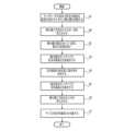
図2は、板状物(具体的には、チップ15)を備える積層体を製造する積層体の製造方法の一例を模式的に示すフローチャートである。この方法においては、まず、チップ15の一方の面(例えば、デバイス13が形成されていない側の面)及び仮支持基板のチップ15に仮接合される側の面である仮接合面のそれぞれに酸化膜を成膜する(成膜ステップS1)。Figure 2 is a flow chart showing a schematic example of a method for manufacturing a laminate including a plate-like object (specifically, a chip 15). In this method, first, an oxide film is formed on one surface of the chip 15 (e.g., the surface on which the
図3(A)は、それぞれの一方の面に酸化膜が成膜された複数のチップ15を模式的に示す断面図である。図3(A)に示される酸化膜17は、例えば、PECVD(Plasma Enhanced Chemical Vapor Deposition)を利用して成膜される酸化シリコン膜である。Figure 3(A) is a cross-sectional view showing a schematic of
このような酸化膜17は、例えば、複数のチップ15のそれぞれの一方の面が内部空間において露出されているチャンバに液体TEOS(Tetraethyl orthosilicate)等の液体原料を気化することによって得られるガスを供給した状態で、このガスをプラズマ化することによって成膜される。Such an
ここで、酸化膜17を成膜する際の雰囲気の温度、すなわち、チャンバ内の温度は、成膜される酸化膜17の水の含有量が多くなるように設定される。例えば、この温度は、80℃以上300℃以下、好ましくは100℃以上260℃以下、より好ましくは120℃以上220℃以下、最も好ましくは120℃以上180℃以下の第1温度範囲に含まれるように設定される。Here, the temperature of the atmosphere when forming the
また、酸化膜17は、後述するチップ15と仮支持基板との仮接合の際にチップ15の仮支持基板側への沈み込みが抑制されるように、薄い膜厚を有する。例えば、この酸化膜17は、1μm以下、好ましくは500nm以下、より好ましくは250nm以下、最も好ましくは125nm以下の膜厚を有する。In addition, the
また、酸化膜17の露出されている面、すなわち、デバイス13から遠い側の面を平坦化するために、この面には化学機械研磨(CMP)等の平坦化処理が施されてもよい。さらに、酸化膜17は、膜厚が1μm超にされるように成膜された後、膜厚が1μm以下になるとともに露出されている面が平坦化されるように平坦化処理が施されてもよい。加えて、平坦化処理は、酸化膜17を成膜前のチップ15の一方の面に対して施されてもよい。In addition, in order to planarize the exposed surface of the
図3(B)は、仮接合面に酸化膜が成膜された仮支持基板を模式的に示す断面図である。図3(B)に示される仮支持基板19は、例えば、複数のデバイス13が形成されていない点を除いて図1(A)に示されるウェーハ11と同じ構造物である。Figure 3(B) is a cross-sectional view showing a schematic diagram of a temporary support substrate with an oxide film formed on the temporary bonding surface. The
あるいは、仮支持基板19は、ガラス等の絶縁材料を素材とする基板であってもよい。また、仮支持基板19は、図1(A)に示されるウェーハ11よりも厚く、かつ/又は、直径が大きい基板であってもよい。Alternatively, the
また、図3(B)に示される酸化膜21は、例えば、図3(A)に示される酸化膜17と同様の方法で成膜される酸化シリコン膜である。さらに、この酸化膜21の露出されている面及び/又は酸化膜21を成膜前の仮支持基板19の仮接合面に対して平坦化処理が施されてもよい。The
成膜ステップS1の後には、酸化膜17,21の露出されている面に親水化処理を施す(親水化ステップS2)。図4(A)は、酸化膜17の露出されている面に親水化処理を施す様子を模式的に示す断面図であり、図4(B)は、酸化膜21の露出されている面に親水化処理を施す様子を模式的に示す断面図である。After the film formation step S1, the exposed surfaces of the
この親水化処理は、酸化膜17,21の露出されている面にOH基を形成して活性化するための処理である。例えば、親水化処理は、大気圧下において、窒素プラズマ又は紫外線を照射部10から酸化膜17,21の露出されている面に向かって照射することによって実施される。This hydrophilic treatment is a process for forming and activating OH groups on the exposed surfaces of the
なお、この親水化処理を実施する際には、酸化膜17,21に内包されている水が気化されないことが好ましい。そのため、親水化処理を実施する際の雰囲気の温度は、酸化膜17,21を成膜する際の雰囲気の温度よりも低い温度、例えば、室温に設定される。When carrying out this hydrophilic treatment, it is preferable that the water contained in the
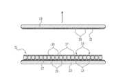
親水化ステップS2の後には、酸化膜17,21を介してチップ15と仮支持基板19とを仮接合する(仮接合ステップS3)。図5(A)は、チップ15と仮支持基板19とを仮接合する様子を模式的に示す断面図であり、図5(B)は、仮接合されたチップ15及び仮支持基板19を模式的に示す断面図である。After the hydrophilization step S2, the
この仮接合の際には、まず、複数のチップ15のそれぞれの一方の面と仮支持基板19の仮接合面とを酸化膜17,21を介して対向させる。そして、この状態を維持したまま、複数のチップ15のそれぞれと仮支持基板19とに、例えば、10kN程度の荷重が作用するまで両面を接近させる。その結果、酸化膜17と酸化膜21との間で水素結合が生じることによって複数のチップ15と仮支持基板19とが仮接合される。When this temporary bonding is performed, first, one surface of each of the
なお、この仮接合は、大気圧下において実施されてもよいし、105Pa以下の減圧雰囲気下で実施されてもよい。また、酸化膜17と酸化膜21との間で生じる水素結合を促進するために、この仮接合の直前に酸化膜17,21の露出されている面に水が供給されてもよい。 This temporary bonding may be performed under atmospheric pressure or under a reduced pressure atmosphere of 105 Pa or less. In order to promote hydrogen bonding between the
また、この仮接合を実施する際には、酸化膜17,21に内包されている水が気化されないことが好ましい。そのため、仮接合を実施する際の雰囲気の温度は、酸化膜17,21を成膜する際の雰囲気の温度よりも低い温度、例えば、室温に設定される。When performing this temporary bonding, it is preferable that the water contained in the
仮接合ステップS3の後には、支持基板のチップ15に接合される側の面である接合面に接合材を形成する(接合材形成ステップS4)。図6は、接合面に接合材が形成された支持基板を模式的に示す断面図である。After the temporary bonding step S3, a bonding material is formed on the bonding surface of the support substrate, which is the surface that is to be bonded to the chip 15 (bonding material formation step S4). Figure 6 is a cross-sectional view that shows a schematic diagram of the support substrate with a bonding material formed on the bonding surface.
図6に示される支持基板23は、例えば、単結晶シリコン等の半導体材料を素材とし、かつ、図1(A)に示されるウェーハ11と同様の形状を有するウェーハである。また、支持基板23の接合面側には、それぞれがチップ15に含まれるデバイス13と接続される複数のデバイス25が形成されている。なお、複数のデバイス25は、必須の構成要素ではなく、なくてもよい。The
図6に示される接合材27は、例えば、図3(A)に示される酸化膜17と同様の方法で酸化シリコン膜を成膜した後、複数のデバイス25が露出されるように接合材27の露出されている面にCMP等の平坦化処理を施すことによって形成される。ただし、この場合、接合材27を成膜する際の雰囲気の温度は、成膜される酸化シリコン膜の水の含有量が少なくなるような温度、例えば、350℃超に設定される。The
あるいは、接合材27は、BCB(Benzocyclobutene)等を含む有機接着剤であってもよい。この場合、接合材27は、例えば、雰囲気の温度を、例えば、室温に維持した状態で複数のデバイス25が露出されるように支持基板23の接合面に塗布してから、有機接着剤がプリベーク(ソフトベーク)されるように雰囲気の温度を、例えば、170℃程度に維持することによって形成される。Alternatively, the
接合材形成ステップS4の後には、接合材27を介してチップ15と支持基板23とを接合する(接合ステップS5)。図7(A)は、チップ15と支持基板23とを接合する様子を模式的に示す断面図であり、図7(B)は、接合されたチップ15及び支持基板23を模式的に示す断面図である。After the bonding material forming step S4, the
なお、接合材27が酸化シリコン膜によって構成される場合には、接合材形成ステップS4の後かつ接合ステップS5の前に、上述した親水化処理を接合材27の露出されている面に対して施すことが必要になる。また、接合ステップS5の直前には、複数のチップ15のそれぞれの他方の面及び/又は支持基板23の接合面が洗浄されてもよい。When the
チップ15と支持基板23とを接合する際には、まず、複数のチップ15のそれぞれの他方の面と支持基板23の接合面とを接合材27を介して対向させる。そして、この状態を維持したまま、複数のチップ15のそれぞれと支持基板23とに、例えば、10kN程度の荷重が作用するまで両面を接近させる。その結果、複数のチップ15と支持基板23とが接合される。When bonding the
なお、この接合は、大気圧下において実施されてもよいし、105Pa以下の減圧雰囲気下で実施されてもよい。また、接合材27が酸化シリコン膜によって構成される場合には、複数のチップ15と接合材27との水素結合を促進するために、この接合の直前に複数のチップ15のそれぞれの他方の面及び/又は接合材27の露出されている面に水が供給されてもよい。 This bonding may be performed under atmospheric pressure or under a reduced pressure atmosphere of 105 Pa or less. When the
また、接合材27が有機接着剤によって構成される場合、この接合を実施する際の雰囲気の温度は、接合材27を硬化させることが可能な温度、例えば、300℃程度に設定される。さらに、接合ステップS5においてデバイス13に含まれる配線(例えば、銅(Cu)配線)とデバイス25に含まれる配線(例えば、銅(Cu)配線)とを直接接続させる場合、すなわち、ハイブリッドボンディングを形成する場合には、この接合を実施する際の雰囲気の温度は、例えば、250℃以上350℃以下に設定されてもよい。When the
接合ステップS5の後には、酸化膜17,21に内包された水を気化させる(気化ステップS6)。図8は、酸化膜17,21に内包された水が気化した後の複数のチップ15、仮支持基板19及び支持基板23を備える積層体を模式的に示す断面図である。After the bonding step S5, the water contained in the
この気化ステップS6においては、例えば、赤外線ランプを備える熱処理装置を利用して窒素雰囲気下で積層体を加熱する。これにより、仮支持基板19を複数のチップ15から分離させる際に分離起点として作用する多数のボイド29が酸化膜17,21に形成される。In this vaporization step S6, the laminate is heated in a nitrogen atmosphere using, for example, a heat treatment device equipped with an infrared lamp. This forms a large number of
なお、酸化膜17,21に内包された水を気化させるためには、酸化膜17,21を成膜する時よりも雰囲気の温度を高くする必要がある。他方、積層体を加熱する際の雰囲気の温度が高すぎると、酸化膜17と酸化膜21との間で水素結合よりも強固なシロキサン結合が生じるおそれがある。In order to vaporize the water contained in the
そのため、積層体を加熱する際の雰囲気の温度は、200℃以上350℃以下、好ましくは215℃以上320℃以下、より好ましくは230℃以上290℃以下、最も好ましくは245℃以上260℃以下の第2温度範囲に含まれるように設定される。Therefore, the temperature of the atmosphere when heating the laminate is set to be within the second temperature range of 200°C or higher and 350°C or lower, preferably 215°C or higher and 320°C or lower, more preferably 230°C or higher and 290°C or lower, and most preferably 245°C or higher and 260°C or lower.
また、接合材27が有機接着剤によって構成される場合、すなわち、接合ステップS5において雰囲気の温度が、例えば、300℃程度に設定される場合には、接合ステップS5と気化ステップS6とが間断なく連続して実施されてもよい。In addition, when the
気化ステップS6の後には、チップ15と仮支持基板19とを分離する(分離ステップS7)。図9は、チップ15から仮支持基板19を分離する様子を模式的に示す断面図である。After the vaporization step S6, the
この分離ステップS7においては、チップ15から仮支持基板19を離隔させるような外力を仮支持基板19及び/又は支持基板23に付与する。その結果、仮支持基板19がチップ15から分離されてチップ15と支持基板23とを備える積層体31が製造される。In this separation step S7, an external force is applied to the
さらに、仮支持基板19がチップ15から分離された後にチップ15の一方の面に残存する酸化膜17が除去されるように、この積層体31にエッチングが施されてもよい。また、この積層体31は、複数のチップ15の境界に沿って分割されることによって個片化されてもよい。Furthermore, the laminate 31 may be etched so that the
図2に示される積層体の製造方法においては、その露出されている面が親水化された酸化膜17,21を利用してチップ15と仮支持基板19とが仮接合される。すなわち、この方法においては、有機接着剤を利用することなく、酸化膜17,21の露出されている面において生じる水素結合を利用してチップ15と仮支持基板19とが仮接合される。In the method for manufacturing the laminate shown in FIG. 2, the
また、この方法においては、チップ15と支持基板23との接合が完了した後に、酸化膜17,21を成膜する際の雰囲気の温度(第1温度範囲)よりも高い温度(第2温度範囲)に雰囲気の温度を維持することによって酸化膜17,21に内包された水を気化させる。これにより、仮支持基板19を複数のチップ15から分離させる際に分離起点として作用する多数のボイド29が酸化膜17,21に形成される。その結果、この方法においては、仮支持基板19をチップ15から分離することが容易になる。In addition, in this method, after the bonding of the
なお、上述した内容は本発明の一態様であって、本発明は上述した内容に限定されない。例えば、成膜ステップS1においては、各チップ15の一方の面又は仮支持基板19の仮接合面のいずれか一方のみに酸化膜17,21が成膜されてもよい。すなわち、本発明においては、酸化膜17又は酸化膜21のいずれか一方はなくてもよい。The above is one aspect of the present invention, and the present invention is not limited to the above. For example, in the film formation step S1, the
また、成膜ステップS1においては、各チップ15のデバイス13が形成されている側の面に酸化膜17が成膜されてもよい。すなわち、各チップ15は、そのデバイス13が形成されている側が仮支持基板19に接合され、かつ、そのデバイス13が形成されていない側が支持基板23に接合されてもよい。また、この場合には、支持基板23の接合面側には、複数のデバイス25が形成されなくてもよい。In addition, in the film formation step S1, an
また、成膜ステップS1においては、複数のチップ15へと分割される前のウェーハ11の一方の面(例えば、裏面11b)に酸化膜17が成膜されてもよい。この場合、複数のチップ15は、成膜ステップS1の後かつ親水化ステップS2の前に、複数のデバイス13の境界に沿ってウェーハ11を分割することによって製造されてもよい。In addition, in the film-forming step S1, an
また、本発明においては、接合ステップS5よりも前であれば接合材形成ステップS4が実施されるタイミングは限定されない。例えば、接合材形成ステップS4は、成膜ステップS1よりも前に実施されてもよい。In addition, in the present invention, the timing of performing the bonding material forming step S4 is not limited as long as it is performed before the bonding step S5. For example, the bonding material forming step S4 may be performed before the film forming step S1.
そして、成膜ステップS1に先立つ接合材形成ステップS4においては、板状物(具体的には、複数のチップ15又は複数のチップ15へと分割される前のウェーハ11)の他方の面に、上述した酸化シリコン膜によって構成される接合材27と同様の接合材が形成されてもよい。In the bonding material formation step S4 prior to the film formation step S1, a bonding material similar to the
すなわち、この場合、支持基板23の接合面のみならず、板状物の他方の面にも接合材が形成されてもよい。あるいは、この場合、支持基板23の接合面に接合材27を形成することなく、板状物の他方の面にのみ接合材が形成されてもよい。That is, in this case, the bonding material may be formed not only on the bonding surface of the
また、本発明の積層体の製造方法は、図2に示されるステップ以外のステップを含んでもよい。図10は、図2に示される積層体の製造方法とは異なる積層体の製造方法の一例を模式的に示すフローチャートである。具体的には、図10に示される方法においては、成膜ステップS1の後かつ親水化ステップS2の前に、酸化膜17,21に内包された水の一部を気化させる(予備気化ステップS8)。The laminate manufacturing method of the present invention may also include steps other than those shown in FIG. 2. FIG. 10 is a flow chart that shows a schematic example of a laminate manufacturing method different from the laminate manufacturing method shown in FIG. 2. Specifically, in the method shown in FIG. 10, after the film forming step S1 and before the hydrophilization step S2, a portion of the water contained in the
この予備気化ステップS8においては、例えば、酸化膜17,21に内包される水の量を減少させるために、赤外線ランプを備える熱処理装置を利用して窒素雰囲気下で一方の面に酸化膜17が成膜されている板状物及び/又は仮接合面に酸化膜21が成膜されている仮支持基板19を加熱する。In this preliminary vaporization step S8, for example, in order to reduce the amount of water contained in the
なお、酸化膜17,21に内包された水を気化させるためには、酸化膜17,21を成膜する時よりも雰囲気の温度を高くする必要がある。他方、積層体を加熱する際の雰囲気の温度が高すぎると、酸化膜17,21に内包される水の全てが気化されるおそれがある。そのため、板状物及び/又は仮支持基板19を加熱する際の雰囲気の温度は、上記の第1温度範囲よりも高く、かつ、上記の第2温度範囲よりも低い第3温度範囲に含まれるように設定される。In order to vaporize the water contained in the
また、本発明においては、仮支持基板19に仮接合され、かつ、支持基板23に接合される板状物は、ウェーハ11であってもよい。すなわち、本発明においては、ウェーハ11から製造される複数のチップ15が支持基板23に接合されるのではなく、ウェーハ11自体が支持基板23に接合されてもよい。さらに、この場合、複数のデバイス13がウェーハ11に形成されなくてもよい。In addition, in the present invention, the plate-like object that is temporarily bonded to the
その他、上述した実施形態にかかる構造及び方法等は、本発明の目的の範囲を逸脱しない限りにおいて適宜変更して実施できる。In addition, the structures and methods of the above-described embodiments can be modified as appropriate without departing from the scope of the present invention.
10:照射部
11:ウェーハ(11a:表面、11b:裏面、11c:ノッチ)
13:デバイス
15:チップ
17:酸化膜
19:仮支持基板
21:酸化膜
23:支持基板
25:デバイス
27:接合材
29:ボイド
31:積層体 10: Irradiation unit 11: Wafer (11a: front surface, 11b: back surface, 11c: notch)
13: Device 15: Chip 17: Oxide film 19: Temporary support substrate 21: Oxide film 23: Support substrate 25: Device 27: Bonding material 29: Void 31: Laminate
Claims (5)
Translated fromJapanese雰囲気の温度が第1温度範囲に維持された状態で該板状物の該一方の面又は仮支持基板の仮接合面の少なくとも一方に酸化膜を成膜する成膜ステップと、
該成膜ステップの後に、該酸化膜の露出されている面に親水化処理を施す親水化ステップと、
該親水化ステップの後に、該板状物の該一方の面と該仮支持基板の該仮接合面とが該酸化膜を介して対向した状態で両面を接近させることによって、該酸化膜を介して該板状物と該仮支持基板とを仮接合する仮接合ステップと、
該板状物の該他方の面又は支持基板の接合面の少なくとも一方に接合材を形成する接合材形成ステップと、
該仮接合ステップ及び該接合材形成ステップの後に、該板状物の該他方の面と該支持基板の該接合面とが該接合材を介して対向した状態で両面を接近させることによって、該接合材を介して該板状物と該支持基板とを接合する接合ステップと、
該接合ステップの後に、雰囲気の温度を該第1温度範囲よりも高い第2温度範囲に維持することによって、該酸化膜に内包された水を気化させる気化ステップと、
該気化ステップの後に、該板状物と該仮支持基板とを分離する分離ステップと、
を備える積層体の製造方法。 A method for producing a laminate including a plate-shaped object having one surface and another surface located on the back side of the one surface, comprising:
a film forming step of forming an oxide film on at least one of the one surface of the plate-like object or the temporary bonding surface of the temporary support substrate while maintaining the temperature of the atmosphere within a first temperature range;
a hydrophilization step of subjecting an exposed surface of the oxide film to a hydrophilic treatment after the film-forming step;
a temporary bonding step of temporarily bonding the plate-like object and the temporary bonding surface of the temporary support substrate via the oxide film by bringing the two surfaces of the plate-like object close to each other in a state where the two surfaces face each other via the oxide film after the hydrophilization step;
a bonding material forming step of forming a bonding material on at least one of the other surface of the plate-like object or the bonding surface of a support substrate;
a bonding step of bonding the plate-like object and the supporting substrate via the bonding material by bringing the other surface of the plate-like object and the bonding surface of the supporting substrate close to each other in a state in which the other surface and the bonding material are opposed to each other via the bonding material, after the temporary bonding step and the bonding material forming step;
a vaporization step of vaporizing water contained in the oxide film by maintaining an atmosphere temperature in a second temperature range higher than the first temperature range after the bonding step;
a separation step of separating the plate-like object from the temporary support substrate after the vaporization step;
A method for manufacturing a laminate comprising the steps of:
Priority Applications (2)
| Application Number | Priority Date | Filing Date | Title |
|---|---|---|---|
| JP2023081568AJP2024165397A (en) | 2023-05-17 | 2023-05-17 | Manufacturing method of laminate |
| US18/662,007US20240387229A1 (en) | 2023-05-17 | 2024-05-13 | Method of manufacturing laminated assembly |
Applications Claiming Priority (1)
| Application Number | Priority Date | Filing Date | Title |
|---|---|---|---|
| JP2023081568AJP2024165397A (en) | 2023-05-17 | 2023-05-17 | Manufacturing method of laminate |
Publications (1)
| Publication Number | Publication Date |
|---|---|
| JP2024165397Atrue JP2024165397A (en) | 2024-11-28 |
Family
ID=93464585
Family Applications (1)
| Application Number | Title | Priority Date | Filing Date |
|---|---|---|---|
| JP2023081568APendingJP2024165397A (en) | 2023-05-17 | 2023-05-17 | Manufacturing method of laminate |
Country Status (2)
| Country | Link |
|---|---|
| US (1) | US20240387229A1 (en) |
| JP (1) | JP2024165397A (en) |
- 2023
- 2023-05-17JPJP2023081568Apatent/JP2024165397A/enactivePending
- 2024
- 2024-05-13USUS18/662,007patent/US20240387229A1/enactivePending
Also Published As
| Publication number | Publication date |
|---|---|
| US20240387229A1 (en) | 2024-11-21 |
Similar Documents
| Publication | Publication Date | Title |
|---|---|---|
| JP2024515032A (en) | Direct bonding and peeling of carriers | |
| US7371662B2 (en) | Method for forming a 3D interconnect and resulting structures | |
| TWI402170B (en) | Method of bonding two substrates | |
| US10121762B2 (en) | Wafer bonding structure and wafer bonding method | |
| JP5462289B2 (en) | Method for generating heterostructures with locally matching coefficients of thermal expansion | |
| JP2009111362A5 (en) | ||
| JP5769716B2 (en) | Method for bonding a chip to a wafer | |
| KR102155074B1 (en) | Method for bonding by means of molecular adhesion | |
| TWI616966B (en) | Process for bonding in a gas atmosphere exhibiting a negative joule-thomson coefficient | |
| JP2022548171A (en) | High density logic and memory manufacturing method for advanced circuit architecture | |
| WO2015070684A1 (en) | Handler wafer removal | |
| Sakuma et al. | Voids-free die-level Cu/ILD hybrid bonding | |
| JP7165342B1 (en) | Chemical bonding method and package type electronic parts, and hybrid bonding method for electronic devices | |
| JP2024165397A (en) | Manufacturing method of laminate | |
| TW201336041A (en) | Method for three-dimensional packaging of electronic devices | |
| WO2014049414A1 (en) | Direct bonding process | |
| JP2010021466A (en) | Substrate bonding method and electronic component | |
| JPS61174661A (en) | Semiconductor integrated circuit device and manufacture thereof | |
| JP6349121B2 (en) | Manufacturing method of laminated device | |
| JP2022049603A (en) | Method for manufacturing semiconductor device | |
| JP2583764B2 (en) | Method for manufacturing semiconductor integrated circuit device | |
| TWI895994B (en) | Semiconductor device manufacturing method and semiconductor device | |
| CN119626973B (en) | Temporary bonding and debonding methods, preparation method of composite substrate and manufacturing method of wafer | |
| JP2013038316A (en) | Method for manufacturing group iii nitride layer composite substrate | |
| JP2017028178A (en) | Three-dimensional mounting method for semiconductor wafer and joining method for semiconductor wafer |