JP2024154027A - Acoustic wave device and manufacturing method thereof - Google Patents
Acoustic wave device and manufacturing method thereofDownload PDFInfo
- Publication number
- JP2024154027A JP2024154027AJP2023067605AJP2023067605AJP2024154027AJP 2024154027 AJP2024154027 AJP 2024154027AJP 2023067605 AJP2023067605 AJP 2023067605AJP 2023067605 AJP2023067605 AJP 2023067605AJP 2024154027 AJP2024154027 AJP 2024154027A
- Authority
- JP
- Japan
- Prior art keywords
- layer
- resin
- acoustic wave
- device chip
- wave device
- Prior art date
- Legal status (The legal status is an assumption and is not a legal conclusion. Google has not performed a legal analysis and makes no representation as to the accuracy of the status listed.)
- Pending
Links
Images


Classifications
- H—ELECTRICITY
- H03—ELECTRONIC CIRCUITRY
- H03H—IMPEDANCE NETWORKS, e.g. RESONANT CIRCUITS; RESONATORS
- H03H9/00—Networks comprising electromechanical or electro-acoustic elements; Electromechanical resonators
- H03H9/02—Details
- H03H9/02007—Details of bulk acoustic wave devices
- H03H9/02015—Characteristics of piezoelectric layers, e.g. cutting angles
- H03H9/02023—Characteristics of piezoelectric layers, e.g. cutting angles consisting of quartz
- H—ELECTRICITY
- H03—ELECTRONIC CIRCUITRY
- H03H—IMPEDANCE NETWORKS, e.g. RESONANT CIRCUITS; RESONATORS
- H03H3/00—Apparatus or processes specially adapted for the manufacture of impedance networks, resonating circuits, resonators
- H03H3/007—Apparatus or processes specially adapted for the manufacture of impedance networks, resonating circuits, resonators for the manufacture of electromechanical resonators or networks
- H03H3/02—Apparatus or processes specially adapted for the manufacture of impedance networks, resonating circuits, resonators for the manufacture of electromechanical resonators or networks for the manufacture of piezoelectric or electrostrictive resonators or networks
- H—ELECTRICITY
- H03—ELECTRONIC CIRCUITRY
- H03H—IMPEDANCE NETWORKS, e.g. RESONANT CIRCUITS; RESONATORS
- H03H9/00—Networks comprising electromechanical or electro-acoustic elements; Electromechanical resonators
- H03H9/02—Details
- H03H9/02007—Details of bulk acoustic wave devices
- H03H9/02015—Characteristics of piezoelectric layers, e.g. cutting angles
- H03H9/02039—Characteristics of piezoelectric layers, e.g. cutting angles consisting of a material from the crystal group 32, e.g. langasite, langatate, langanite
- H—ELECTRICITY
- H03—ELECTRONIC CIRCUITRY
- H03H—IMPEDANCE NETWORKS, e.g. RESONANT CIRCUITS; RESONATORS
- H03H9/00—Networks comprising electromechanical or electro-acoustic elements; Electromechanical resonators
- H03H9/02—Details
- H03H9/02007—Details of bulk acoustic wave devices
- H03H9/02047—Treatment of substrates
- H—ELECTRICITY
- H03—ELECTRONIC CIRCUITRY
- H03H—IMPEDANCE NETWORKS, e.g. RESONANT CIRCUITS; RESONATORS
- H03H9/00—Networks comprising electromechanical or electro-acoustic elements; Electromechanical resonators
- H03H9/02—Details
- H03H9/02535—Details of surface acoustic wave devices
- H03H9/02543—Characteristics of substrate, e.g. cutting angles
- H03H9/02551—Characteristics of substrate, e.g. cutting angles of quartz substrates
- H—ELECTRICITY
- H03—ELECTRONIC CIRCUITRY
- H03H—IMPEDANCE NETWORKS, e.g. RESONANT CIRCUITS; RESONATORS
- H03H9/00—Networks comprising electromechanical or electro-acoustic elements; Electromechanical resonators
- H03H9/02—Details
- H03H9/02535—Details of surface acoustic wave devices
- H03H9/02543—Characteristics of substrate, e.g. cutting angles
- H03H9/02559—Characteristics of substrate, e.g. cutting angles of lithium niobate or lithium-tantalate substrates
- H—ELECTRICITY
- H03—ELECTRONIC CIRCUITRY
- H03H—IMPEDANCE NETWORKS, e.g. RESONANT CIRCUITS; RESONATORS
- H03H9/00—Networks comprising electromechanical or electro-acoustic elements; Electromechanical resonators
- H03H9/02—Details
- H03H9/02535—Details of surface acoustic wave devices
- H03H9/02614—Treatment of substrates, e.g. curved, spherical, cylindrical substrates ensuring closed round-about circuits for the acoustical waves
- H—ELECTRICITY
- H03—ELECTRONIC CIRCUITRY
- H03H—IMPEDANCE NETWORKS, e.g. RESONANT CIRCUITS; RESONATORS
- H03H9/00—Networks comprising electromechanical or electro-acoustic elements; Electromechanical resonators
- H03H9/02—Details
- H03H9/125—Driving means, e.g. electrodes, coils
- H03H9/13—Driving means, e.g. electrodes, coils for networks consisting of piezoelectric or electrostrictive materials
- H—ELECTRICITY
- H03—ELECTRONIC CIRCUITRY
- H03H—IMPEDANCE NETWORKS, e.g. RESONANT CIRCUITS; RESONATORS
- H03H3/00—Apparatus or processes specially adapted for the manufacture of impedance networks, resonating circuits, resonators
- H03H3/007—Apparatus or processes specially adapted for the manufacture of impedance networks, resonating circuits, resonators for the manufacture of electromechanical resonators or networks
- H03H3/02—Apparatus or processes specially adapted for the manufacture of impedance networks, resonating circuits, resonators for the manufacture of electromechanical resonators or networks for the manufacture of piezoelectric or electrostrictive resonators or networks
- H03H2003/023—Apparatus or processes specially adapted for the manufacture of impedance networks, resonating circuits, resonators for the manufacture of electromechanical resonators or networks for the manufacture of piezoelectric or electrostrictive resonators or networks the resonators or networks being of the membrane type
Landscapes
- Physics & Mathematics (AREA)
- Acoustics & Sound (AREA)
- Engineering & Computer Science (AREA)
- Chemical & Material Sciences (AREA)
- Manufacturing & Machinery (AREA)
- Materials Engineering (AREA)
- Crystallography & Structural Chemistry (AREA)
- Surface Acoustic Wave Elements And Circuit Networks Thereof (AREA)
Abstract
Translated fromJapaneseDescription
Translated fromJapaneseこの発明は、モバイル通信機器などにおいて周波数フィルタなどとして使用するのに適した弾性波デバイス、およびその製造方法の改良に関する。This invention relates to an acoustic wave device suitable for use as a frequency filter in mobile communication devices and the like, and to an improved method for manufacturing the same.
WLP(Wafer Level Package)構造を有する弾性波(Surface Acoustic Wave/SAW)デバイスは、特許文献1に示される構造を持つ。
この特許文献1のものは、デバイスチップの一面上にカバーを設けると共に、このカバーにより形成された内部空間内に前記一面に形成させたIDT電極が位置されるようになっている。
ここで、弾性波デバイスへの信号の入力によりデバイスチップには熱が生じるが、デバイスチップを構成する圧電体は熱伝導率が低く放熱性が悪い。圧電体として利用されるタンタル酸リチウムやニオブ酸リチウムの熱伝導率は約4から6W/mK程度である。 A surface acoustic wave (SAW) device having a wafer level package (WLP) structure has a structure shown in Japanese Patent Laid-Open No. 2003-233996.
In the device disclosed in
Here, heat is generated in the device chip due to the input of a signal to the acoustic wave device, but the piezoelectric material constituting the device chip has low thermal conductivity and poor heat dissipation. The thermal conductivity of lithium tantalate and lithium niobate used as piezoelectric materials is about 4 to 6 W/mK.
この発明が解決しようとする主たる問題点は、この種のWLP構造の弾性波デバイスにおいて、これを構成するデバイスチップの放熱性を合理的に向上可能な新しい構造、および、その製法を提供する点にある。The main problem that this invention aims to solve is to provide a new structure and manufacturing method that can rationally improve the heat dissipation of the device chip that constitutes this type of WLP structure acoustic wave device.
前記課題を達成するために、この発明にあっては、第一の観点から、弾性波デバイスを、
一面にIDT電極を含んだ機能素子を形成させたデバイスチップの前記一面上に樹脂製の支持層を介して樹脂製のカバー層を支持させてこれら三者間に形成された内部空間に前記機能素子を位置させるようにしてなる弾性波デバイスであって、
前記支持層は、前記デバイスチップの前記一面に接する下層部と、前記カバー層と前記下層部との間にあって両者に接する上層部とから構成されていると共に、
前記下層部を、前記上層部を構成する樹脂より熱伝導率が高く、かつ、非感光性の樹脂から構成し、
前記上層部を、感光性の樹脂から構成させてなる、ものとした。 In order to achieve the above object, from a first aspect, the present invention provides an acoustic wave device comprising:
An acoustic wave device comprising a device chip having a functional element including an IDT electrode formed on one surface thereof, a resin cover layer supported on the one surface thereof via a resin support layer, and the functional element being positioned in an internal space formed between these three elements,
the support layer is composed of a lower layer portion in contact with the one surface of the device chip, and an upper layer portion located between the cover layer and the lower layer portion in contact with both of them,
The lower layer is made of a resin having a higher thermal conductivity than a resin constituting the upper layer and being non-photosensitive;
The upper layer is made of a photosensitive resin.
前記カバー層及び前記支持層を貫通すると共に穴底に前記デバイスチップの前記一面に形成されて前記機能素子に接続されたバンプパッドを位置させる通過穴内にバンプを形成させるようにすることが、この発明の態様の一つとされる。One aspect of the invention is to form a bump in a through hole that penetrates the cover layer and the support layer and has a bump pad formed on the surface of the device chip at the bottom of the hole and connected to the functional element.
また、前記デバイスチップの前記一面に沿う向きの断面において、前記内部空間の断面積が、前記上層部の形成レベルに比し前記下層部の形成レベルにおいて大きくなるようにすることが、この発明の態様の一つとされる。In addition, one aspect of the invention is that the cross-sectional area of the internal space in a cross section along the one surface of the device chip is larger at the formation level of the lower layer than at the formation level of the upper layer.
また、前記課題を達成するために、この発明にあっては、第二の観点から、弾性波デバイスの製造方法を、
前記弾性波デバイスの製造方法であって、
前記デバイスチップとなるウエハの一面に前記機能素子、配線及び前記バンプパッドを形成する第1ステップと、
前記第1ステップを経た前記ウエハの前記一面に前記下層部となる第一樹脂層を形成させる第2ステップと、
前記第2ステップにより形成された前記第一樹脂層上に前記上層部となる第二樹脂層を形成させる第3ステップと、
前記第3ステップにより形成された第二樹脂層における前記機能素子の形成領域上に位置される領域以外の領域を露光させる第4ステップと、
前記第二樹脂層における前記露光された領域以外の領域を現像により取り除く第5ステップと、
前記第5ステップ後に前記第二樹脂層の前記露光された領域をマスクとして前記第一樹脂層をエッチングして前記下層部の形成レベルにおいて前記内部空間となる空間を形成させる第6ステップとを備えてなる、ものとした。 In order to achieve the above object, from a second standpoint, the present invention provides a method for manufacturing an acoustic wave device, comprising the steps of:
A method for manufacturing the acoustic wave device, comprising the steps of:
a first step of forming the functional elements, wiring, and bump pads on one surface of a wafer that will become the device chip;
a second step of forming a first resin layer that becomes the lower layer portion on the one surface of the wafer that has been subjected to the first step;
a third step of forming a second resin layer to be the upper layer portion on the first resin layer formed in the second step;
a fourth step of exposing a region of the second resin layer formed in the third step other than a region located on a formation region of the functional element;
a fifth step of removing an area of the second resin layer other than the exposed area by development;
and a sixth step of etching the first resin layer using the exposed area of the second resin layer as a mask after the fifth step to form a space that becomes the internal space at the formation level of the lower layer portion.
この発明にあっては、前記支持層の下層部を利用して、前記デバイスチップの放熱性を合理的に向上させることができる。また、かかる支持層の下層部を備えた弾性波デバイスを容易且つ適切に製造することができる。In this invention, the lower layer of the support layer can be used to rationally improve the heat dissipation of the device chip. In addition, an acoustic wave device including such a lower layer of the support layer can be easily and appropriately manufactured.
以下、図1~図13に基づいて、この発明の典型的な実施の形態について、説明する。この実施の形態にかかる弾性波デバイス1は、モバイル通信機器などにおいて周波数フィルタなどとして使用するのに適したものである。A typical embodiment of the present invention will be described below with reference to Figs. 1 to 13. The
かかる弾性波デバイス1は、
デバイスチップ2と、
前記デバイスチップ2の一面2aに形成されたIDT電極6bなどの機能素子6と、
前記一面2aにおいて前記機能素子6を囲うように形成された支持層3(ウォール/Wall)と、
前記支持層3上に形成されて前記デバイスチップ2と前記支持層3と共働して前記機能素子6を気密封止する内部空間5(キャビティ、中空構造部)を形成するカバー層4(ルーフ/Roof)とを備えたものとなっている。 The
A
A
A support layer 3 (wall) formed on the
The
典型的には、前記デバイスチップ2は、一辺を0.5ないし1mmとし、厚さを0.15ないし0.2mmとする四角形(図示の例では長方形)の板状をなすように構成される。
また、典型的には、支持層3は、前記デバイスチップ2の一面2aに直交する向きの厚さ(デバイスチップ2の一面2aを基準とした支持層3の高さ)を10ないし30μmとするように構成される。
また、典型的には、カバー層4は、厚さを15ないし35μmとするように構成される。
これらから構成される弾性波デバイス1は、典型的には、厚さを0.25ないし0.35mm程度とする。 Typically, the
Typically, the
Typically, the
The
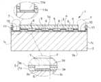
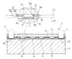
図1に示されるように、かかる弾性波デバイス1は、前記デバイスチップ2の前記一面2aに直交する向きから見た状態において正方形又は長方形の四角形状の輪郭を持つようなっている。
すなわち、かかる弾性波デバイス1は、前記四角形状の二つの面1a、1bと、この二つの面1a、1b間に亘る四つの側面1cとを備えた扁平の六面体状を呈している。
なお、各図においては、弾性波デバイス1の構成を理解しやすいように、その構成要素の厚さは誇張して表している。 As shown in FIG. 1, the
That is, the
In each drawing, the thicknesses of the components of the
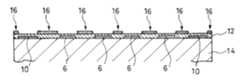
弾性波デバイス1の断面構造を図2に示す。図中符号6は機能素子、符号5は内部空間、符号3は支持層、符号4はカバー層、符号7は機能素子6を配線9(図4参照)とバンプパッド10とを介して外部に接続するためのバンプである。The cross-sectional structure of the
デバイスチップ2の一面2a上には複数の機能素子6が形成されている。デバイスチップ2の一面2aにおける各機能素子6の形成領域はそれぞれ、支持層3で囲繞されると共に、この支持層3上に形成されるカバー層4で蓋がされた形態となっており、これにより弾性波デバイス1は複数の前記内部空間5を備えたものとなっている。
支持層3及びカバー層4は、絶縁性を備えた合成樹脂から構成される。 A plurality of
The
デバイスチップ2は、弾性波を伝搬させる機能を持つ。デバイスチップ2には、典型的には、圧電体としてタンタル酸リチウムやニオブ酸リチウムが用いられ、また、デバイスチップ2は、これらにサファイア、シリコン、アルミナ、スピネル、水晶またはガラスなどを積層させて、構成される場合もある。The
図3に機能素子6の一例としての共振器6aを示す。共振器6aはIDT電極6bと、IDT電極6bを挟むようにして形成される反射器6eとを有する。IDT電極6bは、電極対からなり、各電極対は弾性波の伝搬方向xに長さ方向を交叉させるように平行配列された複数の電極指6c同士をこれらの一端側においてバスバー6dで接続させてなる。反射器6eは、弾性波の伝搬方向xに長さ方向を交叉させるように平行配列された複数の電極指6fの端部間をバスバー6gで接続させてなる。
かかる機能素子6は、典型的には、フォトリソグラフィ技術により形成された導電性金属膜によって構成される。 3 shows a resonator 6a as an example of the
Such a
図4に一つのデバイスチップ2上に備えられる回路の一例の概念を示す。符号6aaは入出力ポート間に直列に接続された共振器6a、符号6abは入出力ポート間に並列に接続された共振器6a、符号8はグランドを示す。機能素子6の数や配置は必要に応じて変更される。すなわち、図4の回路によってラダー型フィルタが構成されるようになっている。
前記バンプパッド10は前記回路を構成する配線9に接続される。かかる配線9、及び、前記バンプパッド10も、典型的には、フォトリソグラフィ技術により形成された導電性金属膜によって、前記デバイスチップ2の一面2a上に形成される。 4 shows the concept of an example of a circuit provided on one
The
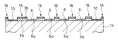
この実施の形態にかかる弾性波デバイスにあっては、前記支持層3は、前記デバイスチップ2の前記一面2aに接する下層部3aと、前記カバー層4と前記下層部3aとの間にあって両者に接する上層部3bとから構成されている。
それと共に、前記下層部3aを、前記上層部3bを構成する樹脂より熱伝導率が高く、かつ、非感光性の樹脂から構成している。
一方、前記上層部3bを、感光性の樹脂から構成させている。 In the elastic wave device of this embodiment, the
In addition, the
On the other hand, the
弾性波デバイスへの信号の入力によりデバイスチップ2には熱が生じるが、デバイスチップ2を構成する圧電体は熱伝導率が低く放熱性が悪い。
前記支持層3の全体を熱伝導率の高い樹脂から構成すれば、デバイスチップ2の放熱性を向上させることができる。
こうした熱伝導率の高い樹脂としては、熱伝導率の高い物質からなるフィラーを、基材となる樹脂に対して70wt%ないし90wt%の範囲で含ませるようにしたものが用いられる。かかるフィラーは典型的には直径10μm前後の粒状体として構成される。
しかるに、このように熱伝導率を高められた樹脂は感光性が低下する。このため、前記支持層3の全体を熱伝導率の高い樹脂から構成させた場合、デバイスチップ2における機能素子の形成領域上に前記内部空間5をフォトリソグラフィ技術を利用して形成し難くなる。
この実施の形態にかかる弾性波デバイスにあっては、デバイスチップ2の一面2a上に前記下層部3aとなる後述の第一樹脂層12を形成し、次いで、上層部3bとなる後述の第二樹脂層13を形成させた後、この第二樹脂層13を露光と現像とによりパターニングし、この後、パターニングされた第二樹脂層13をいわばマスクとして第一樹脂層12をエッチングすることで、前記内部空間5をフォトリソグラフィ技術を利用して形成可能としながら、デバイスチップ2の一面2aに直接的に接する支持層3の下層部3aの熱伝導率を高めてデバイスチップ2の放熱性を向上させることができる。 When a signal is input to the acoustic wave device, heat is generated in the
If the
Such a resin with high thermal conductivity is made by mixing 70 wt % to 90 wt % of a filler made of a substance with high thermal conductivity with respect to the base resin. Such a filler is typically formed as a granular material with a diameter of about 10 μm.
However, the resin with increased thermal conductivity has reduced photosensitivity, so that if the
In the acoustic wave device of this embodiment, a first resin layer 12 (described later) which becomes the
前記下層部3aを構成する樹脂としては、典型的には、フィラーを含有するエポキシ系樹脂や、フィラーを含有するフェノール系樹脂を用いることができる。フィラーとしては、典型的には、アルミナ、窒化アルミ、粉末ダイヤモンドを用いることができる。
一方、前記上層部3bを構成する樹脂としては、典型的には、感光性を持ったエポキシ系樹脂や、感光性を持ったフェノール系樹脂を用いることができる。 The resin constituting the
On the other hand, the resin constituting the
また、この実施の形態にあっては、弾性波デバイス1は、前記カバー層4及び前記支持層3を貫通すると共に穴底に前記デバイスチップ2の前記一面2aに形成されて前記機能素子6に接続されたバンプパッド10を位置させる通過穴11を備えている。そして、この通過穴11内に金属製のバンプ7が形成されている。
図示の例では、通過穴11は、弾性波デバイス1の四隅にそれぞれ形成されている。各通過穴11はそれぞれ、その上側穴部11aは前記パターニングにより上層部3bの一部を取り除くことにより形成され、その下側穴部11bは前記上側穴部11aを利用してなされたエッチングによって下層部3aの一部を取り除くことで形成されている。
このように形成された通過穴11内に形成されるバンプ7と、通過穴11内でこのバンプ7に接する前記支持層3の下層部3aにより、デバイスチップ2からの放熱経路が形成される。 In this embodiment, the
In the illustrated example, the through
A heat dissipation path from the
図1ないし図12に示される第一例では、デバイスチップ2の一面2aに直交する向きにおいて、いずれの位置で断面にしても、前記内部空間5の断面積は実質的に等しくなるようにしてある。
すなわち、第一例では、支持層3におけるデバイスチップ2の一面2aに固着された下面3cとルーフ層に固着された上面3dとの間に亘る前記内部空間5に臨んだ側面3eは、デバイスチップ2の一面2aに直交する仮想の一つの面y(図2参照)上に位置するようになっている。 In the first example shown in FIGS. 1 to 12, the cross-sectional area of the
That is, in the first example, the
対し、図13に示される第二例では、前記デバイスチップ2の前記一面2aに沿う向きの断面において、前記内部空間5の断面積が、前記上層部3bの形成レベルL1(図13参照)に比し前記下層部3aの形成レベルL2(図13参照)において大きくなるようにしてある。
すなわち、第二例では、前記内部空間5の中心z(図13参照)を巡るいずれの位置においても、支持層3の上面3dと上層部3bにおける下層部3aに対する固着部3fとの間に亘る上層側面3gが、支持層3の下面3cと前記固着部3fとの間に亘る下層側面3hよりも前記内部空間5の中心z側に位置し、この上層側面3gと下層側面3hとの間にデバイスチップ2の一面2aに向き合った段差面3iが形成されるようになっている。
この第二例のようにすることは、前記のようにパターニングされた第二樹脂層13をいわばマスクとして第一樹脂層12を時間や温度などのコンディションを調整してエッチングすることで可能となる。
この第二例のようにした場合、支持層3とカバー層4との固着面積を可及的に広く確保して両者の機械的一体性を高めつつ、その下方においては前記内部空間5の断面積、つまり、前記機能素子6の形成領域の面積を可及的に広く確保させることができる。 In contrast, in the second example shown in Figure 13, in a cross section oriented along the one
That is, in the second example, at any position around the center z of the internal space 5 (see Figure 13), the upper
This second example can be achieved by using the
In the case of using the second example, the bonding area between the
以上に説明した弾性波デバイス1は、以下の各ステップを含む製造方法によって、適切且つ合理的に製造することができる。The
先ず、前記デバイスチップ2となるウエハ14の一面に、前記機能素子6、配線9(図示は省略する。)及び前記バンプパッド10を形成する(図5/第1ステップ)。First, the
次いで、前記第1ステップを経た前記ウエハ14の前記一面に前記下層部3aとなる第一樹脂層12を形成させる(図6/第2ステップ)。
第一樹脂層12は、前記ウエハ14の一面上に、熱伝導率が高く、かつ、非感光性の樹脂よりなる面状体(フィルム)を積層し、両者を一体化させることで、形成させることができる。
あるいはまた、第一樹脂層12は、前記ウエハ14の一面に、熱伝導率が高く、かつ、非感光性で、しかも塗布可能な性状の樹脂を塗布することで、形成させることができる。 Next, a
The
Alternatively, the
次いで、前記第2ステップにより形成された前記第一樹脂層12上に前記上層部3bとなる第二樹脂層13を形成させる(図7/第3ステップ)。
第二樹脂層13は、感光性の樹脂よりなる面状体(フィルム)を第一樹脂層12上に積層し、両者を一体化させることで、形成させることができる。
あるいはまた、第二樹脂層13は、前記第一樹脂層12上に、感光性で、しかも塗布可能な性状の樹脂を塗布することで、形成させることができる。 Next, a
The
Alternatively, the
次いで、前記第3ステップにより形成された第二樹脂層13における前記機能素子6の形成領域上に位置される領域以外の領域16を露光させる(図8/第4ステップ)。図8中、符号15は前記形成領域上に位置される領域を覆うマスクを示している。このとき、前記バンプ7の通過穴11の形成箇所も露光対象から除外する。Next, the
次いで、前記第二樹脂層13における前記露光された領域16以外の領域を現像により取り除く(図9/第5ステップ)。
すなわち、前記機能素子6の形成領域上にある第二樹脂層13及び前記バンプパッド10の直上(通過穴11の形成箇所)にある第二樹脂層13を現像液に溶解させて取り除く。 Next, the areas of the
That is, the
次いで、前記第5ステップ後に前記第二樹脂層13の前記露光された領域16をマスクとして前記第一樹脂層12をエッチングして前記下層部3aの形成レベルにおいて前記内部空間5となる空間5aを形成させる(図10/第6ステップ)。Then, after the fifth step, the
第6ステップ後、リフロー処理などにより第一樹脂層12及び第二樹脂層13を硬化させて支持層3の形成が完了する。After the sixth step, the
この後、支持層3上にカバー層4を形成させて前記内部空間5が形成される(図11)。カバー層4は典型的には感光性の樹脂よりなる面状体(フィルム)を支持層3上に積層し、支持層3と一体化させることで、形成される。前記バンプ7の通過穴11の形成箇所においてはフォトリソグラフィ技術によりカバー層4の一部が除去される。Then, the
このように形成される通過穴11内に、典型的には印刷機によりクリーム半田が塗布・充填され、その後のリフロー処理によりカバー層4の外面から突き出す高さの柱状のバンプ7が形成される(図12)。Cream solder is typically applied and filled into the through
この後、前記ウエハ14に対しダイシングを施すことで、前記ウエハ14から複数の前記の構造を備えた弾性波デバイス1が生成される。Then, the
なお、当然のことながら、本発明は以上に説明した実施態様に限定されるものではなく、本発明の目的を達成し得るすべての実施態様を含むものである。Naturally, the present invention is not limited to the embodiments described above, but includes all embodiments that can achieve the object of the present invention.
1 弾性波デバイス
1a、1b 面
1c 側面
2 デバイスチップ
2a 一面
3 支持層
3a 下層部
3b 上層部
3c 下面
3d 上面
3e 側面
3f 固着部
3g 上層側面
3h 下層側面
3i 段差面
4 カバー層
4a 外面
4b 内面
5 内部空間
5a 空間
6 機能素子
6a、6aa、6ab 共振器
6b IDT電極
6c 電極指
6d バスバー
6e 反射器
6f 電極指
6g バスバー
7 バンプ
8 グランド
9 配線
10 バンプパッド
11 通過穴
11a 上側穴部
11b 下側穴部
12 第一樹脂層
13 第二樹脂層
14 ウエハ
15 マスク
16 領域
x 伝搬方向
y 仮想の一つの面
z 内部空間の中心
L1、L2 形成レベル REFERENCE SIGNS
Claims (4)
Translated fromJapanese前記支持層は、前記デバイスチップの前記一面に接する下層部と、前記カバー層と前記下層部との間にあって両者に接する上層部とから構成されていると共に、
前記下層部を、前記上層部を構成する樹脂より熱伝導率が高く、かつ、非感光性の樹脂から構成し、
前記上層部を、感光性の樹脂から構成させてなる、弾性波デバイス。 An acoustic wave device comprising a device chip having a functional element including an IDT electrode formed on one surface thereof, a resin cover layer supported on the one surface thereof via a resin support layer, and the functional element being positioned in an internal space formed between these three elements,
the support layer is composed of a lower layer portion in contact with the one surface of the device chip, and an upper layer portion located between the cover layer and the lower layer portion in contact with both of them,
The lower layer is made of a resin having a higher thermal conductivity than a resin constituting the upper layer and being non-photosensitive;
The upper layer of the acoustic wave device is made of a photosensitive resin.
前記デバイスチップとなるウエハの一面に前記機能素子、配線及び前記バンプパッドを形成する第1ステップと、
前記第1ステップを経た前記ウエハの前記一面に前記下層部となる第一樹脂層を形成させる第2ステップと、
前記第2ステップにより形成された前記第一樹脂層上に前記上層部となる第二樹脂層を形成させる第3ステップと、
前記第3ステップにより形成された第二樹脂層における前記機能素子の形成領域上に位置される領域以外の領域を露光させる第4ステップと、
前記第二樹脂層における前記露光された領域以外の領域を現像により取り除く第5ステップと、
前記第5ステップ後に前記第二樹脂層の前記露光された領域をマスクとして前記第一樹脂層をエッチングして前記下層部の形成レベルにおいて前記内部空間となる空間を形成させる第6ステップとを備えてなる、弾性波デバイスの製造方法。 A method for manufacturing the acoustic wave device according to any one of claims 1 to 3, comprising the steps of:
a first step of forming the functional elements, wiring, and bump pads on one surface of a wafer that will become the device chip;
a second step of forming a first resin layer that becomes the lower layer portion on the one surface of the wafer that has been subjected to the first step;
a third step of forming a second resin layer to be the upper layer portion on the first resin layer formed in the second step;
a fourth step of exposing a region of the second resin layer formed in the third step other than a region located on a formation region of the functional element;
a fifth step of removing an area of the second resin layer other than the exposed area by development;
A method for manufacturing an acoustic wave device, comprising: a sixth step of etching the first resin layer using the exposed area of the second resin layer as a mask after the fifth step to form a space that becomes the internal space at the formation level of the lower layer.
Priority Applications (2)
| Application Number | Priority Date | Filing Date | Title |
|---|---|---|---|
| JP2023067605AJP2024154027A (en) | 2023-04-18 | 2023-04-18 | Acoustic wave device and manufacturing method thereof |
| CN202410465262.9ACN118826681A (en) | 2023-04-18 | 2024-04-18 | Elastic wave device and method for manufacturing the same |
Applications Claiming Priority (1)
| Application Number | Priority Date | Filing Date | Title |
|---|---|---|---|
| JP2023067605AJP2024154027A (en) | 2023-04-18 | 2023-04-18 | Acoustic wave device and manufacturing method thereof |
Publications (1)
| Publication Number | Publication Date |
|---|---|
| JP2024154027Atrue JP2024154027A (en) | 2024-10-30 |
Family
ID=93066869
Family Applications (1)
| Application Number | Title | Priority Date | Filing Date |
|---|---|---|---|
| JP2023067605APendingJP2024154027A (en) | 2023-04-18 | 2023-04-18 | Acoustic wave device and manufacturing method thereof |
Country Status (2)
| Country | Link |
|---|---|
| JP (1) | JP2024154027A (en) |
| CN (1) | CN118826681A (en) |
- 2023
- 2023-04-18JPJP2023067605Apatent/JP2024154027A/enactivePending
- 2024
- 2024-04-18CNCN202410465262.9Apatent/CN118826681A/enactivePending
Also Published As
| Publication number | Publication date |
|---|---|
| CN118826681A (en) | 2024-10-22 |
Similar Documents
| Publication | Publication Date | Title |
|---|---|---|
| CN101501989B (en) | Method for manufacturing surface acoustic wave device | |
| US11677378B2 (en) | Elastic wave device | |
| JPWO2006001125A1 (en) | Piezoelectric device | |
| CN114208027B (en) | Piezoelectric vibration plate, piezoelectric vibration device, and method for manufacturing piezoelectric vibration device | |
| JP2015156626A (en) | Elastic wave device, duplexer, and communication device | |
| JP2004274574A (en) | Surface acoustic wave device and manufacturing method thereof | |
| JP2005033689A (en) | Surface acoustic wave device and manufacturing method thereof | |
| CN114208032B (en) | Piezoelectric vibration device and manufacturing method thereof | |
| JP2024154027A (en) | Acoustic wave device and manufacturing method thereof | |
| JP6793009B2 (en) | Elastic wave device and multi-chamfered substrate | |
| JP2025086424A (en) | Elastic wave device | |
| US20240405744A1 (en) | Acoustic wave devices | |
| JP2024130520A (en) | Acoustic wave device and manufacturing method thereof | |
| JP2005217670A (en) | Surface acoustic wave device and communication device | |
| JP2025096864A (en) | Acoustic Wave Devices | |
| JP2025086449A (en) | Method for manufacturing an acoustic wave device | |
| JP2024171534A (en) | Acoustic Wave Devices | |
| JP2024157184A (en) | Acoustic Wave Devices | |
| JP7530149B2 (en) | Method for manufacturing an acoustic wave device | |
| JP2025049851A (en) | Acoustic wave device and method for manufacturing the same | |
| JP2024071103A (en) | Elastic wave device and method for manufacturing elastic wave device | |
| JP2025054002A (en) | Electronic Components, Acoustic Wave Devices, Filters, and Multiplexers | |
| JP2024004311A (en) | elastic wave device | |
| JP2024082872A (en) | Elastic wave device | |
| JP2024076836A (en) | Electronic component |