JP2024148294A - Electronic module and imaging device - Google Patents
Electronic module and imaging deviceDownload PDFInfo
- Publication number
- JP2024148294A JP2024148294AJP2023061308AJP2023061308AJP2024148294AJP 2024148294 AJP2024148294 AJP 2024148294AJP 2023061308 AJP2023061308 AJP 2023061308AJP 2023061308 AJP2023061308 AJP 2023061308AJP 2024148294 AJP2024148294 AJP 2024148294A
- Authority
- JP
- Japan
- Prior art keywords
- substrate
- electronic module
- line
- frame member
- module according
- Prior art date
- Legal status (The legal status is an assumption and is not a legal conclusion. Google has not performed a legal analysis and makes no representation as to the accuracy of the status listed.)
- Pending
Links
Images


Classifications
- H—ELECTRICITY
- H04—ELECTRIC COMMUNICATION TECHNIQUE
- H04N—PICTORIAL COMMUNICATION, e.g. TELEVISION
- H04N23/00—Cameras or camera modules comprising electronic image sensors; Control thereof
- H04N23/50—Constructional details
- H04N23/53—Constructional details of electronic viewfinders, e.g. rotatable or detachable
- G—PHYSICS
- G02—OPTICS
- G02F—OPTICAL DEVICES OR ARRANGEMENTS FOR THE CONTROL OF LIGHT BY MODIFICATION OF THE OPTICAL PROPERTIES OF THE MEDIA OF THE ELEMENTS INVOLVED THEREIN; NON-LINEAR OPTICS; FREQUENCY-CHANGING OF LIGHT; OPTICAL LOGIC ELEMENTS; OPTICAL ANALOGUE/DIGITAL CONVERTERS
- G02F1/00—Devices or arrangements for the control of the intensity, colour, phase, polarisation or direction of light arriving from an independent light source, e.g. switching, gating or modulating; Non-linear optics
- G02F1/01—Devices or arrangements for the control of the intensity, colour, phase, polarisation or direction of light arriving from an independent light source, e.g. switching, gating or modulating; Non-linear optics for the control of the intensity, phase, polarisation or colour
- G02F1/13—Devices or arrangements for the control of the intensity, colour, phase, polarisation or direction of light arriving from an independent light source, e.g. switching, gating or modulating; Non-linear optics for the control of the intensity, phase, polarisation or colour based on liquid crystals, e.g. single liquid crystal display cells
- G02F1/133—Constructional arrangements; Operation of liquid crystal cells; Circuit arrangements
- G02F1/1333—Constructional arrangements; Manufacturing methods
- H—ELECTRICITY
- H04—ELECTRIC COMMUNICATION TECHNIQUE
- H04N—PICTORIAL COMMUNICATION, e.g. TELEVISION
- H04N23/00—Cameras or camera modules comprising electronic image sensors; Control thereof
- H04N23/50—Constructional details
- H04N23/54—Mounting of pick-up tubes, electronic image sensors, deviation or focusing coils
- G—PHYSICS
- G02—OPTICS
- G02B—OPTICAL ELEMENTS, SYSTEMS OR APPARATUS
- G02B6/00—Light guides; Structural details of arrangements comprising light guides and other optical elements, e.g. couplings
- H—ELECTRICITY
- H04—ELECTRIC COMMUNICATION TECHNIQUE
- H04N—PICTORIAL COMMUNICATION, e.g. TELEVISION
- H04N23/00—Cameras or camera modules comprising electronic image sensors; Control thereof
- H04N23/50—Constructional details
- H04N23/55—Optical parts specially adapted for electronic image sensors; Mounting thereof
Landscapes
- Physics & Mathematics (AREA)
- Engineering & Computer Science (AREA)
- Multimedia (AREA)
- Signal Processing (AREA)
- Nonlinear Science (AREA)
- Mathematical Physics (AREA)
- Chemical & Material Sciences (AREA)
- Crystallography & Structural Chemistry (AREA)
- General Physics & Mathematics (AREA)
- Optics & Photonics (AREA)
- Devices For Indicating Variable Information By Combining Individual Elements (AREA)
- Solid State Image Pick-Up Elements (AREA)
Abstract
Description
Translated fromJapanese本発明は、電子モジュールおよび撮像装置に関する。The present invention relates to an electronic module and an imaging device.
光学素子や半導体素子などの回路素子を備える素子基板は、素子基板を固定するための枠部材とともに電子モジュールを構成する。素子基板のうち枠部材によって区画される領域は表示領域と呼ばれ、画像や動画を表示する役割を有する。An element substrate, which includes circuit elements such as optical elements and semiconductor elements, constitutes an electronic module together with a frame member for fixing the element substrate. The area of the element substrate defined by the frame member is called the display area, and serves to display images and videos.
特許文献1には、素子基板と、素子基板を取り囲むように配される内壁を有する枠部材と、を有する電子モジュールが記載されている。
しかし、特許文献1に記載の電子モジュールは、枠部材は、製造時に枠部材が有する内壁の側面部に突起物が発生することがある。突起物は、表示領域に達するものもあるので、除去しない場合には、表示画像の画質が低下することがある。突起物が表示領域に影響を与えないためには、当該突起物を除去する必要があった。However, in the electronic module described in
本発明は、上記課題を鑑みてなされるものであり、その目的は、枠部材の側面の突起物の発生が抑制された電子モジュールを提供することである。The present invention has been made in consideration of the above problems, and its purpose is to provide an electronic module in which the occurrence of protrusions on the side surfaces of the frame member is suppressed.
本発明に係る電子モジュールは、第1基板と、前記第1基板上に配された枠部材とを有する電子モジュールであって、前記枠部材は、前記第1基板と対向する第1面と、前記第1面と反対側に配される第2面と、前記第1面と前記第2面に接する内壁側側面とを有し、前記内壁側側面は少なくとも前記第1面に接する第1端面と、前記第2面に接する第2端面とを有し、前記第2面に対する法線を第1線、前記第1端面と前記第2端面とが接する点を通り、前記第2面に対して平行な線を第2線とすると、前記第1線と前記第1端面とがなす角と、前記第1線と前記第2端面とがなす角はそれぞれ異なり、前記第2面に対して垂直方向における、前記第2面と前記第2線との距離は、前記第1面と前記第2面との距離の10%以上であることを特徴とする。The electronic module according to the present invention is an electronic module having a first substrate and a frame member arranged on the first substrate, the frame member having a first surface facing the first substrate, a second surface arranged on the opposite side to the first surface, and an inner wall side surface in contact with the first surface and the second surface, the inner wall side surface having at least a first end surface in contact with the first surface and a second end surface in contact with the second surface, the normal line to the second surface is defined as a first line, and the line passing through the point where the first end surface and the second end surface are in contact with the second surface and is parallel to the second surface is defined as a second line, the angle between the first line and the first end surface and the angle between the first line and the second end surface are different, and the distance between the second surface and the second line in the direction perpendicular to the second surface is 10% or more of the distance between the first surface and the second surface.
本発明によれば、表示画像の画質の低下を抑制できる電子モジュールを提供することができる。The present invention provides an electronic module that can suppress deterioration in the quality of a displayed image.
以下、添付図面を参照して本発明に係る実施形態を詳しく説明する。なお、以下の実施形態は特許請求の範囲に係る発明を限定するものではない。実施形態には複数の特徴が記載されているが、これらの複数の特徴の全てが発明に必須のものとは限らず、また、複数の特徴は任意に組み合わせられてもよい。さらに、添付図面においては、同一もしくは同様の構成に同一の参照番号を付し、重複した説明は省略する。Below, the embodiments of the present invention will be described in detail with reference to the attached drawings. Note that the following embodiments do not limit the invention according to the claims. Although the embodiments describe multiple features, not all of these multiple features are necessarily essential to the invention, and multiple features may be combined in any manner. Furthermore, in the attached drawings, the same reference numbers are used for the same or similar configurations, and duplicate explanations will be omitted.
(第1実施形態)
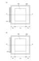
図1乃至図3および図16を参照して、本実施形態に係る電子モジュールについて説明する。図1は本実施形態に係る電子モジュールの平面図であり、図2(a)は図1(a)のA-A’間の断面図であり、図2(b)は図1(b)のB-B’間の断面図である。図3(a)および(b)は図2の拡大図である。図16は従来の電子モジュールの断面図である。 First Embodiment
The electronic module according to this embodiment will be described with reference to Figures 1 to 3 and Figure 16. Figure 1 is a plan view of the electronic module according to this embodiment, Figure 2(a) is a cross-sectional view taken along line A-A' in Figure 1(a), and Figure 2(b) is a cross-sectional view taken along line B-B' in Figure 1(b). Figures 3(a) and (b) are enlarged views of Figure 2. Figure 16 is a cross-sectional view of a conventional electronic module.
第1基板100は、表示領域AAと周辺領域PAを有する。第1基板100は、図1に示されるように、平面視において矩形状を有する。平面視における第1基板100の形状は、正方形であってもよいし、長方形であってもよい。また、それぞれの辺(側面)と辺(側面)との頂点において、ある角部が面取りされていてもよい。また、第1基板100は表示領域AAに発光部を有していてもよい。The
また、第1基板100は電極部101を有していてよい。電極部101は平面視における周辺領域PAの外周に設けられていてもよく、図1(b)に示したように電極部101の少なくとも一部が周辺領域PAと重畳するように設けられていてもよい。電極部101の少なくとも一部が周辺領域PAと重畳するように設けられることで、電子モジュールのサイズをより小さくすることが可能である。特に、電極部101が周辺領域PA上に設けられることで、電子モジュールのサイズをより小さくすることが可能である。The
枠部材200は、図1に示されるように、第1基板100上に配される。具体的には、枠部材200は第1基板100の周辺領域上に配される。平面視において枠部材200は、第1基板100よりも大きな矩形の筒形状を有しており、表示領域を囲むように配される。枠部材200を構成する材料は特に限定されないが、吸光材料であってよい。または、液晶ポリマーであってよい。これらの材料を用いることで、外光による影響を低減することができる。The
図2に示されるように、枠部材200は第1基板100と重畳する重畳部206を有する。重畳部206は、表示領域AAを囲うように配されていてよい。As shown in FIG. 2, the
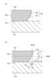
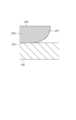
図3に示されるように、枠部材200は、第1基板100に対向する第1面201と、第1面201に対向する第2面202と、第1面201と第2面202に接する内壁側側面207とを有する。具体的には、内壁側側面207は、第1面201と第2面202に接し、かつ、表示領域AA側に配される面である。内壁側側面207は、少なくとも第1面201に接する第1端面203と、第2面202に接する第2端面204とを有する。第1基板100および枠部材200を通る断面図において、本実施形態に係る電子モジュールは、第1端面203および第2端面204が曲面でない実施形態である。3, the
第2面202に対する法線を第1線とする。具体的には、第1基板100および枠部材200を通る断面図において、第2面202と第2端面204とが接する点を通り、第2面202に対する法線を第1線とする。このとき、第1線と第1端面203とがなす角をθ1、第1線と第2端面204とがなす角をθ2とする。図3(b)は、図3(a)を用いてθ1とθ2の関係を示した断面図である。The normal to the
このとき、θ1とθ2はそれぞれ異なる。具体的には、θ1は10°以上であり、20°以上であることが好ましく、23°より大きいことが更に好ましい。また、θ1は50°以下であり、40°以下であることが好ましい。θ2は2°以上であり、3°より大きいことが好ましい。なぜなら、金型と枠部材200との間の摩擦をより抑制することができるため、第2端面204上に発生する突起物をより抑制することができるためである。また、θ2は20°以下であり、10°以下であることが好ましい。なぜなら、枠部材200の強度を維持することができるためである。At this time, θ1 and θ2 are different from each other. Specifically, θ1 is 10° or more, preferably 20° or more, and more preferably greater than 23°. Moreover, θ1 is 50° or less, and preferably 40° or less. θ2 is 2° or more, and preferably greater than 3°. This is because friction between the mold and the
本発明に係る電子モジュールは、第1線と第2端面204とがなす角がθ2となることで、第2端面204上に発生する突起物を低減することができる。したがって、本実施形態に係る電子モジュールは、表示画像の画質の低下を抑制することができる。The electronic module according to the present invention can reduce protrusions that occur on the
ここで、図16を参照して、従来の電子モジュールと本発明に係る電子モジュールを比較する。従来の電子モジュールは、第1線と第2端面204とが角を形成しない。換言すると、第1線と第2端面204が平行である構成である。このような構成を有する場合、枠部材200を形成するとき、金型と枠部材との間で摩擦が生じやすくなる。その結果、第2端面204上に突起物が発生し、発生した突起物が表示領域上に重畳することで、表示画像の画質の低下を引き起こす。Now, referring to FIG. 16, a conventional electronic module will be compared with the electronic module of the present invention. In the conventional electronic module, the first line and the
それに対して、本発明に係る電子モジュールは、第1線と第2端面204とがθ2という角を形成する。換言すると、第1線と第2端面204が平行でない構成である。このような構成を有することで、枠部材200を形成するとき、金型と枠部材との間の摩擦を低減することができる。その結果、第2端面204上の突起物の発生を抑制することができる。In contrast, in the electronic module according to the present invention, the first line and the
以上より、本実施形態に係る電子モジュールは、表示画像の画質の低下を抑制できる。As a result, the electronic module according to this embodiment can suppress degradation of the image quality of the displayed image.
また、本実施形態に係る電子モジュールは、以下の構成を有することが好ましい。In addition, it is preferable that the electronic module according to this embodiment has the following configuration:
第1端面203と第2端面204とが接する点を通り、第2面202に対して平行な線を第2線とする。このとき、第2面202に対して垂直方向における、第1面201と第2線との距離を第1距離d1、第2面202と第2線との距離を第2距離d2とする。第2面202に対して垂直方向における第1面201と第2面202との距離を距離Dとする。図3(b)は、図3(a)を用いて第1距離d1、第2距離d2、および距離Dの関係を示した断面図である。The second line is a line that passes through the point where the
第1距離d1、第2距離d2、および距離Dは、距離Dが最も大きくなる位置で定義してもよく、距離Dが最も小さくなる位置で定義してもよく、それ以外の位置で定義してもよい。例えば、本実施形態に係る電子モジュールであれば、第1面201と第2面202は互いに平行に配されているので、任意の位置で第1距離d1、第2距離d2、および距離Dを定義することができる。The first distance d1, the second distance d2, and the distance D may be defined at the position where the distance D is greatest, or at the position where the distance D is smallest, or at some other position. For example, in the electronic module according to this embodiment, the
このとき、本発明に係る電子モジュールは、第2距離d2が距離Dの10%以上であることが好ましい。なぜなら、第2距離d2が距離Dの10%以上であることで、枠部材200の強度を維持することができるためである。具体的には、第2距離d2は、第1面201と第2面202との距離Dの10%以上90%以下であってよく、20%以上50%以下であることが好ましい。In this case, in the electronic module according to the present invention, it is preferable that the second distance d2 is 10% or more of the distance D. This is because the strength of the
特に、第2距離d2が大きい場合、枠部材200自体の強度の観点から好ましい。また、第1距離d1が大きい場合、表示領域AAからの迷光による乱反射を抑制できるため好ましい。これらの観点について、本発明者らが鋭意検討を行った結果、第2距離d2は第1距離d1以下であることが好ましく、具体的には、第2距離d2が第1距離d1の25%以上50%以下であることが好ましい。In particular, when the second distance d2 is large, this is preferable from the viewpoint of the strength of the
このとき、本実施形態に係る電子モジュールは、枠部材200の強度を維持しながら、表示画像の画質の低下をより抑制できる。In this case, the electronic module according to this embodiment can further suppress deterioration in the image quality of the display image while maintaining the strength of the
(第2実施形態)
図4乃至図6を参照して、第2実施形態に係る電子モジュールについて説明する。図4は本実施形態に係る電子モジュールの平面図であり、図5は図4のC-C’間の断面図であり、図6は図5の拡大図である。 Second Embodiment
An electronic module according to a second embodiment will be described with reference to Fig. 4 to Fig. 6. Fig. 4 is a plan view of the electronic module according to the present embodiment, Fig. 5 is a cross-sectional view taken along the line CC' in Fig. 4, and Fig. 6 is an enlarged view of Fig. 5.
本実施形態に係る電子モジュールは、第1基板100と第2基板300とが結合部材600を介して接していること、第1基板100と第3基板400とが電極部101を介して接続している点、第2基板300の側面、結合部材600の側面、第3基板の側面に接する部材を有する点で、第1実施形態とは異なる。The electronic module according to this embodiment differs from the first embodiment in that the
本実施形態において、第2基板300は表示領域AAと周辺領域PAを有する。また、第1基板100は支持基板であってよく、第2基板300は表示領域AAに発光部を有していてもよい。結合部材600は第1基板100が有する第1主面上に配され、第1基板100と第2基板300は結合部材600を介して接続される。第1基板100が有する第1主面は、枠部材200が有する第1面201に対向する面である。In this embodiment, the
第3基板400は、第1基板100が有する電極部101と接続されている。第3基板400は、Auバンプや異方性導電フィルムや異方性導電ペーストなどを介して、電極部101と接続されていてよい。第3基板400はフレキシブル配線板(FPC)などの配線基板であってよい。The
図6を参照すると、本実施形態に係る電子モジュールは、第1基板100が有する第1主面の少なくとも一部、第2基板300の側面、結合部材600の側面、および第3基板400の端部を覆うように部材500が配されている。その結果、本実施形態に係る電子モジュールは、第1基板100が有する電極部101と第3基板400との接続の信頼性が高くなる。Referring to FIG. 6, in the electronic module according to this embodiment, the
図6において部材500は、第1基板100が有する第1主面の少なくとも一部、第2基板300の側面、結合部材600の側面、および第3基板400の端部を覆うように配されているが、これに限定されるものではない。部材500は、電極部101と第3基板400との接続の信頼性が向上するように配されていればよい。したがって、部材500は、少なくとも第1基板100が有する第1主面の少なくとも一部と、第3基板400の端部を覆うように配されていればよい。より好ましくは、第1基板100が有する第1主面の少なくとも一部、第2基板300の側面、結合部材600の側面、および第3基板400の端部を覆うように配される。その結果、本実施形態に係る電子モジュールは、第1基板100が有する電極部101と第3基板400との接続の信頼性が高くなる。6, the
部材500は補強部材とも呼ばれ、具体的には、アクリル樹脂、エポキシ樹脂、シリコーン樹脂であってよい。補強部材は熱硬化性樹脂、紫外線硬化性樹脂のいずれであってもよいが、紫外線硬化性樹脂であることが好ましい。なぜなら、部材500が熱硬化性樹脂である場合、表示領域AAからの発熱や外部からの太陽光などによって補強部材が温められ、硬化してしまうことがあるからである。The
上記の構成を有することで、本実施形態に係る電子モジュールは、電極部101と第3基板400の接続の信頼性を向上させることができる。By having the above configuration, the electronic module according to this embodiment can improve the reliability of the connection between the
(第3実施形態)
図7を参照して、第3実施形態に係る電子モジュールについて説明する。図7は、本実施形態に係る電子モジュールの断面図である。本実施形態に係る電子モジュールは、内壁側側面207が少なくとも第1端面203、第2端面204、第1端面203と第2端面204に接する第3端面205を有する点で、第1実施形態とは異なる。本実施形態では第3端面205のみを記載しているが、本実施形態に係る電子モジュールは、第1端面203と第2端面204との間に第4端面など、複数の端面を有していてよい。 Third Embodiment
An electronic module according to a third embodiment will be described with reference to Fig. 7. Fig. 7 is a cross-sectional view of the electronic module according to this embodiment. The electronic module according to this embodiment differs from the first embodiment in that the inner
ここで、第2面202に対する法線を第1線とする。具体的には、第1基板100および枠部材200を通る断面図において、第2面202と第2端面204とが接する点を通り、第2面202に対する法線を第1線とする。このとき、第1線と第1端面203とがなす角をθ1、第1線と第2端面204とがなす角をθ2、第1線と第3端面205とがなす角をθ3とする。Here, the normal to the
また、第2端面204と第3端面205とが接する点を通り、第2面202に対して平行な線を第2線、第3端面205と第1端面203とが接する点を通り、第2面202に対して平行な線を第3線とする。このとき、第2面202に対して垂直方向における、第1面201と第3線との距離を第1距離d1、第2面202と第2線との距離を第2距離d2、第2線と第3線との距離を第3距離d3とする。第2面202に対して垂直方向における第1面201と第2面202との距離を距離Dとする。The line that passes through the point where the
第1距離d1、第2距離d2、第3距離d3、および距離Dは、距離Dが最も大きくなる位置で定義してもよく、距離Dが最も小さくなる位置で定義してもよく、それ以外の位置で定義してもよい。例えば、本実施形態に係る電子モジュールであれば、第1面201および第2面202は互いに平行に配されているので、任意の位置で第1距離d1、第2距離d2、第3距離d3、および距離Dを定義することができる。The first distance d1, the second distance d2, the third distance d3, and the distance D may be defined at the position where the distance D is greatest, or at the position where the distance D is smallest, or at any other position. For example, in the electronic module according to this embodiment, the
ここで、図7(d)は、図7(a)を用いてθ1、θ2、θ3、第1距離d1、第2距離d2、第3距離d3の関係を示した図である。Here, FIG. 7(d) is a diagram showing the relationship between θ1, θ2, θ3, the first distance d1, the second distance d2, and the third distance d3 using FIG. 7(a).
このとき、θ1とθ2とθ3は、それぞれ角度が異なる。例えば、θ1は2°以上10°以下であり、θ2はθ1より大きく89°以下であり、θ3は0°より大きく89°以下である。In this case, θ1, θ2, and θ3 are all different angles. For example, θ1 is between 2° and 10°, θ2 is greater than θ1 and less than 89°, and θ3 is greater than 0° and less than 89°.
また、第1距離d1は距離Dの7%以上50%以下であり、10%以上50%以下であることが好ましく、20%以上50%以下であることが更に好ましい。第2距離d2は距離Dの10%以上70%以下であり、10%以上50%以下であることが好ましい。第3距離d3は距離Dの0%以上70%以下であり、0%以上50%以下であることが好ましい。また、第1距離d1が第2距離d2および第3距離d3より大きい場合、枠部材200の強度がより向上するため、好ましい。The first distance d1 is 7% to 50% of the distance D, preferably 10% to 50%, and more preferably 20% to 50%. The second distance d2 is 10% to 70% of the distance D, preferably 10% to 50%. The third distance d3 is 0% to 70% of the distance D, preferably 0% to 50%. It is also preferable that the first distance d1 is greater than the second distance d2 and the third distance d3, since this further improves the strength of the
図7(a)は、θ1、θ3、θ2の順に角度が大きい構成である。このような構成を有することで、本実施形態に係る電子モジュールは、枠部材200の強度を保ちながら、枠部材200を形成する材料を減らすことができる。その結果、本実施形態に係る電子モジュールは、高強度かつ低コストである。Figure 7(a) shows a configuration in which the angles are larger in the order of θ1, θ3, and θ2. With this configuration, the electronic module according to this embodiment can reduce the material used to form the
また、図7(a)において、θ1は20°以上であり、50°以上であることが好ましい。また、θ1は80°以下であり、70°以下であることが好ましい。θ2は2°以上であり、3°より大きいことが好ましい。また、θ2は20°以下であり、10°以下であることが好ましい。θ3は、10°以上であり、20°以上であることが好ましい。また、θ3は60°以下であり、40°以下であることが好ましい。In FIG. 7(a), θ1 is 20° or more, and preferably 50° or more. θ1 is 80° or less, and preferably 70° or less. θ2 is 2° or more, and preferably greater than 3°. θ2 is 20° or less, and preferably 10° or less. θ3 is 10° or more, and preferably 20° or more. θ3 is 60° or less, and preferably 40° or less.
図7(b)は、θ3、θ1、θ2の順に角度が大きい構成である。このような構成を有することで、本実施形態に係る電子モジュールは、枠部材200を形成する材料を、より抑制することができる。そのため、本実施形態に係る電子モジュールは、より低コストで得ることができる。Figure 7(b) shows a configuration in which the angles are larger in the order of θ3, θ1, and θ2. With this configuration, the electronic module according to this embodiment can further reduce the amount of material used to form the
また、図7(b)において、θ1は10°以上であり、20°以上であることが好ましい。また、θ1は、50°以下であり、40°以下であることが好ましい。θ2は2°以上であり、3°より大きいことが好ましい。また、θ2は、20°以下であり、10°以下であることが好ましい。θ3は20°以上であり、40°以上であることが好ましい。また、θ3は、80°以下であり、70°以下であることが好ましい。In FIG. 7(b), θ1 is 10° or more, and preferably 20° or more. θ1 is 50° or less, and preferably 40° or less. θ2 is 2° or more, and preferably greater than 3°. θ2 is 20° or more, and preferably 10° or less. θ3 is 20° or more, and preferably 40° or more. θ3 is 80° or less, and preferably 70° or less.
図7(c)は、θ3、θ2、θ1の順に角度が大きい構成である。このような構成を有することで、本実施形態に係る電子モジュールは、枠部材200を形成する材料を、より抑制することができる。そのため、本実施形態に係る電子モジュールは、より低コストで得ることができる。Figure 7(c) shows a configuration in which the angles are larger in the order of θ3, θ2, and θ1. With this configuration, the electronic module according to this embodiment can further reduce the amount of material used to form the
また、図7(c)において、θ1は例えば0°であってよい。θ1が0°であるとき、第1端面203は第2面202に対して垂直であるため、第1端面203上に突起物が形成されることがある。しかし、本実施形態に係る電子モジュールは、第1端面203が、第2端面204および第3端面205よりも周辺領域PA側に配されるため、第1端面203上に突起物が発生しても、表示画像の画質へ及ぼす影響は小さい。そのため、本実施形態に係る電子モジュールは、表示画像の画質の低下を抑制しながら、低コストで得ることができる。In addition, in FIG. 7(c), θ1 may be, for example, 0°. When θ1 is 0°, the
また、θ2は2°以上であり、3°より大きいことが好ましい。また、θ2は20°以下であり、10°以下であることが好ましい。θ3は80°以上90°以下であってよく、例えば90°であってよい。In addition, θ2 is 2° or more, and preferably greater than 3°. In addition, θ2 is 20° or less, and preferably 10° or less. θ3 may be 80° or more and 90° or less, for example, 90°.
以上より、本実施形態に係る電子モジュールは、表示画像の画質の低下を抑制しながら、低コスト化ができる電子モジュールである。As a result, the electronic module according to this embodiment is an electronic module that can reduce costs while suppressing degradation of the quality of the displayed image.
(第4実施形態)
図8を参照して、第4実施形態に係る電子モジュールについて説明する。図8は、本実施形態に係る電子モジュールの断面図である。本実施形態に係る電子モジュールは、第1基板100および枠部材200を通る断面図において、内壁側側面207が曲面である点で、第1実施形態とは異なる。 Fourth Embodiment
An electronic module according to a fourth embodiment will be described with reference to Fig. 8. Fig. 8 is a cross-sectional view of the electronic module according to this embodiment. The electronic module according to this embodiment differs from the first embodiment in that, in a cross-sectional view passing through the
本実施形態に係る電子モジュールは、内壁側側面207が曲面である。換言すると、端面同士が角部を形成しない電子モジュールである。本実施形態に係る電子モジュールであっても、枠部材200を形成するとき、金型と枠部材との間の摩擦を低減することができる。その結果、内壁側側面207上の突起物の発生を抑制することができるため、画像の画質の低下を抑制できる。The electronic module according to this embodiment has a curved inner
また、本実施形態に係る電子モジュールは、上述したように端面同士が角部を形成しない。そのため、本実施形態に係る電子モジュールは、枠部材200を構成する材料がより充填されやすい。そのため、上述した他の実施形態に比べて、枠部材200内で生じる気泡の発生を抑制することができる。そのため、枠部材200内の気泡によって、表示領域AAからの迷光が乱反射することを抑制できる。In addition, as described above, the end faces of the electronic module according to this embodiment do not form corners. Therefore, the electronic module according to this embodiment is more easily filled with the material that constitutes the
以上より、本実施形態に係る電子モジュールは、表示画像の画質の低下をより抑制することができる。As a result, the electronic module according to this embodiment can further suppress deterioration in the quality of the displayed image.
(第5実施形態)
図9を参照して、第5実施形態に係る電子モジュールについて説明する。図9は本実施形態に係る電子モジュールの断面図である。 Fifth Embodiment
An electronic module according to a fifth embodiment will be described with reference to Fig. 9. Fig. 9 is a cross-sectional view of the electronic module according to this embodiment.
図9(a)は、第1基板100に対向する透光板700を有する点で、第1実施形態とは異なる。図9(a)に記載の電子ビューファインダは、第1基板100に対向する透光板700を有することで、外部から表示領域AAへの異物の混入を抑制することができる。そのため、本実施形態に係る電子ビューファインダは、異物の混入による表示画像の画質の低下を抑制することができる。図9(b)についても同様である。Figure 9(a) differs from the first embodiment in that it has a light-transmitting
また、本実施形態に係る電子ビューファインダは、透光板700の代わりに、第1基板100に対向する光学部材を有していてもよい。光学部材は、図9(a)および図9(b)において、透光板700よりも第1基板100に対して上側に配されてよい。具体的には、図9(a)および図9(b)において、透光板700よりも観察者側に配されてよい。光学部材は、具体的に、レンズやプリズムである。透光板700の代わりに、第1基板100に対向する光学部材を設けることでも、異物の混入を抑制することができる。そのため、異物の混入による表示画像の画質の低下を抑制することができる。The electronic viewfinder according to this embodiment may have an optical member facing the
また、本実施形態に係る電子ビューファインダは、透光板700と光学部材とを同時に有していてもよい。このような構成を有することで、透光板700が異物の混入を抑制し、光学部材が外光による表示画像の画質の低下を抑制することができる。The electronic viewfinder according to this embodiment may also have both the light-transmitting
(応用例)
以下、図10乃至図15を参照して、本発明に係る電子モジュールを用いた表示装置、撮像装置、電子機器、ウェアラブルデバイス、画像形成装置について説明する。 (Application example)
Hereinafter, a display device, an imaging device, an electronic device, a wearable device, and an image forming device using an electronic module according to the present invention will be described with reference to FIGS.
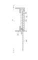
図10は、本実施形態に係る表示装置の一例を示す模式図である。表示装置1000は、上部カバー1001と下部カバー1009との間に、タッチパネル1003、表示パネル1005、フレーム1006、回路基板1007、バッテリー1008を有してよい。タッチパネル1003および表示パネル1005には、それぞれフレキシブルプリント回路FPC1002、1004が接続されている。表示パネル1005は、本発明に係る電子モジュールを有していてよい。回路基板1007には、トランジスタがプリントされている。バッテリー1008は、表示装置が携帯機器でなければ、設けなくてもよいし、携帯機器であっても、別の位置に設けてもよい。Figure 10 is a schematic diagram showing an example of a display device according to this embodiment. The
本実施形態に係る表示装置は、赤色、緑色、青色を有するカラーフィルタを有してよい。カラーフィルタは、当該赤色、緑色、青色がデルタ配列で配置されてよい。The display device according to this embodiment may have a color filter having red, green, and blue colors. The color filters may be arranged such that the red, green, and blue colors are arranged in a delta arrangement.
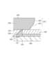
本実施形態に係る表示装置は、光を受光する撮像素子を有する撮像装置の表示部に用いられてよい。撮像装置は、撮像素子が取得した情報を表示する表示部を有してよい。また、表示部は、撮像装置の外部に露出した表示部であっても、ファインダ内に配置された表示部であってもよい。撮像装置は、デジタルカメラ、デジタルビデオカメラであってよい。The display device according to this embodiment may be used in the display section of an imaging device having an imaging element that receives light. The imaging device may have a display section that displays information acquired by the imaging element. The display section may be a display section that is exposed to the outside of the imaging device, or a display section that is arranged within the viewfinder. The imaging device may be a digital camera or a digital video camera.
図11(a)は、本実施形態に係る撮像装置の一例を示す模式図である。撮像装置1100は、ビューファインダ1101、背面ディスプレイ1102、操作部1103、筐体1104を有してよい。ビューファインダ1101および背面ディスプレイ1102は、本発明に係る電子モジュールを有してよい。その場合、表示装置は、撮像する画像のみならず、環境情報、撮像指示等を表示してよい。環境情報には、外光の強度、外光の向き、被写体の動く速度、被写体が遮蔽物に遮蔽される可能性等であってよい。Figure 11 (a) is a schematic diagram showing an example of an imaging device according to this embodiment. The
撮像装置1100は、不図示の光学部を更に有してよい。光学部が有するレンズは、単数であっても、複数であってもよく、筐体1104内に収容されている撮像素子に結像する。複数のレンズは、その相対位置を調整することで、焦点を調整することができる。この操作を自動で行うこともできる。撮像装置は光電変換装置と呼ばれてもよい。光電変換装置は逐次撮像するのではなく、前画像からの差分を検出する方法、常に記録されている画像から切り出す方法等を撮像の方法として含むことができる。The
図11(b)は、本実施形態に係る電子機器の一例を表す模式図である。電子機器1200は、表示部1201と、操作部1202と、筐体1203とを有する。筐体1203は、回路、当該回路を有するプリント基板、バッテリー、通信部を有してよい。操作部1202はボタンであってもよく、タッチパネル方式の反応部であってもよい。操作部1202は、指紋を認識してロックの解除等を行う、生体認識部であってもよい。通信部を有する電子機器は、通信機器ということもできる。電子機器は、レンズと、撮像素子とを備えることで、カメラ機能をさらに有してよい。カメラ機能により撮像された画像が表示部1201に表示される。電子機器としては、スマートフォン、ノートパソコン等があげられる。FIG. 11B is a schematic diagram showing an example of an electronic device according to this embodiment. The
図12は、本実施形態に係る表示装置の一例を表す模式図である。図12(a)は、テレビモニタやPCモニタ等の表示装置である。表示装置1300は、筐体1301と、表示部1302とを有する。表示部1302には、本発明に係る有機デバイスが用いられてよい。Figure 12 is a schematic diagram showing an example of a display device according to this embodiment. Figure 12(a) shows a display device such as a television monitor or a PC monitor. The
表示装置1300は、筐体1301と表示部1302とを支える土台1303をさらに有してもよい。土台1303は、図12(a)の形態に限定されない。筐体1301の下辺が土台を兼ねてもよい。The
また、筐体1301および表示部1302は、曲がっていてもよい。その曲率半径は、5000mm以上6000mm以下であってよい。The
図12(b)は、本実施形態に係る表示装置の他の例を表す模式図である。図12(b)の表示装置1310は、折り曲げ可能に構成されており、いわゆるフォルダブルな表示装置である。表示装置1310は、第一表示部1311、第二表示部1312、筐体1313、屈曲点1314を有する。第一表示部1311と第二表示部は、本発明に係る有機デバイスを有してよい。第一表示部1311と第二表示部1312とは、つなぎ目のない1枚の表示装置であってよい。第一表示部1311と第二表示部1312とは、屈曲点で分けることができる。第一表示部1311、第二表示部1312は、それぞれ異なる画像を表示してもよいし、第一表示部1311および第二表示部1312とで1つの画像を表示してもよい。FIG. 12(b) is a schematic diagram showing another example of the display device according to the present embodiment. The
図13(a)は、本実施形態に係る照明装置の一例を表す模式図である。照明装置1400は、筐体1401と、光源1402と、回路基板1403とを有してよい。光源1402は、本発明に係る電子モジュールを有していてよい。照明装置1400は、光源の演色性を向上させるために、光学フィルム1404を有してよい。また、照明装置1400は、光源の光を効果的に拡散するために、光拡散部1405を有してよい。照明装置1400が光拡散部1405を有することで、広い範囲に光を届けることができる。光学フィルム1404および光拡散部1405は、照明の光出射側に設けられてよい。必要に応じて、最外部にカバーを設けてもよい。FIG. 13(a) is a schematic diagram showing an example of a lighting device according to the present embodiment. The
照明装置は、例えば、室内を照明する装置である。照明装置は白色、昼白色、その他青から赤のいずれの色を発光するものであってよい。それらを調光する調光回路を有してよい。照明装置は、電源回路を有してよい。電源回路は、交流電圧から直流電圧に変換する回路であってよい。また、白とは、色温度が4200Kで、昼白色とは、色温度が5000Kである。照明装置はカラーフィルタを有してもよい。The lighting device is, for example, a device that illuminates a room. The lighting device may emit white light, daylight white light, or any other color from blue to red. It may have a dimming circuit that adjusts the light intensity. The lighting device may have a power supply circuit. The power supply circuit may be a circuit that converts AC voltage to DC voltage. Furthermore, white has a color temperature of 4200K, and daylight white has a color temperature of 5000K. The lighting device may have a color filter.
また、本実施形態に係る照明装置は、放熱部を有していてもよい。放熱部は装置内の熱を装置外へ放出するものであり、熱伝導率の大きな金属、セラミックからなる。The lighting device according to this embodiment may also have a heat dissipation section. The heat dissipation section dissipates heat from within the device to the outside, and is made of metal or ceramic with high thermal conductivity.
図13(b)は、本実施形態に係る移動体の一例である自動車の模式図である。当該自動車は灯具の一例であるテールランプを有する。自動車1500は、テールランプ1501を有し、ブレーキ操作等を行った際に、テールランプが点灯する携帯であってよい。自動車1500は、車体1503、それに取り付けられている窓1502を有してよい。Figure 13(b) is a schematic diagram of an automobile, which is an example of a moving body according to this embodiment. The automobile has tail lamps, which are an example of a lamp. The
テールランプ1501は、本発明に係る電子モジュールを有してよい。テールランプは、光源を保護する保護部材を有してよい。保護部材はある程度高い強度を有し、透明であれば材料は問わないが、ポリカーボネート等で構成されることが好ましい。ポリカーボネートにフランジカルボン酸誘導体、アクリロニトリル誘導体等を混ぜてよい。The
本実施形態に係る移動体は、自動車、船舶、航空機、ドローン等であってよい。移動体は、機体と当該機体に設けられた灯具を有してよい。灯具は、機体の位置を知られるために発光していてもよい。The moving body according to this embodiment may be an automobile, a ship, an aircraft, a drone, etc. The moving body may have a body and a lamp provided on the body. The lamp may emit light to indicate the position of the body.
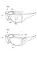
電子機器あるいは表示装置は、例えば、スマートグラス、ヘッドマウントディスプレイ、スマートコンタクトのようなウェアラブルデバイスとして装着可能なシステムに適用できる。電子機器は、可視光を光電変換可能な撮像装置と、可視光を発光可能な表示装置とを有してもよい。The electronic device or display device can be applied to a system that can be attached as a wearable device such as smart glasses, a head-mounted display, or smart contacts. The electronic device may have an imaging device capable of photoelectric conversion of visible light, and a display device capable of emitting visible light.
図14は、本実施形態に係るウェアラブルデバイス(スマートグラス)の一例を表す模式図である。図14(a)を用いて、眼鏡1600(スマートグラス)を説明する。眼鏡1600は、レンズ1601の裏面側に、表示部を有する。当該表示部は、本発明に係る電子モジュールを有していてもよい。更に、レンズ1601の表面側に、CMOSセンサやSPADのような撮像装置1602が設けられていてもよい。Figure 14 is a schematic diagram showing an example of a wearable device (smart glasses) according to this embodiment. Glasses 1600 (smart glasses) will be described using Figure 14 (a).
眼鏡1600は、制御装置1603をさらに備える。制御装置1603は、撮像装置1602と表示部に電力を供給する電源として機能する。また、制御装置1603は、撮像装置1602と表示部の動作を制御する。レンズ1601には、撮像装置1602や表示部の光を集光するための光学系が形成されている。The
図14(b)を用いて、眼鏡1610(スマートグラス)を説明する。眼鏡1610は、制御装置1612を有しており、制御装置1612に、本発明に係る電子モジュールを有する表示装置が設けられている。制御装置1612は、撮像装置1602に相当する撮像装置をさらに有していてもよい。レンズ1611には、制御装置1612からの発光を投影するための光学系が形成されており、レンズ1611には画像が投影される。制御装置1612は、撮像装置および表示装置に電力を供給する電源として機能するとともに、撮像装置および表示装置の動作を制御する。制御装置は、装着車の視線を検知する視線検知部を有してもよい。視線の検知は、赤外線を用いてよい。赤外線発光部は、表示画像を注視しているユーザーの眼球に対して赤外線を発光する。発せられた赤外光のうち、眼球からの反射光を、受光素子を有する撮像部が検出することで眼球の撮像画像が得られる。平面視における赤外発光部から表示部への光を低減する低減手段を有することで、画像品位の低下を低減する。The glasses 1610 (smart glasses) will be described with reference to FIG. 14(b). The
赤外光の撮像により得られた眼球の撮像画像から、制御装置1612は表示画像に対するユーザーの視線を検出する。眼球の撮像画像を用いた視線検出には、任意の公知の手法が適用できる。一例として、角膜での照射光の反射によるプルキニエ像に基づき視線検出方法を用いることができる。The
より具体的には、瞳孔角膜反射法に基づく視線検出処理が行われる。瞳孔角膜反射法を用いて、眼球の撮像画像に含まれる瞳孔の像とプルキニエ像とに基づいて、眼球の向き(回転角度)を表す視線ベクトルが産出されることにより、ユーザーの視線が検出される。More specifically, gaze detection processing is performed based on the pupil-corneal reflex method. Using the pupil-corneal reflex method, a gaze vector that represents the direction (rotation angle) of the eyeball is generated based on the pupil image and Purkinje image contained in the captured image of the eyeball, thereby detecting the user's gaze.
本発明の一実施形態に係るウェアラブルデバイスは、受光素子を有する撮像装置を有し、撮像装置からのユーザーの視線情報に基づいて表示装置の表示画像を制御してよい。A wearable device according to one embodiment of the present invention may have an imaging device with a light receiving element, and may control the image displayed on the display device based on the user's line of sight information from the imaging device.
具体的には、表示装置は視線情報に基づいて、ユーザーが注視する第一の視界領域と、第一の視界領域以外の第二の視界領域とを決定する。第一の視界領域、第二の視界領域は、表示装置の制御装置が決定してもよいし、外部の制御装置が決定したものを受信してもよい。表示装置の表示領域において、第一の視界領域の表示解像度を、第二の視界領域の表示解像度よりも高く制御してよい。つまり、第二の視界領域の解像度を第一の視界領域よりも低くしてよい。Specifically, the display device determines a first field of view area on which the user gazes and a second field of view area other than the first field of view area based on the line of sight information. The first field of view area and the second field of view area may be determined by a control device of the display device, or may be received from an external control device. In the display area of the display device, the display resolution of the first field of view area may be controlled to be higher than the display resolution of the second field of view area. In other words, the resolution of the second field of view area may be lower than the first field of view area.
なお、第一の表示領域や優先度が高い表示領域の決定には、AIを用いてもよい。AIは、眼球の画像と当該画像の眼球が実際に視ていた方向とを教師データとして、眼球の画像から視線の角度、視線の先の目的物までの距離を推定するよう構成されたモデルであってよい。AIは、表示装置が有してもよいし、撮像装置が有してもよいし、外部装置有してもよい。外部装置がAIを有する場合は、外部を撮像する撮像装置を更に有するスマートグラスに好ましく適用できる。スマートグラスは、撮像した外部情報をリアルタイムで表示することができる。AI may be used to determine the first display area or the display area with high priority. The AI may be a model configured to estimate the angle of the line of sight and the distance to an object in the line of sight from the image of the eyeball, using as teacher data an image of the eyeball and the direction in which the eyeball in the image was actually looking. The AI may be included in the display device, the imaging device, or an external device. When the external device includes AI, it is preferably applicable to smart glasses that further include an imaging device that captures images of the outside. The smart glasses can display captured external information in real time.
図15(a)は、本実施形態に係る画像形成装置の一例を示す模式図である。画像形成装置40は電子写真方式の画像形成装置であり、感光体27、露光光源28、帯電部30、現像部31、転写器32、搬送ローラー33、定着器35を有する。露光光源28から光29が照射され、感光体27の表面に静電潜像が形成される。この露光光源28が本発明に係る電子モジュールを有してよい。現像部31はトナー等を有する。帯電部30は感光体27を帯電させる。転写器32は現像された画像を記録媒体34に転写する。搬送ローラー33は記録媒体34を搬送する。記録媒体34は例えば紙である。定着器35は記録媒体34に形成された画像を定着させる。Figure 15 (a) is a schematic diagram showing an example of an image forming apparatus according to this embodiment. The
図15(b)および図15(c)は、露光光源28を示す図であり、発光部36が長尺状の基板に複数配置されている様子を示す模式図である。矢印37は有機発光素子が配列されている列方向を表わす。この列方向は、感光体27が回転する軸の方向と同じである。この方向は感光体27の長軸方向と呼ぶこともできる。図15(b)は発光部36を感光体27の長軸方向に沿って配置した形態である。図15(c)は、図15(b)とは異なる形態であり、第一の列と第二の列のそれぞれにおいて発光部36が列方向に交互に配置されている形態である。第一の列と第二の列は行方向に異なる位置に配置されている。第一の列は、複数の発光部36が間隔をあけて配置されている。第二の列は、第一の列の発光部36同士の間隔に対応する位置に発光部36を有する。すなわち、行方向にも、複数の発光部36が間隔をあけて配置されている。図15(c)の配置は、たとえば格子状に配置されている状態、千鳥格子に配置されている状態、あるいは市松模様と言い換えることもできる。Figures 15(b) and 15(c) are diagrams showing an
以下、実施例を用いて、本発明を詳細に説明する。The present invention will now be described in detail with reference to examples.
液晶ポリマーであるUA201(上野製薬株式会社製)を用いて、枠部材を形成した。不良発生率は、複数の枠部材に対して、表示画像の画質が低下するほどの突起物が枠部材の第2端面上に発生した割合を示す。The frame members were formed using UA201 (manufactured by Ueno Pharmaceutical Co., Ltd.), a liquid crystal polymer. The defect rate indicates the percentage of multiple frame members in which protrusions occurred on the second end surface of the frame member that were so large that the quality of the displayed image was degraded.

表1より、θ2に一定の角度を設けることで、不良発生率を低減することができる。From Table 1, we can see that by setting a certain angle for θ2, the defect rate can be reduced.
以上より、本発明に係る電子モジュールは、表示画像の画質の低下を抑制することができる。さらに、本発明は上述の実施形態に限定されないことはいまでもなく、本発明の要旨を逸脱しない範囲で、上述した実施形態は適宜変更、組み合わせが可能である。As described above, the electronic module according to the present invention can suppress deterioration in the quality of the displayed image. Furthermore, the present invention is not limited to the above-described embodiments, and the above-described embodiments can be modified and combined as appropriate without departing from the gist of the present invention.
また、本発明は以下の構成を有することができる。The present invention can also have the following configuration:
(構成1)
第1基板と、前記第1基板上に配された枠部材とを有する電子モジュールであって、
前記枠部材は、前記第1基板と対向する第1面と、前記第1面と反対側に配される第2面と、前記第1面と前記第2面に接する内壁側側面とを有し、
前記内壁側側面は少なくとも前記第1面に接する第1端面と、前記第2面に接する第2端面とを有し、
前記第2面に対する法線を第1線、前記第1端面と前記第2端面とが接する点を通り、前記第2面に対して平行な線を第2線とすると、
前記第1線と前記第1端面とがなす角と、前記第1線と前記第2端面とがなす角はそれぞれ異なり、
前記第2面に対して垂直方向における、前記第2面と前記第2線との距離は、前記第1面と前記第2面との距離の10%以上であることを特徴とする電子モジュール。 (Configuration 1)
An electronic module having a first substrate and a frame member disposed on the first substrate,
the frame member has a first surface facing the first substrate, a second surface disposed on an opposite side to the first surface, and an inner wall side surface in contact with the first surface and the second surface;
the inner wall side surface has at least a first end surface in contact with the first surface and a second end surface in contact with the second surface,
If a normal line to the second surface is defined as a first line, and a line that passes through a point where the first end surface and the second end surface are in contact and is parallel to the second surface is defined as a second line,
an angle between the first line and the first end surface and an angle between the first line and the second end surface are different from each other;
An electronic module, characterized in that a distance between the second surface and the second line in a direction perpendicular to the second surface is 10% or more of a distance between the first surface and the second surface.
(構成2)
前記第2面と前記第2線との距離は、前記第1面と前記第2面との距離の20%以上50%以下であることを特徴とする構成1に記載の電子モジュール。 (Configuration 2)
The electronic module described in
(構成3)
前記第1基板および前記枠部材を通る断面図において、前記第1端面および前記第2端面は、曲面でないことを特徴とする構成1または2に記載の電子モジュール。 (Configuration 3)
3. The electronic module according to
(構成4)
前記第1線と前記第1端面とがなす角が、20°以上40°以下であり、前記第1線と前記第2端面とがなす角が2°以上10°以下であることを特徴とする構成1乃至3のいずれか一項に記載の電子モジュール。 (Configuration 4)
An electronic module described in any one of
(構成5)
前記第1基板は表示領域と周辺領域とを有し、
前記枠部材は前記第1基板と重畳する重畳部を有し、
前記重畳部は、前記表示領域を囲うように配されていることを特徴とする構成1乃至4のいずれか一項に記載の電子モジュール。 (Configuration 5)
the first substrate has a display area and a peripheral area;
the frame member has an overlapping portion that overlaps with the first substrate,
5. The electronic module according to any one of
(構成6)
前記第1基板は、前記第1面と対向する第1主面と、前記第1主面上に結合部材とを有し、
前記第1基板は、前記結合部材を介して第2基板と接することを特徴とする構成1乃至5のいずれか一項に記載の電子モジュール。 (Configuration 6)
the first substrate has a first main surface opposite to the first surface and a bonding member on the first main surface;
6. The electronic module according to any one of
(構成7)
前記第1基板は表示領域と電極部を有する周辺領域を有し、前記第1基板は前記電極部を介して第3基板と接続することを特徴とする構成1乃至6のいずれか一項に記載の電子モジュール。 (Configuration 7)
The electronic module according to any one of
(構成8)
前記電極部は前記枠部材と重畳しないことを特徴とする構成7に記載の電子モジュール。 (Configuration 8)
The electronic module according to configuration 7, wherein the electrode portion does not overlap with the frame member.
(構成9)
前記電極部は前記枠部材と少なくとも一部が重畳することを特徴とする構成7に記載の電子モジュール。 (Configuration 9)
The electronic module according to configuration 7, wherein the electrode portion at least partially overlaps with the frame member.
(構成10)
前記第1基板は、前記第1面と対向する第1主面と、電極部とを有し、
前記第1基板は、前記電極部を介して第3基板と接しており、
前記電子モジュールは、少なくとも前記第1主面の少なくとも一部と前記第3基板の端部を覆うように配される部材を有することを特徴とする構成1乃至9のいずれか一項に記載の電子モジュール。 (Configuration 10)
the first substrate has a first main surface opposite to the first surface and an electrode portion;
the first substrate is in contact with a third substrate via the electrode portion,
The electronic module according to any one of
(構成11)
前記枠部材は、液晶ポリマーからなることを特徴とする構成1乃至10のいずれか一項に記載の電子モジュール。 (Configuration 11)
11. The electronic module according to any one of
(構成12)
第1基板と、前記第1基板上に配された枠部材とを有する電子モジュールであって、
前記枠部材は、前記第1基板と対向する第1面と、前記第1面と反対側に配される第2面と、前記第1面と前記第2面に接する内壁側側面とを有し、
前記内壁側側面は少なくとも前記第1面に接する第1端面と、前記第2面に接する第2端面と、前記第1端面と前記第2端面に接する第3端面を有し、
前記第2面に対する法線を第1線とすると、
前記第1線と前記第1端面とがなす角と、前記第1線と前記第2端面とがなす角と、前記第1線と前記第3端面とがなす角はそれぞれ異なることを特徴とする電子モジュール。 (Configuration 12)
An electronic module having a first substrate and a frame member disposed on the first substrate,
the frame member has a first surface facing the first substrate, a second surface disposed on an opposite side to the first surface, and an inner wall side surface in contact with the first surface and the second surface;
the inner wall side surface has at least a first end surface in contact with the first surface, a second end surface in contact with the second surface, and a third end surface in contact with the first end surface and the second end surface,
If the normal to the second surface is defined as the first line,
an angle between the first line and the first end face, an angle between the first line and the second end face, and an angle between the first line and the third end face are different from each other.
(構成13)
第1基板と、前記第1基板上に配された枠部材とを有する電子モジュールであって、
前記枠部材は、前記第1基板と対向する第1面と、前記第1面と反対側に配される第2面と、前記第1面と前記第2面に接する内壁側側面とを有し、
前記内壁側側面は少なくとも前記第1面に接する第1端面と、前記第2面に接する第2端面とを有し、
前記第2面に対する法線を第1線とすると、
前記第1線と前記第2端面とがなす角度が3°より大きいことを特徴とする電子モジュール。 (Configuration 13)
An electronic module having a first substrate and a frame member disposed on the first substrate,
the frame member has a first surface facing the first substrate, a second surface disposed on an opposite side to the first surface, and an inner wall side surface in contact with the first surface and the second surface;
the inner wall side surface has at least a first end surface in contact with the first surface and a second end surface in contact with the second surface,
If the normal to the second surface is defined as the first line,
An electronic module, wherein an angle between the first line and the second end face is greater than 3°.
(構成14)
前記第1線と前記第2端面とがなす角度が10°以下であることを特徴とする構成13に記載の電子モジュール。 (Configuration 14)
14. The electronic module of configuration 13, wherein the angle between the first line and the second end face is less than or equal to 10 degrees.
(構成15)
第1基板と、前記第1基板上に配された枠部材とを有する電子モジュールであって、
前記枠部材は、前記第1基板と対向する第1面と、前記第1面と反対側に配される第2面と、前記第1面と前記第2面にする内壁側側面とを有し、
前記内壁側側面は少なくとも前記第1面に接する第1端面と、前記第2面に接する第2端面とを有し、
前記第2面に対する法線を第1線とすると、
前記第1線と前記第1端面とがなす角度が23°より大きいことを特徴とする電子モジュール。 (Configuration 15)
An electronic module having a first substrate and a frame member disposed on the first substrate,
the frame member has a first surface facing the first substrate, a second surface disposed on an opposite side to the first surface, and an inner wall side surface between the first surface and the second surface,
the inner wall side surface has at least a first end surface in contact with the first surface and a second end surface in contact with the second surface,
If the normal to the second surface is defined as the first line,
An electronic module, wherein an angle between the first line and the first end face is greater than 23°.
(構成16)
前記第1線と前記第2端面とがなす角度が40°以下であることを特徴とする構成15に記載の電子モジュール。 (Configuration 16)
16. The electronic module of configuration 15, wherein the angle between the first line and the second end face is less than or equal to 40 degrees.
(構成17)
第1基板と、前記第1基板上に配された枠部材とを有する電子モジュールであって、
前記枠部材は、前記第1基板と対向する第1面と、前記第1面と反対側に配される第2面と、前記第1面と前記第2面に接する内壁側側面とを有し、
前記第1基板および前記枠部材を通る断面図において、前記内壁側側面は曲面であることを特徴とする電子モジュール。 (Configuration 17)
An electronic module having a first substrate and a frame member disposed on the first substrate,
the frame member has a first surface facing the first substrate, a second surface disposed on an opposite side to the first surface, and an inner wall side surface in contact with the first surface and the second surface;
An electronic module, characterized in that, in a cross-sectional view passing through the first substrate and the frame member, the inner wall side surface is a curved surface.
(構成18)
前記第1基板に対向する透光板を有することを特徴とする構成1乃至17のいずれか一項に記載の電子モジュール。 (Configuration 18)
18. The electronic module of any one of
(構成19)
前記第1基板に対向する光学部材を有することを特徴とする構成1乃至18のいずれか一項に記載の電子モジュール。 (Configuration 19)
19. The electronic module of any one of
(構成20)
光を受光する撮像素子と、前記撮像素子が撮像した画像を表示する表示部と、を有し、
構成1乃至19のいずれか一項に記載の電子モジュールが前記表示部であることを特徴とする撮像装置。 (Configuration 20)
An imaging element that receives light, and a display unit that displays an image captured by the imaging element,
20. An imaging device, wherein the electronic module according to any one of
(構成21)
構成1乃至19のいずれか一項に記載の電子モジュールを有する表示部と、前記表示部が設けられた筐体と、を有することを特徴とする表示装置。 (Configuration 21)
20. A display device comprising: a display unit having the electronic module according to any one of
(構成22)
構成1乃至19のいずれか一項に記載の電子モジュールを有する表示部と、前記表示部が設けられた筐体と、前記筐体に設けられ、外部と通信する通信部を有することを特徴とする電子機器。 (Configuration 22)
20. An electronic device comprising: a display unit having an electronic module according to any one of
(構成23)
構成1乃至19のいずれか一項に記載の電子モジュールを有する光源と、前記光源が設けられた筐体と、を有することを特徴とする照明装置。 (Configuration 23)
20. A lighting device comprising: a light source having the electronic module according to any one of
(構成24)
構成1乃至19のいずれか一項に記載の電子モジュールを有する灯具と、前記灯具が設けられた機体と、を有することを特徴とする移動体。 (Configuration 24)
20. A moving body comprising: a lamp having an electronic module according to any one of
(構成25)
請求項1乃至19のいずれか一項に記載の電子モジュールを有する表示部と、前記表示部の光を集光する光学系と、前記表示部の動作を制御する制御装置と、を有することを特徴とするウェアラブルデバイス。 (Configuration 25)
A wearable device comprising: a display unit having an electronic module according to any one of
(構成26)
感光体と、前記感光体を露光する露光光源と、を有し、
前記露光光源は、構成1乃至19のいずれか一項に記載の電子モジュールを有することを特徴とする画像形成装置。 (Configuration 26)
A photoconductor and an exposure light source for exposing the photoconductor,
20. An image forming apparatus, wherein the exposure light source has the electronic module according to any one of
10 電子モジュール
100 第1基板
200 枠部材
201 第1面
202 第2面
203 第1端面
204 第2端面
207 内壁側側面
300 第2基板
400 第3基板
500 部材
600 結合部材
700 透光板 REFERENCE SIGNS
Claims (20)
Translated fromJapanese前記枠部材は、前記第1基板と対向する第1面と、前記第1面と反対側に配される第2面と、前記第1面と前記第2面に接する内壁側側面とを有し、
前記内壁側側面は少なくとも前記第1面に接する第1端面と、前記第2面に接する第2端面とを有し、
前記第2面に対する法線を第1線、前記第1端面と前記第2端面とが接する点を通り、前記第2面に対して平行な線を第2線とすると、
前記第1線と前記第1端面とがなす角と、前記第1線と前記第2端面とがなす角はそれぞれ異なり、
前記第2面に対して垂直方向における、前記第2面と前記第2線との距離は、前記第1面と前記第2面との距離の10%以上であることを特徴とする電子モジュール。 An electronic module having a first substrate and a frame member disposed on the first substrate,
the frame member has a first surface facing the first substrate, a second surface disposed on an opposite side to the first surface, and an inner wall side surface in contact with the first surface and the second surface;
the inner wall side surface has at least a first end surface in contact with the first surface and a second end surface in contact with the second surface,
If a normal line to the second surface is defined as a first line, and a line that passes through a point where the first end surface and the second end surface are in contact and is parallel to the second surface is defined as a second line,
an angle between the first line and the first end surface and an angle between the first line and the second end surface are different from each other;
An electronic module, characterized in that a distance between the second surface and the second line in a direction perpendicular to the second surface is 10% or more of a distance between the first surface and the second surface.
前記枠部材は前記第1基板と重畳する重畳部を有し、
前記重畳部は、前記表示領域を囲うように配されていることを特徴とする請求項1に記載の電子モジュール。 the first substrate has a display area and a peripheral area;
the frame member has an overlapping portion that overlaps with the first substrate,
The electronic module according to claim 1 , wherein the overlapping portion is disposed so as to surround the display area.
前記第1基板は、前記結合部材を介して第2基板と接することを特徴とする請求項1に記載の電子モジュール。 the first substrate has a first main surface opposite to the first surface and a bonding member on the first main surface;
The electronic module according to claim 1 , wherein the first substrate is in contact with the second substrate via the coupling member.
前記第1基板は、前記電極部を介して第3基板と接しており、
前記電子モジュールは、少なくとも前記第1主面の少なくとも一部と前記第3基板の端部を覆うように配される部材を有することを特徴とする請求項1に記載の電子モジュール。 the first substrate has a first main surface opposite to the first surface and an electrode portion;
the first substrate is in contact with a third substrate via the electrode portion,
The electronic module according to claim 1 , further comprising a member arranged to cover at least a portion of the first main surface and an edge of the third substrate.
前記枠部材は、前記第1基板と対向する第1面と、前記第1面と反対側に配される第2面と、前記第1面と前記第2面に接する内壁側側面とを有し、
前記内壁側側面は少なくとも前記第1面に接する第1端面と、前記第2面に接する第2端面と、前記第1端面と前記第2端面に接する第3端面を有し、
前記第2面に対する法線を第1線とすると、
前記第1線と前記第1端面とがなす角と、前記第1線と前記第2端面とがなす角と、前記第1線と前記第3端面とがなす角はそれぞれ異なることを特徴とする電子モジュール。 An electronic module having a first substrate and a frame member disposed on the first substrate,
the frame member has a first surface facing the first substrate, a second surface disposed on an opposite side to the first surface, and an inner wall side surface in contact with the first surface and the second surface;
the inner wall side surface has at least a first end surface in contact with the first surface, a second end surface in contact with the second surface, and a third end surface in contact with the first end surface and the second end surface,
If the normal to the second surface is defined as the first line,
an angle between the first line and the first end face, an angle between the first line and the second end face, and an angle between the first line and the third end face are different from each other.
前記枠部材は、前記第1基板と対向する第1面と、前記第1面と反対側に配される第2面と、前記第1面と前記第2面に接する内壁側側面とを有し、
前記内壁側側面は少なくとも前記第1面に接する第1端面と、前記第2面に接する第2端面とを有し、
前記第2面に対する法線を第1線とすると、
前記第1線と前記第2端面とがなす角度が3°より大きいことを特徴とする電子モジュール。 An electronic module having a first substrate and a frame member disposed on the first substrate,
the frame member has a first surface facing the first substrate, a second surface disposed on an opposite side to the first surface, and an inner wall side surface in contact with the first surface and the second surface;
the inner wall side surface has at least a first end surface in contact with the first surface and a second end surface in contact with the second surface,
If the normal to the second surface is defined as the first line,
An electronic module, wherein an angle between the first line and the second end face is greater than 3°.
前記枠部材は、前記第1基板と対向する第1面と、前記第1面と反対側に配される第2面と、前記第1面と前記第2面に接する内壁側側面とを有し、
前記内壁側側面は少なくとも前記第1面に接する第1端面と、前記第2面に接する第2端面とを有し、
前記第2面に対する法線を第1線とすると、
前記第1線と前記第1端面とがなす角度が23°より大きいことを特徴とする電子モジュール。 An electronic module having a first substrate and a frame member disposed on the first substrate,
the frame member has a first surface facing the first substrate, a second surface disposed on an opposite side to the first surface, and an inner wall side surface in contact with the first surface and the second surface;
the inner wall side surface has at least a first end surface in contact with the first surface and a second end surface in contact with the second surface,
If the normal to the second surface is defined as the first line,
An electronic module, wherein an angle between the first line and the first end face is greater than 23°.
前記枠部材は、前記第1基板と対向する第1面と、前記第1面と反対側に配される第2面と、前記第1面と前記第2面に接する内壁側側面とを有し、
前記第1基板および前記枠部材を通る断面図において、前記内壁側側面は曲面であることを特徴とする電子モジュール。 An electronic module having a first substrate and a frame member disposed on the first substrate,
the frame member has a first surface facing the first substrate, a second surface disposed on an opposite side to the first surface, and an inner wall side surface in contact with the first surface and the second surface;
An electronic module, characterized in that, in a cross-sectional view passing through the first substrate and the frame member, the inner wall side surface is a curved surface.
請求項1乃至19のいずれか一項に記載の電子モジュールが前記表示部であることを特徴とする撮像装置。 An imaging element that receives light, and a display unit that displays an image captured by the imaging element,
20. An imaging device, comprising: an electronic module according to claim 1 as said display section.
Priority Applications (3)
| Application Number | Priority Date | Filing Date | Title |
|---|---|---|---|
| JP2023061308AJP2024148294A (en) | 2023-04-05 | 2023-04-05 | Electronic module and imaging device |
| CN202410394047.4ACN118782623A (en) | 2023-04-05 | 2024-04-02 | Electronic modules and camera equipment |
| US18/624,705US20240340510A1 (en) | 2023-04-05 | 2024-04-02 | Electronic module and imaging apparatus |
Applications Claiming Priority (1)
| Application Number | Priority Date | Filing Date | Title |
|---|---|---|---|
| JP2023061308AJP2024148294A (en) | 2023-04-05 | 2023-04-05 | Electronic module and imaging device |
Publications (1)
| Publication Number | Publication Date |
|---|---|
| JP2024148294Atrue JP2024148294A (en) | 2024-10-18 |
Family
ID=92934358
Family Applications (1)
| Application Number | Title | Priority Date | Filing Date |
|---|---|---|---|
| JP2023061308APendingJP2024148294A (en) | 2023-04-05 | 2023-04-05 | Electronic module and imaging device |
Country Status (3)
| Country | Link |
|---|---|
| US (1) | US20240340510A1 (en) |
| JP (1) | JP2024148294A (en) |
| CN (1) | CN118782623A (en) |
Family Cites Families (18)
| Publication number | Priority date | Publication date | Assignee | Title |
|---|---|---|---|---|
| JP2010072600A (en)* | 2008-09-22 | 2010-04-02 | Hitachi Displays Ltd | Liquid crystal display device |
| JP5489543B2 (en)* | 2009-06-09 | 2014-05-14 | キヤノン株式会社 | Solid-state imaging device |
| KR20120019139A (en)* | 2010-08-25 | 2012-03-06 | 삼성전자주식회사 | Liquid crystal display device |
| KR101841901B1 (en)* | 2010-08-25 | 2018-03-26 | 삼성전자주식회사 | Liquid crystal display device |
| TWI659648B (en)* | 2013-03-25 | 2019-05-11 | 新力股份有限公司 | Solid-state imaging device and camera module, and electronic device |
| US9380193B2 (en)* | 2013-11-05 | 2016-06-28 | Lg Innotek Co., Ltd. | Camera module |
| KR102209885B1 (en)* | 2013-11-05 | 2021-02-01 | 엘지이노텍 주식회사 | Camera module |
| WO2015087599A1 (en)* | 2013-12-09 | 2015-06-18 | ソニー株式会社 | Image pickup unit, lens barrel and portable device |
| JP2015177310A (en)* | 2014-03-14 | 2015-10-05 | 株式会社東芝 | camera module |
| JP2017032798A (en)* | 2015-07-31 | 2017-02-09 | ソニーセミコンダクタソリューションズ株式会社 | SUBSTRATE WITH LENS, LAMINATED LENS STRUCTURE, CAMERA MODULE, AND MANUFACTURING APPARATUS AND METHOD |
| CN108700773A (en)* | 2016-02-08 | 2018-10-23 | 堺显示器制品株式会社 | Display device |
| US20210321025A1 (en)* | 2018-08-21 | 2021-10-14 | Ningbo Sunny Opotech Co., Ltd. | Camera module and molded photosensitive assembly and manufacturing methods thereof, and electronic device |
| EP3813115B1 (en)* | 2018-08-27 | 2022-06-08 | Honor Device Co., Ltd. | Photosensitive chip packaging structure, camera module, and mobile terminal |
| JPWO2020171037A1 (en)* | 2019-02-22 | 2021-12-23 | ソニーセミコンダクタソリューションズ株式会社 | Camera packages, camera package manufacturing methods, and electronic devices |
| CN210514867U (en)* | 2019-11-12 | 2020-05-12 | 北京京东方显示技术有限公司 | Rubber frame, backlight module and liquid crystal display device |
| WO2022164275A1 (en)* | 2021-01-28 | 2022-08-04 | 엘지이노텍 주식회사 | Lens driving device and camera module including same |
| KR20230031693A (en)* | 2021-08-27 | 2023-03-07 | 엘지이노텍 주식회사 | Camera module |
| CN115995403A (en)* | 2021-10-18 | 2023-04-21 | 三赢科技(深圳)有限公司 | Hot pressing components and hot pressing equipment |
- 2023
- 2023-04-05JPJP2023061308Apatent/JP2024148294A/enactivePending
- 2024
- 2024-04-02CNCN202410394047.4Apatent/CN118782623A/enactivePending
- 2024-04-02USUS18/624,705patent/US20240340510A1/enactivePending
Also Published As
| Publication number | Publication date |
|---|---|
| US20240340510A1 (en) | 2024-10-10 |
| CN118782623A (en) | 2024-10-15 |
Similar Documents
| Publication | Publication Date | Title |
|---|---|---|
| TWI301550B (en) | ||
| TWI627442B (en) | Lighting device and image projection device using same | |
| WO2020192327A1 (en) | Camera assembly and electronic device | |
| CN118338141A (en) | Electronic device and under-screen light detection component | |
| WO2020216153A1 (en) | Auto-focus driving assembly, lens and electronic device | |
| KR20110084817A (en) | Shooting and projection modules and shooting and projection devices | |
| US12396350B2 (en) | Display apparatus, photoelectric conversion apparatus, electric equipment, illumination apparatus, moving body, and wearable device | |
| CN104284062B (en) | Camera device and lamp thereof | |
| CN108183989A (en) | Electronic device | |
| US20250218321A1 (en) | Light emitting apparatus, display apparatus, photoelectric conversion apparatus, electric equipment, illumination apparatus, mobile body, wearable device, and image forming apparatus | |
| CN102099724B (en) | Electronic viewfinder device and imaging device | |
| JP2007156648A (en) | Display device | |
| JP2024148294A (en) | Electronic module and imaging device | |
| US20230217791A1 (en) | Light emitting apparatus, display apparatus, image pickup apparatus, electronic apparatus, illuminating apparatus, and movable object | |
| TWI775706B (en) | Camera module, imaging module and electronic device | |
| CN217238428U (en) | Camera module, image module and electronic device | |
| CN114859538B (en) | Plastic light turning element, imaging lens module and electronic device | |
| JP5144006B2 (en) | Camera with display screen | |
| CN111131554A (en) | Terminal device | |
| CN115835001A (en) | Eye movement tracking device and electronic equipment | |
| TW200534003A (en) | A back light module | |
| JP2023028357A (en) | Imaging device | |
| US20250295002A1 (en) | Organic light-emitting device and method for manufacturing the same | |
| US20240047472A1 (en) | Light-emitting device, display device, photoelectric conversion device, electronic equipment, illumination device, and mobile body | |
| CN111308782A (en) | Electronic device |
Legal Events
| Date | Code | Title | Description |
|---|---|---|---|
| RD01 | Notification of change of attorney | Free format text:JAPANESE INTERMEDIATE CODE: A7421 Effective date:20231213 |