JP2024133517A - Display device - Google Patents
Display deviceDownload PDFInfo
- Publication number
- JP2024133517A JP2024133517AJP2024100113AJP2024100113AJP2024133517AJP 2024133517 AJP2024133517 AJP 2024133517AJP 2024100113 AJP2024100113 AJP 2024100113AJP 2024100113 AJP2024100113 AJP 2024100113AJP 2024133517 AJP2024133517 AJP 2024133517A
- Authority
- JP
- Japan
- Prior art keywords
- transistor
- wiring
- signal
- potential
- circuit
- Prior art date
- Legal status (The legal status is an assumption and is not a legal conclusion. Google has not performed a legal analysis and makes no representation as to the accuracy of the status listed.)
- Granted
Links
Images


Classifications
- G—PHYSICS
- G09—EDUCATION; CRYPTOGRAPHY; DISPLAY; ADVERTISING; SEALS
- G09G—ARRANGEMENTS OR CIRCUITS FOR CONTROL OF INDICATING DEVICES USING STATIC MEANS TO PRESENT VARIABLE INFORMATION
- G09G3/00—Control arrangements or circuits, of interest only in connection with visual indicators other than cathode-ray tubes
- G09G3/20—Control arrangements or circuits, of interest only in connection with visual indicators other than cathode-ray tubes for presentation of an assembly of a number of characters, e.g. a page, by composing the assembly by combination of individual elements arranged in a matrix no fixed position being assigned to or needed to be assigned to the individual characters or partial characters
- G09G3/34—Control arrangements or circuits, of interest only in connection with visual indicators other than cathode-ray tubes for presentation of an assembly of a number of characters, e.g. a page, by composing the assembly by combination of individual elements arranged in a matrix no fixed position being assigned to or needed to be assigned to the individual characters or partial characters by control of light from an independent source
- G09G3/36—Control arrangements or circuits, of interest only in connection with visual indicators other than cathode-ray tubes for presentation of an assembly of a number of characters, e.g. a page, by composing the assembly by combination of individual elements arranged in a matrix no fixed position being assigned to or needed to be assigned to the individual characters or partial characters by control of light from an independent source using liquid crystals
- G09G3/3611—Control of matrices with row and column drivers
- G09G3/3648—Control of matrices with row and column drivers using an active matrix
- G—PHYSICS
- G02—OPTICS
- G02F—OPTICAL DEVICES OR ARRANGEMENTS FOR THE CONTROL OF LIGHT BY MODIFICATION OF THE OPTICAL PROPERTIES OF THE MEDIA OF THE ELEMENTS INVOLVED THEREIN; NON-LINEAR OPTICS; FREQUENCY-CHANGING OF LIGHT; OPTICAL LOGIC ELEMENTS; OPTICAL ANALOGUE/DIGITAL CONVERTERS
- G02F1/00—Devices or arrangements for the control of the intensity, colour, phase, polarisation or direction of light arriving from an independent light source, e.g. switching, gating or modulating; Non-linear optics
- G02F1/01—Devices or arrangements for the control of the intensity, colour, phase, polarisation or direction of light arriving from an independent light source, e.g. switching, gating or modulating; Non-linear optics for the control of the intensity, phase, polarisation or colour
- G02F1/13—Devices or arrangements for the control of the intensity, colour, phase, polarisation or direction of light arriving from an independent light source, e.g. switching, gating or modulating; Non-linear optics for the control of the intensity, phase, polarisation or colour based on liquid crystals, e.g. single liquid crystal display cells
- G02F1/133—Constructional arrangements; Operation of liquid crystal cells; Circuit arrangements
- G02F1/13306—Circuit arrangements or driving methods for the control of single liquid crystal cells
- G—PHYSICS
- G02—OPTICS
- G02F—OPTICAL DEVICES OR ARRANGEMENTS FOR THE CONTROL OF LIGHT BY MODIFICATION OF THE OPTICAL PROPERTIES OF THE MEDIA OF THE ELEMENTS INVOLVED THEREIN; NON-LINEAR OPTICS; FREQUENCY-CHANGING OF LIGHT; OPTICAL LOGIC ELEMENTS; OPTICAL ANALOGUE/DIGITAL CONVERTERS
- G02F1/00—Devices or arrangements for the control of the intensity, colour, phase, polarisation or direction of light arriving from an independent light source, e.g. switching, gating or modulating; Non-linear optics
- G02F1/01—Devices or arrangements for the control of the intensity, colour, phase, polarisation or direction of light arriving from an independent light source, e.g. switching, gating or modulating; Non-linear optics for the control of the intensity, phase, polarisation or colour
- G02F1/13—Devices or arrangements for the control of the intensity, colour, phase, polarisation or direction of light arriving from an independent light source, e.g. switching, gating or modulating; Non-linear optics for the control of the intensity, phase, polarisation or colour based on liquid crystals, e.g. single liquid crystal display cells
- G02F1/133—Constructional arrangements; Operation of liquid crystal cells; Circuit arrangements
- G02F1/1333—Constructional arrangements; Manufacturing methods
- G02F1/1339—Gaskets; Spacers; Sealing of cells
- G—PHYSICS
- G02—OPTICS
- G02F—OPTICAL DEVICES OR ARRANGEMENTS FOR THE CONTROL OF LIGHT BY MODIFICATION OF THE OPTICAL PROPERTIES OF THE MEDIA OF THE ELEMENTS INVOLVED THEREIN; NON-LINEAR OPTICS; FREQUENCY-CHANGING OF LIGHT; OPTICAL LOGIC ELEMENTS; OPTICAL ANALOGUE/DIGITAL CONVERTERS
- G02F1/00—Devices or arrangements for the control of the intensity, colour, phase, polarisation or direction of light arriving from an independent light source, e.g. switching, gating or modulating; Non-linear optics
- G02F1/01—Devices or arrangements for the control of the intensity, colour, phase, polarisation or direction of light arriving from an independent light source, e.g. switching, gating or modulating; Non-linear optics for the control of the intensity, phase, polarisation or colour
- G02F1/13—Devices or arrangements for the control of the intensity, colour, phase, polarisation or direction of light arriving from an independent light source, e.g. switching, gating or modulating; Non-linear optics for the control of the intensity, phase, polarisation or colour based on liquid crystals, e.g. single liquid crystal display cells
- G02F1/133—Constructional arrangements; Operation of liquid crystal cells; Circuit arrangements
- G02F1/136—Liquid crystal cells structurally associated with a semi-conducting layer or substrate, e.g. cells forming part of an integrated circuit
- G02F1/1362—Active matrix addressed cells
- G02F1/136213—Storage capacitors associated with the pixel electrode
- G—PHYSICS
- G02—OPTICS
- G02F—OPTICAL DEVICES OR ARRANGEMENTS FOR THE CONTROL OF LIGHT BY MODIFICATION OF THE OPTICAL PROPERTIES OF THE MEDIA OF THE ELEMENTS INVOLVED THEREIN; NON-LINEAR OPTICS; FREQUENCY-CHANGING OF LIGHT; OPTICAL LOGIC ELEMENTS; OPTICAL ANALOGUE/DIGITAL CONVERTERS
- G02F1/00—Devices or arrangements for the control of the intensity, colour, phase, polarisation or direction of light arriving from an independent light source, e.g. switching, gating or modulating; Non-linear optics
- G02F1/01—Devices or arrangements for the control of the intensity, colour, phase, polarisation or direction of light arriving from an independent light source, e.g. switching, gating or modulating; Non-linear optics for the control of the intensity, phase, polarisation or colour
- G02F1/13—Devices or arrangements for the control of the intensity, colour, phase, polarisation or direction of light arriving from an independent light source, e.g. switching, gating or modulating; Non-linear optics for the control of the intensity, phase, polarisation or colour based on liquid crystals, e.g. single liquid crystal display cells
- G02F1/133—Constructional arrangements; Operation of liquid crystal cells; Circuit arrangements
- G02F1/136—Liquid crystal cells structurally associated with a semi-conducting layer or substrate, e.g. cells forming part of an integrated circuit
- G02F1/1362—Active matrix addressed cells
- G02F1/136286—Wiring, e.g. gate line, drain line
- G—PHYSICS
- G02—OPTICS
- G02F—OPTICAL DEVICES OR ARRANGEMENTS FOR THE CONTROL OF LIGHT BY MODIFICATION OF THE OPTICAL PROPERTIES OF THE MEDIA OF THE ELEMENTS INVOLVED THEREIN; NON-LINEAR OPTICS; FREQUENCY-CHANGING OF LIGHT; OPTICAL LOGIC ELEMENTS; OPTICAL ANALOGUE/DIGITAL CONVERTERS
- G02F1/00—Devices or arrangements for the control of the intensity, colour, phase, polarisation or direction of light arriving from an independent light source, e.g. switching, gating or modulating; Non-linear optics
- G02F1/01—Devices or arrangements for the control of the intensity, colour, phase, polarisation or direction of light arriving from an independent light source, e.g. switching, gating or modulating; Non-linear optics for the control of the intensity, phase, polarisation or colour
- G02F1/13—Devices or arrangements for the control of the intensity, colour, phase, polarisation or direction of light arriving from an independent light source, e.g. switching, gating or modulating; Non-linear optics for the control of the intensity, phase, polarisation or colour based on liquid crystals, e.g. single liquid crystal display cells
- G02F1/133—Constructional arrangements; Operation of liquid crystal cells; Circuit arrangements
- G02F1/136—Liquid crystal cells structurally associated with a semi-conducting layer or substrate, e.g. cells forming part of an integrated circuit
- G02F1/1362—Active matrix addressed cells
- G02F1/1368—Active matrix addressed cells in which the switching element is a three-electrode device
- G—PHYSICS
- G09—EDUCATION; CRYPTOGRAPHY; DISPLAY; ADVERTISING; SEALS
- G09G—ARRANGEMENTS OR CIRCUITS FOR CONTROL OF INDICATING DEVICES USING STATIC MEANS TO PRESENT VARIABLE INFORMATION
- G09G3/00—Control arrangements or circuits, of interest only in connection with visual indicators other than cathode-ray tubes
- G09G3/20—Control arrangements or circuits, of interest only in connection with visual indicators other than cathode-ray tubes for presentation of an assembly of a number of characters, e.g. a page, by composing the assembly by combination of individual elements arranged in a matrix no fixed position being assigned to or needed to be assigned to the individual characters or partial characters
- G09G3/22—Control arrangements or circuits, of interest only in connection with visual indicators other than cathode-ray tubes for presentation of an assembly of a number of characters, e.g. a page, by composing the assembly by combination of individual elements arranged in a matrix no fixed position being assigned to or needed to be assigned to the individual characters or partial characters using controlled light sources
- G09G3/30—Control arrangements or circuits, of interest only in connection with visual indicators other than cathode-ray tubes for presentation of an assembly of a number of characters, e.g. a page, by composing the assembly by combination of individual elements arranged in a matrix no fixed position being assigned to or needed to be assigned to the individual characters or partial characters using controlled light sources using electroluminescent panels
- G09G3/32—Control arrangements or circuits, of interest only in connection with visual indicators other than cathode-ray tubes for presentation of an assembly of a number of characters, e.g. a page, by composing the assembly by combination of individual elements arranged in a matrix no fixed position being assigned to or needed to be assigned to the individual characters or partial characters using controlled light sources using electroluminescent panels semiconductive, e.g. using light-emitting diodes [LED]
- G09G3/3208—Control arrangements or circuits, of interest only in connection with visual indicators other than cathode-ray tubes for presentation of an assembly of a number of characters, e.g. a page, by composing the assembly by combination of individual elements arranged in a matrix no fixed position being assigned to or needed to be assigned to the individual characters or partial characters using controlled light sources using electroluminescent panels semiconductive, e.g. using light-emitting diodes [LED] organic, e.g. using organic light-emitting diodes [OLED]
- G09G3/3225—Control arrangements or circuits, of interest only in connection with visual indicators other than cathode-ray tubes for presentation of an assembly of a number of characters, e.g. a page, by composing the assembly by combination of individual elements arranged in a matrix no fixed position being assigned to or needed to be assigned to the individual characters or partial characters using controlled light sources using electroluminescent panels semiconductive, e.g. using light-emitting diodes [LED] organic, e.g. using organic light-emitting diodes [OLED] using an active matrix
- G—PHYSICS
- G09—EDUCATION; CRYPTOGRAPHY; DISPLAY; ADVERTISING; SEALS
- G09G—ARRANGEMENTS OR CIRCUITS FOR CONTROL OF INDICATING DEVICES USING STATIC MEANS TO PRESENT VARIABLE INFORMATION
- G09G3/00—Control arrangements or circuits, of interest only in connection with visual indicators other than cathode-ray tubes
- G09G3/20—Control arrangements or circuits, of interest only in connection with visual indicators other than cathode-ray tubes for presentation of an assembly of a number of characters, e.g. a page, by composing the assembly by combination of individual elements arranged in a matrix no fixed position being assigned to or needed to be assigned to the individual characters or partial characters
- G09G3/22—Control arrangements or circuits, of interest only in connection with visual indicators other than cathode-ray tubes for presentation of an assembly of a number of characters, e.g. a page, by composing the assembly by combination of individual elements arranged in a matrix no fixed position being assigned to or needed to be assigned to the individual characters or partial characters using controlled light sources
- G09G3/30—Control arrangements or circuits, of interest only in connection with visual indicators other than cathode-ray tubes for presentation of an assembly of a number of characters, e.g. a page, by composing the assembly by combination of individual elements arranged in a matrix no fixed position being assigned to or needed to be assigned to the individual characters or partial characters using controlled light sources using electroluminescent panels
- G09G3/32—Control arrangements or circuits, of interest only in connection with visual indicators other than cathode-ray tubes for presentation of an assembly of a number of characters, e.g. a page, by composing the assembly by combination of individual elements arranged in a matrix no fixed position being assigned to or needed to be assigned to the individual characters or partial characters using controlled light sources using electroluminescent panels semiconductive, e.g. using light-emitting diodes [LED]
- G09G3/3208—Control arrangements or circuits, of interest only in connection with visual indicators other than cathode-ray tubes for presentation of an assembly of a number of characters, e.g. a page, by composing the assembly by combination of individual elements arranged in a matrix no fixed position being assigned to or needed to be assigned to the individual characters or partial characters using controlled light sources using electroluminescent panels semiconductive, e.g. using light-emitting diodes [LED] organic, e.g. using organic light-emitting diodes [OLED]
- G09G3/3266—Details of drivers for scan electrodes
- G—PHYSICS
- G11—INFORMATION STORAGE
- G11C—STATIC STORES
- G11C19/00—Digital stores in which the information is moved stepwise, e.g. shift registers
- G11C19/28—Digital stores in which the information is moved stepwise, e.g. shift registers using semiconductor elements
- H—ELECTRICITY
- H10—SEMICONDUCTOR DEVICES; ELECTRIC SOLID-STATE DEVICES NOT OTHERWISE PROVIDED FOR
- H10D—INORGANIC ELECTRIC SEMICONDUCTOR DEVICES
- H10D30/00—Field-effect transistors [FET]
- H10D30/60—Insulated-gate field-effect transistors [IGFET]
- H10D30/67—Thin-film transistors [TFT]
- H10D30/6729—Thin-film transistors [TFT] characterised by the electrodes
- H10D30/673—Thin-film transistors [TFT] characterised by the electrodes characterised by the shapes, relative sizes or dispositions of the gate electrodes
- H—ELECTRICITY
- H10—SEMICONDUCTOR DEVICES; ELECTRIC SOLID-STATE DEVICES NOT OTHERWISE PROVIDED FOR
- H10D—INORGANIC ELECTRIC SEMICONDUCTOR DEVICES
- H10D30/00—Field-effect transistors [FET]
- H10D30/60—Insulated-gate field-effect transistors [IGFET]
- H10D30/67—Thin-film transistors [TFT]
- H10D30/674—Thin-film transistors [TFT] characterised by the active materials
- H10D30/6755—Oxide semiconductors, e.g. zinc oxide, copper aluminium oxide or cadmium stannate
- H—ELECTRICITY
- H10—SEMICONDUCTOR DEVICES; ELECTRIC SOLID-STATE DEVICES NOT OTHERWISE PROVIDED FOR
- H10D—INORGANIC ELECTRIC SEMICONDUCTOR DEVICES
- H10D30/00—Field-effect transistors [FET]
- H10D30/60—Insulated-gate field-effect transistors [IGFET]
- H10D30/67—Thin-film transistors [TFT]
- H10D30/6757—Thin-film transistors [TFT] characterised by the structure of the channel, e.g. transverse or longitudinal shape or doping profile
- H—ELECTRICITY
- H10—SEMICONDUCTOR DEVICES; ELECTRIC SOLID-STATE DEVICES NOT OTHERWISE PROVIDED FOR
- H10D—INORGANIC ELECTRIC SEMICONDUCTOR DEVICES
- H10D84/00—Integrated devices formed in or on semiconductor substrates that comprise only semiconducting layers, e.g. on Si wafers or on GaAs-on-Si wafers
- H10D84/80—Integrated devices formed in or on semiconductor substrates that comprise only semiconducting layers, e.g. on Si wafers or on GaAs-on-Si wafers characterised by the integration of at least one component covered by groups H10D12/00 or H10D30/00, e.g. integration of IGFETs
- H10D84/82—Integrated devices formed in or on semiconductor substrates that comprise only semiconducting layers, e.g. on Si wafers or on GaAs-on-Si wafers characterised by the integration of at least one component covered by groups H10D12/00 or H10D30/00, e.g. integration of IGFETs of only field-effect components
- H10D84/83—Integrated devices formed in or on semiconductor substrates that comprise only semiconducting layers, e.g. on Si wafers or on GaAs-on-Si wafers characterised by the integration of at least one component covered by groups H10D12/00 or H10D30/00, e.g. integration of IGFETs of only field-effect components of only insulated-gate FETs [IGFET]
- H—ELECTRICITY
- H10—SEMICONDUCTOR DEVICES; ELECTRIC SOLID-STATE DEVICES NOT OTHERWISE PROVIDED FOR
- H10D—INORGANIC ELECTRIC SEMICONDUCTOR DEVICES
- H10D86/00—Integrated devices formed in or on insulating or conducting substrates, e.g. formed in silicon-on-insulator [SOI] substrates or on stainless steel or glass substrates
- H10D86/01—Manufacture or treatment
- H10D86/021—Manufacture or treatment of multiple TFTs
- H10D86/0221—Manufacture or treatment of multiple TFTs comprising manufacture, treatment or patterning of TFT semiconductor bodies
- H—ELECTRICITY
- H10—SEMICONDUCTOR DEVICES; ELECTRIC SOLID-STATE DEVICES NOT OTHERWISE PROVIDED FOR
- H10D—INORGANIC ELECTRIC SEMICONDUCTOR DEVICES
- H10D86/00—Integrated devices formed in or on insulating or conducting substrates, e.g. formed in silicon-on-insulator [SOI] substrates or on stainless steel or glass substrates
- H10D86/01—Manufacture or treatment
- H10D86/021—Manufacture or treatment of multiple TFTs
- H10D86/0231—Manufacture or treatment of multiple TFTs using masks, e.g. half-tone masks
- H—ELECTRICITY
- H10—SEMICONDUCTOR DEVICES; ELECTRIC SOLID-STATE DEVICES NOT OTHERWISE PROVIDED FOR
- H10D—INORGANIC ELECTRIC SEMICONDUCTOR DEVICES
- H10D86/00—Integrated devices formed in or on insulating or conducting substrates, e.g. formed in silicon-on-insulator [SOI] substrates or on stainless steel or glass substrates
- H10D86/40—Integrated devices formed in or on insulating or conducting substrates, e.g. formed in silicon-on-insulator [SOI] substrates or on stainless steel or glass substrates characterised by multiple TFTs
- H10D86/421—Integrated devices formed in or on insulating or conducting substrates, e.g. formed in silicon-on-insulator [SOI] substrates or on stainless steel or glass substrates characterised by multiple TFTs having a particular composition, shape or crystalline structure of the active layer
- H10D86/423—Integrated devices formed in or on insulating or conducting substrates, e.g. formed in silicon-on-insulator [SOI] substrates or on stainless steel or glass substrates characterised by multiple TFTs having a particular composition, shape or crystalline structure of the active layer comprising semiconductor materials not belonging to the Group IV, e.g. InGaZnO
- H—ELECTRICITY
- H10—SEMICONDUCTOR DEVICES; ELECTRIC SOLID-STATE DEVICES NOT OTHERWISE PROVIDED FOR
- H10D—INORGANIC ELECTRIC SEMICONDUCTOR DEVICES
- H10D86/00—Integrated devices formed in or on insulating or conducting substrates, e.g. formed in silicon-on-insulator [SOI] substrates or on stainless steel or glass substrates
- H10D86/40—Integrated devices formed in or on insulating or conducting substrates, e.g. formed in silicon-on-insulator [SOI] substrates or on stainless steel or glass substrates characterised by multiple TFTs
- H10D86/441—Interconnections, e.g. scanning lines
- H10D86/443—Interconnections, e.g. scanning lines adapted for preventing breakage, peeling or short circuiting
- H—ELECTRICITY
- H10—SEMICONDUCTOR DEVICES; ELECTRIC SOLID-STATE DEVICES NOT OTHERWISE PROVIDED FOR
- H10D—INORGANIC ELECTRIC SEMICONDUCTOR DEVICES
- H10D86/00—Integrated devices formed in or on insulating or conducting substrates, e.g. formed in silicon-on-insulator [SOI] substrates or on stainless steel or glass substrates
- H10D86/40—Integrated devices formed in or on insulating or conducting substrates, e.g. formed in silicon-on-insulator [SOI] substrates or on stainless steel or glass substrates characterised by multiple TFTs
- H10D86/471—Integrated devices formed in or on insulating or conducting substrates, e.g. formed in silicon-on-insulator [SOI] substrates or on stainless steel or glass substrates characterised by multiple TFTs having different architectures, e.g. having both top-gate and bottom-gate TFTs
- H—ELECTRICITY
- H10—SEMICONDUCTOR DEVICES; ELECTRIC SOLID-STATE DEVICES NOT OTHERWISE PROVIDED FOR
- H10D—INORGANIC ELECTRIC SEMICONDUCTOR DEVICES
- H10D86/00—Integrated devices formed in or on insulating or conducting substrates, e.g. formed in silicon-on-insulator [SOI] substrates or on stainless steel or glass substrates
- H10D86/40—Integrated devices formed in or on insulating or conducting substrates, e.g. formed in silicon-on-insulator [SOI] substrates or on stainless steel or glass substrates characterised by multiple TFTs
- H10D86/481—Integrated devices formed in or on insulating or conducting substrates, e.g. formed in silicon-on-insulator [SOI] substrates or on stainless steel or glass substrates characterised by multiple TFTs integrated with passive devices, e.g. auxiliary capacitors
- H—ELECTRICITY
- H10—SEMICONDUCTOR DEVICES; ELECTRIC SOLID-STATE DEVICES NOT OTHERWISE PROVIDED FOR
- H10D—INORGANIC ELECTRIC SEMICONDUCTOR DEVICES
- H10D86/00—Integrated devices formed in or on insulating or conducting substrates, e.g. formed in silicon-on-insulator [SOI] substrates or on stainless steel or glass substrates
- H10D86/40—Integrated devices formed in or on insulating or conducting substrates, e.g. formed in silicon-on-insulator [SOI] substrates or on stainless steel or glass substrates characterised by multiple TFTs
- H10D86/60—Integrated devices formed in or on insulating or conducting substrates, e.g. formed in silicon-on-insulator [SOI] substrates or on stainless steel or glass substrates characterised by multiple TFTs wherein the TFTs are in active matrices
- G—PHYSICS
- G02—OPTICS
- G02F—OPTICAL DEVICES OR ARRANGEMENTS FOR THE CONTROL OF LIGHT BY MODIFICATION OF THE OPTICAL PROPERTIES OF THE MEDIA OF THE ELEMENTS INVOLVED THEREIN; NON-LINEAR OPTICS; FREQUENCY-CHANGING OF LIGHT; OPTICAL LOGIC ELEMENTS; OPTICAL ANALOGUE/DIGITAL CONVERTERS
- G02F1/00—Devices or arrangements for the control of the intensity, colour, phase, polarisation or direction of light arriving from an independent light source, e.g. switching, gating or modulating; Non-linear optics
- G02F1/01—Devices or arrangements for the control of the intensity, colour, phase, polarisation or direction of light arriving from an independent light source, e.g. switching, gating or modulating; Non-linear optics for the control of the intensity, phase, polarisation or colour
- G02F1/13—Devices or arrangements for the control of the intensity, colour, phase, polarisation or direction of light arriving from an independent light source, e.g. switching, gating or modulating; Non-linear optics for the control of the intensity, phase, polarisation or colour based on liquid crystals, e.g. single liquid crystal display cells
- G02F1/133—Constructional arrangements; Operation of liquid crystal cells; Circuit arrangements
- G02F1/1333—Constructional arrangements; Manufacturing methods
- G02F1/133302—Rigid substrates, e.g. inorganic substrates
- G—PHYSICS
- G02—OPTICS
- G02F—OPTICAL DEVICES OR ARRANGEMENTS FOR THE CONTROL OF LIGHT BY MODIFICATION OF THE OPTICAL PROPERTIES OF THE MEDIA OF THE ELEMENTS INVOLVED THEREIN; NON-LINEAR OPTICS; FREQUENCY-CHANGING OF LIGHT; OPTICAL LOGIC ELEMENTS; OPTICAL ANALOGUE/DIGITAL CONVERTERS
- G02F1/00—Devices or arrangements for the control of the intensity, colour, phase, polarisation or direction of light arriving from an independent light source, e.g. switching, gating or modulating; Non-linear optics
- G02F1/01—Devices or arrangements for the control of the intensity, colour, phase, polarisation or direction of light arriving from an independent light source, e.g. switching, gating or modulating; Non-linear optics for the control of the intensity, phase, polarisation or colour
- G02F1/13—Devices or arrangements for the control of the intensity, colour, phase, polarisation or direction of light arriving from an independent light source, e.g. switching, gating or modulating; Non-linear optics for the control of the intensity, phase, polarisation or colour based on liquid crystals, e.g. single liquid crystal display cells
- G02F1/133—Constructional arrangements; Operation of liquid crystal cells; Circuit arrangements
- G02F1/1333—Constructional arrangements; Manufacturing methods
- G02F1/133345—Insulating layers
- G—PHYSICS
- G02—OPTICS
- G02F—OPTICAL DEVICES OR ARRANGEMENTS FOR THE CONTROL OF LIGHT BY MODIFICATION OF THE OPTICAL PROPERTIES OF THE MEDIA OF THE ELEMENTS INVOLVED THEREIN; NON-LINEAR OPTICS; FREQUENCY-CHANGING OF LIGHT; OPTICAL LOGIC ELEMENTS; OPTICAL ANALOGUE/DIGITAL CONVERTERS
- G02F1/00—Devices or arrangements for the control of the intensity, colour, phase, polarisation or direction of light arriving from an independent light source, e.g. switching, gating or modulating; Non-linear optics
- G02F1/01—Devices or arrangements for the control of the intensity, colour, phase, polarisation or direction of light arriving from an independent light source, e.g. switching, gating or modulating; Non-linear optics for the control of the intensity, phase, polarisation or colour
- G02F1/13—Devices or arrangements for the control of the intensity, colour, phase, polarisation or direction of light arriving from an independent light source, e.g. switching, gating or modulating; Non-linear optics for the control of the intensity, phase, polarisation or colour based on liquid crystals, e.g. single liquid crystal display cells
- G02F1/133—Constructional arrangements; Operation of liquid crystal cells; Circuit arrangements
- G02F1/1333—Constructional arrangements; Manufacturing methods
- G02F1/1343—Electrodes
- G02F1/134309—Electrodes characterised by their geometrical arrangement
- G—PHYSICS
- G02—OPTICS
- G02F—OPTICAL DEVICES OR ARRANGEMENTS FOR THE CONTROL OF LIGHT BY MODIFICATION OF THE OPTICAL PROPERTIES OF THE MEDIA OF THE ELEMENTS INVOLVED THEREIN; NON-LINEAR OPTICS; FREQUENCY-CHANGING OF LIGHT; OPTICAL LOGIC ELEMENTS; OPTICAL ANALOGUE/DIGITAL CONVERTERS
- G02F2201/00—Constructional arrangements not provided for in groups G02F1/00 - G02F7/00
- G02F2201/12—Constructional arrangements not provided for in groups G02F1/00 - G02F7/00 electrode
- G02F2201/121—Constructional arrangements not provided for in groups G02F1/00 - G02F7/00 electrode common or background
- G—PHYSICS
- G02—OPTICS
- G02F—OPTICAL DEVICES OR ARRANGEMENTS FOR THE CONTROL OF LIGHT BY MODIFICATION OF THE OPTICAL PROPERTIES OF THE MEDIA OF THE ELEMENTS INVOLVED THEREIN; NON-LINEAR OPTICS; FREQUENCY-CHANGING OF LIGHT; OPTICAL LOGIC ELEMENTS; OPTICAL ANALOGUE/DIGITAL CONVERTERS
- G02F2201/00—Constructional arrangements not provided for in groups G02F1/00 - G02F7/00
- G02F2201/12—Constructional arrangements not provided for in groups G02F1/00 - G02F7/00 electrode
- G02F2201/123—Constructional arrangements not provided for in groups G02F1/00 - G02F7/00 electrode pixel
- G—PHYSICS
- G09—EDUCATION; CRYPTOGRAPHY; DISPLAY; ADVERTISING; SEALS
- G09G—ARRANGEMENTS OR CIRCUITS FOR CONTROL OF INDICATING DEVICES USING STATIC MEANS TO PRESENT VARIABLE INFORMATION
- G09G2310/00—Command of the display device
- G09G2310/02—Addressing, scanning or driving the display screen or processing steps related thereto
- G09G2310/0243—Details of the generation of driving signals
- G09G2310/0251—Precharge or discharge of pixel before applying new pixel voltage
- G—PHYSICS
- G09—EDUCATION; CRYPTOGRAPHY; DISPLAY; ADVERTISING; SEALS
- G09G—ARRANGEMENTS OR CIRCUITS FOR CONTROL OF INDICATING DEVICES USING STATIC MEANS TO PRESENT VARIABLE INFORMATION
- G09G2310/00—Command of the display device
- G09G2310/08—Details of timing specific for flat panels, other than clock recovery
- G—PHYSICS
- G09—EDUCATION; CRYPTOGRAPHY; DISPLAY; ADVERTISING; SEALS
- G09G—ARRANGEMENTS OR CIRCUITS FOR CONTROL OF INDICATING DEVICES USING STATIC MEANS TO PRESENT VARIABLE INFORMATION
- G09G2320/00—Control of display operating conditions
- G09G2320/04—Maintaining the quality of display appearance
- G09G2320/043—Preventing or counteracting the effects of ageing
- G—PHYSICS
- G09—EDUCATION; CRYPTOGRAPHY; DISPLAY; ADVERTISING; SEALS
- G09G—ARRANGEMENTS OR CIRCUITS FOR CONTROL OF INDICATING DEVICES USING STATIC MEANS TO PRESENT VARIABLE INFORMATION
- G09G2330/00—Aspects of power supply; Aspects of display protection and defect management
- G09G2330/02—Details of power systems and of start or stop of display operation
- G09G2330/021—Power management, e.g. power saving
- G—PHYSICS
- G09—EDUCATION; CRYPTOGRAPHY; DISPLAY; ADVERTISING; SEALS
- G09G—ARRANGEMENTS OR CIRCUITS FOR CONTROL OF INDICATING DEVICES USING STATIC MEANS TO PRESENT VARIABLE INFORMATION
- G09G3/00—Control arrangements or circuits, of interest only in connection with visual indicators other than cathode-ray tubes
- G09G3/20—Control arrangements or circuits, of interest only in connection with visual indicators other than cathode-ray tubes for presentation of an assembly of a number of characters, e.g. a page, by composing the assembly by combination of individual elements arranged in a matrix no fixed position being assigned to or needed to be assigned to the individual characters or partial characters
- G09G3/34—Control arrangements or circuits, of interest only in connection with visual indicators other than cathode-ray tubes for presentation of an assembly of a number of characters, e.g. a page, by composing the assembly by combination of individual elements arranged in a matrix no fixed position being assigned to or needed to be assigned to the individual characters or partial characters by control of light from an independent source
- G09G3/36—Control arrangements or circuits, of interest only in connection with visual indicators other than cathode-ray tubes for presentation of an assembly of a number of characters, e.g. a page, by composing the assembly by combination of individual elements arranged in a matrix no fixed position being assigned to or needed to be assigned to the individual characters or partial characters by control of light from an independent source using liquid crystals
- G09G3/3611—Control of matrices with row and column drivers
- G09G3/3674—Details of drivers for scan electrodes
- G09G3/3677—Details of drivers for scan electrodes suitable for active matrices only
Landscapes
- Physics & Mathematics (AREA)
- Engineering & Computer Science (AREA)
- Nonlinear Science (AREA)
- General Physics & Mathematics (AREA)
- Crystallography & Structural Chemistry (AREA)
- Chemical & Material Sciences (AREA)
- Mathematical Physics (AREA)
- Optics & Photonics (AREA)
- Microelectronics & Electronic Packaging (AREA)
- Theoretical Computer Science (AREA)
- Computer Hardware Design (AREA)
- Power Engineering (AREA)
- Control Of Indicators Other Than Cathode Ray Tubes (AREA)
- Liquid Crystal Display Device Control (AREA)
- Liquid Crystal (AREA)
- Shift Register Type Memory (AREA)
- Logic Circuits (AREA)
- Semiconductor Integrated Circuits (AREA)
- Thin Film Transistor (AREA)
- Electronic Switches (AREA)
- Devices For Indicating Variable Information By Combining Individual Elements (AREA)
- Electroluminescent Light Sources (AREA)
- Led Device Packages (AREA)
- Control Of El Displays (AREA)
Abstract
Description
Translated fromJapanese本発明は半導体装置及びその駆動方法に関する。The present invention relates to a semiconductor device and a method for driving the same.
近年、表示装置は、液晶テレビなどの大型表示装置の増加から、活発に開発が進められて
いる。特に、非単結晶半導体によって構成されるトランジスタを用いて、画素部と同じ基
板にゲートドライバなどの駆動回路を構成する技術は、製造コストの低減、信頼性の向上
に大きく貢献するため、活発に開発が進められている。In recent years, display devices have been actively developed due to the increase in large display devices such as liquid crystal televisions. In particular, technology for configuring driving circuits such as gate drivers on the same substrate as the pixel section using transistors made of non-single crystal semiconductors is being actively developed because it contributes greatly to reducing manufacturing costs and improving reliability.
しかしながら、非単結晶半導体を用いるトランジスタは劣化する。この結果、移動度の低
下、又は閾値電圧の上昇(又は減少)などを生じる。特に、ゲートドライバにおいて、ゲ
ート信号線に負電圧(Lレベルの電位ともいう)を供給する機能を有するトランジスタ(
プルダウントランジスタともいう)では、この劣化が顕著に表れる。なぜなら、ゲート信
号線が選択されていない場合に、プルダウントランジスタは、オンになることによって、
負電圧をゲート信号線に供給するからである。つまり、ゲート信号線は選択されていない
ので、プルダウントランジスタは、1フレーム期間の大部分においてオンになるからであ
る。However, a transistor using a non-single crystal semiconductor is subject to degradation. As a result, a decrease in mobility or an increase (or decrease) in a threshold voltage occurs. In particular, in a gate driver, a transistor (
This degradation is most noticeable in the pull-down transistors (also called pull-down transistors) because when the gate signal line is not selected, the pull-down transistors turn on and
This is because a negative voltage is supplied to the gate signal line, which means that the gate signal line is not selected and the pull-down transistor is on for most of the frame period.
これを解決するために、特許文献1には、プルダウントランジスタの劣化を抑制すること
が可能なゲートドライバが開示されている。特許文献1では、プルダウントランジスタの
劣化を抑制するために、パルスを出力することが可能な回路(例えば特許文献1の図7の
ホールディング制御部350)が、ゲートドライバの各ステージに設けられている。そし
て、プルダウントランジスタの導通状態は、当該回路の出力信号を用いて制御される。当
該回路は、クロック信号などに同期してパルスを出力する。よって、プルダウントランジ
スタがオンになる時間を短くすることができるので、プルダウントランジスタの劣化を抑
制することができる。しかし、上記のパルスを出力することが可能な回路には、1フレー
ム期間の大部分においてオンになるトランジスタQ32が含まれる。このためトランジス
タQ32が劣化する。To solve this problem,
本発明の一態様は、第1乃至第2のトランジスタ、第1乃至第3のスイッチを有する半導
体装置において、第1乃至第2のトランジスタ、第1乃至第3のスイッチの劣化を抑制す
る。または、第1乃至第5のトランジスタを有する半導体装置において、第1乃至第5の
トランジスタの劣化を抑制する。または、さらに第6のトランジスタを有する半導体装置
において、第1乃至第6のトランジスタの劣化を抑制する。または、さらに第7のトラン
ジスタを有する半導体装置において、第1乃至第7のトランジスタの劣化を抑制する。One embodiment of the present invention suppresses deterioration of the first to second transistors and the first to third switches in a semiconductor device having first to second transistors and first to third switches. Or, in a semiconductor device having first to fifth transistors, suppresses deterioration of the first to fifth transistors. Or, in a semiconductor device further having a sixth transistor, suppresses deterioration of the first to sixth transistors. Or, in a semiconductor device further having a seventh transistor, suppresses deterioration of the first to seventh transistors.
本発明の一態様は、第1のトランジスタ、第2のトランジスタ、第1のスイッチ、第2の
スイッチ及び第3のスイッチを有し、第1のトランジスタの第1の端子は第1の配線と接
続され、第2の端子は第2の配線と接続され、第2のトランジスタのゲート及び第1の端
子は第1の配線と接続され、第2の端子は第1のトランジスタのゲートと接続され、第1
のスイッチは第2の配線と第3の配線との間に接続され、第2のスイッチは第2の配線と
第3の配線との間に接続され、第3のスイッチは第1のトランジスタのゲートと第3の配
線との間に接続される半導体装置である。One embodiment of the present invention includes a first transistor, a second transistor, a first switch, a second switch, and a third switch. A first terminal of the first transistor is connected to a first wiring, a second terminal of the first transistor is connected to a second wiring, a gate and a first terminal of the second transistor are connected to the first wiring, and the second terminal of the second transistor is connected to a gate of the first transistor.
the first switch is connected between the second wiring and the third wiring, the second switch is connected between the second wiring and the third wiring, and the third switch is connected between the gate of the first transistor and the third wiring.
上記態様において、第1の期間と第2の期間とを有し、第1の期間において、第1のスイ
ッチ、第2のスイッチ及び第3のスイッチはオフになり、第1の配線の電位がHレベルに
なり、第2の期間において、第1のスイッチがオフになり、第2のスイッチ及び第3のス
イッチがオンになり、第1の配線の電位がLレベルになってもよい。In the above embodiment, there may be a first period and a second period, and in the first period, the first switch, the second switch, and the third switch are turned off and the potential of the first wiring becomes an H level, and in the second period, the first switch is turned off, the second switch and the third switch are turned on, and the potential of the first wiring becomes an L level.
本発明の一態様は、第1のトランジスタ、第2のトランジスタ、第3のトランジスタ、第
4のトランジスタ及び第5のトランジスタを有し、第1のトランジスタの第1の端子は第
1の配線と接続され、第2の端子は第2の配線と接続され、第2のトランジスタのゲート
及び第1の端子は第1の配線と接続され、第2の端子は第1のトランジスタのゲートと接
続され、第3のトランジスタのゲートは第4の配線と接続され、第1の端子は第3の配線
と接続され、第2の端子は第2の配線に接続され、第4のトランジスタのゲートは第5の
配線と接続され、第1の端子は第3の配線と接続され、第2の端子は第2の配線に接続さ
れ、第5のトランジスタのゲートは第5の配線と接続され、第1の端子は第3の配線と接
続され、第2の端子は第1のトランジスタのゲートと接続される半導体装置である。One embodiment of the present invention is a semiconductor device including a first transistor, a second transistor, a third transistor, a fourth transistor, and a fifth transistor, in which a first terminal of the first transistor is connected to a first wiring, a second terminal is connected to a second wiring, a gate and the first terminal of the second transistor are connected to the first wiring, the second terminal is connected to a gate of the first transistor, a gate of the third transistor is connected to a fourth wiring, the first terminal is connected to a third wiring, the second terminal is connected to the second wiring, a gate of the fourth transistor is connected to a fifth wiring, the first terminal is connected to the third wiring, the second terminal is connected to the second wiring, a gate of the fifth transistor is connected to the fifth wiring, the first terminal is connected to the third wiring, and the second terminal is connected to a gate of the first transistor.
上記態様において、第5のトランジスタのチャネル幅は第2のトランジスタのチャネル幅
よりも大きく、第2のトランジスタのチャネル幅は第1のトランジスタのチャネル幅より
も大きくてもよい。In the above aspect, the channel width of the fifth transistor may be larger than the channel width of the second transistor, and the channel width of the second transistor may be larger than the channel width of the first transistor.
上記態様において、第6のトランジスタを有し、第6のトランジスタのゲートは第2の配
線と接続され、第1の端子は第3の配線と接続され、第2の端子は第6の配線に接続され
ていてもよい。In the above aspect, the semiconductor device may have a sixth transistor, the gate of the sixth transistor being connected to the second wiring, the first terminal being connected to the third wiring, and the second terminal being connected to the sixth wiring.
上記態様において、期間A及び期間Bを有し、期間Aにおいて、第1の配線の電位がHレ
ベルになり、第5の配線の電位及び第4の配線の電位がLレベルになり、第1のトランジ
スタ、第2のトランジスタ及び第6のトランジスタがオンになり、第3のトランジスタ、
第4のトランジスタ及び第5のトランジスタがオフになり、第6の配線の電位がLレベル
になり、期間Bにおいて、第1の配線の電位がLレベルになり、第5の配線の電位がHレ
ベルになり、第4の配線の電位がLレベルになり、第1のトランジスタ、第2のトランジ
スタ、第3のトランジスタ及び第6のトランジスタがオフになり、第4のトランジスタ及
び第5のトランジスタがオンになり、第6の配線の電位がLレベルになってもよい。In the above embodiment, the semiconductor device includes a period A and a period B. In the period A, the potential of the first wiring is at an H level, the potential of the fifth wiring and the potential of the fourth wiring are at an L level, the first transistor, the second transistor, and the sixth transistor are turned on, and the third transistor,
The fourth transistor and the fifth transistor are turned off, the potential of the sixth wiring becomes an L level, and in period B, the potential of the first wiring becomes an L level, the potential of the fifth wiring becomes an H level, the potential of the fourth wiring becomes an L level, the first transistor, the second transistor, the third transistor, and the sixth transistor are turned off, the fourth transistor and the fifth transistor are turned on, and the potential of the sixth wiring becomes an L level.
上記態様において、第7のトランジスタを有し、第7のトランジスタのゲートは第4の配
線と接続され、第1の端子は第1の配線と接続され、第2の端子は第6の配線に接続され
てもよい。In the above aspect, the seventh transistor may be provided, the gate of the seventh transistor being connected to the fourth wiring, the first terminal being connected to the first wiring, and the second terminal being connected to the sixth wiring.
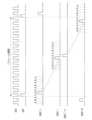
上記態様において、期間A、期間B、期間C、期間D及び期間Eを有し、期間Aにおいて
、第1の配線の電位がHレベルになり、第5の配線の電位及び第4の配線の電位がLレベ
ルになり、第1のトランジスタ、第2のトランジスタ及び第6のトランジスタがオンにな
り、第3のトランジスタ、第4のトランジスタ、第5のトランジスタ及び第7のトランジ
スタがオフになり、第6の配線の電位がLレベルになり、期間Bにおいて、第1の配線の
電位がLレベルになり、第5の配線の電位がHレベルになり、第4の配線の電位がLレベ
ルになり、第1のトランジスタ、第2のトランジスタ、第3のトランジスタ及び第6のト
ランジスタがオフになり、第4のトランジスタ及び第5のトランジスタがオンになり、第
6の配線の電位がLレベルになり、期間Cにおいて、第1の配線の電位がLレベルになり
、第5の配線の電位及び第4の配線の電位がHレベルになり、第1のトランジスタ、第2
のトランジスタ及び第6のトランジスタがオフになり、第3のトランジスタ、第4のトラ
ンジスタ、第5のトランジスタ及び第7のトランジスタがオンになり、第6の配線の電位
がLレベルになり、期間Dにおいて、第1の配線の電位がHレベルになり、第5の配線の
電位がLレベルになり、第4の配線の電位がHレベルになり、第1のトランジスタ、第2
のトランジスタ、第3のトランジスタ及び第7のトランジスタがオンになり、第4のトラ
ンジスタ、第5のトランジスタ及び第6のトランジスタがオフになり、第6の配線の電位
がHレベルになり、期間Eにおいて、第1の配線の電位がLレベルになり、第5の配線の
電位がHレベルになり、第4の配線の電位がLレベルになり、第1のトランジスタ、第2
のトランジスタ、第3のトランジスタ、第6のトランジスタ及び第7のトランジスタがオ
フになり、第4のトランジスタ及び第5のトランジスタがオンになり、第6の配線の電位
がLレベルになってもよい。In the above embodiment, the semiconductor device includes periods A, B, C, D, and E. In period A, the potential of the first wiring becomes an H level, the potential of the fifth wiring and the potential of the fourth wiring become an L level, the first transistor, the second transistor, and the sixth transistor are turned on, the third transistor, the fourth transistor, the fifth transistor, and the seventh transistor are turned off, and the potential of the sixth wiring becomes an L level. In period B, the potential of the first wiring becomes an L level, the potential of the fifth wiring becomes an H level, the potential of the fourth wiring becomes an L level, the first transistor, the second transistor, the third transistor, and the sixth transistor are turned off, the fourth transistor and the fifth transistor are turned on, and the potential of the sixth wiring becomes an L level. In period C, the potential of the first wiring becomes an L level, the potential of the fifth wiring and the potential of the fourth wiring become an H level, and the first transistor, the second transistor, the sixth transistor, and the seventh transistor are turned on.
The first transistor and the sixth transistor are turned off, the third transistor, the fourth transistor, the fifth transistor, and the seventh transistor are turned on, the potential of the sixth wiring becomes L level, and in period D, the potential of the first wiring becomes H level, the potential of the fifth wiring becomes L level, the potential of the fourth wiring becomes H level, and the first transistor, the second transistor, the
The first, third, and seventh transistors are turned on, the fourth, fifth, and sixth transistors are turned off, the potential of the sixth wiring becomes H level, and in a period E, the potential of the first wiring becomes L level, the potential of the fifth wiring becomes H level, the potential of the fourth wiring becomes L level, and the first, second, and seventh transistors are turned on, the fourth, fifth, and sixth transistors are turned off, and the potential of the sixth wiring becomes H level.
The first, third, sixth, and seventh transistors may be turned off, the fourth and fifth transistors may be turned on, and the potential of the sixth wiring may become an L level.
上記の本発明の各態様において、スイッチとしては、様々な形態のものを用いることがで
きる。スイッチとしては、電気的スイッチ又は機械的なスイッチ等を用いることができる
。つまり、スイッチは、電流を制御できるものであればよく、特定のものに限定されない
。電気的スイッチとしては、トランジスタ(例えば、バイポーラトランジスタ、MOSト
ランジスタ等)、ダイオード(例えば、PNダイオード、PINダイオード、ショットキ
ーダイオード、MIM(Metal Insulator Metal)ダイオード、M
IS(Metal Insulator Semiconductor)ダイオード、ダ
イオード接続のトランジスタ等)、又はこれらを組み合わせた論理回路等がある。機械的
なスイッチとしては、デジタルマイクロミラーデバイス(DMD)のように、MEMS(
マイクロ・エレクトロ・メカニカル・システム)技術を用いたスイッチがある。そのスイ
ッチは、機械的に動かすことが可能な電極を有し、その電極が動くことによって、導通と
非導通とを制御して動作する。In each of the above aspects of the present invention, various types of switches can be used. The switch can be an electrical switch, a mechanical switch, or the like. In other words, the switch is not limited to a specific type as long as it can control a current. Examples of electrical switches include transistors (e.g., bipolar transistors, MOS transistors, etc.), diodes (e.g., PN diodes, PIN diodes, Schottky diodes, MIM (Metal Insulator Metal) diodes, M
Examples of mechanical switches include metal insulator semiconductor (IS) diodes, diode-connected transistors, and logic circuits that combine these.
There is a switch that uses Microelectromechanical System (MICS) technology. The switch has an electrode that can be mechanically moved, and the movement of the electrode controls whether the switch is conductive or non-conductive.
なお、スイッチとしてトランジスタを用いる場合、そのトランジスタは単なるスイッチと
して動作するため、トランジスタの極性(導電型)は特に限定されない。ただし、オフ電
流を抑えたい場合、オフ電流が少ない方の極性のトランジスタを用いることが望ましい。
オフ電流が少ないトランジスタはLDD領域を有するトランジスタ、又はマルチゲート構
造を有するトランジスタなどがある。In the case where a transistor is used as a switch, the polarity (conductivity type) of the transistor is not particularly limited because the transistor simply operates as a switch. However, in order to suppress the off-current, it is preferable to use a transistor having a polarity with a smaller off-current.
Examples of transistors with low off-state current include transistors having an LDD region and transistors having a multi-gate structure.
また、上記の本発明の各態様において、スイッチとしてトランジスタを用い、そのトラン
ジスタのソースの電位が低電位側電源(Vss、GND、0V等)の電位に近い値で動作
する場合は、スイッチとしてNチャネル型トランジスタを用いることが望ましい。反対に
、そのトランジスタのソースの電位が高電位側電源(Vdd等)の電位に近い値で動作す
る場合は、スイッチとしてPチャネル型トランジスタを用いることが望ましい。なぜなら
、Nチャネル型トランジスタではソースが低電位側電源の電位に近い値で動作する場合、
Pチャネル型トランジスタではソースが高電位側電源の電位に近い値で動作する場合には
、ゲートとソースとの間の電圧の絶対値を大きくできるからである。そのため、スイッチ
として、より正確な動作を行うことができるからである。または、トランジスタがソース
フォロワ動作をしてしまうことが少ないため、出力電圧の大きさが小さくなってしまうこ
とが少ないからである。In each of the above aspects of the present invention, when a transistor is used as a switch and the source potential of the transistor operates at a value close to the potential of the low potential power supply (Vss, GND, 0 V, etc.), it is preferable to use an N-channel transistor as the switch. Conversely, when the source potential of the transistor operates at a value close to the potential of the high potential power supply (Vdd, etc.), it is preferable to use a P-channel transistor as the switch. This is because, in an N-channel transistor, when the source operates at a value close to the potential of the low potential power supply,
This is because, in the case of a P-channel transistor, when the source operates at a potential close to that of the high-potential power supply, the absolute value of the voltage between the gate and source can be made large. This is because the switch can operate more accurately. Also, the transistor rarely operates as a source follower, so the output voltage is less likely to become small.
また、上記の本発明の各態様において、スイッチとして、Nチャネル型トランジスタとP
チャネル型トランジスタとの両方を用いて、CMOS型のスイッチを用いてもよい。CM
OS型のスイッチにすると、Pチャネル型トランジスタとNチャネル型トランジスタとの
どちらか一方が導通すれば、電流が流れるため、スイッチとして機能しやすくなる。よっ
て、スイッチへの入力信号の電圧が高い場合でも、低い場合でも、適切に電圧を出力させ
ることができる。または、スイッチをオン又はオフさせるための信号の電圧振幅値を小さ
くすることができるので、消費電力を小さくすることができる。In each of the above aspects of the present invention, the switch may be an N-channel transistor and a P
A CMOS type switch may be used by using both a CMOS type transistor and a CMOS type transistor.
In the case of an OS-type switch, if either a P-channel transistor or an N-channel transistor is conductive, a current flows, and the switch can easily function as a switch. Therefore, whether the voltage of the input signal to the switch is high or low, the switch can output an appropriate voltage. In addition, the voltage amplitude value of the signal for turning the switch on or off can be reduced, so that power consumption can be reduced.
なお、スイッチとしてトランジスタを用いる場合、スイッチは、入力端子(ソースまたは
ドレインの一方)と、出力端子(ソースまたはドレインの他方)と、導通を制御する端子
(ゲート)とを有する場合がある。一方、スイッチとしてダイオードを用いる場合、スイ
ッチは、導通を制御する端子を有していない場合がある。したがって、トランジスタより
もダイオードをスイッチとして用いた方が、端子を制御するための配線を少なくすること
ができる。When a transistor is used as a switch, the switch may have an input terminal (either the source or the drain), an output terminal (the other of the source or the drain), and a terminal (gate) that controls conduction. On the other hand, when a diode is used as a switch, the switch may not have a terminal that controls conduction. Therefore, using a diode as a switch rather than a transistor can reduce the amount of wiring for controlling the terminal.
本明細書に開示されている発明では、トランジスタとして、様々な構造のトランジスタを
用いることができる。つまり、用いるトランジスタの構成に限定はない。In the invention disclosed in this specification, transistors having various structures can be used as the transistors, that is, there is no limitation on the structure of the transistors to be used.
本明細書において、半導体装置とは、半導体素子(トランジスタ、ダイオード、サイリス
タ等)を含む回路を有する装置のことをいう。ただし、半導体特性を利用することで機能
しうる装置全般、又は半導体材料を有する装置のことを半導体装置と呼んでもよい。本明
細書において、表示装置とは、表示素子を有する装置のことを言う。In this specification, a semiconductor device refers to a device having a circuit including a semiconductor element (transistor, diode, thyristor, etc.). However, any device that can function by utilizing semiconductor characteristics or a device having a semiconductor material may be called a semiconductor device. In this specification, a display device refers to a device having a display element.
本明細書において、駆動装置とは、半導体素子、電気回路、電子回路を有する装置のこと
を言う。例えば、ソース信号線から画素内への信号の入力を制御するトランジスタ(選択
用トランジスタ、スイッチング用トランジスタ等と呼ぶことがある)、画素電極に電圧ま
たは電流を供給するトランジスタ、発光素子に電圧または電流を供給するトランジスタ等
は、駆動装置の一例である。さらに、ゲート信号線に信号を供給する回路(ゲートドライ
バ、ゲート線駆動回路等と呼ぶことがある)、ソース信号線に信号を供給する回路(ソー
スドライバ、ソース線駆動回路等と呼ぶことがある)等は、駆動装置の一例である。In this specification, the driving device refers to a device having a semiconductor element, an electric circuit, and an electronic circuit. For example, a transistor that controls the input of a signal from a source signal line into a pixel (sometimes called a selection transistor, a switching transistor, etc.), a transistor that supplies a voltage or current to a pixel electrode, a transistor that supplies a voltage or current to a light-emitting element, etc. are examples of the driving device. Furthermore, a circuit that supplies a signal to a gate signal line (sometimes called a gate driver, a gate line driving circuit, etc.), a circuit that supplies a signal to a source signal line (sometimes called a source driver, a source line driving circuit, etc.), etc. are examples of the driving device.
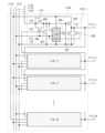
また、表示装置、半導体装置、照明装置、冷却装置、発光装置、反射装置、および駆動装
置等を互いに組み合わせることが可能であり、このような装置も本発明の態様に含まれる
。例えば、表示装置が、半導体装置および発光装置を有する場合がある。あるいは、半導
体装置が、表示装置および駆動装置を有する場合がある。In addition, the display device, the semiconductor device, the lighting device, the cooling device, the light-emitting device, the reflecting device, the driving device, and the like can be combined with one another, and such devices are also included in the aspects of the present invention. For example, a display device may have a semiconductor device and a light-emitting device. Alternatively, a semiconductor device may have a display device and a driving device.
また、本発明の各態様において、所定の機能を実現させるために必要な回路の全てを、同
一の基板(例えば、ガラス基板、プラスチック基板、単結晶基板、又はSOI基板等)に
形成することが可能である。こうして、部品点数の削減によるコストの低減、又は回路部
品との接続点数の低減による信頼性の向上を図ることができる。In addition, in each aspect of the present invention, all of the circuits required to realize a predetermined function can be formed on the same substrate (e.g., a glass substrate, a plastic substrate, a single crystal substrate, an SOI substrate, etc.), thereby reducing the number of components and thereby reducing costs, and improving reliability by reducing the number of connections to the circuit components.
また、所定の機能を実現させるために必要な回路の全てを同じ基板に形成しないことが可
能である。つまり、所定の機能を実現させるために必要な回路の一部は、ある基板に形成
され、所定の機能を実現させるために必要な回路の別の一部は、別の基板に形成されてい
ることが可能である。例えば、所定の機能を実現させるために必要な回路の一部は、ガラ
ス基板に形成され、所定の機能を実現させるために必要な回路の別の一部は、単結晶基板
(又はSOI基板)に形成されることが可能である。そして、所定の機能を実現させるた
めに必要な回路の別の一部が形成される単結晶基板(ICチップともいう)を、COG(
Chip On Glass)によって、ガラス基板に接続して、ガラス基板にそのIC
チップを配置することが可能である。または、ICチップを、TAB(Tape Aut
omated Bonding)、COF(Chip On Film)、SMT(Su
rface Mount Technology)、又はプリント基板等を用いてガラス
基板と接続することが可能である。It is also possible that all of the circuits necessary to realize a specified function are not formed on the same substrate. In other words, a part of the circuits necessary to realize a specified function can be formed on one substrate, and another part of the circuits necessary to realize the specified function can be formed on another substrate. For example, a part of the circuits necessary to realize a specified function can be formed on a glass substrate, and another part of the circuits necessary to realize the specified function can be formed on a single crystal substrate (or an SOI substrate). Then, the single crystal substrate (also called an IC chip) on which the other part of the circuits necessary to realize the specified function is formed can be formed on a COG (
By using a chip on glass (Chip On Glass), the IC is connected to the glass substrate.
Alternatively, the IC chip can be mounted on the substrate using a tape auto-adhesive (TAB) method.
COF (Chip On Film), SMT (Su
It is possible to connect the semiconductor device to the glass substrate using a face mount technology (Face Mount Technology) or a printed circuit board.
本明細書において、XとYとが接続されている、と明示的に記載する場合は、XとYとが
電気的に接続されている場合と、XとYとが機能的に接続されている場合と、XとYとが
直接接続されている場合とを含むものとする。ここで、X、Yは、対象物(例えば、装置
、素子、回路、配線、電極、端子、導電膜、層等)であるとする。したがって、所定の接
続関係、例えば、図または文章に示された接続関係に限定されず、図または文章に示され
た接続関係以外のものも含むものとする。In this specification, when it is explicitly stated that X and Y are connected, this includes cases where X and Y are electrically connected, where X and Y are functionally connected, and where X and Y are directly connected. Here, X and Y are objects (e.g., devices, elements, circuits, wiring, electrodes, terminals, conductive films, layers, etc.). Therefore, it is not limited to a specific connection relationship, for example, a connection relationship shown in a figure or text, but also includes connection relationships other than those shown in a figure or text.
XとYとが電気的に接続されている場合の一例としては、XとYとの電気的な接続を可能
とする素子(例えば、スイッチ、トランジスタ、容量素子、インダクタ、抵抗素子、ダイ
オード等)が、XとYとの間に1個以上接続されることが可能である。As an example of the case where X and Y are electrically connected, one or more elements (e.g., a switch, a transistor, a capacitance element, an inductor, a resistance element, a diode, etc.) that enable the electrical connection between X and Y can be connected between X and Y.
XとYとが機能的に接続されている場合の一例としては、XとYとの機能的な接続を可能
とする回路(例えば、論理回路(インバータ、NAND回路、NOR回路等)、信号変換
回路(DA変換回路、AD変換回路、ガンマ補正回路等)、電位レベル変換回路(電源回
路(昇圧回路、降圧回路等)、信号の電位レベルを変えるレベルシフタ回路等)、電圧源
、電流源、切り替え回路、増幅回路(信号振幅または電流量等を大きくできる回路、オペ
アンプ、差動増幅回路、ソースフォロワ回路、バッファ回路等)、信号生成回路、記憶回
路、制御回路等)が、XとYとの間に1個以上接続されることが可能である。なお、一例
として、XとYとの間に別の回路を挟んでいても、Xから出力された信号がYへ伝達され
る場合は、XとYとは機能的に接続されているものとする。As an example of a case where X and Y are functionally connected, one or more circuits that enable the functional connection between X and Y (for example, logic circuits (inverters, NAND circuits, NOR circuits, etc.), signal conversion circuits (DA conversion circuits, AD conversion circuits, gamma correction circuits, etc.), potential level conversion circuits (power supply circuits (boosting circuits, step-down circuits, etc.), level shifter circuits that change the potential level of a signal, etc.), voltage sources, current sources, switching circuits, amplifier circuits (circuits that can increase the signal amplitude or current amount, operational amplifiers, differential amplifier circuits, source follower circuits, buffer circuits, etc.), signal generation circuits, memory circuits, control circuits, etc.) can be connected between X and Y. As an example, even if another circuit is sandwiched between X and Y, if a signal output from X is transmitted to Y, X and Y are considered to be functionally connected.
本明細書において、明示的に単数として記載されているものについては、単数であること
が望ましい。ただし、この場合でも、複数であることも可能である。同様に、明示的に複
数として記載されているものについては、複数であることが望ましい。ただし、この場合
でも、単数であることも可能である。In this specification, when something is explicitly described as singular, it is preferable to use the singular. However, even in this case, it is possible to use the plural. Similarly, when something is explicitly described as plural, it is preferable to use the plural. However, even in this case, it is possible to use the singular.
本出願の図において、大きさ、層の厚さ、又は領域は、明瞭化のために誇張されている場
合がある。よって、必ずしもそのスケールに限定されない。図は、理想的な例を模式的に
示すものであり、図に示す形状又は値等に限定されない。例えば、製造技術による形状の
ばらつき、誤差による形状のばらつき、ノイズによる信号、電圧、若しくは電流のばらつ
き、又は、タイミングのずれによる信号、電圧、若しくは電流のばらつき等を含むことが
可能である。In the figures of the present application, the size, layer thickness, or area may be exaggerated for clarity. Therefore, the figures are not necessarily limited to the scale. The figures are schematic illustrations of ideal examples, and are not limited to the shapes or values shown in the figures. For example, it is possible to include shape variations due to manufacturing techniques, shape variations due to errors, signal, voltage, or current variations due to noise, or signal, voltage, or current variations due to timing deviations.
なお、専門用語は、特定の実施の形態、又は実施例等を述べる目的で用いられる場合が多
い。ただし、本発明の一態様は、専門用語によって、限定して解釈されるものではない。Note that technical terms are often used for the purpose of describing a specific embodiment, example, etc. However, one aspect of the present invention should not be interpreted as being limited by technical terms.
なお、定義されていない文言(専門用語又は学術用語等の科学技術文言を含む)は、通常
の当業者が理解する一般的な意味と同等の意味として用いることが可能である。辞書等に
より定義されている文言は、関連技術の背景と矛盾がないような意味に解釈されることが
好ましい。In addition, undefined terms (including scientific and technical terms such as technical terms or academic terms) may be used with the same meaning as that generally understood by a person of ordinary skill in the art. Terms defined in dictionaries, etc. are preferably interpreted in a way that is consistent with the background of the related technology.
なお、第1、第2、第3等の語句は、様々な要素、部材、領域、層、区域などについて、
区別して記述するために用いられる。よって、第1、第2、第3等の語句は、要素、部材
、領域、層、区域等の順序および個数を限定するものではない。さらに、例えば、「第1
の」を「第2の」又は「第3の」等と置き換えることが可能である。In addition, the terms "first,""second,""third," etc., are used to refer to various elements, members, regions, layers, areas, etc.
The terms "first", "second", "third" and the like are used to distinguish and describe the elements, members, regions, layers, areas, and the like.
It is possible to replace "the" with "the second" or "the third", etc.
また、「上に」、「上方に」、「下に」、「下方に」、「横に」、「右に」、「左に」、
「斜めに」、「奥に」、「手前に」、「内に」、「外に」、又は「中に」等の空間的配置
を示す語句は、ある要素又は特徴と、他の要素又は特徴との関連を、図によって簡単に示
すために用いられる。ただし、このような用法に限定されず、これらの空間的配置を示す
語句は、図に描く方向に加えて、他の方向を含む場合がある。例えば、Xの上にY、と明
示的に示される場合は、YがXの上にあることに限定されない。図中の構成は反転、又は
180°回転させることが可能なので、YがXの下にあることを含むことが可能である。
このように、「上に」という語句は、「上に」の方向に加え、「下に」の方向を含むこと
が可能である。ただし、これに限定されず、図中のデバイスは様々な方向に回転すること
が可能なので、「上に」という語句は、「上に」、および「下に」の方向に加え、「横に
」、「右に」、「左に」、「斜めに」、「奥に」、「手前に」、「内に」、「外に」、又
は「中に」等の他の方向を含むことが可能である。つまり、状況に応じて適切に解釈する
ことが可能である。Also, "up,""upward,""down,""downward,""sideways,""right,""left,"
Spatial terms such as "diagonally,""in the back,""infront,""inside,""outside," or "inside" are used to easily illustrate the relationship of one element or feature to another element or feature in the figures. However, without being limited to such usage, these spatial terms may include other orientations in addition to those depicted in the figures. For example, explicitly indicating Y above X is not limited to Y being above X. Configurations in the figures may be flipped or rotated 180 degrees, so could include Y being below X.
In this way, the term "on" can include the direction of "on" as well as the direction of "under". However, without being limited thereto, since the device in the figure can be rotated in various directions, the term "on" can include other directions such as "sideways", "right", "left", "diagonally", "back", "forward", "inside", "outside", or "inside" in addition to the directions of "on" and "down". In other words, it can be interpreted appropriately depending on the situation.
なお、Xの上にYが形成されている、あるいは、X上にYが形成されている、と明示的に
記載する場合は、Xの上にYが直接接して形成されていることに限定されない。直接接し
てはいない場合、つまり、XとYと間に別の対象物が介在する場合も含むものとする。こ
こで、X、Yは、対象物(例えば、装置、素子、回路、配線、電極、端子、導電膜、層、
等)であるとする。In addition, when it is explicitly stated that Y is formed on X, or that Y is formed on X, it is not limited to Y being formed directly on X. It also includes the case where they are not in direct contact, that is, where another object is interposed between X and Y. Here, X and Y are objects (for example, a device, an element, a circuit, wiring, an electrode, a terminal, a conductive film, a layer,
etc.).
従って例えば、層Xの上に(もしくは層X上に)、層Yが形成されている、と明示的に記
載されている場合は、層Xの上に直接接して層Yが形成されている場合と、層Xの上に直
接接して別の層(例えば層Z等)が形成されていて、その上に直接接して層Yが形成され
ている場合とを含むものとする。なお、別の層(例えば層Z等)は、単層でもよいし、複
層でもよい。Therefore, for example, when it is explicitly stated that a layer Y is formed on (or on) a layer X, this includes the case where a layer Y is formed directly on and in contact with the layer X, and the case where another layer (e.g., layer Z, etc.) is formed directly on and in contact with the layer X, and the layer Y is formed directly on the other layer. The other layer (e.g., layer Z, etc.) may be a single layer or multiple layers.
さらに、Xの上方にYが形成されている、と明示的に記載されている場合についても同様
であり、Xの上にYが直接接していることに限定されず、XとYとの間に別の対象物が介
在する場合も含むものとする。従って例えば、層Xの上方に、層Yが形成されている、と
いう場合は、層Xの上に直接接して層Yが形成されている場合と、層Xの上に直接接して
別の層(例えば層Z等)が形成されていて、その上に直接接して層Yが形成されている場
合とを含むものとする。なお、別の層(例えば層Z等)は、単層でもよいし、複層でもよ
い。The same is true for cases where it is explicitly stated that Y is formed above X, and is not limited to Y being directly on X, but also includes cases where another object is interposed between X and Y. Thus, for example, when it is stated that layer Y is formed above layer X, it includes cases where layer Y is formed directly on layer X, and cases where another layer (e.g. layer Z, etc.) is formed directly on layer X, and layer Y is formed directly on the other layer. The other layer (e.g. layer Z, etc.) may be a single layer or multiple layers.
なお、Xの上にYが形成されている、X上にYが形成されている、又はXの上方にYが形
成されている、と明示的に記載する場合、Xの斜め上にYが形成される場合も含むことと
する。In addition, when it is explicitly stated that Y is formed on X, that Y is formed on X, or that Y is formed above X, this also includes the case where Y is formed diagonally above X.
なお、Xの下にYが、あるいは、Xの下方にYが、との記載についても同様である。The same applies to statements such as "Y below X" or "Y below X."
本発明の一態様は、第1のトランジスタ、第2のトランジスタ、第1のスイッチ、第2の
スイッチ、及び第3のスイッチを有する。第1のトランジスタの第1の端子は、第1の配
線と接続され、第1のトランジスタの第2の端子は、第2の配線と接続される。第2のト
ランジスタの第1の端子は、第1の配線と接続され、第2のトランジスタの第2の端子は
、第1のトランジスタのゲートと接続され、第2のトランジスタのゲートは、第1の配線
と接続される。第1のスイッチは、第2の配線と第3の配線との間に接続される。第2の
スイッチは、第2の配線と第3の配線との間に接続される。第3のスイッチは、第1のト
ランジスタのゲートと第3の配線との間に接続される。One embodiment of the present invention includes a first transistor, a second transistor, a first switch, a second switch, and a third switch. A first terminal of the first transistor is connected to a first wiring, and a second terminal of the first transistor is connected to a second wiring. A first terminal of the second transistor is connected to the first wiring, a second terminal of the second transistor is connected to a gate of the first transistor, and a gate of the second transistor is connected to the first wiring. The first switch is connected between the second wiring and a third wiring. The second switch is connected between the second wiring and the third wiring. The third switch is connected between the gate of the first transistor and the third wiring.
なお、本発明の一態様は、第1の期間と第2の期間とを有することが可能である。第1の
期間において、第1~第3のスイッチがオフになることが可能である。そして、第1の配
線の電位がHレベルになることが可能である。第2の期間において、第1のスイッチがオ
フになり、第2~第3のスイッチがオンになることが可能である。そして、第1の配線の
電位がLレベルになることが可能である。Note that one embodiment of the present invention can have a first period and a second period. In the first period, the first to third switches can be turned off. Then, the potential of the first wiring can be at an H level. In the second period, the first switch can be turned off and the second and third switches can be turned on. Then, the potential of the first wiring can be at an L level.
本発明の一態様は、第1-第2のトランジスタ、第1-第3のスイッチを有する半導体装
置において、第1-第2のトランジスタ、第1-第3のスイッチがオンになる時間を短く
又はオンになる回数を少なくできるので劣化を抑制することができる。または、第1-第
5のトランジスタを有する半導体装置において、第1-第5のトランジスタがオンになる
時間を短く又はオンになる回数を少なくできるので劣化を抑制することができる。または
、さらに第6のトランジスタを有する半導体装置において、第1-第6のトランジスタが
オンになる時間を短く又はオンになる回数を少なくできるので劣化を抑制することができ
る。または、さらに第7のトランジスタを有する半導体装置において、第1-第7のトラ
ンジスタがオンになる時間を短く又はオンになる回数を少なくできるので劣化を抑制する
ことができる。In one embodiment of the present invention, in a semiconductor device having first and second transistors and first and third switches, the time when the first and second transistors and the first and third switches are turned on can be shortened or the number of times they are turned on can be reduced, so that deterioration can be suppressed. Or, in a semiconductor device having first to fifth transistors, the time when the first to fifth transistors are turned on can be shortened or the number of times they are turned on can be reduced, so that deterioration can be suppressed. Or, in a semiconductor device having a sixth transistor, the time when the first to sixth transistors are turned on can be shortened or the number of times they are turned on can be reduced, so that deterioration can be suppressed. Or, in a semiconductor device having a seventh transistor, the time when the first to seventh transistors are turned on can be shortened or the number of times they are turned on can be reduced, so that deterioration can be suppressed.
以下、実施の形態について図面を参照しながら説明する。但し、実施の形態は多くの異な
る態様で実施することが可能であり、趣旨及びその範囲から逸脱することなくその形態及
び詳細を様々に変更し得ることは当業者であれば容易に理解される。従って実施の形態の
記載内容に限定して解釈されるものではない。なお、以下に説明する構成において、同一
部分又は同様な機能を有する部分は異なる図面間で共通の符号を用いて示し、同一部分又
は同様な機能を有する部分の詳細な説明は省略する。Hereinafter, the embodiments will be described with reference to the drawings. However, it will be easily understood by those skilled in the art that the embodiments can be implemented in many different ways, and that the form and details can be changed in various ways without departing from the spirit and scope of the invention. Therefore, the present invention should not be interpreted as being limited to the description of the embodiments. In the configurations described below, the same parts or parts having similar functions are indicated by the same reference numerals in different drawings, and detailed descriptions of the same parts or parts having similar functions are omitted.
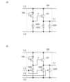
(実施の形態1)
本実施の形態の構成について、図45(A)を参照して説明する。図45(A)には、本
実施の形態の半導体装置の回路図を示す。(Embodiment 1)
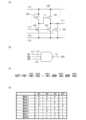
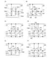
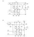
The configuration of this embodiment mode will be described with reference to Fig. 45A, which shows a circuit diagram of a semiconductor device of this embodiment mode.
回路100は、トランジスタ101(第1のトランジスタ)、スイッチ102S(第1の
スイッチ)、スイッチ103S(第2のスイッチ)、トランジスタ104(第2のトラン
ジスタ)、及びスイッチ105S(第3のスイッチ)を有する。The
なお、トランジスタ101及びトランジスタ104は、Nチャネル型とする。Nチャネル
型のトランジスタは、ゲートとソースとの間の電位差(Vgs)が閾値電圧(Vth)を
上回った場合にオンする。ただし、これに限定されず、トランジスタ101及びトランジ
スタ104は、Pチャネル型であることが可能である。Pチャネル型トランジスタは、ゲ
ートとソースとの間の電位差(Vgs)が閾値電圧(Vth)を下回った場合にオンする
。Note that the
トランジスタ101の第1の端子は、配線112(第1の配線)と接続され、トランジス
タ101の第2の端子は、配線111(第2の配線)と接続される。スイッチ102Sは
、配線111と配線115(第3の配線)との間に接続される。スイッチ103Sは、配
線111と配線115との間に接続される。トランジスタ104の第1の端子は、配線1
12と接続され、トランジスタ104の第2の端子は、トランジスタ101のゲートと接
続され、トランジスタ104のゲートは、配線112と接続される。スイッチ105Sは
、配線115とトランジスタ101のゲートとの間に接続される。A first terminal of the
12, a second terminal of the
なお、スイッチ102S、スイッチ103S、及びスイッチ105Sは、制御端子を有す
ることが可能である。図45(B)には、スイッチ102Sの制御端子が配線114(第
4の配線)と接続され、スイッチ103Sの制御端子が配線113(第5の配線)と接続
され、スイッチ105Sの制御端子が配線113と接続される場合の構成を示す。45B shows a configuration in which the control terminal of the
なお、スイッチ102S、スイッチ103S、及びスイッチ105Sとしては、トランジ
スタを用いることが可能である。図1(A)は、スイッチとしてトランジスタを用いる。
スイッチ102S、スイッチ103S、及びスイッチ105Sとして、各々、トランジス
タ102(第3のトランジスタ)、トランジスタ103(第4のトランジスタ)、トラン
ジスタ105(第5のトランジスタ)が用いられる場合の例を示す。トランジスタ102
の第1の端子は、配線115と接続され、トランジスタ102の第2の端子は、配線11
1と接続され、トランジスタ102のゲートは、配線114と接続される。トランジスタ
103の第1の端子は、配線115と接続され、トランジスタ103の第2の端子は、配
線111と接続され、トランジスタ103のゲートは、配線113と接続される。トラン
ジスタ105の第1の端子は、配線115と接続され、トランジスタ105の第2の端子
は、トランジスタ101のゲートと接続され、トランジスタ105のゲートは、配線11
3と接続される。Note that transistors can be used as the
In this example, the transistor 102 (a third transistor), the transistor 103 (a fourth transistor), and the transistor 105 (a fifth transistor) are used as the
A first terminal of the
A first terminal of the
3 is connected.
なお、トランジスタ102、トランジスタ103、及びトランジスタ105は、トランジ
スタ101と同じNチャネル型である。ただしトランジスタ102、トランジスタ103
、及びトランジスタ105は、Pチャネル型でもよい。Note that the
, and the
なお、トランジスタ101のゲートとトランジスタ104の第2の端子との接続箇所、又
はトランジスタ101のゲートとトランジスタ105の第2の端子との接続箇所をノード
11と示す。Note that a connection point between the gate of the
次に、配線111~配線115に、入力又は出力される信号又は電圧の一例、及びこれら
の配線の機能について説明する。Next, examples of signals or voltages input to or output from the
配線111からは、信号OUTが出力される。The signal OUT is output from
配線112には、信号IN1が入力される。配線113には、信号IN2が入力される。
配線114には、信号IN3が入力される。A signal IN1 is input to the
A signal IN3 is input to the
配線115には、電圧V1が供給される。電圧V1は、電源電圧、基準電圧、グランド電
圧、アース、又は負電源電圧である。ただし、これに限定されず、配線115には、信号
(例えばクロック信号又は反転クロック信号など)が入力されてもよい。A voltage V1 is supplied to the
Lレベルの信号、L信号、Lレベルの電位、又は電圧V1などと記載する場合、これらの
電位はおおむねV1である。Hレベルの信号、H信号、Hレベルの電位、又は電圧V2な
どと記載する場合、これらの電位はおおむねV2(V2>V1)である。なおおおむねと
は、ノイズによる誤差、プロセスのばらつきによる誤差、素子の作製工程のばらつきによ
る誤差、及び/又は、測定誤差などの様々な誤差を含む(以下、同じ)。When referring to an L level signal, an L signal, an L level potential, or a voltage V1, these potentials are approximately V1. When referring to an H level signal, an H signal, an H level potential, or a voltage V2, these potentials are approximately V2 (V2>V1). Note that "approximately" includes various errors such as errors due to noise, errors due to process variations, errors due to variations in the manufacturing process of the element, and/or measurement errors (the same applies below).
例えば、あるノードにトランジスタのゲートが接続され、当該ノードの電位がLレベルに
なると、当該トランジスタはオフ(又はオン)になるとする。この場合、当該ノードの電
位がLレベルになるとは、当該ノードの電位が当該トランジスタをオフ(又はオン)にす
ることが可能な値になることをいう。または、当該ノードの電位がLレベルになるとは、
当該ノードの電位が、当該トランジスタを含む回路が所定の動作を実現することが可能な
程度に、当該トランジスタのゲートとソースとの間の電圧(Vgs)を小さく(又は大き
く)することが可能な値になることをいう。For example, when a gate of a transistor is connected to a certain node and the potential of the node becomes L level, the transistor is turned off (or on). In this case, the potential of the node becomes L level when the potential of the node becomes a value that can turn the transistor off (or on). Alternatively, the potential of the node becomes L level when
This means that the potential of the node becomes a value that allows the voltage (Vgs) between the gate and source of the transistor to be reduced (or increased) to an extent that the circuit including the transistor can perform a specified operation.
なお、信号IN1~IN3としてクロック信号が用いられるとすると、当該クロック信号
は、平衡であることが可能であるし、非平衡(不平衡ともいう)であることが可能である
。平衡とは、1周期のうち、Hレベルになる期間とLレベルになる期間とがおおむね等し
いことをいう。非平衡とは、Hレベルになる期間とLレベルになる期間とが異なることを
いう。If clock signals are used as the signals IN1 to IN3, the clock signals can be balanced or unbalanced (also called unbalanced). Balanced means that the period during which a signal is at H level and the period during which a signal is at L level are roughly equal in one cycle. Unbalanced means that the period during which a signal is at H level and the period during which a signal is at L level are different.
例えば、信号IN1としてクロック信号が用いられ、信号IN2として信号IN1から位
相がおおむね180°ずれた信号が用いられ、信号IN1及び信号IN2が非平衡である
とする。この場合、信号IN2は、信号IN1の反転信号ではないことがある。For example, assume that a clock signal is used as the signal IN1, a signal that is approximately 180° out of phase with the signal IN1 is used as the signal IN2, and the signals IN1 and IN2 are unbalanced. In this case, the signal IN2 may not be an inverted signal of the signal IN1.
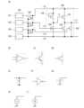
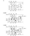
ここで、図5(A)に示すように、配線112~配線115には、回路150から信号又
は電圧が供給される。回路150は、信号又は電圧などを生成し、配線112~配線11
5に信号又は電圧を供給する。5A, a signal or a voltage is supplied to the
5 supplies a signal or voltage.
回路150は、回路151~回路154を有することが可能である。回路151は、信号
又は電圧を生成し、配線112に信号又は電圧を供給する機能を有する。回路152は、
信号又は電圧を生成し、配線113に信号又は電圧を供給する機能を有する。回路153
は、信号又は電圧を生成し、配線114に信号又は電圧を供給する機能を有する。回路1
54は、信号又は電圧を生成し、配線115に信号又は電圧を供給する機能を有する。The
The
has a function of generating a signal or a voltage and supplying the signal or the voltage to the
The element 54 has a function of generating a signal or a voltage and supplying the signal or the voltage to the
回路150~154は、各々、図5(B)の増幅回路、図5(C)のバイポーラトランジ
スタ、図5(D)のMOSトランジスタ、図5(E)の容量素子、図5(F)のインバー
タ、図5(G)の直流電圧源、図5(H)の交流電圧源、及び/又は、図5(I)の直流
電流源などを含む。Each of the
図5(A)に示すように、配線112~114には保護回路160が接続される。As shown in FIG. 5(A), a
次に、回路100、及びトランジスタ101~105の機能について説明する。Next, the functions of the
回路100は配線111の電位を制御する機能を有する。または、回路100は、配線1
12の電位、配線113の電位、配線114の電位、又は配線115の電位を配線111
に供給するタイミングを制御する機能を有する。または、回路100は、配線111に、
信号又は電圧を供給するタイミングを制御する機能を有する。または、回路100は、配
線111に、H信号又は電圧V2を供給するタイミングを制御する機能を有する。または
、回路100は、配線111に、L信号又は電圧V1を供給するタイミングを制御する機
能を有する。または、回路100は、配線111の電位を上昇させるタイミングを制御す
る機能を有する。または、回路100は、配線111の電位を減少させるタイミングを制
御する機能を有する。または、回路100は、配線111の電位を維持するタイミングを
制御する機能を有する。以上のように、回路100は、制御回路としての機能を有する。
なお、回路100は、上記の機能のすべてを有する必要はない。なお回路100は、信号
IN1~IN3に応じて制御される。The
The potential of the
Alternatively, the
The
It is not necessary for the
なお、回路100は、図1(B)に示すように、ANDを含む論理回路としての機能を有
する。具体的には、回路100は、3入力のANDと、二つのNOTとを組み合わせた論
理回路としての機能を有する。そして、ANDの第1の入力端子には、信号IN1が入力
され、ANDの第2の入力端子には、信号IN2が第1のNOTによって反転される信号
が入力され、ANDの第3の入力端子には、信号IN3が第2のNOTによって反転され
る信号が入力され、ANDの出力からは信号OUTが出力される。つまり、回路100は
、図1(C)に示す論理式を実現する機能、又は図1(D)に示す真理値表を実現する機
能を有する。As shown in FIG 1B, the
トランジスタ101は、配線112と配線111との導通状態を制御する機能を有する。
または、トランジスタ101は、配線112の電位を配線111に供給するタイミングを
制御する機能を有する。または、配線112に信号又は電圧が入力されると、トランジス
タ101は、配線112に入力される信号又は電圧を配線111に供給するタイミングを
制御する機能を有する。または、トランジスタ101は、配線111に、H信号又は電圧
V2を供給するタイミングを制御する機能を有する。または、トランジスタ101は、配
線111に、L信号又は電圧V1を供給するタイミングを制御する機能を有する。または
、トランジスタ101は、配線111の電位を上昇させるタイミングを制御する機能を有
する。または、トランジスタ101は、配線111の電位を減少させるタイミングを制御
する機能を有する。または、トランジスタ101は、ブートストラップ動作を行う機能を
有する。または、トランジスタ101は、ノード11の電位をブートストラップ動作によ
って上昇させる機能を有する。以上のように、トランジスタ101は、スイッチ、又はバ
ッファとしての機能を有する。なお、トランジスタ101は、上記の機能のすべてを有す
る必要はない。The
Alternatively, the
トランジスタ102は、配線115と配線111との導通状態を制御する機能を有する。
または、トランジスタ102は、配線115の電位を配線111に供給するタイミングを
制御する機能を有する。または、配線115に信号又は電圧が入力されると、トランジス
タ102は、配線115に入力される信号又は電圧を配線111に供給するタイミングを
制御する機能を有する。または、トランジスタ102は、配線111に、L信号又は電圧
V1を供給するタイミングを制御する機能を有する。または、トランジスタ102は、配
線111の電位を減少させるタイミングを制御する機能を有する。以上のように、トラン
ジスタ102は、スイッチとしての機能を有する。なお、トランジスタ102は、上記の
機能のすべてを有する必要はない。なお、トランジスタ102は、配線114の電位(信
号IN3)によって制御されることが可能である。The
Alternatively, the
トランジスタ103は、配線115と配線111との導通状態を制御する機能を有する。
または、トランジスタ103は、配線115の電位を配線111に供給するタイミングを
制御する機能を有する。または、配線115に信号又は電圧が入力されるとすると、トラ
ンジスタ103は、配線115に入力される信号又は電圧を配線111に供給するタイミ
ングを制御する機能を有する。または、トランジスタ103は、配線111に、L信号又
は電圧V1を供給するタイミングを制御する機能を有する。または、トランジスタ103
は、配線111の電位を減少させるタイミングを制御する機能を有する。以上のように、
トランジスタ103は、スイッチとしての機能を有する。なお、トランジスタ103は、
上記の機能のすべてを有する必要はない。なお、トランジスタ103は、配線113の電
位(信号IN2)によって制御されることが可能である。The
Alternatively, the
has a function of controlling the timing at which the potential of the
The
The
トランジスタ104は、配線112とノード11との導通状態を制御する機能を有する。
または、トランジスタ104は、配線112の電位をノード11に供給するタイミングを
制御する機能を有する。または、配線112に信号又は電圧が入力されると、トランジス
タ104は、配線112に入力される信号又は電圧をノード11に供給するタイミングを
制御する機能を有する。または、トランジスタ104は、ノード11に、H信号又は電圧
V2を供給するタイミングを制御する機能を有する。または、トランジスタ104は、ノ
ード11の電位を上昇させるタイミングを制御する機能を有する。または、トランジスタ
104は、ノード11を浮遊状態にする機能を有する。以上のように、トランジスタ10
4は、スイッチ、ダイオード、又はダイオード接続のトランジスタなどとしての機能を有
する。なお、トランジスタ104は、上記の機能のすべてを有する必要はない。なお、ト
ランジスタ104は、配線112の電位(信号IN1)、及び/又は、ノード11の電位
によって制御されることが可能である。The
Alternatively, the
The
トランジスタ105は、配線115とノード11との導通状態を制御する機能を有する。
または、トランジスタ105は、配線115の電位をノード11に供給するタイミングを
制御する機能を有する。または、配線115に信号又は電圧が入力されると、トランジス
タ105は、配線115に入力される信号又は電圧をノード11に供給するタイミングを
制御する機能を有する。または、トランジスタ105は、ノード11に、L信号又は電圧
V1を供給するタイミングを制御する機能を有する。または、トランジスタ105は、ノ
ード11の電位を減少させるタイミングを制御する機能を有する。以上のように、トラン
ジスタ105は、スイッチとしての機能を有する。なお、トランジスタ105は、上記の
機能のすべてを有する必要はない。なお、トランジスタ105は、配線113の電位(信
号IN2)によって制御されることが可能である。The
Alternatively, the
次に、回路100の動作について、図1(D)の真理値表(動作表ともいう)を参照して
説明する。図1(D)には、信号IN1~IN3がデジタル信号である場合の真理値表を
示す。よって、信号IN1~IN3のHレベルとLレベルとの組み合わせは、8パターン
ある。つまり、回路100は、少なくとも8パターンの動作を行うことが可能である。こ
こでは、その8パターンの動作についてそれぞれ説明する。Next, the operation of the
なお、回路100は、これらの8パターンの動作の全てを行う必要はなく、一部を選択し
て行うことが可能である。なお、回路100は、これらの8パターンの動作以外の動作を
行うことが可能である。例えば、信号IN1~IN3が三つ以上の値を有する場合、又は
信号IN1~IN3がアナログ信号である場合、回路100は、これらの8パターン以外
にも、さらに多くの動作を行うことが可能である。Note that the
まず、回路100の動作1について、図2(A)を参照して説明する。信号IN2はHレ
ベルになるので、トランジスタ105はオンになる。すると、配線115とノード11と
は導通状態になるので、配線115の電位(例えば電圧V1)はノード11に供給される
。このとき、信号IN1はHレベルになるので、トランジスタ104はオンになる。する
と、配線112とノード11とは導通状態になるので、配線112の電位(例えばHレベ
ルの信号IN1)はノード11に供給される。つまり、ノード11には、配線115の電
位(例えば電圧V1)と配線112の電位(例えばHレベルの信号IN1)とが供給され
る。ここで、トランジスタ105のチャネル幅は、トランジスタ104のチャネル幅より
も大きいとする。よって、ノード11の電位は、Lレベルになる。このときのノード11
の電位は、V1よりも大きく、V1+Vth101(Vth101はトランジスタ101
の閾値電圧)よりも小さい値である。この結果、トランジスタ101はオフになるので、
配線112と配線111とは非導通状態になる。First,
The potential of the
As a result, the
The
そして、信号IN2はHレベルになるので、トランジスタ103はオンになる。このとき
、信号IN3はHレベルになるので、トランジスタ102はオンになる。すると、配線1
15と配線111とは導通状態になるので、配線115の電位(例えば電圧V1)は配線
111に供給される。よって、配線111の電位はV1になるので、信号OUTはLレベ
ルになる。Then, the signal IN2 becomes H level, and the
Since the
なお「トランジスタAのチャネル幅は、トランジスタBのチャネル幅よりも大きい」は「
トランジスタAの1/W(Wはチャネル幅)は、トランジスタBの1/Wよりも小さい」
、「トランジスタAのL(Lはチャネル長)は、トランジスタBのLよりも小さい」、「
トランジスタAの1/Lは、トランジスタBの1/Lよりも大きい」、「トランジスタA
のW/Lは、トランジスタBのW/Lよりも大きい」、「トランジスタAのVgs(Vg
sはゲートとソースとの間の電位差)は、トランジスタBのVgsよりも大きい」などと
言い換えることが可能である。トランジスタがマルチゲート構造であり、トランジスタが
複数のゲートを有する場合、「トランジスタAのゲートの本数は、トランジスタBのゲー
トの本数よりも少ない」、又は「トランジスタAのゲートの本数の逆数は、トランジスタ
Bのゲートの本数の逆数よりも大きい」と言い換えることが可能である。Note that "The channel width of transistor A is larger than the channel width of transistor B" is "
1/W (W is the channel width) of transistor A is smaller than 1/W of transistor B."
"L (L is the channel length) of transistor A is smaller than L of transistor B,"
"1/L of transistor A is greater than 1/L of transistor B,""Transistor A
The W/L of transistor A is greater than the W/L of transistor B, and the Vgs (Vg
In the case where a transistor has a multi-gate structure and has multiple gates, this can be rephrased as "the number of gates of transistor A is smaller than the number of gates of transistor B" or "the reciprocal of the number of gates of transistor A is greater than the reciprocal of the number of gates of transistor B."
次に、回路100の動作2について、図2(B)を参照して説明する。動作2は、動作1
と比較して、信号IN3がLレベルになるところが異なる。よって、信号IN3がLレベ
ルになるので、トランジスタ102はオフになる。ただし、トランジスタ102はオフに
なるものの、トランジスタ103は、動作1と同様にオンになる。つまり、配線115と
配線111とは、動作1と同様に導通状態になるので、配線111には、配線115の電
位(例えば電圧V1)が供給される。よって、配線111の電位はV1になるので、信号
OUTはLレベルになる。Next,
1, the difference is that the signal IN3 becomes an L level. Therefore, since the signal IN3 becomes an L level, the
次に、回路100の動作3について、図2(C)を参照して説明する。信号IN2はLレ
ベルになるので、トランジスタ105はオフになる。すると、配線115とノード11と
は非導通状態になる。このとき、信号IN1はHレベルになるので、トランジスタ104
はオンになる。すると、配線112とノード11とは導通状態になるので、配線112の
電位(例えばHレベルの信号IN1)はノード11に供給される。つまり、ノード11に
は、配線112の電位(例えばHレベルの信号IN1)が供給される。すると、ノード1
1の電位は上昇し始める。やがて、ノード11の電位がV1+Vth101+Va(Va
は正の数)になると、トランジスタ101はオンになる。すると、配線112と配線11
1とは導通状態になるので、配線112の電位(例えばHレベルの信号IN1)は、配線
111に供給される。その後も、ノード11の電位は上昇し続ける。やがて、ノード11
の電位がV2-Vth104(Vth104はトランジスタ104の閾値電圧)になると
、トランジスタ104はオフになる。すると、配線112とノード11とは非導通状態に
なる。よって、ノード11は、その電位をV2-Vth104に維持したまま、浮遊状態
になる。Next,
Then, the
The potential of
When the potential difference between the
Since the potential of the wiring 112 (for example, the H-level signal IN1) is supplied to the
When the potential of the
そして、信号IN2はLレベルになるので、トランジスタ103はオフになる。このとき
、信号IN3はHレベルになるので、トランジスタ102はオンになる。すると、配線1
15と配線111とは導通状態になるので、配線115の電位(例えば電圧V1)は配線
111に供給される。つまり、配線111には、配線115の電位(例えば電圧V1)と
配線112の電位(例えばHレベルの信号IN1)とが供給される。ここで、トランジス
タ102のチャネル幅は、トランジスタ101のチャネル幅よりも大きいとする。よって
、配線111の電位は、Lレベルになる。このときの配線111の電位は、電圧V1と、
トランジスタ101~105のいずれか一のトランジスタの閾値電圧との和よりも低い値
になるとする。こうして、配線111の電位はLレベルになるので、信号OUTはLレベ
ルになる。Then, the signal IN2 becomes L level, and the
Since the
It is assumed that the potential becomes lower than the sum of the threshold voltage of any one of the
次に、回路100の動作4について、図3(A)を参照して説明する。動作4は、動作3
と比較して、信号IN3がLレベルになるところが異なる。よって、信号IN3がLレベ
ルになるので、トランジスタ102はオフになる。このとき、トランジスタ103もオフ
になっているので、配線115と配線111とは非導通状態になる。つまり、配線111
には、配線112の電位(例えばHレベルの信号IN1)が供給される。よって、配線1
11の電位は上昇し始める。このとき、ノード11は浮遊状態になっている。すると、ト
ランジスタ101のゲートと第2の端子との間の寄生容量によって、ノード11の電位は
上昇する。この結果、ノード11の電位は、V2+Vth101+Vaとなる。いわゆる
、ブートストラップ動作である。こうして、配線111の電位はV2になるので、信号O
UTはHレベルになる。Next, operation 4 of the
1, the difference is that the signal IN3 becomes L level. Therefore, since the signal IN3 becomes L level, the
The potential of the wiring 112 (for example, the signal IN1 at the H level) is supplied to the
The potential of the
UT becomes H level.
次に、回路100の動作5について、図3(B)を参照して説明する。信号IN2はHレ
ベルになるので、トランジスタ105はオンになる。すると、配線115とノード11と
は導通状態になるので、配線115の電位(例えば電圧V1)はノード11に供給される
。このとき、信号IN1はLレベルになるので、トランジスタ104はオフになる。する
と、配線112とノード11とは非導通状態になる。つまり、ノード11には、配線11
5の電位(例えば電圧V1)が供給される。よって、ノード11の電位はV1になる。す
ると、トランジスタ101はオフになるので、配線112と配線111とは非導通状態に
なる。Next,
A potential of the node 11 (for example, the voltage V1) is supplied to the
そして、信号IN2はHレベルになるので、トランジスタ103はオンになる。このとき
、信号IN3はHレベルになるので、トランジスタ102はオンになる。すると、配線1
15と配線111とは導通状態になるので、配線115の電位(例えば電圧V1)は配線
111に供給される。よって、配線111の電位はV1になるので、信号OUTはLレベ
ルになる。Then, the signal IN2 becomes H level, and the
Since the
次に、回路100の動作6について、図3(C)を参照して説明する。動作6は、動作5
と比較して、信号IN3がLレベルになるところが異なる。よって、信号IN3がLレベ
ルになるので、トランジスタ102はオフになる。ただし、トランジスタ102はオフに
なるものの、トランジスタ103は、動作5と同様にオンになる。つまり、配線115と
配線111とは、動作5と同様に導通状態になるので、配線111には配線115の電位
(例えば電圧V1)が供給される。よって、配線111の電位はV1になるので、信号O
UTはLレベルになる。Next, operation 6 of the
10. The difference is that the signal IN3 becomes L level. Therefore, since the signal IN3 becomes L level, the
UT becomes L level.
次に、回路100の動作7について、図4(A)を参照して説明する。信号IN2はLレ
ベルになるので、トランジスタ105はオフになる。すると、配線115とノード11と
は非導通状態になる。このとき、信号IN1はLレベルになるので、トランジスタ104
はオフになる。すると、配線112とノード11とは非導通状態になる。つまり、ノード
11は、浮遊状態になるので、前の状態における電位を維持する。ここでは、ノード11
の電位は、V1+Vth101よりも低い値である。よって、トランジスタ101はオフ
になるので、配線112と配線111とは非導通状態になる。Next,
is turned off. Then, the
The potential of V1 is lower than V1+Vth101. Therefore, the
そして、信号IN2は、Lレベルになるので、トランジスタ103はオフになる。このと
き、信号IN3はHレベルになるので、トランジスタ102はオンになる。すると、配線
115と配線111とは導通状態になるので、配線115の電位(例えば電圧V1)は配
線111に供給される。よって、配線111の電位はV1になるので、信号OUTはLレ
ベルになる。Then, the signal IN2 becomes L level, so that the
次に、回路100の動作8について、図4(B)を参照して説明する。動作8は、動作7
と比較して、信号IN3がLレベルになるところが異なる。よって、信号IN3がLレベ
ルになるので、トランジスタ102はオフになる。このとき、トランジスタ103もオフ
になっているので、配線115と配線111とは非導通状態になる。つまり、配線111
は、不定状態Z(浮遊状態、フローティング状態、又はハイインピーダンス状態)になる
。そのため、ノイズなどによる電位の変動がなければ、配線111の電位は、前の状態に
おける値を維持する。よって、例えば、動作8の一つ前の動作が動作1~3、及び動作5
~7のいずれかであるとする。この場合、信号OUTは、Lレベルになる。または、例え
ば、動作8の一つ前の動作が動作4であるとする。この場合、信号OUTは、Hレベルに
なる。Next, operation 8 of the
1, the difference is that the signal IN3 becomes L level. Therefore, since the signal IN3 becomes L level, the
becomes an indefinite state Z (a floating state, or a high impedance state). Therefore, unless there is a fluctuation in potential due to noise or the like, the potential of the
1 through 7. In this case, the signal OUT goes to L level. Alternatively, for example, the operation immediately preceding operation 8 is operation 4. In this case, the signal OUT goes to H level.
以上のように、トランジスタ101~105は、動作1~動作8のいずれかにおいて、オ
フになる。よって、トランジスタがオンになる時間を短くする、又はトランジスタがオン
になる回数を少なくすることができるので、トランジスタの劣化を抑制することができる
。この結果、トランジスタの特性劣化(例えば閾値電圧の上昇、又は移動度の低下など)
を抑制することができる。As described above, the
can be suppressed.
または、トランジスタの劣化を抑制することができるので、又は回路100が有するトラ
ンジスタの極性をすべてNチャネル型とすることが可能なので、トランジスタの半導体層
として、単結晶半導体よりも劣化しやすい材料(例えば、非晶質半導体若しくは微結晶半
導体などの非単結晶半導体、有機半導体、又は酸化物半導体など)を用いることが可能に
なる。したがって、工程数を削減すること、歩留まりを高くすること、及び/又は、製造
コストを削減することなどができる。または、例えば、本実施の形態の半導体装置が表示
装置に用いられるとする。この場合、表示装置を大型にすることができる。Alternatively, since deterioration of the transistor can be suppressed or the polarity of all the transistors included in the
または、トランジスタが劣化した場合のことを考慮し、トランジスタのチャネル幅を大き
くする必要がなくなる。または、ブートストラップ動作によって、トランジスタのVgs
を大きくすることができるので、トランジスタのチャネル幅を小さくすることができる。
または、出力信号の振幅を電源電圧と同じ値又は信号の振幅と同じ値にすることができる
ので、出力信号の振幅を大きくすることができる。よって、当該出力信号によって制御さ
れるトランジスタのチャネル幅を小さくすることができる。つまり、トランジスタのチャ
ネル幅を小さくすることができるので、トランジスタのチャネルの面積を小さくすること
ができる。Alternatively, it is not necessary to increase the channel width of the transistor in consideration of the case where the transistor is deteriorated. Alternatively, the Vgs of the transistor can be reduced by the bootstrap operation.
can be increased, so that the channel width of the transistor can be reduced.
Alternatively, the amplitude of the output signal can be made the same as the power supply voltage or the amplitude of the signal, so that the amplitude of the output signal can be increased. Therefore, the channel width of the transistor controlled by the output signal can be reduced. In other words, the channel width of the transistor can be reduced, so that the channel area of the transistor can be reduced.
または、トランジスタのチャネルの面積を小さくすることができるので、レイアウト面積
を小さくすることができる。この結果、例えば、本実施の形態の半導体装置が表示装置に
用いられるとする。この場合、表示装置の解像度を高くすることができる。または、表示
装置の額縁を小さくすることができる。Alternatively, the area of the channel of the transistor can be reduced, and therefore the layout area can be reduced. As a result, for example, it is assumed that the semiconductor device of this embodiment is used in a display device. In this case, the resolution of the display device can be increased. Alternatively, the frame of the display device can be reduced.
または、トランジスタのチャネルの面積を小さくすることができるので、ゲートとしての
機能を有する材料と半導体層とが絶縁層を介して重なる面積を小さくすることができる。
この結果、ゲートとしての機能を有する材料と半導体層とがショートしてしまうことを少
なくすることができる。よって、出力信号のばらつきを低減すること、誤動作を防止する
こと、及び/又は、歩留まりを高くすることなどができる。Alternatively, since the area of the channel of the transistor can be reduced, the area where a material functioning as a gate and a semiconductor layer overlap with an insulating layer interposed therebetween can be reduced.
As a result, it is possible to reduce short circuits between the material functioning as a gate and the semiconductor layer, thereby making it possible to reduce variations in output signals, prevent malfunctions, and/or increase yields.
または、すべてのトランジスタをNチャネル型とすること、又はすべてのトランジスタを
Pチャネル型にすることが可能である。したがって、CMOS回路と比較して、工程数の
削減、歩留まりの向上、信頼性の向上、又は製造コストの削減を図ることができる。特に
、すべてのトランジスタをNチャネル型にすることによって、トランジスタの半導体層と
して、非晶質半導体若しくは微結晶半導体などの非単結晶半導体、有機半導体、又は酸化
物半導体などを用いることが可能になる。ただし、これらの半導体層を用いるトランジス
タは、劣化しやすい。しかし、本実施の形態の半導体装置は、トランジスタの劣化を抑制
することができる。Alternatively, all the transistors can be N-channel type or P-channel type. Therefore, compared to a CMOS circuit, it is possible to reduce the number of steps, improve the yield, improve the reliability, or reduce the manufacturing cost. In particular, by making all the transistors N-channel type, it becomes possible to use a non-single-crystal semiconductor such as an amorphous semiconductor or a microcrystalline semiconductor, an organic semiconductor, an oxide semiconductor, or the like as the semiconductor layer of the transistor. However, transistors using such semiconductor layers are prone to deterioration. However, the semiconductor device of this embodiment can suppress the deterioration of the transistor.
次に、動作1~動作8の他に、回路100が行うことが可能な動作について説明する。Next, we will explain the operations that the
まず、動作1、及び動作2において、トランジスタ104のチャネル幅をトランジスタ1
05のチャネル幅よりも大きくすることによって、トランジスタ101はオンになること
が可能である。すると、配線112と配線111とは導通状態になるので、配線112の
電位(例えばHレベルの信号IN1)は配線111に供給される。つまり、配線111に
は、配線115の電位(例えば電圧V1)と配線112の電位(例えばHレベルの信号I
N1)とが供給されることになる。この場合、トランジスタ101の電流供給能力を小さ
くし、配線111の電位をV1よりも少し高い値にすることによって、信号OUTをLレ
ベルにすることが可能である。このために、トランジスタ101のチャネル幅は、トラン
ジスタ102のチャネル幅又はトランジスタ103のチャネル幅よりも小さいことが好ま
しい。または、トランジスタ101のVgsは、V2-V1よりも小さいことが好ましい
。より好ましくは、(V2-V1)×1/2よりも小さいことが好ましい。例えば、トラ
ンジスタ101のVgsを制御することによって、配線111からアナログ電圧を出力す
ることが可能である。つまり、回路100は、アナログバッファ又は増幅回路などとして
の機能を有することが可能である。別の例として、トランジスタ101のチャネル幅をト
ランジスタ102のチャネル幅とトランジスタ103のチャネル幅との和よりも大きくす
ることによって、信号OUTをHレベルにすることが可能である。First, in
By making the channel width of the
N1) is supplied. In this case, the current supply capability of the
次に、信号IN1がHレベルからLレベルになり、信号IN2がLレベルからHレベルに
なることによって、動作4から動作6に切り替わるとする。この場合、図4(C)に示す
ように、動作6において、トランジスタ101をしばらくオンにすることによって、配線
112の電位(例えばLレベルの信号IN1)を配線111に供給することが可能である
。こうすることによって、信号OUTの立ち下がり時間を短くすることができる。これを
実現するために、信号IN1がLレベルになるタイミングよりも、トランジスタ101が
オフになるタイミングを遅くすることが可能である。または、信号IN1がLレベルにな
るタイミングよりも、信号IN2がHレベルになるタイミングを遅くすることが可能であ
る。または、信号IN1のなまりよりも、信号IN2のなまりを大きくすることが可能で
ある。または、トランジスタ103のチャネル幅よりも、トランジスタ105のチャネル
幅を小さくすることが可能である。または、ノード11に容量素子の一方の電極を接続す
ることが可能である。当該容量素子の他方の電極は、電源線又は信号線(例えば、配線1
15又は配線111など)と接続されることが可能である。当該容量素子は、トランジス
タ(例えばトランジスタ101、トランジスタ104、又はトランジスタ105)の寄生
容量であることが可能である。または、配線113には、回路100と同じ基板に形成さ
れる回路から、信号が供給されることが可能である。Next, the signal IN1 changes from H level to L level, and the signal IN2 changes from L level to H level, thereby switching from operation 4 to operation 6. In this case, as shown in FIG. 4C , in operation 6, the
The capacitor can be a parasitic capacitance of a transistor (for example, the
次に、動作7及び動作8において、ノード11の電位は、V1+Vth101+Vaであ
ることが可能である。この場合、トランジスタ101はオンになるので、配線112と配
線111とは導通状態になる。すると、配線112の電位(例えばLレベルの信号IN1
)は配線111に供給される。こうすることによって、特に動作8では、配線111の電
位を固定することができるので、回路を誤動作に強くすることができる。Next, in the
) is supplied to the
以上のように、本実施の形態の半導体装置は、動作1~動作8の他にも様々な動作を行う
ことが可能である。As described above, the semiconductor device of this embodiment can perform various operations in addition to
次に、トランジスタ101~105のチャネル幅の比率について説明する。Next, we will explain the channel width ratios of
まず、トランジスタ104~105が駆動する負荷(例えばトランジスタ101のゲート
)は、トランジスタ101~103が駆動する負荷(例えば配線111と接続される負荷
(例えばトランジスタのゲート))よりも小さい。したがって、トランジスタ104のチ
ャネル幅は、トランジスタ101のチャネル幅、トランジスタ102のチャネル幅、及び
/又は、トランジスタ103のチャネル幅よりも小さいことが可能である。または、トラ
ンジスタ105のチャネル幅は、トランジスタ101のチャネル幅、トランジスタ102
のチャネル幅、及び/又は、トランジスタ103のチャネル幅よりも小さいことが可能で
ある。このような場合、トランジスタ101のチャネル幅は、トランジスタ104のチャ
ネル幅の20倍以下であることが好ましい。より好ましくは、10倍以下であることが好
ましい。さらに好ましくは、7倍以下であることが好ましい。トランジスタ101のチャ
ネル幅は、トランジスタ105のチャネル幅の10倍以下であることが好ましい。より好
ましくは、5倍以下であることが好ましい。さらに好ましくは、3倍以下であることが好
ましい。First, the load driven by the
and/or the channel width of
次に、信号OUTがLレベルになる場合、配線115の電位(例えば電圧V1)がトラン
ジスタ102とトランジスタ103という二つのトランジスタを介して配線111に供給
されることがある。一方で、信号OUTがHレベルになる場合、配線112の電位(例え
ばHレベルの信号IN1)がトランジスタ101という一つのトランジスタを介して配線
111に供給されることがある。したがって、トランジスタ101のチャネル幅は、トラ
ンジスタ102のチャネル幅、及び/又は、トランジスタ103のチャネル幅よりも大き
いことが可能である。このような場合、トランジスタ101のチャネル幅は、トランジス
タ102のチャネル幅又はトランジスタ103のチャネル幅の3倍以下であることが好ま
しい。より好ましくは、2倍以下であることが好ましい。Next, when the signal OUT becomes an L level, the potential of the wiring 115 (for example, a voltage V1) may be supplied to the
次に、信号IN1がHレベルになり、且つトランジスタ101がオンになるとする。この
とき、トランジスタ102又はトランジスタ103がオンになるとする。この場合、配線
111の電位をLレベルにするために、トランジスタ102のチャネル幅は、トランジス
タ101のチャネル幅よりも大きいことが可能である。または、トランジスタ103のチ
ャネル幅は、トランジスタ101のチャネル幅よりも大きいことが可能である。このよう
な場合、トランジスタ101のチャネル幅は、トランジスタ102のチャネル幅又はトラ
ンジスタ103のチャネル幅の1倍以下であることが好ましい。より好ましくは、0.7
倍以下であることが好ましい。Next, the signal IN1 becomes an H level and the
It is preferable that the ratio is equal to or less than twice the normal ratio.
なお、信号IN1がHレベルになり、且つトランジスタ101がオンになるとする。この
とき、トランジスタ103がオンになるが、トランジスタ102がオンになる場合は少な
い。よって、トランジスタ103のチャネル幅は、トランジスタ102のチャネル幅より
も小さいことが可能である。Note that when the signal IN1 becomes an H level and the
次に、動作1~動作2において、トランジスタ104とトランジスタ105とがオンにな
ることによって、ノード11には配線115の電位(例えば電圧V1)と配線112の電
位(例えばHレベルの信号IN1)とが供給される。したがって、すでに述べたように、
ノード11の電位をLレベルにするために、トランジスタ105のチャネル幅は、トラン
ジスタ104のチャネル幅よりも大きいことが可能である。このような場合、トランジス
タ105のチャネル幅は、トランジスタ104のチャネル幅の15倍以下であることが好
ましい。より好ましくは、10倍以下であることが好ましい。さらに好ましくは、8倍以
下であることが好ましい。例えば、トランジスタ104のチャネル長をトランジスタ10
5のチャネル長よりも大きくすることによって、トランジスタ105のW/L比をトラン
ジスタ104のW/L比よりも大きくすることが可能である。このような場合、トランジ
スタ104のチャネル長は、トランジスタ105のチャネル長の9倍以下であることが好
ましい。より好ましくは、6倍以下であることが好ましい。より好ましくは3倍以下であ
ることが好ましい。Next, in
In order to set the potential of the
By making the channel length of
以上のように、トランジスタのチャネル幅の比率を適切な値にすることが好ましい。なお
、上記のトランジスタのサイズの比率を考慮すると、トランジスタ101のチャネル幅は
、100μm以上、1000μm以下であることが好ましい。より好ましくは、100μ
m以上、300μm以下又は500μm以上、800μm以下であることが好ましい。ト
ランジスタ102のチャネル幅又はトランジスタ103のチャネル幅は、100μm以上
、1500μm以下であることが好ましい。より好ましくは、100μm以上、300μ
m以下又は700μm以上、1200μm以下であることが好ましい。トランジスタ10
4のチャネル幅は、10μm以上、300μm以下であることが好ましい。より好ましく
は、20μm以上、100μm以下であることが好ましい。トランジスタ105のチャネ
ル幅は、30μm以上、500μm以下であることが好ましい。より好ましくは、50μ
m以上、150μm以下であることが好ましい。As described above, it is preferable to set the ratio of the channel widths of the transistors to an appropriate value. In consideration of the ratio of the sizes of the transistors, the channel width of the
The channel width of the
It is preferable that the thickness of the transistor 10 is 700 μm or less, or 700 μm or more and 1200 μm or less.
The channel width of the transistor 4 is preferably 10 μm or more and 300 μm or less, more preferably 20 μm or more and 100 μm or less. The channel width of the
It is preferable that the thickness is 100 μm or more and 150 μm or less.
次に、図1(A)とは異なる構成の半導体装置について説明する。Next, we will explain a semiconductor device with a different configuration from that shown in Figure 1 (A).
まず、図1(A)で述べる構成において、トランジスタ105の第1の端子は、配線11
5とは別の配線(例えば配線112など)と接続されることが可能である。または、トラ
ンジスタ105のゲートは、配線113とは別の配線(例えば配線111、配線116又
はノード11など)と接続されることが可能である。First, in the configuration shown in FIG. 1A, the first terminal of the
The gate of the
なお、配線116には、電圧V2が供給されることが可能である。よって、配線116は
、電源線としての機能を有することが可能である。例えば、配線116には、信号が入力
されることが可能である。よって、配線116は、信号線としての機能を有することが可
能である。Note that a voltage V2 can be supplied to the
図6(A)には、図1(A)の半導体装置において、トランジスタ105の第1の端子は
、配線112と接続される構成を示す。トランジスタ105の第1の端子にH信号を供給
することが可能になる。よって、トランジスタ105に逆バイアスを印加することができ
るので、トランジスタ105の劣化を抑制することができる。6A illustrates a configuration in which a first terminal of the
図6(B)には、図1(A)の半導体装置において、トランジスタ105の第1の端子は
、配線112と接続され、トランジスタ105のゲートは、ノード11と接続される構成
を示す。トランジスタ105の第1の端子にH信号を供給することが可能になる。よって
、トランジスタ105に逆バイアスを印加することができるので、トランジスタ105の
劣化を抑制することができる。6B illustrates a configuration in which a first terminal of the
図6(C)には、図1(A)の半導体装置において、トランジスタ105の第1の端子は
、配線112と接続されトランジスタ105のゲートは、配線116と接続される構成を
示す。Hレベルの信号IN1を、トランジスタ104とトランジスタ105とを介してノ
ード11に供給することが可能になる。よって、トランジスタ104のチャネル幅を小さ
くすることができる。6C illustrates a configuration in which a first terminal of the
次に、図1(A)、及び図6(A)~(C)で述べる構成において、トランジスタ103
の第1の端子は、配線115とは別の配線(例えば配線112)と接続されることが可能
である。または、トランジスタ103のゲートは、配線113とは別の配線(例えば配線
111、配線116又はノード11など)と接続されることが可能である。Next, in the configuration described in FIG. 1A and FIGS. 6A to 6C, the
The first terminal of the
図6(D)には、図1(A)の半導体装置において、トランジスタ103の第1の端子は
、配線112と接続される構成を示す。トランジスタ103の第1の端子にH信号を供給
することが可能になる。よって、トランジスタ103に逆バイアスを印加することができ
るので、トランジスタ103の劣化を抑制することができる。6D illustrates a configuration in which the first terminal of the
図6(E)には、図1(A)の半導体装置において、トランジスタ103の第1の端子は
、配線112と接続され、トランジスタ103のゲートは、配線111と接続される構成
を示す。よって、トランジスタ103に逆バイアスを印加することができるので、トラン
ジスタ103の劣化を抑制することができる。6E illustrates a configuration in which a first terminal of the
図6(F)には、図1(A)の半導体装置において、トランジスタ103の第1の端子は
、配線112と接続され、トランジスタ103のゲートは、配線116と接続される構成
を示す。Hレベルの信号IN1を、トランジスタ103とトランジスタ101とを介して
配線111に供給することが可能になる。よって、トランジスタ101のチャネル幅を小
さくすることができる。6F illustrates a configuration in which a first terminal of the
次に、図1(A)、及び図6(A)~(F)で述べる構成において、トランジスタ104
の第1の端子は、配線112とは別の配線(例えば配線116など)と接続されることが
可能である。または、トランジスタ104のゲートは、配線112とは別の配線(例えば
配線116など)と接続されることが可能である。Next, in the configuration described in FIG. 1A and FIGS. 6A to 6F, the
The first terminal of the
図7(A)には、図1(A)の半導体装置において、トランジスタ104の第1の端子が
配線116と接続される構成を示す。FIG. 7A illustrates a structure in which a first terminal of the
図7(B)には、図1(A)の半導体装置において、トランジスタ104のゲートが配線
116と接続される構成を示す。トランジスタ104を介して、配線112の電位(例え
ばLレベルの信号IN1)を供給することが可能になる。よって、ノード11の電位を固
定することができるので、ノイズに強い半導体装置を得ることができる。7B illustrates a configuration in which the gate of the
次に、図1(A)、図6(A)~(F)、及び図7(A)~(B)で述べる構成において
、トランジスタ102の第1の端子は、配線115とは別の配線(例えば配線113、配
線114又はノード11など)と接続されることが可能である。または、トランジスタ1
03の第1の端子、及び/又は、トランジスタ105の第1の端子は、配線115とは別
の配線(例えば配線113、配線114又はノード11など)と接続されることが可能で
ある。Next, in the configurations described in FIG. 1A, FIG. 6A to FIG. 7A to FIG. 7B, the first terminal of the
The first terminal of the
図7(C)には、図1(A)の半導体装置において、トランジスタ102の第1の端子は
、配線113と接続される構成を示す。トランジスタ102の第1の端子にH信号を供給
することが可能になる。よって、トランジスタ102に逆バイアスを印加することができ
るので、トランジスタ102の劣化を抑制することができる。7C illustrates a configuration in which the first terminal of the
図7(D)には、図1(A)の半導体装置において、トランジスタ103の第1の端子、
及びトランジスタ105の第1の端子は、配線114と接続される構成を示す。トランジ
スタ103の第1の端子又はトランジスタ105の第1の端子にH信号を供給することが
可能になる。よって、トランジスタ103又はトランジスタ105に逆バイアスを印加す
ることができるので、トランジスタ103又はトランジスタ105の劣化を抑制すること
ができる。FIG. 7D illustrates a first terminal of the
and the first terminal of the
次に、図1(A)、図6(A)~(F)、及び図7(A)~(D)で述べる構成において
、トランジスタの各端子又は各電極は、別々の配線と接続されることが可能である。例え
ば、トランジスタ101の第1の端子と、トランジスタ104の第1の端子とは、別々の
配線と接続されることが可能である。または、トランジスタ103のゲートと、トランジ
スタ105のゲートとは、別々の配線と接続されることが可能である。または、トランジ
スタ102の第1の端子と、トランジスタ103の第1の端子と、トランジスタ105の
第1の端子とは、別々の配線に接続されることが可能である。これを実現するために、配
線を複数の配線に分割することが可能である。Next, in the configurations described in FIG. 1A, FIG. 6A to FIG. 7A to FIG. 7D, each terminal or each electrode of the transistor can be connected to a different wiring. For example, the first terminal of the
図7(E)には、図1(A)の半導体装置において、配線112は、配線112A~11
2Bという複数の配線に分割され、配線113は、配線113A~113Bという複数の
配線に分割され、配線115は、配線115A~115Cという複数の配線に分割される
構成を示す。そして、トランジスタ101の第1の端子は、配線112Aと接続され、ト
ランジスタ104の第1の端子は、配線112Bと接続され、トランジスタ104のゲー
トは、配線112Bと接続される。または、トランジスタ103のゲートは、配線113
Aと接続され、トランジスタ105のゲートは、配線113Bと接続される。または、ト
ランジスタ102の第1の端子は、配線115Aと接続され、トランジスタ103の第1
の端子は、配線115Bと接続され、トランジスタ105の第1の端子は、配線115C
と接続される。In FIG. 7E, the
2B, the
A first terminal of the
The first terminal of the
and is connected.
なお、配線112A~112Bは、配線112と同様な機能を有することが可能である。
または、配線113A~113Bは、配線113と同様な機能を有することが可能である
。または、配線115A~115Cは、配線115と同様な機能を有することが可能であ
る。よって、配線112A~112Bには、信号IN1が入力されることが可能である。
または、配線113A~113Bには、信号IN2が入力されることが可能である。また
は、配線115A~115Cには、電圧V1が供給されることが可能である。例えば、配
線112A~112Bには、別々の電圧又は別々の信号を供給することが可能である。ま
たは、配線113A~113Bには、別々の電圧又は別々の信号を供給することが可能で
ある。または、配線115A~115Cには、別々の電圧又は別々の信号を供給すること
が可能である。Note that the
Alternatively, the
Alternatively, a signal IN2 can be input to the
次に、図1(A)、図6(A)~(F)、及び図7(A)~(E)で述べる構成において
、トランジスタ105A、及び/又は、トランジスタ103Aを新たに設けることが可能
である。Next, in the structures described in FIG. 1A, FIGS. 6A to 6F, and FIGS. 7A to 7E, a
図8(A)には図1(A)の半導体装置に、トランジスタ105Aを新たに設ける構成を
示す。トランジスタ105Aは、トランジスタ105に対応することが可能であり、同様
の機能を有することが可能である。トランジスタ105Aの第1の端子は、配線112と
接続され、トランジスタ105Aの第2の端子は、ノード11と接続され、トランジスタ
105Aのゲートは、配線113と接続される。例えば、図6(B)~(C)と同様に、
トランジスタ105Aのゲートは、ノード11又は配線116と接続されることが可能で
ある。例えば、図6(B)~(C)と同様に、トランジスタ105Aのゲートは、配線1
13とは別の配線(例えばノード11、配線116又は配線111など)と接続されるこ
とが可能である。8A shows a structure in which a
The gate of the
13 (for example,
図8(B)には、図1(A)の半導体装置に、トランジスタ103Aを新たに設ける構成
を示す。トランジスタ103Aは、トランジスタ103に対応することが可能であり、同
様の機能を有することが可能である。トランジスタ103Aの第1の端子は、配線112
と接続され、トランジスタ103Aの第2の端子は、配線111と接続され、トランジス
タ103Aのゲートは、配線113と接続される。例えば、図6(E)~(F)と同様に
、トランジスタ103Aのゲートは、配線113とは別の配線(例えば配線111、配線
116又はノード11など)と接続されることが可能である。8B shows a structure in which a
6E to 6F, the second terminal of the
次に、図1(A)、図6(A)~(F)、図7(A)~(E)、及び図8(A)~(B)
で述べる構成において、トランジスタ106を新たに設けることが可能である。Next, referring to Figs. 1(A), 6(A) to (F), 7(A) to (E), and 8(A) to (B),
In the configuration described in the above, a
図8(C)には、図1(A)の半導体装置に、トランジスタ106を新たに設ける構成を
示す。トランジスタ106は、Nチャネル型とする。ただし、本実施の形態は、これに限
定されず、トランジスタ106は、Pチャネル型であることが可能である。トランジスタ
106の第1の端子は、配線115と接続され、トランジスタ106の第2の端子は、ノ
ード11と接続され、トランジスタ106のゲートは、配線114と接続される。8C shows a structure in which a
トランジスタ106の機能について説明する。トランジスタ106は、配線115とノー
ド11との導通状態を制御する機能を有する。または、トランジスタ106は、配線11
5の電位をノード11に供給するタイミングを制御する機能を有する。または、配線11
5に信号又は電圧が入力されるとすると、トランジスタ106は、配線115に入力され
る信号又は電圧をノード11に供給するタイミングを制御する機能を有する。または、ト
ランジスタ106は、ノード11に、L信号又は電圧V1を供給するタイミングを制御す
る機能を有する。または、トランジスタ106は、ノード11の電位を減少させるタイミ
ングを制御する機能を有する。以上のように、トランジスタ106は、スイッチとしての
機能を有することが可能である。なお、トランジスタ106は、上記の機能のすべてを有
する必要はない。なお、トランジスタ106は、配線114の電位(信号IN3)によっ
て制御されることが可能である。The function of the
The
If a signal or voltage is input to the
図8(C)の半導体装置の動作について説明する。動作1、動作3、動作5、及び動作7
において、信号IN3がHレベルになるので、トランジスタ106はオンになる。すると
、配線115とノード11とは導通状態になるので、配線115の電位(例えば電圧V1
)は、ノード11に供給される。こうして、ノード11の電位を固定することができるの
で、ノイズに強い半導体装置を得ることができる。または、ノード11の電位をより低く
することができるので、トランジスタ101がオフになりやすくなる。または、トランジ
スタ105のチャネル幅を小さくすることができるので、レイアウト面積を小さくするこ
とができる。一方で、動作2、動作4、動作6、及び動作8において、信号IN3がLレ
ベルになるので、トランジスタ106はオフになる。こうして、トランジスタ106がオ
ンになる時間を短くすることができるので、トランジスタ106の劣化を抑制することが
できる。The operations of the semiconductor device in FIG. 8C will be described below.
Since the signal IN3 becomes H level at this time, the
) is supplied to the
次に、図1(A)、図6(A)~(F)、図7(A)~(E)、及び図8(A)~(C)
で述べる構成において、トランジスタ103、及び/又は、トランジスタ105を省略す
ることが可能である。Next, referring to Figs. 1(A), 6(A) to (F), 7(A) to (E), and 8(A) to (C),
In the configuration described in , the
図8(D)には、図1(A)の半導体装置において、トランジスタ103が省略される構
成を示す。トランジスタ103が省略される場合でも、例えば、トランジスタ101がオ
ンからオフに切り替わるタイミングを、信号IN1がHレベルからLレベルになるタイミ
ングよりも遅らせることによって、配線112の電位(例えばLレベルの信号IN1)を
配線111に供給することが可能になる。よって、配線111の電位をV1にすることが
できる。こうして、トランジスタ103を省略することによって、トランジスタの数を減
らすことができる。8D illustrates a configuration in which the
なお、トランジスタ101がオンからオフに切り替わるタイミングを、信号IN1がHレ
ベルからLレベルになるタイミングよりも遅らせるために、トランジスタ105のチャネ
ル幅は、トランジスタ101のチャネル幅よりも小さいことが可能である。または、トラ
ンジスタ101のチャネルの面積(例えばL×W)は、回路100が有するトランジスタ
の中で一番大きいことが可能である。Note that in order to delay the timing at which the
図8(E)には、図1(A)の半導体装置において、トランジスタ105が省略される構
成を示す。トランジスタ105を省略することによって、トランジスタの数を減らすこと
ができる。8E illustrates a structure in which the
次に、図1(A)、図6(A)~(F)、図7(A)~(E)、及び図8(A)~(E)
で述べる構成において、トランジスタ101のゲートと第2の端子との間に、容量素子1
07を接続することが可能である。例えば、容量素子として、MOS容量を用いることが
可能である。Next, referring to Figs. 1(A), 6(A) to (F), 7(A) to (E), and 8(A) to (E),
In the configuration described in , a
07 can be connected. For example, a MOS capacitor can be used as the capacitance element.
図8(F)には、図1(A)の半導体装置において、トランジスタ101のゲートと第2
の端子との間に、容量素子107を接続する構成を示す。ブートストラップ動作時に、ノ
ード11の電位が上昇しやすくなる。よって、トランジスタ101のVgsを大きくする
ことができる。この結果、トランジスタ101のチャネル幅を小さくすることができる。
または、信号OUTの立ち下がり時間又は立ち上がり時間を短くすることができる。FIG. 8F shows a semiconductor device in FIG.
In the illustrated example, a
Alternatively, the fall time or rise time of the signal OUT can be shortened.
なお、容量素子107の一方の電極の材料は、トランジスタのゲートと同様な材料である
ことが好ましい。または、容量素子107の他方の電極の材料は、トランジスタのソース
又はドレインと同様な材料であることが好ましい。こうして、レイアウト面積を小さくす
ることができる。または、容量値を大きくすることができる。Note that the material of one electrode of the
なお、容量素子107の一方の電極と他方の電極とが重なる面積は、トランジスタ101
においてゲートとして用いられる材料と、半導体層とが重なる面積よりも小さいことが好
ましい。Note that the area where one electrode and the other electrode of the
It is preferable that the area is smaller than the area where the material used as the gate and the semiconductor layer overlap in the above embodiment.
次に、図1(A)、図6(A)~(F)、図7(A)~(E)、及び図8(A)~(F)
で述べる構成において、回路100に、回路120を新たに設けることが可能である。Next, referring to Figs. 1(A), 6(A) to (F), 7(A) to (E), and 8(A) to (F),
In the configuration described above, a
図9(A)には、図1(A)の半導体装置において、回路120を新たに設ける場合の構
成を示す。回路120は、配線113と、トランジスタ103のゲートとトランジスタ1
05のゲートとの接続箇所と、の間に接続される。回路120は、配線113に入力され
る信号IN2を遅延させる機能を有する。よって、例えば、トランジスタ105のゲート
の電位が上昇するタイミングは、信号IN2がLレベルからHレベルになるタイミングよ
りも遅くなる。つまり、トランジスタ105がオンになるタイミング、又はノード11の
電位が減少するタイミングは、信号IN2がLレベルからHレベルになるタイミングより
も遅れる。したがって、例えば、トランジスタ101がオンからオフに切り替わるタイミ
ングは、信号IN1がHレベルからLレベルになるタイミングよりも遅くなることが可能
になる。この結果、Lレベルの信号IN1を配線111に供給することができるので、信
号OUTの立ち下がり時間を短くすることができる。例えば、図9(B)に示すように、
トランジスタ103のゲートは、回路120を介さずに配線113と接続され、トランジ
スタ105のゲートは、回路120を介して配線113と接続されることが可能である。
なぜなら、トランジスタ103は、早くオンになる方が、配線111に早く電圧V1を供
給することが可能になる。よって、信号OUTの立ち下がり時間を短くすることができる
からである。別の例として、トランジスタ105のゲートは、回路120を介して配線1
11と接続されることが可能である。この場合、トランジスタ103のゲートは、トラン
ジスタ105のゲートと接続されることが可能であるし、配線113と接続されることが
可能である。9A shows a structure in which a
05 and the connection point of the gate of the
A gate of the
This is because the voltage V1 can be supplied to the
In this case, the gate of the
なお、回路120としては、少なくとも容量成分と抵抗成分とを有するものであればよい
。例えば、回路120として、抵抗素子、容量素子、トランジスタ、ダイオード、これら
の素子を組み合わせたもの、又はその他の様々な素子を用いることが可能である。図9(
C)~(D)には、回路120が抵抗素子121と容量素子122とを有する構成を示す
。別の例として、回路120として、バッファ回路、インバータ回路、NAND回路、N
OR回路、レベルシフタ回路、これらの回路を組み合わせた回路、又はその他の様々な回
路を用いることが可能である。図9(E)には、回路120がバッファ回路123を有す
る構成を示す。図9(F)には、回路120がインバータ回路124を有する構成を示す
。Note that the
1C to 1D show a configuration in which the
It is possible to use an OR circuit, a level shifter circuit, a circuit that combines these circuits, or various other circuits. Fig. 9E shows a configuration in which the
なお、容量成分は、寄生容量であることが可能であり、抵抗成分は、寄生抵抗であること
が可能である。つまり、回路120として、配線、ある層の材料と別の層の材料とのコン
タクト、又はFPCパッドなどを用いることが可能である。したがって、例えば、配線1
13の配線抵抗は、配線112の配線抵抗よりも大きいことが好ましい。これを実現する
ために、配線113の最小の配線幅は、配線112の最小の配線幅よりも、小さいことが
好ましい。または、配線113は、配線112と比較して、導電材料の中で一番抵抗値が
大きい材料(例えば画素電極の材料を含む材料)を、多く含むことが可能である。または
、例えば、ある材料が配線113と配線112との両方に用いられるとする。この場合、
配線113が有する当該材料の最小の膜厚は、配線112が有する当該材料の最小の膜厚
よりも薄いことが可能である。The capacitance component can be a parasitic capacitance, and the resistance component can be a parasitic resistance. That is, the
It is preferable that the wiring resistance of
The minimum thickness of the material of the
なお、バッファ回路123としては、図9(G)に示す構成を用いることが可能である。
バッファ回路は、トランジスタ125、トランジスタ126、トランジスタ127、及び
トランジスタ128を有する。トランジスタ125の第1の端子は、配線129と接続さ
れ、トランジスタ125の第2の端子は、トランジスタ103のゲートと接続され、トラ
ンジスタ125のゲートは、配線113と接続される。トランジスタ126の第1の端子
は、配線130と接続され、トランジスタ126の第2の端子は、トランジスタ103の
ゲートと接続される。トランジスタ127の第1の端子は、配線129と接続され、トラ
ンジスタ127の第2の端子は、トランジスタ126のゲートと接続され、トランジスタ
127のゲートは、配線129と接続される。トランジスタ128の第1の端子は、配線
130と接続され、トランジスタ128の第2の端子は、トランジスタ126のゲートと
接続され、トランジスタ128のゲートは、配線113と接続される。なお、配線129
には、電圧V2などの高電圧が供給される場合が多く、配線130には、電圧V1などの
負電圧が供給される。Note that the
The buffer circuit includes a
A high voltage such as voltage V2 is often supplied to the
なお、インバータ回路124としては、図9(H)に示す構成を用いることが可能である
。インバータ回路は、トランジスタ131、トランジスタ132、トランジスタ133、
及びトランジスタ134を有する。トランジスタ131の第1の端子は、配線129と接
続され、トランジスタ131の第2の端子は、トランジスタ103のゲートと接続される
。トランジスタ132の第1の端子は、配線130と接続され、トランジスタ132の第
2の端子は、トランジスタ103のゲートと接続され、トランジスタ132のゲートは、
配線113と接続される。トランジスタ133の第1の端子は、配線129と接続され、
トランジスタ133の第2の端子は、トランジスタ131のゲートと接続され、トランジ
スタ133のゲートは、配線129と接続される。トランジスタ134の第1の端子は、
配線130と接続され、トランジスタ134の第2の端子は、トランジスタ131のゲー
トと接続され、トランジスタ134のゲートは、配線113と接続される。Note that the
and a
A first terminal of the
A second terminal of the
A second terminal of the
次に、図1(A)、図6(A)~(F)、図7(A)~(E)、図8(A)~(F)、お
よび図9(A)~(B)で述べる構成において、トランジスタをダイオードに置き換える
ことが可能である。例えば、トランジスタをダイオード接続にすることが可能である。Next, in the configurations described in Figure 1 (A), Figure 6 (A) to (F), Figure 7 (A) to (E), Figure 8 (A) to (F), and Figure 9 (A) to (B), it is possible to replace the transistors with diodes. For example, it is possible to connect the transistors as diodes.
図11(A)には、図1(A)の半導体装置において、トランジスタがダイオードに置き
換えられる構成を示す。トランジスタ101は、一方の電極(例えば入力端子)がノード
11と接続され、他方の電極(例えば出力端子)が配線111と接続されるダイオード1
01dに置き換えられることが可能である。または、トランジスタ102は、一方の電極
(例えば入力端子)が配線111と接続され、他方の電極(例えば出力端子)が配線11
4と接続されるダイオード102dに置き換えられることが可能である。または、トラン
ジスタ103は、一方の電極(例えば入力端子)が配線111と接続され、他方の電極(
例えば出力端子)が配線113と接続されるダイオード103dに置き換えられることが
可能である。または、トランジスタ104を、一方の電極(例えば入力端子)が配線11
2と接続され、他方の電極(例えば出力端子)がノード11と接続されるダイオード10
4dに置き換えられることが可能である。または、トランジスタ105は、一方の電極(
例えば入力端子)がノード11と接続され、他方の電極(例えば出力端子)が配線113
と接続されるダイオード105dに置き換えられることが可能である。こうすることによ
って、信号又は電源の数を減らすことができる。つまり、配線の数を減らすことができる
。よって、回路100が形成される基板と、その基板に信号を供給するための基板との接
続数を減らすことができるので、信頼性の向上、歩留まりの向上、又は製造コストの削減
などを図ることができる。回路100が有する複数のトランジスタ(例えばトランジスタ
101~105)の一部のトランジスタがダイオードに置き換えられることが可能である
。11A shows a structure in which a transistor in the semiconductor device in FIG. 1A is replaced with a diode. A
Alternatively, the
Alternatively, the
Alternatively, the
2 and the other electrode (e.g., an output terminal) of a diode 10 connected to a
4d. Alternatively, the
The other electrode (e.g., an output terminal) is connected to the
105d, which is connected to the input of the
図11(B)には図1(A)の半導体装置において、トランジスタがダイオード接続され
る場合の構成を示す。トランジスタ101の第1の端子は、ノード11と接続されること
が可能である。または、トランジスタ102の第1の端子は、配線114と接続され、ト
ランジスタ102のゲートは、配線111と接続されることが可能である。または、トラ
ンジスタ103の第1の端子は、配線113と接続され、トランジスタ103のゲートは
、配線111と接続されることが可能である。または、トランジスタ105の第1の端子
は、配線113と接続され、トランジスタ105のゲートは、ノード11と接続されるこ
とが可能である。こうすることによって、信号又は電源の数を減らすことができる。つま
り、配線の数を減らすことができる。よって、回路100が形成される基板と、その基板
に信号を供給するための基板との接続数を減らすことができるので、信頼性の向上、歩留
まりの向上、又は製造コストの削減などを図ることができる。回路100が有する複数の
トランジスタ(例えばトランジスタ101~105)の一部のトランジスタがダイオード
接続されることが可能である。FIG. 11B shows a configuration of the semiconductor device of FIG. 1A in which transistors are diode-connected. A first terminal of the
次に、図1(A)、図6(A)~(F)、図7(A)~(E)、図8(A)~(F)、図
9(A)~(B)、及び図11(A)~(B)で述べる構成において、トランジスタを容
量素子に置き換えられることが可能である。例えば、トランジスタを省略せずに、当該容
量素子を新たに設けることが可能である。Next, in the structures described in Fig. 1A, Fig. 6A to Fig. 7A to Fig. 8F, Fig. 9A to Fig. 11A to Fig. 11B, the transistors can be replaced with capacitors. For example, the transistors can be replaced with capacitors without omitting the transistors.
図11(C)には、図1(A)の半導体装置において、トランジスタ104は、配線11
2とノード11との間に接続される容量素子104Aに置き換える構成を示す。容量素子
104Aは、容量結合によって、配線112の電位に応じてノード11の電位を制御する
ことが可能である。このように、トランジスタ104を容量素子104Aに置き換えるこ
とによって、定常電流を減らすことができるので、消費電力の低減を図ることができる。In FIG. 11C, in the semiconductor device of FIG.
2 and the
図11(D)には、図1(A)の半導体装置において、容量素子104Aを新たに設ける
構成を示す。ノード11の電位の変化を急峻にすることができるので、消費電力を小さく
することができる。11D shows a structure in which a
図11(E)には、図1(A)の半導体装置において、トランジスタ102、トランジス
タ103、及びトランジスタ105が、各々、配線114と配線111との間に接続され
る容量素子102A、配線113と配線111との間に接続される容量素子103B、配
線113とノード11との間に接続される容量素子105Bに置き換えられる構成を示す
。FIG. 11E shows a configuration in which the
次に、図1(A)、図6(A)~(F)、図7(A)~(E)、図8(A)~(F)、図
9(A)~(B)、及び図11(A)~(F)で述べる構成において、トランジスタを抵
抗素子に置き換えることが可能である。Next, in the structures described in FIG. 1A, FIG. 6A to FIG. 7E, FIG. 8A to FIG. 8F, FIG. 9A to FIG. 9B, and FIG. 11A to FIG. 11F, the transistors can be replaced with resistor elements.
図11(F)には、図1(A)の半導体装置において、トランジスタ104が抵抗素子1
04Rに置き換えられる構成を示す。抵抗素子104Rは、配線112とノード11との
間に接続される。FIG. 11F shows a semiconductor device in which a
1 shows a configuration in which the
次に、図1(A)、図6(A)~(F)、図7(A)~(E)、図8(A)~(F)、図
9(A)~(B)、及び図11(A)~(F)で述べる構成において、トランジスタ10
8が新たに設けられることが可能である。Next, in the configurations described in FIG. 1A, FIG. 6A to FIG. 7E, FIG. 8A to FIG. 8F, FIG. 9A to FIG. 9B, and FIG. 11A to FIG. 11F, the transistor 10
8 can be newly provided.
図46(A)には、図1(A)の半導体装置に、トランジスタ108が新たに設けられる
構成を示す。トランジスタ108は、Nチャネル型とする。ただし、本実施の形態は、こ
れに限定されず、トランジスタ108は、Pチャネル型であることが可能である。トラン
ジスタ108の第1の端子は、配線111と接続され、トランジスタ108の第2の端子
は、ノード11と接続され、トランジスタ108のゲートは、配線112と接続される。46A shows a structure in which a
図46(A)の半導体装置の動作について説明する。動作1~3において、信号IN1は
Hレベルになるので、トランジスタ108はオンになる。すると、配線111とノード1
1とは導通状態になるので、配線111の電位はノード11に供給される。または、ノー
ド11の電位は、配線111に供給される。ただし、動作4では、信号IN3はHレベル
になるものの、ノード11の電位及び配線111の電位がHレベルになるので、トランジ
スタ108はオフになる。しかし、配線111の電位がHレベルになるまでは、トランジ
スタ108はオンになる。よって、ノード11の電位が減少する。すると、トランジスタ
101のVgsが小さくなるので、トランジスタ101の絶縁破壊、又は劣化などを防止
することができる。一方で、動作5~8では、信号IN1がLレベルになるので、トラン
ジスタ108はオフになる。よって、ノード11と配線111とは非導通状態になる。The operation of the semiconductor device in FIG. 46A will be described. In
Since the signal IN3 is in conduction with the
次に、図1(A)、図6(A)~(F)、図7(A)~(E)、図8(A)~(F)、図
9(A)~(B)、図11(A)~(F)、図46(A)で述べる構成において、信号O
UTとは別の信号を生成することが可能である。このために、これらの半導体装置に、ト
ランジスタ109を新たに設けることが可能である。Next, in the configurations described in FIG. 1(A), FIG. 6(A) to (F), FIG. 7(A) to (E), FIG. 8(A) to (F), FIG. 9(A) to (B), FIG. 11(A) to (F), and FIG. 46(A),
It is possible to generate a signal different from UT. For this purpose, a
図46(B)には、図1(A)の半導体装置に、トランジスタ109を新たに設ける構成
を示す。トランジスタ109は、トランジスタ101と同じ極性である。そして、トラン
ジスタ109は、トランジスタ101と同じ機能を有することが可能である。トランジス
タ109の第1の端子は、配線112と接続され、トランジスタ109の第2の端子は、
配線117と接続され、トランジスタ109のゲートは、ノード11と接続されることが
可能である。46B shows a structure in which a
The gate of the
ここで、図1(A)、図6(A)~(F)、図7(A)~(E)、図8(A)~(F)、
図9(A)~(B)、図11(A)~(F)、図46(A)~(B)で述べる構成を適宜
組み合わせることが可能であることを付記する。Here, Figs. 1(A), 6(A) to (F), 7(A) to (E), 8(A) to (F),
It should be noted that the configurations described in FIGS. 9(A) to (B), 11(A) to (F), and 46(A) to (B) can be appropriately combined.
図12(A)には、図6(B)で述べる構成と図6(E)で述べる構成とを組み合わせる
構成を示す。トランジスタ103の第1の端子は、配線112と接続され、トランジスタ
103の第2の端子は、配線111と接続され、トランジスタ103のゲートは配線11
1と接続される。トランジスタ105の第1の端子は、配線112と接続され、トランジ
スタ105の第2の端子は、ノード11と接続され、トランジスタ105のゲートは、ノ
ード11と接続される。こうして、信号IN2及び配線113を省略することができるの
で、信号数の削減、又は配線数の削減を図ることができる。よって、回路100が形成さ
れる基板と別の基板との接続点数の削減、信頼性の向上、製造コストの削減、及び/又は
消費電力の低減などを図ることができる。12A shows a combination of the structure shown in FIG. 6B and the structure shown in FIG. 6E. A first terminal of the
1. A first terminal of the
図12(B)には、図7(A)で述べる構成と図8(E)で述べる構成とを組み合わせる
構成を示す。トランジスタ105は省略され、トランジスタ104の第1の端子は、配線
112と接続され、トランジスタ104の第2の端子は、ノード11と接続され、トラン
ジスタ104のゲートは、配線116と接続される。こうして、トランジスタの数を減ら
すことができるので、レイアウト面積の縮小を図ることができる。さらに、ノード11の
電位をLレベルに固定することができるので、ノイズに強い回路を得ることができる。12B shows a configuration in which the configuration described in FIG. 7A and the configuration described in FIG. 8E are combined. The
図12(C)には、図7(D)で述べる構成と図11(C)で述べる構成とを組み合わせ
る構成を示す。トランジスタ103の第1の端子は、配線114と接続され、トランジス
タ105の第1の端子は、配線114と接続され、トランジスタ104は、配線112と
ノード11との間に接続される容量素子104Aに置き換えられる。12C shows a configuration in which the configuration described in Fig. 7D and the configuration described in Fig. 11C are combined. A first terminal of the
以上のように、本実施の形態は、図1(A)で述べる構成に限定されず、他にも様々な構
成を用いることができる。As described above, this embodiment mode is not limited to the structure described in FIG. 1A, and various other structures can be used.
次に、図1(A)、図6(A)~(F)、図7(A)~(E)、図8(A)~(F)、図
9(A)~(B)、図11(A)~(F)、図12(A)~(C)、及び図46(A)~
(B)で述べる構成において、トランジスタとして、Pチャネル型トランジスタを用いる
ことが可能である。半導体装置が有する複数のトランジスタの一部のみがPチャネル型で
あることが可能である。つまり、本実施の形態の半導体装置は、CMOS回路であること
が可能である。Next, referring to Figs. 1(A), 6(A) to (F), 7(A) to (E), 8(A) to (F), 9(A) to (B), 11(A) to (F), 12(A) to (C), and Figs.
In the structure described in (B), a P-channel transistor can be used as the transistor. Only some of the transistors included in the semiconductor device can be P-channel. In other words, the semiconductor device of this embodiment mode can be a CMOS circuit.
図13(A)には、図1(A)の半導体装置において、トランジスタとして、Pチャネル
型トランジスタが用いられる場合の構成を示す。トランジスタ101p~105pは、ト
ランジスタ101~105と同様の機能を有し、Pチャネル型である。このような場合、
配線115には、電圧V2が供給される。13A shows a structure in which P-channel transistors are used as the transistors in the semiconductor device in FIG. 1A. The
A voltage V2 is supplied to the
図13(A)の半導体装置では、図13(B)に示すように、回路100は、NANDを
含む論理回路としての機能を有することが可能である。具体的には、回路100は、3入
力のNANDと、二つのNOTとを組み合わせた論理回路としての機能を有することが可
能である。そして、NANDの第1の入力端子には、信号IN1が入力されることが可能
であり、NANDの第2の入力端子には、信号IN2が第1のNOTによって反転される
信号が入力されることが可能であり、NANDの第3の入力端子には、信号IN3が第2
のNOTによって反転される信号が入力されることが可能であり、NANDの出力からは
信号OUTが出力されることが可能である。つまり、回路100は、図13(C)に示す
論理式を実現する機能、又はこの論理式によって得られる真理値表を実現する機能を有す
ることが可能である。よって、信号IN1がLレベルになり、信号IN2及び信号IN3
がHレベルになる場合に、信号OUTはLレベルになり、それ以外の入力信号では、信号
OUTはHレベルになることを付記する。図13(D)には、信号IN1~IN3がデジ
タル信号である場合の真理値表を示す。In the semiconductor device of Fig. 13A, as shown in Fig. 13B, the
A signal that is inverted by NOT of the above can be input, and a signal OUT can be output from the output of the NAND. In other words, the
It should be noted that when IN1 to IN3 are at H level, the signal OUT is at L level, and when the input signals are other than H level, the signal OUT is at H level. Fig. 13D shows a truth table when the signals IN1 to IN3 are digital signals.
図12(D)には、図1(A)の半導体装置において、一部のトランジスタとして、Pチ
ャネル型トランジスタが用いられる構成を示す。トランジスタ104pのゲートは、ノー
ド11と接続される。12D shows a configuration in which P-channel transistors are used as some of the transistors in the semiconductor device in FIG 1A. A gate of the
(実施の形態2)
本実施の形態では、実施の形態1の半導体装置に、素子又は回路などを新たに設ける半導
体装置について説明する。(Embodiment 2)
In this embodiment mode, a semiconductor device in which an element, a circuit, or the like is newly provided to the semiconductor device of
まず、実施の形態1の半導体装置に、トランジスタ201(第6のトランジスタ)を新た
に設ける構成について説明する。図14(A)には、図1(A)の半導体装置に、トラン
ジスタ201を新たに設ける構成を示す。First, a structure in which a transistor 201 (sixth transistor) is newly provided in the semiconductor device of
トランジスタ201は、Nチャネル型である。ただし、本実施の形態は、これに限定され
ず、トランジスタ201は、Pチャネル型であることが可能である。トランジスタ201
の第1の端子は、配線115と接続され、トランジスタ201の第2の端子は、配線21
1(第6の配線)と接続され、トランジスタ201のゲートは、配線111と接続される
。The
A first terminal of the
1 (sixth wiring), and the gate of the
なお、トランジスタ201のゲートをノード12と示す。ノード12は、実施の形態1で
述べる配線111に対応するので、配線111と記載する場合、配線111をノード12
と言い換えることが可能である。よって、配線111の電位(信号OUTの電位)と記載
する場合、配線111の電位(信号OUTの電位)を、ノード12の電位と言い換えるこ
とが可能である。Note that the gate of the
Therefore, when the potential of the wiring 111 (the potential of the signal OUT) is described, the potential of the wiring 111 (the potential of the signal OUT) can be rephrased as the potential of the
トランジスタ201の機能について説明する。トランジスタ201は、配線115と配線
211との導通状態を制御する機能を有する。または、トランジスタ201は、配線11
5の電位を配線211に供給するタイミングを制御する機能を有する。または、配線11
5に信号又は電圧が入力されるとすると、トランジスタ201は、配線115に入力され
る信号又は電圧を配線211に供給するタイミングを制御する機能を有する。または、ト
ランジスタ201は、配線211に、L信号又は電圧V1を供給するタイミングを制御す
る機能を有する。または、トランジスタ201は、配線211の電位を減少させるタイミ
ングを制御する機能を有する。以上のように、トランジスタ201は、スイッチとしての
機能を有することが可能である。なお、トランジスタ201は、上記の機能のすべてを有
する必要はない。なお、トランジスタ201は、回路100の出力信号によって制御され
ることが可能である。The function of the
The potential of the
If a signal or voltage is input to the
次に、図14(A)の半導体装置の動作について、図15(A)を参照して説明する。図
15(A)には、本実施の形態の半導体装置に用いることが可能なタイミングチャートを
示す。Next, the operation of the semiconductor device in Fig. 14A will be described with reference to Fig. 15A, which shows a timing chart that can be used for the semiconductor device of this embodiment mode.
なお、図15(A)のタイミングチャートは、期間Aと期間Bとを有する。そして、図1
5(A)のタイミングチャートには、期間Aと期間Bとは、交互に配置される。図15(
A)のタイミングチャートには、複数の期間Aと複数の期間Bと交互に配置されることが
可能である。または、図15(A)のタイミングチャートは、期間A及び期間B以外の期
間を有することが可能であるし、期間Aと期間Bとの一方の期間を省略することが可能で
ある。Note that the timing chart in FIG. 15A includes a period A and a period B.
In the timing chart of FIG. 5(A), the period A and the period B are alternately arranged.
15A), a plurality of periods A and a plurality of periods B can be arranged alternately. Alternatively, the timing chart of FIG. 15A can have a period other than the period A and the period B, and one of the period A and the period B can be omitted.
なお、期間Aと期間Bとは、おおむね等しい長さである。または、例えば本実施の形態の
半導体装置にクロック信号が入力されるとすると、期間Aの長さ及び期間Bの長さは、そ
のクロック信号の半周期とおおむね等しい長さである。または、例えば本実施の形態の半
導体装置がゲートドライバに用いられるとすると、期間Aの長さ及び期間Bの長さは、1
ゲート選択期間とおおむね等しくなる。Note that the periods A and B are approximately equal in length. Alternatively, for example, if a clock signal is input to the semiconductor device of this embodiment, the lengths of the periods A and B are approximately equal to a half cycle of the clock signal. Alternatively, for example, if the semiconductor device of this embodiment is used as a gate driver, the lengths of the periods A and B are approximately equal to a half cycle of the clock signal.
This is roughly equal to the gate selection period.
まず、期間Aにおける半導体装置の動作について、図14(B)の模式図を参照して説明
する。期間Aでは、信号IN1はHレベルになり、信号IN2はLレベルになり、信号I
N3はLレベルになる。よって、回路100は図3(A)の動作4を行うことが可能なの
で、ノード12の電位(信号OUT)は、Hレベルになる。この結果、トランジスタ20
1はオンになるので、配線115と配線211とは導通状態になる。すると、配線115
の電位(例えば電圧V1)は、配線211に供給されるので、配線211の電位(信号G
OUT)はLレベルになる。First, the operation of the semiconductor device in the period A will be described with reference to the schematic diagram of FIG. 14B. In the period A, the signal IN1 is at an H level, the signal IN2 is at an L level, and the signal I
N3 goes to the L level. Therefore, the
Since the
Since the potential of the wiring 211 (for example, the voltage V1) is supplied to the
OUT) goes to L level.
次に、期間Bにおける半導体装置の動作について、図14(C)の模式図を参照して説明
する。期間Bでは、信号IN1はLレベルになり、信号IN2はHレベルになり、信号I
N3はLレベルになる。よって、回路100は、図3(C)の動作6を行うことが可能な
ので、ノード12の電位(信号OUT)は、Lレベルになる。この結果、トランジスタ2
01はオフになるので、配線115と配線211とは非導通状態になる。よって、配線2
11は浮遊状態になるので、配線211の電位はおおむねV1に維持される。Next, the operation of the semiconductor device in the period B will be described with reference to the schematic diagram of FIG. 14C. In the period B, the signal IN1 is at an L level, the signal IN2 is at an H level, and the signal I
N3 goes to the L level. Therefore, the
Since the
Since the potential of the
以上のように、トランジスタ201は、期間Aではオンになり、期間Bではオフになる。
よって、トランジスタ201がオンになる時間を短くすることができる。よって、トラン
ジスタの劣化を抑制することができる。また期間A及び期間Bにおいて、トランジスタ1
01、トランジスタ102、トランジスタ103、トランジスタ104、トランジスタ1
05及びトランジスタ201がオンし続けることはなく、オンになる時間を短く又はオン
になる回数を少なくすることができる。As described above, the
Therefore, the time during which the
01,
05 and
次に、信号IN1~IN3の機能、及びこれらの信号の特徴について説明する。Next, we will explain the functions of signals IN1 to IN3 and the characteristics of these signals.
まず、信号IN1は、HレベルとLレベルとを期間毎に繰り返す。よって、信号IN1は
、クロック信号としての機能を有することが可能である。または、配線112はクロック
信号線(クロック線、又はクロック供給線)としての機能を有することが可能である。First, the signal IN1 is repeatedly switched between an H level and an L level for each period. Therefore, the signal IN1 can function as a clock signal. Alternatively, the
次に、信号IN2は、HレベルとLレベルとを期間毎に繰り返す。そして、信号IN2は
、信号IN1の反転信号、又は信号IN1から位相が180°ずれた信号である。よって
、信号IN2は、反転クロック信号としての機能を有することが可能である。または、配
線113は、クロック信号線としての機能を有することが可能である。Next, the signal IN2 alternates between an H level and an L level for each period. The signal IN2 is an inverted signal of the signal IN1 or a signal whose phase is shifted by 180° from that of the signal IN1. Therefore, the signal IN2 can function as an inverted clock signal. Alternatively, the
次に、信号IN1、及び信号IN2は、クロック信号としての機能を有するとする。この
場合、信号IN1、及び信号IN2は、図15(A)のように平衡であることが可能であ
るし、非平衡であることが可能である。平衡とは、1周期のうち、Hレベルになる期間と
Lレベルになる期間とがおおむね等しいことをいう。非平衡とは、Hレベルになる期間と
Lレベルになる期間とが異なることをいう。なお、ここでは異なるとはおおむね等しい場
合の範囲以外のものであるとする。Next, signals IN1 and IN2 are assumed to function as clock signals. In this case, signals IN1 and IN2 can be balanced as shown in FIG. 15A, or can be unbalanced. Balanced means that the period during which the signal is at H level and the period during which the signal is at L level are roughly equal in one cycle. Unbalanced means that the period during which the signal is at H level and the period during which the signal is at L level are different. Note that different here means anything other than roughly equal.
図15(B)には、図15(A)のタイミングチャートにおいて、信号IN1及び信号I
N2が非平衡である場合のタイミングチャートを示す。FIG. 15B shows the timing chart of FIG. 15A showing the signal IN1 and the signal I
4 shows a timing diagram when N2 is unbalanced.
次に、本実施の形態の半導体装置には、n相のクロック信号を入力することが可能である
。または、本実施の形態の半導体装置にはn相のクロック信号のうちのいくつかを入力す
ることが可能である。n相のクロック信号とは、周期がそれぞれ1/n周期ずつずれたn
個のクロック信号のことである。Next, n-phase clock signals can be input to the semiconductor device of this embodiment. Alternatively, some of the n-phase clock signals can be input to the semiconductor device of this embodiment. The n-phase clock signals are n clock signals each having a period shifted by 1/n period.
This refers to the clock signals.
図15(C)には、3相のクロック信号の一を信号IN1として用い、3相のクロック信
号の別の一を信号IN2として用いる場合のタイミングチャートを示す。FIG. 15C shows a timing chart in the case where one of the three-phase clock signals is used as the signal IN1 and the other of the three-phase clock signals is used as the signal IN2.
以上のように、信号IN1~IN3としては、図15(A)のタイミングチャートに示す
波形だけでなく、他にも様々な波形とすることが可能である。As described above, the signals IN1 to IN3 can have various waveforms other than the waveforms shown in the timing chart of FIG.
次に、トランジスタ201のチャネル幅の比率について説明する。例えば、配線211が
ゲート信号線としての機能を有する場合、配線211は、画素部に延伸して配置され、画
素と接続されることがある。つまり、配線211には、大きな負荷が接続される。よって
、トランジスタ201のチャネル幅は、回路100が有するトランジスタのチャネル幅よ
りも大きい。このような場合、トランジスタ201のチャネル幅は、トランジスタ101
のチャネル幅の10倍以下であることが好ましい。より好ましくは、トランジスタ201
のチャネル幅は、トランジスタ101のチャネル幅の5倍以下であることが好ましい。さ
らに好ましくは、トランジスタ201のチャネル幅は、トランジスタ101のチャネル幅
の3倍以下であることが好ましい。Next, the ratio of the channel width of the
It is preferable that the channel width of the
The channel width of the
以上のように、トランジスタのチャネル幅の比率を適切な値にすることが好ましい。なお
、上記のトランジスタのチャネル幅の比率を考慮すると、トランジスタ201のチャネル
幅は、1000μm以上、5000μm以下であることが好ましい。より好ましくは、ト
ランジスタ201のチャネル幅は、1500μm以上、4000μm以下であることが好
ましい。より好ましくは、トランジスタ201のチャネル幅、2000μm以上、300
0μm以下であることが好ましい。As described above, it is preferable to set the ratio of the channel widths of the transistors to an appropriate value. In consideration of the ratio of the channel widths of the transistors, the channel width of the
It is preferable that the thickness is 0 μm or less.
次に、図14(A)とは異なる構成の半導体装置について説明する。Next, we will explain a semiconductor device with a different configuration from that shown in Figure 14 (A).
まず、図14(A)で述べる構成において、回路100としては、図1(A)の構成に限
定されず、実施の形態1で述べる様々な構成を用いることが可能である。回路100とし
ては、所定の機能を満たすことができれば、実施の形態1で述べる構成以外の構成を用い
ることが可能である。14A, the
図10(A)には、図14(A)で述べる構成において、回路100として、図7(B)
の構成を用いる構成を示す。FIG. 10A shows a
The configuration using the above structure is shown.
図10(B)には、図14(A)で述べる構成において、回路100として、図8(D)
の構成を用いる構成を示す。トランジスタ103を介してノード12にノイズが生じるこ
と防止することができる。よって、誤動作を防止することができる。FIG. 10B shows a
It is possible to prevent noise from being generated at the
図10(C)には、図14(A)で述べる構成において、回路100として、図8(C)
の構成を用いる場合の構成を示す。ノード11の電位をより小さくすることができるので
、トランジスタ201がオンになることを防止することができる。FIG. 10C shows a
Since the potential of the
次に、図10(A)~(C)、図14(A)で述べる構成において、トランジスタ202
を新たに設けることが可能である。Next, in the configuration described in FIGS. 10A to 10C and 14A, the
It is possible to establish a new
図16(A)には、図14(A)の半導体装置に、トランジスタ202を新たに設ける構
成を示す。トランジスタ202は、Nチャネル型である。ただし、本実施の形態は、これ
に限定されず、トランジスタ202は、Pチャネル型であることが可能である。トランジ
スタ202の第1の端子は、配線115と接続され、トランジスタ202の第2の端子は
、配線211と接続され、トランジスタ202のゲートは、配線113と接続される。ト
ランジスタ202のゲートは、配線113とは別の配線と接続されることが可能である。
または、トランジスタ202の第1の端子は、配線115とは別の配線と接続されること
が可能である。16A shows a structure in which a
Alternatively, the first terminal of the
トランジスタ202の機能について説明する。トランジスタ202は、配線115と配線
211との導通状態を制御する機能を有する。または、トランジスタ202は、配線11
5の電位を配線211に供給するタイミングを制御する機能を有する。または、配線11
5に信号又は電圧が入力されるとすると、トランジスタ202は、配線115に入力され
る信号又は電圧を配線211に供給するタイミングを制御する機能を有する。または、ト
ランジスタ202は、配線211に、L信号又は電圧V1を供給するタイミングを制御す
る機能を有する。または、トランジスタ202は、配線211の電位を減少させるタイミ
ングを制御する機能を有する。以上のように、トランジスタ202は、スイッチとしての
機能を有することが可能である。なお、トランジスタ202は、上記の機能のすべてを有
する必要はない。なお、トランジスタ202は、配線113の電位(例えば信号IN2)
によって制御されることが可能である。The function of the
The potential of the
If a signal or voltage is input to the
It is possible for the signal to be controlled by
図16(A)の半導体装置の動作について説明する。期間Aにおいて、信号IN2はLレ
ベルになるので、図16(B)に示すように、トランジスタ202はオフになる。期間B
において、信号IN2はHレベルになるので、図16(C)に示すように、トランジスタ
202はオンになる。よって、期間Bにおいても、配線115と配線211とは導通状態
になるので、配線115の電位(例えば電圧V1)は、配線211に供給される。よって
、配線211のノイズを低減することができる。例えば、図16(A)の半導体装置が表
示装置に用いられ、且つ配線211が画素の選択用トランジスタのゲートと接続されると
する。この場合、配線211のノイズによって、当該画素に、別の行に属する画素へのビ
デオ信号が書き込まれることを防止することができる。または、配線211のノイズによ
って、画素が保持するビデオ信号が変化することを防止することができる。よって、表示
品位の向上を図ることができる。The operation of the semiconductor device in FIG 16A will be described. In the period A, the signal IN2 is at an L level, and therefore the
In the period B, the signal IN2 becomes an H level, so that the
次に、図10(A)~(C)、図14(A)、及び図16(A)で述べる構成において、
トランジスタ203(第7のトランジスタ)を新たに設けることが可能である。Next, in the configurations described in FIGS. 10(A) to 10(C), 14(A), and 16(A),
A transistor 203 (a seventh transistor) can be newly provided.
図17(A)には、図14(A)の半導体装置に、トランジスタ203を新たに設ける構
成を示す。トランジスタ203は、Nチャネル型である。ただし、本実施の形態は、これ
に限定されず、トランジスタ203は、Pチャネル型であることが可能である。トランジ
スタ203の第1の端子は、配線112と接続され、トランジスタ203の第2の端子は
、配線211と接続される。そして、トランジスタ203のゲートをノード13と示す。
なお、トランジスタ102のゲートは、ノード13と接続されることが可能である。よっ
て、信号IN3として、ノード13の電位(V13)が用いられることが可能である。17A shows a structure in which a
Note that the gate of the
トランジスタ203の機能について説明する。トランジスタ203は、配線112と配線
211との導通状態を制御する機能を有する。または、トランジスタ203は、配線11
2の電位を配線211に供給するタイミングを制御する機能を有する。または、配線11
2に信号又は電圧が入力されるとすると、トランジスタ203は、配線112に入力され
る信号又は電圧を配線211に供給するタイミングを制御する機能を有する。または、ト
ランジスタ203は、配線211に、H信号又は電圧V2を供給するタイミングを制御す
る機能を有する。または、トランジスタ203は、配線211に、L信号又は電圧V1を
供給するタイミングを制御する機能を有する。または、トランジスタ203は、配線21
1の電位を上昇させるタイミングを制御する機能を有する。または、トランジスタ203
は、配線211の電位を減少させるタイミングを制御する機能を有する。または、トラン
ジスタ203は、ブートストラップ動作を行う機能を有する。または、トランジスタ20
3は、ノード13の電位をブートストラップ動作によって上昇させる機能を有する。以上
のように、トランジスタ203は、スイッチ、又はバッファとしての機能を有することが
可能である。なお、トランジスタ203は、上記の機能のすべてを有する必要はない。な
お、トランジスタ203は、ノード13の電位、配線112の電位(信号IN1)、及び
/又は、配線211の電位(信号GOUT)によって制御されることが可能である。The function of the
The potential of the
If a signal or voltage is input to the
The
The
The
図17(A)の半導体装置の動作について、図17(B)を参照して説明する。図17(
B)には、本実施の形態の半導体装置に用いることが可能なタイミングチャートを示す。The operation of the semiconductor device in FIG. 17A will be described with reference to FIG.
FIG. 1B) shows a timing chart that can be used in the semiconductor device of this embodiment mode.
なお、図17(B)のタイミングチャートは、期間A~期間Eを有する。図17(B)の
タイミングチャートには、期間Cと期間Dと期間Eとは、順番に配置される。そして、そ
れ以外の期間に、期間Aと期間Bとが交互に配置される。期間A~期間Eは、様々な順番
に配置されてもよい。17B includes periods A to E. In the timing chart of FIG. 17B, periods C, D, and E are arranged in this order. In the remaining periods, periods A and B are arranged alternately. The periods A to E may be arranged in various orders.
期間Aにおける半導体装置の動作について、図18(A)の模式図を参照して説明する。
期間Aでは、信号IN1はHレベルになり、信号IN2はLレベルになり、ノード13の
電位(信号IN3)はLレベルになる。よって、回路100は、図3(A)の動作4を行
うことが可能になるので、ノード12の電位(信号OUT)はHレベルになる。すると、
トランジスタ201はオンになるので、配線115と配線211とは導通状態になる。よ
って、配線115の電位(例えば電圧V1)は、配線211に供給される。このとき、ノ
ード13の電位はLレベルになるので、トランジスタ203はオフになる。すると、配線
112と配線211とは非導通状態になる。これらの結果、配線211には、配線115
の電位(例えば電圧V1)が供給されるので、信号GOUTはLレベルになる。The operation of the semiconductor device in the period A will be described with reference to a schematic diagram in FIG.
In the period A, the signal IN1 becomes H level, the signal IN2 becomes L level, and the potential of the node 13 (signal IN3) becomes L level. Therefore, the
Since the
Since a potential (for example, voltage V1) is supplied, the signal GOUT becomes L level.
期間Bにおける半導体装置の動作について、図18(B)の模式図を参照して説明する。
期間Bでは、信号IN1はLレベルになり、信号IN2はHレベルになり、ノード13の
電位(信号IN3)はLレベルのままになる。よって、回路100は、図3(C)の動作
6を行うことが可能なので、ノード12の電位(信号OUT)は、Lレベルになる。する
と、トランジスタ201はオフになるので、配線115と配線211とは非導通状態にな
る。このとき、ノード13の電位はLレベルになるので、トランジスタ203はオフにな
る。すると、配線112と配線211とは非導通状態になる。これらの結果、配線211
は浮遊状態になるので、配線211の電位はおおむねV1に維持される。The operation of the semiconductor device in the period B will be described with reference to a schematic diagram in FIG.
In period B, signal IN1 becomes L level, signal IN2 becomes H level, and the potential of node 13 (signal IN3) remains at L level. Therefore, the
Since the potential of the
期間Cにおける半導体装置の動作について、図19(A)の模式図を参照して説明する。
期間Cでは、信号IN1はLレベルになり、信号IN2はHレベルになり、ノード13の
電位(信号IN3)はHレベルになる。よって、回路100は、図3(B)の動作5を行
うことが可能なので、ノード12の電位(信号OUT)は、Lレベルになる。すると、ト
ランジスタ201はオフになるので、配線115と配線211とは非導通状態になる。こ
のとき、ノード13の電位はHレベルになるので、トランジスタ203はオンになる。す
ると、配線112と配線211とは導通状態になるので、配線112の電位(Lレベルの
信号IN1)は、配線211に供給される。これらの結果、配線211には、配線112
の電位(Lレベルの信号IN1)が供給されるので、信号GOUTはLレベルになる。The operation of the semiconductor device in the period C will be described with reference to a schematic diagram in FIG.
In period C, signal IN1 becomes L level, signal IN2 becomes H level, and the potential of node 13 (signal IN3) becomes H level. Therefore, the
Since the potential (signal IN1 at the L level) is supplied, the signal GOUT becomes the L level.
期間Dにおける半導体装置の動作について、図19(B)の模式図を参照して説明する。
期間Dでは、信号IN1はHレベルになり、信号IN2はLレベルになり、ノード13の
電位(信号IN3)はHレベルになる。よって、回路100は、図2(C)の動作3を行
うことが可能なので、ノード12の電位(信号OUT)は、Lレベルになる。すると、ト
ランジスタ201はオフになるので、配線115と配線211とは非導通状態になる。こ
のとき、ノード13の電位は、Hレベルになるので、トランジスタ203はオンになる。
すると、配線112と配線211とは導通状態になるので、配線112の電位(Hレベル
の信号IN1)は、配線211に供給される。これらの結果、配線211には、配線11
2の電位(Hレベルの信号IN1)が供給されるので、配線211の電位は上昇し始める
。このとき、ノード13は、浮遊状態であるとする。すると、トランジスタ203のゲー
トと第2の端子との間の寄生容量によって、ノード13の電位は上昇する。この結果、ノ
ード13の電位は、V2+Vth203+Vaとなる。いわゆる、ブートストラップ動作
である。こうして、配線211の電位はV2になるので、信号GOUTはHレベルになる
。The operation of the semiconductor device in the period D will be described with reference to a schematic diagram in FIG.
In the period D, the signal IN1 becomes H level, the signal IN2 becomes L level, and the potential of the node 13 (signal IN3) becomes H level. Therefore, the
Then, the
Since a potential of Vth2 (signal IN1 at the H level) is supplied, the potential of the
期間Eにおける半導体装置の動作について、図19(C)の模式図を参照して説明する。
期間Eでは、信号IN1はLレベルになり、信号IN2はHレベルになり、ノード13の
電位(信号IN3)はLレベルになる。よって、回路100は、図3(C)の動作6を行
うことが可能なので、ノード12の電位(信号OUT)は、Lレベルになる。すると、ト
ランジスタ201はオフになるので、配線115と配線211とは非導通状態になる。こ
のとき、ノード13の電位は、Lレベルになる。すると、トランジスタ203はオフにな
るので、配線112と配線211とは非導通状態になる。ただし、信号IN1がHレベル
からLレベルになるタイミングは、ノード13の電位がHレベルからLレベルに減少する
タイミングよりも早いことが可能である。この場合、トランジスタ203がオンであると
き、つまり配線112と配線211とが導通状態であるときに、信号IN1はLレベルに
なることがある。よって、Lレベルの信号IN1が配線211に供給されるので、信号G
OUTはLレベルになる。The operation of the semiconductor device in the period E will be described with reference to a schematic diagram in FIG.
In the period E, the signal IN1 becomes an L level, the signal IN2 becomes an H level, and the potential of the node 13 (signal IN3) becomes an L level. Therefore, the
OUT becomes L level.
なお、図10(A)~(C)、図14(A)、図16(A)、及び図17(A)で述べる
構成において、トランジスタ203のゲートは、ノード12と接続されることが可能であ
る。または、トランジスタ201のゲートは、ノード13と接続されることが可能である
(図47(A))。10A to 10C, 14A, 16A, and 17A, the gate of the
なお、図10(A)~(C)、図14(A)、図16(A)、図17(A)、及び図47
(A)で述べる構成において、回路100と、その他のトランジスタとは、別々の配線と
接続されることが可能である。例えば、図47(B)に示すように、トランジスタ203
の第1の端子は、配線112とは別の配線(配線112A)と接続されることが可能であ
る。または、トランジスタ201の第1の端子は、配線115とは別の配線(配線115
A)と接続されることが可能である。10(A) to (C), 14(A), 16(A), 17(A), and 47
In the configuration described in (A), the
The first terminal of the
A).
次に、図10(A)~(C)、図14(A)、図16(A)、図17(A)、及び図47
(A)~(B)で述べる構成において、トランジスタ204を新たに設けることが可能で
ある。Next, FIGS. 10(A) to (C), 14(A), 16(A), 17(A), and 47
In the configurations described in (A) and (B), a
図20(A)には、図17(A)の半導体装置に、トランジスタ204を新たに設ける構
成を示す。トランジスタ204は、Nチャネル型である。ただし、本実施の形態は、これ
に限定されず、トランジスタ204は、Pチャネル型であることが可能である。トランジ
スタ204の第1の端子は、配線115と接続され、トランジスタ204の第2の端子は
、ノード13と接続され、トランジスタ204のゲートは、ノード12と接続される。20A shows a structure in which a
トランジスタ204の機能について説明する。トランジスタ204は、配線115とノー
ド13との導通状態を制御する機能を有する。または、トランジスタ204は、配線11
5の電位をノード13に供給するタイミングを制御する機能を有する。または、配線11
5に信号又は電圧が入力されるとすると、トランジスタ204は、配線115に入力され
る信号又は電圧をノード13に供給するタイミングを制御する機能を有する。または、ト
ランジスタ204は、ノード13に、L信号又は電圧V1を供給するタイミングを制御す
る機能を有する。または、トランジスタ204は、ノード13の電位を減少させるタイミ
ングを制御する機能を有する。以上のように、トランジスタ204は、スイッチとしての
機能を有することが可能である。なお、トランジスタ204は、上記の機能のすべてを有
する必要はない。なお、トランジスタ204は、ノード12の電位(例えば信号OUT)
によって制御されることが可能である。The function of the
The
If a signal or voltage is input to the
It is possible for the signal to be controlled by
図20(A)の半導体装置の動作について説明する。期間Aにおいて、図20(B)に示
すように、回路100はH信号を出力するので、トランジスタ204はオンになる。する
と、配線115とノード13とは導通状態になるので、配線115の電位(例えば電圧V
1)は、ノード13に供給される。期間B~期間Eにおいて、回路100はL信号を出力
するので、トランジスタ204はオフになる。よって、配線115とノード13とは非導
通状態になる。なお、図20(C)には、期間Bにおける図20(A)の半導体装置の模
式図を示す。The operation of the semiconductor device in Fig. 20A will be described. In the period A, as shown in Fig. 20B, the
1) is supplied to the
次に、図10(A)~(C)、図14(A)、図16(A)、図17(A)、図20(A
)、及び図47(A)~(B)で述べる構成において、トランジスタ205を新たに設け
ることが可能である。Next, Figs. 10(A) to (C), 14(A), 16(A), 17(A), and 20(A)
47A and 47B, a
図21(A)には、図17(A)の半導体装置に、トランジスタ205を新たに設ける構
成を示す。トランジスタ205は、Nチャネル型である。ただし、本実施の形態は、これ
に限定されず、トランジスタ205は、Pチャネル型であることが可能である。トランジ
スタ205の第1の端子は、配線212と接続され、トランジスタ205の第2の端子は
、ノード13と接続され、トランジスタ205のゲートは、配線212と接続される。21A shows a structure in which a
配線212に入力される信号、及び配線212の機能について説明する。配線212には
、信号IN4が入力される。信号IN4は、スタートパルスとしての機能を有することが
可能である。よって、配線212は、信号線としての機能を有することが可能である。配
線212には、一定の電圧が供給されることが可能である。よって、配線212は、電源
線としての機能を有することが可能である。A signal input to the
なお、複数の半導体装置が接続されるとすると、配線212は、別の半導体装置(例えば
前の段の半導体装置)の配線211と接続される。よって、配線212は、ゲート信号線
、走査線、選択線、容量線、又は電源線としての機能を有することが可能である。そして
、信号IN4は、ゲート信号、又は走査信号としての機能を有することが可能である。Note that if multiple semiconductor devices are connected, the
トランジスタ205の機能について説明する。トランジスタ205は、配線212とノー
ド13との導通状態を制御する機能を有する。または、トランジスタ205は、配線21
2の電位をノード13に供給するタイミングを制御する機能を有する。または、配線21
2に信号又は電圧が入力されるとすると、トランジスタ205は、配線212に入力され
る信号又は電圧をノード13に供給するタイミングを制御する機能を有する。または、ト
ランジスタ205は、ノード13に、H信号又は電圧V2を供給するタイミングを制御す
る機能を有する。または、トランジスタ205は、信号又は電圧をノード13に供給しな
い機能を有する。または、トランジスタ205は、ノード13の電位を上昇させるタイミ
ングを制御する機能を有する。または、トランジスタ205は、ノード13を浮遊状態に
する機能を有する。以上のように、トランジスタ205は、スイッチ、ダイオード、又は
ダイオード接続のトランジスタなどとしての機能を有することが可能である。なお、トラ
ンジスタ205は、上記の機能のすべてを有する必要はない。なお、トランジスタ205
は、配線212の電位(信号IN4)、及び/又は、ノード13の電位によって制御され
ることが可能である。The function of the
The wiring 21 has a function of controlling the timing at which the potential of the wiring 21 is supplied to the
If a signal or voltage is input to the
can be controlled by the potential of the wiring 212 (signal IN4) and/or the potential of the
図21(A)の半導体装置の動作について、図21(B)を参照して説明する。図21(
B)には、本実施の形態の半導体装置に用いることが可能なタイミングチャートを示す。
期間Cにおいて、図22(A)に示すように、信号IN4は、Hレベルになる。よって、
トランジスタ205はオンになるので、配線212とノード13とは導通状態になる。す
ると、配線212の電位(例えばHレベルの信号IN4)は、ノード13に供給される。
この結果、ノード13の電位は上昇し始める。その後、ノード13の電位がトランジスタ
205のゲートの電位(例えばV2)から、トランジスタ205の閾値電圧(Vth20
5)を引いた値(V2-Vth205)になったところで、トランジスタ205はオフに
なる。よって、ノード13は、浮遊状態になるので、ノード13の電位はV2-Vth2
05に維持される。期間A~B、及び期間D~Eにおいて、信号IN4は、Lレベルにな
る。よって、トランジスタ205はオフになるので、配線212とノード13とは非導通
状態になる。なお、図22(B)には、期間Bにおける図21(A)の半導体装置の動作
の模式図を示す。The operation of the semiconductor device in FIG. 21A will be described with reference to FIG.
FIG. 1B) shows a timing chart that can be used in the semiconductor device of this embodiment mode.
In period C, as shown in FIG. 22A, the signal IN4 goes to H level.
Since the
As a result, the potential of the
When the potential of the
21A in the period B. The signal IN4 is maintained at the L level during the periods A to B and D to E. The
次に、図10(A)~(C)、図14(A)、図16(A)、図17(A)、図20(A
)、図21(A)、及び図47(A)~(B)で述べる構成において、トランジスタ20
6を新たに設けることが可能である。Next, Figs. 10(A) to (C), 14(A), 16(A), 17(A), and 20(A)
21(A) and 47(A)-(B), the transistor 20
It is possible to provide a new number 6.
図23(A)には、図21(A)の半導体装置に、トランジスタ206を設ける構成を示
す。トランジスタ206は、Nチャネル型である。ただし、本実施の形態は、これに限定
されず、トランジスタ206は、Pチャネル型であることが可能である。トランジスタ2
06の第1の端子は、配線212と接続され、トランジスタ206の第2の端子は、ノー
ド13と接続され、トランジスタ206のゲートは、配線113と接続される。23A shows a structure in which a
A first terminal of the
トランジスタ206の機能について説明する。トランジスタ206は、配線212とノー
ド13との導通状態を制御する機能を有する。または、トランジスタ206は、配線21
2の電位をノード13に供給するタイミングを制御する機能を有する。または、配線21
2に信号又は電圧が入力されるとすると、トランジスタ206は、配線212に入力され
る信号又は電圧をノード13に供給するタイミングを制御する機能を有する。または、ト
ランジスタ206は、ノード13に、L信号又は電圧V1を供給するタイミングを制御す
る機能を有する。または、トランジスタ206は、ノード13に、H信号又は電圧V2を
供給するタイミングを制御する機能を有する。または、トランジスタ206は、ノード1
3の電位を減少させるタイミングを制御する機能を有する。または、トランジスタ206
は、ノード13の電位を上昇させるタイミングを制御する機能を有する。以上のように、
トランジスタ206は、スイッチとしての機能を有することが可能である。なお、トラン
ジスタ206は、上記の機能のすべてを有する必要はない。なお、トランジスタ206は
、配線113の電位(例えば信号IN2)によって制御されることが可能である。The function of the
The wiring 21 has a function of controlling the timing at which the potential of the wiring 21 is supplied to the
If a signal or voltage is input to the
The
has a function of controlling the timing of increasing the potential of the
The
図23(A)の半導体装置の動作について説明する。期間Cにおいて、図23(B)に示
すように、信号IN2はHレベルになるので、トランジスタ206はオンになる。よって
、配線212とノード13とは導通状態になるので、配線212の電位(例えばHレベル
の信号IN4)は、ノード13に供給される。こうして、期間Cにおいて、ノード13の
電位の変化を急峻にすることができるので、半導体装置の駆動周波数を高くすることがで
きる。The operation of the semiconductor device in Fig. 23A will be described. In period C, as shown in Fig. 23B, the signal IN2 becomes H level, and the
期間B、及び期間Eにおいても、期間Cと同様に、信号IN2はHレベルになるので、ト
ランジスタ206はオンになる。よって、配線212とノード13とは導通状態になるの
で、配線212の電位(例えばLレベルの信号IN4)は、ノード13に供給される。こ
うして、期間Bにおいては、ノード13の電位を固定することができるので、ノイズに強
い半導体装置を得ることができる。または、期間Eにおいては、ノード13の電位を下げ
ることができるので、トランジスタ203をオフにすることができる。なお、図24(A
)には、期間Bにおける図23(A)の半導体装置の動作の模式図を示す。In the periods B and E, as in the period C, the signal IN2 is at the H level, and the
23A ) shows a schematic diagram of the operation of the semiconductor device in FIG. 23A in the period B.
期間Aにおいて、図24(B)に示すように、信号IN2はLレベルになるので、トラン
ジスタ206はオフになる。よって、配線212とノード13とは非導通状態になる。こ
うして、トランジスタ206はオフになるので、トランジスタ206の劣化を抑制するこ
とができる。24B, in the period A, the signal IN2 is at an L level, so that the
次に、図10(A)~(C)、図14(A)、図16(A)、図17(A)、図20(A
)、図21(A)、図23(A)、及び図47(A)~(B)で述べる構成において、ト
ランジスタ207を新たに設けることが可能である。Next, Figs. 10(A) to (C), 14(A), 16(A), 17(A), and 20(A)
21A, 23A, and 47A to 47B, a
図25(A)には、図17(A)の半導体装置に、トランジスタ207を新たに設ける構
成を示す。トランジスタ207は、Nチャネル型である。ただし、本実施の形態は、これ
に限定されず、トランジスタ207は、Pチャネル型であることが可能である。トランジ
スタ207の第1の端子は、配線115と接続され、トランジスタ207の第2の端子は
、ノード13と接続され、トランジスタ207のゲートは、配線213と接続される。25A shows a structure in which a
配線213に入力される信号、及び配線213の機能について説明する。配線213には
、信号IN5が入力される。信号IN5は、リセット信号としての機能を有することが可
能である。よって、配線213は、信号線としての機能を有することが可能である。配線
213には、一定の電圧が供給されることが可能である。よって、配線213は、電源線
としての機能を有することが可能である。A signal input to the
なお、複数の半導体装置が接続されるとすると、配線213は、別の半導体装置(例えば
次の段の半導体装置)の配線211と接続される。よって、配線213は、ゲート信号線
、走査線、選択線、容量線、又は電源線としての機能を有することが可能である。そして
、信号IN5は、ゲート信号、又は走査信号としての機能を有することが可能である。Note that if multiple semiconductor devices are connected, the
トランジスタ207の機能について説明する。トランジスタ207は、配線115とノー
ド13との導通状態を制御する機能を有する。または、トランジスタ207は、配線11
5の電位をノード13に供給するタイミングを制御する機能を有する。または、配線11
5に信号又は電圧が入力されるとすると、トランジスタ207は、配線115に入力され
る信号又は電圧をノード13に供給するタイミングを制御する機能を有する。または、ト
ランジスタ207は、ノード13に、L信号又は電圧V1を供給するタイミングを制御す
る機能を有する。または、トランジスタ207は、ノード13の電位を減少させるタイミ
ングを制御する機能を有する。以上のように、トランジスタ207は、スイッチとしての
機能を有することが可能である。なお、トランジスタ207は、上記の機能のすべてを有
する必要ない。なお、トランジスタ207は、配線213の電位(例えば信号IN5)に
よって制御されることが可能である。The function of the
The
If a signal or voltage is input to the
図25(A)の半導体装置の動作について、図25(B)を参照して説明する。図25(
B)には、本実施の形態の半導体装置に用いることが可能なタイミングチャートを示す。
期間Eにおいて、図26(A)に示すように、信号IN5は、Hレベルになる。よって、
トランジスタ207はオンになるので、配線115とノード13とは導通状態になる。す
ると、配線115の電位(例えば電圧V1)は、ノード13に供給される。この結果、ノ
ード13の電位は減少する。期間A~Dにおいて、信号IN5はLレベルになる。よって
、トランジスタ207はオフになるので、配線115とノード13とは非導通状態になる
。なお、図26(B)には、期間Bにおける図25(A)の半導体装置の動作の模式図を
示す。The operation of the semiconductor device in FIG. 25A will be described with reference to FIG.
FIG. 1B) shows a timing chart that can be used in the semiconductor device of this embodiment mode.
During period E, as shown in FIG. 26A, the signal IN5 goes to H level.
Since the
次に、図10(A)~(C)、図14(A)、図16(A)、図17(A)、図20(A
)、図21(A)、図23(A)、図25(A)、及び図47(A)~(B)で述べる構
成において、トランジスタ102のゲートは、ノード13とは別の配線(例えば配線21
1など)と接続されることが可能である。Next, Figs. 10(A) to (C), 14(A), 16(A), 17(A), and 20(A)
21A, 23A, 25A, and 47A to 47B, the gate of the
1, etc.
図27(B)には、図27(A)の半導体装置において、トランジスタ102のゲートは
、配線211と接続される構成を示す。トランジスタ102のゲートに大きな電圧が印加
されることによって、トランジスタ102が絶縁破壊されること、又は劣化することを防
止することができる。27B illustrates a structure in which the gate of the
なお、図27(A)の半導体装置とは、図14(A)の半導体装置に、トランジスタ20
1~207を新たに追加する構成である。The semiconductor device in FIG. 27A is the semiconductor device in FIG. 14A with a transistor 20
This is a configuration in which
次に、図10(A)~(C)、図14(A)、図16(A)、図17(A)、図20(A
)、図21(A)、図23(A)、図25(A)、図27(A)~(B)、及び図47(
A)~(B)で述べる構成において、トランジスタ204の第1の端子は、配線115と
は別の配線(例えば、配線113、配線212、配線213、ノード12、又はノード1
3など)と接続されることが可能である。または、トランジスタ204のゲートは、ノー
ド12とは別の配線(例えば、配線112など)と接続されることが可能である。Next, Figs. 10(A) to (C), 14(A), 16(A), 17(A), and 20(A)
), FIG. 21(A), FIG. 23(A), FIG. 25(A), FIG. 27(A)-(B), and FIG.
In the configurations described in (A) and (B), the first terminal of the
3, etc. Alternatively, the gate of the
図27(C)には、図27(A)の半導体装置において、トランジスタ204の第1の端
子は、配線211と接続され、トランジスタ204のゲートは、配線112と接続される
構成を示す。こうして、期間Dにおいて、ノード13の電位を低減することができる。よ
って、ノード13と接続されるトランジスタ(例えばトランジスタ102、トランジスタ
203、トランジスタ205、又はトランジスタ206など)の絶縁破壊を防止すること
、又はこれらのトランジスタの劣化を抑制することができる。27C shows a configuration in which a first terminal of the
次に、図10(A)~(C)、図14(A)、図16(A)、図17(A)、図20(A
)、図21(A)、図23(A)、図25(A)、図27(A)~(C)、及び図47(
A)~(B)で述べる構成において、トランジスタ205の第1の端子は、配線212と
は別の配線(例えば、配線113、配線116など)と接続されることが可能である。ま
たは、トランジスタ205のゲートは、配線212とは別の配線(例えば、配線113、
配線116など)と接続されることが可能である。Next, Figs. 10(A) to (C), 14(A), 16(A), 17(A), and 20(A)
), FIG. 21(A), FIG. 23(A), FIG. 25(A), FIG. 27(A) to (C), and FIG.
In the configurations described in A) and B), the first terminal of the
It is possible to connect the
図28(A)には、図27(A)の半導体装置において、トランジスタ205の第1の端
子が配線116と接続される構成を示す。FIG. 28A illustrates a configuration in which a first terminal of a
次に、図10(A)~(C)、図14(A)、図16(A)、図17(A)、図20(A
)、図21(A)、図23(A)、図25(A)、図27(A)~(C)、図28(A)
、及び図47(A)~(B)で述べる構成において、トランジスタ207の第2の端子は
、ノード13とは別の配線(例えば、配線211、ノード11、又はノード12など)と
接続されることが可能である。または、トランジスタ207の第1の端子は、配線115
とは別の配線(例えば、配線112、配線116、ノード11、又はノード12など)と
接続されることが可能である。Next, Figs. 10(A) to (C), 14(A), 16(A), 17(A), and 20(A)
), FIG. 21(A), FIG. 23(A), FIG. 25(A), FIG. 27(A) to (C), FIG. 28(A)
47A and 47B, the second terminal of the
It is possible for the
図28(B)には、図27(A)の半導体装置において、トランジスタ207の第2の端
子は、配線211と接続される構成を示す。期間Eにおいて、配線115の電位(例えば
電圧V1)は、配線211に、トランジスタ207を介して供給されることが可能になる
。よって、信号GOUTの立ち下がり時間を短くすることができる。28B illustrates a configuration in which the second terminal of the
次に、図10(A)~(C)、図14(A)、図16(A)、図17(A)、図20(A
)、図21(A)、図23(A)、図25(A)、図27(A)~(C)、図28(A)
~(B)、及び図47(A)~(B)で述べる構成において、トランジスタ201の第1
の端子は、配線115とは別の配線(例えば、配線113、配線212、配線213、ノ
ード12、又はノード13など)と接続されることが可能である。または、トランジスタ
202の第1の端子は、配線115とは別の配線(例えば配線112、又はノード12な
ど)と接続されることが可能である。または、トランジスタ204の第1の端子は、配線
115とは別の配線(例えば、配線113、配線212、配線213、ノード12、又は
ノード13など)と接続されることが可能である。または、トランジスタ207の第1の
端子は、配線115とは別の配線(例えば、配線112、配線116、配線212、ノー
ド12など)と接続されることが可能である。各トランジスタの各端子は、図で述べる接
続関係以外にも様々な配線と接続されることが可能である。Next, Figs. 10(A) to (C), 14(A), 16(A), 17(A), and 20(A)
), FIG. 21(A), FIG. 23(A), FIG. 25(A), FIG. 27(A) to (C), FIG. 28(A)
47A to 47B, the
The terminal of the
図28(C)には図27(A)の半導体装置において、トランジスタ201の第1の端子
は、配線113と接続され、トランジスタ202の第1の端子は、配線113と接続され
、トランジスタ204の第1の端子は、配線113と接続され、トランジスタ207の第
1の端子は、配線112と接続される構成を示す。トランジスタ201、トランジスタ2
02、トランジスタ204、及びトランジスタ207の第1の端子に、H信号を入力する
ことが可能になるため、これらのトランジスタの劣化を抑制することができる。28C shows a configuration in which a first terminal of a
Since an H signal can be input to the first terminals of the
次に、図10(A)~(C)、図14(A)、図16(A)、図17(A)、図20(A
)、図21(A)、図23(A)、図25(A)、図27(A)~(C)、図28(A)
~(C)、及び図47(A)~(B)で述べる構成において、トランジスタをダイオード
に置き換えることが可能である。例えば、トランジスタをダイオード接続にすることが可
能である。Next, Figs. 10(A) to (C), 14(A), 16(A), 17(A), and 20(A)
), FIG. 21(A), FIG. 23(A), FIG. 25(A), FIG. 27(A) to (C), FIG. 28(A)
47A-47B, the transistors can be replaced with diodes. For example, the transistors can be diode-connected.
図29(A)には、図27(A)の半導体装置において、トランジスタがダイオードに置
き換えられる構成を示す。トランジスタ201は、一方の電極(例えば入力端子)が配線
211と接続され、他方の電極(例えば出力端子)がノード12と接続されるダイオード
201dに置き換えられることが可能である。または、トランジスタ202は、一方の電
極(例えば入力端子)が配線211と接続され、他方の電極(例えば出力端子)が配線1
13と接続されるダイオード202dに置き換えられることが可能である。または、トラ
ンジスタ203は、一方の電極(例えば入力端子)がノード13と接続され、他方の電極
(例えば出力端子)が配線211と接続されるダイオード203dに置き換えられること
が可能である。または、トランジスタ204は、一方の電極(例えば入力端子)がノード
13と接続され、他方の電極(例えば出力端子)がノード12と接続されるダイオード2
04dに置き換えられることが可能である。または、トランジスタ205は、一方の電極
(例えば入力端子)が配線212と接続され、他方の電極(例えば出力端子)がノード1
3と接続されるダイオード205dに置き換えられることが可能である。または、トラン
ジスタ207は、一方の電極(例えば入力端子)がノード13と接続され、他方の電極(
例えば出力端子)が配線213と接続されるダイオード207dに置き換えられることが
可能である。こうして、信号又は電源の数を減らすことができる。つまり、配線の数を減
らすことができる。よって、本実施の形態の半導体装置が形成される基板と、その基板に
信号を供給するための基板との接続数を減らすことができるので、信頼性の向上、歩留ま
りの向上、又は製造コストの削減などを図ることができる。本実施の形態の複数のトラン
ジスタの一部のトランジスタがダイオードに置き換えられることが可能である。29A shows a configuration in which the transistor in the semiconductor device in FIG. 27A is replaced with a diode. The
Alternatively, the
Alternatively, the
Alternatively, the
For example, the output terminal of the
図29(B)には、図27(A)の半導体装置において、トランジスタがダイオード接続
される構成を示す。例えば、トランジスタ201の第1の端子は、ノード12と接続され
、トランジスタ201のゲートは、配線211と接続される。または、例えば、トランジ
スタ202の第1の端子は、配線113と接続され、トランジスタ202のゲートは、配
線211と接続される。または、例えば、トランジスタ203の第1の端子は、ノード1
3と接続され、トランジスタ203のゲートは、ノード13と接続される。または、例え
ば、トランジスタ204の第1の端子は、ノード12と接続され、トランジスタ204の
ゲートは、ノード13と接続される。または、例えば、トランジスタ207の第1の端子
は、配線213と接続され、トランジスタ207のゲートは、ノード13と接続される。
こうして、信号又は電源の数を減らすことができる。つまり、配線の数を減らすことがで
きる。よって、本実施の形態の半導体装置が形成される基板と、その基板に信号を供給す
るための基板との接続数を減らすことができるので、信頼性の向上、歩留まりの向上、又
は製造コストの削減などを図ることができる。本実施の形態の複数のトランジスタの一部
のトランジスタがダイオード接続されることが可能である。29B illustrates a configuration in which transistors are diode-connected in the semiconductor device in FIG. 27A. For example, a first terminal of the
3, and the gate of the
In this way, the number of signals or power sources can be reduced. In other words, the number of wirings can be reduced. Therefore, the number of connections between the substrate on which the semiconductor device of this embodiment is formed and the substrate for supplying signals to the substrate can be reduced, which can improve reliability, improve yield, or reduce manufacturing costs. Some of the multiple transistors of this embodiment can be diode-connected.
図29(C)には、図27(A)の半導体装置において、Pチャネル型のトランジスタが
ダイオード接続される構成を示す。トランジスタ201p、トランジスタ202p、トラ
ンジスタ203p、トランジスタ204p、トランジスタ205p、トランジスタ207
pは、各々、トランジスタ201、トランジスタ202、トランジスタ203、トランジ
スタ204、トランジスタ205、トランジスタ207と同様の機能を有し、Pチャネル
型である。図29(C)の半導体装置は、図29(B)の半導体装置と同じ接続関係であ
る。ただし、トランジスタをダイオード接続にするために、図29(B)の半導体装置と
して比較して、トランジスタ201pのゲートがノード12と接続され、トランジスタ2
02pのゲートが配線113と接続され、トランジスタ203pのゲートが配線211と
接続され、トランジスタ204pのゲートがノード12と接続され、トランジスタ205
pのゲートがノード13と接続され、トランジスタ207pのゲートが配線213と接続
されるところが異なる。こうして、信号又は電源の数を減らすことができる。つまり、配
線の数を減らすことができる。よって、本実施の形態の半導体装置が形成される基板と、
その基板に信号を供給するための基板との接続数を減らすことができるので、信頼性の向
上、歩留まりの向上、又は製造コストの削減などを図ることができる。本実施の形態の複
数のトランジスタの一部のトランジスタがダイオード接続されることが可能である。29C shows a configuration in which P-channel transistors are diode-connected in the semiconductor device of FIG.
The
The gate of
The difference is that the gate of
Since the number of connections to the substrate for supplying signals to the substrate can be reduced, it is possible to improve reliability, improve yield, reduce manufacturing costs, etc. Some of the multiple transistors in this embodiment can be diode-connected.
次に、図10(A)~(C)、図14(A)、図16(A)、図17(A)、図20(A
)、図21(A)、図23(A)、図25(A)、図27(A)~(C)、図28(A)
~(C)、図29(A)~(C)、及び図47(A)~(B)で述べる構成において、ト
ランジスタの各端子又は各電極は、別々の配線と接続されることが可能である。例えば、
トランジスタ101の第1の端子と、トランジスタ104の第1の端子と、トランジスタ
203の第1の端子とは、別々の配線と接続されることが可能である。または、例えば、
トランジスタ103のゲートと、トランジスタ105のゲートと、トランジスタ202の
ゲートとは、別々の配線と接続されることが可能である。または、例えば、トランジスタ
102の第1の端子と、トランジスタ105の第1の端子と、トランジスタ201の第1
の端子と、トランジスタ202の第1の端子と、トランジスタ204の第1の端子と、ト
ランジスタ207の第1の端子とは、別々の配線と接続されることが可能である。または
、例えば、トランジスタ205の第1の端子と、トランジスタ206の第1の端子とは、
別々の配線と接続されることが可能である。これを実現するために、配線を複数の配線に
分割することが可能である。Next, Figs. 10(A) to (C), 14(A), 16(A), 17(A), and 20(A)
), FIG. 21(A), FIG. 23(A), FIG. 25(A), FIG. 27(A) to (C), FIG. 28(A)
In the structures described in FIGS. 29A to 29C, and 47A to 47B, each terminal or electrode of the transistor can be connected to a separate wiring. For example,
The first terminal of the
The gate of the
The first terminal of the
It is possible for the wiring to be split into multiple wirings in order to achieve this.
図30(A)には、図27(A)の半導体装置において、配線112は、配線112A~
112Cという複数の配線に分割され、配線113は、配線113A~113Dという複
数の配線に分割され、配線115は、配線115A~115Gという複数の配線に分割さ
れ、配線212は、配線212A~212Bという複数の配線に分割される構成を示す。
そして、トランジスタ201の第1の端子は、配線115Dと接続される。または、トラ
ンジスタ202の第1の端子は、配線115Eと接続され、トランジスタ202のゲート
は、配線113Cと接続される。または、トランジスタ203の第1の端子は、配線11
2Cと接続される。または、トランジスタ204の第1の端子は、配線115Fと接続さ
れる。または、トランジスタ205の第1の端子及びゲートは、配線212Aと接続され
る。または、トランジスタ206の第1の端子は、配線212Bと接続される。または、
トランジスタ206のゲートは、配線113Dと接続される。または、トランジスタ20
7の第1の端子は、配線115Gと接続される。In FIG. 30A, the
112C, the
A first terminal of the
2C. Alternatively, the first terminal of the
A gate of the
A first terminal of the
なお、配線112A~112Cは、配線112と同様な機能を有することが可能である。
または、配線113A~113Dは、配線113と同様な機能を有することが可能である
。または、配線115A~115Gは、配線115と同様な機能を有することが可能であ
る。または、配線212A~212Bは、配線212と同様な機能を有することが可能で
ある。よって、配線112A~112Cには、信号IN1が入力されることが可能である
。または、配線113A~113Dには、信号IN2が入力されることが可能である。ま
たは、配線115A~115Gには、電圧V1が供給されることが可能である。または、
配線212A~212Bには、信号IN4が入力されることが可能である。配線112A
~112Cには、別々の電圧又は別々の信号が供給されることが可能である。または、配
線113A~113Dには、別々の電圧又は別々の信号が供給されることが可能である。
または、配線115A~115Gには別々の電圧又は別々の信号が供給されることが可能
である。または、配線212A~212Bには、別々の電圧又は別々の信号が供給される
ことが可能である。Note that the
Alternatively, the
A signal IN4 can be input to the
112C may be supplied with different voltages or different signals, or the
Alternatively, different voltages or different signals can be supplied to the
次に、図10(A)~(C)、図14(A)、図16(A)、図17(A)、図20(A
)、図21(A)、図23(A)、図25(A)、図27(A)~(C)、図28(A)
~(C)、図29(A)~(C)、図30(A)、及び図47(A)~(B)で述べる構
成において、一部のトランジスタは、省略されることが可能である。例えば、トランジス
タ201とトランジスタ204の一方を省略されることが可能である。または、例えば、
半導体装置がトランジスタ206を有するとする。この場合、トランジスタ205とトラ
ンジスタ207との一方又は両方を省略することが可能である。他にも必要に応じて、ト
ランジスタの一部を省略することが可能である。Next, Figs. 10(A) to (C), 14(A), 16(A), 17(A), and 20(A)
), FIG. 21(A), FIG. 23(A), FIG. 25(A), FIG. 27(A) to (C), FIG. 28(A)
In the configurations described in FIGS. 29A to 29C, 30A, and 47A to 47B, some of the transistors may be omitted. For example, one of the
It is assumed that the semiconductor device includes a
図30(B)には、図27(A)の半導体装置において、トランジスタ201、及びトラ
ンジスタ205を省略する構成を示す。トランジスタの数が減るので、レイアウト面積を
小さくすることができる。または、消費電力を小さくすることができる。30B illustrates a structure in which the
次に、図10(A)~(C)、図14(A)、図16(A)、図17(A)、図20(A
)、図21(A)、図23(A)、図25(A)、図27(A)~(C)、図28(A)
~(C)、図29(A)~(C)、図30(A)~(B)、及び図47(A)~(B)で
述べる構成において、ノード13と配線211との間に接続される容量素子220を新た
に設けることが可能である。Next, Figs. 10(A) to (C), 14(A), 16(A), 17(A), and 20(A)
), FIG. 21(A), FIG. 23(A), FIG. 25(A), FIG. 27(A) to (C), FIG. 28(A)
In the structures described in Figures 29A to 29C, Figures 30A to 30B, and Figures 47A to 47B, it is possible to provide a
図30(C)には、図17(A)の半導体装置に、ノード13と配線211との間に接続
される容量素子220を新たに設ける構成を示す。こうすることによって、ブートストラ
ップ動作時に、ノード13の電位が上昇しやすくなる。よって、トランジスタ203のV
gsを大きくすることができる。この結果、トランジスタ203のチャネル幅を小さくす
ることができる。または、信号GOUTの立ち下がり時間又は立ち上がり時間を短くする
ことができる。例えば、容量素子としてMOS容量を用いることが可能である。30C illustrates a structure in which a
As a result, the channel width of the
次に、図10(A)~(C)、図14(A)、図16(A)、図17(A)、図20(A
)、図21(A)、図23(A)、図25(A)、図27(A)~(C)、図28(A)
~(C)、図29(A)~(C)、図30(A)~(C)、及び図47(A)~(B)で
述べる構成において、信号GOUTとは別の信号を生成することが可能である。例えば、
本実施の形態の半導体装置は、信号GOUTとは別に、信号SOUTを生成するとする。
そして、例えば、複数の半導体装置が接続されるとする。この場合、信号SOUTは、配
線211に出力されずに、別の段の半導体装置にスタートパルスとして入力されることが
可能である。よって、信号SOUTの遅延又はなまりは、信号GOUTと比較して小さく
なる。したがって、遅延又はなまりが小さい信号を用いて、半導体装置を駆動することが
できるので、半導体装置の出力信号の遅延を低減することができる。これを実現するため
に、図14(A)、図16(A)、図17(A)、図20(A)、図21(A)、図23
(A)、図25(A)、図27(A)~(C)、図28(A)~(C)、図29(A)~
(C)、図30(A)~(C)、及び図47(A)~(B)で述べる構成において、トラ
ンジスタ208を新たに設けることが可能である。Next, Figs. 10(A) to (C), 14(A), 16(A), 17(A), and 20(A)
), FIG. 21(A), FIG. 23(A), FIG. 25(A), FIG. 27(A) to (C), FIG. 28(A)
In the configurations described in (A) to (C), (C) of FIG. 29, (A) to (C), (A) to (C) of FIG. 30, and (A) to (B) of FIG. 47, it is possible to generate a signal other than the signal GOUT. For example,
The semiconductor device of this embodiment generates a signal SOUT in addition to the signal GOUT.
For example, assume that a plurality of semiconductor devices are connected. In this case, the signal SOUT can be input as a start pulse to a semiconductor device in another stage without being output to the
(A), FIG. 25(A), FIG. 27(A) to (C), FIG. 28(A) to (C), FIG.
In the structures described in FIG. 30C, FIG. 30A to FIG. 30C, and FIG. 47A to FIG.
図31(A)には、図17(A)の半導体装置に、トランジスタ208を新たに設ける構
成を示す。トランジスタ208は、トランジスタ203と同じ機能を有することが可能で
あり、同じ極性である。トランジスタ208の第1の端子は、配線112と接続され、ト
ランジスタ208の第2の端子は、配線214と接続され、トランジスタ208のゲート
は、ノード13と接続される。配線214は、配線211と同様の機能を有することが可
能である。そして、例えば、複数の半導体装置が接続されるとすると、配線211は、別
の半導体装置(例えば次の段の半導体装置)の配線212と接続されることが可能である
。例えば、図31(B)に示すように、トランジスタ209を新たに設けることが可能で
ある。トランジスタ209は、トランジスタ203と同じ機能を有することが可能であり
、同じ極性であることが可能である。トランジスタ209の第1の端子は、配線115と
接続され、トランジスタ209の第2の端子は、配線214と接続され、トランジスタ2
09のゲートは、ノード12と接続される。なお、図31(C)には、信号GOUTとは
別に、信号SOUTを生成する場合のタイミングチャートを示す。FIG. 31A shows a structure in which a
The gate of No. 09 is connected to the
以上のように、本実施の形態は、図14(A)で述べる構成に限定されず、他にも様々な
構成を用いることが可能である。As described above, this embodiment mode is not limited to the structure described in FIG. 14A, and various other structures can be used.
次に、図10(A)~(C)、図14(A)、図16(A)、図17(A)、図20(A
)、図21(A)、図23(A)、図25(A)、図27(A)~(C)、図28(A)
~(C)、図29(A)~(C)、図30(A)~(C)、図31(A)~(B)、及び
図47(A)~(B)で述べる構成において、トランジスタとして、Pチャネル型トラン
ジスタを用いることが可能である。半導体装置が有する複数のトランジスタの一部のみが
Pチャネル型であることが可能である。つまり、本実施の形態の半導体装置は、CMOS
回路であることが可能である。Next, Figs. 10(A) to (C), 14(A), 16(A), 17(A), and 20(A)
), FIG. 21(A), FIG. 23(A), FIG. 25(A), FIG. 27(A) to (C), FIG. 28(A)
In the structures described in FIGS. 29A to 29C, 30A to 30C, 31A to 31B, and 47A to 47B, P-channel transistors can be used as the transistors. Only some of the transistors included in the semiconductor device can be P-channel transistors. In other words, the semiconductor device of this embodiment is a CMOS
It can be a circuit.
図32(A)には、図27(A)の半導体装置において、トランジスタとして、Pチャネ
ル型トランジスタが用いられる構成を示す。トランジスタ201p~207pは、トラン
ジスタ201~207と同様の機能を有し、Pチャネル型である。このような場合、配線
115には、電圧V2が供給される。なお、図32(B)のタイミングチャートに示すよ
うに、信号IN1、信号IN2、信号IN4、信号IN5、ノード11の電位、ノード1
2の電位、ノード13の電位、及び信号GOUTは、反転することが可能であることを付
記する。32A shows a configuration in which P-channel transistors are used as the transistors in the semiconductor device in FIG. 27A.
It should be noted that the potentials of
次に、トランジスタ201~209のチャネル幅の比率、及びトランジスタのサイズにつ
いて説明する。Next, the channel width ratios of the
まず、トランジスタ201は、配線211に電位を供給する。そして、配線211の負荷
は、ノード12の負荷よりも大きい。よって、トランジスタ201のチャネル幅は、回路
100が有するトランジスタのチャネル幅よりも大きい。このような場合、トランジスタ
201のチャネル幅は、トランジスタ101のチャネル幅の10倍以下であることが好ま
しい。より好ましくは、5倍以下であることが好ましい。さらに好ましくは、3倍以下で
あることが好ましい。First, the
次に、トランジスタ202のゲートの電位は、トランジスタ201のゲートの電位よりも
急峻に変化する。よって、トランジスタ202のチャネル幅は、トランジスタ201のチ
ャネル幅よりも小さいことが好ましい。このような場合、トランジスタ201のチャネル
幅は、トランジスタ202のチャネル幅の10倍以下であることが好ましい。より好まし
くは、7倍以下であることが好ましい。さらに好ましくは、5倍以下であることが好まし
い。Next, the potential of the gate of the
次に、トランジスタ203は、配線211に電位を供給することによって、配線211の
電位を変化させる。そして、配線211には、大きな負荷(例えばゲート信号線、画素、
トランジスタ、又は容量素子など)が接続される。よって、トランジスタ203のチャネ
ル幅は、本実施の形態の半導体装置が有するトランジスタの中で、一番大きい。例えば、
トランジスタ203のチャネル幅は、トランジスタ201の10倍以下であることが好ま
しい。より好ましくは、5倍以下であることが好ましい。さらに好ましくは2倍以下であ
ることが好ましい。Next, the
Therefore, the channel width of the
The channel width of the
次に、トランジスタ204は、ノード13に電位を供給する。そして、ノード13の負荷
は、ノード12の負荷よりも大きい。よって、トランジスタ204のチャネル幅は、トラ
ンジスタ201のチャネル幅よりも小さい。このような場合、トランジスタ201のチャ
ネル幅は、トランジスタ204のチャネル幅の5倍以下であることが好ましい。より好ま
しくは、3倍以下であることが好ましい。さらに好ましくは、2倍以下であることが好ま
しい。Next, the
次に、トランジスタ205のチャネル幅を大きくすることによって、期間Aにおいて、ノ
ード13の電位の変化を急峻にすることができるので、半導体装置の駆動周波数を高くす
ることができる。よって、トランジスタ205のチャネル幅は、トランジスタ201、又
は回路100が有するトランジスタのチャネル幅よりも大きい。または、トランジスタ2
05のチャネル幅は、トランジスタ203のチャネル幅よりも小さい。このような場合、
トランジスタ203のチャネル幅は、トランジスタ205のチャネル幅の10倍以下であ
ることが好ましい。より好ましくは、5倍以下であることが好ましい。さらに好ましくは
、2倍以下であることが好ましい。Next, by increasing the channel width of the
The channel width of transistor 05 is smaller than the channel width of
The channel width of the
次に、トランジスタ206は、ノード13に電位を供給することによって、ノード13の
電位を維持する。よって、トランジスタ206のチャネル幅は、トランジスタ205のチ
ャネル幅よりも小さい。このような場合、トランジスタ205のチャネル幅は、トランジ
スタ206のチャネル幅の3倍以下であることが好ましい。より好ましくは、2倍以下で
あることが好ましい。さらに好ましくは、1.8倍以下であることが好ましい。Next, the
次に、トランジスタ207は、ノード13に電位を供給することによって、ノード13の
電位を減少させる。ただし、ノード13の電位の減少を遅くすることによって、期間Eに
おいて、トランジスタ203がオンになることが可能である。こうして、期間Eにおいて
、トランジスタ203は、配線211に電位を供給することが可能なので、配線211の
電位を早く下げることができる。よって、トランジスタ207のチャネル幅は、トランジ
スタ205のチャネル幅よりも小さいことが好ましい。このような場合、トランジスタ2
05のチャネル幅は、トランジスタ207のチャネル幅の10倍以下であることが好まし
い。より好ましくは、7倍以下であることが好ましい。さらに好ましくは、5倍以下であ
ることが好ましい。Next, the
The channel width of the
次に、トランジスタ208は、配線214に電位を供給する。そして、配線214の負荷
は、配線211の負荷よりも小さい。よって、トランジスタ208のチャネル幅は、トラ
ンジスタ203のチャネル幅よりも小さい。このような場合、トランジスタ203のチャ
ネル幅は、トランジスタ208の10倍以下であることが好ましい。より好ましくは、7
倍以下であることが好ましい。さらに好ましくは4倍以下であることが好ましい。Next, the
It is preferably 100% or less, and more preferably 40% or less.
次に、トランジスタ209は、配線214に電位を供給する。そして、配線214の負荷
は、配線211の負荷よりも小さい。よって、トランジスタ209のチャネル幅は、トラ
ンジスタ203のチャネル幅よりも小さい。このような場合、トランジスタ203のチャ
ネル幅は、トランジスタ209のチャネル幅の7倍以下であることが好ましい。より好ま
しくは、4倍以下であることが好ましい。さらに好ましくは2.5倍以下であることが好
ましい。Next, the
なお、上記のトランジスタのチャネル幅の比率を考慮すると、トランジスタ201のチャ
ネル幅は、1000μm以上、5000μm以下であることが好ましい。より好ましくは
、トランジスタ201のチャネル幅は、1500μm以上、4000μm以下であること
が好ましい。より好ましくは、トランジスタ201のチャネル幅、2000μm以上、3
000μm以下であることが好ましい。または、トランジスタ202のチャネル幅は、2
00μm以上、3000μm以下であることが好ましい。より好ましくは、300μm以
上、2000μm以下であることが好ましい。さらに好ましくは、400μm以上、10
00μm以下であることが好ましい。または、トランジスタ203のチャネル幅は、20
00μm以上、30000μm以下であることが好ましい。より好ましくは、3000μ
m以上、15000μm以下であることが好ましい。さらに好ましくは、4000μm以
上、10000μm以下であることが好ましい。または、トランジスタ204のチャネル
幅は、200μm以上、2500μm以下であることが好ましい。より好ましくは、40
0μm以上、2000μm以下であることが好ましい。さらに好ましくは、700μm以
上、1500μm以下であることが好ましい。または、トランジスタ205のチャネル幅
は、500μm以上、3000μm以下であることが好ましい。より好ましくは1000
μm以上、2500μm以下であることが好ましい。さらに好ましくは、1500μm以
上、2000μm以下であることが好ましい。または、トランジスタ206のチャネル幅
は、300μm以上、2000μm以下であることが好ましい。より好ましくは500μ
m以上、1500μm以下であることが好ましい。さらに好ましくは800μm以上、1
300μm以下であることが好ましい。または、トランジスタ207のチャネル幅は、1
00μm以上、1500μm以下であることが好ましい。より好ましくは、300μm以
上、1000μm以下であることが好ましい。さらに好ましくは、400μm以上、80
0μm以下であることが好ましい。または、トランジスタ208のチャネル幅は、300
μm以上、5000μm以下であることが好ましい。より好ましくは、500μm以上、
2000μm以下であることが好ましい。さらに好ましくは800μm以上、1500μ
m以下であることが好ましい。または、トランジスタ209のチャネル幅は、200μm
以上、2000μm以下であることが好ましい。より好ましくは、トランジスタ209の
チャネル幅は、400μm以上、1500μm以下であることが好ましい。より好ましく
は、トランジスタ209のチャネル幅は、500μm以上、1000μm以下であること
が好ましい。In consideration of the ratio of the channel widths of the above transistors, the channel width of the
Alternatively, the channel width of the
It is preferable that the thickness is 300 μm or more and 3000 μm or less. More preferably, it is 300 μm or more and 2000 μm or less. Further preferably, it is 400 μm or more and 1000 μm or less.
Alternatively, the channel width of the
It is preferable that the thickness is 3000 μm or more and 30000 μm or less. More preferably, it is 3000 μm or more.
The channel width of the
The channel width of the
The channel width of the
It is preferable that the thickness is 800 μm or more and 1500 μm or less.
The channel width of the
It is preferable that the thickness is 300 μm or more and 1500 μm or less. More preferably, it is 300 μm or more and 1000 μm or less. Further preferably, it is 400 μm or more and 80
Alternatively, the channel width of the
It is preferable that the thickness is 500 μm or more and 5000 μm or less. More preferably, the thickness is 500 μm or more and
It is preferably 2000 μm or less. More preferably, it is 800 μm or more, 1500 μm or more.
Alternatively, the channel width of the
The channel width of the
(実施の形態3)
本実施の形態では、表示装置、表示装置が有する画素、及び表示装置が有するシフトレジ
スタ回路について説明する。なお、当該シフトレジスタ回路は、実施の形態1~実施の形
態2で述べる半導体装置を有することが可能である。(Embodiment 3)
In this embodiment, a display device, a pixel included in the display device, and a shift register circuit included in the display device will be described. Note that the shift register circuit can include the semiconductor device described in any of
まず、図33(A)~(D)を参照して、表示装置について説明する。表示装置は、回路
1001、回路1002、回路1003_1、画素部1004、及び端子1005を有す
る。画素部1004には、回路1003_1から複数の配線が延伸して配置されることが
可能である。当該複数の配線は、ゲート信号線又は走査線としての機能を有することが可
能である。または、画素部1004には、回路1002から複数の配線が延伸して配置さ
れることが可能である。当該複数の配線は、ビデオ信号線又はデータ線としての機能を有
する。そして、回路1003_1から延伸して配置される複数の配線と、回路1002か
ら延伸して配置される複数の配線とに対応して、複数の画素が配置される。例えば、画素
部1004には、他にも様々な配線が配置されることが可能である。当該配線は、ゲート
信号線、データ線、電源線、又は容量線などとしての機能を有することが可能である。First, the display device will be described with reference to Fig. 33 (A) to (D). The display device includes a
なお、回路1001は、回路1002、及び回路1003に、信号、電圧、又は電流など
を供給する機能を有する。または、回路1001は、回路1002、及び回路1003を
制御する機能を有する。このように、回路1001は、コントローラ、制御回路、タイミ
ングジェネレータ、電源回路、又はレギュレータなどとしての機能を有することが可能で
ある。Note that the
なお、回路1002は、ビデオ信号を画素部1004に供給する機能を有する。または、
回路1002は、画素部1004が有する画素の輝度又は透過率などを制御する機能を有
する。このように、回路1002は、駆動回路、ソースドライバ、又は信号線駆動回路な
どとしての機能を有する。Note that the
The
なお、回路1003_1及び回路1003_2は、走査信号、又はゲート信号を画素部1
004に供給する機能を有する。または、回路1003_1及び回路1003_2は、画
素部1004が有する画素を選択する機能を有する。このように、回路1003_1及び
回路1003_2は、駆動回路、ゲートドライバ、又は走査線駆動回路としての機能を有
する。なお、回路1003_1及び回路1003_2は、同じ配線を駆動することが可能
であるし、別々の配線を駆動することが可能である。例えば、回路1003_1が奇数段
目のゲート信号線を駆動し、回路1003_2が偶数段目のゲート信号線を駆動すること
が可能である。Note that the circuit 1003_1 and the circuit 1003_2 transmit a scanning signal or a gate signal to the
1004. Alternatively, the circuit 1003_1 and the circuit 1003_2 have a function of selecting a pixel included in the
なお、回路1001、回路1002、回路1003_1、及び回路1003_2は、画素
部1004と同じ基板1006に形成されることが可能であるし、画素部1004とは別
の基板(例えば半導体基板又はSOI基板など)に形成されることが可能である。Note that the
図33(A)には、回路1003_1が画素部1004と同じ基板1006に形成され、
回路1001及び回路1002が画素部1004とは別の基板に形成される構成を示す。
回路1003_1の駆動周波数は、回路1001又は回路1002と比較して遅い。よっ
て、トランジスタの半導体層として、非単結晶半導体、非晶質半導体、微結晶半導体、酸
化物半導体、有機半導体などを用いることが容易になる。この結果、表示装置を大きくす
ることができる。表示装置を安価に製造することができる。In FIG. 33A, a circuit 1003_1 is formed on the
The
The driving frequency of the circuit 1003_1 is slower than that of the
図33(B)には、回路1003_1及び回路1003_2が画素部1004と同じ基板
1006に形成され、回路1001及び回路1002が画素部1004とは別の基板に形
成される構成を示す。回路1003_1及び回路1003_2の駆動周波数は、回路10
01又は回路1002と比較して、遅い。よって、トランジスタの半導体層として、非単
結晶半導体、非晶質半導体、微結晶半導体、酸化物半導体、有機半導体などを用いること
が容易になる。この結果、表示装置を大きくすることができる。表示装置を安価に製造す
ることができる。33B shows a configuration in which the circuits 1003_1 and 1003_2 are formed on the
1001 or 1002. Therefore, a non-single-crystal semiconductor, an amorphous semiconductor, a microcrystalline semiconductor, an oxide semiconductor, an organic semiconductor, or the like can be easily used as a semiconductor layer of a transistor. As a result, the display device can be enlarged. The display device can be manufactured at low cost.
図33(C)には、回路1002、回路1003_1、及び回路1003_2が画素部1
004と同じ基板1006に形成され、回路1001が画素部1004とは別の基板に形
成される構成を示す。In FIG. 33C, the
10, the
図33(D)には、回路1002の一部の回路1002a、回路1003_1、及び回路
1003_2が画素部1004と同じ基板1006に形成され、回路1001及び回路1
002の別の部分の回路1002bが画素部1004とは別の基板に形成される構成を示
す。この場合、回路1002aとしては、スイッチ、シフトレジスタ、及び/又は、セレ
クタなどの駆動周波数が低い回路を用いることが可能である。In FIG. 33D, a
10 shows a configuration in which a
次に、画素部1004が有する画素について、図33(E)を参照して説明する。画素3
020は、トランジスタ3021、液晶素子3022、及び容量素子3023を有する。
トランジスタ3021の第1の端子は、配線3031と接続され、トランジスタ3021
の第2の端子は、液晶素子3022の一方の電極及び容量素子3023の一方の電極と接
続され、トランジスタ3021のゲートは、配線3032と接続される。液晶素子302
2の他方の電極は、電極3034と接続され、容量素子3023の他方の電極は、配線3
033と接続される。Next, the pixel included in the
The
A first terminal of the
A second terminal of the
The other electrode of the
Connected to 033.
配線3031には、図33(A)~(D)で述べる回路1002からビデオ信号が入力さ
れる。よって、配線3031は、信号線、ビデオ信号線、又はソース信号線としての機能
を有することが可能である。配線3032には、図33(A)~(D)で述べる回路10
03_1、及び/又は、回路1003_2から走査信号、選択信号、又はゲート信号が入
力される。よって、配線3032は、信号線、走査線、又はゲート信号線としての機能を
有することが可能である。配線3033及び電極3034には、図33(A)~(D)で
述べる回路1001から一定の電圧が供給されることが可能である。よって、配線303
3は、電源線、又は容量線としての機能を有することが可能である。または、電極303
4は、共通電極、又は対向電極としての機能を有することが可能である。例えば、配線3
031には、プリチャージ電圧が供給されることが可能である。プリチャージ電圧は、電
極3034に供給される電圧とおおむね等しい値である。別の例として、配線3033に
は、信号が入力されることが可能である。こうして、液晶素子3022に印加される電圧
を制御することが可能になるので、ビデオ信号の振幅を小さくできたり、反転駆動を実現
できたりする。別の例として、電極3034に信号が入力されることが可能である。こう
して、フレーム反転駆動を実現することができる。A video signal is input to the
A scanning signal, a selection signal, or a gate signal is input from the circuit 1003_1 and/or the circuit 1003_2. Therefore, the
The electrode 303 can function as a power supply line or a capacitance line.
The
A precharge voltage can be supplied to the
トランジスタ3021は、配線3031と、液晶素子3022の一方の電極との導通状態
を制御する機能を有する。または、画素にビデオ信号を書き込むタイミングを制御する機
能を有する。このように、トランジスタ3021は、スイッチとしての機能を有する。容
量素子3023は、液晶素子3022の一方の電極の電位と、配線3033の電位との電
位差を保持する機能を有する。または、液晶素子3022に印加される電圧を一定となる
ように保持する機能を有する。このように、容量素子3023は、保持容量としての機能
を有する。The
次に、シフトレジスタ回路について、図34を参照して説明する。当該シフトレジスタ回
路は、回路1002、回路1003_1、及び/又は、回路1003_2に含まれること
が可能である。Next, the shift register circuit will be described with reference to Fig. 34. The shift register circuit can be included in the
シフトレジスタ回路1100は、フリップフロップ回路1101_1~1101_N(N
は自然数)という複数のフリップフロップ回路を有する。なお、フリップフロップ回路1
101_1~1101_Nとしては、各々、実施の形態1~実施の形態2で述べる半導体
装置を用いることが可能である。The
The flip-
The semiconductor devices described in the first and second embodiments can be used for each of 101_1 to 1101_N.
シフトレジスタ回路1100は、配線1111_1~1111_N、配線1112、配線
1113、配線1114、配線1115、及び配線1116と接続される。そして、フリ
ップフロップ回路1101_i(iは、1~Nのいずれか一の自然数)において、配線2
11は、配線1111_iと接続され、配線112は、配線1112と接続され、配線1
13は、配線1113と接続され、配線212は、配線1111_i-1と接続され、配
線213は、配線1111_i+1と接続され、配線115は、配線1115と接続され
る。ただし、奇数段目のフリップフロップ回路と、偶数段目のフリップフロップ回路とで
は、配線112と配線113との接続先が逆になる。なお、フリップフロップ回路110
1_1において、配線212は、配線1114と接続される。なお、フリップフロップ回
路1101_Nにおいて、配線213は、配線1116と接続される。The
11 is connected to the wiring 1111_i, the
The flip-flop circuit 110 is connected to a
In the flip-flop circuit 1101_1, the
次に、各配線に入力又は出力される信号又は電圧の一例、及び各配線の機能について説明
する。配線1111_1~1111_Nからは、各々、信号GOUT_1~GOUT_N
が出力される。信号GOUT_1~GOUT_Nは、各々、フリップフロップ回路110
1_1~1101_Nの出力信号である場合が多く、信号GOUTと同様の機能を有する
ことが可能である。よって、配線1111_1~1111_Nは、配線211と同様の機
能を有することが可能である。配線1112には、信号GCK1が入力され、配線111
3には、信号GCK2が入力される。信号GCK1は、信号IN2又は信号IN3と同様
の機能を有することが可能であり、信号GCK2は、信号IN2又は信号IN3と同様の
機能を有することが可能である。よって、配線1112は、配線112又は配線113と
同様の機能を有することが可能であり、配線1113は、配線112又は配線113と同
様の機能を有することが可能である。配線1114には、信号GSPが入力される。信号
GSPは、信号IN4と同様の機能を有することが可能である。よって、配線1114は
、配線212と同様の機能を有することが可能である。配線1115には、電圧V1が供
給される。よって、配線1115は、配線115と同様の機能を有することが可能である
。配線1116には、信号GREが入力される。信号GREは、信号IN5と同様の機能
を有することが可能である。よって、配線1116は、配線213と同様の機能を有する
ことが可能である。Next, an example of a signal or voltage input to or output from each wiring and a function of each wiring will be described.
The signals GOUT_1 to GOUT_N are output from the flip-flop circuits 110
In many cases, the wirings 1111_1 to 1101_N are output signals from the wirings 1111_1 to 1101_N, and can have a function similar to that of the signal GOUT. Therefore, the wirings 1111_1 to 1111_N can have a function similar to that of the
A signal GCK2 is input to the
次に、図34のシフトレジスタ回路の1フレーム期間中の動作について、図35のタイミ
ングチャートを参照して説明する。Next, the operation of the shift register circuit of FIG. 34 during one frame period will be described with reference to the timing chart of FIG.
例えば、信号GOUT_i-1がHレベルになるとする。すると、フリップフロップ回路
1101_iは、期間Cにおける動作を開始する。その後、信号GCK1、及び信号GC
K2が反転すると、フリップフロップ回路1101_iは、期間Dにおける動作を開始す
る。よって、信号GOUT_iは、Hレベルになる。信号GOUT_iは、フリップフロ
ップ回路1101_i+1に入力されるので、フリップフロップ回路1101_i+1は
、期間Cにおける動作を開始する。その後、信号GCK1、及び信号GCK2が反転する
と、フリップフロップ回路1101_i+1は、期間Dにおける動作を開始する。すると
、信号GOUT_i+1は、Hレベルになる。信号GOUT_i+1は、フリップフロッ
プ回路1101_iに入力されるので、フリップフロップ回路1101_iは、期間Eに
おける動作を開始する。よって、信号GOUT_iは、Lレベルになる。その後、信号G
CK1、及び信号GCK2が反転するたびに、フリップフロップ回路1101_iは、期
間Aにおける動作と期間Bにおける動作とを交互に繰り返す。よって、信号GOUT_i
は、Lレベルに維持される。なお、図35では、信号GCK1及びGCK2の一方をGC
Kと示す。For example, it is assumed that the signal GOUT_i-1 becomes H level. Then, the flip-flop circuit 1101_i starts operating in the period C. After that, the signals GCK1 and GC
When K2 is inverted, the flip-flop circuit 1101_i starts operating in period D. Therefore, the signal GOUT_i becomes H level. Since the signal GOUT_i is input to the flip-flop circuit 1101_i+1, the flip-flop circuit 1101_i+1 starts operating in period C. After that, when the signals GCK1 and GCK2 are inverted, the flip-flop circuit 1101_i+1 starts operating in period D. Then, the signal GOUT_i+1 becomes H level. Since the signal GOUT_i+1 is input to the flip-flop circuit 1101_i, the flip-flop circuit 1101_i starts operating in period E. Therefore, the signal GOUT_i becomes L level. After that, the signal G
Every time the signal CK1 and the signal GCK2 are inverted, the flip-flop circuit 1101_i alternately repeats the operation in the period A and the operation in the period B.
In FIG. 35, one of the signals GCK1 and GCK2 is maintained at the L level.
Marked with K.
なお、本実施の形態のシフトレジスタは、実施の形態1~実施の形態2で述べる半導体装
置を用いることが可能である。よって、信号GOUT_1~GOUT_NのHレベルの値
をV2まで上昇させることができるので、画素が有するトランジスタがオンになる時間を
長くすることができる。この結果、画素に十分な時間でビデオ信号を書き込むことができ
るので、表示品位の向上を図ることができる。または、信号GOUT_1~GOUT_N
の立ち下がり時間、及び立ち上がり時間を短くすることができるので、選択された行に属
する画素に、別の行に属する画素へのビデオ信号が書き込まれてしまうことを防止するこ
とができる。この結果、表示品位の向上を図ることができる。または、信号GOUT_1
~GOUT_Nの立ち下がり時間のばらつきを抑制することができるので、画素が保持す
るビデオ信号へのフィードスルーの影響のばらつきを抑制することができる。よって、ク
ロストーク等の表示ムラを抑制することができる。または、トランジスタのサイズを小さ
くすることができるので、シフトレジスタの負荷(例えば寄生容量など)を小さくするこ
とができる。この結果、シフトレジスタに信号又は電圧などを供給する機能を有する外部
回路、これの電流供給能力を小さくすることができるので、外部回路のサイズ、又は当該
外部回路を有する表示装置のサイズを小さくすることができる。Note that the shift register of this embodiment can use the semiconductor device described in
Since the fall time and rise time of the signal GOUT_1 can be shortened, it is possible to prevent a video signal intended for pixels in another row from being written to pixels in a selected row. As a result, it is possible to improve the display quality.
Since the variation in the fall time of GOUT_N can be suppressed, the variation in the effect of feed-through on the video signal held by the pixel can be suppressed. Therefore, display unevenness such as crosstalk can be suppressed. Also, since the size of the transistor can be reduced, the load of the shift register (for example, parasitic capacitance, etc.) can be reduced. As a result, the external circuit having the function of supplying a signal or voltage to the shift register and the current supply capacity of this can be reduced, so the size of the external circuit or the size of a display device having the external circuit can be reduced.
(実施の形態4)
本実施の形態では、信号線駆動回路について説明する。なお、信号線駆動回路を半導体装
置、又は信号生成回路と示すことが可能である。(Embodiment 4)
In this embodiment mode, a signal line driver circuit will be described. Note that the signal line driver circuit can be referred to as a semiconductor device or a signal generation circuit.
まず、信号線駆動回路の構成について、図36(A)を参照して説明する。信号線駆動回
路は、回路2001、及び回路2002を有する。回路2002は、回路2002_1~
2002_N(Nは自然数)という複数の回路を有する。回路2002_1~2002_
Nは、各々、トランジスタ2003_1~2003_k(kは自然数)という複数のトラ
ンジスタを有する。トランジスタ2003_1~2003_kは、Nチャネル型である。
ただし、これに限定されず、トランジスタ2003_1~2003_kは、Pチャネル型
とすることが可能であるし、CMOS型のスイッチとすることが可能である。First, the configuration of the signal line driver circuit will be described with reference to FIG. 36A. The signal line driver circuit includes a
2002_N (N is a natural number).
Each of N includes a plurality of transistors 2003_1 to 2003_k (k is a natural number). The transistors 2003_1 to 2003_k are N-channel transistors.
However, without being limited thereto, the transistors 2003_1 to 2003_k can be P-channel type, and can be CMOS type switches.
信号線駆動回路の接続関係について、回路2002_1を例にして説明する。トランジス
タ2003_1~2003_kの第1の端子は、各々、配線2004_1~2004_k
と接続される。トランジスタ2003_1~2003_kの第2の端子は、各々、配線S
1~Skと接続される。トランジスタ2003_1~2003_kのゲートは、配線20
05_1と接続される。The connection relationship of the signal line driver circuit will be described using the circuit 2002_1 as an example.
The second terminals of the transistors 2003_1 to 2003_k are connected to the wiring S
The gates of the transistors 2003_1 to 2003_k are connected to the wiring 20
05_1 is connected.
回路2001は、配線2005_1~2005_Nに順番にHレベルの信号を出力するタ
イミングを制御する機能を有する。または、回路2002_1~2002_Nを順番に選
択する機能を有する。このように、回路2001は、シフトレジスタとしての機能を有す
る。回路2001は、配線2005_1~2005_Nに様々な順番でHレベルの信号を
出力することが可能である。または、回路2002_1~2002_Nを様々な順番で選
択することが可能である。このように、回路2001は、デコーダとしての機能を有する
ことが可能である。The
回路2002_1は、配線2004_1~2004_kと配線S1~Skとが導通するタ
イミングを制御する機能を有する。または、回路2002_1は、配線2004_1~2
004_kの電位を配線S1~Skに供給するタイミングを制御する機能を有する。この
ように、回路2002_1は、セレクタとしての機能を有することが可能である。なお、
回路2002_2~2002_Nは、回路2002_1と同様の機能を有することが可能
である。The circuit 2002_1 has a function of controlling the timing of electrical continuity between the wirings 2004_1 to 2004_k and the wirings S1 to Sk.
The circuit 2002_1 has a function of controlling the timing at which the potential of the potential 004_k is supplied to the wirings S1 to Sk. In this manner, the circuit 2002_1 can have a function as a selector.
The circuits 2002_2 to 2002_N can have a similar function to the circuit 2002_1.
トランジスタ2003_1~2003_Nは、各々、配線2004_1~2004_kと
配線S1~Skとが導通するタイミングを制御する機能を有する。または、トランジスタ
2003_1~2003_Nは、各々、配線2004_1~2004_kの電位を配線S
1~Skに供給するタイミングを制御する機能を有する。例えば、トランジスタ2003
_1は、配線2004_1と配線S1とが導通するタイミングを制御する機能を有する。
または、トランジスタ2003_1は、配線2004_1の電位を配線S1に供給するタ
イミングを制御する機能を有する。このように、トランジスタ2003_1~2003_
Nは、各々、スイッチとしての機能を有することが可能である。The transistors 2003_1 to 2003_N each have a function of controlling the timing at which the wirings 2004_1 to 2004_k are electrically connected to the wirings S1 to Sk.
1 to Sk. For example, the transistor 2003
The wiring 2004_1 has a function of controlling the timing at which the wiring 2004_1 and the wiring S1 are brought into electrical conduction.
Alternatively, the transistor 2003_1 has a function of controlling the timing at which the potential of the wiring 2004_1 is supplied to the wiring S1.
Each of the N can function as a switch.
なお、配線2004_1~2004_kには、各々、信号が入力される。当該信号は、画
像情報又は画像信号に応じたアナログ信号である。このように、当該信号は、ビデオ信号
としての機能を有することが可能である。よって、配線2004_1~2004_kは、
信号線としての機能を有することが可能である。例えば、画素構成によっては、デジタル
信号であることが可能であるし、アナログ電圧であることが可能であるし、アナログ電流
であることが可能である。Signals are input to the wirings 2004_1 to 2004_k. The signals are analog signals corresponding to image information or image signals. In this manner, the signals can function as video signals. Therefore, the wirings 2004_1 to 2004_k are
It can have a function as a signal line, for example, it can be a digital signal, an analog voltage, or an analog current depending on the pixel configuration.
次に、図36(A)の信号線駆動回路の動作について、図36(B)のタイミングチャー
トを参照して説明する。図36(B)には、信号2015_1~2015_N、及び信号
2014_1~2014_kを示す。信号2015_1~2015_Nは、各々、回路2
001の出力信号であり、信号2014_1~2014_kは、各々、配線2004_1
~2004_kに入力される信号である。なお、信号線駆動回路の1動作期間は、表示装
置における1ゲート選択期間に対応する。1ゲート選択期間は、期間T0、及び期間T1
~期間TNに分割される。期間T0は、選択された行に属する画素にプリチャージ用の電
圧を同時に印加するための期間であり、プリチャージ期間としての機能を有することが可
能である。期間T1~TNは、各々、選択された行に属する画素にビデオ信号を書き込む
ための期間であり、書き込み期間としての機能を有することが可能である。Next, the operation of the signal line driver circuit in FIG. 36A will be described with reference to the timing chart in FIG. 36B. Signals 2015_1 to 2015_N and signals 2014_1 to 2014_k are shown in FIG. 36B. The signals 2015_1 to 2015_N are respectively connected to the
001, and signals 2014_1 to 2014_k are output from wirings 2004_1 to 2014_k.
1 to 2004_k. Note that one operation period of the signal line driver circuit corresponds to one gate selection period in the display device. One gate selection period is a period T0 and a period T1.
The period T0 is a period for simultaneously applying a precharge voltage to pixels belonging to a selected row, and can function as a precharge period. Each of the periods T1 to TN is a period for writing a video signal to pixels belonging to a selected row, and can function as a writing period.
まず、期間T0において、回路2001は、配線2005_1~2005_Nに、Hレベ
ルの信号を供給する。すると、例えば、回路2002_1において、トランジスタ200
3_1~2003_kがオンになるので、配線2004_1~2004_kと、配線S1
~Skとが導通状態になる。このとき、配線2004_1~2004_kには、プリチャ
ージ電圧Vpが供給される。よって、プリチャージ電圧Vpは、トランジスタ2003_
1~2003_kを介して、配線S1~Skにそれぞれ出力される。よって、プリチャー
ジ電圧Vpは、選択された行に属する画素に書き込まれるので、選択された行に属する画
素がプリチャージされる。First, in the period T0, the
Since the wirings 2004_1 to 2004_k and the wiring S1
At this time, the precharge voltage Vp is supplied to the wirings 2004_1 to 2004_k.
The precharge voltage Vp is output to the wirings S1 to Sk via the lines S2 to S3_k, respectively. Therefore, the precharge voltage Vp is written to the pixels in the selected row, and the pixels in the selected row are precharged.
期間T1~期間TNにおいて、回路2001は、Hレベルの信号を配線2005_1~2
005_Nに順番に出力する。例えば、期間T1において、回路2001は、Hレベルの
信号を配線2005_1に出力する。すると、トランジスタ2003_1~2003_k
はオンになるので、配線2004_1~2004_kと、配線S1~Skとが導通状態に
なる。このとき、配線2004_1~2004_kには、Data(S1)~Data(
Sk)が入力される。Data(S1)~Data(Sk)は、各々、トランジスタ20
03_1~2003_kを介して、選択される行に属する画素のうち、1列目~k列目の
画素に書き込まれる。こうして、期間T1~TNにおいて、選択された行に属する画素に
、k列ずつ順番にビデオ信号が書き込まれる。In the periods T1 to TN, the
For example, in the period T1, the
At this time, Data (S1) to Data (S2) are connected to the wirings 2004_1 to 2004_k, and Data (S3) to Data (S4) are connected to the wirings 2004_1 to 2004_k.
Data (S1) to Data (Sk) are input to the transistors 20
Among the pixels belonging to the selected row, the video signal is written to the pixels in the first to kth columns via 03_1 to 2003_k. In this manner, during periods T1 to TN, the video signal is written to the pixels belonging to the selected row in sequence, k columns at a time.
以上のように、ビデオ信号が複数の列ずつ画素に書き込まれることによって、ビデオ信号
の数、又は配線の数を減らすことができる。よって、外部回路との接続数を減らすことが
できるので、歩留まりの向上、信頼性の向上、部品点数の削減、及び/又は、コストの削
減を図ることができる。または、ビデオ信号が複数の列ずつ画素に書き込まれることによ
って、書き込み時間を長くすることができる。よって、ビデオ信号の書き込み不足を防止
することができるので、表示品位の向上を図ることができる。As described above, by writing video signals to pixels in groups of multiple columns, the number of video signals or the number of wirings can be reduced. This allows the number of connections to external circuits to be reduced, leading to improved yield, improved reliability, reduced number of components, and/or reduced costs. Alternatively, by writing video signals to pixels in groups of multiple columns, the writing time can be extended. This allows the prevention of insufficient writing of video signals, leading to improved display quality.
なお、kを大きくすることによって、外部回路との接続数を減らすことができる。ただし
、kが大きすぎると、画素への書き込み時間が短くなる。よって、k≦6であることが好
ましい。より好ましくはk≦3であることが好ましい。さらに好ましくはk=2であるこ
とが好ましい。In addition, by increasing k, the number of connections to external circuits can be reduced. However, if k is too large, the writing time to the pixel becomes short. Therefore, it is preferable that k≦6. It is more preferable that k≦3. It is further preferable that k=2.
特に、画素の色要素がn(nは自然数)個である場合、k=n、又はk=n×d(dは自
然数)であることが好ましい。例えば、画素の色要素が赤(R)と緑(G)と青(B)と
の三つに分割される場合、k=3、又はk=3×dであることが好ましい。例えば、画素
がm(mは自然数)個のサブ画素(サブ画素のことをサブピクセル又は副画素ともいう)
に分割される場合、k=m、又はk=m×dであることが好ましい。例えば、画素が2個
のサブ画素に分割される場合、k=2であることが好ましい。または、画素の色要素がn
個である場合、k=m×n、又はk=m×n×dであることが好ましい。In particular, when a pixel has n color elements (n is a natural number), it is preferable that k=n or k=n×d (d is a natural number). For example, when a pixel has three color elements, red (R), green (G), and blue (B), it is preferable that k=3 or k=3×d. For example, when a pixel has m sub-pixels (m is a natural number), it is preferable that k=3 or k=3×d.
For example, if the pixel is divided into two sub-pixels, k=2. Or, if the pixel has n color elements, k=m, or k=m×d.
When the number of the n elements is m×n, it is preferable that k=m×n×d.
例えば本実施の形態を表示装置に用いる。この場合、本実施の形態の信号線駆動回路は、
画素部と同じ基板に形成されることが可能であるし、画素部とは別の基板(例えばシリコ
ン基板又はSOI基板など)に形成されることが可能である。または、本実施の形態の信
号線駆動回路の一部(例えば回路2002)が画素部と同じ基板に形成され、本実施の形
態の信号線駆動回路の別の部分(例えば回路2001)が画素部と別の基板に形成される
ことが可能である。For example, this embodiment mode is used for a display device. In this case, the signal line driver circuit of this embodiment mode is
It can be formed on the same substrate as the pixel portion, or on a substrate (such as a silicon substrate or an SOI substrate) different from the pixel portion. Alternatively, a part of the signal line driver circuit of this embodiment mode (such as the circuit 2002) can be formed on the same substrate as the pixel portion, and another part of the signal line driver circuit of this embodiment mode (such as the circuit 2001) can be formed on a substrate different from the pixel portion.
図36(C)には、画素部2007と同じ基板に、回路2001と回路2002とが形成
される構成を示す。こうして、画素部が形成される基板と、外部回路との接続数を減らす
ことができるので、歩留まりの向上、信頼性の向上、部品数の削減、又はコストの削減な
どを図ることができる。特に、走査線駆動回路2006A及び走査線駆動回路2006B
も画素部2007と同じ基板に形成されることによって、さらに外部回路との接続数を減
らすことができる。36C shows a structure in which the
By forming the
図36(D)には、画素部2007と同じ基板に回路2002が形成され、画素部200
7は別の基板に回路2001が形成される構成を示す。この場合でも、画素部が形成され
る基板と、外部回路との接続数を減らすことができるので、歩留まりの向上、信頼性の向
上、部品数の削減、又はコストの削減などを図ることができる。または、画素部2007
と同じ基板に形成する回路が少なくなるので、額縁を小さくすることができる。In FIG. 36D, a
7 shows a structure in which the
Since fewer circuits are formed on the same substrate, the frame can be made smaller.
なお、回路2001として、実施の形態3のシフトレジスタ回路を用いることが可能であ
る。こうして、全てのトランジスタの極性をNチャネル型にすることが可能になるので、
製造工程の削減を図ることができる。または、トランジスタの劣化を抑制することができ
るので、信号線駆動回路の寿命を長くすることができる。Note that the shift register circuit of
The number of manufacturing steps can be reduced, or deterioration of the transistors can be suppressed, thereby extending the life of the signal line driver circuit.
(実施の形態5)
本実施の形態では、保護回路について説明する。保護回路は、ある配線に接続される半導
体デバイス(例えばトランジスタ、容量素子、回路など)などがESD(静電気放電)に
よって破壊されることを防止する目的で設けられる。(Embodiment 5)
In this embodiment, a protection circuit will be described. The protection circuit is provided for the purpose of preventing a semiconductor device (such as a transistor, a capacitor, a circuit, etc.) connected to a certain wiring from being damaged by ESD (electrostatic discharge).
まず、保護回路について、図37(A)を参照して説明する。保護回路3000は、トラ
ンジスタ3001、及びトランジスタ3002を有する。トランジスタ3001、及びト
ランジスタ3002は、Nチャネル型であるとする。ただし、本実施の形態は、これに限
定されず、Pチャネル型であることが可能である。First, a protection circuit will be described with reference to Fig. 37A. The
保護回路3000の接続関係について説明する。トランジスタ3001の第1の端子は、
配線3012と接続され、トランジスタ3001の第2の端子は、配線3011と接続さ
れ、トランジスタ3001のゲートは、配線3011と接続される。トランジスタ300
2の第1の端子は、配線3013と接続され、トランジスタ3002の第2の端子は、配
線3011と接続され、トランジスタ3002のゲートは、配線3013と接続される。The connection relationship of the
A second terminal of the
A first terminal of the
配線3011~3013に入力される信号又は電圧などの一例、及びこれらの配線の機能
について説明する。配線3011には、信号(例えば、走査信号、ビデオ信号、クロック
信号、スタート信号、リセット信号、又は選択信号など)、又は、電圧(負電源電圧、グ
ランド電圧、正電源電圧など)が供給される。よって、配線3011は、信号線、電源線
などとしての機能を有することが可能である。配線3012には、正電源電圧(VDD)
が供給される。よって、配線3012は、電源線としての機能を有することが可能である
。配線3013には、負電源電圧(VSS)、又はグランド電圧などが供給される。よっ
て、配線3013は、電源線としての機能を有することが可能である。An example of a signal or voltage input to the
is supplied to the
保護回路3000の動作について説明する。配線3011の電位がおおむねVSS~VD
Dの間の値であれば、トランジスタ3001、及びトランジスタ3002はオフになる。
よって、配線3011に供給される電圧又は信号などは、配線3011と接続される半導
体デバイスに供給される。ただし、静電気などの影響によって、配線3011に、電源電
圧よりも高い電位、又は電源電圧よりも低い電位が供給される。そして、この電源電圧よ
りも高い電位又は電源電圧よりも低い電位によって、配線3011と接続される半導体デ
バイスが破壊されることがある。このような半導体デバイスの静電破壊を防止するために
、トランジスタ3001又はトランジスタ3002がオンになることによって、配線30
11の変化を抑制する。例えば、配線3011に電源電圧よりも高い電位が供給される場
合、トランジスタ3001がオンになる。すると、配線3011の電荷は、トランジスタ
3001を介して配線3012に移動するので、配線3011の電位が減少する。こうし
て、半導体デバイスの静電破壊を防止することができる。一方、例えば、配線3011に
電源電圧よりも低い電位が供給される場合、トランジスタ3002がオンになる。すると
、配線3011の電荷は、トランジスタ3002を介して配線3013に移動するので、
配線3011の電位が上昇する。こうして、配線3011と接続される半導体デバイスの
静電破壊を防ぐことができる。The operation of the
If the value is between D, the
Therefore, a voltage or signal supplied to the
11 is suppressed from changing. For example, when a potential higher than the power supply voltage is supplied to the
This increases the potential of the
なお、図37(A)で述べる構成において、トランジスタ3001、及びトランジスタ3
002の一方を省略することが可能である。図37(B)には、図37(A)の保護回路
において、トランジスタ3002が省略される構成を示す。図37(C)には、図37(
A)の保護回路において、トランジスタ3001が省略される構成を示す。In the configuration described in FIG. 37A, the
37B shows a configuration in which the
3A) shows a configuration in which the
なお、図37(A)~(C)で述べる構成において、配線3011と配線3012との間
に、複数のトランジスタを直列に接続することが可能である。または、配線3011と配
線3013との間に、複数のトランジスタを直列に接続することが可能である。図37(
D)には、図37(A)の保護回路において、配線3011と配線3012との間に、ト
ランジスタ3001とトランジスタ3003とが直列に接続される構成を示す。そして、
配線3011と配線3013との間に、トランジスタ3002とトランジスタ3004と
が直列に接続される構成を示す。トランジスタ3003の第1の端子は、配線3012と
接続され、トランジスタ3003の第2の端子は、トランジスタ3001の第1の端子と
接続され、トランジスタ3003のゲートは、トランジスタ3001の第1の端子と接続
される。トランジスタ3004の第1の端子は、配線3013と接続され、トランジスタ
3004の第2の端子は、トランジスタ3002の第1の端子と接続され、トランジスタ
3004のゲートは、トランジスタ3004の第1の端子と接続される。例えば、図37
(E)に示すように、トランジスタ3001のゲートとトランジスタ3003のゲートと
は接続されることが可能である。または、トランジスタ3002のゲートとトランジスタ
3004のゲートとは接続されることが可能である。または、配線3011と配線301
2との間と、配線3011と配線3013との間と、の一方において、複数のトランジス
タが直列に接続されることが可能である。In the configurations described in FIGS. 37A to 37C, a plurality of transistors can be connected in series between the
37D) shows a configuration in which a
37 shows a configuration in which a
As shown in FIG. 1E, the gate of the
A plurality of transistors can be connected in series either between the
なお、図37(A)~(E)で述べる構成において、配線3011と配線3012との間
に、複数のトランジスタを並列に接続されることが可能である。または、配線3011と
配線3013との間に、複数のトランジスタを並列に接続することが可能である。図37
(F)には、図37(A)の保護回路において、配線3011と配線3012との間に、
トランジスタ3001とトランジスタ3003とが並列に接続される構成を示す。そして
、配線3011と配線3013との間に、トランジスタ3002とトランジスタ3004
とが並列に接続される構成を示す。トランジスタ3003の第1の端子は、配線3012
と接続され、トランジスタ3003の第2の端子は、配線3011と接続され、トランジ
スタ3003のゲートは、配線3011と接続される。トランジスタ3004の第1の端
子は、配線3013と接続され、トランジスタ3004の第2の端子は、配線3011と
接続され、トランジスタ3004のゲートは、配線3013と接続される。37A to 37E, a plurality of transistors can be connected in parallel between the
In FIG. 37F, in the protection circuit of FIG. 37A,
The
The first terminal of the
a first terminal of the
なお、図37(A)~(F)で述べる構成において、トランジスタのゲートと第1の端子
との間に、容量素子と抵抗素子とを並列に接続することが可能である。トランジスタのゲ
ートと第1の端子との間に、容量素子と抵抗素子との一方のみを接続することが可能であ
る。図37(G)には、図37(A)の保護回路において、トランジスタ3001のゲー
トと第1の端子との間に、容量素子3005と抵抗素子3006とが並列に接続される構
成を示す。そして、トランジスタ3002のゲートと第1の端子との間に、容量素子30
07と抵抗素子3008が並列に接続される構成を示す。こうして、保護回路3000自
体の破壊又は劣化を防止することができる。例えば、配線3011に電源電圧よりも高い
電位が供給される場合、トランジスタ3001のVgsが大きくなる。よって、トランジ
スタ3001がオンになるので、配線3011の電位が減少する。しかし、トランジスタ
3001のゲートと第2の端子との間には、大きな電圧が印加されるので、トランジスタ
3001が破壊されることや、劣化することがある。これを防止するために、トランジス
タ3001のゲートの電位を上昇させて、トランジスタ3001のVgsを小さくする。
これを実現するために、容量素子3005が用いられる。トランジスタ3001がオンに
なると、トランジスタ3001の第1の端子の電位が瞬間的に上昇する。すると、容量素
子3005の容量結合によって、トランジスタ3001のゲートの電位が上昇する。こう
して、トランジスタ3001のVgsを小さくすることができ、トランジスタ3001の
破壊又は劣化を抑制することができる。同様に、配線3011に電源電圧よりも低い電位
が供給されると、トランジスタ3002の第1の端子の電位が瞬間的に減少する。すると
、容量素子3007の容量結合によって、トランジスタ3002のゲートの電位が減少す
る。こうして、トランジスタ3002のVgsを小さくすることができるので、トランジ
スタ3002の破壊又は劣化を抑制することができる。37A to 37F, a capacitor and a resistor can be connected in parallel between the gate and the first terminal of a transistor. Only one of the capacitor and the resistor can be connected between the gate and the first terminal of a transistor. FIG. 37G shows a configuration in which a
3 shows a configuration in which the
To achieve this, a
なお、容量素子としては、トランジスタのゲートと第1の端子との間の寄生容量を用いる
ことが可能である。よって、トランジスタのゲートとして用いられる材料と、トランジス
タの第1の端子として用いられる材料とが重なる面積は、トランジスタのゲートとして用
いられる材料と、トランジスタの第2の端子として用いられる材料とが重なる面積よりも
大きいことが好ましい。Note that a parasitic capacitance between the gate and the first terminal of a transistor can be used as a capacitor element. Therefore, it is preferable that an overlapping area between a material used as the gate of a transistor and a material used as the first terminal of the transistor is larger than an overlapping area between a material used as the gate of the transistor and a material used as the second terminal of the transistor.
なお、抵抗素子としては、配線3011に用いられる材料又はトランジスタのゲートとし
て用いられる材料よりも導電率が低い材料(例えば画素電極と同じ材料、透光性電極、不
純物が添加された半導体層など)を用いることが可能である。As the resistor element, a material having a lower conductivity than the material used for the
ここで、図37(A)~(G)で述べる保護回路は、様々な回路又は配線(例えば信号線
駆動回路、走査線駆動回路、レベルシフト回路、ゲート信号線、ソース信号線、電源線、
容量線など)に用いることが可能である。図38(A)には、ゲート信号線に保護回路を
設ける場合の構成を示す。この場合、配線3012、及び配線3013は、ゲートドライ
バ3100に接続される配線のいずれかと接続されることが可能である。こうすることに
よって、電源の数、及び配線の数を減らすことができる。図38(B)には、FPCなど
の外部から信号又は電圧が供給される端子に、保護回路を設ける場合の構成を示す。この
場合、配線3012、及び配線3013は、外部端子のいずれかと接続されることが可能
である。例えば、配線3012は端子3101aと接続され、配線3013が端子310
1bと接続されるとする。この場合、端子3101aに設けられる保護回路において、ト
ランジスタ3001を省略することが可能である。同様に、端子3101bに設けられる
保護回路において、トランジスタ3002を省略することが可能である。こうすることに
よって、トランジスタの数を減らすことができるので、レイアウト面積の縮小を図ること
ができる。Here, the protection circuits described in FIGS. 37A to 37G include various circuits or wirings (for example, a signal line driver circuit, a scanning line driver circuit, a level shift circuit, a gate signal line, a source signal line, a power supply line,
FIG. 38A shows a configuration in which a protective circuit is provided for a gate signal line. In this case, the
1b. In this case, the
(実施の形態6)
本実施の形態では、トランジスタについて図39(A)、(B)、及び(C)を参照して
説明する。(Embodiment 6)
In this embodiment, a transistor will be described with reference to FIGS.
図39(A)は、トップゲート型のトランジスタと、その上に形成される表示素子とを示
す図である。図39(B)は、ボトムゲート型のトランジスタと、その上に形成される表
示素子とを示す図である。Fig. 39A is a diagram showing a top-gate transistor and a display element formed thereon, and Fig. 39B is a diagram showing a bottom-gate transistor and a display element formed thereon.
図39(A)のトランジスタは、基板5260と、基板5260の上に形成される絶縁層
5261と、絶縁層5261の上に形成され、領域5262a、領域5262b、領域5
262c、領域5262d、及び5262eを有する半導体層5262と、半導体層52
62を覆うように形成される絶縁層5263と、半導体層5262及び絶縁層5263の
上に形成される導電層5264と、絶縁層5263及び導電層5264の上に形成され、
開口部を有する絶縁層5265と、絶縁層5265の上及び絶縁層5265の開口部に形
成される導電層5266と、を有する。The transistor in FIG. 39A includes a
A
An insulating
The semiconductor device includes an insulating
図39(B)のトランジスタは、基板5300と、基板5300の上に形成される導電層
5301と、導電層5301を覆うように形成される絶縁層5302と、導電層5301
及び絶縁層5302の上に形成される半導体層5303aと、半導体層5303aの上に
形成される半導体層5303bと、半導体層5303bの上及び絶縁層5302の上に形
成される導電層5304と、絶縁層5302の上及び導電層5304の上に形成され、開
口部を有する絶縁層5305と、絶縁層5305の上及び絶縁層5305の開口部に形成
される導電層5306と、を有する。The transistor in FIG. 39B includes a
and a
図39(C)のトランジスタは、領域5353及び領域5355を有する半導体基板53
52と、半導体基板5352の上に形成される絶縁層5356と、半導体基板5352の
上に形成される絶縁層5354と、絶縁層5356の上に形成される導電層5357と、
絶縁層5354、絶縁層5356、及び導電層5357の上に形成され、開口部を有する
絶縁層5358と、絶縁層5358の上及び絶縁層5358の開口部に形成される導電層
5359とを有する。こうして、領域5350と領域5351とに、各々、トランジスタ
が作製される。The transistor of FIG. 39C is a semiconductor substrate 53 having a
52, an insulating
An insulating
なお、図39(A)~(C)で述べるトランジスタにおいて、図39(A)に示すように
、トランジスタの上に、導電層5266の上及び絶縁層5265の上に形成され、開口部
を有する絶縁層5267と、絶縁層5267の上及び絶縁層5267の開口部に形成され
る導電層5268と、絶縁層5267の上及び導電層5268の上に形成され、開口部を
有する絶縁層5269と、絶縁層5269の上及び絶縁層5269の開口部に形成される
発光層5270と、絶縁層5269の上及び発光層5270の上に形成される導電層52
71と、を形成することが可能である。39A to 39C, as shown in FIG. 39A, the following layers are provided over the transistor: an insulating
71 and 71 can be formed.
なお、図39(A)~(C)で述べるトランジスタにおいて、図39(B)に示すように
、トランジスタの上に、絶縁層5305の上及び導電層5306の上に配置される液晶層
5307と、液晶層5307の上に形成される導電層5308と、を形成することが可能
である。In the transistors described in Figures 39(A) to (C), as shown in Figure 39(B), a
絶縁層5261は、下地膜として機能することが可能である。絶縁層5354は、素子間
分離層(例えばフィールド酸化膜)として機能する。絶縁層5263、絶縁層5302、
絶縁層5356は、ゲート絶縁膜として機能することが可能である。導電層5264、導
電層5301、導電層5357は、ゲート電極として機能することが可能である。絶縁層
5265、絶縁層5267、絶縁層5305、及び絶縁層5358は、層間膜、又は平坦
化膜として機能することが可能である。導電層5266、導電層5304、及び導電層5
359は、配線、トランジスタの電極、又は容量素子の電極などとして機能することが可
能である。導電層5268、及び導電層5306は、画素電極、又は反射電極などとして
機能することが可能である。絶縁層5269は、隔壁として機能することが可能である。
導電層5271、及び導電層5308は、対向電極、又は共通電極などとして機能するこ
とが可能である。The insulating
The insulating
The insulating
The
基板5260、及び基板5300は、ガラス基板、石英基板、半導体基板(例えばシリコ
ン基板、又は単結晶基板)、SOI基板、プラスチック基板、金属基板、ステンレス基板
、ステンレス・スチル・ホイルを有する基板、タングステン基板、タングステン・ホイル
を有する基板又は可撓性基板などがある。ガラス基板としては、バリウムホウケイ酸ガラ
ス、アルミノホウケイ酸ガラスなどがある。可撓性基板としては、ポリエチレンテレフタ
レート(PET)、ポリエチレンナフタレート(PEN)、ポリエーテルサルフォン(P
ES)に代表されるプラスチック、又はアクリル等の可撓性を有する合成樹脂などがある
。他にも、貼り合わせフィルム(ポリプロピレン、ポリエステル、ビニル、ポリフッ化ビ
ニル、塩化ビニルなど)、繊維状な材料を含む紙、基材フィルム(ポリエステル、ポリア
ミド、ポリイミド、無機蒸着フィルム、紙類等)などがある。The
Examples of materials that can be used include plastics such as polystyrene (PS) and flexible synthetic resins such as acrylic. Other examples include laminated films (polypropylene, polyester, vinyl, polyvinyl fluoride, vinyl chloride, etc.), paper containing fibrous materials, and base films (polyester, polyamide, polyimide, inorganic vapor deposition films, papers, etc.).
半導体基板5352としては、n型又はp型の導電型を有する単結晶Si基板を用いるこ
とが可能である。ただし、これに限定されず、半導体基板5352に用いることのできる
基板を一部または全部に用いて半導体基板5352とすることもできる。領域5353は
、半導体基板5352に不純物が添加された領域であり、ウェルとして機能する。例えば
、半導体基板5352がp型の導電型を有する場合、領域5353は、n型の導電型を有
し、nウェルとして機能する。一方、半導体基板5352がn型の導電型を有する場合、
領域5353は、p型の導電型を有し、pウェルとして機能する。領域5355は、不純
物が半導体基板5352に添加された領域であり、ソース領域又はドレイン領域として機
能する。なお、半導体基板5352に、LDD領域を形成することが可能である。The
The
絶縁層5261としては、酸化珪素(SiOx)、窒化珪素(SiNx)、酸化窒化珪素
(SiOxNy)(x>y>0)、窒化酸化珪素(SiNxOy)(x>y>0)などの
酸素若しくは窒素を有する膜、又はこれらの積層構造などがある。絶縁層5261が2層
構造で設けられる場合、1層目の絶縁層として窒化珪素膜を設け、2層目の絶縁層として
酸化珪素膜を設けることが可能である。絶縁層5261が3層構造で設けられる場合、1
層目の絶縁層として酸化珪素膜を設け、2層目の絶縁層として窒化珪素膜を設け、3層目
の絶縁層として酸化珪素膜を設けることが可能である。The insulating
It is possible to provide a silicon oxide film as the first insulating layer, a silicon nitride film as the second insulating layer, and a silicon oxide film as the third insulating layer.
半導体層5262、半導体層5303a、及び半導体層5303bとしては、非単結晶半
導体(例えば、非晶質(アモルファス)シリコン、多結晶シリコン、微結晶シリコンなど
)、単結晶半導体、化合物半導体若しくは酸化物半導体(例えば、ZnO、InGaZn
O、SiGe、GaAs、IZO(インジウム亜鉛酸化物)、ITO(インジウム錫酸化
物)、SnO、TiO、AlZnSnO(AZTO))、有機半導体、又はカーボンナノ
チューブなどがある。The
Examples of the material include O, SiGe, GaAs, IZO (indium zinc oxide), ITO (indium tin oxide), SnO, TiO, AlZnSnO (AZTO), organic semiconductors, and carbon nanotubes.
なお、例えば、領域5262aは、不純物が半導体層5262に添加されていない真性の
状態であり、チャネル領域として機能する。ただし、領域5262aに不純物を添加する
ことが可能であり、領域5262aに添加される不純物は、領域5262b、領域526
2c、領域5262d、又は領域5262eに添加される不純物の濃度よりも低いことが
好ましい。領域5262b、及び領域5262dは、領域5262c又は領域5262e
よりも低濃度の不純物が添加された領域であり、LDD(Lightly Doped
Drain)領域として機能する。ただし、領域5262b、及び領域5262dを省略
することが可能である。領域5262c、及び領域5262eは、高濃度に不純物が半導
体層5262に添加された領域であり、ソース領域又はドレイン領域として機能する。Note that, for example, the
The concentration of the impurity added to the
The region is doped with impurities at a lower concentration than the region of the first doped semiconductor layer.
The
なお、半導体層5303bは、不純物元素としてリンなどが添加された半導体層であり、
n型の導電型を有する。Note that the
It has n-type conductivity.
なお、半導体層5303aとして、酸化物半導体、又は化合物半導体が用いられる場合、
半導体層5303bを省略することが可能である。When an oxide semiconductor or a compound semiconductor is used for the
The
絶縁層5263、絶縁層5302、及び絶縁層5356としては、酸化珪素(SiOx)
、窒化珪素(SiNx)、酸化窒化珪素(SiOxNy)(x>y>0)、窒化酸化珪素
(SiNxOy)(x>y>0)などの酸素若しくは窒素を有する膜、又はこれらの積層
構造などがある。The insulating
Examples of the oxide semiconductor layer include a film containing oxygen or nitrogen, such as silicon nitride (SiNx ), silicon oxynitride (SiOx Ny ) (x>y>0), silicon nitride oxide (SiNx Oy ) (x>y>0), or a laminate structure of these.
導電層5264、導電層5266、導電層5268、導電層5271、導電層5301、
導電層5304、導電層5306、導電層5308、導電層5357、及び導電層535
9としては、単層構造の導電膜、又はこれらの積層構造などがある。当該導電膜としては
、アルミニウム(Al)、タンタル(Ta)、チタン(Ti)、モリブデン(Mo)、タ
ングステン(W)、ネオジム(Nd)、クロム(Cr)、ニッケル(Ni)、白金(Pt
)、金(Au)、銀(Ag)、銅(Cu)、マンガン(Mn)、コバルト(Co)、ニオ
ブ(Nb)、シリコン(Si)、鉄(Fe)、パラジウム(Pd)、炭素(C)、スカン
ジウム(Sc)、亜鉛(Zn)、ガリウム(Ga)、インジウム(In)、錫(Sn)、
ジルコニウム(Zr)、セリウム(Ce)によって構成される群、この群から選ばれた一
つの元素の単体膜、又は、この群から選ばれた一つの元素若しくは複数の元素を含む化合
物などがある。なお、当該単体膜又は当該化合物は、リン(P)、ボロン(B)、ヒ素(
As)、及び/又は、酸素(O)などを含むことが可能である。A
A
The conductive film 9 may be a single-layer conductive film or a laminated structure thereof. The conductive film may be made of aluminum (Al), tantalum (Ta), titanium (Ti), molybdenum (Mo), tungsten (W), neodymium (Nd), chromium (Cr), nickel (Ni), platinum (Pt
), gold (Au), silver (Ag), copper (Cu), manganese (Mn), cobalt (Co), niobium (Nb), silicon (Si), iron (Fe), palladium (Pd), carbon (C), scandium (Sc), zinc (Zn), gallium (Ga), indium (In), tin (Sn),
The group is composed of zirconium (Zr) and cerium (Ce), a single film of one element selected from this group, or a compound containing one or more elements selected from this group. The single film or compound may be phosphorus (P), boron (B), arsenic (
As) and/or oxygen (O).
当該化合物としては、前述した複数の元素から選ばれた一つの元素若しくは複数の元素を
含む化合物(例えば合金)、前述した複数の元素から選ばれた一つの元素若しくは複数の
元素と窒素との化合物(例えば窒化膜)、前述した複数の元素から選ばれた一つの元素若
しくは複数の元素とシリコンとの化合物(例えばシリサイド膜)、又はナノチューブ材料
などがある。合金としては、インジウム錫酸化物(ITO)、インジウム亜鉛酸化物(I
ZO)、酸化珪素を含むインジウム錫酸化物(ITSO)、酸化亜鉛(ZnO)、酸化錫
(SnO)、酸化錫カドミウム(CTO)、アルミニウムネオジム(Al-Nd)、アル
ミニウムタングステン(Al-W)、アルミニウムジルコニウム(Al-Zr)、アルミ
ニウムチタン(Al-Ti)、アルミニウムセリウム(Al-Ce)、マグネシウム銀(
Mg-Ag)、モリブデンニオブ(Mo-Nb)、モリブデンタングステン(Mo-W)
、モリブデンタンタル(Mo-Ta)などがある。窒化膜としては、窒化チタン、窒化タ
ンタル、窒化モリブデンなどがある。シリサイド膜としては、タングステンシリサイド、
チタンシリサイド、ニッケルシリサイド、アルミニウムシリコン、モリブデンシリコンな
どがある。ナノチューブ材料としては、カーボンナノチューブ、有機ナノチューブ、無機
ナノチューブ、又は金属ナノチューブなどがある。The compound may be a compound containing one or more elements selected from the above-mentioned elements (e.g., an alloy), a compound of one or more elements selected from the above-mentioned elements and nitrogen (e.g., a nitride film), a compound of one or more elements selected from the above-mentioned elements and silicon (e.g., a silicide film), or a nanotube material. Examples of the alloy include indium tin oxide (ITO), indium zinc oxide (I
ZO), indium tin oxide with silicon oxide (ITSO), zinc oxide (ZnO), tin oxide (SnO), cadmium tin oxide (CTO), aluminum neodymium (Al-Nd), aluminum tungsten (Al-W), aluminum zirconium (Al-Zr), aluminum titanium (Al-Ti), aluminum cerium (Al-Ce), magnesium silver (
Mg-Ag), Molybdenum Niobium (Mo-Nb), Molybdenum Tungsten (Mo-W)
, molybdenum tantalum (Mo-Ta), etc. Nitride films include titanium nitride, tantalum nitride, molybdenum nitride, etc. Silicide films include tungsten silicide,
Examples of the nanotube include titanium silicide, nickel silicide, aluminum silicon, molybdenum silicon, etc. The nanotube material may include carbon nanotubes, organic nanotubes, inorganic nanotubes, or metal nanotubes.
絶縁層5265、絶縁層5267、絶縁層5269、絶縁層5305、及び絶縁層535
8としては、単層構造の絶縁層、又はこれらの積層構造などがある。当該絶縁層としては
、酸化珪素(SiOx)、窒化珪素(SiNx)、若しくは酸化窒化珪素(SiOxNy
)(x>y>0)、窒化酸化珪素(SiNxOy)(x>y>0)等の酸素若しくは窒素
を含む膜、DLC(ダイヤモンドライクカーボン)等の炭素を含む膜、又は、シロキサン
樹脂、エポキシ、ポリイミド、ポリアミド、ポリビニルフェノール、ベンゾシクロブテン
、若しくはアクリル等の有機材料などがある。An insulating
The insulating layer 8 may be a single-layer insulating layer or a laminated structure thereof. The insulating layer may be made of silicon oxide (SiOx ), silicon nitride (SiNx ), or silicon oxynitride (SiOx Ny
) (x>y>0), silicon oxynitride (SiNx Oy ) (x>y>0), or other films containing oxygen or nitrogen; films containing carbon such as diamond-like carbon (DLC); or organic materials such as siloxane resin, epoxy, polyimide, polyamide, polyvinylphenol, benzocyclobutene, or acrylic.
発光層5270としては、有機EL素子、又は無機EL素子などがある。有機EL素子と
しては、正孔注入材料からなる正孔注入層、正孔輸送材料からなる正孔輸送層、発光材料
からなる発光層、電子輸送材料からなる電子輸送層、電子注入材料からなる電子注入層な
ど、若しくはこれらの材料のうち複数の材料を混合した層の単層構造、若しくはこれらの
積層構造などがある。The light-emitting
なお、絶縁層5305の上及び導電層5306の上には、配向膜として機能する絶縁層、
突起部として機能する絶縁層などを形成することが可能である。Note that an insulating layer functioning as an alignment film is provided over the insulating
It is possible to form an insulating layer or the like that functions as a protrusion.
なお、導電層5308の上には、カラーフィルタ、ブラックマトリクス、又は突起部とし
て機能する絶縁層などを形成することが可能である。導電層5308の下には、配向膜と
して機能する絶縁層を形成することが可能である。Note that an insulating layer functioning as a color filter, a black matrix, a protrusion, or the like can be formed over the
本実施の形態のトランジスタは、実施の形態1~実施の形態2で述べる半導体装置に用い
ることが可能である。特に、図39(B)において、半導体層として、非単結晶半導体、
非晶質半導体、微結晶半導体、有機半導体、又は酸化物半導体などを用いる場合、トラン
ジスタが劣化してしまう。しかし、実施の形態1~実施の形態6の半導体装置、シフトレ
ジスタ、又は表示装置では、トランジスタの劣化を抑制することができるので有用である
。The transistor of this embodiment mode can be used in the semiconductor device described in
A transistor deteriorates when an amorphous semiconductor, a microcrystalline semiconductor, an organic semiconductor, an oxide semiconductor, or the like is used. However, the semiconductor device, the shift register, or the display device according to any one of
(実施の形態7)
本実施の形態では、表示装置の断面構造について、図40(A)、(B)、及び(C)を
参照して説明する。(Seventh embodiment)
In this embodiment mode, a cross-sectional structure of a display device will be described with reference to FIGS.
図40(A)は、表示装置の上面図である。基板5391に、駆動回路5392と画素部
5393とが形成されている。駆動回路5392としては、走査線駆動回路、又は信号線
駆動回路などがある。40A is a top view of a display device. A
図40(B)には、図40(A)のA-B断面を示す。そして、図40(B)には、基板
5400と、基板5400の上に形成される導電層5401と、導電層5401を覆うよ
うに形成される絶縁層5402と、導電層5401及び絶縁層5402の上に形成される
半導体層5403aと、半導体層5403aの上に形成される半導体層5403bと、半
導体層5403bの上及び絶縁層5402の上に形成される導電層5404と、絶縁層5
402の上及び導電層5404の上に形成され、開口部を有する絶縁層5405と、絶縁
層5405の上及び絶縁層5405の開口部に形成される導電層5406と、絶縁層54
05の上及び導電層5406の上に配置される絶縁層5408と、絶縁層5405の上に
形成される液晶層5407と、液晶層5407の上及び絶縁層5408の上に形成される
導電層5409と、導電層5409の上に形成される基板5410とを示す。40B shows a cross section taken along line AB of FIG. 40A. FIG. 40B shows a
An insulating
5 shows an insulating
導電層5401は、ゲート電極として機能することが可能である。絶縁層5402は、ゲ
ート絶縁膜として機能することが可能である。導電層5404は、配線、トランジスタの
電極、又は容量素子の電極などとして機能することが可能である。絶縁層5405は、層
間膜、又は平坦化膜として機能することが可能である。導電層5406は、配線、画素電
極、又は反射電極として機能することが可能である。絶縁層5408は、シール材として
機能することが可能である。導電層5409は、対向電極、又は共通電極として機能する
ことが可能である。The
ここで、駆動回路5392と、導電層5409との間には、寄生容量が生じることがある
。この結果、駆動回路5392の出力信号又は各ノードの電位に、なまり又は遅延などが
生じてしまう。または、消費電力が大きくなってしまう。しかし、図40(B)に示すよ
うに、駆動回路5392の上に、シール材として機能することが可能な絶縁層5408を
形成することによって、駆動回路5392と、導電層5409との間に生じる寄生容量を
低減することができる。なぜなら、シール材の誘電率は、液晶層の誘電率よりも低いから
である。したがって、駆動回路5392の出力信号又は各ノードの電位のなまり又は遅延
を低減することができる。または、駆動回路5392の消費電力を低減することができる
。Here, parasitic capacitance may occur between the
なお、図40(C)に示すように、駆動回路5392の一部の上に、シール材として機能
することが可能な絶縁層5408が形成されることが可能である。このような場合でも、
駆動回路5392と、導電層5409との間に生じる寄生容量を低減することができるの
で、駆動回路5392の出力信号又は各ノードの電位のなまり又は遅延を低減することが
できる。ただし、これに限定されず、駆動回路5392の上に、シール材として機能する
ことが可能な絶縁層5408が形成されていないことが可能である。As shown in FIG. 40C , an insulating
Since the parasitic capacitance generated between the
なお、表示素子は、液晶素子に限定されず、EL素子、又は電気泳動素子などの様々な表
示素子を用いることが可能である。Note that the display element is not limited to a liquid crystal element, and various display elements such as an EL element or an electrophoretic element can be used.
以上、本実施の形態では、表示装置の断面構造について説明した。このような構造と、実
施の形態1~実施の形態2の半導体装置とを組み合わせることが可能である。例えば、ト
ランジスタの半導体層として、非単結晶半導体、微結晶半導体、有機半導体、又は酸化物
半導体などを用いる場合、トランジスタのチャネル幅が大きくなる。しかし、本実施の形
態のように、駆動回路の寄生容量を小さくできると、トランジスタのチャネル幅を小さく
することができる。よって、レイアウト面積の縮小を図ることができるので、表示装置を
狭額縁にすることができる。または、表示装置を高精細にすることができる。In the above, in this embodiment, the cross-sectional structure of the display device has been described. Such a structure can be combined with the semiconductor device of
(実施の形態8)
本実施の形態では、半導体装置の作製工程について説明する。ここでは、トランジスタ、
及び容量素子の作製工程について説明する。特に、半導体層として、酸化物半導体を用い
る場合の作製工程について説明する。(Embodiment 8)
In this embodiment, a manufacturing process of a semiconductor device will be described.
In particular, a manufacturing process in the case where an oxide semiconductor is used for a semiconductor layer will be described.
図41(A)~(C)を参照して、トランジスタ、及び容量素子の作製工程について説明
する。図41(A)~(C)には、トランジスタ5441、及び容量素子5442の作製
工程である。トランジスタ5441は、逆スタガ型薄膜トランジスタであり、酸化物半導
体層上にソース電極またはドレイン電極を介して配線が設けられているトランジスタであ
る。41A to 41C show manufacturing steps of a transistor and a
まず、基板5420上に、スパッタリング法により第1導電層を全面に形成する。次に、
第1フォトマスクを用いたフォトリソグラフィ工程により形成したレジストマスクを用い
て、選択的に第1導電層のエッチングを行い、導電層5421、及び導電層5422を形
成する。導電層5421は、ゲート電極として機能することが可能であり、導電層542
2は、容量素子の一方の電極として機能することが可能である。ただし、これに限定され
ず、導電層5421、及び導電層5422は、配線、ゲート電極、又は容量素子の電極と
して機能する部分を有することが可能である。この後、レジストマスクを除去する。First, a first conductive layer is formed on the entire surface of a
The first conductive layer is selectively etched using a resist mask formed by a photolithography process using a first photomask to form a
The
次に、絶縁層5423をプラズマCVD法またはスパッタリング法を用いて全面に形成す
る。絶縁層5423は、ゲート絶縁層として機能することが可能であり、導電層5421
、及び導電層5422を覆うように形成される。なお、絶縁層5423の膜厚は、50n
m以上、250nm以下である。Next, an insulating
The insulating
The length is 250 nm or more and 250 nm or less.
次に、第2フォトマスクを用いたフォトリソグラフィ工程により形成したレジストマスク
を用いて、絶縁層5423を選択的にエッチングして導電層5421に達するコンタクト
ホール5424を形成する。この後、レジストマスクを除去する。ただし、これに限定さ
れず、コンタクトホール5424を省略することが可能である。または、酸化物半導体層
の形成後に、コンタクトホール5424を形成することが可能である。ここまでの段階で
の断面図が図41(A)に相当する。Next, the insulating
次に、酸化物半導体層をスパッタリング法により全面に形成する。ただし、これに限定さ
れず、酸化物半導体層をスパッタリング法により形成し、さらにその上にバッファ層(例
えばn+層)を形成することが可能である。なお、酸化物半導体層の膜厚は、5nm以上
、200nm以下である。Next, an oxide semiconductor layer is formed on the entire surface by a sputtering method. However, the present invention is not limited to this, and it is possible to form an oxide semiconductor layer by a sputtering method and then form a buffer layer (e.g., an n+ layer) thereon. The thickness of the oxide semiconductor layer is 5 nm or more and 200 nm or less.
次に、第3フォトマスクを用いたフォトリソグラフィ工程により形成したレジストマスク
を用いて選択的に、酸化物半導体層のエッチングを行う。この後、レジストマスクを除去
する。Next, the oxide semiconductor layer is selectively etched using a resist mask formed by a photolithography process using a third photomask, and then the resist mask is removed.
次に、スパッタリング法により第2導電層を全面に形成する。次に、第4フォトマスクを
用いたフォトリソグラフィ工程により形成したレジストマスクを用いて選択的に第2導電
層のエッチングを行い、導電層5429、導電層5430、及び導電層5431を形成す
る。導電層5429は、コンタクトホール5424を介して導電層5421と接続される
。導電層5429、及び導電層5430は、ソース電極又はドレイン電極として機能する
ことが可能であり、導電層5431は、容量素子の他方の電極として機能することが可能
である。ただし、これに限定されず、導電層5429、導電層5430、及び導電層54
31は、配線、ソース若しくはドレイン電極、又は容量素子の電極として機能する部分を
含むことが可能である。ここまでの段階での断面図が図41(B)に相当する。Next, a second conductive layer is formed over the entire surface by a sputtering method. Next, the second conductive layer is selectively etched using a resist mask formed by a photolithography process using a fourth photomask to form a
The region 31 can include a portion that functions as a wiring, a source or drain electrode, or an electrode of a capacitor element. The cross-sectional view at this stage corresponds to FIG.
次に、大気雰囲気下または窒素雰囲気下で200℃~600℃の加熱処理を行う。この熱
処理によりIn-Ga-Zn-O系非単結晶層の原子レベルの再配列が行われる。このよ
うに、熱処理(光アニールも含む)によりキャリアの移動を阻害する歪が解放される。な
お、この加熱処理を行うタイミングは限定されず、酸化物半導体の形成後であれば、様々
なタイミングで行うことが可能である。Next, heat treatment is performed at 200° C. to 600° C. in an air atmosphere or a nitrogen atmosphere. This heat treatment causes rearrangement at the atomic level in the In—Ga—Zn—O-based non-single crystal layer. In this manner, distortion that inhibits carrier movement is released by the heat treatment (including optical annealing). Note that the timing of performing this heat treatment is not limited, and it can be performed at various times after the formation of the oxide semiconductor.
次に、絶縁層5432を全面に形成する。絶縁層5432としては、単層構造であること
が可能であるし、積層構造であることが可能である。例えば、絶縁層5432として有機
絶縁層を用いる場合、有機絶縁層の材料である組成物を塗布し、大気雰囲気下または窒素
雰囲気下で200℃~600℃の加熱処理を行って、有機絶縁層を形成する。このように
、酸化物半導体層に接する有機絶縁層を形成することにより、電気特性の信頼性の高い薄
膜トランジスタを作製することができる。なお、絶縁層5432として有機絶縁層を用い
る場合、有機絶縁層の下に、窒化珪素膜、又は酸化珪素膜を設けることが可能である。Next, an insulating
次に、第3導電層を全面に形成する。次に、第5フォトマスクを用いたフォトリソグラフ
ィ工程により形成したレジストマスクを用いて第3導電層を選択的にエッチングして、導
電層5433、及び導電層5434を形成する。ここまでの段階での断面図が図41(C
)に相当する。導電層5433、及び導電層5434は、配線、画素電極、反射電極、透
光性電極、又は容量素子の電極として機能することが可能である。特に、導電層5434
は、導電層5422と接続されるので、容量素子5442の電極として機能することが可
能である。ただし、これに限定されず、第1導電層と第2導電層とを接続する機能を有す
ることが可能である。例えば、導電層5433と導電層5434とを接続することによっ
て、導電層5422と導電層5430とを第3導電層(導電層5433及び導電層543
4)を介して接続することが可能になる。Next, a third conductive layer is formed on the entire surface. Next, the third conductive layer is selectively etched using a resist mask formed by a photolithography process using a fifth photomask to form a
The
Since the
4) can be connected.
以上の工程により、トランジスタ5441と容量素子5442とを作製することができる
。Through the above steps, the
なお、図41(D)に示すように、酸化物半導体層5425の上に絶縁層5435を形成
することが可能である。なお、図41(D)中、参照番号5437は導電層、5436は
半導体層を示す。As shown in Fig. 41D, an insulating
なお、図41(E)に示すように、第2導電層をパターニングした後に、酸化物半導体層
5425を形成することが可能である。なお、図41(E)中、参照番号5438、54
39はそれぞれ、導電層を示す。
As shown in FIG. 41E, after the second conductive layer is patterned, an
Each of the reference numerals 39 indicates a conductive layer.
なお、本実施の形態の基板、絶縁層、導電層、及び半導体層としては、他の実施の形態に
述べる材料、又は本明細書において述べる材料と同様なものを用いることが可能である。Note that for the substrate, the insulating layer, the conductive layer, and the semiconductor layer in this embodiment mode, materials described in other embodiment modes or materials similar to those described in this specification can be used.
(実施の形態9)
本実施の形態では、半導体装置のレイアウト図(上面図ともいう)について説明する。本
実施の形態では、図1(A)の半導体装置のレイアウト図について説明する。なお、本実
施の形態で述べる内容は、他の実施の形態で述べる内容と適宜組み合わせることが可能で
ある。なお、本実施の形態のレイアウト図は一例であって、半導体装置のレイアウト図が
これに限定されるものではないことを付記する。(Embodiment 9)
In this embodiment mode, a layout diagram (also referred to as a top view) of a semiconductor device will be described. In this embodiment mode, the layout diagram of the semiconductor device in FIG. 1A will be described. Note that the content described in this embodiment mode can be appropriately combined with the content described in other embodiment modes. Note that the layout diagram in this embodiment mode is an example, and the layout diagram of the semiconductor device is not limited to this.
本実施の形態のレイアウト図について、図42を参照して説明する。図42には、図1(
A)の半導体装置のレイアウト図を示す。The layout diagram of this embodiment will be described with reference to FIG.
FIG. 1A is a layout diagram of the semiconductor device.
図42に示すトランジスタ、又は配線などは、導電層901、半導体層902、導電層9
03、導電層904、及びコンタクトホール905によって構成される。ただし、これに
限定されず、別の導電層、絶縁膜、又は別のコンタクトホールを新たに形成することが可
能である。例えば、導電層901と導電層903とを接続するためのコンタクトホールを
新たに追加することが可能である。The transistor or wiring shown in FIG. 42 includes a
903, a
導電層901は、ゲート電極、又は配線として機能する部分を含むことが可能である。半
導体層902は、トランジスタの半導体層として機能する部分を含むことが可能である。
導電層903は、配線、ソース、又はドレインとして機能する部分を含むことが可能であ
る。導電層904は、透光性電極、画素電極、又は配線として機能する部分を含むことが
可能である。コンタクトホール905は、導電層901と導電層904とを接続する機能
、又は導電層903と導電層904とを接続する機能を有する。The
The
なお、導電層901と導電層903とが重なる部分には、半導体層902を形成すること
が可能である。こうすることによって、導電層901と導電層903との間の寄生容量を
小さくすることができるので、ノイズの低減を図ることができる。同様の理由で、導電層
901と導電層904とが重なる部分には、半導体層902又は導電層903を形成する
ことが可能である。Note that a
なお、導電層901の一部の上に導電層904を形成し、当該導電層901は、コンタク
トホール905を介して導電層904と接続されることが可能である。こうすることによ
って、配線抵抗を下げることができる。または、導電層901の一部の上に導電層903
、及び導電層904を形成し、当該導電層901は、コンタクトホール905を介して当
該導電層904と接続され、当該導電層903は、別のコンタクトホール905を介して
当該導電層904と接続されることが可能である。こうすることによって、配線抵抗をさ
らに下げることができる。Note that a
, and a
なお、導電層903の一部の上に導電層904を形成し、当該導電層903は、コンタク
トホール905を介して導電層904と接続されることが可能である。こうすることによ
って、配線抵抗を下げることができる。Note that a
なお、導電層904の一部の下に導電層901、又は導電層903を形成し、当該導電層
904は、コンタクトホール905を介して、当該導電層901、又は当該導電層903
と接続されることが可能である。こうすることによって、配線抵抗を下げることができる
。Note that the
By doing so, the wiring resistance can be reduced.
なお、すでに述べたように、トランジスタ101において、ゲートと第1の端子との間の
寄生容量よりも、ゲートと第2の端子との間の寄生容量を大きくすることが可能である。
このために、トランジスタ101において、第2の端子としての機能を有する導電層90
3とゲートとしての機能を有する導電層901とが重なる面積は、第1の端子としての機
能を有する導電層903とゲートとしての機能を有する導電層901とが重なる面積より
も、大きいことが好ましい。As already described, in the
For this reason, in the
The area where the
(実施の形態10)
本実施の形態においては、電子機器の例について説明する。(Embodiment 10)
In this embodiment, an example of an electronic device will be described.
図43(A)~(H)、図44(A)~(D)は、電子機器を示す図である。これらの電
子機器は、筐体5000、表示部5001、スピーカ5003、LEDランプ5004、
操作キー5005(電源スイッチ、又は操作スイッチを含む)、接続端子5006、セン
サ5007(力、変位、位置、速度、加速度、角速度、回転数、距離、光、液、磁気、温
度、化学物質、音声、時間、硬度、電場、電流、電圧、電力、放射線、流量、湿度、傾度
、振動、におい又は赤外線を測定する機能を含むもの)、マイクロフォン5008、等を
有することができる。43A to 43H and 44A to 44D are diagrams showing electronic devices. These electronic devices include a
It may have operation keys 5005 (including a power switch or an operation switch),
図43(A)はモバイルコンピュータであり、上述したものの他に、スイッチ5009、
赤外線ポート5010、等を有することができる。図43(B)は記録媒体を備えた携帯
型の画像再生装置(たとえば、DVD再生装置)であり、上述したものの他に、第2表示
部5002、記録媒体読込部5011、等を有することができる。図43(C)はゴーグ
ル型ディスプレイであり、上述したものの他に、第2表示部5002、支持部5012、
イヤホン5013、等を有することができる。図43(D)は携帯型遊技機であり、上述
したものの他に、記録媒体読込部5011、等を有することができる。図43(E)はプ
ロジェクタであり、上述したものの他に、光源5033、投射レンズ5034、等を有す
ることができる。図43(F)は携帯型遊技機であり、上述したものの他に、第2表示部
5002、記録媒体読込部5011、等を有することができる。図43(G)はテレビ受
像器であり、上述したものの他に、チューナ、画像処理部、等を有することができる。図
43(H)は持ち運び型テレビ受像器であり、上述したものの他に、信号の送受信が可能
な充電器5017、等を有することができる。図44(A)はディスプレイであり、上述
したものの他に、支持台5018、等を有することができる。図44(B)はカメラであ
り、上述したものの他に、外部接続ポート5019、シャッターボタン5015、受像部
5016、等を有することができる。図44(C)はコンピュータであり、上述したもの
の他に、ポインティングデバイス5020、外部接続ポート5019、リーダ/ライタ5
021、等を有することができる。図44(D)は携帯電話機であり、上述したものの他
に、アンテナ、携帯電話・移動端末向けの1セグメント部分受信サービス用チューナ、等
を有することができる。FIG. 43A shows a mobile computer, which includes, in addition to the above, a
43B is a portable image reproducing device (for example, a DVD reproducing device) equipped with a recording medium, which can have a
43(D) is a portable game machine, which can have a recording
44(D) shows a mobile phone, which can have an antenna, a tuner for one-segment partial reception service for mobile phones and mobile terminals, and the like, in addition to the above-mentioned components.
図43(A)~(H)、図44(A)~(D)に示す電子機器は、様々な機能を有するこ
とができる。例えば、様々な情報(静止画、動画、テキスト画像など)を表示部に表示す
る機能、タッチパネル機能、カレンダー、日付又は時刻などを表示する機能、様々なソフ
トウェア(プログラム)によって処理を制御する機能、無線通信機能、無線通信機能を用
いて様々なコンピュータネットワークに接続する機能、無線通信機能を用いて様々なデー
タの送信又は受信を行う機能、記録媒体に記録されているプログラム又はデータを読み出
して表示部に表示する機能、等を有することができる。さらに、複数の表示部を有する電
子機器においては、一つの表示部を主として画像情報を表示し、別の一つの表示部を主と
して文字情報を表示する機能、または、複数の表示部に視差を考慮した画像を表示するこ
とで立体的な画像を表示する機能、等を有することができる。さらに、受像部を有する電
子機器においては、静止画を撮影する機能、動画を撮影する機能、撮影した画像を自動ま
たは手動で補正する機能、撮影した画像を記録媒体(外部又はカメラに内蔵)に保存する
機能、撮影した画像を表示部に表示する機能、等を有することができる。なお、図43(
A)~(H)、図44(A)~(D)に示す電子機器が有することのできる機能はこれら
に限定されず、様々な機能を有することができる。The electronic devices shown in Figs. 43(A)-(H) and 44(A)-(D) can have various functions. For example, they can have a function of displaying various information (still images, videos, text images, etc.) on the display unit, a touch panel function, a function of displaying a calendar, date or time, a function of controlling processing by various software (programs), a wireless communication function, a function of connecting to various computer networks using the wireless communication function, a function of transmitting or receiving various data using the wireless communication function, a function of reading out a program or data recorded on a recording medium and displaying it on the display unit, etc. Furthermore, in an electronic device having multiple display units, they can have a function of displaying image information mainly on one display unit and text information mainly on another display unit, or a function of displaying a stereoscopic image by displaying an image taking into account parallax on multiple display units, etc. Furthermore, in an electronic device having an image receiving unit, they can have a function of taking a still image, a function of taking a video, a function of automatically or manually correcting the taken image, a function of saving the taken image on a recording medium (external or built into the camera), a function of displaying the taken image on the display unit, etc. In addition, in the electronic device shown in Fig. 43(
The functions that the electronic devices shown in FIGS. 44A to 44H and 44A to 44D can have are not limited to these, and the electronic devices can have a variety of functions.
本実施の形態において述べた電子機器は、何らかの情報を表示するための表示部を有する
ことを特徴とする。本実施の形態の電子機器と、実施の形態1~実施の形態5の半導体装
置、シフトレジスタ、又は表示装置とを組み合わせることによって、信頼性の向上、歩留
まりの向上、コストの削減、表示部の大型化、表示部の高精細化などを図ることができる
。The electronic device described in this embodiment is characterized by having a display unit for displaying some information. By combining the electronic device of this embodiment with the semiconductor device, shift register, or display device of any of the first to fifth embodiments, it is possible to improve reliability, improve yield, reduce costs, and increase the size and resolution of the display unit.
次に、半導体装置の応用例を説明する。Next, we will explain application examples of semiconductor devices.
図44(E)に、半導体装置を、建造物と一体にして設けた例について示す。図44(E
)は、筐体5022、表示部5023、操作部であるリモコン装置5024、スピーカ5
025等を含む。半導体装置は、壁かけ型として建物と一体となっており、設置するスペ
ースを広く必要とすることなく設置可能である。FIG. 44E shows an example in which a semiconductor device is integrated with a building.
) includes a
The semiconductor device is a wall-mounted type that is integrated with a building, and can be installed without requiring a large installation space.
図44(F)に、建造物内に半導体装置を、建造物と一体にして設けた別の例について示
す。表示パネル5026は、ユニットバス5027と一体に取り付けられており、入浴者
は表示パネル5026の視聴が可能になる。44F shows another example in which a semiconductor device is provided in a building. A
なお、本実施の形態において、建造物として壁、ユニットバスを例としたが、本実施の形
態はこれに限定されず、様々な建造物に半導体装置を設置することができる。In the present embodiment, a wall and a unit bathroom are taken as examples of structures, but the present embodiment is not limited to these, and the semiconductor device can be installed in various structures.
次に、半導体装置を、移動体と一体にして設けた例について示す。Next, we will show an example in which a semiconductor device is integrated with a moving object.
図44(G)は、半導体装置を、自動車に設けた例について示した図である。表示パネル
5028は、自動車の車体5029に取り付けられており、車体の動作又は車体内外から
入力される情報をオンデマンドに表示することができる。なお、ナビゲーション機能を有
していてもよい。44G is a diagram showing an example in which the semiconductor device is provided in an automobile. A
図44(H)は、半導体装置を、旅客用飛行機と一体にして設けた例について示した図で
ある。図44(H)は、旅客用飛行機の座席上部の天井5030に表示パネル5031を
設けたときの、使用時の形状について示した図である。表示パネル5031は、天井50
30とヒンジ部5032を介して一体に取り付けられており、ヒンジ部5032の伸縮に
より乗客は表示パネル5031の視聴が可能になる。表示パネル5031は乗客が操作す
ることで情報を表示する機能を有する。Fig. 44H is a diagram showing an example in which a semiconductor device is integrated with a passenger airplane. Fig. 44H is a diagram showing a shape of a
30 via a
なお、本実施の形態において、移動体としては自動車車体、飛行機機体について例示した
がこれに限定されず、自動二輪車、自動四輪車(自動車、バス等を含む)、電車(モノレ
ール、鉄道等を含む)、船舶等、様々なものに設置することができる。In this embodiment, automobile bodies and airplane bodies are given as examples of moving bodies, but the present invention is not limited to these, and the present invention can be installed on a variety of moving bodies, such as motorcycles, four-wheeled motor vehicles (including automobiles, buses, etc.), trains (including monorails, railways, etc.), ships, etc.
11 ノード
12 ノード
13 ノード
100 回路
101 トランジスタ
101d ダイオード
101p トランジスタ
102 トランジスタ
102A 容量素子
102d ダイオード
102S スイッチ
103 トランジスタ
103A トランジスタ
103B 容量素子
103d ダイオード
103S スイッチ
104 トランジスタ
104A 容量素子
104d ダイオード
104p トランジスタ
104R 抵抗素子
105 トランジスタ
105A トランジスタ
105B 容量素子
105D 容量素子
105S スイッチ
106 トランジスタ
107 容量素子
108 トランジスタ
109 トランジスタ
111 配線
112 配線
112A 配線
112B 配線
112C 配線
113 配線
113A 配線
113B 配線
113C 配線
113D 配線
114 配線
115 配線
115A 配線
115B 配線
115C 配線
115D 配線
115E 配線
115F 配線
115G 配線
116 配線
117 配線
120 回路
121 抵抗素子
122 容量素子
123 バッファ回路
124 インバータ回路
125 トランジスタ
126 トランジスタ
127 トランジスタ
128 トランジスタ
129 配線
130 配線
131 トランジスタ
132 トランジスタ
133 トランジスタ
134 トランジスタ
150 回路
151 回路
152 回路
153 回路
154 回路
160 保護回路
201 トランジスタ
201d ダイオード
201p トランジスタ
202 トランジスタ
202d ダイオード
202p トランジスタ
203 トランジスタ
203d ダイオード
203p トランジスタ
204 トランジスタ
204d ダイオード
204p トランジスタ
205 トランジスタ
205d ダイオード
205p トランジスタ
206 トランジスタ
207 トランジスタ
207d ダイオード
207p トランジスタ
208 トランジスタ
209 トランジスタ
211 配線
212 配線
212A 配線
212B 配線
213 配線
214 配線
220 容量素子
350 ホールディング制御部
901 導電層
902 半導体層
903 導電層
904 導電層
905 コンタクトホール
1001 回路
1002 回路
1002a 回路
1002b 回路
1003 回路
1004 画素部
1005 端子
1006 基板
1100 シフトレジスタ回路
1101 フリップフロップ回路
1111 配線
1112 配線
1113 配線
1114 配線
1115 配線
1116 配線
2000 回路
2001 回路
2002 回路
2003 トランジスタ
2004 配線
2005 配線
2006A 走査線駆動回路
2006B 走査線駆動回路
2007 画素部
2014 信号
2015 信号
2206 トランジスタ
3000 保護回路
3001 トランジスタ
3002 トランジスタ
3003 トランジスタ
3004 トランジスタ
3005 容量素子
3006 抵抗素子
3007 容量素子
3008 抵抗素子
3011 配線
3012 配線
3013 配線
3020 画素
3021 トランジスタ
3022 液晶素子
3023 容量素子
3031 配線
3032 配線
3033 配線
3034 電極
3100 ゲートドライバ
3101a 端子
3101b 端子
5000 筐体
5001 表示部
5002 表示部
5003 スピーカ
5004 LEDランプ
5005 操作キー
5006 接続端子
5007 センサ
5008 マイクロフォン
5009 スイッチ
5010 赤外線ポート
5011 記録媒体読込部
5012 支持部
5013 イヤホン
5015 シャッターボタン
5016 受像部
5017 充電器
5018 支持台
5019 外部接続ポート
5020 ポインティングデバイス
5021 リーダ/ライタ
5022 筐体
5023 表示部
5024 リモコン装置
5025 スピーカ
5026 表示パネル
5027 ユニットバス
5028 表示パネル
5029 車体
5030 天井
5031 表示パネル
5032 ヒンジ部
5033 光源
5034 投射レンズ
5260 基板
5261 絶縁層
5262 半導体層
5262a 領域
5262b 領域
5262c 領域
5262d 領域
5262e 領域
5263 絶縁層
5264 導電層
5265 絶縁層
5266 導電層
5267 絶縁層
5268 導電層
5269 絶縁層
5270 発光層
5271 導電層
5273 絶縁層
5300 基板
5301 導電層
5302 絶縁層
5303a 半導体層
5303b 半導体層
5304 導電層
5305 絶縁層
5306 導電層
5307 液晶層
5308 導電層
5350 領域
5351 領域
5352 半導体基板
5353 領域
5354 絶縁層
5355 領域
5356 絶縁層
5357 導電層
5358 絶縁層
5359 導電層
5391 基板
5392 駆動回路
5393 画素部
5400 基板
5401 導電層
5402 絶縁層
5403a 半導体層
5403b 半導体層
5404 導電層
5405 絶縁層
5406 導電層
5407 液晶層
5408 絶縁層
5409 導電層
5410 基板
5420 基板
5421 導電層
5422 導電層
5423 絶縁層
5424 コンタクトホール
5425 酸化物半導体層
5429 導電層
5430 導電層
5431 導電層
5432 絶縁層
5433 導電層
5434 導電層
5435 絶縁層
5441 トランジスタ
5442 容量素子11 Node 12 Node 13 Node 100 Circuit 101 Transistor 101d Diode 101p Transistor 102 Transistor 102A Capacitor 102d Diode 102S Switch 103 Transistor 103A Transistor 103B Capacitor 103d Diode 103S Switch 104 Transistor 104A Capacitor 104d Diode 104p Transistor 104R Resistor 105 Transistor 105A Transistor 105B Capacitor 105D Capacitor 105S Switch 106 Transistor 107 Capacitor 108 Transistor 109 Transistor 111 Wiring 112 Wiring 112A Wiring 112B Wiring 112C Wiring 113 Wiring 113A Wiring 113B Wiring 113C Wiring 113D Wiring 114 Wiring 115 Wiring 115A Wiring 115B Wiring 115C Wiring 115D Wiring 115E Wiring 115F Wiring 115G Wiring 116 Wiring 117 Wiring 120 Circuit 121 Resistor 122 Capacitor 123 Buffer circuit 124 Inverter circuit 125 Transistor 126 Transistor 127 Transistor 128 Transistor 129 Wiring 130 Wiring 131 Transistor 132 Transistor 133 Transistor 134 Transistor 150 Circuit 151 Circuit 152 Circuit 153 Circuit 154 Circuit 160 Protection circuit 201 Transistor 201d Diode 201p Transistor 202 Transistor 202d Diode 202p Transistor 203 Transistor 203d Diode 203p Transistor 204 Transistor 204d Diode 204p Transistor 205 Transistor 205d Diode 205p Transistor 206 Transistor 207 Transistor 207d Diode 207p Transistor 208 Transistor 209 Transistor 211 Wiring 212 Wiring 212A Wiring 212B Wiring 213 Wiring 214 Wiring 220 Capacitor 350 Holding control unit 901 Conductive layer 902 Semiconductor layer 903 Conductive layer 904 Conductive layer 905 Contact hole 1001 Circuit 1002 Circuit 1002a Circuit 1002b Circuit 1003 Circuit 1004 Pixel unit 1005 Terminal 1006 Substrate 1100 Shift register circuit 1101 Flip-flop circuit 1111 Wiring 1112 Wiring 1113 Wiring 1114 Wiring 1115 Wiring 1116 Wiring 2000 Circuit 2001 Circuit 2002 Circuit 2003 Transistor 2004 Wiring 2005 Wiring 2006A Scanning line driver circuit 2006B Scanning line driver circuit 2007 Pixel portion 2014 Signal 2015 Signal 2206 Transistor 3000 Protection circuit 3001 Transistor 3002 Transistor 3003 Transistor 3004 Transistor 3005 Capacitor 3006 Resistor 3007 Capacitor 3008 Resistor 3011 Wiring 3012 Wiring 3013 Wiring 3020 Pixel 3021 Transistor 3022 Liquid crystal element 3023 Capacitor 3031 Wiring 3032 Wiring 3033 Wiring 3034 Electrode 3100 Gate driver 3101a Terminal 3101b Terminal 5000 Housing 5001 Display portion 5002 Display portion 5003 Speaker 5004 LED lamp 5005 Operation key 5006 Connection terminal 5007 Sensor 5008 Microphone 5009 Switch 5010 Infrared port 5011 Recording medium reading section 5012 Support section 5013 Earphone 5015 Shutter button 5016 Image receiving section 5017 Charger 5018 Support stand 5019 External connection port 5020 Pointing device 5021 Reader/writer 5022 Housing 5023 Display section 5024 Remote control device 5025 Speaker 5026 Display panel 5027 Unit bath 5028 Display panel 5029 Car body 5030 Ceiling 5031 Display panel 5032 Hinge section 5033 Light source 5034 Projection lens 5260 Substrate 5261 Insulating layer 5262 Semiconductor layer 5262a Region 5262b Region 5262c Region 5262d Region 5262e Region 5263 Insulating layer 5264 Conductive layer 5265 Insulating layer 5266 Conductive layer 5267 Insulating layer 5268 Conductive layer 5269 Insulating layer 5270 Light-emitting layer 5271 Conductive layer 5273 Insulating layer 5300 Substrate 5301 Conductive layer 5302 Insulating layer 5303a Semiconductor layer 5303b Semiconductor layer 5304 Conductive layer 5305 Insulating layer 5306 Conductive layer 5307 Liquid crystal layer 5308 Conductive layer 5350 Region 5351 Region 5352 Semiconductor substrate 5353 Region 5354 Insulating layer 5355 Region 5356 Insulating layer 5357 Conductive layer 5358 Insulating layer 5359 Conductive layer 5391 Substrate 5392 Driver circuit 5393 Pixel portion 5400 Substrate 5401 Conductive layer 5402 Insulating layer 5403a Semiconductor layer 5403b Semiconductor layer 5404 Conductive layer 5405 Insulating layer 5406 Conductive layer 5407 Liquid crystal layer 5408 Insulating layer 5409 Conductive layer 5410 Substrate 5420 Substrate 5421 Conductive layer 5422 Conductive layer 5423 Insulating layer 5424 Contact hole 5425 Oxide semiconductor layer 5429 Conductive layer 5430 Conductive layer 5431 Conductive layer 5432 Insulating layer 5433 Conductive layer 5434 Conductive layer 5435 Insulating layer 5441 Transistor 5442 Capacitor element
Claims (1)
Translated fromJapanese前記第1の基板上に配置される第1の導電層と、
前記第1の導電層上に配置される第1の絶縁層と、
前記第1の導電層上及び前記第1の絶縁層上に配置される第1の半導体層と、
前記第1の半導体層上に配置される第2の半導体層と、
前記第2の半導体層上及び前記第1の絶縁層上に配置される第2の導電層と、
前記第1の絶縁層上及び前記第2の導電層上に配置され、開口部を有する第2の絶縁層と、
前記第2の絶縁層上及び前記第2の絶縁層の開口部に配置される第3の導電層と、
前記第2の絶縁層上及び前記第3の導電層上に配置される第3の絶縁層と、
前記第2の絶縁層上に配置される液晶層と、
前記液晶層上及び前記第3の絶縁層上に配置される第4の導電層と、
前記第4の導電層上に配置される第2の基板と、
を有する表示装置。 A first substrate;
a first conductive layer disposed on the first substrate;
a first insulating layer disposed on the first conductive layer;
a first semiconductor layer disposed on the first conductive layer and on the first insulating layer;
a second semiconductor layer disposed on the first semiconductor layer;
a second conductive layer disposed on the second semiconductor layer and on the first insulating layer;
a second insulating layer disposed on the first insulating layer and the second conductive layer, the second insulating layer having an opening;
a third conductive layer disposed on the second insulating layer and in the opening in the second insulating layer;
a third insulating layer disposed on the second insulating layer and on the third conductive layer;
a liquid crystal layer disposed on the second insulating layer;
a fourth conductive layer disposed on the liquid crystal layer and on the third insulating layer;
a second substrate disposed on the fourth conductive layer;
A display device having the above configuration.
Priority Applications (3)
| Application Number | Priority Date | Filing Date | Title |
|---|---|---|---|
| JP2025083864AJP7693146B1 (en) | 2009-09-10 | 2025-05-20 | Semiconductor Device |
| JP2025093300AJP7706036B1 (en) | 2009-09-10 | 2025-06-04 | Semiconductor Device |
| JP2025110610AJP7727148B1 (en) | 2009-09-10 | 2025-06-30 | Semiconductor Devices |
Applications Claiming Priority (6)
| Application Number | Priority Date | Filing Date | Title |
|---|---|---|---|
| JP2009209099 | 2009-09-10 | ||
| JP2009209099 | 2009-09-10 | ||
| JP2020151883AJP6868738B2 (en) | 2009-09-10 | 2020-09-10 | Semiconductor device |
| JP2021067051AJP2021121103A (en) | 2009-09-10 | 2021-04-12 | Semiconductor device |
| JP2022181740AJP2023022088A (en) | 2009-09-10 | 2022-11-14 | Semiconductor device |
| JP2023129739AJP2023157928A (en) | 2009-09-10 | 2023-08-09 | display device |
Related Parent Applications (1)
| Application Number | Title | Priority Date | Filing Date |
|---|---|---|---|
| JP2023129739ADivisionJP2023157928A (en) | 2009-09-10 | 2023-08-09 | display device |
Related Child Applications (1)
| Application Number | Title | Priority Date | Filing Date |
|---|---|---|---|
| JP2025083864ADivisionJP7693146B1 (en) | 2009-09-10 | 2025-05-20 | Semiconductor Device |
Publications (2)
| Publication Number | Publication Date |
|---|---|
| JP2024133517Atrue JP2024133517A (en) | 2024-10-02 |
| JP7686119B2 JP7686119B2 (en) | 2025-05-30 |
Family
ID=43647007
Family Applications (21)
| Application Number | Title | Priority Date | Filing Date |
|---|---|---|---|
| JP2010201897AActiveJP5525975B2 (en) | 2009-09-10 | 2010-09-09 | Semiconductor device |
| JP2014082837AWithdrawnJP2014139691A (en) | 2009-09-10 | 2014-04-14 | Semiconductor device, liquid crystal display device and electronic apparatus |
| JP2015063577AWithdrawnJP2015127833A (en) | 2009-09-10 | 2015-03-26 | Semiconductor device, display device, display module, and electronic apparatus |
| JP2015204233AActiveJP6110457B2 (en) | 2009-09-10 | 2015-10-16 | Semiconductor device |
| JP2015235378AActiveJP6031583B2 (en) | 2009-09-10 | 2015-12-02 | Semiconductor device |
| JP2016007678AActiveJP6117953B2 (en) | 2009-09-10 | 2016-01-19 | Semiconductor device |
| JP2016185062AActiveJP6043457B1 (en) | 2009-09-10 | 2016-09-23 | Semiconductor device |
| JP2016220121AWithdrawnJP2017037346A (en) | 2009-09-10 | 2016-11-11 | Shift register |
| JP2017118427AWithdrawnJP2017204322A (en) | 2009-09-10 | 2017-06-16 | Semiconductor device |
| JP2017118426AActiveJP6346349B2 (en) | 2009-09-10 | 2017-06-16 | Semiconductor device |
| JP2018137706AActiveJP6763918B2 (en) | 2009-09-10 | 2018-07-23 | Semiconductor device |
| JP2020151883AActiveJP6868738B2 (en) | 2009-09-10 | 2020-09-10 | Semiconductor device |
| JP2021067051AWithdrawnJP2021121103A (en) | 2009-09-10 | 2021-04-12 | Semiconductor device |
| JP2022181739AWithdrawnJP2023022087A (en) | 2009-09-10 | 2022-11-14 | semiconductor equipment |
| JP2022181740AWithdrawnJP2023022088A (en) | 2009-09-10 | 2022-11-14 | Semiconductor device |
| JP2023129739AWithdrawnJP2023157928A (en) | 2009-09-10 | 2023-08-09 | display device |
| JP2024100113AActiveJP7686119B2 (en) | 2009-09-10 | 2024-06-21 | Semiconductor Device |
| JP2025007703APendingJP2025065161A (en) | 2009-09-10 | 2025-01-20 | Semiconductor Device |
| JP2025083864AActiveJP7693146B1 (en) | 2009-09-10 | 2025-05-20 | Semiconductor Device |
| JP2025093300AActiveJP7706036B1 (en) | 2009-09-10 | 2025-06-04 | Semiconductor Device |
| JP2025110610AActiveJP7727148B1 (en) | 2009-09-10 | 2025-06-30 | Semiconductor Devices |
Family Applications Before (16)
| Application Number | Title | Priority Date | Filing Date |
|---|---|---|---|
| JP2010201897AActiveJP5525975B2 (en) | 2009-09-10 | 2010-09-09 | Semiconductor device |
| JP2014082837AWithdrawnJP2014139691A (en) | 2009-09-10 | 2014-04-14 | Semiconductor device, liquid crystal display device and electronic apparatus |
| JP2015063577AWithdrawnJP2015127833A (en) | 2009-09-10 | 2015-03-26 | Semiconductor device, display device, display module, and electronic apparatus |
| JP2015204233AActiveJP6110457B2 (en) | 2009-09-10 | 2015-10-16 | Semiconductor device |
| JP2015235378AActiveJP6031583B2 (en) | 2009-09-10 | 2015-12-02 | Semiconductor device |
| JP2016007678AActiveJP6117953B2 (en) | 2009-09-10 | 2016-01-19 | Semiconductor device |
| JP2016185062AActiveJP6043457B1 (en) | 2009-09-10 | 2016-09-23 | Semiconductor device |
| JP2016220121AWithdrawnJP2017037346A (en) | 2009-09-10 | 2016-11-11 | Shift register |
| JP2017118427AWithdrawnJP2017204322A (en) | 2009-09-10 | 2017-06-16 | Semiconductor device |
| JP2017118426AActiveJP6346349B2 (en) | 2009-09-10 | 2017-06-16 | Semiconductor device |
| JP2018137706AActiveJP6763918B2 (en) | 2009-09-10 | 2018-07-23 | Semiconductor device |
| JP2020151883AActiveJP6868738B2 (en) | 2009-09-10 | 2020-09-10 | Semiconductor device |
| JP2021067051AWithdrawnJP2021121103A (en) | 2009-09-10 | 2021-04-12 | Semiconductor device |
| JP2022181739AWithdrawnJP2023022087A (en) | 2009-09-10 | 2022-11-14 | semiconductor equipment |
| JP2022181740AWithdrawnJP2023022088A (en) | 2009-09-10 | 2022-11-14 | Semiconductor device |
| JP2023129739AWithdrawnJP2023157928A (en) | 2009-09-10 | 2023-08-09 | display device |
Family Applications After (4)
| Application Number | Title | Priority Date | Filing Date |
|---|---|---|---|
| JP2025007703APendingJP2025065161A (en) | 2009-09-10 | 2025-01-20 | Semiconductor Device |
| JP2025083864AActiveJP7693146B1 (en) | 2009-09-10 | 2025-05-20 | Semiconductor Device |
| JP2025093300AActiveJP7706036B1 (en) | 2009-09-10 | 2025-06-04 | Semiconductor Device |
| JP2025110610AActiveJP7727148B1 (en) | 2009-09-10 | 2025-06-30 | Semiconductor Devices |
Country Status (5)
| Country | Link |
|---|---|
| US (9) | US9236377B2 (en) |
| JP (21) | JP5525975B2 (en) |
| KR (14) | KR101763118B1 (en) |
| CN (5) | CN104934420B (en) |
| TW (9) | TW202507679A (en) |
Families Citing this family (42)
| Publication number | Priority date | Publication date | Assignee | Title |
|---|---|---|---|---|
| US9153341B2 (en)* | 2005-10-18 | 2015-10-06 | Semiconductor Energy Laboratory Co., Ltd. | Shift register, semiconductor device, display device, and electronic device |
| JP5540430B2 (en)* | 2009-04-14 | 2014-07-02 | Nltテクノロジー株式会社 | Scanning line driving circuit, display device, and scanning line driving method |
| TW202507679A (en) | 2009-09-10 | 2025-02-16 | 日商半導體能源研究所股份有限公司 | Semiconductor device and display device |
| CN102024410B (en)* | 2009-09-16 | 2014-10-22 | 株式会社半导体能源研究所 | Semiconductor devices and electronic equipment |
| US8854867B2 (en) | 2011-04-13 | 2014-10-07 | Semiconductor Energy Laboratory Co., Ltd. | Memory device and driving method of the memory device |
| US8471249B2 (en)* | 2011-05-10 | 2013-06-25 | International Business Machines Corporation | Carbon field effect transistors having charged monolayers to reduce parasitic resistance |
| KR101983976B1 (en) | 2011-05-13 | 2019-05-30 | 가부시키가이샤 한도오따이 에네루기 켄큐쇼 | Semiconductor device |
| US8804344B2 (en) | 2011-06-10 | 2014-08-12 | Scott Moncrieff | Injection molded control panel with in-molded decorated plastic film |
| WO2013054823A1 (en)* | 2011-10-14 | 2013-04-18 | Semiconductor Energy Laboratory Co., Ltd. | Semiconductor device and manufacturing method thereof |
| KR102072244B1 (en)* | 2011-11-30 | 2020-01-31 | 가부시키가이샤 한도오따이 에네루기 켄큐쇼 | Semiconductor device and method for manufacturing the same |
| JP6285150B2 (en)* | 2012-11-16 | 2018-02-28 | 株式会社半導体エネルギー研究所 | Semiconductor device |
| US10199006B2 (en) | 2014-04-24 | 2019-02-05 | Semiconductor Energy Laboratory Co., Ltd. | Semiconductor device, display module, and electronic device |
| KR102223438B1 (en)* | 2014-07-03 | 2021-03-05 | 엘지디스플레이 주식회사 | Display device and display panel integrated with touch screen panel |
| KR102397388B1 (en)* | 2014-07-24 | 2022-05-13 | 가부시키가이샤 한도오따이 에네루기 켄큐쇼 | Semiconductor device, display module, and electronic appliance |
| JP6521794B2 (en) | 2014-09-03 | 2019-05-29 | 株式会社半導体エネルギー研究所 | Semiconductor device and electronic device |
| KR20250028505A (en)* | 2014-09-12 | 2025-02-28 | 가부시키가이샤 한도오따이 에네루기 켄큐쇼 | Display device |
| JP6618779B2 (en)* | 2014-11-28 | 2019-12-11 | 株式会社半導体エネルギー研究所 | Semiconductor device |
| JP6613116B2 (en)* | 2014-12-02 | 2019-11-27 | 株式会社半導体エネルギー研究所 | Semiconductor device and manufacturing method of semiconductor device |
| CN104575425B (en)* | 2015-01-09 | 2017-04-12 | 深圳市华星光电技术有限公司 | Scanning driving circuit and NAND logic operation circuit thereof |
| US20160358566A1 (en)* | 2015-06-08 | 2016-12-08 | Boe Technology Group Co., Ltd. | Shift register unit and driving method thereof, gate driving circuit and display device |
| US10332446B2 (en)* | 2015-12-03 | 2019-06-25 | Innolux Corporation | Driving circuit of active-matrix organic light-emitting diode with hybrid transistors |
| CN205621414U (en)* | 2016-04-26 | 2016-10-05 | 京东方科技集团股份有限公司 | Electrostatic discharge circuit, array substrate and display device |
| JP6903476B2 (en)* | 2017-04-20 | 2021-07-14 | 株式会社ジャパンディスプレイ | Display device |
| CN106950775A (en)* | 2017-05-16 | 2017-07-14 | 京东方科技集团股份有限公司 | A kind of array base palte and display device |
| JP6872795B2 (en)* | 2017-10-05 | 2021-05-19 | 株式会社Joled | Display device |
| CN111357107A (en)* | 2017-11-27 | 2020-06-30 | 深圳市柔宇科技有限公司 | TFT substrate, ESD protection circuit and manufacturing method of TFT substrate |
| CN112334867A (en) | 2018-05-24 | 2021-02-05 | 纽约州立大学研究基金会 | Capacitive sensor |
| TWI723470B (en) | 2018-07-31 | 2021-04-01 | 台灣積體電路製造股份有限公司 | Driver circuit, integrated circuit and method of operating driver circuit |
| US11201613B2 (en) | 2018-07-31 | 2021-12-14 | Taiwan Semiconductor Manufacturing Company, Ltd. | Driver circuit and method of operating the same |
| WO2020058799A1 (en) | 2018-09-21 | 2020-03-26 | 株式会社半導体エネルギー研究所 | Flip-flop circuit, drive circuit, display panel, display device, input/output device, and information processing device |
| CN111754948A (en)* | 2019-03-29 | 2020-10-09 | 鸿富锦精密工业(深圳)有限公司 | Gate scanning unit circuit, gate scanning circuit and display panel |
| CN110690228B (en)* | 2019-09-06 | 2022-03-08 | 深圳市华星光电半导体显示技术有限公司 | Array substrate and display panel |
| CN110707100B (en)* | 2019-10-16 | 2021-12-31 | 友达光电(昆山)有限公司 | Display panel |
| US11763724B2 (en)* | 2019-10-28 | 2023-09-19 | Hefei Boe Joint Technology Co., Ltd. | Shift register unit and method for driving shift register unit, gate drive circuit, and display device |
| CN112786570B (en) | 2019-11-01 | 2024-10-22 | 立积电子股份有限公司 | Integrated circuit with electrostatic discharge protection mechanism |
| TWI739629B (en)* | 2019-11-01 | 2021-09-11 | 立積電子股份有限公司 | Integrated circuit with electrostatic discharge protection |
| CN111276952B (en)* | 2020-01-19 | 2022-03-08 | 上海华虹宏力半导体制造有限公司 | ESD protection circuit |
| US11810918B2 (en)* | 2020-12-07 | 2023-11-07 | International Business Machines Corporation | Stacked vertical transport field-effect transistor logic gate structures with shared epitaxial layers |
| US11699391B2 (en) | 2021-05-13 | 2023-07-11 | Semiconductor Energy Laboratory Co., Ltd. | Semiconductor device, display apparatus, and electronic device |
| TWI775635B (en)* | 2021-10-07 | 2022-08-21 | 世界先進積體電路股份有限公司 | Electronic device |
| US11728644B2 (en) | 2021-11-16 | 2023-08-15 | Vanguard International Semiconductor Corporation | Electronic device and electrostatic discharge protection circuit |
| CN115938324B (en)* | 2022-11-22 | 2025-07-25 | 武汉华星光电半导体显示技术有限公司 | GOA circuit and display panel |
Citations (14)
| Publication number | Priority date | Publication date | Assignee | Title |
|---|---|---|---|---|
| JP2000155550A (en)* | 1998-10-21 | 2000-06-06 | Lg Philips Lcd Co Ltd | Shift register |
| JP2001273785A (en)* | 2000-03-29 | 2001-10-05 | Casio Comput Co Ltd | Shift register and electronic device |
| JP2005050502A (en)* | 2003-07-09 | 2005-02-24 | Samsung Electronics Co Ltd | Shift register, scan driving circuit having the same, and display device |
| JP2005522734A (en)* | 2002-04-08 | 2005-07-28 | サムスン エレクトロニクス カンパニー リミテッド | Gate driving circuit and liquid crystal display device having the same |
| KR20050114850A (en)* | 2004-06-02 | 2005-12-07 | 엘지.필립스 엘시디 주식회사 | Shift register and the lcd using thereof |
| US20060001637A1 (en)* | 2004-06-30 | 2006-01-05 | Sang-Jin Pak | Shift register, display device having the same and method of driving the same |
| JP2006351171A (en)* | 2005-06-13 | 2006-12-28 | Samsung Electronics Co Ltd | Shift register and display device including the same |
| JP2007123861A (en)* | 2005-09-29 | 2007-05-17 | Semiconductor Energy Lab Co Ltd | Semiconductor device and manufacturing method thereof |
| JP2007316110A (en)* | 2006-05-23 | 2007-12-06 | Epson Imaging Devices Corp | Electro-optical device, electronic apparatus, and method of manufacturing electro-optical device |
| JP2008009396A (en)* | 2006-06-02 | 2008-01-17 | Semiconductor Energy Lab Co Ltd | Liquid crystal display device, driving method thereof, and electronic apparatus using them |
| JP2008009393A (en)* | 2006-06-02 | 2008-01-17 | Semiconductor Energy Lab Co Ltd | Liquid crystal display device and electronic device |
| JP2008083692A (en)* | 2006-08-31 | 2008-04-10 | Semiconductor Energy Lab Co Ltd | Liquid crystal display |
| US20080170064A1 (en)* | 2007-01-12 | 2008-07-17 | Se-Hoon Lee | Liquid crystal display device and method of driving the same |
| JP2009188749A (en)* | 2008-02-06 | 2009-08-20 | Sony Corp | Inverter circuit, shift register circuit, nor circuit, and nand circuit |
Family Cites Families (78)
| Publication number | Priority date | Publication date | Assignee | Title |
|---|---|---|---|---|
| US3506851A (en) | 1966-12-14 | 1970-04-14 | North American Rockwell | Field effect transistor driver using capacitor feedback |
| JPS52119160A (en) | 1976-03-31 | 1977-10-06 | Nec Corp | Semiconductor circuit with insulating gate type field dffect transisto r |
| JPS55156427A (en) | 1979-05-23 | 1980-12-05 | Sharp Corp | Bootstrap buffer circuit |
| JPS58151719A (en) | 1982-03-05 | 1983-09-09 | Sony Corp | Pulse generating circuit |
| FR2720185B1 (en) | 1994-05-17 | 1996-07-05 | Thomson Lcd | Shift register using M.I.S. of the same polarity. |
| US5949398A (en) | 1996-04-12 | 1999-09-07 | Thomson Multimedia S.A. | Select line driver for a display matrix with toggling backplane |
| KR100242244B1 (en) | 1997-08-09 | 2000-02-01 | 구본준 | Scanning circuit |
| KR100438525B1 (en) | 1999-02-09 | 2004-07-03 | 엘지.필립스 엘시디 주식회사 | Shift Register Circuit |
| KR100281336B1 (en) | 1998-10-21 | 2001-03-02 | 구본준 | Shift register circuit |
| JP3823614B2 (en)* | 1999-07-01 | 2006-09-20 | カシオ計算機株式会社 | Shift register and electronic device |
| TW525139B (en) | 2001-02-13 | 2003-03-21 | Samsung Electronics Co Ltd | Shift register, liquid crystal display using the same and method for driving gate line and data line blocks thereof |
| KR100752602B1 (en) | 2001-02-13 | 2007-08-29 | 삼성전자주식회사 | Shift resister and liquid crystal display using the same |
| JP4761643B2 (en) | 2001-04-13 | 2011-08-31 | 東芝モバイルディスプレイ株式会社 | Shift register, drive circuit, electrode substrate, and flat display device |
| JP4785271B2 (en) | 2001-04-27 | 2011-10-05 | 株式会社半導体エネルギー研究所 | Liquid crystal display device, electronic equipment |
| JP4439761B2 (en) | 2001-05-11 | 2010-03-24 | 株式会社半導体エネルギー研究所 | Liquid crystal display device, electronic equipment |
| TW582005B (en) | 2001-05-29 | 2004-04-01 | Semiconductor Energy Lab | Pulse output circuit, shift register, and display device |
| SG148032A1 (en) | 2001-07-16 | 2008-12-31 | Semiconductor Energy Lab | Light emitting device |
| US6788108B2 (en) | 2001-07-30 | 2004-09-07 | Semiconductor Energy Laboratory Co., Ltd. | Semiconductor device |
| JP4831895B2 (en) | 2001-08-03 | 2011-12-07 | 株式会社半導体エネルギー研究所 | Semiconductor device |
| JP4397555B2 (en) | 2001-11-30 | 2010-01-13 | 株式会社半導体エネルギー研究所 | Semiconductor devices, electronic equipment |
| JP4069648B2 (en) | 2002-03-15 | 2008-04-02 | カシオ計算機株式会社 | Semiconductor device and display driving device |
| TWI293444B (en)* | 2002-04-08 | 2008-02-11 | Samsung Electronics Co Ltd | Liquid crystal display device |
| WO2003107314A2 (en) | 2002-06-01 | 2003-12-24 | Samsung Electronics Co., Ltd. | Method of driving a shift register, a shift register, a liquid crystal display device having the shift register |
| JP2006054499A (en) | 2002-07-09 | 2006-02-23 | Renesas Technology Corp | Semiconductor integrated circuit device and semiconductor system employing it |
| JP3764135B2 (en) | 2002-10-31 | 2006-04-05 | Necエレクトロニクス株式会社 | Level shifter |
| JP4339103B2 (en) | 2002-12-25 | 2009-10-07 | 株式会社半導体エネルギー研究所 | Semiconductor device and display device |
| JP4425547B2 (en) | 2003-01-17 | 2010-03-03 | 株式会社半導体エネルギー研究所 | Pulse output circuit, shift register, and electronic device |
| KR100917009B1 (en)* | 2003-02-10 | 2009-09-10 | 삼성전자주식회사 | Transistor driving method and shift register driving method and shift register for performing the same |
| US7369111B2 (en)* | 2003-04-29 | 2008-05-06 | Samsung Electronics Co., Ltd. | Gate driving circuit and display apparatus having the same |
| KR101012972B1 (en)* | 2003-12-30 | 2011-02-10 | 엘지디스플레이 주식회사 | Active matrix display |
| KR20050079718A (en) | 2004-02-06 | 2005-08-11 | 삼성전자주식회사 | Shift register and display apparatus including the same |
| KR101023726B1 (en) | 2004-03-31 | 2011-03-25 | 엘지디스플레이 주식회사 | Shift register |
| KR101034780B1 (en) | 2004-06-30 | 2011-05-17 | 삼성전자주식회사 | Shift register, display device and shift register driving method having same |
| JP2006107807A (en) | 2004-10-01 | 2006-04-20 | Matsushita Electric Ind Co Ltd | Cooker |
| JP2006164477A (en)* | 2004-12-10 | 2006-06-22 | Casio Comput Co Ltd | Shift register, drive control method for the shift register, and display drive device including the shift register |
| KR101246023B1 (en) | 2005-01-06 | 2013-03-26 | 삼성디스플레이 주식회사 | Array substrate and display apparatus having the same |
| KR101107703B1 (en) | 2005-05-26 | 2012-01-25 | 엘지디스플레이 주식회사 | Shift register |
| US7203264B2 (en) | 2005-06-28 | 2007-04-10 | Wintek Corporation | High-stability shift circuit using amorphous silicon thin film transistors |
| KR101182323B1 (en)* | 2005-06-30 | 2012-09-20 | 엘지디스플레이 주식회사 | A shifter register |
| KR100658269B1 (en) | 2005-09-20 | 2006-12-14 | 삼성에스디아이 주식회사 | Scan Driving Circuit and Organic Electroluminescent Device Using the Same |
| WO2007080813A1 (en) | 2006-01-07 | 2007-07-19 | Semiconductor Energy Laboratory Co., Ltd. | Semiconductor device, and display device and electronic device having the same |
| CN100520895C (en)* | 2006-02-07 | 2009-07-29 | 友达光电股份有限公司 | Shift register for starting feedback circuit according to next-stage signal |
| JP5128102B2 (en)* | 2006-02-23 | 2013-01-23 | 三菱電機株式会社 | Shift register circuit and image display apparatus including the same |
| US8330492B2 (en) | 2006-06-02 | 2012-12-11 | Semiconductor Energy Laboratory Co., Ltd. | Liquid crystal display device and electronic device |
| US7936332B2 (en)* | 2006-06-21 | 2011-05-03 | Samsung Electronics Co., Ltd. | Gate driving circuit having reduced ripple effect and display apparatus having the same |
| EP1895545B1 (en) | 2006-08-31 | 2014-04-23 | Semiconductor Energy Laboratory Co., Ltd. | Liquid crystal display device |
| JP5468196B2 (en)* | 2006-09-29 | 2014-04-09 | 株式会社半導体エネルギー研究所 | Semiconductor device, display device, and liquid crystal display device |
| JP4932415B2 (en) | 2006-09-29 | 2012-05-16 | 株式会社半導体エネルギー研究所 | Semiconductor device |
| TWI514347B (en) | 2006-09-29 | 2015-12-21 | Semiconductor Energy Lab | Display device and electronic device |
| JP5079301B2 (en) | 2006-10-26 | 2012-11-21 | 三菱電機株式会社 | Shift register circuit and image display apparatus including the same |
| JP4970004B2 (en) | 2006-11-20 | 2012-07-04 | 三菱電機株式会社 | Shift register circuit, image display device including the same, and signal generation circuit |
| US7920668B2 (en) | 2007-01-05 | 2011-04-05 | Chimei Innolux Corporation | Systems for displaying images by utilizing vertical shift register circuit to generate non-overlapped output signals |
| WO2008093458A1 (en)* | 2007-01-31 | 2008-08-07 | Sharp Kabushiki Kaisha | Display device |
| JP5090008B2 (en) | 2007-02-07 | 2012-12-05 | 三菱電機株式会社 | Semiconductor device and shift register circuit |
| JP4912186B2 (en) | 2007-03-05 | 2012-04-11 | 三菱電機株式会社 | Shift register circuit and image display apparatus including the same |
| KR20080083480A (en)* | 2007-03-12 | 2008-09-18 | 삼성전자주식회사 | Inverter and backlight device having same |
| JP5042077B2 (en) | 2007-04-06 | 2012-10-03 | 株式会社半導体エネルギー研究所 | Display device |
| TWI360094B (en)* | 2007-04-25 | 2012-03-11 | Wintek Corp | Shift register and liquid crystal display |
| TWI335599B (en)* | 2007-07-06 | 2011-01-01 | Chimei Innolux Corp | Shift register and liquid crystal display device having same |
| CN101765876A (en)* | 2007-07-24 | 2010-06-30 | 皇家飞利浦电子股份有限公司 | A shift register circuit having threshold voltage compensation |
| CN101377956B (en)* | 2007-08-31 | 2010-12-29 | 群康科技(深圳)有限公司 | Shift register and LCD |
| EP2189987B1 (en)* | 2007-09-12 | 2013-02-13 | Sharp Kabushiki Kaisha | Shift register |
| JP5496500B2 (en)* | 2007-12-18 | 2014-05-21 | 株式会社半導体エネルギー研究所 | Method for manufacturing semiconductor device |
| US7910929B2 (en) | 2007-12-18 | 2011-03-22 | Semiconductor Energy Laboratory Co., Ltd. | Semiconductor device |
| TWI383353B (en)* | 2007-12-27 | 2013-01-21 | Chimei Innolux Corp | Flat display and driving method thereof |
| EP2224594B1 (en) | 2007-12-28 | 2015-02-25 | Sharp Kabushiki Kaisha | Semiconductor device and display device |
| TWI380274B (en) | 2008-02-21 | 2012-12-21 | Chunghwa Picture Tubes Ltd | Shift register and liquid crystal display (lcd) |
| JP4555358B2 (en) | 2008-03-24 | 2010-09-29 | 富士フイルム株式会社 | Thin film field effect transistor and display device |
| KR100963027B1 (en) | 2008-06-30 | 2010-06-10 | 삼성모바일디스플레이주식회사 | Thin film transistor, its manufacturing method, and flat panel display device comprising thin film transistor |
| KR100963026B1 (en) | 2008-06-30 | 2010-06-10 | 삼성모바일디스플레이주식회사 | Thin film transistor, its manufacturing method, and flat panel display device comprising thin film transistor |
| JP4582216B2 (en)* | 2008-07-12 | 2010-11-17 | ソニー株式会社 | Semiconductor device, display panel and electronic equipment |
| JP5345456B2 (en) | 2008-08-14 | 2013-11-20 | 富士フイルム株式会社 | Thin film field effect transistor |
| KR102400984B1 (en) | 2008-11-28 | 2022-05-24 | 가부시키가이샤 한도오따이 에네루기 켄큐쇼 | Semiconductor device, display device and electronic device including the same |
| US9741309B2 (en) | 2009-01-22 | 2017-08-22 | Semiconductor Energy Laboratory Co., Ltd. | Method for driving display device including first to fourth switches |
| TW202507679A (en) | 2009-09-10 | 2025-02-16 | 日商半導體能源研究所股份有限公司 | Semiconductor device and display device |
| KR20210116754A (en) | 2020-03-13 | 2021-09-28 | 삼성디스플레이 주식회사 | Display device |
| KR20230014112A (en) | 2021-07-20 | 2023-01-30 | 삼성디스플레이 주식회사 | Electronic apparatus |
| KR20230167178A (en) | 2022-05-30 | 2023-12-08 | 삼성디스플레이 주식회사 | Display device |
- 2010
- 2010-09-02TWTW113135083Apatent/TW202507679A/enunknown
- 2010-09-02TWTW111140293Apatent/TWI858415B/enactive
- 2010-09-02TWTW106105315Apatent/TWI626634B/enactive
- 2010-09-02TWTW110102869Apatent/TWI783356B/enactive
- 2010-09-02TWTW107110102Apatent/TWI671724B/enactive
- 2010-09-02TWTW104126982Apatent/TWI584251B/enactive
- 2010-09-02TWTW104126983Apatent/TWI642043B/enactive
- 2010-09-02TWTW108121454Apatent/TWI718565B/enactive
- 2010-09-02TWTW099129681Apatent/TWI508037B/enactive
- 2010-09-03USUS12/875,808patent/US9236377B2/enactiveActive
- 2010-09-09KRKR1020100088434Apatent/KR101763118B1/enactiveActive
- 2010-09-09JPJP2010201897Apatent/JP5525975B2/enactiveActive
- 2010-09-10CNCN201510349933.6Apatent/CN104934420B/enactiveActive
- 2010-09-10CNCN201510350218.4Apatent/CN104934421B/enactiveActive
- 2010-09-10CNCN201510349961.8Apatent/CN105047665B/enactiveActive
- 2010-09-10CNCN201510350230.5Apatent/CN105023548B/enactiveActive
- 2010-09-10CNCN201010288990.5Apatent/CN102024412B/ennot_activeExpired - Fee Related
- 2014
- 2014-04-14JPJP2014082837Apatent/JP2014139691A/ennot_activeWithdrawn
- 2015
- 2015-03-16USUS14/658,403patent/US9418989B2/enactiveActive
- 2015-03-26JPJP2015063577Apatent/JP2015127833A/ennot_activeWithdrawn
- 2015-10-16JPJP2015204233Apatent/JP6110457B2/enactiveActive
- 2015-12-02JPJP2015235378Apatent/JP6031583B2/enactiveActive
- 2016
- 2016-01-19JPJP2016007678Apatent/JP6117953B2/enactiveActive
- 2016-08-09USUS15/231,851patent/US9847352B2/enactiveActive
- 2016-09-23JPJP2016185062Apatent/JP6043457B1/enactiveActive
- 2016-10-26USUS15/334,397patent/US9825059B2/enactiveActive
- 2016-11-08KRKR1020160148053Apatent/KR101761100B1/enactiveActive
- 2016-11-11JPJP2016220121Apatent/JP2017037346A/ennot_activeWithdrawn
- 2017
- 2017-06-16JPJP2017118427Apatent/JP2017204322A/ennot_activeWithdrawn
- 2017-06-16JPJP2017118426Apatent/JP6346349B2/enactiveActive
- 2017-07-24KRKR1020170093327Apatent/KR101821114B1/enactiveActive
- 2017-07-24KRKR1020170093332Apatent/KR101877720B1/enactiveActive
- 2017-11-13USUS15/810,228patent/US10269833B2/enactiveActive
- 2018
- 2018-06-26KRKR1020180073454Apatent/KR101992613B1/enactiveActive
- 2018-07-23JPJP2018137706Apatent/JP6763918B2/enactiveActive
- 2019
- 2019-02-14USUS16/275,385patent/US10665612B2/enactiveActive
- 2019-06-04USUS16/430,484patent/US10622382B2/enactiveActive
- 2019-06-17KRKR1020190071476Apatent/KR102111267B1/enactiveActive
- 2020
- 2020-05-08KRKR1020200054867Apatent/KR102248537B1/enactiveActive
- 2020-05-20USUS16/878,755patent/US20210028194A1/enactiveGranted
- 2020-09-10JPJP2020151883Apatent/JP6868738B2/enactiveActive
- 2021
- 2021-04-12JPJP2021067051Apatent/JP2021121103A/ennot_activeWithdrawn
- 2021-04-28KRKR1020210054892Apatent/KR102315477B1/enactiveActive
- 2021-10-13KRKR1020210135448Apatent/KR102369017B1/enactiveActive
- 2022
- 2022-02-24KRKR1020220024022Apatent/KR102453993B1/enactiveActive
- 2022-10-05KRKR1020220126701Apatent/KR20220141264A/ennot_activeCeased
- 2022-11-14JPJP2022181739Apatent/JP2023022087A/ennot_activeWithdrawn
- 2022-11-14JPJP2022181740Apatent/JP2023022088A/ennot_activeWithdrawn
- 2023
- 2023-05-12KRKR1020230061534Apatent/KR20230073159A/ennot_activeCeased
- 2023-08-09JPJP2023129739Apatent/JP2023157928A/ennot_activeWithdrawn
- 2023-10-24USUS18/383,078patent/US20240145485A1/enactivePending
- 2024
- 2024-01-09KRKR1020240003484Apatent/KR102796429B1/enactiveActive
- 2024-06-21JPJP2024100113Apatent/JP7686119B2/enactiveActive
- 2025
- 2025-01-20JPJP2025007703Apatent/JP2025065161A/enactivePending
- 2025-04-10KRKR1020250046598Apatent/KR20250055483A/enactivePending
- 2025-05-20JPJP2025083864Apatent/JP7693146B1/enactiveActive
- 2025-06-04JPJP2025093300Apatent/JP7706036B1/enactiveActive
- 2025-06-30JPJP2025110610Apatent/JP7727148B1/enactiveActive
Patent Citations (15)
| Publication number | Priority date | Publication date | Assignee | Title |
|---|---|---|---|---|
| JP2000155550A (en)* | 1998-10-21 | 2000-06-06 | Lg Philips Lcd Co Ltd | Shift register |
| JP2001273785A (en)* | 2000-03-29 | 2001-10-05 | Casio Comput Co Ltd | Shift register and electronic device |
| JP2005522734A (en)* | 2002-04-08 | 2005-07-28 | サムスン エレクトロニクス カンパニー リミテッド | Gate driving circuit and liquid crystal display device having the same |
| JP2005050502A (en)* | 2003-07-09 | 2005-02-24 | Samsung Electronics Co Ltd | Shift register, scan driving circuit having the same, and display device |
| KR20050114850A (en)* | 2004-06-02 | 2005-12-07 | 엘지.필립스 엘시디 주식회사 | Shift register and the lcd using thereof |
| JP2006024350A (en)* | 2004-06-30 | 2006-01-26 | Samsung Electronics Co Ltd | Shift register, display device having the same, and driving method of the shift register |
| US20060001637A1 (en)* | 2004-06-30 | 2006-01-05 | Sang-Jin Pak | Shift register, display device having the same and method of driving the same |
| JP2006351171A (en)* | 2005-06-13 | 2006-12-28 | Samsung Electronics Co Ltd | Shift register and display device including the same |
| JP2007123861A (en)* | 2005-09-29 | 2007-05-17 | Semiconductor Energy Lab Co Ltd | Semiconductor device and manufacturing method thereof |
| JP2007316110A (en)* | 2006-05-23 | 2007-12-06 | Epson Imaging Devices Corp | Electro-optical device, electronic apparatus, and method of manufacturing electro-optical device |
| JP2008009396A (en)* | 2006-06-02 | 2008-01-17 | Semiconductor Energy Lab Co Ltd | Liquid crystal display device, driving method thereof, and electronic apparatus using them |
| JP2008009393A (en)* | 2006-06-02 | 2008-01-17 | Semiconductor Energy Lab Co Ltd | Liquid crystal display device and electronic device |
| JP2008083692A (en)* | 2006-08-31 | 2008-04-10 | Semiconductor Energy Lab Co Ltd | Liquid crystal display |
| US20080170064A1 (en)* | 2007-01-12 | 2008-07-17 | Se-Hoon Lee | Liquid crystal display device and method of driving the same |
| JP2009188749A (en)* | 2008-02-06 | 2009-08-20 | Sony Corp | Inverter circuit, shift register circuit, nor circuit, and nand circuit |
Also Published As
Similar Documents
| Publication | Publication Date | Title |
|---|---|---|
| JP7693146B1 (en) | Semiconductor Device |
Legal Events
| Date | Code | Title | Description |
|---|---|---|---|
| A621 | Written request for application examination | Free format text:JAPANESE INTERMEDIATE CODE: A621 Effective date:20240709 | |
| A521 | Request for written amendment filed | Free format text:JAPANESE INTERMEDIATE CODE: A523 Effective date:20250414 | |
| A871 | Explanation of circumstances concerning accelerated examination | Free format text:JAPANESE INTERMEDIATE CODE: A871 Effective date:20250414 | |
| A977 | Report on retrieval | Free format text:JAPANESE INTERMEDIATE CODE: A971007 Effective date:20250418 | |
| TRDD | Decision of grant or rejection written | ||
| A01 | Written decision to grant a patent or to grant a registration (utility model) | Free format text:JAPANESE INTERMEDIATE CODE: A01 Effective date:20250507 | |
| A61 | First payment of annual fees (during grant procedure) | Free format text:JAPANESE INTERMEDIATE CODE: A61 Effective date:20250520 | |
| R150 | Certificate of patent or registration of utility model | Ref document number:7686119 Country of ref document:JP Free format text:JAPANESE INTERMEDIATE CODE: R150 |