JP2024131628A - Semiconductor Device - Google Patents
Semiconductor DeviceDownload PDFInfo
- Publication number
- JP2024131628A JP2024131628AJP2023042011AJP2023042011AJP2024131628AJP 2024131628 AJP2024131628 AJP 2024131628AJP 2023042011 AJP2023042011 AJP 2023042011AJP 2023042011 AJP2023042011 AJP 2023042011AJP 2024131628 AJP2024131628 AJP 2024131628A
- Authority
- JP
- Japan
- Prior art keywords
- oxide semiconductor
- transistor
- insulating film
- semiconductor layer
- gate electrode
- Prior art date
- Legal status (The legal status is an assumption and is not a legal conclusion. Google has not performed a legal analysis and makes no representation as to the accuracy of the status listed.)
- Pending
Links
Images


Classifications
- H—ELECTRICITY
- H10—SEMICONDUCTOR DEVICES; ELECTRIC SOLID-STATE DEVICES NOT OTHERWISE PROVIDED FOR
- H10D—INORGANIC ELECTRIC SEMICONDUCTOR DEVICES
- H10D86/00—Integrated devices formed in or on insulating or conducting substrates, e.g. formed in silicon-on-insulator [SOI] substrates or on stainless steel or glass substrates
- H10D86/40—Integrated devices formed in or on insulating or conducting substrates, e.g. formed in silicon-on-insulator [SOI] substrates or on stainless steel or glass substrates characterised by multiple TFTs
- H10D86/60—Integrated devices formed in or on insulating or conducting substrates, e.g. formed in silicon-on-insulator [SOI] substrates or on stainless steel or glass substrates characterised by multiple TFTs wherein the TFTs are in active matrices
- G—PHYSICS
- G02—OPTICS
- G02F—OPTICAL DEVICES OR ARRANGEMENTS FOR THE CONTROL OF LIGHT BY MODIFICATION OF THE OPTICAL PROPERTIES OF THE MEDIA OF THE ELEMENTS INVOLVED THEREIN; NON-LINEAR OPTICS; FREQUENCY-CHANGING OF LIGHT; OPTICAL LOGIC ELEMENTS; OPTICAL ANALOGUE/DIGITAL CONVERTERS
- G02F1/00—Devices or arrangements for the control of the intensity, colour, phase, polarisation or direction of light arriving from an independent light source, e.g. switching, gating or modulating; Non-linear optics
- G02F1/01—Devices or arrangements for the control of the intensity, colour, phase, polarisation or direction of light arriving from an independent light source, e.g. switching, gating or modulating; Non-linear optics for the control of the intensity, phase, polarisation or colour
- G02F1/13—Devices or arrangements for the control of the intensity, colour, phase, polarisation or direction of light arriving from an independent light source, e.g. switching, gating or modulating; Non-linear optics for the control of the intensity, phase, polarisation or colour based on liquid crystals, e.g. single liquid crystal display cells
- G02F1/133—Constructional arrangements; Operation of liquid crystal cells; Circuit arrangements
- G02F1/136—Liquid crystal cells structurally associated with a semi-conducting layer or substrate, e.g. cells forming part of an integrated circuit
- G02F1/1362—Active matrix addressed cells
- G02F1/1368—Active matrix addressed cells in which the switching element is a three-electrode device
- H—ELECTRICITY
- H10—SEMICONDUCTOR DEVICES; ELECTRIC SOLID-STATE DEVICES NOT OTHERWISE PROVIDED FOR
- H10D—INORGANIC ELECTRIC SEMICONDUCTOR DEVICES
- H10D30/00—Field-effect transistors [FET]
- H10D30/60—Insulated-gate field-effect transistors [IGFET]
- H10D30/67—Thin-film transistors [TFT]
- H10D30/6729—Thin-film transistors [TFT] characterised by the electrodes
- H10D30/673—Thin-film transistors [TFT] characterised by the electrodes characterised by the shapes, relative sizes or dispositions of the gate electrodes
- H10D30/6733—Multi-gate TFTs
- H10D30/6734—Multi-gate TFTs having gate electrodes arranged on both top and bottom sides of the channel, e.g. dual-gate TFTs
- H—ELECTRICITY
- H10—SEMICONDUCTOR DEVICES; ELECTRIC SOLID-STATE DEVICES NOT OTHERWISE PROVIDED FOR
- H10D—INORGANIC ELECTRIC SEMICONDUCTOR DEVICES
- H10D30/00—Field-effect transistors [FET]
- H10D30/60—Insulated-gate field-effect transistors [IGFET]
- H10D30/67—Thin-film transistors [TFT]
- H10D30/674—Thin-film transistors [TFT] characterised by the active materials
- H10D30/6755—Oxide semiconductors, e.g. zinc oxide, copper aluminium oxide or cadmium stannate
- H—ELECTRICITY
- H10—SEMICONDUCTOR DEVICES; ELECTRIC SOLID-STATE DEVICES NOT OTHERWISE PROVIDED FOR
- H10D—INORGANIC ELECTRIC SEMICONDUCTOR DEVICES
- H10D30/00—Field-effect transistors [FET]
- H10D30/60—Insulated-gate field-effect transistors [IGFET]
- H10D30/67—Thin-film transistors [TFT]
- H10D30/6757—Thin-film transistors [TFT] characterised by the structure of the channel, e.g. transverse or longitudinal shape or doping profile
- H—ELECTRICITY
- H10—SEMICONDUCTOR DEVICES; ELECTRIC SOLID-STATE DEVICES NOT OTHERWISE PROVIDED FOR
- H10D—INORGANIC ELECTRIC SEMICONDUCTOR DEVICES
- H10D86/00—Integrated devices formed in or on insulating or conducting substrates, e.g. formed in silicon-on-insulator [SOI] substrates or on stainless steel or glass substrates
- H10D86/40—Integrated devices formed in or on insulating or conducting substrates, e.g. formed in silicon-on-insulator [SOI] substrates or on stainless steel or glass substrates characterised by multiple TFTs
- H10D86/421—Integrated devices formed in or on insulating or conducting substrates, e.g. formed in silicon-on-insulator [SOI] substrates or on stainless steel or glass substrates characterised by multiple TFTs having a particular composition, shape or crystalline structure of the active layer
- H10D86/423—Integrated devices formed in or on insulating or conducting substrates, e.g. formed in silicon-on-insulator [SOI] substrates or on stainless steel or glass substrates characterised by multiple TFTs having a particular composition, shape or crystalline structure of the active layer comprising semiconductor materials not belonging to the Group IV, e.g. InGaZnO
- H—ELECTRICITY
- H10—SEMICONDUCTOR DEVICES; ELECTRIC SOLID-STATE DEVICES NOT OTHERWISE PROVIDED FOR
- H10D—INORGANIC ELECTRIC SEMICONDUCTOR DEVICES
- H10D86/00—Integrated devices formed in or on insulating or conducting substrates, e.g. formed in silicon-on-insulator [SOI] substrates or on stainless steel or glass substrates
- H10D86/40—Integrated devices formed in or on insulating or conducting substrates, e.g. formed in silicon-on-insulator [SOI] substrates or on stainless steel or glass substrates characterised by multiple TFTs
- H10D86/421—Integrated devices formed in or on insulating or conducting substrates, e.g. formed in silicon-on-insulator [SOI] substrates or on stainless steel or glass substrates characterised by multiple TFTs having a particular composition, shape or crystalline structure of the active layer
- H10D86/425—Integrated devices formed in or on insulating or conducting substrates, e.g. formed in silicon-on-insulator [SOI] substrates or on stainless steel or glass substrates characterised by multiple TFTs having a particular composition, shape or crystalline structure of the active layer having different crystal properties in different TFTs or within an individual TFT
- H—ELECTRICITY
- H10—SEMICONDUCTOR DEVICES; ELECTRIC SOLID-STATE DEVICES NOT OTHERWISE PROVIDED FOR
- H10D—INORGANIC ELECTRIC SEMICONDUCTOR DEVICES
- H10D86/00—Integrated devices formed in or on insulating or conducting substrates, e.g. formed in silicon-on-insulator [SOI] substrates or on stainless steel or glass substrates
- H10D86/40—Integrated devices formed in or on insulating or conducting substrates, e.g. formed in silicon-on-insulator [SOI] substrates or on stainless steel or glass substrates characterised by multiple TFTs
- H10D86/451—Integrated devices formed in or on insulating or conducting substrates, e.g. formed in silicon-on-insulator [SOI] substrates or on stainless steel or glass substrates characterised by multiple TFTs characterised by the compositions or shapes of the interlayer dielectrics
- H—ELECTRICITY
- H10—SEMICONDUCTOR DEVICES; ELECTRIC SOLID-STATE DEVICES NOT OTHERWISE PROVIDED FOR
- H10D—INORGANIC ELECTRIC SEMICONDUCTOR DEVICES
- H10D86/00—Integrated devices formed in or on insulating or conducting substrates, e.g. formed in silicon-on-insulator [SOI] substrates or on stainless steel or glass substrates
- H10D86/40—Integrated devices formed in or on insulating or conducting substrates, e.g. formed in silicon-on-insulator [SOI] substrates or on stainless steel or glass substrates characterised by multiple TFTs
- H10D86/471—Integrated devices formed in or on insulating or conducting substrates, e.g. formed in silicon-on-insulator [SOI] substrates or on stainless steel or glass substrates characterised by multiple TFTs having different architectures, e.g. having both top-gate and bottom-gate TFTs
- H—ELECTRICITY
- H10—SEMICONDUCTOR DEVICES; ELECTRIC SOLID-STATE DEVICES NOT OTHERWISE PROVIDED FOR
- H10K—ORGANIC ELECTRIC SOLID-STATE DEVICES
- H10K59/00—Integrated devices, or assemblies of multiple devices, comprising at least one organic light-emitting element covered by group H10K50/00
- H10K59/10—OLED displays
- H10K59/12—Active-matrix OLED [AMOLED] displays
- H10K59/121—Active-matrix OLED [AMOLED] displays characterised by the geometry or disposition of pixel elements
- H10K59/1213—Active-matrix OLED [AMOLED] displays characterised by the geometry or disposition of pixel elements the pixel elements being TFTs
Landscapes
- Physics & Mathematics (AREA)
- Nonlinear Science (AREA)
- Engineering & Computer Science (AREA)
- Microelectronics & Electronic Packaging (AREA)
- Crystallography & Structural Chemistry (AREA)
- Chemical & Material Sciences (AREA)
- Mathematical Physics (AREA)
- Geometry (AREA)
- General Physics & Mathematics (AREA)
- Optics & Photonics (AREA)
- Thin Film Transistor (AREA)
- Liquid Crystal (AREA)
- Electroluminescent Light Sources (AREA)
- Devices For Indicating Variable Information By Combining Individual Elements (AREA)
Abstract
Translated fromJapaneseDescription
Translated fromJapanese本発明の一実施形態は、半導体装置及び半導体装置の製造方法に関する。特に、本発明の一実施形態は、チャネルとして酸化物半導体が用いられたトランジスタが積層された半導体装置及び半導体装置の製造方法に関する。One embodiment of the present invention relates to a semiconductor device and a method for manufacturing the semiconductor device. In particular, one embodiment of the present invention relates to a semiconductor device in which transistors using an oxide semiconductor as a channel are stacked, and a method for manufacturing the semiconductor device.
近年、アモルファスシリコン、低温ポリシリコン、及び単結晶シリコンに替わり、酸化物半導体がチャネルに用いられた半導体装置の開発が進められている(例えば、特許文献1)。従来の酸化物半導体層を含む薄膜トランジスタの電界効果移動度は、結晶性を有する酸化物半導体層を用いた場合であってもそれ程大きくはない。そこで、高速に駆動することが要求されるトランジスタには、結晶性シリコンがチャネルに用いられたトランジスタが用いられ、オフ電流が低いことが要求されるトランジスタには、酸化物半導体が用いられた半導体装置が研究されている(例えば、特許文献2、3)。In recent years, development of semiconductor devices using oxide semiconductors for the channel instead of amorphous silicon, low-temperature polysilicon, and single crystal silicon has been progressing (for example, Patent Document 1). The field effect mobility of thin film transistors including conventional oxide semiconductor layers is not so high even when a crystalline oxide semiconductor layer is used. Therefore, for transistors that require high speed operation, transistors using crystalline silicon for the channel are used, and for transistors that require low off-current, semiconductor devices using oxide semiconductors are being researched (for example,
半導体装置の集積度を上げるために、結晶性シリコンがチャネルに用いられたトランジスタと、酸化物半導体がチャネルに用いられたトランジスタとを同一基板上に形成する場合がある。結晶性シリコンがチャネルに用いられたトランジスタの上に、酸化物半導体がチャネルに用いられたトランジスタを積層することが多い。しかしながら、結晶性シリコンがチャネルに用いられたトランジスタと、酸化物半導体がチャネルに用いられたトランジスタとでは、製造プロセスが異なるため製造コストが増大する。In order to increase the integration density of semiconductor devices, a transistor using crystalline silicon for the channel and a transistor using an oxide semiconductor for the channel may be formed on the same substrate. A transistor using an oxide semiconductor for the channel is often stacked on top of a transistor using crystalline silicon for the channel. However, the manufacturing process differs between a transistor using crystalline silicon for the channel and a transistor using an oxide semiconductor for the channel, which increases manufacturing costs.
本発明の一実施形態は、高集積化が可能で、製造コストが低減された半導体装置を提供することを目的の一つとする。One of the objectives of one embodiment of the present invention is to provide a semiconductor device that allows for high integration and reduces manufacturing costs.
本発明の一実施形態に係る半導体装置は、基板と、基板の上に設けられた第1トランジスタと、第1トランジスタの上に設けられた第2トランジスタと、を有し、第1トランジスタは、基板の上に設けられた第1ゲート電極と、第1ゲート電極の上に設けられた第1絶縁膜と、第1絶縁膜の上に設けられ、第1ゲート電極と重畳する領域を有し、多結晶構造を有する第1酸化物半導体層と、第1酸化物半導体層の上に設けられた第2絶縁膜と、第2絶縁膜の上に設けられた第2ゲート電極と、を含み、第2トランジスタは、第2絶縁膜の上に設けられた第3ゲート電極と、第3ゲート電極の上に設けられた第3絶縁膜と、第3絶縁膜の上に設けられ、第3ゲート電極と重畳する領域を有し、第2酸化物半導体層と、第2酸化物半導体層の上に設けられた第4絶縁膜と、第4絶縁膜の上に設けられた第4ゲート電極と、を含む。A semiconductor device according to one embodiment of the present invention includes a substrate, a first transistor provided on the substrate, and a second transistor provided on the first transistor. The first transistor includes a first gate electrode provided on the substrate, a first insulating film provided on the first gate electrode, a first oxide semiconductor layer provided on the first insulating film, having a region overlapping with the first gate electrode, and having a polycrystalline structure, a second insulating film provided on the first oxide semiconductor layer, and a second gate electrode provided on the second insulating film. The second transistor includes a third gate electrode provided on the second insulating film, a third insulating film provided on the third gate electrode, a second oxide semiconductor layer provided on the third insulating film, having a region overlapping with the third gate electrode, a fourth insulating film provided on the second oxide semiconductor layer, and a fourth gate electrode provided on the fourth insulating film.
以下に、本発明の各実施の形態について、図面を参照しつつ説明する。以下の開示はあくまで一例にすぎない。当業者が、発明の主旨を保ちつつ、実施形態の構成を適宜変更することによって容易に想到し得る構成は、当然に本発明の範囲に含有される。図面は説明をより明確にするため、実際の態様に比べ、各部の幅、膜厚、形状等について模式的に表される場合がある。しかし、図示された形状はあくまで一例であって、本発明の解釈を限定するものではない。本明細書と各図において、既出の図に関して前述したものと同様の要素には、同一の符号を付して、詳細な説明を適宜省略することがある。Each embodiment of the present invention will be described below with reference to the drawings. The following disclosure is merely an example. Configurations that a person skilled in the art can easily come up with by appropriately modifying the configuration of the embodiment while maintaining the gist of the invention are naturally included in the scope of the present invention. In order to make the explanation clearer, the drawings may show the width, film thickness, shape, etc. of each part in a schematic manner compared to the actual embodiment. However, the shapes shown are merely examples and do not limit the interpretation of the present invention. In this specification and each figure, elements similar to those described above with respect to the previous figures are given the same reference numerals, and detailed explanations may be omitted as appropriate.
「半導体装置」とは、半導体特性を利用することで機能しうる装置全般をいう。トランジスタ、半導体回路は半導体装置の一形態である。以下に示す実施形態の半導体装置は、例えば、表示装置、マイクロプロセッサ(Micro-Processing Unit:MPU)などの集積回路(Integrated Circuit:IC)、又はメモリ回路に用いられるトランジスタであってもよい。"Semiconductor device" refers to any device that can function by utilizing semiconductor characteristics. A transistor and a semiconductor circuit are one form of semiconductor device. The semiconductor device in the following embodiment may be, for example, a display device, an integrated circuit (IC) such as a microprocessor (Micro-Processing Unit: MPU), or a transistor used in a memory circuit.
「表示装置」とは、電気光学層を用いて映像を表示する構造体を指す。例えば、表示装置という用語は、電気光学層を含む表示パネルを指す場合もあり、又は表示セルに対して他の光学部材(例えば、偏光部材、バックライト、タッチパネル等)を装着した構造体を指す場合もある。「電気光学層」には、技術的な矛盾が生じない限り、液晶層、エレクトロルミネセンス(EL)層、エレクトロクロミック(EC)層、電気泳動層が含まれ得る。したがって、後述する実施形態について、表示装置として、液晶層を含む液晶表示装置、及び有機EL層を含む有機EL表示装置を例示して説明するが、本実施形態における構造は、上述した他の電気光学層を含む表示装置へ適用することができる。"Display device" refers to a structure that displays an image using an electro-optical layer. For example, the term display device may refer to a display panel that includes an electro-optical layer, or may refer to a structure in which other optical components (e.g., polarizing components, backlights, touch panels, etc.) are attached to a display cell. The "electro-optical layer" may include a liquid crystal layer, an electroluminescent (EL) layer, an electrochromic (EC) layer, and an electrophoretic layer, unless technically inconsistent. Therefore, the embodiments described below will be described using a liquid crystal display device that includes a liquid crystal layer and an organic EL display device that includes an organic EL layer as examples of display devices, but the structure in this embodiment can be applied to display devices that include the other electro-optical layers described above.
本発明の各実施の形態において、基板から酸化物半導体層に向かう方向を上又は上方という。逆に、酸化物半導体層から基板に向かう方向を下又は下方という。このように、説明の便宜上、上方又は下方という語句を用いて説明するが、例えば、基板と酸化物半導体層との上下関係が図示と逆になるように配置されてもよい。以下の説明で、例えば基板上の酸化物半導体層という表現は、上記のように基板と酸化物半導体層との上下関係を説明しているに過ぎず、基板と酸化物半導体層との間に他の部材が配置されていてもよい。上方又は下方は、複数の層が積層された構造における積層順を意味するものであり、トランジスタの上方の画素電極と表現する場合、平面視において、トランジスタと画素電極とが重ならない位置関係であってもよい。一方、トランジスタの鉛直上方の画素電極と表現する場合は、平面視において、トランジスタと画素電極とが重なる位置関係を意味する。なお、平面視とは、基板の表面に対して、垂直な方向から見ることをいう。In each embodiment of the present invention, the direction from the substrate toward the oxide semiconductor layer is referred to as "up" or "upper". Conversely, the direction from the oxide semiconductor layer toward the substrate is referred to as "down" or "downper". In this way, for convenience of explanation, the terms "up" or "downper" are used in the explanation, but for example, the substrate and the oxide semiconductor layer may be arranged so that their vertical relationship is reversed from that shown in the figure. In the following explanation, for example, the expression "oxide semiconductor layer on a substrate" merely describes the vertical relationship between the substrate and the oxide semiconductor layer as described above, and other members may be arranged between the substrate and the oxide semiconductor layer. "Up" or "downper" means the order of stacking in a structure in which multiple layers are stacked, and when a pixel electrode is expressed above a transistor, the transistor and the pixel electrode may not overlap in a planar view. On the other hand, when a pixel electrode is expressed vertically above a transistor, the transistor and the pixel electrode overlap in a planar view. Note that a planar view refers to a view from a direction perpendicular to the surface of the substrate.
本明細書等において、「膜」という用語と、「層」という用語とは、場合により、互いに入れ替えることができる。また、本明細書等において、酸化物半導体膜から形成された複数の酸化物半導体層を「-1」、「-2」と区別して記載する場合がある。また、導電膜から形成された複数の導電層及び電極についても同様に記載する場合がある。In this specification, the terms "film" and "layer" may be interchangeable depending on the circumstances. In this specification, multiple oxide semiconductor layers formed from an oxide semiconductor film may be referred to as "-1" and "-2". Multiple conductive layers and electrodes formed from a conductive film may also be referred to in the same manner.
なお、本明細書等において、序数は、部品や、部材、部位、位置、方向等を区別するために用いられており、順番や優先度を示すものではない。In this specification, ordinal numbers are used to distinguish between parts, members, locations, positions, directions, etc., and do not indicate order or priority.
本明細書等において「αはA、B又はCを含む」、「αはA,B及びCのいずれかを含む」、「αはA,B及びCからなる群から選択される一つを含む」、といった表現は、特に明示が無い限り、αがA~Cの複数の組み合わせを含む場合を排除しない。さらに、これらの表現は、αが他の要素を含む場合も排除しない。In this specification, expressions such as "α includes A, B, or C," "α includes any of A, B, and C," and "α includes one selected from the group consisting of A, B, and C" do not exclude cases where α includes multiple combinations of A through C, unless otherwise specified. Furthermore, these expressions do not exclude cases where α includes other elements.
なお、以下の各実施形態は、技術的な矛盾を生じない限り、互いに組み合わせることができる。The following embodiments can be combined with each other as long as no technical contradiction occurs.
〈第1実施形態〉
図1~図16を用いて、本発明の一実施形態に係る半導体装置100について説明する。First Embodiment
A
[半導体装置100の構成]
図1は、本発明の一実施形態に係る半導体装置100の概要を示す断面図である。[Configuration of semiconductor device 100]
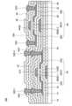
FIG. 1 is a cross-sectional view showing an overview of a
図1に示すように、半導体装置100は、基板10の上に設けられた第1トランジスタ210及び第2トランジスタ220を有している。第1トランジスタ210は、第1ゲート電極12GE、第1絶縁膜14、16、第1酸化物半導体層22、第2絶縁膜24、及び第2ゲート電極26GE-1を含む。第1酸化物半導体層22は、第1チャネル領域22CH、第1ソース領域22S、及び第1ドレイン領域22Dを含む。第2トランジスタ220は、第3ゲート電極26GE-2、第3絶縁膜28、32、第2酸化物半導体層36、第4絶縁膜38、及び第4ゲート電極44GEを含む。第2酸化物半導体層36は、第2チャネル領域36CH、第2ソース領域36S、及び第2ドレイン領域36Dを含む。なお、第1酸化物半導体層22及び第2酸化物半導体層36を区別しない場合、単に、チャネル領域CH、ソース領域S、及びドレイン領域Dと記載する場合がある。1, the
第2トランジスタ220は、第1トランジスタ210の上方に設けられている。第2トランジスタ220は、第1トランジスタ210の上方に設けられているとは、第2酸化物半導体層36が、第1酸化物半導体層22よりも上方に設けられていることをいう。The
第1絶縁膜14、16は、第1トランジスタ210の第1ゲート絶縁膜として機能する。また、第2絶縁膜24は、第1トランジスタ210の第2ゲート絶縁膜として機能する。また、第1絶縁膜14、16及び第2絶縁膜24は、第2トランジスタ220の下地膜としても機能する。第3絶縁膜28、32は、第2トランジスタ220の第3ゲート絶縁膜として機能する。また、第4絶縁膜38は、第2トランジスタの第4ゲート絶縁膜として機能する。また、第3絶縁膜28、32及び第4絶縁膜38は、第1トランジスタ210の層間絶縁膜として機能する。The first insulating
第4絶縁膜38の上には、第1ドレイン電極44D及び第1ドレイン電極44Dが設けられている。第1ソース電極44S及び第1ドレイン電極44Dは、第2絶縁膜24~第4絶縁膜38に設けられたコンタクトホールを介して、第1酸化物半導体層22と接続されている。第1ソース電極44S及び第1ドレイン電極44Dは、第4ゲート電極44GEと同じ第4絶縁膜38の上に設けられている。また、第3絶縁膜28、32は、第1トランジスタ210の層間絶縁膜として機能するとともに、第2トランジスタ220の第3ゲート絶縁膜として機能させることができる。第1ソース電極44S、第1ドレイン電極44D、及び第4ゲート電極44GEの上に、第5絶縁膜46、48が設けられている。A
第5絶縁膜48の上には、第2ソース電極52S及び第2ドレイン電極52Dが設けられている。第2ソース電極52S及び第2ドレイン電極52Dは、第4絶縁膜38及び第5絶縁膜46、48に設けられたコンタクトホールを介して、第2酸化物半導体層36と接続されている。また、第5絶縁膜48の上には、第1電極52E-1及び第2電極52E-2が設けられている。第1電極52E-1及び第2電極52E-2は、第5絶縁膜46、48に設けられたコンタクトホールを介して、第1ソース電極44S及び第1ドレイン電極44Dと接続されている。A
本実施形態において、第1トランジスタ210と第2トランジスタ220とは、同様の構造を有している。そのため、第2トランジスタ220の構造において、第1トランジスタ210と同様の構造については、適宜説明を省略する場合がある。In this embodiment, the
第1酸化物半導体層22及び第2酸化物半導体層36は、複数の結晶粒を含む多結晶構造を有する。詳細は後述するが、Poly-OS(Poly-crystalline Oxide Semiconductor)技術を用いることにより、多結晶構造を有する第1酸化物半導体層22及び第2酸化物半導体層36を形成することができる。以下では、第1酸化物半導体層22及び第2酸化物半導体層36の構成について説明するが、多結晶構造を有する酸化物半導体をPoly-OSという場合がある。The first
第1酸化物半導体層22及び第2酸化物半導体層36は、インジウム元素を含む2以上の金属を含み、2以上の金属におけるインジウム元素の比率は50%以上である。インジウム元素以外の金属元素として、ガリウム(Ga)元素、亜鉛(Zn)元素、アルミニウム(Al)元素、ハフニウム(Hf)元素、イットリウム(Y)元素、ジルコニウム(Zr)元素、およびランタノイド系元素が用いられる。ただし、第1酸化物半導体層22及び第2酸化物半導体層36はPoly-OSを含んでいればよく、上記以外の金属元素が含まれる場合がある。第2酸化物半導体層36は、第1酸化物半導体層22と同じ組成を有する酸化物半導体ターゲットを用いて成膜されることが好ましい。これにより、半導体装置100の製造コストを削減することができる。The first
第1酸化物半導体層22及び第2酸化物半導体層36の上面(または第1酸化物半導体層22及び第2酸化物半導体層36の膜厚方向)または第1酸化物半導体層22及び第2酸化物半導体層36の断面から観察したPoly-OSに含まれる結晶粒の結晶粒径は、0.1μm以上であり、好ましくは0.3μm以上であり、さらに好ましくは0.5μm以上である。結晶粒の結晶粒径は、例えば、断面SEM観察、断面TEM観察、または電子線後方散乱回折(Electron Back Scattered Diffraction:EBSD)法などを用いて取得することができる。The crystal grain size of the crystal grains contained in the Poly-OS observed from the top surface of the first
第1酸化物半導体層22及び第2酸化物半導体層36の各々の膜厚は、10nmより大きく30nm以下である。上述したように、Poly-OSに含まれる結晶粒の結晶粒径は0.1μm以上であるため、第1酸化物半導体層22及び第2酸化物半導体層36は、膜厚方向に1つの結晶粒のみが含まれる領域を含む。また、第1酸化物半導体層22及び第2酸化物半導体層36の各々の膜厚は、同じ膜厚であってもよく、異なる膜厚であってもよい。The thickness of each of the first
Poly-OSでは、複数の結晶粒が1種類の結晶構造を有していてもよく、複数の種類の結晶構造を有していてもよい。Poly-OSの結晶構造は、電子線回折法またはXRD法などを用いて特定することができる。すなわち、第1酸化物半導体層22及び第2酸化物半導体層36の結晶構造は、電子線回折法またはXRD法などを用いて特定することができる。In Poly-OS, multiple crystal grains may have one type of crystal structure, or multiple types of crystal structures. The crystal structure of Poly-OS can be identified using electron beam diffraction, XRD, or the like. That is, the crystal structures of the first
第1酸化物半導体層22及び第2酸化物半導体層36の結晶構造は、立方晶であることが好ましい。立方晶は、結晶構造の対称性が高く、第1酸化物半導体層22及び第2酸化物半導体層36に酸素欠陥が生成された場合においても、構造緩和が起きにくく、結晶構造が安定している。上述したように、インジウム元素の比率を高くすることにより、複数の結晶粒の各々の結晶構造が制御され、立方晶の結晶構造を有する第1酸化物半導体層22及び第2酸化物半導体層36を形成することができる。The crystal structure of the first
第1酸化物半導体層22は、第2ゲート電極26GE-1と重畳し、第1の結晶構造を有する第1の領域と、第2ゲート電極26GE-1と重畳せず、第2の結晶構造を有する第2の領域と、を含む。ここで、第1の領域とは、第1チャネル領域22CHに相当する。また、第2の領域とは、第1ソース領域22S及び第1ドレイン領域22Dに相当する。第2の領域の電気伝導度は、第1の領域の電気伝導度よりも大きい。The first
第2酸化物半導体層36は、第4ゲート電極44GEと重畳し、第1の結晶構造を有する第3の領域と、第4ゲート電極44GEと重畳せず、第2の結晶構造を有する第4の領域と、を含む。ここで、第3の領域とは、第2チャネル領域36CHに相当する。また、第4の領域とは、第2ソース領域36S及び第2ドレイン領域36Dに相当する。第4の領域の電気伝導度は、第3の領域の電気伝導度よりも大きい。The second
また、第2の結晶構造は、第1の結晶構造と同一である。ここで、2つの結晶構造が同一とは、結晶系が同一であることを意味する。例えば、第1酸化物半導体層22の結晶構造が立方晶であるとき、第1の領域の第1の結晶構造および第2の領域の結晶構造は、ともに立方晶であり、同一である。第1の結晶構造および第2の結晶構造は、例えば、極微電子線回折法などを用いて特定することができる。The second crystal structure is the same as the first crystal structure. Here, the two crystal structures being the same means that the crystal systems are the same. For example, when the crystal structure of the first
また、所定の結晶方位において、第1の結晶構造の面間隔d値と、第2の結晶構造の面間隔dとは、略同一である。ここで、2つの面間隔d値が略同一とは、一方の面間隔d値が、他方の面間隔d値の0.95倍以上1.05倍以下であることをいう。あるいは、極微電子線回折法において、2つの回折パターンがほとんど一致している場合をいう。In addition, in a given crystal orientation, the d-spacing value of the first crystal structure and the d-spacing value of the second crystal structure are substantially the same. Here, "substantially the same" in two d-spacing values means that one d-spacing value is 0.95 to 1.05 times the other d-spacing value. Alternatively, in the ultrafine electron beam diffraction method, it means that the two diffraction patterns are almost identical.
第1の領域と第2の領域との間には、結晶粒界が存在しなくてもよい。また、1つの結晶粒の中に、第1の領域および第2の領域が含まれていてもよい。換言すると、第1の領域から第2の領域への変化は、連続的な結晶構造の変化であってもよい。同様に、第3の領域と第4の領域との間には、結晶粒界が存在しなくてもよい。また、1つの結晶粒の中に、第3の領域および第4の領域が含まれていてもよい。換言すると、第3の領域から第4の領域への変化は、連続的な結晶構造の変化であってもよい。There may be no grain boundary between the first region and the second region. Also, the first region and the second region may be included in one crystal grain. In other words, the change from the first region to the second region may be a continuous change in crystal structure. Similarly, there may be no grain boundary between the third region and the fourth region. Also, the third region and the fourth region may be included in one crystal grain. In other words, the change from the third region to the fourth region may be a continuous change in crystal structure.
また、第1ソース領域22S、第1ドレイン領域22D、第2ソース領域36S、及び第2ドレイン領域36Dは、同じ不純物元素を含んでいる。また、第1ソース領域22S、第1ドレイン領域22D、第2ソース領域36S、及び第2ドレイン領域36Dは、不純物元素が添加されることによって、第1チャネル領域22CH及び第2チャネル領域36CHと比較して抵抗率が低下している。つまり、第1ソース領域22S、第1ドレイン領域22D、第2ソース領域36S、及び第2ドレイン領域36Dは、導体としての物性を備えている。なお、第1ソース領域22S、第1ドレイン領域22D、第2ソース領域36S、及び第2ドレイン領域36Dのそれぞれにおいて、前述の領域全てにおいて同一の不純物元素が含まれていても良いし、層毎に異なる不純物元素が含まれていてもよい。例えば、第1ソース領域22S及び第1ドレイン領域22Dにリンを添加し、第2ソース領域36S及び第2ドレイン領域36Dにボロンを添加してもよい。The
第1ソース領域22S、第1ドレイン領域22D、第2ソース領域36S、及び第2ドレイン領域36Dに含まれる不純物元素の濃度は、SIMS分析(二次イオン質量分析)で測定した場合に、1×1018cm-3以上1×1021cm-3以下であることが好ましい。ここで、不純物元素とは、アルゴン(Ar)、リン(P)、又はボロン(B)をいう。 The concentration of an impurity element contained in the
第1ソース領域22S、第1ドレイン領域22D、第2ソース領域36S、及び第2ドレイン領域36Dには、不純物元素が添加されることにより、酸素欠陥が形成される。酸素欠陥に水素がトラップされることで、第1ソース領域22S、第1ドレイン領域22D、第2ソース領域36S、及び第2ドレイン領域36Dの抵抗を、第1チャネル領域22CH及び第2チャネル領域36CHの抵抗よりも低減することができる。なお、第1ソース領域22S、第1ドレイン領域22D、第2ソース領域36S、及び第2ドレイン領域36Dに不純物元素が添加されて、酸素欠陥が形成されても、結晶構造は壊れることなく維持される。そのため、第1ソース領域22S、第1ドレイン領域22D、第2ソース領域36S、及び第2ドレイン領域36Dの結晶構造は、第1チャネル領域22CH及び第2チャネル領域36CHの結晶構造と同一であるといえる。Oxygen defects are formed in the
酸化物半導体層は、層の内部に酸素欠陥が多く含まれると、酸素欠陥に水素がトラップされることでトランジスタの特性に悪影響を及ぼす。そのため、酸化物半導体層に含まれる酸素欠陥を低減させることが求められている。If an oxide semiconductor layer contains many oxygen defects inside the layer, hydrogen is trapped in the oxygen defects, adversely affecting the characteristics of the transistor. Therefore, there is a need to reduce the oxygen defects contained in the oxide semiconductor layer.
酸化物半導体は、アモルファスの酸化物半導体よりも結晶性の酸化物半導体の方が酸素欠陥が形成されにくい。また、酸化物半導体に含まれるインジウムの比率を相対的に高くすることで、結晶性の酸化物半導体が得られやすいことが知られている。しかしながら、インジウムの比率を相対的に高くして、結晶性の酸化物半導体が得られても、必要以上の酸素欠陥が存在する。酸素欠陥は、酸素が供給されることで修復することができる。そのため、酸化物半導体層の周囲の絶縁膜として、酸素を放出することが可能な絶縁膜を配置することで、酸化物半導体層の酸素欠陥を修復する必要がある。Oxygen defects are less likely to form in crystalline oxide semiconductors than in amorphous oxide semiconductors. It is also known that a crystalline oxide semiconductor can be obtained by relatively increasing the ratio of indium contained in the oxide semiconductor. However, even if a crystalline oxide semiconductor is obtained by relatively increasing the ratio of indium, more oxygen defects than necessary will still exist. The oxygen defects can be repaired by supplying oxygen. Therefore, it is necessary to repair the oxygen defects in the oxide semiconductor layer by arranging an insulating film capable of releasing oxygen as an insulating film around the oxide semiconductor layer.
一方で、酸化物半導体層に必要以上の酸素を供給すると、酸化物半導体層に含まれる過剰な酸素によって、酸素欠陥とは異なる欠陥準位が形成されてしまう。これにより、信頼性試験による特性変動、電界効果移動度の低下、又は特性のばらつきなどの現象が発生するおそれがある。On the other hand, if more oxygen than necessary is supplied to the oxide semiconductor layer, the excess oxygen contained in the oxide semiconductor layer will form defect levels that are different from oxygen defects. This may cause phenomena such as characteristic fluctuations due to reliability tests, reduced field-effect mobility, or characteristic variations.
本発明の一実施形態に係る半導体装置100によれば、第1酸化物半導体層22及び第2酸化物半導体層36は、Poly-OSを含む。これにより、第1酸化物半導体層22及び第2酸化物半導体層36は、結晶性が高く、かつ酸素欠陥が十分に低減された層となる。According to the
また、第1酸化物半導体層22及び第2酸化物半導体層36は、チャネル領域CHだけでなく、ソース領域Sおよびドレイン領域Dが結晶構造を有することにより、ソース領域Sおよびドレイン領域Dを十分に低抵抗化することができる。そのため、ソース領域Sおよびドレイン領域Dの寄生抵抗が低減され、第1トランジスタ210及び第2トランジスタ220の電気特性におけるオン電流のばらつきを抑制することができる。第1トランジスタ210及び第2トランジスタ220は移動度が大きいため、半導体装置100を表示装置などに用いる場合、ばらつきが抑制されるとともに、性能が向上する。In addition, the first
本発明の一実施形態に係る半導体装置100では、第1トランジスタ210及び第2トランジスタ220のチャネル領域CHのチャネル長Lが2μm以上4μm以下、かつ、チャネル領域CHのチャネル幅が2μm以上25μm以下の範囲において、移動度が30cm2/Vs以上、35cm2/Vs以上、又は40cm2/Vs以上の電気特性を得ることができる。本明細書等における移動度とはトランジスタの飽和領域における電界効果移動度であって、ソース電極とドレイン電極との間の電位差(Vd)が、ゲート電極に供給される電圧(Vg)からトランジスタの閾値電圧(Vth)を引いた値(Vg-Vth)より大きい領域における電界効果移動度の最大値を意味する。 In the
また、第1酸化物半導体層22及び第2酸化物半導体層36のチャネル領域CHに含まれる酸素欠陥が十分に低減されることで、酸素欠陥に水素がトラップされることを抑制することができる。これにより、第1トランジスタ210及び第2トランジスタ220の信頼性試験における特性変動を少なくすることができるため、半導体装置の信頼性が向上する。In addition, by sufficiently reducing the oxygen defects contained in the channel region CH of the first
ここで、信頼性試験とは、例えば、ゲートに負の電圧を印加するNGBT(Negative Gate Bias-Temperature)ストレス試験、又はゲートに正の電圧を印加するPGBT(Positive Gate Bias-Temperature)ストレス試験をいう。なお、NGBTおよびPGBTなどのBTストレス試験は加速試験の一種であり、長期間の使用によって起こるトランジスタの特性変化(経年変化)を短時間で評価することができる。特に、BTストレス試験前後におけるトランジスタのしきい値電圧の変動量は、信頼性を調べるための重要な指標となる。BTストレス試験前後において、しきい値電圧の変動量が少ないほど、信頼性が高いトランジスタであるといえる。Here, the reliability test refers to, for example, an NGBT (Negative Gate Bias-Temperature) stress test in which a negative voltage is applied to the gate, or a PGBT (Positive Gate Bias-Temperature) stress test in which a positive voltage is applied to the gate. Note that BT stress tests for NGBT and PGBT are a type of accelerated test, and can quickly evaluate changes in transistor characteristics (aging) that occur over a long period of use. In particular, the amount of change in the threshold voltage of a transistor before and after a BT stress test is an important indicator for investigating reliability. The smaller the amount of change in threshold voltage before and after a BT stress test, the more reliable the transistor is.
ところで、半導体材料が異なる2つのトランジスタを積層する場合、2つのトランジスタを接続するための配線構造が複雑となる。また、半導体装置を製造している過程で、下のトランジスタの構成材料によって、上のトランジスタの構成材料に悪影響を及ぼすおそれがある。例えば、低温ポリシリコンを用いたトランジスタは、アモルファスシリコンにレーザ照射プロセスを行う必要があるため、酸化物半導体を用いたトランジスタよりも下層に形成される。低温ポリシリコンを用いたトランジスタの構成材料は、水素を多く含む材料が用いられる。この水素によって、酸化物半導体に悪影響を及ぼす可能性が高い。そのため、低温ポリシリコンを用いたトランジスタと酸化物半導体を用いたトランジスタとを互いに重畳して形成する場合、低温ポリシリコンを用いたトランジスタの構成材料から放出される水素の影響を低減するために絶縁層を増加させたり、加熱処理が増加する場合がある。また、結晶性シリコンを用いたトランジスタ及び酸化物半導体を用いたトランジスタの双方が同じトップゲート構造であったとしても、結晶性シリコンを用いたトランジスタ及び酸化物半導体を用いたトランジスタに用いられる絶縁材料及び導電材料の構成や膜厚はそれぞれ異なるため、トランジスタの構造を共通化することができない。However, when two transistors made of different semiconductor materials are stacked, the wiring structure for connecting the two transistors becomes complicated. In addition, during the process of manufacturing a semiconductor device, the constituent material of the lower transistor may adversely affect the constituent material of the upper transistor. For example, a transistor using low-temperature polysilicon is formed in a lower layer than a transistor using an oxide semiconductor because it is necessary to perform a laser irradiation process on amorphous silicon. A material containing a large amount of hydrogen is used as the constituent material of a transistor using low-temperature polysilicon. This hydrogen is likely to adversely affect the oxide semiconductor. Therefore, when a transistor using low-temperature polysilicon and a transistor using an oxide semiconductor are formed by overlapping each other, the insulating layer may be increased or the heat treatment may be increased in order to reduce the influence of hydrogen released from the constituent material of the transistor using low-temperature polysilicon. In addition, even if both the transistor using crystalline silicon and the transistor using an oxide semiconductor have the same top gate structure, the configuration and film thickness of the insulating material and conductive material used in the transistor using crystalline silicon and the transistor using an oxide semiconductor are different from each other, so the structure of the transistors cannot be made common.
第1トランジスタ210及び第2トランジスタ220の双方において高い移動度が得られるため、高速駆動が要求されるトランジスタに、酸化物半導体がチャネルに用いられたトランジスタを用いることができる。これにより、高速駆動が要求されるトランジスタとして、結晶性シリコンがチャネルに用いられたトランジスタを形成しなくてよい。そのため、高速駆動が要求されるトランジスタと、それ以外の特性が要求されるトランジスタとを、作り分ける必要がなくなる。Since high mobility can be obtained in both the
また、本発明の一実施形態に係る半導体装置100では、半導体材料が同じ2つのトランジスタを積層するため、2つのトランジスタを接続するための配線構造を簡素化することができる。また、酸化物半導体を用いた第1トランジスタ210と第2トランジスタ220との構造を共通化させることが容易である。例えば、第1トランジスタ210及び第2トランジスタ220を、酸化物半導体層を間に挟んだデュアルゲート構造のトランジスタとすることができる。また、第1トランジスタ210及び第2トランジスタ220のゲート電極として用いる導電材料と、ゲート絶縁膜として用いる絶縁材料とを同じ構造にすることができる。In addition, in the
本実施形態では、第1トランジスタ210は、第1ゲート電極12GE、第1絶縁膜14、16として窒化シリコン膜及び酸化シリコン膜の積層、第1酸化物半導体層22、第2絶縁膜24として酸化シリコン膜、及び第2ゲート電極26GE-1を含む。同様に、第2トランジスタは、第3ゲート電極26GE-2、第3絶縁膜28、32として窒化シリコン膜及び酸化シリコン膜の積層、第2酸化物半導体層36、第4絶縁膜38として酸化シリコン膜、及び第4ゲート電極44GEを含む。つまり、第1ゲート電極12GEと第3ゲート電極26GE-2、第1絶縁膜14、16と第3絶縁膜28、32、第2絶縁膜24と第4絶縁膜38、及び第2ゲート電極26GE-1と第4ゲート電極44GEは、それぞれ対応している。また、第1酸化物半導体層22及び第2酸化物半導体層36は、多結晶構造を有している。そのため、同等の性能を有する第1トランジスタ210の上に、第2トランジスタ220を、積層して配置することができる。In this embodiment, the
本実施形態では、第1トランジスタ210として、第2ゲート電極26GE-1によってトランジスタを駆動するトップゲート型トランジスタが用いられる。また、第2トランジスタ220として、第4ゲート電極44GEによってトランジスタを駆動するトップゲート型トランジスタが用いられる。そのため、第2絶縁膜24の膜厚が、第1絶縁膜14、16の膜厚よりも薄いことが好ましい。同様に、第4絶縁膜38の膜厚は、第3絶縁膜28、32の膜厚よりも薄いことが好ましい。In this embodiment, the
例えば、半導体装置を有機ELディスプレイに適用する場合、1つの画素回路において、駆動用のトランジスタとスイッチング用のトランジスタとを合わせて6つ以上必要になる場合がある。同一平面内に、6つのトランジスタを配置する場合、6つ分のトランジスタの面積が必要となる。そのため、画素を高精細にする場合には、画素回路の更なる集積化が困難となる。For example, when applying a semiconductor device to an organic EL display, six or more driving transistors and switching transistors may be required in one pixel circuit. When six transistors are arranged on the same plane, an area for six transistors is required. Therefore, when making pixels into high resolution, it becomes difficult to further integrate the pixel circuits.
半導体装置100では、同じ機能を有するトランジスタを積層して設けることが可能となる。例えば、画素回路においてスイッチング用のトランジスタについては、上層と下層で積層させて設けることで、画素回路の面積を縮小することができる。これにより、画素回路の占める面積を小さくすることができるため、より高精細な有機ELディスプレイを提供することができる。In the
第1トランジスタ210と第2トランジスタ220のそれぞれは、移動度が高い。そのため、高速駆動が要求される駆動回路にも適している。また、表示装置の駆動回路に、半導体装置100を適用する場合、下層の第1トランジスタ210と上層の第2トランジスタ220と、を互いに近接させる、あるいは互いの一部又は全部が重畳するように積層して設けることが可能である。また、上層の第2トランジスタ220の下に、下層の第1トランジスタ210の配線を延在させることも可能となる。これにより、表示装置の駆動回路の面積を縮小することができる。これにより、狭額縁の表示装置を提供することができる。Each of the
本実施形態では、第1トランジスタ210として、第2ゲート電極26GE-1によってトランジスタを駆動するトップゲート型トランジスタが用いられる構成を例示するが、この構成に限定されない。例えば、第1トランジスタ210として、第1ゲート電極12GEによってトランジスタを駆動するボトムゲート型トランジスタが用いられてもよい。または、第1トランジスタ210として、第1ゲート電極12GE及び第2ゲート電極26GE-1によってトランジスタを駆動するデュアルゲート型トランジスタが用いられてもよい。なお、第2トランジスタ220についても、第1トランジスタ210と同様である。第2トランジスタ220として、トップゲート型トランジスタに限定されず、ボトムゲート型トランジスタ又はデュアルゲート型トランジスタのいずれであってもよい。上記の構成はあくまで一実施形態に過ぎず、本発明は上記の構成に限定されない。In this embodiment, a configuration is illustrated in which the
第1ゲート電極12GEは、第1トランジスタ210のボトムゲート及び第1酸化物半導体層22に対する遮光膜としての機能を備える。第1絶縁膜14、16及び第2絶縁膜24は、製造プロセスにおける熱処理によって酸素を放出する機能を備える。第2絶縁膜24、第3絶縁膜28、32、及び第4絶縁膜38は、第1ゲート電極12GEと第1ソース電極44S及び第1ドレイン電極44Dとを絶縁し、両者間の寄生容量を低減する機能を備える。第1トランジスタ210の動作は、主に第2ゲート電極26GE-1に供給される電圧によって制御される。第1ゲート電極12GEには補助的な電圧が供給される。また、第1ゲート電極12GEを単に遮光膜として用いてもよく、この場合、第1ゲート電極12GEに特定の電圧が供給されず、フローティングであってもよい。The first gate electrode 12GE functions as a light-shielding film for the bottom gate of the
第3ゲート電極26GE-2は、第2トランジスタ220のボトムゲート及び第2酸化物半導体層36に対する遮光膜としての機能を備える。第3絶縁膜32及び第4絶縁膜38は、製造プロセスにおける熱処理によって酸素を放出する機能を備える。第4絶縁膜38及び第5絶縁膜46、48は、第4ゲート電極44GEと第2ソース電極52S及び第2ドレイン電極52Dとを絶縁し、両者間の寄生容量を低減する機能を備える。第2トランジスタ220の動作は、主に第4ゲート電極44GEに供給される電圧によって制御される。第3ゲート電極26GE-2には補助的な電圧が供給される。また、第3ゲート電極26GE-2を単に遮光膜として用いてもよく、この場合、第3ゲート電極26GE-2に特定の電圧が供給されず、フローティングであってもよい。The third gate electrode 26GE-2 functions as a light-shielding film for the bottom gate of the
[半導体装置100の製造方法]
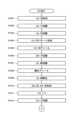
図2~図16を用いて、本発明の一実施形態に係る半導体装置100の製造方法について説明する。図2及び図3は、本発明の一実施形態に係る半導体装置100の製造方法を示すシーケンス図である。[Method of Manufacturing the Semiconductor Device 100]
A method for manufacturing the
図2及び図4に示すように、基板10の上に第1ゲート電極12GEが形成される(図2に示すステップS1001の「1st GE形成」)。As shown in Figures 2 and 4, a first gate electrode 12GE is formed on the substrate 10 ("1st GE formation" in step S1001 shown in Figure 2).
基板10として、ガラス基板、石英基板、及びサファイア基板など、透光性を有する剛性基板が用いられる。基板10が可撓性を備える必要がある場合、基板10として、ポリイミド基板、アクリル基板、シロキサン基板、フッ素樹脂基板など樹脂を含む基板が用いられる。基板10として樹脂を含む基板が用いられる場合、基板10の耐熱性を向上させるために、上記の樹脂に不純物元素が導入されてもよい。特に、半導体装置100がトップエミッション型のディスプレイである場合、基板10が透明である必要はないため、基板10の透明度を低下させる不純物が用いられてもよい。表示装置ではない集積回路に半導体装置100が用いられる場合は、基板10としてシリコン基板、炭化シリコン基板、化合物半導体基板などの半導体基板、又は、ステンレス基板などの導電性基板など、透光性を備えない基板が用いられてもよい。As the
第1ゲート電極12GEは、スパッタリング法によって成膜された導電膜を加工して形成される。第1ゲート電極12GEとして、一般的な金属材料が用いられる。第1ゲート電極12GEとして、例えば、アルミニウム(Al)、チタン(Ti)、クロム(Cr)、コバルト(Co)、ニッケル(Ni)、モリブデン(Mo)、ハフニウム(Hf)、タンタル(Ta)、タングステン(W)、ビスマス(Bi)、銀(Ag)、銅(Cu)、及びこれらの合金又は化合物が用いられる。第1ゲート電極12GEとして、上記の材料が単層で用いられてもよく積層で用いられてもよい。The first gate electrode 12GE is formed by processing a conductive film formed by a sputtering method. A general metal material is used for the first gate electrode 12GE. For example, aluminum (Al), titanium (Ti), chromium (Cr), cobalt (Co), nickel (Ni), molybdenum (Mo), hafnium (Hf), tantalum (Ta), tungsten (W), bismuth (Bi), silver (Ag), copper (Cu), and alloys or compounds thereof are used for the first gate electrode 12GE. The above materials may be used as a single layer or as a laminated layer for the first gate electrode 12GE.
図2及び図4に示すように、基板10及び第1ゲート電極12GEの上に第1絶縁膜14、16が成膜される(図2に示すステップS1002の「1st IF成膜」)。第1絶縁膜14、16はCVD(Chemical Vapor Deposition)法、又はスパッタリング法によって成膜される。第1絶縁膜14、16として、一般的な絶縁性材料が用いられる。第1絶縁膜14、16として、例えば、酸化シリコン(SiOx)、酸化窒化シリコン(SiOxNy)、窒化シリコン(SiNx)、窒化酸化シリコン(SiNxOy)などの無機絶縁材料が用いられる。上記のSiOxNyは、酸素(O)よりも少ない比率(x>y)の窒素(N)を含有するシリコン化合物である。SiNxOyは、窒素よりも少ない比率(x>y)の酸素を含有するシリコン化合物である。 As shown in FIG. 2 and FIG. 4, the first insulating
第1絶縁膜14、16として、基板10から窒素を含む絶縁材料と酸素を含む絶縁材料との順で形成されることが好ましい。例えば、第1絶縁膜14として、窒素を含む絶縁材料を用いることにより、基板10側から第1酸化物半導体層22に向かって拡散する不純物をブロックすることができる。また、第1絶縁膜16として、酸素を含む絶縁材料を用いることにより、加熱処理によって酸素を放出させることができる。酸素を含む絶縁材料が酸素を放出する加熱処理の温度は、例えば、500℃以下、450℃以下、又は400℃以下である。つまり、酸素を含む絶縁材料は、例えば、基板10としてガラス基板が用いられた場合の半導体装置100の製造工程で行われる加熱処理温度で酸素を放出する。本実施形態では、第1絶縁膜14、16として、窒化シリコンと酸化シリコンとの積層構造を用いる例について説明するが、第1絶縁膜として、上述した材料の単層構造を用いてもよい。As the first insulating
図2及び図4に示すように、第1絶縁膜16の上に第1酸化物半導体膜17を成膜する(図2に示すステップS1003「1st OS成膜」)。この工程について、基板10の上に第1酸化物半導体膜17を形成する、という場合がある。第1酸化物半導体膜17は、スパッタリング法又は原子層堆積法(ALD:Atomic Layer Deposition)によって成膜される。第1酸化物半導体膜17の膜厚は、例えば、10nmより大きく30nm以下である。2 and 4, a first
第1酸化物半導体膜17として、半導体の特性を有する金属酸化物を用いることができる。第1酸化物半導体膜17は、インジウム元素を含む2以上の金属を含む酸化物半導体が用いられる。また、2以上の金属におけるインジウム元素の比率は50%以上である。第1酸化物半導体膜17として、インジウム元素以外の金属元素として、ガリウム(Ga)元素、亜鉛(Zn)元素、アルミニウム(Al)元素、ハフニウム(Hf)元素、イットリウム(Y)元素、ジルコニウム(Zr)元素、又はランタノイド系元素が用いられる。A metal oxide having semiconductor properties can be used as the first
後述するOSアニールによって、第1酸化物半導体膜17を結晶化する場合、成膜後かつOSアニール前の第1酸化物半導体膜17はアモルファス(酸化物半導体の結晶成分が少ない状態)であることが好ましい。つまり、第1酸化物半導体膜17の成膜方法は、成膜直後の第1酸化物半導体膜17ができるだけ結晶化しない条件であることが好ましい。例えば、スパッタリング法によって第1酸化物半導体膜17が成膜される場合、被成膜対象物(半導体装置100及びその上に形成された構造物)の温度を制御しながら第1酸化物半導体膜17が成膜される。When the first
スパッタリング法によって被成膜対象物に対して成膜を行うと、プラズマ中で発生したイオン及びスパッタリングターゲットによって反跳した原子が被成膜対象物に衝突するため、成膜処理に伴い被成膜対象物の温度が上昇する。成膜処理中の被成膜対象物の温度が上昇すると、成膜直後の状態で第1酸化物半導体膜17に微結晶が含まれる。第1酸化物半導体膜17に微結晶が含まれると、その後のOSアニールによって結晶粒径を大きくすることができない。上記のように被成膜対象物の温度を制御するために、例えば、被成膜対象物を冷却しながら成膜を行うことができる。例えば、被成膜対象物の被成膜面の温度(以下、「成膜温度」という。)が100℃以下、70℃以下、50℃以下、又は30℃以下になるように、被成膜対象物を当該被成膜面の反対側の面から冷却することができる。特に、本実施形態の第1酸化物半導体膜17の成膜温度は、50℃以下であることが好ましい。基板を冷却しながら第1酸化物半導体膜17の形成を行うことで、成膜直後の状態で結晶成分が少ない第1酸化物半導体膜17を得ることができる。本実施形態では、第1酸化物半導体膜17の形成を50℃以下の成膜温度で行い、後述するOSアニールを400℃以上の加熱温度で行う。このように、本実施形態では、第1酸化物半導体膜17を形成する際の温度と第1酸化物半導体膜17に対してOSアニールを行う際の温度との差分が350℃以上であることが好ましい。When a film is formed on a target object by sputtering, ions generated in the plasma and atoms recoiled by the sputtering target collide with the target object, and the temperature of the target object rises with the film formation process. When the temperature of the target object rises during the film formation process, the first
スパッタリングプロセスでは、酸素分圧10%以下の条件でアモルファスの第1酸化物半導体膜17が成膜される。酸素分圧が高いと、第1酸化物半導体膜17に含まれる過剰な酸素によって成膜直後の第1酸化物半導体膜17に微結晶が含まれてしまう。そのため、酸素分圧が低い条件の下で第1酸化物半導体膜17の成膜が行われることが好ましい。酸素分圧は、例えば、3%以上5%以下であり、好ましくは3%以上4%以下である。なお、酸素分圧が2%の条件で、酸化物半導体膜を成膜した場合、後にOSアニール処理を行っても酸化物半導体膜は十分な結晶性が得られない場合がある。In the sputtering process, the amorphous first
図2及び図5に示すように、第1酸化物半導体層18のパターンを形成する(図2に示すステップS1004の「1st OSパターン形成」)。第1酸化物半導体膜17の上にレジストマスク19を形成し、当該レジストマスク19を用いて第1酸化物半導体膜17をエッチングする。第1酸化物半導体膜17のエッチングとして、ウェットエッチングが用いられてもよく、ドライエッチングが用いられてもよい。ウェットエッチングとして、酸性のエッチャントを用いてエッチングを行うことができる。エッチャントとして、例えば、シュウ酸、PAN、硫酸、過酸化水素水、またはフッ酸を用いることができる。これにより、パターン状の第1酸化物半導体層18を形成することができる。その後、レジストマスク19を除去する。2 and 5, a pattern of the first
第1酸化物半導体膜17は、OSアニール前にパターンが形成されることが好ましい。OSアニールによって第1酸化物半導体膜17が結晶化すると、エッチングし難い傾向がある。また、エッチングによってパターン状の第1酸化物半導体層18にダメージが生じても、OSアニールによって第1酸化物半導体層18のダメージを修復できるため好ましい。It is preferable that the first
図2及び図6に示すように、第1酸化物半導体層18のパターン形成の後に第1酸化物半導体層18に対して加熱処理(OSアニール)が行われる(図2に示すステップS1005「1st OSアニール」)。OSアニールでは、第1酸化物半導体層18が、所定の到達温度で所定の時間保持される。所定の到達温度は、300℃以上500℃以下であり、好ましくは350℃以上450℃以下である。また、到達温度での保持時間は、15分以上120分以下であり、好ましくは30分以上60分以下である。OSアニールを行うことにより、第1酸化物半導体層18が結晶化され、多結晶構造を有する第1酸化物半導体層22が形成される。2 and 6, after the patterning of the first
薄膜トランジスタでは、酸化物半導体層の厚さを小さくすることで、ゲート絶縁膜との界面近傍におけるキャリアを増加させて、バックチャネルの影響を低減することで、電界効果移動度が高くなる傾向がある。つまり、薄膜トランジスタは、酸化物半導体層のチャネルとして機能する領域の厚さが小さいほど、電界効果移動度が高くなる傾向がある。そのため、酸化物半導体層の厚さは小さいほどよい。しかしながら、酸化物半導体層の厚さを10nm以下で成膜した後、加熱処理を行っても、酸化物半導体層が十分な結晶性が得られない場合がある。In thin-film transistors, the field-effect mobility tends to be increased by reducing the thickness of the oxide semiconductor layer, which increases the carriers near the interface with the gate insulating film and reduces the influence of the back channel. In other words, in thin-film transistors, the field-effect mobility tends to be higher as the thickness of the region of the oxide semiconductor layer that functions as a channel is smaller. Therefore, the smaller the thickness of the oxide semiconductor layer, the better. However, even if the oxide semiconductor layer is formed to a thickness of 10 nm or less and then heat treatment is performed, the oxide semiconductor layer may not have sufficient crystallinity.
また、薄膜トランジスタにおいて、第1酸化物半導体層22の結晶性は、電界効果移動度の向上に寄与する。そのため、第1酸化物半導体層22は、多結晶構造を有していることが好ましい。しかしながら、第1酸化物半導体膜17の成膜時に、微結晶が含まれていると、その後、加熱処理を行っても多結晶構造の結晶粒の結晶粒径を大きくすることができない。このように、酸化物半導体層の薄膜化と、良好な結晶化を両立することは困難である。In addition, in a thin-film transistor, the crystallinity of the first
そこで、第1酸化物半導体膜17をスパッタリング法で成膜する際に、3%以上5%以下という低い酸素分圧で成膜する。酸素分圧が低い条件にて第1酸化物半導体膜17を成膜することにより、第1酸化物半導体膜17に過剰に酸素が含まれることを抑制することができ、成膜直後の第1酸化物半導体膜17に微結晶が含まれることを抑制することができる。これにより、第1酸化物半導体層18の加熱処理の際に、微結晶から結晶が成長することを抑制することができる。したがって、第1酸化物半導体膜17が10nmよりも大きく30nm以下の薄い膜厚で成膜された場合であっても、第1酸化物半導体層22の多結晶構造の結晶粒の結晶粒径を大きくすることができる。Therefore, when the first
図2及び図7に示すように、第1酸化物半導体層22の上に第2絶縁膜24を成膜する(図2に示すステップS1006の「2nd IF成膜」)。第2絶縁膜24の成膜方法及び絶縁材料は、第1絶縁膜14、16の説明を参照すればよい。また、第2絶縁膜24の膜厚は、例えば、50nm以上300nm以下、60nm以上200nm以下、又は70nm以上150nm以下である。2 and 7, the second insulating
第2絶縁膜24として、酸素を含む絶縁材料を用いることが好ましい。また、第2絶縁膜24として、欠陥が少ない絶縁膜を用いることが好ましい。例えば、第2絶縁膜24における酸素の組成比と、第2絶縁膜24と同様の組成の絶縁膜(以下、「他の絶縁膜」という)における酸素の組成比と、を比較した場合、第2絶縁膜24における酸素の組成比の方が当該他の絶縁膜における酸素の組成比よりも当該絶縁膜に対する化学量論比に近い。例えば、第2絶縁膜24及び第5絶縁膜48の各々に酸化シリコン(SiOx)が用いられる場合、第2絶縁膜24として用いられる酸化シリコンにおける酸素の組成比は、第5絶縁膜48として用いられる酸化シリコンにおける酸素の組成比に比べて、酸化シリコンの化学量論比に近い。例えば、第2絶縁膜24として、電子スピン共鳴法(ESR)で評価したときに欠陥が観測されない膜が用いられてもよい。 It is preferable to use an insulating material containing oxygen as the second insulating
第2絶縁膜24として欠陥が少ない絶縁膜を形成するために、350℃以上の成膜温度で第2絶縁膜24を成膜してもよい。第2絶縁膜24の厚さは、例えば、50nm以上300nm以下、60nm以上200nm以下、又は70nm以上150nm以下である。第2絶縁膜24を成膜した後に、第2絶縁膜24の一部に酸素を打ち込む処理を行ってもよい。本実施形態では、第2絶縁膜24として、欠陥が少ない絶縁膜を形成するために、350℃以上の成膜温度で酸化シリコンが形成される。In order to form an insulating film with few defects as the second insulating
図2及び図7に示すように、第2絶縁膜24の上に、第1金属酸化物膜25を成膜する(図2に示すステップS1007の「1st MO成膜」)。第1金属酸化物膜25は、スパッタリングによって成膜される。第1金属酸化物膜25をスパッタリング法により成膜することで、第2絶縁膜24に酸素が打ち込まれる。As shown in FIG. 2 and FIG. 7, a first
第1金属酸化物膜25として、アルミニウムを主成分とする金属酸化物が用いられる。例えば、第1金属酸化物膜25として、酸化アルミニウム(AlOx)、酸化窒化アルミニウム(AlOxNy)、窒化酸化アルミニウム(AlNxOy)、窒化アルミニウム(AlNx)などの無機絶縁層が用いられる。アルミニウムを主成分とする金属酸化物膜とは、金属酸化物膜に含まれるアルミニウムの比率が、第1金属酸化物膜25全体の1%以上であることを意味する。第1金属酸化物膜25に含まれるアルミニウムの比率は、第1金属酸化物膜25全体の5%以上70%以下、10%以上60%以下、又は30%以上50%以下であってもよい。上記の比率は、質量比であってもよく、重量比であってもよい。 A metal oxide containing aluminum as a main component is used as the first
第1金属酸化物膜25の厚さは、例えば、5nm以上100nm以下、5nm以上50nm以下、5nm以上30nm以下、又は7nm以上15nm以下である。本実施形態では、第1金属酸化物膜25として酸化アルミニウムが用いられる。酸化アルミニウムは酸素又は水素などのガスに対する高いバリア性を備えている。本実施形態において、第1金属酸化物膜25として用いられる酸化アルミニウムは、第1金属酸化物膜25の成膜時に第2絶縁膜24に打ち込まれた酸素が外方拡散することを抑制する。言い換えると、バリア性とは、酸素又は水素などのガスが、酸化アルミニウムを透過することを抑制する機能をいう。つまり、酸化アルミニウム膜の下に設けられる層から酸素などのガスが存在していても、酸化アルミニウム膜の上に設けられる層に移動させないことを意味する。または、酸化アルミニウム膜の上に設けられる層から酸素などのガスが存在していても、酸化アルミニウム膜の下に設けられる層に移動させないことを意味する。The thickness of the first
例えば、第1金属酸化物膜25をスパッタリング法で成膜した場合、第1金属酸化物膜25の膜中にはスパッタリングで用いられたプロセスガスが残存する。例えば、スパッタリングのプロセスガスとしてArが用いられた場合、第2絶縁膜24の膜中にはArが残存することがある。残存したArは第2絶縁膜24に対するSIMS(Secondary Ion Mass Spectrometry)分析で検出することができる。For example, when the first
第1酸化物半導体層22の上に第2絶縁膜24及び第1金属酸化物膜25が成膜された状態で、第2絶縁膜24から第1酸化物半導体層22へ酸素を供給するための加熱処理(酸化アニール)が行われる(図2に示すステップS1008の「酸化アニール」)。第1酸化物半導体膜17が成膜されてから第1酸化物半導体層22の上に第2絶縁膜24が成膜されるまでの間の工程で、第1酸化物半導体層22の上面及び側面には多くの酸素欠陥が発生する。酸化アニールによって、第1絶縁膜16及び第2絶縁膜24から放出された酸素が第1酸化物半導体層22に供給され、酸素欠陥が修復される。With the second insulating
酸化アニールにおいて、第2絶縁膜24に打ち込まれた酸素は、第1金属酸化物膜25によってブロックされるため、大気中に放出されることが抑制される。したがって、当該酸化アニールによって、当該酸素が効率よく第1酸化物半導体層22に供給され、酸素欠陥が修復される。In the oxidation annealing, the oxygen implanted into the second insulating
図2に示すように、第1金属酸化物膜25をエッチング(除去)する(図2に示すステップS1009の「1st MO除去」)。第1金属酸化物膜25のエッチングとして、ウェットエッチングが用いられてもよく、ドライエッチングが用いられてもよい。ウェットエッチングとして、例えば希釈フッ酸(DHF)が用いられる。As shown in FIG. 2, the first
図2及び図8に示すように、第2絶縁膜24の上に第2ゲート電極26GE-1及び第3ゲート電極26GE-2を形成する(図2に示すステップS1010の「2nd GE、3rd GE形成」)。第2ゲート電極26GE-1及び第3ゲート電極26GE-2は、スパッタリング法によって成膜された導電膜を加工して形成される。第2ゲート電極26GE-1及び第3ゲート電極26GE-2に用いることが可能な材料については、第1ゲート電極12GEの材料の記載を参照すればよい。第2ゲート電極26GE-1及び第3ゲート電極26GE-2として、第1ゲート電極12GEの説明で挙げた材料が単層で用いられてもよく積層で用いられてもよい。また、第2ゲート電極26GE-1及び第3ゲート電極26GE-2として、第1ゲート電極12GEと同じ材料で形成されてもよい。2 and 8, the second gate electrode 26GE-1 and the third gate electrode 26GE-2 are formed on the second insulating film 24 ("2nd GE, 3rd GE formation" in step S1010 shown in FIG. 2). The second gate electrode 26GE-1 and the third gate electrode 26GE-2 are formed by processing a conductive film formed by a sputtering method. For materials that can be used for the second gate electrode 26GE-1 and the third gate electrode 26GE-2, refer to the description of the material of the first gate electrode 12GE. For the second gate electrode 26GE-1 and the third gate electrode 26GE-2, the materials listed in the description of the first gate electrode 12GE may be used in a single layer or in a stacked layer. In addition, the second gate electrode 26GE-1 and the third gate electrode 26GE-2 may be formed of the same material as the first gate electrode 12GE.
図2及び図9に示すように、第2ゲート電極26GE-1をマスクとして、第1酸化物半導体層22に不純物元素を添加する(図2に示すステップS1011の「1st I/I」)。本実施形態では、不純物元素の添加をイオン注入によって行う場合について説明するが、イオンドーピング法によって行ってもよい。2 and 9, impurity elements are added to the first
具体的には、イオン注入によって第2絶縁膜24を通過して、第1ソース領域22S及び第1ドレイン領域22Dに不純物元素が添加される。第1酸化物半導体層22において、第2ゲート電極26GE-1と重畳する領域には不純物元素が添加されず、チャネル領域26CHとして機能する。不純物元素として、例えば、アルゴン(Ar)、リン(P)、又はボロン(B)を用いればよい。また、イオン注入法でボロン(B)の添加を行う場合は、加速エネルギーを、20keV以上40keV以下とし、ボロン(B)の注入量を、1×1014cm-2以上1×1016cm-2以下とすればよい。なお、第3ゲート電極26GE-2の近傍において、第1絶縁膜16及び第2絶縁膜24にも不純物元素が添加される。後に、第2酸化物半導体層が形成される領域に不純物元素が添加されることを抑制するために、第3ゲート電極26GE-2の近傍にレジストマスクを形成した後、不純物元素を添加してもよい。 Specifically, the impurity element is added to the
イオン注入により、第1ソース領域22S及び第1ドレイン領域22Dに不純物元素を1×1018cm-3以上1×1021cm-3以下の濃度で添加することができる。このとき、第1ソース領域22S及び第1ドレイン領域22Dにおける酸化物半導体は、不純物元素が添加されることにより、酸素欠陥が形成される。当該酸素欠陥には、水素がトラップされやすくなる。これにより、第1ソース領域22S及び第1ドレイン領域22Dの抵抗率を低下させて、導体として機能させることができる。第1酸化物半導体層22に不純物元素が添加されて、酸素欠陥が形成されても、結晶構造は壊れることなく維持される。そのため、第1ソース領域22S及び第1ドレイン領域22Dの結晶構造は、第1チャネル領域22CHの結晶構造と同一であるといえる。 By ion implantation, the
例えば、IGZO系の酸化物半導層を用いる場合、酸化物半導体層の抵抗が大きいため、膜厚を大きくしなければ、ソース領域及びドレイン領域の抵抗を十分に低減することができない。これに対し、多結晶構造を有する第1酸化物半導体層22では、第1ソース領域22S及び第1ドレイン領域22Dに不純物元素が添加されることにより、第1ソース領域22S及び第1ドレイン領域22Dのシート抵抗を、1000Ω/sq.以下であり、好ましくは500Ω/sq.以下であり、さらに好ましくは250Ω/sq.にすることができる。For example, when an IGZO-based oxide semiconductor layer is used, the resistance of the oxide semiconductor layer is high, so the resistance of the source region and the drain region cannot be sufficiently reduced unless the film thickness is increased. In contrast, in the first
以上の工程により、第1トランジスタ210が形成される。続いて、第1トランジスタ210の上に設けられる第2トランジスタ220を形成する。本実施形態では、第2トランジスタ220の構造は、第1トランジスタ210の構造と同様である。そのため、第2トランジスタ220の形成方法について、第1トランジスタ210と同様の形成方法については適宜説明を省略する。Through the above steps, the
図3及び図10に示すように、第2絶縁膜24、第2ゲート電極26GE-1、第3ゲート電極26GE-2の上に第3絶縁膜28、32を成膜する(図2に示すステップS1012の「3rd IF成膜」)。第3絶縁膜28、32の成膜方法及び絶縁材料は、第1絶縁膜14、16の材料の説明を参照すればよい。本実施形態では、例えば、第3絶縁膜28として窒化シリコンが形成され、第3絶縁膜32として酸化シリコンが形成される。第3絶縁膜28、32は、第1トランジスタ210の層間絶縁膜として機能するとともに、第2トランジスタ220の第3ゲート絶縁膜として機能させることができる。3 and 10, the third insulating
図3及び図10に示すように、第3絶縁膜32の上に、第2酸化物半導体膜33を成膜する(図3に示すステップS1013の「2nd OS成膜」)。第2酸化物半導体膜33の成膜方法及び材料は、第1酸化物半導体膜17の成膜方法及び材料の説明(図2に示すステップS1003)を参照すればよい。第2酸化物半導体膜33のターゲットは、第1酸化物半導体膜17と同じターゲットを用いることが好ましいが、異なるターゲットを用いてもよい。3 and 10, a second
図3及び図11に示すように、第2酸化物半導体層34のパターンを形成する(図3に示すステップS1014の「2nd OSパターン形成」)。第2酸化物半導体膜33のエッチング方法については、第1酸化物半導体膜17のエッチング方法の説明(図2に示すステップS1004)を参照すればよい。3 and 11, a pattern of the second
図3及び図12に示すように、第2酸化物半導体層34のパターン形成の後に第2酸化物半導体層34に対して加熱処理(OSアニール)が行われる(図3に示すステップS1015の「2nd OSアニール」)。OSアニールの条件については、第1酸化物半導体層18に対するOSアニールの条件(図2に示すステップS1005)を参照すればよい。OSアニールを行うことにより、第2酸化物半導体層34が結晶化され、多結晶構造を有する第2酸化物半導体層36が形成される。第1酸化物半導体層22は前述の通り加熱プロセスに対するマージンが高い。そのため、第2酸化物半導体層34のアニール条件は、第1酸化物半導体層22への熱履歴の追加による影響を心配することなく、第2酸化物半導体層34に最適化した条件を用いることができる。一例としては、2ndアニールの条件に、第1酸化物半導体層22のアニール条件と同様の条件をそのまま参照することも可能である。3 and 12, after the patterning of the second
図3及び図13に示すように、第3絶縁膜32及び第2酸化物半導体層36の上に、第4絶縁膜38を成膜する(図3に示すステップS1016「4th IF成膜」)。第4絶縁膜38の成膜方法及び絶縁材料は、第2絶縁膜24の成膜方法及び絶縁材料の説明を参照すればよい。3 and 13, a fourth insulating
図3及び図13に示すように、第4絶縁膜38の上に、第2金属酸化物膜42を成膜する(図3に示すステップS1017「2nd MO成膜」)。第2金属酸化物膜42の成膜方法及び材料は、第1金属酸化物膜25の成膜方法及び材料の説明を参照すればよい。As shown in FIG. 3 and FIG. 13, a second
図3に示すように、第2金属酸化物膜41を除去する(図3に示すステップS1019の「2nd MO除去」)。As shown in FIG. 3, the second metal oxide film 41 is removed (step S1019 "2nd MO removal" shown in FIG. 3).
図3に示すように、第2絶縁膜24、第3絶縁膜28、32、及び第4絶縁膜38にコンタクトホールを形成する(図3に示すステップS1020「コンタクト開口」)。これにより、第1酸化物半導体層22の第1ソース領域22S及び第1ドレイン領域22Dが露出される。As shown in FIG. 3, contact holes are formed in the second insulating
図3及び図14に示すように、第4絶縁膜38の上に、第1ソース電極44S、第1ドレイン電極44D、及び第4ゲート電極44GEを形成する(図3に示すステップS1021「1st SD、4th GE形成」)。第1ソース電極44S、第1ドレイン電極44D、及び第4ゲート電極44GEは、スパッタリング法によって成膜された導電膜を加工して形成される。第1ソース電極44Sは、第1ソース領域22Sに接続され、第1ドレイン領域22Dに接続される。また、第2酸化物半導体層36と重なる領域に、第4ゲート電極44GEが形成される。第1ソース電極44S、第1ドレイン電極44D、及び第4ゲート電極44GEに用いることが可能な材料については、第1ゲート電極12GEの材料の記載を参照すればよい。3 and 14, the
図3及び図15に示すように、第4ゲート電極44GEをマスクとして、第2酸化物半導体層36に不純物元素を添加する(図3に示すステップS1022の「2nd I/I」)。イオン注入の条件は、図2に示すステップS1010の記載を参照すればよい。3 and 15, impurity elements are added to the second
以上の工程により、第2トランジスタ220が形成される。Through the above steps, the
図3及び図16に示すように、第4絶縁膜38、第1ソース電極44S、第1ドレイン電極44D、及び第4ゲート電極44GEの上に第5絶縁膜46、48を成膜する(図3に示すステップS1023の「5th IF成膜」)。第5絶縁膜46、48は、第1絶縁膜14、16の材料の説明を参照すればよい。本実施形態では、例えば、第5絶縁膜46として窒化シリコンが形成され、第5絶縁膜48として酸化シリコンが形成される。第5絶縁膜46、48は、第2トランジスタ220の層間絶縁膜として機能する。3 and 16, the fifth insulating
図3に示すように、第5絶縁膜46、48にコンタクトホールを形成する(図3に示すステップS1024「コンタクト開口」)。これにより、第1ソース電極44S、第1ドレイン電極44D、第2酸化物半導体層36の第2ソース領域36S及び第2ドレイン領域36Dが露出される。As shown in FIG. 3, contact holes are formed in the fifth insulating
最後に、図3及び図17に示すように、第5絶縁膜48の上に、第1電極52E-1、第2電極52E-2、第2ソース電極52S、第2ドレイン電極52Dを形成する(図3に示すステップS1025「2nd SD形成」)。第1電極52E-1、第2電極52E-2、第2ソース電極52S、第2ドレイン電極52Dは、スパッタリング法によって成膜された導電膜を加工して形成される。第1電極52E-1は、第1ソース電極44Sに接続され、第2電極52E-2は、第1ドレイン電極44Dに接続される。第2ソース電極52Sは、第2ソース領域36Sに接続され、第2ドレイン電極52Dは、第2ドレイン領域36Dに接続される。第1電極52E-1、第2電極52E-2、第2ソース電極52S、第2ドレイン電極52Dに用いることが可能な材料については、第1ゲート電極12GEの材料の記載を参照すればよい。Finally, as shown in FIG. 3 and FIG. 17, the
以上の工程により、図1に示す半導体装置100を製造することができる。By carrying out the above steps, the
半導体材料が異なる2つのトランジスタを積層する場合、例えば、結晶性シリコンを用いたトランジスタ及び酸化物半導体を用いたトランジスタの双方が同じトップゲート構造であったとしても、低温シリコンを用いたトランジスタ及び酸化物半導体を用いたトランジスタに用いられる絶縁材料及び導電材料の構成や膜厚はそれぞれ異なるため、製造プロセスを共通化することが困難である。When stacking two transistors made of different semiconductor materials, for example, even if both the transistor made of crystalline silicon and the transistor made of oxide semiconductor have the same top-gate structure, the configurations and film thicknesses of the insulating and conductive materials used in the transistor made of low-temperature silicon and the transistor made of oxide semiconductor are different, making it difficult to standardize the manufacturing process.
これに対し、本発明の一実施形態に係る半導体装置100では、半導体材料が同じ2つの第1トランジスタ210及び第2トランジスタ220を積層するため、2つのトランジスタの製造プロセスを共通化することが容易である。したがって、第1トランジスタ210の製造プロセスと同様の製造プロセスで、第2トランジスタ220を製造することができる。また、第1トランジスタ210の上に設けられる層間絶縁膜と、第2トランジスタ220の第3ゲート絶縁膜とを、第3絶縁膜28、32として共有することができるため、製造プロセスを簡略化することができる。したがって、半導体装置100の製造コストを低減させることができる。In contrast, in the
本発明の一実施形態に係る半導体装置100では、第1トランジスタに用いる第1酸化物半導体層と、第2トランジスタに用いる第1酸化物半導体層としてそれぞれ酸化物半導体材料を用いる場合、異なる酸化物半導体材料を用いてもよい。例えば、第1トランジスタの第1酸化物半導体層として、Poly-OSを用い、第2トランジスタの第2酸化物半導体層としてIGZOを用いることもできる。In the
Poly-OSを用いたトランジスタは、加熱プロセスに対してマージンがあるため、第2トランジスタ220プロセスとして、第1トランジスタ210のプロセスと同様のプロセスを用いて形成しても第1トランジスタ210の特性を保つことができる。これに対し、IGZOを用いたトランジスタは、Poly-OSを用いたトランジスタよりも加熱プロセスに対するマージンが狭いため、第2トランジスタ220として用いることが好ましい。IGZOの結晶性は特に限定されず、非晶質であってもよいし、結晶性を有していてもよい。第2トランジスタの構造は、トップゲート構造に限定されず、ボトムゲート構造、デュアルゲート構造であってもよい。また、第2トランジスタ220の構造に応じて、不純物元素を適宜添加してもよい。Since a transistor using Poly-OS has a margin for the heating process, the characteristics of the
〈変形例1〉
図17は、半導体装置100とは一部異なる構造を有する半導体装置100Aを示す断面図である。図17に示すように、半導体装置100Aは、第1トランジスタ210及び第2トランジスタ220に加えて、第3トランジスタ230を有する。第3トランジスタ230は、第1トランジスタ210と同じように基板10の上に設けられる。<
Fig. 17 is a cross-sectional view showing a
第3トランジスタ230は、第5ゲート電極12GE-2、第1絶縁膜14、16、第3酸化物半導体層22-2、第2絶縁膜24、及び第6ゲート電極26GE-3を有する。第3酸化物半導体層22-2は、第3チャネル領域22CH-2、第3ソース領域22S-2、及び第3ドレイン領域を有する。図17では、第3酸化物半導体層22-2について、第3チャネル領域36CH-3及び第3ソース領域22S-2のみを図示している。なお、図20においては、第3酸化物半導体層22-2と区別するために、第1トランジスタ210が有する酸化物半導体層を、第1酸化物半導体層22-1と記載している。The
第3トランジスタ230は、第1トランジスタ210と同じ工程で形成される。したがって、第3酸化物半導体層22-2は、第6ゲート電極と重畳し、第1の結晶構造を有する第1の領域と、第6ゲート電極と重畳せず、第2の結晶構造を有する第2の領域と、を含む。ここで、第1の領域とは、第3チャネル領域22CH-2に相当する。また、第2の領域とは、第1ソース領域22S及び第1ドレイン領域22Dに相当する。第2の領域の電気伝導度は、第1の領域の電気伝導度よりも大きい。また、第2の結晶構造は、第1の結晶構造と同一である。The
第2トランジスタ220は、第1トランジスタ210及び第3トランジスタ230の上に設けられる。第2トランジスタ220は、第1トランジスタ210の一部及び第3トランジスタ230の一部と重畳させることができる。つまり、第2酸化物半導体層36の第2ソース領域36Sは、第1酸化物半導体層22-1の第1ドレイン領域22D-1と重畳しており、第2酸化物半導体層36の第2ドレイン領域36Dは、第3酸化物半導体層22-2の第3ソース領域22S-2と重畳している。The
本発明の一実施形態に係る半導体装置100Aでは、第2トランジスタ220と、第1トランジスタ210及び第3トランジスタ230とを互いに重畳させることができる。これにより、例えば、半導体装置100を画素回路や駆動回路に適用する場合、回路面積を縮小させることができる。つまり、半導体装置100をさらに集積化することが可能となる。In the
なお、本実施形態では、第2トランジスタ220の第2ソース領域36Sが第1トランジスタ210の第1ドレイン領域22Dと互いに重畳する例について説明したが、本発明の一実施形態はこれに限定されない。図示しないが、第2ソース領域36Sが、第1トランジスタ210の第1チャネル領域22CHの少なくとも一部と重畳していてもよい。また、第3ゲート電極26GE-2が、第1ドレイン領域22D-1と重畳していてもよい。また、第1ゲート電極12GE(又は第1ゲート電極12GEと接続されたゲート配線)が、第2ソース領域36Sと重畳していてもよい。このように、半導体装置100Aでは、第1トランジスタ210と第2トランジスタ220とが重畳する場合において、構造上の制約を低減することができる。In this embodiment, an example in which the
〈第2実施形態〉
本実施形態では、第1実施形態で説明した半導体装置100とは構成が一部異なる半導体装置100Bについて説明する。Second Embodiment
In this embodiment, a
[半導体装置100Bの構成]
図18は、本発明の一実施形態に係る半導体装置100Bの概要を示す断面図である。[Configuration of
FIG. 18 is a cross-sectional view showing an overview of a
図18に示すように、半導体装置100Bは、基板10の上に設けられた第1トランジスタ210A及び第2トランジスタ220Aを有している。第2トランジスタ220Aの構成は、第1トランジスタ210の構成と同様であるが、第1酸化物半導体層22と第1絶縁膜16との間に、第1金属酸化物層52が設けられている点で異なっている。また、第2トランジスタ220Aの構成は、第2トランジスタ220の構成と同様であるが、第2酸化物半導体層36と第3絶縁膜32との間に、第2金属酸化物層54が設けられている点で異なっている。図示しないが、図17で説明したように、基板10の上において第1トランジスタ210と同一平面の上に、第3トランジスタ230を形成する場合には、第3酸化物半導体層の下の第3金属酸化物層が設けられる。As shown in FIG. 18, the
第1金属酸化物層52及び第2金属酸化物層54として、アルミニウムを主成分とする金属酸化物が用いられる。第1金属酸化物層52及び第2金属酸化物層54は、第1金属酸化物膜25と同様の材料を用いることができる。第1金属酸化物層52及び第2金属酸化物層54の厚さは、例えば、1nm以上100nm以下、1nm以上50nm以下、1nm以上30nm以下、又は1nm以上10nm以下である。本実施形態では、第1金属酸化物層52及び第2金属酸化物層54として酸化アルミニウムが用いられる。酸化アルミニウムはガスに対する高いバリア性を備えている。本実施形態において、第1金属酸化物層52及び第2金属酸化物層54として用いられた酸化アルミニウムは、第1絶縁膜16及び第3絶縁膜32から放出された水素及び酸素をブロックし、放出された水素及び酸素が第1酸化物半導体層22及び第2酸化物半導体層36に到達することを抑制する。Metal oxide containing aluminum as a main component is used as the first
第1酸化物半導体層22及び第2酸化物半導体層36は、過剰に酸素が供給されると、過剰な酸素によって酸素欠陥とは異なる欠陥準位が形成されてしまう。これにより、信頼性試験による特性変動、電界効果移動度の低下、又は特性のばらつきなどの現象が発生するおそれがある。When an excessive amount of oxygen is supplied to the first
第1酸化物半導体層22及び第2酸化物半導体層36の下に、第1金属酸化物層52及び第2金属酸化物層54を設けることにより、第1酸化物半導体層22及び第2酸化物半導体層36の下面に過剰な酸素が供給されることを抑制することができる。これにより、第1酸化物半導体層22及び第2酸化物半導体層36の下面に、欠陥準位が形成されることを抑制することができる。したがって、第1トランジスタ210A及び第2トランジスタ220Aの信頼性試験による特性変動、電界効果移動度の低下、又は特性のばらつきを抑制することができる。By providing the first
[半導体装置100Bの製造方法]
図19~図23を用いて、本発明の一実施形態に係る半導体装置100Bの製造方法について説明する。図19及び図20は、本発明の一実施形態に係る半導体装置100Bの製造方法を示すシーケンス図である。図21~図23は、本発明の一実施形態に係る半導体装置100Bの製造方法を示す断面図である。また、第1実施形態と同様の工程については、詳細な説明を省略する。[Manufacturing Method of
A method for manufacturing a
図19に示すように、ステップS1101~ステップS1102の工程は、図2に示すステップS1001~ステップS1002の工程と同様である。As shown in FIG. 19, steps S1101 and S1102 are similar to steps S1001 and S1002 shown in FIG. 2.
本実施形態では、図19及び図21に示すように、ステップS1102の工程の後に、第1絶縁膜16の上に、アルミニウムを主成分とする第1金属酸化物膜51を成膜する(図19に示すステップS1103「1st MO成膜」)。In this embodiment, as shown in FIG. 19 and FIG. 21, after the process of step S1102, a first
第1金属酸化物膜51は、スパッタリング法または原子層堆積法によって成膜される。第1金属酸化物膜51の厚さは、例えば、1nm以上50nm以下、1nm以上30nm以下、1nm以上20nm以下、又は1nm以上10nm以下である。本実施形態では、第1金属酸化物膜51として酸化アルミニウムが用いられる。酸化アルミニウムは酸素又は水素などのガスに対する高いバリア性を備えている。本実施形態において、第1金属酸化物膜51として用いられた酸化アルミニウムは、第1絶縁膜16から放出された水素及び酸素をブロックし、放出された水素及び酸素が、後に形成される第1酸化物半導体層22に到達することを抑制する。The first
図19及び図21に示すように、第1金属酸化物膜51の上に、第1酸化物半導体膜17を成膜する(図19に示すステップS1104「1st OS成膜」)。本実施形態における第1酸化物半導体膜17の成膜方法及び材料は、第1酸化物半導体膜17の成膜方法及び材料の説明(図2に示すステップS1003)を参照すればよい。19 and 21, a first
図19に示すように、第1酸化物半導体層のパターンを形成する(図19に示すステップS1105の「1st OSパターン形成」)。第1酸化物半導体膜17の上にレジストマスクを形成し、当該レジストマスクを用いて第1酸化物半導体膜17をエッチングする。本実施形態における第1酸化物半導体膜17のエッチング方法については、第1酸化物半導体膜17のエッチング方法の説明(図2に示すステップS1004)を参照すればよい。As shown in FIG. 19, a pattern of the first oxide semiconductor layer is formed (step S1105 "1st OS pattern formation" shown in FIG. 19). A resist mask is formed on the first
次に、第1酸化物半導体層18のパターン形成の後に第1酸化物半導体層18に対して加熱処理(OSアニール)が行われる(図3に示すステップS1015の「2nd OSアニール」)。OSアニールの条件については、第1酸化物半導体層18に対するOSアニールの条件の説明(図2に示すステップS1005)を参照すればよい。また、第2酸化物半導体層34に対するOSアニールの条件は、第1酸化物半導体層18に対するOSアニールの条件と同じであってもよい。図19及び図22に示すように、OSアニールを行うことにより、第1酸化物半導体層18が結晶化され、多結晶構造を有する第1酸化物半導体層22が形成される。Next, after the patterning of the first
図18及び図23に示すように、第1金属酸化物膜51をパターニングして、第1金属酸化物層52を形成する(図18に示すステップS1107の「1st MOパターン形成」)。加熱処理によって十分に結晶化された第1酸化物半導体層22は、エッチング耐性を有する。そのため、結晶化された第1酸化物半導体層22をマスクとして、第1金属酸化物膜51をパターニングする際に、第1酸化物半導体層22が消失してしまうことを抑制することができる。第1金属酸化物膜51は、上記の工程でパターニングされた第1酸化物半導体層22をマスクとしてエッチングされる。第1金属酸化物膜51のエッチングとして、ウェットエッチングが用いられてもよく、ドライエッチングが用いられてもよい。ウェットエッチングとして、例えば希釈フッ酸(DHF)が用いられる。第1酸化物半導体層22をマスクとして第1金属酸化物膜51をエッチングすることで、フォトリソグラフィ工程を省略することができる。18 and 23, the first
その後、図19に示すステップS1108~ステップS1109に示す工程は、図2に示すステップS1006~ステップS1007に示す工程と同様であるため、詳細な説明は省略する。Then, the process shown in steps S1108 to S1109 in FIG. 19 is similar to the process shown in steps S1006 to S1007 in FIG. 2, so a detailed description is omitted.
図19に示すように、第1酸化物半導体層22の上に第2絶縁膜24及び第1金属酸化物膜25が成膜された状態で、第2絶縁膜24から第1酸化物半導体層22へ酸素を供給するための加熱処理(酸化アニール)が行われる(図19に示すステップS1110の「酸化アニール」)。As shown in FIG. 19, with the second insulating
本実施形態では、第1酸化物半導体層22の下に、第1金属酸化物層52が設けられている。この状態で、酸化アニールを行うと、第1絶縁膜16から放出された酸素は、第1金属酸化物層52によってブロックされるため、第1酸化物半導体層22の下面には酸素が供給されにくい。第1絶縁膜16から放出された酸素は、第1金属酸化物層52が形成されていない領域から第1絶縁膜16の上に設けられた第2絶縁膜24に拡散し、第2絶縁膜24を介して第1酸化物半導体層22に到達する。その結果、第1絶縁膜16から放出された酸素は、第1酸化物半導体層22の下面には供給されにくく、主に第1酸化物半導体層22の側面及び上面に供給される。さらに、酸化アニールによって、第2絶縁膜24から放出された酸素が第1酸化物半導体層22の上面及び側面に供給される。上記の酸化アニールによって、第1絶縁膜14、16から水素が放出される場合があるが、当該水素は第1金属酸化物層52によってブロックされる。In this embodiment, the first
上記のように、酸化アニールの工程によって、酸素欠陥の量が少ない第1酸化物半導体層22の下面への酸素の供給を抑制しつつ、酸素欠陥の量が多い第1酸化物半導体層22の上面及び側面へ酸素を供給することができる。As described above, the oxidation annealing process can suppress the supply of oxygen to the underside of the first
その後、図19に示すステップ1111~ステップ1114に示す工程は、図2に示すステップS1009~ステップS1012に示す工程と同様である。Then, the processes shown in steps S1111 to S1114 in FIG. 19 are the same as the processes shown in steps S1009 to S1012 in FIG. 2.
図20に示すステップS1115~ステップS1123に示す工程は、図19に示すステップS1103~ステップS1111に示す工程と同様である。The processes shown in steps S1115 to S1123 in FIG. 20 are similar to the processes shown in steps S1103 to S1111 in FIG. 19.
図20に示すステップS1124~ステップS1129に示す工程は、図3に示すステップS1020~ステップS1025に示す工程と同様である。The processes shown in steps S1124 to S1129 in FIG. 20 are similar to the processes shown in steps S1020 to S1025 in FIG. 3.
以上の工程により、図18に示す半導体装置100Bを製造することができる。By carrying out the above steps, the
上記の製造方法で製造した半導体装置100Bでは、第1実施形態で説明した半導体装置100の製造方法と比較して、第1酸化物半導体層22及び第2酸化物半導体層36に含まれる酸素欠陥をより低減することができる。したがって、本実施形態で説明した半導体装置100Bでは、第1トランジスタ210A及び第2トランジスタ220Aのチャネル領域CHのチャネル長Lが2μm以上4μm以下、かつ、チャネル領域CHのチャネル幅が2μm以上25μm以下の範囲において、移動度が50cm2/Vs以上、55cm2/Vs以上、又は60cm2/Vs以上の電気特性を得ることができる。 In the
また、第1酸化物半導体層22及び第2酸化物半導体層36の下面に過剰な酸素が供給されることを抑制することができる。特に、チャネル領域CHに含まれる酸素欠陥が十分に低減されることで、酸素欠陥に水素がトラップされることを抑制することができる。これにより、第1トランジスタ210A及び第2トランジスタ220Aの信頼性試験における特性変動を少なくすることができるため、半導体装置の信頼性が向上する。In addition, it is possible to prevent excess oxygen from being supplied to the underside of the first
また、第2トランジスタ220Aは、第1トランジスタ210Aを形成する工程に対して大きな変更を伴うことなく形成することができる。したがって、半導体装置100Bの製造方法における製造コストを低減することができる。The second transistor 220A can be formed without significant changes to the process for forming the
〈変形例2〉
半導体装置100Bの製造方法において、図19に示すステップS1109及びS1110に示す工程と、図20に示すステップS1121及びS1123に示す工程を省略してもよい。この場合、第2絶縁膜24の上に第1金属酸化物膜25が形成されていない状態で酸化アニールが行われる。この状態であっても、第1酸化物半導体層22の上に設けられた第2絶縁膜24から酸素が供給される。また、第1金属酸化物層52が第1酸化物半導体層22の下に設けられているため、第1酸化物半導体層22の下面に過剰な酸素が供給されることを抑制することができる。したがって、第1トランジスタ210のチャネル領域CHのチャネル長Lが2μm以上4μm以下、かつ、チャネル領域CHのチャネル幅が2μm以上25μm以下の範囲において、移動度が30cm2/Vs以上、35cm2/Vs以上、又は40cm2/Vs以上の電気特性を得ることができる。なお、第2トランジスタ220についても、第1トランジスタ210と同様の特性が得られる。<
In the manufacturing method of the
〈変形例3〉
本発明の一実施形態に係る半導体装置において、基板10の上に、第1トランジスタ210(図1参照)と、第2トランジスタ220A(図18参照)と、を組み合わせて構成することもできる。この場合、図2に示す半導体装置の製造方法を示すシーケンスにおいて、ステップS1001~S1012に示す工程を行った後、図20に示すステップS1115~ステップS1129に示す工程を行えばよい。<
In the semiconductor device according to one embodiment of the present invention, the first transistor 210 (see FIG. 1) and the second transistor 220A (see FIG. 18) may be combined and configured on the
また、本発明の一実施形態に係る半導体装置において、基板10の上に、第1トランジスタ210A(図18参照)と、第2トランジスタ220(図1参照)と、を組みわせて構成することもできる。この場合、図19に示す半導体装置の製造方法を示すシーケンスにおいて、ステップS1101~S1114に示す工程を行った後、図3に示すステップS1013~ステップS1025に示す工程を行えばよい。In addition, in the semiconductor device according to one embodiment of the present invention, the
このように、本発明の一実施形態に係る半導体装置の製造方法では、工程の大きな変更を伴うことなく、移動度が異なる2種類のトランジスタを積層することができる。したがって、半導体装置100Bの製造方法における製造コストを低減することができる。In this way, in the method for manufacturing a semiconductor device according to one embodiment of the present invention, two types of transistors with different mobilities can be stacked without significant changes to the process. Therefore, the manufacturing cost of the method for manufacturing the
なお、第1実施形態及び第2実施形態では、第1トランジスタ210及び第2トランジスタ220として、トップゲート構造を用いて説明したが、本発明の一実施形態はこれに限定されない。第1トランジスタ210及び第2トランジスタ220として、スタガ型のトランジスタの構造を用いてもよい。In the first and second embodiments, the
〈第3実施形態〉
図24~図27を用いて、本発明の一実施形態に係る半導体装置100を用いた表示装置20について説明する。まず、半導体装置100が液晶表示装置の回路に適用された構成について説明する。Third Embodiment
24 to 27, a
[表示装置20の概要]
図24は、本発明の一実施形態に係る表示装置20の概要を示す平面図である。図24に示すように、表示装置20は、アレイ基板300、シール部310、対向基板320、フレキシブルプリント回路基板330(FPC330)、及びICチップ340を有する。アレイ基板300及び対向基板320はシール部310によって貼り合わせられている。シール部310に囲まれた液晶領域23には、複数の画素回路301がマトリクス状に配置されている。液晶領域23は、後述する液晶素子311と平面視において重なる領域である。[Overview of display device 20]
Fig. 24 is a plan view showing an overview of a
シール部310が設けられたシール領域21は、液晶領域23の周囲の領域である。FPC330は端子領域27に設けられている。端子領域27はアレイ基板300が対向基板320から露出された領域であり、シール領域21の外側に設けられている。シール領域21の外側とは、シール部310が設けられた領域及びシール部310によって囲まれた領域の外側を意味する。ICチップ340はFPC330上に設けられている。ICチップ340は各画素回路301を駆動させるための信号を供給する。The
[表示装置20の回路構成]
図25は、本発明の一実施形態に係る表示装置20の回路構成を示すブロック図である。図25に示すように、画素回路301が配置された液晶領域23に対して第2方向D2(列方向)に隣接する位置にはソースドライバ回路302が設けられており、液晶領域23に対して第1方向D1(行方向)に隣接する位置にはゲートドライバ回路303が設けられている。ソースドライバ回路302及びゲートドライバ回路303は、上記のシール領域21に設けられている。ただし、ソースドライバ回路302及びゲートドライバ回路303が設けられる領域はシール領域21に限定されず、画素回路301が設けられた領域の外側であれば、どの領域でもよい。[Circuit configuration of display device 20]
Fig. 25 is a block diagram showing a circuit configuration of a
ソースドライバ回路302からソース配線304が第2方向D2に延びており、第2方向D2に配列された複数の画素回路301に接続されている。ゲートドライバ回路303からゲート電極160が第1方向D1に延びており、第1方向D1に配列された複数の画素回路301に接続されている。The
端子領域27には端子部306が設けられている。端子部306とソースドライバ回路302とは接続配線307で接続されている。同様に、端子部306とゲートドライバ回路303とは接続配線307で接続されている。FPC330が端子部306に接続されることで、FPC330が接続された外部機器と表示装置20とが接続され、外部機器からの信号によって表示装置20に設けられた各画素回路301が駆動する。A
半導体装置100は、画素回路301、ソースドライバ回路302、及びゲートドライバ回路303に適用できる。半導体装置100は、ソースドライバ回路302及びゲートドライバ回路303に適用することで、第1トランジスタ210と第2トランジスタ220とを重ねることが可能である。そのため、集積度が高いソースドライバ回路302及びゲートドライバ回路303であっても、専有面積を低減することができる。これにより、表示装置20の狭額縁化を図ることができる。なお、半導体装置100を、ソースドライバ回路302及びゲートドライバ回路303に適用する場合について説明したが、半導体装置100A、100Bをソースドライバ回路302及びゲートドライバ回路303に適用してもよい。The
[液晶表示装置の画素回路301]
次に、半導体装置100を液晶表示装置の画素回路に適用する場合について説明する。図26は、本発明の一実施形態に係る表示装置20の画素回路を示す回路図である。図26に示すように、画素回路301は第1トランジスタ210、保持容量350、及び液晶素子311などの素子を含む。第1トランジスタ210はゲート電極160、ソース電極201、及びドレイン電極203を有する。ゲート電極160はゲート配線305に接続されている。ソース電極201はソース配線304に接続されている。ドレイン電極203は保持容量350の一端及び液晶素子311の一端(画素電極)に接続されている。本実施形態では、説明の便宜上、符号「201」で示された電極をソース電極といい、符号「203」で示された電極をドレイン電極というが、符号「201」で示された電極がドレイン電極として機能し、符号「203」で示された電極がソース電極として機能してもよい。[
Next, a case where the
第1トランジスタ210において、第2ゲート電極26GE-1が、ゲート電極160に対応し、第1ソース電極44Sが、ソース電極201に対応し、第1ドレイン電極44Dが、ドレイン電極203に対応する。第1ゲート電極12GEは、第1トランジスタ210のバックゲートとして機能させてもよいし、第1ゲート電極12GEをフローティング状態にしてもよい。In the
画素回路301において、第2トランジスタ220を用いる場合には、第4ゲート電極44GEが、ゲート電極160に対応し、第2ソース電極52Sがソース電極201に対応し、第2ドレイン電極52Dがドレイン電極203に対応する。第3ゲート電極26GE-2は、第2トランジスタ220のバックゲートとして機能させてもよいし、第3ゲート電極26GE-2をフローティング状態にしてもよい。When the
先の実施形態で説明した通り、第1トランジスタ210と第2トランジスタ220とは重ねることができる。したがって、第1トランジスタ210と第2トランジスタ220とを隣接する画素に適用することにより、第1トランジスタ210と第2トランジスタ220とを互いに重畳させることができる。これにより、画素において、第1トランジスタ210と第2トランジスタ220とが占める面積が小さくなることで、画素の開口率を向上させることができる。なお、図26において、半導体装置100を画素回路に適用する場合について説明したが、半導体装置100A、100Bを画素回路に適用してもよい。As described in the previous embodiment, the
[EL表示装置の画素回路301]
次に、第1実施形態で説明した半導体装置100を有機EL表示装置の回路に適用する場合について説明する。表示装置20の概要及び回路構成は図24及び図25に示すものと同様なので、説明を省略する。[
Next, a case where the
図27は、本発明の一実施形態に係る表示装置20の画素回路を示す回路図である。図27に示すように、画素回路301は選択トランジスタ11、駆動トランジスタ13、保持容量350、及び発光素子DOなどの素子を含む。ここでは、第1トランジスタ210を選択トランジスタ11に適用し、第2トランジスタ220を駆動トランジスタ13に適用する場合について説明する。Figure 27 is a circuit diagram showing a pixel circuit of a
選択トランジスタ11のソース電極は信号線211に接続され、選択トランジスタ11のゲート電極はゲート線212に接続されている。駆動トランジスタ13のソース電極はアノード電源線213に接続され、駆動トランジスタ13のドレイン電極は発光素子DOの一端(画素電極)に接続されている。発光素子DOの他端はカソード電源線214に接続されている。駆動トランジスタ13のゲート電極は選択トランジスタ11のドレイン電極に接続されている。保持容量350は駆動トランジスタ13のゲート電極及びドレイン電極に接続されている。信号線211には、発光素子DOの発光強度を決める階調信号が供給される。ゲート線212には、上記の階調信号を書き込む画素行を選択する信号が供給される。The source electrode of the
第1トランジスタ210の第2ゲート電極26GE-1が、選択トランジスタ11のゲート電極に対応し、第1ソース電極44Sが、選択トランジスタ11のソース電極に対応し、第1ドレイン電極44Dが、選択トランジスタ11のドレイン電極に対応する。第1ゲート電極12GEは、第1トランジスタ210のバックゲートとして機能させてもよいし、第1ゲート電極12GEをフローティング状態にしてもよい。The second gate electrode 26GE-1 of the
第2トランジスタ220の第4ゲート電極44GEが、駆動トランジスタ13のゲート電極160に対応し、第2ソース電極52Sが駆動トランジスタ13のソース電極201に対応し、第2ドレイン電極52Dが駆動トランジスタ13のドレイン電極203に対応する。第3ゲート電極26GE-2は、第2トランジスタ220のバックゲートとして機能させてもよいし、第3ゲート電極26GE-2をフローティング状態にしてもよい。The fourth gate electrode 44GE of the
図27では、選択トランジスタ11に下層の第1トランジスタ210を適用し、駆動トランジスタ13に上層の第2トランジスタ220を適用する場合について説明したが、本発明の一実施形態は適用するトランジスタは限定されない。例えば、選択トランジスタ11に上層の第2トランジスタ220を適用し、駆動トランジスタ13に下層の第1トランジスタ210を適用してもよい。また、EL表示装置において、画素回路を構成するトランジスタの数は限定されない。画素回路を構成するトランジスタの数は、3個以上であってもよい。そのため、画素回路を構成する複数のトランジスタの内、一部のトランジスタは下層に設けられ、残りのトランジスタは上層に設けられる構成であってもよい。これにより、小さい面積に複数のトランジスタを構成することができるため、高精細化を図ることができる。In FIG. 27, a case is described in which the
第3実施形態では、第1実施形態で説明した半導体装置を液晶表示装置及び有機EL表示装置に適用した構成について例示したが、これらの表示装置以外の表示装置(例えば、有機EL表示装置以外の自発光型表示装置又は電子ペーパ型表示装置)に当該半導体装置を適用してもよい。また、中小型の表示装置から大型の表示装置まで、特に限定することなく上記半導体装置100の適用が可能である。なお、図27において、半導体装置100を画素回路に適用する場合について説明したが、半導体装置100A、100Bを画素回路に適用してもよい。In the third embodiment, the semiconductor device described in the first embodiment is applied to a liquid crystal display device and an organic EL display device, but the semiconductor device may be applied to display devices other than these display devices (for example, a self-luminous display device other than an organic EL display device or an electronic paper display device). The
本発明の実施形態として上述した各実施形態及び変形例は、相互に矛盾しない限りにおいて、適宜組み合わせて実施することができる。また、各実施形態及び変形例の半導体装置及び表示装置を基にして、当業者が適宜構成要素の追加、削除もしくは設計変更を行ったもの、又は、工程の追加、省略もしくは条件変更を行ったものも、本発明の要旨を備えている限り、本発明の範囲に含まれる。The above-described embodiments and modifications of the present invention may be combined as appropriate, provided they are not mutually inconsistent. In addition, those in which a person skilled in the art has appropriately added or removed components or modified designs, or added or omitted processes or modified conditions, based on the semiconductor device and display device of each embodiment and modification are included in the scope of the present invention, so long as they incorporate the gist of the present invention.
上述した各実施形態の態様によりもたらされる作用効果とは異なる他の作用効果であっても、本明細書の記載から明らかなもの、又は、当業者において容易に予測し得るものについては、当然に本発明によりもたらされるものと解される。Even if there are other effects and advantages different from those brought about by the aspects of each of the above-mentioned embodiments, if they are clear from the description in this specification or can be easily predicted by a person skilled in the art, they are naturally understood to be brought about by the present invention.
10:基板、12GE:第1ゲート電極、12GE-2:第5ゲート電極、14、16:第1絶縁膜、17:第1酸化物半導体膜、18:第1酸化物半導体層、19:レジストマスク、22:第1酸化物半導体層、22-1:第1酸化物半導体層、22-2:第3酸化物半導体層、22CH:第1チャネル領域、22CH-2:第3チャネル領域、22D:第1ドレイン領域、22D-1:第1ドレイン領域、22S:第1ソース領域、22S-2:第3ソース領域、24:第2絶縁膜、25:第1金属酸化物膜、26CH:チャネル領域、26GE-1:第2ゲート電極、26GE-2:第3ゲート電極、26GE-3:第6ゲート電極、28、32:第3絶縁膜、33:第2酸化物半導体膜、34:第2酸化物半導体層、36:第2酸化物半導体層、36CH:第2チャネル領域、36CH-3:第3チャネル領域、36D:第2ドレイン領域、36S:第2ソース領域、38:第4絶縁膜、42:第2金属酸化物膜、44D:第1ドレイン電極、44GE:第4ゲート電極、44S:第1ソース電極、46、48:第5絶縁膜、51:第1金属酸化物膜、52:第1金属酸化物層、52D:第2ドレイン電極、52E-1:第1電極、52E-2:第2電極、52S:第2ソース電極、54:第2金属酸化物層、100、100A、100B:半導体装置、210、210A:第1トランジスタ、220、220A:第2トランジスタ、230:第3トランジスタ
10: substrate, 12GE: first gate electrode, 12GE-2: fifth gate electrode, 14, 16: first insulating film, 17: first oxide semiconductor film, 18: first oxide semiconductor layer, 19: resist mask, 22: first oxide semiconductor layer, 22-1: first oxide semiconductor layer, 22-2: third oxide semiconductor layer, 22CH: first channel region, 22CH-2: third channel region, 22D: first drain region, 22D-1: first drain region, 22S: first source region, 22S-2: third source region, 24: second insulating film, 25: first metal oxide film, 26CH: channel region, 26GE-1: second gate electrode, 26GE-2: third gate electrode, 26GE-3: sixth gate electrode, 28, 32: third insulating film, 33: second oxide Semiconductor film, 34: second oxide semiconductor layer, 36: second oxide semiconductor layer, 36CH: second channel region, 36CH-3: third channel region, 36D: second drain region, 36S: second source region, 38: fourth insulating film, 42: second metal oxide film, 44D: first drain electrode, 44GE: fourth gate electrode, 44S: first source electrode, 46, 48: fifth insulating film, 51: first metal oxide film, 52: first metal oxide layer, 52D: second drain electrode, 52E-1: first electrode, 52E-2: second electrode, 52S: second source electrode, 54: second metal oxide layer, 100, 100A, 100B: semiconductor device, 210, 210A: first transistor, 220, 220A: second transistor, 230: third transistor
Claims (13)
Translated fromJapanese前記第1トランジスタの上に設けられた第2トランジスタと、を有し、
前記第1トランジスタは、
前記基板の上に設けられた第1ゲート電極と、
前記第1ゲート電極の上に設けられた第1絶縁膜と、
前記第1絶縁膜の上に設けられ、前記第1ゲート電極と重畳する領域を有し、多結晶構造を有する第1酸化物半導体層と、
前記第1酸化物半導体層の上に設けられた第2絶縁膜と、
前記第2絶縁膜の上に設けられた第2ゲート電極と、を含み、
前記第2トランジスタは、
前記第2絶縁膜の上に設けられた第3ゲート電極と、
前記第3ゲート電極の上に設けられた第3絶縁膜と、
前記第3絶縁膜の上に設けられ、前記第3ゲート電極と重畳する領域を有し、第2酸化物半導体層と、
前記第2酸化物半導体層の上に設けられた第4絶縁膜と、
前記第4絶縁膜の上に設けられた第4ゲート電極と、を含む、半導体装置。 a first transistor disposed on a substrate;
a second transistor disposed on the first transistor,
The first transistor is
a first gate electrode provided on the substrate;
a first insulating film provided on the first gate electrode;
a first oxide semiconductor layer provided on the first insulating film, having a region overlapping with the first gate electrode, and having a polycrystalline structure;
A second insulating film provided on the first oxide semiconductor layer;
a second gate electrode provided on the second insulating film;
The second transistor is
a third gate electrode provided on the second insulating film;
a third insulating film provided on the third gate electrode;
a second oxide semiconductor layer provided on the third insulating film and having a region overlapping with the third gate electrode;
a fourth insulating film provided on the second oxide semiconductor layer;
a fourth gate electrode provided on the fourth insulating film.
前記第1ゲート電極と重畳し、第1の結晶構造を有する第1の領域と、
前記第1ゲート電極と重畳せず、第2の結晶構造を有する第2の領域と、を含み、
前記第2の領域の電気伝導度は、前記第1の領域の電気伝導度よりも大きい、請求項1に記載の半導体装置。 The first oxide semiconductor layer is
a first region overlapping the first gate electrode and having a first crystal structure;
a second region not overlapping the first gate electrode and having a second crystal structure;
The semiconductor device according to claim 1 , wherein the second region has a higher electrical conductivity than the first region.
前記第2ゲート電極と重畳し、前記第1の結晶構造を有する第3の領域と、
前記第2ゲート電極と重畳せず、前記第2の結晶構造を有する第4の領域と、を含み、
前記第4の領域の電気伝導度は、前記第3の領域の電気伝導度よりも大きく、
前記第2の結晶構造は、前記第1の結晶構造と同一である、請求項2に記載の半導体装置。 the second oxide semiconductor layer has a polycrystalline structure;
a third region overlapping the second gate electrode and having the first crystal structure;
a fourth region that does not overlap the second gate electrode and has the second crystal structure;
the electrical conductivity of the fourth region is greater than the electrical conductivity of the third region;
The semiconductor device according to claim 2 , wherein the second crystal structure is identical to the first crystal structure.
前記第3トランジスタは、
前記基板の上に設けられた第5ゲート電極と、
前記第5ゲート電極の上に設けられた前記第1絶縁膜と、
前記第1絶縁膜の上に設けられ、前記第5ゲート電極と重畳する領域を有する第3酸化物半導体層と、
前記第3酸化物半導体層の上に設けられた前記第2絶縁膜と、
前記第2絶縁膜の上に設けられた第6ゲート電極と、を含む、請求項4に記載の半導体装置。 a third transistor disposed on the substrate;
The third transistor is
a fifth gate electrode provided on the substrate;
the first insulating film provided on the fifth gate electrode;
a third oxide semiconductor layer provided on the first insulating film and having a region overlapping with the fifth gate electrode;
the second insulating film provided on the third oxide semiconductor layer;
5. The semiconductor device according to claim 4, further comprising: a sixth gate electrode provided on said second insulating film.
前記第5ゲート電極と重畳し、第1の結晶構造を有する第5の領域と、
前記第5ゲート電極と重畳せず、第2の結晶構造を有する第6の領域と、を含み、
前記第6の領域の電気伝導度は、前記第5の領域の電気伝導度よりも大きく、
前記第2の結晶構造は、前記第1の結晶構造と同一である、請求項5に記載の半導体装置。 The third oxide semiconductor layer is
a fifth region overlapping the fifth gate electrode and having a first crystal structure;
a sixth region that does not overlap the fifth gate electrode and has a second crystal structure;
the sixth region has a higher electrical conductivity than the fifth region;
The semiconductor device according to claim 5 , wherein the second crystal structure is identical to the first crystal structure.
前記第4絶縁膜の膜厚は、前記第2絶縁膜の膜厚よりも薄い、請求項1に記載の半導体装置。 The second insulating film has a thickness smaller than that of the first insulating film,
2. The semiconductor device according to claim 1, wherein the fourth insulating film has a thickness smaller than a thickness of the second insulating film.
前記第1ソース電極及び前記第1ドレイン電極のそれぞれは、前記第2絶縁膜、前記第3絶縁膜、及び前記第4絶縁膜に設けられたコンタクトホールを介して、前記第1酸化物半導体層に接続される、請求項1に記載の半導体装置。 the first transistor further includes a first source electrode and a first drain electrode provided on the same insulating film as the fourth gate electrode;
2 . The semiconductor device according to claim 1 , wherein each of the first source electrode and the first drain electrode is connected to the first oxide semiconductor layer via a contact hole provided in the second insulating film, the third insulating film, and the fourth insulating film.
2. The semiconductor device according to claim 1, wherein said first insulating film and said third insulating film each have a laminated structure of a silicon nitride film and a silicon oxide film.
Priority Applications (4)
| Application Number | Priority Date | Filing Date | Title |
|---|---|---|---|
| JP2023042011AJP2024131628A (en) | 2023-03-16 | 2023-03-16 | Semiconductor Device |
| US18/588,249US20240312999A1 (en) | 2023-03-16 | 2024-02-27 | Semiconductor device |
| KR1020240027878AKR102834144B1 (en) | 2023-03-16 | 2024-02-27 | Semiconductor device |
| CN202410249347.3ACN118676153A (en) | 2023-03-16 | 2024-03-05 | Semiconductor devices |
Applications Claiming Priority (1)
| Application Number | Priority Date | Filing Date | Title |
|---|---|---|---|
| JP2023042011AJP2024131628A (en) | 2023-03-16 | 2023-03-16 | Semiconductor Device |
Publications (1)
| Publication Number | Publication Date |
|---|---|
| JP2024131628Atrue JP2024131628A (en) | 2024-09-30 |
Family
ID=92714523
Family Applications (1)
| Application Number | Title | Priority Date | Filing Date |
|---|---|---|---|
| JP2023042011APendingJP2024131628A (en) | 2023-03-16 | 2023-03-16 | Semiconductor Device |
Country Status (4)
| Country | Link |
|---|---|
| US (1) | US20240312999A1 (en) |
| JP (1) | JP2024131628A (en) |
| KR (1) | KR102834144B1 (en) |
| CN (1) | CN118676153A (en) |
Family Cites Families (7)
| Publication number | Priority date | Publication date | Assignee | Title |
|---|---|---|---|---|
| TWI469354B (en)* | 2008-07-31 | 2015-01-11 | Semiconductor Energy Lab | Semiconductor device and method of manufacturing same |
| JP5504008B2 (en)* | 2009-03-06 | 2014-05-28 | 株式会社半導体エネルギー研究所 | Semiconductor device |
| KR101849321B1 (en)* | 2009-11-06 | 2018-04-16 | 가부시키가이샤 한도오따이 에네루기 켄큐쇼 | Semiconductor device and manufacturing method thereof |
| KR101720072B1 (en) | 2009-12-11 | 2017-03-27 | 가부시키가이샤 한도오따이 에네루기 켄큐쇼 | Nonvolatile latch circuit and logic circuit, and semiconductor device using the same |
| US9111795B2 (en) | 2011-04-29 | 2015-08-18 | Semiconductor Energy Laboratory Co., Ltd. | Semiconductor device with capacitor connected to memory element through oxide semiconductor film |
| TWI799011B (en) | 2012-09-14 | 2023-04-11 | 日商半導體能源研究所股份有限公司 | Semiconductor device and method for fabricating the same |
| KR20230032187A (en)* | 2021-08-30 | 2023-03-07 | 엘지디스플레이 주식회사 | Display apparatus having an oxide semiconductor |
- 2023
- 2023-03-16JPJP2023042011Apatent/JP2024131628A/enactivePending
- 2024
- 2024-02-27USUS18/588,249patent/US20240312999A1/enactivePending
- 2024-02-27KRKR1020240027878Apatent/KR102834144B1/enactiveActive
- 2024-03-05CNCN202410249347.3Apatent/CN118676153A/enactivePending
Also Published As
| Publication number | Publication date |
|---|---|
| KR20240140810A (en) | 2024-09-24 |
| KR102834144B1 (en) | 2025-07-17 |
| CN118676153A (en) | 2024-09-20 |
| US20240312999A1 (en) | 2024-09-19 |
Similar Documents
| Publication | Publication Date | Title |
|---|---|---|
| KR102801339B1 (en) | Semiconductor device | |
| KR102834144B1 (en) | Semiconductor device | |
| KR102733354B1 (en) | Method of manufacturing semiconductor device | |
| KR102803695B1 (en) | Semiconductor device | |
| WO2024190449A1 (en) | Semiconductor device | |
| US20240290861A1 (en) | Semiconductor device | |
| US20250063761A1 (en) | Semiconductor device | |
| US20230317833A1 (en) | Method for manufacturing semiconductor device | |
| KR20250139208A (en) | Semiconductor device | |
| JP2025058431A (en) | Semiconductor device and its manufacturing method | |
| JP2024145782A (en) | Semiconductor device and its manufacturing method | |
| JP2024040960A (en) | semiconductor equipment | |
| WO2023189549A1 (en) | Semiconductor device and method for producing semiconductor device | |
| WO2023189493A1 (en) | Semiconductor device | |
| WO2023189491A1 (en) | Semiconductor device | |
| KR20240147486A (en) | Semiconductor device and manufacturing method of semiconductor device | |
| WO2023189489A1 (en) | Semiconductor device |
Legal Events
| Date | Code | Title | Description |
|---|---|---|---|
| A711 | Notification of change in applicant | Free format text:JAPANESE INTERMEDIATE CODE: A711 Effective date:20250609 |