JP2024116141A - Semiconductor Device - Google Patents
Semiconductor DeviceDownload PDFInfo
- Publication number
- JP2024116141A JP2024116141AJP2024079357AJP2024079357AJP2024116141AJP 2024116141 AJP2024116141 AJP 2024116141AJP 2024079357 AJP2024079357 AJP 2024079357AJP 2024079357 AJP2024079357 AJP 2024079357AJP 2024116141 AJP2024116141 AJP 2024116141A
- Authority
- JP
- Japan
- Prior art keywords
- film
- insulating film
- transistor
- conductive film
- oxide semiconductor
- Prior art date
- Legal status (The legal status is an assumption and is not a legal conclusion. Google has not performed a legal analysis and makes no representation as to the accuracy of the status listed.)
- Pending
Links
Images


Classifications
- H—ELECTRICITY
- H10—SEMICONDUCTOR DEVICES; ELECTRIC SOLID-STATE DEVICES NOT OTHERWISE PROVIDED FOR
- H10K—ORGANIC ELECTRIC SOLID-STATE DEVICES
- H10K59/00—Integrated devices, or assemblies of multiple devices, comprising at least one organic light-emitting element covered by group H10K50/00
- H10K59/10—OLED displays
- H10K59/12—Active-matrix OLED [AMOLED] displays
- H10K59/121—Active-matrix OLED [AMOLED] displays characterised by the geometry or disposition of pixel elements
- H10K59/1213—Active-matrix OLED [AMOLED] displays characterised by the geometry or disposition of pixel elements the pixel elements being TFTs
- H—ELECTRICITY
- H10—SEMICONDUCTOR DEVICES; ELECTRIC SOLID-STATE DEVICES NOT OTHERWISE PROVIDED FOR
- H10D—INORGANIC ELECTRIC SEMICONDUCTOR DEVICES
- H10D30/00—Field-effect transistors [FET]
- H10D30/60—Insulated-gate field-effect transistors [IGFET]
- H10D30/67—Thin-film transistors [TFT]
- H10D30/6704—Thin-film transistors [TFT] having supplementary regions or layers in the thin films or in the insulated bulk substrates for controlling properties of the device
- H—ELECTRICITY
- H10—SEMICONDUCTOR DEVICES; ELECTRIC SOLID-STATE DEVICES NOT OTHERWISE PROVIDED FOR
- H10D—INORGANIC ELECTRIC SEMICONDUCTOR DEVICES
- H10D30/00—Field-effect transistors [FET]
- H10D30/60—Insulated-gate field-effect transistors [IGFET]
- H10D30/67—Thin-film transistors [TFT]
- H10D30/6729—Thin-film transistors [TFT] characterised by the electrodes
- H10D30/673—Thin-film transistors [TFT] characterised by the electrodes characterised by the shapes, relative sizes or dispositions of the gate electrodes
- H10D30/6733—Multi-gate TFTs
- H10D30/6734—Multi-gate TFTs having gate electrodes arranged on both top and bottom sides of the channel, e.g. dual-gate TFTs
- H—ELECTRICITY
- H10—SEMICONDUCTOR DEVICES; ELECTRIC SOLID-STATE DEVICES NOT OTHERWISE PROVIDED FOR
- H10D—INORGANIC ELECTRIC SEMICONDUCTOR DEVICES
- H10D30/00—Field-effect transistors [FET]
- H10D30/60—Insulated-gate field-effect transistors [IGFET]
- H10D30/67—Thin-film transistors [TFT]
- H10D30/6729—Thin-film transistors [TFT] characterised by the electrodes
- H10D30/6737—Thin-film transistors [TFT] characterised by the electrodes characterised by the electrode materials
- H10D30/6739—Conductor-insulator-semiconductor electrodes
- H—ELECTRICITY
- H10—SEMICONDUCTOR DEVICES; ELECTRIC SOLID-STATE DEVICES NOT OTHERWISE PROVIDED FOR
- H10D—INORGANIC ELECTRIC SEMICONDUCTOR DEVICES
- H10D30/00—Field-effect transistors [FET]
- H10D30/60—Insulated-gate field-effect transistors [IGFET]
- H10D30/67—Thin-film transistors [TFT]
- H10D30/674—Thin-film transistors [TFT] characterised by the active materials
- H10D30/6755—Oxide semiconductors, e.g. zinc oxide, copper aluminium oxide or cadmium stannate
- H—ELECTRICITY
- H10—SEMICONDUCTOR DEVICES; ELECTRIC SOLID-STATE DEVICES NOT OTHERWISE PROVIDED FOR
- H10D—INORGANIC ELECTRIC SEMICONDUCTOR DEVICES
- H10D30/00—Field-effect transistors [FET]
- H10D30/60—Insulated-gate field-effect transistors [IGFET]
- H10D30/67—Thin-film transistors [TFT]
- H10D30/6757—Thin-film transistors [TFT] characterised by the structure of the channel, e.g. transverse or longitudinal shape or doping profile
- H—ELECTRICITY
- H10—SEMICONDUCTOR DEVICES; ELECTRIC SOLID-STATE DEVICES NOT OTHERWISE PROVIDED FOR
- H10D—INORGANIC ELECTRIC SEMICONDUCTOR DEVICES
- H10D30/00—Field-effect transistors [FET]
- H10D30/60—Insulated-gate field-effect transistors [IGFET]
- H10D30/67—Thin-film transistors [TFT]
- H10D30/6758—Thin-film transistors [TFT] characterised by the insulating substrates
- H—ELECTRICITY
- H10—SEMICONDUCTOR DEVICES; ELECTRIC SOLID-STATE DEVICES NOT OTHERWISE PROVIDED FOR
- H10D—INORGANIC ELECTRIC SEMICONDUCTOR DEVICES
- H10D86/00—Integrated devices formed in or on insulating or conducting substrates, e.g. formed in silicon-on-insulator [SOI] substrates or on stainless steel or glass substrates
- H10D86/40—Integrated devices formed in or on insulating or conducting substrates, e.g. formed in silicon-on-insulator [SOI] substrates or on stainless steel or glass substrates characterised by multiple TFTs
- H10D86/421—Integrated devices formed in or on insulating or conducting substrates, e.g. formed in silicon-on-insulator [SOI] substrates or on stainless steel or glass substrates characterised by multiple TFTs having a particular composition, shape or crystalline structure of the active layer
- H10D86/423—Integrated devices formed in or on insulating or conducting substrates, e.g. formed in silicon-on-insulator [SOI] substrates or on stainless steel or glass substrates characterised by multiple TFTs having a particular composition, shape or crystalline structure of the active layer comprising semiconductor materials not belonging to the Group IV, e.g. InGaZnO
- H—ELECTRICITY
- H10—SEMICONDUCTOR DEVICES; ELECTRIC SOLID-STATE DEVICES NOT OTHERWISE PROVIDED FOR
- H10D—INORGANIC ELECTRIC SEMICONDUCTOR DEVICES
- H10D86/00—Integrated devices formed in or on insulating or conducting substrates, e.g. formed in silicon-on-insulator [SOI] substrates or on stainless steel or glass substrates
- H10D86/40—Integrated devices formed in or on insulating or conducting substrates, e.g. formed in silicon-on-insulator [SOI] substrates or on stainless steel or glass substrates characterised by multiple TFTs
- H10D86/481—Integrated devices formed in or on insulating or conducting substrates, e.g. formed in silicon-on-insulator [SOI] substrates or on stainless steel or glass substrates characterised by multiple TFTs integrated with passive devices, e.g. auxiliary capacitors
- H—ELECTRICITY
- H10—SEMICONDUCTOR DEVICES; ELECTRIC SOLID-STATE DEVICES NOT OTHERWISE PROVIDED FOR
- H10D—INORGANIC ELECTRIC SEMICONDUCTOR DEVICES
- H10D86/00—Integrated devices formed in or on insulating or conducting substrates, e.g. formed in silicon-on-insulator [SOI] substrates or on stainless steel or glass substrates
- H10D86/40—Integrated devices formed in or on insulating or conducting substrates, e.g. formed in silicon-on-insulator [SOI] substrates or on stainless steel or glass substrates characterised by multiple TFTs
- H10D86/60—Integrated devices formed in or on insulating or conducting substrates, e.g. formed in silicon-on-insulator [SOI] substrates or on stainless steel or glass substrates characterised by multiple TFTs wherein the TFTs are in active matrices
- H—ELECTRICITY
- H10—SEMICONDUCTOR DEVICES; ELECTRIC SOLID-STATE DEVICES NOT OTHERWISE PROVIDED FOR
- H10F—INORGANIC SEMICONDUCTOR DEVICES SENSITIVE TO INFRARED RADIATION, LIGHT, ELECTROMAGNETIC RADIATION OF SHORTER WAVELENGTH OR CORPUSCULAR RADIATION
- H10F39/00—Integrated devices, or assemblies of multiple devices, comprising at least one element covered by group H10F30/00, e.g. radiation detectors comprising photodiode arrays
- H10F39/80—Constructional details of image sensors
- H10F39/803—Pixels having integrated switching, control, storage or amplification elements
- H10F39/8037—Pixels having integrated switching, control, storage or amplification elements the integrated elements comprising a transistor
- H—ELECTRICITY
- H10—SEMICONDUCTOR DEVICES; ELECTRIC SOLID-STATE DEVICES NOT OTHERWISE PROVIDED FOR
- H10F—INORGANIC SEMICONDUCTOR DEVICES SENSITIVE TO INFRARED RADIATION, LIGHT, ELECTROMAGNETIC RADIATION OF SHORTER WAVELENGTH OR CORPUSCULAR RADIATION
- H10F39/00—Integrated devices, or assemblies of multiple devices, comprising at least one element covered by group H10F30/00, e.g. radiation detectors comprising photodiode arrays
- H10F39/80—Constructional details of image sensors
- H10F39/809—Constructional details of image sensors of hybrid image sensors
- H—ELECTRICITY
- H10—SEMICONDUCTOR DEVICES; ELECTRIC SOLID-STATE DEVICES NOT OTHERWISE PROVIDED FOR
- H10K—ORGANIC ELECTRIC SOLID-STATE DEVICES
- H10K59/00—Integrated devices, or assemblies of multiple devices, comprising at least one organic light-emitting element covered by group H10K50/00
- H10K59/10—OLED displays
- H10K59/12—Active-matrix OLED [AMOLED] displays
- H10K59/121—Active-matrix OLED [AMOLED] displays characterised by the geometry or disposition of pixel elements
- H10K59/1216—Active-matrix OLED [AMOLED] displays characterised by the geometry or disposition of pixel elements the pixel elements being capacitors
- H—ELECTRICITY
- H10—SEMICONDUCTOR DEVICES; ELECTRIC SOLID-STATE DEVICES NOT OTHERWISE PROVIDED FOR
- H10K—ORGANIC ELECTRIC SOLID-STATE DEVICES
- H10K59/00—Integrated devices, or assemblies of multiple devices, comprising at least one organic light-emitting element covered by group H10K50/00
- H10K59/10—OLED displays
- H10K59/12—Active-matrix OLED [AMOLED] displays
- H10K59/131—Interconnections, e.g. wiring lines or terminals
- H—ELECTRICITY
- H10—SEMICONDUCTOR DEVICES; ELECTRIC SOLID-STATE DEVICES NOT OTHERWISE PROVIDED FOR
- H10K—ORGANIC ELECTRIC SOLID-STATE DEVICES
- H10K59/00—Integrated devices, or assemblies of multiple devices, comprising at least one organic light-emitting element covered by group H10K50/00
- H10K59/80—Constructional details
- H10K59/805—Electrodes
Landscapes
- Engineering & Computer Science (AREA)
- Microelectronics & Electronic Packaging (AREA)
- Physics & Mathematics (AREA)
- Geometry (AREA)
- Thin Film Transistor (AREA)
- Electroluminescent Light Sources (AREA)
- Devices For Indicating Variable Information By Combining Individual Elements (AREA)
- Liquid Crystal (AREA)
- Semiconductor Integrated Circuits (AREA)
- Metal-Oxide And Bipolar Metal-Oxide Semiconductor Integrated Circuits (AREA)
- Electrodes Of Semiconductors (AREA)
Abstract
Description
Translated fromJapanese 本発明の一態様は、酸化物半導体膜を用いた半導体装置及び該半導体装置を用いた表示
装置に関する。 One embodiment of the present invention relates to a semiconductor device including an oxide semiconductor film and a display device including the semiconductor device.
なお、本発明の一態様は、上記の技術分野に限定されない。本明細書等で開示する発明
の一態様の技術分野は、物、方法、または、製造方法に関する。または、本発明は、プロ
セス、マシン、マニュファクチャ、または、組成物(コンポジション・オブ・マター)に
関する。特に、本発明の一態様は、半導体装置、表示装置、発光装置、蓄電装置、記憶装
置、それらの駆動方法、またはそれらの製造方法に関する。 Note that one embodiment of the present invention is not limited to the above technical field. The technical field of one embodiment of the invention disclosed in this specification and the like relates to an object, a method, or a manufacturing method. Alternatively, the present invention relates to a process, a machine, a manufacture, or a composition of matter. In particular, one embodiment of the present invention relates to a semiconductor device, a display device, a light-emitting device, a power storage device, a memory device, a driving method thereof, or a manufacturing method thereof.
なお、本明細書等において、半導体装置とは、半導体特性を利用することで機能しうる
装置全般を指す。トランジスタなどの半導体素子をはじめ、半導体回路、演算装置、記憶
装置は、半導体装置の一態様である。撮像装置、表示装置、液晶表示装置、発光装置、電
気光学装置、発電装置(薄膜太陽電池、有機薄膜太陽電池等を含む)、及び電子機器は、
半導体装置を有している場合がある。 In this specification and the like, a semiconductor device refers to any device that can function by utilizing semiconductor characteristics. Semiconductor elements such as transistors, semiconductor circuits, arithmetic devices, and memory devices are one embodiment of semiconductor devices. Imaging devices, display devices, liquid crystal display devices, light-emitting devices, electro-optical devices, power generation devices (including thin-film solar cells, organic thin-film solar cells, and the like), and electronic devices are all embodiments of semiconductor devices.
The device may include a semiconductor device.
絶縁表面を有する基板上に形成された半導体薄膜を用いてトランジスタ(電界効果トラ
ンジスタ(FET)、または薄膜トランジスタ(TFT)ともいう)を構成する技術が注
目されている。該トランジスタは集積回路(IC)や画像表示装置(表示装置)のような
電子デバイスに広く応用されている。トランジスタに適用可能な半導体薄膜としてシリコ
ンを代表とする半導体材料が広く知られているが、その他の材料として酸化物半導体が注
目されている。 A technique for constructing a transistor (also called a field effect transistor (FET) or a thin film transistor (TFT)) using a semiconductor thin film formed on a substrate having an insulating surface has been attracting attention. Such transistors are widely applied to electronic devices such as integrated circuits (ICs) and image display devices (display devices). Semiconductor materials such as silicon are widely known as semiconductor thin films that can be used for transistors, but oxide semiconductors have also been attracting attention as another material.
例えば、酸化物半導体として、In、Zn、Ga、Snなどを含む非晶質酸化物を用い
てトランジスタを作製する技術が開示されている(特許文献1参照)。また、自己整列ト
ップゲート構造を有する酸化物薄膜のトランジスタを作製する技術が開示されている(特
許文献2参照)。 For example, a technique for manufacturing a transistor using an amorphous oxide containing In, Zn, Ga, Sn, or the like as an oxide semiconductor has been disclosed (see Patent Document 1). Also, a technique for manufacturing a transistor using an oxide thin film having a self-aligned top-gate structure has been disclosed (see Patent Document 2).
酸化物半導体膜を用いたトランジスタとしては、例えば、逆スタガ型(ボトムゲート構
造ともいう)またはプレナー型(トップゲート構造ともいう)等が挙げられる。酸化物半
導体膜を用いたトランジスタを表示装置に適用する場合、プレナー型のトランジスタより
も逆スタガ型のトランジスタの方が、作製工程が比較的簡単であり製造コストを抑えられ
るため、利用される場合が多い。しかしながら、表示装置の画面の大型化、または表示装
置の画質の高精細化(例えば、4k×2k(水平方向画素数=3840画素、垂直方向画
素数=2160画素)または8k×4k(水平方向画素数=7680画素、垂直方向画素
数=4320画素)に代表される高精細な表示装置)が進むと、逆スタガ型のトランジス
タでは、ゲート電極とソース電極及びドレイン電極との間の寄生容量があるため、該寄生
容量によって信号遅延等が大きくなり、表示装置の画質が劣化するという問題があった。
また、逆スタガ型のトランジスタの場合、プレナー型のトランジスタと比較して、トラン
ジスタの占有面積が大きくなるといった問題がある。そこで、酸化物半導体膜を用いたプ
レナー型のトランジスタについて、安定した半導体特性及び高い信頼性を有する構造で、
且つ簡単な作製工程で形成されるトランジスタの開発が望まれている。 Examples of transistors using an oxide semiconductor film include an inverted staggered type (also referred to as a bottom-gate structure) and a planar type (also referred to as a top-gate structure). When a transistor using an oxide semiconductor film is applied to a display device, an inverted staggered type transistor is often used because a manufacturing process of the inverted staggered type transistor is relatively simpler and manufacturing costs can be reduced than that of a planar type transistor. However, as the screen size of a display device increases or the image quality of the display device increases (for example, as a high-definition display device represented by 4k×2k (number of horizontal pixels=3840 pixels, number of vertical pixels=2160 pixels) or 8k×4k (number of horizontal pixels=7680 pixels, number of vertical pixels=4320 pixels)), a problem occurs in that a signal delay or the like increases due to the parasitic capacitance between a gate electrode and a source electrode and a drain electrode in an inverted staggered type transistor, and the image quality of the display device deteriorates.
In addition, an inverted staggered transistor has a problem that the area occupied by the transistor is larger than that of a planar transistor.
Furthermore, there is a demand for the development of a transistor that can be formed through a simple manufacturing process.
また、表示装置の画面の大型化、または表示装置の画質の高精細化が進むと、表示装置
の画素に形成されるトランジスタと、該トランジスタに接続される容量素子の構成が重要
となる。容量素子は、画素に書き込まれたデータを保持する保持容量としての機能を有す
る。容量素子の構成によっては、画素に書き込まれたデータを保持できず、表示装置の画
質が劣化するという問題があった。 In addition, as the screen size of a display device increases or the image quality of the display device increases, the configuration of a transistor formed in a pixel of the display device and a capacitor connected to the transistor becomes important. The capacitor functions as a storage capacitor that stores data written to the pixel. Depending on the configuration of the capacitor, the data written to the pixel cannot be stored, which causes a problem of degradation in image quality of the display device.
上記問題に鑑み、本発明の一態様は、酸化物半導体を用いたトランジスタを有する新規
な半導体装置を提供することを課題の1つとする。とくに、酸化物半導体を用いたプレナ
ー型のトランジスタを有する半導体装置を提供することを課題の1つとする。または、酸
化物半導体を用いたプレナー型のトランジスタと、該トランジスタに接続される容量素子
と、を有する半導体装置を提供することを課題の1つとする。または酸化物半導体を用い
たオン電流が大きいトランジスタを有する半導体装置を提供することを課題の1つとする
。または酸化物半導体を用いたオフ電流が小さいトランジスタを有する半導体装置を提供
することを課題の1つとする。または酸化物半導体を用いた占有面積の小さいトランジス
タを有する半導体装置を提供することを課題の1つとする。または酸化物半導体を用いた
安定な電気特性をもつトランジスタを有する半導体装置を提供することを課題の1つとす
る。または酸化物半導体を用いた信頼性の高いトランジスタを有する半導体装置を提供す
ることを課題の1つとする。または新規な半導体装置を提供することを課題の1つとする
。または新規な表示装置を提供することを課題の1つとする。 In view of the above problems, an object of one embodiment of the present invention is to provide a novel semiconductor device including a transistor using an oxide semiconductor. In particular, an object of the present invention is to provide a semiconductor device including a planar transistor using an oxide semiconductor. Another object of the present invention is to provide a semiconductor device including a planar transistor using an oxide semiconductor and a capacitor connected to the transistor. Another object of the present invention is to provide a semiconductor device including a transistor using an oxide semiconductor and having high on-state current. Another object of the present invention is to provide a semiconductor device including a transistor using an oxide semiconductor and having low off-state current. Another object of the present invention is to provide a semiconductor device including a transistor using an oxide semiconductor and having a small occupancy area. Another object of the present invention is to provide a semiconductor device including a transistor using an oxide semiconductor and having stable electrical characteristics. Another object of the present invention is to provide a semiconductor device including a highly reliable transistor using an oxide semiconductor. Another object of the present invention is to provide a novel semiconductor device. Another object of the present invention is to provide a novel display device.
なお、上記の課題の記載は、他の課題の存在を妨げるものではない。なお、本発明の一
態様は、必ずしも、これらの課題の全てを解決する必要はない。上記以外の課題は、明細
書等の記載から自ずと明らかになるものであり、明細書等の記載から上記以外の課題を抽
出することが可能である。 Note that the description of the above problems does not preclude the existence of other problems. Note that one embodiment of the present invention does not necessarily have to solve all of these problems. Problems other than the above will become apparent from the description of the specification, etc., and problems other than the above can be extracted from the description of the specification, etc.
本発明の一態様は、トランジスタと容量素子とを有する半導体装置であって、トランジ
スタは、酸化物半導体膜と、酸化物半導体膜上のゲート絶縁膜と、ゲート絶縁膜上のゲー
ト電極と、ゲート電極上の第2の絶縁膜と、第2の絶縁膜上の第3の絶縁膜と、第3の絶
縁膜上のソース電極と、第3の絶縁膜上のドレイン電極と、を有し、ソース電極は酸化物
半導体膜と電気的に接続され、ドレイン電極は酸化物半導体膜と電気的に接続され、容量
素子は、第1の導電膜と、第2の導電膜と、第2の絶縁膜とを有し、第1の導電膜は、ゲ
ート電極と同一表面上に設けられ、第2の導電膜は、ソース電極及びドレイン電極と同一
表面上に設けられ、第2の絶縁膜は、第1の導電膜と第2の導電膜との間に設けられる。
より詳細には以下の通りである。 One embodiment of the present invention is a semiconductor device including a transistor and a capacitor. The transistor includes an oxide semiconductor film, a gate insulating film over the oxide semiconductor film, a gate electrode over the gate insulating film, a second insulating film over the gate electrode, a third insulating film over the second insulating film, a source electrode over the third insulating film, and a drain electrode over the third insulating film. The source electrode is electrically connected to the oxide semiconductor film. The drain electrode is electrically connected to the oxide semiconductor film. The capacitor includes a first conductive film, a second conductive film, and a second insulating film. The first conductive film is provided on the same surface as the gate electrode. The second conductive film is provided on the same surface as the source electrode and the drain electrode. The second insulating film is provided between the first conductive film and the second conductive film.
More details are as follows.
本発明の一態様は、トランジスタと容量素子とを有する半導体装置であって、トランジ
スタは、第1の絶縁膜上の酸化物半導体膜と、酸化物半導体膜上のゲート絶縁膜と、ゲー
ト絶縁膜上のゲート電極と、ゲート電極上の第2の絶縁膜と、第2の絶縁膜上の第3の絶
縁膜と、第3の絶縁膜上のソース電極と、第3の絶縁膜上のドレイン電極と、を有し、第
1の絶縁膜は、酸素を有し、第2の絶縁膜は、窒素を有し、ソース電極は、酸化物半導体
膜と電気的に接続され、ドレイン電極は、酸化物半導体膜と電気的に接続され、容量素子
は、第1の導電膜と、第2の導電膜と、第2の絶縁膜とを有し、第1の導電膜は、ゲート
電極と同一表面上に設けられ、第2の導電膜は、ソース電極及びドレイン電極と同一表面
上に設けられ、第2の絶縁膜は、第1の導電膜と第2の導電膜との間に設けられる。 One embodiment of the present invention is a semiconductor device including a transistor and a capacitor. The transistor includes an oxide semiconductor film over a first insulating film, a gate insulating film over the oxide semiconductor film, a gate electrode over the gate insulating film, a second insulating film over the gate electrode, a third insulating film over the second insulating film, a source electrode over the third insulating film, and a drain electrode over the third insulating film. The first insulating film contains oxygen and the second insulating film contains nitrogen. The source electrode is electrically connected to the oxide semiconductor film. The drain electrode is electrically connected to the oxide semiconductor film. The capacitor includes a first conductive film, a second conductive film, and a second insulating film. The first conductive film is provided on the same surface as the gate electrode. The second conductive film is provided on the same surface as the source electrode and the drain electrode. The second insulating film is provided between the first conductive film and the second conductive film.
また、本発明の他の一態様は、トランジスタと容量素子とを有する半導体装置であって
、トランジスタは、第1の絶縁膜上の第1のゲート電極と、第1のゲート電極上の第1の
ゲート絶縁膜と、第1のゲート絶縁膜上の酸化物半導体膜と、酸化物半導体膜上の第2の
ゲート絶縁膜と、第2のゲート絶縁膜上の第2のゲート電極と、第2のゲート電極上の第
2の絶縁膜と、第2の絶縁膜上の第3の絶縁膜と、第3の絶縁膜上のソース電極と、第3
の絶縁膜上のドレイン電極と、を有し、第1のゲート絶縁膜は、酸素を有し、第2の絶縁
膜は、窒素を有し、ソース電極は、酸化物半導体膜と電気的に接続され、ドレイン電極は
、酸化物半導体膜と電気的に接続され、容量素子は、第1の導電膜と、第2の導電膜と、
第2の絶縁膜とを有し、第1の導電膜は、第2のゲート電極と同一表面上に設けられ、第
2の導電膜は、ソース電極及びドレイン電極と同一表面上に設けられ、第2の絶縁膜は、
第1の導電膜と第2の導電膜との間に設けられる。 Another embodiment of the present invention is a semiconductor device including a transistor and a capacitor. The transistor includes a first gate electrode over a first insulating film, a first gate insulating film over the first gate electrode, an oxide semiconductor film over the first gate insulating film, a second gate insulating film over the oxide semiconductor film, a second gate electrode over the second gate insulating film, a second insulating film over the second gate electrode, a third insulating film over the second insulating film, a source electrode over the third insulating film, and a third gate insulating film over the third insulating film.
the first gate insulating film contains oxygen; the second insulating film contains nitrogen; the source electrode is electrically connected to the oxide semiconductor film; the drain electrode is electrically connected to the oxide semiconductor film; and the capacitor includes a first conductive film, a second conductive film,
and a second insulating film, the first conductive film being provided on the same surface as the second gate electrode, the second conductive film being provided on the same surface as the source electrode and the drain electrode, and the second insulating film being
It is provided between the first conductive film and the second conductive film.
また、上記態様において、酸化物半導体膜は、第1の領域と、第2の領域とを有し、第
1の領域は、ゲート電極と重なる領域を有し、第2の領域は、ゲート電極と重ならない領
域を有し、第1の領域は、不純物元素の濃度が第1の濃度である部分を有し、第2の領域
は、不純物元素の濃度が第2の濃度である部分を有し、第1の濃度は、第2の濃度と異な
ると好ましい。また、上記態様において、酸化物半導体膜は、第1の領域と、第2の領域
とを有し、第1の領域は、第2のゲート電極と重なる領域を有し、第2の領域は、第2の
ゲート電極と重ならない領域を有し、第1の領域は、不純物元素の濃度が第1の濃度であ
る部分を有し、第2の領域は、不純物元素の濃度が第2の濃度である部分を有し、第1の
濃度は、第2の濃度と異なると好ましい。 In the above embodiment, it is preferable that the oxide semiconductor film has a first region and a second region, the first region has a region overlapping with the gate electrode and the second region has a region not overlapping with the gate electrode, the first region has a portion having a first concentration of the impurity element and the second region has a portion having a second concentration of the impurity element, and the first concentration is different from the second concentration. In the above embodiment, it is preferable that the oxide semiconductor film has a first region and a second region, the first region has a region overlapping with the second gate electrode and the second region has a region not overlapping with the second gate electrode, the first region has a portion having a first concentration of the impurity element and the second region has a portion having a second concentration of the impurity element, and the first concentration is different from the second concentration.
また、上記態様において、不純物元素は、水素、ホウ素、炭素、窒素、フッ素、アルミ
ニウム、シリコン、リン、塩素、または希ガス元素の1以上を有すると好ましい。また、
上記態様において、不純物元素は、アルゴンと水素とを有すると好ましい。 In the above embodiment, the impurity element preferably includes one or more of hydrogen, boron, carbon, nitrogen, fluorine, aluminum, silicon, phosphorus, chlorine, and a rare gas element.
In the above embodiment, the impurity elements preferably include argon and hydrogen.
また、上記態様において、第2の領域は、第2の絶縁膜と接する領域を有すると好まし
い。また、上記態様において、第2の領域は、第1の領域よりも不純物元素の濃度が高い
領域を有すると好ましい。また、上記態様において、第1の領域は、第2の領域よりも結
晶性が高い領域を有すると好ましい。 In the above embodiment, the second region preferably has a region in contact with the second insulating film. In the above embodiment, the second region preferably has a region having a higher concentration of an impurity element than the first region. In the above embodiment, the first region preferably has a region having a higher crystallinity than the second region.
また、上記態様において、酸化物半導体膜は、酸素と、Inと、Znと、M(Mは、T
i、Ga、Y、Zr、La、Ce、Nd、またはHf)とを有すると好ましい。また、上
記態様において、酸化物半導体膜は、結晶部を含み、結晶部はc軸配向性を有し、c軸が
酸化物半導体膜の被形成面の法線ベクトルに平行である部分を有すると好ましい。 In the above embodiment, the oxide semiconductor film is a semiconductor layer including oxygen, In, Zn, and M (M is T
In the above aspect, it is preferable that the oxide semiconductor film includes a crystal portion, the crystal portion has a c-axis orientation, and the c-axis has a portion parallel to a normal vector of a surface on which the oxide semiconductor film is formed.
また、本発明の他の一態様は、上記態様にいずれか一つに記載の半導体装置と表示素子
とを有する表示装置である。また、本発明の他の一態様は、該表示装置とタッチセンサと
を有する表示モジュールである。また、本発明の他の一態様は、上記態様にいずれか一つ
に記載の半導体装置、上記表示装置、または上記表示モジュールと、操作キーまたはバッ
テリとを有する電子機器である。 Another embodiment of the present invention is a display device including the semiconductor device described in any one of the above embodiments and a display element. Another embodiment of the present invention is a display module including the display device and a touch sensor. Another embodiment of the present invention is an electronic device including the semiconductor device described in any one of the above embodiments, the display device, or the display module, and an operation key or a battery.
本発明の一態様により、酸化物半導体を用いたトランジスタを有する新規な半導体装置
を提供することができる。とくに、酸化物半導体を用いたプレナー型のトランジスタを有
する半導体装置を提供することができる。または、酸化物半導体を用いたプレナー型のト
ランジスタと、該トランジスタに接続される容量素子と、を有する半導体装置を提供する
ことができる。または酸化物半導体を用いたオン電流が大きいトランジスタを有する半導
体装置を提供することができる。または酸化物半導体を用いたオフ電流が小さいトランジ
スタを有する半導体装置を提供することができる。または酸化物半導体を用いた占有面積
の小さいトランジスタを有する半導体装置を提供することができる。または酸化物半導体
を用いた安定な電気特性をもつトランジスタを有する半導体装置を提供することができる
。または酸化物半導体を用いた信頼性の高いトランジスタを有する半導体装置を提供する
ことができる。または新規な半導体装置を提供することができる。または新規な表示装置
を提供することができる。 According to one embodiment of the present invention, a novel semiconductor device including a transistor using an oxide semiconductor can be provided. In particular, a semiconductor device including a planar transistor using an oxide semiconductor can be provided. Alternatively, a semiconductor device including a planar transistor using an oxide semiconductor and a capacitor connected to the transistor can be provided. Alternatively, a semiconductor device including a transistor using an oxide semiconductor and having high on-state current can be provided. Alternatively, a semiconductor device including a transistor using an oxide semiconductor and having low off-state current can be provided. Alternatively, a semiconductor device including a transistor using an oxide semiconductor and having a small occupancy area can be provided. Alternatively, a semiconductor device including a transistor using an oxide semiconductor and having stable electrical characteristics can be provided. Alternatively, a semiconductor device including a highly reliable transistor using an oxide semiconductor can be provided. Alternatively, a novel semiconductor device can be provided. Alternatively, a novel display device can be provided.
なお、これらの効果の記載は、他の効果の存在を妨げるものではない。なお、本発明の
一態様は、必ずしも、これらの効果の全てを有する必要はない。なお、これら以外の効果
は、明細書、図面、請求項などの記載から、自ずと明らかとなるものであり、明細書、図
面、請求項などの記載から、これら以外の効果を抽出することが可能である。 Note that the description of these effects does not preclude the existence of other effects. Note that one embodiment of the present invention does not necessarily have all of these effects. Note that effects other than these will become apparent from the description in the specification, drawings, claims, etc., and it is possible to extract effects other than these from the description in the specification, drawings, claims, etc.
以下、実施の形態について図面を参照しながら説明する。但し、実施の形態は多くの異
なる態様で実施することが可能であり、趣旨及びその範囲から逸脱することなくその形態
及び詳細を様々に変更し得ることは当業者であれば容易に理解される。従って、本発明は
、以下の実施の形態の記載内容に限定して解釈されるものではない。 Hereinafter, the embodiments will be described with reference to the drawings. However, it will be easily understood by those skilled in the art that the embodiments can be implemented in many different ways, and that the modes and details can be changed in various ways without departing from the spirit and scope of the present invention. Therefore, the present invention should not be interpreted as being limited to the description of the following embodiments.
また、図面において、大きさ、層の厚さ、又は領域は、明瞭化のために誇張されている
場合がある。よって、必ずしもそのスケールに限定されない。なお図面は、理想的な例を
模式的に示したものであり、図面に示す形状又は値などに限定されない。 In addition, in the drawings, the size, layer thickness, or area may be exaggerated for clarity. Therefore, the scale is not necessarily limited. Note that the drawings are schematic illustrations of ideal examples, and are not limited to the shapes or values shown in the drawings.
また、本明細書にて用いる「第1」、「第2」、「第3」という序数詞は、構成要素の
混同を避けるために付したものであり、数的に限定するものではないことを付記する。 It should also be noted that the ordinal numbers "first,""second," and "third" used in this specification are used to avoid confusion of components and are not intended to limit the numbers.
また、本明細書において、「上に」、「下に」などの配置を示す語句は、構成同士の位
置関係を、図面を参照して説明するために、便宜上用いている。また、構成同士の位置関
係は、各構成を描写する方向に応じて適宜変化するものである。従って、明細書で説明し
た語句に限定されず、状況に応じて適切に言い換えることができる。 In addition, in this specification, the terms indicating the arrangement, such as "above" and "below," are used for convenience in order to explain the positional relationship between the components with reference to the drawings. In addition, the positional relationship between the components changes as appropriate depending on the direction in which each component is depicted. Therefore, the terms are not limited to those described in the specification, and can be rephrased appropriately depending on the situation.
また、本明細書等において、トランジスタとは、ゲートと、ドレインと、ソースとを含
む少なくとも三つの端子を有する素子である。そして、ドレイン(ドレイン端子、ドレイ
ン領域またはドレイン電極)とソース(ソース端子、ソース領域またはソース電極)の間
にチャネル領域を有しており、ドレインとチャネル領域とソースとを介して電流を流すこ
とができるものである。なお、本明細書等において、チャネル領域とは、電流が主として
流れる領域をいう。 In this specification, a transistor is an element having at least three terminals including a gate, a drain, and a source. A channel region is provided between the drain (drain terminal, drain region, or drain electrode) and the source (source terminal, source region, or source electrode), and a current can flow through the drain, channel region, and source. In this specification, a channel region refers to a region through which a current mainly flows.
また、ソースやドレインの機能は、異なる極性のトランジスタを採用する場合や、回路
動作において電流の方向が変化する場合などには入れ替わることがある。このため、本明
細書等においては、ソースやドレインの用語は、入れ替えて用いることができるものとす
る。 Furthermore, the functions of the source and drain may be interchanged when transistors of different polarities are used, when the direction of current changes during circuit operation, etc. For this reason, in this specification and the like, the terms source and drain may be used interchangeably.
また、本明細書等において、「電気的に接続」には、「何らかの電気的作用を有するも
の」を介して接続されている場合が含まれる。ここで、「何らかの電気的作用を有するも
の」は、接続対象間での電気信号の授受を可能とするものであれば、特に制限を受けない
。例えば、「何らかの電気的作用を有するもの」には、電極や配線をはじめ、トランジス
タなどのスイッチング素子、抵抗素子、インダクタ、キャパシタ、その他の各種機能を有
する素子などが含まれる。 In addition, in this specification, "electrical connection" includes a case where a connection is made via "something having some electrical action." Here, "something having some electrical action" is not particularly limited as long as it enables transmission and reception of an electrical signal between the connection objects. For example, "something having some electrical action" includes electrodes and wiring, as well as switching elements such as transistors, resistive elements, inductors, capacitors, and other elements having various functions.
(実施の形態1)
本実施の形態では、トランジスタと容量素子とを同一基板上に備える半導体装置、及び
該半導体装置の作製方法の一例について、図1乃至図16を用いて説明する。(Embodiment 1)
In this embodiment, an example of a semiconductor device including a transistor and a capacitor over the same substrate and a method for manufacturing the semiconductor device will be described with reference to FIGS.
<半導体装置の構成1>
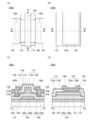
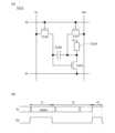
図1(A)(B)(C)(D)に、トランジスタと容量素子とを同一基板上に備える半
導体装置の一例を示す。なお、トランジスタは、トップゲート構造である。<
1A to 1D show an example of a semiconductor device including a transistor and a capacitor over the same substrate. Note that the transistor has a top-gate structure.
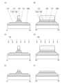
図1(A)は半導体装置が有するトランジスタ100の上面図であり、図1(B)は半
導体装置が有する容量素子150の上面図であり、図1(C)は図1(A)の一点鎖線X
1-X2間の断面図であり、図1(D)は図1(B)の一点鎖線X3-X4間の断面図で
ある。なお、図1(A)(B)では、明瞭化のため、基板102、絶縁膜104、絶縁膜
108、絶縁膜118、絶縁膜120などを省略している。なお、トランジスタ及び容量
素子の上面図においては、以降の図面においても図1(A)(B)と同様に、構成要素の
一部を省略して図示する場合がある。また、一点鎖線X1-X2方向をチャネル長方向、
一点鎖線Y1-Y2方向をチャネル幅方向と呼称する場合がある。 1A is a top view of a
1A and 1B are cross-sectional views taken along dashed line X3-X4 in FIG. 1B. Note that for clarity, the
The direction of the dashed dotted line Y1-Y2 may be referred to as the channel width direction.
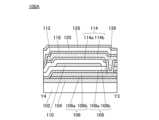
図1(A)(C)に示すトランジスタ100は、基板102上に形成された絶縁膜10
8と、絶縁膜108上の酸化物半導体膜110と、酸化物半導体膜110上の絶縁膜11
2と、絶縁膜112を介して酸化物半導体膜110と重なる導電膜114と、酸化物半導
体膜110、絶縁膜112、及び導電膜114を覆う絶縁膜118と、絶縁膜118上の
絶縁膜120と、絶縁膜118及び絶縁膜120に設けられる開口部140aを介して、
酸化物半導体膜110に接続される導電膜122と、絶縁膜118及び絶縁膜120に設
けられる開口部140bを介して、酸化物半導体膜110に接続される導電膜124と、
を有する。なお、トランジスタ100上には、絶縁膜120、導電膜122、及び導電膜
124、を覆う絶縁膜128を設けてもよい。 The
8, an
2, a
a
Note that an insulating
なお、図1(C)において、絶縁膜108は、絶縁膜108aと、絶縁膜108a上の
絶縁膜108bの積層構造である。また、導電膜114は、導電膜114aと、導電膜1
14a上の導電膜114bの積層構造である。また、導電膜122は、導電膜122aと
、導電膜122a上の導電膜122bの積層構造である。また、導電膜124は、導電膜
124aと、導電膜124a上の導電膜124bの積層構造である。 1C, the insulating
The
トランジスタ100において、導電膜114は、ゲート電極(トップゲート電極ともい
う)としての機能を有し、導電膜122は、ソース電極及びドレイン電極の一方の電極と
しての機能を有し、導電膜124は、ソース電極及びドレイン電極の他方の電極としての
機能を有する。また、トランジスタ100において、絶縁膜108は、酸化物半導体膜1
10の下地膜としての機能を有し、絶縁膜112は、ゲート絶縁膜としての機能を有する
。 In the
The insulating
また、図1(B)(D)に示す容量素子150は、基板102上に形成された絶縁膜1
08と、絶縁膜108上の絶縁膜112と、絶縁膜112上の導電膜116と、絶縁膜1
08、絶縁膜112、及び導電膜116を覆う絶縁膜118と、絶縁膜118上の絶縁膜
120と、絶縁膜120に設けられる開口部140cにおいて、絶縁膜118を介して導
電膜116と重なる導電膜126と、を有する。なお、容量素子150上には、絶縁膜1
20及び導電膜126を覆う絶縁膜128と、を設けてもよい。 The
108, an insulating
The insulating
An insulating
また、図1(D)において、絶縁膜108は、絶縁膜108aと、絶縁膜108a上の
絶縁膜108bの積層構造である。また、導電膜116は、導電膜116aと、導電膜1
16a上の導電膜116bの積層構造である。また、導電膜126は、導電膜126aと
、導電膜126a上の導電膜126bの積層構造である。 1D, the insulating
The
また、容量素子150は、一対の電極間に誘電体を挟持する構造である。より詳しくは
、一対の電極の一方が導電膜116であり、一対の電極の他方が導電膜126であり、導
電膜116と導電膜126の間の絶縁膜118が誘電体として機能する。 The
なお、トランジスタ100のゲート電極として機能する導電膜114と、容量素子15
0の一対の電極の一方として機能する導電膜116は、同じ工程で形成され、少なくとも
一部が同一表面上に形成される。また、トランジスタ100のソース電極及びドレイン電
極として機能する導電膜122及び導電膜124と、容量素子150の一対の電極の他方
として機能する導電膜126は、同じ工程で形成され、少なくとも一部が同一表面上に形
成される。 Note that the
The
このように、トランジスタ100と容量素子150の各電極として機能する導電膜を同
一工程で形成することによって、製造コストを低減することが可能となる。 In this manner, by forming the conductive films functioning as the electrodes of the
また、容量素子150において、絶縁膜120は、開口部140cを有している。した
がって、絶縁膜118及び絶縁膜120が積層された絶縁膜のうち、絶縁膜118のみを
誘電体として機能させている。このような構成とすることにより、容量素子150の容量
値を大きくすることが可能となる。したがって、表示装置の容量値を大きくすることが可
能となる。 Furthermore, in the
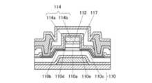
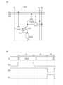
次に、図1(A)に示すトランジスタ100の一点鎖線Y1-Y2方向(チャネル幅方
向)の断面図を図2に示す。 Next, a cross-sectional view of the
図2に示すように、チャネル幅方向において、導電膜114aの端部は、導電膜114
bの端部よりも外側に位置する。また、絶縁膜112の端部は、導電膜114aの端部よ
りも外側に位置する。また、絶縁膜108bは、絶縁膜112が重ならない領域に凹部を
有する。このような構造にすることで、絶縁膜118、120、128の被覆性を向上さ
せることができる。 As shown in FIG. 2, the end of the
The insulating
次に、トランジスタ100が有する酸化物半導体膜110の詳細について、以下説明を
行う。 Next, the
トランジスタ100の酸化物半導体膜110において、導電膜114と重ならない領域
には、酸素欠損を形成する元素を有する。以下、酸素欠損を形成する元素を、不純物元素
として説明する。不純物元素の代表例としては、水素、ホウ素、炭素、窒素、フッ素、ア
ルミニウム、シリコン、リン、塩素、希ガス元素等がある。希ガス元素の代表例としては
、ヘリウム、ネオン、アルゴン、クリプトン及びキセノンがある。 In the
不純物元素が酸化物半導体膜に添加されると、酸化物半導体膜中の金属元素及び酸素の
結合が切断され、酸素欠損が形成される。または、不純物元素が酸化物半導体膜に添加さ
れると、酸化物半導体膜中の金属元素と結合していた酸素が不純物元素と結合し、金属元
素から酸素が脱離され、酸素欠損が形成される。これらの結果、酸化物半導体膜において
キャリア密度が増加し、導電性が高くなる。 When an impurity element is added to the oxide semiconductor film, a bond between a metal element and oxygen in the oxide semiconductor film is cut, and oxygen vacancies are formed. Alternatively, when an impurity element is added to the oxide semiconductor film, oxygen that was bonded to a metal element in the oxide semiconductor film is bonded to the impurity element, and oxygen is released from the metal element, and oxygen vacancies are formed. As a result, the carrier density in the oxide semiconductor film is increased, and the conductivity is increased.
不純物元素の添加により酸素欠損が形成された酸化物半導体に水素を添加すると、酸素
欠損サイトに水素が入り伝導帯近傍にドナー準位が形成される。この結果、酸化物半導体
は、導電性が高くなり、導電体化する。導電体化された酸化物半導体を酸化物導電体とい
うことができる。一般に、酸化物半導体は、エネルギーギャップが大きいため、可視光に
対して透光性を有する。一方、酸化物導電体は、伝導帯近傍にドナー準位を有する酸化物
半導体である。したがって、該ドナー準位による吸収の影響は小さく、可視光に対して酸
化物半導体と同程度の透光性を有する。 When hydrogen is added to an oxide semiconductor in which oxygen vacancies have been formed by the addition of an impurity element, hydrogen enters the oxygen vacancy sites and a donor level is formed near the conduction band. As a result, the oxide semiconductor has high electrical conductivity and becomes a conductor. An oxide semiconductor that has become a conductor can be called an oxide conductor. In general, an oxide semiconductor has a large energy gap and therefore transmits visible light. On the other hand, an oxide conductor is an oxide semiconductor that has a donor level near the conduction band. Therefore, the influence of absorption due to the donor level is small, and the oxide conductor has the same level of transmittance to visible light as an oxide semiconductor.
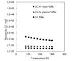
ここで、酸化物導電体で形成される膜(以下、酸化物導電体膜という。)における、抵
抗率の温度依存性について、図39を用いて説明する。 Here, the temperature dependence of resistivity in a film made of an oxide conductor (hereinafter referred to as an oxide conductor film) will be described with reference to FIG.
ここでは、酸化物導電体膜を有する試料を作製した。酸化物導電体膜としては、酸化物
半導体膜が窒化シリコン膜に接することで形成された酸化物導電体膜(OC_SiNx)
、ドーピング装置において酸化物半導体膜にアルゴンが添加され、且つ窒化シリコン膜と
接することで形成された酸化物導電体膜(OC_Ar dope+SiNx)、またはプ
ラズマ処理装置において酸化物半導体膜がアルゴンプラズマに曝され、且つ窒化シリコン
膜と接することで形成された酸化物導電体膜(OC_Ar plasma+SiNx)を
作製した。なお、窒化シリコン膜は、水素を含む。 Here, a sample having an oxide conductor film was fabricated. The oxide conductor film was an oxide conductor film (OC_SiNx ) formed by contacting an oxide semiconductor film with a silicon nitride film.
In a doping apparatus, argon was added to an oxide semiconductor film and the oxide semiconductor film was brought into contact with a silicon nitride film to form an oxide conductor film (OC_Ar dope+SiNx ), or in a plasma processing apparatus, an oxide semiconductor film was exposed to argon plasma and the oxide conductor film was brought into contact with a silicon nitride film to form an oxide conductor film (OC_Ar plasma+SiNx ). Note that the silicon nitride film contains hydrogen.
酸化物導電体膜(OC_SiNx)を含む試料の作製方法を以下に示す。ガラス基板上
に、厚さ400nmの酸化窒化シリコン膜をプラズマCVD法により形成した後、酸素プ
ラズマに曝し、酸素イオンを酸化窒化シリコン膜に添加することで、加熱により酸素を放
出する酸化窒化シリコン膜を形成した。次に、加熱により酸素を放出する酸化窒化シリコ
ン膜上に、原子数比がIn:Ga:Zn=1:1:1.2のスパッタリングターゲットを
用いたスパッタリング法により、厚さ100nmのIn-Ga-Zn酸化物膜を形成し、
450℃の窒素雰囲気で加熱処理した後、450℃の窒素及び酸素の混合ガス雰囲気で加
熱処理した。次に、プラズマCVD法で、厚さ100nmの窒化シリコン膜を形成した。
次に、350℃の窒素及び酸素の混合ガス雰囲気で加熱処理した。 A method for fabricating a sample including an oxide conductor film (OC_SiNx ) is described below. After forming a silicon oxynitride film with a thickness of 400 nm on a glass substrate by plasma CVD, the silicon oxynitride film was exposed to oxygen plasma to add oxygen ions to the silicon oxynitride film, thereby forming a silicon oxynitride film that releases oxygen when heated. Next, a 100-nm-thick In—Ga—Zn oxide film was formed on the silicon oxynitride film that releases oxygen when heated by sputtering using a sputtering target with an atomic ratio of In:Ga:Zn=1:1:1.2.
After heat treatment in a nitrogen atmosphere at 450° C., heat treatment was performed in a mixed gas atmosphere of nitrogen and oxygen at 450° C. Next, a silicon nitride film having a thickness of 100 nm was formed by plasma CVD.
Next, the substrate was heat-treated at 350° C. in a mixed gas atmosphere of nitrogen and oxygen.
酸化物導電体膜(OC_Ar dope+SiNx)を含む試料の作製方法を以下に示
す。ガラス基板上に、厚さ400nmの酸化窒化シリコン膜をプラズマCVD法により形
成した後、酸素プラズマに曝し、酸素イオンを酸化窒化シリコン膜に添加することで、加
熱により酸素を放出する酸化窒化シリコン膜を形成した。次に、加熱により酸素を放出す
る酸化窒化シリコン膜上に、原子数比がIn:Ga:Zn=1:1:1.2のスパッタリ
ングターゲットを用いたスパッタリング法により、厚さ100nmのIn-Ga-Zn酸
化物膜を形成し、450℃の窒素雰囲気で加熱処理した後、450℃の窒素及び酸素の混
合ガス雰囲気で加熱処理した。次に、ドーピング装置を用いて、In-Ga-Zn酸化物
膜に、加速電圧を10kVとし、ドーズ量が5×10¹⁴ions/cm2のアルゴンを
添加して、In-Ga-Zn酸化物膜に酸素欠損を形成した。次に、プラズマCVD法で
、厚さ100nmの窒化シリコン膜を形成した。次に、350℃の窒素及び酸素の混合ガ
ス雰囲気で加熱処理した。 A method for fabricating a sample including an oxide conductor film (OC_Ar dope+SiNx ) is described below. After forming a silicon oxynitride film with a thickness of 400 nm on a glass substrate by plasma CVD, the silicon oxynitride film was exposed to oxygen plasma, and oxygen ions were added to the silicon oxynitride film to form a silicon oxynitride film that releases oxygen by heating. Next, a 100-nm-thick In-Ga-Zn oxide film was formed on the silicon oxynitride film that releases oxygen by heating by sputtering using a sputtering target with an atomic ratio of In:Ga:Zn=1:1:1.2, and then heat-treated in a nitrogen atmosphere at 450° C., and then heat-treated in a mixed gas atmosphere of nitrogen and oxygen at 450° C. Next, using a doping device, argon was added to the In-Ga-Zn oxide film at an acceleration voltage of 10 kV and a dose of 5×10¹⁴ ions/cm2 to form oxygen vacancies in the In-Ga-Zn oxide film. Next, a silicon nitride film having a thickness of 100 nm was formed by plasma CVD, followed by heat treatment at 350° C. in a mixed gas atmosphere of nitrogen and oxygen.
酸化物導電体膜(OC_Ar plasma+SiNx)を含む試料の作製方法を以下
に示す。ガラス基板上に、厚さ400nmの酸化窒化シリコン膜をプラズマCVD法によ
り形成した後、酸素プラズマに曝すことで、加熱により酸素を放出する酸化窒化シリコン
膜を形成した。次に、加熱により酸素を放出する酸化窒化シリコン膜上に、原子数比がI
n:Ga:Zn=1:1:1.2のスパッタリングターゲットを用いたスパッタリング法
により、厚さ100nmのIn-Ga-Zn酸化物膜を形成し、450℃の窒素雰囲気で
加熱処理した後、450℃の窒素及び酸素の混合ガス雰囲気で加熱処理した。次に、プラ
ズマ処理装置において、アルゴンプラズマを発生させ、加速させたアルゴンイオンをIn
-Ga-Zn酸化物膜に衝突させることで酸素欠損を形成した。次に、プラズマCVD法
で、厚さ100nmの窒化シリコン膜を形成した。次に、350℃の窒素及び酸素の混合
ガス雰囲気で加熱処理した。 A method for fabricating a sample including an oxide conductor film (OC_Ar plasma+SiNx ) is described below. After forming a silicon oxynitride film with a thickness of 400 nm on a glass substrate by plasma CVD, the silicon oxynitride film that releases oxygen when heated was formed by exposing the silicon oxynitride film to oxygen plasma. Next, a silicon oxynitride film having an atomic ratio of I
A 100 nm thick In-Ga-Zn oxide film was formed by sputtering using a sputtering target with n:Ga:Zn=1:1:1.2, and then heat-treated in a nitrogen atmosphere at 450° C., and then heat-treated in a mixed gas atmosphere of nitrogen and oxygen at 450° C. Next, argon plasma was generated in a plasma processing device, and accelerated argon ions were converted into In
The -Ga-Zn oxide film was bombarded with oxygen vacancies to form oxygen vacancies. A silicon nitride film having a thickness of 100 nm was then formed by plasma CVD. The film was then heat-treated at 350° C. in a mixed gas atmosphere of nitrogen and oxygen.
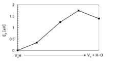
次に、各試料の抵抗率を測定した結果を図39に示す。ここで、抵抗率の測定は4端子
のvan-der-Pauw法で行った。図39において、横軸は測定温度を示し、縦軸
は抵抗率を示す。また、酸化物導電体膜(OC_SiNx)の測定結果を四角印で示し、
酸化物導電体膜(OC_Ar dope+SiNx)の測定結果を丸印で示し、酸化物導
電体膜(OC_Ar plasma+SiNx)の測定結果を三角印で示す。 Next, the results of measuring the resistivity of each sample are shown in FIG. 39. Here, the resistivity was measured by a four-terminal van der Pauw method. In FIG. 39, the horizontal axis indicates the measurement temperature, and the vertical axis indicates the resistivity. The measurement results of the oxide conductor film (OC_SiNx ) are indicated by square marks,
The measurement results of the oxide conductor film (OC_Ar doped+SiNx ) are indicated by circles, and the measurement results of the oxide conductor film (OC_Ar plasma+SiNx ) are indicated by triangles.
なお、図示しないが、窒化シリコン膜と接しない酸化物半導体膜は、抵抗率が高く、抵
抗率の測定が困難であった。このため、酸化物導電体膜は、酸化物半導体膜より抵抗率が
低いことがわかる。 Although not shown, the oxide semiconductor film not in contact with the silicon nitride film had high resistivity and it was difficult to measure the resistivity. Therefore, it is found that the oxide conductor film has a lower resistivity than the oxide semiconductor film.
図39からわかるように、酸化物導電体膜(OC_Ar dope+SiNx)及び酸
化物導電体膜(OC_Ar plasma+SiNx)が、酸素欠損及び水素を含む場合
、抵抗率の変動が小さい。代表的には、80K以上290K以下において、抵抗率の変動
率は、±20%未満である。または、150K以上250K以下において、抵抗率の変動
率は、±10%未満である。即ち、酸化物導電体は、縮退半導体であり、伝導帯端とフェ
ルミ準位とが一致または略一致していると推定される。このため、酸化物導電体膜をトラ
ンジスタのソース領域及びドレイン領域として用いることで、酸化物導電体膜とソース電
極及びドレイン電極として機能する導電膜との接触がオーミック接触となり、酸化物導電
体膜とソース電極及びドレイン電極として機能する導電膜との接触抵抗を低減できる。ま
た、酸化物導電体の抵抗率は温度依存性が低いため、酸化物導電体膜とソース電極及びド
レイン電極として機能する導電膜との接触抵抗の変動量が少なく、信頼性の高いトランジ
スタを作製することが可能である。 As can be seen from FIG. 39, when the oxide conductor film (OC_Ar dope+SiNx ) and the oxide conductor film (OC_Ar plasma+SiNx ) contain oxygen vacancies and hydrogen, the variation in resistivity is small. Typically, the variation in resistivity is less than ±20% at 80 K or more and 290 K or less. Alternatively, the variation in resistivity is less than ±10% at 150 K or more and 250 K or less. That is, it is estimated that the oxide conductor is a degenerate semiconductor, and the conduction band edge and the Fermi level coincide or approximately coincide. Therefore, by using the oxide conductor film as the source region and drain region of the transistor, the contact between the oxide conductor film and the conductive film functioning as the source electrode and drain electrode becomes ohmic contact, and the contact resistance between the oxide conductor film and the conductive film functioning as the source electrode and drain electrode can be reduced. In addition, since the resistivity of the oxide conductor has low temperature dependence, the amount of variation in the contact resistance between the oxide conductor film and the conductive films functioning as source and drain electrodes is small, making it possible to fabricate a highly reliable transistor.
ここで、酸化物半導体膜110近傍の拡大図を図3(A)(B)(C)(D)及び図4
(A)(B)に示す。なお、図3(A)(B)(C)(D)及び図4(A)(B)におい
ては、煩雑さを避けるために、構成要素の一部を省略して図示している。 Here, enlarged views of the vicinity of the
3A, 3B, 3C, 3D, 4A, 4B, and 4C. In order to avoid complication, some of the components are omitted in the drawings.
酸化物半導体膜110のチャネル長方向の断面形状において、酸化物半導体膜のキャリ
ア密度が増加し導電性が高くなる領域(以下、低抵抗領域という)が形成される。また、
酸化物半導体膜110中に形成される低抵抗領域は、図3(A)(B)(C)(D)及び
図4(A)(B)に示すように複数の構造がある。なお、図3(A)(B)(C)(D)
及び図4(A)(B)において、チャネル長Lは、一対の低抵抗領域に挟まれた領域の長
さである。 In the cross-sectional shape of the
The low-resistance region formed in the
4A and 4B, a channel length L is the length of a region sandwiched between a pair of low resistance regions.
図3(A)に示すように、酸化物半導体膜110は、導電膜114と重なる領域に形成
されるチャネル領域110aと、チャネル領域110aを挟み、且つ不純物元素を含む領
域、すなわち低抵抗領域110b、110cとを有する。なお、図3(A)に示すように
、チャネル長方向の断面形状において、チャネル領域110a及び低抵抗領域110b、
110cの境界が、絶縁膜112を介して、導電膜114aの下端部と、一致または概略
一致している。すなわち、上面形状において、チャネル領域110a及び低抵抗領域11
0b、110cの境界が、導電膜114aの下端部と、一致または概略一致している。 3A , the
The boundary between the
The boundary between 0b and 110c coincides or approximately coincides with the lower end of the
なお、図3(A)に示すように、チャネル長方向の断面形状において、導電膜114a
の端部は、導電膜114bの端部より外側に位置し、且つ導電膜114bがテーパ形状で
あってもよい。すなわち、導電膜114a及び導電膜114bが接する面と、導電膜11
4bの側面のなす角度θ1が、90°未満、10°以上85°以下、または15°以上8
5°以下、または30°以上85°以下、または45°以上85°以下、または60°以
上85°以下であってもよい。角度θ1を、90°未満、10°以上85°以下、または
15°以上85°以下、または30°以上85°以下、または45°以上85°以下、ま
たは60°以上85°以下とすることで、導電膜114bの側面における絶縁膜118の
被覆性を高めることが可能である。 As shown in FIG. 3A, the
The end of the
The angle θ1 between the side surfaces of the first and second electrodes 4b is less than 90°, 10° to 85°, or 15° to 85°.
The angle θ1 may be 5° or less, or 30° or more and 85° or less, or 45° or more and 85° or less, or 60° or more and 85° or less. By setting the angle θ1 to less than 90°, 10° or more and 85° or less, or 15° or more and 85° or less, or 30° or more and 85° or less, or 45° or more and 85° or less, or 60° or more and 85° or less, the coverage of the insulating
また、図3(A)に示すように、チャネル長方向の断面形状において、絶縁膜112の
端部が、導電膜114a及び導電膜114bの端部より外側に位置してもよい。また、絶
縁膜112の端部の一部が円弧を有していてもよい。また、絶縁膜112がテーパ形状で
あってもよい。すなわち、酸化物半導体膜110及び絶縁膜112が接する面と、絶縁膜
112の側面のなす角度θ2が90°未満、好ましくは30°以上90°未満であっても
よい。 3A , in the cross-sectional shape in the channel length direction, an end of the insulating
または、図3(B)に示すように、チャネル長方向の断面形状において、低抵抗領域1
10b、110cは、絶縁膜112を介して、導電膜114と重なる領域を有する。該領
域はオーバーラップ領域として機能する。チャネル長方向におけるオーバーラップ領域の
長さをLovと示す。Lovは、チャネル長Lの20%未満、または10%未満、または
5%未満、または2%未満である。 Alternatively, as shown in FIG. 3B, in the cross-sectional shape in the channel length direction, the
The
または、図3(C)に示すように、チャネル長方向の断面形状において、チャネル領域
110aは、導電膜114aの下端部と重ならない領域を有する。該領域は、オフセット
領域として機能する。チャネル長方向におけるオフセット領域の長さをLoffと示す。
なお、オフセット領域が複数ある場合は、一つのオフセット領域の長さをLoffという
。Loffは、チャネル長Lに含まれる。また、Loffは、チャネル長Lの20%未満
、または10%未満、または5%未満、または2%未満である。 3C, the
When there are multiple offset regions, the length of one offset region is referred to asLoff .Loff is included in the channel length L. Furthermore,Loff is less than 20%, less than 10%, less than 5%, or less than 2% of the channel length L.
または、図3(D)に示すように、チャネル長方向の断面形状において、酸化物半導体
膜110は、チャネル領域110aと低抵抗領域110bの間に低抵抗領域110dを有
し、チャネル領域110aと低抵抗領域110cの間に低抵抗領域110eを有する。低
抵抗領域110d、110eは、低抵抗領域110b、110cより不純物元素の濃度が
低く、抵抗率が高い。ここでは、低抵抗領域110d、110eは、絶縁膜112と重な
るが、絶縁膜112及び導電膜114と重なってもよい。 3D , in a cross-sectional shape in the channel length direction, the
または、図4(A)に示すように、チャネル長方向の断面形状において、酸化物半導体
膜110は、導電膜122、124と重なる領域に、領域110f、110gを有する。
領域110f、110gには、不純物元素が添加されていなくてもよい。この場合、酸化
物半導体膜110は、導電膜122、124と接する領域110f、110gとチャネル
領域110aとの間に、不純物元素を有する領域、即ち低抵抗領域110b、110cを
有する。なお、領域110f、110gは、導電膜122、124に電圧が印加されると
導電性を有するため、ソース領域及びドレイン領域としての機能を有する。 Alternatively, as illustrated in FIG. 4A , in a cross-sectional shape in the channel length direction, the
The
なお、図4(A)に示す構造は、導電膜122、124を形成した後、導電膜114、
122、124をマスクとして、絶縁膜120及び絶縁膜118を介して、不純物元素を
酸化物半導体膜110に添加することで形成される。 In the structure shown in FIG. 4A, the
The insulating
または、図4(B)に示すように、チャネル長方向の断面形状において、チャネル領域
110aを挟む低抵抗領域110b、110c、110d、110e、110h、110
iを設けてもよい。 Alternatively, as shown in FIG. 4B, in a cross-sectional shape in the channel length direction, low-
i may be provided.
具体的には、図4(B)に示す酸化物半導体膜110は、チャネル領域110aと、チ
ャネル領域110aを挟む低抵抗領域110h、110iと、低抵抗領域110h、11
0iを挟む低抵抗領域110d、110eと、低抵抗領域110d、110eを挟む低抵
抗領域110b、110cとを有する。低抵抗領域110h、110iは、導電膜114
bと重ならない領域の導電膜114aと、絶縁膜112を介して、不純物元素が添加され
ることにより形成される。また、低抵抗領域110d、110eは、導電膜114a及び
導電膜114bと重ならない領域の絶縁膜112を介して、不純物元素が添加されること
により形成される。また、低抵抗領域110b、110cは、不純物元素が直接添加され
ることにより形成される。したがって、低抵抗領域110h、110iは、低抵抗領域1
10d、110e及び低抵抗領域110b、110cより不純物元素濃度が低く、抵抗率
が高い。また、低抵抗領域110d、110eは、低抵抗領域110b、110cより不
純物元素濃度が低く、抵抗率が高い。 Specifically, the
The
The low-
The low-
なお、図4(B)において、チャネル領域110aは導電膜114bと重なる。また、
低抵抗領域110h、110iは、導電膜114bの外側に突出している導電膜114a
と重なる。また、低抵抗領域110d、110eは、導電膜114aの外側に突出してい
る絶縁膜112と重なる。また、低抵抗領域110b、110cは絶縁膜112の外側に
突出し、絶縁膜118と重なる。 In FIG. 4B, the
The
The low-
図3(D)及び図4(B)に示すように、酸化物半導体膜110が低抵抗領域110b
、110cより、不純物元素の濃度が低く、抵抗率が高い低抵抗領域110d、110e
、110h、110iを有することで、ドレイン領域の電界緩和が可能である。そのため
、ドレイン領域の電界に起因したトランジスタのしきい値電圧の変動を低減することが可
能である。 As shown in FIG. 3D and FIG. 4B, the
, 110c, the low-
, 110h, and 110i, the electric field in the drain region can be relaxed, and therefore, the fluctuation in the threshold voltage of the transistor caused by the electric field in the drain region can be reduced.
また、図3(A)(B)(C)(D)、及び図4(A)(B)に示す酸化物半導体膜1
10は、絶縁膜112及び導電膜114と重ならない領域の膜厚が、絶縁膜112及び導
電膜114と重なる領域の膜厚よりも薄い領域を有する。該薄い領域は、絶縁膜112及
び導電膜114と重なる領域の酸化物半導体膜の膜厚よりも薄く、厚さが0.1nm以上
5nm以下である。 In addition, the
10 has a region where the thickness of a region not overlapping with the insulating
なお、酸化物半導体膜110中の低抵抗領域110b、110cは、ソース領域及びド
レイン領域として機能する。また、低抵抗領域110b、110c及び低抵抗領域110
d、110e、110h、110iには不純物元素が含まれる。 Note that the low-
The
不純物元素が希ガス元素であって、酸化物半導体膜110がスパッタリング法で形成さ
れる場合、チャネル領域110a及び低抵抗領域110b、110c、110d、110
e、110h、110iは、それぞれ希ガス元素を含む。なお、チャネル領域110aと
比較して、低抵抗領域110b、110cの方が希ガス元素の濃度が高い。また、低抵抗
領域110d、110eと比較して、低抵抗領域110b、110cの方が希ガス元素の
濃度が高い。また、低抵抗領域110h、110iと比較して、低抵抗領域110d、1
10eの方が希ガス元素の濃度が高い。 In the case where the impurity element is a rare gas element and the
The low-
10e has a higher concentration of rare gas elements.
これは、酸化物半導体膜110がスパッタリング法で形成される場合、スパッタリング
ガスとして希ガスを用いるため、酸化物半導体膜110に希ガスが含まれること、並びに
低抵抗領域110b、110cにおいて、酸素欠損を形成するために、意図的に希ガスが
添加されることが原因である。また、低抵抗領域110d、110e、110h、110
iは、低抵抗領域110d、110e、110h、110i上に形成される膜構成及び膜
厚の違いから酸素欠損を形成するために添加される希ガスの濃度が、低抵抗領域110d
、110e、110h、110iの中で異なる。なお、低抵抗領域110b、110c、
110d、110e、110h、110iにおいて、チャネル領域110aと異なる希ガ
ス元素が添加されていてもよい。 This is because, when the
The concentration of the rare gas added to form oxygen vacancies due to differences in the film configuration and film thickness formed on the low-
, 110e, 110h, and 110i.
The
また、不純物元素が、ホウ素、炭素、窒素、フッ素、アルミニウム、シリコン、リン、
または、塩素の場合、低抵抗領域110b、110c、110d、110e、110h、
110iは、上記の不純物元素を有する。このため、チャネル領域110aと比較して、
低抵抗領域110b、110c、110d、110e、110h、110iの方が上記の
不純物元素の濃度が高い。なお、低抵抗領域110b、110c、110d、110e、
110h、110iにおいて、二次イオン質量分析法(SIMS:Secondary
Ion Mass Spectrometry)により得られる不純物元素の濃度は、5
×1018atoms/cm3以上1×1022atoms/cm3以下、または1×1
019atoms/cm3以上1×1021atoms/cm3以下、または5×101
9atoms/cm3以上5×1020atoms/cm3以下とすることができる。 In addition, impurity elements include boron, carbon, nitrogen, fluorine, aluminum, silicon, phosphorus,
Or, in the case of chlorine, the
The
The
In 110h and 110i, secondary ion mass spectrometry (SIMS)
The concentration of impurity elements obtained by Ion Mass Spectrometry is 5
x1018 atoms/cm3or more and1x1022 atoms/cm3 or less, or 1x1
019 atoms/cm3 or more and 1×10²¹ atoms/cm3 or less, or 5×101
The concentration can be set to9 atoms/cm3 or more and 5×10²⁰ atoms/cm3 or less.
また、不純物元素が、水素の場合、チャネル領域110aと比較して、低抵抗領域11
0b、110c、110d、110e、110h、110iの方が水素の濃度が高い。な
お、低抵抗領域110b、110c、110d、110e、110h、110iにおいて
、二次イオン質量分析法により得られる水素の濃度は、8×10¹⁹atoms/cm3
以上、または1×10²⁰atoms/cm3以上、または5×1020atoms/c
m3以上とすることができる。 In addition, when the impurity element is hydrogen, the low resistance region 11
The hydrogen concentration in the
or more, or 1×10²⁰ atoms/cm3 or more, or 5×10²⁰ atoms/cm
m3 or more.
低抵抗領域110b、110c、110d、110e、110h、110iは不純物元
素を有するため、酸素欠損が増加し、キャリア密度が増加する。この結果、低抵抗領域1
10b、110c、110d、110e、110h、110iは、導電性が高くなる。 Since the low-
10b, 110c, 110d, 110e, 110h, and 110i have high conductivity.
なお、不純物元素は、水素、ホウ素、炭素、窒素、フッ素、アルミニウム、シリコン、
リン、または塩素の一以上と、希ガスを組み合わせてもよい。この場合、低抵抗領域11
0b、110c、110d、110e、110h、110iにおいて、希ガスにより形成
された酸素欠損と、添加された水素、ホウ素、炭素、窒素、フッ素、アルミニウム、シリ
コン、リン、または塩素の一以上との相互作用により、低抵抗領域110b、110c、
110d、110e、110h、110iは、導電性がさらに高まる場合がある。 The impurity elements are hydrogen, boron, carbon, nitrogen, fluorine, aluminum, silicon,
One or more of phosphorus and chlorine may be combined with a rare gas. In this case, the low resistance region 11
In the semiconductor device, the oxygen vacancies formed by the rare gas interact with one or more of the added hydrogen, boron, carbon, nitrogen, fluorine, aluminum, silicon, phosphorus, and chlorine, forming
110d, 110e, 110h, and 110i may have even higher electrical conductivity.
また、不純物元素の添加により酸素欠損が形成された酸化物半導体に水素を添加すると
、酸素欠損サイトに水素が入り伝導帯近傍にドナー準位が形成される。その結果、酸化物
導電体を形成することができる。このため、酸化物導電体は透光性を有する。なお、ここ
では、導電体化された酸化物半導体を酸化物導電体という。 Furthermore, when hydrogen is added to an oxide semiconductor in which oxygen vacancies have been formed by the addition of an impurity element, hydrogen enters the oxygen vacancy site and a donor level is formed near the conduction band. As a result, an oxide conductor can be formed. For this reason, the oxide conductor has light-transmitting properties. Note that an oxide semiconductor that has been made into a conductor is referred to as an oxide conductor here.
酸化物導電体は、縮退半導体であり、伝導帯端とフェルミ準位とが一致または略一致し
ていると推定される。このため、酸化物導電体膜とソース電極及びドレイン電極として機
能する導電膜との接触はオーミック接触であり、酸化物導電体膜とソース電極及びドレイ
ン電極として機能する導電膜との接触抵抗を低減できる。 The oxide conductor is a degenerate semiconductor, and it is presumed that the conduction band edge and the Fermi level are coincident or approximately coincident with each other. Therefore, the contact between the oxide conductor film and the conductive film functioning as the source electrode and the drain electrode is an ohmic contact, and the contact resistance between the oxide conductor film and the conductive film functioning as the source electrode and the drain electrode can be reduced.
本実施の形態に示すトランジスタ100は、チャネル領域110aがソース領域及びド
レイン領域として機能する低抵抗領域110bと低抵抗領域110cとに挟まれる構造で
ある。したがって、トランジスタ100は、オン電流が大きく、電界効果移動度が高い。
また、トランジスタ100において、導電膜114をマスクとして、不純物元素が酸化物
半導体膜110に添加される。すなわち、セルフアラインで低抵抗領域を形成することが
できる。 The
In the
また、トランジスタ100は、ゲート電極として機能する導電膜114と、ソース電極
及びドレイン電極として機能する導電膜122、124とが重ならない構成である。した
がって、導電膜114と、導電膜122及び導電膜124との間の寄生容量を低減するこ
とが可能である。この結果、基板102として大面積基板を用いた場合、導電膜114と
、導電膜122及び導電膜124における信号遅延を低減することが可能である。 In addition, the
次に、図1(A)(B)(C)(D)に示す半導体装置のその他の構成の詳細について
説明する。 Next, other configurations of the semiconductor device shown in FIGS.
基板102としては、様々な基板を用いることができ、特定のものに限定されることは
ない。基板の一例としては、半導体基板(例えば単結晶基板またはシリコン基板)、SO
I基板、ガラス基板、石英基板、プラスチック基板、金属基板、ステンレス・スチル基板
、ステンレス・スチル・ホイルを有する基板、タングステン基板、タングステン・ホイル
を有する基板、可撓性基板、貼り合わせフィルム、繊維状の材料を含む紙、または基材フ
ィルムなどがある。ガラス基板の一例としては、バリウムホウケイ酸ガラス、アルミノホ
ウケイ酸ガラス、またはソーダライムガラスなどがある。可撓性基板、貼り合わせフィル
ム、基材フィルムなどの一例としては、以下のものがあげられる。例えば、ポリエチレン
テレフタレート(PET)、ポリエチレンナフタレート(PEN)、ポリエーテルサルフ
ォン(PES)に代表されるプラスチックがある。または、一例としては、アクリル等の
合成樹脂などがある。または、一例としては、ポリエステル 、ポリプロピレン、ポリフ
ッ化ビニル、またはポリ塩化ビニルなどがある。または、一例としては、ポリアミド、ポ
リイミド、アラミド、エポキシ、無機蒸着フィルム、または紙類などがある。特に、半導
体基板、単結晶基板、またはSOI基板などを用いてトランジスタ及び容量素子を製造す
ることによって、特性、サイズ、または形状などのばらつきが少なく、電流能力が高く、
サイズの小さいトランジスタ及び容量素子を製造することができる。このようなトランジ
スタ及び容量素子によって回路を構成すると、回路の低消費電力化、または回路の高集積
化を図ることができる。 Various substrates can be used as the
Examples of the substrate include an I substrate, a glass substrate, a quartz substrate, a plastic substrate, a metal substrate, a stainless steel substrate, a substrate having a stainless steel foil, a tungsten substrate, a substrate having a tungsten foil, a flexible substrate, a laminated film, a paper containing a fibrous material, or a base film. Examples of the glass substrate include barium borosilicate glass, aluminoborosilicate glass, or soda lime glass. Examples of the flexible substrate, the laminated film, the base film, or the like include the following. For example, there are plastics represented by polyethylene terephthalate (PET), polyethylene naphthalate (PEN), and polyethersulfone (PES). As an example, there are synthetic resins such as acrylic. As an example, there are polyester, polypropylene, polyvinyl fluoride, or polyvinyl chloride. As an example, there are polyamide, polyimide, aramid, epoxy, inorganic vapor deposition film, or papers. In particular, by manufacturing transistors and capacitors using a semiconductor substrate, a single crystal substrate, an SOI substrate, or the like, the characteristics, size, shape, and other variations are small, and the current capacity is high.
Small-sized transistors and capacitors can be manufactured. When a circuit is configured using such transistors and capacitors, the power consumption of the circuit can be reduced or the circuit can be highly integrated.
また、基板102として、可撓性基板を用い、可撓性基板上に直接、トランジスタ及び
容量素子を形成してもよい。または、基板102とトランジスタ及び容量素子の間に剥離
層を設けてもよい。剥離層は、その上に半導体装置を一部あるいは全部完成させた後、基
板102より分離し、他の基板に転載するのに用いることができる。その際、トランジス
タ及び容量素子は、耐熱性の劣る基板や可撓性の基板にも転載できる。なお、上述の剥離
層には、例えば、タングステン膜と酸化シリコン膜との無機膜の積層構造の構成や、基板
上にポリイミド等の有機樹脂膜が形成された構成等を用いることができる。 Alternatively, a flexible substrate may be used as the
トランジスタ及び容量素子が転載される基板の一例としては、上述したトランジスタ及
び容量素子を形成することが可能な基板に加え、紙基板、セロファン基板、アラミドフィ
ルム基板、ポリイミドフィルム基板、石材基板、木材基板、布基板(天然繊維(絹、綿、
麻)、合成繊維(ナイロン、ポリウレタン、ポリエステル)若しくは再生繊維(アセテー
ト、キュプラ、レーヨン、再生ポリエステル)などを含む)、皮革基板、またはゴム基板
などがある。これらの基板を用いることにより、特性のよいトランジスタの形成、消費電
力の小さいトランジスタの形成、壊れにくい装置の製造、耐熱性の付与、軽量化、または
薄型化を図ることができる。 Examples of the substrate on which the transistors and the capacitance elements are transferred include, in addition to the substrate on which the above-mentioned transistors and the capacitance elements can be formed, a paper substrate, a cellophane substrate, an aramid film substrate, a polyimide film substrate, a stone substrate, a wood substrate, a cloth substrate (natural fibers (silk, cotton,
Examples of substrates include hemp, synthetic fibers (nylon, polyurethane, polyester) or regenerated fibers (acetate, cupra, rayon, regenerated polyester), leather substrates, and rubber substrates. By using these substrates, it is possible to form transistors with good characteristics, form transistors with low power consumption, manufacture devices that are not easily broken, provide heat resistance, and reduce weight or thickness.
絶縁膜108としては、スパッタリング法、CVD法、蒸着法、パルスレーザー堆積(
PLD)法、印刷法、塗布法等を適宜用いて形成することができる。また、絶縁膜108
としては、例えば、酸化物絶縁膜または窒化物絶縁膜を単層または積層して形成すること
ができる。なお、酸化物半導体膜110との界面特性を向上させるため、絶縁膜108に
おいて少なくとも酸化物半導体膜110と接する領域は酸化物絶縁膜で形成することが好
ましい。また、絶縁膜108として加熱により酸素を放出する酸化物絶縁膜を用いること
で、加熱処理により絶縁膜108に含まれる酸素を、酸化物半導体膜110に移動させる
ことが可能である。 The insulating
The insulating
For example, the insulating
絶縁膜108の厚さは、50nm以上、または100nm以上3000nm以下、また
は200nm以上1000nm以下とすることができる。絶縁膜108を厚くすることで
、絶縁膜108の酸素放出量を増加させることができると共に、絶縁膜108と酸化物半
導体膜110との界面における界面準位、並びに酸化物半導体膜110のチャネル領域1
10aに含まれる酸素欠損を低減することが可能である。 The thickness of the insulating
It is possible to reduce oxygen vacancies contained in 10a.
絶縁膜108として、例えば酸化シリコン、酸化窒化シリコン、窒化酸化シリコン、窒
化シリコン、酸化アルミニウム、酸化ハフニウム、酸化ガリウムまたはGa-Zn酸化物
などを用いればよく、単層または積層で設けることができる。本実施の形態では、絶縁膜
108aとして、窒化シリコン膜を用い、絶縁膜108bとして酸化窒化シリコン膜を用
いる。 The insulating
酸化物半導体膜110は、代表的には、In-Ga酸化物、In-Zn酸化物、In-
M-Zn酸化物(Mは、Ti、Ga、Y、Zr、La、Ce、Nd、またはHf)等の金
属酸化物で形成される。なお、酸化物半導体膜110は、透光性を有する。 The
The
なお、酸化物半導体膜110がIn-M-Zn酸化物の場合、InとMの原子数比率は
、In及びMの和を100atomic%としたときInが25atomic%以上、M
が75atomic%未満、またはInが34atomic%以上、Mが66atomi
c%未満とする。 In the case where the
is less than 75 atomic%, or In is 34 atomic% or more, and M is 66 atomic%
The content shall be less than c%.
酸化物半導体膜110は、エネルギーギャップが2eV以上、または2.5eV以上、
または3eV以上である。 The
Or it is 3 eV or more.
酸化物半導体膜110の厚さは、3nm以上200nm以下、または3nm以上100
nm以下、または3nm以上60nm以下とすることができる。 The thickness of the
The thickness can be set to 0.1 nm or less, or 3 nm to 60 nm.
酸化物半導体膜110がIn-M-Zn酸化物の場合、In-M-Zn酸化物を成膜す
るために用いるスパッタリングターゲットの金属元素の原子数比は、In≧M、Zn≧M
を満たすことが好ましい。このようなスパッタリングターゲットの金属元素の原子数比と
して、In:M:Zn=1:1:1、In:M:Zn=1:1:1.2、In:M:Zn
=2:1:1.5、In:M:Zn=2:1:2.3、In:M:Zn=2:1:3、I
n:M:Zn=3:1:2等が好ましい。なお、成膜される酸化物半導体膜110の原子
数比はそれぞれ、誤差として上記のスパッタリングターゲットに含まれる金属元素の原子
数比のプラスマイナス40%の変動を含む。 When the
It is preferable that the atomic ratio of the metal elements in such a sputtering target is In:M:Zn=1:1:1, In:M:Zn=1:1:1.2, In:M:Zn
=2:1:1.5, In:M:Zn=2:1:2.3, In:M:Zn=2:1:3, I
For example, n:M:Zn=3:1:2 is preferable. Note that the atomic ratio of the
また、酸化物半導体膜110において、第14族元素の一つであるシリコンや炭素が含
まれると、酸化物半導体膜110において、酸素欠損が増加し、n型化してしまう。この
ため、酸化物半導体膜110であって、特にチャネル領域110aにおいて、シリコンや
炭素の濃度(二次イオン質量分析法により得られる濃度)を、2×10¹⁸atoms/
cm3以下、または2×10¹⁷atoms/cm3以下とすることができる。この結果
、トランジスタは、しきい値電圧がプラスとなる電気特性(ノーマリーオフ特性ともいう
。)を有する。 Furthermore, when the
3 or less, or 2×10¹⁷ atoms/cm3 or less. As a result, the transistor has electrical characteristics in which the threshold voltage is positive (also referred to as normally-off characteristics).
また、酸化物半導体膜110であって、特にチャネル領域110aにおいて、二次イオ
ン質量分析法により得られるアルカリ金属またはアルカリ土類金属の濃度を、1×101
8atoms/cm3以下、または2×1016atoms/cm3以下とすることがで
きる。アルカリ金属及びアルカリ土類金属は、酸化物半導体と結合するとキャリアを生成
する場合があり、トランジスタのオフ電流が増大してしまうことがある。このため、チャ
ネル領域110aのアルカリ金属またはアルカリ土類金属の濃度を低減することが好まし
い。この結果、トランジスタは、しきい値電圧がプラスとなる電気特性(ノーマリーオフ
特性ともいう。)を有する。 In addition, the concentration of an alkali metal or an alkaline earth metal in the
The concentration of the alkali metal or alkaline earth metal in the
また、酸化物半導体膜110であって、特にチャネル領域110aに窒素が含まれてい
ると、キャリアである電子が生じ、キャリア密度が増加し、n型化となる場合がある。こ
の結果、窒素が含まれている酸化物半導体膜を用いたトランジスタはノーマリーオン特性
となりやすい。従って、当該酸化物半導体膜であって、特にチャネル領域110aにおい
て、窒素はできる限り低減されていることが好ましい。例えば、二次イオン質量分析法に
より得られる窒素濃度を、5×10¹⁸atoms/cm3以下にすることができる。 Furthermore, when the
酸化物半導体膜110であって、特にチャネル領域110aにおいて、不純物元素を低
減することで、酸化物半導体膜のキャリア密度を低減することができる。このため、酸化
物半導体膜110であって、特にチャネル領域110aにおいては、キャリア密度を1×
1017個/cm3以下、または1×1015個/cm3以下、または1×1013個/
cm3以下、または1×10¹¹個/cm3以下、または1×10-9個/cm3以上1
×1010個/cm3以下とすることができる。 By reducing the impurity elements in the
1017 particles/cm3 or less, or 1×10¹⁵ particles/cm3 or less, or 1×10¹³ particles/cm 3 or less
cm3 or less, or 1×10¹¹ particles/cm3 or less, or 1×10⁻⁹ particles/cm3 or more
×1010 particles/cm3 or less.
酸化物半導体膜110として、不純物濃度が低く、欠陥準位密度の低い酸化物半導体膜
を用いることで、さらに優れた電気特性を有するトランジスタを作製することができる。
ここでは、不純物濃度が低く、欠陥準位密度の低い(酸素欠損の少ない)ことを高純度真
性または実質的に高純度真性とよぶ。高純度真性または実質的に高純度真性である酸化物
半導体は、キャリア発生源が少ないため、キャリア密度を低くすることができる場合があ
る。従って、当該酸化物半導体膜にチャネル領域が形成されるトランジスタは、しきい値
電圧がプラスとなる電気特性(ノーマリーオフ特性ともいう。)になりやすい。また、高
純度真性または実質的に高純度真性である酸化物半導体膜は、欠陥準位密度が低いため、
トラップ準位密度も低くなる場合がある。また、高純度真性または実質的に高純度真性で
ある酸化物半導体膜は、オフ電流が著しく小さく、ソース電極とドレイン電極間の電圧(
ドレイン電圧)が1Vから10Vの範囲において、オフ電流が、半導体パラメータアナラ
イザの測定限界以下、すなわち1×10-13A以下という特性を得ることができる。従
って、当該酸化物半導体膜にチャネル領域が形成されるトランジスタは、電気特性の変動
が小さく、信頼性の高いトランジスタとなる場合がある。 When an oxide semiconductor film with a low impurity concentration and a low density of defect states is used as the
Here, a semiconductor having a low impurity concentration and a low density of defect states (few oxygen vacancies) is referred to as being highly pure intrinsic or substantially highly pure intrinsic. A highly pure intrinsic or substantially highly pure intrinsic oxide semiconductor has a small number of carrier generation sources, and therefore the carrier density can be reduced in some cases. Thus, a transistor in which a channel region is formed in the oxide semiconductor film tends to have electrical characteristics in which the threshold voltage is positive (also referred to as normally-off characteristics). In addition, a highly pure intrinsic or substantially highly pure intrinsic oxide semiconductor film has a low density of defect states, and therefore,
The density of trap states may also be reduced. In addition, a highly-purified intrinsic or substantially highly-purified intrinsic oxide semiconductor film has an extremely small off-state current and a low voltage (
In the case where the drain voltage is in the range of 1 V to 10 V, the off-state current is equal to or less than the measurement limit of a semiconductor parameter analyzer, that is, equal to or less than 1×10 A. Therefore, a transistor in which a channel region is formed in the oxide semiconductor film has small fluctuation in electrical characteristics and can be a highly reliable transistor in some cases.
また、酸化物半導体膜110は、例えば非単結晶構造でもよい。非単結晶構造は、例え
ば、後述するCAAC-OS(C Axis Aligned Crystalline
Oxide Semiconductor)、多結晶構造、後述する微結晶構造、また
は非晶質構造を含む。非単結晶構造において、非晶質構造は最も欠陥準位密度が高く、C
AAC-OSは最も欠陥準位密度が低い。 The
Among non-single crystal structures, the amorphous structure has the highest defect level density, and the C
AAC-OS has the lowest density of defect states.
なお、酸化物半導体膜110が、非晶質構造の領域、微結晶構造の領域、多結晶構造の
領域、CAAC-OSの領域、単結晶構造の領域の二種以上を有する混合膜であってもよ
い。混合膜は、例えば、非晶質構造の領域、微結晶構造の領域、多結晶構造の領域、CA
AC-OSの領域、単結晶構造の領域のいずれか二種以上の領域を有する単層構造の場合
がある。また、混合膜は、例えば、非晶質構造の領域、微結晶構造の領域、多結晶構造の
領域、CAAC-OSの領域、単結晶構造の領域のいずれか二種以上が積層された構造の
場合がある。 Note that the
The mixed film may have a single-layer structure including two or more of an AC-OS region and a single crystal region, or may have a stacked structure including two or more of an amorphous region, a microcrystalline region, a polycrystalline region, a CAAC-OS region, and a single crystal region.
なお、酸化物半導体膜110において、チャネル領域110aと低抵抗領域110b、
110c、110d、110e、110h、110iとの結晶性が異なる場合がある。具
体的には、酸化物半導体膜110において、低抵抗領域110b、110c、110d、
110e、110h、110iよりもチャネル領域110aの方が、結晶性が高い。これ
は、低抵抗領域110b、110c、110d、110e、110h、110iに不純物
元素が添加された際に、低抵抗領域110b、110c、110d、110e、110h
、110iにダメージが入ってしまい、結晶性が低下するためである。 In the
Specifically, in the
The
, 110i will be damaged, resulting in a decrease in crystallinity.
絶縁膜112は、酸化物絶縁膜または窒化物絶縁膜を単層または積層して形成すること
ができる。なお、酸化物半導体膜110との界面特性を向上させるため、絶縁膜112に
おいて少なくとも酸化物半導体膜110と接する領域は酸化物絶縁膜を用いて形成するこ
とが好ましい。絶縁膜112として、例えば酸化シリコン、酸化窒化シリコン、窒化酸化
シリコン、窒化シリコン、酸化アルミニウム、酸化ハフニウム、酸化ガリウムまたはGa
-Zn酸化物などを用いればよく、単層または積層で設けることができる。 The insulating
A -Zn oxide or the like may be used, and the layer may be formed as a single layer or a multilayer.
また、絶縁膜112として、酸素、水素、水等のブロッキング効果を有する絶縁膜を設
けることで、酸化物半導体膜110からの酸素の外部への拡散と、外部から酸化物半導体
膜110への水素、水等の侵入を防ぐことができる。酸素、水素、水等のブロッキング効
果を有する絶縁膜としては、酸化アルミニウム、酸化窒化アルミニウム、酸化ガリウム、
酸化窒化ガリウム、酸化イットリウム、酸化窒化イットリウム、酸化ハフニウム、酸化窒
化ハフニウム等がある。 By providing an insulating film having a blocking effect against oxygen, hydrogen, water, and the like as the insulating
Examples of such oxides include gallium oxide, yttrium oxide, yttrium oxide nitride, hafnium oxide, and hafnium oxynitride.
また、絶縁膜112として、ハフニウムシリケート(HfSiOx)、窒素が添加され
たハフニウムシリケート(HfSixOyNz)、窒素が添加されたハフニウムアルミネ
ート(HfAlxOyNz)、酸化ハフニウム、酸化イットリウムなどのhigh-k材
料を用いることでトランジスタのゲートリーク電流を低減できる。 Furthermore, by using a high-k material such as hafnium silicate (HfSiOx ), hafnium silicate doped with nitrogen (HfSix Oy Nz ), hafnium aluminate doped with nitrogen (HfAlx Oy Nz ), hafnium oxide, or yttrium oxide for the insulating
また、絶縁膜112として、加熱により酸素を放出する酸化物絶縁膜を用いることで、
加熱処理により絶縁膜112に含まれる酸素を、酸化物半導体膜110に移動させること
が可能である。 In addition, by using an oxide insulating film that releases oxygen by heating as the insulating
By the heat treatment, oxygen contained in the insulating
絶縁膜112の厚さは、5nm以上400nm以下、または5nm以上300nm以下
、または10nm以上250nm以下とすることができる。 The thickness of the insulating
導電膜114、導電膜116、導電膜122、導電膜124、及び導電膜126として
は、スパッタリング法、真空蒸着法、パルスレーザー堆積(PLD)法、熱CVD法等を
用いて形成することができる。また、導電膜114、導電膜116、導電膜122、導電
膜124、及び導電膜126としては、例えば、アルミニウム、クロム、銅、タンタル、
チタン、モリブデン、ニッケル、鉄、コバルト、タングステンから選ばれた金属元素、ま
たは上述した金属元素を成分とする合金か、上述した金属元素を組み合わせた合金等を用
いて形成することができる。また、マンガン、ジルコニウムのいずれか一または複数から
選択された金属元素を用いてもよい。また、導電膜114、導電膜116、導電膜122
、導電膜124、及び導電膜126は、単層構造でも、二層以上の積層構造としてもよい
。例えば、シリコンを含むアルミニウム膜の単層構造、マンガンを含む銅膜の単層構造、
アルミニウム膜上にチタン膜を積層する二層構造、窒化チタン膜上にチタン膜を積層する
二層構造、窒化チタン膜上にタングステン膜を積層する二層構造、窒化タンタル膜または
窒化タングステン膜上にタングステン膜を積層する二層構造、マンガンを含む銅膜上に銅
膜を積層する二層構造、チタン膜と、そのチタン膜上にアルミニウム膜を積層し、さらに
その上にチタン膜を形成する三層構造、マンガンを含む銅膜上に銅膜を積層し、さらにそ
の上にマンガンを含む銅膜を形成する三層構造等がある。また、アルミニウムに、チタン
、タンタル、タングステン、モリブデン、クロム、ネオジム、スカンジウムから選ばれた
一または複数組み合わせた合金膜、もしくは窒化膜を用いてもよい。 The
The
The
There are two-layer structures, a titanium film laminated on an aluminum film, a titanium film laminated on a titanium nitride film, a tungsten film laminated on a titanium nitride film, a tantalum nitride film or a tungsten nitride film laminated on a tungsten film, a copper film laminated on a manganese-containing copper film, a three-layer structure, a titanium film, an aluminum film laminated on the titanium film, a titanium film formed on the aluminum film, a copper film laminated on the manganese-containing copper film, a manganese-containing copper film formed on the copper film, etc. In addition, an alloy film or a nitride film, which is a combination of one or more elements selected from titanium, tantalum, tungsten, molybdenum, chromium, neodymium, and scandium, may be used for aluminum.
なお、導電膜114と導電膜116は同時に形成されるため、同じ材料及び同じ積層構
造を有する。また、導電膜122、導電膜124、及び導電膜126は同時に形成される
ため、同じ材料及び同じ積層構造を有する。 Note that the
また、導電膜114、導電膜116、導電膜122、導電膜124、及び導電膜126
は、インジウム錫酸化物(Indium Tin Oxide、ITOともいう)、酸化
タングステンを含むインジウム酸化物、酸化タングステンを含むインジウム亜鉛酸化物、
酸化チタンを含むインジウム酸化物、酸化チタンを含むインジウム錫酸化物、インジウム
亜鉛酸化物、酸化シリコンを含むインジウム錫酸化物等の透光性を有する導電性材料を適
用することもできる。また、上記透光性を有する導電性材料と、上記金属元素の積層構造
とすることもできる。 In addition, the
Indium tin oxide (also called ITO), indium oxide containing tungsten oxide, indium zinc oxide containing tungsten oxide,
A light-transmitting conductive material such as indium oxide containing titanium oxide, indium tin oxide containing titanium oxide, indium zinc oxide, indium tin oxide containing silicon oxide, etc. Also, a laminate structure of the light-transmitting conductive material and the metal element may be used.
導電膜114、導電膜116、導電膜122、導電膜124、及び導電膜126の厚さ
は、30nm以上500nm以下、または100nm以上400nm以下とすることがで
きる。 The thickness of the
絶縁膜118は、窒化物絶縁膜を用いる。該窒化物絶縁膜としては、窒化シリコン、窒
化酸化シリコン、窒化アルミニウム、窒化酸化アルミニウム等を用いて形成することがで
きる。絶縁膜118に含まれる水素濃度は、1×10²²atoms/cm3以上である
と好ましい。また、絶縁膜118は、酸化物半導体膜110の低抵抗領域と接する。した
がって、酸化物半導体膜110において、絶縁膜118に含まれる水素が酸化物半導体膜
110の低抵抗領域に拡散することで、チャネル領域と比較して低抵抗領域の方が、水素
濃度が高い。 The insulating
絶縁膜120は、酸化物絶縁膜または窒化物絶縁膜を単層または積層して形成すること
ができる。絶縁膜120として、例えば酸化シリコン、酸化窒化シリコン、窒化酸化シリ
コン、窒化シリコン、酸化アルミニウム、酸化ハフニウム、酸化ガリウムまたはGa-Z
n酸化物などを用いればよく、単層または積層で設けることができる。 The insulating
An n-oxide or the like may be used, and the layer may be formed as a single layer or a multilayer.
絶縁膜128は、外部からの水素、水等のバリア膜として機能する膜であることが好ま
しい。絶縁膜128として、例えば窒化シリコン、窒化酸化シリコン、酸化アルミニウム
などを用いればよく、単層または積層で設けることができる。 The insulating
絶縁膜118、絶縁膜120及び絶縁膜128の厚さはそれぞれ、30nm以上500
nm以下、または100nm以上400nm以下とすることができる。 The thickness of the insulating
The thickness can be set to 100 nm or less, or 100 nm or more and 400 nm or less.
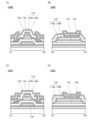
<半導体装置の構成2>
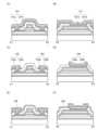
次に、図1(A)(B)(C)(D)に示す半導体装置の別の構成について、図5及び
図6を用いて説明する。<
Next, another structure of the semiconductor device shown in FIGS. 1A, 1B, 1C, and 1D will be described with reference to FIGS.
図5(A)は半導体装置が有するトランジスタ100Aの上面図であり、図5(B)は
半導体装置が有する容量素子150Aの上面図であり、図5(C)は図5(A)の一点鎖
線X1-X2間の断面図であり、図5(D)は図5(B)の一点鎖線X3-X4間の断面
図である。 5A is a top view of a
図5(A)(C)に示すトランジスタ100Aは、基板102上に形成された絶縁膜1
04と、絶縁膜104上の導電膜106と、絶縁膜104及び導電膜106上の絶縁膜1
08と、絶縁膜108を介して導電膜106と重なる酸化物半導体膜110と、酸化物半
導体膜110上の絶縁膜112と、絶縁膜112を介して酸化物半導体膜110と重なる
導電膜114と、酸化物半導体膜110、絶縁膜112、及び導電膜114を覆う絶縁膜
118と、絶縁膜118上の絶縁膜120と、絶縁膜118及び絶縁膜120に設けられ
る開口部140aを介して、酸化物半導体膜110に接続される導電膜122と、絶縁膜
118及び絶縁膜120に設けられる開口部140bを介して、酸化物半導体膜110に
接続される導電膜124と、を有する。なお、トランジスタ100A上には、絶縁膜12
0、導電膜122、及び導電膜124、を覆う絶縁膜128と、を設けてもよい。 The
104, a
100A, an
0, and an insulating
なお、図5(C)において、導電膜106は、導電膜106aと、導電膜106a上の
導電膜106bの積層構造である。また、絶縁膜108は、絶縁膜108aと、絶縁膜1
08a上の絶縁膜108bの積層構造である。また、導電膜114は、導電膜114aと
、導電膜114a上の導電膜114bの積層構造である。また、導電膜122は、導電膜
122aと、導電膜122a上の導電膜122bの積層構造である。また、導電膜124
は、導電膜124aと、導電膜124a上の導電膜124bの積層構造である。 5C, the
The
12 has a stacked structure of a
トランジスタ100Aにおいて、導電膜106は、第1のゲート電極(ボトムゲート電
極ともいう)としての機能を有し、導電膜114は、第2のゲート電極(トップゲート電
極ともいう)としての機能を有し、導電膜122は、ソース電極及びドレイン電極の一方
の電極としての機能を有し、導電膜124は、ソース電極及びドレイン電極の他方の電極
としての機能を有する。また、トランジスタ100Aにおいて、絶縁膜108は、第1の
ゲート絶縁膜としての機能を有し、絶縁膜112は、第2のゲート絶縁膜としての機能を
有する。 In the
なお、図5(A)(C)に示すトランジスタ100Aは、先に説明したトランジスタ1
00と異なり、酸化物半導体膜110の上下にゲート電極として機能する導電膜を有する
構造である。トランジスタ100Aに示すように、本発明の一態様の半導体装置には、2
つ以上のゲート電極を設けてもよい。 The
100A, a conductive film functioning as a gate electrode is provided above and below the
More than one gate electrode may be provided.
また、図5(B)(D)に示す容量素子150Aは、基板102上に形成された絶縁膜
104と、絶縁膜104上の絶縁膜108と、絶縁膜108上の絶縁膜112と、絶縁膜
112上の導電膜116と、絶縁膜108、絶縁膜112、及び導電膜116を覆う絶縁
膜118と、絶縁膜118上の絶縁膜120と、絶縁膜120に設けられる開口部140
cにおいて、絶縁膜118を介して導電膜116と重なる導電膜126と、を有する。な
お、容量素子150A上には、絶縁膜120及び導電膜126を覆う絶縁膜128と、を
設けてもよい。 5B and 5D, a
In FIG. 1C, a
なお、図5(D)において、絶縁膜108は、絶縁膜108aと、絶縁膜108a上の
絶縁膜108bの積層構造である。また、導電膜116は、導電膜116aと、導電膜1
16a上の導電膜116bの積層構造である。また、導電膜126は、導電膜126aと
、導電膜126a上の導電膜126bの積層構造である。 5D, the insulating
The
また、容量素子150Aは、一対の電極間に誘電体を挟持する構造である。より詳しく
は、一対の電極の一方が導電膜116であり、一対の電極の他方が導電膜126であり、
導電膜116と導電膜126の間の絶縁膜118が誘電体として機能する。 The
The insulating
なお、トランジスタ100Aの第2のゲート電極として機能する導電膜114と、容量
素子150Aの一対の電極の一方として機能する導電膜116は、同じ工程で形成され、
少なくとも一部が同一表面上に形成される。また、トランジスタ100Aのソース電極及
びドレイン電極として機能する導電膜122及び導電膜124と、容量素子150Aの一
対の電極の他方として機能する導電膜126は、同じ工程で形成され、少なくとも一部が
同一表面上に形成される。 Note that the
The
このように、トランジスタ100Aと容量素子150Aの各電極として機能する導電膜
を同一工程で形成することによって、製造コストを低減することが可能となる。 In this manner, by forming the conductive films functioning as the electrodes of the
また、容量素子150Aにおいて、絶縁膜120は、開口部140cを有している。し
たがって、絶縁膜118及び絶縁膜120が積層された絶縁膜のうち、絶縁膜118のみ
を誘電体として機能させている。このような構成とすることにより、容量素子150Aの
容量値を大きくすることが可能となる。したがって、表示装置の容量値を大きくすること
が可能となる。 In addition, in the
次に、図5(A)に示すトランジスタ100Aの一点鎖線Y3-Y4方向(チャネル幅
方向)の断面図を図6に示す。 Next, a cross-sectional view of the
図6に示すように、第2のゲート電極として機能する導電膜114は、絶縁膜108及
び絶縁膜112に設けられる開口部139において、第1のゲート電極として機能する導
電膜106に接続される。よって、導電膜114と導電膜106には、同じ電位が与えら
れる。なお、開口部139を設けずに導電膜114と導電膜106とを接続させない構成
としてもよい。導電膜114と導電膜106とを接続させない構成とする場合、導電膜1
14及び導電膜106には、異なる電位を与えてもよい。 6, the
The conductive film 14 and the
また、図6に示すように、酸化物半導体膜110は、第1のゲート電極として機能する
導電膜106と、第2のゲート電極として機能する導電膜114のそれぞれと対向するよ
うに位置し、2つのゲート電極として機能する導電膜に挟まれている。第2のゲート電極
として機能する導電膜114のチャネル幅方向の長さは、酸化物半導体膜110のチャネ
ル幅方向の長さよりも長く、酸化物半導体膜110のチャネル幅方向全体は、絶縁膜11
2を介して導電膜114に覆われている。また、第2のゲート電極として機能する導電膜
114と第1のゲート電極として機能する導電膜106とは、絶縁膜108及び絶縁膜1
12に設けられる開口部139において接続されるため、酸化物半導体膜110のチャネ
ル幅方向の側面の一方は、絶縁膜112を介して第2のゲート電極として機能する導電膜
114と対向している。 6, the
The
12 , one of the side surfaces in the channel width direction of the
別言すると、トランジスタ100Aのチャネル幅方向において、第1のゲート電極とし
て機能する導電膜106及び第2のゲート電極として機能する導電膜114は、第1のゲ
ート絶縁膜として機能する絶縁膜108、及び第2のゲート絶縁膜として機能する絶縁膜
112に設けられる開口部において接続すると共に、第1のゲート絶縁膜として機能する
絶縁膜108、及び第2のゲート絶縁膜として機能する絶縁膜112を介して酸化物半導
体膜110を囲む構成である。 In other words, in the channel width direction of the
このような構成を有することで、トランジスタ100Aに含まれる酸化物半導体膜11
0を、第1のゲート電極として機能する導電膜106及び第2のゲート電極として機能す
る導電膜114の電界によって電気的に囲むことができる。トランジスタ100Aのよう
に、第1のゲート電極及び第2のゲート電極の電界によって、チャネル領域が形成される
酸化物半導体膜を電気的に囲むトランジスタのデバイス構造をsurrounded c
hannel(s-channel)構造と呼ぶことができる。 With such a configuration, the oxide semiconductor film 11 included in the
The oxide semiconductor film in which the channel region is formed can be electrically surrounded by the electric field of the
This can be called a hannel (s-channel) structure.
トランジスタ100Aは、s-channel構造を有するため、第1のゲート電極と
して機能する導電膜106、または第2のゲート電極として機能する導電膜114によっ
てチャネルを誘起させるための電界を効果的に酸化物半導体膜110に印加することがで
きるため、トランジスタ100Aの電流駆動能力が向上し、高いオン電流特性を得ること
が可能となる。また、オン電流を高くすることが可能であるため、トランジスタ100A
を微細化することが可能となる。また、トランジスタ100Aは、酸化物半導体膜110
が第1のゲート電極として機能する導電膜106及び第2のゲート電極として機能する導
電膜114によって囲まれた構造を有するため、トランジスタ100Aの機械的強度を高
めることができる。 Since the
In addition, the
Since the
なお、トランジスタ100Aのチャネル幅方向において、開口部139が形成されてい
ない酸化物半導体膜110の側面に、開口部139と異なる開口部を形成してもよい。 Note that an opening different from the
トランジスタ100A及び容量素子150Aが有する絶縁膜104としては、絶縁膜1
08に示す材料と同様の材料を用いることができる。ここでは、絶縁膜104として、P
ECVD装置を用い、膜厚100nmの窒化シリコン膜を形成する。 The insulating
The insulating
Using an ECVD apparatus, a silicon nitride film is formed to a thickness of 100 nm.
また、トランジスタ100Aが有する導電膜106としては、導電膜114、122、
124に示す材料と同様の材料を用いることができる。ここでは、導電膜106aとして
、スパッタリング装置を用い、膜厚10nmの窒化タンタル膜を形成し、導電膜106b
として、スパッタリング装置を用い、膜厚300nmの銅膜を形成する。 The
The
A sputtering device is used to form a copper film having a thickness of 300 nm.
次に、図1(A)(B)(C)(D)、及び図5(A)(B)(C)(D)に示す半導
体装置の別の構成について、図7乃至図11(A)を用いて説明する。なお、図7乃至図
11(A)に示す半導体装置は、図5(A)(B)(C)(D)に示す半導体装置の変形
例である。 Next, other structures of the semiconductor devices shown in Figures 1A, 1B, 1C, and 1D and Figures 5A, 5B, 5C, and 5D will be described with reference to Figures 7 to 11A. Note that the semiconductor devices shown in Figures 7 to 11A are modified examples of the semiconductor devices shown in Figures 5A, 5B, 5C, and 5D.
図7(A)は半導体装置が有するトランジスタ100Bの断面図であり、図7(B)は
半導体装置が有する容量素子150Bの断面図である。なお、トランジスタ100B及び
容量素子150Bの上面図については、それぞれ図5(A)(B)に示す上面図と同様の
ため、ここでの記載は省略する。また、図7(C)に示すトランジスタ100C、図7(
D)に示す容量素子150C、図8(A)に示すトランジスタ100D、図8(B)に示
す容量素子150D、図8(C)に示すトランジスタ100E、図8(D)に示す容量素
子150E、図9(A)に示すトランジスタ100F、図9(B)に示す容量素子150
F、図9(C)に示すトランジスタ100G、図9(D)に示す容量素子150Gに示す
上面図においても、それぞれ図5(A)(B)に示す上面図と同様のため、ここでの記載
は省略する。 7A is a cross-sectional view of a
8A , the
5A and 5B, and the top views of the
また、図7乃至図11(A)に示す構成において、先に説明した機能と同様の機能を有
する場合には、ハッチパターンを同じくし、特に符号を付さない場合がある。 In addition, in the configurations shown in FIGS. 7 to 11A, when functions similar to those described above are provided, the hatch patterns are the same and no particular reference numerals may be given.
<半導体装置の構成3>
図7(A)に示すトランジスタ100Bは、図5(C)に示すトランジスタ100Aと
導電膜114の形状が相違する。具体的には、トランジスタ100Bが有する導電膜11
4は、導電膜114aと導電膜114a上の導電膜114bの積層構造であり、導電膜1
14aの下端部と絶縁膜112の上端部が一致または概略一致し、導電膜114bの下端
部が、導電膜114aの上端部よりも内側に位置する。また、導電膜114bの端部の一
部が円弧を有する。<Configuration 3 of Semiconductor Device>
The
4 is a laminated structure of a
The lower end of 14a coincides or almost coincides with the upper end of the insulating
また、図7(B)に示す容量素子150Bは、図5(D)に示す容量素子150Aと導
電膜116の形状が相違する。具体的には、容量素子150Bが有する導電膜116は、
導電膜116aと導電膜116a上の導電膜116bの積層構造であり、導電膜116a
の下端部と絶縁膜112の上端部が一致または概略一致し、導電膜116bの下端部が、
導電膜116aの上端部よりも内側に位置する。 7B is different from the
The
The lower end of the
It is located inside the upper end of the
図7(A)(B)に示す絶縁膜112及び/または導電膜114、116の形状とする
ことで、絶縁膜118の被覆性を高めることができる。 By using the shape of the insulating
<半導体装置の構成4>
図7(C)に示すトランジスタ100Cは、図5(C)に示すトランジスタ100Aと
絶縁膜112の形状が相違する。具体的には、トランジスタ100Cが有する絶縁膜11
2は、絶縁膜112の下端部及び上端部が導電膜114の下端部より外側に位置する。す
なわち、絶縁膜112が、導電膜114から迫り出した形状を有する。図7(C)に示す
絶縁膜112の形状とすることで、酸化物半導体膜110のチャネル領域から、絶縁膜1
18を遠ざけることが可能であるため、絶縁膜118に含まれる窒素、水素等が、酸化物
半導体膜110のチャネル領域に入り込むのを抑制することができる。<Configuration 4 of Semiconductor Device>
The
7C , the insulating
Since the insulating
図7(D)に示す容量素子150Cは、図5(D)に示す容量素子150Aと絶縁膜1
12の形状が相違する。具体的には、容量素子150Cが有する絶縁膜112は、絶縁膜
112の下端部及び上端部が導電膜116の下端部より外側に位置する。 The
Specifically, the insulating
図7(C)(D)に示す絶縁膜112の形状とすることで、絶縁膜118の被覆性を高
めることができる。 When the insulating
<半導体装置の構成5>
図8(A)に示すトランジスタ100Dは、図5(C)に示すトランジスタ100Aと
絶縁膜108及び絶縁膜112の構造が相違する。具体的には、図8(A)に示すトラン
ジスタ100Dが有する絶縁膜108は、絶縁膜108a、絶縁膜108b、及び絶縁膜
108cの積層構造である。また、図8(A)に示すトランジスタ100Dが有する絶縁
膜112は、絶縁膜112a及び絶縁膜112bの積層構造である。<Configuration of Semiconductor Device 5>
The
図8(B)に示す容量素子150Dは、図5(D)に示す容量素子150Aと絶縁膜1
08及び絶縁膜112の構造が相違する。具体的には、図8(B)に示す容量素子150
Dが有する絶縁膜108は、絶縁膜108a、絶縁膜108b、及び絶縁膜108cの積
層構造である。また、図8(B)に示す容量素子150Dが有する絶縁膜112は、絶縁
膜112a、及び絶縁膜112bの積層構造である。 The
8B. Specifically, the structure of the
8B. The insulating
なお、図8(A)(B)に示す絶縁膜108c及び絶縁膜112aは、酸化物半導体膜
の価電子帯の上端のエネルギー(Ev_os)と伝導帯の下端のエネルギー(Ec_os
)の間に窒素酸化物の準位密度が低い酸化物絶縁膜を用いて形成することができる。Ev
_osとEc_osの間に窒素酸化物の準位密度が低い酸化物絶縁膜として、窒素酸化物
の放出量が少ない酸化窒化シリコン膜、または窒素酸化物の放出量が少ない酸化窒化アル
ミニウム膜等を用いることができる。なお、絶縁膜108c、112aは、平均膜厚が、
0.1nm以上50nm以下、または0.5nm以上10nm以下である。 Note that the insulating
) can be formed usingan oxide insulating film having a low density of nitrogen oxide levels.
As an oxide insulating film having a low density of nitrogen oxide levels between Ec_os and Ec_os , a silicon oxynitride film that releases a small amount of nitrogen oxide, an aluminum oxynitride film that releases a small amount of nitrogen oxide, or the like can be used.
The thickness is 0.1 nm or more and 50 nm or less, or 0.5 nm or more and 10 nm or less.
なお、窒素酸化物の放出量の少ない酸化窒化シリコン膜は、昇温脱離ガス分析法(TD
S(Thermal Desorption Spectroscopy))において、
窒素酸化物の放出量よりアンモニアの放出量が多い膜であり、代表的にはアンモニアの放
出量が1×10¹⁸個/cm3以上5×1019個/cm3以下である。なお、アンモニ
アの放出量は、膜の表面温度が50℃以上650℃以下、好ましくは50℃以上550℃
以下の加熱処理による放出量とする。 The silicon oxynitride film, which emits a small amount of nitrogen oxide, is analyzed by thermal desorption spectrometry (TD).
In Thermal Desorption Spectroscopy (S),
This is a film that releases more ammonia than nitrogen oxide, and typically releases ammonia at a rate of 1×10¹⁸ particles/cm3 or more and 5×10¹⁹ particles/cm3 or less. The amount of ammonia released is determined when the surface temperature of the film is 50° C. or more and 650° C. or less, preferably 50° C. or more and 550° C. or less.
The amount released due to the following heat treatment is considered.
絶縁膜108b、112bは、加熱により酸素を放出する酸化物絶縁膜を用いて形成す
ることができる。なお、絶縁膜108b、112bは、平均膜厚が5nm以上1000n
m以下、または10nm以上500nm以下である。 The insulating
m or less, or from 10 nm to 500 nm.
加熱により酸素を放出する酸化物絶縁膜の代表例としては、酸化窒化シリコン膜、酸化
窒化アルミニウム膜等がある。 Typical examples of the oxide insulating film that releases oxygen when heated include a silicon oxynitride film and an aluminum oxynitride film.
窒素酸化物(NOx、xは0以上2以下、好ましくは1以上2以下)、代表的にはNO
2またはNOは、絶縁膜108及び絶縁膜112などに準位を形成する。当該準位は、酸
化物半導体膜110のエネルギーギャップ内に位置する。そのため、窒素酸化物が、絶縁
膜108、112及び酸化物半導体膜110の界面に拡散すると、当該準位が絶縁膜10
8、112側において電子をトラップする場合がある。この結果、トラップされた電子が
、絶縁膜108、112及び酸化物半導体膜110界面近傍に留まるため、トランジスタ
のしきい値電圧をプラス方向にシフトさせてしまう。 Nitrogen oxides (NOx , x is 0 to 2, preferably 1 to 2), typically NO
Nitrogen oxide orNO forms a level in the insulating
Electrons may be trapped on the insulating
また、窒素酸化物は、加熱処理においてアンモニア及び酸素と反応する。絶縁膜108
b、112bに含まれる窒素酸化物は、加熱処理において、絶縁膜108c、112aに
含まれるアンモニアと反応するため、絶縁膜108b、112bに含まれる窒素酸化物が
低減される。このため、絶縁膜108、112及び酸化物半導体膜110の界面において
、電子がトラップされにくい。 Nitrogen oxide reacts with ammonia and oxygen during heat treatment.
In the heat treatment, the nitrogen oxides contained in the insulating
絶縁膜108c、112aとして、Ev_osとEc_osの間に窒素酸化物の準位密
度が低い酸化物絶縁膜を用いることで、トランジスタのしきい値電圧のシフトを低減する
ことが可能であり、トランジスタの電気特性の変動を低減することができる。 By using an oxide insulating film having a low density of nitrogen oxide states between Ev_os and Ec_os as the insulating
なお、トランジスタの作製工程の加熱処理、代表的には300℃以上基板歪み点未満の
加熱処理により、絶縁膜108、112は、100K以下のESRで測定して得られたス
ペクトルにおいてg値が2.037以上2.039以下の第1のシグナル、g値が2.0
01以上2.003以下の第2のシグナル、及びg値が1.964以上1.966以下の
第3のシグナルが観測される。なお、第1のシグナル及び第2のシグナルのスプリット幅
、並びに第2のシグナル及び第3のシグナルのスプリット幅は、XバンドのESR測定に
おいて約5mTである。また、g値が2.037以上2.039以下の第1のシグナル、
g値が2.001以上2.003以下の第2のシグナル、及びg値が1.964以上1.
966以下である第3のシグナルのスピンの密度の合計が1×10¹⁸spins/cm
3未満であり、代表的には1×10¹⁷spins/cm3以上1×1018spins
/cm3未満である。 Note that, in a heat treatment in a manufacturing process of a transistor, typically, heat treatment at 300° C. or higher and lower than the substrate distortion point, the insulating
A second signal having a g-value of 1.01 or more and 2.003 or less, and a third signal having a g-value of 1.964 or more and 1.966 or less are observed. The split width of the first signal and the second signal, and the split width of the second signal and the third signal are about 5 mT in X-band ESR measurement. In addition, a first signal having a g-value of 2.037 or more and 2.039 or less,
A second signal having a g value of 2.001 or more and 2.003 or less, and a g value of 1.964 or more and 1.
The sum of the spin densities of the third signals that are 966 or less is 1×10¹⁸ spins/cm
3 , typically 1×10¹⁷ spins/cm3 or more and 1×10¹⁸ spins/cm 3 or more.
/cm3 or less.
なお、100K以下のESRスペクトルにおいてg値が2.037以上2.039以下
の第1シグナル、g値が2.001以上2.003以下の第2のシグナル、及びg値が1
.964以上1.966以下の第3のシグナルは、窒素酸化物(NOx、xは0以上2以
下、好ましくは1以上2以下)起因のシグナルに相当する。窒素酸化物の代表例としては
、一酸化窒素、二酸化窒素等がある。即ち、g値が2.037以上2.039以下の第1
のシグナル、g値が2.001以上2.003以下の第2のシグナル、及びg値が1.9
64以上1.966以下である第3のシグナルのスピンの密度の合計が少ないほど、酸化
物絶縁膜に含まれる窒素酸化物の含有量が少ないといえる。 In the ESR spectrum at 100K or less, a first signal has a g value of 2.037 or more and 2.039 or less, a second signal has a g value of 2.001 or more and 2.003 or less, and a g value of 1
The third signal having a g value of 2.037 to 2.039 corresponds to a signal caused by nitrogen oxides (NOx , where x is 0 to 2, preferably 1 to 2). Representative examples of nitrogen oxides include nitrogen monoxide and nitrogen dioxide.
a second signal having a g value of 2.001 to 2.003, and a third signal having a g value of 1.9
It can be said that the smaller the total spin density of the third signal is from 64 to 1.966, the smaller the content of nitrogen oxide in the oxide insulating film.
また、窒素を含み、且つ欠陥量の少ない酸化物絶縁膜は、SIMSで測定される窒素濃
度が6×10²⁰atoms/cm3以下である。 In addition, the oxide insulating film which contains nitrogen and has few defects has a nitrogen concentration measured by SIMS of 6×10²⁰ atoms/cm3 or less.
基板温度が220℃以上、または280℃以上、または350℃以上であり、シラン及
び一酸化二窒素を用いたPECVD法を用いて、窒素を含み、且つ欠陥量の少ない酸化物
絶縁膜を形成することで、緻密であり、且つ硬度の高い膜を形成することができる。 By forming an oxide insulating film that contains nitrogen and has few defects by using a PECVD method using silane and dinitrogen monoxide at a substrate temperature of 220° C. or higher, or 280° C. or higher, or 350° C. or higher, a dense film with high hardness can be formed.
<半導体装置の構成6>
図8(C)に示すトランジスタ100Eは、図5(C)に示すトランジスタ100Aと
絶縁膜112及び導電膜114の形状が相違する。具体的には、トランジスタ100Eが
有する絶縁膜112の端部の一部が円弧を有する。また、導電膜114aの下端部及び上
端部が絶縁膜112の上端部よりも内側に位置する。また、導電膜114bの下端部が、
導電膜114aの上端部よりも内側に位置する。また、導電膜114a及び導電膜114
bの端部の一部が円弧を有する。<Configuration 6 of Semiconductor Device>
5C , the
The
A part of the end of b has a circular arc.
図8(D)に示す容量素子150Eは、図5(D)に示す容量素子150Aと絶縁膜1
12及び導電膜116の形状が相違する。具体的には、容量素子150Eが有する絶縁膜
112の端部の一部が円弧を有する。また、導電膜116aの下端部及び上端部が絶縁膜
112の上端部よりも内側に位置する。また、導電膜116bの下端部が、導電膜116
aの上端部よりも内側に位置する。なお、導電膜116a及び導電膜116bの端部の一
部が円弧を有する。 The
The shapes of the
The
<半導体装置の構成7>
図9(A)に示すトランジスタ100Fは、図5(C)に示すトランジスタ100Aと
絶縁膜112及び導電膜114の形状等が相違する。具体的には、トランジスタ100F
が有する絶縁膜112及び導電膜114は、断面において矩形形状である。また、トラン
ジスタ100Fは、酸化物半導体膜110と、絶縁膜118との間に、絶縁膜117を有
する。<Configuration 7 of Semiconductor Device>
The
The insulating
図9(B)に示す容量素子150Fは、図5(D)に示す容量素子150Aと絶縁膜1
12及び導電膜116の形状等が相違する。具体的には、容量素子150Fが有する絶縁
膜112及び導電膜116は、断面において矩形形状である。また、容量素子150Fは
、導電膜116と、絶縁膜118との間に、絶縁膜117を有する。 The
12 and the shape of the
図9(A)(B)に示す絶縁膜117は、図8(A)(B)に示すトランジスタ100
D及び容量素子150Dで説明した、絶縁膜108c及び絶縁膜112aに用いることの
できる、窒素を含み、且つ欠陥量の少ない酸化物絶縁膜を用いて形成することができる。 The insulating
The insulating
トランジスタ100Fの構造を図9(A)に示す形状とすることで、酸化物半導体膜1
10中に形成される低抵抗領域の形状が図10に示す構造となる場合がある。 By forming the
In some cases, the shape of the low resistance region formed in the
図10は、図9(A)に示すトランジスタ100Fの酸化物半導体膜110近傍の拡大
図である。図10に示すように、酸化物半導体膜110のチャネル長方向の断面形状にお
いて、酸化物半導体膜のキャリア密度が増加し導電性が高くなる領域(低抵抗領域)が形
成される。また、図10において、チャネル長Lは、一対の低抵抗領域に挟まれた領域の
長さである。 10 is an enlarged view of the
図10に示す酸化物半導体膜110は、チャネル長方向の断面形状において、チャネル
領域110a及び低抵抗領域110bの間に低抵抗領域110dを有し、チャネル領域1
10a及び低抵抗領域110cの間に低抵抗領域110eを有する。低抵抗領域110d
、110eは、低抵抗領域110b、110cより不純物元素の濃度が低く、抵抗率が高
い。なお、ここでは、低抵抗領域110d、110eは、絶縁膜112及び導電膜114
の側面に接する絶縁膜117と重なる領域である。なお、低抵抗領域110d、110e
は、絶縁膜112及び導電膜114と重なってもよい。 The
The
The low-
The
may overlap with the insulating
酸化物半導体膜110が低抵抗領域110b、110cより、不純物元素の濃度が低く
、抵抗率が高い低抵抗領域110d、110eを有することで、ドレイン領域の電界緩和
が可能である。そのため、ドレイン領域の電界に起因したトランジスタのしきい値電圧の
変動を低減することが可能である。 The
<半導体装置の構成8>
図9(C)に示すトランジスタ100Gは、図5(C)に示すトランジスタ100Aと
絶縁膜112及び酸化物半導体膜110の形状が相違する。具体的には、トランジスタ1
00Gが有する絶縁膜112は、2つの膜厚を有しており、導電膜114と重なる領域の
膜厚と、導電膜114と重ならない領域の膜厚が異なる。導電膜114と重なる領域の膜
厚より、導電膜114と重ならない領域の膜厚の方が薄い。また、絶縁膜112が酸化物
半導体膜110を覆う構成のため、酸化物半導体膜110の全体において、膜厚が概略同
一である。<Configuration of Semiconductor Device 8>
The
The insulating
図9(D)に示す容量素子150Gは、図5(D)に示す容量素子150Aと絶縁膜1
12の形状が相違する。具体的には、容量素子150Gが有する絶縁膜112は、2つの
膜厚を有しており、導電膜116と重なる領域の膜厚と、導電膜116と重ならない領域
の膜厚が異なる。導電膜116と重なる領域の膜厚より、導電膜116と重ならない領域
の膜厚の方が薄い。 The
Specifically, the insulating
図9(C)(D)に示す絶縁膜112の形成方法としては、例えば、導電膜114の加
工の後に、絶縁膜112を除去する際に、導電膜114と重ならない領域の絶縁膜112
を残すことによって形成することができる。 As a method for forming the insulating
can be formed by leaving
なお、図9(C)に示すトランジスタ100Gは、絶縁膜112が、酸化物半導体膜1
10のチャネル領域110aに接するとともに、低抵抗領域110b、110cに接する
。また、絶縁膜112は、チャネル領域110aと接する領域と比較して、低抵抗領域1
10b、110cと接する領域の膜厚が薄く、代表的には、平均膜厚が、0.1nm以上
50nm以下、または0.5nm以上10nm以下である。この結果、絶縁膜112を介
して、酸化物半導体膜110に不純物元素を添加することが可能であると共に、絶縁膜1
18に含まれる水素を、絶縁膜112を介して酸化物半導体膜110へ移動させることが
できる。この結果、低抵抗領域110b、110cを形成することができる。 Note that in the
The insulating
The thickness of the region in contact with the insulating
Hydrogen contained in the insulating
絶縁膜112として、窒素を含み、且つ欠陥量の少ない酸化物絶縁膜を用いて形成する
ことで、絶縁膜112において窒素酸化物が生成されにくくなり、絶縁膜112と、酸化
物半導体膜110との界面におけるキャリアのトラップを低減することが可能である。こ
の結果、トランジスタのしきい値電圧のシフトを低減することが可能であり、トランジス
タの電気特性の変動を低減することができる。 When the insulating
さらに、絶縁膜108を絶縁膜108a、108b、108cの多層構造とし、例えば
、窒化物絶縁膜を用いて絶縁膜108aを形成し、加熱により酸素を放出する酸化物絶縁
膜を用いて絶縁膜108bを形成し、窒素を含み、且つ欠陥量の少ない酸化物絶縁膜を用
いて絶縁膜108cを形成する。さらに、窒素を含み、且つ欠陥量の少ない酸化物絶縁膜
を用いて絶縁膜112を形成する。すなわち、窒素を含み、且つ欠陥量の少ない酸化物絶
縁膜で、酸化物半導体膜110を覆うことができる。この結果、絶縁膜108bに含まれ
る酸素を、加熱処理により酸化物半導体膜110に移動させ、酸化物半導体膜110のチ
ャネル領域110aに含まれる酸素欠損を低減しつつ、絶縁膜108c、112と、酸化
物半導体膜110との界面におけるキャリアのトラップを低減することが可能である。こ
の結果、トランジスタのしきい値電圧のシフトを低減することが可能であり、トランジス
タの電気特性の変動を低減することができる。 Further, the insulating
<半導体装置の構成9>
図11(A)に示すトランジスタ100Hは、図5(C)に示すトランジスタ100A
と酸化物半導体膜110の構造が相違する。具体的には、トランジスタ100Hが有する
酸化物半導体膜110は、酸化物半導体膜110_1と、酸化物半導体膜110_1に接
して設けられる酸化物半導体膜110_2と、を有する。すなわち、酸化物半導体膜11
0が多層構造である。<Configuration of Semiconductor Device 9>
The
The
0 is a multi-layer structure.
また、図11(A)に示すトランジスタ100Hの酸化物半導体膜110は、先に説明
した低抵抗領域を有する。具体的には、トランジスタ100Hの酸化物半導体膜110は
、チャネル領域110a_1と、チャネル領域110a_2と、低抵抗領域110b_1
と、低抵抗領域110b_2と、低抵抗領域110c_1と、低抵抗領域110c_2と
、を有する。 11A includes the low-resistance region described above. Specifically, the
, a low resistance region 110b_2, a low resistance region 110c_1, and a low resistance region 110c_2.
<バンド構造>
ここで、図11(B)に、トランジスタ100Hのチャネル領域を含むA-B断面にお
けるバンド構造を示す。なお、酸化物半導体膜110_2は、酸化物半導体膜110_1
よりもエネルギーギャップが大きいとする。また、絶縁膜108a、絶縁膜108b及び
絶縁膜112は、酸化物半導体膜110_1及び酸化物半導体膜110_2よりもエネル
ギーギャップが大きいとする。また、酸化物半導体膜110_1、酸化物半導体膜110
_2、絶縁膜108a、絶縁膜108b及び絶縁膜112のフェルミ準位(Efと表記す
る。)は、それぞれの真性フェルミ準位(Eiと表記する。)の位置とする。また、導電
膜106及び導電膜114の仕事関数は、該フェルミ準位と同じ位置とする。<Band structure>
11B shows a band structure in a cross section taken along line AB including a channel region of the
The insulating
The Fermi levels (Ef) of the insulating
ゲート電圧をトランジスタのしきい値電圧以上としたとき、酸化物半導体膜110_1
と酸化物半導体膜110_2との間の伝導帯下端のエネルギーの差により、電子は酸化物
半導体膜110_1を優先的に流れる。すなわち酸化物半導体膜110_1に電子が埋め
込まれると推定することができる。なお、伝導帯下端のエネルギーをEcと表記し、価電
子帯上端のエネルギーをEvと表記する。 When the gate voltage is set to be equal to or higher than the threshold voltage of the transistor, the
Due to the difference in energy between the bottom of the conduction band of the oxide semiconductor film 110_1 and the oxide semiconductor film 110_2, electrons flow preferentially through the oxide semiconductor film 110_1. In other words, it can be assumed that electrons are embedded in the oxide semiconductor film 110_1. Note that the energy of the bottom of the conduction band is denoted as Ec, and the energy of the top of the valence band is denoted as Ev.
したがって、本発明の一態様に係るトランジスタは、電子の埋め込みによって界面散乱
の影響が低減されている。そのため、本発明の一態様に係るトランジスタは、チャネル抵
抗が小さい。 Therefore, in the transistor according to one embodiment of the present invention, the influence of interface scattering is reduced by the embedding of electrons, and therefore the channel resistance of the transistor according to one embodiment of the present invention is low.
次に、図11(C)に、トランジスタのソース領域またはドレイン領域を含むC-D断
面におけるバンド構造を示す。なお、低抵抗領域110c_1及び低抵抗領域110c_
2は、縮退状態とする。また、低抵抗領域110c_1において、酸化物半導体膜110
_1のフェルミ準位は伝導帯下端のエネルギーと同程度とする。また、低抵抗領域110
c_2において、酸化物半導体膜110_2のフェルミ準位は伝導帯下端のエネルギーと
同程度とする。 11C shows a band structure in a cross section taken along line C-D including a source region or a drain region of a transistor.
In the low-resistance region 110c_1, the
The Fermi level of the low-
In c_2, the Fermi level of the oxide semiconductor film 110_2 is set to be approximately the same as the energy of the bottom of the conduction band.
このとき、ソース電極またはドレイン電極としての機能を有する導電膜124と、低抵
抗領域110c_2と、はエネルギー障壁が十分小さいため、オーミック接触となる。ま
た、低抵抗領域110c_2と、低抵抗領域110c_1と、はオーミック接触となる。
したがって、導電膜124と、酸化物半導体膜110_1及び酸化物半導体膜110_2
と、の間で、電子の授受がスムーズに行われることがわかる。 At this time, the
Therefore, the
It can be seen that electrons are exchanged smoothly between and .
なお、トランジスタのソース電極及びドレイン電極の一方の電極として機能する導電膜
122と酸化物半導体膜110の低抵抗領域110b_1及び低抵抗領域110b_2が
接触する領域においても、図11(C)と同様の説明を行うことができる。 Note that the same description as in FIG. 11C can also be applied to a region where the
以上に示したように、本発明の一態様に係るトランジスタは、ソース電極及びドレイン
電極と、チャネル領域と、の間の電子の授受がスムーズに行われ、かつチャネル抵抗の小
さいトランジスタである。即ち、優れたスイッチング特性を有するトランジスタであるこ
とがわかる。 As described above, the transistor according to one embodiment of the present invention is a transistor in which electrons are smoothly exchanged between the source electrode and the drain electrode and between the channel region and has low channel resistance, i.e., excellent switching characteristics.
<半導体装置の導電膜の接続部及び交差部>
次に、図5(A)(B)(C)(D)に示す、本発明の一態様の半導体装置の各導電膜
の接続部及び交差部の構成について、図30(A)(B)(C)(D)を用いて説明する
。なお、図30(A)(B)(C)は、各導電膜の接続部の構成を示す断面図であり、図
30(D)は、異なる2つの導電膜の交差部の構成を示す断面図である。<Connections and intersections of conductive films in semiconductor device>
Next, structures of connection portions and intersection portions of the conductive films of the semiconductor device of one embodiment of the present invention shown in Figures 5A, 5B, 5C, and 5D will be described with reference to Figures 30A, 30B, 30C, and 30D. Figures 30A, 30B, and 30C are cross-sectional views showing the structure of a connection portion of the conductive films, and Figure 30D is a cross-sectional view showing the structure of an intersection portion of two different conductive films.
図30(A)に示す接続部は、基板102上の絶縁膜104と、絶縁膜104上の導電
膜306と、導電膜306を覆う絶縁膜108と、絶縁膜108上の絶縁膜112と、絶
縁膜112上に設けられ、絶縁膜112及び絶縁膜108に設けられた開口部352を介
して、導電膜306と接続する導電膜314と、絶縁膜108、112、及び導電膜31
4を覆う絶縁膜118と、絶縁膜118上の絶縁膜120と、絶縁膜120上に設けられ
、絶縁膜118、120に設けられた開口部353を介して、導電膜314と接続する導
電膜318と、絶縁膜120及び導電膜318を覆う絶縁膜128と、を有する。 The connection portion shown in FIG. 30A includes an insulating
4, an insulating
図30(B)に示す接続部は、基板102上の絶縁膜104と、絶縁膜104上の絶縁
膜108と、絶縁膜108上の絶縁膜112と、絶縁膜112上の導電膜324と、絶縁
膜108、112、及び導電膜324を覆う絶縁膜118と、絶縁膜118上の絶縁膜1
20と、絶縁膜120上に設けられ、絶縁膜118、120に設けられた開口部354を
介して、導電膜324と接続する導電膜328と、絶縁膜120及び導電膜328を覆う
絶縁膜128と、を有する。 The connection portion shown in FIG. 30B includes an insulating
20 , a
図30(C)に示す接続部は、基板102上の絶縁膜104と、絶縁膜104上の導電
膜316と、導電膜316を覆う絶縁膜108と、絶縁膜108上の絶縁膜112と、絶
縁膜112上に設けられ、絶縁膜112及び絶縁膜108に設けられた開口部355を介
して、導電膜316と接続する導電膜334と、絶縁膜108及び導電膜334を覆う絶
縁膜118と、絶縁膜118上の絶縁膜120と、絶縁膜120上の絶縁膜128と、を
有する。 The connection portion shown in Figure 30 (C) includes an insulating
図30(D)に示す交差部は、基板102上の絶縁膜104と、絶縁膜104上の導電
膜326と、導電膜326を覆う絶縁膜108と、絶縁膜108上の絶縁膜118と、絶
縁膜118上の絶縁膜120と、絶縁膜120上の導電膜338と、導電膜338上の絶
縁膜128と、を有する。 The intersection shown in Figure 30 (D) has an insulating
なお、図30(A)(B)(C)(D)において、絶縁膜108は、絶縁膜108aと
、絶縁膜108a上の絶縁膜108bとの積層構造である。また、図30(A)において
、導電膜306は、導電膜306aと、導電膜306a上の導電膜306bとの積層構造
であり、導電膜314は、導電膜314aと、導電膜314a上の導電膜314bとの積
層構造であり、導電膜318は、導電膜318aと、導電膜318a上の導電膜318b
との積層構造である。また、図30(B)において、導電膜324は、導電膜324aと
、導電膜324a上の導電膜324bとの積層構造であり、導電膜328は、導電膜32
8aと、導電膜328a上の導電膜328bとの積層構造である。また、図30(C)に
おいて、導電膜316は、導電膜316aと、導電膜316a上の導電膜316bとの積
層構造であり、導電膜334は、導電膜334aと、導電膜334a上の導電膜334b
との積層構造である。また、図30(D)において、導電膜326は、導電膜326aと
、導電膜326a上の導電膜326bとの積層構造であり、導電膜338は、導電膜33
8aと、導電膜338a上の導電膜338bとの積層構造である。 30A, 30B, 30C, and 30D, the insulating
30B, the
30C, the
30D, the
8a and a
導電膜306、316、326は、トランジスタ100Aが有する導電膜106と同一
工程で形成される。すなわち、導電膜106と、導電膜306と、導電膜316と、導電
膜326は、少なくとも一部が同一表面上に形成される。また、導電膜314、324、
334は、トランジスタ100Aが有する導電膜114及び容量素子150Aが有する導
電膜116と、同一工程で形成される。すなわち、導電膜114と、導電膜116と、導
電膜314と、導電膜324と、導電膜334は、少なくとも一部が同一表面上に形成さ
れる。また、導電膜318、328、338は、トランジスタ100Aが有する導電膜1
22及び導電膜124、並びに容量素子150Aが有する導電膜126と、同一工程で形
成される。すなわち、導電膜124と、導電膜126と、導電膜318と、導電膜328
と、導電膜338は、少なくとも一部が同一表面上に形成される。 The
The
22, the
At least a portion of the
また、図30(D)に示すように、導電膜326と導電膜338の間には、絶縁膜10
8と、絶縁膜118と、絶縁膜120が設けられている。すなわち、導電膜326と導電
膜338の交差部においては、複数の絶縁膜が積層された構造である。図30(D)に示
すような導電膜の交差部の構造とすることで、導電膜が交差する部分における寄生容量を
低減することができる。この結果、該寄生容量による信号遅延を低減することができる。 As shown in FIG. 30D, the insulating
30D, a
<半導体装置の作製方法1>
次に、図1に示すトランジスタ100及び容量素子150の作製方法の一例について、
図12乃至図16を用いて説明する。<
Next, an example of a method for manufacturing the
This will be described with reference to FIG. 12 to FIG.
なお、トランジスタ100及び容量素子150を構成する膜(絶縁膜、酸化物半導体膜
、導電膜等)は、スパッタリング法、化学気相堆積(CVD)法、真空蒸着法、パルスレ
ーザー堆積(PLD)法を用いて形成することができる。あるいは、塗布法や印刷法で形
成することができる。成膜方法としては、スパッタリング法、プラズマ化学気相堆積(P
ECVD)法が代表的であるが、熱CVD法でもよい。熱CVD法の例として、MOCV
D(有機金属化学堆積)法やALD(原子層成膜)法を使ってもよい。 Note that the films (an insulating film, an oxide semiconductor film, a conductive film, and the like) constituting the
A typical example of the thermal CVD method is MOCVD.
Metal organic chemical deposition (D) and atomic layer deposition (ALD) may also be used.
熱CVD法は、チャンバー内を大気圧または減圧下とし、原料ガスと酸化剤を同時にチ
ャンバー内に送り、基板近傍または基板上で反応させて基板上に堆積させることで成膜を
行う。このように、熱CVD法は、プラズマを発生させない成膜方法であるため、プラズ
マダメージにより欠陥が生成されることが無いという利点を有する。 In the thermal CVD method, the pressure in the chamber is set to atmospheric pressure or reduced pressure, and a source gas and an oxidizing agent are simultaneously fed into the chamber, and the gas and the oxidizing agent are reacted near or on the substrate to deposit the film on the substrate. In this way, the thermal CVD method is a film formation method that does not generate plasma, and therefore has the advantage that defects due to plasma damage are not generated.
また、ALD法は、チャンバー内を大気圧または減圧下とし、反応のための原料ガスが
順次にチャンバーに導入され、そのガス導入の順序を繰り返すことで成膜を行う。例えば
、それぞれのスイッチングバルブ(高速バルブともよぶ。)を切り替えて2種類以上の原
料ガスを順番にチャンバーに供給し、複数種の原料ガスが混ざらないように第1の原料ガ
スと同時またはその後に不活性ガス(アルゴン、或いは窒素など)などを導入し、第2の
原料ガスを導入する。なお、同時に不活性ガスを導入する場合には、不活性ガスはキャリ
アガスとなり、また、第2の原料ガスの導入時にも同時に不活性ガスを導入してもよい。
また、不活性ガスを導入する代わりに真空排気によって第1の原料ガスを排出した後、第
2の原料ガスを導入してもよい。第1の原料ガスが基板の表面に吸着して第1の単原子層
を成膜し、後から導入される第2の原料ガスと反応して、第2の単原子層が第1の単原子
層上に積層されて薄膜が形成される。 In the ALD method, the chamber is kept at atmospheric pressure or reduced pressure, raw material gases for reaction are sequentially introduced into the chamber, and the order of gas introduction is repeated to form a film. For example, two or more types of raw material gases are sequentially supplied to the chamber by switching each switching valve (also called high-speed valve), and an inert gas (argon, nitrogen, etc.) is introduced simultaneously with or after the first raw material gas so that the multiple raw material gases are not mixed, and then the second raw material gas is introduced. When the inert gas is introduced simultaneously, the inert gas becomes a carrier gas, and the inert gas may be introduced simultaneously with the introduction of the second raw material gas.
Alternatively, instead of introducing an inert gas, a first source gas may be discharged by evacuation and then a second source gas may be introduced. The first source gas is adsorbed on the surface of the substrate to form a first monoatomic layer, which reacts with a second source gas introduced later to form a second monoatomic layer on the first monoatomic layer, thereby forming a thin film.
このガス導入順序を制御しつつ所望の厚さになるまで複数回繰り返すことで、段差被覆
性に優れた薄膜を形成することができる。薄膜の厚さは、ガス導入順序を繰り返す回数に
よって調節することができるため、精密な膜厚調節が可能であり、微細なトランジスタを
作製する場合に適している。 By controlling the gas introduction sequence and repeating the process several times until the desired thickness is achieved, a thin film with excellent step coverage can be formed. The thickness of the thin film can be adjusted by the number of times the gas introduction sequence is repeated, allowing precise film thickness adjustment, making it suitable for producing fine transistors.
なお、図12(A)(C)(E)(G)、図13(A)(C)(E)、図14(A)(
C)(E)、図15(A)(C)(E)、及び図16(A)(C)(E)がトランジスタ
100の作製方法を説明する断面図であり、図12(B)(D)(F)(H)、図13(
B)(D)(F)、図14(B)(D)(F)、図15(B)(D)(F)、及び図16
(B)(D)(F)が容量素子150の作製方法を説明する断面図である。 In addition, Figs. 12(A), (C), (E), (G), 13(A), (C), (E), and 14(A),
15A, 15C, 15E, and 16A, 16C, 16E are cross-sectional views illustrating a method for manufacturing the
14(B)(D)(F), 15(B)(D)(F), and 16(B)(D)(F).
1B, 1D, and 1F are cross-sectional views illustrating a method for manufacturing the
まず、基板102上に絶縁膜108(絶縁膜108a及び絶縁膜108b)を形成する
(図12(A)(B)参照)。 First, the insulating film 108 (the insulating
絶縁膜108としては、スパッタリング法、CVD法、蒸着法、パルスレーザー堆積(
PLD)法、印刷法、塗布法等を適宜用いて形成することができる。本実施の形態におい
ては、絶縁膜108aとして、PECVD装置を用い、窒化シリコン膜を100nm形成
する。また、絶縁膜108bとして、PECVD装置を用い、酸化窒化シリコン膜を40
0nm形成する。 The insulating
The insulating
0 nm is formed.
また、絶縁膜108bを形成した後、絶縁膜108bに酸素を添加してもよい。絶縁膜
108bに添加する酸素としては、酸素ラジカル、酸素原子、酸素原子イオン、酸素分子
イオン等がある。また、添加方法としては、イオンドーピング法、イオン注入法、プラズ
マ処理法等がある。また、絶縁膜上に酸素の脱離を抑制する膜を形成した後、該膜を介し
て絶縁膜108bに酸素を添加してもよい。 After the insulating
また、PECVD装置の真空排気された処理室内に載置された基板を180℃以上28
0℃以下、又は200℃以上240℃以下に保持し、処理室に原料ガスを導入して処理室
内における圧力を100Pa以上250Pa以下、又は100Pa以上200Pa以下と
し、処理室内に設けられる電極に0.17W/cm2以上0.5W/cm2以下、又は0
.25W/cm2以上0.35W/cm2以下の高周波電力を供給する条件により、加熱
処理により酸素を放出することが可能な酸化シリコン膜又は酸化窒化シリコン膜を絶縁膜
108bとして形成することができる。 In addition, the substrate placed in the evacuated processing chamber of the PECVD apparatus was heated to 180° C. or higher for 28
The temperature is kept at 0° C. or lower, or at least 200° C. and at most 240° C., a raw material gas is introduced into the processing chamber to set the pressure in the processing chamber to at least 100 Pa and at most 250 Pa, or at least 100 Pa and at most 200 Pa, and a power of at least 0.17 W/cm2 or at most 0.5 W/cm2 is applied to an electrode provided in the processing chamber.
Under the condition of supplying high-frequency power of 25 W/cm2 or more and 0.35 W/cm2 or less, a silicon oxide film or a silicon oxynitride film capable of releasing oxygen by heat treatment can be formed as the insulating
ここでは、絶縁膜108b上に酸素の脱離を抑制する膜を形成した後、該膜を介して絶
縁膜108bに酸素を添加する方法を説明する。 Here, a method is described in which a film for suppressing oxygen desorption is formed over the insulating
絶縁膜108b上に、酸素の脱離を抑制する膜141を形成する(図12(C)(D)
参照)。 A
reference).
次に、膜141を介して絶縁膜108bに酸素142を添加する(図12(E)(F)
参照)。 Next,
reference).
酸素の脱離を抑制する膜141として、アルミニウム、クロム、タンタル、チタン、モ
リブデン、ニッケル、鉄、コバルト、タングステンから選ばれた金属元素、上述した金属
元素を成分とする合金、上述した金属元素を組み合わせた合金、上述した金属元素を有す
る金属窒化物、上述した金属元素を有する金属酸化物、上述した金属元素を有する金属窒
化酸化物等の導電性を有する材料を用いて形成する。 The
酸素の脱離を抑制する膜141の厚さは、1nm以上20nm以下、または2nm以上
10nm以下とすることができる。 The thickness of the
膜141を介して絶縁膜108bに酸素142を添加する方法としては、イオンドーピ
ング法、イオン注入法、プラズマ処理法等がある。絶縁膜108b上に膜141を設けて
酸素を添加することで、膜141が絶縁膜108bから酸素が脱離することを抑制する保
護膜として機能する。このため、絶縁膜108bにより多くの酸素を添加することができ
る。 Methods for adding
また、プラズマ処理で酸素の添加を行う場合、マイクロ波で酸素を励起し、高密度な酸
素プラズマを発生させることで、絶縁膜108bへの酸素添加量を増加させることができ
る。 In addition, in the case where oxygen is added by plasma treatment, oxygen is excited by microwaves to generate high-density oxygen plasma, whereby the amount of oxygen added to the insulating
こののち、膜141を除去する(図12(G)(H)参照)。After this, the
なお、成膜後に十分に酸素が添加された絶縁膜108bを形成できる場合においては、
図12(C)(D)、及び図12(E)(F)に示す酸素を添加する処理を行わなくても
よい。 In addition, in the case where the insulating
The oxygen addition treatment shown in FIGS. 12C, 12D, 12E and 12F may not be performed.
次に、絶縁膜108b上に酸化物半導体膜を形成し、該酸化物半導体膜を所望の形状に
加工することで、酸化物半導体膜110を形成する。こののち、絶縁膜108b及び酸化
物半導体膜110上に絶縁膜112を形成する(図13(A)(B)参照)。 Next, an oxide semiconductor film is formed over the insulating
酸化物半導体膜110の形成方法について以下に説明する。絶縁膜108b上にスパッ
タリング法、塗布法、パルスレーザー蒸着法、レーザーアブレーション法、熱CVD法等
により酸化物半導体膜を形成する。次に、酸化物半導体膜上にリソグラフィ工程によりマ
スクを形成した後、該マスクを用いて酸化物半導体膜の一部をエッチングすることで、図
13(A)に示すように、酸化物半導体膜110を形成することができる。この後、マス
クを除去する。なお、酸化物半導体膜110を形成した後、加熱処理を行ってもよい。 A method for forming the
また、酸化物半導体膜110として印刷法を用いることで、素子分離された酸化物半導
体膜110を直接形成することができる。 In addition, by using a printing method for the
スパッタリング法で酸化物半導体膜を形成する場合、プラズマを発生させるための電源
装置は、RF電源装置、AC電源装置、DC電源装置等を適宜用いることができる。なお
、AC電源装置またはDC電源装置を用いることで、CAAC-OS膜を形成することが
可能である。また、RF電源装置を用いたスパッタリング法で酸化物半導体膜を形成する
よりも、AC電源装置またはDC電源装置を用いたスパッタリング法で酸化物半導体膜を
形成した方が、膜厚の分布、膜組成の分布、または結晶性の分布が均一となるため好まし
い。 When an oxide semiconductor film is formed by a sputtering method, an RF power supply, an AC power supply, a DC power supply, or the like can be used as appropriate as a power supply for generating plasma. Note that a CAAC-OS film can be formed by using an AC power supply or a DC power supply. In addition, forming an oxide semiconductor film by a sputtering method using an AC power supply or a DC power supply is preferable to forming an oxide semiconductor film by a sputtering method using an RF power supply because the distribution of the film thickness, the distribution of the film composition, or the distribution of crystallinity can be made more uniform.
酸化物半導体膜を形成する場合のスパッタリングガスは、希ガス(代表的にはアルゴン
)、酸素ガス、希ガス及び酸素ガスの混合ガスを適宜用いる。なお、希ガス及び酸素ガス
の混合ガスの場合、希ガスに対して酸素のガス比を高めることが好ましい。 A rare gas (typically, argon), oxygen gas, or a mixed gas of a rare gas and oxygen gas is used as a sputtering gas for forming an oxide semiconductor film. In the case of a mixed gas of a rare gas and oxygen gas, the gas ratio of oxygen to the rare gas is preferably increased.
また、酸化物半導体膜を形成する場合のスパッタリングターゲットは、形成する酸化物
半導体膜の組成にあわせて、適宜選択すればよい。 In addition, a sputtering target for forming an oxide semiconductor film may be appropriately selected depending on the composition of the oxide semiconductor film to be formed.
なお、酸化物半導体膜を形成する際に、例えば、スパッタリング法を用いる場合、基板
温度を150℃以上750℃以下、または150℃以上450℃以下、または200℃以
上350℃以下として、酸化物半導体膜を成膜することで、CAAC-OS膜を形成する
ことができる。また、基板温度を25℃以上150℃未満とすることで、微結晶酸化物半
導体膜を形成することができる。 Note that in the case where the oxide semiconductor film is formed by a sputtering method, for example, a CAAC-OS film can be formed by setting the substrate temperature to 150° C. or higher and 750° C. or lower, or 150° C. or higher and 450° C. or lower, or 200° C. or higher and 350° C. or lower. A microcrystalline oxide semiconductor film can be formed by setting the substrate temperature to 25° C. or higher and lower than 150° C.
また、後述するCAAC-OS膜を成膜するために、以下の条件を適用することが好ま
しい。 In addition, the following conditions are preferably applied to deposit a CAAC-OS film, which will be described later.
成膜時の不純物混入を抑制することで、不純物によって結晶状態が崩れることを抑制で
きる。例えば、成膜室内に存在する不純物濃度(水素、水、二酸化炭素及び窒素など)を
低減すればよい。また、成膜ガス中の不純物濃度を低減すればよい。具体的には、露点が
-80℃以下、または-100℃以下である成膜ガスを用いる。 By suppressing the inclusion of impurities during film formation, it is possible to suppress the crystal state from being destroyed by the impurities. For example, this can be achieved by reducing the concentration of impurities (hydrogen, water, carbon dioxide, nitrogen, etc.) present in the film formation chamber. Also, this can be achieved by reducing the concentration of impurities in the film formation gas. Specifically, a film formation gas with a dew point of -80°C or less, or -100°C or less is used.
また、成膜ガス中の酸素割合を高め、電力を最適化することで成膜時のプラズマダメー
ジを軽減すると好ましい。成膜ガス中の酸素割合は、30体積%以上、または100体積
%とする。 It is also preferable to reduce plasma damage during film formation by increasing the oxygen ratio in the film formation gas and optimizing the power. The oxygen ratio in the film formation gas is set to 30 volume % or more, or 100 volume %.
また、酸化物半導体膜を形成した後、加熱処理を行い、酸化物半導体膜の脱水素化また
は脱水化をしてもよい。加熱処理の温度は、代表的には、150℃以上基板歪み点未満、
または250℃以上450℃以下、または300℃以上450℃以下とする。 After the oxide semiconductor film is formed, heat treatment may be performed to dehydrogenate or dehydrate the oxide semiconductor film. The temperature of the heat treatment is typically 150° C. or higher and lower than the distortion point of the substrate.
Alternatively, the temperature is set to 250° C. or higher and 450° C. or lower, or 300° C. or higher and 450° C. or lower.
加熱処理は、ヘリウム、ネオン、アルゴン、キセノン、クリプトン等の希ガス、または
窒素を含む不活性ガス雰囲気で行う。または、不活性ガス雰囲気で加熱した後、酸素雰囲
気で加熱してもよい。なお、上記不活性雰囲気及び酸素雰囲気に水素、水などが含まれな
いことが好ましい。処理時間は3分以上24時間以下とする。 The heat treatment is performed in an inert gas atmosphere containing a rare gas such as helium, neon, argon, xenon, or krypton, or nitrogen. Alternatively, the heat treatment may be performed in an inert gas atmosphere and then in an oxygen atmosphere. Note that it is preferable that the inert atmosphere and the oxygen atmosphere do not contain hydrogen, water, or the like. The treatment time is 3 minutes to 24 hours.
該加熱処理は、電気炉、RTA装置等を用いることができる。RTA装置を用いること
で、短時間に限り、基板の歪み点以上の温度で熱処理を行うことができる。そのため加熱
処理時間を短縮することができる。 The heat treatment can be performed using an electric furnace, an RTA apparatus, etc. By using an RTA apparatus, the heat treatment can be performed at a temperature equal to or higher than the distortion point of the substrate for a short period of time, and therefore the heat treatment time can be shortened.
酸化物半導体膜を加熱しながら成膜することで、さらには酸化物半導体膜を形成した後
、加熱処理を行うことで、酸化物半導体膜において、二次イオン質量分析法により得られ
る水素濃度を5×10¹⁹atoms/cm3以下、または1×1019atoms/c
m3以下、5×10¹⁸atoms/cm3以下、または1×1018atoms/cm
3以下、または5×10¹⁷atoms/cm3以下、または1×1016atoms/
cm3以下とすることができる。 By forming the oxide semiconductor film while heating, or by performing heat treatment after the oxide semiconductor film is formed, the hydrogen concentration in the oxide semiconductor film measured by secondary ion mass spectrometry can be reduced to 5×10¹⁹ atoms/cm3 or less or 1×10¹⁹ atoms/cm 3 or less.
m3 or less, 5×10¹⁸ atoms/cm3or less, or 1×10¹⁸ atoms/cm
3 or less, or 5×10¹⁷ atoms/cm3 or less, or 1×10¹⁶ atoms/cm
cm3 or less.
ALDを利用する成膜装置により酸化物半導体膜、例えばInGaZnOX(X>0)
膜を成膜する場合には、In(CH3)3ガスとO3ガスを順次繰り返し導入してInO
2層を形成し、その後、Ga(CH3)3ガスとO3ガスを同時に導入してGaO層を形
成し、更にその後Zn(CH3)2とO3ガスを同時に導入してZnO層を形成する。な
お、これらの層の順番はこの例に限らない。また、これらのガスを混ぜてInGaO2層
やInZnO2層、GaInO層、ZnInO層、GaZnO層などの混合化合物層を形
成してもよい。なお、O3ガスに変えてAr等の不活性ガスでバブリングしたH2Oガス
を用いてもよいが、Hを含まないO3ガスを用いる方が好ましい。また、In(CH3)
3ガスにかえて、In(C2H5)3ガスを用いてもよい 。また、Ga(CH3)3ガ
スにかえて、Ga(C2H5)3ガスを用いてもよい。また、Zn(CH3)2ガスを用
いてもよい。 An oxide semiconductor film, for example, InGaZnOx (x>0) is formed by a film formation apparatus using ALD.
When forming a film, In(CH3 )3 gas and O3 gas are introduced in sequence and repeatedly to form InO
In the first step,a GaO layer is formed, and then Ga(CH3 )3 gas andO3 gas are simultaneously introduced to form a GaO layer, and then Zn(CH3 )2 andO3 gas are simultaneously introduced to form a ZnO layer. The order of these layers is not limited to this example. These gases may also be mixed to form a mixed compound layer such as anInGaO2 layer, anInZnO2 layer, a GaInO layer, a ZnInO layer, or a GaZnO layer. AlthoughH2O gas bubbled with an inert gas such as Ar may be used instead of O3 gas, it is preferable to useO3 gas that does not contain H. In addition, In(CH3 )
In(C2 H5 )3 gas may be used instead of the Ga(CH3 )3 gas, and Ga(C2 H5 )3 gas may be used instead of the Ga(CH 3 )3 gas, and Zn(CH3 )2 gas may be used instead of the Ga(CH 3 ) 3 gas.
なお、本実施の形態においては、酸化物半導体膜110として、スパッタリング装置を
用い、スパッタリングターゲットとしてIn-Ga-Zn金属酸化物(In:Ga:Zn
=1:1:1.2[原子数比])を用いて、膜厚50nmの酸化物半導体膜を成膜した後
、加熱処理を行い、絶縁膜108bに含まれる酸素を酸化物半導体膜に移動させる。次に
、当該酸化物半導体膜上にマスクを形成し、酸化物半導体膜の一部を選択的にエッチング
することで、酸化物半導体膜110を形成する。 Note that in this embodiment, a sputtering apparatus is used to form the
A 50-nm-thick oxide semiconductor film is formed using an oxide semiconductor layer having an atomic ratio of 1:1:1.2 (atomic ratio) and then heat treatment is performed to move oxygen contained in the insulating
なお、加熱処理は、350℃より高く650℃以下、または450℃以上600℃以下
で行うことで、後述するCAAC化率が、60%以上100%未満、または80%以上1
00%未満、または90%以上100%未満、または95%以上98%以下である酸化物
半導体膜を得ることができる。また、水素、水等の含有量が低減された酸化物半導体膜を
得ることが可能である。すなわち、不純物濃度が低く、欠陥準位密度の低い酸化物半導体
膜を形成することができる。 In addition, by carrying out the heat treatment at a temperature higher than 350° C. and not higher than 650° C., or at a temperature of 450° C. or higher and 600° C. or lower, the CAAC conversion rate described below can be set to 60% or higher and lower than 100%, or at a temperature of 80% or higher and lower than 100%.
It is possible to obtain an oxide semiconductor film having a conductivity of less than 0.00%, or greater than or equal to 90% and less than 100%, or greater than or equal to 95% and less than or equal to 98%. In addition, it is possible to obtain an oxide semiconductor film with a reduced content of hydrogen, water, and the like. That is, it is possible to form an oxide semiconductor film having a low impurity concentration and a low density of defect states.
絶縁膜112は、絶縁膜108bの形成方法を適宜用いることができる。絶縁膜112
としては、酸化シリコン膜または酸化窒化シリコン膜を、PECVD法を用いて形成する
ことができる。この場合、原料ガスとしては、シリコンを含む堆積性気体及び酸化性気体
を用いることが好ましい。シリコンを含む堆積性気体の代表例としては、シラン、ジシラ
ン、トリシラン、フッ化シラン等がある。酸化性気体としては、酸素、オゾン、一酸化二
窒素、二酸化窒素等がある。 The insulating
As the deposition gas, a silicon oxide film or a silicon oxynitride film can be formed by using a PECVD method. In this case, it is preferable to use a deposition gas containing silicon and an oxidizing gas as a source gas. Representative examples of the deposition gas containing silicon include silane, disilane, trisilane, and silane fluoride. Examples of the oxidizing gas include oxygen, ozone, nitrous oxide, and nitrogen dioxide.
また、絶縁膜112として、堆積性気体に対する酸化性気体を20倍より大きく100
倍未満、または40倍以上80倍以下とし、処理室内の圧力を100Pa未満、または5
0Pa以下とするPECVD法を用いることで、欠陥量の少ない酸化窒化シリコン膜を形
成することができる。 In addition, the insulating
100 Pa or less, or 40 times or more and 80 times or less, and the pressure in the processing chamber is less than 100 Pa, or 5
By using the PECVD method at a pressure of 0 Pa or less, a silicon oxynitride film with a small amount of defects can be formed.
また、絶縁膜112として、PECVD装置の真空排気された処理室内に載置された基
板を280℃以上400℃以下に保持し、処理室に原料ガスを導入して処理室内における
圧力を20Pa以上250Pa以下、さらに好ましくは100Pa以上250Pa以下と
し、処理室内に設けられる電極に高周波電力を供給する条件により、絶縁膜112として
、緻密である酸化シリコン膜または酸化窒化シリコン膜を形成することができる。 In addition, a dense silicon oxide film or silicon oxynitride film can be formed as the insulating
また、絶縁膜112を、マイクロ波を用いたプラズマCVD法を用いて形成することが
できる。マイクロ波とは300MHzから300GHzの周波数域を指す。マイクロ波は
電子温度が低く、電子エネルギーが小さい。また、供給された電力において、電子の加速
に用いられる割合が少なく、より多くの分子の解離及び電離に用いられることが可能であ
り、密度の高いプラズマ(高密度プラズマ)を励起することができる。このため、被成膜
面及び堆積物へのプラズマダメージが少なく、欠陥の少ない絶縁膜112を形成すること
ができる。 The insulating
また、絶縁膜112を、有機シランガスを用いたCVD法を用いて形成することができ
る。有機シランガスとしては、珪酸エチル(TEOS:化学式Si(OC2H5)4)、
テトラメチルシラン(TMS:化学式Si(CH3)4)、テトラメチルシクロテトラシ
ロキサン(TMCTS)、オクタメチルシクロテトラシロキサン(OMCTS)、ヘキサ
メチルジシラザン(HMDS)、トリエトキシシラン(SiH(OC2H5)3)、トリ
スジメチルアミノシラン(SiH(N(CH3)2)3)などのシリコン含有化合物を用
いることができる。有機シランガスを用いたCVD法を用いることで、被覆性の高い絶縁
膜112を形成することができる。 The insulating
Silicon-containing compounds such as tetramethylsilane (TMS: chemical formula Si(CH3 )4 ), tetramethylcyclotetrasiloxane (TMCTS), octamethylcyclotetrasiloxane (OMCTS), hexamethyldisilazane (HMDS), triethoxysilane (SiH(OC2H5 )3 ), and trisdimethylaminosilane (SiH(N(CH3 )2 )3 ) can be used. By using the CVD method using an organosilane gas, the insulating
また、絶縁膜112として酸化ガリウム膜を形成する場合、MOCVD(Metal
Organic Chemical Vapor Deposition)法を用いて形
成することができる。 In addition, when a gallium oxide film is formed as the insulating
The film can be formed by using an organic chemical vapor deposition (OCVD) method.
また、絶縁膜112として、MOCVD法やALD法などの熱CVD法を用いて、酸化
ハフニウム膜を形成する場合には、溶媒とハフニウム前駆体化合物を含む液体(ハフニウ
ムアルコキシド溶液、代表的にはテトラキスジメチルアミドハフニウム(TDMAH))
を気化させた原料ガスと、酸化剤としてオゾン(O3)の2種類のガスを用いる。なお、
テトラキスジメチルアミドハフニウムの化学式はHf[N(CH3)2]4である。また
、他の材料液としては、テトラキス(エチルメチルアミド)ハフニウムなどがある。 In addition, when a hafnium oxide film is formed as the insulating
Two types of gases are used: a raw material gas obtained by vaporizing the above-mentioned and ozone (O3 ) as an oxidizing agent.
The chemical formula for tetrakisdimethylamidohafnium is Hf[N(CH3 )2 ]4. Other material liquids include tetrakis(ethylmethylamido)hafnium.
また、絶縁膜112として、MOCVD法やALD法などの熱CVD法を用いて、酸化
アルミニウム膜を形成する場合には、溶媒とアルミニウム前駆体化合物を含む液体(トリ
メチルアルミニウムTMAなど)を気化させた原料ガスと、酸化剤としてH2Oの2種類
のガスを用いる。なお、トリメチルアルミニウムの化学式はAl(CH3)3である。ま
た、他の材料液としては、トリス(ジメチルアミド)アルミニウム、トリイソブチルアル
ミニウム、アルミニウムトリス(2,2,6,6-テトラメチル-3,5-ヘプタンジオ
ナート)などがある。なお、ALD法で形成することで、被覆率が高く、膜厚の薄い絶縁
膜112を形成することが可能である。 When an aluminum oxide film is formed as the insulating
また、絶縁膜112として、MOCVD法やALD法などの熱CVD法を用いて、酸化
シリコン膜を形成する場合には、ヘキサクロロジシランを被成膜面に吸着させ、吸着物に
含まれる塩素を除去し、酸化性ガス(O2、一酸化二窒素)のラジカルを供給して吸着物
と反応させる。 Furthermore, when a silicon oxide film is formed as the insulating
ここでは、絶縁膜112として、PECVD装置を用い、厚さ100nmの酸化窒化シ
リコン膜を形成する。 Here, as the insulating
次に、絶縁膜112上に導電膜113(導電膜113a及び導電膜113b)を形成す
る(図13(C)(D)参照)。 Next, a conductive film 113 (a
導電膜113としては、スパッタリング法、真空蒸着法、パルスレーザー堆積(PLD
)法、熱CVD法等を用いて形成することができる。本実施の形態においては、導電膜1
13aとして、スパッタリング装置を用い、窒化タンタル膜を10nm形成する。また、
導電膜113bとして、スパッタリング装置を用い、銅膜を300nm形成する。なお、
導電膜113aと導電膜113bを真空中で連続して形成すると、導電膜113aと導電
膜113bの界面に不純物が混入するのを抑制できるため好適である。 The
In this embodiment, the
As the film 13a, a tantalum nitride film is formed to a thickness of 10 nm using a sputtering device.
As the
It is preferable to form the
また、ALD法を利用する成膜装置により導電膜113bとしてタングステン膜を成膜
することができる。この場合には、WF6ガスとB2H6ガスを順次繰り返し導入して初
期タングステン膜を形成し、その後、WF6ガスとH2ガスを同時に導入してタングステ
ン膜を形成する。なお、B2H6ガスに代えてSiH4ガスを用いてもよい。 Also, a tungsten film can be formed as the
次に、導電膜113b上にリソグラフィ工程によりマスク145を形成した後、導電膜
113b、導電膜113a、及び絶縁膜112の一部をエッチングする(図13(E)(
F)参照)。 Next, a
See F).
導電膜113及び絶縁膜112をエッチングする方法は、ウエットエッチング法または
/及びドライエッチング法を適宜用いることができる。 The
次に、マスク145を縮小させながら、導電膜113及び絶縁膜112を加工すること
で、導電膜114a、114b、116a、116bを形成する(図14(A)(B)参
照)。 Next, the
また、トランジスタ100においては、導電膜113及び絶縁膜112のエッチング工
程において、酸化物半導体膜110の一部を露出させる。なお、酸化物半導体膜110の
一部が露出した領域は、導電膜114及び絶縁膜112のエッチング工程により、導電膜
114と重なる酸化物半導体膜110よりも膜厚が薄くなる場合がある。また、トランジ
スタ100においては、導電膜113及び絶縁膜112のエッチング工程において、下地
膜として機能する絶縁膜108bの酸化物半導体膜110から露出した領域の一部が除去
され、酸化物半導体膜110と重畳する領域の膜厚よりも薄くなる場合がある。また、容
量素子150においては、導電膜113及び絶縁膜112のエッチング工程において、下
地膜として機能する絶縁膜108bの絶縁膜112から露出した領域の一部が除去され、
絶縁膜112と重畳する領域の膜厚よりも薄くなる場合がある。 In the
The thickness of the insulating
次に、絶縁膜108b、絶縁膜112、酸化物半導体膜110、導電膜114、及びマ
スク145上から不純物元素143を添加する(図14(C)(D)参照)。 Next, the
不純物元素143の添加工程において、導電膜114、絶縁膜112、及びマスク14
5に覆われていない酸化物半導体膜110に不純物元素が添加される。なお、不純物元素
143の添加により、酸化物半導体膜110には酸素欠損が形成される。 In the step of adding the
The
不純物元素143の添加方法としては、イオンドーピング法、イオン注入法、プラズマ
処理法等がある。プラズマ処理法の場合、添加する不純物元素を含むガス雰囲気にてプラ
ズマを発生させて、プラズマ処理を行うことによって、不純物元素を添加することができ
る。上記プラズマを発生させる装置としては、ドライエッチング装置、アッシング装置、
プラズマCVD装置、高密度プラズマCVD装置等を用いることができる。 The
A plasma CVD apparatus, a high density plasma CVD apparatus, or the like can be used.
なお、不純物元素143の原料ガスとして、B2H6、PH3、CH4、N2、NH3
、AlH3、AlCl3、SiH4、Si2H6、F2、HF、H2及び希ガスの一以上
を用いることができる。または、希ガスで希釈されたB2H6、PH3、N2、NH3、
AlH3、AlCl3、F2、HF、及びH2の一以上を用いることができる。希ガスで
希釈されたB2H6、PH3、N2、NH3、AlH3、AlCl3、F2、HF、及び
H2の一以上を用いて不純物元素143を酸化物半導体膜110に添加することで、希ガ
スと、水素、ホウ素、炭素、窒素、フッ素、アルミニウム、シリコン、リン、及び塩素の
一以上とを同時に酸化物半導体膜110に添加することができる。 The source gas of the
, AlH3 , AlCl3 , SiH4 , Si2 H6 , F2 , HF, H2 and one or more of a rare gas can be used. Or, B2 H6 diluted with a rare gas, PH3 , N2 , NH3 ,
One or more of AlH3 , AlCl3 , F2 , HF, and H2 can be used. By adding the
または、希ガスを酸化物半導体膜110に添加した後、B2H6、PH3、CH4、N
2、NH3、AlH3、AlCl3、SiH4、Si2H6、F2、HF、及びH2の一
以上を酸化物半導体膜110に添加してもよい。 Alternatively, after adding a rare gas to the
The
または、B2H6、PH3、CH4、N2、NH3、AlH3、AlCl3、SiH4
、Si2H6、F2、HF、及びH2の一以上を酸化物半導体膜110に添加した後、希
ガスを酸化物半導体膜110に添加してもよい。 Or B2 H6 , PH3 , CH4 , N2 , NH3 , AlH3 , AlCl3 , SiH4
After one or more of
不純物元素143の添加は、加速電圧、ドーズ量などの注入条件を適宜設定して制御す
ればよい。例えば、イオン注入法でアルゴンの添加を行う場合、加速電圧10kV、ドー
ズ量は1×10¹³ions/cm2以上1×1016ions/cm2以下とすればよ
く、例えば、1×10¹⁴ions/cm2とすればよい。また、イオン注入法でリンイ
オンの添加を行う場合、加速電圧30kV、ドーズ量は1×10¹³ions/cm2以
上5×10¹⁶ions/cm2以下とすればよく、例えば、1×1015ions/c
m2とすればよい。 The addition of the
m2 .
また、ドライエッチング装置を用いて、不純物元素143として、アルゴンの添加を行
う場合、平行平板のカソード側に基板を設置し、基板側にバイアスが印加されるように、
RF電力を供給すればよい。該RF電力としては、例えば、電力密度を0.1W/cm2
以上2W/cm2以下とすればよい。 In addition, when argon is added as the
RF power may be supplied. For example, the RF power may have a power density of 0.1 W/cm2.
It is sufficient to set the intensity to2 W/cm2 or less.
なお、本実施の形態に示すように、マスク145を残した状態で、不純物元素143の
添加を行うと好適である。マスク145を残した状態で不純物元素143の添加を行うこ
とで、導電膜114の構成元素が絶縁膜112の側壁に付着するのを抑制することができ
る。ただし、不純物元素143の添加方法は、これに限定されず、例えば、マスク145
を除去した後に、導電膜114及び絶縁膜112をマスクに不純物元素143の添加を行
ってもよい。 As shown in this embodiment mode, it is preferable to add the
After the insulating
こののち、加熱処理を行い、不純物元素143が添加された領域の導電性をさらに高め
てもよい。上記加熱処理の温度は、代表的には、150℃以上基板歪み点未満、または2
50℃以上450℃以下、または300℃以上450℃以下とする。 After that, a heat treatment may be performed to further increase the conductivity of the region to which the
The temperature is from 50°C to 450°C, or from 300°C to 450°C.
次に、マスク145を除去する(図14(E)(F)参照)。Next, the
次に、絶縁膜108b、酸化物半導体膜110、及び導電膜114、116上に絶縁膜
118を形成し、絶縁膜118上に絶縁膜120を形成する(図15(A)(B)参照)
。 Next, the insulating
.
絶縁膜118及び絶縁膜120は、絶縁膜108a及び絶縁膜108bの形成方法を適
宜用いることができる。 The insulating
本実施の形態においては、絶縁膜118としては、PECVD装置を用い、窒化シリコ
ン膜を100nm形成する。また、絶縁膜120としては、PECVD装置を用い、酸化
窒化シリコン膜を300nm形成する。 In this embodiment, a PECVD apparatus is used to form a silicon nitride film having a thickness of 100 nm as the insulating
絶縁膜118として窒化シリコン膜を用いることで、該窒化シリコン膜中の水素が酸化
物半導体膜110中に入り込み、絶縁膜118に接する酸化物半導体膜110のキャリア
濃度をさらに向上させることが可能となる。 By using a silicon nitride film as the insulating
次に、絶縁膜120上にリソグラフィ工程によりマスクを形成した後、絶縁膜120の
一部をエッチングして、絶縁膜118に達する開口部140cを形成する(図15(C)
(D)参照)。 Next, a mask is formed on the insulating
(See (D)).
絶縁膜120をエッチングする方法は、ウエットエッチング法または/及びドライエッ
チング法を適宜用いることができる。 The insulating
次に、絶縁膜120上にリソグラフィ工程によりマスクを形成した後、絶縁膜118及
び絶縁膜120の一部をエッチングして、酸化物半導体膜110に達する開口部140a
及び開口部140bを形成する(図15(E)(F)参照)。 Next, a mask is formed over the insulating
And an
なお、本実施の形態においては、開口部140cと開口部140a及び開口部140b
とは、別工程にて形成する方法について例示したが、これに限定されない。例えば、ハー
フトーンマスクまたはグレートーンマスクを用いて、開口部140cと開口部140a及
び開口部140bを一括して形成してもよい。ハーフトーンマスクまたはグレートーンマ
スクを用いることで、リソグラフィ工程を1工程少なくすることが可能となるため、製造
コストを低減することが可能となる。 In this embodiment, the
Although the method of forming the
次に、開口部140a、開口部140b、及び開口部140cを覆うように、絶縁膜1
20上に導電膜121(導電膜121a及び導電膜121b)を形成する(図16(A)
(B)参照)。 Next, the insulating
A conductive film 121 (
(See (B)).
導電膜121としては、導電膜113の形成方法を適宜用いることができる。ここでは
、導電膜121aとしては、スパッタリング装置を用い、厚さ50nmのタングステン膜
を形成する。また、導電膜121bとしては、スパッタリング装置を用い、厚さ200n
mの銅膜を形成する。 The
A copper film having a thickness of m is formed.
次に、導電膜121b上にリソグラフィ工程によりマスクを形成した後、導電膜121
a及び導電膜121bの一部をエッチングして、導電膜122、導電膜124、及び導電
膜126を形成する(図16(C)(D)参照)。 Next, a mask is formed over the
a and part of the
なお、導電膜122は、導電膜122aと導電膜122a上の導電膜122bの積層構
造となる。また、導電膜124は、導電膜124aと導電膜124a上の導電膜124b
の積層構造となる。また、導電膜126は、導電膜126aと導電膜126a上の導電膜
126bの積層構造となる。 Note that the
The
次に、絶縁膜120、導電膜122、導電膜124、及び導電膜126上に絶縁膜12
8を形成する(図16(E)(F)参照)。 Next, the insulating film 12 is formed over the insulating
8 is formed (see FIGS. 16(E) and 16(F)).
絶縁膜128は、絶縁膜108aの形成方法を適宜用いることができる。ここでは、絶
縁膜128としては、PECVD装置を用い、厚さ200nmの窒化シリコン膜を形成す
る。 The insulating
以上の工程により、トランジスタ100及び容量素子150を同一基板上に作製するこ
とができる。 Through the above steps, the
<半導体装置の作製方法2>
次に、図5に示すトランジスタ100A及び容量素子150Aの作製方法の一例につい
て、以下説明する。<
Next, an example of a method for manufacturing the
基板102上に絶縁膜104を形成する。次に絶縁膜104上に導電膜を形成し、該導
電膜を所望の形状に加工することで、導電膜106を形成する。次に、図12(A)乃至
(H)、及び図13(A)(B)に示す工程と同様の工程を行う。その後、絶縁膜112
上にリソグラフィ工程によりマスクを形成した後、絶縁膜112の一部をエッチングして
導電膜106に達する開口部139を形成する。その後の工程については、図13(C)
以降に示す工程と同様の工程を行うことで、図5に示すトランジスタ100A及び容量素
子150Aを同一基板上に作製することができる。 An insulating
After forming a mask by a lithography process, a part of the insulating
By performing steps similar to those described below, the
以上、本実施の形態で示す構成、方法は、他の実施の形態で示す構成、方法と適宜組み
合わせて用いることができる。 The structures and methods described in this embodiment mode can be used in appropriate combination with structures and methods described in other embodiment modes.
(実施の形態2)
本実施の形態では、本発明の一態様の半導体装置に含まれる酸化物半導体膜の構成につ
いて以下詳細に説明を行う。(Embodiment 2)
In this embodiment, a structure of an oxide semiconductor film included in a semiconductor device of one embodiment of the present invention will be described in detail below.
まず、以下に酸化物半導体膜の有しうる構造について説明する。First, possible structures of the oxide semiconductor film are described below.
酸化物半導体膜は、非単結晶酸化物半導体膜と単結晶酸化物半導体膜とに大別される。
非単結晶酸化物半導体膜とは、CAAC-OS(C Axis Aligned Cry
stalline Oxide Semiconductor)膜、多結晶酸化物半導体
膜、微結晶酸化物半導体膜、非晶質酸化物半導体膜などをいう。 Oxide semiconductor films are roughly classified into non-single-crystal oxide semiconductor films and single-crystal oxide semiconductor films.
The non-single-crystal oxide semiconductor film is a CAAC-OS (C Axis Aligned Cryogenic
The oxide semiconductor film includes a stalline oxide semiconductor film, a polycrystalline oxide semiconductor film, a microcrystalline oxide semiconductor film, an amorphous oxide semiconductor film, and the like.
まずは、CAAC-OS膜について説明する。First, we will explain the CAAC-OS film.
CAAC-OS膜は、c軸配向した複数の結晶部を有する酸化物半導体膜の一つである
。 The CAAC-OS film is one of oxide semiconductor films having a plurality of crystal parts which are c-axis aligned.
CAAC-OS膜を透過型電子顕微鏡(TEM:Transmission Elec
tron Microscope)によって観察すると、明確な結晶部同士の境界、即ち
結晶粒界(グレインバウンダリーともいう。)を確認することができない。そのため、C
AAC-OS膜は、結晶粒界に起因する電子移動度の低下が起こりにくいといえる。 The CAAC-OS film was observed using a transmission electron microscope (TEM).
When observed with a CT microscope, it is not possible to clearly see the boundaries between the crystals, i.e., the grain boundaries.
It can be said that the AAC-OS film is less susceptible to a decrease in electron mobility due to grain boundaries.
CAAC-OS膜を、試料面と概略平行な方向からTEMによって観察(断面TEM観
察)すると、結晶部において、金属原子が層状に配列していることを確認できる。金属原
子の各層は、CAAC-OS膜の膜を形成する面(被形成面ともいう。)または上面の凹
凸を反映した形状であり、CAAC-OS膜の被形成面または上面と平行に配列する。 When the CAAC-OS film is observed by a TEM from a direction approximately parallel to the sample surface (cross-sectional TEM observation), it can be seen that metal atoms are arranged in layers in the crystal parts. Each layer of metal atoms has a shape that reflects the unevenness of the surface (also referred to as the surface on which the CAAC-OS film is formed) or the top surface of the CAAC-OS film, and is arranged in parallel to the surface on which the CAAC-OS film is formed or the top surface.
一方、CAAC-OS膜を、試料面と概略垂直な方向からTEMによって観察(平面T
EM観察)すると、結晶部において、金属原子が三角形状または六角形状に配列している
ことを確認できる。しかしながら、異なる結晶部間で、金属原子の配列に規則性は見られ
ない。 On the other hand, the CAAC-OS film was observed by TEM from a direction approximately perpendicular to the sample surface (plane T
When observed by EM, it can be seen that the metal atoms are arranged in triangular or hexagonal shapes in the crystal parts. However, no regularity is observed in the arrangement of the metal atoms between different crystal parts.
図17(A)は、CAAC-OS膜の断面TEM像である。また、図17(B)は、図
17(A)をさらに拡大した断面TEM像であり、理解を容易にするために原子配列を強
調表示している。 Fig. 17A is a cross-sectional TEM image of a CAAC-OS film, and Fig. 17B is a further enlarged cross-sectional TEM image of Fig. 17A, in which the atomic arrangement is highlighted for ease of understanding.
図17(C)は、図17(A)のA-O-A’間において、丸で囲んだ領域(直径約4
nm)の局所的なフーリエ変換像である。図17(C)より、各領域においてc軸配向性
が確認できる。また、A-O間とO-A’間とでは、c軸の向きが異なるため、異なるグ
レインであることが示唆される。また、A-O間では、c軸の角度が14.3°、16.
6°、30.9°のように少しずつ連続的に変化していることがわかる。同様に、O-A
’間では、c軸の角度が-18.3°、-17.6°、-11.3°と少しずつ連続的に
変化していることがわかる。 FIG. 17C shows the area surrounded by a circle (diameter: about 4 mm) between A-O-A' in FIG. 17A.
17(C) is a localized Fourier transform image of a region of 100 nm in diameter. From FIG. 17(C), the c-axis orientation can be confirmed in each region. In addition, the c-axis orientation is different between A-O and O-A', suggesting that they are different grains. In addition, between A-O, the c-axis angle is 14.3° and 16.
It can be seen that the angle changes gradually and continuously, such as 6°, 30.9°, etc.
It can be seen that between these two angles, the c-axis angle changes gradually and continuously to -18.3°, -17.6°, and -11.3°.
なお、CAAC-OS膜に対し、電子回折を行うと、配向性を示すスポット(輝点)が
観測される。例えば、CAAC-OS膜の上面に対し、例えば1nm以上30nm以下の
電子線を用いる電子回折(ナノビーム電子回折ともいう。)を行うと、スポットが観測さ
れる(図18(A)参照)。 Note that when electron diffraction is performed on the CAAC-OS film, spots (bright points) indicating orientation are observed. For example, when electron diffraction (also referred to as nanobeam electron diffraction) is performed on the top surface of the CAAC-OS film using an electron beam with a diameter of 1 nm to 30 nm, spots are observed (see FIG. 18A).
断面TEM観察及び平面TEM観察より、CAAC-OS膜の結晶部は配向性を有して
いることがわかる。 Cross-sectional and planar TEM images show that the crystal parts of the CAAC-OS film have orientation.
なお、CAAC-OS膜に含まれるほとんどの結晶部は、一辺が100nm未満の立方
体内に収まる大きさである。従って、CAAC-OS膜に含まれる結晶部は、一辺が10
nm未満、5nm未満または3nm未満の立方体内に収まる大きさの場合も含まれる。た
だし、CAAC-OS膜に含まれる複数の結晶部が連結することで、一つの大きな結晶領
域を形成する場合がある。例えば、平面TEM像において、2500nm2以上、5μm
2以上または1000μm2以上となる結晶領域が観察される場合がある。 Note that most of the crystal parts in the CAAC-OS film are sized to fit within a cube with one side less than 100 nm.
However, a plurality of crystal parts in the CAAC-OS film may be connected to each other to form asingle large crystal region.
Crystalline regions measuring2 or more or 1000 μm2 ormore may be observed.
CAAC-OS膜に対し、X線回折(XRD:X-Ray Diffraction)
装置を用いて構造解析を行うと、例えばInGaZnO4の結晶を有するCAAC-OS
膜のout-of-plane法による解析では、回折角(2θ)が31°近傍にピーク
が現れる場合がある。このピークは、InGaZnO4の結晶の(009)面に帰属され
ることから、CAAC-OS膜の結晶がc軸配向性を有し、c軸が被形成面または上面に
概略垂直な方向を向いていることが確認できる。 X-ray diffraction (XRD) of the CAAC-OS film
When the structure was analyzed using the device, for example, a CAAC-OS having InGaZnO4 crystals was found.
In an out-of-plane analysis of the film, a peak may appear at a diffraction angle (2θ) of approximately 31°. This peak is attributed to the (009) plane of the InGaZnO4 crystals, which confirms that the crystals of the CAAC-OS film have c-axis orientation, and the c-axis faces a direction approximately perpendicular to the surface on which the film is formed or the top surface.
一方、CAAC-OS膜に対し、c軸に概略垂直な方向からX線を入射させるin-p
lane法による解析では、2θが56°近傍にピークが現れる場合がある。このピーク
は、InGaZnO4の結晶の(110)面に帰属される。InGaZnO4の単結晶酸
化物半導体膜であれば、2θを56°近傍に固定し、試料面の法線ベクトルを軸(φ軸)
として試料を回転させながら分析(φスキャン)を行うと、(110)面と等価な結晶面
に帰属されるピークが6本観察される。これに対し、CAAC-OS膜の場合は、2θを
56°近傍に固定してφスキャンした場合でも、明瞭なピークが現れない。 On the other hand, in-p X-rays are incident on the CAAC-OS film from a direction approximately perpendicular to the c-axis.
In the analysis by the lane method, a peak may appear when 2θ is around 56°. This peak is attributed to the (110) plane of the InGaZnO4 crystal. In the case of a single crystal oxide semiconductor film of InGaZnO4 , 2θ is fixed at around 56°, and the normal vector of the sample plane is set as the axis (φ axis).
When the analysis (φ scan) is performed while rotating the sample at 2θ, six peaks attributable to a crystal plane equivalent to the (110) plane are observed. In contrast, in the case of the CAAC-OS film, no clear peaks appear even when φ scan is performed with 2θ fixed at around 56°.
以上のことから、CAAC-OS膜では、異なる結晶部間ではa軸及びb軸の配向は不
規則であるが、c軸配向性を有し、かつc軸が被形成面または上面の法線ベクトルに平行
な方向を向いていることがわかる。従って、前述の断面TEM観察で確認された層状に配
列した金属原子の各層は、結晶のab面に平行な面である。 From the above, it can be seen that in the CAAC-OS film, the a-axis and b-axis orientations are irregular between different crystal parts, but the film has a c-axis orientation, and the c-axis is parallel to the normal vector of the surface on which the film is formed or the top surface. Therefore, each layer of metal atoms arranged in layers confirmed by the above-mentioned cross-sectional TEM observation is a plane parallel to the a-b plane of the crystal.
なお、結晶部は、CAAC-OS膜を成膜した際、または加熱処理などの結晶化処理を
行った際に形成される。上述したように、結晶のc軸は、CAAC-OS膜の被形成面ま
たは上面の法線ベクトルに平行な方向に配向する。従って、例えば、CAAC-OS膜の
形状をエッチングなどによって変化させた場合、結晶のc軸がCAAC-OS膜の被形成
面または上面の法線ベクトルと平行にならないこともある。 The crystalline parts are formed when the CAAC-OS film is formed or when a crystallization treatment such as heat treatment is performed. As described above, the c-axis of the crystal is oriented in a direction parallel to the normal vector of the surface on which the CAAC-OS film is formed or the top surface. Therefore, for example, when the shape of the CAAC-OS film is changed by etching or the like, the c-axis of the crystal may not be parallel to the normal vector of the surface on which the CAAC-OS film is formed or the top surface.
また、CAAC-OS膜中において、c軸配向した結晶部の分布が均一でなくてもよい
。例えば、CAAC-OS膜の結晶部が、CAAC-OS膜の上面近傍からの結晶成長に
よって形成される場合、上面近傍の領域は、被形成面近傍の領域よりもc軸配向した結晶
部の割合が高くなることがある。また、CAAC-OS膜に不純物を添加する場合、不純
物が添加された領域が変質し、部分的にc軸配向した結晶部の割合の異なる領域が形成さ
れることもある。 Furthermore, the distribution of c-axis oriented crystal parts in the CAAC-OS film does not have to be uniform. For example, when the crystal parts of the CAAC-OS film are formed by crystal growth from the vicinity of the top surface of the CAAC-OS film, the region near the top surface may have a higher proportion of c-axis oriented crystal parts than the region near the surface on which the film is formed. Furthermore, when an impurity is added to the CAAC-OS film, the region to which the impurity is added may be altered, and a region with a different proportion of c-axis oriented crystal parts may be formed.
なお、InGaZnO4の結晶を有するCAAC-OS膜のout-of-plane
法による解析では、2θが31°近傍のピークの他に、2θが36°近傍にもピークが現
れる場合がある。2θが36°近傍のピークは、CAAC-OS膜中の一部に、c軸配向
性を有さない結晶が含まれることを示している。CAAC-OS膜は、2θが31°近傍
にピークを示し、2θが36°近傍にピークを示さないことが好ましい。 Note that the out-of-plane phase of the CAAC-OS film containing InGaZnO4 crystals
In the analysis by the method, in addition to the peak when 2θ is around 31°, a peak may also appear when 2θ is around 36°. The peak when 2θ is around 36° indicates that crystals without c-axis orientation are contained in part of the CAAC-OS film. It is preferable that the CAAC-OS film shows a peak when 2θ is around 31° and does not show a peak when 2θ is around 36°.
CAAC-OS膜は、不純物濃度の低い酸化物半導体膜である。不純物は、水素、炭素
、シリコン、遷移金属元素などの酸化物半導体膜の主成分以外の元素である。特に、シリ
コンなどの、酸化物半導体膜を構成する金属元素よりも酸素との結合力の強い元素は、酸
化物半導体膜から酸素を奪うことで酸化物半導体膜の原子配列を乱し、結晶性を低下させ
る要因となる。また、鉄やニッケルなどの重金属、アルゴン、二酸化炭素などは、原子半
径(または分子半径)が大きいため、酸化物半導体膜内部に含まれると、酸化物半導体膜
の原子配列を乱し、結晶性を低下させる要因となる。なお、酸化物半導体膜に含まれる不
純物は、キャリアトラップやキャリア発生源となる場合がある。 The CAAC-OS film is an oxide semiconductor film with a low impurity concentration. The impurities are elements other than the main components of the oxide semiconductor film, such as hydrogen, carbon, silicon, and transition metal elements. In particular, an element such as silicon that has stronger bonding strength with oxygen than metal elements constituting the oxide semiconductor film removes oxygen from the oxide semiconductor film, thereby disturbing the atomic arrangement of the oxide semiconductor film and causing a decrease in crystallinity. In addition, heavy metals such as iron and nickel, argon, and carbon dioxide have a large atomic radius (or molecular radius), and therefore, when contained inside the oxide semiconductor film, they disturb the atomic arrangement of the oxide semiconductor film and cause a decrease in crystallinity. Note that the impurities contained in the oxide semiconductor film may become a carrier trap or a carrier generation source.
また、CAAC-OS膜は、欠陥準位密度の低い酸化物半導体膜である。例えば、酸化
物半導体膜中の酸素欠損は、キャリアトラップとなることや、水素を捕獲することによっ
てキャリア発生源となることがある。 The CAAC-OS film is an oxide semiconductor film with a low density of defect states. For example, oxygen vacancies in the oxide semiconductor film can become carrier traps or can trap hydrogen and become a source of carrier generation.
次に、微結晶酸化物半導体膜について説明する。Next, we will explain the microcrystalline oxide semiconductor film.
微結晶酸化物半導体膜は、TEMによる観察像では、明確に結晶部を確認することがで
きない場合がある。微結晶酸化物半導体膜に含まれる結晶部は、1nm以上100nm以
下、または1nm以上10nm以下の大きさであることが多い。特に、1nm以上10n
m以下、または1nm以上3nm以下の微結晶であるナノ結晶(nc:nanocrys
tal)を有する酸化物半導体膜を、nc-OS(nanocrystalline O
xide Semiconductor)膜と呼ぶ。また、nc-OS膜は、例えば、T
EMによる観察像では、結晶粒界を明確に確認できない場合がある。 In the microcrystalline oxide semiconductor film, crystal parts may not be clearly observed in the TEM image. The crystal parts included in the microcrystalline oxide semiconductor film often have a size of 1 nm to 100 nm, or 1 nm to 10 nm.
Nanocrystals (nc) are microcrystals with a size of 1 nm or more and 3 nm or less.
The oxide semiconductor film having tal was formed using nanocrystalline OS (nc-OS).
The nc-OS film is called a T
In EM observation images, the crystal grain boundaries may not be clearly identified.
nc-OS膜は、微小な領域(例えば、1nm以上10nm以下の領域、特に1nm以
上3nm以下の領域)において原子配列に周期性を有する。また、nc-OS膜は、異な
る結晶部間で結晶方位に規則性が見られない。そのため、膜全体で配向性が見られない。
従って、nc-OS膜は、分析方法によっては、非晶質酸化物半導体膜と区別が付かない
場合がある。例えば、nc-OS膜に対し、結晶部よりも大きい径のX線を用いるXRD
装置を用いて構造解析を行うと、out-of-plane法による解析では、結晶面を
示すピークが検出されない。また、nc-OS膜に対し、結晶部よりも大きいプローブ径
(例えば50nm以上)の電子線を用いる電子回折(制限視野電子回折ともいう。)を行
うと、ハローパターンのような回折パターンが観測される。一方、nc-OS膜に対し、
結晶部の大きさと近いか結晶部より小さいプローブ径の電子線を用いるナノビーム電子回
折を行うと、スポットが観測される。また、nc-OS膜に対しナノビーム電子回折を行
うと、円を描くように(リング状に)輝度の高い領域が観測される場合がある。また、n
c-OS膜に対しナノビーム電子回折を行うと、リング状の領域内に複数のスポットが観
測される場合がある(図18(B)参照。)。 The nc-OS film has periodic atomic arrangement in a minute region (for example, a region of 1 nm to 10 nm, particularly a region of 1 nm to 3 nm). Furthermore, the nc-OS film has no regularity in crystal orientation between different crystal parts. Therefore, no orientation is observed in the entire film.
Therefore, the nc-OS film may be indistinguishable from an amorphous oxide semiconductor film depending on the analysis method.
When a structural analysis is performed using a device, no peaks indicating crystal planes are detected by the out-of-plane analysis. When the nc-OS film is subjected to electron diffraction (also called selected area electron diffraction) using an electron beam with a probe diameter (e.g., 50 nm or more) larger than the crystal part, a diffraction pattern resembling a halo pattern is observed. On the other hand, when the nc-OS film is subjected to electron diffraction (also called selected area electron diffraction) using an electron beam with a probe diameter (e.g., 50 nm or more) larger than the crystal part, a diffraction pattern resembling a halo pattern is observed.
When nanobeam electron diffraction is performed using an electron beam with a probe diameter close to or smaller than the size of the crystal part, spots are observed. When nanobeam electron diffraction is performed on an nc-OS film, a circular (ring-shaped) region with high brightness is sometimes observed.
When nanobeam electron diffraction is performed on the c-OS film, a plurality of spots are observed within a ring-shaped region in some cases (see FIG. 18B).
nc-OS膜は、非晶質酸化物半導体膜よりも規則性の高い酸化物半導体膜である。そ
のため、nc-OS膜は、非晶質酸化物半導体膜よりも欠陥準位密度が低くなる。ただし
、nc-OS膜は、異なる結晶部間で結晶方位に規則性が見られない。そのため、nc-
OS膜は、CAAC-OS膜と比べて欠陥準位密度が高くなる。 The nc-OS film is an oxide semiconductor film with higher regularity than an amorphous oxide semiconductor film. Therefore, the nc-OS film has a lower density of defect states than an amorphous oxide semiconductor film. However, the nc-OS film does not have regularity in the crystal orientation between different crystal parts.
The OS film has a higher density of defect states than the CAAC-OS film.
なお、酸化物半導体膜は、例えば、非晶質酸化物半導体膜、微結晶酸化物半導体膜、C
AAC-OS膜のうち、二種以上の構造を有する膜であってもよい。 The oxide semiconductor film may be, for example, an amorphous oxide semiconductor film, a microcrystalline oxide semiconductor film, or a C
The AAC-OS film may have two or more types of structures.
酸化物半導体膜が複数の構造を有する場合、ナノビーム電子回折を用いることで構造解
析が可能となる場合がある。 When the oxide semiconductor film has a plurality of structures, the structures can be analyzed by nanobeam electron diffraction in some cases.
図18(C)に、電子銃室210と、電子銃室210の下の光学系212と、光学系2
12の下の試料室214と、試料室214の下の光学系216と、光学系216の下の観
察室220と、観察室220に設置されたカメラ218と、観察室220の下のフィルム
室222と、を有する透過電子回折測定装置を示す。カメラ218は、観察室220内部
に向けて設置される。なお、フィルム室222を有さなくても構わない。 FIG. 18C shows an electron gun chamber 210, an optical system 212 below the electron gun chamber 210, and an optical system 213 below the electron gun chamber 210.
12, an optical system 216 below the sample chamber 214, an observation chamber 220 below the optical system 216, a camera 218 installed in the observation chamber 220, and a film chamber 222 below the observation chamber 220. The camera 218 is installed facing the inside of the observation chamber 220. The film chamber 222 does not necessarily have to be provided.
また、図18(D)に、図18(C)で示した透過電子回折測定装置内部の構造を示す
。透過電子回折測定装置内部では、電子銃室210に設置された電子銃から放出された電
子が、光学系212を介して試料室214に配置された物質228に照射される。物質2
28を通過した電子は、光学系216を介して観察室220内部に設置された蛍光板23
2に入射する。蛍光板232では、入射した電子の強度に応じたパターンが現れることで
透過電子回折パターンを測定することができる。 18D shows the internal structure of the transmission electron diffraction measurement device shown in FIG. 18C. In the transmission electron diffraction measurement device, electrons emitted from an electron gun installed in an electron gun chamber 210 are irradiated onto a material 228 placed in a sample chamber 214 via an optical system 212.
The electrons passing through the 28 are guided via an optical system 216 to a fluorescent screen 23 installed inside an observation chamber 220.
The electrons are incident on the fluorescent screen 232. A pattern appears on the fluorescent screen 232 according to the intensity of the incident electrons, making it possible to measure the transmission electron diffraction pattern.
カメラ218は、蛍光板232を向いて設置されており、蛍光板232に現れたパター
ンを撮影することが可能である。カメラ218のレンズの中央、及び蛍光板232の中央
を通る直線と蛍光板232との為す角度は、例えば、15°以上80°以下、30°以上
75°以下、または45°以上70°以下とする。該角度が小さいほど、カメラ218で
撮影される透過電子回折パターンは歪みが大きくなる。ただし、あらかじめ該角度がわか
っていれば、得られた透過電子回折パターンの歪みを補正することも可能である。なお、
カメラ218をフィルム室222に設置しても構わない場合がある。例えば、カメラ21
8をフィルム室222に、電子224の入射方向と対向するように設置してもよい。この
場合、蛍光板232の裏面から歪みの少ない透過電子回折パターンを撮影することができ
る。 Camera 218 is installed facing fluorescent screen 232, and is capable of photographing the pattern appearing on fluorescent screen 232. The angle between fluorescent screen 232 and a line passing through the center of the lens of camera 218 and the center of fluorescent screen 232 is, for example, 15° to 80°, 30° to 75°, or 45° to 70°. The smaller the angle, the more distortion there will be in the transmission electron diffraction pattern photographed by camera 218. However, if the angle is known in advance, it is also possible to correct the distortion of the obtained transmission electron diffraction pattern.
In some cases, the camera 218 may be installed in the film chamber 222.
8 may be installed in the film chamber 222 so as to face the direction of incidence of the electrons 224. In this case, a transmission electron diffraction pattern with little distortion can be photographed from the rear surface of the fluorescent screen 232.
試料室214には、試料である物質228を固定するためのホルダが設置されている。
ホルダは、物質228を通過する電子を透過するような構造をしている。ホルダは、例え
ば、物質228をX軸、Y軸、Z軸などに移動させる機能を有していてもよい。ホルダの
移動機能は、例えば、1nm以上10nm以下、5nm以上50nm以下、10nm以上
100nm以下、50nm以上500nm以下、100nm以上1μm以下などの範囲で
移動させる精度を有すればよい。これらの範囲は、物質228の構造によって最適な範囲
を設定すればよい。 A holder for fixing a substance 228 serving as a sample is placed in the sample chamber 214 .
The holder has a structure that allows electrons passing through the material 228 to pass through. The holder may have a function of moving the material 228 in the X-axis, Y-axis, Z-axis, etc. The moving function of the holder may have a precision for moving within a range of, for example, 1 nm or more and 10 nm or less, 5 nm or more and 50 nm or less, 10 nm or more and 100 nm or less, 50 nm or more and 500 nm or less, 100 nm or more and 1 μm or less, etc. These ranges may be set to an optimal range depending on the structure of the material 228.
次に、上述した透過電子回折測定装置を用いて、物質の透過電子回折パターンを測定す
る方法について説明する。 Next, a method for measuring the transmission electron diffraction pattern of a substance using the above-mentioned transmission electron diffraction measurement device will be described.
例えば、図18(D)に示すように物質におけるナノビームである電子224の照射位
置を変化させる(スキャンする)ことで、物質の構造が変化していく様子を確認すること
ができる。このとき、物質228がCAAC-OS膜であれば、図18(A)に示したよ
うな回折パターンが観測される。または、物質228がnc-OS膜であれば、図18(
B)に示したような回折パターンが観測される。 For example, as shown in FIG. 18D, by changing (scanning) the irradiation position of the electron 224, which is a nanobeam, on the material, it is possible to confirm how the structure of the material changes. In this case, if the material 228 is a CAAC-OS film, a diffraction pattern such as that shown in FIG. 18A is observed. Alternatively, if the material 228 is an nc-OS film, a diffraction pattern such as that shown in FIG.
A diffraction pattern as shown in FIG.
ところで、物質228がCAAC-OS膜であったとしても、部分的にnc-OS膜な
どと同様の回折パターンが観測される場合がある。したがって、CAAC-OS膜の良否
は、一定の範囲におけるCAAC-OS膜の回折パターンが観測される領域の割合(CA
AC化率ともいう。)で表すことができる場合がある。例えば、良質なCAAC-OS膜
であれば、CAAC化率は、60%以上、好ましくは80%以上、さらに好ましくは90
%以上、より好ましくは95%以上となる。なお、CAAC-OS膜と異なる回折パター
ンが観測される領域の割合を非CAAC化率と表記する。 Even if the substance 228 is a CAAC-OS film, a diffraction pattern similar to that of an nc-OS film or the like may be observed partially. Therefore, the quality of the CAAC-OS film can be determined by the ratio of a region in a certain area where the diffraction pattern of the CAAC-OS film is observed (CA
For example, in the case of a high-quality CAAC-OS film, the CAAC ratio is 60% or more, preferably 80% or more, and further preferably 90% or more.
% or more, and more preferably 95% or more. Note that the ratio of a region where a diffraction pattern different from that of the CAAC-OS film is observed is referred to as a non-CAAC ratio.
一例として、成膜直後(as-sputteredと表記。)、または酸素を含む雰囲
気における450℃加熱処理後のCAAC-OS膜を有する各試料の上面に対し、スキャ
ンしながら透過電子回折パターンを取得した。ここでは、5nm/秒の速度で60秒間ス
キャンしながら回折パターンを観測し、観測された回折パターンを0.5秒ごとに静止画
に変換することで、CAAC化率を導出した。なお、電子線としては、プローブ径が1n
mのナノビームを用いた。なお、同様の測定は6試料に対して行った。そしてCAAC化
率の算出には、6試料における平均値を用いた。 As an example, a transmission electron diffraction pattern was obtained while scanning the top surface of each sample having a CAAC-OS film immediately after deposition (referred to as "as-sputtered") or after heat treatment at 450° C. in an oxygen-containing atmosphere. Here, the diffraction pattern was observed while scanning at a speed of 5 nm/sec for 60 sec, and the CAAC conversion rate was calculated by converting the observed diffraction pattern into a still image every 0.5 sec. Note that the electron beam was used with a probe diameter of 1 nm.
A nanobeam of 1.5 m was used. The same measurement was performed on six samples. The CAAC conversion rate was calculated using the average value of the six samples.
各試料におけるCAAC化率を図19(A)に示す。成膜直後のCAAC-OS膜のC
AAC化率は75.7%(非CAAC化率は24.3%)であった。また、450℃加熱
処理後のCAAC-OS膜のCAAC化率は85.3%(非CAAC化率は14.7%)
であった。成膜直後と比べて、450℃加熱処理後のCAAC化率が高いことがわかる。
即ち、高い温度(例えば400℃以上)における加熱処理によって、非CAAC化率が低
くなる(CAAC化率が高くなる)ことがわかる。また、500℃未満の加熱処理におい
ても高いCAAC化率を有するCAAC-OS膜が得られることがわかる。 The CAAC ratio in each sample is shown in FIG.
The CAAC ratio was 75.7% (non-CAAC ratio was 24.3%). The CAAC ratio of the CAAC-OS film after the heat treatment at 450° C. was 85.3% (non-CAAC ratio was 14.7%).
It can be seen that the CAAC conversion rate after the heat treatment at 450° C. is higher than that immediately after the film formation.
That is, it is found that the non-CAAC ratio is decreased (the CAAC ratio is increased) by heat treatment at a high temperature (for example, 400° C. or higher). It is also found that a CAAC-OS film with a high CAAC ratio can be obtained even by heat treatment at a temperature lower than 500° C.
ここで、CAAC-OS膜と異なる回折パターンのほとんどはnc-OS膜と同様の回
折パターンであった。また、測定領域において非晶質酸化物半導体膜は、確認することが
できなかった。したがって、加熱処理によって、nc-OS膜と同様の構造を有する領域
が、隣接する領域の構造の影響を受けて再配列し、CAAC化していることが示唆される
。 Here, most of the diffraction patterns different from those of the CAAC-OS film were similar to those of the nc-OS film. In addition, an amorphous oxide semiconductor film could not be confirmed in the measurement region. This suggests that a region having a structure similar to that of the nc-OS film was rearranged by the influence of the structure of an adjacent region by heat treatment and became CAAC.
図19(B)及び図19(C)は、成膜直後及び450℃加熱処理後のCAAC-OS
膜の平面TEM像である。図19(B)と図19(C)とを比較することにより、450
℃加熱処理後のCAAC-OS膜は、膜質がより均質であることがわかる。即ち、高い温
度における加熱処理によって、CAAC-OS膜の膜質が向上することがわかる。 19B and 19C show the CAAC-OS just after deposition and after heat treatment at 450° C.
19(B) and 19(C) are planar TEM images of the film.
It can be seen that the quality of the CAAC-OS film after heat treatment at 0.degree. C. is more uniform. That is, it can be seen that the quality of the CAAC-OS film is improved by heat treatment at a high temperature.
このような測定方法を用いれば、複数の構造を有する酸化物半導体膜の構造解析が可能
となる場合がある。 By using such a measurement method, it may be possible to perform structural analysis of an oxide semiconductor film having a plurality of structures.
以上のいずれかの構成を有する酸化物半導体膜を用いて本発明の一態様に係る半導体装
置を構成することができる。 A semiconductor device according to one embodiment of the present invention can be formed using an oxide semiconductor film having any of the above structures.
<成膜モデル>
以下では、CAAC-OSおよびnc-OSの成膜モデルについて説明する。<Film formation model>
A film formation model of the CAAC-OS and the nc-OS will be described below.
図40(A)は、スパッタリング法によりCAAC-OSが成膜される様子を示した成
膜室内の模式図である。 FIG. 40A is a schematic diagram of the inside of a film formation chamber, illustrating how a CAAC-OS film is formed by a sputtering method.
ターゲット1130は、バッキングプレート上に接着されている。ターゲット1130
およびバッキングプレート下には、複数のマグネットが配置される。該複数のマグネット
によって、ターゲット1130上には磁場が生じている。マグネットの磁場を利用して成
膜速度を高めるスパッタリング法は、マグネトロンスパッタリング法と呼ばれる。 The
A plurality of magnets are disposed under the backing plate, which generates a magnetic field above the
ターゲット1130は、多結晶構造を有し、いずれかの結晶粒には劈開面が含まれる。
なお、劈開面の詳細については後述する。 The
The cleavage plane will be described in detail later.
基板1120は、ターゲット1130と向かい合うように配置しており、その距離d(
ターゲット-基板間距離(T-S間距離)ともいう。)は0.01m以上1m以下、好ま
しくは0.02m以上0.5m以下とする。成膜室内は、ほとんどが成膜ガス(例えば、
酸素、アルゴン、または酸素を50体積%以上の割合で含む混合ガス)で満たされ、0.
01Pa以上100Pa以下、好ましくは0.1Pa以上10Pa以下に制御される。こ
こで、ターゲット1130に一定以上の電圧を印加することで、放電が始まり、プラズマ
が確認される。なお、ターゲット1130上の磁場によって、高密度プラズマ領域が形成
される。高密度プラズマ領域では、成膜ガスがイオン化することで、イオン1101が生
じる。イオン1101は、例えば、酸素の陽イオン(O+)やアルゴンの陽イオン(Ar
+)などである。 The
The target-substrate distance (also called the T-S distance) is set to 0.01 m or more and 1 m or less, preferably 0.02 m or more and 0.5 m or less.
oxygen, argon, or a mixed gas containing 50% or more by volume of oxygen) and
The pressure is controlled to be 0.01 Pa or more and 100 Pa or less, preferably 0.1 Pa or more and 10 Pa or less. Here, by applying a voltage of a certain level or more to the
+ ).
イオン1101は、電界によってターゲット1130側に加速され、やがてターゲット
1130と衝突する。このとき、劈開面から平板状またはペレット状のスパッタリング粒
子であるペレット1100aおよびペレット1100bが剥離し、叩き出される。なお、
ペレット1100aおよびペレット1100bは、イオン1101の衝突の衝撃によって
、構造に歪みが生じる場合がある。 The
The
ペレット1100aは、三角形、例えば正三角形の平面を有する平板状またはペレット
状のスパッタリング粒子である。また、ペレット1100bは、六角形、例えば正六角形
の平面を有する平板状またはペレット状のスパッタリング粒子である。なお、ペレット1
100aおよびペレット1100bなどの平板状またはペレット状のスパッタリング粒子
を総称してペレット1100と呼ぶ。ペレット1100の平面の形状は、三角形、六角形
に限定されない、例えば、三角形が2個以上6個以下合わさった形状となる場合がある。
例えば、三角形(正三角形)が2個合わさった四角形(ひし形)となる場合もある。 The
The plate-like or pellet-like sputtering particles such as 100a and
For example, two triangles (equilateral triangles) may join together to form a quadrilateral (rhombus).
ペレット1100は、成膜ガスの種類などに応じて厚さが決定する。理由は後述するが
、ペレット1100の厚さは、均一にすることが好ましい。また、スパッタ粒子は厚みの
ないペレット状である方が、厚みのあるサイコロ状であるよりも好ましい。 The thickness of the
ペレット1100は、プラズマを通過する際に電荷を受け取ることで、側面が負または
正に帯電する場合がある。ペレット1100は、側面に酸素原子を有し、当該酸素原子が
負に帯電する可能性がある。例えば、ペレット1100aが、側面に負に帯電した酸素原
子を有する例を図42に示す。このように、側面が同じ極性の電荷を帯びることにより、
電荷同士の反発が起こり、平板状の形状を維持することが可能となる。なお、CAAC-
OSが、In-Ga-Zn酸化物である場合、インジウム原子と結合した酸素原子が負に
帯電する可能性がある。または、インジウム原子、ガリウム原子および亜鉛原子と結合し
た酸素原子が負に帯電する可能性がある。 The
The charges repel each other, making it possible to maintain the flat shape.
When the OS is an In--Ga--Zn oxide, an oxygen atom bonded to an indium atom may be negatively charged, or an oxygen atom bonded to an indium atom, a gallium atom, and a zinc atom may be negatively charged.
図40(A)に示すように、例えば、ペレット1100は、プラズマ中を凧のように飛
翔し、ひらひらと基板1120上まで舞い上がっていく。ペレット1100は電荷を帯び
ているため、ほかのペレット1100が既に堆積している領域が近づくと、斥力が生じる
。ここで、基板1120の上面では、基板1120の上面に平行な向きの磁場が生じてい
る。また、基板1120およびターゲット1130間には、電位差が与えられているため
、基板1120からターゲット1130に向けて電流が流れている。したがって、ペレッ
ト1100は、基板1120の上面において、磁場および電流の作用によって、力(ロー
レンツ力)を受ける(図43参照。)。このことは、フレミングの左手の法則によって理
解できる。なお、ペレット1100に与える力を大きくするためには、基板1120の上
面において、基板1120の上面に平行な向きの磁場が10G以上、好ましくは20G以
上、さらに好ましくは30G以上、より好ましくは50G以上となる領域を設けるとよい
。または、基板1120の上面において、基板1120の上面に平行な向きの磁場が、基
板1120の上面に垂直な向きの磁場の1.5倍以上、好ましくは2倍以上、さらに好ま
しくは3倍以上、より好ましくは5倍以上となる領域を設けるとよい。 As shown in FIG. 40A, for example, the
また、基板1120は加熱されており、ペレット1100と基板1120との間で摩擦
などの抵抗が小さい状態となっている。その結果、図44(A)に示すように、ペレット
1100は、基板1120の上面を滑空するように移動する。ペレット1100の移動は
、平板面を基板1120に向けた状態で起こる。その後、図44(B)に示すように、既
に堆積しているほかのペレット1100の側面まで到達すると、側面同士が結合する。こ
のとき、ペレット1100の側面にある酸素原子が脱離する。脱離した酸素原子によって
、CAAC-OS中の酸素欠損が埋まる場合があるため、欠陥準位密度の低いCAAC-
OSとなる。 In addition, the
It becomes OS.
また、ペレット1100が基板1120上で加熱されることにより、原子が再配列し、
イオン1101の衝突で生じた構造の歪みが緩和される。歪みの緩和されたペレット11
00は、ほぼ単結晶となる。ペレット1100がほぼ単結晶となることにより、ペレット
1100同士が結合した後に加熱されたとしても、ペレット1100自体の伸縮はほとん
ど起こり得ない。したがって、ペレット1100間の隙間が広がることで結晶粒界などの
欠陥を形成し、クレバス化することがない。また、隙間には、伸縮性のある金属原子など
が敷き詰められ、向きのずれたペレット1100同士の側面を高速道路のように繋いでい
ると考えられる。 In addition, when the
The structural distortion caused by the collision of the
00 becomes almost a single crystal. By making the
以上のようなモデルにより、ペレット1100が基板1120上に堆積していくと考え
られる。したがって、エピタキシャル成長とは異なり、被形成面が結晶構造を有さない場
合においても、CAAC-OSの成膜が可能であることがわかる。例えば、基板1120
の上面(被形成面)の構造が非晶質構造であっても、CAAC-OSを成膜することは可
能である。 From the above model, it is considered that the
Even if the structure of the top surface (formation surface) of the substrate is amorphous, it is possible to form a CAAC-OS film.
また、CAAC-OSは、平坦面に対してだけでなく、被形成面である基板1120の
上面に凹凸がある場合でも、その形状に沿ってペレット1100が配列することがわかる
。例えば、基板1120の上面が原子レベルで平坦な場合、ペレット1100はab面と
平行な平面である平板面を下に向けて並置するため、厚さが均一で平坦、かつ高い結晶性
を有する層が形成される。そして、当該層がn段(nは自然数。)積み重なることで、C
AAC-OSを得ることができる(図40(B)参照。)。 It can also be seen that the
An AAC-OS can be obtained (see FIG. 40B).
一方、基板1120の上面が凹凸を有する場合でも、CAAC-OSは、ペレット11
00が凸面に沿って並置した層がn段(nは自然数。)積み重なった構造となる。基板1
120が凹凸を有するため、CAAC-OSは、ペレット1100間に隙間が生じやすい
場合がある。ただし、ペレット1100間で分子間力が働き、凹凸があってもペレット間
の隙間はなるべく小さくなるように配列する。したがって、凹凸があっても高い結晶性を
有するCAAC-OSとすることができる(図40(C)参照。)。 On the other hand, even if the upper surface of the
The structure is made up of n layers (n is a natural number) of layers in which 00 are arranged side by side along the convex surface.
Since the
したがって、CAAC-OSは、レーザ結晶化が不要であり、大面積のガラス基板など
であっても均一な成膜が可能である。 Therefore, the CAAC-OS does not require laser crystallization, and can be formed into a uniform film even on a large-area glass substrate.
このようなモデルによってCAAC-OSが成膜されるため、スパッタ粒子が厚みのな
いペレット状である方が好ましい。なお、スパッタ粒子が厚みのあるサイコロ状である場
合、基板1120上に向ける面が一定とならず、厚さや結晶の配向を均一にできない場合
がある。 Since the CAAC-OS film is formed by such a model, it is preferable that the sputtered particles are in a pellet shape with no thickness. Note that, when the sputtered particles are in a thick cubic shape, the surface facing the
以上に示した成膜モデルにより、非晶質構造を有する被形成面上であっても、高い結晶
性を有するCAAC-OSを得ることができる。 According to the film formation model described above, a CAAC-OS with high crystallinity can be obtained even on a formation surface having an amorphous structure.
また、CAAC-OSは、ペレット1100のほかに酸化亜鉛粒子を有する成膜モデル
によっても説明することができる。 CAAC-OS can also be explained by a deposition model having zinc oxide particles in addition to the
酸化亜鉛粒子は、ペレット1100よりも質量が小さいため、先に基板1120に到達
する。基板1120の上面において、酸化亜鉛粒子は、水平方向に優先的に結晶成長する
ことで薄い酸化亜鉛層を形成する。該酸化亜鉛層は、c軸配向性を有する。なお、該酸化
亜鉛層の結晶のc軸は、基板1120の法線ベクトルに平行な方向を向く。該酸化亜鉛層
は、CAAC-OSを成長させるためのシード層の役割を果たすため、CAAC-OSの
結晶性を高める機能を有する。なお、該酸化亜鉛層は、厚さが0.1nm以上5nm以下
、ほとんどが1nm以上3nm以下となる。該酸化亜鉛層は十分薄いため、結晶粒界をほ
とんど確認することができない。 Since the zinc oxide particles have a smaller mass than the
したがって、結晶性の高いCAAC-OSを成膜するためには、化学量論的組成よりも
高い割合で亜鉛を含むターゲットを用いることが好ましい。 Therefore, in order to deposit a CAAC-OS film with high crystallinity, it is preferable to use a target containing zinc at a ratio higher than that in the stoichiometric composition.
同様に、nc-OSは、図41に示す成膜モデルによって理解することができる。なお
、図41と図40(A)との違いは、基板1120の加熱の有無のみである。 Similarly, the nc-OS can be understood by the film formation model shown in Fig. 41. Note that the only difference between Fig. 41 and Fig. 40A is whether the
したがって、基板1120は加熱されておらず、ペレット1100と基板1120との
間で摩擦などの抵抗が大きい状態となっている。その結果、ペレット1100は、基板1
120の上面を滑空するように移動することができないため、不規則に降り積もっていく
ことでnc-OSを得ることができる。 Therefore, the
Since the particles cannot glide across the upper surface of 120, the particles fall irregularly and accumulate to obtain the nc-OS.
<劈開面>
以下では、CAAC-OSの成膜モデルにおいて記載のターゲットの劈開面について説
明する。<Cleavage plane>
The cleavage plane of the target in the film formation model of CAAC-OS will be described below.
まずは、ターゲットの劈開面について図45を用いて説明する。図45に、InGaZ
nO4の結晶の構造を示す。なお、図45(A)は、c軸を上向きとし、b軸に平行な方
向からInGaZnO4の結晶を観察した場合の構造を示す。また、図45(B)は、c
軸に平行な方向からInGaZnO4の結晶を観察した場合の構造を示す。 First, the cleavage plane of the target will be described with reference to FIG.
FIG. 45(A) shows the structure of anInGaZnO4 crystal when the c-axis is facing upward and the crystal is observed from a direction parallel to the b-axis. FIG. 45(B) shows the structure of anInGaZnO4 crystal when the c-axis is facing upward and the crystal is observed from a direction parallel to the b-axis.
The structure of an InGaZnO4 crystal is shown when observed from a direction parallel to the axis.
InGaZnO4の結晶の各結晶面における劈開に必要なエネルギーを、第一原理計算
により算出する。なお、計算には、擬ポテンシャルと、平面波基底を用いた密度汎関数プ
ログラム(CASTEP)を用いる。なお、擬ポテンシャルには、ウルトラソフト型の擬
ポテンシャルを用いる。また、汎関数には、GGA PBEを用いる。また、カットオフ
エネルギーは400eVとする。 The energy required for cleavage at each crystal plane of the InGaZnO4 crystal is calculated by first-principles calculation. The calculation uses a pseudopotential and a density functional program (CASTEP) using a plane wave basis. The pseudopotential is an ultra-soft type pseudopotential. The functional is GGA PBE. The cutoff energy is 400 eV.
初期状態における構造のエネルギーは、セルサイズを含めた構造最適化を行った後に導
出する。また、各面で劈開後の構造のエネルギーは、セルサイズを固定した状態で、原子
配置の構造最適化を行った後に導出する。 The energy of the initial structure is derived after optimization of the structure including the cell size, while the energy of the structure after cleavage on each plane is derived after optimization of the atomic arrangement with the cell size fixed.
図45に示したInGaZnO4の結晶の構造をもとに、第1の面、第2の面、第3の
面、第4の面のいずれかで劈開した構造を作製し、セルサイズを固定した構造最適化計算
を行う。ここで、第1の面は、Ga-Zn-O層とIn-O層との間の結晶面であり、(
001)面(またはab面)に平行な結晶面である(図45(A)参照。)。第2の面は
、Ga-Zn-O層とGa-Zn-O層との間の結晶面であり、(001)面(またはa
b面)に平行な結晶面である(図45(A)参照。)。第3の面は、(110)面に平行
な結晶面である(図45(B)参照。)。第4の面は、(100)面(またはbc面)に
平行な結晶面である(図45(B)参照。)。 Based on the InGaZnO4 crystal structure shown in Figure 45, a structure is created by cleaving at the first, second, third, or fourth plane, and a structural optimization calculation is performed with the cell size fixed. Here, the first plane is the crystal plane between the Ga-Zn-O layer and the In-O layer, (
The second plane is a crystal plane between the Ga—Zn—O layer and the Ga—Zn—O layer, and is parallel to the (001) plane (or the a-b plane) (see FIG. 45(A)).
The first plane is a crystal plane parallel to the (110) plane (or bc-plane) (see FIG. 45A). The second plane is a crystal plane parallel to the (110) plane (see FIG. 45B). The fourth plane is a crystal plane parallel to the (100) plane (or bc-plane) (see FIG. 45B).
以上のような条件で、各面で劈開後の構造のエネルギーを算出する。次に、劈開後の構
造のエネルギーと初期状態における構造のエネルギーとの差を、劈開面の面積で除すこと
で、各面における劈開しやすさの尺度である劈開エネルギーを算出する。なお、構造のエ
ネルギーは、構造に含まれる原子と電子に対して、電子の運動エネルギーと、原子間、原
子-電子間、および電子間の相互作用と、を考慮したエネルギーである。 Under the above conditions, the energy of the structure after cleavage is calculated on each plane. Next, the difference between the energy of the structure after cleavage and the energy of the structure in the initial state is divided by the area of the cleavage plane to calculate the cleavage energy, which is a measure of the ease of cleavage on each plane. Note that the energy of the structure is an energy that takes into account the kinetic energy of electrons and interactions between atoms, atoms and electrons, and electrons, for the atoms and electrons contained in the structure.
計算の結果、第1の面の劈開エネルギーは2.60J/m2、第2の面の劈開エネルギ
ーは0.68J/m2、第3の面の劈開エネルギーは2.18J/m2、第4の面の劈開
エネルギーは2.12J/m2であることがわかった(表1参照。)。 Calculations showed that the cleavage energy of the first plane was 2.60 J/m2 , the cleavage energy of the second plane was 0.68 J/m2 , the cleavage energy of the third plane was 2.18 J/m2 , and the cleavage energy of the fourth plane was 2.12 J/m2 (see Table 1).
この計算により、図45に示したInGaZnO4の結晶の構造において、第2の面に
おける劈開エネルギーが最も低くなる。即ち、Ga-Zn-O層とGa-Zn-O層との
間が最も劈開しやすい面(劈開面)であることがわかる。したがって、本明細書において
、劈開面と記載する場合、最も劈開しやすい面である第2の面のことを示す。 This calculation shows that the cleavage energy at the second plane is the lowest in the crystal structure of InGaZnO4 shown in Figure 45. In other words, it is found that the plane (cleavage plane) that is easiest to cleave is between the Ga-Zn-O layer and the Ga-Zn-O layer. Therefore, in this specification, when the term "cleavage plane" is used, it refers to the second plane, which is the easiest plane to cleave.
Ga-Zn-O層とGa-Zn-O層との間である第2の面に劈開面を有するため、図
45(A)に示すInGaZnO4の結晶は、二つの第2の面と等価な面で分離すること
ができる。したがって、ターゲットにイオンなどを衝突させる場合、もっとも劈開エネル
ギーの低い面で劈開したウェハース状のユニット(我々はこれをペレットと呼ぶ。)が最
小単位となって飛び出してくると考えられる。その場合、InGaZnO4のペレットは
、Ga-Zn-O層、In-O層およびGa-Zn-O層の3層となる。 Since the InGaZnO4 crystal shown in FIG. 45(A) has a cleavage plane on the second plane between the Ga-Zn-O layer and the Ga-Zn-O layer, it can be separated on a plane equivalent to the two second planes. Therefore, when ions or the like are bombarded against a target, it is considered that a wafer-shaped unit (we call this a pellet) cleaved on the plane with the lowest cleavage energy will fly out as the smallest unit. In that case, the InGaZnO4 pellet will have three layers: a Ga-Zn-O layer, an In-O layer, and a Ga-Zn-O layer.
また、第1の面(Ga-Zn-O層とIn-O層との間の結晶面であり、(001)面
(またはab面)に平行な結晶面)よりも、第3の面(110)面に平行な結晶面)、第
4の面((100)面(またはbc面)に平行な結晶面)の劈開エネルギーが低いことか
ら、ペレットの平面形状は三角形状または六角形状が多いことが示唆される。 In addition, since the cleavage energies of the third plane (a crystal plane parallel to the (110) plane) and the fourth plane (a crystal plane parallel to the (100) plane (or the bc plane)) are lower than those of the first plane (a crystal plane between the Ga-Zn-O layer and the In-O layer, and parallel to the (001) plane (or the ab plane)), it is suggested that the planar shape of the pellet is often triangular or hexagonal.
次に、古典分子動力学計算により、ターゲットとしてホモロガス構造を有するInGa
ZnO4の結晶を仮定し、当該ターゲットをアルゴン(Ar)または酸素(O)によりス
パッタした場合の劈開面について評価する。計算に用いたInGaZnO4の結晶(26
88原子)の断面構造を図46(A)に、上面構造を図46(B)に示す。なお、図46
(A)に示す固定層は、位置が変動しないよう原子の配置を固定した層である。また、図
46(A)に示す温度制御層は、常に一定の温度(300K)とした層である。 Next, classical molecular dynamics calculations were used to determine the homologous structure of InGaAs as the target.
Assuminga ZnO4 crystal, the cleavage plane is evaluated when the target is sputtered with argon (Ar) or oxygen (O).
The cross-sectional structure of the 88-atom semiconductor is shown in FIG. 46(A), and the top view structure is shown in FIG. 46(B).
The fixed layer shown in (A) is a layer in which the arrangement of atoms is fixed so that the positions do not fluctuate, and the temperature control layer shown in Fig. 46(A) is a layer that is always kept at a constant temperature (300K).
古典分子動力学計算には、富士通株式会社製Materials Explorer5
.0を用いる。なお、初期温度を300K、セルサイズを一定、時間刻み幅を0.01フ
ェムト秒、ステップ数を1000万回とする。計算では、当該条件のもと、原子に300
eVのエネルギーを与え、InGaZnO4の結晶のab面に垂直な方向からセルに原子
を入射させる。 For classical molecular dynamics calculations, Fujitsu Materials Explorer 5 was used.
. 0 is used. The initial temperature is 300K, the cell size is constant, the time step is 0.01 femtoseconds, and the number of steps is 10 million. In the calculation, under these conditions, 300 atoms are
The atoms are given energy of 100 eV and made to enter the cell from a direction perpendicular to the ab plane of the InGaZnO4 crystal.
図47(A)は、図46に示したInGaZnO4の結晶を有するセルにアルゴンが入
射してから99.9ピコ秒(psec)後の原子配列を示す。また、図47(B)は、セ
ルに酸素が入射してから99.9ピコ秒後の原子配列を示す。なお、図47では、図46
(A)に示した固定層の一部を省略して示す。 Fig. 47(A) shows the atomic arrangement 99.9 picoseconds (psec) after argon is injected into the cell having the InGaZnO4 crystal shown in Fig. 46. Fig. 47(B) shows the atomic arrangement 99.9 picoseconds after oxygen is injected into the cell.
1A is a partially omitted view of the fixing layer.
図47(A)より、アルゴンがセルに入射してから99.9ピコ秒までに、図45(A
)に示した第2の面に対応する劈開面から亀裂が生じる。したがって、InGaZnO4
の結晶に、アルゴンが衝突した場合、最上面を第2の面(0番目)とすると、第2の面(
2番目)に大きな亀裂が生じることがわかる。 From FIG. 47(A), within 99.9 picoseconds after argon enters the cell, the
A crack occurs from the cleavage plane corresponding to the second plane shown in FIG.
When argon collides with a crystal of the above, if the top surface is the second surface (0th surface), the second surface (
It can be seen that a large crack occurs in the second part.
一方、図47(B)より、酸素がセルに入射してから99.9ピコ秒までに、図45(
A)に示した第2の面に対応する劈開面から亀裂が生じることがわかる。ただし、酸素が
衝突した場合は、InGaZnO4の結晶の第2の面(1番目)において大きな亀裂が生
じることがわかる。 On the other hand, from FIG. 47(B), within 99.9 picoseconds after oxygen was injected into the cell, the
It can be seen that cracks occur from the cleavage plane corresponding to the second plane shown in A). However, when oxygen collides, it can be seen that a large crack occurs in the second plane (first) of the InGaZnO4 crystal.
したがって、ホモロガス構造を有するInGaZnO4の結晶を含むターゲットの上面
から原子(イオン)が衝突すると、InGaZnO4の結晶は第2の面に沿って劈開し、
平板状の粒子(ペレット)が剥離することがわかる。また、このとき、ペレットの大きさ
は、アルゴンを衝突させた場合よりも、酸素を衝突させた場合の方が小さくなることがわ
かる。 Therefore, when atoms (ions) collide with the top surface of a target containing InGaZnO4 crystals having a homologous structure, the InGaZnO4 crystals cleave along the second plane,
It can be seen that flat particles (pellets) peel off. It can also be seen that the size of the pellets is smaller when oxygen is bombarded than when argon is bombarded.
なお、上述の計算から、剥離したペレットは損傷領域を含むことが示唆される。ペレッ
トに含まれる損傷領域は、損傷によって生じた欠陥に酸素を反応させることで修復できる
場合がある。 The above calculations suggest that the exfoliated pellet contains damaged regions that may be repaired by reacting oxygen with the defects caused by the damage.
そこで、衝突させる原子の違いによって、ペレットの大きさが異なることについて調査
する。 Therefore, we will investigate the difference in pellet size depending on the type of atoms that are collided.
図48(A)に、図46に示したInGaZnO4の結晶を有するセルにアルゴンが入
射した後、0ピコ秒から0.3ピコ秒までにおける各原子の軌跡を示す。したがって、図
48(A)は、図46から図47(A)の間の期間に対応する。 Fig. 48(A) shows the trajectory of each atom from 0 picoseconds to 0.3 picoseconds after argon is injected into the cell having the InGaZnO4 crystal shown in Fig. 46. Therefore, Fig. 48(A) corresponds to the period between Fig. 46 and Fig. 47(A).
図48(A)より、アルゴンが第1層(Ga-Zn-O層)のガリウム(Ga)と衝突
すると、当該ガリウムが第3層(Ga-Zn-O層)の亜鉛(Zn)と衝突した後、当該
亜鉛が第6層(Ga-Zn-O層)の近傍まで到達することがわかる。なお、ガリウムと
衝突したアルゴンは、外に弾き飛ばされる。したがって、InGaZnO4の結晶を含む
ターゲットにアルゴンを衝突させた場合、図46(A)における第2の面(2番目)に亀
裂が入ると考えられる。 From Fig. 48(A), it can be seen that when argon collides with gallium (Ga) in the first layer (Ga-Zn-O layer), the gallium collides with zinc (Zn) in the third layer (Ga-Zn-O layer), and then the zinc reaches the vicinity of the sixth layer (Ga-Zn-O layer). The argon that collides with gallium is repelled to the outside. Therefore, when argon is collided with a target containing InGaZnO4 crystals, it is considered that a crack will appear on the second surface (second) in Fig. 46(A).
また、図48(B)に、図46に示したInGaZnO4の結晶を有するセルに酸素が
入射した後、0ピコ秒から0.3ピコ秒までにおける各原子の軌跡を示す。したがって、
図48(B)は、図46から図47(A)の間の期間に対応する。 FIG. 48B shows the trajectory of each atom from 0 picoseconds to 0.3 picoseconds after oxygen is incident on the cell having the InGaZnO4 crystal shown in FIG. 46. Therefore,
FIG. 48(B) corresponds to the period between FIG. 46 and FIG. 47(A).
一方、図48(B)より、酸素が第1層(Ga-Zn-O層)のガリウム(Ga)と衝
突すると、当該ガリウムが第3層(Ga-Zn-O層)の亜鉛(Zn)と衝突した後、当
該亜鉛が第5層(In-O層)まで到達しないことがわかる。なお、ガリウムと衝突した
酸素は、外に弾き飛ばされる。したがって、InGaZnO4の結晶を含むターゲットに
酸素を衝突させた場合、図46(A)における第2の面(1番目)に亀裂が入ると考えら
れる。 On the other hand, from Fig. 48(B), it can be seen that when oxygen collides with gallium (Ga) in the first layer (Ga-Zn-O layer), the gallium collides with zinc (Zn) in the third layer (Ga-Zn-O layer), and then the zinc does not reach the fifth layer (In-O layer). Note that oxygen that collides with gallium is repelled to the outside. Therefore, when oxygen is collided with a target containing InGaZnO4 crystals, it is considered that a crack will appear on the second surface (first) in Fig. 46(A).
本計算からも、InGaZnO4の結晶は、原子(イオン)が衝突した場合、劈開面か
ら剥離することが示唆される。 This calculation also suggests that InGaZnO4 crystals will peel off from the cleavage plane when bombarded with atoms (ions).
また、亀裂の深さの違いを保存則の観点から検討する。エネルギー保存則および運動量
保存則は、式(1)および式(2)のように示すことができる。ここで、Eは衝突前のア
ルゴンまたは酸素の持つエネルギー(300eV)、mAはアルゴンまたは酸素の質量、
vAは衝突前のアルゴンまたは酸素の速度、v’Aは衝突後のアルゴンまたは酸素の速度
、mGaはガリウムの質量、vGaは衝突前のガリウムの速度、v’Gaは衝突後のガリ
ウムの速度である。 In addition, the difference in crack depth is considered from the viewpoint of conservation laws. The law of conservation of energy and the law of conservation of momentum can be expressed as formulas (1) and (2). Here, E is the energy of argon or oxygen before the collision (300 eV),mA is the mass of argon or oxygen,
vA is the velocity of argon or oxygen before the collision, v'A is the velocity of argon or oxygen after the collision, mGa is the mass of gallium, vGa is the velocity of gallium before the collision, and v'Ga is the velocity of gallium after the collision.
アルゴンまたは酸素の衝突が弾性衝突であると仮定すると、vA、v’A、vGaおよ
びv’Gaの関係は式(3)のように表すことができる。 Assuming that the collision of argon or oxygen is an elastic collision, the relationship between vA , v′A , vGa and v′Ga can be expressed as in formula (3).
式(1)、式(2)および式(3)より、vGaを0とすると、アルゴンまたは酸素が
衝突した後のガリウムの速度v’Gaは、式(4)のように表すことができる。 From equations (1), (2) and (3), when vGa is set to 0, the velocity v'Ga of gallium after collision with argon or oxygen can be expressed as in equation (4).
式(4)において、mAにアルゴンの質量または酸素の質量を代入し、それぞれの原子
が衝突した後のガリウムの速度を比較する。アルゴンおよび酸素の衝突前に持つエネルギ
ーが同じである場合、アルゴンが衝突した場合の方が、酸素が衝突した場合よりも1.2
4倍ガリウムの速度が高いことがわかる。したがって、ガリウムの持つエネルギーもアル
ゴンが衝突した場合の方が、酸素が衝突した場合よりも速度の二乗分だけ高くなる。 In equation (4), substitute the mass of argon or the mass of oxygen for mA and compare the speed of gallium after each atom collides. If the energy of argon and oxygen before the collision is the same, the speed of gallium is 1.2 times faster when argon collides than when oxygen collides.
We can see that the speed of gallium is four times higher. Therefore, the energy of gallium when it collides with argon is higher by the square of the speed than when it collides with oxygen.
アルゴンを衝突させた場合の方が、酸素を衝突させた場合よりも、衝突後のガリウムの
速度(エネルギー)が高くなることがわかる。したがって、アルゴンを衝突させた場合の
方が、酸素を衝突させた場合よりも深い位置に亀裂が生じたと考えられる。 It can be seen that the velocity (energy) of gallium after the collision is higher when argon is collided than when oxygen is collided. Therefore, it is believed that when argon is collided, cracks are generated at a deeper position than when oxygen is collided.
以上の計算により、ホモロガス構造を有するInGaZnO4の結晶を含むターゲット
をスパッタすると、劈開面から剥離し、ペレットが形成されることがわかる。一方、劈開
面を有さないターゲットの他の構造の領域をスパッタしてもペレットは形成されず、ペレ
ットよりも微細な原子レベルの大きさのスパッタ粒子が形成される。該スパッタ粒子は、
ペレットと比べて小さいため、スパッタリング装置に接続されている真空ポンプを介して
排気されると考えられる。したがって、ホモロガス構造を有するInGaZnO4の結晶
を含むターゲットをスパッタした場合、様々な大きさ、形状の粒子が基板まで飛翔し、堆
積することで成膜されるモデルは考えにくい。スパッタされたペレットが堆積してCAA
C-OSを成膜する図40(A)などに記載のモデルが道理に適っている。 From the above calculations, it can be seen that when a target containing InGaZnO4 crystals having a homologous structure is sputtered, the crystals peel off from the cleavage plane and form pellets. On the other hand, when a region of a target having a different structure that does not have a cleavage plane is sputtered, no pellets are formed, and sputtered particles having atomic levels smaller than pellets are formed. The sputtered particles are
Since the particles are smaller than the pellets, they are thought to be exhausted through a vacuum pump connected to the sputtering device. Therefore, when a target containing InGaZnO4 crystals having a homologous structure is sputtered, it is difficult to imagine a model in which particles of various sizes and shapes fly to the substrate and are deposited to form a film. The sputtered pellets are deposited and the CAA
The model for forming a C-OS film shown in FIG.
このようにして成膜されたCAAC-OSの密度は、単結晶OSと同程度の密度を有す
る。例えば、InGaZnO4のホモロガス構造を有する単結晶OSの密度は6.36g
/cm3であるのに対し、同程度の原子数比であるCAAC-OSの密度は6.3g/c
m3程度となる。 The density of the CAAC-OS thus formed is comparable to that of a single-crystal OS. For example, the density of a single-crystal OS having a homologous structure ofInGaZnO4 is 6.36 g.
/cm3 , whereas the density of CAAC-OS, which has a similar atomic ratio, is 6.3 g/cm
It will be about3 m3.
図49に、スパッタリング法で成膜したCAAC-OSであるIn-Ga-Zn酸化物
(図49(A)参照。)、およびそのターゲット(図49(B)参照。)の断面における
原子配列を示す。原子配列の観察には、高角散乱環状暗視野走査透過電子顕微鏡法(HA
ADF-STEM:High-Angle Annular Dark Field S
canning Transmission Electron Microscopy
)を用いる。なお、HAADF-STEMでは、各原子の像強度は原子番号の二乗に比例
する。したがって、原子番号の近いZn(原子番号30)とGa(原子番号31)とは、
ほとんど区別できない。HAADF-STEMには、日立走査透過電子顕微鏡HD-27
00を用いる。 49A and 49B show atomic arrangements in cross sections of an In—Ga—Zn oxide, which is a CAAC-OS film formed by a sputtering method (see FIG. 49A ), and its target (see FIG. 49B ). The atomic arrangements were observed using a high-angle scattering annular dark-field scanning transmission electron microscope (HA).
ADF-STEM: High-Angle Annular Dark Field S
canning transmission electron microscopy
In HAADF-STEM, the image intensity of each atom is proportional to the square of the atomic number. Therefore, for Zn (atomic number 30) and Ga (atomic number 31), which have similar atomic numbers,
The HAADF-STEM uses a Hitachi HD-27 scanning transmission electron microscope.
図49(A)および図49(B)を比較すると、CAAC-OSと、ターゲットは、と
もにホモロガス構造を有しており、それぞれの原子の配置が対応していることがわかる。
したがって、図40(A)などの成膜モデルに示したように、ターゲットの結晶構造が転
写されることでCAAC-OSが成膜されることがわかる。 Comparing FIG. 49A and FIG. 49B, it can be seen that the CAAC-OS and the target both have homologous structures, and the arrangements of their atoms correspond to each other.
Therefore, as shown in the film formation model in FIG. 40A and the like, it can be seen that the crystal structure of the target is transferred to form a CAAC-OS film.
以上、本実施の形態で示す構成、方法は、他の実施の形態で示す構成、方法と適宜組み
合わせて用いることができる。 The structures and methods described in this embodiment mode can be used in appropriate combination with structures and methods described in other embodiment modes.
(実施の形態3)
本実施の形態においては、酸化物半導体膜の酸素欠損について、以下詳細に説明を行う
。(Embodiment 3)
In this embodiment, oxygen vacancies in an oxide semiconductor film will be described in detail below.
<(1)VoHの形成しやすさ及び安定性>
酸化物半導体膜(以下、IGZOと示す。)が完全な結晶の場合、室温では、Hは、優
先的にab面に沿って拡散する。また、450℃の加熱処理の際には、Hは、ab面及び
c軸方向それぞれに拡散する。そこで、ここでは、IGZOに酸素欠損Voが存在する場
合、Hは酸素欠損Vo中に入りやすいか否かについて説明する。ここで、酸素欠損Vo中
にHがある状態をVoHと表記する。<(1) Ease of formation and stability of Vo H>
When an oxide semiconductor film (hereinafter referred to as IGZO) is a perfect crystal, H preferentially diffuses along the ab plane at room temperature. Furthermore, during heat treatment at 450° C., H diffuses in both the ab plane and the c-axis direction. Here, therefore, in the case where oxygen vacancies Vo exist in IGZO, whether or not H is likely to enter the oxygen vacancies Vo will be described. Here, a state in which H exists in the oxygen vacancies Vo is referred to as VoH .
計算には、図20に示すInGaZnO4結晶モデルを用いた。ここで、VoH中のH
がVoから出ていき、酸素と結合する反応経路の活性化障壁(Ea)を、NEB(Nud
ged Elastic Band)法を用いて計算した。計算条件を表2に示す。 For the calculation, theInGaZnO4 crystal model shown in FIG.
The activation barrier (Ea ) of the reaction pathway inwhich NEB (Nu
The calculation conditions are shown in Table 2.
また、InGaZnO4結晶モデルにおいて、酸素が結合する金属元素及びその数の違
いから、図20に示すように酸素サイト1乃至酸素サイト4がある。ここでは、酸素欠損
Voを形成しやすい酸素サイト1及び酸素サイト2について計算を行った。 In the InGaZnO4 crystal model, there are
はじめに、酸素欠損Voを形成しやすい酸素サイト1として、3個のInと1個のZn
と結合した酸素サイトについて計算を行った。 First, three In atoms and one Zn atom are used as
The calculations were performed for the oxygen sites bonded to the
初期状態のモデルを図21(A)に示し、最終状態のモデルを図21(B)に示す。ま
た、初期状態及び最終状態において、算出した活性化障壁(Ea)を図22に示す。なお
、ここでの初期状態とは、酸素欠損Vo中にHがある状態(VoH)であり、最終状態と
は、酸素欠損Voと、1個のGa及び2個のZnと結合した酸素とHとが結合した状態(
H-O)を有する構造である。 A model of the initial state is shown in Fig. 21(A), and a model of the final state is shown in Fig. 21(B). The calculated activation barrier (Ea ) in the initial and final states is shown in Fig. 22. The initial state here refers to a state in which H exists in the oxygen vacancyVo (VoH ), and the final state refers to a state in which the oxygen vacancyVo is bonded to one Ga atom and two Zn atoms and H is bonded to the oxygen vacancy Vo (VoH).
It is a structure having a structure having a ring structure (H-O).
計算の結果、酸素欠損Vo中のHが他のOと結合するには約1.52eVのエネルギー
が必要であるのに対して、Oと結合したHが酸素欠損Vo中に入るには約0.46eVの
エネルギーが必要であった。 As a result of calculation, it was found that an energy of about 1.52 eV is required for H inthe oxygen vacancy V to bond with another O, whereas an energy of about 0.46 eV is required for H bonded to O to enter the oxygen vacancyV.
ここで、計算により得られた活性化障壁(Ea)と数式5より、反応頻度(Γ)を算出
した。なお、数式5において、kBはボルツマン定数であり、Tは絶対温度である。 Here, the reaction frequency (Γ) was calculated from the calculated activation barrier (Ea ) and Equation 5. In Equation 5, kB is the Boltzmann constant, and T is the absolute temperature.
頻度因子ν=1013[1/sec]と仮定して350℃における反応頻度を算出した
。図21(A)に示すモデルから図21(B)に示すモデルへHが移動する頻度は5.5
2×100[1/sec]であった。また、図21(B)に示すモデルから図21(A)
に示すモデルへHが移動する頻度は1.82×10⁹[1/sec]であった。このこと
から、IGZO中を拡散するHは、近くに酸素欠損VoがあるとVoHを形成しやすく、
一旦VoHを形成すると酸素欠損Voから放出されにくいと考えられる。 The reaction frequency at 350° C. was calculated assuming a frequency factor of ν=1013 [1/sec]. The frequency of H transfer from the model shown in FIG. 21(A) to the model shown in FIG. 21(B) was 5.5.
2×100 [1/sec]. In addition, from the model shown in FIG.
The frequency of H migration to the model shown in is 1.82 × 10⁹ [1/sec]. From this, it can be seen that H diffusing in IGZO is likely to form Vo H if there is an oxygen vacancy Vo nearby,
It is believed that onceVoH is formed, it is difficult to release it from the oxygen vacancyVo .
次に、酸素欠損Voを形成しやすい酸素サイト2として、1個のGaと2個のZnと結
合した酸素サイトについて計算を行った。 Next, calculations were performed for an oxygen site bonded to one Ga atom and two Zn atoms as
初期状態のモデルを図23(A)に示し、最終状態のモデルを図23(B)に示す。ま
た、初期状態及び最終状態において、算出した活性化障壁(Ea)を図24に示す。なお
、ここでの初期状態とは、酸素欠損Vo中にHがある状態(VoH)であり、最終状態と
は、酸素欠損Voと、1個のGa及び2個のZnと結合した酸素とHとが結合した状態(
H-O)を有する構造である。 A model of the initial state is shown in Fig. 23(A), and a model of the final state is shown in Fig. 23(B). The calculated activation barriers (Ea ) in the initial and final states are shown in Fig. 24. The initial state here refers to a state in which H exists in the oxygen vacancyVo (Vo H), and the final state refers to a state in which the oxygen vacancyVo is bonded to one Ga atom and two Zn atoms and H is bonded to the oxygen vacancy Vo (
It is a structure having a structure having a ring structure (H-O).
計算の結果、酸素欠損Vo中のHが他のOと結合するには約1.75eVのエネルギー
が必要であるのに対して、Oと結合したHが酸素欠損Vo中に入るには約0.35eVの
エネルギーが必要であった。 As a result of calculation, it was found that an energy of about 1.75 eV is required for H in the oxygenvacancy Vo to bond with another O, whereas an energy of about 0.35 eV is required for H bonded to O to enter the oxygen vacancyVo .
また、計算により得られた活性化障壁(Ea)と上記の数式5より、反応頻度(Γ)を
算出した。 In addition, the reaction frequency (Γ) was calculated from the activation barrier (Ea ) obtained by calculation and the above-mentioned formula 5.
頻度因子ν=1013[1/sec]と仮定して350℃における反応頻度を算出した
。図23(A)に示すモデルから図23(B)に示すモデルへHが移動する頻度は7.5
3×10⁻²[1/sec]であった。また、図23(B)に示すモデルから図23(A
)に示すモデルへHが移動する頻度は1.44×10¹⁰[1/sec]であった。この
ことから、一旦VoHを形成すると酸素欠損VoからHは放出されにくいと考えられる。 The reaction frequency at 350° C. was calculated assuming a frequency factor of ν=1013 [1/sec]. The frequency of H transfer from the model shown in FIG. 23(A) to the model shown in FIG. 23(B) was 7.5
3×10⁻² [1/sec]. Also, from the model shown in FIG.
) was 1.44×10¹⁰ [1/sec]. From this, it is considered that once Vo H is formed, H is difficult to be released from the oxygen vacancy Vo .
以上のことから、アニール時にIGZO中のHは拡散し易く、酸素欠損Voがある場合
は酸素欠損Voの中に入ってVoHとなりやすいことが分かった。 From the above, it was found that H in IGZO is likely to diffuse during annealing, and when there is oxygen vacancyVo , it is likely to enter the oxygen vacancyVo and becomeVoH .
<(2)VoHの遷移レベル>
IGZO中において酸素欠損VoとHが存在する場合、<(1)VoHの形成しやすさ
及び安定性>で示した、NEB法を用いた計算より、酸素欠損VoとHはVoHを形成し
やすく、さらにVoHは安定であると考えられる。そこで、VoHがキャリアトラップに
関与するかを調べるため、VoHの遷移レベルの算出を行った。<(2) Transition Level ofVoH >
When oxygen vacanciesVo and H exist in IGZO, the oxygen vacancies Voand H tend to formVoH , andVoH is considered to be stable, according to the calculation using the NEB method shown in (1) Ease of formation and stability ofVoH . Therefore, in order to investigate whetherVoH is involved in carrier trapping, the transition level ofVoH was calculated.
計算にはInGaZnO4結晶モデル(112原子)を用いた。図20に示す酸素サイ
ト1及び酸素サイト2に対してVoHモデルを作成し、遷移レベルの算出を行った。計算
条件を表3に示す。 For the calculation, an InGaZnO4 crystal model (112 atoms) was used. A Vo H model was created for
実験値に近いバンドギャップが出るよう、交換項の混合比を調整したことで、欠陥のな
いInGaZnO4結晶モデルのバンドギャップは3.08eVとなり、実験値の3.1
5eVと近い結果となった。 By adjusting the mixing ratio of the exchange terms to obtain a band gap close to the experimental value, the band gap of the defect-free InGaZnO4 crystal model was 3.08 eV, which is smaller than the experimental value of 3.1.
The result was close to 5 eV.
欠陥Dをもつモデルの遷移レベル(ε(q/q’))は、以下の数式6により算出され
る。なお、ΔE(Dq)は欠陥Dの電荷qにおける形成エネルギーであり、数式7より算
出される。 The transition level (ε(q/q′)) of the model having a defect D is calculated by the following formula 6. Here, ΔE(Dq ) is the formation energy of the defect D at charge q, and is calculated by formula 7.
数式6及び数式7において、Etot(Dq)は欠陥Dを含むモデルの電荷qにおける
全エネルギー、Etot(bulk)は欠陥のないモデル(完全結晶)の全エネルギー、
Δniは欠陥に関する原子iの増減数、μiは原子iの化学ポテンシャル、εVBMは欠
陥のないモデルにおける価電子帯上端のエネルギー、ΔVqは静電ポテンシャルに関する
補正項、EFはフェルミエネルギーである。 In Equation 6 and Equation 7, Etot (Dq ) is the total energy at charge q of the model including defect D, Etot (bulk) is the total energy of the model without defects (perfect crystal),
Δni is the increase or decrease in the number of atoms i related to the defect, μi is the chemical potential of atom i, εVBM is the energy of the top of the valence band in a defect-free model, ΔVq is a correction term related to the electrostatic potential, and EF is the Fermi energy.
算出したVoHの遷移レベルを図25に示す。図25中の数値は伝導帯下端からの深さ
である。図25より、酸素サイト1に対するVoHの遷移レベルは伝導帯下端の下0.0
5eVに存在し、酸素サイト2に対するVoHの遷移レベルは伝導帯下端の下0.11e
Vに存在するため、それぞれのVoHは電子トラップに関与すると考えられる。すなわち
、VoHはドナーとして振る舞うことが明らかになった。また、VoHを有するIGZO
は導電性を有することが明らかになった。 The calculated Vo H transition level is shown in Fig. 25. The values in Fig. 25 are depths from the bottom of the conduction band. From Fig. 25, it can be seen that the Vo H transition level for
5 eV, and the Vo H transition level for
Since each Vo H exists in V, it is considered that each Vo H participates in electron trapping. In other words, it was revealed that Vo H behaves as a donor.
It was revealed that the material has electrical conductivity.
本実施の形態に示す構成は、他の実施の形態に示す構成と適宜組み合わせて用いること
ができる。 The structure described in this embodiment mode can be used in appropriate combination with structures described in other embodiments.
(実施の形態4)
本実施の形態においては、先の実施の形態で例示したトランジスタ及び容量素子を用い
た表示装置の一例について、図26乃至図28を用いて以下説明を行う。(Embodiment 4)
In this embodiment, an example of a display device including the transistor and the capacitor described in the above embodiment will be described below with reference to FIGS.
図26は、表示装置の一例を示す上面図である。図26に示す表示装置700は、第1
の基板701上に設けられた画素部702と、第1の基板701に設けられたソースドラ
イバ回路部704及びゲートドライバ回路部706と、画素部702、ソースドライバ回
路部704、及びゲートドライバ回路部706を囲むように配置されるシール材712と
、第1の基板701に対向するように設けられる第2の基板705と、を有する。なお、
第1の基板701と第2の基板705は、シール材712によって封止されている。すな
わち、画素部702、ソースドライバ回路部704、及びゲートドライバ回路部706は
、第1の基板701とシール材712と第2の基板705によって封止されている。なお
、図26には図示しないが、第1の基板701と第2の基板705の間には表示素子が設
けられる。 26 is a top view showing an example of a display device. The
The
The
また、表示装置700は、第1の基板701上のシール材712によって囲まれている
領域とは異なる領域に、画素部702、ソースドライバ回路部704、及びゲートドライ
バ回路部706と電気的に接続されるFPC端子部708(FPC:Flexible
printed circuit)が設けられる。また、FPC端子部708には、FP
C716が接続され、FPC716によって画素部702、ソースドライバ回路部704
、及びゲートドライバ回路部706に各種信号等が供給される。また、画素部702、ソ
ースドライバ回路部704、ゲートドライバ回路部706、及びFPC端子部708には
、信号線710が各々接続されている。FPC716により供給される各種信号等は、信
号線710を介して、画素部702、ソースドライバ回路部704、ゲートドライバ回路
部706、及びFPC端子部708に与えられる。 In addition, in the
In addition, the FPC
C716 is connected, and the
Various signals and the like are supplied to the
また、表示装置700にゲートドライバ回路部706を複数設けてもよい。また、表示
装置700としては、ソースドライバ回路部704、及びゲートドライバ回路部706を
画素部702と同じ第1の基板701に形成している例を示しているが、この構成に限定
されない。例えば、ゲートドライバ回路部706のみを第1の基板701に形成しても良
い、またはソースドライバ回路部704のみを第1の基板701に形成しても良い。この
場合、ソースドライバ回路またはゲートドライバ回路等が形成された基板(例えば、単結
晶半導体膜、多結晶半導体膜で形成された駆動回路基板)を、第1の基板701に実装す
る構成としても良い。なお、別途形成した駆動回路基板の接続方法は、特に限定されるも
のではなく、COG(Chip On Glass)方法、ワイヤボンディング方法など
を用いることができる。 A plurality of gate
また、表示装置700が有する画素部702、ソースドライバ回路部704及びゲート
ドライバ回路部706は、複数のトランジスタを有しており、本発明の一態様の半導体装
置であるトランジスタを適用することができる。また、画素部702においては、本発明
の一態様の半導体装置であるトランジスタ及び容量素子を適用することができる。 The
また、表示装置700は、様々な素子を有することが出来る。該素子の一例としては、
液晶素子、EL(エレクトロルミネッセンス)素子(有機物及び無機物を含むEL素子、
有機EL素子、無機EL素子)、LED(白色LED、赤色LED、緑色LED、青色L
EDなど)、トランジスタ(電流に応じて発光するトランジスタ)、電子放出素子、電子
インク、電気泳動素子、グレーティングライトバルブ(GLV)、プラズマディスプレイ
(PDP)、MEMS(マイクロ・エレクトロ・メカニカル・システム)を用いた表示素
子、デジタルマイクロミラーデバイス(DMD)、DMS(デジタル・マイクロ・シャッ
ター)、MIRASOL(登録商標)、IMOD(インターフェアレンス・モジュレーシ
ョン)素子、シャッター方式のMEMS表示素子、光干渉方式のMEMS表示素子、エレ
クトロウェッティング素子、圧電セラミックディスプレイ、カーボンナノチューブを用い
た表示素子などがある。これらの他にも、電気的または磁気的作用により、コントラスト
、輝度、反射率、透過率などが変化する表示媒体を有していても良い。。EL素子を用い
た表示装置の一例としては、ELディスプレイなどがある。電子放出素子を用いた表示装
置の一例としては、フィールドエミッションディスプレイ(FED)又はSED方式平面
型ディスプレイ(SED:Surface-conduction Electron-
emitter Display)などがある。液晶素子を用いた表示装置の一例として
は、液晶ディスプレイ(透過型液晶ディスプレイ、半透過型液晶ディスプレイ、反射型液
晶ディスプレイ、直視型液晶ディスプレイ、投射型液晶ディスプレイ)などがある。電子
インク又は電気泳動素子を用いた表示装置の一例としては、電子ペーパーなどがある。な
お、半透過型液晶ディスプレイや反射型液晶ディスプレイを実現する場合には、画素電極
の一部、または、全部が、反射電極としての機能を有するようにすればよい。例えば、画
素電極の一部、または、全部が、アルミニウム、銀、などを有するようにすればよい。さ
らに、その場合、反射電極の下に、SRAMなどの記憶回路を設けることも可能である。
これにより、さらに、消費電力を低減することができる。 The
Liquid crystal elements, EL (electroluminescence) elements (EL elements containing organic and inorganic materials,
Organic EL elements, inorganic EL elements), LEDs (white LEDs, red LEDs, green LEDs, blue LEDs
ED, etc.), transistors (transistors that emit light in response to current), electron-emitting elements, electronic ink, electrophoretic elements, grating light valves (GLV), plasma displays (PDP), display elements using MEMS (microelectromechanical systems), digital micromirror devices (DMD), DMS (digital microshutter), MIRASOL (registered trademark), IMOD (interference modulation) elements, shutter-type MEMS display elements, optical interference-type MEMS display elements, electrowetting elements, piezoelectric ceramic displays, display elements using carbon nanotubes, etc. In addition to these, a display medium whose contrast, brightness, reflectance, transmittance, etc. change due to electrical or magnetic action may be included. An example of a display device using an EL element is an EL display. An example of a display device using an electron-emitting element is a field emission display (FED) or an SED-type flat display (SED: Surface-conduction Electron-
Examples of display devices using liquid crystal elements include liquid crystal displays (transmissive liquid crystal displays, semi-transmissive liquid crystal displays, reflective liquid crystal displays, direct-view liquid crystal displays, projection liquid crystal displays). Examples of display devices using electronic ink or electrophoretic elements include electronic paper. When realizing a semi-transmissive liquid crystal display or a reflective liquid crystal display, a part or all of the pixel electrodes may be made to function as reflective electrodes. For example, a part or all of the pixel electrodes may be made to have aluminum, silver, or the like. In that case, a memory circuit such as an SRAM may be provided under the reflective electrode.
This makes it possible to further reduce power consumption.
なお、表示装置700における表示方式は、プログレッシブ方式やインターレース方式
等を用いることができる。また、カラー表示する際に画素で制御する色要素としては、R
GB(Rは赤、Gは緑、Bは青を表す)の三色に限定されない。例えば、Rの画素とGの
画素とBの画素とW(白)の画素の四画素から構成されてもよい。または、ペンタイル配
列のように、RGBのうちの2色分で一つの色要素を構成し、色要素によって、異なる2
色を選択して構成してもよい。またはRGBに、イエロー、シアン、マゼンタ等を一色以
上追加してもよい。なお、色要素のドット毎にその表示領域の大きさが異なっていてもよ
い。ただし、開示する発明はカラー表示の表示装置に限定されるものではなく、モノクロ
表示の表示装置に適用することもできる。 The display method of the
The color is not limited to the three colors GB (R stands for red, G for green, and B for blue). For example, it may be composed of four pixels, an R pixel, a G pixel, a B pixel, and a W (white) pixel. Or, as in a Pentile array, one color element is composed of two colors out of RGB, and different two colors are assigned depending on the color element.
The color may be selected. Alternatively, one or more colors such as yellow, cyan, magenta, etc. may be added to RGB. The size of the display area may differ for each dot of the color element. However, the disclosed invention is not limited to a color display device, and may also be applied to a monochrome display device.
また、バックライト(有機EL素子、無機EL素子、LED、蛍光灯など)に白色光(
W)を用いて表示装置をフルカラー表示させるために、着色層(カラーフィルタともいう
。)を用いてもよい。着色層は、例えば、レッド(R)、グリーン(G)、ブルー(B)
、イエロー(Y)などを適宜組み合わせて用いることができる。着色層を用いることで、
着色層を用いない場合と比べて色の再現性を高くすることができる。このとき、着色層を
有する領域と、着色層を有さない領域と、を配置することによって、着色層を有さない領
域における白色光を直接表示に利用しても構わない。一部に着色層を有さない領域を配置
することで、明るい表示の際に、着色層による輝度の低下を少なくでき、消費電力を2割
から3割程度低減できる場合がある。ただし、有機EL素子や無機EL素子などの自発光
素子を用いてフルカラー表示する場合、R、G、B、Y、Wを、それぞれの発光色を有す
る素子から発光させても構わない。自発光素子を用いることで、着色層を用いた場合より
も、さらに消費電力を低減できる場合がある。 In addition, the backlight (organic EL element, inorganic EL element, LED, fluorescent lamp, etc.) is white light (
In order to make the display device display full color using a color filter, a colored layer (also called a color filter) may be used. The colored layer may be, for example, red (R), green (G), blue (B), etc.
, yellow (Y), etc. can be used in appropriate combination.
The color reproducibility can be improved compared to when a colored layer is not used. In this case, by arranging a region having a colored layer and a region not having a colored layer, the white light in the region not having a colored layer may be directly used for display. By arranging a region not having a colored layer in a part, the decrease in luminance due to the colored layer during bright display can be reduced, and power consumption may be reduced by about 20% to 30%. However, when a full-color display is performed using self-luminous elements such as organic EL elements or inorganic EL elements, R, G, B, Y, and W may be emitted from elements having the respective luminous colors. By using self-luminous elements, power consumption may be further reduced compared to when a colored layer is used.
本実施の形態においては、表示素子として液晶素子及びEL素子を用いる構成について
、図27及び図28を用いて説明する。なお、図27は、図26に示す一点鎖線Q-Rに
おける断面図であり、表示素子として液晶素子を用いた構成である。また、図28は、図
26に示す一点鎖線Q-Rにおける断面図であり、表示素子としてEL素子を用いた構成
である。 In this embodiment, a configuration using liquid crystal elements and EL elements as display elements will be described with reference to Fig. 27 and Fig. 28. Fig. 27 is a cross-sectional view taken along dashed line QR in Fig. 26, showing a configuration using liquid crystal elements as display elements. Fig. 28 is a cross-sectional view taken along dashed line QR in Fig. 26, showing a configuration using EL elements as display elements.
まず、図27及び図28に示す共通部分について最初に説明し、次に異なる部分につい
て以下説明する。 First, the common parts shown in FIG. 27 and FIG. 28 will be described, and then the different parts will be described below.
<表示装置の共通部分に関する説明>
図27及び図28に示す表示装置700は、引き回し配線部711と、画素部702と
、ソースドライバ回路部704と、FPC端子部708と、を有する。また、引き回し配
線部711は、信号線710を有する。また、画素部702は、トランジスタ750及び
容量素子790を有する。また、ソースドライバ回路部704は、トランジスタ752を
有する。<Description of common parts of the display device>
27 and 28 includes a
トランジスタ750及びトランジスタ752は、先に示すトランジスタ100Aと同様
の構成である。なお、トランジスタ750及びトランジスタ752の構成については、先
の実施の形態に示す、その他のトランジスタを用いてもよい。 The
本実施の形態で用いるトランジスタは、高純度化し、酸素欠損の形成を抑制した酸化物
半導体膜を有する。該トランジスタは、オフ状態における電流値(オフ電流値)を低くす
ることができる。よって、画像信号等の電気信号の保持時間を長くすることができ、電源
オン状態では書き込み間隔も長く設定できる。よって、リフレッシュ動作の頻度を少なく
することができるため、消費電力を抑制する効果を奏する。 The transistor used in this embodiment has an oxide semiconductor film that is highly purified and in which formation of oxygen vacancies is suppressed. The transistor can have a low current value in an off state (off-state current value). Thus, the retention time of an electric signal such as an image signal can be extended, and the writing interval can be set long in a power-on state. Thus, the frequency of a refresh operation can be reduced, which leads to an effect of suppressing power consumption.
また、本実施の形態で用いるトランジスタは、比較的高い電界効果移動度が得られるた
め、高速駆動が可能である。例えば、このような高速駆動が可能なトランジスタを液晶表
示装置に用いることで、画素部のスイッチングトランジスタと、駆動回路部に使用するド
ライバトランジスタを同一基板上に形成することができる。すなわち、別途駆動回路とし
て、シリコンウェハ等により形成された半導体装置を用いる必要がないため、半導体装置
の部品点数を削減することができる。また、画素部においても、高速駆動が可能なトラン
ジスタを用いることで、高画質な画像を提供することができる。 In addition, the transistor used in this embodiment can achieve relatively high field-effect mobility and thus can be driven at high speed. For example, by using such a transistor capable of high speed driving in a liquid crystal display device, a switching transistor in a pixel portion and a driver transistor used in a driver circuit portion can be formed over the same substrate. In other words, since it is not necessary to use a semiconductor device formed of a silicon wafer or the like as a separate driver circuit, the number of components of the semiconductor device can be reduced. Furthermore, by using a transistor capable of high speed driving in the pixel portion, a high-quality image can be provided.
容量素子790は、先に示す容量素子150Aと同様の構成である。
また、図27及び図28において、トランジスタ750、トランジスタ752、及び容
量素子790上に、絶縁膜766及び平坦化絶縁膜770が設けられている。 27 and 28, an insulating
絶縁膜766としては、先の実施の形態に示す絶縁膜128と、同様の材料及び作製方
法により形成することができる。また、平坦化絶縁膜770としては、ポリイミド樹脂、
アクリル樹脂、ポリイミドアミド樹脂、ベンゾシクロブテン樹脂、ポリアミド樹脂、エポ
キシ樹脂等の耐熱性を有する有機材料を用いることができる。なお、これらの材料で形成
される絶縁膜を複数積層させることで、平坦化絶縁膜770を形成してもよい。また、平
坦化絶縁膜770を設けない構成としてもよい。 The insulating
An organic material having heat resistance, such as an acrylic resin, a polyimideamide resin, a benzocyclobutene resin, a polyamide resin, or an epoxy resin, can be used. Note that the
また、信号線710は、トランジスタ750、752のソース電極及びドレイン電極と
して機能する導電膜と同じ工程で形成される。なお、信号線710は、トランジスタ75
0、752のソース電極及びドレイン電極と異なる工程で形成された導電膜、例えば第1
のゲート電極として機能する導電膜、または第2のゲート電極として機能する導電膜を用
いてもよい。信号線710として、例えば、銅元素を含む材料を用いた場合、配線抵抗に
起因する信号遅延等が少なく、大画面での表示が可能となる。 The
A conductive film formed in a process different from that of the source electrode and drain electrode of 752, for example,
For example, when a material containing copper is used as the
また、FPC端子部708は、接続電極760、異方性導電膜780、及びFPC71
6を有する。なお、接続電極760は、トランジスタ750、752のソース電極及びド
レイン電極として機能する導電膜と同じ工程で形成される。また、接続電極760は、F
PC716が有する端子と異方性導電膜780を介して、電気的に接続される。 The FPC
The
The terminal of the
また、第1の基板701及び第2の基板705としては、例えばガラス基板を用いるこ
とができる。また、第1の基板701及び第2の基板705として、可撓性を有する基板
を用いてもよい。該可撓性を有する基板としては、例えばプラスチック基板等が挙げられ
る。 Further, for example, a glass substrate can be used as the
また、第1の基板701と第2の基板705の間には、構造体778が設けられる。構
造体778は、絶縁膜を選択的にエッチングすることで得られる柱状のスペーサであり、
第1の基板701と第2の基板705の間の距離(セルギャップ)を制御するために設け
られる。なお、構造体778として、球状のスペーサを用いていても良い。 In addition, a
The
また、第2の基板705側には、ブラックマトリクスとして機能する遮光膜738と、
カラーフィルタとして機能する着色膜736と、遮光膜738及び着色膜736に接する
絶縁膜734が設けられる。 In addition, on the
A
<表示素子として液晶素子を用いる表示装置の構成例>
図27に示す表示装置700は、液晶素子775を有する。液晶素子775は、導電膜
772、導電膜774、及び液晶層776を有する。導電膜774は、第2の基板705
側に設けられ、対向電極としての機能を有する。図27に示す表示装置700は、導電膜
772と導電膜774に印加される電圧によって、液晶層776の配向状態が変わること
によって光の透過、非透過が制御され画像を表示することができる。<Configuration Example of a Display Device Using Liquid Crystal Elements as Display Elements>
27 includes a
27, the orientation state of a
また、導電膜772は、トランジスタ750が有するソース電極及びドレイン電極とし
て機能する導電膜に接続される。導電膜772は、平坦化絶縁膜770上に形成され画素
電極、すなわち表示素子の一方の電極として機能する。また、導電膜772は、反射電極
としての機能を有する。図27に示す表示装置700は、外光を利用し導電膜772で光
を反射して着色膜736を介して表示する、所謂反射型のカラー液晶表示装置である。 The
導電膜772としては、可視光において透光性のある導電膜、または可視光において反
射性のある導電膜を用いることができる。可視光において透光性のある導電膜としては、
例えば、インジウム(In)、亜鉛(Zn)、錫(Sn)の中から選ばれた一種を含む材
料を用いるとよい。可視光において反射性のある導電膜としては、例えば、アルミニウム
、または銀を含む材料を用いるとよい。本実施の形態においては、導電膜772として、
可視光において、反射性のある導電膜を用いる。 The
For example, a material containing one selected from indium (In), zinc (Zn), and tin (Sn) may be used. For a conductive film that is reflective to visible light, a material containing aluminum or silver may be used. In this embodiment, the
A conductive film that is reflective in visible light is used.
また、図27に示す表示装置700においては、画素部702の平坦化絶縁膜770の
一部に凹凸が設けられている。該凹凸は、例えば、平坦化絶縁膜770を有機樹脂膜等で
形成し、該有機樹脂膜の表面に凹凸を設けることで形成することができる。また、反射電
極として機能する導電膜772は、上記凹凸に沿って形成される。したがって、外光が導
電膜772に入射した場合において、導電膜772の表面で光を乱反射することが可能と
なり、視認性を向上させることができる。 27, a part of the
なお、図27に示す表示装置700は、反射型のカラー液晶表示装置について例示した
が、これに限定されない、例えば、導電膜772を可視光において、透光性のある導電膜
を用いることで透過型のカラー液晶表示装置としてもよい。透過型のカラー液晶表示装置
の場合、平坦化絶縁膜770に設けられる凹凸については、設けない構成としてもよい。 27 is a reflective color liquid crystal display device, but is not limited thereto, and may be a transmissive color liquid crystal display device by using a conductive film that transmits visible light as the
なお、図27において図示しないが、導電膜772、774の液晶層776と接する側
に、それぞれ配向膜を設ける構成としてもよい。また、図27において図示しないが、偏
光部材、位相差部材、反射防止部材などの光学部材(光学基板)などは適宜設けてもよい
。例えば、偏光基板及び位相差基板による円偏光を用いてもよい。また、光源としてバッ
クライト、サイドライトなどを用いてもよい。 27, an alignment film may be provided on each of the
表示素子として液晶素子を用いる場合、サーモトロピック液晶、低分子液晶、高分子液
晶、高分子分散型液晶、強誘電性液晶、反強誘電性液晶等を用いることができる。これら
の液晶材料は、条件により、コレステリック相、スメクチック相、キュービック相、カイ
ラルネマチック相、等方相等を示す。 When a liquid crystal element is used as a display element, it is possible to use thermotropic liquid crystal, low molecular weight liquid crystal, polymer liquid crystal, polymer dispersion type liquid crystal, ferroelectric liquid crystal, antiferroelectric liquid crystal, etc. These liquid crystal materials exhibit a cholesteric phase, a smectic phase, a cubic phase, a chiral nematic phase, an isotropic phase, etc., depending on the conditions.
また、横電界方式を採用する場合、配向膜を用いないブルー相を示す液晶を用いてもよ
い。ブルー相は液晶相の一つであり、コレステリック液晶を昇温していくと、コレステリ
ック相から等方相へ転移する直前に発現する相である。ブルー相は狭い温度範囲でしか発
現しないため、温度範囲を改善するために数重量%以上のカイラル剤を混合させた液晶組
成物を用いて液晶層に用いる。ブルー相を示す液晶とカイラル剤とを含む液晶組成物は、
応答速度が短い。また、ブルー相を示す液晶とカイラル剤とを含む液晶組成物は、光学的
等方性であるため配向処理が不要であり、且つ視野角依存性が小さい。また配向膜を設け
なくてもよいのでラビング処理も不要となるため、ラビング処理によって引き起こされる
静電破壊を防止することができ、作製工程中の液晶表示装置の不良や破損を軽減すること
ができる。 Furthermore, when the in-plane switching mode is adopted, liquid crystals exhibiting a blue phase without using an alignment film may be used. The blue phase is one of the liquid crystal phases, and is a phase that appears immediately before the cholesteric phase transitions to an isotropic phase when the temperature of cholesteric liquid crystal is increased. Since the blue phase appears only in a narrow temperature range, a liquid crystal composition containing a chiral agent of several weight percent or more is used in the liquid crystal layer in order to improve the temperature range. A liquid crystal composition containing liquid crystal exhibiting a blue phase and a chiral agent is:
The response speed is short. In addition, the liquid crystal composition containing the liquid crystal exhibiting the blue phase and the chiral agent is optically isotropic, so that alignment treatment is not required, and the viewing angle dependency is small. In addition, since an alignment film is not required, rubbing treatment is also unnecessary, so that electrostatic breakdown caused by rubbing treatment can be prevented, and defects and damage of the liquid crystal display device during the manufacturing process can be reduced.
また、表示素子として液晶素子を用いる場合、TN(Twisted Nematic
)モード、IPS(In-Plane-Switching)モード、FFS(Frin
ge Field Switching)モード、ASM(Axially Symme
tric aligned Micro-cell)モード、OCB(Optical
Compensated Birefringence)モード、FLC(Ferroe
lectric Liquid Crystal)モード、AFLC(AntiFerr
oelectric Liquid Crystal)モードなどを用いることができる
。 When a liquid crystal element is used as a display element, a TN (Twisted Nematic)
) mode, IPS (In-Plane-Switching) mode, FFS (Frequency Shift Switching) mode
ge Field Switching mode, ASM (Axially Symme
Tric aligned Micro-cell mode, OCB (Optical
Compensated Birefringence mode, FLC (Ferrole
electric Liquid Crystal) mode, AFLC (AntiFerr
A 3D electrochemical liquid crystal mode or the like can be used.
また、ノーマリーブラック型の液晶表示装置、例えば垂直配向(VA)モードを採用し
た透過型の液晶表示装置としてもよい。垂直配向モードとしては、いくつか挙げられるが
、例えば、MVA(Multi-Domain Vertical Alignment
)モード、PVA(Patterned Vertical Alignment)モー
ド、ASVモードなどを用いることができる。 In addition, the liquid crystal display device may be a normally black type liquid crystal display device, for example, a transmissive type liquid crystal display device that employs a vertical alignment (VA) mode. There are several types of vertical alignment modes, for example, MVA (Multi-Domain Vertical Alignment
) mode, PVA (Patterned Vertical Alignment) mode, ASV mode, etc. can be used.
<表示素子として発光素子を用いる表示装置>
図28に示す表示装置700は、発光素子782を有する。発光素子782は、導電膜
784、EL層786、及び導電膜788を有する。図28に示す表示装置700は、発
光素子782が有するEL層786が発光することによって、画像を表示することができ
る。<Display device using light-emitting elements as display elements>
28 includes a light-emitting
また、導電膜784は、トランジスタ750が有するソース電極及びドレイン電極とし
て機能する導電膜に接続される。導電膜784は、平坦化絶縁膜770上に形成され画素
電極、すなわち表示素子の一方の電極として機能する。導電膜784としては、可視光に
おいて透光性のある導電膜、または可視光において反射性のある導電膜を用いることがで
きる。可視光において透光性のある導電膜としては、例えば、インジウム(In)、亜鉛
(Zn)、錫(Sn)の中から選ばれた一種を含む材料を用いるとよい。可視光において
反射性のある導電膜としては、例えば、アルミニウム、または銀を含む材料を用いるとよ
い。 The
また、図28に示す表示装置700には、平坦化絶縁膜770及び導電膜784上に絶
縁膜730が設けられる。絶縁膜730は、導電膜784の一部を覆う。なお、発光素子
782はトップエミッション構造である。したがって、導電膜788は透光性を有し、E
L層786が発する光を透過する。なお、本実施の形態においては、トップエミッション
構造について、例示するが、これに限定されない。例えば、導電膜784側に光を射出す
るボトムエミッション構造や、導電膜784及び導電膜788の双方に光を射出するデュ
アルエミッション構造にも適用することができる。 28, an insulating
The light emitted by the
また、発光素子782と重なる位置に、着色膜736が設けられ、絶縁膜730と重な
る位置、引き回し配線部711、及びソースドライバ回路部704に遮光膜738が設け
られている。また、着色膜736及び遮光膜738は、絶縁膜734で覆われている。ま
た、発光素子782と絶縁膜734の間は封止膜732で充填されている。なお、図28
に示す表示装置700においては、着色膜736を設ける構成について例示したが、これ
に限定されない。例えば、EL層786を塗り分けにより形成する場合においては、着色
膜736を設けない構成としてもよい。 A
1 shows an example of the
本実施の形態に示す構成は、他の実施の形態に示す構成と適宜組み合わせて用いること
ができる。 The structure described in this embodiment mode can be used in appropriate combination with structures described in other embodiments.
(実施の形態5)
本実施の形態では、本発明の一態様の半導体装置を用いる発光装置の一態様について説
明する。なお、本実施の形態では、発光装置の画素部の構成について、図29(A)(B
)を用いて説明する。(Embodiment 5)
In this embodiment, one mode of a light-emitting device using a semiconductor device according to one embodiment of the present invention will be described. Note that in this embodiment, the structure of a pixel portion of a light-emitting device will be described with reference to FIGS.
) will be used to explain.
図29(A)では、第1の基板502上に複数のFET500が形成されており、各F
ET500は、各発光素子(504R、504G、504B、504W)と電気的に接続
されている。具体的には、各FET500と発光素子が有する第1の導電膜506と電気
的に接続されている。なお、各発光素子(504R、504G、504B、504W)は
、第1の導電膜506、第2の導電膜507、EL層510、及び第3の導電膜512に
よって構成される。 In FIG. 29A, a plurality of
The
また、各発光素子(504R、504G、504B、504W)に対向する位置に、着
色層(514R、514G、514B、514W)がそれぞれ設けられている。なお、着
色層(514R、514G、514B、514W)としては、第2の基板516に接して
設けられている。また、第1の基板502と第2の基板516との間には封止膜518が
設けられている。封止膜518としては、例えば、ガラスフリットなどのガラス材料や、
二液混合型の樹脂などの常温で硬化する硬化樹脂、光硬化性の樹脂、熱硬化性の樹脂など
の樹脂材料を用いることができる。 Colored layers (514R, 514G, 514B, 514W) are provided at positions facing the light-emitting elements (504R, 504G, 504B, 504W). The colored layers (514R, 514G, 514B, 514W) are provided in contact with the
Resin materials that can be used include curable resins that cure at room temperature, such as two-liquid mixed resins, photocurable resins, and thermosetting resins.
また、隣り合う第1の導電膜506及び第2の導電膜507の端部を覆うように隔壁5
08が設けられている。また、隔壁508上には、構造体509が設けられている。なお
、第1の導電膜506は、反射電極としての機能と、発光素子の陽極としての機能を有す
る。また、第2の導電膜507は、各発光素子の光路長を調整する機能を有する。また、
第2の導電膜507上には、EL層510が形成されており、EL層510上には、第3
の導電膜512が形成されている。また、第3の導電膜512は、半透過・半反射電極と
しての機能と、発光素子の陰極としての機能を有する。また、構造体509は、発光素子
と着色層の間に設けられ、スペーサとしての機能を有する。 In addition, the partition wall 5 is formed so as to cover the ends of the first
08 is provided on the
An
A
また、EL層510については、各発光素子(504R、504G、504B、504
W)で共通して用いることができる。なお、各発光素子(504R、504G、504B
、504W)は、第1の導電膜506と第3の導電膜512によってEL層510からの
発光を共振させる微小光共振器(マイクロキャビティともいう)構造を有しており、同じ
EL層510を有していても異なる波長の光のスペクトルを狭線化して取り出すことがで
きる。具体的には、各発光素子(504R、504G、504B、504W)は、EL層
510の下方に設けられる第2の導電膜507の膜厚をそれぞれ調整することによって、
EL層510から得られるスペクトルを所望の発光スペクトルとし、色純度の良い発光を
得ることができる。したがって、図29(A)に示す構成とすることにより、EL層の塗
り分けの工程が不要となり、高精細化を実現することが容易となる。 In addition, the
The light emitting elements (504R, 504G, 504B) can be used in common.
Each of the light-emitting elements (504R, 504G, 504B, 504W) has a micro-optical resonator (also called a microcavity) structure that resonates light emitted from the
The spectrum obtained from the
また、図29(A)に示す発光装置は、着色層(カラーフィルタ)を有する。したがっ
て、マイクロキャビティ構造とカラーフィルタとを組み合わせることで、さらに色純度の
良い発光を得ることができる。具体的には、発光素子504Rは、赤色発光が得られるよ
うに発光素子の光路長が調整されており、着色層514Rを通って矢印の方向に赤色の光
が射出される。また、発光素子504Gは、緑色発光が得られるように発光素子の光路長
が調整されており、着色層514Gを通って矢印の方向に緑色の光が射出される。また、
発光素子504Bは、青色発光が得られるように発光素子の光路長が調整されており、着
色層514Bを通って矢印の方向に青色の光が射出される。また、発光素子504Wは、
白色発光が得られるように発光素子の光路長が調整されており、着色層514Wを通って
矢印の方向に白色の光が射出される。 Furthermore, the light emitting device shown in FIG. 29A has a colored layer (color filter). Therefore, by combining the microcavity structure with a color filter, it is possible to obtain light emission with even better color purity. Specifically, the
The light path length of the
The optical path length of the light emitting element is adjusted so as to obtain white light emission, and white light is emitted in the direction of the arrow through
なお、各発光素子の光路長の調整方法については、これに限定されない。例えば、各発
光素子において、EL層510の膜厚を調整して光路長を調整してもよい。 The method of adjusting the optical path length of each light-emitting element is not limited to this. For example, the optical path length of each light-emitting element may be adjusted by adjusting the film thickness of the
また、着色層(514R、514G、514B)としては、特定の波長帯域の光を透過
する機能を有していればよく、例えば、赤色の波長帯域の光を透過する赤色(R)のカラ
ーフィルタ、緑色の波長帯域の光を透過する緑色(G)のカラーフィルタ、青色の波長帯
域の光を透過する青色(B)のカラーフィルタなどを用いることができる。また、着色層
514Wとしては、例えば、顔料等を含まないアクリル系の樹脂材料等を用いればよい。
着色層(514R、514G、514B、514W)としては、様々な材料を用いて、印
刷法、インクジェット法、フォトリソグラフィ技術を用いたエッチング方法などで形成す
ることができる。 The colored layers (514R, 514G, 514B) may have a function of transmitting light in a specific wavelength band, and may be, for example, a red (R) color filter that transmits light in a red wavelength band, a green (G) color filter that transmits light in a green wavelength band, a blue (B) color filter that transmits light in a blue wavelength band, etc. The
The colored layers (514R, 514G, 514B, 514W) can be formed using various materials by a printing method, an inkjet method, an etching method using photolithography technology, or the like.
第1の導電膜506としては、例えば、反射率が高い(可視光の反射率が40%以上1
00%以下、好ましくは70%以上100%以下)金属膜を用いることができる。導電膜
506としては、アルミニウム、銀、または、これらの金属材料を含む合金(例えば、銀
とパラジウムと銅の合金)を、単層または積層して形成することができる。 The first
The
また、第2の導電膜507としては、例えば、導電性の金属酸化物を用いて形成するこ
とができる。導電性の金属酸化物としては酸化インジウム、酸化スズ、酸化亜鉛、インジ
ウムスズ酸化物、インジウム亜鉛酸化物(Indium Zinc Oxide)、また
はこれらの金属酸化物材料に酸化シリコン、酸化タングステンを含ませたものを用いるこ
とができる。第2の導電膜507を設けることによって、後に形成されるEL層510と
第1の導電膜506との間に形成される絶縁膜の生成を抑制することができるので好適で
ある。また、第1の導電膜506の下層に、第2の導電膜507として用いる導電性の金
属酸化物を形成してもよい。 The second
また、第3の導電膜512としては、反射性を有する導電性材料と透光性を有する導電
性材料とにより形成され、可視光の反射率が20%以上80%以下、好ましくは40%以
上70%以下であると好ましい。第3の導電膜512としては、例えば、銀、マグネシウ
ム、またはこれらの金属材料を含む合金等を薄く(例えば、10nm以下)形成し、その
後、第2の導電膜507に用いることのできる導電性の金属酸化物を形成すればよい。 The third
以上に説明した構成においては、第2の基板516側に発光を取り出す構造(トップエ
ミッション構造)の発光装置となるが、FET500が形成されている第1の基板501
側に光を取り出す構造(ボトムエミッション構造)、または第1の基板501側及び第2
の基板516側の双方に光を取り出す構造(デュアルエミッション構造)の発光装置とし
ても良い。ボトムエミッション構造の場合、例えば、着色層(514R、514G、51
4B、514W)を第1の導電膜506の下方に形成する構成とすればよい。なお、光を
射出する側の基板には、透光性の基板を用いればよく、光を射出しない側の基板には、透
光性の基板及び遮光性の基板を用いることができる。 In the above-described configuration, the light emitting device has a structure (top emission structure) in which light is extracted to the
A structure in which light is extracted from the first substrate 501 side (bottom emission structure), or
In the case of a bottom emission structure, for example, the colored layers (514R, 514G, 51
4B, 514W) may be formed below the first
また、図29(A)においては、発光素子が4色(赤(R)、緑(G)、青(B)、白
(W))の構成について例示したが、これに限定されない。例えば、発光素子が3色(赤
(R)、緑(G)、青(B))の構成としてもよい。 29A illustrates a configuration in which the light-emitting elements have four colors (red (R), green (G), blue (B), and white (W)), but the present invention is not limited to this. For example, the light-emitting elements may have three colors (red (R), green (G), and blue (B)).
ここで、各発光素子と各FETの接続関係について、図29(B)を用いて詳細に説明
する。なお、図29(B)は、図29(A)に示す破線で囲まれた領域520の構成の一
例である。 Here, the connection relationship between each light emitting element and each FET will be described in detail with reference to Fig. 29B. Fig. 29B is an example of the configuration of a
図29(B)では、FET500上に平坦化膜として機能する絶縁膜522が形成され
ている。また、絶縁膜522には、FET500のソース電極またはドレイン電極として
機能する導電膜に達する開口部524が形成されている。また、絶縁膜522上には、F
ET500のソース電極またはドレイン電極として機能する導電膜に接続される第1の導
電膜506が形成されている。また、第1の導電膜506上には、第2の導電膜507が
形成されている。 29B, an insulating
A first
また、FET500としては、先の実施の形態に示すトランジスタ100Aと同様の構
成のため、ここでの説明は省略する。 Moreover, the
なお、本実施の形態に示す構成は、他の実施の形態に示した構成を適宜組み合わせて用
いることができる。 Note that the structure described in this embodiment mode can be used in appropriate combination with structures described in other embodiment modes.
(実施の形態6)
本実施の形態においては、本発明の一態様に係る表示装置の構成例について説明する。(Embodiment 6)
In this embodiment, a structure example of a display device according to one embodiment of the present invention will be described.
<表示装置の構成例>
図31(A)には、本発明の一態様に係る表示装置の上面図を示す。また、図31(B
)には、本発明の一態様に係る表示装置の画素に液晶素子を用いた場合における画素回路
を示す。また、図31(C)には、本発明の一態様に係る表示装置の画素に有機EL素子
を用いた場合における画素回路を示す。<Example of the configuration of the display device>
FIG. 31A is a top view of a display device according to one embodiment of the present invention.
31A shows a pixel circuit in the case where a liquid crystal element is used for a pixel of a display device according to one embodiment of the present invention. FIG. 31C shows a pixel circuit in the case where an organic EL element is used for a pixel of a display device according to one embodiment of the present invention.
画素に用いるトランジスタは、上述したトランジスタを用いることができる。ここでは
、nチャネル型のトランジスタを用いる例を示す。なお、画素に用いたトランジスタと、
同一工程を経て作製したトランジスタを駆動回路として用いても構わない。また、画素に
用いる容量素子は、上述した容量素子を用いることができる。このように、画素や駆動回
路に上述したトランジスタ及び容量素子を用いることにより、表示品位が高い、または/
及び信頼性の高い表示装置となる。 The transistor used in the pixel can be any of the above-described transistors. Here, an example in which an n-channel transistor is used is shown.
A transistor manufactured through the same process may be used as a driver circuit. In addition, the above-described capacitor element can be used as a capacitor element used in a pixel. In this way, by using the above-described transistor and capacitor element in a pixel or a driver circuit, high display quality or/and low-light display quality can be achieved.
This results in a highly reliable display device.
アクティブマトリクス型表示装置の上面図の一例を図31(A)に示す。表示装置の基
板5000上には、画素部5001、第1の走査線駆動回路5002、第2の走査線駆動
回路5003、信号線駆動回路5004が配置される。画素部5001は、複数の信号線
によって信号線駆動回路5004と電気的に接続され、複数の走査線によって第1の走査
線駆動回路5002、及び第2の走査線駆動回路5003と電気的に接続される。なお、
走査線と信号線とによって区切られる領域には、それぞれ表示素子を有する画素が配置さ
れている。また、表示装置の基板5000は、FPC等の接続部を介して、タイミング制
御回路(コントローラ、制御ICともいう)に電気的に接続されている。 An example of a top view of an active matrix display device is shown in Fig. 31A. A
In the regions partitioned by the scanning lines and the signal lines, pixels each having a display element are arranged. The
第1の走査線駆動回路5002、第2の走査線駆動回路5003及び信号線駆動回路5
004は、画素部5001と同じ基板5000上に形成される。そのため、駆動回路を別
途作製する場合と比べて、表示装置を作製するコストを低減することができる。また、駆
動回路を別途作製した場合、配線間の接続数が増える。したがって、同じ基板5000上
に駆動回路を設けることで、配線間の接続数を減らすことができ、信頼性の向上、または
/及び歩留まりの向上を図ることができる。 A first scanning
5004 is formed on the
<(1)液晶表示装置>
また、画素の回路構成の一例を図31(B)に示す。ここでは、VA型液晶表示装置の
画素などに適用することができる画素回路を示す。<(1) Liquid crystal display device>
31B shows an example of a pixel circuit configuration. Here, a pixel circuit that can be applied to a pixel of a VA type liquid crystal display device or the like is shown.
この画素回路は、一つの画素に複数の画素電極を有する構成に適用できる。それぞれの
画素電極は異なるトランジスタに接続され、各トランジスタは異なるゲート信号で駆動で
きるように構成されている。これにより、マルチドメイン設計された画素の個々の画素電
極に印加する信号を、独立して制御できる。 This pixel circuit can be applied to a configuration in which one pixel has multiple pixel electrodes. Each pixel electrode is connected to a different transistor, and each transistor is configured to be driven by a different gate signal. This allows the signals applied to each pixel electrode of a multi-domain designed pixel to be controlled independently.
トランジスタ5016のゲート配線5012と、トランジスタ5017のゲート配線5
013には、異なるゲート信号を与えることができるように分離されている。一方、デー
タ線として機能するソース電極またはドレイン電極5014は、トランジスタ5016と
トランジスタ5017で共通に用いられている。トランジスタ5016とトランジスタ5
017は上述したトランジスタを適宜用いることができる。また、容量素子5023a、
5023bは、上述した容量素子を適宜用いることができる。これにより、表示品位が高
い、または/及び信頼性の高い液晶表示装置を提供することができる。 The
The
The above-described transistor can be appropriately used for the
The above-described capacitor element can be appropriately used for 5023b. This makes it possible to provide a liquid crystal display device with high display quality and/or high reliability.
また、トランジスタ5016には、第1の画素電極が電気的に接続され、トランジスタ
5017には、第2の画素電極が電気的に接続される。第1の画素電極と第2の画素電極
とは、それぞれ分離されている。なお、第1の画素電極及び第2の画素電極の形状として
は、特に限定は無く、例えばV字状とすればよい。 A first pixel electrode is electrically connected to the
トランジスタ5016のゲート電極はゲート配線5012と電気的に接続され、トラン
ジスタ5017のゲート電極はゲート配線5013と電気的に接続されている。ゲート配
線5012とゲート配線5013に異なるゲート信号を与えてトランジスタ5016とト
ランジスタ5017の動作タイミングを異ならせ、液晶の配向を制御することができる。 A gate electrode of the
また、容量配線5010と、誘電体として機能する絶縁膜と、第1の画素電極または第
2の画素電極と電気的に接続する導電膜とで容量素子を形成してもよい。 Alternatively, a capacitor may be formed by the
マルチドメイン構造は、一画素に第1の液晶素子5018と第2の液晶素子5019を
備える。第1の液晶素子5018は第1の画素電極と対向電極とその間の液晶層とで構成
され、第2の液晶素子5019は第2の画素電極と対向電極とその間の液晶層とで構成さ
れる。 The multi-domain structure includes a first
なお、本発明の一態様に係る表示装置は、図31(B)に示す画素回路に限定されない
。例えば、図31(B)に示す画素に新たにスイッチ、抵抗素子、容量素子、トランジス
タ、センサ、または論理回路などを追加してもよい。 Note that a display device according to one embodiment of the present invention is not limited to the pixel circuit illustrated in Fig. 31B. For example, a switch, a resistor, a capacitor, a transistor, a sensor, a logic circuit, or the like may be newly added to the pixel illustrated in Fig. 31B.
<(2)発光装置>
画素の回路構成の他の一例を図31(C)に示す。ここでは、有機EL素子に代表され
る発光素子を用いた表示装置(発光装置ともいう。)の画素構造を示す。<(2) Light-emitting device>
Another example of the circuit configuration of a pixel is shown in Fig. 31C, which shows a pixel structure of a display device (also called a light-emitting device) using a light-emitting element typified by an organic EL element.
有機EL素子は、発光素子に電圧を印加することにより、有機EL素子が有する一対の
電極の一方から電子が、他方から正孔がそれぞれ発光性の有機化合物を含む層に注入され
、電流が流れる。そして、電子及び正孔が再結合することにより、発光性の有機化合物が
励起状態を形成し、その励起状態が基底状態に戻る際に発光する。このようなメカニズム
から、このような発光素子は、電流励起型の発光素子と呼ばれる。 In an organic EL element, when a voltage is applied to a light-emitting element, electrons are injected from one of a pair of electrodes of the organic EL element, and holes are injected from the other into a layer containing a light-emitting organic compound, causing a current to flow. Then, the electrons and holes are recombined to form an excited state in the light-emitting organic compound, and light is emitted when the excited state returns to the ground state. Due to this mechanism, such a light-emitting element is called a current-excited light-emitting element.
図31(C)は、画素回路の一例を示す図である。ここでは1つの画素にnチャネル型
のトランジスタを2つ用い、容量素子を1つ用いる例を示す。なお、nチャネル型のトラ
ンジスタには、上述したトランジスタを用いることができる。また、容量素子には、上述
した容量素子を用いることができる。また、当該画素回路は、デジタル時間階調駆動を適
用することができる。 FIG. 31C is a diagram showing an example of a pixel circuit. Here, an example is shown in which two n-channel transistors and one capacitor are used in one pixel. Note that the n-channel transistors can be the transistors described above. Also, the capacitor can be the capacitor described above. Also, digital time gray scale driving can be applied to the pixel circuit.
適用可能な画素回路の構成及びデジタル時間階調駆動を適用した場合の画素の動作につ
いて説明する。 The configuration of an applicable pixel circuit and the operation of a pixel when digital time gray scale driving is applied will be described.
画素5020は、スイッチング用トランジスタ5021、駆動用トランジスタ5022
、発光素子5024及び容量素子5023を有する。スイッチング用トランジスタ502
1は、ゲート電極が走査線5026に接続され、第1電極(ソース電極、ドレイン電極の
一方)が信号線5025に接続され、第2電極(ソース電極、ドレイン電極の他方)が駆
動用トランジスタ5022のゲート電極に接続されている。駆動用トランジスタ5022
は、ゲート電極が容量素子5023を介して電源線5027に接続され、第1電極が電源
線5027に接続され、第2電極が発光素子5024の第1電極(画素電極)に接続され
ている。発光素子5024の第2電極は共通電極5028に相当する。共通電極5028
は、同一基板上に形成される共通電位線と電気的に接続される。 The
, a
The gate electrode of the driving
The gate electrode of the light-emitting
is electrically connected to a common potential line formed on the same substrate.
スイッチング用トランジスタ5021及び駆動用トランジスタ5022は上述したトラ
ンジスタを用いることができる。また、容量素子5023は上述した容量素子を用いるこ
とができる。これにより、表示品位の高い、または/及び信頼性の高い有機EL表示装置
となる。 The above-described transistors can be used for the
発光素子5024の第2電極(共通電極5028)の電位は低電源電位に設定する。な
お、低電源電位とは、電源線5027に供給される高電源電位より低い電位であり、例え
ばGND、0Vなどを低電源電位として設定することができる。発光素子5024の順方
向のしきい値電圧以上となるように高電源電位と低電源電位を設定し、その電位差を発光
素子5024に印加することにより、発光素子5024に電流を流して発光させる。なお
、発光素子5024の順方向電圧とは、所望の輝度とする場合の電圧を指しており、少な
くとも順方向しきい値電圧を含む。 The potential of the second electrode (common electrode 5028) of the light-emitting
なお、容量素子5023は駆動用トランジスタ5022のゲート容量を代用することに
より省略できる場合がある。駆動用トランジスタ5022のゲート容量については、チャ
ネル形成領域とゲート電極との間で容量が形成されていてもよい。 Note that the
次に、駆動用トランジスタ5022に入力する信号について説明する。電圧入力電圧駆
動方式の場合、駆動用トランジスタ5022がオンまたはオフの二つの状態となるような
ビデオ信号を、駆動用トランジスタ5022に入力する。なお、駆動用トランジスタ50
22を線形領域で動作させるために、電源線5027の電圧よりも高い電圧を駆動用トラ
ンジスタ5022のゲート電極に与える。また、信号線5025には、電源線電圧に駆動
用トランジスタ5022のしきい値電圧Vthを加えた値以上の電圧をかける。 Next, a signal to be input to the driving
In order to operate the
アナログ階調駆動を行う場合、駆動用トランジスタ5022のゲート電極に発光素子5
024の順方向電圧に駆動用トランジスタ5022のしきい値電圧Vthを加えた値以上
の電圧をかける。なお、駆動用トランジスタ5022が飽和領域で動作するようにビデオ
信号を入力し、発光素子5024に電流を流す。また、駆動用トランジスタ5022を飽
和領域で動作させるために、電源線5027の電位を、駆動用トランジスタ5022のゲ
ート電位より高くする。ビデオ信号をアナログとすることで、発光素子5024にビデオ
信号に応じた電流を流し、アナログ階調駆動を行うことができる。 When analog gradation driving is performed, the gate electrode of the driving
A voltage equal to or greater than the sum of the forward voltage of the
なお、本発明の一態様に係る表示装置は、図31(C)に示す画素構成に限定されない
。例えば、図31(C)に示す画素回路にスイッチ、抵抗素子、容量素子、センサ、トラ
ンジスタまたは論理回路などを追加してもよい。 Note that a display device according to one embodiment of the present invention is not limited to the pixel configuration shown in Fig. 31C. For example, a switch, a resistor, a capacitor, a sensor, a transistor, a logic circuit, or the like may be added to the pixel circuit shown in Fig. 31C.
例えば、図32(A)は、画素回路の一例を示す図である。ここでは1つの画素にnチ
ャネル型のトランジスタを3つ用い、容量素子を1つ用いる例を示す。 For example, Fig. 32A is a diagram showing an example of a pixel circuit, in which three n-channel transistors and one capacitor are used in one pixel.
図32(A)に、画素5111の回路図の一例を示す。画素5111は、トランジスタ
5155と、トランジスタ5156と、トランジスタ5157と、容量素子5158と、
発光素子5154と、を有する。 32A shows an example of a circuit diagram of a
The light-emitting
発光素子5154の画素電極は、画素5111に入力される画像信号Sigにしたがっ
て電位が制御される。また、発光素子5154の輝度は、画素電極と共通電極の間の電位
差によって定まる。 The potential of the pixel electrode of the light-emitting
トランジスタ5156は、配線SLと、トランジスタ5155のゲートとの間の導通状
態を制御する機能を有する。トランジスタ5155は、ソース及びドレインの一方が、発
光素子5154の陽極に電気的に接続され、ソース及びドレインの他方が配線VLに電気
的に接続されている。トランジスタ5157は、配線MLと、トランジスタ5155のソ
ース及びドレインの一方の間の導通状態を制御する機能を有する。容量素子5158の一
対の電極のうち、一方はトランジスタ5155のゲートに電気的に接続され、他方は発光
素子5154の陽極に電気的に接続されている。 The
また、トランジスタ5156のスイッチングは、トランジスタ5156のゲートに電気
的に接続された配線GLの電位にしたがって行われる。トランジスタ5157のスイッチ
ングは、トランジスタ5157のゲートに電気的に接続された配線GLの電位にしたがっ
て行われる。 The
なお、トランジスタ5155、トランジスタ5156及びトランジスタ5157の少な
くともいずれかに、上述したトランジスタを用いることができる。また、容量素子515
8は、上述した容量素子を用いることができる。 Note that the above-described transistor can be used as at least one of the
The above-mentioned capacitance element can be used for 8 .
なお、例えば、トランジスタのソース(又は第1の端子など)が、Z1を介して(又は
介さず)、Xと電気的に接続され、トランジスタのドレイン(又は第2の端子など)が、
Z2を介して(又は介さず)、Yと電気的に接続されている場合や、トランジスタのソー
ス(又は第1の端子など)が、Z1の一部と直接的に接続され、Z1の別の一部がXと直
接的に接続され、トランジスタのドレイン(又は第2の端子など)が、Z2の一部と直接
的に接続され、Z2の別の一部がYと直接的に接続されている場合では、以下のように表
現することができる。 For example, the source (or the first terminal, etc.) of the transistor is electrically connected to X through (or without) Z1, and the drain (or the second terminal, etc.) of the transistor is
In the case where the transistor is electrically connected to Y through (or without) Z2, or where the source (or the first terminal, etc.) of the transistor is directly connected to a part of Z1, another part of Z1 is directly connected to X, and the drain (or the second terminal, etc.) of the transistor is directly connected to a part of Z2, and another part of Z2 is directly connected to Y, it can be expressed as follows.
例えば、「XとYとトランジスタのソース(又は第1の端子など)とドレイン(又は第
2の端子など)とは、互いに電気的に接続されており、X、トランジスタのソース(又は
第1の端子など)、トランジスタのドレイン(又は第2の端子など)、Yの順序で電気的
に接続されている。」と表現することができる。または、「トランジスタのソース(又は
第1の端子など)は、Xと電気的に接続され、トランジスタのドレイン(又は第2の端子
など)はYと電気的に接続され、X、トランジスタのソース(又は第1の端子など)、ト
ランジスタのドレイン(又は第2の端子など)、Yは、この順序で電気的に接続されてい
る」と表現することができる。または、「Xは、トランジスタのソース(又は第1の端子
など)とドレイン(又は第2の端子など)とを介して、Yと電気的に接続され、X、トラ
ンジスタのソース(又は第1の端子など)、トランジスタのドレイン(又は第2の端子な
ど)、Yは、この接続順序で設けられている」と表現することができる。これらの例と同
様な表現方法を用いて、回路構成における接続の順序について規定することにより、トラ
ンジスタのソース(又は第1の端子など)と、ドレイン(又は第2の端子など)とを、区
別して、技術的範囲を決定することができる。なお、これらの表現方法は、一例であり、
これらの表現方法に限定されない。ここで、X、Y、Z1、Z2は、対象物(例えば、装
置、素子、回路、配線、電極、端子、導電膜、層、など)であるとする。 For example, it can be expressed as "X, Y, and the source (or first terminal, etc.) and drain (or second terminal, etc.) of the transistor are electrically connected to each other, and are electrically connected in the order of X, the source (or first terminal, etc.) of the transistor, the drain (or second terminal, etc.) of the transistor, and Y." Or, it can be expressed as "The source (or first terminal, etc.) of the transistor is electrically connected to X, the drain (or second terminal, etc.) of the transistor is electrically connected to Y, and X, the source (or first terminal, etc.) of the transistor, the drain (or second terminal, etc.) of the transistor, and Y are electrically connected in this order." Or, it can be expressed as "X is electrically connected to Y through the source (or first terminal, etc.) and drain (or second terminal, etc.) of the transistor, and X, the source (or first terminal, etc.) of the transistor, the drain (or second terminal, etc.) of the transistor, and Y are provided in this connection order." By defining the order of connections in a circuit configuration using expressions similar to these examples, the source (or first terminal, etc.) and the drain (or second terminal, etc.) of a transistor can be distinguished to determine the technical scope. Note that these expressions are merely examples,
The present invention is not limited to these representation methods. Here, X, Y, Z1, and Z2 are objects (for example, a device, an element, a circuit, a wiring, an electrode, a terminal, a conductive film, a layer, etc.).
次に、図32(A)に示す画素5111の動作例について説明する。Next, an example of the operation of
図32(B)に、図32(A)に示す画素5111に電気的に接続される配線GLの電
位と、配線SLに供給される画像信号Sigの電位のタイミングチャートを例示する。な
お、図32(B)に示すタイミングチャートは、図32(A)に示す画素5111に含ま
れるトランジスタが全てnチャネル型である場合を例示するものである。 32B illustrates an example of a timing chart of the potential of the wiring GL electrically connected to the
まず、期間t1では、配線GLにハイレベルの電位が与えられる。よって、トランジス
タ5156及びトランジスタ5157がオンとなる。そして、配線SLには、画像信号S
igの電位Vdataが与えられており、電位Vdataは、トランジスタ5156を介
してトランジスタ5155のゲートに与えられる。 First, in the period t1, a high-level potential is applied to the wiring GL. Therefore, the
A potential Vdata of the ig is applied to the gate of the
また、配線VLには電位Vanoが与えられ、配線CLには電位Vcatが与えられる
。電位Vanoは、電位Vcatに発光素子5154のしきい値電圧Vtheとトランジ
スタ5155のしきい値電圧Vthを加算した電位よりも高くすることが好ましい。配線
VLと配線CLとの間に上記電位差が設けられることにより、電位Vdataにしたがっ
て、トランジスタ5155のドレイン電流の値が定められる。そして、当該ドレイン電流
が発光素子5154に供給されることで、発光素子5154の輝度が定められる。 Further, a potential Vano is applied to the wiring VL, and a potential Vcat is applied to the wiring CL. The potential Vano is preferably higher than the potential Vcat plus the threshold voltage Vthe of the light-emitting
また、トランジスタ5155がnチャネル型である場合、期間t1では、配線MLの電
位が、配線CLの電位に発光素子5154のしきい値電圧Vtheを加算した電位よりも
低く、配線VLの電位が、配線MLの電位にトランジスタ5155のしきい値電圧Vth
を加算した電位よりも高いことが好ましい。上記構成により、トランジスタ5157がオ
ンであっても、トランジスタ5155のドレイン電流を、発光素子5154ではなく配線
MLの方に優先的に流すことができる。 In addition, in the case where the
With the above structure, even when the
次に、期間t2では、配線GLにローレベルの電位が与えられる。よって、トランジス
タ5156及びトランジスタ5157がオフとなる。トランジスタ5156がオフになる
ことで、トランジスタ5155のゲートにおいて、電位Vdataが保持される。また、
配線VLには電位Vanoが与えられ、配線CLには電位Vcatが与えられる。よって
、発光素子5154では、期間t1において定められた輝度にしたがって発光する。 Next, in the period t2, a low-level potential is applied to the wiring GL. Therefore, the
A potential Vano is applied to the wiring VL, and a potential Vcat is applied to the wiring CL. Therefore, the light-emitting
次に、期間t3では、配線GLにハイレベルの電位が与えられる。よって、トランジス
タ5156及びトランジスタ5157がオンとなる。また、配線SLには、トランジスタ
5155のゲート電圧がしきい値電圧Vthよりも大きくなるような電位が与えられる。
また、配線CLには電位Vcatが与えられる。そして、配線MLの電位は、配線CLの
電位に発光素子5154のしきい値電圧Vtheを加算した電位よりも低くなり、配線V
Lの電位は、配線MLの電位にトランジスタ5155のしきい値電圧Vthを加算した電
位よりも高くなる。上記構成により、トランジスタ5155のドレイン電流を、発光素子
5154ではなく配線MLの方に優先的に流すことができる。 Next, in a period t3, a high-level potential is applied to the wiring GL, which turns on the
In addition, a potential Vcat is applied to the wiring CL. The potential of the wiring ML becomes lower than the potential of the wiring CL plus the threshold voltage Vthe of the light-emitting
The potential of L is higher than the potential of the wiring ML plus the threshold voltage Vth of the
そして、トランジスタ5155のドレイン電流は、配線MLを介してモニター回路に供
給される。モニター回路は、配線MLに流れたドレイン電流を用いて、当該ドレイン電流
の値を情報として含む信号を生成する。そして、本発明の一態様に係る発光装置では、上
記信号を用いて、画素5111に供給される画像信号Sigの電位Vdataの値を、補
正することができる。 The drain current of the
なお、図32(A)に示す画素5111を有する発光装置では、期間t2の動作の後に
期間t3の動作を行わなくてもよい。例えば、画素5111において、期間t1から期間
t2の動作を複数回繰り返した後に、期間t3の動作を行うようにしてもよい。また、1
行の画素5111において期間t3の動作を行った後、最小の階調値0に対応する画像信
号を、当該動作を行った1行の画素5111に書き込むことで、発光素子5154を非発
光の状態にした後、次の行の画素5111において、期間t3の動作を行うようにしても
よい。 In the light-emitting device having the
After performing the operation for period t3 in the
また、図33(A)に示す画素回路の構成としてもよい。図33(A)は、画素回路の
一例を示す図である。ここでは1つの画素にnチャネル型のトランジスタを4つ用い、容
量素子を1つ用いる例を示す。 In addition, the pixel circuit may have a configuration shown in Fig. 33A. Fig. 33A is a diagram showing an example of a pixel circuit. Here, an example is shown in which one pixel uses four n-channel transistors and one capacitor.
図33(A)に示す画素5211は、トランジスタ5215と、トランジスタ5216
と、トランジスタ5217と、容量素子5218と、発光素子5214と、トランジスタ
5219と、を有する。 A
The pixel circuit includes a
発光素子5214の画素電極は、画素5211に入力される画像信号Sigにしたがっ
て電位が制御される。また、発光素子5214の輝度は、画素電極と共通電極の間の電位
差によって定まる。 The potential of the pixel electrode of the light-emitting
トランジスタ5219は、配線SLと、トランジスタ5215のゲートとの間の導通状
態を制御する機能を有する。トランジスタ5215は、ソース及びドレインの一方が、発
光素子5214の陽極に電気的に接続されている。トランジスタ5216は、配線VLと
、トランジスタ5215のソース及びドレインの他方との間の導通状態を制御する機能を
有する。トランジスタ5217は、配線MLと、トランジスタ5215のソース及びドレ
インの他方との間の導通状態を制御する機能を有する。容量素子5218の一対の電極の
うち、一方はトランジスタ5215のゲートに電気的に接続され、他方は発光素子521
4の陽極に電気的に接続されている。 The
The positive electrode 4 is electrically connected to the positive electrode 4.
また、トランジスタ5219のスイッチングは、トランジスタ5219のゲートに電気
的に接続された配線GLaの電位にしたがって行われる。トランジスタ5216のスイッ
チングは、トランジスタ5216のゲートに電気的に接続された配線GLbの電位にした
がって行われる。トランジスタ5217のスイッチングは、トランジスタ5217のゲー
トに電気的に接続された配線GLcの電位にしたがって行われる。 The
なお、トランジスタ5215、トランジスタ5216、トランジスタ5217及びトラ
ンジスタ5219の少なくともいずれかに、上述したトランジスタを用いることができる
。また、容量素子5218は、上述した容量素子を用いることができる。 Note that the above-described transistor can be used as at least one of the
次に、図33(A)に示す画素5211の、外部補正の動作例について説明する。Next, an example of the external correction operation for
図33(B)に、図33(A)に示す画素5211に電気的に接続される配線GLa、
配線GLb、配線GLcの電位と、配線SLに供給される画像信号Sigの電位のタイミ
ングチャートを例示する。なお、図33(B)に示すタイミングチャートは、図33(A
)に示す画素5211に含まれるトランジスタが全てnチャネル型である場合を例示する
ものである。 FIG. 33B shows a wiring GLa electrically connected to the
33A shows an example of a timing chart of the potentials of the wirings GLb and GLc and the potential of the image signal Sig supplied to the wiring SL.
5.) all of the transistors included in the
まず、期間t1では、配線GLaにハイレベルの電位が与えられ、配線GLbにハイレ
ベルの電位が与えられ、配線GLcにローレベルの電位が与えられる。よって、トランジ
スタ5219及びトランジスタ5216がオンとなり、トランジスタ5217はオフとな
る。そして、配線SLには、画像信号Sigの電位Vdataが与えられており、電位V
dataは、トランジスタ5219を介してトランジスタ5215のゲートに与えられる
。 First, in the period t1, a high-level potential is applied to the wiring GLa, a high-level potential is applied to the wiring GLb, and a low-level potential is applied to the wiring GLc. Therefore, the
The data is provided to the gate of the
また、配線VLには電位Vanoが与えられ、配線CLには電位Vcatが与えられる
。電位Vanoは、電位Vcatに発光素子5214のしきい値電圧Vtheを加算した
電位よりも高くすることが好ましい。配線VLの電位Vanoは、トランジスタ5216
を介して、トランジスタ5215のソース及びドレインの他方に与えられる。よって、電
位Vdataにしたがって、トランジスタ5215のドレイン電流の値が定められる。そ
して、当該ドレイン電流が発光素子5214に供給されることで、発光素子5214の輝
度が定められる。 A potential Vano is applied to the wiring VL, and a potential Vcat is applied to the wiring CL. The potential Vano is preferably higher than the potential Vcat plus the threshold voltage Vthe of the light-emitting
to the other of the source and the drain of the
次に、期間t2では、配線GLaにローレベルの電位が与えられ、配線GLbにハイレ
ベルの電位が与えられ、配線GLcにローレベルの電位が与えられる。よって、トランジ
スタ5216がオンとなり、トランジスタ5219、及びトランジスタ5217がオフと
なる。トランジスタ5219がオフになることで、トランジスタ5215のゲートにおい
て、電位Vdataが保持される。また、配線VLには電位Vanoが与えられ、配線C
Lには電位Vcatが与えられる。よって、発光素子5214では、期間t1において定
められた輝度が保持される。 Next, in a period t2, a low-level potential is applied to the wiring GLa, a high-level potential is applied to the wiring GLb, and a low-level potential is applied to the wiring GLc. Thus, the
A potential Vcat is applied to L. Therefore, the light-emitting
次に、期間t3では、配線GLaにローレベルの電位が与えられ、配線GLbにローレ
ベルの電位が与えられ、配線GLcにハイレベルの電位が与えられる。よって、トランジ
スタ5217がオンとなり、トランジスタ5219及びトランジスタ5216がオフとな
る。また、配線CLには電位Vcatが与えられる。そして、配線MLには電位Vano
が与えられ、なおかつモニター回路に接続される。 Next, in a period t3, a low-level potential is applied to the wiring GLa, a low-level potential is applied to the wiring GLb, and a high-level potential is applied to the wiring GLc. Therefore, the
is provided and is connected to a monitor circuit.
上記動作により、トランジスタ5217を介して、トランジスタ5215のドレイン電
流は、発光素子5214に供給される。なおかつ、当該ドレイン電流は、配線MLを介し
てモニター回路にも供給される。モニター回路は、配線MLに流れたドレイン電流を用い
て、当該ドレイン電流の値を情報として含む信号を生成する。そして、本発明の一態様に
係る発光装置では、上記信号を用いて、画素5211に供給される画像信号Sigの電位
Vdataの値を、補正することができる。 By the above operation, the drain current of the
なお、図33(A)に示す画素5211を有する発光装置では、期間t2の動作の後に
期間t3の動作を行わなくてもよい。例えば、発光装置において、期間t1から期間t2
の動作を複数回繰り返した後に、期間t3の動作を行うようにしてもよい。また、1行の
画素5211において期間t3の動作を行った後、最小の階調値0に対応する画像信号を
、当該動作を行った1行の画素5211に書き込むことで、発光素子5214を非発光の
状態にした後、次の行の画素5211において、期間t3の動作を行うようにしてもよい
。 Note that in a light-emitting device having the
Alternatively, after performing the operation for the period t3 in one row of
また、図34(A)に示す画素回路の構成としてもよい。図34(A)は、画素回路の
一例を示す図である。ここでは1つの画素にnチャネル型のトランジスタを5つ用い、容
量素子を1つ用いる例を示す。 In addition, the pixel circuit may have a configuration shown in Fig. 34A. Fig. 34A is a diagram showing an example of a pixel circuit. Here, an example is shown in which five n-channel transistors and one capacitor are used in one pixel.
図34(A)に示す画素5311は、トランジスタ5315と、トランジスタ5316
と、トランジスタ5317と、容量素子5318と、発光素子5314と、トランジスタ
5319と、トランジスタ5320と、を有する。 A
The pixel includes a
トランジスタ5320は、配線RLと、発光素子5314の陽極との間の導通状態を制
御する機能を有する。トランジスタ5319は、配線SLと、トランジスタ5315のゲ
ートとの間の導通状態を制御する機能を有する。トランジスタ5315は、ソース及びド
レインの一方が、発光素子5314の陽極に電気的に接続されている。トランジスタ53
16は、配線VLと、トランジスタ5315のソース及びドレインの他方との間の導通状
態を制御する機能を有する。トランジスタ5317は、配線MLと、トランジスタ531
5のソース及びドレインの他方との間の導通状態を制御する機能を有する。容量素子53
18の一対の電極のうち、一方はトランジスタ5315のゲートに電気的に接続され、他
方は発光素子5314の陽極に電気的に接続されている。 The
The
The capacitance element 53 has a function of controlling the conduction state between the other of the source and drain of the capacitance element 53.
Of the pair of electrodes 18 , one is electrically connected to the gate of the
また、トランジスタ5319のスイッチングは、トランジスタ5319のゲートに電気
的に接続された配線GLaの電位にしたがって行われる。トランジスタ5316のスイッ
チングは、トランジスタ5316のゲートに電気的に接続された配線GLbの電位にした
がって行われる。トランジスタ5317のスイッチングは、トランジスタ5317のゲー
トに電気的に接続された配線GLcの電位にしたがって行われる。トランジスタ5320
のスイッチングは、トランジスタ5320のゲートに電気的に接続された配線GLdの電
位にしたがって行われる。 The
The switching is performed according to the potential of the wiring GLd electrically connected to the gate of the
なお、トランジスタ5315、トランジスタ5316、トランジスタ5317、トラン
ジスタ5319及びトランジスタ5320の少なくともいずれかに、上述したトランジス
タを用いることができる。また、容量素子5318は、上述した容量素子を用いることが
できる。 Note that the above-described transistor can be used as at least one of the
次に、図34(A)に示す画素5311の、外部補正の動作例について説明する。Next, an example of the external correction operation for
図34(B)に、図34(A)に示す画素5311に電気的に接続される配線GLa、
配線GLb、配線GLc、配線GLdの電位と、配線SLに供給される画像信号Sigの
電位のタイミングチャートを例示する。なお、図34(B)に示すタイミングチャートは
、図34(A)に示す画素5311に含まれるトランジスタが全てnチャネル型である場
合を例示するものである。 FIG. 34B shows a wiring GLa electrically connected to the
34B shows an example of a timing chart of the potentials of the wirings GLb, GLc, and GLd and the potential of the image signal Sig supplied to the wiring SL. Note that the timing chart shown in FIG. 34B shows an example of a case where all the transistors included in the
まず、期間t1では、配線GLaにハイレベルの電位が与えられ、配線GLbにハイレ
ベルの電位が与えられ、配線GLcにローレベルの電位が与えられ、配線GLdにハイレ
ベルの電位が与えられる。よって、トランジスタ5319、トランジスタ5316、及び
トランジスタ5320がオンとなり、トランジスタ5317はオフとなる。また、配線S
Lには、画像信号Sigの電位Vdataが与えられており、電位Vdataは、トラン
ジスタ5319を介してトランジスタ5315のゲートに与えられる。よって、電位Vd
ataにしたがって、トランジスタ5315のドレイン電流の値が定められる。そして、
配線VLには電位Vanoが与えられ、配線RLには電位V1が与えられるため、当該ド
レイン電流は、トランジスタ5316及びトランジスタ5320を介して、配線VLと配
線RLの間に流れる。 First, in the period t1, a high-level potential is applied to the wiring GLa, a high-level potential is applied to the wiring GLb, a low-level potential is applied to the wiring GLc, and a high-level potential is applied to the wiring GLd. Therefore, the
A potential Vdata of the image signal Sig is applied to the L, and the potential Vdata is applied to the gate of the
The value of the drain current of the
Since the potential Vano is applied to the wiring VL and the potential V1 is applied to the wiring RL, the drain current flows between the wiring VL and the wiring RL through the
電位Vanoは、電位Vcatに発光素子5314のしきい値電圧Vtheを加算した
電位よりも高くすることが好ましい。配線VLの電位Vanoは、トランジスタ5316
を介して、トランジスタ5315のソース及びドレインの他方に与えられる。また、配線
RLに与えられた電位V1は、トランジスタ5320を介してトランジスタ5315のソ
ース及びドレインの一方に与えられる。配線CLには電位Vcatが与えられる。 The potential Vano is preferably set to be higher than the potential Vcat plus the threshold voltage Vthe of the light-emitting
The potential V1 applied to the wiring RL is applied to one of the source and the drain of the
なお、電位V1は、電位V0からトランジスタ5315のしきい値電圧Vthを差し引
いた電位よりも、十分低いことが好ましい。期間t1では、電位V1を、電位Vcatか
ら発光素子5314のしきい値電圧Vtheを差し引いた電位よりも十分低くすることが
できるので、発光素子5314は発光しない。 Note that the potential V1 is preferably sufficiently lower than the potential V0 minus the threshold voltage Vth of the
次に、期間t2では、配線GLaにローレベルの電位が与えられ、配線GLbにハイレ
ベルの電位が与えられ、配線GLcにローレベルの電位が与えられ、配線GLdにローレ
ベルの電位が与えられる。よって、トランジスタ5316がオンとなり、トランジスタ5
319、トランジスタ5317及びトランジスタ5320がオフとなる。トランジスタ5
319がオフになることで、トランジスタ5315のゲートにおいて、電位Vdataが
保持される。 Next, in the period t2, a low-level potential is applied to the wiring GLa, a high-level potential is applied to the wiring GLb, a low-level potential is applied to the wiring GLc, and a low-level potential is applied to the wiring GLd. Therefore, the
319,
When the
また、配線VLには電位Vanoが与えられ、配線CLには電位Vcatが与えられる
。よって、期間t1において値が定められたトランジスタ5315のドレイン電流は、ト
ランジスタ5320がオフになることで、発光素子5314に供給される。そして、発光
素子5314に当該ドレイン電流が供給されることで、発光素子5314の輝度が定めら
れ、当該輝度は期間t2において保持される。 Further, a potential Vano is applied to the wiring VL, and a potential Vcat is applied to the wiring CL. Thus, when the
次に、期間t3では、配線GLaにローレベルの電位が与えられ、配線GLbにローレ
ベルの電位が与えられ、配線GLcにハイレベルの電位が与えられ、配線GLdにローレ
ベルの電位が与えられる。よって、トランジスタ5317がオンとなり、トランジスタ5
319、トランジスタ5316及びトランジスタ5320がオフとなる。また、配線CL
には電位Vcatが与えられる。そして、配線MLには電位Vanoが与えられ、なおか
つモニター回路に接続される。 Next, in the period t3, a low-level potential is applied to the wiring GLa, a low-level potential is applied to the wiring GLb, a high-level potential is applied to the wiring GLc, and a low-level potential is applied to the wiring GLd. Therefore, the
319, the
A potential Vcat is applied to the wiring ML. A potential Vano is applied to the wiring ML and is connected to the monitor circuit.
上記動作により、トランジスタ5317を介して、トランジスタ5315のドレイン電
流は、発光素子5314に供給される。なおかつ、当該ドレイン電流は、配線MLを介し
てモニター回路にも供給される。モニター回路は、配線MLに流れたドレイン電流を用い
て、当該ドレイン電流の値を情報として含む信号を生成する。そして、本発明の一態様に
係る発光装置では、上記信号を用いて、画素5311に供給される画像信号Sigの電位
Vdataの値を、補正することができる。 By the above operation, the drain current of the
なお、図34(A)に示す画素5311を有する発光装置では、期間t2の動作の後に
期間t3の動作を行わなくてもよい。例えば、発光装置において、期間t1から期間t2
の動作を複数回繰り返した後に、期間t3の動作を行うようにしてもよい。また、1行の
画素5311において期間t3の動作を行った後、最小の階調値0に対応する画像信号を
、当該動作を行った1行の画素5311に書き込むことで、発光素子5314を非発光の
状態にした後、次の行の画素5311において、期間t3の動作を行うようにしてもよい
。 Note that in a light-emitting device having the
Alternatively, after performing the operation for the period t3 in one row of
また、図34(A)に示す画素5311では、発光素子5314の劣化などにより、発
光素子5314の陽極と陰極間の抵抗値が画素間でばらついても、電位Vdataをトラ
ンジスタ5315のゲートに与える際に、トランジスタ5315のソースの電位を所定の
電位V1に設定することができる。よって、画素間において発光素子5314の輝度にば
らつきが生じるのを、防ぐことができる。 34A, even if the resistance value between the anode and cathode of the light-emitting
また、図35(A)に示す画素回路の構成としてもよい。図35(A)は、画素回路の
一例を示す図である。ここでは1つの画素にnチャネル型のトランジスタを6つ用い、容
量素子を1つ用いる例を示す。 Alternatively, the pixel circuit may have a configuration shown in Fig. 35A. Fig. 35A is a diagram showing an example of a pixel circuit. Here, an example is shown in which six n-channel transistors and one capacitor are used in one pixel.
図35(A)に示す画素5411は、トランジスタ5415と、トランジスタ5416
と、トランジスタ5417と、容量素子5418と、発光素子5414と、トランジスタ
5440と、トランジスタ5441と、トランジスタ5442と、を有する。 A
The pixel circuit includes a
発光素子5414の画素電極は、画素5411に入力される画像信号Sigにしたがっ
て電位が制御される。また、発光素子5414の輝度は、画素電極と共通電極の間の電位
差によって定まる。 The potential of the pixel electrode of the light-emitting
トランジスタ5440は、配線SLと、容量素子5418の一対の電極のうちの一方と
の間の導通状態を制御する機能を有する。容量素子5418の一対の電極のうちの他方は
、トランジスタ5415のソース及びドレインの一方に電気的に接続される。トランジス
タ5416は、配線VL1と、トランジスタ5415のゲートとの間の導通状態を制御す
る機能を有する。トランジスタ5441は、容量素子5418の一対の電極のうちの一方
と、トランジスタ5415のゲートとの間の導通状態を制御する機能を有する。トランジ
スタ5442は、トランジスタ5415のソース及びドレインの一方と、発光素子541
4の陽極との間の導通状態を制御する機能を有する。トランジスタ5417は、トランジ
スタ5415のソース及びドレインの一方と、配線MLとの間の導通状態を制御する機能
を有する。 The
The
さらに、図35(A)では、トランジスタ5415のソース及びドレインの他方は配線
VLに電気的に接続されている。 Further, in FIG. 35A, the other of the source and the drain of the
また、トランジスタ5440におけるオンまたはオフの選択は、トランジスタ5440
のゲートに電気的に接続された配線GLaの電位にしたがって行われる。トランジスタ5
416におけるオンまたはオフの選択は、トランジスタ5416のゲートに電気的に接続
された配線GLaの電位にしたがって行われる。トランジスタ5441におけるオンまた
はオフの選択は、トランジスタ5441のゲートに電気的に接続された配線GLbの電位
にしたがって行われる。トランジスタ5442におけるオンまたはオフの選択は、トラン
ジスタ5442のゲートに電気的に接続された配線GLbの電位にしたがって行われる。
トランジスタ5417におけるオンまたはオフの選択は、トランジスタ5417のゲート
に電気的に接続された配線GLcの電位にしたがって行われる。 In addition, the selection of whether the
The potential of the wiring GLa electrically connected to the gate of the transistor 5 is set.
The
The
図35(B)に、図35(A)に示す画素5411に電気的に接続される配線GLa、
配線GLb、配線GLcの電位と、配線SLに供給される画像信号Sigの電位のタイミ
ングチャートを例示する。なお、図35(B)に示すタイミングチャートは、図35(A
)に示す画素5411に含まれるトランジスタが全てnチャネル型である場合を例示する
ものである。 FIG. 35B shows a wiring GLa electrically connected to the
35A shows an example of a timing chart of the potentials of the wirings GLb and GLc and the potential of the image signal Sig supplied to the wiring SL.
5.) all have n-channel transistors.
まず、期間t1では、配線GLaにローレベルの電位が与えられ、配線GLbにハイレ
ベルの電位が与えられ、配線GLcにハイレベルの電位が与えられる。よって、トランジ
スタ5441、トランジスタ5442及びトランジスタ5417がオンとなり、トランジ
スタ5440及びトランジスタ5416はオフとなる。トランジスタ5442及びトラン
ジスタ5417がオンになることで、トランジスタ5415のソース及びドレインの一方
及び容量素子5418の一対の電極のうちの他方(ノードAとして図示する。)に、配線
MLの電位V0が与えられる。 First, in a period t1, a low-level potential is applied to the wiring GLa, a high-level potential is applied to the wiring GLb, and a high-level potential is applied to the wiring GLc. Therefore, the
また、配線VLには電位Vanoが与えられ、配線CLには電位Vcatが与えられる
。電位Vanoは、電位V0に発光素子5414のしきい値電圧Vtheを加算した電位
よりも高くすることが好ましい。また、電位V0は、電位Vcatに発光素子5414の
しきい値電圧Vtheを加算した電位よりも、低いことが好ましい。電位V0を上記値に
設定することで、期間t1において発光素子5414に電流が流れるのを防ぐことができ
る。 A potential Vano is applied to the wiring VL, and a potential Vcat is applied to the wiring CL. The potential Vano is preferably higher than the potential V0 plus the threshold voltage Vthe of the light-emitting
次に、配線GLbにローレベルの電位が与えられることで、トランジスタ5441及び
トランジスタ5442がオフになり、ノードAは電位V0に保持される。 Next, a low-level potential is applied to the wiring GLb, so that the
次に、期間t2では、配線GLaにハイレベルの電位が与えられ、配線GLbにローレ
ベルの電位が与えられ、配線GLcにローレベルの電位が与えられる。よって、トランジ
スタ5440及びトランジスタ5416がオンとなり、トランジスタ5441、トランジ
スタ5442及びトランジスタ5417がオフとなる。 Next, in the period t2, a high-level potential is applied to the wiring GLa, a low-level potential is applied to the wiring GLb, and a low-level potential is applied to the wiring GLc. Therefore, the
なお、期間t1から期間t2に移行する際、配線GLaに与える電位をローレベルから
ハイレベルに切り替えた後に、配線GLcに与える電位をハイレベルからローレベルに切
り替えることが好ましい。このような動作を行うことによって、配線GLaに与えられる
電位の切り替えによる、ノードAの電位の変動を防ぐことができる。 Note that when transitioning from the period t1 to the period t2, it is preferable to switch the potential applied to the wiring GLc from high to low after switching the potential applied to the wiring GLa from low to high. By performing such an operation, it is possible to prevent the potential of the node A from changing due to switching of the potential applied to the wiring GLa.
また、配線VLには電位Vanoが与えられ、配線CLには電位Vcatが与えられる
。そして、配線SLには画像信号Sigの電位Vdataが与えられ、配線VL1には電
位V1が与えられる。電位V1は、電位Vcatにトランジスタ5415のしきい値電圧
Vthを加算した電位よりも高く、電位Vanoにトランジスタ5415のしきい値電圧
Vthを加算した電位より低いことが好ましい。 A potential Vano is applied to the wiring VL, and a potential Vcat is applied to the wiring CL. A potential Vdata of the image signal Sig is applied to the wiring SL, and a potential V1 is applied to the wiring VL1. The potential V1 is preferably higher than the potential Vcat plus the threshold voltage Vth of the
なお、図35(A)に示す画素構成では、電位V1を、発光素子5414のしきい値電
圧Vtheを電位Vcatに加算した値より高くしても、トランジスタ5442がオフで
ある限り、発光素子5414は発光しない。そのため、電位V0として設定できる値の幅
を広げることが可能となり、V1-V0として取りうる値の幅も広げることが可能となる
。したがって、V1-V0の値の設定の自由度が上がるため、トランジスタ5415のし
きい値電圧Vthの取得に要する時間を短縮した場合、またはしきい値電圧Vthの取得
期間に制限がある場合においても、正確にトランジスタ5415のしきい値電圧Vthの
取得を行うことができる。 35A, even if the potential V1 is set higher than the value obtained by adding the threshold voltage Vthe of the light-emitting
上記動作により、トランジスタ5415のゲート(ノードBとして図示する。)に、ノ
ードAの電位にしきい値電圧Vthを加算した電位よりも、高い電位V1が入力され、ト
ランジスタ5415がオンとなる。よって、トランジスタ5415を介して容量素子54
18の電荷が放出され、電位V0だったノードAの電位が上昇を始める。そして、最終的
にはノードAの電位がV1-Vthに収束し、トランジスタ5415のゲート電圧がしき
い値電圧Vthに収束すると、トランジスタ5415がオフになる。 By the above operation, a potential V1 that is higher than the potential of the node A plus the threshold voltage Vth is input to the gate of the transistor 5415 (illustrated as node B), and the
The electric charge of 18 is released, and the potential of the node A, which was the potential V0, starts to rise. Then, finally, the potential of the node A converges to V1-Vth, and when the gate voltage of the
また、容量素子5418の一対の電極のうちの一方(ノードCとして図示する。)には
、配線SLに与えられた画像信号Sigの電位Vdataが、トランジスタ5440を介
して与えられる。 A potential Vdata of the image signal Sig supplied to the wiring SL is applied to one of a pair of electrodes of the capacitor 5418 (illustrated as a node C) through a
次に、期間t3では、配線GLaにローレベルの電位が与えられ、配線GLbにハイレ
ベルの電位が与えられ、配線GLcにローレベルの電位が与えられる。よって、トランジ
スタ5441及びトランジスタ5442がオンとなり、トランジスタ5440、トランジ
スタ5416及びトランジスタ5417がオフとなる。 Next, in a period t3, a low-level potential is applied to the wiring GLa, a high-level potential is applied to the wiring GLb, and a low-level potential is applied to the wiring GLc. Therefore, the
なお、期間t2から期間t3に移行する際、配線GLaに与える電位がハイレベルから
ローレベルに切り替えられてから、配線GLbに与える電位をローレベルからハイレベル
に切り替えることが好ましい。上記構成により、配線GLaに与える電位の切り替えによ
るノードAにおける電位の変動を防ぐことができる。 Note that when the period t2 is switched to the period t3, it is preferable that the potential applied to the wiring GLa be switched from high to low and then the potential applied to the wiring GLb be switched from low to high. With the above configuration, it is possible to prevent a change in the potential at the node A due to switching of the potential applied to the wiring GLa.
また、配線VLには電位Vanoが与えられ、配線CLには電位Vcatが与えられる
。 A potential Vano is applied to the wiring VL, and a potential Vcat is applied to the wiring CL.
上記動作により、ノードBに電位Vdataが与えられるため、トランジスタ5415
のゲート電圧がVdata-V1+Vthとなる。よって、トランジスタ5415のゲー
ト電圧を、しきい値電圧Vthが加味された値に設定することができる。上記構成により
、トランジスタ5415のしきい値電圧Vthのばらつきを抑制することができる。よっ
て、発光素子5414に供給する電流値のばらつきを抑えることができ、発光装置の輝度
ムラを低減することができる。 By the above operation, the potential Vdata is applied to the node B, so that the
The gate voltage of the
なお、配線GLbに与える電位の変動を大きくしておくことで、トランジスタ5442
のしきい値電圧のばらつきが発光素子5414に供給する電流値に影響を及ぼすことを防
ぐことができる。つまり、配線GLbに与えるハイレベルの電位をトランジスタ5442
のしきい値電圧よりも十分大きく、また、配線GLbに与えるローレベルの電位をトラン
ジスタ5442のしきい値電圧よりも十分小さくしてやることで、トランジスタ5442
のオンとオフの切り替えを確実に行い、トランジスタ5442のしきい値電圧のばらつき
が発光素子5414の電流値に影響を及ぼすことを防ぐことができる。 Note that by increasing the fluctuation of the potential applied to the wiring GLb,
In other words, the high-level potential applied to the wiring GLb can be prevented from being influenced by the variation in the threshold voltage of the
In addition, the low-level potential applied to the wiring GLb is set to be sufficiently lower than the threshold voltage of the
By reliably switching on and off the
次に、期間t4では、配線GLaにローレベルの電位が与えられ、配線GLbにローレ
ベルの電位が与えられ、配線GLcにハイレベルの電位が与えられる。よって、トランジ
スタ5417がオンとなり、トランジスタ5416、トランジスタ5440、トランジス
タ5441及びトランジスタ5442がオフとなる。 Next, in the period t4, a low-level potential is applied to the wiring GLa, a low-level potential is applied to the wiring GLb, and a high-level potential is applied to the wiring GLc. Therefore, the
また、配線VLには電位Vanoが与えられ、配線MLは、モニター回路に電気的に接
続される。 A potential Vano is applied to the wiring VL, and the wiring ML is electrically connected to the monitor circuit.
上記動作により、トランジスタ5415のドレイン電流Idが、発光素子5414では
なく、トランジスタ5417を介して配線MLに流れる。モニター回路は、配線MLに流
れたドレイン電流Idを用いて、当該ドレイン電流Idの値を情報として含む信号を生成
する。このドレイン電流Idは、トランジスタ5415の移動度やトランジスタ5415
のサイズ(チャネル長、チャネル幅)などに依存した大きさとなっている。そして、本発
明の一態様に係る発光装置では、上記信号を用いて、画素5411に供給される画像信号
Sigの電位Vdataの値を、補正することができる。つまり、トランジスタ5415
の移動度のばらつきの影響を低減することが出来る。 By the above operation, the drain current Id of the
In the light-emitting device according to one embodiment of the present invention, the value of the potential Vdata of the image signal Sig supplied to the
Therefore, the influence of the variation in mobility of the electrons can be reduced.
なお、図35(A)に示す画素5411を有する発光装置では、期間t3の動作の後に
期間t4の動作を行わなくてもよい。例えば、発光装置において、期間t1から期間t3
の動作を複数回繰り返した後に、期間t4の動作を行うようにしてもよい。また、一行の
画素5411において期間t4の動作を行った後、最小の階調値0に対応する画像信号を
、当該動作を行った一行の画素5411に書き込むことで、発光素子5414を非発光の
状態にした後、次の行の画素5411において、期間t4の動作を行うようにしてもよい
。 Note that in a light-emitting device having the
Alternatively, after performing the operation for the period t4 in one row of
図35(A)に示した画素5411を有する発光装置では、トランジスタ5415のソ
ース及びドレインの他方と、トランジスタ5415のゲートとが電気的に分離しているの
で、それぞれの電位を個別に制御することができる。よって、期間t2において、トラン
ジスタ5415のソース及びドレインの他方の電位を、トランジスタ5415のゲートの
電位に、しきい値電圧Vthを加算した電位よりも高い値に設定することができる。その
ため、トランジスタ5415がノーマリーオンである場合に、すなわちしきい値電圧Vt
hがマイナスの値を有している場合に、トランジスタ5415において、ソースの電位が
ゲートの電位V1よりも高くなるまで、容量素子5418に電荷を蓄積することができる
。よって、本発明の一態様に係る発光装置では、トランジスタ5415がノーマリーオン
であっても、期間t2においてしきい値電圧Vthを取得することができ、期間t3にお
いて、しきい値電圧Vthを加味した値になるよう、トランジスタ5415のゲート電圧
を設定することができる。 In the light-emitting device having the
When h has a negative value, charge can be accumulated in the
したがって、本発明の一態様に係る発光装置では、トランジスタ5415がノーマリー
オンとなっても、表示ムラを低減でき、高い画質の表示を行うことができる。 Therefore, in the light-emitting device according to one embodiment of the present invention, even if the
なお、トランジスタ5415の特性だけでなく、発光素子5414の特性もモニターし
てもよい。このとき、画像信号Sigの電位Vdataを制御することなどにより、トラ
ンジスタ5415には、電流が流れないようにしておくことが好ましい。これにより、発
光素子5414の電流を取り出すことが出来る。その結果、発光素子5414の電流特性
の劣化やばらつきの状態を取得することが出来る。 Note that not only the characteristics of the
本実施の形態に示す構成は、他の実施の形態に示す構成と適宜組み合わせて用いること
ができる。 The structure described in this embodiment mode can be used in appropriate combination with structures described in other embodiments.
(実施の形態7)
本実施の形態では、本発明の一態様の半導体装置を用いることができる表示モジュール
及び電子機器について、図36及び図37を用いて説明を行う。(Seventh embodiment)
In this embodiment, a display module and an electronic device in which the semiconductor device of one embodiment of the present invention can be used will be described with reference to FIGS.
図36に示す表示モジュール8000は、上部カバー8001と下部カバー8002と
の間に、FPC8003に接続されたタッチパネル8004、FPC8005に接続され
た表示パネル8006、バックライトユニット8007、フレーム8009、プリント基
板8010、バッテリ8011を有する。 The
本発明の一態様の半導体装置は、例えば、表示パネル8006に用いることができる。The semiconductor device of one embodiment of the present invention can be used for the
上部カバー8001及び下部カバー8002は、タッチパネル8004及び表示パネル
8006のサイズに合わせて、形状や寸法を適宜変更することができる。 The shape and dimensions of the
タッチパネル8004は、抵抗膜方式または静電容量方式のタッチパネルを表示パネル
8006に重畳して用いることができる。また、表示パネル8006の対向基板(封止基
板)に、タッチパネル機能を持たせるようにすることも可能である。また、表示パネル8
006の各画素内に光センサを設け、光学式のタッチパネルとすることも可能である。 The
It is also possible to provide an optical sensor in each pixel of the touch panel 006 to form an optical touch panel.
バックライトユニット8007は、光源8008を有する。なお、図36において、バ
ックライトユニット8007上に光源8008を配置する構成について例示したが、これ
に限定さない。例えば、バックライトユニット8007の端部に光源8008を配置し、
さらに光拡散板を用いる構成としてもよい。なお、有機EL素子等の自発光型の発光素子
を用いる場合、または反射型パネル等の場合においては、バックライトユニット8007
を設けない構成としてもよい。 The
In addition, a light diffusion plate may be used. In the case of using a self-luminous light-emitting element such as an organic EL element, or in the case of a reflective panel, the
It is also possible to adopt a configuration in which no.
フレーム8009は、表示パネル8006の保護機能の他、プリント基板8010の動
作により発生する電磁波を遮断するための電磁シールドとしての機能を有する。またフレ
ーム8009は、放熱板としての機能を有していてもよい。 The
プリント基板8010は、電源回路、ビデオ信号及びクロック信号を出力するための信
号処理回路を有する。電源回路に電力を供給する電源としては、外部の商用電源であって
も良いし、別途設けたバッテリ8011による電源であってもよい。バッテリ8011は
、商用電源を用いる場合には、省略可能である。 The printed
また、表示モジュール8000は、偏光板、位相差板、プリズムシートなどの部材を追
加して設けてもよい。 The
図37(A)乃至図37(H)は、電子機器を示す図である。これらの電子機器は、筐
体9000、表示部9001、スピーカ9003、LEDランプ9004、操作キー90
05(電源スイッチ、又は操作スイッチを含む)、接続端子9006、センサ9007(
力、変位、位置、速度、加速度、角速度、回転数、距離、光、液、磁気、温度、化学物質
、音声、時間、硬度、電場、電流、電圧、電力、放射線、流量、湿度、傾度、振動、にお
い又は赤外線を測定する機能を含むもの)、マイクロフォン9008、等を有することが
できる。 37A to 37H are diagrams showing electronic devices. These electronic devices include a
05 (including a power switch or an operation switch), a
The sensor may have a sensor device that can measure a variety of sensors, including those capable of measuring force, displacement, position, velocity, acceleration, angular velocity, rotation speed, distance, light, liquid, magnetism, temperature, chemicals, sound, time, hardness, electric field, current, voltage, power, radiation, flow rate, humidity, gradient, vibration, odor or infrared light), a
図37(A)はモバイルコンピュータであり、上述したものの他に、スイッチ9009
、赤外線ポート9010、等を有することができる。図37(B)は記録媒体を備えた携
帯型の画像再生装置(たとえば、DVD再生装置)であり、上述したものの他に、第2表
示部9002、記録媒体読込部9011、等を有することができる。図37(C)はゴー
グル型ディスプレイであり、上述したものの他に、第2表示部9002、支持部9012
、イヤホン9013、等を有することができる。図37(D)は携帯型遊技機であり、上
述したものの他に、記録媒体読込部9011、等を有することができる。図37(E)は
テレビ受像機能付きデジタルカメラであり、上述したものの他に、アンテナ9014、シ
ャッターボタン9015、受像部9016、等を有することができる。図37(F)は携
帯型遊技機であり、上述したものの他に、第2表示部9002、記録媒体読込部9011
、等を有することができる。図37(G)はテレビ受像器であり、上述したものの他に、
チューナ、画像処理部、等を有することができる。図37(H)は持ち運び型テレビ受像
器であり、上述したものの他に、信号の送受信が可能な充電器9017、等を有すること
ができる。 FIG. 37A shows a mobile computer, which, in addition to the above, includes a
37B shows a portable image reproducing device (for example, a DVD reproducing device) equipped with a recording medium, which can have a
,
, etc. FIG. 37(G) shows a television receiver, which, in addition to the above, has
It can have a tuner, an image processor, etc. Fig. 37H shows a portable television receiver, which can have a
図37(A)乃至図37(H)に示す電子機器は、様々な機能を有することができる。
例えば、様々な情報(静止画、動画、テキスト画像など)を表示部に表示する機能、タッ
チパネル機能、カレンダー、日付又は時刻などを表示する機能、様々なソフトウェア(プ
ログラム)によって処理を制御する機能、無線通信機能、無線通信機能を用いて様々なコ
ンピュータネットワークに接続する機能、無線通信機能を用いて様々なデータの送信又は
受信を行う機能、記録媒体に記録されているプログラム又はデータを読み出して表示部に
表示する機能、等を有することができる。さらに、複数の表示部を有する電子機器におい
ては、一つの表示部を主として画像情報を表示し、別の一つの表示部を主として文字情報
を表示する機能、または、複数の表示部に視差を考慮した画像を表示することで立体的な
画像を表示する機能、等を有することができる。さらに、受像部を有する電子機器におい
ては、静止画を撮影する機能、動画を撮影する機能、撮影した画像を自動または手動で補
正する機能、撮影した画像を記録媒体(外部又はカメラに内蔵)に保存する機能、撮影し
た画像を表示部に表示する機能、等を有することができる。なお、図37(A)乃至図3
7(H)に示す電子機器が有することのできる機能はこれらに限定されず、様々な機能を
有することができる。 The electronic devices shown in FIGS. 37A to 37H can have various functions.
For example, the electronic device may have a function of displaying various information (still images, videos, text images, etc.) on the display unit, a touch panel function, a function of displaying a calendar, date or time, a function of controlling processing by various software (programs), a wireless communication function, a function of connecting to various computer networks using the wireless communication function, a function of transmitting or receiving various data using the wireless communication function, a function of reading out a program or data recorded on a recording medium and displaying it on the display unit, etc. Furthermore, in an electronic device having multiple display units, the electronic device may have a function of displaying image information mainly on one display unit and text information mainly on another display unit, or a function of displaying a stereoscopic image by displaying an image taking into account parallax on multiple display units, etc. Furthermore, in an electronic device having an image receiving unit, the electronic device may have a function of taking a still image, a function of taking a video, a function of automatically or manually correcting the taken image, a function of saving the taken image on a recording medium (external or built into the camera), a function of displaying the taken image on the display unit, etc. Note that, in the electronic device shown in FIG. 37A to FIG. 37B, the electronic device may have a function of displaying a still image, a function of taking a video, a function of automatically or manually correcting the taken image, a function of saving the taken image on a recording medium (external or built into the camera), a function of displaying the taken image on the display unit, etc.
The functions that the electronic device shown in FIG. 7(H) can have are not limited to these, and the electronic device can have a variety of functions.
本実施の形態において述べた電子機器は、何らかの情報を表示するための表示部を有す
ることを特徴とする。なお、本発明の一態様の半導体装置は、表示部を有さない電子機器
にも適用することができる。 The electronic devices described in this embodiment each have a display portion for displaying some information. Note that the semiconductor device of one embodiment of the present invention can also be applied to electronic devices that do not have a display portion.
本実施の形態に示す構成は、他の実施の形態に示す構成と適宜組み合わせて用いること
ができる。 The structure described in this embodiment mode can be used in appropriate combination with structures described in other embodiments.
本実施例においては、本発明の一態様のトランジスタの断面形状について観察を行った
。 In this example, the cross-sectional shape of a transistor of one embodiment of the present invention was observed.
本実施例で観察した試料の作製方法について、以下説明を行う。なお、本実施例におい
ては、図1(A)(C)に示すトランジスタ100に相当するトランジスタを作製した。 A method for manufacturing a sample observed in this example will be described below. In this example, a transistor corresponding to the
まず、基板102を準備した。基板102としては、ガラス基板を用いた。次に、基板
102上に絶縁膜108aとして、厚さ100nmの窒化シリコン膜(SiN-1)を形
成した。次に、絶縁膜108a上に絶縁膜108bとして、厚さ400nmの酸化窒化シ
リコン膜(SiON-1)を形成した。なお、絶縁膜108aと絶縁膜108bとしては
、PECVD装置を用い、真空中で連続して形成した。 First, the
次に、絶縁膜108b上に酸素の脱離を抑制する膜として、厚さ5nmの窒化タンタル
膜を形成した。なお、該窒化タンタル膜は、スパッタリング装置を用いて形成した。次に
、窒化タンタル膜上から、アッシング装置を用い、酸素を絶縁膜108b中に添加した。
次に、上記窒化タンタル膜を、ドライエッチング装置を用い除去した。 Next, a tantalum nitride film having a thickness of 5 nm was formed on the insulating
Next, the tantalum nitride film was removed using a dry etching device.
次に、絶縁膜108b上に酸化物半導体膜110として、厚さ50nmの酸化物半導体
膜(IGZO)を形成した。なお、酸化物半導体膜110としては、スパッタリング装置
を用い、In:Ga:Zn=1:1:1.2[原子%]の金属酸化物をスパッタリングタ
ーゲットとし、該スパッタリングターゲットに印加する電源としてはAC電源を用いた。
次に、酸化物半導体膜110が形成された基板の熱処理を行った。該熱処理としては、窒
素雰囲気下において、450℃ 1時間の熱処理を行い、続けて窒素と酸素の混合ガス雰
囲気下において、450℃ 1時間の熱処理を行った。 Next, an oxide semiconductor film (IGZO) with a thickness of 50 nm was formed over the insulating
Next, heat treatment was performed on the substrate on which the
次に、酸化物半導体膜110上にリソグラフィ工程によりマスクを形成し、該マスクを
用いて、酸化物半導体膜110を島状に加工した。なお、酸化物半導体膜110の加工に
は、薬液を用いたウエットエッチング法により行った。 Next, a mask was formed over the
次に、島状の酸化物半導体膜110上に絶縁膜112として、厚さ100nmの酸化窒
化シリコン膜(SiON-2)を形成した。なお、絶縁膜112としては、PECVD装
置を用いて形成した。 Next, a silicon oxynitride film (SiON-2) with a thickness of 100 nm was formed as the insulating
次に、絶縁膜112上に導電膜114aとして、厚さ30nmの窒化タンタル膜(Ta
N)を形成した。次に、導電膜114a上に導電膜114bとして、厚さ150nmのタ
ングステン膜(W)を形成した。なお、導電膜114aと導電膜114bとしては、スパ
ッタリング装置を用い、真空中で連続して形成した。 Next, a tantalum nitride film (TaN) having a thickness of 30 nm is formed on the insulating
Next, a tungsten (W) film was formed as the
次に、導電膜114b上にリソグラフィ工程によりマスクを形成し、該マスクを用いて
導電膜114b、114a及び絶縁膜112を島状に加工した。導電膜114a、114
b、及び絶縁膜112の加工には、ドライエッチング装置を用いた。次に、上記マスクを
残したままの状態で、酸化物半導体膜110中に不純物元素を添加した。該不純物元素の
添加方法としては、エッチング装置を用い、エッチング装置チャンバー内の平行平板間に
基板を配置した。その後、上記チャンバー内にアルゴンガスを導入し、基板側にバイアス
がかかるように該平行平板間にRF電力を印加した。 Next, a mask was formed over the
A dry etching apparatus was used to process the
次に、絶縁膜108b、酸化物半導体膜110、絶縁膜112、及び導電膜114a、
114bを覆うように絶縁膜118として、厚さ100nmの窒化シリコン膜(SiN-
2)を形成した。次に、絶縁膜118上に絶縁膜120として、厚さ300nmの酸化窒
化シリコン膜(SiON-3)を形成した。なお、絶縁膜118と絶縁膜120としては
、PECVD装置を用い、真空中で連続して形成した。 Next, the insulating
A silicon nitride film (SiN-) having a thickness of 100 nm is used as an insulating
2) was formed. Next, a silicon oxynitride film (SiON-3) having a thickness of 300 nm was formed as the insulating
次に、絶縁膜120上にリソグラフィ工程によりマスクを形成し、該マスクを用いて、
絶縁膜120、118に開口部を形成した。なお、該開口部は、酸化物半導体膜110に
達する。また、該開口部の加工には、ドライエッチング装置を用いた。 Next, a mask is formed on the insulating
Openings were formed in the insulating
次に、絶縁膜120及び上記開口部を覆うように導電膜を形成した。該導電膜としては
、厚さ50nmのタングステン膜と、厚さ400nmのアルミニウム膜と、厚さ100n
mのチタン膜を形成した。なお、上記導電膜としては、スパッタリング装置を用いて、真
空中で連続して形成した。 Next, a conductive film was formed so as to cover the insulating
The conductive film was formed successively in a vacuum using a sputtering apparatus.
次に、上記導電膜上にリソグラフィ工程によりマスクを形成し、該マスクを用いて、導
電膜122及び導電膜124を形成した。 Next, a mask was formed over the conductive film by a lithography process, and the
以上の工程によって、本実施例の断面観察用の試料を作製した。The above steps were used to prepare the sample for cross-sectional observation in this example.
断面観察の結果を図38(A)(B)に示す。なお、断面観察としては、透過型電子顕
微鏡(TEM:Transmission Electron Microscope)
を用いた。 The results of the cross-sectional observation are shown in Figures 38(A) and (B). The cross-sectional observation was performed using a transmission electron microscope (TEM).
was used.
なお、図38(A)は、図1(A)に示す一点鎖線X1-X2方向の、導電膜114近
傍の断面TEM像である。また、図38(B)は、図1(A)に示す一点鎖線Y1-Y2
方向の、導電膜114近傍の断面TEM像である。 38A is a cross-sectional TEM image of the
1 is a cross-sectional TEM image of the vicinity of the
なお、図38(A)(B)に示す、SiN-1、SiN-2、SiON-1、SiON
-2、SiON-3、TaN、Wは、上記実施例の括弧内に記載のそれぞれの膜種に対応
する。また、図38(A)(B)に示すPtは、断面観察用の表面コーティングのプラチ
ナを表す。 In addition, SiN-1, SiN-2, SiON-1, and SiON shown in FIGS.
38A and 38B, Pt represents platinum, which is a surface coating for cross-sectional observation.
図38(A)に示す断面TEM像より、窒化タンタル膜(TaN)の端部は、タングス
テン膜(W)の端部より外側に位置する。また、酸化窒化シリコン膜(SiON-2)の
端部は、窒化タンタル膜(TaN)の端部よりも外側に位置する。また、図38(B)に
示す断面TEM像より、窒化タンタル膜(TaN)の端部は、タングステン膜(W)の端
部よりも外側に位置する。また、酸化窒化シリコン膜(SiON-2)の端部は、窒化タ
ンタル膜(TaN)の端部よりも外側に位置する。また、酸化窒化シリコン膜(SiON
-1)は、酸化窒化シリコン膜(SiON-2)が重ならない領域に凹部を有する。また
、図38(A)(B)に示す断面TEM像より、本実施例で作製した試料は、窒化シリコ
ン膜(SiN-2)の被覆性が良く、良好な断面形状を有していることが確認された。 In the cross-sectional TEM image shown in FIG. 38(A), the end of the tantalum nitride film (TaN) is located outside the end of the tungsten film (W). In addition, the end of the silicon oxynitride film (SiON-2) is located outside the end of the tantalum nitride film (TaN). In addition, in the cross-sectional TEM image shown in FIG. 38(B), the end of the tantalum nitride film (TaN) is located outside the end of the tungsten film (W). In addition, the end of the silicon oxynitride film (SiON-2) is located outside the end of the tantalum nitride film (TaN). In addition, the end of the silicon oxynitride film (SiON
38A and 38B, the sample fabricated in this example has a good cross-sectional shape and good coverage with the silicon nitride film (SiN-2).
以上、本実施例に示す構成は、他の実施の形態に示す構成と適宜組み合わせて用いるこ
とができる。 As described above, the structure shown in this embodiment can be used in appropriate combination with structures shown in other embodiment modes.
100 トランジスタ
100A トランジスタ
100B トランジスタ
100C トランジスタ
100D トランジスタ
100E トランジスタ
100F トランジスタ
100G トランジスタ
100H トランジスタ
102 基板
104 絶縁膜
106 導電膜
106a 導電膜
106b 導電膜
108 絶縁膜
108a 絶縁膜
108b 絶縁膜
108c 絶縁膜
110 酸化物半導体膜
110_1 酸化物半導体膜
110_2 酸化物半導体膜
110a チャネル領域
110a_1 チャネル領域
110a_2 チャネル領域
110b 低抵抗領域
110b_1 低抵抗領域
110b_2 低抵抗領域
110c 低抵抗領域
110c_1 低抵抗領域
110c_2 低抵抗領域
110d 低抵抗領域
110e 低抵抗領域
110f 領域
110g 領域
110h 低抵抗領域
110i 低抵抗領域
112 絶縁膜
112a 絶縁膜
112b 絶縁膜
113 導電膜
113a 導電膜
113b 導電膜
114 導電膜
114a 導電膜
114b 導電膜
116 導電膜
116a 導電膜
116b 導電膜
117 絶縁膜
118 絶縁膜
120 絶縁膜
121 導電膜
121a 導電膜
121b 導電膜
122 導電膜
122a 導電膜
122b 導電膜
124 導電膜
124a 導電膜
124b 導電膜
126 導電膜
126a 導電膜
126b 導電膜
128 絶縁膜
139 開口部
140a 開口部
140b 開口部
140c 開口部
141 膜
142 酸素
143 不純物元素
145 マスク
150 容量素子
150A 容量素子
150B 容量素子
150C 容量素子
150D 容量素子
150E 容量素子
150F 容量素子
150G 容量素子
210 電子銃室
212 光学系
214 試料室
216 光学系
218 カメラ
220 観察室
222 フィルム室
224 電子
228 物質
232 蛍光板
306 導電膜
306a 導電膜
306b 導電膜
314 導電膜
314a 導電膜
314b 導電膜
316 導電膜
316a 導電膜
316b 導電膜
318 導電膜
318a 導電膜
318b 導電膜
324 導電膜
324a 導電膜
324b 導電膜
326 導電膜
326a 導電膜
326b 導電膜
328 導電膜
328a 導電膜
328b 導電膜
334 導電膜
334a 導電膜
334b 導電膜
338 導電膜
338a 導電膜
338b 導電膜
352 開口部
353 開口部
354 開口部
355 開口部
500 FET
501 基板
502 基板
504B 発光素子
504G 発光素子
504R 発光素子
504W 発光素子
506 導電膜
507 導電膜
508 隔壁
509 構造体
510 EL層
512 導電膜
514B 着色層
514G 着色層
514R 着色層
514W 着色層
516 基板
518 封止膜
520 領域
522 絶縁膜
524 開口部
700 表示装置
701 基板
702 画素部
704 ソースドライバ回路部
705 基板
706 ゲートドライバ回路部
708 FPC端子部
710 信号線
711 配線部
712 シール材
716 FPC
730 絶縁膜
732 封止膜
734 絶縁膜
736 着色膜
738 遮光膜
750 トランジスタ
752 トランジスタ
760 接続電極
766 絶縁膜
770 平坦化絶縁膜
772 導電膜
774 導電膜
775 液晶素子
776 液晶層
778 構造体
780 異方性導電膜
782 発光素子
784 導電膜
786 EL層
788 導電膜
790 容量素子
1100 ペレット
1100a ペレット
1100b ペレット
1101 イオン
1120 基板
1130 ターゲット
5000 基板
5001 画素部
5002 走査線駆動回路
5003 走査線駆動回路
5004 信号線駆動回路
5010 容量配線
5012 ゲート配線
5013 ゲート配線
5014 ドレイン電極
5016 トランジスタ
5017 トランジスタ
5018 液晶素子
5019 液晶素子
5020 画素
5021 スイッチング用トランジスタ
5022 駆動用トランジスタ
5023 容量素子
5023a 容量素子
5023b 容量素子
5024 発光素子
5025 信号線
5026 走査線
5027 電源線
5028 共通電極
5111 画素
5154 発光素子
5155 トランジスタ
5156 トランジスタ
5157 トランジスタ
5158 容量素子
5211 画素
5214 発光素子
5215 トランジスタ
5216 トランジスタ
5217 トランジスタ
5218 容量素子
5219 トランジスタ
5311 画素
5314 発光素子
5315 トランジスタ
5316 トランジスタ
5317 トランジスタ
5318 容量素子
5319 トランジスタ
5320 トランジスタ
5411 画素
5414 発光素子
5415 トランジスタ
5416 トランジスタ
5417 トランジスタ
5418 容量素子
5440 トランジスタ
5441 トランジスタ
5442 トランジスタ
8000 表示モジュール
8001 上部カバー
8002 下部カバー
8003 FPC
8004 タッチパネル
8005 FPC
8006 表示パネル
8007 バックライトユニット
8008 光源
8009 フレーム
8010 プリント基板
8011 バッテリ
9000 筐体
9001 表示部
9002 表示部
9003 スピーカ
9004 LEDランプ
9005 操作キー
9006 接続端子
9007 センサ
9008 マイクロフォン
9009 スイッチ
9010 赤外線ポート
9011 記録媒体読込部
9012 支持部
9013 イヤホン
9014 アンテナ
9015 シャッターボタン
9016 受像部
9017 充電器100 Transistor 100A Transistor 100B Transistor 100C Transistor 100D Transistor 100E Transistor 100F Transistor 100G Transistor 100H Transistor 102 Substrate 104 Insulating film 106 Conductive film 106a Conductive film 106b Conductive film 108 Insulating film 108a Insulating film 108b Insulating film 108c Insulating film 110 Oxide semiconductor film 110_1 Oxide semiconductor film 110_2 Oxide semiconductor film 110a Channel region 110a_1 Channel region 110a_2 Channel region 110b Low resistance region 110b_1 Low resistance region 110b_2 Low resistance region 110c Low resistance region 110c_1 Low resistance region 110c_2 Low resistance region 110d Low resistance region 110e Low resistance region 110f Region 110g Region 110h Low-resistance region 110i Low-resistance region 112 Insulating film 112a Insulating film 112b Insulating film 113 Conductive film 113a Conductive film 113b Conductive film 114 Conductive film 114a Conductive film 114b Conductive film 116 Conductive film 116a Conductive film 116b Conductive film 117 Insulating film 118 Insulating film 120 Insulating film 121 Conductive film 121a Conductive film 121b Conductive film 122 Conductive film 122a Conductive film 122b Conductive film 124 Conductive film 124a Conductive film 124b Conductive film 126 Conductive film 126a Conductive film 126b Conductive film 128 Insulating film 139 Opening 140a Opening 140b Opening 140c Opening 141 Film 142 Oxygen 143 Impurity element 145 Mask 150 Capacitive element 150A Capacitive element 150B Capacitive element 150C Capacitive element 150D Capacitive element 150E Capacitive element 150F Capacitive element 150G Capacitive element 210 Electron gun chamber 212 Optical system 214 Sample chamber 216 Optical system 218 Camera 220 Observation chamber 222 Film chamber 224 Electrons 228 Substance 232 Fluorescent screen 306 Conductive film 306a Conductive film 306b Conductive film 314 Conductive film 314a Conductive film 314b Conductive film 316 Conductive film 316a Conductive film 316b Conductive film 318 Conductive film 318a Conductive film 318b Conductive film 324 Conductive film 324a Conductive film 324b Conductive film 326 Conductive film 326a Conductive film 326b Conductive film 328 Conductive film 328a Conductive film 328b Conductive film 334 Conductive film 334a Conductive film 334b Conductive film 338 Conductive film 338a Conductive film 338b Conductive film 352 Opening 353 Opening 354 Opening 355 Opening 500 FET
501
730
8004
8006
Claims (1)
Translated fromJapanese前記トランジスタは、
第1の絶縁膜上の酸化物半導体膜と、
前記酸化物半導体膜上のゲート絶縁膜と、
前記ゲート絶縁膜上のゲート電極と、
前記ゲート電極上の第2の絶縁膜と、
前記第2の絶縁膜上の第3の絶縁膜と、
前記第3の絶縁膜上のソース電極と、
前記第3の絶縁膜上のドレイン電極と、を有し、
前記第1の絶縁膜は、酸素を有し、
前記第2の絶縁膜は、窒素を有し、
前記ソース電極は、前記酸化物半導体膜と電気的に接続され、
前記ドレイン電極は、前記酸化物半導体膜と電気的に接続され、
前記容量素子は、第1の導電膜と、第2の導電膜と、前記第2の絶縁膜とを有し、
前記第1の導電膜は、前記ゲート電極と同一表面上に設けられ、
前記第2の導電膜は、前記ソース電極及び前記ドレイン電極と同一表面上に設けられ、
前記第2の絶縁膜は、前記第1の導電膜と前記第2の導電膜との間に設けられる、半導体装置。 A semiconductor device having a transistor and a capacitor,
The transistor is
an oxide semiconductor film over a first insulating film;
a gate insulating film on the oxide semiconductor film;
a gate electrode on the gate insulating film;
a second insulating film on the gate electrode;
a third insulating film on the second insulating film;
a source electrode on the third insulating film;
a drain electrode on the third insulating film;
the first insulating film contains oxygen;
the second insulating film contains nitrogen;
the source electrode is electrically connected to the oxide semiconductor film;
the drain electrode is electrically connected to the oxide semiconductor film;
the capacitance element includes a first conductive film, a second conductive film, and the second insulating film;
the first conductive film is provided on the same surface as the gate electrode,
the second conductive film is provided on the same surface as the source electrode and the drain electrode;
The second insulating film is provided between the first conductive film and the second conductive film.
Applications Claiming Priority (7)
| Application Number | Priority Date | Filing Date | Title |
|---|---|---|---|
| JP2014020517 | 2014-02-05 | ||
| JP2014020517 | 2014-02-05 | ||
| JP2014037209 | 2014-02-27 | ||
| JP2014037209 | 2014-02-27 | ||
| JP2019230029AJP2020065066A (en) | 2014-02-05 | 2019-12-20 | Transistor |
| JP2021092793AJP2021168386A (en) | 2014-02-05 | 2021-06-02 | Semiconductor device |
| JP2023041531AJP7490845B2 (en) | 2014-02-05 | 2023-03-16 | Light-emitting device |
Related Parent Applications (1)
| Application Number | Title | Priority Date | Filing Date |
|---|---|---|---|
| JP2023041531ADivisionJP7490845B2 (en) | 2014-02-05 | 2023-03-16 | Light-emitting device |
Publications (1)
| Publication Number | Publication Date |
|---|---|
| JP2024116141Atrue JP2024116141A (en) | 2024-08-27 |
Family
ID=53547273
Family Applications (11)
| Application Number | Title | Priority Date | Filing Date |
|---|---|---|---|
| JP2015018644AActiveJP6440514B2 (en) | 2014-02-05 | 2015-02-02 | Semiconductor device |
| JP2018146588AActiveJP6423123B2 (en) | 2014-02-05 | 2018-08-03 | Transistor, semiconductor device |
| JP2018195524AActiveJP6460614B1 (en) | 2014-02-05 | 2018-10-17 | Transistor, semiconductor device |
| JP2018240439AActiveJP6533862B2 (en) | 2014-02-05 | 2018-12-24 | Semiconductor device |
| JP2019061412AActiveJP6871295B2 (en) | 2014-02-05 | 2019-03-27 | Semiconductor devices and methods for manufacturing semiconductor devices |
| JP2019098442AActiveJP6637629B2 (en) | 2014-02-05 | 2019-05-27 | Transistor |
| JP2019230029AWithdrawnJP2020065066A (en) | 2014-02-05 | 2019-12-20 | Transistor |
| JP2020174446AActiveJP6871471B2 (en) | 2014-02-05 | 2020-10-16 | Transistor |
| JP2021092793AWithdrawnJP2021168386A (en) | 2014-02-05 | 2021-06-02 | Semiconductor device |
| JP2023041531AActiveJP7490845B2 (en) | 2014-02-05 | 2023-03-16 | Light-emitting device |
| JP2024079357APendingJP2024116141A (en) | 2014-02-05 | 2024-05-15 | Semiconductor Device |
Family Applications Before (10)
| Application Number | Title | Priority Date | Filing Date |
|---|---|---|---|
| JP2015018644AActiveJP6440514B2 (en) | 2014-02-05 | 2015-02-02 | Semiconductor device |
| JP2018146588AActiveJP6423123B2 (en) | 2014-02-05 | 2018-08-03 | Transistor, semiconductor device |
| JP2018195524AActiveJP6460614B1 (en) | 2014-02-05 | 2018-10-17 | Transistor, semiconductor device |
| JP2018240439AActiveJP6533862B2 (en) | 2014-02-05 | 2018-12-24 | Semiconductor device |
| JP2019061412AActiveJP6871295B2 (en) | 2014-02-05 | 2019-03-27 | Semiconductor devices and methods for manufacturing semiconductor devices |
| JP2019098442AActiveJP6637629B2 (en) | 2014-02-05 | 2019-05-27 | Transistor |
| JP2019230029AWithdrawnJP2020065066A (en) | 2014-02-05 | 2019-12-20 | Transistor |
| JP2020174446AActiveJP6871471B2 (en) | 2014-02-05 | 2020-10-16 | Transistor |
| JP2021092793AWithdrawnJP2021168386A (en) | 2014-02-05 | 2021-06-02 | Semiconductor device |
| JP2023041531AActiveJP7490845B2 (en) | 2014-02-05 | 2023-03-16 | Light-emitting device |
Country Status (6)
| Country | Link |
|---|---|
| US (6) | US9443876B2 (en) |
| JP (11) | JP6440514B2 (en) |
| KR (6) | KR102306498B1 (en) |
| CN (5) | CN110518017B (en) |
| DE (1) | DE102015201707A1 (en) |
| TW (7) | TWI667777B (en) |
Families Citing this family (120)
| Publication number | Priority date | Publication date | Assignee | Title |
|---|---|---|---|---|
| KR102113160B1 (en)* | 2012-06-15 | 2020-05-20 | 가부시키가이샤 한도오따이 에네루기 켄큐쇼 | Semiconductor device |
| TWI665778B (en) | 2014-02-05 | 2019-07-11 | 日商半導體能源研究所股份有限公司 | Semiconductor device, module and electronic device |
| US9653487B2 (en) | 2014-02-05 | 2017-05-16 | Semiconductor Energy Laboratory Co., Ltd. | Semiconductor device, manufacturing method thereof, module, and electronic device |
| US9443876B2 (en) | 2014-02-05 | 2016-09-13 | Semiconductor Energy Laboratory Co., Ltd. | Semiconductor device, display device including the semiconductor device, display module including the display device, and electronic device including the semiconductor device, the display device, and the display module |
| JP2015188062A (en) | 2014-02-07 | 2015-10-29 | 株式会社半導体エネルギー研究所 | semiconductor device |
| US9640669B2 (en) | 2014-03-13 | 2017-05-02 | Semiconductor Energy Laboratory Co., Ltd. | Semiconductor device, display device including the semiconductor device, display module including the display device, and electronic appliance including the semiconductor device, the display device, and the display module |
| WO2016063159A1 (en) | 2014-10-20 | 2016-04-28 | Semiconductor Energy Laboratory Co., Ltd. | Semiconductor device and manufacturing method thereof, module, and electronic device |
| JP6613116B2 (en) | 2014-12-02 | 2019-11-27 | 株式会社半導体エネルギー研究所 | Semiconductor device and manufacturing method of semiconductor device |
| US9837547B2 (en) | 2015-05-22 | 2017-12-05 | Semiconductor Energy Laboratory Co., Ltd. | Semiconductor device comprising oxide conductor and display device including the semiconductor device |
| US11024725B2 (en)* | 2015-07-24 | 2021-06-01 | Semiconductor Energy Laboratory Co., Ltd. | Semiconductor device including metal oxide film |
| US11189736B2 (en)* | 2015-07-24 | 2021-11-30 | Semiconductor Energy Laboratory Co., Ltd. | Semiconductor device and manufacturing method thereof |
| CN106409919A (en) | 2015-07-30 | 2017-02-15 | 株式会社半导体能源研究所 | Semiconductor device and display device including the semiconductor device |
| WO2017029576A1 (en) | 2015-08-19 | 2017-02-23 | Semiconductor Energy Laboratory Co., Ltd. | Manufacturing method of semiconductor device |
| KR102578673B1 (en)* | 2015-09-10 | 2023-09-13 | 가부시키가이샤 한도오따이 에네루기 켄큐쇼 | Imaging device, module, electronic device, and method of operating the imaging device |
| JP6851166B2 (en)* | 2015-10-12 | 2021-03-31 | 株式会社半導体エネルギー研究所 | Manufacturing method of semiconductor device |
| CN116154003A (en) | 2015-11-20 | 2023-05-23 | 株式会社半导体能源研究所 | Semiconductor device, display device including the semiconductor device, and electronic equipment including the semiconductor device |
| JP7023114B2 (en) | 2015-11-20 | 2022-02-21 | 株式会社半導体エネルギー研究所 | Semiconductor devices, display devices, display modules, electronic devices |
| CN109121438B (en)* | 2016-02-12 | 2022-02-18 | 株式会社半导体能源研究所 | Semiconductor device and display device including the same |
| DE112017000905T5 (en)* | 2016-02-18 | 2018-10-25 | Semiconductor Energy Laboratory Co., Ltd. | Semiconductor device, manufacturing method therefor, display device and electronic device |
| US9826306B2 (en) | 2016-02-22 | 2017-11-21 | Sonos, Inc. | Default playback device designation |
| US10095470B2 (en) | 2016-02-22 | 2018-10-09 | Sonos, Inc. | Audio response playback |
| US9965247B2 (en) | 2016-02-22 | 2018-05-08 | Sonos, Inc. | Voice controlled media playback system based on user profile |
| US9811314B2 (en) | 2016-02-22 | 2017-11-07 | Sonos, Inc. | Metadata exchange involving a networked playback system and a networked microphone system |
| US10264030B2 (en) | 2016-02-22 | 2019-04-16 | Sonos, Inc. | Networked microphone device control |
| US9947316B2 (en) | 2016-02-22 | 2018-04-17 | Sonos, Inc. | Voice control of a media playback system |
| US10142754B2 (en)* | 2016-02-22 | 2018-11-27 | Sonos, Inc. | Sensor on moving component of transducer |
| KR102562898B1 (en)* | 2016-03-31 | 2023-08-04 | 삼성디스플레이 주식회사 | Display Device |
| KR102320483B1 (en) | 2016-04-08 | 2021-11-02 | 가부시키가이샤 한도오따이 에네루기 켄큐쇼 | Semiconductor device and method for manufacturing the same |
| US9978390B2 (en) | 2016-06-09 | 2018-05-22 | Sonos, Inc. | Dynamic player selection for audio signal processing |
| TWI737664B (en)* | 2016-07-11 | 2021-09-01 | 日商半導體能源硏究所股份有限公司 | Metal oxide and semiconductor device |
| US10152969B2 (en) | 2016-07-15 | 2018-12-11 | Sonos, Inc. | Voice detection by multiple devices |
| US10134399B2 (en) | 2016-07-15 | 2018-11-20 | Sonos, Inc. | Contextualization of voice inputs |
| US10115400B2 (en) | 2016-08-05 | 2018-10-30 | Sonos, Inc. | Multiple voice services |
| TWI729030B (en)* | 2016-08-29 | 2021-06-01 | 日商半導體能源研究所股份有限公司 | Display device and control program |
| US9942678B1 (en) | 2016-09-27 | 2018-04-10 | Sonos, Inc. | Audio playback settings for voice interaction |
| US9743204B1 (en) | 2016-09-30 | 2017-08-22 | Sonos, Inc. | Multi-orientation playback device microphones |
| US10181323B2 (en) | 2016-10-19 | 2019-01-15 | Sonos, Inc. | Arbitration-based voice recognition |
| TWI651848B (en) | 2016-12-13 | 2019-02-21 | 友達光電股份有限公司 | Crystallization method of metal oxide semiconductor layer, semiconductor structure, active array substrate, and indium gallium zinc oxide crystal |
| JP6732713B2 (en)* | 2017-10-04 | 2020-07-29 | 株式会社Joled | Semiconductor device and display device |
| CN106783628B (en) | 2017-02-27 | 2019-12-03 | 武汉华星光电技术有限公司 | Manufacturing method of thin film transistor, thin film transistor and display |
| US11183181B2 (en) | 2017-03-27 | 2021-11-23 | Sonos, Inc. | Systems and methods of multiple voice services |
| US20180323246A1 (en)* | 2017-05-02 | 2018-11-08 | Shenzhen China Star Optoelectronics Technology Co., Ltd. | Organic light-emitting diode display panel and manufacturing method thereof |
| JP6844845B2 (en) | 2017-05-31 | 2021-03-17 | 三国電子有限会社 | Display device |
| WO2019016642A1 (en)* | 2017-07-21 | 2019-01-24 | 株式会社半導体エネルギー研究所 | Semiconductor device, and method for manufacturing semiconductor device |
| US10475449B2 (en) | 2017-08-07 | 2019-11-12 | Sonos, Inc. | Wake-word detection suppression |
| US10048930B1 (en) | 2017-09-08 | 2018-08-14 | Sonos, Inc. | Dynamic computation of system response volume |
| US10446165B2 (en) | 2017-09-27 | 2019-10-15 | Sonos, Inc. | Robust short-time fourier transform acoustic echo cancellation during audio playback |
| US10051366B1 (en) | 2017-09-28 | 2018-08-14 | Sonos, Inc. | Three-dimensional beam forming with a microphone array |
| US10621981B2 (en) | 2017-09-28 | 2020-04-14 | Sonos, Inc. | Tone interference cancellation |
| US10482868B2 (en) | 2017-09-28 | 2019-11-19 | Sonos, Inc. | Multi-channel acoustic echo cancellation |
| US10466962B2 (en) | 2017-09-29 | 2019-11-05 | Sonos, Inc. | Media playback system with voice assistance |
| US10880650B2 (en) | 2017-12-10 | 2020-12-29 | Sonos, Inc. | Network microphone devices with automatic do not disturb actuation capabilities |
| US10818290B2 (en) | 2017-12-11 | 2020-10-27 | Sonos, Inc. | Home graph |
| US11343614B2 (en) | 2018-01-31 | 2022-05-24 | Sonos, Inc. | Device designation of playback and network microphone device arrangements |
| JP7242633B2 (en)* | 2018-03-16 | 2023-03-20 | 株式会社半導体エネルギー研究所 | SEMICONDUCTOR DEVICE AND METHOD FOR MANUFACTURING SEMICONDUCTOR DEVICE |
| US11175880B2 (en) | 2018-05-10 | 2021-11-16 | Sonos, Inc. | Systems and methods for voice-assisted media content selection |
| US10847178B2 (en) | 2018-05-18 | 2020-11-24 | Sonos, Inc. | Linear filtering for noise-suppressed speech detection |
| US10959029B2 (en) | 2018-05-25 | 2021-03-23 | Sonos, Inc. | Determining and adapting to changes in microphone performance of playback devices |
| KR102086411B1 (en)* | 2018-06-04 | 2020-03-09 | 주식회사 코엠에스 | PCB Plate Film Monitoring System |
| US10681460B2 (en) | 2018-06-28 | 2020-06-09 | Sonos, Inc. | Systems and methods for associating playback devices with voice assistant services |
| TW202032242A (en)* | 2018-08-03 | 2020-09-01 | 日商半導體能源研究所股份有限公司 | Semiconductor device |
| US10461710B1 (en) | 2018-08-28 | 2019-10-29 | Sonos, Inc. | Media playback system with maximum volume setting |
| US11076035B2 (en) | 2018-08-28 | 2021-07-27 | Sonos, Inc. | Do not disturb feature for audio notifications |
| WO2020044170A1 (en)* | 2018-08-29 | 2020-03-05 | 株式会社半導体エネルギー研究所 | Display panel, display device, input/output device, and information processing device |
| JP7190729B2 (en) | 2018-08-31 | 2022-12-16 | 三国電子有限会社 | ORGANIC ELECTROLUMINESCENT DEVICE HAVING CARRIER INJECTION CONTROL ELECTRODE |
| US10587430B1 (en) | 2018-09-14 | 2020-03-10 | Sonos, Inc. | Networked devices, systems, and methods for associating playback devices based on sound codes |
| US10878811B2 (en) | 2018-09-14 | 2020-12-29 | Sonos, Inc. | Networked devices, systems, and methods for intelligently deactivating wake-word engines |
| US11024331B2 (en) | 2018-09-21 | 2021-06-01 | Sonos, Inc. | Voice detection optimization using sound metadata |
| US10811015B2 (en) | 2018-09-25 | 2020-10-20 | Sonos, Inc. | Voice detection optimization based on selected voice assistant service |
| JP7246681B2 (en) | 2018-09-26 | 2023-03-28 | 三国電子有限会社 | TRANSISTOR, TRANSISTOR MANUFACTURING METHOD, AND DISPLAY DEVICE INCLUDING TRANSISTOR |
| US11100923B2 (en) | 2018-09-28 | 2021-08-24 | Sonos, Inc. | Systems and methods for selective wake word detection using neural network models |
| US10692518B2 (en) | 2018-09-29 | 2020-06-23 | Sonos, Inc. | Linear filtering for noise-suppressed speech detection via multiple network microphone devices |
| CN112805838B (en)* | 2018-10-10 | 2024-09-20 | 株式会社半导体能源研究所 | Semiconductor devices |
| US11899519B2 (en) | 2018-10-23 | 2024-02-13 | Sonos, Inc. | Multiple stage network microphone device with reduced power consumption and processing load |
| WO2020084406A1 (en) | 2018-10-26 | 2020-04-30 | 株式会社半導体エネルギー研究所 | Semiconductor device and method for producing semiconductor device |
| US12100747B2 (en) | 2018-11-02 | 2024-09-24 | Semiconductor Energy Laboratory Co., Ltd. | Semiconductor device |
| CN209000913U (en)* | 2018-11-06 | 2019-06-18 | 惠科股份有限公司 | Display panel and display device |
| EP3654249A1 (en) | 2018-11-15 | 2020-05-20 | Snips | Dilated convolutions and gating for efficient keyword spotting |
| US11183183B2 (en) | 2018-12-07 | 2021-11-23 | Sonos, Inc. | Systems and methods of operating media playback systems having multiple voice assistant services |
| US11132989B2 (en) | 2018-12-13 | 2021-09-28 | Sonos, Inc. | Networked microphone devices, systems, and methods of localized arbitration |
| US10602268B1 (en) | 2018-12-20 | 2020-03-24 | Sonos, Inc. | Optimization of network microphone devices using noise classification |
| US10978563B2 (en)* | 2018-12-21 | 2021-04-13 | Semiconductor Energy Laboratory Co., Ltd. | Semiconductor device and method for manufacturing semiconductor device |
| US10867604B2 (en) | 2019-02-08 | 2020-12-15 | Sonos, Inc. | Devices, systems, and methods for distributed voice processing |
| US11315556B2 (en) | 2019-02-08 | 2022-04-26 | Sonos, Inc. | Devices, systems, and methods for distributed voice processing by transmitting sound data associated with a wake word to an appropriate device for identification |
| JP7190740B2 (en) | 2019-02-22 | 2022-12-16 | 三国電子有限会社 | Display device having an electroluminescence element |
| CN113474830B (en)* | 2019-02-27 | 2023-04-18 | 夏普株式会社 | Display device and method for manufacturing the same |
| US11094811B2 (en)* | 2019-04-19 | 2021-08-17 | Taiwan Semiconductor Manufacturing Co., Ltd. | Semiconductor device and manufacturing method thereof |
| US11120794B2 (en) | 2019-05-03 | 2021-09-14 | Sonos, Inc. | Voice assistant persistence across multiple network microphone devices |
| CN110190132A (en)* | 2019-05-17 | 2019-08-30 | 深圳市华星光电半导体显示技术有限公司 | Thin film transistor device and manufacturing method thereof |
| US11200894B2 (en) | 2019-06-12 | 2021-12-14 | Sonos, Inc. | Network microphone device with command keyword eventing |
| US11361756B2 (en) | 2019-06-12 | 2022-06-14 | Sonos, Inc. | Conditional wake word eventing based on environment |
| US10586540B1 (en) | 2019-06-12 | 2020-03-10 | Sonos, Inc. | Network microphone device with command keyword conditioning |
| KR20210004795A (en) | 2019-07-04 | 2021-01-13 | 엘지디스플레이 주식회사 | Display apparatus having an oxide semiconductor pattern |
| KR102814905B1 (en) | 2019-07-17 | 2025-05-30 | 삼성디스플레이 주식회사 | Display device and method for fabricating the same |
| US10871943B1 (en) | 2019-07-31 | 2020-12-22 | Sonos, Inc. | Noise classification for event detection |
| US11138969B2 (en) | 2019-07-31 | 2021-10-05 | Sonos, Inc. | Locally distributed keyword detection |
| US11138975B2 (en) | 2019-07-31 | 2021-10-05 | Sonos, Inc. | Locally distributed keyword detection |
| US20220320340A1 (en)* | 2019-08-09 | 2022-10-06 | Semiconductor Energy Laboratory Co., Ltd. | Semiconductor device and method for manufacturing semiconductor device |
| US11189286B2 (en) | 2019-10-22 | 2021-11-30 | Sonos, Inc. | VAS toggle based on device orientation |
| CN111028687B (en)* | 2019-12-16 | 2021-10-15 | 厦门天马微电子有限公司 | Display panel and display device |
| US11200900B2 (en) | 2019-12-20 | 2021-12-14 | Sonos, Inc. | Offline voice control |
| US11562740B2 (en) | 2020-01-07 | 2023-01-24 | Sonos, Inc. | Voice verification for media playback |
| US11556307B2 (en) | 2020-01-31 | 2023-01-17 | Sonos, Inc. | Local voice data processing |
| JP7444436B2 (en) | 2020-02-05 | 2024-03-06 | 三国電子有限会社 | liquid crystal display device |
| US11308958B2 (en) | 2020-02-07 | 2022-04-19 | Sonos, Inc. | Localized wakeword verification |
| JP2021141193A (en)* | 2020-03-05 | 2021-09-16 | 株式会社ジャパンディスプレイ | Semiconductor devices and display devices |
| US11482224B2 (en) | 2020-05-20 | 2022-10-25 | Sonos, Inc. | Command keywords with input detection windowing |
| US11308962B2 (en) | 2020-05-20 | 2022-04-19 | Sonos, Inc. | Input detection windowing |
| US11727919B2 (en) | 2020-05-20 | 2023-08-15 | Sonos, Inc. | Memory allocation for keyword spotting engines |
| US12387716B2 (en) | 2020-06-08 | 2025-08-12 | Sonos, Inc. | Wakewordless voice quickstarts |
| US11698771B2 (en) | 2020-08-25 | 2023-07-11 | Sonos, Inc. | Vocal guidance engines for playback devices |
| US12283269B2 (en) | 2020-10-16 | 2025-04-22 | Sonos, Inc. | Intent inference in audiovisual communication sessions |
| US11984123B2 (en) | 2020-11-12 | 2024-05-14 | Sonos, Inc. | Network device interaction by range |
| US12439650B2 (en)* | 2021-01-15 | 2025-10-07 | Taiwan Semiconductor Manufacturing Co., Ltd. | CMOS fabrication methods for back-gate transistor |
| US11551700B2 (en) | 2021-01-25 | 2023-01-10 | Sonos, Inc. | Systems and methods for power-efficient keyword detection |
| CN113193048A (en)* | 2021-04-26 | 2021-07-30 | 深圳市华星光电半导体显示技术有限公司 | Thin film transistor and preparation method thereof |
| US11842937B2 (en) | 2021-07-30 | 2023-12-12 | Wolfspeed, Inc. | Encapsulation stack for improved humidity performance and related fabrication methods |
| EP4409933A1 (en) | 2021-09-30 | 2024-08-07 | Sonos, Inc. | Enabling and disabling microphones and voice assistants |
| US12327549B2 (en) | 2022-02-09 | 2025-06-10 | Sonos, Inc. | Gatekeeping for voice intent processing |
| TWI824928B (en)* | 2023-01-17 | 2023-12-01 | 友達光電股份有限公司 | Thin film transistor and manufacturing method thereof |
Citations (3)
| Publication number | Priority date | Publication date | Assignee | Title |
|---|---|---|---|---|
| JP2008275937A (en)* | 2007-04-27 | 2008-11-13 | Mitsubishi Electric Corp | Thin film transistor array substrate, manufacturing method thereof, and display device |
| US20100140613A1 (en)* | 2008-12-05 | 2010-06-10 | Semiconductor Energy Laboratory Co., Ltd. | Semiconductor device |
| JP2021092793A (en)* | 2021-02-02 | 2021-06-17 | パイオニア株式会社 | Map data structure, transmission device, and map display device |
Family Cites Families (183)
| Publication number | Priority date | Publication date | Assignee | Title |
|---|---|---|---|---|
| JPS60198861A (en) | 1984-03-23 | 1985-10-08 | Fujitsu Ltd | Thin film transistor |
| JPH0244256B2 (en) | 1987-01-28 | 1990-10-03 | Kagaku Gijutsucho Mukizaishitsu Kenkyushocho | INGAZN2O5DESHIMESARERUROTSUHOSHOKEINOSOJOKOZOOJUSURUKAGOBUTSUOYOBISONOSEIZOHO |
| JPH0244258B2 (en) | 1987-02-24 | 1990-10-03 | Kagaku Gijutsucho Mukizaishitsu Kenkyushocho | INGAZN3O6DESHIMESARERUROTSUHOSHOKEINOSOJOKOZOOJUSURUKAGOBUTSUOYOBISONOSEIZOHO |
| JPS63210023A (en) | 1987-02-24 | 1988-08-31 | Natl Inst For Res In Inorg Mater | Compound having a hexagonal layered structure represented by InGaZn↓4O↓7 and its manufacturing method |
| JPH0244260B2 (en) | 1987-02-24 | 1990-10-03 | Kagaku Gijutsucho Mukizaishitsu Kenkyushocho | INGAZN5O8DESHIMESARERUROTSUHOSHOKEINOSOJOKOZOOJUSURUKAGOBUTSUOYOBISONOSEIZOHO |
| JPH0244262B2 (en) | 1987-02-27 | 1990-10-03 | Kagaku Gijutsucho Mukizaishitsu Kenkyushocho | INGAZN6O9DESHIMESARERUROTSUHOSHOKEINOSOJOKOZOOJUSURUKAGOBUTSUOYOBISONOSEIZOHO |
| JPH0244263B2 (en) | 1987-04-22 | 1990-10-03 | Kagaku Gijutsucho Mukizaishitsu Kenkyushocho | INGAZN7O10DESHIMESARERUROTSUHOSHOKEINOSOJOKOZOOJUSURUKAGOBUTSUOYOBISONOSEIZOHO |
| JPH05251705A (en) | 1992-03-04 | 1993-09-28 | Fuji Xerox Co Ltd | Thin-film transistor |
| JPH07249766A (en) | 1994-03-10 | 1995-09-26 | Fujitsu Ltd | Semiconductor device and manufacturing method thereof |
| JP3479375B2 (en) | 1995-03-27 | 2003-12-15 | 科学技術振興事業団 | Metal oxide semiconductor device in which a pn junction is formed with a thin film transistor made of a metal oxide semiconductor such as cuprous oxide, and methods for manufacturing the same |
| KR100394896B1 (en) | 1995-08-03 | 2003-11-28 | 코닌클리케 필립스 일렉트로닉스 엔.브이. | A semiconductor device including a transparent switching element |
| JP3625598B2 (en) | 1995-12-30 | 2005-03-02 | 三星電子株式会社 | Manufacturing method of liquid crystal display device |
| JP4170454B2 (en) | 1998-07-24 | 2008-10-22 | Hoya株式会社 | Article having transparent conductive oxide thin film and method for producing the same |
| JP2000150861A (en) | 1998-11-16 | 2000-05-30 | Tdk Corp | Oxide thin film |
| JP3276930B2 (en) | 1998-11-17 | 2002-04-22 | 科学技術振興事業団 | Transistor and semiconductor device |
| TW460731B (en) | 1999-09-03 | 2001-10-21 | Ind Tech Res Inst | Electrode structure and production method of wide viewing angle LCD |
| JP4089858B2 (en) | 2000-09-01 | 2008-05-28 | 国立大学法人東北大学 | Semiconductor device |
| KR20020038482A (en) | 2000-11-15 | 2002-05-23 | 모리시타 요이찌 | Thin film transistor array, method for producing the same, and display panel using the same |
| JP3997731B2 (en) | 2001-03-19 | 2007-10-24 | 富士ゼロックス株式会社 | Method for forming a crystalline semiconductor thin film on a substrate |
| JP2002289859A (en) | 2001-03-23 | 2002-10-04 | Minolta Co Ltd | Thin film transistor |
| TW564471B (en) | 2001-07-16 | 2003-12-01 | Semiconductor Energy Lab | Semiconductor device and peeling off method and method of manufacturing semiconductor device |
| JP3800050B2 (en)* | 2001-08-09 | 2006-07-19 | 日本電気株式会社 | Display device drive circuit |
| JP4090716B2 (en) | 2001-09-10 | 2008-05-28 | 雅司 川崎 | Thin film transistor and matrix display device |
| JP3925839B2 (en) | 2001-09-10 | 2007-06-06 | シャープ株式会社 | Semiconductor memory device and test method thereof |
| US7456810B2 (en)* | 2001-10-26 | 2008-11-25 | Semiconductor Energy Laboratory Co., Ltd. | Light-emitting device and driving method thereof |
| JP4164562B2 (en) | 2002-09-11 | 2008-10-15 | 独立行政法人科学技術振興機構 | Transparent thin film field effect transistor using homologous thin film as active layer |
| WO2003040441A1 (en) | 2001-11-05 | 2003-05-15 | Japan Science And Technology Agency | Natural superlattice homologous single crystal thin film, method for preparation thereof, and device using said single crystal thin film |
| KR100940342B1 (en) | 2001-11-13 | 2010-02-04 | 가부시키가이샤 한도오따이 에네루기 켄큐쇼 | Display device and driving method |
| JP4485119B2 (en)* | 2001-11-13 | 2010-06-16 | 株式会社半導体エネルギー研究所 | Display device |
| US6953735B2 (en) | 2001-12-28 | 2005-10-11 | Semiconductor Energy Laboratory Co., Ltd. | Method for fabricating a semiconductor device by transferring a layer to a support with curvature |
| JP4083486B2 (en) | 2002-02-21 | 2008-04-30 | 独立行政法人科学技術振興機構 | Method for producing LnCuO (S, Se, Te) single crystal thin film |
| CN1445821A (en) | 2002-03-15 | 2003-10-01 | 三洋电机株式会社 | Forming method of ZnO film and ZnO semiconductor layer, semiconductor element and manufacturing method thereof |
| JP3933591B2 (en) | 2002-03-26 | 2007-06-20 | 淳二 城戸 | Organic electroluminescent device |
| US20030201974A1 (en) | 2002-04-26 | 2003-10-30 | Yin Memphis Zhihong | Apparatus display |
| US7339187B2 (en) | 2002-05-21 | 2008-03-04 | State Of Oregon Acting By And Through The Oregon State Board Of Higher Education On Behalf Of Oregon State University | Transistor structures |
| JP2004022625A (en) | 2002-06-13 | 2004-01-22 | Murata Mfg Co Ltd | Semiconductor device and method of manufacturing the semiconductor device |
| US7105868B2 (en) | 2002-06-24 | 2006-09-12 | Cermet, Inc. | High-electron mobility transistor with zinc oxide |
| US7067843B2 (en) | 2002-10-11 | 2006-06-27 | E. I. Du Pont De Nemours And Company | Transparent oxide semiconductor thin film transistors |
| JP4166105B2 (en) | 2003-03-06 | 2008-10-15 | シャープ株式会社 | Semiconductor device and manufacturing method thereof |
| JP2004273732A (en) | 2003-03-07 | 2004-09-30 | Sharp Corp | Active matrix substrate and manufacturing method thereof |
| JP4108633B2 (en) | 2003-06-20 | 2008-06-25 | シャープ株式会社 | THIN FILM TRANSISTOR, MANUFACTURING METHOD THEREOF, AND ELECTRONIC DEVICE |
| US7262463B2 (en) | 2003-07-25 | 2007-08-28 | Hewlett-Packard Development Company, L.P. | Transistor including a deposited channel region having a doped portion |
| JP4011540B2 (en) | 2003-12-22 | 2007-11-21 | シャープ株式会社 | Thin film transistor matrix substrate and liquid crystal display device |
| CN1998087B (en) | 2004-03-12 | 2014-12-31 | 独立行政法人科学技术振兴机构 | Amorphous oxide and thin film transistor |
| US7297977B2 (en) | 2004-03-12 | 2007-11-20 | Hewlett-Packard Development Company, L.P. | Semiconductor device |
| US7282782B2 (en) | 2004-03-12 | 2007-10-16 | Hewlett-Packard Development Company, L.P. | Combined binary oxide semiconductor device |
| US7145174B2 (en) | 2004-03-12 | 2006-12-05 | Hewlett-Packard Development Company, Lp. | Semiconductor device |
| US7211825B2 (en) | 2004-06-14 | 2007-05-01 | Yi-Chi Shih | Indium oxide-based thin film transistors and circuits |
| JP2006100760A (en) | 2004-09-02 | 2006-04-13 | Casio Comput Co Ltd | Thin film transistor and manufacturing method thereof |
| US7285501B2 (en) | 2004-09-17 | 2007-10-23 | Hewlett-Packard Development Company, L.P. | Method of forming a solution processed device |
| US7298084B2 (en) | 2004-11-02 | 2007-11-20 | 3M Innovative Properties Company | Methods and displays utilizing integrated zinc oxide row and column drivers in conjunction with organic light emitting diodes |
| US7863611B2 (en) | 2004-11-10 | 2011-01-04 | Canon Kabushiki Kaisha | Integrated circuits utilizing amorphous oxides |
| KR100953596B1 (en) | 2004-11-10 | 2010-04-21 | 캐논 가부시끼가이샤 | Light emitting device |
| JP5138163B2 (en) | 2004-11-10 | 2013-02-06 | キヤノン株式会社 | Field effect transistor |
| US7453065B2 (en) | 2004-11-10 | 2008-11-18 | Canon Kabushiki Kaisha | Sensor and image pickup device |
| AU2005302964B2 (en) | 2004-11-10 | 2010-11-04 | Canon Kabushiki Kaisha | Field effect transistor employing an amorphous oxide |
| US7829444B2 (en) | 2004-11-10 | 2010-11-09 | Canon Kabushiki Kaisha | Field effect transistor manufacturing method |
| US7791072B2 (en) | 2004-11-10 | 2010-09-07 | Canon Kabushiki Kaisha | Display |
| EP2453481B1 (en) | 2004-11-10 | 2017-01-11 | Canon Kabushiki Kaisha | Field effect transistor with amorphous oxide |
| US7317434B2 (en)* | 2004-12-03 | 2008-01-08 | Dupont Displays, Inc. | Circuits including switches for electronic devices and methods of using the electronic devices |
| US7579224B2 (en) | 2005-01-21 | 2009-08-25 | Semiconductor Energy Laboratory Co., Ltd. | Method for manufacturing a thin film semiconductor device |
| TWI445178B (en) | 2005-01-28 | 2014-07-11 | Semiconductor Energy Lab | Semiconductor device, electronic device, and method of manufacturing semiconductor device |
| TWI505473B (en) | 2005-01-28 | 2015-10-21 | Semiconductor Energy Lab | Semiconductor device, electronic device, and method of manufacturing semiconductor device |
| US7858451B2 (en) | 2005-02-03 | 2010-12-28 | Semiconductor Energy Laboratory Co., Ltd. | Electronic device, semiconductor device and manufacturing method thereof |
| US7948171B2 (en) | 2005-02-18 | 2011-05-24 | Semiconductor Energy Laboratory Co., Ltd. | Light emitting device |
| US20060197092A1 (en) | 2005-03-03 | 2006-09-07 | Randy Hoffman | System and method for forming conductive material on a substrate |
| US8681077B2 (en) | 2005-03-18 | 2014-03-25 | Semiconductor Energy Laboratory Co., Ltd. | Semiconductor device, and display device, driving method and electronic apparatus thereof |
| US7544967B2 (en) | 2005-03-28 | 2009-06-09 | Massachusetts Institute Of Technology | Low voltage flexible organic/transparent transistor for selective gas sensing, photodetecting and CMOS device applications |
| US7645478B2 (en) | 2005-03-31 | 2010-01-12 | 3M Innovative Properties Company | Methods of making displays |
| US8300031B2 (en) | 2005-04-20 | 2012-10-30 | Semiconductor Energy Laboratory Co., Ltd. | Semiconductor device comprising transistor having gate and drain connected through a current-voltage conversion element |
| JP2006344849A (en) | 2005-06-10 | 2006-12-21 | Casio Comput Co Ltd | Thin film transistor |
| US7691666B2 (en) | 2005-06-16 | 2010-04-06 | Eastman Kodak Company | Methods of making thin film transistors comprising zinc-oxide-based semiconductor materials and transistors made thereby |
| US7402506B2 (en) | 2005-06-16 | 2008-07-22 | Eastman Kodak Company | Methods of making thin film transistors comprising zinc-oxide-based semiconductor materials and transistors made thereby |
| US7507618B2 (en) | 2005-06-27 | 2009-03-24 | 3M Innovative Properties Company | Method for making electronic devices using metal oxide nanoparticles |
| KR100711890B1 (en) | 2005-07-28 | 2007-04-25 | 삼성에스디아이 주식회사 | OLED display and manufacturing method thereof |
| JP2007059128A (en) | 2005-08-23 | 2007-03-08 | Canon Inc | Organic EL display device and manufacturing method thereof |
| JP5116225B2 (en) | 2005-09-06 | 2013-01-09 | キヤノン株式会社 | Manufacturing method of oxide semiconductor device |
| JP4280736B2 (en) | 2005-09-06 | 2009-06-17 | キヤノン株式会社 | Semiconductor element |
| JP4850457B2 (en) | 2005-09-06 | 2012-01-11 | キヤノン株式会社 | Thin film transistor and thin film diode |
| JP2007073705A (en) | 2005-09-06 | 2007-03-22 | Canon Inc | Oxide semiconductor channel thin film transistor and method for manufacturing the same |
| EP1770788A3 (en) | 2005-09-29 | 2011-09-21 | Semiconductor Energy Laboratory Co., Ltd. | Semiconductor device having oxide semiconductor layer and manufacturing method thereof |
| JP5037808B2 (en) | 2005-10-20 | 2012-10-03 | キヤノン株式会社 | Field effect transistor using amorphous oxide, and display device using the transistor |
| CN101577231B (en)* | 2005-11-15 | 2013-01-02 | 株式会社半导体能源研究所 | Semiconductor device and method of manufacturing the same |
| TWI292281B (en) | 2005-12-29 | 2008-01-01 | Ind Tech Res Inst | Pixel structure of active organic light emitting diode and method of fabricating the same |
| US7867636B2 (en) | 2006-01-11 | 2011-01-11 | Murata Manufacturing Co., Ltd. | Transparent conductive film and method for manufacturing the same |
| JP4977478B2 (en) | 2006-01-21 | 2012-07-18 | 三星電子株式会社 | ZnO film and method of manufacturing TFT using the same |
| US7576394B2 (en) | 2006-02-02 | 2009-08-18 | Kochi Industrial Promotion Center | Thin film transistor including low resistance conductive thin films and manufacturing method thereof |
| US7977169B2 (en) | 2006-02-15 | 2011-07-12 | Kochi Industrial Promotion Center | Semiconductor device including active layer made of zinc oxide with controlled orientations and manufacturing method thereof |
| JP5015471B2 (en) | 2006-02-15 | 2012-08-29 | 財団法人高知県産業振興センター | Thin film transistor and manufacturing method thereof |
| KR20070101595A (en) | 2006-04-11 | 2007-10-17 | 삼성전자주식회사 | ZnO TFT |
| US20070252928A1 (en) | 2006-04-28 | 2007-11-01 | Toppan Printing Co., Ltd. | Structure, transmission type liquid crystal display, reflection type display and manufacturing method thereof |
| JP5028033B2 (en) | 2006-06-13 | 2012-09-19 | キヤノン株式会社 | Oxide semiconductor film dry etching method |
| JP4999400B2 (en) | 2006-08-09 | 2012-08-15 | キヤノン株式会社 | Oxide semiconductor film dry etching method |
| JP4609797B2 (en) | 2006-08-09 | 2011-01-12 | Nec液晶テクノロジー株式会社 | Thin film device and manufacturing method thereof |
| JP4332545B2 (en) | 2006-09-15 | 2009-09-16 | キヤノン株式会社 | Field effect transistor and manufacturing method thereof |
| JP4274219B2 (en) | 2006-09-27 | 2009-06-03 | セイコーエプソン株式会社 | Electronic devices, organic electroluminescence devices, organic thin film semiconductor devices |
| JP5164357B2 (en) | 2006-09-27 | 2013-03-21 | キヤノン株式会社 | Semiconductor device and manufacturing method of semiconductor device |
| US7622371B2 (en) | 2006-10-10 | 2009-11-24 | Hewlett-Packard Development Company, L.P. | Fused nanocrystal thin film semiconductor and method |
| US7772021B2 (en) | 2006-11-29 | 2010-08-10 | Samsung Electronics Co., Ltd. | Flat panel displays comprising a thin-film transistor having a semiconductive oxide in its channel and methods of fabricating the same for use in flat panel displays |
| JP2008140684A (en) | 2006-12-04 | 2008-06-19 | Toppan Printing Co Ltd | Color EL display and manufacturing method thereof |
| JP5352081B2 (en)* | 2006-12-20 | 2013-11-27 | 株式会社半導体エネルギー研究所 | Method for manufacturing semiconductor device |
| KR101303578B1 (en) | 2007-01-05 | 2013-09-09 | 삼성전자주식회사 | Etching method of thin film |
| US8207063B2 (en) | 2007-01-26 | 2012-06-26 | Eastman Kodak Company | Process for atomic layer deposition |
| KR100851215B1 (en) | 2007-03-14 | 2008-08-07 | 삼성에스디아이 주식회사 | Thin film transistor and organic light emitting display device using same |
| WO2008126250A1 (en) | 2007-03-30 | 2008-10-23 | Pioneer Corporation | Light emitting device |
| US7795613B2 (en) | 2007-04-17 | 2010-09-14 | Toppan Printing Co., Ltd. | Structure with transistor |
| KR101325053B1 (en) | 2007-04-18 | 2013-11-05 | 삼성디스플레이 주식회사 | Thin film transistor substrate and manufacturing method thereof |
| KR20080094300A (en) | 2007-04-19 | 2008-10-23 | 삼성전자주식회사 | Thin film transistors and methods of manufacturing the same and flat panel displays comprising thin film transistors |
| KR101334181B1 (en) | 2007-04-20 | 2013-11-28 | 삼성전자주식회사 | Thin Film Transistor having selectively crystallized channel layer and method of manufacturing the same |
| CN101663762B (en) | 2007-04-25 | 2011-09-21 | 佳能株式会社 | Oxynitride semiconductor |
| KR101345376B1 (en) | 2007-05-29 | 2013-12-24 | 삼성전자주식회사 | Fabrication method of ZnO family Thin film transistor |
| US8202365B2 (en) | 2007-12-17 | 2012-06-19 | Fujifilm Corporation | Process for producing oriented inorganic crystalline film, and semiconductor device using the oriented inorganic crystalline film |
| JP2009265459A (en)* | 2008-04-28 | 2009-11-12 | Fujifilm Corp | Pixel circuit and display device |
| JP5704790B2 (en)* | 2008-05-07 | 2015-04-22 | キヤノン株式会社 | Thin film transistor and display device |
| KR101496148B1 (en) | 2008-05-15 | 2015-02-27 | 삼성전자주식회사 | Semiconductor device and manufacturing method thereof |
| JP5107824B2 (en)* | 2008-08-18 | 2012-12-26 | 富士フイルム株式会社 | Display device and drive control method thereof |
| JP4623179B2 (en) | 2008-09-18 | 2011-02-02 | ソニー株式会社 | Thin film transistor and manufacturing method thereof |
| JP5430113B2 (en) | 2008-10-08 | 2014-02-26 | キヤノン株式会社 | Field effect transistor and manufacturing method thereof |
| JP5451280B2 (en) | 2008-10-09 | 2014-03-26 | キヤノン株式会社 | Wurtzite crystal growth substrate, manufacturing method thereof, and semiconductor device |
| KR101521219B1 (en) | 2008-11-10 | 2015-05-18 | 엘지전자 주식회사 | Mobile terminal using flexible display and operation method thereof |
| JP2010153813A (en) | 2008-11-18 | 2010-07-08 | Semiconductor Energy Lab Co Ltd | Light-emitting device, method of manufacturing the same, and portable telephone |
| EP2515337B1 (en) | 2008-12-24 | 2016-02-24 | Semiconductor Energy Laboratory Co., Ltd. | Driver circuit and semiconductor device |
| JP5545970B2 (en) | 2009-03-26 | 2014-07-09 | 株式会社半導体エネルギー研究所 | Light emitting device and manufacturing method thereof |
| CN101924816B (en) | 2009-06-12 | 2013-03-20 | 清华大学 | Flexible mobile phone |
| CN101996535A (en) | 2009-08-25 | 2011-03-30 | 精工爱普生株式会社 | Electro-optical device and electronic apparatus |
| CN102598283B (en) | 2009-09-04 | 2016-05-18 | 株式会社半导体能源研究所 | Semiconductor device and manufacturing method thereof |
| KR20120084751A (en) | 2009-10-05 | 2012-07-30 | 가부시키가이샤 한도오따이 에네루기 켄큐쇼 | Semiconductor device and manufacturing method thereof |
| WO2011043194A1 (en) | 2009-10-09 | 2011-04-14 | Semiconductor Energy Laboratory Co., Ltd. | Semiconductor device and method for manufacturing the same |
| CN102598278B (en) | 2009-10-09 | 2015-04-08 | 株式会社半导体能源研究所 | Semiconductor device |
| IN2012DN03080A (en)* | 2009-10-30 | 2015-07-31 | Semiconductor Energy Lab | |
| WO2011068022A1 (en) | 2009-12-04 | 2011-06-09 | Semiconductor Energy Laboratory Co., Ltd. | Semiconductor device |
| JP5708910B2 (en) | 2010-03-30 | 2015-04-30 | ソニー株式会社 | THIN FILM TRANSISTOR, MANUFACTURING METHOD THEREOF, AND DISPLAY DEVICE |
| US8519387B2 (en) | 2010-07-26 | 2013-08-27 | Semiconductor Energy Laboratory Co., Ltd. | Semiconductor device and method for manufacturing |
| JP2012033836A (en)* | 2010-08-03 | 2012-02-16 | Canon Inc | Top gate type thin film transistor and display device including the same |
| JPWO2012039310A1 (en)* | 2010-09-22 | 2014-02-03 | 株式会社アルバック | Organic EL element manufacturing method, film forming apparatus, and organic EL element |
| US8530273B2 (en)* | 2010-09-29 | 2013-09-10 | Guardian Industries Corp. | Method of making oxide thin film transistor array |
| US8916866B2 (en)* | 2010-11-03 | 2014-12-23 | Semiconductor Energy Laboratory Co., Ltd. | Semiconductor device |
| US8941112B2 (en) | 2010-12-28 | 2015-01-27 | Semiconductor Energy Laboratory Co., Ltd. | Semiconductor device and method for manufacturing the same |
| US8883556B2 (en) | 2010-12-28 | 2014-11-11 | Semiconductor Energy Laboratory Co., Ltd. | Semiconductor device and manufacturing method thereof |
| TWI866652B (en) | 2011-01-26 | 2024-12-11 | 日商半導體能源研究所股份有限公司 | Semiconductor device and manufacturing method thereof |
| KR20130140824A (en) | 2011-01-27 | 2013-12-24 | 가부시키가이샤 한도오따이 에네루기 켄큐쇼 | Semiconductor device |
| KR101780419B1 (en) | 2011-02-15 | 2017-10-11 | 삼성디스플레이 주식회사 | Flexible display |
| US9023684B2 (en) | 2011-03-04 | 2015-05-05 | Semiconductor Energy Laboratory Co., Ltd. | Semiconductor device and manufacturing method thereof |
| US9006803B2 (en) | 2011-04-22 | 2015-04-14 | Semiconductor Energy Laboratory Co., Ltd. | Semiconductor device and method for manufacturing thereof |
| US9111795B2 (en) | 2011-04-29 | 2015-08-18 | Semiconductor Energy Laboratory Co., Ltd. | Semiconductor device with capacitor connected to memory element through oxide semiconductor film |
| US9093539B2 (en) | 2011-05-13 | 2015-07-28 | Semiconductor Energy Laboratory Co., Ltd. | Semiconductor device and method for manufacturing the same |
| NL2006862C2 (en) | 2011-05-30 | 2012-12-03 | Polymer Vision Bv | Display device with flexible display. |
| US9112036B2 (en) | 2011-06-10 | 2015-08-18 | Semiconductor Energy Laboratory Co., Ltd. | Manufacturing method of semiconductor device |
| JP6005401B2 (en) | 2011-06-10 | 2016-10-12 | 株式会社半導体エネルギー研究所 | Method for manufacturing semiconductor device |
| KR101320384B1 (en) | 2011-06-30 | 2013-10-23 | 삼성디스플레이 주식회사 | Flexible display panel and the display apparatus comprising the flexible display panel |
| US10061356B2 (en) | 2011-06-30 | 2018-08-28 | Samsung Display Co., Ltd. | Flexible display panel and display apparatus including the flexible display panel |
| JP6016532B2 (en) | 2011-09-07 | 2016-10-26 | 株式会社半導体エネルギー研究所 | Semiconductor device |
| US9082663B2 (en) | 2011-09-16 | 2015-07-14 | Semiconductor Energy Laboratory Co., Ltd. | Semiconductor device and manufacturing method thereof |
| WO2013039126A1 (en) | 2011-09-16 | 2013-03-21 | Semiconductor Energy Laboratory Co., Ltd. | Semiconductor device |
| US8952379B2 (en) | 2011-09-16 | 2015-02-10 | Semiconductor Energy Laboratory Co., Ltd. | Semiconductor device |
| WO2013054933A1 (en) | 2011-10-14 | 2013-04-18 | Semiconductor Energy Laboratory Co., Ltd. | Semiconductor device |
| KR102012981B1 (en) | 2011-11-09 | 2019-08-21 | 가부시키가이샤 한도오따이 에네루기 켄큐쇼 | Semiconductor device |
| TW201322341A (en)* | 2011-11-21 | 2013-06-01 | Ind Tech Res Inst | Semiconductor component and method of manufacturing the same |
| US8907392B2 (en) | 2011-12-22 | 2014-12-09 | Semiconductor Energy Laboratory Co., Ltd. | Semiconductor memory device including stacked sub memory cells |
| TWI569446B (en) | 2011-12-23 | 2017-02-01 | 半導體能源研究所股份有限公司 | Semiconductor device, method of manufacturing semiconductor device, and semiconductor device including the same |
| KR101935553B1 (en) | 2012-02-01 | 2019-01-07 | 삼성디스플레이 주식회사 | A flexible display device and the manufacturing method thereof |
| US8916424B2 (en) | 2012-02-07 | 2014-12-23 | Semiconductor Energy Laboratory Co., Ltd. | Method for manufacturing semiconductor device |
| US9859114B2 (en) | 2012-02-08 | 2018-01-02 | Semiconductor Energy Laboratory Co., Ltd. | Oxide semiconductor device with an oxygen-controlling insulating layer |
| KR101922937B1 (en)* | 2012-02-28 | 2018-11-28 | 엘지디스플레이 주식회사 | Thin film transistor array substrate and method for fabricating the same |
| JP6207178B2 (en) | 2012-03-05 | 2017-10-04 | 株式会社半導体エネルギー研究所 | Semiconductor device |
| JP6168795B2 (en) | 2012-03-14 | 2017-07-26 | 株式会社半導体エネルギー研究所 | Method for manufacturing semiconductor device |
| JP6087672B2 (en)* | 2012-03-16 | 2017-03-01 | 株式会社半導体エネルギー研究所 | Semiconductor device |
| US8999773B2 (en) | 2012-04-05 | 2015-04-07 | Semiconductor Energy Laboratory Co., Ltd. | Processing method of stacked-layer film and manufacturing method of semiconductor device |
| JP2013236068A (en) | 2012-04-12 | 2013-11-21 | Semiconductor Energy Lab Co Ltd | Semiconductor device and manufacturing method therefor |
| JP6139952B2 (en) | 2012-04-13 | 2017-05-31 | 株式会社半導体エネルギー研究所 | Semiconductor device |
| US8860022B2 (en)* | 2012-04-27 | 2014-10-14 | Semiconductor Energy Laboratory Co., Ltd. | Oxide semiconductor film and semiconductor device |
| JP5942574B2 (en)* | 2012-05-10 | 2016-06-29 | セイコーエプソン株式会社 | Force detection element, force detection module, force detection unit and robot |
| US20130300456A1 (en) | 2012-05-10 | 2013-11-14 | Semiconductor Energy Laboratory Co., Ltd. | Semiconductor chip and semiconductor device |
| US9087753B2 (en) | 2012-05-10 | 2015-07-21 | International Business Machines Corporation | Printed transistor and fabrication method |
| JP6077382B2 (en) | 2012-05-11 | 2017-02-08 | 株式会社半導体エネルギー研究所 | Semiconductor device and manufacturing method of semiconductor device |
| US9320111B2 (en)* | 2012-05-31 | 2016-04-19 | Semiconductor Energy Laboratory Co., Ltd. | Light-emitting device |
| KR102039424B1 (en)* | 2012-06-22 | 2019-11-01 | 엘지디스플레이 주식회사 | Method of fabricating oxide thin film transistor |
| KR102099445B1 (en) | 2012-06-29 | 2020-04-09 | 가부시키가이샤 한도오따이 에네루기 켄큐쇼 | Semiconductor device and method for manufacturing semiconductor device |
| JP2014020517A (en) | 2012-07-23 | 2014-02-03 | jia bin Zhang | Bicycle hub driving device |
| JP2014037209A (en) | 2012-08-20 | 2014-02-27 | Mitsubishi Motors Corp | Pull handle structure of vehicle door |
| TWI799011B (en)* | 2012-09-14 | 2023-04-11 | 日商半導體能源研究所股份有限公司 | Semiconductor device and method for fabricating the same |
| CN103293790B (en)* | 2013-05-27 | 2016-01-06 | 京东方科技集团股份有限公司 | Pixel cell and preparation method thereof, array base palte, display device |
| US9443876B2 (en) | 2014-02-05 | 2016-09-13 | Semiconductor Energy Laboratory Co., Ltd. | Semiconductor device, display device including the semiconductor device, display module including the display device, and electronic device including the semiconductor device, the display device, and the display module |
- 2015
- 2015-01-26USUS14/604,999patent/US9443876B2/enactiveActive
- 2015-01-29TWTW108102055Apatent/TWI667777B/enactive
- 2015-01-29TWTW108126104Apatent/TWI698006B/enactive
- 2015-01-29TWTW111101335Apatent/TWI781043B/enactive
- 2015-01-29TWTW108113444Apatent/TWI675462B/enactive
- 2015-01-29TWTW104103057Apatent/TWI655752B/ennot_activeIP Right Cessation
- 2015-01-29TWTW110129818Apatent/TWI754604B/enactive
- 2015-01-29TWTW109120205Apatent/TWI738384B/enactive
- 2015-02-02DEDE102015201707.9Apatent/DE102015201707A1/enactivePending
- 2015-02-02JPJP2015018644Apatent/JP6440514B2/enactiveActive
- 2015-02-04KRKR1020150017531Apatent/KR102306498B1/enactiveActive
- 2015-02-05CNCN201910418591.7Apatent/CN110518017B/enactiveActive
- 2015-02-05CNCN201510060315.XApatent/CN104821338B/enactiveActive
- 2015-02-05CNCN202510774553.0Apatent/CN120640746A/enactivePending
- 2015-02-05CNCN202011132943.1Apatent/CN112510053A/enactivePending
- 2015-02-05CNCN202011132912.6Apatent/CN112510097B/enactiveActive
- 2016
- 2016-07-27USUS15/220,430patent/US10249645B2/enactiveActive
- 2018
- 2018-08-03JPJP2018146588Apatent/JP6423123B2/enactiveActive
- 2018-10-17JPJP2018195524Apatent/JP6460614B1/enactiveActive
- 2018-12-24JPJP2018240439Apatent/JP6533862B2/enactiveActive
- 2019
- 2019-03-22USUS16/361,452patent/US10811435B2/enactiveActive
- 2019-03-27JPJP2019061412Apatent/JP6871295B2/enactiveActive
- 2019-04-19KRKR1020190045953Apatent/KR102257136B1/enactiveActive
- 2019-05-27JPJP2019098442Apatent/JP6637629B2/enactiveActive
- 2019-12-20JPJP2019230029Apatent/JP2020065066A/ennot_activeWithdrawn
- 2020
- 2020-09-22USUS17/028,014patent/US11107837B2/enactiveActive
- 2020-10-16JPJP2020174446Apatent/JP6871471B2/enactiveActive
- 2021
- 2021-01-11KRKR1020210003267Apatent/KR102335159B1/enactiveActive
- 2021-06-02JPJP2021092793Apatent/JP2021168386A/ennot_activeWithdrawn
- 2021-08-03USUS17/392,766patent/US11699762B2/enactiveActive
- 2021-11-30KRKR1020210169111Apatent/KR102538469B1/enactiveActive
- 2023
- 2023-03-16JPJP2023041531Apatent/JP7490845B2/enactiveActive
- 2023-05-25KRKR1020230067552Apatent/KR102723329B1/enactiveActive
- 2023-06-09USUS18/208,101patent/US12142694B2/enactiveActive
- 2024
- 2024-05-15JPJP2024079357Apatent/JP2024116141A/enactivePending
- 2024-10-24KRKR1020240146568Apatent/KR20240157007A/enactivePending
Patent Citations (5)
| Publication number | Priority date | Publication date | Assignee | Title |
|---|---|---|---|---|
| JP2008275937A (en)* | 2007-04-27 | 2008-11-13 | Mitsubishi Electric Corp | Thin film transistor array substrate, manufacturing method thereof, and display device |
| US20100140613A1 (en)* | 2008-12-05 | 2010-06-10 | Semiconductor Energy Laboratory Co., Ltd. | Semiconductor device |
| CN101752390A (en)* | 2008-12-05 | 2010-06-23 | 株式会社半导体能源研究所 | Semiconductor device with a plurality of semiconductor chips |
| JP2010156963A (en)* | 2008-12-05 | 2010-07-15 | Semiconductor Energy Lab Co Ltd | Semiconductor device |
| JP2021092793A (en)* | 2021-02-02 | 2021-06-17 | パイオニア株式会社 | Map data structure, transmission device, and map display device |
Also Published As
Similar Documents
| Publication | Publication Date | Title |
|---|---|---|
| JP7490845B2 (en) | Light-emitting device | |
| JP7634042B2 (en) | Semiconductor Device | |
| JP2024112927A (en) | Semiconductor Device | |
| JP2024099633A (en) | Transistor |
Legal Events
| Date | Code | Title | Description |
|---|---|---|---|
| A621 | Written request for application examination | Free format text:JAPANESE INTERMEDIATE CODE: A621 Effective date:20240613 | |
| A131 | Notification of reasons for refusal | Free format text:JAPANESE INTERMEDIATE CODE: A131 Effective date:20250415 | |
| A02 | Decision of refusal | Free format text:JAPANESE INTERMEDIATE CODE: A02 Effective date:20250909 |