JP2024106996A - Semiconductor Device - Google Patents
Semiconductor DeviceDownload PDFInfo
- Publication number
- JP2024106996A JP2024106996AJP2024071610AJP2024071610AJP2024106996AJP 2024106996 AJP2024106996 AJP 2024106996AJP 2024071610 AJP2024071610 AJP 2024071610AJP 2024071610 AJP2024071610 AJP 2024071610AJP 2024106996 AJP2024106996 AJP 2024106996A
- Authority
- JP
- Japan
- Prior art keywords
- transistor
- drain
- source
- electrically connected
- gate
- Prior art date
- Legal status (The legal status is an assumption and is not a legal conclusion. Google has not performed a legal analysis and makes no representation as to the accuracy of the status listed.)
- Granted
Links
Images


Classifications
- G—PHYSICS
- G11—INFORMATION STORAGE
- G11C—STATIC STORES
- G11C19/00—Digital stores in which the information is moved stepwise, e.g. shift registers
- G11C19/28—Digital stores in which the information is moved stepwise, e.g. shift registers using semiconductor elements
- H—ELECTRICITY
- H03—ELECTRONIC CIRCUITRY
- H03K—PULSE TECHNIQUE
- H03K19/00—Logic circuits, i.e. having at least two inputs acting on one output; Inverting circuits
- H03K19/0175—Coupling arrangements; Interface arrangements
- H03K19/0185—Coupling arrangements; Interface arrangements using field effect transistors only
- H03K19/018507—Interface arrangements
- G—PHYSICS
- G09—EDUCATION; CRYPTOGRAPHY; DISPLAY; ADVERTISING; SEALS
- G09F—DISPLAYING; ADVERTISING; SIGNS; LABELS OR NAME-PLATES; SEALS
- G09F9/00—Indicating arrangements for variable information in which the information is built-up on a support by selection or combination of individual elements
- G09F9/30—Indicating arrangements for variable information in which the information is built-up on a support by selection or combination of individual elements in which the desired character or characters are formed by combining individual elements
- G—PHYSICS
- G09—EDUCATION; CRYPTOGRAPHY; DISPLAY; ADVERTISING; SEALS
- G09G—ARRANGEMENTS OR CIRCUITS FOR CONTROL OF INDICATING DEVICES USING STATIC MEANS TO PRESENT VARIABLE INFORMATION
- G09G3/00—Control arrangements or circuits, of interest only in connection with visual indicators other than cathode-ray tubes
- G09G3/20—Control arrangements or circuits, of interest only in connection with visual indicators other than cathode-ray tubes for presentation of an assembly of a number of characters, e.g. a page, by composing the assembly by combination of individual elements arranged in a matrix no fixed position being assigned to or needed to be assigned to the individual characters or partial characters
- G09G3/34—Control arrangements or circuits, of interest only in connection with visual indicators other than cathode-ray tubes for presentation of an assembly of a number of characters, e.g. a page, by composing the assembly by combination of individual elements arranged in a matrix no fixed position being assigned to or needed to be assigned to the individual characters or partial characters by control of light from an independent source
- G09G3/36—Control arrangements or circuits, of interest only in connection with visual indicators other than cathode-ray tubes for presentation of an assembly of a number of characters, e.g. a page, by composing the assembly by combination of individual elements arranged in a matrix no fixed position being assigned to or needed to be assigned to the individual characters or partial characters by control of light from an independent source using liquid crystals
- G09G3/3611—Control of matrices with row and column drivers
- G09G3/3674—Details of drivers for scan electrodes
- G09G3/3677—Details of drivers for scan electrodes suitable for active matrices only
- G—PHYSICS
- G09—EDUCATION; CRYPTOGRAPHY; DISPLAY; ADVERTISING; SEALS
- G09G—ARRANGEMENTS OR CIRCUITS FOR CONTROL OF INDICATING DEVICES USING STATIC MEANS TO PRESENT VARIABLE INFORMATION
- G09G3/00—Control arrangements or circuits, of interest only in connection with visual indicators other than cathode-ray tubes
- G09G3/20—Control arrangements or circuits, of interest only in connection with visual indicators other than cathode-ray tubes for presentation of an assembly of a number of characters, e.g. a page, by composing the assembly by combination of individual elements arranged in a matrix no fixed position being assigned to or needed to be assigned to the individual characters or partial characters
- G09G3/34—Control arrangements or circuits, of interest only in connection with visual indicators other than cathode-ray tubes for presentation of an assembly of a number of characters, e.g. a page, by composing the assembly by combination of individual elements arranged in a matrix no fixed position being assigned to or needed to be assigned to the individual characters or partial characters by control of light from an independent source
- G09G3/36—Control arrangements or circuits, of interest only in connection with visual indicators other than cathode-ray tubes for presentation of an assembly of a number of characters, e.g. a page, by composing the assembly by combination of individual elements arranged in a matrix no fixed position being assigned to or needed to be assigned to the individual characters or partial characters by control of light from an independent source using liquid crystals
- G09G3/3611—Control of matrices with row and column drivers
- G09G3/3696—Generation of voltages supplied to electrode drivers
- G—PHYSICS
- G11—INFORMATION STORAGE
- G11C—STATIC STORES
- G11C19/00—Digital stores in which the information is moved stepwise, e.g. shift registers
- G11C19/18—Digital stores in which the information is moved stepwise, e.g. shift registers using capacitors as main elements of the stages
- G11C19/182—Digital stores in which the information is moved stepwise, e.g. shift registers using capacitors as main elements of the stages in combination with semiconductor elements, e.g. bipolar transistors, diodes
- G11C19/184—Digital stores in which the information is moved stepwise, e.g. shift registers using capacitors as main elements of the stages in combination with semiconductor elements, e.g. bipolar transistors, diodes with field-effect transistors, e.g. MOS-FET
- H—ELECTRICITY
- H01—ELECTRIC ELEMENTS
- H01L—SEMICONDUCTOR DEVICES NOT COVERED BY CLASS H10
- H01L21/00—Processes or apparatus adapted for the manufacture or treatment of semiconductor or solid state devices or of parts thereof
- H01L21/02—Manufacture or treatment of semiconductor devices or of parts thereof
- H01L21/04—Manufacture or treatment of semiconductor devices or of parts thereof the devices having potential barriers, e.g. a PN junction, depletion layer or carrier concentration layer
- H01L21/18—Manufacture or treatment of semiconductor devices or of parts thereof the devices having potential barriers, e.g. a PN junction, depletion layer or carrier concentration layer the devices having semiconductor bodies comprising elements of Group IV of the Periodic Table or AIIIBV compounds with or without impurities, e.g. doping materials
- H01L21/28—Manufacture of electrodes on semiconductor bodies using processes or apparatus not provided for in groups H01L21/20 - H01L21/268
- H01L21/283—Deposition of conductive or insulating materials for electrodes conducting electric current
- H01L21/288—Deposition of conductive or insulating materials for electrodes conducting electric current from a liquid, e.g. electrolytic deposition
- H—ELECTRICITY
- H01—ELECTRIC ELEMENTS
- H01L—SEMICONDUCTOR DEVICES NOT COVERED BY CLASS H10
- H01L25/00—Assemblies consisting of a plurality of semiconductor or other solid state devices
- H01L25/03—Assemblies consisting of a plurality of semiconductor or other solid state devices all the devices being of a type provided for in a single subclass of subclasses H10B, H10D, H10F, H10H, H10K or H10N, e.g. assemblies of rectifier diodes
- H—ELECTRICITY
- H03—ELECTRONIC CIRCUITRY
- H03K—PULSE TECHNIQUE
- H03K19/00—Logic circuits, i.e. having at least two inputs acting on one output; Inverting circuits
- H03K19/0008—Arrangements for reducing power consumption
- H03K19/0013—Arrangements for reducing power consumption in field effect transistor circuits
- H—ELECTRICITY
- H03—ELECTRONIC CIRCUITRY
- H03K—PULSE TECHNIQUE
- H03K19/00—Logic circuits, i.e. having at least two inputs acting on one output; Inverting circuits
- H03K19/0175—Coupling arrangements; Interface arrangements
- H—ELECTRICITY
- H03—ELECTRONIC CIRCUITRY
- H03K—PULSE TECHNIQUE
- H03K19/00—Logic circuits, i.e. having at least two inputs acting on one output; Inverting circuits
- H03K19/02—Logic circuits, i.e. having at least two inputs acting on one output; Inverting circuits using specified components
- H03K19/08—Logic circuits, i.e. having at least two inputs acting on one output; Inverting circuits using specified components using semiconductor devices
- H03K19/094—Logic circuits, i.e. having at least two inputs acting on one output; Inverting circuits using specified components using semiconductor devices using field-effect transistors
- H03K19/0944—Logic circuits, i.e. having at least two inputs acting on one output; Inverting circuits using specified components using semiconductor devices using field-effect transistors using MOSFET or insulated gate field-effect transistors, i.e. IGFET
- H—ELECTRICITY
- H03—ELECTRONIC CIRCUITRY
- H03K—PULSE TECHNIQUE
- H03K19/00—Logic circuits, i.e. having at least two inputs acting on one output; Inverting circuits
- H03K19/02—Logic circuits, i.e. having at least two inputs acting on one output; Inverting circuits using specified components
- H03K19/08—Logic circuits, i.e. having at least two inputs acting on one output; Inverting circuits using specified components using semiconductor devices
- H03K19/094—Logic circuits, i.e. having at least two inputs acting on one output; Inverting circuits using specified components using semiconductor devices using field-effect transistors
- H03K19/0952—Logic circuits, i.e. having at least two inputs acting on one output; Inverting circuits using specified components using semiconductor devices using field-effect transistors using Schottky type FET MESFET
- H—ELECTRICITY
- H03—ELECTRONIC CIRCUITRY
- H03K—PULSE TECHNIQUE
- H03K23/00—Pulse counters comprising counting chains; Frequency dividers comprising counting chains
- H03K23/40—Gating or clocking signals applied to all stages, i.e. synchronous counters
- H03K23/42—Out-of-phase gating or clocking signals applied to counter stages
- H03K23/44—Out-of-phase gating or clocking signals applied to counter stages using field-effect transistors
- H—ELECTRICITY
- H05—ELECTRIC TECHNIQUES NOT OTHERWISE PROVIDED FOR
- H05K—PRINTED CIRCUITS; CASINGS OR CONSTRUCTIONAL DETAILS OF ELECTRIC APPARATUS; MANUFACTURE OF ASSEMBLAGES OF ELECTRICAL COMPONENTS
- H05K7/00—Constructional details common to different types of electric apparatus
- H05K7/02—Arrangements of circuit components or wiring on supporting structure
- H—ELECTRICITY
- H10—SEMICONDUCTOR DEVICES; ELECTRIC SOLID-STATE DEVICES NOT OTHERWISE PROVIDED FOR
- H10D—INORGANIC ELECTRIC SEMICONDUCTOR DEVICES
- H10D30/00—Field-effect transistors [FET]
- H10D30/60—Insulated-gate field-effect transistors [IGFET]
- H10D30/67—Thin-film transistors [TFT]
- H10D30/674—Thin-film transistors [TFT] characterised by the active materials
- H10D30/6755—Oxide semiconductors, e.g. zinc oxide, copper aluminium oxide or cadmium stannate
- H—ELECTRICITY
- H10—SEMICONDUCTOR DEVICES; ELECTRIC SOLID-STATE DEVICES NOT OTHERWISE PROVIDED FOR
- H10D—INORGANIC ELECTRIC SEMICONDUCTOR DEVICES
- H10D62/00—Semiconductor bodies, or regions thereof, of devices having potential barriers
- H10D62/40—Crystalline structures
- H—ELECTRICITY
- H10—SEMICONDUCTOR DEVICES; ELECTRIC SOLID-STATE DEVICES NOT OTHERWISE PROVIDED FOR
- H10D—INORGANIC ELECTRIC SEMICONDUCTOR DEVICES
- H10D62/00—Semiconductor bodies, or regions thereof, of devices having potential barriers
- H10D62/40—Crystalline structures
- H10D62/405—Orientations of crystalline planes
- H—ELECTRICITY
- H10—SEMICONDUCTOR DEVICES; ELECTRIC SOLID-STATE DEVICES NOT OTHERWISE PROVIDED FOR
- H10D—INORGANIC ELECTRIC SEMICONDUCTOR DEVICES
- H10D86/00—Integrated devices formed in or on insulating or conducting substrates, e.g. formed in silicon-on-insulator [SOI] substrates or on stainless steel or glass substrates
- H10D86/01—Manufacture or treatment
- H10D86/021—Manufacture or treatment of multiple TFTs
- H10D86/0221—Manufacture or treatment of multiple TFTs comprising manufacture, treatment or patterning of TFT semiconductor bodies
- H—ELECTRICITY
- H10—SEMICONDUCTOR DEVICES; ELECTRIC SOLID-STATE DEVICES NOT OTHERWISE PROVIDED FOR
- H10D—INORGANIC ELECTRIC SEMICONDUCTOR DEVICES
- H10D86/00—Integrated devices formed in or on insulating or conducting substrates, e.g. formed in silicon-on-insulator [SOI] substrates or on stainless steel or glass substrates
- H10D86/01—Manufacture or treatment
- H10D86/021—Manufacture or treatment of multiple TFTs
- H10D86/0231—Manufacture or treatment of multiple TFTs using masks, e.g. half-tone masks
- H—ELECTRICITY
- H10—SEMICONDUCTOR DEVICES; ELECTRIC SOLID-STATE DEVICES NOT OTHERWISE PROVIDED FOR
- H10D—INORGANIC ELECTRIC SEMICONDUCTOR DEVICES
- H10D86/00—Integrated devices formed in or on insulating or conducting substrates, e.g. formed in silicon-on-insulator [SOI] substrates or on stainless steel or glass substrates
- H10D86/40—Integrated devices formed in or on insulating or conducting substrates, e.g. formed in silicon-on-insulator [SOI] substrates or on stainless steel or glass substrates characterised by multiple TFTs
- H10D86/421—Integrated devices formed in or on insulating or conducting substrates, e.g. formed in silicon-on-insulator [SOI] substrates or on stainless steel or glass substrates characterised by multiple TFTs having a particular composition, shape or crystalline structure of the active layer
- H10D86/423—Integrated devices formed in or on insulating or conducting substrates, e.g. formed in silicon-on-insulator [SOI] substrates or on stainless steel or glass substrates characterised by multiple TFTs having a particular composition, shape or crystalline structure of the active layer comprising semiconductor materials not belonging to the Group IV, e.g. InGaZnO
- H—ELECTRICITY
- H10—SEMICONDUCTOR DEVICES; ELECTRIC SOLID-STATE DEVICES NOT OTHERWISE PROVIDED FOR
- H10D—INORGANIC ELECTRIC SEMICONDUCTOR DEVICES
- H10D86/00—Integrated devices formed in or on insulating or conducting substrates, e.g. formed in silicon-on-insulator [SOI] substrates or on stainless steel or glass substrates
- H10D86/40—Integrated devices formed in or on insulating or conducting substrates, e.g. formed in silicon-on-insulator [SOI] substrates or on stainless steel or glass substrates characterised by multiple TFTs
- H10D86/441—Interconnections, e.g. scanning lines
- H—ELECTRICITY
- H10—SEMICONDUCTOR DEVICES; ELECTRIC SOLID-STATE DEVICES NOT OTHERWISE PROVIDED FOR
- H10D—INORGANIC ELECTRIC SEMICONDUCTOR DEVICES
- H10D86/00—Integrated devices formed in or on insulating or conducting substrates, e.g. formed in silicon-on-insulator [SOI] substrates or on stainless steel or glass substrates
- H10D86/40—Integrated devices formed in or on insulating or conducting substrates, e.g. formed in silicon-on-insulator [SOI] substrates or on stainless steel or glass substrates characterised by multiple TFTs
- H10D86/471—Integrated devices formed in or on insulating or conducting substrates, e.g. formed in silicon-on-insulator [SOI] substrates or on stainless steel or glass substrates characterised by multiple TFTs having different architectures, e.g. having both top-gate and bottom-gate TFTs
- H—ELECTRICITY
- H10—SEMICONDUCTOR DEVICES; ELECTRIC SOLID-STATE DEVICES NOT OTHERWISE PROVIDED FOR
- H10D—INORGANIC ELECTRIC SEMICONDUCTOR DEVICES
- H10D86/00—Integrated devices formed in or on insulating or conducting substrates, e.g. formed in silicon-on-insulator [SOI] substrates or on stainless steel or glass substrates
- H10D86/40—Integrated devices formed in or on insulating or conducting substrates, e.g. formed in silicon-on-insulator [SOI] substrates or on stainless steel or glass substrates characterised by multiple TFTs
- H10D86/60—Integrated devices formed in or on insulating or conducting substrates, e.g. formed in silicon-on-insulator [SOI] substrates or on stainless steel or glass substrates characterised by multiple TFTs wherein the TFTs are in active matrices
- H—ELECTRICITY
- H10—SEMICONDUCTOR DEVICES; ELECTRIC SOLID-STATE DEVICES NOT OTHERWISE PROVIDED FOR
- H10K—ORGANIC ELECTRIC SOLID-STATE DEVICES
- H10K59/00—Integrated devices, or assemblies of multiple devices, comprising at least one organic light-emitting element covered by group H10K50/00
- G—PHYSICS
- G09—EDUCATION; CRYPTOGRAPHY; DISPLAY; ADVERTISING; SEALS
- G09G—ARRANGEMENTS OR CIRCUITS FOR CONTROL OF INDICATING DEVICES USING STATIC MEANS TO PRESENT VARIABLE INFORMATION
- G09G2300/00—Aspects of the constitution of display devices
- G09G2300/08—Active matrix structure, i.e. with use of active elements, inclusive of non-linear two terminal elements, in the pixels together with light emitting or modulating elements
- G09G2300/0809—Several active elements per pixel in active matrix panels
- G—PHYSICS
- G09—EDUCATION; CRYPTOGRAPHY; DISPLAY; ADVERTISING; SEALS
- G09G—ARRANGEMENTS OR CIRCUITS FOR CONTROL OF INDICATING DEVICES USING STATIC MEANS TO PRESENT VARIABLE INFORMATION
- G09G2310/00—Command of the display device
- G09G2310/02—Addressing, scanning or driving the display screen or processing steps related thereto
- G09G2310/0264—Details of driving circuits
- G09G2310/0286—Details of a shift registers arranged for use in a driving circuit
- G—PHYSICS
- G11—INFORMATION STORAGE
- G11C—STATIC STORES
- G11C19/00—Digital stores in which the information is moved stepwise, e.g. shift registers
- G11C19/28—Digital stores in which the information is moved stepwise, e.g. shift registers using semiconductor elements
- G11C19/287—Organisation of a multiplicity of shift registers
- H—ELECTRICITY
- H01—ELECTRIC ELEMENTS
- H01L—SEMICONDUCTOR DEVICES NOT COVERED BY CLASS H10
- H01L2924/00—Indexing scheme for arrangements or methods for connecting or disconnecting semiconductor or solid-state bodies as covered by H01L24/00
- H01L2924/0001—Technical content checked by a classifier
- H01L2924/0002—Not covered by any one of groups H01L24/00, H01L24/00 and H01L2224/00
Landscapes
- Engineering & Computer Science (AREA)
- Computer Hardware Design (AREA)
- Physics & Mathematics (AREA)
- Microelectronics & Electronic Packaging (AREA)
- Power Engineering (AREA)
- Computing Systems (AREA)
- Mathematical Physics (AREA)
- General Engineering & Computer Science (AREA)
- General Physics & Mathematics (AREA)
- Theoretical Computer Science (AREA)
- Chemical & Material Sciences (AREA)
- Crystallography & Structural Chemistry (AREA)
- Condensed Matter Physics & Semiconductors (AREA)
- Manufacturing & Machinery (AREA)
- Shift Register Type Memory (AREA)
- Thin Film Transistor (AREA)
- Control Of Indicators Other Than Cathode Ray Tubes (AREA)
- Logic Circuits (AREA)
- Liquid Crystal Display Device Control (AREA)
- Metal-Oxide And Bipolar Metal-Oxide Semiconductor Integrated Circuits (AREA)
- Devices For Indicating Variable Information By Combining Individual Elements (AREA)
- Liquid Crystal (AREA)
- Electronic Switches (AREA)
- Electroluminescent Light Sources (AREA)
- Control Of El Displays (AREA)
- Electrodes Of Semiconductors (AREA)
Abstract
Description
Translated fromJapanese開示する発明は、パルス信号出力回路およびシフトレジスタに関する。The disclosed invention relates to a pulse signal output circuit and a shift register.
液晶表示装置などに用いられているように、ガラス基板などの平板に形成されるトランジ
スタは、主にアモルファスシリコン又は多結晶シリコンなどの半導体材料を用いて作製さ
れる。アモルファスシリコンを用いたトランジスタは、電界効果移動度が低いもののガラ
ス基板の大面積化に対応することができる。一方、多結晶シリコンを用いたトランジスタ
は、電界効果移動度が高いもののレーザアニールなどの結晶化工程が必要であり、ガラス
基板の大面積化には必ずしも適応しないといった特性を有している。Transistors formed on flat plates such as glass substrates, as used in liquid crystal display devices, are mainly manufactured using semiconductor materials such as amorphous silicon or polycrystalline silicon. Amorphous silicon transistors have low field effect mobility but can be used on large glass substrates. On the other hand, polycrystalline silicon transistors have high field effect mobility but require a crystallization process such as laser annealing, and are not necessarily suitable for large glass substrates.
これに対し、半導体材料として酸化物半導体を用いるトランジスタが注目されている。例
えば、半導体材料として酸化亜鉛又はIn-Ga-Zn-O系酸化物半導体を用いてトラ
ンジスタを作製し、画像表示装置のスイッチング素子として用いる技術が特許文献1及び
特許文献2で開示されている。In response to this, transistors using an oxide semiconductor as a semiconductor material have attracted attention. For example,
酸化物半導体をチャネル形成領域に用いたトランジスタは、アモルファスシリコンを用い
たトランジスタよりも高い電界効果移動度が得られている。また、酸化物半導体膜は、ス
パッタ法などによって300℃以下の温度での膜形成が可能であり、多結晶シリコンを用
いたトランジスタよりも作製が容易である。A transistor using an oxide semiconductor for a channel formation region has a higher field-effect mobility than a transistor using amorphous silicon. In addition, an oxide semiconductor film can be formed at a temperature of 300° C. or lower by a sputtering method or the like, and is easier to manufacture than a transistor using polycrystalline silicon.
このような酸化物半導体を用いて作製されたトランジスタは、液晶ディスプレイ、エレク
トロルミネセンスディスプレイ又は電子ペーパーなどの表示装置の画素部及び駆動回路を
構成するスイッチング素子に適用されることが期待されている。例えば、上記の酸化物半
導体を用いて作製されたトランジスタによって表示装置の画素部及び駆動回路を構成する
技術が非特許文献1で開示されている。Such a transistor manufactured using an oxide semiconductor is expected to be applied to a switching element constituting a pixel portion and a driver circuit of a display device such as a liquid crystal display, an electroluminescence display, or electronic paper. For example, Non-Patent
ただし、上記の酸化物半導体を用いて作製されたトランジスタは、全てnチャネル型トラ
ンジスタである。そのため、酸化物半導体を用いて作製したトランジスタを用いて駆動回
路を構成する場合、当該駆動回路は、nチャネル型トランジスタのみによって構成される
ことになる。However, all of the above transistors manufactured using an oxide semiconductor are n-channel transistors. Therefore, when a driver circuit is formed using transistors manufactured using an oxide semiconductor, the driver circuit is formed only using n-channel transistors.
表示装置等に用いられる駆動回路は、パルス信号出力回路を含むシフトレジスタなどによ
って構成される。当該シフトレジスタが単極性のトランジスタによって構成される場合、
動作が不安定になるなどの問題が生じることがある。A driving circuit used in a display device or the like is configured with a shift register including a pulse signal output circuit. When the shift register is configured with transistors of the same conductivity type,
Problems such as unstable operation may occur.
上述の問題に鑑み、本発明の一態様は、安定して動作することが可能なパルス信号出力回
路及びそれを含むシフトレジスタを提供することを課題の一とする。In view of the above problems, an object of one embodiment of the present invention is to provide a pulse signal output circuit that can operate stably and a shift register including the pulse signal output circuit.
本発明の一態様は、第1乃至第10のトランジスタを有し、第1のトランジスタの第1の
端子と、第2のトランジスタの第1の端子と、第1の出力端子と、は電気的に接続され、
第3のトランジスタの第1の端子と、第4のトランジスタの第1の端子と、第2の出力端
子と、は電気的に接続され、第5のトランジスタの第1の端子と、第6のトランジスタの
第1の端子と、第7のトランジスタの第1の端子と、は電気的に接続され、第1のトラン
ジスタのゲート端子と、第3のトランジスタのゲート端子と、第7のトランジスタの第2
の端子と、は電気的に接続され、第2のトランジスタのゲート端子と、第4のトランジス
タのゲート端子と、第6のトランジスタのゲート端子と、第8のトランジスタの第1の端
子と、第9のトランジスタの第1の端子と、は電気的に接続され、第8のトランジスタの
第2の端子と、第10のトランジスタの第1の端子とは、電気的に接続され、第1のトラ
ンジスタおよび第3のトランジスタのチャネル長Lに対するチャネル幅Wの比W/Lは、
第6のトランジスタのチャネル長Lに対するチャネル幅Wの比W/Lよりも大きく、第5
のトランジスタのチャネル長Lに対するチャネル幅Wの比W/Lは、第6のトランジスタ
のチャネル長Lに対するチャネル幅Wの比W/Lよりも大きく、第5のトランジスタのチ
ャネル長Lに対するチャネル幅Wの比W/Lは、第7のトランジスタのチャネル長Lに対
するチャネル幅Wの比W/Lと等しく、第3のトランジスタのチャネル長Lに対するチャ
ネル幅Wの比W/Lは、第4のトランジスタのチャネル長Lに対するチャネル幅Wの比W
/Lよりも大きいパルス信号出力回路である。One embodiment of the present invention includes first to tenth transistors, a first terminal of the first transistor, a first terminal of the second transistor, and a first output terminal are electrically connected to each other,
The first terminal of the third transistor, the first terminal of the fourth transistor, and the second output terminal are electrically connected to each other, the first terminal of the fifth transistor, the first terminal of the sixth transistor, and the first terminal of the seventh transistor are electrically connected to each other, and the gate terminal of the first transistor, the gate terminal of the third transistor, and the second output terminal of the seventh transistor are electrically connected to each other.
a gate terminal of the second transistor, a gate terminal of the fourth transistor, a gate terminal of the sixth transistor, a first terminal of the eighth transistor, and a first terminal of the ninth transistor are electrically connected, a second terminal of the eighth transistor and a first terminal of the tenth transistor are electrically connected, and a ratio W/L of a channel width W to a channel length L of the first transistor and the third transistor is
a ratio W/L of a channel width W to a channel length L of the sixth transistor;
The ratio W/L of the channel width W to the channel length L of the first transistor is larger than the ratio W/L of the channel width W to the channel length L of the sixth transistor, the ratio W/L of the channel width W to the channel length L of the fifth transistor is equal to the ratio W/L of the channel width W to the channel length L of the seventh transistor, and the ratio W/L of the channel width W to the channel length L of the third transistor is equal to the ratio W/L of the channel width W to the channel length L of the fourth transistor.
/L.
上記のパルス信号出力回路において、第1のトランジスタの第2の端子、および第3のト
ランジスタの第2の端子には、第1のクロック信号が入力され、第8のトランジスタのゲ
ート端子には、第2のクロック信号が入力され、第10のトランジスタのゲート端子には
、第3のクロック信号が入力され、第2のトランジスタの第2の端子、第4のトランジス
タの第2の端子、第6のトランジスタの第2の端子、および第9のトランジスタの第2の
端子には、第1の電位が与えられ、第5のトランジスタの第2の端子、第7のトランジス
タのゲート端子、および第10のトランジスタの第2の端子には、第1の電位より高い第
2の電位が与えられ、第5のトランジスタのゲート端子および第9のトランジスタのゲー
ト端子には、第1のパルス信号が入力され、第1の出力端子または第2の出力端子から、
第2のパルス信号を出力する場合がある。In the above pulse signal output circuit, a first clock signal is input to the second terminal of the first transistor and the second terminal of the third transistor, a second clock signal is input to the gate terminal of the eighth transistor, a third clock signal is input to the gate terminal of the tenth transistor, a first potential is applied to the second terminal of the second transistor, the second terminal of the fourth transistor, the second terminal of the sixth transistor, and the second terminal of the ninth transistor, a second potential higher than the first potential is applied to the second terminal of the fifth transistor, the gate terminal of the seventh transistor, and the second terminal of the tenth transistor, a first pulse signal is input to the gate terminal of the fifth transistor and the gate terminal of the ninth transistor, and a first pulse signal is output from the first output terminal or the second output terminal.
A second pulse signal may be output.
また、容量素子を有し、容量素子は、第2のトランジスタのゲート端子と、第4のトラン
ジスタのゲート端子と、第6のトランジスタのゲート端子と、第8のトランジスタの第1
の端子と、第9のトランジスタの第1の端子と、に電気的に接続されている場合がある。The capacitor includes a gate terminal of the second transistor, a gate terminal of the fourth transistor, a gate terminal of the sixth transistor, and a first gate terminal of the eighth transistor.
and the first terminal of the ninth transistor.
上記において、第11のトランジスタを有し、第11のトランジスタの第1の端子は、第
2のトランジスタのゲート端子と、第4のトランジスタのゲート端子と、第6のトランジ
スタのゲート端子と、第8のトランジスタの第1の端子と、第9のトランジスタの第1の
端子と、に電気的に接続され、第11のトランジスタの第2の端子は、第8のトランジス
タの第2の端子と、第9のトランジスタの第1の端子と、容量素子と、に電気的に接続さ
れ、第8のトランジスタ及び第10のトランジスタのチャネル幅Wは、第11のトランジ
スタのチャネル幅Wよりも小さい場合がある。In the above, there is an 11th transistor, a first terminal of the 11th transistor is electrically connected to a gate terminal of the second transistor, a gate terminal of the fourth transistor, a gate terminal of the sixth transistor, a first terminal of the eighth transistor, and a first terminal of the ninth transistor, a second terminal of the 11th transistor is electrically connected to a second terminal of the eighth transistor, a first terminal of the ninth transistor, and a capacitor, and a channel width W of the eighth transistor and the tenth transistor may be smaller than a channel width W of the 11th transistor.
また、上記のパルス信号出力回路において、第11のトランジスタの第2の端子には、第
2の電位が与えられ、第11のトランジスタのゲート端子には第3のパルス信号が入力さ
れる場合がある。In the above pulse signal output circuit, a second potential may be applied to the second terminal of the eleventh transistor, and a third pulse signal may be input to the gate terminal of the eleventh transistor.
また、上記のパルス信号出力回路を複数用いてシフトレジスタを構成することができる。
より具体的には、例えば、上記第11のトランジスタを有しないパルス信号出力回路を2
個、上記第11のトランジスタを有するパルス信号出力回路をn個(n:自然数)有する
n段のシフトレジスタであって、第11のトランジスタを有しないパルス信号出力回路の
第8のトランジスタまたは第10のトランジスタのチャネル幅Wは、第11のトランジス
タを有するパルス信号出力回路の第8のトランジスタまたは第10のトランジスタのチャ
ネル幅Wより大きい構成とする場合がある。Moreover, a shift register can be configured by using a plurality of the above-described pulse signal output circuits.
More specifically, for example, two pulse signal output circuits not including the eleventh transistor are
In one embodiment, the shift register has n stages and n (n: natural number) pulse signal output circuits each having the eleventh transistor, and the channel width W of the eighth transistor or the tenth transistor of a pulse signal output circuit that does not have the eleventh transistor is larger than the channel width W of the eighth transistor or the tenth transistor of a pulse signal output circuit that has the eleventh transistor.
また、上記のパルス信号出力回路またはシフトレジスタを構成する複数のトランジスタの
いずれかに、酸化物半導体を用いるのが好適である。また、上記のパルス信号出力回路を
複数用いて、シフトレジスタを構成することができる。In addition, an oxide semiconductor is preferably used for any one of the plurality of transistors included in the pulse signal output circuit or the shift register. A shift register can be formed using a plurality of the pulse signal output circuits.
なお、上記において、酸化物半導体を用いてトランジスタを構成することがあるが、開示
する発明はこれに限定されない。酸化物半導体と同等のオフ電流特性が実現できる材料、
例えば、炭化シリコンをはじめとするワイドギャップ材料(より具体的には、例えば、エ
ネルギーギャップEgが3eVより大きい半導体材料)などを適用しても良い。Note that in the above description, a transistor may be formed using an oxide semiconductor; however, the disclosed invention is not limited to this.
For example, a wide gap material such as silicon carbide (more specifically, for example, a semiconductor material with an energy gap Eg of more than 3 eV) may be used.
なお、本明細書等において「上」や「下」という用語は、構成要素の位置関係が「直上」
または「直下」であることを限定するものではない。例えば、「ゲート絶縁層上のゲート
電極」という表現であれば、ゲート絶縁層とゲート電極との間に他の構成要素を含むもの
を除外しない。In this specification, the terms "above" and "below" refer to the positional relationship of the components "directly above" and "below."
For example, the expression "a gate electrode on a gate insulating layer" does not exclude other components between the gate insulating layer and the gate electrode.
また、本明細書等において「電極」や「配線」という用語は、これらの構成要素を機能的
に限定するものではない。例えば、「電極」は「配線」の一部として用いられることがあ
り、その逆もまた同様である。さらに、「電極」や「配線」という用語は、複数の「電極
」や「配線」が一体となって形成されている場合なども含む。In addition, the terms "electrode" and "wiring" used in this specification and the like do not limit the functionality of these components. For example, an "electrode" may be used as part of a "wiring", and vice versa. Furthermore, the terms "electrode" and "wiring" include cases where multiple "electrodes" or "wirings" are formed integrally.
また、「ソース」や「ドレイン」の機能は、異なる極性のトランジスタを採用する場合や
、回路動作において電流の方向が変化する場合などには入れ替わることがある。このため
、本明細書においては、「ソース」や「ドレイン」という用語は、入れ替えて用いること
ができるものとする。In addition, the functions of "source" and "drain" may be interchangeable when transistors of different polarities are used, when the direction of current flow changes during circuit operation, etc. For this reason, in this specification, the terms "source" and "drain" may be used interchangeably.
なお、本明細書等において、「電気的に接続」には、「何らかの電気的作用を有するもの
」を介して接続されている場合が含まれる。ここで、「何らかの電気的作用を有するもの
」は、接続対象間での電気信号の授受を可能とするものであれば、特に制限を受けない。In this specification and the like, "electrically connected" includes a case where a connection is made via "something having some electrical action." Here, the "something having some electrical action" is not particularly limited as long as it enables transmission and reception of electrical signals between the connection objects.
例えば、「何らかの電気的作用を有するもの」には、電極や配線をはじめ、トランジスタ
などのスイッチング素子、抵抗素子、インダクタ、キャパシタ、その他の各種機能を有す
る素子などが含まれる。For example, "something having an electrical effect" includes electrodes and wiring, as well as switching elements such as transistors, resistive elements, inductors, capacitors, and other elements having various other functions.
安定して動作することが可能なパルス信号出力回路及びそれを含むシフトレジスタを提供
することができる。It is possible to provide a pulse signal output circuit capable of stably operating and a shift register including the same.
本発明の実施の形態の一例について、図面を用いて以下に説明する。但し、本発明は以下
の説明に限定されず、本発明の趣旨およびその範囲から逸脱することなくその形態および
詳細を様々に変更し得ることは当業者であれば容易に理解される。従って、本発明は以下
に示す実施の形態の記載内容に限定して解釈されるものではない。An example of an embodiment of the present invention will be described below with reference to the drawings. However, the present invention is not limited to the following description, and it will be easily understood by those skilled in the art that the form and details can be modified in various ways without departing from the spirit and scope of the present invention. Therefore, the present invention should not be interpreted as being limited to the description of the embodiment shown below.
なお、図面等において示す各構成の、位置、大きさ、範囲などは、理解の簡単のため、実
際の位置、大きさ、範囲などを表していない場合がある。このため、開示する発明は、必
ずしも、図面等に開示された位置、大きさ、範囲などに限定されない。In addition, for ease of understanding, the position, size, range, etc. of each component shown in the drawings, etc. may not represent the actual position, size, range, etc. Therefore, the disclosed invention is not necessarily limited to the position, size, range, etc. disclosed in the drawings, etc.
なお、本明細書等における「第1」、「第2」、「第3」などの序数詞は、構成要素の混
同を避けるために付すものであり、数的に限定するものではないことを付記する。It should be noted that the ordinal numbers such as "first,""second," and "third" used in this specification are used to avoid confusion of components and do not limit the numbers.
(実施の形態1)
本実施の形態では、パルス信号出力回路、およびパルス信号出力回路を含むシフトレジス
タの構成例およびその動作に関して図1乃至図4を参照して説明する。(Embodiment 1)
In this embodiment mode, configuration examples and operations of a pulse signal output circuit and a shift register including the pulse signal output circuit will be described with reference to FIGS.
〈回路構成〉
はじめに、パルス信号出力回路、およびパルス信号出力回路を含むシフトレジスタの回路
構成例について図1を参照して説明する。<Circuit configuration>
First, an example of a circuit configuration of a pulse signal output circuit and a shift register including the pulse signal output circuit will be described with reference to FIG.
本実施の形態で示すシフトレジスタは、第1のパルス信号出力回路10_1~第nのパル
ス信号出力回路10_n(nは2以上の自然数)と、クロック信号を伝達する第1の信号
線11~第4の信号線14を有する(図1(A)参照)。第1の信号線11には第1のク
ロック信号CLK1が与えられ、第2の信号線12には第2のクロック信号CLK2が与
えられ、第3の信号線13には第3のクロック信号CLK3が与えられ、第4の信号線1
4に第4のクロック信号CLK4が与えられる。The shift register shown in this embodiment includes a first pulse signal output circuit10_1 to an n-th pulse signal output circuit10_n (n is a natural number of 2 or more) and a
A fourth clock signal CLK4 is applied to the fourth clock signal CLK4.
クロック信号は、一定の間隔でH信号(高電位)とL信号(低電位)を繰り返す信号であ
る。ここでは、第1のクロック信号CLK1~第4のクロック信号CLK4は、1/4周
期ずつ遅延した信号とする。本実施の形態では、上記クロック信号を利用して、パルス信
号出力回路の制御等を行う。The clock signal is a signal that repeats an H signal (high potential) and an L signal (low potential) at regular intervals. Here, the first clock signal CLK1 to the fourth clock signal CLK4 are signals that are delayed by 1/4 period each. In this embodiment, the clock signals are used to control the pulse signal output circuit, etc.
第1のパルス信号出力回路10_1~第nのパルス信号出力回路10_nは、それぞれ、
第1の入力端子21、第2の入力端子22、第3の入力端子23、第4の入力端子24、
第5の入力端子25、第1の出力端子26、第2の出力端子27を有する(図1(B)参
照)。The first pulse
A
It has a
第1の入力端子21、第2の入力端子22及び第3の入力端子23は、第1の信号線11
~第4の信号線14のいずれかと電気的に接続される。例えば、第1のパルス信号出力回
路10_1は、第1の入力端子21が第1の信号線11と電気的に接続され、第2の入力
端子22が第2の信号線12と電気的に接続され、第3の入力端子23が第3の信号線1
3と電気的に接続されている。また、第2のパルス信号出力回路10_2は、第1の入力
端子21が第2の信号線12と電気的に接続され、第2の入力端子22が第3の信号線1
3と電気的に接続され、第3の入力端子23が第4の信号線14と電気的に接続されてい
る。なお、ここでは、第nのパルス信号出力回路10_nと接続される信号線が、第2の
信号線12、第3の信号線13、第4の信号線14である場合を示しているが、第nのパ
ルス信号出力回路10_nと接続される信号線は、nの値によって異なるものになる。こ
のため、ここで示す構成はあくまでも一例に過ぎないことを付記する。The
1 through the
The second pulse signal output circuit10_2 has a
3, and the
また、本実施の形態で示すシフトレジスタの第mのパルス信号出力回路(mは2以上の自
然数)において、第4の入力端子24は第(m-1)のパルス信号出力回路の第1の出力
端子26と電気的に接続され、第5の入力端子25は第(m+2)のパルス信号出力回路
の第1の出力端子26と電気的に接続され、第1の出力端子26は第(m+1)のパルス
信号出力回路の第4の入力端子24と電気的に接続され、第2の出力端子27はOUT(
m)に信号を出力する。In addition, in the mth pulse signal output circuit (m is a natural number of 2 or more) of the shift register shown in this embodiment, the fourth input terminal 24 is electrically connected to the
m).
例えば、第3のパルス信号出力回路10_3では、第4の入力端子24は第2のパルス信
号出力回路10_2の第1の出力端子26と電気的に接続され、第5の入力端子25は第
5のパルス信号出力回路10_5の第1の出力端子26と電気的に接続され、第1の出力
端子26は第4のパルス信号出力回路10_4の第4の入力端子24及び第1のパルス信
号出力回路10_1の第5の入力端子25と電気的に接続されている。For example, in the third pulse signal output circuit10_3 , the fourth input terminal 24 is electrically connected to the
また、第1のパルス信号出力回路10_1では、第4の入力端子24に第5の配線15か
らの第1のスタートパルス(SP1)が入力される。また、第kのパルス信号出力回路1
0_k(kは2以上n以下の自然数)では、第4の入力端子24に前段の出力パルスが入
力される。また、第(n-1)のパルス信号出力回路10(n-1)では、第5の入力端
子25に第2のスタートパルス(SP2)が入力される。また、第nのパルス信号出力回
路10_nでは、第5の入力端子25に第3のスタートパルス(SP3)が入力される。
なお、第2のスタートパルス(SP2)及び第3のスタートパルス(SP3)は、外部よ
り入力される信号としてもよいし、回路内部で生成される信号としてもよい。In the first pulse signal output circuit10_1 , a first start pulse (SP1) is input to the fourth input terminal 24 from the
In the (n-1)th pulse signal output circuit 10(n-1), a second start pulse (SP2) is input to the fifth input terminal 25. In the nth pulse signal output circuit 10_n, a third start pulse (SP3) is input to the fifth input terminal 25. In the (n-1)th pulse signal output circuit 10(n-1), a second start pulse (SP2) is input to the
The second start pulse (SP2) and the third start pulse (SP3) may be signals input from the outside, or may be signals generated within the circuit.
次に、第1のパルス信号出力回路10_1~第nのパルス信号出力回路10_nの具体的
な構成に関して説明する。Next, a specific configuration of the first pulse
第1のパルス信号出力回路10_1~第nのパルス信号出力回路10_nの各々は、第1
のトランジスタ101~第4のトランジスタ104で構成されるパルス信号生成回路20
0と、第5のトランジスタ105~第7のトランジスタ107で構成される第1の入力信
号生成回路201と、第8のトランジスタ108~第11のトランジスタ111で構成さ
れる第2の入力信号生成回路202と、を含む(図1(C)参照)。また、上述した第1
の入力端子21~第5の入力端子25に加え、第1の電源線31および第2の電源線32
から、第1のトランジスタ101~第11のトランジスタ111に信号が供給される。Each of the first pulse
A pulse signal generating circuit 20 configured with the first to
0, a first input
In addition to the
A signal is supplied from the
パルス信号生成回路の具体的な構成例は次の通りである。A specific example of the configuration of a pulse signal generating circuit is as follows:
第1のトランジスタ101の第1の端子(ソース端子とドレイン端子の一方、以下同じ)
と、第2のトランジスタ102の第1の端子と、第1の出力端子26は電気的に接続され
る。同様に、第3のトランジスタ103の第1の端子と、第4のトランジスタ104の第
1の端子と、第2の出力端子27は電気的に接続される。そして、第1のトランジスタ1
01のゲート端子と、第3のトランジスタ103のゲート端子と、第1の入力信号生成回
路の出力端子と、は電気的に接続される。また、第2のトランジスタ102のゲート端子
と、第4のトランジスタ104のゲート端子と、第2の入力信号生成回路の出力端子と、
は電気的に接続される。A first terminal (one of the source terminal and the drain terminal, the same applies below) of the
The first terminal of the
The gate terminal of the
are electrically connected.
第1のトランジスタ101の第2の端子(ソース端子とドレイン端子の他方、以下同じ)
と、第3のトランジスタの第2の端子とは電気的に接続され、第1のクロック信号CLK
1がノードに入力される。また、第1のトランジスタ101の第2の端子と、第3のトラ
ンジスタの第2の端子は、パルス信号出力回路の第1の入力端子21としても機能する。
第2のトランジスタ102の第2の端子には、第1の電源線31を介して第1の電位(例
えば、低電位VSS)が与えられ、第4のトランジスタ104の第2の端子には、第1の
電源線31を介して第1の電位が与えられる。A second terminal of the first transistor 101 (the other of the source terminal and the drain terminal, the same applies below)
and the second terminal of the third transistor are electrically connected to each other, and a first clock signal CLK
1 is input to the
A first potential (e.g., a low potential VSS) is applied to a second terminal of the
第1の入力信号生成回路の具体的な構成例は次の通りである。A specific example of the configuration of the first input signal generation circuit is as follows:
第5のトランジスタ105の第1の端子と、第6のトランジスタ106の第1の端子と、
第7のトランジスタ107の第1の端子と、は電気的に接続される。また、第7のトラン
ジスタ107の第2の端子は、第1の入力信号生成回路の出力端子として機能する。また
、第5のトランジスタ105のゲート端子は、第1の入力信号生成回路の第1の入力端子
として機能すると共に、パルス信号出力回路の第4の入力端子24としても機能する。a first terminal of the
The gate terminal of the
第5のトランジスタ105の第2の端子には、第2の電源線32を介して第2の電位が与
えられ、第6のトランジスタ106の第2の端子には、第1の電源線31を介して第1の
電位が与えられ、第5のトランジスタ105のゲート端子には、前段からのパルス信号(
第1のパルス信号出力回路ではスタートパルス信号)が入力される。第6のトランジスタ
106のゲート端子には、第2の入力信号生成回路の出力信号が入力される。また、第6
のトランジスタ106のゲート端子は、第1の入力信号生成回路の第2の入力端子として
機能する。第7のトランジスタ107のゲート端子には第2の電源線32を介して第2の
電位が与えられる。A second potential is applied to a second terminal of the
The first pulse signal output circuit receives a start pulse signal. The gate terminal of the
A gate terminal of the
なお、本実施の形態では、第7のトランジスタ107を設けているが、第7のトランジス
タ107を設けない構成としても良い。第7のトランジスタ107を設ける場合には、ブ
ートストラップ動作に起因して生じうる第5のトランジスタ105の第1の端子の電位上
昇を抑制できる。つまり、第5のトランジスタ105のゲートとソースの間(またはゲー
トとドレインの間)の領域に大きな電圧が加わることを防止できるため、第5のトランジ
スタ105の劣化を抑制することができる。Note that although the
第2の入力信号生成回路の具体的な構成例は次の通りである。A specific example of the configuration of the second input signal generation circuit is as follows:
第10のトランジスタ110の第2の端子と、第8のトランジスタ108の第1の端子と
は電気的に接続される。また、第8のトランジスタの第2の端子と、第11のトランジス
タの第2の端子と、第9のトランジスタの第1の端子とは電気的に接続されて第2の入力
信号生成回路の出力端子として機能する。The second terminal of the
第11のトランジスタ111の第1の端子と、第10のトランジスタ110の第1の端子
には、第2の電源線32を介して第2の電位が与えられる。第9のトランジスタ109の
第2の端子には、第1の電源線31を介して第1の電位が与えられる。第11のトランジ
スタ111のゲート端子には2段後ろからのパルス信号が入力される。また、第11のト
ランジスタ111のゲート端子は、第2の入力信号生成回路の第1の入力端子として機能
すると共に、パルス信号出力回路の第5の入力端子25としても機能する。第8のトラン
ジスタ108のゲート端子には第2のクロック信号CLK2が入力される。また、第8の
トランジスタ108のゲート端子は、第2の入力信号生成回路の第2の入力端子として機
能すると共に、パルス信号出力回路の第2の入力端子22としても機能する。第9のトラ
ンジスタ109のゲート端子には前段からのパルス信号(第1のパルス信号出力回路では
スタートパルス信号)が入力される。また、第9のトランジスタ109のゲート端子は、
第2の入力信号生成回路の第3の入力端子として機能すると共に、パルス信号出力回路の
第4の入力端子24としても機能する。第10のトランジスタ110のゲート端子には第
3のクロック信号CLK3が入力される。また、第10のトランジスタ110のゲート端
子は、第2の入力信号生成回路の第4の入力端子として機能すると共に、パルス信号出力
回路の第3の入力端子23としても機能する。A second potential is applied to a first terminal of the eleventh transistor 111 and a first terminal of the
The
なお、上述したパルス信号出力回路の各構成(パルス信号生成回路、第1の入力信号生成
回路、および、第2の入力信号生成回路の構成例など)は一例にすぎず、開示する発明が
これに限定されるものではない。Note that each configuration of the above-described pulse signal output circuit (such as configuration examples of the pulse signal generation circuit, the first input signal generation circuit, and the second input signal generation circuit) is merely an example, and the disclosed invention is not limited to this.
本実施の形態の以下の説明では、図1(C)に示すパルス信号出力回路において第1のト
ランジスタ101のゲート端子と、第3のトランジスタ103のゲート端子と、第1の入
力信号生成回路の出力端子と、の接続により構成されるノードを、ノードAとする。また
、第2のトランジスタ102のゲート端子と、第4のトランジスタ104のゲート端子と
、第2の入力信号生成回路の出力端子と、の接続により構成されるノードを、ノードBと
する。1C , a node formed by connecting the gate terminal of the
上記ノードAと第1の出力端子26との間には、ブートストラップ動作を好適に行うため
の容量素子を設けても良い。また、上記ノードBの電位を保持するために、ノードBに電
気的に接続された容量素子を設けてもよい。A capacitive element for suitably performing a bootstrap operation may be provided between the node A and the
図1(C)において、第1のトランジスタ101および第3のトランジスタ103のチャ
ネル長Lに対するチャネル幅Wの比W/Lは、第6のトランジスタ106のチャネル長L
に対するチャネル幅Wの比W/Lよりも大きいことが好ましい。In FIG. 1C, the ratio W/L of the channel width W to the channel length L of the
It is preferable that the ratio of the channel width W to the width L is larger than W/L.
また、図1(C)において、第5のトランジスタ105のチャネル長Lに対するチャネル
幅Wの比W/Lは、第6のトランジスタ106のチャネル長Lに対するチャネル幅Wの比
W/Lよりも大きいことが好ましい。また、第5のトランジスタ105のチャネル長Lに
対するチャネル幅Wの比W/Lは、第7のトランジスタ107のチャネル長Lに対するチ
ャネル幅Wの比W/Lと等しいことが好ましい。または、第5のトランジスタ105のチ
ャネル長Lに対するチャネル幅Wの比W/Lは、第7のトランジスタ107のチャネル長
Lに対するチャネル幅Wの比W/Lよりも大きいことが好ましい。1C , the ratio W/L of the channel width W to the channel length L of the
また、図1(C)において、第3のトランジスタ103のチャネル長Lに対するチャネル
幅Wの比W/Lは、第4のトランジスタ104のチャネル長Lに対するチャネル幅Wの比
W/Lよりも大きいことが好ましい。In addition, in FIG. 1C , the ratio W/L of the channel width W to the channel length L of the
また、図1(C)において、第8のトランジスタ108及び第10のトランジスタ110
のチャネル幅(W)は、第11のトランジスタ111のチャネル幅(W)よりも小さいこ
とが好ましい。In addition, in FIG. 1C, the
The channel width (W) of the second transistor 111 is preferably smaller than the channel width (W) of the third transistor 111.
なお、第1のトランジスタ101~第11のトランジスタ111には、酸化物半導体を用
いるのが好適である。酸化物半導体を用いることにより、トランジスタのオフ電流を低減
することができる。また、非晶質シリコンなどと比較して、オン電流および電界効果移動
度を高めることが出来る。また、トランジスタの劣化を抑制することができる。これによ
り、消費電力が小さく、高速動作が可能で、動作の正確性が高められた電子回路が実現す
る。なお、酸化物半導体を用いたトランジスタについては後の実施の形態において詳述す
るから、ここでは省略する。Note that an oxide semiconductor is preferably used for the
〈動作〉
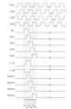
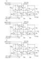
次に、図1に示すシフトレジスタの動作について図2乃至図4および図14を参照して説
明する。具体的には、図2に示すタイミングチャート中の、第1の期間51~第6の期間
56の各期間における動作を、図3および図4を用いて説明する。タイミングチャート中
、CLK1~CLK4はそれぞれクロック信号を示し、SP1は第1のスタートパルスを
示し、OUT1~OUT4は、第1のパルス信号出力回路10_1~第4のパルス信号出
力回路10_4の第2の出力端子からの出力を示し、ノードAおよびノードBはそれぞれ
ノードAおよびノードBの電位を示し、SROUT1~SROUT4は、第1のパルス信
号出力回路10_1~第4のパルス信号出力回路10_4の第1の出力端子からの出力を
示す。Actions
Next, the operation of the shift register shown in Fig. 1 will be described with reference to Fig. 2 to Fig. 4 and Fig. 14. Specifically, the operation in each of the
なお、以下の説明において、第1のトランジスタ101~第11のトランジスタ111は
、全てnチャネル型のトランジスタであるものとする。また、図3および図4において、
トランジスタが実線で表現されている場合には、当該トランジスタが導通状態(オン状態
)にあることを表し、破線で表現されている場合には、当該トランジスタが非導通状態(
オフ状態)にあることを表すものとする。In the following description, the
When a transistor is represented by a solid line, it indicates that the transistor is in a conductive state (on state), and when it is represented by a dashed line, it indicates that the transistor is in a non-conductive state (
This indicates that the power is in the OFF state.
代表的に、第1のパルス信号出力回路10_1の動作について説明する。第1のパルス信
号出力回路10_1の構成は、上述の通りである。また、入力される各信号、供給される
各電位の関係も上述の通りである。なお、以下の説明では、各入力端子および各電源線に
与えられる高電位(Hレベル、H信号などとも呼ぶ)は全てVDDとし、低電位(Lレベ
ル、L信号などとも呼ぶ)は全てVSSとする。Representatively, the operation of the first pulse signal output circuit10_1 will be described. The configuration of the first pulse signal output circuit10_1 is as described above. The relationships between the input signals and the supplied potentials are also as described above. In the following description, all high potentials (also referred to as H level, H signal, etc.) applied to each input terminal and each power supply line are VDD, and all low potentials (also referred to as L level, L signal, etc.) are VSS.
第1の期間51において、SP1がHレベルであるから、第1のパルス信号出力回路10
_1の第4の入力端子24として機能する第5のトランジスタ105のゲート端子と第9
のトランジスタ109のゲート端子に高電位が与えられ、第5のトランジスタ105と第
9のトランジスタ109は導通状態になる。第1の期間51においてはCLK3もHレベ
ルであるため、第10のトランジスタ110もオン状態となる。また、第7のトランジス
タ107のゲート端子には高電位が与えられているため、第7のトランジスタ107もオ
ン状態となる(図3(A)参照)。During the
The gate terminal of the
A high potential is applied to the gate terminal of the
第5のトランジスタ105と第7のトランジスタ107がオン状態となることにより、ノ
ードAの電位は上昇する。また、第9のトランジスタ109がオン状態となることにより
、ノードBの電位は下降する。第5のトランジスタ105の第2の端子の電位はVDDで
あるため、第5のトランジスタ105の第1の端子の電位は、第2の端子の電位から第5
のトランジスタ105のしきい値電圧分低下した値(VDD-Vth105)となる。そ
して、第7のトランジスタ107のゲート端子の電位がVDDであるため、第7のトラン
ジスタ107のしきい値電圧Vth107がVth105以上の場合には、ノードAの電
位は(VDD-Vth107)となって第7のトランジスタ107がオフ状態となる。一
方、Vth107がVth105未満の場合には、第7のトランジスタ107はオン状態
を保ったまま、ノードAの電位は(VDD-Vth105)まで上昇する。以下、第1の
期間51におけるノードAの電位の到達点(最高電位)をVAHとする。When the
The potential of the gate terminal of the
ノードAの電位がVAHになると、第1のトランジスタ101および第3のトランジスタ
103がオン状態となる。ここで、CLK1はLレベルであるため、第1の出力端子26
および第2の出力端子27からはLレベルが出力される。When the potential of the node A becomesVAH , the
And the
第2の期間52においては、CLK1の電位がLレベルからHレベルに切り替わる。ここ
で、第1のトランジスタ101および第3のトランジスタ103はオン状態であるため、
第1の出力端子26の電位および第2の出力端子27の電位が上昇する。さらに、第1の
トランジスタ101のゲート端子とソース端子(またはドレイン端子)との間には容量が
存在し、これによってゲート端子とソース端子(またはドレイン端子)とが容量結合され
ている。同様に、第3のトランジスタ103のゲート端子とソース端子(またはドレイン
端子)との間には容量が存在し、これによってゲート端子とソース端子(またはドレイン
端子)とが容量結合されている。したがって、第1の出力端子26の電位および第2の出
力端子27の電位の上昇と共に、浮遊状態であるノードAの電位が上昇することになる(
ブートストラップ動作)。ノードAの電位は最終的にVDD+Vth101より高くなり
、第1の出力端子26の電位および第2の出力端子27の電位はVDD(Hレベル)とな
る(図2および図3(B)参照)。In the
The potential of the
(Bootstrap operation) The potential of the node A finally becomes higher than VDD+Vth101 , and the potential of the
また、第2の期間52においては、第9のトランジスタ109がオン状態であるため、ノ
ードBもLレベルに維持されている。このため、第1の出力端子26がLレベルからHレ
ベルに変化する際の、容量結合に起因するノードBの電位変動を抑制し、これによる不具
合の発生を防止できる。In the
なお、上述のように第2の期間52において、第2の出力端子27の電位をHレベルとす
る場合、第2の出力端子27の電位を確実にVDD(Hレベル)まで上昇させるためには
、第3のトランジスタ103をオン状態とさせるために第3のトランジスタのゲート電圧
(Vgs)を十分に大きくする必要がある。第3のトランジスタ103のVgsが小さい
場合、第3のトランジスタに係るドレイン電流が小さくなるため、指定された期間内(こ
こでは、第2の期間内)に、第2の出力端子27の電位をVDD(Hレベル)まで上昇さ
せるのに時間がかかってしまう。これにより、第2の出力端子27の波形の立ち上がりが
鈍り、誤動作の原因となる。In addition, when the potential of the
ところで、第2の期間52における第3のトランジスタ103のVgsの大きさは、第1
の期間51におけるノードAの電位によって決まる。そのため、第3のトランジスタ10
3のVgsを大きくするためには、第1の期間51のうちにノードAの電位をできるだけ
大きくする必要がある(回路設計上、最大でVDD-Vth105またはVDD-Vth
107)。第1の出力端子26と第1のトランジスタ101のVgsについても、同様の
ことが言える。By the way, the magnitude of Vgs of the
The potential of the
In order to increase Vgs of the
107 ). The same can be said for the Vgs of the
そのため、第5のトランジスタ105のチャネル長Lに対するチャネル幅Wの比W/Lは
、第6のトランジスタ106のチャネル長Lに対するチャネル幅Wの比W/Lよりも大き
いことが好ましい。第5のトランジスタ105のチャネル長Lに対するチャネル幅Wの比
W/Lを、第6のトランジスタ106のチャネル長Lに対するチャネル幅Wの比W/Lよ
りも大きくすることにより、第1の期間51でのノードAの電位を、より短い時間で、V
DD-Vth105またはVDD-Vth107まで上昇させることができる。また、第
1の期間51では、第6のトランジスタ106はオフ状態となっているが、第5のトラン
ジスタ105のチャネル長Lに対するチャネル幅Wの比W/Lを、第6のトランジスタ1
06のチャネル長Lに対するチャネル幅Wの比W/Lよりも大きくすることにより、第6
のトランジスタ106におけるリーク電流(Ioff)を小さくすることができるため、
ノードAの電位を、より短い時間でVDD-Vth105まで上昇させることができる。Therefore, it is preferable that the ratio W/L of the channel width W to the channel length L of the
The voltage Vdd-Vth105 or the voltage Vdd-Vth107 can be increased to DD-
By making the ratio W/L of the channel width W to the channel length L of the sixth embodiment larger than that of the sixth embodiment,
Since the leakage current (Ioff) in the
The potential of the node A can be raised to VDD-Vth105 in a shorter time.
また、トランジスタの微細化によりチャネル長Lが小さくなると、しきい値電圧のシフト
が生じて第6のトランジスタ106がノーマリオン化する場合もある。このような場合で
も、第6のトランジスタ106のチャネル長Lに対するチャネル幅Wの比W/Lを第5の
トランジスタ105のチャネル長Lに対するチャネル幅Wの比W/Lよりも小さくするこ
とにより、第6のトランジスタ106のオン抵抗を第5のトランジスタ105のオン抵抗
よりも大きくできる。これにより、ノードAの電位をVDD-Vth105またはVDD
-Vth107により近い電位にすることができる。Furthermore, when the channel length L is reduced by miniaturization of the transistor, a shift in threshold voltage may occur, causing the
It is possible to make the potential closer to −Vth107 .
また、第5のトランジスタ105のチャネル長Lに対するチャネル幅Wの比W/Lは、第
7のトランジスタ107のチャネル長Lに対するチャネル幅Wの比W/Lと概ね等しいこ
とが好ましい。概ね等しいとは、製造誤差やばらつきに起因する多少の差を有している場
合があることを想定した上で、等しいとみなせる場合のことである。第5のトランジスタ
105および第7のトランジスタ107のチャネル長Lに対するチャネル幅Wの比W/L
を等しくすることにより、第5のトランジスタ105および第7のトランジスタ107の
電流供給能力を等しくすることができるため、ノードAの電位を効率よく上昇させること
ができる。なお、第5のトランジスタ105および第7のトランジスタ107のしきい値
電圧Vthは、概ね等しいことが望ましい。In addition, it is preferable that the ratio W/L of the channel width W to the channel length L of the
By making the threshold voltages Vth and Vth of the
なお、第5のトランジスタ105のチャネル長Lに対するチャネル幅Wの比W/Lは、ト
ランジスタ特性、クロック周波数、第1のトランジスタ101および第3のトランジスタ
103のゲート容量、シフトレジスタの動作電圧などによって決めることができる。The ratio W/L of the channel width W to the channel length L of the
また、第6のトランジスタ106のチャネル幅Wが大きくなると、第6のトランジスタ特
性がノーマリオン化した場合、リーク電流が増加するため、ノードAの電位降下につなが
ってしまう。または、第5のトランジスタ105によるノードAの充電の妨げとなってし
まう。さらに、高速動作が必要な場合に、ノードBの電位の下降を短時間で行い、ノード
Aの充電を短時間で行う必要がある。このような場合、第6のトランジスタの電位を短時
間で下降させる必要がある。Furthermore, when the channel width W of the
したがって、第5のトランジスタのチャネル幅Wよりも、第6のトランジスタのチャネル
幅Wを小さくすることにより、ノードAの電位の変位を防止することができる。また、ノ
ードBの負荷を低減することができる。このように、トランジスタの特性や駆動仕様に合
わせて、第5のトランジスタ105、第6のトランジスタ106および第7のトランジス
タ107のサイズを決定することによって、効率のよいシフトレジスタを実現することが
できる。Therefore, by making the channel width W of the sixth transistor smaller than the channel width W of the fifth transistor, it is possible to prevent a change in the potential of the node A. Also, it is possible to reduce the load of the node B. In this manner, by determining the sizes of the
第3の期間53においては、SP1がLレベルとなり、第5のトランジスタ105と第9
のトランジスタ109がオフ状態となる。また、CLK1がHレベルに維持され、ノード
Aの電位も変化しないため、第1の出力端子26および第2の出力端子27からはVDD
(Hレベル)が出力される(図3(C)参照)。なお、第3の期間53ではノードBが浮
遊状態となるが、第1の出力端子26の電位も変化しないため、容量結合による不具合は
無視できる程度である。In the
Since the clock signal CLK1 is maintained at the H level and the potential of the node A does not change, the
(H level) is output (see FIG. 3C). Note that in the
第4の期間54においては、CLK2およびCLK3がHレベルとなるため、ノードBの
電位が短時間で上昇する。また、CLK1がLレベルとなる。その結果、第2のトランジ
スタ102および第4のトランジスタ104がオン状態となり、第1の出力端子26およ
び第2の出力端子27の電位が短時間で下降する(図4(A)参照)。また、第6のトラ
ンジスタ106がオン状態となるので、ノードAの電位がLレベルとなる。これにより、
第1のトランジスタ101および第3のトランジスタ103がオフ状態となるので、第1
の出力端子26および第2の出力端子27の電位はLレベルとなる。In the
Since the
The potentials of the
第4の期間54において、ノードAの電位は、CLK1がHレベルとなる第6の期間の前
まで(つまり第4の期間54および第5の期間55中)に、確実にVSSとする必要があ
る。第5の期間55中に、ノードAの電位がVSSまで下降していないと、第3のトラン
ジスタ103のゲートとソース間の容量結合によって、再びノードAは電位が上昇し、第
1のトランジスタ101および第3のトランジスタ103がオン状態となり、第1の出力
端子26および第2の出力端子27に電荷が流れ、誤動作となるおそれがある。In the
そのため、第1のトランジスタ101、第3のトランジスタ103および第6のトランジ
スタ106の関係を、式(1)乃至式(7)のように決めることで、負荷に起因する動作
の不具合を低減し、動作の安定化を図ることができる。Therefore, by determining the relationship between the
(6)
(6)
上式において、tCKHとはCLK1のHレベルの期間、即ち第2の期間52および第3
の期間53に相当し、tCKLとはCLK1のLレベルの期間、即ち、第4の期間54お
よび第5の期間55に相当し、toffとはノードAがVSSまで放電するのに要する時
間に相当する。つまり、tCKL期間内のうちtoffの時間を使ってノードAの電位を
VSSまで下降させることになる。toffは第4の期間54および第5の期間55の中
であれば、たとえば、第4の期間54_1でも第4の期間54_1~54_3でも第4の
期間54_1~54_5でもよい(図14参照)。好ましくは第4の期間54および第5
の期間55の1/2の期間に相当する第4の期間54_1~54_3である。tCKLに
対してtoffをあまりに短く設定すると、ノードAの電位を早く下降させるために第6
のトランジスタ106のチャネル幅Wサイズを大きくする必要があり、toffを長く設
定すると次のクロックの信号Hが入るまでにノードAの電位をVSSまで放電しきれず誤
動作となる可能性があるためである。つまり、toffは、クロック信号の周波数等を考
慮して決定する必要がある。なお、図14に示すタイミングチャートは、一部の期間(例
えば、第4の期間54_1~54_5)を誇張して示しているが、図2に示すタイミング
チャートと大きく変わるところはない。In the above formula,tCKH is the period during which CLK1 is at the H level, that is, the
tCKL corresponds to the
The fourth period 54_1 to 54_3 corresponds to half the period of the
This is because it is necessary to increase the channel width W of the
また、C101およびC103はそれぞれ第1のトランジスタ101および第3のトラン
ジスタ103のゲート容量を示し、VfとはノードAの第3の期間53での電位を示す。Moreover,C101 andC103 respectively denote the gate capacitances of the
式(2)に示すi106は、第6のトランジスタ106のドレイン電流を示している。こ
れより第6のトランジスタ106のサイズ(例えば、W/L)を決定することができる。
即ち、第6のトランジスタ106のサイズは、CLK1の動作周波数、第1のトランジス
タ101と第3のトランジスタ103のサイズ、およびノードAの電位によって決めるこ
とができる。In the formula (2), i106 indicates the drain current of the
That is, the size of the
例えば、CLK1の動作周波数が高い場合、ノードAの電位はより早く下降させる必要が
あるため、式(1)よりtoffを小さくすることが必要になり、そのため、i106を
大きくする必要が生じる。そこで、i106に合わせて式(2)よりW106を計算し、
Wサイズを決定することができる。For example, when the operating frequency of CLK1 is high, the potential of node A needs to be lowered more quickly, so toff needs to be reduced from equation (1), and therefore i106 needs to be increased. Therefore, W106 is calculated from equation (2) according to i106 ,
The W size can be determined.
一方、第1のトランジスタ101および第3のトランジスタ103のサイズが小さい場合
には、i106は小さくて良いため、式(2)より、W106は小さくなる。ところで、
第3のトランジスタ103は、出力負荷の充放電に使用しているため、第3のトランジス
タのサイズを大きくすることにより、放電の際に、第4のトランジスタ104だけでなく
、第3のトランジスタ103においても放電することができるため、出力の電位の下降を
短時間で行うことができる。したがって、ノードAの電位を緩やかに下降させると、第3
のトランジスタ103はオン状態であるため、第4のトランジスタ104だけで放電する
よりも、出力の電位の下降を短時間で行うことができる。このように、トランジスタの特
性や駆動仕様に合わせて第6のトランジスタ106のサイズを決定することによって、効
率のよいシフトレジスタを実現することができる。On the other hand, when the sizes of the
Since the
Since the
また、第4の期間54において、CLK1がHレベルからLレベルになると同時に、第5
の入力端子25にパルス信号(SROUT3)が入力され、第11のトランジスタ111
がオン状態となる。第11のトランジスタ111がオン状態となることで、ノードBの電
位がVDD-Vth111まで充電され、第2のトランジスタ102、第4のトランジス
タ104および第6のトランジスタ106がオン状態となる。第2のトランジスタ102
および第4のトランジスタ104がオン状態となることで、第1の出力端子26および第
2の出力端子27の電位はVSSとなる。また、第1のトランジスタ101および第3の
トランジスタ103はオフ状態となる。In the
A pulse signal (SROUT3) is input to the
When the eleventh transistor 111 is turned on, the potential of the node B is charged to VDD-Vth111 , and the
When the
このとき、ノードBの充電は第11のトランジスタ111を通じて行われると共に、第1
0のトランジスタ110、第8のトランジスタ108を通じて行われる。第10のトラン
ジスタ110および第8のトランジスタ108のゲートは、それぞれ第3の入力端子23
および第2の入力端子22に接続されており、ゲート容量はそのまま第3の入力端子23
および第2の入力端子22の負荷になる。At this time, the node B is charged through the eleventh transistor 111, and the first
The gates of the
and the
and acts as a load on the
なお、本実施の形態において示すシフトレジスタにおいて、クロック線に接続するトラン
ジスタの負荷は、シフトレジスタの全段数÷4×(第3のトランジスタ103のLov+
第1のトランジスタ101のLov+第10のトランジスタ110のゲート容量+第8の
トランジスタ108のゲート容量)、で表現される。また、ゲート容量は、ε0×ε×(
L×W)/toxで表現される。なお、Lovとは、トランジスタのソース電極層又はド
レイン電極層と半導体層とが重畳する領域のチャネル長方向における長さを表している。Note that in the shift register described in this embodiment, the load of the transistors connected to the clock line is the total number of stages of the shift register divided by 4×(Lov of the
The gate capacitance is expressed as ε0 ×ε×(Lov of the
Note that Lov represents the length in the channel length direction of a region where a source electrode layer or a drain electrode layer of a transistor overlaps with a semiconductor layer.
クロック線に接続されるゲート容量を減らすため、第8のトランジスタ108及び第10
のトランジスタ110のチャネル幅(W)は、第11のトランジスタ111のチャネル幅
(W)よりも小さいことが好ましい。これにより、クロック線の負荷を低減することがで
き、高速動作させることができる。また、第10のトランジスタ110および第8のトラ
ンジスタ108のチャネル幅(W)を減少させることによって、レイアウト面積を縮小さ
せることができる。In order to reduce the gate capacitance connected to the clock line, the
It is preferable that the channel width (W) of the
第5の期間55においては、第5の入力端子25(つまりSROUT3)の電位がHレベ
ルを保持することにより、ノードBの電位が保持される。このため、第2のトランジスタ
102、第4のトランジスタ104および第6のトランジスタ106のオン状態が保持さ
れて、第1の出力端子26および第2の出力端子27の電位がLレベルに保持される(図
4(B)参照)。In the
第6の期間56においては、第5の入力端子25(つまりSROUT3)がLレベルとな
り、第11のトランジスタ111がオフ状態となる。このとき、ノードBは、上述の電位
を保持したまま浮遊状態となる。これにより、第2のトランジスタ102、第4のトラン
ジスタ104および第6のトランジスタ106のオン状態が継続する(図4(C)参照)
。なお、ノードBの電位は、通常、トランジスタのオフ電流等に起因して下降するが、十
分にオフ電流が小さいトランジスタ(例えば、酸化物半導体を用いたトランジスタ)を適
用する場合には、このような問題は生じない。また、ノードBの電位の下降を緩和するた
めに、容量素子を設けても良い。In the
Note that the potential of the node B usually drops due to the off-state current of a transistor or the like. However, such a problem does not occur when a transistor with a sufficiently small off-state current (for example, a transistor including an oxide semiconductor) is used. In addition, a capacitor may be provided to reduce the drop in the potential of the node B.
なお、その後の期間において、CLK2とCLK3とが共にHレベルとなる場合には、第
8のトランジスタ108と第10のトランジスタ110がオン状態となり、定期的にノー
ドBに電位が与えられる。このため、オフ電流の比較的大きなトランジスタを用いる場合
であっても、パルス信号出力回路の誤動作を防止できる。In addition, in the subsequent period, when CLK2 and CLK3 are both at the H level, the
なお、シフトレジスタからの出力(OUT1~OUT4など)については、電位の上昇時
を重視する場合と、電位の下降時を重視する場合がある。例えば、電位の上昇によってデ
ータを確定させる場合(例えば、データの書き込みを行う場合など)には、電位の上昇時
が重視される。また、電位の下降によってデータを確定させる場合には、電位の下降時が
重視される。With regard to the outputs (OUT1 to OUT4, etc.) from the shift register, there are cases where emphasis is placed on the rising potential and cases where emphasis is placed on the falling potential. For example, when data is determined by the rising potential (e.g., when writing data), emphasis is placed on the rising potential. On the other hand, when data is determined by the falling potential, emphasis is placed on the falling potential.
電位の上昇によってデータを確定させる場合には、電位の上昇に要する時間を短くする必
要がある。そのためには、第3のトランジスタ103のチャネル長Lに対するチャネル幅
Wの比W/Lを、第4のトランジスタ104のチャネル長Lに対するチャネル幅Wの比W
/Lよりも大きくすることが好ましい。In order to determine data by increasing the potential, it is necessary to shorten the time required for the potential to increase. To achieve this, the ratio W/L of the channel width W to the channel length L of the
It is preferable that the axial length of the slit is larger than /L.
電位の下降によってデータを確定させる場合には、電位の下降に要する時間を短くする必
要がある。そのためには、第3のトランジスタ103のチャネル長Lに対するチャネル幅
Wの比W/Lを、第4のトランジスタ104のチャネル長Lに対するチャネル幅Wの比W
/Lよりも大きくすることが好ましい。In order to determine data by decreasing the potential, it is necessary to shorten the time required for the potential to decrease. To achieve this, the ratio W/L of the channel width W to the channel length L of the
It is preferable that the axial length of the slit is larger than /L.
但し、開示する発明の一態様では、ノードAの電位を第3のトランジスタ103のゲート
とソース間の容量結合を利用したブートストラップ動作によって所定の電位まで上昇させ
ることにより、第3のトランジスタ103をオン状態とし、Hレベル信号を出力させる。
そのため、第3のトランジスタ103のチャネル長Lに対するチャネル幅Wの比W/Lが
十分に大きくなければ、シフトレジスタの出力するHレベルの電位が、VDDまで上がり
きらないという問題が生じうるから、第3のトランジスタ103のチャネル長Lに対する
チャネル幅Wの比W/Lは、十分に大きくすることが望ましい。However, in one embodiment of the disclosed invention, the potential of node A is increased to a predetermined potential by bootstrap operation using capacitive coupling between the gate and source of the
Therefore, if the ratio W/L of the channel width W to the channel length L of the
なお、本実施の形態において示すシフトレジスタは、第mのパルス信号出力回路から出力
されるパルスと第(m+1)のパルス信号出力回路から出力されるパルスが半分重なる駆
動方法を採用している。このため、当該駆動方法を採用しない場合と比較して、配線の充
電に使用できる時間を長くすることができる。つまり、当該駆動方法によって、大きな負
荷に耐え、高い周波数で動作するパルス信号出力回路が提供される。In addition, the shift register shown in this embodiment employs a driving method in which the pulse output from the mth pulse signal output circuit and the pulse output from the (m+1)th pulse signal output circuit overlap by half. Therefore, the time available for charging the wiring can be extended compared to a case in which this driving method is not adopted. In other words, this driving method provides a pulse signal output circuit that can withstand a large load and operate at a high frequency.
(実施の形態2)
本実施の形態では、先の実施の形態において示したパルス信号出力回路、およびシフトレ
ジスタとは異なる態様の構成例およびその動作に関して図5乃至図8を参照して説明する
。(Embodiment 2)
In this embodiment mode, configuration examples and operations of a pulse signal output circuit and a shift register different from those described in the previous embodiment mode will be described with reference to FIGS. 5 to 8. FIG.
〈回路構成〉
はじめに、パルス信号出力回路、およびパルス信号出力回路を含むシフトレジスタの回路
構成例について図5を参照して説明する。<Circuit configuration>
First, a circuit configuration example of a pulse signal output circuit and a shift register including the pulse signal output circuit will be described with reference to FIG.
本実施の形態で示すシフトレジスタの構成は、先の実施の形態において示したシフトレジ
スタの構成に近似している。相違点の一は、第1のパルス信号出力回路10_1~第nの
パルス信号出力回路10_nは、第3の入力端子23を有しない点である(図5(A)乃
至図5(C)参照)。つまり、一のパルス信号出力回路には、二種類のクロック信号が入
力される。その他の構成については先の実施の形態と同様である。The configuration of the shift register shown in this embodiment is similar to that of the shift register shown in the previous embodiment. One difference is that the first pulse signal output circuit10_1 to the n-th pulse signal output circuit10_n do not have the third input terminal 23 (see FIGS. 5A to 5C). In other words, two types of clock signals are input to one pulse signal output circuit. The other configurations are similar to those of the previous embodiment.
第1のパルス信号出力回路10_1~第nのパルス信号出力回路10_nは、第3の入力
端子23を有しないため、これと接続される第10のトランジスタを有しない(図5(C
)参照)。そして、これに伴い、図1に示す第2の入力信号生成回路202と図5に示す
第2の入力信号生成回路203の接続関係は一部異なっている。The first pulse
5.) Accordingly, the connection relationship between the second input
具体的には、第1のパルス信号出力回路10_1~第nのパルス信号出力回路10_nの
各々は、第1のトランジスタ101~第4のトランジスタ104で構成されるパルス信号
生成回路200と、第5のトランジスタ105~第7のトランジスタ107で構成される
第1の入力信号生成回路201と、第8のトランジスタ108、第9のトランジスタ10
9および第11のトランジスタ111で構成される第2の入力信号生成回路203と、を
含む。また、上述した第1の入力端子21~第5の入力端子25に加え、第1の電源線3
1および第2の電源線32から、第1のトランジスタ101~第11のトランジスタ11
1に信号が供給される。Specifically, each of the first pulse
and a second input
The first and second
A signal is provided to 1.
第2の入力信号生成回路203の具体的な構成例は次の通りである。A specific example configuration of the second input
第8のトランジスタ108の第2の端子と、第11のトランジスタ111の第2の端子と
、第9のトランジスタ109の第1の端子とは電気的に接続されて第2の入力信号生成回
路の出力端子として機能する。The second terminal of the
第11のトランジスタ111の第1の端子と、第8のトランジスタ108の第1の端子に
は、第2の電源線32を介して第2の電位が与えられる。第9のトランジスタ109の第
2の端子には、第1の電源線31を介して第1の電位が与えられる。第11のトランジス
タ111のゲート端子にはパルス信号が入力される。また、第11のトランジスタ111
のゲート端子は、第2の入力信号生成回路の第1の入力端子として機能すると共に、パル
ス信号出力回路の第5の入力端子25としても機能する。第8のトランジスタ108のゲ
ート端子には第2のクロック信号CLK2が入力される。また、第8のトランジスタ10
8のゲート端子は、第2の入力信号生成回路の第2の入力端子として機能すると共に、パ
ルス信号出力回路の第2の入力端子22としても機能する。第9のトランジスタ109の
ゲート端子にはパルス信号が入力される。また、第9のトランジスタ109のゲート端子
は、第2の入力信号生成回路の第3の入力端子として機能すると共に、パルス信号出力回
路の第4の入力端子24としても機能する。A second potential is applied to a first terminal of the eleventh transistor 111 and a first terminal of the
The gate terminal of the
The gate terminal of the
なお、上述した構成は一例にすぎず、開示する発明がこれに限定されるものではない。Note that the above-mentioned configuration is merely an example, and the disclosed invention is not limited to this.
本実施の形態の以下の説明では、先の実施の形態と同様、図5(C)に示すパルス信号出
力回路において第1のトランジスタ101のゲート端子と、第3のトランジスタ103の
ゲート端子と、第1の入力信号生成回路の出力端子と、の接続により構成されるノードを
、ノードAとする。また、第2のトランジスタ102のゲート端子と、第4のトランジス
タ104のゲート端子と、第8のトランジスタ108の第2の端子と、第11のトランジ
スタ111の第2の端子と、第9のトランジスタ109の第1の端子と、の接続により構
成されるノードを、ノードBとする。5C , a node formed by connecting the gate terminal of the
上記ノードAと第1の出力端子26との間には、ブートストラップ動作を好適に行うため
の容量素子を設けても良い。また、上記ノードBの電位を保持するために、ノードBに電
気的に接続された容量素子を設けてもよい。A capacitive element for suitably performing a bootstrap operation may be provided between the node A and the
なお、第1のトランジスタ101~第9のトランジスタ109、第11のトランジスタ1
11には、酸化物半導体を用いるのが好適である。酸化物半導体を用いることにより、ト
ランジスタのオフ電流を低減することができる。また、非晶質シリコンなどと比較して、
オン電流および電界効果移動度を高めることが出来る。また、トランジスタの劣化を抑制
することができる。これにより、消費電力が小さく、高速動作が可能で、動作の正確性が
高められた電子回路を実現することが可能となる。なお、酸化物半導体を用いたトランジ
スタについては後の実施の形態において詳述するから、ここでは省略する。Note that the
An oxide semiconductor is preferably used for the first insulating
The on-state current and the field effect mobility can be increased. In addition, deterioration of the transistor can be suppressed. As a result, an electronic circuit with low power consumption, high speed operation, and improved accuracy in operation can be realized. Note that a transistor using an oxide semiconductor will be described in detail in a later embodiment, and therefore will not be described here.
〈動作〉
次に、図5に示すシフトレジスタの動作について図6乃至図8を参照して説明する。具体
的には、図6に示すタイミングチャート中の、第1の期間51~第5の期間55の各期間
における動作を、図7および図8を用いて説明する。タイミングチャート中、CLK1~
CLK4はそれぞれクロック信号を示し、SP1は第1のスタートパルスを示し、OUT
1~OUT4は、第1のパルス信号出力回路10_1~第4のパルス信号出力回路10_
4の第2の出力端子からの出力を示し、ノードAおよびノードBはそれぞれノードAおよ
びノードBの電位を示し、SROUT1~SROUT4は、第1のパルス信号出力回路1
0_1~第4のパルス信号出力回路10_4の第1の出力端子からの出力を示す。Actions
Next, the operation of the shift register shown in Fig. 5 will be described with reference to Fig. 6 to Fig. 8. Specifically, the operation in each of the
CLK4 indicates a clock signal, SP1 indicates a first start pulse, and OUT
1 to OUT4 correspond to the first pulse
4 , node A and node B indicate the potentials of node A and node B, respectively, and SROUT1 to SROUT4 indicate the potentials of the first pulse
0_1 to 10 _4 indicate outputs from the first output terminals of the fourth pulse
なお、以下の説明において、第1のトランジスタ101~第9のトランジスタ109、第
11のトランジスタ111は、全てnチャネル型のトランジスタであるものとする。また
、図7および図8において、トランジスタが実線で表現されている場合には、当該トラン
ジスタが導通状態(オン状態)にあることを表し、破線で表現されている場合には、当該
トランジスタが非導通状態(オフ状態)にあることを表すものとする。In the following description, the
代表的に、第1のパルス信号出力回路10_1の動作について説明する。第1のパルス信
号出力回路10_1の構成は、上述の通りである。また、入力される各信号、供給される
各電位の関係も上述の通りである。なお、以下の説明では、各入力端子および各電源線に
与えられる高電位(Hレベル、H信号などとも呼ぶ)は全てVDDとし、低電位(Lレベ
ル、L信号などとも呼ぶ)は全てVSSとする。Representatively, the operation of the first pulse signal output circuit10_1 will be described. The configuration of the first pulse signal output circuit10_1 is as described above. The relationships between the input signals and the supplied potentials are also as described above. In the following description, all high potentials (also referred to as H level, H signal, etc.) applied to each input terminal and each power supply line are VDD, and all low potentials (also referred to as L level, L signal, etc.) are VSS.
第1の期間51において、SP1がHレベルであるから、第1のパルス信号出力回路10
_1の第4の入力端子24として機能する第5のトランジスタ105のゲート端子と第9
のトランジスタ109のゲート端子に高電位が与えられ、第5のトランジスタ105と第
9のトランジスタ109は導通状態になる。また、第7のトランジスタ107のゲート端
子には高電位が与えられているため、第7のトランジスタ107もオン状態となる(図7
(A)参照)。During the
The gate terminal of the
A high potential is applied to the gate terminal of the
(See (A)).
第5のトランジスタ105と第7のトランジスタ107がオン状態となることにより、ノ
ードAの電位は上昇する。また、第9のトランジスタ109がオン状態となることにより
、ノードBの電位は下降する。ノードAの電位がVAH(VAH=VDD-Vth105
-Vth107)にまで達すると、第5のトランジスタ105および第7のトランジスタ
107がオフ状態となり、ノードAは、VAHを維持したまま浮遊状態となる。When the
When the potential of the node A reaches −Vth107 , the
ノードAの電位がVAHになると、第1のトランジスタ101および第3のトランジスタ
103がオン状態となる。ここで、CLK1はLレベルであるため、第1の出力端子26
および第2の出力端子27からはLレベル信号が出力される。When the potential of the node A becomesVAH , the
And, the
第2の期間52においては、CLK1の電位がLレベルからHレベルに切り替わる。ここ
で、第1のトランジスタ101および第3のトランジスタ103はオン状態であるため、
第1の出力端子26の電位および第2の出力端子27の電位が上昇する。さらに、第1の
トランジスタ101のゲート端子とソース端子(またはドレイン端子)との間には容量が
存在し、これによってゲート端子とソース端子(またはドレイン端子)とが容量結合され
ている。同様に、第3のトランジスタ103のゲート端子とソース端子(またはドレイン
端子)との間には容量が存在し、これによってゲート端子とソース端子(またはドレイン
端子)とが容量結合されている。したがって、第1の出力端子26の電位および第2の出
力端子27の電位の上昇と共に、浮遊状態であるノードAの電位が上昇することになる(
ブートストラップ動作)。ノードAの電位は最終的にVDD+Vth101より高くなり
、第1の出力端子26の電位および第2の出力端子27の電位はVDD(Hレベル)とな
る(図6および図7(B)参照)。In the
The potential of the
(Bootstrap operation) The potential of the node A finally becomes higher than VDD+Vth101 , and the potential of the
第3の期間53においては、CLK2の電位がHレベルとなり、第8のトランジスタ10
8がオン状態となる。これにより、ノードBの電位が上昇する。ノードBの電位の上昇に
より、第2のトランジスタ102、第4のトランジスタ104、および第6のトランジス
タ106がオン状態となり、ノードAの電位が下降する。このため、第1の出力端子26
の電位および第2の出力端子27の電位はLレベルとなる(図7(C)参照)。In the
8 is turned on, and the potential of the node B is increased. Due to the increase in the potential of the node B, the
The potential of the
第4の期間54においては、CLK2の電位がLレベルとなり、第8のトランジスタ10
8がオフ状態となるが、第5の入力端子25(つまりSROUT3)の電位がHレベルと
なるため、第11のトランジスタ111がオン状態となる。このため、ノードAの電位と
ノードBの電位は第3の期間53の電位が保持されて、第1の出力端子26の電位および
第2の出力端子27の電位はLレベルに保持される(図8(A)参照)。In the
Since the potential of the fifth input terminal 25 (i.e., SROUT3) becomes H level, the eleventh transistor 111 becomes ON state. Therefore, the potentials of the nodes A and B are held at the potentials of the
第5の期間55においては、第5の入力端子25(つまりSROUT3)の電位がLレベ
ルとなり、ノードBの電位が保持される。このため、第2のトランジスタ102、第4の
トランジスタ104および第6のトランジスタ106のオン状態が保持されて、第1の出
力端子26および第2の出力端子27の電位がLレベルに保持される(図8(B)参照)
。In the
.
なお、ノードBの電位は、通常、トランジスタのオフ電流等に起因して下降するが、十分
にオフ電流が小さいトランジスタ(例えば、酸化物半導体を用いたトランジスタ)を適用
する場合には、このような問題は生じない。また、ノードBの電位の下降を緩和するため
に、容量素子を設けても良い。この場合に設けられた容量素子は、第2のトランジスタ1
02のゲート端子と、第4のトランジスタ104のゲート端子と、第6のトランジスタ1
06のゲート端子と、第8のトランジスタ108の第1の端子と、第9のトランジスタ1
09の第1の端子と、に電気的に接続される。Note that the potential of the node B usually drops due to the off-state current of the transistor, but such a problem does not occur when a transistor with a sufficiently small off-state current (for example, a transistor including an oxide semiconductor) is used. In order to reduce the drop in the potential of the node B, a capacitor may be provided. In this case, the capacitor provided is a capacitor having a capacitance between the
02, the gate terminal of the
the gate terminal of the
09 and a first terminal thereof.
なお、その後の期間において、CLK2の電位がHレベルとなる場合には、第8のトラン
ジスタ108がオン状態となり、定期的にノードBに電位が与えられる。このため、オフ
電流の比較的大きなトランジスタを用いる場合であっても、パルス信号出力回路の誤動作
を防止できる。In addition, in the subsequent period, when the potential of CLK2 becomes an H level, the
以上、本実施の形態に示す構成、方法などは、他の実施の形態に示す構成、方法などと適
宜組み合わせて用いることができる。The structures, methods, and the like described in this embodiment can be used in appropriate combination with the structures, methods, and the like described in other embodiments.
(実施の形態3)
本実施の形態では、先の実施の形態において示したパルス信号出力回路、およびシフトレ
ジスタとは異なる態様の構成例に関して図9を参照して説明する。(Embodiment 3)
In this embodiment mode, a configuration example of a pulse signal output circuit and a shift register different from those described in the previous embodiment mode will be described with reference to FIG.
本実施の形態で示すシフトレジスタの構成は、先の実施の形態において示したシフトレジ
スタの構成に近似している。相違点の一は、第nのパルス信号出力回路10_nの後段に
、第1のダミーパルス信号出力回路10_D1および第2のダミーパルス信号出力回路1
0_D2が接続されている点である(図9(A)参照)。第1のダミーパルス信号出力回
路10_D1や第2のダミーパルス信号出力回路10_D2は、第n-1のパルス信号出
力回路10_n-1や第nのパルス信号出力回路10_nの第5の入力端子25に、パル
ス信号を供給する機能を有する。The configuration of the shift register shown in this embodiment is similar to the configuration of the shift register shown in the previous embodiment. One of the differences is that a first dummy pulse signal output circuit10_D1 and a second dummy pulse signal output circuit 10_D2 are provided in the rear stage of the n-th pulse signal output circuit10_n .
9A. The first dummy pulse
第1のダミーパルス信号出力回路10_D1や第2のダミーパルス信号出力回路10_D
2の後段には、パルス信号出力回路は存在しない。つまり、第1~第nのパルス信号出力
回路とは異なり、第1のダミーパルス信号出力回路10_D1や第2のダミーパルス信号
出力回路10_D2には後段(この場合、2段後)からのパルス信号が入力されない。こ
のため、第1~第nのパルス信号出力回路における第5の入力端子25に相当する端子が
存在しない(図9(B)および図9(C)参照)。また、第5の入力端子25に関連する
第11のトランジスタ111も存在しない(図9(C)参照)。The first dummy pulse signal output circuit10_D1 and the second dummy pulse signal output circuit10_D
In other words, unlike the first to n-th pulse signal output circuits, the first dummy pulse signal output circuit10_D1 and the second dummy pulse signal output circuit10_D2 do not receive a pulse signal from the subsequent stage (two stages later in this case). Therefore, there is no terminal equivalent to the
ダミーパルス信号出力回路(第1~第2のダミーパルス信号出力回路)の機能は、正規段
のパルス信号出力回路(第n-1~第nのパルス信号出力回路)に適切なパルス信号を出
力することであるから、ダミーパルス信号出力回路には、そのノードBを十分に充電でき
る能力が必要となる。ここで、第1~第nのパルス信号出力回路では、クロック信号の入
力に起因する消費電力を低減するために、第8のトランジスタ108および第10のトラ
ンジスタ110のサイズを小さくし(例えば、チャネル幅W、またはチャネル長Lに対す
るチャネル幅Wの比W/Lを小さくし)、第11のトランジスタ111によって充電能力
を確保する構成を取るのが有効である。一方で、ダミーパルス信号出力回路には第11の
トランジスタ111が存在しないから、第11のトランジスタ111による充電能力を補
うことができる程度に、第8のトランジスタ108および第10のトランジスタ110の
サイズを大きくすることが必要になる。Since the function of the dummy pulse signal output circuits (first to second dummy pulse signal output circuits) is to output an appropriate pulse signal to the pulse signal output circuits (n-1th to nth pulse signal output circuits) of the normal stages, the dummy pulse signal output circuits need to have the ability to sufficiently charge the node B. Here, in the first to nth pulse signal output circuits, in order to reduce the power consumption caused by the input of the clock signal, it is effective to adopt a configuration in which the
具体的には、例えば、第1~第2のダミーパルス信号出力回路の第8のトランジスタまた
は第10のトランジスタのチャネル幅W(またはチャネル長Lに対するチャネル幅Wの比
W/L)を、第1~第nのパルス信号出力回路の第8のトランジスタまたは第10のトラ
ンジスタのチャネル幅W(またはチャネル長Lに対するチャネル幅Wの比W/L)より大
きくすればよい。このような構成を採用することで、正規段のパルス信号出力回路(第n
-1~第nのパルス信号出力回路)における消費電力を低減しつつ、適切な動作を確保し
たシフトレジスタが実現される。Specifically, for example, the channel width W (or the ratio W/L of the channel width W to the channel length L) of the eighth or tenth transistor of the first to second dummy pulse signal output circuits may be made larger than the channel width W (or the ratio W/L of the channel width W to the channel length L) of the eighth or tenth transistor of the first to nth pulse signal output circuits. By adopting such a configuration,
A shift register is realized that ensures proper operation while reducing power consumption in the first to nth pulse signal output circuits.
なお、ダミーパルス信号出力回路の基本的な構成は、上記相違点を除き、先の実施の形態
において示したパルス信号出力回路と同様である。具体的には、第1のパルス信号出力回
路10_1~第nのパルス信号出力回路10_nの各々は、第1のトランジスタ101~
第4のトランジスタ104で構成されるダミーパルス信号生成回路204と、第5のトラ
ンジスタ105~第7のトランジスタ107で構成される第1の入力信号生成回路205
と、第8のトランジスタ108~第10のトランジスタ110で構成される第2の入力信
号生成回路206と、を含む。また、第1の電源線31および第2の電源線32から、第
1のトランジスタ101~第10のトランジスタ110に信号が供給される。The basic configuration of the dummy pulse signal output circuit is the same as that of the pulse signal output circuit shown in the previous embodiment except for the above-mentioned difference. Specifically, each of the first pulse
A dummy pulse
and a second input
また、ダミーパルス信号出力回路の動作についても、後段の出力が入力されない点を除い
て先の実施の形態において示したパルス信号出力回路と同様である。よって、詳細につい
ては先の実施の形態を参酌することが可能である。なお、第10のトランジスタ110は
、設けても良いし設けなくとも良い。また、ダミーパルス信号出力回路では、少なくとも
正規段のパルス信号出力回路(第n-1~第nのパルス信号出力回路)への出力が確保さ
れればよいから、出力端子は2系統に限らず、1系統としても良い。つまり、第1の出力
端子26または第2の出力端子27を省略することが可能である。なお、この場合には、
省略される出力端子に付随するトランジスタ(例えば、第2の出力端子27を省略する場
合には、第3のトランジスタ103および第4のトランジスタ104)は、適宜省略すれ
ばよい。The operation of the dummy pulse signal output circuit is similar to that of the pulse signal output circuit shown in the previous embodiment, except that the output of the subsequent stage is not input. Therefore, the previous embodiment can be referred to for details. The
The transistors associated with the omitted output terminal (for example, the
以上、本実施の形態に示す構成、方法などは、他の実施の形態に示す構成、方法などと適
宜組み合わせて用いることができる。The structures, methods, and the like described in this embodiment can be used in appropriate combination with the structures, methods, and the like described in other embodiments.
(実施の形態4)
本実施の形態では、上記実施の形態で述べたパルス信号出力回路やシフトレジスタに適用
できるトランジスタの例につき、図10を参照して説明する。なお、トランジスタの構造
は特に限定されず、例えば、トップゲート構造またはボトムゲート構造、スタガ型または
プレーナ型など、適当な構造を採用することができる。また、トランジスタはチャネル形
成領域を一つ有するシングルゲート構造でも、チャネル形成領域を二つ以上有するマルチ
ゲート構造であっても良い。また、チャネル領域の上下にゲート絶縁層を介して配置され
た2つのゲート電極層を有する構造でもよい。(Embodiment 4)
In this embodiment mode, an example of a transistor applicable to the pulse signal output circuit or the shift register described in the above embodiment mode will be described with reference to FIG. 10. Note that the structure of the transistor is not particularly limited, and for example, an appropriate structure such as a top-gate structure or a bottom-gate structure, a staggered type or a planar type can be adopted. In addition, the transistor may have a single-gate structure having one channel formation region or a multi-gate structure having two or more channel formation regions. In addition, a structure having two gate electrode layers arranged above and below the channel region with a gate insulating layer interposed therebetween may be used.
図10(A)乃至図10(D)には、トランジスタの断面構造の例を示す。図10(A)
乃至図10(D)に示すトランジスタは、半導体として酸化物半導体を用いるものである
。酸化物半導体を用いることのメリットは、簡単なプロセス、低温のプロセスで、高い移
動度と低いオフ電流が実現できることといえる。10A to 10D show examples of cross-sectional structures of transistors.
10D includes an oxide semiconductor as a semiconductor. An advantage of using an oxide semiconductor is that high mobility and low off-state current can be achieved through a simple process and a low-temperature process.
図10(A)に示すトランジスタ410は、ボトムゲート構造のトランジスタの一例であ
り、逆スタガ型トランジスタともいう。A
トランジスタ410は、絶縁表面を有する基板400上の、ゲート電極層401、ゲート
絶縁層402、酸化物半導体層403、ソース電極層405a、及びドレイン電極層40
5bを含む。また、酸化物半導体層403に接する絶縁層407が設けられている。絶縁
層407上にはさらに保護絶縁層409が形成されている。The
5b. In addition, an insulating
図10(B)に示すトランジスタ420は、チャネル保護型(チャネルストップ型ともい
う)と呼ばれるボトムゲート構造のトランジスタの一例であり、逆スタガ型トランジスタ
ともいう。A
トランジスタ420は、絶縁表面を有する基板400上の、ゲート電極層401、ゲート
絶縁層402、酸化物半導体層403、チャネル保護層として機能する絶縁層427、ソ
ース電極層405a、及びドレイン電極層405bを含む。また、保護絶縁層409が設
けられている。The
図10(C)に示すトランジスタ430は、ボトムゲート型のトランジスタの一例である
。トランジスタ430は、絶縁表面を有する基板400上の、ゲート電極層401、ゲー
ト絶縁層402、ソース電極層405a、ドレイン電極層405b、及び酸化物半導体層
403を含む。また、酸化物半導体層403に接する絶縁層407が設けられている。絶
縁層407上にはさらに保護絶縁層409が形成されている。10C is an example of a bottom-gate transistor. The
トランジスタ430においては、ゲート絶縁層402は基板400及びゲート電極層40
1上に接して設けられ、また、ゲート絶縁層402上には、ソース電極層405a、ドレ
イン電極層405bが接して設けられている。そして、ゲート絶縁層402、及びソース
電極層405a、ドレイン電極層405b上に酸化物半導体層403が設けられている。In the
A
図10(D)に示すトランジスタ440は、トップゲート構造のトランジスタの一例であ
る。トランジスタ440は、絶縁表面を有する基板400上の、絶縁層437、酸化物半
導体層403、ソース電極層405a、ドレイン電極層405b、ゲート絶縁層402、
及びゲート電極層401を含む。そして、ソース電極層405a、ドレイン電極層405
bにそれぞれ配線層436a、配線層436bが接して設けられている。10D is an example of a top-gate transistor. The
and a
The
本実施の形態では、上述のとおり、半導体層として酸化物半導体層403を用いる。酸化
物半導体層403に用いる酸化物半導体としては、四元系金属酸化物であるIn-Sn-
Ga-Zn-O系や、三元系金属酸化物であるIn-Ga-Zn-O系、In-Sn-Z
n-O系、In-Al-Zn-O系、Sn-Ga-Zn-O系、Al-Ga-Zn-O系
、Sn-Al-Zn-O系や、二元系金属酸化物であるIn-Zn-O系、In-Ga-
O系、Sn-Zn-O系、Al-Zn-O系、Zn-Mg-O系、Sn-Mg-O系、I
n-Mg-O系や、一元系金属酸化物であるIn-O系、Sn-O系、Zn-O系などが
ある。また、上記酸化物半導体にSiO2を添加してもよい。ここで、例えば、In-G
a-Zn-O系酸化物半導体とは、少なくともInとGaとZnを含む酸化物であり、そ
の組成比に特に制限はない。また、InとGaとZn以外の元素を含んでもよい。In this embodiment, as described above, the
Ga-Zn-O system, ternary metal oxides such as In-Ga-Zn-O system and In-Sn-Z
In-Al-Zn-O system, Sn-Ga-Zn-O system, Al-Ga-Zn-O system, Sn-Al-Zn-O system, and binary metal oxides such as In-Zn-O system, In-Ga-
O series, Sn-Zn-O series, Al-Zn-O series, Zn-Mg-O series, Sn-Mg-O series, I
Examples of the oxide semiconductor include n-Mg-O-based, In-O-based, Sn-O-based, and Zn-O-based oxides, which are single-element metal oxides. SiO2 may also be added to the oxide semiconductor.
The a-Zn-O based oxide semiconductor is an oxide containing at least In, Ga, and Zn, and there is no particular limitation on the composition ratio thereof. Moreover, the a-Zn-O based oxide semiconductor may contain elements other than In, Ga, and Zn.
また、酸化物半導体層403には、化学式InMO3(ZnO)m(m>0、m:非自然
数)で表記される酸化物半導体を用いることができる。ここで、Mは、ガリウム(Ga)
、アルミニウム(Al)、マンガン(Mn)およびコバルト(Co)から選ばれた一また
は複数の金属元素を示す。例えば、Mとしては、Ga、Ga及びAl、Ga及びMn、ま
たはGa及びCoなどがある。For the
M represents one or more metal elements selected from the group consisting of aluminum (Al), manganese (Mn) and cobalt (Co). For example, M can be Ga, Ga and Al, Ga and Mn, or Ga and Co.
酸化物半導体層403を用いたトランジスタ410、トランジスタ420、トランジスタ
430、トランジスタ440は、オフ電流を極めて小さくすることが可能である。よって
、これをパルス信号出力回路やシフトレジスタに用いることで、各ノードの電位保持が容
易になり、パルス信号出力回路やシフトレジスタの誤動作の確率を極めて低く抑えること
ができる。The off-state current of the
絶縁表面を有する基板400に使用することができる基板に大きな制限はない。例えば、
液晶表示装置などに用いられるガラス基板や、石英基板などを用いることができる。また
、シリコンウェハ上に絶縁層を形成した基板などを用いても良い。There is no significant limitation on the substrate that can be used for the
A glass substrate or a quartz substrate used in a liquid crystal display device can be used. A substrate having an insulating layer formed on a silicon wafer can also be used.
ボトムゲート構造のトランジスタ410、トランジスタ420、トランジスタ430にお
いて、下地となる絶縁層を基板とゲート電極層の間に設けてもよい。当該絶縁層は、基板
からの不純物元素の拡散を防止する機能があり、窒化シリコン膜、酸化シリコン膜、窒化
酸化シリコン膜、又は酸化窒化シリコン膜から選ばれた一又は複数の膜により形成するこ
とができる。A base insulating layer may be provided between the substrate and the gate electrode layer in each of the
ゲート電極層401は、モリブデン、チタン、クロム、タンタル、タングステン、アルミ
ニウム、銅、ネオジム、スカンジウム等の金属材料またはこれらを主成分とする合金材料
を用いて形成することができる。また、その構造は、単層構造としても良いし、積層構造
としても良い。The
ゲート絶縁層402は、プラズマCVD法やスパッタ法などを用いて、酸化シリコン膜、
窒化シリコン膜、酸化窒化シリコン膜、窒化酸化シリコン膜、酸化アルミニウム膜、窒化
アルミニウム膜、酸化窒化アルミニウム膜、窒化酸化アルミニウム膜、酸化ハフニウム膜
などから選ばれた一又は複数の膜により形成することができる。例えば、第1のゲート絶
縁層としてプラズマCVD法により膜厚50nm以上200nm以下の窒化シリコン膜(
SiNy(y>0))を形成し、第1のゲート絶縁層上に第2のゲート絶縁層としてスパ
ッタ法により膜厚5nm以上300nm以下の酸化シリコン膜(SiOx(x>0))を
形成して、合計膜厚300nm程度のゲート絶縁層とすることができる。The
The first gate insulating layer can be formed of one or more films selected from a silicon nitride film, a silicon oxynitride film, a silicon nitride oxide film, an aluminum oxide film, an aluminum nitride film, an aluminum oxynitride film, an aluminum nitride oxide film, a hafnium oxide film, etc. For example, the first gate insulating layer can be formed of a silicon nitride film (
A silicon oxide film (SiOx (x>0)) having a thickness of 5 nm to 300 nm is formed asa second gate insulating layer on the first gate insulating layer by a sputtering method, thereby forming a gate insulating layer with a total thickness of about 300 nm.
ソース電極層405a、ドレイン電極層405bは、モリブデン、チタン、クロム、タン
タル、タングステン、アルミニウム、銅、ネオジム、スカンジウム等の金属材料またはこ
れらを主成分とする合金材料を用いて形成することができる。例えば、アルミニウムや銅
などの金属層と、チタン、モリブデン、タングステンなどの高融点金属層との積層構造と
することができる。ヒロックやウィスカーの発生を防止する元素(シリコン、ネオジム、
スカンジウムなど)が添加されたアルミニウム材料を用いることで耐熱性を向上させても
良い。The
The heat resistance may be improved by using an aluminum material to which scandium or the like has been added.
また、ソース電極層405a、ドレイン電極層405b(これと同じ層で形成される配線
層を含む)となる導電膜として、導電性の金属酸化物膜を用いても良い。導電性の金属酸
化物としては酸化インジウム(In2O3)、酸化スズ(SnO2)、酸化亜鉛(ZnO
)、酸化インジウム酸化スズ合金(In2O3―SnO2、ITOと略記する場合がある
)、酸化インジウム酸化亜鉛合金(In2O3―ZnO)またはこれらの金属酸化物材料
に酸化シリコンを含ませたもの、などを用いることができる。Alternatively, a conductive metal oxide film may be used as the conductive film to be the
), an indium oxide-tin oxide alloy (In2 O3 —SnO2 , sometimes abbreviated as ITO), an indium oxide-zinc oxide alloy (In2 O3 —ZnO), or any of these metal oxide materials containing silicon oxide can be used.
ソース電極層405a、ドレイン電極層405bに接する配線層436a、配線層436
bについては、ソース電極層405a、ドレイン電極層405bと同様の材料を用いて形
成することができる。The
The
絶縁層407、絶縁層427、絶縁層437としては、代表的には酸化シリコン膜、酸化
窒化シリコン膜、酸化アルミニウム膜、または酸化窒化アルミニウム膜などの無機絶縁膜
を用いることができる。As the insulating
保護絶縁層409としては、窒化シリコン膜、窒化アルミニウム膜、窒化酸化シリコン膜
、窒化酸化アルミニウム膜などの無機絶縁膜を用いることができる。As the protective insulating
また、保護絶縁層409上には、トランジスタ起因の表面凹凸を低減するための平坦化絶
縁膜を形成してもよい。平坦化絶縁膜としては、ポリイミド、アクリル、ベンゾシクロブ
テン等の有機材料を用いることができる。また、上記有機材料の他に、低誘電率材料(l
ow-k材料)等を用いることができる。なお、これらの材料で形成される絶縁膜を複数
積層させることで、平坦化絶縁膜を形成してもよい。A planarization insulating film for reducing surface unevenness due to transistors may be formed over the protective insulating
A planarizing insulating film may be formed by stacking a plurality of insulating films made of these materials.
以上、本実施の形態に示す構成、方法などは、他の実施の形態に示す構成、方法などと適
宜組み合わせて用いることができる。The structures, methods, and the like described in this embodiment can be used in appropriate combination with the structures, methods, and the like described in other embodiments.
(実施の形態5)
本実施の形態では、酸化物半導体層を含むトランジスタ、およびその作製方法の一例を、
図11を用いて詳細に説明する。(Embodiment 5)
In this embodiment, an example of a transistor including an oxide semiconductor layer and a manufacturing method thereof will be described.
This will be described in detail with reference to FIG.
図11(A)乃至(E)は、トランジスタの作製工程にかかる断面図である。なお、ここ
で示すトランジスタ510は、図10(A)に示すトランジスタ410と同様の逆スタガ
型トランジスタである。11A to 11E are cross-sectional views illustrating a manufacturing process of a transistor. Note that a
本実施の形態の半導体層に用いる酸化物半導体は、n型不純物である水素を酸化物半導体
から除去し、酸化物半導体の主成分以外の不純物が極力含まれないように高純度化するこ
とによりi型(真性)の酸化物半導体、又はi型(真性)に限りなく近い酸化物半導体と
したものである。The oxide semiconductor used for the semiconductor layer in this embodiment is an i-type (intrinsic) oxide semiconductor or an oxide semiconductor that is as close to i-type (intrinsic) as possible by removing hydrogen, which is an n-type impurity, from the oxide semiconductor and purifying the oxide semiconductor so that impurities other than main components of the oxide semiconductor are contained as little as possible.
なお、高純度化された酸化物半導体中ではキャリアが極めて少なく、キャリア濃度は1×
1014/cm3未満、好ましくは1×1012/cm3未満、さらに好ましくは1×1
011/cm3未満となる。また、このようにキャリアが少ないことで、オフ状態におけ
る電流(オフ電流)は十分に小さくなる。Note that the number of carriers in a highly purified oxide semiconductor is extremely small, and the carrier concentration is 1×
Less than 1014 /cm3 , preferably less than 1×10¹² /cm3 , more preferably less than 1×10 12 /
011 /cm3 or less. In addition, such a small number of carriers makes the current in the off state (off current) sufficiently small.
具体的には、上述の酸化物半導体層を具備するトランジスタでは、室温(25℃)におけ
るチャネル幅1μmあたりのオフ電流密度を、トランジスタのチャネル長Lが10μm、
トランジスタのソース-ドレイン間の電圧が3Vの条件において、100zA/μm(1
×10-19A/μm)以下、さらには10zA/μm(1×10-20A/μm)以下
にすることが可能である。Specifically, in the transistor including the above-described oxide semiconductor layer, the off-state current density per 1 μm of channel width at room temperature (25° C.) is
Under the condition that the voltage between the source and drain of the transistor is 3 V,
It is possible to reduce the resistivity to 10zA/μm (1×10⁻¹⁹ A/μm) or less, or even to 10zA/μm (1×10⁻²⁰ A/μm) or less.
また、高純度化された酸化物半導体層を具備するトランジスタ510は、オン電流の温度
依存性がほとんど見られず、オフ電流も非常に小さいままである。Furthermore, the
以下、図11(A)乃至(E)を用い、基板505上にトランジスタ510を作製する工
程を説明する。A process for manufacturing a
まず、絶縁表面を有する基板505上に導電膜を形成した後、第1のフォトリソグラフィ
工程によりゲート電極層511を形成する。なお、当該フォトリソグラフィ工程に用いる
レジストマスクは、インクジェット法で形成してもよい。レジストマスクをインクジェッ
ト法で形成するとフォトマスクを使用しないため、製造コストを低減できる。First, a conductive film is formed over a
絶縁表面を有する基板505には、上記実施の形態における基板400と同様の基板を用
いることができる。本実施の形態では基板505としてガラス基板を用いる。The
なお、下地となる絶縁層を基板505とゲート電極層511との間に設けてもよい。当該
絶縁層には、基板505からの不純物元素の拡散を防止する機能があり、窒化シリコン膜
、酸化シリコン膜、窒化酸化シリコン膜、酸化窒化シリコン膜などから選ばれた一または
複数の膜により形成することができる。Note that a base insulating layer may be provided between the
また、ゲート電極層511は、モリブデン、チタン、クロム、タンタル、タングステン、
アルミニウム、銅、ネオジム、スカンジウム等の金属材料またはこれらを主成分とする合
金材料を用いて形成することができる。また、その構造は、単層構造としても良いし、積
層構造としても良い。The
The insulating film can be formed using a metal material such as aluminum, copper, neodymium, or scandium, or an alloy material containing these as a main component, and the insulating film can have a single-layer structure or a multilayer structure.
次いで、ゲート電極層511上にゲート絶縁層507を形成する。ゲート絶縁層507は
、プラズマCVD法やスパッタ法などを用いて形成することができる。また、酸化シリコ
ン膜、窒化シリコン膜、酸化窒化シリコン膜、窒化酸化シリコン膜、酸化アルミニウム膜
、窒化アルミニウム膜、酸化窒化アルミニウム膜、窒化酸化アルミニウム膜、酸化ハフニ
ウム膜などから選ばれた一又は複数の膜により形成することができる。Next, a
なお、ゲート絶縁層507、酸化物半導体膜530に水素、水酸基及び水分がなるべく含
まれないようにするために、酸化物半導体膜530の成膜の前処理として、スパッタ装置
の予備加熱室でゲート電極層511が形成された基板505、またはゲート絶縁層507
までが形成された基板505を予備加熱し、基板505が吸着している水素、水分などの
不純物を脱離させることが好ましい。また、予備加熱室に設ける排気手段は、クライオポ
ンプとすることが好ましい。また、当該予備加熱は、ソース電極層515a及びドレイン
電極層515bまで形成した基板505に対して行っても良い。なお、この予備加熱の処
理は省略することもできる。Note that in order to prevent hydrogen, a hydroxyl group, and moisture from being contained in the
It is preferable to preheat the
次いで、ゲート絶縁層507上に、膜厚2nm以上200nm以下、好ましくは5nm以
上30nm以下の酸化物半導体膜530を形成する(図11(A)参照)。Next, an
酸化物半導体膜530には、上記実施の形態に示した四元系金属酸化物、三元系金属酸化
物、二元系金属酸化物、In-O系、Sn-O系、Zn-O系などを用いることができる
。For the
酸化物半導体膜530をスパッタ法で作製するためのターゲットとしては、特に、In:
Ga:Zn=1:x:y(xは0以上、yは0.5以上5以下)の組成比を有するものを
用いるのが好適である。例えば、In2O3:Ga2O3:ZnO=1:1:2[mol
数比]の組成比を有するターゲットなどを用いることができる。また、In2O3:Ga
2O3:ZnO=1:1:1[mol数比]の組成比を有するターゲットや、In2O3
:Ga2O3:ZnO=1:1:4[mol数比]の組成比を有するターゲットや、In
2O3:Ga2O3:ZnO=1:0:2[mol数比]の組成比を有するターゲットを
用いることもできる。As a target for forming the
It is preferable to use a material having a composition ratio of Ga:Zn=1:x:y (x is 0 or more, y is 0.5 or more and 5 or less). For example, In2 O3 :Ga2 O3 :ZnO=1:1:2 [mol
In addition, a target having a composition ratio of In2 O3 :Ga can be used.
A target having a composition ratio ofIn 2O3 :ZnO=1:1:1 [molar ratio],
A target having a composition ratio of In:Ga2 O3 :ZnO=1:1:4 [molar ratio],
It is also possible to use a target having a composition ratio of Ga2 O3 :Ga2 O3 :ZnO=1:0:2 [molar ratio].
本実施の形態では、非晶質構造の酸化物半導体層を、In-Ga-Zn-O系の金属酸化
物ターゲットを用いるスパッタ法により形成することとする。In this embodiment, the oxide semiconductor layer having an amorphous structure is formed by a sputtering method using an In--Ga--Zn--O-based metal oxide target.
金属酸化物ターゲット中の金属酸化物の相対密度は80%以上、好ましくは95%以上、
さらに好ましくは99.9%以上とする。相対密度の高い金属酸化物ターゲットを用いる
ことにより、緻密な構造の酸化物半導体層を形成することが可能である。The relative density of the metal oxide in the metal oxide target is 80% or more, preferably 95% or more.
The relative density is more preferably 99.9% or more. By using a metal oxide target with a high relative density, an oxide semiconductor layer with a dense structure can be formed.
酸化物半導体膜530の形成雰囲気は、希ガス(代表的にはアルゴン)雰囲気、酸素雰囲
気、または、希ガス(代表的にはアルゴン)と酸素との混合雰囲気とするのが好適である
。具体的には、例えば、水素、水、水酸基、水素化物などの不純物が、濃度1ppm以下
(望ましくは濃度10ppb以下)にまで除去された高純度ガス雰囲気を用いるのが好適
である。The
酸化物半導体膜530の形成の際には、例えば、減圧状態に保持された処理室内に被処理
物を保持し、被処理物の温度が100℃以上550℃未満、好ましくは200℃以上40
0℃以下となるように被処理物を熱する。または、酸化物半導体膜530の形成の際の被
処理物の温度は、室温(25℃±10℃(15℃以上35℃以下))としてもよい。そし
て、処理室内の水分を除去しつつ、水素や水などが除去されたスパッタガスを導入し、上
記ターゲットを用いて酸化物半導体膜530を形成する。被処理物を熱しながら酸化物半
導体膜530を形成することにより、酸化物半導体層に含まれる不純物を低減することが
できる。また、スパッタによる損傷を軽減することができる。処理室内の水分を除去する
ためには、吸着型の真空ポンプを用いることが好ましい。例えば、クライオポンプ、イオ
ンポンプ、チタンサブリメーションポンプなどを用いることができる。また、ターボポン
プにコールドトラップを加えたものを用いてもよい。クライオポンプなどを用いて排気す
ることで、処理室から水素や水などを除去することができるため、酸化物半導体膜530
中の不純物濃度を低減できる。When the
The workpiece is heated to 0° C. or lower. Alternatively, the temperature of the workpiece during the formation of the
The concentration of impurities in the
酸化物半導体膜530の形成条件としては、例えば、被処理物とターゲットの間との距離
が170mm、圧力が0.4Pa、直流(DC)電力が0.5kW、雰囲気が酸素(酸素
100%)雰囲気、またはアルゴン(アルゴン100%)雰囲気、または酸素とアルゴン
の混合雰囲気、といった条件を適用することができる。なお、パルス直流(DC)電源を
用いると、成膜時に発生する粉状物質(パーティクル、ゴミともいう)を低減でき、膜厚
分布も均一となるため好ましい。酸化物半導体膜530の厚さは、1nm以上50nm以
下、好ましくは1nm以上30nm以下、より好ましくは1nm以上10nm以下とする
。このような厚さの酸化物半導体膜530を用いることで、微細化に伴う短チャネル効果
を抑制することが可能である。ただし、適用する酸化物半導体材料や、半導体装置の用途
などにより適切な厚さは異なるから、その厚さは、用いる材料や用途などに応じて選択す
ることもできる。The
なお、酸化物半導体膜530をスパッタ法により形成する前には、アルゴンガスを導入し
てプラズマを発生させる逆スパッタを行い、形成表面(例えばゲート絶縁層507の表面
)の付着物を除去するのが好適である。ここで、逆スパッタとは、通常のスパッタにおい
ては、スパッタターゲットにイオンを衝突させるところを、逆に、処理表面にイオンを衝
突させることによってその表面を改質する方法のことをいう。処理表面にイオンを衝突さ
せる方法としては、アルゴン雰囲気下で処理表面側に高周波電圧を印加して、被処理物付
近にプラズマを生成する方法などがある。なお、アルゴン雰囲気に代えて窒素、ヘリウム
、酸素などによる雰囲気を適用してもよい。Note that, before forming the
次いで、酸化物半導体膜530を第2のフォトリソグラフィ工程により島状の酸化物半導
体層に加工する。なお、当該フォトリソグラフィ工程に用いるレジストマスクは、インク
ジェット法で形成してもよい。レジストマスクをインクジェット法で形成するとフォトマ
スクを使用しないため、製造コストを低減できる。Next, the
なお、ゲート絶縁層507にコンタクトホールを形成する場合、その工程は酸化物半導体
膜530の加工と同時に行うことができる。Note that in the case where a contact hole is formed in the
酸化物半導体膜530のエッチングは、ドライエッチングでもウェットエッチングでもよ
く、両方を用いてもよい。例えば、酸化物半導体膜530のウェットエッチングに用いる
エッチング液としては、燐酸と酢酸と硝酸とを混合させた溶液などを用いることができる
。また、ITO07N(関東化学社製)を用いてもよい。The
その後、酸化物半導体層に対して、熱処理(第1の熱処理)を行い、酸化物半導体層53
1を得る(図11(B)参照)。この第1の熱処理によって酸化物半導体層中の過剰な水
素(水や水酸基を含む)を除去し、酸化物半導体層の構造を整え、エネルギーギャップ中
の欠陥準位を低減することができる。第1の熱処理の温度は、例えば、300℃以上55
0℃未満、または400℃以上500℃以下とする。After that, the oxide semiconductor layer is subjected to heat treatment (first heat treatment) to form an
By the first heat treatment, excess hydrogen (including water and a hydroxyl group) in the oxide semiconductor layer can be removed, the structure of the oxide semiconductor layer can be adjusted, and defect levels in the energy gap can be reduced. The temperature of the first heat treatment is, for example, 300° C. or higher and 55° C. or lower.
The temperature is set to less than 0°C, or 400°C or higher and 500°C or lower.
熱処理は、例えば、抵抗発熱体などを用いた電気炉に被処理物を導入し、窒素雰囲気下、
450℃、1時間の条件で行うことができる。この間、酸化物半導体層は大気に触れさせ
ず、水や水素の混入が生じないようにする。The heat treatment is carried out, for example, by placing the workpiece in an electric furnace using a resistance heating element, and heating the workpiece in a nitrogen atmosphere.
The heat treatment can be performed under conditions of 450° C. for 1 hour. During this time, the oxide semiconductor layer is not exposed to air, and water or hydrogen is prevented from being mixed in.
熱処理装置は電気炉に限られず、加熱されたガスなどの媒体からの熱伝導、または熱輻射
によって、被処理物を加熱する装置を用いても良い。例えば、LRTA(Lamp Ra
pid Thermal Anneal)装置、GRTA(Gas Rapid The
rmal Anneal)装置等のRTA(Rapid Thermal Anneal
)装置を用いることができる。LRTA装置とは、ハロゲンランプ、メタルハライドラン
プ、キセノンアークランプ、カーボンアークランプ、高圧ナトリウムランプ、高圧水銀ラ
ンプなどのランプから発する光(電磁波)の輻射により、被処理物を加熱する装置である
。GRTA装置とは、高温のガスを用いて熱処理を行う装置である。ガスとしては、アル
ゴンなどの希ガス、または窒素のような、熱処理によって被処理物と反応しない不活性気
体が用いられる。The heat treatment apparatus is not limited to an electric furnace, and an apparatus that heats the workpiece by thermal conduction from a medium such as a heated gas or by thermal radiation may be used. For example, an LRTA (Lamp Radar)
Gas Rapid Thermal Anneal (GRTA) equipment
RTA (Rapid Thermal Anneal) equipment
) equipment can be used. The LRTA equipment is an equipment that heats the workpiece by radiating light (electromagnetic waves) emitted from lamps such as halogen lamps, metal halide lamps, xenon arc lamps, carbon arc lamps, high-pressure sodium lamps, and high-pressure mercury lamps. The GRTA equipment is an equipment that performs heat treatment using high-temperature gas. The gas used is an inert gas that does not react with the workpiece during heat treatment, such as a rare gas such as argon or nitrogen.
例えば、第1の熱処理として、熱せられた不活性ガス雰囲気中に被処理物を投入し、数分
間熱した後、当該不活性ガス雰囲気から被処理物を取り出すGRTA処理を行ってもよい
。GRTA処理を用いると短時間での高温熱処理が可能となる。また、被処理物の耐熱温
度を超える温度条件であっても適用が可能となる。なお、処理中に、不活性ガスを、酸素
を含むガスに切り替えても良い。酸素を含む雰囲気において第1の熱処理を行うことで、
酸素欠損に起因するエネルギーギャップ中の欠陥準位を低減することができるためである
。For example, the first heat treatment may be a GRTA process in which the workpiece is placed in a heated inert gas atmosphere, heated for several minutes, and then removed from the inert gas atmosphere. The GRTA process allows high-temperature heat treatment in a short time. It can also be applied to temperature conditions that exceed the heat resistance temperature of the workpiece. During the process, the inert gas may be switched to a gas containing oxygen. By performing the first heat treatment in an atmosphere containing oxygen,
This is because it is possible to reduce defect levels in the energy gap caused by oxygen vacancies.
なお、不活性ガス雰囲気としては、窒素、または希ガス(ヘリウム、ネオン、アルゴン等
)を主成分とする雰囲気であって、水、水素などが含まれない雰囲気を適用するのが望ま
しい。例えば、熱処理装置に導入する窒素や、ヘリウム、ネオン、アルゴン等の希ガスの
純度を、6N(99.9999%)以上、好ましくは7N(99.99999%)以上(
すなわち、不純物濃度が1ppm以下、好ましくは0.1ppm以下)とする。The inert gas atmosphere is preferably an atmosphere containing nitrogen or a rare gas (helium, neon, argon, etc.) as a main component and not containing water, hydrogen, etc. For example, the purity of nitrogen or a rare gas such as helium, neon, or argon introduced into the heat treatment device is 6N (99.9999%) or more, preferably 7N (99.99999%) or more (
That is, the impurity concentration is set to 1 ppm or less, preferably 0.1 ppm or less.
いずれにしても、第1の熱処理によって不純物を低減し、i型(真性半導体)またはi型
に限りなく近い酸化物半導体層を形成することで、極めて優れた特性のトランジスタを実
現することができる。In any case, by reducing impurities through the first heat treatment and forming an i-type (intrinsic semiconductor) or an oxide semiconductor layer that is extremely close to i-type, a transistor with extremely excellent characteristics can be realized.
ところで、上述の熱処理(第1の熱処理)には水素や水などを除去する効果があるから、
当該熱処理を、脱水化処理や、脱水素化処理などと呼ぶこともできる。当該脱水化処理や
、脱水素化処理は、酸化物半導体膜530の形成後、島状の酸化物半導体層に加工する前
において行うことも可能である。また、このような脱水化処理、脱水素化処理は、一回に
限らず複数回行っても良い。By the way, the above-mentioned heat treatment (first heat treatment) has the effect of removing hydrogen, water, etc.
This heat treatment can also be called a dehydration treatment, a dehydrogenation treatment, etc. The dehydration treatment or the dehydrogenation treatment can be performed after the
なお、第1の加熱処理は、上記以外に、ソース電極層及びドレイン電極層を形成した後、
ソース電極層及びドレイン電極層上に絶縁層を形成した後、などのタイミングにおいて行
うことができる。In addition to the above, the first heat treatment is performed after forming the source electrode layer and the drain electrode layer.
The deposition can be performed at any timing, such as after an insulating layer is formed over the source electrode layer and the drain electrode layer.
次いで、ゲート絶縁層507、及び酸化物半導体層531上に、ソース電極層及びドレイ
ン電極層(これと同じ層で形成される配線を含む)となる導電膜を形成する。ソース電極
層、及びドレイン電極層に用いる導電膜としては、上記実施の形態において示した材料を
用いることができる。Next, a conductive film to be a source electrode layer and a drain electrode layer (including wirings formed in the same layer) is formed over the
第3のフォトリソグラフィ工程により導電膜上にレジストマスクを形成し、選択的にエッ
チングを行ってソース電極層515a、ドレイン電極層515bを形成した後、レジスト
マスクを除去する(図11(C)参照)。A resist mask is formed over the conductive film by a third photolithography process, and the conductive film is selectively etched to form a
第3のフォトリソグラフィ工程でのレジストマスク形成時の露光には、紫外線やKrFレ
ーザ光やArFレーザ光を用いるとよい。なお、トランジスタのチャネル長(L)は、ソ
ース電極層とドレイン電極層の間隔によって決定される。このため、チャネル長(L)が
25nm未満のトランジスタの作製に用いるマスク形成時の露光には、数nm~数10n
mと波長の短い超紫外線(Extreme Ultraviolet)を用いるのが望ま
しい。超紫外線による露光は、解像度が高く焦点深度も大きい。従って、後に形成される
トランジスタのチャネル長(L)を、10nm以上1000nm(1μm)以下とするこ
とも可能であり、回路の動作速度を高めることが可能である。また、微細化によって、半
導体装置の消費電力を低減することも可能である。For exposure to light when forming a resist mask in the third photolithography process, ultraviolet light, KrF laser light, or ArF laser light may be used. Note that the channel length (L) of a transistor is determined by the distance between the source electrode layer and the drain electrode layer. For this reason, exposure to light when forming a mask used to manufacture a transistor with a channel length (L) of less than 25 nm is performed with a distance of several nm to several tens of nm.
It is preferable to use extreme ultraviolet light having a short wavelength of 1.0 m. Extreme ultraviolet light exposure has high resolution and a large focal depth. Therefore, it is possible to set the channel length (L) of a transistor to be formed later to 10 nm or more and 1000 nm (1 μm) or less, and the operating speed of the circuit can be increased. In addition, the power consumption of the semiconductor device can be reduced by miniaturization.
また、フォトリソグラフィ工程で用いるフォトマスク数及び工程数を削減するため、多階
調マスクによって形成されたレジストマスクを用いてエッチング工程を行ってもよい。多
階調マスクを用いて形成されたレジストマスクは異なる厚さの領域を有し、エッチングを
行うことでさらに形状を変形することができるため、異なるパターンに加工するための複
数のエッチング工程に用いることができる。よって、一枚の多階調マスクによって、少な
くとも二種類以上の異なるパターンに対応するレジストマスクを形成することができる。
これにより、露光マスク数を削減することができ、対応するフォトリソグラフィ工程も削
減できるため、工程の簡略化が可能となる。In addition, in order to reduce the number of photomasks and steps used in the photolithography process, an etching process may be performed using a resist mask formed by a multi-tone mask. The resist mask formed using the multi-tone mask has regions of different thicknesses, and can be further deformed by etching, so that it can be used in multiple etching processes for processing into different patterns. Therefore, a single multi-tone mask can be used to form resist masks corresponding to at least two or more different patterns.
This makes it possible to reduce the number of exposure masks and the corresponding photolithography steps, thereby simplifying the process.
なお、導電膜のエッチングの際には、酸化物半導体層531がエッチングにより分断され
ることのないように、エッチング条件を最適化することが望まれる。しかしながら、導電
膜のみをエッチングし、酸化物半導体層531を全くエッチングしないという条件を得る
ことは難しく、導電膜のエッチングの際に、酸化物半導体層531の一部がエッチングさ
れ溝部(凹部)が形成されることもある。Note that, when the conductive film is etched, it is desirable to optimize the etching conditions so as not to divide the
導電膜のエッチングには、ウェットエッチング、ドライエッチングのいずれを用いても良
い。なお、素子の微細化という観点からはドライエッチングを用いるのが好適である。エ
ッチングガスやエッチング液については被エッチング材料に応じて適宜選択することがで
きる。本実施の形態では、導電膜としてチタン膜を用い、酸化物半導体層531にはIn
-Ga-Zn-O系の材料を用いているため、例えばウェットエッチングを適用する場合
には、エッチャントとしてアンモニア過水(31重量%過酸化水素水:28重量%アンモ
ニア水:水=5:2:2)を用いることができる。The conductive film may be etched by either wet etching or dry etching. From the viewpoint of miniaturization of elements, dry etching is preferably used. An etching gas and an etchant can be appropriately selected depending on a material to be etched. In this embodiment, a titanium film is used as the conductive film, and an In film is used as the
Since a Ga—Zn—O-based material is used, when wet etching is applied, for example, an ammonia hydrogen peroxide mixture (31 wt % hydrogen peroxide solution: 28 wt % ammonia water: water = 5:2:2) can be used as an etchant.
次いで、亜酸化窒素(N2O)、窒素(N2)、またはアルゴン(Ar)などのガスを用
いたプラズマ処理を行い、露出している酸化物半導体層の表面に付着した水素や水などを
除去するのが望ましい。当該プラズマ処理を行う場合は、処理後、大気に触れない条件で
、保護絶縁膜となる絶縁層516を形成する。Next, it is preferable to perform plasma treatment using a gas such as nitrous oxide (N2 O), nitrogen (N2 ), or argon (Ar) to remove hydrogen, water, and the like attached to the exposed surface of the oxide semiconductor layer. In the case where the plasma treatment is performed, the insulating
絶縁層516は、少なくとも1nm以上の膜厚とし、スパッタ法など、絶縁層516に水
や水素等の不純物を混入させない方法を用いて形成することが望ましい。絶縁層516に
水素が含まれると、その水素の酸化物半導体層への侵入や、水素による酸化物半導体層中
の酸素の引き抜きなどが生じ、酸化物半導体層のバックチャネルが低抵抗化(n型化)し
て寄生チャネルが形成されるおそれがあるからである。また、絶縁層516には、酸化シ
リコン膜、酸化窒化シリコン膜、酸化アルミニウム膜、または酸化窒化アルミニウム膜な
どを用いるのが望ましい。The insulating
本実施の形態では、絶縁層516として膜厚200nmの酸化シリコン膜を、スパッタ法
を用いて成膜する。成膜時の基板温度は、室温(25℃)以上300℃以下とすればよく
、本実施の形態では100℃とする。酸化シリコン膜のスパッタ法による成膜は、希ガス
(代表的にはアルゴン)雰囲気下、酸素雰囲気下、または希ガスと酸素の混合雰囲気下に
おいて行うことができる。また、ターゲットとして酸化シリコンターゲットまたはシリコ
ンターゲットを用いることができる。In this embodiment, a silicon oxide film having a thickness of 200 nm is formed as the insulating
酸化物半導体膜530の成膜時と同様に、絶縁層516の成膜室内の残留水分を除去する
ためには、吸着型の真空ポンプ(クライオポンプなど)を用いることが好ましい。クライ
オポンプを用いて排気した成膜室で成膜することにより、絶縁層516に含まれる不純物
の濃度を低減できる。また、絶縁層516の成膜室内の残留水分を除去するための排気手
段として、ターボポンプにコールドトラップを加えたものを用いても良い。As in the formation of the
絶縁層516の成膜に用いるスパッタガスは、水素や水などの不純物が除去された高純度
ガスであることが望ましい。The sputtering gas used in the formation of the insulating
次いで、不活性ガス雰囲気下、または酸素雰囲気下で第2の熱処理を行う。第2の熱処理
の温度は、200℃以上450℃以下、望ましくは250℃以上350℃以下とする。例
えば、窒素雰囲気下で250℃、1時間の熱処理を行えばよい。第2の熱処理を行うこと
によって、トランジスタの電気的特性のばらつきを軽減することができる。また、絶縁層
516から酸化物半導体層531への酸素の供給により、該酸化物半導体層531の酸素
欠損を補填して、i型(真性半導体)またはi型に限りなく近い酸化物半導体層を形成す
ることもできる。Next, a second heat treatment is performed in an inert gas atmosphere or an oxygen atmosphere. The temperature of the second heat treatment is 200° C. to 450° C., preferably 250° C. to 350° C. For example, the heat treatment may be performed at 250° C. for one hour in a nitrogen atmosphere. By performing the second heat treatment, variation in electrical characteristics of the transistors can be reduced. Furthermore, oxygen can be supplied from the insulating
なお、本実施の形態では、絶縁層516の形成後に第2の熱処理を行っているが、第2の
熱処理のタイミングはこれに限定されない。例えば、第1の熱処理に続けて第2の熱処理
を行っても良いし、第1の熱処理に第2の熱処理を兼ねさせても良い。Note that in this embodiment, the second heat treatment is performed after the insulating
上述のように、第1の熱処理および第2の熱処理によって、酸化物半導体層531を、そ
の主成分以外の不純物が極力含まれないように高純度化し、i型(真性)化することがで
きる。As described above, the first heat treatment and the second heat treatment can highly purify the
以上の工程でトランジスタ510が形成される(図11(D)参照)。By the above process,
なお、絶縁層516上には、さらに保護絶縁層506を形成するのが望ましい(図11(
E)参照)。保護絶縁層506は、水素や水などの、外部からの侵入を防止する。保護絶
縁層506としては、例えば、窒化シリコン膜、窒化アルミニウム膜などを用いることが
できる。成膜方法は特に限定されないが、RFスパッタ法は量産性がよいため、保護絶縁
層506の成膜方法として適している。It is preferable to further form a protective
E)). The protective
なお、保護絶縁層506の形成後には、さらに、大気中、100℃以上200℃以下、1
時間以上30時間以下の条件で、熱処理を行ってもよい。After the protective insulating
The heat treatment may be performed under conditions of from 100 to 30 hours.
このように、本実施の形態を用いて作製した、高純度化された酸化物半導体層を含むトラ
ンジスタは、オフ電流が極めて小さいという特徴を有している。このため、このトランジ
スタを用いることにより、ノードの電位保持が容易になる。よって、これをパルス信号出
力回路やシフトレジスタに用いることで、パルス信号出力回路やシフトレジスタの誤動作
の確率を極めて低く抑えることができる。As described above, the transistor including the highly purified oxide semiconductor layer manufactured according to this embodiment has a feature of having an extremely small off-state current. For this reason, the use of this transistor makes it easy to hold a potential of a node. Therefore, by using this transistor in a pulse signal output circuit or a shift register, the probability of malfunction of the pulse signal output circuit or the shift register can be reduced significantly.
以上、本実施の形態に示す構成、方法などは、他の実施の形態に示す構成、方法などと適
宜組み合わせて用いることができる。The structures, methods, and the like described in this embodiment can be used in appropriate combination with the structures, methods, and the like described in other embodiments.
(実施の形態6)
上記実施の形態1乃至実施の形態3で一例を示したシフトレジスタを用いて、表示機能を
有する半導体装置(表示装置ともいう)を作製することができる。また、駆動回路の一部
または全体を、画素部と同じ基板上に一体形成し、システムオンパネルを形成することが
できる。(Embodiment 6)
A semiconductor device having a display function (also referred to as a display device) can be manufactured using the shift register, an example of which is shown in any of the above-described
表示装置に用いる表示素子としては液晶素子(液晶表示素子ともいう)、発光素子(発光
表示素子ともいう)を適用することができる。発光素子は、電流または電圧によって輝度
が制御される素子をその範疇に含んでおり、具体的には無機EL(Electro Lu
minescence)、有機EL等が含まれる。また、電子インクなど、電気的作用に
よりコントラストが変化する表示媒体も適用することができる。As a display element used in a display device, a liquid crystal element (also called a liquid crystal display element) or a light-emitting element (also called a light-emitting display element) can be used. The light-emitting element includes an element whose luminance is controlled by a current or a voltage, and specifically, an inorganic EL (Electro Luminescence) element is an example of the light-emitting element.
minescence), organic EL, etc. Also, a display medium in which the contrast changes due to an electrical effect, such as electronic ink, can be used.
図12(A)において、第1の基板4001上に設けられた画素部4002を囲むように
して、シール材4005が設けられ、第1の基板4001と第2の基板4006によって
封止されている。図12(A)においては、第1の基板4001上のシール材4005に
よって囲まれている領域とは異なる領域に、別途用意された基板上に走査線駆動回路40
04、信号線駆動回路4003が実装されている。また別途形成された信号線駆動回路4
003と、走査線駆動回路4004または画素部4002に与えられる各種信号及び電位
は、FPC(Flexible printed circuit)4018a、401
8bから供給されている。12A, a
04, and a signal
Various signals and potentials applied to the scanning
It is supplied from 8b.
図12(B)及び図12(C)において、第1の基板4001上に設けられた画素部40
02と、走査線駆動回路4004とを囲むようにして、シール材4005が設けられてい
る。また画素部4002と、走査線駆動回路4004の上に第2の基板4006が設けら
れている。よって画素部4002と、走査線駆動回路4004とは、第1の基板4001
とシール材4005と第2の基板4006とによって、表示素子と共に封止されている。
図12(B)及び図12(C)においては、第1の基板4001上のシール材4005に
よって囲まれている領域とは異なる領域に、別途用意された基板上に信号線駆動回路40
03が実装されている。図12(B)及び図12(C)においては、別途形成された信号
線駆動回路4003と、走査線駆動回路4004または画素部4002に与えられる各種
信号及び電位は、FPC4018から供給されている。In FIG. 12B and FIG. 12C, a pixel portion 40 provided on a
A
The display element is sealed by a
In FIG. 12B and FIG. 12C, the signal
12B and 12C, various signals and potentials applied to a signal
また図12(B)及び図12(C)においては、信号線駆動回路4003を別途形成し、
第1の基板4001に実装している例を示しているが、この構成に限定されない。走査線
駆動回路を別途形成して実装しても良いし、信号線駆動回路の一部または走査線駆動回路
の一部のみを別途形成して実装しても良い。In addition, in FIG. 12B and FIG. 12C, a signal
Although an example in which the
なお、別途形成した駆動回路の接続方法は、特に限定されるものではなく、COG(Ch
ip On Glass)方法、ワイヤボンディング方法、或いはTAB(Tape A
utomated Bonding)方法などを用いることができる。図12(A)は、
COG方法により信号線駆動回路4003、走査線駆動回路4004を実装する例であり
、図12(B)は、COG方法により信号線駆動回路4003を実装する例であり、図1
2(C)は、TAB方法により信号線駆動回路4003を実装する例である。The method of connecting the separately formed drive circuit is not particularly limited, and may be any method such as COG (
ip on glass method, wire bonding method, or TAB (Tape A
A method such as a self-adhesive bonding method can be used.
FIG. 12B is an example in which a signal
2(C) is an example in which a signal
また、表示装置は、表示素子が封止された状態にあるパネルと、該パネルにコントローラ
を含むIC等を実装した状態にあるモジュールとを含む。The display device includes a panel in which a display element is sealed, and a module in which an IC including a controller and the like are mounted on the panel.
なお、本明細書中における表示装置とは、画像表示デバイス、表示デバイス、もしくは光
源(照明装置含む)を指す。また、コネクター、例えばFPCもしくはTABテープもし
くはTCPが取り付けられたモジュール、TABテープやTCPの先にプリント配線板が
設けられたモジュール、または表示素子にCOG方式によりIC(集積回路)が直接実装
されたモジュールも全て表示装置に含むものとする。In this specification, the term "display device" refers to an image display device, a display device, or a light source (including a lighting device). In addition, the term "display device" also includes a module to which a connector, such as an FPC, a TAB tape, or a TCP, a module to which a printed wiring board is provided at the end of a TAB tape or a TCP, or a module in which an IC (integrated circuit) is directly mounted on a display element by a COG method.
また、第1の基板上に設けられた画素部は、トランジスタを複数有しており、該トランジ
スタとして、先の実施の形態で例示したトランジスタを適用してもよい。Further, the pixel portion provided over the first substrate includes a plurality of transistors, and any of the transistors described in the above embodiments may be used as the transistors.
表示素子として、液晶素子を用いる場合、サーモトロピック液晶、低分子液晶、高分子液
晶、高分子分散型液晶、強誘電性液晶、反強誘電性液晶等を用いる。これらの液晶材料は
、条件により、コレステリック相、スメクチック相、キュービック相、カイラルネマチッ
ク相、等方相等を示す。When a liquid crystal element is used as a display element, a thermotropic liquid crystal, a low molecular weight liquid crystal, a polymer liquid crystal, a polymer dispersed liquid crystal, a ferroelectric liquid crystal, an antiferroelectric liquid crystal, etc. These liquid crystal materials exhibit a cholesteric phase, a smectic phase, a cubic phase, a chiral nematic phase, an isotropic phase, etc., depending on the conditions.
また、配向膜を用いないブルー相を示す液晶を用いてもよい。ブルー相は液晶相の一つで
あり、コレステリック液晶を昇温していくと、コレステリック相から等方相へ転移する直
前に発現する相である。ブルー相は狭い温度範囲でしか発現しないため、温度範囲を改善
するために5重量%以上のカイラル剤を混合させた液晶組成物を液晶層に用いると良い。
ブルー相を示す液晶とカイラル剤とを含む液晶組成物は、応答速度が1msec以下と短
く、光学的等方性であるため配向処理が不要であり、視野角依存性が小さい。また配向膜
を設けなくてもよいのでラビング処理が不要となる。このため、ラビング処理によって引
き起こされる静電破壊を防止することができ、作製工程中の液晶表示装置の不良や破損を
軽減することができる。よって液晶表示装置の生産性を向上させることが可能となる。Alternatively, liquid crystals exhibiting a blue phase without using an alignment film may be used. The blue phase is one of the liquid crystal phases, and is a phase that appears immediately before the cholesteric phase transitions to an isotropic phase when the temperature of cholesteric liquid crystal is increased. Since the blue phase appears only in a narrow temperature range, it is preferable to use a liquid crystal composition containing 5% by weight or more of a chiral agent in the liquid crystal layer in order to improve the temperature range.
A liquid crystal composition containing a liquid crystal exhibiting a blue phase and a chiral agent has a short response speed of 1 msec or less, is optically isotropic, so no alignment treatment is required, and has small viewing angle dependency. In addition, since no alignment film is required, rubbing treatment is not required. This makes it possible to prevent electrostatic breakdown caused by rubbing treatment, and reduce defects and damage to liquid crystal display devices during the manufacturing process. This makes it possible to improve the productivity of liquid crystal display devices.
また、液晶材料の固有抵抗は、1×10⁹Ω・cm以上であり、好ましくは1×10¹¹
Ω・cm以上であり、さらに好ましくは1×10¹²Ω・cm以上である。なお、本明細
書における固有抵抗の値は、20℃で測定した値とする。The liquid crystal material has a resistivity of 1×10⁹ Ω·cm or more, and preferably 1×10¹¹
The resistivity is preferably Ω·cm or more, and more preferably 1×10¹² Ω·cm or more. Note that the resistivity value in this specification is a value measured at 20°C.
液晶表示装置に設けられる保持容量の大きさは、画素部に配置されるトランジスタのリー
ク電流等を考慮して、所定の期間の間電荷を保持できるように設定される。保持容量の大
きさは、トランジスタのオフ電流等を考慮して設定すればよい。The size of a storage capacitor provided in a liquid crystal display device is set in consideration of a leakage current of a transistor arranged in a pixel portion so that the storage capacitor can store electric charge for a predetermined period. The size of the storage capacitor may be set in consideration of an off-state current of the transistor.
液晶表示装置には、TN(Twisted Nematic)モード、IPS(In-P
lane-Switching)モード、FFS(Fringe Field Swit
ching)モード、ASM(Axially Symmetric aligned
Micro-cell)モード、OCB(Optical Compensated B
irefringence)モード、FLC(Ferroelectric Liqui
d Crystal)モード、AFLC(AntiFerroelectric Liq
uid Crystal)モードなどを用いる。The liquid crystal display device includes TN (Twisted Nematic) mode, IPS (In-P
lane-switching mode, FFS (Fringe Field Switch
ching) mode, ASM (Axially Symmetric aligned)
Micro-cell mode, OCB (Optical Compensated B)
irefringence) mode, FLC (Ferroelectric Liquid
d Crystal) mode, AFLC (AntiFerroelectric Liq)
uid Crystal mode, etc. is used.
また、ノーマリーブラック型の液晶表示装置、例えば垂直配向(VA)モードを採用した
透過型の液晶表示装置としてもよい。VA型の液晶表示装置とは、液晶表示パネルの液晶
分子の配列を制御する方式の一種である。VA型の液晶表示装置は、電圧が印加されてい
ないときにパネル面に対して液晶分子が垂直方向を向く方式である。垂直配向モードとし
ては、いくつか挙げられるが、例えば、MVA(Multi-Domain Verti
cal Alignment)モード、PVA(Patterned Vertical
Alignment)モード、ASVモードなどを用いることができる。また、画素(
ピクセル)をいくつかの領域(サブピクセル)に分け、それぞれ別の方向に分子を倒すよ
う工夫されているマルチドメイン化あるいはマルチドメイン設計といわれる方法を用いる
ことができる。Alternatively, a normally black type liquid crystal display device, for example a transmissive type liquid crystal display device employing a vertical alignment (VA) mode, may be used. A VA type liquid crystal display device is a type of device that controls the alignment of liquid crystal molecules in a liquid crystal display panel. A VA type liquid crystal display device is a device in which the liquid crystal molecules are oriented vertically to the panel surface when no voltage is applied. There are several types of vertical alignment modes, including MVA (Multi-Domain Verti
cal Alignment mode, PVA (Patterned Vertical
Alignment mode, ASV mode, etc. can be used.
It is possible to use a method known as multi-domain or multi-domain design, in which one pixel (a pixel) is divided into several regions (sub-pixels) and the molecules are tilted in different directions in each region.
また、表示装置において、ブラックマトリクス(遮光層)、偏光部材、位相差部材、反射
防止部材などの光学部材(光学基板)などを適宜設ける。例えば、偏光基板及び位相差基
板による円偏光を用いてもよい。また、光源としてバックライト、サイドライトなどを用
いてもよい。In addition, in the display device, optical members (optical substrates) such as a black matrix (light-shielding layer), a polarizing member, a retardation member, and an anti-reflection member are appropriately provided. For example, circularly polarized light produced by a polarizing substrate and a retardation substrate may be used. In addition, a backlight, a sidelight, or the like may be used as a light source.
また、画素部における表示方式は、プログレッシブ方式やインターレース方式等を用いる
ことができる。また、カラー表示する際に画素で制御する色要素としては、RGB(Rは
赤、Gは緑、Bは青を表す)の三色に限定されない。例えば、RGBW(Wは白を表す)
、又はRGBに、イエロー、シアン、マゼンタ等を一色以上追加したものがある。なお、
色要素のドット毎にその表示領域の大きさが異なっていてもよい。ただし、開示する発明
は、カラー表示の表示装置に限定されるものではなく、モノクロ表示の表示装置に適用す
ることもできる。The display method in the pixel section can be a progressive method, an interlace method, etc. The color elements controlled by the pixels when displaying colors are not limited to the three colors of RGB (R stands for red, G stands for green, and B stands for blue). For example, RGBW (W stands for white)
Or, there are colors that add one or more colors such as yellow, cyan, magenta, etc. to RGB.
The size of the display area may be different for each dot of the color element. However, the disclosed invention is not limited to a color display device, and can also be applied to a monochrome display device.
また、表示装置に含まれる表示素子として、エレクトロルミネッセンスを利用する発光素
子を適用することができる。エレクトロルミネッセンスを利用する発光素子は、発光材料
が有機化合物であるか、無機化合物であるかによって区別され、一般的に、前者は有機E
L素子、後者は無機EL素子と呼ばれている。In addition, a light-emitting element using electroluminescence can be applied as a display element included in the display device. Light-emitting elements using electroluminescence are classified according to whether the light-emitting material is an organic compound or an inorganic compound. In general, the former is called an organic E
The latter is called an inorganic EL element.
有機EL素子では、発光素子に電圧を印加することにより、一対の電極から電子および正
孔がそれぞれ発光性の有機化合物を含む層に注入され、電流が流れる。そして、それらキ
ャリア(電子および正孔)が再結合することにより、発光性の有機化合物が励起状態を形
成し、その励起状態が基底状態に戻る際に発光する。当該メカニズムから、このような発
光素子は電流励起型の発光素子と呼ばれる。In an organic EL element, when a voltage is applied to a light-emitting element, electrons and holes are injected from a pair of electrodes into a layer containing a light-emitting organic compound, causing a current to flow. Then, the carriers (electrons and holes) recombine, causing the light-emitting organic compound to form an excited state, and light is emitted when the excited state returns to the ground state. Due to this mechanism, such a light-emitting element is called a current-excited light-emitting element.
無機EL素子は、その素子構成により、分散型無機EL素子と薄膜型無機EL素子とに分
類される。分散型無機EL素子は、発光材料の粒子をバインダ中に分散させた発光層を有
するものであり、発光メカニズムはドナー準位とアクセプター準位を利用するドナー-ア
クセプター再結合型発光である。薄膜型無機EL素子は、発光層を誘電体層で挟み込み、
さらにそれを電極で挟んだ構造であり、発光メカニズムは金属イオンの内殻電子遷移を利
用する局在型発光である。Inorganic EL elements are classified into dispersion-type inorganic EL elements and thin-film inorganic EL elements according to the element structure. Dispersion-type inorganic EL elements have a light-emitting layer in which particles of a light-emitting material are dispersed in a binder, and the light-emitting mechanism is a donor-acceptor recombination type light emission that utilizes a donor level and an acceptor level. Thin-film inorganic EL elements have a light-emitting layer sandwiched between dielectric layers,
The structure is further sandwiched between electrodes, and the light emission mechanism is localized light emission that utilizes the inner-shell electron transition of metal ions.
また、表示装置として、電子インクを駆動させる電子ペーパーを提供することも可能であ
る。電子ペーパーは、電気泳動表示装置(電気泳動ディスプレイ)とも呼ばれており、紙
と同じ読みやすさ、他の表示装置に比べ低消費電力、薄くて軽い形状とすることが可能と
いう利点を有している。It is also possible to provide electronic paper that drives electronic ink as a display device. Electronic paper is also called an electrophoretic display device (electrophoretic display), and has the advantages of being as easy to read as paper, consuming less power than other display devices, and being able to be made thin and lightweight.
電気泳動表示装置は、様々な形態が考えられ得るが、プラスの電荷を有する第1の粒子と
、マイナスの電荷を有する第2の粒子とを含むマイクロカプセルが溶媒または溶質に複数
分散されたものであり、マイクロカプセルに電界を印加することによって、マイクロカプ
セル中の粒子を互いに反対方向に移動させて一方側に集合した粒子の色のみを表示するも
のである。なお、第1の粒子または第2の粒子は染料を含み、電界がない場合において移
動しないものである。また、第1の粒子の色と第2の粒子の色は異なるもの(無色を含む
)とする。Electrophoretic display devices may take various forms, but in one example, multiple microcapsules containing first particles having a positive charge and second particles having a negative charge are dispersed in a solvent or solute, and an electric field is applied to the microcapsules to move the particles in the microcapsules in opposite directions to each other, thereby displaying only the color of the particles gathered on one side. Note that the first particles or the second particles contain a dye and do not move in the absence of an electric field. The colors of the first particles and the second particles are different (including colorless).
このように、電気泳動表示装置は、誘電定数の高い物質が高い電界領域に移動する、いわ
ゆる誘電泳動的効果を利用したディスプレイである。Thus, the electrophoretic display device is a display that utilizes the so-called dielectrophoretic effect, in which a substance with a high dielectric constant moves to a region of high electric field.
上記マイクロカプセルを溶媒中に分散させたものが電子インクと呼ばれるものであり、こ
の電子インクはガラス、プラスチック、布、紙などの表面に印刷することができる。また
、カラーフィルタや色素を有する粒子を用いることによってカラー表示も可能である。The above-mentioned microcapsules dispersed in a solvent are called electronic ink, and this electronic ink can be printed on the surfaces of glass, plastic, cloth, paper, etc. Also, color display is possible by using color filters or particles having pigments.
なお、マイクロカプセル中の第1の粒子および第2の粒子には、導電体材料、絶縁体材料
、半導体材料、磁性材料、液晶材料、強誘電性材料、エレクトロルミネセント材料、エレ
クトロクロミック材料、磁気泳動材料から選ばれた一種の材料、またはこれらの複合材料
を用いればよい。The first and second particles in the microcapsules may be made of a material selected from a conductive material, an insulating material, a semiconductor material, a magnetic material, a liquid crystal material, a ferroelectric material, an electroluminescent material, an electrochromic material, and a magnetophoretic material, or a composite material of these materials.
また、電子ペーパーとして、ツイストボール表示方式を用いる表示装置も適用することが
できる。ツイストボール表示方式とは、白と黒に塗り分けられた球形粒子を表示素子に用
いる電極層である第1の電極層及び第2の電極層の間に配置し、第1の電極層及び第2の
電極層に電位差を生じさせての球形粒子の向きを制御することにより、表示を行う方法で
ある。A display device using a twist ball display method can also be applied as electronic paper. The twist ball display method is a method of displaying by disposing spherical particles painted in black and white between a first electrode layer and a second electrode layer, which are electrode layers used in a display element, and controlling the orientation of the spherical particles by generating a potential difference between the first electrode layer and the second electrode layer.
以上に例示する表示装置に、実施の形態1または実施の形態2で示したパルス信号出力回
路を適用することで、様々な機能を有する表示装置を提供することができる。By applying the pulse signal output circuit described in
以上、本実施の形態に示す構成、方法などは、他の実施の形態に示す構成、方法などと適
宜組み合わせて用いることができる。The structures, methods, and the like described in this embodiment can be used in appropriate combination with the structures, methods, and the like described in other embodiments.
(実施の形態7)
本明細書に開示する半導体装置は、さまざまな電子機器(遊技機も含む)に適用すること
ができる。電子機器としては、例えば、テレビジョン装置(テレビ、またはテレビジョン
受信機ともいう)、コンピュータ用などのモニタ、デジタルカメラ、デジタルビデオカメ
ラなどのカメラ、デジタルフォトフレーム、携帯電話機(携帯電話、携帯電話装置ともい
う)、携帯型ゲーム機、携帯情報端末、音響再生装置、パチンコ機などの大型ゲーム機な
どが挙げられる。(Seventh embodiment)
The semiconductor device disclosed in this specification can be applied to various electronic devices (including game machines), such as television devices (also called televisions or television receivers), computer monitors, cameras such as digital cameras and digital video cameras, digital photo frames, mobile phones (also called mobile phones or mobile phone devices), portable game machines, personal digital assistants, audio playback devices, and large game machines such as pachinko machines.
図13(A)は、本明細書に開示する半導体装置を少なくとも一部品として実装して作製
したノート型のパーソナルコンピュータであり、本体3001、筐体3002、表示部3
003、キーボード3004などによって構成されている。FIG. 13A shows a notebook-type personal computer manufactured by mounting the semiconductor device disclosed in this specification as at least one component. The notebook-type personal computer includes a
3003, a
図13(B)は、本明細書に開示する半導体装置を少なくとも一部品として実装して作製
した携帯情報端末(PDA)であり、本体3021には表示部3023と、外部インター
フェイス3025と、操作ボタン3024等が設けられている。また操作用の付属品とし
てスタイラス3022がある。13B shows a personal digital assistant (PDA) manufactured by mounting at least one component of the semiconductor device disclosed in this specification, in which a
また、本明細書に開示する半導体装置は、電子ペーパーとして適用することができる。図
13(C)は該電子ペーパーを一部品として実装して作製した電子書籍である。図13(
C)は、電子書籍の一例を示している。例えば、電子書籍2700は、筐体2701およ
び筐体2703の2つの筐体で構成されている。筐体2701および筐体2703は、軸
部2711により一体とされており、該軸部2711を軸として開閉動作を行うことがで
きる。このような構成により、紙の書籍のような動作を行うことが可能となる。The semiconductor device disclosed in this specification can be applied to electronic paper. FIG. 13C shows an electronic book manufactured by mounting the electronic paper as one component.
27C) shows an example of an electronic book. For example, an
筐体2701には表示部2705が組み込まれ、筐体2703には表示部2707が組み
込まれている。表示部2705および表示部2707は、続き画面を表示する構成として
もよいし、異なる画面を表示する構成としてもよい。異なる画面を表示する構成とするこ
とで、例えば右側の表示部(図13(C)では表示部2705)に文章を表示し、左側の
表示部(図13(C)では表示部2707)に画像を表示することができる。A
また、図13(C)では、筐体2701に操作部などを備えた例を示している。例えば、
筐体2701において、電源2721、操作キー2723、スピーカー2725などを備
えている。操作キー2723により、頁を送ることができる。なお、筐体の表示部と同一
面にキーボードやポインティングデバイスなどを備える構成としてもよい。また、筐体の
裏面や側面に、外部接続用端子(イヤホン端子、USB端子など)、記録媒体挿入部など
を備える構成としてもよい。さらに、電子書籍2700は、電子辞書としての機能を持た
せた構成としてもよい。FIG. 13C shows an example in which an operation unit and the like are provided on the
The
また、電子書籍2700は、無線で情報を送受信できる構成としてもよい。無線により、
電子書籍サーバから、所望の書籍データなどを購入し、ダウンロードする構成とすること
も可能である。The
It is also possible to configure the system so that desired book data, etc. can be purchased and downloaded from an electronic book server.
図13(D)は、本明細書に開示する半導体装置を少なくとも一部品として実装して作製
した携帯電話であり、筐体2800及び筐体2801の二つの筐体で構成されている。筐
体2801には、表示パネル2802、スピーカー2803、マイクロフォン2804、
ポインティングデバイス2806、カメラ用レンズ2807、外部接続端子2808など
を備えている。また、筐体2800には、携帯型情報端末の充電を行う太陽電池セル28
10、外部メモリスロット2811などを備えている。また、アンテナは筐体2801内
部に内蔵されている。13D shows a mobile phone manufactured by mounting the semiconductor device disclosed in this specification as at least one component, and the mobile phone is constituted by two housings, a
The portable information terminal is provided with a
10, an
また、表示パネル2802はタッチパネルを備えており、図13(D)には映像表示され
ている複数の操作キー2805を点線で示している。なお、太陽電池セル2810で出力
される電圧を各回路に必要な電圧に昇圧するための昇圧回路も実装している。The
表示パネル2802は、使用形態に応じて表示の方向が適宜変化する。また、表示パネル
2802と同一面上にカメラ用レンズ2807を備えているため、テレビ電話が可能であ
る。スピーカー2803及びマイクロフォン2804は音声通話に限らず、テレビ電話、
録音、再生などが可能である。さらに、筐体2800と筐体2801は、スライドし、図
13(D)のように展開している状態から重なり合った状態とすることができ、携帯に適
した小型化が可能である。The display direction of the
The
外部接続端子2808はACアダプタ及びUSBケーブルなどの各種ケーブルと接続可能
であり、充電及びパーソナルコンピュータなどとのデータ通信が可能である。また、外部
メモリスロット2811に記録媒体を挿入することで、より大量のデータ保存及び移動に
対応できる。The
また、上記機能に加えて、赤外線通信機能、テレビ受信機能などを備えたものであっても
よい。In addition to the above functions, the device may also be equipped with an infrared communication function, a television receiving function, and the like.
図13(E)は本明細書に開示する半導体装置を少なくとも一部品として実装して作製し
たデジタルビデオカメラであり、本体3051、第1の表示部3057、接眼部3053
、操作スイッチ3054、第2の表示部3055、バッテリー3056などによって構成
されている。FIG. 13E shows a digital video camera manufactured by mounting the semiconductor device disclosed in this specification as at least one component. The digital video camera includes a
, an
図13(F)は、本明細書に開示する半導体装置を少なくとも一部品として実装したテレ
ビジョン装置の一例を示している。テレビジョン装置9600では、筐体9601に表示
部9603が組み込まれている。表示部9603により、映像を表示することが可能であ
る。また、ここでは、スタンド9605により筐体9601を支持した構成を示している
。13F shows an example of a television set in which a semiconductor device disclosed in this specification is mounted as at least one component. In the
テレビジョン装置9600の操作は、筐体9601が備える操作スイッチや、別体のリモ
コン操作機により行うことができる。また、リモコン操作機に、当該リモコン操作機から
出力する情報を表示する表示部を設ける構成としてもよい。The
なお、テレビジョン装置9600は、受信機やモデムなどを備えた構成とする。受信機に
より一般のテレビ放送の受信を行うことができ、さらにモデムを介して有線または無線に
よる通信ネットワークに接続することにより、一方向(送信者から受信者)または双方向
(送信者と受信者間、あるいは受信者間同士など)の情報通信を行うことも可能である。The
以上、本実施の形態に示す構成、方法などは、他の実施の形態に示す構成、方法などと適
宜組み合わせて用いることができる。The structures, methods, and the like described in this embodiment can be used in appropriate combination with the structures, methods, and the like described in other embodiments.
11 信号線
12 信号線
13 信号線
14 信号線
15 配線
21 入力端子
22 入力端子
23 入力端子
24 入力端子
25 入力端子
26 出力端子
27 出力端子
31 電源線
32 電源線
51 期間
52 期間
53 期間
54 期間
55 期間
56 期間
101 トランジスタ
102 トランジスタ
103 トランジスタ
104 トランジスタ
105 トランジスタ
106 トランジスタ
107 トランジスタ
108 トランジスタ
109 トランジスタ
110 トランジスタ
111 トランジスタ
200 パルス信号生成回路
201 第1の入力信号生成回路
202 第2の入力信号生成回路
203 第2の入力信号生成回路
204 ダミーパルス信号生成回路
205 第1の入力信号生成回路
206 第2の入力信号生成回路
400 基板
401 ゲート電極層
402 ゲート絶縁層
403 酸化物半導体層
405a ソース電極層
405b ドレイン電極層
407 絶縁層
409 保護絶縁層
410 トランジスタ
420 トランジスタ
427 絶縁層
430 トランジスタ
436a 配線層
436b 配線層
437 絶縁層
440 トランジスタ
505 基板
506 保護絶縁層
507 ゲート絶縁層
510 トランジスタ
511 ゲート電極層
515a ソース電極層
515b ドレイン電極層
516 絶縁層
530 酸化物半導体膜
531 酸化物半導体層
2700 電子書籍
2701 筐体
2703 筐体
2705 表示部
2707 表示部
2711 軸部
2721 電源
2723 操作キー
2725 スピーカー
2800 筐体
2801 筐体
2802 表示パネル
2803 スピーカー
2804 マイクロフォン
2805 操作キー
2806 ポインティングデバイス
2807 カメラ用レンズ
2808 外部接続端子
2810 太陽電池セル
2811 外部メモリスロット
3001 本体
3002 筐体
3003 表示部
3004 キーボード
3021 本体
3022 スタイラス
3023 表示部
3024 操作ボタン
3025 外部インターフェイス
3051 本体
3053 接眼部
3054 操作スイッチ
3055 表示部
3056 バッテリー
3057 表示部
4001 基板
4002 画素部
4003 信号線駆動回路
4004 走査線駆動回路
4005 シール材
4006 基板
4018 FPC
4018a FPC
4018b FPC
9600 テレビジョン装置
9601 筐体
9603 表示部
9605 スタンド11 signal line 12 signal line 13 signal line 14 signal line 15 wiring 21 input terminal 22 input terminal 23 input terminal 24 input terminal 25 input terminal 26 output terminal 27 output terminal 31 power supply line 32 power supply line 51 period 52 period 53 period 54 period 55 period 56 period 101 transistor 102 transistor 103 transistor 104 transistor 105 transistor 106 transistor 107 transistor 108 transistor 109 transistor 110 transistor 111 transistor 200 pulse signal generating circuit 201 first input signal generating circuit 202 second input signal generating circuit 203 second input signal generating circuit 204 dummy pulse signal generating circuit 205 first input signal generating circuit 206 second input signal generating circuit 400 substrate 401 gate electrode layer 402 gate insulating layer 403 oxide semiconductor layer 405a source electrode layer 405b Drain electrode layer 407 Insulating layer 409 Protective insulating layer 410 Transistor 420 Transistor 427 Insulating layer 430 Transistor 436a Wiring layer 436b Wiring layer 437 Insulating layer 440 Transistor 505 Substrate 506 Protective insulating layer 507 Gate insulating layer 510 Transistor 511 Gate electrode layer 515a Source electrode layer 515b Drain electrode layer 516 Insulating layer 530 Oxide semiconductor film 531 Oxide semiconductor layer 2700 Electronic book 2701 Housing 2703 Housing 2705 Display portion 2707 Display portion 2711 Axis portion 2721 Power source 2723 Operation keys 2725 Speaker 2800 Housing 2801 Housing 2802 Display panel 2803 Speaker 2804 Microphone 2805 Operation keys 2806 Pointing device 2807 Camera lens 2808 External connection terminal 2810 Solar cell 2811 External memory slot 3001 Main body 3002 Housing 3003 Display section 3004 Keyboard 3021 Main body 3022 Stylus 3023 Display section 3024 Operation button 3025 External interface 3051 Main body 3053 Eyepiece section 3054 Operation switch 3055 Display section 3056 Battery 3057 Display section 4001 Substrate 4002 Pixel section 4003 Signal line driver circuit 4004 Scanning line driver circuit 4005 Sealing material 4006 Substrate 4018 FPC
4018a FPC
4018b FPC
9600
Claims (6)
Translated fromJapanese前記第1のトランジスタのソース又はドレインの一方は、出力信号配線と常に導通し、
前記第1のトランジスタのソース又はドレインの他方は、クロック信号線と常に導通し、
前記第2のトランジスタのソース又はドレインの一方は、電源線と常に導通し、
前記第2のトランジスタのソース又はドレインの他方は、前記出力信号配線と常に導通し、
前記第3のトランジスタのソース又はドレインの一方は、前記第1のトランジスタのゲートと常に導通し、
前記第4のトランジスタのソース又はドレインの一方は、前記電源線と常に導通し、
前記第4のトランジスタのソース又はドレインの他方は、前記第1のトランジスタのゲートと常に導通し、
前記第4のトランジスタのゲートは、前記第2のトランジスタのゲートと常に導通し、
前記第5のトランジスタのソース又はドレインの一方は、前記第2のトランジスタのゲートと常に導通し、
前記第5のトランジスタのソース又はドレインの他方は、配線と常に導通し、
前記第6のトランジスタのソース又はドレインの一方は、前記第2のトランジスタのゲートと常に導通し、
前記第6のトランジスタのソース又はドレインの他方は、前記配線と常に導通し、
前記第3のトランジスタのソース又はドレインの他方が少なくとも前記第3のトランジスタのチャネル形成領域を介して前記第1のトランジスタのゲートと導通状態であるとき、前記第3のトランジスタのソース又はドレインの他方の電位が少なくとも前記第3のトランジスタのチャネル形成領域を介して前記第1のトランジスタのゲートに入力され、
前記第5のトランジスタのチャネル幅は、前記第6のトランジスタのチャネル幅よりも小さい半導体装置。 The first to sixth transistors are included.
one of the source and the drain of the first transistor is always electrically connected to an output signal line;
the other of the source and the drain of the first transistor is always electrically connected to a clock signal line;
one of the source and the drain of the second transistor is always electrically connected to a power supply line;
the other of the source and the drain of the second transistor is always electrically connected to the output signal wiring;
one of the source and the drain of the third transistor is always electrically connected to the gate of the first transistor;
one of the source and the drain of the fourth transistor is always electrically connected to the power supply line;
the other of the source and the drain of the fourth transistor is always electrically connected to the gate of the first transistor;
a gate of the fourth transistor is always electrically connected to a gate of the second transistor;
one of the source and the drain of the fifth transistor is always electrically connected to the gate of the second transistor;
the other of the source and the drain of the fifth transistor is always electrically connected to a wiring;
one of the source and the drain of the sixth transistor is always electrically connected to the gate of the second transistor;
the other of the source and the drain of the sixth transistor is always electrically connected to the wiring;
when the other of the source or the drain of the third transistor is in a conductive state with the gate of the first transistor at least through a channel formation region of the third transistor, a potential of the other of the source or the drain of the third transistor is input to the gate of the first transistor at least through the channel formation region of the third transistor,
A semiconductor device, wherein a channel width of the fifth transistor is smaller than a channel width of the sixth transistor.
前記第1のトランジスタのソース又はドレインの一方は、出力信号配線と常に導通し、
前記第1のトランジスタのソース又はドレインの他方は、クロック信号線と常に導通し、
前記第2のトランジスタのソース又はドレインの一方は、電源線と常に導通し、
前記第2のトランジスタのソース又はドレインの他方は、前記出力信号配線と常に導通し、
前記第3のトランジスタのソース又はドレインの一方は、前記第1のトランジスタのゲートと常に導通し、
前記第4のトランジスタのソース又はドレインの一方は、前記電源線と常に導通し、
前記第4のトランジスタのソース又はドレインの他方は、前記第1のトランジスタのゲートと常に導通し、
前記第4のトランジスタのゲートは、前記第2のトランジスタのゲートと常に導通し、
前記第5のトランジスタのソース又はドレインの一方は、前記第2のトランジスタのゲートと常に導通し、
前記第6のトランジスタのソース又はドレインの一方は、前記第2のトランジスタのゲートと常に導通し、
前記第6のトランジスタのソース又はドレインの他方は、前記第5のトランジスタのソース又はドレインの他方と常に導通し、
前記第3のトランジスタのソース又はドレインの他方が少なくとも前記第3のトランジスタのチャネル形成領域を介して前記第1のトランジスタのゲートと導通状態であるとき、前記第3のトランジスタのソース又はドレインの他方の電位が少なくとも前記第3のトランジスタのチャネル形成領域を介して前記第1のトランジスタのゲートに入力され、
前記第3のトランジスタのW/L(Wはチャネル幅、Lはチャネル長)は、前記第4のトランジスタのW/Lよりも大きく、
前記第5のトランジスタのチャネル幅は、前記第6のトランジスタのチャネル幅よりも小さい半導体装置。 The first to sixth transistors are included.
one of the source and the drain of the first transistor is always electrically connected to an output signal line;
the other of the source and the drain of the first transistor is always electrically connected to a clock signal line;
one of the source and the drain of the second transistor is always electrically connected to a power supply line;
the other of the source and the drain of the second transistor is always electrically connected to the output signal wiring;
one of the source and the drain of the third transistor is always electrically connected to the gate of the first transistor;
one of the source and the drain of the fourth transistor is always electrically connected to the power supply line;
the other of the source and the drain of the fourth transistor is always electrically connected to the gate of the first transistor;
a gate of the fourth transistor is always electrically connected to a gate of the second transistor;
one of the source and the drain of the fifth transistor is always electrically connected to the gate of the second transistor;
one of the source and the drain of the sixth transistor is always electrically connected to the gate of the second transistor;
the other of the source and the drain of the sixth transistor is always electrically connected to the other of the source and the drain of the fifth transistor;
when the other of the source or the drain of the third transistor is in a conductive state with the gate of the first transistor at least through a channel formation region of the third transistor, a potential of the other of the source or the drain of the third transistor is input to the gate of the first transistor at least through the channel formation region of the third transistor,
The W/L (W is a channel width, L is a channel length) of the third transistor is larger than the W/L of the fourth transistor,
A semiconductor device, wherein a channel width of the fifth transistor is smaller than a channel width of the sixth transistor.
前記第1のトランジスタのソース又はドレインの一方は、出力信号配線と常に導通し、
前記第1のトランジスタのソース又はドレインの他方は、クロック信号線と常に導通し、
前記第2のトランジスタのソース又はドレインの一方は、電源線と常に導通し、
前記第2のトランジスタのソース又はドレインの他方は、前記出力信号配線と常に導通し、
前記第3のトランジスタのソース又はドレインの一方は、前記第1のトランジスタのゲートと常に導通し、
前記第4のトランジスタのソース又はドレインの一方は、前記電源線と常に導通し、
前記第4のトランジスタのソース又はドレインの他方は、前記第1のトランジスタのゲートと常に導通し、
前記第4のトランジスタのゲートは、前記第2のトランジスタのゲートと常に導通し、
前記第5のトランジスタのソース又はドレインの一方は、前記第2のトランジスタのゲートと常に導通し、
前記第6のトランジスタのソース又はドレインの一方は、前記第2のトランジスタのゲートと常に導通し、
前記第6のトランジスタのソース又はドレインの他方は、前記第5のトランジスタのソース又はドレインの他方と常に導通し、
前記第7のトランジスタのソース又はドレインの一方は、前記電源線と常に導通し、
前記第7のトランジスタのソース又はドレインの他方は、前記第2のトランジスタのゲートと常に導通し、
第1の信号線の電位が前記第7のトランジスタのゲートに入力されると、前記第1の信号線の電位に従って、前記第7のトランジスタのゲートの電位が制御され、
前記第3のトランジスタのソース又はドレインの他方が少なくとも前記第3のトランジスタのチャネル形成領域を介して前記第1のトランジスタのゲートと導通状態であるとき、前記第3のトランジスタのソース又はドレインの他方の電位が少なくとも前記第3のトランジスタのチャネル形成領域を介して前記第1のトランジスタのゲートに入力され、
前記第3のトランジスタのW/L(Wはチャネル幅、Lはチャネル長)は、前記第4のトランジスタのW/Lよりも大きく、
前記第5のトランジスタのチャネル幅は、前記第6のトランジスタのチャネル幅よりも小さい半導体装置。 The semiconductor device includes first to seventh transistors,
one of the source and the drain of the first transistor is always electrically connected to an output signal line;
the other of the source and the drain of the first transistor is always electrically connected to a clock signal line;
one of the source and the drain of the second transistor is always electrically connected to a power supply line;
the other of the source and the drain of the second transistor is always electrically connected to the output signal wiring;
one of the source and the drain of the third transistor is always electrically connected to the gate of the first transistor;
one of the source and the drain of the fourth transistor is always electrically connected to the power supply line;
the other of the source and the drain of the fourth transistor is always electrically connected to the gate of the first transistor;
a gate of the fourth transistor is always electrically connected to a gate of the second transistor;
one of the source and the drain of the fifth transistor is always electrically connected to the gate of the second transistor;
one of the source and the drain of the sixth transistor is always electrically connected to the gate of the second transistor;
the other of the source and the drain of the sixth transistor is always electrically connected to the other of the source and the drain of the fifth transistor;
one of the source and the drain of the seventh transistor is always electrically connected to the power supply line;
the other of the source and the drain of the seventh transistor is always electrically connected to the gate of the second transistor;
When a potential of a first signal line is input to a gate of the seventh transistor, a potential of the gate of the seventh transistor is controlled in accordance with the potential of the first signal line;
when the other of the source or the drain of the third transistor is in a conductive state with the gate of the first transistor at least through a channel formation region of the third transistor, a potential of the other of the source or the drain of the third transistor is input to the gate of the first transistor at least through the channel formation region of the third transistor,
The W/L (W is a channel width, L is a channel length) of the third transistor is larger than the W/L of the fourth transistor,
A semiconductor device, wherein a channel width of the fifth transistor is smaller than a channel width of the sixth transistor.
前記第1のトランジスタのソース又はドレインの一方は、第1の出力信号配線と常に導通し、
前記第1のトランジスタのソース又はドレインの他方は、クロック信号線と常に導通し、
前記第2のトランジスタのソース又はドレインの一方は、電源線と常に導通し、
前記第2のトランジスタのソース又はドレインの他方は、前記第1の出力信号配線と常に導通し、
前記第3のトランジスタのソース又はドレインの一方は、前記第1のトランジスタのゲートと常に導通し、
前記第4のトランジスタのソース又はドレインの一方は、前記電源線と常に導通し、
前記第4のトランジスタのソース又はドレインの他方は、前記第1のトランジスタのゲートと常に導通し、
前記第4のトランジスタのゲートは、前記第2のトランジスタのゲートと常に導通し、
前記第5のトランジスタのソース又はドレインの一方は、前記第2のトランジスタのゲートと常に導通し、
前記第5のトランジスタのソース又はドレインの他方は、配線と常に導通し、
前記第6のトランジスタのソース又はドレインの一方は、前記第2のトランジスタのゲートと常に導通し、
前記第6のトランジスタのソース又はドレインの他方は、前記配線と常に導通し、
前記第7のトランジスタのソース又はドレインの一方は、第2の出力信号配線と常に導通し、
前記第7のトランジスタのソース又はドレインの他方は、前記クロック信号線と常に導通し、
前記第7のトランジスタのゲートは、前記第1のトランジスタのゲートと常に導通し、
前記第8のトランジスタのソース又はドレインの一方は、前記第2の出力信号配線と常に導通し、
前記第3のトランジスタのソース又はドレインの他方が少なくとも前記第3のトランジスタのチャネル形成領域を介して前記第1のトランジスタのゲートと導通状態であるとき、前記第3のトランジスタのソース又はドレインの他方の電位が少なくとも前記第3のトランジスタのチャネル形成領域を介して前記第1のトランジスタのゲートに入力され、
前記第8のトランジスタのソース又はドレインの他方が少なくとも前記第8のトランジスタのチャネル形成領域を介して前記第2の出力信号配線と導通状態であるとき、前記第8のトランジスタのソース又はドレインの他方の電位が少なくとも前記第8のトランジスタのチャネル形成領域を介して前記第2の出力信号配線に入力され、
前記第5のトランジスタのチャネル幅は、前記第6のトランジスタのチャネル幅よりも小さい半導体装置。 The semiconductor device includes first to eighth transistors,
one of the source and the drain of the first transistor is always electrically connected to a first output signal wiring;
the other of the source and the drain of the first transistor is always electrically connected to a clock signal line;
one of the source and the drain of the second transistor is always electrically connected to a power supply line;
the other of the source and the drain of the second transistor is always electrically connected to the first output signal wiring;
one of the source and the drain of the third transistor is always electrically connected to the gate of the first transistor;
one of the source and the drain of the fourth transistor is always electrically connected to the power supply line;
the other of the source and the drain of the fourth transistor is always electrically connected to the gate of the first transistor;
a gate of the fourth transistor is always electrically connected to a gate of the second transistor;
one of the source and the drain of the fifth transistor is always electrically connected to the gate of the second transistor;
the other of the source and the drain of the fifth transistor is always electrically connected to a wiring;
one of the source and the drain of the sixth transistor is always electrically connected to the gate of the second transistor;
the other of the source and the drain of the sixth transistor is always electrically connected to the wiring;
one of the source and the drain of the seventh transistor is always electrically connected to the second output signal wiring;
the other of the source and the drain of the seventh transistor is always electrically connected to the clock signal line;
a gate of the seventh transistor is always electrically connected to a gate of the first transistor;
one of the source and the drain of the eighth transistor is always electrically connected to the second output signal wiring;
when the other of the source or the drain of the third transistor is in a conductive state with the gate of the first transistor at least through a channel formation region of the third transistor, a potential of the other of the source or the drain of the third transistor is input to the gate of the first transistor at least through the channel formation region of the third transistor,
when the other of the source or the drain of the eighth transistor is in a conductive state with the second output signal wiring via at least a channel formation region of the eighth transistor, a potential of the other of the source or the drain of the eighth transistor is input to the second output signal wiring via at least a channel formation region of the eighth transistor,
A semiconductor device, wherein a channel width of the fifth transistor is smaller than a channel width of the sixth transistor.
前記第1のトランジスタのソース又はドレインの一方は、第1の出力信号配線と常に導通し、
前記第1のトランジスタのソース又はドレインの他方は、クロック信号線と常に導通し、
前記第2のトランジスタのソース又はドレインの一方は、電源線と常に導通し、
前記第2のトランジスタのソース又はドレインの他方は、前記第1の出力信号配線と常に導通し、
前記第3のトランジスタのソース又はドレインの一方は、前記第1のトランジスタのゲートと常に導通し、
前記第4のトランジスタのソース又はドレインの一方は、前記電源線と常に導通し、
前記第4のトランジスタのソース又はドレインの他方は、前記第1のトランジスタのゲートと常に導通し、
前記第4のトランジスタのゲートは、前記第2のトランジスタのゲートと常に導通し、
前記第5のトランジスタのソース又はドレインの一方は、前記第2のトランジスタのゲートと常に導通し、
前記第6のトランジスタのソース又はドレインの一方は、前記第2のトランジスタのゲートと常に導通し、
前記第6のトランジスタのソース又はドレインの他方は、前記第5のトランジスタのソース又はドレインの他方と常に導通し、
前記第7のトランジスタのソース又はドレインの一方は、第2の出力信号配線と常に導通し、
前記第7のトランジスタのソース又はドレインの他方は、前記クロック信号線と常に導通し、
前記第8のトランジスタのソース又はドレインの一方は、前記第2の出力信号配線と常に導通し、
前記第3のトランジスタのソース又はドレインの他方が少なくとも前記第3のトランジスタのチャネル形成領域を介して前記第1のトランジスタのゲートと導通状態であるとき、前記第3のトランジスタのソース又はドレインの他方の電位が少なくとも前記第3のトランジスタのチャネル形成領域を介して前記第1のトランジスタのゲートに入力され、
前記第8のトランジスタのソース又はドレインの他方が少なくとも前記第8のトランジスタのチャネル形成領域を介して前記第2の出力信号配線と導通状態であるとき、前記第8のトランジスタのソース又はドレインの他方の電位が少なくとも前記第8のトランジスタのチャネル形成領域を介して前記第2の出力信号配線に入力され、
前記第3のトランジスタのW/L(Wはチャネル幅、Lはチャネル長)は、前記第4のトランジスタのW/Lよりも大きく、
前記第5のトランジスタのチャネル幅は、前記第6のトランジスタのチャネル幅よりも小さい半導体装置。 The semiconductor device includes first to eighth transistors,
one of the source and the drain of the first transistor is always electrically connected to a first output signal wiring;
the other of the source and the drain of the first transistor is always electrically connected to a clock signal line;
one of the source and the drain of the second transistor is always electrically connected to a power supply line;
the other of the source and the drain of the second transistor is always electrically connected to the first output signal wiring;
one of the source and the drain of the third transistor is always electrically connected to the gate of the first transistor;
one of the source and the drain of the fourth transistor is always electrically connected to the power supply line;
the other of the source and the drain of the fourth transistor is always electrically connected to the gate of the first transistor;
a gate of the fourth transistor is always electrically connected to a gate of the second transistor;
one of the source and the drain of the fifth transistor is always electrically connected to the gate of the second transistor;
one of the source and the drain of the sixth transistor is always electrically connected to the gate of the second transistor;
the other of the source and the drain of the sixth transistor is always electrically connected to the other of the source and the drain of the fifth transistor;
one of the source and the drain of the seventh transistor is always electrically connected to the second output signal wiring;
the other of the source and the drain of the seventh transistor is always electrically connected to the clock signal line;
one of the source and the drain of the eighth transistor is always electrically connected to the second output signal wiring;
when the other of the source or the drain of the third transistor is in a conductive state with the gate of the first transistor at least through a channel formation region of the third transistor, a potential of the other of the source or the drain of the third transistor is input to the gate of the first transistor at least through the channel formation region of the third transistor,
when the other of the source or the drain of the eighth transistor is in a conductive state with the second output signal wiring via at least a channel formation region of the eighth transistor, a potential of the other of the source or the drain of the eighth transistor is input to the second output signal wiring via at least a channel formation region of the eighth transistor,
The W/L (W is a channel width, L is a channel length) of the third transistor is larger than the W/L of the fourth transistor,
A semiconductor device, wherein a channel width of the fifth transistor is smaller than a channel width of the sixth transistor.
前記第1のトランジスタのソース又はドレインの一方は、第1の出力信号配線と常に導通し、
前記第1のトランジスタのソース又はドレインの他方は、クロック信号線と常に導通し、
前記第2のトランジスタのソース又はドレインの一方は、電源線と常に導通し、
前記第2のトランジスタのソース又はドレインの他方は、前記第1の出力信号配線と常に導通し、
前記第3のトランジスタのソース又はドレインの一方は、前記第1のトランジスタのゲートと常に導通し、
前記第4のトランジスタのソース又はドレインの一方は、前記電源線と常に導通し、
前記第4のトランジスタのソース又はドレインの他方は、前記第1のトランジスタのゲートと常に導通し、
前記第4のトランジスタのゲートは、前記第2のトランジスタのゲートと常に導通し、
前記第5のトランジスタのソース又はドレインの一方は、前記第2のトランジスタのゲートと常に導通し、
前記第6のトランジスタのソース又はドレインの一方は、前記第2のトランジスタのゲートと常に導通し、
前記第6のトランジスタのソース又はドレインの他方は、前記第5のトランジスタのソース又はドレインの他方と常に導通し、
前記第7のトランジスタのソース又はドレインの一方は、第2の出力信号配線と常に導通し、
前記第7のトランジスタのソース又はドレインの他方は、前記クロック信号線と常に導通し、
前記第8のトランジスタのソース又はドレインの一方は、前記第2の出力信号配線と常に導通し、
前記第9のトランジスタのソース又はドレインの一方は、前記電源線と常に導通し、
前記第9のトランジスタのソース又はドレインの他方は、前記第2のトランジスタのゲートと常に導通し、
第1の信号線の電位が前記第9のトランジスタのゲートに入力されると、前記第1の信号線の電位に従って、前記第9のトランジスタのゲートの電位が制御され、
前記第3のトランジスタのソース又はドレインの他方が少なくとも前記第3のトランジスタのチャネル形成領域を介して前記第1のトランジスタのゲートと導通状態であるとき、前記第3のトランジスタのソース又はドレインの他方の電位が少なくとも前記第3のトランジスタのチャネル形成領域を介して前記第1のトランジスタのゲートに入力され、
前記第8のトランジスタのソース又はドレインの他方が少なくとも前記第8のトランジスタのチャネル形成領域を介して前記第2の出力信号配線と導通状態であるとき、前記第8のトランジスタのソース又はドレインの他方の電位が少なくとも前記第8のトランジスタのチャネル形成領域を介して前記第2の出力信号配線に入力され、
前記第3のトランジスタのW/L(Wはチャネル幅、Lはチャネル長)は、前記第4のトランジスタのW/Lよりも大きく、
前記第5のトランジスタのチャネル幅は、前記第6のトランジスタのチャネル幅よりも小さい半導体装置。 The first to ninth transistors are included.
one of the source and the drain of the first transistor is always electrically connected to a first output signal wiring;
the other of the source and the drain of the first transistor is always electrically connected to a clock signal line;
one of the source and the drain of the second transistor is always electrically connected to a power supply line;
the other of the source and the drain of the second transistor is always electrically connected to the first output signal wiring;
one of the source and the drain of the third transistor is always electrically connected to the gate of the first transistor;
one of the source and the drain of the fourth transistor is always electrically connected to the power supply line;
the other of the source and the drain of the fourth transistor is always electrically connected to the gate of the first transistor;
a gate of the fourth transistor is always electrically connected to a gate of the second transistor;
one of the source and the drain of the fifth transistor is always electrically connected to the gate of the second transistor;
one of the source and the drain of the sixth transistor is always electrically connected to the gate of the second transistor;
the other of the source and the drain of the sixth transistor is always electrically connected to the other of the source and the drain of the fifth transistor;
one of the source and the drain of the seventh transistor is always electrically connected to the second output signal wiring;
the other of the source and the drain of the seventh transistor is always electrically connected to the clock signal line;
one of the source and the drain of the eighth transistor is always electrically connected to the second output signal wiring;
one of the source and the drain of the ninth transistor is always electrically connected to the power supply line;
the other of the source and the drain of the ninth transistor is always electrically connected to the gate of the second transistor;
when a potential of a first signal line is input to a gate of the ninth transistor, a potential of the gate of the ninth transistor is controlled in accordance with the potential of the first signal line;
when the other of the source or the drain of the third transistor is in a conductive state with the gate of the first transistor at least through a channel formation region of the third transistor, a potential of the other of the source or the drain of the third transistor is input to the gate of the first transistor at least through the channel formation region of the third transistor,
when the other of the source or the drain of the eighth transistor is in a conductive state with the second output signal wiring via at least a channel formation region of the eighth transistor, a potential of the other of the source or the drain of the eighth transistor is input to the second output signal wiring via at least a channel formation region of the eighth transistor,
The W/L (W is a channel width, L is a channel length) of the third transistor is larger than the W/L of the fourth transistor,
A semiconductor device, wherein a channel width of the fifth transistor is smaller than a channel width of the sixth transistor.
Priority Applications (1)
| Application Number | Priority Date | Filing Date | Title |
|---|---|---|---|
| JP2024147366AJP2024164242A (en) | 2010-03-02 | 2024-08-29 | Semiconductor Device |
Applications Claiming Priority (4)
| Application Number | Priority Date | Filing Date | Title |
|---|---|---|---|
| JP2010045884 | 2010-03-02 | ||
| JP2010045884 | 2010-03-02 | ||
| JP2021168060AJP2022023125A (en) | 2010-03-02 | 2021-10-13 | Semiconductor device |
| JP2023071480AJP7481535B2 (en) | 2010-03-02 | 2023-04-25 | Semiconductor Device |
Related Parent Applications (1)
| Application Number | Title | Priority Date | Filing Date |
|---|---|---|---|
| JP2023071480ADivisionJP7481535B2 (en) | 2010-03-02 | 2023-04-25 | Semiconductor Device |
Related Child Applications (1)
| Application Number | Title | Priority Date | Filing Date |
|---|---|---|---|
| JP2024147366ADivisionJP2024164242A (en) | 2010-03-02 | 2024-08-29 | Semiconductor Device |
Publications (2)
| Publication Number | Publication Date |
|---|---|
| JP2024106996Atrue JP2024106996A (en) | 2024-08-08 |
| JP7549174B2 JP7549174B2 (en) | 2024-09-10 |
Family
ID=44531347
Family Applications (16)
| Application Number | Title | Priority Date | Filing Date |
|---|---|---|---|
| JP2011045420AActiveJP5628069B2 (en) | 2010-03-02 | 2011-03-02 | Semiconductor device, display module, and electronic device |
| JP2012162842AActiveJP5111680B2 (en) | 2010-03-02 | 2012-07-23 | Semiconductor device |
| JP2012267996AActiveJP5442836B2 (en) | 2010-03-02 | 2012-12-07 | Semiconductor device, display module, and electronic device |
| JP2014178648AActiveJP5671650B1 (en) | 2010-03-02 | 2014-09-03 | Semiconductor device and display device |
| JP2014178652AActiveJP5671651B1 (en) | 2010-03-02 | 2014-09-03 | Semiconductor device and display device |
| JP2014178644AActiveJP5671649B1 (en) | 2010-03-02 | 2014-09-03 | Semiconductor device and display device |
| JP2014256928AActiveJP5873160B2 (en) | 2010-03-02 | 2014-12-19 | Semiconductor device and display device |
| JP2016004882AActiveJP6078664B2 (en) | 2010-03-02 | 2016-01-14 | Semiconductor device and display device |
| JP2017004832AActiveJP6105827B1 (en) | 2010-03-02 | 2017-01-16 | Semiconductor device and manufacturing method of semiconductor device |
| JP2017039082AWithdrawnJP2017147018A (en) | 2010-03-02 | 2017-03-02 | Semiconductor device |
| JP2018187480AActiveJP6721652B2 (en) | 2010-03-02 | 2018-10-02 | Semiconductor device |
| JP2020105270AActiveJP6961760B2 (en) | 2010-03-02 | 2020-06-18 | Semiconductor device |
| JP2021168060AWithdrawnJP2022023125A (en) | 2010-03-02 | 2021-10-13 | Semiconductor device |
| JP2023071480AActiveJP7481535B2 (en) | 2010-03-02 | 2023-04-25 | Semiconductor Device |
| JP2024071610AActiveJP7549174B2 (en) | 2010-03-02 | 2024-04-25 | Semiconductor Device |
| JP2024147366APendingJP2024164242A (en) | 2010-03-02 | 2024-08-29 | Semiconductor Device |
Family Applications Before (14)
| Application Number | Title | Priority Date | Filing Date |
|---|---|---|---|
| JP2011045420AActiveJP5628069B2 (en) | 2010-03-02 | 2011-03-02 | Semiconductor device, display module, and electronic device |
| JP2012162842AActiveJP5111680B2 (en) | 2010-03-02 | 2012-07-23 | Semiconductor device |
| JP2012267996AActiveJP5442836B2 (en) | 2010-03-02 | 2012-12-07 | Semiconductor device, display module, and electronic device |
| JP2014178648AActiveJP5671650B1 (en) | 2010-03-02 | 2014-09-03 | Semiconductor device and display device |
| JP2014178652AActiveJP5671651B1 (en) | 2010-03-02 | 2014-09-03 | Semiconductor device and display device |
| JP2014178644AActiveJP5671649B1 (en) | 2010-03-02 | 2014-09-03 | Semiconductor device and display device |
| JP2014256928AActiveJP5873160B2 (en) | 2010-03-02 | 2014-12-19 | Semiconductor device and display device |
| JP2016004882AActiveJP6078664B2 (en) | 2010-03-02 | 2016-01-14 | Semiconductor device and display device |
| JP2017004832AActiveJP6105827B1 (en) | 2010-03-02 | 2017-01-16 | Semiconductor device and manufacturing method of semiconductor device |
| JP2017039082AWithdrawnJP2017147018A (en) | 2010-03-02 | 2017-03-02 | Semiconductor device |
| JP2018187480AActiveJP6721652B2 (en) | 2010-03-02 | 2018-10-02 | Semiconductor device |
| JP2020105270AActiveJP6961760B2 (en) | 2010-03-02 | 2020-06-18 | Semiconductor device |
| JP2021168060AWithdrawnJP2022023125A (en) | 2010-03-02 | 2021-10-13 | Semiconductor device |
| JP2023071480AActiveJP7481535B2 (en) | 2010-03-02 | 2023-04-25 | Semiconductor Device |
Family Applications After (1)
| Application Number | Title | Priority Date | Filing Date |
|---|---|---|---|
| JP2024147366APendingJP2024164242A (en) | 2010-03-02 | 2024-08-29 | Semiconductor Device |
Country Status (7)
| Country | Link |
|---|---|
| US (7) | US8442183B2 (en) |
| JP (16) | JP5628069B2 (en) |
| KR (5) | KR101828961B1 (en) |
| CN (2) | CN105553462B (en) |
| DE (5) | DE112011106185B3 (en) |
| TW (8) | TWI779333B (en) |
| WO (1) | WO2011108678A1 (en) |
Families Citing this family (47)
| Publication number | Priority date | Publication date | Assignee | Title |
|---|---|---|---|---|
| US8330492B2 (en)* | 2006-06-02 | 2012-12-11 | Semiconductor Energy Laboratory Co., Ltd. | Liquid crystal display device and electronic device |
| CN102428521B (en)* | 2009-05-28 | 2015-02-18 | 夏普株式会社 | Shift Register |
| WO2011070929A1 (en) | 2009-12-11 | 2011-06-16 | Semiconductor Energy Laboratory Co., Ltd. | Semiconductor device and electronic device |
| KR101838628B1 (en)* | 2010-03-02 | 2018-03-14 | 가부시키가이샤 한도오따이 에네루기 켄큐쇼 | Pulse signal output circuit and shift register |
| WO2011108678A1 (en)* | 2010-03-02 | 2011-09-09 | Semiconductor Energy Laboratory Co., Ltd. | Pulse signal output circuit and shift register |
| DE112011100749B4 (en)* | 2010-03-02 | 2015-06-11 | Semiconductor Energy Laboratory Co., Ltd. | Pulse signal output circuit and shift register |
| KR102615409B1 (en) | 2010-05-21 | 2023-12-20 | 가부시키가이샤 한도오따이 에네루기 켄큐쇼 | Pulse output circuit, shift register, and display device |
| US8718224B2 (en) | 2011-08-05 | 2014-05-06 | Semiconductor Energy Laboratory Co., Ltd. | Pulse signal output circuit and shift register |
| JP6204004B2 (en) | 2011-08-31 | 2017-09-27 | 株式会社半導体エネルギー研究所 | Manufacturing method of secondary battery |
| JP2013093565A (en) | 2011-10-07 | 2013-05-16 | Semiconductor Energy Lab Co Ltd | Semiconductor device |
| JP6099372B2 (en)* | 2011-12-05 | 2017-03-22 | 株式会社半導体エネルギー研究所 | Semiconductor device and electronic equipment |
| US8995607B2 (en) | 2012-05-31 | 2015-03-31 | Semiconductor Energy Laboratory Co., Ltd. | Pulse signal output circuit and shift register |
| JP6285150B2 (en) | 2012-11-16 | 2018-02-28 | 株式会社半導体エネルギー研究所 | Semiconductor device |
| US9041453B2 (en)* | 2013-04-04 | 2015-05-26 | Semiconductor Energy Laboratory Co., Ltd. | Pulse generation circuit and semiconductor device |
| TWI654614B (en) | 2013-07-10 | 2019-03-21 | 日商半導體能源研究所股份有限公司 | Semiconductor device |
| KR102187047B1 (en) | 2013-07-10 | 2020-12-04 | 가부시키가이샤 한도오따이 에네루기 켄큐쇼 | Semiconductor device, driver circuit, and display device |
| KR102264987B1 (en) | 2013-12-02 | 2021-06-16 | 가부시키가이샤 한도오따이 에네루기 켄큐쇼 | Display device |
| US9349751B2 (en) | 2013-12-12 | 2016-05-24 | Semiconductor Energy Laboratory Co., Ltd. | Semiconductor device |
| TWI845968B (en)* | 2014-02-21 | 2024-06-21 | 日商半導體能源研究所股份有限公司 | Semiconductor device |
| US9698170B2 (en)* | 2014-10-07 | 2017-07-04 | Semiconductor Energy Laboratory Co., Ltd. | Semiconductor device, display module, and electronic device |
| CN104464628B (en)* | 2014-12-18 | 2017-01-18 | 京东方科技集团股份有限公司 | Shifting register unit, driving method of shifting register unit, grid drive circuit and display device |
| CN106356030B (en)* | 2015-07-17 | 2019-06-28 | 群创光电股份有限公司 | gate drive circuit |
| CN104966506B (en)* | 2015-08-06 | 2017-06-06 | 京东方科技集团股份有限公司 | The driving method and relevant apparatus of a kind of shift register, display panel |
| CN105096865B (en)* | 2015-08-06 | 2018-09-07 | 京东方科技集团股份有限公司 | Output control unit, shift register and its driving method and gate drive apparatus of shift register |
| CN105225635B (en)* | 2015-10-20 | 2018-03-23 | 信利(惠州)智能显示有限公司 | Array base palte horizontal drive circuit, shift register, array base palte and display |
| CN105609072B (en)* | 2016-01-07 | 2018-03-27 | 武汉华星光电技术有限公司 | Gate driving circuit and the liquid crystal display using gate driving circuit |
| CN105448266B (en)* | 2016-01-07 | 2018-01-12 | 武汉华星光电技术有限公司 | Gate driving circuit and the liquid crystal display using gate driving circuit |
| US10586495B2 (en) | 2016-07-22 | 2020-03-10 | Semiconductor Energy Laboratory Co., Ltd. | Display device and electronic device |
| TWI594223B (en)* | 2016-09-07 | 2017-08-01 | 友達光電股份有限公司 | Array substrate and display device using same |
| TWI637184B (en)* | 2017-07-28 | 2018-10-01 | 大陸商北京集創北方科技股份有限公司 | Touch screen test method, touch screen test system and automatic test device |
| CN107481659B (en)* | 2017-10-16 | 2020-02-11 | 京东方科技集团股份有限公司 | Gate drive circuit, shift register and drive control method thereof |
| JP2019090927A (en)* | 2017-11-15 | 2019-06-13 | シャープ株式会社 | Scan signal line drive circuit and display device including the same |
| CN108039150B (en)* | 2017-11-16 | 2020-05-19 | 武汉华星光电半导体显示技术有限公司 | Shift register circuit and shift register unit |
| CN108364601B (en)* | 2018-03-07 | 2020-07-07 | 京东方科技集团股份有限公司 | Shifting register, grid driving circuit and display device |
| CN108364622B (en)* | 2018-04-24 | 2020-11-06 | 京东方科技集团股份有限公司 | Shift register unit and driving method, driving device and display device thereof |
| TWI665847B (en)* | 2018-11-20 | 2019-07-11 | 聯陽半導體股份有限公司 | Power switch system |
| US12120918B2 (en) | 2019-06-28 | 2024-10-15 | Semiconductor Energy Laboratory Co., Ltd. | Display device |
| TWI714293B (en)* | 2019-10-03 | 2020-12-21 | 友達光電股份有限公司 | Shift register circuit |
| KR102712061B1 (en)* | 2019-11-15 | 2024-10-04 | 삼성디스플레이 주식회사 | Display device |
| US11699397B2 (en)* | 2020-03-16 | 2023-07-11 | Chengdu Boe Optoelectronics Technology Co., Ltd. | Display substrate, manufacturing method thereof, and display device having the same |
| CN113785350B (en) | 2020-04-10 | 2023-06-16 | 京东方科技集团股份有限公司 | Display substrate, manufacturing method thereof and display device |
| CN114270431B (en)* | 2020-06-04 | 2023-06-02 | 京东方科技集团股份有限公司 | Display substrate, manufacturing method and display device |
| CN112530937B (en)* | 2020-12-02 | 2022-09-27 | Tcl华星光电技术有限公司 | An electrostatic protection circuit and display panel |
| JP7625446B2 (en)* | 2021-03-10 | 2025-02-03 | キオクシア株式会社 | MEMORY SYSTEM AND CONTROL METHOD - Patent application |
| KR102744905B1 (en) | 2022-12-30 | 2024-12-19 | 한국전자기술연구원 | Thin film transistor manufactured by low-temperature process, manufacturing method of the same transistor, transistor device and electronic device including the same transistor |
| CN117496860A (en)* | 2023-06-27 | 2024-02-02 | 惠州华星光电显示有限公司 | Gate driving circuit and display panel |
| CN119649750A (en)* | 2024-12-30 | 2025-03-18 | 武汉华星光电半导体显示技术有限公司 | Gate driving device and display panel |
Citations (9)
| Publication number | Priority date | Publication date | Assignee | Title |
|---|---|---|---|---|
| JPH07182891A (en)* | 1993-10-28 | 1995-07-21 | Rca Thomson Licensing Corp | Shift register used as selecting line scanner for liquid-crystal display |
| JP2004226429A (en)* | 2003-01-17 | 2004-08-12 | Semiconductor Energy Lab Co Ltd | Pulse output circuit, shift register, and electronic device |
| JP2004334216A (en)* | 2003-05-06 | 2004-11-25 | Samsung Electronics Co Ltd | Display device |
| US6970530B1 (en)* | 2004-08-24 | 2005-11-29 | Wintek Corporation | High-reliability shift register circuit |
| JP2006277860A (en)* | 2005-03-30 | 2006-10-12 | Mitsubishi Electric Corp | Shift register circuit and image display apparatus including the same |
| JP2008089874A (en)* | 2006-09-29 | 2008-04-17 | Semiconductor Energy Lab Co Ltd | Liquid crystal display device |
| JP2008089915A (en)* | 2006-09-29 | 2008-04-17 | Semiconductor Energy Lab Co Ltd | Liquid crystal display |
| JP2008107807A (en)* | 2006-09-29 | 2008-05-08 | Semiconductor Energy Lab Co Ltd | Liquid crystal display device and electronic apparatus |
| JP2008122939A (en)* | 2006-10-17 | 2008-05-29 | Semiconductor Energy Lab Co Ltd | Pulse output circuit, shift register and display device |
Family Cites Families (200)
| Publication number | Priority date | Publication date | Assignee | Title |
|---|---|---|---|---|
| JPS5164383U (en) | 1974-11-15 | 1976-05-20 | ||
| JPS5164383A (en) | 1974-12-02 | 1976-06-03 | Japan Aviation Electron | Teikochikahensochi |
| JPS5180029U (en) | 1974-12-17 | 1976-06-25 | ||
| JPS5180029A (en) | 1975-01-08 | 1976-07-13 | Katsuji Fujiwara | EAABENTO |
| JPS5671650U (en) | 1979-11-07 | 1981-06-12 | ||
| JPS5671650A (en) | 1979-11-15 | 1981-06-15 | Akebono Brake Ind Co Ltd | Liquid pressure controller for double piping in brake system of vehicle |
| FR2524714B1 (en) | 1982-04-01 | 1986-05-02 | Suwa Seikosha Kk | THIN FILM TRANSISTOR |
| JPS60198861A (en) | 1984-03-23 | 1985-10-08 | Fujitsu Ltd | Thin film transistor |
| JPH0244256B2 (en) | 1987-01-28 | 1990-10-03 | Kagaku Gijutsucho Mukizaishitsu Kenkyushocho | INGAZN2O5DESHIMESARERUROTSUHOSHOKEINOSOJOKOZOOJUSURUKAGOBUTSUOYOBISONOSEIZOHO |
| JPH0244258B2 (en) | 1987-02-24 | 1990-10-03 | Kagaku Gijutsucho Mukizaishitsu Kenkyushocho | INGAZN3O6DESHIMESARERUROTSUHOSHOKEINOSOJOKOZOOJUSURUKAGOBUTSUOYOBISONOSEIZOHO |
| JPS63210023A (en) | 1987-02-24 | 1988-08-31 | Natl Inst For Res In Inorg Mater | Compound having a hexagonal layered structure represented by InGaZn↓4O↓7 and its manufacturing method |
| JPH0244260B2 (en) | 1987-02-24 | 1990-10-03 | Kagaku Gijutsucho Mukizaishitsu Kenkyushocho | INGAZN5O8DESHIMESARERUROTSUHOSHOKEINOSOJOKOZOOJUSURUKAGOBUTSUOYOBISONOSEIZOHO |
| JPH0244262B2 (en) | 1987-02-27 | 1990-10-03 | Kagaku Gijutsucho Mukizaishitsu Kenkyushocho | INGAZN6O9DESHIMESARERUROTSUHOSHOKEINOSOJOKOZOOJUSURUKAGOBUTSUOYOBISONOSEIZOHO |
| JPS63242020A (en)* | 1987-03-30 | 1988-10-07 | Toshiba Corp | bootstrap circuit |
| JPH0244263B2 (en) | 1987-04-22 | 1990-10-03 | Kagaku Gijutsucho Mukizaishitsu Kenkyushocho | INGAZN7O10DESHIMESARERUROTSUHOSHOKEINOSOJOKOZOOJUSURUKAGOBUTSUOYOBISONOSEIZOHO |
| JPH02268019A (en)* | 1989-04-08 | 1990-11-01 | Nec Yamagata Ltd | Logic circuit |
| JPH03293641A (en) | 1990-04-12 | 1991-12-25 | Sharp Corp | active matrix display device |
| JPH05251705A (en) | 1992-03-04 | 1993-09-28 | Fuji Xerox Co Ltd | Thin-film transistor |
| US6126743A (en)* | 1993-03-12 | 2000-10-03 | Sumitomo Chemical Company, Limited | Process for producing dielectrics and fine single crystal powders and thin film capacitor |
| JP3479375B2 (en) | 1995-03-27 | 2003-12-15 | 科学技術振興事業団 | Metal oxide semiconductor device in which a pn junction is formed with a thin film transistor made of a metal oxide semiconductor such as cuprous oxide, and methods for manufacturing the same |
| KR100394896B1 (en) | 1995-08-03 | 2003-11-28 | 코닌클리케 필립스 일렉트로닉스 엔.브이. | A semiconductor device including a transparent switching element |
| JP3625598B2 (en)* | 1995-12-30 | 2005-03-02 | 三星電子株式会社 | Manufacturing method of liquid crystal display device |
| JP4170454B2 (en) | 1998-07-24 | 2008-10-22 | Hoya株式会社 | Article having transparent conductive oxide thin film and method for producing the same |
| KR100438525B1 (en)* | 1999-02-09 | 2004-07-03 | 엘지.필립스 엘시디 주식회사 | Shift Register Circuit |
| DE19950860B4 (en)* | 1998-10-21 | 2009-08-27 | Lg Display Co., Ltd. | shift register |
| JP2000150861A (en)* | 1998-11-16 | 2000-05-30 | Tdk Corp | Oxide thin film |
| JP3276930B2 (en) | 1998-11-17 | 2002-04-22 | 科学技術振興事業団 | Transistor and semiconductor device |
| JP3556533B2 (en) | 1999-07-27 | 2004-08-18 | シャープ株式会社 | Level shifter circuit |
| TW460731B (en) | 1999-09-03 | 2001-10-21 | Ind Tech Res Inst | Electrode structure and production method of wide viewing angle LCD |
| JP4089858B2 (en) | 2000-09-01 | 2008-05-28 | 国立大学法人東北大学 | Semiconductor device |
| KR20020038482A (en)* | 2000-11-15 | 2002-05-23 | 모리시타 요이찌 | Thin film transistor array, method for producing the same, and display panel using the same |
| JP3997731B2 (en)* | 2001-03-19 | 2007-10-24 | 富士ゼロックス株式会社 | Method for forming a crystalline semiconductor thin film on a substrate |
| JP2002289859A (en) | 2001-03-23 | 2002-10-04 | Minolta Co Ltd | Thin film transistor |
| JP4761643B2 (en)* | 2001-04-13 | 2011-08-31 | 東芝モバイルディスプレイ株式会社 | Shift register, drive circuit, electrode substrate, and flat display device |
| JP4785271B2 (en) | 2001-04-27 | 2011-10-05 | 株式会社半導体エネルギー研究所 | Liquid crystal display device, electronic equipment |
| TW582005B (en) | 2001-05-29 | 2004-04-01 | Semiconductor Energy Lab | Pulse output circuit, shift register, and display device |
| KR100803163B1 (en) | 2001-09-03 | 2008-02-14 | 삼성전자주식회사 | LCD Display |
| JP3925839B2 (en) | 2001-09-10 | 2007-06-06 | シャープ株式会社 | Semiconductor memory device and test method thereof |
| JP4090716B2 (en)* | 2001-09-10 | 2008-05-28 | 雅司 川崎 | Thin film transistor and matrix display device |
| KR100753365B1 (en) | 2001-10-16 | 2007-08-30 | 삼성전자주식회사 | Shift register and liquid crystal display device having same |
| WO2003040441A1 (en)* | 2001-11-05 | 2003-05-15 | Japan Science And Technology Agency | Natural superlattice homologous single crystal thin film, method for preparation thereof, and device using said single crystal thin film |
| JP4164562B2 (en) | 2002-09-11 | 2008-10-15 | 独立行政法人科学技術振興機構 | Transparent thin film field effect transistor using homologous thin film as active layer |
| JP4083486B2 (en)* | 2002-02-21 | 2008-04-30 | 独立行政法人科学技術振興機構 | Method for producing LnCuO (S, Se, Te) single crystal thin film |
| CN1445821A (en)* | 2002-03-15 | 2003-10-01 | 三洋电机株式会社 | Forming method of ZnO film and ZnO semiconductor layer, semiconductor element and manufacturing method thereof |
| JP3933591B2 (en)* | 2002-03-26 | 2007-06-20 | 淳二 城戸 | Organic electroluminescent device |
| JP4302535B2 (en) | 2002-04-08 | 2009-07-29 | サムスン エレクトロニクス カンパニー リミテッド | Gate driving circuit and liquid crystal display device having the same |
| US7339187B2 (en) | 2002-05-21 | 2008-03-04 | State Of Oregon Acting By And Through The Oregon State Board Of Higher Education On Behalf Of Oregon State University | Transistor structures |
| WO2003107314A2 (en)* | 2002-06-01 | 2003-12-24 | Samsung Electronics Co., Ltd. | Method of driving a shift register, a shift register, a liquid crystal display device having the shift register |
| JP2004022625A (en)* | 2002-06-13 | 2004-01-22 | Murata Mfg Co Ltd | Semiconductor device and method of manufacturing the semiconductor device |
| US7105868B2 (en)* | 2002-06-24 | 2006-09-12 | Cermet, Inc. | High-electron mobility transistor with zinc oxide |
| US7067843B2 (en)* | 2002-10-11 | 2006-06-27 | E. I. Du Pont De Nemours And Company | Transparent oxide semiconductor thin film transistors |
| JP4166105B2 (en) | 2003-03-06 | 2008-10-15 | シャープ株式会社 | Semiconductor device and manufacturing method thereof |
| JP2004273732A (en) | 2003-03-07 | 2004-09-30 | Sharp Corp | Active matrix substrate and manufacturing method thereof |
| US7369111B2 (en)* | 2003-04-29 | 2008-05-06 | Samsung Electronics Co., Ltd. | Gate driving circuit and display apparatus having the same |
| US20070151144A1 (en) | 2003-05-06 | 2007-07-05 | Samsung Electronics Co., Ltd. | Detergent comprising the reaction product an amino alcohol, a high molecular weight hydroxy aromatic compound, and an aldehydye |
| JP3675457B2 (en) | 2003-06-19 | 2005-07-27 | セイコーエプソン株式会社 | Boost clock generation circuit and semiconductor device |
| JP4108633B2 (en) | 2003-06-20 | 2008-06-25 | シャープ株式会社 | THIN FILM TRANSISTOR, MANUFACTURING METHOD THEREOF, AND ELECTRONIC DEVICE |
| JP4480968B2 (en)* | 2003-07-18 | 2010-06-16 | 株式会社半導体エネルギー研究所 | Display device |
| US7262463B2 (en)* | 2003-07-25 | 2007-08-28 | Hewlett-Packard Development Company, L.P. | Transistor including a deposited channel region having a doped portion |
| CN1998087B (en) | 2004-03-12 | 2014-12-31 | 独立行政法人科学技术振兴机构 | Amorphous oxide and thin film transistor |
| US7297977B2 (en) | 2004-03-12 | 2007-11-20 | Hewlett-Packard Development Company, L.P. | Semiconductor device |
| US7282782B2 (en) | 2004-03-12 | 2007-10-16 | Hewlett-Packard Development Company, L.P. | Combined binary oxide semiconductor device |
| KR101032945B1 (en) | 2004-03-12 | 2011-05-09 | 삼성전자주식회사 | Shift register and display device including same |
| US7145174B2 (en)* | 2004-03-12 | 2006-12-05 | Hewlett-Packard Development Company, Lp. | Semiconductor device |
| US7639226B2 (en)* | 2004-05-31 | 2009-12-29 | Lg Display Co., Ltd. | Liquid crystal display panel with built-in driving circuit |
| KR101057891B1 (en)* | 2004-05-31 | 2011-08-19 | 엘지디스플레이 주식회사 | Shift register |
| US7211825B2 (en)* | 2004-06-14 | 2007-05-01 | Yi-Chi Shih | Indium oxide-based thin film transistors and circuits |
| CN100334806C (en)* | 2004-06-30 | 2007-08-29 | 统宝光电股份有限公司 | A shift register and the shift register group that uses it |
| US7239179B2 (en)* | 2004-08-05 | 2007-07-03 | Sony Corporation | Level conversion circuit, power supply voltage generation circuit, shift circuit, shift register circuit, and display apparatus |
| KR101057297B1 (en)* | 2004-08-31 | 2011-08-22 | 엘지디스플레이 주식회사 | Built-in gate driver and display device with same |
| JP2006100760A (en)* | 2004-09-02 | 2006-04-13 | Casio Comput Co Ltd | Thin film transistor and manufacturing method thereof |
| US7285501B2 (en)* | 2004-09-17 | 2007-10-23 | Hewlett-Packard Development Company, L.P. | Method of forming a solution processed device |
| KR101074402B1 (en)* | 2004-09-23 | 2011-10-17 | 엘지디스플레이 주식회사 | Liquid crystal display device and method for driving the same |
| US7298084B2 (en)* | 2004-11-02 | 2007-11-20 | 3M Innovative Properties Company | Methods and displays utilizing integrated zinc oxide row and column drivers in conjunction with organic light emitting diodes |
| US7863611B2 (en)* | 2004-11-10 | 2011-01-04 | Canon Kabushiki Kaisha | Integrated circuits utilizing amorphous oxides |
| US7829444B2 (en)* | 2004-11-10 | 2010-11-09 | Canon Kabushiki Kaisha | Field effect transistor manufacturing method |
| AU2005302964B2 (en)* | 2004-11-10 | 2010-11-04 | Canon Kabushiki Kaisha | Field effect transistor employing an amorphous oxide |
| US7791072B2 (en)* | 2004-11-10 | 2010-09-07 | Canon Kabushiki Kaisha | Display |
| KR100953596B1 (en)* | 2004-11-10 | 2010-04-21 | 캐논 가부시끼가이샤 | Light emitting device |
| US7453065B2 (en)* | 2004-11-10 | 2008-11-18 | Canon Kabushiki Kaisha | Sensor and image pickup device |
| EP2453481B1 (en)* | 2004-11-10 | 2017-01-11 | Canon Kabushiki Kaisha | Field effect transistor with amorphous oxide |
| JP2006164477A (en) | 2004-12-10 | 2006-06-22 | Casio Comput Co Ltd | Shift register, drive control method for the shift register, and display drive device including the shift register |
| US7579224B2 (en)* | 2005-01-21 | 2009-08-25 | Semiconductor Energy Laboratory Co., Ltd. | Method for manufacturing a thin film semiconductor device |
| TWI505473B (en)* | 2005-01-28 | 2015-10-21 | Semiconductor Energy Lab | Semiconductor device, electronic device, and method of manufacturing semiconductor device |
| TWI445178B (en)* | 2005-01-28 | 2014-07-11 | Semiconductor Energy Lab | Semiconductor device, electronic device, and method of manufacturing semiconductor device |
| US7858451B2 (en)* | 2005-02-03 | 2010-12-28 | Semiconductor Energy Laboratory Co., Ltd. | Electronic device, semiconductor device and manufacturing method thereof |
| US7948171B2 (en)* | 2005-02-18 | 2011-05-24 | Semiconductor Energy Laboratory Co., Ltd. | Light emitting device |
| US20060197092A1 (en)* | 2005-03-03 | 2006-09-07 | Randy Hoffman | System and method for forming conductive material on a substrate |
| US8681077B2 (en)* | 2005-03-18 | 2014-03-25 | Semiconductor Energy Laboratory Co., Ltd. | Semiconductor device, and display device, driving method and electronic apparatus thereof |
| US7544967B2 (en)* | 2005-03-28 | 2009-06-09 | Massachusetts Institute Of Technology | Low voltage flexible organic/transparent transistor for selective gas sensing, photodetecting and CMOS device applications |
| US7645478B2 (en)* | 2005-03-31 | 2010-01-12 | 3M Innovative Properties Company | Methods of making displays |
| KR101157241B1 (en)* | 2005-04-11 | 2012-06-15 | 엘지디스플레이 주식회사 | Gate driver and driving method thereof |
| US8300031B2 (en)* | 2005-04-20 | 2012-10-30 | Semiconductor Energy Laboratory Co., Ltd. | Semiconductor device comprising transistor having gate and drain connected through a current-voltage conversion element |
| KR101107714B1 (en) | 2005-04-22 | 2012-01-25 | 엘지디스플레이 주식회사 | Shift register and its driving method |
| CN100538794C (en) | 2005-05-02 | 2009-09-09 | 株式会社半导体能源研究所 | Light emitting device, method of driving the same, display module, and electronic apparatus |
| EP2264690A1 (en) | 2005-05-02 | 2010-12-22 | Semiconductor Energy Laboratory Co, Ltd. | Display device and gray scale driving method with subframes thereof |
| JP5190722B2 (en) | 2005-05-20 | 2013-04-24 | Nltテクノロジー株式会社 | Bootstrap circuit and shift register, scanning circuit and display device using the same |
| CN100592358C (en)* | 2005-05-20 | 2010-02-24 | 株式会社半导体能源研究所 | Display devices and electronic equipment |
| JP2006344849A (en) | 2005-06-10 | 2006-12-21 | Casio Comput Co Ltd | Thin film transistor |
| US7691666B2 (en) | 2005-06-16 | 2010-04-06 | Eastman Kodak Company | Methods of making thin film transistors comprising zinc-oxide-based semiconductor materials and transistors made thereby |
| US7402506B2 (en)* | 2005-06-16 | 2008-07-22 | Eastman Kodak Company | Methods of making thin film transistors comprising zinc-oxide-based semiconductor materials and transistors made thereby |
| US7507618B2 (en) | 2005-06-27 | 2009-03-24 | 3M Innovative Properties Company | Method for making electronic devices using metal oxide nanoparticles |
| KR101137847B1 (en)* | 2005-06-30 | 2012-04-20 | 엘지디스플레이 주식회사 | Shift register and liquid crystal display using the same |
| TWI278183B (en) | 2005-07-01 | 2007-04-01 | Au Optronics Corp | Shift register and level shifter thereof |
| JP3767630B2 (en) | 2005-07-13 | 2006-04-19 | 株式会社日立製作所 | Liquid crystal display |
| KR100711890B1 (en)* | 2005-07-28 | 2007-04-25 | 삼성에스디아이 주식회사 | OLED display and manufacturing method thereof |
| JP2007059128A (en)* | 2005-08-23 | 2007-03-08 | Canon Inc | Organic EL display device and manufacturing method thereof |
| JP4280736B2 (en)* | 2005-09-06 | 2009-06-17 | キヤノン株式会社 | Semiconductor element |
| JP5116225B2 (en)* | 2005-09-06 | 2013-01-09 | キヤノン株式会社 | Manufacturing method of oxide semiconductor device |
| JP4850457B2 (en) | 2005-09-06 | 2012-01-11 | キヤノン株式会社 | Thin film transistor and thin film diode |
| JP2007073705A (en)* | 2005-09-06 | 2007-03-22 | Canon Inc | Oxide semiconductor channel thin film transistor and method for manufacturing the same |
| JP5064747B2 (en) | 2005-09-29 | 2012-10-31 | 株式会社半導体エネルギー研究所 | Semiconductor device, electrophoretic display device, display module, electronic device, and method for manufacturing semiconductor device |
| EP1770788A3 (en)* | 2005-09-29 | 2011-09-21 | Semiconductor Energy Laboratory Co., Ltd. | Semiconductor device having oxide semiconductor layer and manufacturing method thereof |
| JP5078246B2 (en) | 2005-09-29 | 2012-11-21 | 株式会社半導体エネルギー研究所 | Semiconductor device and manufacturing method of semiconductor device |
| JP5037808B2 (en)* | 2005-10-20 | 2012-10-03 | キヤノン株式会社 | Field effect transistor using amorphous oxide, and display device using the transistor |
| US20070206642A1 (en)* | 2005-11-10 | 2007-09-06 | X-Emi, Inc. | Bidirectional active signal management in cables and other interconnects |
| CN101577231B (en)* | 2005-11-15 | 2013-01-02 | 株式会社半导体能源研究所 | Semiconductor device and method of manufacturing the same |
| KR101192777B1 (en) | 2005-12-02 | 2012-10-18 | 엘지디스플레이 주식회사 | A shift register |
| US7612770B2 (en)* | 2005-12-15 | 2009-11-03 | Tpo Displays Corp. | Systems for displaying images |
| TWI292281B (en)* | 2005-12-29 | 2008-01-01 | Ind Tech Res Inst | Pixel structure of active organic light emitting diode and method of fabricating the same |
| WO2007080813A1 (en) | 2006-01-07 | 2007-07-19 | Semiconductor Energy Laboratory Co., Ltd. | Semiconductor device, and display device and electronic device having the same |
| JP5164383B2 (en)* | 2006-01-07 | 2013-03-21 | 株式会社半導体エネルギー研究所 | Semiconductor device, display device, liquid crystal display device, display module, and electronic apparatus |
| US7867636B2 (en)* | 2006-01-11 | 2011-01-11 | Murata Manufacturing Co., Ltd. | Transparent conductive film and method for manufacturing the same |
| JP4977478B2 (en)* | 2006-01-21 | 2012-07-18 | 三星電子株式会社 | ZnO film and method of manufacturing TFT using the same |
| US7576394B2 (en) | 2006-02-02 | 2009-08-18 | Kochi Industrial Promotion Center | Thin film transistor including low resistance conductive thin films and manufacturing method thereof |
| TWI325132B (en) | 2006-02-10 | 2010-05-21 | Au Optronics Corp | Shift register capable of self feedback |
| US7977169B2 (en)* | 2006-02-15 | 2011-07-12 | Kochi Industrial Promotion Center | Semiconductor device including active layer made of zinc oxide with controlled orientations and manufacturing method thereof |
| CA2576588C (en)* | 2006-02-16 | 2011-08-16 | Rohm And Haas Company | Method for generation of hydrogen gas from borohydride |
| KR20070101595A (en) | 2006-04-11 | 2007-10-17 | 삼성전자주식회사 | ZnO TFT |
| JP5079350B2 (en) | 2006-04-25 | 2012-11-21 | 三菱電機株式会社 | Shift register circuit |
| US20070252928A1 (en) | 2006-04-28 | 2007-11-01 | Toppan Printing Co., Ltd. | Structure, transmission type liquid crystal display, reflection type display and manufacturing method thereof |
| TWI338877B (en)* | 2006-05-04 | 2011-03-11 | Chi Mei El Corp | A shift register circuit and a pull high element thereof |
| US7443202B2 (en)* | 2006-06-02 | 2008-10-28 | Semiconductor Energy Laboratory Co., Ltd. | Semiconductor device and electronic apparatus having the same |
| JP5028033B2 (en) | 2006-06-13 | 2012-09-19 | キヤノン株式会社 | Oxide semiconductor film dry etching method |
| US7832647B2 (en)* | 2006-06-30 | 2010-11-16 | Semiconductor Energy Laboratory Co., Ltd. | Semiconductor device |
| KR101243807B1 (en)* | 2006-06-30 | 2013-03-18 | 엘지디스플레이 주식회사 | Shift register |
| JP4609797B2 (en)* | 2006-08-09 | 2011-01-12 | Nec液晶テクノロジー株式会社 | Thin film device and manufacturing method thereof |
| JP4999400B2 (en)* | 2006-08-09 | 2012-08-15 | キヤノン株式会社 | Oxide semiconductor film dry etching method |
| EP1895545B1 (en)* | 2006-08-31 | 2014-04-23 | Semiconductor Energy Laboratory Co., Ltd. | Liquid crystal display device |
| JP4332545B2 (en)* | 2006-09-15 | 2009-09-16 | キヤノン株式会社 | Field effect transistor and manufacturing method thereof |
| JP5164357B2 (en) | 2006-09-27 | 2013-03-21 | キヤノン株式会社 | Semiconductor device and manufacturing method of semiconductor device |
| JP4274219B2 (en)* | 2006-09-27 | 2009-06-03 | セイコーエプソン株式会社 | Electronic devices, organic electroluminescence devices, organic thin film semiconductor devices |
| TWI514347B (en) | 2006-09-29 | 2015-12-21 | Semiconductor Energy Lab | Display device and electronic device |
| JP4990034B2 (en)* | 2006-10-03 | 2012-08-01 | 三菱電機株式会社 | Shift register circuit and image display apparatus including the same |
| US7622371B2 (en)* | 2006-10-10 | 2009-11-24 | Hewlett-Packard Development Company, L.P. | Fused nanocrystal thin film semiconductor and method |
| TWI511116B (en) | 2006-10-17 | 2015-12-01 | Semiconductor Energy Lab | Pulse output circuit, shift register and display device |
| JP4968671B2 (en)* | 2006-11-27 | 2012-07-04 | Nltテクノロジー株式会社 | Semiconductor circuit, scanning circuit, and display device using the same |
| US7772021B2 (en)* | 2006-11-29 | 2010-08-10 | Samsung Electronics Co., Ltd. | Flat panel displays comprising a thin-film transistor having a semiconductive oxide in its channel and methods of fabricating the same for use in flat panel displays |
| JP2008140684A (en)* | 2006-12-04 | 2008-06-19 | Toppan Printing Co Ltd | Color EL display and manufacturing method thereof |
| KR101303578B1 (en)* | 2007-01-05 | 2013-09-09 | 삼성전자주식회사 | Etching method of thin film |
| US8207063B2 (en)* | 2007-01-26 | 2012-06-26 | Eastman Kodak Company | Process for atomic layer deposition |
| JP5090008B2 (en)* | 2007-02-07 | 2012-12-05 | 三菱電機株式会社 | Semiconductor device and shift register circuit |
| CN100583295C (en)* | 2007-02-09 | 2010-01-20 | 群康科技(深圳)有限公司 | Shift register and LCD device |
| KR101337256B1 (en) | 2007-02-14 | 2013-12-05 | 삼성디스플레이 주식회사 | Driving apparatus for display device and display device including the same |
| KR100851215B1 (en)* | 2007-03-14 | 2008-08-07 | 삼성에스디아이 주식회사 | Thin film transistor and organic light emitting display device using same |
| TWI337003B (en) | 2007-04-16 | 2011-02-01 | Hannstar Display Corp | Shift register apparatus and shift register thereof |
| US7795613B2 (en) | 2007-04-17 | 2010-09-14 | Toppan Printing Co., Ltd. | Structure with transistor |
| KR101325053B1 (en) | 2007-04-18 | 2013-11-05 | 삼성디스플레이 주식회사 | Thin film transistor substrate and manufacturing method thereof |
| KR20080094300A (en) | 2007-04-19 | 2008-10-23 | 삼성전자주식회사 | Thin film transistors and methods of manufacturing the same and flat panel displays comprising thin film transistors |
| KR101334181B1 (en) | 2007-04-20 | 2013-11-28 | 삼성전자주식회사 | Thin Film Transistor having selectively crystallized channel layer and method of manufacturing the same |
| CN101663762B (en)* | 2007-04-25 | 2011-09-21 | 佳能株式会社 | Oxynitride semiconductor |
| JP2008281671A (en)* | 2007-05-09 | 2008-11-20 | Sony Corp | Pixel circuit and display device |
| TWI373019B (en)* | 2007-05-09 | 2012-09-21 | Chunghwa Picture Tubes Ltd | Shift register and shift register apparatus therein |
| KR101345376B1 (en) | 2007-05-29 | 2013-12-24 | 삼성전자주식회사 | Fabrication method of ZnO family Thin film transistor |
| US8354674B2 (en)* | 2007-06-29 | 2013-01-15 | Semiconductor Energy Laboratory Co., Ltd. | Semiconductor device wherein a property of a first semiconductor layer is different from a property of a second semiconductor layer |
| GB2452279A (en)* | 2007-08-30 | 2009-03-04 | Sharp Kk | An LCD scan pulse shift register stage with a gate line driver and a separate logic output buffer |
| GB2452278A (en) | 2007-08-30 | 2009-03-04 | Sharp Kk | A scan pulse shift register for an active matrix LCD display |
| TWI385626B (en)* | 2007-09-07 | 2013-02-11 | Chimei Innolux Corp | Shift register and liquid crystal display |
| EP2189988B1 (en) | 2007-09-12 | 2012-12-12 | Sharp Kabushiki Kaisha | Shift register |
| CN101388253B (en)* | 2007-09-14 | 2011-07-27 | 群康科技(深圳)有限公司 | Shifting register and LCD |
| US8202365B2 (en)* | 2007-12-17 | 2012-06-19 | Fujifilm Corporation | Process for producing oriented inorganic crystalline film, and semiconductor device using the oriented inorganic crystalline film |
| TWI334144B (en) | 2008-01-09 | 2010-12-01 | Au Optronics Corp | Shift register |
| JP5163145B2 (en) | 2008-01-22 | 2013-03-13 | セイコーエプソン株式会社 | Output circuit and electronic equipment |
| JP2009193981A (en) | 2008-02-12 | 2009-08-27 | Toyama Prefecture | Semiconductor integrated circuit device |
| JP5151585B2 (en)* | 2008-03-18 | 2013-02-27 | ソニー株式会社 | Semiconductor device, display panel and electronic equipment |
| JP4835626B2 (en) | 2008-04-03 | 2011-12-14 | ソニー株式会社 | Shift register circuit, display panel and electronic device |
| JP2009302631A (en) | 2008-06-10 | 2009-12-24 | Hitachi Ulsi Systems Co Ltd | Semiconductor integrated circuit device |
| US8314765B2 (en) | 2008-06-17 | 2012-11-20 | Semiconductor Energy Laboratory Co., Ltd. | Driver circuit, display device, and electronic device |
| JP2010033690A (en) | 2008-06-30 | 2010-02-12 | Mitsubishi Electric Corp | Shift register circuit |
| JP4582216B2 (en) | 2008-07-12 | 2010-11-17 | ソニー株式会社 | Semiconductor device, display panel and electronic equipment |
| JP2010045884A (en) | 2008-08-11 | 2010-02-25 | Meidensha Corp | Motor driving device and current detection method |
| JP4623179B2 (en)* | 2008-09-18 | 2011-02-02 | ソニー株式会社 | Thin film transistor and manufacturing method thereof |
| JP5451280B2 (en)* | 2008-10-09 | 2014-03-26 | キヤノン株式会社 | Wurtzite crystal growth substrate, manufacturing method thereof, and semiconductor device |
| KR101643204B1 (en)* | 2008-12-01 | 2016-07-27 | 가부시키가이샤 한도오따이 에네루기 켄큐쇼 | Semiconductor device and manufacturing method thereof |
| EP2515337B1 (en)* | 2008-12-24 | 2016-02-24 | Semiconductor Energy Laboratory Co., Ltd. | Driver circuit and semiconductor device |
| US8330702B2 (en)* | 2009-02-12 | 2012-12-11 | Semiconductor Energy Laboratory Co., Ltd. | Pulse output circuit, display device, and electronic device |
| CN101504829B (en) | 2009-03-23 | 2011-07-27 | 友达光电股份有限公司 | Liquid crystal display device and shift register with bidirectional voltage stabilizing function |
| US20120082287A1 (en)* | 2009-05-20 | 2012-04-05 | Sharp Kabushiki Kaisha | Shift register |
| CN102428521B (en)* | 2009-05-28 | 2015-02-18 | 夏普株式会社 | Shift Register |
| BRPI1013283A2 (en)* | 2009-06-15 | 2019-04-09 | Sharp Kk | shift log and display device |
| WO2010146743A1 (en)* | 2009-06-15 | 2010-12-23 | シャープ株式会社 | Shift register and display device |
| JP5406295B2 (en)* | 2009-06-18 | 2014-02-05 | シャープ株式会社 | Semiconductor device |
| JP5478165B2 (en)* | 2009-06-30 | 2014-04-23 | 株式会社半導体エネルギー研究所 | Semiconductor device |
| KR101882350B1 (en)* | 2009-10-09 | 2018-07-27 | 가부시키가이샤 한도오따이 에네루기 켄큐쇼 | Display device |
| KR101763660B1 (en)* | 2009-12-18 | 2017-08-01 | 가부시키가이샤 한도오따이 에네루기 켄큐쇼 | Liquid crystal display device and driving method thereof |
| KR101838628B1 (en) | 2010-03-02 | 2018-03-14 | 가부시키가이샤 한도오따이 에네루기 켄큐쇼 | Pulse signal output circuit and shift register |
| WO2011108678A1 (en)* | 2010-03-02 | 2011-09-09 | Semiconductor Energy Laboratory Co., Ltd. | Pulse signal output circuit and shift register |
| DE112011100749B4 (en) | 2010-03-02 | 2015-06-11 | Semiconductor Energy Laboratory Co., Ltd. | Pulse signal output circuit and shift register |
| KR102615409B1 (en)* | 2010-05-21 | 2023-12-20 | 가부시키가이샤 한도오따이 에네루기 켄큐쇼 | Pulse output circuit, shift register, and display device |
| JP5766012B2 (en)* | 2010-05-21 | 2015-08-19 | 株式会社半導体エネルギー研究所 | Liquid crystal display |
- 2011
- 2011-02-25WOPCT/JP2011/055001patent/WO2011108678A1/enactiveApplication Filing
- 2011-02-25DEDE112011106185.4Tpatent/DE112011106185B3/enactiveActive
- 2011-02-25DEDE112011100756.6Tpatent/DE112011100756B4/enactiveActive
- 2011-02-25CNCN201510910099.3Apatent/CN105553462B/enactiveActive
- 2011-02-25CNCN201180011903.4Apatent/CN102783030B/enactiveActive
- 2011-02-25KRKR1020177012677Apatent/KR101828961B1/enactiveActive
- 2011-02-25KRKR1020157001686Apatent/KR101706292B1/enactiveActive
- 2011-02-25KRKR1020127025120Apatent/KR101570853B1/enactiveActive
- 2011-02-25DEDE112011106208.7Tpatent/DE112011106208B4/enactiveActive
- 2011-02-25KRKR1020177012678Apatent/KR101828960B1/enactiveActive
- 2011-02-25KRKR1020177003180Apatent/KR101807734B1/enactiveActive
- 2011-02-25DEDE112011106202.8Tpatent/DE112011106202B4/ennot_activeExpired - Fee Related
- 2011-02-25DEDE112011106101.3Tpatent/DE112011106101B3/enactiveActive
- 2011-02-28USUS13/036,140patent/US8442183B2/enactiveActive
- 2011-03-02TWTW109128648Apatent/TWI779333B/enactive
- 2011-03-02TWTW108113711Apatent/TWI704770B/enactive
- 2011-03-02TWTW111136277Apatent/TWI857352B/enactive
- 2011-03-02TWTW107114551Apatent/TWI664817B/enactive
- 2011-03-02JPJP2011045420Apatent/JP5628069B2/enactiveActive
- 2011-03-02TWTW105103544Apatent/TWI584591B/enactive
- 2011-03-02TWTW100106923Apatent/TWI532316B/enactive
- 2011-03-02TWTW106106171Apatent/TWI631823B/enactive
- 2011-03-02TWTW113133393Apatent/TW202518851A/enunknown
- 2012
- 2012-07-23JPJP2012162842Apatent/JP5111680B2/enactiveActive
- 2012-12-07JPJP2012267996Apatent/JP5442836B2/enactiveActive
- 2013
- 2013-05-10USUS13/891,364patent/US8693617B2/enactiveActive
- 2014
- 2014-04-04USUS14/245,097patent/US9396812B2/enactiveActive
- 2014-09-03JPJP2014178648Apatent/JP5671650B1/enactiveActive
- 2014-09-03JPJP2014178652Apatent/JP5671651B1/enactiveActive
- 2014-09-03JPJP2014178644Apatent/JP5671649B1/enactiveActive
- 2014-12-19JPJP2014256928Apatent/JP5873160B2/enactiveActive
- 2016
- 2016-01-14JPJP2016004882Apatent/JP6078664B2/enactiveActive
- 2016-07-07USUS15/203,885patent/US10340021B2/enactiveActive
- 2017
- 2017-01-16JPJP2017004832Apatent/JP6105827B1/enactiveActive
- 2017-03-02JPJP2017039082Apatent/JP2017147018A/ennot_activeWithdrawn
- 2018
- 2018-10-02JPJP2018187480Apatent/JP6721652B2/enactiveActive
- 2019
- 2019-07-01USUS16/458,304patent/US11348653B2/enactiveActive
- 2020
- 2020-06-18JPJP2020105270Apatent/JP6961760B2/enactiveActive
- 2021
- 2021-10-13JPJP2021168060Apatent/JP2022023125A/ennot_activeWithdrawn
- 2022
- 2022-05-20USUS17/749,309patent/US11942170B2/enactiveActive
- 2023
- 2023-04-25JPJP2023071480Apatent/JP7481535B2/enactiveActive
- 2024
- 2024-03-06USUS18/596,906patent/US20240212774A1/enactivePending
- 2024-04-25JPJP2024071610Apatent/JP7549174B2/enactiveActive
- 2024-08-29JPJP2024147366Apatent/JP2024164242A/enactivePending
Patent Citations (9)
| Publication number | Priority date | Publication date | Assignee | Title |
|---|---|---|---|---|
| JPH07182891A (en)* | 1993-10-28 | 1995-07-21 | Rca Thomson Licensing Corp | Shift register used as selecting line scanner for liquid-crystal display |
| JP2004226429A (en)* | 2003-01-17 | 2004-08-12 | Semiconductor Energy Lab Co Ltd | Pulse output circuit, shift register, and electronic device |
| JP2004334216A (en)* | 2003-05-06 | 2004-11-25 | Samsung Electronics Co Ltd | Display device |
| US6970530B1 (en)* | 2004-08-24 | 2005-11-29 | Wintek Corporation | High-reliability shift register circuit |
| JP2006277860A (en)* | 2005-03-30 | 2006-10-12 | Mitsubishi Electric Corp | Shift register circuit and image display apparatus including the same |
| JP2008089874A (en)* | 2006-09-29 | 2008-04-17 | Semiconductor Energy Lab Co Ltd | Liquid crystal display device |
| JP2008089915A (en)* | 2006-09-29 | 2008-04-17 | Semiconductor Energy Lab Co Ltd | Liquid crystal display |
| JP2008107807A (en)* | 2006-09-29 | 2008-05-08 | Semiconductor Energy Lab Co Ltd | Liquid crystal display device and electronic apparatus |
| JP2008122939A (en)* | 2006-10-17 | 2008-05-29 | Semiconductor Energy Lab Co Ltd | Pulse output circuit, shift register and display device |
Also Published As
Similar Documents
| Publication | Publication Date | Title |
|---|---|---|
| JP7549174B2 (en) | Semiconductor Device | |
| JP7681677B2 (en) | Semiconductor Device | |
| JP5806376B2 (en) | Pulse signal output circuit |
Legal Events
| Date | Code | Title | Description |
|---|---|---|---|
| A621 | Written request for application examination | Free format text:JAPANESE INTERMEDIATE CODE: A621 Effective date:20240426 | |
| A871 | Explanation of circumstances concerning accelerated examination | Free format text:JAPANESE INTERMEDIATE CODE: A871 Effective date:20240426 | |
| A131 | Notification of reasons for refusal | Free format text:JAPANESE INTERMEDIATE CODE: A131 Effective date:20240514 | |
| A521 | Request for written amendment filed | Free format text:JAPANESE INTERMEDIATE CODE: A523 Effective date:20240528 | |
| A131 | Notification of reasons for refusal | Free format text:JAPANESE INTERMEDIATE CODE: A131 Effective date:20240625 | |
| A521 | Request for written amendment filed | Free format text:JAPANESE INTERMEDIATE CODE: A523 Effective date:20240716 | |
| TRDD | Decision of grant or rejection written | ||
| A01 | Written decision to grant a patent or to grant a registration (utility model) | Free format text:JAPANESE INTERMEDIATE CODE: A01 Effective date:20240806 | |
| A61 | First payment of annual fees (during grant procedure) | Free format text:JAPANESE INTERMEDIATE CODE: A61 Effective date:20240829 | |
| R150 | Certificate of patent or registration of utility model | Ref document number:7549174 Country of ref document:JP Free format text:JAPANESE INTERMEDIATE CODE: R150 |