JP2024093381A - Display devices and electronic devices - Google Patents
Display devices and electronic devicesDownload PDFInfo
- Publication number
- JP2024093381A JP2024093381AJP2022209725AJP2022209725AJP2024093381AJP 2024093381 AJP2024093381 AJP 2024093381AJP 2022209725 AJP2022209725 AJP 2022209725AJP 2022209725 AJP2022209725 AJP 2022209725AJP 2024093381 AJP2024093381 AJP 2024093381A
- Authority
- JP
- Japan
- Prior art keywords
- transistor
- data line
- display device
- potential
- wiring
- Prior art date
- Legal status (The legal status is an assumption and is not a legal conclusion. Google has not performed a legal analysis and makes no representation as to the accuracy of the status listed.)
- Pending
Links
- 238000007599dischargingMethods0.000abstractdescription22
- 238000010586diagramMethods0.000description46
- 230000003287optical effectEffects0.000description16
- 241000750042ViniSpecies0.000description15
- 230000003071parasitic effectEffects0.000description15
- 239000003990capacitorSubstances0.000description11
- 230000000052comparative effectEffects0.000description9
- 230000006870functionEffects0.000description8
- 239000000758substrateSubstances0.000description4
- 230000008859changeEffects0.000description3
- 238000012986modificationMethods0.000description3
- 230000004048modificationEffects0.000description3
- 210000001747pupilAnatomy0.000description3
- 239000004065semiconductorSubstances0.000description3
- XUIMIQQOPSSXEZ-UHFFFAOYSA-NSiliconChemical compound[Si]XUIMIQQOPSSXEZ-UHFFFAOYSA-N0.000description2
- 230000005540biological transmissionEffects0.000description2
- 238000006243chemical reactionMethods0.000description2
- 230000007423decreaseEffects0.000description2
- 238000005401electroluminescenceMethods0.000description2
- 230000005669field effectEffects0.000description2
- 238000000034methodMethods0.000description2
- 230000002093peripheral effectEffects0.000description2
- 230000008569processEffects0.000description2
- 229910052710siliconInorganic materials0.000description2
- 239000010703siliconSubstances0.000description2
- 230000008878couplingEffects0.000description1
- 238000010168coupling processMethods0.000description1
- 238000005859coupling reactionMethods0.000description1
- 230000000694effectsEffects0.000description1
- 239000011159matrix materialSubstances0.000description1
- 238000007781pre-processingMethods0.000description1
- 230000000644propagated effectEffects0.000description1
- 239000010409thin filmSubstances0.000description1
Images


Classifications
- G—PHYSICS
- G09—EDUCATION; CRYPTOGRAPHY; DISPLAY; ADVERTISING; SEALS
- G09G—ARRANGEMENTS OR CIRCUITS FOR CONTROL OF INDICATING DEVICES USING STATIC MEANS TO PRESENT VARIABLE INFORMATION
- G09G3/00—Control arrangements or circuits, of interest only in connection with visual indicators other than cathode-ray tubes
- G09G3/20—Control arrangements or circuits, of interest only in connection with visual indicators other than cathode-ray tubes for presentation of an assembly of a number of characters, e.g. a page, by composing the assembly by combination of individual elements arranged in a matrix no fixed position being assigned to or needed to be assigned to the individual characters or partial characters
- G09G3/22—Control arrangements or circuits, of interest only in connection with visual indicators other than cathode-ray tubes for presentation of an assembly of a number of characters, e.g. a page, by composing the assembly by combination of individual elements arranged in a matrix no fixed position being assigned to or needed to be assigned to the individual characters or partial characters using controlled light sources
- G09G3/30—Control arrangements or circuits, of interest only in connection with visual indicators other than cathode-ray tubes for presentation of an assembly of a number of characters, e.g. a page, by composing the assembly by combination of individual elements arranged in a matrix no fixed position being assigned to or needed to be assigned to the individual characters or partial characters using controlled light sources using electroluminescent panels
- G09G3/32—Control arrangements or circuits, of interest only in connection with visual indicators other than cathode-ray tubes for presentation of an assembly of a number of characters, e.g. a page, by composing the assembly by combination of individual elements arranged in a matrix no fixed position being assigned to or needed to be assigned to the individual characters or partial characters using controlled light sources using electroluminescent panels semiconductive, e.g. using light-emitting diodes [LED]
- G09G3/3208—Control arrangements or circuits, of interest only in connection with visual indicators other than cathode-ray tubes for presentation of an assembly of a number of characters, e.g. a page, by composing the assembly by combination of individual elements arranged in a matrix no fixed position being assigned to or needed to be assigned to the individual characters or partial characters using controlled light sources using electroluminescent panels semiconductive, e.g. using light-emitting diodes [LED] organic, e.g. using organic light-emitting diodes [OLED]
- G09G3/3225—Control arrangements or circuits, of interest only in connection with visual indicators other than cathode-ray tubes for presentation of an assembly of a number of characters, e.g. a page, by composing the assembly by combination of individual elements arranged in a matrix no fixed position being assigned to or needed to be assigned to the individual characters or partial characters using controlled light sources using electroluminescent panels semiconductive, e.g. using light-emitting diodes [LED] organic, e.g. using organic light-emitting diodes [OLED] using an active matrix
- G09G3/3233—Control arrangements or circuits, of interest only in connection with visual indicators other than cathode-ray tubes for presentation of an assembly of a number of characters, e.g. a page, by composing the assembly by combination of individual elements arranged in a matrix no fixed position being assigned to or needed to be assigned to the individual characters or partial characters using controlled light sources using electroluminescent panels semiconductive, e.g. using light-emitting diodes [LED] organic, e.g. using organic light-emitting diodes [OLED] using an active matrix with pixel circuitry controlling the current through the light-emitting element
- H—ELECTRICITY
- H10—SEMICONDUCTOR DEVICES; ELECTRIC SOLID-STATE DEVICES NOT OTHERWISE PROVIDED FOR
- H10K—ORGANIC ELECTRIC SOLID-STATE DEVICES
- H10K59/00—Integrated devices, or assemblies of multiple devices, comprising at least one organic light-emitting element covered by group H10K50/00
- H10K59/10—OLED displays
- H10K59/12—Active-matrix OLED [AMOLED] displays
- H10K59/131—Interconnections, e.g. wiring lines or terminals
- G—PHYSICS
- G09—EDUCATION; CRYPTOGRAPHY; DISPLAY; ADVERTISING; SEALS
- G09G—ARRANGEMENTS OR CIRCUITS FOR CONTROL OF INDICATING DEVICES USING STATIC MEANS TO PRESENT VARIABLE INFORMATION
- G09G2300/00—Aspects of the constitution of display devices
- G09G2300/08—Active matrix structure, i.e. with use of active elements, inclusive of non-linear two terminal elements, in the pixels together with light emitting or modulating elements
- G09G2300/0809—Several active elements per pixel in active matrix panels
- G09G2300/0819—Several active elements per pixel in active matrix panels used for counteracting undesired variations, e.g. feedback or autozeroing
- G—PHYSICS
- G09—EDUCATION; CRYPTOGRAPHY; DISPLAY; ADVERTISING; SEALS
- G09G—ARRANGEMENTS OR CIRCUITS FOR CONTROL OF INDICATING DEVICES USING STATIC MEANS TO PRESENT VARIABLE INFORMATION
- G09G2300/00—Aspects of the constitution of display devices
- G09G2300/08—Active matrix structure, i.e. with use of active elements, inclusive of non-linear two terminal elements, in the pixels together with light emitting or modulating elements
- G09G2300/0809—Several active elements per pixel in active matrix panels
- G09G2300/0842—Several active elements per pixel in active matrix panels forming a memory circuit, e.g. a dynamic memory with one capacitor
- G—PHYSICS
- G09—EDUCATION; CRYPTOGRAPHY; DISPLAY; ADVERTISING; SEALS
- G09G—ARRANGEMENTS OR CIRCUITS FOR CONTROL OF INDICATING DEVICES USING STATIC MEANS TO PRESENT VARIABLE INFORMATION
- G09G2330/00—Aspects of power supply; Aspects of display protection and defect management
- G09G2330/02—Details of power systems and of start or stop of display operation
- G09G2330/021—Power management, e.g. power saving
Landscapes
- Engineering & Computer Science (AREA)
- Physics & Mathematics (AREA)
- Computer Hardware Design (AREA)
- General Physics & Mathematics (AREA)
- Theoretical Computer Science (AREA)
- Microelectronics & Electronic Packaging (AREA)
- Control Of Indicators Other Than Cathode Ray Tubes (AREA)
- Control Of El Displays (AREA)
Abstract
Translated fromJapaneseDescription
Translated fromJapanese本発明は、表示装置および電子機器に関する。The present invention relates to a display device and an electronic device.
有機エレクトロルミネッセンス素子等の発光素子を有する表示装置が知られている。かかる表示装置の一例として、特許文献1に記載の電気光学装置が挙げられる。特許文献1に記載の電気光学装置は、画像を表示する表示パネルを有する。表示パネルには、走査線とデータ線との交差に対応して画素回路が設けられる。また、画素回路は、発光素子と、トランジスター回路とを含む。Display devices having light-emitting elements such as organic electroluminescence elements are known. One example of such a display device is the electro-optical device described in
当該トランジスター回路は、駆動トランジスターと、放電トランジスターとを有する。駆動トランジスターは、発光輝度を指示するデータ信号に応じた駆動電流を発光素子に供給する。放電トランジスターは、非発光期間である水平走査期間にオンになって、電位Vorstが印加される給電線と発光素子のアノードとを電気的に接続する。放電トランジスターがオンすることで、発光素子のアノードが電位Vorstにリセットされる。発光素子が電位Vorstにリセットされることで、トランジスター回路と発光素子との接続ノードに残存した電荷が放電される。また、当該表示パネルのデータ線には、容量素子、および寄生容量等の各種容量が存在する。The transistor circuit has a drive transistor and a discharge transistor. The drive transistor supplies a drive current to the light-emitting element according to a data signal that indicates the light emission brightness. The discharge transistor turns on during the horizontal scanning period, which is a non-light-emitting period, and electrically connects the power supply line to which the potential Vorst is applied and the anode of the light-emitting element. When the discharge transistor turns on, the anode of the light-emitting element is reset to the potential Vorst. When the light-emitting element is reset to the potential Vorst, the charge remaining in the connection node between the transistor circuit and the light-emitting element is discharged. In addition, various types of capacitance, such as capacitive elements and parasitic capacitances, exist in the data lines of the display panel.
発光素子のアノードが電位Vorstにリセットされる初期化期間を含む水平走査期間において、各種容量の充放電により、消費電力が増加するという問題がある。During the horizontal scanning period, which includes the initialization period in which the anode of the light-emitting element is reset to the potential Vorst, there is a problem in that power consumption increases due to the charging and discharging of various capacitances.
以上の課題を解決するために、本発明の好適な態様に係る表示装置は、発光素子と、データ線と、配線と、第1定電位が供給される第1定電位線と、前記配線および前記データ線を介して供給される映像信号に応じた駆動電流を前記発光素子に供給する第1トランジスターと、前記データ線と前記第1定電位線とを電気的に接続する第2トランジスターと、前記データ線と前記配線とを電気的に接続するスイッチング素子と、を備える。In order to solve the above problems, a display device according to a preferred embodiment of the present invention includes a light-emitting element, a data line, a wiring, a first constant potential line to which a first constant potential is supplied, a first transistor to supply a driving current to the light-emitting element according to a video signal supplied via the wiring and the data line, a second transistor to electrically connect the data line and the first constant potential line, and a switching element to electrically connect the data line and the wiring.
以下、添付図面を参照しながら本発明に係る好適な実施形態を説明する。なお、図面において各部の寸法や縮尺は実際のものと適宜異なり、理解を容易にするために模式的に示す部分もある。また、本発明の範囲は、以下の説明において特に本発明を限定する旨の記載がない限り、これらの形態に限られない。また、本明細書において、「接続」とは、2以上の要素間の直接的または間接的な接続を意味する。Below, preferred embodiments of the present invention will be described with reference to the attached drawings. Note that the dimensions and scale of each part in the drawings may differ from the actual ones, and some parts are shown diagrammatically to facilitate understanding. Furthermore, the scope of the present invention is not limited to these forms unless otherwise specified in the following description to the effect that the present invention is limited thereto. Furthermore, in this specification, "connection" means a direct or indirect connection between two or more elements.
A.第1実施形態
1.表示装置1の基本構成
図1は、第1実施形態の表示装置1を模式的に示す平面図である。図1に示す表示装置1は、例えばヘッドマウントディスプレイにおいて画像を表示するマイクロディスプレイである。また、表示装置1は、例えば、発光素子の一例であるOLEDを含む有機EL装置である。OLEDは、Organic Light Emitting Diodeの略称である。ELは、Electroluminescenceの略称である。本実施形態では、表示装置1は、フルカラーの画像の表示が可能である。なお、画像には、文字情報のみを表示するものが含まれる。また、表示装置1は単色のみを表示可能な装置であってもよい。 A.
表示装置1は、画像を表示する表示部10を有し、表示部10で開口する枠状のケース71に収納される。表示装置1には、FPC基板72の一端が接続されている。FPCは、Flexible Printed Circuitsの略称である。FPC基板72の他端には、図示省略されたホスト装置を接続するための複数の端子73が設けられる。複数の端子73が当該ホスト装置に接続されると、表示装置1には、当該ホスト装置からFPC基板72を介して各種信号が供給される。The
2.表示装置1の回路構成
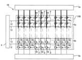
図2は、実施形態の表示装置1の構成を示すブロック図である。なお、図2では、互いに直交するX軸およびY軸が図示される。X軸に沿った方向が「行方向」であり、Y軸に沿った方向が「列方向」である。 2. Circuit configuration of the
図2に示すように、表示装置1は、前述の表示部10に加え、制御回路3、走査線駆動回路4、およびデータ線駆動回路5を含む。表示部10、制御回路3、走査線駆動回路4、およびデータ線駆動回路5は、例えばシリコン基板等の半導体基板上に形成される。As shown in FIG. 2, the
2-1.表示部10
図2に示すように、表示部10には、複数の画素回路100が行方向および列方向に行列状に配列される。複数の画素回路100は、複数の画素Pに対応して設けられる。 2-1.
2, a plurality of
表示部10には、m行の走査線12と、3列ごとにグループ化された3n列のデータ線14とが設けられる。なお、mおよびnのそれぞれは、2以上の整数である。nは、グループ数を表す。m行の走査線12のそれぞれはX軸に沿って設けられ、3n列のデータ線14のそれぞれはY軸に沿って設けられる。複数の画素回路100は、m行の走査線12と3n列のデータ線14との交差に対応して設けられる。複数の画素回路100は、画素Pに1対1で設けられており、例えば行方向に並ぶ3個ごとにグループ化される。よって、画素Pも同様に、例えば行方向に並ぶ3個ごとにグループ化される。グループ化される3つの画素Pは、画像を構成する画素の1ドットを表現する。The
2-2.制御回路3
図2に示す制御回路3には、図示省略されたホスト装置から出力されるデジタルの映像データVideoが同期信号Syncに同期して供給される。制御回路3は、映像データVideoおよび同期信号Syncに基づいて表示装置1の各部を制御する。映像データVideoとは、表示すべき画像における画素Pの階調レベルを例えば8ビットで指定する。また、同期信号Syncとは、映像データVideoの垂直走査開始を指示する垂直同期信号、水平走査開始を指示する水平同期信号、およびドットクロック信号を含む信号である。 2-2.
2 is supplied with digital video data Video output from a host device (not shown) in synchronization with a synchronization signal Sync. The
制御回路3は、同期信号Syncに基づいて制御信号Ctr1を生成し、制御信号Ctr1を走査線駆動回路4に供給するとともに、同期信号Syncに基づいて制御信号Ctr2を生成し、制御信号Ctr2をデータ線駆動回路5に供給する。制御信号Ctr1およびCtr2のそれぞれは、パルス信号や、クロック信号、イネーブル信号などの複数の信号を含む。The
さらに、制御回路3は、映像データVideoに基づいて画像データVidを生成し、画像データVidをデータ線駆動回路5に供給する。画像データVidで示される階調レベルと、画素回路100に含まれる後述の発光素子150とでは、輝度の特性が一致しない場合がある。そこで、映像データVideoで示される階調レベルに対応した輝度で発光素子150を発光させるために、制御回路3は、例えば、映像データVideoの8ビットを10ビットに変更した画像データVidを生成する。Furthermore, the
また、制御回路3は、同期信号Syncに基づいて各種制御信号を生成し、各種制御信号をデータ線駆動回路5に対して供給する。具体的には、制御回路3は、制御信号/Gref、/Gini、Sel、/Selをデータ線駆動回路5に供給する。制御信号/Grefは負論理の制御信号である。制御信号/Giniは負論理の制御信号である。制御信号/Selは制御信号Selと論理反転の関係にある。The
また、制御回路3は、図示省略された電源回路からの電力の供給を受け、データ線駆動回路5に対して所定電位を供給する。具体的には、制御回路3は、データ線駆動回路5に対して電位Vorst、電位Vrefおよび電位Vini等を供給する。また、当該電源回路から、表示部10の各画素回路100、走査線駆動回路4およびデータ線駆動回路5へ電源電位が供給される。The
2-3.走査線駆動回路4
図2に示すように、走査線駆動回路4は、制御信号Ctr1に基づいて走査信号/Gwrを生成する。走査信号/Gwrは、垂直同期信号により規定される各フレーム期間Vにおいてm行の走査線12を1行ごとに順番に選択して走査するため信号である。図2では、1、2、3、…、m行目の走査線12に供給される走査信号/Gwrは、/Gwr_1、/Gwr_2、/Gwr_3、…/Gwr_mと表記される。なお、フレーム期間Vとは、表示装置1が1カット分の画像を表示するのに要する期間をいう。フレーム期間Vの長さは、例えば、駆動フレームレートが60Hzである場合、1/60秒である。また、本実施形態では、m行の走査線12が1行ごとに順次選択されるが、複数行ごとに順次選択されてもよい。 2-3. Scanning
As shown in FIG. 2, the scanning
また、図2では図示省略するが、走査線駆動回路4は、走査信号/Gwrの他にも、後述の各種の制御信号/Gcmp、/Gorst、/Drst、/Gelを生成する。Although not shown in FIG. 2, the scanning
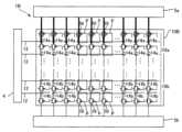
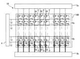
2-4.データ線駆動回路5
図2に示すように、データ線駆動回路5は、データ信号供給回路50と、n個のデマルチプレクサーDMと、3n個の補助回路51と、3n個の初期化回路52と、を備える。図2では、n個のデマルチプレクサーDMは、DM_1、DM_2、…、DM_nと表記される。3n個の補助回路51と3n個の初期化回路52とは、3n個の配線15を介して接続される。 2-4. Data
2, the data
データ信号供給回路50は、画像データVidおよび制御信号Ctr2に基づいて映像信号Vdを生成する。図2では、3n個の映像信号Vdが、Vd_1、Vd_2、Vd_3、Vd_4、Vd_5、Vd_6、…Vd_3n-2、Vd_3n-1およびVd_3nと表記される。データ信号供給回路50は、例えば、シフトレジスター、ラッチ回路、D/A変換回路およびアンプ群を含む。データ信号供給回路50は、シリアルで供給される画像データVidを、3相にパラレル変換し、階調レベルに応じた階調電位に変換して映像信号Vdとして出力する。The data signal
n個のデマルチプレクサーDMは、グループを構成する3列のデータ線14ごとに設けられる。デマルチプレクサーDM_1には、映像信号Vd_1、Vd_2、Vd_3が供給され、デマルチプレクサーDM_2には、映像信号Vd_4、Vd_5、Vd_6が供給され、デマルチプレクサーDM_nには、映像信号Vd_3n-2、Vd_3n-1およびVd_3nが供給される。また、n個のデマルチプレクサーDMは、グループを構成する3列のデータ線14に映像信号Vdを順番に供給する。The n demultiplexers DM are provided for each of the three columns of
3n個の補助回路51は、3n個の配線15に対して1対1で設けられる。また、3n個の初期化回路52は、3n個のデータ線14に対して1対1で設けられる。The 3n
3.画素回路100およびこれに対応する周辺回路の詳細
図3は、図2に示す画素回路100およびデータ線駆動回路5の構成例を示す図である。複数の画素回路100は同様の構成である。このため、以下では、複数の画素回路100のうちの任意の1つ、およびそれに対応するデータ線駆動回路5内の要素について中心に説明する。 3. Details of the
3-1.画素回路100
図3に示すように、画素回路100は、第1トランジスター506、トランジスター507、508、509、保持容量110、および発光素子150を含む。なお、第1トランジスター506、トランジスター507、508、および509のそれぞれは、PチャネルMOS型のトランジスターである。MOSとは、Metal-Oxide-Semiconductor field-effect transistorの略称である。 3-1.
3, the
第1トランジスター506のソースは給電線111に電気的に接続される。給電線111には、高電位である電位Velが供給される。第1トランジスター506は、ゲートおよびソース間の電位Vgsに応じた駆動電流を発光素子150に流す駆動トランジスターである。第1トランジスター506は、データ線14に後述のトランジスター507を介して接続されている。第1トランジスター506には、配線15およびデータ線14を介して供給される映像信号Vdに応じた電位に基づく駆動電流を発光素子150に供給する。The source of the
トランジスター507のゲートは走査線12に電気的に接続される。また、トランジスター507のソースまたはドレインの一方はデータ線14に電気的に接続され、他方は第1トランジスター506のゲートと、保持容量110の一方の電極とにそれぞれ電気的に接続される。ゆえに、トランジスター507は、第1トランジスター506のゲートと、データ線14とを電気的な接続を制御している。トランジスター507がオンに設定されると、データ線14に供給される映像信号Vdに応じた電位が第1トランジスター506のゲートに供給される。The gate of the
トランジスター508のソースまたはドレインの一方はデータ線14に電気的に接続され、他方は第1トランジスター506のドレインに電気的に接続される。ゆえに、トランジスター508は、第1トランジスター506が有するドレインとデータ線14とを電気的に接続する。トランジスター508のゲートには制御信号/Gcmpが供給される。トランジスター508は、第1トランジスター506のゲートおよびドレインの間の電位を閾値電位|Vth|に収束させる閾値電位補償を行う閾値補償トランジスターとして機能する。なお、第1トランジスター506の閾値電位とは、ソースとドレインとの間に電流が流れ始める際のゲートとソースとの電位差をいう。One of the source or drain of the
トランジスター509のソースは第1トランジスター506のドレインに電気的に接続されており、トランジスター509のドレインは発光素子150のアノードに電気的に接続される。トランジスター509は、第1トランジスター506のドレインと発光素子150のアノードとの間の電気的な接続を制御する制御トランジスターとして機能する。また、トランジスター509のゲートには、制御線112が接続される。制御線112には、制御信号/Gelが供給される。The source of the
発光素子150は、アノードとカソードとで有機EL層を挟持した構成である。発光素子150のアノードは、画素回路100ごとに個別に設けられる画素電極である。これに対して、発光素子150のカソードは、画素回路100のすべてにわたって共通に設けられる共通電極であり、給電線118に接続される。給電線118には、固定電位である電位Vctが供給される。The light-emitting
保持容量110は、一方の電極が第1トランジスター506のゲートに電気的に接続され、他方の電極が給電線111に電気的に接続される。このため、保持容量110は、第1トランジスター506のゲートとソースとの間の電位を保持する。なお、保持容量110としては、第1トランジスター506のゲートに寄生する寄生容量を用いてもよいし、シリコン基板等の半導体基板において互いに異なる導電層で絶縁層を挟持することによって形成される容量素子を用いてもよい。One electrode of the
なお、第1トランジスター506、トランジスター507、508、および509のソースおよびドレインは、第1トランジスター506、トランジスター507、508、および509の電位の関係に応じて入れ替わってもよい。また、第1トランジスター506、トランジスター507、508、および509は薄膜トランジスターであっても電界効果トランジスターであってもよい。The sources and drains of the
3-2.デマルチプレクサーDM
図3に示すように、n個のデマルチプレクサーDMのそれぞれは、各グループを構成する3列に対応する3個の第3トランジスター501を有し、各グループを構成する3列に映像信号Vdを順番に供給する。第3トランジスター501は、例えば、トランスミッションゲートで構成される。なお、図3では、1つの列に対応する1個の第3トランジスター501が図示される。また、詳細な図示はしないが、各デマルチプレクサーDMが有する3個の第3トランジスター501の入力端は互いに共通接続される。また、3個の第3トランジスター501の各出力端は、第2配線16を介して後述の容量素子120の第2電極122に接続される。各第3トランジスター501は、制御信号SelがHレベルであるときにオンし、制御信号SelがLレベルであるときにオフする。すなわち、第3トランジスター501は、制御信号/SelがHレベルであるときにオフし、制御信号/SelがLレベルであるときにオンする。なお、制御信号Selは、列ごとに順次排他的に供給される。 3-2. Demultiplexer DM
As shown in FIG. 3, each of the n demultiplexers DM has three
3-3.補助回路51
図3に示すように、補助回路51は、映像信号Vdの電圧振幅の圧縮のために用いられる。補助回路51は、PチャネルMOS型の第5トランジスター502および容量素子120を含む。第5トランジスター502のドレインは第2配線16に接続され、第5トランジスター502のソースは、「第3定電位」としての電位Vrefを供給する第3定電位線113に接続される。第5トランジスター502のゲートには、制御信号/Grefが供給される。 3-3.
3, the
容量素子120は、配線15と第2配線16との間に設けられ、これらに電気的に接続される。容量素子120は、カップリング容量として機能する。容量素子120は、第1電極121と第2電極122と絶縁層123とを有する。第1電極121は、配線15と電気的に接続される。第2電極122は、第1電極121と対向して配置され、第2配線16に電気的に接続される。よって、第2電極122は、第3トランジスター501と電気的に接続される。絶縁層123は、第1電極121と第2電極122との間に配置される。容量素子120は、例えば、映像信号Vdの電圧振幅の圧縮のために設けられる。The
3-4.初期化回路52
図3に示すように、初期化回路52は、後述の初期化期間Aにおいて、画素回路100に含まれる所定の要素の初期化のために用いられる。初期化回路52は、PチャネルMOS型の第4トランジスター503、トランジスター504、トランジスター505、およびスイッチング素子55を含む。 3-4.
3, the
スイッチング素子55は、データ線14と配線15との間に配置され、データ線14と配線15との電気的な接続を制御する。後で詳述するが、スイッチング素子55が設けられることで、配線15の寄生容量、および容量素子120の充放電による消費電力の増大を抑制することができる。The switching
スイッチング素子55は、例えば、トランスミッションゲートで構成される。スイッチング素子55の入力端は、第4トランジスター503に接続され、出力端は、トランジスター504に接続される。また、スイッチング素子55は、制御信号ZgopnがHレベルであるときにオンし、制御信号ZgopnがLレベルであるときにオフする。すなわち、第3トランジスター501は、制御信号/ZgopnがHレベルであるときにオフし、制御信号/ZgopnがLレベルであるときにオンする。The switching
第4トランジスター503のドレインは配線15に接続され、第4トランジスター503のソースは、「第2定電位」としての電位Viniを供給する第2定電位線114に接続される。電位Viniは、高電位である電位Velと後述の低電位である電位Vorstとの間の電位である。第4トランジスター503のゲートには、制御信号/Giniが供給される。The drain of the
トランジスター504のドレインはデータ線14に接続され、トランジスター504のソースは低電位である電位Vorstを供給する給電線115に接続される。トランジスター504のゲートには、制御信号/Gorstが供給される。The drain of the
トランジスター505のドレインはデータ線14に接続され、トランジスター505のソースは高電位である電位Velを供給する給電線116に接続される。つまり、トランジスター505は、データ線14と給電線116とを電気的に接続する。トランジスター505のゲートには、制御信号/Drstが供給される。The drain of the
本実施形態では、トランジスター505は、「第2トランジスター」の例示である。給電線116は、「第1定電位線」に相当し、電位Velは、「第1定電位」に相当する。なお、トランジスター504を「第2トランジスター」と捉えてもよい。この場合、給電線115が「第1定電位線」に相当し、電位Vorstは、「第1定電位」に相当する。In this embodiment, the
また、データ線14には、保持容量130を介して給電線117が接続される。給電線117には、高電位である電位Velが供給される。保持容量130は、データ線14の寄生容量であり、データ線14と給電線117との間の配線間容量としても捉えられる。The
4.表示装置1の動作
図4は、表示装置1の動作を説明するためのタイミングチャートである。図4に示す1フレーム期間Vは、複数の水平走査期間Hおよび複数の発光期間Dを含む。1フレーム期間Vにおいて、1水平走査期間Hごとに1~m行の走査線12が順番に走査される。なお、図4では、1フレーム期間Vのうちの1水平走査期間および1発光期間Dが示される。また、1水平走査期間Hは、1行分の水平走査に要する期間である。1水平走査期間Hは、初期化期間A、補償期間Bおよび書込期間Cを含む。 4. Operation of the
なお、1水平走査期間Hの動作は、各行の画素回路100で共通である。以下では、複数の画素回路100のうちの任意の1つの画素回路100、およびそれに対応する周辺回路について中心に説明する。The operation during one horizontal scanning period H is common to the
4-1.フレーム期間V
4-1A.初期化期間A
図4に示すように、初期化期間Aは、第1初期化期間A1と、第2初期化期間A2と、第3初期化期間A3とを含む。初期化期間Aでは、画素回路100が有する所定の要素の初期化が行われる。 4-1. Frame period V
4-1A. Initialization Period A
4, the initialization period A includes a first initialization period A1, a second initialization period A2, and a third initialization period A3. In the initialization period A, predetermined elements of the
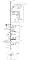
4-1Aa.第1初期化期間A1
図5は、図4の第1初期化期間A1における表示装置1の動作を説明するための図である。具体的には、第1初期化期間A1では、第1トランジスター506のゲートに高電位である電位Velが供給される。第1初期化期間A1は、第1トランジスター506をオフ状態にするための期間である。 4-1Aa. First initialization period A1
5 is a diagram for explaining the operation of the
図4に示すように、第1初期化期間A1では、走査信号/Gwrおよび制御信号/DrstがLレベルに設定される。このため、図5に示すトランジスター507およびトランジスター505のそれぞれがオンする。この結果、第1トランジスター506のゲートには、トランジスター505、データ線14、およびトランジスター507を順に介して高電位である電位Velが供給される。第1トランジスター506のゲートに高電位である電位Velが供給されると、ゲートおよびソース間の電位がゼロになる。このため、第1トランジスター506はオフ状態になる。また、データ線14の保持容量130の一端には、電位Velが供給される。As shown in FIG. 4, in the first initialization period A1, the scanning signal /Gwr and the control signal /Drst are set to the L level. Therefore, the
また、図4に示すように、第1初期化期間A1では、制御信号/GcmpはHレベルである。よって、図5に示すトランジスター508はオフである。したがって、第1初期化期間A1では、第1トランジスター506およびトランジスター508がオフである。このため、発光素子150に供給される電流の経路が遮断される。As shown in FIG. 4, in the first initialization period A1, the control signal /Gcmp is at the H level. Therefore, the
また、図4に示すように、第1初期化期間A1では、制御信号ZgopnがLレベルに設定される。このため、図5に示すスイッチング素子55は、オフに設定される。よって、データ線14と配線15とは非接続な状態である。また、第1初期化期間A1では、制御信号/Grefおよび制御信号/GiniのそれぞれがLレベルに設定される。このため、図5に示す第4トランジスター503および第5トランジスター502のそれぞれがオンする。よって、配線15および容量素子120の第1電極121に電位Viniが供給され、第2配線16および容量素子120の第2電極122に電位Vrefが供給される。As shown in FIG. 4, in the first initialization period A1, the control signal Zgopn is set to the L level. Therefore, the switching
スイッチング素子55が設けられていることで、第1初期化期間A1においてデータ線14と配線15とを非接続にすることができる。よって、第1初期化期間A1では、配線15、および第2配線16には、データ線14の電位とは異なる電位が供給される。By providing the switching
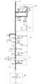
4-1Ab.第2初期化期間A2
図6は、図4の第2初期化期間A2における表示装置1の動作を説明するための図である。第2初期化期間A2では、発光素子150の各アノードにリセット電位としての電位Vorstが供給される。第2初期化期間A2は、発光素子150のアノードを初期化するための期間である。 4-1Ab. Second initialization period A2
Fig. 6 is a diagram for explaining the operation of the
図4に示すように、第2初期化期間A2では、制御信号/Gel、制御信号/Gcmpおよび制御信号/Gorstのそれぞれが、Lレベルに設定される。このため、図6に示すトランジスター508、509および504のそれぞれが、オンする。この結果、発光素子150のアノードには、トランジスター504、データ線14、トランジスター508および509を介して低電位である電位Vorstが印加される。発光素子150のアノードが電位Vorstにリセットされることで、発光素子150のアノードとトランジスター509との接続ノードに残存した電荷が放電される。したがって、第2初期化期間A2では、発光素子150のアノードが電位Vorstに初期化される。As shown in FIG. 4, in the second initialization period A2, the control signal /Gel, the control signal /Gcmp, and the control signal /Gorst are each set to the L level. Therefore, each of the
前述のように、発光素子150のそれぞれは、アノードとカソードとで有機EL層を挟持した構成である。このため、発光の際、アノードとカソードとの間には保持容量が寄生する。第2初期化期間A2では、電位Vorstがアノードに供給されることで、アノードとカソードとの間の保持容量によって保持される電位がリセットされる。このため、発光素子150に再び駆動電流が流れるとき、当該保持容量で保持される電位の影響を受け難い。As described above, each of the light-emitting
また、第2初期化期間A2においても、第1初期化期間A1と同様に、制御信号ZgopnがLレベルのままであるので、図6に示すスイッチング素子55は、オフのままである。よって、データ線14と配線15とは非接続な状態のままである。また、第1初期化期間A1では、制御信号/Grefおよび制御信号/GiniのそれぞれがLレベルのままであるので、第4トランジスター503および第5トランジスター502のそれぞれはオンのままである。よって、第2初期化期間A2においても、第1初期化期間A1と同様に、配線15、および第2配線16には、データ線14の電位とは異なる電位が供給される。Also, in the second initialization period A2, as in the first initialization period A1, the control signal Zgopn remains at the L level, so the switching
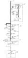
4-1Ac.第3初期化期間A3
図7は、図4の第3初期化期間A3における表示装置1の動作を説明するための図である。第3初期化期間A3では、第1トランジスター506のゲートに電位Viniが供給される。第3初期化期間A3は、補償期間Bのための前処理期間である。 4-1Ac. Third initialization period A3
Fig. 7 is a diagram for explaining the operation of the
図4に示すように、第3初期化期間A3では、制御信号ZgopnがHレベルに設定される。このため、図7に示すスイッチング素子55がオンする。この結果、データ線14と配線15とが電気的に接続される。また、第3初期化期間A3では、走査信号/Gwrおよび制御信号/Giniのそれぞれが、Lレベルに設定される。このため、図7に示すトランジスター507および第4トランジスター503のそれぞれがオンする。この結果、第1トランジスター506のゲート、および保持容量110の一端には、第4トランジスター503、配線15、データ線14およびトランジスター507を順に介して電位Viniが供給される。電位Viniは、|Vel-Vini|が第1トランジスター506の閾値電位|Vth|よりも大きくなるように設定される。このように設定されることで、後述の補償期間Bを短くすることができる。As shown in FIG. 4, in the third initialization period A3, the control signal Zgopn is set to H level. Therefore, the switching
また、第3初期化期間A3では、制御信号/GrefがLレベルのままであるので、第5トランジスター502はオンのままである。よって、第3初期化期間A3において、第2配線16および容量素子120の第2電極122に電位Vrefが供給される状態が継続される。In addition, during the third initialization period A3, the control signal /Gref remains at the L level, so the
4-1B.補償期間B
図8は、図4の補償期間Bにおける表示装置1の動作を説明するための図である。補償期間Bでは、第1トランジスター506のゲートおよびドレインの間の電位を閾値電位|Vth|に収束させる閾値電位補償を行う。 4-1B. Compensation period B
8 is a diagram for explaining the operation of the
図4に示すように、補償期間Bでは、制御信号ZgopnはHレベルのままであるため、図8に示すデータ線14および配線15とは電気的に接続された状態である。また、補償期間Bでは、走査信号/Gwrおよび制御信号/Gcmpのそれぞれが、Lレベルに設定される。このため、図8に示すトランジスター507およびトランジスター508のそれぞれがオンする。よって、第1トランジスター506のドレインは、トランジスター508、データ線14およびトランジスター507を順に介して第1トランジスター506のゲートに接続される。よって、第1トランジスター506は、ダイオード接続状態になる。それゆえ、データ線14および第1トランジスター506のゲートの各電位は、電位Viniから上昇し、電位(Vel-|Vth|)で飽和する。また、保持容量110は第1トランジスター506の閾値電位|Vth|を保持し、第1トランジスター506のゲートおよびドレインの間の電位は閾値電位|Vth|に収束する。As shown in FIG. 4, during compensation period B, the control signal Zgopn remains at H level, so that it is electrically connected to the
また、補償期間Bでは、制御信号/GrefがLレベルのままであるので、第5トランジスター502はオンのままである。よって、補償期間Bにおいて、第2配線16および容量素子120の第2電極122に電位Vrefが供給される状態が継続される。In addition, during compensation period B, the control signal /Gref remains at the L level, so the
4-1C.書込期間C
図9は、図4の書込期間Cにおける表示装置1の動作を説明するための図である。書込期間Cでは、映像信号Vdに応じた電位が第1トランジスター506のゲートに供給されるデータ書込み処理が行われる。 4-1C. Write period C
Fig. 9 is a diagram for explaining the operation of the
図4に示すように、書込期間Cでは、走査信号/GwrはLレベルに設定されたままである一方、制御信号/GcmpはHレベルに設定される。このため、図9に示すように、第1トランジスター506のダイオード接続状態が解除される。As shown in FIG. 4, during the write period C, the scanning signal /Gwr remains set to the L level, while the control signal /Gcmp is set to the H level. Therefore, as shown in FIG. 9, the diode-connected state of the
さらに、書込期間Cでは、制御信号SelがHレベルに設定され、制御信号/GrefがHレベルに設定される。このため、第5トランジスター502がオフし、第3トランジスター501がオンする。よって、容量素子120の一端の電位は、電位Vrefから映像信号Vdの電位に変化する。この変化分の電位をΔVとする。この電位の変化は、第2配線16、容量素子120、配線15、データ線14、トランジスター507を順に介して第1トランジスター506のゲートに伝播する。Furthermore, in the write period C, the control signal Sel is set to the H level, and the control signal /Gref is set to the H level. This causes the
また、第1トランジスター506のゲートは、補償期間Bにおける電位(Vel-|Vth|)から、前述の電位の変化分ΔVに容量比k1を乗じた値だけ、上昇方向にシフトした値(Vel-|Vth|+k1・ΔV)になる。よって、第1トランジスター506のゲートおよびソース間の電位Vgsは、Vel-(Vel-|Vth|+k1・ΔV)=(|Vth|-k1・ΔV)になる。The gate of the
なお、容量比k1は、Crf/(Cpara+Crf)である。なお、Crfは、容量素子120の容量である。Cparaは、保持容量130の容量である。また、保持容量110の容量をCpixとする。保持容量110の容量Cpixと、保持容量130の容量Cparaと、容量素子120の容量Crfとの関係は、Cpara>Crf>>Cpixである。容量Cpixは、容量Crf、Cparaに比較して十分に小さい。このため、上記容量比k1において考慮しない。The capacitance ratio k1 is Crf/(Cpara+Crf). Crf is the capacitance of the
4-1D.発光期間D
図10は、図4の発光期間Dにおける表示装置1の動作を説明するための図である。発光期間Dでは、発光素子150が発光する。 4-1D. Light Emitting Period D
Fig. 10 is a diagram for explaining the operation of the
図4に示すように、発光期間Dでは、走査信号/GwrがHレベルに変化し、走査信号/Gcmp、および/GorstはHレベルを維持し、制御信号/GelがLレベルに変化する。このため、図10に示すトランジスター507、およびトランジスター508はオフし、トランジスター509がオンする。この結果、第1トランジスター506の電位Vgsに応じた駆動電流が発光素子150に供給される。発光期間Dでの電位Vgsは、第1トランジスター506の閾値電位から、映像信号Vdの電位に応じてレベルシフトした電位である。このため、発光期間Dにおいて、発光素子150には、階調レベルに応じた電流が第1トランジスター506の閾値電位を補償した状態で供給される。As shown in FIG. 4, during the light emission period D, the scanning signal /Gwr changes to the H level, the scanning signals /Gcmp and /Gorst remain at the H level, and the control signal /Gel changes to the L level. Therefore, the
以上説明のように、表示装置1は、発光素子150と、データ線14と、配線15と、「第1定電位線」としての給電線116と、駆動トランジスターとしての第1トランジスター506と、初期化において用いられるトランジスター505と、スイッチング素子55とを備える。スイッチング素子55は、データ線14と配線15との電気的な接続を制御する。スイッチング素子55をオンすることで、データ線14と配線15とが接続される。スイッチング素子55をオフすることで、データ線14と配線15とが非接続になる。As described above, the
かかるスイッチング素子55が設けられることで、配線15に容量素子120が設けられている場合、容量素子120の充放電による消費電力の増大を抑制することができる。具体的には、水平走査期間Hの初期化期間Aにおいて、容量素子120の充放電による消費電力の増大を抑制することができる。By providing such a
前述のように、第1初期化期間A1では、図5に示すように、データ線14の保持容量130、および第1トランジスター506のゲートは、発光期間Dにおけるデータ線14の電位から高電位の電位Velに充電される。この第1初期化期間A1では、スイッチング素子55はオフに設定されるので、データ線14と配線15とは非接続である。よって、第1初期化期間A1では、容量素子120の第1電極121は、高電位の電位Velに充電されない。第1電極121には、中間電位である電位Viniが供給される。また、第2電極122には、電位Vrefが供給される。このため、第1電極121が高電位の電位Velに充電される場合に比べ、容量素子120の低消費電力化を図ることができる。As described above, in the first initialization period A1, as shown in FIG. 5, the
また、第2初期化期間A2において、図6に示すように、データ線14の保持容量130、および発光素子150のアノードは、高電位の電位Velから低電位の電位Vorstに放電される。この第2初期化期間A2では、スイッチング素子55はオフに設定されるので、データ線14と配線15とは非接続である。よって、第2初期化期間A2では、容量素子120の第1電極121は、低電位の電位Vorstに放電されない。第1電極121の電位は、第1初期化期間A1での電位を保ち、電位Viniのままである。また、第2電極122には、電位Vrefのままである。このため、容量素子120は充放電されない。よって、低消費電力化を図ることができる。In addition, in the second initialization period A2, as shown in FIG. 6, the
また、第3初期化期間A3において、スイッチング素子55はオンに設定されるので、データ線14と配線15とは電気的に接続される。そして、図7に示すように、データ線14の保持容量130、および第1トランジスター506のゲートは、低電位の電位Vorstから中間電位の電位Viniに充電される。第3初期化期間A3での第1電極121の電位は、第1初期化期間A1および第2初期化期間A2での電位を保ち、電位Viniのままである。また、第2電極122には、電位Vrefのままである。このため、容量素子120は充放電されない。よって、低消費電力化を図ることができる。In addition, in the third initialization period A3, the switching
前述のように、スイッチング素子55が設けられていることで、初期化期間Aにおいて、容量素子120の第1電極121が電位Viniに一定に保たれる。また、第2電極122は電位Vrefに一定に保たれる。このため、初期化期間Aにおける容量素子120の複数回の充放電が回避される。よって、消費電力の増大を抑制することができる。さらに、容量素子120が設けられる配線15の寄生容量の充放電による消費電力の増大を抑制することができる。As described above, by providing the switching
図11は、第1初期化期間A1における比較例の表示装置1Xの動作を説明するための図である。比較例では、スイッチング素子55および配線15が設けられておらず、容量素子120がデータ線14に設けられている。図11に示すように、比較例では、第1初期化期間A1において、容量素子120の第1電極121は、発光期間Dにおけるデータ線14の電位から高電位の電位Velに充電される。Figure 11 is a diagram for explaining the operation of a
図12は、第2初期化期間A2における比較例の表示装置1Xの動作を説明するための図である。図12に示すように、比較例では、第2初期化期間A2において、容量素子120の第1電極121は、高電位の電位Velから低電位の電位Vorstに放電される。また、第3初期化期間A3では、容量素子120の第1電極121は、低電位の電位Vorstから中間電位の電位Viniに充電される。Figure 12 is a diagram for explaining the operation of the
比較例では、スイッチング素子55および配線15が設けられておらず、容量素子120がデータ線14に設けられているため、本実施形態に比べ、初期化期間Aにおいて容量素子120が複数回充放電される。よって、比較例では、本実施形態に比べ、消費電力が増大する。In the comparative example, the switching
なお、映像信号を圧縮しない場合、容量素子120は省略してもよい。この場合であっても、スイッチング素子55および配線15を有するため、第1初期化期間A1および第2初期化期間A2でスイッチング素子55をオフにすることで、配線15の寄生容量の充放電を抑制することができる。よって、低消費電力化を図ることができる。If the video signal is not compressed, the
また、前述のように、表示装置1は、第3トランジスター501と容量素子120とを有する。第3トランジスターは、第2配線16、配線15およびデータ線14への映像信号Vdに応じた電位の供給を制御する。よって、映像信号Vdに応じた電位は、第2配線16および配線15を介してデータ線14に供給される。前述のように、容量素子120がある場合、スイッチング素子55が設けられていることで、充放電による消費電力の増大を抑制することができる。このため、容量素子120がある場合には、配線15の寄生容量の充放電に加え、容量素子120の充放電による消費電力の増大を抑制できる。よって、容量素子120がある場合、表示装置1がスイッチング素子55を備えることは特に有効である。As described above, the
表示装置1は、第4トランジスター503を有する。第4トランジスター503は、第1電極121と第2定電位線114とを電気的に接続する。このため、初期化期間Aにおいて第1電極121を電位Viniで一定に保つことができる。よって、容量素子120の充放電による消費電力の増大が抑制される。The
さらに、表示装置1は、第5トランジスター502を有する。第5トランジスター502は、第2電極122と第3定電位線113とを電気的に接続する。このため、初期化期間Aにおいて第2電極122を電位Vrefで一定に保つことができる。よって、容量素子120の充放電による消費電力の増大が抑制される。The
B.第2実施形態
第2実施形態を説明する。なお、以下の各例示において機能が第1実施形態と同様である要素については、第1実施形態の説明で使用した符号を流用して各々の詳細な説明を適宜に省略する。 B. Second embodiment A second embodiment will be described. In the following examples, the reference numerals used in the description of the first embodiment will be used for elements whose functions are similar to those of the first embodiment, and detailed descriptions of each element will be omitted as appropriate.
図13は、第2実施形態の表示装置1Aの構成を示すブロック図である。図14は、図13に示す画素回路100およびデータ線駆動回路5の構成例の図である。Figure 13 is a block diagram showing the configuration of a
第2実施形態の表示装置1Aは、複数の第2スイッチング素子56を有すること、およびデータ線14が複数のデータ線14aに分割されていることが第1実施形態の表示装置1と異なる。The
図13に示すように、表示装置1Aは、複数の第2スイッチング素子56を有する。各第2スイッチング素子56は、行ごとに設けられる。別の見方をすれば、各第2スイッチング素子56は、画素回路100ごとに設けられる。As shown in FIG. 13, the
図14に示すように、データ線14は、複数のデータ線14aに分割されている。具体的には、データ線14は、行ごとに分割されている。このため、複数のデータ線14aが、画素回路100ごとに設けられる。別の見方をすれば、列ごとに複数のデータ線14aが第2スイッチング素子56を介して接続されている。よって、1つのデータ線14aは、他のデータ線14aに第2スイッチング素子56を介して接続される。なお、保持容量130は、1列分の寄生容量である。As shown in FIG. 14, the
図15および図16のそれぞれは、図13に示す表示装置1Aの動作を説明するための図である。本実施形態では、データ書込み処理が終了した行から順次、第2スイッチング素子56がオフに設定される。Each of Figures 15 and 16 is a diagram for explaining the operation of the
図15に示すように、まず、全ての第2スイッチング素子56がオンに設定される。この状態で、表示部10の上から1行目に対応する画素Pにおけるデータ書込み処理が行われる。1行目の画素Pにおけるデータ書込み処理が終了したら、1行目の画素Pに対応する第2スイッチング素子56をオフにする。次に、図16に示すように、2行目の画素Pにおけるデータ書込み処理が行われる。この2行目の画素Pにおけるデータ書込み処理では、1行目に対応する第2スイッチング素子56がオフに設定されているため、1行目に対応するデータ線14aと2行目に対応するデータ線14aとは非接続の状態である。2行目の画素Pにおけるデータ書込み処理が終了したら、2行目の画素Pに対応する第2スイッチング素子56をオフにする。このようにして、第2スイッチング素子56が順次オフに設定される。As shown in FIG. 15, first, all the
前述のように、行ごとに複数の第2スイッチング素子56が設けられていることで、1行ずつ順次第2スイッチング素子56をオフにすることができる。このため、初期化期間Aにおける保持容量130の充放電量は減少していく。よって、本実施形態では、第1実施形態に比べて保持容量130の充放電による消費電力の増大をさらに抑制することができる。よって、第1実施形態に比べて低消費電力化を図ることができる。As described above, by providing multiple
また、本実施形態においても、第1実施形態と同様に、スイッチング素子55が設けられているため、配線15の寄生容量および容量素子120の充放電による消費電力の増大を抑制することができる。In addition, in this embodiment, as in the first embodiment, a switching
C.第3実施形態
第3実施形態を説明する。なお、以下の各例示において機能が第1実施形態と同様である要素については、第1実施形態の説明で使用した符号を流用して各々の詳細な説明を適宜に省略する。 C. Third embodiment A third embodiment will be described. In the following examples, the reference numerals used in the description of the first embodiment will be used for elements whose functions are similar to those of the first embodiment, and detailed descriptions of each element will be omitted as appropriate.
図17は、第3実施形態の表示装置1Bの構成を示すブロック図である。図18は、図17に示す上部回路10aおよびデータ線駆動回路5aの構成例の図である。図19は、図17に示す下部回路10bおよびデータ線駆動回路5bの構成例の図である。Figure 17 is a block diagram showing the configuration of a
第3実施形態の表示装置1Bの表示部10Bは、上部回路10aと下部回路10bとを有すること、およびデータ線駆動回路5aとデータ線駆動回路5bとを有することが第1実施形態の表示装置1と異なる。The
図17に示すように各データ線14は、第1データ線141と第2データ線142とに分割されている。上部回路10aには第1データ線141が設けられ、下部回路10bには、第2データ線142が設けられる。また、上部回路10aの第1データ線141には、データ線駆動回路5aが電気的に接続される。下部回路10bの第2データ線142には、データ線駆動回路5bが電気的に接続される。なお、データ線駆動回路5aおよび5bは、第1実施形態のデータ線駆動回路5と同様の構成および機能を有する。したがって、詳細な図示はしないが、データ線駆動回路5aおよび5bのそれぞれは、初期化回路52、補助回路51、デマルチプレクサーDMおよびデータ信号供給回路50を含む。As shown in FIG. 17, each
図18に示すように、上部回路10aには複数の第2スイッチング素子56aが設けられる。複数の第2スイッチング素子56aのそれぞれは、行ごとに設けられる。別の見方をすれば、複数の第2スイッチング素子56aのそれぞれは、画素回路100ごとに設けられる。図18に示すように、第1データ線141は、複数のデータ線14aに分割されている。列ごとに複数のデータ線14aが第2スイッチング素子56aを介して接続されている。よって、1つのデータ線14aは、他のデータ線14aに第2スイッチング素子56aを介して接続される。なお、保持容量130aは、1列分の寄生容量である。As shown in FIG. 18, a plurality of
図19に示すように、下部回路10bには複数の第2スイッチング素子56bが設けられる。複数の第2スイッチング素子56bのそれぞれは、行ごとに設けられる。別の見方をすれば、複数の第2スイッチング素子56bのそれぞれは、画素回路100ごとに設けられる。また、第2データ線142は、複数のデータ線14bに分割されている。列ごとに複数のデータ線14bが第2スイッチング素子56bを介して接続されている。よって、1つのデータ線14bは、他のデータ線14bに第2スイッチング素子56bを介して接続される。なお、保持容量130bは、1列分の寄生容量である。As shown in FIG. 19, a plurality of
図20および図21のそれぞれは、図17に示す上部回路10aにおける動作を説明するための図である。上部回路10aでは、データ書込みが終了した行から順次、第2スイッチング素子56aがオンに設定される。Each of Figures 20 and 21 is a diagram for explaining the operation of the
図20に示すように、まず、1行目に対応する第2スイッチング素子56aがオンに設定され、その他のスイッチング素子はオフに設定される。この状態で、1行目の画素Pにおけるデータ書込み処理が行われる。この1行目の画素Pにおけるデータ書込み処理では、2行目に対応する第2スイッチング素子56aがオフに設定されているため、2行目に対応するデータ線14aと1行目に対応するデータ線14aとは非接続の状態である。図21に示すように、1行目の画素Pにおけるデータ書込み処理が終了したら、2行目の画素Pに対応する第2スイッチング素子56aをオンにし、2行目の画素Pにおけるデータ書込み処理が行われる。2行目の画素Pにおけるデータ書込み処理が終了したら、2行目の画素Pに対応する第2スイッチング素子56aをオンにする。このようにして、複数の第2スイッチング素子56aは、1行目から順次オンに設定される。As shown in FIG. 20, first, the
前述のように、上部回路10aにおいて、行ごとに複数の第2スイッチング素子56aが設けられていることで、上から順に第2スイッチング素子56aがオンに設定される。このため、保持容量130aの充放電量が徐々に増加する。しかし、全体として保持容量130aの充放電による消費電力の増大を抑制することができる。As described above, in the
図22および図23のそれぞれは、図17に示す下部回路10bにおける動作を説明するための図である。下部回路10bにおいて、データ書込みが終了した行から順次、第2スイッチング素子56bがオフに設定される。下部回路10bでは、全ての第2スイッチング素子56がオンに設定された状態で、表示部10の上から1行ずつ順次データ書込み処理が行われる。Each of Figures 22 and 23 is a diagram for explaining the operation of the
図22に示すように、例えば、m-1行目の書込みが行われる場合、m行目およびm-1行名に対応する第2スイッチング素子56bがオンに設定され、その他の第2スイッチング素子56bはオフに設定される。この状態で、m-1行目の画素Pにおけるデータ書込み処理が行われる。このm-1行目の画素Pにおけるデータ書込み処理では、m-2行目に対応する第2スイッチング素子56bがオフに設定されているため、m-1行目に対応するデータ線14aとm-2行目に対応するデータ線14aとは非接続の状態である。図23に示すように、m-1行目の画素Pにおけるデータ書込み処理が終了したら、m-1行目の画素Pに対応する第2スイッチング素子56bをオフにし、m行目の画素Pにおけるデータ書込み処理が行われる。このようにして、複数の第2スイッチング素子56bは、上から順次オンに設定される。As shown in FIG. 22, for example, when writing to the m-1th row, the
前述のように、下部回路10bにおいて、行ごとに複数の第2スイッチング素子56bが設けられていることで、上から順に第2スイッチング素子56bがオフに設定される。このため、初期化期間Aにおける保持容量130bの充放電量は減少していく。このため、本実施形態では、第1実施形態に比べて、保持容量130bの充放電による消費電力の増大を抑制することができる。よって、第1実施形態に比べて低消費電力化を図ることができる。As described above, in the
また、本実施形態においても、第1実施形態と同様に、スイッチング素子55が設けられているため、配線15の寄生容量および容量素子120の充放電による消費電力の増大を抑制することができる。In addition, in this embodiment, as in the first embodiment, a switching
D.第4実施形態
第4実施形態を説明する。なお、以下の各例示において機能が第1実施形態と同様である要素については、第3実施形態の説明で使用した符号を流用して各々の詳細な説明を適宜に省略する。 D. Fourth embodiment A fourth embodiment will be described. In the following examples, the reference numerals used in the description of the third embodiment will be used for elements whose functions are similar to those of the first embodiment, and detailed descriptions of each element will be omitted as appropriate.
図24は、第3実施形態の表示装置1Cの構成を示すブロック図である。第3実施形態の表示装置1Cの表示部10Cは、上部回路10aと下部回路10bとの間に第3スイッチング素子57を有することが第1実施形態の表示装置1と異なる。また、表示装置1Cのデータ線駆動回路5cでは、補助回路51、デマルチプレクサーDMおよびデータ信号供給回路50が省略される。Figure 24 is a block diagram showing the configuration of a
図24に示すように第1データ線141と第2データ線142との間には、第3スイッチング素子57が設けられる。第3スイッチング素子57は、第1データ線141と第2データ線142の接続を制御する。また、第2データ線142には、データ線駆動回路5cが電気的に接続される。詳細な図示はしないが、データ線駆動回路5cは、初期化回路52を有する。ただし、データ線駆動回路5cでは、補助回路51、デマルチプレクサーDMおよびデータ信号供給回路50が省略される。24, a
本実施形態では、データ線駆動回路5bから、上部回路10aおよび下部回路10bに映像信号Vdに応じた電位が供給される。上部回路10aにおける初期化の際には第3スイッチング素子57をオフにし、データ書込みの際には第3スイッチング素子57をオンにする。このため、初期化期間Aにおける保持容量130の充放電による消費電力の増大を抑制することができるとともに、データ線駆動回路5cの配置スペースをデータ線駆動回路5bに比べて小さくすることができる。In this embodiment, a potential corresponding to the video signal Vd is supplied from the data line driving
また、図示はしないが、本実施形態においても、第1実施形態と同様に、表示装置1Cはスイッチング素子55を備えている。このため、配線15の寄生容量および容量素子120の充放電による消費電力の増大を抑制することができる。Although not shown, in this embodiment, as in the first embodiment, the
E.変形例
前述の各実施形態は、例えば、以下に述べる各種の変形が可能である。また、各変形例を適宜組み合わせてもよい。 E. Modifications The above-described embodiments may be modified in various ways, for example as described below. In addition, the modifications may be combined as appropriate.
図25は、変形例の表示装置1Dを示すブロック図である。図25に示す表示装置1Dは、データ線14が第1データ線141と第2データ線142とに分割されている。また、第1データ線141にはデータ線駆動回路5aが接続され、第2データ線142にデータ線駆動回路5bが接続される。データ線14が2つに分割されていることで、第1実施形態に比べ、保持容量130の充放電による消費電力の増大を抑制することができる。Fig. 25 is a block diagram showing a modified
前述の実施形態では、発光素子150のそれぞれは、OLEDである。しかし、例えば「発光素子」は、LED、ミニLED、マイクロLED等であってもよい。LEDは、light-emitting diodeの略である。In the above embodiment, each of the light-emitting
F.電子機器
前述の各実施形態または各変形例の表示装置1、1A、1B、1Cおよび1Dは、各種の電子機器に適用することができる。前述の実施形態に係る表示装置1は、特に2K2K以上の高精細な画像の表示を要求され、かつ小型であることを要求される電子機器に好適である。 F. Electronic Device The
図26は、電子機器としてのヘッドマウントディスプレイ300の外観を示す斜視図である。図27は、図26に示すヘッドマウントディスプレイ300の光学的な構成の図である。図27では、左眼用の表示装置1を表示装置1Lと表記し、右眼用の表示装置1を表示装置1Rと表記する。なお、表示装置1の代わりに、表示装置1A、1B、1Cまたは1Dを用いてもよい。Figure 26 is a perspective view showing the appearance of a head mounted
図26に示されるように、ヘッドマウントディスプレイ300は、テンプル310、ブリッジ320、投射光学系301L、投射光学系301R、および制御部350を備える。また、図27に示すように、ヘッドマウントディスプレイ300は、2つの表示装置1を備える。制御部350は、例えばプロセッサーおよびメモリーを含み、2つの表示装置1の各動作を制御する。As shown in FIG. 26, the head mounted
表示装置1Lによって形成される映像光LLは、投射光学系301Lに出射される。投射光学系301Lは、光学レンズ302Lおよびハーフミラー303Lを含む。映像光LLは、光学レンズ302Lを介してハーフミラー303Lに向けて出射される。映像光LLの一部はハーフミラー303Lで反射し、ヘッドマウントディスプレイ300の装着者の瞳EYに投射される。また、映像光LLの一部は、ハーフミラー303Lを透過する。同様に、表示装置1Rによって形成される映像光LRは、投射光学系301Rに出射される。投射光学系301Rは、光学レンズ302Rおよびハーフミラー303Rを含む。映像光LRは、光学レンズ302Rを介してハーフミラー303Lに向けて出射される。映像光LRの一部はハーフミラー303Rで反射し、ヘッドマウントディスプレイ300の装着者の瞳EYに投射される。また、映像光LRの一部は、ハーフミラー303Rを透過する。The image light LL formed by the display device 1L is emitted to the projection
ヘッドマウントディスプレイ300の装着者は、外界像を視認しながら、映像光LLおよびLRにより形成された画像を視認することができる。A person wearing the head mounted
ヘッドマウントディスプレイ300は、前述の表示装置1および制御部350を備える。表示装置1によれば、各種容量の充放電による消費電力を抑制することができる。したがって、ヘッドマウントディスプレイ300が表示装置1を備えることで、ヘッドマウントディスプレイ300の低消費電力化を図ることができる。The head mounted
なお、前述の表示装置1が適用される電子機器としては、ヘッドマウントディスプレイ300のほか、デジタルスコープ、デジタル双眼鏡、デジタルスチルカメラ、ビデオカメラなど眼に近接して配置する電子機器が挙げられる。さらに、携帯電話機、スマートフォン、スマートウォッチ、携帯情報端末(PDA:Personal Digital Assistants)、カーナビゲーション装置、および車載用のインストルメントパネルなどの表示器等の電子機器に設けられる表示部として適用することができる。また、表示装置1は、投写式プロジェクターのライトバルブに適用可能である。Note that examples of electronic devices to which the
以上、本発明について図示の実施形態および変形例に基づいて説明したが、本発明は、これらに限定されるものではない。また、本発明の各部の構成は、前述した実施形態の同様の機能を発揮する任意の構成のものに置換することができ、また、任意の構成を付加することもできる。The present invention has been described above based on the illustrated embodiment and modified examples, but the present invention is not limited to these. Furthermore, the configuration of each part of the present invention can be replaced with any configuration that performs the same function as the above-mentioned embodiment, and any configuration can be added.
1…表示装置、3…制御回路、4…走査線駆動回路、5…データ線駆動回路、5a…データ線駆動回路、5b…データ線駆動回路、5c…データ線駆動回路、10…表示部、10B…表示部、10C…表示部、10a…上部回路、10b…下部回路、12…走査線、14…データ線、14X…データ線、14a…データ線、14b…データ線、15…配線、16…第2配線、50…データ信号供給回路、51…補助回路、52…初期化回路、55…スイッチング素子、56…第2スイッチング素子、56a…第2スイッチング素子、56b…第2スイッチング素子、57…第3スイッチング素子、71…ケース、72…FPC基板、73…端子、100…画素回路、110…保持容量、111…給電線、112…制御線、113…第3定電位線、114…第2定電位線、115…給電線、116…給電線、117…給電線、118…給電線、120…容量素子、120X…容量素子、121…第1電極、121X…第1電極、122…第2電極、123…絶縁層、130…保持容量、130X…保持容量、130a…保持容量、130b…保持容量、141…第1データ線、142…第2データ線、150…発光素子、300…ヘッドマウントディスプレイ、301L…投射光学系、301R…投射光学系、302L…光学レンズ、302R…光学レンズ、303L…ハーフミラー、303R…ハーフミラー、310…テンプル、320…ブリッジ、350…制御部、501…第3トランジスター、502…第5トランジスター、503…第4トランジスター、504…トランジスター、505…トランジスター、506…第1トランジスター、506X…第1トランジスター、507…トランジスター、508…トランジスター、509…トランジスター、A…初期化期間、A1…第1初期化期間、A2…第2初期化期間、A3…第3初期化期間、B…補償期間、C…書込期間、D…発光期間、DM…デマルチプレクサー、EY…瞳、H…水平走査期間、V…フレーム期間、LL…映像光、LR…映像光、P…画素。1...display device, 3...control circuit, 4...scanning line driving circuit, 5...data line driving circuit, 5a...data line driving circuit, 5b...data line driving circuit, 5c...data line driving circuit, 10...display section, 10B...display section, 10C...display section, 10a...upper circuit, 10b...lower circuit, 12...scanning line, 14...data line, 14X...data line, 14a...data line, 14b...data line, 15...wiring, 16...second wiring, 50...data signal supply circuit, 51...auxiliary circuit, 52...initialization circuit, 55...switching element, 56...second switch switching element, 56a...second switching element, 56b...second switching element, 57...third switching element, 71...case, 72...FPC board, 73...terminal, 100...pixel circuit, 110...storage capacitance, 111...power supply line, 112...control line, 113...third constant potential line, 114...second constant potential line, 115...power supply line, 116...power supply line, 117...power supply line, 118...power supply line, 120...capacitive element, 120X...capacitive element, 121...first electrode, 121X...first electrode, 122...second electrode, 123...insulating layer , 130...storage capacitance, 130X...storage capacitance, 130a...storage capacitance, 130b...storage capacitance, 141...first data line, 142...second data line, 150...light-emitting element, 300...head mounted display, 301L...projection optical system, 301R...projection optical system, 302L...optical lens, 302R...optical lens, 303L...half mirror, 303R...half mirror, 310...temple, 320...bridge, 350...control unit, 501...third transistor, 502...fifth transistor, 503...third 4 transistors, 504...transistor, 505...transistor, 506...first transistor, 506X...first transistor, 507...transistor, 508...transistor, 509...transistor, A...initialization period, A1...first initialization period, A2...second initialization period, A3...third initialization period, B...compensation period, C...writing period, D...light emission period, DM...demultiplexer, EY...pupil, H...horizontal scanning period, V...frame period, LL...image light, LR...image light, P...pixel.
Claims (7)
Translated fromJapaneseデータ線と、
配線と、
第1定電位が供給される第1定電位線と、
前記配線および前記データ線を介して供給される映像信号に応じた電位に基づく駆動電流を前記発光素子に供給する第1トランジスターと、
前記データ線と前記第1定電位線とを電気的に接続する第2トランジスターと、
前記データ線と前記配線とを電気的に接続するスイッチング素子と、
を備えることを特徴とする表示装置。 A light-emitting element;
Data lines and
Wiring and
a first constant potential line to which a first constant potential is supplied;
a first transistor that supplies a driving current to the light-emitting element based on a potential corresponding to a video signal supplied via the wiring and the data line;
a second transistor electrically connecting the data line and the first constant potential line;
a switching element that electrically connects the data line and the wiring;
A display device comprising:
前記配線と電気的に接続された第1電極と、前記第1電極と対向して配置され、前記第3トランジスターと電気的に接続された第2電極とを有する容量素子と、
をさらに備える請求項1に記載の表示装置。 a third transistor that controls the supply of the video signal to the wiring and the data line;
a capacitance element having a first electrode electrically connected to the wiring and a second electrode arranged opposite to the first electrode and electrically connected to the third transistor;
The display device according to claim 1 , further comprising:
前記第1電極と前記第2定電位線とを電気的に接続する第4トランジスターと、
をさらに備える請求項2に記載の表示装置。 a second constant potential line to which a second constant potential is supplied;
a fourth transistor electrically connecting the first electrode and the second constant potential line;
The display device according to claim 2 , further comprising:
前記第2電極と前記第3定電位線とを電気的に接続する第5トランジスターと、
をさらに備える請求項2に記載の表示装置。 a third constant potential line to which a third constant potential is supplied;
a fifth transistor electrically connecting the second electrode and the third constant potential line;
The display device according to claim 2 , further comprising:
前記データ線は、複数のデータ線に分割されており、
前記複数のデータ線のそれぞれは、前記第2スイッチング素子を介して他のデータ線に接続される、
さらに備える請求項1に記載の表示装置。 Further comprising a second switching element,
The data line is divided into a plurality of data lines,
Each of the plurality of data lines is connected to another data line via the second switching element.
The display device according to claim 1 further comprising:
前記第1データ線と前記第2データ線とを電気的に接続する第3スイッチング素子を、
さらに備える請求項1に記載の表示装置。 The data line is divided into a first data line and a second data line,
a third switching element electrically connecting the first data line and the second data line;
The display device according to claim 1 further comprising:
前記表示装置の動作を制御する制御部と、を有することを特徴とする電子機器。 A display device according to claim 1;
and a control unit for controlling an operation of the display device.
Priority Applications (3)
| Application Number | Priority Date | Filing Date | Title |
|---|---|---|---|
| JP2022209725AJP2024093381A (en) | 2022-12-27 | 2022-12-27 | Display devices and electronic devices |
| CN202311801497.2ACN118265369A (en) | 2022-12-27 | 2023-12-25 | Display device and electronic apparatus |
| US18/395,848US12300176B2 (en) | 2022-12-27 | 2023-12-26 | Display device and electronic apparatus |
Applications Claiming Priority (1)
| Application Number | Priority Date | Filing Date | Title |
|---|---|---|---|
| JP2022209725AJP2024093381A (en) | 2022-12-27 | 2022-12-27 | Display devices and electronic devices |
Publications (1)
| Publication Number | Publication Date |
|---|---|
| JP2024093381Atrue JP2024093381A (en) | 2024-07-09 |
Family
ID=91583747
Family Applications (1)
| Application Number | Title | Priority Date | Filing Date |
|---|---|---|---|
| JP2022209725APendingJP2024093381A (en) | 2022-12-27 | 2022-12-27 | Display devices and electronic devices |
Country Status (3)
| Country | Link |
|---|---|
| US (1) | US12300176B2 (en) |
| JP (1) | JP2024093381A (en) |
| CN (1) | CN118265369A (en) |
Families Citing this family (1)
| Publication number | Priority date | Publication date | Assignee | Title |
|---|---|---|---|---|
| JP2024099940A (en)* | 2023-01-13 | 2024-07-26 | セイコーエプソン株式会社 | Display device and electronic apparatus |
Family Cites Families (15)
| Publication number | Priority date | Publication date | Assignee | Title |
|---|---|---|---|---|
| TW200641774A (en) | 2005-04-28 | 2006-12-01 | Sanyo Electric Co | Electroluminescense display device and data line driving circuit |
| JP2006308861A (en) | 2005-04-28 | 2006-11-09 | Sanyo Electric Co Ltd | Data line driving circuit |
| JP5236324B2 (en) | 2008-03-19 | 2013-07-17 | グローバル・オーエルイーディー・テクノロジー・リミテッド・ライアビリティ・カンパニー | Display panel |
| JP5352101B2 (en) | 2008-03-19 | 2013-11-27 | グローバル・オーエルイーディー・テクノロジー・リミテッド・ライアビリティ・カンパニー | Display panel |
| JP5260230B2 (en) | 2008-10-16 | 2013-08-14 | グローバル・オーエルイーディー・テクノロジー・リミテッド・ライアビリティ・カンパニー | Display device |
| JP2010249955A (en) | 2009-04-13 | 2010-11-04 | Global Oled Technology Llc | Display device |
| JP5399198B2 (en) | 2009-10-08 | 2014-01-29 | グローバル・オーエルイーディー・テクノロジー・リミテッド・ライアビリティ・カンパニー | Pixel circuit and display device |
| JP5879944B2 (en)* | 2011-11-16 | 2016-03-08 | セイコーエプソン株式会社 | Electro-optical device and electronic apparatus |
| JP6535441B2 (en)* | 2014-08-06 | 2019-06-26 | セイコーエプソン株式会社 | Electro-optical device, electronic apparatus, and method of driving electro-optical device |
| JP6657800B2 (en)* | 2015-10-30 | 2020-03-04 | セイコーエプソン株式会社 | Electro-optical device, electronic apparatus, and method of driving electro-optical device |
| JP6911406B2 (en) | 2017-03-13 | 2021-07-28 | セイコーエプソン株式会社 | Pixel circuits, electro-optics and electronic devices |
| JP6593480B2 (en)* | 2018-03-09 | 2019-10-23 | セイコーエプソン株式会社 | Electro-optical device and electronic apparatus |
| JP6673388B2 (en)* | 2018-03-09 | 2020-03-25 | セイコーエプソン株式会社 | Driving method of electro-optical device |
| CN108962120B (en)* | 2018-08-01 | 2021-10-22 | 京东方科技集团股份有限公司 | Display substrate, display panel, display device, and display driving method |
| JP2023112315A (en)* | 2022-02-01 | 2023-08-14 | セイコーエプソン株式会社 | Electro-optic device and electronic apparatus |
- 2022
- 2022-12-27JPJP2022209725Apatent/JP2024093381A/enactivePending
- 2023
- 2023-12-25CNCN202311801497.2Apatent/CN118265369A/enactivePending
- 2023-12-26USUS18/395,848patent/US12300176B2/enactiveActive
Also Published As
| Publication number | Publication date |
|---|---|
| US20240212614A1 (en) | 2024-06-27 |
| CN118265369A (en) | 2024-06-28 |
| US12300176B2 (en) | 2025-05-13 |
Similar Documents
| Publication | Publication Date | Title |
|---|---|---|
| CN110827767B (en) | Electro-optical device | |
| CN103065582B (en) | Electro-optical device, driving method of electro-optical device, and electronic device | |
| CN107248395B (en) | The driving method of electro-optical device | |
| JP7237918B2 (en) | Pixel circuit, display device, method for driving pixel circuit, and electronic device | |
| CN110246457B (en) | Electro-optical device, driving method of electro-optical device, and electronic device | |
| JP2023050791A (en) | ELECTRO-OPTICAL DEVICE, ELECTRONIC DEVICE, AND METHOD FOR DRIVING ELECTRO-OPTICAL DEVICE | |
| CN110246461B (en) | Electro-optical device and electronic apparatus | |
| US12300176B2 (en) | Display device and electronic apparatus | |
| US12236881B2 (en) | Electro-optical device and electronic apparatus | |
| US12080235B2 (en) | Electro-optical device, electronic device and method of driving electro-optical device | |
| JP2024117945A (en) | Electro-optical devices and electronic equipment | |
| JP2024081222A (en) | Display devices and electronic devices | |
| US20250279055A1 (en) | Display device and electronic apparatus | |
| JP2019133191A (en) | Display device and electronic apparatus | |
| US20250104634A1 (en) | Electro-optical device and electronic apparatus | |
| US20250299632A1 (en) | Display device and electronic apparatus | |
| JP7528436B2 (en) | Display devices and electronic devices | |
| KR20250127798A (en) | Pixel and display device including the same | |
| JP2025119807A (en) | DA conversion circuit, electro-optical device and electronic device | |
| JP2025021550A (en) | Electro-optical devices and electronic equipment | |
| JP6299090B2 (en) | Electro-optical device, driving method of electro-optical device, and electronic apparatus |