JP2024086726A - Semiconductor Device - Google Patents
Semiconductor DeviceDownload PDFInfo
- Publication number
- JP2024086726A JP2024086726AJP2024038905AJP2024038905AJP2024086726AJP 2024086726 AJP2024086726 AJP 2024086726AJP 2024038905 AJP2024038905 AJP 2024038905AJP 2024038905 AJP2024038905 AJP 2024038905AJP 2024086726 AJP2024086726 AJP 2024086726A
- Authority
- JP
- Japan
- Prior art keywords
- oxide semiconductor
- film
- transistor
- semiconductor layer
- oxide
- Prior art date
- Legal status (The legal status is an assumption and is not a legal conclusion. Google has not performed a legal analysis and makes no representation as to the accuracy of the status listed.)
- Granted
Links
Images


Classifications
- H—ELECTRICITY
- H10—SEMICONDUCTOR DEVICES; ELECTRIC SOLID-STATE DEVICES NOT OTHERWISE PROVIDED FOR
- H10D—INORGANIC ELECTRIC SEMICONDUCTOR DEVICES
- H10D30/00—Field-effect transistors [FET]
- H10D30/60—Insulated-gate field-effect transistors [IGFET]
- H10D30/67—Thin-film transistors [TFT]
- H10D30/674—Thin-film transistors [TFT] characterised by the active materials
- H10D30/6755—Oxide semiconductors, e.g. zinc oxide, copper aluminium oxide or cadmium stannate
- H—ELECTRICITY
- H10—SEMICONDUCTOR DEVICES; ELECTRIC SOLID-STATE DEVICES NOT OTHERWISE PROVIDED FOR
- H10D—INORGANIC ELECTRIC SEMICONDUCTOR DEVICES
- H10D30/00—Field-effect transistors [FET]
- H10D30/01—Manufacture or treatment
- H10D30/021—Manufacture or treatment of FETs having insulated gates [IGFET]
- H10D30/031—Manufacture or treatment of FETs having insulated gates [IGFET] of thin-film transistors [TFT]
- H—ELECTRICITY
- H10—SEMICONDUCTOR DEVICES; ELECTRIC SOLID-STATE DEVICES NOT OTHERWISE PROVIDED FOR
- H10D—INORGANIC ELECTRIC SEMICONDUCTOR DEVICES
- H10D30/00—Field-effect transistors [FET]
- H10D30/60—Insulated-gate field-effect transistors [IGFET]
- H10D30/67—Thin-film transistors [TFT]
- H—ELECTRICITY
- H10—SEMICONDUCTOR DEVICES; ELECTRIC SOLID-STATE DEVICES NOT OTHERWISE PROVIDED FOR
- H10D—INORGANIC ELECTRIC SEMICONDUCTOR DEVICES
- H10D30/00—Field-effect transistors [FET]
- H10D30/60—Insulated-gate field-effect transistors [IGFET]
- H10D30/67—Thin-film transistors [TFT]
- H10D30/674—Thin-film transistors [TFT] characterised by the active materials
- H10D30/6755—Oxide semiconductors, e.g. zinc oxide, copper aluminium oxide or cadmium stannate
- H10D30/6756—Amorphous oxide semiconductors
- H—ELECTRICITY
- H10—SEMICONDUCTOR DEVICES; ELECTRIC SOLID-STATE DEVICES NOT OTHERWISE PROVIDED FOR
- H10D—INORGANIC ELECTRIC SEMICONDUCTOR DEVICES
- H10D30/00—Field-effect transistors [FET]
- H10D30/60—Insulated-gate field-effect transistors [IGFET]
- H10D30/67—Thin-film transistors [TFT]
- H10D30/6757—Thin-film transistors [TFT] characterised by the structure of the channel, e.g. transverse or longitudinal shape or doping profile
- H—ELECTRICITY
- H10—SEMICONDUCTOR DEVICES; ELECTRIC SOLID-STATE DEVICES NOT OTHERWISE PROVIDED FOR
- H10D—INORGANIC ELECTRIC SEMICONDUCTOR DEVICES
- H10D62/00—Semiconductor bodies, or regions thereof, of devices having potential barriers
- H10D62/40—Crystalline structures
- H—ELECTRICITY
- H10—SEMICONDUCTOR DEVICES; ELECTRIC SOLID-STATE DEVICES NOT OTHERWISE PROVIDED FOR
- H10D—INORGANIC ELECTRIC SEMICONDUCTOR DEVICES
- H10D62/00—Semiconductor bodies, or regions thereof, of devices having potential barriers
- H10D62/40—Crystalline structures
- H10D62/405—Orientations of crystalline planes
- H—ELECTRICITY
- H10—SEMICONDUCTOR DEVICES; ELECTRIC SOLID-STATE DEVICES NOT OTHERWISE PROVIDED FOR
- H10D—INORGANIC ELECTRIC SEMICONDUCTOR DEVICES
- H10D62/00—Semiconductor bodies, or regions thereof, of devices having potential barriers
- H10D62/80—Semiconductor bodies, or regions thereof, of devices having potential barriers characterised by the materials
Landscapes
- Thin Film Transistor (AREA)
- Semiconductor Memories (AREA)
- Solid State Image Pick-Up Elements (AREA)
- Electroluminescent Light Sources (AREA)
- Liquid Crystal (AREA)
- Chemical & Material Sciences (AREA)
- Crystallography & Structural Chemistry (AREA)
- Metal-Oxide And Bipolar Metal-Oxide Semiconductor Integrated Circuits (AREA)
- Devices For Indicating Variable Information By Combining Individual Elements (AREA)
- Physics & Mathematics (AREA)
- Geometry (AREA)
- Engineering & Computer Science (AREA)
- Microelectronics & Electronic Packaging (AREA)
- Electrodes Of Semiconductors (AREA)
- Non-Volatile Memory (AREA)
- Mechanical Treatment Of Semiconductor (AREA)
- Bipolar Transistors (AREA)
- Noodles (AREA)
Abstract
Translated fromJapanese
Description
Translated fromJapanese半導体装置及び半導体装置の作製方法に関する。Related to semiconductor devices and methods for manufacturing semiconductor devices.
なお、本明細書中において半導体装置とは、半導体特性を利用することで機能しうる装置
全般を指し、電気光学装置、半導体回路および電子機器は全て半導体装置である。In this specification, the term "semiconductor device" refers to any device that can function by utilizing semiconductor characteristics, and electro-optical devices, semiconductor circuits, and electronic devices are all classified as semiconductor devices.
絶縁表面を有する基板上に形成された半導体薄膜を用いてトランジスタ(薄膜トランジス
タ(TFT)ともいう)を構成する技術が注目されている。該トランジスタは集積回路(
IC)や画像表示装置(表示装置)のような電子デバイスに広く応用されている。トラン
ジスタに適用可能な半導体薄膜としてシリコン系半導体材料が広く知られているが、その
他の材料として酸化物半導体が注目されている。A technology for constructing a transistor (also called a thin film transistor (TFT)) using a semiconductor thin film formed on a substrate having an insulating surface is attracting attention.
These materials are widely used in electronic devices such as integrated circuits (ICs) and image display devices (display devices). Silicon-based semiconductor materials are widely known as semiconductor thin films applicable to transistors, but oxide semiconductors have also attracted attention as other materials.
例えば、トランジスタの活性層として、インジウム(In)、ガリウム(Ga)、及び亜
鉛(Zn)を含む非晶質酸化物を用いたトランジスタが開示されている(特許文献1参照
)。For example, a transistor using an amorphous oxide containing indium (In), gallium (Ga), and zinc (Zn) as an active layer of the transistor has been disclosed (see Patent Document 1).
トランジスタのオン特性(例えば、オン電流や電界効果移動度)が向上すると、半導体装
置において入力信号に対する高速応答、高速駆動が可能になり、より高性能な半導体装置
が実現できる。一方、半導体装置の低消費電力化には、トランジスタのオフ電流が十分低
いことが求められる。このように、トランジスタに求められる電気特性は用途や目的に合
わせて様々であり、該電気特性をより精度よく制御することは有益である。When the on-characteristics of a transistor (e.g., on-current and field effect mobility) are improved, the semiconductor device can respond quickly to an input signal and can be driven at high speed, thereby realizing a semiconductor device with higher performance. On the other hand, in order to reduce the power consumption of a semiconductor device, the off-current of the transistor is required to be sufficiently low. As described above, the electrical characteristics required of a transistor vary depending on the application and purpose, and it is useful to control the electrical characteristics with greater precision.
酸化物半導体をチャネル形成領域に用いたトランジスタの電気特性のしきい値電圧をプラ
スにすることができ、所謂ノーマリーオフのスイッチング素子を実現するトランジスタ構
造およびその作製方法を課題の一つとする。An object of the present invention is to provide a transistor structure and a manufacturing method thereof which can realize a so-called normally-off switching element by making the threshold voltage of a transistor in which an oxide semiconductor is used for a channel formation region positive.
トランジスタは、ゲート電圧が0Vにできるだけ近い正のしきい値電圧でチャネルが形成
されることが望ましい。トランジスタのしきい値電圧値がマイナスであると、ゲート電圧
が0Vでもソース電極とドレイン電極の間に電流が流れる、所謂ノーマリーオンとなりや
すい。LSIやCPUやメモリにおいては、回路を構成するトランジスタの電気特性が重
要であり、この電気特性が半導体装置の消費電力を左右する。特に、トランジスタの電気
特性のうち、しきい値電圧(Vth)が重要である。電界効果移動度が高くとも、しきい
値電圧値がマイナスであると、回路として制御することが困難である。負の電圧状態でも
チャネルが形成されてドレイン電流が流れるトランジスタは、半導体装置の集積回路に用
いるトランジスタとしては不向きである。It is desirable for a transistor to have a channel formed at a gate voltage with a positive threshold voltage as close as possible to 0V. If the threshold voltage value of a transistor is negative, a current flows between the source electrode and the drain electrode even when the gate voltage is 0V, which is a so-called normally-on state. In LSIs, CPUs, and memories, the electrical characteristics of transistors constituting circuits are important, and these electrical characteristics affect the power consumption of semiconductor devices. In particular, among the electrical characteristics of transistors, the threshold voltage (Vth) is important. Even if the field-effect mobility is high, if the threshold voltage value is negative, it is difficult to control the circuit. A transistor in which a channel is formed and a drain current flows even in a negative voltage state is not suitable as a transistor to be used in an integrated circuit of a semiconductor device.
また、材料や作製条件によっては、作製されたトランジスタがノーマリーオフとならない
場合であっても、ノーマリーオフの特性に近づけることが重要であり、しきい値電圧値が
マイナスである、所謂ノーマリーオンであっても、トランジスタのしきい値をゼロに近づ
ける構成およびその作製方法を提供することも課題の一つとする。Even if the manufactured transistor does not have normally-off characteristics depending on the material and manufacturing conditions, it is important to bring the transistor close to normally-off characteristics. Another object of the present invention is to provide a structure and a manufacturing method thereof in which the threshold voltage of the transistor is close to zero even if the transistor is normally-on, that is, has a negative threshold voltage value.
また、より高性能な半導体装置を実現するため、トランジスタのオン特性(例えば、オン
電流や電界効果移動度)を向上させて、半導体装置の高速応答、高速駆動を実現する構成
およびその作製方法を提供することも課題の一つとする。Another object of the present invention is to provide a structure and a manufacturing method thereof that improves on-state characteristics (e.g., on-state current and field-effect mobility) of a transistor to realize a semiconductor device with higher performance, thereby realizing high-speed response and high-speed operation of the semiconductor device.
上記のように、用途に合わせて要求される電気的特性を備えた酸化物半導体層を用いたト
ランジスタ、及び該トランジスタを有する半導体装置を提供することを課題の一とする。As described above, an object of the present invention is to provide a transistor including an oxide semiconductor layer and having electrical characteristics required for an application, and a semiconductor device including the transistor.
上記課題のうち、少なくともいずれか一を解決することを課題とする。The objective is to solve at least one of the above problems.
少なくともゲート電極層、ゲート絶縁膜、及び半導体層が順に積層されたボトムゲート構
造のトランジスタにおいて、該半導体層としてエネルギーギャップの異なる少なくとも2
層の酸化物半導体層を含む酸化物半導体積層を用いる。In a bottom-gate transistor in which at least a gate electrode layer, a gate insulating film, and a semiconductor layer are laminated in this order, at least two semiconductor layers having different energy gaps are used as the semiconductor layer.
In the present embodiment, a stack of oxide semiconductor layers including an oxide semiconductor layer is used.
酸化物半導体積層を第1の酸化物半導体層及び第2の酸化物半導体層の積層構造とする場
合、第1の酸化物半導体層及び第2の酸化物半導体層は、それぞれの有するエネルギーギ
ャップが異なればよく、その積層順は限定されず、ゲート絶縁膜と接する方をエネルギー
ギャップが大きい層としてもよいし、エネルギーギャップが小さい層としてもよい。In the case where the oxide semiconductor stack has a stacked structure of a first oxide semiconductor layer and a second oxide semiconductor layer, the first oxide semiconductor layer and the second oxide semiconductor layer may have different energy gaps, and the stacking order is not limited. The layer in contact with the gate insulating film may be a layer having a larger energy gap or a layer having a smaller energy gap.
具体的には、酸化物半導体積層において、一方の酸化物半導体層のエネルギーギャップを
3eV以上とし、他方の酸化物半導体層のエネルギーギャップを3eV未満とする。なお
、本明細書において、「エネルギーギャップ」という用語は、「バンドギャップ」や、「
禁制帯幅」と同じ意味で用いている。Specifically, in the oxide semiconductor stack, the energy gap of one oxide semiconductor layer is set to 3 eV or more, and the energy gap of the other oxide semiconductor layer is set to less than 3 eV.
It is used synonymously with "forbidden band width."
酸化物半導体積層を3層以上の積層構造とする場合、すべての酸化物半導体層同士が異な
るエネルギーギャップを有する構造であってもよいし、ほぼ同じエネルギーギャップを有
する酸化物半導体層を複数酸化物半導体積層中に用いてもよい。When the oxide semiconductor stack has a stack structure of three or more layers, all the oxide semiconductor layers may have different energy gaps, or oxide semiconductor layers having approximately the same energy gap may be used in the multiple oxide semiconductor stack.
例えば、酸化物半導体積層を第1の酸化物半導体層、第2の酸化物半導体層、及び第3の
酸化物半導体層の積層構造において、第2の酸化物半導体層のエネルギーギャップを第1
の酸化物半導体層及び第3の酸化物半導体層のエネルギーギャップより小さくする。また
は、第2の酸化物半導体層の電子親和力を、第1の酸化物半導体層及び第3の酸化物半導
体層の電子親和力よりも大きくする。この場合、第1の酸化物半導体層及び第3の酸化物
半導体層のエネルギーギャップと電子親和力とは同等とすることができる。エネルギーギ
ャップの小さい第2の酸化物半導体層を、エネルギーギャップの大きい第1の酸化物半導
体層及び第3の酸化物半導体層により挟む構造とすることによって、よりトランジスタの
オフ電流(リーク電流)を低減する効果が得られる。ここで、電子親和力とは真空準位と
酸化物半導体の伝導帯とのエネルギー差を表す。For example, in a stacked structure of a first oxide semiconductor layer, a second oxide semiconductor layer, and a third oxide semiconductor layer, the energy gap of the second oxide semiconductor layer is set to be larger than that of the first oxide semiconductor layer.
The energy gap of the second oxide semiconductor layer is made smaller than that of the first oxide semiconductor layer and the third oxide semiconductor layer. Alternatively, the electron affinity of the second oxide semiconductor layer is made larger than that of the first oxide semiconductor layer and the third oxide semiconductor layer. In this case, the energy gap and the electron affinity of the first oxide semiconductor layer and the third oxide semiconductor layer can be made equal to each other. By using a structure in which the second oxide semiconductor layer having a small energy gap is sandwiched between the first oxide semiconductor layer and the third oxide semiconductor layer having a large energy gap, an effect of further reducing the off-state current (leakage current) of the transistor can be obtained. Here, the electron affinity refers to the energy difference between the vacuum level and the conduction band of the oxide semiconductor.
酸化物半導体層を用いたトランジスタにおいて、該酸化物半導体層のエネルギーギャップ
は、トランジスタの電気特性に影響を与える。例えば、酸化物半導体層を用いたトランジ
スタにおいて、酸化物半導体層のエネルギーギャップが小さいと、オン特性(例えば、オ
ン電流や電界効果移動度)が向上し、一方、酸化物半導体層のエネルギーギャップが大き
いと、オフ電流が低減できる。In a transistor including an oxide semiconductor layer, the energy gap of the oxide semiconductor layer affects the electrical characteristics of the transistor. For example, in a transistor including an oxide semiconductor layer, when the energy gap of the oxide semiconductor layer is small, the on-characteristics (for example, on-current and field-effect mobility) are improved, whereas when the energy gap of the oxide semiconductor layer is large, the off-current can be reduced.
単層の酸化物半導体層では該酸化物半導体層のエネルギーギャップの大きさで、トランジ
スタの電気特性はほぼ決定してしまうため、所望の電気的特性をトランジスタに付与する
ことは難しい。In the case of a single oxide semiconductor layer, the electrical characteristics of a transistor are almost determined by the energy gap of the oxide semiconductor layer, so it is difficult to impart desired electrical characteristics to a transistor.
異なるエネルギーギャップを有する複数の酸化物半導体層を用いた酸化物半導体積層を用
いることによって、トランジスタの電気特性をより精度よく制御することができ、所望の
電気特性をトランジスタに付与することが可能となる。By using a stack of oxide semiconductor layers using a plurality of oxide semiconductor layers having different energy gaps, the electrical characteristics of a transistor can be controlled with greater accuracy and desired electrical characteristics can be imparted to the transistor.
従って、高機能、高信頼性、又は低消費電力など、種々の目的に応じた半導体装置を提供
することができる。Therefore, it is possible to provide semiconductor devices that meet various objectives, such as high performance, high reliability, and low power consumption.
本明細書で開示する発明の構成の一形態は、ゲート電極層上にゲート絶縁膜と、ゲート電
極層と重なるゲート絶縁膜上にエネルギーギャップが異なる第1の酸化物半導体層及び第
2の酸化物半導体層を含む酸化物半導体積層と、酸化物半導体積層上にソース電極層及び
ドレイン電極層とを有する半導体装置である。One embodiment of a configuration of the invention disclosed in this specification is a semiconductor device including a gate insulating film over a gate electrode layer, an oxide semiconductor stack including a first oxide semiconductor layer and a second oxide semiconductor layer having different energy gaps over the gate insulating film overlapping with the gate electrode layer, and a source electrode layer and a drain electrode layer over the oxide semiconductor stack.
本明細書で開示する発明の構成の一形態は、ゲート電極層上にゲート絶縁膜と、ゲート電
極層と重なるゲート絶縁膜上に第1の酸化物半導体層、第2の酸化物半導体層、及び第3
の酸化物半導体層を順に含む酸化物半導体積層と、酸化物半導体積層上にソース電極層及
びドレイン電極層とを有し、第2の酸化物半導体層は、第1の酸化物半導体層及び第3の
酸化物半導体層のエネルギーギャップより小さいエネルギーギャップを有する半導体装置
である。One embodiment of a structure of the invention disclosed in this specification is a gate insulating film over a gate electrode layer, a first oxide semiconductor layer, a second oxide semiconductor layer, and a third oxide semiconductor layer over the gate insulating film overlapping with the gate electrode layer.
and a source electrode layer and a drain electrode layer over the oxide semiconductor stack, in which the second oxide semiconductor layer has a smaller energy gap than the first oxide semiconductor layer and the third oxide semiconductor layer.
本明細書で開示する発明の構成の一形態は、ゲート電極層上にゲート絶縁膜と、ゲート絶
縁膜上にソース電極層及びドレイン電極層と、ゲート絶縁膜、ソース電極層、及びドレイ
ン電極層上にゲート電極層と重なって、エネルギーギャップが異なる第1の酸化物半導体
層及び第2の酸化物半導体層を含む酸化物半導体積層とを有する半導体装置である。One embodiment of a configuration of the invention disclosed in this specification is a semiconductor device including a gate insulating film over a gate electrode layer, a source electrode layer and a drain electrode layer over the gate insulating film, and an oxide semiconductor stack including a first oxide semiconductor layer and a second oxide semiconductor layer overlapping with the gate electrode layer and having different energy gaps over the gate insulating film, the source electrode layer, and the drain electrode layer.
本明細書で開示する発明の構成の一形態は、ゲート電極層上にゲート絶縁膜と、ゲート絶
縁膜上にソース電極層及びドレイン電極層と、ゲート電極層と重なるゲート絶縁膜、ソー
ス電極層、及びドレイン電極層上に第1の酸化物半導体層、第2の酸化物半導体層、及び
第3の酸化物半導体層を順に含む酸化物半導体積層とを有し、第2の酸化物半導体層は、
第1の酸化物半導体層及び第3の酸化物半導体層のエネルギーギャップより小さいエネル
ギーギャップを有する半導体装置である。One embodiment of a structure of the invention disclosed in this specification includes a gate insulating film over a gate electrode layer, a source electrode layer and a drain electrode layer over the gate insulating film, and an oxide semiconductor stack including a first oxide semiconductor layer, a second oxide semiconductor layer, and a third oxide semiconductor layer in this order over the gate insulating film, the source electrode layer, and the drain electrode layer overlapping with the gate electrode layer,
The semiconductor device has an energy gap smaller than the energy gaps of the first oxide semiconductor layer and the third oxide semiconductor layer.
酸化物半導体積層において、上層の酸化物半導体層が下層の酸化物半導体層の上面及び側
面を覆う構造としてもよい。例えば上記構成において、第2の酸化物半導体層により第1
の酸化物半導体層の上面及び側面を覆う構造、又は第3の酸化物半導体層により第2の酸
化物半導体層の上面、及び第2の酸化物半導体層(若しくは第1の酸化物半導体層及び第
2の酸化物半導体層)の側面を覆う構造とすることができる。In the oxide semiconductor stack, the upper oxide semiconductor layer may cover the top surface and side surfaces of the lower oxide semiconductor layer.
or a structure in which the top surface of the second oxide semiconductor layer and the side surfaces of the second oxide semiconductor layer (or the first oxide semiconductor layer and the second oxide semiconductor layer) are covered with the third oxide semiconductor layer.
また、酸化物半導体積層において、ソース電極層またはドレイン電極層と重畳しない領域
は、ソース電極層またはドレイン電極層と重畳する領域よりも高い酸素濃度を有する構成
としてもよい。Further, in the oxide semiconductor stack, a region that does not overlap with the source electrode layer or the drain electrode layer may have a higher oxygen concentration than a region that overlaps with the source electrode layer or the drain electrode layer.
また、酸化物半導体積層において、ゲート電極層と重畳しない領域は、ドーパントを含む
構成とし、低抵抗領域を有してもよい。Further, in the oxide semiconductor stack, a region that does not overlap with the gate electrode layer may contain a dopant and may have a low-resistance region.
本明細書で開示する発明の構成の一形態は、ゲート電極層上にゲート絶縁膜を形成し、ゲ
ート電極層と重なるゲート絶縁膜上にエネルギーギャップが異なる第1の酸化物半導体層
及び第2の酸化物半導体層を含む酸化物半導体積層を形成し、酸化物半導体積層上にソー
ス電極層及びドレイン電極層を形成する半導体装置の作製方法である。One embodiment of a configuration of the invention disclosed in this specification is a method for manufacturing a semiconductor device, in which a gate insulating film is formed over a gate electrode layer, an oxide semiconductor stack including a first oxide semiconductor layer and a second oxide semiconductor layer having different energy gaps is formed over the gate insulating film overlapping with the gate electrode layer, and a source electrode layer and a drain electrode layer are formed over the oxide semiconductor stack.
本明細書で開示する発明の構成の一形態は、ゲート電極層上にゲート絶縁膜を形成し、ゲ
ート電極層と重なるゲート絶縁膜上に第1の酸化物半導体層を形成し、第1の酸化物半導
体層上に第1の酸化物半導体層よりエネルギーギャップが小さい第2の酸化物半導体層を
形成し、第2の酸化物半導体層よりエネルギーギャップが大きい第3の酸化物半導体層を
成膜して酸化物半導体積層を形成し、酸化物半導体積層上にソース電極層及びドレイン電
極層を形成する半導体装置の作製方法である。One embodiment of a configuration of the invention disclosed in this specification is a method for manufacturing a semiconductor device, comprising: forming a gate insulating film over a gate electrode layer; forming a first oxide semiconductor layer over the gate insulating film overlapping with the gate electrode layer; forming a second oxide semiconductor layer over the first oxide semiconductor layer having a smaller energy gap than the first oxide semiconductor layer; and forming a third oxide semiconductor layer over the second oxide semiconductor layer to form an oxide semiconductor stack; and forming a source electrode layer and a drain electrode layer over the oxide semiconductor stack.
本明細書で開示する発明の構成の一形態は、ゲート電極層上にゲート絶縁膜を形成し、ゲ
ート絶縁膜上にソース電極層及びドレイン電極層を形成し、ゲート電極層と重なるゲート
絶縁膜、ソース電極層、及びドレイン電極層上にエネルギーギャップが異なる第1の酸化
物半導体層及び第2の酸化物半導体層を含む酸化物半導体積層を形成する半導体装置の作
製方法である。One embodiment of a configuration of the invention disclosed in this specification is a method for manufacturing a semiconductor device, in which a gate insulating film is formed over a gate electrode layer, a source electrode layer and a drain electrode layer are formed over the gate insulating film, and an oxide semiconductor stack including a first oxide semiconductor layer and a second oxide semiconductor layer having different energy gaps is formed over the gate insulating film, the source electrode layer, and the drain electrode layer which overlap with the gate electrode layer.
本明細書で開示する発明の構成の一形態は、ゲート電極層上にゲート絶縁膜を形成し、ゲ
ート絶縁膜上にソース電極層及びドレイン電極層を形成し、ゲート電極層と重なるゲート
絶縁膜、ソース電極層、及びドレイン電極層上に第1の酸化物半導体層を形成し、第1の
酸化物半導体層上に第1の酸化物半導体層よりエネルギーギャップが小さい第2の酸化物
半導体層を形成し、第2の酸化物半導体層よりエネルギーギャップが大きい第3の酸化物
半導体層を成膜して酸化物半導体積層を形成する半導体装置の作製方法である。One embodiment of a configuration of the invention disclosed in this specification is a method for manufacturing a semiconductor device in which a gate insulating film is formed over a gate electrode layer, a source electrode layer and a drain electrode layer are formed over the gate insulating film, a first oxide semiconductor layer is formed over the gate insulating film, the source electrode layer, and the drain electrode layer which overlap with the gate electrode layer, a second oxide semiconductor layer having a smaller energy gap than the first oxide semiconductor layer is formed over the first oxide semiconductor layer, and a third oxide semiconductor layer having a larger energy gap than the second oxide semiconductor layer is formed.
また、酸化物半導体積層に選択的にドーパントを導入し、酸化物半導体積層においてチャ
ネル形成領域を挟んでチャネル形成領域より抵抗が低く、ドーパントを含む低抵抗領域を
形成してもよい。ドーパントは、酸化物半導体積層の導電率を変化させる不純物である。
ドーパントの導入方法としては、イオン注入法、イオンドーピング法、プラズマイマージ
ョンイオンインプランテーション法などを用いることができる。Alternatively, a dopant may be selectively introduced into the oxide semiconductor stack to form low-resistance regions containing the dopant and having lower resistance than the channel formation region in the oxide semiconductor stack, the low-resistance regions sandwiching the channel formation region. The dopant is an impurity that changes the electrical conductivity of the oxide semiconductor stack.
The dopant can be introduced by ion implantation, ion doping, plasma immersion ion implantation, or the like.
チャネル長方向にチャネル形成領域を挟んで低抵抗領域を含む酸化物半導体積層を有する
ことにより、該トランジスタはオン特性(例えば、オン電流及び電界効果移動度)が高く
、高速動作、高速応答が可能となる。When the transistor has a stack of oxide semiconductor layers including low-resistance regions sandwiching a channel formation region in the channel length direction, the transistor can have high on-state characteristics (e.g., on-state current and field-effect mobility) and can operate at high speed and respond at high speed.
また、酸化物半導体層に水素若しくは水を放出させる加熱処理(脱水化又は脱水素化処理
)を行ってもよい。脱水化又は脱水素化処理は、混合領域を形成する加熱処理と兼ねるこ
とができる。また、酸化物半導体層として結晶性酸化物半導体層を用いる場合、混合領域
を形成する加熱処理を、結晶化のための加熱処理と兼ねることができる。Further, heat treatment (dehydration or dehydrogenation treatment) for releasing hydrogen or water from the oxide semiconductor layer may be performed. The dehydration or dehydrogenation treatment can also serve as heat treatment for forming a mixed region. In addition, in the case where a crystalline oxide semiconductor layer is used as the oxide semiconductor layer, the heat treatment for forming the mixed region can also serve as heat treatment for crystallization.
また、脱水化又は脱水素化処理によって、酸化物半導体を構成する主成分材料である酸素
が同時に脱離して減少してしまうおそれがある。酸化物半導体膜において、酸素が脱離し
た箇所では酸素欠損が存在し、該酸素欠損に起因してトランジスタの電気的特性変動を招
くドナー準位が生じてしまう。In addition, oxygen, which is a main component material of the oxide semiconductor, may be simultaneously released and reduced by the dehydration or dehydrogenation treatment. In the oxide semiconductor film, oxygen vacancies are present in the portions from which oxygen is released, and the oxygen vacancies cause donor levels that cause fluctuations in the electrical characteristics of a transistor.
よって、脱水化又は脱水素化処理を行った酸化物半導体層に、酸素を供給することが好ま
しい。酸化物半導体層へ酸素を供給することにより、膜中の酸素欠損を補填することがで
きる。Therefore, it is preferable to supply oxygen to the oxide semiconductor layer that has been subjected to dehydration or dehydrogenation treatment. By supplying oxygen to the oxide semiconductor layer, oxygen vacancies in the film can be filled.
例えば、酸素の供給源となる酸素を多く(過剰に)含む酸化物絶縁膜を酸化物半導体層と
接して設けることによって、該酸化物絶縁膜から酸化物半導体層へ酸素を供給することが
できる。上記構成において、脱水化又は脱水素化処理として加熱処理を行った酸化物半導
体層及び酸化物絶縁膜を少なくとも一部が接した状態で加熱処理を行うことによって酸化
物半導体層への酸素の供給を行ってもよい。For example, by providing an oxide insulating film containing a large amount (excessive amount) of oxygen as an oxygen supply source in contact with the oxide semiconductor layer, oxygen can be supplied from the oxide insulating film to the oxide semiconductor layer. In the above structure, oxygen may be supplied to the oxide semiconductor layer by performing heat treatment in a state where the oxide semiconductor layer and the oxide insulating film that have been subjected to heat treatment as dehydration or dehydrogenation treatment are at least partially in contact with each other.
また、脱水化又は脱水素化処理を行った酸化物半導体層に、酸素(少なくとも、酸素ラジ
カル、酸素原子、酸素イオン、のいずれかを含む)を導入して膜中に酸素を供給してもよ
い。酸素の導入方法としては、イオン注入法、イオンドーピング法、プラズマイマージョ
ンイオンインプランテーション法、プラズマ処理などを用いることができる。Alternatively, oxygen (including at least any of oxygen radicals, oxygen atoms, and oxygen ions) may be introduced into the oxide semiconductor layer that has been subjected to dehydration or dehydrogenation treatment to supply oxygen into the film. Examples of a method for introducing oxygen include ion implantation, ion doping, plasma immersion ion implantation, and plasma treatment.
さらに、好ましくはトランジスタに設けられる酸化物半導体層は、酸化物半導体が結晶状
態における化学量論的組成比に対し、酸素の含有量が過剰な領域が含まれている膜とする
とよい。この場合、酸素の含有量は、酸化物半導体の化学量論的組成比における含有量を
超える程度とする。あるいは、酸素の含有量は、単結晶の場合の酸素の量を超える程度と
する。酸化物半導体の格子間に酸素が存在する場合もある。Furthermore, the oxide semiconductor layer provided in the transistor is preferably a film including a region in which the oxygen content is excessive with respect to the stoichiometric composition ratio when the oxide semiconductor is in a crystalline state. In this case, the oxygen content is set to a level exceeding the oxygen content in the stoichiometric composition ratio of the oxide semiconductor. Alternatively, the oxygen content is set to a level exceeding the amount of oxygen in the case of a single crystal. Oxygen may be present between lattices of the oxide semiconductor.
水素若しくは水を酸化物半導体から除去し、不純物が極力含まれないように高純度化し、
酸素を供給して酸素欠損を補填することによりI型(真性)の酸化物半導体、又はI型(
真性)に限りなく近い酸化物半導体とすることができる。そうすることにより、酸化物半
導体のフェルミ準位(Ef)を真性フェルミ準位(Ei)と同じレベルにまですることが
できる。よって、該酸化物半導体層をトランジスタに用いることで、酸素欠損に起因する
トランジスタのしきい値電圧Vthのばらつき、しきい値電圧のシフトΔVthを低減す
ることができる。Hydrogen or water is removed from the oxide semiconductor, and the oxide semiconductor is highly purified so that impurities are not included as much as possible.
By supplying oxygen to compensate for oxygen vacancies, an I-type (intrinsic) oxide semiconductor or an I-type (
In this way, the Fermi level (Ef) of the oxide semiconductor can be made to be the same as the intrinsic Fermi level (Ei). Therefore, by using the oxide semiconductor layer in a transistor, the variation in the threshold voltage Vth of the transistor caused by oxygen vacancies and the threshold voltage shift ΔVth can be reduced.
本発明の一形態は、トランジスタ若しくはトランジスタを含んで構成される回路を有する
半導体装置に関する。例えば、酸化物半導体でチャネル形成領域が形成される、トランジ
スタ若しくはトランジスタを含んで構成される回路を有する半導体装置に関する。例えば
、LSIや、CPUや、電源回路に搭載されるパワーデバイスや、メモリ、サイリスタ、
コンバータ、イメージセンサなどを含む半導体集積回路、液晶表示パネルに代表される電
気光学装置や発光素子を有する発光表示装置を部品として搭載した電子機器に関する。One embodiment of the present invention relates to a semiconductor device including a transistor or a circuit including a transistor. For example, the present invention relates to a semiconductor device including a transistor in which a channel formation region is formed using an oxide semiconductor or a circuit including a transistor. For example, the present invention relates to an LSI, a CPU, a power device mounted in a power supply circuit, a memory, a thyristor,
The present invention relates to electronic equipment incorporating, as components, semiconductor integrated circuits including converters and image sensors, electro-optical devices such as liquid crystal display panels, and light-emitting display devices having light-emitting elements.
異なるエネルギーギャップを有する複数の酸化物半導体層を用いた酸化物半導体積層を用
いることによって、トランジスタの電気特性をより精度よく制御することができ、所望の
電気特性をトランジスタに付与することが可能となる。By using a stack of oxide semiconductor layers using a plurality of oxide semiconductor layers having different energy gaps, the electrical characteristics of a transistor can be controlled with greater accuracy and desired electrical characteristics can be imparted to the transistor.
従って、高機能、高信頼性、又は低消費電力など、種々の目的に応じた半導体装置を提供
することができる。Therefore, it is possible to provide semiconductor devices that meet various objectives, such as high performance, high reliability, and low power consumption.
以下では、本明細書に開示する発明の実施の形態について図面を用いて詳細に説明する。
ただし、本明細書に開示する発明は以下の説明に限定されず、その形態および詳細を様々
に変更し得ることは、当業者であれば容易に理解される。また、本明細書に開示する発明
は以下に示す実施の形態の記載内容に限定して解釈されるものではない。なお、第1、第
2として付される序数詞は便宜上用いるものであり、工程順又は積層順を示すものではな
い。また、本明細書において発明を特定するための事項として固有の名称を示すものでは
ない。Hereinafter, embodiments of the invention disclosed in this specification will be described in detail with reference to the drawings.
However, the invention disclosed in this specification is not limited to the following description, and it will be easily understood by those skilled in the art that the form and details can be modified in various ways. Furthermore, the invention disclosed in this specification is not to be interpreted as being limited to the description of the embodiment shown below. Note that the ordinal numbers such as 1st and 2nd are used for convenience and do not indicate the order of processes or the order of stacking. Furthermore, they do not indicate specific names as matters for identifying the invention in this specification.
(実施の形態1)
本実施の形態では、半導体装置及び半導体装置の作製方法の一形態を、図1及び図3を用
いて説明する。本実施の形態では、半導体装置の一例として酸化物半導体膜を有するトラ
ンジスタを示す。(Embodiment 1)
In this embodiment, one mode of a semiconductor device and a manufacturing method of the semiconductor device will be described with reference to FIGS. 1 and 3. In this embodiment, a transistor including an oxide semiconductor film will be described as an example of a semiconductor device.
トランジスタはチャネル形成領域が1つ形成されるシングルゲート構造でも、2つ形成さ
れるダブルゲート構造もしくは3つ形成されるトリプルゲート構造であってもよい。また
、チャネル形成領域の上下にゲート絶縁膜を介して配置された2つのゲート電極層を有す
る、デュアルゲート型でもよい。The transistor may have a single gate structure in which one channel formation region is formed, a double gate structure in which two channel formation regions are formed, or a triple gate structure in which three channel formation regions are formed, or may be a dual gate type having two gate electrode layers disposed above and below the channel formation region with a gate insulating film interposed therebetween.
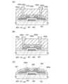
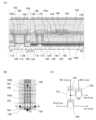
図1(A)(B)に示すトランジスタ440a、トランジスタ440bは、ボトムゲート
構造を有する逆スタガ型のトランジスタの例である。A
図1(A)(B)に示すように、トランジスタ440a、トランジスタ440bは、絶縁
表面を有する基板400上に順に設けられた、ゲート電極層401、ゲート絶縁膜402
、エネルギーギャップの異なる第1の酸化物半導体層101及び第2の酸化物半導体層1
02を含む酸化物半導体積層403、ソース電極層405a、ドレイン電極層405bを
有する。トランジスタ440a、トランジスタ440b上には、絶縁膜407が形成され
ている。As shown in FIGS. 1A and 1B, the
A first
The
なお、図1において、第1の酸化物半導体層101と第2の酸化物半導体層102の界面
を点線で図示しているが、これは酸化物半導体積層403を模式的に示したものである。
材料や成膜条件や加熱処理によっては、第1の酸化物半導体層101と第2の酸化物半導
体層102との界面が不明確になる場合もある。不明確になる場合、異なる複数の酸化物
半導体層の混合領域又は混合層とよぶことのできる箇所が形成されることもある。これは
本明細書の他の図面においても同様である。Note that in FIG. 1 , the interface between the first
Depending on the material, the film formation conditions, and the heat treatment, the interface between the first
例えば、第1の酸化物半導体層101及び第2の酸化物半導体層102の間に混合領域1
05を有するトランジスタ449を図3(C)に示す。For example, a
A
トランジスタ449の酸化物半導体積層403において、第1の酸化物半導体層101及
び第2の酸化物半導体層102の界面は不明確であり、第1の酸化物半導体層101及び
第2の酸化物半導体層102の間に混合領域105を有する。なお、界面が不明確とは、
例えば高分解能透過電子顕微鏡を用いた酸化物半導体積層403の断面観察(TEM像)
において、積層する酸化物半導体層の間に明確で連続的な線状の界面が確認できない場合
を指す。In the
For example, a cross-sectional observation (TEM image) of the
This refers to a case where a clear, continuous, linear interface cannot be observed between stacked oxide semiconductor layers.
混合領域105は、積層する第1の酸化物半導体層101及び第2の酸化物半導体層10
2に含まれる元素が混合する領域であり、第1の酸化物半導体層101及び第2の酸化物
半導体層102とは少なくとも構成する元素の組成が異なる。例えば、酸化物半導体積層
403をインジウム、スズ、及び亜鉛を含む第1の酸化物半導体層及びインジウム、ガリ
ウム、及び亜鉛を含む第2の酸化物半導体層の積層構造とする場合、第1の酸化物半導体
層と第2の酸化物半導体層との間に、インジウム、スズ、ガリウム、及び亜鉛を含む混合
領域105を形成することができる。また、第1の酸化物半導体層101と第2の酸化物
半導体層102と含まれる元素は同じでも、その組成(組成比)が異なる混合領域105
を形成することができる。よって、混合領域105の有するエネルギーギャップも、第1
の酸化物半導体層101及び第2の酸化物半導体層102のエネルギーギャップとは異な
り、混合領域105のエネルギーギャップは、第1の酸化物半導体層101のエネルギー
ギャップ及び第2の酸化物半導体層102のエネルギーギャップの間の値となる。The
2 are mixed, and the first
Therefore, the energy gap of the
Unlike the energy gaps of the first
従って、混合領域105を設けることで、酸化物半導体積層403はエネルギーバンド図
において連続接合となり、積層する第1の酸化物半導体層101及び第2の酸化物半導体
層102の界面における散乱を抑制することができる。界面散乱を抑制することができる
ため、混合領域105が設けられた酸化物半導体積層403を用いたトランジスタ449
は、電界効果移動度を向上させることができる。Therefore, by providing the
can improve the field effect mobility.
混合領域105を設けることでエネルギーバンド図において、第1の酸化物半導体層10
1と第2の酸化物半導体層102との間に勾配を形成できる。該勾配は、複数段の階段状
であってもよい。By providing the
In this case, a gradient can be formed between the first and second oxide semiconductor layers 101 and 102. The gradient may be a multi-step staircase pattern.
なお、第1の酸化物半導体層101、混合領域105、及び第2の酸化物半導体層102
の界面を点線で図示しているが、これは酸化物半導体積層403において界面が不明確(
不明瞭)であることを模式的に示したものである。Note that the first
The interface is illustrated by a dotted line, but this is because the interface is unclear in the oxide semiconductor stack 403 (
This is a schematic diagram showing that the
混合領域105は、複数の酸化物半導体層を含む酸化物半導体積層403に加熱処理を行
うことによって形成することができる。加熱処理は、積層する酸化物半導体層中の元素が
熱により拡散できる温度とし、かつ積層する酸化物半導体層が酸化物半導体積層全領域に
おいて、組成(組成比)が均一な混合領域とならない条件で行う。The
酸化物半導体積層403において、第1の酸化物半導体層101及び第2の酸化物半導体
層102は、それぞれの有するエネルギーギャップが異なればよく、その積層順は限定さ
れない。In the
具体的には、酸化物半導体積層403において、一方の酸化物半導体層のエネルギーギャ
ップを3eV以上とし、他方の酸化物半導体層のエネルギーギャップを3eV未満とする
。Specifically, in the
図1(A)に示すトランジスタ440aは、第1の酸化物半導体層101より第2の酸化
物半導体層102の方が、該エネルギーギャップが大きい例である。本実施の形態では、
トランジスタ440aにおける第1の酸化物半導体層101としてIn-Sn-Zn系酸
化物膜(エネルギーギャップ2.6eV~2.9eV、代表的には2.8eV)、第2の
酸化物半導体層102としてはIn-Ga-Zn系酸化物膜(エネルギーギャップ3.0
eV~3.4eV、代表的には3.2eV)を用いる。A
In the
A neutron emission tomography (EUV to 3.4 eV, typically 3.2 eV) is used.
一方、図1(B)に示すトランジスタ440bは、第1の酸化物半導体層101より第2
の酸化物半導体層102の方が、該エネルギーギャップが小さい例である。本実施の形態
では、トランジスタ440bにおける第1の酸化物半導体層101としてIn-Ga-Z
n系酸化物膜(エネルギーギャップ3.2eV)、第2の酸化物半導体層102としては
In-Sn-Zn系酸化物膜(エネルギーギャップ2.8eV)を用いる。On the other hand, the
In this embodiment, the first
An n-based oxide film (energy gap 3.2 eV) is used as the second
このように、酸化物半導体積層403において、第1の酸化物半導体層101及び第2の
酸化物半導体層102は、ゲート絶縁膜402と接する方をエネルギーギャップが大きい
層としてもよいし、エネルギーギャップが小さい層としてもよい。In this manner, in the
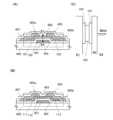
図4(A)に酸化物半導体積層403として第1の酸化物半導体層101、第2の酸化物
半導体層102、及び第3の酸化物半導体層103の3層構造の積層を用いたトランジス
タ480を示す。FIG. 4A illustrates a
トランジスタ480は、絶縁表面を有する基板400上に順に設けられた、ゲート電極層
401、ゲート絶縁膜402、第1の酸化物半導体層101、第2の酸化物半導体層10
2、及び第3の酸化物半導体層103を含む酸化物半導体積層403、ソース電極層40
5a、ドレイン電極層405bを有する。トランジスタ480上には、絶縁膜407が形
成されている。The
2, and the third
An insulating
トランジスタ480の酸化物半導体積層403において、第1の酸化物半導体層101、
第2の酸化物半導体層102、及び第3の酸化物半導体層103のエネルギーギャップは
全て同じではなく、少なくとも2種類の異なる値のエネルギーギャップを含む。In the
The second
酸化物半導体積層403を3層以上の積層構造とする場合、すべての酸化物半導体層同士
が異なるエネルギーギャップを有する構造であってもよいし、ほぼ同じエネルギーギャッ
プを有する酸化物半導体層を複数酸化物半導体積層403中に用いてもよい。When the
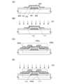
また、半導体装置の他の一形態として図9(A)にトランジスタ410を示す。トランジ
スタ410は、チャネル保護型(チャネルストップ型ともいう)と呼ばれるボトムゲート
構造の一つであり逆スタガ型トランジスタともいう。9A illustrates a
図9(A)に示すように、トランジスタ410は、絶縁表面を有する基板400上に順に
設けられた、ゲート電極層401、ゲート絶縁膜402、エネルギーギャップの異なる第
1の酸化物半導体層101及び第2の酸化物半導体層102を含む酸化物半導体積層40
3、絶縁膜427、ソース電極層405a、ドレイン電極層405bを有する。トランジ
スタ410上には、絶縁膜409が形成されている。As illustrated in FIG. 9A , the
The
絶縁膜427は、ゲート電極層401と重畳する酸化物半導体積層403上に設けられて
おり、チャネル保護膜として機能する。The insulating
絶縁膜427は絶縁膜407と同様な材料及び方法で形成すればよく、代表的には酸化シ
リコン膜、酸化窒化シリコン膜、酸化アルミニウム膜、酸化窒化アルミニウム膜、酸化ハ
フニウム膜、又は酸化ガリウム膜、窒化シリコン膜、窒化アルミニウム膜、窒化酸化シリ
コン膜、窒化酸化アルミニウム膜、酸化アルミニウム膜などの無機絶縁膜の単層又は積層
を用いることができる。The insulating
酸化物半導体積層403と接する絶縁膜427(絶縁膜427が積層構造であった場合、
酸化物半導体積層403と接する膜)を、酸素を多く含む状態とすると、酸化物半導体積
層403へ酸素を供給する供給源として好適に機能させることができる。The insulating
When the
なお、絶縁膜409は絶縁膜407と同様な材料及び方法を用いて形成することができる
。Note that the insulating
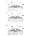
また、半導体装置の他の一形態として図10(A)にボトムゲート構造のトランジスタ4
30を示す。As another embodiment of the semiconductor device, a
図10(A)に示すように、トランジスタ430は、絶縁表面を有する基板400上に順
に設けられたゲート電極層401、ゲート絶縁膜402、ソース電極層405a、ドレイ
ン電極層405b、エネルギーギャップの異なる第1の酸化物半導体層101及び第2の
酸化物半導体層102を含む酸化物半導体積層403を有する。トランジスタ430上に
は、絶縁膜407が形成されている。10A , the
トランジスタ430は、ソース電極層405a及びドレイン電極層405b上にエネルギ
ーギャップの異なる第1の酸化物半導体層101及び第2の酸化物半導体層102を含む
酸化物半導体積層403が設けられる構造である。The
酸化物半導体積層403(第1の酸化物半導体層101、第2の酸化物半導体層102、
第3の酸化物半導体層103)に用いる酸化物半導体としては、少なくともインジウム(
In)あるいは亜鉛(Zn)を含むことが好ましい。特にInとZnを含むことが好まし
い。また、該酸化物を用いたトランジスタの電気特性のばらつきを減らすためのスタビラ
イザーとして、それらに加えてガリウム(Ga)を有することが好ましい。また、スタビ
ライザーとしてスズ(Sn)を有することが好ましい。また、スタビライザーとしてハフ
ニウム(Hf)を有することが好ましい。また、スタビライザーとしてアルミニウム(A
l)を有することが好ましい。また、スタビライザーとしてジルコニウム(Zr)を有す
ることが好ましい。An oxide semiconductor stack 403 (a first
The oxide semiconductor used for the third oxide semiconductor layer 103) is at least indium (
It is preferable that the oxide contains In (In) or zinc (Zn). It is particularly preferable that the oxide contains In and Zn. It is also preferable that the oxide contains gallium (Ga) in addition to the above as a stabilizer for reducing the variation in electrical characteristics of a transistor using the oxide. It is also preferable that the oxide contains tin (Sn) as a stabilizer. It is also preferable that the oxide contains hafnium (Hf) as a stabilizer. It is also preferable that the oxide contains aluminum (A) as a stabilizer.
It is preferable that the alloy contains zirconium (Zr) as a stabilizer.
また、他のスタビライザーとして、ランタノイドである、ランタン(La)、セリウム(
Ce)、プラセオジム(Pr)、ネオジム(Nd)、サマリウム(Sm)、ユウロピウム
(Eu)、ガドリニウム(Gd)、テルビウム(Tb)、ジスプロシウム(Dy)、ホル
ミウム(Ho)、エルビウム(Er)、ツリウム(Tm)、イッテルビウム(Yb)、ル
テチウム(Lu)のいずれか一種あるいは複数種を有してもよい。Other stabilizers include lanthanides such as lanthanum (La) and cerium (
The element may have one or more of the following: arsenic (Ce), praseodymium (Pr), neodymium (Nd), samarium (Sm), europium (Eu), gadolinium (Gd), terbium (Tb), dysprosium (Dy), holmium (Ho), erbium (Er), thulium (Tm), ytterbium (Yb), and lutetium (Lu).
例えば、酸化物半導体として、酸化インジウム、酸化スズ、酸化亜鉛、二元系金属の酸化
物であるIn-Zn系酸化物、Sn-Zn系酸化物、Al-Zn系酸化物、Zn-Mg系
酸化物、Sn-Mg系酸化物、In-Mg系酸化物、In-Ga系酸化物、三元系金属の
酸化物であるIn-Ga-Zn系酸化物、In-Al-Zn系酸化物、In-Sn-Zn
系酸化物、Sn-Ga-Zn系酸化物、Al-Ga-Zn系酸化物、Sn-Al-Zn系
酸化物、In-Hf-Zn系酸化物、In-La-Zn系酸化物、In-Ce-Zn系酸
化物、In-Pr-Zn系酸化物、In-Nd-Zn系酸化物、In-Sm-Zn系酸化
物、In-Eu-Zn系酸化物、In-Gd-Zn系酸化物、In-Tb-Zn系酸化物
、In-Dy-Zn系酸化物、In-Ho-Zn系酸化物、In-Er-Zn系酸化物、
In-Tm-Zn系酸化物、In-Yb-Zn系酸化物、In-Lu-Zn系酸化物、四
元系金属の酸化物であるIn-Sn-Ga-Zn系酸化物、In-Hf-Ga-Zn系酸
化物、In-Al-Ga-Zn系酸化物、In-Sn-Al-Zn系酸化物、In-Sn
-Hf-Zn系酸化物、In-Hf-Al-Zn系酸化物を用いることができる。Examples of oxide semiconductors include indium oxide, tin oxide, zinc oxide, oxides of binary metals such as In-Zn oxides, Sn-Zn oxides, Al-Zn oxides, Zn-Mg oxides, Sn-Mg oxides, In-Mg oxides, In-Ga oxides, oxides of ternary metals such as In-Ga-Zn oxides, In-Al-Zn oxides, In-Sn-Zn oxides,
based oxides, Sn-Ga-Zn based oxides, Al-Ga-Zn based oxides, Sn-Al-Zn based oxides, In-Hf-Zn based oxides, In-La-Zn based oxides, In-Ce-Zn based oxides, In-Pr-Zn based oxides, In-Nd-Zn based oxides, In-Sm-Zn based oxides, In-Eu-Zn based oxides, In-Gd-Zn based oxides, In-Tb-Zn based oxides, In-Dy-Zn based oxides, In-Ho-Zn based oxides, In-Er-Zn based oxides,
In-Tm-Zn oxides, In-Yb-Zn oxides, In-Lu-Zn oxides, oxides of quaternary metals such as In-Sn-Ga-Zn oxides, In-Hf-Ga-Zn oxides, In-Al-Ga-Zn oxides, In-Sn-Al-Zn oxides, In-Sn
For example, Hf-Zn-based oxides and In-Hf-Al-Zn-based oxides can be used.
なお、ここで、例えば、In-Ga-Zn系酸化物とは、InとGaとZnを主成分とし
て有する酸化物という意味であり、InとGaとZnの比率は問わない。また、InとG
aとZn以外の金属元素が入っていてもよい。In addition, for example, an In-Ga-Zn oxide means an oxide having In, Ga, and Zn as main components, and the ratio of In, Ga, and Zn does not matter.
Metal elements other than a and Zn may be present.
また、酸化物半導体として、InMO3(ZnO)m(m>0、且つ、mは整数でない)
で表記される材料を用いてもよい。なお、Mは、Ga、Fe、Mn及びCoから選ばれた
一の金属元素または複数の金属元素を示す。また、酸化物半導体として、In2SnO5
(ZnO)n(n>0、且つ、nは整数)で表記される材料を用いてもよい。In addition, the oxide semiconductor may be InMO3 (ZnO)m (m>0, and m is not an integer).
In addition, M represents one or more metal elements selected from Ga, Fe, Mn, and Co. In addition, asthe oxidesemiconductor , a material represented by the formula:
A material expressed as (ZnO)n (n>0, and n is an integer) may be used.
例えば、In:Ga:Zn=1:1:1(=1/3:1/3:1/3)あるいはIn:G
a:Zn=2:2:1(=2/5:2/5:1/5)の原子比のIn-Ga-Zn系酸化
物やその組成の近傍の酸化物を用いることができる。あるいは、In:Sn:Zn=1:
1:1(=1/3:1/3:1/3)、In:Sn:Zn=2:1:3(=1/3:1/
6:1/2)あるいはIn:Sn:Zn=2:1:5(=1/4:1/8:5/8)の原
子比のIn-Sn-Zn系酸化物やその組成の近傍の酸化物を用いるとよい。For example, In:Ga:Zn=1:1:1 (=1/3:1/3:1/3) or In:
An In-Ga-Zn oxide having an atomic ratio of a:Zn=2:2:1 (=2/5:2/5:1/5) or an oxide having a composition close to that can be used.
1:1 (=1/3:1/3:1/3), In:Sn:Zn=2:1:3 (=1/3:1/
For example, an In--Sn--Zn oxide having an atomic ratio of In:Sn:Zn=2:1:5 (=1/4:1/8:5/8) or an oxide having a composition close to this may be used.
しかし、これらに限られず、必要とする半導体特性(移動度、しきい値、ばらつき等)に
応じて適切な組成のものを用いればよい。また、必要とする半導体特性を得るために、キ
ャリア濃度や不純物濃度、欠陥密度、金属元素と酸素の原子数比、原子間結合距離、密度
等を適切なものとすることが好ましい。However, the present invention is not limited to these, and an appropriate composition may be used depending on the required semiconductor characteristics (mobility, threshold value, variation, etc.) In order to obtain the required semiconductor characteristics, it is preferable to appropriately select the carrier concentration, impurity concentration, defect density, atomic ratio of metal element to oxygen, interatomic bond distance, density, etc.
例えば、In-Sn-Zn系酸化物では比較的容易に高い移動度が得られる。しかしなが
ら、In-Ga-Zn系酸化物でも、バルク内欠陥密度を低くすることにより移動度を上
げることができる。For example, high mobility can be obtained relatively easily in In--Sn--Zn oxides, but mobility can also be increased in In--Ga--Zn oxides by lowering the bulk defect density.
なお、例えば、In、Ga、Znの原子数比がIn:Ga:Zn=a:b:c(a+b+
c=1)である酸化物の組成が、原子数比がIn:Ga:Zn=A:B:C(A+B+C
=1)の酸化物の組成のrだけ近傍であるとは、a、b、cが、(a-A)2+(b-B
)2+(c-C)2≦r2を満たすことをいう。rとしては、例えば、0.05とすれば
よい。他の酸化物でも同様である。For example, the atomic ratio of In, Ga, and Zn is In:Ga:Zn=a:b:c (a+b+
The composition of the oxide in which the atomic ratio is In:Ga:Zn=A:B:C (A+B+C
= 1), a, b, and c are (a-A)2 + (b-B
)2 + (c−C)2 ≦r2 is satisfied. For example, r may be set to 0.05. The same applies to other oxides.
酸化物半導体は単結晶でも、非単結晶でもよい。後者の場合、アモルファスでも、多結晶
でもよい。また、アモルファス中に結晶性を有する部分を含む構造でも、非アモルファス
でもよい。The oxide semiconductor may be single crystal or non-single crystal. In the latter case, it may be amorphous or polycrystalline. In addition, it may have a structure including a crystalline portion in an amorphous state or may be non-amorphous.
アモルファス状態の酸化物半導体は、比較的容易に平坦な表面を得ることができるため、
これを用いてトランジスタを作製した際の界面散乱を低減でき、比較的容易に、比較的高
い移動度を得ることができる。Since it is relatively easy to obtain a flat surface for an amorphous oxide semiconductor,
When a transistor is fabricated using this, the interface scattering can be reduced, and a relatively high mobility can be obtained relatively easily.
また、結晶性を有する酸化物半導体では、よりバルク内欠陥を低減することができ、表面
の平坦性を高めればアモルファス状態の酸化物半導体以上の移動度を得ることができる。
表面の平坦性を高めるためには、平坦な表面上に酸化物半導体を形成することが好ましく
、具体的には、平均面粗さ(Ra)が1nm以下、好ましくは0.3nm以下、より好ま
しくは0.1nm以下の表面上に形成するとよい。In addition, in a crystalline oxide semiconductor, defects in the bulk can be further reduced, and if the flatness of the surface is improved, a mobility equal to or higher than that of an amorphous oxide semiconductor can be obtained.
In order to improve the flatness of the surface, it is preferable to form the oxide semiconductor on a flat surface. Specifically, it is preferable to form the oxide semiconductor on a surface having an average surface roughness (Ra) of 1 nm or less, preferably 0.3 nm or less, and more preferably 0.1 nm or less.
なお、Raは、JIS B0601:2001(ISO4287:1997)で定義され
ている算術平均粗さを曲面に対して適用できるよう三次元に拡張したものであり、「基準
面から指定面までの偏差の絶対値を平均した値」で表現でき、以下の式にて定義される。Note that Ra is a three-dimensional extension of the arithmetic mean roughness defined in JIS B0601:2001 (ISO 4287:1997) so that it can be applied to curved surfaces, and can be expressed as "the average of the absolute values of the deviations from a reference surface to a specified surface" and is defined by the following formula.
ここで、指定面とは、粗さ計測の対象となる面であり、座標((x1,y1,f(x1,
y1)),(x1,y2,f(x1,y2)),(x2,y1,f(x2,y1)),(
x2,y2,f(x2,y2))の4点で表される四角形の領域とし、指定面をxy平面
に投影した長方形の面積をS0、指定面の平均高さをZ0とする。Raは原子間力顕微鏡
(AFM:Atomic Force Microscope)にて測定可能である。Here, the designated surface is a surface to be subjected to roughness measurement, and is represented by coordinates ((x1 ,y1 , f(x1 ,
y1 )), (x1 ,y2 , f(x1 ,y2 )), (x2 ,y1 , f(x2 ,y1 )), (
The specified surface is a quadrangular region represented by four points, x2 , y2 , f(x2 , y2 ), the area of a rectangle obtained by projecting the specified surface onto the xy plane is S0 , and the average height of the specified surface is Z0. Ra can be measured with an atomic force microscope (AFM).
酸化物半導体積層403(第1の酸化物半導体層101、第2の酸化物半導体層102、
第3の酸化物半導体層103)として、結晶を含み、結晶性を有する酸化物半導体層(結
晶性酸化物半導体層)を用いることができる。結晶性酸化物半導体層における結晶状態は
、結晶軸の方向が無秩序な状態でも、一定の配向性を有する状態であってもよい。An oxide semiconductor stack 403 (a first
An oxide semiconductor layer that contains crystals and has crystallinity (a crystalline oxide semiconductor layer) can be used as the third
例えば、結晶性酸化物半導体層として、表面に概略垂直なc軸を有している結晶を含む酸
化物半導体層を用いることができる。For example, as the crystalline oxide semiconductor layer, an oxide semiconductor layer including crystals having a c-axis approximately perpendicular to the surface can be used.
表面に概略垂直なc軸を有している結晶を含む酸化物半導体層は、単結晶構造ではなく、
非晶質構造でもない構造であり、c軸配向を有した結晶性酸化物半導体(C Axis
Aligned Crystalline Oxide Semiconductor;
CAAC-OSともいう)膜である。The oxide semiconductor layer including crystals having a c-axis approximately perpendicular to the surface does not have a single crystal structure,
The structure is not amorphous, and is a crystalline oxide semiconductor having a c-axis orientation (C Axis
Aligned Crystalline Oxide Semiconductor;
It is a film (also called CAAC-OS).
CAAC-OS膜は、完全な単結晶ではなく、完全な非晶質でもない。CAAC-OS膜
は、非晶質相に結晶部および非晶質部を有する結晶-非晶質混相構造の酸化物半導体膜で
ある。なお、当該結晶部は、一辺が100nm未満の立方体内に収まる大きさであること
が多い。また、透過型電子顕微鏡(TEM:Transmission Electro
n Microscope)による観察像では、CAAC-OS膜に含まれる非晶質部と
結晶部との境界は明確ではない。また、TEMによってCAAC-OS膜には粒界(グレ
インバウンダリーともいう。)は確認できない。そのため、CAAC-OS膜は、粒界に
起因する電子移動度の低下が抑制される。The CAAC-OS film is neither completely single crystalline nor completely amorphous. The CAAC-OS film is an oxide semiconductor film with a crystalline-amorphous mixed phase structure in which a crystalline part and an amorphous part are included in an amorphous phase. Note that the crystalline part is often within a cube with one side less than 100 nm.
In an image observed with a TEM (N Microscope), the boundary between the amorphous and crystalline parts in the CAAC-OS film is not clear. Furthermore, no grain boundaries can be confirmed in the CAAC-OS film by TEM. Therefore, in the CAAC-OS film, a decrease in electron mobility due to grain boundaries is suppressed.
CAAC-OS膜に含まれる結晶部は、c軸がCAAC-OS膜の被形成面の法線ベクト
ルまたは表面の法線ベクトルに平行な方向に揃い、かつab面に垂直な方向から見て三角
形状または六角形状の原子配列を有し、c軸に垂直な方向から見て金属原子が層状または
金属原子と酸素原子とが層状に配列している。なお、異なる結晶部間で、それぞれa軸お
よびb軸の向きが異なっていてもよい。本明細書において、単に垂直と記載する場合、8
5°以上95°以下の範囲も含まれることとする。また、単に平行と記載する場合、-5
°以上5°以下の範囲も含まれることとする。The crystal parts included in the CAAC-OS film have c-axes aligned in a direction parallel to the normal vector of the surface on which the CAAC-OS film is formed or the normal vector of the surface, and have a triangular or hexagonal atomic arrangement when viewed from a direction perpendicular to the a-b plane, with metal atoms arranged in layers or metal atoms and oxygen atoms arranged in layers when viewed from a direction perpendicular to the c-axis. Note that the directions of the a-axis and b-axis may differ between different crystal parts. In the present specification, when it is simply described as "perpendicular," 8
The range of 5° to 95° is also included.
The range of from 0 to 5° is also included.
なお、CAAC-OS膜において、結晶部の分布が一様でなくてもよい。例えば、CAA
C-OS膜の形成過程において、酸化物半導体膜の表面側から結晶成長させる場合、被形
成面の近傍に対し表面の近傍では結晶部の占める割合が高くなることがある。また、CA
AC-OS膜へ不純物を添加することにより、当該不純物添加領域において結晶部が非晶
質化することもある。Note that the distribution of crystal parts in the CAAC-OS film does not have to be uniform.
In the process of forming a C-OS film, when crystals are grown from the surface side of the oxide semiconductor film, the proportion of crystal parts in the vicinity of the surface may be higher than that in the vicinity of the formation surface.
Adding an impurity to the AC-OS film may cause a crystalline portion in a region where the impurity has been added to become amorphous.
CAAC-OS膜に含まれる結晶部のc軸は、CAAC-OS膜の被形成面の法線ベクト
ルまたは表面の法線ベクトルに平行な方向に揃うため、CAAC-OS膜の形状(被形成
面の断面形状または表面の断面形状)によっては互いに異なる方向を向くことがある。な
お、結晶部のc軸の方向は、CAAC-OS膜が形成されたときの被形成面の法線ベクト
ルまたは表面の法線ベクトルに平行な方向となる。結晶部は、成膜することにより、また
は成膜後に加熱処理などの結晶化処理を行うことにより形成される。The c-axes of the crystal parts included in the CAAC-OS film are aligned in a direction parallel to the normal vector of the surface on which the CAAC-OS film is formed or the normal vector of the surface, and may be oriented in a different direction depending on the shape of the CAAC-OS film (the cross-sectional shape of the surface on which the CAAC-OS film is formed or the cross-sectional shape of the surface). Note that the c-axes of the crystal parts are oriented in a direction parallel to the normal vector of the surface on which the CAAC-OS film is formed or the normal vector of the surface when the CAAC-OS film is formed. The crystal parts are formed by film formation or by carrying out a crystallization treatment such as a heat treatment after film formation.
CAAC-OS膜を用いたトランジスタは、可視光や紫外光の照射による電気特性の変動
を低減することが可能である。よって、当該トランジスタは、信頼性が高い。A transistor including a CAAC-OS film can reduce change in electrical characteristics due to irradiation with visible light or ultraviolet light, and thus the transistor has high reliability.
c軸配向を有した結晶性酸化物半導体層を得る方法としては、3つ挙げられる。1つ目は
、成膜温度を200℃以上500℃以下として酸化物半導体層の成膜を行い、表面に概略
垂直にc軸配向させる方法である。2つ目は、膜厚を薄く成膜した後、200℃以上70
0℃以下の加熱処理を行い、表面に概略垂直にc軸配向させる方法である。3つ目は、一
層目の膜厚を薄く成膜した後、200℃以上700℃以下の加熱処理を行い、2層目の成
膜を行い、表面に概略垂直にc軸配向させる方法である。There are three methods for obtaining a crystalline oxide semiconductor layer having c-axis orientation. The first method is to form an oxide semiconductor layer at a film formation temperature of 200° C. to 500° C., and to orient the c-axis approximately perpendicularly to the surface. The second method is to form a thin oxide semiconductor layer and then heat the oxide semiconductor layer at a temperature of 200° C. to 70° C.
The third method is to form a thin first layer, then perform a heat treatment at 200° C. to 700° C., and then form a second layer, with the c-axis oriented approximately perpendicular to the surface.
第1の酸化物半導体層101、第2の酸化物半導体層102、第3の酸化物半導体層10
3の膜厚は、1nm以上10nm以下(好ましくは5nm以上30nm以下)とし、スパ
ッタリング法、MBE(Molecular Beam Epitaxy)法、CVD法
、パルスレーザ堆積法、ALD(Atomic Layer Deposition)法
等を適宜用いることができる。また、第1の酸化物半導体層101、第2の酸化物半導体
層102、第3の酸化物半導体層103は、スパッタリングターゲット表面に対し、概略
垂直に複数の基板表面がセットされた状態で成膜を行うスパッタ装置を用いて成膜しても
よい。First
The thickness of the
酸化物半導体層を用いたトランジスタにおいて、該酸化物半導体層のエネルギーギャップ
は、トランジスタの電気特性に影響を与える。例えば、酸化物半導体層を用いたトランジ
スタにおいて、酸化物半導体層のエネルギーギャップが小さいと、オン特性(例えば、オ
ン電流や電界効果移動度)が向上し、一方、酸化物半導体層のエネルギーギャップが大き
いと、オフ電流が低減できる。In a transistor including an oxide semiconductor layer, the energy gap of the oxide semiconductor layer affects the electrical characteristics of the transistor. For example, in a transistor including an oxide semiconductor layer, when the energy gap of the oxide semiconductor layer is small, the on-characteristics (for example, on-current and field-effect mobility) are improved, whereas when the energy gap of the oxide semiconductor layer is large, the off-current can be reduced.
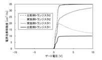
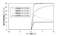
異なるエネルギーギャップを有する複数の酸化物半導体層を用いた酸化物半導体積層40
3を用いることによって、トランジスタ440a、トランジスタ440b、トランジスタ
480の電気特性をより精度よく制御することができ、所望の電気特性をトランジスタ4
40a、トランジスタ440b、トランジスタ480に付与することが可能となる。Oxide semiconductor stack 40 using a plurality of oxide semiconductor layers having different energy gaps
By using the
It is possible to provide the transistor 40a, the
例えば、図4(A)に示すトランジスタ480の酸化物半導体積層403において、第2
の酸化物半導体層102のエネルギーギャップを第1の酸化物半導体層101及び第3の
酸化物半導体層103のエネルギーギャップより小さくする。この場合、第1の酸化物半
導体層101及び第3の酸化物半導体層103のエネルギーギャップはほぼ同じとするこ
とができる。For example, in the
The energy gap of the second
図4(C)に、図4(A)における膜厚方向(E1-E2間)のエネルギーバンド図を示
す。トランジスタ480では、図4(C)に示すエネルギーバンド図となるように、第1
の酸化物半導体層101、第2の酸化物半導体層102、及び第3の酸化物半導体層10
3の材料を選択することが好ましい。ただし、伝導帯に埋め込みチャネルが形成されれば
十分な効果が得られるため、必ずしも図4(C)のように伝導帯と価電子帯の両方に凹部
を有するエネルギーバンド図に限定しなくともよく、例えば伝導帯のみに凹部を有するエ
ネルギーバンド図が得られる構成としてもよい。4C shows an energy band diagram in the film thickness direction (between E1 and E2) in FIG. 4A. In the
The first
It is preferable to select the material of the third embodiment. However, since a sufficient effect can be obtained if a buried channel is formed in the conduction band, the energy band diagram is not necessarily limited to one having a concave portion in both the conduction band and the valence band as shown in Fig. 4C. For example, a configuration in which an energy band diagram having a concave portion only in the conduction band can be obtained is also acceptable.
例えば、トランジスタ480における第1の酸化物半導体層101としてIn-Ga-Z
n系酸化物膜(エネルギーギャップ3.2eV)、第2の酸化物半導体層102としては
In-Sn-Zn系酸化物膜(エネルギーギャップ2.8eV)、第3の酸化物半導体層
103としてIn-Ga-Zn系酸化物膜(エネルギーギャップ3.2eV)を用いる。For example, the first
An n-based oxide film (energy gap 3.2 eV) is used as the second
また、トランジスタ480におけるような3層積層の酸化物半導体積層403としては、
第1の酸化物半導体層101としてIn-Ga-Zn系酸化物膜、第2の酸化物半導体層
102としてはIn-Zn系酸化物膜、第3の酸化物半導体層103としてIn-Ga-
Zn系酸化物膜の積層、第1の酸化物半導体層101としてGa-Zn系酸化物膜、第2
の酸化物半導体層102としてはIn-Sn-Zn系酸化物膜、第3の酸化物半導体層1
03としてGa-Zn系酸化物膜の積層、第1の酸化物半導体層101としてGa-Zn
系酸化物膜、第2の酸化物半導体層102としてはIn-Zn系酸化物膜、第3の酸化物
半導体層103としてGa-Zn系酸化物膜の積層、第1の酸化物半導体層101として
In-Ga系酸化物膜、第2の酸化物半導体層102としてはIn-Ga-Zn系酸化物
膜、第3の酸化物半導体層103としてIn-Ga系酸化物膜の積層、又は第1の酸化物
半導体層101としてIn-Ga-Zn系酸化物膜、第2の酸化物半導体層102として
は酸化インジウム(In系酸化物)膜、第3の酸化物半導体層103としてIn-Ga-
Zn系酸化物膜の積層などを用いることができる。The three-layer
The first
A stack of Zn-based oxide films, a Ga-Zn-based oxide film as the first
The
03 is a stack of Ga—Zn-based oxide films, and the first
a stack of an In—Ga-based oxide film as the first
A stack of Zn-based oxide films can be used.
エネルギーギャップの小さい第2の酸化物半導体層102を、エネルギーギャップの大き
い第1の酸化物半導体層101及び第3の酸化物半導体層103により挟む構造とするこ
とによって、よりトランジスタ480のオフ電流(リーク電流)を低減する効果が得られ
る。The structure in which the second
図2(A)乃至(E)にトランジスタ440aを用いて、作製方法の一例を示す。Figures 2(A) to (E) show an example of a manufacturing
まず、絶縁表面を有する基板400上に導電膜を形成した後、第1のフォトリソグラフィ
工程によりゲート電極層401を形成する。なお、レジストマスクをインクジェット法で
形成してもよい。レジストマスクをインクジェット法で形成するとフォトマスクを使用し
ないため、製造コストを低減できる。First, a conductive film is formed over a
絶縁表面を有する基板400に使用することができる基板に大きな制限はないが、少なく
とも、後の熱処理に耐えうる程度の耐熱性を有していることが必要となる。例えば、バリ
ウムホウケイ酸ガラスやアルミノホウケイ酸ガラスなどのガラス基板、セラミック基板、
石英基板、サファイア基板などを用いることができる。また、シリコンや炭化シリコンな
どの単結晶半導体基板、多結晶半導体基板、シリコンゲルマニウムなどの化合物半導体基
板、SOI基板などを適用することもでき、これらの基板上に半導体素子が設けられたも
のを、基板400として用いてもよい。There is no particular limitation on the substrate that can be used for the
A quartz substrate, a sapphire substrate, or the like can be used. In addition, a single crystal semiconductor substrate such as silicon or silicon carbide, a polycrystalline semiconductor substrate, a compound semiconductor substrate such as silicon germanium, an SOI substrate, or the like can also be applied, and any of these substrates on which semiconductor elements are provided may be used as the
また、基板400として、可撓性基板を用いて半導体装置を作製してもよい。可撓性を有
する半導体装置を作製するには、可撓性基板上に酸化物半導体積層403を含むトランジ
スタ440aを直接作製してもよいし、他の作製基板に酸化物半導体積層403を含むト
ランジスタ440aを作製し、その後可撓性基板に剥離、転置してもよい。なお、作製基
板から可撓性基板に剥離、転置するために、作製基板と酸化物半導体膜を含むトランジス
タ440aとの間に剥離層を設けるとよい。Alternatively, a semiconductor device may be manufactured using a flexible substrate as the
下地膜となる絶縁膜を基板400とゲート電極層401との間に設けてもよい。下地膜は
、基板400からの不純物元素の拡散を防止する機能があり、窒化シリコン膜、酸化シリ
コン膜、窒化酸化シリコン膜、又は酸化窒化シリコン膜から選ばれた一又は複数の膜によ
る積層構造により形成することができる。また、下地膜として、酸化アルミニウム、酸化
窒化アルミニウム、酸化ハフニウム、酸化ガリウム、又はこれらの混合材料を用いて形成
することができる。下地膜はプラズマCVD法又はスパッタリング法等により形成すれば
よい。An insulating film serving as a base film may be provided between the
また、ゲート電極層401の材料は、プラズマCVD法又はスパッタリング法等により、
モリブデン、チタン、タンタル、タングステン、アルミニウム、銅、ネオジム、スカンジ
ウム等の金属材料又はこれらを主成分とする合金材料を用いて、単層で又は積層して形成
することができる。また、ゲート電極層401としてリン等の不純物元素をドーピングし
た多結晶シリコン膜に代表される半導体膜、ニッケルシリサイドなどのシリサイド膜を用
いてもよい。ゲート電極層401は、単層構造としてもよいし、積層構造としてもよい。The material of the
The
また、ゲート電極層401の材料は、インジウム錫酸化物、酸化タングステンを含むイン
ジウム酸化物、酸化タングステンを含むインジウム亜鉛酸化物、酸化チタンを含むインジ
ウム酸化物、酸化チタンを含むインジウム錫酸化物、インジウム亜鉛酸化物、酸化ケイ素
を添加したインジウム錫酸化物などの導電性材料を適用することもできる。また、上記導
電性材料と、上記金属材料の積層構造とすることもできる。The
また、ゲート電極層401を積層構造とし、その一層として、In-Sn系、In-Sn
-Zn系、In-Al-Zn系、Sn-Ga-Zn系、Al-Ga-Zn系、Sn-Al
-Zn系、In-Zn系、Sn-Zn系、Al-Zn系、In系、Sn系、Zn系の金属
酸化物を用いてもよい。The
-Zn system, In-Al-Zn system, Sn-Ga-Zn system, Al-Ga-Zn system, Sn-Al
Alternatively, metal oxides of Al-Zn, In-Zn, Sn-Zn, Al-Zn, In, Sn, and Zn may be used.
また、ゲート絶縁膜402と接するゲート電極層401の一層として、窒素を含む金属酸
化物、具体的には、窒素を含むIn-Ga-Zn-O膜や、窒素を含むIn-Sn-O膜
や、窒素を含むIn-Ga-O膜や、窒素を含むIn-Zn-O膜や、窒素を含むSn-
O膜や、窒素を含むIn-O膜や、金属窒化膜(InN、SnNなど)を用いることがで
きる。これらの膜は5eV(電子ボルト)、好ましくは5.5eV(電子ボルト)以上の
仕事関数を有し、ゲート電極層として用いた場合、トランジスタの電気特性のしきい値電
圧をプラスにすることができ、所謂ノーマリーオフのスイッチング素子を実現できる。As one layer of the
Examples of the film that can be used include an In—O film, an In—O film containing nitrogen, and a metal nitride film (InN, SnN, etc.). These films have a work function of 5 eV (electron volts), preferably 5.5 eV (electron volts) or more, and when used as a gate electrode layer, the threshold voltage of the electrical characteristics of the transistor can be made positive, thereby realizing a so-called normally-off switching element.
例えば、ゲート電極層401を積層構造とし、その一層として特に仕事関数の大きな材料
であるインジウム、ガリウム、及び亜鉛を含む酸窒化物膜を用いることが好ましい。イン
ジウム、ガリウム、及び亜鉛を含む酸窒化物膜は、アルゴン及び窒素の混合ガス雰囲気下
で成膜することにより得られる。For example, it is preferable that the
例えば、ゲート電極層401として基板400側から銅膜と、タングステン膜と、インジ
ウム、ガリウム、及び亜鉛を含む酸窒化物膜との積層構造、タングステン膜と、窒化タン
グステン膜と、銅膜と、チタン膜との積層構造などを用いることができる。For example, the
次いで、ゲート電極層401上にゲート絶縁膜402を形成する(図2(A)参照)。ゲ
ート絶縁膜402は、作製するトランジスタのサイズやゲート絶縁膜402の段差被覆性
を考慮して形成することが好ましい。Next, a
ゲート絶縁膜402の膜厚は、1nm以上20nm以下とし、スパッタリング法、MBE
法、CVD法、パルスレーザ堆積法、ALD法等を適宜用いることができる。また、ゲー
ト絶縁膜402は、スパッタリングターゲット表面に対し、概略垂直に複数の基板表面が
セットされた状態で成膜を行うスパッタ装置を用いて成膜してもよい。The thickness of the
A method such as a deposition method, a CVD method, a pulsed laser deposition method, an ALD method, etc. can be appropriately used. The
ゲート絶縁膜402の材料としては、酸化シリコン膜、酸化ガリウム膜、酸化アルミニウ
ム膜、窒化シリコン膜、酸化窒化シリコン膜、酸化窒化アルミニウム膜、または窒化酸化
シリコン膜を用いて形成することができる。The
また、ゲート絶縁膜402の材料として酸化ハフニウム、酸化イットリウム、ハフニウム
シリケート(HfSixOyx>0、y>0))、窒素が添加されたハフニウムシリケー
ト(HfSiOxNy(x>0、y>0))、ハフニウムアルミネート(HfAlxOy
(x>0、y>0))、酸化ランタンなどのhigh-k材料を用いることでゲートリー
ク電流を低減できる。The material of the
(x>0, y>0)) and the use of high-k materials such as lanthanum oxide can reduce gate leakage current.
ゲート絶縁膜402は単層でも積層でもよいが、酸化物半導体積層403に接する膜とし
ては、酸化物絶縁膜が好ましい。本実施の形態では、ゲート絶縁膜402として酸化シリ
コン膜を用いる。The
また、ゲート絶縁膜402を積層とする場合、例えば、ゲート電極層401上に酸化シリ
コン膜、In-Hf-Zn系酸化物膜、酸化物半導体積層403を順に積層してもよいし
、ゲート電極層401上に酸化シリコン膜、In:Zr:Zn=1:1:1の原子比のI
n-Zr-Zn系酸化物膜、酸化物半導体積層403を順に積層してもよいし、ゲート電
極層401上に酸化シリコン膜、In:Gd:Zn=1:1:1の原子比のIn-Gd-
Zn系酸化物膜、酸化物半導体積層403を順に積層してもよい。In the case where the
Alternatively, a silicon oxide film and an In-Gd-Zn-based oxide film having an atomic ratio of In:Gd:Zn=1:1:1 may be stacked on the
A Zn-based oxide film and an
次に、ゲート絶縁膜402上に第1の酸化物半導体膜191及び第2の酸化物半導体膜1
92からなる酸化物半導体膜の積層493を形成する(図2(B)参照)。Next, the first
Then, a
ゲート絶縁膜402は、酸化物半導体膜の積層493(酸化物半導体積層403)と接す
るため、膜中(バルク中)に少なくとも化学量論比を超える量の酸素が存在することが好
ましい。例えば、ゲート絶縁膜402として、酸化シリコン膜を用いる場合には、SiO
2+α(ただし、α>0)とする。このようなゲート絶縁膜402を用いることで、酸化
物半導体膜の積層493(酸化物半導体積層403)に酸素を供給することができ、特性
を良好にすることができる。酸化物半導体膜の積層493(酸化物半導体積層403)へ
酸素を供給することにより、膜中の酸素欠損を補填することができる。Since the
2+α (where α>0). By using such a
例えば、酸素の供給源となる酸素を多く(過剰に)含むゲート絶縁膜402を酸化物半導
体膜の積層493(酸化物半導体積層403)と接して設けることによって、該ゲート絶
縁膜402から酸化物半導体膜の積層493(酸化物半導体積層403)へ酸素を供給す
ることができる。酸化物半導体膜の積層493(酸化物半導体積層403)及びゲート絶
縁膜402を少なくとも一部が接した状態で加熱処理を行うことによって酸化物半導体膜
の積層493(酸化物半導体積層403)への酸素の供給を行ってもよい。For example, by providing the
酸化物半導体膜の積層493(第1の酸化物半導体膜191及び第2の酸化物半導体膜1
92)の形成工程において、酸化物半導体膜の積層493(第1の酸化物半導体膜191
及び第2の酸化物半導体膜192)に水素、又は水がなるべく含まれないようにするため
に、酸化物半導体膜の積層493(第1の酸化物半導体膜191及び第2の酸化物半導体
膜192)の成膜の前処理として、スパッタリング装置の予備加熱室でゲート絶縁膜40
2が形成された基板を予備加熱し、基板及びゲート絶縁膜402に吸着した水素、水など
の不純物を脱離し排気することが好ましい。なお、予備加熱室に設ける排気手段はクライ
オポンプが好ましい。A stack of oxide semiconductor films 493 (a first
In the step of forming the oxide semiconductor film stack 493 (the first
In order to prevent hydrogen or water from being contained in the
It is preferable to preheat the substrate on which the
ゲート絶縁膜402において酸化物半導体膜の積層493(酸化物半導体積層403)が
接して形成される領域に、平坦化処理を行ってもよい。平坦化処理としては、特に限定さ
れないが、研磨処理(例えば、化学的機械研磨(Chemical Mechanica
l Polishing:CMP)法)、ドライエッチング処理、プラズマ処理を用いる
ことができる。Planarization treatment may be performed on a region of the
For example, a chemical mechanical polishing (CMP) method, a dry etching treatment, or a plasma treatment can be used.
プラズマ処理としては、例えば、アルゴンガスを導入してプラズマを発生させる逆スパッ
タリングを行うことができる。逆スパッタリングとは、アルゴン雰囲気下で基板側にRF
電源を用いて電圧を印加して基板近傍にプラズマを形成して表面を改質する方法である。
なお、アルゴン雰囲気に代えて窒素、ヘリウム、酸素などを用いてもよい。逆スパッタリ
ングを行うと、ゲート絶縁膜402の表面に付着している粉状物質(パーティクル、ごみ
ともいう)を除去することができる。As the plasma treatment, for example, reverse sputtering can be performed by introducing argon gas to generate plasma. In reverse sputtering, RF is applied to the substrate side in an argon atmosphere.
This method involves applying voltage using a power supply to generate plasma in the vicinity of the substrate to modify the surface.
Note that the argon atmosphere may be replaced with nitrogen, helium, oxygen, or the like. By performing reverse sputtering, powdery substances (also referred to as particles or dust) attached to the surface of the
平坦化処理として、研磨処理、ドライエッチング処理、プラズマ処理は複数回行ってもよ
く、それらを組み合わせて行ってもよい。また、組み合わせて行う場合、工程順も特に限
定されず、ゲート絶縁膜402表面の凹凸状態に合わせて適宜設定すればよい。As the planarization treatment, a polishing treatment, a dry etching treatment, or a plasma treatment may be performed multiple times, or a combination of these may be performed. In addition, when a combination of these treatments is performed, the order of the steps is not particularly limited and may be appropriately set according to the unevenness of the surface of the
なお、第1の酸化物半導体膜191及び第2の酸化物半導体膜192は、成膜時に酸素が
多く含まれるような条件(例えば、酸素100%の雰囲気下でスパッタリング法により成
膜を行うなど)で成膜して、酸素を多く含む(好ましくは酸化物半導体が結晶状態におけ
る化学量論的組成比に対し、酸素の含有量が過剰な領域が含まれている)膜とすることが
好ましい。Note that the first
なお、本実施の形態において、第1の酸化物半導体膜191を、スパッタリング法で作製
するためのターゲットとしては、例えば、組成比として、In:Sn:Znが原子数比で
、1:2:2、2:1:3、1:1:1、または20:45:35などとなる酸化物ター
ゲットを用いて、In-Sn-Zn-O膜を成膜する。Note that in this embodiment, as a target for forming the first
なお、本実施の形態において、第2の酸化物半導体膜192を、スパッタリング法で作製
するためのターゲットとしては、例えば、組成比として、In2O3:Ga2O3:Zn
O=1:1:2[mol比]の酸化物ターゲットを用い、In-Ga-Zn系酸化物膜を
成膜する。また、このターゲットの材料及び組成に限定されず、例えば、In2O3:G
a2O3:ZnO=1:1:1[mol比]の金属酸化物ターゲットを用いてもよい。In this embodiment, the second
An In-Ga-Zn oxide film is formed using an oxide target with a molar ratio of 1:1:2. The material and composition of the target are not limited to this, and may be, for example, In2 O3 :G
A metal oxide target having a molar ratio of a2 O3 :ZnO=1:1:1 may be used.
また、金属酸化物ターゲットの充填率は90%以上100%以下、好ましくは95%以上
99.9%以下である。充填率の高い金属酸化物ターゲットを用いることにより、成膜し
た酸化物半導体膜は緻密な膜とすることができる。The filling rate of the metal oxide target is 90% to 100%, preferably 95% to 99.9%. By using a metal oxide target with a high filling rate, the oxide semiconductor film can be formed as a dense film.
第1の酸化物半導体膜191及び第2の酸化物半導体膜192を、成膜する際に用いるス
パッタリングガスは水素、水、水酸基又は水素化物などの不純物が除去された高純度ガス
を用いることが好ましい。A high-purity gas from which impurities such as hydrogen, water, a hydroxyl group, or hydride are removed is preferably used as a sputtering gas for forming the first
減圧状態に保持された成膜室内に基板を保持する。そして、成膜室内の残留水分を除去し
つつ水素及び水が除去されたスパッタガスを導入し、上記ターゲットを用いて基板400
上に酸化物半導体膜の積層493(第1の酸化物半導体膜191及び第2の酸化物半導体
膜192)を成膜する。成膜室内の残留水分を除去するためには、吸着型の真空ポンプ、
例えば、クライオポンプ、イオンポンプ、チタンサブリメーションポンプを用いることが
好ましい。また、排気手段としては、ターボ分子ポンプにコールドトラップを加えたもの
であってもよい。クライオポンプを用いて排気した成膜室は、例えば、水素原子、水(H
2O)など水素原子を含む化合物(より好ましくは炭素原子を含む化合物も)等が排気さ
れるため、当該成膜室で成膜した酸化物半導体膜の積層493(第1の酸化物半導体膜1
91及び第2の酸化物半導体膜192)に含まれる不純物の濃度を低減できる。The substrate is held in a film formation chamber that is maintained in a reduced pressure state. Then, while removing the residual moisture in the film formation chamber, a sputtering gas from which hydrogen and water have been removed is introduced, and the
A
For example, it is preferable to use a cryopump, an ion pump, or a titanium sublimation pump. The exhaust means may be a turbo molecular pump with a cold trap added. The deposition chamber evacuated using a cryopump is filled with, for example, hydrogen atoms, water (H
2 O) (more preferably, a compound containing a carbon atom) is exhausted.
By using this, the concentration of impurities in the second oxide semiconductor film 91 and the second
また、ゲート絶縁膜402と酸化物半導体膜の積層493(第1の酸化物半導体膜191
及び第2の酸化物半導体膜192)とを大気に解放せずに連続的に形成することが好まし
い。ゲート絶縁膜402と酸化物半導体膜の積層493(第1の酸化物半導体膜191及
び第2の酸化物半導体膜192)とを大気に曝露せずに連続して形成すると、ゲート絶縁
膜402表面に水素や水などの不純物が吸着することを防止することができる。In addition, a
It is preferable to successively form the
CAAC-OS膜は、例えば、多結晶である酸化物半導体スパッタリング用ターゲットを
用い、スパッタリング法によって成膜する。当該スパッタリング用ターゲットにイオンが
衝突すると、スパッタリング用ターゲットに含まれる結晶領域がa-b面から劈開し、a
-b面に平行な面を有する平板状またはペレット状のスパッタリング粒子として剥離する
ことがある。この場合、当該平板状のスパッタリング粒子が、結晶状態を維持したまま基
板に到達することで、CAAC-OS膜を成膜することができる。The CAAC-OS film is formed by a sputtering method using a polycrystalline oxide semiconductor sputtering target. When ions collide with the sputtering target, a crystalline region included in the sputtering target is cleaved from the a-b plane.
The sputtered particles may be peeled off as flat or pellet-like sputtered particles having a surface parallel to the -b plane. In this case, the flat sputtered particles reach the substrate while maintaining their crystalline state, whereby a CAAC-OS film can be formed.
また、CAAC-OS膜を成膜するために、以下の条件を適用することが好ましい。In addition, it is preferable to apply the following conditions to form a CAAC-OS film.
成膜時の不純物混入を低減することで、不純物によって結晶状態が崩れることを抑制でき
る。例えば、成膜室内に存在する不純物濃度(水素、水、二酸化炭素および窒素など)を
低減すればよい。また、成膜ガス中の不純物濃度を低減すればよい。具体的には、露点が
-80℃以下、好ましくは-100℃以下である成膜ガスを用いる。By reducing the amount of impurities mixed in during film formation, it is possible to prevent the crystal state from being destroyed by the impurities. For example, the concentration of impurities (hydrogen, water, carbon dioxide, nitrogen, etc.) present in the film formation chamber may be reduced. Also, the concentration of impurities in the film formation gas may be reduced. Specifically, a film formation gas having a dew point of -80°C or less, preferably -100°C or less, may be used.
また、成膜時の基板加熱温度を高めることで、基板到達後にスパッタリング粒子のマイグ
レーションが起こる。具体的には、基板加熱温度を100℃以上740℃以下、好ましく
は200℃以上500℃以下として成膜する。成膜時の基板加熱温度を高めることで、平
板状のスパッタリング粒子が基板に到達した場合、基板上でマイグレーションが起こり、
スパッタリング粒子の平らな面が基板に付着する。In addition, by increasing the substrate heating temperature during film formation, migration of sputtered particles occurs after the particles reach the substrate. Specifically, the substrate heating temperature is set to 100° C. or higher and 740° C. or lower, preferably 200° C. or higher and 500° C. or lower, during film formation. By increasing the substrate heating temperature during film formation, when flat sputtered particles reach the substrate, migration occurs on the substrate,
The flat surface of the sputtered particle adheres to the substrate.
また、成膜ガス中の酸素割合を高め、電力を最適化することで成膜時のプラズマダメージ
を軽減すると好ましい。成膜ガス中の酸素割合は、30体積%以上、好ましくは100体
積%とする。It is also preferable to reduce plasma damage during film formation by increasing the oxygen ratio in the film formation gas and optimizing the power. The oxygen ratio in the film formation gas is set to 30 volume % or more, preferably 100 volume %.
スパッタリング用ターゲットの一例として、In-Ga-Zn-O化合物ターゲットにつ
いて以下に示す。As an example of a sputtering target, an In-Ga-Zn-O compound target will be described below.
InOX粉末、GaOY粉末およびZnOZ粉末を所定のmol数比で混合し、加圧処理
後、1000℃以上1500℃以下の温度で加熱処理をすることで多結晶であるIn-G
a-Zn-O化合物ターゲットとする。なお、X、YおよびZは任意の正数である。ここ
で、所定のmol数比は、例えば、InOX粉末、GaOY粉末およびZnOZ粉末が、
2:2:1、8:4:3、3:1:1、1:1:1、4:2:3または3:1:2である
。なお、粉末の種類、およびその混合するmol数比は、作製するスパッタリング用ター
ゲットによって適宜変更すればよい。InOX powder, GaOY powder, and ZnOZ powder are mixed in a predetermined molar ratio, pressurized, and then heated at a temperature of 1000° C. to 1500° C. to produce polycrystalline In-GaAs.
The target is an a-Zn-O compound. X, Y, and Z are any positive numbers. Here, the predetermined molar ratio is, for example, InOX powder, GaOY powder, and ZnOZ powder,
The molar ratio of the powders is 2:2:1, 8:4:3, 3:1:1, 1:1:1, 4:2:3, or 3:1:2. The types of powders and the molar ratio of the powders to be mixed may be appropriately changed depending on the sputtering target to be produced.
酸化物半導体膜の積層493(第1の酸化物半導体膜191及び第2の酸化物半導体膜1
92)をフォトリソグラフィ工程により島状の酸化物半導体積層403(第1の酸化物半
導体層101及び第2の酸化物半導体層102)に加工する(図2(C)参照)。A stack of oxide semiconductor films 493 (a first
92) is processed into an island-shaped oxide semiconductor stack 403 (the first
また、島状の酸化物半導体積層403を形成するためのレジストマスクをインクジェット
法で形成してもよい。レジストマスクをインクジェット法で形成するとフォトマスクを使
用しないため、製造コストを低減できる。Alternatively, a resist mask for forming the island-shaped
なお、酸化物半導体膜のエッチングは、ドライエッチングでもウェットエッチングでもよ
く、両方を用いてもよい。例えば、酸化物半導体膜のウェットエッチングに用いるエッチ
ング液としては、燐酸と酢酸と硝酸を混ぜた溶液などを用いることができる。また、IT
O07N(関東化学社製)を用いてもよい。The oxide semiconductor film may be etched by dry etching or wet etching, or may be etched by both. For example, a mixed solution of phosphoric acid, acetic acid, and nitric acid may be used as an etching solution for wet etching of the oxide semiconductor film.
O07N (manufactured by Kanto Chemical Co., Ltd.) may also be used.
本実施の形態では、第1の酸化物半導体膜191及び第2の酸化物半導体膜192を同じ
マスクによりエッチング加工して形成するため、第1の酸化物半導体層101及び第2の
酸化物半導体層102は側面の端部が一致した同形状の酸化物半導体層となる。酸化物半
導体積層403において、第1の酸化物半導体層101及び第2の酸化物半導体層102
の側面(端部)は露出している。In this embodiment, the first
The sides (ends) of the are exposed.
なお、開示する発明の一形態において、酸化物半導体積層は、本実施の形態で示すように
島状に加工してもよいし、形状を加工せず、膜状のまままでもよい。Note that in one embodiment of the disclosed invention, the oxide semiconductor stack may be processed into an island shape as described in this embodiment, or may be left in a film shape without being processed.
また、ゲート絶縁膜402にコンタクトホールを形成する場合、その工程は第1の酸化物
半導体膜191及び第2の酸化物半導体膜192の加工時に同時に行うことができる。In the case where a contact hole is formed in the
なお、図3(C)のトランジスタ449のように、酸化物半導体積層403に加熱処理を
行い、第1の酸化物半導体層101及び第2の酸化物半導体層102の間に混合領域10
5を形成してもよい。加熱処理は、第1の酸化物半導体層101及び第2の酸化物半導体
層102中の元素が熱により拡散できる温度とし、かつ第1の酸化物半導体層101及び
第2の酸化物半導体層102が酸化物半導体積層403全領域において、組成が均一な混
合領域とならない条件で行えばよい。Note that like the
The heat treatment may be performed at a temperature at which elements in the first
加熱処理は減圧下、窒素雰囲気下、酸素雰囲気下、又は大気(超乾燥エア)下、希ガス雰
囲気下などで行うことができる。また、加熱処理は条件(温度、雰囲気、時間など)を変
えて複数回行ってもよい。例えば、該加熱処理として、温度を650℃とし、窒素雰囲気
下で1時間加熱した後、酸素雰囲気下で1時間加熱すればよい。The heat treatment can be performed under reduced pressure, in a nitrogen atmosphere, in an oxygen atmosphere, in the air (ultra-dry air), in a rare gas atmosphere, etc. The heat treatment can be performed multiple times by changing the conditions (temperature, atmosphere, time, etc.). For example, the heat treatment can be performed at a temperature of 650° C., by heating in a nitrogen atmosphere for 1 hour, and then by heating in an oxygen atmosphere for 1 hour.
混合領域105を形成するための加熱処理を行う工程は、第1の酸化物半導体膜191及
び第2の酸化物半導体膜192を形成した後であれば特に限定されず、膜状の第1の酸化
物半導体膜191及び第2の酸化物半導体膜192に行ってもよいし、本実施の形態のよ
うに島状の第1の酸化物半導体層101及び第2の酸化物半導体層102に行ってもよい
。また、加熱処理はトランジスタの作製工程中で行う他の加熱処理(例えば、脱水化また
は脱水素化するための加熱処理、又は結晶化のための加熱処理など)と兼ねてもよい。The step of performing heat treatment to form the
また、酸化物半導体積層403(酸化物半導体膜の積層493)に、過剰な水素(水や水
酸基を含む)を除去(脱水化または脱水素化)するための加熱処理を行ってもよい。加熱
処理の温度は、300℃以上700℃以下、または基板の歪み点未満とする。加熱処理は
減圧下又は窒素雰囲気下などで行うことができる。例えば、加熱処理装置の一つである電
気炉に基板を導入し、酸化物半導体積層403(酸化物半導体膜の積層493)に対して
窒素雰囲気下450℃において1時間の加熱処理を行う。Further, the oxide semiconductor stack 403 (stack of oxide semiconductor films 493) may be subjected to heat treatment in order to remove excess hydrogen (including water and hydroxyl groups) (dehydration or dehydrogenation). The temperature of the heat treatment is 300° C. or higher and 700° C. or lower, or lower than the strain point of the substrate. The heat treatment can be performed under reduced pressure or in a nitrogen atmosphere. For example, the substrate is introduced into an electric furnace, which is one type of heat treatment apparatus, and the oxide semiconductor stack 403 (stack of oxide semiconductor films 493) is subjected to heat treatment at 450° C. in a nitrogen atmosphere for one hour.
なお、加熱処理装置は電気炉に限られず、抵抗発熱体などの発熱体からの熱伝導または熱
輻射によって、被処理物を加熱する装置を用いてもよい。例えば、GRTA(Gas R
apid Thermal Anneal)装置、LRTA(Lamp Rapid T
hermal Anneal)装置等のRTA(Rapid Thermal Anne
al)装置を用いることができる。LRTA装置は、ハロゲンランプ、メタルハライドラ
ンプ、キセノンアークランプ、カーボンアークランプ、高圧ナトリウムランプ、高圧水銀
ランプなどのランプから発する光(電磁波)の輻射により、被処理物を加熱する装置であ
る。GRTA装置は、高温のガスを用いて加熱処理を行う装置である。高温のガスには、
アルゴンなどの希ガス、または窒素のような、加熱処理によって被処理物と反応しない不
活性気体が用いられる。The heat treatment device is not limited to an electric furnace, and a device that heats the workpiece by heat conduction or heat radiation from a heating element such as a resistance heating element may be used. For example, a GRTA (Gas Reactor Annular Heating) may be used.
Rapid Thermal Annealing (LRTA) equipment, Lamp Rapid Thermal Annealing (LRTA)
RTA (Rapid Thermal Anneal) equipment
The LRTA apparatus is an apparatus that heats the workpiece by radiating light (electromagnetic waves) emitted from a lamp such as a halogen lamp, a metal halide lamp, a xenon arc lamp, a carbon arc lamp, a high-pressure sodium lamp, or a high-pressure mercury lamp. The GRTA apparatus is an apparatus that performs heat treatment using a high-temperature gas. The high-temperature gas includes
An inert gas that does not react with an object to be treated by heat treatment, such as a rare gas such as argon or nitrogen, is used.
例えば、加熱処理として、650℃~700℃の高温に加熱した不活性ガス中に基板を入
れ、数分間加熱した後、基板を不活性ガス中から出すGRTAを行ってもよい。For example, as the heat treatment, GRTA may be performed in which the substrate is placed in an inert gas heated to a high temperature of 650° C. to 700° C., heated for several minutes, and then removed from the inert gas.
なお、加熱処理においては、窒素、またはヘリウム、ネオン、アルゴン等の希ガスに、水
、水素などが含まれないことが好ましい。または、熱処理装置に導入する窒素、またはヘ
リウム、ネオン、アルゴン等の希ガスの純度を、6N(99.9999%)以上好ましく
は7N(99.99999%)以上(即ち不純物濃度を1ppm以下、好ましくは0.1
ppm以下)とすることが好ましい。In the heat treatment, it is preferable that nitrogen or a rare gas such as helium, neon, or argon does not contain water, hydrogen, or the like. Alternatively, the purity of nitrogen or a rare gas such as helium, neon, or argon introduced into the heat treatment apparatus is 6N (99.9999%) or more, preferably 7N (99.99999%) or more (i.e., the impurity concentration is 1 ppm or less, preferably 0.1 ppm or less).
It is preferable that the content be less than or equal to 1 ppm.
また、加熱処理で酸化物半導体積層403(酸化物半導体膜の積層493)を加熱した後
、同じ炉に高純度の酸素ガス、高純度の一酸化二窒素ガス、又は超乾燥エア(CRDS(
キャビティリングダウンレーザー分光法)方式の露点計を用いて測定した場合の水分量が
20ppm(露点換算で-55℃)以下、好ましくは1ppm以下、より好ましくは10
ppb以下の空気)を導入してもよい。酸素ガスまたは一酸化二窒素ガスに、水、水素な
どが含まれないことが好ましい。または、熱処理装置に導入する酸素ガスまたは一酸化二
窒素ガスの純度を、6N以上好ましくは7N以上(即ち、酸素ガスまたは一酸化二窒素ガ
ス中の不純物濃度を1ppm以下、好ましくは0.1ppm以下)とすることが好ましい
。酸素ガス又は一酸化二窒素ガスの作用により、脱水化または脱水素化処理による不純物
の排除工程によって同時に減少してしまった酸化物半導体を構成する主成分材料である酸
素を供給することによって、酸化物半導体積層403(酸化物半導体膜の積層493)を
高純度化及びI型(真性)化することができる。After the oxide semiconductor stack 403 (the oxide semiconductor film stack 493) is heated by the heat treatment, high-purity oxygen gas, high-purity dinitrogen monoxide gas, or ultra-dry air (CRDS (
The moisture content, as measured using a dew point meter using a cavity ring down laser spectroscopy method, is 20 ppm or less (-55°C in terms of dew point), preferably 1 ppm or less, more preferably 10
ppb or less). It is preferable that the oxygen gas or nitrous oxide gas does not contain water, hydrogen, or the like. Alternatively, it is preferable that the purity of the oxygen gas or nitrous oxide gas introduced into the heat treatment device is 6N or more, preferably 7N or more (i.e., the impurity concentration in the oxygen gas or nitrous oxide gas is 1 ppm or less, preferably 0.1 ppm or less). By supplying oxygen, which is a main component material of the oxide semiconductor and which has been reduced at the same time in the impurity removal step by the dehydration or dehydrogenation treatment, due to the action of the oxygen gas or nitrous oxide gas, the oxide semiconductor stack 403 (stack 493 of oxide semiconductor films) can be highly purified and made into an I-type (intrinsic).
なお、脱水化又は脱水素化のための加熱処理は、酸化物半導体膜の積層493(第1の酸
化物半導体膜191及び第2の酸化物半導体膜192)の形成後、絶縁膜407の形成前
であれば、トランジスタ440aの作製工程においてどのタイミングで行ってもよい。例
えば、酸化物半導体膜の積層493(第1の酸化物半導体膜191及び第2の酸化物半導
体膜192)の形成後、又は島状の酸化物半導体積層403(第1の酸化物半導体層10
1及び第2の酸化物半導体層102)形成後に行うことができる。Note that the heat treatment for dehydration or dehydrogenation may be performed at any timing in the manufacturing process of the
This can be performed after the formation of the first and second oxide semiconductor layers 102).
また、脱水化又は脱水素化のための加熱処理は、複数回行ってもよく、他の加熱処理と兼
ねてもよい。例えば、第1の酸化物半導体膜191形成後と、第2の酸化物半導体膜19
2形成後に2回加熱処理を行ってもよい。The heat treatment for dehydration or dehydrogenation may be performed multiple times or may be performed together with other heat treatments.
After the formation, heat treatment may be carried out twice.
脱水化又は脱水素化のための加熱処理を、酸化物半導体積層403(第1の酸化物半導体
層101及び第2の酸化物半導体層102)として島状に加工される前、酸化物半導体膜
の積層493(第1の酸化物半導体膜191及び第2の酸化物半導体膜192)がゲート
絶縁膜402を覆った状態で行うと、ゲート絶縁膜402に含まれる酸素が加熱処理によ
って放出されるのを防止することができるため好ましい。It is preferable that the heat treatment for dehydration or dehydrogenation be performed in a state in which the
次いでゲート絶縁膜402、酸化物半導体積層403上に、ソース電極層及びドレイン電
極層(これと同じ層で形成される配線を含む)となる導電膜を形成する。該導電膜は後の
加熱処理に耐えられる材料を用いる。ソース電極層、及びドレイン電極層に用いる導電膜
としては、例えば、Al、Cr、Cu、Ta、Ti、Mo、Wから選ばれた元素を含む金
属膜、または上述した元素を成分とする金属窒化物膜(窒化チタン膜、窒化モリブデン膜
、窒化タングステン膜)等を用いることができる。また、Al、Cuなどの金属膜の下側
又は上側の一方または双方にTi、Mo、Wなどの高融点金属膜またはそれらの金属窒化
物膜(窒化チタン膜、窒化モリブデン膜、窒化タングステン膜)を積層させた構成として
も良い。また、ソース電極層、及びドレイン電極層に用いる導電膜としては、導電性の金
属酸化物で形成しても良い。導電性の金属酸化物としては酸化インジウム(In2O3)
、酸化スズ(SnO2)、酸化亜鉛(ZnO)、酸化インジウム酸化スズ(In2O3―
SnO2)、酸化インジウム酸化亜鉛(In2O3―ZnO)またはこれらの金属酸化物
材料に酸化シリコンを含ませたものを用いることができる。Next, a conductive film to be a source electrode layer and a drain electrode layer (including wirings formed in the same layer) is formed on the
, tin oxide (SnO2 ), zinc oxide (ZnO), indium tin oxide (In2 O3 -
SnO2 ), indium zinc oxide (In2 O3 —ZnO), or these metal oxide materials containing silicon oxide can be used.
フォトリソグラフィ工程により導電膜上にレジストマスクを形成し、選択的にエッチング
を行ってソース電極層405a、ドレイン電極層405bを形成した後、レジストマスク
を除去する。A resist mask is formed over the conductive film by a photolithography process, and the conductive film is selectively etched to form the
酸化物半導体積層403において、第1の酸化物半導体層101及び第2の酸化物半導体
層102の側面(端部)は露出しているため、ソース電極層405a、ドレイン電極層4
05bは、第1の酸化物半導体層101及び第2の酸化物半導体層102の側面の一部に
接するように形成される。In the
The oxide semiconductor layer 05 b is formed so as to be in contact with parts of the side surfaces of the first
また、フォトリソグラフィ工程で用いるフォトマスク数及び工程数を削減するため、透過
した光が複数の強度となる露光マスクである多階調マスクによって形成されたレジストマ
スクを用いてエッチング工程を行ってもよい。多階調マスクを用いて形成したレジストマ
スクは複数の膜厚を有する形状となり、エッチングを行うことでさらに形状を変形するこ
とができるため、異なるパターンに加工する複数のエッチング工程に用いることができる
。よって、一枚の多階調マスクによって、少なくとも二種類以上の異なるパターンに対応
するレジストマスクを形成することができる。よって露光マスク数を削減することができ
、対応するフォトリソグラフィ工程も削減できるため、工程の簡略化が可能となる。In addition, in order to reduce the number of photomasks and steps used in the photolithography process, an etching process may be performed using a resist mask formed by a multi-tone mask, which is an exposure mask that transmits light with multiple intensities. The resist mask formed using the multi-tone mask has a shape with multiple film thicknesses, and the shape can be further deformed by etching, so that it can be used in multiple etching processes to process into different patterns. Therefore, a single multi-tone mask can form resist masks corresponding to at least two or more different patterns. Therefore, the number of exposure masks can be reduced, and the corresponding photolithography steps can also be reduced, so that the process can be simplified.
なお、導電膜のエッチングの際に、酸化物半導体積層403がエッチングされ、分断する
ことのないようエッチング条件を最適化することが望まれる。しかしながら、導電膜のみ
をエッチングし、酸化物半導体積層403を全くエッチングしないという条件を得ること
は難しく、導電膜のエッチングの際に酸化物半導体積層403は一部のみがエッチングさ
れ、溝部(凹部)を有する酸化物半導体積層403となることもある。Note that it is preferable to optimize the etching conditions so that the conductive film is not etched and divided. However, it is difficult to obtain conditions under which only the conductive film is etched and the
本実施の形態では、導電膜としてTi膜を用い、酸化物半導体積層403にはIn-Ga
-Zn系酸化物半導体を用いたので、エッチング液としてアンモニア過水(アンモニア、
水、過酸化水素水の混合液)を用いる。In this embodiment, a Ti film is used as the conductive film, and an In—Ga
Since a -Zn-based oxide semiconductor was used, the etching solution was ammonia hydrogen peroxide (ammonia,
A mixture of water and hydrogen peroxide is used.
以上の工程で、本実施の形態のトランジスタ440aが作製される(図2(D)参照)。
異なるエネルギーギャップを有する複数の酸化物半導体層(第1の酸化物半導体層101
及び第2の酸化物半導体層102)を用いた酸化物半導体積層403を用いることによっ
て、トランジスタ440a、440bの電気特性をより精度よく制御することができ、所
望の電気特性をトランジスタ440a、440bに付与することが可能となる。Through the above steps, the
A plurality of oxide semiconductor layers having different energy gaps (first
By using the
次いで、酸化物半導体積層403の一部に接する絶縁膜407を形成する(図2(E)参
照)。Next, an insulating
絶縁膜407は、プラズマCVD法、スパッタリング法、又は蒸着法等により成膜するこ
とができる。絶縁膜407は、代表的には酸化シリコン膜、酸化窒化シリコン膜、酸化窒
化アルミニウム膜、又は酸化ガリウム膜などの無機絶縁膜などを用いることができる。The insulating
また、絶縁膜407として、酸化アルミニウム膜、酸化ハフニウム膜、酸化マグネシウム
膜、酸化ジルコニウム膜、酸化ランタン膜、酸化バリウム膜)、又は金属窒化物膜(例え
ば、窒化アルミニウム膜)も用いることができる。Alternatively, the insulating
絶縁膜407は、単層でも積層でもよく、例えば酸化シリコン膜及び酸化アルミニウム膜
の積層を用いることができる。The insulating
酸化物半導体積層403上に設けられる絶縁膜407として用いることのできる酸化アル
ミニウム膜は、水素、水などの不純物、及び酸素の両方に対して膜を通過させない遮断効
果(ブロック効果)が高い。An aluminum oxide film that can be used as the insulating
従って、酸化アルミニウム膜は、作製工程中及び作製後において、変動要因となる水素、
水などの不純物の酸化物半導体積層403への混入、及び酸化物半導体を構成する主成分
材料である酸素の酸化物半導体積層403からの放出を防止する保護膜として機能する。Therefore, the aluminum oxide film is free from hydrogen, which is a variable factor during and after the manufacturing process.
The
絶縁膜407は、スパッタリング法など、絶縁膜407に水、水素等の不純物を混入させ
ない方法を適宜用いて形成することが好ましい。また、絶縁膜407において、酸化物半
導体積層403に接する絶縁膜は、酸素を過剰に含む膜とすると、酸化物半導体積層40
3への酸素の供給源となるために好ましい。The insulating
This is preferred because it serves as a source of oxygen for 3.
本実施の形態では、絶縁膜407として膜厚100nmの酸化シリコン膜を、スパッタリ
ング法を用いて成膜する。酸化シリコン膜のスパッタリング法による成膜は、希ガス(代
表的にはアルゴン)雰囲気下、酸素雰囲気下、または希ガスと酸素の混合雰囲気下におい
て行うことができる。In this embodiment, a 100-nm-thick silicon oxide film is formed by a sputtering method as the insulating
また、絶縁膜407を積層とする場合、例えば、酸化物半導体積層403上にIn-Hf
-Zn系酸化物膜、酸化シリコン膜を順に積層してもよいし、酸化物半導体積層403上
にIn:Zr:Zn=1:1:1の原子比のIn-Zr-Zn系酸化物膜、酸化シリコン
膜を順に積層してもよいし、酸化物半導体積層403上にIn:Gd:Zn=1:1:1
の原子比のIn-Gd-Zn系酸化物膜、酸化シリコン膜を順に積層してもよい。In the case where the insulating
Alternatively, an In—Zr—Zn-based oxide film having an atomic ratio of In:Zr:Zn=1:1:1 and a silicon oxide film may be stacked in this order on the
Alternatively, an In--Gd--Zn-based oxide film having an atomic ratio of 100 to 1500 and a silicon oxide film may be laminated in this order.
酸化物半導体膜の成膜時と同様に、絶縁膜407の成膜室内の残留水分を除去するために
は、吸着型の真空ポンプ(クライオポンプなど)を用いることが好ましい。クライオポン
プを用いて排気した成膜室で成膜した絶縁膜407に含まれる不純物の濃度を低減できる
。また、絶縁膜407の成膜室内の残留水分を除去するための排気手段としては、ターボ
分子ポンプにコールドトラップを加えたものであってもよい。As in the formation of the oxide semiconductor film, an adsorption type vacuum pump (such as a cryopump) is preferably used to remove residual moisture in the formation chamber of the insulating
絶縁膜407を、成膜する際に用いるスパッタガスとしては、水素、水、水酸基又は水素
化物などの不純物が除去された高純度ガスを用いることが好ましい。A high-purity gas from which impurities such as hydrogen, water, a hydroxyl group, or a hydride are removed is preferably used as a sputtering gas used for forming the insulating
また、図3(A)(B)に示すように、トランジスタ440c、440d上に層間絶縁膜
として、トランジスタ起因の表面凹凸を低減するために平坦化絶縁膜416を形成しても
よい。平坦化絶縁膜416としては、ポリイミド、アクリル樹脂、ベンゾシクロブテン系
樹脂、等の有機材料を用いることができる。また上記有機材料の他に、低誘電率材料(l
ow-k材料)等を用いることができる。なお、これらの材料で形成される絶縁膜を複数
積層させることで、平坦化絶縁膜416を形成してもよい。3A and 3B, a
Note that the
また、絶縁膜407、及び平坦化絶縁膜416にソース電極層405a、ドレイン電極層
405bに達する開口を形成し、開口にソース電極層405a、ドレイン電極層405b
と電気的に接続する配線層を形成してもよい。配線層を用いて他のトランジスタと接続さ
せ、様々な回路を構成することができる。In addition, openings reaching the
A wiring layer may be formed to electrically connect the transistor to another transistor. By using the wiring layer, various circuits can be formed.
ソース電極層405a、ドレイン電極層405bはソース電極層405a、ドレイン電極
層405bに達する開口を形成する際のエッチング工程により、一部オーバーエッチング
され、除去されることがある。ソース電極層及びドレイン電極層を積層構造とし、開口形
成時のエッチングストッパーとしても機能する導電膜をソース電極層及びドレイン電極層
として設けることができる。The
図3(A)で示すように、トランジスタ440cはソース電極層及びドレイン電極層を積
層構造とする例であり、ソース電極層としてソース電極層404a及びソース電極層40
5a、ドレイン電極層としてドレイン電極層404b及びドレイン電極層405bが積層
されている。トランジスタ440cのように、平坦化絶縁膜416、絶縁膜407、及び
ソース電極層405a、ドレイン電極層405bにソース電極層404a、ドレイン電極
層404bに達する開口を形成し、開口にソース電極層404a、ドレイン電極層404
bと電気的に接続する配線層465a、配線層465bを形成してもよい。As shown in FIG. 3A, the
As in the
トランジスタ440cにおいて、ソース電極層404a、ドレイン電極層404bは開口
形成時においてエッチングストッパーとしても機能する。ソース電極層404a、ドレイ
ン電極層404bとしてはタングステン膜や窒化タンタル膜など、ソース電極層405a
、ドレイン電極層405bとしては銅膜やアルミニウム膜などをそれぞれ用いることがで
きる。In the
A copper film, an aluminum film, or the like can be used for the
また、図3(B)のトランジスタ440dで示すように、ソース電極層405a、ドレイ
ン電極層405bを酸化物半導体積層403上のみに設け、酸化物半導体積層403の側
面に接しない構成としてもよい。トランジスタ440dで示す構成は、多階調マスクによ
って形成されたレジストマスクを用いてエッチング工程を行うことでも作製することがで
きる。このような構成とすることで、トランジスタ440dのソース電極層405aおよ
びドレイン電極層405bのリーク電流(寄生チャネル)をさらに低減することができる
。3B, the
配線層465a、配線層465bはゲート電極層401、ソース電極層405a、ドレイ
ン電極層405bと同様の材料及び方法を用いて形成することができる。例えば、配線層
465a、配線層465bとして窒化タンタル膜と銅膜との積層、又は窒化タンタル膜と
タングステン膜との積層などを用いることができる。The
高純度化され、酸素欠損が補填された酸化物半導体積層403は、水素、水などの不純物
が十分に除去されており、酸化物半導体積層403中の水素濃度は5×10¹⁹atom
s/cm3以下、好ましくは5×1018atoms/cm3以下である。なお、酸化物
半導体積層403中の水素濃度は、二次イオン質量分析法(SIMS:Secondar
y Ion Mass Spectrometry)で測定されるものである。The
The hydrogen concentration in the oxidesemiconductor stack 403 ismeasured by secondary ion mass spectrometry (SIMS).
The ion concentration is measured by ion mass spectrometry (Ion Mass Spectrometry).
本実施の形態を用いて作製した、高純度化し、酸素欠損を補填する酸素を過剰に含む酸化
物半導体積層403を用いたトランジスタ440aは、オフ状態における電流値(オフ電
流値)を、チャネル幅1μm当たり室温にて100zA/μm(1zA(ゼプトアンペア
)は1×10-21A)以下、好ましくは10zA/μm以下、より好ましくは1zA/
μm以下、さらに好ましくは100yA/μm以下レベルにまで低くすることができる。The
It is possible to reduce the capacitance to a level of 100 yA/μm or less, more preferably to a level of 100 yA/μm or less.
以上のように、高機能、高信頼性、又は低消費電力など、種々の目的に応じた半導体装置
を提供することができる。As described above, semiconductor devices that meet various objectives, such as high functionality, high reliability, or low power consumption, can be provided.
(実施の形態2)
本実施の形態では、半導体装置及び半導体装置の作製方法の他の一形態を、図7、図8及
び図11を用いて説明する。上記実施の形態と同一部分又は同様な機能を有する部分、及
び工程は、上記実施の形態と同様に行うことができ、繰り返しの説明は省略する。また同
じ箇所の詳細な説明は省略する。(Embodiment 2)
In this embodiment mode, another embodiment of a semiconductor device and a method for manufacturing the semiconductor device will be described with reference to Fig. 7, Fig. 8, and Fig. 11. The same parts as those in the above embodiment mode or parts and steps having similar functions can be performed in the same manner as those in the above embodiment mode, and repeated explanations will be omitted. Also, detailed explanations of the same parts will be omitted.
本実施の形態では酸化物半導体積層において、上層の酸化物半導体層が下層の酸化物半導
体層の側面を覆う構造とする例を示す。In this embodiment, an example of a stack of oxide semiconductor layers in which an upper oxide semiconductor layer covers side surfaces of a lower oxide semiconductor layer will be described.
図7(A)乃至(C)に示すトランジスタ340は、ボトムゲート構造を有する逆スタガ
型のトランジスタの一例である。図7(A)は平面図であり、図7(A)中の一点鎖線X
-Yで切断した断面が図7(B)に相当し、図7(A)中の一点鎖線V-Wで切断した断
面が図7(C)に相当する。A
The cross section taken along the line -Y corresponds to FIG. 7B, and the cross section taken along the dashed line VW in FIG. 7A corresponds to FIG. 7C.
チャネル長方向の断面図である図7(B)に示すように、トランジスタ340は、絶縁表
面を有する基板400上に順に設けられた、ゲート電極層401、ゲート絶縁膜402、
エネルギーギャップの異なる第1の酸化物半導体層101及び第2の酸化物半導体層10
2を含む酸化物半導体積層403、ソース電極層405a、ドレイン電極層405bを有
する。なお、トランジスタ340上には、絶縁膜407が形成されている。As shown in FIG. 7B , which is a cross-sectional view in a channel length direction, the
A first
The
第1の酸化物半導体層101は、ゲート絶縁膜402上に接して形成され、第2の酸化物
半導体層102は、第1の酸化物半導体層101の上面及び側面を覆って形成され、第2
の酸化物半導体層102の周縁部は、ゲート絶縁膜402と接する構造としている。第1
の酸化物半導体層101がソース電極層405aまたはドレイン電極層405bと接して
いない構造とすることで、トランジスタ340のソース電極層405aおよびドレイン電
極層405bのリーク電流(寄生チャネル)の発生を低減している。The first
The periphery of the
The
図7(C)は、チャネル幅方向の断面図であり、図7(B)と同様に第1の酸化物半導体
層101の端部(側面)が第2の酸化物半導体層102の端部で覆われ、第1の酸化物半
導体層101が絶縁膜407と接していない構造としている。FIG. 7C is a cross-sectional view in the channel width direction, and similarly to FIG. 7B, end portions (side surfaces) of the first
第1の酸化物半導体層101及び第2の酸化物半導体層102はエネルギーギャップが異
なる。本実施の形態では、第1の酸化物半導体層101及び第2の酸化物半導体層102
は組成が異なり、第2の酸化物半導体層102のエネルギーギャップが第1の酸化物半導
体層101よりエネルギーギャップが大きい例である。The first
is an example in which the second
図8(A)乃至(C)に酸化物半導体積層403として第1の酸化物半導体層101、第
2の酸化物半導体層102、及び第3の酸化物半導体層103の3層構造の積層を用いた
トランジスタ380aを示す。8A to 8C illustrate a
図8(A)乃至(C)に示すトランジスタ380aは、ボトムゲート構造を有する逆スタ
ガ型のトランジスタの一例である。図8(A)は平面図であり、図8(A)中の一点鎖線
X-Yで切断した断面が図8(B)に相当し、図8(A)中の一点鎖線V-Wで切断した
断面が図8(C)に相当する。The
チャネル長方向の断面図である図8(B)に示すように、トランジスタ380aは、絶縁
表面を有する基板400上に順に設けられた、ゲート電極層401、ゲート絶縁膜402
、第1の酸化物半導体層101、第2の酸化物半導体層102、及び第3の酸化物半導体
層103を含む酸化物半導体積層403、ソース電極層405a、ドレイン電極層405
bを有する。トランジスタ380a上には、絶縁膜407が形成されている。As shown in FIG. 8B, which is a cross-sectional view in a channel length direction, the
, an
An insulating
第1の酸化物半導体層101は、ゲート絶縁膜402上に接して形成され、第1の酸化物
半導体層101上に第2の酸化物半導体層102が積層される。第3の酸化物半導体層1
03は、第1の酸化物半導体層101の側面並びに第2の酸化物半導体層102の上面及
び側面を覆って形成され、第3の酸化物半導体層103の周縁部は、ゲート絶縁膜402
と接する構造としている。第1の酸化物半導体層101及び第2の酸化物半導体層102
をソース電極層405aまたはドレイン電極層405bと接していない構造とすることで
、トランジスタ380aのソース電極層405aおよびドレイン電極層405bのリーク
電流(寄生チャネル)の発生を低減している。The first
The
The first
By providing a structure in which the
図8(C)は、チャネル幅方向の断面図であり、図8(B)と同様に第1の酸化物半導体
層101及び第2の酸化物半導体層102の端部(側面)が第3の酸化物半導体層103
の端部で覆われ、第1の酸化物半導体層101及び第2の酸化物半導体層102が絶縁膜
407と接していない構造としている。FIG. 8C is a cross-sectional view in the channel width direction, and similarly to FIG. 8B, end portions (side surfaces) of the first
407, and the first
第1の酸化物半導体層101及び第2の酸化物半導体層102はエネルギーギャップが異
なる。本実施の形態では第2の酸化物半導体層102のエネルギーギャップが第1の酸化
物半導体層101よりエネルギーギャップが小さい例である。The first
また、第2の酸化物半導体層102及び第3の酸化物半導体層103はエネルギーギャッ
プが異なる。本実施の形態では第3の酸化物半導体層103のエネルギーギャップが第2
の酸化物半導体層102よりエネルギーギャップが大きい例である。The second
1 is an example in which the energy gap is larger than that of the
なお、本実施の形態においては、第3の酸化物半導体層103のエネルギーギャップは、
第1の酸化物半導体層101のエネルギーギャップとほぼ同じである。In this embodiment, the energy gap of the third
The energy gap is almost the same as that of the first
例えば、トランジスタ380aにおける第1の酸化物半導体層101としてIn-Ga-
Zn系酸化物膜(エネルギーギャップ3.2eV)、第2の酸化物半導体層102として
はIn-Sn-Zn系酸化物膜(エネルギーギャップ2.8eV)、第3の酸化物半導体
層103としてIn-Ga-Zn系酸化物膜(エネルギーギャップ3.2eV)を用いる
。For example, the first
A Zn-based oxide film (energy gap 3.2 eV) is used as the second
また、トランジスタ380aのような3層積層の酸化物半導体積層403としては、第1
の酸化物半導体層101としてIn-Ga-Zn系酸化物膜、第2の酸化物半導体層10
2としてはIn-Zn系酸化物膜、第3の酸化物半導体層103としてIn-Ga-Zn
系酸化物膜の積層、第1の酸化物半導体層101としてGa-Zn系酸化物膜、第2の酸
化物半導体層102としてはIn-Sn-Zn系酸化物膜、第3の酸化物半導体層103
としてGa-Zn系酸化物膜の積層、第1の酸化物半導体層101としてGa-Zn系酸
化物膜、第2の酸化物半導体層102としてはIn-Zn系酸化物膜、第3の酸化物半導
体層103としてGa-Zn系酸化物膜の積層、第1の酸化物半導体層101としてIn
-Ga系酸化物膜、第2の酸化物半導体層102としてはIn-Ga-Zn系酸化物膜、
第3の酸化物半導体層103としてIn-Ga系酸化物膜の積層、又は第1の酸化物半導
体層101としてIn-Ga-Zn系酸化物膜、第2の酸化物半導体層102としては酸
化インジウム(In系酸化物)膜、第3の酸化物半導体層103としてIn-Ga-Zn
系酸化物膜の積層などを用いることができる。In addition, the three-layer
The
The second
a Ga—Zn-based oxide film as the first
The first
a Ga-based oxide film as the second
The third
For example, a laminate of oxide films based on such a material can be used.
また、第2の酸化物半導体層102の周囲を第1の酸化物半導体層101と第3の酸化物
半導体層103で覆うことで、第2の酸化物半導体層102の酸素欠損の増加を抑え、ト
ランジスタ380aのしきい値電圧をゼロに近づける構成とすることができる。さらには
、第2の酸化物半導体層102が埋め込みチャネルとなることでチャネル形成領域を絶縁
膜界面から遠ざけることができ、これによりキャリアの界面散乱が低減され、高い電界効
果移動度を実現することができる。Furthermore, by covering the periphery of the second
図11(A)に示すトランジスタ380bは、第1の酸化物半導体層101及び第2の酸
化物半導体層102を島状に加工する際に、同じマスクを用いて(或いは、加工によって
作製した島状の第1の酸化物半導体層101及び第2の酸化物半導体層102をマスクと
して)ゲート絶縁膜402の一部をエッチングして薄くした構成である。トランジスタ3
80bにおいてゲート絶縁膜402は、島状の第1の酸化物半導体層101及び第2の酸
化物半導体層102と重畳する領域は、その他の領域(重畳しない領域)と比較して厚い
膜厚を有している。第1の酸化物半導体層101及び第2の酸化物半導体層102の島状
への加工の際に、ゲート絶縁膜402の一部までエッチングすることによって第1の酸化
物半導体層101の残渣などのエッチング残りを除去し、リーク電流の発生を低減するこ
とができる。11A has a structure in which part of the
In the
また、図11(B)に示すトランジスタ380cは、3回のフォトリソグラフィ工程によ
り、酸化物半導体積層403を形成した構成である。トランジスタ380cに含まれる酸
化物半導体積層403は、第1の酸化物半導体膜を成膜後、第1のマスクを用いて島状の
第1の酸化物半導体層101を形成し、島状の第1の酸化物半導体層101上に第2の酸
化物半導体膜を成膜後、第2のマスクを用いて島状の第2の酸化物半導体層102を形成
し、島状の第1の酸化物半導体層101及び第2の酸化物半導体層102上に第3の酸化
物半導体膜を成膜後、第3のマスクを用いて島状の第3の酸化物半導体層103に加工す
ることで、形成される。11B has a structure in which the
なお、トランジスタ380cは、第1の酸化物半導体層101の端面が、第2の酸化物半
導体層102の側面から突出した構造であり、第3の酸化物半導体層103が第1の酸化
物半導体層101の上面の一部と接する構成とした例である。Note that the
また、半導体装置の他の一形態として図9(B)にボトムゲート構造を有するチャネル保
護型のトランジスタ418を示す。FIG. 9B shows a channel
チャネル長方向の断面図である図9(B)に示すように、トランジスタ418は、絶縁表
面を有する基板400上に順に設けられた、ゲート電極層401、ゲート絶縁膜402、
第1の酸化物半導体層101、第2の酸化物半導体層102、及び第3の酸化物半導体層
103を含む酸化物半導体積層403、チャネル保護膜として機能する絶縁膜427、ソ
ース電極層405a、ドレイン電極層405bを有する。トランジスタ418上には、絶
縁膜409が形成されている。As shown in FIG. 9B , which is a cross-sectional view in a channel length direction, the
The
第1の酸化物半導体層101は、ゲート絶縁膜402上に接して形成され、第1の酸化物
半導体層101上に第2の酸化物半導体層102が積層される。第3の酸化物半導体層1
03は、第1の酸化物半導体層101の側面並びに第2の酸化物半導体層102の上面及
び側面を覆って形成され、第3の酸化物半導体層103の周縁部は、ゲート絶縁膜402
と接する構造としている。第1の酸化物半導体層101及び第2の酸化物半導体層102
をソース電極層405aまたはドレイン電極層405bと接していない構造とすることで
、トランジスタ418のソース電極層405aおよびドレイン電極層405bのリーク電
流(寄生チャネル)の発生を低減している。The first
The
The first
By providing a structure in which the
また、半導体装置の他の一形態として図10(B)にボトムゲート構造のトランジスタ4
38を示す。As another embodiment of the semiconductor device, a
Shows 38.
図10(B)に示すように、トランジスタ438は、絶縁表面を有する基板400上に順
に設けられたゲート電極層401、ゲート絶縁膜402、ソース電極層405a、ドレイ
ン電極層405b、第1の酸化物半導体層101、第2の酸化物半導体層102、及び第
3の酸化物半導体層103を含む酸化物半導体積層403を有する。トランジスタ438
上には、絶縁膜407が形成されている。10B , the
An insulating
トランジスタ438は、ソース電極層405a及びドレイン電極層405b上に第1の酸
化物半導体層101、第2の酸化物半導体層102、及び第3の酸化物半導体層103を
含む酸化物半導体積層403が設けられる構造である。第1の酸化物半導体層101、第
2の酸化物半導体層102、及び第3の酸化物半導体層103のうち少なくとも一は該エ
ネルギーギャップが異なる。The
トランジスタ438において、第1の酸化物半導体層101は、ソース電極層405a及
びドレイン電極層405b上に接して形成され、第1の酸化物半導体層101上に第2の
酸化物半導体層102が積層される。第3の酸化物半導体層103は、第1の酸化物半導
体層101の側面並びに第2の酸化物半導体層102の上面及び側面を覆って形成され、
第3の酸化物半導体層103の周縁部は、ソース電極層405a及びドレイン電極層40
5bと接する構造としている。In the
The periphery of the third
It is structured to be in contact with 5b.
このように、積層する酸化物半導体層の形状は、酸化物半導体層ごとに異なる形状として
もよく、酸化物半導体積層は種々の形状及び構造を選択することができる。In this manner, the shape of each oxide semiconductor layer to be stacked may be different, and various shapes and structures can be selected for the oxide semiconductor stack.
以上のように、高機能、高信頼性、又は低消費電力など、種々の目的に応じた半導体装置
を提供することができる。As described above, semiconductor devices that meet various objectives, such as high functionality, high reliability, or low power consumption, can be provided.
本実施の形態は、他の実施の形態と適宜組み合わせて実施することが可能である。This embodiment can be implemented in appropriate combination with other embodiments.
(実施の形態3)
本実施の形態では、半導体装置及び半導体装置の作製方法の他の一形態を、図5を用いて
説明する。上記実施の形態と同一部分又は同様な機能を有する部分、及び工程は、上記実
施の形態と同様に行うことができ、繰り返しの説明は省略する。また同じ箇所の詳細な説
明は省略する。(Embodiment 3)
In this embodiment mode, another embodiment of a semiconductor device and a method for manufacturing the semiconductor device will be described with reference to Fig. 5. The same parts as those in the above embodiment mode or parts and steps having similar functions can be performed in the same manner as those in the above embodiment mode, and repeated explanations will be omitted. Also, detailed explanations of the same parts will be omitted.
本実施の形態では、開示する発明に係る半導体装置の作製方法において、脱水化又は脱水
素化処理を行った酸化物半導体積層に、酸素(少なくとも、酸素ラジカル、酸素原子、酸
素イオン、のいずれかを含む)を導入して膜中に酸素を供給する例を示す。In this embodiment, an example of a method for manufacturing a semiconductor device according to the disclosed invention is described in which oxygen (including at least any of oxygen radicals, oxygen atoms, and oxygen ions) is introduced into an oxide semiconductor stack that has been subjected to dehydration or dehydrogenation treatment to supply oxygen to the film.
脱水化又は脱水素化処理によって、酸化物半導体を構成する主成分材料である酸素が同時
に脱離して減少してしまうおそれがある。酸化物半導体積層において、酸素が脱離した箇
所では酸素欠損が存在し、該酸素欠損に起因してトランジスタの電気特性変動を招くドナ
ー準位が生じてしまう。The dehydration or dehydrogenation treatment may cause oxygen, which is a main component material of the oxide semiconductor, to be released and reduced at the same time. In the oxide semiconductor stack, oxygen vacancies are present in the portions from which oxygen is released, and the oxygen vacancies cause donor levels that cause fluctuations in the electrical characteristics of a transistor.
よって、脱水化又は脱水素化処理を行った酸化物半導体積層に、酸素を供給することが好
ましい。酸化物半導体積層へ酸素を供給することにより、膜中の酸素欠損を補填すること
ができる。該酸化物半導体積層をトランジスタに用いることで、酸素欠損に起因するトラ
ンジスタのしきい値電圧Vthのばらつき、しきい値電圧のシフトΔVthを低減するこ
とができる。また、しきい値電圧をプラスシフトさせ、トランジスタをノーマリーオフ化
することもできる。Therefore, it is preferable to supply oxygen to the oxide semiconductor stack that has been subjected to dehydration or dehydrogenation treatment. By supplying oxygen to the oxide semiconductor stack, oxygen vacancies in the film can be filled. By using the oxide semiconductor stack for a transistor, variation in threshold voltage Vth of the transistor caused by oxygen vacancies and a threshold voltage shift ΔVth can be reduced. In addition, the threshold voltage can be shifted in the positive direction to make the transistor normally off.
図5(A)は、図2(C)と対応しており、絶縁表面を有する基板400上に、ゲート電
極層401、ゲート絶縁膜402、エネルギーギャップの異なる第1の酸化物半導体層1
01及び第2の酸化物半導体層102を含む酸化物半導体積層403が形成されている。FIG. 5A corresponds to FIG. 2C. A
In the example shown in FIG. 1, an
次に、酸化物半導体積層403に酸素431(少なくとも、酸素ラジカル、酸素原子、酸
素イオン、のいずれかを含む)を導入して、第1の酸化物半導体層101及び第2の酸化
物半導体層102を含む酸化物半導体積層403に、酸素過剰領域111、112を形成
し、酸素の供給を行う(図5(B)参照)。Next, oxygen 431 (including at least any one of oxygen radicals, oxygen atoms, and oxygen ions) is introduced into the
なお、酸素過剰領域111、112は、酸化物半導体が結晶状態における化学量論的組成
比に対し、酸素の含有量が過剰な領域が、少なくとも一部含まれている領域とする。酸素
過剰領域111、112に供給された酸素431によって、第1の酸化物半導体層101
及び第2の酸化物半導体層102を含む酸化物半導体積層403中に存在する酸素欠損を
補填することができる。Note that the
Oxygen vacancies in the
ゲート絶縁膜402、酸素過剰領域111、112を有する酸化物半導体積層403上に
ソース電極層405a、ドレイン電極層405bを形成し、トランジスタ443aを作製
する(図5(C)参照)。A
なお、酸素431の導入工程は、ソース電極層405a、ドレイン電極層405bの形成
後に行うこともできる。図5(D)にソース電極層405a、ドレイン電極層405bの
形成後、酸化物半導体層101及び第2の酸化物半導体層102を含む酸化物半導体積層
403に酸素を導入して作製する例としてトランジスタ443bを示す。Note that the step of introducing
図5(D)に示すように、酸素431はソース電極層405a、ドレイン電極層405b
がマスクとなり、酸化物半導体層101及び第2の酸化物半導体層102を含む酸化物半
導体積層403のチャネル形成領域に選択的に導入される。トランジスタ443bの酸化
物半導体積層403において、ソース電極層405aまたはドレイン電極層405bと重
畳しない領域は、ソース電極層405aまたはドレイン電極層405bと重畳する領域よ
りも高い酸素濃度を有する構成となる。As shown in FIG. 5D,
The second
また、半導体装置の他の一形態として図4(B)に酸化物半導体積層403に酸素を導入
したボトムゲート構造を有するトランジスタ483を示す。図4(A)に酸化物半導体積
層403として第1の酸化物半導体層101、第2の酸化物半導体層102、及び第3の
酸化物半導体層103の3層構造の積層を用いたトランジスタ480を示す。4B shows a
トランジスタ483は、絶縁表面を有する基板400上に順に設けられた、ゲート電極層
401、ゲート絶縁膜402、酸素過剰領域111を有する第1の酸化物半導体層101
、酸素過剰領域112を含む第2の酸化物半導体層102、及び酸素過剰領域113を含
む第3の酸化物半導体層103を含む酸化物半導体積層403、ソース電極層405a、
ドレイン電極層405bを有する。トランジスタ483上には、絶縁膜407が形成され
ている。The
an
An insulating
トランジスタ483の酸化物半導体積層403において、第1の酸化物半導体層101、
第2の酸化物半導体層102、及び第3の酸化物半導体層103のエネルギーギャップは
全て同じではなく、少なくとも2種類の異なる値のエネルギーギャップを含む。In the
The second
トランジスタ483は、酸化物半導体積層403全体に酸素が導入された例であり、第1
の酸化物半導体層101、第2の酸化物半導体層102、第3の酸化物半導体層103に
おいて、それぞれ該全体に酸素過剰領域111、酸素過剰領域112、又は酸素過剰領域
113が設けられている。The
In the first
また、半導体装置の他の一形態として図9(C)に酸化物半導体積層403に酸素を導入
したボトムゲート構造を有するチャネル保護型のトランジスタ413を示す。As another mode of a semiconductor device, a channel-
トランジスタ413は、絶縁表面を有する基板400上に順に設けられた、ゲート電極層
401、ゲート絶縁膜402、酸素過剰領域111を含む第1の酸化物半導体層101、
酸素過剰領域112を含む第2の酸化物半導体層102、及び酸素過剰領域113を含む
第3の酸化物半導体層103を含む酸化物半導体積層403、チャネル保護膜として機能
する絶縁膜427、ソース電極層405a、ドレイン電極層405bを有する。トランジ
スタ413上には、絶縁膜409が形成されている。The
The
第1の酸化物半導体層101、第2の酸化物半導体層102、及び第3の酸化物半導体層
103のうち少なくとも一は、他の酸化物半導体層とエネルギーギャップが異なる。トラ
ンジスタ413においては、第2の酸化物半導体層102のエネルギーギャップが第1の
酸化物半導体層101及び第3の酸化物半導体層103より小さい例である。At least one of the first
トランジスタ413は、酸化物半導体積層403全体に酸素が導入された例であり、第1
の酸化物半導体層101、第2の酸化物半導体層102、第3の酸化物半導体層103に
おいて、それぞれ該全体に酸素過剰領域111、酸素過剰領域112、又は酸素過剰領域
113が設けられている。The
In the first
また、トランジスタ413において、第1の酸化物半導体層101は、ゲート絶縁膜40
2上に接して形成され、第1の酸化物半導体層101上に第2の酸化物半導体層102が
積層される。第3の酸化物半導体層103は、第1の酸化物半導体層101の側面並びに
第2の酸化物半導体層102の上面及び側面を覆って形成され、第3の酸化物半導体層1
03の周縁部は、ゲート絶縁膜402と接する構造としている。第1の酸化物半導体層1
01及び第2の酸化物半導体層102をソース電極層405aまたはドレイン電極層40
5bと接していない構造とすることで、トランジスタ413のソース電極層405aおよ
びドレイン電極層405bのリーク電流(寄生チャネル)の発生を低減している。In the
The third
The peripheral portion of the first
The first
5b, generation of leakage current (parasitic channel) in the
また、半導体装置の他の一形態として図10(C)に酸化物半導体積層403に酸素を導
入したボトムゲート構造のトランジスタ433を示す。As another mode of a semiconductor device, a
図10(C)に示すように、トランジスタ433は、絶縁表面を有する基板400上に順
に設けられたゲート電極層401、ゲート絶縁膜402、ソース電極層405a、ドレイ
ン電極層405b、酸素過剰領域111を含む第1の酸化物半導体層101、酸素過剰領
域112を含む第2の酸化物半導体層102、及び酸素過剰領域113を含む第3の酸化
物半導体層103を含む酸化物半導体積層403を有する。トランジスタ433上には、
絶縁膜407が形成されている。10C , the
An insulating
トランジスタ433は、ソース電極層405a及びドレイン電極層405b上に第1の酸
化物半導体層101、第2の酸化物半導体層102、及び第3の酸化物半導体層を含む酸
化物半導体積層403が設けられる構造である。第1の酸化物半導体層101、第2の酸
化物半導体層102、及び第3の酸化物半導体層103のうち少なくとも一はエネルギー
ギャップが他の酸化物半導体層と異なり、トランジスタ433は第2の酸化物半導体層1
02のエネルギーギャップが第1の酸化物半導体層101及び第3の酸化物半導体層10
3より小さい例である。The
The energy gap of the first
Here is an example smaller than 3.
トランジスタ433は、酸化物半導体積層403全体に酸素が導入された例であり、第1
の酸化物半導体層101、第2の酸化物半導体層102、第3の酸化物半導体層103に
おいて、それぞれ該全体に酸素過剰領域111、酸素過剰領域112、又は酸素過剰領域
113が設けられている。The
In the first
トランジスタ433において、酸素の導入は、露出された酸化物半導体積層403に直接
行ってもよいし、絶縁膜407を通過させて行ってもよい。In the
なお、実施の形態2で示した上層の酸化物半導体層が下層の酸化物半導体層の側面を覆う
構造とするトランジスタ340とトランジスタ380aにおいて、酸化物半導体積層40
3に酸素を導入して酸素過剰領域を設ける例を図7(D)、図8(D)に示す。Note that in the
An example in which oxygen is introduced into the
図7(D)におけるトランジスタ343は、絶縁表面を有する基板400上に順に設けら
れた、ゲート電極層401、ゲート絶縁膜402、エネルギーギャップの異なる第1の酸
化物半導体層101及び第2の酸化物半導体層102を含む酸化物半導体積層403、ソ
ース電極層405a、ドレイン電極層405bを有する。トランジスタ343上には、絶
縁膜407が形成されている。トランジスタ343において、酸化物半導体積層403は
、酸素過剰領域111を含む第1の酸化物半導体層101、及び酸素過剰領域112を含
む第2の酸化物半導体層102を有する。7D includes a
図8(D)におけるトランジスタ383は、絶縁表面を有する基板400上に順に設けら
れた、ゲート電極層401、ゲート絶縁膜402、エネルギーギャップの異なる第1の酸
化物半導体層101、第2の酸化物半導体層102、及び第3の酸化物半導体層103を
含む酸化物半導体積層403、ソース電極層405a、ドレイン電極層405bを有する
。トランジスタ383上には、絶縁膜407が形成されている。トランジスタ383にお
いて、酸化物半導体積層403は、酸素過剰領域111を含む第1の酸化物半導体層10
1、酸素過剰領域112を含む第2の酸化物半導体層102、及び酸素過剰領域113を
含む第3の酸化物半導体層103を有する。8D includes an
1. A second
なお、トランジスタ343及びトランジスタ383に示すような、下層の酸化物半導体層
よりエネルギーギャップの大きい酸化物半導体層を上層に積層する酸化物半導体積層にお
いて、上層の酸化物半導体層が下層の酸化物半導体層の側面を覆う構造とすることで、ト
ランジスタのソース電極層およびドレイン電極層のリーク電流(寄生チャネル)の発生を
低減することができる。In an oxide semiconductor stack in which an oxide semiconductor layer having a larger energy gap than a lower oxide semiconductor layer is stacked on an upper layer as in the
脱水化又は脱水素化処理を行った酸化物半導体積層403に、酸素を導入して膜中に酸素
を供給することによって、酸化物半導体積層403を高純度化、及びI型(真性)化する
ことができる。高純度化し、I型(真性)化した酸化物半導体積層403を有するトラン
ジスタ443a、トランジスタ443b、トランジスタ413、トランジスタ433、ト
ランジスタ343、トランジスタ383は、電気特性変動が抑制されており、電気的に安
定である。By introducing oxygen into the
酸素の導入方法としては、イオン注入法、イオンドーピング法、プラズマイマージョンイ
オンインプランテーション法、プラズマ処理などを用いることができる。The oxygen can be introduced by ion implantation, ion doping, plasma immersion ion implantation, plasma treatment, or the like.
酸素の導入工程は、酸化物半導体積層403に酸素導入する場合、酸化物半導体積層40
3に直接導入してもよいし、絶縁膜407などの他の膜を通過して酸化物半導体積層40
3へ導入してもよい。酸素を他の膜を通過して導入する場合は、イオン注入法、イオンド
ーピング法、プラズマイマージョンイオンインプランテーション法などを用いればよいが
、酸素を露出された酸化物半導体積層403へ直接導入する場合は、プラズマ処理なども
用いることができる。In the case where oxygen is introduced into the
The
In the case where oxygen is introduced through another film, an ion implantation method, an ion doping method, a plasma immersion ion implantation method, or the like may be used; however, in the case where oxygen is directly introduced into the exposed
酸化物半導体積層403への酸素の導入は、脱水化又は脱水素化処理を行った後であれば
よく、特に限定されない。また、上記脱水化又は脱水素化処理を行った酸化物半導体積層
403への酸素の導入は複数回行ってもよい。There is no particular limitation on the time for introducing oxygen into the
例えば、実施の形態1において、酸化物半導体積層403への酸素の導入は、露出した酸
化物半導体膜の積層493、又は酸化物半導体積層403に対して、ソース電極層405
a、ドレイン電極層405b形成後、ゲート絶縁膜402形成後、ゲート電極層401形
成後、絶縁膜407形成後に行うことができる。For example, in the case of
The step can be performed after the
また、酸化物半導体積層403中の酸素過剰領域111、112において、酸素の導入工
程によって導入された酸素濃度を1×10¹⁸atoms/cm3以上5×1021at
oms/cm3以下とするのが好ましい。In addition, in the
It is preferable to set it to oms/cm3 or less.
なお、酸化物半導体において、酸素は主たる成分材料の一つである。このため、酸化物半
導体積層403中の酸素濃度を、SIMSなどの方法を用いて、正確に見積もることは難
しい。つまり、酸化物半導体積層403に酸素が意図的に添加されたか否かを判別するこ
とは困難であるといえる。Note that oxygen is one of the main components of an oxide semiconductor. For this reason, it is difficult to accurately estimate the oxygen concentration in the
ところで、酸素には17Oや18Oといった同位体が存在し、自然界におけるこれらの存
在比率はそれぞれ酸素原子全体の0.037%、0.204%程度であることが知られて
いる。つまり、酸化物半導体積層403中にこれらの同位体を意図的に添加した場合、こ
れら同位体の濃度は、SIMSなどの方法によって見積もることができ、これらの濃度を
測定することで、酸化物半導体積層403中の酸素濃度をより正確に見積もることが可能
な場合がある。よって、これらの濃度を測定することで、酸化物半導体積層403に意図
的に酸素が添加されたか否かを判別しても良い。Incidentally, oxygen has isotopes such as17 O and18 O, and it is known that the abundance ratios of these isotopes in nature are approximately 0.037% and 0.204%, respectively, of all oxygen atoms. That is, when these isotopes are intentionally added to the
また、酸化物半導体膜へ酸素を導入した後、加熱処理を行うことが好ましい。In addition, it is preferable to perform heat treatment after introducing oxygen into the oxide semiconductor film.
本実施の形態のトランジスタ443a、トランジスタ443bのように、酸素を直接酸化
物半導体積層403へ導入する場合は、酸化物半導体積層403と接するゲート絶縁膜4
02、絶縁膜407を、必ずしも酸素を多くに含む膜とする必要はない。導入した酸素が
再度酸化物半導体積層403から脱離しないように、また、水素、水など不純物が酸化物
半導体積層403へ再度混入しないように、酸素、水素、水などの不純物に対して遮断効
果(ブロック効果)が高い膜を絶縁膜407として設けることが好ましい。例えば、水素
、水などの不純物、及び酸素の両方に対して遮断効果(ブロック効果)が高い酸化アルミ
ニウム膜などを用いるとよい。In the case of the
02, the insulating
もちろん、酸化物半導体膜と接するゲート絶縁膜402、絶縁膜407を、酸素を多く含
む膜とし、さらに酸素を直接酸化物半導体積層403に導入し、複数の酸素供給方法を行
ってもよい。Of course, a plurality of oxygen supply methods may be used in which the
また、本実施の形態では酸化物半導体積層403への酸素導入を例として説明するが、酸
素の導入は酸化物半導体積層403と接するゲート絶縁膜402、絶縁膜407などに行
ってもよい。酸化物半導体積層403と接するゲート絶縁膜402、絶縁膜407に酸素
を導入し、酸素過剰とすることによって、酸化物半導体積層403への酸素の供給を行う
ことができる。Although an example of introducing oxygen into the
以上のように、安定した電気特性を有する酸化物半導体積層を用いた半導体装置を提供す
ることができる。よって、信頼性の高い半導体装置を提供することができる。As described above, a semiconductor device including an oxide semiconductor stack and having stable electrical characteristics can be provided, thereby making it possible to provide a highly reliable semiconductor device.
本実施の形態は、他の実施の形態と適宜組み合わせて実施することが可能である。This embodiment can be implemented in appropriate combination with other embodiments.
(実施の形態4)
本実施の形態では、半導体装置及び半導体装置の作製方法の他の一形態を、図6を用いて
説明する。上記実施の形態と同一部分又は同様な機能を有する部分、及び工程は、上記実
施の形態と同様に行うことができ、繰り返しの説明は省略する。また同じ箇所の詳細な説
明は省略する。(Embodiment 4)
In this embodiment mode, another embodiment of a semiconductor device and a method for manufacturing the semiconductor device will be described with reference to Fig. 6. The same parts as those in the above embodiment mode or parts and steps having similar functions can be performed in the same manner as those in the above embodiment mode, and repeated explanations will be omitted. Also, detailed explanations of the same parts will be omitted.
本実施の形態では、開示する発明に係る半導体装置の作製方法において、酸化物半導体積
層に低抵抗領域を形成する例である。低抵抗領域は、酸化物半導体積層へ導電率を変化さ
せる不純物(ドーパントともいう)を導入して形成することができる。This embodiment describes an example of forming a low-resistance region in an oxide semiconductor stack in a method for manufacturing a semiconductor device according to the disclosed invention. The low-resistance region can be formed by adding an impurity (also referred to as a dopant) that changes the electrical conductivity to the oxide semiconductor stack.
本実施の形態では、ボトムゲート構造を有するチャネル保護型のトランジスタ420の例
を示す。図6(A)乃至(C)にトランジスタ420の作製方法の一例を示す。This embodiment describes an example of a channel-
まず、絶縁表面を有する基板400上にゲート電極層401を形成し、ゲート電極層40
1上にゲート絶縁膜402を形成する。First, a
A
そしてゲート絶縁膜402上にエネルギーギャップの異なる第1の酸化物半導体層101
及び第2の酸化物半導体層102を含む酸化物半導体積層403を形成する。A first
An
なお、酸化物半導体積層403には実施の形態2で示したように酸素を導入し、酸素過剰
領域を含む酸化物半導体積層403としてもよい。また、酸化物半導体積層403が3層
構造でもよく、上層の酸化物半導体層が下層の酸化物半導体層の側面を覆う構造であって
もよい。Note that the
ゲート電極層401と重畳する酸化物半導体積層403上にチャネル保護膜として機能す
る絶縁膜427を形成する(図6(A)参照)。An insulating
次に、絶縁膜427をマスクとして、酸化物半導体積層403に、ドーパント421を選
択的に導入し、低抵抗領域121a、121b、122a、122bを形成する(図6(
B)参照)。Next, a
See B).
本実施の形態では、チャネル保護膜として機能する絶縁膜427をドーパント421導入
工程におけるマスクとして用いるが、別途レジストマスクを形成して、ドーパント421
を選択的に導入してもよい。また、チャネル保護膜を設けないトランジスタ440a、ト
ランジスタ430などの場合は、別途レジストマスクを形成してドーパントを選択的に導
入すればよい。In this embodiment mode, the insulating
In the case of the
ドーパント421の導入条件によっては、第1の酸化物半導体層101のみ、第2の酸化
物半導体層102のみにドーパント421が導入され、低抵抗領域が形成される場合、第
1の酸化物半導体層101及び第2の酸化物半導体層102においてドーパントの濃度分
布が存在する場合がある。Depending on the conditions for introducing the
ドーパント421は、酸化物半導体積層403の導電率を変化させる不純物である。ドー
パント421としては、15族元素(代表的にはリン(P)、砒素(As)、およびアン
チモン(Sb))、ホウ素(B)、アルミニウム(Al)、窒素(N)、アルゴン(Ar
)、ヘリウム(He)、ネオン(Ne)、インジウム(In)、フッ素(F)、塩素(C
l)、チタン(Ti)、及び亜鉛(Zn)のいずれかから選択される一以上を用いること
ができる。The
), helium (He), neon (Ne), indium (In), fluorine (F), chlorine (C
One or more selected from the group consisting of titanium (Ti) and zinc (Zn) can be used.
ドーパント421は、注入法により、酸化物半導体積層403に導入する。ドーパント4
21の導入方法としては、イオン注入法、イオンドーピング法、プラズマイマージョンイ
オンインプランテーション法などを用いることができる。その際には、ドーパント421
の単体のイオンあるいはフッ化物、塩化物のイオンを用いると好ましい。The
The method of introducing the
It is preferable to use the simple ions of the above, or fluoride or chloride ions.
ドーパント421の導入工程は、加速電圧、ドーズ量などの注入条件、またマスクとなる
絶縁膜427の膜厚を適宜設定して制御すればよい。本実施の形態では、ドーパント42
1としてホウ素を用いて、イオン注入法でホウ素イオンの注入を行う。なお、ドーパント
421のドーズ量は1×10¹³ions/cm2以上5×1016ions/cm2以
下とすればよい。The process of introducing the
Boron is used as the
低抵抗領域におけるドーパント421の濃度は、5×10¹⁸atoms/cm3以上1
×1022atoms/cm3以下であることが好ましい。The concentration of the
.times.10.sup.22 atoms/cm.sup.3 or less is preferable.
ドーパント421を導入する際に、基板400を加熱しながら行ってもよい。The
なお、酸化物半導体積層403にドーパント421を導入する処理は、複数回行ってもよ
く、ドーパントの種類も複数種用いてもよい。Note that the treatment of introducing the
また、ドーパント421の導入処理後、加熱処理を行ってもよい。加熱条件としては、温
度300℃以上700℃以下、好ましくは300℃以上450℃以下で1時間、酸素雰囲
気下で行うことが好ましい。また、窒素雰囲気下、減圧下、大気(超乾燥エア)下で加熱
処理を行ってもよい。After the introduction of the
酸化物半導体積層403を結晶性酸化物半導体膜とした場合、ドーパント421の導入に
より、一部非晶質化する場合がある。この場合、ドーパント421の導入後に加熱処理を
行うことによって、酸化物半導体積層403の結晶性を回復することができる。When the
よって酸化物半導体積層403において、チャネル形成領域121cを挟んで低抵抗領域
121a、121bが設けられた第1の酸化物半導体層101と、チャネル形成領域12
2cを挟んで低抵抗領域122a、122bが設けられた第2の酸化物半導体層102と
が形成される。Therefore, in the
The second
次に、低抵抗領域121a、121b、122a、122bと接してソース電極層405
a、ドレイン電極層405bを形成する。Next, a source electrode layer 405 is formed in contact with the
a. The
以上の工程で、本実施の形態のトランジスタ420が作製される(図6(C)参照)。Through the above steps, the
チャネル長方向にチャネル形成領域121cを挟んで低抵抗領域121a、121bが設
けられた第1の酸化物半導体層101と、チャネル形成領域122cを挟んで低抵抗領域
122a、122bが設けられた第2の酸化物半導体層102とを含む酸化物半導体積層
403を有することにより、トランジスタ420はオン特性(例えば、オン電流及び電界
効果移動度)が高く、高速動作、高速応答が可能となる。The
トランジスタ420において、低抵抗領域121a、121b、122a、122bはソ
ース領域、又はドレイン領域として機能させることができる。低抵抗領域121a、12
1b、122a、122bを設けることによって、低抵抗領域121a、121b、12
2a、122bの間に形成されるチャネル形成領域121c、122cに加わる電界を緩
和させることができる。また、低抵抗領域121a、121b、122a、122bにお
いて酸化物半導体積層403とソース電極層405a及びドレイン電極層405bとを電
気的に接続させることによって、酸化物半導体積層403とソース電極層405a及びド
レイン電極層405bとの接触抵抗を低減することができる。従って、トランジスタの電
気特性を向上させることができる。In the
By providing the
In addition, by electrically connecting the
本実施の形態は、他の実施の形態と適宜組み合わせて実施することが可能である。This embodiment can be implemented in appropriate combination with other embodiments.
(実施の形態5)
実施の形態1乃至4のいずれかで一例を示したトランジスタを用いて表示機能を有する半
導体装置(表示装置ともいう)を作製することができる。また、トランジスタを含む駆動
回路の一部または全体を、画素部と同じ基板上に一体形成し、システムオンパネルを形成
することができる。(Embodiment 5)
A semiconductor device having a display function (also referred to as a display device) can be manufactured using the transistor as an example described in any of
図12(A)において、第1の基板4001上に設けられた画素部4002を囲むように
して、シール材4005が設けられ、第2の基板4006によって封止されている。図1
2(A)においては、第1の基板4001上のシール材4005によって囲まれている領
域とは異なる領域に、別途用意された基板上に単結晶半導体膜又は多結晶半導体膜で形成
された走査線駆動回路4004、信号線駆動回路4003が実装されている。また別途形
成された信号線駆動回路4003と、走査線駆動回路4004または画素部4002に与
えられる各種信号及び電位は、FPC(Flexible printed circu
it)4018a、4018bから供給されている。In FIG. 12A, a
In FIG. 2A, a scanning
it) 4018a, 4018b.
図12(B)(C)において、第1の基板4001上に設けられた画素部4002と、走
査線駆動回路4004とを囲むようにして、シール材4005が設けられている。また画
素部4002と、走査線駆動回路4004の上に第2の基板4006が設けられている。
よって画素部4002と、走査線駆動回路4004とは、第1の基板4001とシール材
4005と第2の基板4006とによって、表示素子と共に封止されている。図12(B
)(C)においては、第1の基板4001上のシール材4005によって囲まれている領
域とは異なる領域に、別途用意された基板上に単結晶半導体膜又は多結晶半導体膜で形成
された信号線駆動回路4003が実装されている。図12(B)(C)においては、別途
形成された信号線駆動回路4003と、走査線駆動回路4004または画素部4002に
与えられる各種信号及び電位は、FPC4018から供給されている。12B and 12C, a
Therefore, the
12B and 12C, a signal
また図12(B)(C)においては、信号線駆動回路4003を別途形成し、第1の基板
4001に実装している例を示しているが、この構成に限定されない。走査線駆動回路を
別途形成して実装してもよいし、信号線駆動回路の一部または走査線駆動回路の一部のみ
を別途形成して実装してもよい。12B and 12C show an example in which the signal
なお、別途形成した駆動回路の接続方法は、特に限定されるものではなく、COG(Ch
ip On Glass)方法、ワイヤボンディング方法、或いはTAB(Tape A
utomated Bonding)方法などを用いることができる。図12(A)は、
COG方法により信号線駆動回路4003、走査線駆動回路4004を実装する例であり
、図12(B)は、COG方法により信号線駆動回路4003を実装する例であり、図1
2(C)は、TAB方法により信号線駆動回路4003を実装する例である。The method of connecting the separately formed drive circuit is not particularly limited, and may be any method such as COG (
ip on glass method, wire bonding method, or TAB (Tape A
A method such as a self-adhesive bonding method can be used.
FIG. 12B is an example in which a signal
2(C) is an example in which a signal
また、表示装置は、表示素子が封止された状態にあるパネルと、該パネルにコントローラ
を含むIC等を実装した状態にあるモジュールとを含む。The display device includes a panel in which a display element is sealed, and a module in which an IC including a controller and the like are mounted on the panel.
なお、本明細書中における表示装置とは、画像表示デバイス、表示デバイス、もしくは光
源(照明装置含む)を指す。また、コネクター、例えばFPCもしくはTABテープもし
くはTCPが取り付けられたモジュール、TABテープやTCPの先にプリント配線板が
設けられたモジュール、または表示素子にCOG方式によりIC(集積回路)が直接実装
されたモジュールも全て表示装置に含むものとする。In this specification, the term "display device" refers to an image display device, a display device, or a light source (including a lighting device). In addition, the term "display device" also includes a module to which a connector, such as an FPC, a TAB tape, or a TCP, a module to which a printed wiring board is provided at the end of a TAB tape or a TCP, or a module in which an IC (integrated circuit) is directly mounted on a display element by a COG method.
また第1の基板上に設けられた画素部及び走査線駆動回路は、トランジスタを複数有して
おり、実施の形態1乃至4のいずれかで一例を示したトランジスタを適用することができ
る。Further, the pixel portion and the scan line driver circuit provided over the first substrate include a plurality of transistors, and any of the transistors shown as examples in any of
表示装置に設けられる表示素子としては液晶素子(液晶表示素子ともいう)、発光素子(
発光表示素子ともいう)、を用いることができる。発光素子は、電流または電圧によって
輝度が制御される素子をその範疇に含んでおり、具体的には無機EL(Electro
Luminescence)、有機EL等が含まれる。また、電子インクなど、電気的作
用によりコントラストが変化する表示媒体も適用することができる。Examples of display elements provided in the display device include liquid crystal elements (also called liquid crystal display elements), light-emitting elements (
The light-emitting element includes an element whose luminance is controlled by a current or a voltage, and specifically, an inorganic EL (Electroluminescent display element) can be used.
Luminescence), organic electroluminescence, etc. Also, a display medium in which the contrast changes due to an electrical effect, such as electronic ink, can be used.
半導体装置の一形態について、図12及び図13を用いて説明する。図13は、図12(
B)のM-Nにおける断面図に相当する。One embodiment of a semiconductor device will be described with reference to FIGS.
1B) corresponds to a cross-sectional view taken along line MN.
図13で示すように、半導体装置は接続端子電極4015及び端子電極4016を有して
おり、接続端子電極4015及び端子電極4016はFPC4018が有する端子と異方
性導電膜4019を介して、電気的に接続されている。As shown in FIG. 13, the semiconductor device has a
接続端子電極4015は、第1の電極層4030と同じ導電膜から形成され、端子電極4
016は、トランジスタ4010、4011のソース電極層及びドレイン電極層と同じ導
電膜で形成されている。The
The transistor 016 is formed using the same conductive film as the source and drain electrode layers of the
また第1の基板4001上に設けられた画素部4002と、走査線駆動回路4004は、
トランジスタを複数有しており、図13では、画素部4002に含まれるトランジスタ4
010と、走査線駆動回路4004に含まれるトランジスタ4011とを例示している。
図13(A)では、トランジスタ4010、4011上には絶縁膜4020が設けられ、
図13(B)ではさらに、絶縁膜4021が設けられている。なお、絶縁膜4023は下
地膜として機能する絶縁膜である。A
The
4010 and a
In FIG. 13A, an insulating
13B, an insulating
トランジスタ4010、トランジスタ4011としては、実施の形態1乃至4のいずれか
で示したトランジスタを適用することができる。本実施の形態では、実施の形態1で示し
たトランジスタ440aと同様な構造を有するトランジスタを適用する例を示す。The
トランジスタ4010及びトランジスタ4011は、エネルギーギャップの異なる少なく
とも2層の酸化物半導体層を含む酸化物半導体積層を有するトランジスタである。異なる
エネルギーギャップを有する複数の酸化物半導体層を用いた酸化物半導体積層を用いるこ
とによって、トランジスタの電気特性をより精度よく制御することができ、所望の電気特
性をトランジスタ4010及びトランジスタ4011に付与することが可能となる。The
よって、図12及び図13で示す本実施の形態の半導体装置として、高機能、高信頼性、
又は低消費電力など、種々の目的に応じた半導体装置を提供することができる。Therefore, the semiconductor device of this embodiment shown in FIG. 12 and FIG. 13 has high functionality and high reliability.
It is possible to provide a semiconductor device that meets various objectives, such as low power consumption.
画素部4002に設けられたトランジスタ4010は表示素子と電気的に接続し、表示パ
ネルを構成する。表示素子は表示を行うことができれば特に限定されず、様々な表示素子
を用いることができる。A
図13(A)に表示素子として液晶素子を用いた液晶表示装置の例を示す。図13(A)
において、表示素子である液晶素子4013は、第1の電極層4030、第2の電極層4
031、及び液晶層4008を含む。なお、液晶層4008を挟持するように配向膜とし
て機能する絶縁膜4032、4033が設けられている。第2の電極層4031は第2の
基板4006側に設けられ、第1の電極層4030と第2の電極層4031とは液晶層4
008を介して積層する構成となっている。FIG. 13A shows an example of a liquid crystal display device using a liquid crystal element as a display element.
In the liquid crystal element 4013 which is a display element, a
The
008 are laminated therebetween.
また4035は絶縁膜を選択的にエッチングすることで得られる柱状のスペーサであり、
液晶層4008の膜厚(セルギャップ)を制御するために設けられている。なお球状のス
ペーサを用いていてもよい。Also, 4035 is a columnar spacer obtained by selectively etching the insulating film.
It is provided to control the film thickness (cell gap) of the liquid crystal layer 4008. Note that a spherical spacer may also be used.
表示素子として、液晶素子を用いる場合、サーモトロピック液晶、低分子液晶、高分子液
晶、高分子分散型液晶、強誘電性液晶、反強誘電性液晶等を用いることができる。これら
の液晶材料(液晶組成物)は、条件により、コレステリック相、スメクチック相、キュー
ビック相、カイラルネマチック相、等方相等を示す。When a liquid crystal element is used as a display element, it is possible to use thermotropic liquid crystal, low molecular weight liquid crystal, polymer liquid crystal, polymer dispersion type liquid crystal, ferroelectric liquid crystal, antiferroelectric liquid crystal, etc. These liquid crystal materials (liquid crystal compositions) exhibit a cholesteric phase, a smectic phase, a cubic phase, a chiral nematic phase, an isotropic phase, etc., depending on the conditions.
また、液晶層4008に、配向膜を用いないブルー相を発現する液晶組成物を用いてもよ
い。ブルー相は液晶相の一つであり、コレステリック液晶を昇温していくと、コレステリ
ック相から等方相へ転移する直前に発現する相である。ブルー相は、液晶及びカイラル剤
を混合させた液晶組成物を用いて発現させることができる。また、ブルー相が発現する温
度範囲を広げるために、ブルー相を発現する液晶組成物に重合性モノマー及び重合開始剤
などを添加し、高分子安定化させる処理を行って液晶層を形成することもできる。ブルー
相を発現する液晶組成物は、応答速度が短く、光学的等方性であるため配向処理が不要で
あり、視野角依存性が小さい。また配向膜を設けなくてもよいのでラビング処理も不要と
なるため、ラビング処理によって引き起こされる静電破壊を防止することができ、作製工
程中の液晶表示装置の不良や破損を軽減することができる。よって液晶表示装置の生産性
を向上させることが可能となる。酸化物半導体膜を用いるトランジスタは、静電気の影響
によりトランジスタの電気的な特性が著しく変動して設計範囲を逸脱する恐れがある。よ
って酸化物半導体膜を用いるトランジスタを有する液晶表示装置にブルー相を発現する液
晶組成物を用いることはより効果的である。In addition, a liquid crystal composition that exhibits a blue phase without using an alignment film may be used for the liquid crystal layer 4008. The blue phase is one of the liquid crystal phases, and is a phase that appears immediately before the cholesteric phase transitions to an isotropic phase when the temperature of cholesteric liquid crystal is increased. The blue phase can be expressed by using a liquid crystal composition in which liquid crystal and a chiral agent are mixed. In addition, in order to expand the temperature range in which the blue phase appears, a polymerizable monomer and a polymerization initiator are added to the liquid crystal composition that exhibits the blue phase, and a polymer stabilization process is performed to form a liquid crystal layer. The liquid crystal composition that exhibits the blue phase has a short response speed and is optically isotropic, so that an alignment process is not required, and the viewing angle dependency is small. In addition, since an alignment film is not required, a rubbing process is also not required, so that electrostatic breakdown caused by the rubbing process can be prevented, and defects and damage of the liquid crystal display device during the manufacturing process can be reduced. Therefore, it is possible to improve the productivity of the liquid crystal display device. In a transistor using an oxide semiconductor film, the electrical characteristics of the transistor may significantly vary due to the influence of static electricity, and may deviate from the design range. Therefore, it is more effective to use a liquid crystal composition exhibiting a blue phase in a liquid crystal display device including a transistor using an oxide semiconductor film.
また、液晶材料の固有抵抗は、1×10⁹Ω・cm以上であり、好ましくは1×10¹¹
Ω・cm以上であり、さらに好ましくは1×10¹²Ω・cm以上である。なお、本明細
書における固有抵抗の値は、20℃で測定した値とする。The liquid crystal material has a resistivity of 1×10⁹ Ω·cm or more, and preferably 1×10¹¹
The resistivity is preferably Ω·cm or more, and more preferably 1×10¹² Ω·cm or more. Note that the resistivity value in this specification is a value measured at 20°C.
液晶表示装置に設けられる保持容量の大きさは、画素部に配置されるトランジスタのリー
ク電流等を考慮して、所定の期間の間電荷を保持できるように設定される。保持容量の大
きさは、トランジスタのオフ電流等を考慮して設定すればよい。本明細書に開示する酸化
物半導体膜を有するトランジスタを用いることにより、各画素における液晶容量に対して
1/3以下、好ましくは1/5以下の容量の大きさを有する保持容量を設ければ充分であ
る。The size of a storage capacitor provided in a liquid crystal display device is set so that charge can be stored for a predetermined period, taking into consideration a leakage current of a transistor arranged in a pixel portion, etc. The size of the storage capacitor may be set in consideration of an off-state current of the transistor, etc. By using a transistor including an oxide semiconductor film disclosed in this specification, it is sufficient to provide a storage capacitor having a capacitance that is ⅓ or less, preferably ⅕ or less, of the liquid crystal capacitance in each pixel.
本明細書に開示する酸化物半導体膜を用いたトランジスタは、オフ状態における電流値(
オフ電流値)を低く制御することができる。よって、画像信号等の電気信号の保持時間を
長くすることができ、電源オン状態では書き込み間隔も長く設定できる。よって、リフレ
ッシュ動作の頻度を少なくすることができるため、消費電力を抑制する効果を奏する。The transistor including the oxide semiconductor film disclosed in this specification has a current value in an off state (
The off-state current (OFF-state current value) can be controlled to be low. This allows the retention time of electrical signals such as image signals to be extended, and the write interval can be set longer when the power is on. This reduces the frequency of refresh operations, which has the effect of suppressing power consumption.
また、本明細書に開示する酸化物半導体膜を用いたトランジスタは、電界効果移動度を高
く制御することができるため、高速駆動が可能である。例えば、このような高速駆動が可
能なトランジスタを液晶表示装置に用いることで、画素部のスイッチングトランジスタと
、駆動回路部に使用するドライバートランジスタを同一基板上に形成することができる。
すなわち、別途駆動回路として、シリコンウェハ等により形成された半導体装置を用いる
必要がないため、半導体装置の部品点数を削減することができる。また、画素部において
も、高速駆動が可能なトランジスタを用いることで、高画質な画像を提供することができ
る。よって、半導体装置として高信頼化も達成できる。In addition, the field-effect mobility of the transistor using the oxide semiconductor film disclosed in this specification can be controlled to be high, and therefore the transistor can be driven at high speed. For example, by using such a transistor capable of driving at high speed in a liquid crystal display device, a switching transistor in a pixel portion and a driver transistor used in a driver circuit portion can be formed over the same substrate.
In other words, since there is no need to use a semiconductor device formed of a silicon wafer or the like as a separate driver circuit, the number of components of the semiconductor device can be reduced. Also, by using transistors capable of high-speed operation in the pixel portion, a high-quality image can be provided. Therefore, the semiconductor device can be made highly reliable.
液晶表示装置には、TN(Twisted Nematic)モード、IPS(In-P
lane-Switching)モード、FFS(Fringe Field Swit
ching)モード、ASM(Axially Symmetric aligned
Micro-cell)モード、OCB(Optical Compensated B
irefringence)モード、FLC(Ferroelectric Liqui
d Crystal)モード、AFLC(AntiFerroelectric Liq
uid Crystal)モードなどを用いることができる。The liquid crystal display device includes TN (Twisted Nematic) mode, IPS (In-P
lane-switching mode, FFS (Fringe Field Switch
ching) mode, ASM (Axially Symmetric aligned)
Micro-cell mode, OCB (Optical Compensated B)
irefringence) mode, FLC (Ferroelectric Liquid
d Crystal) mode, AFLC (AntiFerroelectric Liq
uid Crystal mode, etc. can be used.
また、ノーマリーブラック型の液晶表示装置、例えば垂直配向(VA)モードを採用した
透過型の液晶表示装置としてもよい。垂直配向モードとしては、いくつか挙げられるが、
例えば、MVA(Multi-Domain Vertical Alignment)
モード、PVA(Patterned Vertical Alignment)モード
、ASV(Advanced Super View)モードなどを用いることができる
。また、VA型の液晶表示装置にも適用することができる。VA型の液晶表示装置とは、
液晶表示パネルの液晶分子の配列を制御する方式の一種である。VA型の液晶表示装置は
、電圧が印加されていないときにパネル面に対して液晶分子が垂直方向を向く方式である
。また、画素(ピクセル)をいくつかの領域(サブピクセル)に分け、それぞれ別の方向
に分子を倒すよう工夫されているマルチドメイン化あるいはマルチドメイン設計といわれ
る方法を用いることができる。In addition, the liquid crystal display device may be a normally black type liquid crystal display device, for example, a transmissive type liquid crystal display device that employs a vertical alignment (VA) mode. There are several types of vertical alignment modes, including:
For example, MVA (Multi-Domain Vertical Alignment)
A VA mode, a PVA (Patterned Vertical Alignment) mode, an ASV (Advanced Super View) mode, etc. can be used. The present invention can also be applied to a VA type liquid crystal display device. A VA type liquid crystal display device is a
It is a type of method for controlling the alignment of liquid crystal molecules in a liquid crystal display panel. In a VA type liquid crystal display device, the liquid crystal molecules are oriented vertically to the panel surface when no voltage is applied. It is also possible to use a method called multi-domain or multi-domain design, in which a pixel is divided into several regions (sub-pixels) and the molecules are tilted in a different direction in each region.
また、表示装置において、ブラックマトリクス(遮光層)、偏光部材、位相差部材、反射
防止部材などの光学部材(光学基板)などは適宜設ける。例えば、偏光基板及び位相差基
板による円偏光を用いてもよい。また、光源としてバックライト、サイドライトなどを用
いてもよい。In addition, in the display device, optical members (optical substrates) such as a black matrix (light-shielding layer), a polarizing member, a retardation member, and an anti-reflection member are appropriately provided. For example, circular polarization by a polarizing substrate and a retardation substrate may be used. In addition, a backlight, a sidelight, or the like may be used as a light source.
また、画素部における表示方式は、プログレッシブ方式やインターレース方式等を用いる
ことができる。また、カラー表示する際に画素で制御する色要素としては、RGB(Rは
赤、Gは緑、Bは青を表す)の三色に限定されない。例えば、RGBW(Wは白を表す)
、又はRGBに、イエロー、シアン、マゼンタ等を一色以上追加したものがある。なお、
色要素のドット毎にその表示領域の大きさが異なっていてもよい。ただし、開示する発明
はカラー表示の表示装置に限定されるものではなく、モノクロ表示の表示装置に適用する
こともできる。The display method in the pixel section can be a progressive method, an interlace method, etc. The color elements controlled by the pixels when displaying colors are not limited to the three colors of RGB (R stands for red, G stands for green, and B stands for blue). For example, RGBW (W stands for white)
Or, one or more colors such as yellow, cyan, magenta, etc. are added to RGB.
The size of the display area may be different for each dot of the color element, but the disclosed invention is not limited to color display devices and can also be applied to monochrome display devices.
また、表示装置に含まれる表示素子として、エレクトロルミネッセンスを利用する発光素
子を適用することができる。エレクトロルミネッセンスを利用する発光素子は、発光材料
が有機化合物であるか、無機化合物であるかによって区別され、一般的に、前者は有機E
L素子、後者は無機EL素子と呼ばれている。In addition, a light-emitting element using electroluminescence can be applied as a display element included in the display device. Light-emitting elements using electroluminescence are classified according to whether the light-emitting material is an organic compound or an inorganic compound. In general, the former is called an organic E
The latter is called an inorganic EL element.
有機EL素子は、発光素子に電圧を印加することにより、一対の電極から電子および正孔
がそれぞれ発光性の有機化合物を含む層に注入され、電流が流れる。そして、それらキャ
リア(電子および正孔)が再結合することにより、発光性の有機化合物が励起状態を形成
し、その励起状態が基底状態に戻る際に発光する。このようなメカニズムから、このよう
な発光素子は、電流励起型の発光素子と呼ばれる。In an organic EL element, when a voltage is applied to a light-emitting element, electrons and holes are injected from a pair of electrodes into a layer containing a light-emitting organic compound, causing a current to flow. Then, the carriers (electrons and holes) recombine to form an excited state in the light-emitting organic compound, and light is emitted when the excited state returns to the ground state. Due to this mechanism, such a light-emitting element is called a current-excited light-emitting element.
無機EL素子は、その素子構成により、分散型無機EL素子と薄膜型無機EL素子とに分
類される。分散型無機EL素子は、発光材料の粒子をバインダ中に分散させた発光層を有
するものであり、発光メカニズムはドナー準位とアクセプター準位を利用するドナー-ア
クセプター再結合型発光である。薄膜型無機EL素子は、発光層を誘電体層で挟み込み、
さらにそれを電極で挟んだ構造であり、発光メカニズムは金属イオンの内殻電子遷移を利
用する局在型発光である。なお、ここでは、発光素子として有機EL素子を用いて説明す
る。Inorganic EL elements are classified into dispersion-type inorganic EL elements and thin-film inorganic EL elements according to the element structure. Dispersion-type inorganic EL elements have a light-emitting layer in which particles of a light-emitting material are dispersed in a binder, and the light-emitting mechanism is a donor-acceptor recombination type light emission that utilizes a donor level and an acceptor level. Thin-film inorganic EL elements have a light-emitting layer sandwiched between dielectric layers,
The light emitting mechanism is localized light emission that utilizes the inner shell electron transition of metal ions. Note that, in this embodiment, an organic EL element is used as the light emitting element.
発光素子は発光を取り出すために少なくとも一対の電極の一方が透光性であればよい。そ
して、基板上にトランジスタ及び発光素子を形成し、基板とは逆側の面から発光を取り出
す上面射出や、基板側の面から発光を取り出す下面射出や、基板側及び基板とは反対側の
面から発光を取り出す両面射出構造の発光素子があり、どの射出構造の発光素子も適用す
ることができる。The light-emitting element may have at least one of a pair of electrodes that is light-transmitting in order to extract light emission. A transistor and a light-emitting element are formed on a substrate, and light is extracted from the surface opposite the substrate (top emission), light is extracted from the surface on the substrate side (bottom emission), or light is extracted from both the substrate side and the surface opposite the substrate (double emission). Any light-emitting element with any emission structure can be used.
図13(B)に表示素子として発光素子を用いた発光装置の例を示す。表示素子である発
光素子4513は、画素部4002に設けられたトランジスタ4010と電気的に接続し
ている。なお発光素子4513の構成は、第1の電極層4030、電界発光層4511、
第2の電極層4031の積層構造であるが、示した構成に限定されない。発光素子451
3から取り出す光の方向などに合わせて、発光素子4513の構成は適宜変えることがで
きる。13B shows an example of a light-emitting device using a light-emitting element as a display element. A light-emitting
The second electrode layer 4031 has a stacked structure, but is not limited to the structure shown.
The structure of the
隔壁4510は、有機絶縁材料、又は無機絶縁材料を用いて形成する。特に感光性の樹脂
材料を用い、第1の電極層4030上に開口部を形成し、その開口部の側壁が連続した曲
率を持って形成される傾斜面となるように形成することが好ましい。The
電界発光層4511は、単数の層で構成されていても、複数の層が積層されるように構成
されていてもどちらでもよい。The
発光素子4513に酸素、水素、水、二酸化炭素等が侵入しないように、第2の電極層4
031及び隔壁4510上に保護膜を形成してもよい。保護膜としては、窒化シリコン膜
、窒化酸化シリコン膜、DLC膜等を形成することができる。また、第1の基板4001
、第2の基板4006、及びシール材4005によって封止された空間には充填材451
4が設けられ密封されている。このように外気に曝されないように気密性が高く、脱ガス
の少ない保護フィルム(貼り合わせフィルム、紫外線硬化樹脂フィルム等)やカバー材で
パッケージング(封入)することが好ましい。In order to prevent oxygen, hydrogen, water, carbon dioxide, and the like from entering the
A protective film may be formed on the
A filler 451 is filled in the space sealed by the
In order to prevent exposure to the outside air, it is preferable to package (enclose) the device with a protective film (lamination film, ultraviolet curing resin film, etc.) or a cover material that has high airtightness and little outgassing.
充填材4514としては窒素やアルゴンなどの不活性な気体の他に、紫外線硬化樹脂また
は熱硬化樹脂を用いることができ、PVC(ポリビニルクロライド)、アクリル樹脂、ポ
リイミド、エポキシ樹脂、シリコーン樹脂、PVB(ポリビニルブチラル)またはEVA
(エチレンビニルアセテート)を用いることができる。例えば充填材として窒素を用いれ
ばよい。As the filler 4514, in addition to an inert gas such as nitrogen or argon, an ultraviolet curing resin or a heat curing resin can be used, and PVC (polyvinyl chloride), acrylic resin, polyimide, epoxy resin, silicone resin, PVB (polyvinyl butyral), or EVA can be used.
(ethylene vinyl acetate) can be used. For example, nitrogen can be used as a filler.
また、必要であれば、発光素子の射出面に偏光板、又は円偏光板(楕円偏光板を含む)、
位相差板(λ/4板、λ/2板)、カラーフィルタなどの光学フィルムを適宜設けてもよ
い。また、偏光板又は円偏光板に反射防止膜を設けてもよい。例えば、表面の凹凸により
反射光を拡散し、映り込みを低減できるアンチグレア処理を施すことができる。If necessary, a polarizing plate or a circular polarizing plate (including an elliptical polarizing plate) may be provided on the light-emitting surface of the light-emitting element.
Optical films such as retardation plates (lambda/4 plates, lambda/2 plates) and color filters may be provided as appropriate. In addition, an anti-reflection film may be provided on the polarizing plate or the circular polarizing plate. For example, an anti-glare treatment may be applied to the surface to diffuse reflected light and reduce glare by using uneven surfaces.
また、表示装置として、電子インクを駆動させる電子ペーパーを提供することも可能であ
る。電子ペーパーは、電気泳動表示装置(電気泳動ディスプレイ)も呼ばれており、紙と
同じ読みやすさ、他の表示装置に比べ低消費電力、薄くて軽い形状とすることが可能とい
う利点を有している。It is also possible to provide electronic paper that drives electronic ink as a display device. Electronic paper is also called an electrophoretic display device (electrophoretic display), and has the advantages of being as easy to read as paper, consuming less power than other display devices, and being able to be made thin and lightweight.
電気泳動表示装置は、様々な形態が考えられ得るが、プラスの電荷を有する第1の粒子と
、マイナスの電荷を有する第2の粒子とを含むマイクロカプセルが溶媒または溶質に複数
分散されたものであり、マイクロカプセルに電界を印加することによって、マイクロカプ
セル中の粒子を互いに反対方向に移動させて一方側に集合した粒子の色のみを表示するも
のである。なお、第1の粒子または第2の粒子は染料を含み、電界がない場合において移
動しないものである。また、第1の粒子の色と第2の粒子の色は異なるもの(無色を含む
)とする。Electrophoretic display devices may take various forms, but in one example, multiple microcapsules containing first particles having a positive charge and second particles having a negative charge are dispersed in a solvent or solute, and an electric field is applied to the microcapsules to move the particles in the microcapsules in opposite directions to each other, thereby displaying only the color of the particles gathered on one side. Note that the first particles or the second particles contain a dye and do not move in the absence of an electric field. The colors of the first particles and the second particles are different (including colorless).
このように、電気泳動表示装置は、誘電定数の高い物質が高い電界領域に移動する、いわ
ゆる誘電泳動的効果を利用したディスプレイである。Thus, the electrophoretic display device is a display that utilizes the so-called dielectrophoretic effect, in which a substance with a high dielectric constant moves to a region of high electric field.
上記マイクロカプセルを溶媒中に分散させたものが電子インクと呼ばれるものであり、こ
の電子インクはガラス、プラスチック、布、紙などの表面に印刷することができる。また
、カラーフィルタや色素を有する粒子を用いることによってカラー表示も可能である。The above-mentioned microcapsules dispersed in a solvent are called electronic ink, and this electronic ink can be printed on the surfaces of glass, plastic, cloth, paper, etc. Also, color display is possible by using color filters or particles having pigments.
なお、マイクロカプセル中の第1の粒子および第2の粒子は、導電体材料、絶縁体材料、
半導体材料、磁性材料、液晶材料、強誘電性材料、エレクトロルミネセント材料、エレク
トロクロミック材料、磁気泳動材料から選ばれた一種の材料、またはこれらの複合材料を
用いればよい。The first particles and the second particles in the microcapsules are made of a conductive material, an insulating material,
A material selected from the group consisting of semiconductor materials, magnetic materials, liquid crystal materials, ferroelectric materials, electroluminescent materials, electrochromic materials, and magnetophoretic materials, or a composite material of these materials may be used.
また、電子ペーパーとして、ツイストボール表示方式を用いる表示装置も適用することが
できる。ツイストボール表示方式とは、白と黒に塗り分けられた球形粒子を表示素子に用
いる電極層である第1の電極層及び第2の電極層の間に配置し、第1の電極層及び第2の
電極層に電位差を生じさせての球形粒子の向きを制御することにより、表示を行う方法で
ある。A display device using a twist ball display method can also be applied as electronic paper. The twist ball display method is a method of displaying by disposing spherical particles painted in black and white between a first electrode layer and a second electrode layer, which are electrode layers used in a display element, and controlling the orientation of the spherical particles by generating a potential difference between the first electrode layer and the second electrode layer.
なお、図12及び図13において、第1の基板4001、第2の基板4006としては、
ガラス基板の他、可撓性を有する基板も用いることができ、例えば透光性を有するプラス
チック基板などを用いることができる。プラスチックとしては、FRP(Fibergl
ass-Reinforced Plastics)板、PVF(ポリビニルフルオライ
ド)フィルム、ポリエステルフィルムまたはアクリル樹脂フィルムを用いることができる
。また、透光性が必要でなければ、アルミニウムやステンレスなどの金属基板(金属フィ
ルム)を用いてもよい。例えば、アルミニウムホイルをPVFフィルムやポリエステルフ
ィルムで挟んだ構造のシートを用いることもできる。In addition, in FIG. 12 and FIG. 13, the
In addition to a glass substrate, a substrate having flexibility may be used, for example, a plastic substrate having light transmission properties.
Examples of the substrate include a polyvinyl fluoride (PVF) plate, a polyester film, and an acrylic resin film. If light transmission is not required, a metal substrate (metal film) such as aluminum or stainless steel may be used. For example, a sheet having a structure in which aluminum foil is sandwiched between PVF films or polyester films may be used.
本実施の形態では、絶縁膜4020として酸化アルミニウム膜を用いる。In this embodiment, an aluminum oxide film is used as the insulating
酸化物半導体膜上に絶縁膜4020として設けられた酸化アルミニウム膜は、水素、水な
どの不純物、及び酸素の両方に対して膜を透過させない遮断効果(ブロック効果)が高い
。The aluminum oxide film provided as the insulating
従って、酸化アルミニウム膜は、作製工程中及び作製後において、変動要因となる水素、
水などの不純物の酸化物半導体膜への混入、及び酸化物半導体を構成する主成分材料であ
る酸素の酸化物半導体膜からの放出を防止する保護膜として機能する。Therefore, the aluminum oxide film is free from hydrogen, which is a variable factor during and after the manufacturing process.
The protective film functions as a protective film for preventing impurities such as water from entering the oxide semiconductor film and preventing oxygen, which is a main component material of the oxide semiconductor, from being released from the oxide semiconductor film.
また、平坦化絶縁膜として機能する絶縁膜4021は、アクリル樹脂、ポリイミド、ベン
ゾシクロブテン系樹脂、ポリアミド、エポキシ等の、耐熱性を有する有機材料を用いるこ
とができる。また上記有機材料の他に、低誘電率材料(low-k材料)、シロキサン系
樹脂、PSG(リンガラス)、BPSG(リンボロンガラス)等を用いることができる。
なお、これらの材料で形成される絶縁膜を複数積層させることで、絶縁膜を形成してもよ
い。The insulating
Note that the insulating film may be formed by stacking a plurality of insulating films made of these materials.
絶縁膜4021の形成法は、特に限定されず、その材料に応じて、スパッタリング法、S
OG法、スピンコート、ディップ、スプレー塗布、液滴吐出法(インクジェット法等)、
印刷法(スクリーン印刷、オフセット印刷等)、ドクターナイフ、ロールコーター、カー
テンコーター、ナイフコーター等を用いることができる。The method for forming the insulating
OG method, spin coating, dip coating, spray coating, droplet ejection method (inkjet method, etc.),
Printing methods (screen printing, offset printing, etc.), doctor knives, roll coaters, curtain coaters, knife coaters, etc. can be used.
表示装置は光源又は表示素子からの光を透過させて表示を行う。よって光が透過する画素
部に設けられる基板、絶縁膜、導電膜などの薄膜はすべて可視光の波長領域の光に対して
透光性とする。A display device transmits light from a light source or a display element to perform display, and therefore, thin films such as a substrate, an insulating film, and a conductive film provided in a pixel portion through which light transmits are all transparent to light in the visible light wavelength range.
表示素子に電圧を印加する第1の電極層及び第2の電極層(画素電極層、共通電極層、対
向電極層などともいう)においては、取り出す光の方向、電極層が設けられる場所、及び
電極層のパターン構造によって透光性、反射性を選択すればよい。In the first electrode layer and the second electrode layer (also referred to as a pixel electrode layer, a common electrode layer, a counter electrode layer, etc.) that apply a voltage to the display element, the light transmittance and reflectivity can be selected depending on the direction of the extracted light, the location where the electrode layer is provided, and the pattern structure of the electrode layer.
第1の電極層4030、第2の電極層4031は、酸化タングステンを含むインジウム酸
化物、酸化タングステンを含むインジウム亜鉛酸化物、酸化チタンを含むインジウム酸化
物、酸化チタンを含むインジウム錫酸化物、インジウム錫酸化物、インジウム亜鉛酸化物
、酸化ケイ素を添加したインジウム錫酸化物、グラフェンなどの透光性を有する導電性材
料を用いることができる。For the
また、第1の電極層4030、第2の電極層4031はタングステン(W)、モリブデン
(Mo)、ジルコニウム(Zr)、ハフニウム(Hf)、バナジウム(V)、ニオブ(N
b)、タンタル(Ta)、クロム(Cr)、コバルト(Co)、ニッケル(Ni)、チタ
ン(Ti)、白金(Pt)、アルミニウム(Al)、銅(Cu)、銀(Ag)等の金属、
又はその合金、若しくはその金属窒化物から一つ、又は複数種を用いて形成することがで
きる。The
b), metals such as tantalum (Ta), chromium (Cr), cobalt (Co), nickel (Ni), titanium (Ti), platinum (Pt), aluminum (Al), copper (Cu), and silver (Ag);
Alternatively, it may be formed using one or more of the alloys or metal nitrides thereof.
また、第1の電極層4030、第2の電極層4031として、導電性高分子(導電性ポリ
マーともいう)を含む導電性組成物を用いて形成することができる。導電性高分子として
は、いわゆるπ電子共役系導電性高分子が用いることができる。例えば、ポリアニリンま
たはその誘導体、ポリピロールまたはその誘導体、ポリチオフェンまたはその誘導体、若
しくはアニリン、ピロールおよびチオフェンの2種以上からなる共重合体若しくはその誘
導体などがあげられる。The
また、トランジスタは静電気などにより破壊されやすいため、駆動回路保護用の保護回路
を設けることが好ましい。保護回路は、非線形素子を用いて構成することが好ましい。In addition, since a transistor is easily damaged by static electricity, etc., it is preferable to provide a protection circuit for protecting the driver circuit. The protection circuit is preferably configured using a nonlinear element.
以上のように実施の形態1乃至4のいずれかで示したトランジスタを適用することで、様
々な機能を有する半導体装置を提供することができる。As described above, by using the transistor described in any of
(実施の形態6)
実施の形態1乃至4のいずれかで一例を示したトランジスタを用いて、対象物の情報を読
み取るイメージセンサ機能を有する半導体装置を作製することができる。(Embodiment 6)
A semiconductor device having an image sensor function for reading information of an object can be manufactured using the transistor described as an example in any of
図14(A)に、イメージセンサ機能を有する半導体装置の一例を示す。図14(A)は
フォトセンサの等価回路であり、図14(B)はフォトセンサの一部を示す断面図である
。An example of a semiconductor device having an image sensor function is shown in Fig. 14A, in which Fig. 14A is an equivalent circuit of a photosensor, and Fig. 14B is a cross-sectional view showing a part of the photosensor.
フォトダイオード602は、一方の電極がフォトダイオードリセット信号線658に、他
方の電極がトランジスタ640のゲートに電気的に接続されている。トランジスタ640
は、ソース又はドレインの一方がフォトセンサ基準信号線672に、ソース又はドレイン
の他方がトランジスタ656のソース又はドレインの一方に電気的に接続されている。ト
ランジスタ656は、ゲートがゲート信号線659に、ソース又はドレインの他方がフォ
トセンサ出力信号線671に電気的に接続されている。One electrode of the
One of the source or the drain is electrically connected to the photosensor
なお、本明細書における回路図において、酸化物半導体膜を用いるトランジスタと明確に
判明できるように、酸化物半導体膜を用いるトランジスタの記号には「OS」と記載して
いる。図14(A)において、トランジスタ640、トランジスタ656は実施の形態1
乃至4に示したトランジスタが適用でき、酸化物半導体膜を用いるトランジスタである。
本実施の形態では、実施の形態1で示したトランジスタ440aと同様な構造を有するト
ランジスタを適用する例を示す。Note that in the circuit diagrams in this specification, a transistor including an oxide semiconductor film is denoted by the symbol “OS” so that the transistor can be clearly identified as a transistor including an oxide semiconductor film.
The transistors described in any of the above to 4 can be used, and are transistors including an oxide semiconductor film.
In this embodiment, an example in which a transistor having a structure similar to that of the
図14(B)は、フォトセンサにおけるフォトダイオード602及びトランジスタ640
に示す断面図であり、絶縁表面を有する基板601(TFT基板)上に、センサとして機
能するフォトダイオード602及びトランジスタ640が設けられている。フォトダイオ
ード602、トランジスタ640の上には接着層608を用いて基板613が設けられて
いる。FIG. 14B shows a
6 is a cross-sectional view of a
トランジスタ640上には絶縁膜631、絶縁膜632、層間絶縁膜633、層間絶縁膜
634が設けられている。フォトダイオード602は、層間絶縁膜633上に設けられ、
層間絶縁膜633上に形成した電極層641と、層間絶縁膜634上に設けられた電極層
642との間に、層間絶縁膜633側から順に第1半導体膜606a、第2半導体膜60
6b、及び第3半導体膜606cを積層した構造を有している。An insulating
Between an
6b, and a third semiconductor film 606c.
電極層641は、層間絶縁膜634に形成された導電層643と電気的に接続し、電極層
642は電極層641を介して導電層645と電気的に接続している。導電層645は、
トランジスタ640のゲート電極層と電気的に接続しており、フォトダイオード602は
トランジスタ640と電気的に接続している。The
The
ここでは、第1半導体膜606aとしてp型の導電型を有する半導体膜と、第2半導体膜
606bとして高抵抗な半導体膜(I型半導体膜)、第3半導体膜606cとしてn型の
導電型を有する半導体膜を積層するpin型のフォトダイオードを例示している。Here, a pin-type photodiode is illustrated in which a semiconductor film having p-type conductivity is stacked as the
第1半導体膜606aはp型半導体膜であり、p型を付与する不純物元素を含むアモルフ
ァスシリコン膜により形成することができる。第1半導体膜606aの形成には13族の
不純物元素(例えばボロン(B))を含む半導体材料ガスを用いて、プラズマCVD法に
より形成する。半導体材料ガスとしてはシラン(SiH4)を用いればよい。または、S
i2H6、SiH2Cl2、SiHCl3、SiCl4、SiF4等を用いてもよい。ま
た、不純物元素を含まないアモルファスシリコン膜を形成した後に、拡散法やイオン注入
法を用いて該アモルファスシリコン膜に不純物元素を導入してもよい。イオン注入法等に
より不純物元素を導入した後に加熱等を行うことで、不純物元素を拡散させるとよい。こ
の場合にアモルファスシリコン膜を形成する方法としては、LPCVD法、気相成長法、
又はスパッタリング法等を用いればよい。第1半導体膜606aの膜厚は10nm以上5
0nm以下となるよう形成することが好ましい。The
Alternatively,i2H6 ,SiH2Cl2 ,SiHCl3 ,SiCl4 ,SiF4, orthe like may be used. After forming an amorphous silicon film that does not contain an impurity element, an impurity element may be introduced into the amorphous silicon film by using a diffusion method or an ion implantation method. After introducing the impurity element by the ion implantation method or the like, the impurity element may be diffused by heating or the like. In this case, the method for forming the amorphous silicon film may be an LPCVD method, a vapor phase growth method,
Alternatively, a sputtering method or the like may be used.
It is preferable to form the film so that the thickness is 0 nm or less.
第2半導体膜606bは、I型半導体膜(真性半導体膜)であり、アモルファスシリコン
膜により形成する。第2半導体膜606bの形成には、半導体材料ガスを用いて、アモル
ファスシリコン膜をプラズマCVD法により形成する。半導体材料ガスとしては、シラン
(SiH4)を用いればよい。または、Si2H6、SiH2Cl2、SiHCl3、S
iCl4、SiF4等を用いてもよい。第2半導体膜606bの形成は、LPCVD法、
気相成長法、スパッタリング法等により行ってもよい。第2半導体膜606bの膜厚は2
00nm以上1000nm以下となるように形成することが好ましい。The
iCl4 , SiF4 , etc. may be used. The
The
It is preferable to form the insulating film so that the thickness is 00 nm or more and 1000 nm or less.
第3半導体膜606cは、n型半導体膜であり、n型を付与する不純物元素を含むアモル
ファスシリコン膜により形成する。第3半導体膜606cの形成には、15族の不純物元
素(例えばリン(P))を含む半導体材料ガスを用いて、プラズマCVD法により形成す
る。半導体材料ガスとしてはシラン(SiH4)を用いればよい。または、Si2H6、
SiH2Cl2、SiHCl3、SiCl4、SiF4等を用いてもよい。また、不純物
元素を含まないアモルファスシリコン膜を形成した後に、拡散法やイオン注入法を用いて
該アモルファスシリコン膜に不純物元素を導入してもよい。イオン注入法等により不純物
元素を導入した後に加熱等を行うことで、不純物元素を拡散させるとよい。この場合にア
モルファスシリコン膜を形成する方法としては、LPCVD法、気相成長法、又はスパッ
タリング法等を用いればよい。第3半導体膜606cの膜厚は20nm以上200nm以
下となるよう形成することが好ましい。The third semiconductor film 606c is an n-type semiconductor film and is formed of an amorphous silicon film containing an impurity element that imparts n-type conductivity. The third semiconductor film 606c is formed by a plasma CVD method using a semiconductor material gas containing a
SiH2 Cl2 , SiHCl3 , SiCl4 , SiF4 or the like may be used. After forming an amorphous silicon film that does not contain an impurity element, an impurity element may be introduced into the amorphous silicon film by using a diffusion method or an ion implantation method. The impurity element may be diffused by heating or the like after the impurity element is introduced by an ion implantation method or the like. In this case, the amorphous silicon film may be formed by using an LPCVD method, a vapor phase growth method, a sputtering method or the like. The third semiconductor film 606c is preferably formed to have a thickness of 20 nm or more and 200 nm or less.
また、第1半導体膜606a、第2半導体膜606b、及び第3半導体膜606cは、ア
モルファス半導体ではなく、多結晶半導体を用いて形成してもよいし、微結晶(セミアモ
ルファス(Semi Amorphous Semiconductor:SAS))半
導体を用いて形成してもよい。The
微結晶半導体は、ギブスの自由エネルギーを考慮すれば非晶質と単結晶の中間的な準安定
状態に属するものである。すなわち、自由エネルギー的に安定な第3の状態を有する半導
体であって、短距離秩序を持ち格子歪みを有する。柱状または針状結晶が基板表面に対し
て法線方向に成長している。微結晶半導体の代表例である微結晶シリコンは、そのラマン
スペクトルが単結晶シリコンを示す520cm-1よりも低波数側に、シフトしている。
即ち、単結晶シリコンを示す520cm-1とアモルファスシリコンを示す480cm-
1の間に微結晶シリコンのラマンスペクトルのピークがある。また、未結合手(ダングリ
ングボンド)を終端するため水素またはハロゲンを少なくとも1原子%またはそれ以上含
ませている。さらに、ヘリウム、アルゴン、クリプトン、ネオンなどの希ガス元素を含ま
せて格子歪みをさらに助長させることで、安定性が増し良好な微結晶半導体膜が得られる
。Considering the Gibbs free energy, a microcrystalline semiconductor belongs to a metastable state intermediate between amorphous and single crystal. That is, it is a semiconductor having a third state that is stable in terms of free energy, and has a short-range order and lattice distortion. Columnar or needle-like crystals grow in the normal direction to the substrate surface. Microcrystalline silicon, a representative example of a microcrystalline semiconductor, has a Raman spectrum shifted to the lower wavenumber side than 520 cm-1 , which indicates single crystal silicon.
That is, 520 cm−1 indicates single crystal silicon and 480 cm −1 indicates amorphous silicon.
The Raman spectrum of microcrystalline silicon has a peak between 1 and2. In addition, at least 1 atomic % or more of hydrogen or halogen is contained in order to terminate dangling bonds. Furthermore, by containing a rare gas element such as helium, argon, krypton, or neon, the lattice distortion is further promoted, and thus the stability is increased, and a good microcrystalline semiconductor film can be obtained.
この微結晶半導体膜は、周波数が数十MHz~数百MHzの高周波プラズマCVD法、ま
たは周波数が1GHz以上のマイクロ波プラズマCVD装置により形成することができる
。代表的には、SiH4、Si2H6、SiH2Cl2、SiHCl3、SiCl4、S
iF4などの珪素を含む化合物を水素で希釈して形成することができる。また、珪素を含
む化合物(例えば水素化珪素)及び水素に加え、ヘリウム、アルゴン、クリプトン、ネオ
ンから選ばれた一種または複数種の希ガス元素で希釈して微結晶半導体膜を形成すること
ができる。これらのときの珪素を含む化合物(例えば水素化珪素)に対して水素の流量比
を5倍以上200倍以下、好ましくは50倍以上150倍以下、更に好ましくは100倍
とする。さらには、シリコンを含む気体中に、CH4、C2H6等の炭化物気体、GeH
4、GeF4等のゲルマニウム化気体、F2等を混入させてもよい。This microcrystalline semiconductor film can be formed by a high-frequency plasma CVD method with a frequencyof severaltensofMHz to several hundreds of MHz,or a microwave plasma CVD apparatus with a frequency of 1 GHzor more.
The microcrystalline semiconductor film can be formed by diluting a silicon-containing compound such asiF4 with hydrogen. In addition to the silicon-containing compound (e.g., silicon hydride) and hydrogen, the microcrystalline semiconductor film can be formed by diluting with one or more rare gas elements selected from helium, argon, krypton, and neon. In these cases, the flow rate ratio of hydrogen to the silicon-containing compound (e.g., silicon hydride) is set to 5 times or more and 200 times or less, preferably 50 times or more and 150 times or less, and more preferably 100 times. Furthermore, a carbide gas such asCH4orC2H6 , GeH
A germanium gas such asGeF4 , orF2 may be mixed in.
また、光電効果で発生した正孔の移動度は電子の移動度に比べて小さいため、pin型の
フォトダイオードはp型の半導体膜側を受光面とする方がよい特性を示す。ここでは、p
in型のフォトダイオードが形成されている基板601の面からフォトダイオード602
が受ける光を電気信号に変換する例を示す。また、受光面とした半導体膜側とは逆の導電
型を有する半導体膜側からの光は外乱光となるため、電極層は遮光性を有する導電膜を用
いるとよい。また、n型の半導体膜側を受光面として用いることもできる。In addition, since the mobility of holes generated by the photoelectric effect is smaller than that of electrons, a pin-type photodiode exhibits better characteristics when the p-type semiconductor film side is used as the light receiving surface.
From the surface of the
The following shows an example in which the light received by the semiconductor film is converted into an electric signal. Since light from the semiconductor film side having the opposite conductivity type to the semiconductor film side serving as the light receiving surface becomes disturbance light, it is preferable to use a conductive film having a light blocking property for the electrode layer. The n-type semiconductor film side can also be used as the light receiving surface.
絶縁膜632、層間絶縁膜633、層間絶縁膜634としては、絶縁性材料を用いて、そ
の材料に応じて、スパッタリング法、プラズマCVD法、SOG法、スピンコート、ディ
ップ、スプレー塗布、液滴吐出法(インクジェット法等)、印刷法(スクリーン印刷、オ
フセット印刷等)、ドクターナイフ、ロールコーター、カーテンコーター、ナイフコータ
ー等を用いて形成することができる。The insulating
本実施の形態では、絶縁膜631として酸化アルミニウム膜を用いる。絶縁膜631はス
パッタリング法やプラズマCVD法によって形成することができる。In this embodiment mode, an aluminum oxide film is used as the insulating
酸化物半導体膜上に絶縁膜631として設けられた酸化アルミニウム膜は、水素、水など
の不純物、及び酸素の両方に対して膜を透過させない遮断効果(ブロック効果)が高い。The aluminum oxide film provided as the insulating
従って、酸化アルミニウム膜は、作製工程中及び作製後において、変動要因となる水素、
水などの不純物の酸化物半導体膜への混入、及び酸化物半導体を構成する主成分材料であ
る酸素の酸化物半導体膜からの放出を防止する保護膜として機能する。Therefore, the aluminum oxide film is free from hydrogen, which is a variable factor during and after the manufacturing process.
The protective film functions as a protective film for preventing impurities such as water from entering the oxide semiconductor film and preventing oxygen, which is a main component material of the oxide semiconductor, from being released from the oxide semiconductor film.
絶縁膜632としては、無機絶縁材料としては、酸化シリコン層、酸化窒化シリコン層、
酸化アルミニウム層、又は酸化窒化アルミニウム層などの酸化物絶縁膜、窒化シリコン層
、窒化酸化シリコン層、窒化アルミニウム層、又は窒化酸化アルミニウム層などの窒化物
絶縁膜の単層、又は積層を用いることができる。The insulating
A single layer or a stack of an oxide insulating film such as an aluminum oxide layer or an aluminum oxynitride layer, or a nitride insulating film such as a silicon nitride layer, a silicon nitride oxide layer, an aluminum nitride layer, or an aluminum nitride oxide layer can be used.
層間絶縁膜633、634としては、表面凹凸を低減するため平坦化絶縁膜として機能す
る絶縁膜が好ましい。層間絶縁膜633、634としては、例えばポリイミド、アクリル
樹脂、ベンゾシクロブテン系樹脂、ポリアミド、エポキシ樹脂等の、耐熱性を有する有機
絶縁材料を用いることができる。また上記有機絶縁材料の他に、低誘電率材料(low-
k材料)、シロキサン系樹脂、PSG(リンガラス)、BPSG(リンボロンガラス)等
の単層、又は積層を用いることができる。The
For example, a single layer or a laminate of a material such as a siloxane resin, PSG (phosphorus glass), or BPSG (borophosphorus glass) can be used.
フォトダイオード602に入射する光を検出することによって、被検出物の情報を読み取
ることができる。なお、被検出物の情報を読み取る際にバックライトなどの光源を用いる
ことができる。Information on the detected object can be read by detecting light incident on the
以上のように、半導体層として異なるエネルギーギャップを有する複数の酸化物半導体層
を含む酸化物半導体積層を用いることによって、トランジスタの電気特性をより精度よく
制御することができ、所望の電気特性をトランジスタに付与することが可能となる。よっ
て、該トランジスタを用いることで、高機能、高信頼性、又は低消費電力など、種々の目
的に応じた半導体装置を提供することができる。As described above, by using a stack of oxide semiconductor layers including a plurality of oxide semiconductor layers having different energy gaps as a semiconductor layer, the electrical characteristics of a transistor can be controlled with higher accuracy, and the transistor can have desired electrical characteristics. Thus, by using the transistor, a semiconductor device that meets various objectives, such as high performance, high reliability, or low power consumption, can be provided.
本実施の形態は、他の実施の形態に記載した構成と適宜組み合わせて実施することが可能
である。This embodiment mode can be implemented in appropriate combination with structures described in other embodiment modes.
(実施の形態7)
実施の形態1乃至4のいずれかで一例を示したトランジスタは、複数のトランジスタを積
層する集積回路を有する半導体装置に好適に用いることができる。本実施の形態では、半
導体装置の一例として、記憶媒体(メモリ素子)の例を示す。(Seventh embodiment)
The transistors described in any one of
実施の形態では、単結晶半導体基板に作製された第1のトランジスタであるトランジスタ
140と絶縁膜を介してトランジスタ140の上方に半導体膜を用いて作製された第2の
トランジスタであるトランジスタ162を含む半導体装置を作製する。実施の形態1乃至
3のいずれかで一例を示したトランジスタは、トランジスタ162に好適に用いることが
できる。本実施の形態では、トランジスタ162として実施の形態1で示したトランジス
タ440aと同様な構造を有するトランジスタを用いる例を示す。In this embodiment, a semiconductor device is manufactured including a
積層するトランジスタ140、トランジスタ162の半導体材料、及び構造は、同一でも
よいし異なっていてもよい。本実施の形態は、記憶媒体(メモリ素子)の回路に好適な材
料及び構造のトランジスタをそれぞれ用いる例である。The semiconductor materials and structures of the stacked
図15は、半導体装置の構成の一例である。図15(A)には、半導体装置の断面を、図
15(B)には、半導体装置の平面を、それぞれ示す。ここで、図15(A)は、図15
(B)のC1-C2およびD1-D2における断面に相当する。また、図15(C)には
、上記半導体装置をメモリ素子として用いる場合の回路図の一例を示す。図15(A)お
よび図15(B)に示される半導体装置は、下部に第1の半導体材料を用いたトランジス
タ140を有し、上部に第2の半導体材料を用いたトランジスタ162を有する。本実施
の形態では、第1の半導体材料を酸化物半導体以外の半導体材料とし、第2の半導体材料
を酸化物半導体とする。酸化物半導体以外の半導体材料としては、例えば、シリコン、ゲ
ルマニウム、シリコンゲルマニウム、炭化シリコン、またはガリウムヒ素等の化合物半導
体材料などを用いることができ、単結晶半導体を用いるのが好ましい。他に、有機半導体
材料などを用いてもよい。このような半導体材料を用いたトランジスタは、高速動作が容
易である。一方で、酸化物半導体を用いたトランジスタは、その特性により長時間の電荷
保持を可能とする。15A and 15B show an example of the configuration of a semiconductor device. FIG. 15A shows a cross section of the semiconductor device, and FIG. 15B shows a plan view of the semiconductor device.
15B. FIG. 15C shows an example of a circuit diagram in the case where the semiconductor device is used as a memory element. The semiconductor device shown in FIG. 15A and FIG. 15B has a
図15における半導体装置を図15(A)乃至(C)を用いて説明する。The semiconductor device in Figure 15 will be explained using Figures 15(A) to (C).
トランジスタ140は、半導体材料(例えば、シリコンなど)を含む基板185に設けら
れたチャネル形成領域116と、チャネル形成領域116を挟むように設けられた不純物
領域120と、不純物領域120に接する金属化合物領域124と、チャネル形成領域1
16上に設けられたゲート絶縁膜108と、ゲート絶縁膜108上に設けられたゲート電
極110とを有する。The
The semiconductor device has a
半導体材料を含む基板185は、シリコンや炭化シリコンなどの単結晶半導体基板、多結
晶半導体基板、シリコンゲルマニウムなどの化合物半導体基板、SOI基板などを適用す
ることができる。なお、一般に「SOI基板」は、絶縁表面上にシリコン半導体膜が設け
られた構成の基板をいうが、本明細書等においては、絶縁表面上にシリコン以外の材料か
らなる半導体膜が設けられた構成の基板も含む。つまり、「SOI基板」が有する半導体
膜は、シリコン半導体膜に限定されない。また、SOI基板には、ガラス基板などの絶縁
基板上に絶縁膜を介して半導体膜が設けられた構成のものが含まれるものとする。The
SOI基板の作製方法としては、鏡面研磨ウェハーに酸素イオンを注入した後、高温加熱
することにより、表面から一定の深さに酸化層を形成させるとともに、表面層に生じた欠
陥を消滅させて作る方法、水素イオン照射により形成された微小ボイドの熱処理による成
長を利用して半導体基板を劈開する方法や、絶縁表面上に結晶成長により単結晶半導体膜
を形成する方法等を用いることができる。Methods for producing an SOI substrate include a method in which oxygen ions are implanted into a mirror-polished wafer, followed by heating at high temperature to form an oxide layer to a certain depth from the surface and eliminate defects that have occurred in the surface layer; a method in which a semiconductor substrate is cleaved by utilizing the growth of microvoids formed by hydrogen ion irradiation through heat treatment; and a method in which a single crystal semiconductor film is formed on an insulating surface by crystal growth.
例えば、単結晶半導体基板の一つの面からイオンを添加して、単結晶半導体基板の一つの
面から一定の深さに脆弱化層を形成し、単結晶半導体基板の一つの面上、又は素子基板上
のどちらか一方に絶縁膜を形成する。単結晶半導体基板と素子基板を、絶縁膜を挟んで重
ね合わせた状態で、脆弱化層に亀裂を生じさせ、単結晶半導体基板を脆弱化層で分離する
熱処理を行い、単結晶半導体基板より半導体膜として単結晶半導体膜を素子基板上に形成
する。上記方法を用いて作製されたSOI基板も好適に用いることができる。For example, ions are added from one surface of a single crystal semiconductor substrate to form a weakened layer at a certain depth from the one surface of the single crystal semiconductor substrate, and an insulating film is formed on either one surface of the single crystal semiconductor substrate or on the element substrate. In a state where the single crystal semiconductor substrate and the element substrate are superimposed with an insulating film sandwiched therebetween, a crack is generated in the weakened layer, and heat treatment is performed to separate the single crystal semiconductor substrate at the weakened layer, and a single crystal semiconductor film is formed on the element substrate as a semiconductor film from the single crystal semiconductor substrate. An SOI substrate manufactured using the above method can also be suitably used.
基板185上にはトランジスタ140を囲むように素子分離絶縁層106が設けられてい
る。なお、高集積化を実現するためには、図15に示すようにトランジスタ140がサイ
ドウォールとなる側壁絶縁層を有しない構成とすることが望ましい。一方で、トランジス
タ140の特性を重視する場合には、ゲート電極110の側面にサイドウォールとなる側
壁絶縁層を設け、不純物濃度が異なる領域を含む不純物領域120を設けてもよい。An element
単結晶半導体基板を用いたトランジスタ140は、高速動作が可能である。このため、当
該トランジスタを読み出し用のトランジスタとして用いることで、情報の読み出しを高速
に行うことができる。トランジスタ140を覆うように絶縁膜を2層形成する。トランジ
スタ162および容量素子164の形成前の処理として、該絶縁膜2層にCMP処理を施
して、平坦化した絶縁膜128、絶縁膜130を形成し、同時にゲート電極110の上面
を露出させる。The
絶縁膜128、絶縁膜130は、代表的には酸化シリコン膜、酸化窒化シリコン膜、酸化
アルミニウム膜、酸化窒化アルミニウム膜、窒化シリコン膜、窒化アルミニウム膜、窒化
酸化シリコン膜、窒化酸化アルミニウム膜などの無機絶縁膜を用いることができる。絶縁
膜128、絶縁膜130は、プラズマCVD法又はスパッタリング法等を用いて形成する
ことができる。Typically, an inorganic insulating film such as a silicon oxide film, a silicon oxynitride film, an aluminum oxide film, an aluminum oxynitride film, a silicon nitride film, an aluminum nitride film, a silicon nitride oxide film, or an aluminum nitride oxide film can be used for the insulating
また、ポリイミド、アクリル樹脂、ベンゾシクロブテン系樹脂、等の有機材料を用いるこ
とができる。また上記有機材料の他に、低誘電率材料(low-k材料)等を用いること
ができる。有機材料を用いる場合、スピンコート法、印刷法などの湿式法によって絶縁膜
128、絶縁膜130を形成してもよい。Alternatively, organic materials such as polyimide, acrylic resin, and benzocyclobutene resin can be used. In addition to the above organic materials, low dielectric constant materials (low-k materials) can be used. When using organic materials, the insulating
なお、絶縁膜130において、半導体膜と接する膜は酸化シリコン膜を用いる。In the insulating
本実施の形態では、絶縁膜128としてスパッタリング法により膜厚50nmの酸化窒化
シリコン膜を形成し、絶縁膜130としてスパッタリング法により膜厚550nmの酸化
シリコン膜を形成する。In this embodiment mode, a silicon oxynitride film is formed to a thickness of 50 nm as the insulating
CMP処理により十分に平坦化した絶縁膜130上にゲート電極層148を形成する。ゲ
ート電極層148は、導電層を形成した後に、当該導電層を選択的にエッチングすること
によって形成することができる。A
ゲート電極層148上にゲート絶縁膜146を形成する。A
ゲート絶縁膜146として、プラズマCVD法又はスパッタリング法等を用いて、酸化シ
リコン膜、窒化シリコン膜、酸化窒化シリコン膜、窒化酸化シリコン膜、酸化アルミニウ
ム膜、窒化アルミニウム膜、酸化窒化アルミニウム膜、窒化酸化アルミニウム膜、酸化ハ
フニウム膜、又は酸化ガリウム膜を形成することができる。As the
ゲート絶縁膜146上にエネルギーギャップの異なる酸化物半導体膜を積層する。本実施
の形態では、酸化物半導体膜の積層としてスパッタリング法により、ゲート絶縁膜146
上にIn-Sn-Zn系酸化物及びIn-Ga-Zn系酸化物層を順に積層する。Oxide semiconductor films having different energy gaps are stacked over the
An In--Sn--Zn based oxide layer and an In--Ga--Zn based oxide layer are laminated in this order on top.
次に酸化物半導体膜の積層を選択的にエッチングして島状の酸化物半導体積層144を形
成する。Next, the stack of oxide semiconductor films is selectively etched to form an island-shaped
酸化物半導体積層144上にソース電極またはドレイン電極142a、ソース電極または
ドレイン電極142bを形成する。A source or
ゲート電極層148、ソース電極またはドレイン電極142a、ソース電極またはドレイ
ン電極142bに用いることのできる導電層は、スパッタリング法をはじめとするPVD
法や、プラズマCVD法などのCVD法を用いて形成することができる。また、導電層の
材料としては、Al、Cr、Cu、Ta、Ti、Mo、Wから選ばれた元素や、上述した
元素を成分とする合金等を用いることができる。Mn、Mg、Zr、Be、Nd、Scの
いずれか、またはこれらを複数組み合わせた材料を用いてもよい。A conductive layer that can be used for the
The conductive layer can be formed by a CVD method such as a plasma CVD method or the like. The conductive layer can be made of an element selected from Al, Cr, Cu, Ta, Ti, Mo, and W, or an alloy containing the above-mentioned elements. A material selected from Mn, Mg, Zr, Be, Nd, and Sc, or a combination of two or more of these, can also be used.
導電層は、単層構造であってもよいし、2層以上の積層構造としてもよい。例えば、チタ
ン膜や窒化チタン膜の単層構造、シリコンを含むアルミニウム膜の単層構造、アルミニウ
ム膜上にチタン膜が積層された2層構造、窒化チタン膜上にチタン膜が積層された2層構
造、チタン膜とアルミニウム膜とチタン膜とが積層された3層構造などが挙げられる。な
お、導電層を、チタン膜や窒化チタン膜の単層構造とする場合には、テーパー形状を有す
るソース電極またはドレイン電極142a、およびソース電極またはドレイン電極142
bへの加工が容易であるというメリットがある。The conductive layer may have a single-layer structure or a laminated structure of two or more layers. For example, a single-layer structure of a titanium film or a titanium nitride film, a single-layer structure of an aluminum film containing silicon, a two-layer structure in which a titanium film is laminated on an aluminum film, a two-layer structure in which a titanium film is laminated on a titanium nitride film, a three-layer structure in which a titanium film, an aluminum film, and a titanium film are laminated, etc. In addition, when the conductive layer has a single-layer structure of a titanium film or a titanium nitride film, the source or
It has the advantage that it is easy to process into b.
次に、ゲート電極層148、ゲート絶縁膜146、酸化物半導体積層144上に、絶縁膜
150を形成する。本実施の形態では、絶縁膜150として酸化アルミニウム膜を形成す
る。Next, the insulating
酸化物半導体積層144上に絶縁膜150として設けられた酸化アルミニウム膜は、水素
、水などの不純物、及び酸素の両方に対して膜を通過させない遮断効果(ブロック効果)
が高い。The aluminum oxide film provided as the insulating
is high.
従って、酸化アルミニウム膜は、作製工程中及び作製後において、変動要因となる水素、
水などの不純物の酸化物半導体積層144への混入、及び酸化物半導体を構成する主成分
材料である酸素の酸化物半導体積層144からの放出を防止する保護膜として機能する。Therefore, the aluminum oxide film is free from hydrogen, which is a variable factor during and after the manufacturing process.
The
また、絶縁膜150上に積層して別途絶縁膜を形成してもよい。Alternatively, a separate insulating film may be formed by stacking it on the insulating
絶縁膜としては、プラズマCVD法又はスパッタリング法等を用いて、酸化シリコン膜、
窒化シリコン膜、酸化窒化シリコン膜、窒化酸化シリコン膜、窒化アルミニウム膜、酸化
アルミニウム膜、酸化窒化アルミニウム膜、窒化酸化アルミニウム膜、酸化ハフニウム膜
、又は酸化ガリウム膜を用いることができる。The insulating film is a silicon oxide film formed by plasma CVD or sputtering.
A silicon nitride film, a silicon oxynitride film, a silicon nitride oxide film, an aluminum nitride film, an aluminum oxide film, an aluminum oxynitride film, an aluminum nitride oxide film, a hafnium oxide film, or a gallium oxide film can be used.
絶縁膜150上において、ソース電極またはドレイン電極142aと重畳する領域に電極
層153を形成する。An
次にトランジスタ162、及び電極層153上に、絶縁膜152を形成する。絶縁膜15
2は、スパッタリング法やCVD法などを用いて形成することができる。また、酸化シリ
コン、酸化窒化シリコン、窒化シリコン、酸化ハフニウム、酸化アルミニウム等の無機絶
縁材料を含む材料を用いて形成することができる。また、ポリイミド、アクリル、ベンゾ
シクロブテン系樹脂、等の有機材料を用いることができ、上記有機材料には塗布法、印刷
法、インクジェット法などの湿式法を用いることができる。Next, the insulating
The insulating
次に、ゲート絶縁膜146、絶縁膜150、及び絶縁膜152に、ソース電極またはドレ
イン電極142bにまで達する開口を形成する。当該開口の形成は、マスクなどを用いた
選択的なエッチングにより行われる。Next, an opening reaching the source or
その後、上記開口にソース電極またはドレイン電極142bに接する配線156を形成す
る。なお、図15にはソース電極またはドレイン電極142bと配線156との接続箇所
は図示していない。After that, a
配線156は、スパッタリング法をはじめとするPVD法や、プラズマCVD法などのC
VD法を用いて導電層を形成した後、当該導電層をエッチング加工することによって形成
される。また、導電層の材料としては、Al、Cr、Cu、Ta、Ti、Mo、Wから選
ばれた元素や、上述した元素を成分とする合金等を用いることができる。Mn、Mg、Z
r、Be、Nd、Scのいずれか、またはこれらを複数組み合わせた材料を用いてもよい
。詳細は、ソース電極またはドレイン電極142aなどと同様である。The
The conductive layer is formed by forming the conductive layer using a VD method and then etching the conductive layer. The conductive layer may be made of an element selected from the group consisting of Al, Cr, Cu, Ta, Ti, Mo, and W, or an alloy containing the above-mentioned elements.
The material may be any one of R, Be, Nd, and Sc, or a combination of two or more of these. Details are similar to those of the source or
以上の工程でトランジスタ162及び容量素子164が形成される。本実施の形態では、
トランジスタ162は、エネルギーギャップの異なる少なくとも2層の酸化物半導体層を
含む酸化物半導体積層144を有するトランジスタである。半導体層として異なるエネル
ギーギャップを有する複数の酸化物半導体層を用いた酸化物半導体積層144を用いるこ
とによって、トランジスタ162の電気特性をより精度よく制御することができ、所望の
電気特性をトランジスタ162に付与することが可能となる。また、本実施の形態におい
ては、酸化物半導体積層144を高純度化し、酸素欠損を補填する酸素を過剰に含む酸化
物半導体積層とする。よって、トランジスタ162は、オフ電流を低減され、電気特性変
動が抑制されており、電気的に安定である。容量素子164は、ソース電極またはドレイ
ン電極142a、絶縁膜150および電極層153、で構成される。Through the above steps, the
The
容量が不要の場合は、容量素子164を設けない構成とすることも可能である。If capacitance is not required, it is possible to configure the device without providing the
図15(C)には、上記半導体装置をメモリ素子として用いる場合の回路図の一例を示す
。図15(C)において、トランジスタ162のソース電極またはドレイン電極の一方と
、容量素子164の電極の一方と、トランジスタ140のゲート電極と、は電気的に接続
されている。また、第1の配線(1st Line:ソース線とも呼ぶ)とトランジスタ
140のソース電極とは、電気的に接続され、第2の配線(2nd Line:ビット線
とも呼ぶ)とトランジスタ140のドレイン電極とは、電気的に接続されている。また、
第3の配線(3rd Line:第1の信号線とも呼ぶ)とトランジスタ162のソース
電極またはドレイン電極の他方とは、電気的に接続され、第4の配線(4th Line
:第2の信号線とも呼ぶ)と、トランジスタ162のゲート電極とは、電気的に接続され
ている。そして、第5の配線(5th Line:ワード線とも呼ぶ)と、容量素子16
4の電極の他方は電気的に接続されている。15C shows an example of a circuit diagram in the case where the semiconductor device is used as a memory element. In FIG. 15C, one of a source electrode or a drain electrode of a
A third wiring (also referred to as a first signal line) and the other of the source electrode and the drain electrode of the
A fifth line (also called a word line) and a gate electrode of the
The other of the four electrodes is electrically connected.
酸化物半導体を用いたトランジスタ162は、オフ電流が極めて小さいという特徴を有し
ているため、トランジスタ162をオフ状態とすることで、トランジスタ162のソース
電極またはドレイン電極の一方と、容量素子164の電極の一方と、トランジスタ140
のゲート電極とが電気的に接続されたノード(以下、ノードFG)の電位を極めて長時間
にわたって保持することが可能である。そして、容量素子164を有することにより、ノ
ードFGに与えられた電荷の保持が容易になり、また、保持された情報の読み出しが容易
になる。The
The potential of a node (hereinafter, node FG) to which the gate electrode of the transistor 161 is electrically connected can be held for an extremely long time. By including the
半導体装置に情報を記憶させる場合(書き込み)は、まず、第4の配線の電位を、トラン
ジスタ162がオン状態となる電位にして、トランジスタ162をオン状態とする。これ
により、第3の配線の電位が、ノードFGに供給され、ノードFGに所定量の電荷が蓄積
される。ここでは、異なる二つの電位レベルを与える電荷(以下、ロー(Low)レベル
電荷、ハイ(High)レベル電荷という)のいずれかが与えられるものとする。その後
、第4の配線の電位を、トランジスタ162がオフ状態となる電位にして、トランジスタ
162をオフ状態とすることにより、ノードFGが浮遊状態となるため、ノードFGには
所定の電荷が保持されたままの状態となる。以上のように、ノードFGに所定量の電荷を
蓄積及び保持させることで、メモリセルに情報を記憶させることができる。When storing (writing) information in the semiconductor device, first, the potential of the fourth wiring is set to a potential at which the
トランジスタ162のオフ電流は極めて小さく制御されているため、ノードFGに供給さ
れた電荷は長時間にわたって保持される。したがって、リフレッシュ動作が不要となるか
、または、リフレッシュ動作の頻度を極めて低くすることが可能となり、消費電力を十分
に低減することができる。また、電力の供給がない場合であっても、長期にわたって記憶
内容を保持することが可能である。Since the off-state current of the
記憶された情報を読み出す場合(読み出し)は、第1の配線に所定の電位(定電位)を与
えた状態で、第5の配線に適切な電位(読み出し電位)を与えると、ノードFGに保持さ
れた電荷量に応じて、トランジスタ140は異なる状態をとる。一般に、トランジスタ1
40をnチャネル型とすると、ノードFGにHighレベル電荷が保持されている場合の
トランジスタ140の見かけのしきい値Vth_Hは、ノードFGにLowレベル電荷が
保持されている場合のトランジスタ140の見かけのしきい値Vth_Lより低くなるた
めである。ここで、見かけのしきい値とは、トランジスタ140を「オン状態」とするた
めに必要な第5の配線の電位をいうものとする。したがって、第5の配線の電位をVth
_HとVth_Lの間の電位V0とすることにより、ノードFGに保持された電荷を判別
できる。例えば、書き込みにおいて、Highレベル電荷が与えられていた場合には、第
5の配線の電位がV0(>Vth_H)となれば、トランジスタ140は「オン状態」と
なる。Lowレベル電荷が与えられていた場合には、第5の配線の電位がV0(<Vth
_L)となっても、トランジスタ140は「オフ状態」のままである。このため、第5の
配線の電位を制御して、トランジスタ140のオン状態またはオフ状態を読み出す(第2
の配線の電位を読み出す)ことで、記憶された情報を読み出すことができる。When the stored information is read (read), when a predetermined potential (constant potential) is applied to the first wiring and an appropriate potential (read potential) is applied to the fifth wiring, the
This is because, if the
By setting the potentialV0 betweenVth_H andVth_L , the charge held in the node FG can be determined. For example, when a high-level charge is applied in writing, if the potential of the fifth wiring becomesV0 (>Vth_H ), the
_L ), the
The stored information can be read out by detecting the potential of the wiring in the memory cell.
また、記憶させた情報を書き換える場合においては、上記の書き込みによって所定量の電
荷を保持したノードFGに、新たな電位を供給することで、ノードFGに新たな情報に係
る電荷を保持させる。具体的には、第4の配線の電位を、トランジスタ162がオン状態
となる電位にして、トランジスタ162をオン状態とする。これにより、第3の配線の電
位(新たな情報に係る電位)が、ノードFGに供給され、ノードFGに所定量の電荷が蓄
積される。その後、第4の配線の電位をトランジスタ162がオフ状態となる電位にして
、トランジスタ162をオフ状態とすることにより、ノードFGには、新たな情報に係る
電荷が保持された状態となる。すなわち、ノードFGに第1の書き込みによって所定量の
電荷が保持された状態で、第1の書き込みと同様の動作(第2の書き込み)を行うことで
、記憶させた情報を上書きすることが可能である。In addition, when the stored information is rewritten, a new potential is supplied to the node FG that has held a predetermined amount of charge by the above writing, so that the node FG holds a charge related to the new information. Specifically, the potential of the fourth wiring is set to a potential that turns on the
本実施の形態で示すトランジスタ162は、エネルギーギャップの異なる少なくとも2層
の酸化物半導体層を含む酸化物半導体積層を有し、オフ電流が十分に低くなるよう制御さ
れたトランジスタである。このようなトランジスタを用いることで、極めて長期にわたり
記憶内容を保持することが可能な半導体装置が得られる。The
以上のように、異なるエネルギーギャップを有する複数の酸化物半導体層を含む酸化物半
導体積層を用いることによって、トランジスタの電気特性をより精度よく制御することが
でき、所望の電気特性をトランジスタに付与することが可能となる。よって、高機能、高
信頼性、又は低消費電力など、種々の目的に応じた半導体装置を提供することができる。As described above, by using an oxide semiconductor stack including a plurality of oxide semiconductor layers having different energy gaps, the electrical characteristics of a transistor can be controlled with higher accuracy, and desired electrical characteristics can be imparted to the transistor. Thus, a semiconductor device that meets various objectives, such as high performance, high reliability, or low power consumption, can be provided.
以上、本実施の形態に示す構成、方法などは、他の実施の形態に示す構成、方法などと適
宜組み合わせて用いることができる。The structures, methods, and the like described in this embodiment can be used in appropriate combination with the structures, methods, and the like described in other embodiments.
(実施の形態8)
本明細書に開示する半導体装置は、さまざまな電子機器(遊技機も含む)に適用すること
ができる。電子機器としては、例えば、テレビジョン装置(テレビ、またはテレビジョン
受信機ともいう)、コンピュータ用などのモニタ、デジタルカメラ、デジタルビデオカメ
ラ等のカメラ、デジタルフォトフレーム、携帯電話機(携帯電話、携帯電話装置ともいう
)、携帯型ゲーム機、携帯情報端末、音響再生装置、パチンコ機などの大型ゲーム機など
が挙げられる。上記実施の形態で説明した半導体装置を具備する電子機器の例について説
明する。上記実施の形態で説明した半導体装置を具備することによって、高機能、高信頼
性、又は低消費電力など、種々の目的に応じた品質を付与された電子機器を提供すること
ができる。(Embodiment 8)
The semiconductor device disclosed in this specification can be applied to various electronic devices (including game machines). Examples of electronic devices include television devices (also called televisions or television receivers), monitors for computers, cameras such as digital cameras and digital video cameras, digital photo frames, mobile phones (also called mobile phones or mobile phone devices), portable game machines, personal digital assistants, sound reproduction devices, and large game machines such as pachinko machines. An example of an electronic device including the semiconductor device described in the above embodiment will be described. By including the semiconductor device described in the above embodiment, it is possible to provide an electronic device that is provided with qualities according to various purposes, such as high functionality, high reliability, or low power consumption.
図16(A)は、表示部を有するテーブル9000を示している。テーブル9000は、
筐体9001に表示部9003が組み込まれている。本発明の一態様を用いて作製される
半導体装置は、表示部9003に用いることが可能であり、表示部9003により映像を
表示することが可能である。なお、4本の脚部9002により筐体9001を支持した構
成を示している。また、電力供給のための電源コード9005を筐体9001に有してい
る。FIG. 16A shows a table 9000 having a display section. The table 9000 includes:
A
表示部9003は、タッチ入力機能を有しており、テーブル9000の表示部9003に
表示された表示ボタン9004を指などで触れることで、画面操作や、情報を入力するこ
とができ、また他の家電製品との通信を可能とする、または制御を可能とすることで、画
面操作により他の家電製品をコントロールする制御装置としてもよい。例えば、実施の形
態6に示したイメージセンサ機能を有する半導体装置を用いれば、表示部9003にタッ
チ入力機能を持たせることができる。The
また、筐体9001に設けられたヒンジによって、表示部9003の画面を床に対して垂
直に立てることもでき、テレビジョン装置としても利用できる。狭い部屋においては、大
きな画面のテレビジョン装置は設置すると自由な空間が狭くなってしまうが、テーブルに
表示部が内蔵されていれば、部屋の空間を有効に利用することができる。In addition, the screen of the
図16(B)は、テレビジョン装置9100を示している。テレビジョン装置9100は
、筐体9101に表示部9103が組み込まれている。本発明の一態様を用いて作製され
る半導体装置は、表示部9103に用いることが可能であり、表示部9103により映像
を表示することが可能である。なお、ここではスタンド9105により筐体9101を支
持した構成を示している。16B illustrates a
テレビジョン装置9100の操作は、筐体9101が備える操作スイッチや、別体のリモ
コン操作機9110により行うことができる。リモコン操作機9110が備える操作キー
9109により、チャンネルや音量の操作を行うことができ、表示部9103に表示され
る映像を操作することができる。また、リモコン操作機9110に、当該リモコン操作機
9110から出力する情報を表示する表示部9107を設ける構成としてもよい。The
図16(B)に示すテレビジョン装置9100は、受信機やモデムなどを備えている。テ
レビジョン装置9100は、受信機により一般のテレビ放送の受信を行うことができ、さ
らにモデムを介して有線または無線による通信ネットワークに接続することにより、一方
向(送信者から受信者)または双方向(送信者と受信者間、あるいは受信者間同士など)
の情報通信を行うことも可能である。The
It is also possible to carry out information communication.
実施の形態1乃至7のいずれかで示した半導体装置を表示部9103に適用することによ
り、より高性能及び高信頼性なテレビジョン装置とすることができる。By applying the semiconductor device described in any of
図16(C)はコンピュータであり、本体9201、筐体9202、表示部9203、キ
ーボード9204、外部接続ポート9205、ポインティングデバイス9206等を含む
。コンピュータは、本発明の一態様を用いて作製される半導体装置をその表示部9203
に用いることにより作製される。16C shows a computer, which includes a
It is produced by using
実施の形態1乃至7のいずれかで示した半導体装置を表示部9203に適用することによ
り、より高性能及び高信頼性なコンピュータとすることができる。By applying the semiconductor device described in any of
図16(D)は、携帯電話機の一例を示している。携帯電話機9500は、筐体9501
に組み込まれた表示部9502の他、操作ボタン9503、外部接続ポート9504、ス
ピーカ9505、マイク9506、操作ボタン9507などを備えている。実施の形態1
乃至7のいずれかで示した半導体装置を表示部9502に適用することにより、より高性
能及び高信頼性な携帯電話機とすることができる。FIG. 16D shows an example of a mobile phone. The
In addition to a
By applying the semiconductor device described in any of the above to the
図16(D)に示す携帯電話機9500は、表示部9502を指などで触れることで、情
報を入力する、電話を掛ける、またはメールを作成するなどの操作を行うことができる。In the
表示部9502の画面は、主として3つのモードがある。第1は、画像の表示を主とする
表示モードであり、第2は、文字等の情報の入力を主とする入力モードである。第3は表
示モードと入力モードの2つのモードが混合したものである。The screen of the
例えば、電話を掛ける、またはメールを作成する場合は、表示部9502を文字の入力を
主とする入力モードとし、画面に表示させた文字の入力操作を行えばよい。この場合、表
示部9502の画面のほとんどにキーボードまたは番号ボタンを表示させることが好まし
い。For example, when making a call or composing an e-mail, the
また、携帯電話機9500内部に、ジャイロ、加速度センサ等の傾きを検出するセンサを
有する検出装置を設けることで、携帯電話機9500の向き(縦向きか横向きか)を判断
して、表示部9502の画面表示を自動的に切り替えるようにすることができる。In addition, by providing a detection device having a sensor that detects tilt, such as a gyro or acceleration sensor, inside the
また、画面モードの切り替えは、表示部9502を触れる、または筐体9501の操作ボ
タン9503の操作により行われる。また、表示部9502に表示される画像の種類によ
って切り替えるようにすることもできる。例えば、表示部に表示する画像信号が動画のデ
ータであれば表示モード、テキストデータであれば入力モードに切り替える。The screen mode can be switched by touching the
また、入力モードにおいて、表示部9502の光センサで検出される信号を検知し、表示
部9502のタッチ操作による入力が一定期間ない場合には、画面のモードを入力モード
から表示モードに切り替えるように制御してもよい。In addition, in the input mode, a signal detected by an optical sensor in the
また、表示部9502は、イメージセンサとして機能させることもできる。例えば、表示
部9502に掌や指を触れ、掌紋、指紋等を撮像することで、本人認証を行うことができ
る。また、表示部に近赤外光を発光するバックライトまたは近赤外光を発光するセンシン
グ用光源を用いれば、指静脈、掌静脈などを撮像することもできる。The
以上、本実施の形態に示す構成、方法などは、他の実施の形態に示す構成、方法などと適
宜組み合わせて用いることができる。The structures, methods, and the like described in this embodiment can be used in appropriate combination with the structures, methods, and the like described in other embodiments.
本実施例では、第1の酸化物半導体層上に、第1の酸化物半導体層のエネルギーギャップ
よりも小さい第2の酸化物半導体層を形成し、さらに第2の酸化物半導体層上に第3の酸
化物半導体層を形成したサンプル(試料1A、試料1B、試料2A、及び試料2B)を作
製し、試料1A、試料1B、試料2A、及び試料2Bの断面構造を観察した。また、試料
1A及び試料2Aのイオン化ポテンシャの測定を行い、その結果に基づきエネルギーバン
ド図を計算した。本明細書において、イオン化ポテンシャルの値は、バンドギャップと電
子親和力を加算した値であり、バンドギャップの値は、材料の単膜のエリプソで測定して
得られる値を用いる。In this example, a second oxide semiconductor layer having an energy gap smaller than that of the first oxide semiconductor layer was formed on a first oxide semiconductor layer, and a third oxide semiconductor layer was further formed on the second oxide semiconductor layer to prepare samples (Sample 1A, Sample 1B, Sample 2A, and Sample 2B). The cross-sectional structures of Sample 1A, Sample 1B, Sample 2A, and Sample 2B were observed. In addition, the ionization potential of Sample 1A and Sample 2A were measured, and energy band diagrams were calculated based on the results. In this specification, the value of the ionization potential is the sum of the band gap and the electron affinity, and the value of the band gap is obtained by measuring a single film of the material using an ellipsometer.
試料1Aとして、基板1000である石英基板上に第1の酸化物半導体層1001として
膜厚5nmのIn-Ga-Zn系酸化物膜、第2の酸化物半導体層1002として膜厚5
nmのIn-Sn-Zn系酸化物膜、第3の酸化物半導体層1003として膜厚5nmの
In-Ga-Zn系酸化物膜を積層成膜した。それぞれの成膜条件は、スパッタリング法
を用いて基板温度300℃、酸素雰囲気(酸素100%)下で成膜を行った。ターゲット
は、In:Ga:Zn=1:1:1[原子数比]の酸化物ターゲットを用い、In-Ga
-Zn系酸化物膜を成膜する。また、In-Sn-Zn系酸化物膜は、In:Sn:Zn
=2:1:3[原子数比]の酸化物ターゲットを用いる。As the sample 1A, a quartz substrate 1000 was formed on a first oxide semiconductor layer 1001 of an In—Ga—Zn-based oxide film having a thickness of 5 nm, a second oxide semiconductor layer 1002 of an In—Ga—Zn-based oxide film having a thickness of 5 nm, and a third oxide semiconductor layer 1003 of an In—Ga—Zn-based oxide film having a thickness of 5 nm were formed on the first oxide semiconductor layer 1001 of an In—Ga—Zn-based oxide film having a thickness of 5 nm.
As the third oxide semiconductor layer 1002, an In—Sn—Zn-based oxide film having a thickness of 5 nm was deposited as the oxide semiconductor layer 1003, and as the third oxide semiconductor layer 1004, an In—Ga—Zn-based oxide film having a thickness of 5 nm was deposited as the oxide semiconductor layer 1005. The deposition conditions for each film were a substrate temperature of 300° C. and an oxygen atmosphere (100% oxygen). An oxide target having an atomic ratio of In:Ga:Zn=1:1:1 was used, and the In—Ga
The In--Sn--Zn oxide film is formed by depositing an In:Sn:Zn oxide film.
An oxide target having an atomic ratio of 2:1:3 is used.
試料1Bは、試料1Aと同様に成膜した酸化物半導体積層に加熱処理を行い、混合領域を
有する酸化物半導体積層を作製し、試料1Bとした。加熱処理は、温度650℃、窒素雰
囲気下で1時間行った後、温度650℃、酸素雰囲気下で1時間行った。For Sample 1B, an oxide semiconductor stack having a mixed region was formed by performing heat treatment on an oxide semiconductor stack formed in the same manner as in Sample 1A, and the heat treatment was performed at 650° C. in a nitrogen atmosphere for 1 hour and then at 650° C. in an oxygen atmosphere for 1 hour.
試料2Aとして、基板1000である石英基板上に第1の酸化物半導体層1001として
膜厚5nmのIn-Ga-Zn系酸化物膜、第2の酸化物半導体層1002として膜厚5
nmのIn-Zn系酸化物膜、第3の酸化物半導体層1003として膜厚5nmのIn-
Ga-Zn系酸化物膜を積層成膜した。それぞれの成膜条件は、スパッタリング法を用い
て基板温度300℃、酸素雰囲気(酸素100%)下で成膜を行った。ターゲットは、I
n:Ga:Zn=1:1:1[原子数比]の酸化物ターゲットを用い、In-Ga-Zn
系酸化物膜を成膜する。また、In-Zn系酸化物膜は、In:Zn=2:1[原子数比
]の酸化物ターゲットを用いる。As the sample 2A, a quartz substrate 1000 was formed on a first oxide semiconductor layer 1001 of an In—Ga—Zn-based oxide film having a thickness of 5 nm, a second oxide semiconductor layer 1002 of an In—Ga—Zn-based oxide film having a thickness of 5 nm, and a third oxide semiconductor layer 1003 of an In—Ga—Zn-based oxide film having a thickness of 5 nm were formed on the first oxide semiconductor layer 1001 of an In—Ga—Zn-based oxide film having a thickness of 5 nm.
a 5-nm-thick In—Zn-based oxide film as the third oxide semiconductor layer 1003;
The Ga—Zn oxide films were laminated and formed. The film formation conditions were a substrate temperature of 300° C. and an oxygen atmosphere (100% oxygen) using a sputtering method.
Using an oxide target with an atomic ratio of n:Ga:Zn=1:1:1, In-Ga-Zn
For the In-Zn based oxide film, an oxide target with an atomic ratio of In:Zn=2:1 is used.
試料2Bは、試料2Aと同様に成膜した酸化物半導体積層に加熱処理を行い、混合領域を
有する酸化物半導体積層を作製し、試料2Bとした。加熱処理は、温度650℃、窒素雰
囲気下で1時間行った後、温度650℃、酸素雰囲気下で1時間行った。For Sample 2B, an oxide semiconductor stack having a mixed region was formed by performing heat treatment on an oxide semiconductor stack formed in the same manner as in Sample 2A, and the heat treatment was performed at 650° C. in a nitrogen atmosphere for 1 hour and then at 650° C. in an oxygen atmosphere for 1 hour.
試料1A、試料1B、試料2A、及び試料2Bにおいて、端面を切り出し、高分解能透過
電子顕微鏡(日立ハイテクノロジー製「H9000-NAR」:TEM)で加速電圧を3
00kVとし、試料1A、試料1B、試料2A、及び試料2Bの断面観察を行った。図1
7(B)に試料1A、図17(C)に試料1B、図18(B)に試料2A、図18(C)
に試料2BのTEM像を示す。なお、試料1A及び試料2Aの模式図を図17(A)及び
図18(A)に示す。図17(A)及び図18(A)において、積層する酸化物半導体層
の界面を点線で図示しているが、模式的に示したものである。End faces of Sample 1A, Sample 1B, Sample 2A, and Sample 2B were cut out and observed with a high-resolution transmission electron microscope (Hitachi High-Technologies Corporation "H9000-NAR": TEM) at an accelerating voltage of 3
The cross-sectional observation of Sample 1A, Sample 1B, Sample 2A, and Sample 2B was performed at a voltage of 00 kV.
7(B) shows sample 1A, FIG. 17(C) shows sample 1B, FIG. 18(B) shows sample 2A, and FIG. 18(C) shows sample 2A.
A TEM image of Sample 2B is shown in FIG. 17A and FIG. 18A are schematic views of Sample 1A and Sample 2A. In FIG. 17A and FIG. 18A, the interfaces of stacked oxide semiconductor layers are illustrated by dotted lines, but are only schematic views.
図17(B)(C)に示す試料1A及び試料1BのTEM像は、基板1000上に第1の
酸化物半導体層1001である膜厚5nmの第1のIn-Ga-Zn系酸化物膜、第2の
酸化物半導体層1002である膜厚5nmのIn-Sn-Zn系酸化物膜、第3の酸化物
半導体層1003である膜厚5nmの第2のIn-Ga-Zn系酸化物膜を積層成膜した
酸化物半導体積層である。図17(B)の試料1AのTEM像は、積層する酸化物半導体
層間に界面が確認できる。一方、酸化物半導体積層を形成後、加熱処理を行った試料1B
のTEM像は、図17(C)に示すように積層する酸化物半導体層の間は明確な界面は確
認できず、混合領域となっている。17B and 17C show TEM images of Sample 1A and Sample 1B, which are oxide semiconductor stacks formed over a substrate 1000, including a first In—Ga—Zn-based oxide film with a thickness of 5 nm as a first oxide semiconductor layer 1001, a second In—Sn—Zn-based oxide film with a thickness of 5 nm as a second oxide semiconductor layer 1002, and a second In—Ga—Zn-based oxide film with a thickness of 5 nm as a third oxide semiconductor layer 1003. In the TEM image of Sample 1A in FIG. 17B, an interface can be seen between the stacked oxide semiconductor layers. On the other hand, Sample 1B, which was subjected to heat treatment after the formation of the oxide semiconductor stack, shows a structure in which a first In—Ga—Zn-based oxide film with a thickness of 5 nm is stacked over the substrate 1000.
In the TEM image of FIG. 17C, no clear interface is observed between the stacked oxide semiconductor layers, and a mixed region is formed.
図18(B)(C)に示す試料2A及び試料2BのTEM像は、基板1000上に第1の
酸化物半導体層1001である膜厚5nmの第1のIn-Ga-Zn系酸化物膜、第2の
酸化物半導体層1002である膜厚5nmのIn-Zn系酸化物膜、第3の酸化物半導体
層1003である膜厚5nmの第2のIn-Ga-Zn系酸化物膜を積層成膜した酸化物
半導体積層である。図18(B)の試料2AのTEM像は、積層する酸化物半導体層間に
界面が確認できる。一方、酸化物半導体積層を形成後、加熱処理を行った試料2BのTE
M像は、図18(C)に示すように積層する酸化物半導体層の間は明確な界面は確認でき
ず、混合領域となっている。18B and 18C show TEM images of Sample 2A and Sample 2B, which are oxide semiconductor stacks formed over a substrate 1000, including a first In—Ga—Zn-based oxide film with a thickness of 5 nm as a first oxide semiconductor layer 1001, a second In—Ga—Zn-based oxide film with a thickness of 5 nm as a second oxide semiconductor layer 1002, and a third In—Ga—Zn-based oxide film with a thickness of 5 nm as a third oxide semiconductor layer 1003. In the TEM image of Sample 2A in FIG. 18B, an interface can be confirmed between the stacked oxide semiconductor layers. On the other hand, in the TEM image of Sample 2B in which heat treatment was performed after the formation of the oxide semiconductor stack,
In the M image, as shown in FIG. 18C, no clear interface is observed between the stacked oxide semiconductor layers, and a mixed region is formed.
なお、図17(B)(C)及び図18(B)(C)に示すように、試料1A、試料1B、
試料2A、及び試料2Bは、第1の酸化物半導体層1001である第1のIn-Ga-Z
n系酸化物膜、第2の酸化物半導体層1002であるIn-Sn-Zn系酸化物膜及びI
n-Zn系酸化物膜、並びに第3の酸化物半導体層1003である第2のIn-Ga-Z
n系酸化物膜は、結晶を含んでおり、c軸配向を有した結晶性酸化物半導体(CAAC-
OS)膜であることが確認できる。また、第1の酸化物半導体層1001である第1のI
n-Ga-Zn系酸化物膜は非晶質構造も含んでいる。As shown in FIGS. 17B and 17C and 18B and 18C, Sample 1A, Sample 1B,
Sample 2A and Sample 2B are the first In—Ga—Z oxide semiconductor layer 1001.
The n-based oxide film, the In—Sn—Zn-based oxide film which is the second oxide semiconductor layer 1002, and the I
The n-Zn-based oxide film and the second In—Ga—Z
The n-type oxide film contains crystals and is a crystalline oxide semiconductor having a c-axis orientation (CAAC-
It can be seen that the first oxide semiconductor layer 1001 is a first oxide semiconductor film.
The n-Ga-Zn oxide film also contains an amorphous structure.
なお、酸化物半導体積層において、それぞれの酸化物半導体層の結晶状態は特に限定され
ず、すべて結晶構造を有している酸化物半導体層でもよいし、すべて非晶質構造であって
もよいし、結晶構造を有する酸化物半導体層と非晶質構造である酸化物半導体層とが混在
してもよい。Note that in the oxide semiconductor stack, the crystalline state of each oxide semiconductor layer is not particularly limited; all the oxide semiconductor layers may have a crystalline structure, all the oxide semiconductor layers may have an amorphous structure, or an oxide semiconductor layer having a crystalline structure and an oxide semiconductor layer having an amorphous structure may be mixed.
また、基板を単結晶シリコン基板として、同じ成膜条件で積層成膜して得られた試料1A
及び試料2Aの表面からスパッタリングしながら紫外線光電子分光分析(UPS:Ult
raviolet Photoelectron Spctroscopy)によるイオ
ン化ポテンシャルを測定した結果を図19及び図21に示す。In addition, a single crystal silicon substrate was used as the substrate, and a laminated film was formed under the same film forming conditions.
While sputtering from the surface of sample 2A, ultraviolet photoelectron spectroscopy (UPS: Ult
The results of measuring the ionization potential by raviolet photoelectron spectroscopy are shown in FIG. 19 and FIG.
図19及び図21において、横軸はサンプル表面からのスパッタリング時間を表し、縦軸
はイオン化ポテンシャルを表している。なお、In-Ga-Zn系酸化物膜とIn-Sn
-Zn系酸化物膜のスパッタレート、In-Ga-Zn系酸化物膜とIn-Zn系酸化物
膜のスパッタレートは等しいと仮定して試料の境界を表示している。19 and 21, the horizontal axis represents the sputtering time from the sample surface, and the vertical axis represents the ionization potential.
The boundaries of the samples are shown on the assumption that the sputtering rates of the In--Zn based oxide film, the In--Ga--Zn based oxide film and the In--Zn based oxide film are equal.
図19から、In-Ga-Zn系酸化物膜に挟まれたIn-Sn-Zn系酸化物膜でイオ
ン化ポテンシャルが低下することがわかる。なお、イオン化ポテンシャルは真空準位から
価電子帯までのエネルギー差を表す。19, it can be seen that the ionization potential is reduced in the In-Sn-Zn oxide film sandwiched between the In-Ga-Zn oxide films. Note that the ionization potential represents the energy difference from the vacuum level to the valence band.
イオン化ポテンシャルの値からエリプソで測定したバンドギャップを引くことで伝導帯の
エネルギーを算出し、この積層膜のバンド構造を作成した。ただし、In-Ga-Zn系
酸化物膜とIn-Sn-Zn系酸化物膜のバンドギャップはそれぞれ3.2eV、2.8
eVとした。その結果が図20になる。図20には、図4(C)に示したエネルギーバン
ド図のように埋め込みチャネルが形成されていることがわかる。The conduction band energy was calculated by subtracting the band gap measured by ellipsometry from the ionization potential value, and the band structure of this laminated film was created. Note that the band gaps of the In-Ga-Zn oxide film and the In-Sn-Zn oxide film are 3.2 eV and 2.8 eV, respectively.
The result is shown in Fig. 20. It can be seen from Fig. 20 that a buried channel is formed as in the energy band diagram shown in Fig. 4(C).
図21から、In-Ga-Zn系酸化物膜に挟まれたIn-Zn系酸化物膜でイオン化ポ
テンシャルが低下することがわかる。なお、イオン化ポテンシャルは真空準位から価電子
帯までのエネルギー差を表す。21, it can be seen that the ionization potential is reduced in an In-Zn based oxide film sandwiched between In-Ga-Zn based oxide films. Note that the ionization potential represents the energy difference from the vacuum level to the valence band.
イオン化ポテンシャルの値からエリプソで測定したバンドギャップを引くことで伝導帯の
エネルギーを算出し、この積層膜のバンド構造を作成した。ただし、In-Ga-Zn系
酸化物膜とIn-Zn系酸化物膜のバンドギャップはそれぞれ3.2eV、2.6eVと
した。その結果が図22になる。図22には、図4(C)に示したエネルギーバンド図の
ように埋め込みチャネルが形成されていることがわかる。The conduction band energy was calculated by subtracting the band gap measured by ellipsometry from the ionization potential value, and the band structure of this laminated film was created. However, the band gaps of the In-Ga-Zn oxide film and the In-Zn oxide film were set to 3.2 eV and 2.6 eV, respectively. The result is shown in Figure 22. In Figure 22, it can be seen that a buried channel is formed as in the energy band diagram shown in Figure 4(C).
本実施例において、第1の酸化物半導体層及び第3の酸化物半導体層としてIn-Ga-
Zn系酸化物膜を用い、第1の酸化物半導体層及び第3の酸化物半導体層よりも小さいイ
オン化ポテンシャルを有し、且つ、小さいエネルギーギャップを有する第2の酸化物半導
体層としてIn-Sn-Zn系酸化物膜、又はIn-Zn系酸化物膜を用いた積層は、図
20、図22、又は図4(C)に示すエネルギーバンド図で表すことができることを確認
した。第1の酸化物半導体層、第2の酸化物半導体層、及び第3の酸化物半導体層の材料
の組み合わせは、特に限定されず、図20、図22、又は図4(C)に示すエネルギーバ
ンド図となるように、実施者が用いる材料のエネルギーギャップを考慮して適宜材料を選
択し、組み合わせればよい。In this embodiment, the first oxide semiconductor layer and the third oxide semiconductor layer are made of In—Ga—
It was confirmed that a stack using an In-Sn-Zn-based oxide film or an In-Zn-based oxide film as a second oxide semiconductor layer having a smaller ionization potential and a smaller energy gap than the first oxide semiconductor layer and the third oxide semiconductor layer can be represented by the energy band diagram shown in Fig. 20, Fig. 22, or Fig. 4C. The combination of materials for the first oxide semiconductor layer, the second oxide semiconductor layer, and the third oxide semiconductor layer is not particularly limited, and materials may be appropriately selected and combined in consideration of the energy gap of the materials used by a practitioner so as to obtain the energy band diagram shown in Fig. 20, Fig. 22, or Fig. 4C.
本実施例では、実施の形態1においてトランジスタ440a、440b、430として示
した、第1の酸化物半導体層と第2の酸化物半導体層の積層よりなる酸化物半導体積層を
有するトランジスタ(実施例トランジスタ1乃至4、及び比較例トランジスタ1乃至4)
の特性について計算を行った。In this example, transistors including a stack of oxide semiconductor layers including a first oxide semiconductor layer and a second oxide semiconductor layer, which are illustrated as the
The characteristics of the device were calculated.
本実施例の計算には、シノプシス社製シミュレーションソフトTCAD(Technol
ogy Computer-Aided Design)を用いた。The calculations in this embodiment were performed using the simulation software TCAD (Technol.
A gy Computer-Aided Design was used.
実施例トランジスタ1、実施例トランジスタ2、比較例トランジスタ1、及び比較例トラ
ンジスタ2として、実施の形態1においてトランジスタ440a、440bで示したよう
な、ゲート電極層上に設けられた膜厚100nmのゲート絶縁膜上に、第1の酸化物半導
体層及び第2の酸化物半導体層が順に積層された酸化物半導体積層と、酸化物半導体積層
上に設けられたソース電極層及びドレイン電極層とを有するボトムゲート構造(チャネル
エッチ型)のトランジスタを用いた。As the
実施例トランジスタ3、実施例トランジスタ4、比較例トランジスタ3、及び比較例トラ
ンジスタ4として、実施の形態1においてトランジスタ430で示したような、ゲート電
極層上に設けられた膜厚100nmのゲート絶縁膜上に、ソース電極層及びドレイン電極
層と、該ソース電極層及びドレイン電極層上に第1の酸化物半導体層及び第2の酸化物半
導体層が順に積層された酸化物半導体積層と、を有するボトムゲート構造のトランジスタ
を用いた。As the
実施例トランジスタ1乃至4、及び比較例トランジスタ1乃至4において、また、チャネ
ル長(L)及びチャネル幅(W)を共に10μmとして、ドレイン電圧(Vd)を1Vと
して計算した。In the
また、実施例トランジスタ1乃至4に含まれる酸化物半導体積層の構成は、エネルギーギ
ャップの異なる第1の酸化物半導体層及び第2の酸化物半導体層を有し、第1の酸化物半
導体層として膜厚5nmのIn-Sn-Zn系酸化物膜、第2の酸化物半導体層として膜
厚5nmのIn-Ga-Zn系酸化物膜を有する実施例トランジスタ1及び実施例トラン
ジスタ3と、第1の酸化物半導体層として膜厚5nmのIn-Ga-Zn系酸化物膜、第
2の酸化物半導体層として膜厚5nmのIn-Sn-Zn系酸化物膜を有する実施例トラ
ンジスタ2及び実施例トランジスタ4とした。The oxide semiconductor stacks included in the
一方、比較例となる比較例トランジスタ1乃至4に含まれる酸化物半導体積層の構成は、
エネルギーギャップの同じ第1の酸化物半導体層及び第2の酸化物半導体層を有し、第1
の酸化物半導体層として膜厚5nmのIn-Ga-Zn系酸化物膜、第2の酸化物半導体
層として膜厚5nmのIn-Ga-Zn系酸化物膜を有する(すなわち、酸化物半導体積
層がIn-Ga-Zn系酸化物膜の単層でなる)比較例トランジスタ1及び比較例トラン
ジスタ3と、第1の酸化物半導体層として膜厚5nmのIn-Sn-Zn系酸化物膜、第
2の酸化物半導体層として膜厚5nmのIn-Sn-Zn系酸化物膜を有する(すなわち
、酸化物半導体層がITGO膜の単層でなる)比較例トランジスタ2及び比較例トランジ
スタ4とした。On the other hand, the oxide semiconductor stacks included in
A first oxide semiconductor layer and a second oxide semiconductor layer having the same energy gap are provided.
実施例トランジスタ1乃至4、及び比較例トランジスタ1乃至4に含まれるIn-Ga-
Zn系酸化物膜は、バンドギャップを3.15eV、キャリアライフタイムを1nsec
、バルク移動度を10cm2/Vs、電子親和力を4.6eVとして計算し、In-Sn
-Zn系酸化物膜は、バンドギャップを2.8eV、キャリアライフタイムを1nsec
、バルク移動度を35cm2/Vs、電子親和力を4.6eVとして計算した。In--Ga- contained in the
The Zn-based oxide film has a band gap of 3.15 eV and a carrier lifetime of 1 nsec.
The bulk mobility was calculated as 10 cm2 /Vs and the electron affinity was calculated as 4.6 eV.
-Zn-based oxide film has a band gap of 2.8 eV and a carrier lifetime of 1 nsec.
The calculation was performed assuming a bulk mobility of 35 cm2 /Vs and an electron affinity of 4.6 eV.
計算によって得られた実施例トランジスタ1、実施例トランジスタ2、比較例トランジス
タ1、及び比較例トランジスタ2のオフ電流値を図23(A)(B)に、実施例トランジ
スタ3、実施例トランジスタ4、比較例トランジスタ3、及び比較例トランジスタ4のオ
フ電流値を図25(A)(B)にそれぞれ示す。なお、図23(B)及び図25(B)は
、図23(A)又は図25(A)においてドレイン電流が1.0×10⁻³⁵A乃至1.
0×10-25Aの範囲を拡大して示したグラフである。図23(A)(B)及び図25
(A)(B)において、縦軸はドレイン電流(A)、横軸は、ゲート電圧(V)を示す。23A and 23B show the calculated off-state current values of
23A and 23B are graphs showing an enlarged range of 0×10−25 A.
In (A) and (B), the vertical axis represents the drain current (A) and the horizontal axis represents the gate voltage (V).
また、計算によって得られた実施例トランジスタ1、実施例トランジスタ2、比較例トラ
ンジスタ1、及び比較例トランジスタ2の電界効果移動度を図24に、実施例トランジス
タ3、実施例トランジスタ4、比較例トランジスタ3、及び比較例トランジスタ4の電界
効果移動度を図26にそれぞれ示す。図24及び図26において、縦軸は電界効果移動度
(cm2/Vs)、横軸はゲート電圧(V)を示す。The calculated field effect mobilities of
同じ構造のトランジスタである実施例トランジスタ1、実施例トランジスタ2、比較例ト
ランジスタ1、及び比較例トランジスタ2において、図23(A)(B)に示すようにオ
フ電流値が異なり、図24に示すように電界効果移動度も異なる値を示した。
同様に、同じ構造のトランジスタである実施例トランジスタ3、実施例トランジスタ4、
比較例トランジスタ3、及び比較例トランジスタ4において、図25(A)(B)に示す
ようにオフ電流値が異なり、図26に示すように電界効果移動度も異なる値を示した。Similarly,
特に本実施例では、図24及び図26で示す電界効果移動度において、酸化物半導体積層
に用いる酸化物半導体材料及び該積層順によって、該値の違いは顕著であった。In particular, in this example, the field-effect mobility shown in FIG. 24 and FIG. 26 significantly differed depending on the oxide semiconductor materials used in the oxide semiconductor stack and the stacking order.
以上の結果より、同じ構造のトランジスタでありながら、バンドギャップが異なる酸化物
半導体層を積層させることによって、トランジスタの電気特性を(本実施例においては電
界効果移動度及びオフ電流特性)を様々に変更できることが示された。The above results show that although transistors have the same structure, the electrical characteristics of the transistors (in this embodiment, the field-effect mobility and the off-state current characteristics) can be changed in various ways by stacking oxide semiconductor layers having different band gaps.
したがって酸化物半導体積層を用いることによって、トランジスタの電気特性をより精度
よく制御することができ、所望の電気特性をトランジスタに付与することが可能となる。Therefore, by using a stack of oxide semiconductor layers, the electrical characteristics of a transistor can be controlled with greater accuracy; therefore, the transistor can have desired electrical characteristics.
101 酸化物半導体層
102 酸化物半導体層
103 酸化物半導体層
105 混合領域
106 素子分離絶縁層
108 ゲート絶縁膜
110 ゲート電極
111 酸素過剰領域
112 酸素過剰領域
113 酸素過剰領域
116 チャネル形成領域
120 不純物領域
121a 低抵抗領域
121b 低抵抗領域
121c チャネル形成領域
122a 低抵抗領域
122b 低抵抗領域
122c チャネル形成領域
124 金属化合物領域
128 絶縁膜
130 絶縁膜
140 トランジスタ
142a ドレイン電極
142b ドレイン電極
144 酸化物半導体積層
146 ゲート絶縁膜
148 ゲート電極層
150 絶縁膜
152 絶縁膜
153 電極層
156 配線
162 トランジスタ
164 容量素子
185 基板
191 酸化物半導体膜
192 酸化物半導体膜
340 トランジスタ
343 トランジスタ
380a トランジスタ
380b トランジスタ
380c トランジスタ
383 トランジスタ
400 基板
401 ゲート電極層
402 ゲート絶縁膜
403 酸化物半導体積層
404a ソース電極層
404b ドレイン電極層
405a ソース電極層
405b ドレイン電極層
407 絶縁膜
409 絶縁膜
410 トランジスタ
413 トランジスタ
416 平坦化絶縁膜
418 トランジスタ
420 トランジスタ
421 ドーパント
427 絶縁膜
430 トランジスタ
431 酸素
433 トランジスタ
438 トランジスタ
440a トランジスタ
440b トランジスタ
440c トランジスタ
440d トランジスタ
443a トランジスタ
443b トランジスタ
449 トランジスタ
465a 配線層
465b 配線層
480 トランジスタ
483 トランジスタ
493 積層
601 基板
602 フォトダイオード
606a 半導体膜
606b 半導体膜
606c 半導体膜
608 接着層
613 基板
631 絶縁膜
632 絶縁膜
633 層間絶縁膜
634 層間絶縁膜
640 トランジスタ
641 電極層
642 電極層
643 導電層
645 導電層
656 トランジスタ
658 フォトダイオードリセット信号線
659 ゲート信号線
671 フォトセンサ出力信号線
672 フォトセンサ基準信号線
1000 基板
1001 酸化物半導体層
1002 酸化物半導体層
1003 酸化物半導体層
4001 基板
4002 画素部
4003 信号線駆動回路
4004 走査線駆動回路
4005 シール材
4006 基板
4008 液晶層
4010 トランジスタ
4011 トランジスタ
4013 液晶素子
4015 接続端子電極
4016 端子電極
4018 FPC
4019 異方性導電膜
4020 絶縁膜
4021 絶縁膜
4023 絶縁膜
4030 電極層
4031 電極層
4032 絶縁膜
4033 絶縁膜
4510 隔壁
4511 電界発光層
4513 発光素子
4514 充填材
9000 テーブル
9001 筐体
9002 脚部
9003 表示部
9004 表示ボタン
9005 電源コード
9100 テレビジョン装置
9101 筐体
9103 表示部
9105 スタンド
9107 表示部
9109 操作キー
9110 リモコン操作機
9201 本体
9202 筐体
9203 表示部
9204 キーボード
9205 外部接続ポート
9206 ポインティングデバイス
9500 携帯電話機
9501 筐体
9502 表示部
9503 操作ボタン
9504 外部接続ポート
9505 スピーカ
9506 マイク
9507 操作ボタン101 Oxide semiconductor layer 102 Oxide semiconductor layer 103 Oxide semiconductor layer 105 Mixed region 106 Element isolation insulating layer 108 Gate insulating film 110 Gate electrode 111 Oxygen excess region 112 Oxygen excess region 113 Oxygen excess region 116 Channel formation region 120 Impurity region 121a Low resistance region 121b Low resistance region 121c Channel formation region 122a Low resistance region 122b Low resistance region 122c Channel formation region 124 Metal compound region 128 Insulating film 130 Insulating film 140 Transistor 142a Drain electrode 142b Drain electrode 144 Oxide semiconductor stack 146 Gate insulating film 148 Gate electrode layer 150 Insulating film 152 Insulating film 153 Electrode layer 156 Wiring 162 Transistor 164 Capacitor 185 Substrate 191 Oxide semiconductor film 192 Oxide semiconductor film 340 Transistor 343 Transistor 380a Transistor 380b Transistor 380c Transistor 383 Transistor 400 Substrate 401 Gate electrode layer 402 Gate insulating film 403 Oxide semiconductor stack 404a Source electrode layer 404b Drain electrode layer 405a Source electrode layer 405b Drain electrode layer 407 Insulating film 409 Insulating film 410 Transistor 413 Transistor 416 Planarization insulating film 418 Transistor 420 Transistor 421 Dopant 427 Insulating film 430 Transistor 431 Oxygen 433 Transistor 438 Transistor 440a Transistor 440b Transistor 440c Transistor 440d Transistor 443a Transistor 443b Transistor 449 Transistor 465a Wiring layer 465b Wiring layer 480 Transistor 483 Transistor 493 Stack 601 Substrate 602 Photodiode 606a Semiconductor film 606b Semiconductor film 606c Semiconductor film 608 Adhesive layer 613 Substrate 631 Insulating film 632 Insulating film 633 Interlayer insulating film 634 Interlayer insulating film 640 Transistor 641 Electrode layer 642 Electrode layer 643 Conductive layer 645 Conductive layer 656 Transistor 658 Photodiode reset signal line 659 Gate signal line 671 Photosensor output signal line 672 Photosensor reference signal line 1000 Substrate 1001 Oxide semiconductor layer 1002 Oxide semiconductor layer 1003 Oxide semiconductor layer 4001 Substrate 4002 Pixel portion 4003 Signal line driver circuit 4004 Scanning line driver circuit 4005 Sealant 4006 Substrate 4008 Liquid crystal layer 4010 Transistor 4011 Transistor 4013 Liquid crystal element 4015 Connection terminal electrode 4016 Terminal electrode 4018 FPC
4019 Anisotropic
Claims (1)
Translated fromJapanese前記ゲート電極層と重なる前記ゲート絶縁膜上にエネルギーギャップが異なる第1の酸化物半導体層及び第2の酸化物半導体層を含む酸化物半導体積層と、
前記酸化物半導体積層上にソース電極層及びドレイン電極層とを有する、半導体装置。 a gate insulating film on the gate electrode layer;
an oxide semiconductor stack including a first oxide semiconductor layer and a second oxide semiconductor layer having different energy gaps and disposed on the gate insulating film overlapping with the gate electrode layer;
The semiconductor device further includes a source electrode layer and a drain electrode layer over the oxide semiconductor stack.
Priority Applications (1)
| Application Number | Priority Date | Filing Date | Title |
|---|---|---|---|
| JP2025028895AJP2025074139A (en) | 2011-07-08 | 2025-02-26 | Semiconductor Device |
Applications Claiming Priority (4)
| Application Number | Priority Date | Filing Date | Title |
|---|---|---|---|
| JP2011152099 | 2011-07-08 | ||
| JP2011152099 | 2011-07-08 | ||
| JP2021203153AJP7258996B2 (en) | 2011-07-08 | 2021-12-15 | semiconductor equipment |
| JP2023061361AJP7456042B2 (en) | 2011-07-08 | 2023-04-05 | semiconductor equipment |
Related Parent Applications (1)
| Application Number | Title | Priority Date | Filing Date |
|---|---|---|---|
| JP2023061361ADivisionJP7456042B2 (en) | 2011-07-08 | 2023-04-05 | semiconductor equipment |
Related Child Applications (1)
| Application Number | Title | Priority Date | Filing Date |
|---|---|---|---|
| JP2025028895ADivisionJP2025074139A (en) | 2011-07-08 | 2025-02-26 | Semiconductor Device |
Publications (2)
| Publication Number | Publication Date |
|---|---|
| JP2024086726Atrue JP2024086726A (en) | 2024-06-28 |
| JP7642895B2 JP7642895B2 (en) | 2025-03-10 |
Family
ID=47438121
Family Applications (12)
| Application Number | Title | Priority Date | Filing Date |
|---|---|---|---|
| JP2012151178AActiveJP6148829B2 (en) | 2011-07-08 | 2012-07-05 | Semiconductor device |
| JP2015109649AActiveJP6010660B2 (en) | 2011-07-08 | 2015-05-29 | Semiconductor device |
| JP2016181157AActiveJP6420285B2 (en) | 2011-07-08 | 2016-09-16 | Semiconductor device |
| JP2017012911AWithdrawnJP2017085168A (en) | 2011-07-08 | 2017-01-27 | Semiconductor device |
| JP2017100552AActiveJP6457016B2 (en) | 2011-07-08 | 2017-05-22 | Semiconductor device |
| JP2018192303AActiveJP6646123B2 (en) | 2011-07-08 | 2018-10-11 | Semiconductor device |
| JP2019024077AWithdrawnJP2019087759A (en) | 2011-07-08 | 2019-02-14 | Semiconductor device |
| JP2020105109AActiveJP6995936B2 (en) | 2011-07-08 | 2020-06-18 | Semiconductor device |
| JP2021203153AActiveJP7258996B2 (en) | 2011-07-08 | 2021-12-15 | semiconductor equipment |
| JP2023061361AActiveJP7456042B2 (en) | 2011-07-08 | 2023-04-05 | semiconductor equipment |
| JP2024038905AActiveJP7642895B2 (en) | 2011-07-08 | 2024-03-13 | Semiconductor Device |
| JP2025028895APendingJP2025074139A (en) | 2011-07-08 | 2025-02-26 | Semiconductor Device |
Family Applications Before (10)
| Application Number | Title | Priority Date | Filing Date |
|---|---|---|---|
| JP2012151178AActiveJP6148829B2 (en) | 2011-07-08 | 2012-07-05 | Semiconductor device |
| JP2015109649AActiveJP6010660B2 (en) | 2011-07-08 | 2015-05-29 | Semiconductor device |
| JP2016181157AActiveJP6420285B2 (en) | 2011-07-08 | 2016-09-16 | Semiconductor device |
| JP2017012911AWithdrawnJP2017085168A (en) | 2011-07-08 | 2017-01-27 | Semiconductor device |
| JP2017100552AActiveJP6457016B2 (en) | 2011-07-08 | 2017-05-22 | Semiconductor device |
| JP2018192303AActiveJP6646123B2 (en) | 2011-07-08 | 2018-10-11 | Semiconductor device |
| JP2019024077AWithdrawnJP2019087759A (en) | 2011-07-08 | 2019-02-14 | Semiconductor device |
| JP2020105109AActiveJP6995936B2 (en) | 2011-07-08 | 2020-06-18 | Semiconductor device |
| JP2021203153AActiveJP7258996B2 (en) | 2011-07-08 | 2021-12-15 | semiconductor equipment |
| JP2023061361AActiveJP7456042B2 (en) | 2011-07-08 | 2023-04-05 | semiconductor equipment |
Family Applications After (1)
| Application Number | Title | Priority Date | Filing Date |
|---|---|---|---|
| JP2025028895APendingJP2025074139A (en) | 2011-07-08 | 2025-02-26 | Semiconductor Device |
Country Status (4)
| Country | Link |
|---|---|
| US (10) | US8952377B2 (en) |
| JP (12) | JP6148829B2 (en) |
| KR (7) | KR20130006344A (en) |
| CN (2) | CN102867854B (en) |
Families Citing this family (123)
| Publication number | Priority date | Publication date | Assignee | Title |
|---|---|---|---|---|
| US9214474B2 (en) | 2011-07-08 | 2015-12-15 | Semiconductor Energy Laboratory Co., Ltd. | Semiconductor device and method for manufacturing semiconductor device |
| TWI581431B (en) | 2012-01-26 | 2017-05-01 | 半導體能源研究所股份有限公司 | Semiconductor device and method of manufacturing semiconductor device |
| JP6175740B2 (en)* | 2012-03-30 | 2017-08-09 | 株式会社Joled | THIN FILM TRANSISTOR, MANUFACTURING METHOD THEREOF, DISPLAY DEVICE AND ELECTRONIC DEVICE |
| KR102278505B1 (en)* | 2013-09-10 | 2021-07-16 | 삼성디스플레이 주식회사 | Thin film transistor, thin film trnasistor array panel and manufacturing method of thin film transistor |
| KR20230004930A (en) | 2012-04-13 | 2023-01-06 | 가부시키가이샤 한도오따이 에네루기 켄큐쇼 | Semiconductor device |
| JP6076612B2 (en)* | 2012-04-17 | 2017-02-08 | 株式会社半導体エネルギー研究所 | Semiconductor device |
| CN104272463B (en)* | 2012-05-09 | 2017-08-15 | 株式会社神户制钢所 | Thin film transistor (TFT) and display device |
| KR20210109658A (en) | 2012-05-10 | 2021-09-06 | 가부시키가이샤 한도오따이 에네루기 켄큐쇼 | Semiconductor device |
| KR102119914B1 (en) | 2012-05-31 | 2020-06-05 | 가부시키가이샤 한도오따이 에네루기 켄큐쇼 | Semiconductor device and manufacturing method thereof |
| KR102113160B1 (en) | 2012-06-15 | 2020-05-20 | 가부시키가이샤 한도오따이 에네루기 켄큐쇼 | Semiconductor device |
| US9059219B2 (en) | 2012-06-27 | 2015-06-16 | Semiconductor Energy Laboratory Co., Ltd. | Semiconductor device and method for manufacturing semiconductor device |
| US8865551B2 (en)* | 2012-06-28 | 2014-10-21 | International Business Machines Corporation | Reducing the inversion oxide thickness of a high-k stack fabricated on high mobility semiconductor material |
| JP6134598B2 (en) | 2012-08-02 | 2017-05-24 | 株式会社半導体エネルギー研究所 | Semiconductor device |
| WO2014021442A1 (en) | 2012-08-03 | 2014-02-06 | Semiconductor Energy Laboratory Co., Ltd. | Oxide semiconductor stacked film and semiconductor device |
| US9929276B2 (en) | 2012-08-10 | 2018-03-27 | Semiconductor Energy Laboratory Co., Ltd. | Semiconductor device and method for manufacturing the same |
| US9245958B2 (en) | 2012-08-10 | 2016-01-26 | Semiconductor Energy Laboratory Co., Ltd. | Semiconductor device and method for manufacturing the same |
| KR101483026B1 (en)* | 2012-08-31 | 2015-01-15 | 엘지디스플레이 주식회사 | Substrate inculding oxide thin-film transistor and method for fabbicating the same, dirving circuit for liquid crystal display device using thereof |
| WO2014061567A1 (en) | 2012-10-17 | 2014-04-24 | Semiconductor Energy Laboratory Co., Ltd. | Programmable logic device |
| KR102220279B1 (en)* | 2012-10-19 | 2021-02-24 | 가부시키가이샤 한도오따이 에네루기 켄큐쇼 | Method for forming multilayer film including oxide semiconductor film and method for manufacturing semiconductor device |
| US9287411B2 (en) | 2012-10-24 | 2016-03-15 | Semiconductor Energy Laboratory Co., Ltd. | Semiconductor device and method for manufacturing the same |
| US9569992B2 (en) | 2012-11-15 | 2017-02-14 | Semiconductor Energy Laboratory Co., Ltd. | Method for driving information processing device, program, and information processing device |
| TWI620323B (en) | 2012-11-16 | 2018-04-01 | 半導體能源研究所股份有限公司 | Semiconductor device |
| US9246011B2 (en)* | 2012-11-30 | 2016-01-26 | Semiconductor Energy Laboratory Co., Ltd. | Semiconductor device |
| US9406810B2 (en) | 2012-12-03 | 2016-08-02 | Semiconductor Energy Laboratory Co., Ltd. | Semiconductor device and manufacturing method thereof |
| DE112013006219T5 (en) | 2012-12-25 | 2015-09-24 | Semiconductor Energy Laboratory Co., Ltd. | Semiconductor device and its manufacturing method |
| JP6329762B2 (en) | 2012-12-28 | 2018-05-23 | 株式会社半導体エネルギー研究所 | Semiconductor device |
| KR102853941B1 (en) | 2012-12-28 | 2025-09-02 | 가부시키가이샤 한도오따이 에네루기 켄큐쇼 | Semiconductor device |
| US9231111B2 (en) | 2013-02-13 | 2016-01-05 | Semiconductor Energy Laboratory Co., Ltd. | Semiconductor device |
| JP6141777B2 (en)* | 2013-02-28 | 2017-06-07 | 株式会社半導体エネルギー研究所 | Method for manufacturing semiconductor device |
| JP6193786B2 (en)* | 2013-03-14 | 2017-09-06 | 株式会社半導体エネルギー研究所 | Semiconductor device and manufacturing method thereof |
| US10566455B2 (en)* | 2013-03-28 | 2020-02-18 | Semiconductor Energy Laboratory Co., Ltd. | Semiconductor device and manufacturing method thereof |
| KR102196949B1 (en)* | 2013-03-29 | 2020-12-30 | 엘지디스플레이 주식회사 | Thin film transistor, method for manufacturing the same and display device comprising the same |
| US10304859B2 (en)* | 2013-04-12 | 2019-05-28 | Semiconductor Energy Laboratory Co., Ltd. | Semiconductor device having an oxide film on an oxide semiconductor film |
| TWI742574B (en)* | 2013-05-16 | 2021-10-11 | 日商半導體能源研究所股份有限公司 | Semiconductor device |
| DE102014019794B4 (en) | 2013-05-20 | 2024-10-24 | Semiconductor Energy Laboratory Co., Ltd. | semiconductor device |
| CN109888022A (en)* | 2013-05-20 | 2019-06-14 | 株式会社半导体能源研究所 | semiconductor device |
| TWI520348B (en)* | 2013-06-24 | 2016-02-01 | 緯創資通股份有限公司 | Thin film transistor structure, manufacturing method thereof, and thin film transistor light emitting element structure |
| US20150008428A1 (en)* | 2013-07-08 | 2015-01-08 | Semiconductor Energy Laboratory Co., Ltd. | Semiconductor device and method for manufacturing semiconductor device |
| KR102225594B1 (en)* | 2013-09-12 | 2021-03-09 | 삼성디스플레이 주식회사 | Thin film transistor and manufacturing method thereof |
| TWI646690B (en) | 2013-09-13 | 2019-01-01 | 半導體能源研究所股份有限公司 | Semiconductor device and manufacturing method thereof |
| JP6386323B2 (en)* | 2013-10-04 | 2018-09-05 | 株式会社半導体エネルギー研究所 | Semiconductor device |
| JP2015109424A (en)* | 2013-10-22 | 2015-06-11 | 株式会社半導体エネルギー研究所 | Semiconductor device, method for manufacturing the semiconductor device, and etching solution used for the semiconductor device |
| CN105659369B (en)* | 2013-10-22 | 2019-10-22 | 株式会社半导体能源研究所 | Semiconductor device and method of manufacturing the same |
| KR102264987B1 (en)* | 2013-12-02 | 2021-06-16 | 가부시키가이샤 한도오따이 에네루기 켄큐쇼 | Display device |
| US9991392B2 (en)* | 2013-12-03 | 2018-06-05 | Semiconductor Energy Laboratory Co., Ltd. | Semiconductor device and manufacturing method thereof |
| US9349751B2 (en) | 2013-12-12 | 2016-05-24 | Semiconductor Energy Laboratory Co., Ltd. | Semiconductor device |
| TWI642186B (en)* | 2013-12-18 | 2018-11-21 | 日商半導體能源研究所股份有限公司 | Semiconductor device |
| TWI666770B (en) | 2013-12-19 | 2019-07-21 | 日商半導體能源研究所股份有限公司 | Semiconductor device |
| JP6444714B2 (en)* | 2013-12-20 | 2018-12-26 | 株式会社半導体エネルギー研究所 | Method for manufacturing semiconductor device |
| CN103730346B (en) | 2013-12-24 | 2016-08-31 | 京东方科技集团股份有限公司 | A kind of thin film transistor (TFT) and preparation method thereof, array base palte, display device |
| WO2015097596A1 (en)* | 2013-12-26 | 2015-07-02 | Semiconductor Energy Laboratory Co., Ltd. | Semiconductor device |
| US20150187958A1 (en)* | 2013-12-26 | 2015-07-02 | Intermolecular Inc. | IGZO Devices with Reduced Electrode Contact Resistivity and Methods for Forming the Same |
| JP2015188062A (en) | 2014-02-07 | 2015-10-29 | 株式会社半導体エネルギー研究所 | semiconductor device |
| TWI675004B (en)* | 2014-02-21 | 2019-10-21 | 日商半導體能源研究所股份有限公司 | Semiconductor film, transistor, semiconductor device, display device, and electronic appliance |
| JP6537341B2 (en) | 2014-05-07 | 2019-07-03 | 株式会社半導体エネルギー研究所 | Semiconductor device |
| TWI663726B (en) | 2014-05-30 | 2019-06-21 | Semiconductor Energy Laboratory Co., Ltd. | Semiconductor device, module and electronic device |
| JP6446204B2 (en)* | 2014-08-27 | 2018-12-26 | 株式会社ジャパンディスプレイ | Display device |
| JP6427595B2 (en)* | 2014-11-28 | 2018-11-21 | シャープ株式会社 | Semiconductor device and method of manufacturing the same |
| CN105845545A (en)* | 2015-01-14 | 2016-08-10 | 南京瀚宇彩欣科技有限责任公司 | Semiconductor device and manufacturing method thereof |
| US9842938B2 (en)* | 2015-03-24 | 2017-12-12 | Semiconductor Energy Laboratory Co., Ltd. | Semiconductor device and display device including semiconductor device |
| KR20160114511A (en) | 2015-03-24 | 2016-10-05 | 가부시키가이샤 한도오따이 에네루기 켄큐쇼 | Method for manufacturing semiconductor device |
| US10096715B2 (en) | 2015-03-26 | 2018-10-09 | Semiconductor Energy Laboratory Co., Ltd. | Semiconductor device, method for manufacturing the same, and electronic device |
| US9806200B2 (en) | 2015-03-27 | 2017-10-31 | Semiconductor Energy Laboratory Co., Ltd. | Semiconductor device |
| US20160308067A1 (en)* | 2015-04-17 | 2016-10-20 | Ishiang Shih | Metal oxynitride transistor devices |
| CN104916703B (en)* | 2015-05-07 | 2018-07-31 | 京东方科技集团股份有限公司 | A kind of oxide thin film transistor, array substrate and display device |
| JP6803682B2 (en) | 2015-05-22 | 2020-12-23 | 株式会社半導体エネルギー研究所 | Manufacturing method of semiconductor device |
| TWI578546B (en)* | 2015-05-28 | 2017-04-11 | 鴻海精密工業股份有限公司 | Method for manufacturing thin film transistor |
| US10297694B2 (en) | 2015-10-14 | 2019-05-21 | Sharp Kabushiki Kaisha | Semiconductor device and method for manufacturing same |
| US10714633B2 (en) | 2015-12-15 | 2020-07-14 | Semiconductor Energy Laboratory Co., Ltd. | Semiconductor device and display device |
| JP2017123427A (en)* | 2016-01-08 | 2017-07-13 | 株式会社ジャパンディスプレイ | Thin film transistor |
| WO2017149428A1 (en)* | 2016-03-04 | 2017-09-08 | Semiconductor Energy Laboratory Co., Ltd. | Semiconductor device, manufacturing method thereof, and display device including the semiconductor device |
| KR20180123028A (en) | 2016-03-11 | 2018-11-14 | 가부시키가이샤 한도오따이 에네루기 켄큐쇼 | Semiconductor equipment, a method of manufacturing the semiconductor device, and a display device including the semiconductor device |
| DE112017001488T5 (en) | 2016-03-22 | 2018-12-20 | Semiconductor Energy Laboratory Co., Ltd. | Semiconductor device and display device comprising the same |
| US10388738B2 (en)* | 2016-04-01 | 2019-08-20 | Semiconductor Energy Laboratory Co., Ltd. | Composite oxide semiconductor and method for manufacturing the same |
| US10043659B2 (en) | 2016-05-20 | 2018-08-07 | Semiconductor Energy Laboratory Co., Ltd. | Semiconductor device or display device including the same |
| KR102656977B1 (en) | 2016-05-20 | 2024-04-12 | 가부시키가이샤 한도오따이 에네루기 켄큐쇼 | Semiconductor device or display device including the same |
| WO2017208119A1 (en) | 2016-06-03 | 2017-12-07 | Semiconductor Energy Laboratory Co., Ltd. | Metal oxide and field-effect transistor |
| CN105895534B (en)* | 2016-06-15 | 2018-10-19 | 武汉华星光电技术有限公司 | The preparation method of thin film transistor (TFT) |
| KR102330605B1 (en)* | 2016-06-22 | 2021-11-24 | 가부시키가이샤 한도오따이 에네루기 켄큐쇼 | Semiconductor device |
| WO2018002764A1 (en)* | 2016-06-27 | 2018-01-04 | 株式会社半導体エネルギー研究所 | Method for fabricating metal oxide using sputtering device |
| US20170373195A1 (en)* | 2016-06-27 | 2017-12-28 | Semiconductor Energy Laboratory Co., Ltd. | Transistor and semiconductor device |
| US20170373194A1 (en)* | 2016-06-27 | 2017-12-28 | Semiconductor Energy Laboratory Co., Ltd. | Transistor |
| TWI737665B (en) | 2016-07-01 | 2021-09-01 | 日商半導體能源硏究所股份有限公司 | Semiconductor device and method for manufacturing semiconductor device |
| TWI771281B (en)* | 2016-07-11 | 2022-07-21 | 日商半導體能源硏究所股份有限公司 | Metal oxide and semiconductor device including the metal oxide |
| TWI737664B (en)* | 2016-07-11 | 2021-09-01 | 日商半導體能源硏究所股份有限公司 | Metal oxide and semiconductor device |
| TWI720097B (en) | 2016-07-11 | 2021-03-01 | 日商半導體能源硏究所股份有限公司 | Sputtering target and method for manufacturing the same |
| KR20180011713A (en)* | 2016-07-25 | 2018-02-02 | 가부시키가이샤 한도오따이 에네루기 켄큐쇼 | Semiconductor device and method for manufacturing the same |
| JP6618628B2 (en)* | 2016-09-27 | 2019-12-11 | シャープ株式会社 | Semiconductor device and manufacturing method thereof |
| US9806191B1 (en)* | 2016-10-11 | 2017-10-31 | United Microelectronics Corp. | Vertical channel oxide semiconductor field effect transistor and method for fabricating the same |
| CN108122759B (en)* | 2016-11-30 | 2021-01-26 | 京东方科技集团股份有限公司 | Thin film transistor, manufacturing method thereof, array substrate and display device |
| JP7060367B2 (en)* | 2017-02-21 | 2022-04-26 | 日本放送協会 | Thin film device |
| US11545581B2 (en)* | 2019-08-02 | 2023-01-03 | South China University Of Technology | Metal oxide (MO) semiconductor and thin-film transistor and application thereof |
| CN107146816B (en)* | 2017-04-10 | 2020-05-15 | 华南理工大学 | Oxide semiconductor film and thin film transistor prepared from same |
| CN108987482B (en) | 2017-05-31 | 2022-05-17 | 乐金显示有限公司 | Thin film transistor, gate driver including the same, and display device including the gate driver |
| DE112018002846T5 (en) | 2017-06-05 | 2020-02-13 | Semiconductor Energy Laboratory Co., Ltd. | Semiconductor device and manufacturing method of the semiconductor device |
| CN109148592B (en) | 2017-06-27 | 2022-03-11 | 乐金显示有限公司 | Thin film transistor including oxide semiconductor layer, method for manufacturing the same, and display device including the same |
| KR102034767B1 (en)* | 2017-11-07 | 2019-10-21 | 순천대학교 산학협력단 | Method for manufacturing oxide thin film transistor and oxide thin film transistor |
| US11545580B2 (en)* | 2017-11-15 | 2023-01-03 | South China University Of Technology | Metal oxide (MO semiconductor and thin-film transistor and application thereof |
| CN107978560B (en)* | 2017-11-21 | 2019-12-03 | 深圳市华星光电半导体显示技术有限公司 | Carry on the back channel etch type TFT substrate and preparation method thereof |
| CN113434051B (en)* | 2017-12-13 | 2024-01-19 | 上海耕岩智能科技有限公司 | Physiological characteristic detection and identification method and light detection device |
| WO2019175698A1 (en) | 2018-03-12 | 2019-09-19 | 株式会社半導体エネルギー研究所 | Metal oxide, and transistor having metal oxide |
| CN108878264B (en)* | 2018-06-29 | 2020-12-25 | 云南大学 | Preparation method of metal oxide laminated field effect material |
| CN112805813B (en)* | 2018-11-22 | 2024-08-13 | 三井化学株式会社 | Semiconductor element intermediate and method for producing semiconductor element intermediate |
| KR102708746B1 (en)* | 2018-12-19 | 2024-09-20 | 엘지디스플레이 주식회사 | Thin film trnasistors and display device comprising the same |
| WO2020150895A1 (en)* | 2019-01-22 | 2020-07-30 | 深圳市柔宇科技有限公司 | Array substrate and oled display device |
| WO2020177056A1 (en)* | 2019-03-04 | 2020-09-10 | 京东方科技集团股份有限公司 | Thin film transistor and manufacture method therefor |
| CN109785797B (en)* | 2019-03-14 | 2020-11-17 | 电子科技大学 | AMOLED pixel circuit |
| KR102864580B1 (en)* | 2019-06-04 | 2025-09-24 | 어플라이드 머티어리얼스, 인코포레이티드 | Thin film transistor |
| US20210280719A1 (en)* | 2019-06-04 | 2021-09-09 | Applied Materials, Inc. | High mobility semiconductor channel based thin-film transistors and manufacturing methods |
| CN110458036B (en)* | 2019-07-17 | 2022-04-05 | 武汉华星光电技术有限公司 | Fingerprint identification module, preparation method thereof and related device |
| CN110718467B (en)* | 2019-09-24 | 2021-12-03 | Tcl华星光电技术有限公司 | Manufacturing method of TFT array substrate |
| WO2021070007A1 (en)* | 2019-10-11 | 2021-04-15 | 株式会社半導体エネルギー研究所 | Semiconductor device |
| KR20220120577A (en) | 2019-12-27 | 2022-08-30 | 가부시키가이샤 한도오따이 에네루기 켄큐쇼 | Semiconductor device, manufacturing method of semiconductor device |
| CN113838801B (en)* | 2020-06-24 | 2024-10-22 | 京东方科技集团股份有限公司 | Method for manufacturing semiconductor substrate and semiconductor substrate |
| CN113838938A (en) | 2020-06-24 | 2021-12-24 | 京东方科技集团股份有限公司 | Thin film transistor and its manufacturing method, array substrate and electronic device |
| US12384598B2 (en) | 2020-10-15 | 2025-08-12 | Sumitomo Electric Optifrontier Co., Ltd. | Housing case for fusion splicer and fusion splicer set |
| CN114420762A (en)* | 2020-10-28 | 2022-04-29 | 京东方科技集团股份有限公司 | Oxide thin film transistor, manufacturing method thereof and display device |
| US20220190035A1 (en)* | 2020-12-10 | 2022-06-16 | Intel Corporation | Deck select transistor for three-dimensional cross point memory |
| JP7677999B2 (en) | 2021-01-28 | 2025-05-15 | 京東方科技集團股▲ふん▼有限公司 | Thin film transistor and its manufacturing method, array substrate, and display device |
| CN113675722B (en)* | 2021-07-14 | 2024-10-29 | 威科赛乐微电子股份有限公司 | Cap layer etching optimization method |
| TWI813217B (en)* | 2021-12-09 | 2023-08-21 | 友達光電股份有限公司 | Semiconductor device and manufacturing method thereof |
| CN115249617B (en)* | 2022-09-22 | 2023-02-10 | 广州粤芯半导体技术有限公司 | Semiconductor device and method for manufacturing the same |
| TWI874057B (en)* | 2023-12-20 | 2025-02-21 | 友達光電股份有限公司 | Semiconductor device and manufacturing method thereof |
Citations (3)
| Publication number | Priority date | Publication date | Assignee | Title |
|---|---|---|---|---|
| JP2003050405A (en)* | 2000-11-15 | 2003-02-21 | Matsushita Electric Ind Co Ltd | Thin film transistor array, method of manufacturing the same, and display panel using the same |
| US20110101351A1 (en)* | 2009-10-29 | 2011-05-05 | Semiconductor Energy Laboratory Co., Ltd. | Semiconductor device |
| JP2011129893A (en)* | 2009-11-20 | 2011-06-30 | Semiconductor Energy Lab Co Ltd | Semiconductor device |
Family Cites Families (186)
| Publication number | Priority date | Publication date | Assignee | Title |
|---|---|---|---|---|
| JPS60160173A (en) | 1984-01-30 | 1985-08-21 | Sharp Corp | thin film transistor |
| JPS60198861A (en) | 1984-03-23 | 1985-10-08 | Fujitsu Ltd | Thin film transistor |
| JPH0244256B2 (en) | 1987-01-28 | 1990-10-03 | Kagaku Gijutsucho Mukizaishitsu Kenkyushocho | INGAZN2O5DESHIMESARERUROTSUHOSHOKEINOSOJOKOZOOJUSURUKAGOBUTSUOYOBISONOSEIZOHO |
| JPS63210023A (en) | 1987-02-24 | 1988-08-31 | Natl Inst For Res In Inorg Mater | Compound having a hexagonal layered structure represented by InGaZn↓4O↓7 and its manufacturing method |
| JPH0244260B2 (en) | 1987-02-24 | 1990-10-03 | Kagaku Gijutsucho Mukizaishitsu Kenkyushocho | INGAZN5O8DESHIMESARERUROTSUHOSHOKEINOSOJOKOZOOJUSURUKAGOBUTSUOYOBISONOSEIZOHO |
| JPH0244258B2 (en) | 1987-02-24 | 1990-10-03 | Kagaku Gijutsucho Mukizaishitsu Kenkyushocho | INGAZN3O6DESHIMESARERUROTSUHOSHOKEINOSOJOKOZOOJUSURUKAGOBUTSUOYOBISONOSEIZOHO |
| JPH0244262B2 (en) | 1987-02-27 | 1990-10-03 | Kagaku Gijutsucho Mukizaishitsu Kenkyushocho | INGAZN6O9DESHIMESARERUROTSUHOSHOKEINOSOJOKOZOOJUSURUKAGOBUTSUOYOBISONOSEIZOHO |
| JPH0244263B2 (en) | 1987-04-22 | 1990-10-03 | Kagaku Gijutsucho Mukizaishitsu Kenkyushocho | INGAZN7O10DESHIMESARERUROTSUHOSHOKEINOSOJOKOZOOJUSURUKAGOBUTSUOYOBISONOSEIZOHO |
| JPH05251705A (en) | 1992-03-04 | 1993-09-28 | Fuji Xerox Co Ltd | Thin-film transistor |
| JP3479375B2 (en) | 1995-03-27 | 2003-12-15 | 科学技術振興事業団 | Metal oxide semiconductor device in which a pn junction is formed with a thin film transistor made of a metal oxide semiconductor such as cuprous oxide, and methods for manufacturing the same |
| KR100394896B1 (en) | 1995-08-03 | 2003-11-28 | 코닌클리케 필립스 일렉트로닉스 엔.브이. | A semiconductor device including a transparent switching element |
| JP3625598B2 (en) | 1995-12-30 | 2005-03-02 | 三星電子株式会社 | Manufacturing method of liquid crystal display device |
| JPH1012889A (en) | 1996-06-18 | 1998-01-16 | Semiconductor Energy Lab Co Ltd | Semiconductor thin film and semiconductor device |
| JP4170454B2 (en) | 1998-07-24 | 2008-10-22 | Hoya株式会社 | Article having transparent conductive oxide thin film and method for producing the same |
| JP2000150861A (en) | 1998-11-16 | 2000-05-30 | Tdk Corp | Oxide thin film |
| JP3276930B2 (en) | 1998-11-17 | 2002-04-22 | 科学技術振興事業団 | Transistor and semiconductor device |
| TW460731B (en) | 1999-09-03 | 2001-10-21 | Ind Tech Res Inst | Electrode structure and production method of wide viewing angle LCD |
| JP4089858B2 (en) | 2000-09-01 | 2008-05-28 | 国立大学法人東北大学 | Semiconductor device |
| KR20020038482A (en) | 2000-11-15 | 2002-05-23 | 모리시타 요이찌 | Thin film transistor array, method for producing the same, and display panel using the same |
| JP3997731B2 (en) | 2001-03-19 | 2007-10-24 | 富士ゼロックス株式会社 | Method for forming a crystalline semiconductor thin film on a substrate |
| JP2002289859A (en) | 2001-03-23 | 2002-10-04 | Minolta Co Ltd | Thin film transistor |
| JP3925839B2 (en) | 2001-09-10 | 2007-06-06 | シャープ株式会社 | Semiconductor memory device and test method thereof |
| JP4090716B2 (en) | 2001-09-10 | 2008-05-28 | 雅司 川崎 | Thin film transistor and matrix display device |
| WO2003040441A1 (en) | 2001-11-05 | 2003-05-15 | Japan Science And Technology Agency | Natural superlattice homologous single crystal thin film, method for preparation thereof, and device using said single crystal thin film |
| JP4164562B2 (en) | 2002-09-11 | 2008-10-15 | 独立行政法人科学技術振興機構 | Transparent thin film field effect transistor using homologous thin film as active layer |
| JP4083486B2 (en) | 2002-02-21 | 2008-04-30 | 独立行政法人科学技術振興機構 | Method for producing LnCuO (S, Se, Te) single crystal thin film |
| CN1445821A (en) | 2002-03-15 | 2003-10-01 | 三洋电机株式会社 | Forming method of ZnO film and ZnO semiconductor layer, semiconductor element and manufacturing method thereof |
| JP3933591B2 (en) | 2002-03-26 | 2007-06-20 | 淳二 城戸 | Organic electroluminescent device |
| US7339187B2 (en) | 2002-05-21 | 2008-03-04 | State Of Oregon Acting By And Through The Oregon State Board Of Higher Education On Behalf Of Oregon State University | Transistor structures |
| JP2004022625A (en) | 2002-06-13 | 2004-01-22 | Murata Mfg Co Ltd | Semiconductor device and method of manufacturing the semiconductor device |
| US7105868B2 (en) | 2002-06-24 | 2006-09-12 | Cermet, Inc. | High-electron mobility transistor with zinc oxide |
| US7067843B2 (en) | 2002-10-11 | 2006-06-27 | E. I. Du Pont De Nemours And Company | Transparent oxide semiconductor thin film transistors |
| JP4166105B2 (en) | 2003-03-06 | 2008-10-15 | シャープ株式会社 | Semiconductor device and manufacturing method thereof |
| JP2004273732A (en) | 2003-03-07 | 2004-09-30 | Sharp Corp | Active matrix substrate and manufacturing method thereof |
| JP4108633B2 (en) | 2003-06-20 | 2008-06-25 | シャープ株式会社 | THIN FILM TRANSISTOR, MANUFACTURING METHOD THEREOF, AND ELECTRONIC DEVICE |
| US7262463B2 (en) | 2003-07-25 | 2007-08-28 | Hewlett-Packard Development Company, L.P. | Transistor including a deposited channel region having a doped portion |
| US7145174B2 (en) | 2004-03-12 | 2006-12-05 | Hewlett-Packard Development Company, Lp. | Semiconductor device |
| US7282782B2 (en) | 2004-03-12 | 2007-10-16 | Hewlett-Packard Development Company, L.P. | Combined binary oxide semiconductor device |
| US7297977B2 (en) | 2004-03-12 | 2007-11-20 | Hewlett-Packard Development Company, L.P. | Semiconductor device |
| CN1998087B (en) | 2004-03-12 | 2014-12-31 | 独立行政法人科学技术振兴机构 | Amorphous oxide and thin film transistor |
| US7211825B2 (en) | 2004-06-14 | 2007-05-01 | Yi-Chi Shih | Indium oxide-based thin film transistors and circuits |
| JP2006100760A (en) | 2004-09-02 | 2006-04-13 | Casio Comput Co Ltd | Thin film transistor and manufacturing method thereof |
| US7285501B2 (en) | 2004-09-17 | 2007-10-23 | Hewlett-Packard Development Company, L.P. | Method of forming a solution processed device |
| US7298084B2 (en) | 2004-11-02 | 2007-11-20 | 3M Innovative Properties Company | Methods and displays utilizing integrated zinc oxide row and column drivers in conjunction with organic light emitting diodes |
| AU2005302964B2 (en) | 2004-11-10 | 2010-11-04 | Canon Kabushiki Kaisha | Field effect transistor employing an amorphous oxide |
| US7791072B2 (en) | 2004-11-10 | 2010-09-07 | Canon Kabushiki Kaisha | Display |
| US7829444B2 (en) | 2004-11-10 | 2010-11-09 | Canon Kabushiki Kaisha | Field effect transistor manufacturing method |
| JP5138163B2 (en) | 2004-11-10 | 2013-02-06 | キヤノン株式会社 | Field effect transistor |
| US7863611B2 (en) | 2004-11-10 | 2011-01-04 | Canon Kabushiki Kaisha | Integrated circuits utilizing amorphous oxides |
| US7453065B2 (en) | 2004-11-10 | 2008-11-18 | Canon Kabushiki Kaisha | Sensor and image pickup device |
| EP2453481B1 (en) | 2004-11-10 | 2017-01-11 | Canon Kabushiki Kaisha | Field effect transistor with amorphous oxide |
| KR100953596B1 (en) | 2004-11-10 | 2010-04-21 | 캐논 가부시끼가이샤 | Light emitting device |
| JP5126729B2 (en) | 2004-11-10 | 2013-01-23 | キヤノン株式会社 | Image display device |
| US7579224B2 (en) | 2005-01-21 | 2009-08-25 | Semiconductor Energy Laboratory Co., Ltd. | Method for manufacturing a thin film semiconductor device |
| TWI445178B (en) | 2005-01-28 | 2014-07-11 | Semiconductor Energy Lab | Semiconductor device, electronic device, and method of manufacturing semiconductor device |
| TWI505473B (en) | 2005-01-28 | 2015-10-21 | Semiconductor Energy Lab | Semiconductor device, electronic device, and method of manufacturing semiconductor device |
| US7858451B2 (en) | 2005-02-03 | 2010-12-28 | Semiconductor Energy Laboratory Co., Ltd. | Electronic device, semiconductor device and manufacturing method thereof |
| US7948171B2 (en) | 2005-02-18 | 2011-05-24 | Semiconductor Energy Laboratory Co., Ltd. | Light emitting device |
| US20060197092A1 (en) | 2005-03-03 | 2006-09-07 | Randy Hoffman | System and method for forming conductive material on a substrate |
| US8681077B2 (en) | 2005-03-18 | 2014-03-25 | Semiconductor Energy Laboratory Co., Ltd. | Semiconductor device, and display device, driving method and electronic apparatus thereof |
| US7544967B2 (en) | 2005-03-28 | 2009-06-09 | Massachusetts Institute Of Technology | Low voltage flexible organic/transparent transistor for selective gas sensing, photodetecting and CMOS device applications |
| US7645478B2 (en) | 2005-03-31 | 2010-01-12 | 3M Innovative Properties Company | Methods of making displays |
| US8300031B2 (en) | 2005-04-20 | 2012-10-30 | Semiconductor Energy Laboratory Co., Ltd. | Semiconductor device comprising transistor having gate and drain connected through a current-voltage conversion element |
| JP2006344849A (en) | 2005-06-10 | 2006-12-21 | Casio Comput Co Ltd | Thin film transistor |
| US7402506B2 (en) | 2005-06-16 | 2008-07-22 | Eastman Kodak Company | Methods of making thin film transistors comprising zinc-oxide-based semiconductor materials and transistors made thereby |
| US7691666B2 (en) | 2005-06-16 | 2010-04-06 | Eastman Kodak Company | Methods of making thin film transistors comprising zinc-oxide-based semiconductor materials and transistors made thereby |
| US7507618B2 (en) | 2005-06-27 | 2009-03-24 | 3M Innovative Properties Company | Method for making electronic devices using metal oxide nanoparticles |
| KR100711890B1 (en) | 2005-07-28 | 2007-04-25 | 삼성에스디아이 주식회사 | OLED display and manufacturing method thereof |
| JP2007059128A (en) | 2005-08-23 | 2007-03-08 | Canon Inc | Organic EL display device and manufacturing method thereof |
| JP2007073705A (en) | 2005-09-06 | 2007-03-22 | Canon Inc | Oxide semiconductor channel thin film transistor and method for manufacturing the same |
| JP5116225B2 (en) | 2005-09-06 | 2013-01-09 | キヤノン株式会社 | Manufacturing method of oxide semiconductor device |
| JP4850457B2 (en) | 2005-09-06 | 2012-01-11 | キヤノン株式会社 | Thin film transistor and thin film diode |
| JP4981283B2 (en)* | 2005-09-06 | 2012-07-18 | キヤノン株式会社 | Thin film transistor using amorphous oxide layer |
| JP4280736B2 (en) | 2005-09-06 | 2009-06-17 | キヤノン株式会社 | Semiconductor element |
| JP5078246B2 (en) | 2005-09-29 | 2012-11-21 | 株式会社半導体エネルギー研究所 | Semiconductor device and manufacturing method of semiconductor device |
| EP1770788A3 (en) | 2005-09-29 | 2011-09-21 | Semiconductor Energy Laboratory Co., Ltd. | Semiconductor device having oxide semiconductor layer and manufacturing method thereof |
| JP5037808B2 (en) | 2005-10-20 | 2012-10-03 | キヤノン株式会社 | Field effect transistor using amorphous oxide, and display device using the transistor |
| CN101577231B (en) | 2005-11-15 | 2013-01-02 | 株式会社半导体能源研究所 | Semiconductor device and method of manufacturing the same |
| JP5250929B2 (en) | 2005-11-30 | 2013-07-31 | 凸版印刷株式会社 | Transistor and manufacturing method thereof |
| WO2007063966A1 (en) | 2005-12-02 | 2007-06-07 | Idemitsu Kosan Co., Ltd. | Tft substrate and tft substrate manufacturing method |
| TWI292281B (en) | 2005-12-29 | 2008-01-01 | Ind Tech Res Inst | Pixel structure of active organic light emitting diode and method of fabricating the same |
| US7867636B2 (en) | 2006-01-11 | 2011-01-11 | Murata Manufacturing Co., Ltd. | Transparent conductive film and method for manufacturing the same |
| JP4977478B2 (en) | 2006-01-21 | 2012-07-18 | 三星電子株式会社 | ZnO film and method of manufacturing TFT using the same |
| US7576394B2 (en) | 2006-02-02 | 2009-08-18 | Kochi Industrial Promotion Center | Thin film transistor including low resistance conductive thin films and manufacturing method thereof |
| US7977169B2 (en) | 2006-02-15 | 2011-07-12 | Kochi Industrial Promotion Center | Semiconductor device including active layer made of zinc oxide with controlled orientations and manufacturing method thereof |
| JP5015470B2 (en) | 2006-02-15 | 2012-08-29 | 財団法人高知県産業振興センター | Thin film transistor and manufacturing method thereof |
| KR20070101595A (en) | 2006-04-11 | 2007-10-17 | 삼성전자주식회사 | ZnO TFT |
| US20070252928A1 (en) | 2006-04-28 | 2007-11-01 | Toppan Printing Co., Ltd. | Structure, transmission type liquid crystal display, reflection type display and manufacturing method thereof |
| WO2007142167A1 (en) | 2006-06-02 | 2007-12-13 | Kochi Industrial Promotion Center | Semiconductor device including an oxide semiconductor thin film layer of zinc oxide and manufacturing method thereof |
| JP5028033B2 (en) | 2006-06-13 | 2012-09-19 | キヤノン株式会社 | Oxide semiconductor film dry etching method |
| KR100787455B1 (en) | 2006-08-09 | 2007-12-26 | 삼성에스디아이 주식회사 | Manufacturing Method of Transparent Thin Film Transistor |
| JP4609797B2 (en) | 2006-08-09 | 2011-01-12 | Nec液晶テクノロジー株式会社 | Thin film device and manufacturing method thereof |
| JP4999400B2 (en) | 2006-08-09 | 2012-08-15 | キヤノン株式会社 | Oxide semiconductor film dry etching method |
| JP4332545B2 (en) | 2006-09-15 | 2009-09-16 | キヤノン株式会社 | Field effect transistor and manufacturing method thereof |
| JP4274219B2 (en) | 2006-09-27 | 2009-06-03 | セイコーエプソン株式会社 | Electronic devices, organic electroluminescence devices, organic thin film semiconductor devices |
| JP5164357B2 (en) | 2006-09-27 | 2013-03-21 | キヤノン株式会社 | Semiconductor device and manufacturing method of semiconductor device |
| US7622371B2 (en) | 2006-10-10 | 2009-11-24 | Hewlett-Packard Development Company, L.P. | Fused nanocrystal thin film semiconductor and method |
| US7772021B2 (en) | 2006-11-29 | 2010-08-10 | Samsung Electronics Co., Ltd. | Flat panel displays comprising a thin-film transistor having a semiconductive oxide in its channel and methods of fabricating the same for use in flat panel displays |
| JP2008140984A (en)* | 2006-12-01 | 2008-06-19 | Sharp Corp | Semiconductor device, method for manufacturing semiconductor device, and display device |
| JP2008140684A (en) | 2006-12-04 | 2008-06-19 | Toppan Printing Co Ltd | Color EL display and manufacturing method thereof |
| KR101303578B1 (en) | 2007-01-05 | 2013-09-09 | 삼성전자주식회사 | Etching method of thin film |
| US8207063B2 (en) | 2007-01-26 | 2012-06-26 | Eastman Kodak Company | Process for atomic layer deposition |
| KR100858088B1 (en) | 2007-02-28 | 2008-09-10 | 삼성전자주식회사 | Thin film transistor and method of manufacturing the same |
| KR100851215B1 (en) | 2007-03-14 | 2008-08-07 | 삼성에스디아이 주식회사 | Thin film transistor and organic light emitting display device using same |
| JP5244331B2 (en) | 2007-03-26 | 2013-07-24 | 出光興産株式会社 | Amorphous oxide semiconductor thin film, manufacturing method thereof, thin film transistor manufacturing method, field effect transistor, light emitting device, display device, and sputtering target |
| JP4727684B2 (en) | 2007-03-27 | 2011-07-20 | 富士フイルム株式会社 | Thin film field effect transistor and display device using the same |
| JP2008276212A (en) | 2007-04-05 | 2008-11-13 | Fujifilm Corp | Organic electroluminescence display |
| JP5197058B2 (en) | 2007-04-09 | 2013-05-15 | キヤノン株式会社 | Light emitting device and manufacturing method thereof |
| US7795613B2 (en) | 2007-04-17 | 2010-09-14 | Toppan Printing Co., Ltd. | Structure with transistor |
| KR101325053B1 (en) | 2007-04-18 | 2013-11-05 | 삼성디스플레이 주식회사 | Thin film transistor substrate and manufacturing method thereof |
| KR20080094300A (en) | 2007-04-19 | 2008-10-23 | 삼성전자주식회사 | Thin film transistors and methods of manufacturing the same and flat panel displays comprising thin film transistors |
| KR101334181B1 (en) | 2007-04-20 | 2013-11-28 | 삼성전자주식회사 | Thin Film Transistor having selectively crystallized channel layer and method of manufacturing the same |
| CN101663762B (en) | 2007-04-25 | 2011-09-21 | 佳能株式会社 | Oxynitride semiconductor |
| KR101345376B1 (en) | 2007-05-29 | 2013-12-24 | 삼성전자주식회사 | Fabrication method of ZnO family Thin film transistor |
| JPWO2009028453A1 (en)* | 2007-08-31 | 2010-12-02 | コニカミノルタホールディングス株式会社 | Thin film transistor |
| JPWO2009034953A1 (en) | 2007-09-10 | 2010-12-24 | 出光興産株式会社 | Thin film transistor |
| JP5489446B2 (en)* | 2007-11-15 | 2014-05-14 | 富士フイルム株式会社 | Thin film field effect transistor and display device using the same |
| JP5213422B2 (en) | 2007-12-04 | 2013-06-19 | キヤノン株式会社 | Oxide semiconductor element having insulating layer and display device using the same |
| US8202365B2 (en) | 2007-12-17 | 2012-06-19 | Fujifilm Corporation | Process for producing oriented inorganic crystalline film, and semiconductor device using the oriented inorganic crystalline film |
| US7812348B2 (en)* | 2008-02-29 | 2010-10-12 | Semiconductor Energy Laboratory Co., Ltd. | Thin-film transistor and display device |
| JP4555358B2 (en) | 2008-03-24 | 2010-09-29 | 富士フイルム株式会社 | Thin film field effect transistor and display device |
| KR100941850B1 (en) | 2008-04-03 | 2010-02-11 | 삼성모바일디스플레이주식회사 | Thin film transistor, its manufacturing method, and flat panel display device comprising thin film transistor |
| JP5325446B2 (en) | 2008-04-16 | 2013-10-23 | 株式会社日立製作所 | Semiconductor device and manufacturing method thereof |
| JP5430248B2 (en) | 2008-06-24 | 2014-02-26 | 富士フイルム株式会社 | Thin film field effect transistor and display device |
| KR100963027B1 (en) | 2008-06-30 | 2010-06-10 | 삼성모바일디스플레이주식회사 | Thin film transistor, its manufacturing method, and flat panel display device comprising thin film transistor |
| KR100963026B1 (en) | 2008-06-30 | 2010-06-10 | 삼성모바일디스플레이주식회사 | Thin film transistor, its manufacturing method, and flat panel display device comprising thin film transistor |
| KR100963104B1 (en) | 2008-07-08 | 2010-06-14 | 삼성모바일디스플레이주식회사 | Thin film transistor, its manufacturing method, and flat panel display device comprising thin film transistor |
| JP5250322B2 (en) | 2008-07-10 | 2013-07-31 | 富士フイルム株式会社 | Metal oxide film, method for manufacturing the same, and semiconductor device |
| EP2146379B1 (en) | 2008-07-14 | 2015-01-28 | Samsung Electronics Co., Ltd. | Transistor comprising ZnO based channel layer |
| KR101603775B1 (en)* | 2008-07-14 | 2016-03-18 | 삼성전자주식회사 | Channel layer and transistor comprising the same |
| JP2010040552A (en)* | 2008-07-31 | 2010-02-18 | Idemitsu Kosan Co Ltd | Thin film transistor and manufacturing method thereof |
| TWI627757B (en) | 2008-07-31 | 2018-06-21 | 半導體能源研究所股份有限公司 | Semiconductor device |
| JP5345456B2 (en) | 2008-08-14 | 2013-11-20 | 富士フイルム株式会社 | Thin film field effect transistor |
| KR101516050B1 (en) | 2008-08-27 | 2015-05-04 | 이데미쓰 고산 가부시키가이샤 | Field-effect transistor, method for manufacturing same, and sputtering target |
| JP5345359B2 (en) | 2008-09-18 | 2013-11-20 | 富士フイルム株式会社 | Thin film field effect transistor and display device using the same |
| JP4623179B2 (en) | 2008-09-18 | 2011-02-02 | ソニー株式会社 | Thin film transistor and manufacturing method thereof |
| JP5451280B2 (en) | 2008-10-09 | 2014-03-26 | キヤノン株式会社 | Wurtzite crystal growth substrate, manufacturing method thereof, and semiconductor device |
| JP5538797B2 (en) | 2008-12-12 | 2014-07-02 | キヤノン株式会社 | Field effect transistor and display device |
| US8383470B2 (en) | 2008-12-25 | 2013-02-26 | Semiconductor Energy Laboratory Co., Ltd. | Thin film transistor (TFT) having a protective layer and manufacturing method thereof |
| TWI501319B (en) | 2008-12-26 | 2015-09-21 | Semiconductor Energy Lab | Semiconductor device and manufacturing method thereof |
| KR101034686B1 (en)* | 2009-01-12 | 2011-05-16 | 삼성모바일디스플레이주식회사 | Organic light emitting display device and manufacturing method thereof |
| KR101648927B1 (en) | 2009-01-16 | 2016-08-17 | 가부시키가이샤 한도오따이 에네루기 켄큐쇼 | Semiconductor device and manufacturing method thereof |
| JP5371467B2 (en) | 2009-02-12 | 2013-12-18 | 富士フイルム株式会社 | FIELD EFFECT TRANSISTOR AND METHOD FOR MANUFACTURING FIELD EFFECT TRANSISTOR |
| JP5328414B2 (en)* | 2009-02-25 | 2013-10-30 | 富士フイルム株式会社 | Top gate type field effect transistor, method of manufacturing the same, and display device including the same |
| US8704216B2 (en) | 2009-02-27 | 2014-04-22 | Semiconductor Energy Laboratory Co., Ltd. | Semiconductor device and manufacturing method thereof |
| JP5504008B2 (en)* | 2009-03-06 | 2014-05-28 | 株式会社半導体エネルギー研究所 | Semiconductor device |
| TWI535023B (en)* | 2009-04-16 | 2016-05-21 | 半導體能源研究所股份有限公司 | Semiconductor device and method of manufacturing same |
| JP5322787B2 (en)* | 2009-06-11 | 2013-10-23 | 富士フイルム株式会社 | THIN FILM TRANSISTOR AND MANUFACTURING METHOD THEREOF, ELECTRO-OPTICAL DEVICE, AND SENSOR |
| WO2011013596A1 (en) | 2009-07-31 | 2011-02-03 | Semiconductor Energy Laboratory Co., Ltd. | Semiconductor device and manufacturing method thereof |
| WO2011034012A1 (en) | 2009-09-16 | 2011-03-24 | Semiconductor Energy Laboratory Co., Ltd. | Logic circuit, light emitting device, semiconductor device, and electronic device |
| KR20190045396A (en) | 2009-09-16 | 2019-05-02 | 가부시키가이샤 한도오따이 에네루기 켄큐쇼 | Transistor |
| KR20220127372A (en) | 2009-09-24 | 2022-09-19 | 가부시키가이샤 한도오따이 에네루기 켄큐쇼 | Oxide semiconductor film and semiconductor device |
| JP2011077450A (en)* | 2009-10-01 | 2011-04-14 | Fujifilm Corp | Thin film transistor and method of manufacturing thin film transistor |
| KR102246127B1 (en) | 2009-10-08 | 2021-04-29 | 가부시키가이샤 한도오따이 에네루기 켄큐쇼 | Semiconductor device |
| EP2486594B1 (en)* | 2009-10-08 | 2017-10-25 | Semiconductor Energy Laboratory Co., Ltd. | Oxide semiconductor device |
| KR101779349B1 (en) | 2009-10-14 | 2017-09-18 | 가부시키가이샤 한도오따이 에네루기 켄큐쇼 | Semiconductor device and manufacturing method thereof |
| KR101969279B1 (en) | 2009-10-29 | 2019-04-15 | 가부시키가이샤 한도오따이 에네루기 켄큐쇼 | Semiconductor device |
| KR101849321B1 (en) | 2009-11-06 | 2018-04-16 | 가부시키가이샤 한도오따이 에네루기 켄큐쇼 | Semiconductor device and manufacturing method thereof |
| KR102148664B1 (en) | 2009-11-06 | 2020-08-28 | 가부시키가이샤 한도오따이 에네루기 켄큐쇼 | Semiconductor device and manufacturing method thereof |
| KR102393447B1 (en)* | 2009-11-13 | 2022-05-03 | 가부시키가이샤 한도오따이 에네루기 켄큐쇼 | Semiconductor device and manufacturing method thereof |
| JP5503667B2 (en) | 2009-11-27 | 2014-05-28 | 株式会社日立製作所 | Field effect transistor and method of manufacturing field effect transistor |
| WO2011065258A1 (en) | 2009-11-27 | 2011-06-03 | Semiconductor Energy Laboratory Co., Ltd. | Semiconductor device |
| WO2011065210A1 (en)* | 2009-11-28 | 2011-06-03 | Semiconductor Energy Laboratory Co., Ltd. | Stacked oxide material, semiconductor device, and method for manufacturing the semiconductor device |
| WO2011065243A1 (en)* | 2009-11-28 | 2011-06-03 | Semiconductor Energy Laboratory Co., Ltd. | Semiconductor device and manufacturing method thereof |
| WO2011065244A1 (en) | 2009-11-28 | 2011-06-03 | Semiconductor Energy Laboratory Co., Ltd. | Semiconductor device and method for manufacturing the same |
| KR101825345B1 (en) | 2009-11-28 | 2018-02-05 | 가부시키가이샤 한도오따이 에네루기 켄큐쇼 | Stacked oxide material, semiconductor device, and method for manufacturing the semiconductor device |
| KR102719739B1 (en)* | 2009-12-04 | 2024-10-21 | 가부시키가이샤 한도오따이 에네루기 켄큐쇼 | Semiconductor device |
| KR102250803B1 (en) | 2009-12-04 | 2021-05-11 | 가부시키가이샤 한도오따이 에네루기 켄큐쇼 | Semiconductor device |
| KR101945171B1 (en)* | 2009-12-08 | 2019-02-07 | 가부시키가이샤 한도오따이 에네루기 켄큐쇼 | Semiconductor device |
| JP5497417B2 (en) | 2009-12-10 | 2014-05-21 | 富士フイルム株式会社 | THIN FILM TRANSISTOR, MANUFACTURING METHOD THEREOF, AND APPARATUS HAVING THE THIN FILM TRANSISTOR |
| CN102903758B (en)* | 2009-12-28 | 2015-06-03 | 株式会社半导体能源研究所 | Semiconductor device |
| JP2011138934A (en) | 2009-12-28 | 2011-07-14 | Sony Corp | Thin film transistor, display device, and electronic equipment |
| KR101603246B1 (en) | 2009-12-31 | 2016-03-15 | 엘지디스플레이 주식회사 | Thin film transistor |
| KR101701208B1 (en)* | 2010-01-15 | 2017-02-02 | 삼성디스플레이 주식회사 | Display substrate |
| KR20130009978A (en)* | 2010-02-26 | 2013-01-24 | 가부시키가이샤 한도오따이 에네루기 켄큐쇼 | Method for manufacturing semiconductor element and deposition apparatus |
| KR102276768B1 (en)* | 2010-04-02 | 2021-07-13 | 가부시키가이샤 한도오따이 에네루기 켄큐쇼 | Semiconductor device |
| JP5606787B2 (en) | 2010-05-18 | 2014-10-15 | 富士フイルム株式会社 | Thin film transistor manufacturing method, thin film transistor, image sensor, X-ray sensor, and X-ray digital imaging apparatus |
| JP5626978B2 (en) | 2010-09-08 | 2014-11-19 | 富士フイルム株式会社 | THIN FILM TRANSISTOR, MANUFACTURING METHOD THEREOF, AND APPARATUS HAVING THE THIN FILM TRANSISTOR |
| US8912536B2 (en)* | 2010-11-19 | 2014-12-16 | Samsung Electronics Co., Ltd. | Transistors, methods of manufacturing the same and electronic devices including transistors |
| JP2012160679A (en) | 2011-02-03 | 2012-08-23 | Sony Corp | Thin-film transistor, display device, and electronic apparatus |
| JP5615744B2 (en)* | 2011-03-14 | 2014-10-29 | 富士フイルム株式会社 | FIELD EFFECT TRANSISTOR, DISPLAY DEVICE, SENSOR, AND METHOD FOR MANUFACTURING FIELD EFFECT TRANSISTOR |
| US9166055B2 (en) | 2011-06-17 | 2015-10-20 | Semiconductor Energy Laboratory Co., Ltd. | Semiconductor device and method for manufacturing the same |
| KR20130007426A (en) | 2011-06-17 | 2013-01-18 | 가부시키가이샤 한도오따이 에네루기 켄큐쇼 | Semiconductor device and manufacturing method thereof |
| KR102282833B1 (en) | 2011-06-17 | 2021-07-27 | 가부시키가이샤 한도오따이 에네루기 켄큐쇼 | Transistor |
| US9214474B2 (en) | 2011-07-08 | 2015-12-15 | Semiconductor Energy Laboratory Co., Ltd. | Semiconductor device and method for manufacturing semiconductor device |
| US8748886B2 (en) | 2011-07-08 | 2014-06-10 | Semiconductor Energy Laboratory Co., Ltd. | Semiconductor device and method for manufacturing semiconductor device |
- 2012
- 2012-06-20USUS13/527,882patent/US8952377B2/enactiveActive
- 2012-07-05KRKR20120073339Apatent/KR20130006344A/ennot_activeCeased
- 2012-07-05JPJP2012151178Apatent/JP6148829B2/enactiveActive
- 2012-07-09CNCN201210235123.4Apatent/CN102867854B/enactiveActive
- 2012-07-09CNCN201611205405.4Apatent/CN106960880A/enactivePending
- 2015
- 2015-01-06USUS14/590,133patent/US9196745B2/enactiveActive
- 2015-05-29JPJP2015109649Apatent/JP6010660B2/enactiveActive
- 2015-11-05USUS14/933,392patent/US9530897B2/enactiveActive
- 2016
- 2016-09-16JPJP2016181157Apatent/JP6420285B2/enactiveActive
- 2016-11-21USUS15/356,976patent/US20170069765A1/ennot_activeAbandoned
- 2017
- 2017-01-27JPJP2017012911Apatent/JP2017085168A/ennot_activeWithdrawn
- 2017-05-22JPJP2017100552Apatent/JP6457016B2/enactiveActive
- 2017-07-10USUS15/645,217patent/US10043918B2/enactiveActive
- 2018
- 2018-08-02USUS16/053,188patent/US10658522B2/enactiveActive
- 2018-10-11JPJP2018192303Apatent/JP6646123B2/enactiveActive
- 2019
- 2019-02-14JPJP2019024077Apatent/JP2019087759A/ennot_activeWithdrawn
- 2019-05-10KRKR1020190054940Apatent/KR20190054040A/ennot_activeCeased
- 2020
- 2020-04-14USUS16/847,912patent/US11011652B2/enactiveActive
- 2020-06-18JPJP2020105109Apatent/JP6995936B2/enactiveActive
- 2020-08-20KRKR1020200104343Apatent/KR102256797B1/enactiveActive
- 2021
- 2021-05-05USUS17/308,658patent/US11588058B2/enactiveActive
- 2021-05-20KRKR1020210064705Apatent/KR102437211B1/enactiveActive
- 2021-12-15JPJP2021203153Apatent/JP7258996B2/enactiveActive
- 2022
- 2022-08-22KRKR1020220105002Apatent/KR102663353B1/enactiveActive
- 2023
- 2023-02-09USUS18/107,559patent/US12132121B2/enactiveActive
- 2023-04-05JPJP2023061361Apatent/JP7456042B2/enactiveActive
- 2024
- 2024-03-13JPJP2024038905Apatent/JP7642895B2/enactiveActive
- 2024-04-26KRKR1020240055879Apatent/KR102854145B1/enactiveActive
- 2024-10-23USUS18/923,776patent/US20250120128A1/enactivePending
- 2025
- 2025-02-26JPJP2025028895Apatent/JP2025074139A/enactivePending
- 2025-08-28KRKR1020250120689Apatent/KR20250136273A/enactivePending
Patent Citations (3)
| Publication number | Priority date | Publication date | Assignee | Title |
|---|---|---|---|---|
| JP2003050405A (en)* | 2000-11-15 | 2003-02-21 | Matsushita Electric Ind Co Ltd | Thin film transistor array, method of manufacturing the same, and display panel using the same |
| US20110101351A1 (en)* | 2009-10-29 | 2011-05-05 | Semiconductor Energy Laboratory Co., Ltd. | Semiconductor device |
| JP2011129893A (en)* | 2009-11-20 | 2011-06-30 | Semiconductor Energy Lab Co Ltd | Semiconductor device |
Also Published As
Similar Documents
| Publication | Publication Date | Title |
|---|---|---|
| JP7642895B2 (en) | Semiconductor Device | |
| JP7467576B2 (en) | Light-emitting device | |
| JP7532485B2 (en) | Semiconductor Device | |
| JP6049966B2 (en) | Method for manufacturing semiconductor device | |
| JP6226518B2 (en) | Semiconductor device | |
| JP2013149953A (en) | Semiconductor device and method for manufacturing semiconductor device | |
| JP2013140949A (en) | Method for manufacturing semiconductor device |
Legal Events
| Date | Code | Title | Description |
|---|---|---|---|
| A521 | Request for written amendment filed | Free format text:JAPANESE INTERMEDIATE CODE: A523 Effective date:20240410 | |
| A621 | Written request for application examination | Free format text:JAPANESE INTERMEDIATE CODE: A621 Effective date:20240410 | |
| A977 | Report on retrieval | Free format text:JAPANESE INTERMEDIATE CODE: A971007 Effective date:20241121 | |
| A131 | Notification of reasons for refusal | Free format text:JAPANESE INTERMEDIATE CODE: A131 Effective date:20241126 | |
| TRDD | Decision of grant or rejection written | ||
| A01 | Written decision to grant a patent or to grant a registration (utility model) | Free format text:JAPANESE INTERMEDIATE CODE: A01 Effective date:20250128 | |
| A61 | First payment of annual fees (during grant procedure) | Free format text:JAPANESE INTERMEDIATE CODE: A61 Effective date:20250226 | |
| R150 | Certificate of patent or registration of utility model | Ref document number:7642895 Country of ref document:JP Free format text:JAPANESE INTERMEDIATE CODE: R150 |