JP2024071735A - Semiconductor Device - Google Patents
Semiconductor DeviceDownload PDFInfo
- Publication number
- JP2024071735A JP2024071735AJP2024059019AJP2024059019AJP2024071735AJP 2024071735 AJP2024071735 AJP 2024071735AJP 2024059019 AJP2024059019 AJP 2024059019AJP 2024059019 AJP2024059019 AJP 2024059019AJP 2024071735 AJP2024071735 AJP 2024071735A
- Authority
- JP
- Japan
- Prior art keywords
- transistor
- potential
- wiring
- semiconductor layer
- light
- Prior art date
- Legal status (The legal status is an assumption and is not a legal conclusion. Google has not performed a legal analysis and makes no representation as to the accuracy of the status listed.)
- Withdrawn
Links
Images


Classifications
- H—ELECTRICITY
- H04—ELECTRIC COMMUNICATION TECHNIQUE
- H04N—PICTORIAL COMMUNICATION, e.g. TELEVISION
- H04N25/00—Circuitry of solid-state image sensors [SSIS]; Control thereof
- H04N25/70—SSIS architectures; Circuits associated therewith
- H04N25/76—Addressed sensors, e.g. MOS or CMOS sensors
- H04N25/77—Pixel circuitry, e.g. memories, A/D converters, pixel amplifiers, shared circuits or shared components
- G—PHYSICS
- G01—MEASURING; TESTING
- G01S—RADIO DIRECTION-FINDING; RADIO NAVIGATION; DETERMINING DISTANCE OR VELOCITY BY USE OF RADIO WAVES; LOCATING OR PRESENCE-DETECTING BY USE OF THE REFLECTION OR RERADIATION OF RADIO WAVES; ANALOGOUS ARRANGEMENTS USING OTHER WAVES
- G01S17/00—Systems using the reflection or reradiation of electromagnetic waves other than radio waves, e.g. lidar systems
- G01S17/02—Systems using the reflection of electromagnetic waves other than radio waves
- G—PHYSICS
- G01—MEASURING; TESTING
- G01S—RADIO DIRECTION-FINDING; RADIO NAVIGATION; DETERMINING DISTANCE OR VELOCITY BY USE OF RADIO WAVES; LOCATING OR PRESENCE-DETECTING BY USE OF THE REFLECTION OR RERADIATION OF RADIO WAVES; ANALOGOUS ARRANGEMENTS USING OTHER WAVES
- G01S17/00—Systems using the reflection or reradiation of electromagnetic waves other than radio waves, e.g. lidar systems
- G01S17/88—Lidar systems specially adapted for specific applications
- G01S17/89—Lidar systems specially adapted for specific applications for mapping or imaging
- G01S17/894—3D imaging with simultaneous measurement of time-of-flight at a 2D array of receiver pixels, e.g. time-of-flight cameras or flash lidar
- G—PHYSICS
- G01—MEASURING; TESTING
- G01S—RADIO DIRECTION-FINDING; RADIO NAVIGATION; DETERMINING DISTANCE OR VELOCITY BY USE OF RADIO WAVES; LOCATING OR PRESENCE-DETECTING BY USE OF THE REFLECTION OR RERADIATION OF RADIO WAVES; ANALOGOUS ARRANGEMENTS USING OTHER WAVES
- G01S7/00—Details of systems according to groups G01S13/00, G01S15/00, G01S17/00
- G01S7/48—Details of systems according to groups G01S13/00, G01S15/00, G01S17/00 of systems according to group G01S17/00
- G01S7/481—Constructional features, e.g. arrangements of optical elements
- G01S7/4816—Constructional features, e.g. arrangements of optical elements of receivers alone
- G—PHYSICS
- G01—MEASURING; TESTING
- G01S—RADIO DIRECTION-FINDING; RADIO NAVIGATION; DETERMINING DISTANCE OR VELOCITY BY USE OF RADIO WAVES; LOCATING OR PRESENCE-DETECTING BY USE OF THE REFLECTION OR RERADIATION OF RADIO WAVES; ANALOGOUS ARRANGEMENTS USING OTHER WAVES
- G01S7/00—Details of systems according to groups G01S13/00, G01S15/00, G01S17/00
- G01S7/48—Details of systems according to groups G01S13/00, G01S15/00, G01S17/00 of systems according to group G01S17/00
- G01S7/483—Details of pulse systems
- G01S7/486—Receivers
- G01S7/4861—Circuits for detection, sampling, integration or read-out
- G01S7/4863—Detector arrays, e.g. charge-transfer gates
- H—ELECTRICITY
- H04—ELECTRIC COMMUNICATION TECHNIQUE
- H04N—PICTORIAL COMMUNICATION, e.g. TELEVISION
- H04N25/00—Circuitry of solid-state image sensors [SSIS]; Control thereof
- H04N25/40—Extracting pixel data from image sensors by controlling scanning circuits, e.g. by modifying the number of pixels sampled or to be sampled
- H04N25/42—Extracting pixel data from image sensors by controlling scanning circuits, e.g. by modifying the number of pixels sampled or to be sampled by switching between different modes of operation using different resolutions or aspect ratios, e.g. switching between interlaced and non-interlaced mode
- H—ELECTRICITY
- H04—ELECTRIC COMMUNICATION TECHNIQUE
- H04N—PICTORIAL COMMUNICATION, e.g. TELEVISION
- H04N25/00—Circuitry of solid-state image sensors [SSIS]; Control thereof
- H04N25/40—Extracting pixel data from image sensors by controlling scanning circuits, e.g. by modifying the number of pixels sampled or to be sampled
- H04N25/46—Extracting pixel data from image sensors by controlling scanning circuits, e.g. by modifying the number of pixels sampled or to be sampled by combining or binning pixels
- H—ELECTRICITY
- H04—ELECTRIC COMMUNICATION TECHNIQUE
- H04N—PICTORIAL COMMUNICATION, e.g. TELEVISION
- H04N25/00—Circuitry of solid-state image sensors [SSIS]; Control thereof
- H04N25/70—SSIS architectures; Circuits associated therewith
- H04N25/76—Addressed sensors, e.g. MOS or CMOS sensors
- H04N25/77—Pixel circuitry, e.g. memories, A/D converters, pixel amplifiers, shared circuits or shared components
- H04N25/778—Pixel circuitry, e.g. memories, A/D converters, pixel amplifiers, shared circuits or shared components comprising amplifiers shared between a plurality of pixels, i.e. at least one part of the amplifier must be on the sensor array itself
- H—ELECTRICITY
- H10—SEMICONDUCTOR DEVICES; ELECTRIC SOLID-STATE DEVICES NOT OTHERWISE PROVIDED FOR
- H10F—INORGANIC SEMICONDUCTOR DEVICES SENSITIVE TO INFRARED RADIATION, LIGHT, ELECTROMAGNETIC RADIATION OF SHORTER WAVELENGTH OR CORPUSCULAR RADIATION
- H10F39/00—Integrated devices, or assemblies of multiple devices, comprising at least one element covered by group H10F30/00, e.g. radiation detectors comprising photodiode arrays
- H10F39/011—Manufacture or treatment of image sensors covered by group H10F39/12
- H10F39/014—Manufacture or treatment of image sensors covered by group H10F39/12 of CMOS image sensors
- H—ELECTRICITY
- H10—SEMICONDUCTOR DEVICES; ELECTRIC SOLID-STATE DEVICES NOT OTHERWISE PROVIDED FOR
- H10F—INORGANIC SEMICONDUCTOR DEVICES SENSITIVE TO INFRARED RADIATION, LIGHT, ELECTROMAGNETIC RADIATION OF SHORTER WAVELENGTH OR CORPUSCULAR RADIATION
- H10F39/00—Integrated devices, or assemblies of multiple devices, comprising at least one element covered by group H10F30/00, e.g. radiation detectors comprising photodiode arrays
- H10F39/10—Integrated devices
- H10F39/12—Image sensors
- H10F39/18—Complementary metal-oxide-semiconductor [CMOS] image sensors; Photodiode array image sensors
- H10F39/182—Colour image sensors
- H—ELECTRICITY
- H10—SEMICONDUCTOR DEVICES; ELECTRIC SOLID-STATE DEVICES NOT OTHERWISE PROVIDED FOR
- H10F—INORGANIC SEMICONDUCTOR DEVICES SENSITIVE TO INFRARED RADIATION, LIGHT, ELECTROMAGNETIC RADIATION OF SHORTER WAVELENGTH OR CORPUSCULAR RADIATION
- H10F39/00—Integrated devices, or assemblies of multiple devices, comprising at least one element covered by group H10F30/00, e.g. radiation detectors comprising photodiode arrays
- H10F39/10—Integrated devices
- H10F39/12—Image sensors
- H10F39/18—Complementary metal-oxide-semiconductor [CMOS] image sensors; Photodiode array image sensors
- H10F39/184—Infrared image sensors
- H—ELECTRICITY
- H10—SEMICONDUCTOR DEVICES; ELECTRIC SOLID-STATE DEVICES NOT OTHERWISE PROVIDED FOR
- H10F—INORGANIC SEMICONDUCTOR DEVICES SENSITIVE TO INFRARED RADIATION, LIGHT, ELECTROMAGNETIC RADIATION OF SHORTER WAVELENGTH OR CORPUSCULAR RADIATION
- H10F39/00—Integrated devices, or assemblies of multiple devices, comprising at least one element covered by group H10F30/00, e.g. radiation detectors comprising photodiode arrays
- H10F39/10—Integrated devices
- H10F39/12—Image sensors
- H10F39/199—Back-illuminated image sensors
- H—ELECTRICITY
- H10—SEMICONDUCTOR DEVICES; ELECTRIC SOLID-STATE DEVICES NOT OTHERWISE PROVIDED FOR
- H10F—INORGANIC SEMICONDUCTOR DEVICES SENSITIVE TO INFRARED RADIATION, LIGHT, ELECTROMAGNETIC RADIATION OF SHORTER WAVELENGTH OR CORPUSCULAR RADIATION
- H10F39/00—Integrated devices, or assemblies of multiple devices, comprising at least one element covered by group H10F30/00, e.g. radiation detectors comprising photodiode arrays
- H10F39/80—Constructional details of image sensors
- H10F39/803—Pixels having integrated switching, control, storage or amplification elements
- H10F39/8037—Pixels having integrated switching, control, storage or amplification elements the integrated elements comprising a transistor
- H10F39/80373—Pixels having integrated switching, control, storage or amplification elements the integrated elements comprising a transistor characterised by the gate of the transistor
- H—ELECTRICITY
- H10—SEMICONDUCTOR DEVICES; ELECTRIC SOLID-STATE DEVICES NOT OTHERWISE PROVIDED FOR
- H10F—INORGANIC SEMICONDUCTOR DEVICES SENSITIVE TO INFRARED RADIATION, LIGHT, ELECTROMAGNETIC RADIATION OF SHORTER WAVELENGTH OR CORPUSCULAR RADIATION
- H10F39/00—Integrated devices, or assemblies of multiple devices, comprising at least one element covered by group H10F30/00, e.g. radiation detectors comprising photodiode arrays
- H10F39/80—Constructional details of image sensors
- H10F39/805—Coatings
- H10F39/8053—Colour filters
Landscapes
- Engineering & Computer Science (AREA)
- Physics & Mathematics (AREA)
- Computer Networks & Wireless Communication (AREA)
- General Physics & Mathematics (AREA)
- Radar, Positioning & Navigation (AREA)
- Remote Sensing (AREA)
- Electromagnetism (AREA)
- Signal Processing (AREA)
- Multimedia (AREA)
- Thin Film Transistor (AREA)
- Solid State Image Pick-Up Elements (AREA)
- Transforming Light Signals Into Electric Signals (AREA)
- Metal-Oxide And Bipolar Metal-Oxide Semiconductor Integrated Circuits (AREA)
- Electroluminescent Light Sources (AREA)
- Focusing (AREA)
- Automatic Focus Adjustment (AREA)
Abstract
Description
Translated fromJapanese 本発明の一態様は、半導体装置とその駆動方法に関する。具体的には、フォトセンサを
有する複数の画素が設けられた固体撮像装置と、その駆動方法に関する。更には、当該固
体撮像装置を有する電子機器に関する。 TECHNICAL FIELD One embodiment of the present invention relates to a semiconductor device and a driving method thereof. Specifically, the present invention relates to a solid-state imaging device provided with a plurality of pixels each having a photosensor and a driving method thereof, and further to an electronic device including the solid-state imaging device.
なお、本発明の一態様は、上記の技術分野に限定されない。例えば、本発明の一態様は
、物、方法、もしくは製造方法に関する。または、本発明は、プロセス、マシン、マニュ
ファクチャ、もしくは組成物(コンポジション・オブ・マター)に関する。または、本発
明の一態様は、記憶装置、プロセッサそれらの駆動方法またはそれらの製造方法に関する
。 Note that one aspect of the present invention is not limited to the above technical field. For example, one aspect of the present invention relates to an object, a method, or a manufacturing method. Alternatively, one aspect of the present invention relates to a process, a machine, a manufacture, or a composition of matter. Alternatively, one aspect of the present invention relates to a storage device, a processor, a driving method thereof, or a manufacturing method thereof.
本明細書等において半導体装置とは、半導体特性を利用することで機能しうるもの全般
を指す。よって、トランジスタやダイオードなどの半導体素子や半導体回路は半導体装置
である。また、表示装置、発光装置、照明装置、電気光学装置、固体撮像装置、および電
子機器などは、半導体素子や半導体回路を含む場合がある。よって、表示装置、発光装置
、照明装置、電気光学装置、固体撮像装置、および電子機器なども半導体装置を有する場
合がある。 In this specification and the like, a semiconductor device generally refers to anything that can function by utilizing semiconductor characteristics. Thus, semiconductor elements and semiconductor circuits such as transistors and diodes are semiconductor devices. Furthermore, display devices, light-emitting devices, lighting devices, electro-optical devices, solid-state imaging devices, electronic devices, and the like may include semiconductor elements and semiconductor circuits. Thus, display devices, light-emitting devices, lighting devices, electro-optical devices, solid-state imaging devices, electronic devices, and the like may also include semiconductor devices.
CMOS(相補性金属酸化膜半導体:Complementary Metal Ox
ide Semiconductor)センサと呼ばれる、MOS(金属酸化膜半導体:
Metal Oxide Semiconductor)トランジスタの増幅機能を用い
たフォトセンサは、汎用のCMOSプロセスを用いて製造できる。そのため、CMOSセ
ンサを各画素に有する撮像装置の製造コストを低くできる上に、フォトセンサと表示素子
を同一基板上に作り込んだ半導体装置を実現することができる。また、CMOSセンサは
CCD(電荷結合素子:Charge Coupled Device)センサに比べて
駆動電圧が低いため、固体撮像装置の消費電力を低く抑えることができる。 CMOS (Complementary Metal Oxide Semiconductor)
The sensor is called a MOS (metal oxide semiconductor:
A photosensor using the amplification function of a Metal Oxide Semiconductor (CMOS) transistor can be manufactured using a general-purpose CMOS process. This makes it possible to reduce the manufacturing cost of an imaging device having a CMOS sensor in each pixel, and to realize a semiconductor device in which a photosensor and a display element are fabricated on the same substrate. In addition, since a CMOS sensor has a lower driving voltage than a CCD (Charge Coupled Device) sensor, the power consumption of the solid-state imaging device can be kept low.
CMOSセンサを用いた固体撮像装置では、撮像の際に、フォトダイオードにおける電
荷の蓄積動作と、上記電荷の読み出し動作とを、行ごとに順次行うローリングシャッタ方
式が一般的に用いられている(特許文献1参照)。また、ローリングシャッタ方式の代わ
りに、電荷の蓄積動作が全画素において一斉に行われるグローバルシャッタ方式が採用さ
れる場合もある。 In solid-state imaging devices using CMOS sensors, a rolling shutter system is generally used in which charge accumulation in photodiodes and readout of the charge are performed sequentially for each row when capturing an image (see
また、非特許文献1には反射光を検出することにより被検出物の3次元の撮像を行う一
例が示されている。 Also, Non-Patent
非特許文献1にも記載されているように、フォトダイオードの光電変換により得られた
電荷を電荷蓄積領域に転送するトランジスタにおいては、転送効率を高めるために該トラ
ンジスタのチャネル幅を増大させている。 As described in
しかしながらトランジスタのチャネル幅を増大させるとオフ電流が増大するおそれがあ
り、蓄積した電荷の保持特性が低下する恐れがある。本発明の一態様は、品質の高い画像
を撮像することが可能な固体撮像装置などを提供することを課題の一とする。または、撮
像間隔の短い固体撮像装置などを提供することを課題の一とする。または、本発明の一態
様は、低消費電力である固体撮像装置などを提供することを課題の一とする。または、こ
れらの駆動方法を提供することを課題の一とする。 However, increasing the channel width of a transistor may increase off-state current, which may degrade retention characteristics of accumulated charge. Another object of one embodiment of the present invention is to provide a solid-state imaging device or the like that can capture high-quality images. Another object of one embodiment of the present invention is to provide a solid-state imaging device or the like with a short imaging interval. Another object of one embodiment of the present invention is to provide a solid-state imaging device or the like that consumes low power. Another object of one embodiment of the present invention is to provide a driving method thereof.
または、本発明の一態様は、短い撮像間隔で3次元の撮像が可能な固体撮像装置を提供
することを課題の一とする。または、高精細の2次元の撮像が可能な固体撮像装置を提供
することを課題の一とする。または、信頼性の高い撮像装置を提供することを課題の一と
する。または、これらの駆動方法を提供することを課題の一とする。 Another object of one embodiment of the present invention is to provide a solid-state imaging device capable of three-dimensional imaging at a short imaging interval, to provide a solid-state imaging device capable of high-resolution two-dimensional imaging, to provide an imaging device with high reliability, or to provide a driving method thereof.
なお、これらの課題の記載は、他の課題の存在を妨げるものではない。なお、本発明の
一態様は、これらの課題の全てを解決する必要はないものとする。なお、これら以外の課
題は、明細書、図面、請求項などの記載から、自ずと明らかとなるものであり、明細書、
図面、請求項などの記載から、これら以外の課題を抽出することが可能である。 Note that the description of these problems does not preclude the existence of other problems. Note that one embodiment of the present invention does not necessarily solve all of these problems. Note that problems other than these will become apparent from the description of the specification, drawings, claims, etc., and will not be described in detail without departing from the spirit and scope of the present invention.
Other issues can be extracted from the drawings, claims, etc.
本発明の一態様は、第1の回路と、第2の回路と、第3のトランジスタと、光源と、を
有する半導体装置の駆動方法である。第1の回路は、第1の光電変換素子と、第1のトラ
ンジスタと、第1の電荷蓄積領域と、を有する。第2の回路は、第2の光電変換素子と、
第2のトランジスタと、第2の電荷蓄積領域と、を有する。第1のトランジスタのソース
またはドレインの一方は、第1の光電変換素子と電気的に接続され、第1のトランジスタ
のソースまたはドレインの他方は、第1の電荷蓄積領域と電気的に接続される。第2のト
ランジスタのソースまたはドレインの一方は、第2の光電変換素子と電気的に接続され、
第2のトランジスタのソースまたはドレインの他方は、第2の電荷蓄積領域と電気的に接
続される。第3のトランジスタのソースまたはドレインの一方は、第1の光電変換素子と
電気的に接続され、第3のトランジスタのソースまたはドレインの他方は、第2の光電変
換素子と電気的に接続される。本発明の一態様の半導体装置の駆動方法は、第1のステッ
プと、第2のステップと、第3のステップと、第4のステップと、を有する。第1のステ
ップにおいて、光源は、光の放出を開始し、第1のステップにおいて、第1のトランジス
タ及び第3のトランジスタはオン状態であり、第1のステップにおいて、第2のトランジ
スタはオフ状態であり、第1のステップにおいて、第1の光電変換素子の受光量と第2の
光電変換素子の受光量を合わせた受光量に応じた第1の電位を第1の電荷蓄積領域に書き
込む。第2のステップにおいて、光源は、光の放出を終了し、第2のステップにおいて、
第1のトランジスタはオフ状態であり、第2のステップにおいて、第2のトランジスタ及
び第3のトランジスタはオン状態であり、第2のステップにおいて、第1の光電変換素子
の受光量と第2の光電変換素子の受光量を合わせた受光量に応じた第2の電位を第2の電
荷蓄積領域に書き込む。第3のステップにおいて、第1のトランジスタ及び第2のトラン
ジスタはオフ状態であり、第3のステップにおいて、第1の電荷蓄積領域に書き込まれた
第1の電位に応じた第1の情報を読み出す。第4のステップにおいて、第1のトランジス
タ及び第2のトランジスタはオフ状態であり、第4のステップにおいて、第2の電荷蓄積
領域に書き込まれた第2の電位に応じた第2の情報を読み出す。 One embodiment of the present invention is a method for driving a semiconductor device including a first circuit, a second circuit, a third transistor, and a light source. The first circuit includes a first photoelectric conversion element, a first transistor, and a first charge accumulation region. The second circuit includes a second photoelectric conversion element,
The first transistor has a second transistor and a second charge accumulation region. One of the source or drain of the first transistor is electrically connected to the first photoelectric conversion element, and the other of the source or drain of the first transistor is electrically connected to the first charge accumulation region. One of the source or drain of the second transistor is electrically connected to the second photoelectric conversion element.
The other of the source or drain of the second transistor is electrically connected to the second charge accumulation region. One of the source or drain of the third transistor is electrically connected to the first photoelectric conversion element, and the other of the source or drain of the third transistor is electrically connected to the second photoelectric conversion element. A method for driving a semiconductor device according to one aspect of the present invention includes a first step, a second step, a third step, and a fourth step. In the first step, a light source starts emitting light, the first transistor and the third transistor are on, and in the first step, the second transistor is off, and in the first step, a first potential corresponding to an amount of light received that is a sum of an amount of light received by the first photoelectric conversion element and an amount of light received by the second photoelectric conversion element is written to the first charge accumulation region. In the second step, the light source stops emitting light, and in the second step,
The first transistor is in an off state, and in a second step, the second transistor and the third transistor are in an on state, and in the second step, a second potential corresponding to a total amount of light received by the first photoelectric conversion element and the second photoelectric conversion element is written to the second charge accumulation region. In a third step, the first transistor and the second transistor are in an off state, and in the third step, first information corresponding to the first potential written to the first charge accumulation region is read. In a fourth step, the first transistor and the second transistor are in an off state, and in the fourth step, second information corresponding to the second potential written to the second charge accumulation region is read.
上記構成において、半導体装置は撮像装置を有し、撮像装置は、第1のステップおよび
第2のステップにより被検出物の撮像を行い、第1のステップにより、光源から放出され
る光が被検出物に照射され、第1の情報と、第2の情報と、を用いて撮像装置と被検出物
との距離を算出することが好ましい。また、上記構成において、第1のトランジスタ及び
第2のトランジスタは、酸化物半導体を有することが好ましい。また、上記構成において
、第1の光電変換素子及び第2の光電変換素子は、pin型の接合を有することが好まし
い。 In the above configuration, it is preferable that the semiconductor device has an imaging device, and the imaging device images the object to be detected in a first step and a second step, the object to be detected is irradiated with light emitted from a light source in the first step, and a distance between the imaging device and the object to be detected is calculated using the first information and the second information. In the above configuration, it is preferable that the first transistor and the second transistor have an oxide semiconductor. In the above configuration, it is preferable that the first photoelectric conversion element and the second photoelectric conversion element have a pin-type junction.
また、上記構成において、第1の回路は第4のトランジスタを有し、第2の回路は第5
のトランジスタを有し、第4のトランジスタのゲートは、第1の電荷蓄積領域と電気的に
接続され、第5のトランジスタのゲートは、第2の電荷蓄積領域と電気的に接続され、第
1のトランジスタのソースまたはドレインの一方は、第3のトランジスタのソースまたは
ドレインの一方と電気的に接続され、第2のトランジスタのソースまたはドレインの一方
は、第3のトランジスタのソースまたはドレインの他方と電気的に接続されることが好ま
しい。 In the above configuration, the first circuit has a fourth transistor, and the second circuit has a fifth transistor.
It is preferable that the gate of the fourth transistor is electrically connected to the first charge storage region, the gate of the fifth transistor is electrically connected to the second charge storage region, one of the source or drain of the first transistor is electrically connected to one of the source or drain of the third transistor, and one of the source or drain of the second transistor is electrically connected to the other of the source or drain of the third transistor.
本発明の一態様により、品質の高い画像を撮像することが可能な固体撮像装置などを提
供することができる。または、撮像間隔の短い固体撮像装置などを提供することができる
。または、本発明の一態様は、低消費電力である固体撮像装置などを提供することができ
る。または、これらの駆動方法を提供することができる。 According to one embodiment of the present invention, a solid-state imaging device capable of capturing high-quality images or a solid-state imaging device with a short imaging interval can be provided. According to one embodiment of the present invention, a solid-state imaging device with low power consumption or a driving method thereof can be provided.
または、本発明の一態様により、短い撮像間隔で3次元の撮像が可能な固体撮像装置を
提供することができる。または、高精細の2次元の撮像が可能な固体撮像装置を提供する
ことができる。または、信頼性の高い撮像装置を提供することができる。または、これら
の駆動方法を提供することができる。 According to one embodiment of the present invention, a solid-state imaging device capable of three-dimensional imaging at a short imaging interval can be provided. Alternatively, a solid-state imaging device capable of high-resolution two-dimensional imaging can be provided. Alternatively, a highly reliable imaging device or a driving method thereof can be provided.
なお、本発明の一態様はこれらの効果に限定されるものではない。例えば、本発明の一
態様は、場合によっては、または、状況に応じて、これらの効果以外の効果を有する場合
もある。または、例えば、本発明の一態様は、場合によっては、または、状況に応じて、
これらの効果を有さない場合もある。 Note that the effects of one embodiment of the present invention are not limited to these. For example, one embodiment of the present invention may have effects other than these effects depending on the case or situation. Alternatively, for example, one embodiment of the present invention may have effects other than these effects depending on the case or situation.
In some cases, these effects may not be present.
以下では、本発明の実施の形態について図面を用いて詳細に説明する。ただし、本発明
は以下の説明に限定されず、その形態および詳細を様々に変更し得ることは、当業者であ
れば容易に理解される。また、本発明は以下に示す実施の形態の記載内容に限定して解釈
されるものではない。なお、実施の形態を説明するための全図において、同一部分または
同様な機能を有する部分には同一の符号を付し、その繰り返しの説明は省略することがあ
る。 Hereinafter, the embodiments of the present invention will be described in detail with reference to the drawings. However, the present invention is not limited to the following description, and it is easily understood by those skilled in the art that the form and details of the present invention can be modified in various ways. Furthermore, the present invention is not interpreted as being limited to the description of the embodiments shown below. In all the drawings for explaining the embodiments, the same parts or parts having similar functions are given the same reference numerals, and repeated explanations of them may be omitted.
また、本明細書等において「電極」や「配線」の用語は、これらの構成要素を機能的に
限定するものではない。例えば、「電極」は「配線」の一部として用いられることがあり
、その逆もまた同様である。さらに、「電極」や「配線」の用語は、複数の「電極」や「
配線」が一体となって形成されている場合なども含む。 In addition, the terms "electrode" and "wiring" used in this specification and the like do not limit the functionality of these components. For example, an "electrode" may be used as a part of a "wiring", and vice versa. Furthermore, the terms "electrode" and "wiring" may be used to refer to a plurality of "electrodes" or "wirings".
This also includes cases where the wiring is formed integrally.
例えば、本明細書等において、XとYとが接続されている、と明示的に記載されている
場合は、XとYとが電気的に接続されている場合と、XとYとが機能的に接続されている
場合と、XとYとが直接接続されている場合とが、本明細書等に開示されているものとす
る。したがって、所定の接続関係、例えば、図または文章に示された接続関係に限定され
ず、図または文章に示された接続関係以外のものも、図または文章に記載されているもの
とする。 For example, when it is explicitly stated in this specification that X and Y are connected, it is assumed that the following cases are disclosed in this specification: when X and Y are electrically connected, when X and Y are functionally connected, and when X and Y are directly connected. Therefore, it is not limited to a specific connection relationship, for example, a connection relationship shown in a figure or text, and it is assumed that a connection relationship other than that shown in a figure or text is also described in a figure or text.
ここで、X、Yは、対象物(例えば、装置、素子、回路、配線、電極、端子、導電膜、
層、など)であるとする。 Here, X and Y are the objects (e.g., devices, elements, circuits, wiring, electrodes, terminals, conductive films,
layer, etc.).
XとYとが直接的に接続されている場合の一例としては、XとYとの電気的な接続を可
能とする素子(例えば、スイッチ、トランジスタ、容量素子、インダクタ、抵抗素子、ダ
イオード、表示素子、発光素子、負荷など)が、XとYとの間に接続されていない場合で
あり、XとYとの電気的な接続を可能とする素子(例えば、スイッチ、トランジスタ、容
量素子、インダクタ、抵抗素子、ダイオード、表示素子、発光素子、負荷など)を介さず
に、XとYとが、接続されている場合である。 An example of a case where X and Y are directly connected is a case where an element (e.g., a switch, a transistor, a capacitance element, an inductor, a resistance element, a diode, a display element, a light-emitting element, a load, etc.) that enables an electrical connection between X and Y is not connected between X and Y, and is a case where X and Y are connected without an element (e.g., a switch, a transistor, a capacitance element, an inductor, a resistance element, a diode, a display element, a light-emitting element, a load, etc.) that enables an electrical connection between X and Y.
XとYとが電気的に接続されている場合の一例としては、XとYとの電気的な接続を可
能とする素子(例えば、スイッチ、トランジスタ、容量素子、インダクタ、抵抗素子、ダ
イオード、表示素子、発光素子、負荷など)が、XとYとの間に1個以上接続されること
が可能である。なお、スイッチは、オンオフが制御される機能を有している。つまり、ス
イッチは、導通状態(オン状態)、または、非導通状態(オフ状態)になり、電流を流す
か流さないかを制御する機能を有している。または、スイッチは、電流を流す経路を選択
して切り替える機能を有している。なお、XとYとが電気的に接続されている場合は、X
とYとが直接的に接続されている場合を含むものとする。 As an example of a case where X and Y are electrically connected, one or more elements (e.g., a switch, a transistor, a capacitance element, an inductor, a resistance element, a diode, a display element, a light-emitting element, a load, etc.) that enable the electrical connection between X and Y can be connected between X and Y. The switch has a function of controlling on/off. In other words, the switch has a function of being in a conductive state (on state) or a non-conductive state (off state) and controlling whether or not a current flows. Alternatively, the switch has a function of selecting and switching a path for the current to flow. When X and Y are electrically connected, X
and Y are directly connected.
XとYとが機能的に接続されている場合の一例としては、XとYとの機能的な接続を可
能とする回路(例えば、論理回路(インバータ、NAND回路、NOR回路など)、信号
変換回路(DA変換回路、AD変換回路、ガンマ補正回路など)、電位レベル変換回路(
電源回路(昇圧回路、降圧回路など)、信号の電位レベルを変えるレベルシフタ回路など
)、電圧源、電流源、切り替え回路、増幅回路(信号振幅または電流量などを大きく出来
る回路、オペアンプ、差動増幅回路、ソースフォロワ回路、バッファ回路など)、信号生
成回路、記憶回路、制御回路など)が、XとYとの間に1個以上接続されることが可能で
ある。なお、一例として、XとYとの間に別の回路を挟んでいても、Xから出力された信
号がYへ伝達される場合は、XとYとは機能的に接続されているものとする。なお、Xと
Yとが機能的に接続されている場合は、XとYとが直接的に接続されている場合と、Xと
Yとが電気的に接続されている場合とを含むものとする。 As an example of a case where X and Y are functionally connected, a circuit that enables the functional connection between X and Y (for example, a logic circuit (inverter, NAND circuit, NOR circuit, etc.), a signal conversion circuit (DA conversion circuit, AD conversion circuit, gamma correction circuit, etc.), a potential level conversion circuit (
One or more power supply circuits (such as a step-up circuit or step-down circuit, a level shifter circuit that changes the potential level of a signal, etc.), voltage sources, current sources, switching circuits, amplifier circuits (circuits that can increase the signal amplitude or current amount, such as an operational amplifier, a differential amplifier circuit, a source follower circuit, a buffer circuit, etc.), signal generation circuits, memory circuits, control circuits, etc.) can be connected between X and Y. As an example, even if another circuit is sandwiched between X and Y, if a signal output from X is transmitted to Y, X and Y are considered to be functionally connected. When X and Y are functionally connected, this includes the case where X and Y are directly connected and the case where X and Y are electrically connected.
なお、XとYとが電気的に接続されている、と明示的に記載されている場合は、XとY
とが電気的に接続されている場合(つまり、XとYとの間に別の素子又は別の回路を挟ん
で接続されている場合)と、XとYとが機能的に接続されている場合(つまり、XとYと
の間に別の回路を挟んで機能的に接続されている場合)と、XとYとが直接接続されてい
る場合(つまり、XとYとの間に別の素子又は別の回路を挟まずに接続されている場合)
とが、本明細書等に開示されているものとする。つまり、電気的に接続されている、と明
示的に記載されている場合は、単に、接続されている、とのみ明示的に記載されている場
合と同様な内容が、本明細書等に開示されているものとする。 In addition, when it is explicitly stated that X and Y are electrically connected,
and are electrically connected (i.e., connected with another element or circuit between X and Y), X and Y are functionally connected (i.e., connected with another circuit between X and Y), and X and Y are directly connected (i.e., connected without another element or circuit between X and Y).
and are deemed to be disclosed in this specification, etc. In other words, when it is explicitly stated that they are electrically connected, the same content as when it is explicitly stated only that they are connected is deemed to be disclosed in this specification, etc.
なお、例えば、トランジスタのソース(又は第1の端子など)が、Z1を介して(又は
介さず)、Xと電気的に接続され、トランジスタのドレイン(又は第2の端子など)が、
Z2を介して(又は介さず)、Yと電気的に接続されている場合や、トランジスタのソー
ス(又は第1の端子など)が、Z1の一部と直接的に接続され、Z1の別の一部がXと直
接的に接続され、トランジスタのドレイン(又は第2の端子など)が、Z2の一部と直接
的に接続され、Z2の別の一部がYと直接的に接続されている場合では、以下のように表
現することが出来る。 For example, the source (or the first terminal, etc.) of the transistor is electrically connected to X through (or without) Z1, and the drain (or the second terminal, etc.) of the transistor is
In the case where the transistor is electrically connected to Y through (or without) Z2, or where the source (or the first terminal, etc.) of the transistor is directly connected to a part of Z1, another part of Z1 is directly connected to X, and the drain (or the second terminal, etc.) of the transistor is directly connected to a part of Z2, and another part of Z2 is directly connected to Y, it can be expressed as follows.
例えば、「XとYとトランジスタのソース(又は第1の端子など)とドレイン(又は第
2の端子など)とは、互いに電気的に接続されており、X、トランジスタのソース(又は
第1の端子など)、トランジスタのドレイン(又は第2の端子など)、Yの順序で電気的
に接続されている。」と表現することができる。または、「トランジスタのソース(又は
第1の端子など)は、Xと電気的に接続され、トランジスタのドレイン(又は第2の端子
など)はYと電気的に接続され、X、トランジスタのソース(又は第1の端子など)、ト
ランジスタのドレイン(又は第2の端子など)、Yは、この順序で電気的に接続されてい
る」と表現することができる。または、「Xは、トランジスタのソース(又は第1の端子
など)とドレイン(又は第2の端子など)とを介して、Yと電気的に接続され、X、トラ
ンジスタのソース(又は第1の端子など)、トランジスタのドレイン(又は第2の端子な
ど)、Yは、この接続順序で設けられている」と表現することができる。これらの例と同
様な表現方法を用いて、回路構成における接続の順序について規定することにより、トラ
ンジスタのソース(又は第1の端子など)と、ドレイン(又は第2の端子など)とを、区
別して、技術的範囲を決定することができる。 For example, it can be expressed as "X, Y, and the source (or first terminal, etc.) and drain (or second terminal, etc.) of the transistor are electrically connected to each other, and are electrically connected in the order of X, the source (or first terminal, etc.) of the transistor, the drain (or second terminal, etc.) of the transistor, and Y." Or, it can be expressed as "The source (or first terminal, etc.) of the transistor is electrically connected to X, the drain (or second terminal, etc.) of the transistor is electrically connected to Y, and X, the source (or first terminal, etc.) of the transistor, the drain (or second terminal, etc.) of the transistor, and Y are electrically connected in this order." Or, it can be expressed as "X is electrically connected to Y through the source (or first terminal, etc.) and drain (or second terminal, etc.) of the transistor, and X, the source (or first terminal, etc.) of the transistor, the drain (or second terminal, etc.) of the transistor, and Y are provided in this connection order." By using an expression method similar to these examples to specify the order of connections in a circuit configuration, the source (or first terminal, etc.) and the drain (or second terminal, etc.) of a transistor can be distinguished and the technical scope can be determined.
または、別の表現方法として、例えば、「トランジスタのソース(又は第1の端子など
)は、少なくとも第1の接続経路を介して、Xと電気的に接続され、前記第1の接続経路
は、第2の接続経路を有しておらず、前記第2の接続経路は、トランジスタを介した、ト
ランジスタのソース(又は第1の端子など)とトランジスタのドレイン(又は第2の端子
など)との間の経路であり、前記第1の接続経路は、Z1を介した経路であり、トランジ
スタのドレイン(又は第2の端子など)は、少なくとも第3の接続経路を介して、Yと電
気的に接続され、前記第3の接続経路は、前記第2の接続経路を有しておらず、前記第3
の接続経路は、Z2を介した経路である。」と表現することができる。または、「トラン
ジスタのソース(又は第1の端子など)は、少なくとも第1の接続経路によって、Z1を
介して、Xと電気的に接続され、前記第1の接続経路は、第2の接続経路を有しておらず
、前記第2の接続経路は、トランジスタを介した接続経路を有し、トランジスタのドレイ
ン(又は第2の端子など)は、少なくとも第3の接続経路によって、Z2を介して、Yと
電気的に接続され、前記第3の接続経路は、前記第2の接続経路を有していない。」と表
現することができる。または、「トランジスタのソース(又は第1の端子など)は、少な
くとも第1の電気的パスによって、Z1を介して、Xと電気的に接続され、前記第1の電
気的パスは、第2の電気的パスを有しておらず、前記第2の電気的パスは、トランジスタ
のソース(又は第1の端子など)からトランジスタのドレイン(又は第2の端子など)へ
の電気的パスであり、トランジスタのドレイン(又は第2の端子など)は、少なくとも第
3の電気的パスによって、Z2を介して、Yと電気的に接続され、前記第3の電気的パス
は、前記第4の電気的パスを有しておらず、前記第4の電気的パスは、トランジスタのド
レイン(又は第2の端子など)からトランジスタのソース(又は第1の端子など)への電
気的パスである。」と表現することができる。これらの例と同様な表現方法を用いて、回
路構成における接続経路について規定することにより、トランジスタのソース(又は第1
の端子など)と、ドレイン(又は第2の端子など)とを、区別して、技術的範囲を決定す
ることができる。 Alternatively, as another way of expressing it, for example, "a source (or a first terminal, etc.) of a transistor is electrically connected to X via at least a first connection path, the first connection path does not have a second connection path, the second connection path is a path between a source (or a first terminal, etc.) of a transistor and a drain (or a second terminal, etc.) of a transistor via a transistor, the first connection path is a path via Z1, the drain (or a second terminal, etc.) of the transistor is electrically connected to Y via at least a third connection path, the third connection path does not have the second connection path, and the third connection path does not have the second connection path,
The connection path of is a path via Z2." Or, it can be expressed as "The source (or the first terminal, etc.) of the transistor is electrically connected to X via Z1 by at least a first connection path, the first connection path does not have a second connection path, the second connection path has a connection path via a transistor, the drain (or the second terminal, etc.) of the transistor is electrically connected to Y via Z2 by at least a third connection path, and the third connection path does not have the second connection path." Alternatively, it can be expressed as follows: "The source (or first terminal, etc.) of the transistor is electrically connected to X via Z1 by at least a first electrical path, the first electrical path does not have a second electrical path, the second electrical path is an electrical path from the source (or first terminal, etc.) of the transistor to the drain (or second terminal, etc.) of the transistor, and the drain (or second terminal, etc.) of the transistor is electrically connected to Y via Z2 by at least a third electrical path, the third electrical path does not have the fourth electrical path, and the fourth electrical path is an electrical path from the drain (or second terminal, etc.) of the transistor to the source (or first terminal, etc.) of the transistor." Using an expression method similar to these examples, it is possible to specify the connection path in the circuit configuration.
A distinction can be made between a first terminal (or a second terminal, etc.) and a drain (or a second terminal, etc.) to determine the technical scope.
なお、これらの表現方法は、一例であり、これらの表現方法に限定されない。ここで、
X、Y、Z1、Z2は、対象物(例えば、装置、素子、回路、配線、電極、端子、導電膜
、層、など)であるとする。 Note that these expression methods are merely examples, and the present invention is not limited to these expression methods.
X, Y, Z1, and Z2 are assumed to be objects (for example, a device, an element, a circuit, a wiring, an electrode, a terminal, a conductive film, a layer, etc.).
なお、回路図上は独立している構成要素同士が電気的に接続しているように図示されて
いる場合であっても、1つの構成要素が、複数の構成要素の機能を併せ持っている場合も
ある。例えば配線の一部が電極としても機能する場合は、一の導電膜が、配線の機能、及
び電極の機能の両方の構成要素の機能を併せ持っている。したがって、本明細書における
電気的に接続とは、このような、一の導電膜が、複数の構成要素の機能を併せ持っている
場合も、その範疇に含める。 In addition, even when components that are independent on a circuit diagram are shown as being electrically connected to each other, one component may have the functions of multiple components. For example, when a part of a wiring also functions as an electrode, one conductive film has the functions of both components, that is, the wiring function and the electrode function. Therefore, the term "electrical connection" in this specification also includes such a case where one conductive film has the functions of multiple components.
なお、本明細書等において、様々な基板を用いて、トランジスタを形成することが出来
る。基板の種類は、特定のものに限定されることはない。その基板の一例としては、半導
体基板(例えば単結晶基板またはシリコン基板)、SOI基板、ガラス基板、石英基板、
プラスチック基板、金属基板、ステンレス・スチル基板、ステンレス・スチル・ホイルを
有する基板、タングステン基板、タングステン・ホイルを有する基板、可撓性基板、貼り
合わせフィルム、繊維状の材料を含む紙、または基材フィルムなどがある。ガラス基板の
一例としては、バリウムホウケイ酸ガラス、アルミノホウケイ酸ガラス、またはソーダラ
イムガラスなどがある。可撓性基板の一例としては、ポリエチレンテレフタレート(PE
T)、ポリエチレンナフタレート(PEN)、ポリエーテルサルフォン(PES)に代表
されるプラスチック、またはアクリル等の可撓性を有する合成樹脂などがある。貼り合わ
せフィルムの一例としては、ポリプロピレン、ポリエステル、ポリフッ化ビニル、ポリテ
トラフルオロエチレン(PTFE)、またはポリ塩化ビニルなどがある。基材フィルムの
一例としては、ポリエステル、ポリアミド、ポリイミド、無機蒸着フィルム、または紙類
などがある。特に、半導体基板、単結晶基板、またはSOI基板などを用いてトランジス
タを製造することによって、特性、サイズ、または形状などのばらつきが少なく、電流能
力が高く、サイズの小さいトランジスタを製造することができる。このようなトランジス
タによって回路を構成すると、回路の低消費電力化、または回路の高集積化を図ることが
できる。 In this specification and the like, a transistor can be formed using various substrates. The type of substrate is not limited to a specific one. Examples of the substrate include a semiconductor substrate (e.g., a single crystal substrate or a silicon substrate), an SOI substrate, a glass substrate, a quartz substrate,
Examples of the substrate include plastic substrates, metal substrates, stainless steel substrates, substrates with stainless steel foils, tungsten substrates, substrates with tungsten foils, flexible substrates, laminated films, paper containing fibrous materials, or base films. Examples of glass substrates include barium borosilicate glass, aluminoborosilicate glass, or soda lime glass. Examples of flexible substrates include polyethylene terephthalate (PE
Examples of the laminated film include polypropylene, polyester, polyvinyl fluoride, polytetrafluoroethylene (PTFE), and polyvinyl chloride. Examples of the base film include polyester, polyamide, polyimide, inorganic deposition film, and paper. In particular, by manufacturing a transistor using a semiconductor substrate, a single crystal substrate, or an SOI substrate, a transistor with small variations in characteristics, size, or shape, high current capacity, and small size can be manufactured. When a circuit is constructed using such transistors, it is possible to reduce the power consumption of the circuit or to increase the integration of the circuit.
なお、ある基板を用いてトランジスタを形成し、その後、別の基板にトランジスタを転
置し、別の基板上にトランジスタを配置してもよい。トランジスタが転置される基板の一
例としては、上述したトランジスタを形成することが可能な基板に加え、紙基板、セロフ
ァン基板、石材基板、木材基板、布基板(天然繊維(絹、綿、麻)、合成繊維(ナイロン
、ポリウレタン、ポリエステル)若しくは再生繊維(アセテート、キュプラ、レーヨン、
再生ポリエステル)などを含む)、皮革基板、またはゴム基板などがある。これらの基板
を用いることにより、特性のよいトランジスタの形成、消費電力の小さいトランジスタの
形成、壊れにくい装置の製造、耐熱性の付与、軽量化、または薄型化を図ることができる
。 Note that a transistor may be formed using a certain substrate, and then the transistor may be transferred to another substrate, and the transistor may be disposed on the other substrate. Examples of substrates onto which transistors are transferred include, in addition to the substrates on which the above-mentioned transistors can be formed, paper substrates, cellophane substrates, stone substrates, wood substrates, cloth substrates (natural fibers (silk, cotton, hemp), synthetic fibers (nylon, polyurethane, polyester), or regenerated fibers (acetate, cupra, rayon,
The substrates include substrates made of materials such as recycled polyester, leather, and rubber. By using these substrates, it is possible to form transistors with good characteristics, transistors with low power consumption, and devices that are not easily broken, and to provide heat resistance, light weight, and thinness.
また、図面等において示す各構成の、位置、大きさ、範囲などは、発明の理解を容易と
するため、実際の位置、大きさ、範囲などを表していない場合がある。このため、開示す
る発明は、必ずしも、図面等に開示された位置、大きさ、範囲などに限定されない。例え
ば、実際の製造工程において、エッチングなどの処理によりレジストマスクなどが意図せ
ずに目減りすることがあるが、理解を容易とするために省略して示すことがある。 In addition, the position, size, range, etc. of each component shown in the drawings, etc. may not represent the actual position, size, range, etc. in order to facilitate understanding of the invention. Therefore, the disclosed invention is not necessarily limited to the position, size, range, etc. disclosed in the drawings, etc. For example, in an actual manufacturing process, a resist mask, etc. may be unintentionally eroded by a process such as etching, but this may be omitted in order to facilitate understanding.
また、特に上面図(「平面図」ともいう。)において、図面をわかりやすくするために
、一部の構成要素の記載を省略する場合がある。また、一部の隠れ線等の記載を省略する
場合がある。 In order to make the drawings easier to understand, particularly in top views (also called "plan views"), some components may be omitted from the drawings, and some hidden lines and the like may be omitted.
なお、本明細書等において「上」や「下」の用語は、構成要素の位置関係が直上または
直下で、かつ、直接接していることを限定するものではない。例えば、「絶縁層A上の電
極B」の表現であれば、絶縁層Aの上に電極Bが直接接して形成されている必要はなく、
絶縁層Aと電極Bとの間に他の構成要素を含むものを除外しない。 In this specification, the terms "above" and "below" do not limit the positional relationship of components to being directly above or below, and in direct contact with each other. For example, the expression "electrode B on insulating layer A" does not necessarily mean that electrode B is formed directly on insulating layer A.
The inclusion of other components between the insulating layer A and the electrode B is not excluded.
また、ソースおよびドレインの機能は、異なる極性のトランジスタを採用する場合や、
回路動作において電流の方向が変化する場合など、動作条件などによって互いに入れ替わ
るため、いずれがソースまたはドレインであるかを限定することが困難である。このため
、本明細書においては、ソースおよびドレインの用語は、入れ替えて用いることができる
ものとする。 In addition, the source and drain functions may be different in some cases, such as when transistors of different polarities are used.
When the direction of current changes during circuit operation, the two are interchangeable depending on the operating conditions, making it difficult to determine which is the source and which is the drain. For this reason, the terms source and drain can be used interchangeably in this specification.
また、本明細書において、「平行」とは、二つの直線が-10°以上10°以下の角度
で配置されている状態をいう。従って、-5°以上5°以下の場合も含まれる。また、「
垂直」および「直交」とは、二つの直線が80°以上100°以下の角度で配置されてい
る状態をいう。従って、85°以上95°以下の場合も含まれる。 In addition, in this specification, "parallel" refers to a state in which two straight lines are arranged at an angle of -10° or more and 10° or less. Therefore, the case of an angle of -5° or more and 5° or less is also included.
"Perpendicular" and "orthogonal" refer to a state in which two straight lines are arranged at an angle of 80° or more and 100° or less. Therefore, the angle also includes the case of an angle of 85° or more and 95° or less.
また、電圧は、ある電位と、基準の電位(例えば接地電位(接地電位)またはソース電
位)との電位差のことを示す場合が多い。よって、電圧を電位と言い換えることが可能で
ある。 Furthermore, the term "voltage" often refers to the potential difference between a certain potential and a reference potential (for example, a ground potential or a source potential). Therefore, the term "voltage" can be rephrased as "potential."
なお、「半導体」と表記した場合でも、例えば、導電性が十分低い場合は「絶縁体」と
しての特性を有する。よって、「半導体」を「絶縁体」に置き換えて用いることも可能で
ある。この場合、「半導体」と「絶縁体」の境界は曖昧であり、両者の厳密な区別は難し
い。したがって、本明細書に記載の「半導体」と「絶縁体」は、互いに読み換えることが
できる場合がある。 Even when written as "semiconductor", for example, if the conductivity is sufficiently low, it has the characteristics of an "insulator". Therefore, it is also possible to use "semiconductor" instead of "insulator". In this case, the boundary between "semiconductor" and "insulator" is ambiguous, and it is difficult to strictly distinguish between the two. Therefore, "semiconductor" and "insulator" described in this specification may be read as interchangeable.
また、「半導体」と表記した場合でも、例えば、導電性が十分高い場合は「導電体」と
しての特性を有する。よって、「半導体」を「導電体」に置き換えて用いることも可能で
ある。この場合、「半導体」と「導電体」の境界は曖昧であり、両者の厳密な区別は難し
い。したがって、本明細書に記載の「半導体」と「導電体」は、互いに読み換えることが
できる場合がある。 Furthermore, even when written as "semiconductor", if the conductivity is sufficiently high, it has the characteristics of a "conductor". Therefore, it is also possible to use "semiconductor" in place of "conductor". In this case, the boundary between "semiconductor" and "conductor" is ambiguous, and it is difficult to strictly distinguish between the two. Therefore, "semiconductor" and "conductor" described in this specification may be interchangeable.
なお、半導体の不純物とは、例えば、半導体を構成する主成分以外をいう。例えば、濃
度が0.1原子%未満の元素は不純物と言える。不純物が含まれることにより、例えば、
半導体のDOS(Density of State)が高くなることや、キャリア移動
度が低下することや、結晶性が低下することなどが起こる場合がある。半導体が酸化物半
導体である場合、半導体の特性を変化させる不純物としては、例えば、第1族元素、第2
族元素、第14族元素、第15族元素、主成分以外の遷移金属などがあり、特に、例えば
、水素(水にも含まれる)、リチウム、ナトリウム、シリコン、ホウ素、リン、炭素、窒
素などがある。酸化物半導体の場合、例えば水素などの不純物の混入によって酸素欠損を
形成する場合がある。また、半導体がシリコン膜である場合、半導体の特性を変化させる
不純物としては、例えば、酸素、水素を除く第1族元素、第2族元素、第13族元素、第
15族元素などがある。 Note that impurities in a semiconductor refer to, for example, anything other than the main component that constitutes the semiconductor. For example, an element with a concentration of less than 0.1 atomic % can be considered an impurity.
In some cases, the density of state (DOS) of the semiconductor may increase, the carrier mobility may decrease, the crystallinity may decrease, etc. In the case where the semiconductor is an oxide semiconductor, impurities that change the characteristics of the semiconductor include, for example,
The impurities include group elements, group 14 elements, group 15 elements, transition metals other than the main components, and in particular, for example, hydrogen (also included in water), lithium, sodium, silicon, boron, phosphorus, carbon, nitrogen, etc. In the case of an oxide semiconductor, for example, oxygen vacancies may be formed by the inclusion of impurities such as hydrogen. In addition, when the semiconductor is a silicon film, the impurities that change the characteristics of the semiconductor include, for example,
なお、本明細書等における「第1」、「第2」等の序数詞は、構成要素の混同を避ける
ために付すものであり、工程順または積層順など、なんらかの順番や順位を示すものでは
ない。また、本明細書等において序数詞が付されていない用語であっても、構成要素の混
同を避けるため、特許請求の範囲において序数詞が付される場合がある。また、本明細書
等において序数詞が付されている用語であっても、特許請求の範囲において異なる序数詞
が付される場合がある。また、本明細書等において序数詞が付されている用語であっても
、特許請求の範囲などにおいて序数詞を省略する場合がある。 In addition, ordinal numbers such as "first" and "second" in this specification are used to avoid confusion of components, and do not indicate any order or ranking, such as a process order or a stacking order. Even if a term does not have an ordinal number in this specification, an ordinal number may be added in the claims to avoid confusion of components. Even if a term has an ordinal number in this specification, a different ordinal number may be added in the claims. Even if a term has an ordinal number in this specification, the ordinal number may be omitted in the claims.
なお、「チャネル長」とは、例えば、トランジスタの上面図において、半導体(または
トランジスタがオン状態のときに半導体の中で電流の流れる部分)とゲート電極とが重な
る領域、またはチャネルが形成される領域における、ソース(ソース領域またはソース電
極)とドレイン(ドレイン領域またはドレイン電極)との間の距離をいう。なお、一つの
トランジスタにおいて、チャネル長が全ての領域で同じ値をとるとは限らない。すなわち
、一つのトランジスタのチャネル長は、一つの値に定まらない場合がある。そのため、本
明細書では、チャネル長は、チャネルの形成される領域における、いずれか一の値、最大
値、最小値または平均値とする。 Note that "channel length" refers to, for example, the distance between the source (source region or source electrode) and the drain (drain region or drain electrode) in a region where a semiconductor (or a portion in the semiconductor through which current flows when the transistor is on) and a gate electrode overlap in a top view of a transistor, or in a region where a channel is formed. Note that the channel length of one transistor does not necessarily have the same value in all regions. In other words, the channel length of one transistor may not be fixed to one value. Therefore, in this specification, the channel length is defined as any one value, maximum value, minimum value, or average value in the region where a channel is formed.
また、「チャネル幅」とは、例えば、半導体(またはトランジスタがオン状態のときに
半導体の中で電流の流れる部分)とゲート電極とが重なる領域、またはチャネルが形成さ
れる領域における、ソースとドレインとが向かい合っている部分の長さをいう。なお、一
つのトランジスタにおいて、チャネル幅がすべての領域で同じ値をとるとは限らない。す
なわち、一つのトランジスタのチャネル幅は、一つの値に定まらない場合がある。そのた
め、本明細書では、チャネル幅は、チャネルの形成される領域における、いずれか一の値
、最大値、最小値または平均値とする。 Furthermore, "channel width" refers to, for example, the length of the portion where the source and drain face each other in the region where the semiconductor (or the portion in the semiconductor through which current flows when the transistor is on) and the gate electrode overlap, or in the region where the channel is formed. Note that the channel width of one transistor does not necessarily have the same value in all regions. In other words, the channel width of one transistor may not be fixed to one value. Therefore, in this specification, the channel width is defined as any one value, maximum value, minimum value, or average value in the region where the channel is formed.
なお、トランジスタの構造によっては、実際にチャネルの形成される領域におけるチャ
ネル幅(以下、実効的なチャネル幅と呼ぶ。)と、トランジスタの上面図において示され
るチャネル幅(以下、見かけ上のチャネル幅と呼ぶ。)と、が異なる場合がある。例えば
、立体的な構造を有するトランジスタでは、実効的なチャネル幅が、トランジスタの上面
図において示される見かけ上のチャネル幅よりも大きくなり、その影響が無視できなくな
る場合がある。例えば、微細かつ立体的な構造を有するトランジスタでは、半導体の上面
に形成されるチャネル領域の割合に対して、半導体の側面に形成されるチャネル領域の割
合が大きくなる場合がある。その場合は、上面図において示される見かけ上のチャネル幅
よりも、実際にチャネルの形成される実効的なチャネル幅の方が大きくなる。 Depending on the structure of the transistor, the channel width in the region where the channel is actually formed (hereinafter referred to as the effective channel width) may differ from the channel width shown in the top view of the transistor (hereinafter referred to as the apparent channel width). For example, in a transistor having a three-dimensional structure, the effective channel width may be larger than the apparent channel width shown in the top view of the transistor, and the influence of this may not be negligible. For example, in a transistor having a fine and three-dimensional structure, the ratio of the channel region formed on the side of the semiconductor may be larger than the ratio of the channel region formed on the top surface of the semiconductor. In that case, the effective channel width where the channel is actually formed is larger than the apparent channel width shown in the top view.
ところで、立体的な構造を有するトランジスタにおいては、実効的なチャネル幅の、実
測による見積もりが困難となる場合がある。例えば、設計値から実効的なチャネル幅を見
積もるためには、半導体の形状が既知という仮定が必要である。したがって、半導体の形
状が正確にわからない場合には、実効的なチャネル幅を正確に測定することは困難である
。 However, in a transistor having a three-dimensional structure, it may be difficult to estimate the effective channel width by actual measurement. For example, in order to estimate the effective channel width from a design value, it is necessary to assume that the shape of the semiconductor is known. Therefore, if the shape of the semiconductor is not known accurately, it is difficult to accurately measure the effective channel width.
そこで、本明細書では、トランジスタの上面図において、半導体とゲート電極とが重な
る領域における、ソースとドレインとが向かい合っている部分の長さである見かけ上のチ
ャネル幅を、「囲い込みチャネル幅(SCW:Surrounded Channel
Width)」と呼ぶ場合がある。また、本明細書では、単にチャネル幅と記載した場合
には、囲い込みチャネル幅または見かけ上のチャネル幅を指す場合がある。または、本明
細書では、単にチャネル幅と記載した場合には、実効的なチャネル幅を指す場合がある。
なお、チャネル長、チャネル幅、実効的なチャネル幅、見かけ上のチャネル幅、囲い込み
チャネル幅などは、断面TEM像などを取得して、その画像を解析することなどによって
、値を決定することができる。 Therefore, in this specification, the apparent channel width, which is the length of the portion where the source and drain face each other in the region where the semiconductor and the gate electrode overlap in the top view of the transistor, is referred to as the "surrounded channel width (SCW)".
In this specification, when simply referred to as a channel width, it may refer to a surrounded channel width or an apparent channel width. In this specification, when simply referred to as a channel width, it may refer to an effective channel width.
The channel length, channel width, effective channel width, apparent channel width, enclosed channel width, etc. can be determined by obtaining a cross-sectional TEM image or the like and analyzing the image.
なお、トランジスタの電界効果移動度や、チャネル幅当たりの電流値などを計算して求
める場合、囲い込みチャネル幅を用いて計算する場合がある。その場合には、実効的なチ
ャネル幅を用いて計算する場合とは異なる値をとる場合がある。 In addition, when calculating the field effect mobility of a transistor, the current value per channel width, and the like, the calculation may be performed using the enclosed channel width. In that case, the calculated value may be different from the value calculated using the effective channel width.
また、本明細書等において、高電源電位VDD(以下、単に「VDD」または「H電位
」ともいう)とは、低電源電位VSSよりも高い電位の電源電位を示す。また、低電源電
位VSS(以下、単に「VSS」または「L電位」ともいう)とは、高電源電位VDDよ
りも低い電位の電源電位を示す。また、接地電位をVDDまたはVSSとして用いること
もできる。例えばVDDが接地電位の場合には、VSSは接地電位より低い電位であり、
VSSが接地電位の場合には、VDDは接地電位より高い電位である。 In this specification and the like, a high power supply potential VDD (hereinafter simply referred to as "VDD" or "H potential") refers to a power supply potential that is higher than a low power supply potential VSS. A low power supply potential VSS (hereinafter simply referred to as "VSS" or "L potential") refers to a power supply potential that is lower than a high power supply potential VDD. A ground potential can also be used as VDD or VSS. For example, when VDD is a ground potential, VSS is a potential lower than the ground potential,
If VSS is at ground potential, then VDD is at a potential higher than ground potential.
なお、「膜」という言葉と、「層」という言葉とは、場合によっては、または、状況に
応じて、互いに入れ替えることが可能である。例えば、「導電層」という用語を、「導電
膜」という用語に変更することが可能な場合がある。または、例えば、「絶縁膜」という
用語を、「絶縁層」という用語に変更することが可能な場合がある。 In addition, the words "film" and "layer" can be interchangeable depending on the case or situation. For example, the term "conductive layer" can be changed to the term "conductive film". Or, for example, the term "insulating film" can be changed to the term "insulating layer".
(実施の形態1)
本実施の形態では、本発明の一態様の撮像装置について、図面を参照して説明する。(Embodiment 1)
In this embodiment, an imaging device of one embodiment of the present invention will be described with reference to drawings.
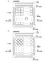
[撮像装置100の構成例]
図1(A)は、本発明の一態様の撮像装置100の構成例を示す平面図である。撮像装
置100は、画素部110と、画素部110を駆動するための第1の周辺回路260、第
2の周辺回路270、第3の周辺回路280、及び第4の周辺回路290を有する。画素
部110は、p行q列(p及びqは2以上の自然数)のマトリクス状に配置された複数の
画素111を有する。第1の周辺回路260乃至第4の周辺回路290は、複数の画素1
11に接続し、複数の画素111を駆動するための信号を供給する機能を有する。なお、
本明細書等において、第1の周辺回路260乃至第4の周辺回路290などを「周辺回路
」もしくは「駆動回路」と呼ぶ場合がある。例えば、第1の周辺回路260は周辺回路の
一部と言える。[Example of configuration of imaging device 100]
1A is a plan view illustrating a configuration example of an
11 and has a function of supplying signals for driving a plurality of
In this specification and the like, the first
また、撮像装置100は、光源190を有することが好ましい。光源190は、光P1
を放射することができる。 The
can be emitted.
また、周辺回路は、少なくとも、論理回路、スイッチ、バッファ、増幅回路、または変
換回路の1つを有する。また、周辺回路は画素部110を形成する基板に形成してもよい
し、周辺回路の一部または全部をIC等の半導体装置で実装してもよい。なお、周辺回路
は、第1の周辺回路260乃至第4の周辺回路290のうち、少なくとも1つを省略して
もよい。例えば、第1の周辺回路260または第4の周辺回路290の一方の機能を、第
1の周辺回路260または第4の周辺回路290の他方に付加して、第1の周辺回路26
0または第4の周辺回路290の一方を省略してもよい。また、例えば、第2の周辺回路
270または第3の周辺回路280の一方の機能を、第2の周辺回路270または第3の
周辺回路280の他方に付加して、第2の周辺回路270または第3の周辺回路280の
一方を省略してもよい。また、例えば、第1の周辺回路260乃至第4の周辺回路290
のいずれか1つに、他の回路の機能を付加して、第1の周辺回路260乃至第4の周辺回
路290のいずれか1つ以外を省略してもよい。 The peripheral circuits include at least one of a logic circuit, a switch, a buffer, an amplifier circuit, and a converter circuit. The peripheral circuits may be formed on a substrate on which the
Alternatively, for example, the function of one of the second
Alternatively, the functions of other circuits may be added to any one of the first to fourth
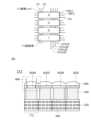
また、図1(B)に示すように、撮像装置100が有する画素部110において、画素
111を傾けて配置してもよい。画素111を傾けて配置することにより、行方向および
列方向の画素間隔(ピッチ)を短くすることができる。これにより、撮像装置100で撮
像された画像の品質をより高めることができる。 1B, the
例えば、第1の周辺回路260または第4の周辺回路290は、画素111から出力さ
れたアナログ信号を処理する機能を有する。例えば、図11に示すように、第1の周辺回
路260に信号処理回路271、列駆動回路272、出力回路273などを設けてもよい
。 For example, the first
また、図11に示す信号処理回路271は、列ごとに設けられた回路274を有する。
回路274は、ノイズの除去、アナログ-デジタル変換などの信号処理を行う機能を有す
ることができる。図11に示す回路274は、アナログ-デジタル変換の機能を有する。
信号処理回路271は列並列型(カラム型)アナログ-デジタル変換装置として機能する
ことができる。 Moreover, the
The
The
回路274は、コンパレータ274aとカウンタ回路274bを有する。コンパレータ
274aは、列ごとに設けられた配線999から入力されるアナログ信号と、配線277
から入力される参照用電位信号(例えば、ランプ波信号)の電位を比較する機能を有する
。カウンタ回路274bは、配線278からクロック信号が入力される。カウンタ回路2
74bは、コンパレータ274aでの比較動作により第1の値が出力されている期間を計
測し、計測結果をNビットデジタル値として保持する機能を有する。 The
The
The
列駆動回路272は、列選択回路、水平駆動回路等とも呼ばれる。列駆動回路272は
、信号を読み出す列を選択する選択信号を生成する。列駆動回路272は、シフトレジス
タなどで構成することができる。列駆動回路272により列が順次選択され、選択された
列の回路274から出力された信号が、配線279を介して出力回路273に入力される
。配線279は水平転送線として機能することができる。 The
出力回路273に入力された信号は、出力回路273で処理されて、撮像装置100の
外部に出力される。出力回路273は、例えばバッファ回路で構成することができる。ま
た、出力回路273は、撮像装置100の外部に信号を出力するタイミングを制御できる
機能を有していてもよい。 The signal input to the
また、例えば、第2の周辺回路270または第3の周辺回路280は、信号を読み出す
画素111を選択する選択信号を生成して出力する機能を有する。なお、第2の周辺回路
270または第3の周辺回路280を、行選択回路、又は垂直駆動回路と呼ぶ場合がある
。 Furthermore, for example, the second
また、図35(A1)及び図35(B1)に示すように、撮像装置100を湾曲させて
もよい。図35(A1)は、撮像装置100を同図中の二点鎖線X1-X2の方向に湾曲
させた状態を示している。図35(A2)は、図35(A1)中の二点鎖線X1-X2で
示した部位の断面図である。図35(A3)は、図35(A1)中の二点鎖線Y1-Y2
で示した部位の断面図である。 Also, as shown in Fig. 35(A1) and Fig. 35(B1), the
FIG.
図35(B1)は、撮像装置100を同図中の二点鎖線X3-X4の方向に湾曲させ、
かつ、同図中の二点鎖線Y3-Y4の方向に湾曲させた状態を示している。図35(B2
)は、図35(B1)中の二点鎖線X3-X4で示した部位の断面図である。図35(B
3)は、図35(B1)中の二点鎖線Y3-Y4で示した部位の断面図である。 FIG. 35B1 shows the state in which the
In addition, the state shown is bent in the direction of the two-dot chain line Y3-Y4 in the figure.
35(B1) is a cross-sectional view of the portion indicated by the two-dot chain line X3-X4 in FIG.
3) is a cross-sectional view of a portion indicated by a two-dot chain line Y3-Y4 in FIG. 35(B1).
撮像装置100を湾曲させることで、像面湾曲や非点収差を低減することができる。よ
って、撮像装置100と組み合わせて用いるレンズなどの光学設計を容易とすることがで
きる。例えば、収差補正のためのレンズ枚数を低減できるため、撮像装置100を用いた
撮像装置や半導体装置などの小型化や軽量化を容易とすることができる。また、撮像され
た画像の品質を向上させる事ができる。 Curving the
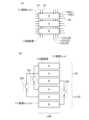
[画素111の構成例]
撮像装置100が有する1つの画素111を複数の副画素112で構成し、それぞれの
副画素112に特定の波長帯域の光を透過するフィルタ(カラーフィルタ)を組み合わせ
ることで、カラー画像表示を実現するための情報を取得することができる。[Configuration example of pixel 111]
By configuring one
図2(A)は、カラー画像を取得するための画素111の一例を示す平面図である。図
2(A)に示す画素111は、赤(R)の波長帯域を透過するカラーフィルタが設けられ
た副画素112(以下、「副画素112R」ともいう)、緑(G)の波長帯域を透過する
カラーフィルタが設けられた副画素112(以下、「副画素112G」ともいう)及び青
(B)の波長帯域を透過するカラーフィルタが設けられた副画素112(以下、「副画素
112B」ともいう)を有する。副画素112は、フォトセンサとして機能させることが
できる。 Fig. 2A is a plan view showing an example of a
副画素112(副画素112R、副画素112G、及び副画素112B)は、配線13
1、配線141、配線144、配線146、配線135と電気的に接続される。また、副
画素112R、副画素112G、及び副画素112Bは、それぞれが独立した配線137
に接続している。また、本明細書等において、例えばn行目の画素111に接続された配
線144及び配線146を、それぞれ配線144[n]及び配線146[n]と記載する
。また、例えばm列目の画素111に接続された配線137を、配線137[m]と記載
する。なお、図2(A)において、m列目の画素111が有する副画素112Rに接続す
る配線137を137[m]R、副画素112Gに接続する配線137を配線137[m
]G、及び副画素112Bに接続する配線137を配線137[m]Bと記載している。
副画素112は、上記配線を介して周辺回路と電気的に接続される。 The sub-pixels 112 (sub-pixels 112R, 112G, and 112B) are connected to the wiring 13
1, the
In this specification and the like, for example, the
]G, and the
The
また、本実施の形態に示す撮像装置100は、隣接する画素111の、同じ波長帯域の
光を透過するカラーフィルタが設けられた副画素112がスイッチを介して接続する構成
を有する。図2(B)に、n行(nは1以上p以下の自然数)m列(mは1以上q以下の
自然数)に配置された画素111が有する副画素112と、該画素に隣接するn+1行m
列に配置された画素111が有する副画素112の接続例を示す。図2(B)において、
n行m列に配置された副画素112Rと、n+1行m列に配置された副画素112Rがス
イッチ201を介して接続されている。また、n行m列に配置された副画素112Gと、
n+1行m列に配置された副画素112Gがスイッチ202を介して接続されている。ま
た、n行m列に配置された副画素112Bと、n+1行m列に配置された副画素112B
がスイッチ203を介して接続されている。 In addition, the
2B shows an example of a connection of sub-pixels 112 included in
A sub-pixel 112R arranged in the nth row and mth column is connected to a sub-pixel 112R arranged in the (n+1)th row and mth column via a
The sub-pixel 112G arranged in the n+1th row and the mth column is connected via the
are connected via a
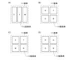
なお、副画素112に用いるカラーフィルタは、赤(R)、緑(G)、青(B)に限定
されず、図3(A)に示すように、それぞれシアン(C)、黄(Y)及びマゼンダ(M)
の光を透過するカラーフィルタを用いてもよい。1つの画素111に3種類の異なる波長
帯域の光を検出する副画素112を設けることで、フルカラー画像を取得することができ
る。 The color filters used for the sub-pixels 112 are not limited to red (R), green (G), and blue (B), but may be cyan (C), yellow (Y), and magenta (M), as shown in FIG.
Alternatively, a color filter that transmits light of three different wavelength bands may be used. By providing one
図3(B)は、それぞれ赤(R)、緑(G)及び青(B)の光を透過するカラーフィル
タが設けられた副画素112に加えて、黄(Y)の光を透過するカラーフィルタが設けら
れた副画素112を有する画素111を例示している。図3(C)は、それぞれシアン(
C)、黄(Y)及びマゼンダ(M)の光を透過するカラーフィルタが設けられた副画素1
12に加えて、青(B)の光を透過するカラーフィルタが設けられた副画素112を有す
る画素111を例示している。1つの画素111に4種類の異なる波長帯域の光を検出す
る副画素112を設けることで、取得した画像の色の再現性をさらに高めることができる
。 3B illustrates a
C), a
In addition to the pixel 12, the
また、例えば、図2(A)において、赤の波長帯域を検出する副画素112、緑の波長
帯域を検出する副画素112、および青の波長帯域を検出する副画素112の画素数比(
または受光面積比)は、必ずしも1:1:1である必要は無い。図3(D)に示すように
、画素数比(受光面積比)を赤:緑:青=1:2:1とするBayer配列としてもよい
。また、画素数比(受光面積比)を赤:緑:青=1:6:1としてもよい。 In addition, for example, in FIG. 2A, the pixel number ratio of the sub-pixels 112 detecting the red wavelength band, the sub-pixels 112 detecting the green wavelength band, and the sub-pixels 112 detecting the blue wavelength band (
The pixel number ratio (light receiving area ratio) does not necessarily have to be 1:1:1. As shown in Fig. 3D, a Bayer arrangement in which the pixel number ratio (light receiving area ratio) is red:green:blue = 1:2:1 may be used. Also, the pixel number ratio (light receiving area ratio) may be red:green:blue = 1:6:1.
なお、画素111に設ける副画素112は1つでもよいが、2つ以上が好ましい。例え
ば、同じ波長帯域を検出する副画素112を2つ以上設けることで、冗長性を高め、撮像
装置100の信頼性を高めることができる。 Although one
また、フィルタとして可視光を吸収または反射して、赤外光を透過するIR(IR:I
nfrared)フィルタを用いることで、赤外光を検出する撮像装置100を実現する
ことができる。 In addition, it can also be used as a filter to absorb or reflect visible light and transmit infrared light (IR: Infrared).
By using an infrared filter, it is possible to realize an
また、フィルタ602としてND(ND:Neutral Density)フィルタ
ー(減光フィルター)を用いると、光電変換素子(受光素子)に大光量光が入射した時に
生じる出力飽和することを防ぐことができる。減光量の異なるNDフィルタを組み合わせ
て用いることで、撮像装置のダイナミックレンジを大きくすることができる。 Furthermore, by using an ND (Neutral Density) filter (neutral density filter) as the filter 602, it is possible to prevent output saturation that occurs when a large amount of light is incident on a photoelectric conversion element (light receiving element). By using a combination of ND filters with different light reduction amounts, it is possible to increase the dynamic range of the imaging device.
また、前述したフィルタ以外に、画素111にレンズを設けてもよい。ここで、図4の
断面図を用いて、画素111、フィルタ602、レンズ600の配置例を説明する。レン
ズ600を設けることで、光電変換素子が入射光を効率よく受光することができる。具体
的には、図4(A)に示すように、画素111に形成したレンズ600、フィルタ602
(フィルタ602R、フィルタ602G、フィルタ602B)、及び画素回路230等を
通して光660を光電変換素子220に入射させる構造とすることができる。 In addition to the above-mentioned filter, a lens may be provided in the
(filter 602R,
ただし、二点鎖線で囲んだ領域に示すように、矢印で示す光660の一部が配線層60
4の一部によって遮光されてしまうことがある。したがって、図4(B)に示すように光
電変換素子220側にレンズ600及びフィルタ602を形成して、光電変換素子220
が入射光を効率良く受光できる構造が好ましい。光電変換素子220側から光660を光
電変換素子220に入射させることで、検出感度の高い撮像装置100を提供することが
できる。 However, as shown in the area surrounded by the two-dot chain line, a part of the light 660 indicated by the arrow is incident on the wiring layer 60.
Therefore, as shown in FIG. 4B, a
A structure capable of efficiently receiving incident light is preferable. By making light 660 incident on the
図4に示す光電変換素子220として、pin型の接合が形成された光電変換素子を用
いてもよい。pin型の接合が形成された光電変換素子については、実施の形態3で詳細
を説明する。 A photoelectric conversion element having a pin junction may be used as the
また、光電変換素子220を、放射線を吸収して電荷を発生させることが可能な材料を
用いて形成してもよい。放射線を吸収して電荷を発生させることが可能な材料としては、
セレン、ヨウ化鉛、ヨウ化水銀、ガリウムヒ素、CdTe、CdZn等がある。 The
Examples include selenium, lead iodide, mercury iodide, gallium arsenide, CdTe, and CdZn.
例えば、光電変換素子220にセレンを用いると、可視光や、紫外光、赤外光に加えて
、X線や、ガンマ線といった幅広い波長帯域にわたって光吸収係数を有する光電変換素子
220を実現できる。 For example, when selenium is used for the
ここで、撮像装置100が有する1つの画素111は、図2や図3に示す副画素に加え
て、第1のフィルターを有する副画素を有してもよい。一例を図10に示す。 Here, one
図10(A)は、図2に示す画素111が、副画素112R、副画素112G、副画素
112Bに加えて、フィルタ602Iが設けられた副画素(以下、「副画素112I」)
を有する例を示す。フィルタ602Iとして、光P1が有する波長帯域の光を透過するフ
ィルターを設けることが好ましい。フィルタ602Iとして、例えば光P1に赤外の波長
帯域を有する光を用いる場合には、赤外の波長域の光を透過するカラーフィルタを用いる
ことができる。 FIG. 10A illustrates a
As the filter 602I, it is preferable to provide a filter that transmits light in the wavelength band of the light P1. For example, when light having an infrared wavelength band is used as the light P1, a color filter that transmits light in the infrared wavelength band can be used as the filter 602I.
図10(B)の断面図は、画素111が、フィルタ602R、フィルタ602G、フィ
ルタ602Bおよびフィルタ602Iが設けられた4つの副画素112(副画素112R
、副画素112G、副画素112Bおよび副画素112I)を有する例を示す。また、画
素111にはレンズ600が形成されている。 In the cross-sectional view of FIG. 10B, the
1, an example is shown in which the
[副画素112の回路構成例]
次に、図5の回路図を用いて、副画素112の具体的な回路構成例について説明する。
図5に、n行目の画素111が有する副画素112[n]と、n+1行目の画素111が
有する副画素112[n+1]が、トランジスタ129を介して電気的に接続する回路構
成例を示す。トランジスタ129は、スイッチ201、スイッチ202、またはスイッチ
203として機能できる。[Example of a circuit configuration of the sub-pixel 112]
Next, a specific example of the circuit configuration of the sub-pixel 112 will be described with reference to the circuit diagram of FIG.
5 shows an example of a circuit configuration in which a subpixel 112[n] included in a
図5では、光電変換素子として、フォトダイオードを用いる例を示す。Figure 5 shows an example in which a photodiode is used as the photoelectric conversion element.
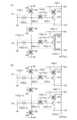
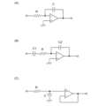
図5に示す回路図において、具体的には、n行目の画素111が有する副画素112[
n]は、フォトダイオードPD[n](光電変換素子)、トランジスタ121、トランジ
スタ123、およびトランジスタ124を含んで構成される。また、n+1行目の画素1
11が有する副画素112[n+1]は、フォトダイオードPD[n+1]、トランジス
タ125、トランジスタ127、およびトランジスタ128を含んで構成される。 In the circuit diagram shown in FIG. 5, specifically, the sub-pixel 112 [
The
The sub-pixel 112[n+1] of the pixel 11 includes a photodiode PD[n+1], a
本実施の形態では、トランジスタ121乃至トランジスタ129としてnチャネル型の
トランジスタを用いる場合を例示する。よって、トランジスタ121乃至トランジスタ1
29では、ゲートに供給される信号がH電位の時にソースとドレインとの間が導通状態(
オン状態)となり、L電位の時に非導通状態(オフ状態)となる。 In this embodiment, the case where n-channel transistors are used as the
In the case of 29, when the signal supplied to the gate is at H potential, the source and drain are in a conductive state (
When the potential is L, the transistor is in a non-conducting state (OFF state).
ただし、本発明の一態様はこれに限定されず、トランジスタ121乃至トランジスタ1
29としてpチャネル型のトランジスタを用いることもできる。また、nチャネル型のト
ランジスタとpチャネル型のトランジスタを適宜組み合わせて用いることもできる。 However, one embodiment of the present invention is not limited thereto, and the
A p-channel transistor may also be used as the transistor 29. Furthermore, an appropriate combination of an n-channel transistor and a p-channel transistor may also be used.
図5の回路図において、フォトダイオードPD[n]のアノードまたはカソードの一方
は、電位VPを供給可能な配線131と電気的に接続される。また、フォトダイオードP
D[n]のアノードまたはカソードの他方と、トランジスタ121のソースまたはドレイ
ンの一方と、トランジスタ122のソースまたはドレインの一方は、ノードND[n]に
電気的に接続される。また、トランジスタ122のソースまたはドレインの他方は、電位
VRを供給可能な配線133と電気的に接続され、トランジスタ122のゲートは電位P
Rを供給可能な配線141と電気的に接続される。また、トランジスタ121のソースま
たはドレインの他方とトランジスタ123のゲートは、電荷蓄積領域であるノードFD[
n]に電気的に接続され、トランジスタ121のゲートは電位TX[n]を供給可能な配
線144[n]と電気的に接続される。また、トランジスタ123のソースまたはドレイ
ンの一方は、電位VOを供給可能な配線135に電気的に接続され、トランジスタ123
のソースまたはドレインの他方は、トランジスタ124のソースまたはドレインの一方と
電気的に接続される。また、トランジスタ124のソースまたはドレインの他方は、配線
137[m]と電気的に接続され、トランジスタ124のゲートは電位SELを供給可能
な配線146[n]と電気的に接続される。また、トランジスタ129のソースまたはド
レインの一方は、ノードND[n]に電気的に接続され、トランジスタ129のゲートは
電位PAを供給可能な配線142と電気的に接続される。 In the circuit diagram of FIG. 5, one of the anode and the cathode of the photodiode PD[n] is electrically connected to a
The other of the anode or the cathode of the
The other of the source and the drain of the
The gate of the
The other of the source or drain of the
また、フォトダイオードPD[n+1]のアノードまたはカソードの一方は、電位VP
を供給可能な配線132と電気的に接続される。また、フォトダイオードPD[n+1]
のアノードまたはカソードの他方と、トランジスタ125のソースまたはドレインの一方
と、トランジスタ126のソースまたはドレインの一方は、電荷蓄積領域であるノードN
D[n+1]に電気的に接続される。また、トランジスタ126のソースまたはドレイン
の他方は、電位VRを供給可能な配線134と電気的に接続され、トランジスタ126の
ゲートは電位PRを供給可能な配線143と電気的に接続される。また、トランジスタ1
25のソースまたはドレインの他方とトランジスタ127のゲートは、ノードFD[n+
1]に電気的に接続され、トランジスタ125のゲートは電位TX[n+1]を供給可能
な配線144[n+1]と電気的に接続される。また、トランジスタ127のソースまた
はドレインの一方は、電位VOを供給可能な配線136に電気的に接続され、トランジス
タ127のソースまたはドレインの他方は、トランジスタ128のソースまたはドレイン
の一方と電気的に接続される。また、トランジスタ128のソースまたはドレインの他方
は、配線137[m]と電気的に接続され、トランジスタ128のゲートは電位SELを
供給可能な配線146[n+1]と電気的に接続される。また、トランジスタ129のソ
ースまたはドレインの他方は、ノードND[n+1]に電気的に接続される。 In addition, one of the anode and cathode of the photodiode PD[n+1] is connected to a potential VP
The photodiode PD[n+1] is electrically connected to the
The other of the anode or cathode of the
The other of the source and the drain of the
The other of the source or drain of the
The
また、図5では配線131及び配線132を分けて記載しているが、1本の共通配線と
してもよい。また、図5では配線141及び配線143を分けて記載しているが、1本の
共通配線としてもよい。また、図5では配線135及び配線136を分けて記載している
が、1本の共通配線としてもよい。 5, the
なお、図5では光電変換素子としてフォトダイオードを用いたが、光電変換が可能な素
子であればこれに限定されない。 Although a photodiode is used as the photoelectric conversion element in FIG. 5, the present invention is not limited to this as long as the element is capable of photoelectric conversion.
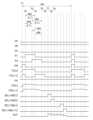
<動作例1>
次に、図6乃至図9を用いて、撮像装置100を用いて、2次元の撮像をグローバルシ
ャッタ方式で行う撮像動作の一例を説明する。全ての副画素112において、リセット動
作及び蓄積動作を一括で行い、読み出し動作を順次行うことで、グローバルシャッタ方式
による撮像を行うことができる。ここでは、副画素112の動作例を、副画素112[n
]及び副画素112[n+1]を用いて説明する。<Operation example 1>
Next, an example of an imaging operation in which two-dimensional imaging is performed by the
] and subpixel 112[n+1] will be used for explanation.
図6は副画素112の動作を説明するタイミングチャートであり、図7乃至図9は、副
画素112の動作状態を示す回路図である。なお、本実施の形態に示すタイミングチャー
トでは、駆動方法を分かりやすく説明するため、前述した配線およびノードには、特に明
示する場合を除いてH電位またはL電位が与えられるものとする。 6 is a timing chart for explaining the operation of the
グローバルシャッタ方式を用いることで、全ての画素111の蓄積動作を同一期間内に
行うことができる。したがって、ローリングシャッタ方式を用いた場合のように、蓄積動
作を行う期間が異なることによる撮像画像の歪みが生じない。なお、グローバルシャッタ
方式を用いた場合のフレーム間隔を期間301として図6に示す。期間301は、リセッ
ト動作、蓄積動作、全行の画素の読み出し動作に要する時間の和となる。また期間301
は例えば、リセット動作後、次のリセット動作を行うまでの期間である。 By using the global shutter method, the accumulation operation of all the
is, for example, the period from one reset operation to the next reset operation.
動作例1では、電位PAをL電位として、トランジスタ129をオフ状態とした場合の
撮像動作について説明する。電位PAをL電位とすることで、副画素112[n]及び副
画素112[n+1]をそれぞれ独立して動作させることができる。また、電位VRをH
電位とし、電位VPおよび電位VOをL電位とする。また、電位SEL[n]および電位
SEL[n+1]をL電位とする。 In the operation example 1, an imaging operation will be described in which the potential PA is set to an L potential and the
The potentials VP and VO are set to L potentials, and the potentials SEL[n] and SEL[n+1] are set to L potentials.
[リセット動作]
まず、時刻T1において、電位PR、電位TX[n]、および電位TX[n+1]の電
位をH電位とする。すると、トランジスタ121、トランジスタ122がオン状態となり
、ノードND[n]、およびノードFD[n]がH電位となる。また、トランジスタ12
5、トランジスタ126がオン状態となり、ノードND[n+1]、およびノードFD[
n+1]がH電位となる。この動作により、ノードFD[n]およびノードFD[n+1
]に保持されている電荷量がリセットされる(図7(A)参照。)。時刻T1乃至時刻T
2までの期間を「リセット期間」ともいう。また、リセット期間中の動作を「リセット動
作」ともいう。[Reset action]
First, at time T1, the potentials PR, TX[n], and TX[n+1] are set to H potentials. Then, the
5. The
By this operation, the node FD[n] and the node FD[n+1
The amount of charge held in the charge storage capacitor 11 is reset (see FIG. 7A).
The period from
なお、図示していないが、リセット期間において撮像装置100が有する全てのノード
FD[n]およびノードFD[n+1]がリセットされる。 Although not shown, all the nodes FD[n] and nodes FD[n+1] included in the
[蓄積動作]
次いで、時刻T2において、電位PRをL電位とする。電位TX[n]および電位TX
[n+1]はH電位のままとする。また、時刻T2において、フォトダイオードPD[n
]およびフォトダイオードPD[n+1]には、逆方向バイアスが印加されている。フォ
トダイオードPD[n]およびフォトダイオードPD[n+1]に逆方向バイアスが印加
されている状態で、フォトダイオードPD[n]およびフォトダイオードPD[n+1]
に光が入射すると、フォトダイオードPD[n]およびフォトダイオードPD[n+1]
が有する電極の他方から一方に向かって電流が流れる(図7(B)参照。)。この時の電
流量は光の強度に従って変化する。すなわち、フォトダイオードPD[n]およびフォト
ダイオードPD[n+1]に入射する光の強度が高いほど上記電流量は多くなり、ノード
FD[n]およびノードFD[n+1]からの電荷の流出も多くなる。逆に、フォトダイ
オードPD[n]およびフォトダイオードPD[n+1]に入射する光の強度が低いほど
上記電流量は少なくなり、ノードFD[n]およびノードFD[n+1]からの電荷の流
出も少なくなる。よって、ノードFD[n]およびノードFD[n+1]の電位は、光の
強度が高いほど変化が大きく、光の強度が低いほど変化が小さい。[Storage Operation]
Next, at time T2, the potential PR is set to the L potential.
[n+1] remains at the H potential. Also, at time T2, the photodiode PD[n
A reverse bias is applied to the photodiode PD[n] and the photodiode PD[n+1]. When a reverse bias is applied to the photodiode PD[n] and the photodiode PD[n+1],
When light is incident on the photodiode PD[n] and the photodiode PD[n+1]
A current flows from the other electrode to the other electrode (see FIG. 7B). The amount of current at this time changes according to the intensity of light. That is, the higher the intensity of light incident on the photodiode PD[n] and the photodiode PD[n+1], the larger the amount of current, and the more charge flows out from the node FD[n] and the node FD[n+1]. Conversely, the lower the intensity of light incident on the photodiode PD[n] and the photodiode PD[n+1], the smaller the amount of current, and the less charge flows out from the node FD[n] and the node FD[n+1]. Therefore, the higher the intensity of light, the larger the change in the potential of the node FD[n] and the node FD[n+1], and the smaller the change in the potential of the node FD[n] and the node FD[n+1].
次いで、時刻T3において、電位TX[n]および電位TX[n+1]をL電位とする
。すると、トランジスタ121及びトランジスタ125はオフ状態となる。トランジスタ
121及びトランジスタ125をオフ状態とすることで、ノードFD[n]およびノード
FD[n+1]からフォトダイオードPD[n]およびフォトダイオードPD[n+1]
への電荷の移動が止まり、ノードFD[n]およびノードFD[n+1]の電位が決定さ
れる(図8(A)参照。)。時刻T2乃至時刻T3までの期間を「露光期間」ともいう。
動作例1における露光期間を期間311として図6に示す。また、露光期間中の動作を「
蓄積動作」ともいう。 Next, at time T3, the potentials TX[n] and TX[n+1] are set to L potentials, so that the
The transfer of electric charges to the node FD[n] stops, and the potentials of the node FD[n+1] are determined (see FIG. 8A). The period from time T2 to time T3 is also referred to as an "exposure period".
The exposure period in the operation example 1 is shown in FIG. 6 as
This is also called the "accumulation operation."
[読み出し動作]
次いで、時刻T4において、配線146[n]に供給する電位SELをH電位とする。
ここでは、nが1の場合(1行目の場合)について説明する。なお、配線146[n]に
H電位を供給する直前に、配線137[m]の電位がH電位になるようにプリチャージし
ておく。配線146[n]に供給する電位SELをH電位とすると、トランジスタ124
がオン状態となり、ノードFD[n]の電位に応じた速度で配線137[m]の電位が低
下する(図8(B)参照。)。時刻T5において配線146[n]に供給する電位SEL
をL電位とすると、トランジスタ124がオフ状態となり、配線137[m]の電位が決
定される。この時の配線137[m]の電位を測定することで、副画素112[n]の受
光量を算出することができる。[Read operation]
Next, at time T4, the potential SEL supplied to the wiring 146[n] is set to an H potential.
Here, the case where n is 1 (the case of the first row) will be described. Note that the wiring 137[m] is precharged to have an H potential immediately before an H potential is supplied to the wiring 146[n]. If the potential SEL supplied to the wiring 146[n] is an H potential, the
The potential of the wiring 137[m] is decreased at a rate corresponding to the potential of the node FD[n] (see FIG. 8B).
When the potential of the wiring 137[m] is set to L, the
次に、時刻T5において、配線146[n+1](ここでは、2行目の配線146)に
供給する電位SELをH電位とする。なお、配線146[n+1]に供給する電位をH電
位とする直前に、配線137[m]の電位がH電位になるようにプリチャージしておく。
配線146[n+1]に供給する電位SELをH電位とすると、トランジスタ128がオ
ン状態となり、ノードFD[n+1]の電位に応じた速度で配線137[m]の電位が低
下する(図9(A)参照。)。時刻T6において配線146[n+1]に供給する電位S
ELをL電位とすると、トランジスタ128がオフ状態となり、配線137[m]の電位
が決定される(図9(B)参照)。この時の配線137[m]の電位を測定することで、
副画素112[n+1]の受光量を算出することができる。 Next, at time T5, the potential SEL supplied to the wiring 146[n+1] (here, the
When the potential SEL supplied to the wiring 146[n+1] is set to an H potential, the
When EL is set to an L potential, the
The amount of light received by the sub-pixel 112[n+1] can be calculated.
このようにして、時刻T6の後も、3行目から順に配線137[m]の電位を測定する
ことで、n行目及びn+1行目の配線137[m]の電位を取得することができる。1行
目乃至p行目の配線137[m]の電位を測定することによって、撮像装置100が有す
る画素111それぞれの受光量を取得することができる。すなわち、撮像装置100によ
り撮像された被写体の画像データを取得することができる。例えば、時刻T4乃至時刻T
5までの期間など、各行毎に受光量を取得する期間を「読み出し期間」ともいう。また、
読み出し期間中の動作を「読み出し動作」ともいう。なお、読み出し動作を行うタイミン
グは適宜決めることができる。なお、n行目に接続された、1列目からq列目の配線13
7の電位の測定は、1列目から順に行ってもよいし、1列目からq列目までを同時に行っ
てもよいし、複数列単位で行ってもよい。 In this manner, even after time T6, the potentials of the wirings 137[m] in the nth and (n+1)th rows can be obtained by measuring the potentials of the wirings 137[m] in the third row and onward. By measuring the potentials of the wirings 137[m] in the first to pth rows, the amount of received light of each
The period during which the amount of received light is acquired for each row, such as the period up to row 5, is also called the "readout period."
The operation during the read period is also called a "read operation." The timing for performing the read operation can be determined appropriately.
The measurement of the potential of 7 may be performed sequentially from the first column, or may be performed simultaneously from the first column to the qth column, or may be performed in units of multiple columns.
なお、グローバルシャッタ方式では、リセット動作及び蓄積動作を全画素で一斉に行う
ため、全ての列の画素において、一斉に電位TX[n]、電位TX[n+1]、及び電位
PRの電位を変化させればよい。 In addition, in the global shutter method, the reset operation and the accumulation operation are performed simultaneously in all pixels, so that the potentials TX[n], TX[n+1], and PR can be changed simultaneously in the pixels in all columns.
蓄積動作が終了してから読み出し動作が開始されるまでの期間は、各行の画素のノード
FDに電荷が保持されるため、当該期間を電荷保持期間ともいう。グローバルシャッタ方
式では、リセット動作と蓄積動作を全画素で一斉に行うため、露光期間が終了するタイミ
ングは全画素で同じとなる。しかし、各行の画素について順次読み出し動作を行うため、
電荷保持期間が各行の画素によって異なる。例えば、1行目の画素の電荷保持期間は、時
刻T3からT4までの期間であるが、2行目の画素の電荷保持期間は、時刻T3から時刻
T5までの期間である。このように、読み出し動作は各行毎に行うため、読み出し期間が
開始されるタイミングは各行毎に異なる。よって、最終行の画素における電荷保持期間が
最長となる。 During the period from the end of the accumulation operation to the start of the readout operation, charges are held in the node FD of the pixels in each row, and this period is also called the charge holding period. In the global shutter method, the reset operation and accumulation operation are performed simultaneously for all pixels, so the timing at which the exposure period ends is the same for all pixels. However, since the readout operation is performed sequentially for the pixels in each row,
The charge retention period differs for pixels in each row. For example, the charge retention period for pixels in the first row is the period from time T3 to time T4, while the charge retention period for pixels in the second row is the period from time T3 to time T5. In this way, since the readout operation is performed for each row, the timing at which the readout period starts differs for each row. Therefore, the charge retention period for pixels in the last row is the longest.
階調数が画一的な画像を撮像すると、理想的には全ての画素において同じ高さの電位を
有する出力信号が得られる。しかし、電荷保持期間の長さが行毎に異なる場合、各行の画
素のノードFDに蓄積されている電荷が時間の経過と共にリークしてしまうと、画素の出
力信号の電位が行毎に異なってしまい、行毎にその階調数が変化した画像データが得られ
てしまう。 When capturing an image with a uniform number of gradations, ideally, output signals having the same potential level are obtained for all pixels. However, if the length of the charge retention period differs for each row, and the charges stored in the nodes FD of the pixels in each row leak over time, the potential of the pixel output signals will differ for each row, resulting in image data with a different number of gradations for each row.
そこで、トランジスタ121及びトランジスタ125にオフ電流が著しく低いトランジ
スタを用いることが好ましい。トランジスタ121及びトランジスタ125にオフ電流が
著しく低いトランジスタを用いることで、グローバルシャッタ方式を用いて撮像を行って
も、電荷保持期間が異なることに起因するノードFD[n]及びノードFD[n+1]の
電位変化を小さく抑えることができる。すなわち、グローバルシャッタ方式を用いて撮像
を行っても、電荷保持期間が異なることに起因する画像データの階調の変化を小さく抑え
、撮像された画像の品質を向上させることができる。 Therefore, it is preferable to use transistors with extremely low off-state current as the
図5に示した回路構成を用いて、グローバルシャッター駆動方法を行う場合、n行目の
画像データと、n+1行目の画像データが混合する可能性がある。よって、トランジスタ
129にオフ電流が著しく低いトランジスタを用いることが好ましい。トランジスタ12
9にオフ電流が著しく低いトランジスタを用いることによって、当該画像データの混合を
抑制できる。 5, image data of the nth row and image data of the n+1th row may be mixed. Therefore, a transistor with an extremely low off-state current is preferably used as the
By using a transistor with extremely low off-state current for the pixel 9, the mixture of the image data can be suppressed.
本発明の一態様によれば、撮像された画像の品質を向上することができる。According to one aspect of the present invention, the quality of captured images can be improved.
<動作例2>
次に、図1に示す撮像装置100を用いて、3次元の撮像を行う例を説明する。本発明
の一態様を用いることにより、撮像装置100を用いて、2次元の撮像と3次元の撮像を
行うことができる。<Operation example 2>
Next, an example of three-dimensional imaging will be described using the
3次元の撮像には例えば、2次元の撮像に用いた図5に示す副画素112の回路構成例
を用いることができる。 For three-dimensional imaging, for example, the circuit configuration example of the sub-pixel 112 used for two-dimensional imaging shown in FIG. 5 can be used.
次に、図5に示す回路構成を備え、3次元の撮像を実現する撮像装置100の動作例を
、図12乃至図16を用いて説明する。図12は副画素112の動作を説明するタイミン
グチャートであり、図13乃至図16は、副画素112の動作状態を示す回路図である。 Next, an operation example of the
なお、動作例2におけるフレーム間隔を期間401として図12に示す。期間401は
、リセット動作、蓄積動作、全行の画素の読み出し動作に要する時間の和となる。また期
間401は例えば、リセット動作後、次のリセット動作を行うまでの期間である。 12, the frame interval in the operation example 2 is shown as a
動作例2では、電位PAをH電位として、トランジスタ129をオン状態とした場合の
撮像動作について説明する。電位PAをH電位とすることで、副画素112[n]と副画
素112[n+1]を並列に接続して使用することができる。また、電位VRをH電位と
し、電位VPおよび電位VOをL電位とする。 In the second operation example, an imaging operation will be described in which the potential PA is set to an H potential and the
副画素112[n]が有するフォトダイオードPD[n]と副画素112[n+1]が
有するフォトダイオードPD[n+1]を並列に接続して使用することにより、電荷蓄積
領域を複数有する構成とすることができる。電荷蓄積領域を複数有することにより、高い
受光感度を実現することができる。また、短時間で3次元の撮像が可能となる。 By connecting the photodiode PD[n] of the subpixel 112[n] and the photodiode PD[n+1] of the subpixel 112[n+1] in parallel, a configuration having multiple charge storage regions can be achieved. By having multiple charge storage regions, high light receiving sensitivity can be achieved. In addition, three-dimensional imaging can be achieved in a short time.
[検出光]
動作例2では、光P1を被検出物に照射し、その反射光P2を検出して撮像装置100
から被検出物までの距離xを取得する例を示す。距離xを用いて、3次元の画像を実現す
ることができる。[Detection light]
In the second operation example, the light P1 is irradiated onto the object to be detected, and the reflected light P2 is detected.
An example of acquiring a distance x from a target object to a target object will be shown. A three-dimensional image can be realized by using the distance x.
図36は、撮像装置100が有する光源190から放射された光P1が被検出物620
の表面に照射され、反射光P2がn行m列の画素111(n,m)が有するフォトダイオ
ードPDに入射する一例を示す模式図である。図36において、撮像装置100は光源1
90、画素111およびレンズ600を有する。また、撮像装置100は、2以上のレン
ズを有してもよい。例えば、撮像装置100は、図36に示すようにレンズ600および
レンズ610を有してもよい。 FIG. 36 shows a case where light P1 emitted from a
36 is a schematic diagram showing an example in which light P1 is irradiated onto the surface of a pixel 111 (n, m) in the nth row and the mth column, and reflected light P2 is incident on a photodiode PD of the pixel 111 (n, m).
36 , the
光P1としては、撮像装置100に用いる光電変換素子が変換できる光であれば、どの
ような波長の光を用いてもよい。例えば、可視光、紫外光、赤外光などを用いることがで
きる。また、光P1として、X線や、ガンマ線を用いてもよい。また、白色光のように幅
広い波長分布を有する光を用いてもよい。 As the light P1, light of any wavelength may be used as long as it is light that can be converted by the photoelectric conversion element used in the
被検出物620には、光P1以外の光が照射される場合がある。被検出物620に照射
される光のうち、光P1以外の光を外光P3と呼ぶ。外光P3として、例えば太陽光や照
明などが挙げられる。 Light other than the light P1 may be irradiated onto the detection object 620. Of the light irradiated onto the detection object 620, light other than the light P1 is referred to as external light P3. Examples of the external light P3 include sunlight and lighting.
ここで、光P1は外光P3よりも強度が大きいことが好ましい。光P1として特定の波
長域に分布を有する光、例えば赤外光などを利用し、フォトダイオードPDに該波長域の
光を透過するフィルターを組み合わせることで、外光P3の影響を小さくすることができ
る。例えば、照明として蛍光灯を用いる場合には赤外光をほとんど含まないため、検出光
として赤外光を用いることにより、外光P3の影響を小さくすることができる。よって、
撮像装置100で撮影される3次元画像の品質を向上することができる。 Here, it is preferable that the light P1 has a greater intensity than the external light P3. By using light having a distribution in a specific wavelength range, such as infrared light, as the light P1 and combining the photodiode PD with a filter that transmits light in that wavelength range, it is possible to reduce the influence of the external light P3. For example, when a fluorescent lamp is used as lighting, it contains almost no infrared light, so by using infrared light as the detection light, it is possible to reduce the influence of the external light P3. Therefore,
The quality of the three-dimensional image captured by the
光P1は、短時間のパルス波を生成できることが好ましい。光P1として、例えばパル
ス発光のLED(Light Emitting Diode)を用いてもよい。また、
メカニカルシャッターなどのシャッターを高速で開閉することによりパルス光を生成して
もよい。 It is preferable that the light P1 can generate a short-duration pulse wave. For example, a pulsed light emitting diode (LED) may be used as the light P1.
The pulsed light may be generated by rapidly opening and closing a shutter, such as a mechanical shutter.
また、光P1は、被検出物620に広く均一に照射することが好ましい。また、光P1
は、画素111の近くに配置されることが好ましい。 In addition, it is preferable that the light P1 is irradiated widely and uniformly onto the object 620.
is preferably located near the
[リセット動作]
まず時刻T1において、電位PR、電位TX[n]および電位TX[n+1]の電位を
H電位とする。すると、トランジスタ121、トランジスタ122がオン状態となり、ノ
ードND[n]、およびノードFD[n]がH電位となる。また、トランジスタ125、
トランジスタ126がオン状態となり、ノードND[n+1]、およびノードFD[n+
1]がH電位となる。この動作により、ノードFD[n]およびノードFD[n+1]に
保持されている電荷量がリセットされる(図13(A)参照。)。[Reset action]
First, at time T1, the potentials PR, TX[n], and TX[n+1] are set to H potentials. Then, the
The
The potentials of the nodes FD[n] and FD[n+1] become H potentials. By this operation, the amounts of charge held in the nodes FD[n] and FD[n+1] are reset (see FIG. 13A).
また、動作例2では、トランジスタ129をオン状態としているため、リセット期間中
にトランジスタ122またはトランジスタ126のうちどちらか一方をオフ状態としても
よい。なお、図示していないが、リセット期間において撮像装置100が有する全てのノ
ードFD[n]およびノードFD[n+1]がリセットされる。 In addition, in the operation example 2, since the
[蓄積動作]
フォトダイオードPD[n]およびフォトダイオードPD[n+1]には、逆方向バイ
アスが印加されている。フォトダイオードPD[n]およびフォトダイオードPD[n+
1]に逆方向バイアスが印加されている状態で、フォトダイオードPD[n]およびフォ
トダイオードPD[n+1]に光が入射すると、フォトダイオードPD[n]およびフォ
トダイオードPD[n+1]が有する電極の他方から一方に向かって電流が流れる。前述
したように、この時の電流量は光の強度に従って変化する。よって、ノードFD[n]の
電位は、光の強度が高いほど変化が大きく、光の強度が低いほど変化が小さい。[Storage Operation]
A reverse bias is applied to the photodiode PD[n] and the photodiode PD[n+1].
When light is incident on the photodiode PD[n] and the photodiode PD[n+1] while a reverse bias is applied to the photodiode PD[n] and the photodiode PD[n+1], a current flows from the other of the electrodes of the photodiode PD[n] and the photodiode PD[n+1] to the other. As described above, the amount of current at this time changes according to the intensity of the light. Therefore, the potential of the node FD[n] changes more as the intensity of the light increases, and changes less as the intensity of the light decreases.
時刻T2において、電位PRをL電位とする。また、配線144[n+1]に供給され
る電位TX[n+1]をL電位とする。配線144[n]に供給される電位TX[n]は
H電位のままとする(図13(B)参照。)。次に、光P1の被検出物620への照射を
開始する。光P1は、図12に示す期間402、すなわち時間T2乃至時間T4に被検出
物620に照射される。 At time T2, the potential PR is set to an L potential. The potential TX[n+1] supplied to the wiring 144[n+1] is set to an L potential. The potential TX[n] supplied to the wiring 144[n] remains at an H potential (see FIG. 13B). Next, irradiation of the object to be detected 620 with the light P1 starts. The object to be detected 620 is irradiated with the light P1 during the
時刻T2に被検出物620に照射された光P1は物体の表面で反射し、時刻T3におい
て反射光P2としてフォトダイオードPD[n]およびフォトダイオードPD[n+1]
に入射する。そして、ノードFD[n]からフォトダイオードPD[n]およびフォトダ
イオードPD[n+1]へ電荷が移動する(図14(A)参照。)。ここで図12に示す
期間403は、光P1の照射を時刻T2に開始してから、反射光P2が時刻T3にフォト
ダイオードに入射するまでの期間である。 Light P1 irradiated onto the object 620 at time T2 is reflected by the surface of the object, and is incident on the photodiode PD[n] and the photodiode PD[n+1] as reflected light P2 at time T3.
Then, charges move from the node FD[n] to the photodiode PD[n] and the photodiode PD[n+1] (see FIG. 14A). Here, the
ここで、撮像装置100から被検出物までの距離xについて説明する。図36に示すよ
うに、撮像装置100の光源(光P1)から、被検出物620のn行m列目の画素で検出
される箇所までの距離をx1とし、被検出物620のn行m列目の画素で検出される箇所
から、n行m列目の画素までの距離をx2とする。この時、例えば撮像装置100と被検
出物620との距離xはx1とx2の平均、すなわちx=(x1+x2)/2とすればよ
い。ここで撮像装置100の大きさに比べて距離x1およびx2が充分大きい場合、被検
出物620までの距離xは、x1もしくはx2で近似できる。 Here, the distance x from the
ここで、期間403の長さ、すなわち時刻T2と時刻T3の差をΔTX、撮像装置10
0と被検出物620との距離をx、光速をcとすると、ΔTX=2x/cの関係を満たし
、ΔTXは撮像装置と被検出物620との距離に応じて変化する。 Here, the length of the
If the distance between 0 and the object 620 is x and the speed of light is c, then the relationship ΔTX =2x/c is satisfied, and ΔTX changes according to the distance between the imaging device and the object 620 .
次いで、時刻T4において、光P1の照射を終了する。また、配線144[n]に供給
される電位TX[n]をL電位とし、配線144[n+1]に供給される電位TX[n+
1]をH電位とする(図14(B)参照。)。電位TX[n+1]をH電位とすることに
より、トランジスタ125はオン状態となる。よって、ノードFD[n+1]からフォト
ダイオードPD[n]およびPD[n+1]へ電荷が移動する。また、電位TX[n]を
L電位とすることによりトランジスタ121はオフ状態となる。トランジスタ121がオ
フ状態となることでノードFD[n]からフォトダイオードPD[n]およびPD[n+
1]への電荷の移動が止まる。ノードFD[n]の電位は、トランジスタ121がオン状
態の期間、すなわち時刻T2乃至時刻T4の期間のフォトダイオードPD[n]およびフ
ォトダイオードPD[n+1]の受光量に応じて決まる。 Next, at time T4, the irradiation of the light P1 is terminated. The potential TX[n] supplied to the wiring 144[n] is set to an L potential, and the potential TX[n+1] supplied to the wiring 144[n+1] is set to an L potential.
The potential TX[n+1] is set to an H potential (see FIG. 14B). When the potential TX[n+1] is set to an H potential, the
The potential of the node FD[n] is determined by the amount of light received by the photodiode PD[n] and the photodiode PD[n+1] during the period in which the
光P1の反射光P2がフォトダイオードPD[n]およびフォトダイオードPD[n+
1]に入射することによるノードFD[n]からの電荷の移動は、図12に示す期間40
5、すなわち時刻T3乃至時刻T4に生じる。ここで、期間405を「第1の露光期間」
と呼ぶ。 The reflected light P2 of the light P1 is incident on the photodiode PD[n] and the photodiode PD[n+
The charge transfer from node FD[n] due to the charge being incident on node FD[1] occurs during the period 40
5, i.e., from time T3 to time T4. Here, the period 405 is referred to as the “first exposure period.”
It is called.
時刻T2乃至時刻T4の期間に、外光P3が被検出物620に照射され反射した光がフ
ォトダイオードPD[n]およびフォトダイオードPD[n+1]に入射すると、ノード
FD[n]へ電荷が移動し、ノードFD[n]の電位に影響を与える。 During the period from time T2 to time T4, when external light P3 is irradiated onto the object to be detected 620 and the reflected light is incident on the photodiode PD[n] and the photodiode PD[n+1], charge is transferred to the node FD[n], affecting the potential of the node FD[n].
光P1は外光P3よりも大きいことが好ましい。光P1が外光P3よりも充分大きけれ
ば、時刻T2乃至時刻T4におけるノードFD[n]からの電荷の移動量は、期間405
にフォトダイオードPD[n]およびフォトダイオードPD[n+1]に反射光P2が入
射することによる電荷の移動量で大よそ決定される。 It is preferable that the light P1 is greater than the external light P3. If the light P1 is sufficiently greater than the external light P3, the amount of charge transferred from the node FD[n] during the period from time T2 to time T4 is
is roughly determined by the amount of charge movement caused by reflected light P2 being incident on the photodiode PD[n] and the photodiode PD[n+1].
また、外光P3の影響を打ち消すために、光P1を照射しない状態でバックグラウンド
を測定しておき、補正を行ってもよい。 In order to cancel the effect of the external light P3, the background may be measured without irradiation with the light P1, and then correction may be performed.
時刻T3において、フォトダイオードPD[n]およびフォトダイオードPD[n+1
]に入射した反射光P2は、時刻T5に入射を終了する。 At time T3, the photodiode PD[n] and the photodiode PD[
The reflected light P2 incident on the
ここで、時刻T5は撮像装置と被検出物620との距離に応じて変化する。また、期間
402の長さ、すなわち時刻T4と時刻T2の差をΔTAとすると、T5=T3+ΔTA
の関係が成り立つ。 Here, time T5 changes depending on the distance between the imaging device and the detected object 620. In addition, if the length of the
The relationship holds.
次いで、時刻T6において、配線144[n+1]に供給される電位TX[n+1]を
L電位とする。また、電位TX[n]はL電位のままとする(図15(A)参照。)。ト
ランジスタ125がオン状態の期間、すなわち時刻T4乃至時刻T6においてノードFD
[n+1]からフォトダイオードPD[n]およびPD[n+1]へ電荷が移動すること
ができる。ノードFD[n+1]の電位は、時刻T4乃至時刻T6のフォトダイオードP
D[n]およびフォトダイオードPD[n+1]の受光量に応じて決まる。 Next, at time T6, the potential TX[n+1] supplied to the wiring 144[n+1] is set to an L potential. The potential TX[n] is kept at an L potential (see FIG. 15A).
Charge can be transferred from the node FD[n+1] to the photodiodes PD[n] and PD[n+1]. The potential of the node FD[n+1] is
D[n] and the amount of light received by the photodiode PD[n+1].
光P1の反射光P2がフォトダイオードPD[n]およびフォトダイオードPD[n+
1]に入射することによるノードFD[n+1]からの電荷の移動は、図12に示す期間
406、すなわち時刻T4乃至時刻T5に生じる。ここで、期間406を「第2の露光期
間」と呼ぶ。ここで、図12に示す期間404の長さ、すなわち時刻T5と時刻T3の差
はΔTAである。 The reflected light P2 of the light P1 is incident on the photodiode PD[n] and the photodiode PD[n+
The charge transfer from node FD[n+1] by the incident light entering node FD[n+1] occurs during
時刻T4乃至時刻T6の期間に、外光P3が被検出物620に照射され反射した光がフ
ォトダイオードPD[n]およびフォトダイオードPD[n+1]に入射すると、ノード
FD[n+1]へ電荷が移動し、ノードFD[n+1]の電位に影響を与える。 During the period from time T4 to time T6, when external light P3 is irradiated onto the object to be detected 620 and the reflected light is incident on the photodiode PD[n] and the photodiode PD[n+1], charge moves to the node FD[n+1], affecting the potential of the node FD[n+1].
ここで期間405、すなわち「第1の露光期間」の長さは、ΔTA-ΔTXで表すこと
ができる。また、期間406、「第2の露光期間」の長さは、ΔTXとなる。 Here, the length of the period 405, that is, the "first exposure period", can be expressed as ΔTA -ΔTX. Moreover, the length of the
撮像装置と被検出物620との距離xが長くなると、ΔTXも大きくなる。ΔTXが大
きくなるほど、「第1の露光期間」は短くなり、「第2の露光期間」は長くなる。すなわ
ち、ノードFD[n]に蓄積される電荷量は減少しノードFD[n+1]に蓄積される電
荷量は増大する。 When the distance x between the imaging device and the object 620 increases, ΔTX also increases. As ΔTX increases, the "first exposure period" becomes shorter and the "second exposure period" becomes longer. That is, the amount of charge stored in the node FD[n] decreases and the amount of charge stored in the node FD[n+1] increases.
ここで、n行目の蓄積動作終了後に、リセット動作を行わずにn+1行目の蓄積動作を
行うことで、フレーム間隔を短くすることができる。 Here, after the accumulation operation in the nth row is completed, the frame interval can be shortened by performing the accumulation operation in the (n+1)th row without performing the reset operation.
副画素112[n]、副画素112[n+1]、トランジスタ129、およびそれらを
接続する配線において、ノードFD[n]およびノードFD[n+1]の容量に対して、
それ以外の領域の寄生容量(ここでは第1の寄生容量と呼ぶ)は充分に小さいことが好ま
しい。第1の寄生容量の例として、トランジスタ121からノードND[n]の間の配線
と他の配線や半導体層と重なることにより形成される容量、ノードND[n]からノード
ND[n+1]の間の配線およびトランジスタと他の配線や半導体層と重なることにより
形成される容量、ノードND[n+1]からトランジスタ125の間の配線と他の配線や
半導体層と重なることにより形成される容量、ノードNDからフォトダイオードPDまで
の配線と他の配線や半導体層と重なることにより形成される容量、などが挙げられる。 In the subpixel 112[n], the subpixel 112[n+1], the
It is preferable that the parasitic capacitance of the other region (herein referred to as the first parasitic capacitance) is sufficiently small. Examples of the first parasitic capacitance include a capacitance formed by overlapping a wiring between the
ここで、ノードFD[n+1]の電位は、時刻T1のリセット動作により決定され、時
刻T4まで保持される。一方、時刻T4において、第1の寄生容量の電位、例えばノード
ND[n]やノードND[n+1]の電位はノードFD[n]の電位と同等な電位になる
。ここで、第1の寄生容量がノードFD[n+1]の容量に比べて充分小さいとはいえな
い場合には、時刻T4にトランジスタ125をオン状態にした直後に、ノードFD[n+
1]の顕著な電圧降下が生じる場合がある。このような場合には、後述する動作例3に示
すように、トランジスタ125をオン状態にした直後に2回目のリセット動作を行い、F
D[n+1]の電位をH電位にリセットしてもよい。 Here, the potential of the node FD[n+1] is determined by the reset operation at time T1 and is held until time T4. Meanwhile, at time T4, the potential of the first parasitic capacitance, for example, the potential of the node ND[n] or the node ND[n+1], becomes equivalent to the potential of the node FD[n]. Here, if it cannot be said that the first parasitic capacitance is sufficiently smaller than the capacitance of the node FD[n+1], the potential of the node FD[n+1] becomes equal to the potential of the node FD[n+1] immediately after the
In such a case, as shown in the operation example 3 described later, a second reset operation is performed immediately after the
The potential of D[n+1] may be reset to the H potential.
[読み出し動作]
まず、時刻T7において、配線146[n]に供給する電位SELをH電位とする。こ
こでは、nが1の場合(1行目の場合)について説明する。なお、配線146[n]にH
電位を供給する直前に、配線137[m]の電位がH電位になるようにプリチャージして
おく。配線146[n]に供給する電位SELをH電位とすると、トランジスタ124が
オン状態となり、ノードFD[n]の電位に応じた速度で配線137[m]の電位が低下
する(図15(B)参照。)。時刻T8において配線146[n]に供給する電位SEL
をL電位とすると、トランジスタ124がオフ状態となり、配線137[m]の電位が決
定される。この時の配線137[m]の電位を測定することで、副画素112[n]の受
光量を算出することができる。[Read operation]
First, at time T7, the potential SEL supplied to the wiring 146[n] is set to an H potential. Here, the case where n is 1 (the first row) is described.
Just before supplying a potential, the wiring 137[m] is precharged to an H potential. When the potential SEL supplied to the wiring 146[n] is set to an H potential, the
When the potential of the wiring 137[m] is set to L, the
次に、時刻T8において、配線146[n+1](ここでは、2行目の配線146)に
供給する電位SELをH電位とする。なお、配線146[n+1]に供給する電位をH電
位とする直前に、配線137[m]の電位がH電位になるようにプリチャージしておく。
配線146[n+1]に供給する電位SELをH電位とすると、トランジスタ128がオ
ン状態となり、ノードFD[n+1]の電位に応じた速度で配線137[m]の電位が低
下する(図16(A)参照。)。時刻T6において配線146[n+1]に供給する電位
SELをL電位とすると、トランジスタ128がオフ状態となり、配線137[m]の電
位が決定される(図16(B)参照)。この時の配線137[m]の電位を測定すること
で、副画素112[n+1]の受光量を算出することができる。 Next, at time T8, the potential SEL supplied to the wiring 146[n+1] (here, the
When the potential SEL supplied to the wiring 146[n+1] is set to H potential, the
このようにして、時刻T9の後も、3行目から順に配線137[m]の電位を測定する
ことで、n行目及びn+1行目の配線137[m]の電位を取得することができる。1行
目乃至p行目の配線137[m]の電位を測定することによって、撮像装置100が有す
る画素111それぞれの受光量を取得することができる。すなわち、撮像装置100によ
り撮像された被写体の画像データを取得することができる。例えば、時刻T7乃至時刻T
8までの期間など、各行毎に受光量を取得する期間を「読み出し期間」ともいう。また、
読み出し期間中の動作を「読み出し動作」ともいう。なお、読み出し動作を行うタイミン
グは適宜決めることができる。なお、n行目に接続された、1列目からq列目の配線13
7の電位の測定は、1列目から順に行ってもよいし、1列目からq列目までを同時に行っ
てもよいし、複数列単位で行ってもよい。 In this manner, even after time T9, the potentials of the wirings 137[m] in the nth and (n+1)th rows can be obtained by measuring the potentials of the wirings 137[m] in the third row and onward. By measuring the potentials of the wirings 137[m] in the first to pth rows, the amount of received light of each
The period during which the amount of received light is acquired for each row, such as the period up to row 8, is also called the "readout period."
The operation during the read period is also called a "read operation." The timing for performing the read operation can be determined appropriately.
The measurement of the potential of 7 may be performed sequentially from the first column, or may be performed simultaneously from the first column to the qth column, or may be performed in units of multiple columns.
ここで、読み出し動作により得られるn行目の電位をS[n]、n+1行目の電位をS
[n+1]とする。ここで外光P3に比べて、光P1が充分に強い場合には、S[n]=
k(ΔTA-ΔTX)、S[n+1]=k・ΔTXで近似できるものとする。ここでkは
定数である。ΔTXは、ΔTX=ΔTA・S[n+1]/(S[n]+S[n+1])と
算出することができる。また、x={cΔTA・S[n+1]/(S[n]+S[n+1
])}/2と算出することができる。算出される距離xを用いて、3次元の画像を実現す
ることができる。 Here, the potential of the nth row obtained by the read operation is S[n], and the potential of the n+1th row is S
Here, when the light P1 is sufficiently strong compared to the external light P3, S[n]=
It can be approximated by k(ΔTA - ΔTX ), S[n+1] = k · ΔTX , where k is a constant. ΔTX can be calculated as ΔTX = ΔTA · S[n+1] / (S[n] + S[n+1]). Also, x = {cΔTA · S[n+1] / (S[n] + S[n+1
]))/2 Using the calculated distance x, a three-dimensional image can be realized.
また、リセット動作および蓄積動作は、例えば、配線144[n]を奇数行、配線14
4[n+1]を偶数行として行ってもよい。また、フォトダイオードPDが有する電極の
他方を共通とする画素を増やすことで、より連続して蓄積動作を行うことができる。すな
わち、m個の画素におけるフォトダイオードが有する電極の他方を共通とし、m回の連続
した蓄積動作で順に各画素の電荷蓄積領域に電荷を蓄積した後、各画素の撮像データを順
次読み出すことで、m回の短い時間間隔で連続したフレームの画像データを取得すること
ができる。 In addition, the reset operation and the accumulation operation are performed, for example, by connecting the wiring 144[n] to the odd-numbered rows and the wiring 14
4[n+1] may be an even number of rows. In addition, by increasing the number of pixels in which the other electrode of the photodiode PD is shared, it is possible to perform the accumulation operation more continuously. That is, by sharing the other electrode of the photodiode in m pixels, accumulating charges in the charge accumulation region of each pixel in sequence in m consecutive accumulation operations, and then sequentially reading out the imaging data of each pixel, it is possible to obtain image data of consecutive frames at m short time intervals.
本発明の一態様によれば、短い撮像間隔で3次元の撮像が可能な固体撮像装置を提供す
ることができる。また、高精細の2次元の撮像が可能な固体撮像装置を提供することがで
きる。 According to one embodiment of the present invention, a solid-state imaging device capable of capturing three-dimensional images at short imaging intervals and a solid-state imaging device capable of capturing high-resolution two-dimensional images can be provided.
<動作例2の変形例>
また、図5では副画素112[n]と副画素112[n+1]とを隣接する行に配列し
て並列に接続する構成としているが、副画素112[m]と副画素112[m+1]とを
隣接する列に配列して並列に接続する構成としてもよい。<Modification of Operation Example 2>
In addition, although the sub-pixels 112[n] and 112[n+1] in FIG. 5 are arranged in adjacent rows and connected in parallel, the sub-pixels 112[m] and 112[m+1] may be arranged in adjacent columns and connected in parallel.
また、副画素112[m]と副画素112[m+1]とを隣接する列に配列して並列に
接続する場合には、配線146[n]と配線146[n+1]を共通とし、OUT[m]
を別々に設ける構成としてもよい。その例を図17に示す。 In addition, when the sub-pixels 112[m] and 112[m+1] are arranged in adjacent columns and connected in parallel, the wiring 146[n] and the wiring 146[n+1] are shared, and the OUT[m]
An example of such a configuration is shown in FIG.
図17の回路図において、フォトダイオードPD[m]のアノードまたはカソードの一
方は、電位VPを供給可能な配線131と電気的に接続される。また、フォトダイオード
PD[m]のアノードまたはカソードの他方と、トランジスタ121のソースまたはドレ
インの一方と、トランジスタ122のソースまたはドレインの一方は、ノードND[m]
に電気的に接続される。また、トランジスタ122のソースまたはドレインの他方は、電
位VRを供給可能な配線133と電気的に接続され、トランジスタ122のゲートは電位
PRを供給可能な配線141と電気的に接続される。また、トランジスタ121のソース
またはドレインの他方とトランジスタ123のゲートは、ノードFD[m]に電気的に接
続され、トランジスタ121のゲートは電位TX[m]を供給可能な配線144[m]と
電気的に接続される。また、トランジスタ123のソースまたはドレインの一方は、電位
VOを供給可能な配線135に電気的に接続され、トランジスタ123のソースまたはド
レインの他方は、トランジスタ124のソースまたはドレインの一方と電気的に接続され
る。また、トランジスタ124のソースまたはドレインの他方は、配線137[m]と電
気的に接続され、トランジスタ124のゲートは電位SELを供給可能な配線146[n
]と電気的に接続される。また、トランジスタ169のソースまたはドレインの一方は、
ノードND[m]に電気的に接続され、トランジスタ169のゲートは電位PAを供給可
能な配線182と電気的に接続される。 17, one of the anode and the cathode of the photodiode PD[m] is electrically connected to a
The other of the source or drain of the
In addition, one of the source and drain of the
The
また、フォトダイオードPD[m+1]のアノードまたはカソードの一方は、電位VP
を供給可能な配線172と電気的に接続される。また、フォトダイオードPD[m+1]
のアノードまたはカソードの他方と、トランジスタ165のソースまたはドレインの一方
と、トランジスタ166のソースまたはドレインの一方は、ノードND[m+1]に電気
的に接続される。また、トランジスタ166のソースまたはドレインの他方は、電位VR
を供給可能な配線174と電気的に接続され、トランジスタ166のゲートは電位PRを
供給可能な配線183と電気的に接続される。また、トランジスタ165のソースまたは
ドレインの他方とトランジスタ167のゲートは、ノードFD[m+1]に電気的に接続
され、トランジスタ165のゲートは電位TX[m+1]を供給可能な配線144[m+
1]と電気的に接続される。また、トランジスタ167のソースまたはドレインの一方は
、電位VOを供給可能な配線176に電気的に接続され、トランジスタ167のソースま
たはドレインの他方は、トランジスタ168のソースまたはドレインの一方と電気的に接
続される。また、トランジスタ168のソースまたはドレインの他方は、配線137[m
+1]と電気的に接続され、トランジスタ168のゲートは電位SELを供給可能な配線
146[n]と電気的に接続される。また、トランジスタ169のソースまたはドレイン
の他方は、ノードND[m+1]に電気的に接続される。 In addition, one of the anode and cathode of the photodiode PD[m+1] is connected to a potential VP
The photodiode PD[m+1] is electrically connected to the
The other of the anode or the cathode of the transistor 161, the source or the drain of the
The gate of the
One of the source and the drain of the
The gate of the
また、図17では配線131及び配線172を分けて記載しているが、1本の共通配線
としてもよい。また、図17では配線141及び配線183を分けて記載しているが、1
本の共通配線としてもよい。また、図17では配線135及び配線176を分けて記載し
ているが、1本の共通配線としてもよい。 17, the
17, the
図17の構成を用いた場合の撮像装置100の撮像動作の一例を図18に示す。期間5
01は、リセット動作、蓄積動作、全行の画素の読み出し動作に要する時間の和となる。
また期間501は例えば、リセット動作後、次のリセット動作を行うまでの期間である。 FIG. 18 shows an example of the imaging operation of the
01 is the sum of the time required for the reset operation, the accumulation operation, and the readout operation of the pixels in all rows.
Moreover, the
[リセット動作]
まず時刻T1において、電位PR、電位TX[m]および電位TX[m+1]の電位を
H電位とし、ノードFD[m]およびノードFD[m+1]に保持されている電荷量をリ
セットする。なお、図示していないが、リセット期間において撮像装置100が有する全
てのノードFD[m]およびノードFD[m+1]がリセットされる。[Reset action]
First, at time T1, the potentials PR, TX[m], and TX[m+1] are set to H potentials, and the amounts of charge held in the nodes FD[m] and FD[m+1] are reset. Note that, although not shown, all the nodes FD[m] and FD[m+1] of the
[蓄積動作]
時刻T2において、電位PRをL電位とする。また、配線144[m+1]に供給され
る電位TX[m+1]をL電位とする。配線144[m]に供給される電位TX[m]は
H電位のままとする。また、光P1の被検出物620への照射を開始する。[Storage Operation]
At time T2, the potential PR is set to an L potential. The potential TX[m+1] supplied to the wiring 144[m+1] is set to an L potential. The potential TX[m] supplied to the wiring 144[m] remains at an H potential. Irradiation of the light P1 to the object to be detected 620 is started.
時刻T2に被検出物620に照射された光P1は物体の表面で反射し、時刻T3におい
て反射光P2としてフォトダイオードPD[m]およびフォトダイオードPD[m+1]
に入射する。 Light P1 irradiated onto the object 620 at time T2 is reflected by the surface of the object, and is incident on the photodiode PD[m] and the photodiode PD[m+1] as reflected light P2 at time T3.
is incident on
次いで、時刻T4において、光P1の照射を終了する。また、配線144[m]に供給
される電位TX[m]をL電位とし、配線144[m+1]に供給される電位TX[m+
1]をH電位とする。光P1の反射光P2がフォトダイオードPD[m]およびフォトダ
イオードPD[m+1]に入射することにより生じる電荷の移動は、時刻T3乃至時刻T
4に生じる。 Next, at time T4, the irradiation of the light P1 is terminated. The potential TX[m] supplied to the wiring 144[m] is set to an L potential, and the potential TX[m+1] supplied to the wiring 144[m+2] is set to an L potential.
The charge transfer caused by the reflected light P2 of the light P1 being incident on the photodiode PD[m] and the photodiode PD[m+1] occurs from time T3 to time T
This occurs at 4.
時刻T3において、フォトダイオードPD[m]およびフォトダイオードPD[m+1
]に入射し、受光される反射光P2は、時刻T5まで受光される。 At time T3, the photodiode PD[m] and the photodiode PD[m+1
] and is received until time T5.
次いで、時刻T6において、配線144[m+1]に供給される電位TX[m+1]を
L電位とする。また、電位TX[m]はL電位のままとする。光P1の反射光P2がフォ
トダイオードPD[m]およびフォトダイオードPD[m+1]に入射することにより生
じる電荷の移動は、時刻T4乃至時刻T5に生じる。 Next, at time T6, the potential TX[m+1] supplied to the wiring 144[m+1] is set to an L potential. The potential TX[m] is kept at an L potential. The transfer of charges caused by the reflected light P2 of the light P1 being incident on the photodiode PD[m] and the photodiode PD[m+1] occurs from time T4 to time T5.
また、図17の構成において、リセット動作および蓄積動作は、例えば、配線144[
m]を奇数列、配線144[m+1]を偶数列として行ってもよい。 In the configuration of FIG. 17, the reset operation and the storage operation are performed, for example, by using the wiring 144 [
Alternatively, wiring 144[m+1] may be an odd-numbered column and wiring 144[m+1] an even-numbered column.
[読み出し動作]
読み出しは、動作例2に示す読み出し方法と同様の読み出し方法を用いることができる
。[Read operation]
The readout can be performed using a method similar to that shown in the second operation example.
読み出し方法の一例を説明する。ここで、電位VOをL電位とする。読み出しは、配線
146[n]に供給する電位SELをH電位とすることで行う。なお、配線146[n]
にH電位を供給する直前に、配線137[m]および配線137[m+1]の電位がH電
位になるようにプリチャージしておく構成が好ましい。また、配線137[m]および配
線137[m+1]を抵抗もしくはトランジスタを用いてプルアップする構成とすること
で、プリチャージをする必要はない。この時、ノードND[m]、ノードND[m+1]
の電位に応じて、配線137[m]、配線137[m+1]の電位は変化し、したがって
、配線137[m]、配線137[m+1]の電位を順次、測定することで、副画素11
2[m]、副画素112[m+1]の受光量を算出することができる。このような読み出
し方法とすることで、読み出し速度を高めることができる。 An example of a reading method will be described. Here, the potential VO is set to an L potential. Reading is performed by setting the potential SEL supplied to the wiring 146[n] to an H potential.
It is preferable to precharge the wiring 137[m] and the wiring 137[m+1] to the H potential immediately before supplying the H potential to the node ND[m] and the node ND[m+1]. In addition, by using a resistor or a transistor to pull up the wiring 137[m] and the wiring 137[m+1], there is no need to precharge the wiring 137[m] and the wiring 137[m+1].
The potentials of the wiring 137[m] and the wiring 137[m+1] change depending on the potential of the subpixel 11. Therefore, by measuring the potentials of the wiring 137[m] and the wiring 137[m+1] in sequence,
By using this readout method, the amount of received light of the sub-pixel 112[m] and the sub-pixel 112[m+1] can be calculated. By using this readout method, the readout speed can be increased.
また、上記とは異なる読み出し方法の一例を説明する。ここで、電位VOをH電位とす
る。また、配線137[m]、配線137[m+1]を抵抗もしくはトランジスタを用い
てプルダウンする構成としておく。読み出しは、配線146[n]に供給する電位SEL
をH電位とすることで行う。この時、ノードND[m]、ノードND[m+1]の電位に
応じて、配線137[m]、配線137[m+1]の電位は変化し、したがって配線13
7[m]、配線137[m+1]の電位を順次、測定することで、副画素112[m]、
副画素112[m+1]の受光量を算出することができる。このような読み出し方法とす
ることで、配線137[m]、配線137[m+1]の電位変化がノードND[m]、ノ
ードND[m+1]の電位に概ね比例し、距離の算出の精度を高めることができる。 An example of a reading method different from the above will be described. Here, the potential VO is set to H potential. The wiring 137[m] and the wiring 137[m+1] are configured to be pulled down using resistors or transistors. The reading is performed by using the potential SEL
At this time, the potentials of the wiring 137[m] and the wiring 137[m+1] change depending on the potentials of the node ND[m] and the node ND[m+1].
The potentials of the subpixels 112[m], 112[m+1], and 137[m+1] are sequentially measured.
The amount of light received by the subpixel 112[m+1] can be calculated. By using such a readout method, the potential changes of the wirings 137[m] and 137[m+1] are roughly proportional to the potentials of the nodes ND[m] and ND[m+1], and the accuracy of distance calculation can be improved.
ここで、読み出し動作により得られるn行m列目の電位をS[m]、n行(m+1)列
目の電位をS[m+1]とする。外光P3に比べて、光P1が充分に強い場合には、撮像
装置100から被検出物620までの距離xは、x={cΔTA・S[m+1]/(S[
m]+S[m+1])}/2と近似することができる。算出される距離xを用いて、3次
元の画像を実現することができる。 Here, the potential of the nth row and mth column obtained by the readout operation is assumed to be S[m], and the potential of the nth row and (m+1)th column is assumed to be S[m+1]. When the light P1 is sufficiently strong compared to the external light P3, the distance x from the
m]+S[m+1]))/2. Using the calculated distance x, a three-dimensional image can be realized.
<動作例3>
図19に示すタイミングチャートは、3次元の撮像方法の一例を示す。ノードFD[n
]の電位を決定し、トランジスタ125をオン状態にした直後に、図19では2回目のリ
セット動作を行う。2回目のリセット動作の有無が、図12との相違点である。<Operation example 3>
The timing chart shown in FIG. 19 illustrates an example of a three-dimensional imaging method.
19, the second reset operation is performed immediately after the potential of the input terminal [Vcc] is determined and the
次に、図19を用いて撮像装置100の撮像動作の説明を行う。Next, the imaging operation of the
[リセット動作]
まず時刻T1において、電位PRおよび電位TX[n]の電位をH電位とする。すると
、トランジスタ121、トランジスタ122がオン状態となり、ノードND[n]、およ
びノードFD[n]がH電位となる。この動作により、ノードFD[n]に保持されてい
る電荷量がリセットされる。また、トランジスタ126がオン状態となる。次に、光P1
の被検出物620への照射を開始する。光P1は、図19に示す期間502および期間5
03、すなわち時間T1乃至時間T4に被検出物620に照射される。[Reset action]
First, at time T1, the potentials PR and TX[n] are set to H potentials. Then, the
The light P1 is irradiated to the object 620 during the
03, that is, the light is irradiated onto the object 620 from time T1 to time T4.
[蓄積動作]
フォトダイオードPD[n]およびフォトダイオードPD[n+1]には、逆方向バイ
アスが印加されている。時刻T1のΔTB後の時刻T2において、電位PRをL電位とす
る。配線144[n]に供給される電位TX[n]はH電位のままとする。また、配線1
44[n+1]に供給される電位TX[n+1]はL電位のままとする。[Storage Operation]
A reverse bias is applied to the photodiode PD[n] and the photodiode PD[n+1]. At time T2, which is ΔTB after time T1, the potential PR is set to an L potential. The potential TX[n] supplied to the wiring 144[n] remains at an H potential.
The potential TX[n+1] supplied to 44[n+1] remains at the L potential.
時刻T2に被検出物620に照射された光P1は物体の表面で反射し、時刻T3におい
て反射光P2としてフォトダイオードPD[n]およびフォトダイオードPD[n+1]
に入射する。そして、ノードFD[n]からフォトダイオードPD[n]およびフォトダ
イオードPD[n+1]へ電荷が移動する。ここで図19に示す期間506は、光P1の
照射を時刻T2に開始してから、反射光P2が時刻T3にフォトダイオードに入射するま
での期間である。 Light P1 irradiated onto the object 620 at time T2 is reflected by the surface of the object, and is incident on the photodiode PD[n] and the photodiode PD[n+1] as reflected light P2 at time T3.
19 is a period from when the irradiation of the light P1 starts at time T2 until the reflected light P2 is incident on the photodiode at time T3. Then, charges move from the node FD[n] to the photodiode PD[n] and the photodiode PD[n+1]. Here, a
ここで、期間506の長さ、すなわち時刻T3と時刻T1の差をΔTY、撮像装置と被
検出物620との距離をy、光速をcとすると、ΔTY=2x/cの関係を満たし、ΔT
Yは撮像装置と被検出物620との距離に応じて変化する。 Here, if the length of the
Y changes according to the distance between the imaging device and the detected object 620 .
光P1の反射光P2がフォトダイオードPD[n]およびフォトダイオードPD[n+
1]に入射することによるノードFD[n]からの電荷の移動は、図19に示す期間50
7、すなわち時刻T3乃至時刻T4に生じる。期間507の長さは(ΔTB+ΔTC-Δ
TY)で表すことができる。ここで期間507を第1の露光期間と呼ぶ。 The reflected light P2 of the light P1 is incident on the photodiode PD[n] and the photodiode PD[n+
The charge transfer from node FD[n] due to the charge being incident on node FD[1] occurs during the period 50
7, that is, occurs from time T3 to time T4. The length of the
TY ), where
次いで、時刻T4において、光P1の照射を終了する。また、配線144[n]に供給
される電位TX[n]をL電位とし、電位PRおよび配線144[n+1]に供給される
電位TX[n+1]をH電位とする。この動作により、トランジスタ125、トランジス
タ126はオン状態となり、ノードND[n+1]がH電位となる。この動作により、ノ
ードND[n+1]に保持されている電荷量がリセットされる。また、電位TX[n]を
L電位とすることによりトランジスタ121はオフ状態となる。トランジスタ121がオ
フ状態となることでノードFD[n]からフォトダイオードPD[n]およびPD[n+
1]への電荷の移動が止まり、ノードFD[n]の電位が決まる。 Next, at time T4, the irradiation of light P1 is terminated. The potential TX[n] supplied to the wiring 144[n] is set to an L potential, and the potential TX[n+1] supplied to the potential PR and the wiring 144[n+1] is set to an H potential. This operation turns on the
The transfer of charge to node FD[n] stops, and the potential of node FD[n] is determined.
次いで、時刻T4のΔTB後の時刻T5において、電位PRをL電位とする。また、電
位TX[n+1]はH電位のままとする。この動作により、トランジスタ126はオフ状
態となる。また、ノードFD[n+1]からフォトダイオードPD[n]およびPD[n
+1]へ電荷が移動する。ここで、光P1の反射光P2がフォトダイオードPD[n]お
よびフォトダイオードPD[n+1]に入射することによるFD[n+1]から電荷の移
動は、図19に示す期間508、すなわち時刻T5乃至時刻T6に生じる。ここで、期間
508の長さは(ΔTY-ΔTB)で表すことができる。ここで期間508を第2の露光
期間と呼ぶ。 Next, at time T5, which is ΔTB after time T4, the potential PR is set to an L potential. The potential TX[n+1] is kept at an H potential. This operation turns off the
Charge moves to FD[n+1]. Here, the movement of charge from FD[n+1] due to reflected light P2 of light P1 being incident on photodiode PD[n] and photodiode PD[n+1] occurs during
次いで、時刻T7において、配線144[n+1]に供給される電位TX[n+1]を
L電位とする。また、電位TX[n]はL電位のままとする。ノードFD[n+1]から
フォトダイオードPD[n]およびPD[n+1]への電荷の移動が止まり、ノードFD
[n+1]の電位が決まる。 Next, at time T7, the potential TX[n+1] supplied to the wiring 144[n+1] is set to an L potential. The potential TX[n] is kept at an L potential. The transfer of charge from the node FD[n+1] to the photodiodes PD[n] and PD[n+1] stops, and the node FD
The potential of [n+1] is determined.
[読み出し動作]
読み出し動作は、動作例2に示す読み出し動作と同様に行うことができる。[Read operation]
The read operation can be performed in the same manner as the read operation shown in the second operation example.
読み出し動作により得られるn行目の電位をS[n]、n+1行目の電位をS[n+1
]とする。ここで外光P3に比べて、光P1が充分に強い場合には、S[n]=j(ΔT
C+ΔTB-ΔTY)、S[n+1]=j(ΔTY-ΔTB)で近似できるものとする。
ここでjは定数である。ΔTYは、ΔTY={S[n+1]/(S[n]+S[n+1]
)}・ΔTC+ΔTBと算出することができる。また、y=c・[{S[n+1]/(S
[n]+S[n+1])}・ΔTC+ΔTB]/2と算出することができる。算出される
距離yを用いて、3次元の画像を実現することができる。 The potential of the nth row obtained by the read operation is S[n], and the potential of the n+1th row is S[n+1
]. If the light P1 is sufficiently strong compared to the external light P3, S[n] = j(ΔT
C + ΔTB - ΔTY ), and S[n+1] = j(ΔTY - ΔTB ).
Here, j is a constant. ΔTY is expressed as follows: ΔTY = {S[n+1]/(S[n]+S[n+1]
)}·ΔTC +ΔTB. Also, y=c·[{S[n+1]/(S
[n]+S[n+1])}·ΔTC +ΔTB ]/2 Using the calculated distance y, a three-dimensional image can be realized.
(実施の形態2)
本実施の形態では、副画素112の他の回路構成例について、図面を参照して説明する
。(Embodiment 2)
In this embodiment, another example of the circuit configuration of the
副画素112が有するフォトダイオードPDは、アノードまたはカソードの一方をノー
ドNDに電気的に接続し、アノードまたはカソードの他方を配線131(もしくは配線1
32)に電気的に接続してもよい(図20(A)参照)。この場合、電位VRをL電位と
し、電位VPをH電位とすることで、前述した動作例と同様に撮像装置100を動作させ
ることができる。 The photodiode PD of the
32) (see FIG. 20A). In this case, the
また、副画素112のノードFDに、容量素子151を設けてもよい(図20(B)参
照)。容量素子151を設けることで、ノードFDにおける画像データの保持時間を高め
ることができる。また、撮像装置100のダイナミックレンジを高めることができる。 A
本実施の形態は、他の実施の形態に記載した構成と適宜組み合わせて実施することが可
能である。 This embodiment mode can be implemented in appropriate combination with structures described in other embodiment modes.
(実施の形態3)
本実施の形態では、撮像装置100を、固体撮像素子の一種であるCMOSイメージセ
ンサで構成する場合の構成例について、図21乃至図24を用いて説明する。図21に示
す画素領域251は、撮像装置100が有する画素111の一部の断面図である。図21
に示す周辺回路領域252は、撮像装置100が有する周辺回路の一部の断面図である。
また、図21に示すトランジスタ241の拡大図を図22に示す。また、図21に示すト
ランジスタ281の拡大図を図24(A)に示す。また、図21に示すトランジスタ28
2の拡大図を図24(B)に示す。(Embodiment 3)
In this embodiment, a configuration example in which the
2 is a cross-sectional view of a portion of the peripheral circuitry of the
22 is an enlarged view of a
An enlarged view of No. 2 is shown in FIG.
本実施の形態で例示する撮像装置100は、基板101上に絶縁層102を有し、絶縁
層102上にpin型の接合が形成された光電変換素子220を有する。光電変換素子2
20は、p型半導体層221、i型半導体層222、およびn型半導体層223を有する
。なお、光電変換素子220は、p型半導体層221とn型半導体層223の間にi型半
導体層222挟んで形成されている。なお、光電変換素子220は、i型半導体層222
を設けずにp型半導体層221とn型半導体層223で構成してもよい。光電変換素子2
20にi型半導体層222を設けることで、受光感度を高めることができる。本実施の形
態で例示する光電変換素子220は、上記実施の形態に例示したフォトダイオードPDと
して機能できる。 The
The
Alternatively, the
The light receiving sensitivity can be improved by providing the i-
なお、真性半導体(i型半導体)は、理想的には、不純物を含まずにフェルミレベルが
禁制帯のほぼ中央に位置する半導体であるが、本明細書等では、ドナーとなる不純物また
はアクセプタとなる不純物を添加して、フェルミレベルが禁制帯のほぼ中央に位置するよ
うにした半導体も真性半導体に含む。また、ドナーとなる不純物またはアクセプタとなる
不純物を含む半導体であっても、真性半導体として機能できる状態の半導体であれば、当
該半導体は真性半導体に含まれる。 Intrinsic semiconductors (i-type semiconductors) are ideally semiconductors that do not contain impurities and have a Fermi level located approximately in the center of the forbidden band, but in this specification and the like, semiconductors that are doped with impurities that act as donors or impurities that act as acceptors and have a Fermi level located approximately in the center of the forbidden band are also included in the intrinsic semiconductor. Even if a semiconductor contains impurities that act as donors or impurities that act as acceptors, the semiconductor is included in the intrinsic semiconductor as long as it is in a state where it can function as an intrinsic semiconductor.
基板101としては、ガラス基板、石英基板、サファイア基板、セラミック基板、金属
基板、半導体基板などを用いることができる。また、本実施の形態の処理温度に耐えうる
耐熱性を有するプラスチック基板を用いてもよい。その基板の一例としては、半導体基板
(例えば単結晶基板又はシリコン基板)、SOI(SOI:Silicon on In
sulator)基板、ガラス基板、石英基板、プラスチック基板、金属基板、ステンレ
ス・スチル基板、ステンレス・スチル・ホイルを有する基板、タングステン基板、タング
ステン・ホイルを有する基板、などがある。ガラス基板の一例としては、バリウムホウケ
イ酸ガラス、アルミノホウケイ酸ガラス、又はソーダライムガラスなどがある。 The
Examples of the glass substrate include a sulator substrate, a glass substrate, a quartz substrate, a plastic substrate, a metal substrate, a stainless steel substrate, a substrate having a stainless steel foil, a tungsten substrate, a substrate having a tungsten foil, etc. Examples of the glass substrate include barium borosilicate glass, aluminoborosilicate glass, or soda lime glass.
また、基板として単結晶半導体基板や多結晶半導体基板を用いてもよい。単結晶半導体
基板や多結晶半導体基板を用いて光電変換素子220を形成することにより、光の検出感
度が高い光電変換素子を実現できる場合がある。そのため、i型半導体層222の形成を
省略できる場合がある。 Alternatively, a single crystal semiconductor substrate or a polycrystalline semiconductor substrate may be used as the substrate. By forming the
また、光電変換素子220および画素回路230の形成後に、機械研磨法やエッチング
法などを用いて基板101を除去してもよい。基板101を残す場合は、基板101とし
て光電変換素子220で検出する光が透過できる材料を用いればよい。 Furthermore, after forming the
絶縁層102は、酸化アルミニウム、酸化マグネシウム、酸化シリコン、酸化窒化シリ
コン、酸化ガリウム、酸化ゲルマニウム、酸化イットリウム、酸化ジルコニウム、酸化ラ
ンタン、酸化ネオジム、酸化ハフニウム及び酸化タンタルなどの酸化物材料や、窒化シリ
コン、窒化酸化シリコン、窒化アルミニウム、窒化酸化アルミニウムなどの窒化物材料な
どを、単層または多層で形成することができる。絶縁層102は、スパッタリング法やC
VD法、熱酸化法、塗布法、印刷法等を用いて形成することが可能である。 The insulating
The film can be formed by using a VD method, a thermal oxidation method, a coating method, a printing method, or the like.
p型半導体層221、i型半導体層222、およびn型半導体層223の形成は、例え
ば、絶縁層102上に島状のi型半導体層222を形成した後に、i型半導体層222の
上にマスクを形成し、i型半導体層222の一部に選択的に不純物元素を導入すればよい
。不純物元素の導入は、例えば、質量分離を伴うイオン注入法や、質量分離を伴わないイ
オンドーピング法を用いて行うことができる。不純物元素の導入後、マスクを除去する。 The p-
p型半導体層221、i型半導体層222、およびn型半導体層223は、単結晶半導
体、多結晶半導体、微結晶半導体、ナノクリスタル半導体、セミアモルファス半導体、非
晶質半導体、等を用いて形成することができる。例えば、非晶質シリコンや、微結晶ゲル
マニウム等を用いることができる。また、炭化シリコンやガリウム砒素などの化合物半導
体を用いることができる。 The p-
p型半導体層221、i型半導体層222、およびn型半導体層223を形成するため
の材料としてシリコンを用いる場合、p型の不純物元素としては、例えば第13族元素を
用いることができる。また、n型の不純物元素としては、例えば第15族元素を用いるこ
とができる。 When silicon is used as a material for forming the p-
また、例えば、上記半導体層をSOIにより形成する場合、絶縁層102はBOX層(
BOX:Buried Oxide)であってもよい。 In addition, for example, when the semiconductor layer is formed by SOI, the insulating
BOX: Buried Oxide).
本実施の形態に示す撮像装置100は、p型半導体層221、i型半導体層222、お
よびn型半導体層223上に絶縁層103と絶縁層104を有する。絶縁層103および
絶縁層104は、絶縁層102と同様の材料および方法で形成することができる。なお、
絶縁層103と絶縁層104のどちらか一方を省略してもよいし、絶縁層をさらに積層し
てもよい。 The
Either the insulating
また、本実施の形態に示す撮像装置100は、絶縁層104上に平坦な表面を有する絶
縁層105を形成する。絶縁層105は、絶縁層102と同様の材料および方法で形成す
ることができる。また、絶縁層105として、低誘電率材料(low-k材料)、シロキ
サン系樹脂、PSG(リンガラス)、BPSG(リンボロンガラス)などを用いてもよい
。また、絶縁層105表面に化学的機械研磨(CMP:Chemical Mechan
ical Polishing)処理(以下、「CMP処理」ともいう。)を行ってもよ
い。CMP処理を行うことにより、試料表面の凹凸を低減し、この後形成される絶縁層や
導電層の被覆性を高めることができる。 In the
By performing the CMP treatment, unevenness on the sample surface can be reduced, and the coverage of an insulating layer or a conductive layer to be formed later can be improved.
また、絶縁層103乃至絶縁層105のp型半導体層221と重なる領域に開口224
が形成され、絶縁層103乃至絶縁層105のn型半導体層223と重なる領域に開口2
25が形成されている。また、開口224および開口225中に、コンタクトプラグ10
6が形成されている。コンタクトプラグ106は絶縁層に設けられた開口内に導電性材料
を埋め込むことで形成される。導電性材料として、例えば、タングステン、ポリシリコン
等の埋め込み性の高い導電性材料を用いることができる。また、図示しないが、当該材料
の側面および底面を、チタン層、窒化チタン層又はこれらの積層等からなるバリア層(拡
散防止層)で覆うことができる。この場合、バリア膜も含めてコンタクトプラグという。 In addition, an
An
In addition, the contact plug 10 is formed in the
6 is formed. The
また、絶縁層105の上に、電極226および電極227が形成されている。電極22
6は、開口224において、コンタクトプラグ106を介してp型半導体層221と電気
的に接続されている。また、電極227は、開口225において、コンタクトプラグ10
6を介してn型半導体層223と電気的に接続されている。 In addition, an
The
6 and is electrically connected to the n-
また、電極226および電極227を覆って絶縁層107を形成する。絶縁層107は
、絶縁層105と同様の材料および方法で形成することができる。また、絶縁層107表
面にCMP処理を行ってもよい。CMP処理を行うことにより、試料表面の凹凸を低減し
、この後形成される絶縁層や導電層の被覆性を高めることができる。 Furthermore, an insulating
電極226および電極227は、アルミニウム、チタン、クロム、ニッケル、銅、イッ
トリウム、ジルコニウム、モリブデン、マンガン、銀、タンタル、またはタングステンな
どの金属、またはこれを主成分とする合金を単層構造または積層構造として用いることが
できる。例えば、マンガンを含む銅膜の単層構造、チタン膜上にアルミニウム膜を積層す
る二層構造、タングステン膜上にアルミニウム膜を積層する二層構造、銅-マグネシウム
-アルミニウム合金膜上に銅膜を積層する二層構造、チタン膜上に銅膜を積層する二層構
造、タングステン膜上に銅膜を積層する二層構造、チタン膜または窒化チタン膜と、その
チタン膜または窒化チタン膜上に重ねてアルミニウム膜または銅膜を積層し、さらにその
上にチタン膜または窒化チタン膜を形成する三層構造、モリブデン膜または窒化モリブデ
ン膜と、そのモリブデン膜または窒化モリブデン膜上に重ねてアルミニウム膜または銅膜
を積層し、さらにその上にモリブデン膜または窒化モリブデン膜を形成する三層構造、タ
ングステン膜上に銅膜を積層し、さらにその上にタングステン膜を形成する三層構造等が
ある。また、アルミニウムに、チタン、タンタル、タングステン、モリブデン、クロム、
ネオジム、スカンジウムから選ばれた一または複数を組み合わせた合金膜、もしくは窒化
膜を用いてもよい。 The
Alternatively, an alloy film made of one or a combination of elements selected from neodymium and scandium, or a nitride film may be used.
なお、インジウム錫酸化物、亜鉛酸化物、酸化タングステンを含むインジウム酸化物、
酸化タングステンを含むインジウム亜鉛酸化物、酸化チタンを含むインジウム酸化物、酸
化チタンを含むインジウム錫酸化物、インジウム亜鉛酸化物、酸化ケイ素を添加したイン
ジウム錫酸化物などの酸素を含む導電性材料、窒化チタン、窒化タンタルなどの窒素を含
む導電性材料を用いてもよい。また、前述した金属元素を含む材料と、酸素を含む導電性
材料を組み合わせた積層構造とすることもできる。また、前述した金属元素を含む材料と
、窒素を含む導電性材料を組み合わせた積層構造とすることもできる。また、前述した金
属元素を含む材料、酸素を含む導電性材料、および窒素を含む導電性材料を組み合わせた
積層構造とすることもできる。 In addition, indium tin oxide, zinc oxide, indium oxide containing tungsten oxide,
Conductive materials containing oxygen, such as indium zinc oxide containing tungsten oxide, indium oxide containing titanium oxide, indium tin oxide containing titanium oxide, indium zinc oxide, and indium tin oxide to which silicon oxide has been added, and conductive materials containing nitrogen, such as titanium nitride and tantalum nitride, may be used. A laminate structure may also be formed by combining the above-mentioned material containing a metal element and a conductive material containing oxygen. A laminate structure may also be formed by combining the above-mentioned material containing a metal element and a conductive material containing nitrogen. A laminate structure may also be formed by combining the above-mentioned material containing a metal element, a conductive material containing oxygen, and a conductive material containing nitrogen.
光電変換素子220は、絶縁層102側から入射した光660を検出する。The
画素111が有するトランジスタは、光電変換素子と重ねて設けてもよい。図21では
、光電変換素子220の上方にトランジスタ241及びトランジスタ246を設けている
。具体的には、トランジスタ241及びトランジスタ246を絶縁層108と絶縁層10
9を介して絶縁層107上に設けている。また、図21では、トランジスタ281の上方
にトランジスタ289を設けている。 The transistor included in the
21, a
本実施の形態では、トランジスタ241、トランジスタ246、及びトランジスタ28
9をトップゲート構造のトランジスタとして例示しているが、ボトムゲート構造のトラン
ジスタとしてもよい。 In this embodiment, the
Although the transistor 9 is illustrated as a transistor having a top gate structure, it may be a transistor having a bottom gate structure.
また、上記トランジスタとして、逆スタガ型のトランジスタや、順スタガ型のトランジ
スタを用いることも可能である。また、チャネルが形成される半導体層を2つのゲート電
極で挟む構造の、デュアルゲート型のトランジスタを用いることも可能である。また、シ
ングルゲート構造のトランジスタに限定されず、複数のチャネル形成領域を有するマルチ
ゲート型トランジスタ、例えばダブルゲート型トランジスタとしてもよい。 In addition, an inverted staggered transistor or a forward staggered transistor may be used as the transistor. A dual-gate transistor having a structure in which a semiconductor layer in which a channel is formed is sandwiched between two gate electrodes may be used. In addition, the transistor is not limited to a single-gate transistor, and may be a multi-gate transistor having a plurality of channel forming regions, such as a double-gate transistor.
また、上記トランジスタとして、プレーナ型、FIN型(フィン型)、TRI-GAT
E型(トライゲート型)などの、様々な構成のトランジスタを用いることが出来る。 The transistors include planar type, FIN type, TRI-GAT
It is possible to use transistors of various configurations, such as E-type (tri-gate type).
上記トランジスタは、それぞれが同様の構造を有していてもよいし、異なる構造を有し
ていてもよい。トランジスタのサイズ(例えば、チャネル長、およびチャネル幅)等は、
各トランジスタで適宜調整することができる。 The transistors may have the same structure or different structures. The size of the transistors (e.g., channel length and channel width) may be determined by the following:
Each transistor can be adjusted as appropriate.
撮像装置100が有する複数のトランジスタを全て同じ構造とする場合は、それぞれの
トランジスタを同じ工程で同時に作製することができる。 In the case where the
トランジスタ241は、ゲート電極として機能することができる電極243と、ソース
電極またはドレイン電極の一方として機能することができる電極244と、ソース電極ま
たはドレイン電極の他方として機能することができる電極245と、ゲート絶縁層として
機能できる絶縁層117と、半導体層242と、を有する(図22参照。)。 The
なお、図21では、トランジスタ241のソース電極またはドレイン電極の他方として
機能する電極と、トランジスタ246のソース電極またはドレイン電極の一方として機能
することができる電極を、どちらも電極245を用いて形成している。ただし、本発明の
一態様はこれに限定されない。トランジスタ241のソース電極またはドレイン電極の他
方として機能する電極と、トランジスタ246のソース電極またはドレイン電極の一方と
して機能することができる電極を、それぞれ異なる電極を用いて形成してもよい。 21 , the electrode that functions as the other of the source electrode or drain electrode of the
絶縁層108は、酸素、水素、水、アルカリ金属、アルカリ土類金属等の不純物の拡散
を防ぐ機能を有する絶縁膜を用いて形成することが好ましい。該絶縁膜としては、酸化シ
リコン、酸化窒化シリコン、窒化シリコン、窒化酸化シリコン、酸化ガリウム、酸化ハフ
ニウム、酸化イットリウム、酸化アルミニウム、酸化窒化アルミニウム等がある。なお、
該絶縁膜として、窒化シリコン、酸化ガリウム、酸化ハフニウム、酸化イットリウム、酸
化アルミニウム等を用いることで、光電変換素子220側から拡散する不純物が、半導体
層242へ到達することを抑制することができる。なお、絶縁層108は、スパッタリン
グ法、CVD法、蒸着法、熱酸化法などにより形成することができる。絶縁層108は、
これらの材料を単層で、もしくは積層して用いることができる。 The insulating
By using silicon nitride, gallium oxide, hafnium oxide, yttrium oxide, aluminum oxide, or the like as the insulating film, it is possible to prevent impurities diffusing from the
These materials can be used in a single layer or in a laminated form.
絶縁層109は絶縁層102と同様の材料および方法で形成することができる。また、
半導体層242として酸化物半導体を用いる場合、絶縁層108に化学量論的組成を満た
す酸素よりも多くの酸素を含む絶縁層を用いて形成することが好ましい。化学量論的組成
を満たす酸素よりも多くの酸素を含む絶縁層は、加熱により酸素の一部が脱離する。化学
量論的組成を満たす酸素よりも多くの酸素を含む絶縁層は、TDS分析にて、酸素原子に
換算しての酸素の脱離量が1.0×10¹⁸atoms/cm3以上、好ましくは3.0
×1020atoms/cm3以上である絶縁層である。なお、上記TDS分析時におけ
る膜の表面温度としては100℃以上700℃以下、または100℃以上500℃以下の
範囲が好ましい。 The insulating
In the case where an oxide semiconductor is used for the
.times.10.sup.20 atoms/cm.sup.3 or more. The surface temperature of the film during the TDS analysis is preferably in the range of 100.degree. C. or more and 700.degree. C. or less, or 100.degree. C. or more and 500.degree. C. or less.
また、化学量論的組成を満たす酸素よりも多くの酸素を含む絶縁層は、絶縁層に酸素を
添加する処理を行って形成することもできる。酸素を添加する処理は、酸素雰囲気下によ
る熱処理や、イオン注入装置、イオンドーピング装置またはプラズマ処理装置を用いて行
うことができる。酸素を添加するためのガスとしては、16O2もしくは18O2などの
酸素ガス、亜酸化窒素ガスまたはオゾンガスなどを用いることができる。なお、本明細書
では酸素を添加する処理を「酸素ドープ処理」ともいう。 An insulating layer containing more oxygen than the oxygen that satisfies the stoichiometric composition can also be formed by performing a process of adding oxygen to the insulating layer. The process of adding oxygen can be performed by heat treatment in an oxygen atmosphere, or by using an ion implantation device, an ion doping device, or a plasma processing device. As a gas for adding oxygen, oxygen gas such as16O2 or18O2, nitrous oxide gas, or ozone gas can be used. Note that in this specification, the process of adding oxygenis also referred to as "oxygen doping process".
トランジスタ241、トランジスタ246、トランジスタ289等の半導体層は、単結
晶半導体、多結晶半導体、微結晶半導体、ナノクリスタル半導体、セミアモルファス半導
体、非晶質半導体、等を用いて形成することができる。例えば、非晶質シリコンや、微結
晶ゲルマニウム等を用いることができる。また、炭化シリコン、ガリウム砒素、酸化物半
導体、窒化物半導体などの化合物半導体や、有機半導体等を用いることができる。 The semiconductor layers of the
本実施の形態では、半導体層242として酸化物半導体を用いる例について説明する。
また、本実施の形態では、半導体層242を、半導体層242a、半導体層242b、お
よび半導体層242cの積層とする場合について説明する。 In this embodiment, an example in which an oxide semiconductor is used for the
In this embodiment mode, the case where the
半導体層242a、半導体層242b、および半導体層242cは、InもしくはGa
の一方、または両方を含む材料で形成する。代表的には、In-Ga酸化物(InとGa
を含む酸化物)、In-Zn酸化物(InとZnを含む酸化物)、In-M-Zn酸化物
(Inと、元素Mと、Znを含む酸化物。元素Mは、Al、Ti、Ga、Y、Zr、La
、Ce、NdまたはHfから選ばれた1種類以上の元素で、Inよりも酸素との結合力が
強い金属元素である。)がある。 The semiconductor layers 242a, 242b, and 242c are made of In or Ga.
Typically, the material is In--Ga oxide (In and Ga
In-Zn oxide (oxide containing In and Zn), In-M-Zn oxide (oxide containing In, element M, and Zn. Element M is Al, Ti, Ga, Y, Zr, La, etc.)
, Ce, Nd, or Hf, which is a metal element that has a stronger bond with oxygen than In.
半導体層242aおよび半導体層242cは、半導体層242bを構成する金属元素の
うち、1種類以上の同じ金属元素を含む材料により形成されることが好ましい。このよう
な材料を用いると、半導体層242aおよび半導体層242bとの界面、ならびに半導体
層242cおよび半導体層242bとの界面に界面準位を生じにくくすることができる。
よって、界面におけるキャリアの散乱や捕獲が生じにくく、トランジスタの電界効果移動
度を向上させることが可能となる。また、トランジスタのしきい値電圧のばらつきを低減
することが可能となる。よって、良好な電気特性を有する半導体装置を実現することが可
能となる。 The semiconductor layers 242a and 242c are preferably formed of a material containing one or more of the same metal elements among the metal elements constituting the
Therefore, scattering and capture of carriers at the interface are unlikely to occur, and the field effect mobility of the transistor can be improved. In addition, the variation in the threshold voltage of the transistor can be reduced. Thus, a semiconductor device having good electrical characteristics can be realized.
半導体層242aおよび半導体層242cの厚さは、3nm以上100nm以下、好ま
しくは3nm以上50nm以下とする。また、半導体層242bの厚さは、3nm以上2
00nm以下、好ましくは3nm以上100nm以下、さらに好ましくは3nm以上50
nm以下とする。 The thickness of the
00 nm or less, preferably 3 nm or more and 100 nm or less, and more preferably 3 nm or more and 50
nm or less.
また、半導体層242bがIn-M-Zn酸化物であり、半導体層242aおよび半導
体層242cもIn-M-Zn酸化物であるとき、半導体層242aおよび半導体層24
2cをIn:M:Zn=x1:y1:z1[原子数比]、半導体層242bをIn:M:
Zn=x2:y2:z2[原子数比]とすると、y1/x1がy2/x2よりも大きくな
るように半導体層242a、半導体層242c、および半導体層242bを選択する。好
ましくは、y1/x1がy2/x2よりも1.5倍以上大きくなるように半導体層242
a、半導体層242c、および半導体層242bを選択する。さらに好ましくは、y1/
x1がy2/x2よりも2倍以上大きくなるように半導体層242a、半導体層242c
、および半導体層242bを選択する。より好ましくは、y1/x1がy2/x2よりも
3倍以上大きくなるように半導体層242a、半導体層242cおよび半導体層242b
を選択する。このとき、半導体層242bにおいて、y1がx1以上であるとトランジス
タに安定した電気特性を付与できるため好ましい。ただし、y1がx1の3倍以上になる
と、トランジスタの電界効果移動度が低下してしまうため、y1はx1の3倍未満である
と好ましい。半導体層242aおよび半導体層242cを上記構成とすることにより、半
導体層242aおよび半導体層242cを、半導体層242bよりも酸素欠損が生じにく
い層とすることができる。 In addition, when the
The
When Zn=x2 :y2 :z2 [atomic ratio], the
a, the
The semiconductor layers 242a and 242c are arranged so thatx1 is at least twice as large asy2 /x2.
More preferably, the
In this case, in the
なお、半導体層242aおよび半導体層242cがIn-M-Zn酸化物であるとき、
InおよびMの和を100atomic%としたとき、Inと元素Mの原子数比率は好ま
しくはInが50atomic%未満、元素Mが50atomic%より大きく、さらに
好ましくはInが25atomic%未満、元素Mが75atomic%より大きい。ま
た、半導体層242bがIn-M-Zn酸化物であるとき、InおよびMの和を100a
tomic%としたとき、Inと元素Mの原子数比率は好ましくはInが25atomi
c%より大きく、元素Mが75atomic%未満、さらに好ましくはInが34ato
mic%より大きく、元素Mが66atomic%未満とする。 When the
When the sum of In and M is 100 atomic %, the atomic ratio of In to the element M is preferably less than 50 atomic % and more than 50 atomic %, and more preferably less than 25 atomic % and more than 75 atomic %.
When expressed as % by atomicity, the atomic ratio of In to element M is preferably 25 atomic %.
%, and the element M is less than 75 atomic %, and more preferably In is 34 atomic %.
% and the element M is less than 66 atomic %.
例えば、InまたはGaを含む半導体層242a、およびInまたはGaを含む半導体
層242cとしてIn:Ga:Zn=1:3:2、1:3:4、1:3:6、1:6:4
、または1:9:6などの原子数比のターゲットを用いて形成したIn-Ga-Zn酸化
物や、In:Ga=1:9などの原子数比のターゲットを用いて形成したIn-Ga酸化
物を用いることができる。また、半導体層242bとしてIn:Ga:Zn=3:1:2
、1:1:1または5:5:6などの原子数比のターゲットを用いて形成したIn-Ga
-Zn酸化物を用いることができる。なお、半導体層242aおよび半導体層242bの
原子数比はそれぞれ、誤差として上記の原子数比のプラスマイナス20%の変動を含む。 For example, the
Alternatively, an In—Ga—Zn oxide formed using a target having an atomic ratio of In:Ga=1:9 can be used as the
In—Ga—Al—O—N—O—H—O—N—O—N—O—N—O—N—O
Note that the atomic ratios of the
半導体層242bを用いたトランジスタに安定した電気特性を付与するためには、半導
体層242b中の不純物および酸素欠損を低減して高純度真性化し、半導体層242bを
真性または実質的に真性と見なせる酸化物半導体層とすることが好ましい。また、少なく
とも半導体層242b中のチャネル形成領域が真性または実質的に真性と見なせる半導体
層とすることが好ましい。 In order to provide a transistor including the
なお、実質的に真性と見なせる酸化物半導体層とは、酸化物半導体層中のキャリア密度
が、1×10¹⁷/cm3未満、1×1015/cm3未満、または1×1013/cm
3未満である酸化物半導体層をいう。 Note that an oxide semiconductor layer that can be regarded as substantially intrinsic is an oxide semiconductor layer having a carrier density of less than 1×10¹⁷ /cm3 , less than 1×10¹⁵ /cm3 , or less than 1×10¹³ /cm 3 .
3 or less.
また、図21では光電変換素子220としてp型半導体層221とn型半導体層223
の間にi型半導体層222挟んで形成された光電変換素子を用いたが、光電変換素子22
0は図34に示すように積層型の構造を有してもよい。図34に示す光電変換素子220
において、光電変換層297は電極268および電極298に挟まれている。光電変換素
子220の一方の電極268は、コンタクトプラグ119等を介してトランジスタ241
の有する電極245と電気的に接続される。光電変換層297としては、例えば後述する
実施の形態4に示すセレン系半導体SSeを用いればよい。電極268および電極298
は、例えば電極226で示す材料を用いればよい。また、電極268および電極298は
異なる材料で形成してもよく、同一の材料で形成してもよい。なお、図37に示すように
、画素領域251に用いるトランジスタを図37に示すトランジスタ281aおよびトラ
ンジスタ281bのように、周辺回路領域252に用いるトランジスタ281および28
2と同じ工程を用いて形成することもできる。 In addition, in FIG. 21, a
A photoelectric conversion element was used in which an i-
The
In the
The
For example, the material shown in the
It can also be formed using the same process as in 2.
また、図38に示すように、半導体基板155を用いてp型のトランジスタ281と、
n型のトランジスタ282と、光電変換素子220を形成してもよい。半導体基板155
として、例えばシリコン基板を用いることができる。また例えば、光電変換素子220の
カソードとしてn型半導体層157を用い、アノードとしてp型半導体層156を用いれ
ばよい。ここで、シリコン基板は光を透過しやすくするため研磨等を用いて薄く加工する
ことが好ましい。 As shown in FIG. 38, a p-
An n-
For example, a silicon substrate can be used as the cathode and the p-
[酸化物半導体のエネルギーバンド構造]
ここで、半導体層242a、半導体層242b、および半導体層242cの積層により
構成される半導体層242の機能およびその効果について、図23に示すエネルギーバン
ド構造図を用いて説明する。図23は、図22にC1-C2の一点鎖線で示す部位のエネ
ルギーバンド構造図である。図23は、トランジスタ241のチャネル形成領域のエネル
ギーバンド構造を示している。[Energy band structure of oxide semiconductor]
Here, the function and effect of the
図23中、Ec382、Ec383a、Ec383b、Ec383c、Ec386は、
それぞれ、絶縁層109、半導体層242a、半導体層242b、半導体層242c、絶
縁層117の伝導帯下端のエネルギーを示している。 In FIG. 23, Ec382, Ec383a, Ec383b, Ec383c, and Ec386 are
These graphs show the energies of the conduction band minimums of the insulating
ここで、真空準位と伝導帯下端のエネルギーとの差(「電子親和力」ともいう。)は、
真空準位と価電子帯上端のエネルギーとの差(イオン化ポテンシャルともいう。)からエ
ネルギーギャップを引いた値となる。なお、エネルギーギャップは、分光エリプソメータ
(HORIBA JOBIN YVON社 UT-300)を用いて測定できる。また、
真空準位と価電子帯上端のエネルギー差は、紫外線光電子分光分析(UPS:Ultra
violet Photoelectron Spectroscopy)装置(PHI
社 VersaProbe)を用いて測定できる。 Here, the difference between the vacuum level and the conduction band minimum energy (also called "electron affinity") is
This is the value obtained by subtracting the energy gap from the difference between the vacuum level and the energy at the top of the valence band (also called the ionization potential). The energy gap can be measured using a spectroscopic ellipsometer (HORIBA JOBIN YVON UT-300).
The energy difference between the vacuum level and the top of the valence band is measured by ultraviolet photoelectron spectroscopy (UPS).
Violet Photoelectron Spectroscopy (PHI)
The measurement can be performed using a VersaProbe (manufactured by Epson Corporation).
スパッタリング法を用いて形成されるIn-Ga-Zn酸化物のエネルギーギャップお
よび電子親和力の一例について説明する。原子数比がIn:Ga:Zn=1:3:2のタ
ーゲットを用いて形成したIn-Ga-Zn酸化物のエネルギーギャップは約3.5eV
、電子親和力は約4.5eVである。また、原子数比がIn:Ga:Zn=1:3:4の
ターゲットを用いて形成したIn-Ga-Zn酸化物のエネルギーギャップは約3.4e
V、電子親和力は約4.5eVである。また、原子数比がIn:Ga:Zn=1:3:6
のターゲットを用いて形成したIn-Ga-Zn酸化物のエネルギーギャップは約3.3
eV、電子親和力は約4.5eVである。また、原子数比がIn:Ga:Zn=1:6:
2のターゲットを用いて形成したIn-Ga-Zn酸化物のエネルギーギャップは約3.
9eV、電子親和力は約4.3eVである。また、原子数比がIn:Ga:Zn=1:6
:8のターゲットを用いて形成したIn-Ga-Zn酸化物のエネルギーギャップは約3
.5eV、電子親和力は約4.4eVである。また、原子数比がIn:Ga:Zn=1:
6:10のターゲットを用いて形成したIn-Ga-Zn酸化物のエネルギーギャップは
約3.5eV、電子親和力は約4.5eVである。また、原子数比がIn:Ga:Zn=
1:1:1のターゲットを用いて形成したIn-Ga-Zn酸化物のエネルギーギャップ
は約3.2eV、電子親和力は約4.7eVである。また、原子数比がIn:Ga:Zn
=3:1:2のターゲットを用いて形成したIn-Ga-Zn酸化物のエネルギーギャッ
プは約2.8eV、電子親和力は約5.0eVである。なお、スパッタリング法により形
成されるIn-Ga-Zn酸化物のエネルギーギャップおよび電子親和力は、スパッタリ
ング法の成膜条件により、得られる値が変化することがある。 An example of the energy gap and electron affinity of an In-Ga-Zn oxide formed by sputtering will be described. The energy gap of an In-Ga-Zn oxide formed by using a target with an atomic ratio of In:Ga:Zn=1:3:2 is about 3.5 eV.
The electron affinity is about 4.5 eV. The energy gap of the In-Ga-Zn oxide formed using a target with an atomic ratio of In:Ga:Zn=1:3:4 is about 3.4 eV.
V, and the electron affinity is about 4.5 eV. The atomic ratio of In:Ga:Zn is 1:3:6.
The energy gap of the In-Ga-Zn oxide formed using the target is about 3.3
The atomic ratio of In:Ga:Zn is 1:6:
The energy gap of the In-Ga-Zn oxide formed using the target No. 2 was approximately 3.
The atomic ratio of In:Ga:Zn is 1:6.
The energy gap of the In-Ga-Zn oxide formed using the target of 8 is about 3
The atomic ratio of In:Ga:Zn is 1:5 eV and the electron affinity is about 4.4 eV.
The energy gap of the In-Ga-Zn oxide formed using a 6:10 target is about 3.5 eV and the electron affinity is about 4.5 eV. In addition, the atomic ratio of In:Ga:Zn=
The energy gap of the In-Ga-Zn oxide formed using a 1:1:1 target is about 3.2 eV and the electron affinity is about 4.7 eV.
The energy gap and electron affinity of the In-Ga-Zn oxide formed using a target with a composition ratio of Zn/Zn = 3:1:2 is about 2.8 eV and about 5.0 eV. Note that the energy gap and electron affinity of the In-Ga-Zn oxide formed by sputtering may vary depending on the film formation conditions of the sputtering method.
絶縁層109と絶縁層117は絶縁物であるため、Ec382とEc386は、Ec3
83a、Ec383b、およびEc383cよりも真空準位に近い(電子親和力が小さい
)。 Since the insulating
It is closer to the vacuum level (has smaller electron affinity) than Ec383a, Ec383b, and Ec383c.
また、Ec383aは、Ec383bよりも真空準位に近い。具体的には、Ec383
aは、Ec383bよりも0.05eV以上、0.07eV以上、0.1eV以上または
0.15eV以上、かつ2eV以下、1eV以下、0.5eV以下または0.4eV以下
真空準位に近いことが好ましい。 Also, Ec383a is closer to the vacuum level than Ec383b.
It is preferable that a is closer to the vacuum level than Ec383b by 0.05 eV or more, 0.07 eV or more, 0.1 eV or more, or 0.15 eV or more, and by 2 eV or less, 1 eV or less, 0.5 eV or less, or 0.4 eV or less.
また、Ec383cは、Ec383bよりも真空準位に近い。具体的には、Ec383
cは、Ec383bよりも0.05eV以上、0.07eV以上、0.1eV以上または
0.15eV以上、かつ2eV以下、1eV以下、0.5eV以下または0.4eV以下
真空準位に近いことが好ましい。 Also, Ec383c is closer to the vacuum level than Ec383b.
It is preferable that c is closer to the vacuum level than Ec383b by 0.05 eV or more, 0.07 eV or more, 0.1 eV or more, or 0.15 eV or more, and by 2 eV or less, 1 eV or less, 0.5 eV or less, or 0.4 eV or less.
また、半導体層242aと半導体層242bとの界面近傍、および、半導体層242b
と半導体層242cとの界面近傍では、混合領域が形成されるため、伝導帯下端のエネル
ギーは連続的に変化する。即ち、これらの界面において、準位は存在しないか、ほとんど
ない。 In addition, in the vicinity of the interface between the
In the vicinity of the interface between the
従って、当該エネルギーバンド構造を有する積層構造において、電子は半導体層242
bを主として移動することになる。そのため、半導体層242aと絶縁層109との界面
、または、半導体層242cと絶縁層117との界面に準位が存在したとしても、当該準
位は電子の移動にほとんど影響しない。また、半導体層242aと半導体層242bとの
界面、および半導体層242cと半導体層242bとの界面に準位が存在しないか、ほと
んどないため、当該領域において電子の移動を阻害することもない。従って、上記酸化物
半導体の積層構造を有するトランジスタ241は、高い電界効果移動度を実現することが
できる。 Therefore, in the stacked structure having the above energy band structure, electrons are
b mainly moves. Therefore, even if a state exists at the interface between the
なお、図23に示すように、半導体層242aと絶縁層109の界面、および半導体層
242cと絶縁層117の界面近傍には、不純物や欠陥に起因したトラップ準位390が
形成され得るものの、半導体層242a、および半導体層242cがあることにより、半
導体層242bと当該トラップ準位とを遠ざけることができる。 As shown in FIG. 23,
特に、本実施の形態に例示するトランジスタ241は、半導体層242bの上面と側面
が半導体層242cと接し、半導体層242bの下面が半導体層242aと接して形成さ
れている。このように、半導体層242bを半導体層242aと半導体層242cで覆う
構成とすることで、上記トラップ準位の影響をさらに低減することができる。 In particular, in the
ただし、Ec383aまたはEc383cと、Ec383bとのエネルギー差が小さい
場合、半導体層242bの電子が該エネルギー差を越えてトラップ準位に達することがあ
る。トラップ準位に電子が捕獲されることで、絶縁層の界面にマイナスの固定電荷が生じ
、トランジスタのしきい値電圧はプラス方向にシフトしてしまう。 However, when the energy difference between Ec383a or Ec383c and Ec383b is small, electrons in the
従って、Ec383a、およびEc383cと、Ec383bとのエネルギー差を、そ
れぞれ0.1eV以上、好ましくは0.15eV以上とすると、トランジスタのしきい値
電圧の変動が低減され、トランジスタの電気特性を良好なものとすることができるため、
好ましい。 Therefore, when the energy difference between Ec383a and Ec383c and Ec383b is set to 0.1 eV or more, preferably 0.15 eV or more, respectively, the fluctuation in the threshold voltage of the transistor can be reduced and the electrical characteristics of the transistor can be improved.
preferable.
また、半導体層242a、および半導体層242cのバンドギャップは、半導体層24
2bのバンドギャップよりも広いほうが好ましい。 The band gaps of the
It is preferable that the band gap is wider than that of 2b.
本発明の一態様によれば、電気特性のばらつきが少ないトランジスタを実現することが
できる。よって、電気特性のばらつきが少ない半導体装置を実現することができる。本発
明の一態様によれば、信頼性の良好なトランジスタを実現することができる。よって、信
頼性の良好な半導体装置を実現することができる。 According to one embodiment of the present invention, a transistor with little variation in electrical characteristics can be realized. Therefore, a semiconductor device with little variation in electrical characteristics can be realized. According to one embodiment of the present invention, a transistor with high reliability can be realized. Therefore, a semiconductor device with high reliability can be realized.
また、酸化物半導体のバンドギャップは2eV以上あるため、チャネルが形成される半
導体層に酸化物半導体を用いたトランジスタは、オフ電流を極めて小さくすることができ
る。具体的には、チャネル幅1μm当たりのオフ電流を室温下において1×10-20A
未満、好ましくは1×10-22A未満、さらに好ましくは1×10-24A未満とする
ことができる。すなわち、オンオフ比を20桁以上150桁以下とすることができる。 In addition, since the band gap of an oxide semiconductor is 2 eV or more, a transistor using anoxide semiconductor for a semiconductor layer in which a channel is formed can have an extremely small off-state current.
It is possible to set the on/off ratio to be 20 or more orders of magnitude or less, preferably 1×10⁻²² A or less, and more preferably 1×10⁻²⁴ A or less. That is, the on/off ratio can be set to be 20 or more orders of magnitude or less and 150 or less orders of magnitude.
フォトダイオードの光電変換により得られた電荷を電荷蓄積領域に転送するトランジス
タ、例えば図5のトランジスタ121およびトランジスタ125等において、転送効率を
高めるためにチャネル幅を増大させる場合がある。このような場合においても、これらの
トランジスタに酸化物半導体を用いることにより極めて小さいオフ電流を実現できるため
、電荷蓄積領域の電荷、例えば図5のノードFD[n]やFD[n+1]に蓄積した電荷
のリークを抑えることができる。よって、短い撮像時間を実現することができる。また、
信頼性の高い撮像装置を実現することができる。 In a transistor that transfers charges obtained by photoelectric conversion of a photodiode to a charge accumulation region, such as the
It is possible to realize a highly reliable imaging device.
本発明の一態様によれば、消費電力が少ないトランジスタを実現することができる。よ
って、消費電力が少ない半導体装置を実現することができる。 According to one embodiment of the present invention, a transistor with low power consumption can be provided, and thus a semiconductor device with low power consumption can be provided.
また、酸化物半導体はバンドギャップが広いため、酸化物半導体を用いた半導体装置は
使用できる環境の温度範囲が広い。本発明の一態様によれば、動作温度範囲が広い半導体
装置を実現することができる。 In addition, since an oxide semiconductor has a wide band gap, a semiconductor device including the oxide semiconductor can be used in a wide temperature range. According to one embodiment of the present invention, a semiconductor device having a wide operating temperature range can be provided.
なお、上述の3層構造は一例である。例えば、半導体層242aまたは半導体層242
cの一方を形成しない2層構造としても構わない。 The above-mentioned three-layer structure is an example.
A two-layer structure in which one of the layers c is not formed may also be used.
[酸化物半導体について]
ここで、半導体層242に適用可能な酸化物半導体について詳細に説明しておく。[Oxide Semiconductors]
Here, an oxide semiconductor that can be used for the
本明細書において、「平行」とは、二つの直線が-10°以上10°以下の角度で配置
されている状態をいう。したがって、-5°以上5°以下の場合も含まれる。また、「略
平行」とは、二つの直線が-30°以上30°以下の角度で配置されている状態をいう。
また、「垂直」とは、二つの直線が80°以上100°以下の角度で配置されている状態
をいう。したがって、85°以上95°以下の場合も含まれる。また、「略垂直」とは、
二つの直線が60°以上120°以下の角度で配置されている状態をいう。 In this specification, "parallel" refers to a state in which two straight lines are arranged at an angle of -10° or more and 10° or less. Therefore, the angle also includes the case of -5° or more and 5° or less. Furthermore, "substantially parallel" refers to a state in which two straight lines are arranged at an angle of -30° or more and 30° or less.
In addition, "perpendicular" refers to a state in which two straight lines are arranged at an angle of 80° or more and 100° or less. Therefore, the angle also includes the case of 85° or more and 95° or less. In addition, "substantially perpendicular" means that
This refers to a state in which two straight lines are arranged at an angle of 60° or more and 120° or less.
また、本明細書において、結晶が三方晶または菱面体晶である場合、六方晶系として表
す。 In addition, in this specification, when the crystal is a trigonal or rhombohedral crystal, it is referred to as a hexagonal crystal system.
酸化物半導体膜は、非単結晶酸化物半導体膜と単結晶酸化物半導体膜とに大別される。
非単結晶酸化物半導体膜とは、CAAC-OS(C Axis Aligned Cry
stalline Oxide Semiconductor)膜、多結晶酸化物半導体
膜、微結晶酸化物半導体膜、非晶質酸化物半導体膜などをいう。半導体層として酸化物半
導体を用いる場合は、CAAC-OS(C Axis Aligned Crystal
line Oxide Semiconductor)、多結晶酸化物半導体、微結晶酸
化物半導体、nc-OS(nano Crystalline Oxide Semi
conductor)、非晶質酸化物半導体などを用いることができる。 Oxide semiconductor films are roughly classified into non-single-crystal oxide semiconductor films and single-crystal oxide semiconductor films.
The non-single-crystal oxide semiconductor film is a CAAC-OS (C Axis Aligned Cryogenic
When an oxide semiconductor is used as the semiconductor layer, a CAAC-OS (C-Axis Aligned Crystalline Oxide Semiconductor) film is used.
line oxide semiconductor), polycrystalline oxide semiconductor, microcrystalline oxide semiconductor, nc-OS (nano crystalline line oxide semiconductor
For example, a thin film conductor, an amorphous oxide semiconductor, or the like can be used.
まずは、CAAC-OS膜について説明する。First, we will explain the CAAC-OS film.
CAAC-OS膜は、c軸配向した複数の結晶部を有する酸化物半導体膜の一つである
。 The CAAC-OS film is one of oxide semiconductor films having a plurality of crystal parts which are c-axis aligned.
透過型電子顕微鏡(TEM:Transmission Electron Micr
oscope)によって、CAAC-OS膜の明視野像および回折パターンの複合解析像
(高分解能TEM像ともいう。)を観察することで複数の結晶部を確認することができる
。一方、高分解能TEM像によっても明確な結晶部同士の境界、即ち結晶粒界(グレイン
バウンダリーともいう。)を確認することができない。そのため、CAAC-OS膜は、
結晶粒界に起因する電子移動度の低下が起こりにくいといえる。 Transmission Electron Microscope (TEM)
A composite analysis image (also referred to as a high-resolution TEM image) of a bright-field image and a diffraction pattern of the CAAC-OS film can be observed using a TEM (transmission electron microscope). However, even in a high-resolution TEM image, a clear boundary between crystal parts, that is, a grain boundary, cannot be observed. Therefore, the CAAC-OS film is
It can be said that the decrease in electron mobility caused by the grain boundaries is unlikely to occur.
試料面と略平行な方向から、CAAC-OS膜の断面の高分解能TEM像を観察すると
、結晶部において、金属原子が層状に配列していることを確認できる。金属原子の各層は
、CAAC-OS膜の膜を形成する面(被形成面ともいう。)または上面の凹凸を反映し
た形状であり、CAAC-OS膜の被形成面または上面と平行に配列する。 When a high-resolution TEM image of a cross section of a CAAC-OS film is observed from a direction substantially parallel to the sample surface, it can be seen that metal atoms are arranged in layers in the crystal part. Each layer of metal atoms has a shape that reflects the unevenness of the surface (also referred to as the surface on which the CAAC-OS film is formed) or the top surface of the CAAC-OS film, and is arranged in parallel to the surface on which the CAAC-OS film is formed or the top surface.
一方、試料面と略垂直な方向から、CAAC-OS膜の平面の高分解能TEM像を観察
すると、結晶部において、金属原子が三角形状または六角形状に配列していることを確認
できる。しかしながら、異なる結晶部間で、金属原子の配列に規則性は見られない。 On the other hand, when a high-resolution TEM image of a planar surface of a CAAC-OS film is observed from a direction substantially perpendicular to the sample surface, it can be seen that metal atoms are arranged in a triangular or hexagonal shape in the crystal parts, but no regularity is observed in the arrangement of metal atoms between different crystal parts.
CAAC-OS膜に対し、X線回折(XRD:X-Ray Diffraction)
装置を用いて構造解析を行うと、例えばInGaZnO4の結晶を有するCAAC-OS
膜のout-of-plane法による解析では、回折角(2θ)が31°近傍にピーク
が現れる場合がある。このピークは、InGaZnO4の結晶の(009)面に帰属され
ることから、CAAC-OS膜の結晶がc軸配向性を有し、c軸が被形成面または上面に
略垂直な方向を向いていることが確認できる。 X-ray diffraction (XRD) of the CAAC-OS film
When the structure was analyzed using the device, for example, a CAAC-OS having InGaZnO4 crystals was found.
In an out-of-plane analysis of the film, a peak may appear at a diffraction angle (2θ) of approximately 31°. This peak is attributed to the (009) plane of the InGaZnO4 crystals, which confirms that the crystals of the CAAC-OS film have c-axis orientation and the c-axis faces in a direction approximately perpendicular to the surface on which the film is formed or the top surface.
なお、InGaZnO4の結晶を有するCAAC-OS膜のout-of-plane
法による解析では、2θが31°近傍のピークの他に、2θが36°近傍にもピークが現
れる場合がある。2θが36°近傍のピークは、CAAC-OS膜中の一部に、c軸配向
性を有さない結晶が含まれることを示している。CAAC-OS膜は、2θが31°近傍
にピークを示し、2θが36°近傍にピークを示さないことが好ましい。 Note that the out-of-plane phase of the CAAC-OS film containing InGaZnO4 crystals
In the analysis by the method, in addition to the peak when 2θ is around 31°, a peak may also appear when 2θ is around 36°. The peak when 2θ is around 36° indicates that crystals without c-axis orientation are contained in part of the CAAC-OS film. It is preferable that the CAAC-OS film shows a peak when 2θ is around 31° and does not show a peak when 2θ is around 36°.
CAAC-OS膜は、不純物濃度の低い酸化物半導体膜である。不純物は、水素、炭素
、シリコン、遷移金属元素などの酸化物半導体膜の主成分以外の元素である。特に、シリ
コンなどの、酸化物半導体膜を構成する金属元素よりも酸素との結合力の強い元素は、酸
化物半導体膜から酸素を奪うことで酸化物半導体膜の原子配列を乱し、結晶性を低下させ
る要因となる。また、鉄やニッケルなどの重金属、アルゴン、二酸化炭素などは、原子半
径(または分子半径)が大きいため、酸化物半導体膜内部に含まれると、酸化物半導体膜
の原子配列を乱し、結晶性を低下させる要因となる。なお、酸化物半導体膜に含まれる不
純物は、キャリアトラップやキャリア発生源となる場合がある。 The CAAC-OS film is an oxide semiconductor film with a low impurity concentration. The impurities are elements other than the main components of the oxide semiconductor film, such as hydrogen, carbon, silicon, and transition metal elements. In particular, an element such as silicon that has stronger bonding strength with oxygen than metal elements constituting the oxide semiconductor film removes oxygen from the oxide semiconductor film, thereby disturbing the atomic arrangement of the oxide semiconductor film and causing a decrease in crystallinity. In addition, heavy metals such as iron and nickel, argon, and carbon dioxide have a large atomic radius (or molecular radius), and therefore, when contained inside the oxide semiconductor film, they disturb the atomic arrangement of the oxide semiconductor film and cause a decrease in crystallinity. Note that the impurities contained in the oxide semiconductor film may become a carrier trap or a carrier generation source.
また、CAAC-OS膜は、欠陥準位密度の低い酸化物半導体膜である。例えば、酸化
物半導体膜中の酸素欠損は、キャリアトラップとなることや、水素を捕獲することによっ
てキャリア発生源となることがある。 The CAAC-OS film is an oxide semiconductor film with a low density of defect states. For example, oxygen vacancies in the oxide semiconductor film can become carrier traps or can trap hydrogen and become a source of carrier generation.
不純物濃度が低く、欠陥準位密度が低い(酸素欠損の少ない)ことを、高純度真性また
は実質的に高純度真性と呼ぶ。高純度真性または実質的に高純度真性である酸化物半導体
膜は、キャリア発生源が少ないため、キャリア密度を低くすることができる。したがって
、当該酸化物半導体膜を用いたトランジスタは、しきい値電圧がマイナスとなる電気特性
(ノーマリーオンともいう。)になることが少ない。また、高純度真性または実質的に高
純度真性である酸化物半導体膜は、キャリアトラップが少ない。そのため、当該酸化物半
導体膜を用いたトランジスタは、電気特性の変動が小さく、信頼性の高いトランジスタと
なる。なお、酸化物半導体膜のキャリアトラップに捕獲された電荷は、放出するまでに要
する時間が長く、あたかも固定電荷のように振る舞うことがある。そのため、不純物濃度
が高く、欠陥準位密度が高い酸化物半導体膜を用いたトランジスタは、電気特性が不安定
となる場合がある。 A semiconductor film having a low impurity concentration and a low density of defect states (few oxygen vacancies) is called a highly pure intrinsic film or a substantially highly pure intrinsic film. A highly pure intrinsic or substantially highly pure intrinsic oxide semiconductor film has a small number of carrier generation sources, and therefore the carrier density can be reduced. Thus, a transistor using the oxide semiconductor film is unlikely to have electrical characteristics in which the threshold voltage is negative (also referred to as normally-on). Furthermore, a highly pure intrinsic or substantially highly pure intrinsic oxide semiconductor film has a small number of carrier traps. Thus, a transistor using the oxide semiconductor film has small fluctuations in its electrical characteristics and is highly reliable. Note that charges trapped in carrier traps in the oxide semiconductor film take a long time to be released and may behave as if they are fixed charges. Thus, a transistor using an oxide semiconductor film with a high impurity concentration and a high density of defect states may have unstable electrical characteristics.
また、CAAC-OS膜を用いたトランジスタは、可視光や紫外光の照射による電気特
性の変動が小さい。 Furthermore, in a transistor using a CAAC-OS film, change in electrical characteristics due to irradiation with visible light or ultraviolet light is small.
次に、微結晶酸化物半導体膜について説明する。Next, we will explain the microcrystalline oxide semiconductor film.
微結晶酸化物半導体膜は、高分解能TEM像において、結晶部を確認することのできる
領域と、明確な結晶部を確認することのできない領域と、を有する。微結晶酸化物半導体
膜に含まれる結晶部は、1nm以上100nm以下、または1nm以上10nm以下の大
きさであることが多い。特に、1nm以上10nm以下、または1nm以上3nm以下の
微結晶であるナノ結晶(nc:nanocrystal)を有する酸化物半導体膜を、n
c-OS(nanocrystalline Oxide Semiconductor
)膜と呼ぶ。また、nc-OS膜は、例えば、高分解能TEM像では、結晶粒界を明確に
確認できない場合がある。 The microcrystalline oxide semiconductor film has a region where a crystal part can be confirmed in a high-resolution TEM image and a region where a clear crystal part cannot be confirmed. The crystal parts contained in the microcrystalline oxide semiconductor film often have a size of 1 nm to 100 nm, or 1 nm to 10 nm. In particular, an oxide semiconductor film having nanocrystals (nc), which are microcrystals having a size of 1 nm to 10 nm, or 1 nm to 3 nm, is referred to as n
c-OS (nanocrystalline oxide semiconductor)
In the nc-OS film, crystal grain boundaries may not be clearly identified in a high-resolution TEM image, for example.
nc-OS膜は、微小な領域(例えば、1nm以上10nm以下の領域、特に1nm以
上3nm以下の領域)において原子配列に周期性を有する。また、nc-OS膜は、異な
る結晶部間で結晶方位に規則性が見られない。そのため、膜全体で配向性が見られない。
したがって、nc-OS膜は、分析方法によっては、非晶質酸化物半導体膜と区別が付か
ない場合がある。例えば、nc-OS膜に対し、結晶部よりも大きい径のX線を用いるX
RD装置を用いて構造解析を行うと、out-of-plane法による解析では、結晶
面を示すピークが検出されない。また、nc-OS膜に対し、結晶部よりも大きいプロー
ブ径(例えば50nm以上)の電子線を用いる電子回折(制限視野電子回折ともいう。)
を行うと、ハローパターンのような回折パターンが観測される。一方、nc-OS膜に対
し、結晶部の大きさと近いか結晶部より小さいプローブ径の電子線を用いるナノビーム電
子回折を行うと、スポットが観測される。また、nc-OS膜に対しナノビーム電子回折
を行うと、円を描くように(リング状に)輝度の高い領域が観測される場合がある。また
、nc-OS膜に対しナノビーム電子回折を行うと、リング状の領域内に複数のスポット
が観測される場合がある。 The nc-OS film has periodic atomic arrangement in a minute region (for example, a region of 1 nm to 10 nm, particularly a region of 1 nm to 3 nm). Furthermore, the nc-OS film has no regularity in crystal orientation between different crystal parts. Therefore, no orientation is observed in the entire film.
For example, when an nc-OS film is subjected to X-ray analysis using X-rays with a diameter larger than that of a crystal part, the nc-OS film cannot be distinguished from an amorphous oxide semiconductor film depending on an analysis method.
When a structural analysis is performed using an RD apparatus, no peak indicating a crystal plane is detected by an out-of-plane analysis. In addition, electron diffraction (also called selected area electron diffraction) using an electron beam with a probe diameter (e.g., 50 nm or more) larger than that of the crystal portion of the nc-OS film is performed.
When nanobeam electron diffraction is performed on an nc-OS film, a diffraction pattern resembling a halo pattern is observed. On the other hand, when nanobeam electron diffraction is performed on an nc-OS film using an electron beam with a probe diameter close to or smaller than the size of the crystal part, spots are observed. When nanobeam electron diffraction is performed on an nc-OS film, a region with high brightness that draws a circle (ring-shaped) may be observed. When nanobeam electron diffraction is performed on an nc-OS film, multiple spots may be observed within the ring-shaped region.
nc-OS膜は、非晶質酸化物半導体膜よりも規則性の高い酸化物半導体膜である。そ
のため、nc-OS膜は、非晶質酸化物半導体膜よりも欠陥準位密度が低くなる。ただし
、nc-OS膜は、異なる結晶部間で結晶方位に規則性が見られない。そのため、nc-
OS膜は、CAAC-OS膜と比べて欠陥準位密度が高くなる。 The nc-OS film is an oxide semiconductor film with higher regularity than an amorphous oxide semiconductor film. Therefore, the nc-OS film has a lower density of defect states than an amorphous oxide semiconductor film. However, the nc-OS film does not have regularity in the crystal orientation between different crystal parts.
The OS film has a higher density of defect states than the CAAC-OS film.
次に、非晶質酸化物半導体膜について説明する。Next, we will explain the amorphous oxide semiconductor film.
非晶質酸化物半導体膜は、膜中における原子配列が不規則であり、結晶部を有さない酸
化物半導体膜である。石英のような無定形状態を有する酸化物半導体膜が一例である。 An amorphous oxide semiconductor film is an oxide semiconductor film in which the atomic arrangement in the film is irregular and which does not have a crystal part, such as an oxide semiconductor film having an amorphous state like quartz.
非晶質酸化物半導体膜は、高分解能TEM像において結晶部を確認することができない
。 In the amorphous oxide semiconductor film, no crystal parts can be seen in a high-resolution TEM image.
非晶質酸化物半導体膜に対し、XRD装置を用いた構造解析を行うと、out-of-
plane法による解析では、結晶面を示すピークが検出されない。また、非晶質酸化物
半導体膜に対し、電子回折を行うと、ハローパターンが観測される。また、非晶質酸化物
半導体膜に対し、ナノビーム電子回折を行うと、スポットが観測されず、ハローパターン
が観測される。 When the structure of the amorphous oxide semiconductor film is analyzed using an XRD device, out-of-
In the analysis by the plane method, no peak indicating a crystal plane is detected. In addition, when electron diffraction is performed on the amorphous oxide semiconductor film, a halo pattern is observed. In addition, when nanobeam electron diffraction is performed on the amorphous oxide semiconductor film, no spots are observed, but a halo pattern is observed.
なお、酸化物半導体膜は、nc-OS膜と非晶質酸化物半導体膜との間の物性を示す構
造を有する場合がある。そのような構造を有する酸化物半導体膜を、特に非晶質ライク酸
化物半導体(a-like OS:amorphous-like Oxide Sem
iconductor)膜と呼ぶ。 Note that the oxide semiconductor film may have a structure that shows physical properties between an nc-OS film and an amorphous oxide semiconductor film. An oxide semiconductor film having such a structure is particularly referred to as an amorphous-like oxide semiconductor (a-like OS).
The resulting film is called a conductive film.
a-like OS膜は、高分解能TEM像において鬆(ボイドともいう。)が観察さ
れる場合がある。また、高分解能TEM像において、明確に結晶部を確認することのでき
る領域と、結晶部を確認することのできない領域と、を有する。a-like OS膜は
、TEMによる観察程度の微量な電子照射によって、結晶化が起こり、結晶部の成長が見
られる場合がある。一方、良質なnc-OS膜であれば、TEMによる観察程度の微量な
電子照射による結晶化はほとんど見られない。 In the a-like OS film, voids may be observed in a high-resolution TEM image. In addition, the high-resolution TEM image includes a region where a crystalline part can be clearly observed and a region where a crystalline part cannot be observed. In the a-like OS film, crystallization may occur due to a small amount of electron irradiation at the level observed by TEM, and growth of the crystalline part may be observed. On the other hand, in the case of a good quality nc-OS film, crystallization due to a small amount of electron irradiation at the level observed by TEM is hardly observed.
なお、a-like OS膜およびnc-OS膜の結晶部の大きさの計測は、高分解能
TEM像を用いて行うことができる。例えば、InGaZnO4の結晶は層状構造を有し
、In-O層の間に、Ga-Zn-O層を2層有する。InGaZnO4の結晶の単位格
子は、In-O層を3層有し、またGa-Zn-O層を6層有する、計9層がc軸方向に
層状に重なった構造を有する。よって、これらの近接する層同士の間隔は、(009)面
の格子面間隔(d値ともいう。)と同程度であり、結晶構造解析からその値は0.29n
mと求められている。そのため、高分解能TEM像における格子縞に着目し、格子縞の間
隔が0.28nm以上0.30nm以下である箇所においては、それぞれの格子縞がIn
GaZnO4の結晶のa-b面に対応する。 Note that the size of the crystal parts of the a-like OS film and the nc-OS film can be measured using a high-resolution TEM image. For example, an InGaZnO4 crystal has a layered structure, with two Ga-Zn-O layers between In-O layers. The unit lattice of an InGaZnO4 crystal has a structure in which a total of nine layers, including three In-O layers and six Ga-Zn-O layers, are layered in the c-axis direction. Therefore, the distance between these adjacent layers is approximately the same as the lattice spacing (also referred to as the d value) of the (009) plane, and the value is 0.29n from crystal structure analysis.
Therefore, by focusing on the lattice fringes in the high-resolution TEM image, it is possible to determine that in the area where the spacing between the lattice fringes is 0.28 nm or more and 0.30 nm or less, each lattice fringe is In.
It corresponds to the ab plane of the GaZnO4 crystal.
また、酸化物半導体膜は、構造ごとに密度が異なる場合がある。例えば、ある酸化物半
導体膜の組成がわかれば、該組成と同じ組成における単結晶の密度と比較することにより
、その酸化物半導体膜の構造を推定することができる。例えば、単結晶の密度に対し、a
-like OS膜の密度は78.6%以上92.3%未満となる。また、例えば、単結
晶の密度に対し、nc-OS膜の密度およびCAAC-OS膜の密度は92.3%以上1
00%未満となる。なお、単結晶の密度に対し密度が78%未満となる酸化物半導体膜は
、成膜すること自体が困難である。 In addition, the density of an oxide semiconductor film may differ depending on the structure. For example, if the composition of an oxide semiconductor film is known, the structure of the oxide semiconductor film can be estimated by comparing the density of a single crystal having the same composition as the composition.
The density of the nc-OS film and the CAAC-OS film is 92.3% or more and less than 100% relative to the density of a single crystal.
Note that it is difficult to form an oxide semiconductor film whose density is less than 78% of the density of a single crystal.
上記について、具体例を用いて説明する。例えば、In:Ga:Zn=1:1:1[原
子数比]を満たす酸化物半導体膜において、菱面体晶構造を有する単結晶InGaZnO
4の密度は6.357g/cm3となる。よって、例えば、In:Ga:Zn=1:1:
1[原子数比]を満たす酸化物半導体膜において、a-like OS膜の密度は5.0
g/cm3以上5.9g/cm3未満となる。また、例えば、In:Ga:Zn=1:1
:1[原子数比]を満たす酸化物半導体膜において、nc-OS膜の密度およびCAAC
-OS膜の密度は5.9g/cm3以上6.3g/cm3未満となる。 The above will be described using a specific example. For example, in an oxide semiconductor film that satisfies an atomic ratio of In:Ga:Zn=1:1:1, single crystal InGaZnO having a rhombohedral crystal structure is
The density of In:Ga:Zn=1:1:4 is 6.357 g/cm3 .
In the oxide semiconductor film that satisfies the atomic ratio of 1, the density of the a-like OS film is 5.0
g/cm3 or more and less than 5.9 g/cm3. For example, In:Ga:Zn=1:1
In the oxide semiconductor film that satisfies the atomic ratio of 1:1, the density of the nc-OS film and the CAAC
The density of the −OS film is 5.9 g/cm3 or more and less than 6.3 g/cm3 .
なお、同じ組成の単結晶が存在しない場合がある。その場合、任意の割合で組成の異な
る単結晶を組み合わせることにより、所望の組成の単結晶に相当する密度を算出すること
ができる。所望の組成の単結晶の密度は、組成の異なる単結晶を組み合わせる割合に対し
て、加重平均を用いて算出すればよい。ただし、密度は、可能な限り少ない種類の単結晶
を組み合わせて算出することが好ましい。 In some cases, single crystals of the same composition do not exist. In such cases, the density corresponding to a single crystal of a desired composition can be calculated by combining single crystals of different compositions in any ratio. The density of a single crystal of a desired composition can be calculated using a weighted average of the ratio of the single crystals of different compositions combined. However, it is preferable to calculate the density by combining as few types of single crystals as possible.
なお、酸化物半導体膜は、例えば、非晶質酸化物半導体膜、a-like OS膜、微
結晶酸化物半導体膜、CAAC-OS膜のうち、二種以上を有する積層膜であってもよい
。 Note that the oxide semiconductor film may be a stacked film including two or more of an amorphous oxide semiconductor film, an a-like OS film, a microcrystalline oxide semiconductor film, and a CAAC-OS film, for example.
半導体層242a、半導体層242b、および半導体層242cに適用可能な酸化物半
導体の一例として、インジウムを含む酸化物を挙げることができる。酸化物は、例えば、
インジウムを含むと、キャリア移動度(電子移動度)が高くなる。また、酸化物半導体は
、元素Mを含むと好ましい。元素Mは、好ましくは、アルミニウム、ガリウム、イットリ
ウムまたはスズなどとする。そのほかの元素Mに適用可能な元素としては、ホウ素、シリ
コン、チタン、鉄、ニッケル、ゲルマニウム、イットリウム、ジルコニウム、モリブデン
、ランタン、セリウム、ネオジム、ハフニウム、タンタル、タングステンなどがある。た
だし、元素Mとして、前述の元素を複数組み合わせても構わない場合がある。元素Mは、
例えば、酸素との結合エネルギーが高い元素である。元素Mは、例えば、酸化物のエネル
ギーギャップを大きくする機能を有する元素である。また、酸化物半導体は、亜鉛を含む
と好ましい。酸化物が亜鉛を含むと、例えば、酸化物を結晶化しやすくなる。 An example of an oxide semiconductor that can be used for the
When indium is contained, the carrier mobility (electron mobility) is increased. In addition, it is preferable that the oxide semiconductor contains the element M. The element M is preferably aluminum, gallium, yttrium, tin, or the like. Other elements that can be used as the element M include boron, silicon, titanium, iron, nickel, germanium, yttrium, zirconium, molybdenum, lanthanum, cerium, neodymium, hafnium, tantalum, and tungsten. However, as the element M, a combination of a plurality of the above elements may be used in some cases. The element M is,
For example, the element M is an element having a high bond energy with oxygen. For example, the element M is an element having a function of increasing the energy gap of the oxide. In addition, the oxide semiconductor preferably contains zinc. When the oxide contains zinc, for example, the oxide is easily crystallized.
ただし、酸化物半導体は、インジウムを含む酸化物に限定されない。酸化物半導体は、
例えば、亜鉛スズ酸化物、ガリウムスズ酸化物、ガリウム酸化物であっても構わない。 However, the oxide semiconductor is not limited to an oxide containing indium.
For example, zinc tin oxide, gallium tin oxide, and gallium oxide may be used.
また酸化物半導体は、エネルギーギャップが大きい酸化物を用いる。酸化物半導体のエ
ネルギーギャップは、例えば、2.5eV以上4.2eV以下、好ましくは2.8eV以
上3.8eV以下、さらに好ましくは3eV以上3.5eV以下とする。 The oxide semiconductor used has a large energy gap, for example, from 2.5 eV to 4.2 eV, preferably from 2.8 eV to 3.8 eV, more preferably from 3 eV to 3.5 eV.
以下では、酸化物半導体中における不純物の影響について説明する。なお、トランジス
タの電気特性を安定にするためには、酸化物半導体中の不純物濃度を低減し、低キャリア
密度化および高純度化することが有効である。なお、酸化物半導体のキャリア密度は、1
×1017個/cm3未満、1×1015個/cm3未満、または1×1013個/cm
3未満とする。酸化物半導体中の不純物濃度を低減するためには、近接する膜中の不純物
濃度も低減することが好ましい。 The influence of impurities in an oxide semiconductor will be described below. In order to stabilize the electrical characteristics of a transistor, it is effective to reduce the impurity concentration in the oxide semiconductor to reduce the carrier density and to increase the purity.
x 1017 particles/cm3 or less, 1 x 10¹⁵ particles/cm3 or less, or 1 x 10¹³ particles/cm
In order to reduce the impurity concentration in theoxide semiconductor, it is preferable to also reduce the impurity concentration in a nearby film.
例えば、酸化物半導体中のシリコンは、キャリアトラップやキャリア発生源となる場合
がある。そのため、酸化物半導体中のシリコン濃度を、二次イオン質量分析法(SIMS
:Secondary Ion Mass Spectrometry)において、1×
1019atoms/cm3未満、好ましくは5×1018atoms/cm3未満、さ
らに好ましくは2×10¹⁸atoms/cm3未満とする。 For example, silicon in an oxide semiconductor may become a carrier trap or a carrier generation source. Therefore, the silicon concentration in an oxide semiconductor is measured by secondary ion mass spectrometry (SIMS).
: Secondary Ion Mass Spectrometry)
The concentration is less than 1019 atoms/cm3 , preferably less than 5×10¹⁸ atoms/cm3 , and more preferably less than 2×10¹⁸ atoms/cm3 .
また、酸化物半導体中に水素が含まれると、キャリア密度を増大させてしまう場合があ
る。酸化物半導体の水素濃度はSIMSにおいて、2×10²⁰atoms/cm3以下
、好ましくは5×10¹⁹atoms/cm3以下、より好ましくは1×1019ato
ms/cm3以下、さらに好ましくは5×1018atoms/cm3以下とする。また
、酸化物半導体中に窒素が含まれると、キャリア密度を増大させてしまう場合がある。酸
化物半導体の窒素濃度は、SIMSにおいて、5×10¹⁹atoms/cm3未満、好
ましくは5×10¹⁸atoms/cm3以下、より好ましくは1×1018atoms
/cm3以下、さらに好ましくは5×1017atoms/cm3以下とする。 In addition, when hydrogen is contained in an oxide semiconductor, the carrier density may be increased. The hydrogen concentration of the oxide semiconductor is 2×10²⁰ atoms/cm3 or less, preferably 5×10¹⁹ atoms/cm 3 or less, more preferably 1×10¹⁹ atoms/cm3 or less, as measured by SIMS.
The nitrogen concentration in the oxide semiconductor is less than 5×10 19 atoms/cm3 , preferably less than 5×10¹⁸ atoms/cm3 , more preferably less than 1×10 18 atoms/cm 3 . When nitrogen is contained in the oxide semiconductor, the carrier density may be increased. The nitrogen concentration in the oxide semiconductor is less than 5×10¹⁹ atoms/cm3 , preferably less than 5×10¹⁸ atoms/cm3 , more preferably less than 1×10¹⁸ atoms/cm 3 , as measured by SIMS.
/cm3 or less, and more preferably 5×10¹⁷ atoms/cm3 or less.
また、酸化物半導体の水素濃度を低減するために、半導体層242と接する絶縁層10
9および絶縁層117の水素濃度を低減すると好ましい。絶縁層109および絶縁層11
7の水素濃度はSIMSにおいて、2×10²⁰atoms/cm3以下、好ましくは5
×1019atoms/cm3以下、より好ましくは1×1019atoms/cm3以
下、さらに好ましくは5×10¹⁸atoms/cm3以下とする。また、酸化物半導体
の窒素濃度を低減するために、絶縁層109および絶縁層117の窒素濃度を低減すると
好ましい。絶縁層109および絶縁層117の窒素濃度は、SIMSにおいて、5×10
19atoms/cm3未満、好ましくは5×1018atoms/cm3以下、より好
ましくは1×10¹⁸atoms/cm3以下、さらに好ましくは5×1017atom
s/cm3以下とする。 In order to reduce the hydrogen concentration in the oxide semiconductor, the insulating layer 10
It is preferable to reduce the hydrogen concentration in the insulating
The hydrogen concentration of 7 is 2×10²⁰ atoms/cm3 or less by SIMS, preferably 5
In order to reduce the nitrogenconcentration in the oxide semiconductor, the nitrogen concentration in the insulating layers109and117 is preferably reduced. The nitrogen concentration in the insulating
Less than19 atoms/cm3 , preferably 5×10¹⁸ atoms/cm3 or less, more preferably 1×10¹⁸ atoms/cm3 or less, and even more preferably 5×10¹⁷ atoms/cm 3 or less.
s/cm3 or less.
本実施の形態では、まず、絶縁層109上に半導体層242aを形成し、半導体層24
2a上に半導体層242bを形成する。 In this embodiment, first, the
A
なお、酸化物半導体層の成膜には、スパッタ法を用いることが好ましい。スパッタ法と
しては、RFスパッタ法、DCスパッタ法、ACスパッタ法等を用いることができる。D
Cスパッタ法、またはACスパッタ法は、RFスパッタ法よりも均一性良く成膜すること
ができる。 Note that the oxide semiconductor layer is preferably formed by a sputtering method. Examples of the sputtering method that can be used include an RF sputtering method, a DC sputtering method, and an AC sputtering method.
The C sputtering method or the AC sputtering method can form a film with better uniformity than the RF sputtering method.
本実施の形態では、半導体層242aとして、In-Ga-Zn酸化物ターゲット(I
n:Ga:Zn=1:3:2)を用いて、スパッタリング法により厚さ20nmのIn-
Ga-Zn酸化物を形成する。なお、半導体層242aに適用可能な構成元素および組成
はこれに限られるものではない。 In this embodiment, the
n:Ga:Zn=1:3:2) was used, and a 20 nm thick In-
A Ga-Zn oxide is formed. However, the constituent elements and composition applicable to the
また、半導体層242a形成後に酸素ドープ処理を行ってもよい。In addition, oxygen doping may be performed after the
次に、半導体層242a上に、半導体層242bを形成する。本実施の形態では、半導
体層242bとして、In-Ga-Zn酸化物ターゲット(In:Ga:Zn=1:1:
1)を用いて、スパッタリング法により厚さ30nmのIn-Ga-Zn酸化物を形成す
る。なお、半導体層242bに適用可能な構成元素および組成はこれに限られるものでは
ない。 Next, a
1) is used to form an In--Ga--Zn oxide having a thickness of 30 nm by a sputtering method. Note that the constituent elements and composition applicable to the
また、半導体層242b形成後に酸素ドープ処理を行ってもよい。In addition, oxygen doping may be performed after the
次に、半導体層242aおよび半導体層242bに含まれる水分または水素などの不純
物をさらに低減して、半導体層242aおよび半導体層242bを高純度化するために、
加熱処理を行ってもよい。 Next, in order to further reduce impurities such as moisture or hydrogen contained in the
A heat treatment may be carried out.
例えば、減圧雰囲気下、窒素や希ガスなどの不活性雰囲気下、酸化性雰囲気下、又は超
乾燥エア(CRDS(キャビティリングダウンレーザー分光法)方式の露点計を用いて測
定した場合の水分量が20ppm(露点換算で-55℃)以下、好ましくは1ppm以下
、好ましくは10ppb以下の空気)雰囲気下で、半導体層242aおよび半導体層24
2bに加熱処理を施す。なお、酸化性雰囲気とは、酸素、オゾンまたは窒化酸素などの酸
化性ガスを10ppm以上含有する雰囲気をいう。また、不活性雰囲気とは、前述の酸化
性ガスが10ppm未満であり、その他、窒素または希ガスで充填された雰囲気をいう。 For example, the
Heat treatment is performed on 2b. The oxidizing atmosphere refers to an atmosphere containing 10 ppm or more of an oxidizing gas such as oxygen, ozone, or nitrogen oxide. The inert atmosphere refers to an atmosphere containing less than 10 ppm of the above-mentioned oxidizing gas and filled with nitrogen or a rare gas.
また、加熱処理を行うことにより、不純物の放出と同時に絶縁層109に含まれる酸素
を半導体層242aおよび半導体層242bに拡散させ、半導体層242aおよび半導体
層242bの酸素欠損を低減することができる。なお、不活性ガス雰囲気で加熱処理した
後に、酸化性ガスを10ppm以上、1%以上または10%以上含む雰囲気で加熱処理を
行ってもよい。なお、加熱処理は、半導体層242bの形成後であれば、いつ行ってもよ
い。例えば、半導体層242bの選択的なエッチング後に加熱処理を行ってもよい。 Furthermore, by performing heat treatment, oxygen contained in the insulating
加熱処理は、250℃以上650℃以下、好ましくは300℃以上500℃以下で行え
ばよい。処理時間は24時間以内とする。24時間を超える加熱処理は生産性の低下を招
くため好ましくない。 The heat treatment may be carried out at a temperature of 250° C. to 650° C., preferably 300° C. to 500° C. The treatment time is within 24 hours. Heat treatment for more than 24 hours is not preferable because it reduces productivity.
次に、半導体層242b上にレジストマスクを形成し、該レジストマスクを用いて、半
導体層242aおよび半導体層242bの一部を選択的にエッチングする。この時、絶縁
層109の一部がエッチングされ、絶縁層109に凸部が形成される場合がある。 Next, a resist mask is formed over the
半導体層242aおよび半導体層242bのエッチングは、ドライエッチング法でもウ
ェットエッチング法でもよく、両方を用いてもよい。エッチング終了後、レジストマスク
を除去する。 The etching of the
また、トランジスタ241は、半導体層242b上に、半導体層242bの一部と接し
て、電極244および電極245を有する。電極244および電極245(これらと同じ
層で形成される他の電極または配線を含む)は、電極226と同様の材料および方法で形
成することができる。 Further, the
また、トランジスタ241は、半導体層242b、電極244、および電極245上に
半導体層242cを有する。半導体層242cは、半導体層242b、電極244、およ
び電極245の、それぞれの一部と接する。 The
本実施の形態では、半導体層242cを、In-Ga-Zn酸化物ターゲット(In:
Ga:Zn=1:3:2)を用いたスパッタリング法により形成する。なお、半導体層2
42cに適用可能な構成元素および組成はこれに限られるものではない。例えば、半導体
層242cとして酸化ガリウムを用いてもよい。また、半導体層242cに酸素ドープ処
理を行ってもよい。 In this embodiment, the
The
The constituent elements and composition applicable to the
また、トランジスタ241は、半導体層242c上に絶縁層117を有する。絶縁層1
17はゲート絶縁層として機能することができる。絶縁層117は、絶縁層102と同様
の材料及び方法で形成することができる。また、絶縁層117に酸素ドープ処理を行って
もよい。 The
The insulating
半導体層242cおよび絶縁層117の形成後、絶縁層117上にマスクを形成し、半
導体層242cおよび絶縁層117の一部を選択的にエッチングして、島状の半導体層2
42c、および島状の絶縁層117としてもよい。 After the
42c, and an island-shaped insulating
また、トランジスタ241は、絶縁層117上に電極243を有する。電極243(こ
れらと同じ層で形成される他の電極または配線を含む)は、電極226と同様の材料およ
び方法で形成することができる。 In addition, the
本実施の形態では、電極243を電極243aと電極243bの積層とする例を示して
いる。例えば、電極243aを窒化タンタルで形成し、電極243bを銅で形成する。電
極243aがバリア層として機能し、銅元素の拡散を防ぐことができる。よって、信頼性
の高い半導体装置を実現することができる。 In this embodiment mode, an example in which the
また、トランジスタ241は、電極243を覆う絶縁層118を有する。絶縁層118
は、絶縁層102と同様の材料及び方法で形成することができる。また、絶縁層117に
酸素ドープ処理を行ってもよい。また、絶縁層118表面にCMP処理を行ってもよい。
CMP処理を行うことにより、試料表面の凹凸を低減し、この後形成される絶縁層や導電
層の被覆性を高めることができる。 The
The insulating
By carrying out the CMP process, it is possible to reduce the unevenness of the sample surface and improve the coverage of the insulating layer and conductive layer that will be formed subsequently.
また、絶縁層118上に絶縁層113を有する。絶縁層113は、絶縁層105と同様
の材料および方法で形成することができる。また、絶縁層113表面にCMP処理を行っ
てもよい。CMP処理を行うことにより、試料表面の凹凸を低減し、この後形成される絶
縁層や導電層の被覆性を高めることができる。また、絶縁層113および絶縁層118の
一部に開口が形成されている。また、該開口中に、コンタクトプラグ114が形成されて
いる。 Also, an insulating
また、絶縁層113の上に、配線261、配線265、および配線267(これらと同
じ層で形成される他の電極または配線を含む)が形成されている。配線267は、絶縁層
113及び絶縁層118に設けられた開口において、コンタクトプラグ114を介して電
極249と電気的に接続されている。また、配線265は、絶縁層113及び絶縁層11
8に設けられた開口において、コンタクトプラグ114を介して電極244と電気的に接
続されている。 Moreover, a
8 is electrically connected to an
また、撮像装置100は、配線261、配線265、および配線267(これらと同じ
層で形成される他の電極または配線を含む)を覆って絶縁層115を有する。絶縁層11
5は、絶縁層105と同様の材料および方法で形成することができる。また、絶縁層11
5表面にCMP処理を行ってもよい。CMP処理を行うことにより、試料表面の凹凸を低
減し、この後形成される絶縁層や導電層の被覆性を高めることができる。また、絶縁層1
15の一部に開口が形成されている。また、該開口中に、コンタクトプラグ114が形成
されている。 The
The insulating layer 11 can be formed using the same material and method as the insulating
The surface of the insulating layer 15 may be subjected to CMP treatment. By performing CMP treatment, the unevenness of the sample surface can be reduced, and the coverage of the insulating layer and the conductive layer to be formed later can be improved.
An opening is formed in a part of the semiconductor substrate 15. A
また、絶縁層115の上に、配線263、および配線266(これらと同じ層で形成さ
れる他の電極または配線を含む)が形成されている。 Moreover, a
なお、配線263、および配線266(これらと同じ層で形成される他の電極または配
線を含む)は、それぞれが絶縁層中に形成された開口およびコンタクトプラグを介して、
他層の配線または他層の電極と電気的に接続することができる。 The
It can be electrically connected to wiring or electrodes in other layers.
また、配線263、および配線266を覆って絶縁層116を有する。絶縁層116は
、絶縁層105と同様の材料および方法で形成することができる。また、絶縁層116表
面にCMP処理を行ってもよい。 In addition, an insulating
図21に示すトランジスタ241は、例えば、トランジスタ121相当する。光電変換
素子220上に画素を構成するトランジスタを設けることで、平面視において光電変換素
子220の占有面積を大きくすることができる。よって、撮像装置100の受光感度を高
めることができる。また、解像度を高めても受光感度が低下しにくい撮像装置100を実
現することができる。 21 corresponds to, for example, the
周辺回路を構成するトランジスタの一例として、図21に示したトランジスタ281の
拡大断面図を図24(A)に示す。また、図21に示したトランジスタ282の拡大断面
図を図24(B)に示す。本実施の形態では、一例として、トランジスタ281がpチャ
ネル型のトランジスタ、トランジスタ282がnチャネル型のトランジスタである場合に
ついて説明する。 As an example of a transistor included in a peripheral circuit, an enlarged cross-sectional view of a
トランジスタ281は、チャネルが形成されるi型半導体層283、p型半導体層28
5、絶縁層286、電極287、側壁288を有する。また、i型半導体層283中の側
壁288と重なる領域に低濃度p型不純物領域284を有する。 The
5, an insulating
トランジスタ281が有するi型半導体層283は、光電変換素子220が有するi型
半導体層222と同一工程で同時に形成することができる。また、トランジスタ281が
有するp型半導体層285は、光電変換素子220が有するp型半導体層221と同一工
程で同時に形成することができる。 The i-
絶縁層286はゲート絶縁層として機能できる。また、電極287はゲート電極として
機能できる。低濃度p型不純物領域284は、電極287形成後、側壁288形成前に、
電極287をマスクとして用いて不純物元素を導入することにより形成することができる
。すなわち、低濃度p型不純物領域284は、自己整合方式により形成することができる
。なお、低濃度p型不純物領域284はp型半導体層285と同じ導電型を有し、導電型
を付与する不純物の濃度がp型半導体層285よりも少ない。 The insulating
The low-concentration p-
トランジスタ282はトランジスタ281と同様の構成を有するが、低濃度p型不純物
領域284とp型半導体層285に換えて、低濃度n型不純物領域294とn型半導体層
295を有する点が異なる。 The
また、トランジスタ282が有するn型半導体層295は、光電変換素子220が有す
るn型半導体層223と同一工程で同時に形成することができる。また、トランジスタ2
81と同様に、低濃度n型不純物領域294は、自己整合方式により形成することができ
る。なお、低濃度n型不純物領域294はn型半導体層295と同じ導電型を有し、導電
型を付与する不純物の濃度がn型半導体層295よりも少ない。 In addition, the n-
The low-concentration n-
なお、本明細書等で開示された、金属膜、半導体膜、無機絶縁膜など様々な膜はスパッ
タ法やプラズマCVD法により形成することができるが、他の方法、例えば、熱CVD(
Chemical Vapor Deposition)法により形成してもよい。熱C
VD法の例としてMOCVD(Metal Organic Chemical Vap
or Deposition)法やALD(Atomic Layer Deposit
ion)法を使っても良い。 In addition, various films such as metal films, semiconductor films, and inorganic insulating films disclosed in the present specification can be formed by sputtering or plasma CVD, but other methods, such as thermal CVD (
It may be formed by a thermal chemical vapor deposition (CCVD) method.
As an example of the VD method, MOCVD (Metal Organic Chemical Vapor Deposition)
or Deposition) method and ALD (Atomic Layer Deposition)
The ion method may also be used.
熱CVD法は、プラズマを使わない成膜方法のため、プラズマダメージにより欠陥が生
成されることが無いという利点を有する。 The thermal CVD method is a film formation method that does not use plasma, and therefore has the advantage that defects caused by plasma damage are not generated.
熱CVD法は、原料ガスと酸化剤を同時にチャンバー内に送り、チャンバー内を大気圧
または減圧下とし、基板近傍または基板上で反応させて基板上に堆積させることで成膜を
行ってもよい。 In the thermal CVD method, a source gas and an oxidizing agent may be fed simultaneously into a chamber, the pressure in the chamber may be atmospheric or reduced, and the two may be reacted near or on a substrate to deposit the film on the substrate.
また、ALD法は、チャンバー内を大気圧または減圧下とし、反応のための原料ガスが
順次にチャンバーに導入され、そのガス導入の順序を繰り返すことで成膜を行ってもよい
。例えば、それぞれのスイッチングバルブ(高速バルブとも呼ぶ)を切り替えて2種類以
上の原料ガスを順番にチャンバーに供給し、複数種の原料ガスが混ざらないように第1の
原料ガスと同時またはその後に不活性ガス(アルゴン、或いは窒素など)などを導入し、
第2の原料ガスを導入する。なお、同時に不活性ガスを導入する場合には、不活性ガスは
キャリアガスとなり、また、第2の原料ガスの導入時にも同時に不活性ガスを導入しても
よい。また、不活性ガスを導入する代わりに真空排気によって第1の原料ガスを排出した
後、第2の原料ガスを導入してもよい。第1の原料ガスが基板の表面に吸着して第1の層
を成膜し、後から導入される第2の原料ガスと反応して、第2の層が第1の層上に積層さ
れて薄膜が形成される。このガス導入順序を制御しつつ所望の厚さになるまで複数回繰り
返すことで、段差被覆性に優れた薄膜を形成することができる。薄膜の厚さは、ガス導入
順序を繰り返す回数によって調節することができるため、精密な膜厚調節が可能であり、
微細なFETを作製する場合に適している。 In addition, in the ALD method, the chamber may be under atmospheric pressure or reduced pressure, raw material gases for the reaction may be sequentially introduced into the chamber, and the order of gas introduction may be repeated to form a film. For example, two or more types of raw material gases may be sequentially supplied to the chamber by switching each switching valve (also called a high-speed valve), and an inert gas (argon, nitrogen, etc.) may be introduced simultaneously with or after the first raw material gas so that the multiple raw material gases are not mixed,
The second source gas is introduced. When an inert gas is introduced at the same time, the inert gas becomes a carrier gas, and the inert gas may be introduced at the same time as the introduction of the second source gas. Alternatively, instead of introducing an inert gas, the first source gas may be discharged by vacuum evacuation, and then the second source gas may be introduced. The first source gas is adsorbed on the surface of the substrate to form a first layer, and reacts with the second source gas introduced later, so that the second layer is laminated on the first layer to form a thin film. By repeating this gas introduction sequence multiple times while controlling it until a desired thickness is obtained, a thin film with excellent step coverage can be formed. The thickness of the thin film can be adjusted by the number of times the gas introduction sequence is repeated, so that precise film thickness adjustment is possible,
This is suitable for producing fine FETs.
MOCVD法やALD法などの熱CVD法は、これまでに記載した実施形態に開示され
た金属膜、半導体膜、無機絶縁膜など様々な膜を形成することができ、例えば、In-G
a-Zn-O膜を成膜する場合には、トリメチルインジウム、トリメチルガリウム、及び
ジメチル亜鉛を用いる。なお、トリメチルインジウムの化学式は、In(CH3)3であ
る。また、トリメチルガリウムの化学式は、Ga(CH3)3である。また、ジメチル亜
鉛の化学式は、Zn(CH3)2である。また、これらの組み合わせに限定されず、トリ
メチルガリウムに代えてトリエチルガリウム(化学式Ga(C2H5)3)を用いること
もでき、ジメチル亜鉛に代えてジエチル亜鉛(化学式Zn(C2H5)2)を用いること
もできる。 Thermal CVD methods such as MOCVD and ALD can form various films such as metal films, semiconductor films, and inorganic insulating films disclosed in the embodiments described above. For example, In-G
When forming an a-Zn-O film, trimethylindium, trimethylgallium, and dimethylzinc are used. The chemical formula of trimethylindium is In(CH3 )3. The chemical formula of trimethylgallium is Ga(CH3 )3. The chemical formula of dimethylzinc is Zn(CH3 ) 2. The combinations are not limited to these, and triethylgallium (chemical formula Ga(C2 H5 )3 ) can be used instead of trimethylgallium, and diethylzinc (chemical formula Zn(C2 H5 )2) can be used instead of dimethylzinc.
例えば、ALDを利用する成膜装置により酸化ハフニウム膜を形成する場合には、溶媒
とハフニウム前駆体化合物を含む液体ハフニウムアルコキシドや、テトラキスジメチルア
ミドハフニウム(TDMAH)などのハフニウムアミド)を気化させた原料ガスと、酸化
剤としてオゾン(O3)の2種類のガスを用いる。なお、テトラキスジメチルアミドハフ
ニウムの化学式はHf[N(CH3)2]4である。また、他の材料液としては、テトラ
キス(エチルメチルアミド)ハフニウムなどがある。 For example, when a hafnium oxide film is formed by a film forming apparatus using ALD, two types of gases are used: a liquid hafnium alkoxide containing a solvent and a hafnium precursor compound, or a source gas obtained by vaporizing hafnium amide such as tetrakisdimethylamidohafnium (TDMAH), and ozone (O3 ) as an oxidizing agent. The chemical formula for tetrakisdimethylamidohafnium is Hf[N(CH3 )2 ]4. Other material liquids include tetrakis(ethylmethylamido)hafnium.
例えば、ALDを利用する成膜装置により酸化アルミニウム膜を形成する場合には、溶
媒とアルミニウム前駆体化合物を含む液体(トリメチルアルミニウム(TMA)など)を
気化させた原料ガスと、酸化剤としてH2Oの2種類のガスを用いる。なお、トリメチル
アルミニウムの化学式はAl(CH3)3である。また、他の材料液としては、トリス(
ジメチルアミド)アルミニウム、トリイソブチルアルミニウム、アルミニウムトリス(2
,2,6,6-テトラメチル-3,5-ヘプタンジオナート)などがある。 For example, when forming an aluminum oxide film using a film forming apparatus that utilizes ALD, two types of gases are used: a source gas obtained by vaporizing a liquid containing a solvent and an aluminum precursor compound (such as trimethylaluminum (TMA)), andH2O as an oxidizing agent. The chemical formula for trimethylaluminum is Al(CH3 )3 . Other material liquids include tris(
dimethylamido)aluminum, triisobutylaluminum, aluminum tris(2
, 2,6,6-tetramethyl-3,5-heptanedionate).
例えば、ALDを利用する成膜装置により酸化シリコン膜を形成する場合には、ヘキサ
クロロジシランを被成膜面に吸着させ、吸着物に含まれる塩素を除去し、酸化性ガス(O
2、一酸化二窒素)のラジカルを供給して吸着物と反応させる。 For example, when a silicon oxide film is formed by a film forming apparatus using ALD, hexachlorodisilane is adsorbed on the film forming surface, chlorine contained in the adsorbed matter is removed, and an oxidizing gas (O
2 , nitrous oxide) radicals are supplied to react with the adsorbed material.
例えば、ALDを利用する成膜装置によりタングステン膜を成膜する場合には、WF6
ガスとB2H6ガスを順次繰り返し導入して初期タングステン膜を形成し、その後、WF
6ガスとH2ガスを同時に導入してタングステン膜を形成する。なお、B2H6ガスに代
えてSiH4ガスを用いてもよい。 For example, when a tungsten film is formed using a film forming apparatus that uses ALD, WF6
Gas andB2H6 gas are introduced in sequence to forman initial tungsten film, and then WF
The tungsten film is formed by simultaneously introducing
例えば、ALDを利用する成膜装置により酸化物半導体膜、例えばIn-Ga-Zn-
O膜を成膜する場合には、In(CH3)3ガスとO3ガスを順次繰り返し導入してIn
-O層を形成し、その後、Ga(CH3)3ガスとO3ガスを順次繰り返し導入してGa
O層を形成し、更にその後Zn(CH3)2ガスとO3ガスを順次繰り返し導入してZn
O層を形成する。なお、これらの層の順番はこの例に限らない。また、これらのガスを混
ぜてIn-Ga-O層やIn-Zn-O層、Ga-Zn-O層などの混合化合物層を形成
しても良い。なお、O3ガスに変えてAr等の不活性ガスでバブリングして得られたH2
Oガスを用いても良いが、Hを含まないO3ガスを用いる方が好ましい。また、In(C
H3)3ガスにかえて、In(C2H5)3ガスを用いても良い。また、Ga(CH3)
3ガスにかえて、Ga(C2H5)3ガスを用いても良い。また、Zn(CH3)2ガス
を用いても良い。 For example, an oxide semiconductor film, such as In--Ga--Zn--
When forming an InO film, In(CH3 )3 gas and O3 gas are introduced in sequence and repeatedly to form an In
After that, Ga(CH3 )3 gas and O3 gas are repeatedly introduced in sequence to form a Ga
O layer is formed, and then Zn(CH3 )2 gas and O3 gas are repeatedly introduced in sequence to form Zn
In addition, the order of these layers is not limited to this example. In addition, these gases may be mixed to form a mixed compound layer such as an In-Ga-O layer, an In-Zn-O layer, or a Ga-Zn-O layer. In addition, instead ofO3 gas,H2O obtained by bubbling an inert gas such as Ar is used.
Although O gas may be used, it is preferable to use Ogas that does not contain H.
Instead of Ga(CH3)3 gas, In(C2 H5 )3 gas may be used.
Instead of the Zn(CH 3 )2 gas, Ga(C2 H5 )3 gas may be used. Also, Zn(CH3 )2 gas may be used.
本実施の形態は、他の実施の形態に記載した構成と適宜組み合わせて実施することが可
能である。 This embodiment mode can be implemented in appropriate combination with structures described in other embodiment modes.
(実施の形態4)
周辺回路及び画素回路に、OR回路、AND回路、NAND回路、及びNOR回路など
の論理回路や、インバータ回路、バッファ回路、シフトレジスタ回路、フリップフロップ
回路、エンコーダ回路、デコーダ回路、増幅回路、アナログスイッチ回路、積分回路、微
分回路、及びメモリ素子などを適宜設けることができる。(Embodiment 4)
The peripheral circuits and pixel circuits may be appropriately provided with logic circuits such as OR circuits, AND circuits, NAND circuits, and NOR circuits, inverter circuits, buffer circuits, shift register circuits, flip-flop circuits, encoder circuits, decoder circuits, amplifier circuits, analog switch circuits, integration circuits, differentiation circuits, and memory elements.
本実施の形態では、図25(A)乃至図25(E)を用いて、周辺回路及び画素回路に
用いることができるCMOS回路などの一例を示す。図25(A)乃至図25(E)に示
す回路図において、酸化物半導体を用いたトランジスタであることを明示するために、酸
化物半導体を用いたトランジスタの回路記号に「OS」の記載を付している。 In this embodiment, an example of a CMOS circuit that can be used for a peripheral circuit and a pixel circuit is shown with reference to Fig. 25A to Fig. 25E. In the circuit diagrams in Fig. 25A to Fig. 25E, "OS" is added to the circuit symbol of a transistor including an oxide semiconductor in order to clearly indicate that the transistor includes an oxide semiconductor.
図25(A)に示すCMOS回路は、pチャネル型のトランジスタ281とnチャネル
型のトランジスタ282を直列に接続し、且つ、それぞれのゲートを接続した、いわゆる
インバータ回路の構成例を示している。 The CMOS circuit shown in FIG. 25A shows an example of a so-called inverter circuit configuration in which a p-
図25(B)に示すCMOS回路は、pチャネル型のトランジスタ281とnチャネル
型のトランジスタ282を並列に接続した、いわゆるアナログスイッチ回路の構成例を示
している。 The CMOS circuit shown in FIG. 25B shows a configuration example of a so-called analog switch circuit in which a p-
図25(C)に示す回路は、nチャネル型のトランジスタ289のソースまたはドレイ
ンの一方を、pチャネル型のトランジスタのゲートおよび容量素子257の一方の電極に
接続した、いわゆるメモリ素子の構成例を示している。また、図25(D)に示す回路は
、nチャネル型のトランジスタ289のソースまたはドレインの一方を、容量素子257
の一方の電極に接続した、いわゆるメモリ素子の構成例を示している。 25C shows an example of a so-called memory element in which one of the source and drain of an n-
1 shows a configuration example of a so-called memory element in which one electrode of the first electrode is connected to the second electrode of the second electrode.
図25(C)および図25(D)に示す回路は、トランジスタ289のソースまたはド
レインの他方から入力された電荷を、ノード256に保持することができる。トランジス
タ289に酸化物半導体を用いたトランジスタを用いることで、長期間に渡ってノード2
56の電荷を保持することができる。また、トランジスタ281を、チャネルが形成され
る半導体層に酸化物半導体を用いたトランジスタとしてもよい。 25C and 25D can hold charge input from the other of the source and the drain of the
56. Alternatively, the
図25(E)に示す回路は、光センサの構成例を示している。図25(E)において、
チャネルが形成される半導体層に酸化物半導体を用いたトランジスタ292のソースまた
はドレインの一方はフォトダイオード291と電気的に接続され、トランジスタ292の
ソースまたはドレインの他方はノード254を介してトランジスタ293のゲートと電気
的に接続されている。チャネルが形成される半導体層に酸化物半導体を用いたトランジス
タ292は、オフ電流を極めて小さくすることができるため、受光した光量に応じて決定
されるノード254の電位が変動しにくい。よって、ノイズの影響を受けにくい撮像装置
を実現することができる。また、リニアリティが高い撮像装置を実現することができる。 The circuit shown in FIG. 25E shows a configuration example of an optical sensor.
One of the source and the drain of the
図25(E)の回路図における、フォトダイオード291をセンサSISとしてもよい
。 In the circuit diagram of FIG. 25E, the
センサSISとしては、与えられる物理量を、素子を流れる電流量Isに変換できる素
子であることが好ましい。あるいは、与えられる物理量を一度別の物理量に変換した上で
、素子を流れる電流量に変換できる素子であることが好ましい。 The sensorSIS is preferably an element capable of converting a given physical quantity into the amount of current Is flowing through the element, or an element capable of first converting a given physical quantity into another physical quantity and then converting it into the amount of current flowing through the element.
センサSISにはさまざまなセンサを用いることができる。例えば、センサSISとし
て、温度センサ、光センサ、ガスセンサ、炎センサ、煙センサ、湿度センサ、圧力センサ
、流量センサ、振動センサ、音声センサ、磁気センサ、放射線センサ、匂いセンサ、花粉
センサ、加速度センサ、傾斜角センサ、ジャイロセンサ、方位センサ、電力センサなどを
用いることができる。 Various sensors can be used as the sensorSIS .For example, a temperature sensor, a light sensor, a gas sensor, a flame sensor, a smoke sensor, a humidity sensor, a pressure sensor, a flow rate sensor, a vibration sensor, a sound sensor, a magnetic sensor, a radiation sensor, an odor sensor, a pollen sensor, an acceleration sensor, a tilt angle sensor, a gyro sensor, a direction sensor, a power sensor, etc. can be used as the sensor SIS.
例えば、センサSISとして、光センサを用いる場合は、上述したフォトダイオードや
、フォトトランジスタを用いることが可能である。 For example, when an optical sensor is used as the sensorSIS , the above-mentioned photodiode or phototransistor can be used.
また、センサSISとして、ガスセンサを用いる場合は、酸化スズなどの金属酸化物半
導体にガスが吸着することによる抵抗の変化を検出する半導体式ガスセンサ、接触燃焼式
ガスセンサ、固体電解質式ガスセンサなどを用いることが可能である。 In addition, when a gas sensor is used as the sensorSIS , it is possible to use a semiconductor gas sensor that detects a change in resistance due to the adsorption of gas to a metal oxide semiconductor such as tin oxide, a catalytic combustion gas sensor, a solid electrolyte gas sensor, or the like.
また、一例として、図25(E)に示した光センサにおけるフォトダイオード291を
、セレン系半導体SSeを有する光電変換素子とする回路図を図26(A)に示す。 As an example, a circuit diagram in which the
セレン系半導体SSeを有する光電変換素子としては、電圧を印加することで1個の入
射光子から複数の電子を取り出すことのできる、アバランシェ増倍という現象を利用して
光電変換が可能な素子である。従って、セレン系半導体SSeを有する光電変換素子を用
いた光センサでは、入射する光量に対する電子の増幅を大きく、高感度のセンサとするこ
とができる。 A photoelectric conversion element having a selenium-based semiconductor SSe is an element capable of photoelectric conversion utilizing a phenomenon called avalanche multiplication, which can extract multiple electrons from one incident photon by applying a voltage. Therefore, an optical sensor using a photoelectric conversion element having a selenium-based semiconductor SSe can achieve a large amplification of electrons relative to the amount of incident light, making it a highly sensitive sensor.
セレン系半導体SSeとしては、非晶質性を有するセレン系半導体、あるいは結晶性を
有するセレン系半導体を用いることができる。結晶性を有するセレン系半導体は、一例と
して、非晶質性を有するセレン系半導体を成膜後、熱処理することで得ればよい。なお結
晶性を有するセレン系半導体の結晶粒径を画素ピッチより小さくすることで、画素ごとの
特性ばらつきが低減し、得られる画像の画質が均一になり好ましい。 As the selenium-based semiconductor SSe , an amorphous selenium-based semiconductor or a crystalline selenium-based semiconductor can be used. As an example, a crystalline selenium-based semiconductor can be obtained by forming an amorphous selenium-based semiconductor and then heat-treating it. Note that by making the crystal grain size of the crystalline selenium-based semiconductor smaller than the pixel pitch, the characteristic variation between pixels is reduced, and the image quality of the obtained image becomes uniform, which is preferable.
セレン系半導体SSeの中でも結晶性を有するセレン系半導体は、光吸収係数を広い波
長帯域にわたって有するといった特性を有する。そのため、可視光や、紫外光に加えて、
X線や、ガンマ線といった幅広い波長帯域の撮像素子として利用することができ、X線や
、ガンマ線といった短い波長帯域の光を直接電荷に変換できる、所謂直接変換型の素子と
して用いることができる。 Among the selenium-based semiconductors S (Se) , selenium-based semiconductors having crystallinity have the property of having a light absorption coefficient over a wide wavelength range.
It can be used as an imaging element for a wide wavelength band such as X-rays and gamma rays, and can be used as a so-called direct conversion element that can directly convert light in a short wavelength band such as X-rays and gamma rays into electric charges.
図26(B)には、図26(A)に示す回路構成の一部に対応する、断面構造の模式図
である。図26(B)では、トランジスタM1、トランジスタM1に接続される電極EP
ix、セレン系半導体SSe、電極EVPD、及び基板Subを図示している。 26B is a schematic diagram of a cross-sectional structure corresponding to a part of the circuit configuration shown in FIG. 26A. In FIG. 26B, a transistor M1 and an electrode EP connected to the transistor M1 are shown.
ix , the selenium-based semiconductor SSe , the electrode EVPD and the substrate Sub are shown.
電極EVPD、及び基板Subが設けられる側より、セレン系半導体SSeに向けて光
を入射する。そのため電極EVPD、及び基板Subは透光性を有することが好ましい。
電極EVPDとしては、インジウム錫酸化物を用い、基板Subとしては、ガラス基板を
用いることができる。 Light is incident on the selenium-based semiconductor SSe from the side where the electrode EVPD and the substrate Sub are provided. Therefore, it is preferable that the electrode EVPD and the substrate Sub have light-transmitting properties.
The electrode EVPD may be made of indium tin oxide, and the substrate Sub may be a glass substrate.
セレン系半導体SSe、及びセレン系半導体SSeに積層して設ける電極EVPDは、
画素ごとに形状を加工することなく用いることができる。形状を加工するための工程を削
減することができるため、作製コストの低減、及び作製歩留まりの向上を図ることができ
る。 The selenium-based semiconductor SSe and the electrode EVPD laminated on the selenium-based semiconductor SSe are
It can be used without processing the shape for each pixel, and since the process for processing the shape can be reduced, it is possible to reduce the manufacturing cost and improve the manufacturing yield.
なお、セレン系半導体SSeは、一例として、カルコパイライト系半導体を挙げること
ができる。具体例としては、CuIn1-xGaxSe2(0≦x≦1)(CIGSと略
記)を挙げることができる。CIGSは、蒸着法、スパッタリング法等を用いて形成する
ことができる。 An example of the selenium-based semiconductor SSe is a chalcopyrite-based semiconductor. A specific example is CuIn1-x Gax Se2 (0≦x≦1) (abbreviated as CIGS). CIGS can be formed by vapor deposition, sputtering, or the like.
カルコパイライト系半導体であるセレン系半導体SSeは、数V(5乃至20V)程度
の電圧を印加することで、アバランシェ増倍を発現できる。セレン系半導体SSeに電圧
を印加して光の照射によって生じる信号電荷の移動における直進性を高めることができる
。なおセレン系半導体SSeの膜厚は、1μm以下と薄くすることで、印加する電圧を小
さくできる。 The selenium-based
なおセレン系半導体SSeの膜厚が薄い場合、電圧印加時に暗電流が流れるが、上述し
たカルコパイライト系半導体であるCIGSに暗電流が流れることを防ぐための層(正孔
注入障壁層)を設けることで、暗電流が流れることを抑制できる。正孔注入障壁層として
は、酸化物半導体を用いればよく、一例としては酸化ガリウムを用いることができる。正
孔注入障壁層の膜厚は、セレン系半導体SSeの膜厚より小さいことが好ましい。 In addition, when the selenium-based semiconductor SSe is thin, a dark current flows when a voltage is applied, but the flow of the dark current can be suppressed by providing a layer (hole injection barrier layer) for preventing the dark current from flowing in the chalcopyrite-based semiconductor CIGS described above. As the hole injection barrier layer, an oxide semiconductor may be used, and gallium oxide may be used as one example. The thickness of the hole injection barrier layer is preferably smaller than the thickness of the selenium-based semiconductor SSe .
図26(C)には、図26(B)とは異なる、断面構造の模式図である。図26(C)
では、トランジスタM1、トランジスタM1に接続される電極EPix、セレン系半導体
SSe、電極EVPD、及び基板Subの他に、正孔注入障壁層EOSを図示している。 FIG. 26C is a schematic diagram of a cross-sectional structure different from that of FIG.
1 illustrates a hole-injection barrier layer EOS in addition to a transistor M1, an electrode EPix connected to the transistor M1, a selenium-based semiconductor SSe , an electrode EVPD , and a substrate Sub.
以上説明したようにセンサとしてセレン系半導体SSeを用いることで、作製コストの
低減、及び作製歩留まりの向上、画素ごとの特性ばらつき低減することができ、高感度の
センサとすることができる。 As described above, by using the selenium-based
また、周辺回路に、図27(A)に示すシフトレジスタ回路1800とバッファ回路1
900を組み合わせた回路を設けてもよい。また、周辺回路に、図27(B)に示すシフ
トレジスタ回路1810とバッファ回路1910とアナログスイッチ回路2100を組み
合わせた回路を設けてもよい。各垂直出力線2110はアナログスイッチ回路2100に
よって選択され、出力信号を出力線2200に出力する。アナログスイッチ回路2100
はシフトレジスタ回路1810とバッファ回路1910で順次選択することができる。 In addition, the peripheral circuits include a
27B , a circuit combining the
can be selected sequentially by the
また、上記実施の形態に示した回路図において、配線137(OUT)に図28(A)
、図28(B)、図28(C)に示すような積分回路が接続されていてもよい。当該回路
によって、読み出し信号のS/N比を高めることができ、より微弱な光を検出することが
できる。すなわち、撮像装置の感度を高めることができる。 In the circuit diagram shown in the above embodiment, the wiring 137 (OUT) is
28B and 28C may be connected. The circuit can increase the S/N ratio of the read signal, making it possible to detect weaker light. In other words, the sensitivity of the imaging device can be increased.
図28(A)は、演算増幅回路(OPアンプともいう)を用いた積分回路である。演算
増幅回路の反転入力端子は、抵抗素子Rを介して配線137に接続される。演算増幅回路
の非反転入力端子は、接地電位に接続される。演算増幅回路の出力端子は、容量素子Cを
介して演算増幅回路の反転入力端子に接続される。 28A shows an integrating circuit using an operational amplifier circuit (also called an OP amplifier). The inverting input terminal of the operational amplifier circuit is connected to a
図28(B)は、図28(A)とは異なる構成の演算増幅回路を用いた積分回路である
。演算増幅回路の反転入力端子は、抵抗素子Rと容量素子C1を介して配線137(OU
T)に接続される。演算増幅回路の非反転入力端子は、接地電位に接続される。演算増幅
回路の出力端子は、容量素子C2を介して演算増幅回路の反転入力端子に接続される。 28B is an integrating circuit using an operational amplifier circuit having a different configuration from that shown in FIG. 28A. The inverting input terminal of the operational amplifier circuit is connected to a wiring 137 (OU) via a resistor R and a capacitor C1.
The non-inverting input terminal of the operational amplifier circuit is connected to a ground potential. The output terminal of the operational amplifier circuit is connected to the inverting input terminal of the operational amplifier circuit via a capacitive element C2.
図28(C)は、図28(A)および図28(B)とは異なる構成の演算増幅回路を用
いた積分回路である。演算増幅回路の非反転入力端子は、抵抗素子Rを介して配線137
に接続される。演算増幅回路の出力端子は、演算増幅回路の反転入力端子に接続される。
なお、抵抗素子Rと容量素子Cは、CR積分回路を構成する。また、演算増幅回路はユニ
ティゲインバッファを構成する。 28C shows an integrating circuit using an operational amplifier circuit having a different configuration from those shown in FIG. 28A and FIG. 28B. The non-inverting input terminal of the operational amplifier circuit is connected to a
The output terminal of the operational amplifier circuit is connected to the inverting input terminal of the operational amplifier circuit.
The resistor R and the capacitor C form a CR integrator circuit, and the operational amplifier circuit forms a unity gain buffer.
本実施の形態は、他の実施の形態に記載した構成と適宜組み合わせて実施することが可
能である。 This embodiment mode can be implemented in appropriate combination with structures described in other embodiment modes.
(実施の形態5)
本実施の形態では、上記実施の形態に示したトランジスタに用いることができるトラン
ジスタの構成例について、図29乃至図31を用いて説明する。(Embodiment 5)
In this embodiment, structural examples of a transistor which can be used as the transistor described in the above embodiment will be described with reference to FIGS.
〔ボトムゲート型トランジスタ〕
図29(A1)に例示するトランジスタ410は、ボトムゲート型のトランジスタの1
つであるチャネル保護型のトランジスタである。トランジスタ410は、半導体層242
のチャネル形成領域上に、チャネル保護層として機能できる絶縁層209を有する。絶縁
層209は、絶縁層117と同様の材料および方法により形成することができる。電極2
44の一部、および電極245の一部は、絶縁層209上に形成される。[Bottom-gate transistor]
The
The
The insulating
A portion of 44 and a portion of
チャネル形成領域上に絶縁層209を設けることで、電極244および電極245の形
成時に生じる半導体層242の露出を防ぐことができる。よって、電極244および電極
245の形成時に半導体層242の薄膜化を防ぐことができる。本発明の一態様によれば
、電気特性の良好なトランジスタを実現することができる。 Providing the insulating
図29(A2)に示すトランジスタ411は、絶縁層118上にバックゲート電極とし
て機能できる電極213を有する点が、トランジスタ410と異なる。電極213は、電
極243と同様の材料および方法で形成することができる。 29A2 differs from the
一般に、バックゲート電極は導電層で形成され、ゲート電極とバックゲート電極で半導
体層のチャネル形成領域を挟むように配置される。よって、バックゲート電極は、ゲート
電極と同様に機能させることができる。バックゲート電極の電位は、ゲート電極と同電位
としてもよいし、GND電位や、任意の電位としてもよい。また、バックゲート電極の電
位をゲート電極と連動させず独立して変化させることで、トランジスタのしきい値電圧を
変化させることができる。 In general, the back gate electrode is formed of a conductive layer and is disposed so that the gate electrode and the back gate electrode sandwich the channel formation region of the semiconductor layer. Therefore, the back gate electrode can function in the same manner as the gate electrode. The potential of the back gate electrode may be the same as that of the gate electrode, or may be the GND potential or any other potential. In addition, the threshold voltage of the transistor can be changed by changing the potential of the back gate electrode independently of the gate electrode.
電極243および電極213は、どちらもゲート電極として機能することができる。よ
って、絶縁層117、絶縁層209、および絶縁層118は、ゲート絶縁層として機能す
ることができる。 The
なお、電極243または電極213の一方を、「ゲート電極」という場合、他方を「バ
ックゲート電極」という場合がある。例えば、トランジスタ411において、電極213
を「ゲート電極」と言う場合、電極243を「バックゲート電極」と言う場合がある。ま
た、電極213を「ゲート電極」として用いる場合は、トランジスタ411をトップゲー
ト型のトランジスタの一種と考えることができる。また、電極243および電極213の
どちらか一方を、「第1のゲート電極」といい、他方を「第2のゲート電極」という場合
がある。 Note that when one of the
When the
半導体層242を挟んで電極243および電極213を設けることで、更には、電極2
43および電極213を同電位とすることで、半導体層242においてキャリアの流れる
領域が膜厚方向においてより大きくなるため、キャリアの移動量が増加する。この結果、
トランジスタ411のオン電流が大きくなる共に、電界効果移動度が高くなる。 By providing the
By making the potentials of the
As the on-state current of the
したがって、トランジスタ411は、占有面積に対して大きいオン電流を有するトラン
ジスタである。すなわち、求められるオン電流に対して、トランジスタ411の占有面積
を小さくすることができる。本発明の一態様によれば、トランジスタの占有面積を小さく
することができる。よって、本発明の一態様によれば、集積度の高い半導体装置を実現す
ることができる。 Therefore, the
また、ゲート電極とバックゲート電極は導電層で形成されるため、トランジスタの外部
で生じる電界が、チャネルが形成される半導体層に作用しないようにする機能(特に静電
気に対する静電遮蔽機能)を有する。 In addition, since the gate electrode and the back gate electrode are formed of a conductive layer, they have a function of preventing an electric field generated outside the transistor from acting on the semiconductor layer in which the channel is formed (especially, an electrostatic shielding function against static electricity).
また、電極243および電極213は、それぞれが外部からの電界を遮蔽する機能を有
するため、絶縁層109側もしくは電極213上方に生じる荷電粒子等の電荷が半導体層
242のチャネル形成領域に影響しない。この結果、ストレス試験(例えば、ゲートに負
の電荷を印加する-GBT(Gate Bias-Temperature)ストレス試
験)の劣化が抑制されると共に、異なるドレイン電圧におけるオン電流の立ち上がり電圧
の変動を抑制することができる。なお、この効果は、電極243および電極213が、同
電位、または異なる電位の場合において生じる。 In addition, since the
なお、BTストレス試験は加速試験の一種であり、長期間の使用によって起こるトラン
ジスタの特性変化(すなわち、経年変化)を、短時間で評価することができる。特に、B
Tストレス試験前後におけるトランジスタのしきい値電圧の変動量は、信頼性を調べるた
めの重要な指標となる。BTストレス試験前後において、しきい値電圧の変動量が少ない
ほど、信頼性が高いトランジスタであるといえる。 The BT stress test is a type of accelerated test, and can evaluate, in a short time, the changes in transistor characteristics (i.e., aging) that occur due to long-term use.
The amount of change in threshold voltage of a transistor before and after a T stress test is an important index for examining reliability. The smaller the amount of change in threshold voltage before and after a BT stress test, the more reliable the transistor is.
また、電極243および電極213を有し、且つ電極243および電極213を同電位
とすることで、しきい値電圧の変動量が低減される。このため、複数のトランジスタにお
ける電気特性のばらつきも同時に低減される。 In addition, by providing the
また、バックゲート電極を有するトランジスタは、ゲートに正の電荷を印加する+GB
Tストレス試験前後におけるしきい値電圧の変動も、バックゲート電極を有さないトラン
ジスタより小さい。 In addition, a transistor having a back gate electrode is connected to the gate electrode by applying a positive charge +GB
The variation in threshold voltage before and after the T-stress test is also smaller than that of a transistor without a backgate electrode.
また、バックゲート電極側から光が入射する場合に、バックゲート電極を、遮光性を有
する導電膜で形成することで、バックゲート電極側から半導体層に光が入射することを防
ぐことができる。よって、半導体層の光劣化を防ぎ、トランジスタのしきい値電圧がシフ
トするなどの電気特性の劣化を防ぐことができる。 In addition, when light is incident from the back gate electrode side, the back gate electrode can be formed of a conductive film having a light blocking property to prevent the light from being incident on the semiconductor layer from the back gate electrode side, thereby preventing photodegradation of the semiconductor layer and deterioration of electrical characteristics such as a shift in the threshold voltage of the transistor.
本発明の一態様によれば、信頼性の良好なトランジスタを実現することができる。また
、信頼性の良好な半導体装置を実現することができる。 According to one embodiment of the present invention, a highly reliable transistor and a highly reliable semiconductor device can be provided.
図29(B1)に例示するトランジスタ420は、ボトムゲート型のトランジスタの1
つであるチャネル保護型のトランジスタである。トランジスタ420は、トランジスタ4
10とほぼ同様の構造を有しているが、絶縁層209が半導体層242を覆っている点が
異なる。また、半導体層242と重なる絶縁層209の一部を選択的に除去して形成した
開口部において、半導体層242と電極244が電気的に接続している。また、半導体層
242と重なる絶縁層209の一部を選択的に除去して形成した開口部において、半導体
層242と電極245が電気的に接続している。絶縁層209の、チャネル形成領域と重
なる領域は、チャネル保護層として機能できる。 The
The
10, but differs in that an insulating
図29(B2)に示すトランジスタ421は、絶縁層118上にバックゲート電極とし
て機能できる電極213を有する点が、トランジスタ420と異なる。 A
絶縁層209を設けることで、電極244および電極245の形成時に生じる半導体層
242の露出を防ぐことができる。よって、電極244および電極245の形成時に半導
体層242の薄膜化を防ぐことができる。 The insulating
また、トランジスタ420およびトランジスタ421は、トランジスタ410およびト
ランジスタ411よりも、電極244と電極243の間の距離と、電極245と電極24
3の間の距離が長くなる。よって、電極244と電極243の間に生じる寄生容量を小さ
くすることができる。また、電極245と電極243の間に生じる寄生容量を小さくする
ことができる。本発明の一態様によれば、電気特性の良好なトランジスタを実現できる。 In addition, the
3 is longer. Therefore, the parasitic capacitance generated between the
〔トップゲート型トランジスタ〕
図30(A1)に例示するトランジスタ430は、トップゲート型のトランジスタの1
つである。トランジスタ430は、絶縁層109の上に半導体層242を有し、半導体層
242および絶縁層109上に、半導体層242の一部に接する電極244および半導体
層242の一部に接する電極245を有し、半導体層242、電極244、および電極2
45上に絶縁層117を有し、絶縁層117上に電極243を有する。[Top-gate transistor]
The
The
An insulating
トランジスタ430は、電極243および電極244、並びに、電極243および電極
245が重ならないため、電極243および電極244間に生じる寄生容量、並びに、電
極243および電極245間に生じる寄生容量を小さくすることができる。また、電極2
43を形成した後に、電極243をマスクとして用いて不純物元素255を半導体層24
2に導入することで、半導体層242中に自己整合(セルフアライメント)的に不純物領
域を形成することができる(図30(A3)参照)。本発明の一態様によれば、電気特性
の良好なトランジスタを実現することができる。 In the
After forming the semiconductor layer 43, the
By introducing 2 into the
なお、不純物元素255の導入は、イオン注入装置、イオンドーピング装置またはプラ
ズマ処理装置を用いて行うことができる。 The
不純物元素255としては、例えば、第13族元素または第15族元素のうち、少なく
とも一種類の元素を用いることができる。また、半導体層242に酸化物半導体を用いる
場合は、不純物元素255として、希ガス、水素、および窒素のうち、少なくとも一種類
の元素を用いることも可能である。 For example, at least one of Group 13 elements and Group 15 elements can be used as the
図30(A2)に示すトランジスタ431は、電極213および絶縁層217を有する
点がトランジスタ430と異なる。トランジスタ431は、絶縁層109の上に形成され
た電極213を有し、電極213上に形成された絶縁層217を有する。前述した通り、
電極213は、バックゲート電極として機能することができる。よって、絶縁層217は
、ゲート絶縁層として機能することができる。絶縁層217は、絶縁層205と同様の材
料および方法により形成することができる。 30A2 is different from the
The
トランジスタ411と同様に、トランジスタ431は、占有面積に対して大きいオン電
流を有するトランジスタである。すなわち、求められるオン電流に対して、トランジスタ
431の占有面積を小さくすることができる。本発明の一態様によれば、トランジスタの
占有面積を小さくすることができる。よって、本発明の一態様によれば、集積度の高い半
導体装置を実現することができる。 Like the
図30(B1)に例示するトランジスタ440は、トップゲート型のトランジスタの1
つである。トランジスタ440は、電極244および電極245を形成した後に半導体層
242を形成する点が、トランジスタ430と異なる。また、図30(B2)に例示する
トランジスタ441は、電極213および絶縁層217を有する点が、トランジスタ44
0と異なる。トランジスタ440およびトランジスタ441において、半導体層242の
一部は電極244上に形成され、半導体層242の他の一部は電極245上に形成される
。 The
The
0. In the
トランジスタ411と同様に、トランジスタ441は、占有面積に対して大きいオン電
流を有するトランジスタである。すなわち、求められるオン電流に対して、トランジスタ
441の占有面積を小さくすることができる。本発明の一態様によれば、トランジスタの
占有面積を小さくすることができる。よって、本発明の一態様によれば、集積度の高い半
導体装置を実現することができる。 Like the
トランジスタ440およびトランジスタ441も、電極243を形成した後に、電極2
43をマスクとして用いて不純物元素255を半導体層242に導入することで、半導体
層242中に自己整合的に不純物領域を形成することができる。本発明の一態様によれば
、電気特性の良好なトランジスタを実現することができる。また、本発明の一態様によれ
ば、集積度の高い半導体装置を実現することができる。 After forming the
By introducing the
〔s-channel型トランジスタ〕
図31に例示するトランジスタ450は、半導体層242bの上面及び側面が半導体層
242aに覆われた構造を有する。図31(A)はトランジスタ450の上面図である。
図31(B)は、図31(A)中のX1-X2の一点鎖線で示した部位の断面図(チャネ
ル長方向の断面図)である。図31(C)は、図31(A)中のY1-Y2の一点鎖線で
示した部位の断面図(チャネル幅方向の断面図)である。[s-channel type transistor]
31A is a top view of the
Fig. 31B is a cross-sectional view (cross-sectional view in the channel length direction) of a portion indicated by a dashed line X1-X2 in Fig. 31A, and Fig. 31C is a cross-sectional view (cross-sectional view in the channel width direction) of a portion indicated by a dashed line Y1-Y2 in Fig. 31A.
絶縁層109に設けた凸部上に半導体層242aを設けることによって、半導体層24
2bの側面も電極243で覆うことができる。すなわち、トランジスタ450は、電極2
43の電界によって、半導体層242bを電気的に取り囲むことができる構造を有してい
る。このように、導電膜の電界によって、半導体を電気的に取り囲むトランジスタの構造
を、surrounded channel(s-channel)構造とよぶ。また、
s-channel構造を有するトランジスタを、「s-channel型トランジスタ
」もしくは「s-channelトランジスタ」ともいう。 By providing the
The side surface of the electrode 2b can also be covered with the
The
A transistor having an s-channel structure is also called an "s-channel type transistor" or an "s-channel transistor".
s-channel構造では、半導体層242bの全体(バルク)にチャネルが形成さ
れる場合がある。s-channel構造では、トランジスタのドレイン電流を大きくす
ることができ、さらに大きいオン電流を得ることができる。また、電極243の電界によ
って、半導体層242bに形成されるチャネル形成領域の全領域を空乏化することができ
る。したがって、s-channel構造では、トランジスタのオフ電流をさらに小さく
することができる。 In the s-channel structure, a channel may be formed in the entire (bulk) of the
なお、絶縁層109の凸部を高くし、また、チャネル幅を小さくすることで、s-ch
annel構造によるオン電流の増大効果、オフ電流の低減効果などをより高めることが
できる。また、半導体層242bの形成時に、露出する半導体層242aを除去してもよ
い。この場合、半導体層242aと半導体層242bの側面が揃う場合がある。 In addition, by making the protrusion of the insulating
The effect of increasing the on-current and the effect of reducing the off-current due to the annular structure can be further enhanced. When forming the
また、図32に示すトランジスタ451のように、半導体層242の下方に、絶縁層を
介して電極213を設けてもよい。図32(A)はトランジスタ451の上面図である。
図32(B)は、図32(A)中のX1-X2の一点鎖線で示した部位の断面図である。
図32(C)は、図32(A)中のY1-Y2の一点鎖線で示した部位の断面図である。 32A, an
FIG. 32B is a cross-sectional view of a portion indicated by a dashed line X1-X2 in FIG.
FIG. 32C is a cross-sectional view of a portion indicated by a dashed line Y1-Y2 in FIG.
本実施の形態は、他の実施の形態に記載した構成と適宜組み合わせて実施することが可
能である。 This embodiment mode can be implemented in appropriate combination with structures described in other embodiment modes.
(実施の形態6)
本実施の形態では、本発明の一態様に係る撮像装置を用いた電子機器の一例について説
明する。(Embodiment 6)
In this embodiment, an example of an electronic device using an imaging device according to one embodiment of the present invention will be described.
本発明の一態様に係る撮像装置を用いた電子機器として、テレビ、モニタ等の表示装置
、照明装置、デスクトップ型或いはノート型のパーソナルコンピュータ、ワードプロセッ
サ、DVD(Digital Versatile Disc)などの記録媒体に記憶さ
れた静止画又は動画を再生する画像再生装置、ポータブルCDプレーヤ、ラジオ、テープ
レコーダ、ヘッドホンステレオ、ステレオ、ナビゲーションシステム、置き時計、壁掛け
時計、コードレス電話子機、トランシーバ、携帯電話、自動車電話、携帯型ゲーム機、タ
ブレット型端末、パチンコ機などの大型ゲーム機、電卓、携帯情報端末、電子手帳、電子
書籍端末、電子翻訳機、音声入力機器、ビデオカメラ、デジタルスチルカメラ、電気シェ
ーバ、電子レンジ等の高周波加熱装置、電気炊飯器、電気洗濯機、電気掃除機、温水器、
扇風機、毛髪乾燥機、エアコンディショナー、加湿器、除湿器などの空調設備、食器洗い
器、食器乾燥器、衣類乾燥器、布団乾燥器、電気冷蔵庫、電気冷凍庫、電気冷凍冷蔵庫、
DNA保存用冷凍庫、懐中電灯、チェーンソー等の工具、煙感知器、透析装置等の医療機
器、ファクシミリ、プリンタ、プリンタ複合機、現金自動預け入れ払い機(ATM)、自
動販売機などが挙げられる。さらに、誘導灯、信号機、ベルトコンベア、エレベータ、エ
スカレータ、産業用ロボット、電力貯蔵システム、電力の平準化やスマートグリッドのた
めの蓄電装置等の産業機器が挙げられる。また、燃料を用いたエンジンや、非水系二次電
池からの電力を用いて電動機により推進する移動体なども、電子機器の範疇に含まれるも
のとする。上記移動体として、例えば、電気自動車(EV)、内燃機関と電動機を併せ持
ったハイブリッド車(HEV)、プラグインハイブリッド車(PHEV)、これらのタイ
ヤ車輪を無限軌道に変えた装軌車両、電動アシスト自転車を含む原動機付自転車、自動二
輪車、電動車椅子、ゴルフ用カート、小型又は大型船舶、潜水艦、ヘリコプター、航空機
、ロケット、人工衛星、宇宙探査機や惑星探査機、宇宙船などが挙げられる。 Examples of electronic devices using an imaging device according to one aspect of the present invention include display devices such as televisions and monitors, lighting devices, desktop or notebook personal computers, word processors, image playback devices that play back still images or moving images stored on recording media such as DVDs (Digital Versatile Discs), portable CD players, radios, tape recorders, headphone stereos, stereos, navigation systems, table clocks, wall clocks, cordless telephone handsets, transceivers, mobile phones, car phones, portable game machines, tablet terminals, large game machines such as pachinko machines, calculators, personal digital assistants, electronic organizers, e-book terminals, electronic translators, voice input devices, video cameras, digital still cameras, electric shavers, high-frequency heating devices such as microwave ovens, electric rice cookers, electric washing machines, electric vacuum cleaners, water heaters,
Electric fans, hair dryers, air conditioners, humidifiers, dehumidifiers and other air conditioning equipment, dishwashers, dish dryers, clothes dryers, futon dryers, electric refrigerators, electric freezers, electric refrigerator-freezers,
Examples of such electronic devices include DNA storage freezers, flashlights, tools such as chainsaws, smoke detectors, medical equipment such as dialysis machines, facsimiles, printers, printer-combined machines, automated teller machines (ATMs), and vending machines. Examples of such electronic devices include industrial equipment such as emergency lights, traffic lights, belt conveyors, elevators, escalators, industrial robots, power storage systems, and power storage devices for power leveling and smart grids. Examples of such electronic devices include fuel-powered engines and moving objects propelled by electric motors using power from non-aqueous secondary batteries. Examples of such moving objects include electric vehicles (EVs), hybrid vehicles (HEVs) that combine internal combustion engines and electric motors, plug-in hybrid vehicles (PHEVs), tracked vehicles in which the tires and wheels of these vehicles are replaced with endless tracks, mopeds including electrically assisted bicycles, motorcycles, electric wheelchairs, golf carts, small or large ships, submarines, helicopters, aircraft, rockets, artificial satellites, space probes, planetary probes, and spaceships.
図33(A)はビデオカメラであり、第1筐体941、第2筐体942、表示部943
、操作キー944、レンズ945、接続部946等を有する。操作キー944およびレン
ズ945は第1筐体941に設けられており、表示部943は第2筐体942に設けられ
ている。そして、第1筐体941と第2筐体942とは、接続部946により接続されて
おり、第1筐体941と第2筐体942の間の角度は、接続部946により変更が可能で
ある。表示部943における映像を、接続部946における第1筐体941と第2筐体9
42との間の角度に従って切り替える構成としても良い。レンズ945の焦点となる位置
には本発明の一態様の撮像装置を備えることができる。 FIG. 33A shows a video camera, which includes a
,
42. The imaging device of one embodiment of the present invention can be provided at the focal position of the
図33(B)は携帯電話であり、筐体951に、表示部952、マイク957、スピー
カー954、カメラ959、入出力端子956、操作用のボタン955等を有する。カメ
ラ959には本発明の一態様の撮像装置を用いることができる。 33B shows a mobile phone, which includes a
図33(C)はデジタルカメラであり、筐体921、シャッターボタン922、マイク
923、発光部927、レンズ925等を有する。レンズ925の焦点となる位置には本
発明の一態様の撮像装置を備えることができる。 33C shows a digital camera, which includes a
図33(D)は携帯型ゲーム機であり、筐体901、筐体902、表示部903、表示
部904、マイク905、スピーカー906、操作キー907、スタイラス908、カメ
ラ909等を有する。なお、図33(D)に示した携帯型ゲーム機は、2つの表示部90
3と表示部904とを有しているが、携帯型ゲーム機が有する表示部の数は、これに限定
されない。カメラ909には本発明の一態様の撮像装置を用いることができる。 33D shows a portable game machine, which includes a
However, the number of display units included in the portable game machine is not limited to this. The imaging device of one embodiment of the present invention can be used as the
図33(E)は腕時計型の情報端末であり、筐体931、表示部932、リストバンド
933、カメラ939等を有する。表示部932はタッチパネルとなっていてもよい。カ
メラ939には本発明の一態様の撮像装置を用いることができる。 33E shows a wristwatch-type information terminal, which includes a
図33(F)は携帯データ端末であり、第1筐体911、表示部912、カメラ919
等を有する。表示部912が有するタッチパネル機能により情報の入出力を行うことがで
きる。カメラ919には本発明の一態様の撮像装置を用いることができる。 FIG. 33F shows a portable data terminal, which includes a
Data can be input and output using a touch panel function of the
なお、本発明の一態様の撮像装置を具備していれば、上記で示した電子機器に特に限定
されないことは言うまでもない。 Note that the electronic device is not limited to the above-described electronic devices as long as it includes the imaging device according to one embodiment of the present invention.
本実施の形態は、他の実施の形態に記載した構成と適宜組み合わせて実施することが可
能である。 This embodiment mode can be implemented in appropriate combination with structures described in other embodiment modes.
100 撮像装置
101 基板
102 絶縁層
103 絶縁層
104 絶縁層
105 絶縁層
106 コンタクトプラグ
107 絶縁層
108 絶縁層
109 絶縁層
110 画素部
111 画素
112 副画素
112B 副画素
112G 副画素
112I 副画素
112R 副画素
113 絶縁層
114 コンタクトプラグ
115 絶縁層
116 絶縁層
117 絶縁層
118 絶縁層
119 コンタクトプラグ
121 トランジスタ
122 トランジスタ
123 トランジスタ
124 トランジスタ
125 トランジスタ
126 トランジスタ
127 トランジスタ
128 トランジスタ
129 トランジスタ
131 配線
132 配線
133 配線
135 配線
136 配線
137 配線
141 配線
142 配線
143 配線
144 配線
146 配線
151 容量素子
155 半導体基板
156 p型半導体層
157 n型半導体層
165 トランジスタ
166 トランジスタ
167 トランジスタ
169 トランジスタ
172 配線
174 配線
176 配線
182 配線
183 配線
190 光源
201 スイッチ
202 スイッチ
203 スイッチ
205 絶縁層
209 絶縁層
213 電極
217 絶縁層
220 光電変換素子
221 p型半導体層
222 i型半導体層
223 n型半導体層
224 開口
225 開口
226 電極
227 電極
230 画素回路
241 トランジスタ
242 半導体層
242a 半導体層
242b 半導体層
242c 半導体層
243 電極
243a 電極
243b 電極
244 電極
245 電極
246 トランジスタ
249 電極
251 画素領域
252 周辺回路領域
254 ノード
255 不純物元素
256 ノード
257 容量素子
260 第1の周辺回路
261 配線
263 配線
265 配線
266 配線
267 配線
268 電極
270 第2の周辺回路
271 信号処理回路
272 列駆動回路
273 出力回路
274 回路
274a コンパレータ
274b カウンタ回路
277 配線
278 配線
279 配線
280 第3の周辺回路
281 トランジスタ
282 トランジスタ
283 i型半導体層
284 低濃度p型不純物領域
285 p型半導体層
286 絶縁層
287 電極
288 側壁
289 トランジスタ
290 第4の周辺回路
291 フォトダイオード
292 トランジスタ
293 トランジスタ
294 低濃度n型不純物領域
295 n型半導体層
297 光電変換層
298 電極
301 期間
311 期間
390 トラップ準位
401 期間
402 期間
403 期間
404 期間
405 期間
406 期間
410 トランジスタ
411 トランジスタ
420 トランジスタ
421 トランジスタ
430 トランジスタ
431 トランジスタ
440 トランジスタ
441 トランジスタ
450 トランジスタ
451 トランジスタ
502 期間
503 期間
506 期間
507 期間
508 期間
600 レンズ
602 フィルタ
602B フィルタ
602G フィルタ
602I フィルタ
602R フィルタ
604 配線層
610 レンズ
620 被検出物
660 光
901 筐体
902 筐体
903 表示部
904 表示部
905 マイク
906 スピーカー
907 操作キー
908 スタイラス
909 カメラ
911 筐体
912 表示部
919 カメラ
921 筐体
922 シャッターボタン
923 マイク
925 レンズ
927 発光部
931 筐体
932 表示部
933 リストバンド
939 カメラ
941 筐体
942 筐体
943 表示部
944 操作キー
945 レンズ
946 接続部
951 筐体
952 表示部
954 スピーカー
955 ボタン
956 入出力端子
957 マイク
959 カメラ
999 配線
1800 シフトレジスタ回路
1810 シフトレジスタ回路
1900 バッファ回路
1910 バッファ回路
2100 アナログスイッチ回路
2110 垂直出力線
2200 出力線100 Imaging device 101 Substrate 102 Insulating layer 103 Insulating layer 104 Insulating layer 105 Insulating layer 106 Contact plug 107 Insulating layer 108 Insulating layer 109 Insulating layer 110 Pixel portion 111 Pixel 112 Subpixel 112B Subpixel 112G Subpixel 112I Subpixel 112R Subpixel 113 Insulating layer 114 Contact plug 115 Insulating layer 116 Insulating layer 117 Insulating layer 118 Insulating layer 119 Contact plug 121 Transistor 122 Transistor 123 Transistor 124 Transistor 125 Transistor 126 Transistor 127 Transistor 128 Transistor 129 Transistor 131 Wiring 132 Wiring 133 Wiring 135 Wiring 136 Wiring 137 Wiring 141 Wiring 142 Wiring 143 Wiring 144 Wiring 146 Wiring 151 Capacitor element 155 Semiconductor substrate 156 p-type semiconductor layer 157 n-type semiconductor layer 165 Transistor 166 Transistor 167 Transistor 169 Transistor 172 Wiring 174 Wiring 176 Wiring 182 Wiring 183 Wiring 190 Light source 201 Switch 202 Switch 203 Switch 205 Insulating layer 209 Insulating layer 213 Electrode 217 Insulating layer 220 Photoelectric conversion element 221 p-type semiconductor layer 222 i-type semiconductor layer 223 n-type semiconductor layer 224 Opening 225 Opening 226 Electrode 227 Electrode 230 Pixel circuit 241 Transistor 242 Semiconductor layer 242a Semiconductor layer 242b Semiconductor layer 242c Semiconductor layer 243 Electrode 243a Electrode 243b Electrode 244 Electrode 245 Electrode 246 Transistor 249 Electrode 251 Pixel region 252 Peripheral circuit region 254 Node 255 Impurity element 256 Node 257 Capacitor element 260 First peripheral circuit 261 Wiring 263 Wiring 265 Wiring 266 Wiring 267 Wiring 268 Electrode 270 Second peripheral circuit 271 Signal processing circuit 272 Column driving circuit 273 Output circuit 274 Circuit 274a Comparator 274b Counter circuit 277 Wiring 278 Wiring 279 Wiring 280 Third peripheral circuit 281 Transistor 282 Transistor 283 i-type semiconductor layer 284 Low concentration p-type impurity region 285 p-type semiconductor layer 286 Insulating layer 287 Electrode 288 Sidewall 289 Transistor 290 Fourth peripheral circuit 291 Photodiode 292 Transistor 293 Transistor 294 Low concentration n-type impurity region 295 n-type semiconductor layer 297 Photoelectric conversion layer 298 Electrode 301 Period 311 Period 390 Trap level 401 Period 402 Period 403 Period 404 Period 405 Period 406 Period 410 Transistor 411 Transistor 420 Transistor 421 Transistor 430 Transistor 431 Transistor 440 Transistor 441 Transistor 450 Transistor 451 Transistor 502 Period 503 Period 506 Period 507 Period 508 Period 600 Lens 602 Filter 602B Filter 602G Filter 602I Filter 602R Filter 604 Wiring layer 610 Lens 620 Object to be detected 660 Light 901 Housing 902 Housing 903 Display portion 904 Display portion 905 Microphone 906 Speaker 907 Operation key 908 Stylus 909 Camera 911 Housing 912 Display portion 919 Camera 921 Housing 922 Shutter button 923 Microphone 925 Lens 927 Light-emitting portion 931 Housing 932 Display portion 933 Wristband 939 Camera 941 Housing 942 Housing 943 Display portion 944 Operation keys 945 Lens 946 Connection portion 951 Housing 952 Display portion 954 Speaker 955 Button 956 Input/output terminal 957 Microphone 959 Camera 999 Wiring 1800 Shift register circuit 1810 Shift register circuit 1900 Buffer circuit 1910 Buffer circuit 2100 Analog switch circuit 2110 Vertical output line 2200 Output line
Claims (1)
Translated fromJapanese前記第1の回路は、第1の光電変換素子、第1のトランジスタ、及び第2のトランジスタを有し、
前記第2の回路は、第2の光電変換素子、第3のトランジスタ、及び第4のトランジスタを有し、
前記第1の光電変換素子のカソードは、前記第1のトランジスタを介して前記第2のトランジスタのゲートと電気的に接続され、
前記第2の光電変換素子のカソードは、前記第3のトランジスタを介して前記第4のトランジスタのゲートと電気的に接続され、
前記スイッチは、前記第1の光電変換素子のカソードと前記第2の光電変換素子のカソードとの電気的な接続を制御する機能を有する半導体装置。 A first circuit, a second circuit, and a switch,
the first circuit includes a first photoelectric conversion element, a first transistor, and a second transistor;
the second circuit includes a second photoelectric conversion element, a third transistor, and a fourth transistor;
a cathode of the first photoelectric conversion element is electrically connected to a gate of the second transistor via the first transistor;
a cathode of the second photoelectric conversion element is electrically connected to a gate of the fourth transistor via the third transistor;
The switch is a semiconductor device having a function of controlling an electrical connection between the cathode of the first photoelectric conversion element and the cathode of the second photoelectric conversion element.
Applications Claiming Priority (5)
| Application Number | Priority Date | Filing Date | Title |
|---|---|---|---|
| JP2014143256 | 2014-07-11 | ||
| JP2014143256 | 2014-07-11 | ||
| JP2019164390AJP6925391B2 (en) | 2014-07-11 | 2019-09-10 | Image sensor |
| JP2021127404AJP2021177667A (en) | 2014-07-11 | 2021-08-03 | Semiconductor device |
| JP2023015864AJP7466016B2 (en) | 2014-07-11 | 2023-02-06 | Semiconductor Device |
Related Parent Applications (1)
| Application Number | Title | Priority Date | Filing Date |
|---|---|---|---|
| JP2023015864ADivisionJP7466016B2 (en) | 2014-07-11 | 2023-02-06 | Semiconductor Device |
Publications (1)
| Publication Number | Publication Date |
|---|---|
| JP2024071735Atrue JP2024071735A (en) | 2024-05-24 |
Family
ID=55068521
Family Applications (5)
| Application Number | Title | Priority Date | Filing Date |
|---|---|---|---|
| JP2015135373AActiveJP6587440B2 (en) | 2014-07-11 | 2015-07-06 | Semiconductor device |
| JP2019164390AActiveJP6925391B2 (en) | 2014-07-11 | 2019-09-10 | Image sensor |
| JP2021127404AWithdrawnJP2021177667A (en) | 2014-07-11 | 2021-08-03 | Semiconductor device |
| JP2023015864AActiveJP7466016B2 (en) | 2014-07-11 | 2023-02-06 | Semiconductor Device |
| JP2024059019AWithdrawnJP2024071735A (en) | 2014-07-11 | 2024-04-01 | Semiconductor Device |
Family Applications Before (4)
| Application Number | Title | Priority Date | Filing Date |
|---|---|---|---|
| JP2015135373AActiveJP6587440B2 (en) | 2014-07-11 | 2015-07-06 | Semiconductor device |
| JP2019164390AActiveJP6925391B2 (en) | 2014-07-11 | 2019-09-10 | Image sensor |
| JP2021127404AWithdrawnJP2021177667A (en) | 2014-07-11 | 2021-08-03 | Semiconductor device |
| JP2023015864AActiveJP7466016B2 (en) | 2014-07-11 | 2023-02-06 | Semiconductor Device |
Country Status (2)
| Country | Link |
|---|---|
| US (5) | US9729809B2 (en) |
| JP (5) | JP6587440B2 (en) |
Families Citing this family (19)
| Publication number | Priority date | Publication date | Assignee | Title |
|---|---|---|---|---|
| KR20160048535A (en)* | 2014-10-24 | 2016-05-04 | 삼성전자주식회사 | X-ray detector and method of manufacturing the same and system comprising X-ray detector and method of operating the same |
| US10096348B2 (en) | 2015-05-15 | 2018-10-09 | Purdue Research Foundation | Memory array with reduced read power requirements and increased capacity |
| JP2017022253A (en)* | 2015-07-10 | 2017-01-26 | ソニー株式会社 | Solid-state imaging device, manufacturing method, and electronic apparatus |
| JP2017069553A (en)* | 2015-09-30 | 2017-04-06 | キヤノン株式会社 | Solid-state imaging device, method of manufacturing the same, and camera |
| WO2017156477A1 (en)* | 2016-03-11 | 2017-09-14 | Invisage Technologies, Inc. | Image sensors with electronic shutter |
| US10615187B2 (en)* | 2016-07-27 | 2020-04-07 | Semiconductor Energy Laboratory Co., Ltd. | Transistor, semiconductor device, and electronic device |
| KR20210134066A (en)* | 2016-08-03 | 2021-11-08 | 가부시키가이샤 한도오따이 에네루기 켄큐쇼 | Imaging device, imaging module, electronic device, and imaging system |
| US11127772B2 (en)* | 2017-03-24 | 2021-09-21 | Sony Semiconductor Solutions Corporation | Sensor chip and electronic apparatus |
| CN107359174B (en)* | 2017-07-11 | 2023-07-25 | 展谱光电科技(上海)有限公司 | multispectral camera |
| US11614542B1 (en)* | 2017-08-11 | 2023-03-28 | Zoox, Inc. | Lidar photosensor amplification circuit |
| JP7187260B2 (en)* | 2017-11-08 | 2022-12-12 | ローム株式会社 | Optical sensors and electronics |
| US10760973B2 (en)* | 2017-11-08 | 2020-09-01 | Rohm Co., Ltd. | Optical sensor and electronic device |
| US10720098B2 (en)* | 2017-11-15 | 2020-07-21 | Facebook Technologies, Llc | Pulse-width-modulation control of micro LED |
| CN108900772A (en)* | 2018-07-19 | 2018-11-27 | 维沃移动通信有限公司 | A kind of mobile terminal and image capturing method |
| JP7240151B2 (en) | 2018-11-22 | 2023-03-15 | 株式会社ジャパンディスプレイ | Detection device and display device |
| JP7530786B2 (en)* | 2020-09-25 | 2024-08-08 | 株式会社ジャパンディスプレイ | Detection device |
| JP2024046470A (en)* | 2022-09-22 | 2024-04-03 | 株式会社東芝 | Solid-state imaging device |
| WO2024219154A1 (en)* | 2023-04-20 | 2024-10-24 | パナソニックIpマネジメント株式会社 | Imaging device |
| US20240405127A1 (en)* | 2023-06-02 | 2024-12-05 | Taiwan Semiconductor Manufacturing Company, Ltd. | Semiconductor device capable of releasing process charge, and method for manufacturing the same |
Citations (3)
| Publication number | Priority date | Publication date | Assignee | Title |
|---|---|---|---|---|
| US6452153B1 (en)* | 1999-11-19 | 2002-09-17 | Csem Centre Suisse D'electronique Et De Microtechnique Sa | Optoelectronic sensor |
| JP2011044887A (en)* | 2009-08-20 | 2011-03-03 | Canon Inc | Solid-state imaging apparatus |
| JP2013042481A (en)* | 2011-07-15 | 2013-02-28 | Semiconductor Energy Lab Co Ltd | Semiconductor device and semiconductor device driving method |
Family Cites Families (97)
| Publication number | Priority date | Publication date | Assignee | Title |
|---|---|---|---|---|
| US4438455A (en) | 1981-12-15 | 1984-03-20 | Fuji Photo Film Co., Ltd. | Solid-state color imager with three layer four story structure |
| JPH05251705A (en) | 1992-03-04 | 1993-09-28 | Fuji Xerox Co Ltd | Thin-film transistor |
| US5965875A (en) | 1998-04-24 | 1999-10-12 | Foveon, Inc. | Color separation in an active pixel cell imaging array using a triple-well structure |
| US7053937B1 (en)* | 1999-05-21 | 2006-05-30 | Pentax Corporation | Three-dimensional image capturing device and recording medium |
| JP3467013B2 (en) | 1999-12-06 | 2003-11-17 | キヤノン株式会社 | Solid-state imaging device |
| US6747638B2 (en) | 2000-01-31 | 2004-06-08 | Semiconductor Energy Laboratory Co., Ltd. | Adhesion type area sensor and display device having adhesion type area sensor |
| KR20020038482A (en) | 2000-11-15 | 2002-05-23 | 모리시타 요이찌 | Thin film transistor array, method for producing the same, and display panel using the same |
| JP3884321B2 (en)* | 2001-06-26 | 2007-02-21 | オリンパス株式会社 | 3D information acquisition apparatus, projection pattern in 3D information acquisition, and 3D information acquisition method |
| WO2003040441A1 (en) | 2001-11-05 | 2003-05-15 | Japan Science And Technology Agency | Natural superlattice homologous single crystal thin film, method for preparation thereof, and device using said single crystal thin film |
| US7129466B2 (en) | 2002-05-08 | 2006-10-31 | Canon Kabushiki Kaisha | Color image pickup device and color light-receiving device |
| JP3795846B2 (en) | 2002-08-29 | 2006-07-12 | 富士通株式会社 | Semiconductor device |
| JP3792628B2 (en) | 2002-09-02 | 2006-07-05 | 富士通株式会社 | Solid-state imaging device and image reading method |
| JP4403687B2 (en) | 2002-09-18 | 2010-01-27 | ソニー株式会社 | Solid-state imaging device and drive control method thereof |
| US7067843B2 (en) | 2002-10-11 | 2006-06-27 | E. I. Du Pont De Nemours And Company | Transparent oxide semiconductor thin film transistors |
| JP4235729B2 (en) | 2003-02-03 | 2009-03-11 | 国立大学法人静岡大学 | Distance image sensor |
| JP4108633B2 (en) | 2003-06-20 | 2008-06-25 | シャープ株式会社 | THIN FILM TRANSISTOR, MANUFACTURING METHOD THEREOF, AND ELECTRONIC DEVICE |
| US7262463B2 (en) | 2003-07-25 | 2007-08-28 | Hewlett-Packard Development Company, L.P. | Transistor including a deposited channel region having a doped portion |
| JP4553612B2 (en) | 2004-03-18 | 2010-09-29 | ルネサスエレクトロニクス株式会社 | Image pickup device and image pickup apparatus including the same |
| JP2005268609A (en) | 2004-03-19 | 2005-09-29 | Fuji Photo Film Co Ltd | Multi-layered multi-pixel imaging device and television camera |
| JP4449627B2 (en)* | 2004-07-27 | 2010-04-14 | ソニー株式会社 | Solid-state imaging device |
| JP2006100760A (en) | 2004-09-02 | 2006-04-13 | Casio Comput Co Ltd | Thin film transistor and manufacturing method thereof |
| EP2453481B1 (en) | 2004-11-10 | 2017-01-11 | Canon Kabushiki Kaisha | Field effect transistor with amorphous oxide |
| US7829444B2 (en) | 2004-11-10 | 2010-11-09 | Canon Kabushiki Kaisha | Field effect transistor manufacturing method |
| JP4325557B2 (en) | 2005-01-04 | 2009-09-02 | ソニー株式会社 | Imaging apparatus and imaging method |
| US7579224B2 (en) | 2005-01-21 | 2009-08-25 | Semiconductor Energy Laboratory Co., Ltd. | Method for manufacturing a thin film semiconductor device |
| TWI505473B (en) | 2005-01-28 | 2015-10-21 | Semiconductor Energy Lab | Semiconductor device, electronic device, and method of manufacturing semiconductor device |
| TWI445178B (en) | 2005-01-28 | 2014-07-11 | Semiconductor Energy Lab | Semiconductor device, electronic device, and method of manufacturing semiconductor device |
| US7858451B2 (en) | 2005-02-03 | 2010-12-28 | Semiconductor Energy Laboratory Co., Ltd. | Electronic device, semiconductor device and manufacturing method thereof |
| US7948171B2 (en) | 2005-02-18 | 2011-05-24 | Semiconductor Energy Laboratory Co., Ltd. | Light emitting device |
| US8681077B2 (en) | 2005-03-18 | 2014-03-25 | Semiconductor Energy Laboratory Co., Ltd. | Semiconductor device, and display device, driving method and electronic apparatus thereof |
| US8300031B2 (en) | 2005-04-20 | 2012-10-30 | Semiconductor Energy Laboratory Co., Ltd. | Semiconductor device comprising transistor having gate and drain connected through a current-voltage conversion element |
| TWI429066B (en)* | 2005-06-02 | 2014-03-01 | Sony Corp | Semiconductor image sensor module and manufacturing method thereof |
| US7402506B2 (en) | 2005-06-16 | 2008-07-22 | Eastman Kodak Company | Methods of making thin film transistors comprising zinc-oxide-based semiconductor materials and transistors made thereby |
| KR100718878B1 (en)* | 2005-06-28 | 2007-05-17 | (주)실리콘화일 | Discrete unit pixel of an image sensor having a three-dimensional structure and manufacturing method thereof |
| FR2888989B1 (en) | 2005-07-21 | 2008-06-06 | St Microelectronics Sa | IMAGE SENSOR |
| EP1770788A3 (en) | 2005-09-29 | 2011-09-21 | Semiconductor Energy Laboratory Co., Ltd. | Semiconductor device having oxide semiconductor layer and manufacturing method thereof |
| JP4752447B2 (en) | 2005-10-21 | 2011-08-17 | ソニー株式会社 | Solid-state imaging device and camera |
| CN101577231B (en) | 2005-11-15 | 2013-01-02 | 株式会社半导体能源研究所 | Semiconductor device and method of manufacturing the same |
| JP4631723B2 (en) | 2006-01-27 | 2011-02-16 | ソニー株式会社 | Solid-state imaging device |
| US7576394B2 (en) | 2006-02-02 | 2009-08-18 | Kochi Industrial Promotion Center | Thin film transistor including low resistance conductive thin films and manufacturing method thereof |
| JP4609797B2 (en) | 2006-08-09 | 2011-01-12 | Nec液晶テクノロジー株式会社 | Thin film device and manufacturing method thereof |
| JP4481280B2 (en) | 2006-08-30 | 2010-06-16 | 富士フイルム株式会社 | Image processing apparatus and image processing method |
| US7663165B2 (en) | 2006-08-31 | 2010-02-16 | Aptina Imaging Corporation | Transparent-channel thin-film transistor-based pixels for high-performance image sensors |
| WO2008069141A1 (en)* | 2006-11-30 | 2008-06-12 | National University Corporation Shizuoka University | Semiconductor distance measuring element and solid-state imaging device |
| JP5076528B2 (en)* | 2007-02-06 | 2012-11-21 | 株式会社ニコン | Photoelectric conversion unit connection / separation structure, solid-state imaging device, and imaging apparatus |
| JP2008235478A (en)* | 2007-03-19 | 2008-10-02 | Nikon Corp | Image sensor |
| KR101334181B1 (en) | 2007-04-20 | 2013-11-28 | 삼성전자주식회사 | Thin Film Transistor having selectively crystallized channel layer and method of manufacturing the same |
| CN101663762B (en) | 2007-04-25 | 2011-09-21 | 佳能株式会社 | Oxynitride semiconductor |
| KR20090040158A (en) | 2007-10-19 | 2009-04-23 | 삼성전자주식회사 | CMOS image sensor with transparent transistor |
| JP2009141717A (en) | 2007-12-07 | 2009-06-25 | Hitachi Ltd | Imaging device |
| US8202365B2 (en) | 2007-12-17 | 2012-06-19 | Fujifilm Corporation | Process for producing oriented inorganic crystalline film, and semiconductor device using the oriented inorganic crystalline film |
| US8101978B2 (en)* | 2008-02-08 | 2012-01-24 | Omnivision Technologies, Inc. | Circuit and photo sensor overlap for backside illumination image sensor |
| KR101467509B1 (en) | 2008-07-25 | 2014-12-01 | 삼성전자주식회사 | Image sensor and operating method for image sensor |
| JP4623179B2 (en) | 2008-09-18 | 2011-02-02 | ソニー株式会社 | Thin film transistor and manufacturing method thereof |
| JP5451280B2 (en) | 2008-10-09 | 2014-03-26 | キヤノン株式会社 | Wurtzite crystal growth substrate, manufacturing method thereof, and semiconductor device |
| JP2010098260A (en)* | 2008-10-20 | 2010-04-30 | Honda Motor Co Ltd | Light emitting device, light reception system, and imaging system |
| US8941617B2 (en) | 2008-11-07 | 2015-01-27 | Semiconductor Energy Laboratory Co., Ltd. | Image input-output device with color layer between photodetector and display elements to improve the accuracy of reading images in color |
| JP5029624B2 (en) | 2009-01-15 | 2012-09-19 | ソニー株式会社 | Solid-state imaging device and electronic apparatus |
| JP5100670B2 (en) | 2009-01-21 | 2012-12-19 | 株式会社半導体エネルギー研究所 | Touch panel, electronic equipment |
| JP4835710B2 (en)* | 2009-03-17 | 2011-12-14 | ソニー株式会社 | Solid-state imaging device, method for manufacturing solid-state imaging device, driving method for solid-state imaging device, and electronic apparatus |
| JP5985136B2 (en)* | 2009-03-19 | 2016-09-06 | ソニー株式会社 | SEMICONDUCTOR DEVICE, ITS MANUFACTURING METHOD, AND ELECTRONIC DEVICE |
| JP5458690B2 (en) | 2009-06-22 | 2014-04-02 | ソニー株式会社 | Solid-state imaging device and camera |
| US8633051B2 (en) | 2009-08-24 | 2014-01-21 | Semiconductor Energy Laboratory Co., Ltd. | Semiconductor device and method for manufacturing semiconductor device |
| CN102687400B (en) | 2009-10-30 | 2016-08-24 | 株式会社半导体能源研究所 | Logic circuit and semiconductor device |
| KR101727469B1 (en) | 2009-11-06 | 2017-04-17 | 가부시키가이샤 한도오따이 에네루기 켄큐쇼 | Display device |
| WO2011055637A1 (en) | 2009-11-06 | 2011-05-12 | Semiconductor Energy Laboratory Co., Ltd. | Touch panel and driving method of touch panel |
| WO2011055625A1 (en) | 2009-11-06 | 2011-05-12 | Semiconductor Energy Laboratory Co., Ltd. | Semiconductor device and operating method thereof |
| KR101488521B1 (en) | 2009-11-06 | 2015-02-02 | 가부시키가이샤 한도오따이 에네루기 켄큐쇼 | Semiconductor device |
| JP2011114324A (en) | 2009-11-30 | 2011-06-09 | Sony Corp | Solid-state imaging device and electronic apparatus |
| DE112011100842T5 (en) | 2010-03-08 | 2013-01-17 | Semiconductor Energy Laboratory Co., Ltd. | Semiconductor component and method for its production |
| EP2405663A1 (en)* | 2010-06-15 | 2012-01-11 | Thomson Licensing | Method of driving an image sensor |
| JP5792524B2 (en) | 2010-07-02 | 2015-10-14 | 株式会社半導体エネルギー研究所 | apparatus |
| US8803164B2 (en) | 2010-08-06 | 2014-08-12 | Semiconductor Energy Laboratory Co., Ltd. | Solid-state image sensing device and semiconductor display device |
| JP5763474B2 (en) | 2010-08-27 | 2015-08-12 | 株式会社半導体エネルギー研究所 | Optical sensor |
| JP2012256819A (en) | 2010-09-08 | 2012-12-27 | Semiconductor Energy Lab Co Ltd | Semiconductor device |
| JP6081694B2 (en) | 2010-10-07 | 2017-02-15 | 株式会社半導体エネルギー研究所 | Photodetector |
| JP5821315B2 (en) | 2011-06-21 | 2015-11-24 | ソニー株式会社 | Electronic device, driving method of electronic device |
| KR20130011692A (en)* | 2011-07-22 | 2013-01-30 | 삼성전자주식회사 | Image sensor having pixel architecture for capturing depth iamge and color image |
| TWI575494B (en) | 2011-08-19 | 2017-03-21 | 半導體能源研究所股份有限公司 | Semiconductor device driving method |
| JP5104987B2 (en) | 2011-09-21 | 2012-12-19 | ソニー株式会社 | Solid-state imaging device and electronic apparatus |
| CN107340509B (en) | 2012-03-09 | 2020-04-14 | 株式会社半导体能源研究所 | Driving method of semiconductor device |
| CN104205809B (en) | 2012-03-28 | 2016-06-15 | 富士胶片株式会社 | The driving method of solid-state imager, shooting device and solid-state imager |
| US9153565B2 (en)* | 2012-06-01 | 2015-10-06 | Taiwan Semiconductor Manufacturing Company, Ltd. | Image sensors with a high fill-factor |
| US8872120B2 (en) | 2012-08-23 | 2014-10-28 | Semiconductor Energy Laboratory Co., Ltd. | Imaging device and method for driving the same |
| KR102069683B1 (en) | 2012-08-24 | 2020-01-23 | 가부시키가이샤 한도오따이 에네루기 켄큐쇼 | Radiation detection panel, radiation imaging device, and diagnostic imaging device |
| KR101933994B1 (en)* | 2012-10-16 | 2018-12-31 | 삼성전자주식회사 | Image sensor having pixel architecture for capturing depth iamge and color image |
| US9407837B2 (en)* | 2013-02-28 | 2016-08-02 | Google Inc. | Depth sensor using modulated light projector and image sensor with color and IR sensing |
| JP6368115B2 (en)* | 2013-05-10 | 2018-08-01 | キヤノン株式会社 | Solid-state imaging device and camera |
| US9817520B2 (en) | 2013-05-20 | 2017-11-14 | Semiconductor Energy Laboratory Co., Ltd. | Imaging panel and imaging device |
| US9356061B2 (en)* | 2013-08-05 | 2016-05-31 | Apple Inc. | Image sensor with buried light shield and vertical gate |
| US9360564B2 (en) | 2013-08-30 | 2016-06-07 | Semiconductor Energy Laboratory Co., Ltd. | Imaging device |
| EP3104191B1 (en)* | 2014-02-07 | 2019-06-26 | National University Corporation Shizuoka University | Charge modulation element and solid-state imaging device |
| US9674470B2 (en) | 2014-04-11 | 2017-06-06 | Semiconductor Energy Laboratory Co., Ltd. | Semiconductor device, method for driving semiconductor device, and method for driving electronic device |
| US9584707B2 (en)* | 2014-11-10 | 2017-02-28 | Semiconductor Energy Laboratory Co., Ltd. | Imaging device and electronic device |
| JP2016111425A (en) | 2014-12-03 | 2016-06-20 | ルネサスエレクトロニクス株式会社 | Imaging apparatus |
| JP2016115815A (en)* | 2014-12-15 | 2016-06-23 | キヤノン株式会社 | Imaging apparatus and imaging system |
| US11076115B2 (en)* | 2015-04-14 | 2021-07-27 | Sony Corporation | Solid-state imaging apparatus, imaging system, and distance measurement method |
- 2015
- 2015-07-02USUS14/790,801patent/US9729809B2/ennot_activeExpired - Fee Related
- 2015-07-06JPJP2015135373Apatent/JP6587440B2/enactiveActive
- 2017
- 2017-07-06USUS15/642,390patent/US10516842B2/enactiveActive
- 2019
- 2019-09-10JPJP2019164390Apatent/JP6925391B2/enactiveActive
- 2019-11-25USUS16/693,483patent/US11223789B2/enactiveActive
- 2021
- 2021-08-03JPJP2021127404Apatent/JP2021177667A/ennot_activeWithdrawn
- 2022
- 2022-01-03USUS17/567,234patent/US11882376B2/enactiveActive
- 2023
- 2023-02-06JPJP2023015864Apatent/JP7466016B2/enactiveActive
- 2024
- 2024-01-10USUS18/408,797patent/US12401924B2/enactiveActive
- 2024-04-01JPJP2024059019Apatent/JP2024071735A/ennot_activeWithdrawn
Patent Citations (3)
| Publication number | Priority date | Publication date | Assignee | Title |
|---|---|---|---|---|
| US6452153B1 (en)* | 1999-11-19 | 2002-09-17 | Csem Centre Suisse D'electronique Et De Microtechnique Sa | Optoelectronic sensor |
| JP2011044887A (en)* | 2009-08-20 | 2011-03-03 | Canon Inc | Solid-state imaging apparatus |
| JP2013042481A (en)* | 2011-07-15 | 2013-02-28 | Semiconductor Energy Lab Co Ltd | Semiconductor device and semiconductor device driving method |
Also Published As
| Publication number | Publication date |
|---|---|
| US20200099881A1 (en) | 2020-03-26 |
| US11882376B2 (en) | 2024-01-23 |
| US12401924B2 (en) | 2025-08-26 |
| US20220124275A1 (en) | 2022-04-21 |
| JP2016028469A (en) | 2016-02-25 |
| JP2020017975A (en) | 2020-01-30 |
| JP6587440B2 (en) | 2019-10-09 |
| US20160014362A1 (en) | 2016-01-14 |
| JP2021177667A (en) | 2021-11-11 |
| JP6925391B2 (en) | 2021-08-25 |
| US11223789B2 (en) | 2022-01-11 |
| JP2023058563A (en) | 2023-04-25 |
| JP7466016B2 (en) | 2024-04-11 |
| US10516842B2 (en) | 2019-12-24 |
| US9729809B2 (en) | 2017-08-08 |
| US20240155265A1 (en) | 2024-05-09 |
| US20170310917A1 (en) | 2017-10-26 |
Similar Documents
| Publication | Publication Date | Title |
|---|---|---|
| JP7466016B2 (en) | Semiconductor Device | |
| JP7372390B2 (en) | Imaging devices, mobile information terminals, digital still cameras and video cameras | |
| JP7665806B2 (en) | Semiconductor Device | |
| US11908876B2 (en) | Semiconductor device including photoelectric conversion element |
Legal Events
| Date | Code | Title | Description |
|---|---|---|---|
| A621 | Written request for application examination | Free format text:JAPANESE INTERMEDIATE CODE: A621 Effective date:20240410 | |
| A977 | Report on retrieval | Free format text:JAPANESE INTERMEDIATE CODE: A971007 Effective date:20241227 | |
| A131 | Notification of reasons for refusal | Free format text:JAPANESE INTERMEDIATE CODE: A131 Effective date:20250114 | |
| A02 | Decision of refusal | Free format text:JAPANESE INTERMEDIATE CODE: A02 Effective date:20250603 | |
| A761 | Written withdrawal of application | Free format text:JAPANESE INTERMEDIATE CODE: A761 Effective date:20250807 |