JP2024071103A - Elastic wave device and method for manufacturing elastic wave device - Google Patents
Elastic wave device and method for manufacturing elastic wave deviceDownload PDFInfo
- Publication number
- JP2024071103A JP2024071103AJP2022181860AJP2022181860AJP2024071103AJP 2024071103 AJP2024071103 AJP 2024071103AJP 2022181860 AJP2022181860 AJP 2022181860AJP 2022181860 AJP2022181860 AJP 2022181860AJP 2024071103 AJP2024071103 AJP 2024071103A
- Authority
- JP
- Japan
- Prior art keywords
- acoustic wave
- wave device
- device chip
- support layer
- cover layer
- Prior art date
- Legal status (The legal status is an assumption and is not a legal conclusion. Google has not performed a legal analysis and makes no representation as to the accuracy of the status listed.)
- Pending
Links
- 238000000034methodMethods0.000titleclaimsdescription14
- 238000004519manufacturing processMethods0.000titleclaimsdescription10
- 239000000758substrateSubstances0.000claimsabstractdescription38
- 239000004020conductorSubstances0.000claimsabstractdescription8
- 230000015572biosynthetic processEffects0.000claimsabstractdescription7
- 229910052751metalInorganic materials0.000claimsdescription12
- 239000002184metalSubstances0.000claimsdescription12
- 229920003002synthetic resinPolymers0.000description5
- 239000000057synthetic resinSubstances0.000description5
- 238000010295mobile communicationMethods0.000description4
- 229920005989resinPolymers0.000description4
- 239000011347resinSubstances0.000description4
- 239000000853adhesiveSubstances0.000description3
- 230000001070adhesive effectEffects0.000description3
- 238000004891communicationMethods0.000description3
- 238000000465mouldingMethods0.000description3
- 238000010586diagramMethods0.000description2
- 238000002347injectionMethods0.000description2
- 239000007924injectionSubstances0.000description2
- 238000000206photolithographyMethods0.000description2
- 238000007789sealingMethods0.000description2
- WSMQKESQZFQMFW-UHFFFAOYSA-N5-methyl-pyrazole-3-carboxylic acidChemical compoundCC1=CC(C(O)=O)=NN1WSMQKESQZFQMFW-UHFFFAOYSA-N0.000description1
- PNEYBMLMFCGWSK-UHFFFAOYSA-Naluminium oxideInorganic materials[O-2].[O-2].[O-2].[Al+3].[Al+3]PNEYBMLMFCGWSK-UHFFFAOYSA-N0.000description1
- 238000005516engineering processMethods0.000description1
- 238000005530etchingMethods0.000description1
- 239000011521glassSubstances0.000description1
- 239000011810insulating materialSubstances0.000description1
- 238000010030laminatingMethods0.000description1
- GQYHUHYESMUTHG-UHFFFAOYSA-Nlithium niobateChemical compound[Li+].[O-][Nb](=O)=OGQYHUHYESMUTHG-UHFFFAOYSA-N0.000description1
- 239000000463materialSubstances0.000description1
- 238000007747platingMethods0.000description1
- 230000001902propagating effectEffects0.000description1
- 239000010453quartzSubstances0.000description1
- 229910052594sapphireInorganic materials0.000description1
- 239000010980sapphireSubstances0.000description1
- 229910052710siliconInorganic materials0.000description1
- 239000010703siliconSubstances0.000description1
- VYPSYNLAJGMNEJ-UHFFFAOYSA-Nsilicon dioxideInorganic materialsO=[Si]=OVYPSYNLAJGMNEJ-UHFFFAOYSA-N0.000description1
- 229910000679solderInorganic materials0.000description1
- 239000011029spinelSubstances0.000description1
- 229910052596spinelInorganic materials0.000description1
- 238000004544sputter depositionMethods0.000description1
- 238000007740vapor depositionMethods0.000description1
Images


Classifications
- H—ELECTRICITY
- H03—ELECTRONIC CIRCUITRY
- H03H—IMPEDANCE NETWORKS, e.g. RESONANT CIRCUITS; RESONATORS
- H03H9/00—Networks comprising electromechanical or electro-acoustic elements; Electromechanical resonators
- H03H9/02—Details
- H03H9/05—Holders or supports
- H03H9/10—Mounting in enclosures
- H03H9/1064—Mounting in enclosures for surface acoustic wave [SAW] devices
- H—ELECTRICITY
- H03—ELECTRONIC CIRCUITRY
- H03H—IMPEDANCE NETWORKS, e.g. RESONANT CIRCUITS; RESONATORS
- H03H3/00—Apparatus or processes specially adapted for the manufacture of impedance networks, resonating circuits, resonators
- H03H3/007—Apparatus or processes specially adapted for the manufacture of impedance networks, resonating circuits, resonators for the manufacture of electromechanical resonators or networks
- H03H3/02—Apparatus or processes specially adapted for the manufacture of impedance networks, resonating circuits, resonators for the manufacture of electromechanical resonators or networks for the manufacture of piezoelectric or electrostrictive resonators or networks
- H—ELECTRICITY
- H03—ELECTRONIC CIRCUITRY
- H03H—IMPEDANCE NETWORKS, e.g. RESONANT CIRCUITS; RESONATORS
- H03H3/00—Apparatus or processes specially adapted for the manufacture of impedance networks, resonating circuits, resonators
- H03H3/007—Apparatus or processes specially adapted for the manufacture of impedance networks, resonating circuits, resonators for the manufacture of electromechanical resonators or networks
- H03H3/08—Apparatus or processes specially adapted for the manufacture of impedance networks, resonating circuits, resonators for the manufacture of electromechanical resonators or networks for the manufacture of resonators or networks using surface acoustic waves
- H—ELECTRICITY
- H03—ELECTRONIC CIRCUITRY
- H03H—IMPEDANCE NETWORKS, e.g. RESONANT CIRCUITS; RESONATORS
- H03H9/00—Networks comprising electromechanical or electro-acoustic elements; Electromechanical resonators
- H03H9/02—Details
- H03H9/05—Holders or supports
- H03H9/0504—Holders or supports for bulk acoustic wave devices
- H—ELECTRICITY
- H03—ELECTRONIC CIRCUITRY
- H03H—IMPEDANCE NETWORKS, e.g. RESONANT CIRCUITS; RESONATORS
- H03H9/00—Networks comprising electromechanical or electro-acoustic elements; Electromechanical resonators
- H03H9/02—Details
- H03H9/05—Holders or supports
- H03H9/058—Holders or supports for surface acoustic wave devices
- H—ELECTRICITY
- H03—ELECTRONIC CIRCUITRY
- H03H—IMPEDANCE NETWORKS, e.g. RESONANT CIRCUITS; RESONATORS
- H03H9/00—Networks comprising electromechanical or electro-acoustic elements; Electromechanical resonators
- H03H9/02—Details
- H03H9/05—Holders or supports
- H03H9/10—Mounting in enclosures
- H03H9/1007—Mounting in enclosures for bulk acoustic wave [BAW] devices
Landscapes
- Physics & Mathematics (AREA)
- Acoustics & Sound (AREA)
- Engineering & Computer Science (AREA)
- Manufacturing & Machinery (AREA)
- Surface Acoustic Wave Elements And Circuit Networks Thereof (AREA)
Abstract
Description
Translated fromJapaneseこの発明は、モバイル通信機器などにおいて周波数フィルタなどとして使用するのに適した弾性波デバイスの改良に関する。This invention relates to improvements to acoustic wave devices suitable for use as frequency filters in mobile communication devices and the like.
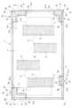
モバイル通信機器などにおいて周波数フィルタなどとして使用される弾性波デバイスDとして図13に示されるものがある。図13中、符号100はデバイスチップ、符号101はデバイスチップ100の一面に形成された共振器101、符号102はデバイスチップ100に形成された合成樹脂製の支持層、符号103は支持層102上に形成されて前記共振器101を気密封止するキャビティ104(内部空間、中空構造部)を形成する合成樹脂製のカバー層、符号105は前記共振器101を含むデバイスチップ100に形成された回路に電気的に接続されたバンプである。An elastic wave device D used as a frequency filter in mobile communication devices and the like is shown in FIG. 13. In FIG. 13,
かかる弾性波デバイスDは前記バンプ105を利用して、他の電子デバイスと一緒にモジュール基板Maに実装されてモジュールMを構成する。バンプ105は典型的にはモジュール基板Ma側に形成された電極に超音波接合などにより接合され、この接合後、弾性波デバイスDはモジュール基板Ma上に形成される封止樹脂層Mbによって封止される。Such an acoustic wave device D is mounted on a module substrate Ma together with other electronic devices using the
図13に示される従来の弾性波デバイスでは、デバイスチップ100の一面上にバンプ105が接合されるバンプパッド106の形成領域を必要とさせる。
また、図13に示される従来の弾性波デバイスは、モジュール基板Maに対しては前記バンプ105によって接合されるため、モジュール基板Maとの間に通常30ないし80μmのギャップGを形成させた状態で、モジュール基板Maに実装されることとなる。 In the conventional acoustic wave device shown in FIG. 13, a region for forming
In addition, the conventional acoustic wave device shown in FIG. 13 is joined to the module substrate Ma by the
この発明が解決しようとする主たる問題点は、この種の弾性波デバイスを前記のようなバンプによらずにモジュール基板に実装できるようにしてデバイスチップ上にバンプパッドを形成する必要がないようにすると共に、この種の弾性波デバイスを前記のようなギャップを形成させることなく、モジュール基板に実装できるようにする点にある。The main problem that this invention aims to solve is to make it possible to mount this type of acoustic wave device on a module substrate without using bumps as described above, thereby eliminating the need to form bump pads on the device chip, and to make it possible to mount this type of acoustic wave device on a module substrate without forming gaps as described above.
前記課題を達成するために、この発明にあっては、第一の観点から、弾性波デバイスを、一面にIDT電極を含む機能素子を形成させてなるデバイスチップと、
前記一面において前記機能素子の形成領域を囲うように形成された支持層と、
前記支持層上に形成されて前記デバイスチップと前記支持層と共働して前記形成領域を気密封止するキャビティを形成するカバー層とを備える弾性波デバイスであって、
前記デバイスチップにおける前記一面と前記一面に対して背中合わせの位置にある他面との間の側面に、前記機能素子に接続された外部接続端子を位置させており、
モジュール基板の実装面に対し前記カバー層の外面を密着させた状態で、前記外部接続端子と前記実装面における前記カバー層の前記外面の密着領域の外側に形成された前記モジュール基板側の接続端子とを導電材料によりつなぎ合わせ可能としてなる、ものとした。 In order to achieve the above object, from a first viewpoint, the present invention provides an acoustic wave device comprising: a device chip having a functional element including an IDT electrode formed on one surface thereof;
a support layer formed on the one surface so as to surround a formation region of the functional element;
an acoustic wave device comprising: a cover layer formed on the support layer and forming a cavity that hermetically seals the formation region in cooperation with the device chip and the support layer,
an external connection terminal connected to the functional element is located on a side surface between the one surface and another surface of the device chip that is located back-to-back with respect to the one surface;
With the outer surface of the cover layer in close contact with the mounting surface of the module substrate, the external connection terminals and the connection terminals of the module substrate formed outside the close contact area of the outer surface of the cover layer on the mounting surface can be connected by a conductive material.
前記外部接続端子を、前記デバイスチップの前記一面における、前記一面と前記側面とが接する外縁と前記支持層との間に位置されるブランク領域において、このブランク領域と前記側面とに亘るように形成された金属膜によって形成されたものとすることが、この発明の態様の一つとされる。In one aspect of the invention, the external connection terminal is formed from a metal film formed in a blank area of the one surface of the device chip, between the outer edge where the one surface and the side surface meet and the support layer, and extending over this blank area and the side surface.
また、前記デバイスチップは四角形の板状を呈すると共に、その四つの隅部の全部又は一部に前記ブランク領域を形成させるようにすることが、この発明の態様の一つとされる。In one aspect of the invention, the device chip has a rectangular plate shape, and the blank areas are formed in all or part of the four corners.
また、前記課題を達成するために、この発明にあっては、第二の観点から、弾性波デバイスの製造方法を、
ウエハ上に設定されてそれぞれ前記デバイスチップの前記一面となる複数の四角形領域にそれぞれ前記機能素子を形成させた状態から、所定の位置において前記四角形領域の境界線と前記支持層との間に前記ブランク領域を形成させるように前記支持層及び前記カバー層を形成させた後、
隣り合う前記四角形領域間に有底溝を形成し、
次いで、前記ブランク領域と前記有底溝とに亘るように前記外部接続端子となる金属膜を形成し、
この後、前記有底溝の溝底にダイシングを施して前記四角形領域の数分の前記弾性波デバイスを生成するようにしてなる、ものとした。 In order to achieve the above object, from a second standpoint, the present invention provides a method for manufacturing an acoustic wave device, comprising the steps of:
In a state where the functional elements are formed in each of a plurality of rectangular regions that are set on a wafer and that form one surface of each of the device chips, the support layer and the cover layer are formed so as to form the blank region between the boundary line of the rectangular region and the support layer at a predetermined position,
A bottomed groove is formed between the adjacent rectangular regions;
Next, a metal film that will become the external connection terminal is formed so as to extend across the blank area and the bottomed groove;
Thereafter, the groove bottom of the bottomed groove is diced to produce the acoustic wave devices in the number corresponding to the square regions.
この発明にかかる弾性波デバイスにあっては、モジュール基板の実装面に対し前記カバー層の外面を密着させた状態で、前記デバイスチップの側面に位置された外部接続端子と前記モジュール基板側の接続端子とを導電材料によりつなぎ合わせ可能としてなることから、第一に、従来の弾性波デバイスのように、デバイスチップの一面上にバンプ用の電極(バンプパッド)を必要としない利点を有する。これは、デバイスチップの小型化に寄与する。
また、第二に、この発明にかかる弾性波デバイスは、モジュール基板への実装にあたって、従来の弾性波デバイスのようなバンプを必要とせず、前記カバー層をモジュール基板の実装面に密着させた状態で、モジュール基板に実装することができる利点を有する。モジュール基板の実装面に対しては弾性波デバイスなどの実装後に合成樹脂によるモールディング(封止樹脂層の形成)が施されるが、カバー層は実装面に密着されるため、カバー層を薄くしてもこのモールディングの際の樹脂の注入圧によるカバー層の変形が生じることがない。したがって、カバー層を可及的に薄く構成可能となる。これは、弾性波デバイスの低背化、ひいては、前記通信モジュールなどの低背化に寄与する。
また、第三に、この発明にかかる弾性波デバイスは、前記カバー層を実装面に面的に密着させた状態で、モジュール基板に実装されることから、この面的に密着させた箇所からモジュール基板側に弾性波デバイスの駆動により生じる熱を効果的に逃すことが可能となる。 In the acoustic wave device according to the present invention, since the external connection terminals located on the side surface of the device chip and the connection terminals on the module substrate can be connected by a conductive material with the outer surface of the cover layer being in close contact with the mounting surface of the module substrate, firstly, there is an advantage that there is no need for bump electrodes (bump pads) on one surface of the device chip as in the conventional acoustic wave device, which contributes to the miniaturization of the device chip.
Secondly, the acoustic wave device according to the present invention has an advantage that, unlike conventional acoustic wave devices, bumps are not required for mounting on a module substrate, and the cover layer can be attached to the mounting surface of the module substrate while being in close contact with the mounting surface of the module substrate. After mounting an acoustic wave device or the like on the mounting surface of the module substrate, molding (forming a sealing resin layer) with synthetic resin is performed. Since the cover layer is in close contact with the mounting surface, even if the cover layer is made thin, deformation of the cover layer due to the injection pressure of the resin during molding does not occur. Therefore, the cover layer can be made as thin as possible. This contributes to reducing the height of the acoustic wave device, and thus the height of the communication module or the like.
Thirdly, since the acoustic wave device of the present invention is mounted on a module substrate with the cover layer in surface-to-surface contact with the mounting surface, it is possible to effectively dissipate heat generated by operation of the acoustic wave device from the point of surface-to-surface contact to the module substrate.
以下、図1~図12に基づいて、この発明の典型的な実施の形態について、説明する。この実施の形態にかかる弾性波デバイス1は、モバイル通信機器などにおいて周波数フィルタなどとして使用するのに適したものである。A typical embodiment of the present invention will be described below with reference to Figs. 1 to 12. The
かかる弾性波デバイス1は、
デバイスチップ2と、
前記デバイスチップ2の一面2aに形成されたIDT電極6bなどの機能素子6と、
前記一面2aにおいて前記機能素子6を囲うように形成された支持層3(ウォール/Wall)と、
前記支持層3上に形成されて前記デバイスチップ2と前記支持層3と共働して前記機能素子6を気密封止するキャビティ5(内部空間、中空構造部)を形成するカバー層4(ルーフ/Roof)とを備えたものとなっている。 The
A
A
A support layer 3 (wall) formed on the
The
典型的には、前記デバイスチップ2は、一辺を0.5ないし1mmとし、厚さを0.15ないし0.2mmとする四角形(図示の例では長方形)の板状をなすように構成される。
また、典型的には、支持層3は、前記デバイスチップ2の一面2aに直交する向きの厚さ(デバイスチップ2の一面2aを基準とした支持層3の高さ)を10~30μmとするように構成される。
また、典型的には、カバー層4は、厚さを15~35μmとするように構成される。
これらから構成される弾性波デバイス1は、典型的には、厚さを0.25ないし0.35mm程度とする。 Typically, the
Typically, the
Typically, the
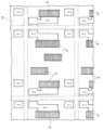
The
弾性波デバイスの断面構造を図2に示す。図中符号6は機能素子、符号5はキャビティ、符号3は支持層、符号4はカバー層、符号7は機能素子に接続されて機能素子と共に後述の回路を構成する配線(Wiring)である。The cross-sectional structure of the acoustic wave device is shown in Figure 2. In the figure,
デバイスチップ2の一面2a上には複数の機能素子6が形成されている。デバイスチップ2の一面2aにおける各機能素子6の形成領域はそれぞれ、支持層3で囲繞されると共に、この支持層3上に形成されるカバー層4で蓋がされた形態となっており、これにより弾性波デバイス1は複数の前記キャビティ5を備えたものとなっている。
支持層3及びカバー層4は、絶縁材料、典型的には、合成樹脂から構成される。 A plurality of
The
デバイスチップ2は、弾性波を伝搬させる機能を持つ。デバイスチップ2には、典型的には、タンタル酸リチウムやニオブ酸リチウムが用いられ、また、デバイスチップ2は、これらにサファイア、シリコン、アルミナ、スピネル、水晶またはガラスなどを積層させて、構成される場合もある。The
図3に機能素子6の一例としての共振器6aを示す。共振器6aはIDT電極6bと、IDT電極6bを挟むようにして形成される反射器6eとを有する。IDT電極6bは、電極対からなり、各電極対は弾性波の伝搬方向xに長さ方向を交叉させるように平行配列された複数の電極指6c同士をこれらの一端側においてバスバー6dで接続させてなる。反射器6eは、弾性波の伝搬方向xに長さ方向を交叉させるように平行配列された複数の電極指6fの端部間をバスバー6gで接続させてなる。
かかる機能素子6は、典型的には、フォトリソグラフィ技術により形成された導電性金属膜によって構成される。 3 shows a resonator 6a as an example of the
Such a
図4に一つのデバイスチップ2上に備えられる回路の一例の概念を示す。符号6aaは入出力ポート(例えば後述の外部出力端子9)間に直列に接続された共振器6a、符号6abは入出力ポート間に並列に接続された共振器6a、符号8はグランドを示す。機能素子6の数や配置は必要に応じて変更される。すなわち、図4の回路によってラダー型フィルタが構成されるようになっている。
かかる回路を構成する前記配線7も、典型的には、フォトリソグラフィ技術により形成された導電性金属膜によって構成される。 4 shows the concept of an example of a circuit provided on one
The
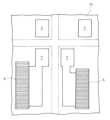
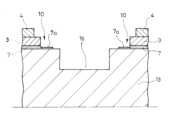
この実施の形態にかかる弾性波デバイス1においては、前記デバイスチップ2における前記一面2aと前記一面2aに対して背中合わせの位置にある他面2bとの間の側面2cに、前記機能素子6に前記配線7を介して電気的に接続された外部接続端子9を位置させている。In the
この実施の形態にあっては、前記外部接続端子9は、前記デバイスチップ2の前記一面2aにおける、前記一面2aと前記側面2cとが接する外縁2dと前記支持層3との間に位置されるブランク領域10(デバイスチップ2の一面2a上の前記支持層3及びカバー層4が形成されていない領域)において、このブランク領域10の前記一面2aと前記側面2cとに亘るように形成された金属膜9aによって形成されている。In this embodiment, the
図示の例では、デバイスチップ2の一面2aは、機能素子6の形成領域を除いて、概ね支持層3によって被覆された状態となっている。それと共に、図示の例では、デバイスチップ2の一面2aの前記外縁2d側において、デバイスチップ2の一面2aを支持層3によって覆っていないブランク領域10が4箇所形成されている。このブランク領域10においてはカバー層4も形成されていない。In the illustrated example, one
図示の例では、前記デバイスチップ2は四角形の板状を呈すると共に、その四つの隅部2eの一部に前記ブランク領域10を形成させている。図示は省略するがブランク領域10は、四つの隅部2eの全部に形成させていても構わない。
図示の例では、デバイスチップ2の四つの隅部2eのうちの三つにブランク領域10を形成させている。 In the illustrated example, the
In the illustrated example,
ブランク領域10では、ブランク領域10にあるデバイスチップ2の外縁2dと実質的に平行をなす支持層3の厚さ方向に沿った第一外面3aが、デバイスチップ2の外縁2dよりもデバイスチップ2の中心2f(図1参照)側に位置して、前記第一外面3aと外縁2dとの間に間隔が形成されている。また、デバイスチップ2の中心2fを周回する方向でのブランク領域10の二箇所の端末10aにはそれぞれ、前記第一外面3aに実質的に直交する支持層3の厚さ方向に沿った第二外面3bが形成されている。この第一外面3aと二箇所の第二外面3bとデバイスチップ2の外縁2dとに囲まれた箇所が前記ブランク領域10となっている。In the
弾性波デバイス1をデバイスチップ2の前記一面2aに直交する向きから見た状態(図1)において、デバイスチップ2の隅部2eに形成されたブランク領域10は、デバイスチップ2の角2gにおいて直角に屈曲し、かつ、この角2gと二箇所の前記第二外面3bとの間をデバイスチップ2の辺2hに沿わせた、L型状となっている。
図示の例では、デバイスチップ2の四つの隅部2eのうちのブランク領域10が形成されていない隅部2eの近傍には、デバイスチップ2の辺2hに沿った直線的なブランク領域10が形成されている(図1における左下のブランク領域10)。 When the
In the illustrated example, a linear
ブランク領域10では、支持層3の前記第一外面3aとデバイスチップ2の外縁2dとの間となる箇所まで、配線7が延び出している。すなわち、ブランク領域10に前記配線7の一部7aが位置されるようになっている。In the
外部接続端子9は、ブランク領域10に位置される前記配線7の一部7aを覆って、ブランク領域10と前記側面2cとに亘るように形成されている。図示の例では、外部接続端子9はブランク領域10の全体を覆い、かつ、ブランク領域10の直下においてデバイスチップ2の厚さ方向2i(図2参照)中程の位置よりもやや一面2a側に近い位置までの範囲でデバイスチップ2の側面2cを覆っている。The
図示の例では、四箇所のブランク領域10のぞれぞれにおいて、前記のように外部接続端子9が形成されている。In the illustrated example, an
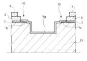
そして、この実施の形態にあっては、モジュール基板11の実装面11aに対し前記カバー層4の外面4aを密着させた状態で、前記外部接続端子9と前記実装面11aにおける前記カバー層4の前記外面4aの密着領域11bの外側に形成された前記モジュール基板11側の接続端子11cとを導電材料12によりつなぎ合わせ可能としている(図5)。In this embodiment, with the
具体的には、以上に説明した弾性波デバイス1と、その他の一又は二以上のデバイスとが実装されてモバイル通信機器などの通信モジュールなどとなるモジュール基板11におけるデバイスが実装される実装面11aに対し、弾性波デバイス1は前記カバー層4の外面4aを実装面11aに密着させた状態で、前記外部接続端子9とモジュール基板11側の接続端子11cとをハンダなどの導電材料12を介して接続させることで、モジュール基板11側に電気的に接続可能となる。カバー層4の外面4aにモジュール基板11の実装面11aに対する粘着機能を付与させておけば、両者の密着性を安定的に確保できる。かかる粘着機能の付与は、カバー層4の外面4aが弱粘着性を持つようにする表面加工により、あるいは、カバー層4の外面4aが弱粘着性を持つようにカバー層4を粘着性を持つ材料から構成することにより、実現できる。Specifically, the
ブランク領域10において配線7に接続されてデバイスチップ2の側面2cを覆いこの側面2cに位置される外部接続端子9に対して、この側面2cの外側に形成される導電材料12によって弾性波デバイス1はモジュール基板11側に電気的に接続される。
すなわち、この実施の形態にかかる弾性波デバイス1とモジュール基板11とは、デバイスチップ2の側面2cに位置される外部接続端子9を利用して、前記カバー層4を実装面11aに密着させた状態で、モジュール基板11に実装することができる。外部接続端子9はブランク領域10において配線7に接続されていれば足り、ブランク領域10の幅、すなわち、支持層3の第一外面3aとデバイスチップ2の外縁2dとの間の距離は可及的に小さくすることが可能である。
これにより、この実施の形態にかかる弾性波デバイス1にあっては、第一に、従来の弾性波デバイス1(図13)のように、デバイスチップ2の一面2a上にバンプ用の電極(バンプパッド)を必要としない利点を有する。これは、デバイスチップ2の小型化に寄与する。
また、第二に、モジュール基板11への実装にあたって、従来の弾性波デバイス1(図13)のようなバンプを必要とせず、前記カバー層4を実装面11aに密着させた状態で、モジュール基板11に実装することができる利点を有する。モジュール基板11の実装面11aに対しては弾性波デバイス1などの実装後に合成樹脂によるモールディングが施されるが、カバー層4は実装面11aに密着されるため、カバー層4を薄くしてもこのモールディングの際の樹脂の注入圧によるカバー層4の変形が生じることがない。したがって、カバー層4を可及的に薄く構成可能となる。これは、弾性波デバイス1の低背化、ひいては、前記通信モジュールなどの低背化に寄与する。
また、第三に、この実施の形態にかかる弾性波デバイス1は、前記カバー層4を実装面11aに面的に密着させた状態で、モジュール基板11に実装されることから、この面的に密着させた箇所からモジュール基板11側に弾性波デバイス1の駆動により生じる熱を効果的に逃すことが可能となる。 In the
That is, the
As a result, the
Secondly, there is an advantage that the
Thirdly, since the
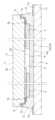
以上に説明した弾性波デバイス11は、以下のようにすることで、適切且つ合理的に製造し得る。この実施の形態にかかる弾性波デバイス11の製造ステップの要部を図6~図12に示す。The
先ず、ウエハ13上に設定されてそれぞれ前記デバイスチップ2となる複数の四角形領域14(図6参照)にそれぞれ、前記機能素子6及び配線7を形成させる(ステップ1/図7、図8)。典型的には、一つの四角形領域14に複数の機能素子6が形成される。図7では配線7は一部のみを模式的に表している。
四角形領域14の大きさなどは必要に応じて適宜設定される。図6中の一点鎖線は、設定される四角形領域14の境界を理解しやすいように示した仮想の境界線である。隣り合う四角形領域14間には、後述の有底溝16が形成される隙間15が形成される。この隙間15は格子状のものとして観念される。 First, the
The size of the
次いで、前記四角形領域14に前記支持層3及び前記カバー層4を形成させると共に、所定の位置において前記境界線と前記支持層3との間に前記ブランク領域10を形成させる(ステップ2/図9)。図示の例では、一つの四角形領域14において、四つのブランク領域10を形成させている。ブランク領域10には前記のように配線7が延び出している(図9においては、カバー層4の記載を省略している。また、ブランク領域10に位置される配線7の一部7aにハッチングを付している。)。Next, the
次いで、隣り合う前記四角形領域14間に有底溝16(トレンチ)を形成する(ステップ3/図10)。有底溝16は隙間15内に形成され格子状をなす。有底溝16は、典型的には、レーザー加工やエッチングにより形成される。Next, bottomed grooves 16 (trenches) are formed between adjacent rectangular regions 14 (
次いで、前記ブランク領域10と前記有底溝16とに亘るように前記外部接続端子9となる導電性を備えた金属膜9aを形成する(ステップ4/図11)。金属膜9aは、典型的には、蒸着、スパッタ、メッキにより形成される。Next, a
次いで、前記有底溝16の溝底にダイシングを施して前記四角形領域14の数分の前記弾性波デバイス1を生成する(ステップ5/図12)。
ダイシングは、前記有底溝16に沿って、かつ、有底溝16の左右の溝壁との間にそれぞれ間隔を開けるようにして、施される。ダイシングされた部分を図12において符号17で示す。このダイシングによって、前記ウエハ13から前記四角形領域14の数分の弾性波デバイス1が切り分けられる。
このように生成される弾性波デバイス1の側面2cは、弾性波デバイス1の中心2fを巡るいずれの箇所においても、前記有底溝16の溝底であった段差面2caと、この段差面2caと前記一面2aとの間に位置される上側垂直面2cbと、この段差面2caと前記他面2bとの間に位置される下側垂直面2ccとから構成される。金属膜9aは前記一面2aにおけるブランク領域10にある部分と、上側垂直面2cbと、段差面2caとに亘って形成されることとなる。 Next, the groove bottom of the bottomed
Dicing is performed along the bottomed
The
なお、当然のことながら、本発明は以上に説明した実施態様に限定されるものではなく、本発明の目的を達成し得るすべての実施態様を含むものである。Naturally, the present invention is not limited to the embodiments described above, but includes all embodiments that can achieve the object of the present invention.
1 弾性波デバイス
2 デバイスチップ
2a 一面
2b 他面
2c 側面
2ca 段差面
2cb 上側垂直面
2cc 下側垂直面
2d 外縁
2e 隅部
2f 中心
2g 角
2h 辺
2i 厚さ方向
3 支持層
3a 第一外面
3b 第二外面
4 カバー層
4a 外面
5 キャビティ
6 機能素子
6a、6aa、6ab 共振器
6b IDT電極
6c 電極指
6d バスバー
6e 反射器
6f 電極指
6g バスバー
7 配線
7a 配線の一部
8 グランド
9 外部接続端子
9a 金属膜
10 ブランク領域
10a 端末
11 モジュール基板
11a 実装面
11b 密着領域
11c 接続端子
12 導電材料
13 ウエハ
14 四角形領域
15 隙間
16 有底溝
x 伝搬方向
1
Claims (4)
Translated fromJapanese前記一面において前記機能素子の形成領域を囲うように形成された支持層と、
前記支持層上に形成されて前記デバイスチップと前記支持層と共働して前記形成領域を気密封止するキャビティを形成するカバー層とを備える弾性波デバイスであって、
前記デバイスチップにおける前記一面と前記一面に対して背中合わせの位置にある他面との間の側面に、前記機能素子に接続された外部接続端子を位置させており、 モジュール基板の実装面に対し前記カバー層の外面を密着させた状態で、前記外部接続端子と前記実装面における前記カバー層の前記外面の密着領域の外側に形成された前記モジュール基板側の接続端子とを導電材料によりつなぎ合わせ可能としてなる、弾性波デバイス。 a device chip having a functional element including an IDT electrode formed on one surface thereof;
a support layer formed on the one surface so as to surround a formation region of the functional element;
an acoustic wave device comprising: a cover layer formed on the support layer and forming a cavity that hermetically seals the formation region in cooperation with the device chip and the support layer,
an external connection terminal connected to the functional element is positioned on a side surface between the one surface of the device chip and the other surface that is back-to-back with the one surface; and with the outer surface of the cover layer in close contact with the mounting surface of a module substrate, the external connection terminal and a connection terminal on the module substrate side that is formed outside the close contact area of the outer surface of the cover layer on the mounting surface can be connected by a conductive material.
隣り合う前記四角形領域間に有底溝を形成し、
次いで、前記ブランク領域と前記有底溝とに亘るように前記外部接続端子となる金属膜を形成し、
この後、前記有底溝の溝底にダイシングを施して前記四角形領域の数分の前記弾性波デバイスを生成するようにしてなる、請求項2又は請求項3に記載の弾性波デバイスの製造方法。 In a state where the functional elements are formed in each of a plurality of rectangular regions that are set on a wafer and that form one surface of each of the device chips, the support layer and the cover layer are formed so as to form the blank region between the boundary line of the rectangular region and the support layer at a predetermined position,
A bottomed groove is formed between the adjacent rectangular regions;
Next, a metal film that will become the external connection terminal is formed so as to extend across the blank area and the bottomed groove;
4. The method for manufacturing an acoustic wave device according to claim 2, further comprising the step of: subsequently dicing the groove bottom of the bottomed groove to produce the acoustic wave devices in a number equal to the number of the quadrangular regions.
Priority Applications (2)
| Application Number | Priority Date | Filing Date | Title |
|---|---|---|---|
| JP2022181860AJP2024071103A (en) | 2022-11-14 | 2022-11-14 | Elastic wave device and method for manufacturing elastic wave device |
| CN202311434211.1ACN118074659A (en) | 2022-11-14 | 2023-10-31 | Elastic wave device and method for manufacturing same |
Applications Claiming Priority (1)
| Application Number | Priority Date | Filing Date | Title |
|---|---|---|---|
| JP2022181860AJP2024071103A (en) | 2022-11-14 | 2022-11-14 | Elastic wave device and method for manufacturing elastic wave device |
Publications (1)
| Publication Number | Publication Date |
|---|---|
| JP2024071103Atrue JP2024071103A (en) | 2024-05-24 |
Family
ID=91094410
Family Applications (1)
| Application Number | Title | Priority Date | Filing Date |
|---|---|---|---|
| JP2022181860APendingJP2024071103A (en) | 2022-11-14 | 2022-11-14 | Elastic wave device and method for manufacturing elastic wave device |
Country Status (2)
| Country | Link |
|---|---|
| JP (1) | JP2024071103A (en) |
| CN (1) | CN118074659A (en) |
- 2022
- 2022-11-14JPJP2022181860Apatent/JP2024071103A/enactivePending
- 2023
- 2023-10-31CNCN202311434211.1Apatent/CN118074659A/enactivePending
Also Published As
| Publication number | Publication date |
|---|---|
| CN118074659A (en) | 2024-05-24 |
Similar Documents
| Publication | Publication Date | Title |
|---|---|---|
| US7528523B2 (en) | Surface acoustic wave device and manufacturing method thereof | |
| CN114208027B (en) | Piezoelectric vibration plate, piezoelectric vibration device, and method for manufacturing piezoelectric vibration device | |
| TWI668960B (en) | Piezo vibrating element and system integration package (SIP) module having the same | |
| CN113196650B (en) | Piezoelectric vibration device | |
| JP6252209B2 (en) | Piezoelectric vibrating piece and piezoelectric device using the piezoelectric vibrating piece | |
| JP6042689B2 (en) | Elastic wave device and design method thereof | |
| JP2019021998A (en) | Electronic components | |
| JP7517135B2 (en) | Piezoelectric Vibration Device | |
| CN114208032B (en) | Piezoelectric vibration device and manufacturing method thereof | |
| JP6696378B2 (en) | Piezoelectric vibration device | |
| WO2024185524A1 (en) | Piezoelectric diaphragm and piezoelectric vibration device | |
| JP2024071103A (en) | Elastic wave device and method for manufacturing elastic wave device | |
| JP2009165102A (en) | Piezoelectric oscillator and method for manufacturing the same | |
| JP7543899B2 (en) | Piezoelectric Vibration Device | |
| JP7196726B2 (en) | crystal wafer | |
| JP2022184006A (en) | piezoelectric vibration device | |
| JP2025049851A (en) | Acoustic wave device and method for manufacturing the same | |
| JP3729090B2 (en) | Piezoelectric filter | |
| JP2025086424A (en) | Elastic wave device | |
| US20240048119A1 (en) | Acoustic wave device | |
| US20240405744A1 (en) | Acoustic wave devices | |
| JP2019036784A (en) | Electronic component and method of manufacturing the same | |
| JP2024179587A (en) | Acoustic Wave Devices, Filters, Multiplexers, and Electronic Components | |
| JP2024112552A (en) | Acoustic Wave Devices | |
| JP2024130520A (en) | Acoustic wave device and manufacturing method thereof |