JP2024058633A - Semiconductor Device - Google Patents
Semiconductor DeviceDownload PDFInfo
- Publication number
- JP2024058633A JP2024058633AJP2023176379AJP2023176379AJP2024058633AJP 2024058633 AJP2024058633 AJP 2024058633AJP 2023176379 AJP2023176379 AJP 2023176379AJP 2023176379 AJP2023176379 AJP 2023176379AJP 2024058633 AJP2024058633 AJP 2024058633A
- Authority
- JP
- Japan
- Prior art keywords
- conductive layer
- transistor
- layer
- semiconductor
- insulating layer
- Prior art date
- Legal status (The legal status is an assumption and is not a legal conclusion. Google has not performed a legal analysis and makes no representation as to the accuracy of the status listed.)
- Pending
Links
Images


Classifications
- H—ELECTRICITY
- H10—SEMICONDUCTOR DEVICES; ELECTRIC SOLID-STATE DEVICES NOT OTHERWISE PROVIDED FOR
- H10B—ELECTRONIC MEMORY DEVICES
- H10B12/00—Dynamic random access memory [DRAM] devices
- H10B12/30—DRAM devices comprising one-transistor - one-capacitor [1T-1C] memory cells
- H—ELECTRICITY
- H10—SEMICONDUCTOR DEVICES; ELECTRIC SOLID-STATE DEVICES NOT OTHERWISE PROVIDED FOR
- H10B—ELECTRONIC MEMORY DEVICES
- H10B12/00—Dynamic random access memory [DRAM] devices
- H10B12/01—Manufacture or treatment
- H10B12/02—Manufacture or treatment for one transistor one-capacitor [1T-1C] memory cells
- H10B12/03—Making the capacitor or connections thereto
- H—ELECTRICITY
- H10—SEMICONDUCTOR DEVICES; ELECTRIC SOLID-STATE DEVICES NOT OTHERWISE PROVIDED FOR
- H10B—ELECTRONIC MEMORY DEVICES
- H10B41/00—Electrically erasable-and-programmable ROM [EEPROM] devices comprising floating gates
- H10B41/70—Electrically erasable-and-programmable ROM [EEPROM] devices comprising floating gates the floating gate being an electrode shared by two or more components
- H—ELECTRICITY
- H10—SEMICONDUCTOR DEVICES; ELECTRIC SOLID-STATE DEVICES NOT OTHERWISE PROVIDED FOR
- H10B—ELECTRONIC MEMORY DEVICES
- H10B12/00—Dynamic random access memory [DRAM] devices
- H—ELECTRICITY
- H10—SEMICONDUCTOR DEVICES; ELECTRIC SOLID-STATE DEVICES NOT OTHERWISE PROVIDED FOR
- H10B—ELECTRONIC MEMORY DEVICES
- H10B12/00—Dynamic random access memory [DRAM] devices
- H10B12/01—Manufacture or treatment
- H10B12/02—Manufacture or treatment for one transistor one-capacitor [1T-1C] memory cells
- H10B12/05—Making the transistor
- H—ELECTRICITY
- H10—SEMICONDUCTOR DEVICES; ELECTRIC SOLID-STATE DEVICES NOT OTHERWISE PROVIDED FOR
- H10B—ELECTRONIC MEMORY DEVICES
- H10B12/00—Dynamic random access memory [DRAM] devices
- H10B12/30—DRAM devices comprising one-transistor - one-capacitor [1T-1C] memory cells
- H10B12/48—Data lines or contacts therefor
- H10B12/482—Bit lines
- H—ELECTRICITY
- H10—SEMICONDUCTOR DEVICES; ELECTRIC SOLID-STATE DEVICES NOT OTHERWISE PROVIDED FOR
- H10B—ELECTRONIC MEMORY DEVICES
- H10B12/00—Dynamic random access memory [DRAM] devices
- H10B12/30—DRAM devices comprising one-transistor - one-capacitor [1T-1C] memory cells
- H10B12/48—Data lines or contacts therefor
- H10B12/488—Word lines
- H—ELECTRICITY
- H10—SEMICONDUCTOR DEVICES; ELECTRIC SOLID-STATE DEVICES NOT OTHERWISE PROVIDED FOR
- H10B—ELECTRONIC MEMORY DEVICES
- H10B12/00—Dynamic random access memory [DRAM] devices
- H10B12/50—Peripheral circuit region structures
- H—ELECTRICITY
- H10—SEMICONDUCTOR DEVICES; ELECTRIC SOLID-STATE DEVICES NOT OTHERWISE PROVIDED FOR
- H10B—ELECTRONIC MEMORY DEVICES
- H10B41/00—Electrically erasable-and-programmable ROM [EEPROM] devices comprising floating gates
- H10B41/20—Electrically erasable-and-programmable ROM [EEPROM] devices comprising floating gates characterised by three-dimensional arrangements, e.g. with cells on different height levels
- H—ELECTRICITY
- H10—SEMICONDUCTOR DEVICES; ELECTRIC SOLID-STATE DEVICES NOT OTHERWISE PROVIDED FOR
- H10B—ELECTRONIC MEMORY DEVICES
- H10B41/00—Electrically erasable-and-programmable ROM [EEPROM] devices comprising floating gates
- H10B41/30—Electrically erasable-and-programmable ROM [EEPROM] devices comprising floating gates characterised by the memory core region
- H—ELECTRICITY
- H10—SEMICONDUCTOR DEVICES; ELECTRIC SOLID-STATE DEVICES NOT OTHERWISE PROVIDED FOR
- H10D—INORGANIC ELECTRIC SEMICONDUCTOR DEVICES
- H10D1/00—Resistors, capacitors or inductors
- H10D1/60—Capacitors
- H10D1/68—Capacitors having no potential barriers
- H—ELECTRICITY
- H10—SEMICONDUCTOR DEVICES; ELECTRIC SOLID-STATE DEVICES NOT OTHERWISE PROVIDED FOR
- H10D—INORGANIC ELECTRIC SEMICONDUCTOR DEVICES
- H10D1/00—Resistors, capacitors or inductors
- H10D1/60—Capacitors
- H10D1/68—Capacitors having no potential barriers
- H10D1/692—Electrodes
- H—ELECTRICITY
- H10—SEMICONDUCTOR DEVICES; ELECTRIC SOLID-STATE DEVICES NOT OTHERWISE PROVIDED FOR
- H10D—INORGANIC ELECTRIC SEMICONDUCTOR DEVICES
- H10D30/00—Field-effect transistors [FET]
- H10D30/60—Insulated-gate field-effect transistors [IGFET]
- H10D30/67—Thin-film transistors [TFT]
- H—ELECTRICITY
- H10—SEMICONDUCTOR DEVICES; ELECTRIC SOLID-STATE DEVICES NOT OTHERWISE PROVIDED FOR
- H10D—INORGANIC ELECTRIC SEMICONDUCTOR DEVICES
- H10D30/00—Field-effect transistors [FET]
- H10D30/60—Insulated-gate field-effect transistors [IGFET]
- H10D30/67—Thin-film transistors [TFT]
- H10D30/674—Thin-film transistors [TFT] characterised by the active materials
- H10D30/6755—Oxide semiconductors, e.g. zinc oxide, copper aluminium oxide or cadmium stannate
- H—ELECTRICITY
- H10—SEMICONDUCTOR DEVICES; ELECTRIC SOLID-STATE DEVICES NOT OTHERWISE PROVIDED FOR
- H10D—INORGANIC ELECTRIC SEMICONDUCTOR DEVICES
- H10D30/00—Field-effect transistors [FET]
- H10D30/60—Insulated-gate field-effect transistors [IGFET]
- H10D30/67—Thin-film transistors [TFT]
- H10D30/6757—Thin-film transistors [TFT] characterised by the structure of the channel, e.g. transverse or longitudinal shape or doping profile
- H—ELECTRICITY
- H10—SEMICONDUCTOR DEVICES; ELECTRIC SOLID-STATE DEVICES NOT OTHERWISE PROVIDED FOR
- H10D—INORGANIC ELECTRIC SEMICONDUCTOR DEVICES
- H10D86/00—Integrated devices formed in or on insulating or conducting substrates, e.g. formed in silicon-on-insulator [SOI] substrates or on stainless steel or glass substrates
- H10D86/40—Integrated devices formed in or on insulating or conducting substrates, e.g. formed in silicon-on-insulator [SOI] substrates or on stainless steel or glass substrates characterised by multiple TFTs
- H10D86/421—Integrated devices formed in or on insulating or conducting substrates, e.g. formed in silicon-on-insulator [SOI] substrates or on stainless steel or glass substrates characterised by multiple TFTs having a particular composition, shape or crystalline structure of the active layer
- H10D86/423—Integrated devices formed in or on insulating or conducting substrates, e.g. formed in silicon-on-insulator [SOI] substrates or on stainless steel or glass substrates characterised by multiple TFTs having a particular composition, shape or crystalline structure of the active layer comprising semiconductor materials not belonging to the Group IV, e.g. InGaZnO
- H—ELECTRICITY
- H10—SEMICONDUCTOR DEVICES; ELECTRIC SOLID-STATE DEVICES NOT OTHERWISE PROVIDED FOR
- H10D—INORGANIC ELECTRIC SEMICONDUCTOR DEVICES
- H10D86/00—Integrated devices formed in or on insulating or conducting substrates, e.g. formed in silicon-on-insulator [SOI] substrates or on stainless steel or glass substrates
- H10D86/40—Integrated devices formed in or on insulating or conducting substrates, e.g. formed in silicon-on-insulator [SOI] substrates or on stainless steel or glass substrates characterised by multiple TFTs
- H10D86/481—Integrated devices formed in or on insulating or conducting substrates, e.g. formed in silicon-on-insulator [SOI] substrates or on stainless steel or glass substrates characterised by multiple TFTs integrated with passive devices, e.g. auxiliary capacitors
- H—ELECTRICITY
- H10—SEMICONDUCTOR DEVICES; ELECTRIC SOLID-STATE DEVICES NOT OTHERWISE PROVIDED FOR
- H10D—INORGANIC ELECTRIC SEMICONDUCTOR DEVICES
- H10D86/00—Integrated devices formed in or on insulating or conducting substrates, e.g. formed in silicon-on-insulator [SOI] substrates or on stainless steel or glass substrates
- H10D86/40—Integrated devices formed in or on insulating or conducting substrates, e.g. formed in silicon-on-insulator [SOI] substrates or on stainless steel or glass substrates characterised by multiple TFTs
- H10D86/60—Integrated devices formed in or on insulating or conducting substrates, e.g. formed in silicon-on-insulator [SOI] substrates or on stainless steel or glass substrates characterised by multiple TFTs wherein the TFTs are in active matrices
- H—ELECTRICITY
- H10—SEMICONDUCTOR DEVICES; ELECTRIC SOLID-STATE DEVICES NOT OTHERWISE PROVIDED FOR
- H10D—INORGANIC ELECTRIC SEMICONDUCTOR DEVICES
- H10D88/00—Three-dimensional [3D] integrated devices
Landscapes
- Engineering & Computer Science (AREA)
- Manufacturing & Machinery (AREA)
- Thin Film Transistor (AREA)
- Semiconductor Memories (AREA)
- Semiconductor Integrated Circuits (AREA)
- Metal-Oxide And Bipolar Metal-Oxide Semiconductor Integrated Circuits (AREA)
Abstract
Description
Translated fromJapanese本発明の一態様は、トランジスタ、半導体装置、記憶装置、および電子機器に関する。または、本発明の一態様は、記憶装置、または半導体装置の作製方法に関する。または、本発明の一態様は、半導体ウエハ、およびモジュールに関する。One aspect of the present invention relates to a transistor, a semiconductor device, a memory device, and an electronic device. Alternatively, one aspect of the present invention relates to a method for manufacturing a memory device or a semiconductor device. Alternatively, one aspect of the present invention relates to a semiconductor wafer and a module.
なお、本発明の一態様は、上記の技術分野に限定されない。本明細書等で開示する本発明の一態様の技術分野としては、半導体装置、表示装置、発光装置、蓄電装置、記憶装置、電子機器、照明装置、入力装置、入出力装置、それらの駆動方法、又はそれらの製造方法、を一例として挙げることができる。半導体装置は、半導体特性を利用することで機能しうる装置全般を指す。Note that one embodiment of the present invention is not limited to the above technical field. Examples of technical fields of one embodiment of the present invention disclosed in this specification and the like include semiconductor devices, display devices, light-emitting devices, power storage devices, memory devices, electronic devices, lighting devices, input devices, input/output devices, driving methods thereof, and manufacturing methods thereof. A semiconductor device refers to any device that can function by utilizing semiconductor characteristics.
近年、半導体装置の開発が進められ、CPU(Central Processing Unit)、メモリ、またはこれら以外のLSI(Large Scale Integration)が主に半導体装置に用いられている。CPUは、半導体ウエハを加工し、チップ化された半導体集積回路(少なくともトランジスタ及びメモリ)を有し、接続端子である電極が形成された半導体素子の集合体である。In recent years, the development of semiconductor devices has progressed, and CPUs (Central Processing Units), memories, and other LSIs (Large Scale Integrations) are mainly used in semiconductor devices. A CPU is a collection of semiconductor elements that have semiconductor integrated circuits (at least transistors and memories) that are chipped by processing a semiconductor wafer and have electrodes that serve as connection terminals.
CPU、メモリ、またはこれら以外のLSIの半導体回路(ICチップ)は、回路基板、例えばプリント配線基板に実装され、様々な電子機器の部品の一つとして用いられる。CPUs, memories, and other LSI semiconductor circuits (IC chips) are mounted on circuit boards, such as printed wiring boards, and used as components in a variety of electronic devices.
また、絶縁表面を有する基板上に形成された半導体薄膜を用いてトランジスタを構成する技術が注目されている。該トランジスタは集積回路、及び画像表示装置(単に表示装置とも表記する)のような半導体部品に広く応用されている。トランジスタに適用可能な半導体薄膜としてシリコン系半導体材料が広く知られているが、その他の材料として酸化物半導体が注目されている。In addition, technology that constructs transistors using semiconductor thin films formed on substrates with insulating surfaces has attracted attention. Such transistors are widely used in semiconductor components such as integrated circuits and image display devices (also simply referred to as display devices). Silicon-based semiconductor materials are widely known as semiconductor thin films that can be used in transistors, but oxide semiconductors are also attracting attention as other materials.
また、酸化物半導体を用いたトランジスタは、非導通状態におけるリーク電流が極めて小さいことが知られている。例えば、特許文献1には、リーク電流が小さいという特性を応用した低消費電力のCPUなどが開示されている。また、例えば、特許文献2には、長期にわたり記憶内容を保持することができる記憶装置などが、開示されている。It is also known that transistors using oxide semiconductors have extremely small leakage currents in a non-conducting state. For example,
また、近年では電子機器の小型化、軽量化に伴い、集積回路のさらなる高密度化への要求が高まっている。また、集積回路を含む半導体装置の生産性の向上が求められている。例えば、特許文献3及び非特許文献1では、酸化物半導体膜を用いるトランジスタを備えるメモリセルを複数重畳して設けることにより、集積回路の高密度化を図る技術が開示されている。また、特許文献4には、酸化物半導体の側面がゲート絶縁体を介してゲート電極に覆われている縦型のトランジスタが開示されている。In recent years, there has been an increasing demand for higher density integrated circuits due to the miniaturization and weight reduction of electronic devices. There is also a demand for improved productivity of semiconductor devices including integrated circuits. For example, Patent Document 3 and Non-Patent
本発明の一態様は、微細化または高集積化が可能な半導体装置または記憶装置を提供することを課題の一とする。または、記憶装置において記憶素子と周辺回路とを低コストで作り分けることを課題の一とする。または、配線の負荷を軽減できる半導体装置または記憶装置を提供することを課題の一とする。または、動作速度が速い半導体装置または記憶装置を提供することを課題の一とする。または、良好な電気特性を有する半導体装置または記憶装置を提供することを課題の一とする。または、トランジスタの電気特性のばらつきが少ない半導体装置または記憶装置を提供することを課題の一とする。または、信頼性が良好な半導体装置または記憶装置を提供することを課題の一とする。または、オン電流が大きい半導体装置を提供することを課題の一とする。または、低消費電力の半導体装置または記憶装置を提供することを課題の一とする。または、新規の半導体装置または記憶装置を提供することを課題の一とする。または、新規の半導体装置または記憶装置の作製方法を提供することを課題の一とする。本発明の一態様は、先行技術の問題点の少なくとも一を、少なくとも軽減することを課題の一とする。One aspect of the present invention has an object to provide a semiconductor device or memory device that can be miniaturized or highly integrated. Another object is to separately fabricate a memory element and a peripheral circuit in a memory device at low cost. Another object is to provide a semiconductor device or memory device that can reduce the load on wiring. Another object is to provide a semiconductor device or memory device with high operating speed. Another object is to provide a semiconductor device or memory device with good electrical characteristics. Another object is to provide a semiconductor device or memory device with less variation in the electrical characteristics of transistors. Another object is to provide a semiconductor device or memory device with good reliability. Another object is to provide a semiconductor device with a large on-current. Another object is to provide a semiconductor device or memory device with low power consumption. Another object is to provide a new semiconductor device or memory device. Another object is to provide a method for manufacturing a new semiconductor device or memory device. One aspect of the present invention has an object to at least reduce at least one of the problems of the prior art.
なお、これらの課題の記載は、他の課題の存在を妨げるものではない。なお、本発明の一態様は、これらの課題の全てを解決する必要はないものとする。なお、これら以外の課題は、明細書、図面、請求項などの記載から抽出することが可能である。The description of these problems does not preclude the existence of other problems. One embodiment of the present invention does not have to solve all of these problems. Problems other than these can be extracted from the description in the specification, drawings, claims, etc.
本発明の一態様は、第1のトランジスタ、容量素子、及び第1の絶縁層を有する半導体装置である。第1のトランジスタは、第1の導電層、第2の導電層、第3の導電層、半導体層、及び第2の絶縁層を有する。容量素子は、第4の導電層、第5の導電層、第6の導電層、第7の導電層、及び第2の絶縁層を有する。第1の絶縁層は、第1の導電層及び第4の導電層上に設けられ、且つ、第1の導電層に達する第1の開口と、第4の導電層に達する第2の開口と、を有する。第2の導電層と第5の導電層とは、それぞれ第1の絶縁層上に設けられる。半導体層は、第2の導電層と接する部分と、第1の開口内において第1の導電層と接する部分と、を有する。第6の導電層は、第5の導電層と接する部分と、第2の開口内において第4の導電層と接する部分と、を有する。第2の絶縁層は、第1の開口内において半導体層を覆う部分と、第2の開口内において第6の導電層を覆う部分と、を有する。第3の導電層は、第1の開口内において第2の絶縁層を介して半導体層と重なる部分を有する。第7の導電層は、第2の開口内において第2の絶縁層を介して第6の導電層と重なる部分を有する。One aspect of the present invention is a semiconductor device having a first transistor, a capacitor, and a first insulating layer. The first transistor has a first conductive layer, a second conductive layer, a third conductive layer, a semiconductor layer, and a second insulating layer. The capacitor has a fourth conductive layer, a fifth conductive layer, a sixth conductive layer, a seventh conductive layer, and a second insulating layer. The first insulating layer is provided on the first conductive layer and the fourth conductive layer, and has a first opening that reaches the first conductive layer and a second opening that reaches the fourth conductive layer. The second conductive layer and the fifth conductive layer are each provided on the first insulating layer. The semiconductor layer has a portion in contact with the second conductive layer and a portion in contact with the first conductive layer in the first opening. The sixth conductive layer has a portion in contact with the fifth conductive layer and a portion in contact with the fourth conductive layer in the second opening. The second insulating layer has a portion that covers the semiconductor layer in the first opening and a portion that covers the sixth conductive layer in the second opening. The third conductive layer has a portion that overlaps with the semiconductor layer through the second insulating layer in the first opening. The seventh conductive layer has a portion that overlaps with the sixth conductive layer through the second insulating layer in the second opening.
また、上記において、第1の導電層は、第1の金属層と、当該第1の金属層上の第1の酸化物層と、を有することが好ましい。さらに第2の導電層は、第2の金属層と、当該第2の金属層上の第2の酸化物層と、を有することが好ましい。このとき、半導体層は、第1の酸化物層と第2の酸化物層と、それぞれ接することが好ましい。In the above, the first conductive layer preferably has a first metal layer and a first oxide layer on the first metal layer. Furthermore, the second conductive layer preferably has a second metal layer and a second oxide layer on the second metal layer. In this case, the semiconductor layer preferably contacts the first oxide layer and the second oxide layer, respectively.
また、上記において、第1の導電層と第4の導電層は、同一材料を含むことが好ましい。また第2の導電層と第5の導電層は、同一材料を含むことが好ましい。さらに第3の導電層と第7の導電層は、同一材料を含むことが好ましい。In addition, in the above, it is preferable that the first conductive layer and the fourth conductive layer contain the same material. It is also preferable that the second conductive layer and the fifth conductive layer contain the same material. It is further preferable that the third conductive layer and the seventh conductive layer contain the same material.
また、上記において、第3の絶縁層をさらに有することが好ましい。このとき、第3の導電層及び第7の導電層は、それぞれ第3の絶縁層に埋め込まれるように設けられることが好ましい。In the above, it is preferable to further include a third insulating layer. In this case, it is preferable that the third conductive layer and the seventh conductive layer are each embedded in the third insulating layer.
また、上記において、第8の導電層、及び第9の導電層をさらに有することが好ましい。このとき、第8の導電層は、第1の開口内において、第2の絶縁層と第3の導電層との間に位置することが好ましい。また第9の導電層は、第2の開口内において、第2の絶縁層と第7の導電層との間に位置することが好ましい。In the above, it is preferable to further have an eighth conductive layer and a ninth conductive layer. In this case, it is preferable that the eighth conductive layer is located between the second insulating layer and the third conductive layer in the first opening. Also, it is preferable that the ninth conductive layer is located between the second insulating layer and the seventh conductive layer in the second opening.
また、上記において、第1の開口は下端の開口径よりも上端の開口径が大きく、第2の開口は下端の開口径よりも上端の開口径が大きいことが好ましい。Furthermore, in the above, it is preferable that the opening diameter of the first opening is larger at the upper end than at the lower end, and the opening diameter of the second opening is larger at the upper end than at the lower end.
また、上記において、第1の導電層は、第4の導電層、第5の導電層、及び第6の導電層と電気的に接続していることが好ましい。In addition, in the above, it is preferable that the first conductive layer is electrically connected to the fourth conductive layer, the fifth conductive layer, and the sixth conductive layer.
また、上記において、第2の導電層は、第4の導電層、第5の導電層、及び第6の導電層と電気的に接続していることが好ましい。In addition, in the above, it is preferable that the second conductive layer is electrically connected to the fourth conductive layer, the fifth conductive layer, and the sixth conductive layer.
また、上記において、第2のトランジスタおよび第3のトランジスタをさらに有することが好ましい。第2のトランジスタは、ゲートが第1の導電層と電気的に接続され、第3のトランジスタは、ソース及びドレインの一方が第2のトランジスタのソース及びドレインの一方と電気的に接続されることが好ましい。In the above, it is preferable to further include a second transistor and a third transistor. It is preferable that the gate of the second transistor is electrically connected to the first conductive layer, and one of the source and drain of the third transistor is electrically connected to one of the source and drain of the second transistor.
また、上記において、第2のトランジスタ及び第3のトランジスタは、第1の導電層よりも下方に位置することが好ましい。また第2のトランジスタは、第1のトランジスタと重なる部分を有することが好ましい。さらに第3のトランジスタは、容量素子と重なる部分を有することが好ましい。In the above, the second transistor and the third transistor are preferably located below the first conductive layer. The second transistor preferably has a portion that overlaps with the first transistor. The third transistor preferably has a portion that overlaps with the capacitive element.
また、上記において、第2のトランジスタ及び第3のトランジスタは、第1の導電層よりも下方に位置することが好ましい。また第2のトランジスタは、容量素子と重なる部分を有することが好ましい。さらに第3のトランジスタは、第1のトランジスタと重なる部分を有することが好ましい。In the above, the second transistor and the third transistor are preferably located below the first conductive layer. The second transistor preferably has a portion that overlaps with the capacitive element. The third transistor preferably has a portion that overlaps with the first transistor.
本発明の一態様によれば、微細化または高集積化が可能な半導体装置または記憶装置を提供できる。または、記憶装置において記憶素子と周辺回路とを低コストで作り分けることができる。または、配線の負荷を軽減できる半導体装置または記憶装置を提供できる。または、動作速度が速い半導体装置または記憶装置を提供できる。または、信頼性が良好な半導体装置または記憶装置を提供できる。または、トランジスタの電気特性のばらつきが少ない半導体装置または記憶装置を提供できる。または、良好な電気特性を有する半導体装置または記憶装置を提供できる。または、オン電流が大きい半導体装置を提供できる。または、低消費電力の半導体装置または記憶装置を提供できる。または、新規の半導体装置または記憶装置を提供できる。または、新規の半導体装置または記憶装置の作製方法を提供できる。本発明の一態様によれば、先行技術の問題点の少なくとも一を、少なくとも軽減できる。According to one aspect of the present invention, a semiconductor device or memory device that can be miniaturized or highly integrated can be provided. Or, in a memory device, memory elements and peripheral circuits can be separately manufactured at low cost. Or, a semiconductor device or memory device that can reduce the load on wiring can be provided. Or, a semiconductor device or memory device with high operating speed can be provided. Or, a semiconductor device or memory device with good reliability can be provided. Or, a semiconductor device or memory device with little variation in the electrical characteristics of the transistors can be provided. Or, a semiconductor device or memory device with good electrical characteristics can be provided. Or, a semiconductor device with a large on-current can be provided. Or, a semiconductor device or memory device with low power consumption can be provided. Or, a new semiconductor device or memory device can be provided. Or, a method for manufacturing a new semiconductor device or memory device can be provided. According to one aspect of the present invention, at least one of the problems of the prior art can be at least alleviated.
なお、これらの効果の記載は、他の効果の存在を妨げるものではない。なお、本発明の一態様は、必ずしも、これらの効果の全てを有する必要はない。なお、これら以外の効果は、明細書、図面、請求項などの記載から抽出することが可能である。The description of these effects does not preclude the existence of other effects. One embodiment of the present invention does not necessarily have to have all of these effects. Effects other than these can be extracted from the description in the specification, drawings, claims, etc.
以下、実施の形態について図面を参照しながら説明する。ただし、実施の形態は多くの異なる態様で実施することが可能であり、趣旨およびその範囲から逸脱することなくその形態および詳細を様々に変更し得ることは、当業者であれば容易に理解される。したがって、本発明は、以下の実施の形態の記載内容に限定して解釈されるものではない。The following describes the embodiments with reference to the drawings. However, it will be readily understood by those skilled in the art that the embodiments can be implemented in many different ways, and that the form and details can be modified in various ways without departing from the spirit and scope of the invention. Therefore, the present invention should not be interpreted as being limited to the description of the embodiments below.
また、図面において、大きさ、層の厚さ、または領域は、明瞭化のために誇張されている場合がある。よって、必ずしもそのスケールに限定されない。なお、図面は、理想的な例を模式的に示したものであり、図面に示す形状または値などに限定されない。例えば、実際の製造工程において、エッチングなどの処理により層、またはレジストマスクなどが意図せずに目減りすることがあるが、理解を容易とするため、図に反映しないことがある。また、図面において、同一部分または同様な機能を有する部分には同一の符号を異なる図面間で共通して用い、その繰り返しの説明は省略する場合がある。また、同様の機能を指す場合には、ハッチングパターンを同じくし、特に符号を付さない場合がある。In addition, in the drawings, the size, layer thickness, or area may be exaggerated for clarity. Therefore, the scale is not necessarily limited. The drawings are schematic illustrations of ideal examples, and are not limited to the shapes or values shown in the drawings. For example, in the actual manufacturing process, layers or resist masks may be unintentionally thinned by etching or other processes, but this may not be reflected in the drawings to facilitate understanding. In addition, in the drawings, the same reference numerals may be used in common between different drawings for the same parts or parts having similar functions, and repeated explanations may be omitted. In addition, when referring to similar functions, the same hatching pattern may be used and no particular reference numeral may be used.
また、特に平面図(「上面図」ともいう)、または斜視図などにおいて、発明の理解を容易とするため、一部の構成要素の記載を省略する場合がある。また、一部の隠れ線の記載を省略する場合がある。In addition, in order to make the invention easier to understand, particularly in plan views (also called "top views") or perspective views, some components may be omitted from the illustration. Also, some hidden lines may be omitted from the illustration.
また、本明細書等において、第1、第2等として付される序数詞は便宜上用いるものであり、工程順または積層順を示すものではない。そのため、例えば、「第1の」を「第2の」または「第3の」などと適宜置き換えて説明することができる。また、本明細書等に記載されている序数詞と、本発明の一態様を特定するために用いられる序数詞は一致しない場合がある。In addition, in this specification, ordinal numbers such as first, second, etc. are used for convenience and do not indicate the order of processes or stacking. Therefore, for example, "first" can be appropriately replaced with "second" or "third" to explain. In addition, the ordinal numbers described in this specification and the ordinal numbers used to identify one aspect of the present invention may not match.
また、本明細書等において、「上に」、「下に」などの配置を示す語句は、構成要素同士の位置関係を、図面を参照して説明するために、便宜上用いている。また、構成要素同士の位置関係は、各構成要素を描写する方向に応じて適宜変化するものである。したがって、明細書で説明した語句に限定されず、状況に応じて適切に言い換えることができる。In addition, in this specification, terms indicating position such as "above" and "below" are used for convenience in order to explain the positional relationship between components with reference to the drawings. Furthermore, the positional relationship between components changes as appropriate depending on the direction in which each component is depicted. Therefore, the terms are not limited to those described in the specification, and can be rephrased appropriately depending on the situation.
例えば、本明細書等において、XとYとが接続されている、とは、XとYとが電気的に接続されているものをいう。ここで、XとYとが電気的に接続されているとは、XとYとの間で対象物(スイッチ、トランジスタ素子、またはダイオード等の素子、あるいは当該素子および配線を含む回路等を指す)が存在する場合にXとYとの電気信号の伝達が可能である接続をいう。なおXとYとが電気的に接続されている場合には、XとYとが直接接続されている場合を含む。ここで、XとYとが直接接続されているとは、上記対象物を介することなく、XとYとの間で配線(または電極)等を介してXとYとの電気信号の伝達が可能である接続をいう。換言すれば、直接接続とは、等価回路で表した際に同じ回路図として見なせる接続をいう。For example, in this specification, X and Y are connected means that X and Y are electrically connected. Here, X and Y are electrically connected means a connection that allows transmission of an electrical signal between X and Y when an object (an element such as a switch, transistor element, or diode, or a circuit including the element and wiring) exists between X and Y. Note that when X and Y are electrically connected, this includes the case where X and Y are directly connected. Here, X and Y are directly connected means a connection that allows transmission of an electrical signal between X and Y through wiring (or electrodes) between X and Y without going through the object. In other words, a direct connection means a connection that can be regarded as the same circuit diagram when expressed as an equivalent circuit.
また、本明細書等において、トランジスタとは、ゲートと、ドレインと、ソースとを含む少なくとも三つの端子を有する素子である。そして、ドレイン(ドレイン端子、ドレイン領域またはドレイン電極)とソース(ソース端子、ソース領域またはソース電極)の間にチャネルが形成される領域(以下、チャネル形成領域ともいう)を有しており、チャネル形成領域を介して、ソースとドレインとの間に電流を流すことができるものである。なお、本明細書等において、チャネル形成領域とは、電流が主として流れる領域をいう。In this specification, a transistor is an element having at least three terminals including a gate, a drain, and a source. A transistor has a region (hereinafter also referred to as a channel formation region) in which a channel is formed between the drain (drain terminal, drain region, or drain electrode) and the source (source terminal, source region, or source electrode), and a current can flow between the source and drain through the channel formation region. In this specification, a channel formation region refers to a region through which a current mainly flows.
また、ソース、またはドレインの機能は、異なる極性のトランジスタを採用する場合、または回路動作において電流の方向が変化する場合などには入れ替わることがある。このため、本明細書等においては、ソース、またはドレインの用語は、入れ替えて用いることができる場合がある。The functions of the source and drain may be interchangeable when transistors of different polarities are used, or when the direction of current changes during circuit operation. For this reason, in this specification and elsewhere, the terms source and drain may be used interchangeably.
なお、半導体の不純物とは、例えば、半導体を構成する主成分以外をいう。例えば、濃度が0.1原子%未満の元素は不純物と言える。不純物が含まれることにより、例えば、半導体の欠陥準位密度が高くなること、結晶性が低下することなどが起こる場合がある。半導体が酸化物半導体である場合、半導体の特性を変化させる不純物としては、例えば、第1族元素、第2族元素、第13族元素、第14族元素、第15族元素、酸化物半導体の主成分以外の遷移金属などがあり、例えば、水素、リチウム、ナトリウム、シリコン、ホウ素、リン、炭素、窒素などがある。なお、水も不純物として機能する場合がある。また、例えば不純物の混入によって、酸化物半導体に酸素欠損(VO:oxygen vacancyともいう)が形成される場合がある。 Note that the impurity of a semiconductor refers to, for example, anything other than the main component constituting the semiconductor. For example, an element with a concentration of less than 0.1 atomic % can be said to be an impurity. When an impurity is contained, for example, the defect level density of the semiconductor may increase, or the crystallinity may decrease. When the semiconductor is an oxide semiconductor, examples of impurities that change the characteristics of the semiconductor include, for example,
なお、本明細書等において、酸化窒化物とは、その組成として、窒素よりも酸素の含有量が多いものである。酸化窒化物としては、酸化窒化シリコン、酸化窒化アルミニウム、及び、酸化窒化ハフニウムなどが挙げられる。また、窒化酸化物とは、その組成として、酸素よりも窒素の含有量が多いものである。窒化酸化物としては、窒化酸化シリコン、窒化酸化アルミニウム、及び、窒化酸化ハフニウムなどが挙げられる。In this specification and the like, an oxynitride is a material whose composition contains more oxygen than nitrogen. Examples of oxynitrides include silicon oxynitride, aluminum oxynitride, and hafnium oxynitride. Also, a nitride oxide is a material whose composition contains more nitrogen than oxygen. Examples of nitride oxides include silicon nitride oxide, aluminum nitride oxide, and hafnium nitride oxide.
また、本明細書等において、「絶縁体」という用語を、絶縁膜または絶縁層と言い換えることができる。また、「導電体」という用語を、導電膜または導電層と言い換えることができる。また、「半導体」という用語を、半導体膜または半導体層と言い換えることができる。In this specification, the term "insulator" can be replaced with "insulating film" or "insulating layer." The term "conductor" can be replaced with "conductive film" or "conductive layer." The term "semiconductor" can be replaced with "semiconductor film" or "semiconductor layer."
また、本明細書等において、「平行」とは、二つの直線が-10度以上10度以下の角度で配置されている状態をいう。また、「概略平行」とは、二つの直線が-30度以上30度以下の角度で配置されている状態をいう。また、「垂直」とは、二つの直線が80度以上100度以下の角度で配置されている状態をいう。また、「概略垂直」とは、二つの直線が60度以上120度以下の角度で配置されている状態をいう。In addition, in this specification, "parallel" refers to a state in which two straight lines are arranged at an angle of -10 degrees or more and 10 degrees or less. "Approximately parallel" refers to a state in which two straight lines are arranged at an angle of -30 degrees or more and 30 degrees or less. "Perpendicular" refers to a state in which two straight lines are arranged at an angle of 80 degrees or more and 100 degrees or less. "Approximately perpendicular" refers to a state in which two straight lines are arranged at an angle of 60 degrees or more and 120 degrees or less.
また、本明細書等において、「電圧」と「電位」は、適宜言い換えることができる。「電圧」は、基準となる電位からの電位差のことであり、例えば基準となる電位をグラウンド電位(接地電位)とすると、「電圧」を「電位」に言い換えることができる。なお、グラウンド電位は必ずしも0Vを意味するとは限らない。また、電位は相対的なものであり、基準となる電位が変わることによって、配線に与えられる電位、回路などに印加される電位、回路などから出力される電位なども変化する。In addition, in this specification, the terms "voltage" and "potential" can be used interchangeably. "Voltage" refers to the potential difference from a reference potential. For example, if the reference potential is the ground potential, then "voltage" can be used interchangeably with "potential." Note that ground potential does not necessarily mean 0V. Potential is relative, and as the reference potential changes, the potential applied to wiring, the potential applied to a circuit, and the potential output from a circuit also change.
なお、本明細書等において、「高さが一致」とは、断面視において、基準となる面(例えば、基板表面などの平坦な面)からの高さが等しい構成を示す。例えば、記憶装置の製造プロセスにおいて、平坦化処理(代表的にはCMP(Chemical Mechanical Polishing)処理)を行うことで、単層または複数の層の表面を露出する場合がある。この場合、CMP処理の被処理面は、基準となる面からの高さが等しい構成となる。ただし、CMP処理の際の処理装置、処理方法、または被処理面の材料によって、複数の層の高さが異なる場合がある。本明細書等においては、この場合も「高さが一致」として扱う。例えば、基準面に対して、2つの高さを有する層(ここでは第1の層と、第2の層とする)を有する場合であって、第1の層の上面の高さと、第2の層の上面の高さとの差が、20nm以下である場合も、「高さが一致」という。In this specification, the term "same height" refers to a configuration in which the heights from a reference surface (for example, a flat surface such as a substrate surface) are equal in cross-sectional view. For example, in the manufacturing process of a memory device, a planarization process (typically a CMP (Chemical Mechanical Polishing) process) may be performed to expose the surface of a single layer or multiple layers. In this case, the surfaces treated in the CMP process have a configuration in which the heights from the reference surface are equal. However, the heights of multiple layers may differ depending on the processing device, processing method, or material of the surface treated in the CMP process. In this specification, this case is also treated as "same height". For example, when there are two layers (here, a first layer and a second layer) with different heights relative to the reference surface, and the difference in height between the top surface of the first layer and the top surface of the second layer is 20 nm or less, this is also referred to as "same height".
なお、本明細書等において、「端部が一致」とは、平面視において、積層した層と層との間で少なくとも輪郭の一部が重なることをいう。例えば、上層と下層とが、同一のマスクパターン、または一部が同一のマスクパターンにより加工された場合を含む。ただし、厳密には輪郭が重ならず、上層の輪郭が下層の輪郭より内側に位置すること、または、上層の輪郭が下層の輪郭より外側に位置することもあり、この場合も「端部が一致」という。In this specification, "edges coincide" means that at least a portion of the contours of stacked layers overlap when viewed in a plane. For example, this includes cases where the upper and lower layers are processed using the same mask pattern, or where a portion of the mask pattern is the same. However, strictly speaking, the contours may not overlap, and the contour of the upper layer may be located inside the contour of the lower layer, or the contour of the upper layer may be located outside the contour of the lower layer, in which case it is also referred to as "edges coincide".
なお、一般に、「完全一致」と「概略一致」の差を明確に区分けするのは困難である。このため、本明細書等において「一致」とは、完全に一致している場合と、概略一致している場合のいずれも含むものとする。In general, it is difficult to clearly distinguish between an "exact match" and an "approximate match." For this reason, in this specification, "match" includes both an exact match and an approximate match.
なお、本明細書等において、ノーマリーオン特性とは、ゲートに電位を印加しなくてもチャネルが存在し、トランジスタに電流が流れてしまう状態のことをいう。また、ノーマリーオフ特性とは、ゲートに電位を印加しない、またはゲートに接地電位を与えたときに、トランジスタに電流が流れない状態のことをいう。In this specification, the normally-on characteristic refers to a state in which a channel exists and current flows through the transistor even when no potential is applied to the gate. The normally-off characteristic refers to a state in which no current flows through the transistor when no potential is applied to the gate or when a ground potential is applied to the gate.
また、本明細書等では、オフ電流と同じ意味で、リーク電流と記載する場合がある。また、本明細書等において、オフ電流とは、例えば、トランジスタがオフ状態にあるときに、ソースとドレインとの間に流れる電流を指す場合がある。In addition, in this specification, the term "leakage current" may be used to mean the same thing as "off-state current." In this specification, the term "off-state current" may refer to, for example, the current that flows between the source and drain when a transistor is in an off state.
(実施の形態1)
本実施の形態では、本発明の一態様の半導体装置の構成例、及びその作製方法例について説明する。本発明の一態様は、同一面上に作り分けられたトランジスタと、容量素子と、を有する。(Embodiment 1)
In this embodiment, a structure example of a semiconductor device according to one embodiment of the present invention and an example of a manufacturing method thereof will be described. One embodiment of the present invention includes a transistor and a capacitor which are separately formed on the same surface.
トランジスタは、ソース電極とドレイン電極とが異なる高さに位置し、半導体層を流れる電流は高さ方向に流れる。すなわち、チャネル長方向が高さ方向(縦方向)の成分を有するということができるため、本発明の一態様のトランジスタは、縦型トランジスタ、縦型チャネルトランジスタ、などとも呼ぶことができる。In a transistor, the source electrode and drain electrode are located at different heights, and the current flowing through the semiconductor layer flows in the height direction. In other words, the channel length direction can be said to have a component in the height direction (vertical direction), so a transistor according to one embodiment of the present invention can also be called a vertical transistor, vertical channel transistor, etc.
より具体的には、トランジスタのソース電極及びドレイン電極の一方である下部電極と、他方である上部電極との間にスペーサとして機能する絶縁層が設けられ、当該絶縁層に設けられた開口内部において、下部電極と上部電極を繋ぐように、チャネルが形成される半導体層が設けられる。開口内部には、半導体層と重ねてゲート絶縁層として機能する絶縁層と、ゲート電極として機能する導電層とが、設けられる。ソース電極、半導体層、及びドレイン電極を重ねて設けることが可能となるため、半導体層を平面上に配置した、いわゆるプレーナ型のトランジスタと比較して、大幅に占有面積を縮小することができる。More specifically, an insulating layer that functions as a spacer is provided between a lower electrode, which is one of the source and drain electrodes of the transistor, and an upper electrode, which is the other, and a semiconductor layer in which a channel is formed is provided inside an opening provided in the insulating layer so as to connect the lower electrode and the upper electrode. Inside the opening, an insulating layer that functions as a gate insulating layer overlapping the semiconductor layer, and a conductive layer that functions as a gate electrode are provided. Since it is possible to provide the source electrode, semiconductor layer, and drain electrode overlapping, the occupied area can be significantly reduced compared to so-called planar type transistors in which the semiconductor layer is arranged on a flat surface.
一方、容量素子は、上記トランジスタにおける半導体層を容量の一方の電極として機能する導電層に置き換えた構成を有する。容量素子は、開口内部に位置し、ゲート絶縁層として機能する絶縁層と、これを挟んで設けられる一対の導電層により、MIM(Metal-Insulator-Metal)容量を構成する。また、スペーサとして機能する絶縁層を挟んで設けられる上部電極と下部電極とは、これらと接する導電層によって導通する。On the other hand, the capacitive element has a structure in which the semiconductor layer in the transistor is replaced with a conductive layer that functions as one electrode of the capacitance. The capacitive element is located inside the opening, and is made up of an insulating layer that functions as a gate insulating layer and a pair of conductive layers sandwiching it, forming a MIM (Metal-Insulator-Metal) capacitance. In addition, the upper and lower electrodes, which are sandwiched between the insulating layer that functions as a spacer, are electrically connected by the conductive layer that contacts them.
このように、トランジスタと容量素子とは、半導体層と導電層の違い以外は、ほとんど同様の構成を有する。このような構成により、半導体層と導電層を作り分ける工程のみを追加することで、同一面上にトランジスタと容量素子とを作り分けることができる。In this way, the transistors and the capacitance elements have almost the same structure, except for the difference between the semiconductor layer and the conductive layer. With this structure, it is possible to separately create the transistors and the capacitance elements on the same surface by simply adding the process of separately creating the semiconductor layer and the conductive layer.
例えば、トランジスタと容量素子とを組み合わせることで、様々な構成のメモリセルを構成できるため、様々な記憶装置を構成することができる。For example, by combining transistors and capacitive elements, memory cells of various configurations can be constructed, allowing the construction of a variety of memory devices.
ここで、トランジスタのチャネル長は、絶縁層の厚さによって精密に制御することが可能となるため、プレーナ型のトランジスタと比較して、チャネル長のばらつきを極めて小さくできる。さらには、絶縁層を薄くすることで、極めてチャネル長の短いトランジスタも作製することができる。例えばチャネル長が2μm以下、1μm以下、500nm以下、300nm以下、200nm以下、100nm以下、50nm以下、30nm以下、または20nm以下であって、5nm以上、7nm以上、または10nm以上のトランジスタを作製することができる。そのため、量産用の露光装置では実現できなかった、極めて小さいチャネル長のトランジスタを実現することができる。また、最先端のLSI技術で用いられる極めて高額な露光装置を用いることなく、チャネル長が10nm未満のトランジスタを実現することもできる。Here, the channel length of the transistor can be precisely controlled by the thickness of the insulating layer, so that the variation in the channel length can be made extremely small compared to planar type transistors. Furthermore, by making the insulating layer thinner, transistors with extremely short channel lengths can be manufactured. For example, transistors with channel lengths of 2 μm or less, 1 μm or less, 500 nm or less, 300 nm or less, 200 nm or less, 100 nm or less, 50 nm or less, 30 nm or less, or 20 nm or less, and 5 nm or more, 7 nm or more, or 10 nm or more can be manufactured. Therefore, it is possible to realize transistors with extremely short channel lengths that could not be realized with exposure equipment for mass production. In addition, it is also possible to realize transistors with channel lengths of less than 10 nm without using extremely expensive exposure equipment used in cutting-edge LSI technology.
半導体層としては、特に半導体特性を有する金属酸化物(酸化物半導体ともいう)を用いると、高い性能と、高い生産性を両立できるため好ましい。特に結晶性を有する酸化物半導体を用いることで、高い信頼性を付与することができるためより好ましい。For the semiconductor layer, it is preferable to use a metal oxide (also called an oxide semiconductor) that has semiconductor properties, since this can achieve both high performance and high productivity. In particular, it is more preferable to use an oxide semiconductor that has crystallinity, since this can provide high reliability.
以下では、より具体的な例について、図面を参照して説明する。More specific examples are described below with reference to the drawings.
[構成例]
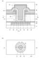
図1(A)にトランジスタ10の斜視概略図を示し、図1(B)に、容量素子50の斜視概略図を示す。図1(A)及び図1(B)では、理解を容易にするため、一部を切り欠いて示している。また、図1(A)及び図1(B)では、一部の構成要素(絶縁層など)については輪郭のみを破線で示している。[Configuration example]
Fig. 1A shows a schematic perspective view of a
図1(A)及び図1(B)では、X方向、Y方向、及びZ方向を矢印で示している。なお、図1(A)と図1(B)とで同じX、Y、Zの符号で示しているが、必ずしもこれらの間で方向が一致しなくてもよい。In Fig. 1(A) and Fig. 1(B), the X direction, Y direction, and Z direction are indicated by arrows. Note that although the same symbols X, Y, and Z are used in Fig. 1(A) and Fig. 1(B), the directions do not necessarily have to be the same between these.
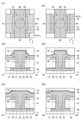
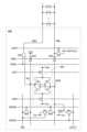
また、図2(A1)にトランジスタ10の平面図を、図2(A2)、(A3)にはそれぞれ図2(A1)中の切断線A1-A2、B1-B2に対応する断面概略図を示している。また図2(B1)に容量素子50の平面図を、図2(B2)、(B3)にはそれぞれ図2(B1)中の切断線A3-A4、B3-B4に対応する断面概略図を示している。なお、図2(A1)及び図2(B1)では、一部の構成要素(絶縁層など)を省略している。また、トランジスタ10及び容量素子50を覆って、絶縁層42と、絶縁層43が積層して設けられている。2(A1) shows a plan view of the
{トランジスタ10}
トランジスタ10は、基板(図示しない)上に設けられる絶縁層11上に設けられる。トランジスタ10は、ソース電極及びドレイン電極の一方として機能する導電層24と、半導体層21と、一部がゲート絶縁層として機能する絶縁層22と、一部がゲート電極として機能する導電層23と、ソース電極及びドレイン電極の他方として機能する導電層25と、を有する。また、導電層24は導電層31上に接して設けられ、導電層25は導電層32上に接して設けられる。導電層31の一部は、導電層24と合わせてソース電極及びドレイン電極の一方として機能し、導電層32の一部は、導電層25と合わせてソース電極及びドレイン電極の他方として機能する。導電層31と導電層24の積層体を、導電層と呼ぶこともできる。同様に、導電層32と導電層25の積層体を、導電層と呼ぶこともできる。{Transistor 10}
The
導電層24上に絶縁層41が設けられ、絶縁層41は導電層24に達する開口20を有する。半導体層21は、当該絶縁層41の開口の内壁に沿って設けられ、導電層24及び導電層25と接する。絶縁層22の一部は、絶縁層41の開口内において、半導体層21の上面を覆って設けられる。また、導電層23は絶縁層22上に設けられ、絶縁層41の開口内における絶縁層22の凹部を埋めるように設けられている。また、導電層31と導電層24は絶縁層44に埋め込まれるように設けられる。また導電層32は絶縁層45に埋め込まれるように設けられる。An insulating
上記のような構成のトランジスタ10は、ソース電極とドレイン電極とが、異なる高さに位置しているため、半導体層を流れる電流は高さ方向に流れることとなる。すなわち、チャネル長方向が高さ方向(縦方向)の成分を有するということができるため、本発明の一態様のトランジスタは、VFET(Vertical Field Effect Transistor)、縦型トランジスタ、縦型チャネルトランジスタ、などとも呼ぶことができる。トランジスタ10は、ソース電極、半導体層、及びドレイン電極を、それぞれ重ねて設けることが可能となるため、半導体層を平面上に配置した、いわゆるプレーナ型のトランジスタ(横型トランジスタ、LFET(Lateral FET)などとも呼ぶことができる)と比較して、大幅に占有面積を縮小することができる。In the
また、トランジスタ10のチャネル長は、スペーサとして機能する絶縁層41の厚さによって精密に制御することが可能となるため、プレーナ型のトランジスタと比較して、チャネル長のばらつきを極めて小さくできる。さらには、絶縁層41を薄くすることで、極めてチャネル長の短いトランジスタも作製することができる。例えばチャネル長が50nm以下、30nm以下、または20nm以下であって、5nm以上、7nm以上、または10nm以上のトランジスタを作製することができる。そのため、最先端のLSI技術で用いられる極めて高額な露光装置を用いることなく、従来の量産用の露光装置であっても、チャネル長が10nm未満のトランジスタを実現することもできる。In addition, the channel length of the
半導体層21には、様々な半導体材料を用いることができるが、特に金属酸化物を含む酸化物半導体を用いることが好ましい。適切な条件で形成された酸化物半導体を用いることで、高いオン電流と、極めて低いオフ電流を兼ね備えたトランジスタを、低コストで実現することができる。以下では特に断りのない場合、半導体層21に酸化物半導体を用いた場合の好適な構成例について説明する。Various semiconductor materials can be used for the
導電層24及び導電層25は、それぞれ上面に半導体層21が接する構成となる。そのため、半導体層21に酸化物半導体を用いた場合、半導体層21となる半導体膜の成膜工程、またはその後にかかる熱の影響などにより、導電層24または導電層25の上面が酸化し、半導体層21との間に絶縁性の酸化物膜が形成され、接触抵抗が増大してしまう恐れがある。そこで、導電層24及び導電層25には、導電性の酸化物を含む酸化物導電体を用いることが好ましい。これにより、導電層24及び導電層25の表面の酸化による接触抵抗の上昇を防止することができる。導電層24及び導電層25は、酸化物層、金属酸化物層、または酸化物導電体層などとも呼ぶことができる。The
導電層31、導電層32、及び導電層23は、それぞれ配線として用いることもできる。図2(A1)等では、導電層31と導電層23とをY方向に延伸する配線として用い、導電層32をX方向に延伸する配線として用いた例を示している。導電層32と導電層23とは絶縁層22を介して重なるため、これらの間の寄生容量は、他の組み合わせ(導電層31と導電層23、及び導電層31と導電層32)と比べて大きくなる。そのため、導電層32を導電層23と交差する向きに延伸させることで、配線間の容量を低減することができる。なお、これに限られず、配線の延伸方向は適宜設定することができる。導電層31及び導電層32は、導電層24及び導電層25と区別するため、金属層、非酸化物層などとも呼ぶことができる。The
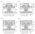
図3(A)に、トランジスタ10の他の構成例における断面概略図を示している。図3(A)では、絶縁層41に代えて、絶縁層41a、絶縁層41b、及び絶縁層41cが設けられている。Figure 3 (A) shows a schematic cross-sectional view of another example of the configuration of the
半導体層21は、絶縁層41bの開口20内の内壁と接して設けられる。絶縁層41bには、酸化物絶縁膜を用いることが好ましい。特に、加熱により酸素を放出する酸化物絶縁膜を用いることが好ましい。また、絶縁層41bを酸素に対するバリア性を有する絶縁層41a及び絶縁層41cで挟み込む構成とすることが好ましい。これにより、絶縁層41bに含まれる酸素は、絶縁層41a、絶縁層41c、及び半導体層21に囲まれた領域に閉じ込めることが可能で、より効率的に半導体層21に酸素を供給することができる。The
半導体層21のうち、絶縁層41bと接する部分は酸素欠損が低減された領域であり、i型の領域と言える。一方、絶縁層41bと接しない部分はキャリアを多く含むn型の領域とすることが好ましい。すなわち、半導体層21の絶縁層41bと接する部分をチャネル形成領域、それ以外の領域を低抵抗領域(ソース領域、またはドレイン領域ともいう)と呼ぶことができる。図3(A)では、半導体層21のチャネル形成領域21iと、低抵抗領域21nとに異なるハッチングパターンを付して示している。The portion of the
このとき、トランジスタ10のチャネル長Lは、図3(A)に示すように、半導体層21の導電層24と接する部分と導電層25と接する部分とを最短距離でつなぐ経路上であって、絶縁層41bと接する部分の長さということができる。絶縁層41bの開口20の側壁の角度(θ)が90度のとき、チャネル長Lは絶縁層41bの厚さと一致する。θを大きくすることで、チャネル長Lを大きくすることができる。In this case, the channel length L of the
一方、トランジスタ10のチャネル幅Wは、開口20の形状に依存する。図3(B)は、図3(A)中の絶縁層41bが設けられる高さに位置する切断線C1-C2で切断したときの切断面を、Z方向から見たときの平面図である。ここでは、開口20を円筒状の形状とした場合について示している。開口20の輪郭が直径Rの円であるとき、チャネル幅Wは、開口20の円周(すなわち、W=π×R)とみなすことができる。ここで、絶縁層41bの開口20の側壁の角度θが90度からずれる場合には、高さに応じて開口20の円周が異なる。その場合は、開口20の径が最も小さい高さの円周をチャネル幅Wとみなしてもよいし、開口20の上端の高さにおける円周をチャネル幅Wとみなしてもよい。On the other hand, the channel width W of the
半導体層21及び絶縁層22は、絶縁層41bの開口20の内壁に沿って形成されるため、成膜方法によっては、この部分の厚さが薄くなる場合がある。例えばスパッタリング法、またはプラズマCVD法などの成膜方法では、基板面に対して水平な面に成膜される膜の厚さと比較して、基板面に対して傾斜している面または垂直な面に成膜される膜の厚さが薄くなる傾向がある。一方、原子層堆積(ALD:Atomic Layer Deposition)法、または熱CVD法などの成膜方法を用いて成膜される膜は、被形成面の角度に寄らず厚さの均一な膜を成膜することができる。例えば、絶縁層41bの開口20の側壁の角度θが75度以上、80度以上、または85度以上の場合には、ALD法を用いて半導体層21及び絶縁層22を形成することが好ましい。Since the
{容量素子50}
続いて容量素子50について説明する。なお、トランジスタ10と容量素子50とにおいて、同一の膜を加工して形成することのできる層については、同一の符号を付して説明している。すなわち、トランジスタ10と容量素子50とで同一の符号が付されている構成要素は、同一材料を含んで構成されうる。なお、同一の符号が付されている構成要素については、上記トランジスタ10の説明を参照することができるため、説明を省略する場合がある。{Capacitive element 50}
Next, the
容量素子50は、絶縁層11上に設けられ、導電層31と、導電層32と、導電層51と、絶縁層22と、導電層23と、を有する。容量素子50は、一方の電極として機能する導電層51と、他方の電極として機能する導電層23と、これらの間に位置し、誘電体として機能する絶縁層22と、により構成される。The
導電層51は、トランジスタ10の半導体層21と同様、絶縁層41の開口20における内壁に沿って設けられる。容量素子50は、縦型容量、シリンダ型容量などと呼ぶことができ、平行平板型の容量と比較して、占有面積当たりの容量を大きくできるため好ましい。The
導電層31上には導電層24が設けられる。導電層24には、開口20と重なる位置に開口が設けられている。導電層51は、導電層24の開口を介して、導電層31の上面と接する。このように、酸化物導電体を含む導電層24を介すことなく、導電層31と導電層51とが接続することで、これらの間の電気抵抗を低減することができる。導電層32と導電層51についても同様であり、導電層32上の導電層25が除去され、導電層32と導電層51とが接して設けられている。A
導電層31と導電層23の一方または双方は、配線として機能する。図2(B1)乃至(B3)等で例示する構成では、導電層31をX方向に延伸する配線として用い、導電層23をY方向に延伸する配線として用いた場合の例を示している。言い換えると、導電層31と導電層23の交差部に容量素子50が設けられている例である。一方、導電層32はX方向及びY方向のどちらにも延伸せず、島状に設けられている。One or both of the
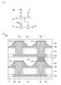
図4(A)、(B)、(C)に示す例は、導電層32をX方向に延伸する配線として用いた場合の例であり、導電層31は島状に設けられている。なお、導電層31と導電層32の双方を配線として用いてもよい。例えば、導電層31をX方向及びY方向の一方に延伸する配線として用い、導電層32を他方に延伸する配線として用いてもよい。The examples shown in Figures 4(A), (B), and (C) are examples in which
{構成要素について}
〈基板〉
トランジスタ及び容量素子を形成する基板としては、例えば、絶縁体基板、半導体基板、または導電体基板を用いればよい。絶縁体基板としては、例えば、ガラス基板、石英基板、サファイア基板、安定化ジルコニア基板(イットリア安定化ジルコニア基板など)、樹脂基板などがある。また、半導体基板としては、例えば、シリコン、ゲルマニウムを材料とした半導体基板、または炭化シリコン、シリコンゲルマニウム、ヒ化ガリウム、リン化インジウム、酸化亜鉛、酸化ガリウムからなる化合物半導体基板などがある。さらには、前述の半導体基板内部に絶縁体領域を有する半導体基板、例えば、SOI(Silicon On Insulator)基板などがある。導電体基板としては、黒鉛基板、金属基板、合金基板、導電性樹脂基板などがある。または、金属の窒化物を有する基板、金属の酸化物を有する基板などを用いることもできる。さらには、絶縁体基板に導電層または半導体層が設けられた基板、半導体基板に導電層または絶縁層が設けられた基板、導電体基板に半導体層または絶縁層が設けられた基板などがある。または、これらの基板に素子が設けられたものを用いてもよい。基板に設けられる素子としては、容量素子、抵抗素子、スイッチ素子、発光素子、記憶素子などがある。{About the components}
<substrate>
As the substrate on which the transistor and the capacitance element are formed, for example, an insulating substrate, a semiconductor substrate, or a conductive substrate may be used. As the insulating substrate, for example, a glass substrate, a quartz substrate, a sapphire substrate, a stabilized zirconia substrate (such as an yttria stabilized zirconia substrate), a resin substrate, etc. are available. As the semiconductor substrate, for example, a semiconductor substrate made of silicon or germanium, or a compound semiconductor substrate made of silicon carbide, silicon germanium, gallium arsenide, indium phosphide, zinc oxide, or gallium oxide, etc. are available. Furthermore, there is a semiconductor substrate having an insulating region inside the aforementioned semiconductor substrate, for example, an SOI (Silicon On Insulator) substrate, etc. are available. As the conductive substrate, there is a graphite substrate, a metal substrate, an alloy substrate, a conductive resin substrate, etc. are available. Alternatively, a substrate having a metal nitride, a substrate having a metal oxide, etc. can be used. Furthermore, there are a substrate in which a conductive layer or a semiconductor layer is provided on an insulating substrate, a substrate in which a conductive layer or an insulating layer is provided on a semiconductor substrate, and a substrate in which a semiconductor layer or an insulating layer is provided on a conductive substrate. Alternatively, a substrate provided with elements may be used. The elements provided on the substrate include a capacitor element, a resistor element, a switch element, a light-emitting element, a memory element, and the like.
〈半導体層〉
半導体層21は、金属酸化物(酸化物半導体)を有することが好ましい。Semiconductor Layer
The
半導体層21に用いることができる金属酸化物として、例えば、In酸化物、Ga酸化物、及びZn酸化物が挙げられる。金属酸化物は、少なくともInまたはZnを含むことが好ましい。また、金属酸化物は、Inと、元素Mと、Znと、の中から選ばれる二または三を有することが好ましい。なお、元素Mは、酸素との結合エネルギーが高い金属元素又は半金属元素であり、例えば、酸素との結合エネルギーがインジウムよりも高い金属元素又は半金属元素である。元素Mとして、具体的には、Al、Ga、Sn、Y、Ti、V、Cr、Mn、Fe、Co、Ni、Zr、Mo、Hf、Ta、W、La、Ce、Nd、Mg、Ca、Sr、Ba、B、Si、Ge、及びSbなどが挙げられる。金属酸化物が有する元素Mは、上記元素のいずれか一種または複数種であることが好ましく、特に、Al、Ga、Y、及びSnから選ばれた一種または複数種であることが好ましく、ガリウムがより好ましい。なお、Inと、Mと、Znとを有する金属酸化物を、以降ではIn-M-Zn酸化物と呼ぶ場合がある。なお、本明細書等において、金属元素と半金属元素をまとめて「金属元素」と呼ぶことがあり、本明細書等に記載の「金属元素」には半金属元素が含まれることがある。Examples of metal oxides that can be used in the
金属酸化物がIn-M-Zn酸化物の場合、当該In-M-Zn酸化物におけるInの原子数比はMの原子数比以上であることが好ましい。例えば、このようなIn-M-Zn酸化物の金属元素の原子数比として、In:M:Zn=1:1:1、In:M:Zn=1:1:1.2、In:M:Zn=2:1:3、In:M:Zn=3:1:2、In:M:Zn=4:2:3、In:M:Zn=4:2:4.1、In:M:Zn=5:1:3、In:M:Zn=5:1:6、In:M:Zn=5:1:7、In:M:Zn=5:1:8、In:M:Zn=6:1:6、In:M:Zn=5:2:5、またはこれらの近傍の組成等が挙げられる。なお、近傍の組成とは、所望の原子数比の±30%の範囲を含む。金属酸化物中のインジウムの原子数比を大きくすることで、トランジスタのオン電流、または電界効果移動度などを高めることができる。When the metal oxide is an In-M-Zn oxide, it is preferable that the atomic ratio of In in the In-M-Zn oxide is equal to or greater than the atomic ratio of M. For example, the atomic ratio of metal elements in such an In-M-Zn oxide may be In:M:Zn = 1:1:1, In:M:Zn = 1:1:1.2, In:M:Zn = 2:1:3, In:M:Zn = 3:1:2, In:M:Zn = 4:2:3, In:M:Zn = 4:2:4.1, In:M:Zn = 5:1:3, In:M:Zn = 5:1:6, In:M:Zn = 5:1:7, In:M:Zn = 5:1:8, In:M:Zn = 6:1:6, In:M:Zn = 5:2:5, or a composition close to these. The composition close to these includes a range of ±30% of the desired atomic ratio. Increasing the atomic ratio of indium in the metal oxide can increase the on-state current or field effect mobility of the transistor.
また、In-M-Zn酸化物におけるInの原子数比はMの原子数比未満であってもよい。例えば、このようなIn-M-Zn酸化物の金属元素の原子数比として、In:M:Zn=1:3:2、In:M:Zn=1:3:3、In:M:Zn=1:3:4、またはこれらの近傍の組成等が挙げられる。金属酸化物中のMの原子数比を大きくすることで、酸素欠損の生成を抑制することができる。The atomic ratio of In in the In-M-Zn oxide may be less than the atomic ratio of M. For example, the atomic ratio of the metal elements in such an In-M-Zn oxide may be In:M:Zn=1:3:2, In:M:Zn=1:3:3, In:M:Zn=1:3:4, or a composition close to these. By increasing the atomic ratio of M in the metal oxide, the generation of oxygen vacancies can be suppressed.
半導体層21は、例えば、In-Zn酸化物、In-Ga酸化物、In-Sn酸化物、In-Ti酸化物、In-Ga-Al酸化物、In-Ga-Sn酸化物、In-Ga-Zn酸化物、In-Sn-Zn酸化物、In-Al-Zn酸化物、In-Ti-Zn酸化物、In-Ga-Sn-Zn酸化物、In-Ga-Al-Zn酸化物などを用いることができる。また、Ga-Zn酸化物を用いてもよい。The
なお、金属酸化物は、インジウムに代えて、又は、インジウムに加えて、周期の数が大きい金属元素の一種または複数種を有してもよい。金属元素の軌道の重なりが大きいほど、金属酸化物におけるキャリア伝導は大きくなる傾向がある。よって、周期の数が大きい金属元素を含むことで、トランジスタの電界効果移動度を高めることができる場合がある。周期の数が大きい金属元素として、第5周期に属する金属元素、及び第6周期に属する金属元素などが挙げられる。当該金属元素として、具体的には、Y、Zr、Ag、Cd、Sn、Sb、Ba、Pb、Bi、La、Ce、Pr、Nd、Pm、Sm、及びEuなどが挙げられる。なお、La、Ce、Pr、Nd、Pm、Sm、及びEuは、軽希土類元素と呼ばれる。Note that the metal oxide may have one or more metal elements with a large periodic number instead of or in addition to indium. The greater the overlap of the orbits of the metal elements, the greater the carrier conduction in the metal oxide tends to be. Therefore, by including a metal element with a large periodic number, the field effect mobility of the transistor may be increased. Examples of metal elements with a large periodic number include metal elements belonging to the fifth period and metal elements belonging to the sixth period. Specific examples of such metal elements include Y, Zr, Ag, Cd, Sn, Sb, Ba, Pb, Bi, La, Ce, Pr, Nd, Pm, Sm, and Eu. Note that La, Ce, Pr, Nd, Pm, Sm, and Eu are called light rare earth elements.
また、金属酸化物は、非金属元素の一種または複数種を有してもよい。金属酸化物が非金属元素を有することで、トランジスタの電界効果移動度を高めることができる場合がある。非金属元素として、例えば、炭素、窒素、リン、硫黄、セレン、フッ素、塩素、臭素、及び水素などが挙げられる。The metal oxide may also contain one or more nonmetallic elements. When the metal oxide contains a nonmetallic element, the field effect mobility of the transistor may be increased. Examples of nonmetallic elements include carbon, nitrogen, phosphorus, sulfur, selenium, fluorine, chlorine, bromine, and hydrogen.
金属酸化物の形成は、スパッタリング法、または原子層堆積(ALD:Atomic Layer Deposition)法を好適に用いることができる。なお、金属酸化物をスパッタリング法で形成する場合、成膜後の金属酸化物の組成はターゲットの組成と異なる場合がある。特に亜鉛は、成膜後の金属酸化物における含有率が、ターゲットと比較して50%程度にまで減少する場合がある。The metal oxide can be preferably formed by sputtering or atomic layer deposition (ALD). When the metal oxide is formed by sputtering, the composition of the metal oxide after film formation may differ from the composition of the target. In particular, the zinc content in the metal oxide after film formation may decrease to about 50% compared to the target.
本明細書等において、金属酸化物のある金属元素の含有率とは、金属酸化物に含まれる金属元素の原子数の総数に対する、その元素の原子数の割合をいう。例えば金属酸化物が金属元素X、金属元素Y、金属元素Zを含み、当該金属酸化物に含まれる金属元素X、金属元素Y、金属元素Zのそれぞれの原子数をAX、AY、AZとしたとき、金属元素Xの含有率は、AX/(AX+AY+AZ)で示すことができる。また、金属酸化物中の金属元素X、金属元素Y、金属元素Zのそれぞれの原子数の比(原子数比)が、BX:BY:BZで示されるとき、金属元素Xの含有率は、BX/(BX+BY+BZ)で示すことができる。 In this specification, the content of a certain metal element in a metal oxide refers to the ratio of the number of atoms of that element to the total number of atoms of the metal element contained in the metal oxide. For example, when a metal oxide contains metal element X, metal element Y, and metal element Z, and the numbers of atoms of metal element X, metal element Y, and metal element Z contained in the metal oxide areAx ,Ay , andAz , respectively, the content of metal element X can be expressed asAx /(Ax +Ay +Az ). In addition, when the ratio of the numbers of atoms of metal element X, metal element Y, and metal elementZ in the metal oxide (atomic ratio) is expressed asBx :By:Bz , the content of metal element X can be expressed asBx /(Bx +By +Bz ).
例えば、Inを含む金属酸化物の場合、Inの含有率を高くすることにより、オン電流の大きいトランジスタを実現することができる。For example, in the case of a metal oxide containing In, a transistor with a large on-state current can be realized by increasing the In content.
半導体層21にGaを含まない、またはGaの含有率の低い金属酸化物を用いることにより、正バイアス印加に対する信頼性が高いトランジスタとすることができる。つまり、PBTS(Positive Bias Temperature Stress)試験でのしきい値電圧の変動量が小さいトランジスタとすることができる。また、Gaを含む金属酸化物を用いる場合は、Inの含有率よりも、Gaの含有率を低くすることが好ましい。これにより、高移動度で且つ信頼性の高いトランジスタを実現することができる。By using a metal oxide that does not contain Ga or has a low Ga content in the
一方、Gaの含有率を高くすることにより、光に対する信頼性の高いトランジスタとすることができる。つまり、NBTIS(Negative Bias Temperature Illumination Stress)試験でのしきい値電圧の変動量が小さいトランジスタとすることができる。具体的には、Gaの原子数比がInの原子数比以上である金属酸化物はバンドギャップがより大きくなり、トランジスタのNBTIS試験でのしきい値電圧の変動量を小さくすることができる。On the other hand, by increasing the Ga content, a transistor with high reliability against light can be obtained. In other words, a transistor with a small variation in threshold voltage in NBTIS (Negative Bias Temperature Illumination Stress) testing can be obtained. Specifically, a metal oxide in which the atomic ratio of Ga is equal to or greater than the atomic ratio of In has a larger band gap, and the variation in threshold voltage of the transistor in NBTIS testing can be reduced.
また、亜鉛の含有率を高くすることにより、結晶性の高い金属酸化物となり、金属酸化物中の不純物の拡散を抑制できる。したがって、トランジスタの電気特性の変動が抑制され、信頼性を高めることができる。In addition, by increasing the zinc content, the metal oxide becomes highly crystalline, and the diffusion of impurities in the metal oxide can be suppressed. This suppresses fluctuations in the electrical characteristics of the transistor, and increases reliability.
半導体層21は、2以上の金属酸化物層を有する積層構造としてもよい。半導体層21が有する2以上の金属酸化物層は、組成が互いに同じ、または概略同じであってもよい。組成が同じ金属酸化物層の積層構造とすることで、例えば、同じスパッタリングターゲットを用いて形成できるため、製造コストを削減できる。なお、異なる組成の酸化物半導体層を2以上積層した積層構造としてもよい。また、ALD法を用いることで、組成が厚さ方向に連続的に異なる金属酸化物層を形成することもできる。これにより、決まった組成の膜を用いる場合と比較して設計の選択の幅を広げることができる。さらに2以上の膜を積層して用いる場合と比較して組成の異なる2層の間に生じる界面準位などの生成を防ぐことができるため、電気特性及び信頼性を高めることができる。The
半導体層21は、結晶性を有する金属酸化物層を用いることが好ましい。例えば、CAAC(c-axis aligned crystal)構造、多結晶構造、微結晶(nc:nano-crystal)構造等を有する金属酸化物層を用いることができる。結晶性を有する金属酸化物層を半導体層21に用いることにより、半導体層21中の欠陥準位密度を低減でき、信頼性の高い半導体装置を実現できる。The
半導体層21に用いる金属酸化物層の結晶性が高いほど、半導体層21中の欠陥準位密度を低減できる。一方、結晶性の低い金属酸化物層を用いることで、大きな電流を流すことができるトランジスタを実現することができる。The higher the crystallinity of the metal oxide layer used in the
酸化物半導体を用いたトランジスタ(以下、OSトランジスタと記す)は、非晶質シリコンを用いたトランジスタと比較して電界効果移動度が極めて高い。また、OSトランジスタは、オフ状態におけるソース-ドレイン間のリーク電流(以下、オフ電流ともいう)が著しく小さく、当該トランジスタと直列に接続された容量に蓄積した電荷を長期間に亘って保持することが可能である。また、OSトランジスタを適用することで、半導体装置の消費電力を低減することができる。Transistors using an oxide semiconductor (hereinafter referred to as OS transistors) have extremely high field-effect mobility compared to transistors using amorphous silicon. In addition, the leakage current between the source and drain in an off state (hereinafter also referred to as off-current) of an OS transistor is extremely small, and the charge accumulated in a capacitance connected in series with the transistor can be held for a long period of time. Furthermore, the use of an OS transistor can reduce the power consumption of a semiconductor device.
本発明の一態様である半導体装置は、例えば、表示装置に適用することができる。表示装置の画素回路に含まれる発光デバイスの発光輝度を高くする場合、発光デバイスに流す電流量を大きくする必要がある。そのためには、画素回路に含まれている駆動トランジスタのソース-ドレイン間電圧を高くする必要がある。OSトランジスタは、シリコンを用いたトランジスタ(以下、Siトランジスタと記す)と比較して、ソース-ドレイン間において耐圧が高いため、OSトランジスタのソース-ドレイン間には高い電圧を印加することができる。したがって、画素回路に含まれる駆動トランジスタをOSトランジスタとすることで、発光デバイスに流れる電流量を大きくし、発光デバイスの発光輝度を高くすることができる。The semiconductor device according to one embodiment of the present invention can be applied to, for example, a display device. In order to increase the light emission luminance of a light-emitting device included in a pixel circuit of a display device, it is necessary to increase the amount of current flowing through the light-emitting device. To achieve this, it is necessary to increase the source-drain voltage of a driving transistor included in the pixel circuit. Since an OS transistor has a higher withstand voltage between the source and drain than a transistor using silicon (hereinafter referred to as a Si transistor), a high voltage can be applied between the source and drain of the OS transistor. Therefore, by using an OS transistor as the driving transistor included in the pixel circuit, it is possible to increase the amount of current flowing through the light-emitting device and increase the light emission luminance of the light-emitting device.
トランジスタが飽和領域で動作する場合において、OSトランジスタは、Siトランジスタよりも、ゲート-ソース間電圧の変化に対して、ソース-ドレイン間電流の変化を小さくすることができる。このため、画素回路に含まれる駆動トランジスタにOSトランジスタを適用することで、発光デバイスに流れる電流量を細かく制御することができる。このため、画素回路における階調を大きくすることができる。また、発光デバイスの電気特性(例えば抵抗)の変動、または電気特性のばらつきが生じたとしても、安定した電流を流すことができる。When the transistor operates in the saturation region, an OS transistor can reduce the change in source-drain current in response to a change in gate-source voltage compared to a Si transistor. Therefore, by using an OS transistor as a driving transistor included in a pixel circuit, the amount of current flowing through the light-emitting device can be finely controlled. This makes it possible to increase the gradation in the pixel circuit. Furthermore, a stable current can be passed even if the electrical characteristics (e.g., resistance) of the light-emitting device fluctuate or there is variation in the electrical characteristics.
上記のとおり、画素回路に含まれる駆動トランジスタにOSトランジスタを用いることで、「黒浮きの抑制」、「発光輝度の上昇」、「多階調化」、「発光デバイスのばらつきの影響の抑制」などを図ることができる。As described above, by using an OS transistor for the driving transistor included in the pixel circuit, it is possible to achieve "suppression of black floating," "increase in light emission luminance," "multiple gradations," and "suppression of the effects of variations in light-emitting devices."
OSトランジスタは、放射線照射による電気特性の変動が小さい、つまり放射線に対する耐性が高いため、放射線が入射しうる環境においても好適に用いることができる。OSトランジスタは、放射線に対する信頼性が高いともいえる。例えば、X線のフラットパネルディテクタの画素回路に、OSトランジスタを好適に用いることができる。また、OSトランジスタは、宇宙空間で使用する半導体装置に好適に用いることができる。放射線として、電磁放射線(例えば、X線、及びガンマ線)、及び粒子放射線(例えば、アルファ線、ベータ線、陽子線、及び中性子線)が挙げられる。OS transistors have small variations in electrical characteristics due to radiation exposure, i.e., are highly resistant to radiation, and therefore can be suitably used in environments where radiation may be incident. It can also be said that OS transistors have high reliability against radiation. For example, OS transistors can be suitably used in pixel circuits of X-ray flat panel detectors. OS transistors can also be suitably used in semiconductor devices used in outer space. Examples of radiation include electromagnetic radiation (e.g., X-rays and gamma rays) and particle radiation (e.g., alpha rays, beta rays, proton rays, and neutron rays).
なお、半導体層21に用いることができる半導体材料は、酸化物半導体に限定されない。例えば、単体元素よりなる半導体、または化合物半導体を用いることができる。単体元素よりなる半導体としては、シリコン(単結晶シリコン、多結晶シリコン、微結晶シリコン、非晶質シリコンを含む)またはゲルマニウムなどが挙げられる。化合物半導体として、例えば、ヒ化ガリウム、シリコンゲルマニウムが挙げられる。化合物半導体として、有機半導体、窒化物半導体、または酸化物半導体等が挙げられる。なお、これらの半導体材料に、ドーパントとして不純物が含まれてもよい。The semiconductor material that can be used for the
または、半導体層21は、半導体として機能する層状物質を有してもよい。層状物質とは、層状の結晶構造を有する材料群の総称である。層状の結晶構造は、共有結合またはイオン結合によって形成される層が、ファンデルワールス結合のような、共有結合またはイオン結合よりも弱い結合を介して積層している構造である。層状物質は、単位層内における電気伝導性が高く、つまり、2次元電気伝導性が高い。半導体として機能し、かつ、2次元電気伝導性の高い材料をチャネル形成領域に用いることで、オン電流の大きいトランジスタを提供することができる。Alternatively, the
上記層状物質として、例えば、グラフェン、シリセン、カルコゲン化物などが挙げられる。カルコゲン化物は、カルコゲン(第16族に属する元素)を含む化合物である。また、カルコゲン化物として、遷移金属カルコゲナイド、13族カルコゲナイドなどが挙げられる。トランジスタの半導体層として適用可能な遷移金属カルコゲナイドとして、具体的には、硫化モリブデン(代表的にはMoS2)、セレン化モリブデン(代表的にはMoSe2)、モリブデンテルル(代表的にはMoTe2)、硫化タングステン(代表的にはWS2)、セレン化タングステン(代表的にはWSe2)、タングステンテルル(代表的にはWTe2)、硫化ハフニウム(代表的にはHfS2)、セレン化ハフニウム(代表的にはHfSe2)、硫化ジルコニウム(代表的にはZrS2)、セレン化ジルコニウム(代表的にはZrSe2)などが挙げられる。 Examples of the layered material include graphene, silicene, and chalcogenides. Chalcogenides are compounds containing chalcogen (an element belonging to Group 16). Examples of the chalcogenides include transition metal chalcogenides and Group 13 chalcogenides. Specific examples of transition metal chalcogenides that can be used as the semiconductor layer of a transistor include molybdenum sulfide (representatively MoS2 ), molybdenum selenide (representatively MoSe2 ), molybdenum tellurium (representatively MoTe2 ), tungsten sulfide (representatively WS2 ), tungsten selenide (representatively WSe2 ), tungsten tellurium (representatively WTe2 ), hafnium sulfide (representatively HfS2 ), hafnium selenide (representatively HfSe2 ), zirconium sulfide (representatively ZrS2 ), zirconium selenide (representatively ZrSe2 ), and the like.
半導体層21に用いる半導体材料の結晶性は特に限定されず、非晶質半導体、単結晶性半導体、または単結晶以外の結晶性を有する半導体(多結晶半導体、微結晶半導体、または一部に結晶領域を有する半導体)のいずれを用いてもよい。結晶性を有する半導体を用いると、トランジスタ特性の劣化を抑制できるため好ましい。The crystallinity of the semiconductor material used for the
〈ゲート絶縁層〉
絶縁層22はトランジスタのゲート絶縁層として機能し、容量素子の誘電層としても機能する。半導体層21に酸化物半導体を用いた場合、絶縁層22の少なくとも半導体層21と接する膜には、酸化物絶縁膜を用いることが好ましい。例えば、酸化シリコン、酸化窒化シリコン、酸化アルミニウム、酸化窒化アルミニウム、酸化ハフニウム、酸化窒化ハフニウム、酸化ガリウム、酸化窒化ガリウム、酸化イットリウム、酸化窒化イットリウム、及びGa-Zn酸化物の一または複数を用いることができる。このほか、絶縁層22として、窒化シリコン、窒化酸化シリコン、窒化アルミニウム、窒化酸化アルミニウムなどの窒化物絶縁膜を用いることもできる。また、絶縁層22は積層構造を有していてもよく、例えば酸化物絶縁膜と窒化物絶縁膜とをそれぞれ1以上有する積層構造としてもよい。<Gate insulating layer>
The insulating
なお、本明細書等において、酸化窒化物は窒素よりも酸素の含有量が多い材料を指す。窒化酸化物は酸素よりも窒素の含有量が多い材料を指す。In this specification, an oxynitride refers to a material that contains more oxygen than nitrogen. An oxynitride refers to a material that contains more nitrogen than oxygen.
また、絶縁層22は、high-k材料からなる絶縁材料を積層して用いることが好ましく、比誘電率が高い(high-k)材料と、当該high-k材料より絶縁耐力が大きい材料との積層構造を用いることが好ましい。例えば、絶縁層22として、酸化ジルコニウム、酸化アルミニウム、酸化ジルコニウムの順番で積層された絶縁膜(ZAZともいう)を用いることができる。また、例えば、酸化ジルコニウム、酸化アルミニウム、酸化ジルコニウム、酸化アルミニウムの順番で積層された絶縁膜(ZAZAともいう)を用いることができる。また、例えば、ハフニウムジルコニウム酸化物、酸化アルミニウム、ハフニウムジルコニウム酸化物、酸化アルミニウムの順番で積層された絶縁膜を用いることができる。酸化アルミニウムのような、比較的絶縁耐力が大きい絶縁体を積層して用いることで、絶縁耐力が向上し、容量素子の静電破壊を抑制できる。The insulating
また、絶縁層22として、強誘電性を示す材料を用いてもよい。強誘電性を示す材料としては、酸化ハフニウム、酸化ジルコニウム、HfZrOX(Xは0よりも大きい実数とする)などの金属酸化物が挙げられる。 Furthermore, a material exhibiting ferroelectricity may be used as the insulating
〈導電層〉
導電層24及び導電層25は、それぞれ上面が半導体層21と接する。ここで、半導体層21として酸化物半導体を用いた場合、導電層24または導電層25に例えばアルミニウムなどの酸化しやすい金属を用いると、導電層24または導電層25と半導体層21との間に絶縁性の酸化物(例えば酸化アルミニウム)が形成され、これらの導通を妨げる恐れがある。そのため、導電層24及び導電層25には、酸化しにくい導電材料、酸化しても電気抵抗が低く保たれる導電材料、または酸化物導電性材料を用いることが好ましい。Conductive Layer
The upper surfaces of the
導電層24及び導電層25としては、例えば窒化タンタル、窒化チタン、チタンとアルミニウムを含む窒化物、タンタルとアルミニウムを含む窒化物、ルテニウム、酸化ルテニウム、窒化ルテニウム、ストロンチウムとルテニウムを含む酸化物、ランタンとニッケルを含む酸化物などを用いることが好ましい。これらは、酸化されにくい導電性材料、または、酸化しても導電性を維持する材料であるため、好ましい。For
または、酸化インジウム、酸化亜鉛、In-Sn酸化物、In-Zn酸化物、In-W酸化物、In-W-Zn酸化物、In-Ti酸化物、In-Ti-Sn酸化物、In-Sn酸化物、In-Sn-Si酸化物、Ga-Zn酸化物などの導電性酸化物を用いることができる。特にインジウムを含む導電性酸化物は、導電性が高いため好ましい。Alternatively, conductive oxides such as indium oxide, zinc oxide, In-Sn oxide, In-Zn oxide, In-W oxide, In-W-Zn oxide, In-Ti oxide, In-Ti-Sn oxide, In-Sn oxide, In-Sn-Si oxide, and Ga-Zn oxide can be used. Conductive oxides containing indium are particularly preferred because of their high conductivity.
導電層23はゲート電極として機能し、様々な導電性材料を用いることができる。導電層23としては、例えばアルミニウム、クロム、銅、銀、金、白金、タンタル、ニッケル、チタン、モリブデン、タングステン、ハフニウム、バナジウム、ニオブ、マンガン、マグネシウム、ジルコニウム、ベリリウム、インジウム、ルテニウム、イリジウム、ストロンチウム、ランタンなどから選ばれた金属元素、当該金属元素を成分とする合金を用いることが好ましい。また、上記金属または合金の窒化物、もしくは上記金属または合金の酸化物を用いてもよい。例えば、窒化タンタル、窒化チタン、タングステン、チタンとアルミニウムを含む窒化物、タンタルとアルミニウムを含む窒化物、酸化ルテニウム、窒化ルテニウム、ストロンチウムとルテニウムを含む酸化物、ランタンとニッケルを含む酸化物などを用いることが好ましい。また、リン等の不純物元素を含有させた多結晶シリコンに代表される、電気伝導度が高い半導体、ニッケルシリサイドなどのシリサイドを用いてもよい。The
また導電層23には、上記導電層24及び導電層25に用いることができる、窒化物、及び酸化物を適用してもよい。
導電層31及び導電層32は、配線として機能するため、低抵抗な導電性材料を用いることができる。また導電層51も低抵抗であるほど好ましい。導電層31、導電層32、及び導電層51としては、上記導電層23と同様の導電性材料を用いることができる。Because the
〈絶縁層〉
絶縁層41(又は絶縁層41b)は、半導体層21と接する部分を有する。半導体層21に酸化物半導体を用いた場合、半導体層21と絶縁層41との界面特性を向上させるため、絶縁層41の少なくとも半導体層21と接する部分には酸化物を用いることが好ましい。例えば、酸化シリコンまたは酸化窒化シリコンを好適に用いることができる。Insulating layer
The insulating layer 41 (or the insulating
また、絶縁層41には、加熱により酸素を放出する膜を用いるとより好ましい。これにより、トランジスタ10の作製工程中にかかる熱により半導体層21に酸素が供給され、半導体層21中の酸素欠損の低減を図ることができ、信頼性を高めることができる。絶縁層41に酸素を供給する方法としては、酸素雰囲気下における加熱処理、酸素雰囲気下におけるプラズマ処理などが挙げられる。また、絶縁層41の上面に対してスパッタリング法により、酸素雰囲気下で酸化物膜を成膜することで酸素を供給してもよい。その後、当該酸化物膜を除去してもよい。More preferably, the insulating
絶縁層41は、スパッタリング法、またはプラズマCVD法などの成膜方法で形成することが好ましい。特に、スパッタリング法を用い、成膜ガスに水素ガスを用いない成膜方法で成膜することで、水素の含有量の極めて少ない膜とすることができる。そのため、半導体層21に水素が供給されることを抑制し、トランジスタ10の電気特性の安定化を図ることができる。The insulating
絶縁層41a及び絶縁層41cは、酸素が拡散しにくい膜を用いることが好ましい。これにより、絶縁層41bに含まれる酸素が、加熱により絶縁層41aを介して絶縁層11側に透過すること、及び、絶縁層41cを介して絶縁層22側に透過することを防ぐことができる。言い換えると、酸素が拡散しにくい絶縁層41a及び絶縁層41cで絶縁層41bの上下を挟むことで、絶縁層41bに含まれる酸素を閉じ込めることができる。これにより、半導体層21に効果的に酸素を供給することができる。It is preferable that the insulating
絶縁層41a及び絶縁層41cとしては、例えば窒化シリコン、窒化酸化シリコン、酸化窒化シリコン、酸化アルミニウム、酸化窒化アルミニウム、窒化アルミニウム、酸化ハフニウム、及びハフニウムアルミネートの一または複数を用いることができる。特に窒化シリコン及び、窒化酸化シリコンは自身からの不純物(例えば、水及び水素)の放出が少なく、酸素及び水素が透過しにくい特徴を有するため、絶縁層41a及び絶縁層41cとして好適に用いることができる。For example, one or more of silicon nitride, silicon nitride oxide, silicon oxynitride, aluminum oxide, aluminum oxynitride, aluminum nitride, hafnium oxide, and hafnium aluminate can be used as the insulating
[変形例]
以下では、上記構成例とは一部の構成が異なる例について説明する。なお、上記と重複する部分については説明を省略する場合がある。[Modification]
In the following, an example in which the configuration is partially different from the above configuration example will be described, and explanations of parts that overlap with the above may be omitted.
{変形例1}
図5(A1)、(A2)にトランジスタ10aの断面図を示し、図5(B1)、(B2)に容量素子50aの断面図を示す。トランジスタ10aと容量素子50aは同一工程で作り分けることができる。トランジスタ10a及び容量素子50aは、上記トランジスタ10及び容量素子50と比較して、導電層23の構成が主に相違している。{Modification 1}
5A1 and 5A2 show cross-sectional views of the
トランジスタ10a及び容量素子50aにおいて、導電層23は島状に設けられ、ゲート電極として機能する。図2(A2)等では、導電層23が絶縁層22の凹部を埋めるように設けられていたが、トランジスタ10a及び容量素子50aでは、導電層23は絶縁層22の上面に沿って設けられる。In the
また、導電層23上にゲート配線として機能する導電層33が設けられている。導電層33は、絶縁層43に埋め込まれ、導電層23の上面と接して設けられている。In addition, a
なお、導電層23を設けず、導電層33と絶縁層22とが接する構成とし、導電層33の一部がゲート電極として機能する構成としてもよい。一方で、導電層23を設けることで、ゲート絶縁層として機能する絶縁層22の表面を導電層23で覆った状態で、絶縁層43及び導電層33を形成することができるため、ゲート絶縁層とゲート電極との間の欠陥準位の生成を抑制することができ、信頼性を高めることができる。In addition, the
{変形例2}
図6(A)にトランジスタ10bの断面概略図を、図6(B)に、容量素子50bの断面概略図をそれぞれ示す。トランジスタ10bと容量素子50bとは、同一の工程により作り分けることができる。トランジスタ10bと容量素子50bは、上記トランジスタ10及び容量素子50と比較して、導電層24の構成が主に相違している。{Modification 2}
6A is a schematic cross-sectional view of a
トランジスタ10bにおいて、導電層24は開口20と重なる領域に凹部を有する。このとき、導電層23の下端の高さ(高さh1)が、導電層24の上面の高さよりも低いことが好ましい。In
トランジスタ10bにおいて、半導体層21の導電層24と接する部分はチャネル形成領域よりも低抵抗な領域となる。したがって、高さh1が導電層24の上面よりも低く位置することで、半導体層21のチャネル形成領域全体に均一にゲート電界を与えることができ、半導体層21中にゲート電界が届きにくいために高抵抗な領域(オフセット領域)ができることを防ぐことができる。そのため、オン電流が高められたトランジスタを実現することができる。このような構成を実現するためには、例えば導電層24の厚さを、少なくとも半導体層21の厚さと絶縁層22の厚さの総和よりも厚くすることが好ましい。In the
また、容量素子50bにおいては、導電層24が厚くなることで、導電層51と導電層24の接触面積が増大するため、これらの間の接触抵抗を低減できるといった副次的な効果を奏する。In addition, in the
{変形例3}
図6(C)、(D)は、開口20の側壁がテーパ形状である場合の例である。図6(C)にはトランジスタ10cの断面図を、図6(D)には容量素子50cの断面図を、それぞれ示している。図6(C)及び図6(D)では、トランジスタ10cの開口20及び容量素子50cの開口20共に、開口20の下端の径(開口径)よりも、上端の径(開口径)の方が大きい。{Modification 3}
6C and 6D show examples in which the sidewall of the
開口20の側壁をテーパ形状とすることで、半導体層21または導電層51などの被覆性が向上し、スパッタリング法などの成膜方法を用いても、膜中の低密度な領域などの欠陥の生成を抑制できる。例えば角度θは、45度以上90度以下、または60度以上90度未満、または70度以上90度未満とすることができる。なお、ALD法などの被覆性が極めて高い成膜方法を用いる場合には、角度θが90度よりも大きくてもよい。By tapering the sidewalls of the
開口20の側壁がテーパ形状である場合、トランジスタ10cのチャネル幅に対応する開口20の径は導電層24側から導電層25側に向かって大きくなる。このとき、トランジスタ10cに流れる電流の大きさは最も小さい径である部分に制限される。したがって、トランジスタ10cのチャネル幅は、最も小さい径の部分の円周とみなすことができる。したがって、開口20の側壁をテーパ形状とすることで、開口20の上端の径よりも小さいチャネル幅のトランジスタを作製することができる。When the sidewall of the
容量素子50cにおいては、開口20の側壁が円筒状である場合と比較して、開口20の側壁がテーパ形状であると静電容量が減少してしまう。そのため、静電容量が不足してしまう場合には、絶縁層22に比誘電率の高い材料を用いる、絶縁層22の厚さを薄くする、絶縁層41の厚さを大きくするなどにより、静電容量を大きくすることができる。In the
以上が、変形例についての説明である。The above is an explanation of the modified version.
[作製方法例]
続いて、本発明の一態様の半導体装置の作製方法について説明する。以下では、トランジスタと容量素子とを同一平面上に作り分ける方法の例について説明する。[Example of manufacturing method]
Next, a method for manufacturing a semiconductor device according to one embodiment of the present invention will be described. An example of a method for separately forming a transistor and a capacitor on the same plane will be described below.
図7(A)乃至図9(C)は、以下で例示する半導体装置の作製方法の各工程における断面概略図である。各図において、左側にトランジスタ10を、右側に容量素子50をそれぞれ示している。また、ここでは図9(C)で例示するように、トランジスタ10と容量素子50とで、導電層31を共有している例について説明する。Figures 7(A) to 9(C) are schematic cross-sectional views of each step of the manufacturing method of a semiconductor device, which will be described below. In each figure, a
以下において、絶縁体を形成するための絶縁性材料、導電体を形成するための導電性材料、または半導体を形成するための半導体材料は、スパッタリング法、CVD法、MBE法、PLD法、ALD法などを適宜用いて成膜することができる。In the following, insulating materials for forming insulators, conductive materials for forming conductors, or semiconductor materials for forming semiconductors can be formed as films using a sputtering method, a CVD method, an MBE method, a PLD method, an ALD method, or the like, as appropriate.
なお、スパッタリング法にはスパッタリング用電源に高周波電源を用いるRFスパッタリング法、直流電源を用いるDCスパッタリング法、さらにパルス的に電極に印加する電圧を変化させるパルスDCスパッタリング法がある。RFスパッタリング法は主に絶縁膜を成膜する場合に用いられ、DCスパッタリング法は主に金属導電膜を成膜する場合に用いられる。また、パルスDCスパッタリング法は、主に、酸化物、窒化物、炭化物などの化合物をリアクティブスパッタリング法で成膜する際に用いられる。There are three types of sputtering: RF sputtering, which uses a high-frequency power source as the sputtering power source; DC sputtering, which uses a direct current power source; and pulsed DC sputtering, which changes the voltage applied to the electrodes in a pulsed manner. RF sputtering is mainly used when depositing insulating films, while DC sputtering is mainly used when depositing metal conductive films. Pulsed DC sputtering is mainly used when depositing compounds such as oxides, nitrides, and carbides using reactive sputtering.
なお、CVD法は、プラズマを利用するプラズマCVD(PECVD)法、熱を利用する熱CVD(TCVD:Thermal CVD)法、光を利用する光CVD(Photo CVD)法などに分類できる。さらに用いる原料ガスによって金属CVD(MCVD:Metal CVD)法、有機金属CVD(MOCVD:Metal Organic CVD)法に分けることができる。CVD methods can be classified into plasma-enhanced CVD (PECVD), which uses plasma; thermal CVD (TCVD), which uses heat; and photo-CVD (photo-CVD), which uses light. They can also be further classified into metal CVD (MCVD) and metal organic CVD (MOCVD), depending on the source gas used.
プラズマCVD法は、比較的低温で高品質の膜が得られる。また、熱CVD法は、プラズマを用いないため、被処理物へのプラズマダメージを小さくすることが可能な成膜方法である。例えば、半導体装置に含まれる配線、電極、素子(トランジスタ、容量素子など)などは、プラズマから電荷を受け取ることでチャージアップする場合がある。このとき、蓄積した電荷によって、半導体装置に含まれる配線、電極、素子などが破壊される場合がある。一方、プラズマを用いない熱CVD法の場合、こういったプラズマダメージが生じないため、半導体装置の歩留まりを高くすることができる。また、熱CVD法では、成膜中のプラズマダメージが生じないため、欠陥の少ない膜が得られる。The plasma CVD method can obtain high-quality films at relatively low temperatures. In addition, the thermal CVD method is a film formation method that can reduce plasma damage to the workpiece because it does not use plasma. For example, wiring, electrodes, elements (transistors, capacitive elements, etc.) included in a semiconductor device may become charged up by receiving electric charge from the plasma. At this time, the accumulated electric charge may destroy the wiring, electrodes, elements, etc. included in the semiconductor device. On the other hand, in the case of the thermal CVD method, which does not use plasma, such plasma damage does not occur, so the yield of semiconductor devices can be increased. In addition, in the thermal CVD method, plasma damage does not occur during film formation, so a film with fewer defects can be obtained.
また、ALD法としては、プリカーサ及びリアクタントの反応を熱エネルギーのみで行う熱ALD法、プラズマ励起されたリアクタントを用いるPEALD法などを用いることができる。Also, the ALD method can be a thermal ALD method in which the reaction between the precursor and reactant is carried out using only thermal energy, or a PEALD method in which a plasma-excited reactant is used.
CVD法およびALD法はスパッタリング法とは異なり、被処理物の形状の影響を受けにくく、良好な段差被覆性を有する成膜方法である。特に、ALD法は、優れた段差被覆性と、優れた厚さの均一性を有するため、アスペクト比の高い開口部の表面を被覆する場合などに好適である。ただし、ALD法は、比較的成膜速度が遅いため、成膜速度の速いCVD法などの他の成膜方法と組み合わせて用いることが好ましい場合もある。Unlike sputtering, CVD and ALD are film formation methods that are less affected by the shape of the workpiece and have good step coverage. In particular, ALD has excellent step coverage and excellent thickness uniformity, making it suitable for coating the surfaces of openings with high aspect ratios. However, since ALD has a relatively slow film formation speed, it may be preferable to use it in combination with other film formation methods such as CVD, which has a faster film formation speed.
また、CVD法では、原料ガスの流量比によって、任意の組成の膜を成膜することができる。例えば、CVD法では、成膜しながら原料ガスの流量比を変化させることによって、組成が連続的に変化した膜を成膜することができる。原料ガスの流量比を変化させながら成膜する場合、複数の成膜室を用いて成膜する場合と比べて、搬送または圧力調整に掛かる時間を要さない分、成膜に掛かる時間を短くすることができる。したがって、半導体装置の生産性を高めることができる場合がある。In addition, in the CVD method, a film of any composition can be formed by changing the flow rate ratio of the raw material gases. For example, in the CVD method, a film with a continuously changing composition can be formed by changing the flow rate ratio of the raw material gases while forming the film. When forming a film while changing the flow rate ratio of the raw material gases, the time required for film formation can be shortened compared to when forming a film using multiple film formation chambers, since no time is required for transportation or pressure adjustment. Therefore, the productivity of semiconductor devices can be increased in some cases.
また、ALD法では、異なる複数種のプリカーサを同時に導入することで任意の組成の膜を成膜することができる。または、異なる複数種のプリカーサを導入する場合、各プリカーサのサイクル数を制御することで任意の組成の膜を成膜することができる。またCVD法と同様に、組成が連続的に変化した膜を成膜することができる。In addition, in the ALD method, a film of any composition can be formed by simultaneously introducing multiple different types of precursors. Or, when multiple different types of precursors are introduced, a film of any composition can be formed by controlling the number of cycles of each precursor. Also, as with the CVD method, a film with a continuously changing composition can be formed.
まず、基板(図示しない)を準備し、当該基板上に絶縁層11を形成する。絶縁層11としては、酸化シリコン膜、酸化窒化シリコン膜などの無機絶縁膜を用いることができる。絶縁層11の成膜は、スパッタリング法、CVD法、MBE法、PLD法、ALD法などを用いることができる。絶縁層11の被形成面が平坦でない場合には、絶縁層11の成膜後に絶縁層11の上面が平坦となるように平坦化処理を行うことが好ましい。First, a substrate (not shown) is prepared, and an insulating
続いて、絶縁層11上に導電層31となる導電膜と、導電層24となる導電膜の積層膜を形成する。続いて、当該積層膜上にフォトリソグラフィ法等によりレジストマスクを形成し、積層膜の当該レジストマスクに覆われない部分をエッチングにより除去したのち、レジストマスクを除去する。これにより、導電層31と導電層24を形成することができる。続いて、絶縁層44となる絶縁膜を成膜し、導電層24と重なる部分を除去することで、絶縁層44と、絶縁層44に埋め込まれた導電層31及び導電層24を形成することができる(図7(A))。絶縁層44となる絶縁膜の加工は、CMP(Chemical Mechanical Polishing)法を用いることが好ましく、例えば導電層24の上面が露出するまで当該絶縁膜を加工することで、図7(A)に示す絶縁層44を形成することができる。Next, a laminated film of a conductive film that will become the
続いて、導電層24及び絶縁層44上に、絶縁層41、導電膜32f、及び導電膜25fを成膜する(図7(B))。Next, the insulating
絶縁層41の成膜は、スパッタリング法、CVD法、MBE法、PLD法、ALD法などを適宜用いて行えばよい。例えば、絶縁層41として、スパッタリング法を用いて酸化シリコン膜を成膜すればよい。The insulating
絶縁層44と導電層24の上面の高さが一致するように平坦化処理を行うことで、絶縁層41の上面を平坦にすることができる。なお、絶縁層44を設けず、導電層24を覆って絶縁層41を設けてもよく、その場合には絶縁層41の上面に対してCMP処理を行なって上面を平坦化させることが好ましい。The upper surface of the insulating
ここで、絶縁層41の厚さがトランジスタのチャネル長に対応するため、絶縁層41の厚さにばらつきが生じないようにすることが重要である。Here, since the thickness of the insulating
また、絶縁層41を、酸素を含む雰囲気でスパッタリング法を用いて成膜することで、膜中に多くの酸素を含む絶縁層41を形成することができる。また、成膜ガスに水素を含む分子を用いなくてもよいスパッタリング法を用いることで、絶縁層41中の水素濃度を低減できる。このように、絶縁層41を成膜することで、絶縁層41から半導体層21のチャネル形成領域に酸素を供給し、酸素欠損の低減を図ることができる。In addition, by forming the insulating
導電膜32fは、上記導電層31となる導電膜と同様の材料及び方法で形成することができる。また、導電膜25fは、上記導電層24となる導電膜と同様の材料及び方法で形成することができる。The
続いて、導電膜25f及び導電膜32fの一部をエッチングにより除去することで、導電層25及び導電層32を形成する(図7(C))。Next,
続いて、導電層25、導電層32、及び絶縁層41に、導電層24に達する開口20を形成する(図7(D))。Next, an
開口20の側壁は、導電層24の上面に対して垂直であることが好ましい。このような構成とすることで、占有面積の小さなトランジスタ及び容量素子を作製することができる。または、開口20の側壁はテーパ形状としてもよい。テーパ形状とすることで、開口20の内部に形成する膜の被覆性を高めることができる。The sidewalls of the
開口20の最大幅(平面視において開口20が円形である場合は最大径)は、できるだけ微細であることが好ましい。例えば、開口20の最大幅は、60nm以下、50nm以下、40nm以下、30nm以下、又は20nm以下であって、5nm以上であることが好ましい。このように、開口20を微細に加工するには、EUV光などの短波長の光、または電子ビームを用いたリソグラフィー法を用いることが好ましい。It is preferable that the maximum width of the opening 20 (maximum diameter when the
開口20はアスペクト比が大きいため、異方性エッチングを用いて形成することが好ましい。特に、ドライエッチング法による加工は、微細加工に適しているため好ましい。また、当該加工は、導電層25のエッチング、導電層32のエッチング、そして絶縁層41のエッチングのそれぞれで、異なる条件で行なってもよい。なお、導電層25、導電層32、及び絶縁層41のそれぞれで、開口20の側壁の角度が異なってもよい。Because the
また、絶縁層41のエッチング時に、導電層24の上部の一部がエッチングされ、開口20の底部における導電層24の厚さが薄くなる場合がある。または、開口20の形成後に続けて導電層24の上部の一部をエッチングし、導電層24を薄くすることができる。When etching the insulating
続いて、加熱処理を行なってもよい。加熱処理は、250℃以上650℃以下、好ましくは300℃以上500℃以下、さらに好ましくは320℃以上450℃以下で行えばよい。なお、加熱処理は、窒素ガスもしくは不活性ガスの雰囲気、または酸化性ガスを10ppm以上、1%以上、もしくは10%以上含む雰囲気で行う。例えば、窒素ガスと酸素ガスの混合雰囲気で加熱処理をする場合、酸素ガスを20%程度にすればよい。また、加熱処理は減圧状態で行なってもよい。または、加熱処理は、窒素ガスもしくは不活性ガスの雰囲気で加熱処理した後に、脱離した酸素を補うために酸化性ガスを10ppm以上、1%以上、または10%以上含む雰囲気で加熱処理を行なってもよい。以上のような加熱処理を行うことで、半導体層となる酸化物半導体膜の成膜前に、絶縁層41などに含まれる、水などの不純物を低減できる。Heat treatment may be subsequently performed. The heat treatment may be performed at 250°C or higher and 650°C or lower, preferably 300°C or higher and 500°C or lower, and more preferably 320°C or higher and 450°C or lower. The heat treatment may be performed in an atmosphere of nitrogen gas or inert gas, or an atmosphere containing 10 ppm or higher, 1% or higher, or 10% or higher of an oxidizing gas. For example, when the heat treatment is performed in a mixed atmosphere of nitrogen gas and oxygen gas, the oxygen gas may be about 20%. The heat treatment may be performed under reduced pressure. Alternatively, the heat treatment may be performed in an atmosphere containing 10 ppm or higher, 1% or higher, or 10% or higher of an oxidizing gas to compensate for the desorbed oxygen after the heat treatment in the nitrogen gas or inert gas atmosphere. By performing the above heat treatment, impurities such as water contained in the insulating
また、上記加熱処理で用いるガスは、高純度化されていることが好ましい。例えば、上記加熱処理で用いるガスに含まれる水分量が1ppb以下、好ましくは0.1ppb以下、より好ましくは0.05ppb以下にすればよい。高純度化されたガスを用いて加熱処理を行うことで、絶縁層41などに水分等が取り込まれることを可能な限り防ぐことができる。The gas used in the heat treatment is preferably highly purified. For example, the amount of moisture contained in the gas used in the heat treatment is 1 ppb or less, preferably 0.1 ppb or less, and more preferably 0.05 ppb or less. By using a highly purified gas to perform the heat treatment, it is possible to prevent moisture and the like from being introduced into the insulating
続いて、絶縁層41、導電層25、開口20などを覆って半導体膜21fを成膜する(図8(A))。Next, a
当該半導体膜21fとしては、酸化物半導体膜を用いることができる。当該酸化物半導体膜の成膜は、スパッタリング法、CVD法、MBE法、PLD法、ALD法などを適宜用いて行えばよい。ここで、当該酸化物半導体膜は、アスペクト比の大きい開口20の底部及び側壁に接して形成されることが好ましい。よって、当該酸化物半導体膜の成膜は、被覆性が良好な成膜方法を用いることが好ましく、CVD法またはALD法などを用いることがより好ましい。例えば、当該酸化物半導体膜として、ALD法を用いて、In-Ga-Zn酸化物を成膜すればよい。なお、開口20がテーパ形状である場合には、酸化物半導体膜を、スパッタリング法を用いて成膜することができる。The
また、酸化物半導体膜の成膜中、または成膜後に、酸素を含む雰囲気でマイクロ波処理を行うことで、当該酸化物半導体膜中の不純物濃度を低減させる処理を行うと好ましい。なお、不純物としては、特に、水素、及び炭素が挙げられる。また、マイクロ波処理を行うことで、酸化物半導体膜の結晶性を高めることができる場合がある。ここで、マイクロ波処理とは、例えばマイクロ波を用いて高密度プラズマを発生させる電源を有する装置を用いた処理のことを指す。In addition, it is preferable to perform a microwave treatment in an oxygen-containing atmosphere during or after the formation of the oxide semiconductor film to reduce the impurity concentration in the oxide semiconductor film. Note that examples of impurities include hydrogen and carbon. In addition, the crystallinity of the oxide semiconductor film can be improved by performing the microwave treatment in some cases. Here, the microwave treatment refers to a treatment using an apparatus having a power source that generates high-density plasma using microwaves, for example.
酸素を含む雰囲気でマイクロ波処理を行うことで、マイクロ波、またはRF等の高周波を用いて酸素ガスをプラズマ化し、当該酸素プラズマを作用させることができる。また、酸化物半導体に作用する酸素は、酸素原子、酸素分子、酸素イオン、及び酸素ラジカル(Oラジカルともいう、不対電子をもつ原子、分子、またはイオン)など様々な形態がある。なお、酸化物半導体に作用する酸素は、上述の形態のいずれか一または複数であればよく、特に酸素ラジカルであると好適である。By performing microwave treatment in an atmosphere containing oxygen, oxygen gas can be turned into plasma using microwaves or high frequency waves such as RF, and the oxygen plasma can act on the oxide semiconductor. Oxygen acting on the oxide semiconductor can take various forms, such as oxygen atoms, oxygen molecules, oxygen ions, and oxygen radicals (also called O radicals, which are atoms, molecules, or ions with unpaired electrons). Note that the oxygen acting on the oxide semiconductor may take one or more of the above forms, and is particularly preferably an oxygen radical.
また、上述の酸素を含む雰囲気でマイクロ波処理を行う際に、基板を加熱することで、酸化物半導体膜中の不純物濃度を、さらに低減させることができるため好適である。上述の基板を加熱する温度としては、100℃以上650℃以下、好ましくは200℃以上600℃以下、さらに好ましくは300℃以上450℃以下で行えばよい。When performing the microwave treatment in the above-mentioned oxygen-containing atmosphere, it is preferable to heat the substrate, since this can further reduce the impurity concentration in the oxide semiconductor film. The temperature at which the substrate is heated may be 100°C or higher and 650°C or lower, preferably 200°C or higher and 600°C or lower, and more preferably 300°C or higher and 450°C or lower.
上述の酸素を含む雰囲気でマイクロ波処理を行う際に基板を加熱することで、SIMSにより得られる酸化物半導体膜中の炭素濃度を、1×10²⁰atoms/cm3未満、好ましくは1×1019atoms/cm3未満、さらに好ましくは1×1018atoms/cm3未満とすることができる。 When the substrate is heated during the microwave treatment in the above-described oxygen-containing atmosphere, the carbon concentration in the oxide semiconductor film measured by SIMS can be set to less than 1×10 atoms/cm3 , preferably less than 1×10 atoms/cm3 , further preferably less than 1×10 atoms/cm3 .
なお、上記においては、酸化物半導体膜に対して、酸素を含む雰囲気でマイクロ波処理を行う構成について例示したが、これに限定されない。例えば、酸化物半導体膜近傍に位置する、絶縁膜、より具体的には酸化シリコン膜に対して、酸素を含む雰囲気でマイクロ波処理を行なってもよい。これにより、当該酸化シリコン膜中に含まれる水素をH2Oとして、外部に放出させることができる。酸化物半導体膜近傍に位置する、酸化シリコン膜から水素を放出させることで、信頼性の高い半導体装置を提供することができる。 Note that, although the above describes an example of a configuration in which the microwave treatment is performed on the oxide semiconductor film in an atmosphere containing oxygen, the present invention is not limited thereto. For example, the microwave treatment may be performed on an insulating film, more specifically, a silicon oxide film, located near the oxide semiconductor film in an atmosphere containing oxygen. This allows hydrogen contained in the silicon oxide film to be released to the outside as H2 O. By releasing hydrogen from the silicon oxide film located near the oxide semiconductor film, a highly reliable semiconductor device can be provided.
また、半導体層21を積層構造とする場合、各層の成膜方法は同じであってもよいし、異なってもよい。例えば、半導体層21を2層の積層構造とする場合、酸化物半導体膜の下層をスパッタリング法で成膜し、酸化物半導体膜の上層をALD法で成膜してもよい。スパッタリング法を用いて成膜された酸化物半導体膜は結晶性を有しやすい。そこで、結晶性を有する酸化物半導体膜を酸化物半導体膜の下層として設けることで、酸化物半導体膜の上層の結晶性を高めることができる。また、スパッタリング法で成膜した酸化物半導体膜の下層にピンホールまたは段切れなどが形成されたとしても、それらと重畳する部分を、被覆性の良好なALD法で成膜した酸化物半導体膜の上層で塞ぐことができる。In addition, when the
ここで、酸化物半導体膜は、開口20における導電層24上面、開口20における絶縁層41の側面、及び絶縁層41上の導電層25の側面及び上面に接して形成されることが好ましい。Here, the oxide semiconductor film is preferably formed in contact with the upper surface of the
次に、加熱処理を行うことが好ましい。加熱処理は、上記酸化物半導体膜が多結晶化しない温度範囲で行えばよく、250℃以上650℃以下、好ましくは400℃以上600℃以下で行えばよい。なお、加熱処理は、窒素ガスもしくは不活性ガスの雰囲気、または酸化性ガスを10ppm以上、1%以上、もしくは10%以上含む雰囲気で行う。例えば、窒素ガスと酸素ガスの混合雰囲気で加熱処理をする場合、酸素ガスを20%程度にすればよい。また、加熱処理は減圧状態で行なってもよい。または、加熱処理は、窒素ガスもしくは不活性ガスの雰囲気で加熱処理した後に、脱離した酸素を補うために酸化性ガスを10ppm以上、1%以上、または10%以上含む雰囲気で加熱処理を行なってもよい。Next, it is preferable to perform heat treatment. The heat treatment may be performed in a temperature range in which the oxide semiconductor film does not become polycrystallized, and may be performed at 250° C. to 650° C., preferably 400° C. to 600° C. Note that the heat treatment is performed in a nitrogen gas or inert gas atmosphere, or an atmosphere containing 10 ppm or more, 1% or more, or 10% or more of an oxidizing gas. For example, when the heat treatment is performed in a mixed atmosphere of nitrogen gas and oxygen gas, the oxygen gas may be about 20%. The heat treatment may be performed under reduced pressure. Alternatively, the heat treatment may be performed in an atmosphere containing 10 ppm or more, 1% or more, or 10% or more of an oxidizing gas to compensate for the desorbed oxygen after the heat treatment in a nitrogen gas or inert gas atmosphere.
また、上記加熱処理で用いるガスは、高純度化されていることが好ましい。例えば、上記加熱処理で用いるガスに含まれる水分量が1ppb以下、好ましくは0.1ppb以下、より好ましくは0.05ppb以下にすればよい。高純度化されたガスを用いて加熱処理を行うことで、上記酸化物半導体膜などに水分等が取り込まれることを可能な限り防ぐことができる。The gas used in the heat treatment is preferably highly purified. For example, the amount of moisture contained in the gas used in the heat treatment is 1 ppb or less, preferably 0.1 ppb or less, and more preferably 0.05 ppb or less. By using a highly purified gas to perform the heat treatment, moisture and the like can be prevented from being introduced into the oxide semiconductor film and the like as much as possible.
ここで、半導体膜21fが、多くの酸素を含む絶縁層41と接した状態で、上記加熱処理を行うことが好ましい。これにより絶縁層41から半導体膜21fのチャネル形成領域となる部分に酸素を供給し、酸素欠損の低減を図ることができる。Here, it is preferable to carry out the above heat treatment while the
なお、上記においては、上記酸化物半導体膜の成膜後に加熱処理を行ったが、本発明はこれに限られるものではない。さらに後の工程で加熱処理を行う構成にしてもよい。In the above, the heat treatment is performed after the oxide semiconductor film is formed, but the present invention is not limited to this. The heat treatment may be performed in a later step.
続いて、半導体膜21fの一部をエッチングにより除去することにより、半導体層21を形成する(図8(B))。半導体膜21fのエッチング時に、導電層25も同時に除去することで、導電層25は半導体層21に覆われる部分のみ残存し、半導体層21に覆われない部分は除去される。さらに、図8(B)の右側に示すように、容量素子50となる領域においては、開口20の底に位置する導電層24も当該エッチングによって除去することが好ましい。このように、半導体膜21fのエッチング工程において、導電層25と導電層24もエッチングすることで、後の導電層51が、導電層32及び導電層31と直接接続する構成とすることができる。Next, a part of the
続いて、絶縁層41、導電層32、半導体層21、及び容量素子50となる領域の開口20等を覆って、導電層51となる導電膜51fを成膜する(図8(C))。Next, a
続いて、導電膜51fの不要な部分をエッチングにより除去し、導電層51を形成する(図8(D))。導電膜51fのエッチングの際に、導電層32がエッチングされない、またはエッチングされにくい条件でエッチングすることが好ましい。エッチングを容易にするため導電層32と導電層51(導電膜51f)とには、異なる導電性材料を用いてもよい。また、エッチングの選択比が十分にとれない場合には、導電層32となる導電膜32fの厚さを、導電膜51fのエッチングにより消失しない程度に、あらかじめ十分に厚くすることが好ましい。Next, unnecessary portions of the
続いて、絶縁層41、導電層32、半導体層21、導電層51等を覆って、絶縁層22を形成する(図9(A))。絶縁層22の成膜は、スパッタリング法、CVD法、MBE法、PLD法、ALD法などを適宜用いて行えばよい。ここで、絶縁層22は、アスペクト比の大きい開口20に設けられた半導体層21、及び導電層51に接して形成されるため、被覆性が良好な成膜方法を用いることが好ましく、CVD法またはALD法などを用いることがより好ましい。例えば、絶縁層22として、ALD法を用いて、酸化シリコンを成膜すればよい。なお、開口20の側壁がテーパ形状である場合には、絶縁層22を、スパッタリング法を用いて成膜することができる。Next, the insulating
続いて、導電層23となる導電膜を、開口20の凹部を埋めるように成膜し、当該導電膜の不要な部分をエッチングにより除去することで、導電層23を形成する(図9(B))。当該導電膜は、被覆性または埋め込み性の高い成膜方法で成膜されることが好ましく、例えばCVD法またはALD法などを用いることがより好ましい。なお、開口20の側壁がテーパ形状である場合には、当該導電膜を、スパッタリング法を用いて成膜することができる。Then, a conductive film that will become the
以上の工程により、絶縁層11上にトランジスタ10と、容量素子50とを作り分けることができる。このように、作製工程を共有することにより、低コストで多機能な半導体装置を実現することができる。By using the above process, the
続いて、絶縁層42、及び絶縁層43を順に成膜する(図9(C))。絶縁層42及び絶縁層43の成膜には、スパッタリング法、CVD法、MBE法、PLD法、ALD法などを用いることができる。Next, insulating
以上が、作製方法例についての説明である。The above is an explanation of an example of the production method.
[応用例]
以下では、トランジスタと容量素子を用いた記憶装置の構成について説明する。[Application example]
A configuration of a memory device including a transistor and a capacitor will be described below.
図10(A)には、メモリセル40aの回路図を示している。メモリセル40aは、1つのトランジスタTr1と1つの容量素子Cにより構成され、1Tr1Cとも表記することができる。トランジスタTr1は、ゲートが配線WWLに、ソース及びドレインの一方が配線BLに、他方が容量素子Cの一方の電極に、それぞれ接続されている。容量素子Cは、他方の電極が配線PLに接続されている。Figure 10 (A) shows a circuit diagram of
図10(B)には、メモリセル40aの断面図を示す。トランジスタ10がトランジスタTr1に、容量素子50が容量素子Cにそれぞれ対応する。Figure 10 (B) shows a cross-sectional view of
これまでは、トランジスタ10と容量素子50とで、同一の膜から構成される導電層には同じ符号を用いて説明してきたが、以下では電気的に分離された導電層を区別するために、異なる符号を用いて説明する場合がある。Up to this point, the same reference numerals have been used to denote conductive layers made of the same film in the
図10(B)において、トランジスタ10は導電層32aと導電層23aを有し、容量素子50は導電層32bと導電層23bを有する。また導電層31は、トランジスタ10と容量素子50とに共通に設けられている。導電層23aは配線WWLに、導電層32aが配線BLに、導電層23bが配線PLにそれぞれ対応する。In FIG. 10B, the
図10(C)は、導電層32を共有する場合の例である。図10(C)において、トランジスタ10は配線WWLに対応する導電層23aと、配線BLに対応する導電層31aを有し、容量素子50は配線PLに対応する導電層23bを有する。また導電層32はトランジスタ10と容量素子50とで共通に設けられ、容量素子50は導電層31bを有している。Figure 10(C) shows an example in which the
なお、ここでは容量素子50の導電層23bが配線PLに対応する例を示したが、導電層31、導電層32、またはその両方を配線PLとしてもよい。その場合には、導電層23bと、トランジスタ10の導電層31または導電層32のいずれか一方とを電気的に接続すればよい。Note that, although an example has been shown in which the
図11(A)に示すメモリセル40bは、3つのトランジスタ(トランジスタTr1、Tr2、Tr3)と1つの容量素子Cにより構成され、3Tr1Cとも表記することができる。メモリセル40bは、図10(A)に示すメモリセル40aに、トランジスタTr2とトランジスタTr3を追加した構成となっている。トランジスタTr2は、ゲートがトランジスタTr1のソース及びドレインの他方、及び容量素子Cの一方の電極と、ソース及びドレインの一方が配線RLと、他方がトランジスタTr3のソース及びドレインの一方と、それぞれ接続される。トランジスタTr3は、ゲートが配線RWLと、ソース及びドレインの他方が配線SLとそれぞれ接続される。The
配線BLは書込みビット線として機能し、データ電位が与えられる。配線WWLは書込みワード線として機能し、トランジスタTr1のオン・オフを制御する制御信号が与えられる。データ電位はトランジスタTr1を介して容量素子Cに充電され、保持される。配線RL及び配線SLのうち一方は読み出し線として機能し、センスアンプなどの読み出し回路が接続され、他方には固定電位または信号が与えられる。配線PLには、固定電位または接地電位が与えられる。The wiring BL functions as a write bit line, and is supplied with a data potential. The wiring WWL functions as a write word line, and is supplied with a control signal that controls the on/off state of the transistor Tr1. The data potential is charged and held in the capacitance element C via the transistor Tr1. One of the wirings RL and SL functions as a read line, and is connected to a read circuit such as a sense amplifier, and a fixed potential or signal is supplied to the other. A fixed potential or ground potential is supplied to the wiring PL.
図11(B)には、メモリセル40bの断面図を示す。メモリセル40bは、トランジスタ10a、トランジスタ10b、トランジスタ10c、及び容量素子50を有する。トランジスタ10b及びトランジスタ10cは、トランジスタ10a及び容量素子50の下方に設けられる。Figure 11 (B) shows a cross-sectional view of
トランジスタ10a、トランジスタ10b、及びトランジスタ10cは、同様の構成を有する。トランジスタ10aは導電層23a、導電層31b、及び導電層32aを有する。トランジスタ10bは導電層23b、導電層31a、及び導電層32bを有する。トランジスタ10cは、導電層23c、導電層31a、及び導電層32cを有する。容量素子50は、導電層31bと導電層23dを有する。また図11(B)では、絶縁層11側から、絶縁層44a、絶縁層41a、絶縁層42a、絶縁層43a、絶縁層44b、絶縁層41b、絶縁層42b、及び絶縁層43bが積層して設けられている。また、導電層31bは絶縁層44bに埋め込まれ、導電層23bと接続電極(プラグ)として機能する導電層61を介して接続されている。
トランジスタ10aはトランジスタTr1と、トランジスタ10bはトランジスタTr2と、トランジスタ10cはトランジスタTr3と、それぞれ対応する。導電層23aは配線WWLと、導電層32aは配線BLと、導電層23dは配線PLと、導電層32bは配線RLと、導電層23cは配線RWLと、導電層32cは配線SLと、それぞれ対応する。
図11(B)では、トランジスタ10bとトランジスタ10aとが重なり、トランジスタ10cと容量素子50とが重なる。このような積層構造とすることで、各トランジスタと容量素子50を重ねずに配置した場合と比較して、平面視におけるメモリセル40bの占有面積を小さくすることができる。In FIG. 11B,
図12(A)及び(B)に示すメモリセル40cは、トランジスタTr2とトランジスタTr3を入れ替えた場合の例である。図12(B)のトランジスタ10bが図12(A)のトランジスタTr3に対応し、トランジスタ10cがトランジスタTr2に対応する。また図12(B)において、トランジスタ10cの導電層23cと、導電層31bとが導電層61を介して接続されている。導電層23bは配線RWLに、導電層32bは配線SLに、導電層32cは配線RLに、それぞれ対応する。
続いて、メモリセル40bを複数用いた記憶装置における、メモリセルの配列方法について説明する。以下では、図11(B)で例示した構成を例にとることとする。ここで、図11(B)に示すように、トランジスタ10aとトランジスタ10bの積層構造をユニット30a、容量素子50とトランジスタ10cの積層構造をユニット30bと呼ぶ。ユニット30aには、配線WWL、配線BL、及び配線RLが接続される。ユニット30bには、配線PL、配線RWL、及び配線SLが接続される。Next, a method of arranging memory cells in a memory device using
図13(A)に、メモリセル40bを周期的に配列する方法の一例を示す。図13(A)は、メモリセル40bの配列方法を模式的に示した平面図である。図13(A)では、直交座標としてx方向、y方向を矢印で示している。Figure 13(A) shows an example of a method for periodically arranging
図13(A)では、ユニット30aをハッチングパターンを付した円形で、ユニット30bを無地の円形でそれぞれ示している。一対のユニット30aとユニット30bによりメモリセル40bが構成される。In FIG. 13A,
配線BL、配線RL、及び配線SLは、x方向に延伸している。配線WWL、配線PL、及び配線RWLはy方向に延伸している。配線BLと配線RLは重ねて配置され、これらをまとめて実線で示し、配線SLを破線で示している。配線PLと配線RWLは重ねて配置され、これらをまとめて実線で示し、配線WWLを破線で示している。Wiring BL, wiring RL, and wiring SL extend in the x direction. Wiring WWL, wiring PL, and wiring RWL extend in the y direction. Wiring BL and wiring RL are arranged so as to overlap, and are collectively shown by solid lines, while wiring SL is shown by dashed lines. Wiring PL and wiring RWL are arranged so as to overlap, and are collectively shown by solid lines, while wiring WWL is shown by dashed lines.
平面視において、配線WWLと配線PL(配線RWL)とは、等間隔に配置されている。また配線SLと配線BL(配線RL)とは、等間隔に配置されている。また、x方向に延伸する配線間の間隔と、y方向に延伸する配線間の間隔とが等しい。In plan view, the wiring WWL and wiring PL (wiring RWL) are arranged at equal intervals. The wiring SL and wiring BL (wiring RL) are arranged at equal intervals. The interval between the wirings extending in the x direction is equal to the interval between the wirings extending in the y direction.
ユニット30aは、配線BL(配線RL)と配線WWLの交差部に配置される。また、ユニット30bは、配線SLと配線PL(配線RWL)の交差部に配置される。ユニット30aとユニット30bを繋ぐ方向は、x方向及びy方向に対して45度傾いている。
このような構成とすることで、最も緻密にメモリセル40bを配置することができる。This configuration allows the
なお、図13(A)は配線の間隔をx方向とy方向で同じにした理想的な場合であるが、x方向とy方向で配線の間隔が異なってもよい。図13(B)は、y方向に配列する配線の間隔を、x方向に配列する配線よりも広くした場合の例である。なお、x方向に配列する配線の間隔を、y方向よりも広くしてもよい。Note that while FIG. 13(A) shows an ideal case where the spacing between the wires is the same in the x and y directions, the spacing between the wires may be different in the x and y directions. FIG. 13(B) shows an example where the spacing between the wires arranged in the y direction is wider than the spacing between the wires arranged in the x direction. Note that the spacing between the wires arranged in the x direction may be wider than the spacing in the y direction.
図14(A)は、配線を斜めに交差させた場合の例である。図14(A)には、斜交座標系として、60度で交差する3つの方向(a方向、b方向、c方向)を矢印で示している。また、b方向に平行に細い破線を示している。Figure 14(A) shows an example of wiring that crosses diagonally. In Figure 14(A), arrows indicate three directions (direction a, direction b, and direction c) that cross at 60 degrees as an oblique coordinate system. A thin dashed line is also shown parallel to direction b.
配線SLと配線BL(配線RL)はa方向に延伸して設けられ、配線WWLと配線PL(配線RWL)はc方向に延伸して設けられる。ユニット30aとユニット30bを繋ぐ直線は、a方向と直交する向きに平行となる。The wiring SL and wiring BL (wiring RL) are arranged to extend in the a direction, and the wiring WWL and wiring PL (wiring RWL) are arranged to extend in the c direction. The straight
図14(B)は、図14(A)の配線の形状を異ならせた場合の例である。図14(B)において、複数の配線WWLと複数の配線PL(配線RWL)は、それぞれb方向とc方向に平行な部分を有するジグザグ形状を有し、且つ、a方向に配列される。例えば図14(A)に示す例では、c方向に延伸する1本の配線に接続するメモリセル40bの個数を揃えるためには、メモリセルアレイの外形形状を平行四辺形(ひし形を含む)にする必要がある。しかしながら、図14(B)に示すように配線をジグザグ形状とすることで、メモリセルアレイの外形形状を直交座標を用いて配列した場合と同様に、矩形(正方形を含む)とすることができる。Figure 14(B) is an example in which the shape of the wiring in Figure 14(A) is changed. In Figure 14(B), the multiple wirings WWL and multiple wirings PL (wirings RWL) each have a zigzag shape with parts parallel to the b direction and the c direction, and are arranged in the a direction. For example, in the example shown in Figure 14(A), in order to make the number of
図15には、センスアンプを含む駆動回路が設けられる層上に、メモリセルを有する層が積層して設けられた記憶装置の断面構成例を示す。Figure 15 shows an example of the cross-sectional configuration of a memory device in which a layer having memory cells is stacked on a layer in which a driver circuit including a sense amplifier is provided.
図15では、トランジスタ70の上方に配線層60が設けられ、配線層60の上方にメモリセル40bが2段積層されている例を示している。なお、メモリセル40bを3段以上積層してもよい。メモリセル40bの構成は上述の記載を参照することができる。In FIG. 15, an example is shown in which a
トランジスタ70は、基板71上に設けられ、ゲートとして機能する導電層74と、ゲート絶縁層として機能する絶縁層73と、基板71の一部からなる半導体領域72と、ソース領域またはドレイン領域として機能する低抵抗領域75a及び低抵抗領域75bと、を有する。トランジスタ70は、pチャネル型またはnチャネル型のいずれでもよい。
トランジスタ70は、チャネルが形成される半導体領域72(基板71の一部)が凸状形状を有する。また、半導体領域72の側面及び上面を、絶縁層73を介して、導電層74が覆うように設けられている。このようなトランジスタ70は半導体基板の凸部を利用していることからFIN型トランジスタとも呼ばれる。なお、凸部の上部に接して、凸部を形成するためのマスクとして機能する絶縁体を有していてもよい。また、ここでは半導体基板の一部を加工して凸部を形成する場合を示したが、SOI基板を加工して凸形状を有する半導体膜を形成してもよい。トランジスタ70の構成は一例であり、これに限られない。回路構成または駆動方法に応じて適切な構成のトランジスタを用いることができる。In the
図15では、配線63を複数有する配線層60が設けられている。このように、各構造体の間には、層間膜、配線、及びプラグ等が設けられた配線層が設けられていてもよい。また、配線層は、設計に応じて複数層設けることができる。ここで、プラグまたは配線として機能する導電体は、複数の構造をまとめて同一の符号を付与する場合がある。また、本明細書等において、配線と、配線と電気的に接続するプラグとが一体物であってもよい。すなわち、導電体の一部が配線として機能する場合、及び導電体の一部がプラグとして機能する場合もある。In FIG. 15, a
例えば、トランジスタ70上には、複数の層間膜が積層して設けられている。各層間膜には、当該層間膜間の配線を電気的に接続するためのプラグが埋め込まれていてもよい。また、層間膜として機能する絶縁体は、その下方の凹凸形状を被覆する平坦化膜として機能してもよい。例えば、絶縁体の上面は、平坦性を高めるためにCMP法等を用いた平坦化処理により平坦化されていてもよい。For example, a plurality of interlayer films are stacked on the
図15には、複数のプラグ62と複数の導電層により構成される接続層65を示している。接続層65を構成する導電層の一部は、メモリセル40bを構成する導電層と同一の導電膜を加工して形成することが好ましい。例えば接続層65を構成する導電層31p、導電層32pは、それぞれメモリセル40bを構成する導電層31、導電層32と同一の工程で作製することができる。Figure 15 shows a
以上が、応用例についての説明である。The above is an explanation of application examples.
本発明の一態様は、トランジスタと容量素子とを容易に作り分けることができるため、トランジスタと容量を有する様々な回路を低コストで作製することができる。さらに本発明の一態様のトランジスタは、チャネル長を極めて小さくすることができることに加え、極めて低いオフ電流が実現できるため、高いオン・オフ比を実現できる。そのため容量素子の充放電に要する時間を短縮できるだけでなく、容量素子に保持した電位を長時間にわたって保持することができる。本発明の一態様は、記憶装置だけでなく、表示装置の画素回路、撮像装置の画素回路など、トランジスタと容量素子が必要な様々な回路、及び当該回路を含む装置に適用することができる。In one embodiment of the present invention, since a transistor and a capacitor can be easily fabricated separately, various circuits having a transistor and a capacitor can be fabricated at low cost. Furthermore, the channel length of the transistor of one embodiment of the present invention can be made extremely small, and an extremely low off-current can be realized, so that a high on-off ratio can be realized. Therefore, not only can the time required for charging and discharging the capacitor be shortened, but also the potential held in the capacitor can be held for a long period of time. One embodiment of the present invention can be applied not only to memory devices, but also to various circuits requiring transistors and capacitors, such as pixel circuits of display devices and pixel circuits of imaging devices, and devices including such circuits.
本実施の形態は、少なくともその一部を本明細書中に記載する他の実施の形態と適宜組み合わせて実施することができる。This embodiment can be implemented in combination with at least a portion of the other embodiments described in this specification.
(実施の形態2)
本実施の形態では、本発明の一態様の記憶装置について図面を用いて説明する。(Embodiment 2)
In this embodiment, a memory device of one embodiment of the present invention will be described with reference to drawings.
図16(A)に、本発明の一態様の記憶装置の斜視概略図を示す。図16(B)に、本発明の一態様の記憶装置のブロック図を示す。Figure 16 (A) shows a schematic perspective view of a storage device according to one embodiment of the present invention. Figure 16 (B) shows a block diagram of a storage device according to one embodiment of the present invention.
図16(A)及び図16(B)に示す記憶装置150は、駆動回路層450と、n層の記憶層411と、を有する。記憶層411は、それぞれ、メモリセルアレイ415を有する。メモリセルアレイ415は、複数のメモリセル410を有する。The
n層の記憶層411は駆動回路層450上に設けられる。n層の記憶層411を駆動回路層450上に設けることで、記憶装置150の占有面積を低減できる。また、単位面積当たりの記憶容量を高めることができる。The n-
本実施の形態では、n層目の記憶層411を記憶層411_nと示す(nは1以上の整数)。なお、本実施の形態等において、n層の記憶層411全体に係る事柄を説明する場合、又はn層ある記憶層411の各層に共通の事柄を示す場合に、単に「記憶層411」と表記する場合がある。In this embodiment, the
<駆動回路層450の構成例>
駆動回路層450は、PSW422(パワースイッチ)、PSW423、及び周辺回路431を有する。周辺回路431は、周辺回路441、コントロール回路432(Control Circuit)、及び電圧生成回路433を有する。<Configuration Example of
The
記憶装置150において、各回路、各信号及び各電圧は、必要に応じて、適宜取捨することができる。或いは、他の回路又は他の信号を追加してもよい。信号BW、信号CE、信号GW、信号CLK、信号WAKE、信号ADDR、信号WDA、信号PON1、信号PON2は外部からの入力信号であり、信号RDAは外部への出力信号である。In the
信号CLKはクロック信号である。信号BW、信号CE、及び信号GWは制御信号である。信号CEはチップイネーブル信号であり、信号GWはグローバル書き込みイネーブル信号であり、信号BWはバイト書き込みイネーブル信号である。信号ADDRはアドレス信号である。信号WDAは書き込みデータであり、信号RDAは読み出しデータである。信号PON1、信号PON2は、パワーゲーティング制御用信号である。なお、信号PON1、信号PON2は、コントロール回路432で生成してもよい。Signal CLK is a clock signal. Signals BW, CE, and GW are control signals. Signal CE is a chip enable signal, signal GW is a global write enable signal, and signal BW is a byte write enable signal. Signal ADDR is an address signal. Signal WDA is write data, and signal RDA is read data. Signals PON1 and PON2 are power gating control signals. Signals PON1 and PON2 may be generated by
コントロール回路432は、記憶装置150の動作全般を制御する機能を有するロジック回路である。例えば、コントロール回路は、信号CE、信号GW及び信号BWを論理演算して、記憶装置150の動作モード(例えば、書き込み動作、読み出し動作)を決定する。又は、コントロール回路432は、この動作モードが実行されるように、周辺回路441の制御信号を生成する。The
電圧生成回路433は負電圧を生成する機能を有する。信号WAKEは、信号CLKの電圧生成回路433への入力を制御する機能を有する。例えば、信号WAKEにHレベルの信号が与えられると、信号CLKが電圧生成回路433へ入力され、電圧生成回路433は負電圧を生成する。The
周辺回路441は、メモリセル410に対するデータの書き込み及び読み出しをするための回路である。周辺回路441は、行デコーダ442、列デコーダ444、行ドライバ443(Row Driver)、列ドライバ445(Column Driver)、入力回路447(Input Cir.)、出力回路448(Output Cir.)、センスアンプ446(Sense Amplifier)を有する。The
行デコーダ442及び列デコーダ444は、信号ADDRをデコードする機能を有する。行デコーダ442は、アクセスする行を指定するための回路であり、列デコーダ444は、アクセスする列を指定するための回路である。行ドライバ443は、行デコーダ442が指定する配線WWL(書き込みワード線)又は配線RWL(読み出しワード線)を選択する機能を有する。列ドライバ445は、データをメモリセル410に書き込む機能、メモリセル410からデータを読み出す機能、及び読み出したデータを保持する機能等を有する。列ドライバ445は、列デコーダ444が指定する配線WBL(書き込みビット線)、及び配線RBL(読み出しビット線)を選択する機能を有する。The row decoder 442 and the
入力回路447は、信号WDAを保持する機能を有する。入力回路447が保持するデータは、列ドライバ445に出力される。入力回路447の出力データが、メモリセル410に書き込むデータ(Din)である。列ドライバ445がメモリセル410から読み出したデータ(Dout)は、出力回路448に出力される。出力回路448は、Doutを保持する機能を有する。また、出力回路448は、Doutを記憶装置150の外部に出力する機能を有する。出力回路448から出力されるデータが信号RDAである。The
PSW422は周辺回路431へのVDDの供給を制御する機能を有する。PSW423は、行ドライバ443へのVHMの供給を制御する機能を有する。ここでは、記憶装置150の高電源電圧がVDDであり、低電源電圧はGND(接地電位)である。また、VHMは、ワード線を高レベルにするために用いられる高電源電圧であり、VDDよりも高い。信号PON1によってPSW422のオン・オフが制御され、信号PON2によってPSW423のオン・オフが制御される。図16(B)では、周辺回路431において、VDDが供給される電源ドメインの数を1としているが、複数にすることもできる。この場合、各電源ドメインに対してパワースイッチを設ければよい。PSW422 has a function of controlling the supply of VDD to the
<記憶層411の構成例>
n層ある記憶層411の構成例について説明する。n層ある記憶層411は、それぞれがメモリセルアレイ415を有する。また、メモリセルアレイ415は、複数のメモリセル410を有する。図16(A)及び図16(B)では、メモリセルアレイ415がp行q列(p及びqは2以上の整数。)のマトリクス状に配置された複数のメモリセル410を有する例を示している。<Configuration example of
A configuration example of an n-layered
なお、行と列は互いに直交する方向に延在する。本実施の形態では、X方向を「行」とし、Y方向を「列」としているが、X方向を「列」とし、Y方向を「行」としてもよい。Note that rows and columns extend in directions perpendicular to each other. In this embodiment, the X direction is referred to as the "rows" and the Y direction is referred to as the "columns", but the X direction may be referred to as the "columns" and the Y direction as the "rows".
図16(B)では、1行1列目に設けられたメモリセル410をメモリセル410[1,1]と示し、p行q列目に設けられたメモリセル410をメモリセル410[p,q]と示している。また、i行j列目(iは1以上p以下の整数。jは1以上q以下の整数。)に設けられたメモリセル410をメモリセル410[i,j]と示している。In FIG. 16B, the
メモリセルの回路構成例を図17(A)及び図17(B)に示す。Examples of the circuit configuration of a memory cell are shown in Figures 17(A) and 17(B).
メモリセル410は、トランジスタM1、トランジスタM2、トランジスタM3、及び容量Cを有する。3つのトランジスタと1つの容量で構成されるメモリセルを、3Tr1C型のメモリセルともいう。よって、本実施の形態に示すメモリセル410は、3Tr1C型のメモリセルである。The
メモリセル410[i,j]において、トランジスタM1のゲートは配線WWL[j]と電気的に接続され、ソース及びドレインの一方は配線WBL[i,s]と電気的に接続される。なお、図17(A)では、配線WWL[j]の一部がトランジスタM1のゲートとして機能する場合の構成例を示している。容量Cの一方の電極は配線PL[i,s]と電気的に接続され、他方の電極はトランジスタM1のソース及びドレインの他方と電気的に接続される。なお、例えば図17(A)では、配線PL[i,s]の一部が容量Cの一方の電極として機能する場合の構成例を示している。また、トランジスタM2のゲートは容量Cの他方の電極と電気的に接続され、ソース及びドレインの一方はトランジスタM3のソース及びドレインの一方と電気的に接続され、ソース及びドレインの他方は配線PL[i,s]と電気的に接続される。また、トランジスタM3のゲートは配線RWL[j]と電気的に接続され、ソース及びドレインの他方は配線RBL[i,s]と電気的に接続される。In the memory cell 410[i,j], the gate of the transistor M1 is electrically connected to the wiring WWL[j], and one of the source and drain is electrically connected to the wiring WBL[i,s]. Note that FIG. 17(A) shows a configuration example in which a part of the wiring WWL[j] functions as the gate of the transistor M1. One electrode of the capacitance C is electrically connected to the wiring PL[i,s], and the other electrode is electrically connected to the other of the source and drain of the transistor M1. Note that, for example, FIG. 17(A) shows a configuration example in which a part of the wiring PL[i,s] functions as one electrode of the capacitance C. In addition, the gate of the transistor M2 is electrically connected to the other electrode of the capacitance C, one of the source and drain is electrically connected to one of the source and drain of the transistor M3, and the other of the source and drain is electrically connected to the wiring PL[i,s]. In addition, the gate of the transistor M3 is electrically connected to the wiring RWL[j], and the other of the source and drain is electrically connected to the wiring RBL[i,s].
メモリセル410[i,j]において、容量Cの他方の電極、トランジスタM1のソース及びドレインの他方、及びトランジスタM2のゲートが電気的に接続し、常に同電位となる領域を「ノードND」と呼ぶ。In memory cell 410[i,j], the other electrode of capacitance C, the other of the source and drain of transistor M1, and the gate of transistor M2 are electrically connected, and the region that is always at the same potential is called "node ND."
メモリセル410[i,j+1]において、トランジスタM1のゲートは配線WWL[j+1]と電気的に接続され、ソース及びドレインの一方は配線WBL[i,s+1]と電気的に接続される。なお、図17(A)では、配線WWL[j+1]の一部がトランジスタM1のゲートとして機能する場合の構成例を示している。容量Cの一方の電極は配線PL[i,s+1]と電気的に接続され、他方の電極はトランジスタM1のソース及びドレインの他方と電気的に接続される。なお、例えば図17(A)では、配線PL[i,s+1]の一部が容量Cの一方の電極として機能する場合の構成例を示している。また、トランジスタM2のゲートは容量Cの他方の電極と電気的に接続され、ソース及びドレインの一方はトランジスタM3のソース及びドレインの一方と電気的に接続され、ソース及びドレインの他方は配線PL[i,s+1]と電気的に接続される。また、トランジスタM3のゲートは配線RWL[j+1]と電気的に接続され、ソース及びドレインの他方は配線RBL[i,s]と電気的に接続される。In the memory cell 410[i,j+1], the gate of the transistor M1 is electrically connected to the wiring WWL[j+1], and one of the source and drain is electrically connected to the wiring WBL[i,s+1]. Note that FIG. 17(A) shows a configuration example in which a part of the wiring WWL[j+1] functions as the gate of the transistor M1. One electrode of the capacitance C is electrically connected to the wiring PL[i,s+1], and the other electrode is electrically connected to the other of the source and drain of the transistor M1. Note that, for example, FIG. 17(A) shows a configuration example in which a part of the wiring PL[i,s+1] functions as one electrode of the capacitance C. In addition, the gate of the transistor M2 is electrically connected to the other electrode of the capacitance C, one of the source and drain is electrically connected to one of the source and drain of the transistor M3, and the other of the source and drain is electrically connected to the wiring PL[i,s+1]. In addition, the gate of transistor M3 is electrically connected to wiring RWL[j+1], and the other of the source and drain is electrically connected to wiring RBL[i,s].
以上より、配線RBL[i,s]は、メモリセル410[i,j]が有するトランジスタM3のソース及びドレインの他方、及びメモリセル410[i,j+1]が有するトランジスタM3のソース及びドレインの他方と電気的に接続される。よって、配線RBL[i,s]は、メモリセル410[i,j]とメモリセル410[i,j+1]により共有される。また、図示しないが、配線WBL[i,s]は、メモリセル410[i,j-1]とメモリセル410[i,j]により共有され、配線WBL[i,s+1]は、メモリセル410[i,j+1]とメモリセル410[i,j+2]により共有される。As a result, the wiring RBL[i,s] is electrically connected to the other of the source and drain of the transistor M3 in the memory cell 410[i,j] and the other of the source and drain of the transistor M3 in the memory cell 410[i,j+1]. Therefore, the wiring RBL[i,s] is shared by the memory cell 410[i,j] and the memory cell 410[i,j+1]. Although not shown, the wiring WBL[i,s] is shared by the memory cell 410[i,j-1] and the memory cell 410[i,j], and the wiring WBL[i,s+1] is shared by the memory cell 410[i,j+1] and the memory cell 410[i,j+2].
メモリセル410[i,j+1]において、容量Cの他方の電極、トランジスタM1のソース及びドレインの他方、及びトランジスタM2のゲートが電気的に接続し、常に同電位となる領域をノードNDと呼ぶ。In memory cell 410[i,j+1], the other electrode of capacitance C, the other of the source and drain of transistor M1, and the gate of transistor M2 are electrically connected, and the region that is always at the same potential is called node ND.
また、図17(A)に示すように、トランジスタM1、トランジスタM2、及びトランジスタM3として、それぞれ、バックゲートを有するトランジスタを用いてもよい。ゲートとバックゲートは、ゲートとバックゲートで半導体のチャネル形成領域を挟むように配置される。ゲートとバックゲートは導電体で形成される。バックゲートはゲートと同様に機能させることができる。また、バックゲートの電位を変化させることで、トランジスタのしきい値電圧を変化させることができる。バックゲートの電位は、ゲートと同電位としてもよく、接地電位若しくは任意の電位としてもよい。As shown in FIG. 17A, transistors M1, M2, and M3 may each have a backgate. The gate and backgate are arranged to sandwich a semiconductor channel formation region. The gate and backgate are made of a conductor. The backgate can function in the same way as the gate. The threshold voltage of the transistor can be changed by changing the potential of the backgate. The potential of the backgate may be the same as the gate, or may be ground potential or any other potential.
なお、トランジスタM1、トランジスタM2、及びトランジスタM3は、それぞれ、バックゲートを有していなくてもよい。例えば、図17(B)に示すように、トランジスタM1に、バックゲートを有するトランジスタを用い、トランジスタM2、及びトランジスタM3に、バックゲートを有さないトランジスタを用いてもよい。Note that transistors M1, M2, and M3 may not have a backgate. For example, as shown in FIG. 17B, transistor M1 may have a backgate, and transistors M2 and M3 may not have a backgate.
また、ゲートとバックゲートは導電体で形成されるため、トランジスタの外部で生じる電場が、チャネルが形成される半導体に作用しないようにする機能(特に静電気に対する静電遮蔽機能)も有する。すなわち、静電気等の外部の電場の影響によりトランジスタの電気的な特性が変動することを抑制できる。また、バックゲートを設けることで、BT試験前後におけるトランジスタのしきい値電圧の変化量が低減できる。In addition, since the gate and backgate are formed of conductors, they also have the function of preventing an electric field generated outside the transistor from acting on the semiconductor in which the channel is formed (particularly, electrostatic shielding against static electricity). In other words, it is possible to suppress fluctuations in the electrical characteristics of the transistor due to the influence of an external electric field such as static electricity. In addition, by providing a backgate, the amount of change in the threshold voltage of the transistor before and after the BT test can be reduced.
例えば、トランジスタM1にバックゲートを有するトランジスタを用いることで、外部の電場の影響が軽減され、安定してオフ状態を維持できる。よって、ノードNDに書き込まれたデータを安定して保持できる。バックゲートを設けることで、メモリセル410の動作が安定し、メモリセル410を含む記憶装置の信頼性を高めることができる。For example, by using a transistor having a back gate for transistor M1, the influence of an external electric field can be reduced and the off state can be stably maintained. Therefore, data written to node ND can be stably held. By providing a back gate, the operation of
同様に、トランジスタM3にバックゲートを有するトランジスタを用いることで、外部の電場の影響が軽減され、安定してオフ状態を維持できる。よって、配線RBLと配線PLの間の漏れ電流が低減され、メモリセル410を含む記憶装置の消費電力を低減できる。Similarly, by using a transistor with a back gate for transistor M3, the influence of an external electric field is reduced and the off state can be stably maintained. Therefore, the leakage current between wiring RBL and wiring PL is reduced, and the power consumption of the memory device including
トランジスタM1、トランジスタM2、及びトランジスタM3のチャネルが形成される半導体層としては、単結晶半導体、多結晶半導体、微結晶半導体、又は非晶質半導体等を、単体で又は組み合わせて用いることができる。半導体材料としては、例えば、シリコン、又はゲルマニウム等を用いることができる。また、シリコンゲルマニウム、炭化シリコン、ヒ化ガリウム、酸化物半導体、又は窒化物半導体等の化合物半導体を用いてもよい。As the semiconductor layer in which the channels of transistors M1, M2, and M3 are formed, a single crystal semiconductor, a polycrystalline semiconductor, a microcrystalline semiconductor, an amorphous semiconductor, or the like can be used alone or in combination. As the semiconductor material, for example, silicon or germanium can be used. In addition, a compound semiconductor such as silicon germanium, silicon carbide, gallium arsenide, an oxide semiconductor, or a nitride semiconductor can also be used.
なお、トランジスタM1、トランジスタM2、及びトランジスタM3のチャネルが形成される半導体層に金属酸化物の一種である酸化物半導体を用いたトランジスタ(「OSトランジスタ」ともいう。)であることが好ましい。酸化物半導体はバンドギャップが2eV以上であるため、オフ電流が著しく少ない。よって、メモリセル410の消費電力を低減できる。よって、メモリセル410を含む記憶装置150の消費電力を低減できる。Note that it is preferable that the transistors M1, M2, and M3 are transistors that use an oxide semiconductor, which is a type of metal oxide, in the semiconductor layer in which the channel is formed (also referred to as an "OS transistor"). The oxide semiconductor has a band gap of 2 eV or more, and therefore has a significantly low off-state current. Therefore, the power consumption of the
また、OSトランジスタを含むメモリセルを「OSメモリ」と呼ぶことができる。また、当該メモリセルを含む記憶装置150も「OSメモリ」と呼ぶことができる。A memory cell including an OS transistor can be called an "OS memory." A
また、OSトランジスタは高温環境下においても動作が安定し、特性変動が少ない。例えば、高温環境下でもオフ電流がほとんど増加しない。具体的には、室温以上200℃以下の環境温度下でもオフ電流がほとんど増加しない。また、高温環境下でもオン電流が低下しにくい。よって、OSメモリは、高温環境下においても動作が安定し、高い信頼性が得られる。Furthermore, OS transistors operate stably even in high-temperature environments, and their characteristics fluctuate little. For example, the off-current hardly increases even in high-temperature environments. Specifically, the off-current hardly increases even in environmental temperatures above room temperature and below 200° C. Furthermore, the on-current is unlikely to decrease even in high-temperature environments. Therefore, OS memory operates stably even in high-temperature environments, and high reliability can be achieved.
<メモリセル410の動作例>
メモリセル410のデータ書き込み動作例と読み出し動作例について説明する。本実施の形態では、トランジスタM1、トランジスタM2、及びトランジスタM3にノーマリーオフ型のnチャネル型トランジスタを用いるものとする。<Operation example of
A description will be given of an example of a data write operation and a data read operation of the
図18はメモリセル410の動作例を説明するためのタイミングチャートである。図19(A)、図19(B)、図20(A)、及び図20(B)は、メモリセル410の動作例を説明するための回路図である。Figure 18 is a timing chart for explaining an example of the operation of
また、図面等において、配線及び電極の電位を示すため、配線及び電極に隣接して電位Hを示す“H”、又は電位Lを示す“L”を付記する場合がある。また、電位変化が生じた配線及び電極には、“H”又は“L”を囲み文字で付記する場合がある。また、トランジスタがオフ状態である場合、当該トランジスタに重ねて“×”記号を付記する場合がある。In addition, in drawings and the like, to indicate the potential of wiring and electrodes, "H" indicating potential H or "L" indicating potential L may be added next to the wiring and electrode. Also, wiring and electrodes in which a potential change has occurred may be added with "H" or "L" enclosed in letters. Also, when a transistor is in an off state, an "x" symbol may be added over the transistor.
また、電位Hがnチャネル型トランジスタのゲートに供給されると、該トランジスタがオン状態になるものとする。また、電位Lがnチャネル型トランジスタのゲートに供給されると、該トランジスタがオフ状態になるものとする。よって、電位Hは電位Lよりも高い電位である。電位Hは高電源電位VDDと同電位であってもよい。また、電位Lは電位Hより低い電位である。電位Lは接地電位GNDと同電位であってもよい。本実施の形態では、電位Lを接地電位GNDと同電位とする。When a potential H is supplied to the gate of an n-channel transistor, the transistor is turned on. When a potential L is supplied to the gate of an n-channel transistor, the transistor is turned off. Therefore, the potential H is higher than the potential L. The potential H may be the same potential as the high power supply potential VDD. The potential L is lower than the potential H. The potential L may be the same potential as the ground potential GND. In this embodiment, the potential L is the same potential as the ground potential GND.
はじめに、期間T0において、配線WWL、配線RWL、配線WBL、配線RBL、配線PL、及びノードNDの電位が電位Lであるものとする(図18)。また、トランジスタM1、トランジスタM2、及びトランジスタM3のバックゲートに接地電位GNDが供給されているものとする。First, in period T0, the potentials of wiring WWL, wiring RWL, wiring WBL, wiring RBL, wiring PL, and node ND are set to potential L (Figure 18). Also, the back gates of transistors M1, M2, and M3 are supplied with ground potential GND.
〔データ書き込み動作〕
期間T1において、配線WWL及び配線WBLに電位Hを供給する(図18及び図19(A))。すると、トランジスタM1がオン状態になり、ノードNDに“1”を示すデータとして、電位Hが書き込まれる。[Data write operation]
In the period T1, a potential H is supplied to the wiring WWL and the wiring WBL (FIGS. 18 and 19A). Then, the transistor M1 is turned on, and the potential H is written to the node ND as data indicating "1".
ノードNDの電位が電位Hになると、トランジスタM2はオン状態になる。また、配線RWLの電位は電位Lであるため、トランジスタM3はオフ状態である。トランジスタM3をオフ状態にしておくことで、配線RBLと配線PLの短絡を防ぐことができる。When the potential of node ND becomes potential H, transistor M2 is turned on. Also, since the potential of wiring RWL is potential L, transistor M3 is in the off state. By keeping transistor M3 in the off state, a short circuit between wiring RBL and wiring PL can be prevented.
〔保持動作〕
期間T2において、配線WWLに電位Lを供給する。すると、トランジスタM1がオフ状態になり、ノードNDがフローティング状態になる。よって、ノードNDに書き込まれたデータ(電位H)が保持される(図18及び図19(B))。なお、期間T2の終了後、配線WBLの電位は電位Lになるものとする。[Holding Operation]
In the period T2, a potential L is supplied to the wiring WWL. Then, the transistor M1 is turned off and the node ND is in a floating state. Therefore, the data (potential H) written to the node ND is held (FIGS. 18 and 19B). Note that after the end of the period T2, the potential of the wiring WBL becomes the potential L.
前述したとおり、OSトランジスタはオフ電流が極めて少ないトランジスタである。トランジスタM1にOSトランジスタを用いることで、ノードNDに書き込まれたデータを長期間保持できる。そのため、ノードNDをリフレッシュする必要がなくなり、メモリセル410の消費電力を低減できる。よって、記憶装置150の消費電力を低減できる。As described above, an OS transistor has an extremely low off-state current. By using an OS transistor for the transistor M1, data written to the node ND can be retained for a long period of time. This eliminates the need to refresh the node ND, and the power consumption of the
また、トランジスタM2及びトランジスタM3の一方又は双方にOSトランジスタを用いることにより、書き込み動作及び保持動作時において、配線RBLと配線PLの間に流れる漏れ電流を極めて少なくすることができる。In addition, by using an OS transistor for one or both of transistors M2 and M3, the leakage current flowing between the wiring RBL and the wiring PL during the write and hold operations can be significantly reduced.
加えて、OSトランジスタは、チャネルが形成される半導体層にシリコンを用いるトランジスタ(Siトランジスタともいう)と比べてソースとドレインの間の絶縁耐圧が高い。トランジスタM1にOSトランジスタを用いることにより、ノードNDにより高い電位を供給できる。よって、ノードNDに保持する電位範囲を大きくすることができる。ノードNDに保持する電位範囲を大きくすることによって、多値データ保持又はアナログデータ保持の実現が容易になる。In addition, an OS transistor has a higher withstand voltage between the source and drain than a transistor that uses silicon for the semiconductor layer in which the channel is formed (also called a Si transistor). By using an OS transistor for transistor M1, a higher potential can be supplied to node ND. Therefore, the potential range held in node ND can be increased. By increasing the potential range held in node ND, it becomes easier to hold multi-value data or analog data.
〔読み出し動作〕
期間T3において、配線RBLに電位Hをプリチャージする。すなわち、配線RBLの電位を電位Hにした後、配線RBLをフローティング状態にする(図18及び図20(A))。[Read operation]
In the period T3, the wiring RBL is precharged to a potential H. That is, the potential of the wiring RBL is set to the potential H, and then the wiring RBL is put into a floating state (FIGS. 18 and 20A).
次に、期間T4において、配線RWLに電位Hを供給し、トランジスタM3をオン状態にする(図18及び図20(B))。この時、ノードNDの電位が電位Hである場合は、トランジスタM2がオン状態であるため、トランジスタM2及びトランジスタM3を介して配線RBLと配線PLが導通状態になる。配線RBLと配線PLが導通状態になると、フローティング状態である配線RBLの電位が電位Hから電位Lに変化する。Next, in period T4, potential H is supplied to wiring RWL to turn on transistor M3 (Figures 18 and 20B). At this time, when the potential of node ND is potential H, transistor M2 is on, so that wiring RBL and wiring PL are in a conductive state via transistors M2 and M3. When wiring RBL and wiring PL are in a conductive state, the potential of wiring RBL, which is in a floating state, changes from potential H to potential L.
なお、ノードNDに“0”を示すデータとして電位Lが書き込まれている場合は、トランジスタM2はオフ状態である。よって、トランジスタM3がオン状態になっても、配線RBLと配線PLは導通状態にならないため、配線RBLの電位は電位Hのままである。When potential L is written to node ND as data indicating "0", transistor M2 is in the off state. Therefore, even if transistor M3 is turned on, wiring RBL and wiring PL are not in a conductive state, so the potential of wiring RBL remains at potential H.
このように、配線RWLに電位Hを供給した時の、配線RBLの電位変化を検出することで、メモリセル410に書き込まれたデータを読み出すことができる。In this way, the data written to the
OSトランジスタを用いたメモリセル410では、OSトランジスタを介してノードNDに電荷を書き込む方式であるため、従来のフラッシュメモリで必要であった高電圧が不要であり、高速な書き込み動作も実現できる。また、フラッシュメモリと異なり、フローティングゲート又は電荷捕獲層への電荷注入及び引き抜きも行われないため、OSトランジスタを用いたメモリセル410はデータの書き込み及び読み出しが可能な回数を実質的に無制限にできる。OSトランジスタを用いたメモリセル410は、フラッシュメモリと異なり繰り返し書き換え動作でも電子捕獲中心の増加による不安定性が認められない。OSトランジスタを用いたメモリセル410は、従来のフラッシュメモリと比較して劣化が少なく高い信頼性が得られる。The
OSトランジスタを用いたメモリセル410は、磁気メモリ或いは抵抗変化型メモリ等と異なり原子レベルでの構造変化を伴わない。よって、OSトランジスタを用いたメモリセル410は、磁気メモリ及び抵抗変化型メモリよりも書き換え耐性に優れている。
<センスアンプ446の構成例>
次いでセンスアンプ446の構成例について説明する。具体的にはセンスアンプ446を含む、データ信号の書き込み又は読み出しを行う書き込み読み出し回路の構成例について説明する。<Configuration Example of
Next, a description will be given of a configuration example of the
図21は、センスアンプ446を含む、データ信号の書き込み読み出しを行う回路600の構成例を示す回路図である。回路600は、配線WBL毎、及び配線RBL毎に設けられる。Figure 21 is a circuit diagram showing an example of the configuration of a
回路600は、トランジスタ661乃至トランジスタ666、センスアンプ446、AND回路652、アナログスイッチ653、及び、アナログスイッチ654を有する。The
回路600は、信号SEN、信号SEP、信号BPR、信号RSEL、信号WSEL、信号GRSEL、及び信号GWSELに従い、動作する。The
回路600に入力されるデータDINは、ノードNSと電気的に接続された配線WBLを介してメモリセル410に書き込まれる。メモリセル410に書き込まれたデータDINは、ノードNSBに電気的に接続された配線RBLに伝えられることで、回路600よりデータDOUTとして出力される。Data DIN input to the
なお、データDIN及びデータDOUTは内部信号であり、それぞれ、信号WDA及び信号RDAに対応する。Note that data DIN and data DOUT are internal signals and correspond to signals WDA and RDA, respectively.
トランジスタ661は、プリチャージ回路を構成する。トランジスタ661によって、配線RBLは、プリチャージ電位Vpreにプリチャージされる。なお、本実施の形態では、プリチャージ電位Vpreとして、電位Vdd(ハイレベル)を用いた場合を説明する(図21では、Vdd(Vpre)と表記する)。信号BPRはプリチャージ信号であり、信号BPRによって、トランジスタ661の導通状態が制御される。
センスアンプ446は、読み出し動作時には、配線RBLに入力されたデータのハイレベル又はローレベルを判定する。また、センスアンプ446は、書き込み動作時には、回路600に入力されたデータDINを一時的に保持するラッチ回路として機能する。During a read operation, the
図21に示すセンスアンプ446は、ラッチ型センスアンプである。センスアンプ446は、2個のインバータ回路を有し、一方のインバータ回路の入力ノードが他方のインバータ回路の出力ノードと接続される。一方のインバータ回路の入力ノードをノードNS、出力ノードをノードNSBとすると、ノードNS及びノードNSBにおいて相補データが保持される。The
信号SEN及び信号SEPは、センスアンプ446を活性化するためのセンスアンプイネーブル信号であり、レファレンス電位Vrefは、読み出し判定電位である。センスアンプ446は、レファレンス電位Vrefを基準に、活性化された時点のノードNSBの電位が、ハイレベルであるか、ローレベルであるかを判定する。The signals SEN and SEP are sense amplifier enable signals for activating the
AND回路652は、ノードNSと、配線WBLとの導通状態を制御する。また、アナログスイッチ653は、ノードNSBと、配線RBLとの導通状態を制御し、アナログスイッチ654は、ノードNSと、レファレンス電位Vrefを供給する配線との導通状態を制御する。AND
データ読み出し時においては、配線RBLの電位はアナログスイッチ653によってノードNSBに伝えられる。配線RBLの電位がレファレンス電位Vrefより低くなると、センスアンプ446は、配線RBLはローレベルであると判定する。また、配線RBLの電位がレファレンス電位Vrefより低くならない場合、センスアンプ446は、配線RBLはハイレベルであると判定する。When reading data, the potential of the line RBL is transmitted to the node NSB by the
信号WSELは、書き込み選択信号であり、AND回路652を制御する。信号RSELは、読み出し選択信号であり、アナログスイッチ653及びアナログスイッチ654を制御する。Signal WSEL is a write selection signal that controls AND
トランジスタ662及びトランジスタ663は、出力MUX(マルチプレクサ)回路を構成する。信号GRSELは、グローバル読み出し選択信号であり、出力MUX回路を制御する。出力MUX回路は、データを読み出す配線RBLを選択する機能を有する。
出力MUX回路は、センスアンプ446から読み出したデータDOUTを出力する機能を有する。The output MUX circuit has the function of outputting data DOUT read from the
トランジスタ664乃至トランジスタ666は、書き込みドライバ回路を構成する。信号GWSELは、グローバル書き込み選択信号であり、書き込みドライバ回路を制御する。書き込みドライバ回路は、データDINをセンスアンプ446に書き込む機能を有する。
書き込みドライバ回路は、データDINを書き込む列を選択する機能を有する。書き込みドライバ回路は、信号GWSELに従い、バイト単位、ハーフワード単位、又は、1ワード単位のデータ書き込みを行う。The write driver circuit has the function of selecting the column into which data DIN is written. The write driver circuit writes data in units of bytes, half words, or one word according to the signal GWSEL.
ゲインセル型のメモリセルは、1メモリセルあたり少なくとも2つのトランジスタが必要であり、単位面積あたりに配置できるメモリセルの数を増やすことが難しいが、メモリセル410を構成するトランジスタにOSトランジスタを用いることで、メモリセルアレイ415を複数積層して設けることができる。すなわち、単位面積あたりに記憶できるデータ量を増やすことができる。また、ゲインセル型のメモリセルは、電荷を蓄積する容量が小さい場合でも、蓄積した電荷を直近のトランジスタで増幅することで、メモリとしての動作を行うことができる。さらに、オフ電流が非常に小さいOSトランジスタを、メモリセル410を構成するトランジスタに用いることで、キャパシタの容量を小さくできる。又は、キャパシタとして、トランジスタのゲート容量及び配線の寄生容量の一方又は双方を利用することができ、キャパシタを省略することができる。すなわち、メモリセル410の面積を小さくできる。Gain cell type memory cells require at least two transistors per memory cell, and it is difficult to increase the number of memory cells that can be arranged per unit area. However, by using OS transistors as the transistors that make up the
本実施の形態は、少なくともその一部を本明細書中に記載する他の実施の形態と適宜組み合わせて実施することができる。This embodiment can be implemented in combination with at least a portion of the other embodiments described in this specification.
(実施の形態3)
本実施の形態では、本発明の一態様の記憶装置が実装されたチップの一例について図面を用いて説明する。(Embodiment 3)
In this embodiment, an example of a chip on which a memory device of one embodiment of the present invention is mounted will be described with reference to drawings.
図22(A)及び図22(B)に示すチップ1200には、複数の回路(システム)が実装されている。このように、複数の回路(システム)を一つのチップに集積する技術を、システムオンチップ(System on Chip:SoC)と呼ぶ場合がある。The
図22(A)に示すように、チップ1200は、CPU1211、GPU1212、一又は複数のアナログ演算部1213、一又は複数のメモリコントローラ1214、一又は複数のインターフェース1215、一又は複数のネットワーク回路1216等を有する。As shown in FIG. 22(A), the
チップ1200には、バンプ(図示しない)が設けられ、図22(B)に示すように、パッケージ基板1201の第1の面と接続する。また、パッケージ基板1201の第1の面の裏面には、複数のバンプ1202が設けられており、マザーボード1203と接続する。Bumps (not shown) are provided on the
マザーボード1203には、DRAM1221、及びフラッシュメモリ1222等の記憶装置が設けられていてもよい。例えば、DRAM1221に先の実施の形態に示すNOSRAMを用いることができる。これにより、DRAM1221を、低消費電力化、高速化、及び大容量化させることができる。The
CPU1211は、複数のCPUコアを有することが好ましい。また、GPU1212は、複数のGPUコアを有することが好ましい。また、CPU1211、及びGPU1212は、それぞれ一時的にデータを格納するメモリを有していてもよい。又は、CPU1211、及びGPU1212に共通のメモリが、チップ1200に設けられていてもよい。該メモリには、前述したNOSRAMを用いることができる。また、GPU1212は、多数のデータの並列計算に適しており、画像処理又は積和演算に用いることができる。GPU1212に、OSトランジスタを用いた画像処理回路、又は、積和演算回路を設けることで、画像処理、又は積和演算を低消費電力で実行することが可能になる。The
また、CPU1211、及びGPU1212が同一チップに設けられていることで、CPU1211とGPU1212の間の配線を短くすることができ、CPU1211からGPU1212へのデータ転送、CPU1211、及びGPU1212が有するメモリ間のデータ転送、及びGPU1212での演算後に、GPU1212からCPU1211への演算結果の転送を高速に行うことができる。In addition, by providing the
アナログ演算部1213はA/D(アナログ/デジタル)変換回路、及びD/A(デジタル/アナログ)変換回路の一、又は両方を有する。また、アナログ演算部1213に上記積和演算回路を設けてもよい。The
メモリコントローラ1214は、DRAM1221のコントローラとして機能する回路、及びフラッシュメモリ1222のインターフェースとして機能する回路を有する。The
インターフェース1215は、表示装置、スピーカー、マイクロフォン、カメラ、及びコントローラ等の外部接続機器とのインターフェース回路を有する。コントローラとは、マウス、キーボード、及びゲーム用コントローラ等を含む。このようなインターフェースとして、USB(Universal Serial Bus)、又はHDMI(登録商標)(High-Definition Multimedia Interface)等を用いることができる。The
ネットワーク回路1216は、LAN(Local Area Network)等のネットワーク回路を有する。また、ネットワークセキュリティー用の回路を有してもよい。The
チップ1200には、上記回路(システム)を同一の製造プロセスで形成することが可能である。そのため、チップ1200に必要な回路の数が増えても、製造プロセスを増やす必要が無く、チップ1200を低コストで作製することができる。The above circuits (systems) can be formed in
GPU1212を有するチップ1200が設けられたパッケージ基板1201、DRAM1221、及びフラッシュメモリ1222が設けられたマザーボード1203は、GPUモジュール1204と呼ぶことができる。The
GPUモジュール1204は、SoC技術を用いたチップ1200を有しているため、そのサイズを小さくすることができる。また、画像処理に優れていることから、スマートフォン、タブレット端末、ラップトップPC、又は携帯型(持ち出し可能な)ゲーム機等の携帯型電子機器に用いることが好適である。また、GPU1212を用いた積和演算回路により、ディープニューラルネットワーク(DNN)、畳み込みニューラルネットワーク(CNN)、再帰型ニューラルネットワーク(RNN)、自己符号化器、深層ボルツマンマシン(DBM)、深層信念ネットワーク(DBN)等の手法を実行できるため、チップ1200をAIチップ、又はGPUモジュール1204をAIシステムモジュールとして用いることができる。The
本実施の形態は、少なくともその一部を本明細書中に記載する他の実施の形態と適宜組み合わせて実施することができる。This embodiment can be implemented in combination with at least a portion of the other embodiments described in this specification.
(実施の形態4)
本実施の形態では、本発明の一態様の記憶装置が組み込まれた電子部品の一例を示す。(Embodiment 4)
In this embodiment, an example of an electronic component in which a memory device of one embodiment of the present invention is incorporated will be described.
[電子部品]
図23(A)に電子部品700及び電子部品700が実装された基板(実装基板704)の斜視図を示す。図23(A)に示す電子部品700は、モールド711内に本発明の一態様の記憶装置である記憶装置150を有している。図23(A)は、電子部品700の内部を示すために、一部の記載を省略している。電子部品700は、モールド711の外側にランド712を有する。ランド712は電極パッド713と電気的に接続され、電極パッド713は記憶装置150とワイヤ714を介して電気的に接続されている。電子部品700は、例えばプリント基板702に実装される。このような電子部品が複数組み合わされて、それぞれがプリント基板702上で電気的に接続されることで実装基板704が完成する。[Electronic Components]
FIG. 23A shows a perspective view of an
上記実施の形態で示した通り、記憶装置150は、駆動回路層450と、記憶層411(メモリセルアレイ415を含む)と、を有する。As described in the above embodiment, the
図23(B)に電子部品730の斜視図を示す。電子部品730は、SiP(System in package)又はMCM(Multi Chip Module)の一例である。電子部品730は、パッケージ基板732(プリント基板)上にインターポーザ731が設けられ、インターポーザ731上に半導体装置735、及び複数の記憶装置150が設けられている。Figure 23 (B) shows a perspective view of the
電子部品730では、記憶装置150を広帯域メモリ(HBM:High Bandwidth Memory)として用いる例を示している。また、半導体装置735は、CPU、GPU、又はFPGA等の集積回路(半導体装置)を用いることができる。The
パッケージ基板732は、例えば、セラミック基板、プラスチック基板、又は、ガラスエポキシ基板を用いることができる。インターポーザ731は、例えば、シリコンインターポーザ、又は樹脂インターポーザを用いることができる。The
インターポーザ731は、複数の配線を有し、端子ピッチの異なる複数の集積回路を電気的に接続する機能を有する。複数の配線は、単層又は多層で設けられる。また、インターポーザ731は、インターポーザ731上に設けられた集積回路をパッケージ基板732に設けられた電極と電気的に接続する機能を有する。これらのことから、インターポーザを「再配線基板」又は「中間基板」と呼ぶ場合がある。また、インターポーザ731に貫通電極を設けて、当該貫通電極を用いて集積回路とパッケージ基板732を電気的に接続する場合もある。また、シリコンインターポーザでは、貫通電極として、TSV(Through Silicon Via)を用いることもできる。The
インターポーザ731としてシリコンインターポーザを用いることが好ましい。シリコンインターポーザでは能動素子を設ける必要が無いため、集積回路よりも低コストで作製することができる。一方で、シリコンインターポーザの配線形成は半導体プロセスで行うことができるため、樹脂インターポーザでは難しい微細配線の形成が容易である。It is preferable to use a silicon interposer as the
HBMでは、広いメモリバンド幅を実現するために多くの配線を接続する必要がある。このため、HBMを実装するインターポーザには、微細かつ高密度の配線形成が求められる。よって、HBMを実装するインターポーザには、シリコンインターポーザを用いることが好ましい。In an HBM, many wiring connections are required to achieve a wide memory bandwidth. For this reason, the interposer on which the HBM is mounted is required to have fine, high-density wiring. Therefore, it is preferable to use a silicon interposer for the interposer on which the HBM is mounted.
また、シリコンインターポーザを用いた、SiP及びMCM等では、集積回路とインターポーザ間の膨張係数の違いによる信頼性の低下が生じにくい。また、シリコンインターポーザは表面の平坦性が高いため、シリコンインターポーザ上に設ける集積回路とシリコンインターポーザ間の接続不良が生じにくい。特に、インターポーザ上に複数の集積回路を横に並べて配置する2.5Dパッケージ(2.5次元実装)では、シリコンインターポーザを用いることが好ましい。In addition, in SiP and MCM using silicon interposers, deterioration in reliability due to differences in the expansion coefficient between the integrated circuit and the interposer is unlikely to occur. In addition, since the surface of the silicon interposer is highly flat, poor connection between the integrated circuit mounted on the silicon interposer and the silicon interposer is unlikely to occur. In particular, it is preferable to use silicon interposers in 2.5D packages (2.5-dimensional mounting) in which multiple integrated circuits are arranged horizontally on the interposer.
また、電子部品730と重ねてヒートシンク(放熱板)を設けてもよい。ヒートシンクを設ける場合は、インターポーザ731上に設ける集積回路の高さを揃えることが好ましい。例えば、本実施の形態に示す電子部品730では、記憶装置150と半導体装置735の高さを揃えることが好ましい。A heat sink (heat sink) may be provided overlapping the
電子部品730を他の基板に実装するため、パッケージ基板732の底部に電極733を設けてもよい。図23(B)では、電極733を半田ボールで形成する例を示している。パッケージ基板732の底部に半田ボールをマトリクス状に設けることで、BGA(Ball Grid Array)実装を実現できる。また、電極733を導電性のピンで形成してもよい。パッケージ基板732の底部に導電性のピンをマトリクス状に設けることで、PGA(Pin Grid Array)実装を実現できる。To mount the
電子部品730は、BGA及びPGAに限らず様々な実装方法を用いて他の基板に実装することができる。実装方法としては、例えば、SPGA(Staggered Pin Grid Array)、LGA(Land Grid Array)、QFP(Quad Flat Package)、QFJ(Quad Flat J-leaded package)、及び、QFN(Quad Flat Non-leaded package)が挙げられる。The
本実施の形態は、少なくともその一部を本明細書中に記載する他の実施の形態と適宜組み合わせて実施することができる。This embodiment can be implemented in combination with at least a portion of the other embodiments described in this specification.
(実施の形態5)
本実施の形態では、本発明の一態様の記憶装置の応用例について説明する。(Embodiment 5)
In this embodiment, an application example of the memory device of one embodiment of the present invention will be described.
本発明の一態様の記憶装置は、各種電子機器(例えば、情報端末、コンピュータ、スマートフォン、電子書籍端末、デジタルスチルカメラ、ビデオカメラ、録画再生装置、ナビゲーションシステム、及び、ゲーム機)の記憶装置に適用できる。また、イメージセンサ、IoT(Internet of Things)、又はヘルスケア関連機器等に用いることもできる。なお、ここで、コンピュータとは、タブレット型のコンピュータ、ノート型のコンピュータ、及び、デスクトップ型のコンピュータの他、サーバシステムのような大型のコンピュータを含むものである。The storage device of one embodiment of the present invention can be applied to storage devices of various electronic devices (e.g., information terminals, computers, smartphones, e-book terminals, digital still cameras, video cameras, recording and playback devices, navigation systems, and game consoles). It can also be used in image sensors, IoT (Internet of Things), healthcare-related devices, and the like. Note that the term "computer" as used herein includes tablet computers, notebook computers, and desktop computers, as well as large computers such as server systems.
本発明の一態様の記憶装置を有する電子機器の一例について説明する。なお、図24(A)乃至図24(J)、及び図25(A)乃至図25(E)には、先の実施の形態で説明した、当該記憶装置を有する電子部品700又は電子部品730が各電子機器に含まれている様子を図示している。An example of an electronic device having a memory device according to one embodiment of the present invention will be described. Note that FIGS. 24(A) to 24(J) and 25(A) to 25(E) show how the
[携帯電話]
図24(A)に示す情報端末5500は、情報端末の一種である携帯電話(スマートフォン)である。情報端末5500は、筐体5510と、表示部5511と、を有しており、入力用インターフェースとして、タッチパネルが表示部5511に備えられ、ボタンが筐体5510に備えられている。[mobile phone]
24A is a mobile phone (smartphone), which is one type of information terminal. The
情報端末5500は、本発明の一態様の記憶装置を適用することで、アプリケーションの実行時に生成される一時的なファイル(例えば、ウェブブラウザの使用時のキャッシュ)を保持することができる。By applying a storage device according to one aspect of the present invention, the
[ウェアラブル端末]
図24(B)に、ウェアラブル端末の一例である情報端末5900を示す。情報端末5900は、筐体5901、表示部5902、操作スイッチ5903、操作スイッチ5904、及びバンド5905等を有する。[Wearable devices]
24B shows an
ウェアラブル端末は、先述した情報端末5500と同様に、本発明の一態様の記憶装置を適用することで、アプリケーションの実行時に生成される一時的なファイルを保持することができる。Similar to the
[情報端末]
図24(C)に、デスクトップ型情報端末5300を示す。デスクトップ型情報端末5300は、情報端末の本体5301と、表示部5302と、キーボード5303と、を有する。[Information terminal]
24C shows a
デスクトップ型情報端末5300は、先述した情報端末5500と同様に、本発明の一態様の記憶装置を適用することで、アプリケーションの実行時に生成される一時的なファイルを保持することができる。The
図24(A)乃至図24(C)では、電子機器として、スマートフォン、ウェアラブル端末、及び、デスクトップ用情報端末について説明したが、他の情報端末としては、例えば、PDA(Personal Digital Assistant)、ノート型情報端末、及び、ワークステーションが挙げられる。In Figures 24(A) to 24(C), a smartphone, a wearable terminal, and a desktop information terminal are described as electronic devices, but other information terminals include, for example, a PDA (Personal Digital Assistant), a notebook information terminal, and a workstation.
[電化製品]
図24(D)に、電化製品の一例として電気冷凍冷蔵庫5800を示す。電気冷凍冷蔵庫5800は、筐体5801、冷蔵室用扉5802、及び冷凍室用扉5803等を有する。例えば、電気冷凍冷蔵庫5800は、IoT(Internet of Things)に対応した電気冷凍冷蔵庫である。[electric appliances]
24D shows an electric refrigerator-
電気冷凍冷蔵庫5800に本発明の一態様の記憶装置を適用することができる。電気冷凍冷蔵庫5800は、電気冷凍冷蔵庫5800に保存されている食材、及びその食材の消費期限等の情報を、例えばインターネットを通じて情報端末に送受信することができる。電気冷凍冷蔵庫5800は、当該情報を送信する際に生成される一時的なファイルを、本発明の一態様の記憶装置に保持することができる。The storage device of one embodiment of the present invention can be applied to the electric refrigerator-
図24(D)では、電化製品として電気冷凍冷蔵庫について説明したが、その他の電化製品としては、例えば、掃除機、電子レンジ、電気オーブン、炊飯器、湯沸かし器、IH調理器、ウォーターサーバ、エアーコンディショナーを含む冷暖房器具、洗濯機、乾燥機、及び、オーディオビジュアル機器が挙げられる。In FIG. 24(D), an electric refrigerator-freezer is described as an example of an electrical appliance, but other electrical appliances include, for example, vacuum cleaners, microwave ovens, electric ovens, rice cookers, water heaters, induction cookers, water servers, air conditioners and other heating and cooling appliances, washing machines, dryers, and audiovisual equipment.
[ゲーム機]
図24(E)には、ゲーム機の一例である携帯ゲーム機5200を示す。携帯ゲーム機5200は、筐体5201、表示部5202、及びボタン5203等を有する。[game machine]
24E shows a
また、図24(F)には、ゲーム機の一例である据え置き型ゲーム機7500を示す。据え置き型ゲーム機7500は、特に、家庭用の据え置き型ゲーム機ということができる。据え置き型ゲーム機7500は、本体7520と、コントローラ7522を有する。なお、本体7520には、無線又は有線によってコントローラ7522を接続することができる。また、図24(F)には示していないが、コントローラ7522は、ゲームの画像を表示する表示部、ボタン以外の入力インターフェースとなる、タッチパネル、スティック、回転式つまみ、又はスライド式つまみ等を備えることができる。また、コントローラ7522は、図24(F)に示す形状に限定されず、ゲームのジャンルに応じて、コントローラ7522の形状を様々に変更してもよい。例えば、FPS(First Person Shooter)等のシューティングゲームでは、トリガーをボタンとし、銃を模した形状のコントローラを用いることができる。また、例えば、音楽ゲームでは、楽器、又は音楽機器等を模した形状のコントローラを用いることができる。さらに、据え置き型ゲーム機は、コントローラを使わず、代わりにカメラ、深度センサ、及び、マイクロフォンの一つ又は複数を備えて、ゲームプレイヤーのジェスチャー、又は音声によって操作する形式としてもよい。Also, FIG. 24(F) shows a
また、上述したゲーム機の映像は、テレビジョン装置、パーソナルコンピュータ用ディスプレイ、ゲーム用ディスプレイ、又はヘッドマウントディスプレイ等の表示装置によって出力することができる。In addition, the images from the above-mentioned game machines can be output by a display device such as a television device, a display for a personal computer, a game display, or a head-mounted display.
携帯ゲーム機5200又は据え置き型ゲーム機7500に本発明の一態様の記憶装置を適用することによって、消費電力を低減できる。また、低消費電力化により、回路からの発熱を低減でき、発熱によるその回路自体、周辺回路、及びモジュールへの影響を少なくすることができる。By applying a storage device of one embodiment of the present invention to the
さらに、携帯ゲーム機5200又は据え置き型ゲーム機7500に本発明の一態様の記憶装置を適用することによって、ゲームの実行中に発生する演算に必要な一時ファイル等の保持を行うことができる。Furthermore, by applying a storage device of one embodiment of the present invention to a
図24(E)及び図24(F)では、ゲーム機の一例として、携帯ゲーム機及び家庭用の据え置き型ゲーム機について説明したが、その他のゲーム機としては、例えば、娯楽施設(ゲームセンター、遊園地等)に設置されるアーケードゲーム機、及び、スポーツ施設に設置されるバッティング練習用の投球マシンが挙げられる。In Figures 24(E) and 24(F), a portable game machine and a home-use stationary game machine are described as examples of game machines, but other game machines include, for example, arcade game machines installed in entertainment facilities (game centers, amusement parks, etc.) and pitching machines for batting practice installed in sports facilities.
[移動体]
本発明の一態様の記憶装置は、移動体である自動車、及び自動車の運転席周辺に適用することができる。[Mobile object]
A storage device according to one embodiment of the present invention can be applied to a vehicle, which is a moving object, and to the vicinity of a driver's seat of the vehicle.
図24(G)には移動体の一例である自動車5700が図示されている。Figure 24 (G) illustrates an
自動車5700の運転席周辺には、スピードメーター、タコメーター、走行距離、燃料計、ギア状態、又はエアコンの設定等を表示することで、様々な情報を提供するインストゥルメントパネルが備えられている。また、運転席周辺には、それらの情報を示す表示装置が備えられていてもよい。Around the driver's seat of the
特に当該表示装置には、自動車5700に設けられた撮像装置(図示しない)からの映像を映し出すことによって、例えばピラーで遮られた視界、又は運転席の死角等を補うことができ、安全性を高めることができる。すなわち、自動車5700の外側に設けられた撮像装置からの画像を表示することによって、死角を補い、安全性を高めることができる。In particular, the display device can display an image from an imaging device (not shown) installed in the
本発明の一態様の記憶装置は、情報を一時的に保持することができるため、例えば、当該記憶装置を、自動車5700の自動運転、道路案内、又は危険予測等を行うシステムにおける、必要な一時的な情報の保持に用いることができる。また、本発明の一態様の記憶装置は、自動車5700に備え付けられたドライビングレコーダの映像を保持する構成としてもよい。The storage device of one embodiment of the present invention can temporarily store information, and therefore can be used, for example, to store temporary information required in a system that performs automatic driving of the
なお、上述では、移動体の一例として自動車について説明しているが、移動体は自動車に限定されない。例えば、移動体としては、電車、モノレール、船、及び、飛行体(ヘリコプター、無人航空機(ドローン)、飛行機、ロケット)も挙げることができる。Note that, although automobiles have been described above as an example of a moving body, moving bodies are not limited to automobiles. For example, moving bodies can also include trains, monorails, ships, and flying bodies (helicopters, unmanned aerial vehicles (drones), airplanes, and rockets).
[カメラ]
本発明の一態様の記憶装置は、カメラに適用することができる。[camera]
The storage device according to one embodiment of the present invention can be applied to a camera.
図24(H)に、撮像装置の一例であるデジタルカメラ6240を示す。デジタルカメラ6240は、筐体6241、表示部6242、操作スイッチ6243、及びシャッターボタン6244等を有し、また、デジタルカメラ6240には、着脱可能なレンズ6246が取り付けられている。なお、ここではデジタルカメラ6240を、レンズ6246を筐体6241から取り外して交換することが可能な構成としたが、レンズ6246と筐体6241とが一体となっていてもよい。また、デジタルカメラ6240は、ストロボ装置、又はビューファインダー等を別途装着することができる構成としてもよい。Figure 24 (H) shows a
デジタルカメラ6240に本発明の一態様の記憶装置を適用することによって、消費電力を低減することができる。また、低消費電力化により、回路からの発熱を低減でき、発熱によるその回路自体、周辺回路、及びモジュールへの影響を少なくすることができる。By applying a storage device of one embodiment of the present invention to the
[ビデオカメラ]
本発明の一態様の記憶装置は、ビデオカメラに適用することができる。[Video camera]
The storage device according to one embodiment of the present invention can be applied to a video camera.
図24(I)に、撮像装置の一例であるビデオカメラ6300を示す。ビデオカメラ6300は、第1筐体6301、第2筐体6302、表示部6303、操作スイッチ6304、レンズ6305、及び接続部6306等を有する。操作スイッチ6304及びレンズ6305は第1筐体6301に設けられており、表示部6303は第2筐体6302に設けられている。そして、第1筐体6301と第2筐体6302とは、接続部6306により接続されており、第1筐体6301と第2筐体6302の間の角度は、接続部6306により変更が可能である。表示部6303における映像を、接続部6306における第1筐体6301と第2筐体6302との間の角度に従って切り替える構成としてもよい。Figure 24 (I) shows a
ビデオカメラ6300で撮影した映像を記録する際、データの記録形式に応じたエンコードを行う必要がある。本発明の一態様の記憶装置を利用することによって、ビデオカメラ6300は、エンコードの際に発生する一時的なファイルの保持を行うことができる。When recording video captured by the
[ICD]
本発明の一態様の記憶装置は、植え込み型除細動器(ICD)に適用できる。[ICD]
A storage device according to one embodiment of the present invention can be applied to an implantable cardioverter defibrillator (ICD).
図24(J)は、ICDの一例を示す断面模式図である。ICD本体5400は、バッテリー5401と、電子部品700と、レギュレータと、制御回路と、アンテナ5404と、右心房へのワイヤ5402と、右心室へのワイヤ5403とを少なくとも有している。Figure 24 (J) is a schematic cross-sectional view showing an example of an ICD. The ICD
ICD本体5400は手術により体内に設置され、二本のワイヤは、人体の鎖骨下静脈5405及び上大静脈5406を通過させて一方のワイヤ先端が右心室、もう一方のワイヤ先端が右心房に設置されるようにする。The
ICD本体5400は、ペースメーカとしての機能を有し、心拍数が規定の範囲から外れた場合に心臓に対してペーシングを行う。また、ペーシングによって心拍数が改善しない場合(速い心室頻拍、又は心室細動等)、電気ショックによる治療が行われる。The ICD
ICD本体5400は、ペーシング及び電気ショックを適切に行うため、心拍数を常に監視する必要がある。そのため、ICD本体5400は、心拍数を検知するためのセンサを有する。また、ICD本体5400は、例えば当該センサによって取得した心拍数のデータ、ペーシングによる治療を行った回数、又は時間等を電子部品700に記憶することができる。The ICD
また、アンテナ5404で電力が受信でき、その電力はバッテリー5401に充電される。また、ICD本体5400は複数のバッテリーを有することにより、安全性を高くすることができる。具体的には、ICD本体5400の一部のバッテリーが使えなくなったとしても残りのバッテリーが機能させることができるため、補助電源としても機能する。In addition, the
また、電力を受信できるアンテナ5404とは別に、生理信号を送信できるアンテナを有していてもよく、例えば、脈拍、呼吸数、心拍数、及び体温等の生理信号を外部のモニタ装置で確認できるような心臓活動を監視するシステムを構成してもよい。In addition to the
[PC用の拡張デバイス]
本発明の一態様の記憶装置は、PC(Personal Computer)等の計算機、及び情報端末用の拡張デバイスに適用することができる。[PC expansion device]
A storage device according to one embodiment of the present invention can be applied to computers such as personal computers (PCs) and expansion devices for information terminals.
図25(A)は、当該拡張デバイスの一例として、持ち運びのできる、情報の記憶が可能なチップが搭載された、PCに外付けする拡張デバイス6100を示している。拡張デバイス6100は、例えばUSB(Universal Serial Bus)でPCに接続することで、当該チップによる情報の記憶を行うことができる。なお、図25(A)は、持ち運びが可能な形態の拡張デバイス6100を図示しているが、本発明の一態様の拡張デバイスは、これに限定されず、例えば冷却用ファンを搭載した比較的大きい形態の拡張デバイスとしてもよい。Figure 25 (A) shows an example of such an expansion device, a
拡張デバイス6100は、筐体6101、キャップ6102、USBコネクタ6103及び基板6104を有する。基板6104は、筐体6101に収納されている。基板6104には、例えば本発明の一態様の記憶装置を駆動する回路が設けられている。例えば、基板6104には、電子部品700、コントローラチップ6106が取り付けられている。USBコネクタ6103は、外部装置と接続するためのインターフェースとして機能する。The
[SDカード]
本発明の一態様の記憶装置は、情報端末、又はデジタルカメラ等の電子機器に取り付けが可能なSDカードに適用することができる。[SD card]
A storage device according to one embodiment of the present invention can be used as an SD card that can be attached to electronic devices such as information terminals or digital cameras.
図25(B)はSDカードの外観の模式図であり、図25(C)は、SDカードの内部構造の模式図である。SDカード5110は、筐体5111、コネクタ5112及び基板5113を有する。コネクタ5112が外部装置と接続するためのインターフェースとして機能する。基板5113は筐体5111に収納されている。基板5113には、記憶装置及び記憶装置を駆動する回路が設けられている。例えば、基板5113には、電子部品700、コントローラチップ5115が取り付けられている。なお、電子部品700とコントローラチップ5115とのそれぞれの回路構成は、上述の記載に限定せず、状況に応じて、適宜回路構成を変更してもよい。例えば、電子部品に備えられている書き込み回路、ロードライバ、又は読み出し回路等は、電子部品700でなく、コントローラチップ5115に組み込んだ構成としてもよい。Figure 25 (B) is a schematic diagram of the external appearance of an SD card, and Figure 25 (C) is a schematic diagram of the internal structure of the SD card. The
基板5113の裏面側にも電子部品700を設けることで、SDカード5110の容量を増やすことができる。また、無線通信機能を備えた無線チップを基板5113に設けてもよい。これによって、外部装置とSDカード5110との間で無線通信を行うことができ、電子部品700のデータの読み出し及び書き込みが可能となる。By providing the
[SSD]
本発明の一態様の記憶装置は、情報端末等の電子機器に取り付けが可能なSSD(Solid State Drive)に適用することができる。[SSD]
A storage device according to one embodiment of the present invention can be applied to a solid state drive (SSD) that can be attached to an electronic device such as an information terminal.
図25(D)はSSDの外観の模式図であり、図25(E)は、SSDの内部構造の模式図である。SSD5150は、筐体5151、コネクタ5152及び基板5153を有する。コネクタ5152が外部装置と接続するためのインターフェースとして機能する。基板5153は筐体5151に収納されている。基板5153には、記憶装置及び記憶装置を駆動する回路が設けられている。例えば、基板5153には、電子部品700、メモリチップ5155、コントローラチップ5156が取り付けられている。基板5153の裏面側にも電子部品700を設けることで、SSD5150の容量を増やすことができる。メモリチップ5155にはワークメモリが組み込まれている。例えば、メモリチップ5155には、DRAMチップを用いればよい。コントローラチップ5156には、プロセッサ、及びECC(Error-Correcting Code)回路等が組み込まれている。なお、電子部品700と、メモリチップ5155と、コントローラチップ5156と、のそれぞれの回路構成は、上述の記載に限定せず、状況に応じて、適宜回路構成を変更してもよい。例えば、コントローラチップ5156にも、ワークメモリとして機能するメモリを設けてもよい。Figure 25 (D) is a schematic diagram of the appearance of an SSD, and Figure 25 (E) is a schematic diagram of the internal structure of an SSD. The
[計算機]
図26(A)に示す計算機5600は、大型の計算機の例である。計算機5600には、ラック5610にラックマウント型の計算機5620が複数格納されている。[calculator]
26A is an example of a large-scale computer. The
計算機5620は、例えば、図26(B)に示す斜視図の構成とすることができる。図26(B)において、計算機5620は、マザーボード5630を有し、マザーボード5630は、複数のスロット5631、複数の接続端子を有する。スロット5631には、PCカード5621が挿されている。加えて、PCカード5621は、接続端子5623、接続端子5624、接続端子5625を有し、それぞれ、マザーボード5630に接続されている。The
図26(C)に示すPCカード5621は、CPU、GPU、及び記憶装置等を備えた処理ボードの一例である。PCカード5621は、ボード5622を有する。また、ボード5622は、接続端子5623と、接続端子5624と、接続端子5625と、半導体装置5626と、半導体装置5627と、半導体装置5628と、接続端子5629と、を有する。なお、図26(C)には、半導体装置5626、半導体装置5627、及び半導体装置5628以外の半導体装置を図示しているが、それらの半導体装置については、以下に記載する半導体装置5626、半導体装置5627、及び半導体装置5628の説明を参照すればよい。The
接続端子5629は、マザーボード5630のスロット5631に挿すことができる形状を有しており、接続端子5629は、PCカード5621とマザーボード5630とを接続するためのインターフェースとして機能する。接続端子5629の規格としては、例えばPCIeが挙げられる。The
接続端子5623、接続端子5624、及び接続端子5625は、例えば、PCカード5621に対して電力供給、又は信号入力等を行うためのインターフェースとすることができる。また、例えば、PCカード5621によって計算された信号の出力を行うためのインターフェースとすることができる。接続端子5623、接続端子5624、接続端子5625のそれぞれの規格としては、例えば、USB(Universal Serial Bus)、SATA(Serial ATA)、及び、SCSI(Small Computer System Interface)が挙げられる。また、接続端子5623、接続端子5624、及び接続端子5625から映像信号を出力する場合、それぞれの規格としては、例えばHDMI(登録商標)が挙げられる。The
半導体装置5626は、信号の入出力を行う端子(図示しない)を有しており、当該端子をボード5622が備えるソケット(図示しない)に対して差し込むことで、半導体装置5626とボード5622を電気的に接続することができる。The
半導体装置5627は、複数の端子を有しており、当該端子をボード5622が備える配線に対して、例えば、リフロー方式のはんだ付けを行うことで、半導体装置5627とボード5622を電気的に接続することができる。半導体装置5627としては、例えば、FPGA(Field Programmable Gate Array)、GPU、及びCPU等が挙げられる。半導体装置5627として、例えば、電子部品730を用いることができる。The
半導体装置5628は、複数の端子を有しており、当該端子をボード5622が備える配線に対して、例えば、リフロー方式のはんだ付けを行うことで、半導体装置5628とボード5622を電気的に接続することができる。半導体装置5628としては、例えば、記憶装置が挙げられる。半導体装置5628として、例えば、電子部品700を用いることができる。The
計算機5600は並列計算機としても機能できる。計算機5600を並列計算機として用いることで、例えば、人工知能の学習、及び推論に必要な大規模の計算を行うことができる。The
上記の各種電子機器等に、本発明の一態様の記憶装置を用いることにより、電子機器の小型化、及び低消費電力化を図ることができる。また、本発明の一態様の記憶装置は消費電力が少ないため、回路からの発熱を低減することができる。よって、当該発熱によるその回路自体、周辺回路、及びモジュールへの悪影響を低減できる。また、本発明の一態様の記憶装置を用いることにより、高温環境下においても動作が安定した電子機器を実現できる。よって、電子機器の信頼性を高めることができる。By using a storage device according to one embodiment of the present invention in the various electronic devices described above, the electronic devices can be made smaller and consume less power. In addition, the storage device according to one embodiment of the present invention consumes less power, so heat generation from the circuit can be reduced. Therefore, adverse effects of the heat on the circuit itself, peripheral circuits, and modules can be reduced. Furthermore, by using a storage device according to one embodiment of the present invention, electronic devices that operate stably even in high-temperature environments can be realized. Therefore, the reliability of the electronic devices can be improved.
本実施の形態は、少なくともその一部を本明細書中に記載する他の実施の形態と適宜組み合わせて実施することができる。This embodiment can be implemented in combination with at least a portion of the other embodiments described in this specification.
(実施の形態6)
本実施の形態では、本発明の一態様の半導体装置を宇宙用機器に適用する場合の具体例について、図27を用いて説明する。(Embodiment 6)
In this embodiment, a specific example in which the semiconductor device of one embodiment of the present invention is applied to space equipment will be described with reference to FIGS.
本発明の一態様の半導体装置は、OSトランジスタを含む。OSトランジスタは、放射線照射による電気特性の変動が小さい。つまり放射線に対する耐性が高いため、放射線が入射しうる環境において好適に用いることができる。例えば、OSトランジスタは、宇宙空間にて使用する場合に好適に用いることができる。The semiconductor device of one embodiment of the present invention includes an OS transistor. The OS transistor has small fluctuations in electrical characteristics due to radiation exposure. In other words, it has high resistance to radiation and can be suitably used in environments where radiation may be incident. For example, the OS transistor can be suitably used in outer space.
図27には、宇宙用機器の一例として、人工衛星6800を示している。人工衛星6800は、機体6801と、ソーラーパネル6802と、アンテナ6803と、二次電池6805と、制御装置6807と、を有する。なお、図27においては、宇宙空間に惑星6804を例示している。なお、宇宙空間とは、例えば、高度100km以上を指すが、本明細書に記載の宇宙空間は、熱圏、中間圏、及び成層圏のうち一つ又は複数を含んでもよい。Figure 27 shows an
また、宇宙空間は、地上に比べて100倍以上、放射線量の高い環境である。なお、放射線として、例えば、X線、及びガンマ線に代表される電磁波(電磁放射線)、並びにアルファ線、ベータ線、中性子線、陽子線、重イオン線、中間子線等に代表される粒子放射線が挙げられる。In addition, outer space is an environment with radiation levels 100 times higher than on Earth. Examples of radiation include electromagnetic waves (electromagnetic radiation) such as X-rays and gamma rays, as well as particle radiation such as alpha rays, beta rays, neutron rays, proton rays, heavy ion rays, and meson rays.
ソーラーパネル6802に太陽光が照射されることにより、人工衛星6800が動作するために必要な電力が生成される。しかしながら、例えばソーラーパネルに太陽光が照射されない状況、又はソーラーパネルに照射される太陽光の光量が少ない状況では、生成される電力が少なくなる。よって、人工衛星6800が動作するために必要な電力が生成されない可能性がある。生成される電力が少ない状況下であっても人工衛星6800を動作させるために、人工衛星6800に二次電池6805を設けるとよい。なお、ソーラーパネルは、太陽電池モジュールと呼ばれる場合がある。When sunlight is irradiated onto the
人工衛星6800は、信号を生成することができる。当該信号は、アンテナ6803を介して送信され、例えば地上に設けられた受信機、又は他の人工衛星が当該信号を受信することができる。人工衛星6800が送信した信号を受信することにより、当該信号を受信した受信機の位置を測定することができる。以上より、人工衛星6800は、衛星測位システムを構成することができる。
また、制御装置6807は、人工衛星6800を制御する機能を有する。制御装置6807としては、例えば、CPU、GPU、及び記憶装置の中から選ばれるいずれか一又は複数を用いて構成される。なお、制御装置6807には、本発明の一態様であるOSトランジスタを含む半導体装置を用いると好適である。OSトランジスタは、Siトランジスタと比較し、放射線照射による電気特性の変動が小さい。つまり放射線が入射しうる環境においても信頼性が高く、好適に用いることができる。The
また、人工衛星6800は、センサを有する構成とすることができる。例えば、可視光センサを有する構成とすることにより、人工衛星6800は、地上に設けられている物体に当たって反射された太陽光を検出する機能を有することができる。又は、熱赤外センサを有する構成とすることにより、人工衛星6800は、地表から放出される熱赤外線を検出する機能を有することができる。以上より、人工衛星6800は、例えば地球観測衛星としての機能を有することができる。The
なお、本実施の形態においては、宇宙用機器の一例として、人工衛星について例示したがこれに限定されない。例えば、本発明の一態様の半導体装置は、宇宙船、宇宙カプセル、及び宇宙探査機等の宇宙用機器に好適に用いることができる。Note that in this embodiment, an artificial satellite is illustrated as an example of space equipment, but the present invention is not limited to this. For example, the semiconductor device of one embodiment of the present invention can be suitably used in space equipment such as a spaceship, a space capsule, and a space probe.
本実施の形態は、少なくともその一部を本明細書中に記載する他の実施の形態と適宜組み合わせて実施することができる。This embodiment can be implemented in combination with at least a portion of the other embodiments described in this specification.
10a:トランジスタ、10b:トランジスタ、10c:トランジスタ、10:トランジスタ、11:絶縁層、20:開口、21f:半導体膜、21i:チャネル形成領域、21n:低抵抗領域、21:半導体層、22:絶縁層、23a:導電層、23b:導電層、23c:導電層、23d:導電層、23:導電層、24:導電層、25f:導電膜、25:導電層、30a:ユニット、30b:ユニット、31a:導電層、31b:導電層、31p:導電層、31:導電層、32a:導電層、32b:導電層、32c:導電層、32f:導電膜、32p:導電層、32:導電層、33:導電層、40a:メモリセル、40b:メモリセル、41a:絶縁層、41b:絶縁層、41c:絶縁層、41:絶縁層、42a:絶縁層、42b:絶縁層、42:絶縁層、43a:絶縁層、43b:絶縁層、43:絶縁層、44a:絶縁層、44b:絶縁層、44:絶縁層、45:絶縁層、50a:容量素子、50b:容量素子、50c:容量素子、50:容量素子、51f:導電膜、51:導電層、60:配線層、61:導電層、62:プラグ、63:配線、65:接続層、70:トランジスタ、71:基板、72:半導体領域、73:絶縁層、74:導電層、75a:低抵抗領域、75b:低抵抗領域10a: transistor, 10b: transistor, 10c: transistor, 10: transistor, 11: insulating layer, 20: opening, 21f: semiconductor film, 21i: channel formation region, 21n: low resistance region, 21: semiconductor layer, 22: insulating layer, 23a: conductive layer, 23b: conductive layer, 23c: conductive layer, 23d: conductive layer, 23: conductive layer, 24: conductive layer, 25f: conductive film, 25: conductive layer, 30a: unit, 30b: unit, 31a: conductive layer, 31b: conductive layer, 31p: conductive layer, 31: conductive layer, 32a: conductive layer, 32b: conductive layer, 32c: conductive layer, 32f: conductive film, 32p: conductive layer, 32: conductive layer, 33: conductive layer, 4 0a: memory cell, 40b: memory cell, 41a: insulating layer, 41b: insulating layer, 41c: insulating layer, 41: insulating layer, 42a: insulating layer, 42b: insulating layer, 42: insulating layer, 43a: insulating layer, 43b: insulating layer, 43: insulating layer, 44a: insulating layer, 44b: insulating layer, 44: insulating layer, 45: insulating layer, 50a: capacitance element, 50b: capacitance element, 50c: capacitance element, 50: capacitance element, 51f: conductive film, 51: conductive layer, 60: wiring layer, 61: conductive layer, 62: plug, 63: wiring, 65: connection layer, 70: transistor, 71: substrate, 72: semiconductor region, 73: insulating layer, 74: conductive layer, 75a: low resistance region, 75b: low resistance region
Claims (11)
Translated fromJapanese前記第1のトランジスタは、第1の導電層、第2の導電層、第3の導電層、半導体層、及び第2の絶縁層を有し、
前記容量素子は、第4の導電層、第5の導電層、第6の導電層、第7の導電層、及び前記第2の絶縁層を有し、
前記第1の絶縁層は、前記第1の導電層及び前記第4の導電層上に設けられ、且つ、前記第1の導電層に達する第1の開口と、前記第4の導電層に達する第2の開口と、を有し、
前記第2の導電層と、前記第5の導電層とは、それぞれ前記第1の絶縁層上に設けられ、
前記半導体層は、前記第2の導電層と接する部分と、前記第1の開口内において前記第1の導電層と接する部分と、を有し、
前記第6の導電層は、前記第5の導電層と接する部分と、前記第2の開口内において前記第4の導電層と接する部分と、を有し、
前記第2の絶縁層は、前記第1の開口内において前記半導体層を覆う部分と、前記第2の開口内において前記第6の導電層を覆う部分と、を有し、
前記第3の導電層は、前記第1の開口内において前記第2の絶縁層を介して前記半導体層と重なる部分を有し、
前記第7の導電層は、前記第2の開口内において前記第2の絶縁層を介して前記第6の導電層と重なる部分を有する、
半導体装置。 a first transistor, a capacitor, and a first insulating layer;
the first transistor includes a first conductive layer, a second conductive layer, a third conductive layer, a semiconductor layer, and a second insulating layer;
the capacitive element includes a fourth conductive layer, a fifth conductive layer, a sixth conductive layer, a seventh conductive layer, and the second insulating layer;
the first insulating layer is provided on the first conductive layer and the fourth conductive layer, and has a first opening reaching the first conductive layer and a second opening reaching the fourth conductive layer;
the second conductive layer and the fifth conductive layer are each provided on the first insulating layer;
the semiconductor layer has a portion in contact with the second conductive layer and a portion in contact with the first conductive layer in the first opening,
the sixth conductive layer has a portion in contact with the fifth conductive layer and a portion in contact with the fourth conductive layer in the second opening,
the second insulating layer has a portion covering the semiconductor layer in the first opening and a portion covering the sixth conductive layer in the second opening;
the third conductive layer has a portion overlapping the semiconductor layer with the second insulating layer interposed therebetween in the first opening;
the seventh conductive layer has a portion overlapping the sixth conductive layer in the second opening with the second insulating layer interposed therebetween;
Semiconductor device.
前記第1の導電層は、第1の金属層と、当該第1の金属層上の第1の酸化物層と、を有し、
前記第2の導電層は、第2の金属層と、当該第2の金属層上の第2の酸化物層と、を有し、
前記半導体層は、前記第1の酸化物層と、前記第2の酸化物層と、それぞれ接する、
半導体装置。 In claim 1,
the first conductive layer includes a first metal layer and a first oxide layer on the first metal layer;
the second conductive layer includes a second metal layer and a second oxide layer on the second metal layer;
The semiconductor layer is in contact with the first oxide layer and the second oxide layer,
Semiconductor device.
前記第1の導電層と前記第4の導電層は、同一材料を含み、
前記第2の導電層と前記第5の導電層は、同一材料を含み、
前記第3の導電層と前記第7の導電層は、同一材料を含む、
半導体装置。 In claim 1,
the first conductive layer and the fourth conductive layer comprise the same material;
the second conductive layer and the fifth conductive layer comprise the same material;
the third conductive layer and the seventh conductive layer comprise the same material;
Semiconductor device.
第3の絶縁層を有し、
前記第3の導電層及び前記第7の導電層は、それぞれ前記第3の絶縁層に埋め込まれるように設けられる、
半導体装置。 In claim 1,
A third insulating layer is provided.
the third conductive layer and the seventh conductive layer are each provided so as to be embedded in the third insulating layer;
Semiconductor device.
第8の導電層、及び第9の導電層を有し、
前記第8の導電層は、前記第1の開口内において、前記第2の絶縁層と前記第3の導電層との間に位置し、
前記第9の導電層は、前記第2の開口内において、前記第2の絶縁層と前記第7の導電層との間に位置する、
半導体装置。 In claim 4,
an eighth conductive layer and a ninth conductive layer;
the eighth conductive layer is located in the first opening between the second insulating layer and the third conductive layer;
the ninth conductive layer is located in the second opening between the second insulating layer and the seventh conductive layer.
Semiconductor device.
前記第1の開口は、下端の開口径よりも上端の開口径が大きく、
前記第2の開口は、下端の開口径よりも上端の開口径が大きい、
半導体装置。 In claim 1,
The first opening has an upper end with a larger opening diameter than a lower end,
The second opening has an upper end with a larger opening diameter than a lower end.
Semiconductor device.
前記第1の導電層は、前記第4の導電層、前記第5の導電層、及び前記第6の導電層と電気的に接続している、
半導体装置。 In claim 1,
the first conductive layer is electrically connected to the fourth conductive layer, the fifth conductive layer, and the sixth conductive layer;
Semiconductor device.
前記第2の導電層は、前記第4の導電層、前記第5の導電層、及び前記第6の導電層と電気的に接続している、
半導体装置。 In claim 1,
the second conductive layer is electrically connected to the fourth conductive layer, the fifth conductive layer, and the sixth conductive layer;
Semiconductor device.
第2のトランジスタおよび第3のトランジスタを有し、
前記第2のトランジスタは、ゲートが前記第1の導電層と電気的に接続され、
前記第3のトランジスタは、ソース及びドレインの一方が、前記第2のトランジスタのソース及びドレインの一方と電気的に接続される、
半導体装置。 In claim 1,
a second transistor and a third transistor;
the second transistor has a gate electrically connected to the first conductive layer;
one of a source and a drain of the third transistor is electrically connected to one of a source and a drain of the second transistor;
Semiconductor device.
前記第2のトランジスタ及び前記第3のトランジスタは、前記第1の導電層よりも下方に位置し、
前記第2のトランジスタは、前記第1のトランジスタと重なる部分を有し、
前記第3のトランジスタは、前記容量素子と重なる部分を有する、
半導体装置。 In claim 9,
the second transistor and the third transistor are located below the first conductive layer;
the second transistor has a portion overlapping with the first transistor,
the third transistor has a portion overlapping with the capacitive element;
Semiconductor device.
前記第2のトランジスタ及び前記第3のトランジスタは、前記第1の導電層よりも下方に位置し、
前記第2のトランジスタは、前記容量素子と重なる部分を有し、
前記第3のトランジスタは、前記第1のトランジスタと重なる部分を有する、
半導体装置。 In claim 9,
the second transistor and the third transistor are located below the first conductive layer;
the second transistor has a portion overlapping with the capacitive element,
the third transistor has a portion overlapping with the first transistor;
Semiconductor device.
Applications Claiming Priority (2)
| Application Number | Priority Date | Filing Date | Title |
|---|---|---|---|
| JP2022165163 | 2022-10-14 | ||
| JP2022165163 | 2022-10-14 |
Publications (1)
| Publication Number | Publication Date |
|---|---|
| JP2024058633Atrue JP2024058633A (en) | 2024-04-25 |
Family
ID=90626097
Family Applications (1)
| Application Number | Title | Priority Date | Filing Date |
|---|---|---|---|
| JP2023176379APendingJP2024058633A (en) | 2022-10-14 | 2023-10-12 | Semiconductor Device |
Country Status (4)
| Country | Link |
|---|---|
| US (1) | US20240130101A1 (en) |
| JP (1) | JP2024058633A (en) |
| KR (1) | KR20240052666A (en) |
| CN (1) | CN117896981A (en) |
Family Cites Families (4)
| Publication number | Priority date | Publication date | Assignee | Title |
|---|---|---|---|---|
| CN103985760B (en) | 2009-12-25 | 2017-07-18 | 株式会社半导体能源研究所 | Semiconductor device |
| CN107947763B (en) | 2010-08-06 | 2021-12-28 | 株式会社半导体能源研究所 | Semiconductor integrated circuit having a plurality of transistors |
| US9312257B2 (en) | 2012-02-29 | 2016-04-12 | Semiconductor Energy Laboratory Co., Ltd. | Semiconductor device |
| DE112020004415T5 (en) | 2019-09-20 | 2022-06-15 | Semiconductor Energy Laboratory Co., Ltd. | Semiconductor device and method of manufacturing the semiconductor device |
- 2023
- 2023-10-11KRKR1020230134859Apatent/KR20240052666A/enactivePending
- 2023-10-12USUS18/485,385patent/US20240130101A1/enactivePending
- 2023-10-12JPJP2023176379Apatent/JP2024058633A/enactivePending
- 2023-10-13CNCN202311323240.0Apatent/CN117896981A/enactivePending
Also Published As
| Publication number | Publication date |
|---|---|
| US20240130101A1 (en) | 2024-04-18 |
| KR20240052666A (en) | 2024-04-23 |
| CN117896981A (en) | 2024-04-16 |
Similar Documents
| Publication | Publication Date | Title |
|---|---|---|
| US12396215B2 (en) | Semiconductor device and electronic device | |
| US12266392B2 (en) | Driving method of semiconductor device | |
| JP7720256B2 (en) | Semiconductor devices and electronic devices | |
| US20210383881A1 (en) | Semiconductor device and electronic device | |
| US20250126795A1 (en) | Semiconductor device, storage device, and electronic device | |
| JP2025089335A (en) | Semiconductor Device | |
| CN114730582A (en) | Computer system and working method of information processing device | |
| US20250151254A1 (en) | Semiconductor device and method for manufacturing the semiconductor device | |
| JP7714471B2 (en) | Semiconductor devices and electronic devices | |
| WO2023144652A1 (en) | Storage device | |
| JP2024058633A (en) | Semiconductor Device | |
| US20250133824A1 (en) | Semiconductor device | |
| US20250113545A1 (en) | Semiconductor device | |
| US20250185340A1 (en) | Semiconductor device | |
| US20250126843A1 (en) | Semiconductor device and method for manufacturing the semiconductor device | |
| US20250120182A1 (en) | Semiconductor device | |
| US20250151295A1 (en) | Semiconductor device | |
| US20240423096A1 (en) | Semiconductor device, storage device, and electronic device | |
| JP2025157403A (en) | Semiconductor Devices | |
| JP2025146942A (en) | Semiconductor devices and electronic devices | |
| WO2023148580A1 (en) | Method of operating semiconductor device | |
| WO2023187544A1 (en) | Semiconductor device, memory device, and electronic device | |
| WO2024042404A1 (en) | Semiconductor device | |
| TW202349459A (en) | Method for producing multilayer body and method for producing semiconductor device | |
| WO2023144653A1 (en) | Storage device |