JP2024043364A - Memory controller, memory controller control method, and memory system - Google Patents
Memory controller, memory controller control method, and memory systemDownload PDFInfo
- Publication number
- JP2024043364A JP2024043364AJP2022148516AJP2022148516AJP2024043364AJP 2024043364 AJP2024043364 AJP 2024043364AJP 2022148516 AJP2022148516 AJP 2022148516AJP 2022148516 AJP2022148516 AJP 2022148516AJP 2024043364 AJP2024043364 AJP 2024043364A
- Authority
- JP
- Japan
- Prior art keywords
- memory
- memory controller
- vector
- determination voltage
- determination
- Prior art date
- Legal status (The legal status is an assumption and is not a legal conclusion. Google has not performed a legal analysis and makes no representation as to the accuracy of the status listed.)
- Pending
Links
Images


Classifications
- G—PHYSICS
- G11—INFORMATION STORAGE
- G11C—STATIC STORES
- G11C11/00—Digital stores characterised by the use of particular electric or magnetic storage elements; Storage elements therefor
- G11C11/56—Digital stores characterised by the use of particular electric or magnetic storage elements; Storage elements therefor using storage elements with more than two stable states represented by steps, e.g. of voltage, current, phase, frequency
- G11C11/5621—Digital stores characterised by the use of particular electric or magnetic storage elements; Storage elements therefor using storage elements with more than two stable states represented by steps, e.g. of voltage, current, phase, frequency using charge storage in a floating gate
- G11C11/5642—Sensing or reading circuits; Data output circuits
- G—PHYSICS
- G06—COMPUTING OR CALCULATING; COUNTING
- G06F—ELECTRIC DIGITAL DATA PROCESSING
- G06F12/00—Accessing, addressing or allocating within memory systems or architectures
- G06F12/02—Addressing or allocation; Relocation
- G06F12/0223—User address space allocation, e.g. contiguous or non contiguous base addressing
- G06F12/023—Free address space management
- G06F12/0238—Memory management in non-volatile memory, e.g. resistive RAM or ferroelectric memory
- G06F12/0246—Memory management in non-volatile memory, e.g. resistive RAM or ferroelectric memory in block erasable memory, e.g. flash memory
- G—PHYSICS
- G06—COMPUTING OR CALCULATING; COUNTING
- G06N—COMPUTING ARRANGEMENTS BASED ON SPECIFIC COMPUTATIONAL MODELS
- G06N3/00—Computing arrangements based on biological models
- G06N3/02—Neural networks
- G06N3/04—Architecture, e.g. interconnection topology
- G06N3/045—Combinations of networks
- G06N3/0455—Auto-encoder networks; Encoder-decoder networks
- G—PHYSICS
- G11—INFORMATION STORAGE
- G11C—STATIC STORES
- G11C16/00—Erasable programmable read-only memories
- G11C16/02—Erasable programmable read-only memories electrically programmable
- G11C16/04—Erasable programmable read-only memories electrically programmable using variable threshold transistors, e.g. FAMOS
- G11C16/0483—Erasable programmable read-only memories electrically programmable using variable threshold transistors, e.g. FAMOS comprising cells having several storage transistors connected in series
- G—PHYSICS
- G11—INFORMATION STORAGE
- G11C—STATIC STORES
- G11C16/00—Erasable programmable read-only memories
- G11C16/02—Erasable programmable read-only memories electrically programmable
- G11C16/06—Auxiliary circuits, e.g. for writing into memory
- G11C16/10—Programming or data input circuits
- G—PHYSICS
- G11—INFORMATION STORAGE
- G11C—STATIC STORES
- G11C29/00—Checking stores for correct operation ; Subsequent repair; Testing stores during standby or offline operation
- G11C29/02—Detection or location of defective auxiliary circuits, e.g. defective refresh counters
- G11C29/021—Detection or location of defective auxiliary circuits, e.g. defective refresh counters in voltage or current generators
- G—PHYSICS
- G06—COMPUTING OR CALCULATING; COUNTING
- G06N—COMPUTING ARRANGEMENTS BASED ON SPECIFIC COMPUTATIONAL MODELS
- G06N3/00—Computing arrangements based on biological models
- G06N3/02—Neural networks
- G06N3/08—Learning methods
- G—PHYSICS
- G11—INFORMATION STORAGE
- G11C—STATIC STORES
- G11C29/00—Checking stores for correct operation ; Subsequent repair; Testing stores during standby or offline operation
- G11C29/02—Detection or location of defective auxiliary circuits, e.g. defective refresh counters
- G11C29/028—Detection or location of defective auxiliary circuits, e.g. defective refresh counters with adaption or trimming of parameters
Landscapes
- Engineering & Computer Science (AREA)
- Theoretical Computer Science (AREA)
- Physics & Mathematics (AREA)
- General Physics & Mathematics (AREA)
- General Engineering & Computer Science (AREA)
- Microelectronics & Electronic Packaging (AREA)
- General Health & Medical Sciences (AREA)
- Biomedical Technology (AREA)
- Data Mining & Analysis (AREA)
- Evolutionary Computation (AREA)
- Biophysics (AREA)
- Molecular Biology (AREA)
- Computing Systems (AREA)
- Computational Linguistics (AREA)
- Artificial Intelligence (AREA)
- Mathematical Physics (AREA)
- Software Systems (AREA)
- Life Sciences & Earth Sciences (AREA)
- Health & Medical Sciences (AREA)
- Computer Hardware Design (AREA)
- Read Only Memory (AREA)
- Memory System (AREA)
Abstract
Translated fromJapanese
Description
Translated fromJapanese本発明の実施形態は、メモリコントローラ、メモリコントローラの制御方法、およびメモリシステムに関する。 Embodiments of the present invention relate to a memory controller, a method for controlling a memory controller, and a memory system.
メモリコントローラが、多値メモリの閾値電圧の判定電圧を、当該メモリのメモリ領域内に記憶させると、判定電圧の記憶データがメモリ領域を圧迫するおそれがある。一方、判定電圧を圧縮し、判定電圧の圧縮データをメモリ領域内に記憶させ、その後に判定電圧の圧縮データを伸張すると、元の判定電圧と判定電圧の伸張データとの間に誤差が生じるおそれがある。 If the memory controller stores the determination voltage of the threshold voltage of the multi-level memory in the memory area of the memory, there is a possibility that the stored data of the determination voltage will overwhelm the memory area. On the other hand, if you compress the determination voltage, store the compressed data of the determination voltage in the memory area, and then expand the compressed data of the determination voltage, there is a risk that an error will occur between the original determination voltage and the expanded data of the determination voltage. There is.
多値メモリの閾値電圧の判定電圧をメモリ領域内に好適に記憶させることが可能なメモリコントローラ、メモリコントローラの制御方法、およびメモリシステムに関する。 The present invention relates to a memory controller, a memory controller control method, and a memory system that can suitably store a threshold voltage determination voltage of a multilevel memory in a memory area.
一の実施形態によれば、メモリコントローラは、3種類以上の値を記憶可能なメモリセル用の閾値電圧の2種類以上の判定電圧を、ベクトル量に圧縮する圧縮部を備える。前記コントローラは、さらに、前記ベクトル量をメモリ領域内に記憶させる記憶部を備える。前記コントローラは、さらに、前記ベクトル量を前記判定電圧に伸張する伸張部を備える。 According to one embodiment, the memory controller includes a compression unit that compresses two or more types of determination voltages of threshold voltages for a memory cell capable of storing three or more types of values into a vector quantity. The controller further includes a storage unit that stores the vector quantity in a memory area. The controller further includes an expansion section that expands the vector amount to the determination voltage.
以下、本発明の実施形態を、図面を参照して説明する。図1~図14において、同一の構成には、同一の符号を付す。 Embodiments of the present invention will be described below with reference to the drawings. In FIGS. 1 to 14, the same components are given the same reference numerals.
(第1実施形態) (First embodiment)
図1は、第1実施形態の情報処理システムの構成を示すブロック図である。図1は、一例として、NANDメモリ12が3つのメモリユニット12aを備える場合を示している。 FIG. 1 is a block diagram showing the configuration of an information processing system according to the first embodiment. FIG. 1 shows, as an example, a case where the
第1実施形態の情報処理システムは、メモリシステム1と、ホスト装置2とを含む。メモリシステム1は、例えば、メモリカード、UFS(Universal Flash Storage)、またはSSD(Solid State Drive)である。メモリシステム1は、例えば、ホスト装置2の外部記憶装置として機能する。ホスト装置2は、例えば、パーソナルコンピュータ、サーバ装置、モバイル装置などの情報処理装置である。ホスト装置2は、メモリシステム1に対するアクセス要求(リード要求およびライト要求)を発行することが可能である。 The information processing system of the first embodiment includes a
メモリシステム1は、メモリコントローラ11と、NANDメモリ12とを備えている。The
メモリコントローラ11は、メモリシステム1の種々の動作を制御する。例えば、メモリコントローラ11は、ホスト装置2からのリード要求に基づいて、NANDメモリ12からのデータの読み出しを制御する。また、メモリコントローラ11は、ホスト装置2からのライト要求に基づいて、NANDメモリ12へのデータの書き込みを制御する。メモリコントローラ11は、CPU(Central Processing Unit)11aと、RAM(Random Access Memory)11bと、ROM(Read Only Memory)11cと、ECC(Error Correcting Code)回路11dと、メモリI/F(Interface)コントローラ11eと、ホストI/Fコントローラ11fとを備えている。メモリコントローラ11は、さらに、ソフトウェアが格納されたストレージを備えていてもよい。メモリコントローラ11は、さらに、情報処理を実行する電気回路(ハードウェア)を備えていてもよい。The
CPU11aは、種々のプログラムを実行するプロセッサである。例えば、ROM11cに格納されたファームフェアが、RAM11bに展開され、CPU11aにより実行される。また、例えば、ストレージ内に格納されたソフトウェアが、RAM11bに展開され、CPU11aにより実行される。
RAM11bは、データの読み出しおよび書き込みが可能な揮発性の半導体メモリである。RAM11bは、CPU11aにワークエリアを提供する。
ROM11cは、データの読み出しが可能な半導体メモリである。ROM11cは、CPU11aの動作に必要な種々のデータを格納している。 The
The
The
ECC回路11dは、エラー訂正処理を行う回路である。ECC回路11dは、NANDメモリ12にデータ(書き込みデータ)が書き込まれる際に、エラー訂正のための符号化を行う。これにより、書き込みデータにエラー訂正符号が付与される。ECC回路11dは、さらに、NANDメモリ12からデータ(読み出しデータ)が読み出される際に、書き込み時に付与されたエラー訂正符号に基づいて、エラー訂正を行う。これにより、読み出しデータにエラーが含まれている場合に、エラーを訂正することが可能となる。 The
メモリI/Fコントローラ11eは、メモリコントローラ11とNANDメモリ12との間のインタフェースを管理する回路である。メモリI/Fコントローラ11eは、CPU11aによる制御の下、メモリコントローラ11とNANDメモリ12との間のデータ転送を制御する。
ホストI/Fコントローラ11fは、メモリコントローラ11とホスト装置2との間のインタフェースを管理する回路である。ホストI/Fコントローラ11fは、CPU11aによる制御の下、メモリコントローラ11とホスト装置2との間のデータ転送を制御する。 The memory I/
The host I/
NANDメモリ12は、各メモリセルに3種類以上の値を記憶させることが可能な多値メモリとして機能する。例えば、NANDメモリ12が16値メモリの場合には、各メモリセルは、16種類の値を記憶することができる。16種類の値としては、例えば、0から15(2進法では、0000から1111)の値がある。NANDメモリ12は、1つまたは複数のメモリユニット12aを備えている。各メモリユニット12aは、複数のメモリセルを含むメモリセルアレイを備えている。メモリセルアレイは、データを記憶可能なメモリ領域として機能する。メモリセルアレイの詳細については、後述する。The
図2は、第1実施形態のメモリコントローラ11の機能構成を示すブロック図である。 FIG. 2 is a block diagram showing the functional configuration of the
メモリコントローラ11は、圧縮部21と、伸張部22と、情報管理部23とを備えている。情報管理部23は、記憶部の例である。これらの機能は、ファームウェア、ソフトウェア、および電気回路のうちのいずれにより実現されてもよい。また、これらの機能は、ファームウェア、ソフトウェア、および電気回路のうちの2つ以上を組み合わせて実現されてもよい。例えば、ROM11c内に格納されたファームフェアが、RAM11bに展開され、CPU11aにより実行されることで、これらの機能が実現される。The
圧縮部21は、NANDメモリ12のメモリセル用の2種類以上の判定電圧を、ベクトル量(圧縮データ)に圧縮する。 The
伸張部22は、ベクトル量をメモリ領域から取得し、ベクトル量を判定電圧(伸張データ)に伸張する。ベクトル量から伸張された判定電圧は、閾値電圧を特定するために使用される。 The
なお、圧縮部21が判定電圧をベクトル量に圧縮する過程は、判定電圧を何らかの量に変換する過程と、この変換量をベクトル量に圧縮する過程とを含んでいてもよい。この場合、伸張部22がベクトル量を判定電圧に伸張する過程は、ベクトル量をこの変換量に伸張する過程と、この変換量を判定電圧に変換する過程とを含んでいてもよい。この変換量の例は、後述するシフト量Sftである。The process in which the
情報管理部23は、ベクトル量をNANDメモリ12のメモリ領域内に記憶させる。例えば、情報管理部23は、メモリコントローラ11の動作に必要な種々の情報を、メモリ領域内に記憶させることで管理する。情報管理部23は、例えば、各メモリユニット12aの各ブロックに関する情報を、ブロック管理情報として管理する。本実施形態の判定電圧は、各メモリユニット12aのブロックごとに設定される。そのため、本実施形態の判定電圧は、ブロック管理情報として管理される。なお、判定電圧は、各ブロックのワード線ごとに設定されてもよい。この場合にも、判定電圧は、ブロック管理情報として管理されてもよい。 The
ここで、上述した判定電圧の詳細を説明する。本実施形態のNANDメモリ12は、各メモリセルに3種類以上の値を記憶させることができる。よって、NANDメモリ12の閾値電圧の分布が、3つ以上のロブ(Lob)と呼ばれるピークを有する。その結果、閾値電圧を特定するために、2種類以上の判定電圧が使用される。例えば、NANDメモリ12が16値メモリの場合、閾値電圧の分布は、16個のロブを有する。この場合、閾値電圧を特定するために、15種類の判定電圧が使用される。判定電圧は、NANDメモリ12からデータを読み出す際に使用される。判定電圧は、読み出し閾値電圧とも呼ばれる。 Here, details of the above-mentioned determination voltage will be explained. The
これらの判定電圧は、NANDメモリ12のメモリ領域内に記憶されることで管理される。この場合、判定電圧をそのままメモリ領域内に記憶させると、メモリ領域を圧迫するおそれがある。理由は、多値メモリの判定電圧の種類が多いからである。そこで、本実施形態のメモリコントローラ11は、判定電圧を圧縮し、判定電圧の圧縮データをメモリ領域内に記憶させる。これにより、メモリ領域の圧迫を抑制することが可能となる。These judgment voltages are managed by being stored in the memory area of the
一方、判定電圧を圧縮し、判定電圧の圧縮データをメモリ領域内に記憶させ、その後に判定電圧の圧縮データを伸張すると、元の判定電圧と判定電圧の伸張データとの間に誤差が生じるおそれがある。そこで、本実施形態のメモリコントローラ11は、3種類以上の判定電圧をスカラー量ではなくベクトル量に圧縮する。これにより、上記のような誤差を低減しつつ、メモリ領域の圧迫を抑制することが可能となる。On the other hand, if the judgment voltage is compressed, the compressed judgment voltage data is stored in a memory area, and then the compressed judgment voltage data is expanded, an error may occur between the original judgment voltage and the expanded judgment voltage data. Therefore, the
本実施形態の圧縮部21、伸張部22、および情報管理部23のさらなる詳細については、後述する。Further details of the
図3は、第1実施形態のメモリユニット12aの構成を示すブロック図である。 FIG. 3 is a block diagram showing the configuration of the
本実施形態の各メモリユニット12aは、I/O(Input/Output)信号処理回路31と、制御信号処理回路32と、チップ制御回路33と、RY/BY生成回路34と、コマンドレジスタ35と、アドレスレジスタ36と、ロウデコーダ41と、カラムデコーダ42と、データレジスタ43と、センスアンプ44と、メモリセルアレイ45とを備えている。ロウデコーダ41、カラムデコーダ42、データレジスタ43、およびセンスアンプ44は、メモリセルアレイ45に対するリード動作、ライト動作、およびイレース動作のインタフェースとして機能する。 Each
I/O信号処理回路31は、メモリユニット12aへの入力信号と、メモリユニット12aからの出力信号とを処理するバッファ回路である。I/O信号処理回路31によりラッチされたコマンド、アドレス、およびデータは、それぞれ、コマンドレジスタ35、アドレスレジスタ36、およびデータレジスタ43に振り分けられる。The I/O
制御信号処理回路32は、メモリユニット12aへの制御信号を処理する回路である。制御信号処理回路32は、メモリユニット12aへの制御信号に基づいて、I/O信号処理回路31による上記の振り分けを制御する。制御信号処理回路32に入力される制御信号は、例えば、CE(チップイネーブル)信号、CLE(コマンドラッチイネーブル)信号、ALE(アドレスラッチイネーブル)信号、WE(ライトイネーブル信号)信号、RE(リードイネーブル)信号、WP(ライトプロテスト)信号などである。制御信号処理回路32は、さらに、制御信号をチップ制御回路33に転送する。 The control
チップ制御回路33は、メモリチップ(メモリユニット12a)を制御する回路である。チップ制御回路33は、制御信号処理回路32から転送された制御信号に基づいて、メモリユニット12aの動作を制御する。チップ制御回路33の動作態様は、例えば、チップ制御回路33の状態が制御信号に応じて遷移することで変化する。 The
RY/BY生成回路34は、RY(レディ)信号およびBY(ビジー)信号を出力する回路である。RY/BY生成回路34は、チップ制御回路33による制御の下、RY信号およびBY信号を選択的に出力する。RY信号は、メモリユニット12aが非動作中(レディ状態)である場合に出力される。BY信号は、メモリユニット12aが動作中(ビジー状態)である場合に出力される。 The RY/
コマンドレジスタ35は、コマンドを格納するレジスタである。コマンドレジスタ35内に格納されたコマンドは、チップ制御回路33により読み出される。The
アドレスレジスタ36は、アドレスを格納するレジスタである。アドレスレジスタ36内に格納されたアドレスは、チップ制御回路33、ロウデコーダ41、およびカラムデコーダ42により読み出される。
ロウデコーダ41は、メモリセルアレイ45のワード線に関する制御を行うデコーダである。ロウデコーダ41は、アドレスレジスタ36から読み出したロウアドレスに基づいて、メモリセルアレイ45内のワード線に電圧を印加する。
カラムデコーダ42は、データレジスタ43のラッチ回路に関する制御を行うデコーダである。カラムデコーダ42は、アドレスレジスタ36から読み出したカラムアドレスに基づいて、データレジスタ43内のラッチ回路を選択する。
データレジスタ43は、データを格納するレジスタである。データレジスタ43は、I/O信号処理回路31からのデータと、センスアンプ44からのデータとを格納する。
センスアンプ44は、メモリセルアレイ45のビット線に関する動作を行うアンプである。センスアンプ44は、メモリセルアレイ45内のビット線に読み出されたデータを検知する。 The
The
The data register 43 is a register for storing data. The data register 43 stores data from the I/O
The
メモリセルアレイ45は、複数のメモリセルを含むアレイである。メモリセルアレイ45は、データを記憶可能なメモリ領域として機能する。本実施形態NANDメモリ12は、これらのメモリセルが3次元アレイ状に配置された3次元半導体メモリとなっている。メモリセルアレイ45のさらなる詳細については、後述する。The
図4は、第1実施形態のメモリセルアレイ45の構成を示す回路図である。Figure 4 is a circuit diagram showing the configuration of the
メモリセルアレイ45は、複数のブロックを含む。図4は、複数のブロックの例として、ブロックBLK0と、ブロックBLK1とを示している。以下、本実施形態のブロックの構成を、ブロックBLK0を題材として説明する。
ブロックBLK0は、複数のストリングユニットSU0~SU3を含んでいる。ストリングユニットSU0~SU3の各々は、p本のビット線BL0~BLp-1とセルソース線CELSRCとの間に、p本のNANDストリングSTRを含んでいる(pは、2以上の整数)。例えばストリングユニットSU0では、ビット線BL0とセルソース線CELSRCとの間のNANDストリングSTRが、ワード線WL0~WL15上にメモリセルトランジスタ(メモリセル)MT0~MT15を備え、選択線SGSL0、SGDL0上に選択トランジスタ(選択ゲート)ST0、DT0を備えている。選択線SGSL0は、ソース側選択線と呼ばれる。選択線SGDL0は、ドレイン側選択線と呼ばれる。本実施形態では、他のNANDストリングSTRも同様の構造を有している。 Block BLK0 includes a plurality of string units SU0 to SU3. Each of string units SU0 to SU3 includes p NAND strings STR between p bit lines BL0 to BLp-1 and cell source line CELSRC (p is an integer of 2 or more). For example, in string unit SU0, a NAND string STR between bit line BL0 and cell source line CELSRC includes memory cell transistors (memory cells) MT0 to MT15 on word lines WL0 to WL15, and memory cell transistors (memory cells) MT0 to MT15 on select lines SGSL0 and SGDL0. It includes selection transistors (selection gates) ST0 and DT0. The selection line SGSL0 is called a source side selection line. The selection line SGDL0 is called a drain side selection line. In this embodiment, other NAND strings STR also have a similar structure.
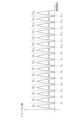
図5は、第1実施形態の閾値電圧とメモリセル数との関係を示すグラフである。 FIG. 5 is a graph showing the relationship between the threshold voltage and the number of memory cells in the first embodiment.
図5は、閾値電圧の分布D1~D16を示している。NANDメモリ12が16値メモリの場合、閾値電圧の分布は、16個のロブを有する。分布D1は、値15(2進法で1111)が記憶されているメモリセルの閾値電圧の分布を示している。分布D2は、値14(2進法で1110)が記憶されているメモリセルの閾値電圧の分布を示している。これは、分布D3~D16についても同様である。 5 shows threshold voltage distributions D1 to D16. When the
図5は、さらに、判定電圧V1~V15を示している。NANDメモリ12が16値メモリの場合、閾値電圧を特定するために、15種類の判定電圧V1~V15が使用される。例えば、判定電圧V1は、値15(2進法で1111)が記憶されているメモリセルの閾値電圧と、値14(2進法で1110)が記憶されているメモリセルの閾値電圧とを区別するために使用される。また、判定電圧V2は、値14(2進法で1110)が記憶されているメモリセルの閾値電圧と、値10(2進法で1010)が記憶されているメモリセルの閾値電圧とを区別するために使用される。これは、判定電圧V3~V15についても同様である。 FIG. 5 further shows determination voltages V1 to V15 . When the
次に、図6および図7を参照し、第1実施形態のメモリコントローラ11と、第1実施形態の比較例のメモリコントローラ11とを比較する。Next, referring to Figures 6 and 7, the
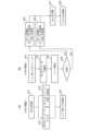
図6は、第1実施形態の比較例のメモリコントローラ11の動作を説明するための図である。比較例のメモリコントローラ11については、実施形態のメモリコントローラ11と同様に、図1~図5に示す符号を用いて説明する。Figure 6 is a diagram for explaining the operation of a
図6(a)は、比較例のメモリコントローラ11の圧縮部21および伸張部22を示している。比較例の圧縮部21は、シフト量Sftをコードブックインデックスiに圧縮する。また、比較例の伸張部22は、コードブックインデックスiをシフト量Sftに伸張する。シフト量Sftは、n個(nは、2以上の整数)の成分S1~Snを含むベクトル量である(Sft={S1,S2,S3,・・・,Sn})。一方、コードブックインデックスiは、スカラー量である。 FIG. 6(a) shows the
比較例のNANDメモリ12が16値メモリの場合、閾値電圧を特定するために15種類の判定電圧V1~V15が使用される。一方、シフト量Sftの成分Skは、判定電圧Vkの所定の電圧Vk(0)に対するシフト値である(kは、1≦k≦nを満たす整数)。よって、シフト量Sftの成分Skは、Sk=Vk-Vk(0)で表される。その結果、15種類の判定電圧V1~V15が使用される場合、シフト量Sftは、15個の成分S1~S15を含む15次ベクトルとなる。以下、シフト量Sftの成分Skを「シフト値Sk」とも表記する。なお、所定の電圧V1(0)~V15(0)は、例えば、判定電圧V1~V15の基準値(デフォルト値)である。 In the case where the
図6(b)は、比較例の情報管理部23により管理されているコードブックテーブルを示している。コードブックテーブルは、コードブックインデックスiとコードブックとの対応関係を示している。コードブックテーブルは、典型的なシフト量Sftをコードブックとして列挙したテーブルである。例えば、シフト量Sftをコードブックインデックスiに圧縮する際に、シフト量Sftが、コードブックインデックスiを「1」とするコードブック{S11,S21,S31,・・・,Sn1}と最も近い場合には、シフト量Sftの圧縮データは、「1」となる。この場合、コードブックインデックスiをシフト量Sftに伸張すると、圧縮データ「1」が伸張データ{S11,S21,S31,・・・,Sn1}に伸張される。すなわち、このシフト量Sft={S1,S2,S3,・・・,Sn}を圧縮および伸張すると、圧縮および伸張により得られるシフト量は、{S11,S21,S31,・・・,Sn1}となる。 FIG. 6(b) shows a codebook table managed by the
図6(c)は、比較例の情報管理部23により管理されているブロック管理情報を示している。ブロック管理情報は、例えば、ブロックインデックスbとコードブックインデックスiとの対応関係を示している。ブロックインデックスbは、NANDメモリ12の各ブロック(図4)を特定するためのインデックスである。例えば、ブロックインデックスbを「b1」「b2」「b3」とするブロックのシフト量Sftがそれぞれ、コードブックインデックスiを「i1」「i2」「i3」とするように圧縮された場合には、図6(c)に示すブロック管理情報が設定される。すなわち、ブロック「b1」「b2」「b3」のコードブックインデックスiの欄に、それぞれ「i1」「i2」「i3」が格納される。ブロックインデックスbは、例えば、スカラー量である。
比較例のシフト量Sftは、コードブックインデックスiに圧縮されて、メモリ領域内に記憶される。これにより、メモリ領域の圧迫を抑制することが可能となる。しかしながら、シフト量Sftをコードブックインデックスiに圧縮し、コードブックインデックスiをシフト量Sft(コードブック)に伸張すると、元のシフト量Sftと、伸張されたシフト量Sft(コードブック)との間に誤差が生じるおそれがある。例えば上述の例では、元のシフト量{S1,S2,S3,・・・,Sn}と、伸張されたシフト量{S11,S21,S31,・・・,Sn1}との間に誤差が生じる。 FIG. 6(c) shows block management information managed by the
The shift amount Sft of the comparative example is compressed into the codebook index i and stored in the memory area. This makes it possible to suppress pressure on the memory area. However, when the shift amount Sft is compressed to the codebook index i and the codebook index i is expanded to the shift amount Sft (codebook), the difference between the original shift amount Sft and the expanded shift amount Sft (codebook) is There is a risk that an error may occur. For example, in the above example, the original shift amount {S1 , S2 , S3 , ..., Sn } and the expanded shift amount {S11 , S21 , S31 , ... , Sn1 }.
図7は、第1実施形態のメモリコントローラ11の動作を説明するための図である。 FIG. 7 is a diagram for explaining the operation of the
図7(a)は、本実施形態のメモリコントローラ11の圧縮部21および伸張部22を示している。圧縮部21は、シフト量Sftを圧縮ベクトルvに圧縮する。また、伸張部22は、圧縮ベクトルvをシフト量Sftに伸張する。シフト量Sftは、上述のように、n個(nは、2以上の整数)の成分S1~Snを含むベクトル量である(Sft={S1,S2,S3,・・・,Sn})。一方、圧縮ベクトルvは、m個(mは、2以上の整数)の成分v1~vmを含むベクトル量である(v={v1,v2,v3,・・・,vm})。ただし、mは、nよりも小さい整数である(n>m≧2)。 FIG. 7(a) shows the
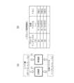
第1実施形態のNANDメモリ12が16値メモリの場合、上述の通り、閾値電圧を特定するために15種類の判定電圧V1~V15が使用される。この場合、シフト量Sftは、15個の成分(シフト値)S1~S15を含む15次ベクトルとなる。一方、圧縮ベクトルvの次数mは、2~14の整数であり、例えば4である。この場合、圧縮ベクトルvは、4個の成分v1~v4を含む4次ベクトルとなる。 When the
図7(b)は、第1実施形態の情報管理部23により管理されているブロック管理情報を示している。ブロック管理情報は、例えば、ブロックインデックスbと圧縮ベクトルvとの対応関係を示している。ブロックインデックスbは、上述のように、NANDメモリ12の各ブロック(図4)を特定するためのインデックスである。例えば、ブロックインデックスbを「b1」「b2」「b3」とするブロックのシフト量Sftがそれぞれ、圧縮ベクトルvを「v1」「v2」「v3」とするように圧縮された場合には、図7(b)に示すブロック管理情報が設定される。すなわち、ブロック「b1」「b2」「b3」の圧縮ベクトルvの欄に、それぞれ「v1」「v2」「v3」が格納される。ブロックインデックスbは、例えば、上述のように、スカラー量である。Figure 7(b) shows block management information managed by the
ブロック管理情報は、さらに、ブロックインデックスbとFBC(Fail Bit Count)との対応関係を示している。FBCは、各ブロックの記憶データが読み出された際に、誤って読み出されたビットの総数である。図7(b)では、ブロック「b1」「b2」「b3」のFBCの欄に、それぞれ「FBC1」「FBC2」「FBC3」が格納されている。 The block management information further indicates the correspondence between block index b and FBC (Fail Bit Count). FBC is the total number of bits that are erroneously read when the stored data of each block is read. In FIG. 7B, "FBC1," "FBC2," and "FBC3" are stored in the FBC columns of blocks "b1," "b2," and "b3," respectively.
第1実施形態のシフト量Sftは、スカラー量であるコードブックインデックスiではなく、ベクトル量である圧縮ベクトルvに圧縮される。これにより、誤差を低減しつつ、メモリ領域の圧迫を抑制することが可能となる。理由は、シフト量Sftをベクトル量に圧縮すれば、一般に、シフト量Sftをスカラー量に圧縮するのに比べて、圧縮により失われる情報量が少ないからである。In the first embodiment, the shift amount Sft is compressed into a compressed vector v, which is a vector amount, instead of the codebook index i, which is a scalar amount. This makes it possible to reduce errors while suppressing the pressure on memory space. This is because, when the shift amount Sft is compressed into a vector amount, the amount of information lost by compression is generally smaller than when the shift amount Sft is compressed into a scalar amount.
次に、図8~図10を参照し、第1実施形態の推定部51について説明する。Next, the
図8は、第1実施形態の推定部51の動作を説明するための模式図である。Figure 8 is a schematic diagram for explaining the operation of the
圧縮部21および伸張部22の少なくともいずれかは、読み出し精度を訓練により向上させるための推定部51を備えていてもよい。例えば、圧縮部21を推定部51により訓練することで、元のシフト量Sftと伸張されたシフト量Sftとの間の誤差が小さくなるように圧縮を行うことが可能となる。また、伸張部22を推定部51により訓練することで、元のシフト量Sftと伸張されたシフト量Sftとの間の誤差が小さくなるように伸張を行うことが可能となる。本実施形態の推定部51は、例えば、図11(b)に示す伸張部22、図13に示す圧縮部21(第2実施形態)、および図13に示す伸張部22(第2実施形態)に適用可能である。 At least one of the
推定部51は、ファームウェア、ソフトウェア、および電気回路のうちのいずれにより実現されてもよい。また、推定部51は、ファームウェア、ソフトウェア、および電気回路のうちの2つ以上を組み合わせて実現されてもよい。本実施形態では、図1に示すROM11c内に格納されたファームフェアが、RAM11bに展開され、CPU11aにより実行されることで、推定部51が実現される。例えば、推定部51は、DNN(Deep Neural Network)モデルなどの機械学習モデルに相当する。本実施形態によれば、メモリシステム1のメーカーによりメモリシステム1が出荷された後に、上記のような誤差を訓練(機械学習)により低減することが可能となる。 The
以下、図8に示す推定部51の動作について説明する。 The operation of the
図8では、シフト量Sftが推定部51に入力され、シフト量Sft’が推定部51から出力されている。推定部51は、圧縮部21と同様にシフト量Sftを圧縮ベクトルvに圧縮し、伸張部22と同様に圧縮ベクトルvをシフト量Sftに伸張する。図8は、伸張されたシフト量Sftを、元のシフト量Sftと区別するために、符号Sft’で示している。よって、推定部51は、元のシフト量Sftを圧縮および伸張して得られたシフト量Sft’を出力している。シフト量Sftとシフト量Sft’とが異なることは、推定部51の解答「Sft’」が正解「Sft」と異なっていることを意味する。 In FIG. 8, the shift amount Sft is input to the
図8は、さらに、損失関数L(Sft,Sft’)を示している。損失関数L(Sft,Sft’)は、シフト量Sftとシフト量Sft’との間の誤差に対応する値を出力する関数である。損失関数L(Sft,Sft’)の出力値は、推定部51に損失(loss)として入力される。本実施形態の訓練は、損失関数L(Sft,Sft’)の出力値を用いて行われる。なお、損失関数L(Sft,Sft’)の出力値は、メモリコントローラ11内の推定部51以外の機能ブロックが計算してもよいし、推定部51が計算してもよい。本実施形態の訓練は、例えば、損失関数L(Sft,Sft’)の出力値がゼロに近付くように行われる。 FIG. 8 further shows the loss function L(Sft, Sft'). The loss function L (Sft, Sft') is a function that outputs a value corresponding to the error between the shift amount Sft and the shift amount Sft'. The output value of the loss function L (Sft, Sft') is input to the
上記の訓練は、どのようなタイミングで行ってもよい。例えば、メモリシステム1内でリード動作が行われた際に、訓練が行われてもよい。また、圧縮部21により圧縮が行われた際に、訓練が行われてもよい。また、メモリシステム1内でパトロールリードまたはリトライが発生した際に、訓練が行われてもよい。The above training may be performed at any timing. For example, training may be performed when a read operation is performed in the
図9は、第1実施形態の変形例の推定部51の動作を説明するための模式図である。図9に示す推定部51については、図8に示す推定部51との相違点を中心に説明する。 FIG. 9 is a schematic diagram for explaining the operation of the
図9でも、シフト量Sftが推定部51に入力され、シフト量Sft’が推定部51から出力されている。本変形例の推定部51も、元のシフト量Sftを圧縮および伸張して得られたシフト量Sft’を出力している。 Also in FIG. 9, the shift amount Sft is input to the
図9は、さらに、FBCを示している。FBCは、例えば、メモリセルアレイ45(図4)のブロックごとに算出される。上述のように、各ブロックのFBCは、各ブロックの記憶データが読み出された際に、誤って読み出されたビットの総数である。本変形例のFBCは、推定部51に損失として入力される。本変形例の訓練は、FBCを用いて行われる。なお、FBCは、メモリコントローラ11内の推定部51以外の機能ブロックが計算してもよいし、推定部51が計算してもよい。本変形例の訓練は、例えば、FBCがゼロに近付くように行われる。 FIG. 9 further shows FBC. FBC is calculated for each block of the memory cell array 45 (FIG. 4), for example. As described above, the FBC of each block is the total number of bits that are read out incorrectly when the stored data of each block is read out. The FBC of this modification is input to the
本変形例では、推定部51からシフト量Sft’が出力されると、シフト量Sft’に対応する判定電圧を用いてリード動作が行われる。その後、このリード動作の際のFBCが算出される。このFBCは、推定部51に訓練用に入力される。また、このFBCは、上述のブロック管理情報として記憶および管理される。 In this modification, when the shift amount Sft' is output from the
図10は、第1実施形態の推定部51の動作について説明するための模式図である。図10に示す推定部51は、図8に示す推定部51と同じものであるが、図9に示す推定部51と同じものでもよい。 FIG. 10 is a schematic diagram for explaining the operation of the
図10は、初期のNANDメモリ12の疲労度の例と、寿命近くのNANDメモリ12の疲労度の例とを示している。初期のNANDメモリ12は、疲労度80%のメモリセルと、疲労度50%のメモリセルと、疲労度10%のメモリセルとを含んでいる。寿命近くのNANDメモリ12の疲労度は、疲労度90%のメモリセルと、疲労度70%のメモリセルと、疲労度50%のメモリセルとを含んでいる。 FIG. 10 shows an example of the fatigue level of the
初期のNANDメモリ12は、疲労度の低いメモリセルを多く含んでいる。寿命近くのNANDメモリ12は、疲労度の高いメモリセルを多く含んでいる。一方、好適な判定電圧(シフト量Sft)の値は、このような疲労度に応じて変化すると考えられる。本実施形態によれば、メモリシステム1の出荷後に推定部51による訓練を行うことができるため、疲労度に追従して判定電圧(シフト量Sft)を変化させることで、疲労度が変化しても読み出し精度を高く維持することが可能となる。An
次に、図11および図12を参照し、本実施形態の圧縮部21および伸張部22のさらなる詳細について説明する。Next, referring to Figures 11 and 12, the
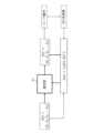
図11は、第1実施形態の圧縮部21および伸張部22の動作を説明するための模式図である。 FIG. 11 is a schematic diagram for explaining the operations of the
図11(a)では、圧縮部21が、シフト量Sftを圧縮ベクトルvに圧縮している。具体的には、圧縮部21は、シフト量Sftの15個のシフト値S1~S15の中から4個のシフト値S4、S7、S10、S14を選択し、選択されたシフト値S4、S7、S10、S14をそれぞれ、圧縮ベクトルvの成分v1、v2、v3、v4として出力している。以下、圧縮ベクトルvの成分v1~v4を「ベクトル成分v1~v4」とも表記する。 In FIG. 11(a), the
図11(a)では、圧縮部21が、関数を用いてシフト量Sftを圧縮ベクトルvに圧縮する。この関数は、シフト値S1~S15を入力とし、ベクトル成分v1~v4を出力としている。これら入力と出力との間には、v1=S4、v2=S7、v3=S10、v4=S14の関係が成り立つ。このように、本実施形態の圧縮部21は、静的な関数を用いてシフト量Sftを圧縮ベクトルvに圧縮する。 In FIG. 11(a), the
なお、ベクトル成分v1~v4の各々は、本実施形態では、シフト値S1~S15のうちの1つに依存しているが、シフト値S1~S15のうちの2つ以上に依存していてもよい。例えば、ベクトル成分v1は、v1=√(S1×S3)で与えられてもよい。 Note that, in this embodiment, each of the vector components v1 to v4 depends on one of the shift values S1 to S15 , but two or more of the shift values S1 to S15 may depend on. For example, vector component v1 may be given by v1 =√(S1 ×S3 ).
図11(b)では、伸張部22が、圧縮ベクトルvをシフト量Sftに伸張している。ベクトル成分v1~v4は、シフト値S1~S15の一部の情報しか含んでいないため、関数を用いて圧縮ベクトルvをシフト量Sftに精度よく伸張することは難しい。そこで、本実施形態の伸張部22は、推定部51を含んでいる。伸張部22は、圧縮ベクトルvからシフト量Sftを推定部51により推定することで、圧縮ベクトルvをシフト量Sftに伸張する。この推定の誤差は、上述の訓練により低減することが可能である。この推定は、ベクトル成分v1~v4と、その他の値とを用いて行ってもよい。このような値の例は、ライト動作からの経過時間t、およびW/EサイクルPEである。 In FIG. 11(b), the
一方、本実施形態の圧縮部21は、関数を用いてシフト量Sftを圧縮ベクトルvに圧縮しているため、本実施形態の圧縮部21は、推定部51を含んでいなくてもよい。本実施形態によれば、関数を用いて圧縮を行うことで、圧縮を簡単に行うことが可能となる。 On the other hand, since the
図12は、第1実施形態の圧縮部21および伸張部22の動作を説明するためのフローチャートである。 FIG. 12 is a flowchart for explaining the operations of the
図12(a)は、圧縮部21の動作フローを示している。 FIG. 12(a) shows the operation flow of the
まず、圧縮部21が、シフト量Sftを取得する(S11)。シフト量Sftの各成分(シフト値)は、図6を参照して説明したように、判定電圧(読み出し閾値電圧Vth)から所定の電圧を減算することで算出可能である。 First, the
次に、圧縮部21が、シフト量Sftを圧縮ベクトルvに変換する(S12)。この変換は、例えば、上記の関数を用いて行われる。 Next, the
次に、圧縮部21が、圧縮ベクトルvを保存する(S13)。圧縮ベクトルvは、例えば、ブロック管理情報としてNANDメモリ12に保存される。 Next, the
図12(b)は、伸張部22等の動作のフローを示している。Figure 12(b) shows the flow of operations of the
まず、伸張部22が、NANDメモリ12に保存されている圧縮ベクトルvを、RAM12bへとフェッチする(S21)。次に、伸張部22が、圧縮ベクトルvからシフト量Sftを推定する(S22)。この推定は、例えば、推定部51により行われる。 First, the
次に、メモリシステム1が、このシフト量Sftから得られた判定電圧を用いて、リード動作を行う(S23)。この際、リード動作が成功した場合には(S24 YES)、正しいシフト量Sftとして、シフト量Sftに追従する上述のシフト量Sft’を、推定部51により取得する(S25)。一方、リード動作が失敗した場合には(S24 NO)、別の方法で、上述のシフト量Sft’に代わる正しいシフト量Sftを取得する(S26)。Next, the
次に、伸張部22(推定部51)が、上述の損失(loss)を計算する(S27)。損失は、例えば、損失関数L(Sft,Sft’)を用いて計算される。次に、計算された損失が推定部51に入力され、推定部51(DNNモデル)が更新される(S28)。 Next, the decompression unit 22 (estimation unit 51) calculates the above-mentioned loss (S27). The loss is calculated using a loss function L (Sft, Sft'), for example. Next, the calculated loss is input to the
以上のように、本実施形態のメモリコントローラ11は、判定電圧のシフト量Sftを圧縮ベクトルvに圧縮して、NANDメモリ12のメモリ領域内に記憶させる。よって、本実施形態によれば、多値メモリの閾値電圧の判定電圧を、メモリ領域内に好適に記憶させることが可能となる。例えば、圧縮前の判定電圧と伸張後の判定電圧との間の誤差を低減しつつ、メモリ領域の圧迫を抑制することが可能となる。 As described above, the
(第2実施形態) (Second embodiment)
図13は、第2実施形態の圧縮部21および伸張部22の動作を説明するための模式図である。図13に示す圧縮部21および伸張部22は、図11に示す圧縮部21および伸張部22の変形例に相当する。 FIG. 13 is a schematic diagram for explaining the operations of the
本実施形態では、圧縮部21および伸張部22の各々が、図8に示す推定部51を備えている。そのため、本実施形態の圧縮部21は、シフト量Sftから圧縮ベクトルvを推定部51により推定することで、シフト量Sftを圧縮ベクトルvに圧縮する。また、本実施形態の伸張部22は、圧縮ベクトルvからシフト量Sftを推定部51により推定することで、圧縮ベクトルvをシフト量Sftに伸張する。圧縮部21および伸張部22の各々が、図8に示す推定部51の代わりに、図9に示す推定部51を備えていてもよい。 In this embodiment, each of the
本実施形態では、圧縮部21が、推定部51としてエンコーダを含み、伸張部22が、推定部51としてデコーダを含んでいる(図13)。エンコーダは、シフト量Sftを特徴量(圧縮ベクトルv)に変換し、デコーダは、特徴量をシフト量Sftに逆変換する。図13は、逆変換(復元)により得られたシフト量Sftを、元のシフト量Sftと区別するために、符号Sft’で示している。図13は、エンコーダおよびデコーダという2つのニューラルネットワークにより構成されるオートエンコーダを示している。エンコーダおよびデコーダは、それぞれ、第1および第2ニューラルネットワークの例である。本実施形態によれば、圧縮も伸張も関数ではなく推定により行うことで、例えば、より正確に疲労度を反映した読み出しを実現することが可能となる。 In this embodiment, the
図14は、第2実施形態の圧縮部21および伸張部22の動作を説明するためのフローチャートである。図14に示すフローは、図12に示すフローの変形例に相当する。 FIG. 14 is a flowchart for explaining the operations of the
図14(a)は、圧縮部21等の動作フローを示している。 FIG. 14(a) shows the operation flow of the
まず、圧縮部21が、シフト量Sftを取得する(S31)。次に、圧縮部21が、シフト量Sftをエンコーダに入力して、圧縮ベクトルvを算出する(S32)。また、メモリシステム1が、このシフト量Sftに対応する判定電圧を用いたリード動作を行って、FBCを取得する(S33)。次に、圧縮部21が、圧縮ベクトルvおよびFBCを保存する(S34)。圧縮ベクトルvおよびFBCは、例えば、ブロック管理情報としてNANDメモリ12に保存される。First, the
図14(b)は、伸張部22等の動作のフローを示している。 FIG. 14(b) shows the flow of operations of the
まず、伸張部22が、NANDメモリ12に保存されている圧縮ベクトルvおよびFBCを、RAM12bへとフェッチする(S41)。次に、伸張部22が、圧縮ベクトルvをデコーダに入力して、シフト量Sftを推定する(S42)。 First, the
次に、メモリシステム1が、このシフト量Sftから得られた判定電圧を用いて、リード動作を行う(S43)。この際、リード動作が成功した場合には(S44 YES)、正しいシフト量Sftとして、シフト量Sftに追従する上述のシフト量Sft’を、推定部51により取得する(S45)。一方、リード動作が失敗した場合には(S44 NO)、別の方法で、上述のシフト量Sft’に代わる正しいシフト量Sftを取得する(S46)。S45、S46の各々では、さらに、このリード動作に関するFBCを取得する。 Next, the
次に、伸張部22(推定部51)が、上述の損失(loss)を計算する(S47)。損失は、例えば、FBCにより与えられる。次に、計算された損失が推定部51に入力され、推定部51(DNNモデル)が更新される(S48)。Next, the decompression unit 22 (estimation unit 51) calculates the above-mentioned loss (S47). The loss is given by, for example, FBC. Next, the calculated loss is input to the
本実施形態のメモリコントローラ11は、第1実施形態のメモリコントローラ11と同様に、判定電圧のシフト量Sftを圧縮ベクトルvに圧縮して、NANDメモリ12のメモリ領域内に記憶させる。よって、本実施形態によれば、多値メモリの閾値電圧の判定電圧を、メモリ領域内に好適に記憶させることが可能となる。例えば、圧縮前の判定電圧と伸張後の判定電圧との間の誤差を低減しつつ、メモリ領域の圧迫を抑制することが可能となる。 Similarly to the
実施形態は例示であり、発明の範囲はそれらに限定されない。 The embodiments are illustrative, and the scope of the invention is not limited thereto.
1 メモリシステム
2 ホスト装置
11 メモリコントローラ
11a CPU
11b RAM
11c ROM
11d ECC回路
11e メモリI/Fコントローラ
11f ホストI/Fコントローラ
12 NANDメモリ
12a メモリユニット
21 圧縮部
22 伸張部
23 情報管理部
31 I/O信号処理回路
32 制御信号処理回路
33 チップ制御回路
34 RY/BY生成回路
35 コマンドレジスタ
36 アドレスレジスタ
41 ロウデコーダ
42 カラムデコーダ
43 データレジスタ
44 センスアンプ
45 メモリセルアレイ
51 推定部 1
11b RAM
11c ROM
Claims (20)
Translated fromJapanese前記ベクトル量をメモリ領域内に記憶させる記憶部と、
前記ベクトル量を前記判定電圧に伸張する伸張部と、
を備えるメモリコントローラ。 a compression unit that compresses two or more types of determination voltages of threshold voltages for a memory cell capable of storing three or more types of values into a vector quantity;
a storage unit that stores the vector quantity in a memory area;
an expansion unit that expands the vector amount to the determination voltage;
A memory controller comprising:
前記関数は、前記n種類の判定電圧に対応するn種類の値を入力とし、前記n種類の値から選択されたm種類の値を出力とする、請求項9に記載のメモリコントローラ。 the determination voltage includes n types of determination voltages, and the vector quantity includes m components (n and m are integers that satisfy n>m≧2);
10. The memory controller according to claim 9, wherein the function receives n types of values corresponding to the n types of determination voltages as inputs, and outputs m types of values selected from the n types of values.
前記ベクトル量を、記憶部によりメモリ領域内に記憶させ、
前記ベクトル量を、伸張部により前記判定電圧に伸張する、
ことを含むメモリコントローラの制御方法。 Compressing two or more types of determination voltages of threshold voltages for a memory cell capable of storing three or more types of values into a vector quantity by a compression unit,
storing the vector quantity in a memory area by a storage unit;
expanding the vector amount to the determination voltage by an expansion unit;
A method for controlling a memory controller, including:
前記メモリセル用の閾値電圧の2種類以上の判定電圧を、ベクトル量に圧縮する圧縮部と、
前記ベクトル量を前記メモリのメモリ領域内に記憶させる記憶部と、
前記ベクトル量を前記判定電圧に伸張する伸張部と、
を備えるメモリシステム。 A memory including memory cells capable of storing three or more types of values;
a compression unit that compresses two or more types of determination voltages of the threshold voltages for the memory cells into a vector quantity;
a storage unit that stores the vector quantity in a memory area of the memory;
an expansion unit that expands the vector amount to the determination voltage;
A memory system with
Priority Applications (2)
| Application Number | Priority Date | Filing Date | Title |
|---|---|---|---|
| JP2022148516AJP2024043364A (en) | 2022-09-16 | 2022-09-16 | Memory controller, memory controller control method, and memory system |
| US18/460,516US12430241B2 (en) | 2022-09-16 | 2023-09-01 | Memory controller, memory controller control method, and memory system |
Applications Claiming Priority (1)
| Application Number | Priority Date | Filing Date | Title |
|---|---|---|---|
| JP2022148516AJP2024043364A (en) | 2022-09-16 | 2022-09-16 | Memory controller, memory controller control method, and memory system |
Publications (1)
| Publication Number | Publication Date |
|---|---|
| JP2024043364Atrue JP2024043364A (en) | 2024-03-29 |
Family
ID=90243686
Family Applications (1)
| Application Number | Title | Priority Date | Filing Date |
|---|---|---|---|
| JP2022148516APendingJP2024043364A (en) | 2022-09-16 | 2022-09-16 | Memory controller, memory controller control method, and memory system |
Country Status (2)
| Country | Link |
|---|---|
| US (1) | US12430241B2 (en) |
| JP (1) | JP2024043364A (en) |
Family Cites Families (9)
| Publication number | Priority date | Publication date | Assignee | Title |
|---|---|---|---|---|
| US8380915B2 (en) | 2010-01-27 | 2013-02-19 | Fusion-Io, Inc. | Apparatus, system, and method for managing solid-state storage media |
| EP2549482B1 (en) | 2011-07-22 | 2018-05-23 | SanDisk Technologies LLC | Apparatus, system and method for determining a configuration parameter for solid-state storage media |
| JP7023204B2 (en)* | 2018-09-14 | 2022-02-21 | キオクシア株式会社 | Memory system and memory system control method |
| US11610116B2 (en) | 2018-12-31 | 2023-03-21 | SK Hynix Inc. | Storage device performance optimization using deep learning |
| EP3938913A1 (en) | 2019-03-15 | 2022-01-19 | INTEL Corporation | Multi-tile architecture for graphics operations |
| US11663746B2 (en) | 2019-11-15 | 2023-05-30 | Intel Corporation | Systolic arithmetic on sparse data |
| US11386972B2 (en)* | 2020-01-30 | 2022-07-12 | Macronix International Co., Ltd. | Determining read voltages for memory systems with machine learning |
| US11024401B1 (en) | 2020-05-07 | 2021-06-01 | Micron Technology, Inc. | Compute an optimized read voltage |
| JP2022050898A (en) | 2020-09-18 | 2022-03-31 | キオクシア株式会社 | Memory system and control method of memory system |
- 2022
- 2022-09-16JPJP2022148516Apatent/JP2024043364A/enactivePending
- 2023
- 2023-09-01USUS18/460,516patent/US12430241B2/enactiveActive
Also Published As
| Publication number | Publication date |
|---|---|
| US20240095162A1 (en) | 2024-03-21 |
| US12430241B2 (en) | 2025-09-30 |
Similar Documents
| Publication | Publication Date | Title |
|---|---|---|
| US11386952B2 (en) | Memory access module for performing a plurality of sensing operations to generate digital values of a storage cell in order to perform decoding of the storage cell | |
| US8793543B2 (en) | Adaptive read comparison signal generation for memory systems | |
| US8850292B2 (en) | Flash memory system and read method in flash memory system | |
| US9898363B2 (en) | Data storage device and operating method thereof | |
| US8289771B2 (en) | Data reading method and control circuit and memory controller using the same | |
| US9478298B2 (en) | Memory system and method of reading data thereof | |
| TWI502359B (en) | Command order re-sequencing in non-volatile memory | |
| CN111813591B (en) | Data error correction method and device of Nand Flash, electronic equipment and storage medium | |
| US11461177B2 (en) | Data storage device and method of operating the same | |
| US20160049204A1 (en) | Memory system and method of controlling non-volatile memory | |
| JP7291816B2 (en) | Adaptive Soft Bit Compression in Flash Memory | |
| CN114496044A (en) | Read threshold optimization system and method using model-free regression | |
| CN112585683B (en) | Offset sampling method for wear leveling | |
| US9009576B1 (en) | Adaptive LLR based on syndrome weight | |
| CN113076218A (en) | Method for rapidly processing data reading errors of NVM (non-volatile memory) chip and controller thereof | |
| JP2018163707A (en) | Semiconductor storage device and read control method of the same | |
| US10372377B2 (en) | Memory controller, memory system, and control method | |
| KR20230095157A (en) | Storage controller including a parity management module, a storage device including the same, and an operating method of the storage device | |
| JP2024043364A (en) | Memory controller, memory controller control method, and memory system | |
| US9015402B2 (en) | Memory controller and a method for writing information to a K-level memory unit | |
| US9239751B1 (en) | Compressing data from multiple reads for error control management in memory systems | |
| JP2012164072A (en) | Memory controller | |
| US12411603B2 (en) | Memory device and operating method thereof | |
| US20240264744A1 (en) | Memory controller and memory system including the memory controller and memory device | |
| KR20140042312A (en) | Semiconductor device and operating method thereof |