JP2024020242A - Fabrication of vertical transistors for memory applications - Google Patents
Fabrication of vertical transistors for memory applicationsDownload PDFInfo
- Publication number
- JP2024020242A JP2024020242AJP2023184098AJP2023184098AJP2024020242AJP 2024020242 AJP2024020242 AJP 2024020242AJP 2023184098 AJP2023184098 AJP 2023184098AJP 2023184098 AJP2023184098 AJP 2023184098AJP 2024020242 AJP2024020242 AJP 2024020242A
- Authority
- JP
- Japan
- Prior art keywords
- layer
- substrate
- channel layer
- memory cell
- protective liner
- Prior art date
- Legal status (The legal status is an assumption and is not a legal conclusion. Google has not performed a legal analysis and makes no representation as to the accuracy of the status listed.)
- Pending
Links
Images


Classifications
- H—ELECTRICITY
- H10—SEMICONDUCTOR DEVICES; ELECTRIC SOLID-STATE DEVICES NOT OTHERWISE PROVIDED FOR
- H10B—ELECTRONIC MEMORY DEVICES
- H10B51/00—Ferroelectric RAM [FeRAM] devices comprising ferroelectric memory transistors
- H10B51/20—Ferroelectric RAM [FeRAM] devices comprising ferroelectric memory transistors characterised by the three-dimensional arrangements, e.g. with cells on different height levels
- H—ELECTRICITY
- H10—SEMICONDUCTOR DEVICES; ELECTRIC SOLID-STATE DEVICES NOT OTHERWISE PROVIDED FOR
- H10B—ELECTRONIC MEMORY DEVICES
- H10B41/00—Electrically erasable-and-programmable ROM [EEPROM] devices comprising floating gates
- H10B41/20—Electrically erasable-and-programmable ROM [EEPROM] devices comprising floating gates characterised by three-dimensional arrangements, e.g. with cells on different height levels
- H10B41/23—Electrically erasable-and-programmable ROM [EEPROM] devices comprising floating gates characterised by three-dimensional arrangements, e.g. with cells on different height levels with source and drain on different levels, e.g. with sloping channels
- H10B41/27—Electrically erasable-and-programmable ROM [EEPROM] devices comprising floating gates characterised by three-dimensional arrangements, e.g. with cells on different height levels with source and drain on different levels, e.g. with sloping channels the channels comprising vertical portions, e.g. U-shaped channels
- H—ELECTRICITY
- H01—ELECTRIC ELEMENTS
- H01L—SEMICONDUCTOR DEVICES NOT COVERED BY CLASS H10
- H01L21/00—Processes or apparatus adapted for the manufacture or treatment of semiconductor or solid state devices or of parts thereof
- H01L21/02—Manufacture or treatment of semiconductor devices or of parts thereof
- H01L21/02104—Forming layers
- H01L21/02107—Forming insulating materials on a substrate
- H01L21/02109—Forming insulating materials on a substrate characterised by the type of layer, e.g. type of material, porous/non-porous, pre-cursors, mixtures or laminates
- H01L21/02112—Forming insulating materials on a substrate characterised by the type of layer, e.g. type of material, porous/non-porous, pre-cursors, mixtures or laminates characterised by the material of the layer
- H01L21/02123—Forming insulating materials on a substrate characterised by the type of layer, e.g. type of material, porous/non-porous, pre-cursors, mixtures or laminates characterised by the material of the layer the material containing silicon
- H01L21/02164—Forming insulating materials on a substrate characterised by the type of layer, e.g. type of material, porous/non-porous, pre-cursors, mixtures or laminates characterised by the material of the layer the material containing silicon the material being a silicon oxide, e.g. SiO2
- H—ELECTRICITY
- H01—ELECTRIC ELEMENTS
- H01L—SEMICONDUCTOR DEVICES NOT COVERED BY CLASS H10
- H01L21/00—Processes or apparatus adapted for the manufacture or treatment of semiconductor or solid state devices or of parts thereof
- H01L21/02—Manufacture or treatment of semiconductor devices or of parts thereof
- H01L21/02104—Forming layers
- H01L21/02107—Forming insulating materials on a substrate
- H01L21/02225—Forming insulating materials on a substrate characterised by the process for the formation of the insulating layer
- H01L21/02227—Forming insulating materials on a substrate characterised by the process for the formation of the insulating layer formation by a process other than a deposition process
- H01L21/0223—Forming insulating materials on a substrate characterised by the process for the formation of the insulating layer formation by a process other than a deposition process formation by oxidation, e.g. oxidation of the substrate
- H01L21/02233—Forming insulating materials on a substrate characterised by the process for the formation of the insulating layer formation by a process other than a deposition process formation by oxidation, e.g. oxidation of the substrate of the semiconductor substrate or a semiconductor layer
- H01L21/02236—Forming insulating materials on a substrate characterised by the process for the formation of the insulating layer formation by a process other than a deposition process formation by oxidation, e.g. oxidation of the substrate of the semiconductor substrate or a semiconductor layer group IV semiconductor
- H—ELECTRICITY
- H01—ELECTRIC ELEMENTS
- H01L—SEMICONDUCTOR DEVICES NOT COVERED BY CLASS H10
- H01L21/00—Processes or apparatus adapted for the manufacture or treatment of semiconductor or solid state devices or of parts thereof
- H01L21/67—Apparatus specially adapted for handling semiconductor or electric solid state devices during manufacture or treatment thereof; Apparatus specially adapted for handling wafers during manufacture or treatment of semiconductor or electric solid state devices or components ; Apparatus not specifically provided for elsewhere
- H01L21/67005—Apparatus not specifically provided for elsewhere
- H01L21/67011—Apparatus for manufacture or treatment
- H01L21/67098—Apparatus for thermal treatment
- H01L21/67103—Apparatus for thermal treatment mainly by conduction
- H—ELECTRICITY
- H01—ELECTRIC ELEMENTS
- H01L—SEMICONDUCTOR DEVICES NOT COVERED BY CLASS H10
- H01L21/00—Processes or apparatus adapted for the manufacture or treatment of semiconductor or solid state devices or of parts thereof
- H01L21/67—Apparatus specially adapted for handling semiconductor or electric solid state devices during manufacture or treatment thereof; Apparatus specially adapted for handling wafers during manufacture or treatment of semiconductor or electric solid state devices or components ; Apparatus not specifically provided for elsewhere
- H01L21/67005—Apparatus not specifically provided for elsewhere
- H01L21/67011—Apparatus for manufacture or treatment
- H01L21/67098—Apparatus for thermal treatment
- H01L21/67109—Apparatus for thermal treatment mainly by convection
- H—ELECTRICITY
- H01—ELECTRIC ELEMENTS
- H01L—SEMICONDUCTOR DEVICES NOT COVERED BY CLASS H10
- H01L21/00—Processes or apparatus adapted for the manufacture or treatment of semiconductor or solid state devices or of parts thereof
- H01L21/67—Apparatus specially adapted for handling semiconductor or electric solid state devices during manufacture or treatment thereof; Apparatus specially adapted for handling wafers during manufacture or treatment of semiconductor or electric solid state devices or components ; Apparatus not specifically provided for elsewhere
- H01L21/683—Apparatus specially adapted for handling semiconductor or electric solid state devices during manufacture or treatment thereof; Apparatus specially adapted for handling wafers during manufacture or treatment of semiconductor or electric solid state devices or components ; Apparatus not specifically provided for elsewhere for supporting or gripping
- H01L21/6831—Apparatus specially adapted for handling semiconductor or electric solid state devices during manufacture or treatment thereof; Apparatus specially adapted for handling wafers during manufacture or treatment of semiconductor or electric solid state devices or components ; Apparatus not specifically provided for elsewhere for supporting or gripping using electrostatic chucks
- H—ELECTRICITY
- H10—SEMICONDUCTOR DEVICES; ELECTRIC SOLID-STATE DEVICES NOT OTHERWISE PROVIDED FOR
- H10B—ELECTRONIC MEMORY DEVICES
- H10B41/00—Electrically erasable-and-programmable ROM [EEPROM] devices comprising floating gates
- H10B41/50—Electrically erasable-and-programmable ROM [EEPROM] devices comprising floating gates characterised by the boundary region between the core region and the peripheral circuit region
- H—ELECTRICITY
- H10—SEMICONDUCTOR DEVICES; ELECTRIC SOLID-STATE DEVICES NOT OTHERWISE PROVIDED FOR
- H10B—ELECTRONIC MEMORY DEVICES
- H10B43/00—EEPROM devices comprising charge-trapping gate insulators
- H10B43/20—EEPROM devices comprising charge-trapping gate insulators characterised by three-dimensional arrangements, e.g. with cells on different height levels
- H10B43/23—EEPROM devices comprising charge-trapping gate insulators characterised by three-dimensional arrangements, e.g. with cells on different height levels with source and drain on different levels, e.g. with sloping channels
- H10B43/27—EEPROM devices comprising charge-trapping gate insulators characterised by three-dimensional arrangements, e.g. with cells on different height levels with source and drain on different levels, e.g. with sloping channels the channels comprising vertical portions, e.g. U-shaped channels
- H—ELECTRICITY
- H10—SEMICONDUCTOR DEVICES; ELECTRIC SOLID-STATE DEVICES NOT OTHERWISE PROVIDED FOR
- H10B—ELECTRONIC MEMORY DEVICES
- H10B43/00—EEPROM devices comprising charge-trapping gate insulators
- H10B43/50—EEPROM devices comprising charge-trapping gate insulators characterised by the boundary region between the core and peripheral circuit regions
- H—ELECTRICITY
- H10—SEMICONDUCTOR DEVICES; ELECTRIC SOLID-STATE DEVICES NOT OTHERWISE PROVIDED FOR
- H10D—INORGANIC ELECTRIC SEMICONDUCTOR DEVICES
- H10D30/00—Field-effect transistors [FET]
- H10D30/01—Manufacture or treatment
- H10D30/021—Manufacture or treatment of FETs having insulated gates [IGFET]
- H10D30/025—Manufacture or treatment of FETs having insulated gates [IGFET] of vertical IGFETs
- H—ELECTRICITY
- H10—SEMICONDUCTOR DEVICES; ELECTRIC SOLID-STATE DEVICES NOT OTHERWISE PROVIDED FOR
- H10D—INORGANIC ELECTRIC SEMICONDUCTOR DEVICES
- H10D30/00—Field-effect transistors [FET]
- H10D30/01—Manufacture or treatment
- H10D30/021—Manufacture or treatment of FETs having insulated gates [IGFET]
- H10D30/0415—Manufacture or treatment of FETs having insulated gates [IGFET] of FETs having ferroelectric gate insulators
- H—ELECTRICITY
- H10—SEMICONDUCTOR DEVICES; ELECTRIC SOLID-STATE DEVICES NOT OTHERWISE PROVIDED FOR
- H10D—INORGANIC ELECTRIC SEMICONDUCTOR DEVICES
- H10D30/00—Field-effect transistors [FET]
- H10D30/60—Insulated-gate field-effect transistors [IGFET]
- H10D30/63—Vertical IGFETs
- H—ELECTRICITY
- H10—SEMICONDUCTOR DEVICES; ELECTRIC SOLID-STATE DEVICES NOT OTHERWISE PROVIDED FOR
- H10D—INORGANIC ELECTRIC SEMICONDUCTOR DEVICES
- H10D30/00—Field-effect transistors [FET]
- H10D30/60—Insulated-gate field-effect transistors [IGFET]
- H10D30/701—IGFETs having ferroelectric gate insulators, e.g. ferroelectric FETs
- H—ELECTRICITY
- H10—SEMICONDUCTOR DEVICES; ELECTRIC SOLID-STATE DEVICES NOT OTHERWISE PROVIDED FOR
- H10D—INORGANIC ELECTRIC SEMICONDUCTOR DEVICES
- H10D64/00—Electrodes of devices having potential barriers
- H10D64/01—Manufacture or treatment
- H10D64/031—Manufacture or treatment of data-storage electrodes
- H10D64/033—Manufacture or treatment of data-storage electrodes comprising ferroelectric layers
- H—ELECTRICITY
- H10—SEMICONDUCTOR DEVICES; ELECTRIC SOLID-STATE DEVICES NOT OTHERWISE PROVIDED FOR
- H10D—INORGANIC ELECTRIC SEMICONDUCTOR DEVICES
- H10D64/00—Electrodes of devices having potential barriers
- H10D64/60—Electrodes characterised by their materials
- H10D64/66—Electrodes having a conductor capacitively coupled to a semiconductor by an insulator, e.g. MIS electrodes
- H10D64/68—Electrodes having a conductor capacitively coupled to a semiconductor by an insulator, e.g. MIS electrodes characterised by the insulator, e.g. by the gate insulator
- H10D64/689—Electrodes having a conductor capacitively coupled to a semiconductor by an insulator, e.g. MIS electrodes characterised by the insulator, e.g. by the gate insulator having ferroelectric layers
- H—ELECTRICITY
- H10—SEMICONDUCTOR DEVICES; ELECTRIC SOLID-STATE DEVICES NOT OTHERWISE PROVIDED FOR
- H10D—INORGANIC ELECTRIC SEMICONDUCTOR DEVICES
- H10D64/00—Electrodes of devices having potential barriers
- H10D64/60—Electrodes characterised by their materials
- H10D64/66—Electrodes having a conductor capacitively coupled to a semiconductor by an insulator, e.g. MIS electrodes
- H10D64/68—Electrodes having a conductor capacitively coupled to a semiconductor by an insulator, e.g. MIS electrodes characterised by the insulator, e.g. by the gate insulator
- H10D64/691—Electrodes having a conductor capacitively coupled to a semiconductor by an insulator, e.g. MIS electrodes characterised by the insulator, e.g. by the gate insulator comprising metallic compounds, e.g. metal oxides or metal silicates
- H—ELECTRICITY
- H01—ELECTRIC ELEMENTS
- H01L—SEMICONDUCTOR DEVICES NOT COVERED BY CLASS H10
- H01L21/00—Processes or apparatus adapted for the manufacture or treatment of semiconductor or solid state devices or of parts thereof
- H01L21/02—Manufacture or treatment of semiconductor devices or of parts thereof
- H01L21/02104—Forming layers
- H01L21/02107—Forming insulating materials on a substrate
- H01L21/02225—Forming insulating materials on a substrate characterised by the process for the formation of the insulating layer
- H01L21/02227—Forming insulating materials on a substrate characterised by the process for the formation of the insulating layer formation by a process other than a deposition process
- H01L21/02252—Forming insulating materials on a substrate characterised by the process for the formation of the insulating layer formation by a process other than a deposition process formation by plasma treatment, e.g. plasma oxidation of the substrate
- H—ELECTRICITY
- H01—ELECTRIC ELEMENTS
- H01L—SEMICONDUCTOR DEVICES NOT COVERED BY CLASS H10
- H01L21/00—Processes or apparatus adapted for the manufacture or treatment of semiconductor or solid state devices or of parts thereof
- H01L21/02—Manufacture or treatment of semiconductor devices or of parts thereof
- H01L21/02104—Forming layers
- H01L21/02365—Forming inorganic semiconducting materials on a substrate
- H01L21/02518—Deposited layers
- H01L21/02521—Materials
- H01L21/02524—Group 14 semiconducting materials
- H01L21/02532—Silicon, silicon germanium, germanium
- H—ELECTRICITY
- H01—ELECTRIC ELEMENTS
- H01L—SEMICONDUCTOR DEVICES NOT COVERED BY CLASS H10
- H01L21/00—Processes or apparatus adapted for the manufacture or treatment of semiconductor or solid state devices or of parts thereof
- H01L21/02—Manufacture or treatment of semiconductor devices or of parts thereof
- H01L21/02104—Forming layers
- H01L21/02365—Forming inorganic semiconducting materials on a substrate
- H01L21/02612—Formation types
- H01L21/02617—Deposition types
- H01L21/0262—Reduction or decomposition of gaseous compounds, e.g. CVD
- H—ELECTRICITY
- H01—ELECTRIC ELEMENTS
- H01L—SEMICONDUCTOR DEVICES NOT COVERED BY CLASS H10
- H01L21/00—Processes or apparatus adapted for the manufacture or treatment of semiconductor or solid state devices or of parts thereof
- H01L21/02—Manufacture or treatment of semiconductor devices or of parts thereof
- H01L21/02104—Forming layers
- H01L21/02365—Forming inorganic semiconducting materials on a substrate
- H01L21/02612—Formation types
- H01L21/02617—Deposition types
- H01L21/02636—Selective deposition, e.g. simultaneous growth of mono- and non-monocrystalline semiconductor materials
- H—ELECTRICITY
- H01—ELECTRIC ELEMENTS
- H01L—SEMICONDUCTOR DEVICES NOT COVERED BY CLASS H10
- H01L21/00—Processes or apparatus adapted for the manufacture or treatment of semiconductor or solid state devices or of parts thereof
- H01L21/02—Manufacture or treatment of semiconductor devices or of parts thereof
- H01L21/04—Manufacture or treatment of semiconductor devices or of parts thereof the devices having potential barriers, e.g. a PN junction, depletion layer or carrier concentration layer
- H01L21/18—Manufacture or treatment of semiconductor devices or of parts thereof the devices having potential barriers, e.g. a PN junction, depletion layer or carrier concentration layer the devices having semiconductor bodies comprising elements of Group IV of the Periodic Table or AIIIBV compounds with or without impurities, e.g. doping materials
- H01L21/30—Treatment of semiconductor bodies using processes or apparatus not provided for in groups H01L21/20 - H01L21/26
- H01L21/31—Treatment of semiconductor bodies using processes or apparatus not provided for in groups H01L21/20 - H01L21/26 to form insulating layers thereon, e.g. for masking or by using photolithographic techniques; After treatment of these layers; Selection of materials for these layers
- H01L21/3105—After-treatment
- H01L21/311—Etching the insulating layers by chemical or physical means
- H01L21/31105—Etching inorganic layers
- H01L21/31111—Etching inorganic layers by chemical means
- H01L21/31116—Etching inorganic layers by chemical means by dry-etching
- H—ELECTRICITY
- H01—ELECTRIC ELEMENTS
- H01L—SEMICONDUCTOR DEVICES NOT COVERED BY CLASS H10
- H01L21/00—Processes or apparatus adapted for the manufacture or treatment of semiconductor or solid state devices or of parts thereof
- H01L21/67—Apparatus specially adapted for handling semiconductor or electric solid state devices during manufacture or treatment thereof; Apparatus specially adapted for handling wafers during manufacture or treatment of semiconductor or electric solid state devices or components ; Apparatus not specifically provided for elsewhere
- H01L21/677—Apparatus specially adapted for handling semiconductor or electric solid state devices during manufacture or treatment thereof; Apparatus specially adapted for handling wafers during manufacture or treatment of semiconductor or electric solid state devices or components ; Apparatus not specifically provided for elsewhere for conveying, e.g. between different workstations
- H01L21/67739—Apparatus specially adapted for handling semiconductor or electric solid state devices during manufacture or treatment thereof; Apparatus specially adapted for handling wafers during manufacture or treatment of semiconductor or electric solid state devices or components ; Apparatus not specifically provided for elsewhere for conveying, e.g. between different workstations into and out of processing chamber
- H01L21/67742—Mechanical parts of transfer devices
Landscapes
- Engineering & Computer Science (AREA)
- Microelectronics & Electronic Packaging (AREA)
- Condensed Matter Physics & Semiconductors (AREA)
- General Physics & Mathematics (AREA)
- Manufacturing & Machinery (AREA)
- Computer Hardware Design (AREA)
- Physics & Mathematics (AREA)
- Power Engineering (AREA)
- Semiconductor Memories (AREA)
- Non-Volatile Memory (AREA)
- Formation Of Insulating Films (AREA)
- Electrodes Of Semiconductors (AREA)
- Internal Circuitry In Semiconductor Integrated Circuit Devices (AREA)
- Thin Film Transistor (AREA)
- Chemical Vapour Deposition (AREA)
Abstract
Translated fromJapaneseDescription
Translated fromJapanese本開示の実施形態は、概して、垂直型メモリセル半導体デバイスを製造する方法に関し、より詳細には、半導体製造用途のための階段状構造を備えた垂直型メモリセル半導体デバイスを製造する方法に関する。 Embodiments of the present disclosure generally relate to methods of manufacturing vertical memory cell semiconductor devices, and more particularly, to methods of manufacturing vertical memory cell semiconductor devices with stepped structures for semiconductor manufacturing applications.
サブハーフミクロン単位のより小さなフィーチャ(feature)を信頼性高く製造することは、半導体デバイスの次世代の大規模集積(VLSI:very large scale integration)及び超大規模集積(ULSI:ultra large scale integration)のための重要な技術課題の1つとなっている。しかしながら、回路技術の限界が更新されるにつれ、寸法が縮小しつつあるVLSI及びULSIの相互接続技術には、処理能力の向上に対する更なる要求がなされている。基板上にゲート構造を信頼性高く形成することは、VLSI及びULSIの成功にとって、また、個々の基板やダイの回路密度や品質を高める継続的な取り組みにとって重要なことである。 Reliably manufacturing smaller sub-half-micron features is the key to the next generation of very large scale integration (VLSI) and ultra large scale integration (ULSI) of semiconductor devices. This is one of the important technical issues for the future. However, as the limits of circuit technology are updated, VLSI and ULSI interconnect technologies are being reduced in size, placing further demands on increased throughput. Reliably forming gate structures on substrates is critical to the success of VLSI and ULSI and to the continued efforts to increase the circuit density and quality of individual substrates and die.
フォトレジスト層といったパターニングされたマスクが、エッチングプロセスによって基板上にゲート構造、シャロートレンチアイソレーション(STI:shallow trench isolation)、バイトライン等といった構造を形成する際に一般的に使用される。パターニングされたマスクは、従来では、リソグラフィプロセスを使用して作製され、所望の臨界寸法を有するパターンが、フォトレジストの層に光学的に転写される。次いで、フォトレジスト層が現像されて、フォトレジストの望まれぬ部分が除去され、これにより、残りのフォトレジストに開口部が作られる。 A patterned mask, such as a photoresist layer, is commonly used to form structures such as gate structures, shallow trench isolation (STI), bite lines, etc. on a substrate by an etching process. Patterned masks are conventionally created using a lithographic process in which a pattern with desired critical dimensions is optically transferred to a layer of photoresist. The photoresist layer is then developed to remove the unwanted portions of the photoresist, thereby creating openings in the remaining photoresist.
次世代のデバイス及び構造物の製造を可能とするために、半導体メモリチップの三次元(3D)積層が、トランジスタの性能を改良させるために利用されることが多い。従来の2次元の代わりに、3次元にトランジスタを配置することによって、複数のトランジスタが、互いにかなり接近して集積回路(IC)内に配置されうる。半導体チップの三次元(3D)積層により、ワイヤ長が縮小されると共に、配線遅延が小さく保たれる。半導体チップの三次元(3D)積層の製造においては、階段状構造が、複数の相互接続構造をその上に配置して高密度の垂直トランジスタデバイスを形成するために利用されることが多い。 To enable the fabrication of next generation devices and structures, three-dimensional (3D) stacking of semiconductor memory chips is often utilized to improve transistor performance. By arranging transistors in three dimensions instead of the traditional two dimensions, multiple transistors can be placed much closer together in an integrated circuit (IC). Three-dimensional (3D) stacking of semiconductor chips reduces wire length and keeps interconnect delays low. In the manufacture of three-dimensional (3D) stacks of semiconductor chips, stepped structures are often utilized to place multiple interconnect structures thereon to form high density vertical transistor devices.
基板上に配置された膜スタックにおいて階段状構造を形成するときには、エッチングプロセスがフォトレジストトリミングプロセスと共に繰り返し行われ、膜スタックが、順次トリミングされたフォトレジスト層をエッチングマスクとして用いてエッチングされる。図1Aに示される例示的な実施形態において、トリミングされたフォトレジスト層(図示せず)が、基板104上に配置された膜スタック120上に構造を転写するためのエッチングマスク層として機能して、半導体デバイス100を形成するための階段状構造110を基板104上に形成することができる。膜スタック120には典型的に、図1Bに示されるように、導電層又は絶縁層である層120a、120b(120a1、120b1、120a2、120b2…120a5、120b5として示される)が互い違いになった層が含まれる。エッチングの間、フォトレジスト層は、エッチマスクとして機能する一方で、様々な寸法に順次トリミングされ、様々な幅を有する階段状構造110が形成される。 When forming a stepped structure in a film stack disposed on a substrate, the etching process is repeated with a photoresist trimming process, and the film stack is etched using the sequentially trimmed photoresist layers as an etching mask. In the exemplary embodiment shown in FIG. 1A, a trimmed photoresist layer (not shown) serves as an etch mask layer to transfer the structure onto a
基板104上に階段状構造110を製造する間、階段状構造110内に形成された各階段は、図1A及び図1Bに示すように、その上にチャネル125(例えば、開口部)が形成できるように、意図された幅を有する。より高いデバイス性能が要求されるいくつかの実施形態において、異なる材料の上記互い違いに層なった120a、120bが利用されうる。例えば、デバイス性能のより高い電気移動度が要求されるときには、金属導電性材料が、階段状構造110で利用されることが多い。一例において、上記互い違いの層120a、120bのうち第2の層120b(図1Bでは120b1…120b5として示す)が、階段状構造110から除去され、図1Cに示されるように金属含有層150と置換され、デバイス100の電気的性能が改善されうる。しかしながら、階段状構造110から元の第2の層120b(図1Bでは120b1…120b5として示す)を除去して、図1Cに示すように、金属含有層150と置換し又は金属含有層150を挿入すると、金属含有層150間の界面130において、残留物及び/又は表面粗さ152が、上位界面における選択的エッチングに起因して見うけられることが多く、したがって、界面130での電気的接触が不十分になり、最終的にデバイスの故障又は電気的性能の劣化につながる。 During fabrication of the
従って、半導体デバイスの三次元(3D)積層のための正確なプロファイル及び寸法制御を含む、階段状構造を形成するための改良された方法及び装置が必要とされている。 Accordingly, there is a need for improved methods and apparatus for forming stepped structures that include precise profile and dimensional control for three-dimensional (3D) stacking of semiconductor devices.
本開示の実施形態は、三次元(3D)積層メモリセル半導体デバイスを製造するための正確なプロファイル及び寸法制御を含む、階段状構造を形成するための装置及び方法を提供する。一実施形態において、メモリセルデバイスが、基板上に水平方向に形成された、互い違いになった誘電体層と導電性構造との対を含む膜スタックと、膜スタックに形成された開口部であって、チャネル層及び中心充填層で充填された開口部と、導電性構造とチャネル層との間に配置された保護ライナ層と、を含む。 Embodiments of the present disclosure provide apparatus and methods for forming stepped structures, including precise profile and dimensional control for manufacturing three-dimensional (3D) stacked memory cell semiconductor devices. In one embodiment, a memory cell device includes a membrane stack formed horizontally on a substrate and including alternating pairs of dielectric layers and conductive structures, and an opening formed in the membrane stack. and a protective liner layer disposed between the conductive structure and the channel layer.
他の実施形態において、基板上のメモリデバイスの方法は、第1の層及び第2の層を含む膜スタックに開口部を形成することと、1つ以上の層で開口部を充填することであって、1つ以上の層がチャネル層を含む、開口部を充填することと、膜スタックから第1の層を選択的に除去して、チャネル層の一部分を露出させることと、チャネル層の一部分を選択的に酸化して、保護ライナ層を形成することと、空間を導電性構造で充填することを含む。 In other embodiments, a method of a memory device on a substrate includes forming an opening in a film stack including a first layer and a second layer and filling the opening with one or more layers. filling the opening, the one or more layers including a channel layer; selectively removing a first layer from the membrane stack to expose a portion of the channel layer; The method includes selectively oxidizing the portion to form a protective liner layer and filling the space with a conductive structure.
さらに別の実施形態において、基板上に階段状構造体を形成する方法は、膜スタックにおいて形成された誘電体層間で画定される空間によって露出したチャネル層の一部分を選択的に酸化することであって、膜スタックが、チャネル層を含む多層構造によって充填された中心開口部を有する、選択的に酸化することと、チャネル層の一部分上に保護ライナ層を形成することと、保護ライナ層と接触する強誘電体層を形成することであって、バリア層が高誘電率材料である、強誘電体層を形成することを含む。 In yet another embodiment, a method of forming a stepped structure on a substrate includes selectively oxidizing a portion of a channel layer exposed by a space defined between dielectric layers formed in a film stack. selectively oxidizing the membrane stack having a central opening filled by a multilayer structure including a channel layer; forming a protective liner layer over a portion of the channel layer; and contacting the protective liner layer. forming a ferroelectric layer, the barrier layer being a high dielectric constant material.
本開示の上記の特徴を詳細に理解することができるように、上記で簡単に要約した本開示のより具体的な説明を、実施形態を参照することによって行うことができ、その幾つかを添付の図面に示す。しかしながら、本開示は他の等しく有効な実施形態も許容しうることから、添付の図面は本開示の典型的な実施形態のみを示しており、従って、本開示の範囲を限定すると見なすべきではないことに留意されたい。 In order that the above features of the present disclosure may be understood in detail, a more specific description of the present disclosure briefly summarized above may be had by reference to the embodiments, some of which are attached hereto. As shown in the drawing. However, the accompanying drawings depict only typical embodiments of the disclosure and therefore should not be considered as limiting the scope of the disclosure, as the disclosure may also tolerate other equally valid embodiments. Please note that.
理解を容易にするために、可能な場合には、複数の図に共通する同一の要素を指し示すために同一の参照番号を使用している。1の実施形態の構成要素及び特徴が、更なる記載がなくとも、他の実施形態に有益に組み込まれうることが想定されている。 To facilitate understanding, the same reference numerals have been used, where possible, to refer to the same elements that are common to the figures. It is envisioned that components and features of one embodiment may be beneficially incorporated into other embodiments without further description.
しかしながら、本開示は他の等しく有効な実施形態も許容しうることから、添付の図面は本開示の典型的な実施形態のみを示しており、従って、本開示の範囲を限定すると見なすべきではないことに留意されたい。 However, the accompanying drawings depict only typical embodiments of the disclosure and therefore should not be considered as limiting the scope of the disclosure, as the disclosure may also tolerate other equally valid embodiments. Please note that.
本開示は、半導体デバイスの三次元(3D)メモリセルのための、階段状構造を基板上に形成する方法を提供する。一例において、選択的堆積及び選択的パターニング/エッチングプロセスと共に、界面において保護界面層(例えば、界面酸化層)を利用することによって、製造中の良好な界面管理、優れた電気的性能、及び良好なプロセス制御が得られる。一例において、三次元(3D)に積層された半導体デバイスのためのメモリセルを形成する方法は、階段状構造体の形成のため膜スタックから或る種の材料を除去するときに、保護酸化層を利用することができる。さらに、高誘電率材料が、導電性材料と共に形成するために利用され、階段状構造の一部分が、導電性構造と置換される。界面/保護酸化層は、除去プロセスの間は保護された状態にあって無傷のままであり、従って、界面プロファイル及びトポグラフィの良好な制御が提供される。したがって、高誘電率材料及び導電性材料を含む導電性構造が、階段状構造において形成された後で、界面における良好な電気的接触が得られ、従って、メモリセルに所望の電気的性能がもたらされる。 The present disclosure provides a method of forming a stepped structure on a substrate for a three-dimensional (3D) memory cell of a semiconductor device. In one example, the utilization of a protective interfacial layer (e.g., an interfacial oxide layer) at the interface, along with selective deposition and selective patterning/etching processes, provides good interfacial control during fabrication, good electrical performance, and Gain process control. In one example, a method of forming a memory cell for a three-dimensional (3D) stacked semiconductor device includes removing a protective oxide layer when removing certain materials from a film stack for the formation of a stepped structure. can be used. Additionally, a high dielectric constant material is utilized to form the conductive material and a portion of the stepped structure is replaced with the conductive structure. The interfacial/protective oxide layer remains protected and intact during the removal process, thus providing good control of interfacial profile and topography. Therefore, after a conductive structure comprising a high dielectric constant material and a conductive material is formed in a stepped structure, good electrical contact at the interface is obtained, thus providing the desired electrical performance to the memory cell. It will be done.
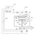
図2は、半導体デバイス製造のための半導体相互接続構造として利用されうるプラズマ堆積プロセス(例えば、プラズマ強化CVD又は金属有機CVD)を実施するのに適したプラズマ処理チャンバ232の断面図である。処理チャンバ232は、カリフォルニア州サンタクララのApplied Materials,Inc.から入手可能な、適切に適合されたCENTURA(登録商標)、PRODUCER(登録商標)SE又はPRODUCER(登録商標)GT又はPRODUCER(登録商標)XP処理システムでありうる。他の製造業者によって製造されたものを含む他の処理システムが、本明細書に記載される実施形態から恩恵を受けうると考えられる。 FIG. 2 is a cross-sectional view of a
処理チャンバ232はチャンバ本体251を含む。チャンバ本体251は、内部空間226を画定するリッド225、側壁201及び底壁222を含む。
基板支持ペデスタル250が、チャンバ本体251の内部空間126内に設けられる。ペデスタル250は、アルミニウム、セラミック、窒化アルミニウム、及び他の適切な材料から製造されうる。一実施形態において、ペデスタル250は、ペデスタル250に熱的損傷を引き起こすことなく、プラズマプロセス環境といった高温環境での使用に適した材料である、窒化アルミニウムといったセラミック材料によって作製される。ペデスタル250は、リフト機構(図示せず)を用いてチャンバ本体251の内部で垂直方向に動かされる。 A
ペデスタル250は、ペデスタル250上で支持された基板290の温度を制御するのに適した、埋め込まれたヒータ要素270を含みうる。一実施形態において、ペデスタル250は、電源206からヒータ要素270に電流を印加することによって抵抗加熱されうる。一実施形態において、ヒータ要素270は、ニッケル-鉄-クロム合金(例えば、INCOLOY(登録商標))シース管内に封入されたニッケル-クロムワイヤで作製されうる。電源206から供給された電流は、ヒータ素子270により生成される熱を制御するために、コントローラ210によって調節され、これにより、基板290及びペデスタル250が、任意の適切な温度範囲での膜堆積の間、実質的に一定の温度に維持される。他の実施形態において、ペデスタルが、必要に応じて室温に維持されてよい。更に別の実施形態において、ペデスタル250はまた、必要に応じて室温よりも低い範囲でペデスタル250を冷却するために、必要に応じて冷却装置(図示せず)を含みうる。供給される電流が調整され、ペデスタル250の温度が約100℃から約700℃までの間で選択的に制御されうる。
熱電対といった温度センサ272が、ペデスタル250の温度を従来のやり方で監視するために、基板支持ペデスタル250に埋め込まれうる。測定された温度がコントローラ210によって利用され、ヒータ要素270に供給される電力が制御されて、基板が所望の温度に維持される。 A
ペデスタル250は、通常、当該ペデスタル250を貫通して配置される複数のリフトピン(図示せず)を含み、この複数のリフトピンは、基板290をペデスタル250から上昇させ、従来のやり方でのロボット(図示せず)による基板290の交換を促進するよう構成されている。
ペデスタル250は、ペデスタル250上に基板290を保持するための少なくとも1つの電極292を含む。電極292は、チャック電源208によって駆動され、従来知られているように、基板290をペデスタル表面に保持する静電力を発生させる。代替的に、基板290は、クランプ、真空又は重力によってペデスタル250に保持されてよい。
一実施形態において、ペデスタル250は、図2に2つのRFバイアス電源284、286として示された少なくとも1つのRFバイアス電源に結合された電極292がその内部に埋め込まれたカソードとして構成される。図2に示す例は、2つのRFバイアス電源284、286を示しているが、RFバイアス電源の数は、必要に応じた任意の数でありうることに注意されたい。RFバイアス電源284、286は、ペデスタル250内に配置された電極292と、処理システム232のガス分配プレート242又はリッド225といった他の電極と、の間に接続される。RFバイアス電源284、286が、処理チャンバ232の処理領域内に配されたガスを励起して、当該ガスから形成されたプラズマ放電を維持する。 In one embodiment,
図2に示す実施形態では、デュアルRFバイアス電源RFバイアス電源284、286が、整合回路204を介してペデスタル250内に配置された電極292に接続されている。RFバイアス電源284、286によって生成された信号が、単一の供給線を通じて、整合回路204を介してペデスタル250に届けられ、プラズマ処理チャンバ232内で、供給された混合ガスがイオン化され、これにより、堆積又は他のプラズマ強化プロセスを実施するために必要なイオンエネルギーが提供される。RFバイアス電源284、286は一般に、約50kHzと約200MHzの間の周波数と、約0ワットと約5000ワットの間の電力と、を有するRF信号を生成することができる。 In the embodiment shown in FIG. 2, dual RF bias power supplies RF bias
真空ポンプ202が、チャンバ本体251の底部222に形成されたポートに結合される。真空ポンプ202は、チャンバ本体251内で所望のガス圧力を維持するために使用される。真空ポンプ202はまた、後処理ガス及びプロセスの副生成物をチャンバ本体251から排出する。 A
処理システム232は、処理システム232のリッド225を介して結合された1つ以上のガス伝達通路244を含む。ガス伝達通路244と真空ポンプ202とが、内部空間226内に層流を誘導して粒子汚染を最小にするために、処理システム232の両端に配置されている。
ガス伝達通路244は、遠隔プラズマ源(RPS:remote plasma source)248を通してガスパネル293に結合されており、混合ガスを内部空間226内に供給する。一実施形態において、ガス伝達通路244を介して供給された混合ガスが、ガス伝達通路244の下方に配置されたガス分配プレート242を介して更に供給されうる。一例において、複数の開孔243を有するガス分配プレート242は、ペデスタル250の上方のチャンバ本体251のリッド225に結合されている。ガス分配プレート242の開孔243は、処理ガスをガスパネル293からチャンバ本体251内に導入するために利用される。開孔243は、様々なプロセス要件のための様々な処理ガスの流れを促進するために、様々なサイズ、数、分散、形状、設計、及び直径を有しうる。プラズマが、ガス分配プレート242を出たプロセス混合ガスから形成され、処理ガスの熱分解を高め、基板290の表面291上に材料を堆積させる。
ガス分配プレート242と基板支持ペデスタル250とは、内部空間226で間隔が置かれた1対の電極を形成しうる。1つ以上のRF供給源247が、整合ネットワーク245を介してガス分配プレート242にバイアス電圧を供給して、ガス分配プレート242とペデスタル250との間でのプラズマ生成を促進する。代替的に、RF供給源247及び整合ネットワーク245が、ガス分配プレート242、基板支持ペデスタル250に結合されてよく、又はガス分配プレート242と基板支持ペデスタル250の両方に結合されてよく、又はチャンバ本体251の外側に配置されたアンテナ(図示せず)に結合されてよい。一実施形態において、RF供給源247は、約30kHzから約13.6MHzの周波数で、約10ワットから約3000ワットまでの電力を供給しうる。代替的に、RF供給源247は、内部空間226内でのプラズマ生成を支援するマイクロ波電力をガス分配プレート242に供給するマイクロ波発振器であってよい。
ガスパネル293から供給されうるガスの例は、ケイ素含有ガス、フッ素含有ガス、酸素含有ガス、水素含有ガス、不活性ガス、及びキャリアガスを含みうる。反応ガスの適切な例には、SiH4、Si2H6、SiF4、SiH2Cl2、Si4H10、Si5H12、TEOS等といったケイ素含有ガスが含まれる。適切なキャリアガスには、窒素(N2)、アルゴン(Ar)、水素(H2)、アルカン、アルケン、ヘリウム(He)、酸素(O2)、オゾン(O3)、水蒸気(H2O)などが含まれる。 Examples of gases that may be supplied from gas panel 293 may include silicon-containing gases, fluorine-containing gases, oxygen-containing gases, hydrogen-containing gases, inert gases, and carrier gases. Suitable examples of reactive gases include silicon-containing gases such as SiH4 , Si2 H6 , SiF4 , SiH2 Cl2 , Si4 H10 , Si5 H12 , TEOS, and the like. Suitable carrier gases include nitrogen (N2), argon (Ar), hydrogen (H2 ), alkanes, alkenes, helium (He), oxygen (O2), ozone (O3 ), water vapor (H2O ), etc. is included.
一実施形態において、遠隔プラズマ源(RPS)248が、代替的に、ガスパネル293から内部空間226内に供給されるガスからプラズマを形成するのを支援するために、ガス伝達通路244に結合されうる。遠隔プラズマ源248は、ガスパネル293によって供給された混合ガスから形成されたプラズマを、処理システム232に供給する。 In one embodiment, a remote plasma source (RPS) 248 is alternatively coupled to
コントローラ210が、中央処理装置(CPU:central processing unit)212と、メモリ216と、プロセスシーケンスを制御し、ガスパネル293からのガス流を調節するために利用されるサポート回路214と、を含む。CPU212は、工業環境で使用されうる任意の形態の汎用コンピュータプロセッサでありうる。ソフトウェアルーチンが、ランダムアクセスメモリ、読み出し専用メモリ、フロッピー、若しくはハードディスクドライブ、又は他の形態のデジタルストレージといったメモリ216に格納されうる。サポート回路214が、従来ではCPU212に接続されており、キャッシュ、クロック回路、入力/出力システム、電源などを含みうる。コントローラ210と処理チャンバ232の様々な構成要素との間の双方向通信が、信号バス218(図2でその幾つかが示される)と総称される数多くの信号ケーブルを介して処理される。
図3は、金属層をエッチングするための、例示的なエッチング処理チャンバ300の簡略化した断面図である。例示的なエッチング処理チャンバ300は、基板290から1つ以上の膜層を除去するのに適している。本発明から恩恵を受けるように適合されうる処理チャンバの1つの例は、カリフォルニア州サンタクララに所在のApplied Materials,Inc.から入手可能なAdvantEdge Mesa Etch処理チャンバである。他の製造業者から入手可能なものを含む他の処理チャンバが、本開示の実施形態を実施するように適合されうると考えられる。 FIG. 3 is a simplified cross-sectional view of an exemplary
処理チャンバ300は、チャンバ本体305を含み、チャンバ本体305内部でチャンバ空間301が画定される。チャンバ本体305は、側壁312及び底部318を有し、これらは接地326に接続されている。側壁312は、側壁312を保護するためのライナ315を有し、処理チャンバ300の保守サイクル間の時間を延ばす。処理チャンバ300のチャンバ本体305及び関連する構成要素の寸法は、限定されず、概して、その中で処理される基板290のサイズに比例して大きくなる。基板サイズの例としては、とりわけ、直径200mm、直径250mm、直径300mm、及び直径450mmが含まれる。 The
チャンバ本体305は、チャンバリッドアセンブリ310を支持し、チャンバ空間301を取り囲む。チャンバ本体305は、アルミニウム又は他の適切な材料から製造されうる。チャンバ本体105の側壁312を貫通して基板アクセスポート313が形成されており、これが処理チャンバ300内外への基板290の移送を容易にする。アクセスポート313は、移送チャンバ及び/又は基板処理システムの他のチャンバに接続されていてよい(図示せず)。
チャンバ本体305の側壁312を貫通してポンピングポート345が形成され、チャンバ空間301に接続される。ポンピング装置(図示せず)が、ポンピングポート345を介して処理空間301に接続されており、その内部を排気しかつその内部の圧力を制御する。ポンピング装置は、1つ以上のポンプ及びスロットルバルブを含みうる。 A pumping
ガスパネル360は、処理ガスをチャンバ空間301内に供給するために、ガス線367によってチャンバ本体305に接続されている。ガスパネル360は1つ以上の処理ガス源361、362、363、364を含み、所望であれば不活性ガス、非反応性ガス、及び反応性ガスを追加的に含みうる。ガスパネル360によって提供されうる処理ガスの例には、限定するものではないが、メタン(CH4)、六フッ化硫黄(SF6)、四フッ化炭素(CF4)、臭化水素(HBr)、炭化水素含有ガス、アルゴンガス(Ar)、塩素(Cl2)、窒素(N2)、及び酸素ガス(O2)を含む炭化水素含有ガスが含まれる。加えて、処理ガスには、塩素、フッ素、酸素、及び水素を含有するガス、例えば、とりわけ、BCl3、C4F8、C4F6、CHF3、CH2F2、CH3F、NF3、CO2、SO2、CO及びH2などが含まれうる。
バルブ366が、ガスパネル360の供給源361、362、363、364からの処理ガスの流れを制御し、コントローラ365によって管理される。ガスパネル360からチャンバ本体305に供給されるガスの流れは、上記ガスの組み合わせを含みうる。
リッドアセンブリ310は、ノズル314を含みうる。ノズル314は、ガスパネル360の供給源361、362、364、363からの処理ガスをチャンバ空間301に導入するための1つ以上のポートを有する。処理ガスがエッチング処理チャンバ300に導入された後で、プラズマを形成するためガスに通電される。1つ以上のインダクタコイルといったアンテナ348が、エッチング処理チャンバ300の近傍に設けられうる。アンテナ電源342が、整合回路341を介してアンテナ348に給電し、RFエネルギーといったエネルギーを処理ガスに誘導結合し、処理チャンバ300のチャンバ空間301内で、処理ガスから形成されたプラズマを維持しうる。アンテナ電源342に代えて、又は追加して、基板290の下方及び/又は基板290の上方の処理電極を利用して、RF電力を処理ガスに容量結合し、チャンバ空間301内でプラズマを維持しうる。アンテナ電源342の動作は、エッチング処理チャンバ300内の他の構成要素の動作も制御するコントローラ(例えば、コントローラ365)によって制御されうる。
基板支持ペデスタル335が、チャンバ空間301内に配置されており、処理中に基板290を支持する。基板支持ペデスタル335は、処理中に基板290を保持するための静電チャック322を含みうる。静電チャック(ESC:electro-static chuck)322は静電引力を利用して、基板290を基板支持ペデスタル335に保持する。ESC322は、整合回路324と一体化したRF電源325から給電される。ESC322は、誘電体内に埋め込まれた電極321を備える。RF電源325は、約200ボルト~約2000ボルトのRFチャッキング電圧を電極321に供給しうる。RF電源325はまた、基板290をチャック及びデチャックするためのDC電流を電極321へ案内することによって電極321の動作を制御するためのシステムコントローラも含みうる。 A
ESC322はまた、内部に配設された電極351を含みうる。電極351は電源350に接続されており、チャンバ空間301内の処理ガスによって形成されるプラズマイオンを、ESC322及びその上に載置される基板290に引き付けるバイアスを提供する。電源350は、基板290の処理中にオンとオフを繰り返し、又はパルスを発しうる。ESC322は、ESC322の側壁がプラズマを引き付けにくくするための絶縁部328を有し、ESC322の保守寿命を延ばす。加えて、基板支持体ペデスタル335はカソードライナ336を有し、プラズマガスから基板支持体ペデスタル335の側壁を保護して、処理チャンバ300の保守間隔を延ばしうる。 ESC 322 may also include
ESC322の内部には、基板加熱用の電源(図示せず)に接続されたヒータが配置されてよく、ESC322を支持する冷却ベース329が、ESC322及びその上に載置される基板290の温度を維持する熱伝導流体を循環させるための導管を含んでよい。ESC322は、基板290上に作製されるデバイスの熱収支が要求する温度範囲内で動作するよう構成されている。例えば、特定の実施形態において、ESC322は、約-25°Cから約500°Cの温度で基板290を維持するよう構成されうる。 A heater connected to a power source (not shown) for heating the substrate may be arranged inside the ESC 322, and a
冷却ベース329が、基板290の温度制御を支援するために設けられている。処理ドリフト及び処理時間を軽減するために、基板290の温度は、基板290がチャンバ300内にある間中、冷却ベース329によってほぼ一定に維持されうる。一実施形態において、基板290の温度が、後続のエッチング処理の間中、約70°Cから90°Cに維持される。 A
カバーリング330が、基板支持ペデスタル335の外周に沿って、ESC322に載置される。カバーリング330は、基板290の露出した上面の所望の部分にエッチングガスを限定し、その一方で、基板支持ペデスタル335の上面を、エッチング処理チャンバ300内部のプラズマ環境から遮蔽するよう構成されている。リフトピン(図示せず)が、基板支持ペデスタル335を通して選択的に動かされ、基板290を基板支持ペデスタル335の上方に持ち上げて、移送ロボット(図示せず)又はその他の適切な移送機構が基板290にアクセスし易くする。 A
コントローラ365が、ガスパネル360からエッチング処理チャンバ300へのガス流、及び他の処理パラメータを調整しながら、処理シーケンスを制御するために利用されうる。ソフトウェアルーチンがCPUによって実行されると、CPUは処理チャンバ300を制御する特定目的のコンピュータ(コントローラ)に変わり、これにより、本発明に従って処理が実行される。ソフトウェアルーチンはまた、処理チャンバ300と一緒に位置する第2のコントローラ(図示せず)によって格納及び/又は実行されうる。 A
基板290の上には様々な膜層が配置されており、様々な膜層は、少なくとも1つの金属層を含みうる。様々な膜層は、基板290内の他の膜層の様々な組成物にとって固有のエッチングレシピを必要としうる。VLSI及びULSI技術の中心を占めるマルチレベルインターコネクトは、ビアや他のインターコネクトといった高アスペクト比のフィーチャの作製を必要としうる。マルチレベルインターコネクトの構築は、様々な膜層にパターンを形成するための1つ以上のエッチングレシピを必要としうる。これらのレシピは、1つのエッチング処理チャンバ内で、又は幾つかのエッチング処理チャンバにわたって実施されうる。各エッチング処理チャンバは、1つ以上のエッチングレシピでエッチングするよう構成されうる。一実施形態において、処理チャンバ300は、少なくとも金属層をエッチングして、導電性構造を形成するよう構成されている。本明細書で提供される処理パラメータについて、処理チャンバ300は、直径300mmの基板、すなわち、約0.0707m2の平面領域を有する基板を処理するよう構成されている。流れ及び電力といった処理パラメータが、概して、チャンバ空間又は基板平面領域の変化に比例してスケール変更されうる。 Various membrane layers are disposed on the
図4は、本明細書に記載の方法が実践されうる半導体処理システム400の平面図を示す。本開示から恩恵を受けるように適合されうる1つの処理システムは、カリフォルニア州サンタクララのApplied Materials,Inc.から入手可能な300mm又は450mmのProducer(登録商標)処理システムである。処理システム400は通常、FOUP414に含まれた基板カセット418が支持され、かつ基板がロードロックチャンバ409にロードされ及びロードロックチャンバ409からアンロードされるところである正面プラットフォーム402と、基板ハンドラ413を収容する移送チャンバ411と、移送チャンバ411に取り付けられた一連のタンデム処理チャンバ406とを、含む。 FIG. 4 shows a top view of a
タンデム処理チャンバ406のそれぞれが、基板を処理するための2つのプロセス領域を含む。2つの処理領域は、共通のガス供給部、共通の圧力制御部、及び共通の処理ガス排気/ポンピングシステムを共有する。システムのモジュール設計により、1つの構成から任意の他の構成への迅速な変換が可能となる。チャンバの配置及び組合せは、具体的な処理ステップを実施するという目的のために変更されうる。タンデム処理チャンバ406のいずれかは、図2及び/又は図3に示された処理チャンバ232、300を参照しながら先に記載した1つ以上のチャンバ構成を含む、以下に記載する発明の態様に係るリッドを含むことが可能である。処理システム400が、必要に応じて、堆積処理、エッチング処理、硬化処理、又は加熱/アニーリング処理を実行するよう構成されうることに注意されたい。一実施形態において、図2及び図3で設計された1つのチャンバとして示される処理チャンバ232、300が、半導体処理システム400に組み込まれうる。 Each
一実施形態において、処理システム400は、化学気相堆積(CVD:chemical vapor deposition)、物理的気相堆積(PVD:physical vapor deposition)、エッチング、硬化、又は加熱/アニーリング等といった、他の様々な既知のプロセスに対応することが知られる支持チャンバハードウェアを有する1つ以上のタンデム処理チャンバにより適合されうる。例えば、処理システム400は、図2の処理チャンバ232の1つにより、金属膜といった堆積のためのプラズマ堆積チャンバとして構成可能であり、又は、図3に示された処理チャンバ300の1つにより、基板上に形成された材料層をエッチングするためのプラズマエッチングチャンバとして構成可能である。このような構成によって、製造利用の研究及び開発を最大限に高め、所望であれば、エッチングされる膜の外気への露出をなくすことが可能である。 In one embodiment,
中央処理装置(CPU:central processing unit)444、メモリ442、及びサポート回路446を含むコントローラ440が、半導体処理システム400の様々な構成要素に接続されており、本発明の処理の制御を促進する。メモリ442は、ランダムアクセスメモリ(RAM:random access memory)、読取り専用メモリ(ROM:read only memory)、フロッピーディスク、ハードディスクといった任意のコンピュータ可読媒体、又は、半導体処理システム400若しくはCPU444に対してローカルの若しくは遠隔の、他の任意の形態のデジタルストレージでありうる。サポート回路446は、従来のやり方でCPUをサポートするためにCPU444に接続されている。上記回路は、キャッシュ、電源、クロック回路、入力/出力回路、及びサブシステム等を含む。メモリ442に格納されたソフトウェアルーチン又は一連のプログラム命令が、CPU444によって実行されると、タンデム処理チャンバ406を作動させる。 A
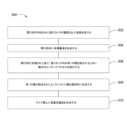
図5は、必要に応じて、システム400又は他の適切な処理チャンバ及びシステムに組み込まれた、図2に示された処理チャンバ232及び図3に示された処理チャンバ300といった処理チャンバ内で実行されうる、基板上に配置された膜スタックにおいてメモリセル構造を形成するための方法500の一実施形態の流れ図である。図6A~図6B、及び図7~図10は、方法500に従って基板上に配置された膜スタックにおいてメモリセル構造を形成するためのシーケンスを示す概略的な断面図である。方法500が、三次元半導体デバイスのための膜スタックにおいて階段状構造を作製するために利用される基板に関して以下に記載されるが、方法500はまた、他のデバイス製造用途において役立てるために利用されうる。 FIG. 5 may be performed in a processing chamber, such as
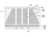
方法500が工程502において、図6Aに示すように、膜スタック604が形成された基板602といった基板を設けることによって開始される。基板602は、必要に応じて、ケイ素ベースの材料、又は任意の適切な絶縁材料若しくは導電性材料とすることができ、基板602には膜スタック604が載置されており、膜スタック604は、当該膜スタック604にメモリセル構造を形成するために利用されうる。
図6Aに示す例示的な実行形態で示すように、基板602は、実質的に平面的な表面、平坦ではない表面、又は、構造がその上に形成された実質的に平面的な表面を有しうる。膜スタック604が、基板602上に形成されている。一実施形態において、膜スタック604が、フロントエンドプロセス又はバックエンドプロセスにおいてゲート構造、コンタクト構造、又は相互接続構造を形成するために利用されうる。方法500は膜スタック604に対して、VNAND構造といったメモリセル構造において使用される階段状構造を当該膜スタック604に形成するために実施されうる。一実施形態において、基板602は、結晶シリコン(例えばSi<100>又はSi<111>)、酸化ケイ素、ストレインドシリコン、シリコンゲルマニウム、ドープされた又はドープされていないポリシリコン、ドープされた又はドープされていないシリコンウエハ及びパターニングされた又はパターニングされていないウエハのシリコンオンインシュレータ(SOI:silicon on insulator)、炭素がドープされた酸化ケイ素、窒化ケイ素、ドープされたシリコン、ゲルマニウム、ヒ化ガリウム、ガラス、又はサファイアといった材料でありうる。基板602は、様々な寸法、例えば200mm、300mm、及び450mm、又はその他の直径を有してもよく、矩形又は方形のパネルであってもよい。別途明記されない限り、本明細書に記載の実施形態及び実施例は、直径200mm、直径300mm、直径450mmの基板上で実行される。SOI構造が基板602のために利用される実施形態において、基板602は、シリコン結晶性基板に配置された、埋設された誘電体層を含みうる。本明細書で示される実施形態において、基板602は、結晶シリコン基板でありうる。 As shown in the exemplary implementation shown in FIG. 6A, the substrate 602 has a substantially planar surface, a non-planar surface, or a substantially planar surface with structures formed thereon. I can do it. A
一実施形態において、基板600に載置された膜スタック604は、垂直方向に積層された複数の層を有する膜スタック604を有しうる。膜スタック604は、第1の層604a及び第2の層604bを含む対を含むことができ、上記第1の層604a及び第2の層604bを含む対は、膜スタック604において繰り返し形成されうる。上記対は、第1の層604aと第2の層604bとが互い違いになっており、第1の層と第2の層の対が所望の数に達するまで、繰り返し形成される。 In one embodiment, the
膜スタック604は、三次元(3D)メモリデバイスといったメモリセルデバイスの一部分である。図6Aには、第1の層604a及び第2の層604bの層が11回繰り返されたものが示されているが、必要に応じて、第1の層と第2の層の対が任意の所望の数だけ繰り返されたものが利用されうることに注意されたい。 The
一実施形態において、膜スタック604は、三次元(3D)メモリデバイスのための複数のゲート構造を形成するために利用されうる。膜スタック604において形成された第1の層604aは、第1の誘電体層とすることができ、第2の層604bは、第2の誘電体層とすることができる。第1の層604a及び第2の層604bを形成するために、適切な誘電体層を利用することができ、上記誘電体層は、とりわけ、酸化ケイ素、窒化ケイ素、酸窒化ケイ素、炭化ケイ素、シリコンオキシカーバイド、窒化チタン、酸化物と窒化物との複合物、窒化物層を挟む少なくとも1つ以上の酸化物層、及びこれらの組合せを含む。 In one embodiment,
1つの特定の例において、第1の層604aは、窒化ケイ素層であり、第2の層604bは、酸化ケイ素層又はポリシリコン層である。一実施形態において、第1の層604aの厚さは、約50Åと約1000Åとの間で制御することができ、例えば約500Åであってよく、各第2の層604bの厚さは、約50Åと約1000Åとの間で制御することができ、例えば約500Åであってよい。膜スタック604の総厚さは、約3ミクロンから10ミクロンであり、技術が進歩するにつれて変わるであろう。 In one particular example, the
窒化ケイ素層の第1の層604aと、酸化ケイ素層の第2の層604bと、の膜スタック604が、基板602上に形成される。膜スタック604が形成されてパターニングされ、絶縁構造610に取り囲まれた階段状構造となる。ハードマスク層608を膜スタック604上に形成して、膜スタック604に開口部606(例えば、トレンチ、ビア、開孔、又は孔と呼ばれる)を形成しやすくすることができる。開口部606は、製造プロセスが完了したときのデバイス構造内のチャネルとして形成するために利用されうる。開口部606が膜スタック604に形成された後で、エピタキシャル堆積プロセスが行われ、開口部606の底部に、ケイ素材料又はSiGe材料といったケイ素含有ポスト612を成長させる。デバイス構造及び構成が、様々なデバイス性能要件のために必要に応じて変えられることに注意されたい。 A
図6Bは、円で示された膜スタック604の一部分の拡大図を示しており、第1の層604a及び第2の層604bで囲まれた開口部606を描いている。説明を容易にするために、図6Aに示した膜スタック604の全体的な断面図の代わりに、膜スタック604の拡大図が以下の説明において利用される。 FIG. 6B shows an enlarged view of a portion of the
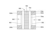
工程504では、図7に示すように、チャネル層702及び中心充填層706を含む多層構造が、開口部606内に形成される。チャネル層702と中央充填層706とが組み合わさって、メモリセルを形成するためのチャネル領域を形成する。一実施形態において、チャネル層702は、ドープされたシリコン、ポリシリコン、酸化ケイ素、SiN、SiON、SiGe、又は他の適切なケイ素含有材料といったケイ素含有材料によって形成されうる。中央充填層706が、図7に示すように開口部606内に形成され、チャネル層702から左側に残された残りの空間を充填する。中心充填層906もまた、SiO2、SiN、SiON、又は他の適切な誘電体材料といった誘電体層でありうる。チャネル層702及び中央充填層706が、CVDプロセス、ALDプロセス、スパッタリングプロセス、コーティングプロセス、又は他の適切なプロセスといった適切な堆積プロセスによって形成されうることに注意されたい。一例において、チャネル層702及び中央充填層706が、図2に示された処理チャンバ232内で形成されうる。 In
工程506において、開口部606が充填された後で、横方向選択的エッチングプロセスが、図8に示すように、膜スタック604から第1の層604aを選択的に除去するために実行される。膜スタック604からの第1の層604aの除去によって、膜スタック604内の第1の層604aが位置していたところに空間802が生まれ、したがって、酸化ケイ素層の第2の層604bのみが基板602上に残った浮遊(suspended)膜スタックが形成される。空間802は、チャネル層702の側壁704aを露出させる。横方向選択的エッチングプロセスは、図3の処理チャンバ300内で実行されうる。 In
工程508において、空間802が画定された後で、図9に示すように、露出した側壁704aを介してチャネル層702を選択的に酸化する選択的酸化プロセスが実行され、保護ライナ層902が形成される。チャネル層702が、ポリシリコン層、ドープされたケイ素層、又は他の適切なケイ素材料といったケイ素含有材料であるとき、選択的酸化プロセス中に供給される酸素元素が、チャネル層702からのケイ素元素と反応して、チャネル層702の側壁704aで保護ライナ層902を形成する。一例において、保護ライナ層902は酸化ケイ素層である。 In
一例において、選択的酸化プロセスは、チャネル層702の側壁704aを酸化するために利用されるラジカルプラズマ酸化プロセス、エピタキシャル堆積プロセス、原子層堆積プロセス、又は化学酸化プロセスでありうる。選択的酸化プロセスによって、チャネル層702の側壁704a上に保護ライナ層902が形成される。一例において、ラジカルプラズマ酸化、エピタキシャル堆積プロセス、又は化学酸化プロセスといった選択的酸化が、個々の酸化チャンバ内で行われうる。特定の実施形態において、酸化チャンバが、図4に示したクラスタシステム400といった統合された処理ツールに接続されてよく、又はその一部であってよい。本明細書に記載される方法は、他の処理チャンバ、及び適切な処理チャンバが接続されたクラスタツールを用いて実施しうることが企図される。 In one example, the selective oxidation process can be a radical plasma oxidation process, an epitaxial deposition process, an atomic layer deposition process, or a chemical oxidation process utilized to oxidize the sidewalls 704a of the
一例において、本明細書に記載の選択的酸化プロセスは、インシトゥ(in-situ)蒸気生成(ISSG:in-situ steam generation)などとしても知られるラジカル酸化のために構成された任意の適切なチャンバ内で実行されうる。適切な酸化チャンバは、限定されるものではないが、カリフォルニア州サンタクララのApplied Materials,Inc.から入手可能なRADIANCE(登録商標)、プラズマ浸漬イオン注入(P3I)、VANTAGE(登録商標)RADOX(商標)、VANTAGE(登録商標)RADIANCE(登録商標)Plus、CENTURA(登録商標)RADOX(商標)チャンバを含みうる。例示的な表面酸化プロセス、又はラジカルプラズマ酸化プロセスと呼ばれるプロセスは、様々な酸化化学物質を用いて実行することができ、このプロセスは、酸化ガス混合物中の水素(H2)、アンモニア(NH3)等のうちの1つ以上といった還元ガスの還元ガス濃度を変更することを含んでよく、上記酸化ガス混合物は、酸素(O2)、一酸化窒素(NO)、亜酸化窒素(N2O)等のうちの1つ以上といった酸化ガスを含み、任意選択的に、窒素ガス(N2)、ヘリウム(He)、アルゴン(Ar)、ネオン(Ne)、及びキセノン(Xe)のうちの1つ以上といった非反応性ガスを含む。ラジカルプラズマ酸化の一形態が、H2及びO2のみを用いて行われる。 In one example, the selective oxidation process described herein can be performed in any suitable chamber configured for radical oxidation, also known as in-situ steam generation (ISSG), etc. can be executed within Suitable oxidation chambers include, but are not limited to, those manufactured by Applied Materials, Inc. of Santa Clara, California. RADIANCE®, plasma immersion ion implantation (P3I), VANTAGE® RADOX®, VANTAGE® RADIANCE® Plus, CENTURA® RADOX® chamber available from may include. An exemplary surface oxidation process, also referred to as a radical plasma oxidation process, can be performed using a variety of oxidizing chemistries, including hydrogen (H2 ), ammonia (NH3), and ammonia (NH3) in an oxidizing gas mixture. ), the oxidizing gas mixture may include oxygen (O2 ), nitric oxide (NO), nitrous oxide (N2O ), etc. ), optionally one of nitrogen gas (N2), helium (He), argon (Ar), neon (Ne), and xenon (Xe). Contains non-reactive gases such as those mentioned above. One form of radical plasma oxidation is performed using onlyH2 andO2 .
工程508における選択的酸化プロセスは、ラジカルプラズマ酸化プロセス又は「インシトゥ蒸気生成」(ISSG)プロセスである。選択的酸化プロセスによって、酸化された環境において熱的に制御されたチャネル層702上で酸化物成長がもたらされうる。インシトゥ蒸気生成(ISSG)プロセスは、酸化される基板が位置する同じチャンバ内での蒸気(H2O)の形成を含む(すなわち、蒸気が基板と共にその場で形成される)。 The selective oxidation process in
形成された保護ライナ層902は、後続のエッチングプロセスの間保護層として利用することができ、これにより、チャネル層702及び中央充填層704といった、開口部606内に形成された膜層が保護され、したがって、エッチングプロセスの間界面保護が改善されて向上する。 The formed
工程510において、保護ライナ層902が形成された後で、図10に示すように、導電性構造912が形成されて、膜スタック604内の空間802に充填される。導電性構造912が、隣接する第2の層604bの間で画定された空間802内に充填される。 In
膜スタック604内で利用される導電性構造912中の金属材料は、後にNAND又はVNAND三次元半導体メモリデバイス内のゲート構造として利用されたときに、膜スタック604における導電率、及び移動度といった電気的性能を効率良くに改善しうると考えられる。堆積プロセスは、有機金属化学気相堆積(MOCVD:metal organic chemical vapor deposition)プロセス、原子層堆積(ALD)プロセス、又はスパッタリング物理的気相堆積プロセス、又は必要に応じて他の適切なプロセスであってよい。堆積プロセスは、図2に示した処理チャンバ232内で実行されうる。図10に示した例では、導電性構造912は、強誘電体層916上に形成された金属含有材料914を含む。強誘電体層916は、金属含有材料914とは異なる材料から作製される。強誘電体層916は、分極を近傍の金属導電材料に切り替えること、したがって金属導電材料の導電率を変化させ、デバイストランジスタに閾値電圧シフトを誘発することができる材料を含む。したがって、強誘電体層916を作製するために利用する材料の適切な選択によって、メモリセルのデバイス性能を変化させて調整することができる。 The metallic material in the
保護ライナ層902が空間802内に形成されているため、強誘電体層916が、チャネル層702と直接的に接触しない又はチャネル層702と境を接しないことが可能であり、これにより、必要に応じて電気的性能が向上する。さらに、強誘電体層916及び金属含有材料914は、真空を破ることなく、図4に示したクラスタシステム400といった1つのクラスタシステム内で形成することができ、したがって、プロセスサイクル時間及び製造効率が改善される。 Because the
さらに、金属含有材料914が強誘電体層916上に形成されているため、強誘電体層916が、後続のエッチング又は堆積プロセスの間、金属含有材料914によって覆われ、保護される。そうすることにより、強誘電体層916が、後続のエッチング又は堆積プロセスの間に、化学的に又はプラズマにより損傷を受けることを回避することができ、したがって、デバイスの電気的性能が向上する。 Furthermore, because the metal-containing
強誘電体層916は、4より大きい誘電率を有する高誘電率材料でありうる。高誘電率材料の適切な例としては、とりわけ、二酸化ハフニウム(HfO2)、ハフニウムシリコンオキサイド(HfSiO2)、ハフニウムアルミニウムオキサイド(HfAlO)又はアルミニウムがドープされた二酸化ハフニウム、ハフニウムジルコニウムオキサイド(HfZrO)、ドープされた二酸化ハフニウム、二酸化ジルコニウム(ZrO2)、ジルコニウムシリコンオキサイド(ZrSiO2)、二酸化タンタル(Ta2O5)、酸化アルミニウム(Al2O3)、ビスマスストロンチウムチタン(BST)、及び白金ジルコニウムチタン(PZT)といった、ハフニウム含有材料が挙げられる。図10に示す例では、強誘電体層916は、二酸化ハフニウム(HfO2)、ハフニウムシリコンオキサイド(HfSiO2)、ハフニウムアルミニウムオキサイド(HfAlO)、ハフニウムジルコニウムオキサイド(HfZrO)、又は適切な、アルミニウムがドープされた二酸化ハフニウムといった、ハフニウム含有材料でありうる。一例において、強誘電体層916は、CVDプロセス、ALDプロセス、スパッタプロセス、又は他の適切な堆積プロセスといった、適切な堆積プロセスによって形成される。1つの特定の例において、強誘電体層916が、ALDプロセスによって形成される。
金属含有材料914の適切な例は、TiN、TaN、TaSiN、TiSiN、タングステン(W)、珪化タングステン(WSi)、タングステンポリシリコン(W/poly)、タングステン合金、タンタル(Ta)、チタン(Ti)、銅(Cu)、ルテニウム(Ru)、ニッケル(Ni)、コバルト(Co)、クロム(Cr)、鉄(Fe)、マンガン(Mn)、アルミニウム(Al)、ハフニウム(Hf)、バナジウム(V)、モリブデン(Mo)、パラジウム(Pd)、金(Au)、銀(Au)、白金(Pt)、それらの合金、又はこれらの組合せからなる群から選択されうる。1つの特定の例において、金属含有材料914はTiNとすることができ、強誘電体層916は、二酸化ハフニウム(HfO2)、ハフニウムシリコンオキサイド(HfSiO2)、ハフニウムアルミニウムオキサイド(HfAlO)、ハフニウムジルコニウムオキサイド(HfZrO)、又は適切な、アルミニウムがドープされた二酸化ハフニウムとすることができる。 Suitable examples of metal-containing
このようにして、半導体デバイスのメモリセルの三次元(3D)積層を製造するための階段状構造を形成する方法及び装置が提供される。界面における保護ライナ層が、選択的堆積及び選択的エッチングプロセスと共に利用され、膜スタック中の誘電体層が導電性構造と置換されうる。保護ライナ層は、強誘電体層及び金属含有層と接触する界面を保護することができ、従って、界面プロファイル及びトポグラフィを良好に制御することができる。さらに、金属含有層及び保護層が外接する形成された強誘電体層が、デバイス構造における保護ライナ層の構造及びプロファイルに関連して支援することができる。結果として、導電性構造が、界面において良好な電気接触を提供し、したがって、メモリセルに所望の電気的性能を提供する。 Thus, a method and apparatus for forming a stepped structure for manufacturing a three-dimensional (3D) stack of memory cells of a semiconductor device is provided. A protective liner layer at the interface can be utilized with selective deposition and selective etching processes to replace dielectric layers in the film stack with conductive structures. The protective liner layer can protect the interface in contact with the ferroelectric layer and the metal-containing layer, thus allowing better control of the interface profile and topography. Furthermore, the formed ferroelectric layer circumscribing the metal-containing layer and the protective layer can assist in relation to the structure and profile of the protective liner layer in the device structure. As a result, the conductive structure provides good electrical contact at the interface, thus providing the desired electrical performance to the memory cell.
以上の説明は本開示の実施形態を対象としているが、本開示の基本的な範囲から逸脱することなく本開示の他の実施形態及び更なる実施形態が考案されてもよく、本開示の範囲は、以下の特許請求の範囲によって規定される。 Although the above description is directed to embodiments of the disclosure, other embodiments and further embodiments of the disclosure may be devised without departing from the essential scope of the disclosure, and the scope of the disclosure is defined by the following claims.
Claims (15)
Translated fromJapanese基板上に水平方向に形成された、互い違いになった誘電体層と導電性構造との対を含む膜スタックと、
前記膜スタックに形成された開口部であって、チャネル層及び中心充填層で充填された開口部と、
前記導電性構造と前記チャネル層との間に配置された保護ライナ層と
を備えた、メモリセルデバイス。 A memory cell device,
a film stack including alternating pairs of dielectric layers and conductive structures formed horizontally on a substrate;
an opening formed in the membrane stack, the opening being filled with a channel layer and a center fill layer;
A memory cell device comprising a protective liner layer disposed between the conductive structure and the channel layer.
金属含有材料と、
前記金属含有材料を覆う強誘電体層と
をさらに含む、請求項1に記載のメモリセルデバイス。 The conductive structure is
metal-containing material;
2. The memory cell device of claim 1, further comprising a ferroelectric layer covering the metal-containing material.
第1の層及び第2の層を含む膜スタックに開口部を形成することと、
1つ以上の層で前記開口部を充填することであって、前記1つ以上の層がチャネル層を含む、前記開口部を充填することと、
前記膜スタックから前記第1の層を選択的に除去して、前記チャネル層の一部分を露出させることと、
前記チャネル層の前記一部分を選択的に酸化して、保護ライナ層を形成することと、
空間を導電性構造で充填すること
を含む、方法。 A method for a memory device on a substrate, the method comprising:
forming an opening in a membrane stack including a first layer and a second layer;
filling the opening with one or more layers, the one or more layers including a channel layer;
selectively removing the first layer from the membrane stack to expose a portion of the channel layer;
selectively oxidizing the portion of the channel layer to form a protective liner layer;
A method comprising filling a space with a conductive structure.
ラジカルプラズマ酸化を行って、前記チャネル層を酸化することをさらに含む、請求項11に記載の方法。 selectively oxidizing the portion of the channel layer;
12. The method of claim 11, further comprising performing radical plasma oxidation to oxidize the channel layer.
膜スタックにおいて形成された誘電体層間で画定される空間によって露出したチャネル層の一部分を選択的に酸化することであって、前記膜スタックが、前記チャネル層を含む多層構造によって充填された中心開口部を有する、選択的に酸化することと、
前記チャネル層の前記一部分上に保護ライナ層を形成することと、
前記保護ライナ層と接触する強誘電体層を形成することであって、前記強誘電体層が高誘電率材料である、強誘電体層を形成すること
を含む、方法。 A method for forming a stepped structure on a substrate, the method comprising:
selectively oxidizing a portion of a channel layer exposed by a space defined between dielectric layers formed in a membrane stack, the membrane stack having a central opening filled with a multilayer structure including the channel layer; selectively oxidizing, having a part;
forming a protective liner layer on the portion of the channel layer;
A method comprising forming a ferroelectric layer in contact with the protective liner layer, the ferroelectric layer being a high dielectric constant material.
Applications Claiming Priority (4)
| Application Number | Priority Date | Filing Date | Title |
|---|---|---|---|
| US16/265,192US11127760B2 (en) | 2019-02-01 | 2019-02-01 | Vertical transistor fabrication for memory applications |
| US16/265,192 | 2019-02-01 | ||
| PCT/US2020/012110WO2020159663A1 (en) | 2019-02-01 | 2020-01-03 | Vertical transistor fabrication for memory applications |
| JP2021544121AJP2022523315A (en) | 2019-02-01 | 2020-01-03 | Fabrication of vertical transistors for memory applications |
Related Parent Applications (1)
| Application Number | Title | Priority Date | Filing Date |
|---|---|---|---|
| JP2021544121ADivisionJP2022523315A (en) | 2019-02-01 | 2020-01-03 | Fabrication of vertical transistors for memory applications |
Publications (1)
| Publication Number | Publication Date |
|---|---|
| JP2024020242Atrue JP2024020242A (en) | 2024-02-14 |
Family
ID=71837863
Family Applications (2)
| Application Number | Title | Priority Date | Filing Date |
|---|---|---|---|
| JP2021544121APendingJP2022523315A (en) | 2019-02-01 | 2020-01-03 | Fabrication of vertical transistors for memory applications |
| JP2023184098APendingJP2024020242A (en) | 2019-02-01 | 2023-10-26 | Fabrication of vertical transistors for memory applications |
Family Applications Before (1)
| Application Number | Title | Priority Date | Filing Date |
|---|---|---|---|
| JP2021544121APendingJP2022523315A (en) | 2019-02-01 | 2020-01-03 | Fabrication of vertical transistors for memory applications |
Country Status (6)
| Country | Link |
|---|---|
| US (2) | US11127760B2 (en) |
| JP (2) | JP2022523315A (en) |
| KR (2) | KR20240111020A (en) |
| CN (1) | CN113366639A (en) |
| TW (2) | TWI845590B (en) |
| WO (1) | WO2020159663A1 (en) |
Families Citing this family (7)
| Publication number | Priority date | Publication date | Assignee | Title |
|---|---|---|---|---|
| US11024648B2 (en)* | 2019-08-15 | 2021-06-01 | Sandisk Technologies Llc | Ferroelectric memory devices including a stack of ferroelectric and antiferroelectric layers and method of making the same |
| US11430813B2 (en) | 2019-08-15 | 2022-08-30 | Sandisk Technologies Llc | Antiferroelectric memory devices and methods of making the same |
| US10937809B1 (en)* | 2019-08-15 | 2021-03-02 | Sandisk Technologies Llc | Three-dimensional memory device containing ferroelectric memory elements encapsulated by transition metal nitride materials and method of making thereof |
| US11502104B2 (en) | 2019-08-15 | 2022-11-15 | Sandisk Technologies Llc | Antiferroelectric memory devices and methods of making the same |
| US20220278127A1 (en)* | 2021-02-26 | 2022-09-01 | Taiwan Semiconductor Manufacturing Company, Ltd. | Semiconductor Memory Structures And Method Of Forming The Same |
| JP2022145049A (en)* | 2021-03-19 | 2022-10-03 | キオクシア株式会社 | semiconductor storage device |
| US20230343643A1 (en)* | 2022-04-25 | 2023-10-26 | Applied Materials, Inc. | Gradient oxidation and etch for pvd metal as bottom liner in bottom up gap fill |
Citations (8)
| Publication number | Priority date | Publication date | Assignee | Title |
|---|---|---|---|---|
| JP2009117843A (en)* | 2007-11-08 | 2009-05-28 | Samsung Electronics Co Ltd | Vertical semiconductor device and manufacturing method thereof |
| US20100155810A1 (en)* | 2008-12-24 | 2010-06-24 | Samsung Electronics Co., Ltd. | Multi-layer nonvolatile memory devices having vertical charge storage regions |
| US20120119283A1 (en)* | 2010-11-17 | 2012-05-17 | Samsung Electronics Co., Ltd. | Methods for forming etch stop layers, semiconductor devices having the same, and methods for fabricating semiconductor devices |
| US20170018563A1 (en)* | 2015-07-13 | 2017-01-19 | Kabushiki Kaisha Toshiba | Semiconductor memory device and method for manufacturing the same |
| US20170278859A1 (en)* | 2016-03-25 | 2017-09-28 | Sandisk Technologies Llc | Three-dimensional memory device containing vertically isolated charge storage regions and method of making thereof |
| CN107305896A (en)* | 2016-04-22 | 2017-10-31 | 中芯国际集成电路制造(上海)有限公司 | The preparation method of semiconductor devices |
| US20180114794A1 (en)* | 2016-10-26 | 2018-04-26 | Samsung Electronics Co., Ltd. | Semiconductor device and method for fabricating the same |
| KR20180059271A (en)* | 2016-11-25 | 2018-06-04 | 연세대학교 산학협력단 | 3 dimensional ferroelectric memory device and method of fabricating the same |
Family Cites Families (12)
| Publication number | Priority date | Publication date | Assignee | Title |
|---|---|---|---|---|
| US6964928B2 (en) | 2002-08-29 | 2005-11-15 | Chentsau Ying | Method for removing residue from a magneto-resistive random access memory (MRAM) film stack using a dual mask |
| US6841395B2 (en) | 2002-11-25 | 2005-01-11 | International Business Machines Corporation | Method of forming a barrier layer of a tunneling magnetoresistive sensor |
| US7750421B2 (en) | 2007-07-23 | 2010-07-06 | Magic Technologies, Inc. | High performance MTJ element for STT-RAM and method for making the same |
| US9028910B2 (en) | 2010-12-10 | 2015-05-12 | Avalanche Technology, Inc. | MTJ manufacturing method utilizing in-situ annealing and etch back |
| US8693241B2 (en) | 2011-07-13 | 2014-04-08 | SK Hynix Inc. | Semiconductor intergrated circuit device, method of manufacturing the same, and method of driving the same |
| US8823118B2 (en) | 2012-01-05 | 2014-09-02 | Headway Technologies, Inc. | Spin torque transfer magnetic tunnel junction fabricated with a composite tunneling barrier layer |
| US9564582B2 (en) | 2014-03-07 | 2017-02-07 | Applied Materials, Inc. | Method of forming magnetic tunneling junctions |
| US9524977B2 (en)* | 2015-04-15 | 2016-12-20 | Sandisk Technologies Llc | Metal-semiconductor alloy region for enhancing on current in a three-dimensional memory structure |
| US20160351799A1 (en) | 2015-05-30 | 2016-12-01 | Applied Materials, Inc. | Hard mask for patterning magnetic tunnel junctions |
| US20170062456A1 (en) | 2015-08-31 | 2017-03-02 | Cypress Semiconductor Corporation | Vertical division of three-dimensional memory device |
| TWI640085B (en)* | 2017-03-23 | 2018-11-01 | 旺宏電子股份有限公司 | Memory device and method for fabricating the same |
| KR102608912B1 (en)* | 2018-12-27 | 2023-12-04 | 에스케이하이닉스 주식회사 | vertical memory device and method of fabricating the same |
- 2019
- 2019-02-01USUS16/265,192patent/US11127760B2/enactiveActive
- 2020
- 2020-01-03WOPCT/US2020/012110patent/WO2020159663A1/ennot_activeCeased
- 2020-01-03KRKR1020247023076Apatent/KR20240111020A/enactivePending
- 2020-01-03JPJP2021544121Apatent/JP2022523315A/enactivePending
- 2020-01-03KRKR1020217026935Apatent/KR102724535B1/enactiveActive
- 2020-01-03CNCN202080012010.0Apatent/CN113366639A/enactivePending
- 2020-01-06TWTW109100265Apatent/TWI845590B/enactive
- 2020-01-06TWTW113119324Apatent/TW202442083A/enunknown
- 2021
- 2021-09-20USUS17/479,789patent/US12108604B2/enactiveActive
- 2023
- 2023-10-26JPJP2023184098Apatent/JP2024020242A/enactivePending
Patent Citations (8)
| Publication number | Priority date | Publication date | Assignee | Title |
|---|---|---|---|---|
| JP2009117843A (en)* | 2007-11-08 | 2009-05-28 | Samsung Electronics Co Ltd | Vertical semiconductor device and manufacturing method thereof |
| US20100155810A1 (en)* | 2008-12-24 | 2010-06-24 | Samsung Electronics Co., Ltd. | Multi-layer nonvolatile memory devices having vertical charge storage regions |
| US20120119283A1 (en)* | 2010-11-17 | 2012-05-17 | Samsung Electronics Co., Ltd. | Methods for forming etch stop layers, semiconductor devices having the same, and methods for fabricating semiconductor devices |
| US20170018563A1 (en)* | 2015-07-13 | 2017-01-19 | Kabushiki Kaisha Toshiba | Semiconductor memory device and method for manufacturing the same |
| US20170278859A1 (en)* | 2016-03-25 | 2017-09-28 | Sandisk Technologies Llc | Three-dimensional memory device containing vertically isolated charge storage regions and method of making thereof |
| CN107305896A (en)* | 2016-04-22 | 2017-10-31 | 中芯国际集成电路制造(上海)有限公司 | The preparation method of semiconductor devices |
| US20180114794A1 (en)* | 2016-10-26 | 2018-04-26 | Samsung Electronics Co., Ltd. | Semiconductor device and method for fabricating the same |
| KR20180059271A (en)* | 2016-11-25 | 2018-06-04 | 연세대학교 산학협력단 | 3 dimensional ferroelectric memory device and method of fabricating the same |
Also Published As
| Publication number | Publication date |
|---|---|
| KR20210110734A (en) | 2021-09-08 |
| US20220005831A1 (en) | 2022-01-06 |
| KR102724535B1 (en) | 2024-10-30 |
| US20200251495A1 (en) | 2020-08-06 |
| TW202442083A (en) | 2024-10-16 |
| TW202044560A (en) | 2020-12-01 |
| CN113366639A (en) | 2021-09-07 |
| WO2020159663A1 (en) | 2020-08-06 |
| TWI845590B (en) | 2024-06-21 |
| JP2022523315A (en) | 2022-04-22 |
| US12108604B2 (en) | 2024-10-01 |
| KR20240111020A (en) | 2024-07-16 |
| US11127760B2 (en) | 2021-09-21 |
Similar Documents
| Publication | Publication Date | Title |
|---|---|---|
| JP7685006B2 (en) | Fabrication of memory cells for 3D NAND applications | |
| KR102724535B1 (en) | Fabrication of vertical transistors for memory applications | |
| US20160240385A1 (en) | Gate electrode material residual removal process | |
| US9653311B1 (en) | 3D NAND staircase CD fabrication utilizing ruthenium material | |
| US12374557B2 (en) | Methods for etching structures with oxygen pulsing | |
| US20170229313A1 (en) | Methods for selective etching of a silicon material | |
| CN103930992B (en) | Inter-polysilicon dielectric cap and method of forming the inter-polysilicon dielectric cap | |
| TW201724500A (en) | Method for fabricating a nanowire for a horizontal wraparound gate device for semiconductor applications | |
| US10930555B2 (en) | Contact over active gate structure | |
| US11658042B2 (en) | Methods for etching structures and smoothing sidewalls |
Legal Events
| Date | Code | Title | Description |
|---|---|---|---|
| A521 | Request for written amendment filed | Free format text:JAPANESE INTERMEDIATE CODE: A523 Effective date:20231124 | |
| A621 | Written request for application examination | Free format text:JAPANESE INTERMEDIATE CODE: A621 Effective date:20231124 | |
| A977 | Report on retrieval | Free format text:JAPANESE INTERMEDIATE CODE: A971007 Effective date:20240925 | |
| A131 | Notification of reasons for refusal | Free format text:JAPANESE INTERMEDIATE CODE: A131 Effective date:20241015 | |
| A521 | Request for written amendment filed | Free format text:JAPANESE INTERMEDIATE CODE: A523 Effective date:20241225 |