JP2024014519A - Automatic test equipment and its interface equipment - Google Patents
Automatic test equipment and its interface equipmentDownload PDFInfo
- Publication number
- JP2024014519A JP2024014519AJP2022117406AJP2022117406AJP2024014519AJP 2024014519 AJP2024014519 AJP 2024014519AJP 2022117406 AJP2022117406 AJP 2022117406AJP 2022117406 AJP2022117406 AJP 2022117406AJP 2024014519 AJP2024014519 AJP 2024014519A
- Authority
- JP
- Japan
- Prior art keywords
- pin electronics
- printed circuit
- dut
- interface device
- ics
- Prior art date
- Legal status (The legal status is an assumption and is not a legal conclusion. Google has not performed a legal analysis and makes no representation as to the accuracy of the status listed.)
- Pending
Links
Images


Classifications
- G—PHYSICS
- G01—MEASURING; TESTING
- G01R—MEASURING ELECTRIC VARIABLES; MEASURING MAGNETIC VARIABLES
- G01R31/00—Arrangements for testing electric properties; Arrangements for locating electric faults; Arrangements for electrical testing characterised by what is being tested not provided for elsewhere
- G01R31/28—Testing of electronic circuits, e.g. by signal tracer
- G01R31/2851—Testing of integrated circuits [IC]
- G01R31/2886—Features relating to contacting the IC under test, e.g. probe heads; chucks
- G01R31/2887—Features relating to contacting the IC under test, e.g. probe heads; chucks involving moving the probe head or the IC under test; docking stations
- G—PHYSICS
- G01—MEASURING; TESTING
- G01R—MEASURING ELECTRIC VARIABLES; MEASURING MAGNETIC VARIABLES
- G01R1/00—Details of instruments or arrangements of the types included in groups G01R5/00 - G01R13/00 and G01R31/00
- G01R1/02—General constructional details
- G01R1/04—Housings; Supporting members; Arrangements of terminals
- G01R1/0408—Test fixtures or contact fields; Connectors or connecting adaptors; Test clips; Test sockets
- G01R1/0416—Connectors, terminals
- G—PHYSICS
- G01—MEASURING; TESTING
- G01R—MEASURING ELECTRIC VARIABLES; MEASURING MAGNETIC VARIABLES
- G01R31/00—Arrangements for testing electric properties; Arrangements for locating electric faults; Arrangements for electrical testing characterised by what is being tested not provided for elsewhere
- G01R31/28—Testing of electronic circuits, e.g. by signal tracer
- G01R31/2851—Testing of integrated circuits [IC]
- G01R31/2855—Environmental, reliability or burn-in testing
- G01R31/286—External aspects, e.g. related to chambers, contacting devices or handlers
- G01R31/2863—Contacting devices, e.g. sockets, burn-in boards or mounting fixtures
- G—PHYSICS
- G01—MEASURING; TESTING
- G01R—MEASURING ELECTRIC VARIABLES; MEASURING MAGNETIC VARIABLES
- G01R1/00—Details of instruments or arrangements of the types included in groups G01R5/00 - G01R13/00 and G01R31/00
- G01R1/02—General constructional details
- G01R1/06—Measuring leads; Measuring probes
- G01R1/067—Measuring probes
- G01R1/073—Multiple probes
- G01R1/07307—Multiple probes with individual probe elements, e.g. needles, cantilever beams or bump contacts, fixed in relation to each other, e.g. bed of nails fixture or probe card
- G01R1/07314—Multiple probes with individual probe elements, e.g. needles, cantilever beams or bump contacts, fixed in relation to each other, e.g. bed of nails fixture or probe card the body of the probe being perpendicular to test object, e.g. bed of nails or probe with bump contacts on a rigid support
- G01R1/07328—Multiple probes with individual probe elements, e.g. needles, cantilever beams or bump contacts, fixed in relation to each other, e.g. bed of nails fixture or probe card the body of the probe being perpendicular to test object, e.g. bed of nails or probe with bump contacts on a rigid support for testing printed circuit boards
- G—PHYSICS
- G01—MEASURING; TESTING
- G01R—MEASURING ELECTRIC VARIABLES; MEASURING MAGNETIC VARIABLES
- G01R1/00—Details of instruments or arrangements of the types included in groups G01R5/00 - G01R13/00 and G01R31/00
- G01R1/02—General constructional details
- G01R1/06—Measuring leads; Measuring probes
- G01R1/067—Measuring probes
- G01R1/073—Multiple probes
- G01R1/07307—Multiple probes with individual probe elements, e.g. needles, cantilever beams or bump contacts, fixed in relation to each other, e.g. bed of nails fixture or probe card
- G01R1/07357—Multiple probes with individual probe elements, e.g. needles, cantilever beams or bump contacts, fixed in relation to each other, e.g. bed of nails fixture or probe card with flexible bodies, e.g. buckling beams
- G—PHYSICS
- G01—MEASURING; TESTING
- G01R—MEASURING ELECTRIC VARIABLES; MEASURING MAGNETIC VARIABLES
- G01R1/00—Details of instruments or arrangements of the types included in groups G01R5/00 - G01R13/00 and G01R31/00
- G01R1/02—General constructional details
- G01R1/06—Measuring leads; Measuring probes
- G01R1/067—Measuring probes
- G01R1/073—Multiple probes
- G01R1/07307—Multiple probes with individual probe elements, e.g. needles, cantilever beams or bump contacts, fixed in relation to each other, e.g. bed of nails fixture or probe card
- G01R1/07364—Multiple probes with individual probe elements, e.g. needles, cantilever beams or bump contacts, fixed in relation to each other, e.g. bed of nails fixture or probe card with provisions for altering position, number or connection of probe tips; Adapting to differences in pitch
- G01R1/07378—Multiple probes with individual probe elements, e.g. needles, cantilever beams or bump contacts, fixed in relation to each other, e.g. bed of nails fixture or probe card with provisions for altering position, number or connection of probe tips; Adapting to differences in pitch using an intermediate adapter, e.g. space transformers
- G—PHYSICS
- G01—MEASURING; TESTING
- G01R—MEASURING ELECTRIC VARIABLES; MEASURING MAGNETIC VARIABLES
- G01R31/00—Arrangements for testing electric properties; Arrangements for locating electric faults; Arrangements for electrical testing characterised by what is being tested not provided for elsewhere
- G01R31/26—Testing of individual semiconductor devices
- G—PHYSICS
- G01—MEASURING; TESTING
- G01R—MEASURING ELECTRIC VARIABLES; MEASURING MAGNETIC VARIABLES
- G01R31/00—Arrangements for testing electric properties; Arrangements for locating electric faults; Arrangements for electrical testing characterised by what is being tested not provided for elsewhere
- G01R31/28—Testing of electronic circuits, e.g. by signal tracer
- G01R31/2851—Testing of integrated circuits [IC]
- G01R31/2855—Environmental, reliability or burn-in testing
- G01R31/286—External aspects, e.g. related to chambers, contacting devices or handlers
- G01R31/2865—Holding devices, e.g. chucks; Handlers or transport devices
- G01R31/2867—Handlers or transport devices, e.g. loaders, carriers, trays
- G—PHYSICS
- G01—MEASURING; TESTING
- G01R—MEASURING ELECTRIC VARIABLES; MEASURING MAGNETIC VARIABLES
- G01R31/00—Arrangements for testing electric properties; Arrangements for locating electric faults; Arrangements for electrical testing characterised by what is being tested not provided for elsewhere
- G01R31/28—Testing of electronic circuits, e.g. by signal tracer
- G01R31/2851—Testing of integrated circuits [IC]
- G01R31/2855—Environmental, reliability or burn-in testing
- G01R31/286—External aspects, e.g. related to chambers, contacting devices or handlers
- G01R31/2868—Complete testing stations; systems; procedures; software aspects
- G—PHYSICS
- G01—MEASURING; TESTING
- G01R—MEASURING ELECTRIC VARIABLES; MEASURING MAGNETIC VARIABLES
- G01R31/00—Arrangements for testing electric properties; Arrangements for locating electric faults; Arrangements for electrical testing characterised by what is being tested not provided for elsewhere
- G01R31/28—Testing of electronic circuits, e.g. by signal tracer
- G01R31/2851—Testing of integrated circuits [IC]
- G01R31/2886—Features relating to contacting the IC under test, e.g. probe heads; chucks
- G01R31/2889—Interfaces, e.g. between probe and tester
- G—PHYSICS
- G01—MEASURING; TESTING
- G01R—MEASURING ELECTRIC VARIABLES; MEASURING MAGNETIC VARIABLES
- G01R31/00—Arrangements for testing electric properties; Arrangements for locating electric faults; Arrangements for electrical testing characterised by what is being tested not provided for elsewhere
- G01R31/28—Testing of electronic circuits, e.g. by signal tracer
- G01R31/2851—Testing of integrated circuits [IC]
- G01R31/2893—Handling, conveying or loading, e.g. belts, boats, vacuum fingers
- H—ELECTRICITY
- H01—ELECTRIC ELEMENTS
- H01R—ELECTRICALLY-CONDUCTIVE CONNECTIONS; STRUCTURAL ASSOCIATIONS OF A PLURALITY OF MUTUALLY-INSULATED ELECTRICAL CONNECTING ELEMENTS; COUPLING DEVICES; CURRENT COLLECTORS
- H01R12/00—Structural associations of a plurality of mutually-insulated electrical connecting elements, specially adapted for printed circuits, e.g. printed circuit boards [PCB], flat or ribbon cables, or like generally planar structures, e.g. terminal strips, terminal blocks; Coupling devices specially adapted for printed circuits, flat or ribbon cables, or like generally planar structures; Terminals specially adapted for contact with, or insertion into, printed circuits, flat or ribbon cables, or like generally planar structures
- H01R12/70—Coupling devices
- H01R12/7076—Coupling devices for connection between PCB and component, e.g. display
Landscapes
- Engineering & Computer Science (AREA)
- Physics & Mathematics (AREA)
- General Physics & Mathematics (AREA)
- Computer Hardware Design (AREA)
- Microelectronics & Electronic Packaging (AREA)
- General Engineering & Computer Science (AREA)
- Environmental & Geological Engineering (AREA)
- Power Engineering (AREA)
- Tests Of Electronic Circuits (AREA)
Abstract
Description
Translated fromJapanese本開示は、自動試験装置に関し、特にテストヘッドとDUTのインタフェース装置に関する。 TECHNICAL FIELD The present disclosure relates to automatic test equipment, and more particularly to a test head and DUT interface device.
メモリやCPU(Central Processing Unit)などの各種半導体デバイスの検査に、自動試験装置(ATE:Automatic Test Equipment)が使用される。ATEは、試験対象の半導体デバイス(以下、被試験デバイス(DUT))に、試験信号を供給し、試験信号に対するDUTの応答を測定し、DUTの良否を判定し、あるいは、不良箇所を特定する。 Automatic test equipment (ATE) is used to test various semiconductor devices such as memories and CPUs (Central Processing Units). ATE supplies a test signal to a semiconductor device under test (hereinafter referred to as a device under test (DUT)), measures the DUT's response to the test signal, and determines whether the DUT is good or bad or identifies a defective location. .
図1は、従来のATE10のブロック図である。ATE10は、テスター(テスター本体ともいう)20、テストヘッド30、インタフェース装置40、ハンドラ50を備える。 FIG. 1 is a block diagram of a
テスター20は、ATE10を統括的に制御する。具体的には、テスター20は、テストプログラムを実行し、テストヘッド30やハンドラ50を制御し、測定結果を収集する。 The
テストヘッド30は、DUT1に供給すべき試験信号を発生し、またDUTからの信号(デバイス信号という)を検出するハードウェアを備える。具体的には、テストヘッド30は、ピンエレクトロニクス(PE)32や、電源回路(不図示)などを備える。PE32は、ドライバおよびコンパレータなどを含むASIC(Application Specific IC)である。従来において、PE32は、PEボード34と呼ばれるプリント基板上に実装され、テストヘッド30の内部に収容されていた。 The
インタフェース装置40は、ハイフィックスとも称され、テストヘッド30とDUT1の間の電気的な接続を中継する。インタフェース装置40は、ソケットボード42を備える。ソケットボード42には、複数のソケット44が設けられており、複数のDUT1を同時測定可能となっている。ウェハレベル試験を行うATEの場合、ソケットボード42に代えて、プローブカードが使用される。 The
複数のソケット44には、ハンドラ50によって、複数のDUT1がロードされ、ソケット44にDUT1が押し付けられる。試験終了後、ハンドラ50は、DUT1をアンロードし、必要に応じて、良品と不良品を分別する。 A plurality of
インタフェース装置40は、ソケットボード42と、テストヘッド30を接続する複数のケーブル46を備える。PE32が発生する試験信号は、ケーブル46を介して、DUT1に伝送され、DUT1が発生するデバイス信号は、ケーブル46を介してPE32に伝送される。 The
近年、DRAM(Dynamic Random Access Memory)の高速化が進んでいる。グラフィックボードに搭載されるGDDR(Graphics Double Data Rate)メモリでは、GDDR6X規格において、NRZ(Non Return to Zero)方式により21Gbpsの伝送速度が達成されている。 In recent years, the speed of DRAM (Dynamic Random Access Memory) has been increasing. A GDDR (Graphics Double Data Rate) memory mounted on a graphic board achieves a transmission speed of 21 Gbps using the NRZ (Non Return to Zero) method in the GDDR6X standard.
次世代のGDDR7では、PAM4(Pulse Amplitude Modulation 4)が採用され、伝送速度は40Gbpsまで高められる。NRZ方式も、年々高速化が進められており、次世代では、28Gbps程度まで高速化される。 The next generation GDDR7 uses PAM4 (Pulse Amplitude Modulation 4) and increases the transmission speed to 40 Gbps. The speed of the NRZ system is also increasing year by year, and the next generation will increase the speed to about 28 Gbps.
伝送速度が20Gbpsを超えると、従来のアーキテクチャを流用したメモリテスタでの正確な測定が難しくなってくる。現状、28Gbpsや40Gbpsの高速なメモリを正確に測定できるATEは市販されていない。 When the transmission speed exceeds 20 Gbps, it becomes difficult to make accurate measurements using a memory tester that uses conventional architecture. Currently, there are no ATEs on the market that can accurately measure high-speed memories of 28 Gbps or 40 Gbps.
本開示は係る状況においてなされたものであり、その例示的な目的のひとつは、20Gbpsを超える高速デバイスを高精度で試験可能なインタフェース装置、および自動試験装置の提供にある。 The present disclosure has been made in such a situation, and one of its illustrative purposes is to provide an interface device and an automatic test device that can test high-speed devices exceeding 20 Gbps with high accuracy.
本開示のある態様は、テストヘッドと被試験デバイス(DUT)の間に設けられるインタフェース装置に関する。インタフェース装置は、複数のピンエレクトロニクスIC(Integrated Circuit)がモジュール化されてなるフロントエンドモジュールを備える。 An aspect of the present disclosure relates to an interface device provided between a test head and a device under test (DUT). The interface device includes a front end module in which a plurality of pin electronics ICs (Integrated Circuits) are modularized.
なお、以上の構成要素を任意に組み合わせたもの、構成要素や表現を、方法、装置などの間で相互に置換したものもまた、本発明の態様として有効である。 It should be noted that arbitrary combinations of the above constituent elements, and mutual substitution of constituent elements and expressions between methods, apparatuses, etc., are also effective as aspects of the present invention.
本開示のある態様によれば、高速デバイスを量産試験可能となる。 According to an aspect of the present disclosure, high-speed devices can be mass-produced and tested.
(実施形態の概要)
本開示のいくつかの例示的な実施形態の概要を説明する。この概要は、後述する詳細な説明の前置きとして、実施形態の基本的な理解を目的として、1つまたは複数の実施形態のいくつかの概念を簡略化して説明するものであり、発明あるいは開示の広さを限定するものではない。この概要は、考えられるすべての実施形態の包括的な概要ではなく、すべての実施形態の重要な要素を特定することも、一部またはすべての態様の範囲を線引きすることも意図していない。便宜上、「一実施形態」は、本明細書に開示するひとつの実施形態(実施例や変形例)または複数の実施形態(実施例や変形例)を指すものとして用いる場合がある。(Summary of embodiment)
1 provides an overview of some example embodiments of the present disclosure. This Summary is intended to provide a simplified description of some concepts of one or more embodiments in order to provide a basic understanding of the embodiments and as a prelude to the more detailed description that is presented later. It does not limit the size. This summary is not an exhaustive overview of all possible embodiments and is not intended to identify key elements of all embodiments or to delineate the scope of any or all aspects. For convenience, "one embodiment" may be used to refer to one embodiment (example or modification) or multiple embodiments (examples or modifications) disclosed in this specification.
超高速のメモリデバイスを試験可能なATEを実現するためには、信号源(ドライバ)とDUTの間の伝送距離を最短化する必要がある。従来は同軸ケーブルを用いたマザーボード(MB)によって、ピンエレクトロニクスボード(PE)とDUT間の伝送を担っていたが、同軸ケーブルの伝送損失および同軸ケーブルと基板との接続に要するコネクタの伝送損失、さらには基板上のピンエレクトロニクスICからコネクタまでの配線引き出しといった伝送媒体の接続点や、接続箇所でのモード変換に伴う信号反射などの信号劣化要因が多く、高速信号を正確に伝送するには不利であった。本開示は、係る知見にもとづいてなされたものである。本開示では、伝送路における損失を低減することにより、高速信号の伝送を可能にする方式を提案する。 In order to realize an ATE capable of testing ultra-high-speed memory devices, it is necessary to minimize the transmission distance between the signal source (driver) and the DUT. Conventionally, a motherboard (MB) using a coaxial cable was responsible for transmission between the pin electronics board (PE) and the DUT, but the transmission loss of the coaxial cable and the transmission loss of the connector required to connect the coaxial cable and the board, Furthermore, there are many signal deterioration factors such as signal reflection due to mode conversion at the connection point of the transmission medium, such as wiring from the pin electronics IC on the board to the connector, and the connection point, which is disadvantageous for accurately transmitting high-speed signals. Met. The present disclosure has been made based on such knowledge. The present disclosure proposes a method that enables high-speed signal transmission by reducing loss in a transmission path.
一実施形態に係るインタフェース装置は、テストヘッドと被試験デバイス(DUT)の間に設けられる。インタフェース装置は、複数のピンエレクトロニクス(PE)IC(Integrated Circuit)がモジュール化されてなるフロントエンドモジュールを備える。 An interface device according to one embodiment is provided between a test head and a device under test (DUT). The interface device includes a front end module in which a plurality of pin electronics (PE) ICs (Integrated Circuits) are modularized.
本発明者らは、従来のATEについて検討し、以下の知見を得た。従来のATEでは、ピンエレクトロニクスICは、テストヘッド内に設けられており、ピンエレクトロニクスICとDUTの間の距離が遠かった。DUTが28Gbpsや40Gbpsの高速なメモリである場合、ピンエレクトロニクスICが発生する試験信号やDUTが発生するデバイス信号は、14GHzを超える高周波数成分を含むようになるが、伝送距離が長いと、高周波成分の損失が顕著となる。高周波成分の減衰は、波形歪みを引き起こし、正確な信号伝送が難しくなる。 The present inventors studied conventional ATE and obtained the following knowledge. In conventional ATE, the pin electronics IC was installed in the test head, and the distance between the pin electronics IC and the DUT was long. If the DUT is a high-speed memory of 28 Gbps or 40 Gbps, the test signal generated by the pin electronics IC and the device signal generated by the DUT will contain high frequency components exceeding 14 GHz. The loss of components becomes significant. Attenuation of high frequency components causes waveform distortion, making accurate signal transmission difficult.
これに対して、本実施形態では、ピンエレクトロニクスICを備えるフロントエンドモジュールを、インタフェース装置に内蔵することにより、ピンエレクトロニクスICを、DUTの直近に配置することが可能となり、試験信号およびデバイス信号の伝送距離を従来に比べて大幅に短くすることができる。これにより高周波成分の損失を抑制でき、高速な試験信号およびデバイス信号を伝送することが可能となり、ひいては正確な試験が可能となる。 In contrast, in this embodiment, by incorporating a front-end module equipped with a pin electronics IC into the interface device, the pin electronics IC can be placed in close proximity to the DUT, and the test signals and device signals can be Transmission distance can be significantly shortened compared to conventional methods. As a result, loss of high frequency components can be suppressed, high-speed test signals and device signals can be transmitted, and accurate testing can be performed.
一実施形態において、フロントエンドモジュールは、複数のピンエレクトロニクスICが実装される複数のプリント基板をさらに備えてもよい。複数のプリント基板は、DUTの面に対して垂直な向きで配置されてもよい。プリント基板をDUTの面に対して垂直方向に配置することにより、各プリント基板に実装される複数のピンエレクトロニクスICと、DUTの距離を揃えることが容易となる。 In one embodiment, the front end module may further include multiple printed circuit boards on which multiple pin electronics ICs are mounted. The plurality of printed circuit boards may be oriented perpendicular to the plane of the DUT. By arranging the printed circuit boards in a direction perpendicular to the surface of the DUT, it becomes easy to align the distances between the plurality of pin electronics ICs mounted on each printed circuit board and the DUT.
一実施形態において、フロントエンドモジュールは、プレート状の冷却装置をさらに備えてもよい。複数のプリント基板は、冷却装置を挟んで積層されてもよい。複数のプリント基板は、重力方向と平行となるように配置されてもよい。これにより、プレート状の冷却装置およびプリント基板が、重力方向と平行に配置されるため、冷却装置やプリント基板に、重力に起因する撓みや応力がかかるのを防止できる。 In one embodiment, the front end module may further include a plate-shaped cooling device. A plurality of printed circuit boards may be stacked with a cooling device in between. The plurality of printed circuit boards may be arranged parallel to the direction of gravity. As a result, the plate-shaped cooling device and the printed circuit board are arranged parallel to the direction of gravity, so it is possible to prevent bending and stress caused by gravity from being applied to the cooling device and the printed circuit board.
一実施形態において、複数のピンエレクトロニクスICは、プリント基板上において、プリント基板の中央よりも、DUTに寄せて実装されてもよい。これにより、プリント基板上での伝送損失も小さくできる。 In one embodiment, the plurality of pin electronics ICs may be mounted on a printed circuit board closer to the DUT than in the center of the printed circuit board. Thereby, transmission loss on the printed circuit board can also be reduced.
一実施形態において、複数のピンエレクトロニクスICは、プリント基板のDUT側の1辺から、50mm以内、より好ましくは30mm以内に配置されてもよい。 In one embodiment, the plurality of pin electronics ICs may be arranged within 50 mm, more preferably within 30 mm from one side of the DUT side of the printed circuit board.
一実施形態において、複数のピンエレクトロニクスICは、1個のDUTに対して、2×M個(M≧1)割り当てられ、M枚のプリント基板に実装され、1枚のプリント基板には、2個のピンエレクトロニクスICが、DUTから等距離の位置に実装されてもよい。 In one embodiment, a plurality of pin electronics ICs are allocated 2×M (M≧1) to one DUT and mounted on M printed circuit boards, and one printed circuit board has two pin electronics ICs. Pin electronics ICs may be mounted equidistant from the DUT.
一実施形態において、同一のプリント基板に実装される2個のピンエレクトロニクスICが並ぶ方向をY方向とするとき、M枚のプリント基板をY方向に沿って見たときに、M枚のプリント基板の中央に、DUTが位置していてもよい。 In one embodiment, when the direction in which two pin electronics ICs mounted on the same printed circuit board are lined up is the Y direction, when M printed circuit boards are viewed along the Y direction, M printed circuit boards The DUT may be located in the center.
一実施形態において、フロントエンドモジュールは、N個(N≧2)のDUTに対応する部分をひとつのユニットとして構成されてもよい。 In one embodiment, the front end module may be configured with parts corresponding to N (N≧2) DUTs as one unit.
一実施形態において、N=4であり、4個のDUTは2行2列に配置され、ユニットは、8枚のプリント基板が積層された構成を有してもよい。 In one embodiment, N=4, the four DUTs are arranged in two rows and two columns, and the unit may have a stacked configuration of eight printed circuit boards.
一実施形態において、インタフェース装置は、それぞれにDUTが装着可能な複数のソケットと、複数のソケットが実装されるソケットプリント基板を有するソケットボードをさらに備えてもよい。フロントエンドモジュールとソケットボードの間は、FPC(Flexible printed circuits)ケーブルを介して接続されてもよい。 In one embodiment, the interface device may further include a socket board having a plurality of sockets each to which a DUT can be attached, and a socket printed circuit board on which the plurality of sockets are mounted. The front end module and the socket board may be connected via an FPC (Flexible printed circuits) cable.
従来の同軸ケーブルに代えて、FPCケーブルを採用することで、高周波領域における損失を低減できる。これにより波形歪みを改善して、高速なデバイスを試験することが可能となる。 By using an FPC cable instead of a conventional coaxial cable, loss in the high frequency range can be reduced. This improves waveform distortion and makes it possible to test high-speed devices.
一実施形態に係る自動試験装置は、テスター本体と、テストヘッドと、テストヘッドに接続される上述のいずれかのインタフェース装置と、を備える。 An automatic test device according to one embodiment includes a tester main body, a test head, and any of the above-mentioned interface devices connected to the test head.
(実施形態)
以下、好適な実施形態について、図面を参照しながら説明する。各図面に示される同一または同等の構成要素、部材、処理には、同一の符号を付するものとし、適宜重複した説明は省略する。また、実施形態は、開示および発明を限定するものではなく例示であって、実施形態に記述されるすべての特徴やその組み合わせは、必ずしも開示および発明の本質的なものであるとは限らない。(Embodiment)
Hereinafter, preferred embodiments will be described with reference to the drawings. Identical or equivalent components, members, and processes shown in each drawing are designated by the same reference numerals, and redundant explanations will be omitted as appropriate. Furthermore, the embodiments are illustrative rather than limiting the disclosure and invention, and all features and combinations thereof described in the embodiments are not necessarily essential to the disclosure and invention.
また図面に記載される各部材の寸法(厚み、長さ、幅など)は、理解の容易化のために適宜、拡大縮小されている場合がある。さらには複数の部材の寸法は、必ずしもそれらの大小関係を表しているとは限らず、図面上で、ある部材Aが、別の部材Bよりも厚く描かれていても、部材Aが部材Bよりも薄いこともあり得る。 Further, the dimensions (thickness, length, width, etc.) of each member shown in the drawings may be scaled up or down as appropriate to facilitate understanding. Furthermore, the dimensions of multiple members do not necessarily represent their size relationship, and even if a member A is drawn thicker than another member B on a drawing, member A may be drawn thicker than member B. It may be thinner than that.
本明細書において、「部材Aが、部材Bと接続された状態」とは、部材Aと部材Bが物理的に直接的に接続される場合のほか、部材Aと部材Bが、それらの電気的な接続状態に実質的な影響を及ぼさない、あるいはそれらの結合により奏される機能や効果を損なわせない、その他の部材を介して間接的に接続される場合も含む。 In this specification, "a state in which member A is connected to member B" refers to not only a case where member A and member B are physically directly connected, but also a state in which member A and member B are electrically connected. This also includes cases in which they are indirectly connected via other members that do not substantially affect the connection state or impair the functions and effects achieved by their combination.
同様に、「部材Cが、部材Aと部材Bの間に接続された(設けられた)状態」とは、部材Aと部材C、あるいは部材Bと部材Cが直接的に接続される場合のほか、それらの電気的な接続状態に実質的な影響を及ぼさない、あるいはそれらの結合により奏される機能や効果を損なわせない、その他の部材を介して間接的に接続される場合も含む。 Similarly, "a state in which member C is connected (provided) between member A and member B" refers to a state in which member A and member C or member B and member C are directly connected. In addition, it also includes cases where they are indirectly connected via other members that do not substantially affect their electrical connection state or impair the functions and effects achieved by their combination.
図2は、実施形態に係るATE100を示す図である。ATE100は、テスター120、テストヘッド130、ハンドラ150およびインタフェース装置200を備える。 FIG. 2 is a diagram showing the ATE 100 according to the embodiment. ATE 100 includes a
テスター120は、ATE100を統括的に制御する。具体的には、テスター120は、テストプログラムを実行し、テストヘッド130やハンドラ150を制御し、測定結果を収集する。 The
ハンドラ150は、DUT1を、インタフェース装置200に供給(ロード)し、試験済みのDUT1を、インタフェース装置200からアンロードする。またハンドラ150は、DUT1を、良品と不良品に分別する。 The
インタフェース装置200は、ソケットボード210、配線220およびフロントエンドモジュール300を備える。 The
本実施形態において、複数のピンエレクトロニクスIC(PE-IC)400は、テストヘッド130内ではなく、インタフェース装置200に設けられている。ピンエレクトロニクスIC400は、試験信号を発生するドライバや、デバイス信号を受信するコンパレータが集積化される特定用途向け集積回路(ASIC:Application Specific IC)である。試験信号およびデバイス信号は、NRZ信号、あるいはPAM4信号である。 In this embodiment, a plurality of pin electronics ICs (PE-ICs) 400 are provided in the
より具体的には、複数のピンエレクトロニクスIC400はモジュール化されている。このモジュールをフロントエンドモジュール300と称する。 More specifically, the multiple
ソケットボード210には、複数のソケット212が設けられている。ソケット212には、DUT1が装着される。フロントエンドモジュール300とソケット212の間は、配線220を介して接続される。 The
以上がATE100の構成である。 The above is the configuration of the ATE 100.
このATE100によれば、複数のピンエレクトロニクスIC400をモジュール化してなるフロントエンドモジュール300を、インタフェース装置200に内蔵することにより、ピンエレクトロニクスIC400を、DUT1の直近に配置することが可能となる。これにより、試験信号およびデバイス信号の伝送距離を、従来に比べて大幅に短くすることができる。 According to this ATE 100, by incorporating the
たとえば、従来のATEにおいて、ピンエレクトロニクスICとソケットボードの間は、長さ500mm~600mm程度の同軸ケーブルで接続されていたが、本実施形態では、配線220の長さを、100mm~150mm程度まで短くすることができる。これにより高周波成分の損失を大幅に低減でき、高速な試験信号およびデバイス信号を伝送することが可能となる。このインタフェース装置200を備えるATE100は、20Gbpsを超える高速メモリの試験が可能となる。 For example, in conventional ATE, the pin electronics IC and the socket board are connected by a coaxial cable with a length of about 500 mm to 600 mm, but in this embodiment, the length of the
本開示は、図2のブロック図や回路図として把握され、あるいは上述の説明から導かれるさまざまな装置、方法に及ぶものであり、特定の構成に限定されるものではない。以下、本開示の範囲を狭めるためではなく、本開示や本発明の本質や動作の理解を助け、またそれらを明確化するために、より具体的な構成例や実施例を説明する。 The present disclosure extends to various devices and methods that can be understood as the block diagram or circuit diagram of FIG. 2 or derived from the above description, and is not limited to a particular configuration. More specific configuration examples and examples will be described below, not to narrow the scope of the present disclosure, but to help understand and clarify the essence and operation of the present disclosure and the present invention.
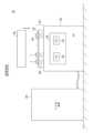
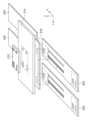
図3は、一実施例に係るインタフェース装置200Aの断面図である。図3には、1個のDUTに関連する構成のみが示される。この実施例において、インタフェース装置200Aは、マザーボード230と、マザーボード230に対して着脱可能なソケットボード210を備える。ソケットボード210は、ソケット212、ソケットプリント基板(ソケットPCB)214、ソケットボード側コネクタ216を備える。 FIG. 3 is a cross-sectional view of an
フロントエンドモジュール300Aは、複数のピンエレクトロニクスIC400が実装される複数のプリント基板(ピンエレクトロニクスPCB)310を備える。複数のピンエレクトロニクスPCB310は、DUTの面(表面および裏面)、言い換えるとソケットボード210の面S1に対して垂直な向きで配置される。本実施形態では、ソケットボード210は、地面と水平であり、したがって複数のピンエレクトロニクスPCB310は、重力方向と平行となるように配置される。 The
フロントエンドモジュール300Aは、プレート状の冷却装置(以下、コールドプレートと称する)320をさらに備える。コールドプレート320は、冷媒が流通する流路を有する。 The
複数のピンエレクトロニクスPCB310a,310bおよびコールドプレート320は、ピンエレクトロニクスIC400がコールドプレート320と熱的に結合する接触する態様で積層されている。 The plurality of
マザーボード230は、ソケットボード側コネクタ232、スペーシングフレーム234、中継コネクタ236を備える。フロントエンドモジュール300Aは、スペーシングフレーム234に対して固定されている。中継コネクタ236は、テストヘッド側コネクタ132と電気的および機械的に結合する。 The
詳しくは後述するように、配線220は、従来の同軸ケーブルに代えて、フレキシブル基板(FPC:Flexible printed circuits)で構成されるケーブル(FPCケーブルともいう)を用いることができる。 As will be described in detail later, the
一方で、ピンエレクトロニクスPCB310と中継コネクタ236の間の配線224には、ピンエレクトロニクスIC400に対する制御信号のみが伝送し、試験信号やデバイス信号は伝送しない。そのため配線224は、同軸ケーブルを利用してもよい。 On the other hand, only control signals for the
複数のピンエレクトロニクスIC400は、ピンエレクトロニクスPCB310上において、ピンエレクトロニクスPCB310の上下方向の中央よりも、DUT寄り(ソケットボード210寄り)に実装される。これにより、ピンエレクトロニクスPCB310上における、試験信号およびデバイス信号の伝送距離を短くすることができ、高速な信号伝送が可能となる。 The plurality of
たとえば、複数のピンエレクトロニクスIC400は、ピンエレクトロニクスPCB310のDUT側の1辺から、50mm以内に配置することが好ましく、30mm以内に配置することができれば、さらに伝送距離を短くできる。 For example, the plurality of
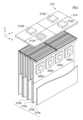
図4は、一実施例に係るフロントエンドモジュール300Bを示す図である。 FIG. 4 is a diagram illustrating a
1個のDUT1には、2×M個(M≧1)のピンエレクトロニクスIC400が割り当てられている。複数のDUTおよびピンエレクトロニクスIC400には、A~Dの添え字を付し、必要に応じて区別する。この例では、DUT1が、192I/Oを有し、ピンエレクトロニクスIC400が24I/Oを有する場合、1個のDUT当たり、192/24=8個(つまりM=4)のピンエレクトロニクスIC400が割り当てられる。 2×M (M≧1)
フロントエンドモジュール300Bは、複数N個(N≧2)のDUT1ごとに分割して構成され、この分割単位をフロントエンドユニット(FEU)と称する。この例では4個のDUTに対応するブロックが、1個のFEUを構成しており、1個のFEUは、2×M×N個=2×4×4=32個のピンエレクトロニクスIC400を備える。 The
図4には、2個のFEUが示されるが、実際にはフロントエンドモジュール300Bは、2個以上のFEUを備えることができる。たとえば64個の同時測定可能なATEでは、64/4=16個のFEUが設けられ、フロントエンドモジュール300B全体としては、64×192I/O=12288I/Oを備えることとなる。 Although two FEUs are shown in FIG. 4, the
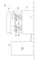
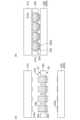
図5は、図4のFEUの構成例を示す斜視図である。4個のDUTに対応するソケット212A~212Dは、2行2列のマトリクス状に配置される。1個のDUT1Aに着目すると、それに割り当てられる8個のピンエレクトロニクスIC400Aは、X方向に並ぶ4枚のピンエレクトロニクスPCB310a~310dに2個ずつに分けて実装される。ソケット212が実装されるソケットPCB214は、DUTごとに分割されていてもよいし、4個のDUTに対応するソケットPCB214が、1枚の基板として一体に構成されてもよい。 FIG. 5 is a perspective view showing an example of the configuration of the FEU shown in FIG. 4. FIG.
1枚のピンエレクトロニクスPCB310に実装される2個のピンエレクトロニクスIC400Aは、Y方向に並べて配置される。2個のピンエレクトロニクスIC400Aは、DUT1Aから等距離の位置に配置されている。 Two
図6は、図4のFEUの構成例を示す断面図である。図3に示したように、2枚のピンエレクトロニクスPCB310aと310bの間には、コールドプレート320が設けられる。同様に、2枚のピンエレクトロニクスPCB310c、310dの間にも、コールドプレート320が設けられる。上述したように、ピンエレクトロニクスIC400は、ピンエレクトロニクスPCB310上のソケットボード210に近い箇所に実装されている。冷却効率を高めるために、ピンエレクトロニクスIC400はベアチップとすることができ、ピンエレクトロニクスIC400とコールドプレート320は、サーマルインターフェースマテリアル(TIM)322を介して熱的に結合している。 FIG. 6 is a sectional view showing an example of the configuration of the FEU shown in FIG. 4. As shown in FIG. 3, a
またFEUを、Y軸に沿って平面視したときに、X方向に積層される4枚(M枚)のピンエレクトロニクスPCB310a~310dの中心位置に、DUTの中心、すなわちソケット212Aが位置している。 Furthermore, when the FEU is viewed from above along the Y axis, the center of the DUT, that is, the
以上がFEUの構成である。 The above is the configuration of FEU.
このFEUの利点を説明する。添え字Aを付したDUT1Aに着目する。1個のDUT1Aに対応する複数(この例では8個)のピンエレクトロニクスIC400Aを、4枚のピンエレクトロニクスPCB310a~310dに2個ずつ、実装することにより、8個のピンエレクトロニクスIC400Aそれぞれから、ソケット212Aまでの距離を均一化することができる。これにより各ピンエレクトロニクスIC400Aからソケット212A(DUT1A)までの伝送線路の損失を均一化でき、正確な試験が可能となる。 The advantages of this FEU will be explained. Attention is paid to DUT1A with the subscript A attached thereto. By mounting a plurality of (eight in this example)
続いて、ピンエレクトロニクスIC400とソケット212の電気的な接続について説明する。 Next, the electrical connection between the
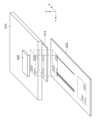
図7は、ピンエレクトロニクスICとソケット(DUT1)の接続の一例を示す断面図である。試験信号およびデバイス信号が伝送する伝送路、すなわちピンエレクトロニクスPCB310とソケットボード210の間の配線220は、FPCケーブル222が用いられる。 FIG. 7 is a cross-sectional view showing an example of the connection between the pin electronics IC and the socket (DUT1). An
ピンエレクトロニクスPCB310とソケットボード210の間の配線220として、同軸ケーブルを用いると、同軸ケーブルの剛性に起因して、ピンエレクトロニクスPCB310とソケットボード210の最短距離が制約される。またこれに対して、FPCケーブル222を利用することにより、その柔軟性によってピンエレクトロニクスPCB310とソケットボード210の距離hを、同軸ケーブルを用いた場合に比べて短縮でき、試験信号およびデバイス信号の伝送距離を短くできる。 When a coaxial cable is used as the
従来の試験装置では、ソケットボード210を着脱可能としたい場合、LIF(Low Insertion Force)コネクタを使用するのが一般的であった。このLIFコネクタは、14GHzより高い周波数帯域において、-3dB程度の無視できない損失を有しており、28Gbpsあるいは40Gbpsの高速伝送においては、波形歪みの原因となる。配線220にFPCケーブル222を用いることで、LIFコネクタが不要となるため、損失(高周波帯域の減衰)に起因する波形歪みを抑制でき、正確な試験が可能となる。 In conventional test equipment, when it is desired to make the
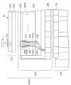
図8は、FPCケーブル222とソケットボード210の接続部分の構成例を示す断面図である。図9は、FPCケーブル222とソケットボード210の接続部分の分解斜視図である。 FIG. 8 is a cross-sectional view showing an example of the configuration of a connecting portion between the
ソケットボード210は、ソケット212およびソケットPCB214を含む。ソケットPCB214は、配線層と絶縁層を含む多層基板である。配線層には、信号経路を水平方向に移動させる配線が形成され、絶縁層には、信号経路を垂直方向に移動させるビアホールVHが形成されている。試験信号およびデバイス信号が伝送する経路は、なるべく水平方向(X方向およびY方向)に移動せずに、ソケットボード210の裏面まで引き出されることが好ましい。反対に、電源信号や周波数が低い制御信号に関しては、ソケットPCB214の内部において、水平方向に引き回しても構わない。
FPCケーブル222とソケットボード210は、ソケットボード側コネクタ216によって接続される。ソケットボード側コネクタ216は、インタポーザ218と、ケーブルクランプ219を含む。 The
インタポーザ218の表面に露出する電極は、ソケットPCB214の裏面に露出する電極と電気的に接続されている。FPCケーブル222は、インタポーザ218の裏面電極と接触した状態で、ケーブルクランプ219によって挟み込まれる。 The electrodes exposed on the surface of the
図10(a)、(b)は、インタポーザの構造および接続を説明する断面図である。図10(a)は、接続前の状態を、図10(b)は、接続後の状態を示す。インタポーザ218は、基板250、非変形電極252、変形電極254を有する。基板250の第1面S1には開口256が設けられており、その内部に、変形電極254が埋め込まれる。変形電極254は、導電性および弾性を有しており、接続前の状態において、基板250の一面よりも突出している。変形電極254は、導電性ガスケットや導電性エラストマーであってもよい。あるいは変形電極254は、ポゴピンのようなバネ付きの電極であってもよい。 FIGS. 10A and 10B are cross-sectional views illustrating the structure and connections of the interposer. FIG. 10(a) shows the state before connection, and FIG. 10(b) shows the state after connection.
基板250の第2面S2には、非変形電極252が設けられる。非変形電極252は、基板250の内部において変形電極254と電気的に接続されている。非変形電極252は、複数の突起を有しており、多点接続が可能となっている。 A
図10(b)に示すように、インタポーザ218を挟んだ状態でソケットPCB214とFPCケーブル222に圧力が加わると、インタポーザ218の非変形電極252が、FPCケーブル222の電極222eと接触する。また変形電極254が変形し、ソケットPCB214の裏面電極214eと接触する。 As shown in FIG. 10(b), when pressure is applied to the
このようなインタポーザ218は、LIFコネクタやZIFコネクタに比べて寄生容量を小さく構成できるため高周波特性に優れており、0~40GHzにわたり、フラットな通過特性(SパラメータのS21特性)を得ることができる。 This kind of
図11は、FPCケーブル222とピンエレクトロニクスPCB310の接続部分の構成例を示す断面図である。図12は、FPCケーブル222とピンエレクトロニクスPCB310の接続部分の分解斜視図である。 FIG. 11 is a cross-sectional view showing an example of the configuration of a connecting portion between the
図11を参照する。FPCケーブル222とピンエレクトロニクスPCB310は、FPCコネクタ312によって接続される。FPCコネクタ312は、ソケットボード側コネクタ216と同様に構成され、具体的には、インタポーザ314とケーブルクランプ316を含む。 See FIG. 11.
インタポーザ314の第1面S1に露出する変形電極254は、ピンエレクトロニクスPCB310の裏面の電極と電気的に接続されている。FPCケーブル222は、インタポーザ314の第2面S2に露出する非変形電極252と電気的に接触した状態で、ケーブルクランプ316によって挟み込まれる。 The
ピンエレクトロニクスPCB310にはビアホールVHが形成される。ピンエレクトロニクスPCB310の内部においても、試験信号およびデバイス信号の伝送路は最短化することが望ましい。そこで、ピンエレクトロニクスPCB310に形成されるビアホールVHは、ピンエレクトロニクスIC400の裏面電極402とオーバーラップする位置に配置するとよい。これにより、ピンエレクトロニクスPCB310の内部において、伝送路がプリント基板の面内方向に引き回されないため、高速な信号伝送が可能となる。 A via hole VH is formed in the
インタフェース装置200には、さまざまな形式があるが、本開示はいずれの形式にも適用可能である。 There are various forms of
・SBC(Socket Board Change)タイプ
SBCタイプは、DUTの種類に応じて、ソケットボード210を交換するタイプのインタフェース装置である。 - SBC (Socket Board Change) type The SBC type is a type of interface device in which the
・CLS(Cable Less)タイプ
CLSタイプは、インタフェース装置200が、上部のDSA(Device Specific Adapter)と下部のマザーボードに分離可能であり、DUTの種類に応じて、DSAを交換するタイプのインタフェース装置である。本実施形態に係るインタフェース装置200をCLSタイプに適用する場合、2つの方式が考えられる。 ・CLS (Cable Less) type The CLS type is a type of interface device in which the
ひとつは、フロントエンドモジュール300を、マザーボード側に配置するものである。この場合、フロントエンドモジュール300を、異なるDUTの試験で共有することができるため、コストの観点から有利である。 One is to place the
別のひとつは、フロントエンドモジュール300をDSA側に配置するものである。この場合、フロントエンドモジュール300がDSAごとに設けられるため、装置のコストは上昇する。一方で、フロントエンドモジュール300を、DUTに近づけることが可能となるため、高速な試験の観点からは有利である。 Another method is to place the
・CCN(Cable Connection)タイプ
CCNタイプは、インタフェース装置200の全体を、DUTの種類に応じて交換するタイプのインタフェース装置である。本実施形態に係るインタフェース装置200をCCNタイプに適用すると、フロントエンドモジュール300をDUTに極限まで近づけることが可能となるため、高速な試験の観点からは有利である。 - CCN (Cable Connection) Type The CCN type is a type of interface device in which the
・ウェハマザーボード
インタフェース装置200は、ウェハレベル試験に使用されるウェハマザーボードであってもよい。この場合、インタフェース装置200は、ソケットボードに代えて、プローブカードを備えることができる。 - Wafer
上述した実施形態は例示であり、それらの各構成要素や各処理プロセスの組み合わせにいろいろな変形例が可能なことが当業者に理解される。以下、こうした変形例について説明する。 The embodiments described above are illustrative, and those skilled in the art will understand that various modifications can be made to the combinations of their constituent elements and processing processes. Hereinafter, such modified examples will be explained.
(変形例1)
実施形態では、ピンエレクトロニクスIC400が実装されるピンエレクトロニクスPCB310とソケットボード210の間を接続する配線220を、FPCケーブルとしたが、本開示はそれに限定されず、その他の低損失な配線を用いることが可能である。(Modification 1)
In the embodiment, the
(変形例2)
FPCケーブル222とピンエレクトロニクスPCB310の間の接続インタフェースとして、あるいはFPCケーブル222とソケットボード210の間の接続インタフェースとして、インタポーザを用いたものを説明したが、本開示はそれに限定されない。(Modification 2)
Although an interposer is used as the connection interface between the
(変形例3)
実施形態では、ソケットボード210が、地面と平行であるインタフェース装置200を説明したが本開示はそれに限定されない。たとえばソケットボード210は、地面と垂直であってもよい。この場合、図5、図6等におけるY方向が、重力方向となる。(Modification 3)
Although embodiments have described
本開示に係る実施形態について、具体的な用語を用いて説明したが、この説明は、理解を助けるための例示に過ぎず、本開示あるいは請求の範囲を限定するものではない。本発明の範囲は、請求の範囲によって規定されるものであり、したがって、ここでは説明しない実施形態、実施例、変形例も、本発明の範囲に含まれる。 Although the embodiments according to the present disclosure have been described using specific terms, this description is merely an example to aid understanding, and does not limit the scope of the present disclosure or the claims. The scope of the present invention is defined by the claims, and therefore embodiments, examples, and modifications not described here are also included within the scope of the present invention.
1 DUT
100 ATE
120 テスター
130 テストヘッド
200 インタフェース装置
210 ソケットボード
212 ソケット
214 ソケットPCB
216 ソケットボード側コネクタ
218 インタポーザ
219 ケーブルクランプ
220 配線
222 FPCケーブル
230 マザーボード
250 基板
252 非変形電極
254 変形電極
256 開口
300 フロントエンドモジュール
310 ピンエレクトロニクスPCB
312 FPCコネクタ
314 インタポーザ
316 ケーブルクランプ
320 コールドプレート
400 ピンエレクトロニクスIC 1 DUT
100 ATE
120
216 Socket
312
Claims (11)
Translated fromJapanese複数のピンエレクトロニクスIC(Integrated Circuit)がモジュール化されてなるフロントエンドモジュールを備えることを特徴とするインタフェース装置。 An interface device provided between a test head and a device under test (DUT),
An interface device characterized by comprising a front end module formed by modularizing a plurality of pin electronics ICs (Integrated Circuits).
前記複数のピンエレクトロニクスICが実装される複数のプリント基板をさらに備え、
前記複数のプリント基板は、前記DUTの面に対して垂直な向きで配置されることを特徴とする請求項1に記載のインタフェース装置。 The front end module includes:
further comprising a plurality of printed circuit boards on which the plurality of pin electronics ICs are mounted,
The interface device according to claim 1, wherein the plurality of printed circuit boards are arranged perpendicularly to a plane of the DUT.
前記複数のプリント基板は、前記冷却装置を挟んで積層され、
前記複数のプリント基板は、重力方向と平行となるように配置されることを特徴とする請求項2に記載のインタフェース装置。 The front end module further includes a plate-shaped cooling device,
The plurality of printed circuit boards are stacked with the cooling device in between,
3. The interface device according to claim 2, wherein the plurality of printed circuit boards are arranged parallel to a direction of gravity.
1枚の前記プリント基板には、2個の前記ピンエレクトロニクスICが、前記DUTから等距離の位置に実装されることを特徴とする請求項2または3に記載のインタフェース装置。 The plurality of pin electronics ICs are assigned 2×M (M≧1) to one DUT and mounted on M pieces of the printed circuit board,
4. The interface device according to claim 2, wherein the two pin electronics ICs are mounted on one printed circuit board at positions equidistant from the DUT.
前記ユニットは、8枚のプリント基板が積層された構成を有することを特徴とする請求項8に記載のインタフェース装置。 N=4, the four DUTs are arranged in 2 rows and 2 columns,
9. The interface device according to claim 8, wherein the unit has a structure in which eight printed circuit boards are stacked.
前記フロントエンドモジュールと前記ソケットボードの間は、FPC(Flexible printed circuits)ケーブルを介して接続されることを特徴とする請求項1から3のいずれかに記載のインタフェース装置。 further comprising a socket board having a plurality of sockets each to which a DUT can be attached, and a socket printed circuit board on which the plurality of sockets are mounted,
4. The interface device according to claim 1, wherein the front-end module and the socket board are connected via an FPC (Flexible printed circuits) cable.
テストヘッドと、
前記テストヘッドに接続される請求項1から3のいずれかに記載のインタフェース装置と、
を備えることを特徴とする自動試験装置。 The tester body,
test head and
an interface device according to any one of claims 1 to 3 connected to the test head;
An automatic test device characterized by comprising:
Priority Applications (5)
| Application Number | Priority Date | Filing Date | Title |
|---|---|---|---|
| JP2022117406AJP2024014519A (en) | 2022-07-22 | 2022-07-22 | Automatic test equipment and its interface equipment |
| TW112122251ATWI876380B (en) | 2022-07-22 | 2023-06-14 | Automatic testing device and its interface device |
| KR1020230087851AKR20240013656A (en) | 2022-07-22 | 2023-07-06 | Automatic test equipment and interface equipment thereof |
| CN202310844479.6ACN117434306A (en) | 2022-07-22 | 2023-07-11 | Automatic test device and interface device thereof |
| US18/354,198US20240027520A1 (en) | 2022-07-22 | 2023-07-18 | Automatic test equipment |
Applications Claiming Priority (1)
| Application Number | Priority Date | Filing Date | Title |
|---|---|---|---|
| JP2022117406AJP2024014519A (en) | 2022-07-22 | 2022-07-22 | Automatic test equipment and its interface equipment |
Publications (1)
| Publication Number | Publication Date |
|---|---|
| JP2024014519Atrue JP2024014519A (en) | 2024-02-01 |
Family
ID=89557189
Family Applications (1)
| Application Number | Title | Priority Date | Filing Date |
|---|---|---|---|
| JP2022117406APendingJP2024014519A (en) | 2022-07-22 | 2022-07-22 | Automatic test equipment and its interface equipment |
Country Status (5)
| Country | Link |
|---|---|
| US (1) | US20240027520A1 (en) |
| JP (1) | JP2024014519A (en) |
| KR (1) | KR20240013656A (en) |
| CN (1) | CN117434306A (en) |
| TW (1) | TWI876380B (en) |
Family Cites Families (12)
| Publication number | Priority date | Publication date | Assignee | Title |
|---|---|---|---|---|
| US6078187A (en)* | 1997-05-23 | 2000-06-20 | Credence Systems Corporation | Hemispherical test head for integrated circuit tester employing radially distributed circuit cards |
| US6426637B1 (en)* | 1999-12-21 | 2002-07-30 | Cerprobe Corporation | Alignment guide and signal transmission apparatus and method for spring contact probe needles |
| DE112004000029T5 (en)* | 2003-06-05 | 2005-07-28 | Advantest Corp. | Component connection device |
| US7375542B2 (en)* | 2004-06-30 | 2008-05-20 | Teradyne, Inc. | Automated test equipment with DIB mounted three dimensional tester electronics bricks |
| JP2008076308A (en) | 2006-09-22 | 2008-04-03 | Advantest Corp | Interface device for electronic component test equipment |
| US7528623B2 (en)* | 2007-02-02 | 2009-05-05 | Teradyne, Inc. | Distributing data among test boards to determine test parameters |
| KR20100040979A (en) | 2007-09-14 | 2010-04-21 | 가부시키가이샤 아드반테스트 | Water jacket |
| US9772378B2 (en)* | 2014-08-28 | 2017-09-26 | Teradyne, Inc. | Multi-stage equalization |
| US10139449B2 (en)* | 2016-01-26 | 2018-11-27 | Teradyne, Inc. | Automatic test system with focused test hardware |
| US10677815B2 (en)* | 2018-06-08 | 2020-06-09 | Teradyne, Inc. | Test system having distributed resources |
| US11966677B1 (en)* | 2020-08-31 | 2024-04-23 | Synopsys, Inc. | Emulation performance analysis using abstract timing graph representation |
| JP7563848B2 (en)* | 2021-03-30 | 2024-10-08 | 東京エレクトロン株式会社 | LED Chuck |
- 2022
- 2022-07-22JPJP2022117406Apatent/JP2024014519A/enactivePending
- 2023
- 2023-06-14TWTW112122251Apatent/TWI876380B/enactive
- 2023-07-06KRKR1020230087851Apatent/KR20240013656A/ennot_activeCeased
- 2023-07-11CNCN202310844479.6Apatent/CN117434306A/enactivePending
- 2023-07-18USUS18/354,198patent/US20240027520A1/enactivePending
Also Published As
| Publication number | Publication date |
|---|---|
| US20240027520A1 (en) | 2024-01-25 |
| TW202409586A (en) | 2024-03-01 |
| CN117434306A (en) | 2024-01-23 |
| KR20240013656A (en) | 2024-01-30 |
| TWI876380B (en) | 2025-03-11 |
Similar Documents
| Publication | Publication Date | Title |
|---|---|---|
| US20100231250A1 (en) | Pin Electronics Liquid Cooled Multi-module for High Performance, Low Cost Automated Test Equipment | |
| US7960991B2 (en) | Test apparatus and probe card | |
| US7288949B2 (en) | Semiconductor test interface | |
| US20080100323A1 (en) | Low cost, high pin count, wafer sort automated test equipment (ate) device under test (dut) interface for testing electronic devices in high parallelism | |
| KR102829130B1 (en) | Automatic test equipment and interface equipment thereof | |
| US20140253165A1 (en) | Probe card | |
| JP2024014519A (en) | Automatic test equipment and its interface equipment | |
| KR102829111B1 (en) | Automatic test equipment and interface equipment thereof | |
| KR102762587B1 (en) | Automatic test equipment and interface equipment thereof | |
| US7717715B2 (en) | System, method and apparatus using at least one flex circuit to connect a printed circuit board and a socket card assembly that are oriented at a right angle to one another | |
| WO2024161595A1 (en) | Semiconductor integrated circuit and module thereof | |
| KR20250007413A (en) | Automatic test equipment and interface equipment thereof | |
| US7459921B2 (en) | Method and apparatus for a paddle board probe card |
Legal Events
| Date | Code | Title | Description |
|---|---|---|---|
| A621 | Written request for application examination | Free format text:JAPANESE INTERMEDIATE CODE: A621 Effective date:20250415 |