JP2024004613A - Physical quantity sensors and inertial measurement devices - Google Patents
Physical quantity sensors and inertial measurement devicesDownload PDFInfo
- Publication number
- JP2024004613A JP2024004613AJP2022104309AJP2022104309AJP2024004613AJP 2024004613 AJP2024004613 AJP 2024004613AJP 2022104309 AJP2022104309 AJP 2022104309AJP 2022104309 AJP2022104309 AJP 2022104309AJP 2024004613 AJP2024004613 AJP 2024004613A
- Authority
- JP
- Japan
- Prior art keywords
- electrode group
- physical quantity
- movable
- support beam
- quantity sensor
- Prior art date
- Legal status (The legal status is an assumption and is not a legal conclusion. Google has not performed a legal analysis and makes no representation as to the accuracy of the status listed.)
- Pending
Links
Images


Classifications
- G—PHYSICS
- G01—MEASURING; TESTING
- G01P—MEASURING LINEAR OR ANGULAR SPEED, ACCELERATION, DECELERATION, OR SHOCK; INDICATING PRESENCE, ABSENCE, OR DIRECTION, OF MOVEMENT
- G01P15/00—Measuring acceleration; Measuring deceleration; Measuring shock, i.e. sudden change of acceleration
- G01P15/02—Measuring acceleration; Measuring deceleration; Measuring shock, i.e. sudden change of acceleration by making use of inertia forces using solid seismic masses
- G01P15/08—Measuring acceleration; Measuring deceleration; Measuring shock, i.e. sudden change of acceleration by making use of inertia forces using solid seismic masses with conversion into electric or magnetic values
- G01P15/125—Measuring acceleration; Measuring deceleration; Measuring shock, i.e. sudden change of acceleration by making use of inertia forces using solid seismic masses with conversion into electric or magnetic values by capacitive pick-up
- G—PHYSICS
- G01—MEASURING; TESTING
- G01P—MEASURING LINEAR OR ANGULAR SPEED, ACCELERATION, DECELERATION, OR SHOCK; INDICATING PRESENCE, ABSENCE, OR DIRECTION, OF MOVEMENT
- G01P1/00—Details of instruments
- G—PHYSICS
- G01—MEASURING; TESTING
- G01P—MEASURING LINEAR OR ANGULAR SPEED, ACCELERATION, DECELERATION, OR SHOCK; INDICATING PRESENCE, ABSENCE, OR DIRECTION, OF MOVEMENT
- G01P15/00—Measuring acceleration; Measuring deceleration; Measuring shock, i.e. sudden change of acceleration
- G01P15/18—Measuring acceleration; Measuring deceleration; Measuring shock, i.e. sudden change of acceleration in two or more dimensions
- G—PHYSICS
- G01—MEASURING; TESTING
- G01P—MEASURING LINEAR OR ANGULAR SPEED, ACCELERATION, DECELERATION, OR SHOCK; INDICATING PRESENCE, ABSENCE, OR DIRECTION, OF MOVEMENT
- G01P15/00—Measuring acceleration; Measuring deceleration; Measuring shock, i.e. sudden change of acceleration
- G01P15/02—Measuring acceleration; Measuring deceleration; Measuring shock, i.e. sudden change of acceleration by making use of inertia forces using solid seismic masses
- G01P15/08—Measuring acceleration; Measuring deceleration; Measuring shock, i.e. sudden change of acceleration by making use of inertia forces using solid seismic masses with conversion into electric or magnetic values
- G01P2015/0805—Measuring acceleration; Measuring deceleration; Measuring shock, i.e. sudden change of acceleration by making use of inertia forces using solid seismic masses with conversion into electric or magnetic values being provided with a particular type of spring-mass-system for defining the displacement of a seismic mass due to an external acceleration
- G01P2015/0822—Measuring acceleration; Measuring deceleration; Measuring shock, i.e. sudden change of acceleration by making use of inertia forces using solid seismic masses with conversion into electric or magnetic values being provided with a particular type of spring-mass-system for defining the displacement of a seismic mass due to an external acceleration for defining out-of-plane movement of the mass
- G01P2015/0825—Measuring acceleration; Measuring deceleration; Measuring shock, i.e. sudden change of acceleration by making use of inertia forces using solid seismic masses with conversion into electric or magnetic values being provided with a particular type of spring-mass-system for defining the displacement of a seismic mass due to an external acceleration for defining out-of-plane movement of the mass for one single degree of freedom of movement of the mass
- G01P2015/0831—Measuring acceleration; Measuring deceleration; Measuring shock, i.e. sudden change of acceleration by making use of inertia forces using solid seismic masses with conversion into electric or magnetic values being provided with a particular type of spring-mass-system for defining the displacement of a seismic mass due to an external acceleration for defining out-of-plane movement of the mass for one single degree of freedom of movement of the mass the mass being of the paddle type having the pivot axis between the longitudinal ends of the mass, e.g. see-saw configuration
- G—PHYSICS
- G01—MEASURING; TESTING
- G01P—MEASURING LINEAR OR ANGULAR SPEED, ACCELERATION, DECELERATION, OR SHOCK; INDICATING PRESENCE, ABSENCE, OR DIRECTION, OF MOVEMENT
- G01P15/00—Measuring acceleration; Measuring deceleration; Measuring shock, i.e. sudden change of acceleration
- G01P15/02—Measuring acceleration; Measuring deceleration; Measuring shock, i.e. sudden change of acceleration by making use of inertia forces using solid seismic masses
- G01P15/08—Measuring acceleration; Measuring deceleration; Measuring shock, i.e. sudden change of acceleration by making use of inertia forces using solid seismic masses with conversion into electric or magnetic values
- G01P2015/0862—Measuring acceleration; Measuring deceleration; Measuring shock, i.e. sudden change of acceleration by making use of inertia forces using solid seismic masses with conversion into electric or magnetic values being provided with particular means being integrated into a MEMS accelerometer structure for providing particular additional functionalities to those of a spring mass system
Landscapes
- Physics & Mathematics (AREA)
- General Physics & Mathematics (AREA)
- Pressure Sensors (AREA)
Abstract
Description
Translated fromJapanese本発明は、物理量センサー及び慣性計測装置等に関する。 The present invention relates to a physical quantity sensor, an inertial measurement device, and the like.
特許文献1には、Z方向の加速度を検出する物理量センサーが開示されている。当該物理量センサーにおいて、複数の第1電極の1つの第1方向に沿う第1電極の長さは、第1導電部の第1方向に沿う第1導電部の長さよりも短いことが開示されている。また当該物理量センサーにおいて、複数の第2電極の1つの第1方向に沿う第2電極の長さは、第2導電部の第1方向に沿う第2導電部の長さよりも短いことが開示されている。
特許文献1に開示された物理量センサーでは、検出対象であるZ軸方向ではない櫛歯電極長方向へ加速度が印可されると、検出軸方向に加速度が印可されたときと同じシーソー動作が発生してしまい、他軸感度が増加するという不具合があった。 In the physical quantity sensor disclosed in
本開示の一態様は、互いに直交する3つの方向を第1方向、第2方向及び第3方向としたとき、前記第3方向での物理量を検出する物理量センサーであって、基板に固定された固定部と、前記固定部に一端が接続され、前記第2方向に沿って設けられる支持梁と、前記支持梁の他端に接続された可動体と、前記基板に設けられ、前記支持梁の前記第1方向に配置される第1固定電極群と、前記基板に設けられ、前記支持梁の前記第1方向の反対方向である第4方向に配置される第2固定電極群と、を含み、前記可動体は、前記支持梁の他端に接続され、前記支持梁から前記第1方向に延びる第1連結部と、前記第1連結部に接続され、前記第2方向に沿って設けられる第1基部と、前記第1基部に設けられ、前記第1固定電極群と前記第2方向において対向する第1可動電極群と、前記支持梁の他端に接続され、前記支持梁から前記第4方向に延びる第2連結部と、前記第2連結部に接続され、前記第2方向に沿って設けられる第2基部と、前記第2基部に設けられ、前記第2固定電極群と前記第2方向において対向する第2可動電極群と、前記第1連結部に接続され、前記第1可動電極群の前記第1方向側に設けられる質量部と、を有する物理量センサーに関係する。 One aspect of the present disclosure is a physical quantity sensor that detects a physical quantity in a third direction when three directions orthogonal to each other are defined as a first direction, a second direction, and a third direction, the physical quantity sensor being a physical quantity sensor fixed to a substrate. a fixed part, a support beam whose one end is connected to the fixed part and is provided along the second direction, a movable body connected to the other end of the support beam, and a movable body which is provided on the substrate and is connected to the support beam. a first fixed electrode group arranged in the first direction; and a second fixed electrode group provided on the substrate and arranged in a fourth direction of the support beam that is opposite to the first direction. , the movable body is connected to the other end of the support beam and extends from the support beam in the first direction; and the movable body is connected to the first connection portion and provided along the second direction. a first base; a first movable electrode group provided on the first base and facing the first fixed electrode group in the second direction; a second connecting portion extending in four directions; a second base connected to the second connecting portion and provided along the second direction; and a second base connected to the second connecting portion and connected to the second fixed electrode group and the first The present invention relates to a physical quantity sensor including a second movable electrode group facing each other in two directions, and a mass part connected to the first connecting part and provided on the first direction side of the first movable electrode group.
また本開示の他の態様は、上記に記載の物理量センサーと、前記物理量センサーから出力された検出信号に基づいて制御を行う制御部と、を含む慣性計測装置に関係する。 Another aspect of the present disclosure relates to an inertial measurement device including the physical quantity sensor described above and a control unit that performs control based on a detection signal output from the physical quantity sensor.
以下、本実施形態について説明する。なお、以下に説明する本実施形態は、特許請求の範囲の記載内容を不当に限定するものではない。また本実施形態で説明される構成の全てが必須構成要件であるとは限らない。 This embodiment will be described below. Note that this embodiment described below does not unduly limit the contents described in the claims. Furthermore, not all of the configurations described in this embodiment are essential configuration requirements.
1.物理量センサー
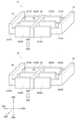
本実施形態の物理量センサー1について、鉛直方向の加速度を検出する加速度センサーを一例として挙げて説明する。図1は、本実施形態の物理量センサー1の基板2に直交する方向での平面視における平面図である。物理量センサー1は、MEMS(Micro Electro Mechanical Systems)デバイスであり、例えば慣性センサーである。1. Physical Quantity Sensor The
なお、図1や後述の図2~図19では、説明の便宜のために各部材の寸法や部材間の間隔等は模式的に示されており、また、全ての構成要素を示してはいない。例えば電極配線、電極端子等については図示を省略している。また以下では、物理量センサー1が検出する物理量が加速度である場合を主に例にとって説明するが、物理量は加速度に限定されず、速度、圧力、変位、姿勢、角速度又は重力等の他の物理量であってもよく、物理量センサー1は圧力センサー又はMEMSスイッチ等として用いられるものであってもよい。また図1において互いに直交する方向を第1方向DR1、第2方向DR2、第3方向DR3としている。第1方向DR1、第2方向DR2、第3方向DR3は、各々、例えばX軸方向、Y軸方向、Z軸方向であるが、これに限定されない。例えばZ軸方向に対応する第3方向DR3は、例えば物理量センサー1の基板2に直交する方向であり、例えば鉛直方向である。そして、第3方向DR3と反対の方向を第5方向DR5とする。X軸方向に対応する第1方向DR1、Y軸方向に対応する第2方向DR2は、第3方向DR3に直交する方向であり、第1方向DR1及び第2方向DR2に沿った面であるXY平面は例えば水平面に沿っている。そして、第1方向DR1の反対の方向を第4方向DR4とし、第4方向は、例えば-X軸方向である。なお「直交」とは、90°で交わっているものの他、90°から若干傾いた角度で交わっている場合も含むものとする。 In addition, in FIG. 1 and FIGS. 2 to 19 described later, the dimensions of each member and the spacing between members are shown schematically for convenience of explanation, and all constituent elements are not shown. . For example, illustrations of electrode wiring, electrode terminals, etc. are omitted. In addition, although the explanation below will mainly take as an example the case where the physical quantity detected by the
基板2は、例えば半導体シリコンで構成されたシリコン基板又はホウケイ酸ガラスなどのガラス材料で構成されたガラス基板などである。但し基板2の構成材料としては、特に限定されず、石英基板又はSOI(Silicon On Insulator)基板等を用いてもよい。 The substrate 2 is, for example, a silicon substrate made of semiconductor silicon or a glass substrate made of a glass material such as borosilicate glass. However, the constituent material of the substrate 2 is not particularly limited, and a quartz substrate, an SOI (Silicon On Insulator) substrate, or the like may be used.
図1に示すように本実施形態の物理量センサー1は、固定部40、支持梁42、可動体MB、第1固定電極群10及び第2固定電極群50を含む。可動体MBは、第1連結部30、第1基部23、第1可動電極群20、第2連結部70、第2基部63、第2可動電極群60及び質量部MPを含む。第1固定電極群10は複数の第1固定電極11、12を有し、第2固定電極群50は複数の第2固定電極51、52を有する。第1可動電極群20は複数の第1可動電極21、22を有し、第2可動電極群60は複数の第2可動電極61、62を有する。 As shown in FIG. 1, the
そして、図1において破線の枠で示すように、物理量センサー1は検出部Z1と検出部Z2を有し、各検出部でZ軸方向である第3方向DR3に沿う方向での加速度等の物理量を検出する。検出部Z1とZ2は、平面視において、それぞれ支持梁42の第1方向DR1側と第4方向DR4側に設けられている。 As shown by the broken line frame in FIG. 1, the
支持梁42の第1方向DR1側に設けられる検出部Z1は、第1固定電極群10、第1可動電極群20を含む。また支持梁42の第4方向DR4側に設けられる検出部Z2は、第2固定電極群50と第2可動電極群60を含む。 The detection unit Z1 provided on the first direction DR1 side of the
図2は本実施形態の物理量センサー1の斜視図である。固定部40は、図2に示すように基板2に設けられている。固定部40は、支持梁42の一端を固定部40を介して基板2に固定している。支持梁42の他端は可動体MBの第1連結部30、第2連結部70に連結されている。このように固定部40は、支持梁42を介して可動体MBを基板2に連結させる。そして、固定部40Aは後述の図4で説明する可動体MBのシーソー運動におけるアンカーとしての役割を担う。 FIG. 2 is a perspective view of the
支持梁42は、可動体MBのシーソー運動における復元力を与える。図2に示すように、支持梁42は一端が固定部40の一部に接続されている。そして、支持梁42の他端は、それぞれ第1連結部30、第2連結部70に接続されている。このように支持梁42は、固定部40と可動体MBとを連結させている。支持梁42は例えば捻れバネである。図1に示すように、支持梁42は平面視において、例えば第2方向DR2を長手方向になるように設けられる。また支持梁42は第1方向DR1での厚みが薄くなっており、可動体MBの動きに対して撓むようになっている。そして、第2方向DR2である例えばY軸上で捻れることで、可動体MBのシーソー運動における復元力をもたらす。このように本実施形態では、支持梁42は、第2方向DR2を回転軸として捻れる捻れバネである。このようにすれば、可動体MBは第2方向DR2を回転軸として揺動運動をすることができる。 The
可動体MBは、例えば第2方向DR2に沿った回転軸の回りに揺動する。即ち、可動体MBは、上述した支持梁42の捻れを第2方向DR2の回りの回転運動における復元力としてシーソー運動を行う。そして、可動体MBの第1可動電極群20、第2可動電極群60をプローブ電極として物理量の検出が行われる。 The movable body MB swings around a rotation axis along the second direction DR2, for example. That is, the movable body MB performs seesaw motion using the above-described twist of the
第1連結部30は、支持梁42の固定部40と接続されていない他端と第1基部23を連結している。そして、第2連結部70は、支持梁42の当該他端と第2基部63を連結している。ここで、図2に示すように、第1連結部30と第2連結部70は、支持梁42の当該他端で接続されており、途中まで一体になっている。そして、平面視において、支持梁42の第1方向DR1側と第2方向DR2側を囲むように分岐し、第1連結部30は支持梁42の第1方向DR1側に、第2連結部70は支持梁42の第4方向DR4側に延在している。このように第1連結部30は、支持梁42の第1方向DR1側に延在しており、支持梁42の第1方向DR1側において第1基部23と接続されている。そして、第2連結部70は、支持梁42の第4方向DR4側に延在しており、支持梁42の第4方向DR4側において第2基部63と接続されている。このように、第1連結部30と第2連結部70は、それぞれ第1基部23と第2基部63を、可動体MBのシーソー運動の回転軸になる支持梁42から一定の距離になるように連結する。 The first connecting portion 30 connects the other end of the
第1基部23は、第1可動電極群20の基部をなしている。即ち、平面視において、第1基部23の第1方向DR1側に、第1基部23を基部として複数の第1可動電極22が延出している。また第1基部23の第4方向DR4側に、第1基部23を基部として複数の第1可動電極21が延出している。そして、図1に示すように、第1連結部30は支持梁42を含む回転軸から第1方向DR1側に延出しており、第1基部23は、回転軸から一定の距離にある位置で第1連結部30から第2方向DR2側に延出するように設けられている。 The
第2基部63は、第2可動電極群60の基部をなしている。第2基部63は、検出部Z2において、検出部Z1における第1基部23と同様な役割を担っている。即ち、平面視において、第2基部63から第1方向DR1側に複数の第2可動電極61が延出しており、第2基部63から第4方向DR4側に複数の第2可動電極62が延出している。そして、第2基部63は、支持梁42を含む回転軸から第4方向DR4側に一定の距離にある位置で第2連結部70から第2方向DR2側に延出するように設けられている。 The
このような構成により、第1基部23は、第1連結部30とともに、第1可動電極群20を可動体MBのシーソー運動における回転軸から一定の距離になるように連結する。そして、第2基部63は、第2連結部70とともに、第2可動電極群60をシーソー運動の回転軸から一定の距離になるように連結する。 With such a configuration, the
第1固定電極群10と第1可動電極群20は、検出部Z1におけるプローブ電極である。第1固定電極群10は基板に固定されたプローブ電極であり、第1可動電極群20は可動体MBと一体となって動くことのできるプローブ電極である。そして、第1固定電極群10と第1可動電極群20により物理量の検出を行うことができる。 The first
第1固定電極群10は、固定部により基板2に固定されている。図1、図2に示すように、第1固定電極群10は、第1基部23の第1方向DR1側と第4方向DR4側とに分かれて設けられている。第1基部23の第1方向DR1側では、第4方向DR4側に延びる櫛歯状の第1固定電極12が設けられ、第1基部23の第4方向DR4側では、第1方向DR1側に延びる櫛歯状の第1固定電極11が設けられている。 The first
第1可動電極群20は、第1基部23の第4方向DR4側に延びる櫛歯状の第1可動電極21を有し、第1基部23の第1方向DR1側に延びる櫛歯状の第1可動電極22を有する。 The first
図3は検出部Z1、検出部Z2におけるプローブ電極の構成を示す斜視図である。図3の上図は、検出部Z1における第1固定電極群10と第1可動電極群20の形状や位置関係を示している。検出部Z1において、第1可動電極21は、第2方向DR2において第1固定電極11と対向するように交互に設けられ、第1可動電極22も第2方向DR2において第1固定電極12と対向するように交互に設けられている。なお、以下においては、適宜、第1固定電極群10の第1固定電極11、12を区別せず、総称して第1固定電極14と表記する。同様に、第1可動電極群20の第1可動電極21、22を第1可動電極24と総称して表記する。また各電極の第3方向DR3での厚みに着目すると、第1可動電極21、22の厚みは、第1固定電極11、12の厚みよりも厚くなっている。ここで、厚みとは、例えば素子の断面をSEM(Scanning Electron Microscope)等により測定した物理的な厚みに限らず、薄膜の屈折率等の光学的特性から見積もられる膜厚も含む。そして第1可動電極21、22及び第1固定電極11、12の第5方向DR5における端部の位置は同じ位置になっている。このため、第1可動電極21、22の第3方向DR3側の端部の位置は、第1固定電極11、12の第3方向DR3側の端部の位置よりも第3方向DR3側に位置している。即ち、検出部Z1において、第3方向DR3側では第1可動電極21、22の端部が第1固定電極11、12の端部よりも凸になっており、第5方向DR5側では第1可動電極21、22の端部と第1固定電極11、12の端部の位置が面一になる片側オフセット構造になっている。 FIG. 3 is a perspective view showing the configuration of probe electrodes in the detection section Z1 and the detection section Z2. The upper diagram of FIG. 3 shows the shape and positional relationship of the first
図3の下図は、検出部Z2における第2固定電極群50と第2可動電極群60の形状と位置関係を示している。検出部Z2においても、図3の上図に示す検出部Z1と同様に片側オフセット構造のプローブ電極の構造になっている。検出部Z2における第2固定電極51、52、第2可動電極61、62は、それぞれ検出部Z1における第1固定電極11、12、第1可動電極21、22に対応しており、第2可動電極61、62の厚みは、第2固定電極51、52の厚みよりも厚くなっている。そして、第3方向DR3側で第2可動電極61、62の端部が第2固定電極51、52の端部よりも凸になる片側オフセット構造をなしている。なお、以下においては、適宜、第2固定電極群50の第2固定電極51、52を区別せず、総称して第2固定電極54と表記する。同様に、第2可動電極群60の第2可動電極61、62を第2可動電極64と総称して表記する。また、検出部Z1の場合と同様に、第2固定電極51、52及び第2可動電極61、62のそれぞれの櫛歯電極の数は任意に設けることができる。 The lower diagram in FIG. 3 shows the shape and positional relationship of the second
即ち、本実施形態では、初期状態において第1可動電極群20と第1固定電極群10の裏面側の位置が一致し、初期状態において第2可動電極群60と第2固定電極群50の裏面側の位置が一致する。 That is, in this embodiment, the positions of the back sides of the first
このようにすれば、第1可動電極群20、第1固定電極群10、第2可動電極群60及び第2固定電極群50の電極材料を形成したあと、同一の加工プロセスで一括して櫛歯電極を形成することができ、製造プロセスが容易になる。 In this way, after forming the electrode materials of the first
質量部MPは、可動体MBのシーソー運動における質量部としての役割を担う。図1に示すように、質量部MPは、平面視において第1方向DR1に延びる第1連結部30の先端部から第2方向DR2側に延出するように設けられている。そして、図2に示すように、検出部Z1の第1方向DR1側を囲むような形状になっている。即ち、本実施形態では、質量部MPは、第1可動電極群20の第1方向DR1側において、第1連結部30から第2方向DR2に沿って延びる。本実施形態の物理量センサー1では、可動体MBは、回転軸を跨いで第1連結部30と第2連結部70が一体となってシーソー運動を行う。このため、回転軸に対して第1方向DR1側の構成部と第4方向DR4側の構成部の各慣性モーメントが釣り合っていると、各構成部に生じるトルクが釣り合ってしまい、可動体MB全体として回転軸の回りで揺動することができない。そこで、回転軸の第1方向側の構成部に質量部MPを設けて、可動体MBの回転軸を挟んだ両側で慣性モーメントを非対称になるような構成にして、加速度に対して可動体MBが傾くことができるようにしている。なお、本実施形態では、質量部MPを第1方向DR1側に設けているが、第4方向DR4側に設けてもよい。 The mass part MP plays a role as a mass part in the seesaw movement of the movable body MB. As shown in FIG. 1, the mass part MP is provided so as to extend in the second direction DR2 from the tip of the first connecting part 30 extending in the first direction DR1 in plan view. As shown in FIG. 2, the shape is such that it surrounds the first direction DR1 side of the detection section Z1. That is, in the present embodiment, the mass portion MP extends from the first connecting portion 30 along the second direction DR2 on the first direction DR1 side of the first
図4は、本実施形態の物理量センサー1の検出部Z1、Z2の動作を説明する図である。具体的には、初期状態から加速度が生じた場合に、加速度の向きに対するプローブ電極の動きを第1方向DR1からの断面の概略図により示している。ここで、初期状態とは、静止した状態、即ち、重力加速度を除いて加速度の生じていない状態をいう。なお、検出部Z1はプローブのP側に対応し、検出部Z2はプローブのN側に対応している。 FIG. 4 is a diagram illustrating the operation of the detection units Z1 and Z2 of the
まず、図4の左側に示す初期状態においては、検出部Z1の第1固定電極14と第1可動電極24は、第3方向DR3に沿って、その一部が重なるように対向して設けられている。具体的には、第1固定電極14と第1可動電極24は、第5方向DR5での端部の位置は一致しているが、第3方向DR3での端部の位置は第1可動電極24の端部の方が、第1固定電極14の端部よりも第3方向DR3側に位置している。初期状態では、このように第3方向DR3に沿って第1固定電極14と第1可動電極24の一部が重なった状態で静止している。また、検出部Z2の第2固定電極54と第2可動電極64も、第3方向DR3に沿って、一部が重なるように対向して設けられており、第3方向DR3において第2固定電極54の端部よりも第2可動電極64の端部の方が、第3方向DR3側に位置している。 First, in the initial state shown on the left side of FIG. 4, the first fixed
本実施形態では、第1可動電極群20の第3方向DR3での厚みは、第1固定電極群10の第3方向DR3での厚みよりも大きく、第2可動電極群60の第3方向DR3での厚みは、第2固定電極群50の第3方向DR3での厚みよりも大きい。 In the present embodiment, the thickness of the first
この初期状態において、検出部Z1での第1固定電極14と第1可動電極24の対向面積に対応する物理量と、検出部Z2での第2固定電極54と第2可動電極64の対向面積に対応する物理量とを合計した物理量が、初期状態における物理量になる。物理量としては、例えば静電容量等がある。 In this initial state, a physical quantity corresponding to the opposing area between the first fixed
次に、図4の中央に示すように第3方向DR3の加速度が生じた状態での動作を説明する。第3方向DR3の加速度が生じた状態では、検出部Z1において第1可動電極24は加速度の向きと逆向きの慣性力を受ける。このため検出部Z1の第1可動電極24は第5方向DR5側、即ち-Z方向に変位し、検出部Z2の第2可動電極64も+Z方向に変位する。これにより検出部Z1では、図4に示すように第1固定電極14と第1可動電極24の対向面積は維持され、検出部Z2では、第2固定電極54と第2可動電極64の対向面積は減少する。従って、検出部Z2での対向面積の減少による物理量の変化を検出することで、第3方向DR3の物理量を検出できる。 Next, the operation in a state where acceleration in the third direction DR3 occurs as shown in the center of FIG. 4 will be described. In a state where acceleration in the third direction DR3 occurs, the first
一方、図4の右側に示すように、初期状態から第5方向DR5の加速度が生じた状態では、第1可動電極24は第3方向DR3の慣性力を受ける。このため検出部Z1では第1可動電極24は第3方向DR3に変位し、検出部Z2の第2可動電極64については、第1可動電極24とは逆方向の第5方向DR5側に変位する。これにより検出部Z1では、第1固定電極14と第1可動電極24の対向面積は減少し、検出部Z2では、第2固定電極54と第2可動電極64の対向面積が維持される。従って、検出部Z1での対向面積の減少による物理量の変化を検出することで、第5方向DR5の物理量を検出できる。なお、物理量として静電容量の変化の検出する場合、例えば不図示の差動増幅回路に、第1固定電極14、第2固定電極54、第1可動電極24、第2可動電極64をそれぞれ配線及びパッドを介して接続することで静電容量を検出できる。 On the other hand, as shown on the right side of FIG. 4, in a state where acceleration in the fifth direction DR5 occurs from the initial state, the first
即ち、本実施形態によれば、第3方向DR3の加速度が生じた場合、検出部Z1では、第1固定電極群10と第1可動電極群20の対向面積が維持され、検出部Z2では、第2固定電極群50と第2可動電極群60の対向面積が減少するため第3方向DR3の物理量の変化を検出できる。また第5方向DR5の加速度が生じた場合、検出部Z2では第2固定電極群50と第2可動電極群60の対向面積が維持され、検出部Z1では第1固定電極群10と第1可動電極群20の対向面積が減少するため、第5方向DR5の物理量の変化を検出できる。 That is, according to the present embodiment, when acceleration in the third direction DR3 occurs, the opposing area of the first
図5、図6は、XY平面内の加速度が生じた場合における可動体MBへの影響について説明する図である。図5、図6は、物理量センサー1を第2方向DR2側から見た断面の概略図になっている。なお、図5、図6においては、第1連結部30、第2連結部70、固定部40、基板2については表示を省略している。 5 and 6 are diagrams illustrating the influence on the movable body MB when acceleration in the XY plane occurs. 5 and 6 are schematic cross-sectional views of the
図5に表示された黒い丸は重心位置を表している。例えば、Grは、支持梁42の重心位置を示している。重心位置Grは、可動体MBがシーソー運動を行う際の、回転軸にあたる位置でもあり、原点Oとする。支持梁42の重心位置Grは、図5に示す断面視において支持梁42の第5方向DR5の端部を含む水平面を基準にして高さがhrの位置にある。高さhrは、支持梁42が捻れる際の捻れの中心位置、即ち可動体MBの回転軸の第3方向DR3での高さでもある。なお、ここでいう高さとは、可動体MBがXY平面に対し水平になっている状態において、支持梁42を含む水平面を基準にした第3方向DR3における高さをいう。即ち、静止状態での支持梁42を含む水平面を基準にした第3方向DR3における高さを指す。The black circle displayed in FIG. 5 represents the center of gravity position. For example,Gr indicates the center of gravity position of the
GZ1は、第1可動電極21、22、第1連結部30、第1基部23及び質量部MPの重心位置を示す。即ち、GZ1は、可動体MBのうち、支持梁42よりも第1方向DR1側にある構成部全体の重心位置を示している。GZ2は、第2可動電極61、62、第2連結部70及び第2基部63の重心位置を示す。即ち、GZ2は、可動体MBのうち、支持梁42よりも第4方向DR4側にある構成部全体の重心位置を示している。そして、Gmは可動体MB全体の重心位置を示す。ここで重心位置GZ1は、重心位置GZ2と異なり、回転軸である支持梁42から最も距離の離れた質量部MPも含めた重心位置である。このため、重心位置GZ1は、支持梁42の第4方向DR4側にある重心位置GZ2と比べて、X軸上において原点Oから離れた位置に存在する。従って、可動体MB全体としての重心位置Gmは、重心位置GZ1と重心位置GZ2の中間位置になり、第2方向DR2での断面視において、支持梁42の第1方向DR1側に存在することになる。重心位置Gmは、支持梁42を含む水平面を基準にした高さがhmの位置にある。図5に示す本実施形態では、可動体MBの各構成部の第3方向DR3での厚みはいずれも等しいため、重心位置Gm、GZ1、GZ2の高さは等しくなっている。このため、hm=hrという関係になる。従って、原点Oから各重心位置までの位置ベクトルrm、rZ1、rZ2は互いに平行になる。GZ1 indicates the position of the center of gravity of the first
なお、上述した重心位置Gm、GZ1、GZ2の高さは等しい、とは略等しいことを意味する。例えば、半導体製造プロセスでエッチング加工処理を行う場合、同一の装置、条件のもとで処理を行っても、装置そのものに起因して仕上がり寸法にばらつきが現れる。このため、ターゲットとする加工寸法に対して一定のマージンを設けてプロセス管理を行うことが一般的である。このような理由から、重心位置Gm、GZ1、GZ2の高さも完全に等しくならないことが通常である。従って、重心位置Gm、GZ1、GZ2の高さは等しい、とは略等しいことを指す。Note that the above-mentioned heights of the center of gravity Gm , GZ1 , and GZ2 are equal, which means that they are substantially equal. For example, when etching is performed in a semiconductor manufacturing process, even if the process is performed using the same equipment and under the same conditions, variations in finished dimensions will occur due to the equipment itself. For this reason, it is common to perform process management by providing a certain margin for the target processing dimensions. For this reason, the heights of the center of gravity positions Gm , GZ1 , and GZ2 are usually not completely equal. Therefore, the heights of the center of gravity positions Gm , GZ1 , and GZ2 are equal, which means that they are substantially equal.
次に、本実施形態の物理量センサー1について、XY平面内の加速度が生じた場合、即ち物理量センサー1の検出対象軸である第3方向DR3と垂直な方向の加速度が生じた際の影響を検討する。具体的には、検出対象軸と垂直な方向の加速度が生じた際に、可動体MBの支持梁42を含む回転軸の回りの揺動運動にどのような影響が生じるのかが問題になる。 Next, regarding the
まず、加速度の方向が第1方向DR1である場合を考えると、図5に示すように、可動体MBの重心位置Gmにその反対方向である第4方向DR4の慣性力FIが作用する。慣性力FIは(FIx、0、0)とベクトルで表記できる。First, considering the case where the direction of acceleration is the first direction DR1, as shown in FIG. 5, an inertial force FI in the fourth direction DR4, which is the opposite direction, acts on the center of gravityGm of the movable body MB. The inertial force FI can be expressed as a vector (FIx , 0, 0).
ここで、一般的にトルクTは位置ベクトル(x、y、z)と力ベクトル(Fx、Fy、Fz)の外積により式(1)のように表される。
従って、可動体MBの原点Oからの位置ベクトルをrm=(rmx、0、0)すると、位置ベクトルをrm=(rmx、0、0)と慣性力ベクトルFI=(FIx、0、0)を式(1)に代入すれば、可動体MBを含む回転物理系に発生するトルクは(0、0、0)と求められる。即ち、第1方向DR1の加速度が生じても、可動体MBの支持梁42を含む回転軸の回りの揺動運動に影響は生じないことになる。Therefore, if the position vector of the movable body MB from the origin O is rm = (rmx , 0, 0), then the position vector is rm = (rmx , 0, 0) and the inertial force vector FI = (FIx , 0, 0) into equation (1), the torque generated in the rotating physical system including the movable body MB can be determined as (0, 0, 0). That is, even if acceleration occurs in the first direction DR1, the swing motion of the movable body MB around the rotation axis including the
ここで、前述の特許文献1に開示される物理量センサーの課題について検討する。図6に示す物理量センサーは、特許文献1のように可動電極の厚みが薄い構造になっている。具体的には、支持梁42と第2可動電極61、62の第3方向DR3での厚みが異なっている。このため、原点Oから重心位置GZ2への位置ベクトルrZ2はXY平面に対して第5方向DR5側に傾いている。従って、可動体MBの重心位置Gmへの位置ベクトルrmは、XY平面に対して角度θだけ傾いている。Here, the problems of the physical quantity sensor disclosed in
従って、位置ベクトルrmは(rmx、0、rmz)というベクトルを用いて表される。なお、Z座標のrmzは負の値である。この場合に、第1方向DR1の加速度が生じ、第4方向DR4側の慣性力FIが作用したとき、位置ベクトルrm=(rmx、0、rmz)と慣性力FI=(FIx、0、0)を式(1)に代入すると、可動体MBを含む回転物理系に生じるトルクTは式(2)のように求められる。
即ち、rmzは負の値であるため、トルクTは-Y方向のベクトルになる。従って、可動体MBは、Y軸を回転軸とする円軌道上で+Z方向側に動こうとする。また、式(2)によって求められるトルクTのy成分はsinθに比例するため、第2可動電極61、62の第3方向の厚みが薄いほど、可動体MBの位置ベクトルrmが第5方向DR5に傾き、トルクTのy成分は大きくなる。即ち、第2可動電極61、62の第3方向の厚みが薄いほど、可動体MBは、Y軸を回転軸とする円軌道上で+Z方向側に強い力を受けることになる。このように、特許文献1に開示される構成では、第2可動電極61、62と第1可動電極21、22、或いは、第2可動電極61、62と支持梁42の第3方向DR3の厚みを変えることにより、可動体MBの重心位置GZ1位への位置ベクトルはXY平面からずれて、第1方向DR1の加速度に対して不要な加速度の検出をすることに繋がる。物理量センサーにおいて他軸感度が大きくなると、検出対象である物理量以外の物理量を検出対象の物理量として検出してしまうため、できる限り他軸感度を抑制することが望ましい。That is, since rmz is a negative value, the torque T becomes a vector in the -Y direction. Therefore, the movable body MB tries to move in the +Z direction on a circular orbit with the Y axis as the rotation axis. Furthermore, since the y component of the torque T determined by equation (2) is proportional to sin θ, the thinner the second
特許文献1に開示される物理量センサー1は、第1可動電極21、22、或いは第2可動電極61、62の第3方向DR3での厚みを薄くして、プローブ電極の対向面積を小さくすることにより、出力信号のSN比を向上させることができる。しかし、当該構成によれば、上述した通り、物理量センサーの他軸感度は増大し、高精度な物理量の検出が困難になる。 In the
この点、本実施形態では、プローブ電極の対向面積を小さくすることで、出力信号のSN比向上というメリットを得つつ、支持梁42の重心位置Grと可動体MBの重心位置Gmの高さを等しくなるようすれば、他軸感度の抑制も実現できる。In this regard, in this embodiment, by reducing the facing area of the probe electrodes, the height of the center of gravity Gr of the
即ち、本実施形態では、第1基部23、第2基部63、第1連結部30、第2連結部70の第3方向DR3での厚みは、支持梁42の第3方向DR3での厚みと等しい。 That is, in the present embodiment, the thickness of the
このようにすれば、支持梁42の回転中心の第3方向DR3での高さhrと可動体MBの重心位置Gmの第3方向DR3での高さhmと等しくすることができる。このため、物理量センサー1において、可動体MBの回転軸である支持梁42から、可動体MBの重心位置Grまでの位置ベクトルrmを水平にできる。従って、第3方向DR3以外の加速度が生じた場合に可動体MBが支持梁42を回転軸として揺動することを抑制できる。In this way, the height hr of the rotation center of the
なお、重心とは、対象とする構成部における質量分布の中心位置をいうが、各構成部において質量分布が均一でない場合には、重心位置は必ずしも各構成部の中央位置にならない。本実施形態では、各構成部の厚みや形状に関わらず、可動体MBの重心位置Gmの高さhmと支持梁42の重心位置Grの高さhrの位置が一致していればよい。例えば、支持梁42、第1可動電極21、22、第2可動電極61、62、質量部MPのそれぞれが図5に示すような大小関係になっていない場合でも、重心位置Gmと重心位置Grの第3方向DR3での位置が一致していればよい。 Note that the center of gravity refers to the center position of the mass distribution in the target component, but if the mass distribution is not uniform in each component, the center of gravity is not necessarily at the center of each component. In this embodiment, the height hm of the center of gravity Gm of the movable body MB and the height hr of the center of gravity Gr of the
即ち、本実施形態の物理量センサー1は、固定部40と支持梁42と可動体MBと第1固定電極群10と第2固定電極群50とを含む。固定部40は基板2に固定され、支持梁42は固定部40に一端が接続され、第2方向DR2に沿って設けられ、可動体MBは支持梁42の他端に接続される。第1固定電極群10は基板2に設けられ、支持梁42の第1方向DR1に配置され、第2固定電極群50は基板2に設けられ、支持梁42の第1方向DR1の反対方向である第4方向DR4に配置される。可動体MBは、第1連結部30と第1基部23と第1可動電極群20と第2連結部70と第2基部63と第2可動電極群60と質量部MPとを有する。第1連結部30は支持梁42の他端に接続され、支持梁42から第1方向DR1に延びる。第1基部23は第1連結部30に接続され、第2方向DR2に沿って設けられる。第1可動電極群20は第1基部23に設けられ、第1固定電極群10と第2方向DR2において対向する。第2連結部70は支持梁42の他端に接続され、支持梁42から第4方向DR4に延びる。第2基部63は第2連結部70に接続され、第2方向DR2に沿って設けられる。第2可動電極群60は第2基部63に設けられ、第2固定電極群50と第2方向DR2において対向する。質量部MPは第1連結部30に接続され、第1可動電極群20の第1方向DR1側に設けられる。 That is, the
このようにすれば、第3方向DR3の加速度に対して、可動体MBは、支持梁42が捻れることで支持梁42を回転軸として揺動運動を行うことができる。そして、可動体MBの揺動運動により、第1固定電極群10と第1可動電極群20の対向面積が変化し、第2固定電極群50と第2可動電極群60の対向面積も変化する。従って、プローブ電極間の対向面積の変化に基づいて、物理量の変化を検出できる。 In this way, in response to acceleration in the third direction DR3, the movable body MB can perform a rocking motion with the
また本実施形態では、可動体MBの第3方向DR3での重心位置の高さをhmとし、支持梁42の回転中心の第3方向DR3での高さをhrとしたとき、hm=hrである。 Further, in this embodiment, when the height of the center of gravity of the movable body MB in the third direction DR3 is hm, and the height of the rotation center of the
本実施形態によれば、可動体MBの重心位置Gmの高さhmと支持梁42の重心位置Grの高さhrが等しくなる。このため、第3方向DR3以外の方向である第1方向DR1、第4方向DR4の加速度に伴う慣性力FIに対しても、可動体MBが第3方向DR3に動くようなトルクTが発生することはなくなる。。従って、物理量センサー1の他軸感度を抑制し、高精度な物理量の検出が可能になる。また、高さhmと高さhrが等しくなるように、第1可動電極群20や第2可動電極群60の第3方向DR3の厚みを薄くすることで、特許文献1に開示される出力信号のSN比向上というメリットも維持できる。According to this embodiment, the height hm of the center of gravityGm of the movable body MB and the height hr of the center of gravityGr of the
また本実施形態では、第1可動電極群20、第2可動電極群60の第3方向DR3での厚みは、支持梁42の第3方向DR3での厚みと等しい。 Further, in this embodiment, the thickness of the first
このようにすれば、第1可動電極群20と第2可動電極群60の第3方向DR3での厚みが等しくなっているため、同じ加工プロセスにおいて一括処理でこれらの電極を形成することが容易になる。 In this way, since the thicknesses of the first
図7は、図3に示すプローブ電極の形状を変更した例である。図3の例とは、第1可動電極21、22、第2可動電極61、62の厚みが異なっている点である。具体的には、図7に示す例では、図7の上図に示すように検出部Z1では第1可動電極21、22の第3方向DR3での厚みが第1固定電極11、12の第3方向DR3での厚みよりも薄くなっている。また、図7の下図に示すように、検出部Z2では第2可動電極61、62の第3方向DR3での厚みが第2固定電極51、52の第3方向DR3での厚みよりも薄くなっている。即ち、図3に示した例とは、第1固定電極群10の第3方向DR3の厚みと第1可動電極群20の第3方向DR3の厚みの大小関係が逆になっている。そして、第2固定電極群50の第3方向DR3の厚みと第2可動電極群60の第3方向DR3の厚みの大小関係も逆になっている。 FIG. 7 is an example in which the shape of the probe electrode shown in FIG. 3 is changed. The difference from the example in FIG. 3 is that the first
図8は、図7に示すプローブ電極の形状を採用した際の物理量センサー1の検出部Z1、Z2の動作を説明する図である。基本的な動作は、図3において説明した通りであるが、加速度が生じた際に検出部Z1、Z2のいずれにおいて物理量の変化が検出されるかが異なっている。具体的には、第3方向DR3の加速度が生じた場合には、図7の中央列に示すように、検出部Z1においてプローブ電極の対向面積が減少することで物理量が検出される。また、第5方向DR5の加速度が生じた場合、図7の右列に示すように、検出部Z2においてプローブ電極の対向面積が減少することで物理量が検出される。 FIG. 8 is a diagram illustrating the operation of the detection units Z1 and Z2 of the
即ち、本実施形態では、第1可動電極群20の第3方向DR3での厚みは、第1固定電極群10の第3方向DR3での厚みよりも小さく、第2可動電極群60の第3方向DR3での厚みは、第2固定電極群50の第3方向DR3での厚みよりも小さい。 That is, in the present embodiment, the thickness of the first
このようにすれば、第3方向DR3の加速度が生じた場合、検出部Z2では、第2固定電極群50と第2可動電極群60の対向面積が維持され、検出部Z1では、第1固定電極群10と第1可動電極群20の対向面積が減少するため、第3方向DR3の物理量の変化を検出できる。また第5方向DR5の加速度が生じた場合、検出部Z1では第1固定電極群10と第1可動電極群20の対向面積が維持され、検出部Z2では第2固定電極群50と第2可動電極群60の対向面積が減少するため、第5方向DR5の物理量の変化を検出できる。 In this way, when acceleration in the third direction DR3 occurs, the opposing area of the second
また本実施形態では、支持梁42に捻れバネを用いている。これにより、支持梁42の第3方向DR3の厚みによって剛性を調整できるため、面積を大きくすることなく容易に高感度化でき、小型化が可能となる。また、捻れバネ長方向の第2方向DR2と櫛歯長方向の第1方向DR1が直交関係にあるため、第1可動電極21、22、第2可動電極61、62の櫛歯長が長くならならず、耐衝撃性や電極同士の貼り付き等の不具合も改善できる。 Further, in this embodiment, a torsion spring is used for the
さらに本実施形態では、第1基部23と第2基部63の長手方向を、回転軸である第2方向DR2と同じ向きに設けている。このようにすれば、基板2の面内回転方向の首振り運動が発生しても、首振り運動の振動周波数と本物理量センサー1の検出モードの周波数を遠ざけることができ、共振現象を抑制できる。従って、首振りモードによる振動が物理量センサー1の検出に干渉を与えることを防ぐことができ、また他軸感度の増加を抑えることも可能になる。 Furthermore, in this embodiment, the longitudinal direction of the
2.詳細な構成例
図9は、本実施形態の第1詳細例の平面図である。第1詳細例は、図1に示す構成例と同様に面外回転による面積変化型構造の物理量センサーであるが、可動体MBが、固定部40Aと固定部40Bの2つの固定部で基板2に連結されている。そして、第1詳細例は、平面視において、図1の構成をαで示す一点鎖線に対して対称になるように第2方向DR2側に拡張させた構成になっている。2. Detailed Configuration Example FIG. 9 is a plan view of a first detailed example of this embodiment. The first detailed example is a physical quantity sensor having an area change type structure due to out-of-plane rotation, similar to the configuration example shown in FIG. is connected to. The first detailed example has a configuration in which the configuration in FIG. 1 is expanded in the second direction DR2 side so as to be symmetrical with respect to the dashed-dotted line indicated by α in plan view.
第1詳細例の固定部40Aは、図1の構成例における固定部40に対応し、固定部40Aに対して平面視においてαで示す一点鎖線に対して対称な位置に固定部40Bが設けられている。そして、固定部40Bから第2方向DR2と反対方向側に延出する支持梁42Bが設けられている。支持梁42Bの固定部40Bと接続されていない他端から、第3連結部30Bが、図1の構成例における第1連結部30にあたる第1連結部30Aと、αで示す一点鎖線に対して対称に設けられている。図1の構成例の第1基部23に対応する第1基部23Aとαで示す一点鎖線に対して対称に第3基部23Bが設けられている。第1詳細例の第1固定電極群10A等は、図1の構成例における第1固定電極群10等に対応している。また、第1詳細例の第1可動電極群20A等、質量部MPAは、図1の構成例における第1可動電極群20等、質量部MPに対応している。そして、第1固定電極群10A等、第1可動電極群20A等、質量部MPAと、αで示す一点鎖線に対して対称に、第3固定電極群10B等、第3可動電極群20B等、質量部MPBが設けられている。このように第1詳細例では、検出部Z1が、第1固定電極群10A、第1可動電極群20A及び第1基部23Aを有する部分と、第3固定電極群10B、第3可動電極群20B、第3基部23Bを有する部分とを含む。 The fixing part 40A of the first detailed example corresponds to the fixing part 40 in the configuration example of FIG. ing. A support beam 42B is provided that extends from the fixed portion 40B in a direction opposite to the second direction DR2. From the other end of the support beam 42B that is not connected to the fixed part 40B, the third connecting part 30B is connected to the first connecting part 30A, which corresponds to the first connecting part 30 in the configuration example of FIG. It is set symmetrically. A
第1詳細例の支持梁42A、42Bを含む回転軸から第4方向DR4側では、支持梁42Bの固定部40Bと接続されていない他端から、第4連結部70Bが第2連結部70Aと、αで示す一点鎖線に対して対称に設けられている。なお、第2連結部70Aは図1の構成例における第2連結部70に対応している。図1の構成例の第2基部63に対応する第2基部63Aと、αで示す一点鎖線に対して対称に第4基部63Bが設けられている。第1詳細例の第2固定電極群50A等は、図1の構成例における第2固定電極群50等に対応している。また第1詳細例の第2可動電極群60A、第2可動電極61A、62Aは、図1の構成例における第2可動電極群60、第2可動電極61、62に対応している。そして、第2固定電極群50A等、第2可動電極群60A等と、αで示す一点鎖線に対して対称に第4固定電極群50B等、第4可動電極群60B等が設けられている。このように第1詳細例では、検出部Z2が、第2固定電極群50A、第2可動電極群60A及び第2基部63Aを有する部分と、第4固定電極群50B、第4可動電極群60B、第4基部63Bを有する部分とを含む。 On the fourth direction DR4 side from the rotation axis including the support beams 42A and 42B of the first detailed example, the fourth connection portion 70B connects with the second connection portion 70A from the other end of the support beam 42B that is not connected to the fixed portion 40B. , and are provided symmetrically with respect to the dashed line indicated by α. Note that the second connecting portion 70A corresponds to the second connecting portion 70 in the configuration example of FIG. A
第1詳細例のプローブ電極の構成については、図3に示す構成と同様の構成になっている。また物理量の検出手法についても、図4に示す手法と同様である。検出部Z1では、プローブ電極の構成については、例えば第1固定電極11A、12Aと第3固定電極11B、12Bは、第3方向DR3の厚みは等しく、第1可動電極21A、22Aと第3可動電極21B、22Bは、第3方向DR3の厚みは等しい。また検出部Z2では、第2固定電極51A、52Aと第4固定電極51B、52Bは、第3方向DR3の厚みは等しく、第2可動電極61A、62Aと第4可動電極61B、62Bは、第3方向DR3の厚みは等しい。そして、第1可動電極21A、22A、第3可動電極21B、22Bの第3方向DR3の厚みは、第1固定電極11A、12A、第3固定電極11B、12Bの第3方向DR3の厚みよりも厚い。また第2可動電極61A、62A、第4可動電極61B、62Bの第3方向DR3の厚みは、第2固定電極51A、52A、第4固定電極51B、52Bの第3方向DR3の厚みよりも厚い。なお、第1詳細例のプローブ電極の第3方向DR3の厚みについて、図7に示すように可動の櫛歯電極を固定の櫛歯電極よりも薄くしてもよい。 The configuration of the probe electrode in the first detailed example is similar to the configuration shown in FIG. 3. Furthermore, the method of detecting physical quantities is also the same as the method shown in FIG. In the detection unit Z1, regarding the structure of the probe electrode, for example, the first
なお、第1詳細例について補足すると、第1詳細例は両側シーソー構造になっており、支持梁42A、42Bを含む回転軸に対し検出部Z1とZ2が分散配置されずに、回転軸の両側でまとまって配置されている。また各構成要素は裏面側で面一になっている。そして、各可動電極群、各連結部、各基部、各支持梁の第3方向DR3での厚みは、それぞれ等しくなっている。 In addition, to supplement the first detailed example, the first detailed example has a seesaw structure on both sides, and the detection parts Z1 and Z2 are not distributed around the rotation axis including the support beams 42A and 42B, but are arranged on both sides of the rotation axis. They are arranged in clusters. Moreover, each component is flush with the back side. The thicknesses of each movable electrode group, each connecting portion, each base, and each support beam in the third direction DR3 are equal to each other.
図10は、第1詳細例の斜視図である。第1詳細例では、プローブ電極は、図3の場合と同様に第1可動電極21A、22A、第3可動電極21B、22Bの第3方向DR3の厚みが、第1固定電極11A、12A、第3固定電極11B、12Bの第3方向DR3の厚みよりも厚くなっている。また第2可動電極61A、62A、第4可動電極61B、62Bの第3方向DR3の厚みは、第2固定電極51A、52A、第4固定電極51B、52Bの第3方向DR3の厚みよりも厚くなっている。 FIG. 10 is a perspective view of the first detailed example. In the first detailed example, the thickness of the probe electrode in the third direction DR3 of the first
プローブ電極は共通の電極材料を成膜し、RIE(Reactive Ion Etching)エッチング等により加工することによって形成する。ここで、平面視において、櫛歯状の電極の表面にオフセットが設けられている場合、オフセットの凹んだ形状を形成するため、レジストを塗布し、リソグラフィーにより露光し、開口部を加工することでオフセットを形成する。このため、各固定電極、各可動電極の表裏面の位置が可動体MBの回転軸を挟む両側で異なっている構成は、露光プロセス等が必要になり、製造コストやスループットの観点から望ましくない。このような製造プロセスの観点で、本実施形態は、支持梁42A、42Bを含む回転軸のどちら側においても可動電極の第3方向DR3の高さは一致しており、表面が面一になっているため、製造工程数を少なくでき、製造コストを最も低く抑えることができる。 The probe electrode is formed by depositing a common electrode material and processing it by RIE (Reactive Ion Etching) etching or the like. Here, when an offset is provided on the surface of the comb-shaped electrode in a plan view, in order to form the offset concave shape, a resist is applied, exposed using lithography, and the openings are processed. Form an offset. Therefore, a configuration in which the positions of the front and back surfaces of each fixed electrode and each movable electrode are different on both sides of the rotation axis of the movable body MB requires an exposure process, which is undesirable from the viewpoint of manufacturing cost and throughput. From the viewpoint of such a manufacturing process, in this embodiment, the height of the movable electrode in the third direction DR3 is the same on either side of the rotation axis including the support beams 42A and 42B, and the surfaces are flush. Therefore, the number of manufacturing steps can be reduced and manufacturing costs can be kept to the lowest possible level.
本実施形態では、物理量センサー1は第3固定電極群10Bと第4固定電極群50Bを含む。可動体MBは第3連結部30Bと第3基部23Bと第3可動電極群20Bと第4連結部70Bと第4基部63Bと第4可動電極群60Bと、を含む。第3連結部30Bは支持梁42Bの他端に接続され、支持梁42Bから第1方向DR1に延びる。第3基部23Bは第3連結部30Bに接続され、第2方向DR2に沿って設けられる。第3可動電極群20Bは第3基部23Bに設けられ、第3固定電極群10Bと第2方向DR2において対向する。第4連結部70Bは支持梁42Bの他端に接続され、支持梁42Bから第4方向DR4に延びる。第4基部63Bは第4連結部70Bに接続され、第2方向DR2に沿って設けられる。第4可動電極群60Bは第4基部63Bに設けられ、第4固定電極群50Bと第2方向DR2において対向する。 In this embodiment, the
このようにすれば、平面視において支持梁42A、42Bを含む回転軸のどちら側においても可動のプローブ電極の第3方向DR3の表面が面一にすることができる。従って、製造プロセスを容易化でき、製造コストを低く抑えることができる。 In this way, the surface of the movable probe electrode in the third direction DR3 can be made flush on either side of the rotation axis including the support beams 42A and 42B in plan view. Therefore, the manufacturing process can be simplified and manufacturing costs can be kept low.
図11は、本実施形態の第2詳細例を示す平面図である。第1詳細例とは、検出部Z1、Z2の配置パターンが異なっている。第2詳細例では、図11に示すように、支持梁42A、42Bを含む回転軸の第1方向DR1側に検出部Z1と検出部Z2が設けられており、回転軸の第4方向DR4側には、検出部Z1’と検出部Z2’が設けられている。そして、支持梁42A、42Bを含む回転軸に対して、検出部Z1と検出部Z2’は対称な位置に設けられ、検出部Z2と検出部Z1’も対称な位置に設けられている。なお、以下において、第1可動電極21A、22A、第2可動電極61A、62A、第3可動電極21B、22B、第4可動電極61B、62Bを、適宜、総称して各可動電極と記載する。同様に、第1固定電極11A、12A、第2固定電極51A、52A、第3固定電極11B、12B、第4固定電極51B、52Bを、適宜、総称して各固定電極と記載する。そして、これらの電極を適宜、総称してプローブ電極と記載する。 FIG. 11 is a plan view showing a second detailed example of this embodiment. The arrangement pattern of the detection units Z1 and Z2 is different from the first detailed example. In the second detailed example, as shown in FIG. 11, the detection unit Z1 and the detection unit Z2 are provided on the first direction DR1 side of the rotation axis including the support beams 42A and 42B, and the detection unit Z2 is provided on the fourth direction DR4 side of the rotation axis. is provided with a detection section Z1' and a detection section Z2'. The detecting section Z1 and the detecting section Z2' are provided at symmetrical positions with respect to the rotation axis including the support beams 42A and 42B, and the detecting section Z2 and the detecting section Z1' are also provided at symmetrical positions. Note that, hereinafter, the first
図12、図13は、第2詳細例のプローブ電極の形状を示す斜視図である。図12は、支持梁42A、42Bを含む回転軸を挟んで対称に設けられる検出部Z1と検出部Z2’のプローブ電極の形状を示している。図12の上図に示す検出部Z1では、第1可動電極21A、22A、第3可動電極21B、22Bは、第1固定電極11A、12A、第3固定電極11B、12Bよりも第3方向DRの厚みが厚くなっている。そして、図12の下図に示す検出部Z2’では、第2可動電極61A、62A、第4可動電極61B、62Bは、第2固定電極51A、52A、第4固定電極51B、52Bよりも第3方向DR3の厚みは厚くなっている。また図12において、上図に示す検出部Z1の第1固定電極11A、12A、第3固定電極11B、12Bと下図に示す検出部Z2’の第2固定電極51A、52A、第4固定電極51B、52Bとで、第3方向DR3での厚みは等しくなっている。また上図に示す検出部Z1の第1可動電極21A、22A、第3可動電極21B、22Bと下図に示す検出部Z2’の第2可動電極61A、62A、第4可動電極61B、62Bとで、第3方向DR3での厚みは等しくなっている。このように、回転軸を挟む両側で、各固定電極の厚みは等しく、また各可動電極の厚みも等しくなっている。 12 and 13 are perspective views showing the shape of the probe electrode of the second detailed example. FIG. 12 shows the shapes of the probe electrodes of the detection section Z1 and the detection section Z2', which are provided symmetrically across the rotation axis including the support beams 42A and 42B. In the detection unit Z1 shown in the upper diagram of FIG. 12, the first
図13は、支持梁42A、42Bを含む回転軸を挟んで対称に設けられる検出部Z2と検出部Z1’のプローブ電極の形状を示している。図13の上図に示す検出部Z2では、第2可動電極61A、62A、第4可動電極61B、62Bは、第2固定電極51A、52A、第4固定電極51B、52Bよりも第3方向DRの厚みは薄くなっている。そして、図13の下図に示す検出部Z1’においても、第1可動電極21A、22A、第3可動電極21B、22Bは、第1固定電極11A、12A、第3固定電極11B、12Bよりも第3方向DRの厚みは薄くなっている。また図13において、上図に示す検出部Z2の第2固定電極51A、52A、第4固定電極51B、52Bと下図に示す検出部Z1’の第1固定電極11A、12A、第3固定電極11B、12Bとで、第3方向DR3での厚みは等しくなっている。また上図に示す検出部Z2の第2可動電極61A、62Aと下図に示す検出部Z1’の第1可動電極21A、22Aとで、第3方向DR3での厚みも等しくなっている。このように、回転軸を挟む両側で、各固定電極の厚みは等しく、また各可動電極の厚みも等しくなっている。 FIG. 13 shows the shapes of the probe electrodes of the detection section Z2 and the detection section Z1', which are provided symmetrically across the rotation axis including the support beams 42A and 42B. In the detection unit Z2 shown in the upper diagram of FIG. 13, the second
図14は、第2詳細例を採用した場合における物理量の検出手法について説明する図である。第2詳細例では、支持梁42A、42Bを含む回転軸の両側にそれぞれ2つの検出部が設けられている。従って、図4に示す検出手法と異なり、回転軸を挟んで対称に設けられる検出部Z1及び検出部Z2’と、検出部Z2及び検出部Z1’のそれぞれについて、加速度が生じた際の動きを考える必要がある。 FIG. 14 is a diagram illustrating a physical quantity detection method when the second detailed example is adopted. In the second detailed example, two detection units are provided on each side of the rotating shaft including the support beams 42A and 42B. Therefore, unlike the detection method shown in FIG. 4, the detection unit Z1 and the detection unit Z2', which are provided symmetrically across the rotation axis, and the movement of the detection unit Z2 and the detection unit Z1', respectively, when acceleration is generated are detected. I need to think about it.
まず、図14の左側に示す初期状態では、各検出部のプローブ電極の裏面側の位置が面一になった状態で静止している。次に、第3方向DR3の加速度が生じた場合を考える。図14の中央列に示すように、第2詳細例の検出部Z1と検出部Z2’は、図1に示す構成例や第1詳細例における検出部Z1、Z2と同様に考えることができ、図4の中央列に示す動作と同様になる。即ち、回転軸の第4方向DR4側に設けられる検出部Z2’で対向するプローブ電極の対向面積が減少する。検出部Z2と検出部Z1’については、第2可動電極64と第1可動電極24の第3方向DR3の厚みが薄くなっており、回転軸の第1方向DR1側に設けられる検出部Z2で対向面積が減少する。 First, in the initial state shown on the left side of FIG. 14, the probe electrodes of each detection section are stationary with their backside positions flush with each other. Next, consider a case where acceleration in the third direction DR3 occurs. As shown in the center column of FIG. 14, the detection section Z1 and the detection section Z2' of the second detailed example can be considered in the same way as the detection sections Z1 and Z2 in the configuration example shown in FIG. 1 and the first detailed example, The operation is similar to that shown in the center column of FIG. That is, the opposing area of the probe electrodes facing each other in the detection section Z2' provided on the fourth direction DR4 side of the rotation axis is reduced. Regarding the detection part Z2 and the detection part Z1', the thickness of the second
そして、第5方向DR5の加速度が生じた場合について考える。図14の右列に示すように、検出部Z1と検出部Z2’は、図1の構成例や第1詳細例における検出部Z1、Z2と同様に考えることができ、図4の右列に示す動作と同様になる。即ち、回転軸の第1方向DR1側に設けられる検出部Z1で対向するプローブ電極の対向面積が減少する。検出部Z2と検出部Z1’については、回転軸の第4方向DR4側に設けられる検出部Z1’で対向面積が減少する。 Then, consider a case where acceleration in the fifth direction DR5 occurs. As shown in the right column of FIG. 14, the detection section Z1 and the detection section Z2' can be considered in the same way as the detection sections Z1 and Z2 in the configuration example of FIG. 1 and the first detailed example. The behavior will be similar to that shown. That is, the opposing area of the probe electrodes facing each other in the detection section Z1 provided on the first direction DR1 side of the rotation axis is reduced. Regarding the detecting section Z2 and the detecting section Z1', the opposing area is reduced in the detecting section Z1' provided on the fourth direction DR4 side of the rotation axis.
第2詳細例は、プローブ電極の厚みの異なるエリアを分散させて配置させる点に特色がある。そして、図11に示す構成例以外にも、多様な配置パターンを選択できる。ここで、プローブ電極の厚みがαで示す一点鎖線に対して対称になるように、各検出部を設けることで、支持梁42A、42Bを含む回転軸の回りの慣性モーメントの対称性に優れた構成を実現できる。このようにすれば、可動体MBのシーソー運動の安定化に繋がる。 The second detailed example is characterized in that areas of the probe electrode having different thicknesses are arranged in a dispersed manner. In addition to the configuration example shown in FIG. 11, various layout patterns can be selected. Here, by providing each detection part so that the thickness of the probe electrode is symmetrical with respect to the dashed-dotted line indicated by α, excellent symmetry of the moment of inertia around the rotation axis including the support beams 42A and 42B can be achieved. configuration can be realized. This leads to stabilization of the seesaw movement of the movable body MB.
本実施形態では、第1可動電極群20Aと第3可動電極群20Bの第3方向DR3での厚みが異なり、第2可動電極群60Aと第4可動電極群60Bの第3方向DR3での厚みが異なる。 In this embodiment, the first
このようにすれば、プローブ電極の第3方向DR3での厚みの異なる検出部を設ける際に多様な配置パターンを選択できる。 In this way, various arrangement patterns can be selected when providing detection parts having different thicknesses in the third direction DR3 of the probe electrode.
なお、上記で説明した図1の構成例や第1詳細例、第2詳細例において、プローブ電極の裏面側で櫛歯電極の位置が面一になる場合について説明したが、表面側で櫛歯電極の位置が面一になっていてもよい。 In addition, in the configuration example of FIG. 1, the first detailed example, and the second detailed example explained above, the case where the position of the comb-teeth electrode is flush with the back surface side of the probe electrode was explained, but the comb-teeth electrode is flush with the position on the front side The positions of the electrodes may be flush.
次に、第3詳細例について説明する。第3詳細例は、第2詳細例のプローブ電極の構成を両側オフセット形状に変更した実施形態である。図15、図16は、第3詳細例におけるプローブ電極の斜視図である。第3詳細例は各検出部の配置パターンについては第2詳細例と同様の構成になっている。これまでに説明してきた図1の構成例や第1詳細例、第2詳細例では、プローブ電極の表面側にオフセット形状の設けられた片側オフセット構造になっている。この点、第3詳細例は、断面視においてプローブ電極の表面、裏面のそれぞれにおいてプローブ電極がオフセット形状を有する両側オフセット構造になっている。 Next, a third detailed example will be explained. The third detailed example is an embodiment in which the configuration of the probe electrode in the second detailed example is changed to a shape offset on both sides. 15 and 16 are perspective views of the probe electrode in the third detailed example. The third detailed example has the same configuration as the second detailed example with respect to the arrangement pattern of each detection section. The configuration example of FIG. 1, the first detailed example, and the second detailed example that have been described so far have a one-sided offset structure in which an offset shape is provided on the surface side of the probe electrode. In this regard, the third detailed example has a double-sided offset structure in which the probe electrode has an offset shape on each of the front and back surfaces of the probe electrode when viewed in cross section.
図15は、検出部Z1と検出部Z2’のプローブ電極の斜視図を示している。即ち、第3詳細例において、可動体MBの回転軸を挟んで、対称に設けられている検出部Z1、Z2’のプローブ電極の形状を示している。図15の上図は、回転軸の第1方向DR1側に設けられる検出部Z1のプローブ電極であり、下図は、回転軸の第4方向DR4側に設けられる検出部Z2’のプローブ電極である。 FIG. 15 shows a perspective view of the probe electrodes of the detection section Z1 and the detection section Z2'. That is, in the third detailed example, the shape of the probe electrodes of the detection parts Z1 and Z2' which are provided symmetrically across the rotation axis of the movable body MB is shown. The upper diagram in FIG. 15 shows the probe electrode of the detection unit Z1 provided on the first direction DR1 side of the rotation axis, and the lower diagram shows the probe electrode of the detection unit Z2′ provided on the fourth direction DR4 side of the rotation axis. .
図15の上図と下図を比較すると、各検出部の表面側では、各可動電極は各固定電極よりも第3方向DR3側に位置しており、オフセット形状ができている。また各検出部の裏面側では、各固定電極は各可動電極よりも第5方向DR5側に位置しており、オフセット形状ができている。そして、各固定電極及び各可動電極の第3方向DR3での厚みは等しくなっている。 Comparing the upper and lower diagrams of FIG. 15, on the front surface side of each detection section, each movable electrode is located closer to the third direction DR3 than each fixed electrode, creating an offset shape. Further, on the back side of each detection section, each fixed electrode is located closer to the fifth direction DR5 than each movable electrode, so that an offset shape is formed. The thicknesses of each fixed electrode and each movable electrode in the third direction DR3 are equal.
図16は、検出部Z2と検出部Z1’のプローブ電極の斜視図を示している。検出部Z2及び検出部Z1’は、図11に示すように、支持梁42A、42Bを含む回転軸を挟んで対称に設けられる。図16の上図は、回転軸の第1方向DR1側に設けられる検出部Z2のプローブ電極であり、下図は、回転軸の第4方向DR4側に設けられる検出部Z1’のプローブ電極である。図16の上図と下図を比較すると、各検出部の表面側では、各固定電極が各可動電極よりも第3方向DR3側に位置し、オフセット形状ができている。また各検出部の裏面側では、各可動電極が各固定電極よりも第5方向DR5側に位置しており、オフセット形状ができている。そして、各プローブ電極の第3方向DR3での厚みは等しくなっている。 FIG. 16 shows a perspective view of the probe electrodes of the detection section Z2 and the detection section Z1'. As shown in FIG. 11, the detection section Z2 and the detection section Z1' are provided symmetrically across a rotation axis including the support beams 42A and 42B. The upper diagram in FIG. 16 shows the probe electrode of the detection unit Z2 provided on the first direction DR1 side of the rotation axis, and the lower diagram shows the probe electrode of the detection unit Z1′ provided on the fourth direction DR4 side of the rotation axis. . Comparing the upper and lower diagrams of FIG. 16, on the front surface side of each detection section, each fixed electrode is located closer to the third direction DR3 than each movable electrode, creating an offset shape. Furthermore, on the back side of each detection section, each movable electrode is located closer to the fifth direction DR5 than each fixed electrode, creating an offset shape. The thickness of each probe electrode in the third direction DR3 is equal.
図17は第3詳細例の動作を説明する図である。第3詳細例は、第2詳細例と検出部の配置パターンは同じで、プローブ電極が両側オフセット構造である点で異なっている。このため、初期状態から加速度が生じた際の各プローブ電極の基本的な動きは、図14に示す第2詳細例と同様になる。しかし、両側オフセット構造のため、いずれの検出部においても対向するプローブ電極間の対向面積に変化が現れる。例えば、図17の中央列に示すように、第3方向DR3の加速度が生じた場合には、検出部Z2’では対向するプローブ電極間の対向面積は減少し、検出部Z1では当該面積は増加する。また検出部Z2では対向するプローブ電極間の対向面積は減少し、検出部Z1’では当該面積は増加する。このように第2詳細例においては、第3方向DR3の加速度が生じた場合に、検出部Z1、Z1’では対向するプローブ電極間の対向面積は変化しなかったのに対して、第3詳細例では増加する。また、図17の右列に示すように、第5方向DR5の加速度が生じた場合、検出部Z1’では対向するプローブ電極間の対向面積が減少し、検出部Z2’では当該面積が増加する。また検出部Z1’では対向するプローブ電極間の対向面積は減少し、検出部Z2では当該面積は増加する。このように第3詳細例では、いずれの検出部においても対向するプローブ電極間の対向面積が変化する。 FIG. 17 is a diagram illustrating the operation of the third detailed example. The third detailed example has the same detection unit arrangement pattern as the second detailed example, but differs in that the probe electrodes have a double-sided offset structure. Therefore, the basic movement of each probe electrode when acceleration occurs from the initial state is the same as in the second detailed example shown in FIG. 14. However, due to the double-sided offset structure, a change appears in the opposing area between opposing probe electrodes in any detection section. For example, as shown in the center row of FIG. 17, when acceleration occurs in the third direction DR3, the opposing area between the opposing probe electrodes decreases in the detection section Z2', and increases in the detection section Z1. do. Further, in the detecting section Z2, the opposing area between the opposing probe electrodes decreases, and in the detecting section Z1', the area increases. In this way, in the second detailed example, when acceleration in the third direction DR3 occurs, the opposing area between the opposing probe electrodes does not change in the detection parts Z1 and Z1', whereas in the third detailed example In the example increases. Furthermore, as shown in the right column of FIG. 17, when acceleration in the fifth direction DR5 occurs, the opposing area between the opposing probe electrodes decreases in the detection section Z1', and increases in the detection section Z2'. . Further, in the detecting section Z1', the opposing area between the opposing probe electrodes decreases, and in the detecting section Z2, the area increases. In this way, in the third detailed example, the opposing area between opposing probe electrodes changes in any detection section.
第3詳細例によれば、例えば第3方向DR3の加速度に対して、いずれの検出部においても対向するプローブ電極間の対向面積の変化が検出されるため、図1の構成例や第1詳細例、第2詳細例と比較して物理量の検出感度を高感度化できる。 According to the third detailed example, for example, in response to acceleration in the third direction DR3, a change in the opposing area between the opposing probe electrodes is detected in any detection unit, so the configuration example in FIG. Example, the detection sensitivity of physical quantities can be made higher than in the second detailed example.
図18は、第1詳細例、第2詳細例及び第3詳細例についての第1変形例である。第1詳細例等とは、質量部MPA、MPBの構成が異なっている。具体的には、第1変形例では、質量部MPAの先端と質量部MPBの先端が接続され、一体になっている。 FIG. 18 shows a first modification of the first detailed example, the second detailed example, and the third detailed example. The configuration of the mass parts MPA and MPB is different from the first detailed example. Specifically, in the first modification, the tip of the mass part MPA and the tip of the mass part MPB are connected and integrated.
図18に示すように、質量部MPAと質量部MPBが一体になった構成を採用しても電極配線に影響を与えない。従って、第1詳細例によれば、質量部MPAと質量部MPBを連結させることにより、可動体MB全体の変形が起こりにくくなり、可動体MBの剛性を向上させ、また回転軸の回りの慣性モーメントを大きくすることができ、物理量の検出感度を向上できる。 As shown in FIG. 18, even if a configuration in which the mass part MPA and the mass part MPB are integrated is adopted, the electrode wiring is not affected. Therefore, according to the first detailed example, by connecting the mass part MPA and the mass part MPB, deformation of the entire movable body MB becomes difficult to occur, the rigidity of the movable body MB is improved, and the inertia around the rotation axis is The moment can be increased, and the detection sensitivity of physical quantities can be improved.
図19は、第1詳細例、第2詳細例及び第3詳細例についての第2変形例である。第1詳細例とは、可動体MBのシーソー運動におけるアンカーにあたる固定部40A、40Bの位置が内側に配置されている点が異なっている。このように、固定部40A、40Bの位置を平面視において可動体MBの内側に近づけて配置することで、基板2の反りの影響を受け難くなり、温度変化による影響も受けにくくなる。従って、物理量センサー1の物理量の検出精度を改善できる。また、第2変形例では、質量部MPは第1変形例と同様に質量部MPAと質量部MPBが一体化した構成を採用しているが、図19においてaで示す突起部が設けられている。このような突起部を設けることで、可動体MBの回転軸の回りの慣性モーメントを大きくすることができ、物理量の検出感度を向上できる。 FIG. 19 is a second modification of the first detailed example, the second detailed example, and the third detailed example. This example differs from the first detailed example in that the fixed portions 40A and 40B, which serve as anchors in the seesaw movement of the movable body MB, are located on the inside. In this way, by arranging the fixed portions 40A and 40B closer to the inside of the movable body MB in plan view, they are less susceptible to the effects of warping of the substrate 2 and are less susceptible to temperature changes. Therefore, the detection accuracy of the physical quantity of the
3.慣性計測装置
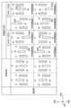
次に、本実施形態の慣性計測装置2000の一例について図20、図21を用いて説明する。図20に示す慣性計測装置2000(IMU:Inertial Measurement Unit)は、自動車やロボットなどの運動体の姿勢や挙動などの慣性運動量を検出する装置である。慣性計測装置2000は、3軸に沿った方向の加速度ax、ay、azを検出する加速度センサーと、3軸回りの角速度ωx,ωy,ωzを検出する角速度センサーと、を備えた、いわゆる6軸モーションセンサーである。3. Inertial Measurement Device Next, an example of the
慣性計測装置2000は、平面形状が略正方形の直方体である。また正方形の対角線方向に位置する2ヶ所の頂点近傍に、マウント部としてのネジ穴2110が形成されている。この2ヶ所のネジ穴2110に2本のネジを通して、自動車などの被装着体の被装着面に慣性計測装置2000を固定することができる。なお、部品の選定や設計変更により、例えば、スマートフォンやデジタルカメラに搭載可能なサイズに小型化することも可能である。 The
慣性計測装置2000は、アウターケース2100と、接合部材2200と、センサーモジュール2300を有し、アウターケース2100の内部に、接合部材2200を介在させて、センサーモジュール2300を挿入した構成となっている。センサーモジュール2300は、インナーケース2310と回路基板2320を有している。インナーケース2310には、回路基板2320との接触を防止するための凹部2311や、後述するコネクター2330を露出させるための開口2312が形成されている。そしてインナーケース2310の下面には、接着剤を介して回路基板2320が接合されている。 The
図21に示すように、回路基板2320の上面には、コネクター2330、Z軸回りの角速度を検出する角速度センサー2340z、X軸、Y軸及びZ軸の各軸方向の加速度を検出する加速度センサーユニット2350などが実装されている。また回路基板2320の側面には、X軸回りの角速度を検出する角速度センサー2340x及びY軸回りの角速度を検出する角速度センサー2340yが実装されている。 As shown in FIG. 21, on the top surface of the
加速度センサーユニット2350は、前述したZ軸方向の加速度を測定するための物理量センサー1を少なくとも含み、必要に応じて、一軸方向の加速度を検出したり、二軸方向や三軸方向の加速度を検出したりすることができる。なお角速度センサー2340x、2340y、2340zとしては、特に限定されないが、例えばコリオリの力を利用した振動ジャイロセンサーを用いることができる。 The
また回路基板2320の下面には、制御IC2360が実装されている。物理量センサー1から出力された検出信号に基づいて制御を行う制御部としての制御IC2360は、例えばMCU(Micro Controller Unit)であり、不揮発性メモリーを含む記憶部や、A/Dコンバーターなどを内蔵しており、慣性計測装置2000の各部を制御する。なお、回路基板2320には、その他にも複数の電子部品が実装されている。 Further, a
以上のように本実施形態の慣性計測装置2000は、物理量センサー1と物理量センサー1から出力された検出信号に基づいて制御を行う制御部としての制御IC2360を含む。この慣性計測装置2000によれば、物理量センサー1を含む加速度センサーユニット2350を用いているため、物理量センサー1の効果を享受でき、高精度化等を実現できる慣性計測装置2000を提供できる。 As described above, the
なお慣性計測装置2000は図20、図21の構成には限定されない。例えば慣性計測装置2000に、角速度センサー2340x、2340y、2340zを設けずに、慣性センサーとして物理量センサー1だけを設ける構成としてもよい。この場合には、例えば物理量センサー1と、制御部を実現する制御IC2360を、収容容器であるパッケージに収容することで慣性計測装置2000を実現すればよい。 Note that the
以上に説明したように本実施形態の物理量センサーは、固定部と支持梁と可動体と第1固定電極群と第2固定電極群とを含む。固定部は基板に固定され、支持梁は固定部に一端が接続され、第2方向に沿って設けられ、可動体は支持梁の他端に接続される。第1固定電極群は基板に設けられ、支持梁の第1方向に配置され、第2固定電極群は基板に設けられ、支持梁の第1方向の反対方向である第4方向に配置される。可動体は、第1連結部と第1基部と第1可動電極群と第2連結部と第2基部と第2可動電極群と質量部とを有する。第1連結部は支持梁の他端に接続され、支持梁から第1方向に延びる。第1基部は第1連結部に接続され、第2方向に沿って設けられる。第1可動電極群は第1基部に設けられ、第1固定電極群と第2方向において対向する。第2連結部は支持梁の他端に接続され、支持梁から第4方向に延びる。第2基部は第2連結部に接続され、第2方向に沿って設けられる。第2可動電極群は第2基部に設けられ、第2固定電極群と第2方向において対向する。質量部は第1連結部に接続され、第1可動電極群の第1方向側に設けられる。 As described above, the physical quantity sensor of this embodiment includes a fixed part, a support beam, a movable body, a first fixed electrode group, and a second fixed electrode group. The fixed part is fixed to the substrate, one end of the support beam is connected to the fixed part and is provided along the second direction, and the movable body is connected to the other end of the support beam. The first fixed electrode group is provided on the substrate and arranged in the first direction of the support beam, and the second fixed electrode group is provided on the substrate and arranged in the fourth direction opposite to the first direction of the support beam. . The movable body includes a first connecting portion, a first base, a first movable electrode group, a second connecting portion, a second base, a second movable electrode group, and a mass portion. The first connecting portion is connected to the other end of the support beam and extends from the support beam in the first direction. The first base portion is connected to the first connecting portion and is provided along the second direction. The first movable electrode group is provided on the first base and faces the first fixed electrode group in the second direction. The second connecting portion is connected to the other end of the support beam and extends from the support beam in the fourth direction. The second base portion is connected to the second connection portion and is provided along the second direction. The second movable electrode group is provided on the second base and faces the second fixed electrode group in the second direction. The mass part is connected to the first connecting part and provided on the first direction side of the first movable electrode group.
本実施形態によれば、第3方向の加速度に対して、可動体は、支持梁が捻れることで支持梁を回転軸として揺動運動を行うことができる。そして、可動体の揺動運動により、第1固定電極群と第1可動電極群の対向面積が変化し、第2固定電極群と第2可動電極群の対向面積も変化する。従って、プローブ電極間の対向面積の変化に基づいて、物理量の変化が検出できる。 According to the present embodiment, in response to acceleration in the third direction, the movable body can perform a rocking motion using the support beam as a rotation axis by twisting the support beam. Then, due to the rocking motion of the movable body, the facing area of the first fixed electrode group and the first movable electrode group changes, and the facing area of the second fixed electrode group and the second movable electrode group also changes. Therefore, a change in the physical quantity can be detected based on a change in the opposing area between the probe electrodes.
また本実施形態では、支持梁は、第2方向を回転軸として捻れる捻れバネである。 Moreover, in this embodiment, the support beam is a torsion spring that twists with the second direction as the rotation axis.
このようにすれば、可動体は第2方向を回転軸として揺動運動をすることができる。 In this way, the movable body can perform rocking motion with the second direction as the rotation axis.
また本実施形態では、可動体の第3方向での重心位置の高さをhmとし、支持梁の回転中心の第3方向での高さをhrとしたとき、hm=hrである。 Further, in this embodiment, when the height of the center of gravity of the movable body in the third direction is hm, and the height of the rotation center of the support beam in the third direction is hr, hm=hr.
このようにすれば、可動体の重心位置の高さhmと支持梁の重心位置の高さhrが等しくなる。このため、第3方向以外の第1方向、第4方向の物理量に対しても、可動体が第3方向に動くようなトルクが発生することはなくなる。従って、物理量センサーの他軸感度を抑制し、高精度な物理量の検出が可能になる。 In this way, the height hm of the center of gravity of the movable body and the height hr of the center of gravity of the support beam become equal. Therefore, torque that would cause the movable body to move in the third direction is not generated even for physical quantities in the first direction and the fourth direction other than the third direction. Therefore, it is possible to suppress the sensitivity of the physical quantity sensor on other axes and to detect the physical quantity with high precision.
また本実施形態では、第1可動電極群、第2可動電極群の第3方向での厚みは、支持梁の第3方向での厚みと等しい。 Further, in this embodiment, the thickness of the first movable electrode group and the second movable electrode group in the third direction is equal to the thickness of the support beam in the third direction.
このようにすれば、第1可動電極群と第2可動電極群の第3方向での厚みが等しくなるため、同一の加工プロセスにおいて一括処理により、これらの電極を形成することが容易になる。 In this way, since the thicknesses of the first movable electrode group and the second movable electrode group in the third direction become equal, it becomes easy to form these electrodes by batch processing in the same processing process.
また本実施形態では、第1基部、第2基部、第1連結部、第2連結部の第3方向での厚みは、支持梁の第3方向での厚みと等しい。 Further, in this embodiment, the thickness of the first base, the second base, the first connecting portion, and the second connecting portion in the third direction is equal to the thickness of the support beam in the third direction.
このようにすれば、支持梁の回転中心の第3方向での高さhrを可動体の重心位置の第3方向での高さhmと等しくすることができる。このため、可動体の回転軸である支持梁から、可動体の重心位置までの位置ベクトルを水平にすることができる。従って、第3方向以外の第1方向、第4方向の加速度が生じた場合に可動体が支持梁を回転軸として揺動することを抑制できる。この場合、可動体は揺動はしないが、第1、4方向への変位は生じるが、各検出部内で対向面積の変化を相殺できるため、検出精度を向上させることができる。 In this way, the height hr of the rotation center of the support beam in the third direction can be made equal to the height hm of the center of gravity of the movable body in the third direction. Therefore, the position vector from the support beam, which is the axis of rotation of the movable body, to the center of gravity of the movable body can be made horizontal. Therefore, when acceleration occurs in the first direction and the fourth direction other than the third direction, it is possible to suppress the movable body from swinging about the support beam as the rotation axis. In this case, the movable body does not swing, but is displaced in the first and fourth directions, but the change in the facing area can be canceled out within each detection section, so detection accuracy can be improved.
また本実施形態では、第1可動電極群の第3方向での厚みは、第1固定電極群の第3方向での厚みよりも大きく、第2可動電極群の第3方向での厚みは、第2固定電極群の第3方向での厚みよりも大きい。 Further, in this embodiment, the thickness of the first movable electrode group in the third direction is larger than the thickness of the first fixed electrode group in the third direction, and the thickness of the second movable electrode group in the third direction is It is larger than the thickness of the second fixed electrode group in the third direction.
このようにすれば、第3方向の加速度が生じた場合、第1固定電極群と第1可動電極群の対向面積が維持され、第2固定電極群と第2可動電極群の対向面積が減少するため、第3方向の物理量の変化を検出できる。また第5方向の加速度が生じた場合、第2固定電極群と第2可動電極群の対向面積が維持され、第1固定電極群と第1可動電極群の対向面積が減少するため、第5方向の物理量の変化を検出できる。 In this way, when acceleration occurs in the third direction, the facing area of the first fixed electrode group and the first movable electrode group is maintained, and the facing area of the second fixed electrode group and the second movable electrode group is reduced. Therefore, changes in physical quantities in the third direction can be detected. Further, when acceleration in the fifth direction occurs, the facing area of the second fixed electrode group and the second movable electrode group is maintained, and the facing area of the first fixed electrode group and the first movable electrode group decreases. Changes in physical quantities in direction can be detected.
また本実施形態では、第1可動電極群の第3方向での厚みは、第1固定電極群の第3方向での厚みよりも小さく、第2可動電極群の第3方向での厚みは、第2固定電極群の第3方向での厚みよりも小さい。 Further, in this embodiment, the thickness of the first movable electrode group in the third direction is smaller than the thickness of the first fixed electrode group in the third direction, and the thickness of the second movable electrode group in the third direction is It is smaller than the thickness of the second fixed electrode group in the third direction.
このようにすれば、第3方向の加速度が生じた場合、第2固定電極群と第2可動電極群の対向面積が維持され、第1固定電極群と第1可動電極群の対向面積が減少するため、第3方向の物理量の変化を検出できる。また第5方向DR5の加速度が生じた場合、第1固定電極群と第1可動電極群の対向面積が維持され、第2固定電極群と第2可動電極群の対向面積が減少するため、第5方向の物理量の変化を検出できる。 In this way, when acceleration in the third direction occurs, the facing area of the second fixed electrode group and the second movable electrode group is maintained, and the facing area of the first fixed electrode group and the first movable electrode group is reduced. Therefore, changes in physical quantities in the third direction can be detected. Further, when acceleration in the fifth direction DR5 occurs, the facing area of the first fixed electrode group and the first movable electrode group is maintained, and the facing area of the second fixed electrode group and the second movable electrode group decreases. Changes in physical quantities in five directions can be detected.
また本実施形態では、初期状態において第1可動電極群と第1固定電極群の裏面側の位置が一致し、初期状態において第2可動電極群と第2固定電極群の裏面側の位置が一致する。 In addition, in this embodiment, the positions of the back side of the first movable electrode group and the first fixed electrode group match in the initial state, and the positions of the back side of the second movable electrode group and the second fixed electrode group match in the initial state. do.
このようにすれば、第1可動電極群、第1固定電極群、第2可動電極群及び第2固定電極群の電極材料の成膜したあと、同一の加工プロセスで一括して櫛歯電極を形成することができ、製造プロセスが容易になる。 In this way, after forming the electrode materials of the first movable electrode group, the first fixed electrode group, the second movable electrode group, and the second fixed electrode group, the comb-teeth electrodes can be formed all at once in the same processing process. can be formed, which simplifies the manufacturing process.
即ち、本実施形態では、物理センサーは第3固定電極群と第4固定電極群を含む。可動体は第3連結部と第3基部と第3可動電極群と第4連結部と第4基部と第4可動電極群と、を含む。第3連結部は支持梁の他端に接続され、支持梁から第1方向に延びる。第3基部は第3連結部に接続され、第2方向に沿って設けられる。第3可動電極群は第3基部に設けられ、第3固定電極群と第2方向において対向する。第4連結部は支持梁の他端に接続され、支持梁から第4方向に延びる。第4基部は第4連結部に接続され、第2方向に沿って設けられる。第4可動電極群は第4基部に設けられ、第4固定電極群と第2方向において対向する。 That is, in this embodiment, the physical sensor includes a third fixed electrode group and a fourth fixed electrode group. The movable body includes a third connecting portion, a third base, a third movable electrode group, a fourth connecting portion, a fourth base, and a fourth movable electrode group. The third connecting portion is connected to the other end of the support beam and extends from the support beam in the first direction. The third base portion is connected to the third connecting portion and is provided along the second direction. The third movable electrode group is provided on the third base and faces the third fixed electrode group in the second direction. The fourth connecting portion is connected to the other end of the support beam and extends in the fourth direction from the support beam. The fourth base is connected to the fourth connection and is provided along the second direction. The fourth movable electrode group is provided on the fourth base and faces the fourth fixed electrode group in the second direction.
このようにすれば、平面視において支持梁を含む回転軸の両側で可動のプローブ電極の第3方向の表面が面一にすることができ、製造プロセスを容易化できる。 In this way, the surfaces in the third direction of the movable probe electrodes on both sides of the rotation axis including the support beam can be made flush with each other in plan view, and the manufacturing process can be facilitated.
本実施形態では、第1可動電極群と第3可動電極群の第3方向での厚みが異なり、第2可動電極群と第4可動電極群の第3方向での厚みが異なる。 In this embodiment, the first movable electrode group and the third movable electrode group have different thicknesses in the third direction, and the second movable electrode group and the fourth movable electrode group have different thicknesses in the third direction.
このようにすれば、プローブ電極の第3方向での厚みの異なる検出部を設ける際に多様な配置パターンを選択できる。 In this way, various arrangement patterns can be selected when providing detection parts having different thicknesses in the third direction of the probe electrode.
また本実施形態は、物理量センサーから出力された検出信号に基づいて制御を行う制御部と、を含む慣性計測装置に関係する。 The present embodiment also relates to an inertial measurement device including a control section that performs control based on a detection signal output from a physical quantity sensor.
なお、上記のように本実施形態について詳細に説明したが、本開示の新規事項及び効果から実体的に逸脱しない多くの変形が可能であることは当業者には容易に理解できるであろう。従って、このような変形例はすべて本開示の範囲に含まれるものとする。例えば、明細書又は図面において、少なくとも一度、より広義または同義な異なる用語と共に記載された用語は、明細書又は図面のいかなる箇所においても、その異なる用語に置き換えることができる。また本実施形態及び変形例の全ての組み合わせも、本開示の範囲に含まれる。また物理量センサー、慣性計測装置の構成・動作等も本実施形態で説明したものに限定されず、種々の変形実施が可能である。 Although the present embodiment has been described in detail as above, those skilled in the art will easily understand that many modifications can be made without substantively departing from the novelty and effects of the present disclosure. Therefore, all such modifications are intended to be included within the scope of the present disclosure. For example, a term that appears at least once in the specification or drawings together with a different term with a broader or synonymous meaning may be replaced by that different term anywhere in the specification or drawings. Furthermore, all combinations of this embodiment and modifications are also included within the scope of the present disclosure. Furthermore, the configuration and operation of the physical quantity sensor and the inertial measurement device are not limited to those described in this embodiment, and various modifications are possible.
1…物理量センサー、2…基板、10…第1固定電極群、10A…第1固定電極群、10B…第3固定電極群、11…第1固定電極、11A…第1固定電極、11B…第3固定電極、12…第1固定電極、12A…第1固定電極、12B…第3固定電極、14…第1固定電極、20…第1可動電極群、20A…第1可動電極群、20B…第3可動電極群、21…第1可動電極、21A…第1可動電極、21B…第3可動電極、22…第1可動電極、22A…第1可動電極、22B…第3可動電極、23…第1基部、23A…第1基部、23B…第3基部、24…第1可動電極、30…第1連結部、30A…第1連結部、30B…第3連結部、40…固定部、40A…固定部、40B…固定部、42…支持梁、42A…支持梁、42B…支持梁、50…第2固定電極群、50A…第2固定電極群、50B…第4固定電極群、51…第2固定電極、51A…第2固定電極、51B…第4固定電極、52…第2固定電極、52A…第2固定電極、52B…第4固定電極、54…第2固定電極、60…第2可動電極群、60A…第2可動電極群、60B…第4可動電極群、61…第2可動電極、61A…第2可動電極、61B…第4可動電極、62…第2可動電極、62A…第2可動電極、62B…第4可動電極、63…第2基部、63A…第2基部、63B…第4基部、64…第2可動電極、70…第2連結部、70A…第2連結部、70B…第4連結部、2000…慣性計測装置、2100…アウターケース、2110…ネジ穴、2200…接合部材、2300…センサーモジュール、2310…インナーケース、2311…凹部、2312…開口、2320…回路基板、2330…コネクター、2340x…角速度センサー、2340y…角速度センサー、2340z…角速度センサー、2350…加速度センサーユニット、DR3…第3方向、DR1…第1方向、DR2…第2方向、DR3…第3方向、DR4…第4方向、DR5…第5方向、FI…慣性力、GZ1…重心位置、GZ2…重心位置、Gm…重心位置、Gr…重心位置、IC2360…制御、MB…可動体、MP…質量部、MPA…質量部、MPB…質量部、O…原点、T…トルク、Z1…検出部、Z1'…検出部、Z2…検出部、Z2'…検出部、ax…加速度、ay…加速度、az…加速度、hm…高さ、hr…高さ、rZ1…位置ベクトル、rZ2…位置ベクトル、rm…位置ベクトル、θ…角度、ωx…角速度DESCRIPTION OF
Claims (12)
Translated fromJapanese基板に固定された固定部と、
前記固定部に一端が接続され、前記第2方向に沿って設けられる支持梁と、
前記支持梁の他端に接続された可動体と、
前記基板に設けられ、前記支持梁の前記第1方向に配置される第1固定電極群と、
前記基板に設けられ、前記支持梁の前記第1方向の反対方向である第4方向に配置される第2固定電極群と、
を含み、
前記可動体は、
前記支持梁の他端に接続され、前記支持梁から前記第1方向に延びる第1連結部と、
前記第1連結部に接続され、前記第2方向に沿って設けられる第1基部と、
前記第1基部に設けられ、前記第1固定電極群と前記第2方向において対向する第1可動電極群と、
前記支持梁の他端に接続され、前記支持梁から前記第4方向に延びる第2連結部と、
前記第2連結部に接続され、前記第2方向に沿って設けられる第2基部と、
前記第2基部に設けられ、前記第2固定電極群と前記第2方向において対向する第2可動電極群と、
前記第1連結部に接続され、前記第1可動電極群の前記第1方向側に設けられる質量部と、
を有することを特徴とする物理量センサー。A physical quantity sensor that detects a physical quantity in the third direction when three directions perpendicular to each other are a first direction, a second direction, and a third direction,
A fixed part fixed to the board,
a support beam having one end connected to the fixed part and provided along the second direction;
a movable body connected to the other end of the support beam;
a first fixed electrode group provided on the substrate and arranged in the first direction of the support beam;
a second fixed electrode group provided on the substrate and arranged in a fourth direction of the support beam that is opposite to the first direction;
including;
The movable body is
a first connecting portion connected to the other end of the support beam and extending from the support beam in the first direction;
a first base connected to the first connecting portion and provided along the second direction;
a first movable electrode group provided on the first base and facing the first fixed electrode group in the second direction;
a second connecting portion connected to the other end of the support beam and extending from the support beam in the fourth direction;
a second base connected to the second connecting portion and provided along the second direction;
a second movable electrode group provided on the second base and facing the second fixed electrode group in the second direction;
a mass part connected to the first connecting part and provided on the first direction side of the first movable electrode group;
A physical quantity sensor characterized by having.
前記質量部は、前記第1可動電極群の前記第1方向側において、前記第1連結部から前記第2方向に沿って延びることを特徴とする物理量センサー。The physical quantity sensor according to claim 1,
The physical quantity sensor is characterized in that the mass part extends along the second direction from the first connecting part on the first direction side of the first movable electrode group.
前記可動体の前記第3方向での重心位置の高さをhmとし、前記支持梁の回転中心の前記第3方向での高さをhrとしたとき、hm=hrであることを特徴とする物理量センサー。The physical quantity sensor according to claim 1,
When the height of the center of gravity of the movable body in the third direction is hm, and the height of the rotation center of the support beam in the third direction is hr, hm=hr. Physical quantity sensor.
前記第1可動電極群、前記第2可動電極群の前記第3方向での厚みは、前記支持梁の前記第3方向での厚みと等しいことを特徴とする物理量センサー。The physical quantity sensor according to any one of claims 1 to 3,
A physical quantity sensor, wherein the thickness of the first movable electrode group and the second movable electrode group in the third direction is equal to the thickness of the support beam in the third direction.
前記第1基部、前記第2基部、前記第1連結部、前記第2連結部の前記第3方向での厚みは、前記支持梁の前記第3方向での厚みと等しいことを特徴とする物理量センサー。In the physical quantity sensor according to claim 4,
A physical quantity characterized in that the thickness of the first base, the second base, the first connecting portion, and the second connecting portion in the third direction is equal to the thickness of the support beam in the third direction. sensor.
前記第1可動電極群の前記第3方向での厚みは、前記第1固定電極群の前記第3方向での厚みよりも大きく、
前記第2可動電極群の前記第3方向での厚みは、前記第2固定電極群の前記第3方向での厚みよりも大きいことを特徴とする物理量センサー。The physical quantity sensor according to any one of claims 1 to 3,
The thickness of the first movable electrode group in the third direction is greater than the thickness of the first fixed electrode group in the third direction,
A physical quantity sensor, wherein a thickness of the second movable electrode group in the third direction is larger than a thickness of the second fixed electrode group in the third direction.
前記第1可動電極群の前記第3方向での厚みは、前記第1固定電極群の前記第3方向での厚みよりも小さく、
前記第2可動電極群の前記第3方向での厚みは、前記第2固定電極群の前記第3方向での厚みよりも小さいことを特徴とする物理量センサー。The physical quantity sensor according to any one of claims 1 to 3,
The thickness of the first movable electrode group in the third direction is smaller than the thickness of the first fixed electrode group in the third direction,
A physical quantity sensor, wherein a thickness of the second movable electrode group in the third direction is smaller than a thickness of the second fixed electrode group in the third direction.
初期状態において前記第1可動電極群と前記第1固定電極群の裏面側の位置が一致し、
前記初期状態において前記第2可動電極群と前記第2固定電極群の裏面側の位置が一致することを特徴とする物理量センサー。The physical quantity sensor according to claim 6,
In an initial state, the positions of the back surfaces of the first movable electrode group and the first fixed electrode group match,
A physical quantity sensor characterized in that, in the initial state, the positions of the second movable electrode group and the second fixed electrode group on the back surface sides match.
前記物理量センサーは第3固定電極群と第4固定電極群を含み、
前記可動体は、
前記支持梁の他端に接続され、前記支持梁から前記第1方向に延びる第3連結部と、
前記第3連結部に接続され、前記第2方向に沿って設けられる第3基部と、
前記第3基部に設けられ、前記第3固定電極群と前記第2方向において対向する第3可動電極群と、
前記支持梁の他端に接続され、前記支持梁から前記第4方向に延びる第4連結部と、
前記第4連結部に接続され、前記第2方向に沿って設けられる第4基部と、
前記第4基部に設けられ、前記第4固定電極群と前記第2方向において対向する第4可動電極群と、
を含むことを特徴とする物理量センサー。The physical quantity sensor according to any one of claims 1 to 3,
The physical quantity sensor includes a third fixed electrode group and a fourth fixed electrode group,
The movable body is
a third connecting portion connected to the other end of the support beam and extending from the support beam in the first direction;
a third base connected to the third connecting portion and provided along the second direction;
a third movable electrode group provided on the third base and facing the third fixed electrode group in the second direction;
a fourth connecting portion connected to the other end of the support beam and extending from the support beam in the fourth direction;
a fourth base connected to the fourth connecting portion and provided along the second direction;
a fourth movable electrode group provided on the fourth base and facing the fourth fixed electrode group in the second direction;
A physical quantity sensor comprising:
前記第1可動電極群と前記第3可動電極群の前記第3方向での厚みが異なり、
前記第2可動電極群と前記第4可動電極群の前記第3方向での厚みが異なることを特徴とする物理量センサー。The physical quantity sensor according to claim 9,
The first movable electrode group and the third movable electrode group have different thicknesses in the third direction,
A physical quantity sensor, wherein the second movable electrode group and the fourth movable electrode group have different thicknesses in the third direction.
前記支持梁は、前記第2方向を回転軸として捻れる捻れバネであることを特徴とする物理量センサー。The physical quantity sensor according to any one of claims 1 to 3,
The physical quantity sensor is characterized in that the support beam is a torsion spring that twists about the second direction as a rotation axis.
前記物理量センサーから出力された検出信号に基づいて制御を行う制御部と、
を含むことを特徴とする慣性計測装置。The physical quantity sensor according to any one of claims 1 to 3,
a control unit that performs control based on a detection signal output from the physical quantity sensor;
An inertial measurement device comprising:
Priority Applications (3)
| Application Number | Priority Date | Filing Date | Title |
|---|---|---|---|
| JP2022104309AJP2024004613A (en) | 2022-06-29 | 2022-06-29 | Physical quantity sensors and inertial measurement devices |
| US18/343,025US20240003935A1 (en) | 2022-06-29 | 2023-06-28 | Physical Quantity Sensor And Inertial Measurement Unit |
| CN202310777470.8ACN117310207A (en) | 2022-06-29 | 2023-06-28 | Physical quantity sensor and inertial measurement device |
Applications Claiming Priority (1)
| Application Number | Priority Date | Filing Date | Title |
|---|---|---|---|
| JP2022104309AJP2024004613A (en) | 2022-06-29 | 2022-06-29 | Physical quantity sensors and inertial measurement devices |
Publications (1)
| Publication Number | Publication Date |
|---|---|
| JP2024004613Atrue JP2024004613A (en) | 2024-01-17 |
Family
ID=89261086
Family Applications (1)
| Application Number | Title | Priority Date | Filing Date |
|---|---|---|---|
| JP2022104309APendingJP2024004613A (en) | 2022-06-29 | 2022-06-29 | Physical quantity sensors and inertial measurement devices |
Country Status (3)
| Country | Link |
|---|---|
| US (1) | US20240003935A1 (en) |
| JP (1) | JP2024004613A (en) |
| CN (1) | CN117310207A (en) |
Family Cites Families (3)
| Publication number | Priority date | Publication date | Assignee | Title |
|---|---|---|---|---|
| JP6787304B2 (en)* | 2017-12-19 | 2020-11-18 | セイコーエプソン株式会社 | Physical quantity sensors, composite sensors, inertial measurement units, portable electronic devices, electronic devices, and mobile objects |
| JP7176353B2 (en)* | 2018-10-29 | 2022-11-22 | セイコーエプソン株式会社 | Physical quantity sensors, electronic devices and mobile objects |
| JP7383978B2 (en)* | 2019-10-23 | 2023-11-21 | セイコーエプソン株式会社 | Physical quantity sensors, electronic devices and moving objects |
- 2022
- 2022-06-29JPJP2022104309Apatent/JP2024004613A/enactivePending
- 2023
- 2023-06-28CNCN202310777470.8Apatent/CN117310207A/enactivePending
- 2023-06-28USUS18/343,025patent/US20240003935A1/enactivePending
Also Published As
| Publication number | Publication date |
|---|---|
| US20240003935A1 (en) | 2024-01-04 |
| CN117310207A (en) | 2023-12-29 |
Similar Documents
| Publication | Publication Date | Title |
|---|---|---|
| KR100436367B1 (en) | MEMS gyroscpoe having inertial masses vibrating vertically on a substrate | |
| EP3717400B1 (en) | Asymmetric out-of-plane accelerometer | |
| US7178398B2 (en) | Coplanar proofmasses employable to sense acceleration along three axes | |
| EP3564682B1 (en) | Inertial sensor with single proof mass and multiple sense axis capability | |
| JP2024015689A (en) | Physical quantity sensors and inertial measurement devices | |
| US20230266360A1 (en) | Accelerometer, inertial measurement unit imu, and electronic device | |
| US20230266359A1 (en) | Physical Quantity Sensor And Inertial Measurement Unit | |
| US20250180598A1 (en) | Physical Quantity Sensor And Inertial Measurement Unit | |
| JP2024004613A (en) | Physical quantity sensors and inertial measurement devices | |
| US20230136163A1 (en) | Physical Quantity Sensor and Inertial Measurement Device | |
| JP2024004653A (en) | Physical quantity sensors and inertial measurement devices | |
| JP2023066602A (en) | Physical quantity sensor and inertial measurement device | |
| CN111316062A (en) | Tachometer with a substrate having a main extension plane, method for producing a tachometer | |
| JP2023080591A (en) | Physical quantity sensor, inertial measurement unit, and manufacturing method | |
| US12399010B2 (en) | Physical quantity sensor, inertial measurement unit, and manufacturing method | |
| US20250306056A1 (en) | Physical Quantity Sensor And Inertial Measurement Unit | |
| CN117871897A (en) | Physical quantity sensors and inertial measurement devices | |
| JP2024065388A (en) | MEMS Devices and Inertial Measurement Units | |
| JP2023146375A (en) | Physical quantity sensor and inertial measurement device | |
| JP2025074694A (en) | Physical Quantity Sensors and Inertial Measurement Units | |
| JP2024024821A (en) | Physical quantity sensors and inertial measurement devices | |
| CN117647663A (en) | Inertial sensor | |
| CN116203281A (en) | Physical quantity sensor and inertial measurement device | |
| JP2008261772A (en) | Inertial force sensor |
Legal Events
| Date | Code | Title | Description |
|---|---|---|---|
| A621 | Written request for application examination | Free format text:JAPANESE INTERMEDIATE CODE: A621 Effective date:20250523 |