JP2023500583A - High index waveguide for image transmission using low period outcoupling gratings - Google Patents
High index waveguide for image transmission using low period outcoupling gratingsDownload PDFInfo
- Publication number
- JP2023500583A JP2023500583AJP2022521979AJP2022521979AJP2023500583AJP 2023500583 AJP2023500583 AJP 2023500583AJP 2022521979 AJP2022521979 AJP 2022521979AJP 2022521979 AJP2022521979 AJP 2022521979AJP 2023500583 AJP2023500583 AJP 2023500583A
- Authority
- JP
- Japan
- Prior art keywords
- waveguide
- grating
- image light
- light
- output
- Prior art date
- Legal status (The legal status is an assumption and is not a legal conclusion. Google has not performed a legal analysis and makes no representation as to the accuracy of the status listed.)
- Pending
Links
Images


Classifications
- G—PHYSICS
- G02—OPTICS
- G02B—OPTICAL ELEMENTS, SYSTEMS OR APPARATUS
- G02B5/00—Optical elements other than lenses
- G02B5/18—Diffraction gratings
- G02B5/1809—Diffraction gratings with pitch less than or comparable to the wavelength
- G—PHYSICS
- G02—OPTICS
- G02B—OPTICAL ELEMENTS, SYSTEMS OR APPARATUS
- G02B27/00—Optical systems or apparatus not provided for by any of the groups G02B1/00 - G02B26/00, G02B30/00
- G02B27/0093—Optical systems or apparatus not provided for by any of the groups G02B1/00 - G02B26/00, G02B30/00 with means for monitoring data relating to the user, e.g. head-tracking, eye-tracking
- G—PHYSICS
- G02—OPTICS
- G02B—OPTICAL ELEMENTS, SYSTEMS OR APPARATUS
- G02B27/00—Optical systems or apparatus not provided for by any of the groups G02B1/00 - G02B26/00, G02B30/00
- G02B27/01—Head-up displays
- G02B27/017—Head mounted
- G02B27/0172—Head mounted characterised by optical features
- G—PHYSICS
- G02—OPTICS
- G02B—OPTICAL ELEMENTS, SYSTEMS OR APPARATUS
- G02B27/00—Optical systems or apparatus not provided for by any of the groups G02B1/00 - G02B26/00, G02B30/00
- G02B27/10—Beam splitting or combining systems
- G02B27/1006—Beam splitting or combining systems for splitting or combining different wavelengths
- G—PHYSICS
- G02—OPTICS
- G02B—OPTICAL ELEMENTS, SYSTEMS OR APPARATUS
- G02B27/00—Optical systems or apparatus not provided for by any of the groups G02B1/00 - G02B26/00, G02B30/00
- G02B27/42—Diffraction optics, i.e. systems including a diffractive element being designed for providing a diffractive effect
- G02B27/4233—Diffraction optics, i.e. systems including a diffractive element being designed for providing a diffractive effect having a diffractive element [DOE] contributing to a non-imaging application
- G02B27/4244—Diffraction optics, i.e. systems including a diffractive element being designed for providing a diffractive effect having a diffractive element [DOE] contributing to a non-imaging application in wavelength selecting devices
- G—PHYSICS
- G02—OPTICS
- G02B—OPTICAL ELEMENTS, SYSTEMS OR APPARATUS
- G02B5/00—Optical elements other than lenses
- G02B5/18—Diffraction gratings
- G02B5/1828—Diffraction gratings having means for producing variable diffraction
- G—PHYSICS
- G02—OPTICS
- G02B—OPTICAL ELEMENTS, SYSTEMS OR APPARATUS
- G02B27/00—Optical systems or apparatus not provided for by any of the groups G02B1/00 - G02B26/00, G02B30/00
- G02B27/01—Head-up displays
- G02B27/0101—Head-up displays characterised by optical features
- G02B2027/0138—Head-up displays characterised by optical features comprising image capture systems, e.g. camera
- G—PHYSICS
- G02—OPTICS
- G02B—OPTICAL ELEMENTS, SYSTEMS OR APPARATUS
- G02B27/00—Optical systems or apparatus not provided for by any of the groups G02B1/00 - G02B26/00, G02B30/00
- G02B27/01—Head-up displays
- G02B27/0101—Head-up displays characterised by optical features
- G02B2027/014—Head-up displays characterised by optical features comprising information/image processing systems
- G—PHYSICS
- G02—OPTICS
- G02B—OPTICAL ELEMENTS, SYSTEMS OR APPARATUS
- G02B27/00—Optical systems or apparatus not provided for by any of the groups G02B1/00 - G02B26/00, G02B30/00
- G02B27/01—Head-up displays
- G02B27/017—Head mounted
- G02B2027/0178—Eyeglass type
Landscapes
- Physics & Mathematics (AREA)
- General Physics & Mathematics (AREA)
- Optics & Photonics (AREA)
- Spectroscopy & Molecular Physics (AREA)
- Optical Couplings Of Light Guides (AREA)
- Diffracting Gratings Or Hologram Optical Elements (AREA)
Abstract
Translated fromJapanese
Description
Translated fromJapanese本開示は、一般的には、光学ディスプレイシステムおよびデバイスに関し、特に、導波路ディスプレイ、および、それらの導波路ディスプレイのための構成要素に関する。 TECHNICAL FIELD This disclosure relates generally to optical display systems and devices, and more particularly to waveguide displays and components for those waveguide displays.
ヘッドマウントディスプレイ(HMD)、ヘルメットマウントディスプレイ、ニアアイディスプレイ(NED)などは、仮想現実(VR)コンテンツ、拡張現実(AR)コンテンツ、複合現実(MR)コンテンツなどを表示するためにますます使用されている。そのようなディスプレイは、ほんの数例を挙げると、娯楽、教育、訓練、およびバイオメディカルサイエンスを含む、多様な分野において用途が見出されている。表示されるVR/AR/MRコンテンツは、体験を向上させ、仮想オブジェクトをユーザが観察する実際のオブジェクトに調和させるために、3次元(3D)であり得る。目の位置および視線方向、ならびに/またはユーザの向きをリアルタイムで追跡することができ、表示される映像を、ユーザの頭部の向きおよび視線方向に応じて動的に調整することができ、シミュレートまたは拡張された環境に没頭する、よりよい体験を可能にする。 Head-mounted displays (HMDs), helmet-mounted displays, near-eye displays (NEDs), etc. are increasingly used to display virtual reality (VR) content, augmented reality (AR) content, mixed reality (MR) content, etc. ing. Such displays find application in a variety of fields, including entertainment, education, training, and biomedical science, to name just a few. The displayed VR/AR/MR content can be three-dimensional (3D) to enhance the experience and blend the virtual objects with the real objects observed by the user. The position and gaze direction of the eyes and/or the orientation of the user can be tracked in real time, the displayed image can be dynamically adjusted according to the user's head orientation and gaze direction, and the simulated enable a better experience of being immersed in a virtual or augmented environment.
コンパクトなディスプレイデバイスが、ヘッドマウントディスプレイには望まれる。HMDまたはNEDのディスプレイは通常、ユーザの頭部上で着用されるので、大きい、嵩張る、不均衡な、および/または、重いディスプレイデバイスは、扱いにくいことになり、ユーザが着用するのに心地よくないものであり得る。 A compact display device is desired for a head mounted display. Since HMD or NED displays are typically worn on the user's head, large, bulky, disproportionate and/or heavy display devices can be cumbersome and uncomfortable for the user to wear. can be
プロジェクタベースのディスプレイは、介在するスクリーンまたはディスプレイパネルなしに、直接的にユーザの目により観察され得る角領域における画像を提供する。イメージング導波路が、角領域における画像を、ユーザの目に搬送するために使用され得る。プロジェクタディスプレイにおいてスクリーンまたはディスプレイパネルがないため、ディスプレイのサイズおよび重量を減らすことができる。 Projector-based displays provide images in corner regions that can be viewed directly by the user's eyes without an intervening screen or display panel. An imaging waveguide may be used to convey the image in the corner region to the user's eye. Since there is no screen or display panel in the projector display, the size and weight of the display can be reduced.
本発明の第1の態様によれば、画像光源からの画像光を、角度範囲Γに及ぶターゲット視野(FOV)を伴うアイボックスに伝達するための導波路であって、全内部反射により導波路内で画像光を伝搬させるための基材と、基材により支持され、画像光を導波路内へとカップリングするように構成される入力カプラと、基材により支持され、アイボックスの方に伝搬させるために画像光を導波路の外にカップリングするように構成される出力カプラとを含み、出力カプラが、
一部の実施形態において、
基材は、少なくとも2.3の屈折率を有し得る。 The substrate may have a refractive index of at least 2.3.
出力カプラは、第1の出力格子と協働して画像光を導波路の外に回折させるように構成される第2の出力格子をさらに含み得、第2の出力格子は、p1を超えないピッチp2を有し得る。The output coupler may further include a second output grating configured to cooperate with thefirst output grating to diffract the image light out of the waveguide, the second output grating exceeding p1. can have a pitch p2 that is not
入力カプラは、p1を超えないピッチp0を有する入力格子を含み得る。代替案として、または追加として、第1の出力格子および第2の出力格子は、導波路への入射の角度に等しい出力角度において画像光を導波路の外に回折するために協働し得る。代替案として、または追加として、第1の出力格子および第2の出力格子は、導波路の反対位置関係の面において配され得る。The input coupler may include an input grating witha pitchp0 not exceeding p1. Alternatively or additionally, the first output grating and the second output grating may cooperate to diffract the image light out of the waveguide at an output angle equal to the angle of incidence on the waveguide. Alternatively or additionally, the first output grating and the second output grating may be arranged on opposite sides of the waveguide.
導波路は、赤色(R)チャネルおよび緑色(G)チャネルのうちの少なくとも1つをアイボックスに伝達するように構成され得る。代替案として、または追加として、λは450nm以下であり得る。 A waveguide may be configured to transmit at least one of a red (R) channel and a green (G) channel to the eyebox. Alternatively or additionally, λ may be 450 nm or less.
一部の実施形態において、p1≦300nmである。In some embodiments, p1 ≦300 nm.
アイボックスは、第1の方向において長さ2aにわたって広がり得る。第1の出力格子は、第1の方向において長さ2bにわたって広がり得、アイボックスから距離dにおいて配され得る。ピッチp1は、
出力カプラは、第1の出力格子と協働して、画像光の入力カプラへの入射角度に等しい出力角度において画像光を導波路の外に回折するように構成される第2の出力格子をさらに含み得、第2の出力格子は、p1を超えないピッチを有する。The output coupler has a second output grating configured to cooperate with the first output grating to diffract the image light out of the waveguide at an output angle equal to the angle of incidence of the image light on the input coupler. Further may be included, the second output grating havinga pitch not exceeding p1.
導波路は、画像光の赤色チャネルまたは画像光の緑色チャネルのうちの少なくとも1つをアイボックスに伝達するように構成され得る。 The waveguide may be configured to transmit at least one of the red channel of image light or the green channel of image light to the eyebox.
一部の実施形態において、λ≦500nmであり、導波路は、600nm以上の波長を伴う画像光の赤色チャネルをアイボックスに伝達するように構成され得る。 In some embodiments, λ≦500 nm, and the waveguide can be configured to transmit the red channel of image light with wavelengths of 600 nm or greater to the eyebox.
本発明の第2の態様によれば、複数の色チャネルを含む画像光を放出するように構成される光源と、光源に光学的に結合され、光源からの画像光の一部分を角度範囲Γに及ぶターゲット視野(FOV)内のアイボックスに伝達するように構成される第1の態様の導波路とを含む、ニアアイディスプレイ(NED)デバイスが提供される。 According to a second aspect of the invention, a light source configured to emit image light comprising a plurality of color channels, and optically coupled to the light source to direct a portion of the image light from the light source into an angular range Γ A near-eye display (NED) device is provided comprising: a waveguide of the first aspect configured to communicate to an eyebox within a target field-of-view (FOV).
デバイスは、導波路を含む導波路積重体を含み得る。導波路積重体の各々の導波路は、最大でp1のピッチを伴う出力格子を含み得る。The device may include a waveguide stack that includes waveguides. Each waveguide of the waveguide stack may include an output grating witha pitch of at most p1.
本発明の第3の態様によれば、画像光源からの複数の色チャネルを含む画像光をアイボックスに伝達するための導波路であって、全内部反射により導波路内で画像光を伝搬させるための基材と、画像光を受け取るために基材により支持される入力カプラと、画像光を導波路の外にアイボックスの方にカップリングするために基材により支持される出力カプラとを含み、出力カプラが、300nmを超えないピッチpを有する第1の出力格子を含む、導波路が提供される。 According to a third aspect of the invention, there is provided a waveguide for communicating image light comprising multiple color channels from an image source to an eyebox, wherein the image light propagates within the waveguide by total internal reflection. an input coupler supported by the substrate for receiving the image light; and an output coupler supported by the substrate for coupling the image light out of the waveguide towards the eyebox. A waveguide is provided, wherein the output coupler includes a first output grating having a pitch p not exceeding 300 nm.
基材は、少なくとも2.3の屈折の率を有し得る。好ましくは、導波路は、画像光の赤色(R)チャネルおよび画像光の緑色(G)チャネルのうちの少なくとも1つをアイボックスに伝達するように構成される。 The substrate can have an index of refraction of at least 2.3. Preferably, the waveguide is configured to transmit at least one of a red (R) channel of image light and a green (G) channel of image light to the eyebox.
本明細書において開示される実施形態は、類する要素が類する参照番号によって指示される、それらの実施形態の例示的な実施形態を表す、添付図面を参照して、より詳細に説明されることになる。 The embodiments disclosed herein will now be described in more detail with reference to the accompanying drawings, which represent exemplary embodiments thereof, in which like elements are indicated by like reference numerals. Become.
後に続く説明において、限定ではなく解説の目的のために、本発明の綿密な理解をもたらすために、個別の光学および電子回路、光学および電子構成要素、技法、その他などの、特定の詳細が論述される。しかしながら、本発明は、これらの特定の詳細から外れる他の実施形態において実践され得ることが、当業者に明らかであることになる。他の実例において、よく知られている方法、デバイス、および回路の詳細な説明は、例示的な実施形態の説明を分かりにくくしないように省略される。原理、態様、および実施形態、ならびに無論のこととして、それらの特定の例を詳述する、本明細書におけるすべての説述は、先述の原理、態様、および実施形態、ならびに、それらの特定の例の、構造的均等物および機能的均等物の両方を網羅することが意図される。加えて、そのような均等物は、現時に知られている均等物、および無論のこととして、将来において開発される均等物の両方、すなわち、構造を問わず同じ機能を遂行する、開発される任意の要素を含むことが意図される。 In the description that follows, for purposes of explanation and not limitation, specific details such as individual optical and electronic circuits, optical and electronic components, techniques, etc. are discussed in order to provide a thorough understanding of the present invention. be done. However, it will be apparent to one skilled in the art that the present invention may be practiced in other embodiments that depart from these specific details. In other instances, detailed descriptions of well-known methods, devices, and circuits are omitted so as not to obscure the description of the example embodiments. All statements herein reciting principles, aspects and embodiments, as well as specific examples thereof, may be interpreted as It is intended to cover both structural and functional equivalents of the examples. In addition, such equivalents are both presently known equivalents and, of course, in the future developed equivalents, i. It is intended to include any element.
本明細書において使用される際、用語「第1の」、「第2の」、等々は、明示的に説述されない限り、順次的な順序付けを含意することが意図されるのではなく、むしろ、1つの要素を別のものから区別することが意図されることに留意されたい。同様に、方法またはプロセスステップの順次的な順序付けは、明示的に説述されない限り、それらのステップの実行の順次的な順序を含意しない。 As used herein, the terms "first", "second", etc. are not intended to imply a sequential ordering, but rather , is intended to distinguish one element from another. Similarly, a sequential ordering of method or process steps does not imply a sequential order of performance of those steps unless explicitly stated.
さらにまた、後に続く略称および頭字語が、本文書において使用され得る:HMD(ヘッドマウントディスプレイ)、NED(ニアアイディスプレイ)、VR(仮想現実)、AR(拡張現実)、MR(複合現実)、LED(発光ダイオード)、FOV(視野)、TIR(全内部反射)。用語「NED」および「HMD」は、本明細書において互換的に使用され得る。 Furthermore, the following abbreviations and acronyms may be used in this document: HMD (Head Mounted Display), NED (Near Eye Display), VR (Virtual Reality), AR (Augmented Reality), MR (Mixed Reality), LED (Light Emitting Diode), FOV (Field of View), TIR (Total Internal Reflection). The terms "NED" and "HMD" may be used interchangeably herein.
例示的な実施形態が、3つの別個の色チャネルから成り立つ多色光を参照して、本明細書において下記で説明され得る。最も短い波長を伴う色チャネルは、青(B)チャネルまたは色と呼称され得、RGB色体系の青チャネルを表し得る。最も長い波長を伴う色チャネルは、赤(R)チャネルまたは色と呼称され得、RGB色体系の赤チャネルを表し得る。赤色チャネルと青色チャネルとの間の波長を伴う色チャネルは、緑(G)チャネルまたは色と呼称され得、RBG色体系の緑チャネルを表し得る。青光または色チャネルは、約500ナノメートル(nm)の、またはより短い波長に対応し得、赤光または色チャネルは、約600nmの、またはより長い波長に対応し得、緑光または色チャネルは、500nmから565nmの波長範囲に対応し得る。しかしながら、本明細書において説明される実施形態は、関連性のある光学スペクトルの異なる一部分を表し得る、2つ以上、または好ましくは、3つ以上の色チャネルの任意の組合せから成り立つ多色光との使用のために適合させられ得ることが認識されることになる。 Exemplary embodiments may be described hereinbelow with reference to polychromatic light made up of three separate color channels. The color channel with the shortest wavelength may be referred to as the blue (B) channel or color and may represent the blue channel of the RGB color system. The color channel with the longest wavelength may be referred to as the red (R) channel or color and may represent the red channel of the RGB color system. Color channels with wavelengths between the red and blue channels may be referred to as green (G) channels or colors, and may represent the green channel of the RBG color system. The blue light or color channel may correspond to wavelengths of about 500 nanometers (nm) or shorter, the red light or color channel may correspond to wavelengths of about 600 nm or longer, and the green light or color channel may correspond to , 500 nm to 565 nm. However, the embodiments described herein work with polychromatic light consisting of any combination of two or more, or preferably three or more color channels, which may represent different portions of the relevant optical spectrum. It will be appreciated that it can be adapted for use.
本開示の態様は、導波路と、その導波路に結合される画像光源とを含むディスプレイシステムであって、導波路は、画像光源により放出される画像光を受け取るように、および、ユーザに提示するために、導波路の視野(FOV)内で受け取られる画像光をアイボックスに伝達するように構成される、導波路は、望ましくない周囲光が使用者の目に向けて指向されるのを防止するように構成され得る。ディスプレイシステムに関する。用語「視野」(FOV)は、ディスプレイシステムとの関係において使用されるとき、システムによりサポートされる、または、ユーザに可視である、光伝搬の角度範囲を規定し得る。2次元(2D)FOVは、2つの直交平面における角度範囲により規定され得る。例えば、NEDデバイスの2D FOVは、例えば水平平面に相対的に±20°の垂直FOV、および、例えば垂直平面に相対的に±30°の水平FOVであり得る、2つの1次元(1D)FOVにより規定され得る。NEDのFOVに関しては、「垂直」および「水平」平面または方向は、NEDを着用して立っている人物の頭部に相対的に規定され得る。他の場合では、用語「垂直」および「水平」は、説明されている光学システムまたはデバイスの2つの直交平面を参照して、光学システムもしくはデバイスが使用される環境との何らの個別の関係性も、または、環境に対するそれらの光学システムもしくはデバイスの何らの個別の向きも含意することなく、本開示において使用され得る。 An aspect of the present disclosure is a display system that includes a waveguide and an image light source coupled to the waveguide, the waveguide for receiving image light emitted by the image light source and presenting it to a user. The waveguide, configured to transmit image light received within the field of view (FOV) of the waveguide to the eyebox, prevents unwanted ambient light from being directed toward the eye of the user. can be configured to prevent It relates to display systems. The term "field of view" (FOV), when used in relation to a display system, may define the angular range of light propagation supported by the system or visible to a user. A two-dimensional (2D) FOV can be defined by angular extents in two orthogonal planes. For example, the 2D FOV of the NED device can be two one-dimensional (1D) FOVs, which can be, for example, a vertical FOV of ±20° relative to the horizontal plane and a horizontal FOV of, for example, ±30° relative to the vertical plane. can be defined by With respect to the FOV of the NED, the "vertical" and "horizontal" planes or directions can be defined relative to the head of a standing person wearing the NED. In other cases, the terms "vertical" and "horizontal" refer to two orthogonal planes of the optical system or device being described and have no separate relationship to the environment in which the optical system or device is used. , or may be used in the present disclosure without implying any particular orientation of those optical systems or devices with respect to the environment.
本開示の態様は、画像光源からの画像光を、角度範囲Γに及ぶターゲットFOVを伴うアイボックスに伝達するための導波路に関する。導波路は、全内部反射により導波路内で画像光を伝搬させるための基材と、基材により支持され、画像光を導波路内へとカップリングするように構成される入力カプラと、基材により支持され、アイボックスの方に伝搬させるために画像光を導波路の外にカップリングするように構成される出力カプラとを含み得る。出力カプラは、
一部の実施態様において、入力カプラは、p1を超えないピッチを有する入力格子を含む。In some embodiments, the input coupler includes an input grating with a pitchno greater than p1.
一部の実施態様において、p1は、
一部の実施態様において、基材は、少なくとも2.3の屈折率を有し得る。一部の実施態様において、基材は、少なくとも2.4の屈折率を有し得る。一部の実施態様において、基材は、少なくとも2.5の屈折率を有し得る。 In some embodiments, the substrate can have a refractive index of at least 2.3. In some embodiments, the substrate can have a refractive index of at least 2.4. In some embodiments, the substrate can have a refractive index of at least 2.5.
一部の実施態様において、出力カプラは、第1の出力格子と協働して画像光を導波路の外に回折させるように構成される第2の出力格子をさらに含み得、第2の出力格子は、pを超えないピッチを有し得る。一部の実施態様において、第1の出力格子および第2の出力格子は、導波路への入射の角度に等しい出力角度において画像光を導波路の外に回折するために協働し得る。一部の実施態様において、第1の出力格子および第2の出力格子は、導波路の反対位置関係の面において配され得る。 In some implementations, the output coupler may further include a second output grating configured to cooperate with the first output grating to diffract the image light out of the waveguide; The grating may have a pitch no greater than p. In some embodiments, the first output grating and the second output grating may cooperate to diffract the image light out of the waveguide at an output angle equal to the angle of incidence on the waveguide. In some embodiments, the first output grating and the second output grating may be arranged on opposite sides of the waveguide.
一部の実施態様において、導波路は、赤色(R)チャネルおよび緑色(G)チャネルのうちの少なくとも1つをアイボックスに伝達するように構成され得、ピッチpは、
一部の実施態様において、ピッチpは300nm以下であり得る。一部の実施態様において、ピッチpは280nm以下であり得る。 In some embodiments, the pitch p can be 300 nm or less. In some embodiments, the pitch p can be 280 nm or less.
アイボックスが第1の方向において長さ2aにわたって広がり、第1の出力格子が、第1の方向に長さ2bにわたって広がり、アイボックスから距離dに配される、一部の実施態様において、ピッチpは、条件
本開示の態様は、複数の色チャネルを含む画像光を放出するように構成される光源と、光源に光学的に結合され、光源からの画像光の一部分を角度範囲Γに及ぶターゲット視野(FOV)内のアイボックスに伝達するように構成される第1の導波路とを含む、ニアアイディスプレイ(NED)デバイスに関する。第1の導波路は、画像光の一部分を受け取るための入力カプラと、前記一部分を第1の導波路の外にアイボックスの方にカップリングするための出力カプラとを含み得る。出力カプラは、
NEDデバイスの一部の実施態様において、第1の導波路は、少なくとも2.3の屈折の率を伴う誘電体材料を含み得る。NEDデバイスの一部の実施態様において、第1の導波路は、少なくとも2.4の屈折の率を伴う誘電体材料を含み得る。NEDデバイスの一部の実施態様において、導波路は、少なくとも2.5の屈折の率を伴う誘電体材料を含み得る。 In some implementations of the NED device, the first waveguide can comprise a dielectric material with an index of refraction of at least 2.3. In some implementations of the NED device, the first waveguide can comprise a dielectric material with an index of refraction of at least 2.4. In some implementations of NED devices, the waveguide may comprise a dielectric material with an index of refraction of at least 2.5.
NEDデバイスの一部の実施態様において、出力カプラは、第1の出力格子と協働して、画像光を第1の導波路の外へ、画像光の入力カプラへの入射角度に等しい出力角度で回折させるように構成される第2の出力格子をさらに含み得、第2の出力格子は、p1を超えないピッチを有する。In some embodiments of the NED device, the output coupler cooperates with the first output grating to direct the image light out of the first waveguide at an output angle equal to the angle of incidence of the image light on the input coupler. may further include a second output grating configured to diffract at , the second output grating havinga pitch not exceeding p1.
NEDデバイスの一部の実施態様において、λは青光の波長であり、第1の導波路は、画像光の赤色チャネルまたは画像光の緑色チャネルのうちの少なくとも1つをアイボックスに伝達するように構成され得る。 In some implementations of the NED device, λ is the wavelength of blue light and the first waveguide is configured to transmit at least one of the red channel of image light or the green channel of image light to the eyebox. can be configured to
NEDデバイスの一部の実施態様において、λ≦500nmであり、第1の導波路は、600nm以上の波長を伴う画像光の赤色チャネルをアイボックスに伝達するように構成され得る。 In some implementations of the NED device, λ≦500 nm, the first waveguide may be configured to transmit the red channel of image light with wavelengths of 600 nm or greater to the eyebox.
一部の実施態様において、NEDデバイスは、第1の導波路を含む導波路積重体を含み得、導波路積重体の各々の導波路は、最大でp1のピッチを伴う出力格子を含む。In some implementations, the NED device can include a waveguide stack including a first waveguide, each waveguide of the waveguide stack including an output grating witha pitch of at most p1.
一部の実施態様において、画像光は、赤色チャネル、緑色チャネル、および赤色チャネルを含むRGB光を含み得、第1の導波路は、赤色チャネル、緑色チャネル、および青色チャネルの各々をアイボックスに伝達するように構成される。 In some implementations, the image light may comprise RGB light including a red channel, a green channel, and a red channel, and the first waveguide directs each of the red, green, and blue channels to the eyebox. configured to transmit.
本開示の態様は、画像光源からの複数の色チャネルを含む画像光をアイボックスに伝達するための導波路であって、全内部反射により導波路内で画像光を伝搬させるための基材と、画像光を受け取るために基材により支持される入力カプラと、画像光を導波路の外にアイボックスの方にカップリングするために基材により支持される出力カプラとを含む、導波路に関する。出力カプラは、300nmを超えないピッチpを有する第1の出力格子を含み得る。一部の実施態様において、基材は、少なくとも2.3の屈折の率を有し得る。一部の実施態様において、基材は、少なくとも2.4の屈折の率を有し得る。一部の実施態様において、基材は、少なくとも2.5の屈折の率を有し得る。一部の実施態様において、導波路は、画像光の赤色(R)チャネルおよび画像光の緑色(G)チャネルのうちの少なくとも1つをアイボックスに伝達するように構成され得る。 An aspect of the present disclosure is a waveguide for transmitting image light including multiple color channels from an image source to an eyebox, comprising a substrate for propagating the image light within the waveguide by total internal reflection; , for a waveguide comprising an input coupler supported by a substrate for receiving image light and an output coupler supported by the substrate for coupling image light out of the waveguide towards the eyebox . The output coupler may include a first output grating having a pitch p no greater than 300 nm. In some embodiments, the substrate can have an index of refraction of at least 2.3. In some embodiments, the substrate can have an index of refraction of at least 2.4. In some embodiments, the substrate can have an index of refraction of at least 2.5. In some implementations, the waveguide may be configured to transmit at least one of a red (R) channel of image light and a green (G) channel of image light to the eyebox.
本開示の態様は、画像光源からの画像光を、角度範囲Γに及ぶターゲット視野(FOV)を伴うアイボックスに伝達するための導波路に関する。導波路は、全内部反射により導波路内で画像光を伝搬させるための基材と、基材により支持され、画像光を導波路内へとカップリングするように構成される入力カプラと、基材により支持され、アイボックスの方に伝搬させるために画像光を導波路の外にカップリングするように構成される出力カプラとを含み得る。出力カプラは、

本開示の例示的な実施形態が、今から、導波路ディスプレイを参照して説明されることになる。一般的には、導波路ディスプレイは、電子ディスプレイアセンブリなどの画像光源と、コントローラと、ユーザに画像を提示するために、電子ディスプレイアセンブリからの画像光を射出瞳に透過させるように構成される光学導波路とを含み得る。画像光源は、さらには、ディスプレイプロジェクタ、画像プロジェクタと、または単純にプロジェクタと本明細書において呼称され得る。ここで開示される特徴および手法が使用され得る、導波路ディスプレイを組み込み得る例示的なディスプレイシステムは、ニアアイディスプレイ(NED)、ヘッドアップディスプレイ(HUD)、ヘッドダウンディスプレイなどを含むが、それらに限定されない。 Exemplary embodiments of the present disclosure will now be described with reference to waveguide displays. Generally, a waveguide display includes an image light source, such as an electronic display assembly, a controller, and optics configured to transmit the image light from the electronic display assembly to an exit pupil for presenting an image to a user. and a waveguide. Image sources may also be referred to herein as display projectors, image projectors, or simply projectors. Exemplary display systems that may incorporate waveguide displays in which the features and techniques disclosed herein may be used include near-eye displays (NEDs), heads-up displays (HUDs), heads-down displays, etc., including but not limited to: Not limited.
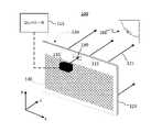
図1Aおよび1Bを参照すると、例示的な実施形態による導波路ディスプレイ100が例解される。導波路ディスプレイ100は、画像光源110と、導波路アセンブリ120とを含み、ディスプレイコントローラ155をさらに含み得る。画像光源110は、画像光111を生成するように構成される。一部の実施形態において、画像光源110は、走査プロジェクタの形式でのものであり、または、走査プロジェクタを含み得る。 1A and 1B, a
一部の実施形態において、画像光源110は、光学部品ブロック116が光学的に続き得る画素化電子ディスプレイ114を含み得る。電子ディスプレイ114は、例えば、限定されるものでないが、液晶ディスプレイ(LCD)、有機発光ディスプレイ(OLED)、無機発光ディスプレイ(ILED)、アクティブマトリクス有機発光ダイオード(AMOLED)ディスプレイ、または透明有機発光ダイオード(TOLED)ディスプレイなどの、画像を表示するように構成される任意の好適な電子ディスプレイであり得る。一部の実施形態において、電子ディスプレイ114は、発光ダイオード(LED)、レーザダイオード(LD)、または類するものなどの光源の直線状アレイの形式でのものであり得、各々の光源は、多色光を放出するように構成される。一部の実施形態において、その電子ディスプレイ114は、2次元(2D)画素アレイを含み得、各々の画素は、多色光を放出するように構成される。 In some embodiments,
光学部品ブロック116は、電子ディスプレイ114によって放出された画像光を好適にコンディショニングするように構成される1つまたは複数の光学構成要素を含み得る。このコンディショニングは、限定することなく、拡大すること、コリメートすること、収差に対して補正すること、および/もしくは、電子ディスプレイ114によって放出された画像光の伝搬の方向を調整すること、または、個別のシステムおよび電子ディスプレイに対して望まれ得るような任意の他の好適なコンディショニングを含み得る。光学部品ブロック116における1つまたは複数の光学構成要素は、限定することなく、1つもしくは複数のレンズ、鏡、開口部、格子、または、それらの組合せを含み得る。一部の実施形態において、光学部品ブロック116は、電子ディスプレイ114によって放出された光のビームを、そのビームの伝搬角度に関して走査するように動作可能な1つまたは複数の調整可能要素を含み得る。 Optics block 116 may include one or more optical components configured to suitably condition image light emitted by
導波路アセンブリ120は、インカプラ130とアウトカプラ140とを含む導波路123の形式でのものであり、または、その導波路123を含み得る。一部の実施形態において、1つが別のものの上方に積重される2つ以上の導波路から組成される導波路積重体が、導波路123の代わりに使用され得る。入力カプラ130は、その入力カプラ130が画像光源110から画像光111を受け取ることができる場所において配され得る。さらにはインカプラ130と本明細書において呼称され得る入力カプラ130は、導波路123内へと画像光111をカップリングするように構成され、その導波路120において、その画像光111は、出力カプラ140の方に伝搬する。さらにはアウトカプラと本明細書において呼称され得る出力カプラ140は、入力カプラ130からずらされ、例えばユーザの目166の方になど、望まれる方向において伝搬させるために、導波路120から画像光をデカップリングするように構成され得る。アウトカプラ140は、画像ビームを、その画像ビームが導波路を離脱する際に、サイズにおいて拡大するために、および、画像光源110の射出瞳より大きい射出瞳をサポートするために、インカプラ130よりサイズにおいて大であり得る。一部の実施形態において、導波路アセンブリ120は、外側光に対して部分的に透明であり得、AR用途において使用され得る。導波路123は、入力カプラ130からの2D FOVを出力カプラ140に、および結局のところはユーザの目166に伝達するように構成され得る。ここで、および、後に続く説明において、デカルト座標系(x,y,z)は便利のために使われ、(x,y)平面は、導波路アセンブリ120の、主面であって、それらを通してアセンブリが画像光を受け取る、および/または出力する、主面に平行であり、z軸は、その(x,y)平面に直交する。導波路123の2D FOVは、さらにはそれぞれ垂直FOVおよび水平FOVと呼称され得る、(y,z)平面における1D FOV、および、(x,z)平面における1D FOVにより規定され得る。
今から図2Aおよび2Bを参照すると、これらは、2つの異なる波長の光の導波路210内へのカップリングを概略的に例解するものであり、この導波路210は、導波路アセンブリ120の導波路123、または導波路123の代わりに使用され得る導波路積重体の任意の導波路を表し得る。図2Aにおける入射光の波長λは、図2Bにおける入射光の波長とは異なり得る、例えば、より小さい。図2Aは、例えば、緑光に対する導波路210の動作を表し得、一方で、図2Bは、例えば、赤光に対する導波路210の動作を表し得る。 2A and 2B, which schematically illustrate the coupling of light of two different wavelengths into a
導波路210は、基材205から形成されたスラブ導波路であり得、この基材205は、例えば、非限定的な例として、ガラスまたは好適なプラスチックもしくはポリマーなどの、可視光において透明である光学材料の薄いプレートの形態であり得る。対向する面211、212は、互いに対して公称的に平行であり得る。基材材料の屈折率nは、包囲する媒体の屈折率より大であり得、例えば1.4から2.6の範囲内であり得る。一部の実施形態において、約2.3以上の屈折の率を有する高屈折率材料が、基材205に使用され得る。一部の実施形態において、これらの材料は、約2.4より大である屈折の率nを有し得る。一部の実施形態において、これらの材料は、約2.5より大である屈折の率nを有し得る。そのような材料の非限定的な例は、ニオブ酸リチウム(LiNbO3)、二酸化チタン(TiO2)、窒化ガリウム(GaN)、窒化アルミニウム(AlN)、炭化ケイ素(SiC)、CVDダイヤモンド、硫化亜鉛(ZnS)である。
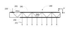
インカプラ230が、導波路210内または上に設けられ得、1つまたは複数の回折格子の形式でのものであり得る。さらには1つまたは複数の回折格子の形式でのものであり得るアウトカプラ240が、例えばy軸に沿って、インカプラ230から横にずらされる。例解される実施形態において、アウトカプラ240は、導波路210の、インカプラ130と同じ面211において場所を定められるが、他の実施形態において、そのアウトカプラ240は、導波路の反対位置関係の面212において場所を定められ得る。一部の実施形態は、導波路の対向する面211、212において配され得る2つの入力格子、および/あるいは、導波路の対向する面211、212において配され得る、2つの出力格子を有し得る。カプラ230、240を具現する格子は、例えばブレーズ格子などの、体積格子および表面レリーフ格子を含む、任意の好適な回折格子であり得る。格子は、さらには体積ホログラフィック格子であり得る。一部の実施形態において、それらの格子は、導波路それ自体の材料内で形成され得る。一部の実施形態において、それらの格子は、望まれる場所において導波路の面または複数の面に貼り付けられ得る、異なる材料または複数の材料内で製作され得る。図2Aおよび2Bにおいて例解される例示的な実施形態において、インカプラ230は、透過で動作する回折格子で具現化され、一方で、アウトカプラ240は、反射で動作する回折格子で具現化される。 An
インカプラ230は、さらには受光角度と本明細書において呼称され得る入力FOV234を、導波路210に提供するように構成され得る。波長に依存する入力FOV234は、入射の角度αの範囲を規定し、その範囲に対して、インカプラ230に入射する光が、導波路内へとカップリングされ、アウトカプラ240の方に伝搬する。本明細書の文脈において、「導波路内へとカップリングされる」は、導波路内へとカップリングされる光が、全内部反射(TIR)により導波路内にトラップされた状態になり、その光がアウトカプラにより関与されるまで、好適に低い減衰を伴って導波路の中で伝搬するように、導波路の導波モード、または、好適に低い放射損失を有するモード内へとカップリングされることを意味する。かくして、導波路210は、導波路の外側からのインカプラ230への光の入射の角度が導波路210の入力FOV234の中であることを前提として、TIRを以て個別の波長λの光をトラップし、アウトカプラ240の方に、トラップされる光を導波し得る。導波路の入力FOV234は、少なくとも部分的に、インカプラ格子230のピッチpにより、および、導波路の屈折率nにより決定される。所与の格子ピッチpに対して、(y,z)平面において入射の角度αにおいて空気から格子230に入射する光の1次回折角度βは、回折式(1)から見出され得る。
n・sin(β)+sin(α)=λ/p (1)
ここで、入射の角度αおよび回折角度βは、対応する光線が、法線207から導波路の対向する面211、212まで同じ側にある場合は正であり、そうでない場合は負である。式(1)は、導波路210が、屈折率nc>1を伴うクラッド材料によって囲まれている実施形態に対して容易に修正され得る。式(1)は、インカプラ格子の溝に対して法線方向の入射の平面を伴う画像光の光線に対して、すなわち、インカプラ格子の格子ベクトルが画像光の入射の平面内にあるときに当てはまる。
n·sin(β)+sin(α)=λ/p (1)
where the angle of incidence α and the angle of diffraction β are positive if the corresponding rays are on the same side of the normal 207 to the opposite faces 211, 212 of the waveguide, and negative otherwise. Equation (1) can be easily modified for embodiments in which waveguide 210 is surrounded by a cladding material with refractive index nc >1. Equation (1) holds true for rays of image light with a plane of incidence normal to the grooves of the incoupler grating, i.e. when the grating vector of the incoupler grating lies in the plane of incidence of the image light. .
インカップリングされる光と以降呼称される、導波路の中の回折させられる光に対するTIR条件は、TIRの式(2)により規定される。
n・sin(β)≧1 (2)
ここに、等号は、臨界TIR角度βc=asin(1/n)に対応する。導波路の入力FOV234は、FOVエッジ角度と本明細書において呼称され得る、入射の第1のFOV角度α1と、入射の第2のFOV角度α2との間に及ぶ。図2Aにおける最も右の入射光線111bに対応する入射の第1のFOV角度α1は、インカップリングされる光、すなわち、導波路の中でトラップされる光の臨界TIR角度βcにより規定される。

n·sin(β)≧1 (2)
Here the equal sign corresponds to the critical TIR angle βc =asin(1/n). The waveguide's
個別の波長における導波路210の入力1D FOVの幅w=|α1-α2|は、式(3)および(4)から推定され得る。一般的には、導波路の入力FOVは、導波路の屈折率が、包囲する媒体の屈折率に相対的に増大する際に増大する。例としてのことであるが、空気により包囲される率nの基材に対して、および、βmax=75°、λ/p=1.3に対して、導波路の入力FOVの幅wは、n=1.5に対して約26°、n=1.8に対して約43°、および、n=2.4に対して約107°である。The width w=|α1 −α2 | of the input 1D FOV of
式(3)および(4)から認められ得るように、導波路210の入力FOV234は、入力光の波長λの関数であり、そのことによって、入力FOV234は、波長が変化する際に、角度空間におけるその入力FOV234の位置をシフトし、例えば、その入力FOV234は、波長が増大する際に、アウトカプラ240の方にシフトする。かくして、多色画像光に対する十分に広いFOVを提供することは、難題であることがある。 As can be seen from equations (3) and (4), the
図3Aを参照すると、インカプラ230により導波路210内へとカップリングされる光が、アウトカプラ240の方に導波路内で伝搬する。アウトカプラ240は、アウトカプラ240により少なくとも部分的に規定される、導波路の出力FOV244の中の角度または複数の角度において、導波路210の外に、インカップリングされる光の少なくとも一部分を再指向するように構成される。導波路の総体的なFOV、すなわち、導波路によりビューアに伝達され得る入射角度αの範囲は、インカプラ230およびアウトカプラ240の両方により、影響され得る。 Referring to FIG. 3A, light coupled into
一部の実施形態において、インカプラ230およびアウトカプラ240を具現する格子は、それらの格子の格子ベクトルkgのベクトル和が実質的にゼロに等しいように構成され得る。
図3Bは、出力カプラ240が、導波路の対向する面において配される2つの回折格子241、242を含む、実施形態を例解する。そのような実施形態において、インカップリングされる光211aは、回折格子241および242により順次的に回折させられた後に、出力光221として導波路を抜け出得る。一部の実施形態において、回折格子241、242の格子ベクトルg1およびg2は、互いに対して所定の角度において指向され得る。少なくとも一部の実施形態において、それらの格子ベクトルは、(g0+g1+g2)=0であるように選択され得、ここに、g0は、インカプラ230の格子ベクトルである。FIG. 3B illustrates an embodiment in which the
図4は、絵図視図において、インカプラ430とアウトカプラ440とを伴うディスプレイ導波路410を例解する。インカプラ430は、アウトカプラ440の方に全体的に指向される格子ベクトルg0を伴う入力回折格子の形式でのものであり得る。アウトカプラ440は、互いに対して所定の角度において向きを定められる格子ベクトルg1およびg2を伴う2つの出力回折格子441および442から成り立つ。一部の実施形態において、格子441および442は、導波路の対向する面において形成される直線状回折格子であり得る。一部の実施形態において、それらの格子は、2D格子を形成するために、導波路のどちらかの面において、または、その導波路の体積内で、互いの上に重ねられ得る。導波路のFOVの中でインカプラ430に入射する光401が、インカップリングされる光線411aおよび411bにより例解されるように、導波路の平面において、サイズにおいて拡大して、アウトカプラ440の方に伝搬するために、導波路内へとインカプラ430によりカップリングされ得る。格子441、442は、それらの格子の各々を離れる続けざまの回折が、導波路の外に、インカップリングされる光を再指向するように構成される。光線411aは、アウトカプラ440が場所を定められる導波路の区域に進入することを機に、導波路の中で、いくらかの距離を伝搬する後に、最初に、第1の格子441により回折させられ、次いで、第2の格子442により導波路の外に回折させられる、インカップリングされる光の光線であり得る。光線411bは、最初に、第2の格子442により回折させられ、次いで、第1の格子441により導波路の外に回折させられる、インカップリングされる光の光線であり得る。さらにはアイボックス投射区域450と呼称され得る、導波路の射出瞳450は、その射出瞳450において、例えば、その射出瞳が、望まれる寸法を有する区域で、アウトカップリングされる光は、ビューイングのための最適の特性を有する。アイボックス投射区域450は、インカプラ430から、いくらかの距離において場所を定められ得る。FIG. 4 illustrates a
図5は、k空間における、すなわち(kx,ky)平面におけるディスプレイ導波路410内の光の変容を例解するものであり、ここに、kxおよびkyは、導波路の平面への投射における光波ベクトルk=(kx,ky)の座標を表象する。
k空間において、インカップリングされる光は、TIR環500により、グラフィカルに表され得る。TIR環500は、TIR円501および最大角度円502により境を定められるk空間の区域である。TIR円501は、臨界TIR角度βcに対応する。最大角度円502は、インカップリングされる光に対する最大伝搬角度βmaxに対応する。TIR円501の中の状態は、カップリングされない光、すなわち、インカプラ430に入射する入来する光、または、アウトカプラ格子441、442の1つにより導波路の外にカップリングされる光を表す。正規化しない場合、TIR円501の半径rTIR、および、外方円502の半径rmaxは、後に続く式により規定され得る。
図5においてg0、g1、およびg2と標記される矢印は、それぞれ、インカプラ430、第1のアウトカプラ格子441、および、第2のアウトカプラ格子442の格子ベクトルを表す。図において、これらは、k空間における2つの可能な経路を描く、2つの閉じられた三角形を形成し、それらの経路に沿って、入来する光は、3つの格子の各々により一度回折させられる後に、k空間における同じ状態に戻り得、そのことにより、導波路の入力から出力まで、角度空間における伝搬の方向を保つ。各々の回折は、対応する格子ベクトルによる(kx,ky)平面におけるシフトとして表され得る。区域520、530は、組み合わさって、(kx,ky)平面における導波路のFOVを表し、それぞれ、第1および第2の部分的FOV区域と呼称され得る。それらの区域は、インカプラ格子およびアウトカプラ格子、ならびに、導波路の屈折率により規定され、入力格子430、および、出力格子441、442の一方上での続けざまの回折、ならびに、2つの出力格子の他方上での後続の回折の後のTIR円501の内方における同じ(kx,ky)場所への戻りの後の、導波路(TIR環500)の中でトラップされる光滞留のすべてのkベクトルを表す。第1の部分的FOV区域520は、入力格子430、第1の出力格子441、および、第2の出力格子442上での続けざまの回折により、その区域自体にイメージングされる、すべての(kx,ky)状態を識別することにより決定され得、それらの回折の各々は、対応する格子ベクトルによる(kx,ky)平面におけるシフトとして表され得る。第2の部分的FOV区域530は、入力格子430、第2の出力格子442、および、第1の出力格子441上での続けざまの回折により、その区域自体にイメージングされる、すべての(kx,ky)状態を識別することにより決定され得る。The arrows labeled g0 , g1 , and g2 in FIG. 5 represent the grating vectors of
図6は、2D角度空間における第1および第2の部分的FOV520、530を例解し、水平軸および垂直軸は、両方が度において、それぞれ、x軸方向およびy軸方向における、入力光の入射の角度θxおよびθyを表す。(0,0)点は、インカプラへの法線方向の入射に対応する。組み合わさって、部分的FOV520、530は、ユーザに伝達され得る選択される色または波長の入力光のすべての入射光線を網羅する、波長λにおける導波路の完全FOV550を規定する。完全FOV550の中にはまる矩形区域555が、ディスプレイにおいて有用であり得る導波路の単色FOVを規定し得る。FIG. 6 illustrates the first and second
角度空間における各々の部分的FOV520、530の位置、サイズ、および形状、ならびにかくして、導波路の完全2D FOVは、入力光の波長λに、入来する光の波長λに対する入力および出力格子のピッチp0、p1、およびp2の比率に、ならびに、格子の相対的な向きに依存する。かくして、導波路の2D FOVは、ピッチサイズ、および、格子の相対的な向きを選択することにより、個別の色チャネルまたは複数のチャネルに対して、角度空間において、好適に形状を定められ、位置を定められ得る。導波路410の一部の実施形態において、出力格子441、442は、同じピッチp1=p2を有し、入力格子に相対的に、対称的に向きを定められ得る。そのような実施形態において、第1および第2の出力格子の格子ベクトルg1、g2は、インカプラの格子ベクトルg0に相対的に、±φの角度において向きを定められ得る。非限定的な例としてのことであるが、格子向き角度φは、50から70度、例えば60から66度の範囲内であり得、導波路の屈折率に依存し得る。図6は、例示的な導波路のFOVを例解するものであり、屈折率n=1.8、φ≒60°、および、p1=p2=p3=pであり、p/λは、FOV555について、法線方向の入射において中心を定めるように選択される。The position, size, and shape of each
一部の実施形態において、図4のディスプレイ導波路410などのNEDのディスプレイ導波路は、NEDのユーザに可視であり得る虹型パターンの出現などの望ましくない視覚的アーチファクトをもたらす方法で、周囲光をアイボックス内へと再指向し得る。この周囲光漏れは、図4の導波路410の格子442および441のいずれか、または図3Bの導波路210の格子241および242のいずれかなど、アウトカプラ格子のうちの1つでの周囲光の回折により引き起こされ得る。 In some embodiments, a NED's display waveguide, such as the
図7は、出力格子741および742が場所を定められるディスプレイ導波路710に入射する周囲光の例示的な光線701を例解する。入力格子730および出力格子741、742は、例えば、図4の導波路410の格子430、442および441、または、図3Bの導波路210の格子230、241および242を参照して上記で説明されたようなものであり得る。例解される例において、光線701は、導波路710の外方表面に、入射の大きな角度α1で接線方向に衝突し、回折させられる光線Bにより例解されるように、出力格子841により導波路内の入射角度α2でアイボックス744の方に回折させられる。回折させられる光線703がTIRを満たす場合、その回折させられる光線703は、導波路によって捕捉され、アイボックスに到達しないことになる。しかしながら、第2の入射角度α2が十分に小さい場合、周囲光の回折させられる光線703は、アイボックス744に到達し、ビューアのFOV内に視覚的アーチファクトの出現をもたらし得る。白周囲光の異なる色成分は、わずかに異なる角度において回折させられ得、この回折は、虹のような視覚的アーチファクトの出現につながり得る。FIG. 7 illustrates an
図8は、図5を参照して上記で説明された(kx,ky)平面におけるこのプロセスのベクトル表現を例解する。ここでも、TIR円501内の区域は、カップリングされない光を表し、外方円502は、導波路内の画像光のターゲット最大伝搬角度βmaxを表し、ベクトルg1およびg2は、出力格子741、742の格子ベクトルである。内TIR円501の内側のkベクトルは、x軸方向とy軸方向との両方において、カップリングされない光の180度の伝搬角度に広がり、TIR円501の中心は、法線方向の入射、または0度に対応する。「A」および「B」と標記されている点は、それぞれ、入射周囲光線701および回折させられる光線703のkベクトルの場所を指示する。TIR円501のすぐ中にある場所「A」は、光線701が、90度に近い入射角度α1を伴う「かすめる(glancing)」光線であることを指示する。出力格子741の格子ベクトルg1の長さがTIR円501の直径D=2・rTIRよりも小さい場合、場所「B」はTIR円501の中にあり、回折させられる光線703が導波路を透過することになり、アイボックス744に到達し得ることを指示する。FIG. 8 illustrates a vector representation of this process in the (kx , ky ) plane described above with reference to FIG. Again, the area within the
今から図9を参照すると、出力格子の格子ベクトルg1、g2がTIR円501の直径D=2・rTIRを超える長さである場合、出力格子からの単一回折による波長λの周囲光のアイボックス内への漏れは解消され得る。式(7)の最初のものから、格子ピッチに対応する条件(8)が得られる。
図10を参照すると、一部の実施形態において、周囲光が、例えば-γから+γまでの角度範囲において、ある一定のFOV内で導波路を通して回折させられるのを防止すれば十分であり得、角度γは、最大虹無し(MRF:maximum rainbow-free)角度と呼称され得、図10において、平面内kベクトルの対応する範囲は、半径kγ≒2π sin(γ)/λの破線の円507内の区域571によって指示される。カップリングされない光の平面内kベクトルの区域571は、NEDのターゲットFOV、または、ターゲットFOVの少なくともあらかじめ規定された中心一部分に対応するか、またはそれ自体の中に包含され得る。例えばTIR円501の隣の場所「A」によって指示されるように、かすめる角度において導波路に当たる周囲光線703が、漏れ無し区域571の外側に回折させられるようにするには、アウトカプラの格子ベクトルgiの長さgは、TIR円501の半径rTIRと、MRF角度γに対応するkベクトルの長さkγとの和を超えるべきである。
pi≦ξλ (9)
ここに、スケーリングパラメータξ<1は、MRF角度γにより規定される。
pi ≤ ξλ (9)
where the scaling parameter ξ<1 is defined by the MRF angle γ.
図11を参照すると、一部の実施形態において、式(9)におけるMRF角度γは、アイボックス747に相対する出力格子741のサイズおよび位置など、導波路を使用するNEDの形状により規定され得る。ビューイング形状は、出力格子741からアイボックス747に進入し得る、したがって、NEDを装着しているユーザに潜在的に可視であり得る、回折させられる光線777の角度範囲を最終的に制限し得る。図11は、幅2aの出力格子741が、アイレリーフ距離dを伴って、幅2bのアイボックス747に対して中心を定められる、例示的な実施形態を例解する。幅2aは、例えば、NEDの水平軸に沿った、または最大格子サイズの寸法に沿った、特定の方向における出力格子741の長さを表し得る。幅2bは、同じ方向におけるアイボックス747の長さを表し得る。この場合、アイボックス747に進入することができる回折させられる光線777の最大角度θmは、
一部の実施形態において、HMDによってサポートされるターゲットFOV内に周囲光が出現するのを防止すれば十分であり得る。そのような実施形態において、MRF角度γは、NEDの特徴的なFOV幅Γ、例えば、FOVの対角幅により規定され得る。図10は、2γの対角幅を有する例示的な矩形FOV577を例解する。一部の実施形態において、HMDのターゲットFOVの一部分内、例えばターゲットFOVの中心80%または90%内にのみ周囲光が出現するのを防止すれば十分であり得る。そのような実施形態において、式(10)は、

条件(8)から(12B)は、特定の波長の周囲光に対する出力格子のピッチを制限する。それら条件のいずれかが、導波路に入射し得る周囲光の可視スペクトルの最も短い波長に対して満たされる場合、その条件は、可視スペクトルのすべてのより長い波長に対しても満たされることになる。用語「可視スペクトル」は、ここでは、約420nmから約700nmに及ぶ、1平方メートルあたり3カンデラ(cd/m2)以上(明所視)などの通常の照明条件下で典型的な人間の目に可視である電磁放射のスペクトルの一部分を指し得る。虹アーチファクトの出現を少なくする目的で、可視光の最も短い波長とも呼称され得る可視スペクトルの最も短い波長は、約420nmの波長に対応し得る。一部の実施形態において、条件(8)から(12B)のうちの1つまたは複数が、可視光の青色範囲の波長に対して満たされれば十分であり得、人間の目の明所視感度は、例えばλ≧450nmの場合、555nmでのピーク値の1~5%未満に低下する。それゆえに、一部の実施形態において、式(8)、(10)、(11)、または(12A)に従って規定されたスケーリング係数を伴う条件(9)が青光に対して満たされれば十分であり得る。一部の実施形態において、出力格子は、λ=450nmの場合に上記で引用した条件のうちの1つを満たすピッチを有するように構成され得る。一部の実施形態において、出力格子は、λ=500nmの場合に上記で引用した条件のうちの1つを満たすピッチを有するように構成され得る。 Conditions (8) through (12B) limit the pitch of the output grating for specific wavelengths of ambient light. If any of those conditions are met for the shortest wavelengths of the visible spectrum of ambient light that can be incident on the waveguide, then that condition will also be met for all longer wavelengths of the visible spectrum. . The term "visible spectrum" is used herein to describe visible can refer to the portion of the spectrum of electromagnetic radiation that is For the purpose of reducing the appearance of rainbow artifacts, the shortest wavelength of the visible spectrum, which may also be referred to as the shortest wavelength of visible light, may correspond to a wavelength of approximately 420 nm. In some embodiments, it may be sufficient if one or more of conditions (8) through (12B) are met for wavelengths in the blue range of visible light, and the photopic luminosity of the human eye is drops to less than 1-5% of the peak value at 555 nm, eg, for λ≧450 nm. Therefore, in some embodiments, it is sufficient that condition (9) is met for blue light with scaling factors defined according to equations (8), (10), (11), or (12A). possible. In some embodiments, the output grating may be configured to have a pitch that satisfies one of the above-cited conditions for λ=450 nm. In some embodiments, the output grating may be configured to have a pitch that satisfies one of the above-cited conditions for λ=500 nm.
例としてのことであるが、波長λの一度回折させられる周囲光がないはずのMRF角度γ=c・Γが60度である実施形態において、出力格子のピッチは、約0.54λ以下であり得る。MRF角度γが45度である場合、出力格子のピッチは、約0.6λ以下であり得る。MRF角度γが30度である場合、出力格子のピッチは、約2/3λ以下であり得る。MRF角度γが20度である場合、出力格子のピッチは、約0.745λ以下であり得る。450nmの波長を伴う青光の場合、対応する値は、それぞれ約241nm、263nm、300nm、および335nmである。 By way of example, in an embodiment where the MRF angle γ=c·Γ is 60 degrees where there should be no ambient light of wavelength λ once diffracted, the pitch of the output grating is about 0.54λ or less. obtain. When the MRF angle γ is 45 degrees, the pitch of the output grating can be about 0.6λ or less. When the MRF angle γ is 30 degrees, the pitch of the output grating can be about 2/3λ or less. When the MRF angle γ is 20 degrees, the pitch of the output grating can be about 0.745λ or less. For blue light with a wavelength of 450 nm, the corresponding values are approximately 241 nm, 263 nm, 300 nm, and 335 nm, respectively.
式(7)からわかるように、k平面におけるTIR環の内径は、波長λに依存し、かくして、異なる波長の光に対するTIR環500は、導波路の波長および屈折率に応じて、部分的にのみ重なるか、またはまったく重ならないかであり得る。導波路の屈折率が大であるほど、平面内kベクトルの範囲が広くなり、2つの異なる画像光の波長は、導波路によりカップリングされ、アイボックスへ導波され得、それゆえに、導波路を採用するディスプレイシステムがサポートできるFOVが広くなる。 As can be seen from equation (7), the inner diameter of the TIR ring in the k-plane depends on the wavelength λ, and thus the
図12は、可視光の2つの異なる波長または色バンドに対するTIR環500Bおよび500Rを例解する。第1の波長λ=λRの光に対するTIR環が、500Rにおいて概略的に指示され、一方で、第2のより短い波長λ=λB<λRの光に対するTIR環が、500Bにおいて概略的に指示される。長い波長のTIR環500Rは、TIR円501Rおよび最大角度円502Rにより境界を定められ、これらの半径は、λ=λRについて式(7)により規定される。より短い波長光のTIR環500Bは、TIR円501Bおよび最大角度円502Bにより境界を定められ、これらの半径は、λ=λBについて式(7)により規定される。例としてのことであるが、より長い波長λRは、例えば635nmの波長を伴う赤光に対応し得、一方で、より短い波長は、例えば465nmの波長を伴う青光に対応し得る。例解される例において、TIR環500Rおよび500Bは、多色TIR環と呼称され得る副環511を共有し、副環511の幅は、以下の条件(13)により規定される。
一部の実施形態において、画像源からのRGB光の複数の色チャネルをNEDのアイボックスに伝達するために、ディスプレイシステムにおいて、光学的に透明な高屈折率材料から作製される単一の導波路が使用され得、赤色および緑色チャネルのうちの少なくとも1つ、および青色チャネルに対して同じ入力格子および出力格子が使用される。一部の実施形態において、導波路の屈折率nの最小値に関する条件は、インカプラ格子が、FOVの角に入射する最も長い波長の色チャネル(赤)の光線を導波路内へとカップリングすることを要求することにより推定され得る。これは、条件

一部の実施形態において、約2.3、または、好ましくは2.4以上の屈折率を伴う、光学的に透明な高屈折率材料から作製される単一の導波路が、画像源からのRGB光をNEDのアイボックスに伝達するために、ディスプレイシステムにおいて使用され得る。一部の実施形態において、屈折率が約2.5~2.6以上の光学的に透明な高屈折率材料から作製される単一の導波路が使用され得る。 In some embodiments, a single waveguide made from an optically transparent high refractive index material with a refractive index of about 2.3, or preferably 2.4 or greater, directs the light from the image source. It can be used in display systems to deliver RGB light to the NED's eyebox. In some embodiments, a single waveguide made from an optically transparent high index material with a refractive index of about 2.5-2.6 or higher may be used.
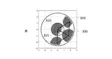
図13A、13B、および13Cは、上記で説明された導波路210、410、または710など、画像光源からの多色RGB光をアイボックスに伝達するように構成される導波路内への赤、緑、および青の色チャネルの画像光それぞれのカップリングを例解する。例解される例において、導波路は、屈折率n=2.6を有する。図の各々は、内TIR円の半径が1であり、外方円の半径がn・sin(βmax)であるように、2π/λに正規化された平面内k空間を例解する。導波路のインカプラの正規化された格子ベクトルは、830において指示され、波長とともにスケーリングする長さg0・λ/2πを有する。例解される例において、導波路のアウトカプラの格子ベクトルg1、g2は同じ長さであり、インカプラ格子に対して±60°において向きを定められ、これら格子ベクトルg1、g2は、他の実施形態において異なる長さおよび向きを有し得る。影付き区域815は、3つの色バンドの各々について導波路によりサポートされる全2D FOV、すなわち、伝搬方向を保ちながら導波路が入力から出力に伝達するすべての光線の平面内kベクトルを指示する。影付き区域820は、導波路によりカップリングされた光の対応するkベクトルを指示する。ある程度の角の口径食を伴う、3色すべてについてサポートされ得る例示的な矩形2D FOVが、810において指示される。例解される例において、2D RGB FOV810は、72°の対角を伴う40×60度であり得、これは、±20°の水平FOV(H-FOV)、±30°の垂直FOV(V-FOV)、および±36°の対角FOV(D-FOV)に対応する。Figures 13A, 13B, and 13C illustrate red, red, and red into waveguides configured to transmit polychromatic RGB light from an image source to the eyebox, such as
図13A~13Bを参照して上記で説明された実施形態において、約280nmに等しいアウトカプラの格子ベクトルg1、g2のピッチpiは、青周囲光について、λ=450nmであり、c=1、およびD-FOVにより規定されるΓ、または例解される例において72°を伴う、条件(12B)を満たし得る。他の実施形態において、導波路のアウトカプラの格子ベクトルg1、g2のピッチpiは、ターゲットFOVのいくらか小さい部分、例えばターゲットFOVの80~90%内の部分について条件(12B)を満たし得、アウトカプラ格子のより大きいピッチ値を可能にする。In the embodiment described above with reference to FIGS. 13A-13B, the pitch pi of the outcoupler grating vectors g1 , g2 equal to about 280 nm is λ=450 nm for blue ambient light, and c= 1, and Γ defined by the D-FOV, or condition (12B) with 72° in the illustrated example. In another embodiment, the pitch pi of the waveguide outcoupler grating vectors g1 , g2 satisfies condition (12B) for some small portion of the target FOV, eg, within 80-90% of the target FOV. , allowing larger pitch values of the outcoupler grating.
一部の実施形態において、異なる波長範囲に対して最適化され得る導波路の入力格子および出力格子を伴う2つ以上の導波路が互いに積重され得る。一部の実施形態において、3つの導波路の積重体が、RGB光の色あたりに1つ、使用され得る。一部の実施形態において、色のうちの1つまたは複数は、2つの異なる導波路を介して伝達され得る。一部の実施形態において、2つの導波路の積重体は、導波路のうちの一方が3つの色バンドのうちの2つ、例えば赤および緑の光を伝達し、他方が残りの色バンド、例えば青の光を伝達するように、RGB光を伝達するために使用され得る。一部の実施形態において、緑色バンドの光は、両方の導波路によって搬送され得る。一部の実施形態において、各々の導波路の出力格子は、ディスプレイのサポートされるFOVのあらかじめ規定された小部分内への周囲光漏れを低減するように、可視スペクトルの少なくとも一部分について式(10)または式(12)によるスケーリング係数ξを伴って条件(9)を満たすように構成され得る。 In some embodiments, two or more waveguides can be stacked together with input and output gratings of the waveguides that can be optimized for different wavelength ranges. In some embodiments, a stack of three waveguides may be used, one per color of RGB light. In some embodiments, one or more of the colors may be transmitted through two different waveguides. In some embodiments, the stack of two waveguides is such that one of the waveguides transmits two of the three color bands, e.g., red and green light, and the other the remaining color bands; It can be used to transmit RGB light, for example to transmit blue light. In some embodiments, green band light may be carried by both waveguides. In some embodiments, the output grating of each waveguide has the formula (10 ) or with a scaling factor ξ according to equation (12) to satisfy condition (9).
図14を参照すると、第1のインカプラ931および第1のアウトカプラ941を有する第1の導波路921と、第2のインカプラ932および第2のアウトカプラ942を有する第2の導波路922とから成り立つ導波路アセンブリ900が例解される。導波路921、922は、インカプラ931がインカプラ932と光学的に位置合わせされ、アウトカプラ941がアウトカプラ942と光学的に位置合わせされる、2導波路積重体を形成するように並べられる。TIRを支援するために、導波路間に小さいギャップ504が設けられ得る。インカプラ931は、ターゲットFOVから画像光901を収集し、その画像光901を、TIRによってアウトカプラに伝達するために2つの導波路のうちの少なくとも1つの中へとカップリングするように構成され得る。画像光901は、赤色チャネル901R、緑色チャネル901G、および赤色チャネル901Rを含み得る。導波路積重体の多色FOVは、入力光901の各色チャネルが、導波路のインカプラのうちの1つによって積重体の導波路のうちの少なくとも1つの中へとカップリングされ、次いで、アウトカプラのうちの1つによって、導波路の外に、アイボックスが場所を定められ得る射出瞳955の方へカップリングされ得る、すべての入射の角度αから成り立つ。入力光901を積重体の2つの導波路の間で拡散させることによって、導波路アセンブリ900は、積重体の導波路のうちのいずれか1つの単色FOVと実質的に等しいか、またはそれより大きい幅の多色FOVをサポートするように構成され得る。一部の実施形態において、導波路アセンブリ900のインカプラおよびアウトカプラは、青光および緑光を第1の導波路921内へとカップリングし、赤光を第2の導波路922内へとカップリングするように構成され得る。一部の実施形態において、導波路アセンブリ900のインカプラおよびアウトカプラは、緑画像光が入射に角度に応じて2つの導波路921、922のうちのいずれか1つ内の射出瞳955に導波され得るように、緑色チャネルを第1の導波路921と第2の導波路922との両方の中へとカップリングするように構成され得る。一部の実施形態において、アウトカプラ941、942は、ディスプレイのサポートされるFOVのあらかじめ規定された小部分内への周囲光の回折を低減するように、可視スペクトルの少なくとも一部分において条件(8)または(12B)を満たすように構成され得る。 Referring to FIG. 14, from a
図15Aは、フレームまたは複数のフレーム1015により支持される2つの導波路アセンブリ1010を含む両眼ニアアイディスプレイ(NED)1000の例示的な配置設計を概略的に例解する。導波路アセンブリ1010の各々は、ディスプレイプロジェクタ1060からの画像光を、ユーザの異なる目に伝達するように構成される。インカプラ1030が、対応するインカプラ1030の方に画像光を投射するために配され得る、共通マイクロディスプレイプロジェクタ、または、2つの別々のマイクロディスプレイプロジェクタ1060とともに設けられ得る。導波路アセンブリ1010は、各々、上記で説明されたような、ターゲットFOV内の多色光を導波するように構成され得る単一の多重層もしくは屈折率分布導波路の形式でのものであり、または、その単一の導波路を含み得る。各々の導波路は、インカプラ1030と、アウトカプラ1040とを含み、各々のインカプラは、対応するアウトカプラと対角に位置合わせされる。他の実施形態において、対応するアウトカプラ1040の周辺部におけるインカプラ1030の配置は異なり得る。各々のアウトカプラ1040は、さらには導波路の射出瞳と呼称され得る、アイボックス投射区域1051を含み、その区域から、動作において、画像光がユーザの目に投射される。アイボックスは、良好な品質の画像がユーザの目に提示され得る、および、動作において、ユーザの目が、場所を定められることを予期される、幾何学的区域である。アイボックス投射区域1051は、それらの区域の中心を接続する軸1001上に配され得る。軸1001は、NEDを着用するユーザの目と好適に位置合わせされ、または、少なくともユーザの目を接続する線に平行であり得、水平軸(x軸)と呼称され得る。インカプラ1030は、全体的にはそれぞれの導波路アセンブリのアイボックス投射区域1051の方に指向され得る格子ベクトルg0を伴う、回折格子の形式でのものであり得る。各々のアウトカプラ1040は、互いに対して所定の角度において向きを定められるそれぞれの格子の格子ベクトルg1およびg2を伴う、2つの回折格子の形式でのものであり得る。これらの格子は、各々の導波路の対向する面において配され得る、または、導波路の面のうちの1つにおいて、もしくは導波路の大部分において重ねられ得る。インカプラおよびアウトカプラの格子は、図15Bにおいて例解されるベクトル線図を満足させるように構成され得る。一部の実施形態において、各々の導波路アセンブリ1010は、格子ベクトルg0、g1、およびg2を伴う、上記で説明されたような、2つ以上の導波路を伴う導波路積重体の形式でのものであり、または、その導波路積重体を含み得、それらの格子ベクトルは、積重体の各々の導波路に対して長さにおいて異なり得、異なる色チャネルを伝達するために最適化され得る。一部の実施形態において、積重体の各々の導波路の格子は、上記で説明されたような、サポートされるFOV、または、少なくともサポートされるFOVのあらかじめ規定された中心一部分内への、一度回折させられる周囲光の漏れを、回避する、または、少なくとも、より少なくするように構成され得る。FIG. 15A schematically illustrates an exemplary layout design for a binocular near-eye display (NED) 1000 including two
図3B、4、7、14、15Aにおいて例解される実施形態などの、複数の出力/再指向格子を伴う実施形態において、望ましくない周囲光もまた、2つ以上の出力格子によって順番に回折された後、アイボックスに到達し得る。よって、一部の実施形態は、アウトカプラ格子からの逐次的な回折の後に、可視スペクトルにおいて二重に回折させられる周囲光がアイボックスに到達するという可能性をより少なくするように構成され得る。インカプラ格子およびアウトカプラ格子が式(5)を満たす、すなわち、和が実質的にゼロになる、例えば、ここに、g0+g1+g2=0である実施形態において、出力格子の各々からの逐次的な回折は、回折方向に関して、(-g0)の格子ベクトルを伴うインカプラ格子からの回折と同等である。よって、一部の実施形態において、インカプラ格子は、可視スペクトルにおける条件(8)~(10)、および(12B)のうちの1つもしくは複数、またはその少なくとも一部分も満たすピッチp0を伴うように構成され得る。言い換えれば、一部の実施形態において、アウトカプラ140、240、440、941、942、1040の格子ピッチに関する条件のうちの1つまたは複数は、インカプラ130、230、430、930、1030の格子ピッチにも適用され得る。In embodiments with multiple output/redirecting gratings, such as the embodiments illustrated in FIGS. 3B, 4, 7, 14, 15A, unwanted ambient light is also diffracted by the two or more output gratings in turn. After that, the eyebox can be reached. Thus, some embodiments may be configured to make it less likely that ambient light that is doubly diffracted in the visible spectrum will reach the eyebox after successive diffractions from the outcoupler gratings. . In embodiments where the in-coupler and out-coupler gratings satisfy equation (5), i.e. sum to substantially zero, e.g., where g0 +g1 +g2 =0, from each of the output gratings Sequential diffraction is equivalent to diffraction from an incoupler grating with a grating vector of (−g0 ) with respect to the diffraction direction. Thus, in some embodiments, the incoupler grating is with a pitch p0 that also satisfies one or more of conditions (8)-(10), and (12B) in the visible spectrum, or at least a portion thereof. can be configured. In other words, in some embodiments, one or more of the conditions for the grating pitches of the
本開示の実施形態は、人工現実システムを含み、または、人工現実システムと連関して実現され得る。人工現実システムは、ユーザへの提示の前に、何らかの様式で、視覚情報、オーディオ、タッチ(体性感覚(somatosensation))情報、加速度、平衡、その他などの、知覚を通して取得される、外側世界に関する知覚的情報を調整する。非限定的な例としてのことであるが、人工現実は、仮想現実(VR)、拡張現実(AR)、複合現実(MR)、ハイブリッド現実、または、それらの何らかの組合せおよび/もしくは派生物を含み得る。人工現実コンテンツは、全面的に生成されるコンテンツ、または、捕捉される(例えば、現実世界)コンテンツと組み合わされる生成されるコンテンツを含み得る。人工現実コンテンツは、ビデオ、オーディオ、体性もしくは触覚フィードバック、または、それらの何らかの組合せを含み得る。このコンテンツのいずれも、単一のチャネルにおいて、または、ビューアに対する3次元効果を生み出すステレオビデオにおいてなど、複数個のチャネルにおいて提示され得る。さらにまた、一部の実施形態において、人工現実は、さらには、例えば人工現実においてコンテンツを創出するために使用される、および/または、他の形で人工現実において使用される(例えば、人工現実において活動を遂行する)、アプリケーション、製品、アクセサリ、サービス、または、それらの何らかの組合せと関連付けられ得る。人工現実コンテンツを提供する人工現実システムは、ホストコンピュータシステムに接続されるHMD、スタンドアローンHMD、眼鏡のフォームファクタを有するニアアイディスプレイなどのウェアラブルディスプレイ、モバイルデバイス、もしくはコンピューティングシステムを含む様々なプラットフォーム、または、1つもしくは複数のビューアに人工現実コンテンツを提供する能力がある任意の他のハードウェアプラットフォーム上で実現され得る。 Embodiments of the present disclosure may include or be implemented in conjunction with an artificial reality system. An artificial reality system has some form of information about the outside world that is acquired through perception, such as visual information, audio, touch (somatosensory) information, acceleration, equilibrium, etc., prior to presentation to the user. Adjust perceptual information. By way of non-limiting example, artificial reality includes virtual reality (VR), augmented reality (AR), mixed reality (MR), hybrid reality, or any combination and/or derivative thereof. obtain. Artificial reality content may include entirely generated content or generated content combined with captured (eg, real-world) content. Artificial reality content may include video, audio, somatic or haptic feedback, or some combination thereof. Any of this content can be presented in a single channel or in multiple channels, such as stereo video that creates a three-dimensional effect for the viewer. Furthermore, in some embodiments, artificial reality is also used, for example, to create content in artificial reality and/or is otherwise used in artificial reality (e.g., artificial reality perform activities in), applications, products, accessories, services, or some combination thereof. Artificial reality systems that provide artificial reality content can be HMDs connected to a host computer system, standalone HMDs, wearable displays such as near-eye displays with the form factor of eyeglasses, mobile devices, or various platforms including computing systems. , or on any other hardware platform capable of providing artificial reality content to one or more viewers.
図16Aを参照すると、HMD1100は、AR/VR環境内への、より大である度合の没入のためにユーザの顔を囲む、AR/VRウェアラブルディスプレイシステムの例である。HMD1100は、例えば、図1Aの導波路ディスプレイ100、または、図17AのNED1200の実施形態であり得る。HMD1100の機能は、コンピュータで生成される映像によって物理的現実世界環境のビューを拡張すること、および/または、全面的に仮想の3D映像を生成することである。HMD1100は、前部本体1102と、バンド1104とを含み得る。前部本体1102は、信頼性の高い、および心地よい様式での、ユーザの目の前部における配置のために構成され、バンド1104は、ユーザの頭部上で前部本体1102を据え付けるために引き伸ばされ得る。ディスプレイシステム1180が、ユーザにAR/VR映像を提示するために、前部本体1102内に配され得る。前部本体1102の側部1106は、不透明または透明であり得る。ディスプレイシステム1180は、画像プロジェクタ1114に結合される、上記で説明されたようなディスプレイ導波路を含み得る。 Referring to FIG. 16A,
一部の実施形態において、前部本体1102は、ロケータ1108と、HMD1100の加速度を追跡するための慣性測定ユニット(IMU)1110と、HMD1100の位置を追跡するための位置センサ1112とを含む。IMU1110は、HMD1100のモーションに応答して1つまたは複数の測定信号を生成する、位置センサ1112のうちの1つまたは複数から受け取られる測定信号に基づいて、HMD1100の位置を指示するデータを生成する電子デバイスである。位置センサ1112の例は、1つもしくは複数の加速度計、1つもしくは複数のジャイロスコープ、1つもしくは複数の磁気計、モーションを検出する別の好適なタイプのセンサ、IMU1110の誤差補正のために使用される所定のタイプのセンサ、または、それらの何らかの組合せを含む。位置センサ1112は、IMU1110の外部に、IMU1110の内部に、または、それらの何らかの組合せで、場所を定められ得る。 In some embodiments, the
ロケータ1108は、仮想現実システムがHMD1100全体の場所および向きを追跡することができるように、仮想現実システムの外部イメージングデバイスによりトレースされる。IMU1110および位置センサ1112により生成される情報が、HMD1100の位置および向きの改善される追跡正確度のために、ロケータ1108を追跡することにより取得される位置および向きと比較され得る。正確な位置および向きは、適切な仮想風景をユーザに提示することを、そのユーザが3D空間において、動き、回る際に行うために重要である。
HMD1100は、HMD1100の一部またはすべてを包囲する局所的区域の深度情報を説明するデータを捕捉する深度カメラアセンブリ(DCA)1111をさらに含み得る。その最終目的のために、DCA1111は、レーザレーダ(LIDAR)、または同様のデバイスを含み得る。深度情報は、3D空間におけるHMD1100の位置および向きの決定の、より良好な正確度のために、IMU1110からの情報と比較され得る。
HMD1100は、リアルタイムでユーザの目の向きおよび位置を決定するための目追跡システムをさらに含み得る。ユーザの目の決定される位置は、HMD1100が(自己)調整手順を遂行することを可能とする。目の取得される位置および向きは、さらには、HMD1100が、ユーザの視線方向を決定すること、および、そのことに応じて、ディスプレイシステム1180により生成される画像を調整することを可能とする。1つの実施形態において、バーゼンス(vergence)、すなわち、ユーザの目の視線の輻輳角度(convergence angle)が決定される。決定される視線方向およびバーゼンス角度が、さらには、ビューの角度および目の位置に依存的な視覚アーチファクトのリアルタイム補償のために使用され得る。さらにまた、決定されるバーゼンスおよび視線角度は、ユーザとの相互作用、オブジェクトをハイライトすること、オブジェクトを前景にもっていくこと、追加的なオブジェクトまたはポインタを創出すること、その他のために使用され得る。例えば、前部本体1102内に作り付けられる小さいスピーカのセットを含む、オーディオシステムが、さらには設けられ得る。
図16Bを参照すると、AR/VRシステム1150は、図1Aの導波路ディスプレイ100、または、図16AのNED1000の例示的な実施態様であり得る。AR/VRシステム1150は、図16AのHMD1100と、様々なAR/VRアプリケーション、セットアップおよび較正手順、3Dビデオ、その他を記憶する外部コンソール1190と、コンソール1190を動作させる、および/または、AR/VR環境と相互作用するための入力/出力(I/O)インターフェイス1115とを含む。HMD1100は、物理的ケーブルによってコンソール1190に「つながれ」、または、Bluetooth(登録商標)、Wi-Fi、その他などのワイヤレス通信リンクによってコンソール1190に接続され得る。関連付けられるI/Oインターフェイス1115を各々が有する、複数個のHMD1100が存在し得、各々のHMD1100およびI/Oインターフェイス1115は、コンソール1190と通信する。代替的構成において、異なる、および/または追加的な構成要素が、AR/VRシステム1150内に含まれたものであり得る。加えて、図16Aおよび16Bにおいて示される構成要素のうちの1つまたは複数と連関して説明される機能性は、一部の実施形態において、図16Aおよび16Bと連関して説明されるのと異なる様式で、構成要素の間で分け散らされ得る。例えば、コンソール1115の機能性の一部またはすべては、HMD1100により提供され得、逆もしかりである。HMD1100は、そのような機能性を達成する能力がある処理モジュールを設けられ得る。 Referring to FIG. 16B, AR/
図16Aを参照して上記で説明されたように、HMD1100は、目の位置および向きを追跡すること、視線角度および輻輳角度を決定すること、その他のための目追跡システム1125と、3D空間におけるHMD1100の位置および向きを決定するためのIMU1110と、外側環境を捕捉するためのDCA1111と、HMD1100の位置を独立的に決定するための位置センサ1112と、ユーザにAR/VRコンテンツを表示するためのディスプレイシステム1180とを含み得る。ディスプレイシステム1180は、液晶ディスプレイ(LCD)、有機発光ディスプレイ(OLED)、無機発光ディスプレイ(ILED)、アクティブマトリクス有機発光ダイオード(AMOLED)ディスプレイ、透明有機発光ダイオード(TOLED)ディスプレイ、プロジェクタ、または、それらの組合せを含むが、それらに限定されない、1つもしくは複数の走査プロジェクタ、または、1つもしくは複数の電子ディスプレイなどの、1つまたは複数の画像プロジェクタ1114を含む(図16B)。ディスプレイシステム1180は、ディスプレイ導波路1130をさらに含み、そのディスプレイ導波路1130の機能は、画像プロジェクタ1114により生成される画像をユーザの目に伝達することである。ディスプレイシステム1180は、光学部品ブロック1135をさらに含み得、その光学部品ブロック1135は、様々なレンズ、例えば、屈折レンズ、Fresnelレンズ、回折レンズ、能動または受動Pancharatnam-Berry位相(PBP)レンズ、液体レンズ、液晶レンズ、その他、瞳複製導波路、格子構造、コーティング、その他を含み得る。一部の実施形態において、光学部品ブロック1135は、例えば、バーゼンス調節矛盾(vergence-accommodation conflict)に対して補償するために、個別のユーザの視力障害に対して補正するために、収差を相殺するために、その他で、可変焦点機能性を含み得る。 As described above with reference to FIG. 16A, the
I/Oインターフェイス1115は、ユーザが、アクション要求を送出し、コンソール1190から応答を受け取ることを可能とするデバイスである。アクション要求は、個別のアクションを遂行するための要求である。例えば、アクション要求は、画像もしくはビデオデータの捕捉を開始もしくは終了するための命令、または、アプリケーションの中で個別のアクションを遂行するための命令であり得る。I/Oインターフェイス1115は、アクション要求を受け取り、コンソール1190にアクション要求を伝えるための、キーボード、マウス、ゲームコントローラ、または、任意の他の好適なデバイスなどの、1つまたは複数の入力デバイスを含み得る。I/Oインターフェイス1115により受け取られるアクション要求は、アクション要求に対応するアクションを遂行するコンソール1190に伝えられる。一部の実施形態において、I/Oインターフェイス1115は、I/Oインターフェイス1115の初期位置に相対的な、I/Oインターフェイス1115の推定される位置を指示する較正データを捕捉するIMUを含む。一部の実施形態において、I/Oインターフェイス1115は、コンソール1190から受け取られる命令によって、ユーザに触覚フィードバックを提供し得る。例えば、触覚フィードバックは、アクション要求が受け取られるときに提供され得、または、コンソール1190は、コンソール1190がアクションを遂行するときに触覚フィードバックを生成することをI/Oインターフェイス1115に行わせる、I/Oインターフェイス1115への命令を伝える。 I/
コンソール1190は、IMU1110、DCA1111、目追跡システム1125、およびI/Oインターフェイス1115のうちの1つまたは複数から受け取られる情報によって処理するために、HMD1100にコンテンツを提供し得る。図16Bにおいて示される例において、コンソール1190は、アプリケーション記憶機構1155と、追跡モジュール1160と、処理モジュール1165とを含む。コンソール1190の一部の実施形態は、図18Bと連関して説明されるモジュールまたは構成要素と異なる、モジュールまたは構成要素を有し得る。同様に、下記でさらに説明される機能は、図16Aおよび16Bと連関して説明されるのと異なる様式で、コンソール1190の構成要素の間で分け散らされ得る。
アプリケーション記憶機構1155は、コンソール1190による実行のための1つまたは複数のアプリケーションを記憶し得る。アプリケーションは、プロセッサにより実行されるときに、ユーザへの提示のためのコンテンツを生成する、命令の群である。アプリケーションにより生成されるコンテンツは、HMD1100またはI/Oインターフェイス1115の動きによってユーザから受け取られる入力に応答したものであり得る。アプリケーションの例は、ゲーミングアプリケーション、プレゼンテーションおよび会議アプリケーション、ビデオ再生アプリケーション、または、他の好適なアプリケーションを含む。
追跡モジュール1160は、1つまたは複数の較正パラメータを使用してAR/VRシステム1150を較正し得、HMD1100またはI/Oインターフェイス1115の位置の決定における誤差を低減するために、1つまたは複数の較正パラメータを調整し得る。追跡モジュール1160により遂行される較正は、さらには、HMD1100内のIMU1110、および/または、もしあれば、I/Oインターフェイス1115内に含まれたものであるIMUから受け取られる情報に対して責任をもつ。加えて、HMD1100の追跡が逃れられる場合、追跡モジュール1160は、AR/VRシステム1150の一部またはすべてを再較正し得る。
追跡モジュール1160は、HMD1100の、または、I/Oインターフェイス1115、IMU1110、もしくは、それらの何らかの組合せの、動きを追跡し得る。例えば、追跡モジュール1160は、HMD1100からの情報に基づいて、局所的区域のマッピングにおけるHMD1100の基準点の位置を決定し得る。追跡モジュール1160は、さらには、それぞれ、IMU1110からのHMD1100の位置を指示するデータを使用して、または、I/Oインターフェイス1115内に含まれたものであるIMUからのI/Oインターフェイス1115の位置を指示するデータを使用して、HMD1100の基準点、または、I/Oインターフェイス1115の基準点の位置を決定し得る。さらにまた、一部の実施形態において、追跡モジュール1160は、IMU1110からの位置またはHMD1100を指示するデータの一部分、および無論のこととして、DCA1111からの局所的区域の表現を使用して、HMD1100の将来の場所を予測し得る。追跡モジュール1160は、HMD1100またはI/Oインターフェイス1115の、推定または予測される将来の位置を、処理モジュール1165に提供する。
処理モジュール1165は、HMD1100から受け取られる情報に基づいて、HMD1100の一部またはすべてを包囲する区域(「局所的区域」)の3Dマッピングを生成し得る。一部の実施形態において、処理モジュール1165は、深度を計算することにおいて使用される技法に対して関連性のある、DCA1111から受け取られる情報に基づいて、局所的区域の3Dマッピングに対する深度情報を決定する。様々な実施形態において、処理モジュール1165は、深度情報を使用して、局所的区域のモデルを更新し、更新されるモデルに部分的に基づいてコンテンツを生成し得る。
処理モジュール1165は、AR/VRシステム1150の中でアプリケーションを実行し、HMD1100の、位置情報、加速度情報、速度情報、予測される将来の位置、または、それらの何らかの組合せを、追跡モジュール1160から受け取る。受け取られる情報に基づいて、処理モジュール1165は、ユーザへの提示のためにHMD1100に提供するためのコンテンツを決定する。例えば、受け取られる情報が、ユーザが左を眺めたことを指示する場合、処理モジュール1165は、仮想環境内での、または、追加的なコンテンツによって局所的区域を拡張する環境内での、ユーザの動きを反映する、HMD1100に対するコンテンツを生成する。加えて、処理モジュール1165は、I/Oインターフェイス1115から受け取られるアクション要求に応答して、コンソール1190上で実行するアプリケーションの中でアクションを遂行し、アクションが遂行されたという、ユーザへのフィードバックを提供する。提供されるフィードバックは、HMD1100による視覚もしくは可聴フィードバック、または、I/Oインターフェイス1115による触覚フィードバックであり得る。
一部の実施形態において、目追跡システム1125から受け取られる目追跡情報(例えば、ユーザの目の向き)に基づいて、処理モジュール1165は、画像プロジェクタ1114によるユーザへの提示のための、HMD1100に提供されるコンテンツの解像度を決定する。処理モジュール1165は、ユーザの視線の中心窩領域において最大画素解像度を有する、HMD1100へのコンテンツを提供し得る。処理モジュール1165は、ユーザの視線の周辺部において、より低い画素解像度を提供し得、かくして、ユーザの視覚体験を損なうことなく、AR/VRシステム1150の電力消費をより少なくし、コンソール1190の計算リソースを節約する。一部の実施形態において、処理モジュール1165は、さらに、バーゼンス調節矛盾を防止するために、ならびに/または、光学ひずみおよび収差を相殺するために、目追跡情報を使用して、どこにオブジェクトがユーザの目に対して表示されるかを調整することができる。 In some embodiments, based on eye tracking information received from eye tracking system 1125 (eg, orientation of the user's eyes),
本明細書において開示される態様と結び付いて説明される、様々な例解的な論理、論理ブロック、モジュール、および回路を実現するために使用されるハードウェアは、本明細書において説明される機能を遂行するように設計される、汎用目的プロセッサ、デジタル信号プロセッサ(DSP)、特定用途向け集積回路(ASIC)、フィールドプログラマブルゲートアレイ(FPGA)もしくは他のプログラマブル論理デバイス、離散ゲートもしくはトランジスタ論理、離散ハードウェア構成要素、または、それらの任意の組合せによって、実現または遂行され得る。汎用目的プロセッサは、マイクロプロセッサであり得、ただし、代替案において、プロセッサは、任意の従来のプロセッサ、コントローラ、マイクロコントローラ、または状態機械であり得る。プロセッサは、さらには、コンピューティングデバイスの組合せ、例えば、DSPおよびマイクロプロセッサの組合せ、複数のマイクロプロセッサ、DSPコアと連関した1つもしくは複数のマイクロプロセッサ、または、任意の他のそのような構成として実現され得る。代替案として、一部のステップまたは方法は、所与の機能に特異的である回路網により遂行され得る。 The hardware used to implement the various illustrative logic, logic blocks, modules, and circuits described in conjunction with the aspects disclosed herein may be the functions described herein. general purpose processors, digital signal processors (DSPs), application specific integrated circuits (ASICs), field programmable gate arrays (FPGAs) or other programmable logic devices, discrete gate or transistor logic, discrete May be realized or performed by hardware components, or any combination thereof. A general-purpose processor may be a microprocessor, but, in the alternative, the processor may be any conventional processor, controller, microcontroller, or state machine. A processor may also be a combination of computing devices, such as a combination of a DSP and a microprocessor, multiple microprocessors, one or more microprocessors associated with a DSP core, or any other such configuration. can be realized. Alternatively, some steps or methods may be performed by circuitry that is specific to a given function.
本開示は、本明細書において説明される特定の実施形態により、範囲において限定されるべきではない。実際のところ、本明細書において説明される実施形態および修正形態に加えて、他の様々な実施形態および修正形態が、前述の説明、および、添付図面から、当業者に明らかであることになる。かくして、そのような他の実施形態および修正形態は、本開示の範囲の中に収まることが意図される。さらに、本開示は、個別の目的のための個別の環境における個別の実施態様の文脈において、本明細書において説明されたが、当業者は、本開示の有用性はその実施態様に限定されないこと、および、本開示は任意の数の目的のために任意の数の環境において有益に実現され得ることを認識することになる。よって、下記で論述される特許請求の範囲は、特許請求の範囲の、最大限の広さおよび範囲の見地において解釈されるべきである。よって、下記で論述される特許請求の範囲は、本明細書において説明される本開示の最大限の広さの見地において解釈されるべきである。 The present disclosure should not be limited in scope by the specific embodiments described herein. Indeed, various other embodiments and modifications in addition to those described herein will become apparent to those skilled in the art from the foregoing description and accompanying drawings. . Thus, such other embodiments and modifications are intended to fall within the scope of the present disclosure. Furthermore, although the disclosure has been described herein in the context of separate implementations in separate environments for separate purposes, those skilled in the art will appreciate that the utility of the disclosure is not limited to such implementations. , and that the present disclosure may be beneficially implemented in any number of environments for any number of purposes. Accordingly, the claims discussed below should be construed in light of their full breadth and scope. Accordingly, the claims discussed below should be construed in light of the broadest aspect of the disclosure set forth herein.
Claims (15)
Translated fromJapanese全内部反射により前記導波路内で前記画像光を伝搬させるための基材と、
前記基材により支持され、前記画像光を前記導波路内へとカップリングするように構成される入力カプラと、
前記基材により支持され、前記アイボックスの方に伝搬させるために前記画像光を前記導波路の外にカップリングするように構成される出力カプラと
を含み、前記出力カプラは、

a substrate for propagating the image light within the waveguide by total internal reflection;
an input coupler supported by the substrate and configured to couple the image light into the waveguide;
an output coupler supported by the substrate and configured to couple the image light out of the waveguide for propagating toward the eyebox, the output coupler comprising:


前記光源に光学的に結合され、前記光源からの前記画像光の一部分を角度範囲Γに及ぶターゲット視野(FOV)内のアイボックスに伝達するように構成される、請求項1から11のいずれか一項に記載の導波路と
を含む、ニアアイディスプレイ(NED)デバイス。a light source configured to emit image light comprising multiple color channels;
12. Optically coupled to the light source and configured to transmit a portion of the image light from the light source to an eyebox within a target field of view (FOV) spanning an angular range Γ. A near-eye display (NED) device comprising the waveguide of claim 1.
全内部反射により前記導波路内で前記画像光を伝搬させるための基材と、
前記画像光を受け取るために前記基材により支持される入力カプラと、
前記画像光を前記導波路の外に前記アイボックスの方にカップリングするために前記基材により支持される出力カプラと
を含み、前記出力カプラが、300nmを超えないピッチpを有する第1の出力格子を含む、導波路。A waveguide for communicating image light comprising multiple color channels from an image source to an eyebox, comprising:
a substrate for propagating the image light within the waveguide by total internal reflection;
an input coupler supported by the substrate for receiving the image light;
an output coupler supported by said substrate for coupling said image light out of said waveguide towards said eyebox, said output coupler having a pitch p not exceeding 300 nm. A waveguide containing an output grating.
Applications Claiming Priority (3)
| Application Number | Priority Date | Filing Date | Title |
|---|---|---|---|
| US16/681,137US20210141130A1 (en) | 2019-11-12 | 2019-11-12 | High-index waveguide for conveying images |
| US16/681,137 | 2019-11-12 | ||
| PCT/US2020/056758WO2021096651A1 (en) | 2019-11-12 | 2020-10-22 | High-index waveguide for conveying images with low period outcoupling grating |
Publications (1)
| Publication Number | Publication Date |
|---|---|
| JP2023500583Atrue JP2023500583A (en) | 2023-01-10 |
Family
ID=73455794
Family Applications (1)
| Application Number | Title | Priority Date | Filing Date |
|---|---|---|---|
| JP2022521979APendingJP2023500583A (en) | 2019-11-12 | 2020-10-22 | High index waveguide for image transmission using low period outcoupling gratings |
Country Status (6)
| Country | Link |
|---|---|
| US (1) | US20210141130A1 (en) |
| EP (1) | EP4058838A1 (en) |
| JP (1) | JP2023500583A (en) |
| KR (1) | KR20220098214A (en) |
| CN (1) | CN114730091A (en) |
| WO (1) | WO2021096651A1 (en) |
Families Citing this family (9)
| Publication number | Priority date | Publication date | Assignee | Title |
|---|---|---|---|---|
| EP3798716A1 (en)* | 2019-09-27 | 2021-03-31 | Schott AG | Waveguide device comprising optical elements of selected refractive index |
| EP4416550A4 (en)* | 2021-10-15 | 2025-08-27 | Applied Materials Inc | Rainbow-free waveguide combiner |
| CN114441142B (en)* | 2021-12-30 | 2025-02-11 | 歌尔科技有限公司 | Method and device for obtaining correction parameters of AR imaging system |
| US12140754B2 (en)* | 2021-12-30 | 2024-11-12 | Goertek Inc. | Optical display system and augmented reality electronic device |
| US20230393322A1 (en)* | 2022-06-07 | 2023-12-07 | Meta Platforms Technologies, Llc | Lightguide with image-forming diffractive in-coupler |
| CN119816773A (en)* | 2022-09-07 | 2025-04-11 | Lg伊诺特有限公司 | Optical device and wearable device including the same |
| KR20240110328A (en)* | 2023-01-06 | 2024-07-15 | 엘지이노텍 주식회사 | Optical device and wearable device comprising the same |
| CN116125585A (en)* | 2023-01-10 | 2023-05-16 | 舜宇奥来半导体光电(上海)有限公司 | Augmented reality waveguide structure |
| CN118192072B (en)* | 2024-04-08 | 2024-11-01 | 尼卡光学(天津)有限公司 | Volume holographic grating and grating vector distribution formulation, manufacturing method and manufacturing device thereof |
Citations (4)
| Publication number | Priority date | Publication date | Assignee | Title |
|---|---|---|---|---|
| CN104656259A (en)* | 2015-02-05 | 2015-05-27 | 上海理湃光晶技术有限公司 | Conjugated narrow-band tri-phosphor staggered volume holographic grating waveguide near-to-eye optical display device |
| JP2017156388A (en)* | 2016-02-29 | 2017-09-07 | セイコーエプソン株式会社 | Luminous flux diameter expansion element and image display device |
| US20180172995A1 (en)* | 2016-12-20 | 2018-06-21 | Oculus Vr, Llc | Waveguide display with a small form factor, a large field of view, and a large eyebox |
| US20180299678A1 (en)* | 2015-12-17 | 2018-10-18 | Carl Zeiss Ag | Optical system and method for transmitting a source image |
Family Cites Families (3)
| Publication number | Priority date | Publication date | Assignee | Title |
|---|---|---|---|---|
| US20160205378A1 (en)* | 2015-01-08 | 2016-07-14 | Amir Nevet | Multimode depth imaging |
| US10379358B2 (en)* | 2015-04-08 | 2019-08-13 | Despelix Oy | Optical see-through display element and device utilizing such element |
| CN109983393B (en)* | 2016-12-12 | 2022-01-04 | 脸谱科技有限责任公司 | Tiled waveguide display |
- 2019
- 2019-11-12USUS16/681,137patent/US20210141130A1/ennot_activeAbandoned
- 2020
- 2020-10-22EPEP20808233.9Apatent/EP4058838A1/ennot_activeWithdrawn
- 2020-10-22KRKR1020227019490Apatent/KR20220098214A/enactivePending
- 2020-10-22JPJP2022521979Apatent/JP2023500583A/enactivePending
- 2020-10-22CNCN202080078508.7Apatent/CN114730091A/enactivePending
- 2020-10-22WOPCT/US2020/056758patent/WO2021096651A1/ennot_activeCeased
Patent Citations (4)
| Publication number | Priority date | Publication date | Assignee | Title |
|---|---|---|---|---|
| CN104656259A (en)* | 2015-02-05 | 2015-05-27 | 上海理湃光晶技术有限公司 | Conjugated narrow-band tri-phosphor staggered volume holographic grating waveguide near-to-eye optical display device |
| US20180299678A1 (en)* | 2015-12-17 | 2018-10-18 | Carl Zeiss Ag | Optical system and method for transmitting a source image |
| JP2017156388A (en)* | 2016-02-29 | 2017-09-07 | セイコーエプソン株式会社 | Luminous flux diameter expansion element and image display device |
| US20180172995A1 (en)* | 2016-12-20 | 2018-06-21 | Oculus Vr, Llc | Waveguide display with a small form factor, a large field of view, and a large eyebox |
Also Published As
| Publication number | Publication date |
|---|---|
| US20210141130A1 (en) | 2021-05-13 |
| WO2021096651A1 (en) | 2021-05-20 |
| EP4058838A1 (en) | 2022-09-21 |
| CN114730091A (en) | 2022-07-08 |
| KR20220098214A (en) | 2022-07-11 |
Similar Documents
| Publication | Publication Date | Title |
|---|---|---|
| US11460701B2 (en) | Display waveguide with a high-index portion | |
| JP2023500583A (en) | High index waveguide for image transmission using low period outcoupling gratings | |
| US20210215936A1 (en) | Waveguide display with increased uniformity and reduced cross-coupling between colors | |
| CN112867956B (en) | Waveguides including volume Bragg gratings | |
| US10386642B2 (en) | Holographic see-through optical device, stereoscopic imaging system, and multimedia head mounted system | |
| US10241332B2 (en) | Reducing stray light transmission in near eye display using resonant grating filter | |
| US11914767B2 (en) | Glint-based eye tracker illumination using dual-sided and dual-layered architectures | |
| US20170363871A1 (en) | Extended field of view in near-eye display using optically stitched imaging | |
| CN112867957B (en) | Waveguides for delivering multiple portions of the field of view | |
| US10989880B2 (en) | Waveguide grating with spatial variation of optical phase | |
| US20090097122A1 (en) | Diffractive Optical Device and System | |
| US11573422B2 (en) | Near-eye display system having multiple pass in-coupling for waveguide display | |
| US20190317270A1 (en) | Near-eye display system with air-gap interference fringe mitigation | |
| CN113568168B (en) | Lens unit and AR apparatus including the same | |
| US11892640B1 (en) | Waveguide combiner with stacked plates | |
| CN120303604A (en) | Reflector orientation in geometric and hybrid waveguides to reduce grating noticeability | |
| US20230393322A1 (en) | Lightguide with image-forming diffractive in-coupler | |
| EP4399560A1 (en) | Lightguide with radial pupil replication and visual display based thereon | |
| JP2023504993A (en) | Anisotropic gratings and waveguides | |
| US20230296887A1 (en) | Microlenses providing wide range chief ray angle manipulation for a panel display |
Legal Events
| Date | Code | Title | Description |
|---|---|---|---|
| A621 | Written request for application examination | Free format text:JAPANESE INTERMEDIATE CODE: A621 Effective date:20230831 | |
| A977 | Report on retrieval | Free format text:JAPANESE INTERMEDIATE CODE: A971007 Effective date:20240830 | |
| A131 | Notification of reasons for refusal | Free format text:JAPANESE INTERMEDIATE CODE: A131 Effective date:20240910 | |
| A02 | Decision of refusal | Free format text:JAPANESE INTERMEDIATE CODE: A02 Effective date:20250311 |