JP2023181500A - semiconductor equipment - Google Patents
semiconductor equipmentDownload PDFInfo
- Publication number
- JP2023181500A JP2023181500AJP2023188558AJP2023188558AJP2023181500AJP 2023181500 AJP2023181500 AJP 2023181500AJP 2023188558 AJP2023188558 AJP 2023188558AJP 2023188558 AJP2023188558 AJP 2023188558AJP 2023181500 AJP2023181500 AJP 2023181500A
- Authority
- JP
- Japan
- Prior art keywords
- oxide semiconductor
- film
- semiconductor film
- oxide
- region
- Prior art date
- Legal status (The legal status is an assumption and is not a legal conclusion. Google has not performed a legal analysis and makes no representation as to the accuracy of the status listed.)
- Granted
Links
Images


Classifications
- H—ELECTRICITY
- H10—SEMICONDUCTOR DEVICES; ELECTRIC SOLID-STATE DEVICES NOT OTHERWISE PROVIDED FOR
- H10D—INORGANIC ELECTRIC SEMICONDUCTOR DEVICES
- H10D30/00—Field-effect transistors [FET]
- H10D30/60—Insulated-gate field-effect transistors [IGFET]
- H10D30/67—Thin-film transistors [TFT]
- H10D30/674—Thin-film transistors [TFT] characterised by the active materials
- H10D30/6755—Oxide semiconductors, e.g. zinc oxide, copper aluminium oxide or cadmium stannate
- H—ELECTRICITY
- H10—SEMICONDUCTOR DEVICES; ELECTRIC SOLID-STATE DEVICES NOT OTHERWISE PROVIDED FOR
- H10D—INORGANIC ELECTRIC SEMICONDUCTOR DEVICES
- H10D30/00—Field-effect transistors [FET]
- H10D30/60—Insulated-gate field-effect transistors [IGFET]
- H10D30/67—Thin-film transistors [TFT]
- H10D30/6729—Thin-film transistors [TFT] characterised by the electrodes
- H10D30/6737—Thin-film transistors [TFT] characterised by the electrodes characterised by the electrode materials
- H10D30/6739—Conductor-insulator-semiconductor electrodes
- H—ELECTRICITY
- H10—SEMICONDUCTOR DEVICES; ELECTRIC SOLID-STATE DEVICES NOT OTHERWISE PROVIDED FOR
- H10D—INORGANIC ELECTRIC SEMICONDUCTOR DEVICES
- H10D30/00—Field-effect transistors [FET]
- H10D30/60—Insulated-gate field-effect transistors [IGFET]
- H10D30/67—Thin-film transistors [TFT]
- H10D30/674—Thin-film transistors [TFT] characterised by the active materials
- H10D30/6755—Oxide semiconductors, e.g. zinc oxide, copper aluminium oxide or cadmium stannate
- H10D30/6756—Amorphous oxide semiconductors
- H—ELECTRICITY
- H10—SEMICONDUCTOR DEVICES; ELECTRIC SOLID-STATE DEVICES NOT OTHERWISE PROVIDED FOR
- H10D—INORGANIC ELECTRIC SEMICONDUCTOR DEVICES
- H10D30/00—Field-effect transistors [FET]
- H10D30/60—Insulated-gate field-effect transistors [IGFET]
- H10D30/67—Thin-film transistors [TFT]
- H10D30/6757—Thin-film transistors [TFT] characterised by the structure of the channel, e.g. transverse or longitudinal shape or doping profile
- H—ELECTRICITY
- H10—SEMICONDUCTOR DEVICES; ELECTRIC SOLID-STATE DEVICES NOT OTHERWISE PROVIDED FOR
- H10D—INORGANIC ELECTRIC SEMICONDUCTOR DEVICES
- H10D62/00—Semiconductor bodies, or regions thereof, of devices having potential barriers
- H10D62/10—Shapes, relative sizes or dispositions of the regions of the semiconductor bodies; Shapes of the semiconductor bodies
- H10D62/17—Semiconductor regions connected to electrodes not carrying current to be rectified, amplified or switched, e.g. channel regions
- H10D62/213—Channel regions of field-effect devices
- H10D62/221—Channel regions of field-effect devices of FETs
- H10D62/235—Channel regions of field-effect devices of FETs of IGFETs
- H—ELECTRICITY
- H10—SEMICONDUCTOR DEVICES; ELECTRIC SOLID-STATE DEVICES NOT OTHERWISE PROVIDED FOR
- H10D—INORGANIC ELECTRIC SEMICONDUCTOR DEVICES
- H10D62/00—Semiconductor bodies, or regions thereof, of devices having potential barriers
- H10D62/40—Crystalline structures
- H10D62/402—Amorphous materials
- H—ELECTRICITY
- H10—SEMICONDUCTOR DEVICES; ELECTRIC SOLID-STATE DEVICES NOT OTHERWISE PROVIDED FOR
- H10D—INORGANIC ELECTRIC SEMICONDUCTOR DEVICES
- H10D62/00—Semiconductor bodies, or regions thereof, of devices having potential barriers
- H10D62/40—Crystalline structures
- H10D62/405—Orientations of crystalline planes
- H—ELECTRICITY
- H10—SEMICONDUCTOR DEVICES; ELECTRIC SOLID-STATE DEVICES NOT OTHERWISE PROVIDED FOR
- H10D—INORGANIC ELECTRIC SEMICONDUCTOR DEVICES
- H10D62/00—Semiconductor bodies, or regions thereof, of devices having potential barriers
- H10D62/80—Semiconductor bodies, or regions thereof, of devices having potential barriers characterised by the materials
Landscapes
- Thin Film Transistor (AREA)
- Physical Deposition Of Substances That Are Components Of Semiconductor Devices (AREA)
- Engineering & Computer Science (AREA)
- Physics & Mathematics (AREA)
- Microelectronics & Electronic Packaging (AREA)
- Condensed Matter Physics & Semiconductors (AREA)
- General Physics & Mathematics (AREA)
- Manufacturing & Machinery (AREA)
- Computer Hardware Design (AREA)
- Power Engineering (AREA)
- Physical Vapour Deposition (AREA)
- Recrystallisation Techniques (AREA)
- Optics & Photonics (AREA)
- Liquid Crystal (AREA)
- Electroluminescent Light Sources (AREA)
Abstract
Description
Translated fromJapanese酸化物半導体膜と、該酸化物半導体膜を用いる半導体装置に関する。 The present invention relates to an oxide semiconductor film and a semiconductor device using the oxide semiconductor film.
なお、本明細書中において半導体装置とは、半導体特性を利用することで機能しうる装
置全般を指し、電気光学装置、半導体回路及び電子機器は全て半導体装置である。Note that in this specification, a semiconductor device refers to all devices that can function by utilizing semiconductor characteristics, and an electro-optical device, a semiconductor circuit, and an electronic device are all semiconductor devices.
液晶表示装置に代表されるように、ガラス基板等に形成されるトランジスタはアモルフ
ァスシリコン、多結晶シリコンなどによって構成されている。アモルファスシリコンを用
いたトランジスタは、ガラス基板の大面積化に容易に対応することができる。しかし、ア
モルファスシリコンを用いたトランジスタは、電界効果移動度が低いという欠点を有して
いる。また、多結晶シリコンを用いたトランジスタは電界効果移動度が高いが、ガラス基
板の大面積化には適していないという欠点を有している。As typified by liquid crystal display devices, transistors formed on glass substrates or the like are made of amorphous silicon, polycrystalline silicon, or the like. Transistors using amorphous silicon can easily accommodate larger glass substrates. However, transistors using amorphous silicon have a drawback of low field-effect mobility. Further, although transistors using polycrystalline silicon have high field effect mobility, they have the disadvantage that they are not suitable for increasing the area of glass substrates.
このような欠点を有するシリコンを用いたトランジスタに対して、酸化物半導体を用い
てトランジスタを作製し、電子デバイスや光デバイスに応用する技術が注目されている。
例えば酸化物半導体として、In、Zn、Ga、Snなどを含む非晶質酸化物を用いてト
ランジスタを作製する技術が特許文献1で開示されている。また、同様のトランジスタを
作製して表示装置の画素のスイッチング素子などに用いる技術が特許文献2で開示されて
いる。In contrast to transistors using silicon, which have such drawbacks, attention is being focused on techniques for manufacturing transistors using oxide semiconductors and applying them to electronic devices and optical devices.
For example,
また、このようなトランジスタに用いる酸化物半導体について、「酸化物半導体は不純
物に対して鈍感であり、膜中にはかなりの金属不純物が含まれていても問題がなく、ナト
リウムのようなアルカリ金属が多量に含まれる廉価なソーダ石灰ガラスも使える」といっ
たことも述べられている(非特許文献1参照)。Furthermore, regarding the oxide semiconductors used in such transistors, ``Oxide semiconductors are insensitive to impurities, and there is no problem even if the film contains a considerable amount of metal impurities; It is also stated that "inexpensive soda-lime glass containing a large amount of carbon dioxide can also be used" (see Non-Patent Document 1).
しかし、酸化物半導体膜および当該酸化物半導体膜を用いた半導体装置の作製工程にお
いて、酸化物半導体膜に酸素欠陥に代表されるような欠陥が生じたり、キャリアの供給源
となる水素の混入などが生じると、酸化物半導体膜の電気伝導度が変化する恐れがある。
このような現象は、酸化物半導体膜を用いたトランジスタにとって電気的特性の変動の要
因となり、半導体装置の信頼性を低下させることになる。However, during the manufacturing process of oxide semiconductor films and semiconductor devices using the oxide semiconductor films, defects such as oxygen defects may occur in the oxide semiconductor films, and hydrogen, which serves as a carrier supply source, may be mixed in. If this occurs, the electrical conductivity of the oxide semiconductor film may change.
Such a phenomenon causes a change in the electrical characteristics of a transistor using an oxide semiconductor film, and reduces the reliability of the semiconductor device.
このような酸化物半導体膜は、可視光や紫外光に照射されることにより、特に電気伝導
度が変化するおそれがある。このような現象も、酸化物半導体膜を用いたトランジスタに
とって電気的特性の変動の要因となり、半導体装置の信頼性を低下させることになる。When such an oxide semiconductor film is irradiated with visible light or ultraviolet light, there is a possibility that the electrical conductivity in particular may change. Such a phenomenon also causes a change in electrical characteristics of a transistor using an oxide semiconductor film, which reduces the reliability of the semiconductor device.
このような問題に鑑み、より電気伝導度の安定した酸化物半導体膜を提供することを課
題の一とする。また、当該酸化物半導体膜を用いることにより、半導体装置に安定した電
気的特性を付与し、信頼性の高い半導体装置を提供することを課題の一とする。In view of such problems, one of the objectives is to provide an oxide semiconductor film with more stable electrical conductivity. Another object of the present invention is to provide a highly reliable semiconductor device by imparting stable electrical characteristics to a semiconductor device by using the oxide semiconductor film.
開示する発明の一態様は、結晶性を有する領域を含み、当該結晶性を有する領域は、a
-b面が膜表面に概略平行であり、c軸が膜表面に概略垂直である結晶よりなる酸化物半
導体膜である。つまり、当該酸化物半導体膜に含まれる結晶性を有する領域は、c軸配向
している。なお、当該酸化物半導体膜は非単結晶である。また、当該酸化物半導体膜全体
が非晶質状態(アモルファス状態)となることはない。One embodiment of the disclosed invention includes a region having crystallinity, and the region having crystallinity has a
This is an oxide semiconductor film made of a crystal whose -b plane is approximately parallel to the film surface and whose c axis is approximately perpendicular to the film surface. In other words, the crystalline region included in the oxide semiconductor film is c-axis oriented. Note that the oxide semiconductor film is non-single crystal. Further, the entire oxide semiconductor film does not become an amorphous state.
開示する発明の一態様は、結晶性を有する領域を含み、結晶性を有する領域は、a-b
面が膜表面に概略平行であり、c軸が膜表面に概略垂直である結晶よりなり、c軸方向か
ら電子線を照射した電子線回折強度測定において、散乱ベクトルの大きさが3.3nm-
1以上4.1nm-1以下のピークにおける半値全幅と、散乱ベクトルの大きさが5.5
nm-1以上7.1nm-1以下のピークにおける半値全幅が0.2nm-1以上である
酸化物半導体膜である。One embodiment of the disclosed invention includes a region having crystallinity, and the region having crystallinity has ab
It is made of a crystal whose plane is approximately parallel to the film surface and the c-axis is approximately perpendicular to the film surface, and in electron beam diffraction intensity measurement with electron beam irradiation from the c-axis direction, the size of the scattering vector is 3.3 nm-
The full width at half maximum at the peakof 1 or more and 4.1 nm and less than-1 and the magnitude of the scattering vector are 5.5
The oxide semiconductor film has a full width at half maximum of 0.2nm-1 or more at a peak of nm -1 or more and 7.1 nm-1 or less.
上記において、散乱ベクトルの大きさが3.3nm-1以上4.1nm-1以下のピー
クにおける半値全幅が0.4nm-1以上0.7nm-1以下であり、散乱ベクトルの大
きさが5.5nm-1以上7.1nm-1以下のピークにおける半値全幅が0.45nm
-1以上1.4nm-1以下であることが好ましい。また、ESR測定におけるg=1.
93近傍のピークのスピン密度が1.3×10¹⁸(spins/cm3)より小さいこ
とが好ましい。また、上記酸化物半導体膜は、結晶性を有する領域を複数含み、結晶のa
軸あるいはb軸の方向は、互いに異なっていてもよい。また、InGaO3(ZnO)m
(mは非自然数)で表される構造を有することが好ましい。In the above, the full width at half maximum of the peak whose scattering vector size is 3.3 nm-1 or more and 4.1 nm-1 or less is 0.4 nm-1 or more and 0.7 nm-1 or less, and the scattering vector size is 5. 5 nm-1 or more 7.1 nm The full width at half maximum of the peakof -1 or less is 0.45 nm
It is preferably-1 or more and 1.4 nm or more and-1 or less. In addition, g=1 in ESR measurement.
It is preferable that the spin density of the peak near 93 is smaller than 1.3×10¹⁸ (spins/cm3 ). Further, the oxide semiconductor film includes a plurality of regions having crystallinity, and the crystal a
The directions of the axes or b-axes may be different from each other. In addition, InGaO3 (ZnO)m
It is preferable to have a structure represented by (m is a non-natural number).
また、開示する発明の他の一態様は、第1の絶縁膜と、第1の絶縁膜上に設けられた、
結晶性を有する領域を含む酸化物半導体膜と、酸化物半導体膜と接するように設けられた
ソース電極およびドレイン電極と、酸化物半導体膜上に設けられた第2の絶縁膜と、第2
の絶縁膜上に設けられたゲート電極と、を有し、結晶性を有する領域は、a-b面が膜表
面に概略平行であり、c軸が膜表面に概略垂直である結晶よりなる半導体装置である。Further, another embodiment of the disclosed invention includes a first insulating film, a first insulating film provided on the first insulating film,
an oxide semiconductor film including a region having crystallinity, a source electrode and a drain electrode provided in contact with the oxide semiconductor film, a second insulating film provided on the oxide semiconductor film, and a second insulating film provided on the oxide semiconductor film;
a gate electrode provided on an insulating film, and the region having crystallinity is a semiconductor made of a crystal whose a-b plane is approximately parallel to the film surface and whose c axis is approximately perpendicular to the film surface. It is a device.
また、開示する発明の他の一態様は、ゲート電極と、ゲート電極上に設けられた第1の
絶縁膜と、第1の絶縁膜上に設けられた、結晶性を有する領域を含む酸化物半導体膜と、
酸化物半導体膜と接するように設けられたソース電極およびドレイン電極と、酸化物半導
体膜上に設けられた第2の絶縁膜と、を有し、結晶性を有する領域は、a-b面が膜表面
に概略平行であり、c軸が膜表面に概略垂直である結晶よりなる半導体装置である。Another embodiment of the disclosed invention provides a gate electrode, a first insulating film provided on the gate electrode, and an oxide including a crystalline region provided on the first insulating film. a semiconductor film;
The crystalline region includes a source electrode and a drain electrode provided so as to be in contact with the oxide semiconductor film, and a second insulating film provided on the oxide semiconductor film, and has an a-b plane. This is a semiconductor device made of a crystal whose c-axis is approximately parallel to the film surface and approximately perpendicular to the film surface.
上記において、第1の絶縁膜と酸化物半導体膜の間に第1の金属酸化物膜を有し、第1
の金属酸化物膜は、酸化ガリウムと酸化亜鉛とを含み、且つ結晶性を有する領域を含み、
結晶性を有する領域は、a-b面が膜表面に概略平行であり、c軸が膜表面に概略垂直で
ある結晶よりなることが好ましい。また、第1の金属酸化物膜において、酸化亜鉛の物質
量は酸化ガリウムの物質量の25%未満であることが好ましい。また、酸化物半導体膜と
第2の絶縁膜の間に第2の金属酸化物膜を有し、第2の金属酸化物膜は、酸化ガリウムと
酸化亜鉛とを含み、且つ結晶性を有する領域を含み、結晶性を有する領域は、a-b面が
膜表面に概略平行であり、c軸が膜表面に概略垂直である結晶よりなることが好ましい。
また、第2の金属酸化物膜において、酸化亜鉛の物質量は酸化ガリウムの物質量の25%
未満であることが好ましい。In the above, the first metal oxide film is provided between the first insulating film and the oxide semiconductor film;
The metal oxide film contains gallium oxide and zinc oxide and includes a crystalline region,
The region having crystallinity is preferably made of a crystal whose ab plane is approximately parallel to the film surface and whose c axis is approximately perpendicular to the film surface. Further, in the first metal oxide film, the amount of zinc oxide is preferably less than 25% of the amount of gallium oxide. Further, a second metal oxide film is provided between the oxide semiconductor film and the second insulating film, and the second metal oxide film includes a region containing gallium oxide and zinc oxide and having crystallinity. It is preferable that the region containing crystallinity is made of a crystal whose ab plane is approximately parallel to the film surface and whose c axis is approximately perpendicular to the film surface.
In addition, in the second metal oxide film, the amount of zinc oxide is 25% of the amount of gallium oxide.
It is preferable that it is less than
なお、本明細書等において、A面がB面に概略平行とはA面の法線とB面の法線がなす
角度が0°以上20°以下の状態を指すものとする。また、本明細書等において、C線が
B面に概略垂直とはC線とB面の法線がなす角度が0°以上20°以下の状態を指すもの
とする。Note that in this specification and the like, the expression that the A plane is approximately parallel to the B plane refers to a state in which the angle between the normal line of the A plane and the normal line of the B plane is 0° or more and 20° or less. Furthermore, in this specification and the like, the expression "line C is approximately perpendicular to surface B" refers to a state in which the angle between line C and the normal to surface B is 0° or more and 20° or less.
結晶性を有する領域を含み、当該結晶性を有する領域は、a-b面が膜表面に概略平行
であり、c軸が膜表面に概略垂直である酸化物半導体膜は、電気伝導度が安定しており、
可視光や紫外光などの照射に対してもより電気的に安定な構造を有する。このような酸化
物半導体膜をトランジスタに用いることによって、安定した電気的特性を有する、信頼性
の高い半導体装置を提供することができる。An oxide semiconductor film that includes a region with crystallinity, in which the a-b plane is approximately parallel to the film surface and the c-axis is approximately perpendicular to the film surface, has stable electrical conductivity. and
It has a more electrically stable structure even when irradiated with visible light or ultraviolet light. By using such an oxide semiconductor film in a transistor, a highly reliable semiconductor device with stable electrical characteristics can be provided.
本発明の実施の形態及び実施例について、図面を用いて詳細に説明する。但し、本発明
は以下の説明に限定されず、本発明の趣旨及びその範囲から逸脱することなくその形態及
び詳細を様々に変更し得ることは当業者であれば容易に理解される。従って、本発明は以
下に示す実施の形態及び実施例の記載内容に限定して解釈されるものではない。なお、以
下に説明する本発明の構成において、同一部分または同様な機能を有する部分には同一の
符号を異なる図面間で共通して用い、その繰り返しの説明は省略する。Embodiments and examples of the present invention will be described in detail with reference to the drawings. However, those skilled in the art will easily understand that the present invention is not limited to the following description, and that the form and details thereof can be changed in various ways without departing from the spirit and scope of the present invention. Therefore, the present invention should not be construed as being limited to the contents described in the embodiments and examples shown below. In the configuration of the present invention described below, the same parts or parts having similar functions are designated by the same reference numerals in different drawings, and repeated explanation thereof will be omitted.
なお、本明細書で説明する各図において、各構成の大きさ、層の厚さ、または領域は、
明瞭化のために誇張されている場合がある。よって、必ずしもそのスケールに限定されな
い。In each figure described in this specification, the size of each structure, layer thickness, or area is as follows.
May be exaggerated for clarity. Therefore, it is not necessarily limited to that scale.
また、本明細書にて用いる第1、第2、第3などの用語は、構成要素の混同を避けるた
めに付したものであり、数的に限定するものではない。そのため、例えば、「第1の」を
「第2の」または「第3の」などと適宜置き換えて説明することができる。Furthermore, terms such as first, second, third, etc. used in this specification are used to avoid confusion among the constituent elements, and are not intended to be numerically limited. Therefore, for example, the description can be made by replacing "first" with "second" or "third" as appropriate.
(実施の形態1)
本実施の形態では、本発明に係る一態様として、酸化物半導体膜について、図1乃至図
5を用いて説明する。(Embodiment 1)
In this embodiment, an oxide semiconductor film will be described as one embodiment of the present invention with reference to FIGS. 1 to 5.
本実施の形態に係る酸化物半導体膜は、結晶性を有する領域を含む。当該結晶性を有す
る領域は、a-b面が膜表面に概略平行であり、c軸が膜表面に概略垂直である結晶より
なる。つまり、当該酸化物半導体膜に含まれる結晶性を有する領域は、c軸配向している
。当該結晶性を有する領域の断面を観察すると、層状に配列した原子が基板から表面に向
かって積層した構造であり、結晶のc軸が表面に概略垂直となっている。また、このよう
にc軸が配向した結晶性を有する領域を含むので、当該酸化物半導体膜を、C Axis
Aligned Crystalline Oxide Semiconductor
; CAAC-OS膜ともよぶ。The oxide semiconductor film according to this embodiment includes a region having crystallinity. The region having crystallinity is made of a crystal whose ab plane is approximately parallel to the film surface and whose c axis is approximately perpendicular to the film surface. In other words, the crystalline region included in the oxide semiconductor film is c-axis oriented. When a cross section of the crystalline region is observed, it has a structure in which atoms arranged in layers are stacked from the substrate toward the surface, and the c-axis of the crystal is approximately perpendicular to the surface. In addition, since the oxide semiconductor film includes a region having crystallinity in which the c-axis is oriented in this way, the oxide semiconductor film is
Aligned Crystalline Oxide Semiconductor
; Also called CAAC-OS film.
ここで、実際に作製した、結晶性を有する領域を含む酸化物半導体膜の断面TEM像を
図1に示す。図1中の矢印が示すように、層状に原子が配向した、すなわちc軸が配向し
た結晶性を有する領域21が、酸化物半導体膜中に確かに観察される。Here, FIG. 1 shows a cross-sectional TEM image of an oxide semiconductor film that was actually manufactured and includes a region having crystallinity. As indicated by the arrows in FIG. 1, a
また、同様に結晶性を有する領域22が酸化物半導体膜中に観察され、結晶性を有する
領域21および結晶性を有する領域22は、非晶質構造を有する領域に3次元的に囲まれ
ている。このように当該酸化物半導体膜中には複数の結晶性を有する領域が存在するが、
図1中に結晶粒界は観察されておらず、酸化物半導体膜全体においても結晶粒界は観察さ
れなかった。Similarly, a
No grain boundaries were observed in FIG. 1, and no grain boundaries were observed in the entire oxide semiconductor film.
また、図1において、結晶性を有する領域21と結晶性を有する領域22は非晶質構造
の領域を介して隔離されているが、結晶性を有する領域21および結晶性を有する領域2
2の層状に配向した原子が同じくらいの間隔で積層しているように見え、非晶質構造の領
域を越えて連続的に層を形成しているように見える。Furthermore, in FIG. 1, the
Two layers of oriented atoms appear to be stacked at similar intervals, and appear to form continuous layers beyond the region of the amorphous structure.
また、図1では結晶性を有する領域21および結晶性を有する領域22の大きさは、3
nm乃至7nm程度であるが、本実施の形態に示す酸化物半導体膜中に形成される結晶性
を有する領域の大きさは、1nm以上1000nm以下程度とすることができる。例えば
、図31に示すように、酸化物半導体膜の結晶性を有する領域を数十nm以上とすること
もできる。Further, in FIG. 1, the size of the
Although the size of the region having crystallinity formed in the oxide semiconductor film described in this embodiment can be approximately 1 nm to 7 nm, the size can be approximately 1 nm to 1000 nm. For example, as shown in FIG. 31, the crystalline region of the oxide semiconductor film can be several tens of nanometers or more thick.
また、当該結晶性を有する領域を膜表面に垂直な方向から観察すると、六角形の格子状
に原子が配列される構造となることが好ましい。このような構造を取ることで、当該結晶
性を有する領域は、三回対称性を有する六方晶構造を容易に取ることができる。なお、本
明細書においては、六方晶の結晶構造は六晶系(Crystal family)におけ
るものを指し、七晶系(Crystal system)の三方晶と六方晶を含む。Furthermore, when the region having crystallinity is observed in a direction perpendicular to the film surface, it is preferable that the region has a structure in which atoms are arranged in a hexagonal lattice. By adopting such a structure, the region having crystallinity can easily have a hexagonal crystal structure having three-fold symmetry. Note that, in this specification, the hexagonal crystal structure refers to a hexagonal crystal family, and includes trigonal and hexagonal crystals of a hepta-crystalline system.
また、本実施の形態に係る酸化物半導体膜は、結晶性を有する領域を複数含んでいても
良く、個々の結晶性を有する領域において、結晶のa軸あるいはb軸の方向は互いに異な
っていてもよい。すなわち、本実施の形態に係る酸化物半導体膜は、個々の結晶性を有す
る領域において、c軸に対して結晶化しているが、a-b面に対しては必ずしも配列して
いない。ただし、a軸あるいはb軸の方向が異なる領域どうしが接しないようにすること
で、互いの領域が接する界面に結晶粒界を形成しないようにすることが好ましい。よって
、結晶性を有する領域を三次元的に囲むように非晶質構造の領域を有する酸化物半導体膜
とすることが好ましい。つまり、当該結晶性を有する領域を含む酸化物半導体膜は非単結
晶であり、且つ膜全体が非晶質状態とはならない。Further, the oxide semiconductor film according to this embodiment may include a plurality of regions having crystallinity, and in each region having crystallinity, the directions of the a-axis or b-axis of the crystal are different from each other. Good too. That is, in the oxide semiconductor film according to this embodiment, each region having crystallinity is crystallized with respect to the c-axis, but is not necessarily aligned with respect to the ab plane. However, it is preferable to prevent the formation of grain boundaries at the interface where the regions touch by preventing regions having different a-axis or b-axes from coming into contact with each other. Therefore, it is preferable that the oxide semiconductor film has a region with an amorphous structure so as to three-dimensionally surround a region with crystallinity. In other words, the oxide semiconductor film including the region having crystallinity is non-single crystal, and the entire film is not in an amorphous state.
当該酸化物半導体膜には、四元系金属酸化物であるIn-Sn-Ga-Zn-O系金属
酸化物や、三元系金属酸化物であるIn-Ga-Zn-O系金属酸化物、In-Sn-Z
n-O系金属酸化物、In-Al-Zn-O系金属酸化物、Sn-Ga-Zn-O系金属
酸化物、Al-Ga-Zn-O系金属酸化物、Sn-Al-Zn-O系金属酸化物や、二
元系金属酸化物であるIn-Zn-O系金属酸化物、Sn-Zn-O系金属酸化物などが
用いられる。The oxide semiconductor film includes an In-Sn-Ga-Zn-O-based metal oxide, which is a quaternary metal oxide, and an In-Ga-Zn-O-based metal oxide, which is a ternary metal oxide. , In-Sn-Z
n-O metal oxide, In-Al-Zn-O metal oxide, Sn-Ga-Zn-O metal oxide, Al-Ga-Zn-O metal oxide, Sn-Al-Zn- O-based metal oxides, binary metal oxides such as In-Zn-O-based metal oxides and Sn-Zn-O-based metal oxides are used.
中でも、In-Ga-Zn-O系金属酸化物は、エネルギーギャップが2eV以上、好
ましくは2.5eV以上、より好ましくは3eV以上とエネルギーギャップの広いものが
多く、それらを用いてトランジスタを作製した場合、オフ状態での抵抗が十分に高くオフ
電流を十分に小さくすることが可能である。In-Ga-Zn-O系金属酸化物中の結晶
性を有する領域は、主に六方晶のウルツ鉱型ではない結晶構造を取ることが多く、例えば
、YbFe2O4型構造、Yb2Fe3O7型構造及びその変形型構造などをとりうる(
M. Nakamura, N. Kimizuka, and T. Mohri
、「The Phase Relations in the In2O3-Ga2Zn
O4-ZnO System at 1350℃」、J. Solid State C
hem.、1991、Vol.93, p.298-315)。なお、YbFe2O4型
構造は、Ybを含む層をA層としFeを含む層をB層とすると、ABB|ABB|ABB
|の繰り返し構造を有し、その変形構造としては、例えば、ABBB|ABBB|の繰り
返し構造を挙げることができる。また、Yb2Fe3O7型構造は、ABB|AB|AB
B|AB|の繰り返し構造を有し、その変形構造としては、例えば、ABBB|ABB|
ABBB|ABB|ABBB|ABB|の繰り返し構造を挙げることができる。また、当
該金属酸化物中のZnOの量が多い場合には、ウルツ鉱型結晶構造をとることもある。Among them, many In-Ga-Zn-O metal oxides have a wide energy gap of 2 eV or more, preferably 2.5 eV or more, and more preferably 3 eV or more, and transistors were fabricated using them. In this case, the resistance in the off state is sufficiently high and the off-state current can be made sufficiently small. The crystalline region in In-Ga-Zn-O metal oxides often has a hexagonal non-wurtzite crystal structure, for example, YbFe2 O4 type structure, Yb2 Fe It can have a3O7type structure and its modified structure (
M. Nakamura, N. Kimizuka, and T. Mohri
, “The Phase Relations in the In2O3-Ga2Zn
O4-ZnO System at 1350°C”, J. Solid State C
hem. , 1991, Vol. 93, p. 298-315). Note that in the YbFe2 O4 type structure, if the layer containing Yb is the A layer and the layer containing Fe is the B layer, then ABB|ABB|ABB
It has a repeating structure of |, and its modified structure includes, for example, a repeating structure of ABBB|ABBB|. Moreover, the Yb2 Fe3 O7 type structure is ABB|AB|AB
It has a repeating structure of B|AB|, and its modified structure is, for example, ABBB|ABB|
A repeating structure of ABBB|ABB|ABBB|ABB| can be mentioned. Furthermore, if the amount of ZnO in the metal oxide is large, it may take on a wurtzite crystal structure.
In-Ga-Zn-O系金属酸化物の代表例としては、InGaO3(ZnO)m(m
>0)で表記されるものがある。ここで、In-Ga-Zn-O系金属酸化物として、例
えば、In2O3:Ga2O3:ZnO=1:1:1[mol数比]の組成比を有する金
属酸化物、In2O3:Ga2O3:ZnO=1:1:2[mol数比]の組成比を有す
る金属酸化物、In2O3:Ga2O3:ZnO=1:1:4[mol数比]の組成比を
有する金属酸化物を挙げることができる。ここで、mは非自然数とするとより好ましい。
なお、上述の組成は結晶構造から導き出されるものであり、あくまでも一例に過ぎないこ
とを付記する。例えば、In-Ga-Zn-O系金属酸化物として、In2O3:Ga2
O3:ZnO=2:1:8[mol数比]の組成比を有する金属酸化物、In2O3:G
a2O3:ZnO=3:1:4[mol数比]の組成比を有する金属酸化物、またはIn
2O3:Ga2O3:ZnO=2:1:6[mol数比]の組成比を有する金属酸化物を
用いてもよい。A typical example of In-Ga-Zn-O metal oxide is InGaO3 (ZnO)m (m
>0). Here, as the In-Ga-Zn-O-based metal oxide, for example, a metal oxide having a composition ratio of In2 O3 :Ga2 O3 :ZnO=1:1:1 [molar ratio], In2 O3 :Ga2 O3 :ZnO=1:1:2 [mol number ratio] metal oxide, In2 O3 :Ga2 O3 :ZnO=1:1:4 [mol number Metal oxides having a composition ratio] can be mentioned. Here, it is more preferable that m is a non-natural number.
It should be noted that the above-mentioned composition is derived from the crystal structure and is merely an example. For example, as an In-Ga-Zn-O metal oxide, In2 O3 :Ga2
A metal oxide having a composition ratio of O3 :ZnO=2:1:8 [molar ratio], In2 O3 :G
A metal oxide having a composition ratio of a2 O3 :ZnO=3:1:4 [molar ratio], or In
A metal oxide having a composition ratio of2 O3 :Ga2 O3 :ZnO=2:1:6 [molar ratio] may be used.
以上のような構造を持つ、酸化物半導体膜に含まれる結晶性を有する領域の構造の一例
として、In2Ga2ZnO7の結晶構造を図2に示す。図2に示すIn2Ga2ZnO
7の結晶構造は、a軸とb軸に平行な平面図と、c軸に平行な断面図を用いて示されてお
り、c軸はa軸とb軸に対して垂直であり、a軸とb軸の間の角度は120°となる。図
2に示すIn2Ga2ZnO7は、平面図にIn原子が取りうるサイト11を示し、断面
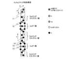
図にIn原子12、Ga原子13、GaまたはZn原子14、O原子15を示す。FIG. 2 shows the crystal structure of In2 Ga2 ZnO7 as an example of the structure of a crystalline region included in an oxide semiconductor film having the above structure. In2 Ga2 ZnO shown in FIG.
The crystal structure of7 is shown using a plan view parallel to the a- and b-axes and a cross-sectional view parallel to the c-axis, where the c-axis is perpendicular to the a- and b-axes, and the a-axis The angle between this and the b axis is 120°. In2 Ga2 ZnO7 shown in FIG. 2, a plan view shows
図2の断面図に示すように、In2Ga2ZnO7は、In酸化物層の間にある1層の
Ga酸化物層と、In酸化物層の間にある2層の酸化物層でGa酸化物層とZn酸化物層
をそれぞれ1層ずつ含むものが、c軸方向に交互に積層する構造となっている。また、図
2の平面図に示すように、In2Ga2ZnO7は三回対称性を有する六方晶構造をとる
。As shown in the cross-sectional view of FIG. 2, In2 Ga2 ZnO7 consists of one Ga oxide layer between the In oxide layers and two oxide layers between the In oxide layers. It has a structure in which layers each including one Ga oxide layer and one Zn oxide layer are stacked alternately in the c-axis direction. Further, as shown in the plan view of FIG. 2, In2 Ga2 ZnO7 has a hexagonal crystal structure with three-fold symmetry.
本実施の形態に示す、結晶性を有する領域を含む酸化物半導体膜は、一定以上の結晶性
を示すものであることが好ましい。また、当該結晶性を有する領域を含む酸化物半導体膜
は、単結晶とは異なる。このように、結晶性を有する領域を含む酸化物半導体膜は、全体
が非晶質構造の酸化物半導体膜と比較して良好な結晶性を有するので、酸素欠陥に代表さ
れるような欠陥や、ダングリングボンドなどに結合する水素などの不純物が低減されてい
る。特に結晶中の金属原子と結合している酸素は、非晶質中の金属原子と結合している酸
素と比較して、結合力が高くなり、水素などの不純物との反応性が低くなるので、欠陥の
生成が低減される。The oxide semiconductor film including a region with crystallinity, which is described in this embodiment, preferably exhibits a certain level of crystallinity or higher. Further, the oxide semiconductor film including the region having crystallinity is different from a single crystal. In this way, an oxide semiconductor film that includes a region with crystallinity has better crystallinity than an oxide semiconductor film that has an entirely amorphous structure, so it is free from defects such as oxygen defects and , impurities such as hydrogen that bond to dangling bonds are reduced. In particular, oxygen bonded to metal atoms in crystals has a higher bonding strength and is less reactive with impurities such as hydrogen than oxygen bonded to metal atoms in amorphous states. , the generation of defects is reduced.
例えば、In-Ga-Zn-O系金属酸化物からなる、結晶性を有する領域を含む酸化
物半導体膜は、c軸方向から電子線を照射した電子線回折強度測定において、散乱ベクト
ルの大きさが3.3nm-1以上4.1nm-1以下のピークにおける半値全幅と、散乱
ベクトルの大きさが5.5nm-1以上7.1nm-1以下のピークにおける半値全幅が
0.2nm-1以上となるような結晶性を示す。また好ましくは、散乱ベクトルの大きさ
が3.3nm-1以上4.1nm-1以下のピークにおける半値全幅が0.4nm-1以
上0.7nm-1以下であり、散乱ベクトルの大きさが5.5nm-1以上7.1nm-
1以下のピークにおける半値全幅が0.45nm-1以上1.4nm-1以下となるよう
な結晶性を示す。For example, in an oxide semiconductor film made of an In-Ga-Zn-O-based metal oxide that includes a crystalline region, the size of the scattering vector is is 3.3 nm-1 to 4.1 nm-1 or less, and the scattering vector size is 5.5 nm-1 to 7.1 nm-1 or less full width at half maximum is 0.2 nm-1 or more It shows crystallinity as follows. Preferably, the full width at half maximum of a peak with a scattering vector size of 3.3 nm-1 or more and 4.1 nm-1 or less is 0.4 nm-1 or more and 0.7 nm-1 or less, and the scattering vector size is 5 nm -1 or more. .5nm-1 or more 7.1nm-
It exhibits crystallinity such that the full width at half maximum at a peak of1 or less is 0.45 nm-1 or more and 1.4 nm-1 or less.
上述のように、本実施の形態に示す、結晶性を有する領域を含む酸化物半導体膜は、酸
素欠陥に代表される膜中の欠陥が低減されていることが好ましい。酸素欠陥に代表される
ような欠陥は、酸化物半導体膜中でキャリアの供給源のように機能するため、当該酸化物
半導体膜の電気伝導度が変動する原因となりうる。よって、これらが低減されている、結
晶性を有する領域を含む酸化物半導体膜は、電気伝導度が安定しており、可視光や紫外光
などの照射に対してもより電気的に安定な構造を有する。As described above, it is preferable that the oxide semiconductor film including a crystalline region described in this embodiment have reduced defects such as oxygen defects. Defects such as oxygen defects function as a carrier supply source in the oxide semiconductor film, and therefore can cause fluctuations in the electrical conductivity of the oxide semiconductor film. Therefore, an oxide semiconductor film containing a crystalline region in which these are reduced has stable electrical conductivity, and has a structure that is more electrically stable even when irradiated with visible light or ultraviolet light. has.
なお、結晶性を有する領域を含む酸化物半導体膜のESR(Electron Spi
n Resonance)測定を行うことにより、当該膜中の孤立電子の量を測定するこ
とができ、それにより酸素欠陥の量を推定することができる。例えば、In-Ga-Zn
-O系金属酸化物からなる結晶性を有する領域を含む酸化物半導体膜は、ESR測定にお
けるg=1.93近傍のピークのスピン密度が1.3×10¹⁸(spins/cm3)
より小さく、好ましくは5×10¹⁷(spins/cm3)以下、より好ましくは5×
1016(spins/cm3)、さらに好ましくは1×1016(spins/cm3
)とする。Note that the ESR (Electron Spi
By performing n Resonance measurement, the amount of lone electrons in the film can be measured, and thereby the amount of oxygen vacancies can be estimated. For example, In-Ga-Zn
An oxide semiconductor film including a crystalline region made of a -O-based metal oxide has a spin density of 1.3×10¹⁸ (spins/cm3 ) at a peak near g=1.93 in ESR measurement.
smaller, preferably 5×10¹⁷ (spins/cm3 ) or less, more preferably 5×
1016 (spins/cm3 ), more preferably 1×10¹⁶ (spins/cm3 )
).
上述のように、結晶性を有する領域を含む酸化物半導体膜中の水素や、水、水酸基また
は水素化物等の水素を含む不純物は低減されていることが好ましく、結晶性を有する領域
を含む酸化物半導体膜中の水素の濃度は1×10¹⁹atoms/cm3以下とすること
が好ましい。ダングリングボンドなどに結合する水素や、水、水酸基または水素化物等の
水素を含む不純物は、酸化物半導体膜中でキャリアの供給源のように機能するため、当該
酸化物半導体膜の電気伝導度が変動する原因となりうる。また、酸化物半導体膜に含まれ
る水素は、金属原子と結合する酸素と反応して水となると共に、酸素が脱離した格子(あ
るいは酸素が脱離した部分)には欠陥が形成されてしまう。よって、これらが低減されて
いる、結晶性を有する領域を含む酸化物半導体膜は、電気伝導度が安定しており、可視光
や紫外光などの照射に対してもより電気的に安定な構造を有する。As described above, hydrogen in an oxide semiconductor film including a region with crystallinity and impurities containing hydrogen such as water, hydroxyl groups, or hydrides are preferably reduced; The concentration of hydrogen in the semiconductor film is preferably 1×10¹⁹ atoms/cm3 or less. Hydrogen bonded to dangling bonds, etc., and impurities containing hydrogen such as water, hydroxyl groups, and hydrides function as a carrier supply source in the oxide semiconductor film, so the electrical conductivity of the oxide semiconductor film increases. may cause fluctuations. Additionally, hydrogen contained in the oxide semiconductor film reacts with oxygen bonded to metal atoms to form water, and defects are formed in the lattice from which oxygen is removed (or in the portion where oxygen is removed). . Therefore, an oxide semiconductor film containing a crystalline region in which these are reduced has stable electrical conductivity, and has a structure that is more electrically stable even when irradiated with visible light or ultraviolet light. has.
また、結晶性を有する領域を含む酸化物半導体膜中のアルカリ金属等の不純物は低減さ
れていることが好ましい。例えば、結晶性を有する領域を含む酸化物半導体膜において、
リチウムの濃度が5×1015cm-3以下、好ましくは1×1015cm-3以下、ナ
トリウムの濃度が5×1016cm-3以下、好ましくは1×1016cm-3以下、さ
らに好ましくは1×1015cm-3以下、カリウムの濃度が5×1015cm-3以下
、好ましくは1×1015cm-3以下とする。Further, impurities such as alkali metals in the oxide semiconductor film including a region having crystallinity are preferably reduced. For example, in an oxide semiconductor film including a region with crystallinity,
The concentration of lithium is 5×1015 cm-3 or less, preferably 1×1015 cm-3 or less, and the sodium concentration is 5×1016 cm-3 or less, preferably 1×1016 cm-3 or less, more preferably The concentration of potassium is 1×1015 cm−3 or less, and the potassium concentration is 5×1015 cm−3 or less, preferably 1×1015 cm−3 or less.
アルカリ金属、及びアルカリ土類金属は結晶性を有する領域を含む酸化物半導体にとっ
ては悪性の不純物であり、少ないほうがよい。特に、当該酸化物半導体膜をトランジスタ
に用いる場合、アルカリ金属のうちナトリウムは結晶性を有する領域を含む酸化物半導体
膜に接する絶縁膜に拡散し、キャリアを供給しうる。また、結晶性を有する領域を含む酸
化物半導体膜内において、金属と酸素の結合を分断し、あるいは結合中に割り込む。その
結果、トランジスタ特性の劣化(例えば、ノーマリオン化(しきい値の負へのシフト)、
移動度の低下等)をもたらす。加えて、特性のばらつきの原因ともなる。Alkali metals and alkaline earth metals are malignant impurities for an oxide semiconductor including a crystalline region, and the less they are, the better. In particular, when the oxide semiconductor film is used in a transistor, sodium among the alkali metals can diffuse into the insulating film in contact with the oxide semiconductor film including a crystalline region and supply carriers. Further, in the oxide semiconductor film including a region having crystallinity, the bond between metal and oxygen is broken or interrupted. As a result, deterioration of transistor characteristics (e.g. normalization (negative shift of threshold)),
(decreased mobility, etc.). In addition, it also causes variations in characteristics.
このような問題は、特に結晶性を有する領域を含む酸化物半導体膜中の水素の濃度が十
分に低い場合において顕著となる。したがって、結晶性を有する領域を含む酸化物半導体
膜中の水素の濃度が5×1019cm-3以下、特に5×1018cm-3以下である場
合には、アルカリ金属の濃度を上記の値にすることが強く求められる。よって、結晶性を
有する領域を含む酸化物半導体膜中の不純物を極めて低減し、アルカリ金属の濃度が5×
1016atoms/cm3以下、水素の濃度が5×1019atoms/cm3以下と
することが好ましい。Such a problem becomes particularly noticeable when the concentration of hydrogen in the oxide semiconductor film including a region having crystallinity is sufficiently low. Therefore, when the hydrogen concentration in the oxide semiconductor film including a crystalline region is 5×1019 cm−3 or less, particularly 5×1018 cm−3 or less, the alkali metal concentration is There is a strong need to make it a value. Therefore, the impurities in the oxide semiconductor film including the crystalline region can be extremely reduced, and the concentration of alkali metal can be reduced to 5x.
It is preferable that the hydrogen concentration is 1016 atoms/cm3 or less, and the hydrogen concentration is 5×10¹⁹ atoms/cm3 or less.
以上のように、結晶性を有する領域を含む酸化物半導体膜は、全体が非晶質構造の酸化
物半導体膜と比較して良好な結晶性を有するので、酸素欠陥に代表されるような欠陥や、
ダングリングボンドなどに結合する水素などの不純物が低減されている。これらの酸素欠
陥に代表されるような欠陥や、ダングリングボンドなどに結合する水素などは、酸化物半
導体膜中でキャリアの供給源のように機能するため、当該酸化物半導体膜の電気伝導度が
変動する原因となりうる。よって、これらが低減されている、結晶性を有する領域を含む
酸化物半導体膜は、電気伝導度が安定しており、可視光や紫外光などの照射に対してもよ
り電気的に安定な構造を有する。このような結晶性を有する領域を含む酸化物半導体膜を
トランジスタに用いることによって、安定した電気的特性を有する、信頼性の高い半導体
装置を提供することができる。As described above, an oxide semiconductor film that includes a crystalline region has better crystallinity than an oxide semiconductor film that has an entirely amorphous structure. or,
Impurities such as hydrogen that bind to dangling bonds are reduced. Defects such as these oxygen defects and hydrogen bonded to dangling bonds function as a carrier supply source in the oxide semiconductor film, so the electrical conductivity of the oxide semiconductor film decreases. may cause fluctuations. Therefore, an oxide semiconductor film containing a crystalline region in which these are reduced has stable electrical conductivity, and has a structure that is more electrically stable even when irradiated with visible light or ultraviolet light. has. By using an oxide semiconductor film including such a region with crystallinity in a transistor, a highly reliable semiconductor device with stable electrical characteristics can be provided.
次に、酸化物半導体膜中の酸素欠陥がどのようにして当該酸化物半導体膜の電気伝導度
に影響を与えるか、密度汎関数理論に基づいた第一原理計算を用いて考察した結果につい
て説明する。なお、以下の第一原理計算には、accelrys社製の第一原理計算ソフ
ト「CASTEP」を用いた。また、汎関数はGGA-PBEを、擬ポテンシャルはウル
トラソフト型を用いた。Next, we will explain how oxygen defects in an oxide semiconductor film affect the electrical conductivity of the oxide semiconductor film, using first-principles calculations based on density functional theory. do. Note that the first-principles calculation software "CASTEP" manufactured by Accelrys was used for the following first-principles calculations. Furthermore, GGA-PBE was used as the functional, and ultrasoft type was used as the pseudopotential.
本計算では、酸化物半導体膜のモデルとして、アモルファス状のInGaZnO4にお
いて酸素原子を一つ脱離させて当該部位に空孔(酸素欠陥)を残存させたモデルを作成し
て計算を行った。当該モデルの原子数は、Inを12個、Gaを12個、Znを12個、
Oを47個とした。このような構造のInGaZnO4に対して原子配置に関する構造最
適化を行い、電子状態密度を算出した。このとき、カットオフエネルギーは300eVと
した。In this calculation, as a model of the oxide semiconductor film, a model was created in which one oxygen atom was removed from amorphous InGaZnO4 and a vacancy (oxygen defect) remained at the corresponding site. The number of atoms in the model is 12 for In, 12 for Ga, 12 for Zn,
The number of O was 47. Structural optimization regarding the atomic arrangement was performed on InGaZnO4 having such a structure, and the electronic density of states was calculated. At this time, the cutoff energy was set to 300 eV.
電子状態密度計算の結果を図3に示す。図3は、縦軸に状態密度(DOS:Densi
ty of State)[states/eV]をとり、横軸にエネルギー[eV]を
とっており、横軸に示すエネルギーの原点は、フェルミエネルギーを示している。図3に
示すように、InGaZnO4の価電子帯上端は-0.74eV、伝導帯下端は0.56
eVとなっている。バンドギャップの値はInGaZnO4の実験値3.15eVと比較
すると非常に小さいが、密度汎関数理論に基づいた第一原理計算ではバンドギャップが実
験値よりも小さくなる事は良く知られており、今回の計算が不適切である事を示している
わけではない。Figure 3 shows the results of the electronic state density calculation. In Figure 3, the vertical axis represents the density of states (DOS).
The energy [eV] is plotted on the horizontal axis, and the origin of the energy shown on the horizontal axis indicates the Fermi energy. As shown in Figure 3, the upper end of the valence band ofInGaZnO4 is -0.74 eV, and the lower end of the conduction band is 0.56 eV.
eV. The value of the band gap is very small compared to the experimental value of 3.15 eV for InGaZnO4 , but it is well known that the band gap becomes smaller than the experimental value in first-principles calculations based on density functional theory. This does not indicate that the current calculation is inappropriate.
図3から、酸素欠陥を有するアモルファス状のInGaZnO4は、バンドギャップ内
に深い準位を有することが分かる。つまり、酸素欠陥を有するアモルファス状の酸化物半
導体のバンド構造では、酸素欠陥に起因するトラップ準位が当該バンドギャップ内の深い
準位として表されることが推測される。From FIG. 3, it can be seen that amorphous InGaZnO4 having oxygen vacancies has a deep level within the band gap. That is, in the band structure of an amorphous oxide semiconductor having oxygen vacancies, it is presumed that a trap level caused by the oxygen vacancies is expressed as a deep level within the bandgap.
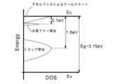
以上の考察に基づく、酸素欠陥を有するアモルファス状の酸化物半導体のバンドダイア
グラムを図4に示す。図4は、縦軸にエネルギー、横軸にDOSをとり、価電子帯(VB
:Valence Band)の上端のエネルギー準位Evから伝導帯(CB:Cond
uction Band)の下端のエネルギー準位Ecまでのエネルギーギャップは、実
験値に基づき3.15eVとした。FIG. 4 shows a band diagram of an amorphous oxide semiconductor having oxygen vacancies based on the above considerations. In Figure 4, energy is plotted on the vertical axis and DOS is plotted on the horizontal axis, and the valence band (VB
: Valence Band) from the upper end energy level Ev to the conduction band (CB: Cond
The energy gap to the lower end energy level Ec of the 3.15 eV was determined based on experimental values.
図4に示すバンドダイアグラム中には、当該酸化物半導体のアモルファス性に起因する
テールステートを伝導帯下端近傍に表している。さらに、伝導帯下端より約0.1eVの
浅いエネルギー準位に、当該アモルファス状の酸化物半導体内のダングリングボンドなど
に結合する水素に起因する水素ドナー準位を想定している。そして、伝導帯下端より約1
.8eVの深いエネルギー準位に、上述した当該アモルファス状の酸化物半導体内の酸素
欠陥に起因するトラップ準位を表している。なお、酸素欠陥に起因するトラップ準位のエ
ネルギー準位の値については、後述する実施例において詳細を説明する。In the band diagram shown in FIG. 4, a tail state due to the amorphous nature of the oxide semiconductor is shown near the lower end of the conduction band. Furthermore, it is assumed that a hydrogen donor level resulting from hydrogen bonded to a dangling bond or the like in the amorphous oxide semiconductor is located at a shallow energy level of approximately 0.1 eV below the lower end of the conduction band. And about 1 from the bottom of the conduction band
.. The deep energy level of 8 eV represents a trap level caused by oxygen defects in the amorphous oxide semiconductor described above. Note that the value of the energy level of the trap level due to oxygen vacancies will be explained in detail in Examples described later.
さらに以上の考察に基づく、バンドギャップ中にこのようなエネルギー準位、特に酸素
欠陥に起因する深いトラップ準位を有するアモルファス状の酸化物半導体の場合における
、バンド構造の電子と正孔の再結合モデルを図5(A)および図5(B)に示す。Furthermore, based on the above considerations, recombination of electrons and holes in the band structure in the case of amorphous oxide semiconductors that have such energy levels in the band gap, especially deep trap levels caused by oxygen defects. The model is shown in FIG. 5(A) and FIG. 5(B).
図5(A)に示す再結合モデルは、価電子帯に十分な数の正孔が存在し、且つ伝導帯に
十分な数の電子が存在する場合の再結合モデルである。当該アモルファス状の酸化物半導
体膜を光照射環境下に曝して、十分な数の電子正孔対が生成されることにより、当該酸化
物半導体のバンド構造は図5(A)に示すような再結合モデルで表される。当該再結合モ
デルにおいて、正孔は価電子帯の上端だけでなく、酸素欠陥に起因する深いトラップ準位
にも生成される。The recombination model shown in FIG. 5A is a recombination model when a sufficient number of holes exist in the valence band and a sufficient number of electrons exist in the conduction band. By exposing the amorphous oxide semiconductor film to a light irradiation environment and generating a sufficient number of electron-hole pairs, the band structure of the oxide semiconductor is reshaped as shown in FIG. 5(A). Represented by a coupled model. In the recombination model, holes are generated not only at the top of the valence band but also at deep trap levels caused by oxygen vacancies.
図5(A)に示す再結合モデルでは、2種類の再結合過程が並列に起こることを想定し
ている。一つの再結合過程は、伝導帯の電子が価電子帯の正孔と直接再結合するバンド間
再結合と呼ばれる再結合過程である。そしてもう一つの再結合過程は、伝導帯の電子が酸
素欠陥に起因するトラップ準位の正孔と再結合する再結合過程である。ここで、バンド間
再結合は酸素欠陥に起因するトラップ準位における再結合より頻度が高いので、価電子帯
の正孔の数が十分に少なくなることで、先にバンド間再結合が終了する。これにより図5
(A)に示す再結合モデルは、伝導帯下端の電子が酸素欠陥に起因するトラップ準位の正
孔と再結合する再結合過程だけとなって図5(B)に示す再結合モデルに移行する。The recombination model shown in FIG. 5(A) assumes that two types of recombination processes occur in parallel. One recombination process is called interband recombination, in which electrons in the conduction band directly recombine with holes in the valence band. Another recombination process is a recombination process in which electrons in the conduction band recombine with holes in the trap level caused by oxygen vacancies. Here, interband recombination is more frequent than recombination at trap levels caused by oxygen vacancies, so when the number of holes in the valence band becomes sufficiently small, interband recombination ends first. . As a result, Figure 5
The recombination model shown in (A) shifts to the recombination model shown in Figure 5 (B), with only the recombination process in which electrons at the bottom of the conduction band recombine with holes in the trap level caused by oxygen defects. do.
なお、価電子帯に十分な数の正孔が存在し、且つ伝導帯に十分な数の電子が存在するよ
うにするには、当該酸化物半導体に十分な光照射を行えばよく、その後光照射を止めるこ
とにより、図5(A)に示す再結合モデルのように、電子と正孔の再結合が行われる。こ
の時の当該酸化物半導体中を流れる電流(光電流とも呼ばれる。)が減衰するのに要する
時間(緩和時間)は、図5(B)に示す再結合モデルにおける光電流の緩和時間と比較す
ると短くなる。なお、これらの詳細については、後述する実施例を参照されたい。Note that in order to have a sufficient number of holes in the valence band and a sufficient number of electrons in the conduction band, it is sufficient to irradiate the oxide semiconductor with sufficient light, and then irradiate the oxide semiconductor with sufficient light. By stopping the irradiation, electrons and holes are recombined as shown in the recombination model shown in FIG. 5(A). The time (relaxation time) required for the current flowing through the oxide semiconductor (also called photocurrent) to decay at this time is compared with the relaxation time of the photocurrent in the recombination model shown in FIG. 5(B). Becomes shorter. Note that for details of these, please refer to Examples described later.
次に、図5(B)に示す再結合モデルは、図5(A)に示す再結合モデルが進行し、価
電子帯の正孔の数が十分に低減された後の再結合モデルである。図5(B)に示す再結合
モデルでは、再結合過程がほとんど酸素欠陥に起因するトラップ準位における再結合だけ
になってしまうので、図5(A)に示す再結合モデルと比較して伝導帯の電子の数は緩や
かに減少する。もちろん当該再結合過程の間、伝導帯に存在する電子は酸化物半導体膜中
の電気伝導に寄与する。これにより、バンド間再結合が主な再結合過程である、図5(A
)に示す再結合モデルと比較して、図5(B)に示す再結合モデルは光電流の緩和時間が
長くなる。なお、これらの詳細については、後述する実施例を参照されたい。Next, the recombination model shown in FIG. 5(B) is a recombination model after the recombination model shown in FIG. 5(A) has progressed and the number of holes in the valence band has been sufficiently reduced. . In the recombination model shown in Fig. 5(B), the recombination process is almost only recombination at the trap level caused by oxygen vacancies, so compared to the recombination model shown in Fig. 5(A), conduction The number of electrons in the band decreases slowly. Of course, during the recombination process, electrons present in the conduction band contribute to electrical conduction in the oxide semiconductor film. This shows that interband recombination is the main recombination process in Figure 5 (A
), the recombination model shown in FIG. 5(B) has a longer photocurrent relaxation time. Note that for details of these, please refer to Examples described later.
このように、酸素欠陥に起因する深いトラップ準位を有するアモルファス状の酸化物半
導体は、バンド構造における電子正孔対の再結合モデルを2種類有し、光電流の緩和時間
も2種類に分けることができる。ここで、特に図5(B)に示す再結合モデルにおける光
電流の緩和の遅延は、当該酸化物半導体膜をトランジスタなどに用いて光照射下でゲート
電極に負バイアスをかける際に、当該酸化物半導体膜やその界面に固定電荷を形成する原
因となりうる。このようにして、酸化物半導体膜中の酸素欠陥は当該酸化物半導体膜の電
気伝導度に悪影響を与えることが考察される。In this way, amorphous oxide semiconductors with deep trap levels caused by oxygen vacancies have two types of recombination models for electron-hole pairs in the band structure, and the relaxation time of photocurrent can also be divided into two types. be able to. Here, in particular, the delay in relaxation of the photocurrent in the recombination model shown in FIG. This may cause fixed charges to be formed in the semiconductor film or its interface. In this way, it is considered that oxygen vacancies in the oxide semiconductor film adversely affect the electrical conductivity of the oxide semiconductor film.
しかし、本発明の一態様に係る、結晶性を有する領域を含む酸化物半導体膜は、全体が
非晶質構造の酸化物半導体膜と比較して良好な結晶性を有するので、酸素欠陥に代表され
るような欠陥が低減されている。よって、本発明の一態様に係る、結晶性を有する領域を
含む酸化物半導体膜は、電気伝導度が安定しており、可視光や紫外光などの照射に対して
もより電気的に安定な構造を有する。このような結晶性を有する領域を含む酸化物半導体
膜をトランジスタに用いることによって、安定した電気的特性を有する、信頼性の高い半
導体装置を提供することができる。However, the oxide semiconductor film including a region with crystallinity according to one embodiment of the present invention has better crystallinity than an oxide semiconductor film having an entirely amorphous structure; Defects such as those that occur are reduced. Therefore, an oxide semiconductor film including a crystalline region according to one embodiment of the present invention has stable electrical conductivity and is more electrically stable even when irradiated with visible light or ultraviolet light. Has a structure. By using an oxide semiconductor film including such a region with crystallinity in a transistor, a highly reliable semiconductor device with stable electrical characteristics can be provided.
以上、本実施の形態に示す構成などは、他の実施の形態に示す構成、方法などと適宜組
み合わせて用いることができる。As described above, the structure shown in this embodiment can be used in combination with the structures, methods, etc. shown in other embodiments, as appropriate.
(実施の形態2)
本実施の形態では、実施の形態1に示す、結晶性を有する領域を含む酸化物半導体膜を
用いたトランジスタおよび当該トランジスタの作製方法について図6乃至図10を用いて
説明する。図6は、半導体装置の構成の一形態である、トップゲート構造のトランジスタ
120の作製工程を示す断面図である。(Embodiment 2)
In this embodiment, a transistor using an oxide semiconductor film including a crystalline region and a method for manufacturing the transistor described in
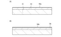
まず、結晶性を有する領域を含む酸化物半導体膜を成膜する前に、図6(A)に示すよ
うに、基板51上に下地絶縁膜53を形成することが好ましい。First, before forming an oxide semiconductor film including a crystalline region, it is preferable to form a
基板51は、少なくとも、後の加熱処理に耐えうる程度の耐熱性を有していることが必
要となる。基板51としてガラス基板を用いる場合、歪み点が730℃以上のものを用い
ることが好ましい。ガラス基板には、例えば、アルミノシリケートガラス、アルミノホウ
ケイ酸ガラス、バリウムホウケイ酸ガラスなどのガラス材料が用いられる。なお、B2O
3よりBaOを多く含むガラス基板を用いることが好ましい。基板51がマザーガラスの
場合、基板の大きさは、第1世代(320mm×400mm)、第2世代(400mm×
500mm)、第3世代(550mm×650mm)、第4世代(680mm×880m
m、または730mm×920mm)、第5世代(1000mm×1200mmまたは1
100mm×1250mm)、第6世代(1500mm×1800mm)、第7世代(1
900mm×2200mm)、第8世代(2160mm×2460mm)、第9世代(2
400mm×2800mm、または2450mm×3050mm)、第10世代(295
0mm×3400mm)等を用いることができる。マザーガラスは、処理温度が高く、処
理時間が長いと大幅に収縮するため、マザーガラスを使用して大量生産を行う場合、作製
工程の加熱処理は、600℃以下、好ましくは450℃以下とすることが望ましい。The
It is preferable to use a glass substrate containing more BaO than3 . When the
500mm), 3rd generation (550mm x 650mm), 4th generation (680mm x 880m)
m, or 730mm x 920mm), 5th generation (1000mm x 1200mm or 1
100mm x 1250mm), 6th generation (1500mm x 1800mm), 7th generation (1
900mm x 2200mm), 8th generation (2160mm x 2460mm), 9th generation (2
400mm x 2800mm or 2450mm x 3050mm), 10th generation (295mm
0 mm x 3400 mm), etc. can be used. Mother glass shrinks significantly when the processing temperature is high and the processing time is long, so when mass production is performed using mother glass, the heat treatment in the manufacturing process should be at 600 ° C or lower, preferably at 450 ° C or lower. This is desirable.
なお、上記のガラス基板に代えて、セラミック基板、石英基板、サファイア基板などの
絶縁体でなる基板を用いることができる。他にも、結晶化ガラスなどを用いることができ
る。さらには、シリコンウェハ等の半導体基板の表面や金属材料よりなる導電性の基板の
表面に絶縁層を形成したものを用いることもできる。Note that instead of the glass substrate described above, a substrate made of an insulator such as a ceramic substrate, a quartz substrate, a sapphire substrate, etc. can be used. Besides, crystallized glass or the like can be used. Furthermore, it is also possible to use an insulating layer formed on the surface of a semiconductor substrate such as a silicon wafer or a conductive substrate made of a metal material.
下地絶縁膜53は、加熱により酸素の一部が放出する酸化物絶縁膜を用いて形成するこ
とが好ましい。加熱により酸素の一部が放出する酸化物絶縁膜としては、化学量論比を満
たす酸素よりも多くの酸素を含む酸化物絶縁膜を用いることが好ましい。加熱により酸素
の一部が放出する酸化物絶縁膜を下地絶縁膜53に用いることで、後の工程で加熱処理を
行う際に酸化物半導体膜に酸素を拡散させることができる。加熱により酸素の一部が放出
する酸化物絶縁膜としては、代表的には、酸化シリコン、酸化窒化シリコン、酸化アルミ
ニウム、酸化窒化アルミニウム、酸化ガリウム、酸化ハフニウム、酸化イットリウム等を
用いることができる。The
下地絶縁膜53は、50nm以上、好ましくは200nm以上500nm以下とする。
下地絶縁膜53を厚くすることで、下地絶縁膜53からの酸素放出量を増加させることが
できると共に、その増加によって下地絶縁膜53及び後に形成される酸化物半導体膜との
界面における欠陥を低減することが可能である。The
By increasing the thickness of the
下地絶縁膜53は、スパッタリング法、CVD法等により形成する。なお、加熱により
酸素の一部が放出する酸化物絶縁膜は、スパッタリング法を用いることで容易に形成する
ことができる。加熱により酸素の一部が放出する酸化物絶縁膜をスパッタリング法により
形成する場合は、成膜ガス中の酸素量が高いことが好ましく、酸素、または酸素及び希ガ
スの混合ガス等を用いることができる。代表的には、成膜ガス中の酸素濃度を6%以上1
00%以下にすることが好ましい。The
It is preferable to set it to 00% or less.
また、下地絶縁膜53は、必ずしも加熱により酸素の一部が放出する酸化物絶縁膜を用
いて形成する必要はなく、窒化シリコン、窒化酸化シリコン、窒化アルミニウムなどを用
いて窒化物絶縁膜を形成してもよい。また、下地絶縁膜53は、上記の酸化物絶縁膜と窒
化物絶縁膜の積層構造としてもよく、その場合には窒化物絶縁膜上に酸化物絶縁膜を設け
ることが好ましい。下地絶縁膜53として窒化物絶縁膜を用いることにより、アルカリ金
属などの不純物を含むガラス基板を用いる場合、アルカリ金属などの酸化物半導体膜への
侵入を防止できる。リチウム、ナトリウム、カリウム等のアルカリ金属は、酸化物半導体
に対して悪性の不純物であるために酸化物半導体膜中の含有量を少なくすることが好まし
い。窒化物絶縁膜は、CVD法、スパッタリング法等で形成することができる。Furthermore, the
次に、図6(B)に示すように、スパッタリング装置を用いたスパッタリング法により
、下地絶縁膜53上に厚さ30nm以上50μm以下の結晶性を有する領域を含む酸化物
半導体膜55を成膜する。Next, as shown in FIG. 6B, an
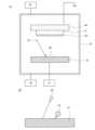
ここで、スパッタリング装置の処理室について、図7(A)を用いて説明する。処理室
31には、排気手段33及びガス供給手段35が接続される。また、処理室31内には、
基板支持体40及びターゲット41が設けられる。ターゲット41は、電源装置37に接
続される。Here, the processing chamber of the sputtering apparatus will be explained using FIG. 7(A). An exhaust means 33 and a gas supply means 35 are connected to the
A
処理室31は、GNDに接続されている。また、処理室31のリークレートを1×10
-10Pa・m3/秒以下とすることで、スパッタリング法により成膜する膜への不純物
の混入を低減することができる。The
By setting it to-10 Pa·m3 /sec or less, it is possible to reduce the incorporation of impurities into the film formed by the sputtering method.
リークレートを低くするには、外部リークのみならず内部リークを低減する必要がある
。外部リークとは、微小な穴やシール不良などによって真空系の外から気体が流入するこ
とである。内部リークとは、真空系内のバルブなどの仕切りからの漏れや内部の部材から
の放出ガスに起因する。リークレートを1×10⁻¹⁰Pa・m3/秒以下とするために
は、外部リーク及び内部リークの両面から対策をとる必要がある。In order to lower the leak rate, it is necessary to reduce not only external leaks but also internal leaks. External leak refers to the inflow of gas from outside the vacuum system due to minute holes or poor sealing. Internal leaks are caused by leaks from partitions such as valves in the vacuum system or by gases released from internal members. In order to reduce the leak rate to 1×10⁻¹⁰ Pa·m3 /sec or less, it is necessary to take measures against both external and internal leaks.
外部リークを減らすには、処理室の開閉部分はメタルガスケットでシールするとよい。
メタルガスケットは、フッ化鉄、酸化アルミニウム、または酸化クロムによって被覆され
た金属材料を用いると好ましい。メタルガスケットはOリングと比べ密着性が高く、外部
リークを低減できる。また、フッ化鉄、酸化アルミニウム、酸化クロムなどの不動態によ
って被覆された金属材料を用いることで、メタルガスケットから生じる水素を含む放出ガ
スが抑制され、内部リークも低減することができる。To reduce external leakage, the opening and closing parts of the processing chamber should be sealed with metal gaskets.
The metal gasket is preferably made of a metal material coated with iron fluoride, aluminum oxide, or chromium oxide. Metal gaskets have higher adhesion than O-rings and can reduce external leakage. Further, by using a metal material coated with a passive state such as iron fluoride, aluminum oxide, or chromium oxide, gases containing hydrogen generated from the metal gasket can be suppressed, and internal leakage can also be reduced.
処理室31の内壁を構成する部材として、水素を含む放出ガスの少ないアルミニウム、
クロム、チタン、ジルコニウム、ニッケルまたはバナジウムを用いる。また、前述の材料
を鉄、クロム及びニッケルなどを含む合金材料に被覆して用いてもよい。鉄、クロム及び
ニッケルなどを含む合金材料は、剛性があり、熱に強く、また加工に適している。ここで
、表面積を小さくするために部材の表面凹凸を研磨などによって低減しておくと、放出ガ
スを低減できる。あるいは、前述のスパッタリング装置の部材をフッ化鉄、酸化アルミニ
ウム、酸化クロムなどの不動態で被覆してもよい。The inner wall of the
Use chromium, titanium, zirconium, nickel or vanadium. Further, the above-mentioned materials may be used by coating an alloy material containing iron, chromium, nickel, etc. Alloy materials containing iron, chromium, nickel, etc. are rigid, heat resistant, and suitable for processing. Here, if the surface irregularities of the member are reduced by polishing or the like in order to reduce the surface area, the released gas can be reduced. Alternatively, the members of the sputtering apparatus described above may be coated with a passivation material such as iron fluoride, aluminum oxide, or chromium oxide.
処理室31の内部に設ける部材は、極力金属材料のみで構成することが好ましく、例え
ば石英などで構成される覗き窓などを設置する場合も、放出ガスを抑制するために表面を
フッ化鉄、酸化アルミニウム、酸化クロムなどの不動態で薄く被覆するとよい。It is preferable that the members installed inside the
さらに、スパッタガスを処理室31に導入する直前に、スパッタガスの精製機を設ける
ことが好ましい。このとき、精製機から処理室までの配管の長さを5m以下、好ましくは
1m以下とする。配管の長さを5m以下または1m以下とすることで、配管からの放出ガ
スの影響を長さに応じて低減できる。Further, it is preferable to provide a sputter gas purifier immediately before introducing the sputter gas into the
シリンダーから処理室31まで、スパッタガスを流すための配管にはフッ化鉄、酸化ア
ルミニウム、酸化クロムなどの不動態で内部が被覆された金属配管を用いることが好まし
い。前述の配管は、例えばSUS316L-EP配管と比べ、水素を含むガスの放出量が
少なく、成膜ガスへの不純物の混入を低減できる。また、配管の継手には、高性能超小型
メタルガスケット継手(UPG継手)を用いるとよい。また、配管の材料を全て金属材料
で構成することで、樹脂等を用いた場合と比べ、生じる放出ガス及び外部リークの影響を
低減できるため好ましい。As the piping for flowing the sputtering gas from the cylinder to the
処理室31の排気は、ドライポンプなどの粗引きポンプと、スパッタイオンポンプ、タ
ーボ分子ポンプ及びクライオポンプなどの高真空ポンプとを適宜組み合わせて行うとよい
。ターボ分子ポンプは大きいサイズの分子の排気が優れる一方、水素や水の排気能力が低
い。そこで、水の排気能力の高いクライオポンプ及び水素の排気能力の高いスパッタイオ
ンポンプを組み合わせることが有効となる。The
処理室31の内側に存在する吸着物は、内壁に吸着しているために処理室の圧力に影響
しないが、処理室を排気した際のガス放出の原因となる。そのため、リークレートと排気
速度に相関はないが、排気能力の高いポンプを用いて、処理室に存在する吸着物をできる
限り脱離し、予め排気しておくことが重要である。なお、吸着物の脱離を促すために、処
理室をベーキングしてもよい。ベーキングすることで吸着物の脱離速度を10倍程度大き
くすることができる。ベーキングは100℃以上450℃以下で行えばよい。このとき、
不活性ガスを導入しながら吸着物の除去を行うと、排気するだけでは脱離しにくい水など
の脱離速度をさらに大きくすることができる。The adsorbate present inside the
If adsorbed substances are removed while introducing an inert gas, the rate of desorption of water, etc., which is difficult to desorb only by exhausting, can be further increased.
排気手段33は、処理室31内の不純物を排気すると共に、処理室31内の圧力を制御
することができる。排気手段33は、吸着型の真空ポンプを用いることが好ましい。例え
ば、クライオポンプ、イオンポンプ、チタンサブリメーションポンプを用いることが好ま
しい。上記吸着型の真空ポンプを用いることで、酸化物半導体膜に含まれる水素の量を低
減することができる。The exhaust means 33 can exhaust impurities within the
なお、酸化物半導体膜に含まれる水素は、水素原子の他、水素分子、水、水酸基、また
は水素化物として含まれる場合もある。Note that hydrogen contained in the oxide semiconductor film may be contained not only as a hydrogen atom but also as a hydrogen molecule, water, a hydroxyl group, or a hydride.
ガス供給手段35は、ターゲットをスパッタリングするためのガスを処理室31内に供
給する手段である。ガス供給手段35は、ガスが充填されたシリンダ、圧力調整弁、スト
ップバルブ、マスフローコントローラ等で構成されている。なお、ガス供給手段35に精
製機を設けることで、処理室31内に導入するガスに含まれる不純物を低下することがで
きる。ターゲットをスパッタリングするガスとしては、ヘリウム、ネオン、アルゴン、キ
セノン、クリプトン等の希ガスを用いる。または、上記希ガスの一と、酸素との混合ガス
を用いることができる。The gas supply means 35 is a means for supplying gas into the
電源装置37は、RF電源装置、AC電源装置、DC電源装置等を適宜用いることがで
きる。なお、図示しないがターゲットを支持するターゲット支持体の内部または外側にマ
グネットを設けると、ターゲット周辺に高密度のプラズマを閉じこめることができ、成膜
速度の向上及び基板へのプラズマダメージを低減できる。当該方法は、マグネトロンスパ
ッタリング法とよばれる。更には、マグネトロンスパッタリング法において、マグネット
を回転可能にすると、磁界の偏りを低減できるため、ターゲットの使用効率が高まり、か
つ基板の面内における膜質のばらつきを低減できる。As the
基板支持体40は、GNDに接続されている。基板支持体40にはヒータが設けられて
いる。ヒータとしては、抵抗発熱体などの発熱体からの熱伝導または熱輻射によって、被
処理物を加熱する装置を用いることができる。The
ターゲット41としては、亜鉛を含む金属酸化物ターゲットを用いることが好ましい。
ターゲット41の代表例としては、四元系金属酸化物であるIn-Sn-Ga-Zn-O
系金属酸化物や、三元系金属酸化物であるIn-Ga-Zn-O系金属酸化物、In-S
n-Zn-O系金属酸化物、In-Al-Zn-O系金属酸化物、Sn-Ga-Zn-O
系金属酸化物、Al-Ga-Zn-O系金属酸化物、Sn-Al-Zn-O系金属酸化物
や、二元系金属酸化物であるIn-Zn-O系金属酸化物、Sn-Zn-O系金属酸化物
などのターゲットを用いることができる。As the
A typical example of the
In-Ga-Zn-O-based metal oxides, In-Ga-Zn-O-based metal oxides that are ternary metal oxides, In-S
n-Zn-O metal oxide, In-Al-Zn-O metal oxide, Sn-Ga-Zn-O
metal oxides, Al-Ga-Zn-O-based metal oxides, Sn-Al-Zn-O-based metal oxides, binary metal oxides such as In-Zn-O-based metal oxides, Sn- A target such as Zn—O-based metal oxide can be used.
ターゲット41の一例として、In、Ga、及びZnを含む金属酸化物ターゲットを、
In2O3:Ga2O3:ZnO=1:1:1[mol数比]の組成比とする。また、I
n2O3:Ga2O3:ZnO=1:1:2[mol数比]の組成比を有するターゲット
、またはIn2O3:Ga2O3:ZnO=1:1:4[mol数比]の組成比を有する
ターゲット、In2O3:Ga2O3:ZnO=2:1:8[mol数比]の組成比を有
するターゲットを用いることもできる。As an example of the
The composition ratio is In2 O3 :Ga2 O3 :ZnO=1:1:1 [molar ratio]. Also, I
A target having a composition ratio of n2 O3 :Ga2 O3 :ZnO=1:1:2 [mol number ratio], or In2 O3 :Ga2 O3 :ZnO=1:1:4 [mol number A target having a composition ratio of In2 O3 :Ga2 O3 :ZnO=2:1:8 [molar ratio] can also be used.
なお、ターゲット41と基板51との間隔(T-S間距離)は、原子量の小さい原子が
優先的に基板51上の下地絶縁膜53に到着することが可能な間隔とすることが好ましい
。Note that the distance between the
図7(A)に示すように、基板支持体40上に下地絶縁膜53が形成された基板51を
、スパッタリング装置の処理室31内に設置する。次に、ガス供給手段35から処理室3
1にターゲット41をスパッタリングするガスを導入する。ターゲット41の純度は、9
9.9%以上、好ましくは99.99%以上のものを用いる。次に、ターゲット41に接
続される電源装置37に電力を供給する。この結果、ガス供給手段35から処理室31に
導入されたスパッタリングガスのイオン43及び電子が、ターゲット41をスパッタリン
グする。As shown in FIG. 7A, a
A gas for sputtering the
The content is 9.9% or more, preferably 99.99% or more. Next, power is supplied to the
ここで、ターゲット41及び基板51の間隔を、原子量の小さい原子が優先的に基板5
1上の下地絶縁膜53に到着し堆積することが可能な間隔としておくことにより、図7(
B)に示すように、ターゲット41に含まれる原子において、原子量の小さい原子45が
、原子量の大きい原子47より優先的に基板側へ移動することができる。Here, the distance between the
7 (
As shown in B), among the atoms contained in the
ターゲット41においては、亜鉛は、インジウム等よりも原子量が小さい。このため、
亜鉛が優先的に下地絶縁膜53上に堆積する。また、成膜時の雰囲気に酸素を含み、基板
支持体40には、成膜時に基板及び堆積膜を加熱するヒータが設けられるため、下地絶縁
膜53上に堆積した亜鉛が酸化され、六方晶構造の亜鉛を含む結晶を有する種結晶55a
、代表的には六方晶構造の酸化亜鉛を有する種結晶が形成される。なお、ターゲット41
にアルミニウム等の亜鉛より原子量の小さい原子が含まれる場合、亜鉛と共に、アルミニ
ウム等の亜鉛より原子量の小さい原子も優先的に下地絶縁膜53上に堆積する。In the
Zinc is preferentially deposited on the
, typically seed crystals having a hexagonal structure of zinc oxide are formed. In addition,
In the case that atoms such as aluminum having an atomic weight smaller than zinc are included, atoms such as aluminum having an atomic weight smaller than zinc are preferentially deposited on the
種結晶55aは、a-b面において六角形の格子を有する結合を有し、a-b面が膜表
面に概略平行であり、c軸が膜表面に概略垂直である六方晶のウルツ鉱構造の亜鉛を含む
結晶を有する。ここで、a-b面において六角形の格子を有する結合を有し、a-b面が
膜表面に概略平行であり、c軸が膜表面に概略垂直である六方晶構造の亜鉛を含む結晶に
ついて、図8を用いて説明する。ここでは、六方晶構造の亜鉛を含む結晶の代表例として
、酸化亜鉛を用いて説明し、黒丸が亜鉛、白丸が酸素を示す。図8(A)は、a-b面に
おける、六方晶構造の酸化亜鉛の模式図であり、図8(B)は、紙面の縦方向をc軸方向
とした、六方晶構造の酸化亜鉛の模式図である。図8(A)に示すように、a-b面にお
ける上平面において、亜鉛及び酸素が六角形をなす結合をしている。また、図8(B)に
示すように、亜鉛及び酸素がなす六角形の格子を有する結合を有する層が積層され、c軸
方向はa-b面に垂直である。種結晶55aは、a-b面において六角形の格子を有する
結合を有する層をc軸方向に1原子層以上有する。The
連続して、ターゲット41をスパッタリングガスでスパッタリングすることで、種結晶
55a上にターゲットに含まれる原子が堆積するが、このとき種結晶55aを核として結
晶成長するため、種結晶55a上に六方晶構造の結晶性を有する領域を含む酸化物半導体
膜55bを形成することができる。なお、基板51は、基板支持体40に設けられるヒー
タによって加熱されるため、種結晶55aを核とし、被表面に堆積する原子が酸化されつ
つ結晶成長する。By continuously sputtering the
酸化物半導体膜55bは、種結晶55aを核とし、ターゲット41の表面における原子
量の重い原子、及び種結晶55aの形成の後にスパッタリングされた原子量の軽い原子が
酸化されつつ結晶成長するため、種結晶55aと同様に、a-b面において六角形の格子
を有する結合を有し、a-b面が膜表面に概略平行であり、c軸が膜表面に概略垂直であ
る六方晶構造の結晶性を有する領域を含む。即ち、種結晶55a及び酸化物半導体膜55
bで構成される酸化物半導体膜55は、下地絶縁膜53表面に概略平行なa-b面におい
て六角形の格子を有する結合を有し、c軸が膜表面に概略垂直である六方晶構造の結晶性
を有する領域を含む。つまり、酸化物半導体膜55に含まれる六方晶構造の結晶性を有す
る領域はc軸配向している。なお、図6(B)では、種結晶55aと酸化物半導体膜55
bの界面を点線で示し、酸化物半導体膜の積層と説明しているが、明確な界面が存在して
いるのではなく、あくまで分かりやすく説明するために図示している。The
The
Although the interface b is indicated by a dotted line and is described as a stack of oxide semiconductor films, there is no clear interface, and the interface is shown for ease of understanding.
このときのヒータによる基板の加熱温度は200℃より大きく400℃以下、好ましく
は250℃以上350℃以下とする。200℃より大きく400℃以下、好ましくは25
0℃以上350℃以下に基板を加熱しながら成膜をすることによって、成膜と同時に加熱
処理がなされるので、良好な結晶性を有する領域を含む酸化物半導体膜を成膜することが
できる。なお、スパッタリング時における被成膜面の温度は、250℃以上基板の熱処理
上限温度以下とする。The heating temperature of the substrate by the heater at this time is greater than 200°C and less than 400°C, preferably greater than 250°C and less than 350°C. More than 200°C and less than 400°C, preferably 25
By forming the film while heating the substrate to a temperature of 0° C. or higher and 350° C. or lower, heat treatment is performed at the same time as the film formation, so it is possible to form an oxide semiconductor film that includes a region with good crystallinity. . Note that the temperature of the surface to be film-formed during sputtering is set to 250° C. or higher and lower than the upper limit temperature for heat treatment of the substrate.
なお、スパッタリングガスは、希ガス(代表的にはアルゴン)、酸素、希ガス及び酸素
の混合ガスを適宜用いる。また、スパッタリングガスには、水素、水、水酸基または水素
化物などの不純物が除去された高純度ガスを用いることが好ましい。Note that as the sputtering gas, a rare gas (typically argon), oxygen, and a mixed gas of the rare gas and oxygen are appropriately used. Furthermore, it is preferable to use a high-purity gas from which impurities such as hydrogen, water, hydroxyl groups, or hydrides are removed as the sputtering gas.
なお、基板支持体40及びターゲット41を有する処理室の圧力を0.4Pa以下とす
ることで、結晶性を有する領域を含む酸化物半導体膜の表面及び膜中への、アルカリ金属
、水素等の不純物の混入を低減することができる。Note that by setting the pressure of the processing chamber containing the
また、スパッタリング装置の処理室のリークレートを1×10⁻¹⁰Pa・m3/秒以
下とすることで、スパッタリング法による成膜途中における結晶性を有する領域を含む酸
化物半導体膜への、アルカリ金属、水素、水、水酸基または水素化物等の不純物の混入を
低減することができる。また、排気系として吸着型の真空ポンプを用いることで、排気系
からアルカリ金属、水素、水、水酸基または水素化物等の不純物の逆流を低減することが
できる。In addition, by setting the leak rate of the processing chamber of the sputtering device to 1×10⁻¹⁰ Pa·m3 /sec or less, the alkali Contamination with impurities such as metals, hydrogen, water, hydroxyl groups, or hydrides can be reduced. Furthermore, by using an adsorption type vacuum pump as the exhaust system, it is possible to reduce the backflow of impurities such as alkali metals, hydrogen, water, hydroxyl groups, or hydrides from the exhaust system.
また、ターゲット41の純度を、99.99%以上とすることで、結晶性を有する領域
を含む酸化物半導体膜に混入するアルカリ金属、水素、水、水酸基または水素化物等を低
減することができる。また、当該ターゲットを用いることで、酸化物半導体膜55におい
て、リチウムの濃度を5×1015cm-3以下、好ましくは1×1015cm-3以下
、ナトリウムの濃度を5×1016cm-3以下、好ましくは1×1016cm-3以下
、さらに好ましくは1×1015cm-3以下、カリウムの濃度を5×1015cm-3
以下、好ましくは1×1015cm-3以下とすることができる。Further, by setting the purity of the
Below, it can be preferably set to 1×1015 cm−3 or less.
上記の成膜方法では、同一のスパッタリング工程において、ターゲットに含まれる原子
量の違いを利用し、原子量の小さい亜鉛を優先的に酸化絶縁膜に堆積させ、種結晶を形成
すると共に、種結晶上に原子量の大きいインジウム等を結晶成長させつつ堆積させるため
、複数の工程を経ずとも、結晶性を有する領域を含む酸化物半導体膜を形成することがで
きる。In the above film formation method, in the same sputtering process, zinc with a small atomic weight is preferentially deposited on the oxide insulating film by utilizing the difference in atomic weight contained in the target, forming a seed crystal, and depositing zinc on the seed crystal. Since indium or the like having a large atomic weight is deposited while growing crystals, an oxide semiconductor film including a region having crystallinity can be formed without going through multiple steps.
上記の酸化物半導体膜55の成膜方法では、スパッタリング法の成膜によって、種結晶
55aと酸化物半導体膜55bとを一括で成膜しながら結晶化したが、本実施の形態に係
る酸化物半導体膜は必ずしもこのように成膜する必要はない。たとえば、種結晶と酸化物
半導体膜の成膜と結晶化をそれぞれ別々に行っても良い。In the above-described method for forming the
以下に、図9を用いて、種結晶と酸化物半導体膜の成膜と結晶化をそれぞれ別々に行う
方法について説明する。また、以下のように結晶性を有する領域を含む酸化物半導体膜を
成膜する方法を、本明細書中で2step法とよぶ場合がある。なお、図1の断面TEM
像に示した、結晶性を有する領域を含む酸化物半導体膜は、当該2step法をもちいて
形成したものである。A method for separately forming and crystallizing a seed crystal and an oxide semiconductor film will be described below with reference to FIG. 9 . Further, a method for forming an oxide semiconductor film including a region having crystallinity as described below is sometimes referred to as a 2-step method in this specification. In addition, the cross-sectional TEM of Figure 1
The oxide semiconductor film including the crystalline region shown in the image was formed using the two-step method.
まず、下地絶縁膜53上に膜厚1nm以上10nm以下の第1の酸化物半導体膜を形成
する。第1の酸化物半導体膜の形成は、スパッタリング法を用い、そのスパッタリング法
による成膜時の基板温度は200℃以上400℃以下とすることが好ましい。その他の成
膜条件については、上記の酸化物半導体膜の成膜方法と同様である。First, a first oxide semiconductor film having a thickness of 1 nm or more and 10 nm or less is formed on the
次いで、基板を配置するチャンバー雰囲気を窒素、または乾燥空気とし、第1の加熱処
理を行う。第1の加熱処理の温度は、400℃以上750℃以下とする。第1の加熱処理
によって、第1の酸化物半導体膜を結晶化し、種結晶56aを形成する(図9(A)参照
)。Next, the atmosphere in the chamber in which the substrate is placed is set to nitrogen or dry air, and a first heat treatment is performed. The temperature of the first heat treatment is 400°C or more and 750°C or less. The first heat treatment crystallizes the first oxide semiconductor film to form a
第1の加熱処理の温度にもよるが、第1の加熱処理によって、膜表面から結晶化が起こ
り、膜の表面から内部に向かって結晶成長し、c軸配向した結晶が得られる。第1の加熱
処理によって、亜鉛と酸素が膜表面に多く集まり、上平面が六角形をなす亜鉛と酸素から
なるグラフェンタイプの二次元結晶が最表面に1層または複数層形成され、これが膜厚方
向に成長して重なり積層となる。加熱処理の温度を上げると表面から内部、そして内部か
ら底部と結晶成長が進行する。Although it depends on the temperature of the first heat treatment, the first heat treatment causes crystallization from the film surface, crystal growth from the surface of the film toward the inside, and c-axis oriented crystals are obtained. Through the first heat treatment, a large amount of zinc and oxygen gather on the film surface, and one or more graphene-type two-dimensional crystals made of zinc and oxygen with a hexagonal upper plane are formed on the outermost surface, and this increases the film thickness. They grow in the same direction and overlap to form a laminate. When the heat treatment temperature is increased, crystal growth progresses from the surface to the inside, and from the inside to the bottom.
また、下地絶縁膜53に加熱により酸素の一部が放出される酸化物絶縁膜をもちいるこ
とにより、第1の加熱処理によって、下地絶縁膜53中の酸素を種結晶56aとの界面ま
たはその近傍(界面からプラスマイナス5nm)に拡散させて、種結晶56aの酸素欠陥
を低減することができる。Furthermore, by using an oxide insulating film in which part of the oxygen is released by heating for the
次いで、種結晶56a上に10nmよりも厚い第2の酸化物半導体膜を形成する。第2
の酸化物半導体膜の形成は、スパッタリング法を用い、その成膜時における基板温度は2
00℃以上400℃以下とする。その他の成膜条件については、上記の酸化物半導体膜の
成膜方法と同様である。Next, a second oxide semiconductor film thicker than 10 nm is formed on the
The oxide semiconductor film was formed using a sputtering method, and the substrate temperature during film formation was 2.
00°C or more and 400°C or less. Other film-forming conditions are the same as the method for forming the oxide semiconductor film described above.
次いで、基板を配置するチャンバー雰囲気を窒素、または乾燥空気とし、第2の加熱処
理を行う。第2の加熱処理の温度は、400℃以上750℃以下とする。第2の加熱処理
によって、第2の酸化物半導体膜を結晶化し、酸化物半導体膜56bを形成する(図9(
B)参照)。第2の加熱処理は、窒素雰囲気下、酸素雰囲気下、或いは窒素と酸素の混合
雰囲気下で行うことにより、酸化物半導体膜56bの高密度化及び欠陥数の減少を図る。
第2の加熱処理によって、種結晶56aを核として膜厚方向、即ち底部から内部に結晶成
長が進行して結晶性を有する領域を含む酸化物半導体膜56bが形成される。このように
して、種結晶56aと酸化物半導体膜56bとからなる酸化物半導体膜56が形成される
。図9(B)では、種結晶56aと酸化物半導体膜56bの界面を点線で示し、酸化物半
導体積層と説明しているが、明確な界面が存在しているのではなく、あくまで分かりやす
く説明するために図示している。Next, the atmosphere in the chamber in which the substrate is placed is set to nitrogen or dry air, and a second heat treatment is performed. The temperature of the second heat treatment is 400°C or more and 750°C or less. By the second heat treatment, the second oxide semiconductor film is crystallized to form the
See B). The second heat treatment is performed in a nitrogen atmosphere, an oxygen atmosphere, or a mixed atmosphere of nitrogen and oxygen to increase the density of the
By the second heat treatment, crystal growth progresses in the film thickness direction, that is, from the bottom to the inside, using the
また、下地絶縁膜53の形成から第2の加熱処理までの工程を大気に触れることなく連
続的に行うことが好ましい。下地絶縁膜53の形成から第2の加熱処理までの工程は、水
素及び水分をほとんど含まない雰囲気(不活性雰囲気、減圧雰囲気、乾燥空気雰囲気など
)下に制御することが好ましく、例えば、水分については露点-40℃以下、好ましくは
露点-50℃以下の乾燥窒素雰囲気とすることが好ましい。Further, it is preferable that the steps from forming the
上記の成膜方法では、原子量の小さい原子を優先的に酸化絶縁膜に堆積させる成膜方法
と比較して、成膜時の基板温度が低くても、良好な結晶性を有する領域を含む酸化物半導
体膜を形成することができる。なお、上記の2step法を用いて成膜した、酸化物半導
体膜56も、原子量の小さい原子を優先的に酸化絶縁膜に堆積させる成膜方法を用いて成
膜した酸化物半導体膜55と同程度の結晶性を有し、電気伝導度も安定している。よって
、どちらの方法で成膜した酸化物半導体膜を用いても、安定した電気的特性を有する、信
頼性の高い半導体装置を提供することができる。なお、以下の工程においては、酸化物半
導体膜55を用いてトランジスタ120の作製工程を説明するが、もちろん同様に酸化物
半導体膜56も用いることができる。In the above film formation method, even if the substrate temperature during film formation is low, compared to the film formation method in which atoms with a small atomic weight are preferentially deposited on the oxide insulating film, A physical semiconductor film can be formed. Note that the
以上の工程により、下地絶縁膜53上に種結晶55aと酸化物半導体膜55bの積層か
らなる酸化物半導体膜55を成膜することができる。次に、基板51に加熱処理を施して
、酸化物半導体膜55から水素を放出させると共に、下地絶縁膜53に含まれる酸素の一
部を、酸化物半導体膜55と、下地絶縁膜53と酸化物半導体膜55の界面近傍と、に拡
散させることが好ましい。Through the above steps, the
加熱処理温度は、酸化物半導体膜55から水素を放出させると共に、下地絶縁膜53に
含まれる酸素の一部を放出させ、さらには酸化物半導体膜55に拡散させる温度が好まし
く、代表的には、150℃以上基板51の歪み点未満、好ましくは250℃以上450℃
以下とする。なお、加熱処理温度は、結晶性を有する領域を含む酸化物半導体膜の成膜温
度より高くすることで、下地絶縁膜53に含まれる酸素の一部をより多く放出させること
ができる。The heat treatment temperature is preferably a temperature at which hydrogen is released from the
The following shall apply. Note that by setting the heat treatment temperature higher than the deposition temperature of an oxide semiconductor film including a region having crystallinity, more of the oxygen contained in the
加熱処理は、水素及び水分をほとんど含まない、不活性ガス雰囲気、酸素雰囲気、窒素
雰囲気、酸素と窒素の混合雰囲気などで行うことが好ましい。不活性ガス雰囲気としては
、代表的には、ヘリウム、ネオン、アルゴン、キセノン、クリプトン等の希ガス雰囲気で
行うことが好ましい。また、加熱処理の加熱時間は1分以上24時間以下とする。The heat treatment is preferably performed in an inert gas atmosphere, an oxygen atmosphere, a nitrogen atmosphere, a mixed atmosphere of oxygen and nitrogen, or the like, which contains almost no hydrogen or moisture. Typically, the inert gas atmosphere is preferably a rare gas atmosphere such as helium, neon, argon, xenon, or krypton. Further, the heating time of the heat treatment is 1 minute or more and 24 hours or less.
当該加熱処理により、酸化物半導体膜55から水素を放出させると共に、下地絶縁膜5
3に含まれる酸素の一部を、酸化物半導体膜55と、下地絶縁膜53と酸化物半導体膜5
5の界面近傍と、に拡散させることができる。当該工程により、酸化物半導体膜55中に
含まれる酸素欠陥を低減することができる。この結果、水素濃度及び酸素欠陥が低減され
た結晶性を有する領域を含む酸化物半導体膜を形成することができる。Through the heat treatment, hydrogen is released from the
A part of the oxygen contained in 3 is transferred to the
It can be diffused into the vicinity of the interface of No. 5. Through this step, oxygen defects contained in the
次に、図6(C)に示すように、酸化物半導体膜55上にマスクを形成し、当該マスク
を用いて酸化物半導体膜55を選択的にエッチングして、酸化物半導体膜59を形成する
。この後、マスクは除去する。Next, as shown in FIG. 6C, a mask is formed on the
酸化物半導体膜55をエッチングするためのマスクは、フォトリソグラフィ工程、イン
クジェット法、印刷法等を適宜用いて作製することができる。また、酸化物半導体膜55
のエッチングはウエットエッチングまたはドライエッチングを適宜用いることができる。A mask for etching the
For etching, wet etching or dry etching can be used as appropriate.
次に、図6(D)に示すように、酸化物半導体膜59に接するソース電極61aおよび
ドレイン電極61bを形成する。Next, as shown in FIG. 6D, a
ソース電極61aおよびドレイン電極61bは、アルミニウム、クロム、銅、タンタル
、チタン、モリブデン、タングステン、マンガン、ジルコニウムから選ばれた金属元素、
または上述した金属元素を成分とする合金か、上述した金属元素を組み合わせた合金など
を用いて形成することができる。また、アルミニウムに、チタン、タンタル、タングステ
ン、モリブデン、クロム、ネオジム、スカンジウムから選ばれた金属元素を単数または複
数組み合わせた合金膜、もしくは窒化膜を用いてもよい。また、ソース電極61aおよび
ドレイン電極61bは、単層構造でも、二層以上の積層構造としてもよい。例えば、シリ
コンを含むアルミニウム膜の単層構造、Cu-Mg-Al合金膜上に銅膜を積層する2層
構造、アルミニウム膜上にチタン膜を積層する二層構造、窒化チタン膜上にチタン膜を積
層する二層構造、窒化チタン膜上にタングステン膜を積層する二層構造、窒化タンタル膜
上にタングステン膜を積層する二層構造、チタン膜と、そのチタン膜上にアルミニウム膜
を積層し、さらにその上にチタン膜を形成する三層構造などがある。The
Alternatively, it can be formed using an alloy containing the above-mentioned metal elements as a component, or an alloy that is a combination of the above-mentioned metal elements. Alternatively, an alloy film or a nitride film may be used in which aluminum is combined with one or more metal elements selected from titanium, tantalum, tungsten, molybdenum, chromium, neodymium, and scandium. Further, the
また、ソース電極61aおよびドレイン電極61bは、インジウム錫酸化物、酸化タン
グステンを含むインジウム酸化物、酸化タングステンを含むインジウム亜鉛酸化物、酸化
チタンを含むインジウム酸化物、酸化チタンを含むインジウム錫酸化物、インジウム亜鉛
酸化物、酸化ケイ素を添加したインジウム錫酸化物などの透光性を有する導電性材料を適
用することもできる。また、上記透光性を有する導電性材料と、上記金属元素の積層構造
とすることもできる。The
ソース電極61aおよびドレイン電極61bは、スパッタリング法、CVD法、蒸着法
等で導電膜を形成した後、該導電膜上にマスクを形成して導電膜をエッチングして形成す
る。導電膜上に形成するマスクは印刷法、インクジェット法、フォトリソグラフィ法を適
宜用いることができる。また、ソース電極61aおよびドレイン電極61bは、印刷法ま
たはインクジェット法により直接形成することもできる。The
ここでは、酸化物半導体膜59および下地絶縁膜53上に導電膜を成膜した後、導電膜
を所定の形状にエッチングしてソース電極61aおよびドレイン電極61bを形成する。Here, after a conductive film is formed over the
なお、酸化物半導体膜55上に導電膜を形成した後、多階調フォトマスクを用いて、酸
化物半導体膜55および導電膜のエッチングを行って、酸化物半導体膜59、ソース電極
61aおよびドレイン電極61bを形成しても良い。凹凸状のマスクを形成し、当該マス
クを用いて酸化物半導体膜55および導電膜をエッチングした後、アッシングにより凹凸
状のマスクを分離し、当該分離されたマスクにより導電膜を選択的にエッチングすること
で、酸化物半導体膜59、ソース電極61aおよびドレイン電極61bを形成することが
できる。当該工程により、フォトマスク数およびフォトリソグラフィ工程数を削減するこ
とができる。Note that after the conductive film is formed on the
次に、酸化物半導体膜59およびソース電極61aおよびドレイン電極61b上にゲー
ト絶縁膜63を形成する。Next, a
ゲート絶縁膜63は、酸化シリコン、酸化窒化シリコン、窒化シリコン、窒化酸化シリ
コン、酸化アルミニウム、酸化窒化アルミニウム、または酸化ガリウムを単層でまたは積
層して形成することができる。なお、ゲート絶縁膜63は、酸化物半導体膜59と接する
部分が酸素を含むことが好ましく、特に好ましくは下地絶縁膜53と同様に加熱により酸
素を放出する酸化物絶縁膜を用いて形成する。酸素を放出する酸化物絶縁膜として酸化シ
リコン膜を用いることで、後の工程で加熱処理を行う際に酸化物半導体膜59に酸素を拡
散させることができ、トランジスタ120の特性を良好にすることができる。The
また、ゲート絶縁膜63として、ハフニウムシリケート(HfSiOx)、窒素が添加
されたハフニウムシリケート(HfSixOyNz)、窒素が添加されたハフニウムアル
ミネート(HfAlxOyNz)、酸化ハフニウム、酸化イットリウムなどのhigh-
k材料を用いることでゲートリークを低減できる。さらには、high-k材料と、酸化
シリコン、酸化窒化シリコン、窒化シリコン、窒化酸化シリコン、酸化アルミニウム、酸
化窒化アルミニウム、および酸化ガリウムのいずれか一以上との積層構造とすることがで
きる。ゲート絶縁膜63の厚さは、1nm以上300nm以下、より好ましくは5nm以
上50nm以下とするとよい。ゲート絶縁膜63の厚さを5nm以上とすることで、ゲー
トリーク電流を低減することができる。Further, as the
By using K material, gate leakage can be reduced. Furthermore, a stacked structure of a high-k material and one or more of silicon oxide, silicon oxynitride, silicon nitride, silicon nitride oxide, aluminum oxide, aluminum oxynitride, and gallium oxide can be provided. The thickness of the
なお、ゲート絶縁膜63を形成する前に、酸化物半導体膜59の表面を、酸素、オゾン
、一酸化二窒素等の酸化性ガスのプラズマに曝し、酸化物半導体膜59の表面を酸化し、
酸素欠損を低減してもよい。Note that before forming the
Oxygen vacancies may be reduced.
次に、ゲート絶縁膜63上であって、酸化物半導体膜59と重畳する領域にゲート電極
65を形成する。Next, a
ゲート電極65は、アルミニウム、クロム、銅、タンタル、チタン、モリブデン、タン
グステン、マンガン、ジルコニウムから選ばれた金属元素、または上述した金属元素を成
分とする合金か、上述した金属元素を組み合わせた合金などを用いて形成することができ
る。また、アルミニウムに、チタン、タンタル、タングステン、モリブデン、クロム、ネ
オジム、スカンジウムから選ばれた金属元素を単数または複数組み合わせた合金膜、もし
くは窒化膜を用いてもよい。また、ゲート電極65は、単層構造でも、二層以上の積層構
造としてもよい。例えば、シリコンを含むアルミニウム膜の単層構造、アルミニウム膜上
にチタン膜を積層する二層構造、窒化チタン膜上にチタン膜を積層する二層構造、窒化チ
タン膜上にタングステン膜を積層する二層構造、窒化タンタル膜上にタングステン膜を積
層する二層構造、チタン膜と、そのチタン膜上にアルミニウム膜を積層し、さらにその上
にチタン膜を形成する三層構造などがある。The
また、ゲート電極65は、インジウム錫酸化物、酸化タングステンを含むインジウム酸
化物、酸化タングステンを含むインジウム亜鉛酸化物、酸化チタンを含むインジウム酸化
物、酸化チタンを含むインジウム錫酸化物、インジウム亜鉛酸化物、酸化ケイ素を添加し
たインジウム錫酸化物などの透光性を有する導電性材料を適用することもできる。また、
In-Ga-Zn-O系金属酸化物をターゲットとし、窒素を含む雰囲気中でスパッタリ
ングすることにより得られる化合物導電体を用いても良い。また、上記透光性を有する導
電性材料と、上記金属元素の積層構造とすることもできる。Further, the
A compound conductor obtained by sputtering an In--Ga--Zn--O based metal oxide as a target in an atmosphere containing nitrogen may also be used. Further, it is also possible to have a laminated structure of the above-mentioned conductive material having light-transmitting properties and the above-mentioned metal element.
さらに、ゲート電極65上に保護膜として絶縁膜69を形成してもよい(図6(E)参
照。)。また、ゲート絶縁膜63および絶縁膜69にコンタクトホールを形成した後、ソ
ース電極61aおよびドレイン電極61bに接続する配線を形成してもよい。Furthermore, an insulating
絶縁膜69は、ゲート絶縁膜63と同様の絶縁膜を適宜用いて形成することができる。
また、絶縁膜69としてスパッタリング法で得られる窒化シリコン膜を形成すると、外部
からの水分やアルカリ金属の侵入を防止することが可能であり、酸化物半導体膜59の不
純物の含有量を低減することができる。The insulating
Furthermore, if a silicon nitride film obtained by sputtering is formed as the insulating
なお、ゲート絶縁膜63の形成の後、または絶縁膜69の形成の後、加熱処理を行って
もよい。当該加熱処理によって、酸化物半導体膜59から水素を放出させると共に、下地
絶縁膜53、ゲート絶縁膜63または絶縁膜69に含まれる酸素の一部を、酸化物半導体
膜59と、下地絶縁膜53と酸化物半導体膜59の界面近傍と、ゲート絶縁膜63と酸化
物半導体膜59の界面近傍と、に拡散させることができる。当該工程により、酸化物半導
体膜59中に含まれる酸素欠陥を低減することができると共に、酸化物半導体膜59と下
地絶縁膜53、または酸化物半導体膜59とゲート絶縁膜63の界面における欠陥を低減
することができる。この結果、水素濃度及び酸素欠陥が低減された酸化物半導体膜59を
形成することができる。このように高純度化され、i型(真性半導体)またはi型に限り
なく近い酸化物半導体膜を形成することで、極めて優れた特性のトランジスタを実現する
ことができる。Note that heat treatment may be performed after forming the
以上の工程により、結晶性を有する領域を含む酸化物半導体膜をチャネル領域に有する
トランジスタ120を作製することができる。図6(E)に示すように、トランジスタ1
20は、基板51上に設けられた下地絶縁膜53と、下地絶縁膜53上に設けられた酸化
物半導体膜59と、酸化物半導体膜59の上面および側面と接するように設けられたソー
ス電極61aおよびドレイン電極61bと、酸化物半導体膜59上に設けられたゲート絶
縁膜63と、酸化物半導体膜59と重畳してゲート絶縁膜63上に設けられたゲート電極
65と、ゲート電極65上に設けられた絶縁膜69とを有する。Through the above steps, the
トランジスタ120に用いられている結晶性を有する領域を含む酸化物半導体膜は、全
体が非晶質構造の酸化物半導体膜と比較して良好な結晶性を有するので、酸素欠陥に代表
されるような欠陥や、ダングリングボンドなどに結合する水素などの不純物が低減されて
いる。これらの酸素欠陥に代表されるような欠陥や、ダングリングボンドなどに結合する
水素などは、酸化物半導体膜中でキャリアの供給源のように機能するため、当該酸化物半
導体膜の電気伝導度が変動する原因となりうる。よって、これらが低減されている、結晶
性を有する領域を含む酸化物半導体膜は、電気伝導度が安定しており、可視光や紫外光な
どの照射に対してもより電気的に安定な構造を有する。このような結晶性を有する領域を
含む酸化物半導体膜をトランジスタに用いることによって、安定した電気的特性を有する
、信頼性の高い半導体装置を提供することができる。The oxide semiconductor film including a region with crystallinity used in the
また、本発明に係る半導体装置は、図6に示すトランジスタ120に限られるものでは
ない。例えば、図10(A)に示すトランジスタ130のような構造としても良い。トラ
ンジスタ130は、基板51上に設けられた下地絶縁膜53と、下地絶縁膜53上に設け
られたソース電極61aおよびドレイン電極61bと、ソース電極61aおよびドレイン
電極61bの上面および側面と接するように設けられた酸化物半導体膜59と、酸化物半
導体膜59上に設けられたゲート絶縁膜63と、酸化物半導体膜59と重畳してゲート絶
縁膜63上に設けられたゲート電極65と、ゲート電極65上に設けられた絶縁膜69と
を有する。つまり、トランジスタ130は、酸化物半導体膜59がソース電極61aおよ
びドレイン電極61bの上面および側面と接するように設けられている点において、トラ
ンジスタ120と異なる。Furthermore, the semiconductor device according to the present invention is not limited to the
また、図10(B)に示すトランジスタ140のような構造としても良い。トランジス
タ140は、基板51上に設けられた下地絶縁膜53と、下地絶縁膜53上に設けられた
ゲート電極65と、ゲート電極65上に設けられたゲート絶縁膜63と、ゲート絶縁膜6
3上に設けられた酸化物半導体膜59と、酸化物半導体膜59の上面および側面と接する
ように設けられたソース電極61aおよびドレイン電極61bと、酸化物半導体膜59上
に設けられた絶縁膜69とを有する。つまり、トランジスタ140は、ゲート電極65と
ゲート絶縁膜63が酸化物半導体膜59の下に設けられた、ボトムゲート構造である点に
おいて、トランジスタ120と異なる。Alternatively, a structure like the
3, a
また、図10(C)に示すトランジスタ150のような構造としても良い。トランジス
タ150は、基板51上に設けられた下地絶縁膜53と、下地絶縁膜53上に設けられた
ゲート電極65と、ゲート電極65上に設けられたゲート絶縁膜63と、ゲート絶縁膜6
3上に設けられたソース電極61aおよびドレイン電極61bと、ソース電極61aおよ
びドレイン電極61bの上面および側面と接するように設けられた酸化物半導体膜59と
、酸化物半導体膜59上に設けられた絶縁膜69とを有する。つまり、トランジスタ15
0は、ゲート電極65とゲート絶縁膜63が酸化物半導体膜59の下に設けられた、ボト
ムゲート構造である点において、トランジスタ130と異なる。Alternatively, a structure like the
3, an
0 differs from the
以上、本実施の形態に示す構成、方法などは、他の実施の形態に示す構成、方法などと
適宜組み合わせて用いることができる。As described above, the structure, method, etc. shown in this embodiment can be used in appropriate combination with the structure, method, etc. shown in other embodiments.
(実施の形態3)
本実施の形態では、先の実施の形態に示す、結晶性を有する領域を含む酸化物半導体膜
を用いたトランジスタとは異なる構造のトランジスタについて図11および図12を用い
て説明する。(Embodiment 3)
In this embodiment, a transistor having a structure different from that of the transistor using an oxide semiconductor film including a crystalline region described in the previous embodiment will be described with reference to FIGS. 11 and 12.
図11(A)に示すトップゲート構造のトランジスタ160は、基板351上に設けら
れた下地絶縁膜353と、下地絶縁膜353上に設けられた金属酸化物膜371と、金属
酸化物膜371上に設けられた酸化物半導体膜359と、酸化物半導体膜359の上面お
よび側面と接するように設けられたソース電極361aおよびドレイン電極361bと、
酸化物半導体膜359上に設けられた金属酸化物膜373と、金属酸化物膜373上に設
けられたゲート絶縁膜363と、酸化物半導体膜359と重畳してゲート絶縁膜363上
に設けられたゲート電極365と、ゲート電極365上に設けられた絶縁膜369とを有
する。The
A
つまり、トランジスタ160は、下地絶縁膜353と酸化物半導体膜359との間に金
属酸化物膜371が設けられ、酸化物半導体膜359とゲート絶縁膜363との間に金属
酸化物膜373が設けられている点において、先の実施の形態に示すトランジスタ120
と異なる。なお、トランジスタ160の他の構成については先の実施の形態に示すトラン
ジスタ120と同様である。つまり、基板351の詳細については基板51の記載を、下
地絶縁膜353の詳細については下地絶縁膜53の記載を、酸化物半導体膜359の詳細
については酸化物半導体膜59の記載を、ソース電極361aおよびドレイン電極361
bの詳細についてはソース電極61aおよびドレイン電極61bの記載を、ゲート絶縁膜
363の詳細についてはゲート絶縁膜63の記載を、ゲート電極365の詳細については
ゲート電極65の記載を参酌することができる。That is, in the
different from. Note that the other structure of the
For details of b, please refer to the description of the
金属酸化物膜371および金属酸化物膜373には、酸化物半導体膜359と同種の成
分でなる金属酸化物を用いるのが望ましい。ここで、「酸化物半導体膜と同種の成分」と
は、酸化物半導体膜の構成金属原子から選択される一または複数の原子を含むことを意味
する。特に、当該酸化物半導体膜359の結晶性を有する領域の結晶構造と同様の結晶構
造を取りうる構成原子とすることが好ましい。このように、酸化物半導体膜359と同種
の成分でなる金属酸化物を用いて金属酸化物膜371および金属酸化物膜373を形成し
、酸化物半導体膜359と同様に結晶性を有する領域を含むようにすることが好ましい。
当該結晶性を有する領域は、a-b面が膜表面に概略平行であり、c軸が膜表面に概略垂
直である結晶よりなることが好ましい。つまり、当該結晶性を有する領域は、c軸配向し
ていることが好ましい。また、当該結晶性を有する領域を膜表面に垂直な方向から観察す
ると、六角形の格子状に原子が配列される構造となることが好ましい。For the
The region having crystallinity is preferably made of a crystal whose ab plane is approximately parallel to the film surface and whose c axis is approximately perpendicular to the film surface. In other words, the region having crystallinity is preferably oriented along the c-axis. Furthermore, when the region having crystallinity is observed in a direction perpendicular to the film surface, it is preferable that the region has a structure in which atoms are arranged in a hexagonal lattice.
以上のような結晶性を有する領域を含む金属酸化物膜371を設けることによって、金
属酸化物膜371と酸化物半導体膜359との界面およびその近傍に、c軸の配向が連続
した結晶性を有する領域が形成されうる。これにより、金属酸化物膜371と酸化物半導
体膜359との界面およびその近傍において、酸素欠陥に代表されるような欠陥や、ダン
グリングボンドなどに結合する水素などの不純物が低減されうる。また、金属酸化物膜3
73と酸化物半導体膜359との界面およびその近傍についても同様に、c軸の配向が連
続した結晶性を有する領域が形成されうる。By providing the
Similarly, at the interface between the oxide semiconductor film 73 and the
上述のように、これらの酸素欠陥に代表されるような欠陥や、ダングリングボンドなど
に結合する水素などは、キャリアの供給源のように機能するため、酸化物半導体膜の電気
伝導度が変動する原因となりうる。よって、酸化物半導体膜359は、金属酸化物膜37
1および金属酸化物膜373との界面とその近傍においてもこれらが低減されている。故
に酸化物半導体膜359は、電気伝導度が安定しており、可視光や紫外光などの照射に対
してもより電気的に安定な構造を有する。このような酸化物半導体膜359、金属酸化物
膜371および金属酸化物膜373をトランジスタに用いることによって、安定した電気
的特性を有する、信頼性の高い半導体装置を提供することができる。As mentioned above, defects such as these oxygen defects and hydrogen bonded to dangling bonds function as a carrier supply source, so the electrical conductivity of the oxide semiconductor film fluctuates. It may cause Therefore, the
1 and the
金属酸化物膜371および金属酸化物膜373としては、例えば、酸化物半導体膜35
9にIn-Ga-Zn-O系の金属酸化物を用いる場合には、酸化ガリウムを含む金属酸
化物、特に、酸化ガリウムに酸化亜鉛を添加したGa-Zn-O系の金属酸化物などを用
いて形成すればよい。Ga-Zn-O系の金属酸化物は、酸化ガリウムに対する酸化亜鉛
の物質量が50%未満となるようにし、より好ましくは25%未満となるようにする。な
お、Ga-Zn-O系の金属酸化物とIn-Ga-Zn-O系の金属酸化物を接触させた
場合のエネルギー障壁は、伝導帯側で約0.5eVとし、価電子帯側で約0.7eVとす
ることができる。As the
When using an In-Ga-Zn-O-based metal oxide for 9, a metal oxide containing gallium oxide, particularly a Ga-Zn-O-based metal oxide obtained by adding zinc oxide to gallium oxide, etc. What is necessary is just to form using it. In the Ga--Zn--O metal oxide, the amount of zinc oxide relative to gallium oxide is less than 50%, more preferably less than 25%. Note that when a Ga-Zn-O based metal oxide and an In-Ga-Zn-O based metal oxide are brought into contact, the energy barrier is approximately 0.5 eV on the conduction band side and approximately 0.5 eV on the valence band side. It can be about 0.7 eV.
なお、酸化物半導体膜359を活性層として用いる関係上、金属酸化物膜371や金属
酸化物膜373のエネルギーギャップは、酸化物半導体膜359のエネルギーギャップよ
り大きいことが求められる。また、金属酸化物膜371と酸化物半導体膜359の間、ま
たは、金属酸化物膜373と酸化物半導体膜359の間には、少なくとも室温(20℃)
において、酸化物半導体膜359からキャリアが流出しない程度のエネルギー障壁の形成
が求められる。例えば、金属酸化物膜371や金属酸化物膜373の伝導帯の下端と、酸
化物半導体膜359の伝導帯の下端とのエネルギー差、あるいは、金属酸化物膜371や
金属酸化物膜373の価電子帯の上端と、酸化物半導体膜359の価電子帯の上端とのエ
ネルギー差は0.5eV以上であるのが望ましく、0.7eV以上であるとより望ましい
。また、1.5eV以下であると望ましい。Note that since the
In this case, it is required to form an energy barrier that prevents carriers from flowing out from the
また、金属酸化物膜371のエネルギーギャップは下地絶縁膜353のエネルギーギャ
ップより小さく、金属酸化物膜373のエネルギーギャップはゲート絶縁膜363のエネ
ルギーギャップより小さいことが好ましい。Further, the energy gap of the
ここで、図12に、トランジスタ160、すなわち、ゲート電極365側からゲート絶
縁膜363、金属酸化物膜373、酸化物半導体膜359、金属酸化物膜371および下
地絶縁膜353を接合した構造、におけるエネルギーバンド図(模式図)を示す。図12
は、ゲート電極365側からゲート絶縁膜363、金属酸化物膜373、酸化物半導体膜
359、金属酸化物膜371および下地絶縁膜353のいずれもが真性であるという理想
的な状況を仮定し、ゲート絶縁膜363、下地絶縁膜353として酸化シリコン(バンド
ギャップEg8eV~9eV)を、金属酸化物膜としてGa-Zn-O系の金属酸化物(
バンドギャップEg4.4eV)を、酸化物半導体膜としてIn-Ga-Zn-O系の金
属酸化物(バンドギャップEg3.2eV)を用いた場合について示している。なお、酸
化シリコンの真空準位と伝導帯下端のエネルギー差は0.95eVであり、Ga-Zn-
O系の金属酸化物の真空準位と伝導帯下端のエネルギー差は4.1eVであり、In-G
a-Zn-O系の金属酸化物の真空準位と伝導帯下端のエネルギー差は4.6eVである
。Here, FIG. 12 shows a
Assuming an ideal situation in which all of the
A band gap Eg of 4.4 eV) is shown for a case where an In-Ga-Zn-O-based metal oxide (band gap Eg of 3.2 eV) is used as the oxide semiconductor film. Note that the energy difference between the vacuum level of silicon oxide and the lower end of the conduction band is 0.95 eV, and Ga-Zn-
The energy difference between the vacuum level and the bottom of the conduction band of O-based metal oxides is 4.1 eV, and In-G
The energy difference between the vacuum level and the lower end of the conduction band of the a-Zn-O metal oxide is 4.6 eV.
図12に示すように、酸化物半導体膜359のゲート電極側(チャネル側)には、酸化
物半導体膜359と金属酸化物膜373との界面に約0.5eVおよび約0.7eVのエ
ネルギー障壁が存在する。同様に、酸化物半導体膜359のバックチャネル側(ゲート電
極とは反対側)にも、酸化物半導体膜359と金属酸化物膜371との界面に約0.5e
Vおよび約0.7eVのエネルギー障壁が存在する。酸化物半導体と金属酸化物との界面
において、このようなエネルギー障壁が存在することにより、その界面においてキャリア
の移動は妨げられるため、キャリアは酸化物半導体膜359から金属酸化物膜371また
は金属酸化物膜373に移動することなく、酸化物半導体中を移動する。つまり、酸化物
半導体膜359を、酸化物半導体よりもバンドギャップが段階的に大きくなる材料(ここ
では、金属酸化物膜と絶縁膜)で挟むように設けることにより、キャリアは酸化物半導体
膜中を移動する。As shown in FIG. 12, on the gate electrode side (channel side) of the
There is an energy barrier of V and about 0.7 eV. The presence of such an energy barrier at the interface between the oxide semiconductor and the metal oxide prevents the movement of carriers at the interface. It moves within the oxide semiconductor without moving to the
金属酸化物膜371および金属酸化物膜373の作製方法に特に限定はない。例えば、
プラズマCVD法やスパッタリング法などの成膜方法を用いて金属酸化物膜371および
金属酸化物膜373を作製することができる。なお、水素や水などが混入しにくいという
点では、スパッタリング法などが適当である。一方で、膜の品質を高めるという点では、
プラズマCVD法などが適当である。また、金属酸化物膜371および金属酸化物膜37
3として、Ga-Zn-O系の金属酸化物膜を用いる場合、亜鉛を用いることにより当該
金属酸化物の導電率が向上しているので、DCスパッタリング法を用いて作製することが
できる。There is no particular limitation on the method for manufacturing the
The
A plasma CVD method or the like is suitable. In addition, the
3, when using a Ga--Zn--O based metal oxide film, since the conductivity of the metal oxide is improved by using zinc, it can be manufactured using a DC sputtering method.
また、本発明に係る半導体装置は、図11(A)に示すトランジスタ160に限られる
ものではない。例えば、図11(B)に示すトランジスタ170のような構造としても良
い。トランジスタ170は、基板351上に設けられた下地絶縁膜353と、下地絶縁膜
353上に設けられた金属酸化物膜371と、金属酸化物膜371上に設けられた酸化物
半導体膜359と、酸化物半導体膜359の上面および側面と接するように設けられたソ
ース電極361aおよびドレイン電極361bと、酸化物半導体膜359上に設けられた
ゲート絶縁膜363と、酸化物半導体膜359と重畳してゲート絶縁膜363上に設けら
れたゲート電極365と、ゲート電極365上に設けられた絶縁膜369とを有する。つ
まり、トランジスタ170は、酸化物半導体膜359とゲート絶縁膜363との間に金属
酸化物膜373が設けられていない点において、トランジスタ160と異なる。Further, the semiconductor device according to the present invention is not limited to the
また、図11(C)に示すトランジスタ180のような構造としても良い。トランジス
タ180は、基板351上に設けられた下地絶縁膜353と、下地絶縁膜353上に設け
られた酸化物半導体膜359と、酸化物半導体膜359の上面および側面と接するように
設けられたソース電極361aおよびドレイン電極361bと、酸化物半導体膜359上
に設けられた金属酸化物膜373と、金属酸化物膜373上に設けられたゲート絶縁膜3
63と、酸化物半導体膜359と重畳してゲート絶縁膜363上に設けられたゲート電極
365と、ゲート電極365上に設けられた絶縁膜369とを有する。つまり、トランジ
スタ180は、下地絶縁膜353と酸化物半導体膜359との間に金属酸化物膜371が
設けられていない点において、トランジスタ160と異なる。Alternatively, a structure like the transistor 180 shown in FIG. 11C may be used. The transistor 180 includes a
63, a
また、本実施の形態において、図11(A)乃至図11(C)で示したトランジスタは
、トップゲート構造とし、かつソース電極361aおよびドレイン電極361bが酸化物
半導体膜359の上面および側面と接するような構造としたが、本発明に係る半導体装置
はこれに限られるものではない。先の実施の形態において、図10(A)乃至図10(C
)で示したトランジスタと同様に、ボトムゲート構造としてもよいし、または酸化物半導
体膜359がソース電極361aおよびドレイン電極361bの上面および側面と接する
ように設けられる構造としてもよい。Further, in this embodiment, the transistors illustrated in FIGS. 11A to 11C have a top-gate structure, and the
) may have a bottom gate structure, or may have a structure in which the
以上、本実施の形態に示す構成、方法などは、他の実施の形態に示す構成、方法などと
適宜組み合わせて用いることができる。As described above, the structure, method, etc. shown in this embodiment can be used in appropriate combination with the structure, method, etc. shown in other embodiments.
(実施の形態4)
本実施の形態では、同一基板上に少なくとも駆動回路の一部と、画素部に配置するトラ
ンジスタを作製する例について以下に説明する。(Embodiment 4)
In this embodiment, an example in which at least part of a driver circuit and a transistor disposed in a pixel portion are manufactured over the same substrate will be described below.
画素部に配置するトランジスタは、実施の形態2または3に従って形成する。また、当
該トランジスタはnチャネル型とすることが容易なので、駆動回路のうち、nチャネル型
トランジスタで構成することができる駆動回路の一部を画素部のトランジスタと同一基板
上に形成する。このように、画素部や駆動回路に先の実施の形態に示すトランジスタを用
いることにより、信頼性の高い表示装置を提供することができる。A transistor arranged in the pixel portion is formed according to
アクティブマトリクス型表示装置のブロック図の一例を図29(A)に示す。表示装置
の基板500上には、画素部501、第1の走査線駆動回路502、第2の走査線駆動回
路503、信号線駆動回路504を有する。画素部501には、複数の信号線が信号線駆
動回路504から延伸して配置され、複数の走査線が第1の走査線駆動回路502、及び
走査線駆動回路503から延伸して配置されている。なお走査線と信号線との交差領域に
は、各々、表示素子を有する画素がマトリクス状に設けられている。また、表示装置の基
板500はFPC(Flexible Printed Circuit)等の接続部を
介して、タイミング制御回路(コントローラ、制御ICともいう)に接続されている。An example of a block diagram of an active matrix display device is shown in FIG. 29(A). A
図29(A)では、第1の走査線駆動回路502、第2の走査線駆動回路503、信号
線駆動回路504は、画素部501と同じ基板500上に形成される。そのため、外部に
設ける駆動回路等の部品の数が減るので、コストの低減を図ることができる。また、基板
500外部に駆動回路を設けた場合、配線を延伸させる必要が生じ、配線間の接続数が増
える。同じ基板500上に駆動回路を設けた場合、その配線間の接続数を減らすことがで
き、信頼性の向上、又は歩留まりの向上を図ることができる。In FIG. 29A, a first scan
また、画素部の回路構成の一例を図29(B)に示す。ここでは、VA型液晶表示パネ
ルの画素構造を示す。Further, an example of the circuit configuration of the pixel portion is shown in FIG. 29(B). Here, the pixel structure of a VA type liquid crystal display panel is shown.
この画素構造は、一つの画素に複数の画素電極層が有り、それぞれの画素電極層にトラ
ンジスタが接続されている。各トランジスタは、異なるゲート信号で駆動されるように構
成されている。すなわち、マルチドメイン設計された画素において、個々の画素電極層に
印加する信号を、独立して制御する構成を有している。In this pixel structure, one pixel has a plurality of pixel electrode layers, and a transistor is connected to each pixel electrode layer. Each transistor is configured to be driven by a different gate signal. That is, in a pixel designed in a multi-domain manner, signals applied to each pixel electrode layer are independently controlled.
トランジスタ516のゲート配線512と、トランジスタ517のゲート配線513に
は、異なるゲート信号を与えることができるように分離されている。一方、データ線とし
て機能するソース電極層又はドレイン電極層514は、トランジスタ516とトランジス
タ517で共通に用いられている。トランジスタ516とトランジスタ517は先の実施
の形態に示すトランジスタを適宜用いることができる。これにより、信頼性の高い液晶表
示パネルを提供することができる。The
トランジスタ516と電気的に接続する第1の画素電極層と、トランジスタ517と電
気的に接続する第2の画素電極層の形状は異なっており、スリットによって分離されてい
る。V字型に広がる第1の画素電極層の外側を囲むように第2の画素電極層が形成されて
いる。第1の画素電極層と第2の画素電極層に印加する電圧のタイミングを、トランジス
タ516及びトランジスタ517により異ならせることで、液晶の配向を制御している。
トランジスタ516はゲート配線512と接続し、トランジスタ517はゲート配線51
3と接続している。ゲート配線512とゲート配線513は異なるゲート信号を与えるこ
とで、トランジスタ516とトランジスタ517の動作タイミングを異ならせることがで
きる。The first pixel electrode layer electrically connected to the
The
It is connected to 3. By applying different gate signals to the
また、容量配線510と、誘電体として機能するゲート絶縁膜と、第1の画素電極層ま
たは第2の画素電極層と電気的に接続する容量電極とで保持容量を形成する。Further, a storage capacitor is formed by the
第1の画素電極層と液晶層と対向電極層が重なり合うことで、第1の液晶素子518が
形成されている。また、第2の画素電極層と液晶層と対向電極層が重なり合うことで、第
2の液晶素子519が形成されている。また、一画素に第1の液晶素子518と第2の液
晶素子519が設けられたマルチドメイン構造である。A first
なお、図29(B)に示す画素構成は、これに限定されない。例えば、図29(B)に
示す画素に新たにスイッチ、抵抗素子、容量素子、トランジスタ、センサ、又は論理回路
などを追加してもよい。Note that the pixel configuration shown in FIG. 29(B) is not limited to this. For example, a switch, a resistive element, a capacitive element, a transistor, a sensor, a logic circuit, or the like may be newly added to the pixel shown in FIG. 29(B).
また、画素部の回路構成の一例を図29(C)に示す。ここでは、有機EL素子を用い
た表示パネルの画素構造を示す。Further, an example of the circuit configuration of the pixel portion is shown in FIG. 29(C). Here, a pixel structure of a display panel using organic EL elements is shown.
有機EL素子は、発光素子に電圧を印加することにより、一対の電極から電子および正
孔がそれぞれ発光性の有機化合物を含む層に注入され、電流が流れる。そして、それらキ
ャリア(電子および正孔)が再結合することにより、発光性の有機化合物が励起状態を形
成し、その励起状態が基底状態に戻る際に発光する。このようなメカニズムから、このよ
うな発光素子は、電流励起型の発光素子と呼ばれる。In an organic EL element, by applying a voltage to a light emitting element, electrons and holes are respectively injected from a pair of electrodes into a layer containing a luminescent organic compound, and a current flows. When these carriers (electrons and holes) recombine, the luminescent organic compound forms an excited state, and emits light when the excited state returns to the ground state. Due to this mechanism, such a light emitting element is called a current excitation type light emitting element.
図29(C)は、半導体装置の例としてデジタル時間階調駆動を適用可能な画素構成の
一例を示す図である。FIG. 29C is a diagram illustrating an example of a pixel configuration to which digital time gradation driving can be applied as an example of a semiconductor device.
デジタル時間階調駆動を適用可能な画素の構成及び画素の動作について説明する。ここ
では酸化物半導体層をチャネル形成領域に用いるnチャネル型のトランジスタを1つの画
素に2つ用いる例を示す。The configuration of a pixel to which digital time gradation driving can be applied and the operation of the pixel will be described. Here, an example is shown in which one pixel uses two n-channel transistors in which an oxide semiconductor layer is used as a channel formation region.
画素520は、スイッチング用トランジスタ521、駆動用トランジスタ522、発光
素子524及び容量素子523を有している。スイッチング用トランジスタ521は、ゲ
ート電極層が走査線526に接続され、第1電極(ソース電極層及びドレイン電極層の一
方)が信号線525に接続され、第2電極(ソース電極層及びドレイン電極層の他方)が
駆動用トランジスタ522のゲート電極層に接続されている。駆動用トランジスタ522
は、ゲート電極層が容量素子523を介して電源線527に接続され、第1電極が電源線
527に接続され、第2電極が発光素子524の第1電極(画素電極)に接続されている
。発光素子524の第2電極は共通電極528に相当する。共通電極528は、同一基板
上に形成される共通電位線と電気的に接続される。The
The gate electrode layer is connected to the
スイッチング用トランジスタ521および駆動用トランジスタ522は先の実施の形態
に示すトランジスタを適宜用いることができる。これにより、信頼性の高い有機EL素子
を用いた表示パネルを提供することができる。As the switching
なお、発光素子524の第2電極(共通電極528)には低電源電位が設定されている
。なお、低電源電位とは、電源線527に設定される高電源電位を基準にして低電源電位
<高電源電位を満たす電位であり、低電源電位としては例えばGND、0Vなどが設定さ
れていても良い。この高電源電位と低電源電位との電位差を発光素子524に印加して、
発光素子524に電流を流して発光素子524を発光させるため、高電源電位と低電源電
位との電位差が発光素子524の順方向しきい値電圧以上となるようにそれぞれの電位を
設定する。Note that a low power supply potential is set to the second electrode (common electrode 528) of the
In order to cause the
なお、容量素子523は駆動用トランジスタ522のゲート容量を代用して省略するこ
とも可能である。駆動用トランジスタ522のゲート容量については、チャネル形成領域
とゲート電極層との間で容量が形成されていてもよい。Note that the
ここで、電圧入力電圧駆動方式の場合には、駆動用トランジスタ522のゲート電極層
には、駆動用トランジスタ522が十分にオンするか、オフするかの二つの状態となるよ
うなビデオ信号を入力する。つまり、駆動用トランジスタ522は線形領域で動作させる
。駆動用トランジスタ522は線形領域で動作させるため、電源線527の電圧よりも高
い電圧を駆動用トランジスタ522のゲート電極層にかける。なお、信号線525には、
(電源線電圧+駆動用トランジスタ522のVth)以上の電圧をかける。Here, in the case of the voltage input voltage driving method, a video signal is input to the gate electrode layer of the driving
A voltage equal to or higher than (power supply line voltage + Vth of driving transistor 522) is applied.
また、デジタル時間階調駆動に代えて、アナログ階調駆動を行う場合、信号の入力を異
ならせることで、図29(C)と同じ画素構成を用いることができる。Further, when analog gradation driving is performed instead of digital time gradation driving, the same pixel configuration as in FIG. 29(C) can be used by changing the signal input.
アナログ階調駆動を行う場合、駆動用トランジスタ522のゲート電極層に発光素子5
24の順方向電圧+駆動用トランジスタ522のVth以上の電圧をかける。発光素子5
24の順方向電圧とは、所望の輝度とする場合の電圧を指しており、少なくとも順方向し
きい値電圧を含む。なお、駆動用トランジスタ522が飽和領域で動作するようなビデオ
信号を入力することで、発光素子524に電流を流すことができる。駆動用トランジスタ
522を飽和領域で動作させるため、電源線527の電位は、駆動用トランジスタ522
のゲート電位よりも高くする。ビデオ信号をアナログとすることで、発光素子524にビ
デオ信号に応じた電流を流し、アナログ階調駆動を行うことができる。When analog gradation driving is performed, the
A voltage equal to or higher than the forward voltage of 24+Vth of the driving
The forward voltage of 24 refers to the voltage for achieving desired brightness, and includes at least the forward threshold voltage. Note that by inputting a video signal that causes the driving
higher than the gate potential of By using an analog video signal, a current corresponding to the video signal can be caused to flow through the
なお、図29(C)に示す画素構成は、これに限定されない。例えば、図29(C)に
示す画素に新たにスイッチ、抵抗素子、容量素子、センサ、トランジスタ又は論理回路な
どを追加してもよい。Note that the pixel configuration shown in FIG. 29(C) is not limited to this. For example, a switch, a resistive element, a capacitive element, a sensor, a transistor, a logic circuit, or the like may be newly added to the pixel shown in FIG. 29(C).
(実施の形態5)
本明細書に開示する半導体装置は、さまざまな電子機器(遊技機も含む)に適用するこ
とができる。電子機器としては、例えば、テレビジョン装置(テレビ、またはテレビジョ
ン受信機ともいう)、コンピュータ用などのモニタ、デジタルカメラ、デジタルビデオカ
メラ等のカメラ、デジタルフォトフレーム、携帯電話機(携帯電話、携帯電話装置ともい
う)、携帯型ゲーム機、携帯情報端末、音響再生装置、パチンコ機などの大型ゲーム機な
どが挙げられる。上記実施の形態で説明した表示装置を具備する電子機器の例について説
明する。(Embodiment 5)
The semiconductor device disclosed in this specification can be applied to various electronic devices (including gaming machines). Examples of electronic devices include television devices (also called televisions or television receivers), computer monitors, cameras such as digital cameras and digital video cameras, digital photo frames, and mobile phones (mobile phones, mobile phones, etc.). (also referred to as devices), portable game machines, personal digital assistants, audio playback devices, and large game machines such as pachinko machines. An example of an electronic device including the display device described in the above embodiment will be described.
図30(A)は、携帯型の情報端末であり、本体1001、筐体1002、表示部10
03a、1003bなどによって構成されている。表示部1003bはタッチパネルとな
っており、表示部1003bに表示されるキーボードボタン1004を触れることで画面
操作や、文字入力を行うことができる。勿論、表示部1003aをタッチパネルとして構
成してもよい。先の実施の形態で示したトランジスタをスイッチング素子として液晶パネ
ルや有機発光パネルを作製して表示部1003a、1003bに適用することにより、信
頼性の高い携帯型の情報端末とすることができる。FIG. 30(A) shows a portable information terminal including a
03a, 1003b, etc. The
図30(A)に示す携帯型の情報端末は、様々な情報(静止画、動画、テキスト画像な
ど)を表示する機能、カレンダー、日付又は時刻などを表示部に表示する機能、表示部に
表示した情報を操作又は編集する機能、様々なソフトウェア(プログラム)によって処理
を制御する機能、等を有することができる。また、筐体の裏面や側面に、外部接続用端子
(イヤホン端子、USB端子など)、記録媒体挿入部などを備える構成としてもよい。The portable information terminal shown in FIG. 30(A) has the function of displaying various information (still images, videos, text images, etc.), the function of displaying a calendar, date or time, etc. The computer may have a function to manipulate or edit the information, a function to control processing by various software (programs), and the like. Further, a configuration may be adopted in which external connection terminals (earphone terminal, USB terminal, etc.), a recording medium insertion section, etc. are provided on the back surface or side surface of the casing.
また、図30(A)に示す携帯型の情報端末は、無線で情報を送受信できる構成として
もよい。無線により、電子書籍サーバから、所望の書籍データなどを購入し、ダウンロー
ドする構成とすることも可能である。Further, the portable information terminal shown in FIG. 30(A) may be configured to be able to transmit and receive information wirelessly. It is also possible to wirelessly purchase and download desired book data from an electronic book server.
図30(B)は、携帯音楽プレイヤーであり、本体1021には表示部1023と、耳
に装着するための固定部1022と、スピーカ、操作ボタン1024、外部メモリスロッ
ト1025等が設けられている。先の実施の形態で示したトランジスタをスイッチング素
子として液晶パネルや有機発光パネルを作製して表示部1023に適用することにより、
より信頼性の高い携帯音楽プレイヤーとすることができる。FIG. 30(B) shows a portable music player, and a
A more reliable portable music player can be obtained.
さらに、図30(B)に示す携帯音楽プレイヤーにアンテナやマイク機能や無線機能を
持たせ、携帯電話と連携させれば、乗用車などを運転しながらワイヤレスによるハンズフ
リーでの会話も可能である。Furthermore, if the portable music player shown in FIG. 30(B) is equipped with an antenna, a microphone function, and a wireless function, and is linked to a mobile phone, it is possible to have a wireless hands-free conversation while driving a passenger car or the like.
図30(C)は、携帯電話であり、筐体1030及び筐体1031の二つの筐体で構成
されている。筐体1031には、表示パネル1032、スピーカー1033、マイクロフ
ォン1034、ポインティングデバイス1036、カメラ用レンズ1037、外部接続端
子1038などを備えている。また、筐体1030には、携帯電話の充電を行う太陽電池
セル1040、外部メモリスロット1041などを備えている。また、アンテナは筐体1
031内部に内蔵されている。先の実施の形態で示したトランジスタを表示パネル103
2に適用することにより、信頼性の高い携帯電話とすることができる。FIG. 30C shows a mobile phone, which is composed of two casings, a
It is built inside 031. The transistor described in the previous embodiment is used in the display panel 103.
By applying 2, a highly reliable mobile phone can be obtained.
また、表示パネル1032はタッチパネルを備えており、図30(C)には映像表示さ
れている複数の操作キー1035を点線で示している。なお、太陽電池セル1040で出
力される電圧を各回路に必要な電圧に昇圧するための昇圧回路も実装している。Further, the
例えば、昇圧回路などの電源回路に用いられるパワートランジスタも先の実施の形態に
示したトランジスタの酸化物半導体膜の膜厚を2μm以上50μm以下とすることで形成
することができる。For example, a power transistor used in a power supply circuit such as a booster circuit can also be formed by setting the thickness of the oxide semiconductor film of the transistor described in the previous embodiment to 2 μm or more and 50 μm or less.
表示パネル1032は、使用形態に応じて表示の方向が適宜変化する。また、表示パネ
ル1032と同一面上にカメラ用レンズ1037を備えているため、テレビ電話が可能で
ある。スピーカー1033及びマイクロフォン1034は音声通話に限らず、テレビ電話
、録音、再生などが可能である。さらに、筐体1030と筐体1031は、スライドし、
図30(C)のように展開している状態から重なり合った状態とすることができ、携帯に
適した小型化が可能である。The display direction of the
It is possible to change the state from the unfolded state to the overlapping state as shown in FIG.
外部接続端子1038はACアダプタ及びUSBケーブルなどの各種ケーブルと接続可
能であり、充電及びパーソナルコンピュータなどとのデータ通信が可能である。また、外
部メモリスロット1041に記録媒体を挿入し、より大量のデータ保存及び移動に対応で
きる。The
また、上記機能に加えて、赤外線通信機能、テレビ受信機能などを備えたものであって
もよい。In addition to the above functions, the device may also have an infrared communication function, a television reception function, etc.
図30(D)は、テレビジョン装置の一例を示している。テレビジョン装置1050は
、筐体1051に表示部1053が組み込まれている。表示部1053により、映像を表
示することが可能である。また、ここでは、CPUを内蔵したスタンド1055により筐
体1051を支持した構成を示している。先の実施の形態で示したトランジスタを表示部
1053に適用することにより、信頼性の高いテレビジョン装置1050とすることがで
きる。FIG. 30(D) shows an example of a television device. The
テレビジョン装置1050の操作は、筐体1051が備える操作スイッチや、別体のリ
モコン操作機により行うことができる。また、リモコン操作機に、当該リモコン操作機か
ら出力する情報を表示する表示部を設ける構成としてもよい。The
なお、テレビジョン装置1050は、受信機やモデムなどを備えた構成とする。受信機
により一般のテレビ放送の受信を行うことができ、さらにモデムを介して有線または無線
による通信ネットワークに接続することにより、一方向(送信者から受信者)または双方
向(送信者と受信者間、あるいは受信者間同士など)の情報通信を行うことも可能である
。Note that the
また、テレビジョン装置1050は、外部接続端子1054や、記憶媒体再生録画部1
052、外部メモリスロットを備えている。外部接続端子1054は、USBケーブルな
どの各種ケーブルと接続可能であり、パーソナルコンピュータなどとのデータ通信が可能
である。記憶媒体再生録画部1052では、ディスク状の記録媒体を挿入し、記録媒体に
記憶されているデータの読み出し、記録媒体への書き込みが可能である。また、外部メモ
リスロットに差し込まれた外部メモリ1056にデータ保存されている画像や映像などを
表示部1053に映し出すことも可能である。The
052, with an external memory slot. The
また、先の実施の形態で示した半導体装置を外部メモリ1056やCPUに適用するこ
とにより、消費電力が十分に低減された信頼性の高いテレビジョン装置1050とするこ
とができる。Furthermore, by applying the semiconductor device described in the previous embodiment to the
本実施例においては、各種測定方法を用い、本発明に係る酸化物半導体膜または当該酸
化物半導体膜を用いた半導体装置について測定を行った結果について説明する。In this example, the results of measurements performed on an oxide semiconductor film according to the present invention or a semiconductor device using the oxide semiconductor film using various measurement methods will be described.
<1.TEMを用いたTEM像の観察と電子線回折強度の測定、およびXRD測定>
本項目では、先の実施の形態に従って酸化物半導体膜を作製し、当該酸化物半導体膜を
透過型電子顕微鏡(TEM:transmission electron micro
scope)を用いて観察した結果について説明する。<1. Observation of TEM image using TEM, measurement of electron beam diffraction intensity, and XRD measurement>
In this item, an oxide semiconductor film is manufactured according to the previous embodiment, and the oxide semiconductor film is subjected to a transmission electron microscopy (TEM).
The results observed using the scope will be explained below.
本項目では、スパッタリング法を用いて石英基板上に酸化物半導体膜を成膜し、サンプ
ルA、サンプルB、サンプルC、サンプルDおよびサンプルEを作製した。サンプルA、
サンプルB、サンプルC、サンプルDおよびサンプルEの成膜時の基板温度は、それぞれ
室温、200℃、250℃、300℃および400℃とした。つまり、サンプルAおよび
サンプルBは実施の形態2に示す成膜方法より成膜時の基板温度を低くし、サンプルC乃
至サンプルEは実施の形態2に示す成膜方法に記載された範囲の基板温度とした。酸化物
半導体膜の成膜ターゲットは、In2O3:Ga2O3:ZnO=1:1:2[mol数
比]の組成比を有するものを用いた。他の成膜条件は、成膜ガス流量をアルゴンガス30
sccmおよび酸素ガス15sccmとし、圧力0.4Pa、基板-ターゲット間距離6
0mm、高周波(RF)電源0.5kWとした。なお、サンプルA、サンプルBおよびサ
ンプルEは膜厚50nmを狙って成膜し、サンプルCおよびサンプルDは膜厚100nm
を狙って成膜した。In this item, sample A, sample B, sample C, sample D, and sample E were produced by forming an oxide semiconductor film on a quartz substrate using a sputtering method. Sample A,
The substrate temperatures during film formation for Sample B, Sample C, Sample D, and Sample E were room temperature, 200° C., 250° C., 300° C., and 400° C., respectively. In other words, samples A and B use lower substrate temperatures during film formation than the film formation method shown in
sccm and
0 mm, and the radio frequency (RF) power source was 0.5 kW. Note that Sample A, Sample B, and Sample E were formed with a film thickness of 50 nm, and Sample C and Sample D were formed with a film thickness of 100 nm.
The film was deposited with the aim of
さらに酸化物半導体膜の成膜後、当該酸化物半導体膜を成膜した石英基板に加熱処理を
行った。加熱処理は、露点-24℃の乾燥雰囲気下において、加熱温度450℃、加熱時
間1時間で行った。このようにして、酸化物半導体膜を石英基板上に成膜した、サンプル
A、サンプルB、サンプルC、サンプルDおよびサンプルEを作製した。Further, after the oxide semiconductor film was formed, the quartz substrate on which the oxide semiconductor film was formed was subjected to heat treatment. The heat treatment was carried out in a dry atmosphere with a dew point of -24°C, at a heating temperature of 450°C, and for a heating time of 1 hour. In this way, Sample A, Sample B, Sample C, Sample D, and Sample E, each having an oxide semiconductor film formed on a quartz substrate, were manufactured.
また、サンプルA乃至サンプルEとは異なり、実施の形態2に示す2step法を用い
て酸化物半導体膜を成膜したサンプルFを作製した。サンプルFは、まず膜厚5nmの第
1の酸化物半導体膜を成膜し、第1の酸化物半導体膜に第1の加熱処理を行い、第1の酸
化物半導体膜上に膜厚30nmの第2の酸化物半導体膜を成膜し、第1の酸化物半導体膜
と第2の酸化物半導体膜に第2の加熱処理を行って作製した。Further, unlike samples A to sample E, sample F was manufactured in which an oxide semiconductor film was formed using the two-step method described in
ここで、第1の酸化物半導体膜の成膜ターゲットは、In2O3:Ga2O3:ZnO
=1:1:2[mol数比]の組成比を有するものを用いた。他の成膜条件は、成膜ガス
流量をアルゴンガス30sccmおよび酸素ガス15sccmとし、圧力0.4Pa、基
板-ターゲット間距離60mm、高周波(RF)電源0.5kWとした。また、第1の加
熱処理の条件は、窒素雰囲気下、加熱温度650℃、加熱時間1時間とした。Here, the deposition target for the first oxide semiconductor film is In2 O3 :Ga2 O3 :ZnO
A composition having a composition ratio of =1:1:2 [molar ratio] was used. Other film forming conditions were a film forming gas flow rate of 30 sccm of argon gas and 15 sccm of oxygen gas, a pressure of 0.4 Pa, a distance between the substrate and the target of 60 mm, and a radio frequency (RF) power source of 0.5 kW. The conditions for the first heat treatment were a nitrogen atmosphere, a heating temperature of 650° C., and a heating time of 1 hour.
また、第2の酸化物半導体膜の成膜ターゲットは、In2O3:Ga2O3:ZnO=
1:1:2[mol数比]の組成比を有するものを用いた。他の成膜条件は、成膜ガス流
量をアルゴンガス30sccmおよび酸素ガス15sccmとし、圧力0.4Pa、基板
-ターゲット間距離60mm、高周波(RF)電源0.5kWとした。また、第2の加熱
処理の条件は、露点-24℃の乾燥雰囲気下で、加熱温度650℃、加熱時間1時間とし
た。Further, the deposition target for the second oxide semiconductor film is In2 O3 :Ga2 O3 :ZnO=
One having a composition ratio of 1:1:2 [molar ratio] was used. Other film forming conditions were a film forming gas flow rate of 30 sccm of argon gas and 15 sccm of oxygen gas, a pressure of 0.4 Pa, a distance between the substrate and the target of 60 mm, and a radio frequency (RF) power source of 0.5 kW. The conditions for the second heat treatment were a dry atmosphere with a dew point of -24°C, a heating temperature of 650°C, and a heating time of 1 hour.
このようにして、2step法を用いて酸化物半導体膜を石英基板上に成膜した、サン
プルFを作製した。In this way, sample F was manufactured in which an oxide semiconductor film was formed on a quartz substrate using the 2-step method.
また、サンプルA乃至サンプルFの比較対象として、イットリア安定化ジルコニア(Y
SZ)基板上にIGZOの単結晶膜を膜厚150nmで成膜した、サンプルGを作製した
。In addition, as a comparison target for samples A to sample F, yttria-stabilized zirconia (Y
Sample G was prepared in which a single crystal film of IGZO was formed on a substrate to a thickness of 150 nm.
以上のサンプルA乃至サンプルGについて、TEMを用いて酸化物半導体膜が成膜され
た基板に対して垂直に、つまり、先の実施の形態におけるc軸方向に平行に電子線を照射
してTEM像および電子線回折パターンの撮影を行った。図13(A)乃至図13(E)
にサンプルA乃至サンプルEの断面TEM像を、それぞれ示す。ここで、図13に示す断
面TEM像は、紙面の上側がサンプルの表面方向となるので、紙面の縦方向がc軸方向と
なる。また、図14(A)乃至図14(E)にサンプルA乃至サンプルEの平面TEM像
を、それぞれ示す。ここで、図14に示す平面TEM像は、紙面の表側がサンプルの表面
方向となるので、紙面の垂直な方向がc軸方向となる。また、図15(A)乃至図15(
E)にサンプルA乃至サンプルEの電子線回折パターンを、それぞれ示す。ここで、図1
5に示す電子線回折パターンは、紙面の表側がサンプルの表面方向となるので、紙面の垂
直な方向がc軸方向となる。また、図16(A)および図16(B)にサンプルFおよび
サンプルGの平面TEM像を、それぞれ示す。図16(C)にサンプルFの電子線回折パ
ターンを示す。図16(D)および図16(E)にサンプルGの電子線回折パターンを示
す。ここで、図16に示す平面TEM像および電子線回折パターンは、紙面の表側がサン
プルの表面方向となるので、紙面の垂直な方向がc軸方向となる。For the above samples A to G, an electron beam was irradiated perpendicularly to the substrate on which the oxide semiconductor film was formed using a TEM, that is, parallel to the c-axis direction in the previous embodiment. Images and electron diffraction patterns were taken. Figures 13(A) to 13(E)
2 shows cross-sectional TEM images of samples A to E, respectively. Here, in the cross-sectional TEM image shown in FIG. 13, since the upper side of the page is the surface direction of the sample, the vertical direction of the page is the c-axis direction. Further, plane TEM images of samples A to E are shown in FIGS. 14(A) to 14(E), respectively. Here, in the planar TEM image shown in FIG. 14, since the front side of the page is the surface direction of the sample, the direction perpendicular to the page is the c-axis direction. In addition, FIGS. 15(A) to 15(
E) shows the electron diffraction patterns of samples A to E, respectively. Here, Figure 1
In the electron diffraction pattern shown in Figure 5, the front side of the paper is the surface direction of the sample, so the direction perpendicular to the paper is the c-axis direction. Further, plane TEM images of sample F and sample G are shown in FIGS. 16(A) and 16(B), respectively. FIG. 16(C) shows the electron diffraction pattern of Sample F. The electron beam diffraction pattern of Sample G is shown in FIG. 16(D) and FIG. 16(E). Here, in the planar TEM image and electron diffraction pattern shown in FIG. 16, the front side of the paper is the surface direction of the sample, so the direction perpendicular to the paper is the c-axis direction.
なお、本項目において、断面TEM像、平面TEM像および電子線回折パターンは、株
式会社日立ハイテクノロジーズ製H-9000NARを用い、電子ビームのスポット径を
1nmとし、加速電圧を300kVとして撮影した。In this item, cross-sectional TEM images, planar TEM images, and electron beam diffraction patterns were taken using H-9000NAR manufactured by Hitachi High-Technologies Corporation, with an electron beam spot diameter of 1 nm and an accelerating voltage of 300 kV.
図13(C)乃至図13(E)に示す断面TEM像では、c軸が配向した結晶性を有す
る領域が観察されたが、図13(A)および図13(B)に示す断面TEM像おいては、
c軸が配向した結晶性を有する領域が明瞭には観察されなかった。よって、酸化物半導体
膜の成膜時基板温度を200℃より大きく、好ましくは250℃以上にすることで、c軸
が配向した結晶性を有する領域が酸化物半導体膜中に形成されることが分かる。また、図
13(C)乃至図13(E)の順番にc軸が配向した結晶性を有する領域が明瞭に見られ
るので、酸化物半導体膜の成膜時基板温度が高くなるほど、酸化物半導体膜の結晶性が高
くなることが推測される。In the cross-sectional TEM images shown in FIGS. 13(C) to 13(E), a region having crystallinity with the c-axis oriented was observed; In other words,
A region with crystallinity in which the c-axis was oriented was not clearly observed. Therefore, by setting the substrate temperature to be higher than 200° C., preferably 250° C. or higher during film formation of the oxide semiconductor film, a region having crystallinity in which the c-axis is oriented can be formed in the oxide semiconductor film. I understand. In addition, since regions with crystallinity in which the c-axis is oriented are clearly seen in the order of FIGS. 13(C) to 13(E), the higher the substrate temperature during film formation of the oxide semiconductor film, the more It is presumed that the crystallinity of the film becomes higher.
図14(E)に示す平面TEM像では、六角形の格子状に配置された原子が観察された
。また、図14(C)および図14(D)に示す平面TEM像においても、六角形の格子
状に配置された原子が淡く観察された。図14(A)および図14(B)に示す平面TE
M像においては、六角形の格子状に配置された原子が明瞭には観察されなかった。また、
図16(A)および図16(B)に示す平面TEM像でも、六角形の格子状に配置された
原子が観察された。このことから、酸化物半導体膜のc軸が配向した結晶性を有する領域
は、図2に示すような、三回対称性を有する六方晶構造を取りやすいことが推測される。
また、2step法を用いて作製されたサンプルFもサンプルC乃至サンプルEと同様に
結晶性を有する領域が酸化物半導体膜中に形成されていることが分かった。また、図13
の断面TEM像の観察結果と同様に、酸化物半導体膜の成膜時基板温度が高くなるほど、
酸化物半導体膜の結晶性が高くなることが推測される。以上の図13および図14の観察
から、サンプルAおよびサンプルBはほとんど結晶性を持たないアモルファス構造の酸化
物半導体膜であり、サンプルC乃至サンプルFはc軸が配向した結晶性を有する領域を含
む酸化物半導体膜であることが分かる。In the planar TEM image shown in FIG. 14(E), atoms arranged in a hexagonal lattice were observed. Further, in the planar TEM images shown in FIGS. 14(C) and 14(D), atoms arranged in a hexagonal lattice were faintly observed. Plane TE shown in FIGS. 14(A) and 14(B)
In the M image, atoms arranged in a hexagonal lattice were not clearly observed. Also,
Also in the planar TEM images shown in FIGS. 16(A) and 16(B), atoms arranged in a hexagonal lattice were observed. From this, it is presumed that a region of the oxide semiconductor film having crystallinity in which the c-axis is oriented tends to have a hexagonal crystal structure with three-fold symmetry as shown in FIG.
Further, it was found that in Sample F manufactured using the 2-step method, a region having crystallinity was formed in the oxide semiconductor film, similarly to Samples C to E. Also, Figure 13
Similar to the observation results of the cross-sectional TEM images, the higher the substrate temperature during the formation of the oxide semiconductor film, the more
It is estimated that the crystallinity of the oxide semiconductor film increases. From the above observations of FIGS. 13 and 14, Sample A and Sample B are oxide semiconductor films with an amorphous structure with almost no crystallinity, and Samples C to F have a region with crystallinity in which the c-axis is oriented. It can be seen that the oxide semiconductor film contains
図15(A)乃至図15(E)に示す電子線回折パターンは、回折パターンの幅が広く
ぼやけている同心円状のハローパターンとなっており、内側のハローパターンより外側の
ハローパターンの方が電子線回折強度が弱くなっている。さらに、図15(A)乃至図1
5(E)の順番に外側のハローパターンの電子線回折強度が強くなっている傾向が観測さ
れる。また、図16(C)に示す電子線回折パターンも同心円状のハローパターンとなる
が、図15(A)乃至図15(E)と比較すると、ハローパターンの幅が細く、内側のハ
ローパターンと外側のハローパターンの電子線回折強度がほぼ同等になっている。The electron beam diffraction patterns shown in FIGS. 15(A) to 15(E) are concentric halo patterns that are wide and blurred, and the outer halo pattern is larger than the inner halo pattern. The electron diffraction intensity is weak. Furthermore, FIGS. 15(A) to 1
A tendency is observed in which the electron beam diffraction intensity of the outer halo pattern becomes stronger in the order of 5(E). Furthermore, the electron beam diffraction pattern shown in FIG. 16(C) also has a concentric halo pattern, but compared to FIGS. 15(A) to 15(E), the width of the halo pattern is narrower and the inner halo pattern The electron diffraction intensities of the outer halo patterns are almost the same.
また、図16(D)に示す電子線回折パターンは、図15(A)乃至図15(E)およ
び図16(C)とは異なり、スポット状の電子線回折パターンが現れる。図16(D)に
示す電子線回折パターンに画像処理を行い、同心円状のパターンにしたものが図16(E
)であるが、図15(A)乃至図15(E)および図16(C)とは異なり、同心円のパ
ターンの幅が狭いのでハロー状にはならない。また、内側の同心円状のパターンより外側
の同心円状のパターンの方が電子線回折強度が強くなっている点においても、図15(A
)乃至図15(E)および図16(C)に示す電子線回折パターンとは異なる。Further, the electron diffraction pattern shown in FIG. 16(D) differs from FIGS. 15(A) to 15(E) and FIG. 16(C) in that a spot-like electron diffraction pattern appears. Image processing was performed on the electron diffraction pattern shown in FIG. 16(D) to create a concentric pattern in FIG. 16(E).
) However, unlike FIGS. 15(A) to 15(E) and FIG. 16(C), the width of the concentric pattern is narrow, so it does not form a halo shape. Also, the electron beam diffraction intensity is stronger for the outer concentric pattern than for the inner concentric pattern, as shown in Figure 15 (A
) to FIG. 15(E) and FIG. 16(C).
図17にサンプルA乃至サンプルGの電子線回折強度のグラフを示す。図17に示すグ
ラフは、縦軸に電子線回折強度(任意単位)をとり、横軸にサンプルの散乱ベクトルの大
きさ(1/d[1/nm])をとる。なお、散乱ベクトルの大きさ(1/d[1/nm]
)のdは結晶中においては結晶の面間隔に相当する。ここで散乱ベクトルの大きさ(1/
d)は、電子線回折パターンのフィルムにおける、中心の透過波の斑点から回折波の同心
円状のパターンまでの距離rと、TEMにおけるサンプルとフィルム間の距離であるカメ
ラ長Lと、TEMで照射した電子線の波長λを用いて以下の式で表すことができる。FIG. 17 shows a graph of electron diffraction intensities of samples A to G. In the graph shown in FIG. 17, the vertical axis represents the electron beam diffraction intensity (arbitrary unit), and the horizontal axis represents the magnitude of the scattering vector of the sample (1/d [1/nm]). Note that the size of the scattering vector (1/d [1/nm]
) in the crystal corresponds to the interplanar spacing of the crystal. Here, the magnitude of the scattering vector (1/
d) is the distance r from the central transmitted wave spot to the concentric pattern of diffracted waves in the electron beam diffraction pattern film, the camera length L which is the distance between the sample and the film in TEM, and the TEM irradiation. It can be expressed by the following equation using the wavelength λ of the electron beam.

つまり、図17の横軸に示す散乱ベクトルの大きさ(1/d)は、図15(A)乃至図
15(E)、図16(C)および図16(E)に示す電子線回折パターンにおける、中心
の透過波の斑点から回折波の同心円状のパターンまでの距離rに比例する量である。In other words, the magnitude (1/d) of the scattering vector shown on the horizontal axis of FIG. 17 is the electron beam diffraction pattern shown in FIGS. is a quantity proportional to the distance r from the central transmitted wave spot to the concentric pattern of diffracted waves.
つまり、図17に示すグラフにおいて、図15(A)乃至図15(E)、図16(C)
および図16(E)に示す電子線回折パターンにおける内側のハローパターンに対応する
ピークは、3.3nm-1≦1/d≦4.1nm-1における第1ピークであり、外側の
ハローパターンに対応するピークは、5.5nm-1≦1/d≦7.1nm-1における
第2ピークである。In other words, in the graph shown in FIG. 17, FIGS. 15(A) to 15(E), and FIG. 16(C)
The peak corresponding to the inner halo pattern in the electron diffraction pattern shown in FIG. 16(E) is the first peak at 3.3 nm−1 ≦1/d≦4.1 nm−1 , The corresponding peak is the second peak at 5.5 nm−1 ≦1/d≦7.1 nm−1 .
図18および図19にサンプルA乃至サンプルGの第1ピークおよび第2ピークの半値
全幅のグラフを示す。図18に示すグラフは、縦軸に第1ピークの半値全幅FWHM(n
m-1)をとり、横軸にサンプルA乃至サンプルEの成膜時基板温度(℃)をとっている
。また、図18のグラフ中の点線はそれぞれ、サンプルFおよびサンプルGの第1ピーク
の半値全幅の値を示している。図19に示すグラフも、図18と同様に第2ピークの半値
全幅を表している。また、図18および図19に示す第1ピークおよび第2ピークのピー
ク位置(nm-1)と半値全幅(nm-1)をまとめた表を表1に示す。18 and 19 show graphs of the full width at half maximum of the first peak and second peak of Samples A to G. In the graph shown in FIG. 18, the vertical axis is the full width at half maximum of the first peak FWHM (n
m−1 ), and the horizontal axis represents the substrate temperature (° C.) during film formation of samples A to E. Further, the dotted lines in the graph of FIG. 18 indicate the full width at half maximum of the first peak of Sample F and Sample G, respectively. The graph shown in FIG. 19 also represents the full width at half maximum of the second peak, similar to FIG. 18. Further, Table 1 shows a table summarizing the peak positions (nm−1 ) and full widths at half maximum (nm−1 ) of the first peak and the second peak shown in FIGS. 18 and 19.

図18および図19より、第1ピーク、第2ピーク共に、酸化物半導体膜の成膜時基板
温度が高くなるにつれて、ピークの半値全幅が小さくなり、ピーク位置が小さくなる傾向
が示された。また、第1ピーク、第2ピーク共に、成膜時基板温度が300℃から400
℃にかけてはピークの半値全幅が大きく変わらないことが示された。さらに、第1ピーク
、第2ピーク共に、2step法を用いて形成されたサンプルFの半値全幅およびピーク
位置は、サンプルA乃至サンプルEの半値全幅およびピーク位置より小さく、単結晶であ
るサンプルGの半値全幅およびピーク位置より大きかった。18 and 19 show that for both the first peak and the second peak, as the substrate temperature during film formation of the oxide semiconductor film increases, the full width at half maximum of the peak decreases, and the peak position tends to decrease. In addition, both the first peak and the second peak showed that the substrate temperature during film formation was 300°C to 400°C.
It was shown that the full width at half maximum of the peak did not change significantly as the temperature increased. Furthermore, the full width at half maximum and peak position of sample F, which was formed using the two-step method, for both the first peak and the second peak are smaller than the full width at half maximum and peak position of samples A to E, and the full width at half maximum and peak position of sample F, which is formed using the two-step method, are smaller than those of sample G, which is a single crystal. It was larger than the full width at half maximum and the peak position.
c軸が配向した結晶性を有する領域を含む酸化物半導体膜は、単結晶構造であるサンプ
ルGとは結晶性が異なるので、c軸方向から電子線を照射した電子線回折強度測定におい
て、第1ピークおよび第2ピークにおける半値全幅が0.2nm-1以上であり、好まし
くは第1ピークの半値全幅が0.4nm-1以上、第2ピークの半値全幅が0.45nm
-1以上であると言える。The oxide semiconductor film that includes a region with crystallinity in which the c-axis is oriented has a crystallinity different from that of Sample G, which has a single crystal structure. The full width at half maximum of the first peak and the second peak is 0.2 nm-1 or more, preferably the full width at half maximum of the first peak is 0.4 nm-1 or more, and the full width at half maximum of the second peak is 0.45 nm.
It can be said that the value is-1 or more.
さらに、図13および図14から、サンプルAおよびサンプルB、つまり成膜時基板温
度が200℃以下の酸化物半導体膜は明瞭な結晶性が見られなかったことを考慮すると、
c軸が配向した結晶性を有する領域を含む酸化物半導体膜は、c軸方向から電子線を照射
した電子線回折強度測定において、第1ピークの半値全幅が0.7nm-1以下、第2ピ
ークの半値全幅が1.4nm-1以下であることが好ましいと言える。Furthermore, considering that from FIGS. 13 and 14, clear crystallinity was not observed in Sample A and Sample B, that is, the oxide semiconductor films in which the substrate temperature was 200° C. or lower during film formation.
An oxide semiconductor film including a region having crystallinity with the c-axis oriented has a full width at half maximum of the first peak of 0.7 nm−1 or less, and a second It can be said that it is preferable that the full width at half maximum of the peak is 1.4 nm−1 or less.
また、サンプルA、サンプルEおよびサンプルGについてさらにX線回折(XRD:X
-ray diffraction)測定を行い、上記のTEMによる測定結果を補強す
る測定結果が得られた。Further, X-ray diffraction (XRD:
-ray diffraction) measurements were carried out, and measurement results were obtained that corroborated the above-mentioned TEM measurement results.
図20にサンプルAおよびサンプルEについて、out-of-plane法を用いて
XRDスペクトルを測定した結果を示す。図20は、縦軸にx線回折強度(任意単位)を
とり、横軸に回転角2θ(deg.)をとる。FIG. 20 shows the results of measuring the XRD spectra of Sample A and Sample E using the out-of-plane method. In FIG. 20, the vertical axis represents the x-ray diffraction intensity (arbitrary unit), and the horizontal axis represents the rotation angle 2θ (deg.).
図20より、サンプルEでは2θ=30°近傍に強いピークが見られるのに対して、サ
ンプルAでは2θ=30°近傍にほとんどピークが見られないことが分かる。当該ピーク
はIGZO結晶の(009)面における回折に起因するものである。このことからも、サ
ンプルEはc軸が配向した結晶性を有する領域を含む酸化物半導体膜であり、アモルファ
ス構造であるサンプルAとは明確に異なることが分かる。From FIG. 20, it can be seen that sample E has a strong peak near 2θ=30°, whereas sample A has almost no peak near 2θ=30°. The peak is due to diffraction on the (009) plane of the IGZO crystal. This also shows that sample E is an oxide semiconductor film including a region with crystallinity in which the c-axis is oriented, and is clearly different from sample A, which has an amorphous structure.
また、図21(A)にサンプルEについてin-plane法を用いてXRDスペクト
ルを測定した結果を示す。同様に図21(B)にサンプルGについてin-plane法
を用いてXRDスペクトルを測定した結果を示す。図21(A)および図21(B)は、
縦軸にx線回折強度(任意単位)をとり、横軸に回転角φ(deg.)をとる。なお、本
実施例で用いたin-plane法においては、サンプルのc軸方向を回転の軸としてサ
ンプルを回転角φで回転させながらXRD測定を行った。Further, FIG. 21(A) shows the results of measuring the XRD spectrum of sample E using the in-plane method. Similarly, FIG. 21(B) shows the results of measuring the XRD spectrum of sample G using the in-plane method. FIG. 21(A) and FIG. 21(B) are
The vertical axis represents the x-ray diffraction intensity (arbitrary unit), and the horizontal axis represents the rotation angle φ (deg.). In the in-plane method used in this example, the XRD measurement was performed while rotating the sample at a rotation angle φ with the c-axis direction of the sample as the axis of rotation.
図21(B)に示すサンプルGのXRDスペクトルは、ちょうど回転角60°ごとに等
間隔のピークが現れており、サンプルGが6回対称性を有する単結晶膜であることを示し
ている。それに対して、図21(A)に示すサンプルEのXRDスペクトルは規則正しい
ピークを持っておらず、結晶性を有する領域のa-b面方向の配向は見られないことが分
かる。すなわち、サンプルEは、個々の結晶性を有する領域において、c軸に対して結晶
化しているが、a-b面に対しては必ずしも配列していない。このことからも、サンプル
Eはc軸が配向した結晶性を有する領域を含む酸化物半導体膜であるが、単結晶構造であ
るサンプルGとは明確に異なることが分かる。In the XRD spectrum of sample G shown in FIG. 21(B), equally spaced peaks appear at every rotation angle of 60°, indicating that sample G is a single crystal film with 6-fold symmetry. In contrast, the XRD spectrum of sample E shown in FIG. 21(A) does not have regular peaks, and it can be seen that no orientation in the a-b plane direction of the crystalline region is observed. That is, in sample E, each region having crystallinity is crystallized with respect to the c axis, but is not necessarily aligned with respect to the ab plane. This also shows that although sample E is an oxide semiconductor film including a region with crystallinity in which the c-axis is oriented, it is clearly different from sample G, which has a single crystal structure.
以上より、本発明に係る、c軸が配向した結晶性を有する領域を含む酸化物半導体膜は
、アモルファス構造の酸化物半導体膜とも、単結晶構造の酸化物半導体膜とも明確に異な
る結晶性を有すると言うことができる。As described above, the oxide semiconductor film according to the present invention including a region with crystallinity in which the c-axis is oriented has crystallinity that is clearly different from that of an oxide semiconductor film with an amorphous structure and an oxide semiconductor film with a single crystal structure. It can be said that it has.
以上に示すようなc軸が配向した結晶性を有する領域を含む酸化物半導体膜は、全体が
非晶質構造の酸化物半導体膜と比較して良好な結晶性を有するので、酸素欠陥に代表され
るような欠陥や、ダングリングボンドなどに結合する水素などの不純物が低減されている
。これらの酸素欠陥に代表されるような欠陥や、ダングリングボンドなどに結合する水素
などは、酸化物半導体膜中でキャリアの供給源のように機能するため、当該酸化物半導体
膜の電気伝導度が変動する原因となりうる。よって、これらが低減されている、結晶性を
有する領域を含む酸化物半導体膜は、電気伝導度が安定しており、可視光や紫外光などの
照射に対してもより電気的に安定な構造を有する。このような結晶性を有する領域を含む
酸化物半導体膜をトランジスタに用いることによって、安定した電気的特性を有する、信
頼性の高い半導体装置を提供することができる。An oxide semiconductor film that includes a region with crystallinity in which the c-axis is oriented as described above has better crystallinity than an oxide semiconductor film that has an entirely amorphous structure. This reduces defects such as those caused by oxidation, as well as impurities such as hydrogen that bond to dangling bonds. Defects such as these oxygen defects and hydrogen bonded to dangling bonds function as a carrier supply source in the oxide semiconductor film, so the electrical conductivity of the oxide semiconductor film decreases. may cause fluctuations. Therefore, an oxide semiconductor film containing a crystalline region in which these are reduced has stable electrical conductivity, and has a structure that is more electrically stable even when irradiated with visible light or ultraviolet light. has. By using an oxide semiconductor film including such a region with crystallinity in a transistor, a highly reliable semiconductor device with stable electrical characteristics can be provided.
<2.ESR測定>
本項目では、先の実施の形態に従って酸化物半導体膜を作製し、当該酸化物半導体膜を
電子スピン共鳴(ESR:Electron Spin Resonance)法を用い
て評価した結果について説明する。<2. ESR measurement>
In this item, an oxide semiconductor film is manufactured according to the above embodiment, and the results of evaluating the oxide semiconductor film using an electron spin resonance (ESR) method will be described.
本項目では、スパッタリング法を用いて石英基板上に酸化物半導体膜を成膜したサンプ
ルHと、さらに、当該酸化物半導体膜を成膜した石英基板に加熱処理を行ったサンプルI
を作製した。酸化物半導体膜の成膜ターゲットは、In2O3:Ga2O3:ZnO=1
:1:2[mol数比]の組成比を有するものを用いた。他の成膜条件は、成膜ガス流量
をアルゴンガス30sccmおよび酸素ガス15sccmとし、成膜時基板温度400℃
、圧力0.4Pa、基板-ターゲット間距離60mm、高周波(RF)電源0.5kW、
膜厚100nmとした。In this article, we will discuss Sample H, in which an oxide semiconductor film was formed on a quartz substrate using a sputtering method, and Sample I, in which the quartz substrate on which the oxide semiconductor film was formed was subjected to heat treatment.
was created. The film formation target for the oxide semiconductor film is In2 O3 :Ga2 O3 :ZnO=1
:1:2 [mol number ratio] was used. Other film-forming conditions were a film-forming gas flow rate of 30 sccm of argon gas and 15 sccm of oxygen gas, and a substrate temperature of 400°C during film-forming.
, pressure 0.4 Pa, substrate-
The film thickness was 100 nm.
サンプルIについては、さらに酸化物半導体膜の成膜後、当該酸化物半導体膜を成膜し
た石英基板に加熱処理を行った。加熱処理は、露点-24℃の乾燥雰囲気下において、加
熱温度450℃、加熱時間1時間で行った。このようにして、酸化物半導体膜を石英基板
上に成膜した、サンプルHおよびサンプルIを作製した。Regarding Sample I, after the oxide semiconductor film was formed, the quartz substrate on which the oxide semiconductor film was formed was subjected to heat treatment. The heat treatment was carried out in a dry atmosphere with a dew point of -24°C, at a heating temperature of 450°C, and for a heating time of 1 hour. In this way, Sample H and Sample I, each having an oxide semiconductor film formed on a quartz substrate, were manufactured.
本項目においては、以上のサンプルHおよびサンプルIについて、ESR測定を行う。
ESR測定はゼーマン効果を利用した物質中の孤立電子の測定方法である。サンプルに特
定の振動数νのマイクロ波を照射しながら、サンプルにかかる磁場Hを掃引することによ
って、特定の磁場Hにおいてサンプル中の孤立電子がマイクロ波を吸収して、磁場に平行
なスピンのエネルギー準位から磁場に反平行なスピンのエネルギー準位に遷移する。この
ときサンプル中の孤立電子に吸収されるマイクロ波の振動数νとサンプルにかかる磁場H
の関係は以下の式で表すことができる。In this item, ESR measurements are performed on Sample H and Sample I above.
ESR measurement is a method of measuring lone electrons in a substance using the Zeeman effect. By sweeping the magnetic field H applied to the sample while irradiating the sample with microwaves with a specific frequency ν, the lone electrons in the sample absorb the microwave in the specific magnetic field H, and the spins parallel to the magnetic field are There is a transition from the energy level to the spin energy level antiparallel to the magnetic field. At this time, the frequency ν of the microwave absorbed by the lone electron in the sample and the magnetic field H applied to the sample
The relationship can be expressed by the following formula.

ここで、hはプランク定数、μBはボーア磁子である。そしてgはg値と呼ばれる係数
であり、物質中の孤立電子にかかる局所磁場に応じて変化する、つまり、上式からg値を
求めることにより、ダングリングボンドなどの孤立電子の環境を知ることができる。Here, h is Planck's constant andμB is the Bohr magneton. And g is a coefficient called the g value, which changes depending on the local magnetic field applied to the lone electron in the material.In other words, by finding the g value from the above equation, you can know the environment of the lone electron such as a dangling bond. Can be done.
本実施例において、ESR測定はブルカー社製E500を用いて行い、測定条件は、測
定温度を室温とし、マイクロ波周波数9.5GHz、マイクロ波電力0.2mWとした。In this example, the ESR measurement was performed using E500 manufactured by Bruker, and the measurement conditions were that the measurement temperature was room temperature, the microwave frequency was 9.5 GHz, and the microwave power was 0.2 mW.
以上のサンプルHおよびサンプルIについて、ESR測定を行った結果を図22のグラ
フに示す。図22に示すグラフは、縦軸にマイクロ波の吸収強度の一次微分をとり、横軸
にg値をとる。The graph of FIG. 22 shows the results of ESR measurement for Sample H and Sample I above. In the graph shown in FIG. 22, the vertical axis represents the first derivative of microwave absorption intensity, and the horizontal axis represents the g value.
図22のグラフに示すように、サンプルIではマイクロ波の吸収に対応するシグナルは
観測されなかったが、サンプルHではg=1.93近傍においてマイクロ波の吸収に対応
するシグナルが観測された。g=1.93近傍のシグナルの積分値を計算することにより
、当該マイクロ波の吸収に対応する孤立電子のスピン密度1.3×10¹⁸(spins
/cm3)が求められる。なお、サンプルIにおいては、マイクロ波の吸収が検出下限以
下ということになるので、サンプルIの孤立電子のスピン密度は1×10¹⁶(spin
s/cm3)以下となる。As shown in the graph of FIG. 22, no signal corresponding to microwave absorption was observed in sample I, but a signal corresponding to microwave absorption was observed in sample H near g=1.93. By calculating the integral value of the signal near g=1.93, the spin density of the lone electron corresponding to the absorption of the microwave is 1.3×10¹⁸ (spins
/cm3 ) is calculated. Note that in Sample I, the absorption of microwaves is below the detection limit, so the spin density of the lone electron in Sample I is 1×10¹⁶ (spin
s/cm3 ) or less.
ここで、In-Ga-Zn-O系酸化物半導体膜中においてg=1.93の近傍のシグ
ナルがどのようなダングリングボンドに帰属するかを調べるために量子化学計算を行った
。具体的な計算手法としては、金属原子が酸素欠陥に対応するダングリングボンドを有す
るようなクラスターモデルを作って構造最適化を行い、構造最適化されたモデルについて
g値の計算を行った。Here, quantum chemical calculations were performed to investigate to what kind of dangling bond the signal in the vicinity of g=1.93 belongs to in the In--Ga--Zn--O based oxide semiconductor film. As a specific calculation method, a cluster model in which metal atoms have dangling bonds corresponding to oxygen vacancies was created, structural optimization was performed, and the g value was calculated for the structurally optimized model.
モデルの構造最適化および構造最適化されたモデルのg値の計算にはADF(Amst
erdam Density Functional software)を用いた。ま
た、モデルの構造最適化および構造最適化されたモデルのg値の計算共に、汎関数にはG
GA:BPを、基底関数にはTZ2Pを用いた。また、Core Typeとして、モデ
ルの構造最適化にはLargeを、g値の計算にはNoneを用いている。ADF (Amst
erdam Density Functional software) was used. In addition, in both the structural optimization of the model and the calculation of the g value of the structurally optimized model, the functional has G
GA:BP was used and TZ2P was used as the basis function. Further, as the Core Type, Large is used for model structure optimization, and None is used for g-value calculation.
上述の量子化学計算によって求めた、In-Ga-Zn-O系酸化物半導体膜中におけ
るダングリングボンドのモデルを図23に示す。図23は、インジウム-酸素結合の酸素
欠陥によるダングリングボンド(g=1.984)と、ガリウム-酸素結合の酸素欠陥に
よるダングリングボンド(g=1.995)と、亜鉛-酸素結合の酸素欠陥によるダング
リングボンド(g=1.996)とを示している。これらのダングリングボンドのg値は
、サンプルHのマイクロ波の吸収に対応するシグナルのg=1.93に比較的近い値とな
っている。つまり、サンプルHにおいて、インジウム、ガリウムまたは亜鉛のいずれか一
または複数と酸素との結合に酸素欠陥が発生した可能性が示唆されている。FIG. 23 shows a model of dangling bonds in an In--Ga--Zn--O-based oxide semiconductor film determined by the quantum chemical calculation described above. Figure 23 shows dangling bonds due to oxygen defects in indium-oxygen bonds (g = 1.984), dangling bonds due to oxygen defects in gallium-oxygen bonds (g = 1.995), and oxygen bonds in zinc-oxygen bonds. A dangling bond (g=1.996) due to a defect is shown. The g value of these dangling bonds is relatively close to g=1.93 of the signal corresponding to the microwave absorption of sample H. That is, in Sample H, it is suggested that oxygen defects may have occurred in the bond between oxygen and one or more of indium, gallium, and zinc.
しかし、サンプルIにおいてはg=1.93近傍にマイクロ波の吸収に対応するシグナ
ルが現れていない。これは、酸化物半導体膜の成膜後に乾燥雰囲気下で加熱処理を行うこ
とにより、酸素欠陥に酸素が補充されたということを示唆している。上述の実施の形態に
おいて述べたように、酸化物半導体膜中の酸素欠陥は電気伝導度を変化させるキャリアと
して機能しうるので、当該酸素欠陥を低減することにより、酸化物半導体膜を用いたトラ
ンジスタの信頼性を向上させることができる。However, in sample I, no signal corresponding to microwave absorption appears near g=1.93. This suggests that the oxygen vacancies were replenished with oxygen by performing heat treatment in a dry atmosphere after forming the oxide semiconductor film. As described in the above embodiments, oxygen vacancies in an oxide semiconductor film can function as carriers that change electrical conductivity, so by reducing the oxygen vacancies, a transistor using an oxide semiconductor film can be improved. reliability can be improved.
よって、本発明の一態様に係る、c軸が配向した結晶性を有する領域を含む酸化物半導
体膜は、成膜後に加熱処理を行い、酸素欠陥に酸素を補充することが好ましく、ESR測
定におけるg=1.93近傍のスピン密度が1.3×10¹⁸(spins/cm3)よ
り小さいことが好ましく、さらに、スピン密度が1×10¹⁶(spins/cm3)以
下となることがより好ましい。Therefore, it is preferable that the oxide semiconductor film including a c-axis-oriented crystalline region according to one embodiment of the present invention be subjected to heat treatment after film formation to replenish oxygen vacancies with oxygen. The spin density near g=1.93 is preferably smaller than 1.3×10¹⁸ (spins/cm3 ), and more preferably the spin density is 1×10¹⁶ (spins/cm3 ) or less. .
<3.低温PL測定>
本項目では、先の実施の形態に従って酸化物半導体膜を作製し、当該酸化物半導体膜を
低温フォトルミネッセンス(PL:photoluminescence)測定を用いて
評価した結果について説明する。<3. Low temperature PL measurement>
In this item, an oxide semiconductor film is manufactured according to the above embodiment, and the results of evaluating the oxide semiconductor film using low-temperature photoluminescence (PL) measurement will be described.
本項目では、スパッタリング法を用いて石英基板上に、成膜時の基板温度200℃で酸
化物半導体膜を成膜したサンプルJと、成膜時の基板温度400℃で酸化物半導体膜を成
膜したサンプルKを作製した。つまり、サンプルJはc軸が配向した結晶性を有する領域
を含まない酸化物半導体膜であり、サンプルKはc軸が配向した結晶性を有する領域を含
む酸化物半導体膜である。酸化物半導体膜の成膜ターゲットは、In2O3:Ga2O3
:ZnO=1:1:2[mol数比]の組成比を有するものを用いた。他の成膜条件は、
成膜ガス流量をアルゴンガス30sccmおよび酸素ガス15sccmとし、圧力0.4
Pa、基板-ターゲット間距離60mm、高周波(RF)電源0.5kW、膜厚100n
mとした。In this article, we will discuss Sample J, in which an oxide semiconductor film was formed on a quartz substrate using a sputtering method at a substrate temperature of 200°C during film formation, and Sample J, in which an oxide semiconductor film was formed at a substrate temperature of 400°C during film formation. A filmed sample K was prepared. That is, sample J is an oxide semiconductor film that does not include a region with crystallinity in which the c-axis is oriented, and sample K is an oxide semiconductor film that includes a region in which crystallinity is oriented in the c-axis. The film formation target for the oxide semiconductor film is In2 O3 :Ga2 O3
:ZnO having a composition ratio of 1:1:2 [molar ratio] was used. Other film forming conditions are:
The film-forming gas flow rate was 30 sccm of argon gas and 15 sccm of oxygen gas, and the pressure was 0.4.
Pa, substrate-target distance 60mm, radio frequency (RF) power supply 0.5kW, film thickness 100n
It was set as m.
さらに酸化物半導体膜の成膜後、サンプルJおよびサンプルKともに、当該酸化物半導
体膜を成膜した石英基板に加熱処理を行った。加熱処理は、露点-24℃の乾燥雰囲気下
において、加熱温度450℃、加熱時間1時間で行った。このようにして、酸化物半導体
膜を石英基板上に成膜した、サンプルJおよびサンプルKを作製した。Furthermore, after the oxide semiconductor film was formed, heat treatment was performed on the quartz substrate on which the oxide semiconductor film was formed for both Sample J and Sample K. The heat treatment was carried out in a dry atmosphere with a dew point of -24°C, at a heating temperature of 450°C, and for a heating time of 1 hour. In this way, Sample J and Sample K, each having an oxide semiconductor film formed on a quartz substrate, were manufactured.
本項目においては、以上のサンプルJおよびサンプルKについて、低温PL測定を行う
。低温PL測定では、極低温雰囲気下で励起光をサンプルに照射してエネルギーを与えて
、サンプル中に電子と正孔を生じさせながら、励起光の照射を止めて、励起光照射により
生じた電子と正孔が再結合することによる発光をCCD(Charge Coupled
Device)などを用いて検出する。In this item, low-temperature PL measurements are performed on the above samples J and K. In low-temperature PL measurement, excitation light is irradiated onto a sample in an extremely low temperature atmosphere to give energy and generate electrons and holes in the sample. CCD (Charge Coupled
Device) etc.
本実施例において、低温PL測定はヘリウムガス雰囲気において測定温度を10Kとし
て行った。励起光は、He-Cdガスレーザ発振器を用いて、波長325nmの光を照射
した。また、発光の検出にはCCDを用いた。In this example, low-temperature PL measurements were performed at a measurement temperature of 10K in a helium gas atmosphere. As excitation light, a He--Cd gas laser oscillator was used to irradiate light with a wavelength of 325 nm. Furthermore, a CCD was used to detect luminescence.
サンプルJおよびサンプルKについて、低温PL測定で検出した発光スペクトルを図2
4のグラフに示す。図24に示すグラフは、縦軸にPL発光検出カウント(counts
)をとり、横軸に検出した発光のエネルギー(eV)をとる。Figure 2 shows the emission spectra detected by low-temperature PL measurements for Sample J and Sample K.
This is shown in graph 4. The graph shown in FIG. 24 has PL emission detection counts (counts) on the vertical axis.
), and the energy (eV) of the detected light emission is plotted on the horizontal axis.
図24のグラフより、サンプルJ、サンプルKともに発光エネルギー1.8eV近傍に
ピークを持つが、サンプルJよりサンプルKの方がPL発光検出カウント数が100程度
少ないことが分かる。なお、サンプルJおよびサンプルKの発光エネルギー3.2eV近
傍のピークは、低温PL測定装置の石英窓に由来するものである。From the graph of FIG. 24, it can be seen that both sample J and sample K have a peak near the emission energy of 1.8 eV, but the number of PL emission detection counts for sample K is about 100 lower than for sample J. Note that the peaks near the emission energy of 3.2 eV in Samples J and K originate from the quartz window of the low-temperature PL measuring device.
ここで、図24のグラフに示す1.8eV近傍のピークは、当該酸化物半導体膜のバン
ド構造において伝導帯下端から1.8eV程度の深さにエネルギー準位が存在しているこ
とを示唆している。このバンドギャップ中の深いエネルギー準位は、図3の電子状態密度
計算の結果に示す、酸素欠陥に起因するトラップ準位と符合している。よって、図24の
グラフに示す1.8eV近傍の発光ピークは、図4に示すバンドダイアグラム中の酸素欠
陥に起因するトラップ準位のエネルギー準位を表していると考えることができる。つまり
、サンプルKにおいて1.8eV近傍の発光検出カウント数がサンプルJより少ないとい
うことは、c軸が配向した結晶性を有する領域を含む酸化物半導体膜の方が、酸素欠陥に
起因するトラップ準位の数が低減されている、つまり、酸素欠陥の数が低減されているこ
とが考えられる。Here, the peak near 1.8 eV shown in the graph of FIG. 24 suggests that an energy level exists at a depth of about 1.8 eV from the bottom of the conduction band in the band structure of the oxide semiconductor film. ing. This deep energy level in the band gap matches the trap level caused by oxygen vacancies shown in the electronic state density calculation results in FIG. Therefore, the emission peak near 1.8 eV shown in the graph of FIG. 24 can be considered to represent the energy level of the trap level caused by oxygen defects in the band diagram shown in FIG. In other words, the fact that the number of light emission detection counts near 1.8 eV in Sample K is smaller than in Sample J means that the oxide semiconductor film containing a region with crystallinity in which the c-axis is oriented is more sensitive to trap conditions caused by oxygen defects. It is conceivable that the number of oxygen vacancies is reduced, that is, the number of oxygen vacancies is reduced.
<4.光負バイアス劣化測定>
本実施例では、先の実施の形態に従って酸化物半導体膜を用いたトランジスタを作製し
、当該トランジスタに光を照射しながらゲートに負電圧を印加してストレスを与え、スト
レスを与えた時間に応じて変化するトランジスタのしきい値電圧を評価した結果について
説明する。なお、このようなストレスによりトランジスタのしきい値電圧などが変化する
ことを光負バイアス劣化という。<4. Optical negative bias deterioration measurement>
In this example, a transistor using an oxide semiconductor film was manufactured according to the previous embodiment, and stress was applied by applying a negative voltage to the gate while irradiating the transistor with light. We will explain the results of evaluating the threshold voltage of the transistor as it changes. Note that the change in the threshold voltage of a transistor due to such stress is called photonegative bias degradation.
本項目では、先の実施の形態に示す、c軸が配向した結晶性を有する領域が形成された
酸化物半導体膜を設けたトランジスタ(サンプルL)と、比較例としてサンプルLと同様
の材料からなるが、c軸が配向した結晶性を有する領域が形成されていない酸化物半導体
膜を設けたトランジスタ(サンプルM)と、を作製した。そしてサンプルLおよびサンプ
ルMに光を照射しながらゲートに負電圧を印加してストレスを与え、ストレスを与えた時
間に応じて変化するサンプルLおよびサンプルMのしきい値電圧Vthを評価した。以下
にサンプルLおよびサンプルMの作製方法について説明する。In this item, we will introduce a transistor (sample L) including an oxide semiconductor film in which a c-axis-oriented crystalline region is formed, which is shown in the previous embodiment, and a transistor made from the same material as sample L as a comparative example. However, a transistor (sample M) including an oxide semiconductor film in which a region having c-axis-oriented crystallinity was not formed was manufactured. Then, a negative voltage was applied to the gates of samples L and M to apply stress while irradiating light, and the threshold voltages Vth of samples L and M, which varied depending on the time of stress application, were evaluated. The method for producing sample L and sample M will be described below.
まず、プラズマCVD法を用いて、下地膜として膜厚100nmの窒化シリコン膜、お
よび膜厚150nmの酸化窒化シリコン膜を連続してガラス基板上に成膜し、続いて酸化
窒化シリコン膜上に、スパッタリング法を用いて膜厚100nmのタングステン膜を成膜
した。ここで、タングステン膜を選択的にエッチングすることにより、テーパー形状を有
するゲート電極を形成した。それから、ゲート電極上に、プラズマCVD法を用いてゲー
ト絶縁膜として膜厚100nmの酸化窒化シリコン膜を成膜した。First, using a plasma CVD method, a 100 nm thick silicon nitride film and a 150 nm thick silicon oxynitride film were successively formed as base films on a glass substrate, and then on the silicon oxynitride film, A tungsten film with a thickness of 100 nm was formed using a sputtering method. Here, a gate electrode having a tapered shape was formed by selectively etching the tungsten film. Then, a silicon oxynitride film with a thickness of 100 nm was formed as a gate insulating film on the gate electrode using a plasma CVD method.
次に、ゲート絶縁膜上にスパッタリング法を用いて酸化物半導体膜を成膜した。ここで
、サンプルLの酸化物半導体膜は、種結晶として機能する膜厚5nmの酸化物半導体膜上
に膜厚30nmの酸化物半導体膜を積層して、c軸が配向した結晶性を有する領域が形成
されるように加熱処理を行って形成される。サンプルMの酸化物半導体膜は、膜厚25n
mの酸化物半導体膜に加熱処理を行って形成される。Next, an oxide semiconductor film was formed over the gate insulating film using a sputtering method. Here, the oxide semiconductor film of sample L is formed by stacking an oxide semiconductor film with a thickness of 30 nm on an oxide semiconductor film with a thickness of 5 nm, which functions as a seed crystal, to form a region having crystallinity in which the c-axis is oriented. It is formed by performing a heat treatment so that it is formed. The oxide semiconductor film of sample M has a thickness of 25n.
It is formed by performing heat treatment on the oxide semiconductor film of m.
まず、サンプルLの酸化物半導体膜の作製方法について説明する。種結晶として機能す
る酸化物半導体膜はスパッタリング法を用いて成膜し、成膜ターゲットとして、In2O
3:Ga2O3:ZnO=1:1:2[mol数比]の組成比を有するものを用いた。他
の成膜条件は、成膜時の基板温度200℃、成膜ガス流量の割合を酸素ガス50%、アル
ゴンガス50%とし、圧力0.6Pa、基板-ターゲット間距離100mm、直流(DC
)電源5kW、膜厚5nmとした。成膜後、窒素雰囲気下で加熱温度450℃、加熱時間
1時間で加熱処理を行い、種結晶として機能する酸化物半導体膜の結晶化を行った。それ
から、種結晶として機能する酸化物半導体膜上に、スパッタリング法を用いて膜厚30n
mの酸化物半導体膜を、種結晶として機能する酸化物半導体膜と同じ成膜条件で成膜し、
オーブンを用いて窒素雰囲気下で加熱温度450℃、加熱時間1時間で加熱処理を行い、
さらに窒素と酸素の混合雰囲気下で加熱温度450℃、加熱時間1時間で加熱処理を行っ
て、c軸が配向した結晶性を有する領域が形成された酸化物半導体膜を成膜した。First, a method for manufacturing the oxide semiconductor film of sample L will be described. The oxide semiconductor film that functions as a seed crystal is formed using a sputtering method, and In2 O is used as a film formation target.
3 :Ga2 O3 :ZnO having a composition ratio of 1:1:2 [molar ratio] was used. Other film formation conditions were: substrate temperature during film formation was 200°C, film formation gas flow rates were 50% oxygen gas and 50% argon gas, pressure 0.6 Pa, substrate-
) The power source was 5 kW and the film thickness was 5 nm. After the film formation, heat treatment was performed in a nitrogen atmosphere at a heating temperature of 450° C. for 1 hour to crystallize the oxide semiconductor film functioning as a seed crystal. Then, a film with a thickness of 30 nm is deposited on the oxide semiconductor film that functions as a seed crystal using a sputtering method.
m oxide semiconductor film is formed under the same film formation conditions as the oxide semiconductor film functioning as a seed crystal,
Heat treatment was performed using an oven under a nitrogen atmosphere at a heating temperature of 450°C and a heating time of 1 hour.
Further, heat treatment was performed in a mixed atmosphere of nitrogen and oxygen at a heating temperature of 450° C. for a heating time of 1 hour to form an oxide semiconductor film in which a region having crystallinity in which the c-axis was oriented was formed.
また、サンプルMの酸化物半導体膜もスパッタリング法を用いて成膜し、成膜ターゲッ
トとして、In2O3:Ga2O3:ZnO=1:1:2[mol数比]の組成比を有す
るものを用いた。他の成膜条件は、成膜時の基板温度200℃、成膜ガス流量の割合を酸
素ガス50%、アルゴンガス50%とし、圧力0.6Pa、基板-ターゲット間距離10
0mm、直流(DC)電源5kW、膜厚25nmとした。成膜後、RTA(Rapid
Thermal Annealing)法を用いて窒素雰囲気下で加熱温度650℃、加
熱時間6分間で加熱処理を行い、さらにオーブンを用いて窒素と酸素の混合雰囲気下で加
熱温度450℃、加熱時間1時間で加熱処理を行って、c軸が配向した結晶性を有する領
域が形成されていない酸化物半導体膜を成膜した。In addition, the oxide semiconductor film of sample M was also formed using a sputtering method, and the composition ratio of In2 O3 :Ga2 O3 :ZnO=1:1:2 [mol number ratio] was used as a film formation target. I used what I had. Other film formation conditions were: substrate temperature during film formation was 200°C, film formation gas flow rates were 50% oxygen gas and 50% argon gas, pressure 0.6 Pa, and substrate-
0 mm, a direct current (DC) power source of 5 kW, and a film thickness of 25 nm. After film formation, RTA (Rapid
Thermal annealing method was used to perform heat treatment in a nitrogen atmosphere at a heating temperature of 650°C for 6 minutes, and then using an oven in a mixed atmosphere of nitrogen and oxygen at a heating temperature of 450°C for a heating time of 1 hour. The treatment was performed to form an oxide semiconductor film in which a region having crystallinity in which the c-axis was oriented was not formed.
次に、酸化物半導体膜上に、チタン膜とアルミニウム膜とチタン膜を積層した導電膜を
、スパッタリング法を用いて成膜し、当該導電膜を選択的にエッチングしてソース電極お
よびドレイン電極を形成した。それから第1の層間絶縁膜として膜厚400nmの酸化シ
リコン膜を成膜した。さらに、第2の層間絶縁膜として膜厚1.5μmのアクリル樹脂か
らなる絶縁膜を成膜した。最後に窒素雰囲気下で加熱温度250℃、加熱時間1時間で加
熱処理を行って、サンプルLおよびサンプルMを作製した。Next, a conductive film in which a titanium film, an aluminum film, and a titanium film are stacked is formed on the oxide semiconductor film using a sputtering method, and the conductive film is selectively etched to form a source electrode and a drain electrode. Formed. Then, a silicon oxide film with a thickness of 400 nm was formed as a first interlayer insulating film. Furthermore, an insulating film made of acrylic resin and having a thickness of 1.5 μm was formed as a second interlayer insulating film. Finally, heat treatment was performed in a nitrogen atmosphere at a heating temperature of 250° C. for a heating time of 1 hour to produce Sample L and Sample M.
以上のサンプルLおよびサンプルMについて、光を照射しながらゲートに負電圧を印加
してストレスを与え、ストレス時間に応じてサンプルLおよびサンプルMのId-Vg特
性を測定し、ストレスを与える前後のしきい値電圧の変化量を求めた。For the above samples L and M, stress was applied by applying a negative voltage to the gate while irradiating light, and the Id-Vg characteristics of sample L and sample M were measured according to the stress time. The amount of change in threshold voltage was determined.
上記ストレスは、室温の大気雰囲気下で与え、ゲート電圧を-20V、ドレイン電圧を
0.1V、ソース電圧を0Vとし、照射光の照度を36000(lx)とした。ストレス
時間は、100秒、300秒、600秒、1000秒、1800秒、3600秒、720
0秒、10000秒、18000秒、43200秒(12時間)としてサンプルLおよび
サンプルMのId-Vg特性の測定を行った。Id-Vg特性を測定する際は、ドレイン
電圧を+10Vとして、ゲート電圧を-10Vから+10Vの範囲で掃引し、他の条件は
ストレスを与えているときと同様にした。The above stress was applied in an air atmosphere at room temperature, with a gate voltage of -20V, a drain voltage of 0.1V, a source voltage of 0V, and an illuminance of irradiation light of 36000 (lx). Stress time is 100 seconds, 300 seconds, 600 seconds, 1000 seconds, 1800 seconds, 3600 seconds, 720 seconds.
The Id-Vg characteristics of Sample L and Sample M were measured at 0 seconds, 10000 seconds, 18000 seconds, and 43200 seconds (12 hours). When measuring the Id-Vg characteristics, the drain voltage was set to +10V, the gate voltage was swept in the range of -10V to +10V, and the other conditions were the same as when applying stress.
図25にサンプルLおよびサンプルMのしきい値電圧の変化量のグラフを示す。図25
に示すグラフは、縦軸にしきい値電圧の変化量ΔVth(V)をとり、横軸にストレス時
間(sec)をとる。FIG. 25 shows a graph of the amount of change in threshold voltage of Sample L and Sample M. Figure 25
In the graph shown in , the vertical axis represents the amount of change in threshold voltage ΔVth (V), and the horizontal axis represents stress time (sec).
図25より、サンプルLのしきい値電圧の変化量ΔVthは最大で-1V程度であるの
に対して、サンプルMのしきい値電圧の変化量ΔVthの変動は最大で-2V程度もあり
、サンプルLのしきい値電圧の変化量ΔVthはサンプルMの約半分に低減されている。From FIG. 25, the amount of change ΔVth in the threshold voltage of sample L is about -1V at the maximum, while the amount of change ΔVth in the threshold voltage of sample M is about -2V at most. The amount of change ΔVth in the threshold voltage of sample L is reduced to about half that of sample M.
これにより、膜中にc軸が配向した結晶性を有する領域が形成された酸化物半導体膜を
用いたトランジスタは、光照射やゲート電圧のストレスに対してより安定した電気的特性
を有し、信頼性が向上していることが示された。As a result, a transistor using an oxide semiconductor film in which a c-axis-oriented crystalline region is formed has electrical characteristics that are more stable against stress from light irradiation and gate voltage. It was shown that reliability has improved.
<5.光応答欠陥評価法による測定>
本項目では、先の実施の形態に従って酸化物半導体膜を用いたトランジスタを作製し、
当該トランジスタに光応答欠陥評価法を用いて酸化物半導体膜の光照射に対する安定性を
評価した結果について説明する。<5. Measurement using photoresponsive defect evaluation method>
In this item, a transistor using an oxide semiconductor film is manufactured according to the previous embodiment,
The results of evaluating the stability of the oxide semiconductor film against light irradiation using the photoresponsive defect evaluation method for the transistor will be described.
本項目では、サンプルLおよびサンプルMと同様の方法を用いて作製したサンプルNお
よびサンプルOを用いて光応答欠陥評価法を行った。光応答欠陥評価法とは、半導体膜に
光照射を行うことにより流れる電流(光電流)の緩和を測定し、光電流の緩和のグラフを
指数関数の線形結合で表される式でフィッティングして緩和時間τを求め、緩和時間τか
ら当該半導体膜中の欠陥を評価する方法である。In this item, a photoresponsive defect evaluation method was performed using Samples N and O, which were produced using the same method as Samples L and M. The photoresponsive defect evaluation method measures the relaxation of a current (photocurrent) that flows by irradiating a semiconductor film with light, and then fits the graph of the relaxation of the photocurrent using an equation expressed by a linear combination of exponential functions. This method determines the relaxation time τ and evaluates defects in the semiconductor film from the relaxation time τ.
ここで、早い応答に対応する緩和時間τ1と、遅い応答に対応する緩和時間τ2(τ2
>τ1)を用いて、電流IDを2項の指数関数の線形結合で表すと、以下の式となる。Here, the relaxation time τ1 corresponding to a fast response and the relaxation time τ2 (τ2
>τ1 ), and the current ID is expressed by a linear combination of two-term exponential functions, the following equation is obtained.

本項目に示す光応答欠陥評価法においては、60秒の暗状態の後、照射光を600秒照
射し、照射光を止めて3000秒光電流の緩和を測定した。照射光は、波長400nm、
強度3.5mW/cm2とし、サンプルNおよびサンプルOのゲート電極およびソース電
極は0Vに固定し、ドレイン電極に0.1Vの微小電圧を印加して光電流の電流値を測定
した。なお、サンプルNおよびサンプルOのチャネル長Lとチャネル幅Wは、L/W=3
0μm/10000μmとした。In the photoresponse defect evaluation method shown in this item, after a dark state of 60 seconds, irradiation light was irradiated for 600 seconds, the irradiation light was stopped, and the relaxation of photocurrent was measured for 3000 seconds. The irradiation light has a wavelength of 400 nm,
The intensity was 3.5 mW/cm2 , the gate electrode and source electrode of Sample N and Sample O were fixed at 0 V, and a minute voltage of 0.1 V was applied to the drain electrode to measure the current value of the photocurrent. Note that the channel length L and channel width W of sample N and sample O are L/W=3.
It was set as 0 μm/10000 μm.
図26(A)および図26(B)にサンプルNおよびサンプルOの光応答欠陥評価法に
おける光電流の変化のグラフを示す。図26(A)および図26(B)に示すグラフは、
縦軸に光電流IDをとり、横軸に経過時間t(sec)をとる。また、図26(A)およ
び図26(B)に示すグラフを指数関数の線形結合で表される式でフィッティングすると
、以下の式で表される。26(A) and 26(B) show graphs of changes in photocurrent in the photoresponse defect evaluation method for Sample N and Sample O. The graphs shown in FIGS. 26(A) and 26(B) are
The vertical axis represents the photocurrent ID, and the horizontal axis represents the elapsed time t (sec). Furthermore, when the graphs shown in FIGS. 26(A) and 26(B) are fitted with an equation expressed by a linear combination of exponential functions, the following equation is obtained.


図26(A)および図26(B)より、c軸が配向した結晶性を有する領域を含む酸化
物半導体膜を有するサンプルNの方がサンプルOより、光電流の最大値が小さく、緩和時
間τ1と緩和時間τ2も短かった。ここで、サンプルNの光電流の最大値Imaxは6.
2×10-11Aであり、緩和時間τ1は0.3秒、緩和時間τ2は39秒であった。そ
れに対して、サンプルOの光電流の最大値Imaxは8.0×10⁻⁹Aであり、緩和時
間τ1は3.9秒、緩和時間τ2は98秒であった。From FIG. 26(A) and FIG. 26(B), sample N, which has an oxide semiconductor film including a region with crystallinity in which the c-axis is oriented, has a smaller maximum photocurrent value and a lower relaxation time than sample O. τ1 and relaxation time τ2 were also short. Here, the maximum value Imax of photocurrent of sample N is 6.
2×10⁻¹¹ A, the relaxation time τ1 was 0.3 seconds, and the relaxation time τ2 was 39 seconds. On the other hand, the maximum photocurrent value Imax of sample O was 8.0×10⁻⁹ A, the relaxation time τ1 was 3.9 seconds, and the relaxation time τ2 was 98 seconds.
サンプルN、サンプルOともに少なくとも2種類の緩和時間からなる指数関数の線形結
合により、光電流IDの緩和をフィッティングできることが示された。これは、サンプル
N、サンプルOともに光電流IDの緩和は、2種類以上の緩和過程を有することを示唆し
ている。これは、図5(A)および図5(B)に示す、2種類の再結合モデルによる光電
流の緩和過程と符合する。つまり、先の実施の形態で図5で示したバンド図のように、酸
化物半導体のバンドギャップ中にトラップ準位が存在することが示唆されている。It was shown that for both sample N and sample O, the relaxation of the photocurrent ID can be fitted by a linear combination of exponential functions consisting of at least two types of relaxation times. This suggests that the relaxation of photocurrent ID in both samples N and O involves two or more types of relaxation processes. This corresponds to the photocurrent relaxation process according to two types of recombination models shown in FIGS. 5(A) and 5(B). In other words, as in the band diagram shown in FIG. 5 in the previous embodiment, it is suggested that a trap level exists in the band gap of the oxide semiconductor.
さらに、c軸が配向した結晶性を有する領域を含む酸化物半導体膜であるサンプルNの
方が、サンプルOより緩和時間τ1および緩和時間τ2も短くなった。これは、図5(A
)および図5(B)に示す再結合モデルにおいて、酸素欠陥に起因するトラップ準位がサ
ンプルNの方が少なくなったことを示唆している。つまり、c軸が配向した結晶性を有す
る領域が含まれることにより、トラップ準位として機能しうる酸化物半導体膜中の欠陥が
減少されたためであると考えることができる。Furthermore, the relaxation time τ1 and the relaxation time τ2 of sample N, which is an oxide semiconductor film including a region having crystallinity in which the c-axis is oriented, were shorter than those of sample O. This is shown in Figure 5 (A
) and the recombination model shown in FIG. 5(B), it is suggested that sample N has fewer trap levels due to oxygen vacancies. In other words, it can be considered that this is because defects in the oxide semiconductor film that can function as trap levels are reduced due to the inclusion of a region having crystallinity in which the c-axis is oriented.
以上より、酸化物半導体膜中にc軸が配向した結晶性を有する領域が形成されることに
より、光照射に対してより安定な構造を取るようになることが分かった。よって、このよ
うな酸化物半導体膜をトランジスタに用いることで安定した電気的特性を有する、信頼性
の高いトランジスタを提供することができる。From the above, it was found that by forming a crystalline region in which the c-axis is oriented in the oxide semiconductor film, a structure becomes more stable against light irradiation. Therefore, by using such an oxide semiconductor film in a transistor, a highly reliable transistor having stable electrical characteristics can be provided.
<6.TDS分析>
本項目では、先の実施の形態に従って酸化物半導体膜を作製し、当該酸化物半導体膜を
TDS(Thermal Desorption Spectroscopy)分析を用
いて評価した結果について説明する。<6. TDS analysis>
In this item, an oxide semiconductor film is manufactured according to the above embodiment, and the results of evaluating the oxide semiconductor film using TDS (thermal desorption spectroscopy) analysis will be described.
本項目では、スパッタリング法を用いて石英基板上に酸化物半導体膜を成膜し、成膜時
の基板温度が室温のサンプルP1と、成膜時の基板温度100℃のサンプルP2と、成膜
時の基板温度200℃のサンプルP3と、成膜時の基板温度300℃のサンプルP4と、
成膜時の基板温度400℃のサンプルP5を作製した。ここで、サンプルP1、サンプル
P2およびサンプルP3は、c軸が配向した結晶性を有する領域を含まない酸化物半導体
膜であり、サンプルP4およびサンプルP5は、c軸が配向した結晶性を有する領域を含
む酸化物半導体膜である。酸化物半導体膜の成膜ターゲットは、In2O3:Ga2O3
:ZnO=1:1:2[mol数比]の組成比を有するものを用いた。他の成膜条件は、
成膜ガス流量をアルゴンガス30sccmおよび酸素ガス15sccmとし、圧力0.4
Pa、基板-ターゲット間距離60mm、高周波(RF)電源0.5kW、膜厚50nm
とした。なお、石英基板については、TDS分析時に基板からの脱離ガスの要因を低減す
るために、予め乾燥雰囲気で850℃の熱処理を行った。In this item, an oxide semiconductor film is formed on a quartz substrate using a sputtering method, and sample P1 where the substrate temperature during film formation is room temperature, sample P2 where the substrate temperature during film formation is 100°C, and A sample P3 with a substrate temperature of 200°C during film formation, and a sample P4 with a substrate temperature of 300°C during film formation,
Sample P5 was prepared with a substrate temperature of 400° C. during film formation. Here, sample P1, sample P2, and sample P3 are oxide semiconductor films that do not include a region with c-axis oriented crystallinity, and sample P4 and sample P5 are oxide semiconductor films that do not include a region with c-axis oriented crystallinity. It is an oxide semiconductor film containing. The film formation target for the oxide semiconductor film is In2 O3 :Ga2 O3
:ZnO having a composition ratio of 1:1:2 [molar ratio] was used. Other film forming conditions are:
The film-forming gas flow rate was 30 sccm of argon gas and 15 sccm of oxygen gas, and the pressure was 0.4.
Pa, substrate-target distance 60mm, radio frequency (RF) power supply 0.5kW, film thickness 50nm
And so. Note that the quartz substrate was previously heat-treated at 850° C. in a dry atmosphere in order to reduce the factor of gas desorbed from the substrate during TDS analysis.
TDS分析とは、真空容器内のサンプルをハロゲンランプで加熱し、昇温中にサンプル
全体から発生するガス成分を四重極質量分析計(QMS:Quardrupole Ma
ss Spectrometer)で検出する分析手法である。検出されるガス成分はM
/z(質量/電荷)で区別され、質量スペクトルとして検出される。In TDS analysis, a sample in a vacuum container is heated with a halogen lamp, and the gas components generated from the entire sample during heating are analyzed using a quadrupole mass spectrometer (QMS).
This is an analysis method that detects using a SS Spectrometer. The detected gas component is M
/z (mass/charge) and detected as a mass spectrum.
本実施例において、TDS分析は電子科学株式会社製WA1000Sを用いて行った。
測定条件は、SEM電圧1500V、基板表面温度は室温から400℃、真空度1.5×
10-7Pa以下、Dwell Time0.2(sec/U)、昇温レート30(℃/
min)として、H2Oに相当するM/z=18の質量スペクトルを検出した。In this example, TDS analysis was performed using WA1000S manufactured by Denshi Kagaku Co., Ltd.
The measurement conditions were: SEM voltage 1500V, substrate surface temperature from room temperature to 400℃, degree of vacuum 1.5×
10-7 Pa or less, dwell time 0.2 (sec/U), temperature increase rate 30 (℃/U)
min), a mass spectrum of M/z=18 corresponding to H2 O was detected.
サンプルP1乃至サンプルP5について、TDS分析を行った結果を図27のグラフに
示す。図27に示すグラフは、縦軸に脱離水分子量(M/z=18)[molecule
s/cm3](counts)をとり、横軸に成膜時の基板温度(℃)をとる。ここで、
脱離水分子量とは、M/z=18の質量スペクトルの昇温温度300℃近傍の積分値を取
ることで求められる量であり、酸化物半導体膜中から脱離する水分子量である。なお、M
/z=18の質量スペクトルは、昇温温度100℃近傍にもピークが存在するが、これは
酸化物半導体膜の表面に吸着した水分量と考えられるので、脱離水分子量としてカウント
していない。The results of TDS analysis performed on samples P1 to P5 are shown in the graph of FIG. 27. The graph shown in FIG. 27 shows the molecular weight of desorbed water (M/z=18) on the vertical axis.
s/cm3 ] (counts), and the horizontal axis represents the substrate temperature (° C.) during film formation. here,
The molecular weight of desorbed water is the amount determined by taking the integral value of the mass spectrum of M/z=18 near the heating temperature of 300° C., and is the molecular weight of water desorbed from the oxide semiconductor film. In addition, M
The mass spectrum for /z=18 also has a peak near the heating temperature of 100° C., but this is considered to be the amount of water adsorbed on the surface of the oxide semiconductor film, so it is not counted as the molecular weight of desorbed water.
図27のグラフより、成膜時の基板温度が高くなるほど、各サンプルから脱離する水分
子量が少なくなることが分かる。よって、成膜時の基板温度を上昇させる、つまり、酸化
物半導体膜中にc軸が配向した結晶性を有する領域を形成することにより、当該酸化物半
導体膜中に含まれる、H2O(水)分子に代表される、H(水素原子)を含む分子やイオ
ンを低減できるということができる。From the graph of FIG. 27, it can be seen that the higher the substrate temperature during film formation, the smaller the amount of water molecules desorbed from each sample. Therefore, by increasing the substrate temperature during film formation, that is, by forming a region with crystallinity in which the c-axis is oriented in the oxide semiconductor film, H2 O ( It can be said that molecules and ions containing H (hydrogen atoms), such as water) molecules, can be reduced.
以上より、c軸が配向した結晶性を有する領域を含む酸化物半導体膜を形成することに
より、酸化物半導体膜中でキャリアの供給源となりうるH2O(水)分子に代表される、
H(水素原子)を含む分子やイオンなどの不純物を低減することができる。これにより、
酸化物半導体膜の電気伝導度が変化することを防ぎ、当該酸化物半導体膜を用いたトラン
ジスタの信頼性を向上させることができる。From the above, by forming an oxide semiconductor film including a region with crystallinity in which the c-axis is oriented, molecules such as H2 O (water) molecules, which can serve as a carrier supply source in the oxide semiconductor film, can be formed.
Impurities such as molecules and ions containing H (hydrogen atoms) can be reduced. This results in
Changes in electrical conductivity of the oxide semiconductor film can be prevented, and reliability of a transistor using the oxide semiconductor film can be improved.
<7.二次イオン質量分析>
本項目では、先の実施の形態に従って酸化物半導体膜を作製し、当該酸化物半導体膜を
二次イオン質量分析(SIMS:Secondary Ion Mass Spectr
ometry)を用いて評価した結果について説明する。<7. Secondary ion mass spectrometry>
In this item, an oxide semiconductor film is manufactured according to the previous embodiment, and the oxide semiconductor film is subjected to secondary ion mass spectrometry (SIMS).
The results of evaluation using ``ometry'' will be explained.
本項目では、スパッタリング法を用いて石英基板上に酸化物半導体膜を成膜し、成膜時
の基板温度が室温のサンプルQ1乃至サンプルQ7と、成膜時の基板温度400℃のサン
プルR1乃至サンプルR7を作製した。ここで、サンプルQ1乃至サンプルQ7は、c軸
が配向した結晶性を有する領域を含まない酸化物半導体膜であり、サンプルR1乃至サン
プルR7は、c軸が配向した結晶性を有する領域を含む酸化物半導体膜である。酸化物半
導体膜の成膜ターゲットは、In2O3:Ga2O3:ZnO=1:1:2[mol数比
]の組成比を有するものを用いた。他の成膜条件は、成膜ガス流量をアルゴンガス30s
ccmおよび酸素ガス15sccmとし、圧力0.4Pa、基板-ターゲット間距離60
mm、高周波(RF)電源0.5kW、膜厚300nmとした。なお、石英基板について
は、予め窒素雰囲気で1時間、850℃の熱処理を行った。In this item, oxide semiconductor films are deposited on quartz substrates using a sputtering method. Samples Q1 to Q7 have a substrate temperature of room temperature during film formation, and Samples R1 to Q7 have a substrate temperature of 400°C during film formation. Sample R7 was produced. Here, samples Q1 to Q7 are oxide semiconductor films that do not include a region with c-axis oriented crystallinity, and samples R1 to R7 are oxide semiconductor films that include a region with c-axis oriented crystallinity. It is a physical semiconductor film. A target for forming the oxide semiconductor film had a composition ratio of In2 O3 :Ga2 O3 :ZnO=1:1:2 [molar ratio]. Other film-forming conditions include a film-forming gas flow rate of argon gas for 30 seconds.
ccm and
mm, a radio frequency (RF) power source of 0.5 kW, and a film thickness of 300 nm. Note that the quartz substrate was previously heat-treated at 850° C. for 1 hour in a nitrogen atmosphere.
さらに、サンプルQ2乃至サンプルQ7、サンプルR2乃至サンプルR7については、
酸化物半導体膜の成膜後、当該酸化物半導体膜を成膜した石英基板に加熱処理を行った。
加熱処理は、窒素雰囲気で所定の温度まで昇温し、酸素雰囲気に切り替えて所定の温度を
1時間保持し、それから酸素雰囲気で降温した。所定の温度は、サンプルQ2およびサン
プルR2は200℃、サンプルQ3およびサンプルR3は250℃、サンプルQ4および
サンプルR4は350℃、サンプルQ5およびサンプルR5は450℃、サンプルQ6お
よびサンプルR6は550℃、サンプルQ7およびサンプルR7は650℃とする。この
ようにして、酸化物半導体膜を石英基板上に成膜した、サンプルQ1乃至サンプルQ7、
サンプルR1乃至サンプルR7を作製した。Furthermore, regarding sample Q2 to sample Q7 and sample R2 to sample R7,
After the oxide semiconductor film was formed, the quartz substrate on which the oxide semiconductor film was formed was subjected to heat treatment.
In the heat treatment, the temperature was raised to a predetermined temperature in a nitrogen atmosphere, the temperature was changed to an oxygen atmosphere, the predetermined temperature was maintained for 1 hour, and then the temperature was lowered in an oxygen atmosphere. The predetermined temperatures are 200 °C for sample Q2 and sample R2, 250 °C for sample Q3 and sample R3, 350 °C for sample Q4 and sample R4, 450 °C for sample Q5 and sample R5, and 550 °C for sample Q6 and sample R6. Sample Q7 and sample R7 are heated to 650°C. Samples Q1 to Q7, in which the oxide semiconductor film was formed on the quartz substrate in this way,
Samples R1 to R7 were produced.
本項目においては、以上のサンプルQ1乃至サンプルQ7、サンプルR1乃至サンプル
R7について、SIMS分析を行った。サンプルQ1乃至サンプルQ7のSIMS分析を
行った結果を図28(A)に、サンプルR1乃至サンプルR7のSIMS分析を行った結
果を図28(B)のグラフに示す。図28(A)および図28(B)のグラフの縦軸に水
素(H)の濃度(atoms/cm3)をとり、横軸に酸化物半導体膜表面からの酸化物
半導体膜および石英基板の深さ(nm)をとっている。In this item, SIMS analysis was performed on the above samples Q1 to Q7 and samples R1 to R7. The results of SIMS analysis of samples Q1 to Q7 are shown in FIG. 28(A), and the results of SIMS analysis of samples R1 to R7 are shown in the graph of FIG. 28(B). The vertical axis of the graphs in FIGS. 28(A) and 28(B) represents the concentration of hydrogen (H) (atoms/cm3 ), and the horizontal axis represents the concentration of hydrogen (H) from the oxide semiconductor film surface to the quartz substrate. Depth (nm) is taken.
図28(A)および図28(B)のグラフより、サンプルQ1とサンプルR1の酸化物
半導体膜中の水素濃度はほぼ同等であるが、サンプルR2乃至サンプルR7の酸化物半導
体膜中の水素濃度はサンプルQ2乃至サンプルQ7よりも低減されている傾向がある。こ
れは、酸化物半導体成膜時の基板温度が高い方が、後の加熱処理の際の水素の混入が起こ
りにくいことを示している。特に、サンプルQ3乃至サンプルQ5のグラフを見ると、加
熱処理の温度上昇に合わせて、酸化物半導体膜の表面側から水素が侵入し、酸化物半導体
膜の奧まで水素濃度が高い層が広がり、さらに温度を上げると酸化物半導体膜の表面側か
ら水素が脱離している様子が分かる。このように、酸化物半導体膜中にc軸が配向した結
晶性を有する領域を形成されない場合、加熱処理による水素の混入や脱離が起こる。しか
し、酸化物半導体膜中にc軸が配向した結晶性を有する領域を形成した、サンプルR2乃
至サンプルR7ではこのような挙動は見られない。From the graphs in FIGS. 28(A) and 28(B), the hydrogen concentrations in the oxide semiconductor films of sample Q1 and sample R1 are almost the same, but the hydrogen concentrations in the oxide semiconductor films of samples R2 to R7 are tends to be lower than in samples Q2 to Q7. This indicates that the higher the substrate temperature during oxide semiconductor film formation, the less likely hydrogen will be mixed in during the subsequent heat treatment. In particular, looking at the graphs for samples Q3 to Q5, as the temperature increases during heat treatment, hydrogen enters from the surface side of the oxide semiconductor film, and a layer with high hydrogen concentration spreads to the depths of the oxide semiconductor film. It can be seen that when the temperature is further increased, hydrogen is desorbed from the surface side of the oxide semiconductor film. As described above, if a region having crystallinity in which the c-axis is oriented is not formed in the oxide semiconductor film, hydrogen is mixed in or desorbed due to heat treatment. However, such behavior is not observed in samples R2 to R7, in which a region having crystallinity in which the c-axis is oriented is formed in the oxide semiconductor film.
これは、酸化物半導体成膜時の基板温度を高くして、酸化物半導体膜中にc軸が配向し
た結晶性を有する領域を形成することにより、酸化物半導体膜中から水素が結合しやすい
ダングリングボンドなどが低減されているためだと考えることができる。This is because the substrate temperature during oxide semiconductor film formation is raised to form a region with crystallinity in which the c-axis is oriented in the oxide semiconductor film, making it easier for hydrogen to bond from within the oxide semiconductor film. This can be considered to be due to the reduction of dangling bonds.
よって、酸化物半導体成膜時の基板温度を高くして、酸化物半導体膜中にc軸が配向し
た結晶性を有する領域を形成することにより、酸化物半導体膜中でキャリアの供給源とな
りうる水素が加熱処理により増大することを防ぐことができる。これにより、酸化物半導
体膜の電気伝導度が変化することを抑制し、当該酸化物半導体膜を用いたトランジスタの
信頼性を向上させることができる。Therefore, by increasing the substrate temperature during oxide semiconductor film formation and forming a crystalline region in which the c-axis is oriented in the oxide semiconductor film, the region can become a source of carriers in the oxide semiconductor film. It is possible to prevent hydrogen from increasing due to heat treatment. Thereby, change in the electrical conductivity of the oxide semiconductor film can be suppressed, and reliability of a transistor using the oxide semiconductor film can be improved.
11 サイト
12 In原子
13 Ga原子
14 Zn原子
15 O原子
31 処理室
33 排気手段
35 ガス供給手段
37 電源装置
40 基板支持体
41 ターゲット
43 イオン
45 原子
47 原子
51 基板
53 下地絶縁膜
55 酸化物半導体膜
56 酸化物半導体膜
59 酸化物半導体膜
63 ゲート絶縁膜
65 ゲート電極
69 絶縁膜
120 トランジスタ
130 トランジスタ
140 トランジスタ
150 トランジスタ
160 トランジスタ
170 トランジスタ
180 トランジスタ
351 基板
353 下地絶縁膜
359 酸化物半導体膜
363 ゲート絶縁膜
365 ゲート電極
369 絶縁膜
371 金属酸化物膜
373 金属酸化物膜
55a 種結晶
55b 酸化物半導体膜
56a 種結晶
56b 酸化物半導体膜
61a ソース電極
61b ドレイン電極
361a ソース電極
361b ドレイン電極
500 基板
501 画素部
502 走査線駆動回路
503 走査線駆動回路
504 信号線駆動回路
510 容量配線
512 ゲート配線
513 ゲート配線
514 ドレイン電極層
516 トランジスタ
517 トランジスタ
518 液晶素子
519 液晶素子
520 画素
521 スイッチング用トランジスタ
522 駆動用トランジスタ
523 容量素子
524 発光素子
525 信号線
526 走査線
527 電源線
528 共通電極
1001 本体
1002 筐体
1004 キーボードボタン
1021 本体
1022 固定部
1023 表示部
1024 操作ボタン
1025 外部メモリスロット
1030 筐体
1031 筐体
1032 表示パネル
1033 スピーカー
1034 マイクロフォン
1035 操作キー
1036 ポインティングデバイス
1037 カメラ用レンズ
1038 外部接続端子
1040 太陽電池セル
1041 外部メモリスロット
1050 テレビジョン装置
1051 筐体
1052 記憶媒体再生録画部
1053 表示部
1054 外部接続端子
1055 スタンド
1056 外部メモリ
1003a 表示部
1003b 表示部11 Site 12 In atom 13 Ga atom 14 Zn atom 15 O atom 31 Processing chamber 33 Exhaust means 35 Gas supply means 37 Power supply device 40 Substrate support 41 Target 43 Ion 45 Atom 47 Atom 51 Substrate 53 Base insulating film 55 Oxide semiconductor film 56 Oxide semiconductor film 59 Oxide semiconductor film 63 Gate insulating film 65 Gate electrode 69 Insulating film 120 Transistor 130 Transistor 140 Transistor 150 Transistor 160 Transistor 170 Transistor 180 Transistor 351 Substrate 353 Base insulating film 359 Oxide semiconductor film 363 Gate insulating film 365 Gate electrode 369 Insulating film 371 Metal oxide film 373 Metal oxide film 55a Seed crystal 55b Oxide semiconductor film 56a Seed crystal 56b Oxide semiconductor film 61a Source electrode 61b Drain electrode 361a Source electrode 361b Drain electrode 500 Substrate 501 Pixel portion 502 Scanning Line drive circuit 503 Scanning line drive circuit 504 Signal line drive circuit 510 Capacitor wiring 512 Gate wiring 513 Gate wiring 514 Drain electrode layer 516 Transistor 517 Transistor 518 Liquid crystal element 519 Liquid crystal element 520 Pixel 521 Switching transistor 522 Drive transistor 523 Capacitor element 524 Light emission element 525 signal line 526 scanning line 527 power supply line 528 common electrode 1001 1002 main body 1002 Keyboard button 1022 fixing portion 1023 display portion 1023 operation button 1025 external memory slot 1030 housing 1031 indication panel 1 033 Speaker 1034 Microphone 1035 Operation keys 1036 Pointing device 1037 Camera lens 1038 External connection terminal 1040 Solar cell 1041 External memory slot 1050 Television device 1051 Housing 1052 Storage medium playback/recording section 1053 Display section 1054 External connection terminal 1055 Stand 1056 External memory 1003a Display section 1003b Display section
Claims (5)
Translated fromJapanese前記導電層上の領域を有する絶縁膜と、
前記絶縁膜上の領域を有する酸化物半導体膜と、を有し、
前記導電層は、トランジスタのゲート電極として機能する領域を有し、
前記絶縁膜は、前記トランジスタのゲート絶縁膜として機能する領域を有し、
前記酸化物半導体膜は、前記トランジスタのチャネル形成領域を有し、
前記酸化物半導体膜は、前記導電層の側面と前記絶縁膜を介して面する第1の領域を有し、
前記第1の領域は、前記第1の領域の表面から内部に向かう方向に沿うようにc軸が配向する複数の結晶を有する、半導体装置。a conductive layer on the substrate;
an insulating film having a region on the conductive layer;
an oxide semiconductor film having a region on the insulating film,
The conductive layer has a region that functions as a gate electrode of a transistor,
The insulating film has a region functioning as a gate insulating film of the transistor,
The oxide semiconductor film has a channel formation region of the transistor,
The oxide semiconductor film has a first region facing a side surface of the conductive layer with the insulating film interposed therebetween,
The first region has a plurality of crystals with c-axes oriented along a direction from the surface of the first region toward the inside.
前記導電層上の領域を有する絶縁膜と、
前記絶縁膜上の領域を有する酸化物半導体膜と、を有し、
前記導電層は、トランジスタのゲート電極として機能する領域を有し、
前記絶縁膜は、前記トランジスタのゲート絶縁膜として機能する領域を有し、
前記酸化物半導体膜は、前記トランジスタのチャネル形成領域を有し、
前記酸化物半導体膜は、前記導電層の上面と前記絶縁膜を介して面する第1の領域と、前記導電層の側面と前記絶縁膜を介して面する第2の領域と、前記導電層と重ならず且つ前記基板の上面と少なくとも前記絶縁膜を介して面する第3の領域と、を有し、
前記第2の領域は、前記第1の領域の表面から内部に向かう方向に沿うようにc軸が配向する複数の結晶を有する、半導体装置。a conductive layer on the substrate;
an insulating film having a region on the conductive layer;
an oxide semiconductor film having a region on the insulating film,
The conductive layer has a region that functions as a gate electrode of a transistor,
The insulating film has a region functioning as a gate insulating film of the transistor,
The oxide semiconductor film has a channel formation region of the transistor,
The oxide semiconductor film includes a first region facing the top surface of the conductive layer and the insulating film, a second region facing the side surface of the conductive layer and the insulating film, and the conductive layer. a third region that does not overlap and faces the upper surface of the substrate through at least the insulating film,
In the semiconductor device, the second region has a plurality of crystals whose c-axes are oriented along a direction from the surface of the first region inward.
前記酸化物半導体膜は、Inと、Gaと、Znと、を有する半導体装置。In claim 1 or claim 2,
A semiconductor device in which the oxide semiconductor film includes In, Ga, and Zn.
前記絶縁膜は、酸化珪素層と窒化珪素層との積層である半導体装置。In any one of claims 1 to 3,
In the semiconductor device, the insulating film is a stack of a silicon oxide layer and a silicon nitride layer.
前記酸化物半導体膜上に、第2の酸化珪素層を有する半導体装置。In any one of claims 1 to 4,
A semiconductor device including a second silicon oxide layer on the oxide semiconductor film.
Priority Applications (3)
| Application Number | Priority Date | Filing Date | Title |
|---|---|---|---|
| JP2024018534AJP2024045486A (en) | 2010-12-03 | 2024-02-09 | Oxide semiconductor film and method for manufacturing oxide semiconductor film |
| JP2025018945AJP2025072563A (en) | 2010-12-03 | 2025-02-07 | OXIDE SEMICONDUCTOR FILM AND METHOD FOR MANUFACTURING OXIDE SEMICONDUCTOR FILM |
| JP2025100001AJP2025120458A (en) | 2010-12-03 | 2025-06-16 | oxide semiconductor film |
Applications Claiming Priority (4)
| Application Number | Priority Date | Filing Date | Title |
|---|---|---|---|
| JP2010270557 | 2010-12-03 | ||
| JP2010270557 | 2010-12-03 | ||
| JP2019218718AJP2020043363A (en) | 2010-12-03 | 2019-12-03 | Transistor |
| JP2022083513AJP2022103433A (en) | 2010-12-03 | 2022-05-23 | Semiconductor device |
Related Parent Applications (1)
| Application Number | Title | Priority Date | Filing Date |
|---|---|---|---|
| JP2022083513ADivisionJP2022103433A (en) | 2010-12-03 | 2022-05-23 | Semiconductor device |
Related Child Applications (1)
| Application Number | Title | Priority Date | Filing Date |
|---|---|---|---|
| JP2024018534ADivisionJP2024045486A (en) | 2010-12-03 | 2024-02-09 | Oxide semiconductor film and method for manufacturing oxide semiconductor film |
Publications (3)
| Publication Number | Publication Date |
|---|---|
| JP2023181500Atrue JP2023181500A (en) | 2023-12-21 |
| JP2023181500A5 JP2023181500A5 (en) | 2024-04-12 |
| JP7682974B2 JP7682974B2 (en) | 2025-05-26 |
Family
ID=46161371
Family Applications (15)
| Application Number | Title | Priority Date | Filing Date |
|---|---|---|---|
| JP2011260854AWithdrawnJP2012134475A (en) | 2010-12-03 | 2011-11-29 | Oxide semiconductor film and semiconductor device |
| JP2012279118AWithdrawnJP2013102171A (en) | 2010-12-03 | 2012-12-21 | Semiconductor device |
| JP2013042847AActiveJP5897485B2 (en) | 2010-12-03 | 2013-03-05 | Method for manufacturing oxide semiconductor film |
| JP2013042839AActiveJP5689490B2 (en) | 2010-12-03 | 2013-03-05 | Oxide semiconductor film |
| JP2015014005AActiveJP6031537B2 (en) | 2010-12-03 | 2015-01-28 | Oxide semiconductor film |
| JP2016207185AWithdrawnJP2017050553A (en) | 2010-12-03 | 2016-10-21 | Semiconductor device |
| JP2018111334AWithdrawnJP2018170515A (en) | 2010-12-03 | 2018-06-11 | Transistor |
| JP2018114242AWithdrawnJP2018139333A (en) | 2010-12-03 | 2018-06-15 | Transistor |
| JP2018148182AActiveJP6568631B2 (en) | 2010-12-03 | 2018-08-07 | Semiconductor device |
| JP2019218718AWithdrawnJP2020043363A (en) | 2010-12-03 | 2019-12-03 | Transistor |
| JP2022083513AWithdrawnJP2022103433A (en) | 2010-12-03 | 2022-05-23 | Semiconductor device |
| JP2023188558AActiveJP7682974B2 (en) | 2010-12-03 | 2023-11-02 | Transistor and display device |
| JP2024018534AWithdrawnJP2024045486A (en) | 2010-12-03 | 2024-02-09 | Oxide semiconductor film and method for manufacturing oxide semiconductor film |
| JP2025018945APendingJP2025072563A (en) | 2010-12-03 | 2025-02-07 | OXIDE SEMICONDUCTOR FILM AND METHOD FOR MANUFACTURING OXIDE SEMICONDUCTOR FILM |
| JP2025100001APendingJP2025120458A (en) | 2010-12-03 | 2025-06-16 | oxide semiconductor film |
Family Applications Before (11)
| Application Number | Title | Priority Date | Filing Date |
|---|---|---|---|
| JP2011260854AWithdrawnJP2012134475A (en) | 2010-12-03 | 2011-11-29 | Oxide semiconductor film and semiconductor device |
| JP2012279118AWithdrawnJP2013102171A (en) | 2010-12-03 | 2012-12-21 | Semiconductor device |
| JP2013042847AActiveJP5897485B2 (en) | 2010-12-03 | 2013-03-05 | Method for manufacturing oxide semiconductor film |
| JP2013042839AActiveJP5689490B2 (en) | 2010-12-03 | 2013-03-05 | Oxide semiconductor film |
| JP2015014005AActiveJP6031537B2 (en) | 2010-12-03 | 2015-01-28 | Oxide semiconductor film |
| JP2016207185AWithdrawnJP2017050553A (en) | 2010-12-03 | 2016-10-21 | Semiconductor device |
| JP2018111334AWithdrawnJP2018170515A (en) | 2010-12-03 | 2018-06-11 | Transistor |
| JP2018114242AWithdrawnJP2018139333A (en) | 2010-12-03 | 2018-06-15 | Transistor |
| JP2018148182AActiveJP6568631B2 (en) | 2010-12-03 | 2018-08-07 | Semiconductor device |
| JP2019218718AWithdrawnJP2020043363A (en) | 2010-12-03 | 2019-12-03 | Transistor |
| JP2022083513AWithdrawnJP2022103433A (en) | 2010-12-03 | 2022-05-23 | Semiconductor device |
Family Applications After (3)
| Application Number | Title | Priority Date | Filing Date |
|---|---|---|---|
| JP2024018534AWithdrawnJP2024045486A (en) | 2010-12-03 | 2024-02-09 | Oxide semiconductor film and method for manufacturing oxide semiconductor film |
| JP2025018945APendingJP2025072563A (en) | 2010-12-03 | 2025-02-07 | OXIDE SEMICONDUCTOR FILM AND METHOD FOR MANUFACTURING OXIDE SEMICONDUCTOR FILM |
| JP2025100001APendingJP2025120458A (en) | 2010-12-03 | 2025-06-16 | oxide semiconductor film |
Country Status (7)
| Country | Link |
|---|---|
| US (8) | US8669556B2 (en) |
| JP (15) | JP2012134475A (en) |
| KR (9) | KR20240025046A (en) |
| CN (3) | CN103500712B (en) |
| DE (1) | DE112011104002B4 (en) |
| TW (11) | TWI668871B (en) |
| WO (1) | WO2012073844A1 (en) |
Families Citing this family (377)
| Publication number | Priority date | Publication date | Assignee | Title |
|---|---|---|---|---|
| CN103500712B (en)* | 2010-12-03 | 2016-05-25 | 株式会社半导体能源研究所 | Semiconductor device |
| WO2012081591A1 (en) | 2010-12-17 | 2012-06-21 | Semiconductor Energy Laboratory Co., Ltd. | Oxide material and semiconductor device |
| US9331206B2 (en) | 2011-04-22 | 2016-05-03 | Semiconductor Energy Laboratory Co., Ltd. | Oxide material and semiconductor device |
| US8969154B2 (en)* | 2011-08-23 | 2015-03-03 | Micron Technology, Inc. | Methods for fabricating semiconductor device structures and arrays of vertical transistor devices |
| KR102504604B1 (en) | 2011-09-29 | 2023-02-27 | 가부시키가이샤 한도오따이 에네루기 켄큐쇼 | Semiconductor device |
| WO2013054933A1 (en) | 2011-10-14 | 2013-04-18 | Semiconductor Energy Laboratory Co., Ltd. | Semiconductor device |
| KR20130040706A (en) | 2011-10-14 | 2013-04-24 | 가부시키가이샤 한도오따이 에네루기 켄큐쇼 | Semiconductor device and method of manufacturing semiconductor device |
| WO2013073619A1 (en) | 2011-11-18 | 2013-05-23 | シャープ株式会社 | Semiconductor device, display device, and method for producing semiconductor device |
| JP2013149953A (en) | 2011-12-20 | 2013-08-01 | Semiconductor Energy Lab Co Ltd | Semiconductor device and method for manufacturing semiconductor device |
| CN104011587B (en) | 2011-12-28 | 2016-08-24 | 夏普株式会社 | Active-matrix substrate |
| KR102103913B1 (en)* | 2012-01-10 | 2020-04-23 | 가부시키가이샤 한도오따이 에네루기 켄큐쇼 | Semiconductor device and method for manufacturing semiconductor device |
| CN104040724B (en) | 2012-01-11 | 2016-11-09 | 夏普株式会社 | Semiconductor device, display device, and method for manufacturing semiconductor device |
| WO2013105537A1 (en) | 2012-01-11 | 2013-07-18 | シャープ株式会社 | Semiconductor device, display device, and semiconductor device manufacturing method |
| US20130187150A1 (en) | 2012-01-20 | 2013-07-25 | Semiconductor Energy Laboratory Co., Ltd. | Semiconductor device |
| US9419146B2 (en) | 2012-01-26 | 2016-08-16 | Semiconductor Energy Laboratory Co., Ltd. | Semiconductor device and method for manufacturing the same |
| SG11201404426YA (en) | 2012-01-31 | 2014-11-27 | Sharp Kk | Semiconductor device and method for producing same |
| CN104094386B (en) | 2012-01-31 | 2017-06-23 | 夏普株式会社 | Semiconductor device and its manufacture method |
| US9276126B2 (en) | 2012-01-31 | 2016-03-01 | Sharp Kabushiki Kaisha | Semiconductor device and method for producing same |
| US9735280B2 (en)* | 2012-03-02 | 2017-08-15 | Semiconductor Energy Laboratory Co., Ltd. | Semiconductor device, method for manufacturing semiconductor device, and method for forming oxide film |
| US9368523B2 (en) | 2012-03-27 | 2016-06-14 | Sharp Kabushiki Kaisha | Semiconductor device, method for manufacturing semiconductor device, and display device |
| WO2013150876A1 (en) | 2012-04-04 | 2013-10-10 | シャープ株式会社 | Liquid-crystal display apparatus |
| CN104205341B (en) | 2012-04-04 | 2017-04-05 | 夏普株式会社 | Semiconductor device and its manufacture method |
| US8901556B2 (en) | 2012-04-06 | 2014-12-02 | Semiconductor Energy Laboratory Co., Ltd. | Insulating film, method for manufacturing semiconductor device, and semiconductor device |
| US9035303B2 (en) | 2012-04-06 | 2015-05-19 | Sharp Kabushiki Kaisha | Semiconductor device and method for manufacturing same |
| JP6128906B2 (en) | 2012-04-13 | 2017-05-17 | 株式会社半導体エネルギー研究所 | Semiconductor device |
| JP6143423B2 (en)* | 2012-04-16 | 2017-06-07 | 株式会社半導体エネルギー研究所 | Manufacturing method of semiconductor device |
| US9726953B2 (en) | 2012-04-18 | 2017-08-08 | Sharp Kabushiki Kaisha | Active matrix substrate and liquid-crystal display device |
| US20130320335A1 (en)* | 2012-06-01 | 2013-12-05 | Semiconductor Energy Laboratory Co., Ltd. | Semiconductor device and method for manufacturing the same |
| WO2013183495A1 (en)* | 2012-06-08 | 2013-12-12 | シャープ株式会社 | Semiconductor device and method for manufacturing same |
| KR20140011945A (en)* | 2012-07-19 | 2014-01-29 | 가부시키가이샤 한도오따이 에네루기 켄큐쇼 | Sputtering target, method for using the same, and method for forming oxide film |
| KR102343715B1 (en) | 2012-07-20 | 2021-12-27 | 가부시키가이샤 한도오따이 에네루기 켄큐쇼 | Semiconductor device and method for manufacturing semiconductor device |
| JP6022838B2 (en)* | 2012-07-20 | 2016-11-09 | 株式会社半導体エネルギー研究所 | Evaluation method of oxide semiconductor film |
| JP2014042004A (en)* | 2012-07-26 | 2014-03-06 | Semiconductor Energy Lab Co Ltd | Semiconductor device and manufacturing method of the same |
| JP6224931B2 (en)* | 2012-07-27 | 2017-11-01 | 株式会社半導体エネルギー研究所 | Semiconductor device |
| WO2014021249A1 (en)* | 2012-08-02 | 2014-02-06 | シャープ株式会社 | Semiconductor device and production method therefor |
| WO2014021442A1 (en)* | 2012-08-03 | 2014-02-06 | Semiconductor Energy Laboratory Co., Ltd. | Oxide semiconductor stacked film and semiconductor device |
| CN104584229B (en)* | 2012-08-10 | 2018-05-15 | 株式会社半导体能源研究所 | Semiconductor device and manufacturing method thereof |
| WO2014024808A1 (en)* | 2012-08-10 | 2014-02-13 | Semiconductor Energy Laboratory Co., Ltd. | Semiconductor device and manufacturing method thereof |
| JP6220597B2 (en)* | 2012-08-10 | 2017-10-25 | 株式会社半導体エネルギー研究所 | Semiconductor device |
| JP5654648B2 (en)* | 2012-08-10 | 2015-01-14 | 株式会社半導体エネルギー研究所 | Metal oxide film |
| US9929276B2 (en) | 2012-08-10 | 2018-03-27 | Semiconductor Energy Laboratory Co., Ltd. | Semiconductor device and method for manufacturing the same |
| US9245958B2 (en)* | 2012-08-10 | 2016-01-26 | Semiconductor Energy Laboratory Co., Ltd. | Semiconductor device and method for manufacturing the same |
| KR20140026257A (en)* | 2012-08-23 | 2014-03-05 | 가부시키가이샤 한도오따이 에네루기 켄큐쇼 | Display device |
| WO2014042116A1 (en) | 2012-09-11 | 2014-03-20 | シャープ株式会社 | Semiconductor device and display device |
| CN104620389B (en)* | 2012-09-12 | 2017-11-17 | 夏普株式会社 | Semiconductor device and its manufacture method |
| MY170813A (en)* | 2012-09-13 | 2019-08-30 | Sharp Kk | Liquid crystal display device |
| SG11201501946WA (en) | 2012-09-13 | 2015-05-28 | Sharp Kk | Liquid crystal display device |
| TWI799011B (en)* | 2012-09-14 | 2023-04-11 | 日商半導體能源研究所股份有限公司 | Semiconductor device and method for fabricating the same |
| TW202431646A (en) | 2012-09-24 | 2024-08-01 | 日商半導體能源研究所股份有限公司 | Semiconductor device |
| JP6033045B2 (en)* | 2012-10-17 | 2016-11-30 | 株式会社半導体エネルギー研究所 | Semiconductor device |
| JP6246549B2 (en)* | 2012-10-17 | 2017-12-13 | 株式会社半導体エネルギー研究所 | Method for manufacturing semiconductor device |
| WO2014061535A1 (en) | 2012-10-17 | 2014-04-24 | Semiconductor Energy Laboratory Co., Ltd. | Semiconductor device |
| US9166021B2 (en)* | 2012-10-17 | 2015-10-20 | Semiconductor Energy Laboratory Co., Ltd. | Semiconductor device and method for manufacturing the same |
| JP5951442B2 (en)* | 2012-10-17 | 2016-07-13 | 株式会社半導体エネルギー研究所 | Semiconductor device |
| JP6204145B2 (en)* | 2012-10-23 | 2017-09-27 | 株式会社半導体エネルギー研究所 | Semiconductor device |
| KR102279459B1 (en)* | 2012-10-24 | 2021-07-19 | 가부시키가이샤 한도오따이 에네루기 켄큐쇼 | Semiconductor device and method for manufacturing the same |
| WO2014065343A1 (en)* | 2012-10-24 | 2014-05-01 | Semiconductor Energy Laboratory Co., Ltd. | Semiconductor device |
| US9570469B2 (en) | 2012-10-29 | 2017-02-14 | Sharp Kabushiki Kaisha | Active-matrix substrate and liquid-crystal display device |
| WO2014073585A1 (en) | 2012-11-08 | 2014-05-15 | Semiconductor Energy Laboratory Co., Ltd. | Metal oxide film and method for forming metal oxide film |
| US9263531B2 (en)* | 2012-11-28 | 2016-02-16 | Semiconductor Energy Laboratory Co., Ltd. | Oxide semiconductor film, film formation method thereof, and semiconductor device |
| TWI624949B (en) | 2012-11-30 | 2018-05-21 | 半導體能源研究所股份有限公司 | Semiconductor device |
| US9153649B2 (en)* | 2012-11-30 | 2015-10-06 | Semiconductor Energy Laboratory Co., Ltd. | Semiconductor device and method for evaluating semiconductor device |
| KR102720789B1 (en)* | 2012-11-30 | 2024-10-22 | 가부시키가이샤 한도오따이 에네루기 켄큐쇼 | Semiconductor device |
| CN104813386B (en)* | 2012-11-30 | 2017-05-31 | 夏普株式会社 | TFT substrate |
| KR102207028B1 (en)* | 2012-12-03 | 2021-01-22 | 가부시키가이샤 한도오따이 에네루기 켄큐쇼 | Semiconductor device |
| US9406810B2 (en)* | 2012-12-03 | 2016-08-02 | Semiconductor Energy Laboratory Co., Ltd. | Semiconductor device and manufacturing method thereof |
| JP6320009B2 (en) | 2012-12-03 | 2018-05-09 | 株式会社半導体エネルギー研究所 | Semiconductor device and manufacturing method thereof |
| KR20140072679A (en)* | 2012-12-05 | 2014-06-13 | 삼성디스플레이 주식회사 | Thin film transistor |
| KR102241249B1 (en) | 2012-12-25 | 2021-04-15 | 가부시키가이샤 한도오따이 에네루기 켄큐쇼 | Resistor, display device, and electronic device |
| DE112013006219T5 (en) | 2012-12-25 | 2015-09-24 | Semiconductor Energy Laboratory Co., Ltd. | Semiconductor device and its manufacturing method |
| KR102853941B1 (en)* | 2012-12-28 | 2025-09-02 | 가부시키가이샤 한도오따이 에네루기 켄큐쇼 | Semiconductor device |
| TWI607510B (en)* | 2012-12-28 | 2017-12-01 | 半導體能源研究所股份有限公司 | Semiconductor device and method of manufacturing semiconductor device |
| US9679925B2 (en) | 2013-01-10 | 2017-06-13 | Sharper Kabushiki Kaisha | Active matrix substrate, display device, defect modification method for display device, and method for manufacturing display device |
| JP6049764B2 (en) | 2013-01-11 | 2016-12-21 | シャープ株式会社 | Display panel |
| US9391096B2 (en)* | 2013-01-18 | 2016-07-12 | Semiconductor Energy Laboratory Co., Ltd. | Semiconductor device and method for manufacturing the same |
| TWI614813B (en)* | 2013-01-21 | 2018-02-11 | 半導體能源研究所股份有限公司 | Semiconductor device manufacturing method |
| US8981374B2 (en)* | 2013-01-30 | 2015-03-17 | Semiconductor Energy Laboratory Co., Ltd. | Semiconductor device |
| US9190527B2 (en)* | 2013-02-13 | 2015-11-17 | Semiconductor Energy Laboratory Co., Ltd. | Semiconductor device and manufacturing method of semiconductor device |
| JP6329779B2 (en)* | 2013-02-25 | 2018-05-23 | 株式会社半導体エネルギー研究所 | Semiconductor device |
| JP6141777B2 (en) | 2013-02-28 | 2017-06-07 | 株式会社半導体エネルギー研究所 | Method for manufacturing semiconductor device |
| US9276125B2 (en)* | 2013-03-01 | 2016-03-01 | Semiconductor Energy Laboratory Co., Ltd. | Semiconductor device and method for manufacturing the same |
| KR102153110B1 (en)* | 2013-03-06 | 2020-09-07 | 가부시키가이샤 한도오따이 에네루기 켄큐쇼 | Semiconductor film and semiconductor device |
| JP6298657B2 (en)* | 2013-03-07 | 2018-03-20 | 株式会社半導体エネルギー研究所 | Semiconductor device |
| CN105027296B (en) | 2013-03-07 | 2018-11-06 | 夏普株式会社 | Semiconductor device and its manufacturing method |
| JP6199581B2 (en)* | 2013-03-08 | 2017-09-20 | 株式会社半導体エネルギー研究所 | Metal oxide film and semiconductor device |
| TWI644433B (en)* | 2013-03-13 | 2018-12-11 | 半導體能源研究所股份有限公司 | Semiconductor device |
| US9153650B2 (en) | 2013-03-19 | 2015-10-06 | Semiconductor Energy Laboratory Co., Ltd. | Oxide semiconductor |
| US9577107B2 (en)* | 2013-03-19 | 2017-02-21 | Semiconductor Energy Laboratory Co., Ltd. | Oxide semiconductor film and method for forming oxide semiconductor film |
| US9368636B2 (en)* | 2013-04-01 | 2016-06-14 | Semiconductor Energy Laboratory Co., Ltd. | Method for manufacturing a semiconductor device comprising a plurality of oxide semiconductor layers |
| TWI620324B (en)* | 2013-04-12 | 2018-04-01 | 半導體能源研究所股份有限公司 | Semiconductor device |
| US10304859B2 (en)* | 2013-04-12 | 2019-05-28 | Semiconductor Energy Laboratory Co., Ltd. | Semiconductor device having an oxide film on an oxide semiconductor film |
| WO2014174888A1 (en)* | 2013-04-23 | 2014-10-30 | シャープ株式会社 | Liquid crystal display device |
| US9953563B2 (en) | 2013-04-23 | 2018-04-24 | Sharp Kabushiki Kaisha | Display device and drive current detection method for same |
| US9658491B2 (en) | 2013-04-24 | 2017-05-23 | Sharp Kabushiki Kaisha | Optical apparatus and display apparatus provided with same |
| CN105144276B (en) | 2013-04-25 | 2017-12-19 | 夏普株式会社 | Display device and driving method thereof |
| US9583515B2 (en) | 2013-04-25 | 2017-02-28 | Sharp Kabushiki Kaisha | Semiconductor device including substrate which is used in display devices |
| KR102222344B1 (en)* | 2013-05-02 | 2021-03-02 | 가부시키가이샤 한도오따이 에네루기 켄큐쇼 | Semiconductor device |
| US9891483B2 (en) | 2013-05-15 | 2018-02-13 | Sharp Kabushiki Kaisha | Liquid crystal display device |
| US9312392B2 (en)* | 2013-05-16 | 2016-04-12 | Semiconductor Energy Laboratory Co., Ltd. | Semiconductor device |
| KR102537022B1 (en) | 2013-05-20 | 2023-05-30 | 가부시키가이샤 한도오따이 에네루기 켄큐쇼 | Semiconductor device |
| DE102014019794B4 (en) | 2013-05-20 | 2024-10-24 | Semiconductor Energy Laboratory Co., Ltd. | semiconductor device |
| WO2014188983A1 (en)* | 2013-05-21 | 2014-11-27 | Semiconductor Energy Laboratory Co., Ltd. | Oxide semiconductor film and formation method thereof |
| WO2014188750A1 (en) | 2013-05-22 | 2014-11-27 | シャープ株式会社 | Display device and display control circuit |
| JP6400336B2 (en)* | 2013-06-05 | 2018-10-03 | 株式会社半導体エネルギー研究所 | Semiconductor device |
| US9806198B2 (en)* | 2013-06-05 | 2017-10-31 | Semiconductor Energy Laboratory Co., Ltd. | Semiconductor device and method for manufacturing the same |
| WO2014199677A1 (en)* | 2013-06-10 | 2014-12-18 | シャープ株式会社 | Display device |
| TWI652822B (en) | 2013-06-19 | 2019-03-01 | 日商半導體能源研究所股份有限公司 | Oxide semiconductor film and formation method thereof |
| WO2014208459A1 (en) | 2013-06-27 | 2014-12-31 | シャープ株式会社 | Display device and drive method for same |
| WO2014208458A1 (en) | 2013-06-27 | 2014-12-31 | シャープ株式会社 | Display device and drive method therefor |
| WO2014208123A1 (en) | 2013-06-28 | 2014-12-31 | シャープ株式会社 | Unit shift register circuit, shift register circuit, method for controlling unit shift register circuit, and display device |
| US20150001533A1 (en)* | 2013-06-28 | 2015-01-01 | Semiconductor Energy Laboratory Co., Ltd. | Semiconductor device |
| JP6322503B2 (en)* | 2013-07-16 | 2018-05-09 | 株式会社半導体エネルギー研究所 | Semiconductor device |
| TWI608523B (en)* | 2013-07-19 | 2017-12-11 | 半導體能源研究所股份有限公司 | Oxide semiconductor film, method of manufacturing oxide semiconductor film, and semiconductor device |
| US9798174B2 (en) | 2013-07-26 | 2017-10-24 | Sharp Kabushiki Kaisha | Liquid crystal display apparatus |
| CN105339998B (en) | 2013-07-30 | 2017-09-08 | 夏普株式会社 | Display device and its driving method |
| US9496330B2 (en) | 2013-08-02 | 2016-11-15 | Semiconductor Energy Laboratory Co., Ltd. | Oxide semiconductor film and semiconductor device |
| WO2015019857A1 (en)* | 2013-08-07 | 2015-02-12 | シャープ株式会社 | Semiconductor device, display device, and method for manufacturing semiconductor device |
| KR102304824B1 (en) | 2013-08-09 | 2021-09-23 | 가부시키가이샤 한도오따이 에네루기 켄큐쇼 | Semiconductor device |
| JP2015041388A (en)* | 2013-08-20 | 2015-03-02 | 株式会社半導体エネルギー研究所 | Storage device and semiconductor device |
| US9443987B2 (en)* | 2013-08-23 | 2016-09-13 | Semiconductor Energy Laboratory Co., Ltd. | Semiconductor device |
| US9911390B2 (en) | 2013-09-05 | 2018-03-06 | Sharp Kabushiki Kaisha | Liquid crystal display device |
| TWI646690B (en) | 2013-09-13 | 2019-01-01 | 半導體能源研究所股份有限公司 | Semiconductor device and manufacturing method thereof |
| JP2015079946A (en)* | 2013-09-13 | 2015-04-23 | 株式会社半導体エネルギー研究所 | Semiconductor device manufacturing method |
| TWI633668B (en) | 2013-09-23 | 2018-08-21 | 半導體能源研究所股份有限公司 | Semiconductor device |
| JP6383616B2 (en) | 2013-09-25 | 2018-08-29 | 株式会社半導体エネルギー研究所 | Semiconductor device |
| CN103489828B (en)* | 2013-09-30 | 2015-07-01 | 深圳市华星光电技术有限公司 | Method for manufacturing thin film transistor array substrate |
| US9985055B2 (en) | 2013-10-09 | 2018-05-29 | Sharp Kabushiki Kaisha | Semiconductor device and method for manufacturing same |
| TW202431651A (en) | 2013-10-10 | 2024-08-01 | 日商半導體能源研究所股份有限公司 | Liquid crystal display device |
| WO2015053009A1 (en)* | 2013-10-11 | 2015-04-16 | シャープ株式会社 | Semiconductor device |
| CN105637637B (en) | 2013-10-11 | 2018-08-24 | 夏普株式会社 | Semiconductor device |
| US9959801B2 (en) | 2013-10-21 | 2018-05-01 | Sharp Kabushiki Kaisha | Display device and method for driving same with light-emission enable signal switching unit |
| US9953603B2 (en) | 2013-11-05 | 2018-04-24 | Sharp Kabushiki Kaisha | Display device and method for driving same |
| JP6034980B2 (en) | 2013-11-18 | 2016-11-30 | シャープ株式会社 | Semiconductor device |
| US9859016B2 (en)* | 2013-11-25 | 2018-01-02 | Sharp Kabushiki Kaisha | Semiconductor device and method for writing thereto |
| US10269831B2 (en) | 2013-11-26 | 2019-04-23 | Sharp Kabushiki Kaisha | Semiconductor device including a plurality of thin-film transistors with one thin-film transistor including two gate electrodes |
| JP6267233B2 (en)* | 2013-12-02 | 2018-01-24 | シャープ株式会社 | Liquid crystal panel and active matrix substrate used therefor |
| US9613990B2 (en) | 2013-12-10 | 2017-04-04 | Sharp Kabushiki Kaisha | Semiconductor device and method for manufacturing same |
| TWI642186B (en) | 2013-12-18 | 2018-11-21 | 日商半導體能源研究所股份有限公司 | Semiconductor device |
| TWI666770B (en) | 2013-12-19 | 2019-07-21 | 日商半導體能源研究所股份有限公司 | Semiconductor device |
| US9379192B2 (en)* | 2013-12-20 | 2016-06-28 | Semiconductor Energy Laboratory Co., Ltd. | Semiconductor device |
| JP6169191B2 (en) | 2013-12-20 | 2017-07-26 | シャープ株式会社 | Display device and driving method thereof |
| US9722049B2 (en)* | 2013-12-23 | 2017-08-01 | Intermolecular, Inc. | Methods for forming crystalline IGZO with a seed layer |
| WO2015097586A1 (en)* | 2013-12-25 | 2015-07-02 | Semiconductor Energy Laboratory Co., Ltd. | Semiconductor device |
| US9401432B2 (en)* | 2014-01-16 | 2016-07-26 | Semiconductor Energy Laboratory Co., Ltd. | Semiconductor device and electronic device |
| WO2015114476A1 (en) | 2014-01-28 | 2015-08-06 | Semiconductor Energy Laboratory Co., Ltd. | Semiconductor device |
| US9653487B2 (en) | 2014-02-05 | 2017-05-16 | Semiconductor Energy Laboratory Co., Ltd. | Semiconductor device, manufacturing method thereof, module, and electronic device |
| JP6286453B2 (en) | 2014-02-10 | 2018-02-28 | シャープ株式会社 | Semiconductor device and manufacturing method thereof |
| JP6227016B2 (en) | 2014-02-14 | 2017-11-08 | シャープ株式会社 | Active matrix substrate |
| KR102317297B1 (en)* | 2014-02-19 | 2021-10-26 | 가부시키가이샤 한도오따이 에네루기 켄큐쇼 | Oxide, semiconductor device, module, and electronic device |
| US9608008B2 (en) | 2014-02-21 | 2017-03-28 | Sharp Kabushiki Kaisha | Active matrix substrate and method for producing same |
| WO2015133469A1 (en)* | 2014-03-05 | 2015-09-11 | シャープ株式会社 | Lcd device |
| JP6218923B2 (en) | 2014-03-11 | 2017-10-25 | シャープ株式会社 | Semiconductor device and manufacturing method thereof |
| US10193101B2 (en) | 2014-03-26 | 2019-01-29 | Sharp Kabushiki Kaisha | Electronic device |
| US10062326B2 (en) | 2014-03-31 | 2018-08-28 | Sharp Kabushiki Kaisha | Display device and method for driving same |
| JP6186077B2 (en) | 2014-04-16 | 2017-08-23 | シャープ株式会社 | Liquid crystal display panel and manufacturing method thereof |
| WO2015163288A1 (en)* | 2014-04-21 | 2015-10-29 | シャープ株式会社 | Light detection device |
| US10073306B2 (en) | 2014-04-25 | 2018-09-11 | Sharp Kabushiki Kaisha | LCD device |
| JP6537341B2 (en)* | 2014-05-07 | 2019-07-03 | 株式会社半導体エネルギー研究所 | Semiconductor device |
| CN103996717B (en)* | 2014-05-07 | 2015-08-26 | 京东方科技集团股份有限公司 | Thin-film transistor and preparation method thereof, display base plate and display unit |
| JP6416899B2 (en) | 2014-06-03 | 2018-10-31 | シャープ株式会社 | Semiconductor device and manufacturing method thereof |
| CN106663685A (en) | 2014-06-06 | 2017-05-10 | 夏普株式会社 | Semiconductor device and method for manufacturing same |
| WO2015189731A1 (en) | 2014-06-13 | 2015-12-17 | Semiconductor Energy Laboratory Co., Ltd. | Semiconductor device and electronic device including the semiconductor device |
| KR101748111B1 (en) | 2014-06-23 | 2017-06-15 | 샤프 가부시키가이샤 | Display device and method for driving same |
| CN106471566B (en) | 2014-06-25 | 2019-01-25 | 夏普株式会社 | Display device and driving method thereof |
| CN106663404A (en) | 2014-07-15 | 2017-05-10 | 夏普株式会社 | Display device and driving method thereof |
| WO2016031659A1 (en) | 2014-08-26 | 2016-03-03 | シャープ株式会社 | Display device and method for driving same |
| CN106796367B (en) | 2014-09-05 | 2020-10-09 | 夏普株式会社 | Liquid crystal display panel |
| WO2016039211A1 (en) | 2014-09-10 | 2016-03-17 | シャープ株式会社 | Semiconductor device, liquid crystal display device, and semiconductor device manufacturing method |
| WO2016043112A1 (en) | 2014-09-17 | 2016-03-24 | シャープ株式会社 | Display device and drive method for same |
| KR20160034200A (en) | 2014-09-19 | 2016-03-29 | 가부시키가이샤 한도오따이 에네루기 켄큐쇼 | Method for manufacturing semiconductor device |
| CN106796959A (en) | 2014-10-08 | 2017-05-31 | 夏普株式会社 | Semiconductor device and manufacturing method thereof |
| US9991393B2 (en)* | 2014-10-16 | 2018-06-05 | Semiconductor Energy Laboratory Co., Ltd. | Semiconductor device, module, and electronic device |
| TWI652362B (en) | 2014-10-28 | 2019-03-01 | 日商半導體能源研究所股份有限公司 | Oxide and manufacturing method thereof |
| CN105655344B (en)* | 2014-11-14 | 2019-02-05 | 群创光电股份有限公司 | Thin film transistor substrate and display panel having the same |
| TWI581317B (en)* | 2014-11-14 | 2017-05-01 | 群創光電股份有限公司 | Thin film transistor substrate and display panel provided with the same |
| JP6427595B2 (en) | 2014-11-28 | 2018-11-21 | シャープ株式会社 | Semiconductor device and method of manufacturing the same |
| WO2016084700A1 (en) | 2014-11-28 | 2016-06-02 | シャープ株式会社 | Semiconductor device and method for manufacturing same |
| WO2016084687A1 (en) | 2014-11-28 | 2016-06-02 | シャープ株式会社 | Semiconductor device and method for producing same |
| WO2016084699A1 (en) | 2014-11-28 | 2016-06-02 | シャープ株式会社 | Semiconductor device and production method therefor |
| JP6647841B2 (en) | 2014-12-01 | 2020-02-14 | 株式会社半導体エネルギー研究所 | Preparation method of oxide |
| WO2016088666A1 (en) | 2014-12-05 | 2016-06-09 | シャープ株式会社 | Data processing device to which display device is connected, and control method for display device |
| WO2016098651A1 (en) | 2014-12-16 | 2016-06-23 | シャープ株式会社 | Semiconductor device and method for manufacturing same, and display device provided with semiconductor device |
| US10141453B2 (en) | 2014-12-25 | 2018-11-27 | Sharp Kabushiki Kaisha | Semiconductor device |
| WO2016104185A1 (en) | 2014-12-26 | 2016-06-30 | シャープ株式会社 | Display device |
| US10396210B2 (en) | 2014-12-26 | 2019-08-27 | Semiconductor Energy Laboratory Co., Ltd. | Semiconductor device with stacked metal oxide and oxide semiconductor layers and display device including the semiconductor device |
| US9633710B2 (en) | 2015-01-23 | 2017-04-25 | Semiconductor Energy Laboratory Co., Ltd. | Method for operating semiconductor device |
| KR102775945B1 (en)* | 2015-02-12 | 2025-03-07 | 가부시키가이샤 한도오따이 에네루기 켄큐쇼 | Oxide semiconductor film and semiconductor device |
| CN107210067B (en) | 2015-02-23 | 2020-05-15 | 夏普株式会社 | Shift register circuit and display device having the same |
| JP6705663B2 (en)* | 2015-03-06 | 2020-06-03 | 株式会社半導体エネルギー研究所 | Semiconductor device and manufacturing method thereof |
| WO2016148067A1 (en) | 2015-03-19 | 2016-09-22 | シャープ株式会社 | Liquid crystal display panel |
| CN107533825B (en) | 2015-04-02 | 2020-05-01 | 夏普株式会社 | display device |
| US10386693B2 (en) | 2015-04-28 | 2019-08-20 | Sharp Kabushiki Kaisha | Electrophoretic element and display device |
| US10386692B2 (en) | 2015-04-28 | 2019-08-20 | Sharp Kabushiki Kaisha | Electrophoretic element and display device |
| CN104916703B (en)* | 2015-05-07 | 2018-07-31 | 京东方科技集团股份有限公司 | A kind of oxide thin film transistor, array substrate and display device |
| WO2016190186A1 (en) | 2015-05-25 | 2016-12-01 | シャープ株式会社 | Shift register circuit |
| JP2016225573A (en)* | 2015-06-03 | 2016-12-28 | 株式会社東芝 | Substrate processing apparatus and substrate processing method |
| US10276593B2 (en) | 2015-06-05 | 2019-04-30 | Sharp Kabushiki Kaisha | Active matrix substrate and method for manufacturing same, display device using active matrix substrate |
| WO2017002724A1 (en) | 2015-06-30 | 2017-01-05 | シャープ株式会社 | Liquid crystal display device |
| WO2017018241A1 (en) | 2015-07-24 | 2017-02-02 | シャープ株式会社 | Display device and method for driving same |
| US10283645B2 (en) | 2015-07-27 | 2019-05-07 | Sharp Kabushiki Kaisha | Semiconductor device and method for manufacturing same |
| US20170062192A1 (en)* | 2015-08-28 | 2017-03-02 | Semiconductor Energy Laboratory Co., Ltd. | Film forming apparatus |
| JP6526215B2 (en) | 2015-09-24 | 2019-06-05 | シャープ株式会社 | Semiconductor device and method of manufacturing the same |
| CN107210534B (en) | 2015-10-09 | 2018-10-09 | 夏普株式会社 | TFT substrate uses the scanning antenna of the TFT substrate and the manufacturing method of TFT substrate |
| WO2017061526A1 (en) | 2015-10-09 | 2017-04-13 | シャープ株式会社 | Scanning antenna and method for driving same |
| US10297694B2 (en) | 2015-10-14 | 2019-05-21 | Sharp Kabushiki Kaisha | Semiconductor device and method for manufacturing same |
| JP6139044B1 (en) | 2015-10-15 | 2017-05-31 | シャープ株式会社 | Scanning antenna and manufacturing method thereof |
| WO2017065097A1 (en) | 2015-10-15 | 2017-04-20 | シャープ株式会社 | Scanning antenna and method for manufacturing same |
| US10756409B2 (en) | 2015-10-15 | 2020-08-25 | Sharp Kabushiki Kaisha | Scanning antenna and method for manufacturing same |
| US10657917B2 (en) | 2015-10-19 | 2020-05-19 | Sharp Kabushiki Kaisha | Shift register and display device including same |
| WO2017069213A1 (en) | 2015-10-22 | 2017-04-27 | シャープ株式会社 | Liquid crystal display panel and method for driving same |
| US10991326B2 (en) | 2015-10-22 | 2021-04-27 | Sharp Kabushiki Kaisha | Liquid crystal display panel and correction method therefor |
| CN108292685B (en) | 2015-11-24 | 2020-10-30 | 夏普株式会社 | Semiconductor device and manufacturing method of semiconductor device |
| WO2017094548A1 (en) | 2015-12-01 | 2017-06-08 | シャープ株式会社 | Active matrix substrate and liquid crystal display panel comprising same |
| US10497330B2 (en) | 2015-12-02 | 2019-12-03 | Sharp Kabushiki Kaisha | Display device that performs pause driving |
| US20180356660A1 (en)* | 2015-12-09 | 2018-12-13 | Sharp Kabushiki Kaisha | Active matrix substrate and liquid crystal display panel provided with same |
| WO2017115672A1 (en) | 2015-12-28 | 2017-07-06 | シャープ株式会社 | Scanned antenna and method for manufacturing same |
| CN113105213A (en) | 2015-12-29 | 2021-07-13 | 株式会社半导体能源研究所 | Metal oxide film and semiconductor device |
| WO2017119338A1 (en) | 2016-01-04 | 2017-07-13 | シャープ株式会社 | Display device |
| WO2017126438A1 (en) | 2016-01-20 | 2017-07-27 | シャープ株式会社 | Liquid crystal display panel and method for manufacturing same |
| CN108496244B (en) | 2016-01-27 | 2021-04-13 | 夏普株式会社 | Semiconductor device and method of manufacturing the same |
| WO2017130489A1 (en) | 2016-01-29 | 2017-08-03 | シャープ株式会社 | Scanning antenna |
| US10498019B2 (en) | 2016-01-29 | 2019-12-03 | Sharp Kabushiki Kaisha | Scanning antenna |
| JP6554224B2 (en) | 2016-02-16 | 2019-07-31 | シャープ株式会社 | Scanning antenna |
| WO2017142032A1 (en) | 2016-02-19 | 2017-08-24 | シャープ株式会社 | Scanning antenna and method for manufacturing same |
| US10510781B2 (en) | 2016-02-22 | 2019-12-17 | Sharp Kabushiki Kaisha | Semiconductor device and method for manufacturing semiconductor device |
| US10629630B2 (en) | 2016-03-02 | 2020-04-21 | Sharp Kabushiki Kaisha | Active matrix substrate, and liquid crystal display device provided with active matrix substrate |
| KR102115870B1 (en)* | 2016-03-07 | 2020-05-28 | 가부시키가이샤 리코 | Devices, cells, and power generation devices |
| US11081790B2 (en) | 2016-03-11 | 2021-08-03 | Sharp Kabushiki Kaisha | Scanned antenna and method of inspecting scanned antenna |
| CN108780758A (en) | 2016-03-14 | 2018-11-09 | 夏普株式会社 | The manufacturing method of semiconductor device and semiconductor device |
| WO2017159625A1 (en) | 2016-03-15 | 2017-09-21 | シャープ株式会社 | Active matrix substrate |
| WO2017170133A1 (en) | 2016-03-29 | 2017-10-05 | シャープ株式会社 | Scanning antenna, method for inspecting scanning antenna, and method for manufacturing scanning antenna |
| WO2017170219A1 (en) | 2016-03-31 | 2017-10-05 | シャープ株式会社 | Active matrix substrate, manufacturing method therefor and display device |
| US10388738B2 (en) | 2016-04-01 | 2019-08-20 | Semiconductor Energy Laboratory Co., Ltd. | Composite oxide semiconductor and method for manufacturing the same |
| US10942408B2 (en)* | 2016-04-01 | 2021-03-09 | Semiconductor Energy Laboratory Co., Ltd. | Composite oxide semiconductor, semiconductor device using the composite oxide semiconductor, and display device including the semiconductor device |
| US10573641B2 (en) | 2016-05-16 | 2020-02-25 | Sharp Kabushiki Kaisha | TFT substrate, scanning antenna provided with TFT substrate, and method for producing TFT substrate |
| US10637156B2 (en) | 2016-05-27 | 2020-04-28 | Sharp Kabushiki Kaisha | Scanning antenna and method for manufacturing scanning antenna |
| JP6589058B2 (en) | 2016-05-30 | 2019-10-09 | シャープ株式会社 | Scanning antenna |
| JP6189484B2 (en)* | 2016-06-08 | 2017-08-30 | 株式会社半導体エネルギー研究所 | Semiconductor device |
| US10663823B2 (en) | 2016-06-09 | 2020-05-26 | Sharp Kabushiki Kaisha | TFT substrate, scanning antenna provided with TFT substrate, and method for producing TFT substrate |
| US10811770B2 (en) | 2016-06-10 | 2020-10-20 | Sharp Kabushiki Kaisha | Scanning antenna |
| US20170373195A1 (en)* | 2016-06-27 | 2017-12-28 | Semiconductor Energy Laboratory Co., Ltd. | Transistor and semiconductor device |
| US20170373194A1 (en)* | 2016-06-27 | 2017-12-28 | Semiconductor Energy Laboratory Co., Ltd. | Transistor |
| CN109564944B (en) | 2016-07-19 | 2021-12-28 | 夏普株式会社 | TFT substrate, scanning antenna provided with TFT substrate, and method for manufacturing TFT substrate |
| WO2018021093A1 (en) | 2016-07-26 | 2018-02-01 | シャープ株式会社 | Scanning antenna and scanning antenna production method |
| WO2018021154A1 (en) | 2016-07-27 | 2018-02-01 | シャープ株式会社 | Scanning antenna, scanning antenna drive method, and liquid crystal device |
| CN109478718B (en) | 2016-07-28 | 2021-01-15 | 夏普株式会社 | scan antenna |
| WO2018021247A1 (en) | 2016-07-29 | 2018-02-01 | シャープ株式会社 | Tft substrate, scanning antenna provided with tft substrate and method for producing tft substrate |
| KR102589754B1 (en) | 2016-08-05 | 2023-10-18 | 삼성디스플레이 주식회사 | Transistors and display devices containing them |
| US10998629B2 (en) | 2016-08-08 | 2021-05-04 | Sharp Kabushiki Kaisha | Scanned antenna |
| US10957268B2 (en) | 2016-08-12 | 2021-03-23 | Sharp Kabushiki Kaisha | Active-matrix substrate and display device |
| CN109643848B (en) | 2016-08-12 | 2021-04-13 | 夏普株式会社 | Scanning antenna |
| WO2018038209A1 (en) | 2016-08-26 | 2018-03-01 | シャープ株式会社 | Scanning antenna and method of manufacturing scanning antenna |
| CN109661701A (en) | 2016-09-01 | 2019-04-19 | 夏普株式会社 | Active-matrix substrate and display device |
| US10777587B2 (en) | 2016-09-02 | 2020-09-15 | Sharp Kabushiki Kaisha | Active matrix substrate and display device provided with active matrix substrate |
| US20190243194A1 (en) | 2016-09-02 | 2019-08-08 | Sharp Kabushiki Kaisha | Active matrix substrate and method for manufacturing same |
| CN109661696B (en) | 2016-09-05 | 2021-04-13 | 夏普株式会社 | Active matrix substrate and manufacturing method thereof |
| JP6618628B2 (en) | 2016-09-27 | 2019-12-11 | シャープ株式会社 | Semiconductor device and manufacturing method thereof |
| JP6495878B2 (en)* | 2016-10-13 | 2019-04-03 | 株式会社半導体エネルギー研究所 | Semiconductor device |
| US10825843B2 (en) | 2016-10-19 | 2020-11-03 | Sharp Kabushiki Kaisha | Active matrix substrate and method for producing same |
| WO2018074361A1 (en) | 2016-10-19 | 2018-04-26 | シャープ株式会社 | Tft substrate |
| TWI715699B (en)* | 2016-10-21 | 2021-01-11 | 日商半導體能源硏究所股份有限公司 | Composite oxide and transistor |
| WO2018079350A1 (en) | 2016-10-27 | 2018-05-03 | シャープ株式会社 | Tft substrate, scanning antenna provided with tft substrate and method for producing tft substrate |
| US11150519B2 (en) | 2016-10-28 | 2021-10-19 | Sharp Kabushiki Kaisha | Liquid crystal display device |
| WO2018088278A1 (en) | 2016-11-09 | 2018-05-17 | シャープ株式会社 | Tft substrate, scanning antenna provided with tft substrate, and method for producing tft substrate |
| WO2018101089A1 (en) | 2016-11-29 | 2018-06-07 | シャープ株式会社 | Liquid crystal device, method for measuring residual dc voltage in liquid crystal device, method for driving liquid crystal device, and method for manufacturing liquid crystal device |
| JP6734934B2 (en) | 2016-12-08 | 2020-08-05 | シャープ株式会社 | TFT substrate, scanning antenna provided with TFT substrate, and method for manufacturing TFT substrate |
| CN110050351B (en) | 2016-12-09 | 2022-06-10 | 夏普株式会社 | TFT substrate, scanning antenna provided with TFT substrate, and manufacturing method of TFT substrate |
| CN110121765B (en) | 2016-12-27 | 2023-04-28 | 夏普株式会社 | Method for manufacturing semiconductor device and film forming apparatus |
| WO2018123660A1 (en) | 2016-12-27 | 2018-07-05 | シャープ株式会社 | Semiconductor device provided with oxide semiconductor tft |
| US10992040B2 (en) | 2016-12-28 | 2021-04-27 | Sharp Kabushiki Kaisha | TFT substrate, scanning antenna comprising TFT substrate, and method for producing TFT substrate |
| CN110192306B (en) | 2017-01-13 | 2021-02-05 | 夏普株式会社 | Scanning antenna and method for manufacturing scanning antenna |
| CN110226193A (en) | 2017-01-27 | 2019-09-10 | 夏普株式会社 | Active-matrix substrate and the display device for using it |
| WO2018143098A1 (en) | 2017-02-06 | 2018-08-09 | シャープ株式会社 | Active matrix substrate and liquid crystal display apparatus |
| WO2018150962A1 (en) | 2017-02-15 | 2018-08-23 | シャープ株式会社 | Active matrix substrate |
| CN110312962A (en) | 2017-02-20 | 2019-10-08 | 夏普株式会社 | Active-matrix substrate and liquid crystal display device |
| WO2018159389A1 (en) | 2017-02-28 | 2018-09-07 | シャープ株式会社 | Tft substrate, scanning antenna provided with tft substrate, and method for manufacturing tft substrate |
| US10833422B2 (en) | 2017-03-03 | 2020-11-10 | Sharp Kabushiki Kaisha | TFT substrate and scanning antenna provided with TFT substrate |
| CN110383493B (en) | 2017-03-09 | 2023-06-02 | 夏普株式会社 | Active matrix substrate and method for manufacturing same |
| WO2018168639A1 (en) | 2017-03-14 | 2018-09-20 | シャープ株式会社 | Semiconductor device and method for producing same |
| US11038001B2 (en) | 2017-03-27 | 2021-06-15 | Sharp Kabushiki Kaisha | Active matrix substrate and method for producing same |
| WO2018180617A1 (en) | 2017-03-27 | 2018-10-04 | シャープ株式会社 | Active matrix substrate, liquid crystal display device, and organic el display device |
| US10818766B2 (en) | 2017-03-30 | 2020-10-27 | Sharp Kabushiki Kaisha | Active matrix substrate and liquid crystal display panel |
| CN110462843B (en) | 2017-04-06 | 2023-07-07 | 夏普株式会社 | TFT substrate and scanning antenna provided with same |
| CN110462842B (en) | 2017-04-07 | 2022-05-17 | 夏普株式会社 | TFT substrate, scanning antenna including TFT substrate, and method of manufacturing TFT substrate |
| US10937812B2 (en) | 2017-04-07 | 2021-03-02 | Sharp Kabushiki Kaisha | TFT substrate, scanning antenna provided with TFT substrate, and method for producing TFT substrate |
| US11145268B2 (en) | 2017-04-10 | 2021-10-12 | Sharp Kabushiki Kaisha | Active matrix substrate including setting thin film transistor and resetting thin film transistor and display device including same |
| JP6345842B2 (en)* | 2017-05-02 | 2018-06-20 | 株式会社半導体エネルギー研究所 | Semiconductor device |
| WO2018212100A1 (en) | 2017-05-18 | 2018-11-22 | シャープ株式会社 | Active matrix substrate and production method therefor |
| JP6844845B2 (en) | 2017-05-31 | 2021-03-17 | 三国電子有限会社 | Display device |
| WO2018221294A1 (en) | 2017-05-31 | 2018-12-06 | シャープ株式会社 | Active matrix substrate and method of manufacturing same |
| CN110709999A (en) | 2017-05-31 | 2020-01-17 | 夏普株式会社 | TFT substrate and scanning antenna with TFT substrate |
| CN110730984B (en) | 2017-06-08 | 2021-12-03 | 夏普株式会社 | Active matrix substrate and display device |
| US11112628B2 (en) | 2017-06-16 | 2021-09-07 | Sharp Kabushiki Kaisha | Liquid crystal display device including common electrode control circuit |
| JP6392955B2 (en)* | 2017-08-24 | 2018-09-19 | 株式会社半導体エネルギー研究所 | Metal oxide film |
| WO2019044546A1 (en) | 2017-08-29 | 2019-03-07 | シャープ株式会社 | Active matrix substrate and display device |
| JP2019049590A (en) | 2017-09-08 | 2019-03-28 | シャープ株式会社 | Active matrix substrate and de-multiplexer circuit |
| JP2019050323A (en) | 2017-09-12 | 2019-03-28 | シャープ株式会社 | Active matrix substrate and demultiplexer circuit |
| JP2019062090A (en) | 2017-09-27 | 2019-04-18 | シャープ株式会社 | TFT substrate, scanning antenna provided with TFT substrate, and method of manufacturing TFT substrate |
| JP6578334B2 (en) | 2017-09-27 | 2019-09-18 | シャープ株式会社 | TFT substrate and scanning antenna equipped with TFT substrate |
| JP2019066505A (en) | 2017-09-28 | 2019-04-25 | シャープ株式会社 | Liquid crystal display |
| JP6684769B2 (en) | 2017-09-28 | 2020-04-22 | シャープ株式会社 | Active matrix substrate, liquid crystal display device, organic EL display device, and method of manufacturing active matrix substrate |
| JP6836604B2 (en)* | 2017-10-18 | 2021-03-03 | 漢陽大学校産学協力団Industry−University Cooperation Foundation Hanyang University | Membrane, multi-level element, manufacturing method of multi-level element, driving method of multi-level element |
| US10978561B2 (en) | 2017-10-18 | 2021-04-13 | Iucf-Hyu (Industry-University Cooperation Foundation Hanyang University) | Layer, multilevel element, method for fabricating multilevel element, and method for driving multilevel element |
| JP2019087552A (en) | 2017-11-01 | 2019-06-06 | シャープ株式会社 | METHOD FOR MANUFACTURING THIN FILM TRANSISTOR, AND THIN FILM TRANSISTOR |
| JP2019091794A (en) | 2017-11-14 | 2019-06-13 | シャープ株式会社 | Semiconductor device |
| JP2019091835A (en) | 2017-11-16 | 2019-06-13 | シャープ株式会社 | Tft substrate, scanning antenna comprising the same, and method of manufacturing tft substrate |
| JP2019134032A (en) | 2018-01-30 | 2019-08-08 | シャープ株式会社 | Tft substrate, scanning antenna comprising the same, and method of manufacturing tft substrate |
| JP2019153656A (en) | 2018-03-02 | 2019-09-12 | シャープ株式会社 | Active matrix substrate and demultiplexer circuit |
| JP6706638B2 (en) | 2018-03-07 | 2020-06-10 | シャープ株式会社 | Semiconductor device and manufacturing method thereof |
| US10756116B2 (en) | 2018-03-20 | 2020-08-25 | Sharp Kabushiki Kaisha | Active matrix substrate having thin film transistors that each include copper gate electrode and oxide semiconductor layer |
| JP6757353B2 (en) | 2018-03-28 | 2020-09-16 | シャープ株式会社 | Active matrix board and display device |
| JP6757352B2 (en) | 2018-03-28 | 2020-09-16 | シャープ株式会社 | Active matrix board and display device |
| US11257430B2 (en) | 2018-03-29 | 2022-02-22 | Sharp Kabushiki Kaisha | Drive method and display device |
| JP6753885B2 (en) | 2018-04-16 | 2020-09-09 | シャープ株式会社 | How to fix defects in active matrix boards, display devices, and active matrix boards |
| DE102019004521B4 (en) | 2018-07-02 | 2025-02-06 | Sharp Kabushiki Kaisha | ACTIVE MATRIX SUBSTRATE AND METHOD FOR PRODUCING AN ACTIVE MATRIX SUBSTRATE |
| JP7190729B2 (en) | 2018-08-31 | 2022-12-16 | 三国電子有限会社 | ORGANIC ELECTROLUMINESCENT DEVICE HAVING CARRIER INJECTION CONTROL ELECTRODE |
| JP6868069B2 (en) | 2018-09-19 | 2021-05-12 | シャープ株式会社 | Liquid crystal display device with touch sensor using active matrix board and active matrix board |
| JP6804603B2 (en) | 2018-09-19 | 2020-12-23 | シャープ株式会社 | Manufacturing method of active matrix substrate and manufacturing method of liquid crystal display device with touch sensor using active matrix substrate |
| JP6799123B2 (en) | 2018-09-19 | 2020-12-09 | シャープ株式会社 | Active matrix substrate and its manufacturing method |
| JP2020053759A (en) | 2018-09-25 | 2020-04-02 | シャープ株式会社 | Scanning antenna and TFT substrate |
| JP7246681B2 (en)* | 2018-09-26 | 2023-03-28 | 三国電子有限会社 | TRANSISTOR, TRANSISTOR MANUFACTURING METHOD, AND DISPLAY DEVICE INCLUDING TRANSISTOR |
| JP7355752B2 (en)* | 2018-10-05 | 2023-10-03 | 株式会社半導体エネルギー研究所 | Method for manufacturing semiconductor devices |
| US11177449B2 (en) | 2018-12-12 | 2021-11-16 | Industry-University Cooperation Foundation Hanyang University | P-type semiconductor layer, P-type multilevel element, and manufacturing method for the element |
| CN113196457B (en) | 2018-12-12 | 2023-06-13 | 夏普株式会社 | Scanning antenna and method of manufacturing scanning antenna |
| KR102265038B1 (en)* | 2018-12-12 | 2021-06-16 | 한양대학교 산학협력단 | P-Type Semiconductor Layer, P-Type Multilevel Element and the Manufacturing Method of the Emement |
| JP7027572B2 (en) | 2018-12-12 | 2022-03-01 | シャープ株式会社 | Manufacturing method of scanning antenna and scanning antenna |
| JP7027571B2 (en) | 2018-12-12 | 2022-03-01 | シャープ株式会社 | Manufacturing method of scanning antenna and scanning antenna |
| US10921669B2 (en) | 2019-01-18 | 2021-02-16 | Sharp Kabushiki Kaisha | Display device and active matrix substrate |
| JP7190740B2 (en) | 2019-02-22 | 2022-12-16 | 三国電子有限会社 | Display device having an electroluminescence element |
| WO2020177056A1 (en)* | 2019-03-04 | 2020-09-10 | 京东方科技集团股份有限公司 | Thin film transistor and manufacture method therefor |
| US11145679B2 (en) | 2019-03-22 | 2021-10-12 | Sharp Kabushiki Kaisha | Method for manufacturing active matrix board |
| JP7284613B2 (en) | 2019-03-29 | 2023-05-31 | シャープ株式会社 | Active matrix substrate and manufacturing method thereof |
| US11431106B2 (en) | 2019-06-04 | 2022-08-30 | Sharp Kabushiki Kaisha | TFT substrate, method for manufacturing TFT substrate, and scanned antenna |
| US10976626B2 (en) | 2019-06-14 | 2021-04-13 | Sharp Kabushiki Kaisha | Display device |
| US11314136B2 (en) | 2019-06-28 | 2022-04-26 | Sharp Kabushiki Kaisha | Active matrix substrate and display device |
| US11327366B2 (en) | 2019-07-26 | 2022-05-10 | Sharp Kabushiki Kaisha | Method for producing liquid crystal display device and electronic apparatus |
| CN112305819B (en) | 2019-07-26 | 2024-04-02 | 夏普株式会社 | Liquid crystal display device having a light shielding layer |
| US11476282B2 (en) | 2019-08-09 | 2022-10-18 | Sharp Kabushiki Kaisha | Active matrix substrate and method for manufacturing same |
| CN110767745A (en)* | 2019-09-18 | 2020-02-07 | 华南理工大学 | Compound Metal Oxide Semiconductors and Thin Film Transistors and Their Applications |
| CN110797395A (en)* | 2019-09-18 | 2020-02-14 | 华南理工大学 | Doped metal oxide semiconductors and thin film transistors and their applications |
| US11682681B2 (en) | 2019-10-17 | 2023-06-20 | Sharp Kabushiki Kaisha | Active matrix substrate and method for manufacturing same |
| US11379231B2 (en) | 2019-10-25 | 2022-07-05 | Semiconductor Energy Laboratory Co., Ltd. | Data processing system and operation method of data processing system |
| US11079636B2 (en) | 2019-10-25 | 2021-08-03 | Sharp Kabushiki Kaisha | Active matrix substrate, liquid crystal display device with touch sensor using active matrix substrate, and method for manufacturing active matrix substrate |
| JP7471075B2 (en) | 2019-12-17 | 2024-04-19 | シャープ株式会社 | Active matrix substrate and its manufacturing method |
| JP7299834B2 (en) | 2019-12-26 | 2023-06-28 | シャープ株式会社 | Active matrix substrate, in-cell touch panel liquid crystal display device provided with active matrix substrate, and method for manufacturing active matrix substrate |
| JP7372832B2 (en) | 2019-12-26 | 2023-11-01 | シャープ株式会社 | Liquid crystal display device and its manufacturing method |
| JP7444436B2 (en) | 2020-02-05 | 2024-03-06 | 三国電子有限会社 | liquid crystal display device |
| US11637132B2 (en) | 2020-02-07 | 2023-04-25 | Sharp Kabushiki Kaisha | Active matrix substrate and method for manufacturing same |
| US11557679B2 (en) | 2020-03-02 | 2023-01-17 | Sharp Kabushiki Kaisha | Active matrix substrate and display device |
| US11502115B2 (en) | 2020-04-21 | 2022-11-15 | Sharp Kabushiki Kaisha | Active matrix substrate and method for manufacturing same |
| US11631704B2 (en) | 2020-04-21 | 2023-04-18 | Sharp Kabushiki Kaisha | Active matrix substrate and display device |
| JP2021192406A (en) | 2020-06-05 | 2021-12-16 | シャープ株式会社 | Active matrix substrate and method of manufacturing the same |
| JP2022014107A (en) | 2020-07-06 | 2022-01-19 | シャープ株式会社 | Active matrix substrate and manufacturing method for the same |
| JP2022014108A (en) | 2020-07-06 | 2022-01-19 | シャープ株式会社 | Active matrix substrate and its manufacturing method |
| US12100711B2 (en) | 2020-12-04 | 2024-09-24 | Sharp Kabushiki Kaisha | Active matrix substrate and method for manufacturing same |
| US11581340B2 (en) | 2020-12-15 | 2023-02-14 | Sharp Kabushiki Kaisha | Active matrix substrate |
| JP2022100714A (en) | 2020-12-24 | 2022-07-06 | シャープ株式会社 | Active matrix substrate and manufacturing method therefor |
| CN114883340A (en) | 2021-02-05 | 2022-08-09 | 夏普株式会社 | Active Matrix Substrate |
| US12009432B2 (en)* | 2021-03-05 | 2024-06-11 | Semiconductor Energy Laboratory Co., Ltd. | Transistor and display device |
| JP2022158302A (en) | 2021-04-01 | 2022-10-17 | シャープ株式会社 | Liquid crystal display device and manufacturing method thereof |
| JP2022167632A (en) | 2021-04-23 | 2022-11-04 | シャープディスプレイテクノロジー株式会社 | Active matrix substrate, method for manufacturing active matrix substrate, and liquid crystal display with touch sensor using active matrix substrate |
| JP2022178523A (en) | 2021-05-20 | 2022-12-02 | シャープディスプレイテクノロジー株式会社 | Active matrix substrate and liquid crystal display device |
| JP2022191755A (en) | 2021-06-16 | 2022-12-28 | シャープディスプレイテクノロジー株式会社 | Semiconductor device |
| JP2023007092A (en) | 2021-07-01 | 2023-01-18 | シャープディスプレイテクノロジー株式会社 | Active matrix substrate and method of manufacturing the same |
| US12369357B2 (en)* | 2021-09-03 | 2025-07-22 | Lg Display Co., Ltd. | Thin film transistor, and display device comprising the same |
| JP2023038651A (en) | 2021-09-07 | 2023-03-17 | シャープディスプレイテクノロジー株式会社 | Active matrix substrate and liquid crystal display |
| JP7723758B2 (en) | 2021-11-22 | 2025-08-14 | シャープディスプレイテクノロジー株式会社 | Active matrix substrate and liquid crystal display device |
| JP2023076275A (en) | 2021-11-22 | 2023-06-01 | シャープディスプレイテクノロジー株式会社 | Active matrix substrate and liquid crystal display device |
| JP7488807B2 (en) | 2021-11-30 | 2024-05-22 | シャープディスプレイテクノロジー株式会社 | Active matrix substrate, liquid crystal display device, and method for manufacturing active matrix substrate |
| US11830454B2 (en) | 2022-02-07 | 2023-11-28 | Sharp Display Technology Corporation | Active matrix substrate and display device |
| JP2023163682A (en) | 2022-04-28 | 2023-11-10 | シャープディスプレイテクノロジー株式会社 | Active matrix substrate and liquid crystal display device |
| US12078903B2 (en) | 2022-09-09 | 2024-09-03 | Sharp Display Technology Corporation | Active matrix substrate and liquid crystal display device |
| JP2024074484A (en) | 2022-11-21 | 2024-05-31 | シャープディスプレイテクノロジー株式会社 | Liquid crystal display device |
| JP2024074483A (en) | 2022-11-21 | 2024-05-31 | シャープディスプレイテクノロジー株式会社 | Liquid crystal display device |
| JP2024121052A (en) | 2023-02-27 | 2024-09-06 | シャープディスプレイテクノロジー株式会社 | Active matrix substrate and liquid crystal display device |
| JP2025015136A (en) | 2023-07-20 | 2025-01-30 | シャープディスプレイテクノロジー株式会社 | Liquid crystal display device |
| JP2025039124A (en) | 2023-09-08 | 2025-03-21 | シャープディスプレイテクノロジー株式会社 | Liquid crystal display device |
Citations (7)
| Publication number | Priority date | Publication date | Assignee | Title |
|---|---|---|---|---|
| JP2008199005A (en)* | 2007-02-09 | 2008-08-28 | Samsung Electronics Co Ltd | Thin film transistor and manufacturing method thereof |
| JP2009167087A (en)* | 2007-12-17 | 2009-07-30 | Fujifilm Corp | Inorganic crystalline alignment film, method for manufacturing the same, and semiconductor device |
| JP2009275236A (en)* | 2007-04-25 | 2009-11-26 | Canon Inc | Semiconductor of oxynitride |
| JP4415062B1 (en)* | 2009-06-22 | 2010-02-17 | 富士フイルム株式会社 | THIN FILM TRANSISTOR AND METHOD FOR PRODUCING THIN FILM TRANSISTOR |
| JP2010062548A (en)* | 2008-08-08 | 2010-03-18 | Semiconductor Energy Lab Co Ltd | Semiconductor device and method of manufacturing the same |
| JP2010153802A (en)* | 2008-11-20 | 2010-07-08 | Semiconductor Energy Lab Co Ltd | Semiconductor device and method of manufacturing the same |
| JP2010177431A (en)* | 2009-01-29 | 2010-08-12 | Fujifilm Corp | Thin film transistor, method for manufacturing polycrystalline oxide semiconductor thin film, and method for manufacturing thin film transistor |
Family Cites Families (253)
| Publication number | Priority date | Publication date | Assignee | Title |
|---|---|---|---|---|
| JPS60198861A (en) | 1984-03-23 | 1985-10-08 | Fujitsu Ltd | Thin film transistor |
| JPS6379791A (en)* | 1986-09-22 | 1988-04-09 | Matsushita Electric Ind Co Ltd | Production of thin film |
| JPH0244256B2 (en) | 1987-01-28 | 1990-10-03 | Kagaku Gijutsucho Mukizaishitsu Kenkyushocho | INGAZN2O5DESHIMESARERUROTSUHOSHOKEINOSOJOKOZOOJUSURUKAGOBUTSUOYOBISONOSEIZOHO |
| JPH0244260B2 (en) | 1987-02-24 | 1990-10-03 | Kagaku Gijutsucho Mukizaishitsu Kenkyushocho | INGAZN5O8DESHIMESARERUROTSUHOSHOKEINOSOJOKOZOOJUSURUKAGOBUTSUOYOBISONOSEIZOHO |
| JPS63210023A (en) | 1987-02-24 | 1988-08-31 | Natl Inst For Res In Inorg Mater | Compound having a hexagonal layered structure represented by InGaZn↓4O↓7 and its manufacturing method |
| JPH0244258B2 (en) | 1987-02-24 | 1990-10-03 | Kagaku Gijutsucho Mukizaishitsu Kenkyushocho | INGAZN3O6DESHIMESARERUROTSUHOSHOKEINOSOJOKOZOOJUSURUKAGOBUTSUOYOBISONOSEIZOHO |
| JPH0244262B2 (en) | 1987-02-27 | 1990-10-03 | Kagaku Gijutsucho Mukizaishitsu Kenkyushocho | INGAZN6O9DESHIMESARERUROTSUHOSHOKEINOSOJOKOZOOJUSURUKAGOBUTSUOYOBISONOSEIZOHO |
| JPH0244263B2 (en) | 1987-04-22 | 1990-10-03 | Kagaku Gijutsucho Mukizaishitsu Kenkyushocho | INGAZN7O10DESHIMESARERUROTSUHOSHOKEINOSOJOKOZOOJUSURUKAGOBUTSUOYOBISONOSEIZOHO |
| CA1340168C (en)* | 1987-07-28 | 1998-12-08 | Rosa Young | Method of aligning grains of a multi-grained superconducting material |
| US5597411A (en)* | 1991-02-19 | 1997-01-28 | Energy Conversion Devices, Inc. | Method of forming a single crystal material |
| JPH05251705A (en) | 1992-03-04 | 1993-09-28 | Fuji Xerox Co Ltd | Thin-film transistor |
| US6326248B1 (en)* | 1994-06-02 | 2001-12-04 | Semiconductor Energy Laboratory Co., Ltd. | Process for fabricating semiconductor device |
| JP3947575B2 (en)* | 1994-06-10 | 2007-07-25 | Hoya株式会社 | Conductive oxide and electrode using the same |
| JP3479375B2 (en) | 1995-03-27 | 2003-12-15 | 科学技術振興事業団 | Metal oxide semiconductor device in which a pn junction is formed with a thin film transistor made of a metal oxide semiconductor such as cuprous oxide, and methods for manufacturing the same |
| JP3325751B2 (en)* | 1995-07-21 | 2002-09-17 | 日立建機株式会社 | Piezoelectric element and method of manufacturing the same |
| KR100394896B1 (en) | 1995-08-03 | 2003-11-28 | 코닌클리케 필립스 일렉트로닉스 엔.브이. | A semiconductor device including a transparent switching element |
| JP3625598B2 (en) | 1995-12-30 | 2005-03-02 | 三星電子株式会社 | Manufacturing method of liquid crystal display device |
| TW335503B (en)* | 1996-02-23 | 1998-07-01 | Semiconductor Energy Lab Kk | Semiconductor thin film and manufacturing method and semiconductor device and its manufacturing method |
| JPH09278514A (en) | 1996-04-04 | 1997-10-28 | Natl Inst For Res In Inorg Mater | Lead germanate ceramic thin film transmissive body and its manufacturing method |
| JPH098340A (en)* | 1996-06-06 | 1997-01-10 | Canon Inc | Photovoltaic device and manufacturing method thereof |
| JP3881407B2 (en)* | 1996-07-31 | 2007-02-14 | Hoya株式会社 | Conductive oxide thin film, article having this thin film, and method for producing the same |
| JP2972678B2 (en)* | 1997-10-29 | 1999-11-08 | 九州日本電気株式会社 | Sputtering apparatus and leak detection method |
| JP2000026119A (en) | 1998-07-09 | 2000-01-25 | Hoya Corp | Article having transparent conductive oxide thin film and method for producing the same |
| JP4170454B2 (en) | 1998-07-24 | 2008-10-22 | Hoya株式会社 | Article having transparent conductive oxide thin film and method for producing the same |
| JP2000133829A (en) | 1998-10-27 | 2000-05-12 | Canon Inc | Method for manufacturing semiconductor device |
| JP2000150861A (en) | 1998-11-16 | 2000-05-30 | Tdk Corp | Oxide thin film |
| JP3276930B2 (en) | 1998-11-17 | 2002-04-22 | 科学技術振興事業団 | Transistor and semiconductor device |
| JP2000275663A (en)* | 1999-03-26 | 2000-10-06 | Hitachi Ltd | Liquid crystal display device and manufacturing method thereof |
| TW460731B (en) | 1999-09-03 | 2001-10-21 | Ind Tech Res Inst | Electrode structure and production method of wide viewing angle LCD |
| WO2002016679A1 (en) | 2000-08-18 | 2002-02-28 | Tohoku Techno Arch Co., Ltd. | Polycrystalline semiconductor material and method of manufacture thereof |
| JP4089858B2 (en) | 2000-09-01 | 2008-05-28 | 国立大学法人東北大学 | Semiconductor device |
| KR20020038482A (en) | 2000-11-15 | 2002-05-23 | 모리시타 요이찌 | Thin film transistor array, method for producing the same, and display panel using the same |
| JP3997731B2 (en) | 2001-03-19 | 2007-10-24 | 富士ゼロックス株式会社 | Method for forming a crystalline semiconductor thin film on a substrate |
| JP2002356400A (en) | 2001-03-22 | 2002-12-13 | Canon Inc | Method for producing needle-shaped structure of zinc oxide, and battery and photoelectric conversion device using the same |
| JP2002289859A (en) | 2001-03-23 | 2002-10-04 | Minolta Co Ltd | Thin film transistor |
| US6888156B2 (en) | 2001-06-29 | 2005-05-03 | National Institute For Materials Science | Thin film device |
| JP2004006562A (en)* | 2001-06-29 | 2004-01-08 | National Institute For Materials Science | Thin film element and method of manufacturing the same |
| JP4267266B2 (en)* | 2001-07-10 | 2009-05-27 | 株式会社半導体エネルギー研究所 | Method for manufacturing semiconductor device |
| JP2003029293A (en) | 2001-07-13 | 2003-01-29 | Minolta Co Ltd | Layered display device and manufacturing method therefor |
| JP3694737B2 (en) | 2001-07-27 | 2005-09-14 | 独立行政法人物質・材料研究機構 | Method for producing zinc oxide-based homologous compound thin film |
| JP4090716B2 (en) | 2001-09-10 | 2008-05-28 | 雅司 川崎 | Thin film transistor and matrix display device |
| JP3925839B2 (en) | 2001-09-10 | 2007-06-06 | シャープ株式会社 | Semiconductor memory device and test method thereof |
| WO2003040441A1 (en) | 2001-11-05 | 2003-05-15 | Japan Science And Technology Agency | Natural superlattice homologous single crystal thin film, method for preparation thereof, and device using said single crystal thin film |
| JP4164562B2 (en) | 2002-09-11 | 2008-10-15 | 独立行政法人科学技術振興機構 | Transparent thin film field effect transistor using homologous thin film as active layer |
| JP4298194B2 (en)* | 2001-11-05 | 2009-07-15 | 独立行政法人科学技術振興機構 | A method for producing a natural superlattice homologous single crystal thin film. |
| JP4083486B2 (en) | 2002-02-21 | 2008-04-30 | 独立行政法人科学技術振興機構 | Method for producing LnCuO (S, Se, Te) single crystal thin film |
| CN1445821A (en) | 2002-03-15 | 2003-10-01 | 三洋电机株式会社 | Forming method of ZnO film and ZnO semiconductor layer, semiconductor element and manufacturing method thereof |
| JP3933591B2 (en) | 2002-03-26 | 2007-06-20 | 淳二 城戸 | Organic electroluminescent device |
| US7339187B2 (en) | 2002-05-21 | 2008-03-04 | State Of Oregon Acting By And Through The Oregon State Board Of Higher Education On Behalf Of Oregon State University | Transistor structures |
| JP2004022625A (en) | 2002-06-13 | 2004-01-22 | Murata Mfg Co Ltd | Semiconductor device and method of manufacturing the semiconductor device |
| US7105868B2 (en) | 2002-06-24 | 2006-09-12 | Cermet, Inc. | High-electron mobility transistor with zinc oxide |
| US7067843B2 (en) | 2002-10-11 | 2006-06-27 | E. I. Du Pont De Nemours And Company | Transparent oxide semiconductor thin film transistors |
| JP4166105B2 (en) | 2003-03-06 | 2008-10-15 | シャープ株式会社 | Semiconductor device and manufacturing method thereof |
| JP2004273732A (en) | 2003-03-07 | 2004-09-30 | Sharp Corp | Active matrix substrate and manufacturing method thereof |
| EP1616981A4 (en) | 2003-04-03 | 2009-06-03 | Tokyo Denpa Kk | MONOCRYSTAL ZINC OXIDE |
| JP4108633B2 (en) | 2003-06-20 | 2008-06-25 | シャープ株式会社 | THIN FILM TRANSISTOR, MANUFACTURING METHOD THEREOF, AND ELECTRONIC DEVICE |
| US8319219B2 (en) | 2003-07-14 | 2012-11-27 | Semiconductor Energy Laboratory Co., Ltd. | Light-emitting device |
| US7262463B2 (en) | 2003-07-25 | 2007-08-28 | Hewlett-Packard Development Company, L.P. | Transistor including a deposited channel region having a doped portion |
| JP3923458B2 (en)* | 2003-09-10 | 2007-05-30 | 株式会社半導体エネルギー研究所 | Semiconductor device |
| US7859187B2 (en) | 2003-11-14 | 2010-12-28 | Semiconductor Energy Laboratory Co., Ltd. | Display device and method for fabricating the same |
| JP4455890B2 (en) | 2004-01-06 | 2010-04-21 | スタンレー電気株式会社 | Manufacturing method of semiconductor device |
| US7145174B2 (en) | 2004-03-12 | 2006-12-05 | Hewlett-Packard Development Company, Lp. | Semiconductor device |
| CN1998087B (en) | 2004-03-12 | 2014-12-31 | 独立行政法人科学技术振兴机构 | Amorphous oxide and thin film transistor |
| US7297977B2 (en) | 2004-03-12 | 2007-11-20 | Hewlett-Packard Development Company, L.P. | Semiconductor device |
| US7282782B2 (en) | 2004-03-12 | 2007-10-16 | Hewlett-Packard Development Company, L.P. | Combined binary oxide semiconductor device |
| JP2005340370A (en)* | 2004-05-25 | 2005-12-08 | Shin Etsu Handotai Co Ltd | Method for manufacturing compound semiconductor element |
| US7211825B2 (en) | 2004-06-14 | 2007-05-01 | Yi-Chi Shih | Indium oxide-based thin film transistors and circuits |
| JP4660124B2 (en) | 2004-06-17 | 2011-03-30 | カシオ計算機株式会社 | Thin film transistor manufacturing method |
| JP2006100760A (en) | 2004-09-02 | 2006-04-13 | Casio Comput Co Ltd | Thin film transistor and manufacturing method thereof |
| US7285501B2 (en) | 2004-09-17 | 2007-10-23 | Hewlett-Packard Development Company, L.P. | Method of forming a solution processed device |
| US7298084B2 (en) | 2004-11-02 | 2007-11-20 | 3M Innovative Properties Company | Methods and displays utilizing integrated zinc oxide row and column drivers in conjunction with organic light emitting diodes |
| KR100953596B1 (en) | 2004-11-10 | 2010-04-21 | 캐논 가부시끼가이샤 | Light emitting device |
| JP5126729B2 (en) | 2004-11-10 | 2013-01-23 | キヤノン株式会社 | Image display device |
| AU2005302964B2 (en) | 2004-11-10 | 2010-11-04 | Canon Kabushiki Kaisha | Field effect transistor employing an amorphous oxide |
| EP2453481B1 (en) | 2004-11-10 | 2017-01-11 | Canon Kabushiki Kaisha | Field effect transistor with amorphous oxide |
| JP5138163B2 (en) | 2004-11-10 | 2013-02-06 | キヤノン株式会社 | Field effect transistor |
| US7791072B2 (en)* | 2004-11-10 | 2010-09-07 | Canon Kabushiki Kaisha | Display |
| US7453065B2 (en) | 2004-11-10 | 2008-11-18 | Canon Kabushiki Kaisha | Sensor and image pickup device |
| US7863611B2 (en) | 2004-11-10 | 2011-01-04 | Canon Kabushiki Kaisha | Integrated circuits utilizing amorphous oxides |
| US7829444B2 (en) | 2004-11-10 | 2010-11-09 | Canon Kabushiki Kaisha | Field effect transistor manufacturing method |
| US7579224B2 (en) | 2005-01-21 | 2009-08-25 | Semiconductor Energy Laboratory Co., Ltd. | Method for manufacturing a thin film semiconductor device |
| TWI445178B (en) | 2005-01-28 | 2014-07-11 | Semiconductor Energy Lab | Semiconductor device, electronic device, and method of manufacturing semiconductor device |
| TWI505473B (en) | 2005-01-28 | 2015-10-21 | Semiconductor Energy Lab | Semiconductor device, electronic device, and method of manufacturing semiconductor device |
| US7858451B2 (en) | 2005-02-03 | 2010-12-28 | Semiconductor Energy Laboratory Co., Ltd. | Electronic device, semiconductor device and manufacturing method thereof |
| US7948171B2 (en) | 2005-02-18 | 2011-05-24 | Semiconductor Energy Laboratory Co., Ltd. | Light emitting device |
| US20060197092A1 (en) | 2005-03-03 | 2006-09-07 | Randy Hoffman | System and method for forming conductive material on a substrate |
| US8681077B2 (en) | 2005-03-18 | 2014-03-25 | Semiconductor Energy Laboratory Co., Ltd. | Semiconductor device, and display device, driving method and electronic apparatus thereof |
| US7544967B2 (en) | 2005-03-28 | 2009-06-09 | Massachusetts Institute Of Technology | Low voltage flexible organic/transparent transistor for selective gas sensing, photodetecting and CMOS device applications |
| US7645478B2 (en) | 2005-03-31 | 2010-01-12 | 3M Innovative Properties Company | Methods of making displays |
| US8300031B2 (en) | 2005-04-20 | 2012-10-30 | Semiconductor Energy Laboratory Co., Ltd. | Semiconductor device comprising transistor having gate and drain connected through a current-voltage conversion element |
| JP2006344849A (en) | 2005-06-10 | 2006-12-21 | Casio Comput Co Ltd | Thin film transistor |
| US7691666B2 (en) | 2005-06-16 | 2010-04-06 | Eastman Kodak Company | Methods of making thin film transistors comprising zinc-oxide-based semiconductor materials and transistors made thereby |
| US7402506B2 (en) | 2005-06-16 | 2008-07-22 | Eastman Kodak Company | Methods of making thin film transistors comprising zinc-oxide-based semiconductor materials and transistors made thereby |
| US7507618B2 (en) | 2005-06-27 | 2009-03-24 | 3M Innovative Properties Company | Method for making electronic devices using metal oxide nanoparticles |
| KR100711890B1 (en) | 2005-07-28 | 2007-04-25 | 삼성에스디아이 주식회사 | OLED display and manufacturing method thereof |
| GB0516401D0 (en) | 2005-08-09 | 2005-09-14 | Univ Cambridge Tech | Nanorod field-effect transistors |
| WO2007017689A2 (en) | 2005-08-09 | 2007-02-15 | Cambridge Enterprise Limited | Nanorod thin-film transistors |
| JP2007059128A (en) | 2005-08-23 | 2007-03-08 | Canon Inc | Organic EL display device and manufacturing method thereof |
| JP4280736B2 (en) | 2005-09-06 | 2009-06-17 | キヤノン株式会社 | Semiconductor element |
| JP2007073705A (en) | 2005-09-06 | 2007-03-22 | Canon Inc | Oxide semiconductor channel thin film transistor and method for manufacturing the same |
| JP4850457B2 (en) | 2005-09-06 | 2012-01-11 | キヤノン株式会社 | Thin film transistor and thin film diode |
| JP4981283B2 (en)* | 2005-09-06 | 2012-07-18 | キヤノン株式会社 | Thin film transistor using amorphous oxide layer |
| JP5116225B2 (en) | 2005-09-06 | 2013-01-09 | キヤノン株式会社 | Manufacturing method of oxide semiconductor device |
| JP4560502B2 (en) | 2005-09-06 | 2010-10-13 | キヤノン株式会社 | Field effect transistor |
| KR100729043B1 (en) | 2005-09-14 | 2007-06-14 | 삼성에스디아이 주식회사 | Transparent thin film transistor and method for manufacturing same |
| JP5078246B2 (en) | 2005-09-29 | 2012-11-21 | 株式会社半導体エネルギー研究所 | Semiconductor device and manufacturing method of semiconductor device |
| JP5064747B2 (en)* | 2005-09-29 | 2012-10-31 | 株式会社半導体エネルギー研究所 | Semiconductor device, electrophoretic display device, display module, electronic device, and method for manufacturing semiconductor device |
| EP1770788A3 (en) | 2005-09-29 | 2011-09-21 | Semiconductor Energy Laboratory Co., Ltd. | Semiconductor device having oxide semiconductor layer and manufacturing method thereof |
| JP2007115735A (en)* | 2005-10-18 | 2007-05-10 | Toppan Printing Co Ltd | Transistor |
| JP5037808B2 (en) | 2005-10-20 | 2012-10-03 | キヤノン株式会社 | Field effect transistor using amorphous oxide, and display device using the transistor |
| JP2007121788A (en) | 2005-10-31 | 2007-05-17 | Hitachi Displays Ltd | Active matrix substrate and liquid crystal display device using the same |
| JP5129473B2 (en) | 2005-11-15 | 2013-01-30 | 富士フイルム株式会社 | Radiation detector |
| CN101577231B (en) | 2005-11-15 | 2013-01-02 | 株式会社半导体能源研究所 | Semiconductor device and method of manufacturing the same |
| US7745798B2 (en) | 2005-11-15 | 2010-06-29 | Fujifilm Corporation | Dual-phosphor flat panel radiation detector |
| US7998372B2 (en) | 2005-11-18 | 2011-08-16 | Idemitsu Kosan Co., Ltd. | Semiconductor thin film, method for manufacturing the same, thin film transistor, and active-matrix-driven display panel |
| JP5376750B2 (en) | 2005-11-18 | 2013-12-25 | 出光興産株式会社 | Semiconductor thin film, manufacturing method thereof, thin film transistor, active matrix drive display panel |
| JP5250930B2 (en)* | 2005-12-07 | 2013-07-31 | 凸版印刷株式会社 | Transistor and manufacturing method thereof |
| KR100732849B1 (en) | 2005-12-21 | 2007-06-27 | 삼성에스디아이 주식회사 | Organic light emitting display |
| TWI292281B (en) | 2005-12-29 | 2008-01-01 | Ind Tech Res Inst | Pixel structure of active organic light emitting diode and method of fabricating the same |
| US7867636B2 (en) | 2006-01-11 | 2011-01-11 | Murata Manufacturing Co., Ltd. | Transparent conductive film and method for manufacturing the same |
| JP4977478B2 (en) | 2006-01-21 | 2012-07-18 | 三星電子株式会社 | ZnO film and method of manufacturing TFT using the same |
| JP5177954B2 (en) | 2006-01-30 | 2013-04-10 | キヤノン株式会社 | Field effect transistor |
| US7576394B2 (en) | 2006-02-02 | 2009-08-18 | Kochi Industrial Promotion Center | Thin film transistor including low resistance conductive thin films and manufacturing method thereof |
| JP5015473B2 (en)* | 2006-02-15 | 2012-08-29 | 財団法人高知県産業振興センター | Thin film transistor array and manufacturing method thereof |
| US7977169B2 (en) | 2006-02-15 | 2011-07-12 | Kochi Industrial Promotion Center | Semiconductor device including active layer made of zinc oxide with controlled orientations and manufacturing method thereof |
| JP2007250982A (en) | 2006-03-17 | 2007-09-27 | Canon Inc | Thin film transistor and display device using oxide semiconductor |
| KR20070101595A (en) | 2006-04-11 | 2007-10-17 | 삼성전자주식회사 | ZnO TFT |
| KR100785038B1 (en) | 2006-04-17 | 2007-12-12 | 삼성전자주식회사 | Amorphous ZnO based Thin Film Transistor |
| US20070252928A1 (en) | 2006-04-28 | 2007-11-01 | Toppan Printing Co., Ltd. | Structure, transmission type liquid crystal display, reflection type display and manufacturing method thereof |
| WO2007142167A1 (en) | 2006-06-02 | 2007-12-13 | Kochi Industrial Promotion Center | Semiconductor device including an oxide semiconductor thin film layer of zinc oxide and manufacturing method thereof |
| JP5028033B2 (en) | 2006-06-13 | 2012-09-19 | キヤノン株式会社 | Oxide semiconductor film dry etching method |
| US7906415B2 (en)* | 2006-07-28 | 2011-03-15 | Xerox Corporation | Device having zinc oxide semiconductor and indium/zinc electrode |
| JP5328083B2 (en) | 2006-08-01 | 2013-10-30 | キヤノン株式会社 | Oxide etching method |
| JP4609797B2 (en)* | 2006-08-09 | 2011-01-12 | Nec液晶テクノロジー株式会社 | Thin film device and manufacturing method thereof |
| JP4999400B2 (en) | 2006-08-09 | 2012-08-15 | キヤノン株式会社 | Oxide semiconductor film dry etching method |
| JP4332545B2 (en) | 2006-09-15 | 2009-09-16 | キヤノン株式会社 | Field effect transistor and manufacturing method thereof |
| JP5164357B2 (en) | 2006-09-27 | 2013-03-21 | キヤノン株式会社 | Semiconductor device and manufacturing method of semiconductor device |
| JP4274219B2 (en) | 2006-09-27 | 2009-06-03 | セイコーエプソン株式会社 | Electronic devices, organic electroluminescence devices, organic thin film semiconductor devices |
| US7622371B2 (en) | 2006-10-10 | 2009-11-24 | Hewlett-Packard Development Company, L.P. | Fused nanocrystal thin film semiconductor and method |
| US7511343B2 (en)* | 2006-10-12 | 2009-03-31 | Xerox Corporation | Thin film transistor |
| US7772021B2 (en) | 2006-11-29 | 2010-08-10 | Samsung Electronics Co., Ltd. | Flat panel displays comprising a thin-film transistor having a semiconductive oxide in its channel and methods of fabricating the same for use in flat panel displays |
| JP2008140684A (en) | 2006-12-04 | 2008-06-19 | Toppan Printing Co Ltd | Color EL display and manufacturing method thereof |
| KR20080052107A (en)* | 2006-12-07 | 2008-06-11 | 엘지전자 주식회사 | Thin film transistor with oxide semiconductor layer |
| CN100428502C (en)* | 2006-12-27 | 2008-10-22 | 电子科技大学 | A kind of preparation method of a-b orientation ZnO nanowire array |
| KR101303578B1 (en) | 2007-01-05 | 2013-09-09 | 삼성전자주식회사 | Etching method of thin film |
| KR100877153B1 (en) | 2007-01-09 | 2009-01-09 | 한국전자통신연구원 | A method of forming a nano semiconductor film for an electronic device and a thin film transistor including the semiconductor film |
| JP4616359B2 (en)* | 2007-01-09 | 2011-01-19 | 韓國電子通信研究院 | Method for forming ZnO semiconductor film for electronic device and thin film transistor including the semiconductor film |
| US8207063B2 (en) | 2007-01-26 | 2012-06-26 | Eastman Kodak Company | Process for atomic layer deposition |
| TWI478347B (en) | 2007-02-09 | 2015-03-21 | Idemitsu Kosan Co | A thin film transistor, a thin film transistor substrate, and an image display device, and an image display device, and a semiconductor device |
| US7972943B2 (en)* | 2007-03-02 | 2011-07-05 | Semiconductor Energy Laboratory Co., Ltd. | Manufacturing method of semiconductor device |
| KR100851215B1 (en) | 2007-03-14 | 2008-08-07 | 삼성에스디아이 주식회사 | Thin film transistor and organic light emitting display device using same |
| JP5244331B2 (en) | 2007-03-26 | 2013-07-24 | 出光興産株式会社 | Amorphous oxide semiconductor thin film, manufacturing method thereof, thin film transistor manufacturing method, field effect transistor, light emitting device, display device, and sputtering target |
| JP2008276212A (en) | 2007-04-05 | 2008-11-13 | Fujifilm Corp | Organic electroluminescence display |
| WO2008126879A1 (en) | 2007-04-09 | 2008-10-23 | Canon Kabushiki Kaisha | Light-emitting apparatus and production method thereof |
| JP5197058B2 (en) | 2007-04-09 | 2013-05-15 | キヤノン株式会社 | Light emitting device and manufacturing method thereof |
| JP5064094B2 (en) | 2007-04-16 | 2012-10-31 | パナソニック株式会社 | Semiconductor memory device and manufacturing method thereof |
| US7795613B2 (en) | 2007-04-17 | 2010-09-14 | Toppan Printing Co., Ltd. | Structure with transistor |
| KR101325053B1 (en) | 2007-04-18 | 2013-11-05 | 삼성디스플레이 주식회사 | Thin film transistor substrate and manufacturing method thereof |
| KR20080094300A (en) | 2007-04-19 | 2008-10-23 | 삼성전자주식회사 | Thin film transistors and methods of manufacturing the same and flat panel displays comprising thin film transistors |
| KR101334181B1 (en) | 2007-04-20 | 2013-11-28 | 삼성전자주식회사 | Thin Film Transistor having selectively crystallized channel layer and method of manufacturing the same |
| JP5043499B2 (en)* | 2007-05-02 | 2012-10-10 | 財団法人高知県産業振興センター | Electronic device and method for manufacturing electronic device |
| KR101345376B1 (en) | 2007-05-29 | 2013-12-24 | 삼성전자주식회사 | Fabrication method of ZnO family Thin film transistor |
| EP2153468B1 (en) | 2007-05-31 | 2010-12-01 | Canon Kabushiki Kaisha | Manufacturing method of thin film transistor using oxide semiconductor |
| US7935964B2 (en) | 2007-06-19 | 2011-05-03 | Samsung Electronics Co., Ltd. | Oxide semiconductors and thin film transistors comprising the same |
| US8354674B2 (en)* | 2007-06-29 | 2013-01-15 | Semiconductor Energy Laboratory Co., Ltd. | Semiconductor device wherein a property of a first semiconductor layer is different from a property of a second semiconductor layer |
| KR20090002841A (en) | 2007-07-04 | 2009-01-09 | 삼성전자주식회사 | Oxide semiconductor, thin film transistor comprising same, and method of manufacturing |
| JPWO2009034953A1 (en) | 2007-09-10 | 2010-12-24 | 出光興産株式会社 | Thin film transistor |
| JP5171178B2 (en)* | 2007-09-13 | 2013-03-27 | 富士フイルム株式会社 | Image sensor and manufacturing method thereof |
| JP2009135430A (en) | 2007-10-10 | 2009-06-18 | Semiconductor Energy Lab Co Ltd | Method for manufacturing semiconductor device |
| JP2009099847A (en) | 2007-10-18 | 2009-05-07 | Canon Inc | THIN FILM TRANSISTOR, ITS MANUFACTURING METHOD, AND DISPLAY DEVICE |
| JP5213422B2 (en) | 2007-12-04 | 2013-06-19 | キヤノン株式会社 | Oxide semiconductor element having insulating layer and display device using the same |
| JP5190275B2 (en)* | 2008-01-09 | 2013-04-24 | パナソニック株式会社 | Semiconductor memory cell and semiconductor memory array using the same |
| JP5264197B2 (en)* | 2008-01-23 | 2013-08-14 | キヤノン株式会社 | Thin film transistor |
| JP5540517B2 (en) | 2008-02-22 | 2014-07-02 | 凸版印刷株式会社 | Image display device |
| JP4555358B2 (en) | 2008-03-24 | 2010-09-29 | 富士フイルム株式会社 | Thin film field effect transistor and display device |
| KR100941850B1 (en) | 2008-04-03 | 2010-02-11 | 삼성모바일디스플레이주식회사 | Thin film transistor, its manufacturing method, and flat panel display device comprising thin film transistor |
| JP2009267399A (en)* | 2008-04-04 | 2009-11-12 | Fujifilm Corp | Semiconductor device, manufacturing method therefor, display device, and manufacturing method therefor |
| JP2009265271A (en) | 2008-04-23 | 2009-11-12 | Nippon Shokubai Co Ltd | Electro-optical display |
| JP5305730B2 (en) | 2008-05-12 | 2013-10-02 | キヤノン株式会社 | Semiconductor device manufacturing method and manufacturing apparatus thereof |
| KR101461127B1 (en) | 2008-05-13 | 2014-11-14 | 삼성디스플레이 주식회사 | Semiconductor device and method for manufacturing the same |
| US9041202B2 (en) | 2008-05-16 | 2015-05-26 | Semiconductor Energy Laboratory Co., Ltd. | Semiconductor device and manufacturing method of the same |
| KR100963026B1 (en) | 2008-06-30 | 2010-06-10 | 삼성모바일디스플레이주식회사 | Thin film transistor, its manufacturing method, and flat panel display device comprising thin film transistor |
| JP5392708B2 (en)* | 2008-06-30 | 2014-01-22 | 国立大学法人東京農工大学 | Heteroepitaxial growth method |
| KR100963027B1 (en) | 2008-06-30 | 2010-06-10 | 삼성모바일디스플레이주식회사 | Thin film transistor, its manufacturing method, and flat panel display device comprising thin film transistor |
| US8822263B2 (en) | 2008-06-30 | 2014-09-02 | National University Corporation Tokyo University Of Agriculture And Technology | Epitaxial growth method of a zinc oxide based semiconductor layer, epitaxial crystal structure, epitaxial crystal growth apparatus, and semiconductor device |
| EP2146379B1 (en) | 2008-07-14 | 2015-01-28 | Samsung Electronics Co., Ltd. | Transistor comprising ZnO based channel layer |
| JP5345349B2 (en)* | 2008-07-24 | 2013-11-20 | 富士フイルム株式会社 | Thin film field effect transistor |
| JP2010056541A (en)* | 2008-07-31 | 2010-03-11 | Semiconductor Energy Lab Co Ltd | Semiconductor device and manufacturing method thereof |
| JP2010040552A (en)* | 2008-07-31 | 2010-02-18 | Idemitsu Kosan Co Ltd | Thin film transistor and manufacturing method thereof |
| TWI424506B (en)* | 2008-08-08 | 2014-01-21 | Semiconductor Energy Lab | Semiconductor device manufacturing method |
| JP5480554B2 (en)* | 2008-08-08 | 2014-04-23 | 株式会社半導体エネルギー研究所 | Semiconductor device |
| JP5525778B2 (en)* | 2008-08-08 | 2014-06-18 | 株式会社半導体エネルギー研究所 | Semiconductor device |
| JP5345456B2 (en) | 2008-08-14 | 2013-11-20 | 富士フイルム株式会社 | Thin film field effect transistor |
| US9082857B2 (en) | 2008-09-01 | 2015-07-14 | Semiconductor Energy Laboratory Co., Ltd. | Semiconductor device comprising an oxide semiconductor layer |
| JP5627071B2 (en)* | 2008-09-01 | 2014-11-19 | 株式会社半導体エネルギー研究所 | Method for manufacturing semiconductor device |
| US7963148B2 (en)* | 2008-09-03 | 2011-06-21 | National Formosa Univeristy | Gas sensor made of field effect transistor based on ZnO nanowires |
| JP5339825B2 (en) | 2008-09-09 | 2013-11-13 | 富士フイルム株式会社 | Thin film field effect transistor and display device using the same |
| WO2010029865A1 (en) | 2008-09-12 | 2010-03-18 | Semiconductor Energy Laboratory Co., Ltd. | Display device |
| KR101657957B1 (en) | 2008-09-12 | 2016-09-20 | 가부시키가이샤 한도오따이 에네루기 켄큐쇼 | Display device |
| JP4623179B2 (en) | 2008-09-18 | 2011-02-02 | ソニー株式会社 | Thin film transistor and manufacturing method thereof |
| CN102160184B (en) | 2008-09-19 | 2014-07-09 | 株式会社半导体能源研究所 | Display device |
| CN102160105B (en) | 2008-09-19 | 2014-06-11 | 株式会社半导体能源研究所 | Display device and manufacturing method thereof |
| KR101670695B1 (en) | 2008-09-19 | 2016-10-31 | 가부시키가이샤 한도오따이 에네루기 켄큐쇼 | Semiconductor device |
| EP2172977A1 (en) | 2008-10-03 | 2010-04-07 | Semiconductor Energy Laboratory Co., Ltd. | Display device |
| KR101435501B1 (en) | 2008-10-03 | 2014-08-29 | 가부시키가이샤 한도오따이 에네루기 켄큐쇼 | Display device |
| JP5451280B2 (en) | 2008-10-09 | 2014-03-26 | キヤノン株式会社 | Wurtzite crystal growth substrate, manufacturing method thereof, and semiconductor device |
| JP5361651B2 (en) | 2008-10-22 | 2013-12-04 | 株式会社半導体エネルギー研究所 | Method for manufacturing semiconductor device |
| US8741702B2 (en) | 2008-10-24 | 2014-06-03 | Semiconductor Energy Laboratory Co., Ltd. | Method for manufacturing semiconductor device |
| JP5442234B2 (en) | 2008-10-24 | 2014-03-12 | 株式会社半導体エネルギー研究所 | Semiconductor device and display device |
| WO2010047288A1 (en) | 2008-10-24 | 2010-04-29 | Semiconductor Energy Laboratory Co., Ltd. | Method for manufacturing semiconductordevice |
| JP5616012B2 (en) | 2008-10-24 | 2014-10-29 | 株式会社半導体エネルギー研究所 | Method for manufacturing semiconductor device |
| KR101667909B1 (en) | 2008-10-24 | 2016-10-28 | 가부시키가이샤 한도오따이 에네루기 켄큐쇼 | Method for manufacturing semiconductor device |
| EP2180518B1 (en) | 2008-10-24 | 2018-04-25 | Semiconductor Energy Laboratory Co, Ltd. | Method for manufacturing semiconductor device |
| US8222740B2 (en) | 2008-10-28 | 2012-07-17 | Jagdish Narayan | Zinc oxide based composites and methods for their fabrication |
| KR20170021903A (en) | 2008-11-07 | 2017-02-28 | 가부시키가이샤 한도오따이 에네루기 켄큐쇼 | Method of manufacturing a semiconductor device |
| TWI656645B (en) | 2008-11-13 | 2019-04-11 | 日商半導體能源研究所股份有限公司 | Semiconductor device and method of manufacturing same |
| JP5538797B2 (en) | 2008-12-12 | 2014-07-02 | キヤノン株式会社 | Field effect transistor and display device |
| KR101648927B1 (en) | 2009-01-16 | 2016-08-17 | 가부시키가이샤 한도오따이 에네루기 켄큐쇼 | Semiconductor device and manufacturing method thereof |
| US8367486B2 (en) | 2009-02-05 | 2013-02-05 | Semiconductor Energy Laboratory Co., Ltd. | Transistor and method for manufacturing the transistor |
| US8247276B2 (en) | 2009-02-20 | 2012-08-21 | Semiconductor Energy Laboratory Co., Ltd. | Thin film transistor, method for manufacturing the same, and semiconductor device |
| US8704216B2 (en) | 2009-02-27 | 2014-04-22 | Semiconductor Energy Laboratory Co., Ltd. | Semiconductor device and manufacturing method thereof |
| JP4936406B2 (en) | 2009-05-25 | 2012-05-23 | キャタピラージャパン株式会社 | Support structure of cab in construction machinery |
| JP5564331B2 (en) | 2009-05-29 | 2014-07-30 | 株式会社半導体エネルギー研究所 | Method for manufacturing semiconductor device |
| JP4571221B1 (en) | 2009-06-22 | 2010-10-27 | 富士フイルム株式会社 | IGZO-based oxide material and method for producing IGZO-based oxide material |
| JP5528734B2 (en)* | 2009-07-09 | 2014-06-25 | 富士フイルム株式会社 | ELECTRONIC DEVICE AND ITS MANUFACTURING METHOD, DISPLAY DEVICE, AND SENSOR |
| TWI596741B (en) | 2009-08-07 | 2017-08-21 | 半導體能源研究所股份有限公司 | Semiconductor device and method of manufacturing same |
| EP2284891B1 (en) | 2009-08-07 | 2019-07-24 | Semiconductor Energy Laboratory Co, Ltd. | Semiconductor device and manufacturing method thereof |
| KR20190045396A (en) | 2009-09-16 | 2019-05-02 | 가부시키가이샤 한도오따이 에네루기 켄큐쇼 | Transistor |
| KR20230165355A (en) | 2009-09-16 | 2023-12-05 | 가부시키가이샤 한도오따이 에네루기 켄큐쇼 | Display device |
| KR20220127372A (en) | 2009-09-24 | 2022-09-19 | 가부시키가이샤 한도오따이 에네루기 켄큐쇼 | Oxide semiconductor film and semiconductor device |
| KR20120084751A (en)* | 2009-10-05 | 2012-07-30 | 가부시키가이샤 한도오따이 에네루기 켄큐쇼 | Semiconductor device and manufacturing method thereof |
| KR102246127B1 (en) | 2009-10-08 | 2021-04-29 | 가부시키가이샤 한도오따이 에네루기 켄큐쇼 | Semiconductor device |
| KR101779349B1 (en) | 2009-10-14 | 2017-09-18 | 가부시키가이샤 한도오따이 에네루기 켄큐쇼 | Semiconductor device and manufacturing method thereof |
| CN102687400B (en) | 2009-10-30 | 2016-08-24 | 株式会社半导体能源研究所 | Logic circuit and semiconductor device |
| CN102576708B (en)* | 2009-10-30 | 2015-09-23 | 株式会社半导体能源研究所 | Semiconductor device |
| KR102148664B1 (en)* | 2009-11-06 | 2020-08-28 | 가부시키가이샤 한도오따이 에네루기 켄큐쇼 | Semiconductor device and manufacturing method thereof |
| KR101829176B1 (en)* | 2009-11-20 | 2018-02-13 | 가부시키가이샤 한도오따이 에네루기 켄큐쇼 | Semiconductor device |
| KR101825345B1 (en)* | 2009-11-28 | 2018-02-05 | 가부시키가이샤 한도오따이 에네루기 켄큐쇼 | Stacked oxide material, semiconductor device, and method for manufacturing the semiconductor device |
| KR102250803B1 (en)* | 2009-12-04 | 2021-05-11 | 가부시키가이샤 한도오따이 에네루기 켄큐쇼 | Semiconductor device |
| KR101945171B1 (en)* | 2009-12-08 | 2019-02-07 | 가부시키가이샤 한도오따이 에네루기 켄큐쇼 | Semiconductor device |
| JP2011138934A (en) | 2009-12-28 | 2011-07-14 | Sony Corp | Thin film transistor, display device, and electronic equipment |
| JP2011187506A (en) | 2010-03-04 | 2011-09-22 | Sony Corp | Thin-film transistor, method of manufacturing the thin-film transistor, and display device |
| KR101878206B1 (en)* | 2010-03-05 | 2018-07-16 | 가부시키가이샤 한도오따이 에네루기 켄큐쇼 | Manufacturing method of oxide semiconductor film and manufacturing method of transistor |
| WO2011118741A1 (en) | 2010-03-26 | 2011-09-29 | Semiconductor Energy Laboratory Co., Ltd. | Method for manufacturing semiconductor device |
| TWI670711B (en)* | 2010-09-14 | 2019-09-01 | 日商半導體能源研究所股份有限公司 | Memory device and semiconductor device |
| US8816425B2 (en)* | 2010-11-30 | 2014-08-26 | Semiconductor Energy Laboratory Co., Ltd. | Semiconductor device and method for manufacturing the same |
| CN103500712B (en)* | 2010-12-03 | 2016-05-25 | 株式会社半导体能源研究所 | Semiconductor device |
| JP2012160679A (en) | 2011-02-03 | 2012-08-23 | Sony Corp | Thin-film transistor, display device, and electronic apparatus |
| US8686416B2 (en)* | 2011-03-25 | 2014-04-01 | Semiconductor Energy Laboratory Co., Ltd. | Oxide semiconductor film and semiconductor device |
| TWI604609B (en)* | 2012-02-02 | 2017-11-01 | 半導體能源研究所股份有限公司 | Semiconductor device |
| CN107406966B (en)* | 2015-03-03 | 2020-11-20 | 株式会社半导体能源研究所 | Oxide semiconductor film, semiconductor device including the oxide semiconductor film, and display device including the semiconductor device |
| KR20160144314A (en)* | 2015-06-08 | 2016-12-16 | 가부시키가이샤 한도오따이 에네루기 켄큐쇼 | Imaging device, operation method thereof, and electronic device |
| US9941475B2 (en)* | 2015-07-29 | 2018-04-10 | Semiconductor Energy Laboratory Co., Ltd. | Method for manufacturing display device and method for manufacturing electronic device |
- 2011
- 2011-11-21CNCN201310376877.6Apatent/CN103500712B/enactiveActive
- 2011-11-21KRKR1020247004791Apatent/KR20240025046A/enactivePending
- 2011-11-21KRKR1020137018239Apatent/KR101457833B1/enactiveActive
- 2011-11-21KRKR1020137015848Apatent/KR101995082B1/enactiveActive
- 2011-11-21KRKR1020197018131Apatent/KR102110496B1/enactiveActive
- 2011-11-21KRKR1020157022686Apatent/KR101763052B1/enactiveActive
- 2011-11-21KRKR1020227025885Apatent/KR102505248B1/enactiveActive
- 2011-11-21CNCN201180066610.6Apatent/CN103339715B/enactiveActive
- 2011-11-21DEDE112011104002.4Tpatent/DE112011104002B4/enactiveActive
- 2011-11-21CNCN201510496344.0Apatent/CN105336791B/enactiveActive
- 2011-11-21WOPCT/JP2011/077292patent/WO2012073844A1/enactiveApplication Filing
- 2011-11-21KRKR1020207013143Apatent/KR20200052993A/ennot_activeCeased
- 2011-11-21KRKR1020147019793Apatent/KR101749387B1/enactiveActive
- 2011-11-21KRKR1020237006773Apatent/KR102637010B1/enactiveActive
- 2011-11-29JPJP2011260854Apatent/JP2012134475A/ennot_activeWithdrawn
- 2011-11-30USUS13/307,398patent/US8669556B2/enactiveActive
- 2011-12-01TWTW106130006Apatent/TWI668871B/enactive
- 2011-12-01TWTW108122956Apatent/TWI713225B/ennot_activeIP Right Cessation
- 2011-12-01TWTW107128489Apatent/TWI692109B/enactive
- 2011-12-01TWTW111102677Apatent/TWI834109B/enactive
- 2011-12-01TWTW112140388Apatent/TW202425354A/enunknown
- 2011-12-01TWTW109139369Apatent/TWI764367B/enactive
- 2011-12-01TWTW102131055Apatent/TWI514581B/enactive
- 2011-12-01TWTW105122429Apatent/TWI606591B/enactive
- 2011-12-01TWTW100144209Apatent/TWI562365B/enactive
- 2011-12-01TWTW104127326Apatent/TWI553873B/enactive
- 2011-12-01TWTW105107574Apatent/TWI577025B/ennot_activeIP Right Cessation
- 2012
- 2012-12-21JPJP2012279118Apatent/JP2013102171A/ennot_activeWithdrawn
- 2013
- 2013-03-05JPJP2013042847Apatent/JP5897485B2/enactiveActive
- 2013-03-05JPJP2013042839Apatent/JP5689490B2/enactiveActive
- 2013-03-15USUS13/832,479patent/US8680522B2/enactiveActive
- 2014
- 2014-03-06USUS14/199,257patent/US8994021B2/enactiveActive
- 2015
- 2015-01-28JPJP2015014005Apatent/JP6031537B2/enactiveActive
- 2015-03-02USUS14/635,199patent/US9331208B2/enactiveActive
- 2016
- 2016-04-25USUS15/137,613patent/US9711655B2/ennot_activeExpired - Fee Related
- 2016-10-21JPJP2016207185Apatent/JP2017050553A/ennot_activeWithdrawn
- 2017
- 2017-07-13USUS15/648,943patent/US10103277B2/enactiveActive
- 2018
- 2018-06-11JPJP2018111334Apatent/JP2018170515A/ennot_activeWithdrawn
- 2018-06-15JPJP2018114242Apatent/JP2018139333A/ennot_activeWithdrawn
- 2018-06-28USUS16/021,490patent/US10916663B2/enactiveActive
- 2018-08-07JPJP2018148182Apatent/JP6568631B2/enactiveActive
- 2019
- 2019-12-03JPJP2019218718Apatent/JP2020043363A/ennot_activeWithdrawn
- 2021
- 2021-02-04USUS17/167,163patent/US20210159345A1/enactivePending
- 2022
- 2022-05-23JPJP2022083513Apatent/JP2022103433A/ennot_activeWithdrawn
- 2023
- 2023-11-02JPJP2023188558Apatent/JP7682974B2/enactiveActive
- 2024
- 2024-02-09JPJP2024018534Apatent/JP2024045486A/ennot_activeWithdrawn
- 2025
- 2025-02-07JPJP2025018945Apatent/JP2025072563A/enactivePending
- 2025-06-16JPJP2025100001Apatent/JP2025120458A/enactivePending
Patent Citations (7)
| Publication number | Priority date | Publication date | Assignee | Title |
|---|---|---|---|---|
| JP2008199005A (en)* | 2007-02-09 | 2008-08-28 | Samsung Electronics Co Ltd | Thin film transistor and manufacturing method thereof |
| JP2009275236A (en)* | 2007-04-25 | 2009-11-26 | Canon Inc | Semiconductor of oxynitride |
| JP2009167087A (en)* | 2007-12-17 | 2009-07-30 | Fujifilm Corp | Inorganic crystalline alignment film, method for manufacturing the same, and semiconductor device |
| JP2010062548A (en)* | 2008-08-08 | 2010-03-18 | Semiconductor Energy Lab Co Ltd | Semiconductor device and method of manufacturing the same |
| JP2010153802A (en)* | 2008-11-20 | 2010-07-08 | Semiconductor Energy Lab Co Ltd | Semiconductor device and method of manufacturing the same |
| JP2010177431A (en)* | 2009-01-29 | 2010-08-12 | Fujifilm Corp | Thin film transistor, method for manufacturing polycrystalline oxide semiconductor thin film, and method for manufacturing thin film transistor |
| JP4415062B1 (en)* | 2009-06-22 | 2010-02-17 | 富士フイルム株式会社 | THIN FILM TRANSISTOR AND METHOD FOR PRODUCING THIN FILM TRANSISTOR |
Also Published As
Similar Documents
| Publication | Publication Date | Title |
|---|---|---|
| JP7682974B2 (en) | Transistor and display device | |
| JP7739573B2 (en) | Semiconductor Devices |
Legal Events
| Date | Code | Title | Description |
|---|---|---|---|
| A621 | Written request for application examination | Free format text:JAPANESE INTERMEDIATE CODE: A621 Effective date:20231201 | |
| A521 | Request for written amendment filed | Free format text:JAPANESE INTERMEDIATE CODE: A523 Effective date:20240117 | |
| A521 | Request for written amendment filed | Free format text:JAPANESE INTERMEDIATE CODE: A523 Effective date:20240216 | |
| A977 | Report on retrieval | Free format text:JAPANESE INTERMEDIATE CODE: A971007 Effective date:20241113 | |
| A131 | Notification of reasons for refusal | Free format text:JAPANESE INTERMEDIATE CODE: A131 Effective date:20241119 | |
| A521 | Request for written amendment filed | Free format text:JAPANESE INTERMEDIATE CODE: A523 Effective date:20241209 | |
| A131 | Notification of reasons for refusal | Free format text:JAPANESE INTERMEDIATE CODE: A131 Effective date:20250311 | |
| A521 | Request for written amendment filed | Free format text:JAPANESE INTERMEDIATE CODE: A523 Effective date:20250327 | |
| TRDD | Decision of grant or rejection written | ||
| A01 | Written decision to grant a patent or to grant a registration (utility model) | Free format text:JAPANESE INTERMEDIATE CODE: A01 Effective date:20250430 | |
| A61 | First payment of annual fees (during grant procedure) | Free format text:JAPANESE INTERMEDIATE CODE: A61 Effective date:20250514 | |
| R150 | Certificate of patent or registration of utility model | Ref document number:7682974 Country of ref document:JP Free format text:JAPANESE INTERMEDIATE CODE: R150 |