JP2023176957A - Anisotropic conductive sheet and method for manufacturing anisotropic conductive sheet - Google Patents
Anisotropic conductive sheet and method for manufacturing anisotropic conductive sheetDownload PDFInfo
- Publication number
- JP2023176957A JP2023176957AJP2022089564AJP2022089564AJP2023176957AJP 2023176957 AJP2023176957 AJP 2023176957AJP 2022089564 AJP2022089564 AJP 2022089564AJP 2022089564 AJP2022089564 AJP 2022089564AJP 2023176957 AJP2023176957 AJP 2023176957A
- Authority
- JP
- Japan
- Prior art keywords
- anisotropic conductive
- conductive sheet
- electrode
- insulating layer
- hole
- Prior art date
- Legal status (The legal status is an assumption and is not a legal conclusion. Google has not performed a legal analysis and makes no representation as to the accuracy of the status listed.)
- Pending
Links
Images


Classifications
- H—ELECTRICITY
- H01—ELECTRIC ELEMENTS
- H01R—ELECTRICALLY-CONDUCTIVE CONNECTIONS; STRUCTURAL ASSOCIATIONS OF A PLURALITY OF MUTUALLY-INSULATED ELECTRICAL CONNECTING ELEMENTS; COUPLING DEVICES; CURRENT COLLECTORS
- H01R11/00—Individual connecting elements providing two or more spaced connecting locations for conductive members which are, or may be, thereby interconnected, e.g. end pieces for wires or cables supported by the wire or cable and having means for facilitating electrical connection to some other wire, terminal, or conductive member, blocks of binding posts
- H01R11/01—Individual connecting elements providing two or more spaced connecting locations for conductive members which are, or may be, thereby interconnected, e.g. end pieces for wires or cables supported by the wire or cable and having means for facilitating electrical connection to some other wire, terminal, or conductive member, blocks of binding posts characterised by the form or arrangement of the conductive interconnection between the connecting locations
- H—ELECTRICITY
- H01—ELECTRIC ELEMENTS
- H01R—ELECTRICALLY-CONDUCTIVE CONNECTIONS; STRUCTURAL ASSOCIATIONS OF A PLURALITY OF MUTUALLY-INSULATED ELECTRICAL CONNECTING ELEMENTS; COUPLING DEVICES; CURRENT COLLECTORS
- H01R43/00—Apparatus or processes specially adapted for manufacturing, assembling, maintaining, or repairing of line connectors or current collectors or for joining electric conductors
Landscapes
- Engineering & Computer Science (AREA)
- Manufacturing & Machinery (AREA)
- Manufacturing Of Electrical Connectors (AREA)
- Measuring Leads Or Probes (AREA)
- Non-Insulated Conductors (AREA)
Abstract
Translated fromJapaneseDescription
Translated fromJapanese本発明は、半導体デバイス等の被検査物に対する検査を繰り返し行うための異方性導電シート及び異方性導電シートの製造方法に関する。 The present invention relates to an anisotropic conductive sheet and a method for manufacturing an anisotropic conductive sheet for repeatedly testing objects to be inspected such as semiconductor devices.
従来、樹脂材料からなる基材シートに貫通孔を形成して中空構造にし、前記貫通孔に金属薄膜からなる貫通電極を形成する電気コネクタの製造方法が提案されている(特許文献1:特開2020-027859号公報、特許文献2:国際公開第2018/212277号)。 Conventionally, a method for manufacturing an electrical connector has been proposed in which a through hole is formed in a base sheet made of a resin material to form a hollow structure, and a through electrode made of a metal thin film is formed in the through hole (Patent Document 1: Japanese Patent Application Laid-Open No. 2020-027859, Patent Document 2: International Publication No. 2018/212277).
半導体デバイスは日進月歩で集積化されており、それら半導体デバイスに対応すべく、より狭ピッチの電極を有する異方性導電シートが求められている。しかしながら、従来技術において、絶縁層は樹脂材であり、貫通電極は金属薄膜であるため、両者は伸び率も硬さも異なる。そのため、繰り返し検査をすることで、貫通電極が絶縁層の伸縮に追随出来ずに亀裂が生じて導通が不安定になってしまう問題や、前記亀裂が拡大して貫通電極が絶縁層から剥がれて導通不良になってしまう問題や、剥がれて脱落した貫通電極の一部が半導体デバイスに付着してコンタミネーションになるなど品質上の問題がある。 Semiconductor devices are becoming increasingly integrated, and anisotropic conductive sheets having narrower pitch electrodes are required to accommodate these semiconductor devices. However, in the prior art, since the insulating layer is made of a resin material and the through electrode is a thin metal film, the elongation rate and hardness of the two are different. Therefore, repeated inspections can cause problems such as the through electrode not being able to follow the expansion and contraction of the insulating layer, resulting in cracks and unstable continuity, or the cracks expanding and the through electrode peeling off from the insulating layer. There are quality problems, such as poor conductivity and parts of the through electrodes that have peeled off and fallen off, adhering to the semiconductor device and causing contamination.
本発明は、上記事情に鑑みてなされ、半導体デバイス等の被検査物に加わる力を抑えつつ、貫通電極の剥離を起こさずに安定して検査を繰り返し行うことが可能な構成の異方性導電シートを提供することを目的とする。 The present invention has been made in view of the above circumstances, and has an anisotropic conductive conductor having a structure that allows stable repeated inspection without peeling of the through electrode while suppressing the force applied to the object to be inspected such as a semiconductor device. The purpose is to provide sheets.
一実施形態として、以下に開示するような解決策により、前記課題を解決する。 In one embodiment, the above problem is solved by a solution as disclosed below.
本発明に係る異方性導電シートは、樹脂材料からなるシート状の絶縁層と、前記絶縁層を厚み方向に貫通した複数の貫通孔と、前記貫通孔に形成された金属薄膜からなる貫通電極とを有し、前記貫通電極は、複数の分割電極が前記貫通孔の周方向に配されて構成されることを特徴とする。 An anisotropic conductive sheet according to the present invention includes a sheet-like insulating layer made of a resin material, a plurality of through holes penetrating the insulating layer in the thickness direction, and a through electrode made of a metal thin film formed in the through holes. The through electrode is characterized in that a plurality of divided electrodes are arranged in a circumferential direction of the through hole.
この構成によれば、被検査物に加わる力を抑えることができるとともに、内部歪みが緩和されて絶縁層の伸縮に貫通電極が追随しやすくなる。よって、繰り返し検査をする場合においても貫通電極の剥離を起こさずに安定して検査を繰り返し行うことができる。 According to this configuration, the force applied to the object to be inspected can be suppressed, internal strain is relaxed, and the through electrode can easily follow the expansion and contraction of the insulating layer. Therefore, even in the case of repeated inspections, the inspections can be stably repeated without causing peeling of the through electrodes.
前記貫通孔それぞれにおける前記分割電極の数は2以上である。前記分割電極の数は9以下であることが好ましい。これにより、絶縁層が伸縮する際の分割電極への影響度合いをより低減することができるとともに、必要な密着強度を確保できる。前記分割電極の数は6以下であることがより好ましい。これにより、必要な導体面積を確保することが容易にできる。一例として、前記貫通孔の形状は、平面視で円形状、扇形状、半円形状、三角形状、四角形状、六角形状、多角形状等に設定される。 The number of the divided electrodes in each of the through holes is two or more. It is preferable that the number of the divided electrodes is 9 or less. Thereby, the degree of influence on the divided electrodes when the insulating layer expands and contracts can be further reduced, and the necessary adhesion strength can be ensured. More preferably, the number of divided electrodes is six or less. This makes it easy to secure the necessary conductor area. As an example, the shape of the through hole is set to a circular shape, a fan shape, a semicircular shape, a triangular shape, a quadrangular shape, a hexagonal shape, a polygonal shape, etc. in plan view.
前記絶縁層の厚みは0.05mm以上であることが好ましい。これにより、被検査物を検査する際の押圧力を緩和することができる。前記絶縁層の厚みは2.00mm以下であることが好ましい、これにより、被検査物を導通させる際の抵抗値の変動を抑えることができる。前記絶縁層の厚みは0.1mm以上0.5mm以下であることがより好ましい。一例として、前記樹脂材料はゴム弾性体からなる。これにより、伸縮性に富み、弾性復元力に優れた構成にできる。一例として、前記貫通孔の直径は0.001mm以上0.040mm以下に設定される。 The thickness of the insulating layer is preferably 0.05 mm or more. Thereby, the pressing force when inspecting the object to be inspected can be alleviated. It is preferable that the thickness of the insulating layer is 2.00 mm or less. This makes it possible to suppress fluctuations in the resistance value when the test object is made conductive. The thickness of the insulating layer is more preferably 0.1 mm or more and 0.5 mm or less. As an example, the resin material is made of a rubber elastic body. This makes it possible to create a structure that is highly stretchable and has excellent elastic restoring force. As an example, the diameter of the through hole is set to 0.001 mm or more and 0.040 mm or less.
一例として、前記貫通電極における前記厚み方向の一端面と他端面とはそれぞれ前記絶縁層における前記厚みの0.8倍以下で突出している構成である。この構成により、被検査物を検査する際の貫通電極との導通をより確実にして接触抵抗を小さくすることができる。 As an example, one end surface and the other end surface of the through electrode in the thickness direction each protrude by 0.8 times or less the thickness of the insulating layer. With this configuration, conduction with the through electrode can be more ensured when inspecting an object to be inspected, and contact resistance can be reduced.
一例として、前記貫通孔に内向きの凸部が形成されており、前記分割電極は前記凸部にて区画されている構成である。この構成により、各分割電極と絶縁層との密着力をより向上させることができる。 As an example, an inward convex portion is formed in the through hole, and the divided electrodes are partitioned by the convex portion. With this configuration, the adhesion between each divided electrode and the insulating layer can be further improved.
本発明に係る異方性導電シートの製造方法は、樹脂材料からなるシート状の絶縁層と、前記絶縁層を厚み方向に貫通した複数の貫通孔と、前記貫通孔に形成された貫通電極とを有する異方性導電シートの製造方法であって、金属薄膜からなる複数の分割電極を前記貫通孔の周方向に配して前記貫通電極にすることを特徴とする。 The method for manufacturing an anisotropic conductive sheet according to the present invention includes: a sheet-like insulating layer made of a resin material; a plurality of through holes penetrating the insulating layer in the thickness direction; and a through electrode formed in the through hole. A method of manufacturing an anisotropic conductive sheet having the above method, characterized in that a plurality of divided electrodes made of a metal thin film are arranged in a circumferential direction of the through hole to form the through electrode.
この構成によれば、被検査物に加わる力を抑えることができるとともに、内部歪みが緩和されて絶縁層の伸縮に貫通電極が追随しやすくなる。よって、貫通電極の剥離を起こさずに安定して検査を繰り返し行うことができる。一例として、前記貫通電極を金属めっきにて形成する。 According to this configuration, the force applied to the object to be inspected can be suppressed, internal strain is relaxed, and the through electrode can easily follow the expansion and contraction of the insulating layer. Therefore, inspections can be performed repeatedly and stably without causing peeling of the through electrodes. As an example, the through electrode is formed by metal plating.
本発明によれば、半導体デバイス等の被検査物に加わる力を抑えつつ、貫通電極の剥離を起こさずに安定して検査を繰り返し行うことが可能な構成の異方性導電シートが実現できる。 According to the present invention, it is possible to realize an anisotropic conductive sheet having a structure that allows stable repeated testing without causing peeling of through electrodes while suppressing the force applied to an object to be tested such as a semiconductor device.
以下、図面を参照して、本発明の実施形態について詳しく説明する。本実施形態に係る異方性導電シート1は、半導体デバイスや半導体素子等の被検査物の電気特性検査に適用される。異方性導電シート1は、樹脂材料からなるシート状の絶縁層2と、絶縁層2を厚み方向に貫通した複数の貫通孔2cと、貫通孔2cに形成された金属薄膜からなる貫通電極3とを有する構成である。ここで、異方性導電シート1の各部の位置関係を説明し易くするため、図中にX,Y,Zの矢印で向きを示している。異方性導電シート1は、いずれの向きにおいても使用できる。なお、実施形態を説明するための全図において、同一の機能を有する部材には同一の符号を付し、その繰り返しの説明は省略する場合がある。 Hereinafter, embodiments of the present invention will be described in detail with reference to the drawings. The anisotropic
絶縁層2を構成する樹脂材料は、ゴム弾性体からなる。前記樹脂材料としては、シリコーンゴム、フッ素ゴム、ウレタンゴム、アクリルゴム、イソプレンゴム、スチレン・ブタジエンゴム、ブタジエンゴム、ブチルゴム、エチレン・プロピレンゴム、エチレン・プロピレン・ジエンゴム、エチレン・酢ビゴム、クロロプレンゴム、クロロスルホン化ポリエチレンゴム、塩素化ポリエチレンゴム、エピクロルヒドリンゴム、チオコールゴム、天然ゴム、ニトリルゴム、その他既知のゴム弾性体が適用可能である。特に、シリコーンゴム、フッ素ゴム、ウレタンゴム、アクリルゴムは、耐薬品性に優れているので好ましい。 The resin material constituting the insulating
一例として、絶縁層2の厚みは2.00mm以下であり、絶縁層2の厚み方向の圧縮弾性率は5N/mm2以下に設定され、絶縁層2の体積抵抗率は10^12Ω・cm超に設定される。半導体デバイスや半導体素子等の被検査物40を検査する際に、被検査物40に加わる荷重は10gf以下に設定される。As an example, the thickness of the insulating
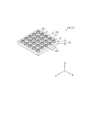
貫通電極3は、良導電性の金属導体により形成されている。良導電性の金属導体としては、金、白金、銅、銅合金、ニッケル、ニッケル合金、その他既知の貴金属等を好適に採用することができる。貫通電極3が形成される貫通孔2cは、一例として、ピッチP1でX方向に5~50個が配されており、ピッチP1でY方向に5~50個が配されている。貫通孔2cはマトリクス配置されており、ピッチP1は、一例として0.005mm以上0.05mm以下である。貫通孔2cの形状は、平面視で円形状、扇形状、半円形状、三角形状、四角形状、六角形状、多角形状等に設定される。一例として、貫通孔2cの直径は0.005mm以上0.025mm以下に設定される。ここで、貫通孔2cの形状や配置は、半導体デバイスや半導体素子等の被検査物40の外部電極41に、貫通電極3における複数の分割電極31(または分割電極32)のうちの2つ以上が接触可能な構成であればよく、上記構成に限定されない。なお、外部電極41は、金属端子に限定されず、半田ボールの場合がある。 The through
続いて、第1例の異方性導電シート1Aについて、以下に説明する。 Next, the first example of the anisotropic
[第1例]
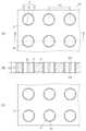
図2Aは第1例の異方性導電シート1Aの要部を模式的に示す平面図であり、図2Bは図2AのB-B線断面図であり、図2Cは図2Aの底面図である。異方性導電シート1Aは、樹脂材料からなるシート状の絶縁層2と、絶縁層2を厚み方向に貫通した複数の円形状の貫通孔2cと、貫通孔2cに形成された金属薄膜からなる貫通電極3とを有し、貫通孔2cの周方向に合計3つの分割電極31が等間隔で配されて貫通電極3が構成される。分割電極31は、貫通孔2cの厚み方向の中心線P3に対して回転対称となる位置に配される。各分割電極31は平面視で円弧状である。ここで、分割電極31の数は、2~9の範囲内で増減可能である。図6Aは、第1例の変形例の要部を模式的に示す平面図であり、この例では、円形状の貫通孔2cの周方向に合計2つの円弧状の分割電極31が配されて貫通電極3が構成される。[First example]
FIG. 2A is a plan view schematically showing a main part of the anisotropic
図2Bの例では、貫通電極3における厚み方向のサイズT2は、絶縁層2における厚み方向のサイズT2よりも大きい値に設定される。貫通電極3における前記厚み方向の一端面と他端面とはそれぞれ絶縁層2における前記厚みの0.8倍以下で突出している。 In the example of FIG. 2B, the size T2 of the through
図7は、異方性導電シート1Aと半導体デバイスなどの被検査物40との位置関係を模式的に示す側面図であり、部分拡大図である。一例として、被検査物40はチップ型ICであり、複数の外部電極41を有する。ここで、貫通電極3のピッチP1は、外部電極41のピッチP2よりも小さい値に設定される。一例として、ピッチP1は、ピッチP2の1/3以下に設定される。これにより、半導体デバイスや半導体素子等の被検査物40の外部電極41に、貫通電極3における複数の分割電極31のうちの2つ以上が接触可能な構成にできるので、マルチコンタクトとなって、貫通電極3と外部電極41との位置合わせの自由度が高くなる。 FIG. 7 is a side view schematically showing the positional relationship between the anisotropic
本実施形態によれば、被検査物40における外部電極41のピッチやサイズ等のバリエーションに容易に対応可能な構成の異方性導電シート1Aにできる。そして、半導体デバイスや半導体素子等の被検査物40に加わる力を抑えつつ均等に分散することができる。尚且つ、内部歪みが緩和されて絶縁層2の伸縮に貫通電極3が追随しやすくなる。よって、貫通電極3の剥離を起こさずに安定して検査を繰り返し行うことができる。 According to this embodiment, the anisotropic
図5は本実施形態に係る異方性導電シート1の製造手順を示すフロー図である。続いて、本実施形態の製造方法について、フロー図に沿って以下に説明する。 FIG. 5 is a flow diagram showing the manufacturing procedure of the anisotropic
金属製で丸針状の芯材をピッチP1で配列した基台を準備する。前記芯材は外周方向に等間隔で、金属薄膜の膜厚と同じか浅い溝もしくはケガキが形成されている。ステップS1は、前記芯材に金または白金もしくは銅からなる金属めっきを施して貫通電極3を前記芯材の外周に形成する。 A base is prepared in which circular needle-shaped core materials made of metal are arranged at a pitch P1. The core material has grooves or markings formed at equal intervals in the outer circumferential direction and having a thickness equal to or shallower than the metal thin film. In step S1, the core material is plated with a metal made of gold, platinum, or copper to form the through
ステップS1に続いてステップS2にて、一例として、液状のシリコーン樹脂またはフッ素樹脂またはウレタン樹脂を前記基台が配された型枠に注型し、樹脂硬化させて、絶縁層2を形成する。 Following step S1, in step S2, for example, a liquid silicone resin, fluororesin, or urethane resin is poured into the mold in which the base is placed, and the resin is cured to form the insulating
ステップS2に続いてステップS3にて、エッチャントにて前記芯材を溶かして不要領域を除去する。例えば、前記芯材が鉄またはアルミニウムであり、前記金属めっきが金または白金である場合、フッ化水素(HF)をエッチャントにすることができる。エッチャントは、所望のエッチャント濃度で水または水溶液に溶解したエッチング液の状態でノズルから吐出される。前記不要領域を除去した後、エッチング液は水などで洗い流される。このようにして、異方性導電シート1を製造する。 Following step S2, in step S3, the core material is melted with an etchant to remove unnecessary areas. For example, when the core material is iron or aluminum and the metal plating is gold or platinum, hydrogen fluoride (HF) can be used as the etchant. The etchant is discharged from the nozzle in the form of an etchant dissolved in water or an aqueous solution at a desired etchant concentration. After removing the unnecessary area, the etching solution is washed away with water or the like. In this way, the anisotropic
この構成によれば、貫通孔2cの周方向に複数の分割電極31を等間隔で配して貫通電極3を形成するので、半導体デバイス等の被検査物40に加わる力を抑えつつ均等に分散することができる。尚且つ、内部歪みが緩和されて絶縁層2の伸縮に貫通電極3が追随しやすくなる。また、ナノメートルサイズの貫通電極3を再現性良く製造することができる。 According to this configuration, the plurality of divided
続いて、第2例の異方性導電シート1Bについて、以下に説明する。 Next, a second example of the anisotropic
[第2例]
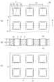
図3Aは第2例の異方性導電シート1Bの要部を模式的に示す平面図であり、図3Bは図3AのB-B線断面図であり、図3Cは図3Aの底面図である。異方性導電シート1Bは、樹脂材料からなるシート状の絶縁層2と、絶縁層2を厚み方向に貫通した複数の四角形状の貫通孔2cと、貫通孔2cに形成された金属薄膜からなる貫通電極3とを有し、貫通孔2cの各辺に合計4つの分割電極32が周方向に等間隔で配されて貫通電極3が構成される。分割電極32は、貫通孔2cの厚み方向の中心線P3に対して回転対称となる位置に配される。各分割電極32は平面視で線状である。ここで、分割電極32の数は、2~9の範囲内で増減可能である。図6Bは、第2例の変形例の要部を模式的に示す平面図であり、この例では、六角形状の貫通孔2cの周方向に合計6つの線状の分割電極32が配されて貫通電極3が構成される。[Second example]
3A is a plan view schematically showing the main parts of the anisotropic
図3Bの例では、貫通電極3における厚み方向のサイズT2は、絶縁層2における厚み方向のサイズT2よりも大きい値に設定される。貫通電極3における前記厚み方向の一端面と他端面とはそれぞれ絶縁層2における前記厚みの0.8倍以下で突出している。 In the example of FIG. 3B, the size T2 of the through
第2例の構成は、金属製で角針状の芯材をピッチP1で配列した基台を準備して、前記芯材は外周方向に等間隔で、金属薄膜の膜厚と同じか浅い溝もしくはケガキを形成することで、第1例と同じように製造できる。貫通孔2cは、四角形状や六角形状に限定されず、五角形状や八角形状などにすることもできる。 The configuration of the second example is to prepare a base in which square needle-shaped core materials made of metal are arranged at a pitch P1, and the core materials have grooves at equal intervals in the outer circumferential direction and as shallow as or equal to the thickness of the metal thin film. Alternatively, it can be manufactured in the same manner as the first example by forming markings. The through
続いて、第3例の異方性導電シート1Cについて、以下に説明する。 Next, a third example of the anisotropic
[第3例]
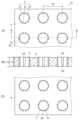
図4Aは第3例の異方性導電シート1Cの要部を模式的に示す平面図であり、図4Bは図4AのB-B線断面図であり、図4Cは図4Aの底面図である。異方性導電シート1Cは、樹脂材料からなるシート状の絶縁層2と、絶縁層2を厚み方向に貫通した複数の略円形状の貫通孔2cと、貫通孔2cに形成された金属薄膜からなる貫通電極3とを有し、貫通孔2cの周方向に合計3つの分割電極31が等間隔で配されて貫通電極3が構成される。そして、貫通孔2cの内壁に前記樹脂材料からなる凸部2dが形成されており、各分割電極31は凸部2dにて区画されている。分割電極31は、貫通孔2cの厚み方向の中心線P3に対して回転対称となる位置に配される。各分割電極31は平面視で円弧状である。ここで、分割電極31の数は、2~9の範囲内で増減可能である。図6Cは、第3例の変形例の要部を模式的に示す平面図であり、この例では、円形状の貫通孔2cの周方向に合計4つの円弧状の分割電極31が配されて貫通電極3が構成される。[3rd example]
FIG. 4A is a plan view schematically showing main parts of an anisotropic
図4Bの例では、貫通電極3における厚み方向のサイズT2は、絶縁層2における厚み方向のサイズT2よりも大きい値に設定される。貫通電極3における前記厚み方向の一端面と他端面とはそれぞれ絶縁層2における前記厚みの0.8倍以下で突出している。 In the example of FIG. 4B, the size T2 of the through
第3例の構成は、金属製で丸針状の芯材をピッチP1で配列した基台を準備して、前記芯材は外周方向に等間隔で、金属薄膜の膜厚よりも深い溝もしくはスリットを形成することで、第1例と同じように製造できる。前記溝の深さは凸部2dの突出量に対応している。凸部2dによって、各分割電極31と絶縁層2との密着力をより向上させることができる。第3例の構成を第2例に適用して、第2例の構成に凸部2dを設けることも可能である。 The configuration of the third example is to prepare a base in which circular needle-shaped core materials made of metal are arranged at a pitch P1, and the core materials are arranged in grooves or grooves deeper than the thickness of the metal thin film at equal intervals in the outer circumferential direction. By forming slits, it can be manufactured in the same manner as the first example. The depth of the groove corresponds to the amount of protrusion of the
本発明は、以上説明した実施例に限定されることなく、本発明を逸脱しない範囲において種々変更が可能である。 The present invention is not limited to the embodiments described above, and various modifications can be made without departing from the scope of the present invention.
1、1A、1B、1C 異方性導電シート
2 絶縁層、2c 貫通孔、2d 凸部
3 貫通電極
31 分割電極
32 分割電極
40 被検査物(半導体デバイス)
41 外部電極1, 1A, 1B, 1C Anisotropic
41 External electrode
Claims (6)
Translated fromJapaneseを特徴とする異方性導電シート。It has a sheet-like insulating layer made of a resin material, a plurality of through holes penetrating the insulating layer in the thickness direction, and a through electrode made of a metal thin film formed in the through hole, and the through electrode has a plurality of through holes. An anisotropic conductive sheet characterized in that divided electrodes are arranged in the circumferential direction of the through hole.
を特徴とする請求項1に記載の異方性導電シート。The anisotropic conductive sheet according to claim 1, wherein the number of the divided electrodes in each of the through holes is 2 or more and 9 or less.
を特徴とする請求項1または2に記載の異方性導電シート。The anisotropic conductive sheet according to claim 1 or 2, wherein the thickness of the insulating layer is 0.05 to 2.00 mm.
を特徴とする請求項3に記載の異方性導電シート。4. The anisotropic conductive sheet according to claim 3, wherein one end surface and the other end surface of the through electrode in the thickness direction each protrude by 0.8 times or less the thickness of the insulating layer.
を特徴とする請求項1または2に記載の異方性導電シート。3. The anisotropic conductive sheet according to claim 1, wherein an inward convex portion is formed in the through hole, and the divided electrodes are partitioned by the convex portion.
を特徴とする異方性導電シートの製造方法。A method for producing an anisotropic conductive sheet having a sheet-like insulating layer made of a resin material, a plurality of through holes penetrating the insulating layer in the thickness direction, and a through electrode formed in the through holes, the method comprising: A method for manufacturing an anisotropic conductive sheet, characterized in that a plurality of divided electrodes made of thin metal films are arranged in the circumferential direction of the through hole to form the through electrode.
Priority Applications (4)
| Application Number | Priority Date | Filing Date | Title |
|---|---|---|---|
| JP2022089564AJP2023176957A (en) | 2022-06-01 | 2022-06-01 | Anisotropic conductive sheet and method for manufacturing anisotropic conductive sheet |
| KR1020247027761AKR20250018460A (en) | 2022-06-01 | 2023-05-22 | Anisotropic challenge sheet and method for manufacturing anisotropic challenge sheet |
| PCT/JP2023/018876WO2023234088A1 (en) | 2022-06-01 | 2023-05-22 | Anisotropic electroconductive sheet and method for manufacturing anisotropic electroconductive sheet |
| TW112120244ATW202412397A (en) | 2022-06-01 | 2023-05-31 | Anisotropic conductive sheet and manufacturing method of anisotropic conductive sheet |
Applications Claiming Priority (1)
| Application Number | Priority Date | Filing Date | Title |
|---|---|---|---|
| JP2022089564AJP2023176957A (en) | 2022-06-01 | 2022-06-01 | Anisotropic conductive sheet and method for manufacturing anisotropic conductive sheet |
Publications (1)
| Publication Number | Publication Date |
|---|---|
| JP2023176957Atrue JP2023176957A (en) | 2023-12-13 |
Family
ID=89024753
Family Applications (1)
| Application Number | Title | Priority Date | Filing Date |
|---|---|---|---|
| JP2022089564APendingJP2023176957A (en) | 2022-06-01 | 2022-06-01 | Anisotropic conductive sheet and method for manufacturing anisotropic conductive sheet |
Country Status (4)
| Country | Link |
|---|---|
| JP (1) | JP2023176957A (en) |
| KR (1) | KR20250018460A (en) |
| TW (1) | TW202412397A (en) |
| WO (1) | WO2023234088A1 (en) |
Family Cites Families (3)
| Publication number | Priority date | Publication date | Assignee | Title |
|---|---|---|---|---|
| JPS58139517A (en)* | 1982-05-24 | 1983-08-18 | Murata Mfg Co Ltd | Chip-shaped piezoelectric oscillating parts |
| KR102545904B1 (en) | 2017-05-18 | 2023-06-20 | 신에츠 폴리머 가부시키가이샤 | Electrical connector and its manufacturing method |
| JP7175132B2 (en) | 2018-08-10 | 2022-11-18 | 信越ポリマー株式会社 | Electrical connector manufacturing method |
- 2022
- 2022-06-01JPJP2022089564Apatent/JP2023176957A/enactivePending
- 2023
- 2023-05-22WOPCT/JP2023/018876patent/WO2023234088A1/ennot_activeCeased
- 2023-05-22KRKR1020247027761Apatent/KR20250018460A/enactivePending
- 2023-05-31TWTW112120244Apatent/TW202412397A/enunknown
Also Published As
| Publication number | Publication date |
|---|---|
| KR20250018460A (en) | 2025-02-06 |
| TW202412397A (en) | 2024-03-16 |
| WO2023234088A1 (en) | 2023-12-07 |
Similar Documents
| Publication | Publication Date | Title |
|---|---|---|
| US6558560B2 (en) | Method for the fabrication of electrical contacts | |
| JP7263060B2 (en) | Electrical connection device | |
| JP5103566B2 (en) | Electrical contact and inspection jig having the same | |
| TW202019021A (en) | Electric connector and manufacturing method thereof | |
| JPWO2019208216A1 (en) | Cylindrical body and method for manufacturing the same | |
| KR20160148097A (en) | PCR device and manufacturing method thereof | |
| JP2023176957A (en) | Anisotropic conductive sheet and method for manufacturing anisotropic conductive sheet | |
| WO2023234089A1 (en) | Anisotropic electroconductive sheet and method for manufacturing anisotropic electroconductive sheet | |
| JP5062355B2 (en) | Connection terminal and method for manufacturing connection terminal | |
| JP3904564B2 (en) | Electronic component inspection probe and electronic component inspection socket including the probe | |
| JP4624372B2 (en) | Multilayer electrical probe | |
| JP2007294558A (en) | Semiconductor device and manufacturing method thereof | |
| JP7476877B2 (en) | Inspection fixture | |
| JPH11167945A (en) | Electrical connector and its manufacture | |
| JP4839777B2 (en) | Plating jig and plating method using the same | |
| US6839965B2 (en) | Method of manufacturing a resistor connector | |
| JP2020027725A (en) | Electric connector and manufacturing method thereof | |
| TWI857034B (en) | Contact terminal, inspection fixture and inspection device | |
| JP2022047035A (en) | Electrical connector and manufacturing method of the same | |
| JP4246093B2 (en) | Flexible wiring board | |
| JP2025150769A (en) | Anisotropic conductive sheet, probe card, electrical inspection device and electrical inspection method | |
| TW202422728A (en) | Cantilever probe for probe card and probe card | |
| JP2023167905A (en) | electrical connector | |
| JPH11295344A (en) | Semiconductor inspection jig and method of manufacturing semiconductor inspection jig | |
| JP2003043103A (en) | Inspection equipment for semiconductor devices |
Legal Events
| Date | Code | Title | Description |
|---|---|---|---|
| A711 | Notification of change in applicant | Free format text:JAPANESE INTERMEDIATE CODE: A712 Effective date:20230516 | |
| A621 | Written request for application examination | Free format text:JAPANESE INTERMEDIATE CODE: A621 Effective date:20250407 |