JP2023170110A - semiconductor light emitting device - Google Patents
semiconductor light emitting deviceDownload PDFInfo
- Publication number
- JP2023170110A JP2023170110AJP2022081594AJP2022081594AJP2023170110AJP 2023170110 AJP2023170110 AJP 2023170110AJP 2022081594 AJP2022081594 AJP 2022081594AJP 2022081594 AJP2022081594 AJP 2022081594AJP 2023170110 AJP2023170110 AJP 2023170110A
- Authority
- JP
- Japan
- Prior art keywords
- groove
- light emitting
- semiconductor light
- edge
- emitting device
- Prior art date
- Legal status (The legal status is an assumption and is not a legal conclusion. Google has not performed a legal analysis and makes no representation as to the accuracy of the status listed.)
- Pending
Links
Images


Classifications
- H—ELECTRICITY
- H10—SEMICONDUCTOR DEVICES; ELECTRIC SOLID-STATE DEVICES NOT OTHERWISE PROVIDED FOR
- H10H—INORGANIC LIGHT-EMITTING SEMICONDUCTOR DEVICES HAVING POTENTIAL BARRIERS
- H10H20/00—Individual inorganic light-emitting semiconductor devices having potential barriers, e.g. light-emitting diodes [LED]
- H10H20/80—Constructional details
- H10H20/85—Packages
- H10H20/857—Interconnections, e.g. lead-frames, bond wires or solder balls
- H—ELECTRICITY
- H01—ELECTRIC ELEMENTS
- H01L—SEMICONDUCTOR DEVICES NOT COVERED BY CLASS H10
- H01L24/00—Arrangements for connecting or disconnecting semiconductor or solid-state bodies; Methods or apparatus related thereto
- H01L24/01—Means for bonding being attached to, or being formed on, the surface to be connected, e.g. chip-to-package, die-attach, "first-level" interconnects; Manufacturing methods related thereto
- H01L24/42—Wire connectors; Manufacturing methods related thereto
- H01L24/47—Structure, shape, material or disposition of the wire connectors after the connecting process
- H01L24/48—Structure, shape, material or disposition of the wire connectors after the connecting process of an individual wire connector
- H—ELECTRICITY
- H10—SEMICONDUCTOR DEVICES; ELECTRIC SOLID-STATE DEVICES NOT OTHERWISE PROVIDED FOR
- H10H—INORGANIC LIGHT-EMITTING SEMICONDUCTOR DEVICES HAVING POTENTIAL BARRIERS
- H10H20/00—Individual inorganic light-emitting semiconductor devices having potential barriers, e.g. light-emitting diodes [LED]
- H10H20/80—Constructional details
- H10H20/85—Packages
- H10H20/8506—Containers
- H—ELECTRICITY
- H01—ELECTRIC ELEMENTS
- H01L—SEMICONDUCTOR DEVICES NOT COVERED BY CLASS H10
- H01L2224/00—Indexing scheme for arrangements for connecting or disconnecting semiconductor or solid-state bodies and methods related thereto as covered by H01L24/00
- H01L2224/01—Means for bonding being attached to, or being formed on, the surface to be connected, e.g. chip-to-package, die-attach, "first-level" interconnects; Manufacturing methods related thereto
- H01L2224/42—Wire connectors; Manufacturing methods related thereto
- H01L2224/44—Structure, shape, material or disposition of the wire connectors prior to the connecting process
- H01L2224/45—Structure, shape, material or disposition of the wire connectors prior to the connecting process of an individual wire connector
- H01L2224/45001—Core members of the connector
- H01L2224/45099—Material
- H01L2224/451—Material with a principal constituent of the material being a metal or a metalloid, e.g. boron (B), silicon (Si), germanium (Ge), arsenic (As), antimony (Sb), tellurium (Te) and polonium (Po), and alloys thereof
- H01L2224/45138—Material with a principal constituent of the material being a metal or a metalloid, e.g. boron (B), silicon (Si), germanium (Ge), arsenic (As), antimony (Sb), tellurium (Te) and polonium (Po), and alloys thereof the principal constituent melting at a temperature of greater than or equal to 950°C and less than 1550°C
- H01L2224/45144—Gold (Au) as principal constituent
- H—ELECTRICITY
- H01—ELECTRIC ELEMENTS
- H01L—SEMICONDUCTOR DEVICES NOT COVERED BY CLASS H10
- H01L2224/00—Indexing scheme for arrangements for connecting or disconnecting semiconductor or solid-state bodies and methods related thereto as covered by H01L24/00
- H01L2224/01—Means for bonding being attached to, or being formed on, the surface to be connected, e.g. chip-to-package, die-attach, "first-level" interconnects; Manufacturing methods related thereto
- H01L2224/42—Wire connectors; Manufacturing methods related thereto
- H01L2224/47—Structure, shape, material or disposition of the wire connectors after the connecting process
- H01L2224/48—Structure, shape, material or disposition of the wire connectors after the connecting process of an individual wire connector
- H01L2224/481—Disposition
- H01L2224/48151—Connecting between a semiconductor or solid-state body and an item not being a semiconductor or solid-state body, e.g. chip-to-substrate, chip-to-passive
- H01L2224/48221—Connecting between a semiconductor or solid-state body and an item not being a semiconductor or solid-state body, e.g. chip-to-substrate, chip-to-passive the body and the item being stacked
- H01L2224/48225—Connecting between a semiconductor or solid-state body and an item not being a semiconductor or solid-state body, e.g. chip-to-substrate, chip-to-passive the body and the item being stacked the item being non-metallic, e.g. insulating substrate with or without metallisation
- H—ELECTRICITY
- H01—ELECTRIC ELEMENTS
- H01L—SEMICONDUCTOR DEVICES NOT COVERED BY CLASS H10
- H01L24/00—Arrangements for connecting or disconnecting semiconductor or solid-state bodies; Methods or apparatus related thereto
- H01L24/01—Means for bonding being attached to, or being formed on, the surface to be connected, e.g. chip-to-package, die-attach, "first-level" interconnects; Manufacturing methods related thereto
- H01L24/42—Wire connectors; Manufacturing methods related thereto
- H01L24/44—Structure, shape, material or disposition of the wire connectors prior to the connecting process
- H01L24/45—Structure, shape, material or disposition of the wire connectors prior to the connecting process of an individual wire connector
- H—ELECTRICITY
- H01—ELECTRIC ELEMENTS
- H01L—SEMICONDUCTOR DEVICES NOT COVERED BY CLASS H10
- H01L25/00—Assemblies consisting of a plurality of semiconductor or other solid state devices
- H01L25/03—Assemblies consisting of a plurality of semiconductor or other solid state devices all the devices being of a type provided for in a single subclass of subclasses H10B, H10D, H10F, H10H, H10K or H10N, e.g. assemblies of rectifier diodes
- H01L25/10—Assemblies consisting of a plurality of semiconductor or other solid state devices all the devices being of a type provided for in a single subclass of subclasses H10B, H10D, H10F, H10H, H10K or H10N, e.g. assemblies of rectifier diodes the devices having separate containers
- H01L25/13—Assemblies consisting of a plurality of semiconductor or other solid state devices all the devices being of a type provided for in a single subclass of subclasses H10B, H10D, H10F, H10H, H10K or H10N, e.g. assemblies of rectifier diodes the devices having separate containers the devices being of a type provided for in group H10H20/00
- H—ELECTRICITY
- H01—ELECTRIC ELEMENTS
- H01L—SEMICONDUCTOR DEVICES NOT COVERED BY CLASS H10
- H01L2924/00—Indexing scheme for arrangements or methods for connecting or disconnecting semiconductor or solid-state bodies as covered by H01L24/00
- H01L2924/10—Details of semiconductor or other solid state devices to be connected
- H01L2924/11—Device type
- H01L2924/12—Passive devices, e.g. 2 terminal devices
- H01L2924/1204—Optical Diode
- H01L2924/12041—LED
- H—ELECTRICITY
- H10—SEMICONDUCTOR DEVICES; ELECTRIC SOLID-STATE DEVICES NOT OTHERWISE PROVIDED FOR
- H10H—INORGANIC LIGHT-EMITTING SEMICONDUCTOR DEVICES HAVING POTENTIAL BARRIERS
- H10H20/00—Individual inorganic light-emitting semiconductor devices having potential barriers, e.g. light-emitting diodes [LED]
- H10H20/80—Constructional details
- H10H20/85—Packages
- H10H20/852—Encapsulations
- H10H20/854—Encapsulations characterised by their material, e.g. epoxy or silicone resins
Landscapes
- Engineering & Computer Science (AREA)
- Computer Hardware Design (AREA)
- Microelectronics & Electronic Packaging (AREA)
- Power Engineering (AREA)
- Led Device Packages (AREA)
Abstract
Translated fromJapanese
Description
Translated fromJapanese本開示は、半導体発光装置に関する。 The present disclosure relates to a semiconductor light emitting device.
半導体発光装置は、電子機器等の光源デバイスとして広く用いられている。特許文献1には、従来の半導体発光装置の一例が開示されている。同文献に開示された半導体発光装置は、基板、LEDチップ(半導体発光素子)および樹脂パッケージ(封止樹脂)を備える。基板は、表面、裏面、および4つの側面を有する。表面は、基板の厚さ方向の一方側を向く。裏面は、基板の厚さ方向の一方側を向く。4つの側面は、基板の厚さ方向に見て概略矩形状をなす。基板には、1対の電極が設けられており、これら電極は、LEDチップへの導通経路をなしている。LEDチップは、基板の表面上に搭載されている。樹脂パッケージは、LEDチップを覆っており、LEDチップからの光を透過する。 Semiconductor light emitting devices are widely used as light source devices for electronic equipment and the like.
特許文献1に記載された半導体発光装置において、基板の4隅には、厚さ方向に延びる凹溝が形成されている。これら凹溝の各々の厚さ方向に垂直な断面形状は、概略四半円形状である。各凹溝にはめっき層等からなる凹溝配線が形成されており、各凹溝配線は、一対の電極のいずれかに導通している。上記構成の半導体発光装置の使用時においては、実装基板に実装される。上記の半導体発光装置は、実装基板の表面と平行な方向に光を出射する、いわゆるサイドビュー型の光源として用いることができる。この場合、半導体発光装置は、基板の側面が実装基板と対向する姿勢で当該実装基板に実装される。サイドビュー型の光源として用いられる半導体発光装置は、凹溝に形成された凹溝配線と、実装基板とが、はんだなどの接合部を介して接合される。 In the semiconductor light emitting device described in
上記半導体発光装置などの製品は、昨今、より一層の小型化が求められている。上記半導体発光装置において製品サイズの小型化を図ると、基板の4隅の凹溝の寸法が小さくなる。その結果、上記従来の半導体発光装置をサイドビュー型の光源として用いる場合、実装基板に対して十分な接合部を形成することができず、実装基板への実装強度が低下することが懸念される。 In recent years, products such as the semiconductor light emitting devices described above are required to be further miniaturized. As the product size of the semiconductor light emitting device is reduced, the dimensions of the grooves at the four corners of the substrate become smaller. As a result, when the conventional semiconductor light emitting device described above is used as a side-view light source, it is not possible to form a sufficient bond to the mounting board, and there is a concern that the mounting strength to the mounting board may decrease. .
本開示は、上記した事情のもとで考え出されたものであって、実装強度を向上し且つ小型化を図るのに適した半導体発光装置を提供することを主たる課題とする。 The present disclosure was conceived under the above-mentioned circumstances, and its main objective is to provide a semiconductor light emitting device suitable for improving mounting strength and reducing size.
本開示によって提供される半導体発光装置は、基板と、前記基板に形成された配線部と、半導体発光素子と、を備え、前記基板は、厚さ方向の一方側を向く第1主面と、前記厚さ方向の他方側を向く第2主面と、前記厚さ方向と直交する第1方向の一方側を向く第1側面と、前記第1方向の他方側を向く第2側面と、前記厚さ方向および前記第1方向の双方に直交する第2方向の一方側を向く第3側面と、前記第1側面および前記第3側面の間に形成され、且つ前記第1側面および前記第3側面から凹む第1凹溝と、を含み、前記第1側面は、前記第2方向の一方側に位置し、且つ前記第1凹溝に接する第1端縁を有し、前記第2側面は、前記第2方向の一方側に位置する第2端縁を有し、前記第3側面は、前記第1方向の一方側に位置し且つ前記第1凹溝に接する第3端縁と、前記第1方向の他方側に位置する第4端縁と、を有し、前記半導体発光素子は、前記第1主面に支持されており、前記配線部は、前記第1凹溝に形成された第1溝配線を含み、前記第1端縁と前記第3端縁との距離である第1距離は、前記第2端縁と前記第4端縁との距離である第2距離よりも大である。 A semiconductor light emitting device provided by the present disclosure includes a substrate, a wiring section formed on the substrate, and a semiconductor light emitting element, and the substrate has a first main surface facing one side in the thickness direction; a second main surface facing the other side in the thickness direction; a first side face facing one side in the first direction perpendicular to the thickness direction; a second side face facing the other side in the first direction; a third side surface facing one side in a second direction perpendicular to both the thickness direction and the first direction; and a third side surface formed between the first side surface and the third side surface; a first groove recessed from a side surface, the first side surface having a first edge located on one side in the second direction and in contact with the first groove, and the second side surface having a first edge in contact with the first groove; , a second end edge located on one side in the second direction, and the third side surface has a third end edge located on one side in the first direction and in contact with the first groove; a fourth edge located on the other side in the first direction, the semiconductor light emitting element is supported by the first main surface, and the wiring part is formed in the first groove. The first distance, which includes the first trench wiring, is the distance between the first edge and the third edge, and is larger than the second distance, which is the distance between the second edge and the fourth edge. It is.
本開示の半導体発光装置によれば、実装強度を高めるとともに、小型化を図ることができる。 According to the semiconductor light emitting device of the present disclosure, it is possible to increase the mounting strength and reduce the size.
本開示のその他の特徴および利点は、添付図面を参照して以下に行う詳細な説明によって、より明らかとなろう。 Other features and advantages of the present disclosure will become more apparent from the detailed description given below with reference to the accompanying drawings.
以下、本開示の好ましい実施の形態につき、図面を参照して具体的に説明する。 Hereinafter, preferred embodiments of the present disclosure will be specifically described with reference to the drawings.
本開示における「第1」、「第2」、「第3」等の用語は、単にラベルとして用いたものであり、必ずしもそれらの対象物に順列を付することを意図していない。 Terms such as "first", "second", "third", etc. in this disclosure are used merely as labels and are not necessarily intended to attach a permutation to those objects.
本開示において、「ある物Aがある物Bに形成されている」および「ある物Aがある物B上に形成されている」とは、特段の断りのない限り、「ある物Aがある物Bに直接形成されていること」、および、「ある物Aとある物Bとの間に他の物を介在させつつ、ある物Aがある物Bに形成されていること」を含む。同様に、「ある物Aがある物Bに配置されている」および「ある物Aがある物B上に配置されている」とは、特段の断りのない限り、「ある物Aがある物Bに直接配置されていること」、および、「ある物Aとある物Bとの間に他の物を介在させつつ、ある物Aがある物Bに配置されていること」を含む。同様に、「ある物Aがある物B上に位置している」とは、特段の断りのない限り、「ある物Aがある物Bに接して、ある物Aがある物B上に位置していること」、および、「ある物Aとある物Bとの間に他の物が介在しつつ、ある物Aがある物B上に位置していること」を含む。また、「ある物Aがある物Bにある方向に見て重なる」とは、特段の断りのない限り、「ある物Aがある物Bのすべてに重なること」、および、「ある物Aがある物Bの一部に重なること」を含む。また、本開示において「ある面Aが方向B(の一方側または他方側)を向く」とは、面Aの方向Bに対する角度が90°である場合に限定されず、面Aが方向Bに対して傾いている場合を含む。また「ある物Aがある物Bに支持されている」とは、特段の断りのない限り、「ある物Aがある物Bに直接支持されていること」、および、「ある物Aとある物Bとの間に他の物を介在させつつ、ある物Aがある物Bに支持されていること」を含む。 In this disclosure, "a thing A is formed on a thing B" and "a thing A is formed on a thing B" mean "a thing A is formed on a thing B" unless otherwise specified. "It is formed directly on object B," and "It is formed on object B, with another object interposed between object A and object B." Similarly, "something A is placed on something B" and "something A is placed on something B" mean "something A is placed on something B" unless otherwise specified. This includes ``directly placed on object B'' and ``placed on object B with another object interposed between object A and object B.'' Similarly, "a certain object A is located on a certain object B" means, unless otherwise specified, "a certain object A is in contact with a certain object B, and a certain object A is located on a certain object B." ``The fact that a certain thing A is located on a certain thing B while another thing is interposed between the certain thing A and the certain thing B.'' In addition, "a certain object A overlaps a certain object B when viewed in a certain direction" means, unless otherwise specified, "a certain object A overlaps all of a certain object B" and "a certain object A overlaps with a certain object B". This includes "overlapping a part of something B." Furthermore, in the present disclosure, "a certain surface A faces (one side or the other side of) the direction B" is not limited to the case where the angle of the surface A with respect to the direction B is 90 degrees; Including cases where it is tilted to the opposite direction. Furthermore, "something A is supported by something B" means "something A is directly supported by something B," and "something A is supported by something B," unless otherwise specified. This includes "an object A being supported by an object B while another object is interposed between it and object B."
<第1実施形態>
図1~図7は、本開示の第1実施形態に係る半導体発光装置を示している。本実施形態の半導体発光装置A1は、基板1、配線部2、第1絶縁膜31、第2絶縁膜32、半導体発光素子4、ワイヤ5、封止樹脂6および絶縁膜7を備えている。<First embodiment>
1 to 7 show a semiconductor light emitting device according to a first embodiment of the present disclosure. The semiconductor light emitting device A1 of this embodiment includes a
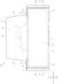
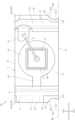
図1は、半導体発光装置A1を示す平面図である。図2は、半導体発光装置A1の正面図である。図3は、半導体発光装置A1の左側面図である。図4は、半導体発光装置A1の底面図である。図5は、図1のV-V線に沿う断面図である。図6は、図1のVI-VI線に沿う断面図である。図7は、図1のVII-VII線に沿う断面図である。なお、図1は、理解の便宜上、封止樹脂6を透過している。 FIG. 1 is a plan view showing a semiconductor light emitting device A1. FIG. 2 is a front view of the semiconductor light emitting device A1. FIG. 3 is a left side view of the semiconductor light emitting device A1. FIG. 4 is a bottom view of the semiconductor light emitting device A1. FIG. 5 is a cross-sectional view taken along line VV in FIG. FIG. 6 is a cross-sectional view taken along line VI-VI in FIG. FIG. 7 is a cross-sectional view taken along line VII-VII in FIG. Note that, in FIG. 1, the sealing
半導体発光装置A1の説明において、半導体発光装置A1の厚さ方向(平面視方向)は、本開示の「厚さ方向」の一例であり、「厚さ方向z」と呼ぶ。厚さ方向zに対して直交する方向は、本開示の「第1方向」の一例であり、「第1方向x」と呼ぶ。厚さ方向zおよび第1方向xの双方に対して直交する方向は、本開示の「第2方向」の一例であり、「第2方向y」と呼ぶ。また、図1において図中下側は本開示の「第1方向の一方側」の一例であり、「第1方向一方側x1」と呼び、図中上側は本開示の「第1方向の他方側」の一例であり、「第1方向他方側x2」と呼ぶ。図1において図中左側は本開示の「第2方向の一方側」の一例であり、「第2方向一方側y1」と呼び、図中右側は本開示の「第2方向の他方側」の一例であり、「第2方向他方側y2」と呼ぶ。図2において図中上側は本開示の「厚さ方向の一方側」の一例であり、「厚さ方向一方側z1」と呼び、図中下側は本開示の「厚さ方向の他方側」の一例であり、「厚さ方向他方側z2」と呼ぶ。図1に示すように、半導体発光装置A1は、厚さ方向zに見て略矩形状である。なお、半導体発光装置A1の大きさは何ら限定されない。 In the description of the semiconductor light emitting device A1, the thickness direction (planar view direction) of the semiconductor light emitting device A1 is an example of the "thickness direction" of the present disclosure, and will be referred to as the "thickness direction z." The direction perpendicular to the thickness direction z is an example of the "first direction" of the present disclosure, and will be referred to as the "first direction x." A direction perpendicular to both the thickness direction z and the first direction x is an example of the "second direction" of the present disclosure, and will be referred to as the "second direction y." In addition, in FIG. 1, the lower side in the figure is an example of "one side in the first direction" of the present disclosure, and is referred to as "first direction one side x1", and the upper side in the figure is an example of "one side in the first direction" of the present disclosure. This is an example of "the other side x2 in the first direction". In FIG. 1, the left side in the figure is an example of "one side in the second direction" of the present disclosure, and is called "one side in the second direction y1", and the right side in the figure is an example of "the other side in the second direction" of the present disclosure. This is an example and will be referred to as "second direction other side y2". In FIG. 2, the upper side in the figure is an example of "one side in the thickness direction" of the present disclosure, and is referred to as "one side in the thickness direction z1", and the lower side in the figure is the "other side in the thickness direction" of the present disclosure. This is an example and will be referred to as "the other side z2 in the thickness direction." As shown in FIG. 1, the semiconductor light emitting device A1 has a substantially rectangular shape when viewed in the thickness direction z. Note that the size of the semiconductor light emitting device A1 is not limited at all.
基板1は、直方体状であり、たとえばガラスエポキシ樹脂等の絶縁材料を含む。基板1の大きさは何ら限定されず、たとえば、第1方向xの大きさが0.8mm程度、第2方向yの大きさが1.6mm程度、厚さ方向zの大きさが0.6mm程度である。 The
基板1は、第1主面11、第2主面12、第1側面13、第2側面14、第3側面15および第4側面16を有する。本実施形態においては、基板1は、第1凹溝171、第2凹溝172、第3凹溝173および第4凹溝174をさらに有する。第1主面11は、厚さ方向一方側z1を向く平面である。第2主面12は、厚さ方向他方側z2を向く平面である。第1側面13は、厚さ方向zにおいて第1主面11と第2主面12との間に位置し、第1方向一方側x1を向く。第2側面14は、厚さ方向zにおいて第1主面11と第2主面12との間に位置し、第1方向他方側x2を向く。第3側面15は、厚さ方向zにおいて第1主面11と第2主面12との間に位置し、第2方向一方側y1を向く。第4側面16は、厚さ方向zにおいて第1主面11と第2主面12との間に位置し、第2方向他方側y2を向く。 The
第1凹溝171、第2凹溝172、第3凹溝173および第4凹溝174は、厚さ方向zに見て基板1の4隅に設けられている。具体的には、第1凹溝171は、第1側面13および第3側面15の間に形成され、第1側面13および第3側面15から凹む。第2凹溝172は、第2側面14および第3側面15の間に形成され、第2側面14および第3側面15から凹む。第3凹溝173は、第1側面13および第4側面16の間に形成され、第1側面13および第4側面16から凹む。第4凹溝174は、第2側面14および第4側面16の間に形成され、第2側面14および第4側面16から凹む。第1凹溝171、第2凹溝172、第3凹溝173および第4凹溝174の各々は、厚さ方向zにおいて第1主面11および第2主面12に達する。 The
本実施形態において、第1凹溝171の厚さ方向zに垂直な断面形状は、概略四半円形状およびこれにつながる線分である。また、第3凹溝173の厚さ方向zに垂直な断面形状は、第1凹溝171と同様に、概略四半円形状およびこれにつながる線分である。その一方、第2凹溝172および第4凹溝174の各々の厚さ方向zに垂直な断面形状は、概略四半円形状である。 In this embodiment, the cross-sectional shape of the
図1、図2および図4に示すように、第1側面13は、第1端縁131および第5端縁132を有する。第1端縁131は、第1側面13の第2方向一方側y1に位置する端縁であり、厚さ方向zに沿っている。第5端縁132は、第1側面13の第2方向他方側y2に位置する端縁であり、厚さ方向zに沿っている。本実施形態において、第1端縁131は、第1凹溝171に接しており、第1側面13と第1凹溝171との境界を兼ねている。また、第5端縁132は、第3凹溝173に接しており、第1側面13と第3凹溝173との境界を兼ねている。 As shown in FIGS. 1, 2, and 4, the
図1および図4に示すように、第2側面14は、第2端縁141および第6端縁142を有する。第2端縁141は、第2側面14の第2方向一方側y1に位置する端縁であり、厚さ方向zに沿っている。第6端縁142は、第2側面14の第2方向他方側y2に位置する端縁であり、厚さ方向zに沿っている。本実施形態において、第2端縁141は、第2凹溝172に接しており、第2側面14と第2凹溝172との境界を兼ねている。また、第6端縁142は、第4凹溝174に接しており、第2側面14と第4凹溝174との境界を兼ねている。 As shown in FIGS. 1 and 4, the
図1、図3および図4に示すように、第3側面15は、第3端縁151および第4端縁152を有する。第3端縁151は、第3側面15の第1方向一方側x1に位置する端縁であり、厚さ方向zに沿っている。第4端縁152は、第3側面15の第1方向他方側x2に位置する端縁であり、厚さ方向zに沿っている。本実施形態において、第3端縁151は、第1凹溝171に接しており、第3側面15と第1凹溝171との境界を兼ねている。また、第4端縁152は、第2凹溝172に接しており、第3側面15と第2凹溝172との境界を兼ねている。 As shown in FIGS. 1, 3, and 4, the
図1および図4に示すように、第4側面16は、第7端縁161および第8端縁162を有する。第7端縁161は、第4側面16の第1方向一方側x1に位置する端縁であり、厚さ方向zに沿っている。第8端縁162は、第4側面16の第1方向他方側x2に位置する端縁であり、厚さ方向zに沿っている。本実施形態において、第7端縁161は、第3凹溝173に接しており、第4側面16と第3凹溝173との境界を兼ねている。また、第8端縁162は、第4凹溝174に接しており、第4側面16と第4凹溝174との境界を兼ねている。 As shown in FIGS. 1 and 4, the
図1に示すように、第1側面13の第1端縁131と第3側面15の第3端縁151との距離(第1距離D1)は、第2側面14の第2端縁141と第3側面15の第4端縁152との距離(第2距離D2)よりも大である。第1凹溝171において、第1側面13から第1方向他方側x2への深さ寸法である第1寸法L1は、第3側面15から第2方向他方側y2への深さ寸法である第2寸法L2よりも大である。また、上記の第1寸法L1は、第2凹溝172において第2側面14から第1方向一方側x1への深さ寸法である第3寸法L3よりも大である。 As shown in FIG. 1, the distance (first distance D1) between the
第1主面11の第1方向xにおける長さ(第7寸法L7)に対する第1凹溝171の第1側面13から第1方向他方側x2への深さ寸法(第1寸法L1)の割合は、たとえば0.15~0.4倍の範囲である。図1に示した例では、第7寸法L7に対する第1寸法L1の割合は、約0.29倍である。 Ratio of the depth dimension (first dimension L1) of the
図1に示すように、第1側面13の第5端縁132と第4側面16の第7端縁161との距離(第3距離D3)は、第2側面14の第6端縁142と第4側面16の第8端縁162との距離(第4距離D4)よりも大である。第3凹溝173において、第1側面13から第1方向他方側x2への深さ寸法である第4寸法L4は、第4側面16から第2方向一方側y1への深さ寸法である第5寸法L5よりも大である。また、上記の第4寸法L4は、第4凹溝174において第2側面14から第1方向一方側x1への深さ寸法である第6寸法L6よりも大である。 As shown in FIG. 1, the distance (third distance D3) between the
第1主面11の第1方向xにおける長さ(第7寸法L7)に対する第3凹溝173の第1側面13から第1方向他方側x2への深さ寸法(第4寸法L4)の割合は、たとえば0.15~0.4倍の範囲である。図1に示した例では、第7寸法L7に対する第4寸法L4の割合は、約0.29倍である。 Ratio of the depth dimension (fourth dimension L4) of the
配線部2は、基板1に形成されている。本実施形態において、配線部2は、基板1上に配置されている。配線部2は、たとえばCu(銅)、Ni(ニッケル)、Fe(鉄)、Sn(錫)、Ag(銀)、Au(金)等の金属またはこれらの合金に代表される導電性材料を含む。配線部2を形成する手法は何ら限定されず、たとえばめっきによって形成される。 The
図1~図7に示すように、配線部2は、第1部21、第2部22、第1ボンディング部23、第2ボンディング部24、第1溝配線251、第2溝配線252、第3溝配線253、第4溝配線254、第3部26および第4部27を含む。 As shown in FIGS. 1 to 7, the
図1および図5等に示すように、第1部21、第2部22、第1ボンディング部23および第2ボンディング部24の各々は、第1主面11に形成されている。本実施形態において、第1ボンディング部23は、第1主面11において第1方向xの中央、且つ第2方向yの中央に位置する。第1ボンディング部23は、厚さ方向zに見て円形状である。第1ボンディング部23は、半導体発光素子4がダイボンディングされる部位である。 As shown in FIGS. 1 and 5, each of the
第1部21は、第1主面11において第2方向一方側y1に位置する。第1部21は、第1主面11において、第1方向一方側x1端から第1方向他方側x2端まで第1方向xに沿って延びている。第1部21の第1方向一方側x1の部位は、第1側面13および第1凹溝171の双方に接する。第1部21の第1方向他方側x2の部位は、第2側面14および第2凹溝172の双方に接する。本実施形態においては、第1部21は、第1方向xにおける中央から第2方向他方側y2に延びる延出部211を有する。これにより、第1部21(延出部211)は、第1主面11上において第1ボンディング部23につながっている。 The
第2部22は、第1主面11において第2方向他方側y2に位置する。第2部22は、第1主面11上において第1部21から離隔している。第2部22は、第1主面11において、第1方向一方側x1端から第1方向他方側x2端まで第1方向xに沿って延びている。第2部22の第1方向一方側x1の部位は、第1側面13および第3凹溝173の双方に接する。第2部22の第1方向他方側x2の部位は、第2側面14および第4凹溝174の双方に接する。本実施形態において、第2ボンディング部24は、第1主面11において第2方向他方側y2寄り、且つ第1方向他方側x2寄りに位置する。第2ボンディング部24は、第1ボンディング部23に対して第2方向他方側y2且つ第1方向他方側x2に離隔している。第2ボンディング部24は、ワイヤ5がボンディングされる部位である。本実施形態においては、第2部22は、第1方向他方側x2寄りの部位が第1主面11上において第2ボンディング部24につながっている。 The
図2~図7に示すように、第3部26は、第2主面12に形成されている。第3部26は、第2主面12において第2方向一方側y1に位置する。図4に示すように、第3部26は、第1方向xに沿って延びている。第3部26の第1方向一方側x1の部位は、第1側面13および第1凹溝171の双方に接する。第3部26の第1方向他方側x2の部位は、第2側面14および第2凹溝172の双方に接する。 As shown in FIGS. 2 to 7, the
図2、図4~図7に示すように、第4部27は、第2主面12に形成されている。第4部27は、第2主面12において第2方向他方側y2に位置する。図4に示すように、第4部27は、第1方向xに沿って延びている。第4部27の第1方向一方側x1の部位は、第1側面13および第3凹溝173の双方に接する。第4部27の第1方向他方側x2の部位は、第2側面14および第4凹溝174の双方に接する。 As shown in FIGS. 2 and 4 to 7, the
図1~図4および図6に示すように、第1溝配線251は、第1凹溝171に形成されている。第1溝配線251は、第1凹溝171の全てを覆っている。第1溝配線251は、第1部21および第3部26の双方につながっている。 As shown in FIGS. 1 to 4 and 6, the
図1、図3、図4および図7に示すように、第2溝配線252は、第2凹溝172に形成されている。第2溝配線252は、第2凹溝172の全てを覆っている。第2溝配線252は、第1部21および第3部26の双方につながっている。 As shown in FIGS. 1, 3, 4, and 7, the
図1、図2、図4および図6に示すように、第3溝配線253は、第3凹溝173に形成されている。第3溝配線253は、第3凹溝173の全てを覆っている。第3溝配線253は、第2部22および第4部27の双方につながっている。 As shown in FIGS. 1, 2, 4, and 6, the
図1、図4および図7に示すように、第4溝配線254は、第4凹溝174に形成されている。第4溝配線254は、第4凹溝174の全てを覆っている。第4溝配線254は、第2部22および第4部27の双方につながっている。 As shown in FIGS. 1, 4, and 7, the
図1、図2、図5~図7に示すように、第1絶縁膜31および第2絶縁膜32は、基板1の第1主面11上に形成されている。第1絶縁膜31および第2絶縁膜32の具体的構成は何ら限定されず、たとえばレジスト層によって構成されている。なお、図1においては、理解の便宜上、第1絶縁膜31の形成領域および第2絶縁膜32の形成領域にハッチングを付している。 As shown in FIGS. 1, 2, and 5 to 7, the first insulating
第1絶縁膜31は、第1主面11において第2方向一方側y1に位置する。第1絶縁膜31は、第1主面11において、第1方向一方側x1端から第1方向他方側x2端まで第1方向xに沿って延びている。第1絶縁膜31は、第1部21(延出部211を含む)および第1主面11に跨って形成されている。第1絶縁膜31の一部は、第1部21と封止樹脂6との間に介在する。第2絶縁膜32は、第1主面11において第2方向他方側y2に位置する。第2絶縁膜32は、第1主面11において、第1方向一方側x1端から第1方向他方側x2端まで第1方向xに沿って延びている。第2絶縁膜32は、第2部22および第1主面11に跨って形成されている。第2絶縁膜32の一部は、第2部22と封止樹脂6との間に介在する。上述の第1絶縁膜31および第2絶縁膜32を備えることにより、半導体発光装置A1を実装基板に実装した際、はんだなどの接合材が第1部21や第2部22の表面を伝って第1ボンディング部23や第2ボンディング部24に到達することは防止される。 The first insulating
半導体発光素子4は、半導体発光装置A1の発光源である。半導体発光素子4の具体的構成は何ら限定されず、たとえば発光ダイオード(LED)またはレーザダイオード(LD)等である。本実施形態においては、半導体発光素子4は、たとえば発光ダイオード(LED)である。なお、本開示の半導体発光装置が備える半導体発光素子の個数は、何ら限定されず、2つ以上であってもよい。 The semiconductor
図1および図5に示すように、半導体発光素子4は、電極41および電極42を有する。電極41は、厚さ方向一方側z1に配置されている。電極42は、厚さ方向他方側z2に配置されている。電極42は、接合材49によって第1ボンディング部23に導通接合されている。接合材49は、たとえば、はんだ、Agペースト等の導電性接合材である。このように第1ボンディング部23に搭載された半導体発光素子4は、厚さ方向zに見て、基板1の中央(第1方向xおよび第2方向yそれぞれの中央)に配置されている。 As shown in FIGS. 1 and 5, the semiconductor
ワイヤ5は、半導体発光素子4の電極41と第2ボンディング部24とに接続されている。ワイヤ5は、たとえばAu(金)等の金属からなる。半導体発光素子4の電極41は、このワイヤ5によって第2ボンディング部24に導通接合されている。 The wire 5 is connected to the
封止樹脂6は、半導体発光素子4およびワイヤ5と、第1主面11、配線部2、第1絶縁膜31および第2絶縁膜32の一部ずつと、を覆っている。より具体的には、封止樹脂6は、配線部2のうち、第1ボンディング部23および第2ボンディング部24と、第1部21および第2部22の一部ずつと、を覆っている。封止樹脂6は、半導体発光素子4からの光を透過する材質からなり、たとえば透明または半透明のエポキシ樹脂からなる。封止樹脂6の具体的構成は何ら限定されず、本実施形態においては、図2、図3および図5~図7に示すように、封止樹脂6は、天面61、2つの側面62および2つの斜面63を有する。 The sealing
天面61は、厚さ方向一方側z1に位置しており、第1方向xおよび第2方向yに沿った平面である。2つの側面62は、第1方向一方側x1および第1方向他方側x2にそれぞれ設けられており、厚さ方向zおよび第2方向yに沿った平面である。第1方向一方側x1の側面62は、基板1の第1側面13と面一(またはほぼ面一)である。第1方向他方側x2の側面62は、基板1の第2側面14と面一(またはほぼ面一)である。2つの斜面63は、第2方向一方側y1および第2方向他方側y2にそれぞれ設けられている。斜面63は、厚さ方向zに対して傾いている。 The
図2および図4~図6に示すように、絶縁膜7は、基板1の第2主面12上に配置されている。絶縁膜7の具体的構成は何ら限定されず、たとえばレジスト層によって構成されている。絶縁膜7は、半導体発光装置A1の接続方向を判断する目印として機能する。絶縁膜7は、第2主面12において、第1方向xの中央付近であって第2方向yにおいて第3部26と第4部27との間に配置されている。絶縁膜7は、厚さ方向zに見て、第4部27の側が第2方向yに突出する凸状をなす。このような形状の絶縁膜7は、半導体発光装置A1の接続方向を判断する目印として機能する。 As shown in FIG. 2 and FIGS. 4 to 6, the insulating
図8は、半導体発光装置A1の製造過程の一例を示す平面図である。図8は、基板材料(基板1となるべき板材)を、第1方向xおよび第2方向yそれぞれに延びる複数の切断ラインに沿って切断することで複数の半導体発光装置A1に分割する態様を表す。切断前の基板材料には、複数の貫通孔H1が設けられている。複数の貫通孔H1は、第1方向xおよび第2方向yそれぞれに所定間隔を隔てて形成されている。各貫通孔H1は、厚さ方向zに貫通しており、第1方向xを長手方向とする長孔である。貫通孔H1は、半導体発光装置A1の4隅に対応するように配置されている。第1方向xに延びる切断ラインは、貫通孔H1の第2方向yにおける中央を通過している。一方、第2方向yに延びる切断ラインは、貫通孔H1の第1方向xにおける中央より第1方向一方側x1に偏倚した位置を通過している。このように基板材料を切断することにより、半導体発光装置A1の4隅には、第1凹溝171、第2凹溝172、第3凹溝173および第4凹溝174が形成される。 FIG. 8 is a plan view showing an example of the manufacturing process of the semiconductor light emitting device A1. FIG. 8 shows a mode in which a substrate material (a plate material to become a substrate 1) is divided into a plurality of semiconductor light emitting devices A1 by cutting along a plurality of cutting lines extending in each of the first direction x and the second direction y. represent. A plurality of through holes H1 are provided in the substrate material before cutting. The plurality of through holes H1 are formed at predetermined intervals in each of the first direction x and the second direction y. Each through hole H1 is a long hole that penetrates in the thickness direction z and whose longitudinal direction is the first direction x. The through holes H1 are arranged to correspond to the four corners of the semiconductor light emitting device A1. The cutting line extending in the first direction x passes through the center of the through hole H1 in the second direction y. On the other hand, the cutting line extending in the second direction y passes through a position offset from the center of the through hole H1 in the first direction x to one side x1 in the first direction. By cutting the substrate material in this way, a
図9は、半導体発光装置A1を実装基板に実装した状態の一例を示す正面図である。半導体発光装置A1は、基板1の第1側面13(第1方向一方側x1を向く面)が実装基板90(想像線で表す)と対向する姿勢で当該実装基板90に実装されている。半導体発光装置A1は、実装基板90の表面と平行な方向に光を出射するサイドビュー型の光源として用いられる。実装基板90の表面には、たとえば配線パターン(図示略)が形成されている。半導体発光装置A1は、たとえばはんだなどの接合部を介して実装基板90に実装される。第1溝配線251、第1部21、第3部26(図示せず)、第3溝配線253、第2部22および第4部27(図示せず)の各々と、実装基板90とが、接合部により接合されている。図9においては、接合部Sd1および接合部Sd2を想像線で表している。接合部Sd1は、第1溝配線251と実装基板90とを接合している。接合部Sd2は、第3溝配線253と実装基板90とを接合している。 FIG. 9 is a front view showing an example of a state in which the semiconductor light emitting device A1 is mounted on a mounting board. The semiconductor light emitting device A1 is mounted on the mounting
次に、本実施形態の半導体発光装置A1の作用について説明する。 Next, the operation of the semiconductor light emitting device A1 of this embodiment will be explained.
半導体発光装置A1は、基板1に形成された配線部2と、基板1の第1主面11に支持された半導体発光素子4と、を備える。基板1は、第1側面13、第2側面14、第3側面15および第1凹溝171を含む。第1側面13は第1方向一方側x1を向き、第2側面14は第1方向他方側x2を向き、第3側面15は第2方向一方側y1を向く。第1凹溝171は、第1側面13および第3側面15の間に形成され、第1側面13および第3側面15から凹む。第1側面13は、第1端縁131を有する。第1端縁131は、第1側面13の第2方向一方側y1に位置し、第1凹溝171に接している。第2側面14は、第2方向一方側y1に位置する第2端縁141を有する。第3側面15は、第3端縁151および第4端縁152を有する。第3端縁151は、第3側面15の第1方向一方側x1に位置し、第1凹溝171に接している。第4端縁152は、第3側面15の第1方向他方側x2に位置する。配線部2は、第1凹溝171に形成された第1溝配線251を含む。第1側面13の第1端縁131と第3側面15の第3端縁151との距離(第1距離D1)は、第2側面14の第2端縁141と第3側面15の第4端縁152との距離(第2距離D2)よりも大である。 The semiconductor light emitting device A1 includes a
このような構成によれば、第1端縁131と第3端縁151との距離(第1距離D1)に対応して、第1凹溝171の寸法を大きく確保することができる。これにより、図9に示すように半導体発光装置A1を実装基板90に実装した際、第1凹溝171に形成された第1溝配線251と実装基板90とは、十分なサイズの接合部Sd1を介して接合される。これにより、半導体発光装置A1の小型化を図りつつ、半導体発光装置A1の実装強度を高めることができる。 According to such a configuration, it is possible to ensure a large dimension of the
第1凹溝171において、第1側面13から第1方向他方側x2への深さ寸法である第1寸法L1は、第3側面15から第2方向他方側y2への深さ寸法である第2寸法L2よりも大である。第1溝配線251に接合された接合部Sd1は、第1凹溝171の第1寸法L1に対応する範囲に形成される。上記のように第1寸法L1が第2寸法L2より大であれば、接合部Sd1の第1方向xの寸法を大きく確保することができる。このことは、半導体発光装置A1の実装強度を高める上で好ましい。 In the
基板1は、第2凹溝172を含む。第2凹溝172は、第2側面14および第3側面15の間に形成され、第2側面14および第3側面15から凹む。第2側面14の第2端縁141および第3側面15の第4端縁152の各々は、第2凹溝172に接する。また、上記の第1寸法L1(第1凹溝171において第1側面13から第1方向他方側x2への深さ寸法)は、第2凹溝172において第2側面14から第1方向一方側x1への深さ寸法である第3寸法L3よりも大である。このような寸法関係の第1凹溝171および第2凹溝172は、図8を参照して説明したように、基板材料に形成した所定形状の貫通孔を適宜位置で切断することにより形成することができる。また、半導体発光装置A1を実装基板90に実装する際、当該実装基板90に対向させる第1側面13について、第1凹溝171および第2凹溝172の寸法の相違から外観上容易に認識することが可能である。 The
基板1は、第4側面16および第3凹溝173を含む。第4側面16は、第2方向他方側y2を向く。第3凹溝173は、第1側面13および第4側面16の間に形成され、第1側面13および第4側面16から凹む。第1側面13は、第5端縁132を有する。第5端縁132は、第1側面13の第2方向他方側y2に位置し、第3凹溝173に接している。第2側面14は、第2方向他方側y2に位置する第6端縁142を有する。第4側面16は、第7端縁161および第8端縁162を有する。第7端縁161は、第4側面16の第1方向一方側x1に位置し、第3凹溝173に接している。第8端縁162は、第4側面16の第1方向他方側x2に位置する。配線部2は、第3凹溝173に形成された第3溝配線253を含む。第1側面13の第5端縁132と第4側面16の第7端縁161との距離(第3距離D3)は、第2側面14の第6端縁142と第4側面16の第8端縁162との距離(第4距離D4)よりも大である。 The
このような構成によれば、第5端縁132と第7端縁161との距離(第3距離D3)に対応して、第3凹溝173の寸法を大きく確保することができる。これにより、図9に示すように半導体発光装置A1を実装基板90に実装した際、第3凹溝173に形成された第3溝配線253と実装基板90とは、十分なサイズの接合部Sd2を介して接合される。これにより、半導体発光装置A1の小型化を図りつつ、半導体発光装置A1の実装強度をより高めることができる。 According to such a configuration, the dimension of the
第3凹溝173において、第1側面13から第1方向他方側x2への深さ寸法である第4寸法L4は、第4側面16から第2方向一方側y1への深さ寸法である第5寸法L5よりも大である。第3溝配線253に接合された接合部Sd2は、第3凹溝173の第4寸法L4に対応する範囲に形成される。上記のように第4寸法L4が第5寸法L5より大であれば、接合部Sd2の第1方向xの寸法を大きく確保することができる。このことは、半導体発光装置A1の実装強度を高める上でより好ましい。 In the
基板1は、第4凹溝174を含む。第4凹溝174は、第2側面14および第4側面16の間に形成され、第2側面14および第4側面16から凹む。第2側面14の第6端縁142および第4側面16の第8端縁162の各々は、第4凹溝174に接する。また、上記の第4寸法L4(第3凹溝173において第1側面13から第1方向他方側x2への深さ寸法)は、第4凹溝174において第2側面14から第1方向一方側x1への深さ寸法である第6寸法L6よりも大である。このような寸法関係の第3凹溝173および第4凹溝174は、図8を参照して説明したように、基板材料に形成した所定形状の貫通孔を適宜位置で切断することにより形成することができる。また、半導体発光装置A1を実装基板90に実装する際、当該実装基板90に対向させる第1側面13について、第3凹溝173および第4凹溝174の寸法の相違から外観上容易に認識することが可能である。 The
<第2実施形態>
図10~図12は、本開示の第2実施形態に係る半導体発光装置を示している。図10は、本実施形態の半導体発光装置A2の平面図である。図11は、半導体発光装置A2の正面図である。図12は、半導体発光装置A2の左側面図である。図10は、理解の便宜上、封止樹脂6を透過している。なお、図10以降の図面において、上記実施形態の半導体発光装置A1と同一または類似の要素には、上記実施形態と同一の符号を付しており、適宜説明を省略する。また、各実施形態における各部の構成は、技術的な矛盾を生じない範囲において相互に適宜組み合わせ可能である。<Second embodiment>
10 to 12 show a semiconductor light emitting device according to a second embodiment of the present disclosure. FIG. 10 is a plan view of the semiconductor light emitting device A2 of this embodiment. FIG. 11 is a front view of the semiconductor light emitting device A2. FIG. 12 is a left side view of the semiconductor light emitting device A2. In FIG. 10, for convenience of understanding, the sealing
本実施形態の半導体発光装置A2においては、基板1に形成された第1凹溝171および第3凹溝173の形状が上記実施形態と異なっている。本実施形態において、第1凹溝171の厚さ方向zに垂直な断面形状は、中心角の異なる2つの円弧がつながった形状である。また、第3凹溝173の厚さ方向zに垂直な断面形状は、第1凹溝171と同様に、中心角の異なる2つの円弧がつながった形状である。 In the semiconductor light emitting device A2 of this embodiment, the shapes of the
本実施形態において、図10に示した例では、第1主面11の第1方向xにおける長さ(第7寸法L7)に対する第1凹溝171の第1側面13から第1方向他方側x2への深さ寸法(第1寸法L1)の割合は、約0.29倍である。また、上記第7寸法L7に対する第3凹溝173の第1側面13から第1方向他方側x2への深さ寸法(第4寸法L4)の割合は、約0.29倍である。 In the present embodiment, in the example shown in FIG. 10, from the
図13は、半導体発光装置A2の製造過程の一例を示す平面図である。図13は、基板材料(基板1となるべき板材)を、第1方向xおよび第2方向yそれぞれに延びる複数の切断ラインに沿って切断することで複数の半導体発光装置A2に分割する態様を表す。切断前の基板材料には、複数の貫通孔H2が設けられている。複数の貫通孔H2は、第1方向xおよび第2方向yそれぞれに所定間隔を隔てて形成されている。各貫通孔H2は、厚さ方向zに貫通しており、2つの円形孔の一部が重なる形状である。貫通孔H2は、厚さ方向zに見て、第1方向xに長状である。貫通孔H2は、半導体発光装置A2の4隅に対応するように配置されている。第1方向xに延びる切断ラインは、貫通孔H2の第2方向yにおける中央を通過している。一方、第2方向yに延びる切断ラインは、貫通孔H2の第1方向xにおける中央より第1方向一方側x1に偏倚した位置を通過している。このように基板材料を切断することにより、半導体発光装置A2の4隅には、第1凹溝171、第2凹溝172、第3凹溝173および第4凹溝174が形成される。 FIG. 13 is a plan view showing an example of the manufacturing process of the semiconductor light emitting device A2. FIG. 13 shows a mode in which a substrate material (a plate material to become a substrate 1) is divided into a plurality of semiconductor light emitting devices A2 by cutting along a plurality of cutting lines extending in the first direction x and the second direction y. represent. A plurality of through holes H2 are provided in the substrate material before cutting. The plurality of through holes H2 are formed at predetermined intervals in each of the first direction x and the second direction y. Each through hole H2 penetrates in the thickness direction z, and has a shape in which two circular holes partially overlap. The through hole H2 is elongated in the first direction x when viewed in the thickness direction z. The through holes H2 are arranged to correspond to the four corners of the semiconductor light emitting device A2. The cutting line extending in the first direction x passes through the center of the through hole H2 in the second direction y. On the other hand, the cutting line extending in the second direction y passes through a position offset from the center of the through hole H2 in the first direction x to one side x1 in the first direction. By cutting the substrate material in this manner, a
図14は、半導体発光装置A2を実装基板に実装した状態の一例を示す正面図である。半導体発光装置A2は、基板1の第1側面13(第1方向一方側x1を向く面)が実装基板90(想像線で表す)と対向する姿勢で当該実装基板90に実装されている。 FIG. 14 is a front view showing an example of a state in which the semiconductor light emitting device A2 is mounted on a mounting board. The semiconductor light emitting device A2 is mounted on the mounting
本実施形態の半導体発光装置A2において、基板1は、第1側面13、第2側面14、第3側面15および第1凹溝171を含む。第1凹溝171は、第1側面13および第3側面15の間に形成され、第1側面13および第3側面15から凹む。第1側面13の第1端縁131と第3側面15の第3端縁151との距離(第1距離D1)は、第2側面14の第2端縁141と第3側面15の第4端縁152との距離(第2距離D2)よりも大である。このような構成によれば、第1端縁131と第3端縁151との距離(第1距離D1)に対応して、第1凹溝171の寸法を大きく確保することができる。これにより、図14に示すように半導体発光装置A2を実装基板90に実装した際、第1凹溝171に形成された第1溝配線251と実装基板90とは、十分なサイズの接合部Sd1を介して接合される。これにより、半導体発光装置A2の小型化を図りつつ、半導体発光装置A2の実装強度を高めることができる。 In the semiconductor light emitting device A2 of this embodiment, the
基板1は、第4側面16および第3凹溝173を含む。第3凹溝173は、第1側面13および第4側面16の間に形成され、第1側面13および第4側面16から凹む。第1側面13の第5端縁132と第4側面16の第7端縁161との距離(第3距離D3)は、第2側面14の第6端縁142と第4側面16の第8端縁162との距離(第4距離D4)よりも大である。このような構成によれば、第5端縁132と第7端縁161との距離(第3距離D3)に対応して、第3凹溝173の寸法を大きく確保することができる。これにより、図14に示すように半導体発光装置A2を実装基板90に実装した際、第3凹溝173に形成された第3溝配線253と実装基板90とは、十分なサイズの接合部Sd2を介して接合される。これにより、半導体発光装置A2の小型化を図りつつ、半導体発光装置A2の実装強度をより高めることができる。その他にも、上記実施形態の半導体発光装置A1と同様の構成の範囲において、上記実施形態と同様の作用効果を奏する。 The
<第3実施形態>
図15~図17は、本開示の第3実施形態に係る半導体発光装置を示している。図15は、本実施形態の半導体発光装置A3の平面図である。図16は、半導体発光装置A3の正面図である。図17は、半導体発光装置A3の左側面図である。なお、図15は、理解の便宜上、封止樹脂6を透過している。<Third embodiment>
15 to 17 show a semiconductor light emitting device according to a third embodiment of the present disclosure. FIG. 15 is a plan view of the semiconductor light emitting device A3 of this embodiment. FIG. 16 is a front view of the semiconductor light emitting device A3. FIG. 17 is a left side view of the semiconductor light emitting device A3. Note that in FIG. 15, the sealing
本実施形態の半導体発光装置A3においては、基板1に形成された第1凹溝171および第3凹溝173の形状が上記実施形態と異なっている。本実施形態において、第1凹溝171の厚さ方向zに垂直な断面形状は、円弧状である。また、第3凹溝173の厚さ方向zに垂直な断面形状は、第1凹溝171と同様に、円弧状である。 In the semiconductor light emitting device A3 of this embodiment, the shapes of the
本実施形態においては、上記実施形態と異なり、基板1の2つの隅部において第2凹溝172および第4凹溝174が設けられていない。第2凹溝172が設けられないことにより、第2側面14において第2方向一方側y1に位置する第2端縁141と、第3側面15において第1方向他方側x2に位置する第4端縁152とが、一致している。したがって、第2側面14の第2端縁141と第3側面15の第4端縁152との距離(第2距離)は、ゼロである。また、第4凹溝174が設けられないことにより、第2側面14において第2方向他方側y2に位置する第6端縁142と、第4側面16において第1方向他方側x2に位置する第8端縁162とが、一致している。したがって、第2側面14の第6端縁142と第4側面16の第8端縁162との距離(第4距離)は、ゼロである。 In this embodiment, unlike the above embodiments, the
本実施形態において、図15に示した例では、第1主面11の第1方向xにおける長さ(第7寸法L7)に対する第1凹溝171の第1側面13から第1方向他方側x2への深さ寸法(第1寸法L1)の割合は、約0.26倍である。また、上記第7寸法L7に対する第3凹溝173の第1側面13から第1方向他方側x2への深さ寸法(第4寸法L4)の割合は、約0.26倍である。 In the present embodiment, in the example shown in FIG. 15, from the
図18は、半導体発光装置A3の製造過程の一例を示す平面図である。図18は、基板材料(基板1となるべき板材)を、第1方向xおよび第2方向yそれぞれに延びる複数の切断ラインに沿って切断することで複数の半導体発光装置A3に分割する態様を表す。切断前の基板材料には、複数の貫通孔H3が設けられている。複数の貫通孔H3は、第1方向xおよび第2方向yそれぞれに所定間隔を隔てて形成されている。各貫通孔H3は、厚さ方向zに貫通しており、円形である。貫通孔H3は、半導体発光装置A3の4隅付近に配置されている。第1方向xに延びる切断ラインは、貫通孔H2の第2方向yにおける中央を通過している。一方、第2方向yに延びる切断ラインは、貫通孔H2の第1方向xにおける中央より第1方向一方側x1に偏倚した位置を通過している。このように基板材料を切断することにより、半導体発光装置A3の2つの隅部には、第1凹溝171および第3凹溝173が形成される。 FIG. 18 is a plan view showing an example of the manufacturing process of the semiconductor light emitting device A3. FIG. 18 shows a mode in which a substrate material (a plate material to become the substrate 1) is divided into a plurality of semiconductor light emitting devices A3 by cutting along a plurality of cutting lines extending in the first direction x and the second direction y. represent. A plurality of through holes H3 are provided in the substrate material before cutting. The plurality of through holes H3 are formed at predetermined intervals in each of the first direction x and the second direction y. Each through hole H3 penetrates in the thickness direction z and has a circular shape. The through holes H3 are arranged near the four corners of the semiconductor light emitting device A3. The cutting line extending in the first direction x passes through the center of the through hole H2 in the second direction y. On the other hand, the cutting line extending in the second direction y passes through a position offset from the center of the through hole H2 in the first direction x to one side x1 in the first direction. By cutting the substrate material in this way, the
図19は、半導体発光装置A3を実装基板に実装した状態の一例を示す正面図である。半導体発光装置A3は、基板1の第1側面13(第1方向一方側x1を向く面)が実装基板90(想像線で表す)と対向する姿勢で当該実装基板90に実装されている。 FIG. 19 is a front view showing an example of a state in which the semiconductor light emitting device A3 is mounted on a mounting board. The semiconductor light emitting device A3 is mounted on the mounting
本実施形態の半導体発光装置A3において、基板1は、第1側面13、第2側面14、第3側面15および第1凹溝171を含む。第1凹溝171は、第1側面13および第3側面15の間に形成され、第1側面13および第3側面15から凹む。第1側面13の第1端縁131と第3側面15の第3端縁151との距離(第1距離D1)は、第2側面14の第2端縁141と第3側面15の第4端縁152との距離(第2距離)よりも大である。このような構成によれば、第1端縁131と第3端縁151との距離(第1距離D1)に対応して、第1凹溝171の寸法を大きく確保することができる。これにより、図19に示すように半導体発光装置A3を実装基板90に実装した際、第1凹溝171に形成された第1溝配線251と実装基板90とは、十分なサイズの接合部Sd1を介して接合される。これにより、半導体発光装置A3の小型化を図りつつ、半導体発光装置A3の実装強度を高めることができる。 In the semiconductor light emitting device A3 of this embodiment, the
基板1は、第4側面16および第3凹溝173を含む。第3凹溝173は、第1側面13および第4側面16の間に形成され、第1側面13および第4側面16から凹む。第1側面13の第5端縁132と第4側面16の第7端縁161との距離(第3距離D3)は、第2側面14の第6端縁142と第4側面16の第8端縁162との距離(第4距離)よりも大である。このような構成によれば、第5端縁132と第7端縁161との距離(第3距離D3)に対応して、第3凹溝173の寸法を大きく確保することができる。これにより、図19に示すように半導体発光装置A3を実装基板90に実装した際、第3凹溝173に形成された第3溝配線253と実装基板90とは、十分なサイズの接合部Sd2を介して接合される。これにより、半導体発光装置A3の小型化を図りつつ、半導体発光装置A3の実装強度をより高めることができる。その他にも、上記実施形態の半導体発光装置A1と同様の構成の範囲において、上記実施形態と同様の作用効果を奏する。 The
本開示に係る半導体発光装置は、上述した実施形態に限定されるものではない。本開示に係る半導体発光装置の各部の具体的な構成は、種々に設計変更自在である。 The semiconductor light emitting device according to the present disclosure is not limited to the embodiments described above. The specific configuration of each part of the semiconductor light emitting device according to the present disclosure can be modified in various ways.
本開示は、以下の付記に関する構成を含む。 The present disclosure includes configurations related to the following additional notes.
〔付記1〕
基板と、
前記基板に形成された配線部と、
半導体発光素子と、を備え、
前記基板は、厚さ方向の一方側を向く第1主面と、前記厚さ方向の他方側を向く第2主面と、前記厚さ方向と直交する第1方向の一方側を向く第1側面と、前記第1方向の他方側を向く第2側面と、前記厚さ方向および前記第1方向の双方に直交する第2方向の一方側を向く第3側面と、前記第1側面および前記第3側面の間に形成され、且つ前記第1側面および前記第3側面から凹む第1凹溝と、を含み、
前記第1側面は、前記第2方向の一方側に位置し、且つ前記第1凹溝に接する第1端縁を有し、
前記第2側面は、前記第2方向の一方側に位置する第2端縁を有し、
前記第3側面は、前記第1方向の一方側に位置し且つ前記第1凹溝に接する第3端縁と、前記第1方向の他方側に位置する第4端縁と、を有し、
前記半導体発光素子は、前記第1主面に支持されており、
前記配線部は、前記第1凹溝に形成された第1溝配線を含み、
前記第1端縁と前記第3端縁との距離である第1距離は、前記第2端縁と前記第4端縁との距離である第2距離よりも大である、半導体発光装置。
〔付記2〕
前記第1凹溝において、前記第1側面から前記第1方向の他方側への深さ寸法である第1寸法は、前記第3側面から前記第2方向の他方側への深さ寸法である第2寸法よりも大である、付記1に記載の半導体発光装置。
〔付記3〕
前記基板は、前記第2側面および前記第3側面の間に形成され、且つ前記第2側面および前記第3側面から凹む第2凹溝を含み、
前記第2端縁および前記第4端縁の各々は、前記第2凹溝に接する、付記2に記載の半導体発光装置。
〔付記4〕
前記第1寸法は、前記第2凹溝において前記第2側面から前記第1方向の一方側への深さ寸法である第3寸法よりも大である、付記3に記載の半導体発光装置。
〔付記5〕
前記第2端縁と前記第4端縁とが一致している、付記1または2に記載の半導体発光装置。
〔付記6〕
前記基板は、前記第2方向の他方側を向く第4側面と、前記第1側面および前記第4側面の間に形成され、且つ前記第1側面および前記第4側面から凹む第3凹溝と、を含み、
前記第1側面は、前記第2方向の他方側に位置し、且つ前記第3凹溝に接する第5端縁を有し、
前記第2側面は、前記第2方向の他方側に位置する第6端縁を有し、
前記第4側面は、前記第1方向の一方側に位置し且つ前記第3凹溝に接する第7端縁と、前記第1方向の他方側に位置する第8端縁と、を有し、
前記配線部は、前記第3凹溝に形成された第3溝配線を含み、
前記第5端縁と前記第7端縁との距離である第3距離は、前記第6端縁と前記第8端縁との距離である第4距離よりも大である、付記1ないし5のいずれかに記載の半導体発光装置。
〔付記7〕
前記第3凹溝において、前記第1側面から前記第1方向の他方側への深さ寸法である第4寸法は、前記第4側面から前記第2方向の一方側への深さ寸法である第5寸法よりも大である、付記6に記載の半導体発光装置。
〔付記8〕
前記基板は、前記第2側面および前記第4側面の間に形成され、且つ前記第2側面および前記第4側面から凹む第4凹溝を含み、
前記第6端縁および前記第8端縁の各々は、前記第4凹溝に接する、付記7に記載の半導体発光装置。
〔付記9〕
前記第4寸法は、前記第4凹溝において前記第2側面から前記第1方向の一方側への深さ寸法である第6寸法よりも大である、付記8に記載の半導体発光装置。
〔付記10〕
前記第6端縁と前記第8端縁とが一致している、付記6または7に記載の半導体発光装置。
〔付記11〕
前記配線部は、各々が前記第1主面に形成された第1ボンディング部および第2ボンディング部を含み、
前記第1ボンディング部は、前記半導体発光素子と導通接合されており、
前記第2ボンディング部は、前記第1主面上において前記第1ボンディング部から離隔し、且つ前記半導体発光素子と導通接合されている、付記6ないし10のいずれかに記載の半導体発光装置。
〔付記12〕
前記第2ボンディング部は、前記第1主面において前記第1方向の他方側寄りに位置しており、
前記半導体発光素子と前記第2ボンディング部とは、ワイヤを介して導通接合されている、付記11に記載の半導体発光装置。
〔付記13〕
前記半導体発光素子は、前記第1ボンディング部上に配置されている、付記11または12に記載の半導体発光装置。
〔付記14〕
前記配線部は、各々が前記第1主面に形成された第1部および第2部を含み、
前記第1部は、前記第1ボンディング部および前記第1溝配線の双方につながり、
前記第2部は、前記第1主面上において前記第1部から離隔し、且つ前記第2ボンディング部および前記第3溝配線の双方につながる、付記11ないし13のいずれかに記載の半導体発光装置。
〔付記15〕
前記第1主面に支持され、且つ前記半導体発光素子を覆う封止樹脂をさらに備える、付記1ないし14のいずれかに記載の半導体発光装置。[Appendix 1]
A substrate and
a wiring section formed on the substrate;
A semiconductor light emitting device;
The substrate has a first main surface facing one side in the thickness direction, a second main surface facing the other side in the thickness direction, and a first main surface facing one side in a first direction perpendicular to the thickness direction. a side surface, a second side surface facing the other side in the first direction, a third side surface facing one side in a second direction perpendicular to both the thickness direction and the first direction, the first side surface and the a first groove formed between the third side surfaces and recessed from the first side surface and the third side surface;
The first side surface is located on one side in the second direction and has a first edge in contact with the first groove,
The second side surface has a second edge located on one side in the second direction,
The third side surface has a third edge located on one side in the first direction and in contact with the first groove, and a fourth edge located on the other side in the first direction,
The semiconductor light emitting device is supported by the first main surface,
The wiring portion includes a first groove wiring formed in the first groove,
A semiconductor light emitting device, wherein a first distance, which is a distance between the first edge and the third edge, is larger than a second distance, which is the distance between the second edge and the fourth edge.
[Appendix 2]
In the first groove, the first dimension that is the depth dimension from the first side surface to the other side in the first direction is the depth dimension from the third side surface to the other side in the second direction. The semiconductor light emitting device according to
[Appendix 3]
The substrate includes a second groove formed between the second side surface and the third side surface and recessed from the second side surface and the third side surface,
The semiconductor light emitting device according to
[Appendix 4]
The semiconductor light emitting device according to
[Appendix 5]
The semiconductor light emitting device according to
[Appendix 6]
The substrate includes a fourth side surface facing the other side in the second direction, and a third groove formed between the first side surface and the fourth side surface and recessed from the first side surface and the fourth side surface. , including;
The first side surface has a fifth edge located on the other side in the second direction and in contact with the third groove,
The second side surface has a sixth edge located on the other side in the second direction,
The fourth side surface has a seventh edge located on one side in the first direction and in contact with the third groove, and an eighth edge located on the other side in the first direction,
The wiring portion includes a third groove wiring formed in the third groove,
[Appendix 7]
In the third groove, a fourth dimension that is a depth dimension from the first side surface to the other side in the first direction is a depth dimension from the fourth side surface to one side in the second direction. The semiconductor light emitting device according to
[Appendix 8]
The substrate includes a fourth groove formed between the second side surface and the fourth side surface and recessed from the second side surface and the fourth side surface,
The semiconductor light emitting device according to
[Appendix 9]
The semiconductor light emitting device according to appendix 8, wherein the fourth dimension is larger than the sixth dimension, which is a depth dimension of the fourth groove from the second side surface to one side in the first direction.
[Appendix 10]
8. The semiconductor light emitting device according to
[Appendix 11]
The wiring portion includes a first bonding portion and a second bonding portion each formed on the first main surface,
The first bonding part is electrically connected to the semiconductor light emitting element,
11. The semiconductor light emitting device according to any one of
[Appendix 12]
The second bonding portion is located on the first main surface closer to the other side in the first direction,
12. The semiconductor light emitting device according to
[Appendix 13]
The semiconductor light emitting device according to
[Appendix 14]
The wiring portion includes a first portion and a second portion each formed on the first main surface,
The first part is connected to both the first bonding part and the first groove wiring,
The semiconductor light emitting device according to any one of
[Appendix 15]
15. The semiconductor light emitting device according to any one of
A1,A2,A3:半導体発光装置
1 :基板
11 :第1主面
12 :第2主面
13 :第1側面
131 :第1端縁
132 :第5端縁
14 :第2側面
141 :第2端縁
142 :第6端縁
15 :第3側面
151 :第3端縁
152 :第4端縁
16 :第4側面
161 :第7端縁
162 :第8端縁
171 :第1凹溝
172 :第2凹溝
173 :第3凹溝
174 :第4凹溝
2 :配線部
21 :第1部
211 :延出部
22 :第2部
23 :第1ボンディング部
24 ;第2ボンディング部
251 :第1溝配線
252 :第2溝配線
253 :第3溝配線
254 :第4溝配線
26 :第3部
27 :第4部
31 :第1絶縁膜
32 :第2絶縁膜
4 :半導体発光素子
41,42:電極
49 :接合材
5 :ワイヤ
6 :封止樹脂
61 :天面
62 :側面
63 :斜面
7 :絶縁膜
90 :実装基板
D1 :第1距離
D2 :第2距離
D3 :第3距離
D4 :第4距離
L1 :第1寸法
L2 :第2寸法
L3 :第3寸法
L4 :第4寸法
L5 :第5寸法
H1,H2,H3:貫通孔
Sd1,Sd2:接合部
x :第1方向
x1 :第1方向一方側
x2 :第1方向他方側
y :第2方向
y1 :第2方向一方側
y2 :第2方向他方側
z :厚さ方向
z1 :厚さ方向一方側
z2 :厚さ方向他方側A1, A2, A3: Semiconductor light emitting device 1: Substrate 11: First main surface 12: Second main surface 13: First side surface 131: First edge 132: Fifth edge 14: Second side surface 141: Second Edge 142 : Sixth edge 15 : Third side 151 : Third edge 152 : Fourth edge 16 : Fourth side 161 : Seventh edge 162 : Eighth edge 171 : First groove 172 : Second groove 173 : Third groove 174 : Fourth groove 2 : Wiring part 21 : First part 211 : Extension part 22 : Second part 23 : First bonding part 24 ; Second bonding part 251 : First part 1 groove wiring 252 : 2nd groove wiring 253 : 3rd groove wiring 254 : 4th groove wiring 26 : 3rd part 27 : 4th part 31 : 1st insulating film 32 : 2nd insulating film 4 : Semiconductor light emitting element 41, 42: Electrode 49: Bonding material 5: Wire 6: Sealing resin 61: Top surface 62: Side surface 63: Slope 7: Insulating film 90: Mounting board D1: First distance D2: Second distance D3: Third distance D4: Fourth distance L1: First dimension L2: Second dimension L3: Third dimension L4: Fourth dimension L5: Fifth dimension H1, H2, H3: Through holes Sd1, Sd2: Joint x: First direction x1: First dimension One side in the first direction x2: The other side in the first direction y: The second direction y1: One side in the second direction y2: The other side in the second direction z: Thickness direction z1: One side in the thickness direction z2: The other side in the thickness direction
Claims (15)
Translated fromJapanese前記基板に形成された配線部と、
半導体発光素子と、を備え、
前記基板は、厚さ方向の一方側を向く第1主面と、前記厚さ方向の他方側を向く第2主面と、前記厚さ方向と直交する第1方向の一方側を向く第1側面と、前記第1方向の他方側を向く第2側面と、前記厚さ方向および前記第1方向の双方に直交する第2方向の一方側を向く第3側面と、前記第1側面および前記第3側面の間に形成され、且つ前記第1側面および前記第3側面から凹む第1凹溝と、を含み、
前記第1側面は、前記第2方向の一方側に位置し、且つ前記第1凹溝に接する第1端縁を有し、
前記第2側面は、前記第2方向の一方側に位置する第2端縁を有し、
前記第3側面は、前記第1方向の一方側に位置し且つ前記第1凹溝に接する第3端縁と、前記第1方向の他方側に位置する第4端縁と、を有し、
前記半導体発光素子は、前記第1主面に支持されており、
前記配線部は、前記第1凹溝に形成された第1溝配線を含み、
前記第1端縁と前記第3端縁との距離である第1距離は、前記第2端縁と前記第4端縁との距離である第2距離よりも大である、半導体発光装置。A substrate and
a wiring section formed on the substrate;
A semiconductor light emitting device;
The substrate has a first main surface facing one side in the thickness direction, a second main surface facing the other side in the thickness direction, and a first main surface facing one side in a first direction perpendicular to the thickness direction. a side surface, a second side surface facing the other side in the first direction, a third side surface facing one side in a second direction perpendicular to both the thickness direction and the first direction, the first side surface and the a first groove formed between the third side surfaces and recessed from the first side surface and the third side surface;
The first side surface is located on one side in the second direction and has a first edge in contact with the first groove,
The second side surface has a second edge located on one side in the second direction,
The third side surface has a third edge located on one side in the first direction and in contact with the first groove, and a fourth edge located on the other side in the first direction,
The semiconductor light emitting device is supported by the first main surface,
The wiring portion includes a first groove wiring formed in the first groove,
A semiconductor light emitting device, wherein a first distance, which is a distance between the first edge and the third edge, is larger than a second distance, which is the distance between the second edge and the fourth edge.
前記第2端縁および前記第4端縁の各々は、前記第2凹溝に接する、請求項2に記載の半導体発光装置。The substrate includes a second groove formed between the second side surface and the third side surface and recessed from the second side surface and the third side surface,
3. The semiconductor light emitting device according to claim 2, wherein each of the second edge and the fourth edge is in contact with the second groove.
前記第1側面は、前記第2方向の他方側に位置し、且つ前記第3凹溝に接する第5端縁を有し、
前記第2側面は、前記第2方向の他方側に位置する第6端縁を有し、
前記第4側面は、前記第1方向の一方側に位置し且つ前記第3凹溝に接する第7端縁と、前記第1方向の他方側に位置する第8端縁と、を有し、
前記配線部は、前記第3凹溝に形成された第3溝配線を含み、
前記第5端縁と前記第7端縁との距離である第3距離は、前記第6端縁と前記第8端縁との距離である第4距離よりも大である、請求項1に記載の半導体発光装置。The substrate includes a fourth side surface facing the other side in the second direction, and a third groove formed between the first side surface and the fourth side surface and recessed from the first side surface and the fourth side surface. , including;
The first side surface has a fifth edge located on the other side in the second direction and in contact with the third groove,
The second side surface has a sixth edge located on the other side in the second direction,
The fourth side surface has a seventh edge located on one side in the first direction and in contact with the third groove, and an eighth edge located on the other side in the first direction,
The wiring portion includes a third groove wiring formed in the third groove,
The third distance, which is the distance between the fifth edge and the seventh edge, is larger than the fourth distance, which is the distance between the sixth edge and the eighth edge. The semiconductor light emitting device described above.
前記第6端縁および前記第8端縁の各々は、前記第4凹溝に接する、請求項7に記載の半導体発光装置。The substrate includes a fourth groove formed between the second side surface and the fourth side surface and recessed from the second side surface and the fourth side surface,
8. The semiconductor light emitting device according to claim 7, wherein each of the sixth edge and the eighth edge is in contact with the fourth groove.
前記第1ボンディング部は、前記半導体発光素子と導通接合されており、
前記第2ボンディング部は、前記第1主面上において前記第1ボンディング部から離隔し、且つ前記半導体発光素子と導通接合されている、請求項6に記載の半導体発光装置。The wiring portion includes a first bonding portion and a second bonding portion each formed on the first main surface,
The first bonding part is electrically connected to the semiconductor light emitting element,
7. The semiconductor light emitting device according to claim 6, wherein the second bonding part is spaced apart from the first bonding part on the first main surface and is electrically connected to the semiconductor light emitting element.
前記半導体発光素子と前記第2ボンディング部とは、ワイヤを介して導通接合されている、請求項11に記載の半導体発光装置。The second bonding portion is located on the first main surface closer to the other side in the first direction,
12. The semiconductor light emitting device according to claim 11, wherein the semiconductor light emitting element and the second bonding part are conductively bonded via a wire.
前記第1部は、前記第1ボンディング部および前記第1溝配線の双方につながり、
前記第2部は、前記第1主面上において前記第1部から離隔し、且つ前記第2ボンディング部および前記第3溝配線の双方につながる、請求項11に記載の半導体発光装置。The wiring portion includes a first portion and a second portion each formed on the first main surface,
The first part is connected to both the first bonding part and the first groove wiring,
12. The semiconductor light emitting device according to claim 11, wherein the second part is spaced apart from the first part on the first main surface and connected to both the second bonding part and the third groove wiring.
Priority Applications (2)
| Application Number | Priority Date | Filing Date | Title |
|---|---|---|---|
| JP2022081594AJP2023170110A (en) | 2022-05-18 | 2022-05-18 | semiconductor light emitting device |
| US18/296,819US20230378415A1 (en) | 2022-05-18 | 2023-04-06 | Semiconductor light-emitting device |
Applications Claiming Priority (1)
| Application Number | Priority Date | Filing Date | Title |
|---|---|---|---|
| JP2022081594AJP2023170110A (en) | 2022-05-18 | 2022-05-18 | semiconductor light emitting device |
Publications (1)
| Publication Number | Publication Date |
|---|---|
| JP2023170110Atrue JP2023170110A (en) | 2023-12-01 |
Family
ID=88790952
Family Applications (1)
| Application Number | Title | Priority Date | Filing Date |
|---|---|---|---|
| JP2022081594APendingJP2023170110A (en) | 2022-05-18 | 2022-05-18 | semiconductor light emitting device |
Country Status (2)
| Country | Link |
|---|---|
| US (1) | US20230378415A1 (en) |
| JP (1) | JP2023170110A (en) |
- 2022
- 2022-05-18JPJP2022081594Apatent/JP2023170110A/enactivePending
- 2023
- 2023-04-06USUS18/296,819patent/US20230378415A1/enactivePending
Also Published As
| Publication number | Publication date |
|---|---|
| US20230378415A1 (en) | 2023-11-23 |
Similar Documents
| Publication | Publication Date | Title |
|---|---|---|
| US9847282B2 (en) | Semiconductor device | |
| US10297734B2 (en) | LED module | |
| US11133276B2 (en) | Semiconductor device and method for manufacturing the same | |
| US11551984B2 (en) | Package | |
| TW201909717A (en) | Electronic module | |
| JP2019186321A (en) | Semiconductor device | |
| JP2023170110A (en) | semiconductor light emitting device | |
| JP7599007B2 (en) | Electronic component mounting package and electronic device | |
| JP2023130123A (en) | semiconductor light emitting device | |
| JP2016039189A (en) | Wiring board | |
| WO2021192788A1 (en) | Semiconductor device | |
| US10211179B2 (en) | Semiconductor device | |
| JP6831624B2 (en) | LED light emitting device | |
| WO2023176351A1 (en) | Semiconductor light-emitting device and mounting structure of semiconductor light-emitting device | |
| JP7412945B2 (en) | semiconductor laser equipment | |
| JP2004228100A (en) | Light emitting device member and light emitting device | |
| WO2023100754A1 (en) | Semiconductor device | |
| WO2025126889A1 (en) | Semiconductor device | |
| WO2024057876A1 (en) | Semiconductor device | |
| WO2021060161A1 (en) | Module | |
| KR20020000499A (en) | Multi-layer wiring substrate and semiconductor device using the multi-layer wiring substrate |
Legal Events
| Date | Code | Title | Description |
|---|---|---|---|
| A621 | Written request for application examination | Free format text:JAPANESE INTERMEDIATE CODE: A621 Effective date:20250423 |