JP2023164550A - image sensor - Google Patents
image sensorDownload PDFInfo
- Publication number
- JP2023164550A JP2023164550AJP2023146874AJP2023146874AJP2023164550AJP 2023164550 AJP2023164550 AJP 2023164550AJP 2023146874 AJP2023146874 AJP 2023146874AJP 2023146874 AJP2023146874 AJP 2023146874AJP 2023164550 AJP2023164550 AJP 2023164550A
- Authority
- JP
- Japan
- Prior art keywords
- photodiode
- transistor
- potential
- oxide semiconductor
- layer
- Prior art date
- Legal status (The legal status is an assumption and is not a legal conclusion. Google has not performed a legal analysis and makes no representation as to the accuracy of the status listed.)
- Granted
Links
Images


Classifications
- H—ELECTRICITY
- H10—SEMICONDUCTOR DEVICES; ELECTRIC SOLID-STATE DEVICES NOT OTHERWISE PROVIDED FOR
- H10F—INORGANIC SEMICONDUCTOR DEVICES SENSITIVE TO INFRARED RADIATION, LIGHT, ELECTROMAGNETIC RADIATION OF SHORTER WAVELENGTH OR CORPUSCULAR RADIATION
- H10F39/00—Integrated devices, or assemblies of multiple devices, comprising at least one element covered by group H10F30/00, e.g. radiation detectors comprising photodiode arrays
- H10F39/80—Constructional details of image sensors
- H10F39/803—Pixels having integrated switching, control, storage or amplification elements
- H10F39/8037—Pixels having integrated switching, control, storage or amplification elements the integrated elements comprising a transistor
- H—ELECTRICITY
- H04—ELECTRIC COMMUNICATION TECHNIQUE
- H04N—PICTORIAL COMMUNICATION, e.g. TELEVISION
- H04N25/00—Circuitry of solid-state image sensors [SSIS]; Control thereof
- H04N25/70—SSIS architectures; Circuits associated therewith
- H04N25/76—Addressed sensors, e.g. MOS or CMOS sensors
- H04N25/77—Pixel circuitry, e.g. memories, A/D converters, pixel amplifiers, shared circuits or shared components
- H04N25/778—Pixel circuitry, e.g. memories, A/D converters, pixel amplifiers, shared circuits or shared components comprising amplifiers shared between a plurality of pixels, i.e. at least one part of the amplifier must be on the sensor array itself
- H—ELECTRICITY
- H10—SEMICONDUCTOR DEVICES; ELECTRIC SOLID-STATE DEVICES NOT OTHERWISE PROVIDED FOR
- H10D—INORGANIC ELECTRIC SEMICONDUCTOR DEVICES
- H10D30/00—Field-effect transistors [FET]
- H10D30/60—Insulated-gate field-effect transistors [IGFET]
- H10D30/67—Thin-film transistors [TFT]
- H10D30/674—Thin-film transistors [TFT] characterised by the active materials
- H10D30/6755—Oxide semiconductors, e.g. zinc oxide, copper aluminium oxide or cadmium stannate
- H—ELECTRICITY
- H10—SEMICONDUCTOR DEVICES; ELECTRIC SOLID-STATE DEVICES NOT OTHERWISE PROVIDED FOR
- H10D—INORGANIC ELECTRIC SEMICONDUCTOR DEVICES
- H10D84/00—Integrated devices formed in or on semiconductor substrates that comprise only semiconducting layers, e.g. on Si wafers or on GaAs-on-Si wafers
- H10D84/80—Integrated devices formed in or on semiconductor substrates that comprise only semiconducting layers, e.g. on Si wafers or on GaAs-on-Si wafers characterised by the integration of at least one component covered by groups H10D12/00 or H10D30/00, e.g. integration of IGFETs
- H10D84/82—Integrated devices formed in or on semiconductor substrates that comprise only semiconducting layers, e.g. on Si wafers or on GaAs-on-Si wafers characterised by the integration of at least one component covered by groups H10D12/00 or H10D30/00, e.g. integration of IGFETs of only field-effect components
- H10D84/83—Integrated devices formed in or on semiconductor substrates that comprise only semiconducting layers, e.g. on Si wafers or on GaAs-on-Si wafers characterised by the integration of at least one component covered by groups H10D12/00 or H10D30/00, e.g. integration of IGFETs of only field-effect components of only insulated-gate FETs [IGFET]
- H—ELECTRICITY
- H10—SEMICONDUCTOR DEVICES; ELECTRIC SOLID-STATE DEVICES NOT OTHERWISE PROVIDED FOR
- H10D—INORGANIC ELECTRIC SEMICONDUCTOR DEVICES
- H10D86/00—Integrated devices formed in or on insulating or conducting substrates, e.g. formed in silicon-on-insulator [SOI] substrates or on stainless steel or glass substrates
- H10D86/201—Integrated devices formed in or on insulating or conducting substrates, e.g. formed in silicon-on-insulator [SOI] substrates or on stainless steel or glass substrates the substrates comprising an insulating layer on a semiconductor body, e.g. SOI
- H—ELECTRICITY
- H10—SEMICONDUCTOR DEVICES; ELECTRIC SOLID-STATE DEVICES NOT OTHERWISE PROVIDED FOR
- H10D—INORGANIC ELECTRIC SEMICONDUCTOR DEVICES
- H10D86/00—Integrated devices formed in or on insulating or conducting substrates, e.g. formed in silicon-on-insulator [SOI] substrates or on stainless steel or glass substrates
- H10D86/40—Integrated devices formed in or on insulating or conducting substrates, e.g. formed in silicon-on-insulator [SOI] substrates or on stainless steel or glass substrates characterised by multiple TFTs
- H10D86/60—Integrated devices formed in or on insulating or conducting substrates, e.g. formed in silicon-on-insulator [SOI] substrates or on stainless steel or glass substrates characterised by multiple TFTs wherein the TFTs are in active matrices
- H—ELECTRICITY
- H10—SEMICONDUCTOR DEVICES; ELECTRIC SOLID-STATE DEVICES NOT OTHERWISE PROVIDED FOR
- H10F—INORGANIC SEMICONDUCTOR DEVICES SENSITIVE TO INFRARED RADIATION, LIGHT, ELECTROMAGNETIC RADIATION OF SHORTER WAVELENGTH OR CORPUSCULAR RADIATION
- H10F39/00—Integrated devices, or assemblies of multiple devices, comprising at least one element covered by group H10F30/00, e.g. radiation detectors comprising photodiode arrays
- H10F39/011—Manufacture or treatment of image sensors covered by group H10F39/12
- H10F39/026—Wafer-level processing
- H—ELECTRICITY
- H10—SEMICONDUCTOR DEVICES; ELECTRIC SOLID-STATE DEVICES NOT OTHERWISE PROVIDED FOR
- H10F—INORGANIC SEMICONDUCTOR DEVICES SENSITIVE TO INFRARED RADIATION, LIGHT, ELECTROMAGNETIC RADIATION OF SHORTER WAVELENGTH OR CORPUSCULAR RADIATION
- H10F39/00—Integrated devices, or assemblies of multiple devices, comprising at least one element covered by group H10F30/00, e.g. radiation detectors comprising photodiode arrays
- H10F39/10—Integrated devices
- H10F39/12—Image sensors
- H10F39/18—Complementary metal-oxide-semiconductor [CMOS] image sensors; Photodiode array image sensors
- H—ELECTRICITY
- H10—SEMICONDUCTOR DEVICES; ELECTRIC SOLID-STATE DEVICES NOT OTHERWISE PROVIDED FOR
- H10F—INORGANIC SEMICONDUCTOR DEVICES SENSITIVE TO INFRARED RADIATION, LIGHT, ELECTROMAGNETIC RADIATION OF SHORTER WAVELENGTH OR CORPUSCULAR RADIATION
- H10F39/00—Integrated devices, or assemblies of multiple devices, comprising at least one element covered by group H10F30/00, e.g. radiation detectors comprising photodiode arrays
- H10F39/80—Constructional details of image sensors
- H10F39/803—Pixels having integrated switching, control, storage or amplification elements
- H10F39/8037—Pixels having integrated switching, control, storage or amplification elements the integrated elements comprising a transistor
- H10F39/80377—Pixels having integrated switching, control, storage or amplification elements the integrated elements comprising a transistor characterised by the channel of the transistor, e.g. channel having a doping gradient
- H—ELECTRICITY
- H10—SEMICONDUCTOR DEVICES; ELECTRIC SOLID-STATE DEVICES NOT OTHERWISE PROVIDED FOR
- H10F—INORGANIC SEMICONDUCTOR DEVICES SENSITIVE TO INFRARED RADIATION, LIGHT, ELECTROMAGNETIC RADIATION OF SHORTER WAVELENGTH OR CORPUSCULAR RADIATION
- H10F39/00—Integrated devices, or assemblies of multiple devices, comprising at least one element covered by group H10F30/00, e.g. radiation detectors comprising photodiode arrays
- H10F39/80—Constructional details of image sensors
- H10F39/806—Optical elements or arrangements associated with the image sensors
- H10F39/8063—Microlenses
- H—ELECTRICITY
- H10—SEMICONDUCTOR DEVICES; ELECTRIC SOLID-STATE DEVICES NOT OTHERWISE PROVIDED FOR
- H10D—INORGANIC ELECTRIC SEMICONDUCTOR DEVICES
- H10D86/00—Integrated devices formed in or on insulating or conducting substrates, e.g. formed in silicon-on-insulator [SOI] substrates or on stainless steel or glass substrates
- H10D86/40—Integrated devices formed in or on insulating or conducting substrates, e.g. formed in silicon-on-insulator [SOI] substrates or on stainless steel or glass substrates characterised by multiple TFTs
- H10D86/421—Integrated devices formed in or on insulating or conducting substrates, e.g. formed in silicon-on-insulator [SOI] substrates or on stainless steel or glass substrates characterised by multiple TFTs having a particular composition, shape or crystalline structure of the active layer
- H10D86/423—Integrated devices formed in or on insulating or conducting substrates, e.g. formed in silicon-on-insulator [SOI] substrates or on stainless steel or glass substrates characterised by multiple TFTs having a particular composition, shape or crystalline structure of the active layer comprising semiconductor materials not belonging to the Group IV, e.g. InGaZnO
Landscapes
- Engineering & Computer Science (AREA)
- Multimedia (AREA)
- Signal Processing (AREA)
- Thin Film Transistor (AREA)
- Solid State Image Pick-Up Elements (AREA)
- Transforming Light Signals Into Electric Signals (AREA)
- Metal-Oxide And Bipolar Metal-Oxide Semiconductor Integrated Circuits (AREA)
- Dram (AREA)
Abstract
Translated fromJapaneseDescription
Translated fromJapanese本発明の一形態は、酸化物半導体を用いた電界効果型トランジスタを有する半導体装置に
関する。One embodiment of the present invention relates to a semiconductor device including a field effect transistor using an oxide semiconductor.
なお、本明細書中において半導体装置とは、半導体特性を利用することで機能しうる装置
全般を指し、電気光学装置、半導体回路及び電子機器は全て半導体装置である。Note that in this specification, a semiconductor device refers to any device that can function by utilizing semiconductor characteristics, and an electro-optical device, a semiconductor circuit, and an electronic device are all semiconductor devices.
絶縁表面を有する基板上に形成された半導体薄膜を用いて薄膜トランジスタを構成する技
術が注目されている。薄膜トランジスタは液晶テレビに代表されるような表示装置に用い
られている。薄膜トランジスタに適用可能な半導体薄膜としてシリコン系半導体材料が公
知であるが、その他の材料として酸化物半導体が注目されている。2. Description of the Related Art A technique of constructing a thin film transistor using a semiconductor thin film formed on a substrate having an insulating surface is attracting attention. Thin film transistors are used in display devices such as liquid crystal televisions. Although silicon-based semiconductor materials are known as semiconductor thin films applicable to thin film transistors, oxide semiconductors are attracting attention as other materials.
酸化物半導体の材料としては、酸化亜鉛又は酸化亜鉛を含む材料が知られている。そして
、キャリア(電子)濃度が1018/cm3未満である非晶質酸化物(酸化物半導体)で
形成された薄膜トランジスタが開示されている(特許文献1乃至3)。Zinc oxide or a material containing zinc oxide is known as an oxide semiconductor material. Thin film transistors formed of amorphous oxides (oxide semiconductors) with a carrier (electron) concentration of less than 1018 /cm3 have been disclosed (
一方で、表示装置に近い構成ながらも、優れた電気特性が要求される固体撮像素子などで
は、SOI基板やバルクの単結晶シリコン基板を用いた電界効果型トランジスタが一般的
に用いられている。On the other hand, field-effect transistors using SOI substrates or bulk single-crystal silicon substrates are commonly used in solid-state imaging devices, etc., which have a configuration similar to that of display devices but require excellent electrical characteristics.
しかしながら、単結晶シリコンを用いた電界効果型トランジスタであっても理想的な電気
特性を有しているとは言えず、例えばオフ電流(リーク電流などとも呼ぶ)は、実質的に
ゼロと言えるほど小さいものではない。また、シリコンは温度特性の変化が比較的大きい
材料でもあり、特にオフ電流は変化しやすい。従って、固体撮像素子など電荷保持型の半
導体装置を構成する場合には、周囲の環境に左右されず、十分な電位保持期間の確保が可
能であり、よりオフ電流が低減されたデバイスの開発が望まれている。However, even field-effect transistors using single-crystal silicon cannot be said to have ideal electrical characteristics; for example, off-state current (also called leakage current) can be said to be virtually zero. It's not small. Furthermore, silicon is a material whose temperature characteristics change relatively significantly, and in particular, its off-state current tends to change easily. Therefore, when constructing a charge retention type semiconductor device such as a solid-state image sensor, it is possible to secure a sufficient potential retention period regardless of the surrounding environment, and it is possible to develop a device with a further reduced off-state current. desired.
そこで、開示する本発明の一態様は、安定した電気特性(例えば、オフ電流が極めて低減
されている)を有する薄膜トランジスタを含む固体撮像素子を提供することを目的とする
。Therefore, an object of one embodiment of the present invention to be disclosed is to provide a solid-state image sensor including a thin film transistor having stable electrical characteristics (for example, off-state current is extremely reduced).
本発明の一態様は、シリコン半導体を用いて形成された光電変換素子及び増幅トランジス
タを少なくとも有し、転送トランジスタが酸化物半導体で形成された画素を有する固体撮
像素子に関する。One embodiment of the present invention relates to a solid-state image sensor that includes at least a photoelectric conversion element and an amplification transistor formed using a silicon semiconductor, and a pixel whose transfer transistor is formed using an oxide semiconductor.
また、本発明の一態様における酸化物半導体は、電子供与体(ドナー)となる不純物を除
去することで、真性又は実質的に真性な半導体であって、シリコン半導体よりもエネルギ
ーギャップが大きい。Further, the oxide semiconductor in one embodiment of the present invention is an intrinsic or substantially intrinsic semiconductor by removing impurities that serve as electron donors, and has a larger energy gap than a silicon semiconductor.
すなわち、本発明の一態様は、酸化物半導体に含まれる水素若しくはOH基を除去するこ
とにより、酸化物半導体に含まれる水素の濃度が、二次イオン質量分析法(SIMS:S
econdary Ion Mass Spectroscopy)における最低値で5
×1019/cm3以下、好ましくは5×1018/cm3以下、より好ましくは5×1
017/cm3以下、または1×1016/cm3未満とし、キャリア濃度を1×101
4/cm3未満、好ましくは1×1012/cm3以下とした酸化物半導体膜でチャネル
領域が形成される薄膜トランジスタを有する固体撮像素子が構成されるものである。That is, in one embodiment of the present invention, by removing hydrogen or OH groups contained in the oxide semiconductor, the concentration of hydrogen contained in the oxide semiconductor is reduced by secondary ion mass spectrometry (SIMS).
5 for the lowest value in secondary Ion Mass Spectroscopy)
×1019 /cm3 or less, preferably 5 × 10¹⁸ /cm3 or less, more preferably 5 × 1
017 /cm3 or less, or less than 1×10¹⁶ /cm3 , and the carrier concentration is 1×101
A solid-state imaging device includes a thin film transistor in which a channel region is formed of an oxide semiconductor film having a density of less than 4/cm 3, preferably 1× 10¹² /cm3 or less.
酸化物半導体のエネルギーギャップは2eV以上、好ましくは2.5eV以上、より好ま
しくは3eV以上として、ドナーを形成する水素等の不純物を極力低減し、キャリア濃度
を1×10¹⁴/cm3以下、好ましくは1×1012/cm3以下となるようにする。The energy gap of the oxide semiconductor is set to 2 eV or more, preferably 2.5 eV or more, more preferably 3 eV or more, and impurities such as hydrogen that form donors are reduced as much as possible, and the carrier concentration is preferably 1×10¹⁴ /cm3 or less. should be 1×10¹² /cm3 or less.
このように高純度化された酸化物半導体は、薄膜トランジスタのチャネル形成領域に用い
ることで、電気特性がノーマリーオフを呈し、1Vから10Vのドレイン電圧において、
そのオフ電流は、1×10-13A以下、または100aA/μm(μmは、薄膜トラン
ジスタのチャネル幅)以下、好ましくは10aA/μm以下、更に好ましくは1aA/μ
m以下となるように作用させることができる。When used in the channel formation region of a thin film transistor, this highly purified oxide semiconductor exhibits normally-off electrical characteristics, and at a drain voltage of 1V to 10V,
The off-state current is 1×10⁻¹³ A or less, or 100 aA/μm (μm is the channel width of the thin film transistor) or less, preferably 10 aA/μm or less, and more preferably 1 aA/μm.
It can be made to act so that it becomes less than m.
本明細書で開示する本発明の一態様は、シリコン半導体に埋設された光電変換素子部と、
光電変換素子部と転送トランジスタを介して電気的に接続される信号電荷蓄積部と、信号
電荷蓄積部と電気的にゲート電極が接続される増幅トランジスタと、を有し、転送トラン
ジスタのチャネル形成領域は酸化物半導体で形成されており、増幅トランジスタのチャネ
ル形成領域はシリコン半導体で形成された画素部を有することを特徴とする半導体装置で
ある。One embodiment of the present invention disclosed in this specification includes a photoelectric conversion element portion embedded in a silicon semiconductor;
A channel forming region of the transfer transistor includes a signal charge storage section electrically connected to the photoelectric conversion element section via the transfer transistor, and an amplification transistor whose gate electrode is electrically connected to the signal charge storage section. is a semiconductor device characterized by having a pixel portion formed of an oxide semiconductor, and a channel formation region of an amplification transistor formed of a silicon semiconductor.
また、上記増幅トランジスタも酸化物半導体を用いた薄膜トランジスタで形成しても良い
。更に上記画素部には、選択トランジスタが設けられていても良い。また、画素部と接続
される周辺回路部は、シリコン半導体を用いたバルクトランジスタで相補型(CMOS)
トランジスタの構成とすることが好ましい。Further, the amplification transistor may also be formed of a thin film transistor using an oxide semiconductor. Furthermore, the pixel portion may be provided with a selection transistor. In addition, the peripheral circuit section connected to the pixel section is a complementary type (CMOS) bulk transistor using silicon semiconductor.
A transistor configuration is preferable.
本明細書で開示する本発明の他の一態様は、光電変換素子部と、光電変換素子部と電気的
に接続される転送トランジスタと、転送トランジスタと電気的に接続される信号電荷蓄積
部と、信号電荷蓄積部と電気的に接続される増幅トランジスタと、を有し、光電変換素子
部を順バイアスとし、転送トランジスタをオンして信号電荷蓄積部を光電変換素子部のカ
ソード電位に初期化し、光電変換素子部を逆バイアスとし、光電変換素子部に光を照射し
て信号電荷蓄積部の電位を変化させ、転送トランジスタをオフして前記信号電荷蓄積部の
電位を保持し、信号電荷蓄積部の電位に従って増幅トランジスタより信号を出力させる半
導体装置の動作方法である。Another embodiment of the present invention disclosed in this specification includes a photoelectric conversion element portion, a transfer transistor electrically connected to the photoelectric conversion element portion, and a signal charge storage portion electrically connected to the transfer transistor. , an amplification transistor electrically connected to the signal charge storage section, and forward biases the photoelectric conversion element section and turns on the transfer transistor to initialize the signal charge storage section to the cathode potential of the photoelectric conversion element section. , the photoelectric conversion element section is reverse biased, the photoelectric conversion element section is irradiated with light to change the potential of the signal charge accumulation section, the transfer transistor is turned off to maintain the potential of the signal charge accumulation section, and the signal charge accumulation is performed. This is a method of operating a semiconductor device in which a signal is output from an amplifying transistor according to the potential of the semiconductor device.
従来のCMOS(Complementary Metal Oxide Semico
nductor)イメージセンサは、リセットトランジスタを動作させることによって、
信号電荷蓄積部の電位を初期化していたが、本発明の一態様では、信号電荷蓄積部を光電
変換素子部(フォトダイオード)のカソード電位に初期化することでリセットトランジス
タを省く構成とすることができる。Conventional CMOS (Complementary Metal Oxide Semiconductor)
By operating the reset transistor, the image sensor
Although the potential of the signal charge storage section is initialized, in one embodiment of the present invention, the signal charge storage section is initialized to the cathode potential of the photoelectric conversion element section (photodiode), thereby omitting the reset transistor. I can do it.
本明細書等において「電極」や「配線」という用語は、これらの構成要素を機能的に限定
するものではない。例えば、「電極」は「配線」の一部として用いられることがあり、「
配線」は「電極」の一部として用いられることがある。さらに、「電極」や「配線」とい
う用語は、複数の「電極」や「配線」が一体となって形成されている場合などをも含む。In this specification and the like, the terms "electrode" and "wiring" do not limit the functionality of these components. For example, "electrode" is sometimes used as part of "wiring";
"Wiring" is sometimes used as part of "electrode." Furthermore, the terms "electrode" and "wiring" also include cases where a plurality of "electrodes" and "wiring" are formed integrally.
また、「SOI基板」に用いる基板は、シリコンウエハなどの半導体基板に限らず、ガラ
ス基板や石英基板、サファイア基板、金属基板などの非半導体基板をも含む。つまり、絶
縁体基板上に半導体材料からなる層を有するものも、広く「SOI基板」に含まれる。さ
らに、本明細書等において、「半導体基板」は、半導体材料のみからなる基板を指すに留
まらず、半導体材料を含む基板全般を指すものとする。つまり、本明細書等においては「
SOI基板」も「半導体基板」に含まれる。Furthermore, the substrate used for the "SOI substrate" is not limited to semiconductor substrates such as silicon wafers, but also includes non-semiconductor substrates such as glass substrates, quartz substrates, sapphire substrates, and metal substrates. In other words, "SOI substrates" broadly include those having a layer made of a semiconductor material on an insulating substrate. Furthermore, in this specification and the like, the term "semiconductor substrate" refers not only to a substrate made only of a semiconductor material, but also to any substrate containing a semiconductor material. In other words, in this specification etc.
``SOI substrate'' is also included in ``semiconductor substrate.''
本発明の一形態によれば、リセットトランジスタを省き、かつオフ電流が極めて小さい酸
化物半導体を用いた薄膜トランジスタを転送トランジスタに用いることで信号電荷蓄積部
の電位が一定に保たれ、ダイナミックレンジを向上させることができる。また、周辺回路
に相補型トランジスタが作製可能なシリコン半導体を用いることで動作が高速で、低消費
電力の半導体装置とすることができる。According to one embodiment of the present invention, by omitting a reset transistor and using a thin film transistor using an oxide semiconductor with extremely low off-state current as a transfer transistor, the potential of the signal charge storage portion is kept constant and the dynamic range is improved. can be done. Further, by using a silicon semiconductor in which complementary transistors can be formed in the peripheral circuit, a semiconductor device that operates at high speed and consumes low power can be obtained.
本発明の実施の形態について、図面を用いて詳細に説明する。但し、本発明は以下の説明
に限定されず、本発明の趣旨及びその範囲から逸脱することなくその形態及び詳細を様々
に変更し得ることは当業者であれば容易に理解される。従って、本発明は以下に示す実施
の形態の記載内容に限定して解釈されるものではない。なお、以下に説明する本発明の構
成において、同一部分又は同様な機能を有する部分には同一の符号を異なる図面間で共通
して用い、その繰り返しの説明は省略する。Embodiments of the present invention will be described in detail using the drawings. However, those skilled in the art will easily understand that the present invention is not limited to the following description, and that the form and details thereof can be changed in various ways without departing from the spirit and scope of the present invention. Therefore, the present invention should not be interpreted as being limited to the contents described in the embodiments shown below. In the configuration of the present invention described below, the same parts or parts having similar functions are designated by the same reference numerals in different drawings, and repeated explanation thereof will be omitted.
なお、本明細書で説明する各図において、各構成要素や領域の大きさ、及び層の厚さ等は
、明瞭化のために誇張されている場合がある。よって、必ずしもそのスケールに限定され
ない。Note that in each figure described in this specification, the size of each component or region, the thickness of a layer, etc. may be exaggerated for clarity. Therefore, it is not necessarily limited to that scale.
なお、本明細書にて用いる第1、第2、第3、等の用語は、構成要素の混同を避けるため
に付したものであり、順序などを限定するものではない。そのため、例えば、「第1の」
を「第2の」又は「第3の」などと適宜置き換えて説明することができる。Note that the terms first, second, third, etc. used in this specification are used to avoid confusion among the constituent elements, and do not limit the order or the like. Therefore, for example, "first"
can be explained by replacing it with "second" or "third" as appropriate.
(実施の形態1)
本発明の一態様は、金属絶縁物半導体素子、所謂MIS(Metal Insulato
r Semiconductor)トランジスタを用いた半導体装置である。本明細書で
は、チャネル形成領域に薄膜の半導体を用いた素子を薄膜トランジスタと称し、チャネル
形成領域にバルクの半導体を用いた素子をバルクトランジスタと称する。ただし、SOI
(Silicon on Insulator)基板に形成されている半導体層は薄膜と
も言えるが、本明細書では該半導体層で形成したトランジスタはバルクトランジスタの一
種とする。(Embodiment 1)
One embodiment of the present invention is a metal insulator semiconductor element, so-called MIS (Metal Insulator).
r Semiconductor) is a semiconductor device using a transistor. In this specification, an element using a thin film semiconductor in a channel formation region is referred to as a thin film transistor, and an element using a bulk semiconductor in a channel formation region is referred to as a bulk transistor. However, SOI
(Silicon on Insulator) A semiconductor layer formed on a substrate can also be called a thin film, but in this specification, a transistor formed using the semiconductor layer is a type of bulk transistor.
本発明の一態様における薄膜トランジスタを含む固体撮像素子の画素を構成する例を以下
に説明する。本実施の形態では、一例として、固体撮像素子における画素が有する薄膜ト
ランジスタと、当該薄膜トランジスタに接続された光電変換素子及びシリコン半導体で形
成されたバルクトランジスタについて説明する。なお画素とは、固体撮像素子に設けられ
た各素子、例えば光電変換素子、トランジスタ、及び配線等からなり、電気的な信号の入
出力で画像を出力させるための素子で構成される素子群のことをいう。An example of configuring a pixel of a solid-state image sensor including a thin film transistor in one embodiment of the present invention will be described below. In this embodiment, as an example, a thin film transistor included in a pixel in a solid-state image sensor, a photoelectric conversion element connected to the thin film transistor, and a bulk transistor formed of a silicon semiconductor will be described. Note that a pixel is a group of elements that consists of each element provided in a solid-state image sensor, such as a photoelectric conversion element, a transistor, and wiring, and that outputs an image by inputting and outputting electrical signals. Say something.
なお画素は、図28(A)の断面図に示すように基板表面側に形成したレンズ600、カ
ラーフィルタ602、及び層間絶縁膜606等を通して入射光を光電変換素子608に受
光させる構造とすることができる。ただし、点線枠で囲んだ領域に示すように、矢印で示
す光路の一部が配線層604の一部によって遮光されてしまうことがあり、図28(B)
に示すように基板裏面側にレンズ610及びカラーフィルタ612を形成して入射光を光
電変換素子618に効率良く受光させる構造としても良い。Note that the pixel has a structure in which the
As shown in FIG. 2, a
また、AとBとが接続されている、と記載する場合は、AとBとが電気的に接続されてい
る場合と、AとBとが直接接続されている場合とを含むものとする。ここで、A、Bは、
対象物(例えば、装置、素子、回路、配線、電極、端子、導電膜、層、など)であるとす
る。Furthermore, when it is stated that A and B are connected, it includes a case where A and B are electrically connected and a case where A and B are directly connected. Here, A and B are
It is assumed that the object is an object (for example, a device, element, circuit, wiring, electrode, terminal, conductive film, layer, etc.).
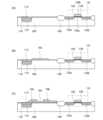
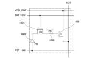
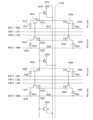
本発明の一態様である固体撮像素子の画素部分の一例を図1に断面図で示す。図1は転送
トランジスタ101に酸化物半導体の薄膜トランジスタを用いた例で、増幅トランジスタ
131は、単結晶シリコン基板100に形成されたnチャネル型のバルクトランジスタで
形成している。光電変換素子110はn型領域112と薄いp型領域114を含むフォト
ダイオードを形成しており、転送トランジスタ101のソース電極104に接続される。
また、転送トランジスタ101のドレイン電極下方には信号電荷蓄積部116(フローテ
ィングディフュージョンとも呼ぶ)が形成される。転送トランジスタ101は、酸化物半
導体層がチャネル領域となるトップゲート構造をしている。増幅トランジスタ131は、
n型領域132a、132bとゲート電極138を含むnチャネル型のバルクトランジス
タであり、増幅トランジスタ131のゲート電極138は、配線154により信号電荷蓄
積部116と電気的に接続されている。FIG. 1 shows a cross-sectional view of an example of a pixel portion of a solid-state image sensor that is one embodiment of the present invention. FIG. 1 shows an example in which an oxide semiconductor thin film transistor is used as the
Further, a signal charge storage section 116 (also referred to as a floating diffusion) is formed below the drain electrode of the
It is an n-channel type bulk transistor including n-
なお、図1の構造において、バルクトランジスタのゲート絶縁層136は薄膜トランジス
タである転送トランジスタ101の下地絶縁層を兼ねており、信号電荷蓄積部116はゲ
ート絶縁層136を誘電体として容量を形成している。また、薄膜トランジスタのゲート
絶縁層118は、バルクトランジスタの層間絶縁層の一部として機能する。Note that in the structure of FIG. 1, the
酸化物半導体をチャネル形成領域に用いた薄膜トランジスタは、トップゲート型を例とし
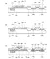
て示したが、逆スタガ構造などのボトムゲート型を用いても良い。また、光電変換素子1
10に光を照射する必要があるため、転送トランジスタ101のソース電極の一部を光電
変換素子110の受光部に接続させる例を挙げたが、ソース電極を透光性導電材料で形成
し、光電変換素子110との接続の状態を変えても良い。例えば、図2(A)に示すよう
に、透光性導電材料で形成したソース電極204を有するトランジスタ201を転送トラ
ンジスタとして用いれば、光電変換素子210の受光面の一部または全面に接続すること
ができる。また、図2(B)に示す様に光電変換素子310への光路を確保できるように
、抵抗の低い金属層をソース電極304及びドレイン電極306とし、透光性導電材料層
をバッファ層305、307として積層したトランジスタ301を転送トランジスタとし
て用いても良い。Although a top gate type thin film transistor using an oxide semiconductor in a channel formation region is shown as an example, a bottom gate type such as an inverted staggered structure may also be used. In addition,
Since it is necessary to irradiate light to the
光電変換素子として形成するフォトダイオードはp型単結晶シリコン基板(SOIの場合
は、p型単結晶シリコン層)にn型領域を形成し、その上部に薄いp型領域を形成した所
謂埋め込み型フォトダイオードを形成する。フォトダイオードの表面にp型領域を形成す
ることで表面で発生する暗電流によるノイズを低減することができる。The photodiode formed as a photoelectric conversion element is a so-called buried photodiode in which an n-type region is formed on a p-type single-crystal silicon substrate (in the case of SOI, a p-type single-crystal silicon layer) and a thin p-type region is formed on top of the n-type region. form a diode. By forming a p-type region on the surface of the photodiode, noise due to dark current generated on the surface can be reduced.
また、上記では単結晶半導体基板を用いた例を示したが、SOI構造の基板であっても良
い。また、バルクトランジスタの構造はこれに限らず、ゲート電極端にサイドウォールを
設けたLDD(Lightly Doped Drain)構造やソースドレイン領域の
一部に低抵抗のシリサイド等を形成した構造であっても良い。Further, although an example using a single crystal semiconductor substrate has been shown above, a substrate having an SOI structure may also be used. Further, the structure of the bulk transistor is not limited to this, and may be an LDD (Lightly Doped Drain) structure in which a sidewall is provided at the end of the gate electrode, or a structure in which low-resistance silicide or the like is formed in a part of the source/drain region. .
また、上記画素部には増幅トランジスタ131と電気的に接続される選択トランジスタを
設けても良い。増幅トランジスタ及び選択トランジスタは共にシリコン半導体、酸化物半
導体のどちらを用いても形成することができる。ただし、増幅トランジスタは、より増幅
率の高いシリコン半導体層を用いたバルクトランジスタで形成することが好ましい。Further, a selection transistor electrically connected to the
また、バルクトランジスタの上部に絶縁層を設け、その上に薄膜トランジスタを設けるこ
ともできる。例えば、薄膜トランジスタで形成する転送トランジスタをバルクトランジス
タで形成する増幅トランジスタの上部に設ければ、一画素につき必要なトランジスタの面
積が1/2から2/3程度となり、集積度の向上やフォトダイオードの受光面積を増加さ
せることができ、ノイズを低減させることもできる。図3はその一例であり、下層に光電
変換素子510とバルクトランジスタで形成された増幅トランジスタ531を形成し、絶
縁膜541を介して上層に薄膜トランジスタで形成された転送トランジスタ501を設け
た例であり、光電変換素子及びバルクトランジスタと薄膜トランジスタの作製工程が分離
できるため、工程の制御が容易となる。ただし、信号電荷蓄積部516を形成するための
容量電極540を設けておくことが好ましい。Alternatively, an insulating layer can be provided above the bulk transistor, and a thin film transistor can be provided thereon. For example, if a transfer transistor made of a thin film transistor is placed above an amplification transistor made of a bulk transistor, the area of the transistor required for each pixel will be reduced to about 1/2 to 2/3, which can improve the degree of integration and reduce the need for photodiodes. The light receiving area can be increased and noise can also be reduced. FIG. 3 is an example of this, in which a
ここで、本発明の一態様は、酸化物半導体層を用いた薄膜トランジスタを含む構成である
とともに、固体撮像素子であるCMOS(Complementary Metal O
xide Semiconductor)イメージセンサの一般的な構成要素であるリセ
ットトランジスタを省いていることに特徴がある。従来のCMOSイメージセンサは、リ
セットトランジスタを動作させることによって、信号電荷蓄積部の電位を初期化していた
が、本発明の一態様では、信号電荷蓄積部をフォトダイオードのカソード電位に初期化す
ることができる。先ず、フォトダイオードを順バイアスとし、転送トランジスタをオンす
ると信号電荷蓄積部はフォトダイオードのカソードと同じ電位となる。次にフォトダイオ
ードを逆バイアスとし、フォトダイオードに光を照射すると信号電荷蓄積部の電位は放電
により低下する。ここで転送トランジスタをオフし、保持された電位に従って増幅トラン
ジスタにより信号を出力させることができる。Here, one embodiment of the present invention has a structure including a thin film transistor using an oxide semiconductor layer, and a CMOS (complementary metal oxide semiconductor) which is a solid-state image sensor.
xide Semiconductor) is characterized by omitting a reset transistor, which is a common component of image sensors. In conventional CMOS image sensors, the potential of the signal charge storage section is initialized by operating a reset transistor, but in one embodiment of the present invention, the signal charge storage section is initialized to the cathode potential of the photodiode. I can do it. First, when the photodiode is forward biased and the transfer transistor is turned on, the signal charge storage section has the same potential as the cathode of the photodiode. Next, when the photodiode is reverse biased and light is irradiated onto the photodiode, the potential of the signal charge storage section decreases due to discharge. At this point, the transfer transistor is turned off, and the amplification transistor can output a signal according to the held potential.
以上の構造の薄膜トランジスタとバルクトランジスタを組み合わせることにより、信号電
荷蓄積部の電位の保持機能を高め、ダイナミックレンジの広い固体撮像素子の画素部を形
成することができる。ただし、この本発明の一態様を実現するには極めてオフ電流の小さ
い薄膜トランジスタを用いることが好ましい。次にその作製方法を説明する。By combining the thin film transistor and bulk transistor having the above structure, it is possible to improve the potential holding function of the signal charge storage section and form a pixel section of a solid-state image sensor with a wide dynamic range. However, in order to realize this embodiment of the present invention, it is preferable to use a thin film transistor with extremely low off-state current. Next, the manufacturing method will be explained.
本発明の一態様は、単結晶シリコン半導体を用いたバルクトランジスタと極めて電気特性
の良好な酸化物半導体を用いた薄膜トランジスタを複合することにより固体撮像素子の画
素部を形成するものである。従って、酸化物半導体を用いた薄膜トランジスタの作製方法
を中心に詳細な説明を行う。One embodiment of the present invention forms a pixel portion of a solid-state image sensor by combining a bulk transistor using a single-crystal silicon semiconductor and a thin film transistor using an oxide semiconductor with extremely good electrical characteristics. Therefore, a detailed description will be given focusing on a method for manufacturing a thin film transistor using an oxide semiconductor.
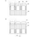
一例として、図1の構造の作製方法を図4及び図5の断面図を用いて説明する。まず、P
型の単結晶シリコン基板100に絶縁膜140(フィールド酸化膜とも言う)で分離した
素子形成領域を形成する。素子分離領域の形成は、LOCOS法(Local Oxid
ation of Silicon)法)やSTI法(Shallow Trench
Isolation)等を用いることができる。As an example, a method for manufacturing the structure shown in FIG. 1 will be described using cross-sectional views shown in FIGS. 4 and 5. First, P
Element formation regions separated by an insulating film 140 (also referred to as a field oxide film) are formed on a mold single
ation of Silicon) method) and STI method (Shallow Trench
Isolation) etc. can be used.
ここで基板は単結晶シリコン基板に限らず、SOI(Silicon on Insul
ator)基板等を用いることもできる。Here, the substrate is not limited to a single crystal silicon substrate, but also an SOI (Silicon on Insulator) substrate.
ator) substrate etc. can also be used.
なお、本実施の形態では、埋め込み型のフォトダイオード及びnチャネル型のバルクトラ
ンジスタを用いる構成であるため、p型単結晶シリコン基板を用いるが、pウェルを形成
すればn型単結晶シリコン基板を用いることもできる。Note that this embodiment uses a p-type single-crystal silicon substrate because it uses a buried photodiode and an n-channel bulk transistor; however, if a p-well is formed, an n-type single-crystal silicon substrate can be used. It can also be used.
次に、素子形成領域を覆うようにゲート絶縁層136を形成する。例えば、熱処理を行い
単結晶シリコン基板100に設けられた素子形成領域の表面を酸化させることにより酸化
シリコン膜を形成することができる。また、熱酸化法により酸化シリコン膜を形成した後
に、窒化処理を行うことによって酸化シリコン膜の表面を窒化させることにより、酸化シ
リコン膜と酸窒化シリコン膜との積層構造で形成してもよい。Next, a
他の方法としては、例えば、単結晶シリコン基板100に設けられた素子形成領域の表面
に高密度プラズマ処理により酸化処理又は窒化処理を行うことにより、ゲート絶縁層13
6として酸化シリコン膜又は窒化シリコン膜で形成することができる。また、高密度プラ
ズマ処理により素子形成領域の表面に酸化処理を行った後に、再度高密度プラズマ処理を
行うことによって窒化処理を行ってもよい。この場合、素子形成領域の表面に接して酸化
シリコン膜が形成され、当該酸化シリコン膜上に酸窒化シリコン膜が形成され、ゲート絶
縁層136は酸化シリコン膜と酸窒化シリコン膜とが積層された膜となる。Another method is to perform oxidation treatment or nitridation treatment on the surface of the element formation region provided in the single
6 can be formed of a silicon oxide film or a silicon nitride film. Further, after performing oxidation treatment on the surface of the element formation region by high-density plasma treatment, nitriding treatment may be performed by performing high-density plasma treatment again. In this case, a silicon oxide film is formed in contact with the surface of the element formation region, a silicon oxynitride film is formed on the silicon oxide film, and the
次に、ゲート絶縁層136を覆うように導電層を形成する。ここでは、導電層138aと
導電層138bを順に積層して形成する。もちろん、導電層は、単層または2層以上の積
層構造で形成してもよい。Next, a conductive layer is formed to cover the
導電層138a、138bとしては、タンタル(Ta)、タングステン(W)、チタン(
Ti)、モリブデン(Mo)、アルミニウム(Al)、銅(Cu)、クロム(Cr)、ニ
オブ(Nb)等から選択された元素またはこれらの元素を主成分とする合金材料若しくは
化合物材料で形成することができる。また、これらの元素を窒化した金属窒化膜で形成す
ることもできる。他にも、リン等の不純物元素をドーピングした多結晶シリコンに代表さ
れる半導体材料により形成することもできる。The
Made of an element selected from Ti), molybdenum (Mo), aluminum (Al), copper (Cu), chromium (Cr), niobium (Nb), etc., or an alloy material or compound material containing these elements as main components. be able to. Alternatively, a metal nitride film obtained by nitriding these elements can also be formed. Alternatively, it can also be formed from a semiconductor material such as polycrystalline silicon doped with an impurity element such as phosphorus.
ここでは、導電層138aとして窒化タンタルを用いて形成し、その上に導電層138b
としてタングステンを用いて積層構造で設ける。また、他にも、導電層138aとして、
窒化タングステン、窒化モリブデン又は窒化チタンから選ばれた単層または積層膜を用い
、導電層138bとして、タンタル、モリブデン、チタンから選ばれた単層または積層膜
を用いることができる。Here, the
It is provided in a laminated structure using tungsten as the material. In addition, as the
A single layer or a stacked film selected from tungsten nitride, molybdenum nitride, or titanium nitride can be used, and a single layer or stacked film selected from tantalum, molybdenum, and titanium can be used as the
次に、積層して設けられた導電層138a、138bを選択的にエッチングして除去する
ことによって、ゲート絶縁層136の上方の一部に導電層138a、138bを残存させ
、ゲート電極138を形成する。Next, by selectively etching and removing the
次に、素子形成領域以外を覆うようにレジストマスクを選択的に形成し、当該レジストマ
スク及びゲート電極138をマスクとして不純物元素を導入することによってn型領域1
32a、132bを形成する。ここでは、nチャネル型のバルクトランジスタを形成する
ため、不純物元素としては、n型を付与する不純物元素であるリン(P)やヒ素(As)
等を用いることができる。Next, a resist mask is selectively formed so as to cover areas other than the element formation region, and an impurity element is introduced using the resist mask and
32a and 132b are formed. Here, in order to form an n-channel type bulk transistor, the impurity elements include phosphorus (P) and arsenic (As), which are impurity elements that impart n-type conductivity.
etc. can be used.
次に、光電変換素子であるフォトダイオードを作製するためにレジストマスクを選択的に
形成する。まず、n型を付与する不純物元素であるリン(P)やヒ素(As)をp型単結
晶シリコン基板に導入しpn接合を形成した後、p型を付与する不純物元素であるホウ素
(B)をn型領域の表層に導入することで埋め込み型のフォトダイオードを形成すること
ができる。Next, a resist mask is selectively formed in order to fabricate a photodiode, which is a photoelectric conversion element. First, phosphorus (P) and arsenic (As), which are impurity elements that impart n-type characteristics, are introduced into a p-type single crystal silicon substrate to form a pn junction, and then boron (B), which is an impurity element that imparts p-type By introducing this into the surface layer of the n-type region, a buried photodiode can be formed.
この段階で、図4(A)の右側に示すバルクトランジスタと左側に示すフォトダイオード
の構造が完成する。At this stage, the structures of the bulk transistor shown on the right side of FIG. 4A and the photodiode shown on the left side are completed.
次に酸化物半導体層をチャネル領域とする薄膜トランジスタの作製方法について説明する
。Next, a method for manufacturing a thin film transistor using an oxide semiconductor layer as a channel region will be described.
本実施の形態では、既に単結晶シリコン基板100上に設けられているバルクトランジス
タのゲート絶縁層136上に薄膜トランジスタを形成する。つまり、薄膜トランジスタの
下地膜とバルクトランジスタのゲート絶縁層とを兼ねることができる。ただし、次の方法
を用いて絶縁層を成膜し、下地膜を積層としても良い。In this embodiment, a thin film transistor is formed on the
酸化物半導体層と接する絶縁層は、酸化シリコン層、酸化窒化シリコン層、酸化アルミニ
ウム層、または酸化窒化アルミニウム層などの酸化物絶縁層を用いると好ましい。絶縁層
の形成方法としては、プラズマCVD法またはスパッタ法等を用いることができるが、絶
縁層中に水素が多量に含まれないようにするためには、スパッタ法で絶縁層を成膜するこ
とが好ましい。The insulating layer in contact with the oxide semiconductor layer is preferably an oxide insulating layer such as a silicon oxide layer, a silicon oxynitride layer, an aluminum oxide layer, or an aluminum oxynitride layer. The insulating layer can be formed using a plasma CVD method or a sputtering method, but in order to prevent a large amount of hydrogen from being contained in the insulating layer, it is preferable to form the insulating layer by a sputtering method. is preferred.
絶縁層として、スパッタ法により酸化シリコン層を形成する例を説明する。単結晶シリコ
ン基板100を処理室へ搬送し、水素及び水分が除去された高純度酸素を含むスパッタガ
スを導入しシリコンターゲットを用いて、単結晶シリコン基板100に絶縁層として、酸
化シリコン層を成膜する。また単結晶シリコン基板100は室温でもよいし、加熱されて
いてもよい。An example in which a silicon oxide layer is formed as the insulating layer by sputtering will be described. The single-
例えば、石英(好ましくは合成石英)をターゲットとして用い、基板温度108℃、基板
とターゲットの間との距離(T-S間距離)を60mm、圧力0.4Pa、高周波電源1
.5kW、酸素及びアルゴン(酸素流量25sccm:アルゴン流量25sccm=1:
1)雰囲気下でRFスパッタ法により酸化シリコン層を成膜する。膜厚は100nmとす
る。なお、石英に代えてシリコンを酸化シリコン層を成膜するためのターゲットとして用
いることができる。このとき、スパッタガスとして酸素または、酸素及びアルゴンの混合
ガスを用いて行う。For example, using quartz (preferably synthetic quartz) as a target, the substrate temperature is 108°C, the distance between the substrate and the target (TS distance) is 60 mm, the pressure is 0.4 Pa, and the high frequency power source is 1.
.. 5kW, oxygen and argon (oxygen flow rate 25sccm: argon flow rate 25sccm=1:
1) A silicon oxide layer is formed by RF sputtering in an atmosphere. The film thickness is 100 nm. Note that silicon can be used as a target for forming the silicon oxide layer instead of quartz. At this time, oxygen or a mixed gas of oxygen and argon is used as the sputtering gas.
この場合において、処理室内の残留水分を除去しつつ絶縁層を成膜することが好ましい。
絶縁層に水素、水酸基又は水分が含まれないようにするためである。In this case, it is preferable to form the insulating layer while removing residual moisture in the processing chamber.
This is to prevent hydrogen, hydroxyl groups, or moisture from being contained in the insulating layer.
処理室内の残留水分を除去するためには、吸着型の真空ポンプを用いることが好ましい。
例えば、クライオポンプ、イオンポンプ、チタンサブリメーションポンプを用いることが
好ましい。また、排気手段としては、ターボポンプにコールドトラップを加えたものであ
ってもよい。クライオポンプを用いて排気した処理室は、例えば、水素原子や、水(H2
O)など水素原子を含む化合物等が排気されるため、当該処理室で成膜し絶縁層に含まれ
る不純物の濃度を低減することができる。In order to remove residual moisture in the processing chamber, it is preferable to use an adsorption type vacuum pump.
For example, it is preferable to use a cryopump, an ion pump, or a titanium sublimation pump. Further, the exhaust means may be a turbo pump with a cold trap added. For example, the processing chamber evacuated using a cryopump can contain hydrogen atoms, water (H2
Since compounds containing hydrogen atoms such as O) are exhausted, the concentration of impurities contained in the insulating layer formed in the processing chamber can be reduced.
絶縁層を成膜する際に用いるスパッタガスは水素、水、水酸基または水素化物などの不純
物がppm程度の濃度またはppb程度の濃度まで除去された高純度ガスを用いることが
好ましい。The sputtering gas used to form the insulating layer is preferably a high-purity gas in which impurities such as hydrogen, water, hydroxyl groups, or hydrides have been removed to a concentration of about ppm or ppb.
スパッタ法にはスパッタ用電源に高周波電源を用いるRFスパッタ法、直流電源を用いる
DCスパッタ法、さらにパルス的にバイアスを与えるパルスDCスパッタ法がある。RF
スパッタ法は主に絶縁膜を成膜する場合に用いられ、DCスパッタ法は主に導電膜を成膜
する場合に用いられる。Sputtering methods include an RF sputtering method using a high frequency power source as a sputtering power source, a DC sputtering method using a DC power source, and a pulsed DC sputtering method using a pulsed bias. RF
The sputtering method is mainly used when forming an insulating film, and the DC sputtering method is mainly used when forming a conductive film.
また、材料の異なるターゲットを複数設置できる多元スパッタ装置もある。多元スパッタ
装置は、同一チャンバーで異なる材料膜を積層成膜することも、同一チャンバーで複数種
類の材料を同時に放電させて成膜することもできる。There is also a multi-source sputtering device that can install multiple targets made of different materials. The multi-source sputtering apparatus can perform layered film formation of different material films in the same chamber, or can perform film formation by simultaneously discharging a plurality of types of materials in the same chamber.
また、チャンバー内部に磁石機構を備えたマグネトロンスパッタ法を用いるスパッタ装置
や、グロー放電を使わずマイクロ波を用いて発生させたプラズマを用いるECRスパッタ
法を用いるスパッタ装置がある。Furthermore, there are sputtering apparatuses that use a magnetron sputtering method that is equipped with a magnet mechanism inside a chamber, and sputtering apparatuses that use an ECR sputtering method that uses plasma generated using microwaves without using glow discharge.
また、スパッタ法を用いる成膜方法として、成膜中にターゲット物質とスパッタガス成分
とを化学反応させてそれらの化合物薄膜を形成するリアクティブスパッタ法や、成膜中に
基板にも電圧をかけるバイアススパッタ法もある。In addition, as a film formation method using sputtering, there is a reactive sputtering method in which a target material and sputtering gas components are chemically reacted during film formation to form a thin film of these compounds, and a reactive sputtering method in which a voltage is also applied to the substrate during film formation. There is also a bias sputtering method.
また、絶縁層は積層構造でもよく、例えば、基板側から窒化シリコン層、窒化酸化シリコ
ン層、窒化アルミニウム層、又は窒化酸化アルミニウム層などの窒化物絶縁層と、上記酸
化物絶縁層との積層構造としてもよい。Further, the insulating layer may have a laminated structure, for example, a laminated structure of a nitride insulating layer such as a silicon nitride layer, a silicon nitride oxide layer, an aluminum nitride layer, or an aluminum nitride oxide layer, and the above-mentioned oxide insulating layer from the substrate side. You can also use it as
例えば、酸化シリコン層と基板との間に水素及び水分が除去された高純度窒素を含むスパ
ッタガスを導入しシリコンターゲットを用いて窒化シリコン層を成膜する。この場合にお
いても、酸化シリコン層と同様に、処理室内の残留水分を除去しつつ窒化シリコン層を成
膜することが好ましい。For example, a sputtering gas containing high purity nitrogen from which hydrogen and moisture have been removed is introduced between the silicon oxide layer and the substrate, and a silicon nitride layer is formed using a silicon target. In this case, as well as the silicon oxide layer, it is preferable to form the silicon nitride layer while removing residual moisture in the processing chamber.
窒化シリコン層を形成する場合も、成膜時に基板を加熱してもよい。Also when forming a silicon nitride layer, the substrate may be heated during film formation.
絶縁層として窒化シリコン層と酸化シリコン層とを積層する場合、窒化シリコン層と酸化
シリコン層を同じ処理室において、共通のシリコンターゲットを用いて成膜することがで
きる。先に窒素を含むスパッタガスを導入して、処理室内に装着されたシリコンターゲッ
トを用いて窒化シリコン層を形成し、次にスパッタガスを酸素を含むスパッタガスに切り
替えて同じシリコンターゲットを用いて酸化シリコン層を成膜する。窒化シリコン層と酸
化シリコン層とを大気に曝露せずに連続して形成することができるため、窒化シリコン層
表面に水素や水分などの不純物が吸着することを防止することができる。When stacking a silicon nitride layer and a silicon oxide layer as an insulating layer, the silicon nitride layer and the silicon oxide layer can be formed in the same processing chamber using a common silicon target. First, a sputtering gas containing nitrogen is introduced to form a silicon nitride layer using a silicon target installed in the processing chamber, and then the sputtering gas is switched to a sputtering gas containing oxygen and oxidation is performed using the same silicon target. Deposit a silicon layer. Since the silicon nitride layer and the silicon oxide layer can be formed continuously without being exposed to the atmosphere, it is possible to prevent impurities such as hydrogen and moisture from adsorbing onto the surface of the silicon nitride layer.
次いで、絶縁層上(本実施の形態ではゲート絶縁層136上)に、膜厚2nm以上200
nm以下の酸化物半導体膜を形成する。Next, on the insulating layer (in this embodiment, on the gate insulating layer 136), a film with a thickness of 2 nm or more and 200 nm is deposited.
An oxide semiconductor film with a thickness of nm or less is formed.
また、酸化物半導体膜に水素、水酸基及び水分がなるべく含まれないようにするために、
成膜の前処理として、スパッタ装置の予備加熱室で単結晶シリコン基板100を予備加熱
し、該基板に吸着した水素、水分などの不純物を脱離し排気することが好ましい。なお、
予備加熱室に設ける排気手段はクライオポンプが好ましい。なお、この予備加熱の処理は
省略することもできる。またこの予備加熱は、後に形成する薄膜トランジスタのゲート絶
縁層118の成膜前に行ってもよいし、後に形成するソース電極及びドレイン電極となる
導電層の成膜前に行っても良い。In addition, in order to prevent the oxide semiconductor film from containing hydrogen, hydroxyl groups, and water as much as possible,
As a pretreatment for film formation, it is preferable to preheat the single
The evacuation means provided in the preheating chamber is preferably a cryopump. Note that this preheating process can also be omitted. Further, this preheating may be performed before forming a
なお、酸化物半導体膜をスパッタ法により成膜する前に、アルゴンガスを導入してプラズ
マを発生させる逆スパッタを行い、絶縁層の表面に付着しているゴミを除去することが好
ましい。逆スパッタとは、アルゴン雰囲気下で基板側にRF電源を用いて電圧を印加し、
イオン化したアルゴンを基板に衝突させて表面を改質する方法である。なお、アルゴンに
代えて窒素、ヘリウム、酸素などを用いてもよい。Note that before forming the oxide semiconductor film by a sputtering method, it is preferable to perform reverse sputtering in which argon gas is introduced to generate plasma to remove dust adhering to the surface of the insulating layer. Reverse sputtering involves applying voltage to the substrate side using an RF power source in an argon atmosphere.
This method modifies the surface by bombarding the substrate with ionized argon. Note that nitrogen, helium, oxygen, etc. may be used instead of argon.
酸化物半導体膜はスパッタ法により成膜する。酸化物半導体膜としては、四元系金属酸化
物であるIn-Sn-Ga-Zn-O膜や、三元系金属酸化物であるIn-Ga-Zn-
O膜、In-Sn-Zn-O膜、In-Al-Zn-O膜、Sn-Ga-Zn-O膜、A
l-Ga-Zn-O膜、Sn-Al-Zn-O膜や、二元系金属酸化物であるIn-Zn
-O膜、Sn-Zn-O膜、Al-Zn-O膜、Zn-Mg-O膜、Sn-Mg-O膜、
In-Mg-O膜や、In-O膜、Sn-O膜、Zn-O膜などを用いることができる。
また、上記酸化物半導体膜にSiO2を含んでもよい。The oxide semiconductor film is formed by a sputtering method. The oxide semiconductor film may be an In-Sn-Ga-Zn-O film which is a quaternary metal oxide or an In-Ga-Zn- which is a ternary metal oxide.
O film, In-Sn-Zn-O film, In-Al-Zn-O film, Sn-Ga-Zn-O film, A
l-Ga-Zn-O film, Sn-Al-Zn-O film, In-Zn which is a binary metal oxide
-O film, Sn-Zn-O film, Al-Zn-O film, Zn-Mg-O film, Sn-Mg-O film,
An In--Mg--O film, an In--O film, a Sn--O film, a Zn--O film, or the like can be used.
Further, the oxide semiconductor film may include SiO2 .
また、酸化物半導体膜は、InMO3(ZnO)m(m>0)で表記される薄膜を用いる
ことができる。ここで、Mは、Ga、Al、MnおよびCoから選ばれた一または複数の
金属元素を示す。例えばMとして、Ga、Ga及びAl、Ga及びMn、またはGa及び
Coなどがある。InMO3(ZnO)m(m>0)で表記される構造の酸化物半導体膜
のうち、MとしてGaを含む構造の酸化物半導体を、In-Ga-Zn-O酸化物半導体
とよび、その薄膜をIn-Ga-Zn-O膜ともよぶこととする。Further, as the oxide semiconductor film, a thin film expressed as InMO3 (ZnO)m (m>0) can be used. Here, M represents one or more metal elements selected from Ga, Al, Mn, and Co. For example, M may include Ga, Ga and Al, Ga and Mn, or Ga and Co. Among oxide semiconductor films having a structure represented by InMO3 (ZnO)m (m>0), an oxide semiconductor having a structure containing Ga as M is called an In-Ga-Zn-O oxide semiconductor. The thin film will also be referred to as an In-Ga-Zn-O film.
本実施の形態では、酸化物半導体膜をIn-Ga-Zn-O系金属酸化物ターゲットを用
いてスパッタ法により成膜する。また、酸化物半導体膜は、希ガス(代表的にはアルゴン
)雰囲気下、酸素雰囲気下、またはそれらの混合雰囲気下においてスパッタ法により形成
することができる。In this embodiment, an oxide semiconductor film is formed by a sputtering method using an In-Ga-Zn-O-based metal oxide target. Further, the oxide semiconductor film can be formed by a sputtering method in a rare gas (typically argon) atmosphere, an oxygen atmosphere, or a mixed atmosphere thereof.
酸化物半導体膜を成膜する際に用いるスパッタガスは水素、水、水酸基または水素化物な
どの不純物がppm程度の濃度またはppb程度の濃度まで除去された高純度ガスを用い
ることが好ましい。The sputtering gas used to form the oxide semiconductor film is preferably a high-purity gas in which impurities such as hydrogen, water, hydroxyl groups, or hydrides have been removed to a concentration of about ppm or ppb.
酸化物半導体膜をスパッタ法で作製するためのターゲットとして、酸化亜鉛を主成分とす
る金属酸化物のターゲットを用いることができる。例えば、組成比として、In2O3:
Ga2O3:ZnO=1:1:1[mol数比]の金属酸化物ターゲットを用いれば良い
。また、In2O3:Ga2O3:ZnO=1:1:2[mol数比]の金属酸化物ター
ゲットを用いてもよい。金属酸化物ターゲットの充填率は90%以上100%以下、好ま
しくは95%以上99.9%である。充填率の高い金属酸化物ターゲットを用いることに
より、成膜した酸化物半導体膜は緻密な膜となる。As a target for manufacturing an oxide semiconductor film by a sputtering method, a metal oxide target containing zinc oxide as a main component can be used. For example, as a composition ratio, In2 O3 :
A metal oxide target of Ga2 O3 :ZnO=1:1:1 [molar ratio] may be used. Alternatively, a metal oxide target having a molar ratio of In2 O3 :Ga2 O3 :ZnO=1:1:2 may be used. The filling rate of the metal oxide target is 90% or more and 100% or less, preferably 95% or more and 99.9%. By using a metal oxide target with a high filling rate, the formed oxide semiconductor film becomes a dense film.
酸化物半導体膜は、減圧状態に保持された処理室内に基板を保持し、処理室内の残留水分
を除去しつつ水素及び水分が除去されたスパッタガスを導入し、金属酸化物をターゲット
として絶縁層上に酸化物半導体膜を成膜する。処理室内の残留水分を除去するためには、
吸着型の真空ポンプを用いることが好ましい。例えば、クライオポンプ、イオンポンプ、
チタンサブリメーションポンプを用いることが好ましい。また、排気手段としては、ター
ボポンプにコールドトラップを加えたものであってもよい。クライオポンプを用いて排気
した処理室は、例えば、水素原子、水(H2O)など水素原子を含む化合物(より好まし
くは炭素原子を含む化合物も)等が排気されるため、当該処理室で成膜した酸化物半導体
膜に含まれる不純物の濃度を低減できる。また、酸化物半導体膜成膜時に基板を加熱して
もよい。Oxide semiconductor films are produced by holding a substrate in a processing chamber maintained at reduced pressure, removing residual moisture in the processing chamber, and introducing sputtering gas from which hydrogen and moisture have been removed. An oxide semiconductor film is formed thereover. To remove residual moisture in the processing chamber,
It is preferable to use an adsorption type vacuum pump. For example, cryopump, ion pump,
Preferably, a titanium sublimation pump is used. Further, the exhaust means may be a turbo pump with a cold trap added. For example, compounds containing hydrogen atoms (more preferably compounds containing carbon atoms) such as hydrogen atoms and water (H2 O) are evacuated from a processing chamber that is evacuated using a cryopump. The concentration of impurities contained in the formed oxide semiconductor film can be reduced. Further, the substrate may be heated during formation of the oxide semiconductor film.
成膜条件の一例としては、基板温度室温、基板とターゲットの間との距離を110mm、
圧力0.4Pa、直流(DC)電源0.5kW、酸素及びアルゴン(酸素流量15scc
m:アルゴン流量30sccm)雰囲気下の条件が適用される。なお、パルス直流(DC
)電源を用いると、成膜時に発生する粉状物質(パーティクル、ゴミともいう)が軽減で
き、膜厚分布も均一となるために好ましい。酸化物半導体膜は好ましくは5nm以上30
nm以下とする。なお、適用する酸化物半導体材料により適切な厚みは異なり、材料に応
じて適宜厚みを選択すればよい。As an example of the film forming conditions, the substrate temperature is room temperature, the distance between the substrate and the target is 110 mm,
Pressure 0.4 Pa, direct current (DC) power supply 0.5 kW, oxygen and argon (
m: argon flow rate 30 sccm) atmospheric conditions are applied. In addition, pulsed direct current (DC
) It is preferable to use a power supply because powdery substances (also referred to as particles or dust) generated during film formation can be reduced and the film thickness distribution can be made uniform. The oxide semiconductor film preferably has a thickness of 5 nm or more30
It should be less than nm. Note that the appropriate thickness varies depending on the oxide semiconductor material to be applied, and the thickness may be appropriately selected depending on the material.
次いで、酸化物半導体膜を第1のフォトリソグラフィ工程及びエッチング工程により島状
の酸化物半導体層102に加工する(図4(B)参照)。Next, the oxide semiconductor film is processed into an island-shaped
なお、島状の酸化物半導体層を形成するためのレジストマスクはインクジェット法で形成
してもよい。レジストマスクをインクジェット法で形成するとフォトマスクを使用しない
ため、製造コストを低減できる。また、ここでの酸化物半導体膜のエッチングは、ドライ
エッチングでもウェットエッチングでもよく、両方を用いてもよい。Note that the resist mask for forming the island-shaped oxide semiconductor layer may be formed by an inkjet method. When a resist mask is formed by an inkjet method, a photomask is not used, so manufacturing costs can be reduced. Further, the etching of the oxide semiconductor film here may be dry etching or wet etching, or both may be used.
ドライエッチングに用いるエッチングガスとしては、塩素を含むガス(塩素系ガス、例え
ば塩素(Cl2)、塩化硼素(BCl3)、塩化珪素(SiCl4)、四塩化炭素(CC
l4)など)が好ましい。Etching gases used for dry etching include gases containing chlorine (chlorine-based gases, such as chlorine (Cl2 ), boron chloride (BCl3 ), silicon chloride (SiCl4 ), carbon tetrachloride (CC
l4 ) etc.) are preferred.
また、フッ素を含むガス(フッ素系ガス、例えば四弗化炭素(CF4)、六弗化硫黄(S
F6)、三弗化窒素(NF3)、トリフルオロメタン(CHF3)など)、臭化水素(H
Br)、酸素(O2)、これらのガスにヘリウム(He)やアルゴン(Ar)などの希ガ
スを添加したガス、などを用いることができる。In addition, gases containing fluorine (fluorine-based gases, such as carbon tetrafluoride (CF4 ), sulfur hexafluoride (S
F6 ), nitrogen trifluoride (NF3 ), trifluoromethane (CHF3 ), etc.), hydrogen bromide (H
Br), oxygen (O2 ), a gas obtained by adding a rare gas such as helium (He) or argon (Ar) to these gases, etc. can be used.
ドライエッチング法としては、平行平板型RIE(Reactive Ion Etch
ing)法や、ICP(Inductively Coupled Plasma:誘導
結合型プラズマ)エッチング法を用いることができる。所望の加工形状にエッチングでき
るように、エッチング条件(コイル型の電極に印加される電力量、基板側の電極に印加さ
れる電力量、基板側の電極温度等)を適宜調節する。As a dry etching method, parallel plate type RIE (Reactive Ion Etch
ing) etching method or ICP (Inductively Coupled Plasma) etching method can be used. Etching conditions (the amount of power applied to the coil-type electrode, the amount of power applied to the electrode on the substrate side, the temperature of the electrode on the substrate side, etc.) are adjusted as appropriate so that the desired processed shape can be etched.
ウェットエッチングに用いるエッチング液としては、燐酸と酢酸と硝酸を混ぜた溶液、ア
ンモニア過水(31重量%過酸化水素水:28重量%アンモニア水:水=5:2:2)な
どを用いることができる。また、ITO-07N(関東化学社製)を用いてもよい。As the etching solution used for wet etching, a solution containing phosphoric acid, acetic acid, and nitric acid, ammonia peroxide (31% by weight hydrogen peroxide solution: 28% by weight ammonia solution: water = 5:2:2), etc. can be used. can. Alternatively, ITO-07N (manufactured by Kanto Kagaku Co., Ltd.) may be used.
また、ウェットエッチング後のエッチング液はエッチングされた材料とともに洗浄によっ
て除去される。その除去された材料を含むエッチング液の廃液を精製し、含まれる材料を
再利用してもよい。当該エッチング後の廃液から酸化物半導体層に含まれるインジウム等
の材料を回収して再利用することにより、資源を有効活用しコストを低減することができ
る。Further, the etching solution after wet etching is removed by cleaning together with the etched material. The waste etching solution containing the removed material may be purified and the contained material may be reused. By recovering and reusing materials such as indium contained in the oxide semiconductor layer from the waste liquid after the etching, it is possible to effectively utilize resources and reduce costs.
所望の形状にエッチングできるように、材料に合わせてエッチング条件(エッチング液、
エッチング時間、温度等)を適宜調節する。Etching conditions (etching solution,
(etching time, temperature, etc.) as appropriate.
本実施の形態では、エッチング液として燐酸と酢酸と硝酸を混ぜた溶液を用いたウェット
エッチング法により、酸化物半導体膜を島状の酸化物半導体層102に加工する。In this embodiment, the oxide semiconductor film is processed into the island-shaped
本実施の形態では、酸化物半導体層102に対して窒素、またはヘリウム、ネオン、アル
ゴン等の希ガス雰囲気下で第1の加熱処理を行う。第1の加熱処理の温度は、400℃以
上750℃以下、好ましくは400℃以上基板の歪み点未満とする。ここでは、加熱処理
装置の一つである電気炉に基板を導入し、酸化物半導体層に対して窒素雰囲気下450℃
において1時間の加熱処理を行う。加熱処理温度からの降温時に雰囲気を酸素に切り替え
ても良い。この第1の加熱処理によって酸化物半導体層102の脱水化または脱水素化を
行うことができる。In this embodiment, the
Heat treatment is performed for 1 hour. The atmosphere may be switched to oxygen when the temperature is lowered from the heat treatment temperature. By this first heat treatment, the
なお、加熱処理装置は電気炉に限られず、抵抗発熱体などの発熱体からの熱伝導または熱
輻射によって、被処理物を加熱する装置を備えていてもよい。例えば、GRTA(Gas
Rapid Thermal Annealing)装置、LRTA(Lamp Ra
pid Thermal Annealing)装置等のRTA(Rapid Ther
mal Annealing)装置を用いることができる。LRTA装置は、ハロゲンラ
ンプ、メタルハライドランプ、キセノンアークランプ、カーボンアークランプ、高圧ナト
リウムランプ、高圧水銀ランプなどのランプから発する光(電磁波)の輻射により、被処
理物を加熱する装置である。GRTA装置は、高温のガスを用いて加熱処理を行う装置で
ある。気体には、アルゴンなどの希ガス、または窒素のような、加熱処理によって被処理
物と反応しない不活性気体が用いられる。Note that the heat treatment apparatus is not limited to an electric furnace, and may include a device that heats the object to be processed by heat conduction or heat radiation from a heating element such as a resistance heating element. For example, GRTA (Gas
Rapid Thermal Annealing) device, LRTA (Lamp Ra
RTA (Rapid Thermal Annealing) equipment, etc.
An annealing (mal annealing) device can be used. An LRTA device is a device that heats a workpiece by radiation of light (electromagnetic waves) emitted from a lamp such as a halogen lamp, a metal halide lamp, a xenon arc lamp, a carbon arc lamp, a high pressure sodium lamp, or a high pressure mercury lamp. The GRTA device is a device that performs heat treatment using high-temperature gas. The gas used is a rare gas such as argon, or an inert gas such as nitrogen that does not react with the object to be processed during the heat treatment.
例えば、第1の加熱処理として、650℃以上700℃以下の高温に加熱した不活性ガス
中に基板を移動させて入れ、数分間加熱した後、基板を移動させて高温に加熱した不活性
ガス中から出すGRTAを行ってもよい。GRTAを用いると短時間での高温加熱処理が
可能となる。For example, as the first heat treatment, the substrate is moved into an inert gas heated to a high temperature of 650°C to 700°C, heated for several minutes, and then the substrate is moved to an inert gas heated to a high temperature of 650°C or more and 700°C or less. You may also perform GRTA to remove it from the inside. Using GRTA enables high-temperature heat treatment in a short time.
なお、第1の加熱処理においては、窒素、ヘリウム、ネオン、またはアルゴン等の雰囲気
ガスに、水、水素などが含まれないことが好ましい。または、該雰囲気ガスの純度を、6
N(99.9999%)以上、好ましくは7N(99.99999%)以上、(即ち不純
物濃度を1ppm以下、好ましくは0.1ppm以下)とする。雰囲気ガスとして酸素を
用いる場合も同様の純度であることが好ましい。Note that in the first heat treatment, it is preferable that the atmospheric gas such as nitrogen, helium, neon, or argon does not contain water, hydrogen, or the like. Or, the purity of the atmospheric gas is 6
N (99.9999%) or more, preferably 7N (99.99999%) or more (that is, the impurity concentration is 1 ppm or less, preferably 0.1 ppm or less). When oxygen is used as the atmospheric gas, it is preferable that the purity be the same.
また、第1の加熱処理の条件、または酸化物半導体層の材料によっては、酸化物半導体層
が結晶化し、微結晶層または多結晶層となる場合もある。例えば、結晶化率が90%以上
、または80%以上の微結晶の酸化物半導体層となる場合もある。また、第1の加熱処理
の条件、または酸化物半導体層の材料によっては、結晶成分を含まない非晶質の酸化物半
導体層となる場合もある。また、非晶質の酸化物半導体の中に微結晶部(粒径1nm以上
20nm以下(代表的には2nm以上4nm以下))が混在する酸化物半導体層となる場
合もある。Further, depending on the conditions of the first heat treatment or the material of the oxide semiconductor layer, the oxide semiconductor layer may be crystallized to become a microcrystalline layer or a polycrystalline layer. For example, a microcrystalline oxide semiconductor layer may have a crystallization rate of 90% or more, or 80% or more. Further, depending on the conditions of the first heat treatment or the material of the oxide semiconductor layer, the oxide semiconductor layer may become an amorphous oxide semiconductor layer that does not contain a crystal component. Further, the oxide semiconductor layer may include microcrystalline portions (grain size of 1 nm or more and 20 nm or less (typically 2 nm or more and 4 nm or less)) mixed in an amorphous oxide semiconductor.
また、酸化物半導体層の第1の加熱処理は、島状の酸化物半導体層に加工する前の酸化物
半導体膜に行うこともできる。Further, the first heat treatment of the oxide semiconductor layer can also be performed on the oxide semiconductor film before being processed into an island-shaped oxide semiconductor layer.
酸化物半導体層に対する脱水化、脱水素化の効果を奏する加熱処理は、酸化物半導体層成
膜後、酸化物半導体層上にソース電極及びドレイン電極を積層させた後、ソース電極及び
ドレイン電極上にゲート絶縁層を形成した後、のいずれで行っても良い。The heat treatment that has the effect of dehydrating and dehydrogenating the oxide semiconductor layer is performed after the oxide semiconductor layer is formed, after the source electrode and the drain electrode are stacked on the oxide semiconductor layer, and after the source electrode and the drain electrode are stacked on the oxide semiconductor layer. It may be performed either after forming the gate insulating layer.
次いで、第2のフォトリソグラフィ工程及びエッチング工程によりフォトダイオード上層
のp型領域に達する開口部を絶縁層に形成し、絶縁層及び酸化物半導体層102上に導電
層を形成する。導電層をスパッタ法や真空蒸着法で形成すればよい。導電層の材料として
は、アルミニウム、クロム、銅、タンタル、チタン、モリブデン、タングステンから選ば
れた元素、または上述した元素を成分とする合金か、上述した元素を組み合わせた合金膜
等が挙げられる。また、マンガン、マグネシウム、ジルコニウム、ベリリウム、イットリ
ウムのいずれか一または複数から選択された材料を用いてもよい。また、金属導電層は、
単層構造でも、2層以上の積層構造としてもよい。例えば、シリコンを含むアルミニウム
膜の単層構造、アルミニウム膜上にチタン膜を積層する2層構造、チタン膜と、そのチタ
ン膜上に重ねてアルミニウム膜を積層し、さらにその上にチタン膜を成膜する3層構造な
どが挙げられる。また、アルミニウムに、チタン、タンタル、タングステン、モリブデン
、クロム、ネオジム、スカンジウムから選ばれた元素を単数、又は複数組み合わせた膜、
合金膜、もしくは窒化膜を用いてもよい。Next, an opening that reaches the p-type region above the photodiode is formed in the insulating layer by a second photolithography step and an etching step, and a conductive layer is formed over the insulating layer and the
It may have a single layer structure or a laminated structure of two or more layers. For example, a single-layer structure of an aluminum film containing silicon, a two-layer structure in which a titanium film is laminated on an aluminum film, a titanium film, an aluminum film on top of the titanium film, and a titanium film on top of that. Examples include a three-layer structure. In addition, a film made of aluminum and a combination of one or more elements selected from titanium, tantalum, tungsten, molybdenum, chromium, neodymium, and scandium,
An alloy film or a nitride film may also be used.
次に、第3のフォトリソグラフィ工程にて導電層上にレジストマスクを形成し、選択的に
エッチングを行って、薄膜トランジスタのソース電極104及びドレイン電極106を形
成した後、レジストマスクを除去する(図4(C)参照)。なお、形成されたソース電極
、ドレイン電極の端部がテーパであると、上に積層するゲート絶縁層の被覆性が向上する
ため好ましい。Next, in a third photolithography step, a resist mask is formed on the conductive layer and selectively etched to form the
本実施の形態では、ソース電極104及びドレイン電極106として、スパッタ法により
膜厚150nmのチタン膜を形成する。In this embodiment, a titanium film with a thickness of 150 nm is formed as the
なお、導電層のエッチングの際に、酸化物半導体層102は酸化物半導体層の一部が除去
されないように、その下の絶縁層が露出しないようにそれぞれの材料及びエッチング条件
を適宜調節する。Note that during etching of the conductive layer, the materials and etching conditions of the
本実施の形態では、導電層としてチタン膜を用いて、酸化物半導体層102にはIn-G
a-Zn-O系酸化物半導体を用いて、エッチャントとしてアンモニア過水(アンモニア
、水、過酸化水素水の混合液)を用いる。In this embodiment, a titanium film is used as the conductive layer, and the
An a-Zn-O-based oxide semiconductor is used, and ammonia peroxide (a mixed solution of ammonia, water, and hydrogen peroxide) is used as an etchant.
なお、第3のフォトリソグラフィ工程及びエッチング工程では、酸化物半導体層102は
一部のみがエッチングされ、溝部(凹部)を有する酸化物半導体層となることもある。ま
た、ソース電極104及びドレイン電極106を形成するためのレジストマスクをインク
ジェット法で形成してもよい。レジストマスクをインクジェット法で形成するとフォトマ
スクを使用しないため、製造コストを低減できる。Note that in the third photolithography step and the etching step, only a portion of the
第3のフォトリソグラフィ工程でのレジストマスク形成時の露光には、紫外線やKrFレ
ーザ光やArFレーザ光を用いる。酸化物半導体層102上で隣り合うソース電極の下端
部とドレイン電極の下端部との間隔幅によって後に形成される薄膜トランジスタのチャネ
ル長Lが決定される。なお、チャネル長L=25nm未満の露光を行う場合には、数nm
~数10nmと極めて波長が短い超紫外線(Extreme Ultraviolet)
を用いて第2のフォトリソグラフィ工程でのレジストマスク形成時の露光を行う。超紫外
線による露光は、解像度が高く焦点深度も大きい。従って、後に形成される薄膜トランジ
スタのチャネル長Lを10nm以上1000nm以下とすることも可能であり、回路の動
作速度を高速化でき、さらにオフ電流値が極めて小さいため、低消費電力化も図ることが
できる。Ultraviolet light, KrF laser light, or ArF laser light is used for exposure when forming a resist mask in the third photolithography step. The channel length L of the thin film transistor to be formed later is determined by the width of the interval between the lower ends of the source electrodes and the lower ends of the drain electrodes that are adjacent to each other on the
~Extreme Ultraviolet, which has an extremely short wavelength of several tens of nanometers
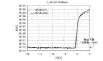
is used to perform exposure when forming a resist mask in the second photolithography step. Exposure with ultra-ultraviolet light has high resolution and a large depth of focus. Therefore, it is possible to set the channel length L of the thin film transistor to be formed later to be 10 nm or more and 1000 nm or less, increasing the operating speed of the circuit, and furthermore, since the off-state current value is extremely small, it is possible to reduce power consumption. can.
次いで、絶縁層、酸化物半導体層102、ソース電極104及びドレイン電極106上に
ゲート絶縁層118を形成する(図5(A)参照)。このとき、バルクトランジスタ上に
もゲート絶縁層118は成膜され、層間絶縁膜の一部となる。Next, a
ここで、不純物を除去することによりi型化または実質的にi型化された酸化物半導体(
高純度化された酸化物半導体)は界面準位、界面電荷に対して極めて敏感であるため、ゲ
ート絶縁層との界面は重要である。そのため高純度化された酸化物半導体に接するゲート
絶縁層(GI)は、高品質化が要求される。Here, an oxide semiconductor (which has become i-type or substantially i-type by removing impurities)
Since highly purified oxide semiconductors are extremely sensitive to interface states and interface charges, the interface with the gate insulating layer is important. Therefore, a gate insulating layer (GI) in contact with a highly purified oxide semiconductor is required to have high quality.
例えば、マイクロ波(2.45GHz)を用いた高密度プラズマCVDは、緻密で絶縁耐
圧の高い高品質な絶縁層を形成できるので好ましい。高純度化された酸化物半導体と高品
質ゲート絶縁層とが密接することにより、界面準位を低減して界面特性を良好なものとす
ることができるからである。もちろん、ゲート絶縁層として良質な絶縁層を形成できるも
のであれば、スパッタ法やプラズマCVD法など他の成膜方法を適用することができる。
また、成膜後の熱処理によってゲート絶縁層の膜質、酸化物半導体との界面特性が改質さ
れる絶縁層であっても良い。いずれにしても、ゲート絶縁層としての膜質が良好であるこ
とは勿論のこと、酸化物半導体との界面準位密度を低減し、良好な界面を形成できるもの
であれば良い。For example, high-density plasma CVD using microwaves (2.45 GHz) is preferable because it can form a dense, high-quality insulating layer with high dielectric strength. This is because the highly purified oxide semiconductor and the high-quality gate insulating layer are brought into close contact with each other, thereby reducing the interface state and improving the interface characteristics. Of course, other film forming methods such as sputtering and plasma CVD can be applied as long as they can form a high-quality insulating layer as the gate insulating layer.
Alternatively, the gate insulating layer may be an insulating layer whose film quality and interface characteristics with an oxide semiconductor are modified by heat treatment after film formation. In any case, any material may be used as long as it has good film quality as a gate insulating layer and can reduce the density of interface states with the oxide semiconductor to form a good interface.
さらに、85℃、2×10⁶V/cm、12時間のゲートバイアス・熱ストレス試験(B
T試験)においては、不純物が酸化物半導体に添加されていると、不純物と酸化物半導体
の主成分との結合が、強電界(B:バイアス)と高温(T:温度)により切断され、生成
された未結合手がしきい値電圧(Vth)のシフトを誘発することとなる。これに対して
、本発明の一態様は、酸化物半導体の不純物、特に水素や水等を極力除去し、上記のよう
にゲート絶縁層との界面特性を良好にすることにより、BT試験を行っても安定な薄膜ト
ランジスタを得ることを可能としている。Furthermore, a gatebias /thermal stress test (B
In the T test), when an impurity is added to an oxide semiconductor, the bond between the impurity and the main component of the oxide semiconductor is broken by a strong electric field (B: bias) and high temperature (T: temperature), resulting in the formation of The resulting dangling bonds induce a shift in threshold voltage (Vth). In contrast, in one embodiment of the present invention, impurities such as hydrogen and water in the oxide semiconductor are removed as much as possible, and the interface characteristics with the gate insulating layer are improved as described above, so that the BT test is performed. This makes it possible to obtain stable thin film transistors.
本実施の形態において、ゲート絶縁層118の形成は、マイクロ波(2.45GHz)を
用いた高密度プラズマCVD装置により行う。ここでは、高密度プラズマCVD装置は、
1×10¹¹/cm3以上のプラズマ密度を達成できる装置を指している。例えば、3k
W~6kWのマイクロ波電力を印加してプラズマを発生させて、絶縁層の成膜を行う。In this embodiment, the
It refers to an apparatus that can achieve a plasma density of 1×10¹¹ /cm3 or more. For example, 3k
A microwave power of W to 6 kW is applied to generate plasma to form an insulating layer.
チャンバーに材料ガスとしてモノシランガス(SiH4)と亜酸化窒素(N2O)と希ガ
スを導入し、10Pa~30Paの圧力下で高密度プラズマを発生させて基板上に絶縁層
を形成する。その後、モノシランガスの供給を停止し、大気に曝すことなく亜酸化窒素(
N2O)と希ガスとを導入して絶縁層表面にプラズマ処理を行ってもよい。少なくとも亜
酸化窒素(N2O)と希ガスとを導入して絶縁層表面に行われるプラズマ処理は、絶縁層
の成膜より後に行う。上記プロセスを経た絶縁層は、膜厚が薄く、例えば100nm未満
であっても信頼性を確保することができる絶縁層である。Monosilane gas (SiH4 ), nitrous oxide (N2 O), and a rare gas are introduced into the chamber as material gases, and high-density plasma is generated under a pressure of 10 Pa to 30 Pa to form an insulating layer on the substrate. Then, the monosilane gas supply is stopped and nitrous oxide (nitrous oxide) is removed without exposure to the atmosphere.
Plasma treatment may be performed on the surface of the insulating layer by introducing N2 O) and a rare gas. Plasma treatment performed on the surface of the insulating layer by introducing at least nitrous oxide (N2 O) and a rare gas is performed after the insulating layer is formed. The insulating layer that has undergone the above process is an insulating layer that can ensure reliability even if the film thickness is thin, for example, less than 100 nm.
ゲート絶縁層118の形成の際、チャンバーに導入するモノシランガス(SiH4)と亜
酸化窒素(N2O)との流量比は、1:10から1:200の範囲とする。また、チャン
バーに導入する希ガスとしては、ヘリウム、アルゴン、クリプトン、キセノンなどを用い
ることができるが、中でも安価であるアルゴンを用いることが好ましい。When forming the
また、高密度プラズマCVD装置により得られた絶縁層は、一定した厚さの層を形成でき
るため段差被覆性に優れている。また、高密度プラズマCVD装置により得られる絶縁層
は、薄い層の厚みを精密に制御することができる。Furthermore, the insulating layer obtained by the high-density plasma CVD apparatus has excellent step coverage because it can form a layer with a constant thickness. Furthermore, the thickness of the thin layer of the insulating layer obtained by the high-density plasma CVD apparatus can be precisely controlled.
上記プロセスを経た絶縁層は、従来の平行平板型のPECVD装置で得られる絶縁層とは
膜質が大きく異なっており、同じエッチャントを用いてエッチング速度を比較した場合に
おいて、平行平板型のPECVD装置で得られる絶縁層の10%以上または20%以上エ
ッチング速度が遅く、高密度プラズマCVD装置で得られる絶縁層は緻密な層と言える。The quality of the insulating layer obtained through the above process is significantly different from that obtained using a conventional parallel plate type PECVD apparatus.When comparing the etching speed using the same etchant, The etching rate of the obtained insulating layer is 10% or more or 20% or more slower, and the insulating layer obtained by a high-density plasma CVD apparatus can be said to be a dense layer.
本実施の形態では、ゲート絶縁層118として高密度プラズマCVD装置による膜厚10
0nmの酸化窒化珪素層(SiOxNyとも呼ぶ、ただし、x>y>0)を用いる。In this embodiment, the
A 0 nm silicon oxynitride layer (also called SiOx Ny , where x>y>0) is used.
その他の方法として、プラズマCVD法又はスパッタ法等を用いて、酸化シリコン層、窒
化シリコン層、酸化窒化シリコン層、窒化酸化シリコン層、又は酸化アルミニウム層を単
層で又は積層して形成することもできる。なお、ゲート絶縁層118中に水素が多量に含
まれないようにするためには、スパッタ法でゲート絶縁層118を成膜することも好まし
い。スパッタ法により酸化シリコン層を成膜する場合には、ターゲットとしてシリコンタ
ーゲット又は石英ターゲットを用い、スパッタガスとして酸素又は、酸素及びアルゴンの
混合ガスを用いて行う。As another method, a silicon oxide layer, a silicon nitride layer, a silicon oxynitride layer, a silicon nitride oxide layer, or an aluminum oxide layer may be formed in a single layer or in a stacked manner using a plasma CVD method or a sputtering method. can. Note that in order to prevent a large amount of hydrogen from being contained in the
ゲート絶縁層118は、ソース電極104及びドレイン電極106から酸化シリコン層と
窒化シリコン層を積層した構造とすることもできる。例えば、第1のゲート絶縁層として
膜厚5nm以上300nm以下の酸化シリコン層(SiOx(x>0))を形成し、第1
のゲート絶縁層上に第2のゲート絶縁層としてスパッタ法により膜厚50nm以上200
nm以下の窒化シリコン層(SiNy(y>0))を積層して、膜厚100nmのゲート
絶縁層としてもよい。The
A second gate insulating layer is formed on the gate insulating layer with a thickness of 50 nm or more by sputtering.
A gate insulating layer with a film thickness of 100 nm may be formed by laminating silicon nitride layers (SiNy (y>0)) with a thickness of 100 nm or less.
次いで、第4のフォトリソグラフィ工程によりレジストマスクを形成し、選択的にエッチ
ングを行ってゲート絶縁層118の一部を除去して、バルクトランジスタのソース領域ま
たはドレイン領域となるn型領域132a、132bに達する開口部を形成する(図5(
B)参照。)Next, a resist mask is formed in a fourth photolithography step, and a portion of the
See B). )
次に、開口部が形成されたゲート絶縁層118上に導電層を形成した後、第5のフォトリ
ソグラフィ工程によりゲート電極108、及び配線層152、153を形成する。なお、
レジストマスクをインクジェット法で形成してもよい。レジストマスクをインクジェット
法で形成するとフォトマスクを使用しないため、製造コストを低減できる。Next, a conductive layer is formed on the
The resist mask may be formed by an inkjet method. When a resist mask is formed by an inkjet method, a photomask is not used, so manufacturing costs can be reduced.
また、ゲート電極108及び配線層152、153は、モリブデン、チタン、クロム、タ
ンタル、タングステン、アルミニウム、銅、ネオジム、スカンジウム等の金属材料又はこ
れらを主成分とする合金材料を用いて、単層で又は積層して形成することができる。Furthermore, the
例えば、ゲート電極108及び配線層152、153を2層とする積層構造としては、ア
ルミニウム層上にモリブデン層が積層された2層の積層構造、または銅層上にモリブデン
層を積層した2層構造、または銅層上に窒化チタン層若しくは窒化タンタルを積層した2
層構造、窒化チタン層とモリブデン層とを積層した2層構造とすることが好ましい。3層
の積層構造としては、タングステン層または窒化タングステン層と、アルミニウムとシリ
コンの合金またはアルミニウムとチタンの合金と、窒化チタン層またはチタン層とを積層
した積層とすることが好ましい。なお、透光性を有する導電層を用いてゲート電極を形成
することもできる。透光性を有する導電層としては、透光性導電性酸化物等をその例に挙
げることができる。For example, a stacked structure in which the
The layer structure is preferably a two-layer structure in which a titanium nitride layer and a molybdenum layer are laminated. The three-layer laminated structure is preferably a laminated layer of a tungsten layer or a tungsten nitride layer, an alloy of aluminum and silicon or an alloy of aluminum and titanium, and a titanium nitride layer or a titanium layer. Note that the gate electrode can also be formed using a light-transmitting conductive layer. Examples of the light-transmitting conductive layer include light-transmitting conductive oxides.
本実施の形態ではゲート電極108及び配線層152、153としてスパッタ法により膜
厚150nmのチタン膜を形成する。In this embodiment, a titanium film with a thickness of 150 nm is formed as the
次いで、不活性ガス雰囲気下、または酸素ガス雰囲気下で第2の加熱処理(好ましくは2
00℃以上400℃以下、例えば250℃以上350℃以下)を行う。本実施の形態では
、窒素雰囲気下で250℃、1時間の第2の加熱処理を行う。また、第2の加熱処理は、
薄膜トランジスタ及びバルクトランジスタ上に保護絶縁層や平坦化絶縁層を形成してから
行ってもよい。Next, a second heat treatment (preferably a second heat treatment) is performed under an inert gas atmosphere or an oxygen gas atmosphere.
00°C or more and 400°C or less, for example 250°C or more and 350°C or less). In this embodiment, the second heat treatment is performed at 250° C. for 1 hour in a nitrogen atmosphere. In addition, the second heat treatment is
This may be performed after forming a protective insulating layer or a planarizing insulating layer on the thin film transistor and the bulk transistor.
さらに大気中、100℃以上200℃以下、1時間以上30時間以下で加熱処理を行って
もよい。この加熱処理は一定の加熱温度を保持して加熱してもよいし、室温から、100
℃以上200℃の加熱温度への昇温と、加熱温度から室温までの降温を複数回くりかえし
て行ってもよい。また、この加熱処理を、酸化物絶縁層の形成前に、減圧下で行ってもよ
い。減圧下で加熱処理を行うと、加熱時間を短縮することができる。Furthermore, heat treatment may be performed in the air at 100° C. or more and 200° C. or less for 1 hour or more and 30 hours or less. This heat treatment may be carried out by heating at a constant heating temperature, or from room temperature to 100
Raising the temperature to a heating temperature of 200° C. or higher and lowering the temperature from the heating temperature to room temperature may be repeated multiple times. Further, this heat treatment may be performed under reduced pressure before forming the oxide insulating layer. If the heat treatment is performed under reduced pressure, the heating time can be shortened.
以上の工程で、水素、水分、水素化物、水酸化物の濃度が低減された酸化物半導体層を有
する薄膜トランジスタを形成することができる(図5(C)参照。)ここで、薄膜トラン
ジスタは転送トランジスタ101として適用することができ、バルクトランジスタは増幅
トランジスタ131として適用することができる。Through the above steps, a thin film transistor having an oxide semiconductor layer with reduced concentrations of hydrogen, water, hydride, and hydroxide can be formed (see FIG. 5C). Here, the thin film transistor is a transfer transistor. The bulk transistor can be used as the
また、薄膜トランジスタ及びバルクトランジスタ上に保護絶縁層142や、図示しないが
、平坦化のための平坦化絶縁層を設けてもよい。例えば、保護絶縁層142として酸化シ
リコン層、窒化シリコン層、酸化窒化シリコン層、窒化酸化シリコン層、又は酸化アルミ
ニウム層を単層で又は積層して形成することができる。Further, although not shown, a protective
また、平坦化絶縁層としては、ポリイミド、アクリル、ベンゾシクロブテン、ポリアミド
、エポキシ等の、耐熱性を有する有機材料を用いることができる。また上記有機材料の他
に、低誘電率材料(low-k材料)、シロキサン系樹脂、PSG(リンガラス)、BP
SG(リンボロンガラス)等を用いることができる。なお、これらの材料で形成される絶
縁膜を複数積層させることで、平坦化絶縁層を形成してもよい。Further, as the planarization insulating layer, a heat-resistant organic material such as polyimide, acrylic, benzocyclobutene, polyamide, epoxy, etc. can be used. In addition to the above organic materials, low dielectric constant materials (low-k materials), siloxane resins, PSG (phosphorus glass), BP
SG (phosphorus boron glass) or the like can be used. Note that the planarization insulating layer may be formed by stacking a plurality of insulating films made of these materials.
なおシロキサン系樹脂とは、シロキサン系材料を出発材料として形成されたSi-O-S
i結合を含む樹脂に相当する。シロキサン系樹脂は置換基としては有機基(例えばアルキ
ル基やアリール基)を用いても良い。また、有機基はフルオロ基を有していても良い。Note that the siloxane-based resin refers to Si-O-S formed using a siloxane-based material as a starting material.
Corresponds to a resin containing an i-bond. In the siloxane resin, an organic group (for example, an alkyl group or an aryl group) may be used as a substituent. Further, the organic group may have a fluoro group.
平坦化絶縁層の形成法は、特に限定されず、その材料に応じて、スパッタ法、SOG法、
スピンコート法、ディップ法、スプレー塗布法、液滴吐出法(インクジェット法、スクリ
ーン印刷法、オフセット印刷法等)などの方法や、ドクターナイフ、ロールコーター、カ
ーテンコーター、ナイフコーター等の器具を用いることができる。The method for forming the planarized insulating layer is not particularly limited, and depending on the material, sputtering, SOG,
Using methods such as spin coating, dipping, spray coating, droplet ejection (inkjet, screen printing, offset printing, etc.), and equipment such as doctor knives, roll coaters, curtain coaters, knife coaters, etc. I can do it.
上記のように酸化物半導体膜を成膜するに際し、雰囲気中の残留水分を除去することで、
該酸化物半導体膜中の水素及び水素化物の濃度を低減することができる。それにより酸化
物半導体膜の安定化を図ることができる。When forming an oxide semiconductor film as described above, by removing residual moisture in the atmosphere,
The concentration of hydrogen and hydride in the oxide semiconductor film can be reduced. Thereby, the oxide semiconductor film can be stabilized.
以上のように、酸化物半導体層を用いる薄膜トランジスタを有する半導体装置において、
安定な電気特性を有し信頼性の高い半導体装置を提供することができる。As described above, in a semiconductor device having a thin film transistor using an oxide semiconductor layer,
A highly reliable semiconductor device having stable electrical characteristics can be provided.
本実施の形態は、他の実施の形態と適宜組み合わせて実施することが可能である。This embodiment can be implemented in combination with other embodiments as appropriate.
(実施の形態2)
本発明の一形態は、酸化物半導体中でキャリアの供与体(ドナーまたはアクセプタ)とな
り得る不純物を極めて少ないレベルにまで除去することで、真性または実質的に真性な半
導体であって、当該酸化物半導体を薄膜トランジスタに適用するものである。本実施の形
態では、評価用素子(TEGとも呼ぶ)でのオフ電流の測定値について以下に説明する。(Embodiment 2)
One embodiment of the present invention is to remove impurities that can serve as carrier donors (donors or acceptors) in an oxide semiconductor to an extremely low level, thereby making the oxide semiconductor an intrinsic or substantially intrinsic semiconductor. The semiconductor is applied to thin film transistors. In this embodiment, measured values of off-state current in an evaluation element (also referred to as TEG) will be described below.
図6にL/W=3μm/50μmの薄膜トランジスタを200個並列に接続し、L/W=
3μm/10000μmの薄膜トランジスタの初期特性を示す。また、薄膜トランジスタ
の上面図を図7(A)に示し、その一部を拡大した図を図7(B)に示す。図7(B)の
点線で囲んだ領域がL/W=3μm/50μm、Lov=1.5μmの1段分の薄膜トラ
ンジスタである。薄膜トランジスタの初期特性を測定するため、基板温度を室温とし、ソ
ース-ドレイン間電圧(以下、ドレイン電圧またはVdという)を10Vとし、ソース-
ゲート間電圧(以下、ゲート電圧またはVgという)を-20V~+20Vまで変化させ
たときのソース-ドレイン電流(以下、ドレイン電流またはIdという)の変化特性、す
なわちVg-Id特性を測定した。なお、図7では、Vgを-20V~+5Vまでの範囲
で示している。In Figure 6, 200 thin film transistors with L/W = 3 μm/50 μm are connected in parallel, and L/W =
The initial characteristics of a 3 μm/10000 μm thin film transistor are shown. Further, a top view of the thin film transistor is shown in FIG. 7(A), and a partially enlarged view is shown in FIG. 7(B). The region surrounded by the dotted line in FIG. 7B is one stage of thin film transistors with L/W=3 μm/50 μm and Lov=1.5 μm. In order to measure the initial characteristics of a thin film transistor, the substrate temperature was set to room temperature, the source-drain voltage (hereinafter referred to as drain voltage or Vd) was 10 V, and the source-drain voltage was set to 10 V.
The change characteristics of the source-drain current (hereinafter referred to as drain current or Id) when the gate-to-gate voltage (hereinafter referred to as gate voltage or Vg) was changed from -20V to +20V, that is, the Vg-Id characteristic, were measured. In addition, in FIG. 7, Vg is shown in the range from -20V to +5V.
図6に示すようにチャネル幅Wが10000μmの薄膜トランジスタは、Vdが1V及び
10Vにおいてオフ電流は1×10-13[A]以下となっており、測定機(半導体パラ
メータ・アナライザ、Agilent 4156C;Agilent社製)の分解能(1
00fA)以下となっている。As shown in FIG. 6, a thin film transistor with a channel width W of 10,000 μm has an off-state current of 1×10⁻¹³ [A] or less at Vd of 1 V and 10 V. resolution (1
00fA) or less.
すなわち、上記の薄膜トランジスタは、電気特性がノーマリーオフを呈し、1Vから10
Vのドレイン電圧において、チャネル幅1μmあたりのオフ電流は、100aA/μm以
下、好ましくは10aA/μm以下、更に好ましくは1aA/μm以下となるように作用
させることができる。That is, the above-mentioned thin film transistor exhibits normally-off electrical characteristics, and has a voltage range of 1V to 10V.
At a drain voltage of V, the off-state current per 1 μm of channel width can be set to 100 aA/μm or less, preferably 10 aA/μm or less, and more preferably 1 aA/μm or less.
測定した薄膜トランジスタの作製方法について説明する。The method for manufacturing the measured thin film transistor will be explained.
まず、ガラス基板上に下地層として、CVD法により窒化珪素層を形成し、窒化珪素層上
に酸化窒化珪素層を形成した。酸化窒化珪素層上にゲート電極としてスパッタ法によりタ
ングステン層を形成した。ここで、タングステン層を選択的にエッチングしてゲート電極
を形成した。First, a silicon nitride layer was formed as a base layer on a glass substrate by a CVD method, and a silicon oxynitride layer was formed on the silicon nitride layer. A tungsten layer was formed as a gate electrode on the silicon oxynitride layer by sputtering. Here, the tungsten layer was selectively etched to form a gate electrode.
次に、ゲート電極上にゲート絶縁層としてCVD法により厚さ100nmの酸化窒化珪素
層を形成した。Next, a silicon oxynitride layer with a thickness of 100 nm was formed as a gate insulating layer on the gate electrode by CVD.
次に、ゲート絶縁層上に、スパッタ法によりIn-Ga-Zn-O系金属酸化物ターゲッ
ト(mol数比で、In2O3:Ga2O3:ZnO=1:1:2)を用いて、厚さ50
nmの酸化物半導体層を形成した。ここで、酸化物半導体層を選択的にエッチングし、島
状の酸化物半導体層を形成した。Next, an In-Ga-Zn-O based metal oxide target (In2 O3 :Ga2 O3 :ZnO=1:1:2 in molar ratio) was sputtered onto the gate insulating layer. Thickness: 50
A nm oxide semiconductor layer was formed. Here, the oxide semiconductor layer was selectively etched to form an island-shaped oxide semiconductor layer.
次に、酸化物半導体層をクリーンオーブンにて窒素雰囲気下、450℃、1時間の第1の
熱処理を行った。Next, the oxide semiconductor layer was subjected to a first heat treatment at 450° C. for 1 hour in a nitrogen atmosphere in a clean oven.
次に、酸化物半導体層上にソース電極及びドレイン電極としてチタン層(厚さ150nm
)をスパッタ法により形成した。ここで、チタン層を選択的にエッチングすることでソー
ス電極及びドレイン電極を形成し、1つの薄膜トランジスタのチャネル長Lが3μm、チ
ャネル幅Wが50μmとし、200個を並列とすることで、L/W=3μm/10000
μmとなるようにした。Next, a titanium layer (thickness: 150 nm) was formed as a source electrode and a drain electrode on the oxide semiconductor layer.
) was formed by sputtering. Here, a source electrode and a drain electrode are formed by selectively etching the titanium layer, and one thin film transistor has a channel length L of 3 μm and a channel width W of 50 μm, and by arranging 200 thin film transistors in parallel, L/ W=3μm/10000
It was made to be μm.
次に、酸化物半導体層に接するように保護絶縁層としてリアクティブスパッタ法により酸
化珪素層を膜厚300nmで形成した。ここで、保護層である酸化珪素層を選択的にエッ
チングし、ゲート電極、ソース電極及びドレイン電極上に開口部を形成した。その後、窒
素雰囲気下、250℃で1時間、第2の熱処理を行った。Next, a silicon oxide layer with a thickness of 300 nm was formed by reactive sputtering as a protective insulating layer so as to be in contact with the oxide semiconductor layer. Here, the silicon oxide layer serving as the protective layer was selectively etched to form openings over the gate electrode, source electrode, and drain electrode. Thereafter, a second heat treatment was performed at 250° C. for 1 hour in a nitrogen atmosphere.
そして、Vg-Id特性を測定する前に150℃、10時間の加熱を行った。Then, before measuring the Vg-Id characteristics, heating was performed at 150° C. for 10 hours.
以上の工程により、ボトムゲート型の薄膜トランジスタを作製した。Through the above steps, a bottom gate thin film transistor was manufactured.
図6に示すように薄膜トランジスタのオフ電流が、1×10-13[A]程度であるのは
、上記作製工程において酸化物半導体層中における水素濃度を十分に低減できたためであ
る。酸化物半導体層中の水素濃度は、5×10¹⁹atoms/cm3以下、好ましくは
5×10¹⁸atoms/cm3以下、さらに好ましくは5×1017atoms/cm
3以下、または1×10¹⁶/cm3未満とする。なお、酸化物半導体層中の水素濃度測
定は、二次イオン質量分析法(SIMS:Secondary Ion Mass Sp
ectroscopy)で行う。As shown in FIG. 6, the off-state current of the thin film transistor is about 1×10⁻¹³ [A] because the hydrogen concentration in the oxide semiconductor layer can be sufficiently reduced in the above manufacturing process. The hydrogen concentration in the oxide semiconductor layer is 5×10¹⁹ atoms/cm3 or less, preferably 5×10¹⁸ atoms/cm3 or less, more preferably 5×10¹⁷ atoms/cm
3 or less, or less than 1×10¹⁶ /cm3 . Note that the hydrogen concentration in the oxide semiconductor layer is measured using secondary ion mass spectrometry (SIMS).
This is done using electronoscopy).
また、In-Ga-Zn-O系酸化物半導体を用いる例を示したが、特に限定されず、他
の酸化物半導体材料、例えば、In-Sn-Zn-O系、Sn-Ga-Zn-O系、Al
-Ga-Zn-O系、Sn-Al-Zn-O系、In-Zn-O系、In-Sn-O系、
Sn-Zn-O系、Al-Zn-O系、In-O系、Sn-O系、Zn-O系などを用い
ることができる。また、酸化物半導体材料として、Alを2.5~10wt%混入したI
n-Al-Zn-O系や、Siを2.5~10wt%混入したIn-Zn-O系を用いる
こともできる。Further, although an example using an In-Ga-Zn-O-based oxide semiconductor has been shown, there is no particular limitation, and other oxide semiconductor materials such as In-Sn-Zn-O-based, Sn-Ga-Zn- O series, Al
-Ga-Zn-O system, Sn-Al-Zn-O system, In-Zn-O system, In-Sn-O system,
Sn--Zn--O type, Al--Zn--O type, In--O type, Sn--O type, Zn--O type, etc. can be used. In addition, as an oxide semiconductor material, I mixed with 2.5 to 10 wt% of Al
An n-Al-Zn-O system or an In-Zn-O system mixed with 2.5 to 10 wt% of Si can also be used.
また、ホール測定機で測定される酸化物半導体層のキャリア濃度は、5×10¹⁴/cm
3以下、好ましくは5×10¹²/cm3以下、さらに好ましくはシリコンのキャリア濃
度1.45×10¹⁰/cm3と同等、もしくはそれ以下である。即ち、酸化物半導体層
のキャリア濃度は、限りなくゼロに近くすることができる。Furthermore, the carrier concentration of the oxide semiconductor layer measured by a Hall measuring device is 5×10¹⁴ /cm
3 or less, preferably 5×10¹² /cm3 or less, more preferably equal to or lower than the carrier concentration of silicon, 1.45×10¹⁰ /cm3 . That is, the carrier concentration of the oxide semiconductor layer can be made as close to zero as possible.
また、薄膜トランジスタのチャネル長Lを10nm以上1000nm以下とすることも可
能であり、回路の動作速度を高速化でき、オフ電流値が極めて小さいため、さらに低消費
電力化も図ることができる。Furthermore, it is possible to set the channel length L of the thin film transistor to 10 nm or more and 1000 nm or less, so that the operating speed of the circuit can be increased, and since the off-state current value is extremely small, it is possible to further reduce power consumption.
また、薄膜トランジスタのオフ状態において、酸化物半導体層は絶縁体とみなせて回路設
計を行うことができる。In addition, when the thin film transistor is in an off state, the oxide semiconductor layer can be regarded as an insulator and a circuit can be designed.
続いて、本実施の形態で作製した薄膜トランジスタに対してオフ電流の温度特性を評価し
た。温度特性は、薄膜トランジスタが使われる最終製品の耐環境性や、性能の維持などを
考慮する上で重要である。当然ながら、変化量が小さいほど好ましく、製品設計の自由度
が増す。Next, the temperature characteristics of the off-state current of the thin film transistor manufactured in this embodiment were evaluated. Temperature characteristics are important when considering environmental resistance and performance maintenance of final products in which thin film transistors are used. Naturally, the smaller the amount of change, the better, and the degree of freedom in product design increases.
温度特性は、恒温槽を用い、-30℃、0℃、25℃、40℃、60℃、80℃、100
℃、及び120℃のそれぞれの温度で薄膜トランジスタを形成した基板を一定温度とし、
ドレイン電圧を6V、ゲート電圧を-20V~+20Vまで変化させてVg-Id特性を
取得した。Temperature characteristics were measured using a thermostat at -30°C, 0°C, 25°C, 40°C, 60°C, 80°C, and 100°C.
The substrate on which the thin film transistor was formed at each temperature of 120°C and 120°C was kept at a constant temperature,
Vg-Id characteristics were obtained by changing the drain voltage to 6V and the gate voltage from -20V to +20V.
図8(A)に示すのは、上記それぞれの温度で測定したVg-Id特性を重ね書きしたも
のであり、点線で囲むオフ電流の領域を拡大したものを図8(B)に示す。図中の矢印で
示す右端の曲線が-30℃、左端が120℃で取得した曲線で、その他の温度で取得した
曲線は、その間に位置する。オン電流の温度依存性はほとんど見られない。一方、オフ電
流は拡大図の図8(B)においても明らかであるように、ゲート電圧が20V近傍を除い
て、全ての温度で測定機の分解能近傍の1×10-12[A]以下となっており、温度依
存性もない。すなわち、120℃の高温においても、オフ電流が1×10-12[A]以
下を維持しており、チャネル幅Wが10000μmであることを考慮すると、オフ電流が
非常に小さいことがわかる。FIG. 8(A) shows an overlay of the Vg-Id characteristics measured at each of the above temperatures, and FIG. 8(B) shows an enlarged view of the off-current region surrounded by the dotted line. The rightmost curve indicated by the arrow in the figure is the curve obtained at -30°C, the leftmost curve is the curve obtained at 120°C, and the curves obtained at other temperatures are located in between. There is almost no temperature dependence of the on-current. On the other hand, as is clear from the enlarged view of FIG. 8(B), the off-state current is below 1×10-12 [A], near the resolution of the measurement device, at all temperatures except when the gate voltage is around 20V. , and there is no temperature dependence. That is, even at a high temperature of 120° C., the off-state current remains below 1×10⁻¹² [A], and considering that the channel width W is 10,000 μm, it can be seen that the off-state current is extremely small.
高純度化された酸化物半導体(purified Oxide Semiconduct
or)を用いた薄膜トランジスタは、オフ電流の温度依存性がほとんど現れない。これは
、図10(A)のバンド図で示すように、酸化物半導体が高純度化されることによって、
導電型が限りなく真性型に近づき、フェルミ準位が禁制帯の中央に位置するため、温度依
存性を示さなくなると言える。また、これは、酸化物半導体のエネルギーが3eV以上で
あり、熱励起キャリアが極めて少ないことにも起因する。また、ソース領域及びドレイン
領域は縮退した状態にあるので温度依存性が現れない要因となっている。薄膜トランジス
タの動作は、縮退したソース領域から酸化物半導体に注入されたキャリアによるものがほ
とんどであり、キャリア密度の温度依存性がないことから上記特性(オフ電流の温度依存
性無し)を説明することができる。また、この極めて低いオフ電流について、以下にバン
ド図を用いて説明する。Purified Oxide Semiconductor
The thin film transistor using the or) exhibits almost no temperature dependence of off-state current. As shown in the band diagram of FIG. 10(A), this is due to the high purity of the oxide semiconductor.
Since the conductivity type approaches the intrinsic type and the Fermi level is located at the center of the forbidden band, it can be said that it does not exhibit temperature dependence. This is also due to the fact that the energy of the oxide semiconductor is 3 eV or more and the number of thermally excited carriers is extremely small. Furthermore, since the source region and the drain region are in a degenerate state, this is a factor that prevents temperature dependence from appearing. The operation of thin film transistors is mostly due to carriers injected into the oxide semiconductor from the degenerate source region, and there is no temperature dependence of carrier density, so the above characteristic (no temperature dependence of off-state current) can be explained. I can do it. Further, this extremely low off-state current will be explained below using a band diagram.
図9は、酸化物半導体を用いた逆スタガ型の薄膜トランジスタの縦断面図である。ゲート
電極(GE1)上にゲート絶縁膜(GI)を介して酸化物半導体層(OS)が設けられ、
その上にソース電極(S)及びドレイン電極(D)が設けられている。FIG. 9 is a vertical cross-sectional view of an inverted staggered thin film transistor using an oxide semiconductor. An oxide semiconductor layer (OS) is provided on the gate electrode (GE1) via a gate insulating film (GI),
A source electrode (S) and a drain electrode (D) are provided thereon.
図10は、図9に示すA-A’断面におけるエネルギーバンド図(模式図)である。図1
0(A)はソースとドレインの間の電圧を等電位(VD=0V)とした場合を示し、図1
0(B)はドレインに正の電位(VD>0)を加えた場合を示す。FIG. 10 is an energy band diagram (schematic diagram) at the AA' cross section shown in FIG. 9. Figure 1
0(A) indicates the case where the voltage between the source and drain is set to the same potential (VD=0V), and is shown in Figure 1.
0(B) indicates a case where a positive potential (VD>0) is applied to the drain.
図11は、図9におけるB-B’の断面におけるエネルギーバンド図(模式図)である。
図11(A)はゲート(G1)に正の電位(+VG)が印加された状態であり、ソースと
ドレイン間にキャリア(電子)が流れるオン状態を示している。また、図11(B)は、
ゲート(G1)に負の電位(-VG)が印加された状態であり、オフ状態(少数キャリア
は流れない)である場合を示す。FIG. 11 is an energy band diagram (schematic diagram) in a cross section taken along line BB' in FIG.
FIG. 11A shows a state in which a positive potential (+VG) is applied to the gate (G1), and shows an on state in which carriers (electrons) flow between the source and drain. Moreover, FIG. 11(B)
This shows a state in which a negative potential (-VG) is applied to the gate (G1), and it is in an off state (minority carriers do not flow).
図12は、真空準位と金属の仕事関数(φM)、酸化物半導体の電子親和力(χ)の関係
を示す。FIG. 12 shows the relationship between the vacuum level, the work function (φM ) of the metal, and the electron affinity (χ) of the oxide semiconductor.
従来の酸化物半導体は一般にn型であり、その場合のフェルミ準位(EF)は、バンドギ
ャップ中央に位置する真性フェルミ準位(Ei)から離れて、伝導帯寄りに位置している
。なお、酸化物半導体において水素の一部はドナーとなり、n型化する一つの要因である
ことが知られている。Conventional oxide semiconductors are generally n-type, and the Fermi level (EF) in this case is located away from the intrinsic Fermi level (Ei) located at the center of the band gap and closer to the conduction band. Note that it is known that some hydrogen in an oxide semiconductor becomes a donor, which is one of the factors that causes the oxide semiconductor to become n-type.
これに対して本発明の一態様に係る酸化物半導体は、n型不純物である水素を酸化物半導
体から除去し、酸化物半導体の主成分以外に不純物が極力含まれないように高純度化する
ことにより真性(i型)とし、又は真性型とせんとしたものである。すなわち、不純物を
添加してi型化するのでなく、水素や水等の不純物を極力除去したことにより、高純度化
されたi型(真性)半導体またはそれに近づけることを特徴としている。そうすることに
より、フェルミ準位(EF)は真性フェルミ準位(Ei)と同じレベルにまですることが
できる。In contrast, the oxide semiconductor according to one embodiment of the present invention is highly purified by removing hydrogen, which is an n-type impurity, from the oxide semiconductor so that impurities other than the main components of the oxide semiconductor are contained as little as possible. Therefore, it is considered to be an intrinsic type (i-type), or it is considered to be an intrinsic type. That is, instead of adding impurities to make it i-type, it is characterized by removing impurities such as hydrogen and water as much as possible to make it a highly purified i-type (intrinsic) semiconductor or close to it. By doing so, the Fermi level (EF) can be brought to the same level as the intrinsic Fermi level (Ei).
酸化物半導体のバンドギャップ(Eg)が3.15eVである場合、電子親和力(χ)は
4.3eVと言われている。ソース電極及びドレイン電極を構成するチタン(Ti)の仕
事関数は、酸化物半導体の電子親和力(χ)とほぼ等しい。この場合、金属-酸化物半導
体界面において、電子に対してショットキー型の障壁は形成されない。When the band gap (Eg) of an oxide semiconductor is 3.15 eV, the electron affinity (χ) is said to be 4.3 eV. The work function of titanium (Ti) constituting the source electrode and the drain electrode is approximately equal to the electron affinity (χ) of the oxide semiconductor. In this case, no Schottky-type barrier for electrons is formed at the metal-oxide semiconductor interface.
すなわち、金属の仕事関数(φM)と酸化物半導体の電子親和力(χ)が等しい場合、両
者が接触すると図10(A)で示すようなエネルギーバンド図(模式図)が示される。That is, when the work function (φM ) of the metal and the electron affinity (χ) of the oxide semiconductor are equal, when they come into contact, an energy band diagram (schematic diagram) as shown in FIG. 10(A) is shown.
図10(B)において黒丸(●)は電子を示し、ドレインに正の電位が印加されると、電
子はバリア(h)をこえて酸化物半導体に注入され、ドレインに向かって流れる。この場
合、バリア(h)の高さは、ゲート電圧とドレイン電圧に依存して変化するが、正のドレ
イン電圧が印加された場合には、電圧印加のない図10(A)のバリアの高さすなわちバ
ンドギャップ(Eg)の1/2よりもバリアの高さ(h)は小さい値となる。In FIG. 10B, black circles (●) indicate electrons, and when a positive potential is applied to the drain, the electrons are injected into the oxide semiconductor across the barrier (h) and flow toward the drain. In this case, the height of the barrier (h) changes depending on the gate voltage and drain voltage, but when a positive drain voltage is applied, the height of the barrier (h) in FIG. In other words, the barrier height (h) has a value smaller than 1/2 of the band gap (Eg).
このとき酸化物半導体に注入された電子は、図11(A)で示すように酸化物半導体中を
流れる。また、図11(B)において、ゲート電極(G1)に負の電位が印加されると、
少数キャリアであるホールは実質的にゼロであるため、電流は限りなく流れなくなる。The electrons injected into the oxide semiconductor at this time flow through the oxide semiconductor as shown in FIG. 11(A). Moreover, in FIG. 11(B), when a negative potential is applied to the gate electrode (G1),
Since the number of holes, which are minority carriers, is essentially zero, current will no longer flow.
例えば、薄膜トランジスタのチャネル幅Wが1×104μmでチャネル長Lが3μmの素
子であっても、室温でのオフ電流が10-13A以下であり、サブスレッショルドスイン
グ値(S値)が0.1V/dec.(ゲート絶縁膜厚100nm)が得られる。For example, even if the channel width W of a thin film transistor is 1×104 μm and the channel length L is 3 μm, the off-state current at room temperature is 10−13 A or less, and the subthreshold swing value (S value) is 0. .1V/dec. (gate insulating
シリコン半導体の真性キャリア密度は1.45×10¹⁰/cm3(300K)であり、
室温においてもキャリアが存在している。これは、室温においても、熱励起キャリアが存
在していることを意味している。さらに、シリコン半導体のバンドギャップは1.12e
Vであるので、シリコン半導体を用いたトランジスタは温度に依存してオフ電流が大きく
変動することとなる。The intrinsic carrier density of a silicon semiconductor is 1.45×10¹⁰ /cm3 (300K),
Carriers exist even at room temperature. This means that thermally excited carriers exist even at room temperature. Furthermore, the bandgap of silicon semiconductor is 1.12e
V, the off-state current of a transistor using a silicon semiconductor varies greatly depending on the temperature.
従って、単にバンドギャップの広い酸化物半導体をトランジスタに適用するのではなく、
酸化物半導体の主成分以外に不純物が極力含まれないように高純度化することにより、キ
ャリア濃度を1×10¹⁴/cm3以下、好ましくは1×1012/cm3以下となるよ
うにすることで、実用的な動作温度で熱的に励起されるキャリアがほとんど無く、ソース
側から注入される電子のみによってトランジスタを動作させることができる。それにより
、オフ電流を1×10-13A以下にまで下げると共に、温度変化によってオフ電流がほ
とんど変化しない極めて安定に動作するトランジスタを得ることができる。Therefore, rather than simply applying wide bandgap oxide semiconductors to transistors,
The oxide semiconductor is highly purified so as to contain as few impurities as possible other than the main components, so that the carrier concentration is 1×10¹⁴ /cm3 or less, preferably 1×10¹² /cm3 or less. As a result, there are almost no carriers that are thermally excited at a practical operating temperature, and the transistor can be operated only by electrons injected from the source side. As a result, it is possible to reduce the off-state current to 1×10⁻¹³ A or less, and to obtain a transistor that operates extremely stably, with the off-state current hardly changing due to temperature changes.
本発明の一態様における技術思想は、酸化物半導体中に、不純物を加えることをせずに逆
に不本意に存在する水、水素という不純物を除去することにより、酸化物半導体自体を高
純度化することにある。すなわち、ドナー準位を作る水または水素を除去し、更にこれと
同時に酸素欠乏状態となった酸化物半導体に酸素を補填することにより、酸化物半導体自
体を高純度化することを特徴としている。The technical idea of one embodiment of the present invention is to highly purify the oxide semiconductor itself by removing impurities such as water and hydrogen that are involuntarily present in the oxide semiconductor without adding impurities. It's about doing. That is, the method is characterized in that the oxide semiconductor itself is highly purified by removing water or hydrogen that forms donor levels and at the same time replenishing oxygen to the oxide semiconductor that has become oxygen-deficient.
酸化物半導体は成膜直後ですら1020/cm3のレベルの水素がSIMS(二次イオン
質量分析)で観察される。ドナー準位を作る水または水素を意図的に除去し、更に水また
は水素の除去に伴い同時に減少してしまう酸素を補填することにより、酸化物半導体を高
純度化し、電気的にi型(真性)半導体とすることを技術思想の一つとしている。Even immediately after film formation of an oxide semiconductor, hydrogen at a level of 1020 /cm3 is observed by SIMS (secondary ion mass spectrometry). By intentionally removing water or hydrogen that forms a donor level and supplementing the oxygen that decreases with the removal of water or hydrogen, the oxide semiconductor can be made highly purified and electrically i-type (intrinsic). ) One of the technical ideas is to make it a semiconductor.
結果として、水素の量は少なければ少ないほど良く、酸化物半導体中のキャリアも少なけ
れば少ないほど良い。酸化物半導体は、薄膜トランジスタに用いる場合に電流の担い手と
してのキャリアを意図的に有するというよりも、逆に酸化物半導体中のキャリアは無くし
てしまい、ソースから供給されるキャリア(電子)を通過させる通路として機能する、い
わゆる高純度化したi型(真性)半導体である。As a result, the smaller the amount of hydrogen, the better, and the fewer carriers in the oxide semiconductor, the better. When used in thin film transistors, oxide semiconductors do not intentionally have carriers that carry current, but rather the carriers in the oxide semiconductor are eliminated and carriers (electrons) supplied from the source are passed through. It is a so-called highly purified i-type (intrinsic) semiconductor that functions as a passageway.
その結果、酸化物半導体中にキャリアが無い、または極めて少なくさせることにより、T
FTのオフ電流が少なくなるというのが本発明の一態様における技術思想である。すなわ
ち、その指標として水素濃度は5×10¹⁹/cm3以下、好ましくは5×1018/c
m3以下、さらに好ましくは5×10¹⁷/cm3以下か、または1×1016/cm3
未満、またキャリア密度は1×10¹⁴/cm3未満、好ましくは1×1012/cm3
以下が求められる。As a result, by eliminating or extremely few carriers in the oxide semiconductor, T
The technical concept of one embodiment of the present invention is that the off-state current of the FT is reduced. That is, as an indicator, the hydrogen concentration is 5×10¹⁹ /cm3 or less, preferably 5×10¹⁸ /c.
m3 or less, more preferably 5×10¹⁷ /cm3 or less, or 1×10¹⁶ /cm3
and the carrier density is less than 1×10¹⁴ /cm3 , preferably less than 1×10¹² /cm3
The following are required.
また結果として、酸化物半導体は通路(パス)として機能し、酸化物半導体自体がキャリ
アを供給しない、またはほとんど供給しないように高純度化したi型(真性)とし、キャ
リアはソース、ドレインにより供給される。In addition, as a result, the oxide semiconductor functions as a path, and the oxide semiconductor itself is highly purified i-type (intrinsic) so that it does not supply carriers or supplies almost no carriers, and carriers are supplied from the source and drain. be done.
このため、オフ電流は少なければ少ないほど良く、1~10Vの間のいずれかのドレイン
電圧を印加した場合のトランジスタ特性において、100aA/μm(チャネル幅W=1
μm当たりの電流)以下、好ましくは10aA/μm以下、さらに好ましくは1aA/μ
m以下であることを特徴としている。Therefore, the smaller the off-state current is, the better it is, and the transistor characteristics when applying a drain voltage between 1 and 10 V are 100 aA/μm (channel width W = 1
Current per μm) or less, preferably 10aA/μm or less, more preferably 1aA/μm
m or less.
このようにオフ電流が極めて小さい薄膜トランジスタを用いて、記憶回路(記憶素子)な
どを作製した場合、オフ電流が小さくほとんどリークがないため、電位保持時間が長く、
記憶データを長時間保持することが可能となる。When a memory circuit (memory element) or the like is fabricated using a thin film transistor with an extremely low off-state current, the off-state current is small and there is almost no leakage, so the potential holding time is long.
It becomes possible to retain stored data for a long time.
本実施の形態は、他の実施の形態に記載した構成と適宜組み合わせて実施することが可能
である。This embodiment mode can be implemented in appropriate combination with the structures described in other embodiment modes.
(実施の形態3)
本発明の一態様における薄膜トランジスタを含む固体撮像素子の動作について説明する。(Embodiment 3)
The operation of a solid-state image sensor including a thin film transistor in one embodiment of the present invention will be described.
固体撮像素子であるCMOS(Complementary Metal Oxide
Semiconductor)イメージセンサは信号電荷蓄積部に電位を保持し、その電
位を増幅トランジスタを介して垂直出力線に出力する。一般的なCMOSイメージセンサ
では、リセットトランジスタ及び/または転送トランジスタにリーク電流があるとそのリ
ーク電流によって充電または放電が起こり、信号電荷蓄積部の電位が変わってしまう。信
号電荷蓄積部の電位が変わると増幅トランジスタの電位も変わってしまい、本来の電位か
らずれた値となり、撮像された映像が劣化してしまうという問題点があった。CMOS (Complementary Metal Oxide) is a solid-state imaging device.
(Semiconductor) An image sensor holds a potential in a signal charge storage section and outputs the potential to a vertical output line via an amplification transistor. In a typical CMOS image sensor, if there is a leakage current in the reset transistor and/or the transfer transistor, charging or discharging occurs due to the leakage current, and the potential of the signal charge storage section changes. When the potential of the signal charge storage section changes, the potential of the amplification transistor also changes, resulting in a value that deviates from the original potential, causing a problem in that the captured image deteriorates.
本実施の形態では、実施の形態1及び2で示した薄膜トランジスタをCMOSイメージセ
ンサの転送トランジスタに適用した場合の動作の効果を説明する。なお、実施の形態1で
説明したように、本発明の一態様ではリセットトランジスタを省くことができる。また、
増幅トランジスタには薄膜トランジスタまたはバルクトランジスタのどちらを適用しても
良い。In this embodiment mode, operational effects when the thin film transistor described in
Either a thin film transistor or a bulk transistor may be applied to the amplification transistor.
図29は、従来のCMOSイメージセンサの画素構成の一例を示す図である。画素は光電
変換素子であるフォトダイオード1002、転送トランジスタ1004、リセットトラン
ジスタ1006、増幅トランジスタ1008及び各種配線で構成されており、マトリクス
状に複数が配置されてセンサを構成する。FIG. 29 is a diagram showing an example of a pixel configuration of a conventional CMOS image sensor. The pixel is composed of a
ここで、フォトダイオード1002は、転送トランジスタ1004のソース側に接続され
ており、転送トランジスタ1004のドレイン側には信号電荷蓄積部1010(FD:フ
ローティングディフュージョンとも呼ぶ)が形成される。信号電荷蓄積部1010にはリ
セットトランジスタ1006のソース及び増幅トランジスタ1008のゲートが接続され
ている。他の構成として、増幅トランジスタに選択トランジスタが接続される場合もある
。Here, the
次に、図30のタイミングチャートを用いて動作を説明する。まず、電源端子に電源電圧
が供給される。続いて、リセットトランジスタ1006のゲートにリセットパルスが入力
され、リセットトランジスタ1006がオンする。信号電荷蓄積部1010はリセット電
源の電位に充電される。その後、リセットトランジスタ1006はオフになり信号電荷蓄
積部1010はリセット電源の電位に保持される。次に、転送トランジスタ1004がオ
ンすると信号電荷蓄積部1010から電流がフォトダイオードに流れて、信号電荷蓄積部
1010の電位は低下する。転送トランジスタ1004がオフすると、オフした時点での
電位が信号電荷蓄積部1010に保持される。そして、増幅トランジスタ1008を介し
て垂直出力線1120に出力される。その後、電源端子への電源電圧の供給が遮断される
。このような順序で信号が出力される。Next, the operation will be explained using the timing chart of FIG. First, a power supply voltage is supplied to the power supply terminal. Subsequently, a reset pulse is input to the gate of the
図13は、本発明の一態様におけるCMOSイメージセンサの画素構成の一例を示す図で
ある。画素は光電変換素子であるフォトダイオード1002、転送トランジスタ1004
、増幅トランジスタ1008及び各種配線で構成されており、マトリクス状に複数が配置
されてセンサを構成している。また、増幅トランジスタ1008と電気的に接続される選
択トランジスタを設けても良い。本発明の一態様は、リセットトランジスタを省いている
ことを特徴とする。FIG. 13 is a diagram illustrating an example of a pixel configuration of a CMOS image sensor according to one embodiment of the present invention. Pixels include a
, an
ここで、フォトダイオード1002は、転送トランジスタ1004のソース側に接続され
ており、転送トランジスタ1004のドレイン側には信号電荷蓄積部1010が形成され
る。信号電荷蓄積部1010には、増幅トランジスタ1008のゲートが接続されている
。Here, the
次に図14のタイミングチャートを用いて動作を説明する。まず、電源端子に電源電圧が
供給される。続いてリセット信号線1040の電位(RST1)がハイレベルになると、
フォトダイオード1002は順バイアスになり、フォトダイオード1002のカソードは
、リセット信号線のハイレベル電位よりもフォトダイオード1002の順方向電圧(Vf
)分だけ下がった電位となる。次に、転送スイッチ線1050の電位がハイレベルとなり
、転送トランジスタ1004がオンすると、信号電荷蓄積部1010の電位(FD)はフ
ォトダイオード1002のカソードの電位になる(期間T1)。次にリセット信号線10
40の電位(RST1)がロウレベル電位になると、フォトダイオード1002のアノー
ドはロウレベル電位となり、フォトダイオード1002は逆バイアスがかかった状態とな
る。ここで、フォトダイオード1002に照射されている光に応じた電流がフォトダイオ
ード1002及び転送トランジスタ1004に流れ、信号電荷蓄積部1010の電位は低
下する(期間T2)。転送スイッチ線1050の電位がロウレベルとなり、転送トランジ
スタ1004がオフすると、オフした時点での電位が信号電荷蓄積部1010に保持され
る(期間T3)。ここで、転送トランジスタ1004にリーク電流がほとんど流れなけれ
ば、次のトランジスタの動作まで信号電荷蓄積部1010の電位(FD)は保持される。
そして、増幅トランジスタ1008を介して垂直出力線1120に出力される。その後、
電源端子への電源電圧の供給が遮断される。このような順序で信号が出力される。Next, the operation will be explained using the timing chart of FIG. First, a power supply voltage is supplied to the power supply terminal. Subsequently, when the potential (RST1) of the
The
). Next, when the potential of the
When the potential (RST1) of 40 becomes a low level potential, the anode of the
The signal is then output to the
The supply of power voltage to the power terminal is cut off. Signals are output in this order.
つまり、リセットトランジスタを省いた構成で動作ができると共に、転送トランジスタ1
004に実施の形態1及び2に示した極めてオフ電流の低い酸化物半導体の薄膜トランジ
スタを適用することによって、信号電荷蓄積部1010から薄膜トランジスタを介したリ
ーク電流をほとんど無くすことができ、上記期間T3の保持期間中に極めて高い電位保持
機能を作用させることができる。In other words, it is possible to operate with a configuration that excludes the reset transistor, and the
By applying the oxide semiconductor thin film transistor with extremely low off-state current described in
次にフォトダイオード1002の動作について図15を用いて説明する。フォトダイオー
ドは光が照射されないときは通常のダイオードと同じ電圧電流特性を示す(図15に示す
Aの曲線)。光が照射されると、特に逆バイアス印加時において、光照射なしに比較して
大きな電流が流れる(図15に示すBの曲線)。フォトダイオード動作点の動きを図13
の画素の動作に合わせて説明する。リセット信号線1040及び転送トランジスタ100
4がオフの状態では、フォトダイオード1002に電流経路がないため、光が照射されて
もフォトダイオード1002のカソードは図15のc点に位置する。リセット信号線10
40の電位がハイレベルになるとフォトダイオード1002は順バイアスになり、フォト
ダイオードのカソードは、リセット電位よりもフォトダイオードの順方向電圧分だけ低い
電位となる。転送トランジスタ1004がオンすると信号電荷蓄積部1010はフォトダ
イオード1002のカソードと同じ電位となり、ここでリセット信号線1040の電位が
ロウレベルになるとフォトダイオード1002は逆バイアスとなり、図15ではd点とな
る。そして、フォトダイオード1002に光が照射されると信号電荷蓄積部1010から
転送トランジスタ1004を介して、放電電流がフォトダイオード1002に流れ、信号
電荷蓄積部1010の電位は低下する。転送トランジスタ1004がオフしたところで、
放電は止まり、そのときの図15での動作点をeとすると動作点dと動作点e間の電位差
がフォトダイオード1002の放電によって得られる信号の電位差となる。Next, the operation of the
The explanation will be based on the operation of the pixel.
4 is off, the
When the potential of 40 becomes high level, the
The discharge stops, and if the operating point in FIG. 15 at that time is e, the potential difference between the operating point d and the operating point e becomes the potential difference of the signal obtained by the discharge of the
次に、増幅トランジスタ、各信号線を複数の画素で兼用する場合の動作について説明する
。図16は、転送トランジスタ、増幅トランジスタ、フォトダイオードが各画素に一つず
つあり、かつリセット信号線、転送スイッチ線、垂直出力線が画素に接続された基本形で
ある。Next, the operation when a plurality of pixels share the amplification transistor and each signal line will be described. FIG. 16 shows a basic configuration in which each pixel has one transfer transistor, one amplification transistor, and one photodiode, and a reset signal line, transfer switch line, and vertical output line are connected to each pixel.
基本形の動作を図17のタイミングチャートに従って説明する。1ライン目の駆動は、ま
ず第1のリセット信号線1240の電位(RST1)がハイレベルになると、第1のフォ
トダイオード1212が順バイアスになり、第1のフォトダイオード1212のカソード
は第1のリセット信号線1240のハイレベル電位よりフォトダイオードの順方向電圧(
Vf)分だけ下がった電位となる。次に、第1の転送スイッチ線1250の電位(TRF
1)がハイレベルになると、第1の転送トランジスタ1214がオンし、信号電荷蓄積部
1210の電位(FD)は第1のフォトダイオード1212のカソードと同じ電位になる
。次に、第1のリセット信号線1240の電位(RST1)がロウレベルになると、フォ
トダイオードのアノードはロウレベル電位になる。このとき第1のフォトダイオード12
12は逆バイアスとなる。ここで、第1のフォトダイオード1212に照射されている光
に応じた電流が第1のフォトダイオード1212および第1の転送トランジスタ1214
に流れ、信号電荷蓄積部1210の電位(FD)は放電により低下する。第1の転送スイ
ッチ線1250の電位(TRF1)がロウレベルになると第1の転送トランジスタ121
4がオフし、電流パスが遮断されるため信号電荷蓄積部1210の電位(FD)は保持さ
れる。この電位を第1の増幅トランジスタ1218を介して垂直出力線1220に出力す
る。そして、次に2ライン目の駆動が行われる。このようにして順次駆動される。The basic operation will be explained according to the timing chart of FIG. To drive the first line, first, when the potential (RST1) of the first
The potential is lowered by Vf). Next, the potential of the first transfer switch line 1250 (TRF
1) becomes high level, the
12 is a reverse bias. Here, a current corresponding to the light irradiated to the
The potential (FD) of the signal
4 is turned off and the current path is cut off, so the potential (FD) of the signal
図18は上記の基本形とは異なり、縦4個の画素について、増幅トランジスタ、リセット
信号線を兼用する垂直4画素共有型の構成を示している。トランジスタ及び配線を削減す
ることで画素面積の縮小による微細化や、フォトダイオードの受光面積拡大によってノイ
ズを低減することができる。縦4個の各画素の転送トランジスタのドレイン側が電気的に
接続され、信号電荷蓄積部1410が形成されており、信号電荷蓄積部1410には増幅
トランジスタ1408のゲートが接続されている。Different from the above-mentioned basic form, FIG. 18 shows a vertical 4-pixel sharing type configuration in which the vertical 4 pixels also serve as an amplification transistor and a reset signal line. By reducing the number of transistors and wiring, noise can be reduced by reducing the pixel area and increasing the light-receiving area of the photodiode. The drain sides of the transfer transistors of each of the four vertical pixels are electrically connected to form a signal
垂直4画素共有型の動作を図19のタイミングチャートに従って説明する。1ライン目の
駆動は、まず第1のリセット信号線1461の電位(RST1)がハイレベルになると、
第1のフォトダイオード1412が順バイアスになり、第1のフォトダイオード1412
のカソードは第1のリセット信号線1461のハイレベル電位よりもフォトダイオードの
順方向電圧(Vf)分だけ下がった電位となる。次に、第1の転送スイッチ線1451の
電位(TRF1)がハイレベルになると、第1の転送トランジスタ1414がオンし、信
号電荷蓄積部1410の電位(FD1)は第1のフォトダイオード1412のカソードと
同じ電位になる。次に第1のリセット信号線1461の電位(RST1)がロウレベルに
なると、フォトダイオードのアノードはロウレベル電位になる。このとき第1のフォトダ
イオード1412は逆バイアスとなる。ここで、第1のフォトダイオード1412に照射
されている光に応じた電流が第1のフォトダイオード1412および第1の転送トランジ
スタ1414に流れ、信号電荷蓄積部1410の電位(FD1)は放電により低下する。
第1の転送スイッチ線1451の電位(TRF1)がロウレベルになると第1の転送トラ
ンジスタ1414がオフし、電流パスが遮断されるため信号電荷蓄積部1410の電位(
FD1)は保持される。この電位を第1の増幅トランジスタ1408を介して垂直出力線
1470に出力する。The operation of the vertical 4-pixel sharing type will be explained with reference to the timing chart of FIG. To drive the first line, first, when the potential (RST1) of the first
The
The cathode has a potential lower than the high level potential of the first
When the potential (TRF1) of the first
FD1) is retained. This potential is output to the
2ライン目の駆動は、まず第1のリセット信号線1461の電位(RST1)がハイレベ
ルになると、第2のフォトダイオード1422が順バイアスになり、第2のフォトダイオ
ード1422のカソードは第1のリセット信号線1461のハイレベル電位よりもフォト
ダイオードの順方向電圧(Vf)分だけ下がった電位となる。次に、第2の転送スイッチ
線1452の電位(TRF2)がハイレベルになると、第2の転送トランジスタ1424
がオンし、信号電荷蓄積部1410の電位(FD1)は第2のフォトダイオード1422
のカソードと同じ電位になる。次に第1のリセット信号線1461の電位(RST1)が
ロウレベルになると、フォトダイオードのアノードはロウレベル電位になる。このとき第
2のフォトダイオード1422は逆バイアスとなる。ここで、第2のフォトダイオード1
422に照射されている光に応じた電流が第2のフォトダイオード1422および第2の
転送トランジスタ1424に流れ、信号電荷蓄積部1410の電位(FD1)は放電によ
り低下する。第2の転送スイッチ線1452の電位(TRF2)がロウレベルになると第
2の転送トランジスタ1424がオフし、電流パスが遮断されるため信号電荷蓄積部14
10の電位(FD1)は保持される。この電位を第1の増幅トランジスタ1408を介し
て垂直出力線1470に出力する。To drive the second line, first, when the potential (RST1) of the first
is turned on, and the potential (FD1) of the signal
has the same potential as the cathode. Next, when the potential (RST1) of the first
A current corresponding to the light irradiated on the signal
The potential (FD1) of 10 is held. This potential is output to the
3ライン目の駆動は、まず第1のリセット信号線1461の電位(RST1)がハイレベ
ルになると、第3のフォトダイオード1432が順バイアスになり、第3のフォトダイオ
ード1432のカソードは第1のリセット信号線1461のハイレベル電位よりもフォト
ダイオードの順方向電圧(Vf)分だけ下がった電位となる。次に、第3の転送スイッチ
線1453の電位(TRF3)がハイレベルになると、第3の転送トランジスタ1434
がオンし、信号電荷蓄積部1410の電位(FD1)は第3のフォトダイオード1432
のカソードと同じ電位になる。次に第1のリセット信号線1461の電位(RST1)が
ロウレベルになると、フォトダイオードのアノードはロウレベル電位になる。このとき第
3のフォトダイオード1432は逆バイアスとなる。ここで、第3のフォトダイオード1
432に照射されている光に応じた電流が第3のフォトダイオード1432および第3の
転送トランジスタ1434に流れ、信号電荷蓄積部1410の電位(FD1)は放電によ
り低下する。第3の転送スイッチ線1453の電位(TRF3)がロウレベルになると第
3の転送トランジスタ1434がオフし、電流パスが遮断されるため信号電荷蓄積部14
10の電位(FD1)は保持される。この電位を第1の増幅トランジスタ1408を介し
て垂直出力線1470に出力する。To drive the third line, first, when the potential (RST1) of the first
is turned on, and the potential (FD1) of the signal
has the same potential as the cathode. Next, when the potential (RST1) of the first
A current corresponding to the light irradiated on the signal
The potential (FD1) of 10 is held. This potential is output to the
4ライン目の駆動は、まず第1のリセット信号線1461の電位(RST1)がハイレベ
ルになると、第4のフォトダイオード1442が順バイアスになり、第4のフォトダイオ
ード1442のカソードは第1のリセット信号線1461のハイレベル電位よりもフォト
ダイオードの順方向電圧(Vf)分だけ下がった電位となる。次に、第4の転送スイッチ
線1454の電位(TRF4)がハイレベルになると、第4の転送トランジスタ1444
がオンし、信号電荷蓄積部1410の電位(FD1)は第4のフォトダイオード1442
のカソードと同じ電位になる。次に第1のリセット信号線1461の電位(RST1)が
ロウレベルになると、フォトダイオードのアノードはロウレベル電位になる。このとき第
4のフォトダイオード1442は逆バイアスとなる。ここで、第4のフォトダイオード1
442に照射されている光に応じた電流が第4のフォトダイオード1442および第4の
転送トランジスタ1444に電流が流れ、信号電荷蓄積部1410の電位(FD1)は放
電により低下する。第4の転送スイッチ線1454の電位(TRF4)がロウレベルにな
ると第4の転送トランジスタ1444がオフし、電流パスが遮断されるため信号電荷蓄積
部1410の電位(FD1)は保持される。この電位を第1の増幅トランジスタ1408
を介して垂直出力線1470に出力する。5ライン目から8ライン目までの駆動について
は、第2のリセット信号線の電位がハイレベルになり、同様に順次駆動される。To drive the fourth line, first, when the potential (RST1) of the first
is turned on, and the potential (FD1) of the signal
has the same potential as the cathode. Next, when the potential (RST1) of the first
A current corresponding to the light irradiated on the signal
to the
図20は図18とは異なる画素共有構成で、垂直、水平それぞれ2個ずつの画素について
、リセット信号線、増幅トランジスタを兼用する垂直水平4画素共有型である。垂直4画
素共有型と同じく、トランジスタ及び配線を削減することで画素面積の縮小による微細化
や、フォトダイオードの受光面積拡大によってノイズを低減することができる。縦横に隣
り合う4個の画素について、各画素の転送トランジスタのドレイン側が電気的に接続され
、信号電荷蓄積部1510が形成されており、信号電荷蓄積部1510には増幅トランジ
スタ1508のゲートが接続されている。FIG. 20 shows a pixel sharing configuration different from that in FIG. 18, which is a vertical and horizontal four pixel sharing type in which two pixels each vertically and horizontally serve as a reset signal line and an amplification transistor. As with the vertical 4-pixel sharing type, noise can be reduced by reducing the pixel area by reducing transistors and wiring, and by increasing the light receiving area of the photodiode. For four pixels adjacent in the vertical and horizontal directions, the drain side of the transfer transistor of each pixel is electrically connected to form a signal
垂直水平4画素共有型の動作を図21のタイミングチャートに従って説明する。1ライン
目の駆動は、まず第1のリセット信号線1561の電位(RST1)がハイレベルになる
と、第1のフォトダイオード1512が順バイアスになり、第1のフォトダイオード15
12のカソードは第1のリセット信号線1561のハイレベル電位よりフォトダイオード
の順方向電圧(Vf)分だけ下がった電位となる。次に、第1の転送スイッチ線1551
の電位(TRF1)がハイレベルになると、第1の転送トランジスタ1514がオンし、
信号電荷蓄積部1510の電位(FD1)は第1のフォトダイオード1512のカソード
と同じ電位になる。The operation of the vertical and horizontal 4-pixel sharing type will be explained with reference to the timing chart of FIG. To drive the first line, first, when the potential (RST1) of the first
The
When the potential (TRF1) becomes high level, the
The potential (FD1) of the signal
次に、第1のリセット信号線1561の電位(RST1)がロウレベルになると、フォト
ダイオードのアノードはロウレベル電位に落ちる。このとき第1のフォトダイオード15
12は逆バイアスとなる。ここで、第1のフォトダイオード1512に照射されている光
に応じた電流が第1のフォトダイオード1512および第1の転送トランジスタ1514
に流れ、信号電荷蓄積部1510の電位(FD1)は放電により低下する。第1の転送ス
イッチ線1551の電位(TRF1)がロウレベルになると第1の転送トランジスタ15
14がオフし、電流パスが遮断されるため信号電荷蓄積部1510の電位(FD1)は保
持される。この電位を第1の増幅トランジスタ1508を介して垂直出力線1570に出
力する。Next, when the potential (RST1) of the first
12 is a reverse bias. Here, a current corresponding to the light irradiated to the
The potential (FD1) of the signal
14 is turned off and the current path is cut off, so the potential (FD1) of the signal
次に、再度第1のリセット信号線1561の電位(RST1)がハイレベルになると、第
2のフォトダイオード1522が順バイアスになり、第2のフォトダイオード1522の
カソードは第1のリセット信号線1561のハイレベル電位よりフォトダイオードの順方
向電圧(Vf)分だけ下がった電位となる。次に、第2の転送スイッチ線1552の電位
(TRF2)がハイレベルになると、第2の転送トランジスタ1524がオンし、信号電
荷蓄積部1510の電位(FD1)は第2のフォトダイオード1522のカソードと同じ
電位になる。Next, when the potential (RST1) of the first
次に、第1のリセット信号線1561の電位(RST1)がロウレベルになると、フォト
ダイオードのアノードはロウレベル電位になる。このとき第2のフォトダイオード152
2は逆バイアスとなる。ここで第2のフォトダイオード1522に照射されている光に応
じた電流が第2のフォトダイオード1522および第2の転送トランジスタ1524に流
れ、信号電荷蓄積部1510の電位(FD1)は放電により低下する。第2の転送スイッ
チ線1552の電位(TRF2)がロウレベルになると第2の転送トランジスタ1524
がオフし、電流パスが遮断されるため信号電荷蓄積部1510の電位(FD1)は保持さ
れる。この電位を第1の増幅トランジスタ1508を介して垂直出力線1570に出力す
る。この2つの動作で1ライン目の画素の出力が順に垂直出力線1570に出力される。Next, when the potential (RST1) of the first
2 is a reverse bias. Here, a current corresponding to the light irradiating the
is turned off and the current path is cut off, so the potential (FD1) of the signal
2ライン目の駆動は、まず第1のリセット信号線1561の電位(RST1)がハイレベ
ルになると、第3のフォトダイオード1532が順バイアスになり、第3のフォトダイオ
ード1532のカソードは第1のリセット信号線1561のハイレベル電位よりフォトダ
イオードの順方向電圧(Vf)分だけ下がった電位となる。次に、第3の転送スイッチ線
1553の電位(TRF3)がハイレベルになると、第3の転送トランジスタ1534が
オンし、信号電荷蓄積部1510の電位(FD1)は第3のフォトダイオード1532の
カソードと同じ電位になる。To drive the second line, first, when the potential (RST1) of the first
次に、第1のリセット信号線1561の電位(RST1)がロウレベルになると、フォト
ダイオードのアノードはロウレベル電位に落ちる。このとき第3のフォトダイオード15
32は逆バイアスとなる。ここで、第3のフォトダイオード1532に照射されている光
に応じた電流が第3のフォトダイオード1532および第3の転送トランジスタ1534
に流れ、信号電荷蓄積部1510の電位(FD1)は放電により低下する。第3の転送ス
イッチ線1553の電位(TRF3)がロウレベルになると第3の転送トランジスタ15
34がオフし、電流パスが遮断されるため信号電荷蓄積部1510の電位(FD1)は保
持される。この電位を第1の増幅トランジスタ1508を介して垂直出力線1570に出
力する。Next, when the potential (RST1) of the first
32 is a reverse bias. Here, a current corresponding to the light irradiated to the
The potential (FD1) of the signal
34 is turned off and the current path is cut off, so the potential (FD1) of the signal
次に、再度第1のリセット信号線1561の電位(RST1)がハイレベルになると、第
4のフォトダイオード1542が順バイアスになり、第4のフォトダイオード1542の
カソードは第1のリセット信号線1561のハイレベル電位よりフォトダイオードの順方
向電圧(Vf)分だけ下がった電位となる。次に、第4の転送スイッチ線1554の電位
(TRF4)がハイレベルになると、第4の転送トランジスタ1544がオンし、信号電
荷蓄積部1510の電位(FD1)は第4のフォトダイオード1542のカソードと同じ
電位になる。Next, when the potential (RST1) of the first
次に、第1のリセット信号線1561の電位(RST1)がロウレベルになると、フォト
ダイオードのアノードはロウレベル電位になる。このとき第4のフォトダイオード154
2は逆バイアスとなる。ここで、第4のフォトダイオード1542に照射されている光に
応じた電流が第4のフォトダイオード1542および第4の転送トランジスタ1544に
流れ、信号電荷蓄積部1510の電位(FD1)は放電により低下する。第4の転送スイ
ッチ線1554の電位(TRF4)がロウレベルになると第4の転送トランジスタ154
4がオフし、電流パスが遮断されるため信号電荷蓄積部1510の電位(FD1)は保持
される。この電位を第1の増幅トランジスタ1508を介して垂直出力線1570に出力
する。この2つの動作で2ライン目の画素の出力が順に垂直出力線1570に出力される
。次に、第2のリセット信号線の電位がハイレベルになり、同様にして順次駆動をおこな
う。Next, when the potential (RST1) of the first
2 is a reverse bias. Here, a current corresponding to the light irradiated to the
4 is turned off and the current path is cut off, so the potential (FD1) of the signal
図22は、垂直、水平それぞれ2個ずつの画素について、リセット信号線、転送スイッチ
線、増幅トランジスタを兼用する転送スイッチ線共有型である。前述した画素共有型に更
に転送スイッチ線を共有させたもので、トランジスタ及び配線を削減することで画素面積
の縮小による微細化や、フォトダイオードの受光面積拡大によってノイズを低減すること
ができる。縦横に隣り合う4個の画素について、各画素の転送トランジスタのドレイン側
が電気的に接続され、信号電荷蓄積部が形成されており、信号電荷蓄積部には増幅トラン
ジスタのゲートが接続されている。また、この構成は、垂直方向の位置する2つの転送ト
ランジスタが転送スイッチ線を共有していることで、水平方向だけでなく、垂直方向にも
同時に動くトランジスタがあることを特徴としている。FIG. 22 shows a transfer switch line sharing type in which two pixels each vertically and horizontally serve as a reset signal line, a transfer switch line, and an amplification transistor. This is the pixel-sharing type described above in which a transfer switch line is shared, and by reducing the number of transistors and wiring, it is possible to achieve miniaturization by reducing the pixel area and to reduce noise by expanding the light-receiving area of the photodiode. For four pixels adjacent in the vertical and horizontal directions, the drain side of the transfer transistor of each pixel is electrically connected to form a signal charge storage section, and the gate of the amplification transistor is connected to the signal charge storage section. Further, this configuration is characterized in that two vertically located transfer transistors share a transfer switch line, so that there are transistors that move simultaneously not only in the horizontal direction but also in the vertical direction.
転送スイッチ線共有型の動作を図23のタイミングチャートに従って説明する。1ライン
目、2ライン目の駆動は、まず第1のリセット信号線1665の電位(RST1)及び第
2のリセット信号線1666の電位(RST2)がハイレベルになると、第1のフォトダ
イオード1612及び第3のフォトダイオード1632が順バイアスになり、第1のフォ
トダイオード1612及び第3のフォトダイオード1632のカソードは第1のリセット
信号線1665及び第2のリセット信号線1666のハイレベル電位よりフォトダイオー
ドの順方向電圧(Vf)分だけ下がった電位となる。The operation of the transfer switch line sharing type will be explained with reference to the timing chart of FIG. To drive the first and second lines, first, when the potential of the first reset signal line 1665 (RST1) and the potential of the second reset signal line 1666 (RST2) become high level, the
次に、第1の転送スイッチ線1751の電位(TRF1)がハイレベルになると、第1の
転送トランジスタ1614がオンし、第1の信号電荷蓄積部1610の電位(FD1)は
第1のフォトダイオード1612のカソードと同じ電位になり、第2の信号電荷蓄積部1
620の電位(FD2)は第3のフォトダイオード1612のカソードと同じ電位になる
。次に第1のリセット信号線1665の電位(RST1)及び第2のリセット信号線16
66の電位(RST2)がロウレベルになると、フォトダイオードのアノードはロウレベ
ル電位になる。このとき第1のフォトダイオード1612及び第3のフォトダイオード1
632は逆バイアスとなる。ここで、第1のフォトダイオード1612及び第3のフォト
ダイオード1632に照射されている光に応じた電流が第1のフォトダイオード1612
、第3のフォトダイオード1632、第1の転送トランジスタ1614及び第3の転送ト
ランジスタ1634に流れ、第1の信号電荷蓄積部1610の電位(FD1)及び第2の
信号電荷蓄積部1620の電位(FD2)は放電により低下する。第1の転送スイッチ線
1751の電位(TRF1)がロウレベルになると第1の転送トランジスタ1614及び
第3の転送トランジスタ1634がオフし、電流パスが遮断されるため第1の信号電荷蓄
積部1610の電位(FD1)及び第2の信号電荷蓄積部1620の電位(FD2)は保
持される。これらの電位を第1の増幅トランジスタ1618を介して第1の垂直出力線1
675に出力し、第2の増幅トランジスタ1628を介して第2の垂直出力線1676に
出力する。Next, when the potential (TRF1) of the first
The potential (FD2) of the photodiode 620 is the same potential as the cathode of the
When the potential (RST2) of 66 becomes low level, the anode of the photodiode becomes low level potential. At this time, the
632 is a reverse bias. Here, a current corresponding to the light irradiated to the
, the potential of the first signal charge storage section 1610 (FD1) and the potential of the second signal charge storage section 1620 (FD2) flow to the
675 and is output to a second
次に、再度第1のリセット信号線1665の電位(RST1)及び第2のリセット信号線
1666の電位(RST2)がハイレベルになると、第2のフォトダイオード1622及
び第4のフォトダイオード1642が順バイアスになり、第2のフォトダイオード162
2及び第4のフォトダイオード1642のカソードは第1のリセット信号線1665及び
第2のリセット信号線1666のハイレベル電位よりフォトダイオードの順方向電圧(V
f)分だけ下がった電位となる。Next, when the potential of the first reset signal line 1665 (RST1) and the potential of the second reset signal line 1666 (RST2) become high level again, the
The cathodes of the second and
The potential is lowered by f).
次に、第2の転送スイッチ線1572の電位(TRF2)がハイレベルになると、第2の
転送トランジスタ1624及び第4の転送トランジスタ1644がオンし、第1の信号電
荷蓄積部1610の電位(FD1)は第2のフォトダイオード1622のカソードと同じ
電位になり、第2の信号電荷蓄積部1620の電位(FD2)は第4のフォトダイオード
1642のカソードと同じ電位になる。次に第1のリセット信号線1665の電位(RS
T1)及び第2のリセット信号線1666の電位(RST2)がロウレベルになると、フ
ォトダイオードのアノードはロウレベル電位になる。このとき第2のフォトダイオード1
622及び第4のフォトダイオード1642は逆バイアスとなる。ここで、第2のフォト
ダイオード1622及び第4のフォトダイオード1642に照射されている光に応じた電
流が第2のフォトダイオード1622、第4のフォトダイオード1642、第2の転送ト
ランジスタ1624及び第4の転送トランジスタ1644に流れ、第1の信号電荷蓄積部
1610の電位(FD1)及び第2の信号電荷蓄積部1620の電位(FD2)は放電に
より低下する。第2の転送スイッチ線1572の電位(TRF2)がロウレベルになると
第2の転送トランジスタ1624及び第4の転送トランジスタ1644がオフし、電流パ
スが遮断されるため第1の信号電荷蓄積部1610の電位(FD1)及び第2の信号電荷
蓄積部1620の電位(FD2)は保持される。これらの電位を第1の増幅トランジスタ
1618を介して第1の垂直出力線1675に出力し、第2の増幅トランジスタ1628
を介して第2の垂直出力線1676に出力する。この2つの動作で1ライン目、2ライン
目の画素の出力が順に第1の垂直出力線1675、第2の垂直出力線1676に出力され
る。Next, when the potential of the second transfer switch line 1572 (TRF2) becomes high level, the
When the potential (RST2) of T1) and the second
622 and the
to a second
次に、3ライン目、4ライン目の駆動について説明する。まず第3のリセット信号線16
67の電位(RST3)及び第4のリセット信号線1668の電位(RST4)がハイレ
ベルになると、第5のフォトダイオード1652及び第7のフォトダイオード1672が
順バイアスになり、第5のフォトダイオード1652及び第7のフォトダイオード167
2のカソードは第3のリセット信号線1667及び第4のリセット信号線1668のハイ
レベル電位よりフォトダイオードの順方向電圧(Vf)分だけ下がった電位となる。Next, driving of the third and fourth lines will be explained. First, the third reset signal line 16
67 potential (RST3) and the potential of the fourth reset signal line 1668 (RST4) become high level, the
The cathode No. 2 has a potential lower than the high-level potential of the third
次に第3の転送スイッチ線1753の電位(TRF3)がハイレベルになると、第5の転
送トランジスタ1654及び第7の転送トランジスタ1674がオンし、第2の信号電荷
蓄積部1620の電位(FD2)及び第3の信号電荷蓄積部1630の電位(FD3)は
第5のフォトダイオード1652及び第7のフォトダイオード1672のカソードと同じ
電位になる。次に第3のリセット信号線1667の電位(RST3)及び第4のリセット
信号線1668の電位(RST4)がロウレベルになると、フォトダイオードのアノード
はロウレベル電位になる。このとき第5のフォトダイオード1652及び第7のフォトダ
イオード1672は逆バイアスとなる。ここで、第5のフォトダイオード1652及び第
7のフォトダイオード1672に照射されている光に応じた電流が第5のフォトダイオー
ド1652、第7のフォトダイオード1672、第5の転送トランジスタ1654及び第
7の転送トランジスタ1674に流れ、第2の信号電荷蓄積部1620の電位(FD2)
及び第3の信号電荷蓄積部1630の電位(FD3)は放電により低下していく。第3の
転送スイッチ線1753の電位(TRF3)がロウレベルになると第5の転送トランジス
タ1654及び第7の転送トランジスタ1674がオフし、電流パスが遮断されるため第
2の信号電荷蓄積部1620の電位(FD2)及び第3の信号電荷蓄積部1630の電位
(FD3)は保持される。この電位を第2の増幅トランジスタを介して第2の垂直出力線
1676に出力し、第3の増幅トランジスタを介して第1の垂直出力線1675に出力す
る。Next, when the potential (TRF3) of the third
The potential (FD3) of the third signal
次に、再度第3のリセット信号線1667の電位(RST3)及び第4のリセット信号線
1668の電位(RST4)がハイレベルになると、第6のフォトダイオード1662及
び第8のフォトダイオード1682が順バイアスになり、第6のフォトダイオード166
2及び第8のフォトダイオード1682のカソードは3のリセット信号線1667及び第
4のリセット信号線1668のハイレベル電位よりフォトダイオードの順方向電圧(Vf
)分だけ下がった電位となる。Next, when the potential of the third reset signal line 1667 (RST3) and the potential of the fourth reset signal line 1668 (RST4) become high level again, the
The cathodes of the second and
).
次に第4の転送スイッチ線1754の電位(TRF4)がハイレベルになると、第6の転
送トランジスタ1664及び第8の転送トランジスタ1684がオンし、第2の信号電荷
蓄積部1620の電位(FD2)及び第3の信号電荷蓄積部1630の電位(FD3)は
第6のフォトダイオード1662及び第8のフォトダイオード1682のカソードと同じ
電位になる。次に第3のリセット信号線1667の電位(RST3)及び第4のリセット
信号線1668の電位(RST4)がロウレベルになると、フォトダイオードのアノード
はロウレベル電位に落ちる。このとき第6のフォトダイオード1662及び第8のフォト
ダイオード1682は逆バイアスとなる。ここで、第6のフォトダイオード1662及び
第8のフォトダイオード1682に照射されている光に応じた電流が第6のフォトダイオ
ード1662、第8のフォトダイオード1682、第6の転送トランジスタ1664及び
第8の転送トランジスタ1684に流れ、第2の信号電荷蓄積部1620の電位(FD2
)及び第3の信号電荷蓄積部1630の電位(FD3)は放電により低下する。第4の転
送スイッチ線1754の電位(TRF4)がロウレベルになると第6の転送トランジスタ
1664及び第8の転送トランジスタ1684がオフし、電流パスが遮断されるため第2
の信号電荷蓄積部1620の電位(FD2)及び第3の信号電荷蓄積部1630の電位(
FD3)は保持される。この電位を第2の増幅トランジスタを介して第2の垂直出力線1
676に出力し、第3の増幅トランジスタを介して第1の垂直出力線1675に出力する
。この2つの動作で3ライン目、4ライン目の画素の出力が順に第2の垂直出力線167
6及び第1の垂直出力線1675に出力される。以下、順次このように動作をおこなう。Next, when the potential (TRF4) of the fourth
) and the potential (FD3) of the third signal
The potential of the signal charge storage section 1620 (FD2) and the potential of the third signal charge storage section 1630 (FD2)
FD3) is retained. This potential is passed through the second amplification transistor to the second
676 and the first
6 and the first
図24はCMOSイメージセンサ全体の図である。画素部2000を有する画素マトリク
ス2100の両側にリセット端子駆動回路2020、転送端子駆動回路2040が配置さ
れる。図24では画素マトリクス2100の両側に該駆動回路を配置しているが、片側に
該駆動回路を配置しても良い。また、該駆動回路からの信号を出力する配線に対して、垂
直方向に垂直出力線駆動回路2060を配置する。リセット端子駆動回路2020及び転
送端子駆動回路2040は、ロウ及びハイの2値出力の駆動回路であるので、図25で示
す様にシフトレジスタ2200とバッファ回路2300の組み合わせで駆動することがで
きる。これらの駆動回路はバルクトランジスタ、または薄膜トランジスタで構成すること
ができるが、相補型トランジスタの形成が可能なシリコン半導体を用いたバルクトランジ
スタを用いることが好ましい。FIG. 24 is a diagram of the entire CMOS image sensor. A reset
垂直出力線駆動回路2060は、図26に示すようにシフトレジスタ2210とバッファ
回路2310とアナログスイッチ2400によって構成することができる。各垂直出力線
2120をアナログスイッチ2400によって選択し、映像出力線2500に映像信号を
出力する。アナログスイッチ2400はシフトレジスタ2210とバッファ回路2310
で順次選択していくものとする。垂直出力線駆動回路2060はバルクトランジスタ、ま
たは薄膜トランジスタで構成することができるが、相補型トランジスタの形成が可能なシ
リコン半導体を用いたバルクトランジスタを用いることが好ましい。The vertical output
The selection will be made sequentially. Although the vertical output
図27にシフトレジスタとバッファ回路の例を示す。図27に示すのはクロックドインバ
ーターによって構成されたシフトレジスタ2220とインバータによって構成されたバッ
ファ回路2320の例である。シフトレジスタ、バッファ回路はこの回路に限定されるも
のではなく、リセット端子駆動回路2020、転送端子駆動回路2040、垂直出力線駆
動回路2060も上記構成に限定されるものではない。FIG. 27 shows an example of a shift register and a buffer circuit. FIG. 27 shows an example of a
上記実施の形態に係る固体撮像素子は、さまざまな電子機器(遊技機も含む)に適用する
ことができる。例えば、デジタルカメラ、デジタルビデオカメラ、携帯電話、携帯型ゲー
ム機、携帯情報端末など、画像情報を取得する手段を有する電子機器に用いることができ
る。The solid-state image sensor according to the embodiment described above can be applied to various electronic devices (including gaming machines). For example, it can be used in electronic devices having means for acquiring image information, such as digital cameras, digital video cameras, mobile phones, portable game machines, and personal digital assistants.
本実施の形態は、他の実施の形態と適宜組み合わせて実施することが可能である。This embodiment can be implemented in combination with other embodiments as appropriate.
100 単結晶シリコン基板
101 転送トランジスタ
102 酸化物半導体層
104 ソース電極
106 ドレイン電極
108 ゲート電極
110 光電変換素子
114 p型領域
116 信号電荷蓄積部
118 ゲート絶縁層
131 増幅トランジスタ
136 ゲート絶縁層
138 ゲート電極
140 絶縁膜
142 保護絶縁層
152 配線層
154 配線
132a n型領域
138a 導電層
138b 導電層
201 トランジスタ
204 ソース電極
210 光電変換素子
301 トランジスタ
304 ソース電極
305 バッファ層
306 ドレイン電極
310 光電変換素子
112 n型領域
450 窒素雰囲気下
501 転送トランジスタ
510 光電変換素子
516 信号電荷蓄積部
531 増幅トランジスタ
540 容量電極
541 絶縁膜
600 レンズ
602 カラーフィルタ
604 配線層
606 層間絶縁膜
608 光電変換素子
610 レンズ
612 カラーフィルタ
618 光電変換素子
1002 フォトダイオード
1004 転送トランジスタ
1006 リセットトランジスタ
1008 増幅トランジスタ
1010 信号電荷蓄積部
1040 リセット信号線
1050 転送スイッチ線
1120 垂直出力線
1210 信号電荷蓄積部
1212 フォトダイオード
1214 転送トランジスタ
1218 増幅トランジスタ
1220 垂直出力線
1240 リセット信号線
1250 転送スイッチ線
1408 増幅トランジスタ
1410 信号電荷蓄積部
1412 フォトダイオード
1414 転送トランジスタ
1422 フォトダイオード
1424 転送トランジスタ
1432 フォトダイオード
1434 転送トランジスタ
1442 フォトダイオード
1444 転送トランジスタ
1451 転送スイッチ線
1452 転送スイッチ線
1453 転送スイッチ線
1454 転送スイッチ線
1461 リセット信号線
1470 垂直出力線
1508 増幅トランジスタ
1510 信号電荷蓄積部
1512 フォトダイオード
1514 転送トランジスタ
1522 フォトダイオード
1524 転送トランジスタ
1532 フォトダイオード
1534 転送トランジスタ
1542 フォトダイオード
1544 転送トランジスタ
1551 転送スイッチ線
1552 転送スイッチ線
1553 転送スイッチ線
1554 転送スイッチ線
1561 リセット信号線
1570 垂直出力線
1572 転送スイッチ線
1610 信号電荷蓄積部
1612 フォトダイオード
1614 転送トランジスタ
1618 増幅トランジスタ
1620 信号電荷蓄積部
1622 フォトダイオード
1624 転送トランジスタ
1628 増幅トランジスタ
1630 信号電荷蓄積部
1632 フォトダイオード
1634 転送トランジスタ
1642 フォトダイオード
1644 転送トランジスタ
1652 フォトダイオード
1654 転送トランジスタ
1662 フォトダイオード
1664 転送トランジスタ
1665 リセット信号線
1666 リセット信号線
1667 リセット信号線
1668 リセット信号線
1672 フォトダイオード
1674 転送トランジスタ
1675 垂直出力線
1676 垂直出力線
1682 フォトダイオード
1684 転送トランジスタ
1751 転送スイッチ線
1753 転送スイッチ線
1754 転送スイッチ線
2000 画素部
2020 リセット端子駆動回路
2040 転送端子駆動回路
2060 垂直出力線駆動回路
2100 画素マトリクス
2120 各垂直出力線
2200 シフトレジスタ
2210 シフトレジスタ
2220 シフトレジスタ
2300 バッファ回路
2310 バッファ回路
2320 バッファ回路
2400 アナログスイッチ
2500 映像出力線100 Single crystal silicon substrate 101 Transfer transistor 102 Oxide semiconductor layer 104 Source electrode 106 Drain electrode 108 Gate electrode 110 Photoelectric conversion element 114 P-type region 116 Signal charge storage section 118 Gate insulating layer 131 Amplification transistor 136 Gate insulating layer 138 Gate electrode 140 Insulating film 142 Protective insulating layer 152 Wiring layer 154 Wiring 132a N-type region 138a Conductive layer 138b Conductive layer 201 Transistor 204 Source electrode 210 Photoelectric conversion element 301 Transistor 304 Source electrode 305 Buffer layer 306 Drain electrode 310 Photoelectric conversion element 112 N-type region 450 Under nitrogen atmosphere 501 Transfer transistor 510 Photoelectric conversion element 516 Signal charge storage section 531 Amplification transistor 540 Capacitor electrode 541 Insulating film 600 Lens 602 Color filter 604 Wiring layer 606 Interlayer insulation film 608 Photoelectric conversion element 610 Lens 612 Color filter 618 Photoelectric conversion element 1002 Photodiode 1004 Transfer transistor 1006 Reset transistor 1008 Amplification transistor 1010 Signal charge storage section 1040 Reset signal line 1050 Transfer switch line 1120 Vertical output line 1210 Signal charge storage section 1212 Photodiode 1214 Transfer transistor 1218 Amplification transistor 1220 Vertical output line 1240 Reset signal line 1250 Transfer switch line 1408 Amplification transistor 1410 Signal charge storage section 1412 Photodiode 1414 Transfer transistor 1422 Photodiode 1424 Transfer transistor 1432 Photodiode 1434 Transfer transistor 1442 Photodiode 1444 Transfer transistor 1451 Transfer switch line 1452 Transfer switch line 1453 Transfer switch line 1454 Transfer Switch line 1461 Reset signal line 1470 Vertical output line 1508 Amplification transistor 1510 Signal charge storage section 1512 Photodiode 1514 Transfer transistor 1522 Photodiode 1524 Transfer transistor 1532 Photodiode 1534 Transfer transistor 1542 Photodiode 1544 Transfer transistor 1551 Transfer switch line 1552 Transfer switch line 1553 Transfer switch line 1554 Transfer switch line 1561 Reset signal line 1570 Vertical output line 1572 Transfer switch line 1610 Signal charge storage section 1612 Photodiode 1614 Transfer transistor 1618 Amplification transistor 1620 Signal charge storage section 1622 Photodiode 1624 Transfer transistor 1628 Amplification transistor 1630 Signal Charge storage section 1632 Photodiode 1634 Transfer transistor 1642 Photodiode 1644 Transfer transistor 1652 Photodiode 1654 Transfer transistor 1662 Photodiode 1664 Transfer transistor 1665 Reset signal line 1666 Reset signal line 1667 Reset signal line 1668 Reset signal line 1672 Photodiode 1674 Transfer transistor 1675 Vertical output line 1676 Vertical output line 1682 Photodiode 1684 Transfer transistor 1751 Transfer switch line 1753 Transfer switch line 1754 Transfer switch line 2000 Pixel section 2020 Reset terminal drive circuit 2040 Transfer terminal drive circuit 2060 Vertical output line drive circuit 2100 Pixel matrix 2120 Each vertical Output line 2200 Shift register 2210 Shift register 2220 Shift register 2300 Buffer circuit 2310 Buffer circuit 2320 Buffer circuit 2400 Analog switch 2500 Video output line
Claims (4)
Translated fromJapanese前記第1のフォトダイオードのカソードは、前記第1の転送トランジスタを介して前記増幅トランジスタのゲートと電気的に接続され、
前記第2のフォトダイオードのカソードは、前記第2の転送トランジスタを介して前記増幅トランジスタのゲートと電気的に接続され、
前記第3のフォトダイオードのカソードは、前記第3の転送トランジスタを介して前記増幅トランジスタのゲートと電気的に接続され、
前記第4のフォトダイオードのカソードは、前記第4の転送トランジスタを介して前記増幅トランジスタのゲートと電気的に接続され、
前記増幅トランジスタのゲートは、前記容量と電気的に接続され、
断面視において、前記容量の電極としての機能を有する第1の導電層と、前記第1の転送トランジスタのゲートとしての機能を有する第2の導電層とは、同層に配置され、
断面視において、前記第1の導電層及び前記第2の導電層は、前記第1の転送トランジスタのゲート絶縁膜となる領域を有する絶縁膜の、前記第1のフォトダイオードの形成された単結晶シリコン基板が配置されている側とは反対側に配置され、
前記第1の転送トランジスタのソースまたはドレインの一方に電気的に接続され、かつ、前記増幅トランジスタのゲートと電気的に接続される第3の導電層は、前記増幅トランジスタのソース領域またはドレイン領域と重なりを有し、
前記複数の回路は、各列に第1の出力線及び第2の出力線がそれぞれ配置され、
前記複数の回路のうち、同じ列に含まれる第1の回路及び第2の回路は、列方向に隣接して配置され、
前記第1の回路が有する前記増幅トランジスタのソースまたはドレインの一方は、電源電圧が供給される一の配線と電気的に接続され、
前記第2の回路が有する前記増幅トランジスタのソースまたはドレインの一方は、前記一の配線と電気的に接続され、
前記第1の回路が有する前記増幅トランジスタのソースまたはドレインの他方は、前記第1の出力線と電気的に接続され、
前記第2の回路が有する前記増幅トランジスタのソースまたはドレインの他方は、前記第2の出力線と電気的に接続される、
イメージセンサ。An image sensor in which a plurality of circuits each having a first photodiode to a fourth photodiode, a first transfer transistor to a fourth transfer transistor, an amplification transistor, and a capacitor are arranged in a matrix. ,
The cathode of the first photodiode is electrically connected to the gate of the amplification transistor via the first transfer transistor,
The cathode of the second photodiode is electrically connected to the gate of the amplification transistor via the second transfer transistor,
The cathode of the third photodiode is electrically connected to the gate of the amplification transistor via the third transfer transistor,
The cathode of the fourth photodiode is electrically connected to the gate of the amplification transistor via the fourth transfer transistor,
a gate of the amplification transistor is electrically connected to the capacitor,
In a cross-sectional view, a first conductive layer having a function as an electrode of the capacitor and a second conductive layer having a function as a gate of the first transfer transistor are arranged in the same layer,
In a cross-sectional view, the first conductive layer and the second conductive layer are formed of a single crystal on which the first photodiode is formed, of an insulating film having a region that becomes a gate insulating film of the first transfer transistor. It is placed on the opposite side to the side where the silicon substrate is placed,
A third conductive layer electrically connected to one of the source or drain of the first transfer transistor and the gate of the amplification transistor is connected to the source region or the drain region of the amplification transistor. have an overlap,
The plurality of circuits each have a first output line and a second output line arranged in each column,
Among the plurality of circuits, a first circuit and a second circuit included in the same column are arranged adjacent to each other in the column direction,
One of the source or drain of the amplification transistor included in the first circuit is electrically connected to one wiring to which a power supply voltage is supplied,
One of the source or drain of the amplification transistor included in the second circuit is electrically connected to the first wiring,
The other of the source or drain of the amplification transistor included in the first circuit is electrically connected to the first output line,
the other of the source or drain of the amplification transistor included in the second circuit is electrically connected to the second output line;
image sensor.
前記第1のフォトダイオードのカソードは、前記第1の転送トランジスタを介して前記増幅トランジスタのゲートと電気的に接続され、
前記第2のフォトダイオードのカソードは、前記第2の転送トランジスタを介して前記増幅トランジスタのゲートと電気的に接続され、
前記第3のフォトダイオードのカソードは、前記第3の転送トランジスタを介して前記増幅トランジスタのゲートと電気的に接続され、
前記第4のフォトダイオードのカソードは、前記第4の転送トランジスタを介して前記増幅トランジスタのゲートと電気的に接続され、
前記増幅トランジスタのゲートは、前記容量と電気的に接続され、
断面視において、前記容量の電極としての機能を有する第1の導電層と、前記第1の転送トランジスタのゲートとしての機能を有する第2の導電層とは、同層に配置され、
断面視において、前記第1の導電層及び前記第2の導電層は、前記第1の転送トランジスタのゲート絶縁膜となる領域を有する絶縁膜を介して、前記第1のフォトダイオードの形成された単結晶シリコン基板と重なりを有するように配置され、
前記第1の転送トランジスタのソースまたはドレインの一方に電気的に接続され、かつ、前記増幅トランジスタのゲートと電気的に接続される第3の導電層は、前記増幅トランジスタのソース領域またはドレイン領域と重なりを有し、
前記複数の回路は、各列に第1の出力線及び第2の出力線がそれぞれ配置され、
前記複数の回路のうち、同じ列に含まれる第1の回路及び第2の回路は、列方向に隣接して配置され、
前記第1の回路が有する前記増幅トランジスタのソースまたはドレインの一方は、電源電圧が供給される一の配線と電気的に接続され、
前記第2の回路が有する前記増幅トランジスタのソースまたはドレインの一方は、前記一の配線と電気的に接続され、
前記第1の回路が有する前記増幅トランジスタのソースまたはドレインの他方は、前記第1の出力線と電気的に接続され、
前記第2の回路が有する前記増幅トランジスタのソースまたはドレインの他方は、前記第2の出力線と電気的に接続される、
イメージセンサ。An image sensor in which a plurality of circuits each having a first photodiode to a fourth photodiode, a first transfer transistor to a fourth transfer transistor, an amplification transistor, and a capacitor are arranged in a matrix. ,
The cathode of the first photodiode is electrically connected to the gate of the amplification transistor via the first transfer transistor,
The cathode of the second photodiode is electrically connected to the gate of the amplification transistor via the second transfer transistor,
The cathode of the third photodiode is electrically connected to the gate of the amplification transistor via the third transfer transistor,
The cathode of the fourth photodiode is electrically connected to the gate of the amplification transistor via the fourth transfer transistor,
a gate of the amplification transistor is electrically connected to the capacitor,
In a cross-sectional view, a first conductive layer having a function as an electrode of the capacitor and a second conductive layer having a function as a gate of the first transfer transistor are arranged in the same layer,
In a cross-sectional view, the first conductive layer and the second conductive layer are connected through an insulating film having a region that becomes a gate insulating film of the first transfer transistor. arranged so as to overlap with a single crystal silicon substrate,
A third conductive layer electrically connected to one of the source or drain of the first transfer transistor and the gate of the amplification transistor is connected to the source region or the drain region of the amplification transistor. have an overlap,
The plurality of circuits each have a first output line and a second output line arranged in each column,
Among the plurality of circuits, a first circuit and a second circuit included in the same column are arranged adjacent to each other in the column direction,
One of the source or drain of the amplification transistor included in the first circuit is electrically connected to one wiring to which a power supply voltage is supplied,
One of the source or drain of the amplification transistor included in the second circuit is electrically connected to the first wiring,
The other of the source or drain of the amplification transistor included in the first circuit is electrically connected to the first output line,
the other of the source or drain of the amplification transistor included in the second circuit is electrically connected to the second output line;
image sensor.
前記第3の導電層は、銅を含む、
イメージセンサ。In claim 1 or claim 2,
The third conductive layer includes copper.
image sensor.
前記第3の導電層は、前記第1の導電層と重なりを有する、
イメージセンサ。
In any one of claims 1 to 3,
The third conductive layer overlaps with the first conductive layer,
image sensor.
Priority Applications (1)
| Application Number | Priority Date | Filing Date | Title |
|---|---|---|---|
| JP2025063521AJP2025096437A (en) | 2009-11-06 | 2025-04-08 | Semiconductor Device |
Applications Claiming Priority (4)
| Application Number | Priority Date | Filing Date | Title |
|---|---|---|---|
| JP2009255253 | 2009-11-06 | ||
| JP2009255253 | 2009-11-06 | ||
| JP2021182313AJP6993535B1 (en) | 2009-11-06 | 2021-11-09 | Image sensor |
| JP2021199960AJP7349485B2 (en) | 2009-11-06 | 2021-12-09 | image sensor |
Related Parent Applications (1)
| Application Number | Title | Priority Date | Filing Date |
|---|---|---|---|
| JP2021199960ADivisionJP7349485B2 (en) | 2009-11-06 | 2021-12-09 | image sensor |
Related Child Applications (1)
| Application Number | Title | Priority Date | Filing Date |
|---|---|---|---|
| JP2025063521ADivisionJP2025096437A (en) | 2009-11-06 | 2025-04-08 | Semiconductor Device |
Publications (2)
| Publication Number | Publication Date |
|---|---|
| JP2023164550Atrue JP2023164550A (en) | 2023-11-10 |
| JP7664983B2 JP7664983B2 (en) | 2025-04-18 |
Family
ID=43969865
Family Applications (12)
| Application Number | Title | Priority Date | Filing Date |
|---|---|---|---|
| JP2010246195AExpired - Fee RelatedJP5489955B2 (en) | 2009-11-06 | 2010-11-02 | Semiconductor device |
| JP2014033896AExpired - Fee RelatedJP5701417B2 (en) | 2009-11-06 | 2014-02-25 | Semiconductor device |
| JP2015028322AExpired - Fee RelatedJP5980356B2 (en) | 2009-11-06 | 2015-02-17 | Method for driving photoelectric conversion device and method for manufacturing photoelectric conversion device |
| JP2016146015AExpired - Fee RelatedJP6246278B2 (en) | 2009-11-06 | 2016-07-26 | Method for manufacturing photoelectric conversion device |
| JP2017218835AExpired - Fee RelatedJP6435394B2 (en) | 2009-11-06 | 2017-11-14 | Method for manufacturing photoelectric conversion device |
| JP2018211919AActiveJP6879646B2 (en) | 2009-11-06 | 2018-11-12 | Photoelectric converter |
| JP2020116260AActiveJP6964165B2 (en) | 2009-11-06 | 2020-07-06 | Image sensor |
| JP2021155012AActiveJP6976478B1 (en) | 2009-11-06 | 2021-09-24 | Image sensor |
| JP2021182313AActiveJP6993535B1 (en) | 2009-11-06 | 2021-11-09 | Image sensor |
| JP2021199960AActiveJP7349485B2 (en) | 2009-11-06 | 2021-12-09 | image sensor |
| JP2023146874AActiveJP7664983B2 (en) | 2009-11-06 | 2023-09-11 | Image Sensor |
| JP2025063521APendingJP2025096437A (en) | 2009-11-06 | 2025-04-08 | Semiconductor Device |
Family Applications Before (10)
| Application Number | Title | Priority Date | Filing Date |
|---|---|---|---|
| JP2010246195AExpired - Fee RelatedJP5489955B2 (en) | 2009-11-06 | 2010-11-02 | Semiconductor device |
| JP2014033896AExpired - Fee RelatedJP5701417B2 (en) | 2009-11-06 | 2014-02-25 | Semiconductor device |
| JP2015028322AExpired - Fee RelatedJP5980356B2 (en) | 2009-11-06 | 2015-02-17 | Method for driving photoelectric conversion device and method for manufacturing photoelectric conversion device |
| JP2016146015AExpired - Fee RelatedJP6246278B2 (en) | 2009-11-06 | 2016-07-26 | Method for manufacturing photoelectric conversion device |
| JP2017218835AExpired - Fee RelatedJP6435394B2 (en) | 2009-11-06 | 2017-11-14 | Method for manufacturing photoelectric conversion device |
| JP2018211919AActiveJP6879646B2 (en) | 2009-11-06 | 2018-11-12 | Photoelectric converter |
| JP2020116260AActiveJP6964165B2 (en) | 2009-11-06 | 2020-07-06 | Image sensor |
| JP2021155012AActiveJP6976478B1 (en) | 2009-11-06 | 2021-09-24 | Image sensor |
| JP2021182313AActiveJP6993535B1 (en) | 2009-11-06 | 2021-11-09 | Image sensor |
| JP2021199960AActiveJP7349485B2 (en) | 2009-11-06 | 2021-12-09 | image sensor |
Family Applications After (1)
| Application Number | Title | Priority Date | Filing Date |
|---|---|---|---|
| JP2025063521APendingJP2025096437A (en) | 2009-11-06 | 2025-04-08 | Semiconductor Device |
Country Status (5)
| Country | Link |
|---|---|
| US (2) | US9117713B2 (en) |
| JP (12) | JP5489955B2 (en) |
| KR (3) | KR101952065B1 (en) |
| TW (3) | TWI626735B (en) |
| WO (1) | WO2011055625A1 (en) |
Families Citing this family (60)
| Publication number | Priority date | Publication date | Assignee | Title |
|---|---|---|---|---|
| WO2011055625A1 (en)* | 2009-11-06 | 2011-05-12 | Semiconductor Energy Laboratory Co., Ltd. | Semiconductor device and operating method thereof |
| KR101488521B1 (en) | 2009-11-06 | 2015-02-02 | 가부시키가이샤 한도오따이 에네루기 켄큐쇼 | Semiconductor device |
| KR101613701B1 (en) | 2009-12-25 | 2016-04-19 | 가부시키가이샤 한도오따이 에네루기 켄큐쇼 | Method for driving liquid crystal display device |
| CN103985760B (en) | 2009-12-25 | 2017-07-18 | 株式会社半导体能源研究所 | Semiconductor device |
| KR20250048807A (en) | 2009-12-25 | 2025-04-10 | 가부시키가이샤 한도오따이 에네루기 켄큐쇼 | Semiconductor device |
| CN104617105B (en) | 2010-02-19 | 2018-01-26 | 株式会社半导体能源研究所 | Semiconductor device |
| US8664658B2 (en) | 2010-05-14 | 2014-03-04 | Semiconductor Energy Laboratory Co., Ltd. | Semiconductor device |
| US9343480B2 (en)* | 2010-08-16 | 2016-05-17 | Semiconductor Energy Laboratory Co., Ltd. | Semiconductor device |
| JP2012256821A (en) | 2010-09-13 | 2012-12-27 | Semiconductor Energy Lab Co Ltd | Memory device |
| KR101843559B1 (en) | 2010-11-05 | 2018-03-30 | 가부시키가이샤 한도오따이 에네루기 켄큐쇼 | Display device with imaging function and method for driving the same |
| US8546732B2 (en) | 2010-11-10 | 2013-10-01 | Lam Research Corporation | Heating plate with planar heater zones for semiconductor processing |
| US9048788B2 (en) | 2011-05-13 | 2015-06-02 | Semiconductor Energy Laboratory Co., Ltd. | Semiconductor device comprising a photoelectric conversion portion |
| KR102081792B1 (en) | 2011-05-19 | 2020-02-26 | 가부시키가이샤 한도오따이 에네루기 켄큐쇼 | Arithmetic circuit and method of driving the same |
| JP6231735B2 (en)* | 2011-06-01 | 2017-11-15 | 株式会社半導体エネルギー研究所 | Semiconductor device |
| JP6024103B2 (en)* | 2011-06-30 | 2016-11-09 | ソニー株式会社 | Image sensor, image sensor drive method, image sensor manufacturing method, and electronic device |
| KR101900847B1 (en)* | 2011-07-08 | 2018-09-20 | 가부시키가이샤 한도오따이 에네루기 켄큐쇼 | Display device |
| WO2013011844A1 (en)* | 2011-07-15 | 2013-01-24 | Semiconductor Energy Laboratory Co., Ltd. | Semiconductor device and method for driving the same |
| US8836626B2 (en) | 2011-07-15 | 2014-09-16 | Semiconductor Energy Laboratory Co., Ltd. | Semiconductor device and method for driving the same |
| US9307578B2 (en) | 2011-08-17 | 2016-04-05 | Lam Research Corporation | System and method for monitoring temperatures of and controlling multiplexed heater array |
| US10388493B2 (en) | 2011-09-16 | 2019-08-20 | Lam Research Corporation | Component of a substrate support assembly producing localized magnetic fields |
| CN103828061B (en)* | 2011-10-07 | 2018-02-13 | 应用材料公司 | Carry out the method for deposit silicon-containing materials using argon-dilution |
| US9076505B2 (en) | 2011-12-09 | 2015-07-07 | Semiconductor Energy Laboratory Co., Ltd. | Memory device |
| US9324589B2 (en)* | 2012-02-28 | 2016-04-26 | Lam Research Corporation | Multiplexed heater array using AC drive for semiconductor processing |
| US9541386B2 (en)* | 2012-03-21 | 2017-01-10 | Semiconductor Energy Laboratory Co., Ltd. | Distance measurement device and distance measurement system |
| US9208849B2 (en) | 2012-04-12 | 2015-12-08 | Semiconductor Energy Laboratory Co., Ltd. | Semiconductor device and method for driving semiconductor device, and electronic device |
| US8809747B2 (en) | 2012-04-13 | 2014-08-19 | Lam Research Corporation | Current peak spreading schemes for multiplexed heated array |
| US9236408B2 (en) | 2012-04-25 | 2016-01-12 | Semiconductor Energy Laboratory Co., Ltd. | Oxide semiconductor device including photodiode |
| JP5965338B2 (en)* | 2012-07-17 | 2016-08-03 | 出光興産株式会社 | Sputtering target, oxide semiconductor thin film, and manufacturing method thereof |
| WO2014084153A1 (en) | 2012-11-28 | 2014-06-05 | Semiconductor Energy Laboratory Co., Ltd. | Display device |
| US8962377B2 (en)* | 2012-12-13 | 2015-02-24 | Cbrite Inc. | Pixelated imager with motfet and process |
| US9379138B2 (en) | 2013-07-19 | 2016-06-28 | Semiconductor Energy Laboratory Co., Ltd. | Imaging device with drive voltage dependent on external light intensity |
| KR20150091900A (en)* | 2014-02-04 | 2015-08-12 | 주식회사 레이언스 | Image sensor and method of manufacturing the same |
| KR102450562B1 (en)* | 2014-03-13 | 2022-10-07 | 가부시키가이샤 한도오따이 에네루기 켄큐쇼 | Imaging device |
| TWI656631B (en)* | 2014-03-28 | 2019-04-11 | 日商半導體能源研究所股份有限公司 | Imaging device |
| US9674470B2 (en) | 2014-04-11 | 2017-06-06 | Semiconductor Energy Laboratory Co., Ltd. | Semiconductor device, method for driving semiconductor device, and method for driving electronic device |
| KR102380829B1 (en)* | 2014-04-23 | 2022-03-31 | 가부시키가이샤 한도오따이 에네루기 켄큐쇼 | Imaging device |
| KR102418666B1 (en) | 2014-05-29 | 2022-07-11 | 가부시키가이샤 한도오따이 에네루기 켄큐쇼 | Imaging element, electronic appliance, method for driving imaging device, and method for driving electronic appliance |
| US11205669B2 (en) | 2014-06-09 | 2021-12-21 | Semiconductor Energy Laboratory Co., Ltd. | Semiconductor device including photoelectric conversion element |
| TWI757788B (en) | 2014-06-27 | 2022-03-11 | 日商半導體能源研究所股份有限公司 | Imaging device and electronic device |
| US9729809B2 (en) | 2014-07-11 | 2017-08-08 | Semiconductor Energy Laboratory Co., Ltd. | Semiconductor device and driving method of semiconductor device or electronic device |
| JP6581825B2 (en)* | 2014-07-18 | 2019-09-25 | 株式会社半導体エネルギー研究所 | Display system |
| JP6570417B2 (en)* | 2014-10-24 | 2019-09-04 | 株式会社半導体エネルギー研究所 | Imaging apparatus and electronic apparatus |
| JP6685240B2 (en)* | 2015-01-27 | 2020-04-22 | 株式会社半導体エネルギー研究所 | Occupant protection device |
| TWI792065B (en)* | 2015-01-30 | 2023-02-11 | 日商半導體能源研究所股份有限公司 | Imaging device and electronic device |
| CN106033731B (en)* | 2015-03-13 | 2019-11-05 | 联华电子股份有限公司 | Semiconductor element and manufacturing method thereof |
| US9685476B2 (en) | 2015-04-03 | 2017-06-20 | Semiconductor Energy Laboratory Co., Ltd. | Imaging device and electronic device |
| KR20230044327A (en) | 2015-04-22 | 2023-04-03 | 가부시키가이샤 한도오따이 에네루기 켄큐쇼 | Imaging device and electronic device |
| JP6736351B2 (en)* | 2015-06-19 | 2020-08-05 | 株式会社半導体エネルギー研究所 | Semiconductor device |
| JP6986831B2 (en)* | 2015-07-17 | 2021-12-22 | 株式会社半導体エネルギー研究所 | Semiconductor devices and electronic devices |
| US10163948B2 (en) | 2015-07-23 | 2018-12-25 | Semiconductor Energy Laboratory Co., Ltd. | Imaging device and electronic device |
| KR102578673B1 (en)* | 2015-09-10 | 2023-09-13 | 가부시키가이샤 한도오따이 에네루기 켄큐쇼 | Imaging device, module, electronic device, and method of operating the imaging device |
| US11887537B2 (en)* | 2015-12-03 | 2024-01-30 | Innolux Corporation | Driving circuit of active-matrix organic light-emitting diode with hybrid transistors |
| KR102458660B1 (en)* | 2016-08-03 | 2022-10-26 | 가부시키가이샤 한도오따이 에네루기 켄큐쇼 | Display device and electronic device |
| KR102716282B1 (en) | 2016-09-12 | 2024-10-11 | 삼성디스플레이 주식회사 | Display device having test unit |
| JP2018093297A (en)* | 2016-11-30 | 2018-06-14 | キヤノン株式会社 | Photoelectric conversion device and imaging system |
| US10714400B2 (en) | 2017-08-30 | 2020-07-14 | Micron Technology, Inc. | Methods of forming semiconductor structures comprising thin film transistors including oxide semiconductors |
| WO2019050024A1 (en)* | 2017-09-11 | 2019-03-14 | パナソニックIpマネジメント株式会社 | Distance measuring method and distance measuring device |
| WO2021048669A1 (en)* | 2019-09-11 | 2021-03-18 | 株式会社半導体エネルギー研究所 | Imaging device |
| WO2021068220A1 (en)* | 2019-10-12 | 2021-04-15 | Yangtze Memory Technologies Co., Ltd. | Semiconductor device and method of fabrication thereof |
| US12040333B2 (en) | 2020-08-27 | 2024-07-16 | Semiconductor Energy Laboratory Co., Ltd. | Semiconductor device, display device, and electronic device |
Citations (6)
| Publication number | Priority date | Publication date | Assignee | Title |
|---|---|---|---|---|
| JP2002016244A (en)* | 2000-04-28 | 2002-01-18 | Eastman Kodak Co | Pixel of image sensor corresponding to batch electronic shutter operation |
| JP2005020716A (en)* | 2003-05-30 | 2005-01-20 | Matsushita Electric Ind Co Ltd | Solid-state imaging device |
| JP2007082063A (en)* | 2005-09-16 | 2007-03-29 | Fujifilm Corp | Solid-state image sensor |
| JP2007115994A (en)* | 2005-10-21 | 2007-05-10 | Sony Corp | Solid-state imaging device and camera |
| JP2007180336A (en)* | 2005-12-28 | 2007-07-12 | Fujitsu Ltd | Semiconductor imaging device |
| JP2009165186A (en)* | 2009-04-23 | 2009-07-23 | Tohoku Univ | Optical sensor and solid-state imaging device |
Family Cites Families (165)
| Publication number | Priority date | Publication date | Assignee | Title |
|---|---|---|---|---|
| JPS60198861A (en) | 1984-03-23 | 1985-10-08 | Fujitsu Ltd | Thin film transistor |
| JPS60199277A (en)* | 1984-03-23 | 1985-10-08 | Junichi Nishizawa | 2D solid-state imaging device |
| JPH0244256B2 (en) | 1987-01-28 | 1990-10-03 | Kagaku Gijutsucho Mukizaishitsu Kenkyushocho | INGAZN2O5DESHIMESARERUROTSUHOSHOKEINOSOJOKOZOOJUSURUKAGOBUTSUOYOBISONOSEIZOHO |
| JPH0244260B2 (en) | 1987-02-24 | 1990-10-03 | Kagaku Gijutsucho Mukizaishitsu Kenkyushocho | INGAZN5O8DESHIMESARERUROTSUHOSHOKEINOSOJOKOZOOJUSURUKAGOBUTSUOYOBISONOSEIZOHO |
| JPS63210023A (en) | 1987-02-24 | 1988-08-31 | Natl Inst For Res In Inorg Mater | Compound having a hexagonal layered structure represented by InGaZn↓4O↓7 and its manufacturing method |
| JPH0244258B2 (en) | 1987-02-24 | 1990-10-03 | Kagaku Gijutsucho Mukizaishitsu Kenkyushocho | INGAZN3O6DESHIMESARERUROTSUHOSHOKEINOSOJOKOZOOJUSURUKAGOBUTSUOYOBISONOSEIZOHO |
| JPH0244262B2 (en) | 1987-02-27 | 1990-10-03 | Kagaku Gijutsucho Mukizaishitsu Kenkyushocho | INGAZN6O9DESHIMESARERUROTSUHOSHOKEINOSOJOKOZOOJUSURUKAGOBUTSUOYOBISONOSEIZOHO |
| JPH0244263B2 (en) | 1987-04-22 | 1990-10-03 | Kagaku Gijutsucho Mukizaishitsu Kenkyushocho | INGAZN7O10DESHIMESARERUROTSUHOSHOKEINOSOJOKOZOOJUSURUKAGOBUTSUOYOBISONOSEIZOHO |
| JPH02208974A (en)* | 1989-02-09 | 1990-08-20 | Hitachi Ltd | solid-state imaging device |
| JPH04257263A (en) | 1991-02-12 | 1992-09-11 | Matsushita Electric Ind Co Ltd | Solid-state image sensing device |
| JPH05251705A (en) | 1992-03-04 | 1993-09-28 | Fuji Xerox Co Ltd | Thin-film transistor |
| JPH0864795A (en) | 1994-08-19 | 1996-03-08 | Fuji Xerox Co Ltd | Thin film transistor and image sensor |
| JP3479375B2 (en) | 1995-03-27 | 2003-12-15 | 科学技術振興事業団 | Metal oxide semiconductor device in which a pn junction is formed with a thin film transistor made of a metal oxide semiconductor such as cuprous oxide, and methods for manufacturing the same |
| DE69631356T2 (en) | 1995-08-02 | 2004-07-15 | Canon K.K. | Semiconductor image sensor with common output power |
| KR100394896B1 (en) | 1995-08-03 | 2003-11-28 | 코닌클리케 필립스 일렉트로닉스 엔.브이. | A semiconductor device including a transparent switching element |
| JP3625598B2 (en) | 1995-12-30 | 2005-03-02 | 三星電子株式会社 | Manufacturing method of liquid crystal display device |
| JP4170454B2 (en) | 1998-07-24 | 2008-10-22 | Hoya株式会社 | Article having transparent conductive oxide thin film and method for producing the same |
| JP2000150861A (en) | 1998-11-16 | 2000-05-30 | Tdk Corp | Oxide thin film |
| JP3276930B2 (en) | 1998-11-17 | 2002-04-22 | 科学技術振興事業団 | Transistor and semiconductor device |
| JP3410976B2 (en)* | 1998-12-08 | 2003-05-26 | インターナショナル・ビジネス・マシーンズ・コーポレーション | Combined logic and memory integrated circuit chip combining thin film and bulk silicon transistors and method of forming the same |
| TW460731B (en) | 1999-09-03 | 2001-10-21 | Ind Tech Res Inst | Electrode structure and production method of wide viewing angle LCD |
| US6960817B2 (en) | 2000-04-21 | 2005-11-01 | Canon Kabushiki Kaisha | Solid-state imaging device |
| JP4089858B2 (en) | 2000-09-01 | 2008-05-28 | 国立大学法人東北大学 | Semiconductor device |
| KR20020038482A (en) | 2000-11-15 | 2002-05-23 | 모리시타 요이찌 | Thin film transistor array, method for producing the same, and display panel using the same |
| JP3899236B2 (en)* | 2001-02-16 | 2007-03-28 | シャープ株式会社 | Manufacturing method of image sensor |
| JP3997731B2 (en) | 2001-03-19 | 2007-10-24 | 富士ゼロックス株式会社 | Method for forming a crystalline semiconductor thin film on a substrate |
| JP2002289859A (en) | 2001-03-23 | 2002-10-04 | Minolta Co Ltd | Thin film transistor |
| JP2002353431A (en)* | 2001-05-22 | 2002-12-06 | Canon Inc | Photoelectric conversion device and method of manufacturing the same |
| JP4090716B2 (en) | 2001-09-10 | 2008-05-28 | 雅司 川崎 | Thin film transistor and matrix display device |
| JP3925839B2 (en) | 2001-09-10 | 2007-06-06 | シャープ株式会社 | Semiconductor memory device and test method thereof |
| JP4164562B2 (en) | 2002-09-11 | 2008-10-15 | 独立行政法人科学技術振興機構 | Transparent thin film field effect transistor using homologous thin film as active layer |
| WO2003040441A1 (en) | 2001-11-05 | 2003-05-15 | Japan Science And Technology Agency | Natural superlattice homologous single crystal thin film, method for preparation thereof, and device using said single crystal thin film |
| JP4115128B2 (en)* | 2001-12-26 | 2008-07-09 | キヤノン株式会社 | Photoelectric conversion device and image forming system |
| JP4083486B2 (en) | 2002-02-21 | 2008-04-30 | 独立行政法人科学技術振興機構 | Method for producing LnCuO (S, Se, Te) single crystal thin film |
| JP2003258227A (en) | 2002-02-27 | 2003-09-12 | Canon Inc | Radiation detection device and method of manufacturing the same |
| JP2003264273A (en)* | 2002-03-08 | 2003-09-19 | Canon Inc | Radiation detector |
| CN1445821A (en) | 2002-03-15 | 2003-10-01 | 三洋电机株式会社 | Forming method of ZnO film and ZnO semiconductor layer, semiconductor element and manufacturing method thereof |
| JP3933591B2 (en) | 2002-03-26 | 2007-06-20 | 淳二 城戸 | Organic electroluminescent device |
| US7339187B2 (en) | 2002-05-21 | 2008-03-04 | State Of Oregon Acting By And Through The Oregon State Board Of Higher Education On Behalf Of Oregon State University | Transistor structures |
| JP2004022625A (en) | 2002-06-13 | 2004-01-22 | Murata Mfg Co Ltd | Semiconductor device and method of manufacturing the semiconductor device |
| US7105868B2 (en) | 2002-06-24 | 2006-09-12 | Cermet, Inc. | High-electron mobility transistor with zinc oxide |
| JP4304927B2 (en)* | 2002-07-16 | 2009-07-29 | ソニー株式会社 | Solid-state imaging device and manufacturing method thereof |
| US7067843B2 (en) | 2002-10-11 | 2006-06-27 | E. I. Du Pont De Nemours And Company | Transparent oxide semiconductor thin film transistors |
| JP4166105B2 (en) | 2003-03-06 | 2008-10-15 | シャープ株式会社 | Semiconductor device and manufacturing method thereof |
| JP2004273732A (en) | 2003-03-07 | 2004-09-30 | Sharp Corp | Active matrix substrate and manufacturing method thereof |
| JP4108633B2 (en) | 2003-06-20 | 2008-06-25 | シャープ株式会社 | THIN FILM TRANSISTOR, MANUFACTURING METHOD THEREOF, AND ELECTRONIC DEVICE |
| US7262463B2 (en) | 2003-07-25 | 2007-08-28 | Hewlett-Packard Development Company, L.P. | Transistor including a deposited channel region having a doped portion |
| US7115923B2 (en) | 2003-08-22 | 2006-10-03 | Micron Technology, Inc. | Imaging with gate controlled charge storage |
| US7253392B2 (en)* | 2003-09-08 | 2007-08-07 | Micron Technology, Inc. | Image sensor with photo diode gate |
| JP4578792B2 (en)* | 2003-09-26 | 2010-11-10 | 富士通セミコンダクター株式会社 | Solid-state imaging device |
| US7332786B2 (en)* | 2003-11-26 | 2008-02-19 | Micron Technology, Inc. | Anti-blooming storage pixel |
| JP2005228997A (en)* | 2004-02-13 | 2005-08-25 | Matsushita Electric Ind Co Ltd | Solid-state imaging device and manufacturing method thereof |
| US7145174B2 (en) | 2004-03-12 | 2006-12-05 | Hewlett-Packard Development Company, Lp. | Semiconductor device |
| US7282782B2 (en) | 2004-03-12 | 2007-10-16 | Hewlett-Packard Development Company, L.P. | Combined binary oxide semiconductor device |
| US7297977B2 (en) | 2004-03-12 | 2007-11-20 | Hewlett-Packard Development Company, L.P. | Semiconductor device |
| CN1998087B (en) | 2004-03-12 | 2014-12-31 | 独立行政法人科学技术振兴机构 | Amorphous oxide and thin film transistor |
| US7211825B2 (en) | 2004-06-14 | 2007-05-01 | Yi-Chi Shih | Indium oxide-based thin film transistors and circuits |
| JP2006100760A (en) | 2004-09-02 | 2006-04-13 | Casio Comput Co Ltd | Thin film transistor and manufacturing method thereof |
| US7285501B2 (en) | 2004-09-17 | 2007-10-23 | Hewlett-Packard Development Company, L.P. | Method of forming a solution processed device |
| US7427776B2 (en) | 2004-10-07 | 2008-09-23 | Hewlett-Packard Development Company, L.P. | Thin-film transistor and methods |
| US7298084B2 (en) | 2004-11-02 | 2007-11-20 | 3M Innovative Properties Company | Methods and displays utilizing integrated zinc oxide row and column drivers in conjunction with organic light emitting diodes |
| US7453065B2 (en) | 2004-11-10 | 2008-11-18 | Canon Kabushiki Kaisha | Sensor and image pickup device |
| JP5126730B2 (en)* | 2004-11-10 | 2013-01-23 | キヤノン株式会社 | Method for manufacturing field effect transistor |
| US7863611B2 (en) | 2004-11-10 | 2011-01-04 | Canon Kabushiki Kaisha | Integrated circuits utilizing amorphous oxides |
| US7791072B2 (en) | 2004-11-10 | 2010-09-07 | Canon Kabushiki Kaisha | Display |
| US7829444B2 (en) | 2004-11-10 | 2010-11-09 | Canon Kabushiki Kaisha | Field effect transistor manufacturing method |
| JP5118810B2 (en) | 2004-11-10 | 2013-01-16 | キヤノン株式会社 | Field effect transistor |
| JP2006165530A (en)* | 2004-11-10 | 2006-06-22 | Canon Inc | Sensor and non-planar imaging device |
| EP2453481B1 (en) | 2004-11-10 | 2017-01-11 | Canon Kabushiki Kaisha | Field effect transistor with amorphous oxide |
| JP5126729B2 (en) | 2004-11-10 | 2013-01-23 | キヤノン株式会社 | Image display device |
| AU2005302964B2 (en) | 2004-11-10 | 2010-11-04 | Canon Kabushiki Kaisha | Field effect transistor employing an amorphous oxide |
| KR100953596B1 (en) | 2004-11-10 | 2010-04-21 | 캐논 가부시끼가이샤 | Light emitting device |
| JP5138163B2 (en) | 2004-11-10 | 2013-02-06 | キヤノン株式会社 | Field effect transistor |
| US7579224B2 (en) | 2005-01-21 | 2009-08-25 | Semiconductor Energy Laboratory Co., Ltd. | Method for manufacturing a thin film semiconductor device |
| TWI445178B (en) | 2005-01-28 | 2014-07-11 | Semiconductor Energy Lab | Semiconductor device, electronic device, and method of manufacturing semiconductor device |
| TWI505473B (en) | 2005-01-28 | 2015-10-21 | Semiconductor Energy Lab | Semiconductor device, electronic device, and method of manufacturing semiconductor device |
| US7858451B2 (en) | 2005-02-03 | 2010-12-28 | Semiconductor Energy Laboratory Co., Ltd. | Electronic device, semiconductor device and manufacturing method thereof |
| US7948171B2 (en) | 2005-02-18 | 2011-05-24 | Semiconductor Energy Laboratory Co., Ltd. | Light emitting device |
| US20060197092A1 (en) | 2005-03-03 | 2006-09-07 | Randy Hoffman | System and method for forming conductive material on a substrate |
| JP4224036B2 (en)* | 2005-03-17 | 2009-02-12 | 富士通マイクロエレクトロニクス株式会社 | Image sensor with embedded photodiode region and method of manufacturing the same |
| JP4459099B2 (en) | 2005-03-18 | 2010-04-28 | キヤノン株式会社 | Solid-state imaging device and camera |
| US8681077B2 (en) | 2005-03-18 | 2014-03-25 | Semiconductor Energy Laboratory Co., Ltd. | Semiconductor device, and display device, driving method and electronic apparatus thereof |
| US7544967B2 (en) | 2005-03-28 | 2009-06-09 | Massachusetts Institute Of Technology | Low voltage flexible organic/transparent transistor for selective gas sensing, photodetecting and CMOS device applications |
| US7645478B2 (en) | 2005-03-31 | 2010-01-12 | 3M Innovative Properties Company | Methods of making displays |
| US8300031B2 (en) | 2005-04-20 | 2012-10-30 | Semiconductor Energy Laboratory Co., Ltd. | Semiconductor device comprising transistor having gate and drain connected through a current-voltage conversion element |
| JP2006344849A (en) | 2005-06-10 | 2006-12-21 | Casio Comput Co Ltd | Thin film transistor |
| US7402506B2 (en) | 2005-06-16 | 2008-07-22 | Eastman Kodak Company | Methods of making thin film transistors comprising zinc-oxide-based semiconductor materials and transistors made thereby |
| US7691666B2 (en) | 2005-06-16 | 2010-04-06 | Eastman Kodak Company | Methods of making thin film transistors comprising zinc-oxide-based semiconductor materials and transistors made thereby |
| US7507618B2 (en) | 2005-06-27 | 2009-03-24 | 3M Innovative Properties Company | Method for making electronic devices using metal oxide nanoparticles |
| FR2888989B1 (en)* | 2005-07-21 | 2008-06-06 | St Microelectronics Sa | IMAGE SENSOR |
| KR100711890B1 (en) | 2005-07-28 | 2007-04-25 | 삼성에스디아이 주식회사 | OLED display and manufacturing method thereof |
| JP2007059128A (en) | 2005-08-23 | 2007-03-08 | Canon Inc | Organic EL display device and manufacturing method thereof |
| JP4280736B2 (en) | 2005-09-06 | 2009-06-17 | キヤノン株式会社 | Semiconductor element |
| JP4560502B2 (en) | 2005-09-06 | 2010-10-13 | キヤノン株式会社 | Field effect transistor |
| JP2007073705A (en) | 2005-09-06 | 2007-03-22 | Canon Inc | Oxide semiconductor channel thin film transistor and method for manufacturing the same |
| JP5116225B2 (en) | 2005-09-06 | 2013-01-09 | キヤノン株式会社 | Manufacturing method of oxide semiconductor device |
| JP4850457B2 (en) | 2005-09-06 | 2012-01-11 | キヤノン株式会社 | Thin film transistor and thin film diode |
| EP1770788A3 (en) | 2005-09-29 | 2011-09-21 | Semiconductor Energy Laboratory Co., Ltd. | Semiconductor device having oxide semiconductor layer and manufacturing method thereof |
| JP4720414B2 (en) | 2005-10-06 | 2011-07-13 | 日本ビクター株式会社 | Solid-state imaging device and manufacturing method thereof |
| JP5037808B2 (en) | 2005-10-20 | 2012-10-03 | キヤノン株式会社 | Field effect transistor using amorphous oxide, and display device using the transistor |
| CN101577231B (en) | 2005-11-15 | 2013-01-02 | 株式会社半导体能源研究所 | Semiconductor device and method of manufacturing the same |
| TWI292281B (en) | 2005-12-29 | 2008-01-01 | Ind Tech Res Inst | Pixel structure of active organic light emitting diode and method of fabricating the same |
| US7867636B2 (en) | 2006-01-11 | 2011-01-11 | Murata Manufacturing Co., Ltd. | Transparent conductive film and method for manufacturing the same |
| JP4894275B2 (en)* | 2006-01-20 | 2012-03-14 | ソニー株式会社 | Solid-state imaging device |
| JP4977478B2 (en) | 2006-01-21 | 2012-07-18 | 三星電子株式会社 | ZnO film and method of manufacturing TFT using the same |
| US7576394B2 (en) | 2006-02-02 | 2009-08-18 | Kochi Industrial Promotion Center | Thin film transistor including low resistance conductive thin films and manufacturing method thereof |
| US7977169B2 (en) | 2006-02-15 | 2011-07-12 | Kochi Industrial Promotion Center | Semiconductor device including active layer made of zinc oxide with controlled orientations and manufacturing method thereof |
| JP5110803B2 (en) | 2006-03-17 | 2012-12-26 | キヤノン株式会社 | FIELD EFFECT TRANSISTOR USING OXIDE FILM FOR CHANNEL AND METHOD FOR MANUFACTURING THE SAME |
| US7419844B2 (en) | 2006-03-17 | 2008-09-02 | Sharp Laboratories Of America, Inc. | Real-time CMOS imager having stacked photodiodes fabricated on SOI wafer |
| KR20070101595A (en) | 2006-04-11 | 2007-10-17 | 삼성전자주식회사 | ZnO TFT |
| US20070252928A1 (en) | 2006-04-28 | 2007-11-01 | Toppan Printing Co., Ltd. | Structure, transmission type liquid crystal display, reflection type display and manufacturing method thereof |
| JP5028033B2 (en) | 2006-06-13 | 2012-09-19 | キヤノン株式会社 | Oxide semiconductor film dry etching method |
| JP5116264B2 (en)* | 2006-07-10 | 2013-01-09 | キヤノン株式会社 | Photoelectric conversion device, method for manufacturing photoelectric conversion device, and imaging system using photoelectric conversion device |
| JP4999400B2 (en) | 2006-08-09 | 2012-08-15 | キヤノン株式会社 | Oxide semiconductor film dry etching method |
| JP4609797B2 (en) | 2006-08-09 | 2011-01-12 | Nec液晶テクノロジー株式会社 | Thin film device and manufacturing method thereof |
| JP5127183B2 (en) | 2006-08-23 | 2013-01-23 | キヤノン株式会社 | Thin film transistor manufacturing method using amorphous oxide semiconductor film |
| US7663165B2 (en)* | 2006-08-31 | 2010-02-16 | Aptina Imaging Corporation | Transparent-channel thin-film transistor-based pixels for high-performance image sensors |
| JP4332545B2 (en) | 2006-09-15 | 2009-09-16 | キヤノン株式会社 | Field effect transistor and manufacturing method thereof |
| JP4274219B2 (en) | 2006-09-27 | 2009-06-03 | セイコーエプソン株式会社 | Electronic devices, organic electroluminescence devices, organic thin film semiconductor devices |
| JP5164357B2 (en) | 2006-09-27 | 2013-03-21 | キヤノン株式会社 | Semiconductor device and manufacturing method of semiconductor device |
| US7622371B2 (en) | 2006-10-10 | 2009-11-24 | Hewlett-Packard Development Company, L.P. | Fused nanocrystal thin film semiconductor and method |
| US7916195B2 (en) | 2006-10-13 | 2011-03-29 | Sony Corporation | Solid-state imaging device, imaging apparatus and camera |
| JP4479736B2 (en)* | 2007-03-02 | 2010-06-09 | ソニー株式会社 | Imaging device and camera |
| JP5116290B2 (en) | 2006-11-21 | 2013-01-09 | キヤノン株式会社 | Thin film transistor manufacturing method |
| US7772021B2 (en) | 2006-11-29 | 2010-08-10 | Samsung Electronics Co., Ltd. | Flat panel displays comprising a thin-film transistor having a semiconductive oxide in its channel and methods of fabricating the same for use in flat panel displays |
| JP2008140684A (en) | 2006-12-04 | 2008-06-19 | Toppan Printing Co Ltd | Color EL display and manufacturing method thereof |
| KR101303578B1 (en) | 2007-01-05 | 2013-09-09 | 삼성전자주식회사 | Etching method of thin film |
| US8207063B2 (en) | 2007-01-26 | 2012-06-26 | Eastman Kodak Company | Process for atomic layer deposition |
| JP2008198648A (en) | 2007-02-08 | 2008-08-28 | Toshiba Corp | X-ray imaging device |
| TWI478347B (en) | 2007-02-09 | 2015-03-21 | Idemitsu Kosan Co | A thin film transistor, a thin film transistor substrate, and an image display device, and an image display device, and a semiconductor device |
| KR100851215B1 (en) | 2007-03-14 | 2008-08-07 | 삼성에스디아이 주식회사 | Thin film transistor and organic light emitting display device using same |
| WO2008117739A1 (en)* | 2007-03-23 | 2008-10-02 | Idemitsu Kosan Co., Ltd. | Semiconductor device, polycrystalline semiconductor thin film, process for producing polycrystalline semiconductor thin film, field effect transistor, and process for producing field effect transistor |
| WO2008126879A1 (en) | 2007-04-09 | 2008-10-23 | Canon Kabushiki Kaisha | Light-emitting apparatus and production method thereof |
| JP5197058B2 (en) | 2007-04-09 | 2013-05-15 | キヤノン株式会社 | Light emitting device and manufacturing method thereof |
| US7795613B2 (en) | 2007-04-17 | 2010-09-14 | Toppan Printing Co., Ltd. | Structure with transistor |
| KR101325053B1 (en) | 2007-04-18 | 2013-11-05 | 삼성디스플레이 주식회사 | Thin film transistor substrate and manufacturing method thereof |
| KR20080094300A (en) | 2007-04-19 | 2008-10-23 | 삼성전자주식회사 | Thin film transistors and methods of manufacturing the same and flat panel displays comprising thin film transistors |
| KR101334181B1 (en) | 2007-04-20 | 2013-11-28 | 삼성전자주식회사 | Thin Film Transistor having selectively crystallized channel layer and method of manufacturing the same |
| CN101663762B (en) | 2007-04-25 | 2011-09-21 | 佳能株式会社 | Oxynitride semiconductor |
| KR101345376B1 (en) | 2007-05-29 | 2013-12-24 | 삼성전자주식회사 | Fabrication method of ZnO family Thin film transistor |
| EP2153468B1 (en) | 2007-05-31 | 2010-12-01 | Canon Kabushiki Kaisha | Manufacturing method of thin film transistor using oxide semiconductor |
| US7759628B2 (en) | 2007-06-22 | 2010-07-20 | Seiko Epson Corporation | Detection device and electronic apparatus having plural scanning lines, detection lines, power supply lines and plural unit circuits arranged on a substrate |
| JP5109687B2 (en) | 2007-06-22 | 2012-12-26 | セイコーエプソン株式会社 | Detection device and electronic device |
| KR20090002841A (en) | 2007-07-04 | 2009-01-09 | 삼성전자주식회사 | Oxide semiconductor, thin film transistor comprising same, and method of manufacturing |
| JP5151375B2 (en) | 2007-10-03 | 2013-02-27 | ソニー株式会社 | Solid-state imaging device, manufacturing method thereof, and imaging device |
| KR20090040158A (en) | 2007-10-19 | 2009-04-23 | 삼성전자주식회사 | CMOS image sensor with transparent transistor |
| JP5292787B2 (en)* | 2007-11-30 | 2013-09-18 | ソニー株式会社 | Solid-state imaging device and camera |
| CN101897031B (en)* | 2007-12-13 | 2013-04-17 | 出光兴产株式会社 | Field-effect transistor using oxide semiconductor and manufacturing method thereof |
| US8202365B2 (en) | 2007-12-17 | 2012-06-19 | Fujifilm Corporation | Process for producing oriented inorganic crystalline film, and semiconductor device using the oriented inorganic crystalline film |
| JP5423396B2 (en) | 2007-12-20 | 2014-02-19 | コニカミノルタ株式会社 | Electronic device and method for manufacturing electronic device |
| WO2009084537A1 (en) | 2007-12-27 | 2009-07-09 | Nippon Mining & Metals Co., Ltd. | Process for producing thin film of a-igzo oxide |
| JP5061915B2 (en) | 2008-01-18 | 2012-10-31 | ソニー株式会社 | Solid-state imaging device and imaging apparatus |
| WO2009093625A1 (en)* | 2008-01-23 | 2009-07-30 | Idemitsu Kosan Co., Ltd. | Field-effect transistor, method for manufacturing field-effect transistor, display device using field-effect transistor, and semiconductor device |
| JP5038188B2 (en) | 2008-02-28 | 2012-10-03 | キヤノン株式会社 | Imaging apparatus and imaging system using the same |
| US8709855B2 (en)* | 2008-06-05 | 2014-04-29 | International Business Machines Corporation | Intralevel conductive light shield |
| JP4623179B2 (en) | 2008-09-18 | 2011-02-02 | ソニー株式会社 | Thin film transistor and manufacturing method thereof |
| JP5451280B2 (en) | 2008-10-09 | 2014-03-26 | キヤノン株式会社 | Wurtzite crystal growth substrate, manufacturing method thereof, and semiconductor device |
| KR101776955B1 (en) | 2009-02-10 | 2017-09-08 | 소니 주식회사 | Solid-state imaging device, method of manufacturing the same, and electronic apparatus |
| JP4835710B2 (en)* | 2009-03-17 | 2011-12-14 | ソニー株式会社 | Solid-state imaging device, method for manufacturing solid-state imaging device, driving method for solid-state imaging device, and electronic apparatus |
| KR101584664B1 (en)* | 2009-05-08 | 2016-01-13 | 삼성전자주식회사 | CMOS image sensor |
| KR101490726B1 (en)* | 2009-10-21 | 2015-02-09 | 가부시키가이샤 한도오따이 에네루기 켄큐쇼 | Semiconductor device |
| KR102162746B1 (en)* | 2009-10-21 | 2020-10-07 | 가부시키가이샤 한도오따이 에네루기 켄큐쇼 | Analog circuit and semiconductor device |
| KR101488521B1 (en) | 2009-11-06 | 2015-02-02 | 가부시키가이샤 한도오따이 에네루기 켄큐쇼 | Semiconductor device |
| WO2011055625A1 (en)* | 2009-11-06 | 2011-05-12 | Semiconductor Energy Laboratory Co., Ltd. | Semiconductor device and operating method thereof |
| US9236408B2 (en)* | 2012-04-25 | 2016-01-12 | Semiconductor Energy Laboratory Co., Ltd. | Oxide semiconductor device including photodiode |
- 2010
- 2010-10-12WOPCT/JP2010/068231patent/WO2011055625A1/enactiveApplication Filing
- 2010-10-12KRKR1020177035531Apatent/KR101952065B1/enactiveActive
- 2010-10-12KRKR1020147013960Apatent/KR101605984B1/enactiveActive
- 2010-10-12KRKR1020127012007Apatent/KR101810254B1/enactiveActive
- 2010-10-27TWTW105105938Apatent/TWI626735B/ennot_activeIP Right Cessation
- 2010-10-27TWTW099136689Apatent/TWI512957B/enactive
- 2010-10-27TWTW103119537Apatent/TWI534998B/ennot_activeIP Right Cessation
- 2010-11-02JPJP2010246195Apatent/JP5489955B2/ennot_activeExpired - Fee Related
- 2010-11-03USUS12/938,399patent/US9117713B2/enactiveActive
- 2014
- 2014-02-25JPJP2014033896Apatent/JP5701417B2/ennot_activeExpired - Fee Related
- 2014-05-12USUS14/275,531patent/US9905596B2/ennot_activeExpired - Fee Related
- 2015
- 2015-02-17JPJP2015028322Apatent/JP5980356B2/ennot_activeExpired - Fee Related
- 2016
- 2016-07-26JPJP2016146015Apatent/JP6246278B2/ennot_activeExpired - Fee Related
- 2017
- 2017-11-14JPJP2017218835Apatent/JP6435394B2/ennot_activeExpired - Fee Related
- 2018
- 2018-11-12JPJP2018211919Apatent/JP6879646B2/enactiveActive
- 2020
- 2020-07-06JPJP2020116260Apatent/JP6964165B2/enactiveActive
- 2021
- 2021-09-24JPJP2021155012Apatent/JP6976478B1/enactiveActive
- 2021-11-09JPJP2021182313Apatent/JP6993535B1/enactiveActive
- 2021-12-09JPJP2021199960Apatent/JP7349485B2/enactiveActive
- 2023
- 2023-09-11JPJP2023146874Apatent/JP7664983B2/enactiveActive
- 2025
- 2025-04-08JPJP2025063521Apatent/JP2025096437A/enactivePending
Patent Citations (6)
| Publication number | Priority date | Publication date | Assignee | Title |
|---|---|---|---|---|
| JP2002016244A (en)* | 2000-04-28 | 2002-01-18 | Eastman Kodak Co | Pixel of image sensor corresponding to batch electronic shutter operation |
| JP2005020716A (en)* | 2003-05-30 | 2005-01-20 | Matsushita Electric Ind Co Ltd | Solid-state imaging device |
| JP2007082063A (en)* | 2005-09-16 | 2007-03-29 | Fujifilm Corp | Solid-state image sensor |
| JP2007115994A (en)* | 2005-10-21 | 2007-05-10 | Sony Corp | Solid-state imaging device and camera |
| JP2007180336A (en)* | 2005-12-28 | 2007-07-12 | Fujitsu Ltd | Semiconductor imaging device |
| JP2009165186A (en)* | 2009-04-23 | 2009-07-23 | Tohoku Univ | Optical sensor and solid-state imaging device |
Also Published As
Similar Documents
| Publication | Publication Date | Title |
|---|---|---|
| JP7349485B2 (en) | image sensor | |
| JP6339508B2 (en) | Image sensor fabrication method |
Legal Events
| Date | Code | Title | Description |
|---|---|---|---|
| A621 | Written request for application examination | Free format text:JAPANESE INTERMEDIATE CODE: A621 Effective date:20230913 | |
| A977 | Report on retrieval | Free format text:JAPANESE INTERMEDIATE CODE: A971007 Effective date:20241017 | |
| A131 | Notification of reasons for refusal | Free format text:JAPANESE INTERMEDIATE CODE: A131 Effective date:20241022 | |
| A601 | Written request for extension of time | Free format text:JAPANESE INTERMEDIATE CODE: A601 Effective date:20241213 | |
| A521 | Request for written amendment filed | Free format text:JAPANESE INTERMEDIATE CODE: A523 Effective date:20250204 | |
| TRDD | Decision of grant or rejection written | ||
| A01 | Written decision to grant a patent or to grant a registration (utility model) | Free format text:JAPANESE INTERMEDIATE CODE: A01 Effective date:20250401 | |
| A61 | First payment of annual fees (during grant procedure) | Free format text:JAPANESE INTERMEDIATE CODE: A61 Effective date:20250408 | |
| R150 | Certificate of patent or registration of utility model | Ref document number:7664983 Country of ref document:JP Free format text:JAPANESE INTERMEDIATE CODE: R150 |