JP2023156397A - 半導体装置 - Google Patents
半導体装置Download PDFInfo
- Publication number
- JP2023156397A JP2023156397AJP2023127127AJP2023127127AJP2023156397AJP 2023156397 AJP2023156397 AJP 2023156397AJP 2023127127 AJP2023127127 AJP 2023127127AJP 2023127127 AJP2023127127 AJP 2023127127AJP 2023156397 AJP2023156397 AJP 2023156397A
- Authority
- JP
- Japan
- Prior art keywords
- transistor
- layer
- electrode
- oxide
- electrode layer
- Prior art date
- Legal status (The legal status is an assumption and is not a legal conclusion. Google has not performed a legal analysis and makes no representation as to the accuracy of the status listed.)
- Granted
Links
Images


Classifications
- H—ELECTRICITY
- H10—SEMICONDUCTOR DEVICES; ELECTRIC SOLID-STATE DEVICES NOT OTHERWISE PROVIDED FOR
- H10B—ELECTRONIC MEMORY DEVICES
- H10B12/00—Dynamic random access memory [DRAM] devices
- H—ELECTRICITY
- H10—SEMICONDUCTOR DEVICES; ELECTRIC SOLID-STATE DEVICES NOT OTHERWISE PROVIDED FOR
- H10D—INORGANIC ELECTRIC SEMICONDUCTOR DEVICES
- H10D87/00—Integrated devices comprising both bulk components and either SOI or SOS components on the same substrate
- H—ELECTRICITY
- H10—SEMICONDUCTOR DEVICES; ELECTRIC SOLID-STATE DEVICES NOT OTHERWISE PROVIDED FOR
- H10B—ELECTRONIC MEMORY DEVICES
- H10B41/00—Electrically erasable-and-programmable ROM [EEPROM] devices comprising floating gates
- H10B41/70—Electrically erasable-and-programmable ROM [EEPROM] devices comprising floating gates the floating gate being an electrode shared by two or more components
- H—ELECTRICITY
- H10—SEMICONDUCTOR DEVICES; ELECTRIC SOLID-STATE DEVICES NOT OTHERWISE PROVIDED FOR
- H10D—INORGANIC ELECTRIC SEMICONDUCTOR DEVICES
- H10D30/00—Field-effect transistors [FET]
- H10D30/60—Insulated-gate field-effect transistors [IGFET]
- H10D30/63—Vertical IGFETs
- H—ELECTRICITY
- H10—SEMICONDUCTOR DEVICES; ELECTRIC SOLID-STATE DEVICES NOT OTHERWISE PROVIDED FOR
- H10D—INORGANIC ELECTRIC SEMICONDUCTOR DEVICES
- H10D30/00—Field-effect transistors [FET]
- H10D30/60—Insulated-gate field-effect transistors [IGFET]
- H10D30/67—Thin-film transistors [TFT]
- H10D30/6728—Vertical TFTs
- H—ELECTRICITY
- H10—SEMICONDUCTOR DEVICES; ELECTRIC SOLID-STATE DEVICES NOT OTHERWISE PROVIDED FOR
- H10D—INORGANIC ELECTRIC SEMICONDUCTOR DEVICES
- H10D30/00—Field-effect transistors [FET]
- H10D30/60—Insulated-gate field-effect transistors [IGFET]
- H10D30/67—Thin-film transistors [TFT]
- H10D30/6729—Thin-film transistors [TFT] characterised by the electrodes
- H10D30/673—Thin-film transistors [TFT] characterised by the electrodes characterised by the shapes, relative sizes or dispositions of the gate electrodes
- H—ELECTRICITY
- H10—SEMICONDUCTOR DEVICES; ELECTRIC SOLID-STATE DEVICES NOT OTHERWISE PROVIDED FOR
- H10D—INORGANIC ELECTRIC SEMICONDUCTOR DEVICES
- H10D30/00—Field-effect transistors [FET]
- H10D30/60—Insulated-gate field-effect transistors [IGFET]
- H10D30/67—Thin-film transistors [TFT]
- H10D30/674—Thin-film transistors [TFT] characterised by the active materials
- H10D30/6755—Oxide semiconductors, e.g. zinc oxide, copper aluminium oxide or cadmium stannate
- H—ELECTRICITY
- H10—SEMICONDUCTOR DEVICES; ELECTRIC SOLID-STATE DEVICES NOT OTHERWISE PROVIDED FOR
- H10D—INORGANIC ELECTRIC SEMICONDUCTOR DEVICES
- H10D84/00—Integrated devices formed in or on semiconductor substrates that comprise only semiconducting layers, e.g. on Si wafers or on GaAs-on-Si wafers
- H—ELECTRICITY
- H10—SEMICONDUCTOR DEVICES; ELECTRIC SOLID-STATE DEVICES NOT OTHERWISE PROVIDED FOR
- H10D—INORGANIC ELECTRIC SEMICONDUCTOR DEVICES
- H10D88/00—Three-dimensional [3D] integrated devices
- G—PHYSICS
- G11—INFORMATION STORAGE
- G11C—STATIC STORES
- G11C16/00—Erasable programmable read-only memories
- G11C16/02—Erasable programmable read-only memories electrically programmable
- G11C16/06—Auxiliary circuits, e.g. for writing into memory
- G11C16/10—Programming or data input circuits
- H—ELECTRICITY
- H10—SEMICONDUCTOR DEVICES; ELECTRIC SOLID-STATE DEVICES NOT OTHERWISE PROVIDED FOR
- H10B—ELECTRONIC MEMORY DEVICES
- H10B12/00—Dynamic random access memory [DRAM] devices
- H10B12/30—DRAM devices comprising one-transistor - one-capacitor [1T-1C] memory cells
- H—ELECTRICITY
- H10—SEMICONDUCTOR DEVICES; ELECTRIC SOLID-STATE DEVICES NOT OTHERWISE PROVIDED FOR
- H10B—ELECTRONIC MEMORY DEVICES
- H10B41/00—Electrically erasable-and-programmable ROM [EEPROM] devices comprising floating gates
- H10B41/20—Electrically erasable-and-programmable ROM [EEPROM] devices comprising floating gates characterised by three-dimensional arrangements, e.g. with cells on different height levels
- H—ELECTRICITY
- H10—SEMICONDUCTOR DEVICES; ELECTRIC SOLID-STATE DEVICES NOT OTHERWISE PROVIDED FOR
- H10B—ELECTRONIC MEMORY DEVICES
- H10B41/00—Electrically erasable-and-programmable ROM [EEPROM] devices comprising floating gates
- H10B41/30—Electrically erasable-and-programmable ROM [EEPROM] devices comprising floating gates characterised by the memory core region
- H—ELECTRICITY
- H10—SEMICONDUCTOR DEVICES; ELECTRIC SOLID-STATE DEVICES NOT OTHERWISE PROVIDED FOR
- H10D—INORGANIC ELECTRIC SEMICONDUCTOR DEVICES
- H10D62/00—Semiconductor bodies, or regions thereof, of devices having potential barriers
- H10D62/80—Semiconductor bodies, or regions thereof, of devices having potential barriers characterised by the materials
- H—ELECTRICITY
- H10—SEMICONDUCTOR DEVICES; ELECTRIC SOLID-STATE DEVICES NOT OTHERWISE PROVIDED FOR
- H10D—INORGANIC ELECTRIC SEMICONDUCTOR DEVICES
- H10D86/00—Integrated devices formed in or on insulating or conducting substrates, e.g. formed in silicon-on-insulator [SOI] substrates or on stainless steel or glass substrates
- H10D86/01—Manufacture or treatment
- H—ELECTRICITY
- H10—SEMICONDUCTOR DEVICES; ELECTRIC SOLID-STATE DEVICES NOT OTHERWISE PROVIDED FOR
- H10D—INORGANIC ELECTRIC SEMICONDUCTOR DEVICES
- H10D86/00—Integrated devices formed in or on insulating or conducting substrates, e.g. formed in silicon-on-insulator [SOI] substrates or on stainless steel or glass substrates
- H10D86/201—Integrated devices formed in or on insulating or conducting substrates, e.g. formed in silicon-on-insulator [SOI] substrates or on stainless steel or glass substrates the substrates comprising an insulating layer on a semiconductor body, e.g. SOI
Landscapes
- Semiconductor Memories (AREA)
- Thin Film Transistor (AREA)
- Dram (AREA)
- Non-Volatile Memory (AREA)
- Metal-Oxide And Bipolar Metal-Oxide Semiconductor Integrated Circuits (AREA)
- Encapsulation Of And Coatings For Semiconductor Or Solid State Devices (AREA)
- Noodles (AREA)
- Credit Cards Or The Like (AREA)
Abstract

Description
装置全般を指し、記憶装置、電気光学装置、半導体回路、電子部品、及び電子機器は全て
半導体装置の一態様である。
が停止すると記憶内容が失われる揮発性の記憶装置と、電力の供給が停止しても記憶内容
が保持される不揮発性の記憶装置に大別される。
Access Memory)やSRAM(Static Random Access
Memory)などが挙げられる。これら揮発性の記憶装置は電力の供給が停止すると
記憶内容が失われるが、不揮発性メモリのような大きな電圧を必要としないため消費電力
は比較的小さい。
面積を低減できるが、データの保持期間が極めて短く、高い頻度でリフレッシュ動作を行
う必要があり、消費電力を十分に低減できないといった問題がある。
が必要なため、占有面積が大きくなってしまう。また、トランジスタの微細化に伴って当
該トランジスタのオフ電流が増大するため、データの保持期間における消費電力を十分に
低減できないといった問題がある。
、フローティングゲートに電荷を保持することにより、半永久的なデータ保持期間を有す
る記憶装置である(例えば、特許文献1参照)。しかしながらフラッシュメモリは、書込
みや消去には高い電圧が必要であるため消費電力が高いうえに、これらの動作の高速化が
容易でないという問題もある。さらに、書込みや消去には絶縁膜に高電界をかけてトンネ
ル電流を発生させることによりフローティングゲートに電荷の注入を行うため、書き換え
回数に応じて当該絶縁膜の劣化が進行してしまう問題もある。
非常に大きなオフ抵抗が発見され、これを用いて記憶装置を構成する記憶素子や信号処理
回路を作製することが提案されている(特許文献2乃至特許文献4参照)。
された容量素子に蓄積された電荷が消滅するまでに長時間を要し、通常のSRAM等に含
まれるフリップフロップ回路で必要であった記憶保持のための電流の消費が削減でき、よ
り消費電力を少なくできる。あるいは、DRAMで必要とされたような極めて大きな容量
素子が不要であるため、回路を小型化でき、製造工程の簡略化や歩留まりの向上が図れる
。
れている。半導体装置の占有面積を縮小することで基板一枚あたりの取り数を増大し、半
導体装置一つにかかるコストを低減できる。記憶装置においては記憶素子の占有面積が小
さいほど、高密度に記憶素子を配置することができ、単位面積あたりのデータ量を増大さ
せることができる。
導体装置が求められている。このような観点から、記憶装置においては電力を停止しても
データを保持可能であることが求められている。
態様は、占有面積が削減された半導体装置を提供することを課題の一とする。または、低
電力で動作可能な半導体装置を提供することを課題の一とする。または、電力の供給が停
止してもデータを保持可能な半導体装置を提供することを課題の一とする。
の容量を有する構成とする。
タを書き込み、当該第2のトランジスタをオフ状態とすることでデータを保持するもので
ある。また、第2のトランジスタと容量との間のノード(保持ノードともいう)の電位が
第1のトランジスタのゲート電極に与えられる。第1のトランジスタの導通状態を検知す
ることで、データを破壊することなく読み出しを行うことができる。
好ましくは、第1のトランジスタを構成するゲート電極と重ねて設ける。また、第2のト
ランジスタの一方の電極(ソース電極又はドレイン電極の一方)と、容量の一方の電極と
を、第1のトランジスタのゲート電極と電気的に接続する構成とする。
タと、容量と、を備える。第1のトランジスタは、第1の半導体層と、第1の半導体層上
に接する第1の絶縁層と、第1の絶縁層上に接し、第1の半導体層と重なる第1の電極層
と、を有する。また第2のトランジスタは、第1の電極層上に重ねて設けられ、当該第1
の電極層と電気的に接続する第2の半導体層と、第2の半導体層の側面に接する第2の絶
縁層と、第2の絶縁層と接し、第2の半導体層の側面の少なくとも一部を覆う第2の電極
層と、第2の半導体層上に設けられ、当該第2の半導体層と電気的に接続する第3の電極
層と、を有する。さらに容量は、第1の電極層上に重なる第4の電極層と、第1の電極層
と第4の電極層との間に誘電層と、を有する。
オン状態とするだけの電圧を用いればよいため、フラッシュメモリで必要であった高い電
圧を用いる必要がない。したがって、極めて低電力で動作可能な半導体装置とすることが
できる。
好ましい。
極めて高速に行うことができる。
タと、容量と、を備える。第1のトランジスタは、第5の電極層と、第5の電極層上に重
ねて設けられ、当該第5の電極層と電気的に接続する第1の半導体層と、第1の半導体層
の側面に接する第1の絶縁層と、第1の絶縁層と接し、第1の半導体層の側面の少なくと
も一部を覆う第1の電極層と、第1の半導体層上に設けられ、当該第1の半導体層と電気
的に接続する第6の電極層と、を有する。また第2のトランジスタは、第1の電極層上に
重ねて設けられ、当該第1の電極層と電気的に接続する第2の半導体層と、第2の半導体
層の側面に接する第2の絶縁層と、第2の絶縁層と接し、第2の半導体層の側面の少なく
とも一部を覆う第2の電極層と、第2の半導体層上に設けられ、当該第2の半導体層と電
気的に接続する第3の電極層と、を有する。さらに容量は、第1の電極層上に重なる第4
の電極層と、第1の電極層と第4の電極層との間に誘電層と、を有する。
ができるため、半導体装置自体の占有面積をより削減することができる。
ギャップの広い半導体を含むことが好ましい。
いることができる。したがって、電力の供給が停止した状態であっても長い期間に渡って
保持ノードに保持された電位を保持することが可能である。したがって、電力の供給が停
止してもデータを保持可能な半導体装置とすることができる。
導体を用いることが好ましい。シリコンよりもバンドギャップが広い酸化物半導体は、低
いオフ電流を実現することができる。
低温で形成されたアモルファス状態の酸化物半導体であっても、他の酸化物半導体に比べ
て良好な電気的特性(高い電界効果移動度や小さいS値など)と高い信頼性を兼ね備えて
いるため好ましい。ここで、例えば酸化物半導体の一つである酸化亜鉛は低温で多結晶状
態となりやすく、その結晶粒界により所望の電界効果移動度やS値などの電気特性を得る
ことが困難である。
て、誘電層は、第2の半導体層と同一の膜から構成されることが好ましい。
層としても用いることができる。したがって上述の構成とすることにより、第1のトラン
ジスタのゲート電極上に、共通の工程により第2のトランジスタと容量を形成することが
できる。したがって、半導体装置の作製工程が簡略化され、低コストで且つ高い歩留まり
が実現された半導体装置とすることができる。
路を備えることが好ましい。
タ、第2のトランジスタまたは容量などの構成と駆動回路とを重ねずに配置する場合に比
べ、半導体装置の占有面積を削減することができる。
タと、容量を備える半導体装置の層が、複数積層されていることが好ましい。
うな積層型の半導体装置とすることにより、半導体装置を極めて高集積化することが可能
であり、半導体装置の占有面積あたりの保持可能なデータ量を極めて増大させることがで
きる。
なくともデータの記憶状態を保持する装置を言う。また、データの記憶状態を保持する記
憶装置を複数備える装置も、記憶装置の一態様である。また、記憶装置に当該記憶装置を
駆動する駆動回路やIC(集積回路)が実装されたモジュールも記憶装置に含むものとす
る。
可能な半導体装置を提供できる。また、電力の供給が停止してもデータを保持可能な半導
体装置を提供できる。
されず、本発明の趣旨及びその範囲から逸脱することなくその形態及び詳細を様々に変更
し得ることは当業者であれば容易に理解される。従って、本発明は以下に示す実施の形態
の記載内容に限定して解釈されるものではない。なお、以下に説明する発明の構成におい
て、同一部分又は同様な機能を有する部分には同一の符号を異なる図面間で共通して用い
、その繰り返しの説明は省略する。
明瞭化のために誇張されている場合がある。よって、必ずしもそのスケールに限定されな
い。
御するスイッチング動作などを実現することができる。本明細書におけるトランジスタは
、IGFET(Insulated Gate Field Effect Trans
istor)や薄膜トランジスタ(TFT:Thin Film Transistor
)を含む。
や、回路動作において電流の方向が変化する場合などには入れ替わることがある。このた
め、本明細書においては、「ソース」や「ドレイン」の用語は、入れ替えて用いることが
できるものとする。
とを「第1電極」または「第1の電極」と呼び、ソース、又はドレインの他方を「第2電
極」または「第2の電極」とも呼ぶことがある。また、ゲートについては「ゲート」又は
「ゲート電極」とも呼ぶ。
の」を介して接続されている場合が含まれる。ここで、「何らかの電気的作用を有するも
の」は、接続対象間での電気信号の授受を可能とするものであれば、特に制限を受けない
。例えば、「何らかの電気的作用を有するもの」には、電極や配線をはじめ、トランジス
タなどのスイッチング素子、抵抗素子、コイル、容量素子、その他の各種機能を有する素
子などが含まれる。
る素子(例えば、配線など)のことをいう。したがって、”Aが接続されたノード”とは
、Aと電気的に接続され、且つAと同電位と見なせる配線のことをいう。なお、配線の途
中に電気的な接続を可能とする素子(例えば、スイッチ、トランジスタ、容量素子、イン
ダクタ、抵抗素子、ダイオードなど)が1個以上配置されていても、Aと同電位であれば
その配線はAが接続されたノードとみなすことができる。
れているとき、これらの構成要素は同一の層として存在すると定義する。例えば、一つの
層が形成され、その後エッチングなどにより構成要素AとBに加工された場合、これらは
同一の層として存在する構成要素とする。
本実施の形態では、本発明の一態様の半導体装置の一例として、記憶装置の構成例につ
いて、図面を参照して説明する。
、トランジスタ101、トランジスタ102及び容量103を備える。
、容量103の一方の電極とがそれぞれ電気的に接続されるノード(保持ノードR)を備
える。
極と電気的に接続する配線を配線Dとする。また、トランジスタ102のゲート電極に電
気的に接続する配線を配線W1、第2の電極と電気的に接続する配線を配線S1とする。
また、容量103の他方の電極と電気的に接続する配線を配線W2とする。
位を入力し、配線S1からトランジスタ102の第2の電極に所定の電位を入力すること
により、トランジスタ102を介して保持ノードRに所定の電位を書き込むことができる
。その後、配線W1にトランジスタ102をオフ状態とする電位を入力すると、保持ノー
ドRに書き込まれた電位が保持される。
されたトランジスタ101はオン状態またはオフ状態のいずれかの状態をとる。したがっ
て、配線S2と配線Dの一方に読み出しのための電位を入力し、他方の電位を検知するこ
とにより、読み出しを行うことができる。
ランジスタ102をオン状態とするだけの電圧を用いればよい。換言すると、保持ノード
Rに書き込むのに要する電圧として、トランジスタ101のオン状態又はオフ状態を制御
するだけの電圧を用いればよい。したがって、本発明の一態様の記憶装置の駆動において
、フラッシュメモリのような高電圧を必要としないため、極めて消費電力が低減された記
憶装置が実現できる。
ランジスタに比べて、オフ状態におけるリーク電流(オフ電流)が低減されたトランジス
タを用いることが好ましい。具体的には、チャネルが形成される半導体として、シリコン
よりもバンドギャップの広い半導体を用いたトランジスタを用いる。シリコンよりも広い
バンドギャップを有する半導体として化合物半導体があり、例えば、酸化物半導体、窒化
物半導体などがある。
子ボルト)では不十分で、バンドギャップが2.5電子ボルト以上4電子ボルト以下、好
ましくは3電子ボルト以上3.8電子ボルト以下のワイドバンドギャップ半導体を使用す
ることが好ましい。例えば、酸化インジウム、酸化亜鉛等の酸化物半導体、窒化ガリウム
等の窒化物半導体、硫化亜鉛等の硫化物半導体等を用いればよい。
ことが好ましい。酸化物半導体は、エネルギーギャップが3.0eV以上と大きく、酸化
物半導体を適切な条件で加工して得られたトランジスタにおいては、オフ状態でのソース
とドレイン間の、チャネル幅1μmあたりのリーク電流(オフ電流)は、ソースとドレイ
ン間の電圧が3.5V、使用時の温度条件下(例えば、25℃)において、100zA(
1×10-19A)以下、もしくは10zA(1×10-20A)以下、さらには1zA
(1×10-21A)以下とすることができる。このため、消費電力の小さい半導体装置
を実現することができる。
低温で形成されたアモルファス状態の酸化物半導体であっても、他の酸化物半導体に比べ
て良好な電気的特性(高い電界効果移動度や小さいS値など)と高い信頼性を兼ね備えて
いるため好ましい。ここで、例えば酸化物半導体の一つである酸化亜鉛は低温で多結晶状
態となりやすく、その結晶粒界により所望の電界効果移動度やS値などの電気特性を得る
ことが困難である。
により、保持ノードRに保持された電位を長い期間に渡って保持することができる。さら
に、記憶装置に供給される電力が停止してもデータの保持が可能となる。
られている。
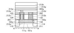
ンジスタである。トランジスタ101は、半導体層115と、半導体層115に電気的に
接続される第1の電極層112及び第2の電極層113と、半導体層115上に接するゲ
ート絶縁層114と、ゲート絶縁層114上に接し、半導体層115のチャネル形成領域
と重なるゲート電極層111と、を備える。トランジスタ101のチャネル方向は半導体
層115の上面と平行である。
111と電気的に接続する半導体層125と、半導体層125上に設けられ、当該半導体
層125と電気的に接続する電極層122と、半導体層125の側面に接して設けられる
ゲート絶縁層124と、ゲート絶縁層124と接し、半導体層125の当該側面と対向し
て設けられるゲート電極層121と、を備える。トランジスタ102は、いわゆる縦型の
トランジスタである。従って、トランジスタ102のチャネル方向はトランジスタの10
1のチャネル方向、および半導体層115の上面に対して垂直である。
ート電極層111と電極層132の間に挟持される誘電層134と、を備える。従って、
トランジスタ101のチャネルはトランジスタ102の半導体層125と容量103の誘
電層134と重畳する。
、ゲート電極層121は配線W1に、電極層132は配線W2に、第1の電極層112は
配線S2に、第2の電極層113は配線Dにそれぞれ電気的に接続する。また、ゲート電
極層111が保持ノードRに相当する。
ンジスタであるトランジスタ102と、容量103とを積層して設けることにより、占有
面積が削減された記憶装置を実現できる。またゲート電極層111が、トランジスタ10
2の一方の電極、及び容量103の一方の電極と兼ねる構成とすることにより、記憶装置
の構成が簡略化され、より低コストでの作製が可能となる。
り、読み出し動作を高速化できる。
を用いた場合、当該材料は極めて抵抗値が高いため、容量を構成する誘電層としても用い
ることができる。このとき、図1(B)に示すように、トランジスタ102の半導体層1
25と同一の材料からなる誘電層134を容量103に適用することが好ましい。すなわ
ち、半導体層125と誘電層134とが同一の層として存在することが好ましい。このよ
うな構成とすることで共通の作製工程によりトランジスタ102と容量103を作製する
ことが可能となるため、記憶装置の作製工程を簡略化でき、低コストで且つ高い歩留まり
が実現された記憶装置とすることができる。
いた構成としてもよい。誘電層134に絶縁材料の薄膜を用いることで、誘電層134の
厚さを薄く形成することができるため、容量103の容量値を高めることができる。
り制御することができる。したがって、微細化に伴いゲート電極層111や電極層122
などの線幅が極めて小さくなった場合でも、半導体層125の厚さによって任意のチャネ
ル長とすることができる。
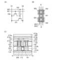
、異なる形状とすることもできる。図2(B)には、半導体層125の形状を円柱形状と
した場合の概略図を示している。また図2(C)は図2(B)におけるゲート電極層12
1及びゲート絶縁層124を破線で示した図である。
ルの実効的な幅を大きくとれるため、トランジスタ102のオン電流を高くすることがで
きる。また、図2(B)及び図2(C)に示すように半導体層125を円柱形状とすると
、その側面に突出した部分がないため、その側面全体にゲート電界が均一に印加されるこ
とになり、信頼性の高いトランジスタ102とすることができる。また、例えばさらにオ
ン電流を高くしたい場合には、半導体層125の底面の形状を例えば星型多角形のように
、少なくともひとつの内角が180°を超える多角形(凹多角形)とし、実効的なチャネ
ル幅を大きくしてもよい。
層125の側面の一部に対向して設ける構成としたが、少なくとも半導体層125の側面
の一部を覆って形成されていればよい。例えばゲート電極層121が半導体層125の外
周を囲う構成としてもよいし、半導体層125の片側の側面にのみゲート電極層121を
設ける構成とすれば、集積度を高くすることができる。図2(B)、図2(C)に示すよ
うに半導体層125の側面を囲う構成とすれば、トランジスタ102の実効的なチャネル
幅を大きくとれるためオン電流を高くすることができる。
量103とが積層され、且つ、トランジスタ102として縦型のトランジスタを適用する
ため、極めて占有面積が低減された記憶装置である。さらに、書き込み及び消去に用いる
電圧として高い電圧が不要であるため、極めて低消費電力で動作できる記憶装置である。
より、電力の供給が停止してもデータの保持が可能であり、且つ、極めて長い期間データ
を保持できる記憶装置を実現できる。
とができる。
本実施の形態では、本発明の一態様の半導体装置の例として、記憶装置の他の構成例に
ついて、図面を参照して説明する。なお、上記実施の形態と重複する部分については、説
明を省略するか簡略化して説明する。
図3(A)は、本実施の形態で例示する記憶装置の主要部における回路図である。
ぶこととする。
103aを含む記憶素子110aと、トランジスタ101b、トランジスタ102b及び
容量103bを含む記憶素子110bを備える。記憶素子110a及び記憶素子110b
の構成は、実施の形態1で例示した記憶装置と同様の構成とすることができる。
的に接続する配線W1と、容量103a及び容量103bの各々の一方の電極に電気的に
接続する配線W2と、トランジスタ102aの第1の電極及びトランジスタ101aの第
1の電極に電気的に接続する配線S11と、トランジスタ102bの第1の電極及びトラ
ンジスタ101bの第1の電極に電気的に接続する配線S12と、トランジスタ101a
及びトランジスタ101bの各々の第2の電極に電気的に接続する配線S2と、が接続さ
れている。
配線S12)とし、且つ隣接する記憶素子間で配線S2を共通化することにより、配線数
を低減することができる。
るが、実際にはこの2つの記憶素子の対が配線W1や配線S2などに沿って周期的に配置
されていることが好ましい。
オン状態とさせる電位が与えられる。続いて配線S11と配線S12の各々に、所望の電
位を与えることにより、トランジスタ102a又はトランジスタ102bを介して各々の
記憶素子の保持ノードにデータを書き込むことができる。
持ノードにトランジスタ101a又はトランジスタ101bをオン状態とさせる電位が保
持されているときには、配線S11又は配線S12の電位が変化する。一方、保持ノード
の電位が当該トランジスタをオフ状態とさせる電位のときには、配線S11又は配線S1
2の電位は変化しない。したがって、配線S11又は配線S12の電位の変化をセンスア
ンプ等で検知することにより、各々の記憶素子に書き込まれたデータを読み出すことがで
きる。
ジスタ101a及びトランジスタ101bを確実にオフ状態とする必要がある。そのとき
は配線W2に所望の電位を与えることにより容量103a又は容量103bを介して各々
の保持ノードの電位をトランジスタ101a又はトランジスタ101bをオフ状態とする
電位に変化させる。このようにして、配線S2に沿って配置された他の記憶素子の読み出
しを確実に行うことができる。
線層202と、配線S11として機能する配線層203aと、配線S12として機能する
配線層203bと、配線S2として機能する配線層204と、を図示している。
れている。同様にして、配線層201と配線層203bが重なる領域にトランジスタ10
2bが、配線層202と配線層203aが重なる領域に容量103aが、配線層202と
配線層203bが重なる領域に容量103bが、それぞれ設けられている。
切断線C-C’で切断した断面概略図を示す。図4(A)は、配線層203aに沿ってト
ランジスタ102aと容量103aを含む領域を切断した断面概略図である。また図4(
B)は、配線層201に沿ってトランジスタ102aとトランジスタ102bを含む領域
を切断した断面概略図である。また図4(C)は、配線層202と容量103aと接続電
極層213bと接続電極層213cと、を含む領域を切断した断面概略図である。
ジスタ102aと、容量103aが積層されている。また記憶素子110bにおいて、ト
ランジスタ101bのゲート電極層111b上にトランジスタ102bと容量103bが
積層されている。
導体として単結晶半導体を用いたトランジスタである。
の電極層112a及び第2の電極層113と、半導体層115上に接するゲート絶縁層1
14と、ゲート絶縁層114上に接し、半導体層115と重なるゲート電極層111aを
有する。
2の電極層113と、ゲート絶縁層114と、ゲート電極層111bを有する。
203bと電気的に接続されている。またトランジスタ101aの第1の電極層112a
も同様に接続電極層213c(図示しない)を介して配線層203aと電気的に接続され
ている。また、トランジスタ101aとトランジスタ101bに共通の第2の電極層11
3は、接続電極層213bを介して配線層204と電気的に接続されている。
1bの側面にはサイドウォール絶縁層を有していてもよい。
体層125の上面に接する電極層122と、半導体層125の側面に接するゲート絶縁層
124とを有する。さらに、ゲート絶縁層124に接し、半導体層125の側面を囲って
配線層201が設けられている。配線層201の一部は、トランジスタ102aのゲート
電極として機能する。従って、トランジスタ102aのゲート電極はトランジスタ101
aのゲート電極層111aとトランジスタ102aの電極層122の間に位置する。
極層122と、ゲート絶縁層124を有し、半導体層125の側面が配線層201に囲ま
れている。トランジスタ102bのゲート電極もトランジスタ101bのゲート電極層1
11bとトランジスタ102bの電極層122の間に位置する。
と電気的に接続されている。また、トランジスタ102bの電極層122も同様に接続電
極層213aを介して配線層203bと電気的に接続されている。
4を有する。また誘電層134の上面に接する配線層202が設けられている。配線層2
02の一部は、容量103aの一方の電極として機能する。ここで、誘電層134は、半
導体層125と同一の層から構成されている。すなわち、誘電層134は半導体層125
と同一の層として存在する。
134の上面に接して配線層202が設けられている。
に分離するために、各々の電極層間、配線層間、または電極層と配線層の間には、絶縁層
212a~212hのいずれかが設けられている。
電気的に分離するための素子分離層211が設けられている。
配線層の幅や、電極層間、配線層間、または電極層と配線層との間の間隔は、用いる作製
方法における最小加工寸法によって形成することができる。ここで最小加工寸法をFとす
ると、Fの値は好ましくは100nm以下、より好ましくは50nm以下、より好ましく
は30nm以下とする。
の占有面積を、F2にまで縮小することができる。
ることにより、2つの記憶素子間を可能な限り近づけて配置することができる。さらに、
トランジスタ101aのゲート電極層111a上に、トランジスタ102aと容量103
aを積層して設けることにより、一つの記憶素子の占有面積を縮小化することができる。
上記構成例では、容量を構成する誘電層として、縦型のトランジスタの半導体層と同一
の層を用いたが(すなわち、前記誘電層と前記半導体層は同一の層として存在する)、以
下では、誘電層として絶縁材料の薄膜を用いた場合について説明する。
た図である。なお、容量103aの構成以外は、上記構成例と同じ構成である。
4と、誘電層134の上面に接する電極層132とを有する。また、電極層132の上面
に接する配線層202が設けられている。
より、誘電層134を薄く形成できるため、単位面積あたりの容量値を高めることができ
る。
4と同一の層として存在することが好ましい。さらに、電極層132は、配線層201と
同一のとして存在することが好ましい。このように誘電層134と電極層132を、トラ
ンジスタ102aを構成する層と同一の層で構成することにより、容量103aとトラン
ジスタ102aとを同一の工程により形成することが可能であるため、作製工程を簡略化
できる。
以下では、上記構成例で例示した記憶装置を作製する方法の一例について図面を参照し
て説明する。なお、本作製工程例では一部を除いて、概略を示すにとどめる。詳細は、公
知の半導体集積回路作製技術を参照すればよい。
る。例えば、図6(A)にはその段階における上面概略図を示し、図6(B)には図6(
A)中の切断線A-A’及びB-B’で切断した断面概略図を示している。
炭化シリコンなどの単結晶半導体基板、多結晶半導体基板、シリコンゲルマニウムなどの
化合物半導体基板、SOI基板などを適用することができる。ここでは、半導体材料を含
む基板として、単結晶シリコン基板を用いる場合の一例について示す。なお、一般に「S
OI基板」は、絶縁表面上にシリコン半導体層が設けられた構成の基板をいうが、本明細
書等においては、絶縁表面上にシリコン以外の材料からなる半導体層が設けられた構成の
基板をも含むこととする。つまり、SOI基板には、ガラス基板などの絶縁基板上に絶縁
層を介して半導体層が設けられた構成も含まれるものとする。
S(Local Oxidation of Silicon)プロセス等を用いて形成
すればよい。また、この工程の前後において、後に形成されるトランジスタ101a及び
トランジスタ101bのしきい値電圧を制御するために、n型の導電性を付与する不純物
元素やp型の導電性を付与する不純物元素を基板に添加してもよい。基板に含まれる半導
体材料がシリコンの場合、n型の導電性を付与する不純物としては例えばリンやヒ素など
を用いることができる。一方、p型の導電性を付与する不純物としては、例えばホウ素、
アルミニウム、ガリウムなどを用いることができる。
、CMP(Chemical Mechanical Polishing)などの研磨
処理やエッチング処理を用いればよい。
ト絶縁層114となるものであり、CVD法やスパッタリング法等を用いて得られる酸化
シリコン、酸化窒化シリコン、窒化酸化シリコン、窒化シリコン、酸化ハフニウム、酸化
アルミニウム、酸化タンタル、酸化イットリウム、ハフニウムシリケート(HfSixO
y(x>0、y>0))、窒素が添加されたハフニウムシリケート、窒素が添加されたハ
フニウムアルミネート(HfAlxOy(x>0、y>0))等を含む膜の単層構造また
は積層構造とすると良い。他に、高密度プラズマ処理や熱処理(熱酸化処理や熱窒化処理
など)によって、基板の表面を酸化、窒化することにより上記絶縁膜を形成しても良い。
高密度プラズマ処理は、例えば、He、Ar、Kr、Xeなどの希ガスと、酸素、酸化窒
素、アンモニア、窒素などとの混合ガスを用いて行うことができる。また、絶縁膜の厚さ
は特に限定されないが、例えば1nm以上100nm以下とすることができる。
極層111a、111bとなるものであり、アルミニウムや銅、チタン、タンタル、タン
グステン、クロム、ニッケル、モリブデン等の金属材料を用いて形成することができる。
また、導電材料を含む多結晶シリコンなどの半導体材料を用いて、導電膜を形成しても良
い。形成方法も特に限定されず、蒸着法、CVD法、スパッタリング法、スピンコート法
など、各種成膜方法を用いることができる。なお本実施の形態では、導電膜として金属材
料を用いる場合の一例について示すものとする。
一方の電極としても機能するため、半導体層125に用いる半導体材料の電子親和力を考
慮して材料を選択することが好ましい。また導電膜を2以上の膜が積層された積層膜とし
、その最上層(半導体層125と接する層)の導電膜に、トランジスタ102a及びトラ
ンジスタ102bの電極に適した材料からなる導電膜を用いる構成としてもよい。
極層111bを形成する。
ル絶縁層を形成する。サイドウォール絶縁層は、ゲート電極層111a及びゲート電極層
111bを覆う絶縁膜を形成した後に、当該絶縁膜に異方性の高いエッチング処理を適用
することで自己整合的に形成することができる。
となる絶縁膜のうち、ゲート電極層111a及びゲート電極層111b及びサイドウォー
ル絶縁層に重ならない部分が同時にエッチングされることにより、ゲート絶縁層114が
形成される。
純物元素が異なる濃度で添加された不純物領域を形成することができる。こうすることで
短チャネル効果などの影響を抑制することができ、好ましい。なお、高集積化が要求され
る場合には、サイドウォールを有しない構成とすることにより、トランジスタサイズを縮
小することができる。
スクとして用い、リンや砒素などの不純物を添加して、第1の電極層112a、第1の電
極層112b、及び第2の電極層113を形成する。なお、pチャネル型のトランジスタ
を形成する場合にはホウ素やアルミニウムなどの不純物元素を添加すればよく、nチャネ
ル型のトランジスタを形成する場合には、リンや砒素などの不純物元素を添加すればよい
。添加する不純物の濃度は適宜設定することができるが、半導体素子が高度に微細化され
る場合には、その濃度を高くすることが望ましい。なお、不純物元素の添加後には加熱処
理を行い、不純物元素の活性化や不純物元素の添加時に生じる欠陥の改善等を図るのが望
ましい。
ート電極層111bが露出するように平坦化処理を行い、絶縁層212aを形成する。
ン、窒化シリコン、酸化アルミニウム、酸化ハフニウム、酸化タンタル等の無機絶縁材料
を含む膜の単膜または積層膜を用いることができる。また、後の工程にかかる熱に耐えう
るのであれば、ポリイミド、アクリル樹脂等の有機絶縁材料を用いて形成することもでき
る。
相当する。
導体層125となる半導体膜を形成する。ここで半導体膜の厚さは、後の平坦化工程で膜
厚が減少してしまうことを考慮して、あらかじめ所望のチャネル長よりも厚くなるように
形成することが好ましい。
よりもバンドギャップの広い半導体材料を用いることが好ましい。シリコンよりも広いバ
ンドギャップを有する半導体として化合物半導体があり、例えば、酸化物半導体、窒化物
半導体などがある。
ャリアの濃度に反比例する。ドナーやアクセプタによるキャリアが全く存在しない状態(
真性半導体)であっても、シリコンの場合にはバンドギャップが1.1電子ボルトである
ため、室温(300K)での熱励起キャリアの濃度は1×1011cm-3程度である。
濃度は1×10⁻⁷cm-3程度となる。電子移動度が同じ場合、抵抗率は、キャリア濃
度に反比例するので、バンドギャップ3.2電子ボルトの半導体の抵抗率は、シリコンよ
り18桁も大きい。
電流を実現できる。このようなトランジスタをトランジスタ102a及びトランジスタ1
02bに適用することにより、各記憶素子の保持ノードに保持される電位を、極めて長い
期間保持させることが可能となる。
。具体的には、In-Ga-Zn系酸化物半導体ターゲットを用いてスパッタリング法に
より形成する。
導体としては、少なくともインジウム(In)あるいは亜鉛(Zn)を含むことが好まし
い。特にInとZnを含むことが好ましい。
ライザーとして、それらに加えてガリウム(Ga)、スズ(Sn)、ハフニウム(Hf)
、アルミニウム(Al)、又はランタノイドのから選ばれた一種又は複数種を有すること
が好ましい。
ネオジム(Nd)、サマリウム(Sm)、ユウロピウム(Eu)、ガドリニウム(Gd)
、テルビウム(Tb)、ジスプロシウム(Dy)、ホルミウム(Ho)、エルビウム(E
r)、ツリウム(Tm)、イッテルビウム(Yb)、ルテチウム(Lu)がある。
できる。
酸化物、Zn-Mg系酸化物、Sn-Mg系酸化物、In-Mg系酸化物、In-Ga系
酸化物等を用いることができる。
n-Sn-Zn系酸化物、Sn-Ga-Zn系酸化物、In-Al-Zn系酸化物、In
-Hf-Zn系酸化物、In-La-Zn系酸化物、In-Ce-Zn系酸化物、In-
Pr-Zn系酸化物、In-Nd-Zn系酸化物、In-Sm-Zn系酸化物、In-E
u-Zn系酸化物、In-Gd-Zn系酸化物、In-Tb-Zn系酸化物、In-Dy
-Zn系酸化物、In-Ho-Zn系酸化物、In-Er-Zn系酸化物、In-Tm-
Zn系酸化物、In-Yb-Zn系酸化物、In-Lu-Zn系酸化物、Al-Ga-Z
n系酸化物、Sn-Al-Zn系酸化物等を用いることができる。
n系酸化物、In-Al-Ga-Zn系酸化物、In-Sn-Al-Zn系酸化物、In
-Sn-Hf-Zn系酸化物、In-Hf-Al-Zn系酸化物等を用いることができる
。
して有する酸化物という意味であり、InとGaとZnの比率は問わない。また、Inと
GaとZn以外の金属元素を含有させてもよい。
こともできる。
体で形成することができる。ここで、Mは、Ga、Al、Mn、及びCoから選ばれた一
つ又は複数の金属元素を示す。
比のIn-Ga-Zn系酸化物やその組成の近傍の酸化物を用いることができる。
n:Sn:Zn=2:1:5の原子比のIn-Sn-Zn系酸化物やその組成の近傍の酸
化物を用いてもよい。
に応じて適切な組成のものを用いればよい。また、必要とする半導体特性を得るために、
キャリア濃度や不純物濃度、欠陥密度、金属元素と酸素の原子数比、原子間距離、密度等
を適切なものとすることが好ましい。
がら、In-Ga-Zn系酸化物でも、バルク内欠陥密度を低減することにより移動度を
上げることができる。
+c=1)である酸化物の組成が、原子数比がIn:Ga:Zn=A:B:C(A+B+
C=1)の酸化物の組成の近傍であるとは、a、b、cが、(a-A)2+(b-B)2
+(c-C)2≦r2を満たすことをいい、rは、例えば、0.05とすればよい。他の
酸化物でも同様である。
でもよい。また、非晶質中に結晶性を有する部分を含む構造でもよい。なお、アモルファ
スは欠陥が多いため、非アモルファスが好ましい。
、これを用いてトランジスタを作製した際の界面散乱を低減でき、比較的容易に、比較的
高い移動度を得ることができる。
面の平坦性を高めればアモルファス状態の酸化物半導体以上の移動度を得ることができる
。
素化合物などの不純物ができるだけ混入しないように形成することが好ましい。例えばス
パッタリングターゲットや成膜に用いるガスに上記不純物が混入しないようにする。また
、成膜の際、成膜装置内を十分排気し、成膜時に基板温度を加熱しながら成膜することに
より、成膜された酸化物半導体膜に含まれる不純物濃度を低減することができる。
導体膜から水素、または水分を除去して、不純物が極力含まれないように高純度化し、脱
水化処理(脱水素化処理)によって増加した酸素欠損を補填するため酸素を酸化物半導体
膜に加える処理を行うことが好ましい。酸素の供給は、酸素雰囲気下で加熱処理を施す方
法や、酸化物半導体膜を加熱により酸素を放出する膜の近傍に配置し、加熱処理を施す方
法等を用いることができる。本明細書等において、酸化物半導体膜に酸素を供給する場合
を、加酸素化処理と記す場合がある、または酸化物半導体膜に含まれる酸素を化学量論的
組成よりも多くする場合を過酸素化処理と記す場合がある。
が除去され、加酸素化処理により酸素欠損を補填することによって、i型(真性)化また
はi型に限りなく近い酸化物半導体膜とすることができる。このような酸化物半導体膜中
には、ドナーに由来するキャリアが極めて少なく(ゼロに近く)、キャリア濃度は1×1
014/cm3未満、好ましくは1×1012/cm3未満、さらに好ましくは1×10
11/cm3未満、より好ましくは1.45×1010/cm3未満となる。
酸素欠損に起因するエネルギーギャップ中の欠陥準位が低減された酸化物半導体膜を備え
るトランジスタは、極めて優れたオフ電流特性を実現できる。例えば、室温(25℃)で
のオフ電流(ここでは、単位チャネル幅(1μm)あたりの値)は、100zA(1zA
(ゼプトアンペア)は1×10-21A)以下、望ましくは、10zA以下となる。また
、85℃では、100zA(1×10-19A)以下、望ましくは10zA(1×10-
20A)以下となる。このように、i型(真性)化または実質的にi型化された酸化物半
導体膜を用いることで、極めて優れたオフ電流特性のトランジスタを得ることができる。
成する。
に後のハードマスクとなる無機膜を形成し、当該無機膜上の半導体層125及び誘電層1
34を形成する領域と重なるようにレジストを形成する。ここで、形成したレジストに対
してアッシングを行いレジストの幅を縮小させる、いわゆるスリミング処理を施すことが
好ましい。スリミング処理を施すことにより半導体層125または誘電層134の幅を最
小加工寸法Fよりも小さくできる。したがって半導体層125及び誘電層134は、ゲー
ト電極層111aまたはゲート電極層111bの幅を最小加工寸法Fで形成した場合であ
っても、その内側の領域に設けることができる。
られる。ハードマスクの形成後にレジストを除去してもよい。
ッチング方法を用いて行う。ここで、エッチングの際に半導体膜よりも下層に設けられる
層をエッチングしない条件を用いる。このようにして、柱状(円柱状、多角柱状を含む)
の半導体層125を形成することができる。
合には、当該レジストを除去した後にハードマスクを除去する。
、ゲート絶縁層124として機能する。したがって、半導体層125の側面に接する部分
は均一な厚さになるように当該絶縁膜を形成することが好ましい。当該絶縁膜は、CVD
法、スパッタリング法などの成膜方法によって形成することができる。また、絶縁膜の膜
中及び半導体層125との界面には水、水素、水素化合物などの水素原子を含む不純物が
十分低減されていることが好ましい。
ズマCVDを用いると、緻密で絶縁耐圧の高い高品質な絶縁膜を形成できるので好ましい
。高純度化された酸化物半導体と高品質ゲート絶縁層とが接触することにより、界面準位
を低減して界面特性を良好にすることができる。
ニウム、酸化アルミニウム、酸化タンタル、酸化イットリウム、ハフニウムシリケート(
HfSixOy(x>0、y>0))、窒素が添加されたハフニウムシリケート(HfS
ixOyNz(x>0、y>0、z>0))、窒素が添加されたハフニウムアルミネート
(HfAlxOyNz(x>0、y>0、z>0))等を含む膜を、単層で、又は積層さ
せることで、形成することができる。
る。
成膜し、当該導電膜の不要な部分をエッチングする。その後、当該絶縁膜及び導電膜上に
、後の絶縁層212bとなる絶縁膜を成膜する。次に、半導体層125及び誘電層134
の上面が露出するように平坦化処理を行うことにより、配線層201と絶縁層212bが
形成される。
用いる導電膜と同様の材料、方法により形成できる。なお、以下、配線層202、配線層
203a、配線層203b、配線層204に用いる導電膜も同様である。
、方法により形成できる。なお、以下、絶縁層212c、絶縁層212d、絶縁層212
e、絶縁層212f、絶縁層212g、絶縁層212hに用いる絶縁膜も同様である。
縁層212b上に接して絶縁層212cとなる絶縁膜を形成する。その後、絶縁層212
cとなる絶縁膜に、半導体層125または誘電層134に到達する開口部を形成すること
により、絶縁層212cが形成される。
層134、及び絶縁層212c上に形成する。その後当該導電膜の不要な部分をエッチン
グすることにより、配線層202及び電極層122が形成される。
02aと容量103aを形成できる。また同時に、トランジスタ101bのゲート電極層
111b上にトランジスタ102bと容量103bが形成される。
る。
絶縁膜を形成する。その後、配線層202及び電極層122の上面が露出するように平坦
化処理を施すことで、絶縁層212dが形成される。
212e及び電極層122上に接続電極層213aとなる導電膜を形成し、絶縁層212
eの上面が露出するように平坦化処理を施すことにより、電極層122に電気的に接続す
る接続電極層213aを形成する。
2b、ゲート絶縁層124を構成する絶縁膜、及び絶縁層212aに、第1の電極層11
2aまたは第1の電極層112bに到達する開口部を形成することにより、第1の電極層
112aまたは第1の電極層112bに電気的に接続する接続電極層213c(図4参照
)を形成する。
203a及び配線層203bとなる導電膜を形成した後、当該導電膜の不要な部分をエッ
チングすることにより配線層203a及び配線層203bを形成する。
なる絶縁膜を形成した後、配線層203a及び配線層203bの上面が露出するように平
坦化処理を施すことにより絶縁層212fを形成する。
なる絶縁膜を成膜し、絶縁層212gを形成する。
212c、絶縁層212b、ゲート絶縁層124を構成する絶縁膜、及び絶縁層212a
に、第2の電極層113に到達する開口部(図示しない)を形成する。その後、絶縁層2
12g及び第2の電極層113上に接続電極層213bとなる導電膜を形成し、絶縁層2
12gの上面が露出するように平坦化処理を施すことにより、第2の電極層113と電気
的に接続する接続電極層213b(図示しない)を形成する(図4(C)参照)。
なる導電膜を形成した後、当該導電膜の不要な部分をエッチングすることにより、配線層
204を形成する(図4(C)参照)。
た絶縁層212hとなる絶縁膜を成膜した後、当該絶縁膜の上面を平坦化処理によって平
坦化して絶縁層212hを形成してもよい。
る。
10bを備える記憶装置を作製することができる。
方法を説明したが、これとは異なる方法により半導体層125及び誘電層134を形成す
ることもできる。以下では上記とは異なる作製方法について、図10を用いて説明する。
1となる導電膜を積層して形成する。ここで、絶縁層212iは、ゲート電極層111a
と配線層201とを絶縁するために設けられる。
成する。この段階における断面概略図が、図10(A)に相当する。
膜を成膜する。または、上記導電膜の上面及び側面を酸化して、絶縁膜を形成してもよい
。
膜とゲート電極層111aのそれぞれの上面が露出し、開口部の側壁にのみ絶縁膜を残す
ことができる。このようにして、開口部の側壁に接するゲート絶縁層124を形成するこ
とができる。
に半導体層125及び誘電層134となる半導体膜を成膜する。その後、当該導電膜の上
面が露出するように平坦化処理を施すことにより、上記開口部内に半導体層125及び誘
電層134を形成することができる。この段階における断面概略図が図10(B)に相当
する。
にレジストを形成し、当該導電膜の不要な部分をエッチングすることにより配線層201
を形成する。
層134、及びゲート絶縁層124の上面が露出するように平坦化処理を施すことにより
、絶縁層212bを形成する。この段階における断面概略図が図10(C)に相当する。
成する。この段階における断面概略図が図10(D)に相当する。
形成することができる。
電極層111aの内側の領域に半導体層125及び誘電層134を形成することができる
。
以下では、図5に示した、容量の誘電層として絶縁材料の薄膜を用いた記憶装置を作製
する方法の一例について図面を参照して説明する。なお、以下では、上記作製工程例と重
複する部分については説明を省略する。
は半導体層125と同時に同一材料からなる誘電層134を形成したが、本変形例では形
成しないことに留意する。
部を誘電層134として用いることができる。この段階における断面概略図が図11(A
)に相当する。
線層201と同一の導電膜からなる島状のパターンを形成することにより、電極層132
を形成する。このようにしてゲート電極層111aと電極層132の間に絶縁膜からなる
誘電層134が挟持された、容量103aを形成することができる。この段階における断
面概略図が図11(B)に相当する。
導体層125に到達する開口部を形成する際に、電極層132に到達する開口部も同時に
形成する。
けられた開口部を介して電極層132と電気的に接続する。この段階における断面概略図
が図11(C)に相当する。
絶縁膜が適用された容量103を備える記憶装置を作製することができる。
ジスタと同時に容量を作製することができるため、低コストで且つ高い歩留まりで記憶装
置を作製できる。
とができる。
本実施の形態では、本発明の一態様の半導体装置の一例として、上記実施の形態とは異
なる記憶装置の構成例について、図面を参照して説明する。なお、以下では上記実施の形
態と重複する部分については、説明を省略するか、簡略化して説明する。
する配線S1と、トランジスタ101の第2の電極と電気的に接続する配線S2と、トラ
ンジスタ102のゲートに接続する配線W1と、容量103の一方の電極と電気的に接続
する配線W2と、を有する。
C)は、図12(B)中の切断線D-D’で切断した断面概略図である。
おけるトランジスタ101を、縦型のトランジスタに置き換えた構成である。
型のトランジスタであるトランジスタ101と、トランジスタ101のゲート電極層11
1上に設けられたトランジスタ102及び容量103と、トランジスタ102のゲート電
極として機能する配線層201と、容量103の一方の電極として機能する配線層202
と、トランジスタ101及び容量103上に設けられ、トランジスタ101及びトランジ
スタ102と電気的に接続された配線層203と、を有する。
は配線W2として機能し、配線層203は配線S1として機能し、配線層204は配線S
2として機能する。またゲート電極層111が保持ノードに相当する。
も下層に設けることが可能であるため、配線層204と配線層203を重ねて設けること
ができる。このとき、配線層204と配線層203は、トランジスタ101が設けられて
いる層と、トランジスタ102及び容量103が設けられている層を介して形成されるた
め、これらの距離を十分に離して形成できる。そのため当該配線層間の容量は無視できる
程度にまで低減することができる。このように、2つの配線層を重ねて形成することによ
り、記憶装置の占有面積を極めて小さいものとすることができる。
を構成する絶縁膜によって電気的に絶縁される構成を示したが、ゲート電極層111と配
線層204との間に絶縁層を別途形成し、これらの間の容量を低減してもよい。その場合
には、当該絶縁層を貫通する接続電極層により配線層204と第2の電極層113とを接
続する構成とすればよい。
する第2の電極層113と、第2の電極層113上に設けられ、当該第2の電極層113
と電気的に接続する半導体層115と、半導体層115上に設けられ、当該半導体層11
5と電気的に接続する第1の電極層112と、半導体層115、第1の電極層112、及
び第2の電極層113の側面に接して設けられるゲート絶縁層114と、少なくとも半導
体層115の当該側面と対向して設けられるゲート電極層111と、を備える。チャネル
方向は絶縁表面に対して垂直である。
ることができる。
また、多結晶半導体としては、代表的にはポリシリコン(多結晶シリコン)があげられる
。ポリシリコンには、800℃以上のプロセス温度を経て形成されるポリシリコンを主材
料として用いた所謂高温ポリシリコンや、600℃以下のプロセス温度で形成されるポリ
シリコンを主材料として用いた所謂低温ポリシリコン、また結晶化を促進する元素などを
用いて、非晶質シリコンを結晶化させたポリシリコンなどを含んでいる。もちろん、微結
晶半導体又は半導体層の一部に結晶相を含む半導体を用いることもできる。
の場合は、第1の電極層112及び第2の電極層113を設けなくてもよい。
ことができる。このとき、半導体層125を構成する半導体の単層膜に換えて、第2の電
極層113を構成する不純物が添加された半導体膜と、半導体層115を構成する半導体
膜と、第1の電極層112を構成する不純物が添加された半導体膜との積層膜を用いるこ
とにより、トランジスタ101を形成することができる。
できる。
タ101をF2の面積の範囲内に納めることができる。同様に、トランジスタ102や容
量103もそれぞれF2の面積の範囲内に納めることができる。そのため高度に集積化し
た場合であっても、極めて占有面積が低減された記憶装置を実現できる。
とができる。
本実施の形態では、本発明の一態様の半導体装置の一例として、上記実施の形態とは異
なる記憶装置の構成例について、図面を参照して説明する。なお以下では、上記実施の形
態と重複する部分については、説明を省略するか、簡略化して説明する。
と容量103を有する記憶装置の層(半導体装置の層ともいえる。以下では、メモリ層と
も呼ぶ)を、複数積層して設けることにより、高度に集積化することが可能となる。また
、当該メモリ層の下層に、駆動回路を設けることもできる。以下では、当該メモリ層を積
層する構成、及びメモリ層の下層に駆動回路を設ける構成の例について説明する。
本構成例で例示する記憶装置の上面図は図3(B)が援用され、図3(B)の切断線A
-A’、切断線B-B’で切断した断面概略図が図13に相当する。
タ101bの構成が異なる点で、実施の形態2(例えば図4(A)、(B))で例示した
記憶装置と相違している。
の側面に接して設けられ、半導体層115とそれぞれ電気的に接続する第1の電極層11
2a及び第2の電極層113と、半導体層115の上面に接して設けられるゲート絶縁層
114と、ゲート絶縁層114の上面に接して設けられるゲート電極層111aと、を備
える。
の電極層113と、ゲート絶縁層114と、ゲート電極層111bと、を備える。
12b、及び第2の電極層113の側面に接して設けられている。
ができる。
た、単結晶半導体を用いる。
熱することにより、表面から一定の深さに酸化層を形成させるとともに、表面層に生じた
欠陥を消滅させて作る方法、水素イオン照射により形成された微小ボイドの熱処理による
成長を利用して半導体基板を劈開する方法や、絶縁表面上に結晶成長により単結晶半導体
層を形成する方法等を用いることができる。
。またゲート電極層111b上にはトランジスタ102bと容量103b(図示しない)
が設けられている。
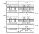
を構成する複数の層をまとめてメモリ層250とする。好適には、メモリ層250は被形
成面に平行な方向に並列して設けられた複数の記憶装置を有する。また、メモリ層250
は、トランジスタや容量を電気的に接続する配線層を含む。
能な構成とすることにより、メモリ層250を複数積層する、またはメモリ層250の下
層に駆動回路を設けることが可能となる。
リ層250aとメモリ層250bとが積層して設けられた記憶装置の構成を示している。
る。また、メモリ層250bは、層間絶縁層251bを介してメモリ層250a上に設け
られている。
が好ましい。また、駆動回路部260とメモリ層250a、またはメモリ層250aとメ
モリ層250bとの間の寄生容量を低減するため、層間絶縁層251a及び層間絶縁層2
51bに低誘電率の絶縁材料を用いることや、または十分に厚く形成することが好ましい
。
駆動回路部260と接続電極層を介して電気的に接続されており、駆動回路部260によ
ってデータの書き込みや消去、読み出し等の動作が制御される。
あたりのデータ量を増大させることができる。また駆動回路をメモリ層の下層に配置する
ことにより占有面積の増大を抑制することができる。
また、実施の形態3で例示した、トランジスタ101に縦型のトランジスタを適用した
場合においても、上記構成例と同様に複数のメモリ層を積層することや下層に駆動回路を
設けることが可能である。
の構成例を示す。
60上に設けられている。また、メモリ層250bは、層間絶縁層251bを介してメモ
リ層250a上に設けられている。
極めて占有面積が低減された記憶装置が適用される。したがってこのようなメモリ層を複
数積層して設けることにより、単位面積あたりのデータ量を極めて大きいものとすること
ができる。
とができる。
上記実施の形態で例示した半導体層125に適用可能な酸化物半導体として、結晶性を
有する半導体膜を用いると、トランジスタの電気特性を向上できる。好ましくは、半導体
膜としてCAAC-OS(C Axis Aligned Crystalline O
xide Semiconductor)膜を用いることが好ましい。以下では、CAA
C-OS膜が適用された半導体装置について説明する。
膜は、非晶質相に結晶部及び非晶質部を有する結晶-非晶質混相構造の酸化物半導体膜で
ある。なお、当該結晶部は、一辺が100nm未満の立方体内に収まる大きさであること
が多い。また、透過型電子顕微鏡(TEM:Transmission Electro
n Microscope)による観察像では、CAAC-OS膜に含まれる非晶質部と
結晶部との境界は明確ではない。また、TEMによってCAAC-OS膜には粒界(グレ
インバウンダリーともいう。)は確認できない。そのため、CAAC-OS膜は、粒界に
起因する電子移動度の低下が抑制される。
トルまたは表面の法線ベクトルに平行な方向に揃い、かつab面に垂直な方向から見て三
角形状または六角形状の原子配列を有し、c軸に垂直な方向から見て金属原子が層状また
は金属原子と酸素原子とが層状に配列している。なお、異なる結晶部間で、それぞれa軸
およびb軸の向きが異なっていてもよい。本明細書において、単に垂直と記載する場合、
85°以上95°以下の範囲も含まれることとする。また、単に平行と記載する場合、-
5°以上5°以下の範囲も含まれることとする。
AC-OS膜の形成過程において、酸化物半導体膜の表面側から結晶成長させる場合、被
形成面の近傍に対し表面の近傍では結晶部の占める割合が高くなることがある。また、C
AAC-OS膜へ不純物を添加することにより、当該不純物添加領域において結晶部が非
晶質化することもある。
トルまたは表面の法線ベクトルに平行な方向に揃うため、CAAC-OS膜の形状(被形
成面の断面形状または表面の断面形状)によっては互いに異なる方向を向くことがある。
なお、結晶部のc軸の方向は、CAAC-OS膜が形成されたときの被形成面の法線ベク
トルまたは表面の法線ベクトルに平行な方向となる。結晶部は、成膜することにより、ま
たは成膜後に熱処理などの結晶化処理を行うことにより形成される。
動が小さい。よって、当該トランジスタは、信頼性が高い。
低減することができ、表面の平坦性を高めればアモルファス状態の酸化物半導体以上の移
動度を得ることができる。表面の平坦性を高めるためには、平坦な表面上に酸化物半導体
を形成することが好ましく、具体的には、平均面粗さ(Ra)が1nm以下、好ましくは
0.3nm以下、より好ましくは0.1nm以下の表面上に形成するとよい。
義されている算術平均粗さを曲面に対して適用できるよう三次元に拡張したものであり、
「基準面から指定面までの偏差の絶対値を平均した値」で表現でき、以下の式(1)にて
定義される。
y1)),(x1,y2,f(x1,y2)),(x2,y1,f(x2,y1)),(
x2,y2,f(x2,y2))の4点で表される四角形の領域とし、指定面をxy平面
に投影した長方形の面積をS0、基準面の高さ(指定面の平均の高さ)をZ0とする。R
aは原子間力顕微鏡(AFM:Atomic Force Microscope)にて
測定可能である。
、基板温度を170℃として)酸化物半導体膜の成膜を行い、表面に概略垂直にc軸配向
させる方法がある。
化物半導体膜と第2の酸化物半導体膜のいずれか一方に、CAAC-OSとは異なる結晶
性の酸化物半導体を適用してもよい。すなわち、CAAC-OSと、単結晶酸化物半導体
、多結晶酸化物半導体、または非晶質酸化物半導体を適宜組み合わせた構成としてもよい
。また、第1の酸化物半導体膜と第2の酸化物半導体膜の少なくともどちらか一方に非晶
質酸化物半導体を適用すると、積層された酸化物半導体膜の内部応力や外部からの応力を
緩和し、トランジスタの特性ばらつきが低減され、また、トランジスタの信頼性をさらに
高めることが可能となる。一方で、非晶質酸化物半導体は水素などのドナーとなる不純物
を吸収しやすく、また、酸素欠損が生じやすいためn型化されやすい。このため、チャネ
ル側の酸化物半導体膜は、CAAC-OSなどの結晶性を有する酸化物半導体を適用する
ことが好ましい。
体膜で非晶質酸化物半導体膜を挟む構造としてもよい。また、結晶性を有する酸化物半導
体膜と非晶質酸化物半導体膜を交互に積層する構造としてもよい。また、酸化物半導体膜
を複数の膜の積層構造とする場合の上記構成は、それぞれを適宜組み合わせて用いること
ができる。
脱水素化処理)において、CAAC-OS膜の上面から容易に水素を離脱させることがで
きる。また、当該熱処理において、酸素の離脱を低減して選択的に水素を多く離脱させる
ことができる。
とができる。
本実施の形態では、半導体装置の一例として、上記実施の形態に開示した記憶装置を少
なくとも一部に用いたCPU(Central Processing Unit)につ
いて説明する。
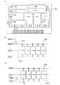
CPUは、基板1190上に、ALU1191(ALU:Arithmetic log
ic unit、演算回路)、ALUコントローラ1192、インストラクションデコー
ダ1193、インタラプトコントローラ1194、タイミングコントローラ1195、レ
ジスタ1196、レジスタコントローラ1197、バスインターフェース1198(Bu
s I/F)、書き換え可能なROM1199、及びROMインターフェース1189(
ROM I/F)を有している。基板1190は、半導体基板、SOI基板、ガラス基板
などを用いる。ROM1199及びROMインターフェース1189は、別チップに設け
てもよい。もちろん、図16(A)に示すCPUは、その構成を簡略化して示した一例に
すぎず、実際のCPUはその用途によって多種多様な構成を有している。
ンデコーダ1193に入力され、デコードされた後、ALUコントローラ1192、イン
タラプトコントローラ1194、レジスタコントローラ1197、タイミングコントロー
ラ1195に入力される。
ーラ1197、タイミングコントローラ1195は、デコードされた命令に基づき、各種
制御を行なう。具体的にALUコントローラ1192は、ALU1191の動作を制御す
るための信号を生成する。また、インタラプトコントローラ1194は、CPUのプログ
ラム実行中に、外部の入出力装置や、周辺回路からの割り込み要求を、その優先度やマス
ク状態から判断し、処理する。レジスタコントローラ1197は、レジスタ1196のア
ドレスを生成し、CPUの状態に応じてレジスタ1196の読み出しや書き込みを行なう
。
92、インストラクションデコーダ1193、インタラプトコントローラ1194、及び
レジスタコントローラ1197の動作のタイミングを制御する信号を生成する。例えばタ
イミングコントローラ1195は、基準クロック信号CLK1を元に、内部クロック信号
CLK2を生成する内部クロック生成部を備えており、内部クロック信号CLK2を上記
各種回路に供給する。
る。メモリセルとして、上記実施の形態1から4で示した記憶装置を適用することができ
る。レジスタ1196のメモリセルには、論理値を反転させる論理素子と上記実施の形態
に開示した記憶装置の両方を備える。
1からの指示に従い、レジスタ1196における保持動作の選択を行う。すなわち、レジ
スタ1196が有するメモリセルにおいて、論理値を反転させる論理素子によるデータの
保持を行うか、記憶装置によるデータの保持を行うかを、選択する。論理値を反転させる
論理素子によるデータの保持が選択されている場合、レジスタ1196内のメモリセルへ
の、電源電圧の供給が行われる。記憶装置におけるデータの保持が選択されている場合、
記憶装置へのデータの書き換えが行われ、レジスタ1196内のメモリセルへの電源電圧
の供給を停止することができる。
、電源電位VDDまたは電源電位VSSの与えられているノード間に、スイッチング素子
を設けることにより行うことができる。以下に図16(B)及び図16(C)の回路の説
明を行う。
供給を制御するスイッチング素子を備える。
142を複数有するメモリセル群1143とを有している。具体的に、各メモリセル11
42には、論理値を反転させる論理素子と上記記憶装置の両方を備えている。メモリセル
群1143が有する各メモリセル1142には、スイッチング素子1141を介して、ハ
イレベルの電源電位VDDが供給されている。さらに、メモリセル群1143が有する各
メモリセル1142には、信号INの電位と、ローレベルの電源電位VSSの電位が与え
られている。
トランジスタは、そのゲート電極に与えられる信号SigAによりスイッチングが制御さ
れる。
構成を示しているが、特に限定されず、トランジスタを複数有していてもよい。スイッチ
ング素子1141が、スイッチング素子として機能するトランジスタを複数有している場
合、上記複数のトランジスタは並列に接続されていてもよいし、直列に接続されていても
よいし、直列と並列が組み合わされて接続されていてもよい。
イッチング素子1141を介して、ローレベルの電源電位VSSが供給されている、レジ
スタ1196の一例を示す。スイッチング素子1141により、メモリセル群1143が
有する各メモリセル1142への、ローレベルの電源電位VSSの供給を制御することが
できる。
スイッチング素子を設け、一時的にCPUの動作を停止し、電源電圧の供給を停止した場
合においてもデータを保持することが可能であり、消費電力の低減を行うことができる。
具体的には、例えば、パーソナルコンピュータのユーザーが、キーボードなどの入力装置
への情報の入力を停止している間でも、メモリセル群中のデータを失うことなくCPUの
動作を停止することができ、それにより消費電力を低減することができる。
えば太陽電池や非接触給電(ワイヤレス給電ともいう)によって得られる比較的小さな電
力でも十分に動作させることができる。例えば、電子機器に太陽電池モジュール又は非接
触給電モジュールと、このようなモジュールによって得られた電力を蓄電する2次電池(
リチウムイオン電池など)を備える構成とする。
Processor)、カスタムLSI、FPGA(Field Programmab
le Gate Array)等のLSIにも応用可能である。
本明細書に開示する記憶装置や半導体装置は、さまざまな電子機器(遊技機も含む)に
適用することができる。電子機器としては、テレビ、モニタ等の表示装置、照明装置、デ
スクトップ型或いはノート型のパーソナルコンピュータ、ワードプロセッサ、DVD(D
igital Versatile Disc)などの記録媒体に記憶された静止画又は
動画を再生する画像再生装置、ポータブルCDプレーヤ、ラジオ、テープレコーダ、ヘッ
ドホンステレオ、ステレオ、コードレス電話子機、トランシーバ、携帯無線機、携帯電話
、自動車電話、携帯型ゲーム機、電卓、携帯情報端末、電子手帳、電子書籍、電子翻訳機
、音声入力機器、ビデオカメラ、デジタルスチルカメラ、電気シェーバ、電子レンジ等の
高周波加熱装置、電気炊飯器、電気洗濯機、電気掃除機、エアコンディショナーなどの空
調設備、食器洗い器、食器乾燥器、衣類乾燥器、布団乾燥器、電気冷蔵庫、電気冷凍庫、
電気冷凍冷蔵庫、DNA保存用冷凍庫、煙感知器、放射線測定器、透析装置等の医療機器
、などが挙げられる。さらに、誘導灯、信号機、ベルトコンベア、エレベータ、エスカレ
ータ、産業用ロボット、電力貯蔵システム等の産業機器も挙げられる。また、石油を用い
たエンジンや、非水系二次電池からの電力を用いて電動機により推進する移動体なども、
電子機器の範疇に含まれるものとする。上記移動体として、例えば、電気自動車(EV)
、内燃機関と電動機を併せ持ったハイブリッド車(HEV)、プラグインハイブリッド車
(PHEV)、これらのタイヤ車輪を無限軌道に変えた装軌車両、電動アシスト自転車を
含む原動機付自転車、自動二輪車、電動車椅子、ゴルフ用カート、小型又は大型船舶、潜
水艦、ヘリコプター、航空機、ロケット、人工衛星、宇宙探査機や惑星探査機、宇宙船が
挙げられる。これらの電子機器の具体例を図17及び図18に示す。
装着するための固定部3022と、操作ボタン3024、外部接続ポート3025等が設
けられている。また、スピーカを有していても良い。上記実施の形態で例示した記憶装置
や半導体装置を、本体3021に内蔵されているメモリやCPUなどに適用することによ
り、より省電力化された携帯音楽プレイヤー(PDA)とすることができる。
たせ、携帯電話と連携させれば、乗用車などを運転しながらワイヤレスによるハンズフリ
ーでの会話も可能である。
部9203、キーボード9204、外部接続ポート9205、ポインティングデバイス9
206等を含む。上記実施の形態に示した記憶装置やCPU等の半導体装置を利用すれば
、省電力化されたコンピュータとすることが可能となる。
が組み込まれており、表示部8002により映像を表示し、スピーカ部8003から音声
を出力することが可能である。上記実施の形態で例示した記憶装置または半導体装置を筐
体8001に組み込まれた表示部8002を動作するための駆動回路に用いることが可能
である。
装置、電気泳動表示装置、DMD(Digital Micromirror Devi
ce)、PDP(Plasma Display Panel)などの、半導体表示装置
を用いることができる。
装置8000は、受信機により一般のテレビ放送の受信を行うことができ、さらにモデム
を介して有線又は無線による通信ネットワークに接続することにより、一方向(送信者か
ら受信者)又は双方向(送信者と受信者間、あるいは受信者間同士など)の情報通信を行
うことも可能である。
いてもよい。テレビジョン装置8000は、上記実施の形態で例示した記憶装置や、CP
Uなどの半導体装置を用いることが可能である。
ナーは、上記実施の形態で例示したCPUなどの半導体装置を用いた電子機器の一例であ
る。具体的に、室内機8200は、筐体8201、送風口8202、CPU8203等を
有する。図18(A)において、CPU8203が、室内機8200に設けられている場
合を例示しているが、CPU8203は室外機8204に設けられていてもよい。或いは
、室内機8200と室外機8204の両方に、CPU8203が設けられていてもよい。
上記実施の形態で例示したCPUを用いることにより、省電力に優れたエアコンディショ
ナーを実現できる。
などの半導体装置を備える電子機器の一例である。具体的に、電気冷凍冷蔵庫8300は
、筐体8301、冷蔵室用扉8302、冷凍室用扉8303、CPU8304等を有する
。図18(A)では、CPU8304が、筐体8301の内部に設けられている。上記実
施の形態で例示したCPUなどの半導体装置を電気冷凍冷蔵庫8300のCPU8304
に用いることによって省電力化が図れる。
す。電気自動車9700には、二次電池9701が搭載されている。二次電池9701の
電力は、制御回路9702により出力が調整されて、駆動装置9703に供給される。制
御回路9702は、図示しないROM、RAM、CPU等を有する処理装置9704によ
って制御される。上記実施の形態で例示した記憶装置やCPUなどの半導体装置を電気自
動車9700の処理装置9704に用いることによって省電力化が図れる。
を組み合わせて構成される。処理装置9704は、電気自動車9700の運転者の操作情
報(加速、減速、停止など)や走行時の情報(上り坂や下り坂等の情報、駆動輪にかかる
負荷情報など)の入力情報に基づき、制御回路9702に制御信号を出力する。制御回路
9702は、処理装置9704の制御信号により、二次電池9701から供給される電気
エネルギーを調整して駆動装置9703の出力を制御する。交流電動機を搭載している場
合は、図示していないが、直流を交流に変換するインバータも内蔵される。
とができる。
101a トランジスタ
101b トランジスタ
102 トランジスタ
102a トランジスタ
102b トランジスタ
103 容量
103a 容量
103b 容量
110a 記憶素子
110b 記憶素子
111 ゲート電極層
111a ゲート電極層
111b ゲート電極層
112 第1の電極層
112a 第1の電極層
112b 第1の電極層
113 第2の電極層
114 ゲート絶縁層
115 半導体層
121 ゲート電極層
122 電極層
124 ゲート絶縁層
125 半導体層
132 電極層
134 誘電層
201 配線層
202 配線層
203 配線層
203a 配線層
203b 配線層
204 配線層
211 素子分離層
212a 絶縁層
212b 絶縁層
212c 絶縁層
212d 絶縁層
212e 絶縁層
212f 絶縁層
212g 絶縁層
212h 絶縁層
212i 絶縁層
213a 接続電極層
213b 接続電極層
213c 接続電極層
250 メモリ層
250a メモリ層
250b メモリ層
251a 層間絶縁層
251b 層間絶縁層
260 駆動回路部
1141 スイッチング素子
1142 メモリセル
1143 メモリセル群
1189 ROMインターフェース
1190 基板
1191 ALU
1192 ALUコントローラ
1193 インストラクションデコーダ
1194 インタラプトコントローラ
1195 タイミングコントローラ
1196 レジスタ
1197 レジスタコントローラ
1198 バスインターフェース
1199 ROM
3021 本体
3022 固定部
3023 表示部
3024 操作ボタン
3025 外部接続ポート
8000 テレビジョン装置
8001 筐体
8002 表示部
8003 スピーカ部
8200 室内機
8201 筐体
8202 送風口
8203 CPU
8204 室外機
8300 電気冷凍冷蔵庫
8301 筐体
8302 冷蔵室用扉
8303 冷凍室用扉
8304 CPU
9201 本体
9202 筐体
9203 表示部
9204 キーボード
9205 外部接続ポート
9206 ポインティングデバイス
9700 電気自動車
9701 二次電池
9702 制御回路
9703 駆動装置
9704 処理装置
Claims (23)
- メモリセル群を有し、
前記メモリセル群は、複数のメモリセルを有し、
前記メモリセルは、論理値を反転させる論理素子と、記憶素子と、を有し、
前記記憶素子は、
第1のトランジスタと、
前記第1のトランジスタの上方に設けられた第2のトランジスタと、を有し、
前記第1のトランジスタのゲート電極は、保持ノードと電気的に接続され、
前記第2のトランジスタのソース電極又はドレイン電極の一方は、前記保持ノードと電気的に接続され、
前記第2のトランジスタは、
チャネル形成領域を有する酸化物半導体層と、
前記酸化物半導体層と接する領域を有するゲート絶縁層と、
前記酸化物半導体層の側面と前記ゲート絶縁層を介して対向する領域を有するゲート電極層と、
前記ソース電極又は前記ドレイン電極の一方として機能する第1の電極層と、
前記ソース電極又は前記ドレイン電極の他方として機能する第2の電極層と、を有し、
前記第2のトランジスタは、縦型のトランジスタである、半導体装置。 - メモリセル群を有し、
前記メモリセル群は、複数のメモリセルを有し、
前記メモリセルは、論理値を反転させる論理素子と、記憶素子と、を有し、
前記記憶素子は、
第1のトランジスタと、
前記第1のトランジスタの上方に設けられた第2のトランジスタと、を有し、
前記第1のトランジスタのゲート電極は、保持ノードと電気的に接続され、
前記第2のトランジスタのソース電極又はドレイン電極の一方は、前記保持ノードと電気的に接続され、
前記第2のトランジスタは、
チャネル形成領域を有する酸化物半導体層と、
前記酸化物半導体層と接する領域を有するゲート絶縁層と、
前記酸化物半導体層の側面と前記ゲート絶縁層を介して対向する領域を有するゲート電極層と、
前記ソース電極又は前記ドレイン電極の一方として機能する第1の電極層と、
前記ソース電極又は前記ドレイン電極の他方として機能する第2の電極層と、を有し、
前記第2のトランジスタの前記ゲート絶縁層は、筒状の領域を有し、
前記第2のトランジスタは、縦型のトランジスタである、半導体装置。 - メモリセル群を有し、
前記メモリセル群は、複数のメモリセルを有し、
前記メモリセルは、論理値を反転させる論理素子と、記憶素子と、を有し、
前記記憶素子は、
第1のトランジスタと、
前記第1のトランジスタの上方に設けられた第2のトランジスタと、
容量と、を有し、
前記第1のトランジスタのゲート電極は、保持ノードと電気的に接続され、
前記第2のトランジスタのソース電極又はドレイン電極の一方は、前記保持ノードと電気的に接続され、
前記容量の一方の電極は、前記保持ノードと電気的に接続され、
前記第2のトランジスタは、
チャネル形成領域を有する酸化物半導体層と、
前記酸化物半導体層と接する領域を有するゲート絶縁層と、
前記酸化物半導体層の側面と前記ゲート絶縁層を介して対向する領域を有するゲート電極層と、
前記ソース電極又は前記ドレイン電極の一方として機能する第1の電極層と、
前記ソース電極又は前記ドレイン電極の他方として機能する第2の電極層と、を有し、
前記第2のトランジスタの前記ゲート絶縁層は、筒状の領域を有し、
前記第2のトランジスタは、縦型のトランジスタである、半導体装置。 - メモリセル群を有し、
前記メモリセル群は、複数のメモリセルを有し、
前記メモリセルは、論理値を反転させる論理素子と、記憶素子と、を有し、
前記記憶素子は、
第1のトランジスタと、
前記第1のトランジスタの上方に設けられた第2のトランジスタと、を有し、
前記第1のトランジスタのゲート電極は、保持ノードと電気的に接続され、
前記第2のトランジスタのソース電極又はドレイン電極の一方は、前記保持ノードと電気的に接続され、
前記第2のトランジスタは、
チャネル形成領域を有する酸化物半導体層と、
前記酸化物半導体層と接する領域を有するゲート絶縁層と、
前記酸化物半導体層の側面と前記ゲート絶縁層を介して対向する領域を有するゲート電極層と、
前記ソース電極又は前記ドレイン電極の一方として機能する第1の電極層と、
前記ソース電極又は前記ドレイン電極の他方として機能する第2の電極層と、を有し、
前記第2のトランジスタは、縦型のトランジスタであり、
前記保持ノードは、前記第2のトランジスタを介してデータが書き込まれ、
前記データは、前記第2のトランジスタがオフになることにより、前記保持ノードに保持される、半導体装置。 - メモリセル群を有し、
前記メモリセル群は、複数のメモリセルを有し、
前記メモリセルは、論理値を反転させる論理素子と、記憶素子と、を有し、
前記記憶素子は、
第1のトランジスタと、
前記第1のトランジスタの上方に設けられた第2のトランジスタと、を有し、
前記第1のトランジスタのゲート電極は、保持ノードと電気的に接続され、
前記第2のトランジスタのソース電極又はドレイン電極の一方は、前記保持ノードと電気的に接続され、
前記第2のトランジスタは、
チャネル形成領域を有する酸化物半導体層と、
前記酸化物半導体層と接する領域を有するゲート絶縁層と、
前記酸化物半導体層の側面と前記ゲート絶縁層を介して対向する領域を有するゲート電極層と、
前記ソース電極又は前記ドレイン電極の一方として機能する第1の電極層と、
前記ソース電極又は前記ドレイン電極の他方として機能する第2の電極層と、を有し、
前記第2のトランジスタの前記ゲート絶縁層は、筒状の領域を有し、
前記第2のトランジスタは、縦型のトランジスタであり、
前記保持ノードは、前記第2のトランジスタを介してデータが書き込まれ、
前記データは、前記第2のトランジスタがオフになることにより、前記保持ノードに保持される、半導体装置。 - メモリセル群を有し、
前記メモリセル群は、複数のメモリセルを有し、
前記メモリセルは、論理値を反転させる論理素子と、記憶素子と、を有し、
前記記憶素子は、
第1のトランジスタと、
前記第1のトランジスタの上方に設けられた第2のトランジスタと、
容量と、を有し、
前記第1のトランジスタのゲート電極は、保持ノードと電気的に接続され、
前記第2のトランジスタのソース電極又はドレイン電極の一方は、前記保持ノードと電気的に接続され、
前記容量の一方の電極は、前記保持ノードと電気的に接続され、
前記第2のトランジスタは、
チャネル形成領域を有する酸化物半導体層と、
前記酸化物半導体層と接する領域を有するゲート絶縁層と、
前記酸化物半導体層の側面と前記ゲート絶縁層を介して対向する領域を有するゲート電極層と、
前記ソース電極又は前記ドレイン電極の一方として機能する第1の電極層と、
前記ソース電極又は前記ドレイン電極の他方として機能する第2の電極層と、を有し、
前記第2のトランジスタの前記ゲート絶縁層は、筒状の領域を有し、
前記第2のトランジスタは、縦型のトランジスタであり、
前記保持ノードは、前記第2のトランジスタを介してデータが書き込まれ、
前記データは、前記第2のトランジスタがオフになることにより、前記保持ノードに保持される、半導体装置。 - 請求項1乃至請求項4のいずれか一において、
前記保持ノードは、前記第2のトランジスタを介してデータが書き込まれ、
前記データは、前記第2のトランジスタがオフになることにより、電力の供給が停止した状態において、前記保持ノードに保持される、半導体装置。 - 請求項1乃至請求項9のいずれか一において、
前記酸化物半導体層と前記第1の電極層とが接する領域は、上面視において前記第1の電極層の周縁の内側の領域に設けられており、 - 請求項1乃至請求項10のいずれか一において、
前記第2のトランジスタの前記ゲート電極層は、上面視において前記酸化物半導体層を囲む領域を有する、半導体装置。 - 請求項1乃至請求項11のいずれか一において、
前記第2のトランジスタの前記ゲート電極層は、断面視において前記第1の電極層と前記第2の電極層の間の領域を有する、半導体装置。 - 請求項1乃至請求項12のいずれか一において、
前記第2のトランジスタの前記チャネル形成領域は、前記第1のトランジスタのチャネル形成領域と重なる領域を有する、半導体装置。 - 請求項1乃至請求項13のいずれか一において、
前記酸化物半導体層は、i型又は実質的にi型である、半導体装置。 - 請求項1乃至請求項14のいずれか一において、
前記酸化物半導体層は、結晶部を有し、
前記結晶部は、c軸が前記酸化物半導体層の被形成面の法線ベクトルに平行な方向に揃う、半導体装置。 - 請求項1乃至請求項14のいずれか一において、
前記酸化物半導体層は、結晶部を有し、
前記結晶部は、c軸が前記第1の電極層の表面の法線ベクトルに平行な方向に揃う、半導体装置。 - 請求項1乃至請求項16のいずれか一において、
前記第2のトランジスタのチャネル長は、前記酸化物半導体層の厚さにより制御されている、半導体装置。 - 請求項1乃至請求項17のいずれか一において、
前記酸化物半導体層は、酸化インジウム、酸化スズ、酸化亜鉛、In-Zn系酸化物、Sn-Zn系酸化物、Al-Zn系酸化物、Zn-Mg系酸化物、Sn-Mg系酸化物、In-Mg系酸化物、In-Ga系酸化物、In-Ga-Zn系酸化物、In-Sn-Zn系酸化物、Sn-Ga-Zn系酸化物、In-Al-Zn系酸化物、In-Hf-Zn系酸化物、In-La-Zn系酸化物、In-Ce-Zn系酸化物、In-Pr-Zn系酸化物、In-Nd-Zn系酸化物、In-Sm-Zn系酸化物、In-Eu-Zn系酸化物、In-Gd-Zn系酸化物、In-Tb-Zn系酸化物、In-Dy-Zn系酸化物、In-Ho-Zn系酸化物、In-Er-Zn系酸化物、In-Tm-Zn系酸化物、In-Yb-Zn系酸化物、In-Lu-Zn系酸化物、Al-Ga-Zn系酸化物、Sn-Al-Zn系酸化物、In-Sn-Ga-Zn系酸化物、In-Hf-Ga-Zn系酸化物、In-Al-Ga-Zn系酸化物、In-Sn-Al-Zn系酸化物、In-Sn-Hf-Zn系酸化物又はIn-Hf-Al-Zn系酸化物のいずれかを有する、半導体装置。 - 請求項1乃至請求項18のいずれか一において、
前記第2のトランジスタのチャネル長方向は、前記第1の電極層の上面に対して垂直方向である、半導体装置。 - 請求項19において、
前記垂直方向は、前記第1の電極層の上面に対して85°以上95°以下の範囲である、半導体装置。 - 請求項1乃至請求項20のいずれか一において、
前記酸化物半導体層は、前記第1の電極層の表面に平行な平面における外周の形状が円形の領域を有する、半導体装置。 - 請求項1乃至請求項20のいずれか一において、
前記酸化物半導体層は、前記第1の電極層の表面に平行な平面における外周の形状が多角形の領域を有する、半導体装置。 - 請求項1乃至請求項22のいずれか一において、
前記複数のメモリセルは、1次元方向に配置されている、半導体装置。
Priority Applications (1)
| Application Number | Priority Date | Filing Date | Title |
|---|---|---|---|
| JP2025049399AJP2025094197A (ja) | 2012-02-29 | 2025-03-25 | 半導体装置 |
Applications Claiming Priority (4)
| Application Number | Priority Date | Filing Date | Title |
|---|---|---|---|
| JP2012044109 | 2012-02-29 | ||
| JP2012044109 | 2012-02-29 | ||
| JP2020132355AJP2020191470A (ja) | 2012-02-29 | 2020-08-04 | 半導体装置 |
| JP2022020164AJP7410991B2 (ja) | 2012-02-29 | 2022-02-14 | 半導体装置 |
Related Parent Applications (1)
| Application Number | Title | Priority Date | Filing Date |
|---|---|---|---|
| JP2022020164ADivisionJP7410991B2 (ja) | 2012-02-29 | 2022-02-14 | 半導体装置 |
Related Child Applications (1)
| Application Number | Title | Priority Date | Filing Date |
|---|---|---|---|
| JP2025049399ADivisionJP2025094197A (ja) | 2012-02-29 | 2025-03-25 | 半導体装置 |
Publications (2)
| Publication Number | Publication Date |
|---|---|
| JP2023156397Atrue JP2023156397A (ja) | 2023-10-24 |
| JP7657266B2 JP7657266B2 (ja) | 2025-04-04 |
Family
ID=49001865
Family Applications (15)
| Application Number | Title | Priority Date | Filing Date |
|---|---|---|---|
| JP2013035320AWithdrawnJP2013211537A (ja) | 2012-02-29 | 2013-02-26 | 半導体装置 |
| JP2017147696AWithdrawnJP2017216474A (ja) | 2012-02-29 | 2017-07-31 | 半導体装置 |
| JP2019012943AActiveJP6745924B2 (ja) | 2012-02-29 | 2019-01-29 | 半導体装置 |
| JP2020132355AWithdrawnJP2020191470A (ja) | 2012-02-29 | 2020-08-04 | 半導体装置 |
| JP2022020164AActiveJP7410991B2 (ja) | 2012-02-29 | 2022-02-14 | 半導体装置 |
| JP2022033538AActiveJP7470142B2 (ja) | 2012-02-29 | 2022-03-04 | 半導体装置 |
| JP2022033537AActiveJP7441869B2 (ja) | 2012-02-29 | 2022-03-04 | 半導体装置 |
| JP2022055695AActiveJP7395639B2 (ja) | 2012-02-29 | 2022-03-30 | 半導体装置 |
| JP2022172869AWithdrawnJP2023002775A (ja) | 2012-02-29 | 2022-10-28 | 半導体装置 |
| JP2023041660AActiveJP7498821B2 (ja) | 2012-02-29 | 2023-03-16 | トランジスタ及び半導体装置 |
| JP2023127121AActiveJP7657265B2 (ja) | 2012-02-29 | 2023-08-03 | 半導体装置 |
| JP2023127127AActiveJP7657266B2 (ja) | 2012-02-29 | 2023-08-03 | 半導体装置 |
| JP2023127125AActiveJP7637730B2 (ja) | 2012-02-29 | 2023-08-03 | 半導体装置 |
| JP2024088615AActiveJP7637817B2 (ja) | 2012-02-29 | 2024-05-31 | トランジスタ及び半導体装置 |
| JP2025049399APendingJP2025094197A (ja) | 2012-02-29 | 2025-03-25 | 半導体装置 |
Family Applications Before (11)
| Application Number | Title | Priority Date | Filing Date |
|---|---|---|---|
| JP2013035320AWithdrawnJP2013211537A (ja) | 2012-02-29 | 2013-02-26 | 半導体装置 |
| JP2017147696AWithdrawnJP2017216474A (ja) | 2012-02-29 | 2017-07-31 | 半導体装置 |
| JP2019012943AActiveJP6745924B2 (ja) | 2012-02-29 | 2019-01-29 | 半導体装置 |
| JP2020132355AWithdrawnJP2020191470A (ja) | 2012-02-29 | 2020-08-04 | 半導体装置 |
| JP2022020164AActiveJP7410991B2 (ja) | 2012-02-29 | 2022-02-14 | 半導体装置 |
| JP2022033538AActiveJP7470142B2 (ja) | 2012-02-29 | 2022-03-04 | 半導体装置 |
| JP2022033537AActiveJP7441869B2 (ja) | 2012-02-29 | 2022-03-04 | 半導体装置 |
| JP2022055695AActiveJP7395639B2 (ja) | 2012-02-29 | 2022-03-30 | 半導体装置 |
| JP2022172869AWithdrawnJP2023002775A (ja) | 2012-02-29 | 2022-10-28 | 半導体装置 |
| JP2023041660AActiveJP7498821B2 (ja) | 2012-02-29 | 2023-03-16 | トランジスタ及び半導体装置 |
| JP2023127121AActiveJP7657265B2 (ja) | 2012-02-29 | 2023-08-03 | 半導体装置 |
Family Applications After (3)
| Application Number | Title | Priority Date | Filing Date |
|---|---|---|---|
| JP2023127125AActiveJP7637730B2 (ja) | 2012-02-29 | 2023-08-03 | 半導体装置 |
| JP2024088615AActiveJP7637817B2 (ja) | 2012-02-29 | 2024-05-31 | トランジスタ及び半導体装置 |
| JP2025049399APendingJP2025094197A (ja) | 2012-02-29 | 2025-03-25 | 半導体装置 |
Country Status (3)
| Country | Link |
|---|---|
| US (9) | US9312257B2 (ja) |
| JP (15) | JP2013211537A (ja) |
| KR (6) | KR20130099847A (ja) |
Families Citing this family (106)
| Publication number | Priority date | Publication date | Assignee | Title |
|---|---|---|---|---|
| US9312257B2 (en) | 2012-02-29 | 2016-04-12 | Semiconductor Energy Laboratory Co., Ltd. | Semiconductor device |
| JP6100559B2 (ja) | 2012-03-05 | 2017-03-22 | 株式会社半導体エネルギー研究所 | 半導体記憶装置 |
| TWI618058B (zh) | 2013-05-16 | 2018-03-11 | 半導體能源研究所股份有限公司 | 半導體裝置 |
| JP6347704B2 (ja) | 2013-09-18 | 2018-06-27 | 株式会社半導体エネルギー研究所 | 半導体装置 |
| WO2015114476A1 (en) | 2014-01-28 | 2015-08-06 | Semiconductor Energy Laboratory Co., Ltd. | Semiconductor device |
| JP6607681B2 (ja) | 2014-03-07 | 2019-11-20 | 株式会社半導体エネルギー研究所 | 半導体装置 |
| TWI695375B (zh) | 2014-04-10 | 2020-06-01 | 日商半導體能源研究所股份有限公司 | 記憶體裝置及半導體裝置 |
| WO2015170220A1 (en) | 2014-05-09 | 2015-11-12 | Semiconductor Energy Laboratory Co., Ltd. | Memory device and electronic device |
| US10204898B2 (en) | 2014-08-08 | 2019-02-12 | Semiconductor Energy Laboratory Co., Ltd. | Semiconductor device and electronic device |
| JP2016111092A (ja)* | 2014-12-03 | 2016-06-20 | 株式会社Joled | 薄膜トランジスタ |
| KR20160087024A (ko) | 2015-01-12 | 2016-07-21 | 삼성디스플레이 주식회사 | 박막트랜지스터 및 그의 제조방법 |
| US9905700B2 (en) | 2015-03-13 | 2018-02-27 | Semiconductor Energy Laboratory Co., Ltd. | Semiconductor device or memory device and driving method thereof |
| JP2016225613A (ja)* | 2015-05-26 | 2016-12-28 | 株式会社半導体エネルギー研究所 | 半導体装置及び半導体装置の駆動方法 |
| US9741400B2 (en) | 2015-11-05 | 2017-08-22 | Semiconductor Energy Laboratory Co., Ltd. | Semiconductor device, memory device, electronic device, and method for operating the semiconductor device |
| JP6917700B2 (ja) | 2015-12-02 | 2021-08-11 | 株式会社半導体エネルギー研究所 | 半導体装置 |
| JP6822853B2 (ja) | 2016-01-21 | 2021-01-27 | 株式会社半導体エネルギー研究所 | 記憶装置及び記憶装置の駆動方法 |
| JP2018036290A (ja)* | 2016-08-29 | 2018-03-08 | 株式会社ジャパンディスプレイ | 表示装置 |
| CN109155145B (zh) | 2016-08-31 | 2022-11-01 | 美光科技公司 | 存储器阵列 |
| WO2018044479A1 (en) | 2016-08-31 | 2018-03-08 | Micron Technology, Inc. | Sense amplifier constructions |
| CN109155312B (zh) | 2016-08-31 | 2023-05-02 | 美光科技公司 | 存储器单元及存储器阵列 |
| US10056386B2 (en) | 2016-08-31 | 2018-08-21 | Micron Technology, Inc. | Memory cells and memory arrays |
| CN109155311A (zh) | 2016-08-31 | 2019-01-04 | 美光科技公司 | 存储器单元及存储器阵列 |
| US10355002B2 (en) | 2016-08-31 | 2019-07-16 | Micron Technology, Inc. | Memory cells, methods of forming an array of two transistor-one capacitor memory cells, and methods used in fabricating integrated circuitry |
| EP3840046B1 (en)* | 2016-08-31 | 2025-03-19 | Micron Technology, Inc. | Memory cells and memory arrays |
| JP6698486B2 (ja) | 2016-09-26 | 2020-05-27 | 株式会社ジャパンディスプレイ | 表示装置 |
| US10014305B2 (en) | 2016-11-01 | 2018-07-03 | Micron Technology, Inc. | Methods of forming an array comprising pairs of vertically opposed capacitors and arrays comprising pairs of vertically opposed capacitors |
| US10692869B2 (en) | 2016-11-17 | 2020-06-23 | Semiconductor Energy Laboratory Co., Ltd. | Semiconductor device and method for manufacturing semiconductor device |
| CN110121765B (zh)* | 2016-12-27 | 2023-04-28 | 夏普株式会社 | 半导体装置的制造方法和成膜装置 |
| US10062745B2 (en) | 2017-01-09 | 2018-08-28 | Micron Technology, Inc. | Methods of forming an array of capacitors, methods of forming an array of memory cells individually comprising a capacitor and a transistor, arrays of capacitors, and arrays of memory cells individually comprising a capacitor and a transistor |
| US9935114B1 (en) | 2017-01-10 | 2018-04-03 | Micron Technology, Inc. | Methods of forming an array comprising pairs of vertically opposed capacitors and arrays comprising pairs of vertically opposed capacitors |
| US11211384B2 (en) | 2017-01-12 | 2021-12-28 | Micron Technology, Inc. | Memory cells, arrays of two transistor-one capacitor memory cells, methods of forming an array of two transistor-one capacitor memory cells, and methods used in fabricating integrated circuitry |
| US9842839B1 (en)* | 2017-01-12 | 2017-12-12 | Micron Technology, Inc. | Memory cell, an array of memory cells individually comprising a capacitor and a transistor with the array comprising rows of access lines and columns of digit lines, a 2T-1C memory cell, and methods of forming an array of capacitors and access transistors there-above |
| TWI648825B (zh)* | 2017-03-16 | 2019-01-21 | 日商東芝記憶體股份有限公司 | 半導體記憶體 |
| US10312239B2 (en)* | 2017-03-16 | 2019-06-04 | Toshiba Memory Corporation | Semiconductor memory including semiconductor oxie |
| US11114470B2 (en) | 2017-06-02 | 2021-09-07 | Semiconductor Energy Laboratory Co., Ltd. | Semiconductor device, electronic component, and electronic device |
| WO2018224911A1 (ja) | 2017-06-08 | 2018-12-13 | 株式会社半導体エネルギー研究所 | 半導体装置及び半導体装置の駆動方法 |
| US10593693B2 (en) | 2017-06-16 | 2020-03-17 | Semiconductor Energy Laboratory Co., Ltd. | Semiconductor device and method for manufacturing semiconductor device |
| CN117276353A (zh) | 2017-06-27 | 2023-12-22 | 株式会社半导体能源研究所 | 半导体装置、半导体晶片、存储装置及电子设备 |
| CN110800102B (zh)* | 2017-06-30 | 2023-08-15 | 株式会社村田制作所 | 电子部件模块及其制造方法 |
| US10665604B2 (en) | 2017-07-21 | 2020-05-26 | Semiconductor Energy Laboratory Co., Ltd. | Semiconductor device, semiconductor wafer, memory device, and electronic device |
| KR102531991B1 (ko) | 2017-08-25 | 2023-05-11 | 가부시키가이샤 한도오따이 에네루기 켄큐쇼 | 반도체 장치 및 반도체 장치의 제작 방법 |
| CN110753962A (zh) | 2017-08-29 | 2020-02-04 | 美光科技公司 | 存储器电路 |
| EP3676872A4 (en) | 2017-08-31 | 2020-11-25 | Micron Technology, Inc. | DEVICES HAVING MEMORY CELLS CONTAINING TWO TRANSISTORS AND ONE CAPACITOR, AND OF WHICH THE BODY REGIONS OF THE TRANSISTORS ARE COUPLED TO REFERENCE VOLTAGES |
| US20190097001A1 (en)* | 2017-09-25 | 2019-03-28 | Raytheon Company | Electrode structure for field effect transistor |
| JP7051511B2 (ja)* | 2018-03-21 | 2022-04-11 | キオクシア株式会社 | 半導体装置及びその製造方法 |
| US10388658B1 (en) | 2018-04-27 | 2019-08-20 | Micron Technology, Inc. | Transistors, arrays of transistors, arrays of memory cells individually comprising a capacitor and an elevationally-extending transistor, and methods of forming an array of transistors |
| US20200091156A1 (en)* | 2018-09-17 | 2020-03-19 | Intel Corporation | Two transistor memory cell using stacked thin-film transistors |
| US10818324B2 (en) | 2018-12-18 | 2020-10-27 | Micron Technology, Inc. | Memory array decoding and interconnects |
| CN110896669B (zh)* | 2018-12-18 | 2021-01-26 | 长江存储科技有限责任公司 | 多堆叠三维存储器件以及其形成方法 |
| US11295985B2 (en)* | 2019-03-05 | 2022-04-05 | International Business Machines Corporation | Forming a backside ground or power plane in a stacked vertical transport field effect transistor |
| JP7210344B2 (ja)* | 2019-03-18 | 2023-01-23 | キオクシア株式会社 | 半導体装置及びその製造方法 |
| US11177266B2 (en) | 2019-08-26 | 2021-11-16 | Micron Technology, Inc. | Array of capacitors, an array of memory cells, a method of forming an array of capacitors, and a method of forming an array of memory cells |
| WO2021059079A1 (ja) | 2019-09-27 | 2021-04-01 | 株式会社半導体エネルギー研究所 | 半導体装置、記憶装置、及び電子機器 |
| US11158643B2 (en)* | 2019-11-26 | 2021-10-26 | Globalfoundries Singapore Pte. Ltd. | Non-volatile memory bit cells with non-rectangular floating gates |
| JP2020120123A (ja)* | 2020-04-16 | 2020-08-06 | 株式会社半導体エネルギー研究所 | 半導体装置 |
| KR20220012622A (ko) | 2020-07-23 | 2022-02-04 | 삼성전자주식회사 | 반도체 장치 |
| KR102744282B1 (ko)* | 2020-08-03 | 2024-12-19 | 에스케이하이닉스 주식회사 | 반도체 장치 및 반도체 장치의 제조 방법 |
| CN114078863B (zh)* | 2020-10-29 | 2025-07-18 | 长江存储科技有限责任公司 | 半导体器件、三维存储器及半导体器件制备方法 |
| US11355531B1 (en) | 2020-11-30 | 2022-06-07 | Micron Technology, Inc. | Array of capacitors, an array of memory cells, method used in forming an array of memory cells, methods used in forming an array of capacitors, and methods used in forming a plurality of horizontally-spaced conductive lines |
| US11557593B2 (en) | 2020-11-30 | 2023-01-17 | Micron Technology, Inc. | Array of memory cells, methods used in forming an array of memory cells, methods used in forming an array of vertical transistors, and methods used in forming an array of capacitors |
| KR20220099142A (ko)* | 2021-01-04 | 2022-07-13 | 삼성전자주식회사 | 반도체 메모리 장치 |
| US11581334B2 (en)* | 2021-02-05 | 2023-02-14 | Taiwan Semiconductor Manufacturing Company, Ltd. | Cocktail layer over gate dielectric layer of FET FeRAM |
| JP7638768B2 (ja) | 2021-04-05 | 2025-03-04 | キオクシア株式会社 | 半導体記憶装置 |
| JP7532587B2 (ja)* | 2022-03-25 | 2024-08-13 | 株式会社半導体エネルギー研究所 | 半導体装置 |
| WO2023199160A1 (ja)* | 2022-04-14 | 2023-10-19 | 株式会社半導体エネルギー研究所 | 半導体装置、及び、半導体装置の作製方法 |
| US20250287692A1 (en)* | 2022-04-19 | 2025-09-11 | Semiconductor Energy Laboratory Co., Ltd. | Semiconductor device and method for manufacturing the semiconductor device |
| CN119096713A (zh)* | 2022-04-28 | 2024-12-06 | 株式会社半导体能源研究所 | 半导体装置 |
| CN114927481A (zh)* | 2022-05-20 | 2022-08-19 | 长鑫存储技术有限公司 | 半导体结构及其形成方法、存储器 |
| KR20250034954A (ko)* | 2022-07-13 | 2025-03-11 | 가부시키가이샤 한도오따이 에네루기 켄큐쇼 | 트랜지스터 및 트랜지스터의 제작 방법 |
| CN117580358A (zh)* | 2022-08-04 | 2024-02-20 | 长鑫存储技术有限公司 | 一种半导体结构及其制备方法 |
| CN119678669A (zh)* | 2022-08-10 | 2025-03-21 | 株式会社半导体能源研究所 | 移位寄存器 |
| TW202425145A (zh) | 2022-09-01 | 2024-06-16 | 日商半導體能源研究所股份有限公司 | 記憶體裝置 |
| CN119732198A (zh) | 2022-09-01 | 2025-03-28 | 株式会社半导体能源研究所 | 存储装置 |
| CN119769187A (zh) | 2022-09-02 | 2025-04-04 | 株式会社半导体能源研究所 | 存储装置以及存储装置的制造方法 |
| WO2024057165A1 (ja) | 2022-09-16 | 2024-03-21 | 株式会社半導体エネルギー研究所 | 記憶装置 |
| DE102023125478A1 (de) | 2022-09-30 | 2024-04-04 | Semiconductor Energy Laboratory Co., Ltd. | Halbleitervorrichtung, Herstellungsverfahren der Halbleitervorrichtung und eines elektronischen Geräts |
| TW202437517A (zh) | 2022-09-30 | 2024-09-16 | 日商半導體能源研究所股份有限公司 | 記憶體裝置 |
| TW202431429A (zh) | 2022-10-14 | 2024-08-01 | 日商半導體能源研究所股份有限公司 | 半導體裝置及記憶體裝置 |
| CN119908180A (zh) | 2022-10-14 | 2025-04-29 | 株式会社半导体能源研究所 | 晶体管及存储装置 |
| KR20240052666A (ko) | 2022-10-14 | 2024-04-23 | 가부시키가이샤 한도오따이 에네루기 켄큐쇼 | 반도체 장치 |
| CN120188582A (zh) | 2022-10-21 | 2025-06-20 | 株式会社半导体能源研究所 | 半导体装置及存储装置 |
| CN117956789A (zh) | 2022-10-28 | 2024-04-30 | 株式会社半导体能源研究所 | 存储装置 |
| TW202422886A (zh) | 2022-10-28 | 2024-06-01 | 日商半導體能源研究所股份有限公司 | 半導體裝置、半導體裝置的製造方法以及電子裝置 |
| JPWO2024095108A1 (ja) | 2022-11-03 | 2024-05-10 | ||
| JPWO2024095110A1 (ja) | 2022-11-03 | 2024-05-10 | ||
| DE112023004639T5 (de) | 2022-11-04 | 2025-10-02 | Semiconductor Energy Laboratory Co., Ltd. | Halbleitervorrichtung und deren Herstellungsverfahren |
| JPWO2024100467A1 (ja) | 2022-11-11 | 2024-05-16 | ||
| WO2024105497A1 (ja) | 2022-11-15 | 2024-05-23 | 株式会社半導体エネルギー研究所 | 記憶装置 |
| TW202445833A (zh) | 2022-11-17 | 2024-11-16 | 日商半導體能源研究所股份有限公司 | 半導體裝置及其製造方法 |
| JPWO2024105515A1 (ja) | 2022-11-17 | 2024-05-23 | ||
| JPWO2024116036A1 (ja) | 2022-12-01 | 2024-06-06 | ||
| JPWO2024116037A1 (ja) | 2022-12-01 | 2024-06-06 | ||
| TW202441602A (zh)* | 2022-12-22 | 2024-10-16 | 日商半導體能源研究所股份有限公司 | 半導體裝置 |
| CN120642592A (zh)* | 2023-02-24 | 2025-09-12 | 株式会社半导体能源研究所 | 半导体装置及存储装置 |
| WO2024194726A1 (ja)* | 2023-03-17 | 2024-09-26 | 株式会社半導体エネルギー研究所 | 半導体装置、及び、半導体装置の作製方法 |
| WO2024236396A1 (ja)* | 2023-05-12 | 2024-11-21 | 株式会社半導体エネルギー研究所 | 半導体装置、記憶装置、半導体装置の作製方法 |
| KR20240164404A (ko) | 2023-05-12 | 2024-11-19 | 가부시키가이샤 한도오따이 에네루기 켄큐쇼 | 반도체 장치 |
| WO2024236457A1 (ja)* | 2023-05-18 | 2024-11-21 | 株式会社半導体エネルギー研究所 | 半導体装置、及び半導体装置の作製方法 |
| US20240395940A1 (en) | 2023-05-25 | 2024-11-28 | Semiconductor Energy Laboratory Co., Ltd. | Semiconductor device, memory device, and method for manufacturing semiconductor device |
| DE102024118091A1 (de) | 2023-07-06 | 2025-01-09 | Semiconductor Energy Laboratory Co., Ltd. | Halbleitervorrichtung |
| US20250015193A1 (en) | 2023-07-06 | 2025-01-09 | Semiconductor Energy Laboratory Co., Ltd. | Oxide semiconductor layer, method for forming the oxide semiconductor layer, semiconductor device, and method for manufacturing the semiconductor device |
| WO2025017440A1 (ja)* | 2023-07-20 | 2025-01-23 | 株式会社半導体エネルギー研究所 | 半導体装置、及び半導体装置の作製方法 |
| CN119947103A (zh) | 2023-11-02 | 2025-05-06 | 株式会社半导体能源研究所 | 半导体装置 |
| CN120417446A (zh) | 2024-01-31 | 2025-08-01 | 株式会社半导体能源研究所 | 半导体装置及存储装置 |
| KR20250126619A (ko) | 2024-02-16 | 2025-08-25 | 가부시키가이샤 한도오따이 에네루기 켄큐쇼 | 반도체 장치 |
| US12245418B1 (en)* | 2024-10-30 | 2025-03-04 | Chun-Ming Lin | Semiconductor structure integrating logic element and memory element |
Citations (7)
| Publication number | Priority date | Publication date | Assignee | Title |
|---|---|---|---|---|
| EP0834912A2 (en)* | 1996-10-02 | 1998-04-08 | Texas Instruments Incorporated | Dry-etching-free process for high dielectric and ferroelectric memory cell capacitor |
| JP2002198499A (ja)* | 2000-12-26 | 2002-07-12 | Toshiba Corp | 半導体記憶装置 |
| US20040262635A1 (en)* | 2003-06-24 | 2004-12-30 | Sang-Yun Lee | Three-dimensional integrated circuit structure and method of making same |
| US20110101339A1 (en)* | 2009-10-30 | 2011-05-05 | Semiconductor Energy Laboratory Co., Ltd. | Semiconductor device |
| US20110127522A1 (en)* | 2009-11-28 | 2011-06-02 | Semiconductor Energy Laboratory Co., Ltd. | Semiconductor device and method for manufacturing the same |
| US20110156024A1 (en)* | 2009-12-25 | 2011-06-30 | Semiconductor Energy Laboratory Co., Ltd. | Memory device, semiconductor device, and electronic device |
| US20120001243A1 (en)* | 2010-07-02 | 2012-01-05 | Semiconductor Energy Laboratory Co., Ltd. | Semiconductor device |
Family Cites Families (177)
| Publication number | Priority date | Publication date | Assignee | Title |
|---|---|---|---|---|
| EP0053878B1 (en) | 1980-12-08 | 1985-08-14 | Kabushiki Kaisha Toshiba | Semiconductor memory device |
| JPS6034199B2 (ja) | 1980-12-20 | 1985-08-07 | 株式会社東芝 | 半導体記憶装置 |
| JPS60198861A (ja) | 1984-03-23 | 1985-10-08 | Fujitsu Ltd | 薄膜トランジスタ |
| JPH0244256B2 (ja) | 1987-01-28 | 1990-10-03 | Kagaku Gijutsucho Mukizaishitsu Kenkyushocho | Ingazn2o5deshimesarerurotsuhoshokeinosojokozoojusurukagobutsuoyobisonoseizoho |
| JPH0244260B2 (ja) | 1987-02-24 | 1990-10-03 | Kagaku Gijutsucho Mukizaishitsu Kenkyushocho | Ingazn5o8deshimesarerurotsuhoshokeinosojokozoojusurukagobutsuoyobisonoseizoho |
| JPH0244258B2 (ja) | 1987-02-24 | 1990-10-03 | Kagaku Gijutsucho Mukizaishitsu Kenkyushocho | Ingazn3o6deshimesarerurotsuhoshokeinosojokozoojusurukagobutsuoyobisonoseizoho |
| JPS63210023A (ja) | 1987-02-24 | 1988-08-31 | Natl Inst For Res In Inorg Mater | InGaZn↓4O↓7で示される六方晶系の層状構造を有する化合物およびその製造法 |
| JPH0244262B2 (ja) | 1987-02-27 | 1990-10-03 | Kagaku Gijutsucho Mukizaishitsu Kenkyushocho | Ingazn6o9deshimesarerurotsuhoshokeinosojokozoojusurukagobutsuoyobisonoseizoho |
| JPH0244263B2 (ja) | 1987-04-22 | 1990-10-03 | Kagaku Gijutsucho Mukizaishitsu Kenkyushocho | Ingazn7o10deshimesarerurotsuhoshokeinosojokozoojusurukagobutsuoyobisonoseizoho |
| EP0510604A3 (en) | 1991-04-23 | 2001-05-09 | Canon Kabushiki Kaisha | Semiconductor device and method of manufacturing the same |
| US5612563A (en) | 1992-03-02 | 1997-03-18 | Motorola Inc. | Vertically stacked vertical transistors used to form vertical logic gate structures |
| US5308782A (en) | 1992-03-02 | 1994-05-03 | Motorola | Semiconductor memory device and method of formation |
| US5286674A (en) | 1992-03-02 | 1994-02-15 | Motorola, Inc. | Method for forming a via structure and semiconductor device having the same |
| US5398200A (en) | 1992-03-02 | 1995-03-14 | Motorola, Inc. | Vertically formed semiconductor random access memory device |
| JPH05251705A (ja) | 1992-03-04 | 1993-09-28 | Fuji Xerox Co Ltd | 薄膜トランジスタ |
| JP3745392B2 (ja)* | 1994-05-26 | 2006-02-15 | 株式会社ルネサステクノロジ | 半導体装置 |
| JP3479375B2 (ja) | 1995-03-27 | 2003-12-15 | 科学技術振興事業団 | 亜酸化銅等の金属酸化物半導体による薄膜トランジスタとpn接合を形成した金属酸化物半導体装置およびそれらの製造方法 |
| US5914504A (en)* | 1995-06-16 | 1999-06-22 | Imec Vzw | DRAM applications using vertical MISFET devices |
| KR100394896B1 (ko) | 1995-08-03 | 2003-11-28 | 코닌클리케 필립스 일렉트로닉스 엔.브이. | 투명스위칭소자를포함하는반도체장치 |
| JP3625598B2 (ja) | 1995-12-30 | 2005-03-02 | 三星電子株式会社 | 液晶表示装置の製造方法 |
| US20010017392A1 (en)* | 1997-05-19 | 2001-08-30 | International Business Machines Corporation. | Vertical transport MOSFETs and method for making the same |
| US6150687A (en) | 1997-07-08 | 2000-11-21 | Micron Technology, Inc. | Memory cell having a vertical transistor with buried source/drain and dual gates |
| JP4170454B2 (ja) | 1998-07-24 | 2008-10-22 | Hoya株式会社 | 透明導電性酸化物薄膜を有する物品及びその製造方法 |
| JP2000113683A (ja) | 1998-10-02 | 2000-04-21 | Hitachi Ltd | 半導体装置 |
| JP2000150861A (ja) | 1998-11-16 | 2000-05-30 | Tdk Corp | 酸化物薄膜 |
| JP3276930B2 (ja) | 1998-11-17 | 2002-04-22 | 科学技術振興事業団 | トランジスタ及び半導体装置 |
| WO2000070683A1 (en) | 1999-05-13 | 2000-11-23 | Hitachi, Ltd. | Semiconductor memory |
| TW460731B (en) | 1999-09-03 | 2001-10-21 | Ind Tech Res Inst | Electrode structure and production method of wide viewing angle LCD |
| TW587252B (en) | 2000-01-18 | 2004-05-11 | Hitachi Ltd | Semiconductor memory device and data processing device |
| JP4089858B2 (ja) | 2000-09-01 | 2008-05-28 | 国立大学法人東北大学 | 半導体デバイス |
| KR20020038482A (ko) | 2000-11-15 | 2002-05-23 | 모리시타 요이찌 | 박막 트랜지스터 어레이, 그 제조방법 및 그것을 이용한표시패널 |
| JP2002203913A (ja) | 2000-12-28 | 2002-07-19 | Hitachi Ltd | 半導体記憶装置の製造方法および半導体記憶装置 |
| JP3997731B2 (ja) | 2001-03-19 | 2007-10-24 | 富士ゼロックス株式会社 | 基材上に結晶性半導体薄膜を形成する方法 |
| JP2002289859A (ja) | 2001-03-23 | 2002-10-04 | Minolta Co Ltd | 薄膜トランジスタ |
| US6387758B1 (en)* | 2001-03-26 | 2002-05-14 | Advanced Micro Devices, Inc. | Method of making vertical field effect transistor having channel length determined by the thickness of a layer of dummy material |
| JP4090716B2 (ja) | 2001-09-10 | 2008-05-28 | 雅司 川崎 | 薄膜トランジスタおよびマトリクス表示装置 |
| JP3925839B2 (ja) | 2001-09-10 | 2007-06-06 | シャープ株式会社 | 半導体記憶装置およびその試験方法 |
| JP4164562B2 (ja) | 2002-09-11 | 2008-10-15 | 独立行政法人科学技術振興機構 | ホモロガス薄膜を活性層として用いる透明薄膜電界効果型トランジスタ |
| WO2003040441A1 (fr) | 2001-11-05 | 2003-05-15 | Japan Science And Technology Agency | Film mince monocristallin homologue a super-reseau naturel, procede de preparation et dispositif dans lequel est utilise ledit film mince monocristallin |
| JP4083486B2 (ja) | 2002-02-21 | 2008-04-30 | 独立行政法人科学技術振興機構 | LnCuO(S,Se,Te)単結晶薄膜の製造方法 |
| CN1445821A (zh) | 2002-03-15 | 2003-10-01 | 三洋电机株式会社 | ZnO膜和ZnO半导体层的形成方法、半导体元件及其制造方法 |
| JP3933591B2 (ja) | 2002-03-26 | 2007-06-20 | 淳二 城戸 | 有機エレクトロルミネッセント素子 |
| US7339187B2 (en) | 2002-05-21 | 2008-03-04 | State Of Oregon Acting By And Through The Oregon State Board Of Higher Education On Behalf Of Oregon State University | Transistor structures |
| US6787835B2 (en) | 2002-06-11 | 2004-09-07 | Hitachi, Ltd. | Semiconductor memories |
| JP2004022625A (ja) | 2002-06-13 | 2004-01-22 | Murata Mfg Co Ltd | 半導体デバイス及び該半導体デバイスの製造方法 |
| US7105868B2 (en) | 2002-06-24 | 2006-09-12 | Cermet, Inc. | High-electron mobility transistor with zinc oxide |
| JP2004103637A (ja)* | 2002-09-05 | 2004-04-02 | Renesas Technology Corp | 半導体装置およびその製造方法 |
| US7067843B2 (en) | 2002-10-11 | 2006-06-27 | E. I. Du Pont De Nemours And Company | Transparent oxide semiconductor thin film transistors |
| JP4166105B2 (ja) | 2003-03-06 | 2008-10-15 | シャープ株式会社 | 半導体装置およびその製造方法 |
| JP2004273732A (ja) | 2003-03-07 | 2004-09-30 | Sharp Corp | アクティブマトリクス基板およびその製造方法 |
| JP2004349291A (ja) | 2003-05-20 | 2004-12-09 | Renesas Technology Corp | 半導体装置およびその製造方法 |
| JP4108633B2 (ja) | 2003-06-20 | 2008-06-25 | シャープ株式会社 | 薄膜トランジスタおよびその製造方法ならびに電子デバイス |
| US7262463B2 (en) | 2003-07-25 | 2007-08-28 | Hewlett-Packard Development Company, L.P. | Transistor including a deposited channel region having a doped portion |
| US7282782B2 (en) | 2004-03-12 | 2007-10-16 | Hewlett-Packard Development Company, L.P. | Combined binary oxide semiconductor device |
| CN1998087B (zh) | 2004-03-12 | 2014-12-31 | 独立行政法人科学技术振兴机构 | 非晶形氧化物和薄膜晶体管 |
| US7145174B2 (en) | 2004-03-12 | 2006-12-05 | Hewlett-Packard Development Company, Lp. | Semiconductor device |
| US7297977B2 (en) | 2004-03-12 | 2007-11-20 | Hewlett-Packard Development Company, L.P. | Semiconductor device |
| US7211825B2 (en) | 2004-06-14 | 2007-05-01 | Yi-Chi Shih | Indium oxide-based thin film transistors and circuits |
| US7378702B2 (en) | 2004-06-21 | 2008-05-27 | Sang-Yun Lee | Vertical memory device structures |
| JP2006100760A (ja) | 2004-09-02 | 2006-04-13 | Casio Comput Co Ltd | 薄膜トランジスタおよびその製造方法 |
| US7285501B2 (en) | 2004-09-17 | 2007-10-23 | Hewlett-Packard Development Company, L.P. | Method of forming a solution processed device |
| US7298084B2 (en) | 2004-11-02 | 2007-11-20 | 3M Innovative Properties Company | Methods and displays utilizing integrated zinc oxide row and column drivers in conjunction with organic light emitting diodes |
| US7791072B2 (en) | 2004-11-10 | 2010-09-07 | Canon Kabushiki Kaisha | Display |
| US7453065B2 (en) | 2004-11-10 | 2008-11-18 | Canon Kabushiki Kaisha | Sensor and image pickup device |
| US7829444B2 (en) | 2004-11-10 | 2010-11-09 | Canon Kabushiki Kaisha | Field effect transistor manufacturing method |
| AU2005302964B2 (en) | 2004-11-10 | 2010-11-04 | Canon Kabushiki Kaisha | Field effect transistor employing an amorphous oxide |
| EP2453481B1 (en) | 2004-11-10 | 2017-01-11 | Canon Kabushiki Kaisha | Field effect transistor with amorphous oxide |
| KR100953596B1 (ko) | 2004-11-10 | 2010-04-21 | 캐논 가부시끼가이샤 | 발광장치 |
| US7863611B2 (en) | 2004-11-10 | 2011-01-04 | Canon Kabushiki Kaisha | Integrated circuits utilizing amorphous oxides |
| US7579224B2 (en) | 2005-01-21 | 2009-08-25 | Semiconductor Energy Laboratory Co., Ltd. | Method for manufacturing a thin film semiconductor device |
| TWI505473B (zh) | 2005-01-28 | 2015-10-21 | Semiconductor Energy Lab | 半導體裝置,電子裝置,和半導體裝置的製造方法 |
| TWI445178B (zh) | 2005-01-28 | 2014-07-11 | Semiconductor Energy Lab | 半導體裝置,電子裝置,和半導體裝置的製造方法 |
| US7858451B2 (en) | 2005-02-03 | 2010-12-28 | Semiconductor Energy Laboratory Co., Ltd. | Electronic device, semiconductor device and manufacturing method thereof |
| US7948171B2 (en) | 2005-02-18 | 2011-05-24 | Semiconductor Energy Laboratory Co., Ltd. | Light emitting device |
| US20060197092A1 (en) | 2005-03-03 | 2006-09-07 | Randy Hoffman | System and method for forming conductive material on a substrate |
| US8681077B2 (en) | 2005-03-18 | 2014-03-25 | Semiconductor Energy Laboratory Co., Ltd. | Semiconductor device, and display device, driving method and electronic apparatus thereof |
| US7544967B2 (en) | 2005-03-28 | 2009-06-09 | Massachusetts Institute Of Technology | Low voltage flexible organic/transparent transistor for selective gas sensing, photodetecting and CMOS device applications |
| US20110143506A1 (en) | 2009-12-10 | 2011-06-16 | Sang-Yun Lee | Method for fabricating a semiconductor memory device |
| US8367524B2 (en) | 2005-03-29 | 2013-02-05 | Sang-Yun Lee | Three-dimensional integrated circuit structure |
| US8455978B2 (en) | 2010-05-27 | 2013-06-04 | Sang-Yun Lee | Semiconductor circuit structure and method of making the same |
| US7645478B2 (en) | 2005-03-31 | 2010-01-12 | 3M Innovative Properties Company | Methods of making displays |
| US8300031B2 (en) | 2005-04-20 | 2012-10-30 | Semiconductor Energy Laboratory Co., Ltd. | Semiconductor device comprising transistor having gate and drain connected through a current-voltage conversion element |
| JP2006344849A (ja) | 2005-06-10 | 2006-12-21 | Casio Comput Co Ltd | 薄膜トランジスタ |
| US7691666B2 (en) | 2005-06-16 | 2010-04-06 | Eastman Kodak Company | Methods of making thin film transistors comprising zinc-oxide-based semiconductor materials and transistors made thereby |
| US7402506B2 (en) | 2005-06-16 | 2008-07-22 | Eastman Kodak Company | Methods of making thin film transistors comprising zinc-oxide-based semiconductor materials and transistors made thereby |
| US7507618B2 (en) | 2005-06-27 | 2009-03-24 | 3M Innovative Properties Company | Method for making electronic devices using metal oxide nanoparticles |
| KR100711890B1 (ko) | 2005-07-28 | 2007-04-25 | 삼성에스디아이 주식회사 | 유기 발광표시장치 및 그의 제조방법 |
| JP2007059128A (ja) | 2005-08-23 | 2007-03-08 | Canon Inc | 有機el表示装置およびその製造方法 |
| JP5116225B2 (ja) | 2005-09-06 | 2013-01-09 | キヤノン株式会社 | 酸化物半導体デバイスの製造方法 |
| JP4850457B2 (ja) | 2005-09-06 | 2012-01-11 | キヤノン株式会社 | 薄膜トランジスタ及び薄膜ダイオード |
| JP4280736B2 (ja) | 2005-09-06 | 2009-06-17 | キヤノン株式会社 | 半導体素子 |
| JP2007073705A (ja) | 2005-09-06 | 2007-03-22 | Canon Inc | 酸化物半導体チャネル薄膜トランジスタおよびその製造方法 |
| EP1770788A3 (en) | 2005-09-29 | 2011-09-21 | Semiconductor Energy Laboratory Co., Ltd. | Semiconductor device having oxide semiconductor layer and manufacturing method thereof |
| JP5037808B2 (ja) | 2005-10-20 | 2012-10-03 | キヤノン株式会社 | アモルファス酸化物を用いた電界効果型トランジスタ、及び該トランジスタを用いた表示装置 |
| CN101577231B (zh) | 2005-11-15 | 2013-01-02 | 株式会社半导体能源研究所 | 半导体器件及其制造方法 |
| TWI292281B (en) | 2005-12-29 | 2008-01-01 | Ind Tech Res Inst | Pixel structure of active organic light emitting diode and method of fabricating the same |
| US7867636B2 (en) | 2006-01-11 | 2011-01-11 | Murata Manufacturing Co., Ltd. | Transparent conductive film and method for manufacturing the same |
| JP4977478B2 (ja) | 2006-01-21 | 2012-07-18 | 三星電子株式会社 | ZnOフィルム及びこれを用いたTFTの製造方法 |
| KR100685659B1 (ko)* | 2006-01-26 | 2007-02-26 | 삼성전자주식회사 | 반도체 장치 및 그 제조 방법 |
| US7576394B2 (en) | 2006-02-02 | 2009-08-18 | Kochi Industrial Promotion Center | Thin film transistor including low resistance conductive thin films and manufacturing method thereof |
| EP1816508A1 (en)* | 2006-02-02 | 2007-08-08 | Semiconductor Energy Laboratory Co., Ltd. | Display device |
| US7977169B2 (en) | 2006-02-15 | 2011-07-12 | Kochi Industrial Promotion Center | Semiconductor device including active layer made of zinc oxide with controlled orientations and manufacturing method thereof |
| KR20070101595A (ko) | 2006-04-11 | 2007-10-17 | 삼성전자주식회사 | ZnO TFT |
| US20070252928A1 (en) | 2006-04-28 | 2007-11-01 | Toppan Printing Co., Ltd. | Structure, transmission type liquid crystal display, reflection type display and manufacturing method thereof |
| JP5028033B2 (ja) | 2006-06-13 | 2012-09-19 | キヤノン株式会社 | 酸化物半導体膜のドライエッチング方法 |
| JP4609797B2 (ja) | 2006-08-09 | 2011-01-12 | Nec液晶テクノロジー株式会社 | 薄膜デバイス及びその製造方法 |
| JP4999400B2 (ja) | 2006-08-09 | 2012-08-15 | キヤノン株式会社 | 酸化物半導体膜のドライエッチング方法 |
| JP4332545B2 (ja) | 2006-09-15 | 2009-09-16 | キヤノン株式会社 | 電界効果型トランジスタ及びその製造方法 |
| JP4274219B2 (ja) | 2006-09-27 | 2009-06-03 | セイコーエプソン株式会社 | 電子デバイス、有機エレクトロルミネッセンス装置、有機薄膜半導体装置 |
| JP5164357B2 (ja) | 2006-09-27 | 2013-03-21 | キヤノン株式会社 | 半導体装置及び半導体装置の製造方法 |
| US7622371B2 (en) | 2006-10-10 | 2009-11-24 | Hewlett-Packard Development Company, L.P. | Fused nanocrystal thin film semiconductor and method |
| US7772021B2 (en) | 2006-11-29 | 2010-08-10 | Samsung Electronics Co., Ltd. | Flat panel displays comprising a thin-film transistor having a semiconductive oxide in its channel and methods of fabricating the same for use in flat panel displays |
| JP2008140684A (ja) | 2006-12-04 | 2008-06-19 | Toppan Printing Co Ltd | カラーelディスプレイおよびその製造方法 |
| KR101303578B1 (ko) | 2007-01-05 | 2013-09-09 | 삼성전자주식회사 | 박막 식각 방법 |
| US8207063B2 (en) | 2007-01-26 | 2012-06-26 | Eastman Kodak Company | Process for atomic layer deposition |
| KR100851215B1 (ko) | 2007-03-14 | 2008-08-07 | 삼성에스디아이 주식회사 | 박막 트랜지스터 및 이를 이용한 유기 전계 발광표시장치 |
| US7795613B2 (en) | 2007-04-17 | 2010-09-14 | Toppan Printing Co., Ltd. | Structure with transistor |
| KR101325053B1 (ko) | 2007-04-18 | 2013-11-05 | 삼성디스플레이 주식회사 | 박막 트랜지스터 기판 및 이의 제조 방법 |
| KR20080094300A (ko) | 2007-04-19 | 2008-10-23 | 삼성전자주식회사 | 박막 트랜지스터 및 그 제조 방법과 박막 트랜지스터를포함하는 평판 디스플레이 |
| KR101334181B1 (ko) | 2007-04-20 | 2013-11-28 | 삼성전자주식회사 | 선택적으로 결정화된 채널층을 갖는 박막 트랜지스터 및 그제조 방법 |
| CN101663762B (zh) | 2007-04-25 | 2011-09-21 | 佳能株式会社 | 氧氮化物半导体 |
| KR101345376B1 (ko) | 2007-05-29 | 2013-12-24 | 삼성전자주식회사 | ZnO 계 박막 트랜지스터 및 그 제조방법 |
| JP5460950B2 (ja) | 2007-06-06 | 2014-04-02 | ピーエスフォー ルクスコ エスエイアールエル | 半導体装置及びその製造方法 |
| KR101344483B1 (ko)* | 2007-06-27 | 2013-12-24 | 삼성전자주식회사 | 박막 트랜지스터 |
| JP2009123882A (ja) | 2007-11-14 | 2009-06-04 | Elpida Memory Inc | 半導体装置およびその製造方法 |
| US20110052490A1 (en) | 2007-11-29 | 2011-03-03 | Plur0Med, Inc | Endoscopic mucosal resectioning using purified inverse thermosensitive polymers |
| US8202365B2 (en) | 2007-12-17 | 2012-06-19 | Fujifilm Corporation | Process for producing oriented inorganic crystalline film, and semiconductor device using the oriented inorganic crystalline film |
| US8212298B2 (en) | 2008-01-29 | 2012-07-03 | Unisantis Electronics Singapore Pte Ltd. | Semiconductor storage device and methods of producing it |
| WO2009096001A1 (ja) | 2008-01-29 | 2009-08-06 | Unisantis Electronics (Japan) Ltd. | 半導体記憶装置およびメモリ混載半導体装置、並びにそれらの製造方法 |
| JP2009266944A (ja) | 2008-04-23 | 2009-11-12 | Toshiba Corp | 三次元積層不揮発性半導体メモリ |
| JP2010056215A (ja) | 2008-08-27 | 2010-03-11 | Nec Electronics Corp | 縦型電界効果トランジスタを備える半導体装置及びその製造方法 |
| JP4623179B2 (ja) | 2008-09-18 | 2011-02-02 | ソニー株式会社 | 薄膜トランジスタおよびその製造方法 |
| JP5451280B2 (ja) | 2008-10-09 | 2014-03-26 | キヤノン株式会社 | ウルツ鉱型結晶成長用基板およびその製造方法ならびに半導体装置 |
| JP2010165803A (ja)* | 2009-01-14 | 2010-07-29 | Toshiba Corp | 半導体記憶装置の製造方法及び半導体記憶装置 |
| US8644046B2 (en) | 2009-02-10 | 2014-02-04 | Samsung Electronics Co., Ltd. | Non-volatile memory devices including vertical NAND channels and methods of forming the same |
| US8614917B2 (en) | 2010-02-05 | 2013-12-24 | Samsung Electronics Co., Ltd. | Vertically-integrated nonvolatile memory devices having laterally-integrated ground select transistors |
| JP5240059B2 (ja) | 2009-05-14 | 2013-07-17 | トヨタ自動車株式会社 | 排気還流装置の異常検出装置 |
| JP2011023543A (ja) | 2009-07-15 | 2011-02-03 | Renesas Electronics Corp | 半導体装置及び半導体装置の製造方法 |
| EP2491585B1 (en) | 2009-10-21 | 2020-01-22 | Semiconductor Energy Laboratory Co. Ltd. | Semiconductor device |
| SG10201406869QA (en) | 2009-10-29 | 2014-12-30 | Semiconductor Energy Lab | Semiconductor device |
| KR20120099657A (ko) | 2009-10-30 | 2012-09-11 | 가부시키가이샤 한도오따이 에네루기 켄큐쇼 | 트랜지스터 |
| WO2011052411A1 (en) | 2009-10-30 | 2011-05-05 | Semiconductor Energy Laboratory Co., Ltd. | Transistor |
| WO2011055660A1 (en) | 2009-11-06 | 2011-05-12 | Semiconductor Energy Laboratory Co., Ltd. | Semiconductor device |
| WO2011062041A1 (en) | 2009-11-20 | 2011-05-26 | Semiconductor Energy Laboratory Co., Ltd. | Transistor |
| CN104332177B (zh) | 2009-11-20 | 2018-05-08 | 株式会社半导体能源研究所 | 非易失性锁存电路和逻辑电路,以及使用其的半导体器件 |
| KR20190124813A (ko)* | 2009-11-20 | 2019-11-05 | 가부시키가이샤 한도오따이 에네루기 켄큐쇼 | 반도체 장치 |
| KR101800852B1 (ko) | 2009-11-20 | 2017-12-20 | 가부시키가이샤 한도오따이 에네루기 켄큐쇼 | 반도체 장치 |
| WO2011065209A1 (en) | 2009-11-27 | 2011-06-03 | Semiconductor Energy Laboratory Co., Ltd. | Non-linear element, display device including non-linear element, and electronic device including display device |
| KR102241766B1 (ko) | 2009-12-04 | 2021-04-19 | 가부시키가이샤 한도오따이 에네루기 켄큐쇼 | 반도체 장치 및 그 제조 방법 |
| KR20110064551A (ko) | 2009-12-08 | 2011-06-15 | 서울대학교산학협력단 | 산화물 반도체 채널을 갖는 수직형 낸드 플래시 메모리 소자 |
| KR101894821B1 (ko) | 2009-12-11 | 2018-09-05 | 가부시키가이샤 한도오따이 에네루기 켄큐쇼 | 반도체 장치 |
| CN103985760B (zh) | 2009-12-25 | 2017-07-18 | 株式会社半导体能源研究所 | 半导体装置 |
| MY187143A (en) | 2010-01-20 | 2021-09-03 | Semiconductor Energy Lab | Semiconductor device |
| WO2011105310A1 (en) | 2010-02-26 | 2011-09-01 | Semiconductor Energy Laboratory Co., Ltd. | Semiconductor device |
| WO2011108382A1 (en) | 2010-03-05 | 2011-09-09 | Semiconductor Energy Laboratory Co., Ltd. | Method for manufacturing semiconductor device |
| KR20110101876A (ko) | 2010-03-10 | 2011-09-16 | 삼성전자주식회사 | 매립 비트 라인을 갖는 반도체 장치 및 반도체 장치의 제조 방법 |
| KR101862539B1 (ko) | 2010-03-26 | 2018-05-31 | 가부시키가이샤 한도오따이 에네루기 켄큐쇼 | 반도체 장치 |
| WO2011135999A1 (en) | 2010-04-27 | 2011-11-03 | Semiconductor Energy Laboratory Co., Ltd. | Semiconductor memory device |
| KR101728068B1 (ko)* | 2010-06-01 | 2017-04-19 | 삼성전자 주식회사 | 적층 반도체 메모리 장치, 이를 포함하는 메모리 시스템, 및 관통전극 결함리페어 방법 |
| JP2012009512A (ja) | 2010-06-22 | 2012-01-12 | Toshiba Corp | 不揮発性半導体記憶装置及びその製造方法 |
| US8928061B2 (en) | 2010-06-30 | 2015-01-06 | SanDisk Technologies, Inc. | Three dimensional NAND device with silicide containing floating gates |
| WO2012008304A1 (en)* | 2010-07-16 | 2012-01-19 | Semiconductor Energy Laboratory Co., Ltd. | Semiconductor device |
| JP2012038994A (ja) | 2010-08-10 | 2012-02-23 | Elpida Memory Inc | 半導体装置及びその製造方法 |
| TWI508294B (zh) | 2010-08-19 | 2015-11-11 | Semiconductor Energy Lab | 半導體裝置 |
| US9431400B2 (en) | 2011-02-08 | 2016-08-30 | Semiconductor Energy Laboratory Co., Ltd. | Semiconductor memory device and method for manufacturing the same |
| US8975680B2 (en) | 2011-02-17 | 2015-03-10 | Semiconductor Energy Laboratory Co., Ltd. | Semiconductor memory device and method manufacturing semiconductor memory device |
| WO2012121265A1 (en) | 2011-03-10 | 2012-09-13 | Semiconductor Energy Laboratory Co., Ltd. | Memory device and method for manufacturing the same |
| JP2013042117A (ja) | 2011-07-15 | 2013-02-28 | Semiconductor Energy Lab Co Ltd | 半導体装置 |
| US9312257B2 (en)* | 2012-02-29 | 2016-04-12 | Semiconductor Energy Laboratory Co., Ltd. | Semiconductor device |
| JP6108103B2 (ja) | 2013-06-06 | 2017-04-05 | トヨタ自動車株式会社 | 巻線装置及び巻線方法 |
| US9306063B2 (en) | 2013-09-27 | 2016-04-05 | Intel Corporation | Vertical transistor devices for embedded memory and logic technologies |
| JP7101049B2 (ja) | 2018-06-06 | 2022-07-14 | 朋和産業株式会社 | 食品用包装袋 |
| JP7114059B2 (ja) | 2018-06-07 | 2022-08-08 | 三甲株式会社 | トレー |
| JP6594576B1 (ja) | 2018-06-07 | 2019-10-23 | キヤノン株式会社 | 光学系、それを備える撮像装置及び撮像システム |
| JP6991930B2 (ja) | 2018-06-07 | 2022-01-13 | 相互印刷株式会社 | プレススルーパックの包装体 |
| JP6788174B1 (ja) | 2019-06-11 | 2020-11-25 | 馨 林谷 | 母板に雑草粘着液排除孔のある刈り払い刃。 |
| WO2023008167A1 (ja) | 2021-07-29 | 2023-02-02 | 京セラ株式会社 | インクジェット記録装置 |
- 2013
- 2013-02-15USUS13/768,753patent/US9312257B2/enactiveActive
- 2013-02-25KRKR1020130019682Apatent/KR20130099847A/konot_activeCeased
- 2013-02-26JPJP2013035320Apatent/JP2013211537A/janot_activeWithdrawn
- 2016
- 2016-04-07USUS15/092,674patent/US9748273B2/enactiveActive
- 2017
- 2017-07-31JPJP2017147696Apatent/JP2017216474A/janot_activeWithdrawn
- 2017-08-08USUS15/671,216patent/US10038011B2/enactiveActive
- 2018
- 2018-07-30USUS16/048,412patent/US10418381B2/enactiveActive
- 2019
- 2019-01-29JPJP2019012943Apatent/JP6745924B2/jaactiveActive
- 2019-08-13USUS16/539,237patent/US10685984B2/enactiveActive
- 2019-11-19KRKR1020190148439Apatent/KR102237515B1/koactiveActive
- 2020
- 2020-06-08USUS16/894,939patent/US11133330B2/enactiveActive
- 2020-08-04JPJP2020132355Apatent/JP2020191470A/janot_activeWithdrawn
- 2021
- 2021-04-01KRKR1020210042793Apatent/KR102407627B1/koactiveActive
- 2021-05-05USUS17/308,116patent/US11923372B2/enactiveActive
- 2022
- 2022-02-14JPJP2022020164Apatent/JP7410991B2/jaactiveActive
- 2022-03-04JPJP2022033538Apatent/JP7470142B2/jaactiveActive
- 2022-03-04JPJP2022033537Apatent/JP7441869B2/jaactiveActive
- 2022-03-30JPJP2022055695Apatent/JP7395639B2/jaactiveActive
- 2022-05-23KRKR1020220063096Apatent/KR102620289B1/koactiveActive
- 2022-10-28JPJP2022172869Apatent/JP2023002775A/janot_activeWithdrawn
- 2023
- 2023-03-16JPJP2023041660Apatent/JP7498821B2/jaactiveActive
- 2023-08-03JPJP2023127121Apatent/JP7657265B2/jaactiveActive
- 2023-08-03JPJP2023127127Apatent/JP7657266B2/jaactiveActive
- 2023-08-03JPJP2023127125Apatent/JP7637730B2/jaactiveActive
- 2023-08-17USUS18/234,942patent/US20230387130A1/enactivePending
- 2023-08-17USUS18/234,959patent/US12382723B2/enactiveActive
- 2023-12-27KRKR1020230193601Apatent/KR20240007102A/koactivePending
- 2023-12-27KRKR1020230193611Apatent/KR20240007103A/koactivePending
- 2024
- 2024-05-31JPJP2024088615Apatent/JP7637817B2/jaactiveActive
- 2025
- 2025-03-25JPJP2025049399Apatent/JP2025094197A/jaactivePending
Patent Citations (18)
| Publication number | Priority date | Publication date | Assignee | Title |
|---|---|---|---|---|
| JPH10107223A (ja)* | 1996-10-02 | 1998-04-24 | Texas Instr Japan Ltd | 誘電体キャパシタ及び誘電体メモリ装置と、これらの製造方法 |
| EP0834912A2 (en)* | 1996-10-02 | 1998-04-08 | Texas Instruments Incorporated | Dry-etching-free process for high dielectric and ferroelectric memory cell capacitor |
| JP2002198499A (ja)* | 2000-12-26 | 2002-07-12 | Toshiba Corp | 半導体記憶装置 |
| US20040262635A1 (en)* | 2003-06-24 | 2004-12-30 | Sang-Yun Lee | Three-dimensional integrated circuit structure and method of making same |
| WO2005010934A2 (en)* | 2003-06-24 | 2005-02-03 | Lee, Sang-Yun | Three-dimensional integrated circuit structure and method of making same |
| JP2007525004A (ja)* | 2003-06-24 | 2007-08-30 | リー,サン−ユン | 三次元集積回路構造及びこれを作る方法 |
| JP2011119675A (ja)* | 2009-10-30 | 2011-06-16 | Semiconductor Energy Lab Co Ltd | 半導体装置 |
| US20110101339A1 (en)* | 2009-10-30 | 2011-05-05 | Semiconductor Energy Laboratory Co., Ltd. | Semiconductor device |
| WO2011052488A1 (en)* | 2009-10-30 | 2011-05-05 | Semiconductor Energy Laboratory Co., Ltd. | Semiconductor device |
| US20110127522A1 (en)* | 2009-11-28 | 2011-06-02 | Semiconductor Energy Laboratory Co., Ltd. | Semiconductor device and method for manufacturing the same |
| WO2011065244A1 (en)* | 2009-11-28 | 2011-06-03 | Semiconductor Energy Laboratory Co., Ltd. | Semiconductor device and method for manufacturing the same |
| JP2011135067A (ja)* | 2009-11-28 | 2011-07-07 | Semiconductor Energy Lab Co Ltd | 半導体装置及びその作製方法 |
| US20110156024A1 (en)* | 2009-12-25 | 2011-06-30 | Semiconductor Energy Laboratory Co., Ltd. | Memory device, semiconductor device, and electronic device |
| WO2011078373A1 (en)* | 2009-12-25 | 2011-06-30 | Semiconductor Energy Laboratory Co., Ltd. | Memory device, semiconductor device, and electronic device |
| JP2011151796A (ja)* | 2009-12-25 | 2011-08-04 | Semiconductor Energy Lab Co Ltd | 記憶装置、半導体装置、及び電子機器 |
| US20120001243A1 (en)* | 2010-07-02 | 2012-01-05 | Semiconductor Energy Laboratory Co., Ltd. | Semiconductor device |
| WO2012002186A1 (en)* | 2010-07-02 | 2012-01-05 | Semiconductor Energy Laboratory Co., Ltd. | Semiconductor device |
| JP2012033906A (ja)* | 2010-07-02 | 2012-02-16 | Semiconductor Energy Lab Co Ltd | 半導体装置 |
Also Published As
Similar Documents
| Publication | Publication Date | Title |
|---|---|---|
| JP7395639B2 (ja) | 半導体装置 |
Legal Events
| Date | Code | Title | Description |
|---|---|---|---|
| A521 | Request for written amendment filed | Free format text:JAPANESE INTERMEDIATE CODE: A523 Effective date:20230810 | |
| A521 | Request for written amendment filed | Free format text:JAPANESE INTERMEDIATE CODE: A523 Effective date:20230831 | |
| A621 | Written request for application examination | Free format text:JAPANESE INTERMEDIATE CODE: A621 Effective date:20230831 | |
| A977 | Report on retrieval | Free format text:JAPANESE INTERMEDIATE CODE: A971007 Effective date:20240823 | |
| A131 | Notification of reasons for refusal | Free format text:JAPANESE INTERMEDIATE CODE: A131 Effective date:20240827 | |
| A601 | Written request for extension of time | Free format text:JAPANESE INTERMEDIATE CODE: A601 Effective date:20241017 | |
| A521 | Request for written amendment filed | Free format text:JAPANESE INTERMEDIATE CODE: A523 Effective date:20241205 | |
| A131 | Notification of reasons for refusal | Free format text:JAPANESE INTERMEDIATE CODE: A131 Effective date:20250212 | |
| A521 | Request for written amendment filed | Free format text:JAPANESE INTERMEDIATE CODE: A523 Effective date:20250217 | |
| TRDD | Decision of grant or rejection written | ||
| A01 | Written decision to grant a patent or to grant a registration (utility model) | Free format text:JAPANESE INTERMEDIATE CODE: A01 Effective date:20250311 | |
| A61 | First payment of annual fees (during grant procedure) | Free format text:JAPANESE INTERMEDIATE CODE: A61 Effective date:20250325 | |
| R150 | Certificate of patent or registration of utility model | Ref document number:7657266 Country of ref document:JP Free format text:JAPANESE INTERMEDIATE CODE: R150 |