JP2023148322A - Continuity inspection device, kelvin measurement prober, and electricity removing device - Google Patents
Continuity inspection device, kelvin measurement prober, and electricity removing deviceDownload PDFInfo
- Publication number
- JP2023148322A JP2023148322AJP2022056271AJP2022056271AJP2023148322AJP 2023148322 AJP2023148322 AJP 2023148322AJP 2022056271 AJP2022056271 AJP 2022056271AJP 2022056271 AJP2022056271 AJP 2022056271AJP 2023148322 AJP2023148322 AJP 2023148322A
- Authority
- JP
- Japan
- Prior art keywords
- relay
- wafer
- connection wiring
- resistor
- semiconductor chip
- Prior art date
- Legal status (The legal status is an assumption and is not a legal conclusion. Google has not performed a legal analysis and makes no representation as to the accuracy of the status listed.)
- Pending
Links
Images


Landscapes
- Tests Of Electronic Circuits (AREA)
- Testing Or Measuring Of Semiconductors Or The Like (AREA)
Abstract
Translated fromJapaneseDescription
Translated fromJapanese本発明は、ウェハに複数形成された半導体チップの電気的特性を検査するウェハテストシステムに用いられる導通検査装置、ケルビン測定用プローバ、及び除電装置に関する。 The present invention relates to a continuity test device, a Kelvin measurement prober, and a static eliminator used in a wafer test system that tests the electrical characteristics of a plurality of semiconductor chips formed on a wafer.
ウェハ(半導体ウェハともいう)には、複数の半導体チップが形成される。そして、形成された半導体チップの電気的特性は、プローバとテスタで構成されるウェハテストシステムにより検査される。形成される半導体チップの種類によっては、表面に電極(表面電極)が形成されると共に、その裏面にも電極(裏面電極)が形成される。このような半導体チップの検査に対応したウェハテストシステムのウェハチャックには、ウェハの裏面に接触した状態でウェハを支持する支持面であって、テスタの測定電極として作用する導電性の支持面(ウェハ載置面)が設けられる。この支持面は、ウェハチャックから引き出されるチャックリード線を介してテスタに電気的に接続される。 A plurality of semiconductor chips are formed on a wafer (also referred to as a semiconductor wafer). Then, the electrical characteristics of the formed semiconductor chip are inspected by a wafer test system consisting of a prober and a tester. Depending on the type of semiconductor chip to be formed, an electrode (front surface electrode) is formed on the front surface, and an electrode (back surface electrode) is also formed on the back surface thereof. The wafer chuck of a wafer test system that is compatible with the inspection of such semiconductor chips includes a support surface that supports the wafer in contact with the back surface of the wafer, and a conductive support surface that acts as a measurement electrode for the tester. A wafer mounting surface) is provided. This support surface is electrically connected to the tester via chuck leads drawn out from the wafer chuck.
ここで、パワーデバイスの半導体チップの測定では、ウェハチャックに2本のチャックリード線(フォース線及びセンス線)を接続してケルビン接続を行って測定を行う(特許文献1参照)。また、ウェハチャックには大電流や高電圧を印加するために、チャックリード線は、径を太く設計したり、チャックリード線材に硬質なのもが使用されたりする。測定中は、ウェハチャックは動き回ると共に温度も高温になるので、チャックリード線は、機械的にも熱的にも過酷な条件にさらされて切れ易い傾向がある。 Here, in the measurement of a semiconductor chip of a power device, two chuck lead wires (a force wire and a sense wire) are connected to a wafer chuck and a Kelvin connection is performed to perform the measurement (see Patent Document 1). Further, in order to apply a large current or high voltage to a wafer chuck, the chuck lead wire is designed to have a large diameter, or a hard chuck lead wire material is used. During measurement, the wafer chuck moves around and the temperature increases, so the chuck leads are exposed to harsh mechanical and thermal conditions and tend to break.
そこで従来、チャックリード線が断線しないようにチャックリード線の固定方法を工夫したり、定期的なメンテナンス時に担当者がハンディテスタなどを用いてチャックリード線の導通を確認していたりしていた。 Conventionally, the chuck lead wires have been fixed in a way that prevents them from breaking, or personnel have used a handy tester to check the continuity of the chuck lead wires during regular maintenance.
また、特許文献2では、チャックリード線の導通検査を自動で行うことができる導通検査装置が提案されている。 Furthermore, Patent Document 2 proposes a continuity testing device that can automatically test the continuity of a chuck lead wire.
しかしながら、チャックリード線が断線しないようにチャックリード線の固定方法を工夫したとしても断線が発生してしまうことがある。また、定期的なメンテナンスが行われる前には、チャックリード線の断線を発見することができず、その間は不正確なウェハの検査が行われることになる。また、特許文献2に記載された導通検査装置では、1本のチャックリード線の導通検査を行う場合に、追加配線をウェハチャックに接続し、チャックリード線と追加配線を含む電流ループを形成し、その電流ループに電流が流れるか否かで、チャックリード線の導通検査を行うため、フォース線及びセンス線で構成される2本のチャックリード線を有し、ケルビン測定を行うウェハテストシステムには適用できない形である。 However, even if a method for fixing the chuck lead wire is devised so as not to break the chuck lead wire, the breakage may occur. Moreover, breakage of the chuck lead wire cannot be detected before regular maintenance is performed, and during that time, wafer inspection will be performed inaccurately. Furthermore, in the continuity testing device described in Patent Document 2, when testing the continuity of one chuck lead wire, additional wiring is connected to the wafer chuck, and a current loop including the chuck lead wire and the additional wiring is formed. In order to test the continuity of the chuck lead wire based on whether or not current flows through the current loop, the wafer test system has two chuck lead wires consisting of a force wire and a sense wire and performs Kelvin measurements. is an inapplicable form.
さらに、ウェハチャックには、電荷(静電気)が帯電し、ひいてはウェハチャック上のウェハにも電荷が帯電するため、ウェハの検査に伴って半導体チップの表面電極とプロー
ブとが接触する際に、半導体チップとプローブとの間に放電によるアークが発生して半導体チップを損傷するおそれがある。このため、ウェハチャックの除電を行う必要がある。Furthermore, the wafer chuck is charged with electric charge (static electricity), and the wafer on the wafer chuck is also charged with electric charge. There is a risk that an arc will occur due to discharge between the chip and the probe, damaging the semiconductor chip. Therefore, it is necessary to eliminate static electricity from the wafer chuck.
本発明はこのような事情に鑑みてなされたものであり、フォース線及びセンス線の2本のチャックリード線の導通の有無を自動且つ簡単に検査することができる導通検査装置及びケルビン測定用プローバを提供することを第1の目的とする。また、リーク電流の発生を最小限に抑えられる除電装置を提供することを第2の目的とする。 The present invention has been made in view of the above circumstances, and provides a continuity testing device and a Kelvin measurement prober that can automatically and easily test for continuity between two chuck lead wires, a force wire and a sense wire. The primary purpose is to provide the following. A second object of the present invention is to provide a static eliminator that can minimize the occurrence of leakage current.
本発明の第1の目的を達成するための導通検査装置は、ケルビン測定用プローバで測定するウェハを保持する支持面を有するウェハチャックと、ウェハの表面に形成された半導体チップの表面電極に接触するプローブと、ウェハの裏面に形成された半導体チップの裏面電極に接触するフォース線及びセンス線と、フォース線又はセンス線のいずれか一方に接続される第1接続配線と、フォース線又はセンス線のいずれか他方に接続される第2接続配線と、第1接続配線の側に設けられた第1リレー及び第1抵抗と、第2接続配線の側に設けられた電源と、備え、第1接続配線と第2接続配線との間を、第1リレー、第1抵抗、及び電源を介して電気的結合して電流ループを形成し、電流ループに電流が流れるか否かの判定を行う判定部を備える。 A continuity testing device for achieving the first object of the present invention includes a wafer chuck having a support surface for holding a wafer to be measured with a Kelvin measurement prober, and a contact surface electrode of a semiconductor chip formed on the surface of the wafer. a force line and a sense line that contact the back side electrode of the semiconductor chip formed on the back side of the wafer, a first connection wiring that is connected to either the force line or the sense line, and the force line or the sense line. a second connection wiring connected to the other one; a first relay and a first resistor provided on the side of the first connection wiring; and a power source provided on the side of the second connection wiring; A determination for forming a current loop by electrically coupling the connection wiring and the second connection wiring via a first relay, a first resistor, and a power source, and determining whether or not current flows in the current loop. Department.
本実施形態によれば、第1接続配線と第2接続配線により、ウェハチャックに設けられたフォース線及びセンス線を含む電流ループを形成することができ、この電流ループに電流が流れるか否かを判定することで、フォース線及びセンス線の導通の有無を判定することができる。 According to this embodiment, a current loop including the force line and the sense line provided on the wafer chuck can be formed by the first connection wiring and the second connection wiring, and it is possible to determine whether current flows through this current loop or not. By determining this, it is possible to determine whether the force line and the sense line are electrically connected.
本発明の他の態様に係る導通検査装置において、電流ループに含まれ、第2接続配線の側に設けられた第2リレー及び第2抵抗と、第2抵抗の電圧を検出する電圧検出部と、を備え、判定部が、電圧検出部の検出結果に基づき、判定を行う。これにより、電圧検出部よる第2抵抗の電圧検出結果に基づき、電流ループに電流が流れるか否かを判定することができる。 A continuity testing device according to another aspect of the present invention includes a second relay and a second resistor included in the current loop and provided on the side of the second connection wiring, and a voltage detection section that detects the voltage of the second resistor. The determination unit makes a determination based on the detection result of the voltage detection unit. Thereby, it is possible to determine whether or not current flows through the current loop based on the voltage detection result of the second resistor by the voltage detection section.
本発明の他の態様に係る導通検査装置において、第1リレー及び第2リレーの双方のクローズ状態とオープン状態との切り替えを個別に行うリレー制御部を備え、判定部が、リレー制御部により第1リレー及び第2リレーの双方がクローズ状態に切り替えられた状態での電圧検出部の検出結果に基づき、判定を行う。これにより、電圧検出部よる第2抵抗の電圧検出結果に基づき、電流ループに電流が流れるか否かを判定することができる。 A continuity testing device according to another aspect of the present invention includes a relay control unit that individually switches both the first relay and the second relay between a closed state and an open state, and the determination unit controls the relay control unit to The determination is made based on the detection result of the voltage detection unit in a state where both the first relay and the second relay are switched to the closed state. Thereby, it is possible to determine whether or not current flows through the current loop based on the voltage detection result of the second resistor by the voltage detection section.
本発明の他の態様に係る導通検査装置において、第1リレー及び第1抵抗は、第1接続配線のフォース線又はセンス線のいずれか一方が接続される一端とは反対側の他端と接地との間に、第1リレー、第1抵抗の順で接続される。これにより、第1リレーをオフすることにより、支持面から第1抵抗を最短で分離することができるので、リーク電流を最小に抑えることができる。 In the continuity testing device according to another aspect of the present invention, the first relay and the first resistor are grounded to the other end of the first connection wiring opposite to the one end to which either the force line or the sense line is connected. A first relay and a first resistor are connected in this order between the two. Thereby, by turning off the first relay, the first resistor can be separated from the support surface in the shortest possible time, so that leakage current can be suppressed to a minimum.
本発明の他の態様に係る導通検査装置において、支持面に接続されたフォース線の一端とは反対側の他端が接続する、半導体チップの電気的特性を検査するテスタのフォースコネクタに、第1接続配線又は第2接続配線のうち一方が接続され、支持面に接続されたセンス線の一端とは反対側の他端が接続する、テスタのセンスコネクタに、第1接続配線又は第2接続配線のうち他方が接続される。 In the continuity testing device according to another aspect of the present invention, a force connector of a tester for testing the electrical characteristics of a semiconductor chip is connected to one end of the force wire connected to the support surface and the other end of the force wire is connected to the other end of the force wire on the opposite side. One of the first connection wiring and the second connection wiring is connected, and the first connection wiring or the second connection wiring is connected to the sense connector of the tester, to which the other end of the sense wire opposite to the one end connected to the support surface is connected. The other of the wires is connected.
本発明の第1の目的を達成するためのケルビン測定用プローバは、半導体チップが複数形成されたウェハを保持するウェハチャックであって、且つウェハの裏面に形成された半
導体チップの裏面電極に接触する導電性の支持面を有するウェハチャックと、ウェハの表面に形成された半導体チップの表面電極に接触するプローブと、上述の導通検査装置と、を備える。A Kelvin measurement prober for achieving the first object of the present invention is a wafer chuck that holds a wafer on which a plurality of semiconductor chips are formed, and that contacts back electrodes of semiconductor chips formed on the back surface of the wafer. The present invention includes a wafer chuck having a conductive support surface, a probe that contacts a surface electrode of a semiconductor chip formed on a surface of a wafer, and the above-described continuity testing device.
本発明の第2の目的を達成するための除電装置は、半導体チップが複数形成されたウェハを保持するウェハチャックと、ウェハの表面に形成された半導体チップの表面電極に接触するプローブと、を備えるケルビン測定用プローバのウェハチャックに設けられたウェハの支持面であって、且つウェハの裏面に形成された半導体チップの裏面電極に接触する導電性の支持面に対して電気的に接続されるフォース線又はセンス線のいずれか一方と、フォース線又はセンス線のうち一方に接続される第1接続配線と、第1接続配線に接続された第1リレーと、第1リレーに接続され且つ接地された第1抵抗と、を備える。 A static eliminator for achieving the second object of the present invention includes a wafer chuck that holds a wafer on which a plurality of semiconductor chips are formed, and a probe that contacts the surface electrode of the semiconductor chip formed on the surface of the wafer. A wafer support surface provided on a wafer chuck of a Kelvin measurement prober, which is electrically connected to a conductive support surface that contacts a back electrode of a semiconductor chip formed on the back surface of the wafer. either one of the force line or the sense line, a first connection wiring connected to one of the force line or the sense line, a first relay connected to the first connection wiring, and a first relay connected to the first relay and grounded. and a first resistor.
この除電装置によれば、第1リレーをオフすることにより、支持面から第1抵抗を最短で分離することができるので、リーク電流を最小に抑えることができる。 According to this static eliminator, the first resistor can be separated from the support surface in the shortest possible time by turning off the first relay, so that leakage current can be suppressed to a minimum.
本発明の導通検査装置及びケルビン測定用プローバによれば、第1接続配線と第2接続配線により、ウェハチャックに設けられたフォース線及びセンス線を含む電流ループを形成することができ、この電流ループに電流が流れるか否かを判定することで、フォース線及びセンス線の導通の有無を判定することができる。また、本発明の除電装置は、リーク電流の発生を最小限に抑えられる。 According to the continuity testing device and Kelvin measurement prober of the present invention, the first connection wiring and the second connection wiring can form a current loop including the force line and the sense line provided on the wafer chuck, and this current By determining whether or not current flows through the loop, it is possible to determine whether or not the force line and the sense line are electrically connected. Furthermore, the static eliminator of the present invention can minimize the occurrence of leakage current.
[ウェハテストシステムの構成]
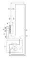
図1は、ウェハテストシステム9の概略図である。以下、図中の上下方向であるZ軸方向の上方及び上面を適宜「上方」及び「上面」といい、Z軸方向の下方及び下面を適宜「下方」及び「下面」という。[Wafer test system configuration]
FIG. 1 is a schematic diagram of a
ウェハテストシステム9は、ウェハWに複数形成された半導体チップ(不図示)であって両面に電極(不図示)が形成されている複数の半導体チップの各々の電気的特性を検査する。このウェハテストシステム9は、プローバ10とテスタ30とを備える。特に、ウェハテストシステム9は、半導体チップとして、パワーデバイスが複数形成されたウェハWを検査するための構成を備えたものである。したがって、プローバ10は、後で説明するようにケルビン接続により接続されるフォース線及びセンス線を有するケルビン測定用プローバである(図2を参照)。 The
プローバ10は、ウェハW上の個々の半導体チップ(不図示)の表面に形成された表面電極(不図示)にプローブ25を接触させると共に、個々の半導体チップの裏面に形成さ
れた裏面電極(不図示)に後述のウェハチャック16の導電性の支持面16aを接触させる。テスタ30は、プローブ25と支持面16aとに電気的に接続され、個々の半導体チップの電気的特性を検査する。The
プローバ10は、基台11と、ベース12と、Yステージ13と、Xステージ14と、Zθステージ15と、ウェハチャック16と、プローブ位置検出カメラ18と、プローブ高さ検出器20と、高さ調整機構21、27と、ウェハアライメントカメラ19と、ヘッドステージ22と、カードホルダ23と、プローブカード24と、プローブ25と、を備える。 The
基台11の上面には、略平板状のベース12が固定されている。なお、基台11の代わりに脚部材を用いてもよいし、或いは基台11を省略してもよい。 A substantially
ベース12の上面には、不図示のY移動部を介して略平板状のYステージ13がY軸方向に移動自在に支持されている。Y移動部は、ベース12の上面に設けられ且つY軸に平行なガイドレールと、Yステージ13の下面に設けられ且つガイドレールに係合するスライダと、Yステージ13をY軸方向に移動させるモータ等の駆動機構と、を備える。このY移動部を駆動することにより、ベース12上でYステージ13と、後述のXステージ14及びZθステージ15等とが一体的にY軸方向に移動される。 A substantially
Yステージ13の上面には、不図示のX移動部を介して略平板状のXステージ14がX軸方向に移動自在に支持されている。X移動部は、Yステージ13の上面に設けられ且つX軸に平行なガイドレールと、Xステージ14の下面に設けられ且つガイドレールに係合するスライダと、Xステージ14をX軸方向に移動させるモータ等の駆動機構と、を備える。このX移動部を駆動することにより、Yステージ13上でXステージ14及び後述のZθステージ15等が一体的にX軸方向に移動される。 A substantially
Xステージ14の上面には、Zθステージ15及び高さ調整機構21、27が設けられている。Zθステージ15の内部には、不図示のZθ移動部が設けられている。また、Zθステージ15の上面には、不図示のZθ移動部を介して、ウェハチャック16が保持されている。このZθ移動部は、例えば、Zθステージ15の上面をZ軸方向に移動自在な昇降機構と、且つこの上面をZ軸の軸周りに回転させる回転機構とを有する。このため、Zθ移動部は、Zθステージ15の上面に保持されているウェハチャック16をZ軸方向に移動させると共に、Z軸の軸周りに回転させる。 A
ウェハチャック16は、ウェハWをその裏面側から保持する。このウェハチャック16は、既述のYステージ13とXステージ14とZθステージ15とにより、ベース12に対してXYZ軸方向に移動自在に支持されている共に、Z軸の軸周りに回転自在に支持されている。これにより、ウェハチャック16に保持されているウェハWと、後述のプローブ25とを相対移動させることができる。 The
ウェハチャック16の上面であるウェハWの支持面16aは、例えばニッケルメッキ又は金メッキ等の各種金属メッキが施されており、導電性を有している。この支持面16aは、ウェハWの各半導体チップの裏面電極(不図示)に接触する。そして、この支持面16aは、後述のチャックリード線(フォース線40F及びセンス線40S)(図2参照)を介してテスタ本体31に接続されており、このテスタ本体31の測定電極として作用する。これにより、ウェハWの各半導体チップ(不図示)の検査時の各種測定条件に応じて、各半導体チップの裏面電極が、支持面16aを介してテスタ本体31から電圧及び電流等が印加されたり、或いは接地されたりする。 The
高さ調整機構21は、後述のプローブ位置検出カメラ18のZ軸方向の昇降を行う。また、高さ調整機構27は、後述のプローブ高さ検出器20のZ軸方向の昇降を行う。高さ調整機構21、27は、公知の直線的な移動機構であればよく、例えばリニアガイド機構及びボールネジ機構等が用いられる。 The
ヘッドステージ22は、例えばプローバ10の不図示の筐体の天板を構成しており、不図示の支柱等によってウェハチャック16(ウェハW)の上方に支持されている。ヘッドステージ22は、略環状に形成されており、その中央部にはプローブカード24を保持する略環状のカードホルダ23が設けられている。すなわち、ヘッドステージ22は、カードホルダ23を介してプローブカード24を保持する。 The
プローブカード24は複数のプローブ25を有している。これらプローブ25は、検査対象のウェハWの不図示の各半導体チップの表面電極の配置パターンに対応するパターンでプローブカード24に配置されている。 The
プローブ位置検出カメラ18は、高さ調整機構21に取り付けられている。プローブ位置検出カメラ18は、例えば針合せ顕微鏡を備えたカメラであり、プローブカード24のプローブ25を下方から撮影する。このプローブ位置検出カメラ18にて撮影されたプローブ25の画像に基づき、プローブ25の位置を検出することができる。具体的には、プローブ25の先端位置のXY座標がプローブ位置検出カメラ18の位置座標から検出され、プローブ25の先端位置のZ座標がプローブ位置検出カメラ18の焦点位置から検出される。 The probe
ウェハアライメントカメラ19は、ベース12上に設けられた不図示の支柱によって支持されており、ウェハチャック16に保持されているウェハWの半導体チップ(不図示)を上方から撮影する。このウェハアライメントカメラ19にて撮影された半導体チップの画像に基づき、半導体チップの電極の位置を検出することができる。これにより、ウェハアライメントカメラ19で得られた情報とプローブ位置検出カメラ18で得られたプローブ25の先端の位置情報とに基づき、プローブ25とウェハWの半導体チップの電極とのXY面内の二次元的な位置合わせ(アライメント)を行うことができる。 The
プローブ高さ検出器20は、Xステージ14上の既述の高さ調整機構27に取り付けられている。このプローブ高さ検出器20は、プローブ位置検出カメラ18の高さの基準となる基準面からのプローブ25の先端の高さを検出する。プローブ高さ検出器20は、接触式の検出器であり、物理的にプローブ25の先端に接触することにより、プローブ25の先端の高さを検出する。ここで、基準面とはプローバ10の全般において高さの基準となる面であり、任意(例えばXステージ14の上面)に設定されるものである。 The
既述の高さ調整機構21は、プローブ25の先端の高さの検出結果に基づいて、プローブ位置検出カメラ18をプローブ25の先端からワーキングディスタンスだけ離れた高さに調整する。これにより、プローブ位置検出カメラ18を上昇させ過ぎて、プローブ位置検出カメラ18がプローブ25の先端に衝突することが防止される。 The
テスタ30は、テスタ本体31を有し、テスタ本体31は、フォース線33F及びセンス線33Sによりプローブカード24に設置されたプローブ25に接続する(図2参照)。プローブカード24には、各プローブ25に接続される端子が設けられている。 The
テスタ本体31は、フォース線33F、センス線33S、プローブカード24、及びプローブ25等を介して不図示の半導体チップの表面電極に電気的に接続され、且つフォース線35F、40F、センス線35S、40S、フォースコネクタ68F、センスコネク
タ68S、及び支持面16a等を介して不図示の半導体チップの裏面電極に電気的に接続される。そして、テスタ本体31は、半導体チップに電流又は電圧等を印加することにより、半導体チップの電気的特性を検査する。The tester
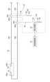
[ケルビン接続]
図2は、テスタ本体31、プローブ25、及びウェハチャック16における配線に関して説明する図である。[Kelvin connection]
FIG. 2 is a diagram illustrating wiring in the tester
ウェハチャック16上にウェハWが載置され、ウェハWに対向するようにプローブカード24がヘッドステージ22(図2では不図示)及びカードホルダ23(図2では不図示)により設置される。プローブカード24は、半導体チップの表面電極に同時に接触可能な一対のプローブ25A、25Bを有する。なお、以下の説明ではプローブ25をプローブ25A、25Bとして説明する。 A wafer W is placed on the
プローブ25Aはフォース線33Fに、プローブ25Bはセンス線33Sに接続されている。フォース線33Fは、プローブ25Aとテスタ本体31とを接続し、センス線33Sは、プローブ25Bとテスタ本体31とを接続する。また、テスタ本体31の内部では、フォース線33Fは、電流源31Bに接続されており、センス線33Sは、電圧計31Aに接続されている。また、フォース線35Fは、電流源31Bとフォースコネクタ68Fとを接続し、センス線35Sは、電圧計31Aとセンスコネクタ68Sとを接続する。また、フォース線40Fは、フォースコネクタ68Fとウェハチャック16に接続され、センス線40Sは、センスコネクタ68Sとウェハチャック16に接続されている。ウェハチャック16の一端(図2の右端)にフォース線40Fが接続され、他端(図2の左端)にセンス線40Sが接続される。
このように、テスタ本体31、プローブ25A、25B、及びウェハチャック16は、フォース線33F、35F、40F及びセンス線33S、35S、40Sを介してケルビン接続されている。 In this way, the tester
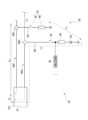
[チャックリード線及び追加回路]
図3は、フォース線40F、センス線40S、及び追加回路52を説明するための説明図である。[Chuck lead wire and additional circuit]
FIG. 3 is an explanatory diagram for explaining the
フォース線40F及びセンス線40Sは、チャックリード線を構成する。したがって、ウェハチャック16には、2本のチャックリード線が電気的に接続されていることになる。フォース線40Fは、支持面16aに電気的に接続される一端40Faと、一端40Faとは反対側の他端40Fbであって且つフォースコネクタ68Fに電気的に接続される他端40Fbと、を有する。また、センス線40Sは、支持面16aに電気的に接続される一端40Saと、一端40Saとは反対側の他端40Sbであって且つセンスコネクタ68Sに電気的に接続される他端40Sbと、を有する。なお、フォース線40F及びセンス線40Sの種類は特に限定はされない。また、本実施形態では、フォース線40F及びセンス線40Sの双方の一部がケーブルベア(登録商標)78内に収納されている。 The
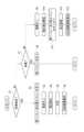
追加回路52は、全体が本発明の導通検査装置として機能し且つその一部が本発明の除電装置として機能するものである。追加回路52は、フォース線40F及びセンス線40Sの導通検査(断線検査)を行うと共に、ウェハチャック16の除電(ディスチャージ)を行う。 The
追加回路52は、フォースコネクタ68F、センスコネクタ68S、第1接続配線64、第2接続配線66、除電回路50(第1リレー46及び第1抵抗48)、第2リレー5
4、第2抵抗56、電源58、及び検出回路60を備える。追加回路52は、フォースコネクタ68F及びセンスコネクタ68Sにおいて、フォース線40Fとセンス線40Sに電気的に接続される。具体的には、フォースコネクタ68Fにおいて、フォース線40Fと第1接続配線64が電気的に接続される。また、センスコネクタ68Sにおいて、センス線40Sと第2接続配線66が電気的に接続される。The
4, a
第1接続配線64のフォースコネクタ68Fに接続する一端とは反対側の他端には、除電回路50を構成する第1リレー46が電気的に接続されている。これにより、フォース線40F、及びフォースコネクタ68Fを介して、支持面16aとテスタ30とが電気的に接続され、且つ支持面16a、第1接続配線64、及び除電回路50(第1リレー46)が電気的に接続される。 The
除電回路50は、本発明の除電装置に相当するものである。除電回路50は、フォース線40Fに、フォースコネクタ68F及び第1接続配線64を介して電気的に接続された第1リレー46と、第1リレー46に接続され且つ接地された第1抵抗48と、を備える。ウェハチャック16には、既述の通り、電荷(静電気)が帯電し、その結果、ウェハチャック16上のウェハWにも電荷が帯電する。このため、除電回路50は、ウェハチャック16に帯電した電荷(静電気)を除電する。 The static eliminating
第1リレー46は、第1接続配線64、フォース線40F、及び支持面16a(以下、支持面16a等と略す)と、第1抵抗48との双方の間において、双方を電気的に接続するクローズ状態(接続状態)と、双方の電気的な接続を解除したオープン状態(非接続状態)とに切替可能である。なお、第1リレー46の種類については特に限定はされない。また、本明細書では第1リレー46を、クローズ状態に切り替えることを「オン」と定義し、逆にオープン状態に切り替えることを「オフ」と定義する。そして、第1リレー46のオンオフの切り替えは、後述の統括制御部62により制御される。 The
第1リレー46は、ウェハチャック16の除電時、及び後述のフォース線40F及びセンス線40Sの導通検査時にオンされ、支持面16a等と第1抵抗48とを電気的に接続する。また、第1リレー46は、各半導体チップ(不図示)の電気的特性の検査時にはオフされ、支持面16a等と第1抵抗48との電気的な接続を解除する。 The
第1抵抗48は、ウェハチャック16の除電時において第1リレー46がオンされた場合に、ウェハチャック16に帯電した電荷(静電気)が接地側に向けて一気に流れることを防止する電流制限抵抗であり、高抵抗体が用いられる。これにより、ウェハチャック16の除電時において、第1リレー46がオンされると、第1抵抗48を介して、ウェハチャック16に帯電した電荷を接地側に徐々に放電することができ、その結果、ウェハチャック16が除電される。 The
次に、本実施形態の除電回路50と比較例の除電回路200(図4参照)と比較して、本実施形態の除電回路50の作用効果についてより詳しく説明する。なお、本発明は以下の作用効果の説明に限定されるものではない。 Next, the effects of the
図4は、比較例の除電回路200の概略図である。なお、図4に示した比較例において、本実施形態と機能又は構成上同一のものについては、同一符号を付してその説明は省略する。図4に示すように、比較例の除電回路200では、例えば特開2003-218175号公報に開示されているように、フォースコネクタ68Fに対して第1抵抗48が先に電気的に接続され、且つこの第1抵抗48に対して接地された第1リレー46が接続されている。 FIG. 4 is a schematic diagram of a
このような比較例の除電回路200においても、第1リレー46をオンすることで、本実施形態の除電回路50と同様に、第1抵抗48を介して、ウェハチャック16に帯電した電荷を接地側に徐々に放電することができる。 In the
しかしながら、比較例の除電回路200では、ウェハチャック16と第1リレー46との間に第1抵抗48が配置されているので、第1リレー46をオフに切り替えた場合でも、支持面16a等と第1抵抗48との接続が維持される。一方、第1抵抗48は、高抵抗体であるため、第1リレー46がオフされている状態ではリーク電流が発生する可能性がある。そして、第1抵抗48からリーク電流が発生すると、このリーク電流が、ウェハWの各半導体チップ(不図示)の検査時に裏面電極(不図示)から出力される信号に混入することで各半導体チップの検査に影響を及ぼしたり、或いは各半導体チップに悪影響を与えたりするおそれがある。したがって、各半導体チップの正確な検査を行うためには、ウェハチャック16が高絶縁状態(外部からのリーク電流等の影響を受けない状態)であることが必要であり、ウェハチャック16に余分な部品を接続することは好ましくない。 However, in the
このような比較例の除電回路200に対して、本実施形態の除電回路50では、図3に示したように、フォースコネクタ68Fに対して第1リレー46を先に電気的に接続し、この第1リレー46に対して接地された第1抵抗48を電気的に接続している。これにより、各半導体チップの検査時には第1リレー46をオフすることにより、支持面16a等から第1抵抗48を最短で分離することができる。その結果、除電用に追加する除電回路50によるリーク電流を最小に抑えることができる。 In contrast to the
図3に戻って、センス線40Sは、一端40Saが支持面16aに電気的に接続されており、一端40Saと反対側の他端40Sbには、センスコネクタ68Sが電気的に接続されている。これにより、センス線40Sとフォース線40Fとは、支持面16aを介して電気的に接続される。また、センス線40Sは、センスコネクタ68Sを介して、第2接続配線66が電気的に接続される。 Returning to FIG. 3, the
第2接続配線66のセンスコネクタ68Sに接続する一端とは反対側の他端には、第2リレー54が電気的に接続されている。これにより、センス線40S、コネクタ44S、及びセンスコネクタ68Sを介して、支持面16aとテスタ30とが電気的に接続され、且つ支持面16a、第2接続配線66、及び第2リレー54が電気的に接続される。 The
第2リレー54は、電源58と、第2抵抗56と、第2接続配線66と、センス線40Sとの間において、電気的に接続するクローズ状態(接続状態)と、電気的な接続を解除したオープン状態(非接続状態)とに切替可能である。なお、第2リレー54の種類についても特に限定はされない。また、本明細書では、第2リレー54についても、クローズ状態に切り替えることを「オン」と定義し、逆にオープン状態に切り替えることを「オフ」と定義する。そして、この第2リレー54のオンオフの切り替えは、第1リレー46と同様に後述の統括制御部62により制御される。 The
第2リレー54は、フォース線40F及びセンス線40Sの導通検査時にオンされ、第2抵抗56と、電源58と、第2接続配線66と、センス線40Sとを電気的に接続する。また、第2リレー54は、ウェハチャック16の除電時及び各半導体チップ(不図示)の電気的特性の検査時にはオフされ、第2抵抗56と、電源58と、第2接続配線66と、センス線40Sとの電気的な接続を解除する。 The
第2抵抗56は、第2リレー54に電気的に接続されている。この第2抵抗56は、第1抵抗48と同様の電流制限抵抗であり、高抵抗体が用いられる。この第2抵抗56の電圧(両端電圧、電位差)は、フォース線40F及びセンス線40Sの導通(断線)の有無
の判定に利用される。The
図5は、電流ループCR及び電源58を説明するための説明図である。図3及び図5に示すように、電源58は、第2抵抗56に接続され且つ接地されている。なお、電源58及び既述の第1抵抗48は、所謂フレーム接地(例えばアース電極又は金属製の筐体に接続)されているので、電源58と第1抵抗48とは電気的に接続されている。このため、フォース線40F、センス線40S、第1リレー46、第1抵抗48、第1接続配線64、第2接続配線66、第2リレー54、第2抵抗56、及び電源58は、電気的結合された電流ループCRを構成している。 FIG. 5 is an explanatory diagram for explaining the current loop CR and the
電源58は、後述のフォース線40F及びセンス線40Sの導通検査時、すなわち、第1リレー46及び第2リレー54の双方がオンされている状態で、電流ループCRに対して電流供給(電圧印加)を行う。これにより、フォース線40F及びセンス線40Sが導通している場合(断線していない場合)、すなわち電流ループCRが構成されている場合、この電流ループCRには電流Is(微小電流)が流れる。 The
検出回路60は、本発明の電圧検出部に相当するものであり、第2抵抗56の電圧(両端電圧、電位差)を検出する電圧計である。第1リレー46及び第2リレー54の双方がオンされている状態でフォース線40F及びセンス線40Sが導通している場合、既述の電流ループCRに電流Isが流れる。この場合、電源58により電流ループCRに印加される電圧V、第1抵抗48の抵抗値をR1、及び第2抵抗56の抵抗値をR2とすると、検出回路60により検出される第2抵抗56の検出電圧は「V×(R2/(R1+R2))」となる。したがって、例えばR1=R2である場合、第2抵抗56の検出電圧は「V/2」となる。以下、説明の煩雑化を防止するため、「R1=R2」として説明を行う。 The
一方、第1リレー46及び第2リレー54の双方がオンされている状態であってもフォース線40F及びセンス線40Sのうち少なくとも一方が断線している場合には、電源58による電流Isは電流ループCRを流れることはない。したがって、この場合に検出回路60による検出電圧は「V」となる。 On the other hand, even if both the
このように検出回路60による検出電圧を参照することで、電流ループCRに電流Isが流れているか否か、すなわちフォース線40F及びセンス線40Sの導通の有無(断線の無し有り)を判定することができる。そして、検出回路60は、第2抵抗56の電圧検出結果を統括制御部62へ出力する。 By referring to the voltage detected by the
また逆に、フォース線40F及びセンス線40Sの導通が確認されている場合、検出回路60による第2抵抗56の電圧検出結果を、第1リレー46及び第2リレー54の自己診断に用いることができる。 Conversely, if continuity is confirmed between the
例えば、第1リレー46及び第2リレー54の双方をオンさせた際に、検出回路60による検出電圧が「V/2」となる場合は第1リレー46及び第2リレー54の双方が正常であると判定することができる。一方、第1リレー46及び第2リレー54の双方をオンさせた際に、検出回路60による検出電圧が「V」となる場合は、第1リレー46及び第2リレー54の少なくとも一方が実際にはオンされていない、すなわち少なくとも一方が異常であると判定することができる。また、第1リレー46及び第2リレー54の少なくとも一方をオフさせた際に、検出回路60による検出電圧が「V/2」となる場合は、第1リレー46及び第2リレー54の双方が実際にはオンされているため、第1リレー46及び第2リレー54の少なくとも一方が異常であると判定することができる。 For example, if the voltage detected by the
図6は、プローバ10(ウェハテストシステム9でも可、以下同じ)の統括制御部62
の機能ブロック図である。統括制御部62は、例えばCPU(Central Processing Unit)或いはFPGA(field-programmable gate array)含む各種の演算部と処理部とメモリ等により構成されており、プローバ10の各部の動作を統括制御する。なお、図6では、統括制御部62の複数の機能の中で、追加回路52によるウェハチャック16の除電、フォース線40F及びセンス線40Sの導通検査、及び各リレー46、54の自己診断に係る機能のみを図示し、ウェハWの検査等のプローバ10の他の制御に係る機能は公知技術であるので図示は省略する。FIG. 6 shows the
FIG. The
統括制御部62には、各種の操作入力を受け付ける操作部70、各種表示を行う表示部72、既述の各リレー46、54、電源58、及び検出回路60の他、プローバ10の各部が接続されている。そして、この統括制御部62は、所定の制御プログラムを実行することで、追加回路制御部76、判定部80、及び自己診断部82として機能する。 The
追加回路制御部76は、追加回路52によるウェハチャック16の除電、フォース線40F及びセンス線40Sの導通検査、及び各リレー46、54の自己診断がそれぞれ開始される際に、各リレー46、54のオンオフと電源58のオンオフとを制御する。すなわち、追加回路制御部76は、本発明のリレー制御部として機能する。 The additional
なお、追加回路52による除電、導通検査、及び自己診断は、不図示の各半導体チップの検査を実行してない任意のタイミング、すなわちプローブ25がウェハWから離間しているタイミングで実行される。例えば、Zθステージ15によりウェハチャック16を下方側に退避させているタイミング、ウェハチャック16へのウェハWのロード又はアンロードのタイミング、及び半導体チップのインデックス送りのタイミング等が例として挙げられる。なお、除電、導通検査、及び自己診断を、操作部70への開始操作に応じて開始させてもよい。 Note that static elimination, continuity testing, and self-diagnosis by the
追加回路制御部76は、除電を実行する任意のタイミングで或いは操作部70への除電開始操作の入力を受けて、第1リレー46のみをオンさせる。また、追加回路制御部76は、導通検査を実行する任意のタイミングで或いは操作部70への導通検査開始操作の入力を受けて、各リレー46、54の双方をオンさせると共に、電源58をオンさせる。さらに、追加回路制御部76は、自己診断を実行するタイミングで或いは操作部70への自己診断開始操作の入力受けて、各リレー46、54を個別に1回以上オンオフさせると共に、電源58をオンさせる。 The additional
判定部80は、導通検査が開始された場合、すなわち第1リレー46及び第2リレー54の双方がオンされ且つ電源58がオンされている場合、検出回路60から入力される第2抵抗56の電圧検出結果に基づき、電流ループCRに電流Isが流れているか否かを判定する。その結果、判定部80は、フォース線40F及びセンス線40Sの導通の有無を判定することができる。既述の通り、判定部80は、第2抵抗56の電圧が「V/2」である場合には、電流ループCRに電流Isが流れていると判定すると共に、フォース線40F及びセンス線40Sが導通していると判定する。一方、判定部80は、第2抵抗56の電圧が「V」である場合には、電流ループCRに電流Isが流れてないと判定すると共に、フォース線40F及びセンス線40Sのうち少なくとも一方が断線していると判定する。 The determining
そして、判定部80は、フォース線40F及びセンス線40Sの導通の有無を表示部72へ出力する。これにより、表示部72にて、フォース線40F及びセンス線40Sの導通の有無(断線の有無)が表示される。なお、表示部72には、画面表示(画像表示)を行うモニタの他に、音声表示(音声出力)を行うスピーカ等も含まれる。 Then, the
自己診断部82は、自己診断が実行されている場合、すなわち各リレー46、54がオンオフされ且つ電源58がオンされている場合、検出回路60から入力される第2抵抗56の電圧検出結果に基づき、各リレー46、54の自己診断を行う。既述の通り、自己診断部82は、例えば、各リレー46、54の双方をオンさせた際に、検出回路60による検出電圧が「V/2」となる場合は各リレー46、54の双方が正常であると判定し、検出電圧が「V」となる場合は各リレー46、54の少なくとも一方が異常であると判定する。また、自己診断部82は、各リレー46、54の少なくとも一方をオフさせた際に、検出回路60による検出電圧が「V/2」となる場合は、各リレー46、54の少なくとも一方が異常であると判定する。 The self-
そして、自己診断部82は、各リレー46、54の自己診断結果を表示部72へ出力する。これにより、表示部72にて、各リレー46、54の自己診断結果が表示される。 Then, the self-
[本実施形態の追加回路の作用]
図7は、上記構成の追加回路52によるウェハチャック16の除電、フォース線40F及びセンス線40Sの導通検査、及び各リレー46、54の自己診断の処理の流れを示すフローチャートである。[Operation of additional circuit of this embodiment]
FIG. 7 is a flowchart illustrating the process of eliminating electricity from the
<導通検査>
図7に示すように、追加回路制御部76は、導通検査を実行する任意のタイミングで或いは操作部70への導通検査開始操作の入力を受けて(ステップS1でYES)、各リレー46、54の双方をオンさせると共に(ステップS2)、電源58をオンさせる(ステップS3)。一方、検出回路60は、電源58のオンに合わせて第2抵抗56の電圧検出を開始し、第2抵抗56の電圧検出結果を判定部80へ出力する(ステップS4)。<Continuity test>
As shown in FIG. 7, the additional
判定部80は、第2抵抗56の電圧が「V/2」である場合には、電流ループCRに電流Isが流れていると判定、すなわちフォース線40F及びセンス線40Sが導通していると判定する(ステップS5)。一方、判定部80は、第2抵抗56の電圧が「V」である場合には、電流ループCRに電流Isが流れていないと判定、すなわちフォース線40F及びセンス線40Sのうち少なくとも一方が断線していると判定する(ステップS5)。そして、判定部80は、判定結果を表示部72に出力する。これにより、表示部72にて、フォース線40F及びセンス線40Sの導通の有無の判定結果が表示される(ステップS6)。 When the voltage of the
<除電>
追加回路制御部76は、除電を実行する任意のタイミングで或いは操作部70への除電開始操作の入力を受けて(ステップS1でNO、ステップS7でYES)、第1リレー46をオンさせる(ステップS8)。これにより、第1抵抗48を介して、ウェハチャック16に帯電した電荷が接地側に放電されるため、ウェハチャック16が除電される。<Static electricity removal>
The additional
<自己診断>
追加回路制御部76は、各リレー46、54の自己診断を実行する任意のタイミングで或いは操作部70への自己診断開始操作の入力を受けて(ステップS1及びステップS7の双方でNO)、電源58をオンさせる(ステップS9)。また、この電源58のオンに合わせて、検出回路60が、第2抵抗56の電圧検出を開始し、その電圧検出結果を自己診断部82へ出力する(ステップS10)。<Self-diagnosis>
The additional
次いで、追加回路制御部76は、各リレー46、54を個別に1回以上オンオフさせる(ステップS11)。そして、自己診断部82は、各リレー46、54のオンオフが実行されている間、検出回路60から入力される第2抵抗56の電圧検出結果に基づき、既述
の通り、各リレー46、54の自己診断を行い、その診断結果を表示部72に出力する(ステップS12)。これにより、表示部72にて、各リレー46、54の自己診断結果が表示される(ステップS13)。Next, the additional
[本実施形態の効果]
以上のように本実施形態の追加回路52によれば、2本のチャックリード線(フォース線40F及びセンス線40S)と、追加回路52とにより電流ループCRを形成し、この電流ループCRに電流Isが流れるか否か、すなわち検出回路60による第2抵抗56の電圧検出結果が「V/2」になるかを検出するだけで、フォース線40F及びセンス線40Sの導通の有無を判定することができる。[Effects of this embodiment]
As described above, according to the
また、特許文献2(特開2019-176080号公報)に記載された導通検査装置では、追加配線を設けて1本のチャックリード線の導通の有無を検査しているのに対して、本実施形態では、フォース線40F及びセンス線40Sの各々に、第1接続配線64及び第2接続配線66を介して追加回路52を電気に接続し、フォース線40F及びセンス線40Sの2本のチャックリード線の導通の有無を判定することができる。 In addition, in the continuity testing device described in Patent Document 2 (Japanese Patent Application Laid-open No. 2019-176080), additional wiring is provided to test the presence or absence of continuity of one chuck lead wire, whereas this method In this embodiment, the
また、本実施形態の除電回路50では、フォースコネクタ68Fに対して第1リレー46を先に電気的に接続し、この第1リレー46に対して接地された第1抵抗48を電気的に接続しているので、各半導体チップの検査時には第1リレー46をオフすることにより、チャックリード線(例えばフォース線40F)から第1抵抗48を最短で分離することができる。その結果、除電回路50に起因するリーク電流を最小に抑えることができるので、リーク電流が、ウェハWの各半導体チップ(不図示)の検査に影響を及ぼしたり、或いは各半導体チップに悪影響を与えたりすることが防止される。 Furthermore, in the
[その他]
上記実施形態では、第1接続配線64にフォース線40Fが電気的に接続され、第2接続配線66にセンス線40Sが電気的に接続されているが、本発明はこれに限定されない。例えば、第1接続配線64にセンス線40Sが電気的に接続され、第2接続配線66にフォース線40Fが電気的に接続されても、上述したように、フォース線40F及びセンス線40Sの導通検査を行うことができる。[others]
In the embodiment described above, the
上記実施形態では、第2接続配線66に対して、第2リレー54、第2抵抗56、及び電源58の順番で接続されているが、第2リレー54のオンオフに応じて電流ループCRへの電流Isの供給をオンオフ可能であれば、その順番は特に限定はされない。また、上記実施形態では、除電回路50によるリーク電流を最小に抑えるために、第1接続配線64に対して第1リレー46及び第1抵抗48の順番で接続しているが、リーク電流を考慮する必要が無い場合には第1接続配線64に対して第1抵抗48及び第1リレー46の順番で接続してもよい。 In the above embodiment, the
上記実施形態では、第1抵抗48及び第2抵抗56としてそれぞれ単体の抵抗を例に挙げて説明したが、第1抵抗48及び第2抵抗56が複数の抵抗(抵抗と等価な電子部品、或いは抵抗以外の電子部品を含む)で構成されていてもよい。 In the above embodiment, each of the
上記実施形態では、検出回路60により第2抵抗56の電圧を検出しているが、検出回路60により第1抵抗48の電圧を検出し、この電圧検出結果に基づき判定部80による判定と自己診断部82による診断とを行ってもよい。 In the embodiment described above, the voltage of the
上記実施形態では、電源58が第2接続配線側に接続されているが、電源58が除電回路50に接続されていてもよい。また、ウェハチャック16の除電のみを目的とする場合
、フォースコネクタ68Fに除電回路50のみが接続されていてもよい。In the embodiment described above, the
以上で本発明の例に関して説明してきたが、本発明は上述した実施の形態に限定されず、本発明の趣旨を逸脱しない範囲で種々の変形が可能であることは言うまでもない。 Although examples of the present invention have been described above, it goes without saying that the present invention is not limited to the embodiments described above, and that various modifications can be made without departing from the spirit of the present invention.
9…ウェハテストシステム
10…プローバ
16…ウェハチャック
16a…支持面
30…テスタ
40F…フォース線
40S…センス線
46…第1リレー
48…第1抵抗
50…除電回路
54…第2リレー
56…第2抵抗
58…電源
60…検出回路
62…統括制御部
80…判定部
82…自己診断部9...
Claims (7)
Translated fromJapanese前記ウェハの表面に形成された半導体チップの表面電極に接触するプローブと、
前記ウェハの裏面に形成された前記半導体チップの裏面電極に接触するフォース線及びセンス線と、
前記フォース線又は前記センス線のいずれか一方に接続される第1接続配線と、
前記フォース線又は前記センス線のいずれか他方に接続される第2接続配線と、
前記第1接続配線の側に設けられた第1リレー及び第1抵抗と、
前記第2接続配線の側に設けられた電源と、
備え、
前記第1接続配線と前記第2接続配線との間を、前記第1リレー、前記第1抵抗、及び前記電源を介して電気的結合して電流ループを形成し、
前記電流ループに電流が流れるか否かの判定を行う判定部を備える、
導通検査装置。a wafer chuck having a support surface for holding a wafer to be measured with a Kelvin measurement prober;
a probe that contacts a surface electrode of a semiconductor chip formed on the surface of the wafer;
a force line and a sense line that contact a backside electrode of the semiconductor chip formed on the backside of the wafer;
a first connection wiring connected to either the force line or the sense line;
a second connection wiring connected to the other of the force line or the sense line;
a first relay and a first resistor provided on the first connection wiring side;
a power source provided on the side of the second connection wiring;
Prepare,
electrically coupling the first connection wiring and the second connection wiring via the first relay, the first resistor, and the power source to form a current loop;
comprising a determination unit that determines whether or not a current flows in the current loop;
Continuity testing device.
前記第2抵抗の電圧を検出する電圧検出部と、を備え、
前記判定部が、前記電圧検出部の検出結果に基づき、前記判定を行う請求項1に記載の導通検査装置。a second relay and a second resistor included in the current loop and provided on the second connection wiring side;
a voltage detection unit that detects the voltage of the second resistor,
The continuity testing device according to claim 1, wherein the determination section makes the determination based on the detection result of the voltage detection section.
前記判定部が、前記リレー制御部により前記第1リレー及び前記第2リレーの双方が前記クローズ状態に切り替えられた状態での前記電圧検出部の前記検出結果に基づき、前記判定を行う請求項2に記載の導通検査装置。comprising a relay control unit that individually switches both the first relay and the second relay between a closed state and an open state,
2. The determination unit makes the determination based on the detection result of the voltage detection unit in a state where both the first relay and the second relay are switched to the closed state by the relay control unit. Continuity testing device described in .
前記支持面に接続された前記センス線の一端とは反対側の他端が接続する、前記テスタのセンスコネクタに、前記第1接続配線又は前記第2接続配線のうち他方が接続される請求項1から4のいずれか1項に記載の導通検査装置。The first connection wiring or the second connection wiring is connected to a force connector of a tester for testing the electrical characteristics of the semiconductor chip, to which the other end opposite to one end of the force wire connected to the support surface is connected. one of them is connected,
The other of the first connection wiring and the second connection wiring is connected to a sense connector of the tester, to which the other end opposite to one end of the sense wire connected to the support surface is connected. 5. The continuity testing device according to any one of 1 to 4.
前記ウェハの表面に形成された前記半導体チップの表面電極に接触するプローブと、
請求項1から5のいずれか1項に記載の導通検査装置と、
を備えるケルビン測定用プローバ。A wafer chuck that holds a wafer on which a plurality of semiconductor chips are formed, the wafer chuck having a conductive support surface that contacts a back electrode of the semiconductor chip formed on the back surface of the wafer;
a probe that contacts a surface electrode of the semiconductor chip formed on the surface of the wafer;
A continuity testing device according to any one of claims 1 to 5,
A prober for Kelvin measurements.
ェハの裏面に形成された前記半導体チップの裏面電極に接触する導電性の支持面に対して電気的に接続されるフォース線又はセンス線のいずれか一方と、
前記フォース線又は前記センス線のうち一方に接続される第1接続配線と、
前記第1接続配線に接続された第1リレーと、
前記第1リレーに接続され且つ接地された第1抵抗と、
を備える除電装置。A Kelvin measurement prober includes a wafer chuck that holds a wafer on which a plurality of semiconductor chips are formed, and a probe that contacts a surface electrode of the semiconductor chip formed on the surface of the wafer. Either a force line or a sense line electrically connected to a conductive support surface that is a support surface of the wafer and contacts a back electrode of the semiconductor chip formed on the back surface of the wafer. ,
a first connection wiring connected to one of the force line or the sense line;
a first relay connected to the first connection wiring;
a first resistor connected to the first relay and grounded;
A static eliminator equipped with:
Priority Applications (1)
| Application Number | Priority Date | Filing Date | Title |
|---|---|---|---|
| JP2022056271AJP2023148322A (en) | 2022-03-30 | 2022-03-30 | Continuity inspection device, kelvin measurement prober, and electricity removing device |
Applications Claiming Priority (1)
| Application Number | Priority Date | Filing Date | Title |
|---|---|---|---|
| JP2022056271AJP2023148322A (en) | 2022-03-30 | 2022-03-30 | Continuity inspection device, kelvin measurement prober, and electricity removing device |
Publications (1)
| Publication Number | Publication Date |
|---|---|
| JP2023148322Atrue JP2023148322A (en) | 2023-10-13 |
Family
ID=88287943
Family Applications (1)
| Application Number | Title | Priority Date | Filing Date |
|---|---|---|---|
| JP2022056271APendingJP2023148322A (en) | 2022-03-30 | 2022-03-30 | Continuity inspection device, kelvin measurement prober, and electricity removing device |
Country Status (1)
| Country | Link |
|---|---|
| JP (1) | JP2023148322A (en) |
- 2022
- 2022-03-30JPJP2022056271Apatent/JP2023148322A/enactivePending
Similar Documents
| Publication | Publication Date | Title |
|---|---|---|
| JP7417835B2 (en) | Continuity testing equipment, prober | |
| EP1182460B1 (en) | Fritting inspection method and apparatus | |
| CN109557376B (en) | Resistance measuring device, substrate inspection device, and resistance measuring method | |
| EP3045921A1 (en) | Prober | |
| KR100810550B1 (en) | Method and apparatus for testing electrical characteristics of object under test | |
| JPH10111315A (en) | Probe card and test apparatus using the same | |
| KR20070056147A (en) | Inspection method and inspection device | |
| US9720014B2 (en) | Semiconductor evaluation apparatus and semiconductor evaluation method | |
| JP2008089485A (en) | Insulation inspection device and insulation inspection method | |
| CN116209904A (en) | Safety system for a pin probe card for high voltage and high current testing of power semiconductor devices, related testing machine and corresponding testing method | |
| TW201447334A (en) | Substrate inspecting apparatus, substrate inspecting method and jig for inspecting substrate | |
| KR101157878B1 (en) | The method for maintenance of inspection fixture, apparatus for the same | |
| CN110794290B (en) | Substrate detection device and substrate detection method | |
| CN120028727A (en) | A probe card OS testing device and testing method | |
| JP2023148322A (en) | Continuity inspection device, kelvin measurement prober, and electricity removing device | |
| JP2008026122A (en) | Maintenance method of semiconductor device inspection apparatus | |
| WO2008001651A1 (en) | Board inspecting method and board inspecting device | |
| JP4329087B2 (en) | Method and apparatus for electrostatic breakdown testing of semiconductor devices | |
| JP2024136732A (en) | Prober | |
| JP2002131365A (en) | Inspection method and inspection device | |
| JP2002100658A (en) | Semiconductor device inspection apparatus | |
| JPH0697241A (en) | Probing device | |
| JPH0758168A (en) | Probing device | |
| JP2010133786A (en) | Inspection apparatus and inspection method | |
| JPH05198633A (en) | Prober for semiconductor wafer |
Legal Events
| Date | Code | Title | Description |
|---|---|---|---|
| A621 | Written request for application examination | Free format text:JAPANESE INTERMEDIATE CODE: A621 Effective date:20250213 |