JP2023141530A - Semiconductor device and semiconductor device manufacturing method - Google Patents
Semiconductor device and semiconductor device manufacturing methodDownload PDFInfo
- Publication number
- JP2023141530A JP2023141530AJP2022047895AJP2022047895AJP2023141530AJP 2023141530 AJP2023141530 AJP 2023141530AJP 2022047895 AJP2022047895 AJP 2022047895AJP 2022047895 AJP2022047895 AJP 2022047895AJP 2023141530 AJP2023141530 AJP 2023141530A
- Authority
- JP
- Japan
- Prior art keywords
- region
- gate electrode
- semiconductor substrate
- insulating film
- sidewall
- Prior art date
- Legal status (The legal status is an assumption and is not a legal conclusion. Google has not performed a legal analysis and makes no representation as to the accuracy of the status listed.)
- Granted
Links
Images


Classifications
- H—ELECTRICITY
- H10—SEMICONDUCTOR DEVICES; ELECTRIC SOLID-STATE DEVICES NOT OTHERWISE PROVIDED FOR
- H10D—INORGANIC ELECTRIC SEMICONDUCTOR DEVICES
- H10D30/00—Field-effect transistors [FET]
- H10D30/60—Insulated-gate field-effect transistors [IGFET]
- H10D30/601—Insulated-gate field-effect transistors [IGFET] having lightly-doped drain or source extensions, e.g. LDD IGFETs or DDD IGFETs
- H—ELECTRICITY
- H01—ELECTRIC ELEMENTS
- H01L—SEMICONDUCTOR DEVICES NOT COVERED BY CLASS H10
- H01L21/00—Processes or apparatus adapted for the manufacture or treatment of semiconductor or solid state devices or of parts thereof
- H01L21/02—Manufacture or treatment of semiconductor devices or of parts thereof
- H01L21/04—Manufacture or treatment of semiconductor devices or of parts thereof the devices having potential barriers, e.g. a PN junction, depletion layer or carrier concentration layer
- H01L21/18—Manufacture or treatment of semiconductor devices or of parts thereof the devices having potential barriers, e.g. a PN junction, depletion layer or carrier concentration layer the devices having semiconductor bodies comprising elements of Group IV of the Periodic Table or AIIIBV compounds with or without impurities, e.g. doping materials
- H01L21/26—Bombardment with radiation
- H01L21/263—Bombardment with radiation with high-energy radiation
- H01L21/265—Bombardment with radiation with high-energy radiation producing ion implantation
- H01L21/26506—Bombardment with radiation with high-energy radiation producing ion implantation in group IV semiconductors
- H—ELECTRICITY
- H01—ELECTRIC ELEMENTS
- H01L—SEMICONDUCTOR DEVICES NOT COVERED BY CLASS H10
- H01L21/00—Processes or apparatus adapted for the manufacture or treatment of semiconductor or solid state devices or of parts thereof
- H01L21/02—Manufacture or treatment of semiconductor devices or of parts thereof
- H01L21/04—Manufacture or treatment of semiconductor devices or of parts thereof the devices having potential barriers, e.g. a PN junction, depletion layer or carrier concentration layer
- H01L21/18—Manufacture or treatment of semiconductor devices or of parts thereof the devices having potential barriers, e.g. a PN junction, depletion layer or carrier concentration layer the devices having semiconductor bodies comprising elements of Group IV of the Periodic Table or AIIIBV compounds with or without impurities, e.g. doping materials
- H01L21/26—Bombardment with radiation
- H01L21/263—Bombardment with radiation with high-energy radiation
- H01L21/265—Bombardment with radiation with high-energy radiation producing ion implantation
- H01L21/266—Bombardment with radiation with high-energy radiation producing ion implantation using masks
- H—ELECTRICITY
- H01—ELECTRIC ELEMENTS
- H01L—SEMICONDUCTOR DEVICES NOT COVERED BY CLASS H10
- H01L21/00—Processes or apparatus adapted for the manufacture or treatment of semiconductor or solid state devices or of parts thereof
- H01L21/02—Manufacture or treatment of semiconductor devices or of parts thereof
- H01L21/04—Manufacture or treatment of semiconductor devices or of parts thereof the devices having potential barriers, e.g. a PN junction, depletion layer or carrier concentration layer
- H01L21/18—Manufacture or treatment of semiconductor devices or of parts thereof the devices having potential barriers, e.g. a PN junction, depletion layer or carrier concentration layer the devices having semiconductor bodies comprising elements of Group IV of the Periodic Table or AIIIBV compounds with or without impurities, e.g. doping materials
- H01L21/28—Manufacture of electrodes on semiconductor bodies using processes or apparatus not provided for in groups H01L21/20 - H01L21/268
- H01L21/28008—Making conductor-insulator-semiconductor electrodes
- H01L21/28017—Making conductor-insulator-semiconductor electrodes the insulator being formed after the semiconductor body, the semiconductor being silicon
- H01L21/28026—Making conductor-insulator-semiconductor electrodes the insulator being formed after the semiconductor body, the semiconductor being silicon characterised by the conductor
- H01L21/28035—Making conductor-insulator-semiconductor electrodes the insulator being formed after the semiconductor body, the semiconductor being silicon characterised by the conductor the final conductor layer next to the insulator being silicon, e.g. polysilicon, with or without impurities
- H—ELECTRICITY
- H10—SEMICONDUCTOR DEVICES; ELECTRIC SOLID-STATE DEVICES NOT OTHERWISE PROVIDED FOR
- H10D—INORGANIC ELECTRIC SEMICONDUCTOR DEVICES
- H10D30/00—Field-effect transistors [FET]
- H10D30/01—Manufacture or treatment
- H10D30/021—Manufacture or treatment of FETs having insulated gates [IGFET]
- H10D30/0221—Manufacture or treatment of FETs having insulated gates [IGFET] having asymmetry in the channel direction, e.g. lateral high-voltage MISFETs having drain offset region or extended-drain MOSFETs [EDMOS]
- H—ELECTRICITY
- H10—SEMICONDUCTOR DEVICES; ELECTRIC SOLID-STATE DEVICES NOT OTHERWISE PROVIDED FOR
- H10D—INORGANIC ELECTRIC SEMICONDUCTOR DEVICES
- H10D30/00—Field-effect transistors [FET]
- H10D30/01—Manufacture or treatment
- H10D30/021—Manufacture or treatment of FETs having insulated gates [IGFET]
- H10D30/0223—Manufacture or treatment of FETs having insulated gates [IGFET] having source and drain regions or source and drain extensions self-aligned to sides of the gate
- H10D30/0227—Manufacture or treatment of FETs having insulated gates [IGFET] having source and drain regions or source and drain extensions self-aligned to sides of the gate having both lightly-doped source and drain extensions and source and drain regions self-aligned to the sides of the gate, e.g. lightly-doped drain [LDD] MOSFET or double-diffused drain [DDD] MOSFET
- H—ELECTRICITY
- H10—SEMICONDUCTOR DEVICES; ELECTRIC SOLID-STATE DEVICES NOT OTHERWISE PROVIDED FOR
- H10D—INORGANIC ELECTRIC SEMICONDUCTOR DEVICES
- H10D30/00—Field-effect transistors [FET]
- H10D30/60—Insulated-gate field-effect transistors [IGFET]
- H10D30/601—Insulated-gate field-effect transistors [IGFET] having lightly-doped drain or source extensions, e.g. LDD IGFETs or DDD IGFETs
- H10D30/603—Insulated-gate field-effect transistors [IGFET] having lightly-doped drain or source extensions, e.g. LDD IGFETs or DDD IGFETs having asymmetry in the channel direction, e.g. lateral high-voltage MISFETs having drain offset region or extended drain IGFETs [EDMOS]
- H—ELECTRICITY
- H10—SEMICONDUCTOR DEVICES; ELECTRIC SOLID-STATE DEVICES NOT OTHERWISE PROVIDED FOR
- H10D—INORGANIC ELECTRIC SEMICONDUCTOR DEVICES
- H10D64/00—Electrodes of devices having potential barriers
- H10D64/01—Manufacture or treatment
- H10D64/021—Manufacture or treatment using multiple gate spacer layers, e.g. bilayered sidewall spacers
- H—ELECTRICITY
- H10—SEMICONDUCTOR DEVICES; ELECTRIC SOLID-STATE DEVICES NOT OTHERWISE PROVIDED FOR
- H10D—INORGANIC ELECTRIC SEMICONDUCTOR DEVICES
- H10D64/00—Electrodes of devices having potential barriers
- H10D64/60—Electrodes characterised by their materials
- H10D64/66—Electrodes having a conductor capacitively coupled to a semiconductor by an insulator, e.g. MIS electrodes
- H10D64/661—Electrodes having a conductor capacitively coupled to a semiconductor by an insulator, e.g. MIS electrodes the conductor comprising a layer of silicon contacting the insulator, e.g. polysilicon having vertical doping variation
- H10D64/662—Electrodes having a conductor capacitively coupled to a semiconductor by an insulator, e.g. MIS electrodes the conductor comprising a layer of silicon contacting the insulator, e.g. polysilicon having vertical doping variation the conductor further comprising additional layers, e.g. multiple silicon layers having different crystal structures
- H—ELECTRICITY
- H10—SEMICONDUCTOR DEVICES; ELECTRIC SOLID-STATE DEVICES NOT OTHERWISE PROVIDED FOR
- H10D—INORGANIC ELECTRIC SEMICONDUCTOR DEVICES
- H10D84/00—Integrated devices formed in or on semiconductor substrates that comprise only semiconducting layers, e.g. on Si wafers or on GaAs-on-Si wafers
- H10D84/01—Manufacture or treatment
- H10D84/0123—Integrating together multiple components covered by H10D12/00 or H10D30/00, e.g. integrating multiple IGBTs
- H10D84/0126—Integrating together multiple components covered by H10D12/00 or H10D30/00, e.g. integrating multiple IGBTs the components including insulated gates, e.g. IGFETs
- H10D84/0165—Integrating together multiple components covered by H10D12/00 or H10D30/00, e.g. integrating multiple IGBTs the components including insulated gates, e.g. IGFETs the components including complementary IGFETs, e.g. CMOS devices
- H10D84/017—Manufacturing their source or drain regions, e.g. silicided source or drain regions
- H—ELECTRICITY
- H10—SEMICONDUCTOR DEVICES; ELECTRIC SOLID-STATE DEVICES NOT OTHERWISE PROVIDED FOR
- H10D—INORGANIC ELECTRIC SEMICONDUCTOR DEVICES
- H10D84/00—Integrated devices formed in or on semiconductor substrates that comprise only semiconducting layers, e.g. on Si wafers or on GaAs-on-Si wafers
- H10D84/01—Manufacture or treatment
- H10D84/0123—Integrating together multiple components covered by H10D12/00 or H10D30/00, e.g. integrating multiple IGBTs
- H10D84/0126—Integrating together multiple components covered by H10D12/00 or H10D30/00, e.g. integrating multiple IGBTs the components including insulated gates, e.g. IGFETs
- H10D84/0165—Integrating together multiple components covered by H10D12/00 or H10D30/00, e.g. integrating multiple IGBTs the components including insulated gates, e.g. IGFETs the components including complementary IGFETs, e.g. CMOS devices
- H10D84/0172—Manufacturing their gate conductors
- H10D84/0177—Manufacturing their gate conductors the gate conductors having different materials or different implants
- H—ELECTRICITY
- H10—SEMICONDUCTOR DEVICES; ELECTRIC SOLID-STATE DEVICES NOT OTHERWISE PROVIDED FOR
- H10D—INORGANIC ELECTRIC SEMICONDUCTOR DEVICES
- H10D84/00—Integrated devices formed in or on semiconductor substrates that comprise only semiconducting layers, e.g. on Si wafers or on GaAs-on-Si wafers
- H10D84/01—Manufacture or treatment
- H10D84/0123—Integrating together multiple components covered by H10D12/00 or H10D30/00, e.g. integrating multiple IGBTs
- H10D84/0126—Integrating together multiple components covered by H10D12/00 or H10D30/00, e.g. integrating multiple IGBTs the components including insulated gates, e.g. IGFETs
- H10D84/0165—Integrating together multiple components covered by H10D12/00 or H10D30/00, e.g. integrating multiple IGBTs the components including insulated gates, e.g. IGFETs the components including complementary IGFETs, e.g. CMOS devices
- H10D84/0172—Manufacturing their gate conductors
- H10D84/0179—Manufacturing their gate conductors the gate conductors having different shapes or dimensions
- H—ELECTRICITY
- H10—SEMICONDUCTOR DEVICES; ELECTRIC SOLID-STATE DEVICES NOT OTHERWISE PROVIDED FOR
- H10D—INORGANIC ELECTRIC SEMICONDUCTOR DEVICES
- H10D84/00—Integrated devices formed in or on semiconductor substrates that comprise only semiconducting layers, e.g. on Si wafers or on GaAs-on-Si wafers
- H10D84/01—Manufacture or treatment
- H10D84/0123—Integrating together multiple components covered by H10D12/00 or H10D30/00, e.g. integrating multiple IGBTs
- H10D84/0126—Integrating together multiple components covered by H10D12/00 or H10D30/00, e.g. integrating multiple IGBTs the components including insulated gates, e.g. IGFETs
- H10D84/0165—Integrating together multiple components covered by H10D12/00 or H10D30/00, e.g. integrating multiple IGBTs the components including insulated gates, e.g. IGFETs the components including complementary IGFETs, e.g. CMOS devices
- H10D84/0181—Manufacturing their gate insulating layers
- H—ELECTRICITY
- H10—SEMICONDUCTOR DEVICES; ELECTRIC SOLID-STATE DEVICES NOT OTHERWISE PROVIDED FOR
- H10D—INORGANIC ELECTRIC SEMICONDUCTOR DEVICES
- H10D84/00—Integrated devices formed in or on semiconductor substrates that comprise only semiconducting layers, e.g. on Si wafers or on GaAs-on-Si wafers
- H10D84/01—Manufacture or treatment
- H10D84/02—Manufacture or treatment characterised by using material-based technologies
- H10D84/03—Manufacture or treatment characterised by using material-based technologies using Group IV technology, e.g. silicon technology or silicon-carbide [SiC] technology
- H10D84/038—Manufacture or treatment characterised by using material-based technologies using Group IV technology, e.g. silicon technology or silicon-carbide [SiC] technology using silicon technology, e.g. SiGe
- H—ELECTRICITY
- H10—SEMICONDUCTOR DEVICES; ELECTRIC SOLID-STATE DEVICES NOT OTHERWISE PROVIDED FOR
- H10D—INORGANIC ELECTRIC SEMICONDUCTOR DEVICES
- H10D84/00—Integrated devices formed in or on semiconductor substrates that comprise only semiconducting layers, e.g. on Si wafers or on GaAs-on-Si wafers
- H10D84/80—Integrated devices formed in or on semiconductor substrates that comprise only semiconducting layers, e.g. on Si wafers or on GaAs-on-Si wafers characterised by the integration of at least one component covered by groups H10D12/00 or H10D30/00, e.g. integration of IGFETs
- H10D84/82—Integrated devices formed in or on semiconductor substrates that comprise only semiconducting layers, e.g. on Si wafers or on GaAs-on-Si wafers characterised by the integration of at least one component covered by groups H10D12/00 or H10D30/00, e.g. integration of IGFETs of only field-effect components
- H10D84/83—Integrated devices formed in or on semiconductor substrates that comprise only semiconducting layers, e.g. on Si wafers or on GaAs-on-Si wafers characterised by the integration of at least one component covered by groups H10D12/00 or H10D30/00, e.g. integration of IGFETs of only field-effect components of only insulated-gate FETs [IGFET]
- H10D84/85—Complementary IGFETs, e.g. CMOS
- H10D84/856—Complementary IGFETs, e.g. CMOS the complementary IGFETs having different architectures than each other, e.g. high-voltage and low-voltage CMOS
Landscapes
- Physics & Mathematics (AREA)
- Engineering & Computer Science (AREA)
- High Energy & Nuclear Physics (AREA)
- Microelectronics & Electronic Packaging (AREA)
- Condensed Matter Physics & Semiconductors (AREA)
- General Physics & Mathematics (AREA)
- Manufacturing & Machinery (AREA)
- Computer Hardware Design (AREA)
- Power Engineering (AREA)
- Toxicology (AREA)
- Health & Medical Sciences (AREA)
- Insulated Gate Type Field-Effect Transistor (AREA)
- Metal-Oxide And Bipolar Metal-Oxide Semiconductor Integrated Circuits (AREA)
Abstract
Translated fromJapanese
Description
Translated fromJapanese本実施形態は、半導体装置及び半導体装置の製造方法に関する。 This embodiment relates to a semiconductor device and a method for manufacturing the semiconductor device.
トランジスタにおいては、閾値電圧のばらつきが少ないことが望ましい。特許文献1には、トランジスタのソース/ドレイン領域とコンタクトの位置関係を規定して閾値電圧のばらつきを抑制するトランジスタが開示されている。また、特許文献2には、ソース/ドレイン領域を選択的にプレアモルファス化し、ゲート電極をプレアモルファス化しないことにより微細化に伴う閾値電圧のばらつきを抑制するトランジスタが開示されている。 In transistors, it is desirable that there be little variation in threshold voltage. Patent Document 1 discloses a transistor that suppresses variations in threshold voltage by defining the positional relationship between a source/drain region of the transistor and a contact. Further, Patent Document 2 discloses a transistor in which variations in threshold voltage due to miniaturization are suppressed by selectively making the source/drain region pre-amorphous and not making the gate electrode pre-amorphous.
本実施形態によれば、微細化に適した構成を備える半導体装置及び半導体装置の製造方法が提供される。 According to the present embodiment, a semiconductor device having a configuration suitable for miniaturization and a method for manufacturing the semiconductor device are provided.
本実施形態は、半導体基板上に形成されたゲート絶縁膜と、前記ゲート絶縁膜上に形成され、少なくとも上部の一部にゲルマニウムを含有するゲート電極と、前記半導体基板に形成されたソース領域と、前記半導体基板に形成されたドレイン領域とから構成されるトランジスタを備える半導体装置を提供する。 This embodiment includes a gate insulating film formed on a semiconductor substrate, a gate electrode formed on the gate insulating film and containing germanium in at least a part of the upper part, and a source region formed on the semiconductor substrate. , and a drain region formed on the semiconductor substrate.
本実施形態は、半導体基板上の第1領域に第1膜厚を有するゲート絶縁膜を形成し、前記半導体基板上の第2領域に前記第1膜厚より大きい第2膜厚を有し、第2ゲート絶縁膜を一部に包含する絶縁膜を形成し、前記ゲート絶縁膜上にゲート電極を形成し、前記第2ゲート絶縁膜上に第2ゲート電極を形成し、前記第1領域における前記半導体基板及び前記ゲート電極上に、かつ、前記第2領域における前記絶縁膜及び前記第2ゲート電極上にスペーサ絶縁膜を形成し、前記スペーサ絶縁膜越しにゲルマニウムを注入して、前記第1領域における前記半導体基板の上部及び前記ゲート電極の上部に非晶質を形成し、かつ、前記第2領域における前記第2ゲート電極の上部に非晶質を形成する、半導体装置の製造方法を提供する。 This embodiment forms a gate insulating film having a first thickness in a first region on a semiconductor substrate, and has a second film thickness larger than the first thickness in a second region on the semiconductor substrate, forming an insulating film partially including a second gate insulating film; forming a gate electrode on the gate insulating film; forming a second gate electrode on the second gate insulating film; A spacer insulating film is formed on the semiconductor substrate and the gate electrode and on the insulating film and the second gate electrode in the second region, germanium is implanted through the spacer insulating film, and the first Provided is a method for manufacturing a semiconductor device, comprising forming an amorphous material on an upper part of the semiconductor substrate and an upper part of the gate electrode in the second region, and forming an amorphous material in the upper part of the second gate electrode in the second region. do.
本実施形態は、半導体基板上の第1領域にゲート絶縁膜を形成し、前記半導体基板上の第2領域に第2ゲート絶縁膜を形成し、前記ゲート絶縁膜上にゲート電極を形成し、前記第2ゲート絶縁膜上に第2ゲート電極を形成し、前記ゲート電極の側面に第1サイドウォール及び第2サイドウォールを形成し、かつ、前記第2ゲート電極の側面に第3サイドウォール及び第4サイドウォールを形成し、前記第1領域における前記ゲート電極上に、前記第2サイドウォールを覆い、前記第1サイドウォールに近接する第1上端部を露出させる第1レジスト膜を形成し、前記第2領域における前記2ゲート電極上に、前記第3サイドウォール及び前記第4サイドウォールを覆い、かつ、前記第2ゲート電極上部の中間部を露出させる第2レジスト膜を形成し、前記第1レジスト膜及び前記第2レジスト膜越しにゲルマニウムを注入して、前記第1領域における前記ゲート電極の前記第1上端部、及び、前記第2領域における前記第2ゲート電極の前記中間部を非晶質化する半導体装置の製造方法を提供する。 In this embodiment, a gate insulating film is formed in a first region on a semiconductor substrate, a second gate insulating film is formed in a second region on the semiconductor substrate, a gate electrode is formed on the gate insulating film, A second gate electrode is formed on the second gate insulating film, a first sidewall and a second sidewall are formed on the side surface of the gate electrode, and a third sidewall and a third sidewall are formed on the side surface of the second gate electrode. forming a fourth sidewall, and forming a first resist film on the gate electrode in the first region, covering the second sidewall and exposing a first upper end portion close to the first sidewall; A second resist film is formed on the two gate electrodes in the second region, covering the third sidewall and the fourth sidewall and exposing an upper intermediate portion of the second gate electrode, and germanium is implanted through the first resist film and the second resist film, and the first upper end portion of the gate electrode in the first region and the middle portion of the second gate electrode in the second region are implanted. A method for manufacturing a semiconductor device that undergoes crystallization is provided.
なお上記半導体装置の製造方法に記載される各行為は、順不同であり、当業者が合理的に想到し得る範囲で変更可能である。 Note that each act described in the above method for manufacturing a semiconductor device is performed in no particular order, and can be modified within a range that can be reasonably conceived by a person skilled in the art.
以下、添付図面を参照しながら本実施形態について説明する。説明の理解を容易にするため、各図面において同一の構成要素に対しては可能な限り同一の符号を付して、重複する説明は省略する。 This embodiment will be described below with reference to the accompanying drawings. In order to facilitate understanding of the description, the same components in each drawing are denoted by the same reference numerals as much as possible, and redundant description will be omitted.
[第1実施形態][First embodiment]
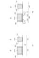
図1は、第1実施形態に係る半導体装置100が備えるトランジスタの構成を模式的に示す断面図である。同図に示されるように半導体装置100は、2種類のトランジスタを備える。一方のトランジスタは、VLV(Very Low Voltage)トランジスタ10である。他方のトランジスタは、HV(High Voltage)トランジスタ20である。これらVLVトランジスタ10及びHVトランジスタ20は、例えば、同一の半導体基板Wに形成されるCMOS論理回路のトランジスタを構成する。ただし、VLVトランジスタ10及びHVトランジスタ20は、異なる半導体基板に形成されてもよい。 FIG. 1 is a cross-sectional view schematically showing the configuration of a transistor included in a
HVトランジスタ20は、VLVトランジスタ10よりも高電圧で使用可能である。このため半導体基板W上の相対的に高電圧で動作する回路が設けられている領域AR2(「第2領域AR2」と呼ばれる場合がある。)には、HVトランジスタ20を形成し、他の領域(「第1領域AR1」と呼ばれる場合がある。)には、VLVトランジスタ10を形成することが可能である。HVトランジスタ20が設けられる第2領域AR2と、VLVトランジスタ10が設けられる第1領域AR1は、例えば、STI等で区分される。以下、各トランジスタの構成について説明する。
[VLVトランジスタ][VLV transistor]
VLVトランジスタは、半導体基板W上に形成された第1ゲート絶縁膜10GIと、第1ゲート絶縁膜10GI上に形成された第1ゲート電極10GC(「ゲートコンタクト」と呼ばれる場合もある。)と、半導体基板Wに形成された第1ソース領域10S及び第1ドレイン領域10Dとを備える。さらにVLVトランジスタは、第1ゲート電極10GCの一方の側面に対向して設けられた第1サイドウォール11Sと、第1ゲート電極10GCの他方の側面に対向して設けられた第2サイドウォール12Sとを備える。なお、半導体装置100はさらに、第1ソース領域10S、第1ドレイン領域10D及び第1ゲート電極10GCにそれぞれ電気的に接続するソースコンタクト、ドレインコンタクト及びゲートコンタクトと、VLVトランジスタその他のトランジスタを絶縁するための絶縁層等を備える。なお本発明は、N型トランジスタにもP型トランジスタにも適用可能である。 The VLV transistor includes a first gate insulating film 10GI formed on the semiconductor substrate W, a first gate electrode 10GC (sometimes referred to as a "gate contact") formed on the first gate insulating film 10GI, and It includes a
半導体基板Wは、例えば、P型乃至N型のシリコンウエハである。 The semiconductor substrate W is, for example, a P-type to N-type silicon wafer.
第1ゲート絶縁膜10GIは、一例として、0.5nm~1nm(例えば、0.8nm)の膜厚T1(「第1膜厚」の一例)を有する。また、第1ゲート絶縁膜10GIのゲート長は、一例として、50nm~100nm(例えば、50nm)である。第1ゲート絶縁膜10GIを含むゲート絶縁膜は、例えば、SiO2又はSiN等から形成される。 The first gate insulating film 10GI has, for example, a film thickness T1 (an example of a "first film thickness") of 0.5 nm to 1 nm (for example, 0.8 nm). Further, the gate length of the first gate insulating film 10GI is, for example, 50 nm to 100 nm (eg, 50 nm). The gate insulating film including the first gate insulating film 10GI is formed of, for example, SiO2 or SiN.
第1ゲート絶縁膜10GI上には第1ゲート電極10GCが形成される。第1ゲート電極10GCは、一例として、50~150nm(例えば、100nm)の高さを有する。第1ゲート電極10GCその他のゲート電極は、例えば、ポリシリコンから形成される。第1ゲート電極10GCのうち、上部の領域10GCUは、後述するように、プレアモルファス化インプラント(Pre-Amorphization Implants。以下、「PAI」と呼ぶ場合がある。)により、ゲルマニウム(Ge)がインプラントされ、かつ、非晶質化されている。なお第1ゲート電極10GCのうち、下部の領域は、PAIの影響が限定的であるか、または、PAIの影響を受けないため、ゲルマニウムを実質的に含有しない。 A first gate electrode 10GC is formed on the first gate insulating film 10GI. The first gate electrode 10GC has a height of, for example, 50 to 150 nm (eg, 100 nm). The first gate electrode 10GC and other gate electrodes are made of polysilicon, for example. The upper region 10GCU of the first gate electrode 10GC is implanted with germanium (Ge) by pre-amorphization implants (hereinafter sometimes referred to as "PAI"), as described later. , and is amorphous. Note that the lower region of the first gate electrode 10GC does not substantially contain germanium because the influence of PAI is limited or it is not affected by PAI.
第1ソース領域10Sは、例えば、ボロン(B)がインプラントされて拡散されたP型の拡散領域である。第1ソース領域10Sのうち、半導体基板Wの表面近傍に設けられる上部ソース領域10SUは、PAIによりゲルマニウム(Ge)がインプラントされ、かつ、非晶質化されている。なお第1ソース領域10Sのうち、上部ソース領域10SUより半導体基板表面から離間する位置に設けられる下部ソース領域10SLは、PAIの影響が限定的であるか、または、PAIの影響を受けないため、ゲルマニウムを実質的に含有しない。 The
このように第1ソース領域10Sの上部ソース領域10SUは、非晶質化されているため、不純物(本実施形態ではボロン)の拡散を抑制し、トランジスタの特性のばらつきを抑制することが可能である。 In this way, since the upper source region 10SU of the
第1ドレイン領域10Dは、例えば、ボロン(B)がインプラントされて拡散されたP型の拡散領域である。第1ドレイン領域10Dのうち、半導体基板Wの表面近傍に設けられる上部ドレイン領域10DUは、PAIにより、ゲルマニウム(Ge)がインプラントされ、かつ、非晶質化されている。なお第1ドレイン領域10Dのうち、上部ドレイン領域10DUより半導体基板W表面から離間する位置に設けられる下部ドレイン領域10DLは、PAIの影響が限定的であるか、または、PAIの影響を受けないため、ゲルマニウムを実質的に含有しない。 The
このように第1ドレイン領域10Dの上部ドレイン領域10DUは、非晶質化されているため、不純物(本実施形態ではボロン)の拡散を抑制し、トランジスタの特性のばらつきを抑制することが可能である。 In this way, since the upper drain region 10DU of the
[HVトランジスタ][HV transistor]
HVトランジスタ20は、VLVトランジスタ10と同一の半導体基板Wの第2領域AR2に形成される。HVトランジスタ20は、第2ゲート絶縁膜20GIと、第2ゲート絶縁膜20GI上に形成され、少なくとも上部にゲルマニウムを含有する第2ゲート電極20GCと、半導体基板Wに形成された第2ソース領域20Sと、半導体基板Wに形成された第2ドレイン領域20Dとを備える。さらにHVトランジスタ20は、第2ゲート電極20GCの一方の側面に対向して設けられた第3サイドウォール23Sと、第2ゲート電極20GCの他方の側面に対向して設けられた第4サイドウォール24Sとを備える。
なお、半導体装置100はさらに、第2ソース領域20S、第2ドレイン領域20D及び第2ゲート電極20GCにそれぞれ電気的に接続するソースコンタクト、ドレインコンタクト及びゲートコンタクトと、HVトランジスタ20その他のトランジスタを絶縁するために半導体基板W上に積層された絶縁層等を備える。なお、第3サイドウォール23S及び第4サイドウォール24Sは、第2ゲート絶縁膜20GI上に形成される点においてHVトランジスタ20は、第1ゲート絶縁膜10GIが第1サイドウォールと第2サイドウォールとの間に形成されるVLVトランジスタ10と異なる構成を有する。
第2ゲート絶縁膜20GIは、第1ゲート絶縁膜10GIの膜厚より大きい膜厚を有し、一例として、1nm~5nm(例えば、3nm)の膜厚T2(「第2膜厚」の一例)を有する。また、第2ゲート絶縁膜20GIのゲート長は、第1ゲート絶縁膜10GIのゲート長より大きくてよく、一例として、10nm~100nm(例えば、50nm)である。The
Note that the
The second gate insulating film 20GI has a thickness larger than that of the first gate insulating film 10GI, and as an example, the film thickness T2 is 1 nm to 5 nm (for example, 3 nm) (an example of a "second film thickness"). has. Further, the gate length of the second gate insulating film 20GI may be larger than the gate length of the first gate insulating film 10GI, and is, for example, 10 nm to 100 nm (eg, 50 nm).
第2ゲート絶縁膜20GI上には第2ゲート電極20GCが形成される。第2ゲート電極20GCは、第1ゲート電極10GCと同じ高さを有するように形成されてよく、一例として、50~150nm(例えば、100nm)の高さを有する。第2ゲート電極20GCのうち、上部の領域20GCUは、PAIにより、ゲルマニウム(Ge)がインプラントされ、かつ、非晶質化されている。なお第2ゲート電極20GCのうち、下部の領域は、PAIの影響が限定的であるか、または、PAIの影響を受けないため、ゲルマニウムを実質的に含有しない。 A second gate electrode 20GC is formed on the second gate insulating film 20GI. The second gate electrode 20GC may be formed to have the same height as the first gate electrode 10GC, and for example, has a height of 50 to 150 nm (eg, 100 nm). The upper region 20GCU of the second gate electrode 20GC is implanted with germanium (Ge) and made amorphous by PAI. Note that the lower region of the second gate electrode 20GC does not substantially contain germanium because the influence of PAI is limited or it is not affected by PAI.
第2ソース領域20Sは、例えば、ボロン(B)がインプラントされて拡散されたP型の拡散領域である。第1ソース領域10Sと異なり、第2ソース領域20Sの上部領域を含む全領域は、PAIの影響が限定的であるか、または、PAIの影響を受けないため、ゲルマニウムを実質的に含有しない。なお第2ソース領域20Sの周縁部にはLDD(Lightly Doped Drain)が形成されている。 The
第2ドレイン領域20Dは、例えば、ボロン(B)がインプラントされて拡散されたP型の拡散領域である。第1ドレイン領域10Dと異なり、第2ドレイン領域20Dの上部領域を含む全領域は、PAIの影響が限定的であるか、または、PAIの影響を受けないため、ゲルマニウムを実質的に含有しない。なお第2ドレイン領域20Dの周縁部にはLDD(Lightly Doped Drain)が形成されている。 The
以上のような構成のHVトランジスタ20によれば、第2ゲート電極20GCのうち、上部の領域の少なくとも一部は、PAIにより、ゲルマニウム(Ge)がインプラントされ、かつ、非晶質化されている。このため、LDD(Lightly Doped Drain)を形成するためのインプラントの際、ドーパントが第2ゲート電極20GCを通過して半導体基板Wのチャネル領域にインプラントされ、閾値電圧が変動することを抑制することが可能となる。 According to the
すなわち本出願の発明者らは、トランジスタの微細化を抑制するためには特にVLVトランジスタのアスペクト比を改善するためにゲート長の微細化に伴ってゲート電極の高さを低減する必要があるところ、ゲート電極の高さを低減すると特にHVトランジスタにLDDを形成する際、ドーパントがゲート電極を通過して半導体基板のチャネル領域にインプラントされてしまい、閾値電圧が変動する課題を有する点に着目した。そこで、ゲート電極(特にHVトランジスタの第2ゲート電極)にPAIを施してゲルマニウム(Ge)をインプラントし、ゲート電極の上部の少なくとも一部を非晶質化することにより、ドーパントがゲート電極を通過してしまう事態を抑制可能となる構成に着想した。 In other words, the inventors of the present application have found that in order to suppress the miniaturization of transistors, it is necessary to reduce the height of the gate electrode as the gate length is miniaturized, especially in order to improve the aspect ratio of VLV transistors. We focused on the problem that if the height of the gate electrode is reduced, especially when forming an LDD in an HV transistor, the dopant will pass through the gate electrode and be implanted into the channel region of the semiconductor substrate, causing the threshold voltage to fluctuate. . Therefore, by applying PAI to the gate electrode (particularly the second gate electrode of the HV transistor) and implanting germanium (Ge) to make at least a part of the upper part of the gate electrode amorphous, the dopant can pass through the gate electrode. We came up with a configuration that can prevent this from happening.
この構成によりドーパントがゲート電極を通過して半導体基板のチャネル領域にインプラントされてしまう事態が抑制可能となるから、微細化に際して閾値変動を抑制できる半導体装置の提供が可能となる。 This configuration makes it possible to prevent the dopant from passing through the gate electrode and being implanted into the channel region of the semiconductor substrate, thereby making it possible to provide a semiconductor device that can suppress threshold fluctuations during miniaturization.
ここでゲート電極(第2ゲート電極20GC)と異なり、HVトランジスタ20の拡散層(第2ソース領域20S及び第2ドレイン領域20D)には、PAIが施されていない。このため、GIDL(Gate-Induced-Drain-Leakage current)を抑制することが可能となる。 Here, unlike the gate electrode (second gate electrode 20GC), the diffusion layer (
以上のとおりであるから、本実施形態に係る半導体装置は、2種類のトランジスタを備える。ゲート絶縁膜の膜厚が相対的に小さいトランジスタ(VLVトランジスタ)については、拡散層(ソース及びドレイン領域)にPAIを施して不純物の拡散を抑制することにより特性の向上を図ることが可能となる。一方で、ゲート絶縁膜の膜厚が相対的に大きいトランジスタ(HVトランジスタ)については、拡散層(ソース及びドレイン領域)にPAIを施さないことにより、GIDLを抑制することが可能となる。加えて、ゲート電極にPAIを施すことにより、LDL形成に伴う閾値変動抑制を可能とした。 As described above, the semiconductor device according to this embodiment includes two types of transistors. For transistors with relatively small gate insulating films (VLV transistors), it is possible to improve the characteristics by applying PAI to the diffusion layers (source and drain regions) to suppress the diffusion of impurities. . On the other hand, in a transistor whose gate insulating film is relatively thick (HV transistor), GIDL can be suppressed by not applying PAI to the diffusion layer (source and drain regions). In addition, by applying PAI to the gate electrode, it was possible to suppress threshold fluctuations associated with LDL formation.
[製造方法][Production method]
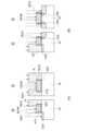
以下、本実施形態に係る半導体装置100の製造方法について説明する。図2及び図3は、本実施形態に係る半導体装置100の製造方法を説明する模式図である。図2(A)に示されるように、まず半導体基板W上の第1領域AR1に、第1ゲート絶縁膜10GIとなる絶縁膜を半導体基板W表面の酸化等により形成する。同様に半導体基板W上の第2領域AR2に、第1ゲート絶縁膜10GIの膜厚T1より大きい膜厚T2を有する第2ゲート絶縁膜20GIとなる絶縁膜を形成する。 A method for manufacturing the
次いで、第1領域AR1及び第2領域AR2の各絶縁膜上に、後に第1ゲート電極10GC及び第2ゲート電極20GCとなるポリシリコン膜を例えばCVDを用いて製膜する。そしてパターニングしてポリシリコン膜の一部を除去することにより、第1領域AR1に、膜厚T1を有する第1ゲート絶縁膜10GI及び第1ゲート絶縁膜10GI上の第1ゲート電極10GCを形成する。 Next, a polysilicon film that will later become the first gate electrode 10GC and the second gate electrode 20GC is formed on each insulating film in the first region AR1 and the second region AR2 using, for example, CVD. Then, by patterning and removing a part of the polysilicon film, a first gate insulating film 10GI having a film thickness T1 and a first gate electrode 10GC on the first gate insulating film 10GI are formed in the first region AR1. .
またパターニングしてポリシリコン膜の一部を除去することにより、第2ゲート絶縁膜20GIとなる絶縁膜上に第2ゲート電極20GCを形成する。ここで第2ゲート絶縁膜20GIを除去せずに半導体基板W上に残存させることにより、同図(A)に示されるように第2領域AR2に、第2ゲート絶縁膜20GIを一部に包含する膜厚T2の絶縁膜を形成することが可能となる。 Further, by patterning and removing a portion of the polysilicon film, a second gate electrode 20GC is formed on the insulating film that will become the second gate insulating film 20GI. By leaving the second gate insulating film 20GI on the semiconductor substrate W without removing it, the second gate insulating film 20GI is partially included in the second region AR2, as shown in FIG. It becomes possible to form an insulating film having a thickness T2.
次いで同図(B)に示されるように、半導体基板Wの第1領域AR1及び第2領域AR2に、後にサイドウォールを構成するスペーサ絶縁膜SIが形成される。具体的には、第1領域AR1における半導体基板W及び第1ゲート電極10GC上に、かつ、第2領域AR2における絶縁膜及び第2ゲート電極20GC上に、スペーサ絶縁膜SIを例えばCVDを用いて製膜する。 Next, as shown in FIG. 3B, a spacer insulating film SI, which will later constitute a sidewall, is formed in the first region AR1 and second region AR2 of the semiconductor substrate W. Specifically, a spacer insulating film SI is formed on the semiconductor substrate W and the first gate electrode 10GC in the first region AR1 and on the insulating film and the second gate electrode 20GC in the second region AR2 using, for example, CVD. Form a film.
次いで同図(C)に示されるように、スペーサ絶縁膜SIで覆われる半導体装置100に対してPAIを施す。具体的には、スペーサ絶縁膜SI越しにゲルマニウムをインプラント(注入)して、第1領域AR1の半導体基板Wの上部(後の上部ソース領域10SU及び上部ドレイン領域10DUに相当する領域)にゲルマニウムを含有させるとともに、この部分を非晶質化する。また、第1ゲート電極10GCの上部の領域10GCUにゲルマニウムをインプラントして、この部分を非晶質化する。 Next, as shown in FIG. 2C, PAI is performed on the
同時に、第2領域AR2の第2ゲート電極20GCの上部の領域20GCUにゲルマニウムをインプラントして、この部分を非晶質化する。しかしながら、このとき第2領域AR2の半導体基板Wの上部(後の第2ソース領域20Sの上部及び第2ドレイン領域20Dの上部に相当する部分)は、スペーサ絶縁膜SIの下方に設けられる厚い絶縁膜に覆われているため、ゲルマニウムがインプラントされず、かつ、非晶質化もされない。換言すると、スペーサ絶縁膜SIを通過するものの、その下方の絶縁膜までは通過しないような加速電圧でゲルマニウムをインプラントするPAIを実行することにより、図1に示される構成のトランジスタを製造することが可能となる。 At the same time, germanium is implanted into the region 20GCU above the second gate electrode 20GC in the second region AR2 to make this part amorphous. However, at this time, the upper part of the semiconductor substrate W in the second region AR2 (the part corresponding to the upper part of the
以上のプロセスの結果、ゲート電極の上部及び拡散層(ソース及びドレイン領域)の上部にゲルマニウムを含有するトランジスタ(VLVトランジスタ)と、ゲート電極の上部にゲルマニウムを含有し拡散層にゲルマニウムを含有しないトランジスタ(HVトランジスタ)という2種類以上のトランジスタを同一半導体基板W上に形成することが可能となる。 As a result of the above process, a transistor containing germanium in the upper part of the gate electrode and the upper part of the diffusion layer (source and drain regions) (VLV transistor), and a transistor containing germanium in the upper part of the gate electrode and no germanium in the diffusion layer. It becomes possible to form two or more types of transistors (HV transistors) on the same semiconductor substrate W.
その後図3(A)に示されるように、例えば、全面に形成されているスペーサ絶縁膜SIを、RIE等の異方性エッチングによりエッチバックすることで、サイドウォールに相当する部分が残るようにスペーサ絶縁膜を除去する。 Thereafter, as shown in FIG. 3A, for example, the spacer insulating film SI formed over the entire surface is etched back by anisotropic etching such as RIE, so that portions corresponding to the sidewalls remain. Remove the spacer insulating film.
そして同図(B)に示されるように、ドーパント(例えば燐)をインプラントしてLDDを形成する。このとき、第2ゲート電極20GCの上部が非晶質化されているため、ドーパントの少なくとも一部は、第2ゲート電極20GCによって遮られる。このため、チャネル領域にドーパントがインプラントされて閾値電圧が変動することを抑制することが可能となる。 Then, as shown in FIG. 3B, a dopant (for example, phosphorus) is implanted to form an LDD. At this time, since the upper part of the second gate electrode 20GC is amorphous, at least a portion of the dopant is blocked by the second gate electrode 20GC. Therefore, it is possible to suppress fluctuations in the threshold voltage due to dopant implantation in the channel region.
その後は、知られた方法に従って、拡散層等を形成することにより、図1に示されるトランジスタを設けることが可能となる。 Thereafter, the transistor shown in FIG. 1 can be provided by forming diffusion layers and the like according to known methods.
[第2実施形態][Second embodiment]
以下第2実施形態について説明する。第1実施形態と同様の構成を備えることが当業者に理解できる部分については説明を省略乃至簡略化し、第1実施形態と異なる部分を中心に説明する。 The second embodiment will be described below. Descriptions of parts that can be understood by those skilled in the art to have the same configuration as the first embodiment will be omitted or simplified, and parts that are different from the first embodiment will be mainly described.
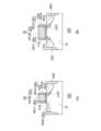
図4(A)及び(B)は、第2実施形態に係る半導体装置200が備えるHVトランジスタの構成を模式的に示す断面図である。同図(A)に示されるHVトランジスタ30と、同図(B)に示されるHVトランジスタ40は、同一の半導体基板W上に形成されてもよいし、異なる半導体基板上に形成されてもよい。例えば同図(A)に示されるHVトランジスタ30は、半導体メモリの周辺回路を構成するペリ部に設けられ、同図(B)に示されるHVトランジスタ40は、同一の半導体基板W上の半導体メモリのコア部に設けられてもよい。さらに同一の半導体基板W上には、第1実施形態に示されたVLVトランジスタ10が設けられてもよい。 FIGS. 4A and 4B are cross-sectional views schematically showing the configuration of an HV transistor included in the
本実施形態に係るトランジスタは、ゲート電極の上部のうち、一部のみがゲルマニウムを含有する非晶質であり、他の一部がゲルマニウムを実質的に含有しない多結晶である構成を備える。 The transistor according to this embodiment has a structure in which only a part of the upper part of the gate electrode is amorphous containing germanium, and the other part is polycrystalline which does not substantially contain germanium.
また、同図(B)に示されるHVトランジスタ30はソースとドレインが対称に設けられている一方で、同図(A)に示されるHVトランジスタ40はソースとドレインが非対称に設けられている点で異なる。 Furthermore, the
同図(B)に示されるHVトランジスタ30は、半導体基板W上に形成された第1ゲート絶縁膜30GIと、第1ゲート絶縁膜30GI上に形成された第1ゲート電極30GCと、半導体基板Wに形成された第1ソース領域30S及び第1ドレイン領域30Dとを備える。さらにHVトランジスタ30は、第1ゲート電極30GCの一方の側面に対向して設けられた第1サイドウォール31Sと、第1ゲート電極30GCの他方の側面に対向して設けられた第2サイドウォール32Sとを備える。なお、半導体装置200はさらに、第1ソース領域30S、第1ドレイン領域30D及び第1ゲート電極30GCにそれぞれ電気的に接続するソースコンタクト、ドレインコンタクト及びゲートコンタクトと、HVトランジスタその他のトランジスタを絶縁するための絶縁層等を備える。 The
第1ゲート電極30GCの上部の領域30Uのうち、第1サイドウォール31Sと第2サイドウォール32Sとの中間領域に相当する中間部30UMは、ゲルマニウムを含有する非晶質である。 Of the
一方で第1ゲート電極30GCの上部の領域30Uうち、中間部30UMよりも第1サイドウォールに近接する第1上端部30U1は、ゲルマニウムを実質的に含有しない多結晶である。 On the other hand, in the
同様に、第1ゲート電極30GCの上部の領域30Uのうち、中間部30UMよりも第2サイドウォール32Sに近接する第2上端部30U2は、ゲルマニウムを実質的に含有しない多結晶である。 Similarly, in the
また、半導体基板Wのうち、第1上端部30U1の下方に相当する領域には、LDD(ソースLDD)が形成され、第2上端部30U2の下方に相当する領域には、LDD(ドレインLDD)が形成されている。 Further, in the semiconductor substrate W, an LDD (source LDD) is formed in a region corresponding to the lower part of the first upper end part 30U1, and an LDD (drain LDD) is formed in a region corresponding to the lower part of the second upper end part 30U2. is formed.
以上のような構成のHVトランジスタ30によれば、第1ゲート電極30GCの上部30Uのうち、中間部30UMが非晶質であるから、LDD形成時にドーパント(例えば燐)が中間部30UMを通過してチャネル領域にインプラントされてしまうことを抑制することが可能となる。 According to the
加えて、第1ゲート絶縁膜30GIの端部の下方にLDDを形成することが可能となるから、GIDLを抑制することが可能となる。 In addition, since it becomes possible to form an LDD below the end of the first gate insulating film 30GI, it becomes possible to suppress GIDL.
一方で同図(A)に示されるHVトランジスタ40は、半導体基板W上に形成された第1ゲート絶縁膜40GIと、第1ゲート絶縁膜上に形成された第1ゲート電極40と、半導体基板に形成された第1ソース領域40S及び第1ドレイン領域40Dとを備える。さらにHVトランジスタ40は、第1ゲート電極40GCの一方の側面に対向して設けられた第1サイドウォール41Sと、第1ゲート電極50GCの他方の側面に対向して設けられた第2サイドウォール42Sとを備える。なお、半導体装置200はさらに、第1ソース領域40S、第1ドレイン領域40D及び第1ゲート電極40GCにそれぞれ電気的に接続するソースコンタクト、ドレインコンタクト及びゲートコンタクトと、HVトランジスタ40その他のトランジスタを絶縁するための絶縁層等を備える。 On the other hand, the
そして第1ゲート電極40GCの上部の領域40Uうち、第1サイドウォール41Sと第2サイドウォール42Sとの中間領域に相当する中間部40UMは、ゲルマニウムを含有する非晶質である。 Of the
また第1ゲート電極40GCの上部の領域40Uうち、中間部40UMよりも第1サイドウォール41Sに近接する第1上端部40U1も、ゲルマニウムを含有する非晶質である。 Further, in the
他方で、第1ゲート電極40GCの上部40Uのうち、中間部40UMよりも第2サイドウォール42Sに近接する第2上端部40U2は、ゲルマニウムを実質的に含有しない多結晶である。 On the other hand, of the
また、半導体基板Wのうち、第1上端部40U1の下方に相当する領域には、LDD(ソースLDD)が形成されない一方で、第2上端部42USの下方に相当する領域には、LDD(ドレインLDD)が形成されている。 Further, in the semiconductor substrate W, an LDD (source LDD) is not formed in a region corresponding to the lower side of the first upper end portion 40U1, whereas an LDD (source LDD) is not formed in a region corresponding to the lower side of the second upper end portion 42US. LDD) is formed.
加えて、第1ソース領域40Sのうち、半導体基板Wの表面付近の上部ソース領域40SUは、PAIによりゲルマニウム(Ge)がインプラントされ、かつ、非晶質化されているため、浅いLDDを構成する。 In addition, in the first source region 40S, the upper source region 40SU near the surface of the semiconductor substrate W is implanted with germanium (Ge) by PAI and is made amorphous, thereby forming a shallow LDD. .
一方で、第1ドレイン領域40Dは、第1ソース領域と異なり、全領域にわたってゲルマニウムを実質的に含有しない。また、第1ドレイン領域は、第1ソース領域よりも深くまで形成されている。 On the other hand, unlike the first source region, the
以上のような構成のHVトランジスタ40によれば、第1ソース領域40Sに相対的に浅いLDDが形成されるため、SCE(Short Channel Effect)を抑制することが可能となる。また第1ドレイン領域40Dに相対的に深いLDDが形成されるため、GIDLを抑制することが可能となる。このため高い増幅度を必要とする回路(例えばコア部)に適用することが可能となる。 According to the
以下、本実施形態に係る半導体装置200の製造方法について説明する。図5及び図6は、本実施形態に係る半導体装置200の製造方法を説明する模式図である。なお対称の拡散層を有するHVトランジスタ30と、非対称の拡散層を有するHVトランジスタ40は、同時に同一半導体基板W上に形成されてもよい。本実施形態においては、同一半導体基板Wの所定領域(以下、「第1領域」と呼ぶ場合がある。)に対称のHVトランジスタ30が形成され、異なる所定領域(以下、「第2領域」と呼ぶ場合がある。)に非対称のHVトランジスタ40が形成される。 A method for manufacturing the
同図(A)に示されるように、半導体基板W上の第1領域及び第2領域に、それぞれ、第1ゲート絶縁膜30GI、40GI、第1ゲート電極30GC、40GC並びに各ゲート電極の2つの側面にそれぞれ対向する第1サイドウォール31S、41S及び第2サイドウォール32S、42Sを形成する。 As shown in FIG. 3A, first gate insulating films 30GI and 40GI, first gate electrodes 30GC and 40GC, and two layers of each gate electrode are provided in the first region and second region on the semiconductor substrate W, respectively. First sidewalls 31S, 41S and second sidewalls 32S, 42S are formed to face each other on the side surfaces.
次いで同図(B)に示されるように、半導体基板Wの第1領域においては、第1サイドウォール31S及び第2サイドウォール32Sを覆い、かつ、第1ゲート電極30GCの上部の領域30Uのうち、少なくとも中間部30UMを露出させるレジスト膜Rを形成する。半導体基板Wの第2領域においては、第2サイドウォール42Sを覆い、かつ、第1ゲート電極40GCの上部の領域40Uのうち、少なくとも中間部40UM及び第1サイドウォール41Sを露出させるレジスト膜Rを形成する。そしてレジスト膜R越しにゲルマニウムを注入して、PAIを実行する。 Next, as shown in FIG. 3B, in the first region of the semiconductor substrate W, a portion of the
この結果、第1領域において、レジスト膜Rに覆われていない第1ゲート電極30GUの中間部30UMは、ゲルマニウムがインプラントされ、かつ、非晶質化される。 As a result, in the first region, the intermediate portion 30UM of the first gate electrode 30GU that is not covered with the resist film R is implanted with germanium and is made amorphous.
また、第2領域において、第1ゲート電極40Uの上部のうち、レジスト膜Rに覆われていない第1ゲート電極40GCの中間部40UM及び中間部40UMよりも第1サイドウォール41Sに近接する第1上端部40U1は、ゲルマニウムがインプラントされ、かつ、非晶質化される。 In addition, in the second region, among the upper part of the
次いで図6(A)に示されるように、レジスト膜Rが残存した状態でドーパント(例えば燐)をインプラントしてLDDを形成する。このとき第2領域の第1ゲート電極40GCは、PAIにより、ゲルマニウムがインプラントされ、かつ、非晶質化されている。このため、LDDを形成するためのインプラントの際、ドーパントが第1ゲート電極40GCを通過して半導体基板Wにインプラントされることが抑制されている。その結果、レジスト膜Rに覆われていない第2領域の第1ソース領域40Sとなる領域にLDDが形成される。 Next, as shown in FIG. 6A, a dopant (for example, phosphorus) is implanted with the resist film R remaining to form an LDD. At this time, the first gate electrode 40GC in the second region is implanted with germanium and made amorphous by PAI. Therefore, during implantation for forming an LDD, the dopant is prevented from passing through the first gate electrode 40GC and being implanted into the semiconductor substrate W. As a result, an LDD is formed in the second region not covered by the resist film R, which will become the first source region 40S.
そして図6(B)に示されるように、レジスト膜Rを除去した後、第2領域において第2サイドウォール42Sを覆い、かつ、第1ゲート電極40GU上部の少なくとも中間部40UM及び第1サイドウォール41Sを露出させるレジスト膜R2を形成する。この状態で、レジスト膜R2越しにドーパント(例えば燐)をインプラントしてLDDを形成する。 Then, as shown in FIG. 6B, after removing the resist film R, the
このとき第1領域において第1上端部30U1及び第2上端部30U2は、非晶質化されておらず多結晶であるため、ドーパントが第1上端部30U1及び第2上端部30U2を通過しやすい。このため第1ゲート絶縁膜30GIのソース側端部の下方にソースLDD領域及びドレイン側端部の下方にドレインLDD領域を形成することが可能となる。 At this time, in the first region, the first upper end portion 30U1 and the second upper end portion 30U2 are not amorphous and are polycrystalline, so the dopant easily passes through the first upper end portion 30U1 and the second upper end portion 30U2. . Therefore, it is possible to form a source LDD region below the source side end of the first gate insulating film 30GI, and a drain LDD region below the drain side end.
一方で第2領域の第2上端部40U2は、非晶質化されておらず多結晶である。このため、ドーパントが第2上端部40U2を通過し、ドレイン領域にLDDが形成される。ここで、図6(A)に示されるLDD形成におけるドーパントの加速電圧よりも図6(B)に示されるLDD形成におけるドーパントの加速電圧を大きくすることにより、相対的に深いLDDをドレイン側に形成することが可能となる。 On the other hand, the second upper end portion 40U2 of the second region is not amorphous but polycrystalline. Therefore, the dopant passes through the second upper end portion 40U2, and an LDD is formed in the drain region. Here, by making the dopant acceleration voltage in the LDD formation shown in FIG. 6(B) larger than the dopant acceleration voltage in the LDD formation shown in FIG. 6(A), the relatively deep LDD is moved to the drain side. It becomes possible to form.
その後は、知られた方法に従って、拡散層等を形成することにより、図4に示される構成のトランジスタを備える半導体装置200を製造することが可能となる。 Thereafter, by forming a diffusion layer and the like according to a known method, it becomes possible to manufacture the
以上、具体例を参照しつつ本実施形態について説明した。しかし、本開示はこれらの具体例に限定されるものではない。これら具体例に、当業者が適宜設計変更を加えたものも、本開示の特徴を備えている限り、本開示の範囲に包含される。前述した各具体例が備える各要素およびその配置、条件、形状などは、例示したものに限定されるわけではなく適宜変更することができる。前述した各具体例が備える各要素は、技術的な矛盾が生じない限り、適宜組み合わせを変えることができる。 The present embodiment has been described above with reference to specific examples. However, the present disclosure is not limited to these specific examples. Design changes made by those skilled in the art as appropriate to these specific examples are also included within the scope of the present disclosure as long as they have the characteristics of the present disclosure. The elements included in each of the specific examples described above, their arrangement, conditions, shapes, etc. are not limited to those illustrated, and can be changed as appropriate. The elements included in each of the specific examples described above can be appropriately combined as long as no technical contradiction occurs.
例えば、ゲート電極の上部の上端部は、ゲルマニウムを含有しない場合のみならず、ゲルマニウムを含有する中間部からゲルマニウムを拡散させることにより、中間部のゲルマニウム濃度(「第1濃度」の一例)よりも低い濃度のゲルマニウムを含有するように構成してもよい。 For example, the upper end of the gate electrode may not only contain no germanium, but also diffuse germanium from the middle part containing germanium, so that the germanium concentration in the middle part (an example of the "first concentration") is higher than that in the middle part. It may also be configured to contain a low concentration of germanium.
W 半導体基板
AR1 第1領域
AR2 第2領域
10 VLVトランジスタ
10I 第1ゲート絶縁膜
10GC 第1ゲート電極
10S 第1ソース領域
10D 第1ドレイン領域
20 HVトランジスタ
20I 第1ゲート絶縁膜
20GC 第1ゲート電極
20S 第1ソース領域
20D 第1ドレイン領域
100 半導体装置W Semiconductor substrate AR1 First region
Claims (11)
Translated fromJapanese前記ゲート絶縁膜上に形成され、少なくとも上部の一部にゲルマニウムを含有するゲート電極と、
前記半導体基板に形成されたソース領域と、
前記半導体基板に形成されたドレイン領域と
から構成されるトランジスタを備える半導体装置。A gate insulating film formed on a semiconductor substrate,
a gate electrode formed on the gate insulating film and containing germanium in at least a portion of the upper portion;
a source region formed in the semiconductor substrate;
and a drain region formed on the semiconductor substrate.
前記ソース領域は、ゲルマニウムを含有し、
前記ドレイン領域は、ゲルマニウムを含有し、
前記半導体基板上に形成され、前記第1膜厚より大きい第2膜厚を有する第2ゲート絶縁膜と、
前記第2ゲート絶縁膜上に形成され、少なくとも上部にゲルマニウムを含有する第2ゲート電極と、
前記半導体基板に形成され、ゲルマニウムを含有しない第2ソース領域と、
前記半導体基板に形成され、ゲルマニウムを含有しない第2ドレイン領域と
から構成される第2トランジスタをさらに備える請求項1に記載の半導体装置。The gate insulating film has a first thickness,
The source region contains germanium,
The drain region contains germanium,
a second gate insulating film formed on the semiconductor substrate and having a second film thickness greater than the first film thickness;
a second gate electrode formed on the second gate insulating film and containing germanium at least in an upper portion;
a second source region formed on the semiconductor substrate and containing no germanium;
2. The semiconductor device according to claim 1, further comprising a second transistor formed on the semiconductor substrate and comprising a second drain region not containing germanium.
ゲルマニウムを含有し、前記半導体基板表面側の上部ソース領域と、
ゲルマニウムを含有せず、前記上部ソース領域より前記半導体基板表面から離間する下部ソース領域とを有し、
前記ドレイン領域は、
ゲルマニウムを含有し、前記半導体基板表面側の上部ドレイン領域と、
ゲルマニウムを含有せず、前記上部ドレイン領域より前記半導体基板表面から離間する下部ドレイン領域とを有する
請求項1又は2に記載の半導体装置。The source region is
an upper source region on the surface side of the semiconductor substrate containing germanium;
a lower source region that does not contain germanium and is spaced further from the semiconductor substrate surface than the upper source region;
The drain region is
an upper drain region containing germanium and on the surface side of the semiconductor substrate;
3. The semiconductor device according to claim 1, further comprising a lower drain region that does not contain germanium and is spaced apart from the surface of the semiconductor substrate than the upper drain region.
前記ゲート電極の一方の側面に対向して設けられた第1サイドウォールと、
前記ゲート電極の他方の側面に対向して設けられた第2サイドウォールとを備え、
前記第2トランジスタは、
前記第2ゲート電極の一方の側面に対向して設けられた第3サイドウォールと、
前記第2ゲート電極の他方の側面に対向して設けられた第4サイドウォールとを備え、
前記第3サイドウォール及び前記第4サイドウォールは、前記第2ゲート絶縁膜上に形成される請求項2に記載の半導体装置。The transistor is
a first sidewall provided opposite to one side of the gate electrode;
a second sidewall provided opposite to the other side of the gate electrode,
The second transistor is
a third sidewall provided opposite to one side of the second gate electrode;
a fourth sidewall provided opposite to the other side surface of the second gate electrode,
3. The semiconductor device according to claim 2, wherein the third sidewall and the fourth sidewall are formed on the second gate insulating film.
前記ゲート電極の一方の側面に対向して設けられた第1サイドウォールと、
前記ゲート電極の他方の側面に対向して設けられた第2サイドウォールとを備え、
前記ゲート電極の前記上部は、
前記第1サイドウォールと前記第2サイドウォールとの中間領域に設けられ、第1濃度のゲルマニウムを含有する中間部と、
前記中間部よりも前記第1サイドウォールに近接し、前記第1濃度より低い濃度のゲルマニウムを含有する、又は、ゲルマニウムを含有しない第1上端部と、
前記中間部よりも前記第2サイドウォールに近接し、前記第1濃度より低い濃度のゲルマニウムを含有する、又は、ゲルマニウムを含有しない第2上端部と
を備える請求項1に記載の半導体装置。The transistor is
a first sidewall provided opposite to one side of the gate electrode;
a second sidewall provided opposite to the other side of the gate electrode,
The upper part of the gate electrode is
an intermediate portion provided in an intermediate region between the first sidewall and the second sidewall and containing germanium at a first concentration;
a first upper end portion that is closer to the first sidewall than the intermediate portion and contains germanium at a concentration lower than the first concentration, or does not contain germanium;
2. The semiconductor device according to claim 1, further comprising a second upper end portion that is closer to the second sidewall than the intermediate portion and contains germanium at a concentration lower than the first concentration or does not contain germanium.
前記半導体基板の、前記第1上端部の下方に相当する領域に形成されたソースLDD領域と、
前記半導体基板の、前記第2上端部の下方に相当する領域に形成されたドレインLDD領域と
をさらに備える請求項5に記載の半導体装置。The transistor is
a source LDD region formed in a region of the semiconductor substrate corresponding to a lower part of the first upper end portion;
6. The semiconductor device according to claim 5, further comprising a drain LDD region formed in a region of the semiconductor substrate corresponding to a lower part of the second upper end portion.
前記ゲート電極の一方の側面に対向して設けられた第1サイドウォールと、
前記ゲート電極の他方の側面に対向して設けられた第2サイドウォールとを備え、
前記ゲート電極の前記上部は、
前記第1サイドウォールと前記第2サイドウォールとの中間領域に設けられ、第1濃度のゲルマニウムを含有する中間部と、
前記中間領域よりも前記第1サイドウォールに近接し、第2濃度のゲルマニウムを含有する第1上端部と、
前記中間領域よりも前記第2サイドウォールに近接し、前記第1濃度及び前記第2濃度より小さい濃度のゲルマニウムを含有する、又は、ゲルマニウムを含有しない第2上端部と
を備える請求項1に記載の半導体装置。The transistor is
a first sidewall provided opposite to one side of the gate electrode;
a second sidewall provided opposite to the other side of the gate electrode,
The upper part of the gate electrode is
an intermediate portion provided in an intermediate region between the first sidewall and the second sidewall and containing germanium at a first concentration;
a first upper end portion that is closer to the first sidewall than the intermediate region and contains germanium at a second concentration;
2. A second upper end portion that is closer to the second sidewall than the intermediate region and contains germanium at a concentration lower than the first concentration and the second concentration, or does not contain germanium. semiconductor devices.
ゲルマニウムを含有し、前記半導体基板表面を含む上部ソース領域と、
ゲルマニウムを含有せず、前記上部ソース領域より深い下部ソース領域とを有し、
前記トランジスタの前記ドレイン領域は、
ゲルマニウムを含有しない
請求項7に記載の半導体装置。The source region of the transistor is
an upper source region containing germanium and including the surface of the semiconductor substrate;
a lower source region that does not contain germanium and is deeper than the upper source region,
The drain region of the transistor is
The semiconductor device according to claim 7, which does not contain germanium.
前記半導体基板に形成された請求項6に記載のトランジスタと
を備える半導体装置。The transistor according to claim 4, formed on the semiconductor substrate;
A semiconductor device comprising: the transistor according to claim 6 formed on the semiconductor substrate.
前記半導体基板上の第2領域に前記第1膜厚より大きい第2膜厚を有し、第2ゲート絶縁膜を一部に包含する絶縁膜を形成し、
前記ゲート絶縁膜上にゲート電極を形成し、
前記第2ゲート絶縁膜上に第2ゲート電極を形成し、
前記第1領域における前記半導体基板及び前記ゲート電極上に、かつ、前記第2領域における前記絶縁膜及び前記第2ゲート電極上にスペーサ絶縁膜を形成し、
前記スペーサ絶縁膜越しにゲルマニウムを注入して、前記第1領域における前記半導体基板の上部及び前記ゲート電極の上部に非晶質を形成し、かつ、前記第2領域における前記第2ゲート電極の上部に非晶質を形成する、
半導体装置の製造方法。forming a gate insulating film having a first thickness in a first region on the semiconductor substrate;
forming an insulating film having a second film thickness larger than the first film thickness in a second region on the semiconductor substrate and partially including a second gate insulating film;
forming a gate electrode on the gate insulating film;
forming a second gate electrode on the second gate insulating film;
forming a spacer insulating film on the semiconductor substrate and the gate electrode in the first region and on the insulating film and the second gate electrode in the second region;
germanium is implanted through the spacer insulating film to form an amorphous material on the top of the semiconductor substrate and the top of the gate electrode in the first region, and the top of the second gate electrode in the second region. form an amorphous substance,
A method for manufacturing a semiconductor device.
前記ゲート絶縁膜上にゲート電極を形成し、
前記ゲート電極の側面に第1サイドウォール及び第2サイドウォールを形成し、
前記第1サイドウォールを覆い、かつ、前記ゲート電極上部の少なくとも中間部を露出させるレジスト膜を形成し、
前記レジスト膜越しにゲルマニウムを注入して、少なくとも前記ゲート電極の前記中間部を非晶質化する
半導体装置の製造方法。forming a gate insulating film in a first region on the semiconductor substrate;
forming a gate electrode on the gate insulating film;
forming a first sidewall and a second sidewall on a side surface of the gate electrode;
forming a resist film that covers the first sidewall and exposes at least a middle portion of the upper part of the gate electrode;
A method of manufacturing a semiconductor device, comprising implanting germanium through the resist film to make at least the intermediate portion of the gate electrode amorphous.
Priority Applications (2)
| Application Number | Priority Date | Filing Date | Title |
|---|---|---|---|
| JP2022047895AJP7728218B2 (en) | 2022-03-24 | 2022-03-24 | Semiconductor device and manufacturing method thereof |
| US17/898,893US20230307540A1 (en) | 2022-03-24 | 2022-08-30 | Semiconductor device and method for manufacturing semiconductor device |
Applications Claiming Priority (1)
| Application Number | Priority Date | Filing Date | Title |
|---|---|---|---|
| JP2022047895AJP7728218B2 (en) | 2022-03-24 | 2022-03-24 | Semiconductor device and manufacturing method thereof |
Publications (2)
| Publication Number | Publication Date |
|---|---|
| JP2023141530Atrue JP2023141530A (en) | 2023-10-05 |
| JP7728218B2 JP7728218B2 (en) | 2025-08-22 |
Family
ID=88096501
Family Applications (1)
| Application Number | Title | Priority Date | Filing Date |
|---|---|---|---|
| JP2022047895AActiveJP7728218B2 (en) | 2022-03-24 | 2022-03-24 | Semiconductor device and manufacturing method thereof |
Country Status (2)
| Country | Link |
|---|---|
| US (1) | US20230307540A1 (en) |
| JP (1) | JP7728218B2 (en) |
Citations (4)
| Publication number | Priority date | Publication date | Assignee | Title |
|---|---|---|---|---|
| JPH11284184A (en)* | 1998-03-26 | 1999-10-15 | Seiko Epson Corp | Semiconductor device and manufacturing method thereof |
| US6030863A (en)* | 1998-09-11 | 2000-02-29 | Taiwan Semiconductor Manufacturing Company | Germanium and arsenic double implanted pre-amorphization process for salicide technology |
| JP2008124393A (en)* | 2006-11-15 | 2008-05-29 | Renesas Technology Corp | Manufacturing method of semiconductor device |
| JP2008187008A (en)* | 2007-01-30 | 2008-08-14 | Sharp Corp | Semiconductor device and manufacturing method thereof |
Family Cites Families (5)
| Publication number | Priority date | Publication date | Assignee | Title |
|---|---|---|---|---|
| US6153477A (en)* | 1998-04-14 | 2000-11-28 | Advanced Micro Devices, Inc. | Ultra short transistor channel length formed using a gate dielectric having a relatively high dielectric constant |
| US6784506B2 (en)* | 2001-08-28 | 2004-08-31 | Advanced Micro Devices, Inc. | Silicide process using high K-dielectrics |
| US10147800B2 (en)* | 2016-02-19 | 2018-12-04 | United Microelectronics Corp. | Method of fabricating a transistor with reduced hot carrier injection effects |
| KR102274813B1 (en)* | 2020-02-27 | 2021-07-07 | 주식회사 키 파운드리 | A Manufacturing Method of Semiconductor Device Using Gate-Through Implantation |
| KR20220169543A (en)* | 2021-06-21 | 2022-12-28 | 삼성전자주식회사 | Asymmetric semiconductor device including ldd region and manufacturing method thereof |
- 2022
- 2022-03-24JPJP2022047895Apatent/JP7728218B2/enactiveActive
- 2022-08-30USUS17/898,893patent/US20230307540A1/enactivePending
Patent Citations (4)
| Publication number | Priority date | Publication date | Assignee | Title |
|---|---|---|---|---|
| JPH11284184A (en)* | 1998-03-26 | 1999-10-15 | Seiko Epson Corp | Semiconductor device and manufacturing method thereof |
| US6030863A (en)* | 1998-09-11 | 2000-02-29 | Taiwan Semiconductor Manufacturing Company | Germanium and arsenic double implanted pre-amorphization process for salicide technology |
| JP2008124393A (en)* | 2006-11-15 | 2008-05-29 | Renesas Technology Corp | Manufacturing method of semiconductor device |
| JP2008187008A (en)* | 2007-01-30 | 2008-08-14 | Sharp Corp | Semiconductor device and manufacturing method thereof |
Also Published As
| Publication number | Publication date |
|---|---|
| US20230307540A1 (en) | 2023-09-28 |
| JP7728218B2 (en) | 2025-08-22 |
Similar Documents
| Publication | Publication Date | Title |
|---|---|---|
| CN1307709C (en) | Semiconductor with Si-Ge grid and producing method thereof | |
| JP4952874B2 (en) | Semiconductor device having CMOS and method for manufacturing the same | |
| KR20020067795A (en) | Method of fabricating Metal Oxide Semiconductor transistor with Lightly Doped Drain structure | |
| JPH10335480A (en) | Semiconductor device and manufacturing method thereof | |
| JP2008091905A (en) | Manufacturing method of semiconductor device provided with FinFET | |
| JP2000077613A (en) | Method for manufacturing semiconductor device | |
| JP4515717B2 (en) | Integrated circuit semiconductor device having uniform silicide junction and method of manufacturing the same | |
| JP7728218B2 (en) | Semiconductor device and manufacturing method thereof | |
| US5550064A (en) | Method for fabricating high-voltage complementary metal-oxide-semiconductor transistors | |
| JP2005026464A (en) | Semiconductor device and manufacturing method thereof | |
| JP3744438B2 (en) | Semiconductor device | |
| KR0146525B1 (en) | Method for manufacturing thin film transistor | |
| TW201017869A (en) | Semiconductor device and method of fabricating the same | |
| JP2008103417A (en) | Semiconductor device and manufacturing method thereof | |
| JP4532857B2 (en) | Manufacturing method of semiconductor device having shallow trench isolation structure | |
| JP7252094B2 (en) | semiconductor devices and transistors | |
| JP2005142528A (en) | MOS transistor and manufacturing method thereof | |
| US7402494B2 (en) | Method for fabricating high voltage semiconductor device | |
| KR100995330B1 (en) | Manufacturing method of semiconductor device | |
| JPH0964361A (en) | Method for manufacturing semiconductor device | |
| KR20090088677A (en) | Semiconductor device and manufacturing method | |
| JPH0438834A (en) | Manufacturing method of MOS transistor | |
| JP2004095884A (en) | Method for manufacturing semiconductor device | |
| KR100266687B1 (en) | Method for fabricating transistor | |
| KR100832706B1 (en) | Semiconductor device and manufacturing method thereof |
Legal Events
| Date | Code | Title | Description |
|---|---|---|---|
| A621 | Written request for application examination | Free format text:JAPANESE INTERMEDIATE CODE: A621 Effective date:20240909 | |
| A977 | Report on retrieval | Free format text:JAPANESE INTERMEDIATE CODE: A971007 Effective date:20250430 | |
| A131 | Notification of reasons for refusal | Free format text:JAPANESE INTERMEDIATE CODE: A131 Effective date:20250520 | |
| A521 | Request for written amendment filed | Free format text:JAPANESE INTERMEDIATE CODE: A523 Effective date:20250704 | |
| TRDD | Decision of grant or rejection written | ||
| A01 | Written decision to grant a patent or to grant a registration (utility model) | Free format text:JAPANESE INTERMEDIATE CODE: A01 Effective date:20250715 | |
| A61 | First payment of annual fees (during grant procedure) | Free format text:JAPANESE INTERMEDIATE CODE: A61 Effective date:20250812 | |
| R150 | Certificate of patent or registration of utility model | Ref document number:7728218 Country of ref document:JP Free format text:JAPANESE INTERMEDIATE CODE: R150 |