JP2023136275A - Semiconductor devices and semiconductor storage devices - Google Patents
Semiconductor devices and semiconductor storage devicesDownload PDFInfo
- Publication number
- JP2023136275A JP2023136275AJP2022041799AJP2022041799AJP2023136275AJP 2023136275 AJP2023136275 AJP 2023136275AJP 2022041799 AJP2022041799 AJP 2022041799AJP 2022041799 AJP2022041799 AJP 2022041799AJP 2023136275 AJP2023136275 AJP 2023136275A
- Authority
- JP
- Japan
- Prior art keywords
- oxide semiconductor
- semiconductor layer
- electrode
- transistor
- oxide
- Prior art date
- Legal status (The legal status is an assumption and is not a legal conclusion. Google has not performed a legal analysis and makes no representation as to the accuracy of the status listed.)
- Pending
Links
Images


Classifications
- H—ELECTRICITY
- H10—SEMICONDUCTOR DEVICES; ELECTRIC SOLID-STATE DEVICES NOT OTHERWISE PROVIDED FOR
- H10D—INORGANIC ELECTRIC SEMICONDUCTOR DEVICES
- H10D30/00—Field-effect transistors [FET]
- H10D30/60—Insulated-gate field-effect transistors [IGFET]
- H10D30/63—Vertical IGFETs
- H—ELECTRICITY
- H10—SEMICONDUCTOR DEVICES; ELECTRIC SOLID-STATE DEVICES NOT OTHERWISE PROVIDED FOR
- H10D—INORGANIC ELECTRIC SEMICONDUCTOR DEVICES
- H10D30/00—Field-effect transistors [FET]
- H10D30/60—Insulated-gate field-effect transistors [IGFET]
- H10D30/67—Thin-film transistors [TFT]
- H10D30/674—Thin-film transistors [TFT] characterised by the active materials
- H10D30/6755—Oxide semiconductors, e.g. zinc oxide, copper aluminium oxide or cadmium stannate
- H—ELECTRICITY
- H10—SEMICONDUCTOR DEVICES; ELECTRIC SOLID-STATE DEVICES NOT OTHERWISE PROVIDED FOR
- H10B—ELECTRONIC MEMORY DEVICES
- H10B12/00—Dynamic random access memory [DRAM] devices
- H10B12/01—Manufacture or treatment
- H10B12/02—Manufacture or treatment for one transistor one-capacitor [1T-1C] memory cells
- H10B12/05—Making the transistor
- H—ELECTRICITY
- H10—SEMICONDUCTOR DEVICES; ELECTRIC SOLID-STATE DEVICES NOT OTHERWISE PROVIDED FOR
- H10B—ELECTRONIC MEMORY DEVICES
- H10B12/00—Dynamic random access memory [DRAM] devices
- H10B12/30—DRAM devices comprising one-transistor - one-capacitor [1T-1C] memory cells
- H—ELECTRICITY
- H10—SEMICONDUCTOR DEVICES; ELECTRIC SOLID-STATE DEVICES NOT OTHERWISE PROVIDED FOR
- H10D—INORGANIC ELECTRIC SEMICONDUCTOR DEVICES
- H10D30/00—Field-effect transistors [FET]
- H10D30/60—Insulated-gate field-effect transistors [IGFET]
- H10D30/67—Thin-film transistors [TFT]
- H10D30/6704—Thin-film transistors [TFT] having supplementary regions or layers in the thin films or in the insulated bulk substrates for controlling properties of the device
- H10D30/6706—Thin-film transistors [TFT] having supplementary regions or layers in the thin films or in the insulated bulk substrates for controlling properties of the device for preventing leakage current
- H—ELECTRICITY
- H10—SEMICONDUCTOR DEVICES; ELECTRIC SOLID-STATE DEVICES NOT OTHERWISE PROVIDED FOR
- H10D—INORGANIC ELECTRIC SEMICONDUCTOR DEVICES
- H10D30/00—Field-effect transistors [FET]
- H10D30/60—Insulated-gate field-effect transistors [IGFET]
- H10D30/67—Thin-film transistors [TFT]
- H10D30/6728—Vertical TFTs
- H—ELECTRICITY
- H10—SEMICONDUCTOR DEVICES; ELECTRIC SOLID-STATE DEVICES NOT OTHERWISE PROVIDED FOR
- H10D—INORGANIC ELECTRIC SEMICONDUCTOR DEVICES
- H10D62/00—Semiconductor bodies, or regions thereof, of devices having potential barriers
- H10D62/10—Shapes, relative sizes or dispositions of the regions of the semiconductor bodies; Shapes of the semiconductor bodies
- H10D62/17—Semiconductor regions connected to electrodes not carrying current to be rectified, amplified or switched, e.g. channel regions
- H10D62/213—Channel regions of field-effect devices
- H10D62/221—Channel regions of field-effect devices of FETs
- H10D62/235—Channel regions of field-effect devices of FETs of IGFETs
- H10D62/292—Non-planar channels of IGFETs
- H—ELECTRICITY
- H10—SEMICONDUCTOR DEVICES; ELECTRIC SOLID-STATE DEVICES NOT OTHERWISE PROVIDED FOR
- H10D—INORGANIC ELECTRIC SEMICONDUCTOR DEVICES
- H10D62/00—Semiconductor bodies, or regions thereof, of devices having potential barriers
- H10D62/80—Semiconductor bodies, or regions thereof, of devices having potential barriers characterised by the materials
- H—ELECTRICITY
- H10—SEMICONDUCTOR DEVICES; ELECTRIC SOLID-STATE DEVICES NOT OTHERWISE PROVIDED FOR
- H10B—ELECTRONIC MEMORY DEVICES
- H10B12/00—Dynamic random access memory [DRAM] devices
- H10B12/30—DRAM devices comprising one-transistor - one-capacitor [1T-1C] memory cells
- H10B12/33—DRAM devices comprising one-transistor - one-capacitor [1T-1C] memory cells the capacitor extending under the transistor
- H—ELECTRICITY
- H10—SEMICONDUCTOR DEVICES; ELECTRIC SOLID-STATE DEVICES NOT OTHERWISE PROVIDED FOR
- H10D—INORGANIC ELECTRIC SEMICONDUCTOR DEVICES
- H10D86/00—Integrated devices formed in or on insulating or conducting substrates, e.g. formed in silicon-on-insulator [SOI] substrates or on stainless steel or glass substrates
- H10D86/40—Integrated devices formed in or on insulating or conducting substrates, e.g. formed in silicon-on-insulator [SOI] substrates or on stainless steel or glass substrates characterised by multiple TFTs
- H10D86/421—Integrated devices formed in or on insulating or conducting substrates, e.g. formed in silicon-on-insulator [SOI] substrates or on stainless steel or glass substrates characterised by multiple TFTs having a particular composition, shape or crystalline structure of the active layer
- H10D86/423—Integrated devices formed in or on insulating or conducting substrates, e.g. formed in silicon-on-insulator [SOI] substrates or on stainless steel or glass substrates characterised by multiple TFTs having a particular composition, shape or crystalline structure of the active layer comprising semiconductor materials not belonging to the Group IV, e.g. InGaZnO
- H—ELECTRICITY
- H10—SEMICONDUCTOR DEVICES; ELECTRIC SOLID-STATE DEVICES NOT OTHERWISE PROVIDED FOR
- H10D—INORGANIC ELECTRIC SEMICONDUCTOR DEVICES
- H10D86/00—Integrated devices formed in or on insulating or conducting substrates, e.g. formed in silicon-on-insulator [SOI] substrates or on stainless steel or glass substrates
- H10D86/40—Integrated devices formed in or on insulating or conducting substrates, e.g. formed in silicon-on-insulator [SOI] substrates or on stainless steel or glass substrates characterised by multiple TFTs
- H10D86/481—Integrated devices formed in or on insulating or conducting substrates, e.g. formed in silicon-on-insulator [SOI] substrates or on stainless steel or glass substrates characterised by multiple TFTs integrated with passive devices, e.g. auxiliary capacitors
- H—ELECTRICITY
- H10—SEMICONDUCTOR DEVICES; ELECTRIC SOLID-STATE DEVICES NOT OTHERWISE PROVIDED FOR
- H10D—INORGANIC ELECTRIC SEMICONDUCTOR DEVICES
- H10D86/00—Integrated devices formed in or on insulating or conducting substrates, e.g. formed in silicon-on-insulator [SOI] substrates or on stainless steel or glass substrates
- H10D86/40—Integrated devices formed in or on insulating or conducting substrates, e.g. formed in silicon-on-insulator [SOI] substrates or on stainless steel or glass substrates characterised by multiple TFTs
- H10D86/60—Integrated devices formed in or on insulating or conducting substrates, e.g. formed in silicon-on-insulator [SOI] substrates or on stainless steel or glass substrates characterised by multiple TFTs wherein the TFTs are in active matrices
Landscapes
- Engineering & Computer Science (AREA)
- Manufacturing & Machinery (AREA)
- Thin Film Transistor (AREA)
- Semiconductor Memories (AREA)
- Non-Volatile Memory (AREA)
Abstract
Translated fromJapaneseDescription
Translated fromJapanese本発明の実施形態は、半導体装置及び半導体記憶装置に関する。 Embodiments of the present invention relate to a semiconductor device and a semiconductor memory device.
酸化物半導体層にチャネルを形成する酸化物半導体トランジスタは、オフ動作時のチャネルリーク電流が極めて小さいという優れた特性を備える。このため、例えば、酸化物半導体トランジスタを、Dynamic Random Access Memory(DRAM)のメモリセルのスイッチングトランジスタに適用することが可能である。 An oxide semiconductor transistor in which a channel is formed in an oxide semiconductor layer has an excellent characteristic of extremely small channel leakage current during off-operation. Therefore, for example, an oxide semiconductor transistor can be applied to a switching transistor of a memory cell of a dynamic random access memory (DRAM).
本発明が解決しようとする課題は、トランジスタ特性の優れた半導体装置を提供することにある。 An object of the present invention is to provide a semiconductor device with excellent transistor characteristics.
実施形態の半導体装置は、第1の電極と、第2の電極と、前記第1の電極と前記第2の電極との間に設けられた第1の酸化物半導体層と、前記第1の酸化物半導体層に対向するゲート電極と、前記ゲート電極と前記第1の酸化物半導体層との間に設けられ、前記第1の電極と離間した第2の酸化物半導体層と、前記ゲート電極と前記第2の酸化物半導体層との間に設けられたゲート絶縁層と、を備える。 The semiconductor device of the embodiment includes a first electrode, a second electrode, a first oxide semiconductor layer provided between the first electrode and the second electrode, and a first oxide semiconductor layer provided between the first electrode and the second electrode. a gate electrode facing the oxide semiconductor layer; a second oxide semiconductor layer provided between the gate electrode and the first oxide semiconductor layer and spaced apart from the first electrode; and the gate electrode. and a gate insulating layer provided between the second oxide semiconductor layer and the second oxide semiconductor layer.
以下、図面を参照しつつ本発明の実施形態を説明する。なお、以下の説明では、同一又は類似の部材などには同一の符号を付し、一度説明した部材などについては適宜その説明を省略する場合がある。 Embodiments of the present invention will be described below with reference to the drawings. In the following description, the same or similar members will be denoted by the same reference numerals, and the description of the members that have already been explained may be omitted as appropriate.
また、本明細書中、便宜上「上」、又は、「下」という用語を用いる場合がある。「上」、又は、「下」とはあくまで図面内での相対的位置関係を示す用語であり、重力に対する位置関係を規定する用語ではない。 Further, in this specification, the term "upper" or "lower" may be used for convenience. "Top" and "bottom" are terms that only indicate relative positional relationships in the drawings, and are not terms that define positional relationships with respect to gravity.
本明細書中の半導体装置及び半導体記憶装置を構成する部材の化学組成の定性分析及び定量分析は、例えば、二次イオン質量分析法(Secondary Ion Mass Spectrometry:SIMS)、エネルギー分散型X線分光法(Energy Dispersive X-ray Spectroscopy:EDX)、ラザフォード後方散乱分析法(Rutherford Back-Scattering Spectroscopy:RBS)により行うことが可能である。また、半導体装置及び半導体記憶装置を構成する部材の厚さ、部材間の距離、結晶粒径等の測定には、例えば、透過型電子顕微鏡(Transmission Electron Microscope:TEM)を用いることが可能である。 Qualitative and quantitative analysis of the chemical composition of the members constituting the semiconductor device and semiconductor storage device in this specification may be performed using, for example, secondary ion mass spectrometry (SIMS), energy dispersive X-ray spectroscopy. (Energy Dispersive X-ray Spectroscopy: EDX), Rutherford Back-Scattering Spectroscopy (RBS). Furthermore, for example, a transmission electron microscope (TEM) can be used to measure the thicknesses, distances between members, crystal grain sizes, etc. of members constituting semiconductor devices and semiconductor storage devices. .
(第1の実施形態)
第1の実施形態の半導体装置は、第1の電極と、第2の電極と、第1の電極と第2の電極との間に設けられた第1の酸化物半導体層と、第1の酸化物半導体層に対向するゲート電極と、ゲート電極と第1の酸化物半導体層との間に設けられ、第1の電極と離間した第2の酸化物半導体層と、ゲート電極と第2の酸化物半導体層との間に設けられたゲート絶縁層と、を備える。(First embodiment)
The semiconductor device of the first embodiment includes a first electrode, a second electrode, a first oxide semiconductor layer provided between the first electrode and the second electrode, and a first oxide semiconductor layer. a gate electrode facing the oxide semiconductor layer; a second oxide semiconductor layer provided between the gate electrode and the first oxide semiconductor layer and spaced apart from the first electrode; and a gate insulating layer provided between the oxide semiconductor layer and the oxide semiconductor layer.
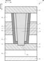
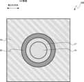
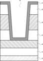
図1、図2、及び図3は、第1の実施形態の半導体装置の模式断面図である。図2は、図1のAA’断面図である。図3は、図1のBB’断面図である。図1において、上下方向を第1の方向と称する。図1において、左右方向を第2の方向と称する。第2の方向は、第1の方向に垂直である。 1, 2, and 3 are schematic cross-sectional views of the semiconductor device of the first embodiment. FIG. 2 is a cross-sectional view taken along line AA' in FIG. FIG. 3 is a sectional view taken along BB' of FIG. In FIG. 1, the vertical direction is referred to as a first direction. In FIG. 1, the left-right direction is referred to as a second direction. The second direction is perpendicular to the first direction.
第1の実施形態の半導体装置は、トランジスタ100である。トランジスタ100は、酸化物半導体にチャネルが形成される酸化物半導体トランジスタである。トランジスタ100は、ゲート電極が、チャネルが形成される酸化物半導体層を囲んで設けられる。トランジスタ100は、いわゆるSurrounding Gate Transistor(SGT)である。トランジスタ100は、いわゆる縦型トランジスタである。 The semiconductor device of the first embodiment is a
トランジスタ100は、下部電極12、上部電極14、第1の酸化物半導体層16、第2の酸化物半導体層17、ゲート電極18、ゲート絶縁層20、下部絶縁層24、及び上部絶縁層26を備える。第1の酸化物半導体層16は、第1の部分16aを含む。 The
下部電極12は、第1の電極の一例である。上部電極14は、第2の電極の一例である。 The
シリコン基板10は、例えば、単結晶シリコンである。基板は、シリコン基板に限定されない。基板は、例えば、シリコン基板以外の半導体基板であっても構わない。基板は、例えば、絶縁基板であっても構わない。
下部電極12は、シリコン基板10の上に設けられる。シリコン基板10と下部電極12との間には、基板絶縁層22が設けられる。
下部電極12は、トランジスタ100のソース電極又はドレイン電極として機能する。 The
下部電極12は、導電体である。下部電極12は、例えば、酸化物導電体又は金属を含む。下部電極12は、例えば、インジウム(In)、スズ(Sn)、及び酸素(O)を含む酸化物導電体である。下部電極12は、例えば、酸化インジウムスズである。下部電極12は、例えば、タングステン(W)、モリブデン(Mo)、銅(Cu)、アルミニウム(Al)、チタン(Ti)、又はタンタル(Ta)を含む金属である。 The
下部電極12は、例えば、複数の導電体の積層構造を有していても構わない。 The
上部電極14は、シリコン基板10の上に設けられる。上部電極14は、下部電極12の上に設けられる。シリコン基板10と上部電極14との間に、下部電極12が設けられる。下部電極12から上部電極14に向かう方向は第1の方向である。
上部電極14は、トランジスタ100のソース電極又はドレイン電極として機能する。 The
上部電極14は、導電体である。上部電極14は、例えば、酸化物導電体又は金属を含む。上部電極14は、例えば、インジウム(In)、スズ(Sn)、及び酸素(O)を含む酸化物導電体である。上部電極14は、例えば、酸化インジウムスズである。上部電極14は、例えば、タングステン(W)、モリブデン(Mo)、銅(Cu)、アルミニウム(Al)、チタン(Ti)、又はタンタル(Ta)を含む金属である。 The
上部電極14は、例えば、複数の導電体の積層構造を有していても構わない。 The
下部電極12と上部電極14とは、例えば、同一の材料で形成される。下部電極12及び上部電極14は、例えば、インジウム(In)、スズ(Sn)、及び酸素(O)を含む酸化物導電体である。下部電極12及び上部電極14は、例えば、酸化インジウムスズである。 The
第1の酸化物半導体層16は、シリコン基板10の上に設けられる。第1の酸化物半導体層16は、下部電極12と上部電極14との間に設けられる。第1の酸化物半導体層16は、例えば、下部電極12に接する。第1の酸化物半導体層16は、例えば、上部電極14に接する。 The first
第1の方向に垂直な断面において、第1の酸化物半導体層16の第2の方向の幅は、例えば、上部電極14から下部電極12に向かって小さくなる。例えば、第1の方向に平行な断面において、第1の酸化物半導体層16の側面は、順テーパ形状を有する。 In the cross section perpendicular to the first direction, the width of the first
第1の酸化物半導体層16の第1の方向の長さは、例えば、80nm以上200nm以下である。第1の酸化物半導体層16の第2の方向の幅は、例えば、20nm以上100nm以下である。 The length of the first
第1の酸化物半導体層16は、酸化物半導体である。第1の酸化物半導体層16は、例えば、アモルファスである。 The first
第1の酸化物半導体層16は、例えば、インジウム(In)、ガリウム(Ga)、シリコン(Si)、アルミニウム(Al)、及びスズ(Sn)からなる群から選ばれる少なくとも一つの元素と、亜鉛(Zn)と、酸素(O)を含む。第1の酸化物半導体層16は、例えば、インジウム(In)、ガリウム(Ga)、及び亜鉛(Zn)を含む。第1の酸化物半導体層16は、例えば、インジウム(In)、アルミニウム(Al)、及び亜鉛(Zn)を含む。 The first
第1の酸化物半導体層16は、例えば、チタン(Ti)、亜鉛(Zn)、及びタングステン(W)からなる群から選ばれる少なくとも一つの元素を含む。第1の酸化物半導体層16は、例えば、酸化チタン、酸化亜鉛、又は酸化タングステンを含む。 The first
第1の酸化物半導体層16は、例えば、下部電極12の化学組成、及び、上部電極14の化学組成と異なる化学組成を有する。 The first
第1の酸化物半導体層16は、第1の部分16aを含む。図3に示すように、第1の部分16aは第1の方向に垂直な面において、下部電極12に囲まれる。 The first
第1の酸化物半導体層16は、例えば、酸素空孔を含む。第1の酸化物半導体層16の中の酸素空孔は、ドナーとして機能する。 The first
第2の酸化物半導体層17は、シリコン基板10の上に設けられる。第2の酸化物半導体層17は、ゲート電極18と第1の酸化物半導体層16との間に設けられる。 The second
図2に示すように、第2の酸化物半導体層17は、第1の酸化物半導体層16を囲む。第2の酸化物半導体層17は、第1の酸化物半導体層16に接する。 As shown in FIG. 2, the second
第2の酸化物半導体層17は、下部電極12と上部電極14との間に設けられる。第2の酸化物半導体層17は、下部電極12と離間する。第2の酸化物半導体層17は、下部電極12と第1の方向に離間する。第1の方向において、第2の酸化物半導体層17と下部電極12との間にゲート絶縁層20が設けられる。 The second
例えば、第1の方向に平行な断面において、第2の酸化物半導体層17の側面は、順テーパ形状を有する。 For example, in a cross section parallel to the first direction, the side surface of the second
第2の酸化物半導体層17には、トランジスタ100のオン動作時に、電流経路となるチャネルが形成される。 A channel serving as a current path is formed in the second
第2の酸化物半導体層17は、酸化物半導体である。第2の酸化物半導体層17は、例えば、アモルファスである。 The second
第2の酸化物半導体層17は、例えば、インジウム(In)、ガリウム(Ga)、シリコン(Si)、アルミニウム(Al)、及びスズ(Sn)からなる群から選ばれる少なくとも一つの元素と、亜鉛(Zn)と、酸素(O)を含む。第2の酸化物半導体層17は、例えば、インジウム(In)、ガリウム(Ga)、及び亜鉛(Zn)を含む。第2の酸化物半導体層17は、例えば、インジウム(In)、アルミニウム(Al)、及び亜鉛(Zn)を含む。 The second
第2の酸化物半導体層17は、例えば、チタン(Ti)、亜鉛(Zn)、及びタングステン(W)からなる群から選ばれる少なくとも一つの元素を含む。第2の酸化物半導体層17は、例えば、酸化チタン、酸化亜鉛、又は酸化タングステンを含む。 The second
第2の酸化物半導体層17は、例えば、第1の酸化物半導体層16と同一の化学組成を有する。第2の酸化物半導体層17は、例えば、下部電極12の化学組成、及び、上部電極14の化学組成と異なる化学組成を有する。 The second
第2の酸化物半導体層17の、ゲート絶縁層20と第1の酸化物半導体層16との間の部分の厚さは、例えば、2nm以上10nm以下である。 The thickness of the portion of the second
ゲート電極18は、第1の酸化物半導体層16に対向する。また、ゲート電極18は、第2の酸化物半導体層17に対向する。ゲート電極18は、その第1の方向における位置座標が、下部電極12の第1の方向における位置座標と上部電極14の第1の方向における位置座標の間の値となるように設けられる。
図2に示すように、ゲート電極18は、第1の酸化物半導体層16を囲んで設けられる。ゲート電極18は、第1の酸化物半導体層16の周囲に設けられる。 As shown in FIG. 2, the
図2に示すように、ゲート電極18は、第2の酸化物半導体層17を囲んで設けられる。ゲート電極18は、第2の酸化物半導体層17の周囲に設けられる。 As shown in FIG. 2, the
ゲート電極18は、例えば、金属、金属化合物、又は半導体である。ゲート電極18は、例えば、タングステン(W)を含む。
ゲート電極18の第1の方向の長さは、例えば、20nm以上100nm以下である。 The length of the
ゲート絶縁層20は、ゲート電極18と第2の酸化物半導体層17との間に設けられる。ゲート絶縁層20は、第2の酸化物半導体層17を囲んで設けられる。ゲート絶縁層20は、第2の酸化物半導体層17に接する。
ゲート絶縁層20は、例えば、酸化物、窒化物、又は酸窒化物である。ゲート絶縁層20は、例えば、酸化シリコン、窒化シリコン、酸窒化シリコン、酸化アルミニウム、酸化ハフニウム、又は酸化ジルコニウムを含む。ゲート絶縁層20は、例えば、酸化シリコン膜、窒化シリコン膜、酸窒化シリコン膜、酸化アルミニウム膜、酸化ハフニウム膜、又は酸化ジルコニウム膜を含む。ゲート絶縁層20は、例えば、上記例示列挙した膜の、積層膜を含む。ゲート絶縁層20の厚さは、例えば、2nm以上10nm以下である。 The
基板絶縁層22は、シリコン基板10と下部電極12との間に設けられる。基板絶縁層22は、例えば、酸化物、窒化物、又は酸窒化物である。基板絶縁層22は、例えば、酸化シリコン、窒化シリコン、又は酸窒化シリコンを含む。基板絶縁層22は、例えば、酸化シリコン、窒化シリコン、又は酸窒化シリコンである。
下部絶縁層24は、下部電極12の上に設けられる。下部絶縁層24は、ゲート電極18と下部電極12との間に設けられる。 Lower insulating
下部絶縁層24は、第1の酸化物半導体層16及び第2の酸化物半導体層17を囲む。下部絶縁層24は、ゲート絶縁層20を囲む。下部絶縁層24と第2の酸化物半導体層17との間に、ゲート絶縁層20が設けられる。 The lower insulating
下部絶縁層24は、例えば、酸化物、窒化物、又は酸窒化物である。下部絶縁層24は、例えば、酸化シリコン、窒化シリコン、又は酸窒化シリコンを含む。下部絶縁層24は、例えば、酸化シリコン層、窒化シリコン層、又は酸窒化シリコン層を含む。下部絶縁層24は、例えば、酸化シリコン層、窒化シリコン層、又は酸窒化シリコン層である。 The lower insulating
上部絶縁層26は、ゲート電極18の上に設けられる。上部絶縁層26は、ゲート電極18と上部電極14との間に設けられる。 Upper insulating
上部絶縁層26は、第1の酸化物半導体層16及び第2の酸化物半導体層17を囲む。上部絶縁層26は、ゲート絶縁層20を囲む。上部絶縁層26と第2の酸化物半導体層17との間に、ゲート絶縁層20が設けられる。 The upper insulating
上部絶縁層26は、例えば、酸化物、窒化物、又は酸窒化物である。上部絶縁層26は、例えば、酸化シリコン、窒化シリコン、又は酸窒化シリコンを含む。上部絶縁層26は、例えば、酸化シリコン層、窒化シリコン層、又は酸窒化シリコン層を含む。上部絶縁層26は、例えば、酸化シリコン層、窒化シリコン層、又は酸窒化シリコン層である。 The upper insulating
次に、第1の実施形態の半導体装置の製造方法の一例について説明する。 Next, an example of a method for manufacturing the semiconductor device of the first embodiment will be described.
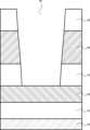
図4、図5、図6、図7、図8、図9、図10、及び図11は、第1の実施形態の半導体装置の製造方法の一例を示す模式断面図である。図4~図11は、それぞれ、図1に対応する断面を示す。図4~図11は、トランジスタ100の製造方法の一例を示す図である。 4, FIG. 5, FIG. 6, FIG. 7, FIG. 8, FIG. 9, FIG. 10, and FIG. 11 are schematic cross-sectional views showing an example of the method for manufacturing the semiconductor device of the first embodiment. 4 to 11 each show a cross section corresponding to FIG. 1. 4 to 11 are diagrams illustrating an example of a method for manufacturing the
最初に、シリコン基板10の上に、第1の酸化シリコン膜31、第1の酸化インジウムスズ膜32、第2の酸化シリコン膜33、タングステン層34、及び第3の酸化シリコン膜35を、この順に第1の方向に積層する(図4)。第1の酸化シリコン膜31、第1の酸化インジウムスズ膜32、第2の酸化シリコン膜33、タングステン層34、及び第3の酸化シリコン膜35は、例えば、Chemical Vapor Deposition法(CVD法)により形成する。 First, a first
第1の酸化シリコン膜31は、最終的に基板絶縁層22となる。第1の酸化インジウムスズ膜32の一部は、最終的に下部電極12となる。第2の酸化シリコン膜33の一部は、最終的に下部絶縁層24となる。タングステン層34の一部は、最終的にゲート電極18となる。第3の酸化シリコン膜35の一部は、最終的に上部絶縁層26となる。 The first
次に、第3の酸化シリコン膜35の表面から、第3の酸化シリコン膜35、タングステン層34、第2の酸化シリコン膜33を貫通し、第1の酸化インジウムスズ膜32に達する開口部36を形成する(図5)。開口部36は、例えば、第1の酸化インジウムスズ膜32に向かって穴径が小さくなる順テーパ形状を有する。開口部36は、例えば、リソグラフィ法、及び、Reactive Ion Etching法(RIE法)を用いて形成する。 Next, an
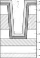
次に、開口部36の内部に、第4の酸化シリコン膜37を形成する(図6)。第4の酸化シリコン膜37は、例えば、CVD法により形成する。第4の酸化シリコン膜37の一部は、最終的にゲート絶縁層20となる。 Next, a fourth
次に、開口部36の内部に、第1の酸化物半導体膜38を形成する(図7)。第1の酸化物半導体膜38の一部は、第2の酸化物半導体層17となる。 Next, a first
第1の酸化物半導体膜38は、例えば、インジウム(In)、ガリウム(Ga)、及び、亜鉛(Zn)を含む。第1の酸化物半導体膜38は、例えば、CVD法で形成する。 The first
次に、開口部36の底部の第1の酸化物半導体膜38及び第4の酸化シリコン膜37をエッチングし、第1の酸化インジウムスズ膜32を露出させる(図8)。さらに、第1の酸化インジウムスズ膜32をエッチングし、凹部40を形成する。第1の酸化物半導体膜38、第4の酸化シリコン膜37、及び第1の酸化インジウムスズ膜32は、RIE法を用いてエッチングする。 Next, the first
第1の酸化物半導体膜38、第4の酸化シリコン膜37、及び第1の酸化インジウムスズ膜32をエッチングする際に、第1の酸化物半導体膜38の表面はエッチングに晒されるため、加工ダメージが加わる。 When etching the first
次に、開口部36を第2の酸化物半導体膜41で埋め込む(図9)。第2の酸化物半導体膜41の一部は、第1の酸化物半導体層16となる。凹部40を埋め込んだ第1の酸化物半導体層16は、第1の酸化物半導体層16の第1の部分16aとなる。 Next, the
第2の酸化物半導体膜41は、例えば、インジウム(In)、ガリウム(Ga)、及び、亜鉛(Zn)を含む。第2の酸化物半導体膜41は、例えば、CVD法で形成する。 The second
次に、第2の酸化物半導体膜41の上部を除去し、第3の酸化シリコン膜35の表面を露出させる(図10)。第2の酸化物半導体膜41は、例えば、RIE法を用いてエッチングし、除去する。 Next, the upper part of the second
次に、第2の酸化インジウムスズ膜42を形成する(図11)。第2の酸化インジウムスズ膜42は、第2の導電膜の一例である。第2の酸化インジウムスズ膜42は、例えば、CVD法により形成する。第2の酸化インジウムスズ膜42は、最終的に上部電極14となる。 Next, a second indium
以上の製造方法により、図1、図2、及び図3に示すトランジスタ100が製造される。 By the above manufacturing method, the
以下、第1の実施形態の半導体装置の作用及び効果について説明する。 The functions and effects of the semiconductor device of the first embodiment will be described below.
酸化物半導体層にチャネルを形成する酸化物半導体トランジスタは、オフ動作時のチャネルリーク電流が極めて小さいという優れた特性を備える。このため、例えば、酸化物半導体トランジスタをDRAMのメモリセルのスイッチングトランジスタに適用することが検討されている。オフ動作時のチャネルリーク電流が極めて小さいため、酸化物半導体トランジスタをスイッチングトランジスタに適用することで、DRAMの電荷保持特性が向上する。 An oxide semiconductor transistor in which a channel is formed in an oxide semiconductor layer has an excellent characteristic of extremely small channel leakage current during off-operation. For this reason, for example, consideration is being given to applying oxide semiconductor transistors to switching transistors of memory cells of DRAMs. Since channel leakage current during off-operation is extremely small, the use of an oxide semiconductor transistor as a switching transistor improves charge retention characteristics of a DRAM.
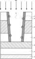
図12は、比較例の半導体装置の模式断面図である。図12は、第1の実施形態の半導体装置の図1に対応する図である。 FIG. 12 is a schematic cross-sectional view of a semiconductor device of a comparative example. FIG. 12 is a diagram corresponding to FIG. 1 of the semiconductor device of the first embodiment.
比較例の半導体装置は、トランジスタ900である。トランジスタ900は、酸化物半導体トランジスタである。トランジスタ900は、ゲート電極18と第1の酸化物半導体層16との間に、第2の酸化物半導体層17を備えない点で、第1の実施形態のトランジスタ100と異なる。また、トランジスタ900は、第1の酸化物半導体層16が、第1の部分16aを備えない点で、第1の実施形態のトランジスタ100と異なる。 A semiconductor device of a comparative example is a
比較例のトランジスタ900は、ゲート絶縁層20と第1の酸化物半導体層16が接する。 In the
図13、図14、及び図15は、比較例の半導体装置の製造方法の一例を示す模式断面図である。図13、図14、及び図15は、それぞれ、図12に対応する断面を示す。図13、図14、及び図15は、トランジスタ900の製造方法の一例を示す図である。 13, FIG. 14, and FIG. 15 are schematic cross-sectional views showing an example of a method for manufacturing a semiconductor device of a comparative example. 13, 14, and 15 each show a cross section corresponding to FIG. 12. 13, FIG. 14, and FIG. 15 are diagrams illustrating an example of a method for manufacturing the
開口部36の内部に、第4の酸化シリコン膜37を形成するまでは、第1の実施形態の製造方法と同様である(図13)。第4の酸化シリコン膜37は、例えば、CVD法により形成する。第4の酸化シリコン膜37の一部は、最終的にゲート絶縁層20となる。 The manufacturing method is the same as that of the first embodiment until the fourth
次に、開口部36の底部の第4の酸化シリコン膜37をエッチングし、第1の酸化インジウムスズ膜32を露出させる(図14)。第4の酸化シリコン膜37は、RIE法を用いてエッチングする。 Next, the fourth
第4の酸化シリコン膜37をエッチングする際に、第4の酸化シリコン膜37の表面はエッチングに晒されるため、加工ダメージが加わる。 When the fourth
次に、開口部36を酸化物半導体膜45で埋め込む(図15)。酸化物半導体膜45の一部は、第1の酸化物半導体層16となる。 Next, the
酸化物半導体膜45は、例えば、インジウム(In)、ガリウム(Ga)、及び、亜鉛(Zn)を含む。酸化物半導体膜45は、例えば、CVD法で形成する。 The
その後、酸化物半導体膜45の上部を除去し、第3の酸化シリコン膜35の表面を露出させる。その後、第1の実施形態の製造方法と同様に、上部電極14となる酸化インジウムスズ膜を形成する。 After that, the upper part of the
以上の製造方法により、図12に示すトランジスタ900が製造される。 By the above manufacturing method, the
比較例のトランジスタ900の製造方法では、開口部36の底部の第4の酸化シリコン膜37をエッチングする際に、ゲート絶縁層20となる第4の酸化シリコン膜37の表面がエッチングに晒され、加工ダメージが加わる。特に、第4の酸化シリコン膜37の表面が順テーパ形状の場合、表面に加えられる加工ダメージは大きくなる。このため、例えば、トランジスタ900のゲート絶縁層20のリーク電流が増大したり、ゲート絶縁層20の信頼性が低下する。 In the method for manufacturing the
また、例えば、ゲート絶縁層20と第1の酸化物半導体層16との界面が加工ダメージを受けることで、キャリアの移動度が低下し、トランジスタ900のオン電流が低下する。 Further, for example, the interface between the
第1の実施形態のトランジスタ100は、ゲート絶縁層20と、第1の酸化物半導体層16との間に第2の酸化物半導体層17が設けられる。第2の酸化物半導体層17が設けられることで、開口部36の底部の第4の酸化シリコン膜37をエッチングする際に、ゲート絶縁層20となる第4の酸化シリコン膜37の表面は、第1の酸化物半導体膜38によって保護される。 In the
したがって、ゲート絶縁層20となる第4の酸化シリコン膜37の表面がエッチングに晒されることがない。よって、トランジスタ100のゲート絶縁層20のリーク電流の増大や、ゲート絶縁層20の信頼性の低下は生じない。 Therefore, the surface of the fourth
また、第1の実施形態のトランジスタ100は、第1の酸化物半導体層16が、下部電極12に接する第1の部分16aを備える。第1の部分16aを備えることで、第1の酸化物半導体層16と下部電極12との間の接触面積を大きくすることができる。したがって、第1の酸化物半導体層16と下部電極12との間のコンタクト抵抗が低減する。よって、トランジスタ100のオン電流が増大する。 Further, in the
第1の実施形態のトランジスタ100では、開口部36の底部の第4の酸化シリコン膜37をエッチングする際に、ゲート絶縁層20となる第4の酸化シリコン膜37の表面は、第1の酸化物半導体膜38によって保護される。このため、オーバーエッチングにより凹部40(図8)を形成することが容易である。この凹部40を用いて、下部電極12に接する第1の部分16aが形成できる。 In the
以上、第1の実施形態によれば、トランジスタ特性の優れた半導体装置が実現される。 As described above, according to the first embodiment, a semiconductor device with excellent transistor characteristics is realized.
(第2の実施形態)
第2の実施形態の半導体装置は、第1の酸化物半導体層の化学組成と、第2の酸化物半導体層の化学組成は異なる点で、第1の実施形態の半導体装置と異なる。以下、第1の実施形態と重複する内容については、一部記述を省略する場合がある。(Second embodiment)
The semiconductor device of the second embodiment differs from the semiconductor device of the first embodiment in that the chemical composition of the first oxide semiconductor layer and the chemical composition of the second oxide semiconductor layer are different. Hereinafter, some descriptions of content that overlaps with the first embodiment may be omitted.
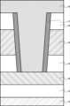
図16は、第2の実施形態の半導体装置の模式断面図である。図16は、第1の実施形態の図1に対応する図である。 FIG. 16 is a schematic cross-sectional view of the semiconductor device of the second embodiment. FIG. 16 is a diagram corresponding to FIG. 1 of the first embodiment.
第2の実施形態の半導体装置は、トランジスタ200である。トランジスタ200は、酸化物半導体にチャネルが形成される酸化物半導体トランジスタである。トランジスタ200は、ゲート電極が、チャネルが形成される酸化物半導体層を囲んで設けられる。トランジスタ200は、いわゆるSGTである。トランジスタ200は、いわゆる縦型トランジスタである。 The semiconductor device of the second embodiment is a
トランジスタ200は、下部電極12、上部電極14、第1の酸化物半導体層16、第2の酸化物半導体層17、ゲート電極18、ゲート絶縁層20、下部絶縁層24、及び上部絶縁層26を備える。第1の酸化物半導体層16は、第1の部分16aを含む。 The
トランジスタ200の第1の酸化物半導体層16の化学組成と、第2の酸化物半導体層17の化学組成は異なる。 The chemical composition of the first
例えば、第2の酸化物半導体層17のインジウム(In)の原子濃度は、第1の酸化物半導体層16のインジウム(In)の原子濃度より高い。例えば、第2の酸化物半導体層17及び第1の酸化物半導体層16は、インジウム(In)、ガリウム(Ga)、及び、亜鉛(Zn)を含み、第2の酸化物半導体層17のインジウム(In)の原子濃度は、第1の酸化物半導体層16のインジウム(In)の原子濃度より高い。 For example, the atomic concentration of indium (In) in the second
また、例えば、第1の酸化物半導体層16のガリウム(Ga)の原子濃度は、第2の酸化物半導体層17のガリウム(Ga)の原子濃度より高い。例えば、第1の酸化物半導体層16及び第2の酸化物半導体層17は、インジウム(In)、ガリウム(Ga)、及び、亜鉛(Zn)を含み、第1の酸化物半導体層16のガリウム(Ga)の原子濃度は、第2の酸化物半導体層17のガリウム(Ga)の原子濃度より高い。 Further, for example, the atomic concentration of gallium (Ga) in the first
また、例えば、第2の酸化物半導体層17は、インジウム(In)、アルミニウム(Al)、及び亜鉛(Zn)を含み、第1の酸化物半導体層16は、インジウム(In)、ガリウム(Ga)、及び、亜鉛(Zn)を含む。例えば、第2の酸化物半導体層17のアルミニウム(Al)の原子濃度は、第1の酸化物半導体層16のアルミニウム(Al)の原子濃度より高い。 Further, for example, the second
第2の実施形態のトランジスタ200によれば、第1の酸化物半導体層16の化学組成と、第2の酸化物半導体層17の化学組成を変えることにより、トランジスタ特性を最適化することができる。 According to the
例えば、第2の酸化物半導体層17のインジウム(In)の原子濃度を、第1の酸化物半導体層16のインジウム(In)の原子濃度より高くすることで、トランジスタ200のキャリア移動度が向上し、オン電流を増加させることができる。 For example, by making the atomic concentration of indium (In) in the second
第2の酸化物半導体層17のインジウム(In)の原子濃度を高くすることで、第2の酸化物半導体層17のキャリア移動度が向上する。トランジスタ200において、第2の酸化物半導体層17は、ゲート絶縁層20を間に挟んで下部電極12と離間する。したがって、第2の酸化物半導体層17から下部電極12への直接的な電流経路は遮断されている。よって、第2の酸化物半導体層17のキャリア移動度が向上しても、トランジスタ200のオフリーク電流の増加は抑制できる。 By increasing the atomic concentration of indium (In) in the second
また、第1の酸化物半導体層16のガリウム(Ga)の原子濃度を、第2の酸化物半導体層17のガリウム(Ga)の原子濃度より高くすることで、トランジスタ200のキャリア移動度が低下し、オフリーク電流を低減させることができる。 Further, by making the atomic concentration of gallium (Ga) in the first
第1の酸化物半導体層16のガリウム(Ga)の原子濃度を高くすることで、第1の酸化物半導体層16のキャリア移動度が低下する。トランジスタ200において、ゲート絶縁層20の直下には、第2の酸化物半導体層17が設けられる。オン電流は主にゲート絶縁層20の直下の第2の酸化物半導体層17を流れる。したがって、第1の酸化物半導体層16のキャリア移動度が低下しても、トランジスタ200のオン電流の低下は抑制できる。 By increasing the atomic concentration of gallium (Ga) in the first
また、第2の酸化物半導体層17のアルミニウム(Al)の原子濃度を、第1の酸化物半導体層16のアルミニウム(Al)の原子濃度より高くすることで、トランジスタ200の閾値変動を抑制することができる。第2の酸化物半導体層17は、例えば、インジウム(In)、アルミニウム(Al)、及び亜鉛(Zn)を含む。 Further, by making the atomic concentration of aluminum (Al) in the second
第2の酸化物半導体層17のアルミニウム(Al)の原子濃度を高くすることで、第2の酸化物半導体層17の耐熱性が向上する。よって、トランジスタ200の閾値変動が抑制できる。第1の酸化物半導体層16の化学組成は、耐熱性以外の特性を最適化するため選択できる。第1の酸化物半導体層16は、例えば、インジウム(In)、ガリウム(Ga)、及び、亜鉛(Zn)を含む。 By increasing the atomic concentration of aluminum (Al) in the second
(変形例)
図17は、第2の実施形態の変形例の半導体装置の模式断面図である。図17は、第2の実施形態の図16に対応する図である。(Modified example)
FIG. 17 is a schematic cross-sectional view of a semiconductor device according to a modification of the second embodiment. FIG. 17 is a diagram corresponding to FIG. 16 of the second embodiment.
第2の実施形態の変形例のトランジスタ201は、第2の酸化物半導体層17は、上部電極14と離間する点で、第2の実施形態のトランジスタ200と異なる。第1の方向において、第2の酸化物半導体層17と上部電極14との間に、第1の酸化物半導体層16が設けられる。変形例のトランジスタ201は、例えば、第1の実施形態の製造方法の図8に対応する凹部形成のエッチングの際に、第2の酸化物半導体層17となる酸化物半導体膜のエッチングレートが、ゲート絶縁層20となる酸化シリコン膜のエッチングレートより速くなるエッチング条件を選択することで形成できる。 A
変形例のトランジスタ201によれば、第2の酸化物半導体層17は、第1の酸化物半導体層16を間に挟んで上部電極14と離間する。したがって、第2の酸化物半導体層17から上部電極14への直接的な電流経路は遮断されている。よって、第2の酸化物半導体層17のキャリア移動度が向上しても、トランジスタ201のオフリーク電流の増加が、第2の実施形態のトランジスタ200と比較して、更に抑制できる。 According to the
以上、第2の実施形態及び変形例によれば、トランジスタ特性の優れた半導体装置が実現される。 As described above, according to the second embodiment and the modified example, a semiconductor device with excellent transistor characteristics is realized.
(第3の実施形態)
第3の実施形態の半導体装置は、コア絶縁層を含む点で、第1の実施形態の半導体装置と異なる。以下、第1の実施形態と重複する内容については、一部記述を省略する場合がある。(Third embodiment)
The semiconductor device of the third embodiment differs from the semiconductor device of the first embodiment in that it includes a core insulating layer. Hereinafter, some descriptions of content that overlaps with the first embodiment may be omitted.
図18は、第3の実施形態の半導体装置の模式断面図である。図18は、第1の実施形態の図1に対応する図である。 FIG. 18 is a schematic cross-sectional view of the semiconductor device of the third embodiment. FIG. 18 is a diagram corresponding to FIG. 1 of the first embodiment.
第3の実施形態の半導体装置は、トランジスタ300である。トランジスタ300は、酸化物半導体にチャネルが形成される酸化物半導体トランジスタである。トランジスタ300は、ゲート電極が、チャネルが形成される酸化物半導体層を囲んで設けられる。トランジスタ300は、いわゆるSGTである。トランジスタ300は、いわゆる縦型トランジスタである。 The semiconductor device of the third embodiment is a
トランジスタ300は、下部電極12、上部電極14、第1の酸化物半導体層16、第2の酸化物半導体層17、ゲート電極18、ゲート絶縁層20、下部絶縁層24、及び上部絶縁層26を備える。第1の酸化物半導体層16は、第1の部分16a、コア絶縁層46を含む。 The
コア絶縁層46は、第1の方向に垂直な面において、第1の酸化物半導体層16に囲まれる。コア絶縁層46は、例えば、ゲート電極18を含み、第1の方向に垂直な断面において、第1の酸化物半導体層16に囲まれる。 The core insulating
コア絶縁層46は、例えば、酸化物、窒化物、又は酸窒化物である。コア絶縁層46は、例えば、酸化シリコン、窒化シリコン、又は酸窒化シリコンを含む。コア絶縁層46は、例えば、酸化シリコン層、窒化シリコン層、又は酸窒化シリコン層を含む。コア絶縁層46は、例えば、酸化シリコン層、窒化シリコン層、又は酸窒化シリコン層である。
コア絶縁層46を含むことで、例えば、第1の酸化物半導体層16の体積が低下し、トランジスタ300のオフリーク電流が低減する。 By including the core insulating
以上、第3の実施形態によれば、トランジスタ特性の優れた半導体装置が実現される。 As described above, according to the third embodiment, a semiconductor device with excellent transistor characteristics is realized.
(第4の実施形態)
第4の実施形態の半導体装置は、第1の方向に平行な断面において、第1の酸化物半導体層の側面が第1の方向に平行な点で、第1の実施形態の半導体装置と異なる。以下、第1の実施形態と重複する内容については、一部記述を省略する場合がある。(Fourth embodiment)
The semiconductor device of the fourth embodiment differs from the semiconductor device of the first embodiment in that the side surface of the first oxide semiconductor layer is parallel to the first direction in a cross section parallel to the first direction. . Hereinafter, some descriptions of content that overlaps with the first embodiment may be omitted.
図19は、第4の実施形態の半導体装置の模式断面図である。図19は、第1の実施形態の図1に対応する図である。 FIG. 19 is a schematic cross-sectional view of the semiconductor device of the fourth embodiment. FIG. 19 is a diagram corresponding to FIG. 1 of the first embodiment.
第4の実施形態の半導体装置は、トランジスタ400である。トランジスタ400は、酸化物半導体にチャネルが形成される酸化物半導体トランジスタである。トランジスタ400は、ゲート電極が、チャネルが形成される酸化物半導体層を囲んで設けられる。トランジスタ400は、いわゆるSGTである。トランジスタ400は、いわゆる縦型トランジスタである。 The semiconductor device of the fourth embodiment is a
トランジスタ400は、下部電極12、上部電極14、第1の酸化物半導体層16、第2の酸化物半導体層17、ゲート電極18、ゲート絶縁層20、下部絶縁層24、及び上部絶縁層26を備える。第1の酸化物半導体層16は、第1の部分16aを含む。 The
第1の方向に平行な断面において、第1の酸化物半導体層16の側面が第1の方向に平行である。第1の酸化物半導体層16の側面は、順テーパ形状を有しない。 In the cross section parallel to the first direction, the side surfaces of the first
第1の酸化物半導体層16の側面が順テーパ形状を有しないことで、第1の酸化物半導体層16の第1の部分16aと下部電極12との間の接触面積を更に大きくすることができる。したがって、第1の酸化物半導体層16と下部電極12との間のコンタクト抵抗が更に低減する。よって、トランジスタ400のオン電流が増大する。 Since the side surface of the first
以上、第4の実施形態によれば、トランジスタ特性の優れた半導体装置が実現される。 As described above, according to the fourth embodiment, a semiconductor device with excellent transistor characteristics is realized.
(第5の実施形態)
第5の実施形態の半導体記憶装置は、第1の電極と、第2の電極と、第1の電極と第2の電極との間に設けられた第1の酸化物半導体層と、第1の酸化物半導体層に対向するゲート電極と、ゲート電極と第1の酸化物半導体層との間に設けられ、第1の電極と離間した第2の酸化物半導体層と、ゲート電極と第2の酸化物半導体層との間に設けられたゲート絶縁層と、第1の電極又は第2の電極に電気的に接続されたキャパシタと、を備える。(Fifth embodiment)
The semiconductor memory device of the fifth embodiment includes a first electrode, a second electrode, a first oxide semiconductor layer provided between the first electrode and the second electrode, and a first oxide semiconductor layer provided between the first electrode and the second electrode. a gate electrode facing the oxide semiconductor layer; a second oxide semiconductor layer provided between the gate electrode and the first oxide semiconductor layer and spaced apart from the first electrode; and a capacitor electrically connected to the first electrode or the second electrode.
第5の実施形態の半導体記憶装置は、半導体メモリ500である。第5の実施形態の半導体記憶装置は、DRAMである。半導体メモリ500は、第1の実施形態のトランジスタ100を、DRAMのメモリセルのスイッチングトランジスタとして使用する。 The semiconductor memory device of the fifth embodiment is a
以下、第1の実施形態と重複する内容については、一部記述を省略する。 Hereinafter, some descriptions of contents that overlap with those of the first embodiment will be omitted.
図20は、第5の実施形態の半導体記憶装置の等価回路図である。図20は、メモリセルMCが1個の場合を例示しているが、メモリセルMCは、例えばアレイ状に複数設けられていても構わない。 FIG. 20 is an equivalent circuit diagram of the semiconductor memory device of the fifth embodiment. Although FIG. 20 illustrates a case where there is one memory cell MC, a plurality of memory cells MC may be provided, for example, in an array.
半導体メモリ500は、メモリセルMC、ワード線WL、ビット線BL、及びプレート線PLを備える。メモリセルMCは、スイッチングトランジスタTR及びキャパシタCAを含む。図20で、破線で囲まれた領域がメモリセルMCである。 The
ワード線WLは、スイッチングトランジスタTRのゲート電極に電気的に接続される。ビット線BLは、スイッチングトランジスタTRのソース・ドレイン電極の一方に電気的に接続される。キャパシタCAの一方の電極は、スイッチングトランジスタTRのソース・ドレイン電極の他方に電気的に接続される。キャパシタCAの他方の電極は、プレート線PLに接続される。 Word line WL is electrically connected to the gate electrode of switching transistor TR. The bit line BL is electrically connected to one of the source and drain electrodes of the switching transistor TR. One electrode of the capacitor CA is electrically connected to the other source/drain electrode of the switching transistor TR. The other electrode of capacitor CA is connected to plate line PL.
メモリセルMCは、キャパシタCAに電荷を蓄積することで、データを記憶する。データの書き込み及び読出しは、スイッチングトランジスタTRをオン動作させることにより行う。 Memory cell MC stores data by accumulating charge in capacitor CA. Data writing and reading are performed by turning on the switching transistor TR.
例えば、ビット線BLに所望の電圧を印加した状態でスイッチングトランジスタTRをオン動作させ、メモリセルMCへのデータの書き込みを行う。 For example, with a desired voltage applied to the bit line BL, the switching transistor TR is turned on to write data into the memory cell MC.
また、例えば、スイッチングトランジスタTRをオン動作させ、キャパシタに蓄積された電荷量に応じたビット線BLの電圧変化を検知し、メモリセルMCのデータの読み出しを行う。 Further, for example, the switching transistor TR is turned on, a voltage change on the bit line BL corresponding to the amount of charge accumulated in the capacitor is detected, and data in the memory cell MC is read.
図21は、第5の実施形態の半導体記憶装置の模式断面図である。図21は、半導体メモリ500のメモリセルMCの断面を示す。 FIG. 21 is a schematic cross-sectional view of the semiconductor memory device of the fifth embodiment. FIG. 21 shows a cross section of memory cell MC of
半導体メモリ500は、シリコン基板10、スイッチングトランジスタTR、キャパシタCA、下部層間絶縁層50、及び上部層間絶縁層52を含む。
スイッチングトランジスタTRは、下部電極12、上部電極14、第1の酸化物半導体層16、第2の酸化物半導体層17、ゲート電極18、ゲート絶縁層20、下部絶縁層24、及び上部絶縁層26を備える。第1の酸化物半導体層16は、第1の部分16aを含む。 The switching transistor TR includes a
下部電極12は、第1の電極の一例である。上部電極14は、第2の電極の一例である。 The
スイッチングトランジスタTRは、第1の実施形態のトランジスタ100と同様の構造を有する。 Switching transistor TR has a structure similar to
キャパシタCAは、シリコン基板10とスイッチングトランジスタTRとの間に設けられる。キャパシタCAは、シリコン基板10と下部電極12との間に設けられる。キャパシタCAは、下部電極12に電気的に接続される。 Capacitor CA is provided between
キャパシタCAは、セル電極71、プレート電極72、キャパシタ絶縁膜73を備える。セル電極71は、下部電極12に電気的に接続される。セル電極71は、例えば、下部電極12に接する。 Capacitor CA includes a
セル電極71及びプレート電極72は、例えば、窒化チタンである。キャパシタ絶縁膜73は、例えば、酸化ジルコニウム、酸化アルミニウム、酸化ジルコニウムの積層構造を有する。 The
ゲート電極18は、例えば、図示しないワード線WLに電気的に接続される。上部電極14は、例えば、図示しないビット線BLに電気的に接続される。プレート電極72は、例えば、図示しないプレート線PLに接続される。 The
半導体メモリ500は、オフ動作時のチャネルリーク電流が極めて小さい酸化物半導体トランジスタをスイッチングトランジスタTRに適用する。したがって、電荷保持特性に優れたDRAMが実現する。 In the
また、半導体メモリ500のスイッチングトランジスタTRは、例えば、ゲート絶縁層20のリーク電流が低減される。よって、半導体メモリ500の動作特性が向上する。 Further, in the switching transistor TR of the
第1ないし第4の実施形態においては、ゲート電極18が第1の酸化物半導体層16を囲んで設けられるトランジスタを例に説明したが、本発明の実施形態のトランジスタは、ゲート電極が酸化物半導体層を囲まないトランジスタであっても構わない。例えば、本発明の実施形態のトランジスタは、酸化物半導体層が2本のゲート電極に挟まれるトランジスタであっても構わない。 In the first to fourth embodiments, the transistor in which the
第5の実施形態においては、第1の実施形態のトランジスタが適用される半導体メモリを例に説明したが、本発明の実施形態の半導体メモリは、第2ないし第4の実施形態のトランジスタが適用される半導体メモリであっても構わない。 In the fifth embodiment, the semiconductor memory to which the transistor of the first embodiment is applied has been described as an example, but the semiconductor memory of the embodiment of the present invention applies the transistors of the second to fourth embodiments. It is also possible to use a semiconductor memory.
第5の実施形態においては、セル電極が下部電極12に電気的に接続される半導体メモリを例に説明したが、本発明の実施形態の半導体メモリは、セル電極が上部電極14に電気的に接続される半導体メモリであっても構わない。 In the fifth embodiment, the semiconductor memory in which the cell electrode is electrically connected to the
以上、本発明のいくつかの実施形態を説明したが、これらの実施形態は、例として提示したものであり、発明の範囲を限定することは意図していない。これら新規な実施形態は、その他の様々な形態で実施されることが可能であり、発明の要旨を逸脱しない範囲で、種々の省略、置き換え、変更を行うことができる。例えば、一実施形態の構成要素を他の実施形態の構成要素と置き換え又は変更してもよい。これら実施形態やその変形は、発明の範囲や要旨に含まれるとともに、特許請求の範囲に記載された発明とその均等の範囲に含まれる。 Although several embodiments of the present invention have been described above, these embodiments are presented as examples and are not intended to limit the scope of the invention. These novel embodiments can be implemented in various other forms, and various omissions, substitutions, and changes can be made without departing from the gist of the invention. For example, components of one embodiment may be replaced or modified with components of other embodiments. These embodiments and their modifications are included within the scope and gist of the invention, as well as within the scope of the invention described in the claims and its equivalents.
12 下部電極(第1の電極)
14 上部電極(第2の電極)
16 第1の酸化物半導体層
16a 第1の部分
17 第2の酸化物半導体層
18 ゲート電極
20 ゲート絶縁層
100 トランジスタ(半導体装置)
200 トランジスタ(半導体装置)
300 トランジスタ(半導体装置)
400 トランジスタ(半導体装置)
500 半導体メモリ(半導体記憶装置)
CA キャパシタ12 Lower electrode (first electrode)
14 Upper electrode (second electrode)
16 First
200 Transistor (semiconductor device)
300 Transistor (semiconductor device)
400 Transistor (semiconductor device)
500 Semiconductor memory (semiconductor storage device)
CA capacitor
Claims (20)
Translated fromJapanese第2の電極と、
前記第1の電極と前記第2の電極との間に設けられた第1の酸化物半導体層と、
前記第1の酸化物半導体層に対向するゲート電極と、
前記ゲート電極と前記第1の酸化物半導体層との間に設けられ、前記第1の電極と離間した第2の酸化物半導体層と、
前記ゲート電極と前記第2の酸化物半導体層との間に設けられたゲート絶縁層と、
を備える半導体装置。a first electrode;
a second electrode;
a first oxide semiconductor layer provided between the first electrode and the second electrode;
a gate electrode facing the first oxide semiconductor layer;
a second oxide semiconductor layer provided between the gate electrode and the first oxide semiconductor layer and spaced apart from the first electrode;
a gate insulating layer provided between the gate electrode and the second oxide semiconductor layer;
A semiconductor device comprising:
第2の電極と、
前記第1の電極と前記第2の電極との間に設けられた第1の酸化物半導体層と、
前記第1の酸化物半導体層に対向するゲート電極と、
前記ゲート電極と前記第1の酸化物半導体層との間に設けられ、前記第1の電極と離間した第2の酸化物半導体層と、
前記ゲート電極と前記第2の酸化物半導体層との間に設けられたゲート絶縁層と、
前記第1の電極又は前記第2の電極に電気的に接続されたキャパシタと、
を備える半導体記憶装置。a first electrode;
a second electrode;
a first oxide semiconductor layer provided between the first electrode and the second electrode;
a gate electrode facing the first oxide semiconductor layer;
a second oxide semiconductor layer provided between the gate electrode and the first oxide semiconductor layer and spaced apart from the first electrode;
a gate insulating layer provided between the gate electrode and the second oxide semiconductor layer;
a capacitor electrically connected to the first electrode or the second electrode;
A semiconductor storage device comprising:
Priority Applications (4)
| Application Number | Priority Date | Filing Date | Title |
|---|---|---|---|
| JP2022041799AJP2023136275A (en) | 2022-03-16 | 2022-03-16 | Semiconductor devices and semiconductor storage devices |
| TW111129020ATWI830322B (en) | 2022-03-16 | 2022-08-02 | Semiconductor devices and semiconductor memory devices |
| CN202211062267.4ACN116825821A (en) | 2022-03-16 | 2022-08-31 | Semiconductor devices and semiconductor memory devices |
| US17/899,909US20230299206A1 (en) | 2022-03-16 | 2022-08-31 | Semiconductor device and semiconductor storage device |
Applications Claiming Priority (1)
| Application Number | Priority Date | Filing Date | Title |
|---|---|---|---|
| JP2022041799AJP2023136275A (en) | 2022-03-16 | 2022-03-16 | Semiconductor devices and semiconductor storage devices |
Publications (1)
| Publication Number | Publication Date |
|---|---|
| JP2023136275Atrue JP2023136275A (en) | 2023-09-29 |
Family
ID=88067380
Family Applications (1)
| Application Number | Title | Priority Date | Filing Date |
|---|---|---|---|
| JP2022041799APendingJP2023136275A (en) | 2022-03-16 | 2022-03-16 | Semiconductor devices and semiconductor storage devices |
Country Status (4)
| Country | Link |
|---|---|
| US (1) | US20230299206A1 (en) |
| JP (1) | JP2023136275A (en) |
| CN (1) | CN116825821A (en) |
| TW (1) | TWI830322B (en) |
Cited By (1)
| Publication number | Priority date | Publication date | Assignee | Title |
|---|---|---|---|---|
| WO2025177132A1 (en)* | 2024-02-22 | 2025-08-28 | 株式会社半導体エネルギー研究所 | Semiconductor device and method for producing semiconductor device |
Family Cites Families (4)
| Publication number | Priority date | Publication date | Assignee | Title |
|---|---|---|---|---|
| US12063770B2 (en)* | 2018-12-28 | 2024-08-13 | Semiconductor Energy Laboratory Co., Ltd. | Memory device and semiconductor device including the memory device |
| JP2020198343A (en)* | 2019-05-31 | 2020-12-10 | キオクシア株式会社 | Semiconductor device and semiconductor memory device |
| JP7387475B2 (en)* | 2020-02-07 | 2023-11-28 | キオクシア株式会社 | Semiconductor devices and semiconductor storage devices |
| JP2021153082A (en)* | 2020-03-24 | 2021-09-30 | キオクシア株式会社 | Semiconductor device and semiconductor storage device |
- 2022
- 2022-03-16JPJP2022041799Apatent/JP2023136275A/enactivePending
- 2022-08-02TWTW111129020Apatent/TWI830322B/enactive
- 2022-08-31USUS17/899,909patent/US20230299206A1/enactivePending
- 2022-08-31CNCN202211062267.4Apatent/CN116825821A/enactivePending
Cited By (1)
| Publication number | Priority date | Publication date | Assignee | Title |
|---|---|---|---|---|
| WO2025177132A1 (en)* | 2024-02-22 | 2025-08-28 | 株式会社半導体エネルギー研究所 | Semiconductor device and method for producing semiconductor device |
Also Published As
| Publication number | Publication date |
|---|---|
| CN116825821A (en) | 2023-09-29 |
| TWI830322B (en) | 2024-01-21 |
| US20230299206A1 (en) | 2023-09-21 |
| TW202339203A (en) | 2023-10-01 |
Similar Documents
| Publication | Publication Date | Title |
|---|---|---|
| US11430886B2 (en) | Semiconductor device and semiconductor memory device | |
| JP2022049604A (en) | Semiconductor devices and semiconductor storage devices | |
| TW202314977A (en) | Semiconductor device and semiconductor memory device | |
| US12310065B2 (en) | Semiconductor device, semiconductor memory device, and method for manufacturing semiconductor device | |
| US20230299206A1 (en) | Semiconductor device and semiconductor storage device | |
| US12432907B2 (en) | Semiconductor device and semiconductor memory device | |
| US20230197857A1 (en) | Semiconductor device, semiconductor memory device, and semiconductor device manufacturing method | |
| US20230328957A1 (en) | Semiconductor device and semiconductor memory device | |
| US20240324180A1 (en) | Semiconductor device and semiconductor memory device | |
| US20230422482A1 (en) | Semiconductor device and semiconductor memory device | |
| US20230290882A1 (en) | Semiconductor device and semiconductor memory device | |
| US20240321995A1 (en) | Semiconductor device and semiconductor memory device | |
| CN115835623B (en) | semiconductor memory devices | |
| US20230387317A1 (en) | Semiconductor device and semiconductor storage device | |
| US20250301629A1 (en) | Oxide semiconductor-based dynamic random access memory (dram) device | |
| JP2025145771A (en) | semiconductor memory device |