JP2023126865A - Electronic element mounting substrate, electronic device, and electronic module - Google Patents
Electronic element mounting substrate, electronic device, and electronic moduleDownload PDFInfo
- Publication number
- JP2023126865A JP2023126865AJP2023107470AJP2023107470AJP2023126865AJP 2023126865 AJP2023126865 AJP 2023126865AJP 2023107470 AJP2023107470 AJP 2023107470AJP 2023107470 AJP2023107470 AJP 2023107470AJP 2023126865 AJP2023126865 AJP 2023126865A
- Authority
- JP
- Japan
- Prior art keywords
- layer
- clearance
- view
- plan
- electronic device
- Prior art date
- Legal status (The legal status is an assumption and is not a legal conclusion. Google has not performed a legal analysis and makes no representation as to the accuracy of the status listed.)
- Granted
Links
Images


Classifications
- H—ELECTRICITY
- H01—ELECTRIC ELEMENTS
- H01L—SEMICONDUCTOR DEVICES NOT COVERED BY CLASS H10
- H01L23/00—Details of semiconductor or other solid state devices
- H01L23/12—Mountings, e.g. non-detachable insulating substrates
- H01L23/14—Mountings, e.g. non-detachable insulating substrates characterised by the material or its electrical properties
- H—ELECTRICITY
- H05—ELECTRIC TECHNIQUES NOT OTHERWISE PROVIDED FOR
- H05K—PRINTED CIRCUITS; CASINGS OR CONSTRUCTIONAL DETAILS OF ELECTRIC APPARATUS; MANUFACTURE OF ASSEMBLAGES OF ELECTRICAL COMPONENTS
- H05K1/00—Printed circuits
- H05K1/02—Details
- H05K1/11—Printed elements for providing electric connections to or between printed circuits
- H05K1/115—Via connections; Lands around holes or via connections
- H05K1/116—Lands, clearance holes or other lay-out details concerning the surrounding of a via
- H—ELECTRICITY
- H05—ELECTRIC TECHNIQUES NOT OTHERWISE PROVIDED FOR
- H05K—PRINTED CIRCUITS; CASINGS OR CONSTRUCTIONAL DETAILS OF ELECTRIC APPARATUS; MANUFACTURE OF ASSEMBLAGES OF ELECTRICAL COMPONENTS
- H05K3/00—Apparatus or processes for manufacturing printed circuits
- H05K3/46—Manufacturing multilayer circuits
- H05K3/4611—Manufacturing multilayer circuits by laminating two or more circuit boards
- H05K3/4626—Manufacturing multilayer circuits by laminating two or more circuit boards characterised by the insulating layers or materials
- H05K3/4629—Manufacturing multilayer circuits by laminating two or more circuit boards characterised by the insulating layers or materials laminating inorganic sheets comprising printed circuits, e.g. green ceramic sheets
- H—ELECTRICITY
- H01—ELECTRIC ELEMENTS
- H01L—SEMICONDUCTOR DEVICES NOT COVERED BY CLASS H10
- H01L21/00—Processes or apparatus adapted for the manufacture or treatment of semiconductor or solid state devices or of parts thereof
- H01L21/02—Manufacture or treatment of semiconductor devices or of parts thereof
- H01L21/04—Manufacture or treatment of semiconductor devices or of parts thereof the devices having potential barriers, e.g. a PN junction, depletion layer or carrier concentration layer
- H01L21/48—Manufacture or treatment of parts, e.g. containers, prior to assembly of the devices, using processes not provided for in a single one of the groups H01L21/18 - H01L21/326 or H10D48/04 - H10D48/07
- H01L21/4814—Conductive parts
- H01L21/4846—Leads on or in insulating or insulated substrates, e.g. metallisation
- H01L21/4857—Multilayer substrates
- H—ELECTRICITY
- H01—ELECTRIC ELEMENTS
- H01L—SEMICONDUCTOR DEVICES NOT COVERED BY CLASS H10
- H01L21/00—Processes or apparatus adapted for the manufacture or treatment of semiconductor or solid state devices or of parts thereof
- H01L21/02—Manufacture or treatment of semiconductor devices or of parts thereof
- H01L21/04—Manufacture or treatment of semiconductor devices or of parts thereof the devices having potential barriers, e.g. a PN junction, depletion layer or carrier concentration layer
- H01L21/48—Manufacture or treatment of parts, e.g. containers, prior to assembly of the devices, using processes not provided for in a single one of the groups H01L21/18 - H01L21/326 or H10D48/04 - H10D48/07
- H01L21/4814—Conductive parts
- H01L21/4846—Leads on or in insulating or insulated substrates, e.g. metallisation
- H01L21/486—Via connections through the substrate with or without pins
- H—ELECTRICITY
- H01—ELECTRIC ELEMENTS
- H01L—SEMICONDUCTOR DEVICES NOT COVERED BY CLASS H10
- H01L21/00—Processes or apparatus adapted for the manufacture or treatment of semiconductor or solid state devices or of parts thereof
- H01L21/02—Manufacture or treatment of semiconductor devices or of parts thereof
- H01L21/04—Manufacture or treatment of semiconductor devices or of parts thereof the devices having potential barriers, e.g. a PN junction, depletion layer or carrier concentration layer
- H01L21/48—Manufacture or treatment of parts, e.g. containers, prior to assembly of the devices, using processes not provided for in a single one of the groups H01L21/18 - H01L21/326 or H10D48/04 - H10D48/07
- H01L21/4814—Conductive parts
- H01L21/4846—Leads on or in insulating or insulated substrates, e.g. metallisation
- H01L21/4867—Applying pastes or inks, e.g. screen printing
- H—ELECTRICITY
- H01—ELECTRIC ELEMENTS
- H01L—SEMICONDUCTOR DEVICES NOT COVERED BY CLASS H10
- H01L23/00—Details of semiconductor or other solid state devices
- H01L23/12—Mountings, e.g. non-detachable insulating substrates
- H—ELECTRICITY
- H01—ELECTRIC ELEMENTS
- H01L—SEMICONDUCTOR DEVICES NOT COVERED BY CLASS H10
- H01L23/00—Details of semiconductor or other solid state devices
- H01L23/48—Arrangements for conducting electric current to or from the solid state body in operation, e.g. leads, terminal arrangements ; Selection of materials therefor
- H01L23/488—Arrangements for conducting electric current to or from the solid state body in operation, e.g. leads, terminal arrangements ; Selection of materials therefor consisting of soldered or bonded constructions
- H01L23/498—Leads, i.e. metallisations or lead-frames on insulating substrates, e.g. chip carriers
- H01L23/49811—Additional leads joined to the metallisation on the insulating substrate, e.g. pins, bumps, wires, flat leads
- H—ELECTRICITY
- H01—ELECTRIC ELEMENTS
- H01L—SEMICONDUCTOR DEVICES NOT COVERED BY CLASS H10
- H01L23/00—Details of semiconductor or other solid state devices
- H01L23/48—Arrangements for conducting electric current to or from the solid state body in operation, e.g. leads, terminal arrangements ; Selection of materials therefor
- H01L23/488—Arrangements for conducting electric current to or from the solid state body in operation, e.g. leads, terminal arrangements ; Selection of materials therefor consisting of soldered or bonded constructions
- H01L23/498—Leads, i.e. metallisations or lead-frames on insulating substrates, e.g. chip carriers
- H01L23/49827—Via connections through the substrates, e.g. pins going through the substrate, coaxial cables
- H—ELECTRICITY
- H05—ELECTRIC TECHNIQUES NOT OTHERWISE PROVIDED FOR
- H05K—PRINTED CIRCUITS; CASINGS OR CONSTRUCTIONAL DETAILS OF ELECTRIC APPARATUS; MANUFACTURE OF ASSEMBLAGES OF ELECTRICAL COMPONENTS
- H05K1/00—Printed circuits
- H05K1/02—Details
- H05K1/0296—Conductive pattern lay-out details not covered by sub groups H05K1/02 - H05K1/0295
- H05K1/0298—Multilayer circuits
- H—ELECTRICITY
- H05—ELECTRIC TECHNIQUES NOT OTHERWISE PROVIDED FOR
- H05K—PRINTED CIRCUITS; CASINGS OR CONSTRUCTIONAL DETAILS OF ELECTRIC APPARATUS; MANUFACTURE OF ASSEMBLAGES OF ELECTRICAL COMPONENTS
- H05K1/00—Printed circuits
- H05K1/02—Details
- H05K1/11—Printed elements for providing electric connections to or between printed circuits
- H05K1/111—Pads for surface mounting, e.g. lay-out
- H05K1/112—Pads for surface mounting, e.g. lay-out directly combined with via connections
- H05K1/113—Via provided in pad; Pad over filled via
- H—ELECTRICITY
- H05—ELECTRIC TECHNIQUES NOT OTHERWISE PROVIDED FOR
- H05K—PRINTED CIRCUITS; CASINGS OR CONSTRUCTIONAL DETAILS OF ELECTRIC APPARATUS; MANUFACTURE OF ASSEMBLAGES OF ELECTRICAL COMPONENTS
- H05K1/00—Printed circuits
- H05K1/18—Printed circuits structurally associated with non-printed electric components
- H05K1/182—Printed circuits structurally associated with non-printed electric components associated with components mounted in the printed circuit board, e.g. insert mounted components [IMC]
- H05K1/184—Components including terminals inserted in holes through the printed circuit board and connected to printed contacts on the walls of the holes or at the edges thereof or protruding over or into the holes
- H—ELECTRICITY
- H01—ELECTRIC ELEMENTS
- H01L—SEMICONDUCTOR DEVICES NOT COVERED BY CLASS H10
- H01L2224/00—Indexing scheme for arrangements for connecting or disconnecting semiconductor or solid-state bodies and methods related thereto as covered by H01L24/00
- H01L2224/01—Means for bonding being attached to, or being formed on, the surface to be connected, e.g. chip-to-package, die-attach, "first-level" interconnects; Manufacturing methods related thereto
- H01L2224/42—Wire connectors; Manufacturing methods related thereto
- H01L2224/47—Structure, shape, material or disposition of the wire connectors after the connecting process
- H01L2224/48—Structure, shape, material or disposition of the wire connectors after the connecting process of an individual wire connector
- H01L2224/4805—Shape
- H01L2224/4809—Loop shape
- H01L2224/48091—Arched
- H—ELECTRICITY
- H01—ELECTRIC ELEMENTS
- H01L—SEMICONDUCTOR DEVICES NOT COVERED BY CLASS H10
- H01L2224/00—Indexing scheme for arrangements for connecting or disconnecting semiconductor or solid-state bodies and methods related thereto as covered by H01L24/00
- H01L2224/01—Means for bonding being attached to, or being formed on, the surface to be connected, e.g. chip-to-package, die-attach, "first-level" interconnects; Manufacturing methods related thereto
- H01L2224/42—Wire connectors; Manufacturing methods related thereto
- H01L2224/47—Structure, shape, material or disposition of the wire connectors after the connecting process
- H01L2224/48—Structure, shape, material or disposition of the wire connectors after the connecting process of an individual wire connector
- H01L2224/484—Connecting portions
- H01L2224/4847—Connecting portions the connecting portion on the bonding area of the semiconductor or solid-state body being a wedge bond
- H01L2224/48472—Connecting portions the connecting portion on the bonding area of the semiconductor or solid-state body being a wedge bond the other connecting portion not on the bonding area also being a wedge bond, i.e. wedge-to-wedge
- H—ELECTRICITY
- H01—ELECTRIC ELEMENTS
- H01L—SEMICONDUCTOR DEVICES NOT COVERED BY CLASS H10
- H01L2224/00—Indexing scheme for arrangements for connecting or disconnecting semiconductor or solid-state bodies and methods related thereto as covered by H01L24/00
- H01L2224/01—Means for bonding being attached to, or being formed on, the surface to be connected, e.g. chip-to-package, die-attach, "first-level" interconnects; Manufacturing methods related thereto
- H01L2224/42—Wire connectors; Manufacturing methods related thereto
- H01L2224/47—Structure, shape, material or disposition of the wire connectors after the connecting process
- H01L2224/49—Structure, shape, material or disposition of the wire connectors after the connecting process of a plurality of wire connectors
- H01L2224/491—Disposition
- H01L2224/4912—Layout
- H01L2224/49175—Parallel arrangements
- H—ELECTRICITY
- H05—ELECTRIC TECHNIQUES NOT OTHERWISE PROVIDED FOR
- H05K—PRINTED CIRCUITS; CASINGS OR CONSTRUCTIONAL DETAILS OF ELECTRIC APPARATUS; MANUFACTURE OF ASSEMBLAGES OF ELECTRICAL COMPONENTS
- H05K2201/00—Indexing scheme relating to printed circuits covered by H05K1/00
- H05K2201/09—Shape and layout
- H05K2201/09209—Shape and layout details of conductors
- H05K2201/09372—Pads and lands
- H05K2201/09454—Inner lands, i.e. lands around via or plated through-hole in internal layer of multilayer PCB
Landscapes
- Engineering & Computer Science (AREA)
- Microelectronics & Electronic Packaging (AREA)
- Computer Hardware Design (AREA)
- Physics & Mathematics (AREA)
- Condensed Matter Physics & Semiconductors (AREA)
- General Physics & Mathematics (AREA)
- Power Engineering (AREA)
- Manufacturing & Machinery (AREA)
- Ceramic Engineering (AREA)
- Inorganic Chemistry (AREA)
- Chemical & Material Sciences (AREA)
- Structure Of Printed Boards (AREA)
- Production Of Multi-Layered Print Wiring Board (AREA)
Abstract
Translated fromJapaneseDescription
Translated fromJapanese本開示は、電子素子等が実装される電子素子実装用基板、電子装置および電子モジュールに関するものである。 The present disclosure relates to an electronic element mounting substrate, an electronic device, and an electronic module on which electronic elements and the like are mounted.
絶縁層と配線層を含み、貫通導体を有する基板を備えた電子素子実装用基板が知られている。また、このような電子素子実装用基板を使用した電子装置は凹部からの上面に蓋体を実装する構造が知られている。(特開2017-183337号公報参照)。 2. Description of the Related Art Electronic device mounting boards are known that include a board that includes an insulating layer and a wiring layer and has a through conductor. Further, it is known that an electronic device using such an electronic element mounting substrate has a structure in which a lid body is mounted on the upper surface of the concave portion. (Refer to Japanese Patent Application Publication No. 2017-183337).
近年、電子装置は薄型化が要求されている。そのため、電子装置に使用される電子素子実装用基板の各絶縁層も薄くなることを要求されている。電子素子実装用基板の貫通導体は導電性を高めるために、各絶縁層の表面または/および下面にランドパターンを設ける。このランドパターンは、同一層の他の電位と接続するパターンからの絶縁性を向上させるためクリアランスを設ける場合が有る。このとき、複数の貫通導体が上面視において一部または全てが重なって位置することで、このクリアランスを上面視において一部またはすべてが重なる。このクリアランスが複数層重なることで、電子素子実装用基板の表面に凹凸が生じるまたは、電子素子実装用基板の内部のクリアランスの縁周辺に空間ができ、電子素子実装用基板の強度の低下またはクラックが発生することが懸念されていた。 In recent years, electronic devices have been required to be thinner. Therefore, each insulating layer of an electronic element mounting substrate used in an electronic device is also required to be thinner. In order to increase the electrical conductivity of the through conductor of the electronic element mounting board, a land pattern is provided on the surface and/or the bottom surface of each insulating layer. This land pattern may be provided with a clearance in order to improve insulation from patterns connected to other potentials on the same layer. At this time, the plurality of through conductors are positioned so that some or all of them overlap when viewed from the top, so that the clearances partially or all overlap when viewed from the top. When multiple layers of this clearance overlap, unevenness occurs on the surface of the electronic device mounting board, or a space is created around the edges of the clearance inside the electronic device mounting board, resulting in a decrease in the strength of the electronic device mounting board or cracks. There were concerns that this would occur.
本開示の1つの態様に係る電子素子実装用基板は、第1層と、前記第1層の下面に位置した第2層と、前記第2層の下面に位置した第3層とを有するとともに、電子素子が実装される基板と、前記第1層から前記第3層にわたって上下方向に貫通したビア導体と、前記第1層と前記第2層との間に位置するとともに、平面透視において前記ビア導体と接続された第1導体層と、前記第2層と前記第3層との間に位置するとともに、平面透視において前記ビア導体と接続された第2導体層と、を備えており、前記第1導体層は、平面透視において、前記ビア導体を囲むとともに前記ビア導体と接続された第1ランド部と、前記第1ランド部を囲む第1クリアランス部と、前記第1クリアランス部を囲むとともに前記第1クリアランス部を介して前記第1ランド部と電気的に絶縁された第1周辺部とを有しており、前記第2導体層は、平面透視において、前記ビア導体を囲むとともに前記ビア導体と接続された第2ランド部と、前記第2ランド部を囲む第2クリアランス部と、前記第2クリアランス部を囲むとともに前記第2クリアランス部を介して前記第2ランド部と電気的に絶縁された第2周辺部とを有しており、平面透視において、前記第1ランド部は、前記第2ランド部と重なって位置している第1部分を有しているとともに、平面透視において、前記第1クリアランス部は、前記第2クリアランス部と重ならずに位置している第2部分を有しており、上下方向の断面視において、前記第1周辺部および前記第2周辺部は、それぞれ、前記ビア導体から遠ざかるにつれて厚みが薄くなっている端部を有し、
前記第1導体層および前記第2導体層は、タングステン、モリブデン、マンガン、パラジウム、もしくは銅、またはこれらから選ばれる少なくとも1種以上の金属材料を含有する合金を含み、かつ銀を含まない。An electronic device mounting board according to one aspect of the present disclosure includes a first layer, a second layer located on the lower surface of the first layer, and a third layer located on the lower surface of the second layer. , a substrate on which an electronic element is mounted; a via conductor that vertically penetrates from the first layer to the third layer; and a via conductor located between the first layer and the second layer, and a first conductor layer connected to the via conductor; and a second conductor layer located between the second layer and the third layer and connected to the via conductor in plan view; The first conductor layer surrounds the via conductor and is connected to the via conductor, a first clearance part surrounding the first land part, and surrounding the first clearance part in plan view. and a first peripheral portion that is electrically insulated from the first land portion via the first clearance portion, and the second conductor layer surrounds the via conductor and also has a first peripheral portion that is electrically insulated from the first land portion through the first clearance portion. a second land connected to the via conductor; a second clearance part surrounding the second land; and a second clearance part surrounding the second clearance part and electrically connected to the second land through the second clearance part. and an insulated second peripheral portion, and in plan view, the first land portion has a first portion overlapping with the second land portion, and in plan view, , the first clearance part has a second part located without overlapping the second clearance part, and in a vertical cross-sectional view, the first peripheral part and the second peripheral part are , each having an end portion that becomes thinner as it moves away from the via conductor,
The first conductor layer and the second conductor layer contain tungsten, molybdenum, manganese, palladium, copper, or an alloy containing at least one metal material selected from these, and do not contain silver.
本開示の1つの態様に係る電子装置は、上述した電子素子実装用基板と、前記電子素子実装用基板に実装された電子素子と、を有している。 An electronic device according to one aspect of the present disclosure includes the above-described electronic element mounting substrate and an electronic element mounted on the electronic element mounting substrate.
本開示の1つの態様に係る電子モジュールは、上述した電子装置と、前記電子装置を囲んで位置した筐体と、を有している。 An electronic module according to one aspect of the present disclosure includes the above-described electronic device and a housing positioned to surround the electronic device.
<電子素子実装用基板および電子装置の構成>
以下、本開示のいくつかの例示的な実施形態について図面を参照して説明する。なお、以下の説明では、電子素子実装用基板に電子素子が実装された構成を電子装置とする。また、電子素子実装用基板の上面側に位置するようにまたは電子装置を囲んで設けられた筐体または部材を有する構成を電子モジュールとする。電子素子実装用基板、電子装置および電子モジュールは、いずれの方向が上方若しくは下方とされてもよいが、便宜的に、直交座標系xyzを定義するとともに、z方向の正側を上方とする。<Configuration of electronic element mounting board and electronic device>
Hereinafter, some exemplary embodiments of the present disclosure will be described with reference to the drawings. Note that in the following description, a configuration in which an electronic element is mounted on an electronic element mounting substrate is referred to as an electronic device. Further, an electronic module is a structure having a casing or a member provided so as to be located on the upper surface side of an electronic element mounting board or surrounding an electronic device. For electronic element mounting substrates, electronic devices, and electronic modules, any direction may be upward or downward, but for convenience, an orthogonal coordinate system xyz is defined, and the positive side of the z direction is assumed to be upward.
(第1の実施形態)
図1~図9を参照して本開示の第1の実施形態に係る電子素子実装用基板1、並びにそれを備えた電子装置21について説明する。なお、図1は電子装置21の上面図および断面図を示しており、図2は電子モジュール31の上面図および断面図を示している。また、図3~図7には電子素子実装用基板1の要部Aの拡大縦断面図を示している。また、図8および図9には、電子素子実装用基板1の要部Aの拡大平面図および拡大断面図を示している。(First embodiment)
An electronic
電子素子実装用基板1は、第1層2aと、第1層2aの下面に位置した第2層2bと、第2層2aの下面に位置した第3層2cとを有するとともに、電子素子10が実装される基板2を有する。基板2は、第1層2a、第2層2bおよび第3層2cを連続して上下方向に貫通したビア導体5を有する。基板2は、第1層2aと第2層2bとの間に位置するとともに、平面透視においてビア導体5と接続される第1導体層6を有する。基板2は、第2層2bと第3層2cとの間に位置するとともに、平面透視においてビア導体5と接続される第2導体層7を有している。第1導体層6は、平面透視において、ビア導体5を囲む第1ランド部6aと、第1ランド部6aを囲む第1クリアランス部6cと、第1クリアランス部6cを囲むとともに第1クリアランス部6cを介して第1ランド部6aと電気的に絶縁された第1周辺部6bとを有している。第2導体層7は、平面透視において、ビア導体5を囲む第2ランド部7aと、第2ランド部7aを囲む第2クリアランス部7cと、第2クリアランス部7cを囲むとともに第2クリアランス部7cを介して第2ランド部7aと電気的に絶縁された第2周辺部7bとを有している。基板2の第1ランド部6aは、第2ランド部7aと重なって位置している第1部分6eを有している。また、平面透視において、第1クリアランス部6cは、第2クリアランス部7cと重ならずに位置した第2部分6fを有している。言い換えると、第1クリアランス部6aと第2クリアランス部7aとは平面透視において大きさおよび/または形状が異なっている。基板2の第1周辺部6bおよび第2周辺部6bは、基板2の上下方向、つまりz方向の断面視において、それぞれ、ビア導体5から遠ざかるにつれて厚みが薄くなっている端部(第1端部6d、第2端部7d)を有する。 The electronic
電子素子実装用基板1は、第1層2aと、第1層2aの下面に位置した第2層2bと、第2層2aの下面に位置した第3層2cとを有するとともに、電子素子10が実装される基板2を有する。基板2aは上面に電子素子10が実装される実装領域を有する。実装領域とは、少なくとも1つ以上の電子素子10が実装される領域であり、例えば後述する電極パッド3の最外周の内側またはそれ以上等、適宜定めることが可能である。また、実装領域に実装される部品は電子素子10に限らず、例えば電子部品であってもよく、電子素子10または/および電子部品の個数は指定されない。 The electronic
基板2を形成する絶縁層の材料として使用される電気絶縁性セラミックスとしては例えば、酸化アルミニウム質焼結体、ムライト質焼結体、炭化珪素質焼結体、窒化アルミニウム質焼結体、窒化珪素質焼結体またはガラスセラミック焼結体等が含まれる。基板2を形成する絶縁層の材料として使用される樹脂としては例えば、熱可塑性の樹脂、エポキシ樹脂、ポリイミド樹脂、アクリル樹脂、フェノール樹脂またはフッ素系樹脂等が含まれる。フッ素系樹脂としては例えば、四フッ化エチレン樹脂が含まれる。 Examples of electrically insulating ceramics used as a material for the insulating layer forming the
基板2は、図1に示すように5層の絶縁層から形成されていてもよいし、4層以下または6層以上の絶縁層から形成されていてもよい。絶縁層が4層以下の場合には、電子素子実装用基板1の薄型化を図ることができる。また、絶縁層が6層以上の場合には、電子素子実装用基板1の剛性を高めることができる。 The
電子素子実装用基板1は例えば、最外周の1辺の大きさは0.3mm~10cmであり、平面視において電子素子実装用基板1が四角形状あるとき、正方形であってもよいし長方形であってもよい。また例えば、電子素子実装用基板1の厚みは0.2mm以上である。 For example, the size of one side of the outermost periphery of the electronic
基板2は、第1層2a、第2層2bおよび第3層2cを連続して上下方向に貫通したビア導体5を有する。基板2は、第1層2aと第2層2bとの間に位置するとともに、平面視においてビア導体5と接続される第1導体層6を有する。基板2は、第2層2bと第3層2cとの間に位置するとともに、平面視においてビア導体5と接続される第2導体層7を有している。 The
また、電子素子実装用基板1の基体2の上面、側面または下面には、外部回路接続用電極が設けられていてもよい。外部回路接続用電極は、基体2と外部回路基板、あるいは電子装置21と外部回路基板とを電気的に接続していてもよい。 Moreover, an electrode for external circuit connection may be provided on the upper surface, side surface, or lower surface of the
さらに基体2の上面または下面には、電極パッド3または/および外部回路接続用電極以外に、絶縁層間に形成される電極、内部配線導体および内部配線導体同士を上下に接続するビア導体5以外の貫通導体が設けられていてもよい。これら電極、内部配線導体または貫通導体は、基板2の表面に露出していてもよい。この電極、内部配線導体または貫通導体によって、電極パッド3または/および外部回路接続用電極はそれぞれ電気的に接続されていてもよい。 Further, on the upper or lower surface of the
電極パッド3、ビア導体5、第1導体層6、第2導体層7、外部回路接続用電極、電極、内部配線導体または/および貫通導体は、基体2が電気絶縁性セラミックスから成る場合には、タングステン(W)、モリブデン(Mo)、マンガン(Mn)、パラジウム(Pd)、銀(Ag)若しくは銅(Cu)またはこれらから選ばれる少なくとも1種以上の金属材料を含有する合金等が含まれる。また、銅(Cu)のみからなっていてもよい。また、電極パッド3、ビア導体5、第1導体層6、第2導体層7、外部回路接続用電極、内部配線導体または/および貫通導体は、基体2が樹脂から成る場合には、銅(Cu)、金(Au)、アルミニウム(Al)、ニッケル(Ni)、モリブデン(Mo)、パラジウム(Pd)若しくはチタン(Ti)またはこれらから選ばれる少なくとも1種以上の金属材料を含有する合金等が含まれる。 The
電極パッド3、ビア導体5、外部回路接続用電極、電極、内部配線導体または/および貫通導体の露出表面に、さらにめっき層を有していてもよい。この構成によれば、外部回路接続用の電極、導体層および貫通導体の露出表面を保護して酸化を低減することができる。また、この構成によれば、電極パッド3と電子素子10と、をワイヤボンディング等の電子素子接続部材13を介して良好に電気的接続することができる。めっき層は、例えば、厚さ0.5μm~10μmのNiめっき層を被着させるか、またはこのNiめっき層および厚さ0.5μm~3μmの金(Au)めっき層を順次被着させてもよい。 The exposed surfaces of the
第1導体層6は、平面視において、ビア導体5を囲む第1ランド部6aと、第1ランド部6aを囲むとともに電気的に絶縁された第1クリアランス部6cと、第1クリアランス部6cを囲む第1周辺部6bとを有している。ここで、第1導体層6の第1ランド部6aと第1周辺部6bとは同一の信号であってもよいし、異なる信号であってもよい。また、第1周辺部6bは例えば幅広のベタパターンであってもよいし、細い線状のシグナルパターンであってもよい。 In plan view, the
第2導体層7は、平面透視において、ビア導体5を囲む第2ランド部7aと、第2ランド部7aを囲む第2クリアランス部7cと、第2クリアランス部7cを囲むとともに、第2クリアランス部を介して第2ランド部7aと電気的に絶縁された第2周辺部7bとを有している。ここで、第2導体層6の第2ランド部7aと第2周辺部7bとは同一の信号であってもよいし、異なる信号であってもよい。また、第2周辺部7bは例えば幅広のベタパターンであってもよいし、細い線状のシグナルパターンであってもよい。 In plan view, the
また、第1導体層6と第2導体層7とは同一の信号であってもよいし、異なる信号であってもよい。 Further, the
基板2は、第1ランド部6aが第2ランド部7aと、平面透視において重なって位置している第1部分6eを有するとともに、第1クリアランス部6aは、第2クリアランス部7aと、平面透視において重ならずに位置している第2部分6fを有している。基板2の第1周辺部6bおよび第2周辺部7bは、上下方向の断面視において、それぞれ、ビア導体5から遠ざかるにつれて厚みが薄くなっている端部(第1端部6d、第2端部7d)を有する。 The
近年、電子装置は薄型化が要求されている。そのため、電子装置に使用される電子素子実装用基板の各絶縁層も薄くなることを要求されている。電子素子実装用基板の貫通導体は導電性を高めるために、各絶縁層の表面または/および下面にランドパターンを設ける。このランドパターンは、同一層の他の電位と接続するパターンからの絶縁性を向上させるためクリアランスを設ける場合が有る。このとき、複数の貫通導体が上面視において一部または全てが重なって位置することで、このクリアランスを上面視において一部またはすべてが重なる場合が有る。電子素子実装用基板の各絶縁層が薄型化すると、このクリアランスが複数層上面視で重なることで、電子素子実装用基板の表面に凹凸が生じることがある。または、電子素子実装用基板の内部のクリアランスの縁周辺に空間ができることがある。このことによって、電子素子実装用基板の強度の低下またはクラックが発生することが懸念されていた。 In recent years, electronic devices have been required to be thinner. Therefore, each insulating layer of an electronic element mounting substrate used in an electronic device is also required to be thinner. In order to increase the electrical conductivity of the through conductor of the electronic element mounting board, a land pattern is provided on the surface and/or the bottom surface of each insulating layer. This land pattern may be provided with a clearance in order to improve insulation from patterns connected to other potentials on the same layer. At this time, because the plurality of through conductors are located so that some or all of them overlap when viewed from the top, this clearance may partially or all overlap when viewed from the top. When each insulating layer of the electronic element mounting substrate becomes thinner, the clearances of the multiple layers overlap when viewed from above, which may cause unevenness on the surface of the electronic element mounting substrate. Alternatively, a space may be created around the edge of the clearance inside the electronic element mounting board. There has been concern that this may lead to a decrease in strength or cracks in the electronic element mounting substrate.
これに対し、本実施形態の電子素子実装用基板1は、第1クリアランス部6aは、第2クリアランス部7aと、平面透視において重ならずに位置している第2部分6fを有している。これにより、複数層のクリアランスが重なることで、電子素子実装用基板1の表面に凹凸が発生することを低減させることが可能となる。 On the other hand, in the electronic
また一般的に、電子素子実装用基板は、各絶縁層間に設けられた配線層の厚みを各絶縁層が変形することで、その配線層の厚みを吸収し、配線層の周囲は絶縁層で覆われる。しかしながら、電子素子実装用基板の薄型化により各絶縁層が薄くなることで、配線層と絶縁層との間に空間が発生する場合が有り、この空間が発生し、複数層で平面透視において重なることで電子素子実装用基板の強度が低下することが懸念されていた。 In general, electronic device mounting boards absorb the thickness of the wiring layer provided between each insulating layer by deforming the thickness of the wiring layer, and the wiring layer is surrounded by an insulating layer. covered. However, as each insulating layer becomes thinner due to the thinning of substrates for mounting electronic devices, a space may be created between the wiring layer and the insulating layer. There was a concern that this would reduce the strength of the electronic element mounting board.
これに対し、本実施形態の電子素子実装用基板1は、基板2の第1周辺部6bの第1端部6dおよび第2周辺部7bの第2端部7dは、上下方向の断面視において、ビア導体5から遠ざかるにつれて厚みが薄くなっている。つまり、各周辺部は、それぞれビア導体5から遠ざかるにつれて厚みが薄くなっている端部(第1端部6d、第2端部7d)を有する。特に、第1周辺部6bおよび第2周辺部7bの両端が、断面視において、端に向かうにつれて厚みが薄くなり、湾曲したレンズ形状であってもよい。つまり、第1端部6dと第2端部7dは断面視においてレンズ状であってもよい。これにより、電子素子実装用基板1の各絶縁層が薄くなったとしても、第1周辺部6bおよび第2周辺部7bの端部が曲線部を描いていることで各絶縁層が第1導体層6および第2導体層7との端部に沿って変形しやすくなる。よって、配線層と絶縁層との間に空間が発生することを低減させることが可能となり、電子素子実装用基板の強度が低下することを低減させることが可能となる。 On the other hand, in the electronic
基板2は上面に枠体を有していてもよい。また、枠体は基板2と同様の材料であってもよいし異なる材料であってもよい。基板2と枠体とは、接合材で接合されていてもよいし基板2と枠体とが絶縁性セラミックスからなるとき同時焼結で結合していてもよい。また、枠体は段差を有しておりそこに電極パッド3を有していてもよく、このとき基板2と枠体とは電気的に接続していてもよい。 The
図1~図6に示す例のように、基板2はさらに第1ランド部6aおよび第2ランド部7aのそれぞれの外端、つまりビア導体5から遠ざかる方向に位置した端部にも、上面および下面に曲線部を有していてもよい。この構造により、電子素子実装用基板1の各絶縁層が薄くなったとしても、第1ランド部6aおよび第2ランド部7aの端部が曲線部を描いていることで各絶縁層が第1導体層6および第2導体層7との端部に沿って変形しやすくなる。よって、配線層と絶縁層との間に空間が発生することを低減させることが可能となり、電子素子実装用基板の強度が低下することを低減させることが可能となる。 As in the examples shown in FIGS. 1 to 6, the
図1~図6に示す例のように、第1周辺部6bおよび第2周辺部7bのそれぞれの外端、つまりビア導体5から遠ざかる方向に位置した端部は、上下方向の断面視において湾曲していてもよい。つまり、第1端部6dおよび第2端部7dのそれぞれの上面および下面が曲線部を有していてもよい。これにより、電子素子実装用基板1の各絶縁層が薄くなったとしても、第1周辺部6bおよび第2周辺部7bの外端が湾曲していることで各絶縁層が第1導体層6および第2導体層7との外端に沿って変形しやすくなる。よって、配線層と絶縁層との間に空間が発生することを低減させることが可能となり、電子素子実装用基板の強度が低下することを低減させることが可能となる。さらに、例えばそれぞれの外端が基板2の外周部近傍に位置しているとき、第1周辺部6aおよび第2周辺部7bのそれぞれの外端は、上下に湾曲していることで、各絶縁層が第1導体層6および第2導体層7との外端に沿って変形しやすくなる。よって、基板2の外周部に製造工程時における絶縁層間の接着不良が発生することを低減させることが可能となる。 As in the examples shown in FIGS. 1 to 6, the outer ends of the first
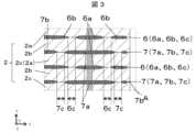
図3~図6に本実施形態の要部Aの拡大断面図を示す。 FIGS. 3 to 6 show enlarged cross-sectional views of main parts A of this embodiment.
図3に示す例では、電子素子実装用基板1は平面透視において第2クリアランス部7cは、第1周辺部6bと重なっている。これにより、第1クリアランス部6aと第2クリアランス部7bとが平面透視において重なることを低減させることが可能となる。よって、電子素子実装用基板1の表面に凹凸が発生することを低減させることが可能となる。また、第2クリアランス部7cが、第1周辺部6bと平面透視で重なっていることで、第2クリアランス部7c部分を補強することが可能となる。よって、電子素子実装用基板の強度が低下することを低減させることが可能となる。なお、このとき第2クリアランス部7cと第1周辺部6bとは平面透視において全てが重なっていてもよいし、一部のみが重なっていてもよい。とくに、第2クリアランス部7cと第1周辺部6bとが平面透視で全てが重なっていることで、補強の効果をより向上させることが可能となる。 In the example shown in FIG. 3, the
図4に示す例では、電子素子実装用基板1は平面透視において第1クリアランス部6cは、第2周辺部7bと重なっている。これにより、第1クリアランス部6cと第2クリアランス部7cとが平面透視において重なることを低減させることが可能となる。よって、電子素子実装用基板1の表面に凹凸が発生することを低減させることが可能となる。また、第1クリアランス部6cが、第2周辺部7bと平面視で重なっていることで、第1クリアランス部6C部分を補強することが可能となる。よって、電子素子実装用基板の強度が低下することを低減させることが可能となる。なお、このとき第1クリアランス部6cと第2周辺部7bとは平面透視において全てが重なっていてもよいし、一部のみが重なっていてもよい。とくに、第1クリアランス部6cと第2周辺部7bとが平面透視で全てが重なっていることで、補強の効果をより向上させることが可能となる。 In the example shown in FIG. 4, the
また、第1導体層6または/および第2導体層7は図3に示す例のように第1周辺部6bまたは/および第2周辺部7bが第1ランド部6aまたは/および第2ランド部7aの周囲を囲むように位置していてもよいし、図4に示す例のように第1ランド部6aまたは/および第2ランド部7bの近傍の一部のみに位置していてもよい。どちらの場合においても、本実施形態の効果を奏することが可能となる。また、図4に示す例のように、第1周辺部6bまたは/および第2周辺部7bが基板2の外辺から第1ランド部6aまたは/および第2ランド部7a側に位置していないことで、基板2が絶縁性セラミックスであるとき積層の工程において圧力が基板2の外周部に均一にかかるため、基板2の外辺部に製造工程時における絶縁層間の接着不良が生じることを低減させることができる。 Further, in the
図5に示す例では、電子素子実装用基板1は断面視において第1導体層6と第2導体層7との間にその他の導体層9を有している。このようの場合においても、第1クリアランス部6cと第2クリアランス部7cとが平面透視において重なることを低減させることが可能となる。また、その他の導体層9を第1導体層6と第2導体層7との間に位置することで、第1クリアランス部6cと第2クリアランス部7cとが平面透面視で一部が重なる部分を有していたとしても、電子素子実装用基板1の表面に凹凸が生じることを低減させることが可能となり、または、電子素子実装用基板1の内部のクリアランスの縁周辺に空間ができ、電子素子実装用基板1の強度の低下またはクラックが発生することを低減させることが可能となる。また、第1クリアランス部6cと第2クリアランス部7cの部分をその他の導体層9で補強することが可能となり、電子素子実装用基板の強度が低下することを低減させることが可能となる。 In the example shown in FIG. 5, the electronic
図6に示す例では、電子素子実装用基板1の第1クリアランス部6cは平面透視において第2ランド部7aと重なって位置している。このような場合においても、本実施形態の効果を奏することが可能となる。また、第1クリアランス部6cが、第2ランド部7aと平面視で重なっていることで、第1クリアランス部6c部分を補強することが可能となる。よって、電子素子実装用基板の強度が低下することを低減させることが可能となる。なお、このとき第1クリアランス部6cと第2ランド部7aとは平面透視において全てが重なっていてもよいし、一部のみが重なっていてもよい。とくに、第1クリアランス部6cと第1ランド部7aとが平面視で全てが重なっていることで、補強の効果をより向上させることが可能となる。 In the example shown in FIG. 6, the
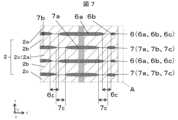
図7に示す例では、電子素子実装用基板1の第2クリアランス部7cは平面透視において第1ランド部6aと重なって位置している。このような場合においても、本実施形態の効果を奏することが可能となる。また、第2クリアランス部7cが、第1ランド部6aと平面透視で重なっていることで、第2クリアランス部7c部分を補強することが可能となる。よって、電子素子実装用基板の強度が低下することを低減させることが可能となる。なお、このとき第2クリアランス部7cと第1ランド部6aとは平面透視において全てが重なっていてもよいし、一部のみが重なっていてもよい。とくに、第2クリアランス部7cと第2ランド部6aとが平面視で全てが重なっていることで、補強の効果をより向上させることが可能となる。 In the example shown in FIG. 7, the
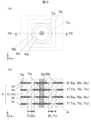
図8~図9に本実施形態の要部Aの拡大平面図および拡大断面図を示す。なお、ここで図8(a)および図9(a)は第1導体層6から平面視したときの図である。 FIGS. 8 and 9 show an enlarged plan view and an enlarged sectional view of the main part A of this embodiment. Note that FIGS. 8A and 9A are views viewed from the
図8に示す例では、第1ランド部6aと第2ランド部7aは平面透視で同一形状であるが、それぞれの大きさが異なっている。例えば、第1ランド部6aと第2ランド部7aが平面透視おいて、ビア導体5の中心から遠ざかる方向を外側としたときの外縁が円形状であるとき、それぞれ径の大きさが異なっている。また、第1クリアランス部6cと第2クリアランス部7cが平面透視おいて、ビア導体5の中心から遠ざかる方向を外側としたときの外縁が円形状であってもよく、それぞれ径の大きさが異なっている。このとき、平面透視における第1クリアランス部6cの外縁の大きさは、第1径r1であり、第2クリアランス部7cの外縁の大きさは、第2径r2である。第1径r1は第2径r2よりも大きくてもよいし、小さくてもよい。第2径r2は、第1径r1と異なっていればよい。また、図9に示す例では、第1ランド部6aと第2ランド部7aは、平面透視で異なる形状である。いずれの場合においても、第1クリアランス部6cと第2クリアランス部7cとは平面透視でそのまま重なることを低減させることが可能となる。これにより、第1クリアランス部6cと第2クリアランス部7cが平面透視で重なることで、第1クリアランス部6cと第2クリアランス部7cに各絶縁層が入り込み電子素子実装用基板1の表面に凹凸が発生することを低減させることが可能となる。 In the example shown in FIG. 8, the
図9に示す例では、第1ランド部6aが円形状であり、第2ランド部7aは矩形状である。これにより、製造時の誤差等が生じ多少形状が変形した場合においても第1ランド部6aおよび第2ランド部7aが全く同じ形状となることを低減させることが可能となる。よって、製造誤差が生じた場合においても本実施形態の効果を奏することが可能となる。また、製造誤差等で同一の形状となることを低減させることが可能となるため、第1ランド部6aと第2ランド部7bとを同程度の大きさとすることが可能となる。よって、電子素子実装用基板1の小型化が可能となる。ここで、第1ランド部6aと第2ランド部7aとの組み合わせは円と矩形状であったが、円と三角形状、三角形状と矩形状、それぞれ形状の異なる多角形状同士であってもよい。 In the example shown in FIG. 9, the
<電子装置の構成>
図1に電子装置21の例を示す。電子装置21は、電子素子実装用基板1と、電子素子実装用基板1の上面に実装された電子素子10を備えている。<Configuration of electronic device>
FIG. 1 shows an example of the
電子装置21は、電子素子実装用基板1と、電子素子実装用基板1の基板2の実装領域に実装された電子素子10を有している。電子素子10の一例としては、例えばCCD(Charge Coupled Device)型またはCMOS(Complementary Metal Oxide Semiconductor)型等の撮像素子、LED(Light Emitting Diode)等の発光素子、圧力、気圧、加速度、ジャイロ等のセンサー機能を有する素子、または集積回路等である。なお、電子素子10は、接着材を介して、基板2の上面に配置されていてもよい。この接着材は、例えば、銀エポキシまたは熱硬化性樹脂等が使用される。 The
電子素子10と電子素子実装用基板1とは例えば電子素子接続部材13で電気的に接続されていてもよい。 The
電子装置21は、電子素子10を覆うとともに、電子素子実装用基板1の上面に接合された蓋体12を有していてもよい。 The
蓋体は、例えば電子素子10がCMOS、CCD等の撮像素子、またはLEDなどの発光素子である場合ガラス材料等の透明度の高い部材が用いられる。また蓋体は例えば、電子素子10が集積回路等であるとき、金属製材料、セラミック材料または有機材料が用いられていてもよい。 For example, when the
蓋体は、蓋体接続部材14を介して電子素子実装用基板1と接合していてもよい。蓋体接続部材14を構成する材料として例えば、熱硬化性樹脂または低融点ガラスまたは金属成分からなるろう材等がある。 The lid may be joined to the electronic
電子装置21が図1~図3に示すような電子素子実装用基板1を有することで、電子素子実装用基板1の表面の凹凸または/および強度を低減させることが可能となる。よって、電子装置21の製造歩留まりを向上させることが可能となる。 When the
<電子モジュールの構成>
図2に電子モジュール31の例を示す。電子モジュール31は、電子装置21とその上面に位置する筐体32を備えている。<Electronic module configuration>
FIG. 2 shows an example of the
本実施形態の電子素子実装用基板1および電子装置21は、電子装置21と電子装置21の上面または電子装置21上に位置した筐体32とを有した電子モジュール31を構成していてもよい。なお、以下に示す例では説明のため撮像モジュールを例に説明する。ここで、電子装置21の上面に位置した筐体32とは、例えば電子装置21自体が筐体32で覆われている場合なども、筐体32の一部が電子装置21上に位置しているため、本構成に含まれる。 The electronic
電子モジュール31は筐体32(レンズホルダー等)を有していてもよい。筐体32を有することでより気密性の向上または電子装置21の外部からの応力が直接電子装置21に加えられることを低減することが可能となる。筐体32は、例えば樹脂または金属材料等から成る。また、筐体32がレンズホルダーであるとき筐体32は、樹脂、液体、ガラスまたは水晶等からなるレンズが1個以上組み込まれていてもよい。また、筐体32は、上下左右の駆動を行う駆動装置等が付いていて、電子素子実装用基板1の表面に位置するパッド等と半田などの接合材を介して電気的に接続されていてもよい。 The
なお、筐体32は上面視において4方向または下面側の少なくとも一つの辺において開口部が設けられていてもよい。そして、筐体32の開口部から外部回路基板が挿入され電子素子実装用基板1と電気的に接続していてもよい。また筐体32の開口部は、外部回路基板が電子素子実装用基板1と電気的に接続された後、樹脂等の封止材等で開口部の隙間を閉じて電子モジュール31の内部が気密されていてもよい。 Note that the
<電子素子実装用基板および電子装置の製造方法>
次に、本実施形態の電子素子実装用基板1および電子装置21の製造方法の一例について説明する。なお、下記で示す製造方法の一例は、多数個取り配線基板を用いた基体2の製造方法である。<Method for manufacturing electronic device mounting substrate and electronic device>
Next, an example of a method for manufacturing the electronic
(1)まず、基体2を構成するセラミックグリーンシートを形成する。例えば、酸化アルミニウム(Al2O3)質焼結体である基体2を得る場合には、Al2O3の粉末に焼結助材としてシリカ(SiO2)、マグネシア(MgO)またはカルシア(CaO)等の粉末を添加し、さらに適当なバインダー、溶剤および可塑剤を添加し、次にこれらの混合物を混錬してスラリー状となす。その後、ドクターブレード法またはカレンダーロール法等の成形方法によって多数個取り用のセラミックグリーンシートを得る。(1) First, a ceramic green sheet constituting the
なお、基体2が、例えば樹脂から成る場合は、所定の形状に成形できるような金型を用いて、トランスファーモールド法、インジェクションモールド法または金型等での押圧等で成形することによって基体2を形成することができる。また、基体2は、例えばガラスエポキシ樹脂のように、ガラス繊維から成る基材に樹脂を含浸させたものであってもよい。この場合には、ガラス繊維から成る基材にエポキシ樹脂の前駆体を含浸させ、このエポキシ樹脂前駆体を所定の温度で熱硬化させることによって基体2を形成できる。 In addition, when the
(2)次に、前述のグリーンシートを金型等によって加工する。ここで基体2がノッチ等を有する場合、基体2となるグリーンシートの所定の箇所に、ノッチ等を同様に形成してもよい。 (2) Next, the green sheet described above is processed using a mold or the like. If the
(3)次に、基体2の各絶縁層となるセラミックグリーンシートを積層して加圧する。このことにより各絶縁層となるグリーンシートを積層し、基体2(電子素子実装用基板1)となるセラミックグリーンシート積層体を作製する。
なお、この時適宜切欠き部等となる部分を金型などで作製してもよい。(3) Next, ceramic green sheets that will become each insulating layer of the
Note that at this time, a portion that will become a notch or the like may be made using a mold or the like.
(4)次に、スクリーン印刷法等によって、セラミックグリーンシートまたセラミックグリーンシート積層体に電極パッド3、外部回路接続用電極、内部配線導体および内部貫通導体となる部分に、金属ペーストを塗布または充填する。なお、セラミックグリーンシートを積層する工程の前に金属ペーストを塗布または充填してもよい。この金属ペーストは、前述した金属材料から成る金属粉末に適当な溶剤およびバインダーを加えて混練することによって、適度な粘度に調整して作製される。なお、金属ペーストは、基体2との接合強度を高めるために、ガラスまたはセラミックスを含んでいても構わない。 (4) Next, by screen printing or the like, metal paste is applied or filled on the ceramic green sheets or the ceramic green sheet laminate to the parts that will become the
また、基体2が樹脂から成る場合には、電極パッド3、外部回路接続用電極、内部配線導体および貫通導体は、スパッタ法、蒸着法等によって作製することができる。また、表面に金属膜を設けた後に、めっき法を用いて作製してもよい。 Further, when the
この工程において、第1導体層6および第2導体層7を上述した方法で作製してもよい。 In this step, the
(5)次にグリーンシートの所定の位置に、金型、パンチング、またはレーザー等を用いて分割溝を設ける。なお、分割溝は、焼成後にスライシング装置により多数個取り配線基板の厚みより小さく切り込むことによって形成することができるが、多数個取り配線基板用のセラミックグリーンシート積層体にカッター刃を押し当てたり、スライシング装置によりセラミックグリーンシート積層体の厚みより小さく切り込んだりすることによって形成してもよい。なお、この工程において複数の穴6を例えば金型等で押圧することで作製してもよい。 (5) Next, dividing grooves are provided at predetermined positions on the green sheet using a mold, punching, laser, or the like. Note that the dividing groove can be formed by cutting into a smaller thickness than the thickness of the multi-chip wiring board using a slicing device after firing, but it is also possible to form the dividing groove by pressing a cutter blade against the ceramic green sheet laminate for the multi-chip wiring board, It may be formed by cutting into a smaller thickness than the thickness of the ceramic green sheet laminate using a slicing device. Note that in this step, the plurality of
(6)次に、このセラミックグリーンシート積層体を約1500℃~1800℃の温度で焼成して、基体2(電子素子実装用基板1)が複数配列された多数個取り配線基板を得る。なお、この工程によって、前述した金属ペーストは、基体2(電子素子実装用基板1)となるセラミックグリーンシートと同時に焼成され、電極パッド3、外部回路接続用電極、内部配線導体および貫通導体となる。 (6) Next, this ceramic green sheet laminate is fired at a temperature of approximately 1,500° C. to 1,800° C. to obtain a multi-chip wiring board in which a plurality of substrates 2 (electronic element mounting substrates 1) are arranged. In addition, through this process, the metal paste described above is fired at the same time as the ceramic green sheet that will become the base 2 (electronic element mounting board 1), and will become the
(7)次に、焼成して得られた多数個取り配線基板を複数の基体2(電子素子実装用基板1)に分断する。この分断においては、基体2(電子素子実装用基板1)の外縁となる箇所に沿って多数個取り配線基板に(5)の工程で分割溝を形成しておき、この分割溝に沿って破断させて分割する方法がある。また、(5)の工程を行わずスライシング法等により基体2(電子素子実装用基板1)の外縁となる箇所に沿って切断する方法もある。なお、上述した多数個取り配線基板を複数の基体2(電子素子実装用基板1)に分割する前もしくは分割した後に、それぞれ電解または無電解めっき法を用いて、電極パッド3、外部接続用パッドおよび露出した配線導体にめっきを被着させてもよい。 (7) Next, the multi-chip wiring board obtained by firing is divided into a plurality of base bodies 2 (substrates for mounting electronic elements 1). In this division, a dividing groove is formed in the multi-chip wiring board along the outer edge of the base 2 (electronic element mounting board 1) in step (5), and the rupture is performed along this dividing groove. There is a way to split it. Alternatively, there is also a method of cutting along the outer edge of the base body 2 (electronic element mounting substrate 1) by a slicing method or the like without performing the step (5). In addition, before or after dividing the multi-chip wiring board described above into a plurality of substrates 2 (electronic element mounting substrate 1),
(8)次に、電子素子実装用基板1に電子素子10を実装する。電子素子10は電子素子接続部材13で電子素子実装用基板1と電気的に接合させる。またこのとき、電子素子10または電子素子実装用基板1に接着材等を設け、電子素子実装用基板1に固定しても構わない。 (8) Next, the
以上(1)~(7)の工程のようにして電子素子実装用基板1を作製し、電子素子10を実装することで、電子装置21を作製することができる。なお、上記(1)~(8)の工程順番は加工可能な順番であれば指定されない。また上記した工程以外でも例えば3Dプリンター等を用いることでも作製することが可能となる。 The
(第2の実施形態)
次に、本開示の第2の実施形態による電子素子実装用基板1について、図10を参照しつつ説明する。(Second embodiment)
Next, an electronic
本実施形態における電子素子実装用基板1において、第1の実施形態の電子素子実装用基板1と異なる点は、第1導体層6と第2導体層7との間にその他の絶縁層2dを有している点、第1クリアランス部6cと第2クリアランス部7cとが平面透視で重なっていない点である。 The electronic
図10に示す例では、電子素子実装用基板1の基板2は第1層2aと第2層2bとの間にその他の絶縁層2dを有しており、第2導体層7とはその他の絶縁層2dと第2層2bとの間に位置している。言い換えると、第1導体層6と第2導体層7との間にその他の絶縁層2dがさらに追加になっている。このような場合においても、第1導体層6と第2導体層7が平面透視において、第1クリアランス部6aと第2クリアランス部7aとは重ならない箇所を有しており、基板2の第1周辺部6bおよび第2周辺部6bは、端に向かうにつれて厚みが薄くなっていることで、電子素子実装用基板1の表面に凹凸が発生することを低減させることが可能となる。また、配線層と絶縁層との間に空間が発生することを低減させることが可能となり、電子素子実装用基板の強度が低下することを低減させることが可能となる。さらに、その他の絶縁層2dを第1導体層6と第2導体層7との間にさらに有していることで、配線層と絶縁層との間に空間が発生することをより低減させることが可能となり、電子素子実装用基板の強度が低下することを低減させることが可能となる。 In the example shown in FIG. 10, the
図10に示す例では、電子素子実装用基板1の第1クリアランス部6cと第2クリアランス部7cは平面透視において離れて位置している。(重なって位置していない)このような場合においても、本実施形態の効果を奏することが可能となる。また、第1クリアランス部6cと第2クリアランス部7cとが離れて位置していることでの基板2の強度の低下および表面の凹凸の発生をより低減させることが可能となる。なおこのとき、第1クリアランス部6cと第2クリアランス部7cは距離をもって位置していてもよいし、それぞれの縁が平面透視で重なって位置していてもよい。第1クリアランス部6cと第2クリアランス部7cは距離をもって位置していることで、工程誤差等が生じた場合においても、第1クリアランス部6cと第2クリアランス部7cが重なる量を小さくすることが可能となり、よって、基板2の強度低下を減らすことが可能となる。また、第1クリアランス部6cと第2クリアランス部7cの縁が平面透視において重なっていることで、本実施形態の効果を奏しつつ、電子素子実装用基板1の小型化が可能となる。 In the example shown in FIG. 10, the
(第3の実施形態)
次に、本開示の第3の実施形態による電子素子実装用基板1について、図11を参照しつつ説明する。(Third embodiment)
Next, an electronic
本実施形態における電子素子実装用基板1において、第1の実施形態の電子素子実装用基板1と異なる点は、基板2は第3導体層8を有しており、第1クリアランス部6c、第2クリアランス部7cおよび第3クリアランス部8cは平面透視で離れて位置している点である。 The electronic
図11に示す例では、基板2は第3の導体層8を有しており、第1クリアランス部6c、第2クリアランス部7cおよび第3クリアランス部8cは平面透視で離れて位置している。ここで、第3の導体層8は第1の導体層6および第2の導体層7と同様に、ビア導体5を囲む第3ランド部8aと、第3ランド部8aを囲むとともに電気的に絶縁された第3クリアランス部8cと、第3クリアランス部8cを囲む第3周辺部8bを有している。
このような場合においても、第1クリアランス部6c、第2クリアランス部7cおよび第3クリアランス部8cが重なっていないことで、電子素子実装用基板1の表面に凹凸が発生することを低減させることが可能となる。また、図11に示す例では、各クリアランス部は各導体層のランド部と平面視で重なっている。これにより、各クリアランス部を各ランド部が補強することが可能となる。よって、電子素子実装用基板の強度が低下することを低減させることが可能となる。In the example shown in FIG. 11, the
Even in such a case, since the
図11に示す例では、第3の導体層8の第3周辺部8bおよび第3ランド部8aは端に向かう、つまりビア導体5から遠ざかるにつれて厚みが薄くなる端部を有していてもよい。この端部は、曲線部を有していてもよい。この構造により、電子素子実装用基板1の各絶縁層が薄くなったとしても、第3周辺部8bおよび第3ランド部8aの端部が薄くなっている、さらに曲線部を描いていることで各絶縁層が第3導体層8との端部に沿って変形しやすくなる。よって、配線層と絶縁層との間に空間が発生することを低減させることが可能となり、電子素子実装用基板の強度が低下することを低減させることが可能となる。 In the example shown in FIG. 11, the third
第1導体層6と第2導体層7が平面透視において、第1クリアランス部6aは第2クリアランス部7aと重ならずに位置した第2部分6fを有している、つまり第1クリアランス部6aは第2クリアランス部7aと大きさおよび/または形状が異なっており、基板2の第1周辺部6bおよび第2周辺部6bは、ビア導体5から遠ざかるにつれて厚みが薄くなっている端部を有していることで、電子素子実装用基板1の表面に凹凸が発生することを低減させることが可能となる。また、配線層と絶縁層との間に空間が発生することを低減させることが可能となり、電子素子実装用基板の強度が低下することを低減させることが可能となる。 When the
第3導体層8を構成する材料および製造方法は上述した第1導体層6および第2導体層8と同様の材料および製造方法で作製することが可能となる。 The
(第4の実施形態)
次に、本開示の第4の実施形態による電子素子実装用基板1について、図12を参照しつつ説明する。(Fourth embodiment)
Next, an electronic
本実施形態における電子素子実装用基板1において、第1の実施形態の電子素子実装用基板1と異なる点は、断面視において第1導体層6と第2導体層7の間にその他の導体層9を有しており、その一部は線状のパターンである点である。 The electronic
図12に示す例では、電子素子実装用基板1は断面視において第1導体層6と第2導体層7の間にその他の導体層9を有しており、その一部は線状のパターンである。このような場合にも、本実施形態の効果を奏することが可能となる。 In the example shown in FIG. 12, the electronic
またこの時、線状のパターンが第1クリアランス部6cまたは/および第2クリアランス部7cと平面透視で重なる位置に位置していてもよい。これにより、線状のパターンであるその他の導体層9が第1クリアランス部6cまたは/および第2クリアランス部7cを埋めるように位置するため、電子素子実装用基板1の表面に凹凸が発生することをより低減させることが可能となる。 Further, at this time, the linear pattern may be located at a position overlapping the
本開示の1つの態様に係る電子素子実装用基板は、基板と、ビア導体と、第1導体層と、第2導体層と、を備えている。基板は、第1層と、前記第1層の下面に位置した第2層と、前記第2層の下面に位置した第3層とを有するとともに、電子素子が実装される。ビア導体は、前記第1層から前記第3層にわたって上下方向に貫通している。第1導体層は、前記第1層と前記第2層との間に位置するとともに、平面透視において前記ビア導体と接続される。第2導体層は、前記第2層と前記第3層との間に位置するとともに、平面透視において前記ビア導体と接続される。また、前記第1導体層は、平面透視において、前記ビア導体を囲むとともに前記ビア導体と接続された第1ランド部と、前記第1ランド部を囲む第1クリアランス部と、前記第1クリアランス部を囲むとともに、前記第1クリアランス部を介して前記第1ランド部と電気的に絶縁された第1周辺部とを有している。前記第2導体層は、平面透視において、前記ビア導体を囲むとともに前記ビア導体と接続された第2ランド部と、前記第2ランド部を囲む第2クリアランス部と、前記第2クリアランス部を囲むとともに、前記第2クリアランス部を介して前記第2ランド部と電気的に絶縁された第2周辺部とを有している。また、平面透視において、前記第1ランド部は、前記第2ランド部と重なって位置している第1部分を有しているとともに、平面透視において、前記第1クリアランス部は、前記第2クリアランス部と重ならずに位置している第2部分を有している。そして、上下方向の断面視において、前記第1周辺部および前記第2周辺部は、それぞれ、前記ビア導体から遠ざかるにつれて厚みが薄くなっている端部を有する。 An electronic device mounting board according to one aspect of the present disclosure includes a board, a via conductor, a first conductor layer, and a second conductor layer. The substrate has a first layer, a second layer located on the lower surface of the first layer, and a third layer located on the lower surface of the second layer, and has an electronic element mounted thereon. The via conductor vertically penetrates from the first layer to the third layer. The first conductor layer is located between the first layer and the second layer, and is connected to the via conductor in plan view. The second conductor layer is located between the second layer and the third layer, and is connected to the via conductor in plan view. Further, in plan view, the first conductor layer includes a first land portion surrounding the via conductor and connected to the via conductor, a first clearance portion surrounding the first land portion, and a first clearance portion. and a first peripheral portion that surrounds the first land portion and is electrically insulated from the first land portion via the first clearance portion. The second conductor layer surrounds the via conductor and is connected to the via conductor, a second clearance part that surrounds the second land part, and a second clearance part that surrounds the second clearance part in plan view. In addition, the second peripheral portion is electrically insulated from the second land portion via the second clearance portion. Further, in plan perspective view, the first land portion has a first portion located overlapping with the second land portion, and in plan perspective view, the first clearance portion has a first portion located above the second land portion. It has a second part that is located without overlapping the second part. In a cross-sectional view in the vertical direction, each of the first peripheral part and the second peripheral part has an end part whose thickness decreases as the distance from the via conductor increases.
なお、本開示は上述の実施形態の例に限定されるものではなく、数値などの種々の変形は可能である。また、例えば、各図に示す例では、電極パッド3の形状は上面視において矩形状であるが、円形状やその他の多角形状であってもかまわない。また、本実施形態における電極パッド3の配置、数、形状および電子素子の実装方法などは指定されない。なお、本実施形態における特徴部の種々の組み合わせは上述の実施形態の例に限定されるものではない。また、各実施形態同士の組み合わせも可能である。 Note that the present disclosure is not limited to the examples of the embodiments described above, and various modifications such as numerical values are possible. Further, for example, in the examples shown in the figures, the shape of the
1・・・・電子素子実装用基板
2・・・・基体
2a・・・第1層
2b・・・第2層
2c・・・第3層
2d・・・その他の層
3・・・・電極パッド
5・・・・ビア導体
6・・・・第1導体層
6a・・・第1ランド部
6b・・・第1周辺部
6c・・・第1クリアランス部
6d・・・第1端部
6e・・・第1部分
6f・・・第2部分
7・・・・第2導体層
7a・・・第2ランド部
7b・・・第2周辺部
7c・・・第2クリアランス部
7d・・・第2端部
8・・・・第3導体層
8a・・・第3ランド部
8b・・・第3周辺部
8c・・・第3クリアランス部
9・・・・その他の導体層
10・・・電子素子
12・・・蓋体
13・・・電子素子接続部材
14・・・蓋体接続部材
21・・・電子装置
31・・・電子モジュール
32・・・筐体
r1・・・第1径
r2・・・第2径1...Substrate for electronic element mounting 2...
Claims (10)
Translated fromJapanese前記第1層から前記第3層にわたって上下方向に貫通したビア導体と、
前記第1層と前記第2層との間に位置するとともに、平面透視において前記ビア導体と接続された第1導体層と、
前記第2層と前記第3層との間に位置するとともに、平面透視において前記ビア導体と接続された第2導体層と、を備えており、
前記第1導体層は、平面透視において、前記ビア導体を囲むとともに前記ビア導体と接続された第1ランド部と、前記第1ランド部を囲む第1クリアランス部と、前記第1クリアランス部を囲むとともに前記第1クリアランス部を介して前記第1ランド部と電気的に絶縁された第1周辺部とを有しており、
前記第2導体層は、平面透視において、前記ビア導体を囲むとともに前記ビア導体と接続された第2ランド部と、前記第2ランド部を囲む第2クリアランス部と、前記第2クリアランス部を囲むとともに前記第2クリアランス部を介して前記第2ランド部と電気的に絶縁された第2周辺部とを有しており、
平面透視において、前記第1ランド部は、前記第2ランド部と重なって位置している第1部分を有しているとともに、
平面透視において、前記第1クリアランス部は、前記第2クリアランス部と重ならずに位置している第2部分を有しており、
上下方向の断面視において、前記第1周辺部および前記第2周辺部は、それぞれ、前記ビア導体から遠ざかるにつれて厚みが薄くなっている端部を有し、
前記第1導体層および前記第2導体層は、タングステン、モリブデン、マンガン、パラジウム、もしくは銅、またはこれらから選ばれる少なくとも1種以上の金属材料を含有する合金を含み、かつ銀を含まない電子素子実装用基板。A substrate having a first layer, a second layer located on the lower surface of the first layer, and a third layer located on the lower surface of the second layer, and on which an electronic element is mounted;
a via conductor that vertically penetrates from the first layer to the third layer;
a first conductor layer located between the first layer and the second layer and connected to the via conductor in plan view;
a second conductor layer located between the second layer and the third layer and connected to the via conductor in plan view;
The first conductor layer surrounds the via conductor and is connected to the via conductor, a first clearance part surrounding the first land part, and surrounding the first clearance part in plan view. and a first peripheral portion electrically insulated from the first land portion via the first clearance portion,
The second conductor layer surrounds the via conductor and is connected to the via conductor, a second clearance part that surrounds the second land part, and a second clearance part that surrounds the second clearance part in plan view. and a second peripheral portion electrically insulated from the second land portion via the second clearance portion,
In plan view, the first land portion has a first portion located overlapping the second land portion, and
In plan view, the first clearance part has a second part located without overlapping the second clearance part,
In a cross-sectional view in the vertical direction, the first peripheral portion and the second peripheral portion each have an end portion whose thickness becomes thinner as it moves away from the via conductor,
The first conductor layer and the second conductor layer contain tungsten, molybdenum, manganese, palladium, copper, or an alloy containing at least one metal material selected from these, and do not contain silver. Mounting board.
前記第2クリアランス部の外縁は、前記第1径とは異なる第2径を有した円形状である請求項1~5のいずれか1つに記載の電子素子実装用基板。In planar perspective, the outer edge of the first clearance part has a circular shape with a first diameter,
6. The electronic device mounting board according to claim 1, wherein the outer edge of the second clearance portion has a circular shape having a second diameter different from the first diameter.
前記電子素子実装用基板に実装された電子素子と、
を備えている電子装置。The electronic device mounting substrate according to any one of claims 1 to 8,
an electronic element mounted on the electronic element mounting substrate;
An electronic device equipped with
前記電子装置を囲んで位置した筐体と、を備えている電子モジュール。The electronic device according to claim 9;
an electronic module, comprising: a housing surrounding the electronic device;
Applications Claiming Priority (4)
| Application Number | Priority Date | Filing Date | Title |
|---|---|---|---|
| JP2019100404 | 2019-05-29 | ||
| JP2019100404 | 2019-05-29 | ||
| PCT/JP2020/021181WO2020241775A1 (en) | 2019-05-29 | 2020-05-28 | Electronic element mounting substrate, electronic device, and electronic module |
| JP2021522875AJP7307161B2 (en) | 2019-05-29 | 2020-05-28 | Electronic device mounting board, electronic device, and electronic module |
Related Parent Applications (1)
| Application Number | Title | Priority Date | Filing Date |
|---|---|---|---|
| JP2021522875ADivisionJP7307161B2 (en) | 2019-05-29 | 2020-05-28 | Electronic device mounting board, electronic device, and electronic module |
Publications (2)
| Publication Number | Publication Date |
|---|---|
| JP2023126865Atrue JP2023126865A (en) | 2023-09-12 |
| JP7610654B2 JP7610654B2 (en) | 2025-01-08 |
Family
ID=73552185
Family Applications (2)
| Application Number | Title | Priority Date | Filing Date |
|---|---|---|---|
| JP2021522875AActiveJP7307161B2 (en) | 2019-05-29 | 2020-05-28 | Electronic device mounting board, electronic device, and electronic module |
| JP2023107470AActiveJP7610654B2 (en) | 2019-05-29 | 2023-06-29 | Substrate for mounting electronic elements, electronic device, and electronic module |
Family Applications Before (1)
| Application Number | Title | Priority Date | Filing Date |
|---|---|---|---|
| JP2021522875AActiveJP7307161B2 (en) | 2019-05-29 | 2020-05-28 | Electronic device mounting board, electronic device, and electronic module |
Country Status (4)
| Country | Link |
|---|---|
| US (1) | US12144114B2 (en) |
| JP (2) | JP7307161B2 (en) |
| CN (1) | CN113875000A (en) |
| WO (1) | WO2020241775A1 (en) |
Families Citing this family (2)
| Publication number | Priority date | Publication date | Assignee | Title |
|---|---|---|---|---|
| WO2025164744A1 (en)* | 2024-01-31 | 2025-08-07 | 京セラ株式会社 | Wiring board and semiconductor device |
| WO2025183114A1 (en)* | 2024-02-29 | 2025-09-04 | 京セラ株式会社 | Wiring board and semiconductor device |
Citations (5)
| Publication number | Priority date | Publication date | Assignee | Title |
|---|---|---|---|---|
| JPH03284896A (en)* | 1990-03-30 | 1991-12-16 | Kyocera Corp | Multilayer interconnection circuit substrate and manufacture thereof |
| JPH0685457A (en)* | 1992-08-31 | 1994-03-25 | Kyocera Corp | Ceramic multilayer circuit board and manufacture thereof |
| JPH07273455A (en)* | 1994-03-30 | 1995-10-20 | Oki Electric Ind Co Ltd | Ceramic multilayer substrate and manufacturing method thereof |
| JPH10154773A (en)* | 1996-11-25 | 1998-06-09 | Kyocera Corp | Semiconductor device |
| JP2019079987A (en)* | 2017-10-26 | 2019-05-23 | 京セラ株式会社 | Electronic element mounting substrate, electronic device, and electronic module |
Family Cites Families (15)
| Publication number | Priority date | Publication date | Assignee | Title |
|---|---|---|---|---|
| JPS5140621B1 (en)* | 1971-02-10 | 1976-11-05 | ||
| JPS5122060A (en)* | 1974-08-19 | 1976-02-21 | Fujitsu Ltd | TASOPURINTOBAN |
| JPH0717166Y2 (en)* | 1988-06-28 | 1995-04-19 | 株式会社フジクラ | Multilayer flexible printed wiring board |
| KR100882664B1 (en)* | 2001-03-14 | 2009-02-06 | 이비덴 가부시키가이샤 | Multilayer printed wiring board |
| JP3911466B2 (en)* | 2002-09-20 | 2007-05-09 | 京セラ株式会社 | Electronic component mounting substrate and electronic component mounting structure |
| JP2005072503A (en)* | 2003-08-27 | 2005-03-17 | Kyocera Corp | WIRING BOARD AND ELECTRONIC DEVICE USING THE SAME |
| JP2005150552A (en)* | 2003-11-18 | 2005-06-09 | Ngk Spark Plug Co Ltd | Method of manufacturing wiring board |
| JP4683269B2 (en)* | 2005-03-23 | 2011-05-18 | Tdk株式会社 | Manufacturing method of multilayer ceramic substrate |
| JP4905550B2 (en)* | 2007-03-01 | 2012-03-28 | 株式会社村田製作所 | Multilayer wiring board |
| JP5294828B2 (en)* | 2008-01-28 | 2013-09-18 | 京セラ株式会社 | Laminated board |
| JP5574038B2 (en)* | 2011-03-07 | 2014-08-20 | 株式会社村田製作所 | Ceramic multilayer substrate and manufacturing method thereof |
| JP5835282B2 (en)* | 2013-07-04 | 2015-12-24 | 株式会社村田製作所 | Multilayer wiring board manufacturing method, probe card manufacturing method, multilayer wiring board and probe card |
| JP2017050391A (en)* | 2015-09-01 | 2017-03-09 | 株式会社デンソー | Multilayer substrate and manufacturing method thereof |
| JP2017123377A (en)* | 2016-01-05 | 2017-07-13 | イビデン株式会社 | Printed wiring board and method of manufacturing printed wiring board |
| JP6832630B2 (en)* | 2016-03-28 | 2021-02-24 | 富士通インターコネクトテクノロジーズ株式会社 | Manufacturing method of wiring board |
- 2020
- 2020-05-28JPJP2021522875Apatent/JP7307161B2/enactiveActive
- 2020-05-28CNCN202080037938.4Apatent/CN113875000A/enactivePending
- 2020-05-28WOPCT/JP2020/021181patent/WO2020241775A1/ennot_activeCeased
- 2020-05-28USUS17/613,514patent/US12144114B2/enactiveActive
- 2023
- 2023-06-29JPJP2023107470Apatent/JP7610654B2/enactiveActive
Patent Citations (5)
| Publication number | Priority date | Publication date | Assignee | Title |
|---|---|---|---|---|
| JPH03284896A (en)* | 1990-03-30 | 1991-12-16 | Kyocera Corp | Multilayer interconnection circuit substrate and manufacture thereof |
| JPH0685457A (en)* | 1992-08-31 | 1994-03-25 | Kyocera Corp | Ceramic multilayer circuit board and manufacture thereof |
| JPH07273455A (en)* | 1994-03-30 | 1995-10-20 | Oki Electric Ind Co Ltd | Ceramic multilayer substrate and manufacturing method thereof |
| JPH10154773A (en)* | 1996-11-25 | 1998-06-09 | Kyocera Corp | Semiconductor device |
| JP2019079987A (en)* | 2017-10-26 | 2019-05-23 | 京セラ株式会社 | Electronic element mounting substrate, electronic device, and electronic module |
Also Published As
| Publication number | Publication date |
|---|---|
| US12144114B2 (en) | 2024-11-12 |
| JPWO2020241775A1 (en) | 2020-12-03 |
| US20220361333A1 (en) | 2022-11-10 |
| JP7610654B2 (en) | 2025-01-08 |
| JP7307161B2 (en) | 2023-07-11 |
| WO2020241775A1 (en) | 2020-12-03 |
| CN113875000A (en) | 2021-12-31 |
Similar Documents
| Publication | Publication Date | Title |
|---|---|---|
| JP7072644B2 (en) | Electronic element mounting boards, electronic devices, and electronic modules | |
| JPWO2014119729A1 (en) | Electronic device mounting substrate, electronic device, and imaging module | |
| JP7610654B2 (en) | Substrate for mounting electronic elements, electronic device, and electronic module | |
| JP2019029401A (en) | Electronic device mounting substrate, electronic device and electronic module | |
| JP7569885B2 (en) | Substrate for mounting electronic elements, electronic device, and electronic module | |
| JP7062569B2 (en) | Electronic device mounting boards, electronic devices, and electronic modules | |
| US12249546B2 (en) | Electronic element mounting substrate and electronic device | |
| JP7163409B2 (en) | Substrate for mounting electronic device and electronic device | |
| US10879184B2 (en) | Electronic device mounting board, electronic package, and electronic module | |
| US10681831B2 (en) | Electronic component mounting board, electronic device, and electronic module | |
| JP7242870B2 (en) | Mounting boards and electronic devices | |
| JPWO2020137878A1 (en) | Substrate for mounting electronic components and electronic devices | |
| US20250233059A1 (en) | Electronic element mounting substrate, electronic device, electronic module, and method for manufacturing electronic element mounting substrate | |
| US12087874B2 (en) | Mounting board, electronic device, and electronic module | |
| JP6943710B2 (en) | Substrate for mounting electronic devices, electronic devices and electronic modules | |
| JP4733061B2 (en) | Plural wiring base, wiring base and electronic device, and division method of multiple wiring base | |
| JP2018200976A (en) | Electronic element mounting substrate, electronic device, and electronic module | |
| JP2021158322A (en) | Mounting board, electronic device, and electronic module |
Legal Events
| Date | Code | Title | Description |
|---|---|---|---|
| A621 | Written request for application examination | Free format text:JAPANESE INTERMEDIATE CODE: A621 Effective date:20230629 | |
| A131 | Notification of reasons for refusal | Free format text:JAPANESE INTERMEDIATE CODE: A131 Effective date:20240709 | |
| A521 | Request for written amendment filed | Free format text:JAPANESE INTERMEDIATE CODE: A523 Effective date:20240909 | |
| TRDD | Decision of grant or rejection written | ||
| A01 | Written decision to grant a patent or to grant a registration (utility model) | Free format text:JAPANESE INTERMEDIATE CODE: A01 Effective date:20241203 | |
| A61 | First payment of annual fees (during grant procedure) | Free format text:JAPANESE INTERMEDIATE CODE: A61 Effective date:20241220 | |
| R150 | Certificate of patent or registration of utility model | Ref document number:7610654 Country of ref document:JP Free format text:JAPANESE INTERMEDIATE CODE: R150 |