Movatterモバイル変換


[0]ホーム

URL:


JP2023124384A - piezoelectric vibration device - Google Patents

piezoelectric vibration device
Download PDF

Info

Publication number
JP2023124384A
JP2023124384AJP2022028118AJP2022028118AJP2023124384AJP 2023124384 AJP2023124384 AJP 2023124384AJP 2022028118 AJP2022028118 AJP 2022028118AJP 2022028118 AJP2022028118 AJP 2022028118AJP 2023124384 AJP2023124384 AJP 2023124384A
Authority
JP
Japan
Prior art keywords
layer
diaphragm
protective layer
piezoelectric element
piezoelectric
Prior art date
Legal status (The legal status is an assumption and is not a legal conclusion. Google has not performed a legal analysis and makes no representation as to the accuracy of the status listed.)
Pending
Application number
JP2022028118A
Other languages
Japanese (ja)
Inventor
高志 小椋
Takashi Ogura
Current Assignee (The listed assignees may be inaccurate. Google has not performed a legal analysis and makes no representation or warranty as to the accuracy of the list.)
Panasonic Intellectual Property Management Co Ltd
Original Assignee
Panasonic Intellectual Property Management Co Ltd
Priority date (The priority date is an assumption and is not a legal conclusion. Google has not performed a legal analysis and makes no representation as to the accuracy of the date listed.)
Filing date
Publication date
Application filed by Panasonic Intellectual Property Management Co LtdfiledCriticalPanasonic Intellectual Property Management Co Ltd
Priority to JP2022028118ApriorityCriticalpatent/JP2023124384A/en
Publication of JP2023124384ApublicationCriticalpatent/JP2023124384A/en
Pendinglegal-statusCriticalCurrent

Links

Images

Landscapes

Abstract

To provide a long life piezoelectric vibration device.SOLUTION: A disclosed piezoelectric vibration device 100 includes: a piezoelectric element 120; a diaphragm 110 joined to the piezoelectric element 120; a first protective layer 151 coating the piezoelectric element 120 and the diaphragm 110 on the side where piezoelectric element 120 is joined; and a second protective layer 152 coating the diaphragm 110 on the side opposite to the first protective layer 151. The diaphragm 120 has a base layer 111 and a surface layer 112 laminated on the base layer 111 and bonded to the piezoelectric element 120.SELECTED DRAWING: Figure 1

Description

Translated fromJapanese

本発明は、圧電素子及び振動板を備えている圧電振動装置に関する。 TECHNICAL FIELD The present invention relates to a piezoelectric vibration device having a piezoelectric element and a diaphragm.

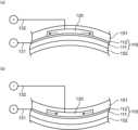
図9(a)及び図9(b)に示すように、導電性を有している平板状の振動板410に円板状の圧電素子420を接合した薄型の圧電スピーカ400が開発されている。振動板410に接合された面とは反対側の圧電素子420の面には、電極431が取り付けられている。また、振動板410には、他の電極432が取り付けられている。 As shown in FIGS. 9(a) and 9(b), a thinpiezoelectric speaker 400 has been developed in which a disk-shapedpiezoelectric element 420 is bonded to a conductive flat plate-shaped diaphragm 410. . Anelectrode 431 is attached to the surface of thepiezoelectric element 420 opposite to the surface bonded to thediaphragm 410 . Anotherelectrode 432 is attached to thediaphragm 410 .

図9(a)に示す圧電スピーカ400では、電極431にプラス極の電圧が印加されている一方で、電極432には、マイナス極の電圧が印加されている。この電圧印加により、圧電素子420は、径方向に伸長する。このとき、振動板410は、圧電素子420側に凸となるように弾性的に湾曲する。電極431,432に印加された電圧がなくなると、振動板410は、復元し、元の平板形状に戻る。 In thepiezoelectric speaker 400 shown in FIG. 9A , a positive voltage is applied to theelectrode 431 while a negative voltage is applied to theelectrode 432 . This voltage application expands thepiezoelectric element 420 in the radial direction. At this time,diaphragm 410 is elastically curved so as to be convex towardpiezoelectric element 420 . When the voltage applied to theelectrodes 431 and 432 is removed, thediaphragm 410 restores to its original flat plate shape.

図9(b)に示す圧電スピーカ400では、電極431,432に印加されている電圧の極は、図9(a)に示す電圧の極とは逆になっている。この状態では、圧電素子420は、径方向に収縮し、振動板410は、圧電素子420とは反対側に凸となるように弾性的に湾曲する。 In thepiezoelectric speaker 400 shown in FIG. 9(b), the polarities of the voltages applied to theelectrodes 431 and 432 are opposite to the polarities of the voltages shown in FIG. 9(a). In this state, thepiezoelectric element 420 contracts in the radial direction, and thevibration plate 410 is elastically curved so as to protrude on the side opposite to thepiezoelectric element 420 .

電極431,432に交流電圧を印加することにより、図9(a)に示す状態と、図9(b)に示す状態と、が繰り返される。すなわち、振動板410は、圧電素子420側に凸となる湾曲変形及び圧電素子420とは反対側に凸となる湾曲変形を繰り返して、振動する。振動板410がこのように振動している場合に、振動板410が元の平板形状に復元するタイミングで電圧の極が切り替えられると、振動板410は、共振状態になり、振動板410の振幅が大きくなる。振動板410が大きな振幅で振動すれば、圧電スピーカ400は、大きな音を発することができる。 By applying an AC voltage to theelectrodes 431 and 432, the state shown in FIG. 9(a) and the state shown in FIG. 9(b) are repeated. In other words, thevibration plate 410 vibrates by repeating bending deformation to become convex toward thepiezoelectric element 420 and bending deformation to become convex toward the side opposite to thepiezoelectric element 420 . When thediaphragm 410 vibrates in this way, if the polarity of the voltage is switched at the timing when thediaphragm 410 restores its original flat plate shape, thediaphragm 410 enters a resonance state, and the amplitude of thediaphragm 410 increases. becomes larger. If thediaphragm 410 vibrates with a large amplitude, thepiezoelectric speaker 400 can emit a loud sound.

振動板410の振動振幅を同一のエネルギの下で更に大きくするために、振動板410を軽量化することが考えられる。振動板410の厚さを低減することにより、振動板410は、軽くなるが、振動板410が湾曲変形した状態から平板状の形状に戻る際の復元力が小さくなり、図9(a)及び図9(b)に示す振動板410の振動を得られなくなる。このため、特許文献1では、図10(a)及び図10(b)に示すように、振動板410の振動に必要とされる厚さを維持しつつ、振動板410を軽量化している。 In order to further increase the vibration amplitude ofdiaphragm 410 under the same energy, it is conceivable to reduce the weight ofdiaphragm 410 . By reducing the thickness of thediaphragm 410, the weight of thediaphragm 410 can be reduced, but the restoring force when thediaphragm 410 returns to the flat plate shape from the curved deformation state is reduced. The vibration ofdiaphragm 410 shown in FIG. 9B cannot be obtained. For this reason, in Patent Document 1, as shown in FIGS. 10A and 10B, thediaphragm 410 is made lighter while maintaining the thickness required for vibration of thediaphragm 410 .

具体的には、特許文献1の圧電スピーカ400の振動板410は、3層構造を有しており、中央の層は、他の層よりも低密度のベース層411になっている。このベース層411の厚さは、振動板410がある程度の大きさの復元力を有するように設定されている。ベース層411において圧電素子420側の面には、表面層412が積層されている。表面層412は、ベース層411よりも高密度の導電性材料によって形成されており、圧電素子420は、表面層412に接合されている。圧電素子420は、以下の理由から、表面層412を介してベース層411に接合されている。 Specifically, thediaphragm 410 of thepiezoelectric speaker 400 of Patent Document 1 has a three-layer structure, and the central layer is abase layer 411 having a lower density than the other layers. The thickness of thebase layer 411 is set so that thediaphragm 410 has a certain degree of restoring force. Asurface layer 412 is laminated on the surface of thebase layer 411 on thepiezoelectric element 420 side. Thesurface layer 412 is made of a conductive material with a higher density than thebase layer 411 , and thepiezoelectric element 420 is bonded to thesurface layer 412 . Thepiezoelectric element 420 is bonded to thebase layer 411 via thesurface layer 412 for the following reasons.

ベース層411は、低密度であるので、ベース層411を構成している分子が互いに接近するような変形、すなわち、ベース層411の収縮が生じやすい。このため、仮に、圧電素子420がベース層411に直接的に接合された状態で圧電素子420が収縮した場合には、圧電素子420と接合された部分のみが圧電素子420の収縮に合わせて収縮し、ベース層411の湾曲変形量が小さくなり得る。したがって、特許文献1では、ベース層411よりも高密度の表面層412を設けて、この表面層412に圧電素子420が接合されている。 Since thebase layer 411 has a low density, thebase layer 411 is likely to be deformed such that the molecules forming thebase layer 411 are brought closer to each other, that is, thebase layer 411 is likely to be shrunk. Therefore, if thepiezoelectric element 420 shrinks while thepiezoelectric element 420 is directly bonded to thebase layer 411, only the portion bonded to thepiezoelectric element 420 shrinks in accordance with the shrinkage of thepiezoelectric element 420. As a result, the amount of bending deformation of thebase layer 411 can be reduced. Therefore, in Patent Document 1, asurface layer 412 having a higher density than thebase layer 411 is provided, and thepiezoelectric element 420 is bonded to thissurface layer 412 .

表面層412とは反対側において他の表面層413がベース層411に積層されている。他の表面層413は、表面層412と同材質であり、表面層412と略等しい厚さを有している。これにより、表面層412側と表面層413側とで振動板410の曲げ剛性が対称的になり、圧電素子420側における振動板410の振動振幅と反対側における振動振幅とが略等しくなる。これらの振動振幅が略等しくなることにより、圧電スピーカ400から発せられる音の歪が抑制される。 Anothersurface layer 413 is laminated to thebase layer 411 on the side opposite to thesurface layer 412 . Theother surface layer 413 is made of the same material as thesurface layer 412 and has approximately the same thickness as thesurface layer 412 . As a result, the bending rigidity of thediaphragm 410 is symmetrical between thesurface layer 412 side and thesurface layer 413 side, and the vibration amplitude of thediaphragm 410 on thepiezoelectric element 420 side and the vibration amplitude on the opposite side are substantially equal. By making these vibration amplitudes substantially equal, distortion of the sound emitted from thepiezoelectric speaker 400 is suppressed.

なお、図9(a)乃至図10(b)の圧電スピーカ400の構造と略同一の構造を用いて、検出対象物の振動を検出する圧電振動センサを構成することが可能になる。すなわち、振動板410が検出対象物の振動を受けるように配置されれば、振動板410は、振動する。この振動に応じて圧電素子420が伸縮し、圧電素子420の伸縮量に応じた大きさの電圧が圧電素子420から出力されるので、振動検出センサとして機能し得る。圧電素子420から出力された電圧をモニタすることにより、検出対象物の振動を検出及び解析し得る。 It is possible to configure a piezoelectric vibration sensor that detects vibration of a detection target by using a structure that is substantially the same as the structure of thepiezoelectric speaker 400 shown in FIGS. 9A to 10B. That is, ifdiaphragm 410 is arranged to receive the vibration of the object to be detected,diaphragm 410 vibrates. Thepiezoelectric element 420 expands and contracts in response to this vibration, and a voltage corresponding to the amount of expansion and contraction of thepiezoelectric element 420 is output from thepiezoelectric element 420, so that thepiezoelectric element 420 can function as a vibration detection sensor. By monitoring the voltage output from thepiezoelectric element 420, the vibration of the detection target can be detected and analyzed.

特開2003-230193号公報Japanese Patent Application Laid-Open No. 2003-230193

図9(a)乃至図10(b)の圧電スピーカ400は、薄いので、様々な装置(たとえば、スマートホン又は洗濯機)に搭載され得るが、圧電スピーカ400が搭載された装置が置かれた環境によっては、その寿命が短くなり得る。たとえば、図9(a)乃至図10(b)の圧電スピーカ400が洗濯機に搭載されれば、圧電スピーカ400の寿命は、湿気により短くなり得る。また、同様の問題が圧電振動センサにも生じうる。 Since thepiezoelectric speaker 400 of FIGS. 9( a ) to 10 ( b ) is thin, it can be mounted on various devices (for example, smart phones or washing machines), but the device mounted with thepiezoelectric speaker 400 was placed Depending on the environment, its life can be shortened. For example, if thepiezoelectric speaker 400 of FIGS. 9(a) to 10(b) is installed in a washing machine, the life of thepiezoelectric speaker 400 may be shortened by moisture. A similar problem can also arise with piezoelectric vibration sensors.

本発明は、圧電スピーカ及び圧電振動センサとして機能し得る圧電振動装置の寿命を長くする技術を提供することを目的とする。 An object of the present invention is to provide a technique for extending the life of a piezoelectric vibration device that can function as a piezoelectric speaker and a piezoelectric vibration sensor.

本開示における圧電振動装置は、振動板と、交流電圧の印加の下で伸縮して振動板を湾曲変形させながら振動板を振動させて音を発生させるように、又は、振動板が湾曲変形しながら振動している状態において振動板の振動に追随して伸縮して電圧信号を発生させるように、振動板の一方の面に接合された圧電素子と、圧電素子と振動板の一方の面とを被覆することによって圧電素子及び振動板を保護する第1保護層と、第1保護層とは反対側の振動板の他方の面を被覆することによって振動板を保護する第2保護層と、を備えている。第1保護層及び第2保護層は、振動板とともに湾曲変形可能である。振動板は、湾曲変形した状態から復元する復元力を生じさせる厚さを有しているベース層と、ベース層における第1保護層側の面及び圧電素子に接合され且つベース層よりも高密度の材質の表面層と、を有している。第2保護層は、表面層に接合されることなく、ベース層に接合されている。 The piezoelectric vibration device according to the present disclosure includes a diaphragm and a vibration plate that expands and contracts under the application of an AC voltage to generate sound by vibrating the diaphragm while bending and deforming the diaphragm, or by bending and deforming the diaphragm. a piezoelectric element bonded to one surface of the diaphragm so as to generate a voltage signal by expanding and contracting following the vibration of the diaphragm in a state of vibrating while the piezoelectric element and the one surface of the diaphragm are connected to each other; a first protective layer that protects the piezoelectric element and the diaphragm by covering a second protective layer that protects the diaphragm by covering the other surface of the diaphragm opposite to the first protective layer; It has The first protective layer and the second protective layer can bend and deform together with the diaphragm. The vibration plate includes a base layer having a thickness that generates a restoring force to restore from a curved and deformed state; and a surface layer made of a material of The second protective layer is bonded to the base layer without being bonded to the surface layer.

上述の圧電振動装置は、長寿命を有する。 The piezoelectric vibration device described above has a long life.

圧電スピーカとして機能する圧電振動装置の一部の平面図A plan view of a portion of a piezoelectric vibration device that functions as a piezoelectric speaker.図1のII-II線に沿う圧電振動装置の概略的な断面図Schematic cross-sectional view of the piezoelectric vibration device along line II-II in FIG.振動板の湾曲変形を概略的に表す図Schematic representation of bending deformation of diaphragm圧電振動装置の一部の平面図A plan view of a part of the piezoelectric vibration device図4のV-V線に沿う圧電振動装置の概略的な断面図Schematic cross-sectional view of the piezoelectric vibration device along line VV in FIG.圧電振動装置の概略的な断面図Schematic cross-sectional view of piezoelectric vibration device圧電振動装置の概略的な断面図Schematic cross-sectional view of piezoelectric vibration device圧電振動センサとして機能する圧電振動装置の概略的な断面図Schematic cross-sectional view of a piezoelectric vibration device functioning as a piezoelectric vibration sensor従来の圧電スピーカの概略的な断面図Schematic cross-sectional view of a conventional piezoelectric speaker従来の圧電スピーカの概略的な断面図Schematic cross-sectional view of a conventional piezoelectric speaker

以下、図面を参照しながら、第1実施形態及び第2実施形態を詳細に説明する。但し、必要以上に詳細な説明は、省略する場合がある。たとえば、既によく知られた事項の詳細説明、又は、実質的に同一の構成に対する重複説明を省略する場合がある。これは、以下の説明が必要以上に冗長になるのを避け、当業者の理解を容易にするためである。なお、添付図面及び以下の説明は、当業者が本開示を十分に理解するために提供されるのであって、これらにより特許請求の範囲に記載の主題を限定することを意図していない。 Hereinafter, the first embodiment and the second embodiment will be described in detail with reference to the drawings. However, more detailed description than necessary may be omitted. For example, detailed descriptions of already well-known matters or redundant descriptions of substantially the same configurations may be omitted. This is to avoid the following description from becoming more redundant than necessary and to facilitate understanding by those skilled in the art. It should be noted that the accompanying drawings and the following description are provided to allow those skilled in the art to fully understand the present disclosure and are not intended to limit the claimed subject matter thereby.

(第1実施形態)
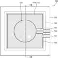
図1は、圧電スピーカとして機能する圧電振動装置100の一部の概略的な平面図である。図2は、圧電振動装置100の概略的な断面図である(図1のII-II線に沿う断面図)。図1及び図2を参照して、圧電振動装置100の構造を説明する。
(First embodiment)
FIG. 1 is a schematic plan view of part of apiezoelectric vibration device 100 that functions as a piezoelectric speaker. FIG. 2 is a schematic cross-sectional view of the piezoelectric vibration device 100 (cross-sectional view taken along line II-II in FIG. 1). The structure of thepiezoelectric vibration device 100 will be described with reference to FIGS. 1 and 2. FIG.

(圧電振動装置の構造)
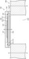
圧電振動装置100は、略正方形状の振動板110と、振動板110に接合された平板状の圧電素子120と、振動板110を周方向に囲んでいる周囲層113と、周囲層113上に積層された剛性層140と、を備えている。
(Structure of piezoelectric vibration device)
Thepiezoelectric vibration device 100 includes a substantiallysquare diaphragm 110, a flatpiezoelectric element 120 joined to thediaphragm 110, a surroundinglayer 113 surrounding thediaphragm 110 in the circumferential direction, and and a laminatedrigid layer 140 .

圧電素子120は、30μm~50μm程度の厚さを有している円板であり、圧電素子120の一方の面が振動板110に接合されている。圧電素子120は、たとえば、アクリル系接着剤を用いて振動板110に接着されていてもよい。圧電素子120は、圧電素子120の両面に交流電圧が印加されると、径方向において伸びたり縮んだりする特性を有している。また、圧電素子120は、圧電素子120の両面に印加される電圧が大きくなればなるほど、大きく伸縮する特性を有している。 Thepiezoelectric element 120 is a disk having a thickness of approximately 30 μm to 50 μm, and one surface of thepiezoelectric element 120 is bonded to thevibration plate 110 .Piezoelectric element 120 may be adhered todiaphragm 110 using, for example, an acrylic adhesive. Thepiezoelectric element 120 has the characteristic of expanding and contracting in the radial direction when an AC voltage is applied to both surfaces of thepiezoelectric element 120 . In addition, thepiezoelectric element 120 has a characteristic of expanding and contracting more as the voltage applied to both surfaces of thepiezoelectric element 120 increases.

本実施形態では、圧電素子120の一方の面(図2における上面)にプラス極の電圧が印加され、且つ、他方の面にマイナス極の電圧が印加されると、圧電素子120は、図3(a)に示すように、径方向において伸長するような特性を有している。また、図3(b)に示すように、図3(a)の状態から電圧の極が逆転すると、圧電素子120は、径方向に収縮するような特性を有している。このような圧電素子120は、たとえば、PZT(チタン酸ジルコン酸鉛)といった圧電素材を用いて形成可能である。 In the present embodiment, when a positive voltage is applied to one surface of the piezoelectric element 120 (upper surface in FIG. 2) and a negative voltage is applied to the other surface, thepiezoelectric element 120 is as shown in FIG. As shown in (a), it has the characteristic of extending in the radial direction. Further, as shown in FIG. 3B, when the polarity of the voltage is reversed from the state shown in FIG. Such apiezoelectric element 120 can be formed using, for example, a piezoelectric material such as PZT (lead zirconate titanate).

なお、圧電素子120を上下に反転して振動板110に接合すれば、図3(a)及び図3(b)に示す伸縮特性とは逆の伸縮特性を有する。すなわち、圧電素子120の一方の面(図2における上面)にマイナス極の電圧が印加され、他方の面にプラス極の電圧が印加された状態で、圧電素子120は、径方向に伸長するような特性を有する。この場合には、印加電圧の極の逆転によって、圧電素子120は、径方向に収縮するような特性を有する。 Note that if thepiezoelectric element 120 is turned upside down and joined to thediaphragm 110, the expansion/contraction characteristics are opposite to those shown in FIGS. 3(a) and 3(b). That is, in a state in which a negative voltage is applied to one surface (upper surface in FIG. 2) of thepiezoelectric element 120 and a positive voltage is applied to the other surface, thepiezoelectric element 120 expands in the radial direction. characteristics. In this case, thepiezoelectric element 120 has the characteristic of contracting in the radial direction due to the polarity reversal of the applied voltage.

振動板110は、圧電素子120の伸縮に伴って湾曲変形する薄板状の部材(たとえば、40μm程度の厚さの部材)である。振動板110は、2層構造を有しており、ベース層111と、圧電素子120側においてベース層111上に接合された表面層112と、により構成されている。表面層112には、圧電素子120が接合されている。 Thevibration plate 110 is a thin plate member (for example, a member having a thickness of about 40 μm) that bends and deforms as thepiezoelectric element 120 expands and contracts. Thediaphragm 110 has a two-layer structure, and is composed of abase layer 111 and asurface layer 112 bonded to thebase layer 111 on thepiezoelectric element 120 side. Apiezoelectric element 120 is bonded to thesurface layer 112 .

ベース層111は、表面層112よりも低密度の材料から形成されている。たとえば、ベース層111は、樹脂フィルム層であってもよいし、アルミニウム層であってもよい。ベース層111が樹脂により構成される場合には、ポリエチレンテレフタレート、ポリエチレン、ポリプロピレン、ポリウレタン、ポリアミド又はポリイミドが用いられてもよい。あるいは、ベース層111は、スチレンブタジエン系ゴム、ブタジエン系ゴム、ブチル系ゴム又はエチレンプロピレン系ゴムにより構成されてもよい。Base layer 111 is made of a material with a lower density thansurface layer 112 . For example, thebase layer 111 may be a resin film layer or an aluminum layer. When thebase layer 111 is made of resin, polyethylene terephthalate, polyethylene, polypropylene, polyurethane, polyamide, or polyimide may be used. Alternatively, thebase layer 111 may be made of styrene-butadiene-based rubber, butadiene-based rubber, butyl-based rubber, or ethylene-propylene-based rubber.

ベース層111は、圧電素子120への電圧印加がなくなったときに、図3(a)及び図3(b)に示す湾曲状態から図2に示す平板状の状態に戻るための復元力が得られる厚さを有しており、表面層112より厚くなっている。たとえば、ベース層111は、30μmの厚さを有している一方で、表面層112は、約10μmの厚さを有している。このように、ベース層111は、表面層112よりも厚くなっているが、上述の如く、表面層112よりも低密度の材質であるので、振動板110の重量の増加が抑制されている。 Thebase layer 111 obtains a restoring force for returning from the curved state shown in FIGS. 3A and 3B to the flat state shown in FIG. and is thicker than thesurface layer 112 . For example,base layer 111 has a thickness of 30 μm, whilesurface layer 112 has a thickness of approximately 10 μm. As described above, thebase layer 111 is thicker than thesurface layer 112, but as described above, it is made of a material with a lower density than thesurface layer 112, so an increase in the weight of thediaphragm 110 is suppressed.

表面層112は、導電性の材料から形成されており、圧電素子120への電圧印加に利用される。また、表面層112は、ベース層111よりも高密度の材料から形成されている。たとえば、表面層112は、42アロイ(42Ni-Fe)の層であってもよいし、銅(Cu)の層であってもよい。表面層112は、ベース層111に対してファンデルワールス力によって接合されている。代替的に、表面層112及びベース層111は、接着剤によって接合されていてもよい。 Thesurface layer 112 is made of a conductive material and used for voltage application to thepiezoelectric element 120 . Also, thesurface layer 112 is made of a material with a higher density than thebase layer 111 . For example,surface layer 112 may be a layer of 42 alloy (42Ni--Fe) or a layer of copper (Cu). Thesurface layer 112 is bonded to thebase layer 111 by van der Waals force. Alternatively,surface layer 112 andbase layer 111 may be joined by an adhesive.

表面層112は、平面視において、全体的に矩形状になっているが、一部が切り欠かれている。この切欠部分において、ベース層111の一部が表面層112から露出している。この切欠部分は、圧電素子120に電圧を印加するための電極132の配置に利用される。 Thesurface layer 112 has an overall rectangular shape in a plan view, but is partially cut out. A portion of thebase layer 111 is exposed from thesurface layer 112 at this notch portion. This notch portion is used for arranging anelectrode 132 for applying a voltage to thepiezoelectric element 120 .

表面層112は、ベース層111よりも高い密度の材質であり、圧電素子120が径方向に伸縮すると、図3(a)及び図3(b)に示すように、圧電素子120側に凸となる方向とその反対方向において凸となる方向に湾曲変形する。このような表面層112の湾曲変形に追随して、表面層112に接合されたベース層111も湾曲変形する。 Thesurface layer 112 is made of a material with a higher density than thebase layer 111, and when thepiezoelectric element 120 expands and contracts in the radial direction, thesurface layer 112 protrudes toward thepiezoelectric element 120 as shown in FIGS. It bends and deforms in the direction of convexity in the direction and the opposite direction. Following the bending deformation of thesurface layer 112, thebase layer 111 joined to thesurface layer 112 also bends and deforms.

表面層112は、図2に示すように、圧電素子120側のベース層111の面にだけ接合されており、圧電素子120とは反対側には設けられていない。このため、振動板110は、表面層112側において高い剛性を有し、反対側では、低い剛性を有している。 As shown in FIG. 2, thesurface layer 112 is bonded only to the surface of thebase layer 111 on the side of thepiezoelectric element 120 and is not provided on the side opposite to thepiezoelectric element 120 . Therefore,diaphragm 110 has high rigidity on thesurface layer 112 side and low rigidity on the opposite side.

周囲層113は、ベース層111を周方向に囲むようにベース層111と一体的に形成されている。すなわち、周囲層113の材質は、ベース層111と同じ材質であり、周囲層113及びベース層111は、1つの樹脂層又はアルミニウム層を構成している。周囲層113は、図2に示すように、振動板110が装置300に設けられた矩形状の開口310に重なった状態で圧電振動装置100が配置されたときに、開口310の周囲において装置300に重なる部分である。この状態で、周囲層113は、周囲層113を保護するための他の層(後述の第3保護層153及び第4保護層154)とともに装置300に固定される。 The surroundinglayer 113 is integrally formed with thebase layer 111 so as to surround thebase layer 111 in the circumferential direction. That is, the material of thesurrounding layer 113 is the same material as that of thebase layer 111, and thesurrounding layer 113 and thebase layer 111 constitute one resin layer or aluminum layer. As shown in FIG. 2 , when thepiezoelectric vibration device 100 is arranged with thevibration plate 110 overlapping therectangular opening 310 provided in thedevice 300 , the surroundinglayer 113 is formed around theopening 310 . is the part that overlaps with In this state, the surroundinglayer 113 is fixed to thedevice 300 together with other layers (thirdprotective layer 153 and fourthprotective layer 154 to be described later) for protecting thesurrounding layer 113 .

周囲層113自体は、ベース層111と同じ低密度の材質であるので、装置300に取り付けられる部分としては十分な剛性を有さないこともあり得る。このため、剛性層140が周囲層113に積層され、積層部分における剛性が高められている。すなわち、剛性層140が周囲層113に積層されることにより、装置300に対する取付部分として適した剛性が得られる。Perimeter layer 113 itself may not be rigid enough to be attached todevice 300 since it is of the same low density material asbase layer 111 . For this reason, therigid layer 140 is laminated on theperipheral layer 113 to increase the rigidity of the laminated portion. That is, by laminating therigid layer 140 on thesurrounding layer 113, a rigidity suitable for the attachment portion to thedevice 300 can be obtained.

剛性層140は、平面視において略C型であり、振動板110を周方向に囲むように積層されている。本実施形態では、剛性層140は、周囲層113及びベース層111によって構成された樹脂層又はアルミニウム層において表面層112が設けられた面に積層されている。剛性層140は、表面層112の切欠部分と同方向に開口しており、この開口部分は、圧電素子120に電圧を印加するための電極131,132の配置に利用される。 Therigid layer 140 is substantially C-shaped in plan view, and is laminated so as to surround thediaphragm 110 in the circumferential direction. In this embodiment, therigid layer 140 is laminated on the surface of the resin layer or aluminum layer formed by the surroundinglayer 113 and thebase layer 111 on which thesurface layer 112 is provided. Therigid layer 140 has an opening in the same direction as the notch portion of thesurface layer 112 , and this opening portion is used for arrangingelectrodes 131 and 132 for applying voltage to thepiezoelectric element 120 .

剛性層140の材質は、表面層112と同じ材質であってもよい。また、装置300に対する取付に十分な剛性が得られれば、剛性層140は、表面層112と同じ厚さを有していてもよい。なお、装置300に対する取り付け部分の剛性を向上させるために、剛性層140は、表面層112よりも厚くてもよい。剛性層140は、図3(a)及び図3(b)に示すように、圧電振動装置100が装置300に取り付けられるときに、開口310の周縁部と全長に亘って重なるように配置され、この状態で、装置300に固定されてもよい。 The material of therigid layer 140 may be the same material as thesurface layer 112 .Rigid layer 140 may also have the same thickness assurface layer 112, provided it is sufficiently rigid for attachment todevice 300. FIG. It should be noted that therigid layer 140 may be thicker than thesurface layer 112 in order to improve the rigidity of the attachment portion to thedevice 300 . As shown in FIGS. 3A and 3B, therigid layer 140 is arranged to overlap the entire length of the peripheral edge of theopening 310 when thepiezoelectric vibration device 100 is attached to thedevice 300, In this state, it may be secured todevice 300 .

剛性層140の内縁は、全長に亘って、表面層112の外縁から略一定の距離だけ離間している。このため、剛性層140の内縁と表面層112の外縁との間には、ベース層111の外縁に沿う周囲層113の内縁部分114が現れる。言い換えると、剛性層140は、周囲層113の内縁部分114の外側において周囲層113に積層されている。 The inner edge ofrigid layer 140 is spaced a substantially constant distance from the outer edge ofsurface layer 112 over its entire length. Therefore, aninner edge portion 114 of thesurrounding layer 113 along the outer edge of thebase layer 111 appears between the inner edge of therigid layer 140 and the outer edge of thesurface layer 112 . In other words,rigid layer 140 is laminated toperimeter layer 113 on the outside ofinner edge portion 114 ofperimeter layer 113 .

周囲層113の内縁部分114には、比較的高い剛性を有している表面層112及び剛性層140のいずれもが積層されていない。このため、図3(a)及び図3(b)に示すように振動板110が湾曲変形したときに、この湾曲変形に伴って、内縁部分114が大きく変形することが許容される。 Neither thesurface layer 112 having a relatively high rigidity nor therigid layer 140 are laminated on theinner edge portion 114 of theperipheral layer 113 . Therefore, when thediaphragm 110 is curved and deformed as shown in FIGS. 3(a) and 3(b), theinner edge portion 114 is allowed to be greatly deformed due to the curved deformation.

また、周囲層113の内縁部分114は、略一定の幅を有している。このため、振動板110は、圧電素子120の径方向におけるいずれかの方向に特異的に振動しやすい状態にはなっていない。すなわち、周囲層113の内縁部分114は、略正方形状の振動板110の四方において略均等に伸縮変形し得るようになっている。 Also, theinner edge portion 114 of thesurrounding layer 113 has a substantially constant width. Therefore, thevibration plate 110 is not in a state in which it is likely to specifically vibrate in any direction in the radial direction of thepiezoelectric element 120 . That is, theinner edge portion 114 of thesurrounding layer 113 can be expanded and contracted in four directions of the substantiallysquare diaphragm 110 substantially uniformly.

上述の如く、剛性層140の開口部分及び表面層112の切欠部分を利用して、電極131,132が配置されている。電極131は、表面層112と一体的に形成されており、周囲層113上に積層されている。電極131は、表面層112と同じく導電性である。 As described above, theelectrodes 131 and 132 are arranged using the opening portion of therigid layer 140 and the cutout portion of thesurface layer 112 . Theelectrode 131 is formed integrally with thesurface layer 112 and laminated on thesurrounding layer 113 .Electrode 131 is electrically conductive, as issurface layer 112 .

一方、電極132は、周囲層113だけでなく、表面層112の切欠領域においてベース層111上においても積層されている。電極132は、導電性及び伸縮性を有する接合材料により、表面層112が接合された側とは反対側の圧電素子120の面に接合されている。接合材料がある程度の伸縮性を有していることにより、圧電素子120の変形の下でも、圧電素子120及び電極132の接続部分の破断が生じにくくなる。接合材料としては、たとえば、銀に樹脂材料が配合された銀ペーストが利用されてもよいし、この銀ペーストに銅、金、ニッケル及びカーボンといった導体がフィラーとして更に配合されたペースト材料が用いられてもよい。また、接合材料の樹脂材料として、ニトリル基を有する樹脂バインダ(たとえば、アクリルニトリルゴム)、エポキシ樹脂を含有している樹脂バインダ及び/又はウレタン系樹脂を含有している樹脂バインダが用いられてもよい。他の樹脂材料として、熱可塑性のポリエステル系を有している樹脂バインダが用いられてもよい。このような樹脂バインダが用いられれば、柔軟性を有する接合材料を得ることができる。 On the other hand, theelectrode 132 is laminated not only on thesurrounding layer 113 but also on thebase layer 111 in the cutout region of thesurface layer 112 . Theelectrode 132 is bonded to the surface of thepiezoelectric element 120 opposite to the side to which thesurface layer 112 is bonded using a conductive and stretchable bonding material. Since the bonding material has a certain degree of stretchability, even when thepiezoelectric element 120 is deformed, the connecting portion between thepiezoelectric element 120 and theelectrode 132 is less likely to break. As the bonding material, for example, a silver paste in which a resin material is mixed with silver may be used, or a paste material in which conductors such as copper, gold, nickel, and carbon are added as fillers to this silver paste. may Further, as the resin material of the bonding material, a resin binder having a nitrile group (for example, acrylonitrile rubber), a resin binder containing an epoxy resin, and/or a resin binder containing a urethane resin may be used. good. As another resin material, a thermoplastic polyester-based resin binder may be used. If such a resin binder is used, a bonding material having flexibility can be obtained.

振動板110、圧電素子120、剛性層140及び電極131,132を、湿気などの環境的な劣化因子から保護するために、図2に示すように、第1保護層151~第4保護層154が設けられている。第1保護層151~第4保護層154は、熱乾燥により重合硬化するアクリル系樹脂、エポキシ系樹脂又はウレタン系樹脂から形成されてもよい。代替的に、第1保護層151~第4保護層154は、紫外線により光重合し硬化する材料(たとえば、ウレタンアクリレート系樹脂、エポキシアクリレート系樹脂又はポリエステルアクリレート系樹脂)から形成されてもよい。 In order to protect thediaphragm 110, thepiezoelectric element 120, therigid layer 140 and theelectrodes 131, 132 from environmental degradation factors such as moisture, as shown in FIG. is provided. The firstprotective layer 151 to the fourthprotective layer 154 may be made of acrylic resin, epoxy resin, or urethane resin that is polymerized and cured by thermal drying. Alternatively, the firstprotective layer 151 to the fourthprotective layer 154 may be made of a material that is photopolymerized and cured by ultraviolet rays (eg, urethane acrylate resin, epoxy acrylate resin, or polyester acrylate resin).

第1保護層151は、振動板110の表面層112及び圧電素子120を保護するために設けられている。すなわち、第1保護層151は、表面層112及び圧電素子120側において表面層112及び圧電素子120に積層されるように設けられており、これらを被覆している。第3保護層153は、第1保護層151とともに1つの樹脂層を形成するように第1保護層151を周方向に囲むように形成され、周囲層113上に積層されている。第3保護層153は、剛性層140及び電極131を保護するために設けられており、これらを被覆している。また、他方の電極132は、第1保護層151及び第3保護層153によって被覆されている。 The firstprotective layer 151 is provided to protect thesurface layer 112 of thediaphragm 110 and thepiezoelectric element 120 . That is, the firstprotective layer 151 is provided so as to be laminated on thesurface layer 112 and thepiezoelectric element 120 on thesurface layer 112 and thepiezoelectric element 120 side, and covers them. The thirdprotective layer 153 is formed so as to surround the firstprotective layer 151 in the circumferential direction so as to form one resin layer together with the firstprotective layer 151 and is laminated on thesurrounding layer 113 . The thirdprotective layer 153 is provided to protect therigid layer 140 and theelectrodes 131 and covers them. Also, theother electrode 132 is covered with a firstprotective layer 151 and a thirdprotective layer 153 .

第2保護層152は、振動板110の厚さ方向(図2の上下方向)において第1保護層151とは反対側に設けられており、ベース層111を被覆している。すなわち、第2保護層152は、表面層112に接合されることなく、ベース層111に接合されている。また、第4保護層154は、第2保護層152とともに1つの樹脂層を形成するように第2保護層152を周方向に囲むように形成され、第3保護層153とは反対側の周囲層113の面上に積層されている。この結果、ベース層111及び周囲層113は、第2保護層152~第4保護層154によって保護される。 The secondprotective layer 152 is provided on the side opposite to the firstprotective layer 151 in the thickness direction of the diaphragm 110 (vertical direction in FIG. 2), and covers thebase layer 111 . That is, the secondprotective layer 152 is bonded to thebase layer 111 without being bonded to thesurface layer 112 . In addition, the fourthprotective layer 154 is formed so as to surround the secondprotective layer 152 in the circumferential direction so as to form one resin layer together with the secondprotective layer 152, and is formed around the opposite side of the thirdprotective layer 153. Laminated on the surface oflayer 113 . As a result, thebase layer 111 and thesurrounding layer 113 are protected by the secondprotective layer 152 to the fourthprotective layer 154. FIG.

第1保護層151~第4保護層154を構成している樹脂層の厚さは、図3(a)及び図3(b)に示す振動板110及び圧電素子120の湾曲変形に追随して、第1保護層151~第4保護層154が湾曲変形できるように設定されている。 The thicknesses of the resin layers constituting the first to fourthprotective layers 151 to 154 follow the bending deformation of thevibration plate 110 and thepiezoelectric element 120 shown in FIGS. 3(a) and 3(b). , the firstprotective layer 151 to the fourthprotective layer 154 are set so as to be curved and deformable.

なお、第2保護層152は、第1保護層151と同じ材料から形成されている一方で、第1保護層151よりも高い剛性を有するように第1保護層151よりも厚くなっている。第2保護層152の厚さは、第2保護層152の曲げ剛性が、第1保護層151と表面層112とからなる積層体の曲げ剛性に近い値になるように設定されていてもよい。言い換えると、ベース層111を挟む2つの層(すなわち、第1保護層151及び表面層112の積層体の層,第2保護層152)の曲げ剛性が略等しくなっていてもよい。 The secondprotective layer 152 is made of the same material as the firstprotective layer 151 , but is thicker than the firstprotective layer 151 so as to have higher rigidity than the firstprotective layer 151 . The thickness of the secondprotective layer 152 may be set so that the flexural rigidity of the secondprotective layer 152 is close to the flexural rigidity of the laminate composed of the firstprotective layer 151 and thesurface layer 112. . In other words, the two layers sandwiching the base layer 111 (that is, the layer of the laminate of the firstprotective layer 151 and thesurface layer 112, and the second protective layer 152) may have approximately the same flexural rigidity.

(動作の説明)
電極131,132に交流電圧が印加されると、圧電素子120及び振動板110は、図3(a)及び図3(b)に示すような湾曲変形を繰り返して振動する。
(Description of operation)
When an AC voltage is applied to theelectrodes 131 and 132, thepiezoelectric element 120 and thediaphragm 110 vibrate by repeatedly bending and deforming as shown in FIGS. 3(a) and 3(b).

図3(a)に示す状態では、電極132を通じて圧電素子120の一方の面(上面)にプラス極の電圧が印加されるとともに、電極131及び表面層112を通じて圧電素子120の他面(下面)にマイナス極の電圧が印加されている。図3(b)に示す状態では、電極132を通じて圧電素子120の一方の面(上面)にマイナス極の電圧が印加されるとともに、電極131及び表面層112を通じて圧電素子120の他面(下面)にプラス極の電圧が印加されている。 In the state shown in FIG. 3A, a positive voltage is applied to one surface (upper surface) of thepiezoelectric element 120 through theelectrode 132, and the other surface (lower surface) of thepiezoelectric element 120 is applied through theelectrode 131 and thesurface layer 112. is applied with a negative voltage. In the state shown in FIG. 3B, a negative voltage is applied to one surface (upper surface) of thepiezoelectric element 120 through theelectrode 132, and the other surface (lower surface) of thepiezoelectric element 120 is applied through theelectrode 131 and thesurface layer 112. A positive voltage is applied to .

図3(a)に示す状態及び図3(b)に示す状態のいずれにおいても、圧電素子120の両面間には電位差が生じ、この電位差により、圧電素子120は伸縮する。図3(a)に示す状態では、圧電素子120は、両面間の電位差により、径方向に伸長し、振動板110は、圧電素子120側において凸となるように湾曲している。一方、図3(b)に示す状態では、圧電素子120は、両面間の電位差により、径方向に収縮し、振動板110は、圧電素子120とは反対側において凸となるように湾曲している。 In both the state shown in FIG. 3A and the state shown in FIG. 3B, a potential difference is generated between both surfaces of thepiezoelectric element 120, and thepiezoelectric element 120 expands and contracts due to this potential difference. In the state shown in FIG. 3A, thepiezoelectric element 120 extends in the radial direction due to the potential difference between the two surfaces, and thediaphragm 110 is curved so as to be convex on thepiezoelectric element 120 side. On the other hand, in the state shown in FIG. 3B, thepiezoelectric element 120 contracts in the radial direction due to the potential difference between the two surfaces, and thediaphragm 110 is curved so as to be convex on the side opposite to thepiezoelectric element 120. there is

図3(a)及び図3(b)に示す状態が所定の周波数で交互に繰り返されれば、振動板110は、所定の周波数で振動した状態になる。振動板110の振動の結果、振動板110の周囲の空気が震え、振動板110の振動周波数に対応する音が発生する。圧電素子120に印加する交流電圧の周波数を変更することによって、振動板110の振動周波数が変化し、圧電振動装置100から発生する音の周波数を変更することが可能になる。 If the states shown in FIGS. 3A and 3B are alternately repeated at a predetermined frequency, thediaphragm 110 vibrates at the predetermined frequency. As a result of the vibration ofdiaphragm 110 , theair surrounding diaphragm 110 vibrates and a sound corresponding to the vibration frequency ofdiaphragm 110 is generated. By changing the frequency of the AC voltage applied to thepiezoelectric element 120, the vibration frequency of thediaphragm 110 is changed, making it possible to change the frequency of the sound generated from thepiezoelectric vibration device 100. FIG.

図3(a)に示すように電圧を印加した後、この電圧がなくなると、振動板110は、図2に示す平板状の状態に戻る。このとき、図3(b)に示すように電圧の極が切り替えられると、ベース層111の復元力による振動板110の変形方向と圧電素子120の収縮による振動板110の変形方向とが一致し、振動板110は、大きく湾曲変形することができる。このように、ベース層111の復元力による振動板110の変形方向と圧電素子120の伸縮による振動板110の変形方向とが一致するように、圧電素子120に印加される交流電圧の周波数が調整されれば、振動板110は、共振状態になる。この状態では、振動板110は、大きな振幅で振動し、圧電振動装置100は、大きな音を発することができる。 After the voltage is applied as shown in FIG. 3(a), when the voltage is removed, thediaphragm 110 returns to the plate-like state shown in FIG. At this time, when the voltage pole is switched as shown in FIG. , thediaphragm 110 can be greatly bent and deformed. In this manner, the frequency of the AC voltage applied to thepiezoelectric element 120 is adjusted so that the deformation direction of thediaphragm 110 due to the restoring force of thebase layer 111 and the deformation direction of thediaphragm 110 due to expansion and contraction of thepiezoelectric element 120 are aligned. Then, thediaphragm 110 is in a resonant state. In this state, thediaphragm 110 vibrates with a large amplitude, and thepiezoelectric vibration device 100 can emit a loud sound.

図3(a)及び図3(b)に示すように振動板110が振動しているとき、振動板110の振動に応じて、周囲層113の内縁部分114も、図2における上下方向に撓み変形する。このため、振動板110の振動振幅は、周囲層113の内縁部分114の変形の分だけ大きくなり、圧電振動装置100は、大きな音を発することができる。 When thediaphragm 110 is vibrating as shown in FIGS. 3A and 3B, theinner edge portion 114 of thesurrounding layer 113 is also bent vertically in FIG. transform. Therefore, the vibration amplitude ofdiaphragm 110 increases by the amount of deformation ofinner edge portion 114 of surroundinglayer 113, andpiezoelectric vibration device 100 can emit a loud sound.

上述の実施形態では、第1保護層151及び第2保護層152により、振動板110、圧電素子120及び剛性層140が保護されるので、圧電振動装置100は、長寿命を有する。 In the above-described embodiments, the firstprotective layer 151 and the secondprotective layer 152 protect thediaphragm 110, thepiezoelectric element 120, and therigid layer 140, so that thepiezoelectric vibration device 100 has a long life.

上述の実施形態では、ベース層111の一方の面にのみ表面層112が設けられている。このため、図10(a)及び図10(b)に示す従来の振動板410(ベース層411を一対の表面層412,413で挟んだ振動板410)よりも表面層112を形成する工程が少なくなる。 In the above-described embodiments, thesurface layer 112 is provided only on one side of thebase layer 111 . Therefore, the step of forming thesurface layer 112 is more necessary than the conventional diaphragm 410 (diaphragm 410 having abase layer 411 sandwiched between a pair of surface layers 412 and 413) shown in FIGS. less.

ベース層111の一方の面にのみに表面層112が設けられる結果、振動板110は、表面層112側で高い曲げ剛性を有し、反対側で低い曲げ剛性を有している。このような曲げ剛性の分布により、振動板110自身の曲げやすさは、圧電素子120側に凸となる方向とその反対側に凸となる方向において相違する。仮に、互いに曲げ剛性が等しい第1保護層151及び第2保護層152が振動板110に積層されても、上述の曲げやすさの相違は解消されない。このため、振動板110、第1保護層151及び第2保護層152の積層体の振動振幅は、圧電素子120側に凸となる方向とその反対側に凸となる方向において相違する。この振動振幅の差は、音の歪を生じさせ得る。 As a result of providing thesurface layer 112 only on one surface of thebase layer 111, thediaphragm 110 has high bending rigidity on thesurface layer 112 side and low bending rigidity on the opposite side. Due to such a distribution of bending rigidity, the easiness of bending of thediaphragm 110 itself differs between the direction in which thediaphragm 110 protrudes toward thepiezoelectric element 120 and the direction in which thevibration plate 110 protrudes on the opposite side. Even if the firstprotective layer 151 and the secondprotective layer 152 having the same flexural rigidity are laminated on thediaphragm 110, the above-described difference in bendability is not resolved. Therefore, the vibration amplitude of the laminate of thediaphragm 110, the firstprotective layer 151, and the secondprotective layer 152 is different between the convex direction toward thepiezoelectric element 120 and the opposite direction. This difference in vibration amplitude can cause sound distortion.

一方、上述の実施形態では、第2保護層152の曲げ剛性は、第1保護層151の曲げ剛性よりも高くなっており、第1保護層151と表面層112との積層体の曲げ剛性に近い値になっている。すなわち、ベース層111を挟んだ2つの層(すなわち、第1保護層151と表面層112との積層体の層及び第2保護層152)の曲げ剛性が略等しくなっている。この結果、振動板110、第1保護層151及び第2保護層152の積層体の曲げやすさは、圧電素子120側に凸となる方向とその反対側に凸となる方向において略等しくなる。言い換えると、これらの方向において、振動板110、第1保護層151及び第2保護層152の積層体の振動振幅は略等しくなり、音の歪が抑制される。 On the other hand, in the above-described embodiment, the flexural rigidity of the secondprotective layer 152 is higher than the flexural rigidity of the firstprotective layer 151, and the flexural rigidity of the laminate of the firstprotective layer 151 and thesurface layer 112 is values are close. That is, the two layers sandwiching the base layer 111 (that is, the laminate layer of the firstprotective layer 151 and thesurface layer 112 and the second protective layer 152) have approximately the same flexural rigidity. As a result, the easiness of bending of the laminated body of thediaphragm 110, the firstprotective layer 151, and the secondprotective layer 152 is substantially equal between the convex direction toward thepiezoelectric element 120 and the opposite direction. In other words, in these directions, the vibration amplitude of the laminate ofdiaphragm 110, firstprotective layer 151, and secondprotective layer 152 becomes substantially equal, and sound distortion is suppressed.

上述の実施形態では、第1保護層151及び第2保護層152は、同じ材料から構成されている。代替的に、第2保護層152は、第1保護層151を構成している材料よりも硬質の材料によって構成されてもよい。この場合、第2保護層152の厚さが第1保護層151の厚さ未満であっても、第2保護層152の曲げ剛性が第1保護層151と表面層112とからなる積層体の曲げ剛性に略等しくなるという条件が満たされ得る。したがって、第2保護層152を比較的硬質の材料を用いて形成することにより、圧電振動装置100の厚さを低減することが可能になる。 In the embodiments described above, the firstprotective layer 151 and the secondprotective layer 152 are made of the same material. Alternatively, the secondprotective layer 152 may be made of a material harder than the material forming the firstprotective layer 151 . In this case, even if the thickness of the secondprotective layer 152 is less than the thickness of the firstprotective layer 151, the flexural rigidity of the secondprotective layer 152 is the same as that of the laminate composed of the firstprotective layer 151 and thesurface layer 112. The condition of being approximately equal to the bending stiffness can be satisfied. Therefore, by forming the secondprotective layer 152 using a relatively hard material, it is possible to reduce the thickness of thepiezoelectric vibration device 100 .

剛性層140は、図4及び図5に示すように、圧電素子120とは反対側の面において、周囲層113に積層されていてもよい。図4及び図5に示す圧電振動装置100では、
剛性層140は、周囲層113の下面に積層されているのに対して、電極131,132は、周囲層113の上面に積層されており、剛性層140と電極131,132との干渉は生じない。このため、剛性層140には、電極131,132を配設するための開口領域を設ける必要はなく、振動板110を完全に囲むように形成されていてもよい。たとえば、剛性層140は、図4及び図5に示すように、平面視において、C型ではなく、略正方形の枠形状に形成されていてもよい。
Therigid layer 140 may be laminated to thesurrounding layer 113 on the side opposite to thepiezoelectric element 120, as shown in FIGS. In thepiezoelectric vibration device 100 shown in FIGS. 4 and 5,
Therigid layer 140 is laminated on the lower surface of thesurrounding layer 113, whereas theelectrodes 131 and 132 are laminated on the upper surface of thesurrounding layer 113, and interference between therigid layer 140 and theelectrodes 131 and 132 occurs. do not have. Therefore, therigid layer 140 does not need to be provided with opening regions for disposing theelectrodes 131 and 132 , and may be formed so as to completely surround thediaphragm 110 . For example, as shown in FIGS. 4 and 5, therigid layer 140 may be formed in a substantially square frame shape instead of a C shape in plan view.

図4及び図5に示す圧電振動装置100では、剛性層140は、周囲層113及びベース層111によって構成された樹脂層又はアルミニウム層の下面に積層されているのに対して、表面層112は、当該樹脂層又はアルミニウム層の上面に積層されている。この場合、剛性層140は、ベース層111に表面層112に積層する積層工程とは別異の積層工程で形成され得る。剛性層140の形成のために、表面層112用の積層工程とは別異の積層工程が設けられる場合、剛性層140を表面層112とは異なる材料から形成しても、表面層112及び剛性層140を形成するための手間はあまり変わらない。したがって、剛性層140は、たとえば、表面層112よりも硬質に形成されていてもよい。 In thepiezoelectric vibration device 100 shown in FIGS. 4 and 5, therigid layer 140 is laminated on the lower surface of the resin layer or the aluminum layer constituted by the surroundinglayer 113 and thebase layer 111, whereas thesurface layer 112 is , is laminated on the upper surface of the resin layer or the aluminum layer. In this case, therigid layer 140 may be formed by a lamination process different from the lamination process of laminating thesurface layer 112 on thebase layer 111 . If a lamination process separate from the lamination process for thesurface layer 112 is provided for forming therigid layer 140, thesurface layer 112 and therigid layer 140 can be formed from a material different from that of thesurface layer 112. The effort for forminglayer 140 is not much different. Therefore, therigid layer 140 may be formed harder than thesurface layer 112, for example.

図4及び図5に示す圧電振動装置100では、剛性層140を保護する第3保護層153は、第2保護層152とともに1つの樹脂層を形成するように設けられている。すなわち、第3保護層153は、第2保護層152を周方向に囲むように形成され、周囲層113上に積層されている。一方、第4保護層154は、第1保護層151を周方向に囲むように周囲層113上に積層されており、第1保護層151とともに1つの樹脂層を形成している。 In thepiezoelectric vibration device 100 shown in FIGS. 4 and 5, the thirdprotective layer 153 that protects therigid layer 140 is provided so as to form one resin layer together with the secondprotective layer 152 . That is, the thirdprotective layer 153 is formed so as to surround the secondprotective layer 152 in the circumferential direction and is laminated on thesurrounding layer 113 . On the other hand, the fourthprotective layer 154 is laminated on thesurrounding layer 113 so as to surround the firstprotective layer 151 in the circumferential direction, and forms one resin layer together with the firstprotective layer 151 .

図1~図5に示す圧電振動装置100では、第1保護層151~第4保護層154は、ベース層111及び周囲層113によって構成された樹脂層又はアルミニウム層の両側を全体的に被覆している。この場合、第1保護層151~第4保護層154は、圧電振動装置100に対して優れた保護機能を発揮し得る一方で、周囲層113の内縁部分114の変形を抑制するようにも作用する。この抑制作用を低減するために、第1保護層151~第4保護層154の樹脂層は、内縁部分114を拘束しないように形成されてもよい。たとえば、図6に示すように、第1保護層151と第3保護層153との間及び第2保護層152と第4保護層154との間に空隙155が形成されていてもよい。この場合、空隙155が周囲層113の内縁部分114に対応する位置に形成されるので、内縁部分114は、第1保護層151~第4保護層154によっては拘束されない。なお、図6に示す圧電振動装置100は、空隙155が形成されている点を除いて、図1及び図2に示す圧電振動装置100と同じ構成を有している。 In thepiezoelectric vibrator 100 shown in FIGS. 1 to 5, the firstprotective layer 151 to the fourthprotective layer 154 entirely cover both sides of the resin layer or aluminum layer constituted by thebase layer 111 and thesurrounding layer 113. ing. In this case, the firstprotective layer 151 to the fourthprotective layer 154 can exhibit an excellent protective function for thepiezoelectric vibration device 100, while also acting to suppress deformation of theinner edge portion 114 of thesurrounding layer 113. do. In order to reduce this suppression effect, the resin layers of the firstprotective layer 151 to the fourthprotective layer 154 may be formed so as not to constrain theinner edge portion 114 . For example, as shown in FIG. 6,gaps 155 may be formed between the firstprotective layer 151 and the thirdprotective layer 153 and between the secondprotective layer 152 and the fourthprotective layer 154 . In this case, thegap 155 is formed at a position corresponding to theinner edge portion 114 of thesurrounding layer 113, so theinner edge portion 114 is not constrained by the firstprotective layer 151 to the fourthprotective layer 154. FIG. Note that thepiezoelectric vibration device 100 shown in FIG. 6 has the same configuration as thepiezoelectric vibration device 100 shown in FIGS. 1 and 2 except that anair gap 155 is formed.

図6に示す圧電振動装置100では、内縁部分114は、第1保護層151~第4保護層154によって被覆されていないので、内縁部分114の変形は、第1保護層151~第4保護層154によって妨げられない。したがって、振動板110は、空隙155が形成されていない場合と比べて、大きな振幅で振動し得る。 In thepiezoelectric vibration device 100 shown in FIG. 6, theinner edge portion 114 is not covered with the firstprotective layer 151 to the fourthprotective layer 154, so the deformation of theinner edge portion 114 is caused by the firstprotective layer 151 to the fourthprotective layer 154. Therefore,diaphragm 110 can vibrate with a larger amplitude than whenair gap 155 is not formed.

図6に示す圧電振動装置100では、空隙155は、第1保護層151と第3保護層153との間及び第2保護層152と第4保護層154との間の両方に形成されている。代替的に、空隙155は、圧電素子120側とその反対側とで振動板110の振幅差が過度に大きくならなければ、一方の側のみに形成されていてもよい。この場合、振動板110の振動振幅は、図6に示す圧電振動装置100の振動振幅よりも小さくなり得るが、第1保護層151~第4保護層154による保護効果が高められ得る。 In thepiezoelectric vibration device 100 shown in FIG. 6, thegap 155 is formed both between the firstprotective layer 151 and the thirdprotective layer 153 and between the secondprotective layer 152 and the fourthprotective layer 154. . Alternatively, theair gap 155 may be formed only on one side as long as the amplitude difference of thediaphragm 110 between thepiezoelectric element 120 side and the opposite side is not excessively large. In this case, the vibration amplitude ofdiaphragm 110 can be smaller than the vibration amplitude ofpiezoelectric vibration device 100 shown in FIG. 6, but the protective effect of firstprotective layer 151 to fourthprotective layer 154 can be enhanced.

空隙155は、図4及び図5に示す圧電振動装置100に形成されてもよい。図4及び図5に示す圧電振動装置100に空隙155が形成されても、振動板110の振動振幅を大きくすることができる。 Theair gap 155 may be formed in thepiezoelectric vibration device 100 shown in FIGS. 4 and 5. FIG. Even if thegap 155 is formed in thepiezoelectric vibration device 100 shown in FIGS. 4 and 5, the vibration amplitude of thevibration plate 110 can be increased.

図1~図6に示す圧電振動装置100は、剛性層140を備えている。代替的に、周囲層113、第3保護層153及び第4保護層154の積層体が、装置300への取付に十分な剛性を有していれば、圧電振動装置100は、図7に示すように、剛性層140を有さなくてもよい。なお、図7に示す圧電振動装置100は、剛性層140を有さない点を除いて、図1及び図2に示す圧電振動装置100と同じ構成を有している。 The piezoelectric vibratingdevice 100 shown in FIGS. 1-6 includes arigid layer 140 . Alternatively, if the stack of surroundinglayer 113, thirdprotective layer 153 and fourthprotective layer 154 are sufficiently rigid for attachment to thedevice 300, the piezoelectric vibratingdevice 100 is shown in FIG. , therigid layer 140 may not be provided. Thepiezoelectric vibration device 100 shown in FIG. 7 has the same configuration as thepiezoelectric vibration device 100 shown in FIGS. 1 and 2 except that therigid layer 140 is not provided.

上述の実施形態に係る一の局面に係る圧電振動装置100は、振動板110と、交流電圧の印加の下で伸縮して振動板110を湾曲変形させながら振動板110を振動させて音を発生させるように、又は、振動板110が湾曲変形しながら振動している状態において振動板110の振動に追随して伸縮して電圧信号を発生させるように、振動板110の一方の面に接合された圧電素子120と、圧電素子120と振動板110の一方の面とを被覆することによって圧電素子120及び振動板110を保護する第1保護層151と、第1保護層151とは反対側の振動板110の他方の面を被覆することによって振動板110を保護する第2保護層152と、を備えている。第1保護層151及び第2保護層152は、振動板110とともに湾曲変形可能である。振動板110は、湾曲変形した状態から復元する復元力を生じさせる厚さを有しているベース層111と、ベース層111における第1保護層151側の面及び圧電素子120に接合され且つベース層111よりも高密度の材質の表面層112と、を有している。第2保護層152は、表面層112に接合されることなく、ベース層111に接合されている。 Thepiezoelectric vibration device 100 according to one aspect of the above-described embodiment vibrates thediaphragm 110 while expanding and contracting under the application of an AC voltage to bend and deform thediaphragm 110 to generate sound. Alternatively, when thediaphragm 110 vibrates while bending and deforming, it expands and contracts following the vibration of thediaphragm 110 to generate a voltage signal. a firstprotective layer 151 that protects thepiezoelectric element 120 and thediaphragm 110 by covering one surface of thepiezoelectric element 120 and thediaphragm 110; and a secondprotective layer 152 that protects thediaphragm 110 by covering the other surface of thediaphragm 110 . The firstprotective layer 151 and the secondprotective layer 152 can bend and deform together with thediaphragm 110 . Thevibration plate 110 includes abase layer 111 having a thickness that generates a restoring force to restore from a curved and deformed state, a surface of thebase layer 111 on the side of the firstprotective layer 151 and thepiezoelectric element 120 that is joined to thebase layer 111 . and asurface layer 112 of higher density material thanlayer 111 . The secondprotective layer 152 is bonded to thebase layer 111 without being bonded to thesurface layer 112 .

上述の構成によれば、圧電素子120に交流電圧が印加された場合には、圧電素子120は、振動板110を湾曲変形させながら振動板110を振動させて音を発生させるので、圧電振動装置100は、圧電スピーカとして機能し得る。一方、振動板110が湾曲変形しながら振動している状態で圧電素子120が振動板110の振動に追随して伸縮すれば、圧電素子120は電圧信号を発生させるので、圧電振動装置100は、振動を検出する圧電振動センサとして機能し得る。 According to the above configuration, when an AC voltage is applied to thepiezoelectric element 120, thepiezoelectric element 120 causes thediaphragm 110 to bend and deform, thereby vibrating thediaphragm 110 to generate sound. 100 may function as a piezoelectric speaker. On the other hand, if thepiezoelectric element 120 expands and contracts following the vibration of thediaphragm 110 while thediaphragm 110 vibrates while bending and deforming, thepiezoelectric element 120 generates a voltage signal. It can function as a piezoelectric vibration sensor that detects vibrations.

圧電素子120及び振動板110は、第1保護層151及び第2保護層152によって被覆されていることによって保護され、圧電振動装置100は、長寿命を有する。また、第2保護層152は、表面層112に接合されることなく、ベース層111に接合されており、第2保護層152とベース層111との間には、表面層112は介在していない。このため、ベース層111を一対の表面層112で挟んだ従来の振動板よりも表面層112を形成する工程が少なくなり、圧電振動装置100の製造工程が簡素化され得る。 Thepiezoelectric element 120 and thevibration plate 110 are protected by being covered with the firstprotective layer 151 and the secondprotective layer 152, and thepiezoelectric vibration device 100 has a long life. The secondprotective layer 152 is bonded to thebase layer 111 without being bonded to thesurface layer 112, and thesurface layer 112 is interposed between the secondprotective layer 152 and thebase layer 111. do not have. Therefore, compared to the conventional diaphragm in which thebase layer 111 is sandwiched between the pair of surface layers 112, the number of steps for forming thesurface layer 112 is reduced, and the manufacturing process of thepiezoelectric vibration device 100 can be simplified.

上述の構成において、第2保護層152の曲げ剛性は、第1保護層151の曲げ剛性よりも大きくてもよい。 In the configuration described above, the bending rigidity of the secondprotective layer 152 may be greater than the bending rigidity of the firstprotective layer 151 .

比較的高剛性の表面層112がベース層111の一方の面にのみ積層された場合、振動板110は、表面層112側において高い剛性を有し、その反対側において低い剛性を有する。このような剛性分布に起因して、振動板110自体を表面層112側に湾曲させるときと、その反対側に湾曲させるときと、において曲げやすさが相違する。このような振動板110に、仮に、互いに曲げ剛性が等しい第1保護層151及び第2保護層152を積層したとしても、上述の曲げやすさの相違は解消されない。この曲げやすさの相違は、表面層112側に湾曲変形した振動板110の振幅と、その反対側に湾曲変形した振動板110の振幅と、の差になって現れる。この状態で、圧電振動装置100が圧電スピーカとして用いられれば、圧電振動装置100が発する音に歪が生じ得る。また、圧電振動装置100が圧電振動センサとして用いられれば、振動板110が表面層112側に湾曲変形したときと、その反対側に湾曲変形したときと、の間で振動の検出精度が相違し得る。 When the relatively high-rigidity surface layer 112 is laminated only on one surface of thebase layer 111, thediaphragm 110 has high rigidity on thesurface layer 112 side and low rigidity on the opposite side. Due to such a rigidity distribution, the easiness of bending differs between when thediaphragm 110 itself is bent toward thesurface layer 112 side and when it is bent toward the opposite side. Even if the firstprotective layer 151 and the secondprotective layer 152 having the same flexural rigidity are laminated on thediaphragm 110, the above-described difference in ease of bending cannot be eliminated. This difference in ease of bending appears as a difference between the amplitude of thediaphragm 110 curved and deformed toward thesurface layer 112 side and the amplitude of thediaphragm 110 curved and deformed toward the opposite side. If thepiezoelectric vibration device 100 is used as a piezoelectric speaker in this state, the sound emitted by thepiezoelectric vibration device 100 may be distorted. Further, if thepiezoelectric vibration device 100 is used as a piezoelectric vibration sensor, the vibration detection accuracy differs between when thevibration plate 110 bends toward thesurface layer 112 and when it bends toward the opposite side. obtain.

このため、上述の構成では、振動板110に積層される第2保護層152の曲げ剛性を第1保護層151の曲げ剛性よりも高くしている。この場合、第1保護層151と表面層112との積層体の曲げ剛性と第2保護層152の曲げ剛性との差が低減され得る。すなわち、ベース層111を挟む2つの層(すなわち、第1保護層151と表面層112との積層体の層と第2保護層152)の曲げ剛性が近い値になり、振動板110の湾曲方向による曲げやすさの相違が抑制される。 Therefore, in the above configuration, the bending rigidity of the secondprotective layer 152 laminated on thediaphragm 110 is made higher than the bending rigidity of the firstprotective layer 151 . In this case, the difference between the bending rigidity of the laminate of the firstprotective layer 151 and thesurface layer 112 and the bending rigidity of the secondprotective layer 152 can be reduced. That is, the flexural rigidity of the two layers sandwiching the base layer 111 (that is, the layer of the laminate of the firstprotective layer 151 and thesurface layer 112 and the second protective layer 152) has a similar value, and the bending direction of thediaphragm 110 The difference in bendability due to is suppressed.

上述の構成において、第2保護層152の材質は、第1保護層151と同じ材質であってもよい。第2保護層152は、第1保護層151よりも厚くてもよい。 In the above configuration, the material of the secondprotective layer 152 may be the same as the material of the firstprotective layer 151 . The secondprotective layer 152 may be thicker than the firstprotective layer 151 .

上述の構成によれば、第1保護層151及び第2保護層152が互いに同じ材質であるので、圧電振動装置100の製造が容易になり得る。この場合において、第2保護層152を第1保護層151よりも厚くすることにより、第2保護層152の曲げ剛性を第1保護層151の曲げ剛性よりも高くすることができる。 According to the above configuration, since the firstprotective layer 151 and the secondprotective layer 152 are made of the same material, thepiezoelectric vibration device 100 can be easily manufactured. In this case, by making the secondprotective layer 152 thicker than the firstprotective layer 151 , the bending rigidity of the secondprotective layer 152 can be made higher than the bending rigidity of the firstprotective layer 151 .

上述の構成において、第2保護層152は、第1保護層151よりも硬質の材料から形成されているとともに第1保護層151の厚さ未満の厚さを有していてもよい。 In the configuration described above, the secondprotective layer 152 may be made of a harder material than the firstprotective layer 151 and may have a thickness less than that of the firstprotective layer 151 .

上述の構成によれば、第2保護層152は、第1保護層151よりも硬質の材料から形成されている。このため、第2保護層152が第1保護層151の厚さ未満の厚さを有していても、第1保護層151と表面層112との積層体の層と第2保護層152の曲げ剛性が近い値になり得る。 According to the configuration described above, the secondprotective layer 152 is made of a harder material than the firstprotective layer 151 . Therefore, even if the secondprotective layer 152 has a thickness less than the thickness of the firstprotective layer 151, Bending stiffness can be close to the value.

上述の構成において、圧電振動装置100は、ベース層111と同じ材料でベース層111を周方向に囲むように構成されているとともに、ベース層111と一体的に形成された周囲層113と、振動板110の一方の面又は他方の面と同じ方向を向いた周囲層113の面に積層されることにより、振動板110の周囲における剛性を高めて、圧電振動装置100を他の装置300に取り付け可能にする剛性層140と、剛性層140を被覆することにより剛性層140を保護する第3保護層153と、を更に備えていてもよい。 In the above-described configuration, thepiezoelectric vibration device 100 is configured to surround thebase layer 111 in the circumferential direction with the same material as thebase layer 111, and has asurrounding layer 113 integrally formed with thebase layer 111 and a vibratinglayer 113. By being laminated on the surface of thesurrounding layer 113 facing in the same direction as one surface or the other surface of theplate 110, the rigidity around thediaphragm 110 is increased, and thepiezoelectric vibration device 100 can be attached to anotherdevice 300. It may further include arigid layer 140 that enables the transmission, and a thirdprotective layer 153 that protects therigid layer 140 by covering therigid layer 140 .

上述の構成によれば、周囲層113において剛性層140が積層された部分は、高い剛性を有しているので、他の装置300への圧電振動装置100の取付に利用可能である。剛性層140は、第3保護層153によって被覆されることによって保護される。 According to the above configuration, the portion of theperipheral layer 113 where therigid layer 140 is laminated has high rigidity, and therefore can be used for attaching thepiezoelectric vibration device 100 to anotherdevice 300 . Therigid layer 140 is protected by being covered with a thirdprotective layer 153 .

上述の構成において、周囲層113は、ベース層111の外縁に沿う内縁部分114を有していてもよい。剛性層140は、内縁部分114が振動板110の振動に追随して変形することを許容するように内縁部分114の外側で周囲層113に積層されていてもよい。第3保護層153は、内縁部分114を拘束しないように剛性層140を被覆していてもよい。 In the configurations described above, theperimeter layer 113 may have aninner edge portion 114 along the outer edge of thebase layer 111 .Rigid layer 140 may be laminated toperipheral layer 113 outsideinner edge portion 114 to allowinner edge portion 114 to deform following vibration ofdiaphragm 110 . The thirdprotective layer 153 may cover therigid layer 140 so as not to constrain theinner edge portion 114 .

上述の構成によれば、周囲層113は、ベース層111と同じ材料から形成されているので、比較的低い密度を有しており、ベース層111の外縁に沿う周囲層113の内縁部分114は、振動板110の振動に追随して変形し得る。周囲層113の内縁部分114が振動板110の振動に追随して大きく変形すれば、振動板110の振動振幅は、大きくなり得る。振動板110が大きな振幅で振動すれば、圧電振動装置100が圧電スピーカとして用いられる場合には、振動板110から大きな音を発生させることができる。また、圧電振動装置100が圧電振動センサとして機能する場合には、電圧信号を大きくし、振動の検出精度を高め得る。このため、周囲層113の内縁部分114の大きな変形を得ることが可能になるように、剛性層140及び第3保護層153の形成位置が設定されている。すなわち、周囲層113の剛性層140は、周囲層113の内縁部分114の外側において周囲層113に積層されているので、周囲層113の内縁部分114は、剛性層140に妨げられることなく、振動板110の振動に追随して変形することができる。また、第3保護層153は、周囲層113の内縁部分114を拘束しないように剛性層140を被覆しているので、内縁部分114は、第3保護層153に妨げられることなく振動板110の振動に追随して変形することができる。 According to the above configuration, the surroundinglayer 113 is made of the same material as thebase layer 111, so it has a relatively low density, and theinner edge portion 114 of thesurrounding layer 113 along the outer edge of thebase layer 111 is , can be deformed following the vibration of thediaphragm 110 . If theinner edge portion 114 of thesurrounding layer 113 is greatly deformed following the vibration of thediaphragm 110, the vibration amplitude of thediaphragm 110 can be increased. When thediaphragm 110 vibrates with a large amplitude, thediaphragm 110 can generate a loud sound when thepiezoelectric vibration device 100 is used as a piezoelectric speaker. Moreover, when thepiezoelectric vibration device 100 functions as a piezoelectric vibration sensor, the voltage signal can be increased to increase the vibration detection accuracy. Therefore, the formation positions of therigid layer 140 and the thirdprotective layer 153 are set so that theinner edge portion 114 of thesurrounding layer 113 can be largely deformed. That is, since therigid layer 140 of thesurrounding layer 113 is laminated to thesurrounding layer 113 outside theinner edge portion 114 of thesurrounding layer 113, theinner edge portion 114 of thesurrounding layer 113 can vibrate without being hindered by therigid layer 140. It can be deformed by following the vibration of theplate 110 . In addition, since the thirdprotective layer 153 covers therigid layer 140 so as not to constrain theinner edge portion 114 of thesurrounding layer 113 , theinner edge portion 114 can move thediaphragm 110 without being hindered by the thirdprotective layer 153 . It can be deformed following vibration.

(第2実施形態)
図1~図7に示す圧電振動装置100は、検出対象物の振動を検出する圧電振動センサとしても機能し得る。すなわち、検出対象物の振動が振動板110に伝達されれば、振動板110が振動する。振動板110が振動すれば、振動板110に接合された圧電素子120が伸縮し、圧電素子120の伸縮量に応じた電位差が圧電素子120に生じ得る。圧電素子120に生じた電位差を検出することによって、検出対象物の振動が検出され得る。第2実施形態では、図1及び図2に示す圧電振動装置100が圧電振動センサとして機能する場合を、図8を参照して説明する。
(Second embodiment)
Thepiezoelectric vibration device 100 shown in FIGS. 1 to 7 can also function as a piezoelectric vibration sensor that detects vibration of a detection target. That is, when the vibration of the object to be detected is transmitted todiaphragm 110,diaphragm 110 vibrates. When thediaphragm 110 vibrates, thepiezoelectric element 120 joined to thediaphragm 110 expands and contracts, and a potential difference corresponding to the amount of expansion and contraction of thepiezoelectric element 120 can occur in thepiezoelectric element 120 . Vibration of the object to be detected can be detected by detecting the potential difference generated in thepiezoelectric element 120 . In the second embodiment, a case where thepiezoelectric vibration device 100 shown in FIGS. 1 and 2 functions as a piezoelectric vibration sensor will be described with reference to FIG.

圧電振動装置100は、検出対象物である装置300(たとえば、洗濯機)に取り付けられている。装置300には、振動板110の振動を妨げないように、振動板110よりも広い略正方形状の開口310が形成されている。 Thepiezoelectric vibration device 100 is attached to a device 300 (for example, a washing machine) that is a detection target. Thedevice 300 has a substantiallysquare opening 310 wider than thediaphragm 110 so as not to interfere with the vibration of thediaphragm 110 .

圧電振動装置100は、剛性層140が開口310の周囲における装置300の部分に重ねられている一方で、剛性層140の内側の領域全体が開口310に重なるように装置300に固定されている。この状態で、装置300が振動すれば、この振動は、圧電振動装置100に伝達され、剛性層140の内側の振動板110及び内縁部分114も振動する。この結果、振動板110は、図3(a)及び図3(b)に示すように変形し得る。 The piezoelectric vibratingdevice 100 is secured to thedevice 300 such that therigid layer 140 overlaps the portion of thedevice 300 around theopening 310 while the entire inner region of therigid layer 140 overlaps theopening 310 . In this state, if thedevice 300 vibrates, this vibration is transmitted to thepiezoelectric vibration device 100, and thevibration plate 110 and theinner edge portion 114 inside therigid layer 140 also vibrate. As a result, thediaphragm 110 can be deformed as shown in FIGS. 3(a) and 3(b).

図3(a)に示す状態では、振動板110は、圧電素子120側に凸となる方向に湾曲変形している。この湾曲変形に追随して、圧電素子120は、径方向に伸長し、圧電素子120の両面の間に電位差が生ずる。また、振動板110の湾曲変形量が大きくなればなるほど、圧電素子120の伸長量が大きくなり、圧電素子120に生ずる電位差が大きくなる。一方、図3(b)に示すように、振動板110が逆向きに湾曲変形すれば、圧電素子120は収縮する。この場合においては、振動板110の湾曲変形量が大きくなればなるほど、圧電素子120の収縮量が大きくなり、圧電素子120に生ずる電位差が大きくなる。 In the state shown in FIG. 3A, thediaphragm 110 is curved and deformed in a convex direction toward thepiezoelectric element 120 side. Following this bending deformation, thepiezoelectric element 120 expands in the radial direction, and a potential difference is generated between both surfaces of thepiezoelectric element 120 . Further, the greater the amount of bending deformation of thevibration plate 110, the greater the amount of expansion of thepiezoelectric element 120, and the greater the potential difference generated in thepiezoelectric element 120. FIG. On the other hand, as shown in FIG. 3B, when thediaphragm 110 is curved and deformed in the opposite direction, thepiezoelectric element 120 contracts. In this case, the greater the amount of bending deformation ofdiaphragm 110, the greater the amount of contraction ofpiezoelectric element 120 and the greater the potential difference generated inpiezoelectric element 120. FIG.

図3(a)に示す状態では、圧電素子120の一方の面(上面)がプラスの電位を有し、圧電素子120の他面(下面)がマイナスの電位を有した状態が生じている。一方、図3(b)に示す状態では、圧電素子120の他面(下面)がプラスの電位を有し、圧電素子120の一方の面(上面)がマイナスの電位を有した状態が生じている。圧電素子120の両面には、電極131,132がそれぞれ接続されているので、圧電素子120に生じた電位差の情報は、電圧信号として電極131,132から出力される。電極131,132は、振動解析機(たとえば、マイクロコンピュータ)に電気的に接続されていてもよい。この場合には、振動解析機は、電圧信号のプラス極とマイナス極との切り替わりの周波数に基づいて、圧電振動装置100、ひいては、装置300の振動周波数に関する情報を取得することができる。また、電圧信号の大きさから、振動解析機は、圧電振動装置100、ひいては、装置300の振動振幅に関する情報を取得することができる。 In the state shown in FIG. 3A, one surface (upper surface) of thepiezoelectric element 120 has a positive potential and the other surface (lower surface) of thepiezoelectric element 120 has a negative potential. On the other hand, in the state shown in FIG. 3B, a state occurs in which the other surface (lower surface) of thepiezoelectric element 120 has a positive potential and one surface (upper surface) of thepiezoelectric element 120 has a negative potential. there is Since theelectrodes 131 and 132 are connected to both surfaces of thepiezoelectric element 120, the information on the potential difference generated in thepiezoelectric element 120 is output from theelectrodes 131 and 132 as voltage signals.Electrodes 131 and 132 may be electrically connected to a vibration analyzer (eg, microcomputer). In this case, the vibration analyzer can acquire information about the vibration frequency of the piezoelectric vibratingdevice 100 and, in turn, thedevice 300, based on the frequency of switching between the positive and negative poles of the voltage signal. Also, from the magnitude of the voltage signal, the vibration analyzer can obtain information about the vibration amplitude of thepiezoelectric vibration device 100 and thus thedevice 300 .

圧電振動装置100が、図6に示す構造を有している場合、第1保護層151及び第2保護層152には、空隙155が形成されている。空隙155の形成領域において、周囲層113は、大きく変形することできるので、振動板110は、より大きな振幅で振動し、圧電素子120の伸縮量が大きくなる。この場合、検出対象物(装置300)の振動振幅が等しいという条件の下では、空隙155が形成されている場合には、空隙155が形成されていない場合と比べて、検出対象物の振動振幅に対してより大きな電圧信号が出力される。したがって、空隙155の形成によって、検出対象物の振動振幅をより精度よく検出することが可能になる。 When the piezoelectric vibratingdevice 100 has the structure shown in FIG. 6,gaps 155 are formed in the firstprotective layer 151 and the secondprotective layer 152 . Since the surroundinglayer 113 can be greatly deformed in the region where theair gap 155 is formed, thevibration plate 110 vibrates with a larger amplitude, and the expansion and contraction amount of thepiezoelectric element 120 increases. In this case, under the condition that the vibration amplitude of the detection target (apparatus 300) is equal, the vibration amplitude of the detection target when thegap 155 is formed is greater than when thegap 155 is not formed. A larger voltage signal is output with respect to Therefore, the formation of theair gap 155 makes it possible to detect the vibration amplitude of the object to be detected with higher accuracy.

第2実施形態に係る一の局面に係る圧電振動装置100は、第1実施形態と同様に、振動板110と、交流電圧の印加の下で伸縮して振動板110を湾曲変形させながら振動板110を振動させて音を発生させるように、又は、振動板110が湾曲変形しながら振動している状態において振動板110の振動に追随して伸縮して電圧信号を発生させるように、振動板110の一方の面に接合された圧電素子120と、圧電素子120と振動板110の一方の面とを被覆することによって圧電素子120及び振動板110を保護する第1保護層151と、第1保護層151とは反対側の振動板110の他方の面を被覆することによって振動板110を保護する第2保護層152と、を備えている。第1保護層151及び第2保護層152は、振動板110とともに湾曲変形可能である。振動板110は、湾曲変形した状態から復元する復元力を生じさせる厚さを有しているベース層111と、ベース層111における第1保護層151側の面及び圧電素子120に接合され且つベース層111よりも高密度の材質の表面層112と、を有している。第2保護層152は、表面層112に接合されることなく、ベース層111に接合されている。 Apiezoelectric vibration device 100 according to one aspect according to the second embodiment, similarly to the first embodiment, expands and contracts under the application of an AC voltage to bend and deform thevibration plate 110 . Thediaphragm 110 vibrates to generate a sound, or expands and contracts to follow the vibration of thediaphragm 110 in a state where thediaphragm 110 vibrates while bending and deforming to generate a voltage signal. a firstprotective layer 151 that protects thepiezoelectric element 120 and thediaphragm 110 by covering thepiezoelectric element 120 and one surface of thediaphragm 110; and a secondprotective layer 152 that protects thediaphragm 110 by covering the other surface of thediaphragm 110 opposite to theprotective layer 151 . The firstprotective layer 151 and the secondprotective layer 152 can bend and deform together with thediaphragm 110 . Thevibration plate 110 includes abase layer 111 having a thickness that generates a restoring force to restore from a curved and deformed state, a surface of thebase layer 111 on the side of the firstprotective layer 151 and thepiezoelectric element 120 that is joined to thebase layer 111 . and asurface layer 112 of higher density material thanlayer 111 . The secondprotective layer 152 is bonded to thebase layer 111 without being bonded to thesurface layer 112 .

上述の構成において、第2保護層152の曲げ剛性は、第1実施形態と同様に、第1保護層151の曲げ剛性よりも大きくてもよい。 In the above configuration, the flexural rigidity of the secondprotective layer 152 may be greater than the flexural rigidity of the firstprotective layer 151, as in the first embodiment.

上述の構成において、第2保護層152の材質は、第1実施形態と同様に、第1保護層151と同じ材質であってもよい。第2保護層152は、第1保護層151よりも厚くてもよい。 In the above configuration, the material of the secondprotective layer 152 may be the same material as that of the firstprotective layer 151, as in the first embodiment. The secondprotective layer 152 may be thicker than the firstprotective layer 151 .

上述の構成において、第2保護層152は、第1実施形態と同様に、第1保護層151よりも硬質の材料から形成されているとともに第1保護層151の厚さ未満の厚さを有していてもよい。 In the above configuration, the secondprotective layer 152 is made of a harder material than the firstprotective layer 151 and has a thickness less than that of the firstprotective layer 151, as in the first embodiment. You may have

上述の構成において、圧電振動装置100は、第1実施形態と同様に、ベース層111と同じ材料でベース層111を周方向に囲むように構成されているとともに、ベース層111と一体的に形成された周囲層113と、振動板110の一方の面又は他方の面と同じ方向を向いた周囲層113の面に積層されることにより、振動板110の周囲における剛性を高めて、圧電振動装置100を他の装置300に取り付け可能にする剛性層140と、剛性層140を被覆することにより剛性層140を保護する第3保護層153と、を更に備えていてもよい。 In the above-described configuration, thepiezoelectric vibration device 100 is configured so as to surround thebase layer 111 in the circumferential direction with the same material as thebase layer 111, and is integrally formed with thebase layer 111, as in the first embodiment. and the surface of thesurrounding layer 113 facing in the same direction as the one surface or the other surface of thediaphragm 110, the rigidity around thediaphragm 110 is increased, and the piezoelectric vibration device is formed. It may further include arigid layer 140 that enables attachment of 100 toother devices 300 and a thirdprotective layer 153 that protectsrigid layer 140 by coveringrigid layer 140 .

上述の構成において、周囲層113は、第1実施形態と同様に、ベース層111の外縁に沿う内縁部分114を有していてもよい。剛性層140は、内縁部分114が振動板110の振動に追随して変形することを許容するように内縁部分114の外側で周囲層113に積層されていてもよい。第3保護層153は、内縁部分114を拘束しないように剛性層140を被覆していてもよい。 In the configuration described above, the surroundinglayer 113 may have aninner edge portion 114 along the outer edge of thebase layer 111 as in the first embodiment.Rigid layer 140 may be laminated toperipheral layer 113 outsideinner edge portion 114 to allowinner edge portion 114 to deform following vibration ofdiaphragm 110 . The thirdprotective layer 153 may cover therigid layer 140 so as not to constrain theinner edge portion 114 .

(効果等)
上述の実施形態に係る圧電振動装置100は、以下の特徴を有しているとともに、以下の効果を奏する。
(effects, etc.)
Thepiezoelectric vibration device 100 according to the above-described embodiment has the following features and the following effects.

上述の実施形態に係る一の局面に係る圧電振動装置は、振動板と、交流電圧の印加の下で伸縮して振動板を湾曲変形させながら振動板を振動させて音を発生させるように、又は、振動板が湾曲変形しながら振動している状態において振動板の振動に追随して伸縮して電圧信号を発生させるように、振動板の一方の面に接合された圧電素子と、圧電素子と振動板の一方の面とを被覆することによって圧電素子及び振動板を保護する第1保護層と、第1保護層とは反対側の振動板の他方の面を被覆することによって振動板を保護する第2保護層と、を備えている。第1保護層及び第2保護層は、振動板とともに湾曲変形可能である。振動板は、湾曲変形した状態から復元する復元力を生じさせる厚さを有しているベース層と、ベース層における第1保護層側の面及び圧電素子に接合され且つベース層よりも高密度の材質の表面層と、を有している。第2保護層は、表面層に接合されることなく、ベース層に接合されている。 A piezoelectric vibration device according to one aspect of the above-described embodiment includes a diaphragm and a vibrating diaphragm that expands and contracts under the application of an AC voltage to bend and deform the diaphragm so as to generate sound by vibrating the diaphragm. Alternatively, a piezoelectric element bonded to one surface of the diaphragm so as to generate a voltage signal by expanding and contracting following the vibration of the diaphragm while the diaphragm vibrates while bending and deforming; and one surface of the diaphragm to protect the piezoelectric element and the diaphragm, and the diaphragm by covering the other surface of the diaphragm opposite to the first protective layer and a second protective layer for protection. The first protective layer and the second protective layer can bend and deform together with the diaphragm. The vibration plate includes a base layer having a thickness that generates a restoring force to restore from a curved and deformed state; and a surface layer made of a material of The second protective layer is bonded to the base layer without being bonded to the surface layer.

上述の構成によれば、圧電素子に交流電圧が印加された場合には、圧電素子は、振動板を湾曲変形させながら振動板を振動させて音を発生させるので、圧電振動装置は、圧電スピーカとして機能し得る。一方、振動板が湾曲変形しながら振動している状態で圧電素子が振動板の振動に追随して伸縮すれば、圧電素子は電圧信号を発生させるので、圧電振動装置は、振動を検出する圧電振動センサとして機能し得る。 According to the above configuration, when an AC voltage is applied to the piezoelectric element, the piezoelectric element vibrates the diaphragm while bending and deforming the diaphragm to generate sound. can function as On the other hand, if the piezoelectric element expands and contracts following the vibration of the diaphragm while the diaphragm vibrates while bending and deforming, the piezoelectric element generates a voltage signal. It can function as a vibration sensor.

圧電素子及び振動板は、第1保護層及び第2保護層によって被覆されていることによって保護され、圧電振動装置は、長寿命を有する。また、第2保護層は、表面層に接合されることなく、ベース層に接合されており、第2保護層とベース層との間には、表面層は介在していない。このため、ベース層を一対の表面層で挟んだ従来の振動板よりも表面層を形成する工程が少なくなり、圧電振動装置の製造工程が簡素化され得る。 The piezoelectric element and the diaphragm are protected by being covered with the first protective layer and the second protective layer, and the piezoelectric vibration device has a long life. The second protective layer is joined to the base layer without being joined to the surface layer, and no surface layer is interposed between the second protective layer and the base layer. Therefore, the number of steps for forming the surface layers is reduced as compared with the conventional diaphragm in which the base layer is sandwiched between the pair of surface layers, and the manufacturing process of the piezoelectric vibration device can be simplified.

上述の構成において、第2保護層の曲げ剛性は、第1保護層の曲げ剛性よりも大きくてもよい。 In the above configuration, the flexural rigidity of the second protective layer may be greater than the flexural rigidity of the first protective layer.

比較的高剛性の表面層がベース層の一方の面にのみ積層された場合、振動板は、表面層側において高い剛性を有し、その反対側において低い剛性を有する。このような剛性分布に起因して、振動板自体を表面層側に湾曲させるときと、その反対側に湾曲させるときと、において曲げやすさが相違する。このような振動板に、仮に、互いに曲げ剛性が等しい第1保護層及び第2保護層を積層したとしても、上述の曲げやすさの相違は解消されない。この曲げやすさの相違は、表面層側に湾曲変形した振動板の振幅と、その反対側に湾曲変形した振動板の振幅と、の差になって現れる。この状態で、圧電振動装置が圧電スピーカとして用いられれば、圧電振動装置が発する音に歪が生じ得る。また、圧電振動装置が圧電振動センサとして用いられれば、振動板が表面層側に湾曲変形したときと、その反対側に湾曲変形したときと、の間で振動の検出精度が相違し得る。 When a relatively high-rigidity surface layer is laminated only on one surface of the base layer, the diaphragm has high rigidity on the surface layer side and low rigidity on the opposite side. Due to such a rigidity distribution, the easiness of bending differs between when the diaphragm itself is bent toward the surface layer side and when it is bent toward the opposite side. Even if a first protective layer and a second protective layer having the same flexural rigidity are laminated on such a diaphragm, the above-described difference in ease of bending cannot be eliminated. This difference in ease of bending appears as a difference between the amplitude of the diaphragm curvedly deformed toward the surface layer side and the amplitude of the diaphragm curvedly deformed toward the opposite side. If the piezoelectric vibration device is used as a piezoelectric speaker in this state, the sound emitted by the piezoelectric vibration device may be distorted. Further, if the piezoelectric vibration device is used as a piezoelectric vibration sensor, the vibration detection accuracy may differ between when the diaphragm bends toward the surface layer side and when it bends toward the opposite side.

このため、上述の構成では、振動板に積層される第2保護層の曲げ剛性を第1保護層の曲げ剛性よりも高くしている。この場合、第1保護層と表面層との積層体の曲げ剛性と第2保護層の曲げ剛性との差が低減され得る。すなわち、ベース層を挟む2つの層(すなわち、第1保護層と表面層との積層体の層と第2保護層)の曲げ剛性が近い値になり、振動板の湾曲方向による曲げやすさの相違が抑制される。 Therefore, in the above configuration, the bending rigidity of the second protective layer laminated on the diaphragm is made higher than the bending rigidity of the first protective layer. In this case, the difference between the flexural rigidity of the laminate of the first protective layer and the surface layer and the flexural rigidity of the second protective layer can be reduced. That is, the flexural rigidity of the two layers sandwiching the base layer (that is, the layer of the laminate of the first protective layer and the surface layer and the second protective layer) has a similar value, and the ease of bending depending on the bending direction of the diaphragm. Differences are suppressed.

上述の構成において、第2保護層の材質は、第1保護層と同じ材質であってもよい。第2保護層は、第1保護層よりも厚くてもよい。 In the above configuration, the material of the second protective layer may be the same as that of the first protective layer. The second protective layer may be thicker than the first protective layer.

上述の構成によれば、第1保護層及び第2保護層が互いに同じ材質であるので、圧電振動装置の製造が容易になり得る。この場合において、第2保護層を第1保護層よりも厚くすることにより、第2保護層の曲げ剛性を第1保護層の曲げ剛性よりも高くすることができる。 According to the above configuration, since the first protective layer and the second protective layer are made of the same material, the piezoelectric vibration device can be easily manufactured. In this case, by making the second protective layer thicker than the first protective layer, the bending rigidity of the second protective layer can be made higher than the bending rigidity of the first protective layer.

上述の構成において、第2保護層は、第1保護層よりも硬質の材料から形成されているとともに第1保護層の厚さ未満の厚さを有していてもよい。 In the above configuration, the second protective layer may be made of a harder material than the first protective layer and have a thickness less than that of the first protective layer.

上述の構成によれば、第2保護層は、第1保護層よりも硬質の材料から形成されているので、第2保護層が第1保護層の厚さ未満の厚さを有していても、第1保護層と表面層との積層体の層と第2保護層の曲げ剛性が近い値になり得る。 According to the above configuration, the second protective layer is made of a harder material than the first protective layer, so the thickness of the second protective layer is less than that of the first protective layer. Also, the flexural rigidity of the laminate of the first protective layer and the surface layer and that of the second protective layer can be close to each other.

上述の構成において、圧電振動装置は、ベース層と同じ材料でベース層を周方向に囲むように構成されているとともに、ベース層と一体的に形成された周囲層と、振動板の一方の面又は他方の面と同じ方向を向いた周囲層の面に積層されることにより、振動板の周囲における剛性を高めて、圧電振動装置を他の装置に取り付け可能にする剛性層と、剛性層を被覆することにより剛性層を保護する第3保護層と、を更に備えていてもよい。 In the above configuration, the piezoelectric vibration device is configured to surround the base layer with the same material as that of the base layer in the circumferential direction. Alternatively, a rigid layer that is laminated on the surface of the surrounding layer that faces the same direction as the other surface increases the rigidity around the diaphragm so that the piezoelectric vibration device can be attached to other devices, and the rigid layer. A third protective layer that protects the rigid layer by covering it may further be provided.

上述の構成によれば、周囲層において剛性層が積層された部分は、高い剛性を有しているので、他の装置への圧電振動装置の取り付けに利用可能である。剛性層は、第3保護層によって被覆されることによって保護される。 According to the above configuration, the portion of the peripheral layer where the rigid layer is laminated has high rigidity, and thus can be used to attach the piezoelectric vibration device to another device. The rigid layer is protected by being covered with a third protective layer.

上述の構成において、周囲層は、ベース層の外縁に沿う内縁部分を有していてもよい。剛性層は、内縁部分が振動板の振動に追随して変形することを許容するように内縁部分の外側で周囲層に積層されていてもよい。第3保護層は、内縁部分を拘束しないように剛性層を被覆していてもよい。 In the configurations described above, the peripheral layer may have an inner edge portion that follows the outer edge of the base layer. The rigid layer may be laminated to the surrounding layer outside the inner edge portion to allow the inner edge portion to deform following vibration of the diaphragm. The third protective layer may cover the rigid layer so as not to constrain the inner edge portion.

上述の構成によれば、周囲層は、ベース層と同じ材料から形成されているので、比較的低い密度を有しており、ベース層の外縁に沿う周囲層の内縁部分は、振動板の振動に追随して変形し得る。内縁部分が振動板の振動に追随して大きく変形すれば、振動板の振動振幅は、大きくなり得る。振動板が大きな振幅で振動すれば、圧電振動装置が圧電スピーカとして用いられる場合には、振動板から大きな音を発生させることができるし、圧電振動装置が圧電振動センサとして機能する場合には、電圧信号を大きくし、振動の検出精度を高め得る。このため、周囲層の内縁部分の大きな変形を得ることが可能になるように、剛性層及び第3保護層の形成位置が設定されている。すなわち、剛性層は、周囲層の内縁部分の外側において周囲層に積層されているので、周囲層の内縁部分は、剛性層に妨げられることなく、振動板の振動に追随して変形することができる。また、第3保護層は、内縁部分を拘束しないように剛性層を被覆しているので、周囲層の内縁部分は、第3保護層に妨げられることなく振動板の振動に追随して変形することができる。 According to the above configuration, since the surrounding layer is made of the same material as the base layer, it has a relatively low density, and the inner edge portion of the surrounding layer along the outer edge of the base layer is the vibration of the diaphragm. can be deformed according to If the inner edge part is greatly deformed following the vibration of the diaphragm, the vibration amplitude of the diaphragm can be increased. If the diaphragm vibrates with a large amplitude, the diaphragm can generate a loud sound when the piezoelectric vibration device is used as a piezoelectric speaker, and when the piezoelectric vibration device functions as a piezoelectric vibration sensor, By increasing the voltage signal, the vibration detection accuracy can be improved. For this reason, the formation positions of the rigid layer and the third protective layer are set so that a large deformation of the inner edge portion of the surrounding layer can be obtained. That is, since the rigid layer is laminated on the surrounding layer outside the inner edge portion of the surrounding layer, the inner edge portion of the surrounding layer can deform following the vibration of the diaphragm without being hindered by the rigid layer. can. Further, since the third protective layer covers the rigid layer so as not to constrain the inner edge portion, the inner edge portion of the surrounding layer deforms following the vibration of the diaphragm without being hindered by the third protective layer. be able to.

以上のように、本出願において開示する技術の例示として、第1実施形態及び第2実施形態を説明した。しかしながら、本開示における技術は、これに限定されず、変更、置き換え、付加、省略などを行った実施形態にも適用できる。また、上述の第1実施形態及び第2実施形態で説明した各構成要素を組み合わせて、新たな実施形態とすることも可能である。 As described above, the first embodiment and the second embodiment have been described as examples of the technology disclosed in the present application. However, the technology in the present disclosure is not limited to this, and can also be applied to embodiments with modifications, replacements, additions, omissions, and the like. Further, it is also possible to combine the constituent elements described in the above-described first and second embodiments to form a new embodiment.

本開示は、音の生成が必要な技術分野及び振動の検出が必要な技術分野に好適に利用される。 INDUSTRIAL APPLICABILITY The present disclosure is suitably used in technical fields requiring sound generation and in technical fields requiring vibration detection.

100・・・・・圧電振動装置
110・・・・・振動板
111・・・・・ベース層
112・・・・・表面層
113・・・・・周囲層
114・・・・・内縁部分
120・・・・・圧電素子
140・・・・・剛性層
151・・・・・第1保護層
152・・・・・第2保護層
153・・・・・第3保護層
300・・・・・装置
REFERENCE SIGNSLIST 100Piezoelectric vibration device 110Diaphragm 111Base layer 112Surface layer 113Surrounding layer 114Inner edge portion 120Piezoelectric element 140Rigid layer 151 Firstprotective layer 152 Secondprotective layer 153 Thirdprotective layer 300 ·Device

Claims (6)

Translated fromJapanese
振動板と、
交流電圧の印加の下で伸縮して前記振動板を湾曲変形させながら前記振動板を振動させて音を発生させるように、又は、前記振動板が湾曲変形しながら振動している状態において前記振動板の振動に追随して伸縮して電圧信号を発生させるように、前記振動板の一方の面に接合された圧電素子と、
前記圧電素子と前記振動板の前記一方の面とを被覆することによって前記圧電素子及び前記振動板を保護する第1保護層と、
前記第1保護層とは反対側の前記振動板の他方の面を被覆することによって前記振動板を保護する第2保護層と、を備え、
前記第1保護層及び前記第2保護層は、前記振動板とともに湾曲変形可能であり、
前記振動板は、湾曲変形した状態から復元する復元力を生じさせる厚さを有しているベース層と、前記ベース層における前記第1保護層側の面及び前記圧電素子に接合され且つ前記ベース層よりも高密度の材質の表面層と、を有しており、
前記第2保護層は、前記表面層に接合されることなく、前記ベース層に接合されている、圧電振動装置。
a diaphragm;
The vibration is generated by vibrating the diaphragm while bending and deforming the diaphragm by expanding and contracting under the application of an AC voltage, or in a state where the diaphragm vibrates while bending and deforming. a piezoelectric element bonded to one surface of the diaphragm so as to expand and contract following vibration of the plate to generate a voltage signal;
a first protective layer that protects the piezoelectric element and the diaphragm by covering the piezoelectric element and the one surface of the diaphragm;
a second protective layer that protects the diaphragm by covering the other surface of the diaphragm opposite to the first protective layer;
The first protective layer and the second protective layer are capable of bending and deforming together with the diaphragm,
The diaphragm includes a base layer having a thickness that generates a restoring force to restore from a curved and deformed state, a surface of the base layer on the side of the first protective layer, and a surface of the base layer that is joined to the piezoelectric element and the base. a surface layer of material having a higher density than the layer;
The piezoelectric vibration device, wherein the second protective layer is bonded to the base layer without being bonded to the surface layer.
前記第2保護層の曲げ剛性は、前記第1保護層の曲げ剛性よりも大きい、請求項1に記載の圧電振動装置。 The piezoelectric vibration device according to claim 1, wherein the second protective layer has a higher bending rigidity than the first protective layer. 前記第2保護層の材質は、前記第1保護層と同じ材質であり、
前記第2保護層は、前記第1保護層よりも厚い、請求項2に記載の圧電振動装置。
The material of the second protective layer is the same material as the first protective layer,
3. The piezoelectric vibration device according to claim 2, wherein said second protective layer is thicker than said first protective layer.
前記第2保護層は、前記第1保護層よりも硬質の材料から形成されているとともに前記第1保護層の厚さ未満の厚さを有している、請求項2に記載の圧電振動装置。 3. The piezoelectric vibration device according to claim 2, wherein said second protective layer is made of a harder material than said first protective layer and has a thickness less than that of said first protective layer. . 前記ベース層と同じ材料で前記ベース層を周方向に囲むように構成されているとともに、前記ベース層と一体的に形成された周囲層と、
前記振動板の前記一方の面又は前記他方の面と同じ方向を向いた前記周囲層の面に積層されることにより、前記振動板の周囲における剛性を高めて、前記圧電振動装置を他の装置に取り付け可能にする剛性層と、
前記剛性層を被覆することにより前記剛性層を保護する第3保護層と、を更に備えている、請求項1乃至4のいずれか1項に記載の圧電振動装置。
a peripheral layer made of the same material as the base layer and configured to surround the base layer in the circumferential direction and integrally formed with the base layer;
By being laminated on the surface of the surrounding layer facing in the same direction as the one surface or the other surface of the diaphragm, the rigidity around the diaphragm is increased, and the piezoelectric vibration device can be used as another device. a rigid layer that allows attachment to the
The piezoelectric vibration device according to any one of claims 1 to 4, further comprising a third protective layer that protects the rigid layer by covering the rigid layer.
前記周囲層は、前記ベース層の外縁に沿う内縁部分を有しており、
前記剛性層は、前記内縁部分が前記振動板の振動に追随して変形することを許容するように前記内縁部分の外側で前記周囲層に積層されており、
前記第3保護層は、前記内縁部分を拘束しないように前記剛性層を被覆している、請求項5に記載の圧電振動装置。
The surrounding layer has an inner edge portion along the outer edge of the base layer,
The rigid layer is laminated on the peripheral layer outside the inner edge portion so as to allow the inner edge portion to follow the vibration of the diaphragm and deform,
6. The piezoelectric vibration device according to claim 5, wherein said third protective layer covers said rigid layer so as not to constrain said inner edge portion.
JP2022028118A2022-02-252022-02-25piezoelectric vibration devicePendingJP2023124384A (en)

Priority Applications (1)

Application NumberPriority DateFiling DateTitle
JP2022028118AJP2023124384A (en)2022-02-252022-02-25piezoelectric vibration device

Applications Claiming Priority (1)

Application NumberPriority DateFiling DateTitle
JP2022028118AJP2023124384A (en)2022-02-252022-02-25piezoelectric vibration device

Publications (1)

Publication NumberPublication Date
JP2023124384Atrue JP2023124384A (en)2023-09-06

Family

ID=87886035

Family Applications (1)

Application NumberTitlePriority DateFiling Date
JP2022028118APendingJP2023124384A (en)2022-02-252022-02-25piezoelectric vibration device

Country Status (1)

CountryLink
JP (1)JP2023124384A (en)

Similar Documents

PublicationPublication DateTitle
KR101487272B1 (en)Piezoelectric vibration device and portable terminal using the same
CN101313628B (en)Electroacoustic transducer
KR20130061751A (en)Piezoelectric vibration device and portable terminal using the same
TW201709752A (en)Vibration transmission structure and piezoelectric speaker
JP5620616B2 (en) SOUND GENERATOR, SOUND GENERATOR, AND ELECTRONIC DEVICE
US9161134B2 (en)Acoustic generator, acoustic generating device, and electronic device
WO2012086180A1 (en)Oscillator device and electronic instrument
CN103765922B (en)Acoustic generator, generating device and electronic equipment
JP2002010393A (en)Piezo-electric electroacoustic transducer
JP5977473B1 (en) Vibration transmission structure and piezoelectric speaker
US20060113879A1 (en)Piezoelectric micro acoustic sensor based on ferroelectric materials
WO2019059101A1 (en)Vibration unit
JP2004266643A (en)Piezoelectric sounding element and its manufacturing method
JP5134431B2 (en) Pronunciation
JP2023124384A (en)piezoelectric vibration device
JP2004221903A (en)Piezoelectric sounding element and its manufacturing method
JP3574601B2 (en) Semiconductor electret condenser microphone
JP5534938B2 (en) Piezoelectric speaker
JP5461074B2 (en) Condenser microphone unit and condenser microphone
JP6514079B2 (en) Sound generator
EP4406240A1 (en)Multilayered electrostatic transducer
JP5541022B2 (en) Vibration device
WO2024034153A1 (en)Piezoelectric vibration device
CN118314804B (en) Display module and display device
JP5982793B2 (en) Acoustic element

Legal Events

DateCodeTitleDescription
A621Written request for application examination

Free format text:JAPANESE INTERMEDIATE CODE: A621

Effective date:20241204

A977Report on retrieval

Free format text:JAPANESE INTERMEDIATE CODE: A971007

Effective date:20250917


[8]ページ先頭

©2009-2025 Movatter.jp