JP2023103314A - Display device - Google Patents
Display deviceDownload PDFInfo
- Publication number
- JP2023103314A JP2023103314AJP2023076511AJP2023076511AJP2023103314AJP 2023103314 AJP2023103314 AJP 2023103314AJP 2023076511 AJP2023076511 AJP 2023076511AJP 2023076511 AJP2023076511 AJP 2023076511AJP 2023103314 AJP2023103314 AJP 2023103314A
- Authority
- JP
- Japan
- Prior art keywords
- transistor
- scanning line
- pulse output
- output circuit
- signal
- Prior art date
- Legal status (The legal status is an assumption and is not a legal conclusion. Google has not performed a legal analysis and makes no representation as to the accuracy of the status listed.)
- Withdrawn
Links
Images


Classifications
- G—PHYSICS
- G09—EDUCATION; CRYPTOGRAPHY; DISPLAY; ADVERTISING; SEALS
- G09G—ARRANGEMENTS OR CIRCUITS FOR CONTROL OF INDICATING DEVICES USING STATIC MEANS TO PRESENT VARIABLE INFORMATION
- G09G3/00—Control arrangements or circuits, of interest only in connection with visual indicators other than cathode-ray tubes
- G09G3/20—Control arrangements or circuits, of interest only in connection with visual indicators other than cathode-ray tubes for presentation of an assembly of a number of characters, e.g. a page, by composing the assembly by combination of individual elements arranged in a matrix no fixed position being assigned to or needed to be assigned to the individual characters or partial characters
- G09G3/34—Control arrangements or circuits, of interest only in connection with visual indicators other than cathode-ray tubes for presentation of an assembly of a number of characters, e.g. a page, by composing the assembly by combination of individual elements arranged in a matrix no fixed position being assigned to or needed to be assigned to the individual characters or partial characters by control of light from an independent source
- G09G3/36—Control arrangements or circuits, of interest only in connection with visual indicators other than cathode-ray tubes for presentation of an assembly of a number of characters, e.g. a page, by composing the assembly by combination of individual elements arranged in a matrix no fixed position being assigned to or needed to be assigned to the individual characters or partial characters by control of light from an independent source using liquid crystals
- G09G3/3611—Control of matrices with row and column drivers
- G09G3/3674—Details of drivers for scan electrodes
- G09G3/3677—Details of drivers for scan electrodes suitable for active matrices only
- G—PHYSICS
- G11—INFORMATION STORAGE
- G11C—STATIC STORES
- G11C19/00—Digital stores in which the information is moved stepwise, e.g. shift registers
- G11C19/28—Digital stores in which the information is moved stepwise, e.g. shift registers using semiconductor elements
- G—PHYSICS
- G11—INFORMATION STORAGE
- G11C—STATIC STORES
- G11C19/00—Digital stores in which the information is moved stepwise, e.g. shift registers
- G11C19/28—Digital stores in which the information is moved stepwise, e.g. shift registers using semiconductor elements
- G11C19/287—Organisation of a multiplicity of shift registers
- G—PHYSICS
- G02—OPTICS
- G02F—OPTICAL DEVICES OR ARRANGEMENTS FOR THE CONTROL OF LIGHT BY MODIFICATION OF THE OPTICAL PROPERTIES OF THE MEDIA OF THE ELEMENTS INVOLVED THEREIN; NON-LINEAR OPTICS; FREQUENCY-CHANGING OF LIGHT; OPTICAL LOGIC ELEMENTS; OPTICAL ANALOGUE/DIGITAL CONVERTERS
- G02F1/00—Devices or arrangements for the control of the intensity, colour, phase, polarisation or direction of light arriving from an independent light source, e.g. switching, gating or modulating; Non-linear optics
- G02F1/01—Devices or arrangements for the control of the intensity, colour, phase, polarisation or direction of light arriving from an independent light source, e.g. switching, gating or modulating; Non-linear optics for the control of the intensity, phase, polarisation or colour
- G02F1/13—Devices or arrangements for the control of the intensity, colour, phase, polarisation or direction of light arriving from an independent light source, e.g. switching, gating or modulating; Non-linear optics for the control of the intensity, phase, polarisation or colour based on liquid crystals, e.g. single liquid crystal display cells
- G02F1/133—Constructional arrangements; Operation of liquid crystal cells; Circuit arrangements
- G02F1/1333—Constructional arrangements; Manufacturing methods
- G02F1/1343—Electrodes
- G02F1/134309—Electrodes characterised by their geometrical arrangement
- G02F1/134336—Matrix
- G—PHYSICS
- G02—OPTICS
- G02F—OPTICAL DEVICES OR ARRANGEMENTS FOR THE CONTROL OF LIGHT BY MODIFICATION OF THE OPTICAL PROPERTIES OF THE MEDIA OF THE ELEMENTS INVOLVED THEREIN; NON-LINEAR OPTICS; FREQUENCY-CHANGING OF LIGHT; OPTICAL LOGIC ELEMENTS; OPTICAL ANALOGUE/DIGITAL CONVERTERS
- G02F1/00—Devices or arrangements for the control of the intensity, colour, phase, polarisation or direction of light arriving from an independent light source, e.g. switching, gating or modulating; Non-linear optics
- G02F1/01—Devices or arrangements for the control of the intensity, colour, phase, polarisation or direction of light arriving from an independent light source, e.g. switching, gating or modulating; Non-linear optics for the control of the intensity, phase, polarisation or colour
- G02F1/13—Devices or arrangements for the control of the intensity, colour, phase, polarisation or direction of light arriving from an independent light source, e.g. switching, gating or modulating; Non-linear optics for the control of the intensity, phase, polarisation or colour based on liquid crystals, e.g. single liquid crystal display cells
- G02F1/133—Constructional arrangements; Operation of liquid crystal cells; Circuit arrangements
- G02F1/136—Liquid crystal cells structurally associated with a semi-conducting layer or substrate, e.g. cells forming part of an integrated circuit
- G02F1/1362—Active matrix addressed cells
- G02F1/136286—Wiring, e.g. gate line, drain line
- G—PHYSICS
- G02—OPTICS
- G02F—OPTICAL DEVICES OR ARRANGEMENTS FOR THE CONTROL OF LIGHT BY MODIFICATION OF THE OPTICAL PROPERTIES OF THE MEDIA OF THE ELEMENTS INVOLVED THEREIN; NON-LINEAR OPTICS; FREQUENCY-CHANGING OF LIGHT; OPTICAL LOGIC ELEMENTS; OPTICAL ANALOGUE/DIGITAL CONVERTERS
- G02F1/00—Devices or arrangements for the control of the intensity, colour, phase, polarisation or direction of light arriving from an independent light source, e.g. switching, gating or modulating; Non-linear optics
- G02F1/01—Devices or arrangements for the control of the intensity, colour, phase, polarisation or direction of light arriving from an independent light source, e.g. switching, gating or modulating; Non-linear optics for the control of the intensity, phase, polarisation or colour
- G02F1/13—Devices or arrangements for the control of the intensity, colour, phase, polarisation or direction of light arriving from an independent light source, e.g. switching, gating or modulating; Non-linear optics for the control of the intensity, phase, polarisation or colour based on liquid crystals, e.g. single liquid crystal display cells
- G02F1/133—Constructional arrangements; Operation of liquid crystal cells; Circuit arrangements
- G02F1/136—Liquid crystal cells structurally associated with a semi-conducting layer or substrate, e.g. cells forming part of an integrated circuit
- G02F1/1362—Active matrix addressed cells
- G02F1/1368—Active matrix addressed cells in which the switching element is a three-electrode device
- G—PHYSICS
- G09—EDUCATION; CRYPTOGRAPHY; DISPLAY; ADVERTISING; SEALS
- G09G—ARRANGEMENTS OR CIRCUITS FOR CONTROL OF INDICATING DEVICES USING STATIC MEANS TO PRESENT VARIABLE INFORMATION
- G09G2300/00—Aspects of the constitution of display devices
- G09G2300/08—Active matrix structure, i.e. with use of active elements, inclusive of non-linear two terminal elements, in the pixels together with light emitting or modulating elements
- G09G2300/0809—Several active elements per pixel in active matrix panels
- G09G2300/0814—Several active elements per pixel in active matrix panels used for selection purposes, e.g. logical AND for partial update
- G—PHYSICS
- G09—EDUCATION; CRYPTOGRAPHY; DISPLAY; ADVERTISING; SEALS
- G09G—ARRANGEMENTS OR CIRCUITS FOR CONTROL OF INDICATING DEVICES USING STATIC MEANS TO PRESENT VARIABLE INFORMATION
- G09G2310/00—Command of the display device
- G09G2310/02—Addressing, scanning or driving the display screen or processing steps related thereto
- G09G2310/0264—Details of driving circuits
- G09G2310/0267—Details of drivers for scan electrodes, other than drivers for liquid crystal, plasma or OLED displays
- G—PHYSICS
- G09—EDUCATION; CRYPTOGRAPHY; DISPLAY; ADVERTISING; SEALS
- G09G—ARRANGEMENTS OR CIRCUITS FOR CONTROL OF INDICATING DEVICES USING STATIC MEANS TO PRESENT VARIABLE INFORMATION
- G09G2310/00—Command of the display device
- G09G2310/02—Addressing, scanning or driving the display screen or processing steps related thereto
- G09G2310/0264—Details of driving circuits
- G09G2310/0286—Details of a shift registers arranged for use in a driving circuit
- G—PHYSICS
- G09—EDUCATION; CRYPTOGRAPHY; DISPLAY; ADVERTISING; SEALS
- G09G—ARRANGEMENTS OR CIRCUITS FOR CONTROL OF INDICATING DEVICES USING STATIC MEANS TO PRESENT VARIABLE INFORMATION
- G09G2310/00—Command of the display device
- G09G2310/06—Details of flat display driving waveforms
- G—PHYSICS
- G09—EDUCATION; CRYPTOGRAPHY; DISPLAY; ADVERTISING; SEALS
- G09G—ARRANGEMENTS OR CIRCUITS FOR CONTROL OF INDICATING DEVICES USING STATIC MEANS TO PRESENT VARIABLE INFORMATION
- G09G2310/00—Command of the display device
- G09G2310/08—Details of timing specific for flat panels, other than clock recovery
- G—PHYSICS
- G09—EDUCATION; CRYPTOGRAPHY; DISPLAY; ADVERTISING; SEALS
- G09G—ARRANGEMENTS OR CIRCUITS FOR CONTROL OF INDICATING DEVICES USING STATIC MEANS TO PRESENT VARIABLE INFORMATION
- G09G2320/00—Control of display operating conditions
- G09G2320/02—Improving the quality of display appearance
- G09G2320/0219—Reducing feedthrough effects in active matrix panels, i.e. voltage changes on the scan electrode influencing the pixel voltage due to capacitive coupling
- G—PHYSICS
- G09—EDUCATION; CRYPTOGRAPHY; DISPLAY; ADVERTISING; SEALS
- G09G—ARRANGEMENTS OR CIRCUITS FOR CONTROL OF INDICATING DEVICES USING STATIC MEANS TO PRESENT VARIABLE INFORMATION
- G09G2320/00—Control of display operating conditions
- G09G2320/02—Improving the quality of display appearance
- G09G2320/0223—Compensation for problems related to R-C delay and attenuation in electrodes of matrix panels, e.g. in gate electrodes or on-substrate video signal electrodes
- G—PHYSICS
- G09—EDUCATION; CRYPTOGRAPHY; DISPLAY; ADVERTISING; SEALS
- G09G—ARRANGEMENTS OR CIRCUITS FOR CONTROL OF INDICATING DEVICES USING STATIC MEANS TO PRESENT VARIABLE INFORMATION
- G09G2330/00—Aspects of power supply; Aspects of display protection and defect management
- G09G2330/02—Details of power systems and of start or stop of display operation
- G09G2330/021—Power management, e.g. power saving
- G—PHYSICS
- G09—EDUCATION; CRYPTOGRAPHY; DISPLAY; ADVERTISING; SEALS
- G09G—ARRANGEMENTS OR CIRCUITS FOR CONTROL OF INDICATING DEVICES USING STATIC MEANS TO PRESENT VARIABLE INFORMATION
- G09G3/00—Control arrangements or circuits, of interest only in connection with visual indicators other than cathode-ray tubes
- G09G3/20—Control arrangements or circuits, of interest only in connection with visual indicators other than cathode-ray tubes for presentation of an assembly of a number of characters, e.g. a page, by composing the assembly by combination of individual elements arranged in a matrix no fixed position being assigned to or needed to be assigned to the individual characters or partial characters
- G09G3/34—Control arrangements or circuits, of interest only in connection with visual indicators other than cathode-ray tubes for presentation of an assembly of a number of characters, e.g. a page, by composing the assembly by combination of individual elements arranged in a matrix no fixed position being assigned to or needed to be assigned to the individual characters or partial characters by control of light from an independent source
- G09G3/36—Control arrangements or circuits, of interest only in connection with visual indicators other than cathode-ray tubes for presentation of an assembly of a number of characters, e.g. a page, by composing the assembly by combination of individual elements arranged in a matrix no fixed position being assigned to or needed to be assigned to the individual characters or partial characters by control of light from an independent source using liquid crystals
- G09G3/3611—Control of matrices with row and column drivers
- G09G3/3648—Control of matrices with row and column drivers using an active matrix
- H—ELECTRICITY
- H10—SEMICONDUCTOR DEVICES; ELECTRIC SOLID-STATE DEVICES NOT OTHERWISE PROVIDED FOR
- H10D—INORGANIC ELECTRIC SEMICONDUCTOR DEVICES
- H10D30/00—Field-effect transistors [FET]
- H10D30/60—Insulated-gate field-effect transistors [IGFET]
- H10D30/67—Thin-film transistors [TFT]
- H10D30/674—Thin-film transistors [TFT] characterised by the active materials
- H10D30/6755—Oxide semiconductors, e.g. zinc oxide, copper aluminium oxide or cadmium stannate
Landscapes
- Engineering & Computer Science (AREA)
- Chemical & Material Sciences (AREA)
- Crystallography & Structural Chemistry (AREA)
- Physics & Mathematics (AREA)
- Computer Hardware Design (AREA)
- General Physics & Mathematics (AREA)
- Theoretical Computer Science (AREA)
- Control Of Indicators Other Than Cathode Ray Tubes (AREA)
- Liquid Crystal Display Device Control (AREA)
- Liquid Crystal (AREA)
- Shift Register Type Memory (AREA)
- Control Of El Displays (AREA)
- Vehicle Body Suspensions (AREA)
- Diaphragms For Electromechanical Transducers (AREA)
- Measuring Pulse, Heart Rate, Blood Pressure Or Blood Flow (AREA)
- Electroluminescent Light Sources (AREA)
Abstract
Description
Translated fromJapanese 本発明は、物、方法、または、製造方法に関する。または、本発明は、プロセス、マシ
ン、マニュファクチャ、または、組成物(コンポジション・オブ・マター)に関する。特
に、本発明の一態様は、半導体装置、表示装置、発光装置、それらの駆動方法、または、
それらの製造方法に関する。特に、本発明の一態様は、アクティブマトリクス型の表示装
置に関する。The present invention relates to an article, method or method of manufacture. Alternatively, the invention relates to a process, machine, manufacture or composition of matter. In particular, one embodiment of the present invention provides a semiconductor device, a display device, a light-emitting device, driving methods thereof, or
It relates to their manufacturing method. In particular, one embodiment of the present invention relates to an active matrix display device.
アクティブマトリクス型の表示装置では、マトリクス状に複数の画素が配設されている
。そして、画素毎に画像信号に応じた特定の色を表示することで、表示装置全体として所
望の画像を表示している。In an active matrix display device, a plurality of pixels are arranged in a matrix. By displaying a specific color corresponding to the image signal for each pixel, the entire display device displays a desired image.
各画素には、当該画像信号の書き換えを行うためにトランジスタが設けられている。そ
して、当該トランジスタのゲートは走査線に接続され、当該走査線の電位を制御すること
で当該トランジスタのスイッチングが制御されている。なお、当該走査線は、マトリクス
状に配設されている複数の画素のうち特定の一行に配設されている複数の画素の各々に含
まれるトランジスタのゲートに接続されている。すなわち、アクティブマトリクス型の表
示装置においては、特定の一行毎に画像信号の書き換えが行われている。Each pixel is provided with a transistor for rewriting the image signal. A gate of the transistor is connected to a scanning line, and switching of the transistor is controlled by controlling the potential of the scanning line. Note that the scan line is connected to gates of transistors included in each of a plurality of pixels arranged in a specific row among the plurality of pixels arranged in matrix. That is, in an active matrix display device, image signals are rewritten for each specific row.
アクティブマトリクス型の表示装置においては、マトリクス状に配設されている複数の
画素の行数と同じ数の走査線が設けられている。そして、それらの走査線の電位を制御す
る走査線駆動回路が設けられている。当該走査線駆動回路は、マトリクス状に配設されて
いる複数の画素の一辺側にまとめて設けることも可能であるが、両側に分割して設ける(
第1の走査線駆動回路と第2の走査線駆動回路を設ける)ことも可能である(特許文献1
及び特許文献2参照)。In an active matrix display device, the same number of scanning lines as the number of rows of a plurality of pixels arranged in a matrix are provided. A scanning line driving circuit is provided to control the potentials of these scanning lines. The scanning line driving circuit can be collectively provided on one side of a plurality of pixels arranged in a matrix, but can be provided separately on both sides (
It is also possible to provide a first scanning line driving circuit and a second scanning line driving circuit (
and Patent Document 2).
走査線では配線抵抗及び寄生容量の影響が顕在化しやすい。具体的には、走査線は、特
定の一行に配設されている複数の画素に沿って延在する。そのため、必然的に走査線の全
長が長くなり、配線抵抗が大きくなりやすい。また、走査線は、複数の信号線(各画素に
対する画像信号の入力経路となる配線)と交差し、且つ複数のトランジスタのゲートと接
続されている。そのため、走査線には、信号線との交差箇所に生じる寄生容量や、走査線
と接続されたトランジスタのゲート容量が付加され、寄生容量が大きくなりやすい。加え
て、表示装置の大型化及び画素数の増加を図った場合にはこれらの影響がさらに大きくな
る。なぜなら、表示装置の大型化に伴って走査線の全長がさらに長くなり、また、表示装
置の画素数の増加に伴って走査線と交差する信号線数及び接続されるトランジスタ数が増
加するからである。In scanning lines, the effects of wiring resistance and parasitic capacitance tend to become apparent. Specifically, a scanning line extends along a plurality of pixels arranged in a specific row. Therefore, the total length of the scanning line is inevitably long, and the wiring resistance tends to increase. In addition, the scanning lines intersect with a plurality of signal lines (wirings serving as input paths of image signals for each pixel) and are connected to the gates of a plurality of transistors. Therefore, the scanning line is added with parasitic capacitance generated at the intersection with the signal line and the gate capacitance of the transistor connected to the scanning line, and the parasitic capacitance tends to increase. In addition, these effects become even greater when the size of the display device and the number of pixels are increased. This is because the total length of the scanning lines becomes longer as the size of the display device increases, and the number of signal lines crossing the scanning lines and the number of connected transistors increase as the number of pixels of the display device increases.
ここで、配線抵抗及び寄生容量が大きくなると表示装置に不具合を生じることがある。
具体的には、走査線に信号が入力された場合には、まず、信号の入力箇所の電位が変化し
、その後に入力箇所から離れた箇所の電位が変化することになる。すなわち、走査線にお
いては場所によって電位が変化するタイミングが異なる。そして、当該タイミングのずれ
は、配線抵抗及び寄生容量に比例して大きくなる。そのため、走査線の配線抵抗及び寄生
容量が大きくなると、当該走査線にゲートが接続されている複数のトランジスタのスイッ
チングのタイミングのずれが大きくなる。その結果、表示装置に不具合を生じることがあ
る。Here, if the wiring resistance and the parasitic capacitance become large, problems may occur in the display device.
Specifically, when a signal is input to the scanning line, first, the potential at the input point of the signal changes, and then the potential at the point away from the input point changes. That is, the timing at which the potential changes differs depending on the location on the scanning line. The timing deviation increases in proportion to the wiring resistance and parasitic capacitance. Therefore, when the wiring resistance and the parasitic capacitance of the scanning line increase, the shift in switching timing of the transistors whose gates are connected to the scanning line increases. As a result, problems may occur in the display device.
なお、トランジスタのスイッチングのタイミングがずれるという表現には、2つの場合
が含まれる。具体的には、当該トランジスタがオフ状態からオン状態になるタイミングが
ずれる場合と、オン状態からオフ状態になるタイミングがずれる場合との2つである。そ
して、アクティブマトリクス型の表示装置においては特に後者の場合に不具合が生じやす
い。なぜなら、トランジスタがオン状態からオフ状態になるタイミングがずれると、所望
の画像信号とは異なる画像信号が画素に入力されてしまう蓋然性が高くなるからである。Note that the expression that the switching timing of the transistor is shifted includes two cases. Specifically, there are two cases: the timing at which the transistor is turned on from the off state is shifted, and the timing at which the transistor is turned off from the on state is shifted. In the case of the active matrix type display device, the latter case is particularly prone to problems. This is because, if the timing at which the transistor turns off from the on state is off, there is a high probability that an image signal different from the desired image signal will be input to the pixel.
以上の点に鑑み、本発明の一態様は、走査線の各箇所における電位変化のタイミングの
ずれを抑制することを目的の一とする。また、本発明の一態様は、走査線にゲートが接続
されている複数のトランジスタのスイッチングのタイミングのずれを抑制することを目的
の一とする。また、本発明の一態様は、表示装置において生じる不具合を抑制することを
目的の一とする。また、本発明の一態様は、新規な表示装置を提供することを目的の一と
する。なお、本発明の一態様は、これらの課題の少なくとも一を解決することを目的とす
る。また、これらの課題の記載は、他の課題の存在を妨げるものではない。これら以外の
課題は、明細書、図面、請求項などの記載から、自ずと明らかとなるものであり、明細書
、図面、請求項などの記載から、これら以外の課題を抽出することが可能である。In view of the above points, it is an object of one embodiment of the present invention to suppress a shift in timing of potential change in each portion of a scan line. Another object of one embodiment of the present invention is to suppress shift in switching timing of a plurality of transistors whose gates are connected to a scan line. Another object of one embodiment of the present invention is to suppress a problem that occurs in a display device. Another object of one embodiment of the present invention is to provide a novel display device. An object of one embodiment of the present invention is to solve at least one of these problems. Moreover, the description of these problems does not preclude the existence of other problems. Problems other than these are naturally apparent from the descriptions of the specification, drawings, claims, etc., and it is possible to extract problems other than these from the descriptions of the specification, drawings, claims, etc.
本発明の一態様は、走査線に入力される信号が選択信号から非選択信号に切り替わる際
に、当該走査線の一端のみならず両端から非選択信号を入力することを要旨とする。なお
、本明細書において、選択信号とは走査線にゲートが接続されているトランジスタをオン
状態とするための信号をいい、非選択信号とはオフ状態とするための信号をいうこととす
る。A gist of one embodiment of the present invention is that when a signal input to a scan line switches from a selection signal to a non-selection signal, the non-selection signal is input not only from one end of the scan line but also from both ends of the scan line. Note that in this specification, a selection signal is a signal for turning on a transistor whose gate is connected to a scan line, and a non-selection signal is a signal for turning off a transistor.
例えば、本発明の一態様は、一端から選択信号又は非選択信号が入力される走査線と、
ゲートにクロック信号が入力され、ソースに非選択信号が入力されるトランジスタと、を
有し、走査線の他端とトランジスタのドレインは電気的に接続され、一端から走査線に入
力される信号が選択信号から非選択信号に切り替わるタイミングが、トランジスタがオフ
状態からオン状態となるタイミングと、同一又は略同一である表示装置である。For example, one aspect of the present invention includes a scanning line to which a selection signal or a non-selection signal is input from one end;
a transistor to which a clock signal is input to a gate and a non-selection signal to a source; the other end of the scanning line and the drain of the transistor are electrically connected;
本発明の一態様の表示装置においては、走査線の一端のみならず両端から非選択信号が
入力される。そのため、当該走査線の各箇所における電位変化のタイミングのずれを抑制
することが可能となる。そして、当該走査線にゲートが接続されている複数のトランジス
タのスイッチングのタイミングがずれることを抑制することが可能となる。その結果、表
示装置において生じる不具合を抑制することが可能となる。In the display device of one embodiment of the present invention, the non-selection signal is input not only from one end of the scan line but also from both ends. Therefore, it is possible to suppress the timing deviation of the potential change at each location of the scanning line. Further, it is possible to suppress shift in timing of switching of a plurality of transistors whose gates are connected to the scan line. As a result, it is possible to suppress defects that occur in the display device.
以下では、本発明の一態様について詳細に説明する。ただし、本発明は以下の説明に限
定されず、本発明の趣旨およびその範囲から逸脱することなくその形態を様々に変更し得
る。したがって、本発明は以下に示す記載内容に限定して解釈されるものではない。One aspect of the present invention is described in detail below. However, the present invention is not limited to the following description, and various modifications can be made without departing from the spirit and scope of the present invention. Therefore, the present invention should not be construed as being limited to the description given below.
また、本明細書等において、XとYとが接続されている、と明示的に記載されている場合
は、XとYとが電気的に接続されている場合と、XとYとが機能的に接続されている場合
と、XとYとが直接接続されている場合とが、本明細書等に開示されているものとする。
したがって、所定の接続関係、例えば、図または文章に示された接続関係に限定されず、
図または文章に示された接続関係以外のものも、図または文章に記載されているものとす
る。In addition, when it is explicitly described in this specification and the like that X and Y are connected, the case where X and Y are electrically connected, the case where X and Y are functionally connected, and the case where X and Y are directly connected shall be disclosed in this specification and the like.
Therefore, it is not limited to predetermined connections, such as those shown in figures or text,
It is assumed that connections other than those shown in the diagram or text are also described in the diagram or text.
ここで、X、Yは、対象物(例えば、装置、素子、回路、配線、電極、端子、導電膜、層
、など)であるとする。Here, X and Y are objects (for example, devices, elements, circuits, wiring, electrodes, terminals, conductive films, layers, etc.).
XとYとが直接的に接続されている場合の一例としては、XとYとの電気的な接続を可能
とする素子(例えば、スイッチ、トランジスタ、容量素子、インダクタ、抵抗素子、ダイ
オード、表示素子、発光素子、負荷など)が、XとYとの間に接続されていない場合であ
り、XとYとの電気的な接続を可能とする素子(例えば、スイッチ、トランジスタ、容量
素子、インダクタ、抵抗素子、ダイオード、表示素子、発光素子、負荷など)を介さずに
、XとYとが、接続されている場合である。An example of the case where X and Y are directly connected is when an element (e.g., switch, transistor, capacitive element, inductor, resistive element, diode, display element, light emitting element, load, etc.) that enables electrical connection between X and Y is not connected between X and Y, and X and Y are connected without an element (e.g., switch, transistor, capacitive element, inductor, resistive element, diode, display element, light emitting element, load, etc.) that enables electrical connection between X and Y. is the case.
XとYとが電気的に接続されている場合の一例としては、XとYとの電気的な接続を可能
とする素子(例えば、スイッチ、トランジスタ、容量素子、インダクタ、抵抗素子、ダイ
オード、表示素子、発光素子、負荷など)が、XとYとの間に1個以上接続されることが
可能である。なお、スイッチは、オンオフが制御される機能を有している。つまり、スイ
ッチは、導通状態(オン状態)、または、非導通状態(オフ状態)になり、電流を流すか
流さないかを制御する機能を有している。または、スイッチは、電流を流す経路を選択し
て切り替える機能を有している。なお、XとYとが電気的に接続されている場合は、Xと
Yとが直接的に接続されている場合を含むものとする。As an example of the case where X and Y are electrically connected, one or more elements (e.g., switches, transistors, capacitive elements, inductors, resistive elements, diodes, display elements, light-emitting elements, loads, etc.) that enable electrical connection between X and Y can be connected between X and Y. Note that the switch has a function of being controlled to be turned on and off. In other words, the switch has the function of being in a conducting state (on state) or a non-conducting state (off state) and controlling whether or not to allow current to flow. Alternatively, the switch has a function of selecting and switching a path through which current flows. Note that the case where X and Y are electrically connected includes the case where X and Y are directly connected.
XとYとが機能的に接続されている場合の一例としては、XとYとの機能的な接続を可能
とする回路(例えば、論理回路(インバータ、NAND回路、NOR回路など)、信号変
換回路(DA変換回路、AD変換回路、ガンマ補正回路など)、電位レベル変換回路(電
源回路(昇圧回路、降圧回路など)、信号の電位レベルを変えるレベルシフタ回路など)
、電圧源、電流源、切り替え回路、増幅回路(信号振幅または電流量などを大きく出来る
回路、オペアンプ、差動増幅回路、ソースフォロワ回路、バッファ回路など)、信号生成
回路、記憶回路、制御回路など)が、XとYとの間に1個以上接続されることが可能であ
る。なお、一例として、XとYとの間に別の回路を挟んでいても、Xから出力された信号
がYへ伝達される場合は、XとYとは機能的に接続されているものとする。なお、XとY
とが機能的に接続されている場合は、XとYとが直接的に接続されている場合と、XとY
とが電気的に接続されている場合とを含むものとする。An example of the case where X and Y are functionally connected is a circuit that enables functional connection between X and Y (e.g., logic circuit (inverter, NAND circuit, NOR circuit, etc.), signal conversion circuit (DA conversion circuit, AD conversion circuit, gamma correction circuit, etc.), potential level conversion circuit (power supply circuit (booster circuit, step-down circuit, etc.), level shifter circuit that changes the potential level of a signal, etc.).
, voltage source, current source, switching circuit, amplifier circuit (circuit that can increase signal amplitude or current amount, operational amplifier, differential amplifier circuit, source follower circuit, buffer circuit, etc.), signal generation circuit, memory circuit, control circuit, etc.) can be connected between X and Y. As an example, even if another circuit is interposed between X and Y, when a signal output from X is transmitted to Y, X and Y are functionally connected. Note that X and Y
are functionally connected, X and Y are directly connected, and X and Y
and are electrically connected.
なお、XとYとが電気的に接続されている、と明示的に記載されている場合は、XとYと
が電気的に接続されている場合(つまり、XとYとの間に別の素子又は別の回路を挟んで
接続されている場合)と、XとYとが機能的に接続されている場合(つまり、XとYとの
間に別の回路を挟んで機能的に接続されている場合)と、XとYとが直接接続されている
場合(つまり、XとYとの間に別の素子又は別の回路を挟まずに接続されている場合)と
が、本明細書等に開示されているものとする。つまり、電気的に接続されている、と明示
的に記載されている場合は、単に、接続されている、とのみ明示的に記載されている場合
と同様な内容が、本明細書等に開示されているものとする。In the case where it is explicitly described that X and Y are electrically connected, X and Y are electrically connected (that is, connected with another element or another circuit interposed between X and Y), X and Y are functionally connected (that is, functionally connected with another circuit interposed between X and Y), and X and Y are directly connected (that is, connected without another element or another circuit interposed between X and Y). (if applicable) shall be disclosed in this specification and the like. In other words, when it is explicitly stated that it is electrically connected, the same content as when it is explicitly stated that it is simply connected is assumed to be disclosed in this specification and the like.
なお、例えば、トランジスタのソース(又は第1の端子など)が、Z1を介して(又は介
さず)、Xと電気的に接続され、トランジスタのドレイン(又は第2の端子など)が、Z
2を介して(又は介さず)、Yと電気的に接続されている場合や、トランジスタのソース
(又は第1の端子など)が、Z1の一部と直接的に接続され、Z1の別の一部がXと直接
的に接続され、トランジスタのドレイン(又は第2の端子など)が、Z2の一部と直接的
に接続され、Z2の別の一部がYと直接的に接続されている場合では、以下のように表現
することが出来る。Note that, for example, the source (or the first terminal, etc.) of the transistor is electrically connected to X via (or not via) Z1, and the drain (or the second terminal, etc.) of the transistor is connected to Z
2 (or not), or the source (or first terminal, etc.) of the transistor is directly connected to part of Z1, another part of Z1 is directly connected to X, the drain (or second terminal, etc.) of the transistor is directly connected to part of Z2, and another part of Z2 is directly connected to Y, can be expressed as follows.
例えば、「XとYとトランジスタのソース(又は第1の端子など)とドレイン(又は第2
の端子など)とは、互いに電気的に接続されており、X、トランジスタのソース(又は第
1の端子など)、トランジスタのドレイン(又は第2の端子など)、Yの順序で電気的に
接続されている。」と表現することができる。または、「トランジスタのソース(又は第
1の端子など)は、Xと電気的に接続され、トランジスタのドレイン(又は第2の端子な
ど)はYと電気的に接続され、X、トランジスタのソース(又は第1の端子など)、トラ
ンジスタのドレイン(又は第2の端子など)、Yは、この順序で電気的に接続されている
」と表現することができる。または、「Xは、トランジスタのソース(又は第1の端子な
ど)とドレイン(又は第2の端子など)とを介して、Yと電気的に接続され、X、トラン
ジスタのソース(又は第1の端子など)、トランジスタのドレイン(又は第2の端子など
)、Yは、この接続順序で設けられている」と表現することができる。これらの例と同様
な表現方法を用いて、回路構成における接続の順序について規定することにより、トラン
ジスタのソース(又は第1の端子など)と、ドレイン(又は第2の端子など)とを、区別
して、技術的範囲を決定することができる。For example, "X and Y and source (or first terminal, etc.) and drain (or second
terminals, etc.) are electrically connected to each other in the order of X, the source of the transistor (or the first terminal, etc.), the drain of the transistor (or the second terminal, etc.), and Y. ” can be expressed. Alternatively, it can be expressed as "the source (or the first terminal, etc.) of the transistor is electrically connected to X, the drain (or the second terminal, etc.) of the transistor is electrically connected to Y, and X, the source (or the first terminal, etc.) of the transistor, the drain (or the second terminal, etc.) of the transistor, and Y are electrically connected in this order." Alternatively, it can be expressed as "X is electrically connected to Y through the source (or the first terminal, etc.) and the drain (or the second terminal, etc.) of the transistor, and X, the source (or the first terminal, etc.) of the transistor, the drain (or the second terminal, etc.) of the transistor, and Y are provided in this connection order." By defining the order of connection in the circuit configuration using a representation method similar to these examples, the source (or the first terminal, etc.) and the drain (or the second terminal, etc.) of the transistor can be distinguished and the technical scope can be determined.
または、別の表現方法として、例えば、「トランジスタのソース(又は第1の端子など)
は、少なくとも第1の接続経路を介して、Xと電気的に接続され、前記第1の接続経路は
、第2の接続経路を有しておらず、前記第2の接続経路は、トランジスタを介した、トラ
ンジスタのソース(又は第1の端子など)とトランジスタのドレイン(又は第2の端子な
ど)との間の経路であり、前記第1の接続経路は、Z1を介した経路であり、トランジス
タのドレイン(又は第2の端子など)は、少なくとも第3の接続経路を介して、Yと電気
的に接続され、前記第3の接続経路は、前記第2の接続経路を有しておらず、前記第3の
接続経路は、Z2を介した経路である。」と表現することができる。または、「トランジ
スタのソース(又は第1の端子など)は、少なくとも第1の接続経路を経由し、Z1を介
して、Xと電気的に接続され、前記第1の接続経路は、第2の接続経路を有しておらず、
前記第2の接続経路は、トランジスタを介した接続経路を有し、トランジスタのドレイン
(又は第2の端子など)は、少なくとも第3の接続経路を経由し、Z2を介して、Yと電
気的に接続され、前記第3の接続経路は、前記第2の接続経路を有していない。」と表現
することができる。または、「トランジスタのソース(又は第1の端子など)は、少なく
とも第1の電気的パスを経由し、Z1を介して、Xと電気的に接続され、前記第1の電気
的パスは、第2の電気的パスを有しておらず、前記第2の電気的パスは、トランジスタの
ソース(又は第1の端子など)からトランジスタのドレイン(又は第2の端子など)への
電気的パスであり、トランジスタのドレイン(又は第2の端子など)は、少なくとも第3
の電気的パスを経由し、Z2を介して、Yと電気的に接続され、前記第3の電気的パスは
、前記第4の電気的パスを有しておらず、前記第4の電気的パスは、トランジスタのドレ
イン(又は第2の端子など)からトランジスタのソース(又は第1の端子など)への電気
的パスである。」と表現することができる。これらの例と同様な表現方法を用いて、回路
構成における接続経路について規定することにより、トランジスタのソース(又は第1の
端子など)と、ドレイン(又は第2の端子など)とを、区別して、技術的範囲を決定する
ことができる。Alternatively, as another expression method, for example, "the source of the transistor (or the first terminal, etc.)
is electrically connected to X via at least a first connection path, said first connection path does not have a second connection path, said second connection path is a path between a transistor source (or first terminal, etc.) and a transistor drain (or second terminal, etc.) via a transistor, said first connection path is via Z1, and said transistor drain (or second terminal, etc.) is via at least a third connection path Y , the third connection path does not have the second connection path, and the third connection path is a path via Z2. ” can be expressed. or "the source (or first terminal, etc.) of the transistor is electrically connected to X via at least a first connection path and via Z1, the first connection path having no second connection path,
The second connection path has a connection path through a transistor, the drain (or second terminal, etc.) of the transistor is electrically connected to Y via at least the third connection path and via Z2, and the third connection path does not have the second connection path. ” can be expressed. Or, "the source (or first terminal, etc.) of a transistor is electrically connected to X via at least a first electrical path and via Z1, the first electrical path does not have a second electrical path, the second electrical path is an electrical path from the source (or first terminal, etc.) of the transistor to the drain (or second terminal, etc.) of the transistor, and the drain (or second terminal, etc.) of the transistor is at least the third
and is electrically connected to Y through Z2, the third electrical path does not have the fourth electrical path, and the fourth electrical path is an electrical path from the transistor drain (or the second terminal, etc.) to the transistor source (or the first terminal, etc.). ” can be expressed. By defining the connection path in the circuit configuration using the same expression method as these examples, the source (or the first terminal, etc.) and the drain (or the second terminal, etc.) of the transistor can be distinguished and the technical scope can be determined.
なお、これらの表現方法は、一例であり、これらの表現方法に限定されない。ここで、X
、Y、Z1、Z2は、対象物(例えば、装置、素子、回路、配線、電極、端子、導電膜、
層、など)であるとする。In addition, these expression methods are examples, and are not limited to these expression methods. where X
, Y, Z1, and Z2 are objects (for example, devices, elements, circuits, wiring, electrodes, terminals, conductive films,
layer, etc.).
なお、回路図上は独立している構成要素同士が電気的に接続しているように図示されてい
る場合であっても、1つの構成要素が、複数の構成要素の機能を併せ持っている場合もあ
る。例えば配線の一部が電極としても機能する場合は、一の導電膜が、配線の機能、及び
電極の機能の両方の構成要素の機能を併せ持っている。したがって、本明細書における電
気的に接続とは、このような、一の導電膜が、複数の構成要素の機能を併せ持っている場
合も、その範疇に含める。Note that even if the circuit diagram shows independent components electrically connected to each other, one component may have the functions of a plurality of components. For example, when a part of the wiring also functions as an electrode, one conductive film has both the function of the wiring and the function of the electrode. Therefore, the term "electrically connected" in this specification includes cases where one conductive film functions as a plurality of constituent elements.
<1.表示装置の構成例>
本発明の一態様の表示装置について、図1(A)を参照して説明する。図1(A)は、
当該表示装置の一部を示す図である。図1(A)では、一端に選択信号(Sel)又は非
選択信号(n-Sel)が入力される走査線10と、ゲートにクロック信号(CK)が入
力され、ソースに非選択信号(n-Sel)が入力されるトランジスタ11とを示してい
る。また、走査線10の他端はトランジスタ11のドレインと接続されている。そして、
図1(A)に示す走査線10では、一端から入力される信号が選択信号(Sel)から非
選択信号(n-Sel)に切り替わるタイミングが、トランジスタ11がオフ状態からオ
ン状態となるタイミングと同一又は略同一となるように信号の入力が行われる。なお、図
1(A)においては、トランジスタ11としてNチャネル型トランジスタを図示している
がトランジスタ11をPチャネル型トランジスタに置換してもよい。<1. Configuration example of display device>
A display device of one embodiment of the present invention is described with reference to FIG. FIG. 1(A) shows
It is a figure which shows a part of said display apparatus. FIG. 1A shows a
In the
実際の表示装置においては、走査線10は特定の一行に配設されている複数の画素の各
々に含まれるトランジスタのゲートと接続されている。図1(B)では、図1(A)に示
す構成に画素12_1、12_2及び画素12_1、12_2が有するトランジスタ13
_1、13_2(以下、画素トランジスタともいう)を追加して図示している。そして、
図1(B)に示すようにトランジスタ13_1、13_2がNチャネル型トランジスタで
ある場合、高電源電位(VDD)が選択信号となり、低電源電位(VSS)が非選択信号
となる。図1(C)は、図1(B)に示す信号の波形の一例を示す図である。図1(C)
に示すように、図1(B)に示す走査線10では、一端から入力される信号が高電源電位
(VDD)から低電源電位(VSS)に切り替わるタイミング(TA)が、クロック信号
(CK)が低電源電位(VSS)から高電源電位(VDD)に切り替わるタイミングと一
致するように信号が入力される。なお、図1(C)では、クロック信号(CK)として、
高電源電位(VDD)と低電源電位(VSS)を繰り返すデューティ比が1/2の信号を
図示しているが、高電源電位(VDD)及び低電源電位(VSS)の少なくとも一方を他
の電位に置換してもよく、また、1/2以外のデューティ比をとる信号を適用してもよい
。In an actual display device, the
_1 and 13_2 (hereinafter also referred to as pixel transistors) are additionally illustrated. and,
When the transistors 13_1 and 13_2 are n-channel transistors as shown in FIG. 1B, the high power supply potential (VDD) serves as a selection signal and the low power supply potential (VSS) serves as a non-selection signal. FIG. 1(C) is a diagram showing an example of the waveform of the signal shown in FIG. 1(B). Fig. 1(C)
1B, in the
Although a signal with a duty ratio of 1/2 that repeats the high power supply potential (VDD) and the low power supply potential (VSS) is illustrated, at least one of the high power supply potential (VDD) and the low power supply potential (VSS) may be replaced with another potential, or a signal having a duty ratio other than 1/2 may be applied.
また、図1(C)に示すように走査線10に高電源電位(VDD)が供給されている期
間においては、トランジスタ11がオフ状態を維持することが好ましい。すなわち、当該
期間において、クロック信号(CK)が低電源電位(VSS)を維持することが好ましい
。これにより、走査線10の一端から他端に無駄な電流が流れることを抑制し、表示装置
の動作不良及び消費電力の増加を抑制することができるからである。Further, as shown in FIG. 1C, the
図1(D)は、図1(B)に示すトランジスタ11、13_1、13_2をPチャネル
型トランジスタ14、15_1、15_2に置換した構成を示す図である。この場合、高
電源電位(VDD)が非選択信号となり、低電源電位(VSS)が選択信号となる。図1
(E)は、図1(D)に示す信号の波形の一例を示す図である。図1(E)に示すように
、図1(D)に示す走査線10では、一端から入力される信号が低電源電位(VSS)か
ら高電源電位(VDD)に切り替わるタイミング(TB)が、クロック信号(CK)が高
電源電位(VDD)から低電源電位(VSS)に切り替わるタイミングと一致するように
信号が入力される。FIG. 1D shows a configuration in which the
(E) is a diagram showing an example of a waveform of the signal shown in FIG. 1 (D). As shown in FIG. 1E, in the
なお、図1(B)に示すように、ドレインが走査線10の他端と接続されたトランジス
タ11と、ゲートが走査線10と接続されたトランジスタ13_1、13_2とは同じ極
性のトランジスタであることが好ましい。また、図1(D)に示すように、ドレインが走
査線10の他端と接続されたトランジスタ14と、ゲートが走査線10と接続されたトラ
ンジスタ15_1、15_2とは同じ極性のトランジスタであることが好ましい。具体的
には、両者が異なる極性のトランジスタである場合と比較して製造プロセス数を低減する
ことが可能となる点で好ましい。また、両者が異なる極性のトランジスタであってクロッ
ク信号(CK)が選択信号に対応する電位及び非選択信号に対応する電位によって構成さ
れる場合、非選択信号が入力される端子がトランジスタ11、14のソースではなくドレ
インとなる。この場合、ゲートが走査線10に接続されたトランジスタのゲートには、非
選択信号に対応する電位ではなく、非選択信号に対応する電位からトランジスタ11、1
4のしきい値電圧分変動した電位が入力されることになる。Note that as shown in FIG. 1B, the
4 threshold voltage is input.
図2(A)は、本発明の一態様の表示装置の一部を示す図である。図2(A)では、紙
面の左側から信号(A1)が入力される走査線101と、紙面の右側から信号(A2)が
入力される走査線102と、ゲートにクロック信号(CK2)が入力され、ソースに低電
源電位(VSS)が入力されるトランジスタ111と、ゲートにクロック信号(CK1)
が入力され、ソースに低電源電位(VSS)が入力されるトランジスタ112とを示して
いる。また、走査線101の紙面の右側の端はトランジスタ111のドレインと接続され
、走査線102の紙面の左側の端はトランジスタ112のドレインと接続されている。ま
た、図2(A)では、画素121_1、121_2、122_1、122_2及びトラン
ジスタ131_1、131_2、132_1、132_2も図示している。なお、トラン
ジスタ111、112、131_1、131_2、132_1、132_2はNチャネル
型トランジスタである。FIG. 2A illustrates part of a display device of one embodiment of the present invention. 2A, a
is input and a low power supply potential (VSS) is input to the source. The right end of the
図2(B)は、図2(A)に示す信号の波形を示す図である。図2(B)に示すように
、図2(A)に示す走査線101、102では、入力される信号が高電源電位(VDD)
から低電源電位(VSS)に切り替わるタイミング(TA1、TA2)が、クロック信号
(CK1、CK2)が低電源電位(VSS)から高電源電位(VDD)に切り替わるタイ
ミングと一致するように信号が入力される。なお、クロック信号(CK1、CK2)のデ
ューティ比等は適宜変更することが可能である。FIG. 2B is a diagram showing waveforms of the signals shown in FIG. 2A. As shown in FIG. 2B, in the
A signal is input so that the timing (TA1, TA2) at which the power supply potential (TA1, TA2) switches from the low power supply potential (VSS) to the low power supply potential (VSS) coincides with the timing at which the clock signals (CK1, CK2) switch from the low power supply potential (VSS) to the high power supply potential (VDD). Note that the duty ratio and the like of the clock signals (CK1, CK2) can be changed as appropriate.
図2(A)に示すような構成の場合、クロック信号(CK1、CK2)の入力経路とな
る配線を表示領域の一辺側にまとめて設けるのではなく対向する両側に分割して設けるこ
とが可能となる。そのため、表示領域が中央部に存在する表示装置の額縁の幅を狭く(狭
額縁化)することが可能である。In the case of the configuration shown in FIG. 2A, it is possible to divide the wirings, which are the input paths of the clock signals (CK1, CK2), not on one side of the display area but on the opposite sides. Therefore, it is possible to narrow the width of the frame of the display device in which the display area exists in the central portion (frame narrowing).
なお、図2(A)、(B)では、表示装置に含まれるトランジスタがNチャネル型トラ
ンジスタである場合について示したが、当該トランジスタとしてPチャネル型トランジス
タを適用してもよい。Note that although FIGS. 2A and 2B show the case where the transistor included in the display device is an N-channel transistor, a P-channel transistor may be used as the transistor.
図3では、図2(A)に示す構成に、紙面の左側に設けられるシフトレジスタ141と
、紙面の右側に設けられるシフトレジスタ142とを追加して図示している。なお、シフ
トレジスタ141は、クロック信号(CK1)が入力され、走査線101に対して信号を
出力する回路である。また、シフトレジスタ142は、クロック信号(CK2)が入力さ
れ、走査線102に対して信号を出力する回路である。In FIG. 3, a
図3に示す構成では、図2(A)に示す構成と同様に狭額縁化を図ることが可能である
。加えて、図3に示す構成では、クロック信号(CK1、CK2)がトランジスタ111
、112のスイッチングを制御するためのみならずシフトレジスタ141、142を動作
させるためにも利用されている。よって、図3に示す構成では、効率よく狭額縁化を図る
ことが可能である。With the structure shown in FIG. 3, it is possible to achieve a narrow frame, as with the structure shown in FIG. In addition, in the configuration shown in FIG. 3, the clock signals (CK1, CK2) are
, 112 as well as to operate the shift registers 141, 142. Therefore, in the configuration shown in FIG. 3, it is possible to efficiently narrow the frame.
なお、シフトレジスタ141、142の構成は、特定の構成に限定されない。例えば、
Pチャネル型トランジスタ及びNチャネル型トランジスタの双方を用いた相補型金属酸化
物半導体(CMOS)回路を用いてシフトレジスタ141、142を構成してもよいし、
いずれか一方のみを用いてシフトレジスタ141、142を構成してもよい。シフトレジ
スタ141、142がCMOS回路を用いて構成される場合、シフトレジスタ141、1
42における消費電力を低減することが可能となる点で好ましい。他方、シフトレジスタ
141、142がトランジスタ111、112、131_1、131_2、132_1、
132_2と同じ極性のトランジスタのみから構成される場合、製造プロセス数を低減す
ることが可能となる点で好ましい。Note that the configurations of the shift registers 141 and 142 are not limited to specific configurations. for example,
The shift registers 141 and 142 may be configured using complementary metal oxide semiconductor (CMOS) circuits using both P-channel transistors and N-channel transistors,
Only one of them may be used to configure the shift registers 141 and 142 . When the shift registers 141 and 142 are configured using CMOS circuits, the shift registers 141 and 1
This is preferable in that the power consumption in 42 can be reduced. On the other hand,
The configuration of only transistors having the same polarity as 132_2 is preferable in that the number of manufacturing processes can be reduced.
<2.表示装置の具体例>
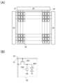
図4(A)は、表示装置の具体例を示す図である。図4(A)に示す表示装置は、m行
n列(m、nは偶数)に配設されているm×n個の画素20と、当該画素間において紙面
の左右方向に延在するm本の走査線21と、当該画素間において紙面の上下方向に延在す
るn本の信号線22と、各々が当該m本の走査線21に接続されている走査線駆動回路2
3、24と、当該n本の信号線22に接続されている信号線駆動回路25とを有する。<2. Specific example of display device>
FIG. 4A is a diagram showing a specific example of a display device. The display device shown in FIG. 4A includes m×n
3, 24, and a signal
<(1)画素20の構成例>
図4(B)は、図4(A)に示す表示装置が有する画素20の回路図の一例を示す図で
ある。図4(B)に示す画素20は、ゲートが走査線21に接続され、ソース又はドレイ
ンの一方が信号線22に接続されているトランジスタ201と、一方の電極がトランジス
タ201のソース又はドレインの他方に接続され、他方の電極が容量電位を供給する配線
(容量線ともいう)に接続されている容量素子202と、一方の電極がトランジスタ20
1のソース又はドレインの他方及び容量素子202の一方の電極に接続され、他方の電極
が共通電位を供給する配線(共通電位線ともいう)に電気的に接続されている液晶素子2
03とを有する。なお、容量電位と共通電位を同一の電位とすることが可能である。また
、図4(B)においては、画素20に液晶素子203が設けられる構成を示しているが、
本明細書で開示される表示装置の画素は当該構成に限定されない。例えば、本明細書で開
示される表示装置においては、画素に発光素子を設けることも可能である。<(1) Configuration example of
FIG. 4B is a diagram showing an example of a circuit diagram of the
1 and one electrode of the
03. Note that the capacitance potential and the common potential can be the same potential. FIG. 4B shows a structure in which the
The pixels of the display device disclosed in this specification are not limited to this configuration. For example, in the display device disclosed in this specification, pixels can be provided with light-emitting elements.
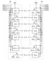
<(2)走査線駆動回路23、24の構成例>
図5は、図4(A)に示す表示装置が有する走査線駆動回路23、24の構成例を示す
図である。図5に示す走査線駆動回路23は、各々がクロック信号(CKL1乃至4)の
いずれか一を供給する4本の配線と、各々が奇数行目に配設されている複数の走査線21
_1、21_3・・・21_m-1のいずれか一に接続されている複数のパルス出力回路
23_1、23_3・・・23_m-1と、各々のゲートが当該4本の配線のいずれか一
に接続され、ソースが低電源電位(VSS)を供給する配線(以下、低電源電位線という
)に接続され、且つドレインが偶数行目に配設された複数の走査線21_2、21_4・
・・21_mのいずれか一に接続されている複数のトランジスタ23_2、23_4・・
・23_mとを有する。また、図5に示す走査線駆動回路24は、各々がクロック信号(
CKR1乃至4)のいずれか一を供給する4本の配線と、各々が偶数行目に配設されてい
る複数の走査線21_2、21_4・・・21_mのいずれか一に接続されている複数の
パルス出力回路24_2、24_4・・・24_mと、各々のゲートが当該4本の配線の
いずれか一に接続され、ソースが低電源電位線に接続され、且つドレインが奇数行目に配
設された複数の走査線21_1、21_3・・・21_m-1のいずれか一に接続されて
いる複数のトランジスタ24_1、24_3・・・24_m-1とを有する。なお、図5
に示す走査線駆動回路23においては、パルス出力回路23_1、23_3・・・23_
m-1によってシフトレジスタが構成され、図5に示す走査線駆動回路24においては、
パルス出力回路24_2、24_4・・・24_mによってシフトレジスタが構成されて
いる。<(2) Configuration example of scanning
FIG. 5 is a diagram showing a configuration example of the scanning
, 23_m-1 connected to any one of _1, 21_3, .
. . , a plurality of transistors 23_2, 23_4 connected to any one of 21_m.
23_m. Further, each of the scanning
CKR1 to CKR4), a plurality of pulse output circuits 24_2, 24_4, . 21_3 . . . 21_m−1 and a plurality of transistors 24_1, 24_3 . In addition, Fig. 5
2, pulse output circuits 23_1, 23_3, . . . 23_
m−1 constitute a shift register, and in the scanning
A shift register is configured by the pulse output circuits 24_2, 24_4, . . . , 24_m.
図6(A)は、クロック信号(CKL1乃至4、CKR1乃至4)の具体的な波形の一
例を示す図である。図6(A)に示すクロック信号(CKL1)は、周期的にハイレベル
の電位(高電源電位(VDD))とロウレベルの電位(低電源電位(VSS))を繰り返
す、デューティ比が3/8の信号である。また、クロック信号(CKL2)は、クロック
信号(CKL1)から1/4周期位相がずれた信号であり、クロック信号(CKL3)は
、クロック信号(CKL1)から1/2周期位相がずれた信号であり、クロック信号(C
KL4)は、クロック信号(CKL1)から3/4周期位相がずれた信号である。また、
クロック信号(CKR1)は、クロック信号(CKL1)から1/8周期位相がずれた信
号であり、クロック信号(CKR2)は、クロック信号(CKL1)から3/8周期位相
がずれた信号であり、クロック信号(CKR3)は、クロック信号(CKL1)から5/
8周期位相がずれた信号であり、クロック信号(CKR4)は、クロック信号(CKL1
)から7/8周期位相がずれた信号である。FIG. 6A is a diagram showing an example of specific waveforms of clock signals (CKL1 to 4, CKR1 to 4). The clock signal (CKL1) shown in FIG. 6A is a signal with a duty ratio of 3/8 that periodically repeats a high-level potential (high power supply potential (VDD)) and a low-level potential (low power supply potential (VSS)). The clock signal (CKL2) is a signal whose phase is shifted by 1/4 period from the clock signal (CKL1), and the clock signal (CKL3) is a signal whose phase is shifted by 1/2 period from the clock signal (CKL1).
KL4) is a signal whose phase is shifted by 3/4 period from the clock signal (CKL1). again,
The clock signal (CKR1) is shifted from the clock signal (CKL1) in phase by 1/8 period, the clock signal (CKR2) is shifted by 3/8 period from the clock signal (CKL1), and the clock signal (CKR3) is shifted by 5/8 from the clock signal (CKL1).
The clock signal (CKR4) is a signal whose phase is shifted by 8 periods, and the clock signal (CKL1
) is out of phase with 7/8 period.
上述した表示装置においては、各パルス出力回路23_1、23_3・・・23_m-
1、24_2、24_4・・・24_mとして、同一の構成を有する回路を適用すること
ができる。ただし、パルス出力回路が有する複数の端子の電気的な接続関係は、パルス出
力回路毎に異なる。具体的な接続関係について図5、図6(B)を参照して説明する。In the display device described above, each pulse output circuit 23_1, 23_3 .
1, 24_2, 24_4, . However, the electrical connection relationship between the terminals of the pulse output circuit differs from pulse output circuit to pulse output circuit. A specific connection relationship will be described with reference to FIGS. 5 and 6B.
各パルス出力回路は、パルス出力回路23_m-1、24_mを除き、端子31乃至3
6を有する。なお、端子31乃至34は入力端子であり、端子35、36は出力端子であ
る。また、パルス出力回路23_m-1、24_mは、端子31乃至35を有する。Each pulse output circuit has
6.
まず、端子31について述べる。パルス出力回路23_1の端子31は、スタートパル
ス(SP1)を供給する配線に接続され、パルス出力回路23_2a-1(aは2以上m
/2以下の自然数)の端子31は、パルス出力回路23_2a-3の端子36に接続され
ている。また、パルス出力回路24_2の端子31は、スタートパルス(SP2)を供給
する配線に接続され、パルス出力回路24_2aの端子31は、パルス出力回路24_2
a-2の端子36に接続されている。First, the terminal 31 will be described. A terminal 31 of the pulse output circuit 23_1 is connected to a wiring for supplying a start pulse (SP1), and a pulse output circuit 23_2a-1 (a is 2 or more m
/2 or less) is connected to the
It is connected to
次いで、端子32について述べる。パルス出力回路23_8b-7(bは、m/8以下
の自然数)の端子32は、クロック信号(CKL1)を供給する配線に接続され、パルス
出力回路23_8b-5の端子32は、クロック信号(CKL2)を供給する配線に接続
され、パルス出力回路23_8b-3の端子32は、クロック信号(CKL3)を供給す
る配線に接続され、パルス出力回路23_8b-1の端子32は、クロック信号(CKL
4)を供給する配線に接続されている。また、パルス出力回路24_8b-6の端子32
は、クロック信号(CKR1)を供給する配線に接続され、パルス出力回路24_8b-
4の端子32は、クロック信号(CKR2)を供給する配線に接続され、パルス出力回路
24_8b-2の端子32は、クロック信号(CKR3)を供給する配線に接続され、パ
ルス出力回路24_8bの端子32は、クロック信号(CKR4)を供給する配線に接続
されている。Next, the terminal 32 will be described. The terminal 32 of the pulse output circuit 23_8b-7 (b is a natural number equal to or less than m/8) is connected to the wiring that supplies the clock signal (CKL1), the
4) is connected to a wiring that supplies . Also, the
is connected to the wiring that supplies the clock signal (CKR1), and the pulse output circuit 24_8b-
4 is connected to the wiring that supplies the clock signal (CKR2), the
次いで、端子33について述べる。パルス出力回路23_8b-7の端子33は、クロ
ック信号(CKL2)を供給する配線に接続され、パルス出力回路23_8b-5の端子
33は、クロック信号(CKL3)を供給する配線に接続され、パルス出力回路23_8
b-3の端子33は、クロック信号(CKL4)を供給する配線に接続され、パルス出力
回路23_8b-1の端子33は、クロック信号(CKL1)を供給する配線に接続され
ている。また、パルス出力回路24_8b-6の端子33は、クロック信号(CKR2)
を供給する配線に接続され、パルス出力回路24_8b-4の端子33は、クロック信号
(CKR3)を供給する配線に接続され、パルス出力回路24_8b-2の端子33は、
クロック信号(CKR4)を供給する配線に接続され、パルス出力回路24_8bの端子
33は、クロック信号(CKR1)を供給する配線に接続されている。Next, the terminal 33 will be described. The terminal 33 of the pulse output circuit 23_8b-7 is connected to the wiring that supplies the clock signal (CKL2), the
The terminal 33 of b-3 is connected to the wiring that supplies the clock signal (CKL4), and the
, the
It is connected to the wiring that supplies the clock signal (CKR4), and the
次いで、端子34について述べる。パルス出力回路23_8b-7の端子34は、クロ
ック信号(CKL3)を供給する配線に接続され、パルス出力回路23_8b-5の端子
34は、クロック信号(CKL4)を供給する配線に接続され、パルス出力回路23_8
b-3の端子34は、クロック信号(CKL1)を供給する配線に接続され、パルス出力
回路23_8b-1の端子34は、クロック信号(CKL2)を供給する配線に接続され
ている。また、パルス出力回路24_8b-6の端子34は、クロック信号(CKR3)
を供給する配線に接続され、パルス出力回路24_8b-4の端子34は、クロック信号
(CKR4)を供給する配線に接続され、パルス出力回路24_8b-2の端子34は、
クロック信号(CKR1)を供給する配線に接続され、パルス出力回路24_8bの端子
34は、クロック信号(CKR2)を供給する配線に接続されている。Next, the terminal 34 will be described. The terminal 34 of the pulse output circuit 23_8b-7 is connected to the wiring that supplies the clock signal (CKL3), and the
The terminal 34 of b-3 is connected to the wiring that supplies the clock signal (CKL1), and the
The terminal 34 of the pulse output circuit 24_8b-4 is connected to the wiring that supplies the clock signal (CKR4), and the
It is connected to the wiring that supplies the clock signal (CKR1), and the
次いで、端子35について述べる。パルス出力回路23_2x-1、24_2x(xは
、m以下の自然数)の端子35は、x行目に配設された走査線21_xに接続されている
。Next, the terminal 35 will be described. The
各パルス出力回路(パルス出力回路23_m-1、24_mを除く)の端子36の接続
関係は既出である。そのため、ここでは前述の説明を援用することとする。The connection relationship of the
<(2-1)パルス出力回路の構成例>
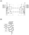
図7(A)は、図5、図6(B)に示すパルス出力回路の構成例を示す図である。図7
(A)に示すパルス出力回路は、トランジスタ41乃至49を有する。なお、パルス出力
回路23_m-1、24_mにはトランジスタ43、44を設けなくてもよい。<(2-1) Configuration example of pulse output circuit>
FIG. 7A is a diagram showing a configuration example of the pulse output circuit shown in FIGS. 5 and 6B. Figure 7
The pulse output circuit illustrated in (A) has
トランジスタ41は、ソース又はドレインの一方が高電源電位(VDD)を供給する配
線(以下、高電源電位線という)に接続され、ゲートが端子31に接続されている。The
トランジスタ42は、ソース又はドレインの一方が低電源電位線に接続され、ソース又
はドレインの他方がトランジスタ41のソース又はドレインの他方に接続されている。One of the source and the drain of the
トランジスタ43は、ソース又はドレインの一方が端子32に接続され、ソース又はド
レインの他方が端子36に接続され、ゲートがトランジスタ41のソース又はドレインの
他方及びトランジスタ42のソース又はドレインの他方に接続されている。The
トランジスタ44は、ソース又はドレインの一方が低電源電位線に接続され、ソース又
はドレインの他方が端子36に接続され、ゲートがトランジスタ42のゲートに接続され
ている。The
トランジスタ45は、ソース又はドレインの一方が低電源電位線に接続され、ソース又
はドレインの他方がトランジスタ42のゲート及びトランジスタ44のゲートに接続され
、ゲートが端子31に電気的に接続されている。The
トランジスタ46は、ソース又はドレインの一方が高電源電位線に接続され、ゲートが
端子33に接続されている。なお、トランジスタ46のソース又はドレインの一方が、低
電源電位(VSS)よりも高電位であり且つ高電源電位(VDD)よりも低電位である電
源電位(VCC)を供給する配線に接続されている構成とすることもできる。The
トランジスタ47は、ソース又はドレインの一方がトランジスタ46のソース又はドレ
インの他方に接続され、ソース又はドレインの他方がトランジスタ42のゲート、トラン
ジスタ44のゲート、及びトランジスタ45のソース又はドレインの他方に接続され、ゲ
ートが端子34に接続されている。The
トランジスタ48は、ソース又はドレインの一方が端子32に接続され、ソース又はド
レインの他方が端子35に接続され、ゲートがトランジスタ41のソース又はドレインの
他方、トランジスタ42のソース又はドレインの他方、及びトランジスタ43のゲートに
接続されている。The
トランジスタ49は、ソース又はドレインの一方が低電源電位線に接続され、ソース又
はドレインの他方が端子35に接続され、ゲートがトランジスタ42のゲート、トランジ
スタ44のゲート、トランジスタ45のソース又はドレインの他方、及びトランジスタ4
7のソース又はドレインの他方に接続されている。The
7 is connected to the other of its source or drain.
なお、以下においては、トランジスタ41のソース又はドレインの他方、トランジスタ
42のソース又はドレインの他方、トランジスタ43のゲート、及びトランジスタ48の
ゲートが接続されたノードをノードAとし、トランジスタ42のゲート、トランジスタ4
4のゲート、トランジスタ45のソース又はドレインの他方、トランジスタ47のソース
又はドレインの他方、及びトランジスタ49のゲートが接続されたノードをノードBとし
て説明する。Note that hereinafter, a node to which the other of the source or the drain of the
4, the other of the source or drain of the
<(2-2)パルス出力回路の動作例>
上述したパルス出力回路の動作例について図7(B)、(C)を参照して説明する。な
お、図7(B)は、パルス出力回路23_1に入出力される信号の波形、及びパルス出力
回路23_1中のノードA、Bの電位を示す図であり、図7(C)は、パルス出力回路2
4_2に入出力される信号の波形、及びパルス出力回路24_2中のノードA、Bの電位
を示す図である。なお、図7(B)、(C)中において、Goutは、パルス出力回路の
走査線に対する出力信号を表し、SRoutは、当該パルス出力回路の後段に設けられて
いるパルス出力回路に対する出力信号を表している。<(2-2) Operation example of pulse output circuit>
An operation example of the pulse output circuit described above will be described with reference to FIGS. 7B shows waveforms of signals input to and output from the pulse output circuit 23_1 and potentials of nodes A and B in the pulse output circuit 23_1.
4 is a diagram showing waveforms of signals input to and output from 4_2 and potentials of nodes A and B in a pulse output circuit 24_2; FIG. In FIGS. 7B and 7C, Gout represents the output signal for the scanning line of the pulse output circuit, and SRout represents the output signal for the pulse output circuit provided after the pulse output circuit.
まず、図7(B)を参照して、パルス出力回路23_1の動作について説明する。 First, the operation of the pulse output circuit 23_1 will be described with reference to FIG. 7B.
タイミングt1において、端子31にハイレベルの電位(高電源電位(VDD))が入
力される。これにより、トランジスタ41、45がオン状態となる。そのため、ノードA
の電位がハイレベルの電位(高電源電位(VDD)からトランジスタ41のしきい値電圧
分下降した電位)に上昇し、その時点でトランジスタ41がオフ状態となる。また、ノー
ドBの電位が低電源電位(VSS)に下降する。これに付随して、トランジスタ43、4
8がオン状態となり、トランジスタ42、44、49がオフ状態となる。以上により、端
子35、36から出力される信号は、端子32に入力される信号となる。ここで、端子3
2に入力される信号は、ロウレベルの電位(低電源電位(VSS))である。そのため、
パルス出力回路23_1は、パルス出力回路23_3の端子31、及び走査線21_1に
ロウレベルの電位(低電源電位(VSS))を出力する。At timing t1, a high level potential (high power supply potential (VDD)) is input to the terminal 31 . As a result, the
increases to a high-level potential (potential lower than the high power supply potential (VDD) by the threshold voltage of the transistor 41), and at that point the
8 is turned on and
2 is a low-level potential (low power supply potential (VSS)). for that reason,
The pulse output circuit 23_1 outputs a low-level potential (low power supply potential (VSS)) to the
タイミングt2において、端子34にロウレベルの電位(低電源電位(VSS))が入
力される。ただし、端子35及び端子36から出力される信号は変化せず、パルス出力回
路23_1は、パルス出力回路23_3の端子31、及び走査線21_1にロウレベルの
電位(低電源電位(VSS))を出力する。At timing t2, a low-level potential (low power supply potential (VSS)) is input to the terminal 34 . However, the signals output from the
タイミングt3において、端子32にハイレベルの電位(高電源電位(VDD))が入
力される。なお、タイミングt3の時点で、ノードAの電位(トランジスタ41のソース
又はドレインの他方の電位)は、既にハイレベルの電位(高電源電位(VDD)からトラ
ンジスタ41のしきい値電圧分下降した電位)まで上昇している。そのため、トランジス
タ41はオフ状態となっている。この時、端子32にハイレベルの電位(高電源電位(V
DD))が入力されることで、トランジスタ43、48のソースとゲートの容量結合によ
って、ノードAの電位(トランジスタ43、48のゲートの電位)がさらに上昇する(ブ
ートストラップ動作)。また、当該ブートストラップ動作を行うことによって、端子35
、36から出力される信号が端子32に入力されるハイレベルの電位(高電源電位(VD
D))から下降することがない。そのため、パルス出力回路23_1は、パルス出力回路
23_3の端子31、及び走査線21_1にハイレベルの電位(高電源電位(VDD))
を出力する。At timing t3, a high level potential (high power supply potential (VDD)) is input to the terminal 32 . Note that at timing t3, the potential of the node A (the other potential of the source or drain of the transistor 41) has already risen to a high-level potential (potential lowered by the threshold voltage of the
DD)) is input, the potential of node A (potential of the gates of
, 36 is applied to the terminal 32 at the high level potential (high power supply potential (VD
D)) never descends. Therefore, the pulse output circuit 23_1 supplies a high-level potential (high power supply potential (VDD)) to the
to output
タイミングt4において、端子31にロウレベルの電位(低電源電位(VSS))が入
力され、タイミングt5において端子33にハイレベルの電位(高電源電位(VDD))
が入力される。ただし、端子35及び端子36から出力される信号は変化せず、パルス出
力回路23_1は、パルス出力回路23_3の端子31、及び走査線21_1にハイレベ
ルの電位(高電源電位(VDD))を出力する。At timing t4, a low-level potential (low power supply potential (VSS)) is input to the terminal 31, and at timing t5, a high-level potential (high power supply potential (VDD)) is applied to the terminal 33.
is entered. However, the signals output from the
タイミングt6において、端子32にロウレベルの電位(低電源電位(VSS))が入
力される。この時、トランジスタ43、48のソースとゲートの容量結合によって、ノー
ドAの電位(トランジスタ43、48のゲートの電位)が下降する(ブートストラップ動
作)。ただし、ノードAの電位は依然としてハイレベルの電位にある。そのため、トラン
ジスタ43、48はオン状態を維持する。よって、端子32に入力される信号が端子35
、36から出力される信号となる。すなわち、パルス出力回路23_1は、パルス出力回
路23_3の端子31、及び走査線21_1にロウレベルの電位(低電源電位(VSS)
)を出力する。At timing t<b>6 , a low-level potential (low power supply potential (VSS)) is input to the terminal 32 . At this time, the potential of node A (potential of the gates of
, 36. That is, the pulse output circuit 23_1 applies a low-level potential (low power supply potential (VSS)) to the
).
タイミングt7において、端子34にハイレベルの電位(高電源電位(VDD))が入
力される。また、タイミングt7においては、端子33にもハイレベルの電位(高電源電
位(VDD))が入力されている。そのため、トランジスタ46、47が共にオン状態と
なる。これにより、ノードBの電位がハイレベルの電位(高電源電位(VDD)からトラ
ンジスタ46及びトランジスタ47のうちしきい値電圧が高い方のしきい値電圧分下降し
た電位)に上昇する。そのため、トランジスタ42、44、49がオン状態となる。また
、これに付随して、ノードAの電位がロウレベルの電位(低電源電位(VSS))へと下
降する。そのため、トランジスタ43、48がオフ状態となる。以上により、タイミング
t7において、端子35及び端子36から出力される信号は、トランジスタ44、49の
ソース又はドレインの一方に入力される信号となる。もっとも、当該信号は低電源電位(
VSS)である。そのため、パルス出力回路23_1のパルス出力回路23_3の端子3
1、及び走査線21_1に対する出力信号は、ロウレベルの電位(低電源電位(VSS)
)のまま維持される。At timing t7, a high level potential (high power supply potential (VDD)) is input to the terminal 34 . At timing t7, a high-level potential (high power supply potential (VDD)) is also input to
VSS). Therefore, the
1, and the output signal to the scanning line 21_1 is a low-level potential (low power supply potential (VSS)
).
次いで、パルス出力回路24_2の動作について説明する。図7(C)に示すように、
パルス出力回路24_2は、パルス出力回路23_1と同様に動作する。ただし、パルス
出力回路24_2は、パルス出力回路23_1と比較してクロック信号(CKL1乃至4
、CKR1乃至4)の1/8周期分遅れて動作する。Next, the operation of the pulse output circuit 24_2 will be described. As shown in FIG. 7(C),
The pulse output circuit 24_2 operates similarly to the pulse output circuit 23_1. However, the pulse output circuit 24_2 has clock signals (CKL1 to 4) compared to the pulse output circuit 23_1.
, CKR1 to CKR4) with a delay of 1/8 cycle.
<(2-3)トランジスタ23_2・・・23_m、24_1・・・24_m-1の動作
例>
トランジスタ23_2・・・23_m、24_1・・・24_m-1の動作例について
、図8を参照して説明する。図8(A)は、図5の一部を抜粋した図であり、図8(B)
は、図7(B)、(C)に示すパルス出力回路23_1、24_2が走査線21_1、2
1_2に出力する信号の波形及びトランジスタ23_2、24_1のゲートに入力される
クロック信号(CKR2、CKL3)を示す図である。<(2-3) Operation example of transistors 23_2 . . . 23_m and 24_1 . . . 24_m−1>
An operation example of the transistors 23_2 . . . 23_m and 24_1 . FIG. 8A is a diagram extracting a part of FIG. 5, and FIG.
7(B) and 7(C) are connected to the scanning lines 21_1 and 21_2.
1_2 and clock signals (CKR2 and CKL3) input to gates of transistors 23_2 and 24_1; FIG.
上述した表示装置においては、図8(B)に示すようにパルス出力回路23_1が走査
線21_1に対して出力する信号がハイレベルの電位(高電源電位(VDD))からロウ
レベルの電位(低電源電位(VSS))に切り替わるタイミング(ta)が、クロック信
号(CKR2)がロウレベルの電位(低電源電位(VSS))からハイレベルの電位(高
電源電位(VDD))に切り替わるタイミングと一致している。すなわち、当該タイミン
グ(ta)が、トランジスタ24_1がオフ状態からオン状態となるタイミングと一致し
ている。同様に、パルス出力回路24_3が走査線21_2に対して出力する信号がハイ
レベルの電位(高電源電位(VDD))からロウレベルの電位(低電源電位(VSS))
に切り替わるタイミング(tb)が、トランジスタ24_1がオフ状態からオン状態とな
るタイミングと一致している。これにより、上述した表示装置においては、走査線の一端
のみならず両端から非選択信号が同時に入力されることになる。そのため、当該走査線の
各箇所における電位変化のタイミングのずれを抑制することが可能である。すなわち、当
該走査線にゲートが接続されている複数のトランジスタのスイッチングのタイミングのず
れを抑制することが可能となる。その結果、表示装置において生じる不具合を抑制するこ
とが可能となる。In the above-described display device, as shown in FIG. 8B, the timing (ta) at which the signal output from the pulse output circuit 23_1 to the scanning line 21_1 switches from the high level potential (high power supply potential (VDD)) to the low level potential (low power supply potential (VSS)) coincides with the timing at which the clock signal (CKR2) switches from the low level potential (low power supply potential (VSS)) to the high level potential (high power supply potential (VDD)). are doing. That is, the timing (ta) coincides with the timing at which the transistor 24_1 is turned on from off. Similarly, when the signal output from the pulse output circuit 24_3 to the scan line 21_2 changes from the high-level potential (high power supply potential (VDD)) to the low-level potential (low power supply potential (VSS)).
, coincides with the timing at which the transistor 24_1 is turned on from the off state. As a result, in the display device described above, the non-selection signal is simultaneously input not only from one end of the scanning line but also from both ends. Therefore, it is possible to suppress the timing deviation of the potential change at each part of the scanning line. That is, it is possible to suppress a shift in switching timing of a plurality of transistors whose gates are connected to the scan line. As a result, it is possible to suppress defects that occur in the display device.
また、上述した表示装置においては、トランジスタ23_2、23_4・・・23_m
、24_1、24_3・・・24_m-1のスイッチングを制御するためにシフトレジス
タを動作する際に用いられるクロック信号(CKL1乃至4、CKR1乃至4)が利用さ
れている。すなわち、トランジスタ23_2、23_4・・・23_m、24_1、24
_3・・・24_m-1のスイッチングを制御するために別途新たな信号を供給する配線
を設ける必要がない。よって、上述した表示装置においては、効率よく狭額縁化を図るこ
とが可能である。Further, in the display device described above, the transistors 23_2, 23_4, .
, 24_1, 24_3, . , 23_m, 24_1, 24
_3 . . . 24_m−1, there is no need to separately provide a wiring for supplying a new signal to control the switching. Therefore, in the display device described above, it is possible to efficiently achieve a narrow frame.
<(3)走査線駆動回路23、24の変形例>
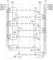
本明細書で開示される表示装置に設けられる走査線駆動回路23、24は、上述した回
路に限定されない。例えば、トランジスタ23_2・・・23_m、24_1・・・24
_m-1のゲートを、図5に示す様にクロック信号を供給する配線(CKL1乃至4、C
KR1乃至4)のいずれか一に接続させる構成とするのではなく、パルス出力回路23_
1・・・23_m-1、24_2・・・24_m-1のいずれか一の端子35に接続させ
る構成とすることも可能である。<(3) Modifications of the scanning
The scanning
The gate of _m−1 is connected to wiring (CKL1 to 4, C
KR1 to KR4), the pulse output circuit 23_
23 — m−1 and 24 — 2 . . . 24 — m−1.
具体的には、パルス出力回路が図7(A)に示す場合であれば、図9に示す構成とする
ことも可能である。図9に示す走査線駆動回路23では、トランジスタ23_2c(cは
m-4以下の偶数)のゲートがパルス出力回路23_c+3の端子35に接続され、トラ
ンジスタ24_d(dはm-3以下の奇数)のゲートがパルス出力回路24_d+3の端
子35に接続されている。なお、図9には図示していないが、図9では、トランジスタ2
3_m-2のゲートがパルス出力回路23_m-7の端子35に接続され、トランジスタ
23_mのゲートがパルス出力回路23_m-5の端子35に接続され、トランジスタ2
4_m-1のゲートがパルス出力回路24_m-6の端子35に接続されている。Specifically, if the pulse output circuit is shown in FIG. 7A, the configuration shown in FIG. 9 can be used. In the scanning
3_m-2 is connected to the
The gate of 4_m-1 is connected to the
図9に示す走査線駆動回路23、24を用いた場合であっても、図5に示す走査線駆動
回路23、24を用いた場合と同様の作用効果を奏する。Even when the scanning
<3.トランジスタの具体例>
上述した表示装置に含まれるトランジスタとしては、どのようなトランジスタを適用し
てもよい。例えば、シリコン膜にチャネルが形成されるトランジスタ(シリコン膜にチャ
ネル形成領域を有するトランジスタ)又は酸化物半導体膜にチャネルが形成されるトラン
ジスタ(酸化物半導体膜にチャネル形成領域を有するトランジスタ)を上述した表示装置
に含まれるトランジスタとして適用することが可能である。<3. Specific Examples of Transistors>
Any transistor may be used as the transistor included in the display device described above. For example, a transistor in which a channel is formed in a silicon film (a transistor having a channel formation region in a silicon film) or a transistor in which a channel is formed in an oxide semiconductor film (a transistor having a channel formation region in an oxide semiconductor film) can be used as the transistor included in the above display device.
以下では、酸化物半導体膜の構造について説明する。 The structure of the oxide semiconductor film is described below.
酸化物半導体膜は、非単結晶酸化物半導体膜と単結晶酸化物半導体膜とに大別される。
非単結晶酸化物半導体膜とは、CAAC-OS(C Axis Aligned Cry
stalline Oxide Semiconductor)膜、多結晶酸化物半導体
膜、微結晶酸化物半導体膜、非晶質酸化物半導体膜などをいう。Oxide semiconductor films are roughly classified into non-single-crystal oxide semiconductor films and single-crystal oxide semiconductor films.
The non-single-crystal oxide semiconductor film is CAAC-OS (C Axis Aligned Cry
(Stalline Oxide Semiconductor) film, polycrystalline oxide semiconductor film, microcrystalline oxide semiconductor film, amorphous oxide semiconductor film, and the like.
まずは、CAAC-OS膜について説明する。 First, the CAAC-OS film will be explained.
CAAC-OS膜は、c軸配向した複数の結晶部を有する酸化物半導体膜の一つである
。A CAAC-OS film is one of oxide semiconductor films having a plurality of c-axis aligned crystal parts.
CAAC-OS膜を透過型電子顕微鏡(TEM:Transmission Elec
tron Microscope)によって観察すると、明確な結晶部同士の境界、即ち
結晶粒界(グレインバウンダリーともいう。)を確認することができない。そのため、C
AAC-OS膜は、結晶粒界に起因する電子移動度の低下が起こりにくいといえる。The CAAC-OS film was observed under a transmission electron microscope (TEM: Transmission Elec
When observed with a tron microscope, a clear boundary between crystal parts, that is, a crystal grain boundary (also called a grain boundary) cannot be confirmed. Therefore, C
It can be said that the AAC-OS film is less prone to decrease in electron mobility due to grain boundaries.
CAAC-OS膜を、試料面と概略平行な方向からTEMによって観察(断面TEM観
察)すると、結晶部において、金属原子が層状に配列していることを確認できる。金属原
子の各層は、CAAC-OS膜の膜を形成する面(被形成面ともいう。)または上面の凹
凸を反映した形状であり、CAAC-OS膜の被形成面または上面と平行に配列する。When the CAAC-OS film is observed with a TEM (cross-sectional TEM observation) from a direction substantially parallel to the sample surface, it can be confirmed that metal atoms are arranged in layers in the crystal part. Each layer of metal atoms has a shape that reflects the unevenness of the surface on which the CAAC-OS film is formed (also referred to as the surface on which the CAAC-OS film is formed) or the upper surface, and is arranged in parallel with the surface on which the CAAC-OS film is formed or the upper surface.
なお、本明細書において、「平行」とは、二つの直線が-10°以上10°以下の角度
で配置されている状態をいう。従って、-5°以上5°以下の場合も含まれる。また、「
垂直」とは、二つの直線が80°以上100°以下の角度で配置されている状態をいう。
従って、85°以上95°以下の場合も含まれる。In this specification, "parallel" means a state in which two straight lines are arranged at an angle of -10° or more and 10° or less. Therefore, the case of −5° or more and 5° or less is also included. again,"
“Perpendicular” means a state in which two straight lines are arranged at an angle of 80° or more and 100° or less.
Therefore, the case of 85° or more and 95° or less is also included.
一方、CAAC-OS膜を、試料面と概略垂直な方向からTEMによって観察(平面T
EM観察)すると、結晶部において、金属原子が三角形状または六角形状に配列している
ことを確認できる。しかしながら、異なる結晶部間で、金属原子の配列に規則性は見られ
ない。On the other hand, the CAAC-OS film was observed by TEM from a direction substantially perpendicular to the sample surface (plane T
EM observation), it can be confirmed that the metal atoms are arranged in a triangular or hexagonal shape in the crystal part. However, there is no regularity in the arrangement of metal atoms between different crystal parts.
断面TEM観察および平面TEM観察より、CAAC-OS膜の結晶部は配向性を有し
ていることがわかる。Cross-sectional TEM observation and planar TEM observation show that the crystal part of the CAAC-OS film has an orientation.
なお、CAAC-OS膜に含まれるほとんどの結晶部は、一辺が100nm未満の立方
体内に収まる大きさである。従って、CAAC-OS膜に含まれる結晶部は、一辺が10
nm未満、5nm未満または3nm未満の立方体内に収まる大きさの場合も含まれる。た
だし、CAAC-OS膜に含まれる複数の結晶部が連結することで、一つの大きな結晶領
域を形成する場合がある。例えば、平面TEM像において、2500nm2以上、5μm
2以上または1000μm2以上となる結晶領域が観察される場合がある。Note that most of the crystal parts included in the CAAC-OS film have a size that fits within a cube with one side of less than 100 nm. Therefore, each side of the crystal part included in the CAAC-OS film is 10
A size that fits within a cube of less than nm, less than 5 nm, or less than 3 nm is also included. However, a plurality of crystal parts included in the CAAC-OS film may be connected to form one large crystal region. For example, in a planar TEM image, 2500 nm2 or more, 5 μm
Crystalline regions of2 or more or 1000 μm2 or more may be observed.
CAAC-OS膜に対し、X線回折(XRD:X-Ray Diffraction)
装置を用いて構造解析を行うと、例えばInGaZnO4の結晶を有するCAAC-OS
膜のout-of-plane法による解析では、回折角(2θ)が31°近傍にピーク
が現れる場合がある。このピークは、InGaZnO4の結晶の(009)面に帰属され
ることから、CAAC-OS膜の結晶がc軸配向性を有し、c軸が被形成面または上面に
概略垂直な方向を向いていることが確認できる。X-ray diffraction (XRD: X-Ray Diffraction) for the CAAC-OS film
Structural analysis using the apparatus revealed, for example, a CAAC-OS having InGaZnO4 crystals.
In the film analysis by the out-of-plane method, a peak may appear near the diffraction angle (2θ) of 31°. Since this peak is attributed to the (009) plane of the crystal of InGaZnO4 , it can be confirmed that the crystal of the CAAC-OS film has c-axis orientation and the c-axis is oriented substantially perpendicular to the formation surface or top surface.
一方、CAAC-OS膜に対し、c軸に概略垂直な方向からX線を入射させるin-p
lane法による解析では、2θが56°近傍にピークが現れる場合がある。このピーク
は、InGaZnO4の結晶の(110)面に帰属される。InGaZnO4の単結晶酸
化物半導体膜であれば、2θを56°近傍に固定し、試料面の法線ベクトルを軸(φ軸)
として試料を回転させながら分析(φスキャン)を行うと、(110)面と等価な結晶面
に帰属されるピークが6本観察される。これに対し、CAAC-OS膜の場合は、2θを
56°近傍に固定してφスキャンした場合でも、明瞭なピークが現れない。On the other hand, an in-p method in which X-rays are incident on the CAAC-OS film from a direction substantially perpendicular to the c-axis
In the analysis by the lane method, a peak may appear near 2θ of 56°. This peak is assigned to the (110) plane of the InGaZnO4 crystal. In the case of a single crystal oxide semiconductor film of InGaZnO4 , 2θ is fixed around 56°, and the normal vector of the sample surface is the axis (φ axis).
When analysis (φ scan) is performed while rotating the sample as , six peaks attributed to crystal planes equivalent to the (110) plane are observed. On the other hand, in the case of the CAAC-OS film, no clear peak appears even when φ scanning is performed with 2θ fixed at around 56°.
以上のことから、CAAC-OS膜では、異なる結晶部間ではa軸およびb軸の配向は
不規則であるが、c軸配向性を有し、かつc軸が被形成面または上面の法線ベクトルに平
行な方向を向いていることがわかる。従って、前述の断面TEM観察で確認された層状に
配列した金属原子の各層は、結晶のab面に平行な面である。From the above, in the CAAC-OS film, although the orientation of the a-axis and b-axis is irregular between different crystal parts, it has c-axis orientation, and the c-axis is oriented in a direction parallel to the normal vector of the formation surface or the upper surface. Therefore, each layer of the metal atoms arranged in layers confirmed by the cross-sectional TEM observation is a plane parallel to the ab plane of the crystal.
なお、結晶部は、CAAC-OS膜を成膜した際、または加熱処理などの結晶化処理を
行った際に形成される。上述したように、結晶のc軸は、CAAC-OS膜の被形成面ま
たは上面の法線ベクトルに平行な方向に配向する。従って、例えば、CAAC-OS膜の
形状をエッチングなどによって変化させた場合、結晶のc軸がCAAC-OS膜の被形成
面または上面の法線ベクトルと平行にならないこともある。Note that the crystal part is formed when the CAAC-OS film is formed or when crystallization treatment such as heat treatment is performed. As described above, the c-axis of the crystal is oriented in a direction parallel to the normal vector of the formation surface or top surface of the CAAC-OS film. Therefore, for example, when the shape of the CAAC-OS film is changed by etching or the like, the c-axis of the crystal may not be parallel to the normal vector of the formation surface or top surface of the CAAC-OS film.
また、CAAC-OS膜中において、c軸配向した結晶部の分布が均一でなくてもよい
。例えば、CAAC-OS膜の結晶部が、CAAC-OS膜の上面近傍からの結晶成長に
よって形成される場合、上面近傍の領域は、被形成面近傍の領域よりもc軸配向した結晶
部の割合が高くなることがある。また、CAAC-OS膜に不純物を添加する場合、不純
物が添加された領域が変質し、部分的にc軸配向した結晶部の割合の異なる領域が形成さ
れることもある。In addition, the distribution of c-axis oriented crystal parts may not be uniform in the CAAC-OS film. For example, when the crystal part of the CAAC-OS film is formed by crystal growth from the vicinity of the upper surface of the CAAC-OS film, the region near the upper surface may have a higher ratio of c-axis oriented crystal parts than the region near the formation surface. In addition, when impurities are added to the CAAC-OS film, the region to which the impurity is added may change in quality, and a region with a different ratio of c-axis oriented crystal parts may be formed.
なお、InGaZnO4の結晶を有するCAAC-OS膜のout-of-plane
法による解析では、2θが31°近傍のピークの他に、2θが36°近傍にもピークが現
れる場合がある。2θが36°近傍のピークは、CAAC-OS膜中の一部に、c軸配向
性を有さない結晶が含まれることを示している。CAAC-OS膜は、2θが31°近傍
にピークを示し、2θが36°近傍にピークを示さないことが好ましい。Note that the out-of-plane of the CAAC-OS film having InGaZnO4 crystals
In the analysis by the method, in addition to the peak near 31° 2θ, a peak may also appear near 36° 2θ. The peak near 36° of 2θ indicates that a portion of the CAAC-OS film contains crystals that do not have c-axis orientation. The CAAC-OS film preferably shows a peak near 31° in 2θ and does not show a peak near 36° in 2θ.
CAAC-OS膜は、不純物濃度の低い酸化物半導体膜である。不純物は、水素、炭素
、シリコン、遷移金属元素などの酸化物半導体膜の主成分以外の元素である。特に、シリ
コンなどの、酸化物半導体膜を構成する金属元素よりも酸素との結合力の強い元素は、酸
化物半導体膜から酸素を奪うことで酸化物半導体膜の原子配列を乱し、結晶性を低下させ
る要因となる。また、鉄やニッケルなどの重金属、アルゴン、二酸化炭素などは、原子半
径(または分子半径)が大きいため、酸化物半導体膜内部に含まれると、酸化物半導体膜
の原子配列を乱し、結晶性を低下させる要因となる。なお、酸化物半導体膜に含まれる不
純物は、キャリアトラップやキャリア発生源となる場合がある。The CAAC-OS film is an oxide semiconductor film with a low impurity concentration. Impurities are elements other than the main components of the oxide semiconductor film, such as hydrogen, carbon, silicon, and transition metal elements. In particular, an element such as silicon that has a stronger bonding force with oxygen than a metal element forming the oxide semiconductor film deprives the oxide semiconductor film of oxygen, thereby disturbing the atomic arrangement of the oxide semiconductor film and lowering the crystallinity. In addition, since heavy metals such as iron and nickel, argon, and carbon dioxide have large atomic radii (or molecular radii), if they are included in the oxide semiconductor film, the atomic arrangement of the oxide semiconductor film is disturbed and crystallinity is lowered. Note that impurities contained in the oxide semiconductor film might serve as a carrier trap or a carrier generation source.
また、CAAC-OS膜は、欠陥準位密度の低い酸化物半導体膜である。例えば、酸化
物半導体膜中の酸素欠損は、キャリアトラップとなることや、水素を捕獲することによっ
てキャリア発生源となることがある。Further, the CAAC-OS film is an oxide semiconductor film with a low defect state density. For example, oxygen vacancies in the oxide semiconductor film may trap carriers or generate carriers by trapping hydrogen.
不純物濃度が低く、欠陥準位密度が低い(酸素欠損の少ない)ことを、高純度真性また
は実質的に高純度真性と呼ぶ。高純度真性または実質的に高純度真性である酸化物半導体
膜は、キャリア発生源が少ないため、キャリア密度を低くすることができる。従って、当
該酸化物半導体膜を用いたトランジスタは、しきい値電圧がマイナスとなる電気特性(ノ
ーマリーオンともいう。)になることが少ない。また、高純度真性または実質的に高純度
真性である酸化物半導体膜は、キャリアトラップが少ない。そのため、当該酸化物半導体
膜を用いたトランジスタは、電気特性の変動が小さく、信頼性の高いトランジスタとなる
。なお、酸化物半導体膜のキャリアトラップに捕獲された電荷は、放出するまでに要する
時間が長く、あたかも固定電荷のように振る舞うことがある。そのため、不純物濃度が高
く、欠陥準位密度が高い酸化物半導体膜を用いたトランジスタは、電気特性が不安定とな
る場合がある。A low impurity concentration and a low defect level density (few oxygen vacancies) is called high-purity intrinsic or substantially high-purity intrinsic. A highly purified intrinsic or substantially highly purified intrinsic oxide semiconductor film has few carrier generation sources, and thus can have a low carrier density. Therefore, a transistor including the oxide semiconductor film rarely has electrical characteristics such that the threshold voltage is negative (also referred to as normally-on). In addition, a highly purified intrinsic or substantially highly purified intrinsic oxide semiconductor film has few carrier traps. Therefore, a transistor including the oxide semiconductor film has little variation in electrical characteristics and is highly reliable. Note that the charge trapped in the carrier trap of the oxide semiconductor film takes a long time to be released, and may behave like a fixed charge. Therefore, a transistor including an oxide semiconductor film with a high impurity concentration and a high density of defect states might have unstable electrical characteristics.
また、CAAC-OS膜を用いたトランジスタは、可視光や紫外光の照射による電気特
性の変動が小さい。In addition, a transistor using a CAAC-OS film has little change in electrical characteristics due to irradiation with visible light or ultraviolet light.
次に、微結晶酸化物半導体膜について説明する。 Next, a microcrystalline oxide semiconductor film is described.
微結晶酸化物半導体膜は、TEMによる観察像では、明確に結晶部を確認することがで
きない場合がある。微結晶酸化物半導体膜に含まれる結晶部は、1nm以上100nm以
下、または1nm以上10nm以下の大きさであることが多い。特に、1nm以上10n
m以下、または1nm以上3nm以下の微結晶であるナノ結晶(nc:nanocrys
tal)を有する酸化物半導体膜を、nc-OS(nanocrystalline O
xide Semiconductor)膜と呼ぶ。また、nc-OS膜は、例えば、T
EMによる観察像では、結晶粒界を明確に確認できない場合がある。In a TEM image of the microcrystalline oxide semiconductor film, crystal parts cannot be clearly seen in some cases. A crystal part included in a microcrystalline oxide semiconductor film often has a size of 1 nm to 100 nm or 1 nm to 10 nm. In particular, 1 nm or more and 10 n
m or less, or nanocrystals (nc: nanocrys
tal) is formed by nc-OS (nanocrystalline O
(xide Semiconductor) film. Further, the nc-OS film is, for example, T
Crystal grain boundaries may not be clearly identified in an EM observation image.
nc-OS膜は、微小な領域(例えば、1nm以上10nm以下の領域、特に1nm以
上3nm以下の領域)において原子配列に周期性を有する。また、nc-OS膜は、異な
る結晶部間で結晶方位に規則性が見られない。そのため、膜全体で配向性が見られない。
従って、nc-OS膜は、分析方法によっては、非晶質酸化物半導体膜と区別が付かない
場合がある。例えば、nc-OS膜に対し、結晶部よりも大きい径のX線を用いるXRD
装置を用いて構造解析を行うと、out-of-plane法による解析では、結晶面を
示すピークが検出されない。また、nc-OS膜に対し、結晶部よりも大きいプローブ径
(例えば50nm以上)の電子線を用いる電子線回折(制限視野電子線回折ともいう。)
を行うと、ハローパターンのような回折パターンが観測される。一方、nc-OS膜に対
し、結晶部の大きさと近いか結晶部より小さいプローブ径(例えば1nm以上30nm以
下)の電子線を用いる電子線回折(ナノビーム電子線回折ともいう。)を行うと、スポッ
トが観測される。また、nc-OS膜に対しナノビーム電子線回折を行うと、円を描くよ
うに(リング状に)輝度の高い領域が観測される場合がある。また、nc-OS膜に対し
ナノビーム電子線回折を行うと、リング状の領域内に複数のスポットが観測される場合が
ある。The nc-OS film has periodicity in atomic arrangement in a minute region (eg, a region of 1 nm to 10 nm, particularly a region of 1 nm to 3 nm). Further, in the nc-OS film, there is no regularity in crystal orientation between different crystal parts. Therefore, no orientation is observed in the entire film.
Therefore, the nc-OS film may be indistinguishable from the amorphous oxide semiconductor film depending on the analysis method. For example, for the nc-OS film, XRD using X-rays with a diameter larger than the crystal part
Structural analysis is performed using an apparatus, and no peak indicating a crystal plane is detected in analysis by the out-of-plane method. Further, electron beam diffraction (also called selected area electron beam diffraction) using an electron beam with a probe diameter (for example, 50 nm or more) larger than the crystal part is performed on the nc-OS film.
, a diffraction pattern like a halo pattern is observed. On the other hand, when the nc-OS film is subjected to electron beam diffraction (also referred to as nanobeam electron diffraction) using an electron beam with a probe diameter (for example, 1 nm or more and 30 nm or less) that is close to the size of the crystal part or smaller than the crystal part, spots are observed. In addition, when the nc-OS film is subjected to nanobeam electron diffraction, a circular (ring-like) region with high brightness may be observed. In addition, when nanobeam electron diffraction is performed on the nc-OS film, a plurality of spots may be observed within a ring-shaped region.
nc-OS膜は、非晶質酸化物半導体膜よりも規則性の高い酸化物半導体膜である。そ
のため、nc-OS膜は、非晶質酸化物半導体膜よりも欠陥準位密度が低くなる。ただし
、nc-OS膜は、異なる結晶部間で結晶方位に規則性が見られない。そのため、nc-
OS膜は、CAAC-OS膜と比べて欠陥準位密度が高くなる。The nc-OS film is an oxide semiconductor film with higher regularity than an amorphous oxide semiconductor film. Therefore, the nc-OS film has a lower defect level density than the amorphous oxide semiconductor film. However, in the nc-OS film, there is no regularity in crystal orientation between different crystal parts. Therefore, nc-
The OS film has a higher defect level density than the CAAC-OS film.
なお、酸化物半導体膜は、例えば、非晶質酸化物半導体膜、微結晶酸化物半導体膜、C
AAC-OS膜のうち、二種以上を有する積層膜であってもよい。Note that the oxide semiconductor film is, for example, an amorphous oxide semiconductor film, a microcrystalline oxide semiconductor film, a C
A laminated film including two or more kinds of AAC-OS films may be used.
<4.表示モジュールの具体例>
以下では、上述した表示装置を構成要素の一とする表示モジュールについて、図10を
参照して説明する。<4. Specific example of display module>
A display module including the display device described above as one of its components will be described below with reference to FIG. 10 .
図10に示す表示モジュール8000は、上部カバー8001と下部カバー8002と
の間に、FPC8003に接続されたタッチパネル8004、FPC8005に接続され
た表示パネル8006、バックライトユニット8007、フレーム8009、プリント基
板8010、バッテリー8011を有する。なお、表示モジュールの構成として、これら
の構成要素の少なくとも一が設けられない(例えば、バックライトユニット8007、バ
ッテリー8011、又はタッチパネル8004が設けられない)構成を適用することも可
能である。A
上述した表示装置は、表示パネル8006に該当する。 The display device described above corresponds to the
上部カバー8001及び下部カバー8002は、タッチパネル8004及び表示パネル
8006のサイズに合わせて、形状や寸法を適宜変更することができる。The shape and dimensions of the
タッチパネル8004は、抵抗膜方式または静電容量方式のタッチパネルであり、表示
パネル8006に重畳されている。また、表示パネル8006の対向基板(封止基板)に
、タッチパネル機能を持たせるようにすることも可能である。また、表示パネル8006
の各画素内に光センサを設け、光学式のタッチパネルとすることも可能である。また、表
示パネル8006の各画素内にタッチセンサ用電極を設け、容量型式のタッチパネルとす
ることも可能である。A
It is also possible to provide an optical sensor in each pixel of to make an optical touch panel. Further, a touch sensor electrode can be provided in each pixel of the
バックライトユニット8007は、マトリクス状に配設されている複数の光源8008
を有する。なお、バックライトユニット8007として、線状光源と光拡散板が設けられ
る構成としてもよい。この場合、バックライトユニット8007は、当該線状光源が発す
る線状光を光拡散板で拡散させ、面状光として射出する。A
have Note that the
フレーム8009は、表示パネル8006の保護機能の他、プリント基板8010の動
作により発生する電磁波を遮断するための電磁シールドとしての機能を有する。またフレ
ーム8009は、放熱板としての機能を有していてもよい。The
プリント基板8010は、電源回路、ビデオ信号及びクロック信号を出力するための信
号処理回路を有する。電源回路に電力を供給する電源としては、外部の商用電源であって
も良いし、別途設けたバッテリー8011による電源であってもよい。バッテリー801
1は、商用電源を用いる場合には、省略可能である。The printed
1 can be omitted when a commercial power source is used.
また、表示モジュール8000には、偏光板、位相差板、プリズムシートなどの部材を
追加して設けてもよい。In addition, the
<5.最終製品の具体例>
以下では、上述した表示装置を用いて製造される最終製品の一例について、図11、1
2を参照して説明する。<5. Specific examples of final products>
An example of a final product manufactured using the display device described above will be described below with reference to FIGS.
2 for explanation.
当該最終製品として、例えば、テレビジョン装置(テレビ、又はテレビジョン受信機と
もいう)、コンピュータ用などのモニタ、デジタルカメラ、デジタルビデオカメラ、デジ
タルフォトフレーム、携帯電話機(携帯電話、携帯電話装置ともいう)、携帯型ゲーム機
、携帯情報端末、音響再生装置、パチンコ機などの大型ゲーム機などが挙げられる。なお
、これらの最終製品は、表示面が曲面形状を備える又は表示面を任意に折り曲げることが
可能な製品とすることも可能である。Examples of the final product include television devices (also referred to as televisions or television receivers), monitors for computers, digital cameras, digital video cameras, digital photo frames, mobile phones (also referred to as mobile phones and mobile phone devices), portable game machines, personal digital assistants, sound reproduction devices, and large game machines such as pachinko machines. It should be noted that these final products can also be products that have a curved display surface or that can be arbitrarily bent.
図11(A)は、携帯電話機の一例を示す図である。携帯電話機7400は、筐体74
01に組み込まれた表示部7402の他、操作ボタン7403、外部接続ポート7404
、スピーカ7405、マイク7406などを備えている。なお、携帯電話機7400では
、上述した表示装置が表示部7402内に組み込まれている。FIG. 11A is a diagram showing an example of a mobile phone. The
01, an
, a
図11(A)に示す携帯電話機7400では、表示部7402の表面を指などで触れる
ことで、表示される画像を変化させるなどの操作をすることができる。また、電話を掛け
る、又は文字を入力するなどの操作も、表示部7402の表面を指などで触れることによ
り行うことができる。In the
また、操作ボタン7403の操作により、携帯電話機7400の起動及び停止、並びに
上述した操作を行うことができる。Further, by operating the
図11(B)は、バングル型の表示装置の一例を示す図である。バングル型の表示装置
7100は、筐体7101、表示部7102、操作ボタン7103、及び送受信装置71
04を備える。なお、バングル型の表示装置7100では、上述した表示装置が表示部7
102内に組み込まれている。FIG. 11B illustrates an example of a bangle-type display device. A bangle-
04. Note that in the bangle-
102.
バングル型の表示装置7100は、送受信装置7104によって映像信号を受信可能で
、受信した映像を表示部7102に表示することができる。また、音声信号を他の送受信
装置との間で送受信することもできる。The bangle-
また、操作ボタン7103によって、バングル型の表示装置7100の起動及び停止、
表示される画像を変化させるなどの操作、並びに音声の調整などを行うことができる。Also, the
It is possible to perform operations such as changing the displayed image and adjusting the sound.
図12(A)は、携帯用製品の一例を示す図である。携帯用製品7300は、筐体73
01、表示部7302、操作ボタン7303、引き出し部材7304、制御部7305を
備える。なお、携帯用製品7300では、上述した表示装置が表示部7302内に組み込
まれている。FIG. 12A is a diagram showing an example of a portable product.
01, a
携帯用製品7300は、筒状の筐体7301内にロール状に巻かれたフレキシブルな表
示部7302を備える。表示部7302は、遮光層などが形成された第1の基板と、トラ
ンジスタなどが形成された第2の基板を有する。表示部7302は、筐体7301内にお
いて常に第2の基板が外側になるように巻かれている。The
また、携帯用製品7300は制御部7305によって映像信号を受信可能で、受信した
映像を表示部7302に表示することができる。また、制御部7305にはバッテリーを
備える。また、制御部7305にコネクタを備え、映像信号や電力を直接供給する構成と
してもよい。Also, the
また、操作ボタン7303によって、起動及び停止、表示される画像を変化させるなど
の操作を行うことができる。In addition, an
図12(B)に、表示部7302を引き出し部材7304により引き出した状態を示す
。この状態で表示部7302に映像を表示することができる。また、筐体7301の表面
に配置された操作ボタン7303によって、片手で容易に操作することができる。FIG. 12B shows a state in which the
なお、表示部7302を引き出した際に表示部7302が湾曲しないよう、表示部73
02の端部に補強のためのフレームを設けていてもよい。Note that the
02 may be provided with a frame for reinforcement.
なお、この構成以外に、筐体にスピーカを設け、映像信号と共に受信した音声信号によ
って音声を出力する構成としてもよい。In addition to this configuration, a configuration in which a speaker is provided in the housing and an audio signal received together with a video signal is used to output audio may be employed.
10 走査線
101 走査線
102 走査線
11 トランジスタ
111 トランジスタ
112 トランジスタ
12_1 画素
12_2 画素
121_1 画素
121_2 画素
122_1 画素
122_2 画素
13_1 トランジスタ
13_2 トランジスタ
131_1 トランジスタ
131_2 トランジスタ
132_1 トランジスタ
132_2 トランジスタ
14 トランジスタ
15_1 トランジスタ
15_2 トランジスタ
141 シフトレジスタ
142 シフトレジスタ
20 画素
201 トランジスタ
202 容量素子
203 液晶素子
21 走査線
21_1~21_m 走査線
22 信号線
23 走査線駆動回路
24 走査線駆動回路
23_1 パルス出力回路
23_3 パルス出力回路
23_5 パルス出力回路
23_m-1 パルス出力回路
24_2 パルス出力回路
24_4 パルス出力回路
24_m パルス出力回路
23_2 トランジスタ
23_4 トランジスタ
23_m トランジスタ
24_1 トランジスタ
24_3 トランジスタ
24_5 トランジスタ
24_m-1 トランジスタ
25 信号線駆動回路
31~36 端子
41~49 トランジスタ
7100 バングル型の表示装置
7101 筐体
7102 表示部
7103 操作ボタン
7104 送受信装置
7300 携帯用製品
7301 筐体
7302 表示部
7303 操作ボタン
7304 引き出し部材
7305 制御部
7400 携帯電話機
7401 筐体
7402 表示部
7403 操作ボタン
7404 外部接続ポート
7405 スピーカ
7406 マイク
8000 表示モジュール
8001 上部カバー
8002 下部カバー
8003 FPC
8004 タッチパネル
8005 FPC
8006 表示パネル
8007 バックライトユニット
8008 光源
8009 フレーム
8010 プリント基板
8011 バッテリー10
8004
8006
Claims (3)
Translated fromJapanese前記第1の走査線の隣に位置する第2の走査線と、
前記第1の走査線の一端と直接接続された第1のパルス出力回路と、
前記第2の走査線の一端と直接接続された第2のパルス出力回路と、
第1のトランジスタと、
第2のトランジスタと、
平面視において、前記第1のパルス出力回路と、前記第2のパルス出力回路との間に位置する画素部と、を有し、
前記第1のトランジスタのソースまたはドレインの一方は、前記第1の走査線の他端と直接接続され、
前記第2のトランジスタのソースまたはドレインの一方は、前記第2の走査線の他端と直接接続され、
前記第1のトランジスタのソースまたはドレインの他方は、第1の電源線と直接接続され、
前記第2のトランジスタのソースまたはドレインの他方は、第2の電源線と直接接続され、
前記第1の走査線の他端は、前記画素部の外側において、前記第1のトランジスタと直接接続され、他のトランジスタと直接接続されず、
前記第2の走査線の他端は、前記画素部の外側において、前記第2のトランジスタと直接接続され、他のトランジスタと直接接続されず、
前記第1のパルス出力回路は、CMOS回路を有し、
前記第2のパルス出力回路は、CMOS回路を有する表示装置。a first scan line;
a second scanning line located next to the first scanning line;
a first pulse output circuit directly connected to one end of the first scanning line;
a second pulse output circuit directly connected to one end of the second scanning line;
a first transistor;
a second transistor;
a pixel portion positioned between the first pulse output circuit and the second pulse output circuit in plan view;
one of the source and the drain of the first transistor is directly connected to the other end of the first scanning line;
one of the source and the drain of the second transistor is directly connected to the other end of the second scanning line;
the other of the source and the drain of the first transistor is directly connected to a first power supply line;
the other of the source and the drain of the second transistor is directly connected to a second power supply line;
the other end of the first scanning line is directly connected to the first transistor outside the pixel portion and not directly connected to other transistors;
the other end of the second scanning line is directly connected to the second transistor outside the pixel portion and not directly connected to another transistor;
The first pulse output circuit has a CMOS circuit,
The display device, wherein the second pulse output circuit has a CMOS circuit.
前記第1の走査線の隣に位置する第2の走査線と、
第1の信号を出力する第1のパルス出力回路と、
第2の信号を出力する第2のパルス出力回路と、
第1のトランジスタと、
第2のトランジスタと、
平面視において、前記第1のパルス出力回路と、前記第2のパルス出力回路との間に位置する画素部と、を有し、
前記第1のパルス出力回路は、前記第1の走査線の一端から、前記第1の信号を前記第1の走査線に供給し、
前記第2のパルス出力回路は、前記第2の走査線の一端から、前記第2の信号を前記第2の走査線に供給し、
前記第1のトランジスタのソースまたはドレインの一方は、前記第1の走査線の他端に直接接続され、
前記第2のトランジスタのソースまたはドレインの一方は、前記第2の走査線の他端に直接接続され、
前記第1の走査線には、前記第1の走査線の他端から、前記第1のトランジスタを介して、第1の非選択信号が供給され、
前記第2の走査線には、前記第2の走査線の他端から、前記第2のトランジスタを介して、第2の非選択信号が供給され、
前記第1の走査線には、前記第1の走査線の他端から選択信号が供給されず、
前記第2の走査線には、前記第2の走査線の他端から選択信号が供給されず、
前記第1の走査線の他端は、前記画素部の外側において、前記第1のトランジスタと直接接続され、他のトランジスタと直接接続されず、
前記第2の走査線の他端は、前記画素部の外側において、前記第2のトランジスタと直接接続され、他のトランジスタと直接接続されず、
前記第1のパルス出力回路は、CMOS回路を有し、
前記第2のパルス出力回路は、CMOS回路を有する表示装置。a first scan line;
a second scanning line located next to the first scanning line;
a first pulse output circuit that outputs a first signal;
a second pulse output circuit that outputs a second signal;
a first transistor;
a second transistor;
a pixel portion positioned between the first pulse output circuit and the second pulse output circuit in plan view;
the first pulse output circuit supplies the first signal to the first scanning line from one end of the first scanning line;
the second pulse output circuit supplies the second signal to the second scanning line from one end of the second scanning line;
one of the source and the drain of the first transistor is directly connected to the other end of the first scanning line;
one of the source and the drain of the second transistor is directly connected to the other end of the second scanning line;
a first non-selection signal is supplied to the first scanning line from the other end of the first scanning line via the first transistor;
a second non-selection signal is supplied to the second scanning line from the other end of the second scanning line via the second transistor;
A selection signal is not supplied to the first scanning line from the other end of the first scanning line,
A selection signal is not supplied to the second scanning line from the other end of the second scanning line,
the other end of the first scanning line is directly connected to the first transistor outside the pixel portion and not directly connected to other transistors;
the other end of the second scanning line is directly connected to the second transistor outside the pixel portion and not directly connected to another transistor;
The first pulse output circuit has a CMOS circuit,
The display device, wherein the second pulse output circuit has a CMOS circuit.
前記第1のトランジスタは、第1のクロック信号により制御され、
前記第2のトランジスタは、第2のクロック信号により制御される表示装置。In claim 1 or 2,
the first transistor is controlled by a first clock signal;
A display device in which the second transistor is controlled by a second clock signal.
Priority Applications (1)
| Application Number | Priority Date | Filing Date | Title |
|---|---|---|---|
| JP2024153365AJP2024174954A (en) | 2013-09-12 | 2024-09-05 | Display device |
Applications Claiming Priority (3)
| Application Number | Priority Date | Filing Date | Title |
|---|---|---|---|
| JP2013189539 | 2013-09-12 | ||
| JP2013189539 | 2013-09-12 | ||
| JP2021126497AJP2021185422A (en) | 2013-09-12 | 2021-08-02 | Display device |
Related Parent Applications (1)
| Application Number | Title | Priority Date | Filing Date |
|---|---|---|---|
| JP2021126497ADivisionJP2021185422A (en) | 2013-09-12 | 2021-08-02 | Display device |
Related Child Applications (1)
| Application Number | Title | Priority Date | Filing Date |
|---|---|---|---|
| JP2024153365ADivisionJP2024174954A (en) | 2013-09-12 | 2024-09-05 | Display device |
Publications (1)
| Publication Number | Publication Date |
|---|---|
| JP2023103314Atrue JP2023103314A (en) | 2023-07-26 |
Family
ID=52625099
Family Applications (7)
| Application Number | Title | Priority Date | Filing Date |
|---|---|---|---|
| JP2014181926AActiveJP6196952B2 (en) | 2013-09-12 | 2014-09-08 | Display device, display module, and electronic device |
| JP2017092023AWithdrawnJP2017161925A (en) | 2013-09-12 | 2017-05-03 | Display device |
| JP2019086998AWithdrawnJP2019148820A (en) | 2013-09-12 | 2019-04-29 | Display device |
| JP2021025370AWithdrawnJP2021101240A (en) | 2013-09-12 | 2021-02-19 | Display device |
| JP2021126497AWithdrawnJP2021185422A (en) | 2013-09-12 | 2021-08-02 | Display device |
| JP2023076511AWithdrawnJP2023103314A (en) | 2013-09-12 | 2023-05-08 | Display device |
| JP2024153365APendingJP2024174954A (en) | 2013-09-12 | 2024-09-05 | Display device |
Family Applications Before (5)
| Application Number | Title | Priority Date | Filing Date |
|---|---|---|---|
| JP2014181926AActiveJP6196952B2 (en) | 2013-09-12 | 2014-09-08 | Display device, display module, and electronic device |
| JP2017092023AWithdrawnJP2017161925A (en) | 2013-09-12 | 2017-05-03 | Display device |
| JP2019086998AWithdrawnJP2019148820A (en) | 2013-09-12 | 2019-04-29 | Display device |
| JP2021025370AWithdrawnJP2021101240A (en) | 2013-09-12 | 2021-02-19 | Display device |
| JP2021126497AWithdrawnJP2021185422A (en) | 2013-09-12 | 2021-08-02 | Display device |
Family Applications After (1)
| Application Number | Title | Priority Date | Filing Date |
|---|---|---|---|
| JP2024153365APendingJP2024174954A (en) | 2013-09-12 | 2024-09-05 | Display device |
Country Status (4)
| Country | Link |
|---|---|
| US (7) | US9583063B2 (en) |
| JP (7) | JP6196952B2 (en) |
| KR (6) | KR102243098B1 (en) |
| TW (6) | TWI696164B (en) |
Families Citing this family (11)
| Publication number | Priority date | Publication date | Assignee | Title |
|---|---|---|---|---|
| JP5485811B2 (en)* | 2010-06-23 | 2014-05-07 | 株式会社ジャパンディスプレイ | Bidirectional shift register and image display device using the same |
| CN104751769A (en)* | 2013-12-25 | 2015-07-01 | 昆山工研院新型平板显示技术中心有限公司 | Scanning driver and organic light emitting display employing same |
| WO2018163938A1 (en)* | 2017-03-07 | 2018-09-13 | シャープ株式会社 | Active substrate and display device equipped with same |
| CN110262147B (en)* | 2018-08-10 | 2021-10-29 | 友达光电股份有限公司 | Semiconductor substrate and driving method |
| TWI703554B (en)* | 2019-07-11 | 2020-09-01 | 友達光電股份有限公司 | Displaying device having function of image scanning and the method thereof |
| CN111624827B (en) | 2020-06-28 | 2023-01-10 | 京东方科技集团股份有限公司 | Array substrate, display panel and display device |
| CN111883077A (en)* | 2020-07-28 | 2020-11-03 | 北海惠科光电技术有限公司 | Grid driving circuit, display module and display device |
| CN112596314A (en)* | 2020-12-10 | 2021-04-02 | Tcl华星光电技术有限公司 | Display panel |
| CN112820246A (en)* | 2021-01-04 | 2021-05-18 | Tcl华星光电技术有限公司 | TFT array substrate |
| KR102833886B1 (en)* | 2021-03-15 | 2025-07-16 | 삼성디스플레이 주식회사 | Display device and method of driving display device |
| CN117456874A (en)* | 2023-10-24 | 2024-01-26 | 深圳市华星光电半导体显示技术有限公司 | Gate driving circuit and display panel |
Citations (3)
| Publication number | Priority date | Publication date | Assignee | Title |
|---|---|---|---|---|
| JPH0961789A (en)* | 1995-08-28 | 1997-03-07 | Sony Corp | Liquid crystal display device |
| JP2008009368A (en)* | 2006-06-29 | 2008-01-17 | Lg Phillips Lcd Co Ltd | Liquid crystal display device and driving method thereof |
| JP2012173742A (en)* | 2011-02-23 | 2012-09-10 | Samsung Electronics Co Ltd | Display panel and display device including the same |
Family Cites Families (77)
| Publication number | Priority date | Publication date | Assignee | Title |
|---|---|---|---|---|
| JPH067239B2 (en) | 1987-08-14 | 1994-01-26 | セイコー電子工業株式会社 | Electro-optical device |
| JP2739821B2 (en) | 1994-03-30 | 1998-04-15 | 日本電気株式会社 | Liquid crystal display |
| JPH07294882A (en) | 1994-04-22 | 1995-11-10 | Sony Corp | Active matrix display device |
| JPH09146489A (en) | 1995-11-20 | 1997-06-06 | Sharp Corp | Scanning circuit and image display device |
| JP2959509B2 (en) | 1997-03-11 | 1999-10-06 | 日本電気株式会社 | Liquid crystal display |
| JP3246546B2 (en) | 1998-07-14 | 2002-01-15 | 村田機械株式会社 | Single-spindle drive type multiple twisting machine |
| US7379039B2 (en) | 1999-07-14 | 2008-05-27 | Sony Corporation | Current drive circuit and display device using same pixel circuit, and drive method |
| EP1130565A4 (en) | 1999-07-14 | 2006-10-04 | Sony Corp | Current drive circuit and display comprising the same, pixel circuit, and drive method |
| JP2002055660A (en)* | 2000-08-11 | 2002-02-20 | Casio Comput Co Ltd | Electronic device |
| US7385579B2 (en)* | 2000-09-29 | 2008-06-10 | Semiconductor Energy Laboratory Co., Ltd. | Liquid crystal display device and method of driving the same |
| JP4011320B2 (en) | 2001-10-01 | 2007-11-21 | 株式会社半導体エネルギー研究所 | Display device and electronic apparatus using the same |
| US7180479B2 (en) | 2001-10-30 | 2007-02-20 | Semiconductor Energy Laboratory Co., Ltd. | Signal line drive circuit and light emitting device and driving method therefor |
| JP4102309B2 (en) | 2001-12-27 | 2008-06-18 | 株式会社ルネサステクノロジ | Display drive control system |
| JP4115763B2 (en) | 2002-07-10 | 2008-07-09 | パイオニア株式会社 | Display device and display method |
| KR100499572B1 (en)* | 2002-12-31 | 2005-07-07 | 엘지.필립스 엘시디 주식회사 | Liquid Crystal Display Device |
| US7122969B2 (en) | 2003-06-18 | 2006-10-17 | Semiconductor Energy Laboratory Co., Ltd. | Element substrate and light emitting device |
| JP4801329B2 (en) | 2003-06-18 | 2011-10-26 | 株式会社半導体エネルギー研究所 | Light emitting device |
| JP2005250382A (en) | 2004-03-08 | 2005-09-15 | Seiko Epson Corp | Method for driving electrooptical device, electrooptical device, and electronic equipment |
| JP2005321457A (en)* | 2004-05-06 | 2005-11-17 | Seiko Epson Corp | Scanning line driving circuit, display device, and electronic apparatus |
| US7332742B2 (en) | 2004-06-29 | 2008-02-19 | Semiconductor Energy Laboratory Co., Ltd. | Display device and electronic apparatus |
| JP4207017B2 (en)* | 2004-08-10 | 2009-01-14 | セイコーエプソン株式会社 | Electro-optical device substrate and inspection method thereof, and electro-optical device and electronic apparatus |
| EP1817764A4 (en)* | 2004-11-30 | 2009-08-26 | Semiconductor Energy Lab | Display device and driving method thereof, semiconductor device, and electronic apparatus |
| KR101112213B1 (en) | 2005-03-30 | 2012-02-27 | 삼성전자주식회사 | Gate driver circuit and display apparatus having the same |
| TW200701167A (en)* | 2005-04-15 | 2007-01-01 | Seiko Epson Corp | Electronic circuit, and driving method, electrooptical device, and electronic apparatus thereof |
| US7928938B2 (en)* | 2005-04-19 | 2011-04-19 | Semiconductor Energy Laboratory Co., Ltd. | Semiconductor device including memory circuit, display device and electronic apparatus |
| EP2264690A1 (en)* | 2005-05-02 | 2010-12-22 | Semiconductor Energy Laboratory Co, Ltd. | Display device and gray scale driving method with subframes thereof |
| TWI429327B (en)* | 2005-06-30 | 2014-03-01 | Semiconductor Energy Lab | Semiconductor device, display device, and electronic device |
| US20070001954A1 (en)* | 2005-07-04 | 2007-01-04 | Semiconductor Energy Laboratory Co., Ltd. | Display device and driving method of display device |
| KR101267286B1 (en)* | 2005-07-04 | 2013-05-23 | 가부시키가이샤 한도오따이 에네루기 켄큐쇼 | Display device and driving method thereof |
| WO2007013646A1 (en)* | 2005-07-29 | 2007-02-01 | Semiconductor Energy Laboratory Co., Ltd. | Display device and driving method thereof |
| EP1770788A3 (en) | 2005-09-29 | 2011-09-21 | Semiconductor Energy Laboratory Co., Ltd. | Semiconductor device having oxide semiconductor layer and manufacturing method thereof |
| US7432737B2 (en)* | 2005-12-28 | 2008-10-07 | Semiconductor Energy Laboratory Co., Ltd. | Semiconductor device, display device, and electronic device |
| TWI430234B (en) | 2006-04-05 | 2014-03-11 | Semiconductor Energy Lab | Semiconductor device, display device, and electronic device |
| US8330492B2 (en) | 2006-06-02 | 2012-12-11 | Semiconductor Energy Laboratory Co., Ltd. | Liquid crystal display device and electronic device |
| US7781768B2 (en) | 2006-06-29 | 2010-08-24 | Semiconductor Energy Laboratory Co., Ltd. | Display device, method for manufacturing the same, and electronic device having the same |
| JP4240068B2 (en) | 2006-06-30 | 2009-03-18 | ソニー株式会社 | Display device and driving method thereof |
| JP4168290B2 (en) | 2006-08-03 | 2008-10-22 | ソニー株式会社 | Display device |
| EP1895545B1 (en) | 2006-08-31 | 2014-04-23 | Semiconductor Energy Laboratory Co., Ltd. | Liquid crystal display device |
| JP2008070406A (en)* | 2006-09-12 | 2008-03-27 | Hitachi Displays Ltd | Liquid crystal display device |
| TWI514347B (en)* | 2006-09-29 | 2015-12-21 | Semiconductor Energy Lab | Display device and electronic device |
| JP5116277B2 (en)* | 2006-09-29 | 2013-01-09 | 株式会社半導体エネルギー研究所 | Semiconductor device, display device, liquid crystal display device, display module, and electronic apparatus |
| JP4932415B2 (en) | 2006-09-29 | 2012-05-16 | 株式会社半導体エネルギー研究所 | Semiconductor device |
| JP4256888B2 (en) | 2006-10-13 | 2009-04-22 | 株式会社 日立ディスプレイズ | Display device |
| JP2008152096A (en) | 2006-12-19 | 2008-07-03 | Sony Corp | Display device, method for driving the same, and electronic equipment |
| JP5508662B2 (en)* | 2007-01-12 | 2014-06-04 | 株式会社半導体エネルギー研究所 | Display device |
| JP2008216436A (en)* | 2007-03-01 | 2008-09-18 | Necディスプレイソリューションズ株式会社 | Image display apparatus |
| JP2008233123A (en)* | 2007-03-16 | 2008-10-02 | Sony Corp | Display device |
| JP5309470B2 (en) | 2007-05-21 | 2013-10-09 | ソニー株式会社 | Display device, driving method thereof, and electronic apparatus |
| JP5317442B2 (en) | 2007-07-18 | 2013-10-16 | 三菱電機株式会社 | Image display device and driving method of image display device |
| JP4981928B2 (en)* | 2007-12-28 | 2012-07-25 | シャープ株式会社 | Display drive circuit and display device |
| WO2009104322A1 (en)* | 2008-02-19 | 2009-08-27 | シャープ株式会社 | Display apparatus, display apparatus driving method, and scan signal line driving circuit |
| JP2010002812A (en) | 2008-06-23 | 2010-01-07 | Videocon Industries Ltd | Liquid crystal display device |
| JP5484109B2 (en) | 2009-02-09 | 2014-05-07 | 三菱電機株式会社 | Electro-optic device |
| TWI401663B (en)* | 2009-03-13 | 2013-07-11 | Au Optronics Corp | Display device with bi-directional voltage stabilizers |
| KR102661073B1 (en) | 2009-06-25 | 2024-04-29 | 가부시키가이샤 한도오따이 에네루기 켄큐쇼 | Semiconductor device |
| JP5493547B2 (en)* | 2009-07-29 | 2014-05-14 | 株式会社Jvcケンウッド | Liquid crystal display device and driving method of liquid crystal display device |
| WO2011033909A1 (en) | 2009-09-16 | 2011-03-24 | Semiconductor Energy Laboratory Co., Ltd. | Driver circuit, display device including the driver circuit, and electronic device including the display device |
| CN107731931B (en)* | 2009-10-21 | 2021-03-23 | 株式会社半导体能源研究所 | Display device and electronic equipment including display device |
| KR102329497B1 (en)* | 2009-11-13 | 2021-11-22 | 가부시키가이샤 한도오따이 에네루기 켄큐쇼 | Display device and electronic device including the same |
| CN102714023B (en) | 2010-01-20 | 2016-05-04 | 株式会社半导体能源研究所 | Driving method of liquid crystal display device |
| JP2011164534A (en) | 2010-02-15 | 2011-08-25 | Hitachi Displays Ltd | Display device |
| KR101710661B1 (en)* | 2010-04-29 | 2017-02-28 | 삼성디스플레이 주식회사 | Gate driving circuit and display apparatus having the same |
| JP5669453B2 (en) | 2010-06-22 | 2015-02-12 | 株式会社ジャパンディスプレイ | Bidirectional shift register and image display device using the same |
| JP5485811B2 (en) | 2010-06-23 | 2014-05-07 | 株式会社ジャパンディスプレイ | Bidirectional shift register and image display device using the same |
| WO2012002040A1 (en) | 2010-07-01 | 2012-01-05 | Semiconductor Energy Laboratory Co., Ltd. | Driving method of liquid crystal display device |
| US9336739B2 (en)* | 2010-07-02 | 2016-05-10 | Semiconductor Energy Laboratory Co., Ltd. | Liquid crystal display device |
| TWI541782B (en)* | 2010-07-02 | 2016-07-11 | 半導體能源研究所股份有限公司 | Liquid crystal display device |
| JP5839896B2 (en) | 2010-09-09 | 2016-01-06 | 株式会社半導体エネルギー研究所 | Display device |
| KR20120033672A (en)* | 2010-09-30 | 2012-04-09 | 삼성모바일디스플레이주식회사 | Driver, display device comprising the same |
| US8947418B2 (en)* | 2010-11-25 | 2015-02-03 | Sharp Kabushiki Kaisha | Display device |
| KR101262472B1 (en) | 2010-12-06 | 2013-05-08 | 국민대학교산학협력단 | roof apparatus for convertible vehicle |
| KR101895326B1 (en)* | 2011-05-13 | 2018-09-05 | 가부시키가이샤 한도오따이 에네루기 켄큐쇼 | Display device |
| JP5842263B2 (en)* | 2011-06-08 | 2016-01-13 | 株式会社Joled | Display element, display device, and electronic device |
| JP2013084333A (en)* | 2011-09-28 | 2013-05-09 | Semiconductor Energy Lab Co Ltd | Shift register circuit |
| KR102082372B1 (en) | 2011-11-30 | 2020-02-27 | 가부시키가이샤 한도오따이 에네루기 켄큐쇼 | Display device |
| KR101975533B1 (en)* | 2012-06-29 | 2019-05-08 | 삼성디스플레이 주식회사 | Driving circuit, flat panel display device having the same and method for repairing the driving circuit |
| CN202838908U (en) | 2012-09-20 | 2013-03-27 | 北京京东方光电科技有限公司 | Grid driving circuit, array substrate and display device |
- 2014
- 2014-09-02USUS14/474,330patent/US9583063B2/enactiveActive
- 2014-09-04KRKR1020140117660Apatent/KR102243098B1/ennot_activeExpired - Fee Related
- 2014-09-08JPJP2014181926Apatent/JP6196952B2/enactiveActive
- 2014-09-11TWTW107144907Apatent/TWI696164B/enactive
- 2014-09-11TWTW109114824Apatent/TWI764142B/ennot_activeIP Right Cessation
- 2014-09-11TWTW113128792Apatent/TW202447595A/enunknown
- 2014-09-11TWTW103131369Apatent/TWI652666B/enactive
- 2014-09-11TWTW111115492Apatent/TWI783900B/enactive
- 2014-09-11TWTW111141503Apatent/TWI854342B/enactive
- 2017
- 2017-02-15USUS15/433,629patent/US9852708B2/enactiveActive
- 2017-05-03JPJP2017092023Apatent/JP2017161925A/ennot_activeWithdrawn
- 2017-12-22USUS15/852,669patent/US10147378B2/enactiveActive
- 2018
- 2018-11-14USUS16/190,205patent/US10885861B2/enactiveActive
- 2019
- 2019-04-29JPJP2019086998Apatent/JP2019148820A/ennot_activeWithdrawn
- 2020
- 2020-12-28USUS17/134,724patent/US11636819B2/enactiveActive
- 2021
- 2021-02-19JPJP2021025370Apatent/JP2021101240A/ennot_activeWithdrawn
- 2021-04-13KRKR1020210047559Apatent/KR102283092B1/enactiveActive
- 2021-07-09KRKR1020210090285Apatent/KR102322936B1/enactiveActive
- 2021-08-02JPJP2021126497Apatent/JP2021185422A/ennot_activeWithdrawn
- 2021-10-27KRKR1020210144523Apatent/KR20210134537A/ennot_activeCeased
- 2023
- 2023-02-16KRKR1020230020572Apatent/KR102737828B1/enactiveActive
- 2023-04-20USUS18/137,259patent/US12142238B2/enactiveActive
- 2023-05-08JPJP2023076511Apatent/JP2023103314A/ennot_activeWithdrawn
- 2024
- 2024-09-05JPJP2024153365Apatent/JP2024174954A/enactivePending
- 2024-11-08USUS18/941,372patent/US20250140216A1/enactivePending
- 2024-11-28KRKR1020240173444Apatent/KR20250003380A/enactivePending
Patent Citations (3)
| Publication number | Priority date | Publication date | Assignee | Title |
|---|---|---|---|---|
| JPH0961789A (en)* | 1995-08-28 | 1997-03-07 | Sony Corp | Liquid crystal display device |
| JP2008009368A (en)* | 2006-06-29 | 2008-01-17 | Lg Phillips Lcd Co Ltd | Liquid crystal display device and driving method thereof |
| JP2012173742A (en)* | 2011-02-23 | 2012-09-10 | Samsung Electronics Co Ltd | Display panel and display device including the same |
Also Published As
Similar Documents
| Publication | Publication Date | Title |
|---|---|---|
| KR102322936B1 (en) | Display device | |
| TWI518656B (en) | Semiconductor devices and electronic devices | |
| CN105355187A (en) | GOA (gate driver on array) circuit based on LTPS (low temperature poly-silicon) semiconductor thin film transistor | |
| KR20020086298A (en) | Pulse output circuit, shift register and display device | |
| JP5393836B2 (en) | Display device, semiconductor device, display module, and electronic device | |
| JP2014041687A (en) | Semiconductor device | |
| JP2014068347A (en) | Semiconductor device and display device | |
| JP2012042961A (en) | Semiconductor device and electronic appliance |
Legal Events
| Date | Code | Title | Description |
|---|---|---|---|
| A621 | Written request for application examination | Free format text:JAPANESE INTERMEDIATE CODE: A621 Effective date:20230509 | |
| A977 | Report on retrieval | Free format text:JAPANESE INTERMEDIATE CODE: A971007 Effective date:20240126 | |
| A131 | Notification of reasons for refusal | Free format text:JAPANESE INTERMEDIATE CODE: A131 Effective date:20240213 | |
| A521 | Request for written amendment filed | Free format text:JAPANESE INTERMEDIATE CODE: A523 Effective date:20240322 | |
| A02 | Decision of refusal | Free format text:JAPANESE INTERMEDIATE CODE: A02 Effective date:20240618 | |
| A761 | Written withdrawal of application | Free format text:JAPANESE INTERMEDIATE CODE: A761 Effective date:20240906 |