JP2023100756A - Display device - Google Patents
Display deviceDownload PDFInfo
- Publication number
- JP2023100756A JP2023100756AJP2023072277AJP2023072277AJP2023100756AJP 2023100756 AJP2023100756 AJP 2023100756AJP 2023072277 AJP2023072277 AJP 2023072277AJP 2023072277 AJP2023072277 AJP 2023072277AJP 2023100756 AJP2023100756 AJP 2023100756A
- Authority
- JP
- Japan
- Prior art keywords
- transistor
- wiring
- terminal
- gate
- potential
- Prior art date
- Legal status (The legal status is an assumption and is not a legal conclusion. Google has not performed a legal analysis and makes no representation as to the accuracy of the status listed.)
- Granted
Links
Images


Classifications
- G—PHYSICS
- G09—EDUCATION; CRYPTOGRAPHY; DISPLAY; ADVERTISING; SEALS
- G09G—ARRANGEMENTS OR CIRCUITS FOR CONTROL OF INDICATING DEVICES USING STATIC MEANS TO PRESENT VARIABLE INFORMATION
- G09G3/00—Control arrangements or circuits, of interest only in connection with visual indicators other than cathode-ray tubes
- G09G3/20—Control arrangements or circuits, of interest only in connection with visual indicators other than cathode-ray tubes for presentation of an assembly of a number of characters, e.g. a page, by composing the assembly by combination of individual elements arranged in a matrix no fixed position being assigned to or needed to be assigned to the individual characters or partial characters
- G09G3/34—Control arrangements or circuits, of interest only in connection with visual indicators other than cathode-ray tubes for presentation of an assembly of a number of characters, e.g. a page, by composing the assembly by combination of individual elements arranged in a matrix no fixed position being assigned to or needed to be assigned to the individual characters or partial characters by control of light from an independent source
- G09G3/3406—Control of illumination source
- G09G3/342—Control of illumination source using several illumination sources separately controlled corresponding to different display panel areas, e.g. along one dimension such as lines
- G—PHYSICS
- G02—OPTICS
- G02F—OPTICAL DEVICES OR ARRANGEMENTS FOR THE CONTROL OF LIGHT BY MODIFICATION OF THE OPTICAL PROPERTIES OF THE MEDIA OF THE ELEMENTS INVOLVED THEREIN; NON-LINEAR OPTICS; FREQUENCY-CHANGING OF LIGHT; OPTICAL LOGIC ELEMENTS; OPTICAL ANALOGUE/DIGITAL CONVERTERS
- G02F1/00—Devices or arrangements for the control of the intensity, colour, phase, polarisation or direction of light arriving from an independent light source, e.g. switching, gating or modulating; Non-linear optics
- G02F1/01—Devices or arrangements for the control of the intensity, colour, phase, polarisation or direction of light arriving from an independent light source, e.g. switching, gating or modulating; Non-linear optics for the control of the intensity, phase, polarisation or colour
- G02F1/13—Devices or arrangements for the control of the intensity, colour, phase, polarisation or direction of light arriving from an independent light source, e.g. switching, gating or modulating; Non-linear optics for the control of the intensity, phase, polarisation or colour based on liquid crystals, e.g. single liquid crystal display cells
- G02F1/133—Constructional arrangements; Operation of liquid crystal cells; Circuit arrangements
- G02F1/13306—Circuit arrangements or driving methods for the control of single liquid crystal cells
- G—PHYSICS
- G02—OPTICS
- G02F—OPTICAL DEVICES OR ARRANGEMENTS FOR THE CONTROL OF LIGHT BY MODIFICATION OF THE OPTICAL PROPERTIES OF THE MEDIA OF THE ELEMENTS INVOLVED THEREIN; NON-LINEAR OPTICS; FREQUENCY-CHANGING OF LIGHT; OPTICAL LOGIC ELEMENTS; OPTICAL ANALOGUE/DIGITAL CONVERTERS
- G02F1/00—Devices or arrangements for the control of the intensity, colour, phase, polarisation or direction of light arriving from an independent light source, e.g. switching, gating or modulating; Non-linear optics
- G02F1/01—Devices or arrangements for the control of the intensity, colour, phase, polarisation or direction of light arriving from an independent light source, e.g. switching, gating or modulating; Non-linear optics for the control of the intensity, phase, polarisation or colour
- G02F1/13—Devices or arrangements for the control of the intensity, colour, phase, polarisation or direction of light arriving from an independent light source, e.g. switching, gating or modulating; Non-linear optics for the control of the intensity, phase, polarisation or colour based on liquid crystals, e.g. single liquid crystal display cells
- G02F1/133—Constructional arrangements; Operation of liquid crystal cells; Circuit arrangements
- G02F1/1333—Constructional arrangements; Manufacturing methods
- G02F1/1345—Conductors connecting electrodes to cell terminals
- G02F1/13452—Conductors connecting driver circuitry and terminals of panels
- G—PHYSICS
- G02—OPTICS
- G02F—OPTICAL DEVICES OR ARRANGEMENTS FOR THE CONTROL OF LIGHT BY MODIFICATION OF THE OPTICAL PROPERTIES OF THE MEDIA OF THE ELEMENTS INVOLVED THEREIN; NON-LINEAR OPTICS; FREQUENCY-CHANGING OF LIGHT; OPTICAL LOGIC ELEMENTS; OPTICAL ANALOGUE/DIGITAL CONVERTERS
- G02F1/00—Devices or arrangements for the control of the intensity, colour, phase, polarisation or direction of light arriving from an independent light source, e.g. switching, gating or modulating; Non-linear optics
- G02F1/01—Devices or arrangements for the control of the intensity, colour, phase, polarisation or direction of light arriving from an independent light source, e.g. switching, gating or modulating; Non-linear optics for the control of the intensity, phase, polarisation or colour
- G02F1/13—Devices or arrangements for the control of the intensity, colour, phase, polarisation or direction of light arriving from an independent light source, e.g. switching, gating or modulating; Non-linear optics for the control of the intensity, phase, polarisation or colour based on liquid crystals, e.g. single liquid crystal display cells
- G02F1/133—Constructional arrangements; Operation of liquid crystal cells; Circuit arrangements
- G02F1/136—Liquid crystal cells structurally associated with a semi-conducting layer or substrate, e.g. cells forming part of an integrated circuit
- G02F1/1362—Active matrix addressed cells
- G02F1/136213—Storage capacitors associated with the pixel electrode
- G—PHYSICS
- G02—OPTICS
- G02F—OPTICAL DEVICES OR ARRANGEMENTS FOR THE CONTROL OF LIGHT BY MODIFICATION OF THE OPTICAL PROPERTIES OF THE MEDIA OF THE ELEMENTS INVOLVED THEREIN; NON-LINEAR OPTICS; FREQUENCY-CHANGING OF LIGHT; OPTICAL LOGIC ELEMENTS; OPTICAL ANALOGUE/DIGITAL CONVERTERS
- G02F1/00—Devices or arrangements for the control of the intensity, colour, phase, polarisation or direction of light arriving from an independent light source, e.g. switching, gating or modulating; Non-linear optics
- G02F1/01—Devices or arrangements for the control of the intensity, colour, phase, polarisation or direction of light arriving from an independent light source, e.g. switching, gating or modulating; Non-linear optics for the control of the intensity, phase, polarisation or colour
- G02F1/13—Devices or arrangements for the control of the intensity, colour, phase, polarisation or direction of light arriving from an independent light source, e.g. switching, gating or modulating; Non-linear optics for the control of the intensity, phase, polarisation or colour based on liquid crystals, e.g. single liquid crystal display cells
- G02F1/133—Constructional arrangements; Operation of liquid crystal cells; Circuit arrangements
- G02F1/136—Liquid crystal cells structurally associated with a semi-conducting layer or substrate, e.g. cells forming part of an integrated circuit
- G02F1/1362—Active matrix addressed cells
- G02F1/136286—Wiring, e.g. gate line, drain line
- G—PHYSICS
- G02—OPTICS
- G02F—OPTICAL DEVICES OR ARRANGEMENTS FOR THE CONTROL OF LIGHT BY MODIFICATION OF THE OPTICAL PROPERTIES OF THE MEDIA OF THE ELEMENTS INVOLVED THEREIN; NON-LINEAR OPTICS; FREQUENCY-CHANGING OF LIGHT; OPTICAL LOGIC ELEMENTS; OPTICAL ANALOGUE/DIGITAL CONVERTERS
- G02F1/00—Devices or arrangements for the control of the intensity, colour, phase, polarisation or direction of light arriving from an independent light source, e.g. switching, gating or modulating; Non-linear optics
- G02F1/01—Devices or arrangements for the control of the intensity, colour, phase, polarisation or direction of light arriving from an independent light source, e.g. switching, gating or modulating; Non-linear optics for the control of the intensity, phase, polarisation or colour
- G02F1/13—Devices or arrangements for the control of the intensity, colour, phase, polarisation or direction of light arriving from an independent light source, e.g. switching, gating or modulating; Non-linear optics for the control of the intensity, phase, polarisation or colour based on liquid crystals, e.g. single liquid crystal display cells
- G02F1/133—Constructional arrangements; Operation of liquid crystal cells; Circuit arrangements
- G02F1/136—Liquid crystal cells structurally associated with a semi-conducting layer or substrate, e.g. cells forming part of an integrated circuit
- G02F1/1362—Active matrix addressed cells
- G02F1/1368—Active matrix addressed cells in which the switching element is a three-electrode device
- G—PHYSICS
- G09—EDUCATION; CRYPTOGRAPHY; DISPLAY; ADVERTISING; SEALS
- G09G—ARRANGEMENTS OR CIRCUITS FOR CONTROL OF INDICATING DEVICES USING STATIC MEANS TO PRESENT VARIABLE INFORMATION
- G09G3/00—Control arrangements or circuits, of interest only in connection with visual indicators other than cathode-ray tubes
- G09G3/20—Control arrangements or circuits, of interest only in connection with visual indicators other than cathode-ray tubes for presentation of an assembly of a number of characters, e.g. a page, by composing the assembly by combination of individual elements arranged in a matrix no fixed position being assigned to or needed to be assigned to the individual characters or partial characters
- G09G3/34—Control arrangements or circuits, of interest only in connection with visual indicators other than cathode-ray tubes for presentation of an assembly of a number of characters, e.g. a page, by composing the assembly by combination of individual elements arranged in a matrix no fixed position being assigned to or needed to be assigned to the individual characters or partial characters by control of light from an independent source
- G09G3/36—Control arrangements or circuits, of interest only in connection with visual indicators other than cathode-ray tubes for presentation of an assembly of a number of characters, e.g. a page, by composing the assembly by combination of individual elements arranged in a matrix no fixed position being assigned to or needed to be assigned to the individual characters or partial characters by control of light from an independent source using liquid crystals
- G09G3/3611—Control of matrices with row and column drivers
- G09G3/3674—Details of drivers for scan electrodes
- G09G3/3677—Details of drivers for scan electrodes suitable for active matrices only
- G—PHYSICS
- G09—EDUCATION; CRYPTOGRAPHY; DISPLAY; ADVERTISING; SEALS
- G09G—ARRANGEMENTS OR CIRCUITS FOR CONTROL OF INDICATING DEVICES USING STATIC MEANS TO PRESENT VARIABLE INFORMATION
- G09G3/00—Control arrangements or circuits, of interest only in connection with visual indicators other than cathode-ray tubes
- G09G3/20—Control arrangements or circuits, of interest only in connection with visual indicators other than cathode-ray tubes for presentation of an assembly of a number of characters, e.g. a page, by composing the assembly by combination of individual elements arranged in a matrix no fixed position being assigned to or needed to be assigned to the individual characters or partial characters
- G09G3/34—Control arrangements or circuits, of interest only in connection with visual indicators other than cathode-ray tubes for presentation of an assembly of a number of characters, e.g. a page, by composing the assembly by combination of individual elements arranged in a matrix no fixed position being assigned to or needed to be assigned to the individual characters or partial characters by control of light from an independent source
- G09G3/36—Control arrangements or circuits, of interest only in connection with visual indicators other than cathode-ray tubes for presentation of an assembly of a number of characters, e.g. a page, by composing the assembly by combination of individual elements arranged in a matrix no fixed position being assigned to or needed to be assigned to the individual characters or partial characters by control of light from an independent source using liquid crystals
- G09G3/3611—Control of matrices with row and column drivers
- G09G3/3685—Details of drivers for data electrodes
- G—PHYSICS
- G11—INFORMATION STORAGE
- G11C—STATIC STORES
- G11C19/00—Digital stores in which the information is moved stepwise, e.g. shift registers
- G11C19/28—Digital stores in which the information is moved stepwise, e.g. shift registers using semiconductor elements
- H—ELECTRICITY
- H10—SEMICONDUCTOR DEVICES; ELECTRIC SOLID-STATE DEVICES NOT OTHERWISE PROVIDED FOR
- H10D—INORGANIC ELECTRIC SEMICONDUCTOR DEVICES
- H10D30/00—Field-effect transistors [FET]
- H10D30/60—Insulated-gate field-effect transistors [IGFET]
- H10D30/67—Thin-film transistors [TFT]
- H10D30/674—Thin-film transistors [TFT] characterised by the active materials
- H10D30/6755—Oxide semiconductors, e.g. zinc oxide, copper aluminium oxide or cadmium stannate
- H10D30/6756—Amorphous oxide semiconductors
- H—ELECTRICITY
- H10—SEMICONDUCTOR DEVICES; ELECTRIC SOLID-STATE DEVICES NOT OTHERWISE PROVIDED FOR
- H10D—INORGANIC ELECTRIC SEMICONDUCTOR DEVICES
- H10D62/00—Semiconductor bodies, or regions thereof, of devices having potential barriers
- H10D62/40—Crystalline structures
- H10D62/402—Amorphous materials
- H—ELECTRICITY
- H10—SEMICONDUCTOR DEVICES; ELECTRIC SOLID-STATE DEVICES NOT OTHERWISE PROVIDED FOR
- H10D—INORGANIC ELECTRIC SEMICONDUCTOR DEVICES
- H10D62/00—Semiconductor bodies, or regions thereof, of devices having potential barriers
- H10D62/80—Semiconductor bodies, or regions thereof, of devices having potential barriers characterised by the materials
- H—ELECTRICITY
- H10—SEMICONDUCTOR DEVICES; ELECTRIC SOLID-STATE DEVICES NOT OTHERWISE PROVIDED FOR
- H10D—INORGANIC ELECTRIC SEMICONDUCTOR DEVICES
- H10D84/00—Integrated devices formed in or on semiconductor substrates that comprise only semiconducting layers, e.g. on Si wafers or on GaAs-on-Si wafers
- H—ELECTRICITY
- H10—SEMICONDUCTOR DEVICES; ELECTRIC SOLID-STATE DEVICES NOT OTHERWISE PROVIDED FOR
- H10D—INORGANIC ELECTRIC SEMICONDUCTOR DEVICES
- H10D86/00—Integrated devices formed in or on insulating or conducting substrates, e.g. formed in silicon-on-insulator [SOI] substrates or on stainless steel or glass substrates
- H10D86/40—Integrated devices formed in or on insulating or conducting substrates, e.g. formed in silicon-on-insulator [SOI] substrates or on stainless steel or glass substrates characterised by multiple TFTs
- H10D86/421—Integrated devices formed in or on insulating or conducting substrates, e.g. formed in silicon-on-insulator [SOI] substrates or on stainless steel or glass substrates characterised by multiple TFTs having a particular composition, shape or crystalline structure of the active layer
- H10D86/423—Integrated devices formed in or on insulating or conducting substrates, e.g. formed in silicon-on-insulator [SOI] substrates or on stainless steel or glass substrates characterised by multiple TFTs having a particular composition, shape or crystalline structure of the active layer comprising semiconductor materials not belonging to the Group IV, e.g. InGaZnO
- H—ELECTRICITY
- H10—SEMICONDUCTOR DEVICES; ELECTRIC SOLID-STATE DEVICES NOT OTHERWISE PROVIDED FOR
- H10D—INORGANIC ELECTRIC SEMICONDUCTOR DEVICES
- H10D86/00—Integrated devices formed in or on insulating or conducting substrates, e.g. formed in silicon-on-insulator [SOI] substrates or on stainless steel or glass substrates
- H10D86/40—Integrated devices formed in or on insulating or conducting substrates, e.g. formed in silicon-on-insulator [SOI] substrates or on stainless steel or glass substrates characterised by multiple TFTs
- H10D86/441—Interconnections, e.g. scanning lines
- H—ELECTRICITY
- H10—SEMICONDUCTOR DEVICES; ELECTRIC SOLID-STATE DEVICES NOT OTHERWISE PROVIDED FOR
- H10D—INORGANIC ELECTRIC SEMICONDUCTOR DEVICES
- H10D86/00—Integrated devices formed in or on insulating or conducting substrates, e.g. formed in silicon-on-insulator [SOI] substrates or on stainless steel or glass substrates
- H10D86/40—Integrated devices formed in or on insulating or conducting substrates, e.g. formed in silicon-on-insulator [SOI] substrates or on stainless steel or glass substrates characterised by multiple TFTs
- H10D86/481—Integrated devices formed in or on insulating or conducting substrates, e.g. formed in silicon-on-insulator [SOI] substrates or on stainless steel or glass substrates characterised by multiple TFTs integrated with passive devices, e.g. auxiliary capacitors
- H—ELECTRICITY
- H10—SEMICONDUCTOR DEVICES; ELECTRIC SOLID-STATE DEVICES NOT OTHERWISE PROVIDED FOR
- H10D—INORGANIC ELECTRIC SEMICONDUCTOR DEVICES
- H10D86/00—Integrated devices formed in or on insulating or conducting substrates, e.g. formed in silicon-on-insulator [SOI] substrates or on stainless steel or glass substrates
- H10D86/40—Integrated devices formed in or on insulating or conducting substrates, e.g. formed in silicon-on-insulator [SOI] substrates or on stainless steel or glass substrates characterised by multiple TFTs
- H10D86/60—Integrated devices formed in or on insulating or conducting substrates, e.g. formed in silicon-on-insulator [SOI] substrates or on stainless steel or glass substrates characterised by multiple TFTs wherein the TFTs are in active matrices
- H—ELECTRICITY
- H10—SEMICONDUCTOR DEVICES; ELECTRIC SOLID-STATE DEVICES NOT OTHERWISE PROVIDED FOR
- H10H—INORGANIC LIGHT-EMITTING SEMICONDUCTOR DEVICES HAVING POTENTIAL BARRIERS
- H10H29/00—Integrated devices, or assemblies of multiple devices, comprising at least one light-emitting semiconductor element covered by group H10H20/00
- H10H29/10—Integrated devices comprising at least one light-emitting semiconductor component covered by group H10H20/00
- H10H29/14—Integrated devices comprising at least one light-emitting semiconductor component covered by group H10H20/00 comprising multiple light-emitting semiconductor components
- H10H29/142—Two-dimensional arrangements, e.g. asymmetric LED layout
- G—PHYSICS
- G02—OPTICS
- G02F—OPTICAL DEVICES OR ARRANGEMENTS FOR THE CONTROL OF LIGHT BY MODIFICATION OF THE OPTICAL PROPERTIES OF THE MEDIA OF THE ELEMENTS INVOLVED THEREIN; NON-LINEAR OPTICS; FREQUENCY-CHANGING OF LIGHT; OPTICAL LOGIC ELEMENTS; OPTICAL ANALOGUE/DIGITAL CONVERTERS
- G02F1/00—Devices or arrangements for the control of the intensity, colour, phase, polarisation or direction of light arriving from an independent light source, e.g. switching, gating or modulating; Non-linear optics
- G02F1/01—Devices or arrangements for the control of the intensity, colour, phase, polarisation or direction of light arriving from an independent light source, e.g. switching, gating or modulating; Non-linear optics for the control of the intensity, phase, polarisation or colour
- G02F1/13—Devices or arrangements for the control of the intensity, colour, phase, polarisation or direction of light arriving from an independent light source, e.g. switching, gating or modulating; Non-linear optics for the control of the intensity, phase, polarisation or colour based on liquid crystals, e.g. single liquid crystal display cells
- G02F1/133—Constructional arrangements; Operation of liquid crystal cells; Circuit arrangements
- G02F1/1333—Constructional arrangements; Manufacturing methods
- G02F1/1335—Structural association of cells with optical devices, e.g. polarisers or reflectors
- G02F1/1336—Illuminating devices
- G02F1/133621—Illuminating devices providing coloured light
- G02F1/133622—Colour sequential illumination
- G—PHYSICS
- G02—OPTICS
- G02F—OPTICAL DEVICES OR ARRANGEMENTS FOR THE CONTROL OF LIGHT BY MODIFICATION OF THE OPTICAL PROPERTIES OF THE MEDIA OF THE ELEMENTS INVOLVED THEREIN; NON-LINEAR OPTICS; FREQUENCY-CHANGING OF LIGHT; OPTICAL LOGIC ELEMENTS; OPTICAL ANALOGUE/DIGITAL CONVERTERS
- G02F1/00—Devices or arrangements for the control of the intensity, colour, phase, polarisation or direction of light arriving from an independent light source, e.g. switching, gating or modulating; Non-linear optics
- G02F1/01—Devices or arrangements for the control of the intensity, colour, phase, polarisation or direction of light arriving from an independent light source, e.g. switching, gating or modulating; Non-linear optics for the control of the intensity, phase, polarisation or colour
- G02F1/13—Devices or arrangements for the control of the intensity, colour, phase, polarisation or direction of light arriving from an independent light source, e.g. switching, gating or modulating; Non-linear optics for the control of the intensity, phase, polarisation or colour based on liquid crystals, e.g. single liquid crystal display cells
- G02F1/133—Constructional arrangements; Operation of liquid crystal cells; Circuit arrangements
- G02F1/1333—Constructional arrangements; Manufacturing methods
- G02F1/1337—Surface-induced orientation of the liquid crystal molecules, e.g. by alignment layers
- G02F1/133753—Surface-induced orientation of the liquid crystal molecules, e.g. by alignment layers with different alignment orientations or pretilt angles on a same surface, e.g. for grey scale or improved viewing angle
- G—PHYSICS
- G02—OPTICS
- G02F—OPTICAL DEVICES OR ARRANGEMENTS FOR THE CONTROL OF LIGHT BY MODIFICATION OF THE OPTICAL PROPERTIES OF THE MEDIA OF THE ELEMENTS INVOLVED THEREIN; NON-LINEAR OPTICS; FREQUENCY-CHANGING OF LIGHT; OPTICAL LOGIC ELEMENTS; OPTICAL ANALOGUE/DIGITAL CONVERTERS
- G02F1/00—Devices or arrangements for the control of the intensity, colour, phase, polarisation or direction of light arriving from an independent light source, e.g. switching, gating or modulating; Non-linear optics
- G02F1/01—Devices or arrangements for the control of the intensity, colour, phase, polarisation or direction of light arriving from an independent light source, e.g. switching, gating or modulating; Non-linear optics for the control of the intensity, phase, polarisation or colour
- G02F1/13—Devices or arrangements for the control of the intensity, colour, phase, polarisation or direction of light arriving from an independent light source, e.g. switching, gating or modulating; Non-linear optics for the control of the intensity, phase, polarisation or colour based on liquid crystals, e.g. single liquid crystal display cells
- G02F1/137—Devices or arrangements for the control of the intensity, colour, phase, polarisation or direction of light arriving from an independent light source, e.g. switching, gating or modulating; Non-linear optics for the control of the intensity, phase, polarisation or colour based on liquid crystals, e.g. single liquid crystal display cells characterised by the electro-optical or magneto-optical effect, e.g. field-induced phase transition, orientation effect, guest-host interaction or dynamic scattering
- G02F1/139—Devices or arrangements for the control of the intensity, colour, phase, polarisation or direction of light arriving from an independent light source, e.g. switching, gating or modulating; Non-linear optics for the control of the intensity, phase, polarisation or colour based on liquid crystals, e.g. single liquid crystal display cells characterised by the electro-optical or magneto-optical effect, e.g. field-induced phase transition, orientation effect, guest-host interaction or dynamic scattering based on orientation effects in which the liquid crystal remains transparent
- G02F1/1393—Devices or arrangements for the control of the intensity, colour, phase, polarisation or direction of light arriving from an independent light source, e.g. switching, gating or modulating; Non-linear optics for the control of the intensity, phase, polarisation or colour based on liquid crystals, e.g. single liquid crystal display cells characterised by the electro-optical or magneto-optical effect, e.g. field-induced phase transition, orientation effect, guest-host interaction or dynamic scattering based on orientation effects in which the liquid crystal remains transparent the birefringence of the liquid crystal being electrically controlled, e.g. ECB-, DAP-, HAN-, PI-LC cells
- G—PHYSICS
- G02—OPTICS
- G02F—OPTICAL DEVICES OR ARRANGEMENTS FOR THE CONTROL OF LIGHT BY MODIFICATION OF THE OPTICAL PROPERTIES OF THE MEDIA OF THE ELEMENTS INVOLVED THEREIN; NON-LINEAR OPTICS; FREQUENCY-CHANGING OF LIGHT; OPTICAL LOGIC ELEMENTS; OPTICAL ANALOGUE/DIGITAL CONVERTERS
- G02F2202/00—Materials and properties
- G02F2202/10—Materials and properties semiconductor
- G02F2202/103—Materials and properties semiconductor a-Si
- G—PHYSICS
- G09—EDUCATION; CRYPTOGRAPHY; DISPLAY; ADVERTISING; SEALS
- G09G—ARRANGEMENTS OR CIRCUITS FOR CONTROL OF INDICATING DEVICES USING STATIC MEANS TO PRESENT VARIABLE INFORMATION
- G09G2300/00—Aspects of the constitution of display devices
- G09G2300/04—Structural and physical details of display devices
- G09G2300/0421—Structural details of the set of electrodes
- G09G2300/0426—Layout of electrodes and connections
- G—PHYSICS
- G09—EDUCATION; CRYPTOGRAPHY; DISPLAY; ADVERTISING; SEALS
- G09G—ARRANGEMENTS OR CIRCUITS FOR CONTROL OF INDICATING DEVICES USING STATIC MEANS TO PRESENT VARIABLE INFORMATION
- G09G2300/00—Aspects of the constitution of display devices
- G09G2300/04—Structural and physical details of display devices
- G09G2300/0439—Pixel structures
- G09G2300/0452—Details of colour pixel setup, e.g. pixel composed of a red, a blue and two green components
- G—PHYSICS
- G09—EDUCATION; CRYPTOGRAPHY; DISPLAY; ADVERTISING; SEALS
- G09G—ARRANGEMENTS OR CIRCUITS FOR CONTROL OF INDICATING DEVICES USING STATIC MEANS TO PRESENT VARIABLE INFORMATION
- G09G2310/00—Command of the display device
- G09G2310/02—Addressing, scanning or driving the display screen or processing steps related thereto
- G09G2310/024—Scrolling of light from the illumination source over the display in combination with the scanning of the display screen
- G—PHYSICS
- G09—EDUCATION; CRYPTOGRAPHY; DISPLAY; ADVERTISING; SEALS
- G09G—ARRANGEMENTS OR CIRCUITS FOR CONTROL OF INDICATING DEVICES USING STATIC MEANS TO PRESENT VARIABLE INFORMATION
- G09G2310/00—Command of the display device
- G09G2310/02—Addressing, scanning or driving the display screen or processing steps related thereto
- G09G2310/0264—Details of driving circuits
- G09G2310/0286—Details of a shift registers arranged for use in a driving circuit
- G—PHYSICS
- G09—EDUCATION; CRYPTOGRAPHY; DISPLAY; ADVERTISING; SEALS
- G09G—ARRANGEMENTS OR CIRCUITS FOR CONTROL OF INDICATING DEVICES USING STATIC MEANS TO PRESENT VARIABLE INFORMATION
- G09G2310/00—Command of the display device
- G09G2310/08—Details of timing specific for flat panels, other than clock recovery
- G—PHYSICS
- G09—EDUCATION; CRYPTOGRAPHY; DISPLAY; ADVERTISING; SEALS
- G09G—ARRANGEMENTS OR CIRCUITS FOR CONTROL OF INDICATING DEVICES USING STATIC MEANS TO PRESENT VARIABLE INFORMATION
- G09G2320/00—Control of display operating conditions
- G09G2320/02—Improving the quality of display appearance
- G09G2320/0252—Improving the response speed
- G—PHYSICS
- G09—EDUCATION; CRYPTOGRAPHY; DISPLAY; ADVERTISING; SEALS
- G09G—ARRANGEMENTS OR CIRCUITS FOR CONTROL OF INDICATING DEVICES USING STATIC MEANS TO PRESENT VARIABLE INFORMATION
- G09G2330/00—Aspects of power supply; Aspects of display protection and defect management
- G09G2330/02—Details of power systems and of start or stop of display operation
- G09G2330/021—Power management, e.g. power saving
- G—PHYSICS
- G09—EDUCATION; CRYPTOGRAPHY; DISPLAY; ADVERTISING; SEALS
- G09G—ARRANGEMENTS OR CIRCUITS FOR CONTROL OF INDICATING DEVICES USING STATIC MEANS TO PRESENT VARIABLE INFORMATION
- G09G3/00—Control arrangements or circuits, of interest only in connection with visual indicators other than cathode-ray tubes
- G09G3/20—Control arrangements or circuits, of interest only in connection with visual indicators other than cathode-ray tubes for presentation of an assembly of a number of characters, e.g. a page, by composing the assembly by combination of individual elements arranged in a matrix no fixed position being assigned to or needed to be assigned to the individual characters or partial characters
- G09G3/34—Control arrangements or circuits, of interest only in connection with visual indicators other than cathode-ray tubes for presentation of an assembly of a number of characters, e.g. a page, by composing the assembly by combination of individual elements arranged in a matrix no fixed position being assigned to or needed to be assigned to the individual characters or partial characters by control of light from an independent source
- G09G3/36—Control arrangements or circuits, of interest only in connection with visual indicators other than cathode-ray tubes for presentation of an assembly of a number of characters, e.g. a page, by composing the assembly by combination of individual elements arranged in a matrix no fixed position being assigned to or needed to be assigned to the individual characters or partial characters by control of light from an independent source using liquid crystals
- G09G3/3611—Control of matrices with row and column drivers
- G09G3/3648—Control of matrices with row and column drivers using an active matrix
- G09G3/3655—Details of drivers for counter electrodes, e.g. common electrodes for pixel capacitors or supplementary storage capacitors
- H—ELECTRICITY
- H01—ELECTRIC ELEMENTS
- H01L—SEMICONDUCTOR DEVICES NOT COVERED BY CLASS H10
- H01L21/00—Processes or apparatus adapted for the manufacture or treatment of semiconductor or solid state devices or of parts thereof
- H01L21/67—Apparatus specially adapted for handling semiconductor or electric solid state devices during manufacture or treatment thereof; Apparatus specially adapted for handling wafers during manufacture or treatment of semiconductor or electric solid state devices or components ; Apparatus not specifically provided for elsewhere
- H01L21/67005—Apparatus not specifically provided for elsewhere
- H01L21/67011—Apparatus for manufacture or treatment
- H01L21/67155—Apparatus for manufacturing or treating in a plurality of work-stations
- H01L21/67161—Apparatus for manufacturing or treating in a plurality of work-stations characterized by the layout of the process chambers
- H01L21/67167—Apparatus for manufacturing or treating in a plurality of work-stations characterized by the layout of the process chambers surrounding a central transfer chamber
- H—ELECTRICITY
- H10—SEMICONDUCTOR DEVICES; ELECTRIC SOLID-STATE DEVICES NOT OTHERWISE PROVIDED FOR
- H10K—ORGANIC ELECTRIC SOLID-STATE DEVICES
- H10K2102/00—Constructional details relating to the organic devices covered by this subclass
- H10K2102/301—Details of OLEDs
- H10K2102/302—Details of OLEDs of OLED structures
- H10K2102/3023—Direction of light emission
- H10K2102/3026—Top emission
- H—ELECTRICITY
- H10—SEMICONDUCTOR DEVICES; ELECTRIC SOLID-STATE DEVICES NOT OTHERWISE PROVIDED FOR
- H10K—ORGANIC ELECTRIC SOLID-STATE DEVICES
- H10K2102/00—Constructional details relating to the organic devices covered by this subclass
- H10K2102/301—Details of OLEDs
- H10K2102/302—Details of OLEDs of OLED structures
- H10K2102/3023—Direction of light emission
- H10K2102/3031—Two-side emission, e.g. transparent OLEDs [TOLED]
- H—ELECTRICITY
- H10—SEMICONDUCTOR DEVICES; ELECTRIC SOLID-STATE DEVICES NOT OTHERWISE PROVIDED FOR
- H10K—ORGANIC ELECTRIC SOLID-STATE DEVICES
- H10K50/00—Organic light-emitting devices
- H10K50/80—Constructional details
- H10K50/84—Passivation; Containers; Encapsulations
- H10K50/842—Containers
- H10K50/8426—Peripheral sealing arrangements, e.g. adhesives, sealants
- H—ELECTRICITY
- H10—SEMICONDUCTOR DEVICES; ELECTRIC SOLID-STATE DEVICES NOT OTHERWISE PROVIDED FOR
- H10K—ORGANIC ELECTRIC SOLID-STATE DEVICES
- H10K59/00—Integrated devices, or assemblies of multiple devices, comprising at least one organic light-emitting element covered by group H10K50/00
- H10K59/10—OLED displays
- H10K59/12—Active-matrix OLED [AMOLED] displays
- H10K59/121—Active-matrix OLED [AMOLED] displays characterised by the geometry or disposition of pixel elements
- H10K59/1213—Active-matrix OLED [AMOLED] displays characterised by the geometry or disposition of pixel elements the pixel elements being TFTs
- H—ELECTRICITY
- H10—SEMICONDUCTOR DEVICES; ELECTRIC SOLID-STATE DEVICES NOT OTHERWISE PROVIDED FOR
- H10K—ORGANIC ELECTRIC SOLID-STATE DEVICES
- H10K59/00—Integrated devices, or assemblies of multiple devices, comprising at least one organic light-emitting element covered by group H10K50/00
- H10K59/10—OLED displays
- H10K59/12—Active-matrix OLED [AMOLED] displays
- H10K59/121—Active-matrix OLED [AMOLED] displays characterised by the geometry or disposition of pixel elements
- H10K59/1216—Active-matrix OLED [AMOLED] displays characterised by the geometry or disposition of pixel elements the pixel elements being capacitors
- H—ELECTRICITY
- H10—SEMICONDUCTOR DEVICES; ELECTRIC SOLID-STATE DEVICES NOT OTHERWISE PROVIDED FOR
- H10K—ORGANIC ELECTRIC SOLID-STATE DEVICES
- H10K59/00—Integrated devices, or assemblies of multiple devices, comprising at least one organic light-emitting element covered by group H10K50/00
- H10K59/10—OLED displays
- H10K59/12—Active-matrix OLED [AMOLED] displays
- H10K59/123—Connection of the pixel electrodes to the thin film transistors [TFT]
- H—ELECTRICITY
- H10—SEMICONDUCTOR DEVICES; ELECTRIC SOLID-STATE DEVICES NOT OTHERWISE PROVIDED FOR
- H10K—ORGANIC ELECTRIC SOLID-STATE DEVICES
- H10K59/00—Integrated devices, or assemblies of multiple devices, comprising at least one organic light-emitting element covered by group H10K50/00
- H10K59/10—OLED displays
- H10K59/12—Active-matrix OLED [AMOLED] displays
- H10K59/124—Insulating layers formed between TFT elements and OLED elements
- H—ELECTRICITY
- H10—SEMICONDUCTOR DEVICES; ELECTRIC SOLID-STATE DEVICES NOT OTHERWISE PROVIDED FOR
- H10K—ORGANIC ELECTRIC SOLID-STATE DEVICES
- H10K59/00—Integrated devices, or assemblies of multiple devices, comprising at least one organic light-emitting element covered by group H10K50/00
- H10K59/10—OLED displays
- H10K59/12—Active-matrix OLED [AMOLED] displays
- H10K59/131—Interconnections, e.g. wiring lines or terminals
- H—ELECTRICITY
- H10—SEMICONDUCTOR DEVICES; ELECTRIC SOLID-STATE DEVICES NOT OTHERWISE PROVIDED FOR
- H10K—ORGANIC ELECTRIC SOLID-STATE DEVICES
- H10K59/00—Integrated devices, or assemblies of multiple devices, comprising at least one organic light-emitting element covered by group H10K50/00
- H10K59/30—Devices specially adapted for multicolour light emission
- H10K59/35—Devices specially adapted for multicolour light emission comprising red-green-blue [RGB] subpixels
- H10K59/351—Devices specially adapted for multicolour light emission comprising red-green-blue [RGB] subpixels comprising more than three subpixels, e.g. red-green-blue-white [RGBW]
- H—ELECTRICITY
- H10—SEMICONDUCTOR DEVICES; ELECTRIC SOLID-STATE DEVICES NOT OTHERWISE PROVIDED FOR
- H10K—ORGANIC ELECTRIC SOLID-STATE DEVICES
- H10K59/00—Integrated devices, or assemblies of multiple devices, comprising at least one organic light-emitting element covered by group H10K50/00
- H10K59/30—Devices specially adapted for multicolour light emission
- H10K59/35—Devices specially adapted for multicolour light emission comprising red-green-blue [RGB] subpixels
- H10K59/352—Devices specially adapted for multicolour light emission comprising red-green-blue [RGB] subpixels the areas of the RGB subpixels being different
- H—ELECTRICITY
- H10—SEMICONDUCTOR DEVICES; ELECTRIC SOLID-STATE DEVICES NOT OTHERWISE PROVIDED FOR
- H10K—ORGANIC ELECTRIC SOLID-STATE DEVICES
- H10K59/00—Integrated devices, or assemblies of multiple devices, comprising at least one organic light-emitting element covered by group H10K50/00
- H10K59/80—Constructional details
- H10K59/87—Passivation; Containers; Encapsulations
- H10K59/871—Self-supporting sealing arrangements
- H10K59/8722—Peripheral sealing arrangements, e.g. adhesives, sealants
- H—ELECTRICITY
- H10—SEMICONDUCTOR DEVICES; ELECTRIC SOLID-STATE DEVICES NOT OTHERWISE PROVIDED FOR
- H10K—ORGANIC ELECTRIC SOLID-STATE DEVICES
- H10K71/00—Manufacture or treatment specially adapted for the organic devices covered by this subclass
- H—ELECTRICITY
- H10—SEMICONDUCTOR DEVICES; ELECTRIC SOLID-STATE DEVICES NOT OTHERWISE PROVIDED FOR
- H10K—ORGANIC ELECTRIC SOLID-STATE DEVICES
- H10K71/00—Manufacture or treatment specially adapted for the organic devices covered by this subclass
- H10K71/40—Thermal treatment, e.g. annealing in the presence of a solvent vapour
- H10K71/421—Thermal treatment, e.g. annealing in the presence of a solvent vapour using coherent electromagnetic radiation, e.g. laser annealing
Landscapes
- Physics & Mathematics (AREA)
- Engineering & Computer Science (AREA)
- General Physics & Mathematics (AREA)
- Crystallography & Structural Chemistry (AREA)
- Chemical & Material Sciences (AREA)
- Nonlinear Science (AREA)
- Theoretical Computer Science (AREA)
- Computer Hardware Design (AREA)
- Mathematical Physics (AREA)
- Optics & Photonics (AREA)
- Microelectronics & Electronic Packaging (AREA)
- Power Engineering (AREA)
- Control Of Indicators Other Than Cathode Ray Tubes (AREA)
- Liquid Crystal Display Device Control (AREA)
- Shift Register Type Memory (AREA)
- Liquid Crystal (AREA)
- Control Of El Displays (AREA)
- Electroluminescent Light Sources (AREA)
- Devices For Indicating Variable Information By Combining Individual Elements (AREA)
- Thin Film Transistor (AREA)
- Electronic Switches (AREA)
- Metal-Oxide And Bipolar Metal-Oxide Semiconductor Integrated Circuits (AREA)
- Semiconductor Integrated Circuits (AREA)
- Design And Manufacture Of Integrated Circuits (AREA)
- Logic Circuits (AREA)
Abstract
Translated fromJapaneseDescription
Translated fromJapanese本発明は、液晶表示装置に関する。特に、トランジスタを用いて構成されたシフトレジス
タを有する液晶表示装置に関する。また、その液晶表示装置の駆動方法に関する。また、
その液晶表示装置を表示部に有する電子機器に関する。The present invention relates to a liquid crystal display device. In particular, the present invention relates to a liquid crystal display device having a shift register configured using transistors. The present invention also relates to a method of driving the liquid crystal display device. again,
The present invention relates to an electronic device having the liquid crystal display device as a display portion.
近年、液晶表示装置は、液晶テレビなどの大型表示装置の増加から、活発に開発が進めら
れている。特に、絶縁基板上に非結晶半導体(以下、アモルファスシリコンともいう)に
よって構成されたトランジスタを用いて、画素回路、及びシフトレジスタ等を含む駆動回
路(以下、内部回路ともいう)を一体形成する技術は、低消費電力化、低コスト化に大き
く貢献するため、活発に開発が進められている。絶縁基板上に形成された内部回路は、F
PC等を介してコントローラIC等(以下、外部回路ともいう)に接続され、その動作が
制御される。2. Description of the Related Art In recent years, liquid crystal display devices have been actively developed due to an increase in large display devices such as liquid crystal televisions. In particular, a technique of integrally forming a driver circuit (hereinafter also referred to as an internal circuit) including a pixel circuit and a shift register using a transistor made of an amorphous semiconductor (hereinafter also referred to as amorphous silicon) on an insulating substrate. is actively being developed because it greatly contributes to lower power consumption and lower costs. The internal circuit formed on the insulating substrate is F
It is connected to a controller IC or the like (hereinafter also referred to as an external circuit) via a PC or the like, and its operation is controlled.
上記示した内部回路の中でも、非結晶半導体によって構成されたトランジスタを用いたシ
フトレジスタが考案されている(例えば、特許文献1)。特許文献1に示されているシフ
トレジスタは、出力端子がフローティングになる期間が長いため、ノイズがシフトレジス
タの出力信号に発生するという問題があった。この特許文献1のシフトレジスタの問題を
解決するために、出力端子をフローティングにしないシフトレジスタの構成が考案されて
いる(例えば、非特許文献1)Among the internal circuits shown above, a shift register using a transistor made of an amorphous semiconductor has been devised (for example, Patent Document 1). The shift register disclosed in
上記、非特許文献1では、非選択期間において、出力端子と負電源との間に接続されたト
ランジスタがオンとなる。したがって、非特許文献1に示したシフトレジスタの出力端子
がフローティングにならず、非特許文献1に示したシフトレジスタは出力信号のノイズを
小さくすることができる。In
しかしながら、非結晶半導体によって構成されたトランジスタは、オンとなる時間、印加
する電圧などにしたがって、特性が劣化することが知られている。中でも、しきい値電圧
がシフト(上昇)するしきい値電圧シフトは、シフトレジスタの誤動作の大きな原因の1
つである。したがって、非特許文献1に示したシフトレジスタでは、非選択期間において
出力端子と負電源との間に接続されたトランジスタがオンとなるため、このトランジスタ
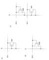
の特性が劣化してしまうことによって、誤動作してしまう。However, it is known that a transistor made of an amorphous semiconductor deteriorates in characteristics depending on the ON time, applied voltage, and the like. Among them, threshold voltage shift, in which the threshold voltage shifts (rises), is one of the major causes of shift register malfunction.
is one. Therefore, in the shift register disclosed in
このような問題点に鑑み、非選択期間において、出力信号のノイズが小さく、且つトラン
ジスタの特性劣化を抑制することができるシフトレジスタを有する液晶表示装置、及び当
該液晶表示装置を具備する電子機器を提供することを目的とする。In view of such problems, a liquid crystal display device having a shift register capable of reducing noise in an output signal and suppressing deterioration of transistor characteristics during a non-selection period, and an electronic device having the liquid crystal display device are proposed. intended to provide
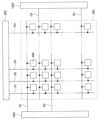
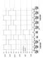
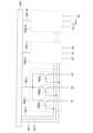
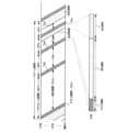
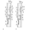
本発明に係わる液晶表示装置は、画素部と、絶縁基板上に画素部と一体形成されたシフト
レジスタを有している。そして、シフトレジスタは複数のフリップフロップを有し、この
複数のフリップフロップそれぞれは非選択期間において一定期間毎にオンとなり出力端子
(走査線)に電源電位を出力するトランジスタを有している。このトランジスタが一定期
間毎にオンとなり走査線に電源電位を供給することによって、複数のフリップフロップそ
れぞれは走査線の電位の変動を抑え、且つ該トランジスタの特性劣化を抑制する。A liquid crystal display device according to the present invention has a pixel portion and a shift register integrally formed with the pixel portion on an insulating substrate. The shift register has a plurality of flip-flops, and each of the plurality of flip-flops has a transistor that turns on at regular intervals during the non-selection period and outputs a power supply potential to an output terminal (scanning line). This transistor is turned on at regular intervals to supply a power supply potential to the scanning line, so that each of the plurality of flip-flops suppresses fluctuations in the potential of the scanning line and suppresses deterioration of the characteristics of the transistor.
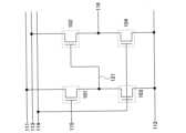
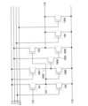
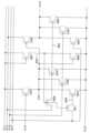
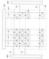
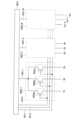
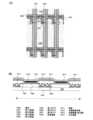
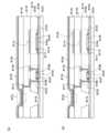
本発明の液晶表示装置は、液晶素子を有する第1の画素及び第2の画素と、駆動回路と、
第1の配線と、第2の配線と、第3の配線と、第4の配線と、第5の配線と、第6の配線
と、を有し、前記第1の画素は、前記第5の配線を介して前記駆動回路に電気的に接続さ
れ、前記第2の画素は、前記第6の配線を介して前記駆動回路に電気的に接続され、駆動
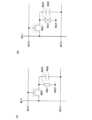
回路は、シフトレジスタを有し、シフトレジスタは、複数のフリップフロップを有し、複
数のフリップフロップのうち少なくとも一つは、第1のトランジスタ、第2のトランジス
タ、第3のトランジスタ及び第4のトランジスタを有し、第1のトランジスタの第1端子
が第1の配線に電気的に接続され、第1のトランジスタの第2端子が第2のトランジスタ
のゲート端子に電気的に接続され、第1のトランジスタのゲート端子が第5の配線に電気
的に接続され、第2のトランジスタの第1端子が第3の配線に電気的に接続され、第2端
子が第6の配線に電気的に接続され、第3のトランジスタの第1端子が第2の配線に電気
的に接続され、第2端子が第2のトランジスタのゲート端子に電気的に接続され、ゲート
端子が第4の配線に電気的に接続され、第4のトランジスタの第1端子が第2の配線に電
気的に接続され、第4のトランジスタの第2端子が第6の配線に電気的に接続され、第4
のトランジスタのゲート端子が第4の配線に電気的に接続されていることを特徴としてい
る。A liquid crystal display device of the present invention includes first pixels and second pixels each having a liquid crystal element, a driving circuit,
It has a first wiring, a second wiring, a third wiring, a fourth wiring, a fifth wiring, and a sixth wiring, and the first pixel is the fifth wiring. the second pixel is electrically connected to the driving circuit through the sixth wiring, the driving circuit has a shift register, The shift register has a plurality of flip-flops, at least one of the plurality of flip-flops has a first transistor, a second transistor, a third transistor and a fourth transistor, and the first transistor is electrically connected to the first wiring, the second terminal of the first transistor is electrically connected to the gate terminal of the second transistor, and the gate terminal of the first transistor is the fifth The first terminal of the second transistor is electrically connected to the third wiring, the second terminal is electrically connected to the sixth wiring, and the first terminal of the third transistor is electrically connected to the wiring. A terminal is electrically connected to the second wiring, the second terminal is electrically connected to the gate terminal of the second transistor, the gate terminal is electrically connected to the fourth wiring, and the gate terminal of the fourth transistor is electrically connected to the fourth wiring. The first terminal is electrically connected to the second wiring, the second terminal of the fourth transistor is electrically connected to the sixth wiring, and the fourth transistor is electrically connected to the sixth wiring.
is electrically connected to the fourth wiring.
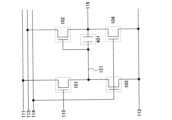
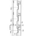
また、本発明の液晶表示装置は、液晶素子を有する第1の画素及び第2の画素と、駆動回
路と、第1の配線と、第2の配線と、第3の配線と、第4の配線と、第5の配線と、を有
し、前記第1の画素は、前記第5の配線を介して前記駆動回路に電気的に接続され、前記
第2の画素は、前記第1の配線を介して前記駆動回路に電気的に接続され、駆動回路は、
シフトレジスタを有し、シフトレジスタは、複数のフリップフロップを有し、複数のフリ
ップフロップのうち少なくとも一つは、第1のトランジスタ、第2のトランジスタ、第3
のトランジスタ及び第4のトランジスタを有し、第1のトランジスタは、第1端子が第5
の配線に電気的に接続され、第2端子が第2のトランジスタのゲート端子に電気的に接続
され、ゲート端子が第5の配線に電気的に接続され、第2のトランジスタは、第1端子が
第3の配線に電気的に接続され、第2端子が第1の配線に電気的に接続され、第3のトラ
ンジスタは、第1端子が第2のトランジスタのゲート端子に電気的に接続され、第2端子
が第2の配線に電気的に接続され、ゲート端子が第4の配線に電気的に接続され、第4の
トランジスタは、第1端子が第1の配線に電気的に接続され、第2端子が第2の配線に電
気的に接続され、ゲート端子が第4の配線に電気的に接続されていることを特徴としてい
る。Further, the liquid crystal display device of the present invention includes a first pixel and a second pixel each having a liquid crystal element, a driver circuit, a first wiring, a second wiring, a third wiring, and a fourth wiring. A wiring and a fifth wiring are provided, the first pixel is electrically connected to the driving circuit through the fifth wiring, and the second pixel is connected to the first wiring. electrically connected to the drive circuit via
A shift register has a plurality of flip-flops, and at least one of the plurality of flip-flops includes a first transistor, a second transistor, and a third transistor.
and a fourth transistor, the first transistor having a first terminal connected to the fifth
A second terminal is electrically connected to the gate terminal of the second transistor, a gate terminal is electrically connected to the fifth wiring, and the second transistor is electrically connected to the first terminal is electrically connected to the third wiring, the second terminal is electrically connected to the first wiring, and the third transistor has the first terminal electrically connected to the gate terminal of the second transistor. , the second terminal is electrically connected to the second wiring, the gate terminal is electrically connected to the fourth wiring, and the fourth transistor has the first terminal electrically connected to the first wiring. , the second terminal is electrically connected to the second wiring, and the gate terminal is electrically connected to the fourth wiring.
なお、本発明において、第1のトランジスタ、第2のトランジスタ、第3のトランジス
タ及び第4のトランジスタは、Nチャネル型トランジスタであってもよい。Note that in the present invention, the first transistor, the second transistor, the third transistor, and the fourth transistor may be n-channel transistors.
また、本発明において、第1のトランジスタ、第2のトランジスタ、第3のトランジス
タ、及び第4のトランジスタは、半導体層を有し、半導体層は、アモルファスシリコンで
あってもよい。Further, in the present invention, the first transistor, the second transistor, the third transistor, and the fourth transistor each have a semiconductor layer, and the semiconductor layer may be amorphous silicon.
また本発明において、第1のトランジスタの第2端子とゲート端子との間に、容量素子
が配置されていてもよい。Further, in the present invention, a capacitor may be arranged between the second terminal and the gate terminal of the first transistor.
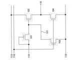
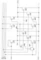
また、本発明の液晶表示装置は、液晶素子を有する第1の画素及び第2の画素と、駆動回
路と、第1の配線と、第2の配線と、第3の配線と、第4の配線と、第5の配線と、第6
の配線と、第7の配線と、を有し、前記第1の画素は、前記第5の配線を介して前記駆動
回路に電気的に接続され、前記第2の画素は、前記第6の配線を介して前記駆動回路に電
気的に接続され、駆動回路は、シフトレジスタを有し、シフトレジスタは、複数のフリッ
プフロップを有し、複数のフリップフロップのうち少なくとも一つは、第1のトランジス
タ、第2のトランジスタ、第3のトランジスタ、第4のトランジスタ及び第5のトランジ
スタを有し、第1のトランジスタは、第1端子が第1の配線に電気的に接続され、第2端
子が第2のトランジスタのゲート端子に電気的に接続され、ゲート端子が第5の配線に電
気的に接続され、第2のトランジスタは、第1端子が第3の配線に電気的に接続され、第
2端子が第6の配線に電気的に接続され、第3のトランジスタは、第1端子が第2のトラ
ンジスタのゲート端子に電気的に接続され、第2端子が第2の配線に電気的に接続され、
ゲート端子が第4の配線に電気的に接続され、第4のトランジスタは、第1端子が第6の
配線に電気的に接続され、第2端子が第2の配線に電気的に接続され、ゲート端子が第4
の配線に電気的に接続され、第5のトランジスタは、第1端子が第6の配線に電気的に接
続され、第2端子が第2の配線に電気的に接続され、ゲート端子が第7の配線に電気的に
接続されていることを特徴としている。Further, the liquid crystal display device of the present invention includes a first pixel and a second pixel each having a liquid crystal element, a driver circuit, a first wiring, a second wiring, a third wiring, and a fourth wiring. wiring, a fifth wiring, and a sixth
and a seventh wiring, the first pixel is electrically connected to the driving circuit through the fifth wiring, and the second pixel is electrically connected to the sixth wiring. electrically connected to the driving circuit via wiring, the driving circuit having a shift register, the shift register having a plurality of flip-flops, at least one of the plurality of flip-flops a transistor, a second transistor, a third transistor, a fourth transistor, and a fifth transistor; the first transistor has a first terminal electrically connected to a first wiring; The gate terminal of the second transistor is electrically connected to the gate terminal of the second transistor, the gate terminal is electrically connected to the fifth wiring, the first terminal of the second transistor is electrically connected to the third wiring, and the gate terminal of the second transistor is electrically connected to the third wiring. Two terminals are electrically connected to the sixth wiring, and the third transistor has the first terminal electrically connected to the gate terminal of the second transistor and the second terminal electrically connected to the second wiring. connected and
the gate terminal is electrically connected to the fourth wiring, the fourth transistor has the first terminal electrically connected to the sixth wiring, the second terminal electrically connected to the second wiring, Gate terminal is fourth
A fifth transistor has a first terminal electrically connected to the sixth wiring, a second terminal electrically connected to the second wiring, and a gate terminal connected to the seventh wiring. is electrically connected to the wiring of the
また、本発明の液晶表示装置は、液晶素子を有する第1の画素及び第2の画素と、駆動回
路と、第1の配線と、第2の配線と、第3の配線と、第4の配線と、第5の配線と、第6
の配線と、を有し、前記第1の画素は、前記第5の配線を介して前記駆動回路に電気的に
接続され、前記第2の画素は、前記第1の配線を介して前記駆動回路に電気的に接続され
、駆動回路は、シフトレジスタを有し、シフトレジスタは、複数のフリップフロップを有
し、複数のフリップフロップのうち少なくとも一つは、第1のトランジスタ、第2のトラ
ンジスタ、第3のトランジスタ、第4のトランジスタ及び第5のトランジスタを有し、第
1のトランジスタは、第1端子が第5の配線に電気的に接続され、第2端子が第2のトラ
ンジスタのゲート端子に電気的に接続され、ゲート端子が第5の配線に電気的に接続され
、第2のトランジスタは、第1端子が第3の配線に電気的に接続され、第2端子が第6の
配線に電気的に接続され、第3のトランジスタは、第1端子が第2の配線に電気的に接続
され、第2端子が第2のトランジスタのゲート端子に電気的に接続され、ゲート端子が第
4の配線に電気的に接続され、第4のトランジスタは、第1端子が第1の配線に電気的に
接続され、第2端子が第2の配線に電気的に接続され、ゲート端子が第4の配線に電気的
に接続され、第5のトランジスタは、第1端子が第6の配線に電気的に接続され、第2端
子が第2の配線に電気的に接続され、ゲート端子が第1の配線に電気的に接続されている
ことを特徴としている。Further, the liquid crystal display device of the present invention includes a first pixel and a second pixel each having a liquid crystal element, a driver circuit, a first wiring, a second wiring, a third wiring, and a fourth wiring. wiring, a fifth wiring, and a sixth
, the first pixel is electrically connected to the driving circuit through the fifth wiring, and the second pixel is electrically connected to the driving circuit through the first wiring. electrically connected to the circuit, the driving circuit having a shift register, the shift register having a plurality of flip-flops, at least one of the plurality of flip-flops comprising a first transistor and a second transistor; , a third transistor, a fourth transistor, and a fifth transistor, wherein the first transistor has a first terminal electrically connected to the fifth wiring and a second terminal connected to the gate of the second transistor. A second transistor has a first terminal electrically connected to the terminal, a gate terminal electrically connected to the fifth wiring, a first terminal electrically connected to the third wiring, and a second terminal electrically connected to the sixth wiring. The third transistor has a first terminal electrically connected to the second wiring, a second terminal electrically connected to the gate terminal of the second transistor, and a gate terminal of the third transistor. The fourth transistor has a first terminal electrically connected to the first wiring, a second terminal electrically connected to the second wiring, and a gate terminal. A fifth transistor has a first terminal electrically connected to the sixth wiring, a second terminal electrically connected to the second wiring, and a gate terminal of the fifth transistor. It is characterized by being electrically connected to the first wiring.
なお、本発明において、第1のトランジスタ、第2のトランジスタ、第3のトランジス
タ、第4のトランジスタ及び第5のトランジスタは、Nチャネル型トランジスタであって
もよい。Note that in the present invention, the first transistor, the second transistor, the third transistor, the fourth transistor, and the fifth transistor may be n-channel transistors.
また、本発明において、第1のトランジスタ、第2のトランジスタ、第3のトランジス
タ、第4のトランジスタ、及び第5のトランジスタは、半導体層を有し、半導体層はアモ
ルファスシリコンであってもよい。Further, in the present invention, the first transistor, the second transistor, the third transistor, the fourth transistor, and the fifth transistor each have a semiconductor layer, and the semiconductor layer may be amorphous silicon.
また、本発明において、第1のトランジスタの第2端子と第1のトランジスタのゲート
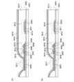
端子との間に、容量素子が配置されていてもよい。Further, in the present invention, a capacitor may be arranged between the second terminal of the first transistor and the gate terminal of the first transistor.
また、本発明の液晶表示装置は、液晶素子を有する第1の画素乃至第4の画素と、第1の
駆動回路と、第2の駆動回路と、第1の配線と、第2の配線と、第3の配線と、第4の配
線と、第5の配線と、第6の配線と、第7の配線と、第8の配線と、第9の配線と、第1
0の配線と、第11の配線と、第12の配線と、を有し、前記第1の画素は、前記第5の
配線を介して前記第1の駆動回路に電気的に接続され、前記第2の画素は、前記第6の配
線を介して前記第1の駆動回路に電気的に接続され、前記第3の画素は、前記第11の配
線を介して前記第2の駆動回路に電気的に接続され、前記第4の画素は、前記第12の配
線を介して前記第2の駆動回路に電気的に接続され、第1の駆動回路は、第1のシフトレ
ジスタを有し、第2の駆動回路は、第2のシフトレジスタを有し、第1のシフトレジスタ
は、複数のフリップフロップを有し、複数のフリップフロップのうち少なくとも一つは、
第1のトランジスタ、第2のトランジスタ、第3のトランジスタ及び第4のトランジスタ
を有し、第1のトランジスタは、第1端子が第1の配線に電気的に接続され、第2端子が
第2のトランジスタのゲート端子に電気的に接続され、ゲート端子が第5の配線に電気的
に接続され、第2のトランジスタは、第1端子が第3の配線に電気的に接続され、第2端
子が第6の配線に電気的に接続され、第3のトランジスタは、第1端子が第2の配線に電
気的に接続され、第2端子が第2のトランジスタのゲート端子に電気的に接続され、ゲー
ト端子が第4の配線に電気的に接続され、第4のトランジスタは、第1端子が第2の配線
に電気的に接続され、第2端子が第6の配線に電気的に接続され、ゲート端子が第4の配
線に電気的に接続され、第2のシフトレジスタは、複数のフリップフロップを有し、複数
のフリップフロップのうち少なくとも一つは、第5のトランジスタ、第6のトランジスタ
、第7のトランジスタ及び第8のトランジスタを有し、第5のトランジスタは、第1端子
が第7の配線に電気的に接続され、第2端子が第6のトランジスタのゲート端子に電気的
に接続され、ゲート端子が第11の配線に電気的に接続され、第6のトランジスタは、第
1端子が第9の配線に電気的に接続され、第2端子が第12の配線に電気的に接続され、
第7のトランジスタは、第1端子が第8の配線に電気的に接続され、第2端子が第6のト
ランジスタのゲート端子に電気的に接続され、ゲート端子が第10の配線に電気的に接続
され、第8のトランジスタは、第1端子が第8の配線に電気的に接続され、第2端子が第
12の配線に電気的に接続され、ゲート端子が第10の配線に電気的に接続されているこ
とを特徴としている。A liquid crystal display device of the present invention includes first to fourth pixels each having a liquid crystal element, a first driver circuit, a second driver circuit, a first wiring, and a second wiring. , a third wiring, a fourth wiring, a fifth wiring, a sixth wiring, a seventh wiring, an eighth wiring, a ninth wiring, and a first wiring
0 wiring, an 11th wiring, and a 12th wiring, the first pixel is electrically connected to the first driving circuit through the fifth wiring, and the The second pixel is electrically connected to the first driving circuit through the sixth wiring, and the third pixel is electrically connected to the second driving circuit through the eleventh wiring. the fourth pixel is electrically connected to the second driving circuit through the twelfth wiring; the first driving circuit has a first shift register; 2 drive circuits have a second shift register, the first shift register has a plurality of flip-flops, at least one of the plurality of flip-flops
A first transistor, a second transistor, a third transistor, and a fourth transistor are provided. The first transistor has a first terminal electrically connected to the first wiring and a second terminal electrically connected to the second wiring. The gate terminal of the transistor is electrically connected to the fifth wiring, the second transistor has the first terminal electrically connected to the third wiring, and the second terminal of the second transistor. is electrically connected to the sixth wiring, and the third transistor has a first terminal electrically connected to the second wiring and a second terminal electrically connected to the gate terminal of the second transistor. , the gate terminal is electrically connected to the fourth wiring, and the fourth transistor has the first terminal electrically connected to the second wiring and the second terminal electrically connected to the sixth wiring. , the gate terminal is electrically connected to the fourth wiring, the second shift register has a plurality of flip-flops, and at least one of the plurality of flip-flops includes a fifth transistor and a sixth transistor. , a seventh transistor and an eighth transistor, wherein the fifth transistor has a first terminal electrically connected to the seventh wiring and a second terminal electrically connected to the gate terminal of the sixth transistor. The gate terminal of the sixth transistor is electrically connected to the eleventh wiring, the first terminal is electrically connected to the ninth wiring, and the second terminal is electrically connected to the twelfth wiring. connected and
The seventh transistor has a first terminal electrically connected to the eighth wiring, a second terminal electrically connected to the gate terminal of the sixth transistor, and a gate terminal electrically connected to the tenth wiring. An eighth transistor has a first terminal electrically connected to the eighth wiring, a second terminal electrically connected to the twelfth wiring, and a gate terminal electrically connected to the tenth wiring. characterized by being connected.
なお、本発明において、第5の配線及び第11の配線は電気的に接続され、第6の配線
及び第12の配線は電気的に接続されていてもよい。Note that in the present invention, the fifth wiring and the eleventh wiring may be electrically connected, and the sixth wiring and the twelfth wiring may be electrically connected.
また、本発明において、第5の配線及び第11の配線は同一の配線であり、第6の配線
及び第12の配線は同一の配線であってもよい。Further, in the present invention, the fifth wiring and the eleventh wiring may be the same wiring, and the sixth wiring and the twelfth wiring may be the same wiring.
また、本発明において、第1の配線及び第7の配線は電気的に接続され、第2の配線及
び第8の配線は電気的に接続され、第3の配線及び第9の配線は電気的に接続され、第4
の配線及び第10の配線は電気的に接続されていてもよい。Further, in the present invention, the first wiring and the seventh wiring are electrically connected, the second wiring and the eighth wiring are electrically connected, and the third wiring and the ninth wiring are electrically connected. connected to the fourth
and the tenth wiring may be electrically connected.
また、本発明において、第1の配線及び第7の配線は同一の配線であり、第2の配線及
び第8の配線は同一の配線であり、第3の配線及び第9の配線は同一の配線であり、第4
の配線及び第10の配線は同一の配線であってもよい。Further, in the present invention, the first wiring and the seventh wiring are the same wiring, the second wiring and the eighth wiring are the same wiring, and the third wiring and the ninth wiring are the same wiring. wiring, and the fourth
and the tenth wiring may be the same wiring.
また、本発明において、第1の配線及び第7の配線は電気的に接続され、第2の配線及
び第8の配線は電気的に接続され、第3の配線及び第9の配線は電気的に接続され、第4
の配線及び第10の配線は電気的に接続され、第5の配線及び第11の配線は電気的に接
続され、第6の配線及び第12の配線は電気的に接続されていてもよい。Further, in the present invention, the first wiring and the seventh wiring are electrically connected, the second wiring and the eighth wiring are electrically connected, and the third wiring and the ninth wiring are electrically connected. connected to the fourth
and the tenth wiring may be electrically connected, the fifth wiring and the eleventh wiring may be electrically connected, and the sixth wiring and the twelfth wiring may be electrically connected.
また、本発明において、第1の配線及び第7の配線は同一の配線であり、第2の配線及
び第8の配線は同一の配線であり、第3の配線及び第9の配線は同一の配線であり、第4
の配線及び第10の配線は同一の配線であり、第5の配線及び第11の配線は同一の配線
であり、第6の配線及び第12の配線は同一の配線であってもよい。Further, in the present invention, the first wiring and the seventh wiring are the same wiring, the second wiring and the eighth wiring are the same wiring, and the third wiring and the ninth wiring are the same wiring. wiring, and the fourth
and the tenth wiring may be the same wiring, the fifth wiring and the eleventh wiring may be the same wiring, and the sixth wiring and the twelfth wiring may be the same wiring.
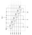
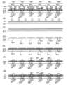
また、本発明の液晶表示装置は、液晶素子を有する第1の画素乃至第4の画素と、第1の
駆動回路と、第2の駆動回路と、第1の配線と、第2の配線と、第3の配線と、第4の配
線と、第5の配線と、第6の配線と、第7の配線と、第8の配線と、第9の配線と、第1
0の配線と、を有し、前記第1の画素は、前記第5の配線を介して前記第1の駆動回路に
電気的に接続され、前記第2の画素は、前記第1の配線を介して前記第1の駆動回路に電
気的に接続され、前記第3の画素は、前記第10の配線を介して前記第2の駆動回路に電
気的に接続され、前記第4の画素は、前記第6の配線を介して前記第2の駆動回路に電気
的に接続され、第1の駆動回路は、第1のシフトレジスタを有し、第2の駆動回路は、第
2のシフトレジスタを有し、第1のシフトレジスタは、複数のフリップフロップを有し、
複数のフリップフロップのうち少なくとも一つは、第1のトランジスタ、第2のトランジ
スタ、第3のトランジスタ及び第4のトランジスタを有し、第1のトランジスタは、第1
端子が第5の配線に電気的に接続され、第2端子が第2のトランジスタのゲート端子に電
気的に接続され、ゲート端子が第5の配線に電気的に接続され、第2のトランジスタは、
第1端子が第3の配線に電気的に接続され、第2端子が第1の配線に電気的に接続され、
第3のトランジスタは、第1端子が第2のトランジスタのゲート端子に電気的に接続され
、第2端子が第2の配線に電気的に接続され、ゲート端子が第4の配線に電気的に接続さ
れ、第4のトランジスタは、第1端子が第1の配線に電気的に接続され、第2端子が第2
の配線に電気的に接続され、ゲート端子が第4の配線に電気的に接続され、第2のシフト
レジスタは、複数のフリップフロップを有し、複数のフリップフロップのうち少なくとも
一つは、第5のトランジスタ、第6のトランジスタ、第7のトランジスタ及び第8のトラ
ンジスタを有し、第5のトランジスタは、第1端子が第10の配線に電気的に接続され、
第2端子が第6のトランジスタのゲート端子に電気的に接続され、ゲート端子が第10の
配線に電気的に接続され、第6のトランジスタは、第1端子が第8の配線に電気的に接続
され、第2端子が第6の配線に電気的に接続され、第7のトランジスタは、第1端子が第
6のトランジスタのゲート端子に電気的に接続され、第2端子が第7の配線に電気的に接
続され、ゲート端子が第9の配線に電気的に接続され、第8のトランジスタは、第1端子
が第6の配線に電気的に接続され、第2端子が第7の配線に電気的に接続され、ゲート端
子が第9の配線に電気的に接続されていることを特徴としている。A liquid crystal display device of the present invention includes first to fourth pixels each having a liquid crystal element, a first driver circuit, a second driver circuit, a first wiring, and a second wiring. , a third wiring, a fourth wiring, a fifth wiring, a sixth wiring, a seventh wiring, an eighth wiring, a ninth wiring, and a first wiring
0 wiring, the first pixel is electrically connected to the first driver circuit through the fifth wiring, and the second pixel is connected to the first wiring. The third pixel is electrically connected to the second drive circuit through the tenth wiring, and the fourth pixel is electrically connected to the first drive circuit through the tenth wiring. It is electrically connected to the second driver circuit through the sixth wiring, the first driver circuit has a first shift register, and the second driver circuit has a second shift register. the first shift register has a plurality of flip-flops;
At least one of the plurality of flip-flops has a first transistor, a second transistor, a third transistor and a fourth transistor, the first transistor being the first
a terminal electrically connected to a fifth wiring, a second terminal electrically connected to a gate terminal of the second transistor, a gate terminal electrically connected to the fifth wiring, and the second transistor ,
The first terminal is electrically connected to the third wiring, the second terminal is electrically connected to the first wiring,
The third transistor has a first terminal electrically connected to the gate terminal of the second transistor, a second terminal electrically connected to the second wiring, and a gate terminal electrically connected to the fourth wiring. The fourth transistor has a first terminal electrically connected to the first wiring and a second terminal electrically connected to the second wiring.
The gate terminal is electrically connected to the fourth wiring, the second shift register has a plurality of flip-flops, and at least one of the plurality of flip-flops is connected to the fourth wiring. 5 transistors, a sixth transistor, a seventh transistor, and an eighth transistor; the fifth transistor has a first terminal electrically connected to a tenth wiring;
The second terminal is electrically connected to the gate terminal of the sixth transistor, the gate terminal is electrically connected to the tenth wiring, and the sixth transistor has the first terminal electrically connected to the eighth wiring. the second terminal is electrically connected to the sixth wiring; and the seventh transistor has the first terminal electrically connected to the gate terminal of the sixth transistor and the second terminal to the seventh wiring. , the gate terminal is electrically connected to the ninth wiring, the eighth transistor has the first terminal electrically connected to the sixth wiring, and the second terminal to the seventh wiring. , and the gate terminal is electrically connected to the ninth wiring.
なお、本発明において、第1の配線及び第6の配線は電気的に接続され、第5の配線及
び第10の配線は電気的に接続されていてもよい。Note that in the present invention, the first wiring and the sixth wiring may be electrically connected, and the fifth wiring and the tenth wiring may be electrically connected.
また、本発明において、第1の配線及び第6の配線は同一の配線であり、第5の配線及
び第10の配線は同一の配線であってもよい。Further, in the present invention, the first wiring and the sixth wiring may be the same wiring, and the fifth wiring and the tenth wiring may be the same wiring.
また、本発明において、第2の配線及び第7の配線は電気的に接続され、第3の配線及
び第8の配線は電気的に接続され、第4の配線及び第9の配線は電気的に接続されていて
もよい。Further, in the present invention, the second wiring and the seventh wiring are electrically connected, the third wiring and the eighth wiring are electrically connected, and the fourth wiring and the ninth wiring are electrically connected. may be connected to
また、本発明において、第2の配線及び第7の配線は同一の配線であり、第3の配線及
び第8の配線は同一の配線であり、第4の配線及び第9の配線は同一の配線であってもよ
い。Further, in the present invention, the second wiring and the seventh wiring are the same wiring, the third wiring and the eighth wiring are the same wiring, and the fourth wiring and the ninth wiring are the same wiring. Wiring may be used.
また、本発明において、第1の配線及び第6の配線は電気的に接続され、第2の配線及
び第7の配線は電気的に接続され、第3の配線及び第8の配線は電気的に接続され、第4
の配線及び第9の配線は電気的に接続され、第5の配線及び第10の配線は電気的に接続
されていてもよい。Further, in the present invention, the first wiring and the sixth wiring are electrically connected, the second wiring and the seventh wiring are electrically connected, and the third wiring and the eighth wiring are electrically connected. connected to the fourth
and the ninth wiring may be electrically connected, and the fifth wiring and the tenth wiring may be electrically connected.
また、本発明において、第1の配線及び第6の配線は同一の配線であり、第2の配線及
び第7の配線は同一の配線であり、第3の配線及び第8の配線は同一の配線であり、第4
の配線及び第9の配線は同一の配線であり、第5の配線及び第10の配線は同一の配線で
あってもよい。Further, in the present invention, the first wiring and the sixth wiring are the same wiring, the second wiring and the seventh wiring are the same wiring, and the third wiring and the eighth wiring are the same wiring. wiring, and the fourth
and the ninth wiring may be the same wiring, and the fifth wiring and the tenth wiring may be the same wiring.
また、本発明において、第1のトランジスタ、第2のトランジスタ、第3のトランジス
タ、第4のトランジスタ、第5のトランジスタ、第6のトランジスタ、第7のトランジス
タ及び第8のトランジスタは、Nチャネル型トランジスタであってもよい。Further, in the present invention, the first, second, third, fourth, fifth, sixth, seventh, and eighth transistors are N-channel transistors. It may be a transistor.
また、本発明において、第1のトランジスタ、第2のトランジスタ、第3のトランジス
タ、第4のトランジスタ、第5のトランジスタ、第6のトランジスタ、第7のトランジス
タ、及び第8のトランジスタは、半導体層を有し、半導体層は、アモルファスシリコンで
あってもよい。Further, in the present invention, the first transistor, the second transistor, the third transistor, the fourth transistor, the fifth transistor, the sixth transistor, the seventh transistor, and the eighth transistor are semiconductor layers. and the semiconductor layer may be amorphous silicon.
また、本発明において、第1のトランジスタの第2端子と、第1のトランジスタのゲー
ト端子との間に、第1の容量素子が配置され、第5のトランジスタの第2端子と、第5の
トランジスタのゲート端子との間に、第2の容量素子が配置されていてもよい。Further, in the present invention, the first capacitor is arranged between the second terminal of the first transistor and the gate terminal of the first transistor, and the second terminal of the fifth transistor and the fifth A second capacitive element may be arranged between the gate terminal of the transistor.
また、本発明の液晶表示装置は、液晶素子を有する第1の画素乃至第4の画素と、第1の
駆動回路と、第2の駆動回路と、第1の配線と、第2の配線と、第3の配線と、第4の配
線と、第5の配線と、第6の配線と、第7の配線と、第8の配線と、第9の配線と、第1
0の配線と、第11の配線と、第12の配線と、第13の配線と、第14の配線と、を有
し、前記第1の画素は、前記第5の配線を介して前記第1の駆動回路に電気的に接続され
、前記第2の画素は、前記第6の配線を介して前記第1の駆動回路に電気的に接続され、
前記第3の画素は、前記第12の配線を介して前記第2の駆動回路に電気的に接続され、
前記第4の画素は、前記第13の配線を介して前記第2の駆動回路に電気的に接続され、
第1の駆動回路は、第1のシフトレジスタを有し、第2の駆動回路は、第2のシフトレジ
スタを有し、第1のシフトレジスタは、複数のフリップフロップを有し、複数のフリップ
フロップのうち少なくとも一つは、第1のトランジスタ、第2のトランジスタ、第3のト
ランジスタ、第4のトランジスタ及び第5のトランジスタを有し、第1のトランジスタは
、第1端子が第1の配線に電気的に接続され、第2端子が第2のトランジスタのゲート端
子に電気的に接続され、ゲート端子が第5の配線に電気的に接続され、第2のトランジス
タは、第1端子が第3の配線に電気的に接続され、第2端子が第6の配線に電気的に接続
され、第3のトランジスタは、第1端子が第2の配線に電気的に接続され、第2端子が第
2のトランジスタのゲート端子に電気的に接続され、ゲート端子が第4の配線に電気的に
接続され、第4のトランジスタは、第1端子が第2の配線に電気的に接続され、第2端子
が第6の配線に電気的に接続され、ゲート端子は、第4の配線に電気的に接続され、第5
のトランジスタは、第1端子が第2の配線に電気的に接続され、第2端子が第6の配線に
電気的に接続され、ゲート端子が第7の配線に電気的に接続され、第2のシフトレジスタ
は、複数のフリップフロップを有し、複数のフリップフロップのうち少なくとも一つは、
第6のトランジスタ、第7のトランジスタ、第8のトランジスタ、第9のトランジスタ及
び第10のトランジスタを有し、第6のトランジスタは、第1端子が第8の配線に電気的
に接続され、第2端子が第7のトランジスタのゲート端子に電気的に接続され、ゲート端
子が第12の配線に電気的に接続され、第7のトランジスタは、第1端子が第10の配線
に電気的に接続され、第2端子が第13の配線に電気的に接続され、第8のトランジスタ
は、第1端子が第9の配線に電気的に接続され、第2端子が第7のトランジスタのゲート
端子に電気的に接続され、ゲート端子が第11の配線に電気的に接続され、第9のトラン
ジスタは、第1端子が第13の配線に電気的に接続され、第2端子が第9の配線に電気的
に接続され、ゲート端子が第11の配線に電気的に接続され、第10のトランジスタは、
第1端子が第13の配線に電気的に接続され、第2端子が第9の配線に電気的に接続され
、ゲート端子が第14の配線に電気的に接続されていることを特徴としている。A liquid crystal display device of the present invention includes first to fourth pixels each having a liquid crystal element, a first driver circuit, a second driver circuit, a first wiring, and a second wiring. , a third wiring, a fourth wiring, a fifth wiring, a sixth wiring, a seventh wiring, an eighth wiring, a ninth wiring, and a first wiring
0 wiring, an 11th wiring, a 12th wiring, a 13th wiring, and a 14th wiring, and the first pixel is connected to the 5th wiring through the 5th wiring. electrically connected to one driving circuit, the second pixel is electrically connected to the first driving circuit through the sixth wiring,
the third pixel is electrically connected to the second drive circuit through the twelfth wiring;
the fourth pixel is electrically connected to the second drive circuit through the thirteenth wiring;
The first drive circuit has a first shift register, the second drive circuit has a second shift register, the first shift register has a plurality of flip-flops, a plurality of flip-flops. At least one of the groups has a first transistor, a second transistor, a third transistor, a fourth transistor, and a fifth transistor, and the first transistor has a first terminal connected to the first wiring. a second terminal electrically connected to the gate terminal of the second transistor; a gate terminal electrically connected to the fifth wiring; the second transistor has a first terminal electrically connected to the first The third transistor has a first terminal electrically connected to the second wiring, a second terminal electrically connected to the second wiring, and a second terminal electrically connected to the sixth wiring. The gate terminal of the second transistor is electrically connected to the gate terminal of the second transistor, the gate terminal is electrically connected to the fourth wiring, the first terminal of the fourth transistor is electrically connected to the second wiring, and the gate terminal of the fourth transistor is electrically connected to the second wiring. The second terminal is electrically connected to the sixth wiring, the gate terminal is electrically connected to the fourth wiring, and the fifth terminal is electrically connected to the fourth wiring.
has a first terminal electrically connected to the second wiring, a second terminal electrically connected to the sixth wiring, a gate terminal electrically connected to the seventh wiring, and a second has a plurality of flip-flops, at least one of the plurality of flip-flops is
a sixth transistor, a seventh transistor, an eighth transistor, a ninth transistor, and a tenth transistor; the sixth transistor has a first terminal electrically connected to an eighth wiring; The second terminal is electrically connected to the gate terminal of the seventh transistor, the gate terminal is electrically connected to the twelfth wiring, and the seventh transistor has the first terminal electrically connected to the tenth wiring. The second terminal is electrically connected to the thirteenth wiring, and the eighth transistor has the first terminal electrically connected to the ninth wiring and the second terminal to the gate terminal of the seventh transistor. The gate terminal of the ninth transistor is electrically connected to the eleventh wiring, the first terminal is electrically connected to the thirteenth wiring, and the second terminal is electrically connected to the ninth wiring. electrically connected, the gate terminal is electrically connected to the 11th wiring, and the 10th transistor is
The first terminal is electrically connected to the thirteenth wiring, the second terminal is electrically connected to the ninth wiring, and the gate terminal is electrically connected to the fourteenth wiring. .
なお、本発明において、第5の配線及び第12の配線は電気的に接続され、第6の配線
及び第13の配線は電気的に接続されていてもよい。Note that in the present invention, the fifth wiring and the twelfth wiring may be electrically connected, and the sixth wiring and the thirteenth wiring may be electrically connected.
また、本発明において、第5の配線及び第12の配線は同一の配線であり、第6の配線
及び第13の配線は同一の配線であってもよい。Further, in the present invention, the fifth wiring and the twelfth wiring may be the same wiring, and the sixth wiring and the thirteenth wiring may be the same wiring.
また、本発明において、第1の配線及び第8の配線は電気的に接続され、第2の配線及
び第9の配線は電気的に接続され、第3の配線及び第10の配線は電気的に接続され、第
4の配線及び第11の配線は電気的に接続され、第7の配線及び第14の配線は電気的に
接続されていてもよい。Further, in the present invention, the first wiring and the eighth wiring are electrically connected, the second wiring and the ninth wiring are electrically connected, and the third wiring and the tenth wiring are electrically connected. , the fourth wiring and the eleventh wiring may be electrically connected, and the seventh wiring and the fourteenth wiring may be electrically connected.
また、本発明において、第1の配線及び第8の配線は同一の配線であり、第2の配線及
び第9の配線は同一の配線であり、第3の配線及び第10の配線は同一の配線であり、第
4の配線及び第11の配線は同一の配線であり、第7の配線及び第14の配線は同一の配
線であってもよい。Further, in the present invention, the first wiring and the eighth wiring are the same wiring, the second wiring and the ninth wiring are the same wiring, and the third wiring and the tenth wiring are the same wiring. The fourth wiring and the eleventh wiring may be the same wiring, and the seventh wiring and the fourteenth wiring may be the same wiring.
また、本発明において、第1の配線及び第8の配線は電気的に接続され、第2の配線及
び第9の配線は電気的に接続され、第3の配線及び第10の配線は電気的に接続され、第
4の配線及び第11の配線は電気的に接続され、第5の配線及び第12の配線は電気的に
接続され、第6の配線及び第13の配線は電気的に接続され、第7の配線及び第14の配
線は電気的に接続されていてもよい。Further, in the present invention, the first wiring and the eighth wiring are electrically connected, the second wiring and the ninth wiring are electrically connected, and the third wiring and the tenth wiring are electrically connected. , the fourth wiring and the 11th wiring are electrically connected, the fifth wiring and the 12th wiring are electrically connected, and the sixth wiring and the 13th wiring are electrically connected and the seventh wiring and the fourteenth wiring may be electrically connected.
また、本発明において、第1の配線及び第8の配線は同一の配線であり、第2の配線及
び第9の配線は同一の配線であり、第3の配線及び第10の配線は同一の配線であり、第
4の配線及び第11の配線は同一の配線であり、第5の配線及び第12の配線は同一の配
線であり、第6の配線及び第13の配線は同一の配線であり、第7の配線及び第14の配
線は同一の配線であってもよい。Further, in the present invention, the first wiring and the eighth wiring are the same wiring, the second wiring and the ninth wiring are the same wiring, and the third wiring and the tenth wiring are the same wiring. the fourth wiring and the 11th wiring are the same wiring; the fifth wiring and the 12th wiring are the same wiring; the sixth wiring and the 13th wiring are the same wiring; , and the seventh wiring and the fourteenth wiring may be the same wiring.
また、本発明の液晶表示装置は、液晶素子を有する第1の画素乃至第4の画素と、第1の
駆動回路と、第2の駆動回路と、第1の配線と、第2の配線と、第3の配線と、第4の配
線と、第5の配線と、第6の配線と、第7の配線と、第8の配線と、第9の配線と、第1
0の配線と、第11の配線と、第12の配線と、を有し、前記第1の画素は、前記第5の
配線を介して前記第1の駆動回路に電気的に接続され、前記第2の画素は、前記第6の配
線を介して前記第1の駆動回路に電気的に接続され、前記第3の画素は、前記第11の配
線を介して前記第2の駆動回路に電気的に接続され、前記第4の画素は、前記第12の配
線を介して前記第2の駆動回路に電気的に接続され、第1の駆動回路は、第1のシフトレ
ジスタを有し、第2の駆動回路は、第2のシフトレジスタを有し、第1のシフトレジスタ
は、複数のフリップフロップを有し、複数のフリップフロップのうち少なくとも一つは、
第1のトランジスタ、第2のトランジスタ、第3のトランジスタ、第4のトランジスタ及
び第5のトランジスタを有し、第1のトランジスタは、第1端子が第5の配線に電気的に
接続され、第2端子が第2のトランジスタのゲート端子に電気的に接続され、ゲート端子
が第5の配線に電気的に接続され、第2のトランジスタは、第1端子が第3の配線に電気
的に接続され、第2端子が第6の配線に電気的に接続され、第3のトランジスタは、第1
端子が第2のトランジスタのゲート端子に電気的に接続され、第2端子が第2の配線に電
気的に接続され、ゲート端子が第4の配線に電気的に接続され、第4のトランジスタは、
第1端子が第6の配線に電気的に接続され、第2端子が第2の配線に電気的に接続され、
ゲート端子が第4の配線に電気的に接続され、第5のトランジスタは、第1端子が第6の
配線に電気的に接続され、第2端子が第2の配線に電気的に接続され、ゲート端子が第1
の配線に電気的に接続され、第2のシフトレジスタは、複数のフリップフロップを有し、
複数のフリップフロップのうち少なくとも一つは、第6のトランジスタ、第7のトランジ
スタ、第8のトランジスタ、第9のトランジスタ及び第10のトランジスタを有し、第6
のトランジスタは、第1端子が第11の配線に電気的に接続され、第2端子が第7のトラ
ンジスタのゲート端子に電気的に接続され、ゲート端子が第11の配線に電気的に接続さ
れ、第7のトランジスタは、第1端子が第9の配線に電気的に接続され、第2端子が第1
2の配線に電気的に接続され、第8のトランジスタは、第1端子が第8の配線に電気的に
接続され、第2端子が第7のトランジスタのゲート端子に電気的に接続され、ゲート端子
が第10の配線に電気的に接続され、第9のトランジスタは、第1端子が第8の配線に電
気的に接続され、第2端子が第12の配線に電気的に接続され、ゲート端子が第10の配
線に電気的に接続され、第10のトランジスタは、第1端子が第8の配線に電気的に接続
され、第2端子が第12の配線に電気的に接続され、ゲート端子が第7の配線に電気的に
接続されていることを特徴としている。A liquid crystal display device of the present invention includes first to fourth pixels each having a liquid crystal element, a first driver circuit, a second driver circuit, a first wiring, and a second wiring. , a third wiring, a fourth wiring, a fifth wiring, a sixth wiring, a seventh wiring, an eighth wiring, a ninth wiring, and a first wiring
0 wiring, an 11th wiring, and a 12th wiring, the first pixel is electrically connected to the first driving circuit through the fifth wiring, and the The second pixel is electrically connected to the first driving circuit through the sixth wiring, and the third pixel is electrically connected to the second driving circuit through the eleventh wiring. the fourth pixel is electrically connected to the second driving circuit through the twelfth wiring; the first driving circuit has a first shift register; 2 drive circuits have a second shift register, the first shift register has a plurality of flip-flops, at least one of the plurality of flip-flops
a first transistor, a second transistor, a third transistor, a fourth transistor, and a fifth transistor; the first transistor has a first terminal electrically connected to a fifth wiring; Two terminals are electrically connected to the gate terminal of the second transistor, the gate terminal is electrically connected to the fifth wiring, and the second transistor has the first terminal electrically connected to the third wiring. , the second terminal is electrically connected to the sixth wiring, and the third transistor is connected to the first
The terminal is electrically connected to the gate terminal of the second transistor, the second terminal is electrically connected to the second wiring, the gate terminal is electrically connected to the fourth wiring, and the fourth transistor is ,
The first terminal is electrically connected to the sixth wiring, the second terminal is electrically connected to the second wiring,
the gate terminal is electrically connected to the fourth wiring, the fifth transistor has the first terminal electrically connected to the sixth wiring, the second terminal electrically connected to the second wiring, gate terminal first
The second shift register has a plurality of flip-flops, and is electrically connected to the wiring of
at least one of the plurality of flip-flops has a sixth transistor, a seventh transistor, an eighth transistor, a ninth transistor and a tenth transistor;
The transistor has a first terminal electrically connected to the eleventh wiring, a second terminal electrically connected to the gate terminal of the seventh transistor, and a gate terminal electrically connected to the eleventh wiring. , the seventh transistor has a first terminal electrically connected to the ninth wiring and a second terminal electrically connected to the first
An eighth transistor has a first terminal electrically connected to the eighth wiring, a second terminal electrically connected to the gate terminal of the seventh transistor, and a gate A ninth transistor has a terminal electrically connected to the tenth wiring, a first terminal electrically connected to the eighth wiring, a second terminal electrically connected to the twelfth wiring, and a gate of the ninth transistor. The tenth transistor has a first terminal electrically connected to the eighth wiring, a second terminal electrically connected to the twelfth wiring, and a gate. The terminal is electrically connected to the seventh wiring.
なお、本発明において、第5の配線及び第11の配線は電気的に接続され、第6の配線
及び第12の配線は電気的に接続されていてもよい。Note that in the present invention, the fifth wiring and the eleventh wiring may be electrically connected, and the sixth wiring and the twelfth wiring may be electrically connected.
なお、本発明において、第5の配線及び第11の配線は同一の配線であり、第6の配線
及び第12の配線は同一の配線であってもよい。Note that in the present invention, the fifth wiring and the eleventh wiring may be the same wiring, and the sixth wiring and the twelfth wiring may be the same wiring.
なお、本発明において、第1の配線及び第7の配線は電気的に接続され、第2の配線及
び第8の配線は電気的に接続され、第3の配線及び第9の配線は電気的に接続され、第4
の配線及び第10の配線は電気的に接続されていてもよい。Note that in the present invention, the first wiring and the seventh wiring are electrically connected, the second wiring and the eighth wiring are electrically connected, and the third wiring and the ninth wiring are electrically connected. connected to the fourth
and the tenth wiring may be electrically connected.
なお、本発明において、第1の配線及び第7の配線は同一の配線であり、第2の配線及
び第8の配線は同一の配線であり、第3の配線及び第9の配線は同一の配線であり、第4
の配線及び第10の配線は同一の配線であってもよい。In the present invention, the first wiring and the seventh wiring are the same wiring, the second wiring and the eighth wiring are the same wiring, and the third wiring and the ninth wiring are the same wiring. wiring, and the fourth
and the tenth wiring may be the same wiring.
なお、本発明において、第1の配線及び第7の配線は電気的に接続され、第2の配線及
び第8の配線は電気的に接続され、第3の配線及び第9の配線は電気的に接続され、第4
の配線及び第10の配線は電気的に接続され、第5の配線及び第11の配線は電気的に接
続され、第6の配線及び第12の配線は電気的に接続されていてもよい。Note that in the present invention, the first wiring and the seventh wiring are electrically connected, the second wiring and the eighth wiring are electrically connected, and the third wiring and the ninth wiring are electrically connected. connected to the fourth
and the tenth wiring may be electrically connected, the fifth wiring and the eleventh wiring may be electrically connected, and the sixth wiring and the twelfth wiring may be electrically connected.
なお、本発明において、第1の配線及び第7の配線は同一の配線であり、第2の配線及
び第8の配線は同一の配線であり、第3の配線及び第9の配線は同一の配線であり、第4
の配線及び第10の配線は同一の配線であり、第5の配線及び第11の配線は同一の配線
であり、第6の配線及び第12の配線は同一の配線であってもよい。In the present invention, the first wiring and the seventh wiring are the same wiring, the second wiring and the eighth wiring are the same wiring, and the third wiring and the ninth wiring are the same wiring. wiring, and the fourth
and the tenth wiring may be the same wiring, the fifth wiring and the eleventh wiring may be the same wiring, and the sixth wiring and the twelfth wiring may be the same wiring.
なお、本発明において、第1のトランジスタ、第2のトランジスタ、第3のトランジス
タ、第4のトランジスタ、第5のトランジスタ、第6のトランジスタ、第7のトランジス
タ、第8のトランジスタ、第9のトランジスタ及び第10のトランジスタは、Nチャネル
型トランジスタであってもよい。Note that in the present invention, the first transistor, the second transistor, the third transistor, the fourth transistor, the fifth transistor, the sixth transistor, the seventh transistor, the eighth transistor, and the ninth transistor and the tenth transistor may be N-channel transistors.
なお、本発明において、第1のトランジスタ、第2のトランジスタ、第3のトランジス
タ、第4のトランジスタ、第5のトランジスタ、第6のトランジスタ、第7のトランジス
タ、第8のトランジスタ、第9のトランジスタ及び、第10のトランジスタは、半導体層
を有し、半導体層は、アモルファスシリコンであってもよい。Note that in the present invention, the first transistor, the second transistor, the third transistor, the fourth transistor, the fifth transistor, the sixth transistor, the seventh transistor, the eighth transistor, and the ninth transistor And the tenth transistor may have a semiconductor layer, and the semiconductor layer may be amorphous silicon.
なお、本発明において、第1のトランジスタの第2端子と、第1のトランジスタのゲー
ト端子との間に、第1の容量素子が配置され、第6のトランジスタの第2端子と、第1の
トランジスタのゲート端子との間に、第2の容量素子が配置されていてもよい。Note that in the present invention, the first capacitor is arranged between the second terminal of the first transistor and the gate terminal of the first transistor, and the second terminal of the sixth transistor and the first capacitor are provided. A second capacitive element may be arranged between the gate terminal of the transistor.
本発明は、上記記載の液晶表示装置を具備する電子機器である。The present invention is an electronic device comprising the liquid crystal display device described above.
なお、本明細書に示すスイッチは、様々な形態のものを用いることができ、一例として、
電気的スイッチや機械的なスイッチなどがある。つまり、電流の流れを制御できるもので
あればよく、特定のものに限定されず、様々なものを用いることができる。例えば、トラ
ンジスタでもよいし、ダイオード(例えば、PNダイオード、PINダイオード、ショッ
トキーダイオード、ダイオード接続のトランジスタなど)でもよいし、サイリスタでもよ
いし、それらを組み合わせた論理回路でもよい。よって、スイッチとしてトランジスタを
用いる場合、そのトランジスタは、単なるスイッチとして動作するため、トランジスタの
極性(導電型)は特に限定されない。ただし、オフ電流が少ない方が望ましい場合、オフ
電流が少ない方の極性のトランジスタを用いることが望ましい。オフ電流が少ないトラン
ジスタとしては、LDD領域を設けているものやマルチゲート構造にしているもの等があ
る。また、スイッチとして動作させるトランジスタのソース端子の電位が、低電位側電源
(Vss、GND、0Vなど)に近い状態で動作する場合はNチャネル型を、反対に、ソ
ース端子の電位が、高電位側電源(Vddなど)に近い状態で動作する場合はPチャネル
型を用いることが望ましい。なぜなら、ゲートとソース間の電圧の絶対値を大きくできる
ため、スイッチとしての動作をより正確に行うことができるからである。Various forms of switches can be used for the switches shown in this specification.
There are electrical switches and mechanical switches. In other words, any device can be used as long as it can control the flow of current, and various devices can be used without being limited to a specific one. For example, it may be a transistor, a diode (for example, a PN diode, a PIN diode, a Schottky diode, a diode-connected transistor, etc.), a thyristor, or a logic circuit combining them. Therefore, when a transistor is used as a switch, the transistor simply operates as a switch, and the polarity (conductivity type) of the transistor is not particularly limited. However, when a smaller off-state current is desirable, it is desirable to use a transistor having a polarity with a smaller off-state current. As a transistor with low off-state current, there are a transistor provided with an LDD region, a transistor with a multi-gate structure, and the like. In addition, when the potential of the source terminal of the transistor operated as a switch operates in a state close to the low potential side power supply (Vss, GND, 0 V, etc.), the N-channel type is used. It is desirable to use a P-channel type when operating in a state close to a side power supply (Vdd, etc.). This is because the absolute value of the voltage between the gate and the source can be increased, so the operation as a switch can be performed more accurately.
なお、Nチャネル型とPチャネル型の両方を用いて、CMOS型のスイッチにしてもよい
。CMOS型のスイッチにすると、Pチャネル型またはNチャネル型スイッチが導通すれ
ば電流を流すことができるため、スイッチとしての動作がより正確に行うことができる。
例えば、スイッチへの入力信号の電圧が高い場合でも、低い場合でも、適切に電圧を出力
させることが出来る。また、スイッチをオンまたはオフさせるための信号の電圧振幅値を
小さくすることが出来るので、消費電力を小さくすることも出来る。また、スイッチとし
てトランジスタを用いる場合は、入力端子(ソース端子またはドレイン端子の一方)と、
出力端子(ソース端子またはドレイン端子の他方)と、導通を制御する端子(ゲート端子
)とを有している。一方、スイッチとしてダイオードを用いる場合は、導通を制御する端
子を有していない場合がある。そのため、端子を制御するための配線を少なくすることが
出来る。Note that both the N-channel type and the P-channel type may be used to form a CMOS type switch. If the switch is of the CMOS type, current can flow when the P-channel or N-channel switch is turned on, so that the switch can operate more accurately.
For example, the voltage can be output appropriately regardless of whether the voltage of the input signal to the switch is high or low. Moreover, since the voltage amplitude value of the signal for turning on or off the switch can be reduced, power consumption can also be reduced. When a transistor is used as a switch, an input terminal (one of the source terminal and the drain terminal),
It has an output terminal (the other of the source terminal and the drain terminal) and a terminal (gate terminal) for controlling conduction. On the other hand, when a diode is used as a switch, it may not have a terminal for controlling conduction. Therefore, wiring for controlling the terminals can be reduced.
なお、本明細書において、接続されているとは、電気的に接続されている場合と機能的に
接続されている場合と直接接続されている場合とを含むものとする。したがって、本明細
書が開示する構成において、所定の接続関係以外のものも含むものとする。例えば、ある
部分とある部分との間に、電気的な接続を可能とする素子(例えば、スイッチやトランジ
スタや容量素子やインダクタや抵抗素子やダイオードなど)が1個以上配置されていても
よい。また、機能的な接続を可能とする回路(例えば、論理回路(インバータやNAND
回路やNOR回路など)や信号変換回路(DA変換回路やAD変換回路やガンマ補正回路
など)や電位レベル変換回路(昇圧回路や降圧回路などの電源回路やH信号やL信号の電
位レベルを変えるレベルシフタ回路など)や電圧源や電流源や切り替え回路や増幅回路(
オペアンプや差動増幅回路やソースフォロワ回路やバッファ回路など、信号振幅や電流量
などを大きく出来る回路など)や信号生成回路や記憶回路や制御回路など)が間に1個以
上配置されていてもよい。あるいは、間に他の素子や他の回路を挟まずに、直接接続され
て、配置されていてもよい。In this specification, "connected" includes electrically connected, functionally connected, and directly connected. Therefore, the configuration disclosed in this specification includes connections other than the predetermined connection relationships. For example, one or more elements that enable electrical connection (for example, switches, transistors, capacitive elements, inductors, resistive elements, diodes, etc.) may be arranged between certain parts. In addition, circuits that enable functional connection (for example, logic circuits (inverters, NAND
circuit, NOR circuit, etc.), signal conversion circuit (DA conversion circuit, AD conversion circuit, gamma correction circuit, etc.), potential level conversion circuit (power supply circuit such as booster circuit, step-down circuit, etc., and change the potential level of H signal and L signal level shifter circuits, etc.), voltage sources, current sources, switching circuits, amplifier circuits (
Even if one or more circuits such as operational amplifiers, differential amplifier circuits, source follower circuits, buffer circuits, etc., which can increase the signal amplitude and current amount, etc.), signal generation circuits, memory circuits, control circuits, etc.) are arranged between good. Alternatively, they may be arranged by being directly connected without any other element or circuit interposed therebetween.
なお、素子や回路を間に介さずに接続されている場合のみを含む場合は、直接接続されて
いる、と記載するものとする。また、電気的に接続されている、と記載する場合は、電気
的に接続されている場合(つまり、間に別の素子を挟んで接続されている場合)と機能的
に接続されている場合(つまり、間に別の回路を挟んで接続されている場合)と直接接続
されている場合(つまり、間に別の素子や別の回路を挟まずに接続されている場合)とを
含むものとする。In addition, when including only the case of being connected without intervening elements or circuits, it is described as being directly connected. In addition, when describing "electrically connected", it refers to the case of being electrically connected (that is, the case of being connected with another element in between) and the case of being functionally connected (i.e., when connected with another circuit in between) and when directly connected (i.e., when connected without another element or another circuit in between) .
なお、表示素子や表示装置や発光素子や発光装置は、様々な形態を用いることができ、ま
た、様々な素子を有することが出来る。例えば、表示素子や表示装置や発光素子や発光装
置としては、EL素子(有機EL素子、無機EL素子又は有機物及び無機物を含むEL素
子)、電子放出素子、液晶素子、電子インク、グレーティングライトバルブ(GLV)、
プラズマディスプレイ(PDP)、デジタルマイクロミラーデバイス(DMD)、圧電セ
ラミックディスプレイ、またはカーボンナノチューブ、など、電気磁気的作用によりコン
トラストが変化する表示媒体を適用することができる。なお、EL素子を用いた表示装置
としてはELディスプレイ、電子放出素子を用いた表示装置としてはフィールドエミッシ
ョンディスプレイ(FED)やSED方式平面型ディスプレイ(SED:Surface
-conduction Electron-emitter Disply)など、液
晶素子を用いた表示装置としては液晶ディスプレイ、透過型液晶ディスプレイ、半透過型
液晶ディスプレイ、反射型液晶ディスプレイ、電子インクを用いた表示装置としては電子
ペーパーがある。Note that a display element, a display device, a light-emitting element, or a light-emitting device can have various modes and can have various elements. For example, display elements, display devices, light-emitting elements, and light-emitting devices include EL elements (organic EL elements, inorganic EL elements, or EL elements containing organic and inorganic substances), electron-emitting elements, liquid crystal elements, electronic ink, grating light valves ( GLV),
A display medium whose contrast is changed by an electromagnetic effect can be applied, such as a plasma display (PDP), a digital micromirror device (DMD), a piezoelectric ceramic display, or a carbon nanotube. A display device using an EL element is an EL display, and a display device using an electron-emitting device is a field emission display (FED) or an SED flat panel display (SED: Surface).
-conduction Electron-emitter Display), display devices using liquid crystal elements include liquid crystal displays, transmissive liquid crystal displays, transflective liquid crystal displays, reflective liquid crystal displays, and electronic paper as display devices using electronic ink. .
なお、本明細書において、トランジスタは、様々な形態のトランジスタを適用させること
が出来る。よって、適用可能なトランジスタの種類に限定はない。したがって、例えば、
非晶質シリコンや多結晶シリコンに代表される非単結晶半導体膜を有する薄膜トランジス
タ(TFT)などを適用することが出来る。これらにより、単結晶半導体膜を用いる場合
より低い製造温度で製造できたり、低コストで製造でき、また大型基板上に製造でき、透
明基板上に製造でき、光を透過させることが可能なトランジスタを製造でき、またトラン
ジスタを用いて表示素子での光の透過を制御することが出来る。また、半導体基板やSO
I基板などを用いて形成することが出来る。また、MOS型トランジスタ、接合型トラン
ジスタ、バイポーラトランジスタなどを適用することが出来る。これらにより、バラツキ
の少ないトランジスタを製造できたり、電流供給能力の高いトランジスタを製造できたり
、サイズの小さいトランジスタを製造でき、また、消費電力の少ない回路を構成すること
が出来る。また、ZnO、a-InGaZnO、SiGe、GaAsなどの化合物半導体
を有するトランジスタや、さらに、それらを薄膜化した薄膜トランジスタなどを適用する
ことが出来る。これらにより、低い製造温度で製造、また室温で製造でき、耐熱性の低い
基板、例えばプラスチック基板やフィルム基板に直接トランジスタを形成することが出来
る。また、インクジェットや印刷法を用いて形成したトランジスタなどを適用することが
出来る。これらにより、室温で製造、また、真空度の低い状態で製造、また、大型基板で
製造することができる。また、マスク(レチクル)を用いなくても製造することが可能と
なるため、トランジスタのレイアウトを容易に変更することが出来る。また、有機半導体
やカーボンナノチューブを有するトランジスタ、その他のトランジスタを適用することが
できる。これらにより、曲げることが可能なトランジスタを形成することが出来る。なお
、非単結晶半導体膜には水素またはハロゲンが含まれていてもよい。また、トランジスタ
が形成されている基板の種類は、様々なものを用いることができ、特定のものに限定され
ることはない。従って例えば、基板として、単結晶基板、SOI基板、ガラス基板、石英
基板、プラスチック基板、紙基板、セロファン基板、石材基板、ステンレス・スチル基板
、ステンレス・スチル・ホイルを有する基板などを用いることが出来る。また、ある基板
でトランジスタを形成し、その後、別の基板にトランジスタを移動させて、別の基板に配
置するようにしてもよい。配置された別の基板としては、単結晶基板、SOI基板、ガラ
ス基板、石英基板、プラスチック基板、紙基板、セロファン基板、石材基板、ステンレス
・スチル基板、ステンレス・スチル・ホイルを有する基板などを用いることができる。こ
れらの基板を用いることにより、特性のよいトランジスタを形成することができ、また消
費電力の小さいトランジスタを形成することができ、また壊れにくい装置とすることがで
き、また耐熱性を持たせることが出来る。Note that in this specification, various types of transistors can be applied to the transistor. Therefore, there is no limitation on the types of applicable transistors. So for example,
A thin film transistor (TFT) having a non-single-crystal semiconductor film typified by amorphous silicon or polycrystalline silicon, or the like can be applied. As a result, a transistor which can be manufactured at a lower manufacturing temperature and at a lower cost than when a single crystal semiconductor film is used, can be manufactured over a large substrate, can be manufactured over a transparent substrate, and can transmit light can be provided. can be manufactured and transistors can be used to control the transmission of light through the display element. In addition, semiconductor substrates and SO
It can be formed using an I substrate or the like. Also, a MOS transistor, a junction transistor, a bipolar transistor, or the like can be applied. As a result, it is possible to manufacture transistors with little variation, transistors with a high current supply capability, transistors with a small size, and a circuit with low power consumption. Further, a transistor having a compound semiconductor such as ZnO, a-InGaZnO, SiGe, or GaAs, or a thin film transistor obtained by thinning them can be applied. With these, it is possible to manufacture at a low manufacturing temperature or at room temperature, and to form a transistor directly on a substrate having low heat resistance such as a plastic substrate or a film substrate. Alternatively, a transistor or the like formed by an inkjet method or a printing method can be used. These allow manufacturing at room temperature, manufacturing in a low degree of vacuum, and manufacturing with a large substrate. Moreover, since it is possible to manufacture without using a mask (reticle), the layout of the transistor can be easily changed. Alternatively, a transistor including an organic semiconductor or a carbon nanotube, or other transistors can be used. These make it possible to form a bendable transistor. Note that the non-single-crystal semiconductor film may contain hydrogen or halogen. Further, various types of substrates on which transistors are formed can be used, and the substrates are not limited to specific ones. Therefore, for example, a single crystal substrate, an SOI substrate, a glass substrate, a quartz substrate, a plastic substrate, a paper substrate, a cellophane substrate, a stone substrate, a stainless steel substrate, a substrate having a stainless steel foil, or the like can be used as the substrate. . Alternatively, a transistor may be formed on one substrate and then transferred to another substrate and arranged on another substrate. A single crystal substrate, an SOI substrate, a glass substrate, a quartz substrate, a plastic substrate, a paper substrate, a cellophane substrate, a stone substrate, a stainless steel substrate, a substrate having stainless steel foil, and the like are used as the other substrates. be able to. By using these substrates, a transistor with good characteristics can be formed, a transistor with low power consumption can be formed, a device that is hard to break, and heat resistance can be imparted. I can.
なお、トランジスタの構成は、様々な形態をとることができる。特定の構成に限定されな
い。例えば、ゲート電極が2個以上になっているマルチゲート構造を用いてもよい。マル
チゲート構造にすると、チャネル領域が直列に接続されるような構成となるため、複数の
トランジスタが直列に接続されたような構成となる。マルチゲート構造にすることにより
、オフ電流を低減、また、トランジスタの耐圧を向上させて信頼性を良くすることができ
、また、飽和領域で動作する時に、ドレインとソース間の電圧が変化しても、ドレインと
ソース間の電流があまり変化せず、フラットな特性にすることなどができる。また、チャ
ネルの上下にゲート電極が配置されている構造でもよい。チャネルの上下にゲート電極が
配置されている構造にすることにより、チャネル領域が増えるため、電流値を大きくする
ことができ、また、空乏層ができやすくなってS値を小さくすることができる。チャネル
の上下にゲート電極が配置されると、複数のトランジスタが並列に接続されたような構成
となる。Note that the transistor can have various structures. Not limited to any particular configuration. For example, a multi-gate structure having two or more gate electrodes may be used. When the multi-gate structure is used, the channel regions are connected in series, so that a plurality of transistors are connected in series. By using a multi-gate structure, it is possible to reduce the off-state current, improve the breakdown voltage of the transistor, and improve its reliability. Also, the current between the drain and the source does not change so much, and flat characteristics can be achieved. Alternatively, a structure in which gate electrodes are arranged above and below the channel may be used. The structure in which the gate electrodes are arranged above and below the channel increases the channel region, so that the current value can be increased, and the depletion layer is easily formed, so that the S value can be decreased. When the gate electrodes are arranged above and below the channel, the configuration is such that a plurality of transistors are connected in parallel.
また、チャネルの上にゲート電極が配置されている構造、チャネルの下にゲート電極が配
置されている構造、正スタガ構造、逆スタガ構造、チャネル領域が複数の領域に分かれて
いる構造、ゲート電極が並列に接続された構造、または直列に接続された構造にすること
が可能である。また、チャネル(もしくはその一部)にソース電極やドレイン電極が重な
っていてもよい。チャネル(もしくはその一部)にソース電極やドレイン電極が重なって
いる構造にすることにより、チャネルの一部に電荷がたまって、動作が不安定になること
を防ぐことができる。また、LDD領域が設けられた構成とすることも可能である。LD
D領域を設けることにより、オフ電流を低減、また、トランジスタの耐圧を向上させて信
頼性を良くすることができ、また、飽和領域で動作する時に、ドレインとソース間の電圧
が変化しても、ドレインとソース間の電流があまり変化せず、フラットな特性にすること
ができる。In addition, a structure in which a gate electrode is arranged above a channel, a structure in which a gate electrode is arranged below a channel, a staggered structure, an inverted staggered structure, a structure in which a channel region is divided into a plurality of regions, a structure in which a gate electrode are connected in parallel or in series. A source electrode or a drain electrode may overlap with the channel (or part thereof). A structure in which a source electrode or a drain electrode overlaps with a channel (or part of it) can prevent electric charges from accumulating in part of the channel, resulting in unstable operation. Moreover, it is also possible to adopt a structure in which an LDD region is provided. LD
By providing the D region, the off-state current can be reduced, the breakdown voltage of the transistor can be improved, and reliability can be improved. , the current between the drain and the source does not change much, and flat characteristics can be achieved.
なお、本明細書におけるトランジスタは、様々なタイプを用いることができ、様々な基板
上に形成させることができる。したがって、回路の全てが、ガラス基板上に形成されてい
てもよいし、プラスチック基板に形成されていてもよいし、単結晶基板に形成されていて
もよいし、SOI基板上に形成されていてもよいし、どのような基板上に形成されていて
もよい。回路の全てが同じ基板上に形成されていることにより、部品点数を減らしてコス
トを低減することができ、また、回路部品との接続点数を減らして信頼性を向上させたり
することができる。あるいは、回路の一部が、ある基板に形成されており、回路の別の一
部が、別の基板に形成されていてもよい。つまり、回路の全てが同じ基板に形成されてい
なくてもよい。例えば、回路の一部は、ガラス基板にトランジスタを用いて形成し、回路
の別の一部は、単結晶基板に形成し、そのICチップをCOG(Chip On Gla
ss)で接続してガラス基板に配置してもよい。あるいは、そのICチップをTAB(T
ape Automated Bonding)やプリント基板を用いてガラス基板と接
続してもよい。このように、回路の一部が同じ基板に形成されていることにより、部品点
数を減らしてコストを低減することができ、また、回路部品との接続点数を減らして信頼
性を向上させたりすることができる。また、駆動電圧が高い部分や駆動周波数が高い部分
は、消費電力が大きくなってしまうので、そのような部分は同じ基板に形成しないように
すれば、消費電力の増加を防ぐことができる。Note that various types of transistors can be used in this specification and can be formed over various substrates. Therefore, all circuits may be formed on a glass substrate, a plastic substrate, a single crystal substrate, or an SOI substrate. It may be formed on any substrate. Since all circuits are formed on the same substrate, the number of parts can be reduced to reduce costs, and the number of connections with circuit parts can be reduced to improve reliability. Alternatively, part of the circuit may be formed on one substrate and another part of the circuit may be formed on another substrate. In other words, not all circuits need to be formed on the same substrate. For example, part of the circuit is formed on a glass substrate using transistors, another part of the circuit is formed on a single crystal substrate, and the IC chip is formed by COG (Chip On Glaze).
ss) and placed on the glass substrate. Alternatively, the IC chip is TAB (T
Ape Automated Bonding) or a printed circuit board may be used to connect to the glass substrate. Since part of the circuit is formed on the same substrate in this way, the number of parts can be reduced and the cost can be reduced, and the number of connections with circuit parts can be reduced to improve reliability. be able to. In addition, a portion with a high drive voltage or a portion with a high drive frequency consumes a large amount of power, so if such a portion is not formed on the same substrate, an increase in power consumption can be prevented.
なお、本明細書においては、一画素とは、明るさを制御できる要素一つ分を示すものとす
る。よって、一例としては、一画素とは、一つの色要素を示すものとし、その色要素一つ
で明るさを表現する。従って、そのときは、R(赤)G(緑)B(青)の色要素からなる
カラー表示装置の場合には、画像の最小単位は、Rの画素とGの画素とBの画素との三画
素から構成されるものとする。なお、色要素は、三色に限定されず、それ以上の数を用い
ても良いし、RGB以外の色を追加しても良い。例えば、白色を加えて、RGBW(Wは
白)としてもよい。また、RGBに、例えば、イエロー、シアン、マゼンタ、エメラルド
グリーン、朱色などを一色以上追加したものでもよい。また、例えばRGBの中の少なく
とも一色について、類似した色を追加してもよい。例えば、R、G、B1、B2としても
よい。B1とB2とは、どちらも青色であるが、少し周波数が異なっている。このような
色要素を用いることにより、より実物に近い表示を行うことができ、消費電力を低減する
ことが出来る。また、別の例としては、1つの色要素について、複数の領域を用いて明る
さを制御する場合は、その領域一つ分を一画素とする。よって、一例としては、面積階調
を行う場合、一つの色要素につき、明るさを制御する領域が複数あり、その全体で階調を
表現するわけであるが、明るさを制御する領域の一つ分を一画素とする。よって、その場
合は、一つの色要素は、複数の画素で構成されることとなる。また、その場合、画素によ
って、表示に寄与する領域の大きさが異なっている場合がある。また、一つの色要素につ
き複数ある、明るさを制御する領域において、つまり、一つの色要素を構成する複数の画
素において、各々に供給する信号を僅かに異ならせるようにして、視野角を広げるように
してもよい。なお、一画素(三色分)と記載する場合は、RとGとBの三画素分を一画素
と考える場合であるとする。一画素(一色分)と記載する場合は、一つの色要素につき、
複数の画素がある場合、それらをまとめて一画素と考える場合であるとする。In this specification, one pixel indicates one element whose brightness can be controlled. Therefore, as an example, one pixel indicates one color element, and the single color element expresses brightness. Therefore, at that time, in the case of a color display device consisting of R (red), G (green) and B (blue) color elements, the minimum unit of an image is an R pixel, a G pixel and a B pixel. It shall consist of three pixels. Note that the color elements are not limited to three colors, more colors may be used, and colors other than RGB may be added. For example, it may be RGBW (where W is white) by adding white. Further, one or more colors such as yellow, cyan, magenta, emerald green, and vermilion may be added to RGB. Also, for example, at least one color among RGB may be added with a similar color. For example, it may be R, G, B1, and B2. Both B1 and B2 are blue, but have slightly different frequencies. By using such color elements, a more realistic display can be achieved, and power consumption can be reduced. As another example, when the brightness is controlled using a plurality of areas for one color element, one area is defined as one pixel. Therefore, as an example, when area gradation is performed, there are a plurality of areas for controlling brightness for each color element, and gradation is expressed by the entire area. 1 pixel. Therefore, in that case, one color element is composed of a plurality of pixels. In that case, the size of the region that contributes to display may differ depending on the pixel. In addition, in a plurality of brightness control regions per color element, that is, in a plurality of pixels constituting one color element, the signals supplied to each are slightly different to widen the viewing angle. You may do so. Note that when describing one pixel (for three colors), it is assumed that three pixels of R, G, and B are considered to be one pixel. When describing one pixel (for one color), for each color element,
Assume that when there are a plurality of pixels, they are collectively considered as one pixel.
なお、本明細書において、画素は、マトリクス状に配置(配列)されている場合を含んで
いる。ここで、画素がマトリクスに配置(配列)されているとは、縦方向もしくは横方向
において、直線上に並んで配置されている場合や、ギザギザな線上に並んでいる場合を含
んでいる。よって、例えば三色の色要素(例えばRGB)でフルカラー表示を行う場合に
、ストライプ配置されている場合や、三つの色要素のドットがいわゆるデルタ配置されて
いる場合も含むものとする。さらに、ベイヤー配置されている場合も含んでいる。なお、
色要素は、三色に限定されず、それ以上でもよく、例えば、RGBW(Wは白)や、RG
Bに、イエロー、シアン、マゼンタなどを一色以上追加したものなどがある。また、色要
素のドット毎にその表示領域の大きさが異なっていてもよい。これにより、消費電力を低
下、また、表示素子の寿命を延ばすことが出来る。In this specification, pixels are arranged (arranged) in a matrix. Here, the arrangement (arrangement) of the pixels in a matrix includes the case where the pixels are arranged in a straight line or the case where the pixels are arranged in a jagged line in the vertical or horizontal direction. Therefore, for example, in the case of full-color display with three color elements (eg, RGB), the case of stripe arrangement and the case of so-called delta arrangement of dots of three color elements are included. Furthermore, it also includes the case of Bayer arrangement. note that,
The color elements are not limited to three colors, and may be more colors. For example, RGBW (W is white), RG
For example, one or more colors such as yellow, cyan, and magenta are added to B. Also, the size of the display area may be different for each dot of the color element. As a result, power consumption can be reduced and the life of the display element can be extended.
なお、トランジスタとは、それぞれ、ゲートと、ドレインと、ソースとを含む少なくとも
三つの端子を有する素子であり、ドレイン領域とソース領域の間にチャネル領域を有して
おり、ドレイン領域とチャネル領域とソース領域とを介して電流を流すことが出来る。こ
こで、ソースとドレインとは、トランジスタの構造や動作条件等によって変わるため、い
ずれがソースまたはドレインであるかを限定することが困難である。そこで、本明細書に
おいては、ソース及びドレインとして機能する領域を、ソースもしくはドレインと呼ばな
い場合がある。その場合、一例としては、それぞれを第1端子、第2端子と表記する場合
がある。なお、トランジスタは、ベースとエミッタとコレクタとを含む少なくとも三つの
端子を有する素子であってもよい。この場合も同様に、エミッタとコレクタとを、第1端
子、第2端子と表記する場合がある。Note that a transistor is an element having at least three terminals each including a gate, a drain, and a source, and has a channel region between the drain region and the source region. A current can flow through the source region. Here, since the source and the drain change depending on the structure of the transistor, operating conditions, etc., it is difficult to define which is the source or the drain. Therefore, in this specification, the regions functioning as the source and the drain may not be called the source or the drain. In that case, as an example, they may be referred to as a first terminal and a second terminal, respectively. A transistor may be a device having at least three terminals including a base, an emitter and a collector. In this case as well, the emitter and collector may be referred to as the first terminal and the second terminal.
なお、ゲートとは、ゲート電極とゲート配線(ゲート線またはゲート信号線等とも言う)
とを含んだ全体、もしくは、それらの一部のことを言う。ゲート電極とは、チャネル領域
やLDD(Lightly Doped Drain)領域などを形成する半導体膜と、
ゲート絶縁膜を介してオーバーラップしている部分の導電膜のことを言う。ゲート配線と
は、各画素のゲート電極の間を接続、またはゲート電極と別の配線とを接続するための配
線のことを言う。Note that a gate means a gate electrode and a gate wiring (also called a gate line or a gate signal line).
It means the whole including and a part of them. A gate electrode includes a semiconductor film forming a channel region, an LDD (Lightly Doped Drain) region, and the like;
This refers to the portion of the conductive film that overlaps with the gate insulating film interposed therebetween. A gate wiring is a wiring for connecting gate electrodes of pixels or connecting a gate electrode and another wiring.
ただし、ゲート電極としても機能し、ゲート配線としても機能するような部分も存在する
。そのような領域は、ゲート電極と呼んでも良いし、ゲート配線と呼んでも良い。つまり
、ゲート電極とゲート配線とが、明確に区別できないような領域も存在する。例えば、延
伸して配置されているゲート配線とオーバーラップしてチャネル領域がある場合、その領
域はゲート配線として機能しているが、ゲート電極としても機能していることになる。よ
って、そのような領域は、ゲート電極と呼んでも良いし、ゲート配線と呼んでも良い。However, there is also a portion that functions both as a gate electrode and as a gate wiring. Such a region may be called a gate electrode or a gate wiring. In other words, there is also a region where the gate electrode and the gate wiring cannot be clearly distinguished. For example, if there is a channel region that overlaps with the gate wiring that is extended, the region functions as the gate wiring and also functions as the gate electrode. Therefore, such a region may be called a gate electrode or a gate wiring.
また、ゲート電極と同じ材料で形成され、ゲート電極とつながっている領域も、ゲート電
極と呼んでも良い。同様に、ゲート配線と同じ材料で形成され、ゲート配線とつながって
いる領域も、ゲート配線と呼んでも良い。このような領域は、厳密な意味では、チャネル
領域とオーバーラップしていなかったり、別のゲート電極と接続させる機能を有してなか
ったりする場合がある。しかし、製造時にマージンを設ける関係で、ゲート電極やゲート
配線と同じ材料で形成され、ゲート電極やゲート配線とつながっている領域がある。よっ
て、そのような領域もゲート電極やゲート配線と呼んでも良い。A region formed of the same material as the gate electrode and connected to the gate electrode may also be called a gate electrode. Similarly, a region formed of the same material as the gate wiring and connected to the gate wiring may also be called a gate wiring. Strictly speaking, such a region may not overlap the channel region or have the function of connecting to another gate electrode. However, there is a region that is formed of the same material as the gate electrode and the gate wiring and is connected to the gate electrode and the gate wiring because a margin is provided at the time of manufacturing. Therefore, such regions may also be called gate electrodes or gate wirings.
また、例えば、マルチゲートのトランジスタにおいて、1つのトランジスタのゲート電極
と、別のトランジスタのゲート電極とは、ゲート電極と同じ材料で形成された導電膜で接
続される場合が多い。そのような領域は、ゲート電極とゲート電極とを接続させるための
領域であるため、ゲート配線と呼んでも良いが、マルチゲートのトランジスタを1つのト
ランジスタであると見なすことも出来るため、ゲート電極と呼んでも良い。つまり、ゲー
ト電極やゲート配線と同じ材料で形成され、それらとつながって配置されているものは、
ゲート電極やゲート配線と呼んでも良い。また、例えば、ゲート電極とゲート配線とを接
続させている部分の導電膜も、ゲート電極と呼んでも良いし、ゲート配線と呼んでも良い
。Further, for example, in a multi-gate transistor, a gate electrode of one transistor and a gate electrode of another transistor are often connected by a conductive film formed using the same material as the gate electrode. Since such a region is a region for connecting gate electrodes to each other, it may be called a gate wiring. You can call me In other words, those formed of the same material as the gate electrode and gate wiring and connected to them are
It may also be called a gate electrode or gate wiring. Further, for example, a portion of the conductive film connecting the gate electrode and the gate wiring may also be called the gate electrode or the gate wiring.
なお、ゲート端子とは、ゲート領域、またはゲート電極の一部や、またはゲート電極と電
気的に接続されている領域の一部または全部のことを言う。Note that a gate terminal means a part of a gate region, a part of a gate electrode, or a part or the whole of a region electrically connected to the gate electrode.
なお、ソースとは、ソース領域とソース電極とソース配線(ソース線またはソース信号線
等とも言う)とを含んだ全体、もしくは、それらの一部のことを言う。ソース領域とは、
P型不純物(ボロンやガリウムなど)やN型不純物(リンやヒ素など)が多く含まれる半
導体領域のことを言う。従って、少しだけP型不純物やN型不純物が含まれる領域、いわ
ゆる、LDD(Lightly Doped Drain)領域は、ソース領域には含ま
れない。ソース電極とは、ソース領域とは別の材料で形成され、ソース領域と電気的に接
続されて配置されている部分の導電層のことを言う。ただし、ソース電極は、ソース領域
も含んでソース電極と呼ぶこともある。ソース配線とは、各画素のソース電極の間を接続
、またはソース電極と別の配線とを接続するための配線のことを言う。Note that the source refers to the whole including a source region, a source electrode, and a source wiring (also called a source line, a source signal line, or the like), or a part of them. What is the source area?
It refers to a semiconductor region containing a large amount of P-type impurities (boron, gallium, etc.) and N-type impurities (phosphorus, arsenic, etc.). Therefore, a region containing a small amount of P-type impurity or N-type impurity, that is, a so-called LDD (Lightly Doped Drain) region is not included in the source region. A source electrode is a portion of a conductive layer formed of a material different from that of a source region and electrically connected to the source region. However, the source electrode may also be called a source electrode including the source region. A source wiring is a wiring for connecting source electrodes of pixels or connecting a source electrode and another wiring.
しかしながら、ソース電極としても機能し、ソース配線としても機能するような部分も存
在する。そのような領域は、ソース電極と呼んでも良いし、ソース配線と呼んでも良い。
つまり、ソース電極とソース配線とが、明確に区別できないような領域も存在する。例え
ば、延伸して配置されているソース配線とオーバーラップしてソース領域がある場合、そ
の領域はソース配線として機能しているが、ソース電極としても機能していることになる
。よって、そのような領域は、ソース電極と呼んでも良いし、ソース配線と呼んでも良い
。However, there is also a portion that functions both as a source electrode and as a source wiring. Such a region may be called a source electrode or a source wiring.
In other words, there are regions where the source electrode and the source wiring cannot be clearly distinguished. For example, when there is a source region that overlaps with the source wiring that is extended and arranged, the region functions as the source wiring and also functions as the source electrode. Therefore, such a region may be called a source electrode or a source wiring.
また、ソース電極と同じ材料で形成され、ソース電極とつながっている領域や、ソース電
極とソース電極とを接続する部分も、ソース電極と呼んでも良い。また、ソース領域とオ
ーバーラップしている部分も、ソース電極と呼んでも良い。同様に、ソース配線と同じ材
料で形成され、ソース配線とつながっている領域も、ソース配線と呼んでも良い。このよ
うな領域は、厳密な意味では、別のソース電極と接続させる機能を有していない場合があ
る。しかし、製造時にマージン設ける関係で、ソース電極やソース配線と同じ材料で形成
され、ソース電極やソース配線とつながっている領域がある。よって、そのような領域も
ソース電極やソース配線と呼んでも良い。A region formed of the same material as the source electrode and connected to the source electrode and a portion connecting the source electrode and the source electrode may also be called the source electrode. A portion overlapping with the source region may also be called a source electrode. Similarly, a region formed of the same material as the source wiring and connected to the source wiring may also be called a source wiring. Strictly speaking, such a region may not have the function of connecting with another source electrode. However, there is a region formed of the same material as the source electrode and the source wiring and connected to the source electrode and the source wiring because a margin is provided at the time of manufacturing. Therefore, such regions may also be called source electrodes or source wirings.
また、例えば、ソース電極とソース配線とを接続している部分の導電膜も、ソース電極と
呼んでも良いし、ソース配線と呼んでも良い。Further, for example, a portion of the conductive film connecting the source electrode and the source wiring may also be called the source electrode or the source wiring.
なお、ソース端子とは、ソース領域、またはソース電極の一部や、ソース電極と電気的に
接続されている領域の一部または全部のことを言う。Note that a source terminal means a part of a source region, a part of a source electrode, or part or all of a region electrically connected to the source electrode.
なお、ドレインについては、ソースと同様である。Note that the drain is the same as the source.
なお、本明細書において、半導体装置とは半導体素子(トランジスタやダイオードなど)
を含む回路を有する装置をいう。また、半導体特性を利用することで機能しうる装置全般
でもよい。また、表示装置とは、表示素子(液晶素子や発光素子など)を有する装置のこ
とを言う。なお、液晶素子やEL素子などの表示素子を含む複数の画素やそれらの画素を
駆動させる周辺駆動回路が同一基板上に形成された表示パネル本体のことでもよい。また
、ワイヤボンディングやバンプなどによって基板上に配置された周辺駆動回路、いわゆる
チップオングラス(COG)で接続されたICチップなどを含んでいても良い。さらに、
ICや抵抗素子や容量素子やインダクタやトランジスタなどが取り付けられたフレキシブ
ルプリントサーキット(FPC)又はプリント配線基板(PWB)も含んでもよい。さら
に、偏光板や位相差板などの光学シートを含んでいても良い。さらに、バックライトユニ
ット(導光板やプリズムシートや拡散シートや反射シートや光源(LEDや冷陰極管など
)を含んでいても良い)を含んでいても良い。また、発光装置とは、特にEL素子やFE
Dで用いる素子などの自発光型の表示素子を有している表示装置をいう。液晶表示装置と
は、液晶素子を有している表示装置をいう。In this specification, a semiconductor device means a semiconductor element (transistor, diode, etc.)
A device having a circuit containing In addition, general devices that can function by utilizing semiconductor characteristics may be used. A display device refers to a device including a display element (a liquid crystal element, a light-emitting element, or the like). It should be noted that the display panel main body in which a plurality of pixels including display elements such as liquid crystal elements and EL elements and peripheral driving circuits for driving the pixels are formed on the same substrate may be used. It may also include a peripheral driving circuit arranged on the substrate by wire bonding, bumps, or the like, an IC chip connected by so-called chip-on-glass (COG). moreover,
It may also include a flexible printed circuit (FPC) or printed wiring board (PWB) on which ICs, resistive elements, capacitive elements, inductors, transistors, etc. are attached. Furthermore, an optical sheet such as a polarizing plate or a retardation plate may be included. Furthermore, a backlight unit (which may include a light guide plate, a prism sheet, a diffusion sheet, a reflection sheet, and a light source (LED, cold cathode tube, etc.)) may be included. In addition, the light emitting device is particularly an EL element or an FE element.
A display device having a self-luminous display element such as the element used in D. A liquid crystal display device refers to a display device having a liquid crystal element.
なお、本明細書において、ある物の上に形成されている、あるいは、~上に形成されてい
る、というように、~の上に、あるいは、~上に、という記載については、ある物の上に
直接接していることに限定されない。直接接してはいない場合、つまり、間に別のものが
挟まっている場合も含むものとする。従って例えば、層Aの上に(もしくは層A上に)、
層Bが形成されている、という場合は、層Aの上に直接接して層Bが形成されている場合
と、層Aの上に直接接して別の層(例えば層Cや層Dなど)が形成されていて、その上に
直接接して層Bが形成されている場合とを含むものとする。また、~の上方に、という記
載についても同様であり、ある物の上に直接接していることに限定されず、間に別のもの
が挟まっている場合も含むものとする。従って例えば、層Aの上方に、層Bが形成されて
いる、という場合は、層Aの上に直接接して層Bが形成されている場合と、層Aの上に直
接接して別の層(例えば層Cや層Dなど)が形成されていて、その上に直接接して層Bが
形成されている場合とを含むものとする。なお、~の下に、あるいは、~の下方に、の場
合についても、同様であり、直接接している場合と、接していない場合とを含むこととす
る。In this specification, regarding the descriptions such as "formed on" or "formed on", "on" or "on" refers to It is not limited to being in direct contact with the top. It includes the case where they are not in direct contact, that is, the case where another object is sandwiched between them. Thus, for example, on layer A (or on layer A),
When the layer B is formed, it means that the layer B is formed directly on the layer A, or that another layer (for example, layer C or layer D) is directly contacted on the layer A. is formed and the layer B is formed in direct contact thereon. The same applies to the description of above, and it is not limited to being in direct contact with a certain object, but also includes the case where another object is sandwiched between them. Therefore, for example, when the layer B is formed above the layer A, the case where the layer B is formed directly on the layer A and the case where the layer B is formed directly on the layer A and another layer (For example, layer C, layer D, etc.) are formed, and layer B is formed in direct contact thereon. It should be noted that the case of "below" or "below" is the same, and includes cases where it is in direct contact and cases where it is not in contact.
本発明により、トランジスタの特性劣化を抑制することができる。そのため、トランジス
タの特性劣化が原因のシフトレジスタの誤動作を防止することができる。また、シフトレ
ジスタの誤動作が原因の液晶表示装置の表示不良を抑制することができる。According to the present invention, deterioration of transistor characteristics can be suppressed. Therefore, malfunction of the shift register due to deterioration of the characteristics of the transistor can be prevented. In addition, display defects of the liquid crystal display device caused by malfunction of the shift register can be suppressed.
以下、本発明の実施の形態について図面を参照しながら説明する。但し、本発明は多くの
異なる態様で実施することが可能であり、本発明の趣旨及びその範囲から逸脱することな
くその形態及び詳細を様々に変更し得ることは当業者であれば容易に理解される。従って
本実施の形態の記載内容に限定して解釈されるものではない。BEST MODE FOR CARRYING OUT THE INVENTION Hereinafter, embodiments of the present invention will be described with reference to the drawings. Those skilled in the art will readily appreciate, however, that the present invention may be embodied in many different forms and that various changes in form and detail may be made therein without departing from the spirit and scope of the invention. be done. Therefore, it should not be construed as being limited to the description of this embodiment.
(実施の形態1)
本実施の形態は、本発明の表示装置のシフトレジスタの基本構成について、図面を参照し
て説明する。図1は、シフトレジスタが有する複数のフリップフロップのうち、ある1段
(例えば1段目)のフリップフロップを示している。図1に示すフリップフロップは、第
1のトランジスタ101、第2のトランジスタ102、第3のトランジスタ103及び第
4のトランジスタ104を有する。なお、フリップフロップは、第1の配線111、第2
の配線112、第3の配線113、第4の配線114、第5の配線115及び第6の配線
116に接続されている。本実施の形態において、第1のトランジスタ101、第2のト
ランジスタ102、第3のトランジスタ103及び第4のトランジスタ104はNチャネ
ル型トランジスタとし、そのゲートとソース間の電圧(Vgs)がしきい値電圧(Vth
)を上回ったとき、導通状態になるものとする。なお、第1の配線111及び第2の配線
112を、それぞれ第1の電源線、第2の電源線と呼んでもよい。また、第3の配線11
3及び第4の配線114を、それぞれ第1の信号線、第2の信号線と呼んでもよい。(Embodiment 1)
In this embodiment mode, the basic structure of the shift register of the display device of the invention will be described with reference to the drawings. FIG. 1 shows a flip-flop at one stage (for example, the first stage) among a plurality of flip-flops included in a shift register. The flip-flop illustrated in FIG. 1 has a
, a
), it shall be in a conducting state. Note that the
The third and
第1のトランジスタ101の第1端子(ソース端子及びドレイン端子の一方)は第1の配
線111に接続され、第2端子(ソース端子及びドレイン端子の他方)は第2のトランジ
スタ102のゲート端子に接続され、ゲート端子は第5の配線115に接続されている。
第3のトランジスタ103の第1端子は第2の配線112に接続され、第2端子は第2の
トランジスタ102のゲート端子に接続され、ゲート端子は第4の配線114に接続され
ている。第2のトランジスタ102の第1端子は第6の配線116に接続され、第2端子
は第3の配線113に接続されている。第4のトランジスタ104の第1端子は第6の配
線116に接続され、第2端子は第2の配線112に接続され、ゲート端子は第4の配線
114に接続されている。なお、第1のトランジスタ101の第2端子と、第2のトラン
ジスタ102のゲート端子と、第3のトランジスタ103の第1端子との接続箇所をノー
ド121とする。A first terminal (one of the source terminal and the drain terminal) of the
The first terminal of the
なお、第3のトランジスタ103の第2端子及び第4のトランジスタ104の第2端子は
、第2の配線112に接続されていることに限定されず、別々の配線に接続されていても
よい。また、第3のトランジスタ103のゲート端子及び第4のトランジスタ104のゲ
ート端子は第4の配線114に接続されているとは限定されず、別々の配線に接続されて
いてもよい。Note that the second terminal of the
次に、図1で示したフリップフロップの動作について、図2のタイミングチャート及び図
3を参照して説明する。なお、図2において、セット期間、選択期間、非選択期間につい
て説明する。なお、非選択期間は、第1の非選択期間、第2の非選択期間及び第3の非選
択期間に分割され、第1の非選択期間、第2の非選択期間及び第3の非選択期間を順に繰
り返している。Next, the operation of the flip-flop shown in FIG. 1 will be described with reference to the timing chart of FIG. 2 and FIG. Note that the set period, the selected period, and the non-selected period will be described with reference to FIG. Note that the non-selection period is divided into a first non-selection period, a second non-selection period and a third non-selection period. Periods are repeated.
なお、第1の配線111にはV1の電位が、第2の配線112にはV2の電位が供給され
ている。ただし、V1>V2とする。Note that the potential of V1 is supplied to the
ただし、第1の配線111にはV1の電位が供給されているとは限定されず、他の電位が
供給されていてもよいし、デジタル信号又はアナログ信号が入力されていてもよい。また
、第2の配線112にはV2の電位が供給されているとは限定されず、他の電位が供給さ
れていてもよいし、デジタル信号又はアナログ信号が入力されていてもよい。However, the
なお、第3の配線113、第4の配線114及び第5の配線115には信号が入力されて
いる。第3の配線113に入力される信号は第1のクロック信号であり、第4の配線11
4に入力される信号は第2のクロック信号であり、第5の配線115に入力される信号は
スタート信号である。また、第3の配線113、第4の配線114及び第5の配線115
に入力される信号は、H信号の電位がV1(以下、Hレベルともいう)、L信号の電位が
V2(以下、Lレベルともいう)のデジタル信号である。Note that signals are input to the
4 is the second clock signal, and the signal input to the
A signal input to is a digital signal in which the potential of the H signal is V1 (hereinafter also referred to as H level) and the potential of the L signal is V2 (hereinafter also referred to as L level).
ただし、第3の配線113には第1のクロック信号が入力されているとは限定されず、他
の信号が入力されてもよいし、一定の電位又は電流が入力されていてもよい。また、第4
の配線114には第2のクロック信号が入力されているとは限定されず、他の信号が入力
されてもよいし、一定の電位又は電流が入力されていてもよい。また、第5の配線115
にはスタート信号が入力されているとは限定されず、他の信号が入力されてもよいし、一
定の電位又は電流が入力されていてもよい。However, the first clock signal is not necessarily input to the
The second clock signal is not necessarily input to the
is not limited to the input of the start signal, and may be input with another signal, or may be input with a constant potential or current.
また、第3の配線113、第4の配線114及び第5の配線115に入力される信号のH
信号の電位はV1、L信号の電位はV2とは限定されず、H信号の電位がL信号の電位よ
りも高ければ、それらの電位は特に限定されない。In addition, when signals input to the
The potential of the signal is not limited to V1, and the potential of the L signal is not limited to V2. As long as the potential of the H signal is higher than the potential of the L signal, those potentials are not particularly limited.
なお、第6の配線116からは信号が出力される。第6の配線116から出力される信号
は、フリップフロップの出力信号であり、次の段のフリップフロップのスタート信号でも
ある。また、第6の配線116から出力される信号は、次の段のフリップフロップの第5
の配線115に入力される。また、第6の配線116から出力される信号は、H信号の電
位がV1(以下、Hレベルともいう)、L信号の電位がV2(以下、Lレベルともいう)
のデジタル信号である。Note that a signal is output from the
is input to the
is a digital signal of
図2において、信号213は第3の配線113に入力される信号であり、信号214は第
4の配線114に入力される信号であり、信号215は第5の配線115に入力される信
号であり、信号216は第6の配線116から出力される信号である。また、電位221
は図1のノード121の電位である。In FIG. 2, a
is the potential of
まず、図2の期間A及び図3(A)に示すセット期間では、信号213がLレベルであり
、信号214がLレベルになり、信号215がHレベルとなる。したがって、第3のトラ
ンジスタ103及び第4のトランジスタ104はオフとなり、第1のトランジスタ101
はオンとなる。このとき、第1のトランジスタ101の第2端子がソース端子となり、ノ
ード121の電位(電位221)は第5の配線115の電位から第1のトランジスタ10
1のしきい値電圧(Vth101)を引いた値になるため、V1-Vth101となる。
よって、第2のトランジスタ102はオンとなり、第6の配線116の電位は第3の配線
113の電位と等しくなるためV2となる。このように、セット期間では、フリップフロ
ップは第2のトランジスタ102をオンしたまま、Lレベルを第6の配線116から出力
する。First, in the period A in FIG. 2 and the set period shown in FIG. 3A, the
is turned on. At this time, the second terminal of the
Since the value is obtained by subtracting the threshold voltage (Vth101) of 1, it becomes V1-Vth101.
Therefore, the
図2の期間B及び図3(B)に示す選択期間では、信号213がHレベルとなり、信号2
14がLレベルのままであり、信号215がLレベルとなる。したがって、第3のトラン
ジスタ103及び第4のトランジスタ104はオフのままであり、第1のトランジスタ1
01はオフとなる。このとき、第2のトランジスタ102の第2端子がソース端子となり
、第6の配線116の電位が上昇し始める。ノード121の電位(電位221)は、ノー
ド121が浮遊状態(以下、フローティング状態ともいう)となっているため、第2のト
ランジスタ102のゲート端子と第2端子との間の寄生容量の容量結合により第6の配線
116の電位と同時に上昇する(ブートストラップ動作ともいう)。よって、第2のトラ
ンジスタ102のゲートとソース間の電圧VgsはVth102+α(Vth102:第
2のトランジスタ102のしきい値電圧、α:任意の正の数)となり、第6の配線116
の電位はHレベル(V1)となる。このように、選択期間では、フリップフロップはノー
ド121の電位をV1+Vth102+αにすることによって、Hレベルを第6の配線1
16から出力することができる。In the period B in FIG. 2 and the selection period shown in FIG.
14 remains at the L level, and the
01 is turned off. At this time, the second terminal of the
becomes H level (V1). In this way, during the selection period, the flip-flop sets the potential of the
16 can be output.
図2の期間C及び図3(C)に示す第1の非選択期間では、信号213がLレベルとなり
、信号214がHレベルとなり、信号215がLレベルのままである。したがって、第3
のトランジスタ103及び第4のトランジスタ104がオンとなり、第1のトランジスタ
101はオフのままである。ノード121及び第6の配線116は、それぞれ第3のトラ
ンジスタ103、第4のトランジスタ104を介して第2の配線112の電位が供給され
るためLレベルとなる。In the period C of FIG. 2 and the first non-selection period shown in FIG. 3C, the
103 and the
図2の期間D及び図3(D)に示す第2の非選択期間では、信号213がLレベルのまま
であり、信号214がLレベルとなり、信号215がLレベルのままである。したがって
、第3のトランジスタ103及び第4のトランジスタ104がオフとなり、第1のトラン
ジスタ101はオフのままである。したがって、ノード121及び第6の配線116はL
レベルを維持する。In the period D in FIG. 2 and the second non-selection period shown in FIG. 3D, the
maintain level.
図2の期間E及び図3(E)に示す第3の非選択期間では、信号213がHレベルとなり
、信号214がLレベルのままであり、信号215がLレベルのままである。したがって
、第1のトランジスタ101、第3のトランジスタ103及び第4のトランジスタ104
がオフのままである。したがって、ノード121及び第6の配線116はLレベルを維持
する。In the period E in FIG. 2 and the third unselected period shown in FIG. 3E, the
remains off. Therefore, the
以上のことから、図1のフリップフロップは、第3のトランジスタ103及び第4のトラ
ンジスタ104は第1の非選択期間のみでオンとなるため、第3のトランジスタ103及
び第4のトランジスタ104の特性劣化(しきい値電圧のシフト)を抑制することができ
る。なお、図1のフリップフロップは、第1のトランジスタ101及び第2のトランジス
タ102はそれぞれセット期間のみ、セット期間及び選択期間のみでオンとなるため、第
1のトランジスタ101及び第2のトランジスタ102の特性劣化も抑制することができ
る。From the above, the flip-flop in FIG. Deterioration (shift of threshold voltage) can be suppressed. Note that in the flip-flop in FIG. 1, the
さらに、図1のフリップフロップは、非選択期間のうち、第1の非選択期間においてノー
ド121及び第6の配線116にV2が供給されるためフリップフロップの誤動作を抑制
することができる。なぜなら、非選択期間において、一定期間毎(第1の非選択期間)に
ノード121及び第6の配線116にV2が供給されており、ノード121及び第6の配
線116の電位を安定してV2に維持することができるからである。Further, in the flip-flop in FIG. 1, V2 is supplied to the
なお、図1のフリップフロップは、第1のトランジスタ101、第2のトランジスタ10
2、第3のトランジスタ103及び第4のトランジスタ104が全てNチャネル型トラン
ジスタで構成されていることを特徴とする。したがって、図1のフリップフロップは、ト
ランジスタの半導体層として、アモルファスシリコンを用いることができるため、製造工
程の簡略化を図ることができ、製造コストの削減や歩留まりの向上を図ることができる。
さらに、大型の表示パネルなどの半導体装置を作製することも可能となる。また、トラン
ジスタの半導体層として、ポリシリコンや単結晶シリコンを用いても製造工程の簡略化を
図ることができる。Note that the flip-flop in FIG. 1 includes a
2. The
Furthermore, it becomes possible to manufacture a semiconductor device such as a large display panel. Further, the manufacturing process can be simplified by using polysilicon or single crystal silicon for the semiconductor layer of the transistor.
また、図1のフリップフロップは、トランジスタの半導体層として特性劣化(しきい値電
圧のシフト)が顕著に表れるアモフファスシリコンを用いても、トランジスタの特性劣化
を抑制することができるため、長寿命な表示パネルなどの半導体装置を作製することがで
きる。In addition, the flip-flop in FIG. 1 can suppress deterioration of transistor characteristics even when amorphous silicon, in which deterioration of characteristics (threshold voltage shift) remarkably appears, is used as a semiconductor layer of the transistor, so that the flip-flop can be used for a long time. A semiconductor device such as a long-life display panel can be manufactured.
ここで、第1のトランジスタ101、第2のトランジスタ102、第3のトランジスタ1
03及び第4のトランジスタ104が有する機能を説明する。第1のトランジスタ101
は、第1の配線111の電位を供給するタイミングを選択する機能を有し、入力用トラン
ジスタとして機能する。第2のトランジスタ102は、第3の配線113の電位を第6の
配線116に供給するタイミングを選択し、ノード121の電位をブートストラップ動作
によって上昇させる機能を有し、ブートストラップ用トランジスタとして機能する。第3
のトランジスタ103は、第2の配線112の電位をノード121に供給するタイミング
を選択する機能を有し、スイッチングトランジスタとして機能する。第4のトランジスタ
104は、第2の配線112の電位を第6の配線116に供給する機能を有し、スイッチ
ングトランジスタとして機能する。Here, the
03 and the functions of the
has a function of selecting the timing of supplying the potential of the
The
なお、図1と同様の動作を行うものであれば、トランジスタの配置及び数などは図1に限
定されない。図1のフリップフロップの動作を説明した図3から分かるように、本実施の
形態では、セット期間、選択期間、第1の非選択期間、第2の非選択期間及び第3の非選
択期間は、それぞれ図3(A)乃至(E)に示す実線のように導通がとれていればよい。
よって、これを満たすようにトランジスタ等を配置し、動作させうる構成であれば、トラ
ンジスタ、その他の素子(抵抗素子、容量素子など)、ダイオード、スイッチ、様々な論
理回路などを新たに配置してもよい。Note that the arrangement and number of transistors are not limited to those shown in FIG. 1 as long as the same operation as in FIG. 1 is performed. As can be seen from FIG. 3 describing the operation of the flip-flop in FIG. , as long as they are electrically connected as indicated by the solid lines in FIGS. 3A to 3E.
Therefore, transistors, other elements (resistive elements, capacitive elements, etc.), diodes, switches, various logic circuits, etc. can be newly arranged as long as the configuration is such that they can be arranged and operated so as to satisfy this requirement. good too.
例えば、図4に示すように、図1に示した第2のトランジスタ102のゲート端子と第2
端子との間に容量素子401を配置してもよい。容量素子401を配置することによって
、選択期間でのブートストラップ動作をより安定して行うことができる。また、第2のト
ランジスタ102のゲート端子と第2端子との間の寄生容量を小さくできるため、各トラ
ンジスタを高速にスイッチングさせることができる。なお、容量素子401は、絶縁層と
してゲート絶縁膜を用いて導電層としてゲート電極層及び配線層を用いてもよいし、絶縁
層としてゲート絶縁膜を用いて導電層としてゲート電極層及び不純物が添加された半導体
層を用いてもよいし、絶縁層として層間膜(絶縁膜)を用いて導電層として配線層及び透
明電極層を用いてもよい。なお、図1の構成と共通するところは共通の符号を用いてその
説明を省略する。For example, as shown in FIG. 4, the gate terminal of the
A
図5のフリップフロップにおいても、図1と同様の動作を行うことができる。図5に示す
ように、図1に示した第1のトランジスタ101がダイオード接続となっていてもよい。
第1のトランジスタ101がダイオード接続されることによって、第1の配線111が不
要になり、配線及び電源(V1)を1つずつ減らすことができる。なお、図1の構成と共
通するところは共通の符号を用いてその説明を省略する。The same operation as in FIG. 1 can also be performed in the flip-flop in FIG. As shown in FIG. 5, the
Diode-connecting the
続いて、上述した本実施の形態のフリップフロップを有するシフトレジスタについて図6
を参照して説明する。Next, FIG. 6 shows the shift register having the flip-flops of the present embodiment described above.
will be described with reference to
シフトレジスタは、第1の配線611、第2の配線612、第3の配線613、第4の配
線614、第5の配線615、第6の配線616、配線622_1~622_n及びn個
(n段)のフリップフロップ601_1~601_nを有する。そして、1+3N段目(
N:0若しくは正の整数)のフリップフロップ601は第1の配線611、第2の配線6
12、第3の配線613及び第4の配線614に接続されている。2+3N段目のフリッ
プフロップ601は第1の配線611、第2の配線612、第4の配線614及び第5の
配線615に接続されている。3+3N段目のフリップフロップ601は第1の配線61
1、第2の配線612、第5の配線615及び第3の配線613に接続されている。また
、例えばi段目のフリップフロップ601_i(フリップフロップ601_1~601_
nのうちいずれか一)のうち、フリップフロップ601_2~フリップフロップ601_
n-1は、i-1段目のフリップフロップ601_i-1及びi+1段目のフリップフロ
ップ601_i+1に接続され、i段目のフリップフロップ601_iとi+1段目のフ
リップフロップ601_i+1との接続箇所は配線622_i(配線622_1~622
_nのうちいずれか一)に接続されている。なお、1段目のフリップフロップ601_1
は第6の配線616と2段目のフリップフロップ601_2に接続され、1段目のフリッ
プフロップ601_1と2段目のフリップフロップ601_2との接続箇所は配線622
_1に接続されている。なお、n段目のフリップフロップ601_nはn-1段目のフリ
ップフロップ601_n-1と配線622_nに接続されている。The shift register includes a
N: 0 or a positive integer) flip-flop 601 is connected to the
12 , the
1, a
n), flip-flop 601_2 to flip-flop 601_
n−1 is connected to the i−1 stage flip-flop 601_i−1 and the i+1 stage flip-flop 601_i+1, and the connection point between the i-th stage flip-flop 601_i and the i+1 stage flip-flop 601_i+1 is a wiring 622_i. (Wirings 622_1 to 622
_n). Note that the first-stage flip-flop 601_1
is connected to the
connected to _1. Note that the n-th flip-flop 601_n is connected to the (n−1)-th flip-flop 601_n−1 and the wiring 622_n.
なお、1+3N段目のフリップフロップ601では、第1の配線611、第2の配線61
2、第3の配線613、第4の配線614は、それぞれ図1の第1の配線111、第2の
配線112、第3の配線113、第4の配線114に接続されている。2+3N段目のフ
リップフロップ601では、第1の配線611、第2の配線612、第4の配線114、
第5の配線615は、それぞれ図1の第1の配線111、第2の配線112、第3の配線
113、第4の配線114に接続されている。3+3N段目のフリップフロップ601で
は、第1の配線611、第2の配線612、第5の配線615、第3の配線613は、そ
れぞれ図1の第1の配線111、第2の配線112、第3の配線113、第4の配線61
4に接続されている。また、例えばi段目のフリップフロップ601_iのうち、フリッ
プフロップ601_2~フリップフロップ601_n-1の図1に示す第5の配線115
及び第6の配線116は、それぞれi-1段目のフリップフロップ601_i-1の図1
に示す第6の配線116、i+1段目のフリップフロップ601_i+1の図1に示す第
5の配線115に接続されている。なお、1段目のフリップフロップ601_1の図1に
示す第5の配線115及び第6の配線116は、それぞれ図6の第6の配線616、2段
目のフリップフロップ601_2の図1に示す第5の配線115に接続されている。なお
、n段目のフリップフロップ601_nの図1に示す第5の配線115及び第6の配線1
16は、それぞれn-1段目のフリップフロップ601_n-1の図1に示す第6の配線
116、図6の配線622_nに接続されている。Note that in the 1+3N-th stage flip-flop 601, the
2, a
The
4 is connected. Further, for example, among the i-th flip-flops 601_i, the
and the
is connected to the
16 are connected to the
次に、図6に示したシフトレジスタの上面図の一形態を図92に示す。なお、図92に示
すシフトレジスタは、図1のフリップフロップを用いた場合のシフトレジスタであり、n
段目のフリップフロップ601_n及びn+1段目のフリップフロップ601_n+1を
示す。図92のシフトレジスタが有するフリップフロップには、第1のトランジスタ10
1、第2のトランジスタ102、第3のトランジスタ103及び第4のトランジスタ10
4が配置されている。そして、図92のシフトレジスタが有するフリップフロップそれぞ
れは、第1の配線611、第2の配線612、第3の配線613、第4の配線614及び
第5の配線615に接続されている。なお、第1のトランジスタ101、第2のトランジ
スタ102、第3のトランジスタ103及び第4のトランジスタ104は、逆スタガ型の
トランジスタ構造であり、チャネルエッチ型の場合について説明する。ただし、第1のト
ランジスタ101、第2のトランジスタ102、第3のトランジスタ103及び第4のト
ランジスタ104は、チャネル保護型でもよい。また、第1のトランジスタ101、第2
のトランジスタ102、第3のトランジスタ103及び第4のトランジスタ104は、ト
ップゲート型のトランジスタとしてもよい。Next, FIG. 92 shows one mode of a top view of the shift register shown in FIG. The shift register shown in FIG. 92 is a shift register using the flip-flops shown in FIG.
A stage flip-flop 601_n and an n+1 stage flip-flop 601_n+1 are shown. The flip-flop included in the shift register of FIG. 92 includes the first transistor 10
1, a
4 are placed. 92 are connected to the
The
また、図92に示すシフトレジスタのレイアウト図は、第1の導電膜9201、半導体層
9202、コンタクト9203及び第2の導電膜9204によって構成されている。なお
、第1の導電膜9201はゲート電極として機能する。半導体層9202は不純物を含ま
ない真性の非結晶半導体膜である。コンタクト9203は、第1の導電膜9201と第2
の導電膜9204とを電気的に接続するために機能する。92 is composed of a first
It functions to electrically connect with the
図92のシフトレジスタは、第1の配線611の配線幅を第3の配線613の配線幅、第
4の配線614の配線幅及び第5の配線615の配線幅よりも小さくすることができる。
なぜなら、第1の配線611に流れる電流は第3の配線613、第4の配線614及び第
5の配線615に比べて小さいため、第1の配線611の配線幅を小さくしてもシフトレ
ジスタの動作への影響は少ないからである。同様に、図92のシフトレジスタは、第2の
配線612の配線幅を第3の配線613の配線幅、第4の配線614の配線幅及び第5の
配線615の配線幅よりも小さくすることができる。ただし、第2の配線612に流れる
電流は第1の配線611に流れる電流よりも大きいため、第2の配線612の配線幅は第
1の配線611の配線幅よりも大きいことが望ましい。したがって、図92のシフトレジ
スタは、1段分のフリップフロップのピッチを小さくできる。また、図92のシフトレジ
スタは、各トランジスタを効率的に配置できる。また、図92のシフトレジスタは、各ト
ランジスタのチャネル幅を大きくすることができる。In the shift register of FIG. 92, the wiring width of the
This is because the current flowing through the
また、図92のシフトレジスタは、第2のトランジスタ102のチャネル幅を大きくする
ことで、ブートストラップ動作をより容易に行なうことができる。なぜなら、第2のトラ
ンジスタ102のチャネル幅が大きいため、第2のトランジスタ102のゲート端子と第
2端子との間の寄生容量が大きくなるからである。また、図92のシフトレジスタは、第
2のトランジスタ102のチャネル幅を大きくすることで、高い駆動能力を得ることがで
きる。なぜなら、第2のトランジスタ102のチャネル幅が大きいため、第2のトランジ
スタ102の電流供給能力が大きくなるからである。なお、すでに述べたように、図92
のシフトレジスタは第1の配線611及び第2の配線612の配線幅を小さくして、各ト
ランジスタを配置できる面積を大きくできる。その場合、図92のシフトレジスタは第2
のトランジスタ102のチャネル幅を優先的に大きくすることでより高い駆動能力を得る
ことができる。したがって、第2のトランジスタのチャネル幅は、第1のトランジスタ1
01のチャネル幅、第3のトランジスタ103のチャネル幅、第4のトランジスタ104
のチャネル幅よりも大きくすることが望ましい。Further, the shift register of FIG. 92 can more easily perform the bootstrap operation by increasing the channel width of the
In the shift register of 1, the wiring widths of the
By preferentially increasing the channel width of the
01 channel width, the
channel width.
また、図92のシフトレジスタは、第2のトランジスタ102のチャネル形状をU字型に
することで、第2のトランジスタ102のチャネル幅を大きくすることができる。In the shift register in FIG. 92, the channel width of the
なお、図92に示したレイアウト図の特徴は、他のシフトレジスタにも適用することがで
きる。Note that the features of the layout diagram shown in FIG. 92 can also be applied to other shift registers.
次に、図6に示したシフトレジスタの動作について、図7のタイミングチャートを参照し
て説明する。Next, the operation of the shift register shown in FIG. 6 will be described with reference to the timing chart of FIG.
なお、第1の配線611にはV1の電位が、第2の配線612にはV2の電位が供給され
ている。ただし、V1>V2とする。Note that the potential of V1 is supplied to the
ただし、第1の配線611にはV1の電位が供給されているとは限定されず、他の電位が
供給されていてもよいし、デジタル信号又はアナログ信号が入力されていてもよい。また
、第2の配線612にはV2の電位が供給されているとは限定されず、他の電位が供給さ
れていてもよいし、デジタル信号又はアナログ信号が入力されていてもよい。However, the
なお、第3の配線613、第4の配線614、第5の配線615、第6の配線616には
信号が入力されている。第3の配線613、第4の配線614、第5の配線615に入力
される信号は位相が120度ずつずれた3相のクロック信号である。第6の配線616に
入力される信号はスタート信号である。また、第3の配線613、第4の配線614、第
5の配線615、第6の配線616に入力される信号は、H信号の電位がV1、L信号の
電位がV2のデジタル信号である。Signals are input to the
ただし、第3の配線613、第4の配線614及び第5の配線615にはそれぞれ位相が
120度ずつずれた3相のクロック信号が入力されているとは限定されず、他の信号が入
力されてもよいし、一定の電位又は電流が入力されていてもよい。また、第6の配線61
6にはスタート信号が入力されているとは限定されず、他の信号が入力されてもよいし、
一定の電位又は電流が入力されていてもよい。However, the
6 is not limited to the input of the start signal, and other signals may be input,
A constant potential or current may be input.
また、第3の配線613、第4の配線614、第5の配線615及び第6の配線616に
入力される信号のH信号の電位はV1、L信号の電位はV2とは限定されず、H信号の電
位がL信号の電位よりも高ければ、その電位は特に限定されない。Further, the potential of the H signal input to the
なお、配線622からは信号が出力される。例えば、配線622_i(iは任意の正の数
)から出力される信号は、i段目のフリップフロップ601_iの出力信号であり、i+
1段目のフリップフロップ601_i+1入力信号でもある。Note that a signal is output from the wiring 622 . For example, a signal output from a wiring 622_i (i is any positive number) is an output signal of the i-th flip-flop 601_i, i+
It is also the input signal of the flip-flop 601_i+1 of the first stage.
図7において、信号716は第6の配線616に入力される信号を示している。また、信
号722_1、信号722_i、信号722_i+1、信号722_nは、それぞれ1段
目、i段目、i+1段目、n段目の配線622から出力される信号(配線622の電位)
を示している。A
is shown.
図7に示すように、例えば、i段目のフリップフロップ601_iが選択期間になると配
線622_iにH信号(722_i)を出力する。このとき、i+1段目のフリップフロ
ップ601_i+1はセット期間となり配線622_i+1にL信号を出力する。その後
、i段目のフリップフロップ601_iは第1の非選択期間となり配線622_iにL信
号を出力する。このとき、i+1段目のフリップフロップ601_i+1は選択期間とな
り配線622_i+1にH信号を出力する。その後、i段目のフリップフロップ601_
iは第2の非選択期間となり配線622_iはLレベルを維持したまま浮遊状態となる。
このとき、i+1段目のフリップフロップ601_i+1は第1の非選択期間となり配線
622_i+1にL信号を出力する。その後、i段目のフリップフロップ601_iは第
3の非選択期間となり配線622_iはLレベルを維持したまま浮遊状態のままである。
このとき、i+1段目のフリップフロップ601_i+1は第2の非選択期間となり配線
622_i+1はLレベルを維持したまま浮遊状態となる。その後は、i段目のフリップ
フロップ601_iは、次のセット期間まで第1の非選択期間、第2の非選択期間、第3
の非選択期間を順に繰り返す。同様に、i+1段目のフリップフロップ601_i+1は
、次のセット期間(i段目のフリップフロップ601_iの選択期間)まで、第3の非選
択期間、第1の非選択期間、第2の非選択期間を順に繰り返す。As shown in FIG. 7, for example, the i-th flip-flop 601_i outputs an H signal (722_i) to the wiring 622_i during the selection period. At this time, the i+1-th stage flip-flop 601_i+1 enters the set period and outputs an L signal to the
i is the second non-selected period, and the wiring 622_i is in a floating state while maintaining the L level.
At this time, the i+1-th flip-flop 601_i+1 enters the first non-selection period and outputs an L signal to the
At this time, the i+1-th flip-flop 601_i+1 is in the second non-selected period, and the wiring 622_i+1 is in a floating state while maintaining the L level. After that, the i-th flip-flop 601_i continues through the first non-selection period, the second non-selection period, and the third non-selection period until the next set period.
are repeated in order. Similarly, the i+1-th stage flip-flop 601_i+1 performs the third non-selection period, the first non-selection period, and the second non-selection period until the next set period (the selection period of the i-th flip-flop 601_i). are repeated in order.
以上のことから、図6のシフトレジスタは、3相のクロック信号を用いることができるた
め、立ち上がりまたは立ち下がりの回数を減らすことができ、省電力化を実現できる。ま
た、本実施の形態のシフトレジスタは、各クロック信号線(第3の配線613、第4の配
線614、第5の配線615)に接続されているフリップフロップ601の段数が単相の
クロック信号を用いた場合の2/3になるため、各クロック信号線の負荷を小さくするこ
とができる。As described above, since the shift register in FIG. 6 can use a three-phase clock signal, it is possible to reduce the number of rising and falling times, and to save power. Further, in the shift register of this embodiment mode, the number of stages of the flip-flops 601 connected to each clock signal line (the
なお、図6のシフトレジスタは、各段のフリップフロップ601の出力信号をバッファを
介して、それぞれ各段の配線622に出力してもよく、このような構成を図8に示す。図
8のシフトレジスタは、各段のフリップフロップ601がバッファ801を介してそれぞ
れ各段の配線622に接続されているため、動作時における広いマージンを得ることがで
きる。なぜなら、配線622に大きな負荷が接続され、配線622の信号に遅延や波形の
なまりが生じても、シフトレジスタの動作に影響しないからである。なお、バッファ80
1はインバータや、NAND、NORなどの論理回路や、オペアンプなどや、これらを組
み合わせた回路を用いることができる。The shift register of FIG. 6 may output the output signal of the flip-flop 601 of each stage to the wiring 622 of each stage via a buffer, and such a configuration is shown in FIG. In the shift register of FIG. 8, the flip-flops 601 of each stage are connected to the wiring 622 of each stage through the
1 can use an inverter, a logic circuit such as NAND or NOR, an operational amplifier, or a circuit combining these.
続いて、上述した本実施の形態のシフトレジスタを有する表示装置について図9を参照し
て説明する。Next, a display device having the shift register of this embodiment described above will be described with reference to FIGS.
表示装置は、信号線駆動回路901、走査線駆動回路902及び画素部903を有し、画
素部903は、信号線駆動回路901から列方向に伸張して配置された複数の信号線S1
~Sm、走査線駆動回路902から行方向に伸張して配置された複数の走査線G1~Gn
及び信号線S1~Sm並びに走査線G1~Gnに対応してマトリクス状に配置された複数
の画素904を有する。そして、各画素904は、信号線Sj(信号線S1~Smのうち
いずれか一)、走査線Gi(走査線G1~Gnのうちいずれか一)と接続されている。The display device includes a signal
, Sm, and a plurality of scanning lines G1 to Gn extending in the row direction from the scanning
and a plurality of
なお、走査線G1~Gnは、図6及び図8の配線622_1~622_nに相当する。Note that the scanning lines G1 to Gn correspond to the wirings 622_1 to 622_n in FIGS.
なお、配線や電極は、アルミニウム(Al)、タンタル(Ta)、チタン(Ti)、モリ
ブデン(Mo)、タングステン(W)、ネオジウム(Nd)、クロム(Cr)、ニッケル
(Ni)、白金(Pt)、金(Au)、銀(Ag)、銅(Cu)、マグネシウム(Mg)
、スカンジウム(Sc)、コバルト(Co)、亜鉛(Zn)、ニオブ(Nb)、シリコ
ン(Si)、リン(P)、ボロン(B)、ヒ素(As)、ガリウム(Ga)、インジウム
(In)、錫(Sn)、及び酸素(O)から選ばれた一つ又は複数の元素、もしくは、群
から選ばれた一つ又は複数の元素を成分とする化合物や合金材料(例えば、インジウム錫
酸化物(ITO)、インジウム亜鉛酸化物(IZO)、酸化珪素を添加したインジウム錫
酸化物(ITSO)、酸化亜鉛(ZnO)、アルミネオジウム(Al-Nd)、マグネシ
ウム銀(Mg-Ag)など)、もしくは、これらの化合物を組み合わせた物質などを有し
て形成される。もしくは、それらとシリコンの化合物(シリサイド)(例えば、アルミシ
リコン、モリブデンシリコン、ニッケルシリサイドなど)や、それらと窒素の化合物(例
えば、窒化チタン、窒化タンタル、窒化モリブデン等)を有して形成される。なお、シリ
コン(Si)には、n型不純物(リンなど)やp型不純物(ボロンなど)を多く含んでい
てもよい。これらの不純物を含むことにより、導電率が向上、また、通常の導体と同様の
振る舞いをするので、配線や電極として利用しやすくなる。なお、シリコンは、単結晶で
もよいし、多結晶(ポリシリコン)でもよいし、非晶質(アモルファスシリコン)でもよ
い。単結晶シリコンや多結晶シリコンを用いることにより、抵抗を小さくすることが出来
る。また、非晶質シリコンを用いることにより、簡単な製造工程で作ることが出来る。な
お、アルミニウムや銀は、導電率が高いため、信号遅延を低減することができ、また、エ
ッチングしやすいので、パターニングしやすく、微細加工を行うことが出来る。なお、銅
は、導電率が高いため、信号遅延を低減することが出来る。なお、モリブデンは、ITO
やIZOなどの酸化物半導体や、シリコンと接触しても、材料の不良などの問題が生じる
ことなく製造できたり、パターニングやエッチングがしやすく、また、耐熱性が高いため
、望ましい。なお、チタンは、ITOやIZOなどの酸化物半導体や、シリコンと接触し
ても、材料の不良などの問題が生じることなく製造できたり、耐熱性が高いため、望まし
い。なお、タングステンは、耐熱性が高いため、望ましい。なお、ネオジウムは、耐熱性
が高いため、望ましい。特に、ネオジウムとアルミニウムとの合金にすると、耐熱性が向
上し、アルミニウムがヒロックをおこしにくくなるため、望ましい。なお、シリコンは、
トランジスタが有する半導体層と同時に形成できたり、耐熱性が高いため、望ましい。な
お、インジウム錫酸化物(ITO)、インジウム亜鉛酸化物(IZO)、酸化珪素を添加
したインジウム錫酸化物(ITSO)、酸化亜鉛(ZnO)、シリコン(Si)は、透光
性を有しているため、光を透過させるような部分に用いることができるため、望ましい。
たとえば、画素電極や共通電極として用いることができる。Note that the wiring and electrodes are aluminum (Al), tantalum (Ta), titanium (Ti), molybdenum (Mo), tungsten (W), neodymium (Nd), chromium (Cr), nickel (Ni), and platinum (Pt). ), gold (Au), silver (Ag), copper (Cu), magnesium (Mg)
, scandium (Sc), cobalt (Co), zinc (Zn), niobium (Nb), silicon (Si), phosphorus (P), boron (B), arsenic (As), gallium (Ga), indium (In) , tin (Sn), and oxygen (O), or a compound or alloy material (e.g., indium tin oxide (ITO), indium zinc oxide (IZO), silicon oxide-added indium tin oxide (ITSO), zinc oxide (ZnO), aluminum neodymium (Al—Nd), magnesium silver (Mg—Ag), etc.), or , substances that combine these compounds, and the like. Alternatively, they are formed by compounding them with silicon (silicide) (eg, aluminum silicon, molybdenum silicon, nickel silicide, etc.) or compounding them with nitrogen (eg, titanium nitride, tantalum nitride, molybdenum nitride, etc.). . Note that silicon (Si) may contain many n-type impurities (such as phosphorus) and p-type impurities (such as boron). Containing these impurities improves the electrical conductivity and behaves like a normal conductor, making it easier to use as wiring and electrodes. Silicon may be single crystal, polycrystalline (polysilicon), or amorphous (amorphous silicon). The resistance can be reduced by using single crystal silicon or polycrystalline silicon. Also, by using amorphous silicon, it can be manufactured by a simple manufacturing process. In addition, since aluminum and silver have high conductivity, signal delay can be reduced, and since they are easily etched, they are easily patterned and fine processing can be performed. Note that since copper has high conductivity, signal delay can be reduced. Molybdenum is ITO
Even when in contact with an oxide semiconductor such as or IZO or silicon, it is desirable because it can be manufactured without problems such as material defects, is easy to pattern and etch, and has high heat resistance. Note that titanium is desirable because it can be manufactured without causing problems such as material defects even when in contact with oxide semiconductors such as ITO and IZO, and silicon, and has high heat resistance. Tungsten is desirable because it has high heat resistance. Neodymium is desirable because it has high heat resistance. In particular, an alloy of neodymium and aluminum is desirable because the heat resistance is improved and aluminum is less likely to cause hillocks. In addition, silicon
It is desirable because it can be formed at the same time as a semiconductor layer included in a transistor and has high heat resistance. Note that indium tin oxide (ITO), indium zinc oxide (IZO), indium tin oxide to which silicon oxide is added (ITSO), zinc oxide (ZnO), and silicon (Si) have translucency. Therefore, it is desirable because it can be used for a portion that transmits light.
For example, it can be used as a pixel electrode or a common electrode.
なお、これらが単層で配線や電極を形成していてもよいし、多層構造になっていてもよい
。単層構造で形成することにより、製造工程を簡略化することができ、工程時間を少なく
でき、コストを低減することが出来る。また、多層構造にすることにより、それぞれの材
料のメリットを生かし、一の材料のデメリットを、他の材料を用いることにより低減させ
、性能の良い配線や電極を形成することが出来る。たとえば、抵抗の低い材料(アルミニ
ウムなど)を多層構造の中に含むようにすることにより、配線の低抵抗化を図ることがで
きる。また、耐熱性が高い材料を含むようにすれば、例えば、耐熱性が弱いが、別のメリ
ットを有する材料を、耐熱性が高い材料で挟むような積層構造にすることにより、配線や
電極全体として、耐熱性を高くすることが出来る。例えば、アルミニウムを含む層を、モ
リブデンやチタンを含む層で挟んだような形にした積層構造にすると望ましい。また、別
の材料の配線や電極などと直接接するような部分がある場合、お互いに悪影響を及ぼすこ
とがある。例えば、一方の材料が他方の材料の中に入っていって、性質を変えてしまい、
本来の目的を果たせなくなったり、製造するときに、問題が生じて、正常に製造できなく
なったりすることがある。そのような場合、ある層を別の層で挟んだり、覆ったりするこ
とにより、問題を解決することが出来る。例えば、インジウム錫酸化物(ITO)と、ア
ルミニウムを接触させたい場合は、間に、チタンやモリブデンを挟むことが望ましい。ま
た、シリコンとアルミニウムを接触させたい場合は、間に、チタンやモリブデンを挟むこ
とが望ましい。In addition, these may form a wiring and an electrode with a single layer, and may have a multilayer structure. By forming with a single layer structure, the manufacturing process can be simplified, the process time can be reduced, and the cost can be reduced. In addition, by employing a multilayer structure, it is possible to make use of the merits of each material and reduce the demerit of one material by using another material, thereby forming wires and electrodes with good performance. For example, by including a low-resistance material (such as aluminum) in the multilayer structure, the resistance of the wiring can be reduced. In addition, if a material with high heat resistance is included, for example, by making a laminated structure in which a material with weak heat resistance but having another merit is sandwiched between materials with high heat resistance, the wiring and the entire electrode can be formed. As a result, the heat resistance can be increased. For example, it is desirable to have a laminated structure in which a layer containing aluminum is sandwiched between layers containing molybdenum or titanium. In addition, if there is a portion in direct contact with wiring or electrodes made of different materials, they may adversely affect each other. For example, one material enters the other material and changes its properties,
There are times when the original purpose cannot be fulfilled, or problems occur during manufacturing, and the product cannot be manufactured normally. In such cases, the problem can be solved by sandwiching or covering one layer with another. For example, when it is desired to bring indium tin oxide (ITO) and aluminum into contact with each other, it is desirable to sandwich titanium or molybdenum between them. Further, when it is desired to bring silicon and aluminum into contact with each other, it is desirable to sandwich titanium or molybdenum between them.
なお、上記説明した配線や電極は、他の表示装置並びにシフトレジスタにも適用すること
が出来る。Note that the wirings and electrodes described above can be applied to other display devices and shift registers.
なお、信号線駆動回路901は、信号線S1~Smにビデオ信号に応じた電位若しくは電
流を入力する。また、信号線駆動回路901は、画素部903と同一基板上に形成される
必要はなく、ICなどの単結晶基板上に形成されていてもよいし、一部を画素部903と
同一基板上に形成され、残りの部分をICなどの単結晶基板に形成してもよい。Note that the signal
なお、走査線駆動回路902は、走査線G1~Gnに信号を入力し、走査線G1~Gnを
1行目から順に選択(以下、走査するともいう)する。そして、選択された走査線に接続
されている複数の画素904も同時に選択される。なお、1つの走査線が選択されている
期間を1ゲート選択期間と呼び、1つの走査線が選択されていない期間を非選択期間と呼
ぶ。また、走査線駆動回路902は図6又は図8に示したシフトレジスタを適用すること
ができる。また、走査線駆動回路902は、画素部903と同一基板上に形成されている
ことを特徴とする。Note that the scanning
なお、画素904は、選択されている場合には信号線駆動回路901から信号線を介して
ビデオ信号に応じた電位若しくは電流が入力される。ただし、選択されていない場合には
ビデオ信号に応じた電位若しくは電流は入力されない。Note that when the
次に、図9に示した表示装置の動作について、図10のタイミングチャートを参照して説
明する。なお、図10において、1画面分の画像を表示する期間に相当する1フレーム期
間を示す。なお、1フレーム期間は特に限定はしないが、画像を見る人がちらつき(フリ
ッカー)を感じないように1/60秒以下とすることが好ましい。Next, the operation of the display device shown in FIG. 9 will be described with reference to the timing chart of FIG. Note that FIG. 10 shows one frame period corresponding to a period for displaying an image for one screen. Although one frame period is not particularly limited, it is preferably 1/60 seconds or less so that the viewer of the image does not feel flicker.
なお、図10のタイミングチャートでは、1行目の走査線G1、i行目の走査線Gi、i
+1行目の走査線Gi+1及びn行目の走査線Gnがそれぞれ選択されるタイミングを示
している。In the timing chart of FIG. 10, the first scanning line G1, the i-th scanning line Gi, i
The +1-th scanning line Gi+1 and the n-th scanning line Gn are selected respectively.
図10において、例えばi行目の走査線Giが選択され、走査線Giに接続されている複
数の画素904が選択される。そして、走査線Giに接続されている複数の画素904に
はそれぞれビデオ信号が書き込まれ、それぞれの表示素子の輝度若しくは透過率がビデオ
信号に応じた値となる。その後、i行目の走査線Giが非選択になると、i+1行目の走
査線Gi+1が選択され、走査線Gi+1に接続されている複数の画素904が選択され
る。そして、走査線Gi+1に接続されている複数の画素904にはそれぞれビデオ信号
が書き込まれ、それぞれの表示素子の輝度若しくは透過率がビデオ信号に応じた値となる
。なお、各画素904は非選択状態になっても書き込まれたビデオ信号を保持するため、
それぞれの表示素子はビデオ信号に応じた輝度若しくは透過率を維持する。In FIG. 10, for example, the i-th scanning line Gi is selected, and a plurality of
Each display element maintains its brightness or transmittance according to the video signal.
以上のことから、走査線G1~Gnそれぞれは、1フレーム期間のうち1ゲート選択期間
で選択され、1ゲート選択期間以外では非選択期間となり選択されない。1ゲート選択期
間の長さは1フレーム期間の長さをnで割ったものとおおむね等しいため、1フレーム期
間のうちほとんどの期間は非選択期間となる。つまり、走査線駆動回路902に図6又は
図8に示したシフトレジスタを適用した場合には、図6又は図8に示すフリップフロップ
601_1~601_iそれぞれは1フレーム期間のうちほとんどの期間で第1の非選択
期間、第2の非選択期間及び第3の非選択期間を順に繰り返している。したがって、走査
線駆動回路902は、図6及び図8に示すフリップフロップ601_1~601_iそれ
ぞれが有するトランジスタの劣化を抑制することができるため、寿命を長くすることがで
きる。さらに、長寿命な走査線駆動回路902を画素部903と一体形成した図9の表示
装置も寿命を長くすることができる。As described above, each of the scanning lines G1 to Gn is selected in one gate selection period in one frame period, and is not selected in the non-selection period other than one gate selection period. Since the length of one gate selection period is roughly equal to the length of one frame period divided by n, most of one frame period is a non-selection period. That is, when the shift register shown in FIG. 6 or 8 is applied to the scanning
なお、図9のように、画素を選択し、画素にビデオ信号を書き込むことができれば、駆動
回路の数や配置などは図9に限定されない。Note that as long as pixels can be selected and video signals can be written to the pixels as shown in FIG. 9, the number and arrangement of the driver circuits are not limited to those shown in FIG.
例えば、図11に示すように、走査線G1~走査線Gnを第1の走査線駆動回路1101
及び第2の走査線駆動回路1102によって走査してもよい。なお、第1の走査線駆動回
路1101及び第2の走査線駆動回路1102は、図9に示した走査線駆動回路902と
同様の構成であり、同じタイミングで走査線G1~走査線Gnを走査する。走査線G1~
走査線Gnを第1の走査線駆動回路1101及び第2の走査線駆動回路1102によって
走査することによって、走査線G1~走査線Gnそれぞれに出力する信号の遅延やなまり
が低減され、走査線G1~走査線Gnが高速に走査される。つまり、図11の表示装置は
、パネルサイズが大きくなり、走査線G1~走査線Gnの配線抵抗や寄生容量が大きくな
っても、走査線G1~走査線Gnそれぞれに出力する信号の遅延やなまりが低減されるた
め、大型化を可能にすることができる。さらに、図11の表示装置は、パネルサイズが大
きくなる若しくはパネルが高精細になって画素数が増えることにより、走査線G1~走査
線Gnを高速に走査する必要があっても、走査線G1~走査線Gnを高速に走査すること
ができるため、大型化、高精細化を可能にすることができる。さらに、図11の表示装置
は、第1の走査線駆動回路1101及び第2の走査線駆動回路1102のうち一方に不良
が生じても、他方の走査線G1~走査線Gnを走査できるため、冗長性を持たせることが
できる。なお、図9の構成と共通するところは共通の符号を用いてその説明を省略する。
なお、図11の表示装置には、図9と同様に図10のタイミングチャートを用いることが
できる。For example, as shown in FIG. 11, scanning lines G1 to Gn are driven by a first scanning
and the second scanning
By scanning the scanning line Gn with the first scanning
Note that the timing chart in FIG. 10 can be used for the display device in FIG. 11 as in FIG.
図12に示した表示装置においても、図9のように画素を選択し、画素にビデオ信号を書
き込むことができる。図12に示すように、第1の走査線駆動回路1201及び第2の走
査線駆動回路1202によって、走査線G1~走査線Gnを1行毎に走査してもよい。な
お、第1の走査線駆動回路1201及び第2の走査線駆動回路1202は、図9に示した
走査線駆動回路902と同様の構成であり、駆動タイミングが異なる。第1の走査線駆動
回路1201が奇数行目の走査線を走査し、第2の走査線駆動回路1202が偶数行目の
走査線を走査することによって、第1の走査線駆動回路1201及び第2の走査線駆動回
路1202の駆動周波数を小さくでき、第1の走査線駆動回路1201及び第2の走査線
駆動回路1202が有するフリップフロップの1段分のピッチが広がる。つまり、図12
の表示装置は、第1の走査線駆動回路1201及び第2の走査線駆動回路1202の駆動
周波数を小さくできるため、省電力化を実現できる。さらに、図12の表示装置は、第1
の走査線駆動回路1201及び第2の走査線駆動回路1202が有するフリップフロップ
の1段分のピッチが広がるため、効率的にレイアウトでき、額縁を小さくすることができ
る。さらに、図12の表示装置は、第1の走査線駆動回路1201及び第2の走査線駆動
回路1202を左右に配置するため、額縁を左右均一にするこができる。なお、図9の構
成と共通するところは共通の符号を用いてその説明を省略する。なお、図12の表示装置
には、図9と同様に図10のタイミングチャートを用いることができる。In the display device shown in FIG. 12 as well, pixels can be selected as shown in FIG. 9 and video signals can be written to the pixels. As shown in FIG. 12, the first scanning
1 can reduce the driving frequency of the first scan
Since the pitch of flip-flops included in the scanning
また、図44に示した表示装置においても、図9のように画素を選択し、画素にビデオ信
号を書き込むことができる。図44に示すように、第1の走査線駆動回路4402及び第
2の走査線駆動回路4403によって、走査線G1~走査線Gnを1行毎に走査してもよ
い。また、画素904は、1行毎に左右の信号線に接続されている。例えば、j列目の複
数の画素904は、i行目では信号線Sj(信号線S1~信号線Sm+1のうちいずれか
一)に接続され、i+1行目では信号線Sj+1に接続され、i-1行目では信号線Sj
+1に接続されている。Also in the display device shown in FIG. 44, pixels can be selected as shown in FIG. 9 and video signals can be written to the pixels. As shown in FIG. 44, the first scanning
+1.
図44に示した表示装置の動作について、図45のタイミングチャートを参照して説明す
る。なお、図45において、1画面分の画像を表示する期間に相当する1フレーム期間を
示す。なお、1フレーム期間は特に限定はしないが、画像を見る人がちらつき(フリッカ
ー)を感じないように1/60秒以下とすることが好ましい。The operation of the display device shown in FIG. 44 will be described with reference to the timing chart of FIG. Note that FIG. 45 shows one frame period corresponding to a period for displaying an image for one screen. Although one frame period is not particularly limited, it is preferably 1/60 seconds or less so that the viewer of the image does not feel flicker.
なお、図45のタイミングチャートでは、1行目の走査線G1、i-1行目の走査線Gi
-1、i行目の走査線Gi、i+1行目の走査線Gi+1及びn行目の走査線Gnがそれ
ぞれ選択されるタイミングを示している。図45のタイミングチャートでは、1つの選択
期間を選択期間Taと選択期間Tbとに分割している。Note that in the timing chart of FIG. 45, the scanning line G1 on the first row, the scanning line Gi on the (i-1)th row,
−1, i-th scanning line Gi, i+1-th scanning line Gi+1, and n-th scanning line Gn are selected. In the timing chart of FIG. 45, one selection period is divided into a selection period Ta and a selection period Tb.
なお、図44の表示装置は、1フレーム期間において各信号線に1列毎に正極のビデオ信
号と負極のビデオ信号とを入力するだけで、ドット反転駆動をすることができる。また、
図44の表示装置は、1フレーム期間毎に、各信号線に入力するビデオ信号の極性を反転
することでフレーム反転駆動をすることができる。なお、図45のタイミングチャートで
は、表示装置がドット反転駆動及びフレーム反転駆動をする場合について説明する。Note that the display device of FIG. 44 can perform dot inversion driving only by inputting a positive video signal and a negative video signal to each signal line for each column in one frame period. again,
The display device in FIG. 44 can perform frame inversion driving by inverting the polarity of the video signal input to each signal line every frame period. Note that the timing chart of FIG. 45 describes a case where the display device performs dot inversion driving and frame inversion driving.
図45において、例えばi行目の走査線Giの選択期間Taは、i-1行目の走査線Gi
-1の選択期間と重なっており、i行目の走査線Giの選択期間Tbは、i+1行目の走
査線Gi+1の選択期間と重なっている。したがって、選択期間Taにおいて、i-1行
・j+1列目の画素904に入力されるビデオ信号と同様なものが、i行j列目の画素9
04に入力される。また、選択期間Tbにおいて、i行j列目の画素904に入力される
ビデオ信号と同様なものが、i+1行・j-1列目の画素904に入力される。なお、選
択期間Tbにおいて画素904に入力されるビデオ信号が本来のビデオ信号であり、選択
期間Taにおいて画素904に入力されるビデオ信号が画素904のプリチャージ用のビ
デオ信号である。したがって、画素904それぞれは、選択期間Taにおいて入力される
ビデオ信号によってプリチャージされ、選択期間Tbにおいて入力されるビデオ信号を保
持する。In FIG. 45, for example, the selection period Ta of the i-th scanning line Gi is the i−1-th scanning line Gi
−1, and the selection period Tb of the i-th scanning line Gi overlaps with the selection period of the i+1-th scanning
04. Also, in the selection period Tb, the same video signal as the video signal input to the i-th row and j-
以上のことから、図44の表示装置は、画素904に高速にビデオ信号を書き込むことが
できるため、大型化、高精細化を容易に実現することができる。さらに、図44の表示装
置は、1フレーム期間において信号線各々は同じ極性のビデオ信号が入力されるため、各
信号線の充放電が少なく、低消費電力化を実現できる。また、図44の表示装置は、ビデ
オ信号を供給するためのICの負荷が大幅に低減されるため、ICの発熱や消費電力など
を低減することができる。さらに、図44の表示装置は、第1の走査線駆動回路4402
及び第2の走査線駆動回路4403の駆動周波数を約半分にできる。As described above, since the display device in FIG. 44 can write video signals to the
And the driving frequency of the second scanning
なお、図9、図11、図12、及び図44の表示装置は、画素904の構成によって別の
配線などを追加してもよい。例えば、一定の電位に保たれている電源線、新たな走査線及
び容量線などを追加してもよい。なお、新たに走査線を追加する場合には、図6及び図8
に示したシフトレジスタを適用した走査線駆動回路を新たに追加してもよい。9, 11, 12, and 44, another wiring or the like may be added depending on the structure of the
A scanning line driver circuit to which the shift register shown in 1 is applied may be newly added.
なお、本実施の形態で示したシフトレジスタやフリップフロップは、本明細書中の他の実
施の形態に示した表示装置の構成と自由に組み合わせて実施することができる。また、本
実施の形態で示したシフトレジスタやフリップフロップの構成も自由に組み合わせて実施
することができる。Note that the shift registers and flip-flops described in this embodiment can be freely combined with the structures of the display devices described in other embodiments in this specification. Further, the structures of the shift registers and flip-flops shown in this embodiment mode can be combined freely.
(実施の形態2)
本実施の形態では、実施の形態1とは異なる構成のフリップフロップを図13に示す。な
お、実施の形態1と同様なものに関しては共通の符号を用いて示し、同一部分又は同様な
機能を有する部分の詳細な説明は省略する。(Embodiment 2)
In this embodiment mode, a flip-flop having a structure different from that of
図13に示すフリップフロップは、第1のトランジスタ101、第2のトランジスタ10
2、第3のトランジスタ103、第4のトランジスタ104及び第5のトランジスタ13
05を有する。なお、フリップフロップは、第1の配線111、第2の配線112、第3
の配線113、第4の配線114、第5の配線115、第6の配線116及び第7の配線
1317に接続されている。本実施の形態において、第5のトランジスタ1305はNチ
ャネル型トランジスタとし、そのゲートとソース間の電圧(Vgs)がしきい値電圧(V
th)を上回ったとき、導通状態になるものとする。なお、第7の配線1317を、第3
の信号線と呼んでもよい。The flip-flop shown in FIG. 13 includes a
2, the
05. Note that the flip-flop includes the
, the
th), shall be in a conducting state. Note that the
can be called a signal line.
第1のトランジスタ101の第1端子(ソース端子及びドレイン端子の一方)は第1の配
線111に接続され、第2端子(ソース端子及びドレイン端子の他方)は第2のトランジ
スタ102のゲート端子に接続され、ゲート端子は第5の配線115に接続されている。
第3のトランジスタ103の第1端子は第2のトランジスタ102のゲート端子に接続さ
れ、第2端子は第2の配線112に接続され、ゲート端子は第4の配線114に接続され
ている。第2のトランジスタ102の第1端子は第3の配線113に接続され、第2端子
は第6の配線116に接続されている。第4のトランジスタ104の第1端子は第6の配
線116に接続され、第2端子は第2の配線112に接続され、ゲート端子は配線114
に接続されている。第5のトランジスタ1305の第1端子は第6の配線116に接続さ
れ、第2端子は第2の配線112に接続され、ゲート端子は第7の配線1317に接続さ
れている。A first terminal (one of the source terminal and the drain terminal) of the
The
It is connected to the. The
なお、第3のトランジスタ103の第2端子、第4のトランジスタ104の第2端子及び
第5のトランジスタ1305の第2端子は、第2の配線112に接続されているとは限定
されず、別々の配線に接続されていてもよい。また、第3のトランジスタ103のゲート
端子及び第4のトランジスタ104のゲート端子は第4の配線114に接続されていると
は限定されず、別々の配線に接続されていてもよい。Note that the second terminal of the
次に、図13で示したフリップフロップの動作について、図14のタイミングチャートを
参照して説明する。なお、図14は、図13のフリップフロップを図1に示したフリップ
フロップと同様に動作させる場合のタイミングチャートである。なお、図2のタイミング
チャートと共通するところは共通の符号を用いて説明を省略する。Next, the operation of the flip-flop shown in FIG. 13 will be described with reference to the timing chart of FIG. 14 is a timing chart when the flip-flop of FIG. 13 is operated in the same manner as the flip-flop shown in FIG. It should be noted that common reference numerals are used for portions that are common to the timing chart of FIG. 2, and description thereof is omitted.
なお、第7の配線1317には信号が入力されている。第7の配線1317に入力される
信号は、第3のクロック信号である。また、第7の配線1317に入力される信号は、H
信号の電位がV1(以下、Hレベルともいう)、L信号の電位がV2(以下、Lレベルと
もいう)のデジタル信号である。Note that a signal is input to the
It is a digital signal in which the potential of the signal is V1 (hereinafter also referred to as H level) and the potential of the L signal is V2 (hereinafter also referred to as L level).
ただし、第7の配線1317には第3のクロック信号が入力されているとは限定されず、
他の信号が入力されてもよいし、一定の電位又は電流が入力されていてもよい。However, the
Other signals may be input, or constant potential or current may be input.
図14において、信号1417は第7の配線1317に入力される信号である。A
図13のフリップフロップでは、セット期間及び第2の非選択期間において、第5のトラ
ンジスタ1305がオンとなる。そして、第6の配線116は、第5のトランジスタ13
05を介して第2の配線112の電位が供給されるためLレベルを維持する。In the flip-flop of FIG. 13, the
05, the potential of the
以上のことから、図13のフリップフロップは、第1の非選択期間、第2の非選択期間、
第3の非選択期間のうち、第1の非選択期間及び第2の非選択期間において、第6の配線
116にV2が供給されるためフリップフロップの誤動作をさらに抑制することができる
。なぜなら、非選択期間において、一定期間毎(第1の非選択期間及び第2の非選択期間
)に第6の配線116にV2が供給されており、第6の配線116の電位を安定してV2
に維持することができるからである。From the above, the flip-flop in FIG. 13 has a first non-selection period, a second non-selection period,
Since V2 is supplied to the
This is because it can be maintained at
さらに、図13のフリップフロップの第5のトランジスタ1305は、セット期間及び第
2の非選択期間のみでオンとなるため、第5のトランジスタ1305の特性劣化を抑制す
ることができる。Furthermore, since the
なお、図13のフリップフロップは、第1のトランジスタ101、第2のトランジスタ1
02、第3のトランジスタ103、第4のトランジスタ104及び第5のトランジスタ1
305が全てNチャネル型トランジスタで構成されていることを特徴とする。したがって
、図13のフリップフロップは、トランジスタの半導体層として、アモルファスシリコン
を用いることができるため、製造工程の簡略化を図ることができ、製造コストの削減や歩
留まりの向上を図ることができる。さらに、大型の表示パネルなどの半導体装置を作製す
ることも可能となる。また、トランジスタの半導体層として、ポリシリコンや単結晶シリ
コンを用いても製造工程の簡略化を図ることができる。Note that the flip-flop in FIG.
02, a
305 are all composed of N-channel transistors. Therefore, since the flip-flop of FIG. 13 can use amorphous silicon as the semiconductor layer of the transistor, the manufacturing process can be simplified, and the manufacturing cost can be reduced and the yield can be improved. Furthermore, it becomes possible to manufacture a semiconductor device such as a large display panel. Further, the manufacturing process can be simplified by using polysilicon or single crystal silicon for the semiconductor layer of the transistor.
また、図13のフリップフロップは、トランジスタの半導体層として特性劣化(しきい値
電圧のシフト)が顕著に表れるアモフファスシリコンを用いても、トランジスタの特性劣
化を抑制することができるため、長寿命な表示パネルなどの半導体装置を作製することが
できる。Further, the flip-flop in FIG. 13 can suppress the deterioration of transistor characteristics even when amorphous silicon, in which deterioration of characteristics (threshold voltage shift) remarkably appears, is used as a semiconductor layer of the transistor. A semiconductor device such as a long-life display panel can be manufactured.
ここで、第5のトランジスタ1305が有する機能を説明する。第5のトランジスタ13
05は、第2の配線112の電位を第6の配線116に供給するタイミングを選択する機
能を有し、スイッチングトランジスタとして機能する。Here, functions of the
05 has a function of selecting the timing of supplying the potential of the
なお、図13と同様の動作を行うものであれば、トランジスタの配置及び数などは図13
に限定されない。よって、トランジスタ、その他の素子(抵抗素子、容量素子など)、ダ
イオード、スイッチ、様々な論理回路などを新たに配置してもよい。If the same operation as in FIG. 13 is performed, the arrangement and number of transistors are the same as those in FIG.
is not limited to Therefore, transistors, other elements (resistive elements, capacitive elements, etc.), diodes, switches, various logic circuits, and the like may be newly arranged.
例えば、図15に示すように、図13に示した第2のトランジスタ102のゲート端子と
第2端子との間に容量素子1501を配置してもよい。容量素子1501を配置すること
によって、選択期間でのブートストラップ動作をより安定して行うことができる。また、
第2のトランジスタ102のゲート端子と第2端子との間の寄生容量を小さくできるため
、各トランジスタを高速にスイッチングさせることができる。なお、容量素子1501は
、絶縁層としてゲート絶縁膜を用いて導電層としてゲート電極層及び配線層を用いてもよ
いし、絶縁層としてゲート絶縁膜を用いて導電層としてゲート電極層及び不純物が添加さ
れた半導体層を用いてもよいし、絶縁層として層間膜(絶縁膜)を用いて導電層として配
線層及び透明電極層を用いてもよい。なお、図13の構成と共通するところは共通の符号
を用いてその説明を省略する。For example, as shown in FIG. 15, a
Since the parasitic capacitance between the gate terminal and the second terminal of the
図16のフリップフロップにおいても、図13と同様の動作を行うことができる。図16
に示すように、図13に示した第1のトランジスタ101がダイオード接続してもよい。
第1のトランジスタ101がダイオード接続されることによって、第1の配線111が不
必要になり、配線及び電源(V1)を1つずつ減らすことができる。なお、図13の構成
と共通するところは共通の符号を用いてその説明を省略する。The same operation as in FIG. 13 can also be performed in the flip-flop of FIG. Figure 16
, the
By diode-connecting the
続いて、上述した本実施の形態のフリップフロップを有するシフトレジスタについて図1
7を参照して説明する。なお、図1に示したフリップフロップを有するシフトレジスタを
説明した図6と共通するところは共通の符号を用いて説明を省略する。Next, FIG. 1 shows the shift register having the flip-flops of the present embodiment described above.
7 for explanation. 6, which describes the shift register having the flip-flops shown in FIG.
シフトレジスタは、第1の配線611、第2の配線612、第3の配線613、第4の配
線614、第5の配線615、第6の配線616、配線622_1~622_n及びn個
(n段)のフリップフロップ1701_1~1701_nを有する。そして、n個(n段
)のフリップフロップ1701_1~1701_nそれぞれは、第1の配線611、第2
の配線612、第3の配線613、第4の配線614、第5の配線615に接続されてい
る。また、例えばi段目のフリップフロップ1701_i(フリップフロップ1701_
1~1701_nのうちいずれか一)のうち、フリップフリップ1701_2~フリップ
フロップ_n-1は、i-1段目のフリップフロップ1701_i-1及びi+1段目の
フリップフロップ1701_i+1に接続され、i段目のフリップフロップ1701_i
とi+1段目のフリップフロップ1701_i+1との接続箇所は配線622_i(配線
622_1~622_nのうちいずれか一)に接続されている。なお、1段目のフリップ
フロップ1701_1は第6の配線616と2段目のフリップフロップ1701_2に接
続され、1段目のフリップフロップ1701_1と2段目のフリップフロップ1701_
2との接続箇所は配線622_1に接続されている。なお、n段目のフリップフロップ1
701_nはn-1段目のフリップフロップ1701_n-1と配線622_nに接続さ
れている。The shift register includes a
, a
1 to 1701_n), the flip-flops 1701_2 to _n-1 are connected to the i-1 stage flip-flop 1701_i-1 and the i+1 stage flip-flop 1701_i+1, and the i-th stage flip-flop 1701_i
and the (i+1)-th stage flip-flop 1701_i+1 is connected to a wiring 622_i (one of the wirings 622_1 to 622_n). Note that the flip-flop 1701_1 at the first stage is connected to the
2 is connected to the wiring 622_1. Note that the n-th flip-
701_n is connected to the n−1th stage flip-flop 1701_n−1 and the wiring 622_n.
なお、1+3N段目のフリップフロップ1701では、第1の配線611、第2の配線6
12、第3の配線613、第4の配線614、第5の配線615は、それぞれ図13の第
1の配線111、第2の配線112、第3の配線113、第4の配線114、第7の配線
1317に接続されている。2+3N段目のフリップフロップ1701では、第1の配線
611、第2の配線612、第4の配線614、第5の配線615、第3の配線613は
、それぞれ図13の第1の配線111、第2の配線112、第3の配線113、第4の配
線114、第7の配線1317に接続されている。3+3N段目のフリップフロップ60
1では、第1の配線611、第2の配線612、第5の配線615、第3の配線613、
第4の配線614は、それぞれ図13の第1の配線111、第2の配線112、第3の配
線113、第4の配線614、第7の配線1317に接続されている。また、例えばi段
目のフリップフロップ1701_iのうち、フリップフロップ1701_2~フリップフ
ロップ1701_n-1の図13に示す第5の配線115及び第6の配線116は、それ
ぞれi-1段目のフリップフロップ1701_i-1の図13に示す第6の配線116、
i+1段目のフリップフロップ1701_i+1の図13に示す第5の配線115に接続
されている。なお、1段目のフリップフロップ1701_1の図13に示す第5の配線1
15及び第6の配線116は、それぞれ図17の第6の配線616、2段目のフリップフ
ロップ1701_2の図13に示す第5の配線115に接続されている。なお、n段目の
フリップフロップ1701_nの図13に示す第5の配線115及び第6の配線116は
、それぞれn-1段目のフリップフロップ1701_n-1の図13に示す第6の配線1
16、図17の配線622_nに接続されている。Note that in the 1+3N-th stage flip-flop 1701, the
12, a
1, a
The
It is connected to the
15 and the
16, is connected to the wiring 622_n in FIG.
なお、図17に示したシフトレジスタは、図6に示したシフトレジスタと同様の動作を行
うことができる。したがって、図17に示したシフトレジスタには、図7のタイミングチ
ャートを用いることができる。Note that the shift register shown in FIG. 17 can perform the same operation as the shift register shown in FIG. Therefore, the timing chart of FIG. 7 can be used for the shift register shown in FIG.
よって、図17のシフトレジスタは、実施の形態1と同様、3相のクロック信号を用いる
ことができるため省電力化を実現できる。また、本実施の形態のシフトレジスタは、各ク
ロック信号線(第3の配線613、第4の配線614、第5の配線615)に接続されて
いるフリップフロップ1701の段数が単相のクロック信号を用いた場合の2/3になる
ため、各クロック信号線の負荷を小さくすることができる。Therefore, the shift register in FIG. 17 can use a three-phase clock signal, as in
なお、図17のシフトレジスタは、各段のフリップフロップ1701の出力信号をバッフ
ァを介して、それぞれ各段の配線622に出力してもよく、このような構成を図18に示
す。図18のシフトレジスタは、各段のフリップフロップ1701がバッファ1801を
介してそれぞれ各段の配線622に接続されているため、動作における広いマージンを得
ることができる。なぜなら、配線622に大きな負荷が接続され、配線622の信号に遅
延や波形のなまりが生じても、シフトレジスタの動作に影響しないからである。なお、バ
ッファ1801はインバータや、NAND、NORなどの論理回路や、オペアンプなどや
、これらを組み合わせた回路を用いることができる。The shift register of FIG. 17 may output the output signal of the flip-flop 1701 of each stage to the wiring 622 of each stage via a buffer, and such a configuration is shown in FIG. In the shift register of FIG. 18, since the flip-flops 1701 of each stage are connected to the wiring 622 of each stage through the
また、本実施の形態に示したシフトレジスタを図9、図11、図12及び図44の表示装
置に適用することができる。実施の形態1と同様、画素部と一体形成した走査線駆動回路
に本実施の形態を適用することによって、表示装置の寿命を長くすることができる。Further, the shift register described in this embodiment can be applied to the display devices in FIGS. As in
なお、本実施の形態で示したシフトレジスタやフリップフロップは、本明細書中の他の実
施の形態に示した表示装置の構成と自由に組み合わせて実施することができる。また、本
実施の形態で示したシフトレジスタやフリップフロップの構成も自由に組み合わせて実施
することができる。Note that the shift registers and flip-flops described in this embodiment can be freely combined with the structures of the display devices described in other embodiments in this specification. Further, the structures of the shift registers and flip-flops shown in this embodiment mode can be combined freely.
(実施の形態3)
本実施の形態では、実施の形態1及び実施の形態2とは異なる構成のフリップフロップを
図19に示す。なお、実施の形態1及び実施の形態2と同様なものに関しては共通の符号
を用いて示し、同一部分又は同様な機能を有する部分の詳細な説明は省略する。(Embodiment 3)
In this embodiment mode, a flip-flop having a structure different from that of
図19に示すフリップフロップは、第1のトランジスタ101、第2のトランジスタ10
2、第3のトランジスタ103、第4のトランジスタ104、第5のトランジスタ130
5、第6のトランジスタ1906、第7のトランジスタ1907、第8のトランジスタ1
908及び第9のトランジスタ1909を有している。なお、フリップフロップは、第1
の配線111、第2の配線112、第3の配線113、第4の配線114、第5の配線1
15、第6の配線116及び第7の配線1317に接続されている。本実施の形態におい
て、第6のトランジスタ1906、第7のトランジスタ1907、第8のトランジスタ1
908及び第9のトランジスタ1909はNチャネル型トランジスタとし、そのゲートと
ソース間の電圧(Vgs)がしきい値電圧(Vth)を上回ったとき、導通状態になるも
のとする。The flip-flop shown in FIG. 19 includes a
2,
5,
908 and a
wiring 111,
15 , the
The 908 and the
第1のトランジスタ101の第1端子(ソース端子及びドレイン端子の一方)は第1の配
線111に接続され、第2端子(ソース端子及びドレイン端子の他方)は第2のトランジ
スタ102のゲート端子に接続され、ゲート端子は第5の配線115に接続されている。
第3のトランジスタ103の第1端子は第2のトランジスタ102のゲート端子に接続さ
れ、第2端子は第2の配線112に接続され、ゲート端子は第4の配線114に接続され
ている。第2のトランジスタ102の第1端子は第3の配線113に接続され、第2端子
は第6の配線116に接続されている。第4のトランジスタ104の第1端子は第6の配
線116に接続され、第2端子は第2の配線112に接続され、ゲート端子は配線114
に接続されている。第5のトランジスタ1305の第1端子は第6の配線116に接続さ
れ、第2端子は第2の配線112に接続され、ゲート端子は第7の配線1317に接続さ
れている。第6のトランジスタ1906の第1端子は第8のトランジスタ1908のゲー
ト端子に接続され、第2端子は第2の配線112に接続され、ゲート端子は第2のトラン
ジスタ102のゲート端子に接続されている。第7のトランジスタ1907の第1端子は
第1の配線111に接続され、第2端子は第8のトランジスタ1908のゲート端子に接
続され、ゲート端子は第1の配線111に接続されている。第8のトランジスタ1908
の第1端子は第3の配線113に接続され、第2端子は第9のトランジスタ1909のゲ
ート端子に接続されている。第9のトランジスタ1909の第1端子は第6の配線116
に接続され、第2端子は第2の配線112に接続されている。なお、第6のトランジスタ
1906の第1端子、第7のトランジスタ1907の第2端子及び第8のトランジスタ1
908のゲート端子の接続箇所をノード1922とする。また、第8のトランジスタ19
08の第2端子及び第9のトランジスタ1909のゲート端子の接続箇所をノード192
3とする。A first terminal (one of the source terminal and the drain terminal) of the
The
It is connected to the. The
The first terminal of is connected to the
, and the second terminal is connected to the
A
08 and the gate terminal of the
3.
なお、第3のトランジスタ103の第2端子、第4のトランジスタ104の第2端子、第
5のトランジスタ1305の第2端子、第6のトランジスタ1906の第2端子及び第9
のトランジスタ1909の第2端子は第2の配線112に接続されているとは限定されず
、別々の配線に接続されていてもよい。また、第3のトランジスタ103のゲート端子及
び第4のトランジスタ104のゲート端子は第4の配線に接続されているとは限定されず
、別々の配線に接続されていてもよい。また、第1のトランジスタ101の第1端子、第
7のトランジスタ1907の第1端子及び第7のトランジスタ1907のゲート端子は第
1の配線111に接続されているとは限定されず、別々の配線に接続されていてもよい。
また、第2のトランジスタ102の第1端子及び第8のトランジスタ1908の第1端子
は第3の配線113に接続されているとは限定されず、別々の配線に接続されていてもよ
い。Note that the second terminal of the
The second terminal of the
Further, the first terminal of the
次に、図19で示したフリップフロップの動作について、図20のタイミングチャートを
参照して説明する。なお、図20は、図19のフリップフロップを図1及び図13に示し
たフリップフロップと同様に動作させる場合のタイミングチャートである。なお、図2及
び図14のタイミングチャートと共通するところは共通の符号を用いて説明を省略する。Next, the operation of the flip-flop shown in FIG. 19 will be described with reference to the timing chart of FIG. 20 is a timing chart when the flip-flop of FIG. 19 is operated in the same manner as the flip-flops shown in FIGS. 1 and 13. FIG. 2 and 14 are denoted by common reference numerals, and description thereof is omitted.
図20において、電位2022は図19のノード1922の電位であり、電位2023は
図19のノード1923の電位である。20, potential 2022 is the potential of
図19のフリップフロップでは、第3の非選択期間において、第9のトランジスタ190
9がオンとなる。そして、第6の配線116は、第9のトランジスタ1909を介して第
2の配線112の電位が供給されるためLレベルを維持する。In the flip-flop of FIG. 19, the ninth transistor 190
9 is turned on. Since the potential of the
具体的に第9のトランジスタ1909のオン及びオフの制御を説明する。まず、第6のト
ランジスタ1906及び第7のトランジスタ1907はインバータを構成しており、第6
のトランジスタ1906のゲート端子にHレベルが入力されると、ノード1922の電位
(電位2022)がおおむねV2となる。ただし、このときの電位2022は、このとき
の第6のトランジスタ1906と第7のトランジスタ1907との抵抗比によって決定す
るため、V2よりも少し高い値となる。また、第6のトランジスタ1906のゲート端子
にLレベルが入力されると、ノード1922の電位が第1の配線111の電位から第7の
トランジスタ1907のしきい値電圧(Vth1907)を引いた値となるためV1-V
th1907となる。したがって、第1の非選択期間、第2の非選択期間及び第3の非選
択期間では、ノード121がLレベルであり、ノード1922がHレベルになるため第8
のトランジスタ1908はオンとなる。よって、第9のトランジスタ1909は、第3の
配線113に入力される信号によって制御されるため、第3の非選択期間においてオンと
なり、第1の非選択期間及び第2の非選択期間においてはオフとなる。一方で、セット期
間及び選択期間では、ノード121がHレベルであり、ノード1922がLレベルになる
ため第8のトランジスタ1908はオフとなる。よって、第9のトランジスタ1909の
ゲート端子の電位がセット期間の前の期間である第1の非選択期間の電位、つまりLレベ
ルを維持するため、第9のトランジスタ1909はオフとなる。On/off control of the
When an H level is input to the gate terminal of the
th1907. Therefore, in the first non-selection period, the second non-selection period and the third non-selection period, the
以上のことから、図19のフリップフロップは、第1の非選択期間、第2の非選択期間及
び第3の非選択期間において、配線116にV2が供給されるため、フリップフロップの
誤動作をさらに抑制することができる。なぜなら、非選択期間において、第6の配線11
6にV2を供給することができるからである。また、図19のフリップフロップは、非選
択期間において第6の配線116にV2が供給されるため、第6の配線116のノイズを
少なくすることができる。As described above, in the flip-flop of FIG. 19, V2 is supplied to the
6 can be supplied with V2. In the flip-flop of FIG. 19, V2 is supplied to the
さらに、図19のフリップフロップは、第6のトランジスタ1906、第7のトランジス
タ1907、第8のトランジスタ1908及び第9のトランジスタ1909の特性劣化を
抑制することができる。なぜなら、第6のトランジスタ1906はセット期間及び選択期
間のみでオンとなるからである。また、第7のトランジスタ1907は選択期間の後の第
1の非選択期間のうちノード1922の電位がV1-Vth1907まで上昇する期間の
みでオンとなるからである。また、第8のトランジスタ1908は第1の非選択期間、第
2の非選択期間及び第3の非選択期間のうちノード1923の電位がV1-β(β:Vt
h1907+Vth1908)まで上昇する期間のみでオンとなるからである。また、第
9のトランジスタ1909は第3の非選択期間のみでオンとなるからである。Further, the flip-flop in FIG. 19 can suppress deterioration in characteristics of the
This is because it is turned on only during the period when it rises to (h1907+Vth1908). This is also because the
なお、図19のフリップフロップは、第1のトランジスタ101、第2のトランジスタ1
02、第3のトランジスタ103、第4のトランジスタ104、第5のトランジスタ13
05、第6のトランジスタ1906、第7のトランジスタ1907、第8のトランジスタ
1908及び第9のトランジスタ1909が全てNチャネル型トランジスタで構成されて
いることを特徴とする。したがって、図19のフリップフロップは、トランジスタの半導
体層として、アモルファスシリコンを用いることができるため、製造工程の簡略化を図る
ことができ、製造コストの削減や歩留まりの向上を図ることができる。さらに、大型の表
示パネルなどの半導体装置を作製することも可能となる。また、トランジスタの半導体層
として、ポリシリコンや単結晶シリコンを用いても製造工程の簡略化を図ることができる
。Note that the flip-flop in FIG.
02,
05, the
また、図19のフリップフロップは、トランジスタの半導体層として特性劣化(しきい値
電圧のシフト)が顕著に表れるアモフファスシリコンを用いても、トランジスタの特性劣
化を抑制することができるため、長寿命な表示パネルなどの半導体装置を作製することが
できる。Further, the flip-flop in FIG. 19 can suppress the deterioration of transistor characteristics even when amorphous silicon, in which characteristic deterioration (threshold voltage shift) remarkably appears, is used as a semiconductor layer of the transistor. A semiconductor device such as a long-life display panel can be manufactured.
ここで、第6のトランジスタ1906、第7のトランジスタ1907、第8のトランジス
タ1908及び第9のトランジスタ1909が有する機能を説明する。第6のトランジス
タ1906は、第2の配線112の電位をノード1922に供給するタイミングを選択す
る機能を有し、スイッチングトランジスタとして機能する。第7のトランジスタ1907
は、第1の配線111の電位をノード1922に供給するタイミングを選択する機能を有
し、ダイオードとして機能する。第8のトランジスタ1908は、第3の配線113の電
位をノード1923に供給するタイミングを選択する機能を有し、スイッチングトランジ
スタとして機能する。第9のトランジスタ1909は、第2の配線112の電位を第6の
配線116に供給するタイミングを選択する機能を有し、スイッチングトランジスタとし
て機能する。Here, functions of the
has a function of selecting the timing of supplying the potential of the
なお、図19と同様の動作を行うものであれば、トランジスタの配置及び数などは図19
に限定されない。よって、トランジスタ、その他の素子(抵抗素子、容量素子など)、ダ
イオード、スイッチ、様々な論理回路などを新たに配置してもよい。If the same operation as in FIG. 19 is performed, the arrangement and number of transistors will be the
is not limited to Therefore, transistors, other elements (resistive elements, capacitive elements, etc.), diodes, switches, various logic circuits, and the like may be newly arranged.
例えば、図21に示すように、図19に示した第2のトランジスタ102のゲート端子と
第2端子との間に容量素子2101を配置してもよい。容量素子2101を配置すること
によって、選択期間でのブートストラップ動作をより安定して行うことができる。また、
第2のトランジスタ102のゲート端子と第2端子との間の寄生容量を小さくできるため
、各トランジスタを高速にスイッチングさせることができる。なお、容量素子2101は
、絶縁層としてゲート絶縁膜を用いて導電層としてゲート電極層及び配線層を用いてもよ
いし、絶縁層としてゲート絶縁膜を用いて導電層としてゲート電極層及び不純物が添加さ
れた半導体層を用いてもよいし、絶縁層として層間膜(絶縁膜)を用いて導電層として配
線層及び透明電極層を用いてもよい。なお、図19の構成と共通するところは共通の符号
を用いてその説明を省略する。For example, as shown in FIG. 21, a
Since the parasitic capacitance between the gate terminal and the second terminal of the
図22のフリップフロップにおいても、図19と同様の動作を行うことができる。図22
に示すように、図19に示した第1のトランジスタ101がダイオード接続してもよい。
第1のトランジスタ101がダイオード接続されることによって、第1の配線111に流
れる電流が小さくなるため、第1の配線111の配線幅を小さくすることができる。なお
、図19の構成と共通するところは共通の符号を用いてその説明を省略する。The same operation as in FIG. 19 can also be performed in the flip-flop of FIG. Figure 22
, the
Diode-connection of the
また、本実施の形態に示したフリップフロップを図17及び図18のシフトレジスタに適
用することができる。実施の形態1及び実施の形態2と同様、3相のクロック信号を用い
ることができるため省電力化を実現できる。また、本実施の形態のシフトレジスタは、各
クロック信号線(第3の配線613、第4の配線614、第5の配線615)に接続され
ているフリップフロップ1701の段数が単相のクロック信号を用いた場合の2/3とな
るため、各クロック信号線の負荷を小さくすることができる。Further, the flip-flop described in this embodiment can be applied to the shift registers in FIGS. As in
また、本実施の形態に示したシフトレジスタを図9、図11、図12及び図44の表示装
置に適用することができる。実施の形態1及び実施の形態2と同様、画素部と一体形成し
た走査線駆動回路に本実施の形態を適用することによって、表示装置の寿命を長くするこ
とができる。Further, the shift register described in this embodiment can be applied to the display devices in FIGS. As in
なお、本実施の形態で示したシフトレジスタやフリップフロップは、本明細書中の他の実
施の形態に示した表示装置の構成と自由に組み合わせて実施することができる。また、本
実施の形態で示したシフトレジスタやフリップフロップの構成も自由に組み合わせて実施
することができる。Note that the shift registers and flip-flops described in this embodiment can be freely combined with the structures of the display devices described in other embodiments in this specification. Further, the structures of the shift registers and flip-flops shown in this embodiment mode can be combined freely.
(実施の形態4)
本実施の形態では、実施の形態1、実施の形態2及び実施の形態3とは異なる構成のフリ
ップフロップを図23に示す。なお、実施の形態1、実施の形態2及び実施の形態3と同
様なものに関しては共通の符号を用いて示し、同一部分又は同様な機能を有する部分の詳
細な説明は省略する。(Embodiment 4)
In this embodiment mode, FIG. 23 shows a flip-flop having a structure different from that of
図23に示すフリップフロップは、第1のトランジスタ101、第2のトランジスタ10
2、第3のトランジスタ103、第4のトランジスタ104、第5のトランジスタ130
5、第6のトランジスタ1906、第7のトランジスタ1907、第8のトランジスタ1
908、第9のトランジスタ1909、第10のトランジスタ2310、第11のトラン
ジスタ2311及び第12のトランジスタ2312を有している。なお、フリップフロッ
プは、第1の配線111、第2の配線112、第3の配線113、第4の配線114、第
5の配線115、第6の配線116及び第7の配線1317に接続されている。本実施の
形態において、第10のトランジスタ2310、第11のトランジスタ2311及び第1
2のトランジスタ2312は、Nチャネル型トランジスタとし、そのゲートとソース間の
電圧(Vgs)がしきい値電圧(Vth)を上回ったとき、導通状態になるものとする。The flip-flop shown in FIG. 23 includes a
2,
5,
908 , a
2
第1のトランジスタ101の第1端子(ソース端子及びドレイン端子の一方)は第1の配
線111に接続され、第2端子(ソース端子及びドレイン端子の他方)は第2のトランジ
スタ102のゲート端子に接続され、ゲート端子は第5の配線115に接続されている。
第3のトランジスタ103の第1端子は第2の配線112に接続され、第2端子は第2の
トランジスタ102のゲート端子に接続され、ゲート端子は第4の配線114に接続され
ている。第2のトランジスタ102の第1端子は第3の配線113に接続され、第2端子
は第6の配線116に接続されている。第4のトランジスタ104の第1端子は第2の配
線112に接続され、第2端子は第6の配線116に接続され、ゲート端子は第4の配線
114に接続されている。第5のトランジスタ1305の第1端子は第2の配線112に
接続され、第2端子は第6の配線116に接続され、ゲート端子は第7の配線1317に
接続されている。第6のトランジスタ1906の第1端子は第2の配線112に接続され
、第2端子は第8のトランジスタ1908のゲート端子及び第11のトランジスタ231
1のゲート端子に接続され、ゲート端子は第2のトランジスタ102のゲート端子に接続
されている。第7のトランジスタ1907の第1端子は第1の配線111に接続され、第
2端子は第8のトランジスタ1908のゲート端子及び第11のトランジスタ2311の
ゲート端子に接続され、ゲート端子は第1の配線111に接続されている。第8のトラン
ジスタ1908の第1端子は第3の配線113に接続され、第2端子は第9のトランジス
タ1909のゲート端子及び第10のトランジスタ2310のゲート端子に接続されてい
る。第9のトランジスタ1909の第1端子は第2の配線112に接続され、第2端子は
第6の配線116に接続されている。第10のトランジスタ2310の第1端子は第2の
配線112に接続され、第2端子は第2のトランジスタ102のゲート端子に接続されて
いる。第11のトランジスタ2311の第1端子は第7の配線1317に接続され、第2
端子は第12のトランジスタ2312のゲート端子に接続されている。第12のトランジ
スタ2312の第1端子は第2の配線112に接続され、第2端子は第2のトランジスタ
102のゲート端子に接続されている。なお、第11のトランジスタ2311の第2端子
及び第12のトランジスタ2312のゲート端子の接続箇所をノード2324とする。A first terminal (one of the source terminal and the drain terminal) of the
The first terminal of the
1 and the gate terminal is connected to the gate terminal of the
The terminal is connected to the gate terminal of the
なお、第3のトランジスタ103の第1端子、第4のトランジスタ104の第1端子、第
5のトランジスタ1305の第1端子、第6のトランジスタ1906の第1端子、第9の
トランジスタ1909の第1端子、第10のトランジスタ2310の第1端子及び第12
のトランジスタ2312の第1端子は第2の配線112に接続されているとは限定されず
、別々の配線に接続されていてもよい。また、第3のトランジスタ103のゲート端子及
び第4のトランジスタ104のゲート端子は第4の配線114に接続されているとは限定
されず、別々の配線に接続されていてもよい。また、第1のトランジスタ101の第1端
子、第7のトランジスタ1907の第1端子及び第7のトランジスタ1907のゲート端
子は第1の配線111に接続されているとは限定されず、別々の配線に接続されていても
よい。また、第2のトランジスタ102の第1端子及び第8のトランジスタ1908の第
1端子は第3の配線113に接続されているとは限定されず、別々の配線に接続されてい
てもよい。また、第5のトランジスタ1305のゲート端子及び第11のトランジスタ2
311の第1端子は第7の配線1317に接続されているとは限定されず、別々の配線に
接続されていてもよい。Note that the first terminal of the
The first terminal of the
The first terminal of 311 is not necessarily connected to the
次に、図23で示したフリップフロップの動作について、図24のタイミングチャートを
参照して説明する。図24は、図23のフリップフロップを図1、図13及び図19に示
したフリップフロップと同様に動作させる場合のタイミングチャートである。なお、図2
、図14及び図20のタイミングチャートと共通するところは共通の符号を用いて説明を
省略する。Next, the operation of the flip-flop shown in FIG. 23 will be described with reference to the timing chart of FIG. FIG. 24 is a timing chart for operating the flip-flop of FIG. 23 in the same manner as the flip-flops shown in FIGS. In addition, Fig. 2
, and parts common to the timing charts of FIGS. 14 and 20 are denoted by common reference numerals, and description thereof is omitted.
図24において、電位2424は図23のノード2324の電位である。In FIG. 24, potential 2424 is the potential of
図23のフリップフロップでは、第3の非選択期間において第10のトランジスタ231
0がオンとなる。そして、ノード121は、第10のトランジスタ2310を介して第2
の配線112の電位が供給されるためLレベルをより安定して維持できる。さらに、図2
3のフリップフロップでは、第1の非選択期間において第12のトランジスタ2312が
オンとなる。そして、ノード121は、第12のトランジスタ2312を介して第2の配
線112の電位が供給されるためLレベルをより安定して維持できる。In the flip-flop of FIG. 23, the tenth transistor 231
0 is on.
Since the potential of the
In the flip-flop No. 3, the
具体的に第12のトランジスタ2312のオン及びオフの制御を説明する。なお、第10
のトランジスタ2310のオン及びオフの制御は、実施の形態3に示した第9のトランジ
スタ1909のオン及びオフの制御と同様である。まず、図19のフリップフロップと同
様に第6のトランジスタ1906及び第7のトランジスタ1907はインバータを構成し
ている。したがって、第1の非選択期間、第2の非選択期間及び第3の非選択期間では、
ノード121がLレベルでありノード1922がHレベルになるため第11のトランジス
タ2311はオンとなる。よって、第12のトランジスタ2312は、第7の配線131
7に入力される信号によって制御されるため、第2の非選択期間においてオンとなり、第
1の非選択期間及び第3の非選択期間においてオフとなる。一方で、セット期間及び選択
期間ではノード121がHレベルであり、ノード1922がLレベルになるため第11の
トランジスタ2311はオフとなる。よって、第12のトランジスタ2312のゲート端
子の電位がセット期間の前の期間である第1の非選択期間の電位、つまりLレベルを維持
するため、第12のトランジスタ2312はオフとなる。Turning on and off of the
The on/off control of the
Since the
7, it is turned on during the second non-selection period and turned off during the first and third non-selection periods. On the other hand, in the set period and the selection period, the
以上のことから、図23のフリップフロップは、第1の非選択期間、第2の非選択期間及
び第3の非選択期間において、第6の配線116及びノード121にV2が供給されるた
め、フリップフロップの誤動作をさらに抑制することができる。なぜなら、非選択期間に
おいて、第6の配線116及びノード121にV2を供給することができるからである。
また、図23のフリップフロップは、非選択期間において第6の配線116及びノード1
21にV2が供給されるため、第6の配線116及びノード121のノイズを少なくする
ことができる。As described above, in the flip-flop of FIG. 23, V2 is supplied to the
In addition, the flip-flop in FIG. 23 connects the
21 is supplied with V2, noise in the
さらに、図23のフリップフロップは、第10のトランジスタ2310、第11のトラン
ジスタ2311及び第12のトランジスタ2312の特性劣化を抑制することができる。
なぜなら、第10のトランジスタ2310は第3の非選択期間のみでオンとなるからであ
る。また、第11のトランジスタ2311は第1の非選択期間、第2の非選択期間及び第
3の非選択期間のうちノード2324の電位がV1-γ(γ:Vth1907+Vth2
311)まで上昇する期間のみでオンとなるからである。また、第12のトランジスタ2
312は、第2の非選択期間のみでオンとなるからである。Further, the flip-flop in FIG. 23 can suppress deterioration in characteristics of the
This is because the
311). Also, the
312 is turned on only during the second non-selection period.
なお、図23のフリップフロップは、第1のトランジスタ101、第2のトランジスタ1
02、第3のトランジスタ103、第4のトランジスタ104、第5のトランジスタ13
05、第6のトランジスタ1906、第7のトランジスタ1907、第8のトランジスタ
1908、第9のトランジスタ1909、第10のトランジスタ2310、第11のトラ
ンジスタ2311及び第12のトランジスタ2312が全てNチャネル型トランジスタで
構成されていることを特徴とする。したがって、図23のフリップフロップは、トランジ
スタの半導体層として、アモルファスシリコンを用いることができるため、製造工程の簡
略化を図ることができ、製造コストの削減や歩留まりの向上を図ることができる。さらに
、大型の表示パネルなどの半導体装置を作製することも可能となる。また、トランジスタ
の半導体層として、ポリシリコンや単結晶シリコンを用いても製造工程の簡略化を図るこ
とができる。Note that the flip-flop in FIG. 23 includes the
02,
05, the
また、図23のフリップフロップは、トランジスタの半導体層として特性劣化(しきい値
電圧のシフト)が顕著に表れるアモフファスシリコンを用いても、トランジスタの特性劣
化を抑制することができるため、長寿命な表示パネルなどの半導体装置を作製することが
できる。Further, the flip-flop in FIG. 23 can suppress the deterioration of transistor characteristics even when amorphous silicon, in which deterioration of characteristics (threshold voltage shift) remarkably appears, is used as a semiconductor layer of the transistor. A semiconductor device such as a long-life display panel can be manufactured.
ここで、第10のトランジスタ2310、第11のトランジスタ2311及び第12のト
ランジスタ2312が有する機能を説明する。第10のトランジスタ2310は、第2の
配線112の電位をノード121に供給するタイミングを選択する機能を有し、スイッチ
ングトランジスタとして機能する。第11のトランジスタ2311は、第7の配線131
7の電位をノード2324に供給するタイミングを選択する機能を有し、スイッチングト
ランジスタとして機能する。第12のトランジスタ2312は第2の配線112の電位を
ノード121に供給するタイミングを選択する機能を有し、スイッチングトランジスタと
して機能する。Here, functions of the
7 to the
なお、図23と同様の動作を行うものであれば、トランジスタの配置及び数などは図23
に限定されない。よって、トランジスタ、その他の素子(抵抗素子、容量素子など)、ダ
イオード、スイッチ、様々な論理回路などを新たに配置してもよい。If the same operation as in FIG. 23 is performed, the arrangement and number of transistors are the same as those in FIG.
is not limited to Therefore, transistors, other elements (resistive elements, capacitive elements, etc.), diodes, switches, various logic circuits, and the like may be newly arranged.
例えば、図25に示すように、図23に示した第2のトランジスタ102のゲート端子と
第2端子との間に容量素子2501を配置してもよい。容量素子2501を配置すること
によって、選択期間でのブートストラップ動作をより安定して行うことができる。また、
第2のトランジスタ102のゲート端子と第2端子との間の寄生容量を小さくできるため
、各トランジスタを高速にスイッチングさせることができる。なお、容量素子2501は
、絶縁層としてゲート絶縁膜を用いて導電層としてゲート電極層及び配線層を用いてもよ
いし、絶縁層としてゲート絶縁膜を用いて導電層としてゲート電極層及び不純物が添加さ
れた半導体層を用いてもよいし、絶縁層として層間膜(絶縁膜)を用いて導電層として配
線層及び透明電極層を用いてもよい。なお、図23の構成と共通するところは共通の符号
を用いてその説明を省略する。For example, as shown in FIG. 25, a
Since the parasitic capacitance between the gate terminal and the second terminal of the
図26のフリップフロップにおいても、図23と同様の動作を行うことができる。図26
に示すように、図23に示した第1のトランジスタ101がダイオード接続してもよい。
第1のトランジスタ101がダイオード接続されることによって、第1の配線111に流
れる電流が小さくなるため、第1の配線111の配線幅を小さくすることができる。The same operation as in FIG. 23 can be performed in the flip-flop in FIG. Figure 26
23, the
Diode-connection of the
また、本実施の形態に示したフリップフロップを図17及び図18のシフトレジスタに適
用することができる。実施の形態1、実施の形態2及び実施の形態3と同様、3相のクロ
ック信号を用いることができるため省電力化を実現できる。また、本実施の形態のシフト
レジスタは、各クロック信号線(第3の配線613、第4の配線614、第5の配線61
5)に接続されているフリップフロップ1701の段数が単相のクロック信号を用いた場
合に比べて2/3になるため、各クロック信号線の負荷を小さくすることができる。Further, the flip-flop described in this embodiment can be applied to the shift registers in FIGS. As in
5), the number of stages of the flip-flops 1701 connected to 5) is reduced to ⅔ compared to the case where a single-phase clock signal is used, so the load on each clock signal line can be reduced.
また、本実施の形態に示したシフトレジスタを図9、図11、図12及び図44の表示装
置に適用することができる。実施の形態1、実施の形態2及び実施の形態3と同様、画素
部と一体形成した走査線駆動回路に本実施の形態を適用することによって、表示装置の寿
命を長くすることができる。Further, the shift register described in this embodiment can be applied to the display devices in FIGS. As in
なお、本実施の形態で示したシフトレジスタやフリップフロップは、本明細書中の他の実
施の形態に示した表示装置の構成と自由に組み合わせて実施することができる。また、本
実施の形態で示したシフトレジスタやフリップフロップの構成も自由に組み合わせて実施
することができる。Note that the shift registers and flip-flops described in this embodiment can be freely combined with the structures of the display devices described in other embodiments in this specification. Further, the structures of the shift registers and flip-flops shown in this embodiment mode can be combined freely.
(実施の形態5)
本実施形態では、フリップフロップが有するトランジスタにPチャネル型トランジスタを
適用した場合について図27を参照して説明する。なお、Pチャネル型トランジスタで構
成されるフリップフロップは、Nチャネル型トランジスタで構成されるフリップフロップ
と基本的な構成は同様である。だたし、電源電位及び信号のHレベル、Lレベルが反転し
ている。(Embodiment 5)
In this embodiment mode, a case where a P-channel transistor is used as a transistor included in a flip-flop will be described with reference to FIG. A flip-flop made up of P-channel transistors has the same basic configuration as a flip-flop made up of N-channel transistors. However, the power supply potential and the H level and L level of the signal are inverted.
図27は、シフトレジスタが有する複数のフリップフロップのうち、ある1段(例えば1
段目)のフリップフロップを示している。図27に示すフリップフロップは、第1のトラ
ンジスタ2701、第2のトランジスタ2702、第3のトランジスタ2703及び第4
のトランジスタ2704を有する。なお、フリップフロップは、第1の配線2711、第
2の配線2712、第3の配線2713、第4の配線2714、第5の配線2715及び
第6の配線2716に接続されている。本実施の形態において、第1のトランジスタ27
01、第2のトランジスタ2702、第3のトランジスタ2703及び第4のトランジス
タ2704はPチャネル型トランジスタとし、そのゲートとソース間の電圧の絶対値(|
Vgs|)がしきい値電圧(|Vth|)を上回ったとき(VgsがVthを下回ったと
き)、導通状態になるものとする。なお、第1の配線2711及び第2の配線2712を
、それぞれ第1の電源線、第2の電源線と呼んでもよい。また、第3の配線2713及び
第4の配線2714を、それぞれ第1の信号線、第2の信号線と呼んでもよい。FIG. 27 shows one stage (for example, 1
stage). The flip-flop shown in FIG. 27 includes a
of
01, the
Vgs|) exceeds the threshold voltage (|Vth|) (when Vgs falls below Vth), it shall be in a conducting state. Note that the
なお、第1のトランジスタ2701、第2のトランジスタ2702、第3のトランジスタ
2703及び第4のトランジスタ2704は、それぞれ図1の第1のトランジスタ101
、第2のトランジスタ102、第3のトランジスタ103及び第4のトランジスタ104
に相当する。また、第1の配線2711、第2の配線2712、第3の配線2713、第
4の配線2714、第5の配線2715及び第6の配線2716は、それぞれ図1の第1
の配線111、第2の配線112、第3の配線113、第4の配線114、第5の配線1
15、第6の配線116に相当する。Note that the
, a
corresponds to In addition, the
wiring 111,
15 corresponds to the
第1のトランジスタ2701の第1端子(ソース端子及びドレイン端子の一方)は第1の
配線2711に接続され、第2端子(ソース端子及びドレイン端子の他方)は第2のトラ
ンジスタ2702のゲート端子に接続され、ゲート端子は第5の配線2715に接続され
ている。第3のトランジスタ2703の第1端子は第2の配線2712に接続され、第2
端子は第2のトランジスタ2702のゲート端子に接続され、ゲート端子は第4の配線2
714に接続されている。第2のトランジスタ2702の第1端子は第3の配線2713
に接続され、第2端子は第6の配線2716に接続されている。第4のトランジスタ27
04の第1端子は第2の配線2712に接続され、第2端子は第6の配線2716に接続
され、ゲート端子は第4の配線2714に接続されている。なお、第1のトランジスタ2
701の第2端子と、第2のトランジスタ2702のゲート端子と、第3のトランジスタ
2703の第2端子との接続箇所をノード2721とする。A first terminal (one of the source terminal and the drain terminal) of the
A terminal is connected to the gate terminal of the
714. A first terminal of the
, and the second terminal is connected to the
04 has a first terminal connected to a
701, the gate terminal of the
なお、第3のトランジスタ2703の第2端子及び第4のトランジスタ2704の第2端
子は、第2の配線2712に接続されているとは限定されず、別々の配線に接続されてい
てもよい。また、第3のトランジスタ2703のゲート端子及び第4のトランジスタ27
04のゲート端子は第4の配線2714に接続されているとは限定されず、別々の配線に
接続されていてもよい。Note that the second terminal of the
04 is not limited to being connected to the
次に、図27で示したフリップフロップの動作について、図28のタイミングチャート及
び図29を参照して説明する。なお、図28において、セット期間、選択期間、非選択期
間について説明する。なお、非選択期間は、第1の非選択期間、第2の非選択期間及び第
3の非選択期間に分割され、第1の非選択期間、第2の非選択期間及び第3の非選択期間
を順に繰り返している。Next, the operation of the flip-flop shown in FIG. 27 will be described with reference to the timing chart of FIG. 28 and FIG. Note that the set period, the selected period, and the non-selected period will be described with reference to FIG. Note that the non-selection period is divided into a first non-selection period, a second non-selection period and a third non-selection period. Periods are repeated.
なお、第1の配線2711にはV2の電位が、第2の配線2712にはV1の電位が供給
されている。ただし、V1>V2とする。Note that the potential of V2 is supplied to the
ただし、第1の配線2711にはV2の電位が供給されているとは限定されず、他の電位
が供給されていてもよいし、デジタル信号又はアナログ信号が入力されていてもよい。ま
た、第2の配線2712にはV1の電位が供給されているとは限定されず、他の電位が供
給されていてもよいし、デジタル信号又はアナログ信号が入力されていてもよい。However, the
なお、第3の配線2713、第4の配線2714及び第5の配線2715には信号が入力
されている。第3の配線2713に入力される信号は第1のクロック信号であり、第4の
配線2714に入力される信号は第2のクロック信号であり、第5の配線2715に入力
される信号はスタート信号である。また、第3の配線2713、第4の配線2714及び
第5の配線2715に入力される信号は、H信号の電位がV1(以下、Hレベルともいう
)、L信号の電位がV2(以下、Lレベルともいう)のデジタル信号である。Signals are input to the
ただし、第3の配線2713には第1のクロック信号が入力されているとは限定されず、
他の信号が入力されてもよいし、一定の電位又は電流が入力されていてもよい。また、第
4の配線2714には第2のクロック信号が入力されているとは限定されず、他の信号が
入力されてもよいし、一定の電位又は電流が入力されていてもよい。また、第5の配線2
715にはスタート信号が入力されているとは限定されず、他の信号が入力されてもよい
し、一定の電位又は電流が入力されていてもよい。However, the
Other signals may be input, or constant potential or current may be input. Further, the second clock signal is not necessarily input to the
The start signal is not necessarily input to 715, and another signal may be input, or a constant potential or current may be input.
また、第3の配線2713、第4の配線2714及び第5の配線2715に入力される信
号のH信号の電位はV1、L信号の電位はV2とは限定されず、H信号の電位がL信号の
電位よりも高ければ、その電位は特に限定されない。Further, the potential of the H signal of the signals input to the
なお、第6の配線2716からは信号が出力される。第6の配線2716から出力される
信号は、フリップフロップの出力信号であり、次の段のフリップフロップのスタート信号
でもある。また、第6の配線2716から出力される信号は、次の段のフリップフロップ
の第5の配線2715に入力される。また、第6の配線2716から出力される信号は、
H信号の電位がV1(以下、Hレベルともいう)、L信号の電位がV2(以下、Lレベル
ともいう)のデジタル信号である。Note that a signal is output from the
It is a digital signal in which the potential of the H signal is V1 (hereinafter also referred to as H level) and the potential of the L signal is V2 (hereinafter also referred to as L level).
図28において、信号2813は第3の配線2713に入力される信号であり、信号28
14は第4の配線2714に入力される信号であり、信号2815は第5の配線2715
に入力される信号であり、信号2816は第6の配線2716から出力される信号である
。また、電位2821は図27のノード2721の電位である。In FIG. 28, a
14 is a signal input to the
A
まず、図28の期間A及び図29(A)に示すセット期間では、信号2813及び信号2
814がHレベルであり、信号2815がLレベルとなる。したがって、第3のトランジ
スタ2703及び第4のトランジスタ2704はオフとなり、第1のトランジスタ270
1はオンとなる。このとき、第1のトランジスタ2701の第2端子がソース端子となり
、ノード2721の電位(電位2821)は第5の配線2715の電位と第1のトランジ
スタ2701のしきい値電圧の絶対値との和になるためV2+|Vth2701|となる
。よって、第2のトランジスタ2702はオンとなり、第6の配線2716の電位は第3
の配線2713の電位と等しくなるためV1となる。このように、セット期間では、フリ
ップフロップは第2のトランジスタ2702をオンしたまま、Hレベルを第6の配線27
16から出力する。First, in the period A of FIG. 28 and the set period shown in FIG.
814 is at H level, and
1 is on. At this time, the second terminal of the
becomes equal to the potential of the
Output from 16.
図28の期間B及び図29(B)に示す選択期間では、信号2813がLレベルとなり、
信号2814がHレベルのままであり、信号2815がHレベルとなる。したがって、第
3のトランジスタ2703及び第4のトランジスタ2704はオフのままであり、第1の
トランジスタ2701はオフとなる。このとき、第2のトランジスタ2702の第2端子
がソース端子となり、第6の配線2716の電位が減少し始める。ノード2721の電位
(電位2821)は、ノード2721が浮遊状態(以下、フローティング状態ともいう)
となっているため、第2のトランジスタ2702のゲート端子と第2端子との間の寄生容
量の容量結合により第6の配線2716の電位と同時に減少する(ブートストラップ動作
ともいう)。よって、第2のトランジスタ2702のゲートとソース間の電圧Vgsは-
|Vth2702|-α(Vth2702:第2のトランジスタ2702のしきい値電圧
、α:任意の正の数)となり、第6の配線2716の電位はLレベル(V2)となる。こ
のように、選択期間では、フリップフロップはノード2721の電位をV2-|Vth2
702|-αにすることによって、Lレベルを第6の配線2716から出力することがで
きる。In the period B of FIG. 28 and the selection period shown in FIG.
The
Therefore, the potential of the
|Vth2702|-α (Vth2702: the threshold voltage of the
The L level can be output from the
図28の期間C及び図29(C)に示す第1の非選択期間では、信号2813がHレベル
となり、信号2814がLレベルとなり、信号2815がHレベルのままである。したが
って、第3のトランジスタ2703及び第4のトランジスタ2704がオンとなり、第1
のトランジスタ2701はオフのままである。ノード2721及び第6の配線2716は
、それぞれ第3のトランジスタ2703、第4のトランジスタ2704を介して第2の配
線2712の電位が供給されるためHレベルとなる。In the period C in FIG. 28 and the first non-selection period shown in FIG. 29C, the
図28の期間D及び図29(D)に示す第2の非選択期間では、信号2813がHレベル
のままであり、信号2814がHレベルとなり、信号2815がHレベルのままである。
したがって、第3のトランジスタ2703及び第4のトランジスタ2704がオフとなり
、第1のトランジスタ2701はオフのままである。したがって、ノード2721及び第
6の配線2716はHレベルを維持する。In the period D in FIG. 28 and the second non-selection period shown in FIG. 29D, the
Therefore, the
図28の期間E及び図29(E)に示す第3の非選択期間では、信号2813がLレベル
となり、信号2814がHレベルのままであり、信号2815がHレベルのままである。
したがって、第1のトランジスタ2701、第3のトランジスタ2703及び第4のトラ
ンジスタ2704がオフのままである。したがって、ノード2721及び第6の配線27
16はHレベルを維持する。In the period E in FIG. 28 and the third non-selection period shown in FIG. 29E, the
Therefore, the
16 maintains the H level.
以上のことから、図27のフリップフロップは、第3のトランジスタ2703及び第4の
トランジスタ2704は第1の非選択期間のみでオンとなるため、第3のトランジスタ2
703及び第4のトランジスタ2704の特性劣化(しきい値電圧のシフト)を抑制する
ことができる。なお、図27のフリップフロップは、第1のトランジスタ2701及び第
2のトランジスタ2702はそれぞれセット期間のみ、セット期間及び選択期間のみでオ
ンとなるため、第1のトランジスタ2701及び第2のトランジスタ2702の特性劣化
も抑制することができる。As described above, the flip-flop in FIG.
Characteristic deterioration (threshold voltage shift) of the 703 and the
さらに、図27のフリップフロップは、非選択期間のうち、第1の非選択期間においてノ
ード2721及び第6の配線2716にV1が供給されるためフリップフロップの誤動作
を抑制することができる。なぜなら、非選択期間において、一定期間毎(第1の非選択期
間)にノード2721及び第6の配線2716にV1が供給されており、ノード2721
及び第6の配線2716の電位を安定してV1に維持することができるからである。Further, in the flip-flop in FIG. 27, V1 is supplied to the
Also, the potential of the
なお、図27のフリップフロップは、第1のトランジスタ2701、第2のトランジスタ
2702、第3のトランジスタ2703及び第4のトランジスタ2704が全てPチャネ
ル型トランジスタで構成されていることを特徴とする。したがって、図27のフリップフ
ロップは、製造工程の簡略化を図ることができ、製造コストの削減や歩留まりの向上を図
ることができる。また、トランジスタの半導体層として、ポリシリコンや単結晶シリコン
を用いても製造工程の簡略化を図ることができる。Note that the flip-flop in FIG. 27 is characterized in that the
ここで、第1のトランジスタ2701、第2のトランジスタ2702、第3のトランジス
タ2703及び第4のトランジスタ2704が有する機能を説明する。第1のトランジス
タ2701は、第1の配線2711の電位を供給するタイミングを選択する機能を有し、
入力用トランジスタとして機能する。第2のトランジスタ2702は、第3の配線271
3の電位を第6の配線2716に供給するタイミングを選択し、ノード2721の電位を
ブートストラップ動作によって減少させる機能を有し、ブートストラップ用トランジスタ
として機能する。第3のトランジスタ2703は、第2の配線2712の電位をノード2
721に供給するタイミングを選択する機能を有し、スイッチングトランジスタとして機
能する。第4のトランジスタ2704は、第2の配線2712の電位を第6の配線271
6に供給する機能を有し、スイッチングトランジスタとして機能する。Here, functions of the
Functions as an input transistor. The
It has a function of selecting the timing of supplying the potential of 3 to the
721 and functions as a switching transistor. The
6 and functions as a switching transistor.
なお、図27と同様の動作を行うものであれば、トランジスタの配置及び数などは図27
に限定されない。図27のフリップフロップの動作を説明した図29から分かるように、
本実施の形態では、セット期間、選択期間、第1の非選択期間、第2の非選択期間及び第
3の非選択期間は、それぞれ図29(A)乃至(E)に示す実線のように導通がとれてい
ればよい。よって、これを満たすようにトランジスタ等を配置し、動作させうる構成であ
れば、トランジスタ、その他の素子(抵抗素子、容量素子など)、ダイオード、スイッチ
、様々な論理回路などを新たに配置してもよい。If the same operation as in FIG. 27 is performed, the arrangement and number of transistors are the same as those in FIG.
is not limited to As can be seen from FIG. 29 which describes the operation of the flip-flop of FIG.
In this embodiment, the set period, the selection period, the first non-selection period, the second non-selection period, and the third non-selection period are indicated by solid lines in FIGS. It is sufficient if electrical continuity is maintained. Therefore, transistors, other elements (resistive elements, capacitive elements, etc.), diodes, switches, various logic circuits, etc. can be newly arranged as long as the configuration is such that they can be arranged and operated so as to satisfy this requirement. good too.
例えば、図30に示すように、図27に示した第2のトランジスタ2701のゲート端子
と第2端子との間に容量素子3001を配置してもよい。容量素子3001を配置するこ
とによって、選択期間でのブートストラップ動作をより安定して行うことができる。また
、第2のトランジスタ2702のゲート端子と第2端子との間の寄生容量を小さくできる
ため、各トランジスタを高速にスイッチングさせることができる。なお、容量素子300
1は、絶縁層としてゲート絶縁膜を用いて導電層としてゲート電極層及び配線層を用いて
もよいし、絶縁層としてゲート絶縁膜を用いて導電層としてゲート電極層及び不純物が添
加された半導体層を用いてもよいし、絶縁層として層間膜(絶縁膜)を用いて導電層とし
て配線層及び透明電極層を用いてもよい。なお、図27の構成と共通するところは共通の
符号を用いてその説明を省略する。For example, as shown in FIG. 30, a
1 may use a gate insulating film as an insulating layer and use a gate electrode layer and a wiring layer as conductive layers, or use a gate insulating film as an insulating layer and use a gate electrode layer and an impurity-doped semiconductor as conductive layers. A layer may be used, or an interlayer film (insulating film) may be used as an insulating layer, and a wiring layer and a transparent electrode layer may be used as conductive layers. 27 are denoted by common reference numerals, and description thereof will be omitted.
なお、容量素子3001は、図4の容量素子401に相当する。Note that the
図31のフリップフロップにおいても、図27と同様の動作を行うことができる。図31
に示すように、図27に示した第1のトランジスタ2701がダイオード接続となってい
てもよい。第1のトランジスタ2701がダイオード接続されることによって、第1の配
線2711が不必要になり、配線及び電源(V2)を1つずつ減らすことができる。なお
、図27の構成と共通するところは共通の符号を用いてその説明を省略する。The same operation as in FIG. 27 can be performed in the flip-flop in FIG. Figure 31
27, the
また、本実施の形態に示したフリップフロップを図6及び図8のシフトレジスタに適用す
ることができる。実施の形態1乃至実施の形態4と同様、3相のクロック信号を用いるこ
とができるため省電力化を実現できる。また、本実施の形態のシフトレジスタは、各クロ
ック信号線(第3の配線613、第4の配線614、第5の配線615)に接続されてい
るフリップフロップ601の段数が単相のクロック信号を用いた場合に比べて2/3にな
るため、各クロック信号線の負荷を小さくすることができる。ただし、第1の配線611
及び第2の配線612に供給される電位と、第3の配線613、第4の配線614、第5
の配線615及び第6の配線616に入力される信号と、配線622に出力される信号は
それぞれ、Nチャネル型トランジスタで構成されたフリップフロップを図6及び図8のシ
フトレジスタに適用した場合と比較して、Hレベル、Lレベルが反転している。Further, the flip-flop described in this embodiment can be applied to the shift registers in FIGS. As in
and a potential supplied to the
Signals input to the
また、本実施の形態に示したシフトレジスタを図9、図11、図12及び図44の表示装
置に適用することができる。実施の形態1乃至実施の形態4と同様、画素部と一体形成し
た走査線駆動回路に本実施の形態を適用することによって、表示装置の寿命を長くするこ
とができる。Further, the shift register described in this embodiment can be applied to the display devices in FIGS. As in
なお、本実施の形態で示したシフトレジスタやフリップフロップは、本明細書中の他の実
施の形態に示した表示装置の構成と自由に組み合わせて実施することができる。また、本
実施の形態で示したシフトレジスタやフリップフロップの構成も自由に組み合わせて実施
することができる。Note that the shift registers and flip-flops described in this embodiment can be freely combined with the structures of the display devices described in other embodiments in this specification. Further, the structures of the shift registers and flip-flops shown in this embodiment mode can be combined freely.
(実施の形態6)
本実施の形態では、実施の形態5とは異なる構成のPチャネル型トランジスタで構成され
たフリップフロップを図32に示す。なお、実施の形態5と同様なものに関しては共通の
符号を用いて示し、同一部分又は同様な機能を有する部分の詳細な説明は省略する。(Embodiment 6)
In this embodiment mode, FIG. 32 shows a flip-flop composed of P-channel transistors having a structure different from that of the fifth embodiment mode. The same reference numerals are used for the same parts as in the fifth embodiment, and detailed descriptions of the same parts or parts having similar functions are omitted.
図32に示すフリップフロップは、第1のトランジスタ2701、第2のトランジスタ2
702、第3のトランジスタ2703、第4のトランジスタ2704及び第5のトランジ
スタ3205を有する。なお、フリップフロップは、第1の配線2711、第2の配線2
712、第3の配線2713、第4の配線2714、第5の配線2715、第6の配線2
716及び第7の配線3217に接続されている。本実施の形態において、第5のトラン
ジスタ3205はPチャネル型トランジスタとし、そのゲートとソース間の電圧の絶対値
(|Vgs|)がしきい値電圧(|Vth|)を上回ったとき(VgsがVthを下回っ
たとき)、導通状態になるものとする。なお、第7の配線3217を、第3の信号線と呼
んでもよい。The flip-flop shown in FIG. 32 includes a
702 , a
712,
716 and the
なお、第5のトランジスタ3205は、図13の第5のトランジスタ1305に相当する
。また、第7の配線3217は、図13の第7の配線1317に相当する。Note that the
第1のトランジスタ2701の第1端子(ソース端子及びドレイン端子の一方)は第1の
配線2711に接続され、第2端子(ソース端子及びドレイン端子の他方)は第2のトラ
ンジスタ2702のゲート端子に接続され、ゲート端子は第5の配線2715に接続され
ている。第3のトランジスタ2703の第1端子は第2の配線2712に接続され、第2
端子は第2のトランジスタ2702のゲート端子に接続され、ゲート端子は第4の配線2
714に接続されている。第2のトランジスタ2702の第1端子は第3の配線2713
に接続され、第2端子は第6の配線2716に接続されている。第4のトランジスタ27
04の第1端子は第2の配線2712に接続され、第2端子は第6の配線2716に接続
され、ゲート端子は第4の配線2714に接続されている。第5のトランジスタ3205
の第1端子は第2の配線2712に接続され、第2端子は第6の配線2716に接続され
、ゲート端子は第7の配線3217に接続されている。A first terminal (one of the source terminal and the drain terminal) of the
A terminal is connected to the gate terminal of the
714. A first terminal of the
, and the second terminal is connected to the
04 has a first terminal connected to a
A first terminal of is connected to the
なお、第3のトランジスタ2703の第1端子、第4のトランジスタ2704の第1端子
及び第5のトランジスタ3205の第1端子は、第2の配線2712に接続されていると
は限定されず、別々の配線に接続されていてもよい。また、第3のトランジスタ2703
のゲート端子及び第4のトランジスタ2704のゲート端子は第4の配線2714に接続
されているとは限定されず、別々の配線に接続されていてもよい。Note that the first terminal of the
and the gate terminal of the
次に、図32で示したフリップフロップの動作について、図33のタイミングチャートを
参照して説明する。なお、図33は、図32のフリップフロップを図27に示したフリッ
プフロップと同様に動作させる場合のタイミングチャートである。なお、図28のタイミ
ングチャートと共通するところは共通の符号を用いて説明を省略する。The operation of the flip-flop shown in FIG. 32 will now be described with reference to the timing chart of FIG. 33 is a timing chart for operating the flip-flop of FIG. 32 in the same manner as the flip-flop shown in FIG. It should be noted that common reference numerals are used for portions that are common to the timing chart of FIG. 28, and description thereof is omitted.
なお、第7の配線3217には信号が入力されている。第7の配線3217に入力される
信号は、第3のクロック信号である。また、第7の配線3217に入力される信号は、H
信号の電位がV1(以下、Hレベルともいう)、L信号の電位がV2(以下、Lレベルと
もいう)のデジタル信号である。Note that a signal is input to the
It is a digital signal in which the potential of the signal is V1 (hereinafter also referred to as H level) and the potential of the L signal is V2 (hereinafter also referred to as L level).
ただし、第7の配線3217には第3のクロック信号が入力されているとは限定されず、
他の信号が入力されてもよいし、一定の電位又は電流が入力されていてもよい。However, the
Other signals may be input, or constant potential or current may be input.
図33において、信号3317は第7の配線3217に入力される信号である。In FIG. 33, a
図32のフリップフロップでは、セット期間及び第2の非選択期間において、第5のトラ
ンジスタ3205がオンとなる。そして、第6の配線2716は、第5のトランジスタ3
205を介して第2の配線2712の電位が供給されるためHレベルを維持する。In the flip-flop of FIG. 32, the
Since the potential of the
以上のことから、図32のフリップフロップは、第1の非選択期間、第2の非選択期間、
第3の非選択期間のうち、第1の非選択期間及び第2の非選択期間において、第6の配線
2716にV1が供給されるためフリップフロップの誤動作をさらに抑制することができ
る。なぜなら、非選択期間において、一定期間毎(第1の非選択期間及び第2の非選択期
間)に第6の配線2716にV1が供給されており、第6の配線2716の電位を安定し
てV1に維持することができるからである。From the above, the flip-flop of FIG. 32 has a first non-selection period, a second non-selection period,
Since V1 is supplied to the
さらに、図32のフリップフロップは、第5のトランジスタ3205はセット期間及び第
2の非選択期間のみでオンとなるため、第5のトランジスタ3205の特性劣化を抑制す
ることができる。Furthermore, in the flip-flop of FIG. 32, since the
なお、図32のフリップフロップは、第1のトランジスタ2701、第2のトランジスタ
2702、第3のトランジスタ2703、第4のトランジスタ2704及び第5のトラン
ジスタ3205が全てPチャネル型トランジスタで構成されていることを特徴とする。し
たがって、図32のフリップフロップは、製造工程の簡略化を図ることができ、製造コス
トの削減や歩留まりの向上を図ることができる。また、トランジスタの半導体層として、
ポリシリコンや単結晶シリコンを用いても製造工程の簡略化を図ることができる。Note that in the flip-flop in FIG. 32, the
The manufacturing process can also be simplified by using polysilicon or single crystal silicon.
ここで、第5のトランジスタ3205が有する機能を説明する。第5のトランジスタ32
05は、第2の配線2712の電位を第6の配線276に供給するタイミングを選択する
機能を有し、スイッチングトランジスタとして機能する。Here, functions of the
05 has a function of selecting the timing of supplying the potential of the
なお、図32と同様の動作を行うものであれば、トランジスタの配置及び数などは図32
に限定されない。よって、トランジスタ、その他の素子(抵抗素子、容量素子など)、ダ
イオード、スイッチ、様々な論理回路などを新たに配置してもよい。If the same operation as in FIG. 32 is performed, the arrangement and number of transistors will be the same as in FIG.
is not limited to Therefore, transistors, other elements (resistive elements, capacitive elements, etc.), diodes, switches, various logic circuits, and the like may be newly arranged.
例えば、図34に示すように、図32に示した第2のトランジスタ2702のゲート端子
と第2端子との間に容量素子3401を配置してもよい。容量素子3401を配置するこ
とによって、選択期間でのブートストラップ動作をより安定して行うことができる。また
、第2のトランジスタ2702のゲート端子と第2端子との間の寄生容量を小さくできる
ため、各トランジスタを高速にスイッチングさせることができる。なお、容量素子340
1は、絶縁層としてゲート絶縁膜を用いて導電層としてゲート電極層及び配線層を用いて
もよいし、絶縁層としてゲート絶縁膜を用いて導電層としてゲート電極層及び不純物が添
加された半導体層を用いてもよいし、絶縁層として層間膜(絶縁膜)を用いて導電層とし
て配線層及び透明電極層を用いてもよい。なお、図32の構成と共通するところは共通の
符号を用いてその説明を省略する。For example, as shown in FIG. 34, a
1 may use a gate insulating film as an insulating layer and use a gate electrode layer and a wiring layer as conductive layers, or use a gate insulating film as an insulating layer and use a gate electrode layer and an impurity-doped semiconductor as conductive layers. A layer may be used, or an interlayer film (insulating film) may be used as an insulating layer, and a wiring layer and a transparent electrode layer may be used as conductive layers. 32 are denoted by common reference numerals, and description thereof will be omitted.
なお、容量素子3401は、図15の容量素子1501に相当する。Note that the
図35のフリップフロップにおいても、図32と同様の動作を行うことができる。図35
に示すように、図32に示した第1のトランジスタ2701がダイオード接続されていて
もよい。第1のトランジスタ2701がダイオード接続されることによって、第1の配線
2711が不必要になり、配線及び電源(V2)を1つずつ減らすことができる。なお、
図32の構成と共通するところは共通の符号を用いてその説明を省略する。The same operation as in FIG. 32 can be performed in the flip-flop of FIG. Figure 35
32, the
Parts common to the configuration of FIG. 32 are denoted by common reference numerals, and descriptions thereof are omitted.
また、本実施の形態に示したフリップフロップを図17及び図18のシフトレジスタに適
用することができる。実施の形態1乃至実施の形態5と同様、3相のクロック信号を用い
ることができるため省電力化を実現できる。また、本実施の形態のシフトレジスタは、各
クロック信号線(第3の配線613、第4の配線614、第5の配線615)に接続され
ているフリップフロップ1701の段数が単相のクロック信号を用いた場合に比べて2/
3になるため、各クロック信号線の負荷を小さくすることができる。ただし、第1の配線
611及び第2の配線612に供給される電位と、第3の配線613、第4の配線614
、第5の配線615及び第6の配線616に入力される信号と、配線622に出力される
信号はそれぞれ、Nチャネル型トランジスタで構成されたフリップフロップを図17及び
図18のシフトレジスタに適用した場合と比較して、Hレベル、Lレベルが反転している
。Further, the flip-flop described in this embodiment can be applied to the shift registers in FIGS. As in
3, the load on each clock signal line can be reduced. However, the potentials supplied to the
, a signal input to the
また、本実施の形態に示したシフトレジスタを図9、図11、図12及び図44の表示装
置に適用することができる。実施の形態1乃至実施の形態5と同様、画素部と一体形成し
た走査線駆動回路に本実施の形態を適用することによって、表示装置の寿命を長くするこ
とができる。Further, the shift register described in this embodiment can be applied to the display devices in FIGS. As in
なお、本実施の形態で示したシフトレジスタやフリップフロップは、本明細書中の他の実
施の形態に示した表示装置の構成と自由に組み合わせて実施することができる。また、本
実施の形態で示したシフトレジスタやフリップフロップの構成も自由に組み合わせて実施
することができる。Note that the shift registers and flip-flops described in this embodiment can be freely combined with the structures of the display devices described in other embodiments in this specification. Further, the structures of the shift registers and flip-flops shown in this embodiment mode can be combined freely.
(実施の形態7)
本実施の形態では、実施の形態5及び実施の形態6とは異なる構成のフリップフロップを
図36に示す。なお、実施の形態5及び実施の形態6と同様なものに関しては共通の符号
を用いて示し、同一部分又は同様な機能を有する部分の詳細な説明は省略する。(Embodiment 7)
In this embodiment mode, a flip-flop having a structure different from that of Embodiment Modes 5 and 6 is shown in FIG. The same reference numerals are used for the same parts as in the fifth and sixth embodiments, and the detailed description of the same parts or parts having similar functions will be omitted.
図36に示すフリップフロップは、第1のトランジスタ2701、第2のトランジスタ2
702、第3のトランジスタ2703、第4のトランジスタ2704、第5のトランジス
タ3205、第6のトランジスタ3606、第7のトランジスタ3607、第8のトラン
ジスタ3608及び第9のトランジスタ3609を有している。なお、フリップフロップ
は、第1の配線2711、第2の配線2712、第3の配線2713、第4の配線271
4、第5の配線2715、第6の配線2716及び第7の配線3217に接続されている
。本実施の形態において、第6のトランジスタ3606、第7のトランジスタ3607、
第8のトランジスタ3608及び第9のトランジスタ3609はPチャネル型トランジス
タとし、そのゲートとソース間の電圧の絶対値(|Vgs|)がしきい値電圧(|Vth
|)を上回ったとき(VgsがVthを下回ったとき)、導通状態になるものとする。The flip-flop shown in FIG.
702 , a
4, the
The
|) (when Vgs falls below Vth), it shall be in a conducting state.
第1のトランジスタ2701の第1端子(ソース端子及びドレイン端子の一方)は第1の
配線2711に接続され、第2端子(ソース端子及びドレイン端子の他方)は第2のトラ
ンジスタ2702のゲート端子に接続され、ゲート端子は第5の配線2715に接続され
ている。第3のトランジスタ2703の第1端子は第2の配線2712に接続され、第2
端子は第2のトランジスタ2702のゲート端子に接続され、ゲート端子は第4の配線2
714に接続されている。第2のトランジスタ2702の第1端子は第3の配線2713
に接続され、第2端子は第6の配線2716に接続されている。第4のトランジスタ27
04の第1端子は第2の配線2712に接続され、第2端子は第6の配線2716に接続
され、ゲート端子は第4の配線2714に接続されている。第5のトランジスタ3205
の第1端子は第2の配線2712に接続され、第2端子は第6の配線2716に接続され
、ゲート端子は第7の配線3217に接続されている。第6のトランジスタ3606の第
1端子は第2の配線2712に接続され、第2端子は第8のトランジスタ3208のゲー
ト端子に接続され、ゲート端子は第2のトランジスタ2702のゲート端子に接続されて
いる。第7のトランジスタ3607の第1端子は第1の配線2711に接続され、第2端
子は第8のトランジスタ3608のゲート端子に接続され、ゲート端子は第1の配線27
11に接続されている。第8のトランジスタ3608の第1端子は第3の配線2713に
接続され、第2端子は第9のトランジスタ3609のゲート端子に接続されている。第9
のトランジスタ3609の第1端子は第2の配線2712に接続され、第2端子は第6の
配線2716に接続されている。なお、第6のトランジスタ3606の第2端子、第7の
トランジスタ3607の第2端子及び第8のトランジスタ3608のゲート端子の接続箇
所をノード3622とする。また、第8のトランジスタ3608の第2端子及び第9のト
ランジスタ3609のゲート端子の接続箇所をノード3623とする。A first terminal (one of the source terminal and the drain terminal) of the
A terminal is connected to the gate terminal of the
714. A first terminal of the
, and the second terminal is connected to the
04 has a first terminal connected to a
A first terminal of is connected to the
11 is connected. The
A first terminal of the
なお、第3のトランジスタ2703の第1端子、第4のトランジスタ2704の第1端子
、第5のトランジスタ3205の第1端子、第6のトランジスタ3606の第1端子及び
第9のトランジスタ3609の第1端子は第2の配線2712に接続されているとは限定
されず、別々の配線に接続されていてもよい。また、第3のトランジスタ2703のゲー
ト端子及び第4のトランジスタ2704のゲート端子は第4の配線2714に接続されて
いるとは限定されず、別々の配線に接続されていてもよい。また、第1のトランジスタ2
701の第1端子、第7のトランジスタ3607の第1端子及び第7のトランジスタ36
07のゲート端子は第1の配線2711に接続されているとは限定されず、別々の配線に
接続されていてもよい。また、第2のトランジスタ2702の第1端子及び第8のトラン
ジスタ3608の第1端子は第3の配線2713に接続されているとは限定されず、別々
の配線に接続されていてもよい。Note that the first terminal of the
701, the first terminal of the
07 is not limited to being connected to the
次に、図36で示したフリップフロップの動作について、図37のタイミングチャートを
参照して説明する。なお、図37は、図36のフリップフロップを図27及び図32に示
したフリップフロップと同様に動作させる場合のタイミングチャートである。なお、図2
8及び図33のタイミングチャートと共通するところは共通の符号を用いて説明を省略す
る。The operation of the flip-flop shown in FIG. 36 will now be described with reference to the timing chart of FIG. 37 is a timing chart when the flip-flop of FIG. 36 is operated in the same manner as the flip-flops shown in FIGS. 27 and 32. FIG. In addition, Fig. 2
8 and FIG. 33 are denoted by common reference numerals, and descriptions thereof are omitted.
図37において、電位3722は図36のノード3622の電位であり、電位3723は
図36のノード3623の電位である。37, potential 3722 is the potential of
図36のフリップフロップでは、第3の非選択期間において、第9のトランジスタ360
9がオンとなる。そして、第6の配線2716は、第9のトランジスタ3609を介して
第2の配線2712の電位が供給されるためHレベルを維持する。In the flip-flop of FIG. 36, the ninth transistor 360
9 is turned on. Since the potential of the
具体的に第9のトランジスタ3609のオン及びオフの制御を説明する。まず、第6のト
ランジスタ3606及び第7のトランジスタ3607はインバータを構成しており、トラ
ンジスタ3606のゲート端子にLレベルが入力されると、ノード3622の電位(電位
3722)がおおむねV1となる。ただし、このときの電位3722は、このときの第6
のトランジスタ3606と第7のトランジスタ3607との抵抗比によって決定するため
、V1よりも少し低い値となる。また、第6のトランジスタ3606のゲート端子にHレ
ベルが入力されると、ノード3622の電位が第1の配線2711の電位と第7のトラン
ジスタ3607のしきい値電圧の絶対値との和となるためV2+|Vth3607|とな
る。したがって、第1の非選択期間、第2の非選択期間及び第3の非選択期間では、ノー
ド2721がHレベルであり、ノード3622がLレベルになるため第8のトランジスタ
3608はオンとなる。よって、第9のトランジスタ3609は、第3の配線2713に
入力される信号によって制御されるため、第3の非選択期間においてオンとなり、第1の
非選択期間及び第2の非選択期間においてオフとなる。一方で、セット期間及び選択期間
では、ノード2721がLレベルであり、ノード3622がHレベルになるため第8のト
ランジスタ3608はオフとなる。よって、第9のトランジスタ3609のゲート端子の
電位がセット期間の前の期間である第1の非選択期間の電位、つまりHレベルを維持する
ため、第9のトランジスタ3609はオフとなる。On/off control of the
is determined by the resistance ratio of the
以上のことから、図36のフリップフロップは、第1の非選択期間、第2の非選択期間及
び第3の非選択期間において、第6の配線2716にV1が供給されるため、フリップフ
ロップの誤動作をさらに抑制することができる。なぜなら、非選択期間において、第6の
配線2716にV1を供給することができるからである。また、図36のフリップフロッ
プは、非選択期間において第6の配線2716にV1が供給されるため、第6の配線27
16のノイズを少なくすることができる。As described above, in the flip-flop of FIG. 36, V1 is supplied to the
16 noise can be reduced.
さらに、図36のフリップフロップは、第6のトランジスタ3606、第7のトランジス
タ3607、第8のトランジスタ3608及び第9のトランジスタ3609の特性劣化を
抑制することができる。なぜなら、第6のトランジスタ3606はセット期間及び選択期
間のみでオンとなるからである。また、第7のトランジスタ3607は選択期間の後の第
1の非選択期間のうちノード3622の電位がV2+|Vth3607|まで減少する期
間のみでオンとなるからである。また、第8のトランジスタ3608は第1の非選択期間
、第2の非選択期間及び第3の非選択期間のうちノード3623の電位がV2+δ(δ:
|Vth3607|+|Vth3608|)まで減少する期間のみでオンとなるからであ
る。また、第9のトランジスタ3609は第3の非選択期間のみでオンとなるからである
。Furthermore, the flip-flop in FIG. 36 can suppress deterioration in characteristics of the
This is because it is turned on only during the period in which it decreases to |Vth3607|+|Vth3608|). This is also because the
なお、図36のフリップフロップは、第1のトランジスタ2701、第2のトランジスタ
2702、第3のトランジスタ2703、第4のトランジスタ2704、第5のトランジ
スタ3205、第6のトランジスタ3606、第7のトランジスタ3607、第8のトラ
ンジスタ3608及び第9のトランジスタ3609が全てPチャネル型トランジスタで構
成されていることを特徴とする。したがって、図36のフリップフロップは、トランジス
タの半導体層として、ポリシリコンや単結晶シリコンを用いても製造工程の簡略化を図る
ことができる。Note that the flip-flop in FIG. , the
ここで、第6のトランジスタ3606、第7のトランジスタ3607、第8のトランジス
タ3608及び第9のトランジスタ3609が有する機能を説明する。第6のトランジス
タ3606は、第2の配線2712の電位をノード3622に供給するタイミングを選択
する機能を有し、スイッチングトランジスタとして機能する。第7のトランジスタ360
7は、第1の配線2711の電位をノード3622に供給するタイミングを選択する機能
を有し、ダイオードとして機能する。第8のトランジスタ3608は、第3の配線271
3の電位をノード3623に供給するタイミングを選択する機能を有し、スイッチングト
ランジスタとして機能する。第9のトランジスタ3609は、第2の配線2712の電位
を第6の配線2716に供給するタイミングを選択する機能を有し、スイッチングトラン
ジスタとして機能する。Here, functions of the
7 has a function of selecting the timing of supplying the potential of the
3623, and functions as a switching transistor. The
なお、図36と同様の動作を行うものであれば、トランジスタの配置及び数などは図36
に限定されない。よって、トランジスタ、その他の素子(抵抗素子、容量素子など)、ダ
イオード、スイッチ、様々な論理回路などを新たに配置してもよい。If the same operation as in FIG. 36 is performed, the arrangement and number of transistors are the same as in FIG.
is not limited to Therefore, transistors, other elements (resistive elements, capacitive elements, etc.), diodes, switches, various logic circuits, and the like may be newly arranged.
例えば、図38に示すように、図36に示した第2のトランジスタ2702のゲート端子
と第2端子との間に容量素子3801を配置してもよい。容量素子3801を配置するこ
とによって、選択期間でのブートストラップ動作をより安定して行うことができる。また
、第2のトランジスタ2702のゲート端子と第2端子との間の寄生容量を小さくできる
ため、各トランジスタを高速にスイッチングさせることができる。なお、容量素子380
1は、絶縁層としてゲート絶縁膜を用いて導電層としてゲート電極層及び配線層を用いて
もよいし、絶縁層としてゲート絶縁膜を用いて導電層としてゲート電極層及び不純物が添
加された半導体層を用いてもよいし、絶縁層として層間膜(絶縁膜)を用いて導電層とし
て配線層及び透明電極層を用いてもよい。なお、図36の構成と共通するところは共通の
符号を用いてその説明を省略する。For example, as shown in FIG. 38, a
1 may use a gate insulating film as an insulating layer and use a gate electrode layer and a wiring layer as conductive layers, or use a gate insulating film as an insulating layer and use a gate electrode layer and an impurity-doped semiconductor as conductive layers. A layer may be used, or an interlayer film (insulating film) may be used as an insulating layer, and a wiring layer and a transparent electrode layer may be used as conductive layers. 36 are denoted by common reference numerals, and descriptions thereof will be omitted.
図39のフリップフロップにおいても、図36と同様の動作を行うことができる。図39
に示すように、図36に示した第1のトランジスタ2701がダイオード接続してもよい
。第1のトランジスタ2701がダイオード接続されることによって、第1の配線271
1に流れる電流が小さくなるため、第1の配線2711の配線幅を小さくすることができ
る。なお、図36の構成と共通するところは共通の符号を用いてその説明を省略する。The same operation as in FIG. 36 can be performed in the flip-flop of FIG. Figure 39
, the
1, the wiring width of the
また、本実施の形態に示したフリップフロップを図17及び図18のシフトレジスタに適
用することができる。実施の形態1乃至実施の形態6と同様、3相のクロック信号を用い
ることができるため省電力化を実現できる。また、本実施の形態のシフトレジスタは、各
クロック信号線(第3の配線613、第4の配線614、第5の配線615)に接続され
ているフリップフロップ1701の段数が単相のクロック信号を用いた場合の2/3にな
るため、各クロック信号線の負荷を小さくすることができる。ただし、第1の配線611
及び第2の配線612に供給される電位と、第3の配線613、第4の配線614、第5
の配線615及び第6の配線616に入力される信号と、配線622に出力される信号は
それぞれ、Nチャネル型トランジスタで構成されたフリップフロップを図17及び図18
のシフトレジスタに適用した場合と比較して、Hレベル、Lレベルが反転している。Further, the flip-flop described in this embodiment can be applied to the shift registers in FIGS. As in
and a potential supplied to the
Signals input to the
H level and L level are inverted compared to the case of applying to the shift register.
また、本実施の形態に示したシフトレジスタを図9、図11、図12及び図44の表示装
置に適用することができる。実施の形態1乃至実施の形態6と同様、画素部と一体形成し
た走査線駆動回路に本実施の形態を適用することによって、表示装置の寿命を長くするこ
とができる。Further, the shift register described in this embodiment can be applied to the display devices in FIGS. As in
なお、本実施の形態で示したシフトレジスタやフリップフロップは、本明細書中の他の実
施の形態に示した表示装置の構成と自由に組み合わせて実施することができる。また、本
実施の形態で示したシフトレジスタやフリップフロップの構成も自由に組み合わせて実施
することができる。Note that the shift registers and flip-flops described in this embodiment can be freely combined with the structures of the display devices described in other embodiments in this specification. Further, the structures of the shift registers and flip-flops shown in this embodiment mode can be combined freely.
(実施の形態8)
本実施の形態では、実施の形態5、実施の形態6及び実施の形態7とは異なる構成のフリ
ップフロップを図40に示す。なお、実施の形態5、実施の形態6及び実施の形態7と同
様なものに関しては共通の符号を用いて示し、同一部分又は同様な機能を有する部分の詳
細な説明は省略する。(Embodiment 8)
In this embodiment mode, FIG. 40 shows a flip-flop having a structure different from that of Embodiment Modes 5, 6, and 7. FIG. The same reference numerals are used for the same parts as those in the fifth, sixth, and seventh embodiments, and detailed descriptions of the same parts or parts having similar functions are omitted.
図40に示すフリップフロップは、第1のトランジスタ2701、第2のトランジスタ2
702、第3のトランジスタ2703、第4のトランジスタ2704、第5のトランジス
タ3205、第6のトランジスタ3606、第7のトランジスタ3607、第8のトラン
ジスタ3608、第9のトランジスタ3609、第10のトランジスタ4010、第11
のトランジスタ4011及び第12のトランジスタ4012を有している。なお、フリッ
プフロップは、第1の配線2711、第2の配線2712、第3の配線2713、第4の
配線2714、第5の配線2715、第6の配線2716及び第7の配線3217に接続
されている。本実施の形態において、第10のトランジスタ4010、第11のトランジ
スタ4011及び第12のトランジスタ4012は、Pチャネル型トランジスタとし、そ
のゲートとソース間の電圧の絶対値(|Vgs|)がしきい値電圧(|Vth|)を上回
ったとき(VgsがVthを下回ったとき)、導通状態になるものとする。The flip-flop shown in FIG. 40 has a
702,
and a
第1のトランジスタ2701の第1端子(ソース端子及びドレイン端子の一方)は第1の
配線2711に接続され、第2端子(ソース端子及びドレイン端子の他方)は第2のトラ
ンジスタ2702のゲート端子に接続され、ゲート端子は第5の配線2715に接続され
ている。第3のトランジスタ2703の第1端子は第2の配線2712に接続され、第2
端子は第2のトランジスタ2702のゲート端子に接続され、ゲート端子は第4の配線2
714に接続されている。第2のトランジスタ2702の第1端子は第3の配線2713
に接続され、第2端子は第6の配線2716に接続されている。第4のトランジスタ27
04の第1端子は第2の配線2712に接続され、第2端子は第6の配線2716に接続
され、ゲート端子は第4の配線2714に接続されている。第5のトランジスタ3205
の第1端子は第2の配線2712に接続され、第2端子は第6の配線2716に接続され
、ゲート端子は第7の配線3217に接続されている。第6のトランジスタ3606の第
1端子は第2の配線2712に接続され、第2端子は第8のトランジスタ3608のゲー
ト端子及び第11のトランジスタ4011のゲート端子に接続され、ゲート端子は第2の
トランジスタ2702のゲート端子に接続されている。第7のトランジスタ3607の第
1端子は第1の配線2711に接続され、第2端子は第8のトランジスタ3608のゲー
ト端子及び第11のトランジスタ4011のゲート端子に接続され、ゲート端子は第1の
配線2711に接続されている。第8のトランジスタ3608の第1端子は第3の配線2
713に接続され、第2端子は第9のトランジスタ3609のゲート端子及び第10のト
ランジスタ4010のゲート端子に接続されている。第9のトランジスタ3609の第1
端子は第2の配線2712に接続され、第2端子は第6の配線2716に接続されている
。第10のトランジスタ4010の第1端子は第2の配線2712に接続され、第2端子
は第2のトランジスタ2702のゲート端子に接続されている。第11のトランジスタ4
011の第1端子は第7の配線3217に接続され、第2端子は第12のトランジスタ4
012のゲート端子に接続されている。第12のトランジスタ4012の第1端子は第2
の配線2712に接続され、第2端子は第2のトランジスタ2702のゲート端子に接続
されている。なお、第11のトランジスタ4011の第2端子及び第12のトランジスタ
4012のゲート端子の接続箇所をノード4024とする。A first terminal (one of the source terminal and the drain terminal) of the
A terminal is connected to the gate terminal of the
714. A first terminal of the
, and the second terminal is connected to the
04 has a first terminal connected to a
A first terminal of is connected to the
713 and the second terminal is connected to the gate terminal of the
The terminal is connected to the
011 is connected to the
012 gate terminal. The first terminal of the
, and the second terminal is connected to the gate terminal of the
なお、第3のトランジスタ2703の第2端子、第4のトランジスタ2704の第2端子
、第5のトランジスタ3205の第2端子、第6のトランジスタ3606の第2端子、第
9のトランジスタ3609の第2端子、第10のトランジスタ4010の第2端子及び第
12のトランジスタ4012の第2端子は第2の配線2712に接続されているとは限定
されず、別々の配線に接続されていてもよい。また、第3のトランジスタ2703のゲー
ト端子及び第4のトランジスタ2704のゲート端子は第4の配線2714に接続されて
いるとは限定されず、別々の配線に接続されていてもよい。また、第1のトランジスタ2
701の第1端子、第7のトランジスタ3607の第1端子及び第7のトランジスタ36
07のゲート端子は第1の配線2711に接続されているとは限定されず、別々の配線に
接続されていてもよい。また、第2のトランジスタ2702の第1端子及び第8のトラン
ジスタ3608の第1端子は第3の配線2713に接続されているとは限定されず、別々
の配線に接続されていてもよい。また、第5のトランジスタ3205のゲート端子及び第
11のトランジスタ4011の第1端子は第7の配線3217に接続されているとは限定
されず、別々の配線に接続されていてもよい。Note that the second terminal of the
701, the first terminal of the
07 is not limited to being connected to the
次に、図40で示したフリップフロップの動作について、図41のタイミングチャートを
参照して説明する。図41は、図40のフリップフロップを図27、図32及び図36に
示したフリップフロップと同様に動作させる場合のタイミングチャートである。なお、図
28、図33及び図37のタイミングチャートと共通するところは共通の符号を用いて説
明を省略する。The operation of the flip-flop shown in FIG. 40 will now be described with reference to the timing chart of FIG. FIG. 41 is a timing chart for operating the flip-flop of FIG. 40 in the same manner as the flip-flops shown in FIGS. 28, 33, and 37 are denoted by common reference numerals, and description thereof will be omitted.
図41において、電位4124は図40のノード4024の電位である。In FIG. 41, potential 4124 is the potential of
図40のフリップフロップでは、第3の非選択期間において第10のトランジスタ401
0がオンとなる。そして、ノード2721は、第10のトランジスタ4010を介して第
2の配線2712の電位が供給されるためHレベルをより安定して維持できる。さらに、
図40のフリップフロップでは、第1の非選択期間において第12のトランジスタ401
2がオンとなる。そして、ノード2721は、第12のトランジスタ4012を介して第
2の配線2712の電位が供給されるためHレベルをより安定して維持できる。In the flip-flop of FIG. 40, the
0 is on. Since the potential of the
In the flip-flop of FIG. 40, the
2 is turned on. Since the potential of the
具体的に第12のトランジスタ4012のオン及びオフの制御を説明する。なお、第10
のトランジスタ4010のオン及びオフの制御は、実施の形態7に示した第9のトランジ
スタ3609のオン及びオフの制御と同様である。まず、図36のフリップフロップと同
様に第6のトランジスタ3606及び第7のトランジスタ3607はインバータを構成し
ている。したがって、第1の非選択期間、第2の非選択期間及び第3の非選択期間では、
ノード2721がHレベルであり、ノード3622がLレベルになるため第11のトラン
ジスタ4011はオンとなる。よって、第12のトランジスタ4012は、第7の配線3
217に入力される信号によって制御されるため、第2の非選択期間おいてオンし、第1
の非選択期間及び第3の非選択期間においてオフとなる。一方で、セット期間及び選択期
間ではノード2721がLレベルであり、ノード3622がHレベルになるため第11の
トランジスタ4011はオフとなる。よって、第12のトランジスタ4012のゲート端
子の電位がセット期間の前の期間である第1の非選択期間の電位、つまりHレベルを維持
するため、第12のトランジスタ4012はオフとなる。On/off control of the
The on/off control of the
Since the
217, it turns on during the second non-selection period, and the first
and the third non-selection period. On the other hand, in the set period and the selection period, the
以上のことから、図40のフリップフロップは、第1の非選択期間、第2の非選択期間及
び第3の非選択期間において、第6の配線2716及びノード2721にV1が供給され
るため、フリップフロップの誤動作をさらに抑制することができる。なぜなら、非選択期
間において、第6の配線2716及びノード2721にV1を供給することができるから
である。また、図40のフリップフロップは、非選択期間において第6の配線2716及
びノード2721にV1が供給されるため、第6の配線2716及びノード2721のノ
イズを少なくすることができる。From the above, in the flip-flop of FIG. 40, V1 is supplied to the
さらに、図40のフリップフロップは、第10のトランジスタ4010、第11のトラン
ジスタ4011及び第12のトランジスタ4012の特性劣化を抑制することができる。
なぜなら、第10のトランジスタ4010は第3の非選択期間のみでオンとなるからであ
る。また、第11のトランジスタ4011は第1の非選択期間、第2の非選択期間及び第
3の非選択期間のうちノード4024の電位がV2+ε(ε:|Vth3607|+|V
th4011|)まで減少する期間のみでオンとなるからである。また、第12のトラン
ジスタ4012は、第2の非選択期間のみでオンとなるからである。Further, the flip-flop in FIG. 40 can suppress deterioration in characteristics of the
This is because the
This is because it is turned on only during the period when it decreases to th4011|). Also, the
なお、図40のフリップフロップは、第1のトランジスタ2701、第2のトランジスタ
2702、第3のトランジスタ2703、第4のトランジスタ2704、第5のトランジ
スタ3205、第6のトランジスタ3606、第7のトランジスタ3607、第8のトラ
ンジスタ3608、第9のトランジスタ3609、第10のトランジスタ4010、第1
1のトランジスタ4011及び第12のトランジスタ4012が全てPチャネル型トラン
ジスタで構成されていることを特徴とする。したがって、図40のフリップフロップは、
トランジスタの半導体層として、ポリシリコンや単結晶シリコンを用いても製造工程の簡
略化を図ることができる。Note that the flip-flop in FIG. ,
The
The manufacturing process can also be simplified by using polysilicon or single crystal silicon for the semiconductor layer of the transistor.
ここで、第10のトランジスタ4010、第11のトランジスタ4011及び第12のト
ランジスタ4012が有する機能を説明する。第10のトランジスタ4010は、第2の
配線2712の電位をノード2721に供給する機能を有し、スイッチングトランジスタ
として機能する。第11のトランジスタ4011は、第7の配線3217の電位をノード
4024に供給する機能を有し、スイッチングトランジスタとして機能する。第12のト
ランジスタ4012は第2の配線2712の電位をノード2721に供給する機能を有し
、スイッチングトランジスタとして機能する。Here, functions of the
なお、図40と同様の動作を行うものであれば、トランジスタの配置及び数などは図23
に限定されない。よって、トランジスタ、その他の素子(抵抗素子、容量素子など)、ダ
イオード、スイッチ、様々な論理回路などを新たに配置してもよい。If the same operation as in FIG. 40 is performed, the arrangement and number of transistors are shown in FIG.
is not limited to Therefore, transistors, other elements (resistive elements, capacitive elements, etc.), diodes, switches, various logic circuits, and the like may be newly arranged.
例えば、図42に示すように、図40に示した第2のトランジスタ2702のゲート端子
と第2端子との間に容量素子4201を配置してもよい。容量素子4201を配置するこ
とによって、選択期間でのブートストラップ動作をより安定して行うことができる。また
、第2のトランジスタ2702のゲート端子と第2端子との間の寄生容量を小さくできる
ため、各トランジスタを高速にスイッチングさせることができる。なお、容量素子420
1は、絶縁層としてゲート絶縁膜を用いて導電層としてゲート電極層及び配線層を用いて
もよいし、絶縁層としてゲート絶縁膜を用いて導電層としてゲート電極層及び不純物が添
加された半導体層を用いてもよいし、絶縁層として層間膜(絶縁膜)を用いて導電層とし
て配線層及び透明電極層を用いてもよい。なお、図40の構成と共通するところは共通の
符号を用いてその説明を省略する。For example, as shown in FIG. 42, a
1 may use a gate insulating film as an insulating layer and use a gate electrode layer and a wiring layer as conductive layers, or use a gate insulating film as an insulating layer and use a gate electrode layer and an impurity-doped semiconductor as conductive layers. A layer may be used, or an interlayer film (insulating film) may be used as an insulating layer, and a wiring layer and a transparent electrode layer may be used as conductive layers. It should be noted that common reference numerals are used for portions that are common to the configuration of FIG. 40, and descriptions thereof are omitted.
図43のフリップフロップにおいても、図40と同様の動作を行うことができる。図43
に示すように、図40に示した第1のトランジスタ2701がダイオード接続してもよい
。第1のトランジスタ2701がダイオード接続されることによって、第1の配線271
1に流れる電流が小さくなるため、第1の配線2711の配線幅を小さくする。The same operation as in FIG. 40 can be performed in the flip-flop of FIG. Figure 43
40, the
1, the width of the
また、本実施の形態に示したフリップフロップを図17及び図18のシフトレジスタに適
用することができる。実施の形態1乃至実施の形態7と同様、3相のクロック信号を用い
ることができるため省電力化を実現できる。また、本実施の形態のシフトレジスタは、各
クロック信号線(第3の配線613、第4の配線614、第5の配線615)に接続され
ているフリップフロップ1701の段数が単相のクロック信号を用いた場合に比べて2/
3になるため、各クロック信号線の負荷を小さくすることができる。ただし、第1の配線
611及び第2の配線612に供給される電位と、第3の配線613、第4の配線614
、第5の配線615及び第6の配線616に入力される信号と、配線622に出力される
信号はそれぞれ、Nチャネル型トランジスタで構成されたフリップフロップを図17及び
図18のシフトレジスタに適用した場合と比較して、Hレベル、Lレベルが反転している
。Further, the flip-flop described in this embodiment can be applied to the shift registers in FIGS. As in
3, the load on each clock signal line can be reduced. However, the potentials supplied to the
, a signal input to the
また、本実施の形態に示したシフトレジスタを図9、図11、図12及び図44の表示装
置に適用することができる。実施の形態1乃至実施の形態7と同様、画素部と一体形成し
た走査線駆動回路に本実施の形態を適用することによって、表示装置の寿命を長くするこ
とができる。Further, the shift register described in this embodiment can be applied to the display devices in FIGS. As in
なお、本実施の形態で示したシフトレジスタやフリップフロップは、本明細書中の他の実
施の形態に示した表示装置の構成と自由に組み合わせて実施することができる。また、本
実施の形態で示したシフトレジスタやフリップフロップの構成も自由に組み合わせて実施
することができる。Note that the shift registers and flip-flops described in this embodiment can be freely combined with the structures of the display devices described in other embodiments in this specification. Further, the structures of the shift registers and flip-flops shown in this embodiment mode can be combined freely.
(実施の形態9)
本実施の形態では、実施の形態1乃至実施の形態8に示した表示装置が有する画素の一例
について図46を参照して説明する。(Embodiment 9)
In this embodiment, an example of a pixel included in the display device described in any of
図46の画素構成について説明する。図46(A)に示す画素は、トランジスタ4601
、容量素子4602、表示素子4621を有する。なお、画素は、第1の配線4611、
第2の配線4612及び第3の配線4613に接続されている。また、表示素子4621
には図46(B)に示すように画素電極4623と対向電極4622との間の電界によっ
て光の透過率が変化する液晶素子4631を用いた場合について説明する。なお、第1の
配線4611を信号線と呼んでもよい。また、第2の配線4612を走査線と呼んでもよ
い。また、第3の配線4613を保持容量線と呼んでもよい。The pixel configuration of FIG. 46 will be described. A pixel illustrated in FIG. 46A includes a
, a
It is connected to the
46B, the case of using a
なお、トランジスタ4601は、Nチャネル型のトランジスタを示しているが、Pチャネ
ル型のトランジスタであってもよい。実施の形態1乃至実施の形態4では、トランジスタ
4601としてNチャネル型のトランジスタを用いるほうが望ましい。なぜなら、トラン
ジスタの半導体層として、アモルファスシリコンを用いることができるため、製造工程の
簡略化を図ることができ、製造コストの削減や歩留まりの向上を図ることができるからで
ある。さらに、大型の表示パネルなどの半導体装置を作製することも可能となるからであ
る。また、トランジスタの半導体層として、ポリシリコンや単結晶シリコンを用いても製
造工程の簡略化を図ることができる。また、実施の形態5乃至実施の形態8では、トラン
ジスタ4601としてPチャネル型のトランジスタを用いることが望ましい。なぜなら、
製造工程の簡略化を図ることができ、製造コストの削減や歩留まりの向上を図ることがで
きるからである。Note that although the
This is because the manufacturing process can be simplified, the manufacturing cost can be reduced, and the yield can be improved.
なお、第1の配線4611は、図9、図11、図12及び図44の表示装置に示した信号
線S1~Smのいずれか一に相当する。第2の配線4612は、図9、図11、図12及
び図44の表示装置に示した走査線G1~Gnのいずれか一に相当する。Note that the
なお、第3の配線4613は、図9、図11、図12及び図44には図示していないが、
すでに述べたように必要に応じて図9、図11、図12及び図44に追加するとよい。Although the
As already mentioned, additions to FIGS. 9, 11, 12 and 44 may be made as needed.
なお、容量素子4602は、表示素子4621の画素電極4623の電位を保持する役目
をしている。よって、容量素子4602は、画素電極4623と第3の配線4613との
間に接続されているがこれに限定されない。画素電極4623の電位を保持できるように
配置されていればよく、別(例えば、前行)の画素の第2の配線4612に接続されてい
てもよいし、対向電極4622又は対向電極4622に相当する電極に接続されていても
よい。また、表示素子4621が容量性を有していれば、容量素子4602及び第3の配
線4613は必ずしも必要ではない。Note that the
動作方法としては、第1の配線4611を選択して、トランジスタ4601をオン状態に
して、第1の配線4611からビデオ信号を画素電極4623及び容量素子4602に入
力する。すると、表示素子4621がビデオ信号に応じた透過率となる。As an operation method, the
ここで、表示装置を高画質化できる駆動方法について説明する。なお、表示装置を高画質
化できる駆動方法として、オーバードライブ駆動方法、コモン線(保持容量線)を制御す
る駆動方法、バックライトスキャン、高周波駆動方法などを説明する。また、これらの駆
動方法は、自由に組み合わせて実施することができる。Here, a driving method capable of improving the image quality of the display device will be described. An overdrive driving method, a driving method for controlling a common line (storage capacitor line), a backlight scan, a high frequency driving method, and the like will be described as driving methods capable of improving the image quality of the display device. Moreover, these driving methods can be freely combined and implemented.
まず、オーバードライブ駆動について、図47を参照して説明する。図47(A)は、表
示素子の、入力電圧に対する出力輝度の時間変化を表したものである。破線で表した入力
電圧1に対する表示素子の出力輝度の時間変化は、同じく破線で表した出力輝度1のよう
になる。すなわち、目的の出力輝度Lowを得るための電圧はViであるが、入力電圧と
してViをそのまま入力した場合は、目的の出力輝度Lowに達するまでに、素子の応答
速度に対応した時間を要してしまう。First, overdrive will be described with reference to FIG. FIG. 47A shows temporal changes in output luminance of the display element with respect to input voltage. The time change of the output luminance of the display element with respect to the
オーバードライブ駆動は、この応答速度を速めるための技術である。具体的には、まず、
Viよりも大きい電圧であるVoを素子に一定時間与えることで素子の応答速度を高めて
、目的の出力輝度Lowに近づけた後に、入力電圧をViに戻す、という方法である。こ
のときの入力電圧は入力電圧2、出力輝度は出力輝度2に表したようになる。出力輝度2
のグラフは、目的の輝度Lowに至るまでの時間が、出力輝度1のグラフよりも短くなっ
ている。Overdrive is a technique for increasing this response speed. Specifically, first
In this method, the response speed of the element is increased by applying a voltage Vo, which is higher than Vi, to the element for a certain period of time to bring the output luminance closer to the target Low, and then the input voltage is returned to Vi. At this time, the input voltage is represented as
In the graph of , the time required to reach the target luminance Low is shorter than the graph of the
なお、図47(A)においては、入力電圧に対し出力輝度が正の変化をする場合について
述べたが、入力電圧に対し出力輝度が負の変化をする場合も、本発明は含んでいる。In FIG. 47A, the case where the output luminance changes positively with respect to the input voltage has been described, but the present invention also includes the case where the output luminance changes negatively with respect to the input voltage.
このような駆動を実現するための回路について、図47(B)および図47(C)を参照
して説明する。まず、図47(B)を参照して、入力映像信号Giがアナログ値(離散値
でもよい)をとる信号であり、出力映像信号Goもアナログ値をとる信号である場合につ
いて説明する。図47(B)に示すオーバードライブ回路は、符号化回路4701、フレ
ームメモリ4702、補正回路4703、DA変換回路4704、を備える。A circuit for realizing such driving will be described with reference to FIGS. 47B and 47C. First, with reference to FIG. 47(B), the case where the input video signal Gi is a signal having an analog value (or a discrete value) and the output video signal Go is also a signal having an analog value will be described. The overdrive circuit shown in FIG. 47B includes an
入力映像信号Giは、まず、符号化回路4701に入力され、符号化される。つまり、ア
ナログ信号から、適切なビット数のデジタル信号に変換される。その後、変換されたデジ
タル信号は、フレームメモリ4702と、補正回路4703と、にそれぞれ入力される。
補正回路4703には、フレームメモリ4702に保持されていた前フレームの映像信号
も、同時に入力される。そして、補正回路4703において、当該フレームの映像信号と
、前フレームの映像信号から、あらかじめ用意された数値テーブルにしたがって、補正さ
れた映像信号を出力する。このとき、補正回路4703に出力切替信号を入力し、補正さ
れた映像信号と、当該フレームの映像信号を切替えて出力できるようにしてもよい。次に
、補正された映像信号または当該フレームの映像信号は、DA変換回路4704に入力さ
れる。そして、補正された映像信号または当該フレームの映像信号にしたがった値のアナ
ログ信号である出力映像信号Goが出力される。このようにして、オーバードライブ駆動
が実現できる。The input video signal Gi is first input to the
The video signal of the previous frame held in the
続いて、図47(C)を参照して、入力映像信号Giがデジタル値をとる信号であり、出
力映像信号Goもデジタル値をとる信号である場合について説明する。図47(C)に示
すオーバードライブ回路は、フレームメモリ4712、補正回路4713、を備える。Next, with reference to FIG. 47(C), the case where the input video signal Gi is a signal having a digital value and the output video signal Go is also a signal having a digital value will be described. The overdrive circuit shown in FIG. 47C includes a
入力映像信号Giは、デジタル信号であり、まず、フレームメモリ4712と、補正回路
4713と、にそれぞれ入力される。補正回路4713には、フレームメモリ4712に
保持されていた前フレームの映像信号も、同時に入力される。そして、補正回路4713
において、当該フレームの映像信号と、前フレームの映像信号から、あらかじめ用意され
た数値テーブルにしたがって、補正された映像信号を出力する。このとき、補正回路47
13に出力切替信号を入力し、補正された映像信号と、当該フレームの映像信号を切替え
て出力できるようにしてもよい。このようにして、オーバードライブ駆動が実現できる。The input video signal Gi is a digital signal, and is first input to the
, a corrected video signal is output from the video signal of the current frame and the video signal of the previous frame according to a numerical table prepared in advance. At this time, the correction circuit 47
An output switching signal may be input to 13 so that the corrected video signal and the video signal of the frame can be switched and output. In this way, overdrive can be realized.
なお、補正された映像信号を得るための数値テーブルの組み合わせは、1SFにおいて取
りうる階調の数と、2SFにおいて取りうる階調の数の積となる。この組み合わせの数は
、小さいほど、補正回路4713内に格納するデータ量が小さくなるため、好ましい。本
実施の形態においては、明画像を表示するサブフレームが最高輝度となるまでの中間調に
おいては、暗画像の輝度は0であり、明画像を表示するサブフレームが最高輝度となって
から最高階調となるまでは、明画像の輝度は一定であるため、この組み合わせの数を大幅
に小さくできる。A combination of numerical tables for obtaining a corrected video signal is the product of the number of gradations that can be taken in 1SF and the number of gradations that can be taken in 2SF. The smaller the number of combinations, the smaller the amount of data stored in the
なお、本発明におけるオーバードライブ回路は、入力映像信号Giがアナログ信号であり
、出力映像信号Goがデジタル信号である場合も含む。このときは、図47(B)に示し
た回路から、DA変換回路4704を省略すればよい。また、本発明におけるオーバード
ライブ回路は、入力映像信号Giがデジタル信号であり、出力映像信号Goがアナログ信
号である場合も含む。このときは、図47(B)に示した回路から、符号化回路4701
を省略すればよい。The overdrive circuit of the present invention includes a case where the input video signal Gi is an analog signal and the output video signal Go is a digital signal. In this case, the
should be omitted.
次に、コモン線の電位を操作する駆動について、図48を参照して説明する。図48(A
)は、液晶素子のような容量的な性質を持つ表示素子を用いた表示装置において、走査線
1本に対し、コモン線が1本配置されているときの、複数の画素回路を表した図である。
図48(A)に示す画素回路は、トランジスタ4801、補助容量4802、表示素子4
803、映像信号線4804、走査線4805、コモン線4806、を備えている。Next, the drive for manipulating the potential of the common line will be described with reference to FIG. Figure 48 (A
) is a diagram showing a plurality of pixel circuits when one common line is arranged for one scanning line in a display device using a display element with capacitive properties such as a liquid crystal element. is.
A pixel circuit illustrated in FIG.
803 ,
なお、トランジスタ4801、補助容量4802、表示素子4803、映像信号線480
4、走査線4805、コモン線4806それぞれは、図46に示したトランジスタ460
1、容量素子4602、表示素子4621、第1の配線4611、第2の配線4612、
第3の配線4613に相当する。Note that a
4. Each of the
1, a
It corresponds to the
トランジスタ4801のゲート端子は、走査線4805に電気的に接続され、トランジス
タ4801のソース端子またはドレイン端子の一方は、映像信号線4804に電気的に接
続され、トランジスタ4801のソース端子またはドレイン端子の他方は、補助容量48
02の一方の端子、および表示素子4803の一方の端子に電気的に接続されている。ま
た、補助容量4802の他方の端子は、コモン線4806に電気的に接続されている。A gate terminal of the
02 and one terminal of the
まず、走査線4805によって選択された画素は、トランジスタ4801がオンとなるた
め、それぞれ、映像信号線4804を介して、表示素子4803および補助容量4802
に映像信号に対応した電圧がかかる。このとき、その映像信号が、コモン線4806に接
続された全ての画素に対して最低階調を表示させるものだった場合、または、コモン線4
806に接続された全ての画素に対して最高階調を表示させるものだった場合は、画素に
それぞれ映像信号線4804を介して映像信号を書き込む必要はない。映像信号線480
4を介して映像信号を書き込む代わりに、コモン線4806の電位を動かすことで、表示
素子4803にかかる電圧を変えることができる。First, since the
A voltage corresponding to the video signal is applied to the At this time, if the video signal causes all the pixels connected to the
If all the pixels connected to 806 are to display the highest gradation, there is no need to write the video signal to each pixel via the
4, the voltage applied to the
続いて、図48(B)は、液晶素子のような容量的な性質を持つ表示素子を用いた表示装
置において、走査線1本に対し、コモン線が2本配置されているときの、複数の画素回路
を表した図である。図48(B)に示す画素回路は、トランジスタ4811、補助容量4
812、表示素子4813、映像信号線4814、走査線4815、第1のコモン線48
16、第2のコモン線4817、を備えている。Next, FIG. 48B shows a display device using a display element having a capacitive property such as a liquid crystal element, in which two common lines are arranged for one scanning line. 1 is a diagram showing a pixel circuit of FIG. The pixel circuit shown in FIG. 48B includes a
812,
16 and a second
トランジスタ4811のゲート端子は、走査線4815に電気的に接続され、トランジス
タ4811のソース端子またはドレイン端子の一方は、映像信号線4814に電気的に接
続され、トランジスタ4811のソース端子またはドレイン端子の他方は、補助容量48
12の一方の端子、および表示素子4813の一方の端子に電気的に接続されている。ま
た、補助容量4812の他方の端子は、第1のコモン線4816に電気的に接続されてい
る。また、当該画素と隣接する画素においては、補助容量4812の他方の端子は、第2
のコモン線4817に電気的に接続されている。A gate terminal of the
12 and one terminal of the
is electrically connected to the
図48(B)に示す画素回路は、コモン線1本に対し電気的に接続されている画素が少な
いため、映像信号線4814を介して映像信号を書き込む代わりに、第1のコモン線48
16または第2のコモン線4817の電位を動かすことで、表示素子4813にかかる電
圧を変えることができる頻度が、顕著に大きくなる。また、ソース反転駆動またはドット
反転駆動が可能になる。ソース反転駆動またはドット反転駆動により、素子の信頼性を向
上させ、フリッカーを抑えることができる。In the pixel circuit shown in FIG. 48B, the number of pixels electrically connected to one common line is small.
By moving the potential of 16 or the second
次に、走査型バックライトについて、図49を参照して説明する。図49(A)は、冷陰
極管を並置した走査型バックライトを示す図である。図49(A)に示す走査型バックラ
イトは、拡散板4901と、N個の冷陰極管4902―1から4902―Nと、を備える
。N個の冷陰極管4902―1から4902―Nを、拡散板4901の後ろに並置するこ
とで、N個の冷陰極管4902―1から4902―Nは、その輝度を変化させて走査する
ことができる。Next, a scanning backlight will be described with reference to FIG. FIG. 49A is a diagram showing a scanning backlight in which cold cathode tubes are arranged side by side. The scanning backlight shown in FIG. 49A includes a
走査するときの各冷陰極管の輝度の変化を、図49(C)を用いて説明する。まず、冷陰
極管4902―1の輝度を、一定時間変化させる。そして、その後に、冷陰極管4902
―1の隣に配置された冷陰極管4902―2の輝度を、同じ時間だけ変化させる。このよ
うに、冷陰極管4902―1から4902―Nまで、輝度を順に変化させる。なお、図4
9(C)においては、一定時間変化させる輝度は、元の輝度より小さいものとしたが、元
の輝度より大きくてもよい。また、冷陰極管4902―1から4902―Nまで走査する
としたが、逆方向に冷陰極管4902―Nから4902―1まで走査してもよい。The change in brightness of each cold cathode tube during scanning will be described with reference to FIG. 49(C). First, the brightness of the cold cathode tube 4902-1 is changed for a certain period of time. Then, after that, the
-1 is changed for the same amount of time. In this way, the cold cathode tubes 4902-1 to 4902-N are sequentially changed in brightness. In addition, Fig. 4
In 9(C), the luminance to be changed for a certain period of time is lower than the original luminance, but it may be higher than the original luminance. In addition, although scanning is performed from the cold cathode tubes 4902-1 to 4902-N, scanning may be performed in the opposite direction from the cold cathode tubes 4902-N to 4902-1.
なお、輝度が小さい期間のバックライト輝度は、暗画像を挿入するサブフレームの最高輝
度と同程度とするのが好適である。具体的には、暗画像を1SFに挿入する場合は、1S
Fの最高輝度Lmax1、暗画像を2SFに挿入する場合は、2SFの最高輝度Lmax
2、とするのが好ましい。In addition, it is preferable that the backlight luminance in the period when the luminance is low is approximately the same as the maximum luminance of the subframe in which the dark image is inserted. Specifically, when inserting a dark image into 1SF, 1S
F maximum luminance Lmax1, and when a dark image is inserted into 2SF, the maximum luminance Lmax of 2SF
2, is preferable.
なお、走査型バックライトの光源として、LEDを用いてもよい。その場合の走査型バッ
クライトは、図49(B)のようになる。図49の(B)に示す走査型バックライトは、
拡散板4911と、LEDを並置した光源4912―1から4912―Nと、を備える。
走査型バックライトの光源として、LEDを用いた場合、バックライトを薄く、軽くでき
る利点がある。また、色再現範囲を広げることができるという利点がある。さらに、LE
Dを並置した光源4912―1から4912―Nのそれぞれに並置したLEDも、同様に
走査することができるので、点走査型のバックライトとすることもできる。点走査型とす
れば、動画像の画質をさらに向上させることができる。Note that an LED may be used as the light source of the scanning backlight. The scanning backlight in that case is as shown in FIG. 49(B). The scanning backlight shown in FIG.
It comprises a
When LEDs are used as the light source of the scanning backlight, there is an advantage that the backlight can be thin and light. There is also the advantage that the color reproduction range can be widened. Furthermore, LE
The LEDs juxtaposed with each of the D juxtaposed light sources 4912-1 to 4912-N can also be scanned in a similar manner, so that a point scanning backlight can also be used. If it is of the point scanning type, the image quality of moving images can be further improved.
次に、高周波駆動について、図50を参照して説明する。図50(A)は、フレーム周波
数が60Hzのときに暗画像を挿入して駆動するときの図である。5001は当該フレー
ムの明画像、5002は当該フレームの暗画像、5003は次フレームの明画像、500
4は次フレームの暗画像である。60Hzで駆動する場合は、映像信号のフレームレート
と整合性が取り易く、画像処理回路が複雑にならないという利点がある。Next, high frequency drive will be described with reference to FIG. FIG. 50(A) is a diagram when driving by inserting a dark image when the frame frequency is 60 Hz. 5001 is a bright image of the current frame, 5002 is a dark image of the current frame, 5003 is a bright image of the next frame, 500
4 is a dark image of the next frame. Driving at 60 Hz has the advantage that it is easy to match with the frame rate of the video signal and the image processing circuit does not become complicated.
図50(B)は、フレーム周波数が90Hzのときに暗画像を挿入して駆動するときの図
である。5011は当該フレームの明画像、5012は当該フレームの暗画像、5013
は当該フレームと次フレームと次々フレームから作成した第1の画像の明画像、5014
は当該フレームと次フレームと次々フレームから作成した第1の画像の暗画像、5015
は当該フレームと次フレームと次々フレームから作成した第2の画像の明画像、5016
は当該フレームと次フレームと次々フレームから作成した第2の画像の暗画像である。9
0Hzで駆動する場合は、周辺駆動回路の動作周波数をそれほど高速化することなく、効
果的に動画像の画質を向上できるという利点がある。FIG. 50(B) is a diagram when driving by inserting a dark image when the frame frequency is 90 Hz. 5011 is a bright image of the frame, 5012 is a dark image of the frame, 5013
is the bright image of the first image created from the current frame, the next frame, and the next frame, 5014
is a dark image of the first image created from the current frame, the next frame, and the next frame, 5015
is the bright image of the second image created from the current frame, the next frame, and the next frame, 5016
is a dark image of the second image created from the current frame, the next frame, and the next frame. 9
When driven at 0 Hz, there is an advantage that the image quality of moving images can be effectively improved without increasing the operating frequency of the peripheral drive circuit so much.
図50(C)は、フレーム周波数が120Hzのときに暗画像を挿入して駆動するときの
図である。5021は当該フレームの明画像、5022は当該フレームの暗画像、502
3は当該フレームと次フレームから作成した画像の明画像、5024は当該フレームと次
フレームから作成した画像の暗画像、5025は次フレームの明画像、5026は次フレ
ームの暗画像、5027は次フレームと次々フレームから作成した画像の明画像、502
8は次フレームと次々フレームから作成した画像の暗画像である。120Hzで駆動する
場合は、動画像の画質改善効果が著しく、ほとんど残像を感じることがないという利点が
ある。FIG. 50(C) is a diagram when driving by inserting a dark image when the frame frequency is 120 Hz. 5021 is a bright image of the frame, 5022 is a dark image of the frame, 502
3 is the bright image of the image created from the current frame and the next frame, 5024 is the dark image of the image created from the current frame and the next frame, 5025 is the bright image of the next frame, 5026 is the dark image of the next frame, and 5027 is the next frame. and a bright image, 502, of an image created from one frame after another.
8 is a dark image of an image created from the next frame and the next frame. In the case of driving at 120 Hz, there is an advantage that the image quality improvement effect of moving images is remarkable, and an afterimage is hardly perceived.
図46に示した画素の上面図及び断面図を図51乃至図55に示す。図51乃至図55は
、液晶の動作モードがそれぞれ異なっている。51 to 55 are top views and cross-sectional views of the pixel shown in FIG. 51 to 55 differ from each other in liquid crystal operation mode.
まず、図51は、液晶表示装置の画素構造のうち、TN方式と呼ばれるものに、薄膜トラ
ンジスタ(TFT)を組み合わせた場合の画素の断面図と上面図である。図51(A)は
、画素の断面図であり、図51(B)は、画素の上面図である。また、図51(A)に示
す画素の断面図は、図51(B)に示す画素の上面図における線分a-a’に対応してい
る。図51に示す画素構造の液晶表示装置に本発明を適用することによって、安価に液晶
表示装置を製造することができる。First, FIG. 51 is a sectional view and a top view of a pixel in the case of combining a thin film transistor (TFT) with a so-called TN system pixel structure of a liquid crystal display device. FIG. 51A is a cross-sectional view of a pixel, and FIG. 51B is a top view of the pixel. The cross-sectional view of the pixel shown in FIG. 51A corresponds to the line segment aa' in the top view of the pixel shown in FIG. 51B. By applying the present invention to the liquid crystal display device having the pixel structure shown in FIG. 51, the liquid crystal display device can be manufactured at low cost.
図51(A)を参照して、TN方式の液晶表示装置の画素構造について説明する。液晶表
示装置は、液晶パネルと呼ばれる、画像を表示する基幹部分を有する。液晶パネルは、加
工を施した2枚の基板を、数μmのギャップを持たせて貼り合わせ、2枚の基板間に液晶
材料を注入することで作製される。図51(A)において、2枚の基板は、第1の基板5
101、および第2の基板5116である。第1の基板には、TFTおよび画素電極を作
製し、また、第2の基板には、遮光膜5114、カラーフィルター5115、第4の導電
層5113、スペーサ5117、および第2の配向膜5112を作製してもよい。A pixel structure of a TN liquid crystal display device will be described with reference to FIG. A liquid crystal display device has a main part that displays an image, called a liquid crystal panel. A liquid crystal panel is manufactured by bonding two processed substrates with a gap of several μm, and injecting a liquid crystal material between the two substrates. In FIG. 51(A), the two substrates are the first substrate 5
101 , and a second substrate 5116 . A TFT and a pixel electrode are formed on the first substrate, and a light shielding film 5114, a color filter 5115, a fourth
なお、本発明は、第1の基板5101にTFTを作製しなくとも実施可能である。TFT
を作製せずに本発明を実施する場合は、工程数が減少するため、製造コストを低減するこ
とができる。また、構造が簡単であるので、歩留まりを向上させることができる。一方、
TFTを作製して本発明を実施する場合は、より大型の表示装置を得ることができる。Note that the present invention can be implemented without forming TFTs on the first substrate 5101 . TFT
When the present invention is carried out without manufacturing, the manufacturing cost can be reduced because the number of steps is reduced. Moreover, since the structure is simple, the yield can be improved. on the other hand,
If the present invention is implemented by fabricating TFTs, a larger display device can be obtained.
なお、図51に示すTFTは、非晶質半導体を用いたボトムゲート型のTFTであり、大
面積の基板を用いて、安価に作製できるという利点がある。しかし、本発明はこれに限定
されるものではない。使用できるTFTの構造は、ボトムゲート型のTFTではチャネル
エッチ型、チャネル保護型などがある。また、トップゲート型でもよい。さらに、非晶質
半導体だけではなく、多結晶半導体も用いることができる。Note that the TFT shown in FIG. 51 is a bottom-gate TFT using an amorphous semiconductor, and has the advantage of being inexpensive to manufacture using a large-sized substrate. However, the present invention is not limited to this. The structure of the TFT that can be used includes a channel etch type, a channel protection type, and the like in the case of a bottom gate type TFT. Moreover, a top gate type may be used. Furthermore, not only amorphous semiconductors but also polycrystalline semiconductors can be used.
なお、本発明は、第2の基板5116に遮光膜5114を作製しなくとも実施可能である
。遮光膜5114を作製せずに本発明を実施する場合は、工程数が減少するため、製造コ
ストを低減することができる。また、構造が簡単であるので、歩留まりを向上させること
ができる。一方、遮光膜5114を作製して本発明を実施する場合は、黒表示時に光漏れ
の少ない表示装置を得ることができる。Note that the present invention can be implemented without forming the light shielding film 5114 on the second substrate 5116 . When the present invention is implemented without forming the light shielding film 5114, the manufacturing cost can be reduced because the number of steps is reduced. Moreover, since the structure is simple, the yield can be improved. On the other hand, when the light shielding film 5114 is formed and the present invention is carried out, a display device with less light leakage can be obtained during black display.
なお、本発明は、第2の基板5116にカラーフィルター5115を作製しなくとも実施
可能である。カラーフィルター5115を作製せずに本発明を実施する場合は、工程数が
減少するため、製造コストを低減することができる。また、構造が簡単であるので、歩留
まりを向上させることができる。一方、カラーフィルター5115を作製して本発明を実
施する場合は、カラー表示ができる表示装置を得ることができる。Note that the present invention can be implemented without forming the color filter 5115 on the second substrate 5116 . When the present invention is implemented without manufacturing the color filter 5115, the manufacturing cost can be reduced because the number of steps is reduced. Moreover, since the structure is simple, the yield can be improved. On the other hand, when the color filter 5115 is manufactured and the present invention is carried out, a display device capable of color display can be obtained.
なお、本発明は、第2の基板5116にスペーサ5117を作製せず、球状のスペーサを
散布することでも実施可能である。球状のスペーサを散布することで本発明を実施する場
合は、工程数が減少するため、製造コストを低減することができる。また、構造が簡単で
あるので、歩留まりを向上させることができる。一方、スペーサ5117を作製して本発
明を実施する場合は、スペーサの位置がばらつかないため、2枚の基板間の距離を一様に
することができ、表示ムラの少ない表示装置を得ることができる。Note that the present invention can be implemented by scattering spherical spacers without forming the
次に、第1の基板5101に施す加工について説明する。第1の基板5101は透光性を
有する基板が好適であり、例えば石英基板、ガラス基板またはプラスチック基板でもよい
。なお、第1の基板5101は遮光性の基板でもよく、半導体基板、SOI(Silic
on On Insulator)基板でもよい。Next, processing applied to the first substrate 5101 will be described. The first substrate 5101 is preferably a light-transmitting substrate, such as a quartz substrate, a glass substrate, or a plastic substrate. Note that the first substrate 5101 may be a light-shielding substrate, such as a semiconductor substrate, SOI (Silicone
on On Insulator) substrate.
まず、第1の基板5101に第1の絶縁膜5102を成膜してもよい。第1の絶縁膜51
02は、酸化シリコン膜、窒化シリコン膜または酸化窒化シリコン膜(SiOxNy)等
の絶縁膜であってもよい。または、これらの膜の少なくとも2つの膜を組み合わせた積層
構造の絶縁膜を用いてもよい。第1の絶縁膜5102を成膜して本発明を実施する場合は
、基板からの不純物が半導体層に影響を及ぼし、TFTの性質が変化してしまうのを防ぐ
ことができるので、信頼性の高い表示装置を得ることができる。なお、第1の絶縁膜51
02を成膜せずに本発明を実施する場合は、工程数が減少するため、製造コストを低減す
ることができる。また、構造が簡単であるので、歩留まりを向上させることができる。First, a first
02 may be an insulating film such as a silicon oxide film, a silicon nitride film, or a silicon oxynitride film (SiOxNy). Alternatively, an insulating film having a laminated structure in which at least two of these films are combined may be used. When the first insulating
When the present invention is carried out without forming a film of 02, the number of steps is reduced, so that the manufacturing cost can be reduced. Moreover, since the structure is simple, the yield can be improved.
次に、第1の基板5101または第1の絶縁膜5102上に、第1の導電層5103を形
成する。なお、第1の導電層5103は、形状を加工して形成してもよい。形状を加工す
る工程は、次のようなものであることが好適である。まず、第1の導電層5103を全面
に成膜する。このとき、スパッタ装置、またはCVD装置などの成膜装置を用いてもよい
。次に、全面に成膜した第1の導電層5103上に、感光性のレジスト材料を全面に形成
する。次に、フォトリソグラフィ法やレーザ直描法などによって、形成したい形状に従っ
てレジスト材料を感光させる。次に、感光させたレジスト材料、または感光させなかった
レジスト材料のうち、どちらか一方を、エッチングによって除去することで、第1の導電
層5103を形状加工するためのマスクを得ることができる。その後、形成したマスクパ
ターンに従って、第1の導電層5103をエッチングにより除去することで、所望のパタ
ーンに第1の導電層5103を形状加工することができる。なお、第1の導電層5103
をエッチングする方法には、化学的な方法(ウェットエッチング)と、物理的な方法(ド
ライエッチング)があるが、第1の導電層5103の材料や、第1の導電層5103の下
層にある材料の性質などを勘案し、適宜選択する。なお、第1の導電層5103に使用す
る材料は、Mo、Ti、Al、Nd、Crなどが好適である。または、これらの積層構造
であってもよい。さらに、これらの合金を単層または積層構造として、第1の導電層51
03として形成してもよい。Next, a first
There are a chemical method (wet etching) and a physical method (dry etching) for etching the material of the first
03.
次に、第2の絶縁膜5104を形成する。このとき、スパッタ装置、またはCVD装置な
どの成膜装置を用いてもよい。なお、第2の絶縁膜5104に使用する材料は、熱酸化膜
、酸化シリコン膜、窒化シリコン膜または酸化窒化シリコン膜などが好適である。または
、これらの積層構造であってもよい。なお、第1の半導体層5105に接する部分の第2
の絶縁膜5104は、酸化シリコン膜であることが、特に好適である。それは、酸化シリ
コン膜にすると半導体層5105との界面におけるトラップ準位が少なくなるからである
。なお、第1の導電層5103をMoで形成するときは、第1の導電層5103と接する
部分の第2の絶縁膜5104は窒化シリコン膜が好ましい。それは、窒化シリコン膜はM
oを酸化させないからである。Next, a second
It is particularly preferable that the insulating
This is because it does not oxidize o.
次に、第1の半導体層5105を形成する。その後、第2の半導体層5106を連続して
形成するのが好適である。なお、第1の半導体層5105および第2の半導体層5106
は、形状を加工して形成してもよい。形状を加工する方法は、前述したフォトリソグラフ
ィ法等の方法であることが好適である。なお、第1の半導体層5105に使用する材料は
、シリコンまたはシリコンゲルマニウム(SiGe)などが好適である。また、第2の半
導体層5106に使用する材料は、リン等を含んだシリコン等が好適である。Next, a
may be formed by processing the shape. The method for processing the shape is preferably a method such as the photolithography method described above. Note that a material used for the
次に、第2の導電層5107を形成する。このとき、スパッタ法または印刷法を用いるの
が好適である。なお、第2の導電層5107に使用する材料は、透明性を有していても、
反射性を有していてもよい。透明性を有する場合は、例えば、酸化インジウムに酸化スズ
を混ぜたインジウムスズ酸化物(ITO)膜、インジウムスズ酸化物(ITO)に酸化珪
素を混ぜたインジウムスズ珪素酸化物(ITSO)膜、酸化インジウムに酸化亜鉛を混ぜ
たインジウム亜鉛酸化物(IZO)膜、酸化亜鉛膜、または酸化スズ膜を用いることがで
きる。なお、IZOとは、ITOに2~20wt%の酸化亜鉛(ZnO)を混合させたタ
ーゲットを用いてスパッタリングにより形成される透明導電材料である。一方、反射性を
有する場合は、Ti、Mo、Ta、Cr、W、Alなどを用いることができる。また、T
i、Mo、Ta、Cr、WとAlを積層させた2層構造、AlをTi、Mo、Ta、Cr
、Wなどの金属で挟んだ3層積層構造としても良い。なお、第2の導電層5107は、形
状を加工して形成してもよい。形状を加工する方法は、前述したフォトリソグラフィ法等
の方法であることが好適である。なお、エッチング方法は、ドライエッチングで行なうの
が好適である。ドライエッチングはECR(Electron Cycrotron R
esonance)やICP(Inductive Coupled Plazma)な
どの高密度プラズマ源を用いたドライエッチング装置によって行われてもよい。Next, a second
It may be reflective. In the case of having transparency, for example, an indium tin oxide (ITO) film in which tin oxide is mixed with indium oxide, an indium tin silicon oxide (ITSO) film in which silicon oxide is mixed with indium tin oxide (ITO), an oxide An indium zinc oxide (IZO) film in which zinc oxide is mixed with indium, a zinc oxide film, or a tin oxide film can be used. Note that IZO is a transparent conductive material formed by sputtering using a target in which 2 to 20 wt % of zinc oxide (ZnO) is mixed with ITO. On the other hand, Ti, Mo, Ta, Cr, W, Al, or the like can be used when it has reflectivity. Also, T
A two-layer structure in which i, Mo, Ta, Cr, W and Al are laminated, and Al is Ti, Mo, Ta, Cr
, and W may be sandwiched between metals such as W to form a three-layer laminated structure. Note that the second
Esonance) or a dry etching apparatus using a high-density plasma source such as ICP (Inductive Coupled Plasma) may be used.
次に、TFTのチャネル領域を形成する。このとき、第2の導電層5107をマスクとし
て、第2の半導体層5106のエッチングを行なってもよい。こうすることで、マスク枚
数を減らすことができるので、製造コストを低減することができる。導電性をもつ第2の
半導体層5106のエッチングを行なうことで、除去された部分がTFTのチャネル領域
となる。なお、第1の半導体層5105と第2の半導体層5106を連続で形成せずに、
第1の半導体層5105の形成のあと、TFTのチャネル領域となる部分にストッパーと
なる膜を成膜およびパターン加工し、その後、第2の半導体層5106を形成してもよい
。こうすることで、第2の導電層5107をマスクとして用いないで、TFTのチャネル
領域を形成することができるので、レイアウトパターンの自由度が大きくなる利点がある
。また、第2の半導体層5106のエッチング時に第1の半導体層5105までエッチン
グしてしまわないため、エッチング不良を起こすことなく、確実にTFTのチャネル領域
が形成できる利点がある。Next, a channel region of the TFT is formed. At this time, the
After the formation of the
次に、第3の絶縁膜5108を形成する。第3の絶縁膜5108は、透明性を有している
ことが好適である。なお、第3の絶縁膜5108に用いる材料は、無機材料(酸化シリコ
ン、窒化シリコン、酸化窒化シリコンなど)または、低誘電率の有機化合物材料(感光性
又は非感光性の有機樹脂材料)などが好適である。また、シロキサンを含む材料を用いて
もよい。シロキサンは、シリコン(Si)と酸素(O)との結合で骨格構造が構成される
材料である。置換基として、少なくとも水素を含む有機基(例えばアルキル基、芳香族炭
化水素)が用いられる。置換基としてフルオロ基を用いてもよい。または置換基として、
少なくとも水素を含む有機基と、フルオロ基とを用いてもよい。第3の絶縁膜5108は
積層構造でも良い。なお、第3の絶縁膜5108は、形状を加工して形成してもよい。形
状を加工する方法は、前述したフォトリソグラフィ法等の方法であることが好適である。
このとき、同時に第2の絶縁膜5104もエッチングすることで、第3の絶縁膜5108
だけではなく、第1の導電層5103とのコンタクトホールを形成することができる。な
お、第3の絶縁膜5108の表面は、できるだけ平坦であることが好適である。それは、
液晶が接する面の凹凸により、液晶分子の配向が影響を受けてしまうからである。Next, a third
An organic group containing at least hydrogen and a fluoro group may be used. The third
At this time, by etching the second
In addition, a contact hole with the first
This is because the alignment of the liquid crystal molecules is affected by the unevenness of the surface with which the liquid crystal is in contact.
次に、第3の導電層5109を形成する。このとき、スパッタ法または印刷法を用いるの
が好適である。なお、第3の導電層5109に使用する材料は、第2の導電層5107と
同じく、透明性を有していても、反射性を有していてもよい。なお、第3の導電層510
9として使用できる材料は、第2の導電層5107と同様でもよい。また、第3の導電層
5109は、形状を加工して形成してもよい。形状を加工する方法は、第2の導電層51
07と同様でもよい。Next, a third
Materials that can be used as 9 may be the same as those for the second
07 may be used.
次に、第1の配向膜5110を形成する。配向膜5110には、ポリイミドなどの高分子
膜を用いることができる。なお、第1の配向膜5110を形成後、液晶分子の配向を制御
するために、ラビングを行なってもよい。ラビングは、布で配向膜をこすることによって
、配向膜にスジをつける工程である。ラビングを行なうことによって、配向膜に配向性を
持たせることができる。Next, a
以上のように作製した第1の基板5101と、遮光膜5114、カラーフィルター511
5、第4の導電層5113、スペーサ5117、および第2の配向膜5112を作製した
第2の基板5116を、シール材によって数μmのギャップを持たせて貼り合わせ、2枚
の基板間に液晶材料を注入することで、液晶パネルが作製できる。なお、図51に示すよ
うなTN方式の液晶パネルにおいては、第4の導電層5113は、第2の基板5116の
全面に作製されていてもよい。A first substrate 5101 manufactured as described above, a light-shielding film 5114, and a color filter 511
5. A second substrate 5116 on which a fourth
次に、図51に示す、TN方式の液晶パネルの画素構造の特徴について説明する。図51
(A)に示した液晶分子5118は、長軸と短軸を持った細長い分子である。液晶分子5
118の向きを示すため、図51(A)においては、その長さによって表現している。す
なわち、長く表現された液晶分子5118は、その長軸の向きが紙面に平行であり、短く
表現された液晶分子5118ほど、その長軸の向きが紙面の法線方向に近くなっていると
する。つまり、図51(A)に示した液晶分子5118は、第1の基板5101に近いも
のと、第2の基板5116に近いものとでは、その長軸の向きが90度異なっており、こ
れらの中間に位置する液晶分子5118の長軸の向きは、これらを滑らかにつなぐような
向きとなる。すなわち、図51(A)に示した液晶分子5118は、第1の基板5101
と第2の基板5116の間で、90度ねじれているような配向状態となっている。Next, the features of the pixel structure of the TN liquid crystal panel shown in FIG. 51 will be described. Figure 51
A liquid crystal molecule 5118 shown in (A) is an elongated molecule having a long axis and a short axis. Liquid crystal molecule 5
In order to show the direction of 118, it is represented by its length in FIG. 51(A). That is, the long axis of the liquid crystal molecule 5118 is parallel to the paper surface, and the short liquid crystal molecule 5118 is closer to the normal direction of the paper surface. . That is, the liquid crystal molecules 5118 shown in FIG. 51A are different in orientation of their long axes by 90 degrees between those near the first substrate 5101 and those near the second substrate 5116. The orientation of the long axis of the liquid crystal molecule 5118 positioned in the middle is such that they are smoothly connected. That is, the liquid crystal molecules 5118 shown in FIG.
and the second substrate 5116, the orientation is such that it is twisted by 90 degrees.
次に、図51(B)を参照して、TN方式の液晶表示装置に本発明を適用した場合の、画
素のレイアウトの一例について説明する。本発明を適用したTN方式の液晶表示装置の画
素は、走査線5121と、映像信号線5122と、容量線5123と、TFT5124と
、画素電極5125と、画素容量5126と、を備えていてもよい。Next, with reference to FIG. 51B, an example of layout of pixels when the present invention is applied to a TN liquid crystal display device will be described. A pixel of a TN liquid crystal display device to which the present invention is applied may include a
走査線5121は、TFT5124のゲート端子と電気的に接続されるため、第1の導電
層5103で構成されているのが好適である。The
映像信号線5122は、TFT5124のソース端子またはドレイン端子と電気的に接続
されるため、第2の導電層5107で構成されているのが好適である。また、走査線51
21と映像信号線5122はマトリックス状に配置されるため、少なくとも、異なる層の
導電層で形成されるのが好適である。Since the
21 and the
容量線5123は、画素電極5125と平行に配置されることで、画素容量5126を形
成するための配線であり、第1の導電層5103で構成されているのが好適である。なお
、図51(B)に示すように、容量線5123は、映像信号線5122に沿って、映像信
号線5122を囲むように延設されていてもよい。こうすることで、映像信号線5122
の電位変化に伴って、電位を保持するべき電極の電位が変化してしまう現象、いわゆるク
ロストークを低減することができる。なお、映像信号線5122との交差容量を低減させ
るため、図51(B)に示すように、第1の半導体層5105を容量線5123と映像信
号線5122の交差領域に設けてもよい。The
Therefore, it is possible to reduce a phenomenon in which the potential of the electrode that should hold the potential changes with the change in the potential of the electrodes, that is, the so-called crosstalk. Note that in order to reduce the cross capacitance with the
TFT5124は、映像信号線5122と画素電極5125を導通させるスイッチとして
動作する。なお、図51(B)に示すように、TFT5124のソース領域またはドレイ
ン領域のどちらか一方を、ソース領域またはドレイン領域の他方を囲むように配置しても
よい。こうすることで、小さい面積で大きなチャネル幅を得ることができ、スイッチング
能力を大きくすることができる。なお、図51(B)に示すように、TFT5124のゲ
ート端子は、第1の半導体層5105を囲むように配置してもよい。The
画素電極5125は、TFT5124のソース端子またはドレイン端子の一方に電気的に
接続される。画素電極5125は、映像信号線5122によって伝達された信号電圧を液
晶素子に与えるための電極である。また、容量線5123と画素容量5126を形成して
もよい。こうすることで、映像信号線5122によって伝達された信号電圧を保持する役
割も持つことができる。なお、画素電極5125は、図51の(B)に示すように、矩形
であってもよい。こうすることで、画素の開口率を大きくすることができるので、液晶表
示装置の効率が向上する。また、画素電極5125を、透明性をもつ材料で作製した場合
は、透過型の液晶表示装置を得ることができる。透過型の液晶表示装置は、色の再現性が
高く、高い画質を持った映像を表示することができる。また、画素電極5125を、反射
性をもつ材料で作製した場合は、反射型の液晶表示装置を得ることができる。反射型の液
晶表示装置は、屋外などの明るい環境下における視認性が高く、また、バックライトが不
要なので、消費電力を非常に小さくすることができる。なお、画素電極5125を、透明
性をもつ材料および反射性をもつ材料の両方を用いて作成した場合は、両者の利点を併せ
持つ、半透過型の液晶表示装置を得ることができる。なお、画素電極5125を、反射性
をもつ材料で作製した場合は、画素電極5125の表面に凹凸を持たせてもよい。こうす
ることで、反射光が乱反射するので、反射光の強度分布の角度依存性が小さくなる利点が
ある。つまり、どの角度で見ても、一定の明るさを持った反射型の液晶表示装置を得るこ
とができる。The
次に、図52を参照して、VA(Vertical Alignment)モードの液晶
表示装置に、本発明を適用した場合を説明する。図52は、VAモードの液晶表示装置の
画素構造のうち、配向制御用突起を用いることで、液晶分子が様々な向きを持つように制
御し、視野角を大きくした、いわゆるMVA(Multi-domain Vertic
al Alignment)方式に、本発明を適用した場合の、画素の断面図と上面図で
ある。図52(A)は、画素の断面図であり、図52(B)は、画素の上面図である。ま
た、図52(A)に示す画素の断面図は、図52(B)に示す画素の上面図における線分
a-a’に対応している。図52に示す画素構造の液晶表示装置に本発明を適用すること
によって、視野角が大きく、応答速度が速く、コントラストの大きい液晶表示装置を得る
ことができる。Next, a case where the present invention is applied to a VA (Vertical Alignment) mode liquid crystal display device will be described with reference to FIG. FIG. 52 shows a so-called MVA (Multi-domain) pixel structure of a VA mode liquid crystal display device, in which alignment control protrusions are used to control liquid crystal molecules to have various orientations to increase the viewing angle. Vertical
1A and 1B are a cross-sectional view and a top view of a pixel when the present invention is applied to the Al Alignment method. FIG. 52A is a cross-sectional view of a pixel, and FIG. 52B is a top view of the pixel. The cross-sectional view of the pixel shown in FIG. 52A corresponds to the line segment aa' in the top view of the pixel shown in FIG. 52B. By applying the present invention to the liquid crystal display device having the pixel structure shown in FIG. 52, it is possible to obtain a liquid crystal display device with a wide viewing angle, a fast response speed, and a high contrast.
図52(A)を参照して、MVA方式の液晶表示装置の画素構造について説明する。液晶
表示装置は、液晶パネルと呼ばれる、画像を表示する基幹部分を有する。液晶パネルは、
加工を施した2枚の基板を、数μmのギャップを持たせて貼り合わせ、2枚の基板間に液
晶材料を注入することで作製される。図52(A)において、2枚の基板は、第1の基板
5201、および第2の基板5216である。第1の基板には、TFTおよび画素電極を
作製し、また、第2の基板には、遮光膜5214、カラーフィルター5215、第4の導
電層5213、スペーサ5217、第2の配向膜5212、および配向制御用突起521
9を作製してもよい。The pixel structure of the MVA liquid crystal display device will be described with reference to FIG. A liquid crystal display device has a main part that displays an image, called a liquid crystal panel. LCD panel
It is produced by bonding two processed substrates with a gap of several μm and injecting a liquid crystal material between the two substrates. In FIG. 52A, the two substrates are a first substrate 5201 and a second substrate 5216. In FIG. A TFT and a pixel electrode are formed on the first substrate, and a light shielding film 5214, a color filter 5215, a fourth conductive layer 5213, a
9 may be made.
なお、本発明は、第1の基板5201にTFTを作製しなくとも実施可能である。TFT
を作製せずに本発明を実施する場合は、工程数が減少するため、製造コストを低減するこ
とができる。また、構造が簡単であるので、歩留まりを向上させることができる。一方、
TFTを作製して本発明を実施する場合は、より大型の表示装置を得ることができる。Note that the present invention can be implemented without forming TFTs on the first substrate 5201 . TFT
When the present invention is carried out without manufacturing, the manufacturing cost can be reduced because the number of steps is reduced. Moreover, since the structure is simple, the yield can be improved. on the other hand,
If the present invention is implemented by fabricating TFTs, a larger display device can be obtained.
なお、図52に示すTFTは、非晶質半導体を用いたボトムゲート型のTFTであり、大
面積の基板を用いて、安価に作製できるという利点がある。しかし、本発明はこれに限定
されるものではない。使用できるTFTの構造は、ボトムゲート型のTFTではチャネル
エッチ型、チャネル保護型などがある。また、トップゲート型でもよい。さらに、非晶質
半導体だけではなく、多結晶半導体も用いることができる。Note that the TFT shown in FIG. 52 is a bottom-gate TFT using an amorphous semiconductor, and has the advantage that it can be manufactured at low cost using a large-sized substrate. However, the present invention is not limited to this. The structure of the TFT that can be used includes a channel etch type, a channel protection type, and the like in the case of a bottom gate type TFT. Moreover, a top gate type may be used. Furthermore, not only amorphous semiconductors but also polycrystalline semiconductors can be used.
なお、本発明は、第2の基板5216に遮光膜5214を作製しなくとも実施可能である
。遮光膜5214を作製せずに本発明を実施する場合は、工程数が減少するため、製造コ
ストを低減することができる。また、構造が簡単であるので、歩留まりを向上させること
ができる。一方、遮光膜5214を作製して本発明を実施する場合は、黒表示時に光漏れ
の少ない表示装置を得ることができる。Note that the present invention can be implemented without forming the light shielding film 5214 on the second substrate 5216 . When the present invention is implemented without forming the light shielding film 5214, the manufacturing cost can be reduced because the number of steps is reduced. Moreover, since the structure is simple, the yield can be improved. On the other hand, when the light shielding film 5214 is formed and the present invention is carried out, a display device with little light leakage can be obtained during black display.
なお、本発明は、第2の基板5216にカラーフィルター5215を作製しなくとも実施
可能である。カラーフィルター5215を作製せずに本発明を実施する場合は、工程数が
減少するため、製造コストを低減することができる。また、構造が簡単であるので、歩留
まりを向上させることができる。一方、カラーフィルター5215を作製して本発明を実
施する場合は、カラー表示ができる表示装置を得ることができる。Note that the present invention can be implemented without forming the color filter 5215 on the second substrate 5216 . When the present invention is implemented without manufacturing the color filter 5215, the manufacturing cost can be reduced because the number of steps is reduced. Moreover, since the structure is simple, the yield can be improved. On the other hand, when the color filter 5215 is manufactured and the present invention is carried out, a display device capable of color display can be obtained.
なお、本発明は、第2の基板5216にスペーサ5217を作製せず、球状のスペーサを
散布することでも実施可能である。球状のスペーサを散布することで本発明を実施する場
合は、工程数が減少するため、製造コストを低減することができる。また、構造が簡単で
あるので、歩留まりを向上させることができる。一方、スペーサ5217を作製して本発
明を実施する場合は、スペーサの位置がばらつかないため、2枚の基板間の距離を一様に
することができ、表示ムラの少ない表示装置を得ることができる。Note that the present invention can also be implemented by scattering spherical spacers without forming the
次に、第1の基板5201に施す加工については、図51で説明した方法を用いてもよい
ため、省略する。ここで、第1の基板5201、第1の絶縁膜5202、第1の導電層5
203、第2の絶縁膜5204、第1の半導体層5205、第2の半導体層5206、第
2の導電層5207、第3の絶縁膜5208、第3の導電層5209、第1の配向膜52
10が、それぞれ、図51における第1の基板5101、第1の絶縁膜5102、第1の
導電層5103、第2の絶縁膜5104、第1の半導体層5105、第2の半導体層51
06、第2の導電層5107、第3の絶縁膜5108、第3の導電層5109、第1の配
向膜5110、と対応する。なお、図示はしないが、第1の基板側にも、配向制御用突起
を設けてもよい。こうすることで、より確実に液晶分子の配向を制御することができる。
また、第1の配向膜5210および第2の配向膜5212は、垂直配向膜でもよい。こう
することで、液晶分子5218を垂直に配向することができる。Next, since the method described with reference to FIG. 51 may be used for the processing performed on the first substrate 5201, the description thereof will be omitted. Here, the first substrate 5201, the first insulating
203, second insulating
10 are the first substrate 5101, the first insulating
06, a second
Also, the
以上のように作製した第1の基板5201と、遮光膜5214、カラーフィルター521
5、第4の導電層5213、スペーサ5217、および第2の配向膜5212を作製した
第2の基板5216を、シール材によって数μmのギャップを持たせて貼り合わせ、2枚
の基板間に液晶材料を注入することで、液晶パネルが作製できる。なお、図52に示すよ
うなMVA方式の液晶パネルにおいては、第4の導電層5213は、第2の基板5216
の全面に作製されていてもよい。また、第4の導電層5213に接して、配向制御用突起
5219を作製してもよい。なお、配向制御用突起5219の形状に限定はないが、滑ら
かな曲面を持った形状であるのが好適である。こうすることで、近接する液晶分子521
8の配向が極近いものとなるため、配向不良が低減する。また、第2の配向膜5212が
、配向制御用突起5219によって段切れを起こしてしまうことによる、配向膜の不良も
低減することができる。A first substrate 5201 manufactured as described above, a light-shielding film 5214, and a color filter 521
5. A second substrate 5216 on which a fourth conductive layer 5213,
may be produced on the entire surface of the Further, an
Since the orientation of 8 is very close to each other, poor orientation is reduced. In addition, defects in the alignment film due to the
次に、図52に示す、MVA方式の液晶パネルの画素構造の特徴について説明する。図5
2の(A)に示した液晶分子5218は、長軸と短軸を持った細長い分子である。液晶分
子5218の向きを示すため、図52の(A)においては、その長さによって表現してい
る。すなわち、長く表現された液晶分子5218は、その長軸の向きが紙面に平行であり
、短く表現された液晶分子5218ほど、その長軸の向きが紙面の法線方向に近くなって
いるとする。つまり、図52の(A)に示した液晶分子5218は、その長軸の向きが配
向膜の法線方向を向くように配向している。よって、配向制御用突起5219のある部分
の液晶分子5218は、配向制御用突起5219を中心として放射状に配向する。この状
態となることによって、視野角の大きい液晶表示装置を得ることができる。Next, the features of the pixel structure of the MVA liquid crystal panel shown in FIG. 52 will be described. Figure 5
The liquid crystal molecules 5218 shown in (A) of 2 are elongate molecules having a long axis and a short axis. In order to indicate the orientation of the liquid crystal molecules 5218, they are represented by their lengths in FIG. 52(A). That is, the long axis of the liquid crystal molecule 5218 is parallel to the plane of the paper, and the shorter the liquid crystal molecule 5218 is, the closer the long axis is to the normal to the plane of the paper. . In other words, the liquid crystal molecules 5218 shown in FIG. 52A are oriented so that their long axes are oriented in the normal direction of the orientation film. Therefore, the liquid crystal molecules 5218 in the portion where the
次に、図52の(B)を参照して、MVA方式の液晶表示装置に本発明を適用した場合の
、画素のレイアウトの一例について説明する。本発明を適用したMVA方式の液晶表示装
置の画素は、走査線5221と、映像信号線5222と、容量線5223と、TFT52
24と、画素電極5225と、画素容量5226と、配向制御用突起5219と、を備え
ていてもよい。Next, with reference to FIG. 52B, an example of layout of pixels when the present invention is applied to an MVA liquid crystal display device will be described. Pixels of the MVA liquid crystal display device to which the present invention is applied include a
24, a
走査線5221は、TFT5224のゲート端子と電気的に接続されるため、第1の導電
層5203で構成されているのが好適である。Since the
映像信号線5222は、TFT5224のソース端子またはドレイン端子と電気的に接続
されるため、第2の導電層5207で構成されているのが好適である。また、走査線52
21と映像信号線5222はマトリックス状に配置されるため、少なくとも、異なる層の
導電層で形成されるのが好適である。Since the
21 and the
容量線5223は、画素電極5225と平行に配置されることで、画素容量5226を形
成するための配線であり、第1の導電層5203で構成されているのが好適である。なお
、図52(B)に示すように、容量線5223は、映像信号線5222に沿って、映像信
号線5222を囲むように延設されていてもよい。こうすることで、映像信号線5222
の電位変化に伴って、電位を保持するべき電極の電位が変化してしまう現象、いわゆるク
ロストークを低減することができる。なお、映像信号線5222との交差容量を低減させ
るため、図52(B)に示すように、第1の半導体層5205を容量線5223と映像信
号線5222の交差領域に設けてもよい。The
Therefore, it is possible to reduce a phenomenon in which the potential of the electrode that should hold the potential changes with the change in the potential of the electrodes, that is, the so-called crosstalk. In order to reduce the cross capacitance with the
TFT5224は、映像信号線5222と画素電極5225を導通させるスイッチとして
動作する。なお、図52(B)に示すように、TFT5224のソース領域またはドレイ
ン領域のどちらか一方を、ソース領域またはドレイン領域の他方を囲むように配置しても
よい。こうすることで、小さい面積で大きなチャネル幅を得ることができ、スイッチング
能力を大きくすることができる。なお、図52(B)に示すように、TFT5224のゲ
ート端子は、第1の半導体層5205を囲むように配置してもよい。The
画素電極5225は、TFT5224のソース端子またはドレイン端子の一方に電気的に
接続される。画素電極5225は、映像信号線5222によって伝達された信号電圧を液
晶素子に与えるための電極である。また、容量線5223と画素容量5226を形成して
もよい。こうすることで、映像信号線5222によって伝達された信号電圧を保持する役
割も持つことができる。なお、画素電極5225は、図52の(B)に示すように、矩形
であってもよい。こうすることで、画素の開口率を大きくすることができるので、液晶表
示装置の効率が向上する。また、画素電極5225を、透明性をもつ材料で作製した場合
は、透過型の液晶表示装置を得ることができる。透過型の液晶表示装置は、色の再現性が
高く、高い画質を持った映像を表示することができる。また、画素電極5225を、反射
性をもつ材料で作製した場合は、反射型の液晶表示装置を得ることができる。反射型の液
晶表示装置は、屋外などの明るい環境下における視認性が高く、また、バックライトが不
要なので、消費電力を非常に小さくすることができる。なお、画素電極5225を、透明
性をもつ材料および反射性をもつ材料の両方を用いて作成した場合は、両者の利点を併せ
持つ、半透過型の液晶表示装置を得ることができる。なお、画素電極5225を、反射性
をもつ材料で作製した場合は、画素電極5225の表面に凹凸を持たせてもよい。こうす
ることで、反射光が乱反射するので、反射光の強度分布の角度依存性が小さくなる利点が
ある。つまり、どの角度で見ても、一定の明るさを持った反射型の液晶表示装置を得るこ
とができる。The
次に、図53を参照して、VA(Vertical Alignment)モードの液晶
表示装置に、本発明を適用した場合の、別の例を説明する。図53は、VAモードの液晶
表示装置の画素構造のうち、第4の導電層5313にパターン加工を施すことで、液晶分
子が様々な向きを持つように制御し、視野角を大きくした、いわゆるPVA(Pater
ned Vertical Alignment)方式に、本発明を適用した場合の、画
素の断面図と上面図である。図53(A)は、画素の断面図であり、図53(B)は、画
素の上面図である。また、図53(A)に示す画素の断面図は、図53(B)に示す画素
の上面図における線分a-a’に対応している。図53に示す画素構造の液晶表示装置に
本発明を適用することによって、視野角が大きく、応答速度が速く、コントラストの大き
い液晶表示装置を得ることができる。Next, another example in which the present invention is applied to a VA (Vertical Alignment) mode liquid crystal display device will be described with reference to FIG. FIG. 53 shows a pixel structure of a VA mode liquid crystal display device in which the fourth
3A and 3B are a cross-sectional view and a top view of a pixel when the present invention is applied to the Ned Vertical Alignment method; FIG. 53A is a cross-sectional view of a pixel, and FIG. 53B is a top view of the pixel. The cross-sectional view of the pixel shown in FIG. 53A corresponds to line segment aa' in the top view of the pixel shown in FIG. 53B. By applying the present invention to the liquid crystal display device having the pixel structure shown in FIG. 53, it is possible to obtain a liquid crystal display device with a wide viewing angle, a fast response speed, and a high contrast.
図53(A)を参照して、PVA方式の液晶表示装置の画素構造について説明する。液晶
表示装置は、液晶パネルと呼ばれる、画像を表示する基幹部分を有する。液晶パネルは、
加工を施した2枚の基板を、数μmのギャップを持たせて貼り合わせ、2枚の基板間に液
晶材料を注入することで作製される。図53(A)において、2枚の基板は、第1の基板
5301、および第2の基板5316である。第1の基板には、TFTおよび画素電極を
作製し、また、第2の基板には、遮光膜5314、カラーフィルター5315、第4の導
電層5313、スペーサ5317、および第2の配向膜5312を作製してもよい。A pixel structure of a PVA liquid crystal display device will be described with reference to FIG. A liquid crystal display device has a main part that displays an image, called a liquid crystal panel. LCD panel
It is produced by bonding two processed substrates with a gap of several μm and injecting a liquid crystal material between the two substrates. In FIG. 53A, the two substrates are a first substrate 5301 and a
なお、本発明は、第1の基板5301にTFTを作製しなくとも実施可能である。TFT
を作製せずに本発明を実施する場合は、工程数が減少するため、製造コストを低減するこ
とができる。また、構造が簡単であるので、歩留まりを向上させることができる。一方、
TFTを作製して本発明を実施する場合は、より大型の表示装置を得ることができる。Note that the present invention can be implemented without forming TFTs on the first substrate 5301 . TFT
When the present invention is carried out without manufacturing, the manufacturing cost can be reduced because the number of steps is reduced. Moreover, since the structure is simple, the yield can be improved. on the other hand,
If the present invention is implemented by fabricating TFTs, a larger display device can be obtained.
なお、図53に示すTFTは、非晶質半導体を用いたボトムゲート型のTFTであり、大
面積の基板を用いて、安価に作製できるという利点がある。しかし、本発明はこれに限定
されるものではない。使用できるTFTの構造は、ボトムゲート型のTFTではチャネル
エッチ型、チャネル保護型などがある。また、トップゲート型でもよい。さらに、非晶質
半導体だけではなく、多結晶半導体も用いることができる。Note that the TFT shown in FIG. 53 is a bottom-gate TFT using an amorphous semiconductor, and has the advantage that it can be manufactured at low cost using a large-sized substrate. However, the invention is not limited to this. The structure of the TFT that can be used includes a channel etch type, a channel protection type, and the like in the case of a bottom gate type TFT. Moreover, a top gate type may be used. Furthermore, not only amorphous semiconductors but also polycrystalline semiconductors can be used.
なお、本発明は、第2の基板5316に遮光膜5314を作製しなくとも実施可能である
。遮光膜5314を作製せずに本発明を実施する場合は、工程数が減少するため、製造コ
ストを低減することができる。また、構造が簡単であるので、歩留まりを向上させること
ができる。一方、遮光膜5314を作製して本発明を実施する場合は、黒表示時に光漏れ
の少ない表示装置を得ることができる。Note that the present invention can be implemented without forming the light shielding film 5314 on the
なお、本発明は、第2の基板5316にカラーフィルター5315を作製しなくとも実施
可能である。カラーフィルター5315を作製せずに本発明を実施する場合は、工程数が
減少するため、製造コストを低減することができる。また、構造が簡単であるので、歩留
まりを向上させることができる。一方、カラーフィルター5315を作製して本発明を実
施する場合は、カラー表示ができる表示装置を得ることができる。Note that the present invention can be implemented without forming the color filter 5315 on the
なお、本発明は、第2の基板5316にスペーサ5317を作製せず、球状のスペーサを
散布することでも実施可能である。球状のスペーサを散布することで本発明を実施する場
合は、工程数が減少するため、製造コストを低減することができる。また、構造が簡単で
あるので、歩留まりを向上させることができる。一方、スペーサ5317を作製して本発
明を実施する場合は、スペーサの位置がばらつかないため、2枚の基板間の距離を一様に
することができ、表示ムラの少ない表示装置を得ることができる。Note that the present invention can also be implemented by scattering spherical spacers without forming the
次に、第1の基板5301に施す加工については、図51で説明した方法を用いてもよい
ため、省略する。ここで、第1の基板5301、第1の絶縁膜5302、第1の導電層5
303、第2の絶縁膜5304、第1の半導体層5305、第2の半導体層5306、第
2の導電層5307、第3の絶縁膜5308、第3の導電層5309、第1の配向膜53
10が、それぞれ、図51における第1の基板5101、第1の絶縁膜5102、第1の
導電層5103、第2の絶縁膜5104、第1の半導体層5105、第2の半導体層51
06、第2の導電層5107、第3の絶縁膜5108、第3の導電層5109、第1の配
向膜5110、と対応する。なお、第1の基板5301側の第3の導電層5309に、電
極切り欠き部を設けてもよい。こうすることで、より確実に液晶分子の配向を制御するこ
とができる。また、第1の配向膜5310および第2の配向膜5312は、垂直配向膜で
もよい。こうすることで、液晶分子5318を垂直に配向することができる。Next, since the method described with reference to FIG. 51 may be used for processing the first substrate 5301, the description thereof will be omitted. Here, the first substrate 5301, the first insulating
303 , second insulating
10 are the first substrate 5101, the first insulating
06, a second
以上のように作製した第1の基板5301と、遮光膜5314、カラーフィルター531
5、第4の導電層5313、スペーサ5317、および第2の配向膜5312を作製した
第2の基板5316を、シール材によって数μmのギャップを持たせて貼り合わせ、2枚
の基板間に液晶材料を注入することで、液晶パネルが作製できる。なお、図53に示すよ
うなPVA方式の液晶パネルにおいては、第4の導電層5313は、パターン加工を施し
て、電極切り欠き部5319を作製してもよい。なお、電極切り欠き部5319の形状に
限定はないが、異なる向きを持った複数の矩形を組み合わせた形状であるのが好適である
。こうすることで、配向の異なる複数の領域が形成できるので、視野角の大きな液晶表示
装置を得ることができる。また、電極切り欠き部5319と第4の導電層5313の境界
における第4の導電層5313の形状は、滑らかな曲線であることが好適である。こうす
ることで、近接する液晶分子5318の配向が極近いものとなるため、配向不良が低減す
る。また、第2の配向膜5312が、電極切り欠き部5319によって段切れを起こして
しまうことによる、配向膜の不良も低減することができる。A first substrate 5301 manufactured as described above, a light-shielding film 5314, and a color filter 531
5. A
次に、図53に示す、PVA方式の液晶パネルの画素構造の特徴について説明する。図5
3(A)に示した液晶分子5318は、長軸と短軸を持った細長い分子である。液晶分子
5318の向きを示すため、図53(A)においては、その長さによって表現している。
すなわち、長く表現された液晶分子5318は、その長軸の向きが紙面に平行であり、短
く表現された液晶分子5318ほど、その長軸の向きが紙面の法線方向に近くなっている
とする。つまり、図53(A)に示した液晶分子5318は、その長軸の向きが配向膜の
法線方向を向くように配向している。よって、電極切り欠き部5319のある部分の液晶
分子5318は、電極切り欠き部5319と第4の導電層5313の境界を中心として放
射状に配向する。この状態となることによって、視野角の大きい液晶表示装置を得ること
ができる。Next, the features of the pixel structure of the PVA type liquid crystal panel shown in FIG. 53 will be described. Figure 5
A liquid crystal molecule 5318 shown in 3A is an elongated molecule having a long axis and a short axis. In order to show the orientation of the liquid crystal molecules 5318, they are represented by their lengths in FIG. 53(A).
That is, the long axis of the liquid crystal molecule 5318 is parallel to the paper surface, and the short liquid crystal molecule 5318 is closer to the normal direction of the paper surface. . That is, the liquid crystal molecules 5318 shown in FIG. 53(A) are oriented so that their long axes are directed in the normal direction of the orientation film. Therefore, the liquid crystal molecules 5318 in the portion where the
次に、図53(B)を参照して、PVA方式の液晶表示装置に本発明を適用した場合の、
画素のレイアウトの一例について説明する。本発明を適用したPVA方式の液晶表示装置
の画素は、走査線5321と、映像信号線5322と、容量線5323と、TFT532
4と、画素電極5325と、画素容量5326と、電極切り欠き部5319と、を備えて
いてもよい。Next, referring to FIG. 53B, when the present invention is applied to a PVA type liquid crystal display device,
An example of the layout of pixels will be described. Pixels of the PVA liquid crystal display device to which the present invention is applied include
4, a
走査線5321は、TFT5324のゲート端子と電気的に接続されるため、第1の導電
層5303で構成されているのが好適である。Since the
映像信号線5322は、TFT5324のソース端子またはドレイン端子と電気的に接続
されるため、第2の導電層5307で構成されているのが好適である。また、走査線53
21と映像信号線5322はマトリックス状に配置されるため、少なくとも、異なる層の
導電層で形成されるのが好適である。Since the
21 and the
容量線5323は、画素電極5325と平行に配置されることで、画素容量5326を形
成するための配線であり、第1の導電層5303で構成されているのが好適である。なお
、図53(B)に示すように、容量線5323は、映像信号線5322に沿って、映像信
号線5322を囲むように延設されていてもよい。こうすることで、映像信号線5322
の電位変化に伴って、電位を保持するべき電極の電位が変化してしまう現象、いわゆるク
ロストークを低減することができる。なお、映像信号線5322との交差容量を低減させ
るため、図53の(B)に示すように、第1の半導体層5305を容量線5323と映像
信号線5322の交差領域に設けてもよい。A
Therefore, it is possible to reduce a phenomenon in which the potential of the electrode that should hold the potential changes with the change in the potential of the electrodes, that is, the so-called crosstalk. In order to reduce the cross capacitance with the
TFT5324は、映像信号線5322と画素電極5325を導通させるスイッチとして
動作する。なお、図53(B)に示すように、TFT5324のソース領域またはドレイ
ン領域のどちらか一方を、ソース領域またはドレイン領域の他方を囲むように配置しても
よい。こうすることで、小さい面積で大きなチャネル幅を得ることができ、スイッチング
能力を大きくすることができる。なお、図53の(B)に示すように、TFT5324の
ゲート端子は、第1の半導体層5305を囲むように配置してもよい。The
画素電極5325は、TFT5324のソース端子またはドレイン端子の一方に電気的に
接続される。画素電極5325は、映像信号線5322によって伝達された信号電圧を液
晶素子に与えるための電極である。また、容量線5323と画素容量5326を形成して
もよい。こうすることで、映像信号線5322によって伝達された信号電圧を保持する役
割も持つことができる。なお、画素電極5325は、図53(B)に示すように、第4の
導電層5313に設けた電極切り欠き部5319の形状に合わせて、電極切り欠き部53
19のない部分に、画素電極5325を切り欠いた部分を形成するのが好適である。こう
することで、液晶分子5318の配向が異なる複数の領域を形成することができるので、
視野角の大きな液晶表示装置を得ることができる。また、画素電極5325を、透明性を
もつ材料で作製した場合は、透過型の液晶表示装置を得ることができる。透過型の液晶表
示装置は、色の再現性が高く、高い画質を持った映像を表示することができる。また、画
素電極5325を、反射性をもつ材料で作製した場合は、反射型の液晶表示装置を得るこ
とができる。反射型の液晶表示装置は、屋外などの明るい環境下における視認性が高く、
また、バックライトが不要なので、消費電力を非常に小さくすることができる。なお、画
素電極5325を、透明性をもつ材料および反射性をもつ材料の両方を用いて作成した場
合は、両者の利点を併せ持つ、半透過型の液晶表示装置を得ることができる。なお、画素
電極5325を、反射性をもつ材料で作製した場合は、画素電極5325の表面に凹凸を
持たせてもよい。こうすることで、反射光が乱反射するので、反射光の強度分布の角度依
存性が小さくなる利点がある。つまり、どの角度で見ても、一定の明るさを持った反射型
の液晶表示装置を得ることができる。The
It is preferable to form a cutout portion of the
A liquid crystal display device with a wide viewing angle can be obtained. In addition, when the
In addition, since no backlight is required, power consumption can be greatly reduced. Note that when the
次に、図54を参照して、横電界方式の液晶表示装置に、本発明を適用した場合を説明す
る。図54は、液晶分子の配向が基板に対して常に水平であるようにスイッチングを行な
うために、横方向に電界をかける方式の液晶表示装置の画素構造のうち、画素電極542
5と共通電極5423に櫛歯状のパターン加工を施すことで、横方向に電界をかける方式
、いわゆるIPS(In-Plane-Switching)方式に、本発明を適用した
場合の、画素の断面図と上面図である。図54(A)は、画素の断面図であり、図54(
B)は、画素の上面図である。また、図54の(A)に示す画素の断面図は、図54(B
)に示す画素の上面図における線分a-a’に対応している。図54に示す画素構造の液
晶表示装置に本発明を適用することによって、原理的に視野角が大きく、応答速度の階調
依存性の小さい液晶表示装置を得ることができる。Next, with reference to FIG. 54, a case where the present invention is applied to a horizontal electric field type liquid crystal display device will be described. FIG. 54 shows a pixel electrode 542 of the pixel structure of a liquid crystal display device in which an electric field is applied in the lateral direction in order to perform switching so that the orientation of the liquid crystal molecules is always horizontal to the substrate.
5 and a
B) is a top view of a pixel. A cross-sectional view of the pixel shown in FIG. 54A is shown in FIG.
) corresponds to the line segment aa' in the top view of the pixel shown in FIG. By applying the present invention to the liquid crystal display device having the pixel structure shown in FIG. 54, it is possible in principle to obtain a liquid crystal display device having a wide viewing angle and a small gradation dependency of response speed.
図54(A)を参照して、IPS方式の液晶表示装置の画素構造について説明する。液晶
表示装置は、液晶パネルと呼ばれる、画像を表示する基幹部分を有する。液晶パネルは、
加工を施した2枚の基板を、数μmのギャップを持たせて貼り合わせ、2枚の基板間に液
晶材料を注入することで作製される。図54(A)において、2枚の基板は、第1の基板
5401、および第2の基板5416である。第1の基板には、TFTおよび画素電極を
作製し、また、第2の基板には、遮光膜5414、カラーフィルター5415、スペーサ
5417、および第2の配向膜5412を作製してもよい。A pixel structure of an IPS liquid crystal display device will be described with reference to FIG. A liquid crystal display device has a main part that displays an image, called a liquid crystal panel. LCD panel
It is manufactured by bonding two processed substrates with a gap of several μm and injecting a liquid crystal material between the two substrates. In FIG. 54A, the two substrates are a first substrate 5401 and a second substrate 5416. In FIG. A TFT and a pixel electrode may be formed on the first substrate, and a light shielding film 5414, a color filter 5415, a
なお、本発明は、第1の基板5401にTFTを作製しなくとも実施可能である。TFT
を作製せずに本発明を実施する場合は、工程数が減少するため、製造コストを低減するこ
とができる。また、構造が簡単であるので、歩留まりを向上させることができる。一方、
TFTを作製して本発明を実施する場合は、より大型の表示装置を得ることができる。Note that the present invention can be implemented without forming TFTs on the first substrate 5401 . TFT
When the present invention is carried out without manufacturing, the manufacturing cost can be reduced because the number of steps is reduced. Moreover, since the structure is simple, the yield can be improved. on the other hand,
If the present invention is implemented by fabricating TFTs, a larger display device can be obtained.
なお、図54に示すTFTは、非晶質半導体を用いたボトムゲート型のTFTであり、大
面積の基板を用いて、安価に作製できるという利点がある。しかし、本発明はこれに限定
されるものではない。使用できるTFTの構造は、ボトムゲート型のTFTではチャネル
エッチ型、チャネル保護型などがある。また、トップゲート型でもよい。さらに、非晶質
半導体だけではなく、多結晶半導体も用いることができる。Note that the TFT shown in FIG. 54 is a bottom-gate TFT using an amorphous semiconductor, and has the advantage that it can be manufactured at low cost using a large-sized substrate. However, the invention is not limited to this. The structure of the TFT that can be used includes a channel etch type, a channel protection type, and the like in the case of a bottom gate type TFT. Moreover, a top gate type may be used. Furthermore, not only amorphous semiconductors but also polycrystalline semiconductors can be used.
なお、本発明は、第2の基板5416に遮光膜5414を作製しなくとも実施可能である
。遮光膜5414を作製せずに本発明を実施する場合は、工程数が減少するため、製造コ
ストを低減することができる。また、構造が簡単であるので、歩留まりを向上させること
ができる。一方、遮光膜5414を作製して本発明を実施する場合は、黒表示時に光漏れ
の少ない表示装置を得ることができる。Note that the present invention can be implemented without forming the light shielding film 5414 on the second substrate 5416 . When the present invention is implemented without forming the light shielding film 5414, the manufacturing cost can be reduced because the number of steps is reduced. Moreover, since the structure is simple, the yield can be improved. On the other hand, when the light shielding film 5414 is formed and the present invention is carried out, a display device with less light leakage can be obtained during black display.
なお、本発明は、第2の基板5416にカラーフィルター5415を作製しなくとも実施
可能である。カラーフィルター5415を作製せずに本発明を実施する場合は、工程数が
減少するため、製造コストを低減することができる。また、構造が簡単であるので、歩留
まりを向上させることができる。一方、カラーフィルター5415を作製して本発明を実
施する場合は、カラー表示ができる表示装置を得ることができる。Note that the present invention can be implemented without forming the color filter 5415 on the second substrate 5416 . When the present invention is implemented without manufacturing the color filter 5415, the manufacturing cost can be reduced because the number of steps is reduced. Moreover, since the structure is simple, the yield can be improved. On the other hand, when the color filter 5415 is manufactured and the present invention is carried out, a display device capable of color display can be obtained.
なお、本発明は、第2の基板5416にスペーサ5417を作製せず、球状のスペーサを
散布することでも実施可能である。球状のスペーサを散布することで本発明を実施する場
合は、工程数が減少するため、製造コストを低減することができる。また、構造が簡単で
あるので、歩留まりを向上させることができる。一方、スペーサ5417を作製して本発
明を実施する場合は、スペーサの位置がばらつかないため、2枚の基板間の距離を一様に
することができ、表示ムラの少ない表示装置を得ることができる。Note that the present invention can be implemented by scattering spherical spacers without forming the
次に、第1の基板5401に施す加工については、図51で説明した方法を用いてもよい
ため、省略する。ここで、第1の基板5401、第1の絶縁膜5402、第1の導電層5
403、第2の絶縁膜5404、第1の半導体層5405、第2の半導体層5406、第
2の導電層5407、第3の絶縁膜5408、第3の導電層5409、第1の配向膜54
10が、それぞれ、図51における第1の基板5101、第1の絶縁膜5102、第1の
導電層5103、第2の絶縁膜5104、第1の半導体層5105、第2の半導体層51
06、第2の導電層5107、第3の絶縁膜5108、第3の導電層5109、第1の配
向膜5110、と対応する。なお、第1の基板5401側の第3の導電層5409にパタ
ーン加工を施し、互いにかみ合った2つの櫛歯状の形状に形成してもよい。また、一方の
櫛歯状の電極は、TFT5424のソース端子またはドレイ端子の一方と電気的に接続さ
れ、他方の櫛歯状の電極は、共通電極5423と電気的に接続されていてもよい。こうす
ることで、液晶分子5418に効果的に横方向の電界をかけることができる。Next, since the method described with reference to FIG. 51 may be used for the processing performed on the first substrate 5401, the description thereof will be omitted. Here, the first substrate 5401, the first insulating
403, second insulating
10 are the first substrate 5101, the first insulating
06, a second
以上のように作製した第1の基板5401と、遮光膜5414、カラーフィルター541
5、スペーサ5417、および第2の配向膜5412を作製した第2の基板5416を、
シール材によって数μmのギャップを持たせて貼り合わせ、2枚の基板間に液晶材料を注
入することで、液晶パネルが作製できる。なお、図示しないが、第2の基板5416側に
、導電層を形成してもよい。第2の基板5416側に導電層を形成することで、外部から
の電磁波ノイズの影響を受けにくくすることができる。A first substrate 5401 manufactured as described above, a light-shielding film 5414, and a color filter 541
5, a second substrate 5416 on which spacers 5417 and a
A liquid crystal panel can be manufactured by bonding the two substrates with a gap of several μm using a sealing material and injecting a liquid crystal material between the two substrates. Although not illustrated, a conductive layer may be formed on the second substrate 5416 side. By forming the conductive layer on the second substrate 5416 side, the influence of electromagnetic noise from the outside can be reduced.
次に、図54に示す、IPS方式の液晶パネルの画素構造の特徴について説明する。図5
4(A)に示した液晶分子5418は、長軸と短軸を持った細長い分子である。液晶分子
5418の向きを示すため、図54(A)においては、その長さによって表現している。
すなわち、長く表現された液晶分子5418は、その長軸の向きが紙面に平行であり、短
く表現された液晶分子5418ほど、その長軸の向きが紙面の法線方向に近くなっている
とする。つまり、図54(A)に示した液晶分子5418は、その長軸の向きが常に基板
と水平の方向を向くように配向している。図54(A)においては、電界のない状態にお
ける配向を表しているが、液晶分子5418に電界がかかったときは、その長軸の向きが
常に基板と水平の方向を保ったまま、水平面内で回転する。この状態となることによって
、視野角の大きい液晶表示装置を得ることができる。Next, the features of the pixel structure of the IPS liquid crystal panel shown in FIG. 54 will be described. Figure 5
A liquid crystal molecule 5418 shown in 4A is an elongated molecule having a long axis and a short axis. In order to indicate the orientation of the liquid crystal molecules 5418, they are represented by their lengths in FIG. 54(A).
That is, the long axis of the liquid crystal molecule 5418 is parallel to the plane of the paper, and the shorter the liquid crystal molecule 5418 is, the closer the long axis is to the normal to the plane of the paper. . That is, the liquid crystal molecules 5418 shown in FIG. 54(A) are oriented so that their long axes are always parallel to the substrate. FIG. 54(A) shows the alignment in the absence of an electric field, but when an electric field is applied to the liquid crystal molecules 5418, the direction of the long axis is always kept parallel to the substrate, and the orientation is in the horizontal plane. to rotate. With this state, a liquid crystal display device with a wide viewing angle can be obtained.
次に、図54(B)を参照して、IPS方式の液晶表示装置に本発明を適用した場合の、
画素のレイアウトの一例について説明する。本発明を適用したIPS方式の液晶表示装置
の画素は、走査線5421と、映像信号線5422と、共通電極5423と、TFT54
24と、画素電極5425と、を備えていてもよい。Next, referring to FIG. 54B, when the present invention is applied to an IPS liquid crystal display device,
An example of the layout of pixels will be described. Pixels of the IPS liquid crystal display device to which the present invention is applied include a
24 and a
走査線5421は、TFT5424のゲート端子と電気的に接続されるため、第1の導電
層5403で構成されているのが好適である。Since the
映像信号線5422は、TFT5424のソース端子またはドレイン端子と電気的に接続
されるため、第2の導電層5407で構成されているのが好適である。また、走査線54
21と映像信号線5422はマトリックス状に配置されるため、少なくとも、異なる層の
導電層で形成されるのが好適である。なお、図54(B)に示すように、映像信号線54
22は、画素電極5425および共通電極5423の形状に合わせるように、画素内で屈
曲して形成されていてもよい。こうすることで、画素の開口率を大きくすることができる
ため、液晶表示装置の効率を向上させることができる。Since the
21 and the
22 may be bent within the pixel so as to match the shapes of the
共通電極5423は、画素電極5425と平行に配置されることで、横方向の電界を発生
させるための電極であり、第1の導電層5403および第3の導電層5409で構成され
ているのが好適である。なお、図54(B)に示すように、共通電極5423は、映像信
号線5422に沿って、映像信号線5422を囲むように延設されていてもよい。こうす
ることで、映像信号線5422の電位変化に伴って、電位を保持するべき電極の電位が変
化してしまう現象、いわゆるクロストークを低減することができる。なお、映像信号線5
422との交差容量を低減させるため、図54(B)に示すように、第1の半導体層54
05を共通電極5423と映像信号線5422の交差領域に設けてもよい。The
422, the first semiconductor layer 54 is formed as shown in FIG.
05 may be provided in the intersection region of the
TFT5424は、映像信号線5422と画素電極5425を導通させるスイッチとして
動作する。なお、図54(B)に示すように、TFT5424のソース領域またはドレイ
ン領域のどちらか一方を、ソース領域またはドレイン領域の他方を囲むように配置しても
よい。こうすることで、小さい面積で大きなチャネル幅を得ることができ、スイッチング
能力を大きくすることができる。なお、図54(B)に示すように、TFT5424のゲ
ート端子は、第1の半導体層5405を囲むように配置してもよい。The
画素電極5425は、TFT5424のソース端子またはドレイン端子の一方に電気的に
接続される。画素電極5425は、映像信号線5422によって伝達された信号電圧を液
晶素子に与えるための電極である。また、共通電極5423と画素容量を形成してもよい
。こうすることで、映像信号線5422によって伝達された信号電圧を保持する役割も持
つことができる。なお、画素電極5425および櫛歯状の共通電極5423は、図54(
B)に示すように、屈曲した櫛歯状の形状として形成するのが好適である。こうすること
で、液晶分子5418の配向が異なる複数の領域を形成することができるので、視野角の
大きな液晶表示装置を得ることができる。また、画素電極5425および櫛歯状の共通電
極5423を、透明性をもつ材料で作製した場合は、透過型の液晶表示装置を得ることが
できる。透過型の液晶表示装置は、色の再現性が高く、高い画質を持った映像を表示する
ことができる。また、画素電極5425および櫛歯状の共通電極5423を、反射性をも
つ材料で作製した場合は、反射型の液晶表示装置を得ることができる。反射型の液晶表示
装置は、屋外などの明るい環境下における視認性が高く、また、バックライトが不要なの
で、消費電力を非常に小さくすることができる。なお、画素電極5425および櫛歯状の
共通電極5423を、透明性をもつ材料および反射性をもつ材料の両方を用いて作成した
場合は、両者の利点を併せ持つ、半透過型の液晶表示装置を得ることができる。なお、画
素電極5425および櫛歯状の共通電極5423を、反射性をもつ材料で作製した場合は
、画素電極5425および櫛歯状の共通電極5423の表面に凹凸を持たせてもよい。こ
うすることで、反射光が乱反射するので、反射光の強度分布の角度依存性が小さくなる利
点がある。つまり、どの角度で見ても、一定の明るさを持った反射型の液晶表示装置を得
ることができる。The
As shown in B), it is preferably formed in a bent comb shape. By doing so, a plurality of regions in which the liquid crystal molecules 5418 are oriented differently can be formed, so that a liquid crystal display device with a wide viewing angle can be obtained. Further, when the
なお、櫛歯状の画素電極5425と、櫛歯状の共通電極5423は、ともに第3の導電層
5409で形成されるとしたが、本発明が適用できる画素構成は、これに限定されず、適
宜選択することができる。例えば、櫛歯状の画素電極5425と、櫛歯状の共通電極54
23を、ともに第2の導電層5407で形成してもよいし、ともに第1の導電層5403
で形成してもよいし、どちらか一方を第3の導電層5409で形成し、他方を第2の導電
層5407で形成してもよいし、どちらか一方を第3の導電層5409で形成し、他方を
第1の導電層5403で形成してもよいし、どちらか一方を第2の導電層5407で形成
し、他方を第1の導電層5403で形成してもよい。Although the comb-shaped
23 may be both formed of the second
Either one may be formed using the third
次に、図55を参照して、別の横電界方式の液晶表示装置に、本発明を適用した場合を説
明する。図55は、液晶分子の配向が基板に対して常に水平であるようにスイッチングを
行なうために、横方向に電界をかける方式の液晶表示装置の別の画素構造を示す図である
。より詳細には、画素電極5525と共通電極5523のうち、どちらか一方に櫛歯状の
パターン加工を施し、他方は櫛歯状の形状に重なる領域に一様に電極を形成することで、
横方向に電界をかける方式、いわゆるFFS(Fringe Field Switch
ing)方式に、本発明を適用した場合の、画素の断面図と上面図である。図55(A)
は、画素の断面図であり、図55(B)は、画素の上面図である。また、図55(A)に
示す画素の断面図は、図55(B)に示す画素の上面図における線分a-a’に対応して
いる。図55に示す画素構造の液晶表示装置に本発明を適用することによって、原理的に
視野角が大きく、応答速度の階調依存性の小さい液晶表示装置を得ることができる。Next, with reference to FIG. 55, a case where the present invention is applied to another horizontal electric field type liquid crystal display device will be described. FIG. 55 is a diagram showing another pixel structure of a liquid crystal display device in which an electric field is applied laterally in order to perform switching so that the orientation of the liquid crystal molecules is always horizontal with respect to the substrate. More specifically, one of the
A method of applying an electric field in the lateral direction, the so-called FFS (Fringe Field Switch
ing) is a sectional view and a top view of a pixel when the present invention is applied to the method. Figure 55(A)
is a cross-sectional view of a pixel, and FIG. 55B is a top view of the pixel. Also, the cross-sectional view of the pixel shown in FIG. 55A corresponds to the line segment aa' in the top view of the pixel shown in FIG. 55B. By applying the present invention to the liquid crystal display device having the pixel structure shown in FIG. 55, it is possible in principle to obtain a liquid crystal display device having a wide viewing angle and a small gradation dependency of response speed.
図55(A)を参照して、FFS方式の液晶表示装置の画素構造について説明する。液晶
表示装置は、液晶パネルと呼ばれる、画像を表示する基幹部分を有する。液晶パネルは、
加工を施した2枚の基板を、数μmのギャップを持たせて貼り合わせ、2枚の基板間に液
晶材料を注入することで作製される。図55(A)において、2枚の基板は、第1の基板
5501、および第2の基板5516である。第1の基板には、TFTおよび画素電極を
作製し、また、第2の基板には、遮光膜5514、カラーフィルター5515、スペーサ
5517、および第2の配向膜5512を作製してもよい。A pixel structure of an FFS liquid crystal display device will be described with reference to FIG. A liquid crystal display device has a main part that displays an image, called a liquid crystal panel. LCD panel
It is manufactured by bonding two processed substrates with a gap of several μm and injecting a liquid crystal material between the two substrates. In FIG. 55A, the two substrates are a first substrate 5501 and a second substrate 5516. In FIG. A TFT and a pixel electrode may be formed on the first substrate, and a light shielding film 5514, a color filter 5515, a
なお、本発明は、第1の基板5501にTFTを作製しなくとも実施可能である。TFT
を作製せずに本発明を実施する場合は、工程数が減少するため、製造コストを低減するこ
とができる。また、構造が簡単であるので、歩留まりを向上させることができる。一方、
TFTを作製して本発明を実施する場合は、より大型の表示装置を得ることができる。Note that the present invention can be implemented without forming TFTs on the first substrate 5501 . TFT
When the present invention is carried out without manufacturing, the manufacturing cost can be reduced because the number of steps is reduced. Moreover, since the structure is simple, the yield can be improved. on the other hand,
If the present invention is implemented by fabricating TFTs, a larger display device can be obtained.
なお、図55に示すTFTは、非晶質半導体を用いたボトムゲート型のTFTであり、大
面積の基板を用いて、安価に作製できるという利点がある。しかし、本発明はこれに限定
されるものではない。使用できるTFTの構造は、ボトムゲート型のTFTではチャネル
エッチ型、チャネル保護型などがある。また、トップゲート型でもよい。さらに、非晶質
半導体だけではなく、多結晶半導体も用いることができる。Note that the TFT shown in FIG. 55 is a bottom-gate TFT using an amorphous semiconductor, and has the advantage that it can be manufactured at low cost using a large-sized substrate. However, the present invention is not limited to this. The structure of the TFT that can be used includes a channel etch type, a channel protection type, and the like in the case of a bottom gate type TFT. Moreover, a top gate type may be used. Furthermore, not only amorphous semiconductors but also polycrystalline semiconductors can be used.
なお、本発明は、第2の基板5516に遮光膜5514を作製しなくとも実施可能である
。遮光膜5514を作製せずに本発明を実施する場合は、工程数が減少するため、製造コ
ストを低減することができる。また、構造が簡単であるので、歩留まりを向上させること
ができる。一方、遮光膜5514を作製して本発明を実施する場合は、黒表示時に光漏れ
の少ない表示装置を得ることができる。Note that the present invention can be implemented without forming the light shielding film 5514 on the second substrate 5516 . When the present invention is implemented without forming the light shielding film 5514, the manufacturing cost can be reduced because the number of steps is reduced. Moreover, since the structure is simple, the yield can be improved. On the other hand, when the light shielding film 5514 is formed and the present invention is carried out, a display device with little light leakage can be obtained during black display.
なお、本発明は、第2の基板5516にカラーフィルター5515を作製しなくとも実施
可能である。カラーフィルター5515を作製せずに本発明を実施する場合は、工程数が
減少するため、製造コストを低減することができる。また、構造が簡単であるので、歩留
まりを向上させることができる。一方、カラーフィルター5515を作製して本発明を実
施する場合は、カラー表示ができる表示装置を得ることができる。Note that the present invention can be implemented without forming the color filter 5515 on the second substrate 5516 . When the present invention is implemented without manufacturing the color filter 5515, the manufacturing cost can be reduced because the number of steps is reduced. Moreover, since the structure is simple, the yield can be improved. On the other hand, when the color filter 5515 is manufactured and the present invention is carried out, a display device capable of color display can be obtained.
なお、本発明は、第2の基板5516にスペーサ5517を作製せず、球状のスペーサを
散布することでも実施可能である。球状のスペーサを散布することで本発明を実施する場
合は、工程数が減少するため、製造コストを低減することができる。また、構造が簡単で
あるので、歩留まりを向上させることができる。一方、スペーサ5517を作製して本発
明を実施する場合は、スペーサの位置がばらつかないため、2枚の基板間の距離を一様に
することができ、表示ムラの少ない表示装置を得ることができる。Note that the present invention can also be implemented by scattering spherical spacers without forming the
次に、第1の基板5501に施す加工については、図51で説明した方法を用いてもよい
ため、省略する。ここで、第1の基板5501、第1の絶縁膜5502、第1の導電層5
503、第2の絶縁膜5504、第1の半導体層5505、第2の半導体層5506、第
2の導電層5507、第3の絶縁膜5508、第3の導電層5509、第1の配向膜55
10が、それぞれ、図51における第1の基板5101、第1の絶縁膜5102、第1の
導電層5103、第2の絶縁膜5104、第1の半導体層5105、第2の半導体層51
06、第2の導電層5107、第3の絶縁膜5108、第3の導電層5109、第1の配
向膜5110、と対応する。Next, since the method described with reference to FIG. 51 may be used for the processing performed on the first substrate 5501, the description thereof will be omitted. Here, the first substrate 5501, the first insulating
503, second insulating
10 are the first substrate 5101, the first insulating
06, a second
ただし、図51と異なる点は、第1の基板5501側に、第4の絶縁膜5519および第
4の導電層5513を形成してもよいという点である。より詳細には、第3の導電層55
09にパターン加工を施したあと、第4の絶縁膜5519を成膜し、パターン加工を施し
てコンタクトホールを形成した後、第4の導電層5513を成膜し、同様にパターン加工
を施した後、第1の配向膜5510を形成してもよい。なお、第4の絶縁膜5519およ
び第4の導電層5513に使用できる材料および加工方法は、第3の絶縁膜5508およ
び第3の導電層5509に用いるものと同様のものを用いることができる。また、櫛歯状
の電極は、TFT5524のソース端子またはドレイン端子の一方と電気的に接続され、
一様な電極は、共通電極5523と電気的に接続されていてもよい。こうすることで、液
晶分子5518に効果的に横方向の電界をかけることができる。However, the difference from FIG. 51 is that a fourth
09 is patterned, a fourth
A uniform electrode may be electrically connected to the
以上のように作製した第1の基板5501と、遮光膜5514、カラーフィルター551
5、スペーサ5517、および第2の配向膜5512を作製した第2の基板5516を、
シール材によって数μmのギャップを持たせて貼り合わせ、2枚の基板間に液晶材料を注
入することで、液晶パネルが作製できる。なお、図示しないが、第2の基板5516側に
、導電層を形成してもよい。第2の基板5516側に導電層を形成することで、外部から
の電磁波ノイズの影響を受けにくくすることができる。A first substrate 5501 manufactured as described above, a light-shielding film 5514, and a color filter 551
5, a second substrate 5516 on which spacers 5517 and a
A liquid crystal panel can be manufactured by bonding the two substrates with a gap of several μm using a sealing material and injecting a liquid crystal material between the two substrates. Although not shown, a conductive layer may be formed on the second substrate 5516 side. By forming the conductive layer on the second substrate 5516 side, the influence of electromagnetic noise from the outside can be reduced.
次に、図55に示す、FFS方式の液晶パネルの画素構造の特徴について説明する。図5
5(A)に示した液晶分子5518は、長軸と短軸を持った細長い分子である。液晶分子
5518の向きを示すため、図55(A)においては、その長さによって表現している。
すなわち、長く表現された液晶分子5518は、その長軸の向きが紙面に平行であり、短
く表現された液晶分子5518ほど、その長軸の向きが紙面の法線方向に近くなっている
とする。つまり、図55(A)に示した液晶分子5518は、その長軸の向きが常に基板
と水平の方向を向くように配向している。図55(A)においては、電界のない状態にお
ける配向を表しているが、液晶分子5518に電界がかかったときは、その長軸の向きが
常に基板と水平の方向を保ったまま、水平面内で回転する。この状態となることによって
、視野角の大きい液晶表示装置を得ることができる。Next, the features of the pixel structure of the FFS liquid crystal panel shown in FIG. 55 will be described. Figure 5
A
That is, the long axis of the
次に、図55(B)を参照して、FFS方式の液晶表示装置に本発明を適用した場合の、
画素のレイアウトの一例について説明する。本発明を適用したFFS方式の液晶表示装置
の画素は、走査線5521と、映像信号線5522と、共通電極5523と、TFT55
24と、画素電極5525と、を備えていてもよい。Next, referring to FIG. 55B, when the present invention is applied to an FFS liquid crystal display device,
An example of the layout of pixels will be described. Pixels of the FFS liquid crystal display device to which the present invention is applied include a
24 and a
走査線5521は、TFT5524のゲート端子と電気的に接続されるため、第1の導電
層5503で構成されているのが好適である。Since the
映像信号線5522は、TFT5524のソース端子またはドレイン端子と電気的に接続
されるため、第2の導電層5507で構成されているのが好適である。また、走査線55
21と映像信号線5522はマトリックス状に配置されるため、少なくとも、異なる層の
導電層で形成されるのが好適である。なお、図55(B)に示すように、映像信号線55
22は、画素電極5525の形状に合わせるように、画素内で屈曲して形成されていても
よい。こうすることで、画素の開口率を大きくすることができるため、液晶表示装置の効
率を向上させることができる。Since the
21 and the
22 may be bent within the pixel so as to match the shape of the
共通電極5523は、画素電極5525と平行に配置されることで、横方向の電界を発生
させるための電極であり、第1の導電層5503および第3の導電層5509で構成され
ているのが好適である。なお、図55(B)に示すように、共通電極5523は、映像信
号線5522に沿った形状に形成されていてもよい。こうすることで、映像信号線552
2の電位変化に伴って、電位を保持するべき電極の電位が変化してしまう現象、いわゆる
クロストークを低減することができる。なお、映像信号線5522との交差容量を低減さ
せるため、図55(B)に示すように、第1の半導体層5505を共通電極5523と映
像信号線5522の交差領域に設けてもよい。The
Therefore, it is possible to reduce the phenomenon that the potential of the electrode that should hold the potential changes with the potential change of 2, that is, the so-called crosstalk. In order to reduce the cross capacitance with the
TFT5524は、映像信号線5522と画素電極5525を導通させるスイッチとして
動作する。なお、図55(B)に示すように、TFT5524のソース領域またはドレイ
ン領域のどちらか一方を、ソース領域またはドレイン領域の他方を囲むように配置しても
よい。こうすることで、小さい面積で大きなチャネル幅を得ることができ、スイッチング
能力を大きくすることができる。なお、図55(B)に示すように、TFT5524のゲ
ート端子は、第1の半導体層5505を囲むように配置してもよい。The
画素電極5525は、TFT5524のソース端子またはドレイン端子の一方に電気的に
接続される。画素電極5525は、映像信号線5522によって伝達された信号電圧を液
晶素子に与えるための電極である。また、共通電極5523と画素容量を形成してもよい
。こうすることで、映像信号線5522によって伝達された信号電圧を保持する役割も持
つことができる。なお、画素電極5525は、図55の(B)に示すように、屈曲した櫛
歯状の形状として形成するのが好適である。こうすることで、液晶分子5518の配向が
異なる複数の領域を形成することができるので、視野角の大きな液晶表示装置を得ること
ができる。また、画素電極5525および櫛歯状の共通電極5523を、透明性をもつ材
料で作製した場合は、透過型の液晶表示装置を得ることができる。透過型の液晶表示装置
は、色の再現性が高く、高い画質を持った映像を表示することができる。また、画素電極
5525および櫛歯状の共通電極5523を、反射性をもつ材料で作製した場合は、反射
型の液晶表示装置を得ることができる。反射型の液晶表示装置は、屋外などの明るい環境
下における視認性が高く、また、バックライトが不要なので、消費電力を非常に小さくす
ることができる。なお、画素電極5525および櫛歯状の共通電極5523を、透明性を
もつ材料および反射性をもつ材料の両方を用いて作成した場合は、両者の利点を併せ持つ
、半透過型の液晶表示装置を得ることができる。なお、画素電極5525および櫛歯状の
共通電極5523を、反射性をもつ材料で作製した場合は、画素電極5525および櫛歯
状の共通電極5523の表面に凹凸を持たせてもよい。こうすることで、反射光が乱反射
するので、反射光の強度分布の角度依存性が小さくなる利点がある。つまり、どの角度で
見ても、一定の明るさを持った反射型の液晶表示装置を得ることができる。The
なお、櫛歯状の画素電極5525は、第4の導電層5513で形成され、一様な共通電極
5523は、第3の導電層5509で形成されるとしたが、本発明が適用できる画素構成
は、これに限定されず、ある条件を満たしていれば、適宜選択することができる。より詳
細には、第1の基板5501から見て、櫛歯状の電極が、一様な電極より液晶に近いほう
に位置していればよい。なぜならば、横方向の電界は、櫛歯状の電極から見た場合、常に
、一様な電極とは逆方向に発生するからである。つまり、液晶に横電界をかけるためには
、櫛歯状の電極は、一様な電極よりも液晶よりに位置していなければならないからである
。Note that the comb-shaped
この条件を満たすには、例えば、櫛歯状の電極を第4の導電層5513で形成し、一様な
電極を第3の導電層5509で形成してもよいし、櫛歯状の電極を第4の導電層5513
で形成し、一様な電極を第2の導電層5507で形成してもよいし、櫛歯状の電極を第4
の導電層5513で形成し、一様な電極を第1の導電層5503で形成してもよいし、櫛
歯状の電極を第3の導電層5509で形成し、一様な電極を第2の導電層5507で形成
してもよいし、櫛歯状の電極を第3の導電層5509で形成し、一様な電極を第1の導電
層5503で形成してもよいし、櫛歯状の電極を第2の導電層5507で形成し、一様な
電極を第1の導電層5503で形成してもよい。なお、櫛歯状の電極は、TFT5524
のソース領域またはドレイン領域の一方と電気的に接続され、一様な電極は、共通電極5
523と電気的に接続されるとしたが、この接続は、逆でもよい。その場合は、一様な電
極が画素ごとに独立して形成されていてもよい。To satisfy this condition, for example, a comb-shaped electrode may be formed from the fourth
, and a uniform electrode may be formed by the second
A
The uniform electrode is electrically connected to one of the source region or the drain region of the common electrode 5
523, this connection may be reversed. In that case, a uniform electrode may be formed independently for each pixel.
なお、本発明の液晶表示装置が有する液晶素子の動作モードは、TN(Twisted
Nematic)モード、IPS(In-Plane-Switching)モード、F
FS(Fringe Field Switching)モード、MVA(Multi-
domain Vertical Alignment)モード、PVA(Patter
ned Vertical Alignment)、ASM(Axially Symm
etric aligned Micro-cell)モード、OCB(Optical
Compensated Bend)モード、FLC(Ferroelectric
Liquid Crystal)モード、AFLC(AntiFerroelectri
c Liquid Crystal)モード、PDLC(Polymer Disper
sed Liquid Crystal)モード等を自由に用いることができる。The operation mode of the liquid crystal element included in the liquid crystal display device of the present invention is TN (twisted mode).
Nematic) mode, IPS (In-Plane-Switching) mode, F
FS (Fringe Field Switching) mode, MVA (Multi-
domain Vertical Alignment) mode, PVA (Pattern
ned Vertical Alignment), ASM (Axially Symmetrical
tric aligned Micro-cell) mode, OCB (Optical
Compensated Bend) mode, FLC (Ferroelectric
Liquid Crystal) mode, AFLC (AntiFerroelectric
c Liquid Crystal) mode, PDLC (Polymer Disper
sed Liquid Crystal) mode or the like can be freely used.
液晶表示装置に上記実施の形態で示した表示装置の構成を適用することにより、トランジ
スタの特性劣化を抑制することができる。そのため、トランジスタの特性劣化が原因のシ
フトレジスタの誤動作を防止することができる。また、シフトレジスタの誤動作が原因の
液晶表示装置の表示不良を抑制することができる。By applying the structure of the display device described in the above embodiment mode to the liquid crystal display device, deterioration in characteristics of the transistor can be suppressed. Therefore, malfunction of the shift register due to deterioration of the characteristics of the transistor can be prevented. In addition, display defects of the liquid crystal display device caused by malfunction of the shift register can be suppressed.
なお、本実施の形態で示した画素の構成は、本明細書中の他の実施の形態に示した表示装
置の構成と自由に組み合わせて実施することができる。また、本実施の形態で示した画素
の構成も自由に組み合わせて実施することができる。Note that the structure of the pixel described in this embodiment can be freely combined with the structure of the display device described in any of the other embodiments in this specification. In addition, the pixel structures shown in this embodiment mode can also be freely combined.
(実施の形態10)
本実施の形態では、実施の形態1乃至実施の形態8に示した表示装置が有する画素の一例
について、実施の形態9とは別の一例を説明する。(Embodiment 10)
In this embodiment, an example of a pixel included in the display device described in any of
図65(A)の画素構成について説明する。図65(A)に示す画素回路は、容量素子6
500、第1のトランジスタ6501、第2のトランジスタ6502及び表示素子652
1を有する。なお、画素は、第1の配線6511、第2の配線6512、第3の配線65
13に接続されている。また、表示素子6521は発光層が画素電極と対向電極6522
との間に挟持され、画素電極から対向電極6522に電流が流れるEL素子を適用するこ
とができる。なお、第1の配線6511は信号線と呼んでもよい。また、第2の配線65
12は電源線と呼んでもよい。また、第3の配線6513は走査線と呼んでもよい。なお
、第1のトランジスタ6501は駆動トランジスタと呼んでもよい。また、第2のトラン
ジスタ6502は選択用トランジスタと呼んでもよい。The pixel configuration of FIG. 65A will be described. The pixel circuit shown in FIG.
500, a
1. Note that the pixel includes the
13 is connected. In the
and an EL element in which a current flows from the pixel electrode to the
12 may be called a power line. Also, the
なお、表示素子6521として、EL素子などの発光素子を適用した場合について説明す
る。Note that the case where a light-emitting element such as an EL element is used as the
なお、トランジスタ6501及びトランジスタ6502は、Nチャネル型のトランジスタ
を示しているが、Pチャネル型のトランジスタであってもよい。実施の形態1乃至実施の
形態4では、トランジスタ6501及びトランジスタ6502としてNチャネル型のトラ
ンジスタを用いるほうが望ましい。なぜなら、トランジスタの半導体層として、アモルフ
ァスシリコンを用いることができるため、製造工程の簡略化を図ることができ、製造コス
トの削減や歩留まりの向上を図ることができるからである。さらに、大型の表示パネルな
どの半導体装置を作製することも可能となるからである。また、トランジスタの半導体層
として、ポリシリコンや単結晶シリコンを用いても製造工程の簡略化を図ることができる
。また、実施の形態5乃至実施の形態8では、トランジスタ6501及びトランジスタ6
502としてPチャネル型のトランジスタを用いることが望ましい。なぜなら、製造工程
の簡略化を図ることができ、製造コストの削減や歩留まりの向上を図ることができるから
である。Note that although the
Preferably, 502 is a P-channel transistor. This is because the manufacturing process can be simplified, the manufacturing cost can be reduced, and the yield can be improved.
なお、第1の配線6511は、図9、図11、図12及び図44の表示装置に示した信号
線S1~Smのいずれか一に相当する。第3の配線6513は、図9、図11、図12及
び図44の表示装置に示した走査線G1~Gnのいずれか一に相当する。Note that the
なお、第2の配線6512は、図9、図11、図12及び図44には図示していないが、
すでに述べたように必要に応じて図9、図11、図12及び図44に追加するとよい。Although the
Additions may be made to FIGS. 9, 11, 12 and 44 as required, as previously described.
第1のトランジスタ6501の第1端子は第2の配線6512に接続され、第2端子は表
示素子6521の画素電極に接続されている。第2のトランジスタ6502の第1端子は
第1の配線6511に接続され、第2端子は第1のトランジスタ6501のゲート端子に
接続され、ゲート端子は第3の配線6513に接続されている。容量素子6500の第1
の電極は第2の配線6512に接続され、第2の電極は第1のトランジスタ6501のゲ
ート端子に接続されている。A first terminal of the
The second electrode is connected to the
なお、容量素子6500は、第1のトランジスタ6501のゲート端子の電圧を保持する
役目をしている。よって、容量素子6500は、第1のトランジスタ6501と第2の配
線6512との間に接続されているがこれに限定されない。容量素子6500は、第1の
トランジスタ6501のゲート端子の電圧を保持できるように配置されていればよく、別
の(例えば、前行)の画素の第3の配線6513に接続されてもよい。また、容量素子6
500は、第1のトランジスタ6501のゲート容量を用いることで、省略してもよい。Note that the
500 may be omitted by using the gate capacitance of the
動作方法としては、第3の配線6513を選択し、第2のトランジスタ6502をオン状
態にして、第1の配線6511からビデオ信号を容量素子6500及び第1のトランジス
タ6501のゲート端子に入力する。すると、第1のトランジスタ6501がゲートとソ
ース間の電圧に応じた電流を表示素子6521に流すことで、表示素子6521が発光す
る。As an operation method, the
ところで、表示装置の階調を表現する駆動方式には、表示アナログ階調方式とデジタル階
調方式とがある。表示アナログ階調方式には、表示素子の発光強度をアナログ制御する方
式と表示素子の発光時間をアナログ制御する方式とがある。アナログ階調方式において表
示素子の発光強度をアナログ制御方式がよく用いられる。一方、デジタル階調方式はデジ
タル制御で表示素子をオンまたはオフさせ、階調を表現している。デジタル階調方式の場
合、デジタル信号で処理できるためノイズに強いというメリットがあるが、発光・非発光
の2状態しかないため、このままでは2階調しか表現できない。そこで、別の手法を組み
合わせて、多階調化を図ることが行われている。多階調化のための手法としては、画素の
発光面積に重みをつけてその選択により階調表示を行う面積階調方式と、発光時間に重み
をつけてその選択により階調表示を行う時間階調方式とがある。By the way, there are a display analog gradation method and a digital gradation method as driving methods for expressing the gradation of a display device. The display analog gradation method includes a method of analog-controlling the emission intensity of the display element and a method of analog-controlling the emission time of the display element. In the analog gradation method, an analog control method is often used for the emission intensity of the display element. On the other hand, the digital gradation method turns on or off a display element by digital control to express gradation. In the case of the digital gradation method, there is an advantage that it is resistant to noise because it can process digital signals. Therefore, different methods are combined to achieve multi-gradation. As a method for multi-gradation, there is an area gradation method in which gradation is displayed by weighting the light emitting area of the pixel and by selecting it, and a time period in which gradation is displayed by weighting the light emitting time and selecting it. There is a gradation method.
このデジタル階調方式と時間階調方式とを組み合わせた場合、図68に示すように、1フ
レーム期間を複数のサブフレーム期間(SFn)に分割する。各サブフレーム期間は、初
期化期間、しきい値電圧書き込み期間及びデータ書き込み期間を有するアドレス期間(T
a)と、発光期間(Ts)とを有する。なお、サブフレーム期間は表示ビット数nに応じ
た数を1フレーム期間に設ける。また、1フレーム期間において各々のサブフレーム期間
における発光期間の長さの比を2(n-1):2(n-2):…:2:1とし、各発光期
間で表示素子の発光、もしくは非発光を選択し、表示素子が発光している1フレーム期間
中の合計時間の差を利用して階調表現を行う。1フレーム期間において、発光している合
計時間が長ければ輝度が高く、短ければ輝度が低くなる。なお、図68においては4ビッ
ト階調の例を示しており、1フレーム期間は4つのサブフレーム期間に分割され、発光期
間の組み合わせによって、24=16階調を表現できる。なお、発光期間の長さの比は、
特に2のべき乗の比としなくても、階調表現は可能である。また、あるサブフレーム期間
をさらに分割していても良い。When the digital gradation method and the time gradation method are combined, one frame period is divided into a plurality of subframe periods (SFn) as shown in FIG. Each subframe period includes an address period (T
a) and a light emission period (Ts). The number of sub-frame periods corresponding to the number of display bits n is provided in one frame period. Also, the ratio of the length of the light emission period in each subframe period in one frame period is set to 2(n-1):2(n-2):...:2:1, and light emission of the display element in each light emission period, Alternatively, non-light emission is selected, and gradation expression is performed using the difference in the total time during one frame period during which the display element emits light. In one frame period, the longer the total time of light emission, the higher the luminance, and the shorter the total time, the lower the luminance. Note that FIG. 68 shows an example of 4-bit gradation, in which one frame period is divided into four subframe periods, and 24=16 gradations can be expressed by combining the light emitting periods. In addition, the ratio of the length of the light emission period is
Gradation expression is possible without using a power-of-two ratio. Also, a certain subframe period may be further divided.
なお、上記のように時間階調方式を用いて多階調化を図る場合、下位ビットの発光期間の
長さは短いため、発光期間の終了後直ちに次のサブフレーム期間のデータ書き込み動作を
開始しようとすると、前のサブフレーム期間のデータ書き込み動作と重複してしまい、正
常な動作ができなくなる。そのため、図65(B)のように、第3のトランジスタ650
3を第1のトランジスタ6501のゲート端子と第3の配線6513との間に設け、発光
期間の一部において第3のトランジスタ6503がオンし、強制的に第1のトランジスタ
6501をオフとなり、強制的に非発光状態を作り、非発光状態の期間(消去期間)を設
けることで、全行に要するデータ書き込み期間より短い発光も表現することができる。な
お、第3のトランジスタ6503のオン及びオフは第4の配線6514によって制御され
ている。よって、表示アナログ階調において特に有効であることはもちろんであるが、デ
ジタル階調方式と時間階調方式とを組み合わせた方式においても有効である。なお、非発
光状態に作るには表示素子に電流が流れなければ良いため、上述したように第1のトラン
ジスタ6501をオフさせる他、第2の配線6512の電位を下げたりすることで非発光
状態を得ることができる。また、第1のトランジスタ6501と第2の配線6512との
間に新たなスイッチを設け、そのスイッチを用いて第1のトランジスタ6501と第2の
配線6512とを非導通にすることで非発光状態を得ることもできる。また、第1のトラ
ンジスタ6501と表示素子6521の画素電極との間に新たにスイッチを設け、そのス
イッチを用いて表示素子6521への電流の供給を止めることで非発光状態を得ることも
できる。When multi-gradation is achieved using the time gradation method as described above, since the length of the light emission period for the lower bits is short, the data write operation for the next subframe period is started immediately after the light emission period ends. If you try to do so, the data write operation in the previous subframe period will overlap, and normal operation will not be possible. Therefore, as shown in FIG. 65B, the third transistor 650
3 is provided between the gate terminal of the
次に、図65とは別の画素の構成について、図66を参照して説明する。Next, a pixel configuration different from that in FIG. 65 will be described with reference to FIG.
図66の画素構成について説明する。図66に示す画素回路は、容量素子6600、第1
のトランジスタ6601、第2のトランジスタ6602、第3のトランジスタ6603及
び表示素子6621を有する。なお、画素は、第1の配線6611、第2の配線6612
、第3の配線6613及び第4の配線6614に接続されている。また、表示素子662
1は画素電極と対向電極6622との間に挟持され、画素電極から対向電極6622に電
流が流れるEL素子を適用することができる。なお、第1の配線6611は信号線と呼ん
でもよい。また、第2の配線6612は電源線と呼んでもよい。また、第3の配線661
3及び第4の配線6614は、第1の走査線、第2の走査線と呼んでもよい。なお、第1
のトランジスタ6601は駆動トランジスタと呼んでもよい。また、第2のトランジスタ
6602及び第3のトランジスタ6603は、第1のスイッチング用トランジスタ、第2
のスイッチング用トランジスタと呼んでもよい。The pixel configuration of FIG. 66 will be described. The pixel circuit shown in FIG. 66 includes a
A
, to the
1 is sandwiched between the pixel electrode and the
The third and
can be called a switching transistor.
なお、表示素子6621として、EL素子などの発光素子を適用した場合について説明す
る。Note that the case where a light-emitting element such as an EL element is used as the
なお、第1のトランジスタ6601、第2のトランジスタ6602及び第3のトランジス
タ6603は、Nチャネル型のトランジスタを示しているが、Pチャネル型のトランジス
タであってもよい。実施の形態1乃至実施の形態4では、第1のトランジスタ6601、
第2のトランジスタ6602及び第3のトランジスタ6603としてNチャネル型のトラ
ンジスタを用いるほうが望ましい。なぜなら、トランジスタの半導体層として、アモルフ
ァスシリコンを用いることができるため、製造工程の簡略化を図ることができ、製造コス
トの削減や歩留まりの向上を図ることができるからである。さらに、大型の表示パネルな
どの半導体装置を作製することも可能となるからである。また、トランジスタの半導体層
として、ポリシリコンや単結晶シリコンを用いても製造工程の簡略化を図ることができる
。また、実施の形態5乃至実施の形態8では、第1のトランジスタ6601、第2のトラ
ンジスタ6602及び第3のトランジスタ6603としてPチャネル型のトランジスタを
用いることが望ましい。なぜなら、製造工程の簡略化を図ることができ、製造コストの削
減や歩留まりの向上を図ることができるからである。Note that although the
N-channel transistors are preferably used as the
なお、第1の配線6611は、図9、図11、図12及び図44の表示装置に示した信号
線S1~Smのいずれか一に相当する。第3の配線6613は、図9、図11、図12及
び図44の表示装置に示した走査線G1~Gnのいずれか一に相当する。Note that the
なお、第2の配線6612、第4の配線6614は、図9、図11、図12及び図44に
は図示していないが、すでに述べたように必要に応じて図9、図11、図12及び図44
に追加するとよい。Although the
should be added to
第1のトランジスタ6601の第1端子は第2の配線6612に接続され、第2端子は表
示素子6621の画素電極に接続されている。第2のトランジスタ6602の第1端子は
第1の配線6611に接続され、第2端子は表示素子6621の画素電極に接続され、ゲ
ート端子は第3の配線6613に接続されている。第3のトランジスタ6603の第1端
子は第2の配線6612に接続され、第2端子は第1のトランジスタ6601のゲート端
子に接続され、ゲート端子は第4の配線6614に接続されている。容量素子6600の
第1の電極は第1のトランジスタ6601のゲート端子に接続され、第2の電極は表示素
子6621の画素電極に接続されている。A first terminal of the
駆動方法としては、第3の配線6613及び第4の配線6614を選択し、第2のトラン
ジスタ6602及び第3のトランジスタ6603をオン状態にし、第2の配線6612の
電位を対向電極6622と同じくらいの電位まで下げる。その後、第2の配線6612か
ら第1の配線6611にビデオ信号に応じた電流を流す(ビデオ信号を入力する)。する
と、第1のトランジスタ6601のゲート端子の電圧は、ビデオ信号に応じた値となり、
そのとき第1のトランジスタ6601のゲートとソース間の電圧(ゲート端子と第2端子
との電位差)が容量素子6600に保持される。その後、第2のトランジスタ6602及
び第3のトランジスタ6603をオフとなり、第2の配線6612の電位を上昇させるこ
とで、表示素子6621に電流が流れ始める。このとき、第1のトランジスタ6601の
ゲートとソース間の電圧は容量素子6600によってビデオ信号に応じた電位を保つため
、ビデオ信号の電流と表示素子6621に流れる電流とが同じ値となる。すると、表示素
子6621はビデオ信号に応じた輝度で発光する。As a driving method, the
At that time, the voltage between the gate and source of the first transistor 6601 (potential difference between the gate terminal and the second terminal) is held in the
次に、図66とは別の画素の構成について、図67を参照して説明する。Next, a pixel configuration different from that in FIG. 66 will be described with reference to FIG.
図67の画素構成について説明する。図67に示す画素回路は、容量素子6700、第1
のトランジスタ6701、第2のトランジスタ6702、第3のトランジスタ6703、
第4のトランジスタ6704及び表示素子6721を有する。なお、画素は、第1の配線
6711、第2の配線6712、第3の配線6713、第4の配線6714及び第5の配
線6715に接続されている。また、表示素子6721は発光層が画素電極と対向電極6
722との間に挟持され、画素電極から対向電極6722に電流が流れるEL素子を適用
することができる。なお、第1の配線6711は信号線と呼んでもよい。また、第2の配
線6712は電源線と呼んでもよい。また、第3の配線6713及び第4の配線6714
は、第1の走査線、第2の走査線と呼んでもよい。また、第5の配線6715は保持容量
線と呼んでもよい。なお、第1のトランジスタ6701及び第2のトランジスタ6702
は第1の駆動トランジスタ、第2の駆動トランジスタと呼んでもよい。また、第3のトラ
ンジスタ6703及び第4のトランジスタ6704は、第1のスイッチング用トランジス
タ、第2のスイッチング用トランジスタと呼んでもよい。なお、第1のトランジスタ67
01及び第2のトランジスタ6702は対をなしており、いわゆるカレントミラーの構成
となっている。The pixel configuration of FIG. 67 will be described. The pixel circuit shown in FIG. 67 includes a
a
It has a
722 and an EL element in which current flows from the pixel electrode to the
may be referred to as a first scan line and a second scan line. Also, the
may be called a first drive transistor and a second drive transistor. Further, the
01 and the
なお、表示素子6721として、EL素子などの発光素子を適用した場合について説明す
る。Note that the case where a light-emitting element such as an EL element is used as the
なお、第1のトランジスタ6701、第2のトランジスタ6702、第3のトランジスタ
6703及び第4のトランジスタ6704は、Nチャネル型のトランジスタを示している
が、Pチャネル型のトランジスタであってもよい。実施の形態1乃至実施の形態4では、
第1のトランジスタ6701、第2のトランジスタ6702、第3のトランジスタ670
3及び第4のトランジスタ6704としてNチャネル型のトランジスタを用いるほうが望
ましい。なぜなら、トランジスタの半導体層として、アモルファスシリコンを用いること
ができるため、製造工程の簡略化を図ることができ、製造コストの削減や歩留まりの向上
を図ることができるからである。さらに、大型の表示パネルなどの半導体装置を作製する
ことも可能となるからである。また、トランジスタの半導体層として、ポリシリコンや単
結晶シリコンを用いても製造工程の簡略化を図ることができる。また、実施の形態5乃至
実施の形態8では、第1のトランジスタ6701、第2のトランジスタ6702、第3の
トランジスタ6703及び第4のトランジスタ6704としてPチャネル型のトランジス
タを用いることが望ましい。なぜなら、製造工程の簡略化を図ることができ、製造コスト
の削減や歩留まりの向上を図ることができるからである。Note that although the
N-channel transistors are preferably used as the third and
なお、第1の配線6711は、図9、図11、図12及び図44の表示装置に示した信号
線S1~Smのいずれか一に相当する。第3の配線6713は、図9、図11、図12及
び図44の表示装置に示した走査線G1~Gnのいずれか一に相当する。Note that the
なお、第2の配線6712、第4の配線6714、第5の配線6715は、図9、図11
、図12及び図44には図示していないが、すでに述べたように必要に応じて図9、図1
1、図12及び図44に追加するとよい。Note that the
, are not shown in FIGS. 12 and 44, but are shown in FIGS. 9 and 1 as required as already described.
1, FIGS. 12 and 44.
第1のトランジスタ6701の第1端子は第2の配線6712に接続され、第2端子は表
示素子6721の画素電極に接続されている。第2のトランジスタ6702の第1端子は
第3のトランジスタ6703の第2端子に接続され、第2端子は表示素子6721の画素
電極に接続されている。第3のトランジスタ6703の第1端子は第1のトランジスタ6
701のゲート端子及び第2のトランジスタ6702のゲート端子に接続され、ゲート端
子は第4の配線6714に接続されている。第4のトランジスタ6704の第1端子は第
1の配線6711に接続され、第2端子は第1のトランジスタ6701のゲート端子及び
第2のトランジスタ6702のゲート端子に接続され、ゲート端子は第3の配線6713
に接続されている。容量素子6700の第1の電極は第5の配線6715に接続され、第
2の電極は第1のトランジスタ6701のゲート端子及び第2のトランジスタ6702の
ゲート端子に接続されている。A first terminal of the
701 and the gate terminal of the
It is connected to the. A first electrode of the
なお、容量素子6700は、第1のトランジスタ6701のゲート端子及び第2のトラン
ジスタ6702のゲート端子の電圧を保持する役目をしている。よって、容量素子670
0は、第1のトランジスタ6701のゲート端子及び第2のトランジスタ6702のゲー
ト端子と第5の配線6715との間に接続されているがこれに限定されない。容量素子6
700は、第1のトランジスタ6701のゲート端子及び第2のトランジスタ6702の
ゲート端子の電圧を保持できるように配置されていればよく、別の(例えば、前行)の画
素の第3の配線6713に接続されてもよい。また、容量素子6700は、第1のトラン
ジスタ6701のゲート容量及び第2のトランジスタ6702のゲート容量を用いること
で、省略してもよい。Note that the
0 is connected between the gate terminal of the
700 may be arranged so as to be able to hold the voltage of the gate terminal of the
駆動方法としては、第3の配線6713及び第4の配線6714を選択し、第3のトラン
ジスタ6703及び第4のトランジスタ6704をオン状態にする。その後、第1の配線
6711から表示素子6721にビデオ信号に応じた電流を流す(ビデオ信号を入力する
)。すると、第1のトランジスタ6701のゲート端子及び第2のトランジスタ6702
のゲート端子の電圧は、ビデオ信号に応じた値となる。そして、第1のトランジスタ67
01のゲート端子及び第2のトランジスタ6702のゲート端子の電圧が容量素子670
0に保持される。その後、第3のトランジスタ6703及び第4のトランジスタ6704
がオフとなる。すると、第1のトランジスタ6701は、ビデオ信号に応じた電流を表示
素子6721に供給し、表示素子6721はビデオ信号に応じた輝度で発光する。As a driving method, the
has a value corresponding to the video signal. and the first transistor 67
01 and the voltage of the gate terminal of the
Held at 0. After that, the
is turned off. Then, the
次に、図65(A)、(B)に示した画素の断面図について説明する。Next, cross-sectional views of the pixels shown in FIGS. 65A and 65B will be described.
図69(A)に、1つの画素に2つのTFTを有する画素の素子のレイアウト例を示す。
また、図69(A)において、X-X’で示される部分の断面図を図69(B)に示す。
なお、図69(A)のレイアウト例は、図65(A)に示した画素に適用することができ
る。FIG. 69A shows an example layout of elements of a pixel having two TFTs in one pixel.
FIG. 69(B) shows a cross-sectional view of the portion indicated by XX' in FIG. 69(A).
Note that the layout example of FIG. 69A can be applied to the pixels shown in FIG. 65A.
図69(A)に示すように、本発明における画素は、第1のTFT6905、第1の配
線6906、第2の配線6907、第2のTFT6908、第3の配線6911、対向電
極6912、コンデンサ6913、画素電極6915、隔壁6916、有機導電体膜69
17、有機薄膜6918、基板6919を有していてもよい。なお、第1のTFT690
5はスイッチング用TFTとして、第1の配線6906はゲート信号線として、第2の配
線6907はソース信号線として、第2のTFT6908は駆動用TFTとして、第3の
配線6911は電流供給線として、それぞれ用いられるのが好適である。As shown in FIG. 69A, the pixel in the present invention includes a
17, an organic
5 as a switching TFT, a
図69(A)に示すように、第1のTFT6905のゲート電極は、第1の配線690
6と電気的に接続され、第1のTFT6905のソース端子またはドレイン端子の一方は
、第2の配線6907と電気的に接続され、第1のTFT6905のソース端子またはド
レイン端子は、第2のTFT6908のゲート端子およびコンデンサ6913の一方の電
極と電気的に接続されているのが好適である。なお、第1のTFT6905のゲート電極
は、図69(A)に示すように、複数のゲート電極によって構成されていても良い。こう
することで、第1のTFT6905のオフ状態におけるリーク電流を低減することができ
る。As shown in FIG. 69A, the gate electrode of the
6, one of the source terminal and the drain terminal of the
また、第2のTFT6908のソース端子またはドレイン端子の一方は、第3の配線69
11と電気的に接続され、第2のTFT6908のソース端子またはドレイン端子の他方
は、画素電極6915と電気的に接続されているのが好適である。こうすることで、画素
電極6915に流れる電流を、第2のTFT6908によって制御することができる。One of the source terminal and the drain terminal of the
11 and the other of the source terminal or the drain terminal of the
画素電極6915上には、有機導電体膜6917が設けられ、さらに有機薄膜(有機化合
物層)6918が設けられていてもよい。有機薄膜(有機化合物層)6918上には、対
向電極6912が設けられていてもよい。なお、対向電極6912は、全ての画素で共通
に接続されるように、一面に形成されていてもよく、シャドーマスクなどを用いてパター
ン形成されていてもよい。An organic
有機薄膜(有機化合物層)6918から発せられた光は、画素電極6915もしくは対
向電極6912のうちいずれかを透過して発せられる。このとき、図69(B)において
、画素電極側、すなわちTFT等が形成されている側に光が発せられる場合を下面射出、
対向電極側に光が発せられる場合を上面射出と呼ぶ。Light emitted from the organic thin film (organic compound layer) 6918 passes through either the
The case where light is emitted to the counter electrode side is called top emission.
下面射出の場合、画素電極6915は透明導電膜によって形成されるのが好適である。
また、上面射出の場合、対向電極6912は透明導電膜によって形成されるのが好適であ
る。In the case of bottom emission, the
In the case of top emission, the
また、カラー表示の発光装置においては、R・G・Bそれぞれの発光色を持つEL素子
を塗り分けても良いし、単色のEL素子を一面に塗り、カラーフィルターによってR・G
・Bの発光を得るようにしても良い。In addition, in a light emitting device for color display, EL elements having luminescent colors of R, G, and B may be painted separately, or a single-color EL element may be painted over the entire surface, and R and G may be displayed by a color filter.
・B emission may be obtained.
なお、図69に示した構成はあくまで一例であり、画素レイアウト、断面構成、EL素
子の電極の積層順等に関して、図69に示した構成以外にも、様々な構成をとることがで
きる。また、発光層は、図示した有機薄膜で構成される素子の他に、LEDのような結晶
性の素子、無機薄膜で構成される素子など、様々な素子を用いることができる。Note that the configuration shown in FIG. 69 is merely an example, and various configurations other than the configuration shown in FIG. 69 can be employed with respect to the pixel layout, cross-sectional configuration, order of stacking of electrodes of EL elements, and the like. In addition to the illustrated organic thin film elements, various elements such as crystalline elements such as LEDs and inorganic thin film elements can be used for the light emitting layer.
次に、図70(A)を参照して、1つの画素に3つのTFTを有する画素の素子のレイア
ウト例について説明する。また、図70(A)において、X-X’で示される部分の断面
図を図70(B)に示す。なお、図70(A)のレイアウト例は、図65(B)に示した
画素に適用することができる。Next, with reference to FIG. 70A, a layout example of elements of a pixel having three TFTs in one pixel will be described. Further, FIG. 70B shows a cross-sectional view of a portion indicated by XX' in FIG. 70A. Note that the layout example of FIG. 70A can be applied to the pixels shown in FIG. 65B.
図70(A)に示すように、本発明における画素は、基板7000、第1の配線700
1、第2の配線7002、第3の配線7003、第4の配線7004、第1のTFT70
05、第2のTFT7006、第3のTFT7007、画素電極7008、隔壁7011
、有機導電体膜7012、有機薄膜7013、対向電極7014、を有していてもよい。
なお、第1の配線7001はソース信号線として、第2の配線7002は書込用ゲート信
号線として、第3の配線7003は消去用ゲート信号線として、第4の配線7004は電
流供給線として、第1のTFT7005はスイッチング用TFTとして、第2のTFT7
006は消去用TFTとして、第3のTFT7007は駆動用TFTとして、それぞれ用
いられるのが好適である。As shown in FIG. 70A, the pixel in the present invention includes a
1,
05,
, an
Note that the
006 is preferably used as an erasing TFT, and the
図70(A)に示すように、第1のTFT7005のゲート電極は、第2の配線700
2と電気的に接続され、第1のTFT7005のソース端子またはドレイン端子の一方は
、第1の配線7001と電気的に接続され、第1のTFT7005のソース端子またはド
レイン電極の端子は、第3のTFT7007のゲート端子と電気的に接続されているのが
好適である。なお、第1のTFT7005のゲート電極は、図70(A)に示すように、
複数のゲート電極によって構成されていても良い。こうすることで、第1のTFT700
5のオフ状態におけるリーク電流を低減することができる。As shown in FIG. 70A, the gate electrode of the
2, one of the source terminal and the drain terminal of the
It may be composed of a plurality of gate electrodes. By doing so, the first TFT 700
The leakage current in the off state of 5 can be reduced.
また、第2のTFT7006のゲート電極は、第3の配線7003と電気的に接続され
、第2のTFT7006のソース電極またはドレイン電極の一方は、第4の配線7004
と電気的に接続され、第2のTFT7006のソース電極またはドレイン電極の他方は、
第3のTFT7007のゲート電極と電気的に接続されているのが好適である。なお、第
2のTFT7006のゲート電極は、図70(A)に示すように、複数のゲート電極によ
って構成されていても良い。こうすることで、第2のTFT7006のオフ状態における
リーク電流を低減することができる。Further, the gate electrode of the
and the other of the source electrode and the drain electrode of the
It is preferably electrically connected to the gate electrode of the
また、第3のTFT7007のソース端子またはドレイン端子の一方は、第4の配線70
04と電気的に接続され、第3のTFT7007のソース端子またはドレイン端子の他方
は、画素電極7008と電気的に接続されているのが好適である。こうすることで、画素
電極7008に流れる電流を、第3のTFT7007によって制御することができる。One of the source terminal and the drain terminal of the
04 and the other of the source terminal and the drain terminal of the
画素電極7008上には、有機導電体膜7012が設けられ、さらに有機薄膜(有機化合
物層)7013が設けられていてもよい。有機薄膜(有機化合物層)7013上には、対
向電極7014が設けられていてもよい。なお、対向電極7014は、全ての画素で共通
に接続されるように、一面に形成されていてもよく、シャドーマスクなどを用いてパター
ン形成されていてもよい。An organic
有機薄膜(有機化合物層)7013から発せられた光は、画素電極7008もしくは対
向電極7014のうちいずれかを透過して発せられる。このとき、図70(B)において
、画素電極側、すなわちTFT等が形成されている側に光が発せられる場合を下面射出、
対向電極側に光が発せられる場合を上面射出と呼ぶ。Light emitted from the organic thin film (organic compound layer) 7013 passes through either the
The case where light is emitted to the counter electrode side is called top emission.
下面射出の場合、画素電極7008は透明導電膜によって形成されるのが好適である。
逆に、上面射出の場合、対向電極7014は透明導電膜によって形成されるのが好適であ
る。In the case of bottom emission, the
Conversely, in the case of top emission, the
また、カラー表示の発光装置においては、R・G・Bそれぞれの発光色を持つEL素子
を塗り分けても良いし、単色のEL素子を一面に形成し、カラーフィルターによってR・
G・Bの発光を得るようにしても良い。In addition, in a light emitting device for color display, EL elements having respective emission colors of R, G, and B may be separately painted, or a single-color EL element may be formed on one surface, and R, G, and R colors may be displayed by color filters.
Emission of G and B may be obtained.
なお、図70に示した構成はあくまで一例であり、画素レイアウト、断面構成、EL素
子の電極の積層順等に関して、図70に示した構成以外にも、様々な構成をとることがで
きる。また、発光層は、図示した有機薄膜で構成される素子の他に、LEDのような結晶
性の素子、無機薄膜で構成される素子など、様々な素子を用いることができる。Note that the configuration shown in FIG. 70 is merely an example, and various configurations other than the configuration shown in FIG. 70 can be employed with respect to the pixel layout, cross-sectional configuration, order of stacking of electrodes of EL elements, and the like. In addition to the illustrated organic thin film elements, various elements such as crystalline elements such as LEDs and inorganic thin film elements can be used for the light emitting layer.
次に、図71(A)を参照して、1つの画素に4つのTFTを有する画素の素子のレイア
ウト例について説明する。また、図71(A)において、X-X’で示される部分の断面
図を図71(B)に示す。Next, with reference to FIG. 71A, a layout example of elements of a pixel having four TFTs in one pixel will be described. Further, FIG. 71B shows a cross-sectional view of a portion indicated by XX' in FIG. 71A.
図71(A)に示すように、本発明における画素は、基板7100、第1の配線710
1、第2の配線7102、第3の配線7103、第4の配線7104、第1のTFT71
05、第2のTFT7106、第3のTFT7107、第4のTFT7108、画素電極
7109、第5の配線7111、第6の配線7112、隔壁7121、有機導電体膜71
22、有機薄膜7123、対向電極7124、を有していてもよい。なお、第1の配線7
101はソース信号線として、第2の配線7102は書込用ゲート信号線として、第3の
配線7103は消去用ゲート信号線として、第4の配線7104は逆方向バイアス用信号
線として、第1のTFT7105はスイッチング用TFTとして、第2のTFT7106
は消去用TFTとして、第3のTFT7107は駆動用TFTとして、第4のTFT71
08は逆方向バイアス用TFTとして、第5の配線7111は電流供給線として、第6の
配線7112は逆方向バイアス用電源線として、それぞれ用いられるのが好適である。As shown in FIG. 71A, a pixel in the present invention includes a
1,
05,
22 , an organic
101 is a source signal line, a
is an erasing TFT, the
08 is preferably used as a reverse bias TFT, the
図71(A)に示すように、第1のTFT7105のゲート電極は、第2の配線710
2と電気的に接続され、第1のTFT7105のソース端子またはドレイン端子の一方は
、第1の配線7101と電気的に接続され、第1のTFT7105のソース端子またはド
レイン端子の他方は、第3のTFT7107のゲート電極と電気的に接続されているのが
好適である。なお、第1のTFT7105のゲート電極は、図71(A)に示すように、
複数のゲート電極によって構成されていても良い。こうすることで、第1のTFT710
5のオフ状態におけるリーク電流を低減することができる。As shown in FIG. 71A, the gate electrode of the
2, one of the source terminal and the drain terminal of the
It may be composed of a plurality of gate electrodes. By doing so, the first TFT 710
The leakage current in the off state of 5 can be reduced.
また、第2のTFT7106のゲート電極は、第3の配線7103と電気的に接続され
、第2のTFT7106のソース端子またはドレイン端子の一方は、第5の配線7111
と電気的に接続され、第2のTFT7106のソース端子またはドレイン端子の他方は、
第3のTFT7107のゲート電極と電気的に接続されているのが好適である。なお、第
2のTFT7106のゲート電極は、図71(A)に示すように、複数のゲート電極によ
って構成されていても良い。こうすることで、第2のTFT7106のオフ状態における
リーク電流を低減することができる。A gate electrode of the
and the other of the source terminal or the drain terminal of the
It is preferably electrically connected to the gate electrode of the
また、第3のTFT7107のソース端子またはドレイン端子の一方は、第5の配線71
11と電気的に接続され、第3のTFT7107のソース端子またはドレイン端子の他方
は、画素電極7109と電気的に接続されているのが好適である。こうすることで、画素
電極7109に流れる電流を、第3のTFT7107によって制御することができる。One of the source terminal and the drain terminal of the
11 and the other of the source terminal and the drain terminal of the
また、第4のTFT7108のゲート電極は、第4の配線7104と電気的に接続され、
第4のTFT7108のソース端子またはドレイン端子の一方は、第6の配線7112と
電気的に接続され、第4のTFT7108のソース電極またはドレイン電極の他方は、画
素電極7109と電気的に接続されているのが好適である。こうすることで、画素電極7
109の電位を、第4のTFT7108によって制御することができるので、有機導電体
膜7122および有機薄膜7123などで構成される発光素子に、逆方向のバイアスを印
加することができる。有機導電体膜7122および有機薄膜7123などで構成される発
光素子に逆方向のバイアスを印加することによって、発光素子の信頼性を大きく向上させ
ることができる。In addition, the gate electrode of the
One of the source terminal and the drain terminal of the
Since the potential of 109 can be controlled by the
たとえば、直流電圧(3.65V)で駆動した場合の輝度半減時間が400時間程度であ
る発光素子を、交流電圧(順方向バイアス:3.7V、逆方向バイアス:1.7V、デュ
ーティ比50%、交流周波数60Hz)で駆動すると、輝度半減時間は700時間以上と
なることがわかっている。For example, a light-emitting element whose brightness half-life is about 400 hours when driven with a DC voltage (3.65 V) is driven with an AC voltage (forward bias: 3.7 V, reverse bias: 1.7 V, duty ratio 50%). , AC frequency of 60 Hz), the luminance half life time is 700 hours or longer.
次に、画素電極7109上には、有機導電体膜7122が設けられ、さらに有機薄膜(有
機化合物層)7123が設けられていてもよい。有機薄膜(有機化合物層)7123上に
は、対向電極7124が設けられていてもよい。なお、対向電極7124は、全ての画素
で共通に接続されるように、一面に形成されていてもよく、シャドーマスクなどを用いて
パターン形成されていてもよい。Next, an organic
有機薄膜(有機化合物層)7123から発せられた光は、画素電極7109もしくは対
向電極7124のうちいずれかを透過して発せられる。このとき、図71(B)において
、画素電極側、すなわちTFT等が形成されている側に光が発せられる場合を下面射出、
対向電極側に光が発せられる場合を上面射出と呼ぶ。Light emitted from the organic thin film (organic compound layer) 7123 passes through either the
The case where light is emitted to the counter electrode side is called top emission.
下面射出の場合、画素電極7109は透明導電膜によって形成されるのが好適である。
逆に、上面射出の場合、対向電極7124は透明導電膜によって形成されるのが好適であ
る。In the case of bottom emission, the
Conversely, in the case of top emission, the
また、カラー表示の発光装置においては、R・G・Bそれぞれの発光色を持つEL素子
を塗り分けても良いし、単色のEL素子を一面に形成し、カラーフィルターによってR・
G・Bの発光を得るようにしても良い。In addition, in a light emitting device for color display, EL elements having respective emission colors of R, G, and B may be separately painted, or a single-color EL element may be formed on one surface, and R, G, and R colors may be displayed by color filters.
Emission of G and B may be obtained.
なお、図71に示した構成はあくまで一例であり、画素レイアウト、断面構成、EL素
子の電極の積層順等に関して、図71に示した構成以外にも、様々な構成をとることがで
きる。また、発光層は、図示した有機薄膜で構成される素子の他に、LEDのような結晶
性の素子、無機薄膜で構成される素子など、様々な素子を用いることができる。Note that the configuration shown in FIG. 71 is merely an example, and various configurations other than the configuration shown in FIG. 71 can be employed with respect to the pixel layout, cross-sectional configuration, order of stacking of electrodes of EL elements, and the like. In addition to the illustrated organic thin film elements, various elements such as crystalline elements such as LEDs and inorganic thin film elements can be used for the light emitting layer.
次に、本発明に適用できるEL素子の構造について説明する。 Next, the structure of an EL element that can be applied to the present invention will be described.
本発明に適用できるEL素子は、正孔注入材料からなる正孔注入層、正孔輸送材料から
なる正孔輸送層、発光材料からなる発光層、電子輸送材料からなる電子輸送層、電子注入
材料からなる電子注入層等が、明確に区別されるような積層構造ではなく、正孔注入材料
、正孔輸送材料、発光材料、電子輸送材料、電子注入材料等の材料のうち、複数の材料が
混合された層(混合層)を有する構成(以下、混合接合型のEL素子と表記する)でもよ
い。EL devices applicable to the present invention include a hole injection layer made of a hole injection material, a hole transport layer made of a hole transport material, a light emitting layer made of a light emitting material, an electron transport layer made of an electron transport material, and an electron injection material. It is not a laminated structure in which the electron injection layer or the like consisting of A structure having a mixed layer (mixed layer) (hereinafter referred to as a mixed junction type EL element) may also be used.
混合接合型のEL素子の構造を示す模式図を、図72に示す。図72において、720
1はEL素子の陽極である。7202はEL素子の陰極である。陽極7201と陰極72
02の間に挟まれた層が、EL層に相当する。FIG. 72 shows a schematic diagram showing the structure of a mixed-junction EL element. In FIG. 72, 720
1 is the anode of the EL element. 7202 is the cathode of the EL element.
02 corresponds to the EL layer.
図72(A)において、EL層は、正孔輸送材料からなる正孔輸送領域7203と、電
子輸送材料からなる電子輸送領域7204とを含み、正孔輸送領域7203は電子輸送領
域7204よりも陽極側に位置し、且つ、正孔輸送領域7203と、電子輸送領域720
4の間に、正孔輸送材料及び電子輸送材料の両方を含む混合領域7205が設けられた構
成とすることができる。In FIG. 72A, the EL layer includes a hole-transporting
4, a
なお、このとき、陽極7201から陰極7202の方向に、混合領域7205内の正孔
輸送材料の濃度は減少し、混合領域7205内の電子輸送材料の濃度は増加することを特
徴としても良い。At this time, the concentration of the hole-transporting material in the
なお、上記構成において、正孔輸送材料のみからなる正孔輸送領域7203が存在せず
、正孔輸送材料及び電子輸送材料の両方を含む混合領域7205内部で各機能材料の濃度
の割合が変化する(濃度勾配を有する)構成であってもよい。また、正孔輸送材料のみか
らなる正孔輸送領域7203及び電子輸送材料のみからなる電子輸送領域7204が存在
せず、正孔輸送材料及び電子輸送材料の両方を含む混合領域7205内部で各機能材料の
濃度の割合が変化する(濃度勾配を有する)構成であってもよい。また、濃度の割合は、
陽極や陰極からの距離に依存して変化する構成であってもよい。更に、濃度の割合の変化
は連続的であってもよい。濃度勾配の設定の仕方は、自由に設定することが可能である。Note that in the above structure, the hole-transporting
A configuration that changes depending on the distance from the anode or cathode may be used. Further, the change in percentage of concentration may be continuous. The method of setting the concentration gradient can be freely set.
混合領域7205内に、発光材料が添加された領域7206を有する。発光材料によっ
て、EL素子の発光色を制御することができる。また、発光材料によって、キャリアをト
ラップすることができる。発光材料としては、キノリン骨格を含む金属錯体、ベンゾオキ
サドール骨格を含む金属錯体、ベンゾチアゾ-ル骨格を含む金属錯体等の他、各種蛍光色
素を用いることができる。これらの発光材料を添加することによって、EL素子の発光色
を制御することができる。Within the
陽極7201としては、効率よく正孔を注入するため、仕事関数の大きな電極材料を用
いることが好ましい。例えば、錫ドープ酸化インジウム(ITO)や、亜鉛ドープ酸化イ
ンジウム(IZO)、ZnO、SnO2、In2O3等の透明電極を用いることができる
。また、透光性を有する必要が無いならば、陽極7201は、不透明の金属材料でもよい
。As the
また、正孔輸送材料としては、芳香族アミン系の化合物等を用いることができる。 Further, an aromatic amine-based compound or the like can be used as the hole transport material.
また、電子輸送材料としては、キノリン誘導体、8-キノリノールまたはその誘導体を
配位子とする金属錯体(特に、トリス(8-キノリノラト)アルミニウム(Alq3))
等を用いることができる。Further, as the electron transport material, a metal complex having a quinoline derivative, 8-quinolinol or a derivative thereof as a ligand (especially, tris(8-quinolinolato)aluminum (Alq3))
etc. can be used.
陰極7202としては、効率よく電子を注入するため、仕事関数の小さな電極材料を用
いることが好ましい。アルミニウム、インジウム、マグネシウム、銀、カルシウム、バリ
ウム、リチウム等の金属を単体で用いることができる。また、これらの金属の合金であっ
ても良いし、これらの金属と他の金属との合金であっても良い。An electrode material with a small work function is preferably used for the
図72(A)とは異なる構成のEL素子の模式図を図72(B)に示す。なお、図72
(A)と同じ部分は同じ符号を用いて示し、説明は省略する。FIG. 72B shows a schematic diagram of an EL element having a structure different from that in FIG. 72A. Fig. 72
The same reference numerals are used for the same parts as in (A), and the description thereof is omitted.
図72(B)では、発光材料が添加された領域を有さない。しかし、電子輸送領域72
04に添加する材料として、電子輸送性及び発光性の両方を有する材料(電子輸送発光材
料)、例えば、トリス(8-キノリノライト)アルミニウム(Alq3)を用いる構成と
し、発光を行うことができる。FIG. 72B does not have a region added with a light-emitting material. However, the electron transport region 72
As a material added to 04, a material having both an electron-transporting property and a light-emitting property (electron-transporting light-emitting material), for example, tris(8-quinolinolite)aluminum (Alq3) can be used to emit light.
または、正孔輸送領域7203に添加する材料として、正孔輸送性及び発光性の両方を
有する材料(正孔輸送発光材料)を用いてもよい。Alternatively, as a material added to the hole-transporting
図72(A)及び図72(B)とは異なる構成のEL素子の模式図を図72(C)に示
す。なお、図72(A)及び図72(B)と同じ部分は同じ符号を用いて示し、説明は省
略する。FIG. 72C shows a schematic diagram of an EL element having a structure different from that in FIGS. 72A and 72B. The same parts as those in FIGS. 72A and 72B are denoted by the same reference numerals, and description thereof is omitted.
図72(C)において、正孔輸送材料に比べて最高被占分子軌道と最低空分子軌道との
エネルギー差が大きい正孔ブロッキング性材料が、混合領域7205内に添加された領域
7207を有する。正孔ブロッキング性材料が添加された領域7207を、混合領域72
05内の発光材料が添加された領域7206より陰極7202側に配置することによって
、キャリアの再結合率を上げ、発光効率を上げることができる。上記、正孔ブロッキング
性材料が添加された領域7207を設ける構成は、特に、三重項励起子のよる発光(燐光
)を利用するEL素子において有効である。In FIG. 72(C), there is a
By arranging the
図72(A)、図72(B)及び図72(C)とは異なる構成のEL素子の模式図を図
72(D)に示す。なお、図72(A)、図72(B)及び図72(C)と同じ部分は同
じ符号を用いて示し、説明は省略する。FIG. 72D shows a schematic diagram of an EL element having a structure different from those in FIGS. 72A, 72B, and 72C. 72(A), 72(B), and 72(C) are denoted by the same reference numerals, and description thereof is omitted.
図72(D)において、電子輸送材料に比べて最高被占分子軌道と最低空分子軌道との
エネルギー差が大きい電子ブロッキング性材料が、混合領域7205内に添加された領域
7208を有する。電子ブロッキング性材料が添加された領域7208を、混合領域72
05内の発光材料が添加された領域7206より陽極7201側に配置することによって
、キャリアの再結合率を上げ、発光効率を上げることができる。上記、電子ブロッキング
性材料が添加された領域7208を設ける構成は、特に、三重項励起子のよる発光(燐光
)を利用するEL素子において有効である。In FIG. 72D, there is a
By arranging the
図72(E)は、図72(A)、図72(B)、図72(C)および図72(D)とは
異なる混合接合型のEL素子の構成を示す模式図である。図72(E)では、EL素子の
電極に接するEL層の部分に、金属材料を添加した領域7209を有する構成の例を示す
。図72(E)において、図72(A)~図72(D)と同じ部分は同じ符号を用いて示
し説明は省略する。図72(E)に示す構成は、たとえば、陰極7202としてMgAg
(Mg―Ag合金)を用い、電子輸送材料が添加された領域7204の、陰極7202に
接する領域にAl(アルミニウム)合金を添加した領域7209を有する構成であっても
よい。上記構成によって、陰極の酸化を防止し、且つ、陰極からの電子の注入効率を高め
ることができる。こうして、混合接合型のEL素子では、その寿命を長くすることができ
る。また、駆動電圧も低くすることができる。FIG. 72(E) is a schematic diagram showing the configuration of a mixed junction EL element different from FIGS. 72(A), 72(B), 72(C) and 72(D). FIG. 72E shows an example of a structure having a
(Mg—Ag alloy) may be used, and a
上記混合接合型のEL素子を作製する手法としては、共蒸着法等を用いることができる
。A co-evaporation method or the like can be used as a method for manufacturing the mixed junction type EL element.
図72(A)~図72(E)に示したような混合接合型のEL素子では、明確な層の界
面が存在せず、電荷の蓄積を低減することができる。こうして、その寿命を長くすること
ができる。また、駆動電圧も低くすることができる。In the mixed-junction EL device as shown in FIGS. 72A to 72E, there is no distinct layer interface, and charge accumulation can be reduced. Thus, its life can be lengthened. Also, the driving voltage can be lowered.
なお、図72(A)~図72(E)に示した構成は、自由に組み合わせて実施すること
が可能である。Note that the configurations shown in FIGS. 72A to 72E can be freely combined for implementation.
なお、混合接合型のEL素子の構成は、これに限定されない。公知の構成を自由に用い
ることができる。Note that the structure of the mixed-junction EL element is not limited to this. Any known configuration can be freely used.
なお、EL素子のEL層を構成する有機材料としては、低分子材料でも高分子材料でもよ
い。また、これらの材料を両方用いてもよい。有機化合物材料として低分子材料を用いる
場合は、蒸着法によって成膜することができる。一方、EL層として高分子材料を用いる
場合では、高分子材料を溶媒に溶かし、スピン塗布法やインクジェット方式で成膜するこ
とができる。The organic material forming the EL layer of the EL element may be a low-molecular-weight material or a high-molecular-weight material. Alternatively, both of these materials may be used. When a low-molecular-weight material is used as the organic compound material, the film can be formed by vapor deposition. On the other hand, when a polymer material is used for the EL layer, the polymer material can be dissolved in a solvent and formed into a film by a spin coating method or an inkjet method.
また、EL層は、中分子材料によって構成されていても良い。本明細書中において、中
分子系有機発光材料とは、昇華性を有さず、かつ、重合度が20程度以下の有機発光材料
を示すものとする。EL層として中分子材料を用いる場合では、インクジェット方式等で
成膜することができる。Also, the EL layer may be composed of a middle-molecular material. In this specification, the medium-molecular-weight organic light-emitting material means an organic light-emitting material that does not have sublimability and has a degree of polymerization of about 20 or less. In the case of using a middle-molecular material for the EL layer, the film can be formed by an inkjet method or the like.
なお、低分子材料と、高分子材料と、中分子材料とを組み合わせて用いても良い。 A low-molecular-weight material, a high-molecular-weight material, and a medium-molecular-weight material may be used in combination.
また、EL素子は、一重項励起子からの発光(蛍光)を利用するものでも、三重項励起
子からの発光(燐光)を利用するものでも、どちらでも良い。Further, the EL element may be one that utilizes light emission (fluorescence) from singlet excitons or one that utilizes light emission (phosphorescence) from triplet excitons, or both.
次に、本発明が適用できる表示装置を製造するための蒸着装置について、図面を参照し
て説明する。Next, a vapor deposition apparatus for manufacturing a display device to which the present invention can be applied will be described with reference to the drawings.
本発明が適用できる表示装置は、EL層を形成して製造されてもよい。EL層は、エレ
クトロルミネセンスを発現する材料を少なくとも一部に含んで形成される。EL層は機能
の異なる複数の層で構成されても良い。その場合、EL層は、正孔注入輸送層、発光層、
電子注入輸送層などとも呼ばれる機能の異なる層が組み合わさって構成されていてもよい
。A display device to which the present invention can be applied may be manufactured by forming an EL layer. The EL layer is formed including at least a part of a material that exhibits electroluminescence. The EL layer may be composed of a plurality of layers with different functions. In that case, the EL layer includes a hole injection transport layer, a light emitting layer,
Layers having different functions, which are also called electron injection transport layers, may be combined.
トランジスタが形成された素子基板に、EL層を形成するための蒸着装置の構成を図7
3に示す。この蒸着装置は、搬送室7360、7361に複数の処理室を連結している。
処理室には、基板を供給するロード室7362、基板を回収するアンロード室7363、
その他、加熱処理室7368、プラズマ処理室7372、EL材料を蒸着する成膜処理室
7369、7370、7371、7373、7374、7375、EL素子の一方の電極
として、アルミニウム若しくはアルミニウムを主成分とする導電膜を形成する成膜処理室
7376を含んでいる。また、搬送室と各処理室の間にはゲートバルブ7377a~73
77lが設けられていて、各処理室の圧力は独立して制御可能とされており、処理室間の
相互汚染を防いでいる。FIG. 7 shows the configuration of a vapor deposition apparatus for forming an EL layer on an element substrate on which transistors are formed.
3. In this vapor deposition apparatus,
The processing chamber includes a
In addition, a
77l are provided, and the pressure in each processing chamber can be independently controlled to prevent cross-contamination between processing chambers.
ロード室7362から搬送室7360に導入された基板は、回転自在に設けられたアー
ム方式の搬送手段7366により、所定の処理室へ搬入される。また、基板は搬送手段7
366により、ある処理室から他の処理室へ搬送される。搬送室7360と搬送室736
1とは成膜処理室7370で連結され、ここで搬送手段7366と搬送手段7367によ
り基板の受け渡しを行う。A substrate introduced from the
366 transports from one process chamber to another.
1 is connected to a film
搬送室7360及び搬送室7361に連結する各処理室は減圧状態に保持されている。
従って、この蒸着装置では、基板は大気に触れることなく連続してEL層の成膜処理が行
われる。EL層の成膜処理が終わった表示パネルは、水蒸気などにより劣化する場合があ
るので、この蒸着装置では、品質を保持するために大気に触れさせる前に封止処理を行う
ための封止処理室7365が搬送室7361に連結されている。封止処理室7365は大
気圧若しくはそれに近い減圧下におかれているので、搬送室7361と封止処理室736
5の間にも中間処理室7364が備えられている。中間処理室7364は基板の受け渡し
と、室間の圧力を緩衝するために設けられている。Each processing chamber connected to the
Therefore, in this vapor deposition apparatus, the film formation process of the EL layer is continuously performed without exposing the substrate to the air. A display panel that has completed the deposition process of the EL layer may be deteriorated by water vapor or the like.
5, an
ロード室、アンロード室、搬送室及び成膜処理室には室内を減圧に保持するための排気
手段が備えられている。排気手段としては、ドライポンプ、ターボ分子ポンプ、拡散ポン
プなど各種の真空ポンプを用いることができる。The load chamber, the unload chamber, the transfer chamber, and the film formation processing chamber are equipped with exhaust means for keeping the chambers at a reduced pressure. Various vacuum pumps such as dry pumps, turbomolecular pumps, and diffusion pumps can be used as the evacuation means.
図73の蒸着装置において、搬送室7360及び搬送室7361に連結される処理室の
数やその構成は、EL素子の積層構造に応じて適宜組み合わせることができる。以下に、
その組み合わせの一例を示す。In the vapor deposition apparatus of FIG. 73, the number of processing chambers connected to the
An example of the combination is shown.
加熱処理室7368は、最初に下部電極や絶縁隔壁等が形成された基板を加熱して脱ガ
ス処理を行う。プラズマ処理室7372は、下地電極表面を希ガスや酸素プラズマ処理を
行う。このプラズマ処理は、表面を清浄化、表面状態の安定化、表面の物理的若しくは化
学的状態(例えば、仕事関数など)を安定化させるために行う。The
成膜処理室7369は、EL素子の一方の電極と接触する電極バッファ層を形成する処
理室である。電極バッファ層はキャリア注入性(正孔注入若しくは電子注入)があり、E
L素子の短絡や暗点欠陥の発生を抑制する層である。代表的には、電極バッファ層は、有
機無機混合材料であって、抵抗率が5×10⁴~1×10⁶Ωcmであり、30~300
nmの厚さに形成される。また、成膜処理室7371は正孔輸送層を成膜する処理室であ
る。A film
This is a layer that suppresses the occurrence of short circuits and dark spot defects in the L element. Typically, the electrode buffer layer is an organic-inorganic mixed material with a resistivity of 5×10⁴ to 1×10⁶ Ωcm and 30 to 300 Ωcm.
It is formed with a thickness of nm. A film
EL素子における発光層は、単色発光をする場合と白色発光をする場合とで、その構成
が異なる。蒸着装置において成膜処理室もそれに応じて配置することが好ましい。例えば
、表示パネルに発光色が異なる三種類のEL素子を形成する場合には、各発光色に対応し
た発光層を成膜する必要がある。この場合、成膜処理室7370を第1の発光層の成膜用
として、成膜処理室7373を第2の発光層の成膜用として、成膜処理室7374を第3
の発光層の成膜用として用いることができる。発光層ごとに成膜処理室を分けることで、
異なる発光材料による相互汚染を防止することができ、成膜処理のスループットを向上さ
せることが出来る。A light-emitting layer in an EL element has a different structure depending on whether it emits monochromatic light or white light. It is preferable to arrange the film formation processing chambers in the vapor deposition apparatus accordingly. For example, when forming three types of EL elements with different emission colors in a display panel, it is necessary to deposit light-emitting layers corresponding to the respective emission colors. In this case, the film
can be used for film formation of the light emitting layer. By dividing the deposition processing chamber for each light-emitting layer,
Mutual contamination by different light-emitting materials can be prevented, and the throughput of film formation can be improved.
また、成膜処理室7370、成膜処理室7373、成膜処理室7374のそれそれで、
発光色が異なる三種類のEL材料を順次蒸着しても良い。この場合、シャドーマスクを使
い、蒸着する領域に応じて当該マスクをずらして蒸着を行うことになる。Also, the film
Three types of EL materials with different emission colors may be vapor-deposited sequentially. In this case, a shadow mask is used and vapor deposition is performed by shifting the mask according to the region to be vapor-deposited.
白色発光するEL素子を形成する場合には、異なる発光色の発光層を縦積みにして形成
する。その場合にも、素子基板が成膜処理室を順次移動して、発光層ごとに成膜すること
ができる。また、同じ成膜処理室で異なる発光層を連続して成膜することもできる。In the case of forming an EL element that emits white light, light-emitting layers with different emission colors are stacked vertically. Also in this case, the element substrate can be sequentially moved in the film formation processing chamber, and the film can be formed for each light emitting layer. In addition, different light-emitting layers can be continuously formed in the same film formation processing chamber.
成膜処理室7376では、EL層の上に電極を成膜する。電極の形成は、電子ビーム蒸
着法やスパッタリング法を適用することもできるが、好ましくは抵抗加熱蒸着法を用いる
ことが好ましい。In the
電極の形成まで終了した素子基板は、中間処理室7364を経て封止処理室7365に
搬入される。封止処理室7365は、ヘリウム、アルゴン、ネオン、若しくは窒素などの
不活性な気体が充填されており、その雰囲気下で素子基板のEL層が形成された側に封止
板を貼り付けて封止する。封止された状態において、素子基板と封止板との間には、不活
性気体が充填されていても良いし、樹脂材料を充填しておいても良い。封止処理室736
5には、シール材を描画するディスペンサーや、素子基板に対向して封止板を固定する固
定ステージやアームなどの機械的要素、樹脂材料を充填するディスペンサー若しくはスピ
ンコーターなどが備えられている。The element substrate on which electrodes have been formed is carried into a sealing
5 includes a dispenser for drawing a sealing material, mechanical elements such as a stationary stage and an arm for fixing the sealing plate facing the element substrate, a dispenser for filling with a resin material, a spin coater, and the like.
図74は、成膜処理室の内部構成を示す。成膜処理室は減圧下に保たれていて、図74
では天板7491と底板7492で挟まれる内側が室内であり、減圧状態に保たれる室内
を示している。FIG. 74 shows the internal configuration of the film formation processing chamber. The film formation processing chamber is kept under reduced pressure, and FIG.
, the inside sandwiched between the
処理室内には、一つ又は複数個の蒸発源が備えられている。組成の異なる複数の層を成
膜する場合や、異なる材料を共蒸着する場合は、複数個の蒸発源を設けることが好ましい
からである。図74では、蒸発源7481a、7481b、7481cが蒸発源ホルダ7
480に装着されている。蒸発源ホルダ7480は多関節アーム7483によって保持さ
れている。多関節アーム7483は関節の伸縮によって、蒸発源ホルダ7480の位置を
その可動範囲内で自在に移動可能としている。また、蒸発源ホルダ7480に距離センサ
ー7482を設け、蒸発源7481a~7481cと基板7489との間隔をモニターし
て、蒸着時における最適な間隔を制御しても良い。その場合には、多関節アームは上下方
向(Z方向)にも変位する多関節アームとしても良い。One or more evaporation sources are provided in the processing chamber. This is because it is preferable to provide a plurality of evaporation sources when forming a plurality of layers having different compositions or co-evaporating different materials. In FIG. 74,
It is installed on the 480.
基板ステージ7486と基板チャック7487は一対となって基板7489を固定する
。基板ステージ7486はヒータを内蔵させて基板7489を加熱できるように構成して
も良い。基板7489は、基板チャック7487により、基板ステージ7486に固定さ
れまた搬出入される。蒸着に際しては、必要に応じて蒸着するパターンに対応して開口部
を備えたシャドーマスク7490を用いることもできる。その場合、シャドーマスク74
90は、基板7489と蒸発源7481a~7481cの間に配置されるようにする。シ
ャドーマスク7490はマスクチャック7488により、基板7489と密着若しくは一
定の間隔を持って固定される。シャドーマスク7490のアライメントが必要な場合には
、処理室内にカメラを配置し、マスクチャック7488にX-Y-θ方向に微動する位置
決め手段を備えることで、その位置合わせを行う。The
90 is positioned between
蒸発源7481には、蒸着材料を蒸発源に連続して供給する蒸着材料供給手段が付加さ
れている。蒸着材料供給手段は、蒸発源7481と離れた位置に配置される材料供給源7
485a、7485b、7485cと、その両者の間を繋ぐ材料供給管7484を有して
いる。典型的には、材料供給源7485a、7485b、7485cは蒸発源7481に
対応して設けられている。図74の場合は、材料供給源7485aと蒸発源7481aが
対応している。材料供給源7485bと蒸発源7481b、材料供給源7485cと蒸発
源7481cについても同様である。The evaporation source 7481 is added with evaporation material supply means for continuously supplying the evaporation material to the evaporation source. The vapor deposition material supply means is the material supply source 7 arranged at a position distant from the evaporation source 7481.
485a, 7485b, 7485c and a
蒸着材料の供給方式には、気流搬送方式、エアロゾル方式などが適用できる。気流搬送
方式は、蒸着材料の微粉末を気流に乗せて搬送するもので、不活性ガスなどを用いて蒸発
源7481に搬送する。エアロゾル方式は、蒸着材料を溶剤中に溶解または分散させた原
料液を搬送し、噴霧器によりエアロゾル化し、エアロゾル中の溶媒を気化させながら行う
蒸着である。いずれの場合にも、蒸発源7481には加熱手段が設けられ、搬送された蒸
着材料を蒸発させて基板7489に成膜する。図74の場合、材料供給管7484は柔軟
に曲げることができ、減圧状態下においても変形しない程度の剛性を持った細管で構成さ
れている。An airflow transport method, an aerosol method, or the like can be applied as a supply method of the vapor deposition material. In the airflow transportation method, fine powder of the vapor deposition material is transported in an airflow, and is transported to the evaporation source 7481 using an inert gas or the like. In the aerosol method, a raw material liquid in which a vapor deposition material is dissolved or dispersed in a solvent is conveyed, aerosolized by an atomizer, and vapor deposition is performed while the solvent in the aerosol is vaporized. In either case, the evaporation source 7481 is provided with a heating means, and the transported evaporation material is evaporated to form a film on the
気流搬送方式やエアロゾル方式を適用する場合には、成膜処理室内を大気圧若しくはそ
れ以下であって、好ましくは133Pa~13300Paの減圧下で成膜を行えば良い。
成膜処理室内にはヘリウム、アルゴン、ネオン、クリプトン、キセノン、若しくは窒素な
どの不活性気体を充填し、または当該気体を供給しながら(同時に排気しながら)、圧力
の調節を行うことができる。また、酸化膜を形成する成膜処理室では、酸素、亜酸化窒素
などの気体を導入して酸化雰囲気としておいても良い。また、有機材料を蒸着する成膜処
理室内には水素などの気体を導入して還元雰囲気にしておいても良い。When the airflow transport method or the aerosol method is applied, the film formation may be performed under a reduced pressure of 133 Pa to 13300 Pa, which is preferably atmospheric pressure or less in the film formation processing chamber.
The deposition treatment chamber can be filled with an inert gas such as helium, argon, neon, krypton, xenon, or nitrogen, or the pressure can be adjusted while supplying the gas (while evacuating at the same time). Further, in a film formation treatment chamber in which an oxide film is formed, a gas such as oxygen or nitrous oxide may be introduced to create an oxidizing atmosphere. Further, a reducing atmosphere may be created by introducing a gas such as hydrogen into a film formation processing chamber in which an organic material is deposited.
その他の蒸着材料の供給方法として、材料供給管7484の中にスクリューを設け蒸着
材料を蒸発源に向けて連続的に押し出す構成としても良い。As another vapor deposition material supply method, a screw may be provided in the
この蒸着装置によれば、大画面の表示パネルであっても、均一性良く、連続して成膜す
ることができる。また、蒸発源に蒸着材料が無くなる度に、その都度蒸着材料を補給する
必要がないので、スループットを向上することができる。According to this vapor deposition apparatus, even a display panel with a large screen can be formed continuously with good uniformity. Moreover, since it is not necessary to replenish the vapor deposition material every time the vapor source runs out of the vapor deposition material, the throughput can be improved.
(実施の形態11)
本実施の形態では、実施の形態1乃至実施の形態8に示した表示装置が有する信号線駆動
回路について説明する。(Embodiment 11)
In this embodiment mode, a signal line driver circuit included in the display devices described in
図56の信号線駆動回路について説明する。図56に示す信号線駆動回路は、ドライバI
C5601、スイッチ群5602_1~5602_M、第1の配線5611、第2の配線
5612、第3の配線5613及び配線5621_1~5621_Mを有する。また、ス
イッチ群5602_1~5602_Mそれぞれは、第1のスイッチ5603a、第2のス
イッチ5603b及び第3のスイッチ5603cを有する。The signal line driving circuit of FIG. 56 will be described. The signal line driving circuit shown in FIG.
C5601, switch groups 5602_1 to 5602_M, a
ドライバIC5601は第1の配線5611、第2の配線5612、第3の配線5613
及び配線5621_1~5621_Mに接続されている。そして、スイッチ群5602_
1~5602_Mそれぞれは、第1の配線5611、第2の配線5612、第3の配線5
613及びスイッチ群5602_1~5602_Mそれぞれに対応した配線5621_1
~5621_Mのうちいずれかに接続されている。そして、配線5621_1~5621
_Mそれぞれは、第1のスイッチ5603a、第2のスイッチ5603b及び第3のスイ
ッチ5603cを介して、3つの信号線に接続されている。例えば、J列目の配線562
1_J(配線5621_1~配線5621_Mのうちいずれか一)は、スイッチ群560
2_Jが有する第1のスイッチ5603a、第2のスイッチ5603b及び第3のスイッ
チ5603cを介して、信号線Sj-1、信号線Sj、信号線Sj+1に接続されている
。The
and wirings 5621_1 to 5621_M. And switch group 5602_
1 to 5602_M are the
613 and wiring 5621_1 corresponding to each of switch groups 5602_1 to 5602_M
to 5621_M. And wiring 5621_1 to 5621
Each _M is connected to three signal lines via a
1_J (one of the wirings 5621_1 to 5621_M) is connected to the switch group 560
2_J is connected to the signal line Sj-1, the signal line Sj, and the signal line Sj+1 via the
なお、ドライバIC5601は、単結晶基板若しくは多結晶半導体を用いたガラス基板上
に形成されていることが望ましい。また、スイッチ群5602_1~5602_Mは、実
施の形態1乃至実施の形態8に示した画素部と同一基板上に形成されていることが望まし
い。したがって、ドライバIC5601とスイッチ群5602_1~5602_MとはF
PCなどを介して接続するとよい。Note that the
It is preferable to connect via a PC or the like.
次に、図56に示した信号線駆動回路の動作について、図57のタイミングチャートを参
照して説明する。なお、図57のタイミングチャートは、i行目の走査線Giが選択され
ている場合のタイミングチャートを示している。また、i行目の走査線Giの選択期間は
、第1のサブ選択期間T1、第2のサブ選択期間T2及び第3のサブ選択期間T3に分割
されている。なお、図56の信号線駆動回路は、他の行の走査線が選択されている場合で
も図57と同様の動作をする。Next, the operation of the signal line driver circuit shown in FIG. 56 will be described with reference to the timing chart of FIG. Note that the timing chart of FIG. 57 shows the timing chart when the i-th scanning line Gi is selected. Also, the selection period of the i-th scanning line Gi is divided into a first sub-selection period T1, a second sub-selection period T2, and a third sub-selection period T3. Note that the signal line driving circuit in FIG. 56 operates in the same manner as in FIG. 57 even when scanning lines in other rows are selected.
なお、第1の配線5611、第2の配線5612及び第3の配線5613には信号が入力
されている。第1の配線5611に入力される信号によって第1のスイッチ5603aの
オン及びオフが制御される。第2の配線5612に入力される信号によって第2のスイッ
チ5603bのオン及びオフが制御される。第3の配線5613に入力される信号によっ
て、第3のスイッチ5603cのオン及びオフが制御される。Note that signals are input to the
なお、図57のタイミングチャートは、J列目の配線5621_Jが第1のスイッチ56
03a、第2のスイッチ5603b及び第3のスイッチ5603cを介して、信号線Sj
-1、信号線Sj、信号線Sj+1に接続されている場合について示している。Note that the timing chart in FIG.
03a, the
−1, signal line Sj, and signal
なお、図57のタイミングチャートは、i行目の走査線Giが選択されるタイミング、第
1のスイッチ5603aのオン及びオフのタイミング5703a、第2のスイッチ560
3bのオン及びオフのタイミング5703b、第3のスイッチ5603cのオン及びオフ
のタイミング5703c及びJ列目の配線5621_Jに入力される信号5721_Jを
示している。Note that the timing chart in FIG. 57 includes timing when the i-th scanning line Gi is selected,
3b, an on/off
なお、配線5621_1~配線5621_Mには第1のサブ選択期間T1、第2のサブ選
択期間T2及び第3のサブ選択期間T3において、それぞれ別のビデオ信号が入力されて
いる。例えば、第1のサブ選択期間T1において配線5621_Jに入力されるビデオ信
号は信号線Sj-1に入力され、第2のサブ選択期間T2において配線5621_Jに入
力されるビデオ信号は信号線Sjに入力され、第3のサブ選択期間T3において配線56
21_Jに入力されるビデオ信号は信号線Sj+1に入力される。また、第1のサブ選択
期間T1、第2のサブ選択期間T2及び第3のサブ選択期間T3において、配線5621
_Jに入力されるビデオ信号をそれぞれDataj-1、Dataj、Dataj+1と
する。Note that different video signals are input to the wirings 5621_1 to 5621_M in the first sub-selection period T1, the second sub-selection period T2, and the third sub-selection period T3. For example, the video signal input to the wiring 5621_J in the first sub-selection period T1 is input to the signal line Sj-1, and the video signal input to the wiring 5621_J in the second sub-selection period T2 is input to the signal line Sj. and the wiring 56 during the third sub-selection period T3.
21_J is input to the signal
Assume that the video signals input to _J are Dataj−1, Dataj, and Dataj+1, respectively.
図57に示すように、第1のサブ選択期間T1において第1のスイッチ5603aがオン
し、第2のスイッチ5603b及び第3のスイッチ5603cがオフとなる。このとき、
配線5621_Jに入力されるDataj-1が、第1のスイッチ5603aを介して信
号線Sj-1に入力される。第2のサブ選択期間T2では、第2のスイッチ5603bが
オンし、第1のスイッチ5603a及び第3のスイッチ5603cがオフとなる。このと
き、配線5621_Jに入力されるDatajが、第2のスイッチ5603bを介して信
号線Sjに入力される。第3のサブ選択期間T3では、第3のスイッチ5603cがオン
し、第1のスイッチ5603a及び第2のスイッチ5603bがオフとなる。このとき、
配線5621_Jに入力されるDataj+1が、第3のスイッチ5603cを介して信
号線Sj+1に入力される。As shown in FIG. 57, the
Dataj-1 input to the wiring 5621_J is input to the signal line Sj-1 through the
Dataj+1 input to the wiring 5621_J is input to the signal line Sj+1 through the
以上のことから、図56の信号線駆動回路は、1ゲート選択期間を3つに分割することで
、1ゲート選択期間中に1つの配線5621から3つの信号線にビデオ信号を入力するこ
とができる。したがって、図56の信号線駆動回路は、ドライバIC5601が形成され
る基板と、画素部が形成されている基板との接続数を信号線の数に比べて約1/3にする
ことができる。接続数が約1/3になることによって、図56の信号線駆動回路は、信頼
性、歩留まりなどを上げることができる。From the above, in the signal line driver circuit of FIG. 56, by dividing one gate selection period into three, a video signal can be input to three signal lines from one wiring 5621 during one gate selection period. can. Therefore, in the signal line driving circuit of FIG. 56, the number of connections between the substrate on which the
なお、本実施形態の信号線駆動回路を実施形態1乃至実施形態8に示した表示装置に適用
することによって、さらに画素部が形成されている基板と外部基板との接続数を減らすこ
とができる。したがって、本発明の表示装置は、信頼性及び歩留まりを高くすることがで
きる。By applying the signal line driver circuit of this embodiment to the display devices described in
次に、第1のスイッチ5603a、第2のスイッチ5603b及び第3のスイッチ560
3cにNチャネル型のトランジスタを適用した場合について図59を参照して説明する。
なお、図56と同様なものに関しては共通の符号を用いて示し、同一部分又は同様な機能
を有する部分の詳細な説明は省略する。Next, the
A case where an N-channel transistor is applied to 3c will be described with reference to FIG.
56 are denoted by common reference numerals, and detailed description of the same parts or parts having similar functions will be omitted.
第1のトランジスタ5903aが第1のスイッチ5603aに相当し、第2のトランジス
タ5903bが第2のスイッチ5603bに相当し、第3のトランジスタ5903cが第
3のスイッチ5603cに相当する。The
例えば、スイッチ群5602_Jの場合、第1のトランジスタ5903aは、第1端子が
配線5621_Jに接続され、第2端子が信号線Sj-1に接続され、ゲート電極が第1
の配線5611に接続されている。第2のトランジスタ5903bは、第1端子が配線5
621_Jに接続され、第2端子が信号線Sjに接続され、ゲート電極が第2の配線56
12に接続されている。第3のトランジスタ5903cは、第1端子が配線5621_J
に接続され、第2端子が信号線Sj+1に接続され、ゲート電極が第3の配線5613に
接続されている。For example, in the case of the switch group 5602_J, the
is connected to the
621_J, the second terminal is connected to the signal line Sj, and the gate electrode is connected to the second wiring 56
12 is connected. A first terminal of the
, the second terminal is connected to the signal line Sj+1, and the gate electrode is connected to the
なお、第1のトランジスタ5903a、第2のトランジスタ5903b、第3のトランジ
スタ5903cは、それぞれスイッチングトランジスタとして機能する。また、第1のト
ランジスタ5903a、第2のトランジスタ5903b、第3のトランジスタ5903c
は、それぞれゲート電極に入力される信号がHレベルのときにオンとなり、ゲート電極に
入力される信号がLレベルのときにオフとなる。Note that the
are turned on when the signal input to the gate electrode is at H level, and turned off when the signal input to the gate electrode is at L level.
なお、第1のスイッチ5603a、第2のスイッチ5603b及び第3のスイッチ560
3cとしてNチャネル型のトランジスタを用いることによって、トランジスタの半導体層
として、アモルファスシリコンを用いることができるため、製造工程の簡略化を図ること
ができ、製造コストの削減や歩留まりの向上を図ることができる。さらに、大型の表示パ
ネルなどの半導体装置を作製することも可能となる。また、トランジスタの半導体層とし
て、ポリシリコンや単結晶シリコンを用いても製造工程の簡略化を図ることができる。し
たがって、図59の信号線駆動回路は実施の形態1乃至実施の形態4の表示装置に適用す
ることが望ましい。Note that the
By using an N-channel transistor as 3c, amorphous silicon can be used as the semiconductor layer of the transistor, so that the manufacturing process can be simplified, the manufacturing cost can be reduced, and the yield can be improved. can. Furthermore, it becomes possible to manufacture a semiconductor device such as a large display panel. Further, the manufacturing process can be simplified by using polysilicon or single crystal silicon for the semiconductor layer of the transistor. Therefore, it is desirable to apply the signal line driver circuit of FIG. 59 to the display devices of
図59の信号線駆動回路では、第1のトランジスタ5903a、第2のトランジスタ59
03b、第3のトランジスタ5903cとしてNチャネル型のトランジスタを用いた場合
について説明したが、第1のトランジスタ5903a、第2のトランジスタ5903b、
第3のトランジスタ5903cとしてPチャネル型のトランジスタを用いてもよい。この
とき、トランジスタはゲート電極に入力される信号がLレベルのときにオンとなり、ゲー
ト電極に入力される信号がHレベルのときにオフとなる。なお、第1のトランジスタ59
03a、第2のトランジスタ5903b、第3のトランジスタ5903cとしてPチャネ
ル型のトランジスタを用いた場合は、実施の形態5乃至実施の形態8の表示装置に適用す
ることが望ましい。In the signal line driver circuit in FIG. 59, the
03b, the case where an N-channel transistor is used as the
A P-channel transistor may be used as the
03a, the
なお、図56のように、1ゲート選択期間を複数のサブ選択期間に分割し、複数のサブ選
択期間それぞれにおいてある1つの配線から複数の信号線それぞれにビデオ信号を入力す
ることができれば、スイッチの配置や数、駆動方法などは限定されない。例えば、3つ以
上のサブ選択期間それぞれにおいて1つの配線から3つ以上の信号線それぞれにビデオ信
号を入力する場合は、スイッチ及びスイッチを制御するための配線を追加すればよい。た
だし、1ゲート選択期間を4つ以上のサブ選択期間に分割すると、1つのサブ選択期間が
短くなる。したがって、1ゲート選択期間は、2つ又は3つのサブ選択期間に分割するこ
とが望ましい。As shown in FIG. 56, if one gate selection period can be divided into a plurality of sub-selection periods and a video signal can be input from one wiring to each of a plurality of signal lines in each of the plurality of sub-selection periods, a switch can be used. are not limited in terms of arrangement, number, driving method, and the like. For example, when inputting a video signal from one wiring to each of three or more signal lines in each of three or more sub-selection periods, a switch and a wiring for controlling the switch may be added. However, if one gate selection period is divided into four or more sub-selection periods, one sub-selection period will be shortened. Therefore, it is desirable to divide one gate selection period into two or three sub-selection periods.
例えば、図58のタイミングチャートに示すように、1つの選択期間をプリチャージ期間
Tp、第1のサブ選択期間T1、第2のサブ選択期間T2、第3のサブ選択期間T3に分
割してもよい。なお、図58のタイミングチャートは、i行目の走査線Giが選択される
タイミング、第1のスイッチ5603aのオン及びオフのタイミング5803a、第2の
スイッチ5603bのオン及びオフのタイミング5803b、第3のスイッチ5603c
のオン及びオフのタイミング5803c及びJ列目の配線5621_Jに入力される信号
5821_Jを示している。図58に示すように、プリチャージ期間Tpにおいて第1の
スイッチ5603a、第2のスイッチ5603b及び第3のスイッチ5603cがオンと
なる。このとき、配線5621_Jに入力されるプリチャージ電圧Vpが第1のスイッチ
5603a、第2のスイッチ5603b及び第3のスイッチ5603cを介してそれぞれ
信号線Sj-1、信号線Sj、信号線Sj+1に入力される。第1のサブ選択期間T1に
おいて第1のスイッチ5603aがオンし、第2のスイッチ5603b及び第3のスイッ
チ5603cがオフとなる。このとき、配線5621_Jに入力されるDataj-1が
、第1のスイッチ5603aを介して信号線Sj-1に入力される。第2のサブ選択期間
T2では、第2のスイッチ5603bがオンし、第1のスイッチ5603a及び第3のス
イッチ5603cがオフとなる。このとき、配線5621_Jに入力されるDatajが
、第2のスイッチ5603bを介して信号線Sjに入力される。第3のサブ選択期間T3
では、第3のスイッチ5603cがオンし、第1のスイッチ5603a及び第2のスイッ
チ5603bがオフとなる。このとき、配線5621_Jに入力されるDataj+1が
、第3のスイッチ5603cを介して信号線Sj+1に入力される。For example, as shown in the timing chart of FIG. 58, one selection period may be divided into a precharge period Tp, a first sub-selection period T1, a second sub-selection period T2, and a third sub-selection period T3. good. Note that the timing chart in FIG. 58 includes timing when the i-th scanning line Gi is selected,
ON and
Now, the
以上のことから、図58のタイミングチャートのように動作させた図56の信号線駆動回
路は、サブ選択期間の前にプリチャージ選択期間を設けることによって、信号線をプリチ
ャージできるため、画素へのビデオ信号の書き込みを高速に行うことができる。また、信
号線がプリチャージされているため、画素が正確なビデオ信号を保持することができる。
もちろん、図58のタイミングチャートのように動作させた図56の信号線駆動回路は、
図57のタイミングチャートのように動作させた図56の信号線駆動回路と同様に、ドラ
イバIC5601が形成される基板と、画素部が形成されている基板との接続数を信号線
の数に比べて約1/3にすることができ、接続数が約1/3になることによって、信頼性
、歩留まりなどを上げることができる。なお、図57と同様なものに関しては共通の符号
を用いて示し、同一部分又は同様な機能を有する部分の詳細な説明は省略する。From the above, the signal line driving circuit of FIG. 56 operated as shown in the timing chart of FIG. 58 can precharge the signal line by providing the precharge selection period before the sub-selection period. video signals can be written at high speed. Also, since the signal line is precharged, the pixel can hold an accurate video signal.
Of course, the signal line driving circuit of FIG. 56 operated as shown in the timing chart of FIG.
Similar to the signal line driver circuit of FIG. 56 operated as shown in the timing chart of FIG. By reducing the number of connections to about 1/3, the reliability and yield can be improved. 57 are denoted by common reference numerals, and detailed description of the same parts or parts having similar functions will be omitted.
図60においても、図56のように、1ゲート選択期間を複数のサブ選択期間に分割し、
複数のサブ選択期間それぞれにおいてある1つの配線から複数の信号線それぞれにビデオ
信号を入力することができる。なお、図60は、信号線駆動回路のうちJ列目のスイッチ
群6022_Jのみを示している。スイッチ群6022_Jは、第1のトランジスタ60
01、第2のトランジスタ6002、第3のトランジスタ6003、第4のトランジスタ
6004、第5のトランジスタ6005、第6のトランジスタ6006を有している。第
1のトランジスタ6001、第2のトランジスタ6002、第3のトランジスタ6003
、第4のトランジスタ6004、第5のトランジスタ6005、第6のトランジスタ60
06はNチャネル型のトランジスタである。スイッチ群6022_Jは、第1の配線60
11、第2の配線6012、第3の配線6013、第4の配線6014、第5の配線60
15、第6の配線6016、配線5621_J、信号線Sj-1、信号線Sj、信号線S
j+1に接続されている。Also in FIG. 60, one gate selection period is divided into a plurality of sub-selection periods as shown in FIG.
A video signal can be input to each of a plurality of signal lines from one wiring in each of a plurality of sub-selection periods. Note that FIG. 60 shows only the switch group 6022_J on the J-th column among the signal line driver circuits. The switch group 6022_J is the first transistor 60
01 , a
,
06 is an N-channel type transistor. The switch group 6022_J is connected to the first wiring 60
11,
15,
第1のトランジスタ6001の第1端子は配線5621_Jに接続され、第2端子は信号
線Sj-1に接続され、ゲート端子は第1の配線6011に接続されている。第2のトラ
ンジスタ6002の第1端子は配線5621_Jに接続され、第2端子は信号線Sj-1
に接続され、ゲート端子は第2の配線6012に接続されている。第3のトランジスタ6
003の第1端子は配線5621_Jに接続され、第2端子は信号線Sjに接続され、ゲ
ート端子は第3の配線6013に接続されている。第4のトランジスタ6004の第1端
子は配線5621_Jに接続され、第2端子は信号線Sjに接続され、ゲート端子は第4
の配線6014に接続されている。第5のトランジスタ6005の第1端子は配線562
1_Jに接続され、第2端子は信号線Sj+1に接続され、ゲート端子は第5の配線60
15に接続されている。第6のトランジスタ6006の第1端子は配線5621_Jに接
続され、第2端子は信号線Sj+1に接続され、ゲート端子は第6の配線6016に接続
されている。The
, and the gate terminal is connected to the
003 has a first terminal connected to the wiring 5621_J, a second terminal connected to the signal line Sj, and a gate terminal connected to the
is connected to the
1_J, the second terminal is connected to the signal line Sj+1, and the gate terminal is connected to the fifth wiring 60
15 is connected. The
なお、第1のトランジスタ6001、第2のトランジスタ6002、第3のトランジスタ
6003、第4のトランジスタ6004、第5のトランジスタ6005、第6のトランジ
スタ6006は、それぞれスイッチングトランジスタとして機能する。また、第1のトラ
ンジスタ6001、第2のトランジスタ6002、第3のトランジスタ6003、第4の
トランジスタ6004、第5のトランジスタ6005、第6のトランジスタ6006は、
それぞれゲート端子に入力される信号がHレベルのときにオンとなり、ゲート端子に入力
される信号がLレベルのときにオフとなる。Note that the
Each of them turns on when the signal input to the gate terminal is at H level, and turns off when the signal input to the gate terminal is at L level.
なお、第1の配線6011及び第2の配線6012は、図59の第1の配線5911に相
当する。第3の配線6013及び第4の配線6014は、図59の第2の配線5912に
相当する。第5の配線6015及び第6の配線6016は、図59の第3の配線5913
に相当する。なお、第1のトランジスタ6001及び第2のトランジスタ6002は、図
59の第1のトランジスタ5903aに相当する。第3のトランジスタ6003及び第4
のトランジスタ6004は、図59の第2のトランジスタ5903bに相当する。第5の
トランジスタ6005及び第6のトランジスタ6006は、図59の第3のトランジスタ
5903cに相当する。Note that the
corresponds to Note that the
corresponds to the
図60では、図57に示した第1のサブ選択期間T1において第1のトランジスタ600
1又は第2のトランジスタ6002のどちらかがオンとなる。第2のサブ選択期間T2に
おいて第3のトランジスタ6003又は第4のトランジスタ6004のどちらかがオンと
なる。第3のサブ選択期間T3において第5のトランジスタ6005又は第6のトランジ
スタ6006のどちらかがオンとなる。また、図58に示したプリチャージ期間Tpにお
いて第1のトランジスタ6001、第3のトランジスタ6003及び第5のトランジスタ
6005か、第2のトランジスタ6002、第4のトランジスタ6004及び第6のトラ
ンジスタ6006のどちらかがオンとなる。60, in the first sub-selection period T1 shown in FIG. 57, the first transistor 600
Either 1 or the
したがって、図60では、各トランジスタのオン時間を短くすることができるため、各ト
ランジスタの特性劣化を抑制することができる。なぜなら、例えば図57に示した第1の
サブ選択期間T1においては、第1のトランジスタ6001又は第2のトランジスタ60
02のどちらかがオンとなればビデオ信号を信号線Sj-1に入力することができるから
である。なお、例えば図57に示した第1のサブ選択期間T1において、第1のトランジ
スタ6001及び第2のトランジスタ6002を同時にオンとなることによって、高速に
ビデオ信号を信号線Sj-1に入力することもできる。Therefore, in FIG. 60, the on-time of each transistor can be shortened, so that deterioration of the characteristics of each transistor can be suppressed. This is because, for example, in the first sub-selection period T1 shown in FIG. 57, the
02 is turned on, the video signal can be input to the signal line Sj-1. For example, in the first sub-selection period T1 shown in FIG. 57, the
なお、第1のトランジスタ6001、第3のトランジスタ6003及び第5のトランジス
タ6005、第2のトランジスタ6002、第4のトランジスタ6004及び第6のトラ
ンジスタ6006としてNチャネル型のトランジスタを用いることによって、トランジス
タの半導体層として、アモルファスシリコンを用いることができるため、製造工程の簡略
化を図ることができ、製造コストの削減や歩留まりの向上を図ることができるからである
。さらに、大型の表示パネルなどの半導体装置を作製することも可能となるからである。
また、トランジスタの半導体層として、ポリシリコンや単結晶シリコンを用いても製造工
程の簡略化を図ることができる。したがって、図60の信号線駆動回路は実施の形態1乃
至実施の形態4の表示装置に適用することが望ましい。Note that by using n-channel transistors as the
Further, the manufacturing process can be simplified by using polysilicon or single crystal silicon for the semiconductor layer of the transistor. Therefore, it is desirable to apply the signal line driver circuit of FIG. 60 to the display devices of
なお、図60では、2つのトランジスタを配線5621と信号線との間に並列に接続する
場合について説明した。しかし、これに限定されず、3つ以上のトランジスタを配線56
21と信号線との間に並列に接続してもよい。こうすることで、さらに各トランジスタの
特性劣化を抑制することができる。Note that FIG. 60 describes the case where two transistors are connected in parallel between the wiring 5621 and the signal line. However, the present invention is not limited to this, and three or more transistors are connected to the wiring 56.
21 and the signal line. By doing so, it is possible to further suppress deterioration of the characteristics of each transistor.
なお、本実施の形態で示した信号線駆動回路は、本明細書中の他の実施の形態に示した表
示装置の構成と自由に組み合わせて実施することができる。また、本実施の形態で示した
信号線駆動回路の構成も自由に組み合わせて実施することができる。Note that the signal line driver circuit described in this embodiment can be freely combined with the structure of the display device described in other embodiments in this specification. Further, the structures of the signal line driver circuits shown in this embodiment mode can also be freely combined.
(実施の形態12)
本実施の形態では、実施の形態1乃至実施の形態8に示した表示装置の静電破壊による不
良を防止するための構成について説明する。(Embodiment 12)
In this embodiment mode, a structure for preventing defects due to electrostatic breakdown of the display devices described in
なお、静電破壊とは、人体又は物体に蓄積された正又は負の電荷が半導体デバイスに触れ
た時にデバイスの入出力端子を介して瞬時に放電されることで、デバイス内部に大電流が
流れて発生する破壊のことである。Electrostatic discharge is the instantaneous discharge of positive or negative charges accumulated in the human body or other object through the device's input/output terminals when it touches the device, causing a large current to flow inside the device. It is the destruction that occurs when
図61(A)は、保護ダイオードによって走査線に発生する静電破壊を防止するための構
成を示す。図61(A)は、保護ダイオードを配線6111と走査線との間に配置した構
成である。なお、図示はしないが、i行目の走査線Giには複数の画素が接続されている
。なお、保護ダイオードとしては、トランジスタ6101を用いる。なお、トランジスタ
6101はNチャネル型のトランジスタである。ただし、Pチャネル型のトランジスタを
用いてもよく、トランジスタ6101の極性は走査線駆動回路や画素が有するトランジス
タの極性と同様なものを用いればよい。FIG. 61(A) shows a configuration for preventing electrostatic breakdown occurring in scanning lines by protection diodes. FIG. 61A shows a configuration in which protective diodes are arranged between
なお、保護ダイオードは1つだけ配置されているが、複数個の保護ダイオードが直列に配
置されていてもよいし、並列に配置されていてもよいし、直並列に配置されていてもよい
。Although only one protection diode is arranged, a plurality of protection diodes may be arranged in series, may be arranged in parallel, or may be arranged in series-parallel.
トランジスタ6101は第1端子がi行目の走査線Giに接続され、第2端子が配線61
11に接続され、ゲート端子がi行目の走査線Giに接続されている。The
11, and the gate terminal is connected to the i-th scanning line Gi.
図61(A)の動作について説明する。配線6111にはある電位が入力されており、そ
の電位は、i行目の走査線Giに入力される信号のLレベルよりも低い電位である。正又
は負の電荷がi行目の走査線Giに放電されていない場合、i行目の走査線Giの電位は
Hレベル若しくはLレベルであるため、トランジスタ6101はオフとなる。一方、負の
電荷がi行目の走査線Giに放電された場合、i行目の走査線Giの電位は瞬間的に下が
る。このとき、i行目の走査線Giの電位が配線6111の電位からトランジスタ610
1のしきい値電圧を引いた値よりも低くなると、トランジスタ6101がオンとなり、電
流がトランジスタ6101を介して配線6111に流れる。したがって、図61(A)に
示した構成によって、大電流が画素に流れ込むことを防ぐことができるため、画素の静電
破壊を防止することができる。The operation of FIG. 61(A) will be described. A certain potential is input to the
When the voltage becomes lower than the value obtained by subtracting the threshold voltage of 1, the
なお、図61(B)は、正の電荷がi行目の走査線Giに放電された場合に静電破壊を防
止するための構成である。保護ダイオードとして機能するトランジスタ6102が走査線
と配線6112との間に配置されている。なお、保護ダイオードは1つだけ配置されてい
るが、複数個の保護ダイオードが直列に配置されていてもよいし、並列に配置されていて
もよいし、直並列に配置されていてもよい。なお、トランジスタ6102はNチャネル型
のトランジスタである。ただし、Pチャネル型のトランジスタを用いてもよく、トランジ
スタ6102の極性は走査線駆動回路や画素が有するトランジスタの極性と同様なものを
用いればよい。トランジスタ6102は第1端子がi行目の走査線Giに接続され、第2
端子が配線6112に接続され、ゲート端子が配線6112に接続されている。なお、配
線6112には、i行目の走査線Giに入力される信号のHレベルよりも高い電位が入力
されている。したがって、トランジスタ6102は、電荷がi行目の走査線Giに放電さ
れていない場合には、オフとなる。一方、正の電荷がi行目の走査線Giに放電された場
合、i行目の走査線Giの電位は瞬間的に上昇する。このとき、i行目の走査線Giの電
位が配線6112の電位とトランジスタ6102のしきい値電圧との和よりも高くなると
、トランジスタ6102がオンとなり、電流がトランジスタ6102を介して配線611
2に流れる。したがって、図61(B)に示した構成によって、大電流が画素に流れ込む
ことを防ぐことができるため、画素の静電破壊を防止することができる。Note that FIG. 61B shows a configuration for preventing electrostatic breakdown when positive charges are discharged to the i-th scanning line Gi. A
A terminal is connected to the
flow to 2. Therefore, the structure shown in FIG. 61B can prevent a large amount of current from flowing into the pixel, so that the pixel can be prevented from being damaged by electrostatic discharge.
なお、図61(C)に示すように、図61(A)と図61(B)とを組み合わせた構成に
することで、正の電荷がi行目の走査線Giに放電された場合でも、負の電荷がi行目の
走査線Giに放電された場合でも、画素の静電破壊を防止することができる。なお、図6
1(A)、(B)と同様なものに関しては共通の符号を用いて示し、同一部分又は同様な
機能を有する部分の詳細な説明は省略する。As shown in FIG. 61(C), by combining the configuration of FIG. 61(A) and FIG. , it is possible to prevent electrostatic breakdown of pixels even when negative charges are discharged to the i-th scanning line Gi. Fig. 6
1(A) and (B) are denoted by common reference numerals, and detailed descriptions of the same parts or parts having similar functions are omitted.
図62(A)は、保護ダイオードとして機能するトランジスタ6201を走査線と保持容
量線との間に接続した場合の構成を示す。なお、保護ダイオードは1つだけ配置されてい
るが、複数個の保護ダイオードが直列に配置されていてもよいし、並列に配置されていて
もよいし、直並列に配置されていてもよい。なお、トランジスタ6201はNチャネル型
のトランジスタである。ただし、Pチャネル型のトランジスタを用いてもよく、トランジ
スタ6201の極性は走査線駆動回路や画素が有するトランジスタの極性と同様なものを
用いればよい。なお、配線6211は、保持容量線として機能する。トランジスタ620
1の第1端子はi行目の走査線Giに接続され、第2端子は配線6211に接続され、ゲ
ート電極はi行目の走査線Giに接続されている。なお、配線6211には、i行目の走
査線Giに入力される信号のLレベルよりも低い電位が入力されている。したがって、ト
ランジスタ6201は、電荷がi行目の走査線Giに放電されていない場合には、オフと
なる。一方、負の電荷がi行目の走査線Giに放電された場合、i行目の走査線Giの電
位は瞬間的に下がる。このとき、i行目の走査線Giの電位が配線6211の電位からト
ランジスタ6201のしきい値電圧を引いた値よりも低くなると、トランジスタ6201
がオンとなり、電流がトランジスタ6201を介して配線6211に流れる。したがって
、図62(A)に示した構成によって、大電流が画素に流れ込むことを防ぐことができる
ため、画素の静電破壊を防止することができる。また、図62(A)に示した構成では、
保持容量線を電荷を逃がす配線として利用しているので、新たに配線を追加する必要がな
い。FIG. 62A shows a structure in which a
1 is connected to the i-th scanning line Gi, the second terminal is connected to the
is turned on, and current flows to the
Since the storage capacitor line is used as a wiring for releasing charges, there is no need to add a new wiring.
なお、図62(B)は、正の電荷がi行目の走査線Giに放電された場合に静電破壊を防
止するための構成である。ここでは、配線6211には、i行目の走査線Giに入力され
る信号のHレベルよりも高い電位が入力されている。したがって、トランジスタ6202
は、電荷がi行目の走査線Giに放電されていない場合には、オフとなる。一方、正の電
荷がi行目の走査線Giに放電された場合、i行目の走査線Giの電位は瞬間的に上昇す
る。このとき、i行目の走査線Giの電位が配線6211の電位とトランジスタ6202
のしきい値電圧との和よりも高くなると、トランジスタ6202がオンとなり、電流がト
ランジスタ6202を介して配線6211に流れる。したがって、図62(B)に示した
構成によって、大電流が画素に流れ込むことを防ぐことができるため、画素の静電破壊を
防止することができる。また、図62(A)に示した構成では、保持容量線を電荷を逃が
す配線として利用しているので、新たに配線を追加する必要がない。なお、図62(B)
と同様なものに関しては共通の符号を用いて示し、同一部分又は同様な機能を有する部分
の詳細な説明は省略する。Note that FIG. 62B shows a configuration for preventing electrostatic breakdown when positive charges are discharged to the i-th scanning line Gi. Here, a potential higher than the H level of the signal input to the i-th scan line Gi is input to the
is turned off when the charge is not discharged to the scanning line Gi of the i-th row. On the other hand, when positive charges are discharged to the i-th scanning line Gi, the potential of the i-th scanning line Gi rises instantaneously. At this time, the potential of the i-th scanning line Gi is the potential of the
, the
, are denoted by common reference numerals, and detailed descriptions of the same parts or parts having similar functions are omitted.
次に、保護ダイオードによって信号線に発生する静電破壊を防止するための構成を図64
(A)に示す。図64(A)は、保護ダイオードを配線6411と信号線との間に配置し
た場合の構成である。なお、図示はしないがj列目の信号線Sjには複数の画素が接続さ
れている。なお、保護ダイオードとしては、トランジスタ6401を用いる。なお、トラ
ンジスタ6401はNチャネル型のトランジスタである。ただし、Pチャネル型のトラン
ジスタを用いてもよく、トランジスタ6401の極性は信号線駆動回路や画素が有するト
ランジスタの極性と同様なものを用いればよい。Next, FIG. 64 shows a configuration for preventing electrostatic breakdown occurring in the signal line by the protection diode.
(A). FIG. 64A shows a configuration in which a protective diode is arranged between the
なお、保護ダイオードは1つだけ配置されているが、複数個の保護ダイオードが直列に配
置されていてもよいし、並列に配置されていてもよいし、直並列に配置されていてもよい
。Although only one protection diode is arranged, a plurality of protection diodes may be arranged in series, may be arranged in parallel, or may be arranged in series-parallel.
トランジスタ6401は第1端子がj列目の信号線Sjに接続され、第2端子が配線64
11に接続され、ゲート端子がj列目の信号線Sjに接続されている。A
11, and the gate terminal is connected to the j-th signal line Sj.
図64(A)の動作について説明する。配線6411にはある電位が入力されており、そ
の電位は、j列目の信号線Sjに入力されるビデオ信号の最小値よりも低い電位である。
正又は負の電荷がj列目の信号線Sjに放電されていない場合、j列目の信号線Sjの電
位はビデオ信号と同電位であるため、トランジスタ6401はオフとなる。一方、負の電
荷がj列目の信号線Sjに放電された場合、j列目の信号線Sjの電位は瞬間的に下がる
。このとき、j列目の信号線Sjの電位が配線6411の電位からトランジスタ6401
のしきい値電圧を引いた値よりも低くなると、トランジスタ6401がオンとなり、電流
がトランジスタ6401を介して配線6411に流れる。したがって、図64(A)に示
した構成によって、大電流が画素に流れ込むことを防ぐことができるため、画素の静電破
壊を防止することができる。The operation of FIG. 64(A) will be described. A certain potential is input to the
When positive or negative charge is not discharged to the j-th signal line Sj, the potential of the j-th signal line Sj is the same as that of the video signal, so the
, the
なお、図64(B)は、正の電荷がj列目の信号線Sjに放電された場合に静電破壊を防
止するための構成である。保護ダイオードとして機能するトランジスタ6402が信号線
と配線6412との間に配置されている。なお、保護ダイオードは1つだけ配置されてい
るが、複数個の保護ダイオードが直列に配置されていてもよいし、並列に配置されていて
もよいし、直並列に配置されていてもよい。なお、トランジスタ6402はNチャネル型
のトランジスタである。ただし、Pチャネル型のトランジスタを用いてもよく、トランジ
スタ6402の極性は信号線駆動回路や画素が有するトランジスタの極性と同様なものを
用いればよい。トランジスタ6402は第1端子がj列目の信号線Sjに接続され、第2
端子が配線6412に接続され、ゲート端子が配線6412に接続されている。なお、配
線6412には、j列目の信号線Sjに入力されるビデオ信号の最大値よりも高い電位が
入力されている。したがって、トランジスタ6402は、電荷がj列目の信号線Sjに放
電されていない場合ときには、オフとなる。一方、正の電荷がj列目の信号線Sjに放電
された場合、j列目の信号線Sjの電位は瞬間的に上昇する。このとき、j列目の信号線
Sjの電位が配線6412の電位とトランジスタ6402のしきい値電圧との和よりも高
くなると、トランジスタ6402がオンとなり、電流がトランジスタ6402を介して配
線6412に流れる。したがって、図64(B)に示した構成によって、大電流が画素に
流れ込むことを防ぐことができるため、画素の静電破壊を防止することができる。Note that FIG. 64B shows a configuration for preventing electrostatic breakdown when positive charges are discharged to the j-th signal line Sj. A
A terminal is connected to the
なお、図64(C)に示すように、図64(A)と図64(B)とを組み合わせた構成に
することで、正の電荷がj列目の信号線Sjに放電された場合でも、負の電荷がj列目の
信号線Sjに放電された場合でも、画素の静電破壊を防止することができる。なお、図6
4(A)、(B)と同様なものに関しては共通の符号を用いて示し、同一部分又は同様な
機能を有する部分の詳細な説明は省略する。As shown in FIG. 64(C), by combining the configuration of FIG. 64(A) and FIG. , even when negative charges are discharged to the signal line Sj of the j-th column, it is possible to prevent the electrostatic breakdown of the pixels. Fig. 6
4(A) and 4(B) are denoted by common reference numerals, and detailed descriptions of the same parts or parts having similar functions are omitted.
本実施の形態では、走査線及び信号線に接続された画素の静電破壊を防止するための構成
を説明した。しかし、本実施の形態の構成は、走査線及び信号線に接続された画素の静電
破壊の防止だけに適用されるものではない。例えば、実施の形態1乃至実施の形態8に示
した走査線駆動回路及び信号線駆動回路に接続されている信号又は電位が入力された配線
に本実施の形態を適用する場合は、走査線駆動回路及び信号線駆動回路の静電破壊を防止
することができる。In this embodiment mode, a structure for preventing electrostatic breakdown of pixels connected to scanning lines and signal lines is described. However, the structure of this embodiment is not applied only to the prevention of electrostatic breakdown of pixels connected to scanning lines and signal lines. For example, when this embodiment is applied to a wiring to which a signal or potential is input and which is connected to the scanning line driver circuit and the signal line driver circuit described in any of
なお、本実施の形態で示した表示装置は、本明細書中の他の実施の形態に示した表示装置
の構成と自由に組み合わせて実施することができる。また、本実施の形態で示した表示装
置の構成も自由に組み合わせて実施することができる。Note that the display device described in this embodiment can be freely combined with the structure of the display device described in any of the other embodiments in this specification. Further, the structures of the display devices described in this embodiment can be freely combined.
(実施の形態13)
本実施の形態では、実施の形態1乃至実施の形態8に示した表示装置に適用できる表示装
置の新たな構成について説明する。(Embodiment 13)
In this embodiment mode, a new structure of a display device that can be applied to the display devices described in
図63(A)は、ダイオード接続されたトランジスタをある走査線と別の走査線との間に
配置した場合の構成である。図63(A)では、i-1行目の走査線Gi-1とi行目の
走査線Giとの間にダイオード接続されたトランジスタ6301aを配置し、i行目の走
査線Giとi+1行目の走査線Gi+1との間にダイオード接続されたトランジスタ63
01bを配置した場合の構成を示している。なお、トランジスタ6301a及びトランジ
スタ6301bはNチャネル型のトランジスタである。ただし、Pチャネル型のトランジ
スタを用いてもよく、トランジスタ6301a及びトランジスタ6301bの極性は走査
線駆動回路や画素が有するトランジスタの極性と同様なものを用いればよい。FIG. 63A shows a configuration in which a diode-connected transistor is arranged between one scanning line and another scanning line. In FIG. 63A, a diode-connected
01b is arranged. Note that the
なお、図63(A)では、代表してi-1行目の走査線Gi-1、i行目の走査線Gi及
びi+1行目の走査線Gi+1を示しているが、他の走査線も同様にダイオード接続され
たトランジスタが配置されている。Note that FIG. 63A representatively shows the i−1 row scanning line Gi−1, the i row scanning line Gi, and the i+1 row scanning line Gi+1, but other scanning lines are also shown. Similarly diode-connected transistors are arranged.
トランジスタ6301aの第1端子はi行目の走査線Giに接続され、第2端子はi-1
行目の走査線Gi-1に接続され、ゲート端子はGi-1行目の走査線Gi-1に接続さ
れている。トランジスタ6301bの第1端子はi+1行目の走査線Gi+1に接続され
、第2端子はi行目の走査線Giに接続され、ゲート端子はi行目の走査線Giに接続さ
れている。The first terminal of the
It is connected to the scanning line Gi-1 of the row, and the gate terminal is connected to the scanning line Gi-1 of the Gi-1 row. The
図63(A)の動作について説明する。実施の形態1乃至実施の形態4に示した走査線駆
動回路では、非選択期間において、i-1行目の走査線Gi-1、i行目の走査線Gi及
びi+1行目の走査線Gi+1はLレベルを維持している。したがって、トランジスタ6
301a及びトランジスタ6301bはオフとなる。しかしながら、例えばノイズなどに
よってi行目の走査線Giの電位が上昇した場合、i行目の走査線Giが画素を選択して
しまい、画素に不正なビデオ信号が書き込まれてしまう。そこで、図63(A)のように
ダイオード接続したトランジスタを走査線間に配置しておくことで、画素に不正なビデオ
信号が書き込まれることを防止することができる。なぜなら、i行目の走査線Giの電位
がi-1行目の走査線Gi-1の電位とトランジスタ6301aのしきい値電圧との和以
上に上昇すると、トランジスタ6301aがオンとなり、i行目の走査線Giの電位が下
がる。したがって、i行目の走査線Giによって画素が選択されることはないからである
。The operation of FIG. 63(A) will be described. In the scanning line driving circuits shown in
301a and
なお、図63(A)の構成は、特に走査線駆動回路と画素部とを同一基板上に一体形成し
た場合に有利である。なぜなら、Nチャネル型のトランジスタ、又はPチャネル型のトラ
ンジスタだけで構成されている走査線駆動回路では、走査線が浮遊状態になることがあり
、走査線にノイズが発生しやすいからである。Note that the configuration of FIG. 63A is particularly advantageous when a scanning line driver circuit and a pixel portion are integrally formed on the same substrate. This is because, in a scanning line driver circuit including only N-channel transistors or P-channel transistors, the scanning lines may be in a floating state, and noise is likely to occur in the scanning lines.
なお、図63(B)は、走査線間に配置するダイオード接続されたトランジスタの向きを
逆にした場合の構成である。なお、トランジスタ6302a及びトランジスタ6302b
はNチャネル型のトランジスタである。ただし、Pチャネル型のトランジスタを用いても
よく、トランジスタ6302a及びトランジスタ6302bの極性は走査線駆動回路や画
素が有するトランジスタの極性と同様なものを用いればよい。図63(B)では、トラン
ジスタ6302aの第1端子がi行目の走査線Giに接続され、第2端子がi-1行目の
走査線Gi-1に接続され、ゲート端子がi行目の走査線Giに接続されている。トラン
ジスタ6302bの第1端子がi+1行目の走査線Gi+1に接続され、第2端子がi行
目の走査線Giに接続され、ゲート端子がi+1行目の走査線Gi+1に接続されている
。図63(B)は、図64(A)と同様に、i行目の走査線Giの電位がi+1行目の走
査線Gi+1の電位とトランジスタ6302bのしきい値電圧との和以上に上昇すると、
トランジスタ6302bがオンとなり、i行目の走査線Giの電位が下がる。したがって
、i行目の走査線Giによって画素が選択されることはなく、画素に不正なビデオ信号が
書き込まれることを防止することができる。Note that FIG. 63B shows a configuration in which the directions of the diode-connected transistors arranged between the scanning lines are reversed. Note that the
is an N-channel transistor. However, a P-channel transistor may be used, and the polarities of the
The
なお、図63(C)に示すように、図63(A)と図63(B)とを組み合わせた構成に
することで、i行目の走査線Giの電位が上昇しても、トランジスタ6301a及びトラ
ンジスタ6302bがオンとなるので、i行目の走査線Giの電位が下がる。なお、図6
3(C)では、電流が2つのトランジスタを介して流れるので、より大きいノイズを除去
することが可能である。なお、図63(A)、(B)と同様なものに関しては共通の符号
を用いて示し、同一部分又は同様な機能を有する部分の詳細な説明は省略する。Note that, as shown in FIG. 63C, by combining FIGS. 63A and 63B, even if the potential of the i-th scanning line Gi increases, the
At 3(C), more noise can be filtered out because the current flows through two transistors. 63A and 63B are denoted by common reference numerals, and detailed description of the same parts or parts having similar functions will be omitted.
なお、図62(A)及び(B)に示すように、走査線と保持容量線との間にダイオード接
続したトランジスタを配置しても図63(A)、(B)、(C)と同様の効果を得ること
ができる。As shown in FIGS. 62A and 62B, even if a diode-connected transistor is arranged between the scanning line and the storage capacitor line, the same effect as in FIGS. 63A, 63B, and 63C effect can be obtained.
なお、本実施の形態で示した表示装置は、本明細書中の他の実施の形態に示した表示装置
の構成と自由に組み合わせて実施することができる。また、本実施の形態で示した表示装
置の構成も自由に組み合わせて実施することができる。Note that the display device described in this embodiment can be freely combined with the structure of the display device described in any of the other embodiments in this specification. Further, the structures of the display devices described in this embodiment can be freely combined.
(実施の形態14)
本実施の形態では、上記実施の形態で示した画素構成を有する表示パネルの構成について
図100(a)、(b)を用いて説明する。(Embodiment 14)
In this embodiment mode, the structure of a display panel having the pixel structure shown in the above embodiment mode will be described with reference to FIGS.
なお、図100(a)は、表示パネルを示す上面図、図100(b)は図100(a)を
A-A’で切断した断面図である。点線で示された信号制御回路10001、画素部10
002、第1のゲートドライバ10003、第2のゲートドライバ10006を有する。
また、封止基板10004、シール材10005を有し、シール材10005で囲まれた
内側は、空間10007になっている。100(a) is a top view showing the display panel, and FIG. 100(b) is a cross-sectional view taken along AA' in FIG. 100(a).
002 , a
In addition, a sealing
なお、配線10008は第1のゲートドライバ10003、第2のゲートドライバ100
06及び信号制御回路10001に入力される信号を伝送するための配線であり、外部入
力端子となるFPC(フレキシブルプリントサーキット)10009からビデオ信号、ク
ロック信号、スタート信号等を受け取る。FPC10009と表示パネルとの接続部上に
はICチップ(メモリ回路や、バッファ回路などが形成された半導体チップ)10019
がCOG(Chip On Glass)等で実装されている。なお、ここではFPCし
か図示されていないが、このFPCにはプリント配線基板(PWB)が取り付けられてい
てもよい。本明細書における表示装置とは、表示パネル本体だけでなく、それにFPCも
しくはPWBが取り付けられた状態をも含むものとする。また、ICチップなどが実装さ
れたものを含むものとする。Note that the
06 and the
is implemented by COG (Chip On Glass) or the like. Although only the FPC is shown here, a printed wiring board (PWB) may be attached to the FPC. The display device in this specification includes not only the display panel main body but also the state in which the FPC or PWB is attached to it. Moreover, it shall include those on which an IC chip or the like is mounted.
次に、断面構造について図100(b)を用いて説明する。基板10010上には画素部
10002とその周辺駆動回路(第1のゲートドライバ10003、第2のゲートドライ
バ10006及び信号制御回路10001)が形成されているが、ここでは、信号制御回
路10001と、画素部10002が示されている。Next, the cross-sectional structure will be described with reference to FIG. 100(b). A
なお、信号制御回路10001はNチャネル型であるトランジスタ10020やNチャネ
ル型であるトランジスタ10021のように単極性のトランジスタで構成されている。な
お、画素構成には図46、図65、図66及び図67の画素構成を適用することにより単
極性のトランジスタで画素を構成することができる。よって、周辺駆動回路をNチャネル
型トランジスタで構成すれば単極性表示パネルを作製することができる。もちろん、単極
性のトランジスタだけでなくPチャネル型トランジスタも用いてCMOS回路を形成して
もよい。Note that the
なお、トランジスタ10020、及びトランジスタ10021がPチャネル型だった場合
でも、周辺駆動回路をPチャネル型トランジスタで構成すれば単極性の表示パネルを作成
することができる。もちろん、単極性のトランジスタだけでなくNチャネル型トランジス
タも用いてCMOS回路を形成してもよい。Note that even when the
また、本実施の形態では、基板上に周辺駆動回路を一体形成した表示パネルを示すが、必
ずしもその必要はなく、周辺駆動回路の全部若しくは一部をICチップなどに形成し、C
OGなどで実装してもよい。その場合には駆動回路は単極性にする必要がなくNチャネル
型トランジスタとPチャネル型トランジスタとを組み合わせて用いることができる。Further, in this embodiment mode, a display panel in which a peripheral driver circuit is integrally formed on a substrate is shown, but this is not always necessary.
It may be implemented by OG or the like. In that case, the drive circuit does not need to be unipolar, and can be used in combination with an N-channel transistor and a P-channel transistor.
また、画素部10002はトランジスタ10011と、トランジスタ10012とを有し
ている。なお、トランジスタ10012のソース端子は第1の電極(画素電極)1001
3と接続されている。また、第1の電極10013の端部を覆って絶縁物10014が形
成されている。ここでは、ポジ型の感光性アクリル樹脂膜を用いることにより形成する。In addition, the
3 is connected. An
また、カバレッジを良好なものとするため、絶縁物10014の上端部または下端部に曲
率を有する曲面が形成されるようにする。例えば、絶縁物10014の材料としてポジ型
の感光性アクリルを用いた場合、絶縁物10014の上端部のみに曲率半径(0.2μm
~3μm)を有する曲面を持たせることが好ましい。また、絶縁物10014として、感
光性の光によってエッチャントに不溶解性となるネガ型、或いは光によってエッチャント
に溶解性となるポジ型のいずれも使用することができる。In addition, in order to improve coverage, the
~3 μm). As the
第1の電極10013上には、有機化合物を含む層10016、および第2の電極(対向
電極)10017がそれぞれ形成されている。ここで、陽極として機能する第1の電極1
0013に用いる材料としては、仕事関数の大きい材料を用いることが望ましい。例えば
、ITO(インジウムスズ酸化物)膜、インジウム亜鉛酸化物(IZO)膜、窒化チタン
膜、クロム膜、タングステン膜、Zn膜、Pt膜などの単層膜の他、窒化チタンとアルミ
ニウムを主成分とする膜との積層、窒化チタン膜とアルミニウムを主成分とする膜と窒化
チタン膜との3層構造等を用いることができる。なお、積層構造とすると、配線としての
抵抗も低く、良好なオーミックコンタクトがとれ、さらに陽極として機能させることがで
きる。A
As a material used for 0013, it is desirable to use a material having a large work function. Examples include single-layer films such as ITO (indium tin oxide), indium zinc oxide (IZO), titanium nitride, chromium, tungsten, Zn, and Pt, as well as titanium nitride and aluminum as main components. It is possible to use a layered structure of a film containing a titanium nitride film, a three-layer structure of a titanium nitride film, a film containing aluminum as a main component, and a titanium nitride film. In the case of a laminated structure, the wiring resistance is low, good ohmic contact can be obtained, and the wiring can function as an anode.
また、有機化合物を含む層10016は、蒸着マスクを用いた蒸着法、またはインクジェ
ット法によって形成される。有機化合物を含む層10016には、元素周期表第4族金属
錯体をその一部に用いることとし、その他、組み合わせて用いることのできる材料として
は、低分子系材料であっても高分子系材料であってもよい。また、有機化合物を含む層に
用いる材料としては、通常、有機化合物を単層もしくは積層で用いる場合が多いが、本実
施の形態においては、有機化合物からなる膜の一部に無機化合物を用いる構成も含めるこ
ととする。さらに、公知の三重項材料を用いることも可能である。In addition, the
さらに、有機化合物を含む層10016上に形成される第2の電極10017に用いる材
料としては、仕事関数の小さい材料(Al、Ag、Li、Ca、またはこれらの合金Mg
Ag、MgIn、AlLi、CaF2、または窒化カルシウム)を用いればよい。なお、
有機化合物を含む層10016で生じた光が第2の電極10017を透過させる場合には
、第2の電極(陰極)10017として、膜厚を薄くした金属薄膜と、透明導電膜(IT
O(酸化インジウム酸化スズ合金)、酸化インジウム酸化亜鉛合金(In2O3―ZnO
)、酸化亜鉛(ZnO)等)との積層を用いるのがよい。Furthermore, as a material used for the
Ag, MgIn, AlLi, CaF2 , or calcium nitride) may be used. note that,
When the light generated in the
O (indium tin oxide alloy), indium zinc oxide alloy (In2 O3 —ZnO
), zinc oxide (ZnO), etc.).
さらにシール材10005で封止基板10004を基板10010と貼り合わせることに
より、基板10010、封止基板10004、およびシール材10005で囲まれた空間
10007に発光素子10018が備えられた構造になっている。なお、空間10007
には、不活性気体(窒素やアルゴン等)が充填される場合の他、シール材10005で充
填される構成も含むものとする。Furthermore, by bonding the sealing
includes a structure in which the sealing
なお、シール材10005にはエポキシ系樹脂を用いるのが好ましい。また、これらの材
料はできるだけ水分や酸素を透過しない材料であることが望ましい。また、封止基板10
004に用いる材料としてガラス基板や石英基板の他、FRP(Fiberglass-
ReinforcedPlastics)、PVF(ポリビニルフロライド)、ポリエス
テルまたはアクリル等からなるプラスチック基板を用いることができる。Note that it is preferable to use an epoxy resin for the sealing
004, in addition to glass substrates and quartz substrates, FRP (Fiberglass-
A plastic substrate made of reinforced plastics), PVF (polyvinyl fluoride), polyester, acrylic, or the like can be used.
以上のようにして、本発明の表示装置の画素構成を有する表示パネルを得ることができる
。なお、上述した構成は一例であって本発明の表示装置の表示パネルの構成はこれに限定
されない。As described above, a display panel having the pixel configuration of the display device of the present invention can be obtained. Note that the configuration described above is an example, and the configuration of the display panel of the display device of the present invention is not limited to this.
図100に示すように、信号制御回路10001、画素部10002、第1のゲートドラ
イバ10003及び第2のゲートドライバ10006を一体形成することで、表示装置の
低コスト化が図れる。また、この場合において、信号制御回路10001、画素部100
02、第1のゲートドライバ10003及び第2のゲートドライバ10006に用いられ
るトランジスタを単極性とすることで作製工程の簡略化が図れるためさらなる低コスト化
が図れる。As shown in FIG. 100, by integrally forming the
02, unipolar transistors used for the
なお、表示パネルの構成としては、図100(a)に示したように信号制御回路1000
1、画素部10002、第1のゲートドライバ10003及び第2のゲートドライバ10
006を一体形成した構成に限られず、信号制御回路10001に相当する図101に示
す信号制御回路10101をICチップ上に形成して、COG等で表示パネルに実装した
構成としてもよい。なお、図101(a)の基板10100、画素部10102、第1の
ゲートドライバ10103、第2のゲートドライバ10104、FPC10105、IC
チップ10106、ICチップ10107、封止基板10108、シール材10109は
図100(a)の基板10010、画素部10002、第1のゲートドライバ10003
、第2のゲートドライバ10006、FPC10009、ICチップ10019、封止基
板10004、シール材10005に相当する。Note that the configuration of the display panel includes a
1,
006 are integrally formed, and a
A
, a
つまり、駆動回路の高速動作が要求される信号制御回路のみを、CMOS等を用いてIC
チップに形成し、低消費電力化を図る。また、ICチップはシリコンウエハ等の半導体チ
ップとすることで、より高速動作且つ低消費電力化を図れる。In other words, only the signal control circuit that requires high-speed operation of the drive circuit is integrated into an IC using CMOS or the like.
Formed on a chip to reduce power consumption. Further, by using a semiconductor chip such as a silicon wafer as the IC chip, higher speed operation and lower power consumption can be achieved.
そして、第2のゲートドライバ10103や第1のゲートドライバ10104を画素部1
0102と一体形成することで、低コスト化が図れる。そして、この第2のゲートドライ
バ10103、第1のゲートドライバ10104及び画素部10102は単極性のトラン
ジスタで構成することでさらなる低コスト化が図れる。画素部10102の有する画素の
構成としては実施の形態10で示した画素を適用することができる。Then, the
By integrally forming with 0102, cost reduction can be achieved. The
こうして、高精細な表示装置の低コスト化が図れる。また、FPC10105と基板10
100との接続部において機能回路(メモリやバッファ)が形成されたICチップを実装
することで基板面積を有効利用することができる。In this way, the cost of a high-definition display device can be reduced. Also, the
By mounting an IC chip on which a functional circuit (memory or buffer) is formed in the connection portion with 100, the substrate area can be effectively used.
また、図100(a)の信号制御回路10001、第1のゲートドライバ10003及び
第2のゲートドライバ10006に相当する図101(b)の信号制御回路10111、
第1のゲートドライバ10114及び第2のゲートドライバ10113をICチップ上に
形成して、COG等で表示パネルに実装した構成としてもよい。この場合には高精細な表
示装置をより低消費電力にすることが可能である。よって、より消費電力が少ない表示装
置とするためには、画素部に用いられるトランジスタの半導体層にはアモルファスシリコ
ンを用いることが望ましい。なお、図101(b)の基板10110、画素部10112
、FPC10115、ICチップ10116、ICチップ10117、封止基板1011
8、シール材10119は図100(a)の基板10010、画素部10002、FPC
10009、ICチップ10019、ICチップ10022、封止基板10004、シー
ル材10005に相当する。101(b) corresponding to the
A structure in which the
,
8. The sealing
10009 ,
また、画素部10112のトランジスタの半導体層にアモルファスシリコンを用いること
により低コスト化を図ることができる。さらに、大型の表示パネルを作製することも可能
となる。In addition, cost reduction can be achieved by using amorphous silicon for the semiconductor layer of the transistor in the
また、画素の行方向及び列方向に第2のゲートドライバ、第1のゲートドライバ及び信号
制御回路を設けなくてもよい。例えば、図75(a)に示すようにICチップ上に形成さ
れた周辺駆動回路7501が図101(b)に示す、第1のゲートドライバ10114、
第2のゲートドライバ10113及び信号制御回路10111の機能を有するようにして
もよい。なお、図75(a)の基板7500、画素部7502、FPC7504、ICチ
ップ7505、ICチップ7506、封止基板7507、シール材7508は図100(
a)の基板10010、画素部10002、FPC10009、ICチップ10019、
ICチップ10022、封止基板10004、シール材10005に相当する。Further, it is not necessary to provide the second gate driver, the first gate driver, and the signal control circuit in the row direction and the column direction of the pixel. For example, a
It may have the functions of the
a)
It corresponds to an
なお、図75(a)の表示装置の配線の接続を説明する模式図を図75(b)に示す。基
板7510、周辺駆動回路7511、画素部7512、FPC7513、FPC7514
を有する。FPC7513より周辺駆動回路7511に外部からの信号及び電源電位が入
力される。そして、周辺駆動回路7511からの出力は、画素部7512の有する画素に
接続された行方向及び列方向の配線に入力される。FIG. 75(b) shows a schematic diagram for explaining the wiring connection of the display device of FIG. 75(a).
have An external signal and a power supply potential are input to the
さらに、発光素子10018に適用可能な発光素子の例を図76(a)、(b)に示す。
つまり、上記実施の形態で示した画素に適用可能な発光素子の構成について図76(a)
、(b)を用いて説明する。Further, examples of light emitting elements applicable to the
That is, FIG.
, (b).
図76(a)の発光素子は、基板7601の上に陽極7602、正孔注入材料からなる正
孔注入層7603、その上に正孔輸送材料からなる正孔輸送層7604、発光層7605
、電子輸送材料からなる電子輸送層7606、電子注入材料からなる電子注入層7607
、そして陰極7608を積層させた素子構造である。ここで、発光層7605は、一種類
の発光材料のみから形成されることもあるが、2種類以上の材料から形成されてもよい。
また、素子の構造は、この構造に限定されない。The light-emitting element in FIG. 76A has an
, an electron-transporting
, and a
Also, the structure of the element is not limited to this structure.
また、図76(a)で示した各機能層を積層した積層構造の他、高分子化合物を用いた素
子、発光層に三重項励起状態から発光する三重項発光材料を利用した高効率素子など、バ
リエーションは多岐にわたる。ホールブロック層によってキャリアの再結合領域を制御し
、発光領域を二つの領域にわけることによって得られる白色発光素子などにも応用可能で
ある。In addition to the laminated structure in which each functional layer is laminated as shown in FIG. 76(a), an element using a polymer compound, a high-efficiency element using a triplet light-emitting material that emits light from a triplet excited state in the light-emitting layer, etc. , with many variations. It can also be applied to a white light emitting device obtained by controlling the recombination region of carriers with a hole blocking layer and dividing the light emitting region into two regions.
図76(a)に示す本実施の形態で示す素子作製方法は、まず、陽極7602(ITO)
を有する基板7601に正孔注入材料、正孔輸送材料、発光材料を順に蒸着する。次に電
子輸送材料、電子注入材料を蒸着し、最後に陰極7608を蒸着で形成する。In the element manufacturing method shown in this embodiment shown in FIG. 76(a), first, an anode 7602 (ITO)
A hole-injecting material, a hole-transporting material, and a light-emitting material are sequentially deposited on a
次に、正孔注入材料、正孔輸送材料、電子輸送材料、電子注入材料、発光材料の材料に好
適な材料を以下に列挙する。Next, materials suitable for hole injection materials, hole transport materials, electron transport materials, electron injection materials, and luminescent materials are listed below.
正孔注入材料としては、有機化合物であればポルフィリン系の化合物や、フタロシアニン
(以下「H2Pc」と記す)、銅フタロシアニン(以下「CuPc」と記す)などが有効
である。また、使用する正孔輸送材料よりもイオン化ポテンシャルの値が小さく、かつ、
正孔輸送機能をもつ材料であれば、これも正孔注入材料として使用できる。導電性高分子
化合物に化学ドーピングを施した材料もあり、ポリスチレンスルホン酸(以下「PSS」
と記す)をドープしたポリエチレンジオキシチオフェン(以下「PEDOT」と記す)や
、ポリアニリンなどが挙げられる。また、絶縁体の高分子化合物も陽極の平坦化の点で有
効であり、ポリイミド(以下「PI」と記す)がよく用いられる。さらに、無機化合物も
用いられ、金や白金などの金属薄膜の他、酸化アルミニウム(以下「アルミナ」と記す)
の超薄膜などがある。Porphyrin compounds, phthalocyanine (hereinafter referred to as “H2 Pc”), copper phthalocyanine (hereinafter referred to as “CuPc”), and the like are effective as the hole injection material if they are organic compounds. In addition, the value of the ionization potential is smaller than that of the hole transport material used, and
Any material that has a hole-transporting function can also be used as a hole-injecting material. There are also materials in which chemical doping is applied to conductive polymer compounds, such as polystyrene sulfonic acid (hereinafter referred to as "PSS"
) doped polyethylenedioxythiophene (hereinafter referred to as "PEDOT"), polyaniline, and the like. Insulating polymer compounds are also effective in flattening the anode, and polyimide (hereinafter referred to as "PI") is often used. Furthermore, inorganic compounds are also used, and in addition to metal thin films such as gold and platinum, aluminum oxide (hereinafter referred to as "alumina")
There is an ultra-thin film of
正孔輸送材料として最も広く用いられているのは、芳香族アミン系(すなわち、ベンゼン
環-窒素の結合を有するもの)の化合物である。広く用いられている材料として、4,4
’-ビス(ジフェニルアミノ)-ビフェニル(以下、「TAD」と記す)や、その誘導体
である4,4’-ビス[N-(3-メチルフェニル)-N-フェニル-アミノ]-ビフェ
ニル(以下、「TPD」と記す)、4,4’-ビス[N-(1-ナフチル)-N-フェニ
ル-アミノ]-ビフェニル(以下、「α-NPD」と記す)がある。4,4’,4”-ト
リス(N,N-ジフェニル-アミノ)-トリフェニルアミン(以下、「TDATA」と記
す)、4,4’,4”-トリス[N-(3-メチルフェニル)-N-フェニル-アミノ]
-トリフェニルアミン(以下、「MTDATA」と記す)などのスターバースト型芳香族
アミン化合物が挙げられる。The most widely used hole-transporting materials are aromatic amine compounds (that is, those having a benzene ring-nitrogen bond). As widely used materials, 4,4
'-Bis(diphenylamino)-biphenyl (hereinafter referred to as "TAD") and its
- Starburst type aromatic amine compounds such as triphenylamine (hereinafter referred to as "MTDATA").
電子輸送材料としては、金属錯体がよく用いられ、Alq、BAlq、トリス(4-メチ
ル-8-キノリノラト)アルミニウム(以下、「Almq」と記す)、ビス(10-ヒド
ロキシベンゾ[h]-キノリナト)ベリリウム(以下、「Bebq」と記す)などのキノ
リン骨格またはベンゾキノリン骨格を有する金属錯体などがある。また、ビス[2-(2
-ヒドロキシフェニル)-ベンゾオキサゾラト]亜鉛(以下、「Zn(BOX)2」と記
す)、ビス[2-(2-ヒドロキシフェニル)-ベンゾチアゾラト]亜鉛(以下、「Zn
(BTZ)2」と記す)などのオキサゾール系、チアゾール系配位子を有する金属錯体も
ある。さらに、金属錯体以外にも、2-(4-ビフェニリル)-5-(4-tert-ブ
チルフェニル)-1,3,4-オキサジアゾール(以下、「PBD」と記す)、OXD-
7などのオキサジアゾール誘導体、TAZ、3-(4-tert-ブチルフェニル)-4
-(4-エチルフェニル)-5-(4-ビフェニリル)-1、2、4-トリアゾール(以
下、「p-EtTAZ」と記す)などのトリアゾール誘導体、バソフェナントロリン(以
下、「BPhen」と記す)、BCPなどのフェナントロリン誘導体が電子輸送性を有す
る。Metal complexes are often used as electron-transporting materials, such as Alq, BAlq, tris(4-methyl-8-quinolinolato)aluminum (hereinafter referred to as "Almq"), bis(10-hydroxybenzo[h]-quinolinato). There are metal complexes having a quinoline skeleton or a benzoquinoline skeleton such as beryllium (hereinafter referred to as “Bebq”). Also, bis[2-(2
-hydroxyphenyl)-benzoxazolato]zinc (hereinafter referred to as “Zn(BOX)2 ”), bis[2-(2-hydroxyphenyl)-benzothiazolato]zinc (hereinafter referred to as “Zn
(BTZ)2 ”) and other metal complexes having oxazole-based and thiazole-based ligands. Furthermore, in addition to metal complexes, 2-(4-biphenylyl)-5-(4-tert-butylphenyl)-1,3,4-oxadiazole (hereinafter referred to as "PBD"), OXD-
Oxadiazole derivatives such as 7, TAZ, 3-(4-tert-butylphenyl)-4
Triazole derivatives such as -(4-ethylphenyl)-5-(4-biphenylyl)-1,2,4-triazole (hereinafter referred to as "p-EtTAZ"), bathophenanthroline (hereinafter referred to as "BPhen") , BCP and other phenanthroline derivatives have electron transport properties.
電子注入材料としては、上で述べた電子輸送材料を用いることができる。その他に、フッ
化カルシウム、フッ化リチウム、フッ化セシウムなどの金属ハロゲン化物や、酸化リチウ
ムなどのアルカリ金属酸化物のような絶縁体の、超薄膜がよく用いられる。また、リチウ
ムアセチルアセトネート(以下、「Li(acac)」と記す)や8-キノリノラト-リ
チウム(以下、「Liq」と記す)などのアルカリ金属錯体も有効である。As the electron injection material, the electron transport material described above can be used. In addition, ultra-thin films of insulators such as metal halides such as calcium fluoride, lithium fluoride and cesium fluoride, and alkali metal oxides such as lithium oxide are often used. Alkali metal complexes such as lithium acetylacetonate (hereinafter referred to as “Li(acac)”) and 8-quinolinolato-lithium (hereinafter referred to as “Liq”) are also effective.
発光材料としては、先に述べたAlq、Almq、BeBq、BAlq、Zn(BOX)
2、Zn(BTZ)2などの金属錯体の他、各種蛍光色素が有効である。蛍光色素としは
、青色の4,4’-ビス(2,2-ジフェニル-ビニル)-ビフェニルや、赤橙色の4-
(ジシアノメチレン)-2-メチル-6-(p-ジメチルアミノスチリル)-4H-ピラ
ンなどがある。また、三重項発光材料も可能であり、白金ないしはイリジウムを中心金属
とする錯体が主体である。三重項発光材料として、トリス(2-フェニルピリジン)イリ
ジウム、ビス(2-(4’-トリル)ピリジナト-N,C2’)アセチルアセトナトイリ
ジウム(以下「acacIr(tpy)2」と記す)、2,3,7,8,23,13,1
7,18-オクタエチル-21H,23Hポルフィリン-白金などが知られている。Alq, Almq, BeBq, BAlq, and Zn(BOX) mentioned above are used as light-emitting materials.
In addition to metal complexes such as2 and Zn(BTZ)2 , various fluorescent dyes are effective. Fluorescent dyes include blue 4,4′-bis(2,2-diphenyl-vinyl)-biphenyl and red-orange 4-
(Dicyanomethylene)-2-methyl-6-(p-dimethylaminostyryl)-4H-pyran and the like. Triplet light-emitting materials are also possible, and are mainly composed of complexes with platinum or iridium as the central metal. As triplet light-emitting materials, tris(2-phenylpyridine)iridium, bis(2-(4'-tolyl)pyridinato-N,C2')acetylacetonatoiridium (hereinafter referred to as "acacIr(tpy)2 "), 2 , 3, 7, 8, 23, 13, 1
7,18-octaethyl-21H,23H porphyrin-platinum and the like are known.
以上で述べたような各機能を有する材料を、各々組み合わせ、高信頼性の発光素子を作製
することができる。A highly reliable light-emitting element can be manufactured by combining the materials having each function as described above.
また、実施の形態10で示した表示素子6521には図76(b)に示すように図76(
a)とは逆の順番に層を形成した発光素子を用いることができる。つまり、基板7611
の上に陰極7618、電子注入材料からなる電子注入層7617、その上に電子輸送材料
からなる電子輸送層7616、発光層7615、正孔輸送材料からなる正孔輸送層761
4、正孔注入材料からなる正孔注入層7613、そして陽極7612を積層させた素子構
造である。76 (b) as shown in FIG.
A light-emitting element in which the layers are formed in the reverse order to a) can be used. That is, the
a
4. A device structure in which a
また、発光素子は発光を取り出すために少なくとも陽極又は陰極の一方が透明であればよ
い。そして、基板上にトランジスタ及び発光素子を形成し、基板とは逆側の面から発光を
取り出す上面射出や、基板側の面から発光を取り出す下面射出や、基板側及び基板とは反
対側の面から発光を取り出す両面射出構造の発光素子があり、本発明の表示装置の画素構
成はどの射出構造の発光素子にも適用することができる。At least one of the anode and the cathode of the light-emitting element should be transparent in order to emit light. Then, a transistor and a light-emitting element are formed on a substrate, and top emission for extracting light from the surface opposite to the substrate, bottom emission for extracting light from the surface on the substrate side, and the surface on the side of the substrate and the surface opposite to the substrate. There is a light-emitting element with a double-side emission structure in which light is extracted from a double-sided emission structure, and the pixel configuration of the display device of the present invention can be applied to any light-emitting element with any emission structure.
上面射出構造の発光素子について図77(a)を用いて説明する。A light-emitting element having a top emission structure will be described with reference to FIG.
基板7700上に駆動用トランジスタ7701が形成され、駆動用トランジスタ7701
のソース端子に接して第1の電極7702が形成され、その上に有機化合物を含む層77
03と第2の電極7704が形成されている。A driving
A
03 and a
また、第1の電極7702は発光素子の陽極である。そして第2の電極7704は発光素
子の陰極である。つまり、第1の電極7702と第2の電極7704とで有機化合物を含
む層7703が挟まれているところが発光素子となる。Also, the
また、ここで、陽極として機能する第1の電極7702に用いる材料としては、仕事関数
の大きい材料を用いることが望ましい。例えば、窒化チタン膜、クロム膜、タングステン
膜、Zn膜、Pt膜などの単層膜の他、窒化チタンとアルミニウムを主成分とする膜との
積層、窒化チタン膜とアルミニウムを主成分とする膜と窒化チタン膜との3層構造等を用
いることができる。なお、積層構造とすると、配線としての抵抗も低く、良好なオーミッ
クコンタクトがとれ、さらに陽極として機能させることができる。光を反射する金属膜を
用いることで光を透過させない陽極を形成することができる。Here, as a material used for the
また、陰極として機能する第2の電極7704に用いる材料としては、仕事関数の小さい
材料(Al、Ag、Li、Ca、またはこれらの合金MgAg、MgIn、AlLi、C
aF2、または窒化カルシウム)からなる金属薄膜と、透明導電膜(ITO(インジウム
スズ酸化物)、インジウム亜鉛酸化物(IZO)、酸化亜鉛(ZnO)等)との積層を用
いるのがよい。こうして薄い金属薄膜と、透明性を有する透明導電膜を用いることで光を
透過させることが可能な陰極を形成することができる。As a material used for the
A laminate of a metal thin film made of aF2 or calcium nitride) and a transparent conductive film (ITO (indium tin oxide), indium zinc oxide (IZO), zinc oxide (ZnO), etc.) is preferably used. In this way, a cathode capable of transmitting light can be formed by using a thin metal thin film and a transparent conductive film having transparency.
こうして、図77(a)の矢印に示すように発光素子からの光を上面に取り出すことが可
能になる。つまり、図100の表示パネルに適用した場合には、封止基板10004側に
光が射出することになる。従って上面射出構造の発光素子を表示装置に用いる場合には封
止基板10004は光透過性を有する基板を用いる。In this way, it is possible to take out the light from the light emitting element to the upper surface as indicated by the arrow in FIG. 77(a). That is, when applied to the display panel of FIG. 100, light is emitted to the sealing
また、光学フィルムを設ける場合には、封止基板10004に光学フィルムを設ければよ
い。In addition, in the case of providing an optical film, the optical film may be provided on the sealing
なお、第1の電極7702を陰極として機能するMgAg、MgIn、AlLi等の仕事
関数の小さい材料からなる金属膜を用いることができる。そして、第2の電極7704に
はITO(インジウムスズ酸化物)膜、インジウム亜鉛酸化物(IZO)などの透明導電
膜を用いることができる。よって、この構成によれば、上面射出の透過率を高くすること
ができる。Note that a metal film made of a material with a small work function, such as MgAg, MgIn, or AlLi, which functions as a cathode, can be used as the
また、下面射出構造の発光素子について図77(b)を用いて説明する。射出構造以外は
図77(a)と同じ構造の発光素子であるため同じ符号を用いて説明する。A light-emitting element having a bottom emission structure will be described with reference to FIG. 77(b). Since the light emitting element has the same structure as that of FIG. 77(a) except for the emission structure, the same reference numerals are used for description.
ここで、陽極として機能する第1の電極7702に用いる材料としては、仕事関数の大き
い材料を用いることが望ましい。例えば、ITO(インジウムスズ酸化物)膜、インジウ
ム亜鉛酸化物(IZO)膜などの透明導電膜を用いることができる。透明性を有する透明
導電膜を用いることで光を透過させることが可能な陽極を形成することができる。Here, as a material used for the
また、陰極として機能する第2の電極7704に用いる材料としては、仕事関数の小さい
材料(Al、Ag、Li、Ca、またはこれらの合金MgAg、MgIn、AlLi、C
aF2、またはCa3N2からなる金属膜を用いることができる。こうして、光を反射す
る金属膜を用いることで光が透過しない陰極を形成することができる。As a material used for the
A metal film made of aF2 or Ca3 N2 can be used. Thus, by using a metal film that reflects light, a cathode that does not transmit light can be formed.
こうして、図77(b)の矢印に示すように発光素子からの光を下面に取り出すことが可
能になる。つまり、図100の表示パネルに適用した場合には、基板10010側に光が
射出することになる。従って下面射出構造の発光素子を表示装置に用いる場合には基板1
0010は光透過性を有する基板を用いる。In this way, it is possible to extract light from the light emitting element to the bottom surface as indicated by the arrow in FIG. 77(b). That is, when applied to the display panel of FIG. 100, light is emitted to the
0010 uses a substrate having optical transparency.
また、光学フィルムを設ける場合には、基板10010に光学フィルムを設ければよい。In the case of providing an optical film, the
両面射出構造の発光素子について図77(c)を用いて説明する。射出構造以外は図77
(a)と同じ構造の発光素子であるため同じ符号を用いて説明する。A light-emitting element having a double emission structure will be described with reference to FIG. 77(c). Figure 77 except injection structure
Since the light emitting element has the same structure as that of (a), the same reference numerals are used for description.
ここで、陽極として機能する第1の電極7702に用いる材料としては、仕事関数の大き
い材料を用いることが望ましい。例えば、ITO(インジウムスズ酸化物)膜、インジウ
ム亜鉛酸化物(IZO)膜などの透明導電膜を用いることができる。透明性を有する透明
導電膜を用いることで光を透過させることが可能な陽極を形成することができる。Here, as a material used for the
また、陰極として機能する第2の電極7704に用いる材料としては、仕事関数の小さい
材料(Al、Ag、Li、Ca、またはこれらの合金MgAg、MgIn、AlLi、C
aF2、または窒化カルシウム)からなる金属薄膜と、透明導電膜(ITO(インジウム
スズ酸化物)、酸化インジウム酸化亜鉛合金(In2O3―ZnO)、酸化亜鉛(ZnO
)等)との積層を用いるのがよい。こうして薄い金属薄膜と、透明性を有する透明導電膜
を用いることで光を透過させることが可能な陰極を形成することができる。As a material used for the
aF2 or calcium nitride) and a transparent conductive film (ITO (indium tin oxide), indium oxide zinc oxide alloy (In2 O3 —ZnO), zinc oxide (ZnO
), etc.). In this way, a cathode capable of transmitting light can be formed by using a thin metal thin film and a transparent conductive film having transparency.
こうして、図77(c)の矢印に示すように発光素子からの光を両面に取り出すことが可
能になる。つまり、図100の表示パネルに適用した場合には、基板10010側と封止
基板10004側に光が射出することになる。従って両面射出構造の発光素子を表示装置
に用いる場合には基板10010および封止基板10004は、ともに光透過性を有する
基板を用いる。In this way, it becomes possible to take out the light from the light emitting element on both sides as indicated by the arrows in FIG. 77(c). That is, when applied to the display panel in FIG. 100, light is emitted to the
また、光学フィルムを設ける場合には、基板10010および封止基板10004の両方
に光学フィルムを設ければよい。In the case of providing an optical film, both the
また、白色の発光素子とカラーフィルターを用いてフルカラー表示を実現する表示装置に
も本発明を適用することが可能である。In addition, the present invention can also be applied to a display device that realizes full-color display using white light-emitting elements and color filters.
図78に示すように、基板7800上に下地膜7802が形成され、その上に駆動用トラ
ンジスタ7801が形成され、駆動用トランジスタ7801のソース端子に接して第1の
電極7803が形成され、その上に有機化合物を含む層7804と第2の電極7805が
形成されている。As shown in FIG. 78, a
また、第1の電極7803は発光素子の陽極である。そして第2の電極7805は発光素
子の陰極である。つまり、第1の電極7803と第2の電極7805とで有機化合物を含
む層7804が挟まれているところが発光素子となる。図78の構成では白色光を発光す
る。そして、発光素子の上部に赤色のカラーフィルター7806R、緑色のカラーフィル
ター7806G、青色のカラーフィルター7806Bを設けられており、フルカラー表示
を行うことができる。また、これらのカラーフィルターを隔離するブラックマトリクス(
BMともいう)7807が設けられている。Also, the
BM) 7807 is provided.
上述した発光素子の構成は組み合わせて用いることができ、本発明の表示装置に適宜用い
ることができる。また、上述した表示パネルの構成や、発光素子は例示であり、もちろん
画素構成は他の構成の表示装置に適用することもできる。The structures of the light-emitting elements described above can be used in combination, and can be used as appropriate for the display device of the present invention. Further, the display panel configuration and the light-emitting elements described above are examples, and the pixel configuration can of course be applied to display devices having other configurations.
次に、表示パネルの画素部の部分断面図を示す。Next, a partial cross-sectional view of a pixel portion of the display panel is shown.
まず、トランジスタの半導体層に結晶性半導体膜(ポリシリコン(p-Si:H)膜)を
用いた場合について図79及び図80を用いて説明する。First, a case where a crystalline semiconductor film (polysilicon (p-Si:H) film) is used for a semiconductor layer of a transistor will be described with reference to FIGS. 79 and 80. FIG.
ここで、半導体層は、例えば基板上にアモルファスシリコン(a-Si)膜を公知の成膜
法で形成する。なお、アモルファスシリコン膜に限定する必要はなく、非晶質構造を含む
半導体膜(微結晶半導体膜を含む)であればよい。さらに非晶質シリコンゲルマニウム膜
などの非晶質構造を含む化合物半導体膜でもよい。Here, the semiconductor layer is formed, for example, by forming an amorphous silicon (a-Si) film on the substrate by a known film forming method. Note that the film is not necessarily limited to an amorphous silicon film, and any semiconductor film (including a microcrystalline semiconductor film) having an amorphous structure may be used. Further, a compound semiconductor film including an amorphous structure such as an amorphous silicon germanium film may be used.
そして、アモルファスシリコン膜をレーザ結晶化法や、RTAやファーネスアニール炉を
用いた熱結晶化法や、結晶化を助長する金属元素を用いた熱結晶化法などにより結晶化さ
せる。もちろん、これらを組み合わせて行ってもよい。Then, the amorphous silicon film is crystallized by a laser crystallization method, a thermal crystallization method using RTA or an annealing furnace, a thermal crystallization method using a metal element that promotes crystallization, or the like. Of course, you may carry out combining these.
上述した結晶化処理によって、非晶質半導体膜に部分的に結晶化された領域が形成される
。A partially crystallized region is formed in the amorphous semiconductor film by the above-described crystallization treatment.
さらに、部分的に結晶性が高められた結晶性半導体膜を所望の形状にパターニングして、
結晶化された領域から島状の半導体膜を形成する。この半導体膜をトランジスタの半導体
層に用いる。Further, the crystalline semiconductor film whose crystallinity is partially enhanced is patterned into a desired shape,
An island-shaped semiconductor film is formed from the crystallized region. This semiconductor film is used as a semiconductor layer of a transistor.
図79に示すように、基板7901上に下地膜7902が形成され、その上に半導体層が
形成されている。半導体層は駆動トランジスタ7918のチャネル形成領域7903及び
ソース領域又はドレイン領域となる不純物領域7905、並びに容量素子7919の下部
電極となるチャネル形成領域7906、LDD領域7907及び不純物領域7908を有
する。なお、チャネル形成領域7903及びチャネル形成領域7906にはチャネルドー
プが行われていてもよい。As shown in FIG. 79, a
基板はガラス基板、石英基板、セラミック基板、プラスチック基板などを用いることがで
きる。また、下地膜7902としては、窒化アルミニウムや酸化珪素、酸化窒化珪素など
の単層やこれらの積層を用いることができる。A glass substrate, a quartz substrate, a ceramic substrate, a plastic substrate, or the like can be used as the substrate. As the
半導体層上にはゲート絶縁膜7909を介してゲート電極7910及び容量素子の上部電
極7911が形成されている。A
駆動トランジスタ7918及び容量素子7919を覆って層間絶縁物7912が形成され
、層間絶縁物7912上にコンタクトホールを介して配線7913が不純物領域7905
と接している。配線7913に接して画素電極7914が形成され、画素電極7914の
端部及び配線7913を覆って第2の層間絶縁物7915が形成されている。ここでは、
ポジ型の感光性アクリル樹脂膜を用いることにより形成する。そして、画素電極7914
上に有機化合物を含む層7916及び対向電極7917が形成され、画素電極7914と
対向電極7917とで有機化合物を含む層7916が挟まれた領域では発光素子7920
が形成されている。An
is in contact with A
It is formed by using a positive photosensitive acrylic resin film. And the
A
is formed.
また、図79(b)に示すように、容量素子7919の下部電極の一部を構成するLDD
領域が、上部電極7911と重なるような領域7921を設けてもよい。なお、図79(
a)と共通するところは共通の符号を用い、説明は省略する。Also, as shown in FIG.
A
Parts common to a) are denoted by common reference numerals, and description thereof is omitted.
また、図80(a)に示すように、駆動トランジスタ7918の不純物領域7905と接
する配線7913と同じ層に形成された第2の上部電極8091を有していてもよい。な
お、図79(a)と共通するところは共通の符号を用い、説明は省略する。第2の上部電
極8091と上部電極7911とで層間絶縁物7912を挟みこみ、第2の容量素子を構
成している。また、第2の上部電極8091は不純物領域7908と接しているため、上
部電極7911とチャネル形成領域7906とで下地膜7902を挟みこんで構成される
第1の容量素子と、上部電極7911と第2の上部電極8091とで層間絶縁物7912
を挟みこんで構成される第2の容量素子と、が並列に接続され、第1の容量素子と第2の
容量素子からなる容量素子8092を構成している。この容量素子8092の容量は第1
の容量素子と第2の容量素子の容量を加算した合成容量であるため、小さい面積で大きな
容量の容量素子を形成することができる。つまり、本発明の表示装置において画素構成の
容量素子として用いるとより開口率の向上が図れる。In addition, as shown in FIG. 80A, a second
are connected in parallel to form a
Since it is a combined capacitance obtained by adding the capacitances of the first capacitance element and the second capacitance element, it is possible to form a capacitance element with a large capacitance in a small area. That is, in the display device of the present invention, the aperture ratio can be further improved by using it as a capacitor in the pixel structure.
また、図80(b)に示すような容量素子の構成としてもよい。基板8001上に下地膜
8002が形成され、その上に半導体層が形成されている。半導体層は駆動トランジスタ
8018のチャネル形成領域8003及びソース領域又はドレイン領域となる不純物領域
8005を有する。なお、チャネル形成領域8003はチャネルドープが行われていても
よい。Alternatively, the capacitive element may be configured as shown in FIG. 80(b). A
基板はガラス基板、石英基板、セラミック基板、プラスチック基板などを用いることがで
きる。また、下地膜7902としては、窒化アルミニウムや酸化珪素、酸化窒化珪素など
の単層やこれらの積層を用いることができる。A glass substrate, a quartz substrate, a ceramic substrate, a plastic substrate, or the like can be used as the substrate. As the
半導体層上にはゲート絶縁膜8006を介してゲート電極8007及び第1の電極800
8が形成されている。A
8 is formed.
駆動トランジスタ8018及び第1の電極8008を覆って第1の層間絶縁物8009が
形成され、第1の層間絶縁物8009上にコンタクトホールを介して配線8010が不純
物領域8005と接している。また、配線8010と同じ材料からなる同層の第2の電極
8011が形成される。A
さらに、配線8010及び第2の電極8011を覆うように第2の層間絶縁物8012が
形成され、第2の層間絶縁物8012上にコンタクトホールを介して、配線8010と接
して画素電極8013が形成されている。また、画素電極8013と同じ材料からなる同
層の第3の電極8014が形成されている。ここで、第1の電極8008、第2の電極8
011及び第3の電極8014からなる容量素子8019が形成される。Further, a
011 and the
画素電極8013と第3の電極8014の端部を覆って第3の層間絶縁物8015が形成
され、第3の層間絶縁物8015及び第3の電極8014上に有機化合物を含む層801
6及び対向電極8017が形成され、画素電極8013と対向電極8017とで有機化合
物を含む層8016が挟まれた領域では発光素子8020が形成されている。A
6 and a
上述したように、結晶性半導体膜を半導体層に用いたトランジスタの構成は図79及び図
80に示したような構成が挙げられる。なお、図79及び図80に示したトランジスタの
構造はトップゲートの構造のトランジスタの一例である。つまり、トランジスタはP型で
もN型でもよい。N型の場合には、LDD領域はゲート電極と重なった構成としてもよい
し、ゲート電極と重なってない構成としてもよいし、又はLDD領域の一部の領域が重な
った構成としてもよい。さらに、ゲート電極はテーパー形状でもよく、ゲート電極のテー
パー部の下部にLDD領域が自己整合的に設けられた構成としてもよい。また、ゲート電
極は二つに限らず三以上のマルチゲート構造でもよいし、一つのゲート電極でもよい。As described above, the structure of a transistor using a crystalline semiconductor film as a semiconductor layer includes the structures shown in FIGS. Note that the structure of the transistor shown in FIGS. 79 and 80 is an example of a transistor with a top-gate structure. That is, the transistor may be either P-type or N-type. In the case of the N-type, the LDD region may overlap with the gate electrode, may not overlap with the gate electrode, or may partially overlap with the LDD region. Furthermore, the gate electrode may have a tapered shape, and the structure may be such that the LDD region is provided in a self-aligned manner under the tapered portion of the gate electrode. Further, the number of gate electrodes is not limited to two, and may be a multi-gate structure with three or more, or one gate electrode.
本発明の表示装置の画素を構成するトランジスタの半導体層(チャネル形成領域やソース
領域やドレイン領域など)に結晶性半導体膜を用いることで、例えば、図100Aにおけ
る第1のゲートドライバ10003、第2のゲートドライバ10006及び信号制御回路
10001を画素部10002と一体形成することが容易になる。By using a crystalline semiconductor film for a semiconductor layer (a channel forming region, a source region, a drain region, etc.) of a transistor constituting a pixel of the display device of the present invention, for example, the
また、半導体層にポリシリコンを用いたトランジスタの構成として、基板と半導体層の間
にゲート電極が挟まれた構造、つまり、半導体層の下にゲート電極が位置するボトムゲー
トのトランジスタを適用した表示パネルの部分断面を図81に示す。In addition, as a structure of a transistor using polysilicon for a semiconductor layer, a structure in which a gate electrode is sandwiched between a substrate and a semiconductor layer, that is, a bottom-gate transistor in which the gate electrode is positioned below the semiconductor layer is applied. A partial cross-section of the panel is shown in FIG.
基板8101上に下地膜8102が形成されている。さらに下地膜8102上にゲート電
極8103が形成されている。また、ゲート電極8103と同層に同じ材料からなる第1
の電極8104が形成されている。ゲート電極8103の材料にはリンが添加された多結
晶シリコンを用いることができる。多結晶シリコンの他に、金属とシリコンの化合物であ
るシリサイドでもよい。A
また、ゲート電極8103及び第1の電極8104を覆うようにゲート絶縁膜8105が
形成されている。ゲート絶縁膜8105としては酸化珪素膜や窒化珪素膜などが用いられ
る。A
また、ゲート絶縁膜8105上に、半導体層が形成されている。半導体層は駆動トランジ
スタ8122のチャネル形成領域8106、LDD領域8107及びソース領域又はドレ
イン領域となる不純物領域8108、並びに容量素子8123の第2の電極となるチャネ
ル形成領域8109、LDD領域8110及び不純物領域8111を有する。なお、チャ
ネル形成領域8106及びチャネル形成領域8109はチャネルドープが行われていても
よい。A semiconductor layer is formed over the
基板はガラス基板、石英基板、セラミック基板、プラスチック基板などを用いることがで
きる。また、下地膜8102としては、窒化アルミニウムや酸化珪素、酸化窒化珪素など
の単層やこれらの積層を用いることができる。A glass substrate, a quartz substrate, a ceramic substrate, a plastic substrate, or the like can be used as the substrate. Further, as the
半導体層を覆って第1の層間絶縁物8112が形成され、第1の層間絶縁物8112上に
コンタクトホールを介して配線8113が不純物領域8108と接している。また、配線
8113と同層に同じ材料で第3の電極8114が形成されている。第1の電極8104
、第2の電極、第3の電極8114によって容量素子8123が構成されている。A
, the second electrode, and the
また、第1の層間絶縁物8112には開口部8115が形成されている。駆動トランジス
タ8122、容量素子8123及び開口部8115を覆うように第2の層間絶縁物811
6が形成され、第2の層間絶縁物8116上にコンタクトホールを介して、画素電極81
17が形成されている。また、画素電極8117の端部を覆って絶縁物8118が形成さ
れている。例えば、ポジ型の感光性アクリル樹脂膜を用いることができる。そして、画素
電極8117上に有機化合物を含む層8119及び対向電極8120が形成され、画素電
極8117と対向電極8120とで有機化合物を含む層8119が挟まれた領域では発光
素子8121が形成されている。そして、発光素子8121の下部に開口部8115が位
置している。つまり、発光素子8121からの発光を基板側から取り出すときには開口部
8115を有するため透過率を高めることができる。An
6 is formed, and the pixel electrode 81 is formed on the
17 is formed. An
また、図81(a)において画素電極8117と同層に同じ材料を用いて第4の電極81
24を形成して、図81(b)のような構成としてもよい。すると、第1の電極8104
、第2の電極、第3の電極8114及び第4の電極8124によって構成される容量素子
8123を形成することができる。In addition, in FIG. 81A, the fourth electrode 81 is formed in the same layer as the
24 may be formed to form a configuration as shown in FIG. 81(b). Then, the
, a second electrode, a
次に、トランジスタの半導体層にアモルファスシリコン(a-Si:H)膜を用いた場合
について説明する。図82にはトップゲートのトランジスタ、図83及び図84にはボト
ムゲートのトランジスタの場合について示す。Next, the case of using an amorphous silicon (a-Si:H) film for the semiconductor layer of the transistor will be described. FIG. 82 shows a top-gate transistor, and FIGS. 83 and 84 show a bottom-gate transistor.
アモルファスシリコンを半導体層に用いたトップゲート構造のトランジスタの断面を図8
2(a)に示す。基板8201上に下地膜8202が形成されている。さらに下地膜82
02上に画素電極8203が形成されている。また、画素電極8203と同層に同じ材料
からなる第1の電極8204が形成されている。FIG. 8 shows a cross section of a top-gate structure transistor using amorphous silicon for the semiconductor layer.
2(a). A
02, a
基板はガラス基板、石英基板、セラミック基板などを用いることができる。また、下地膜
8202としては、窒化アルミニウムや酸化珪素、酸化窒化珪素などの単層やこれらの積
層を用いることができる。A glass substrate, a quartz substrate, a ceramic substrate, or the like can be used as the substrate. Further, as the
また、下地膜8202上に配線8205及び配線8206が形成され、画素電極8203
の端部が配線8205で覆われている。配線8205及び配線8206の上部にN型の導
電型を有するN型半導体層8207及びN型半導体層8208が形成されている。また、
配線8205と配線8206の間であって、下地膜8202上に半導体層8209が形成
されている。そして、半導体層8209の一部はN型半導体層8207及びN型半導体層
8208上にまで延長されている。なお、この半導体層はアモルファスシリコン(a-S
i:H)、微結晶半導体(μ-Si:H)等の非結晶性を有する半導体膜で形成されてい
る。また、半導体層8209上にゲート絶縁膜8210が形成されている。また、ゲート
絶縁膜8210と同層の同じ材料からなる絶縁膜8211が第1の電極8204上にも形
成されている。なお、ゲート絶縁膜8210としては酸化珪素膜や窒化珪素膜などが用い
られる。A
is covered with
A
i:H), a microcrystalline semiconductor (.mu.-Si:H), or other non-crystalline semiconductor film. A
また、ゲート絶縁膜8210上に、ゲート電極8212が形成されている。また、ゲー
ト電極と同層に同じ材料でなる第2の電極8213が第1の電極8204上に絶縁膜82
11を介して形成されている。第1の電極8204及び第2の電極8213で絶縁膜82
11を挟まれた容量素子8219が形成されている。また、画素電極8203の端部、駆
動トランジスタ8218及び容量素子8219を覆い、層間絶縁膜8214が形成されて
いる。A
11. The insulating film 82 is formed between the
A
層間絶縁膜8214及びその開口部に位置する画素電極8203上に有機化合物を含む層
8215及び対向電極8216が形成され、画素電極8203と対向電極8216とで有
機化合物を含む層8215が挟まれた領域では発光素子8217が形成されている。A
また、図82(a)に示す第1の電極8204を図82(b)に示すように第1の電極8
220で形成してもよい。第1の電極8220は配線8205及び8206と同層の同一
材料で形成されている。Also, the
220 may be formed. The
また、アモルファスシリコンを半導体層に用いたボトムゲート構造のトランジスタを用い
た表示装置のパネルの部分断面を図83に示す。FIG. 83 shows a partial cross section of a panel of a display device using a bottom-gate transistor in which amorphous silicon is used for a semiconductor layer.
基板8301上に下地膜8302が形成されている。さらに下地膜8302上にゲート
電極8303が形成されている。また、ゲート電極と同層に同じ材料からなる第1の電極
8304が形成されている。ゲート電極8303の材料にはリンが添加された多結晶シリ
コンを用いることができる。多結晶シリコンの他に、金属とシリコンの化合物であるシリ
サイドでもよい。A
また、ゲート電極8303及び第1の電極8304を覆うようにゲート絶縁膜8305が
形成されている。ゲート絶縁膜8305としては酸化珪素膜や窒化珪素膜などが用いられ
る。A
また、ゲート絶縁膜8305上に、半導体層8306が形成されている。また、半導体
層8306と同層に同じ材料からなる半導体層8307が形成されている。A
基板はガラス基板、石英基板、セラミック基板などを用いることができる。また、下地膜
8202としては、窒化アルミニウムや酸化珪素、酸化窒化珪素などの単層やこれらの積
層を用いることができる。A glass substrate, a quartz substrate, a ceramic substrate, or the like can be used as the substrate. Further, as the
半導体層8306上にはN型の導電性を有するN型半導体層8308、8309が形成さ
れ、半導体層8307上にはN型半導体層8310が形成されている。N-
N型半導体層8308、8309上にはそれぞれ配線8311、8312が形成され、N
型半導体層8310上には配線8311及び8312と同層の同一材料からなる導電層8
313が形成されている。
A
313 are formed.
半導体層8307、N型半導体層8310及び導電層8313からなる第2の電極が構成
される。なお、この第2の電極と第1の電極8304で下地膜8302を挟み込んだ構造
の容量素子8320が形成されている。A second electrode composed of the
また、配線8311の一方の端部は延在し、その延在した配線8311上部に接して画素
電極8314が形成されている。One end of the
また、画素電極8314の端部、駆動トランジスタ8319及び容量素子8320を覆う
ように絶縁物8315が形成されている。An
画素電極8314及び絶縁物8315上には有機化合物を含む層8316及び対向電極8
317が形成され、画素電極8314と対向電極8317とで有機化合物を含む層831
6が挟まれた領域では発光素子8318が形成されている。A
317 is formed, and a layer 831 containing an organic compound is formed between the
A light-emitting
容量素子の第2の電極の一部となる半導体層8307及びN型半導体層8310は設けな
くても良い。つまり第2の電極は導電層8313とし、第1の電極8304と導電層83
13でゲート絶縁膜が挟まれた構造の容量素子としてもよい。The
A capacitive element having a structure in which a gate insulating film is sandwiched by 13 may be used.
なお、図83(a)において、配線8311を形成する前に画素電極8314を形成する
ことで、図83(b)に示すような、画素電極8314からなる第2の電極8321と第
1の電極8304でゲート絶縁膜8305が挟まれた構造の容量素子8322を形成する
ことができる。By forming the
なお、図83では、逆スタガ型のチャネルエッチ構造のトランジスタについて示したが、
もちろんチャネル保護構造のトランジスタでも良い。チャネル保護構造のトランジスタの
場合について、図84(a)、(b)を用いて説明する。Note that FIG. 83 shows a transistor with an inversely staggered channel-etch structure.
Of course, a transistor with a channel protection structure may be used. A case of a transistor having a channel protective structure will be described with reference to FIGS.
図84(a)に示すチャネル保護型構造のトランジスタは図83(a)に示したチャネル
エッチ構造の駆動トランジスタ8319の半導体層8306のチャネルが形成される領域
上にエッチングのマスクとなる絶縁物8401が設けられている点が異なり、他の共通し
ているところは共通の符号を用いている。In the channel protective type transistor shown in FIG. 84(a), an
また、同様に、図84(b)に示すチャネル保護型構造のトランジスタは図83(b)に
示したチャネルエッチ構造の駆動トランジスタ8319の半導体層8306のチャネルが
形成される領域上にエッチングのマスクとなる絶縁物8401が設けられている点が異な
り、他の共通しているところは共通の符号を用いている。Similarly, in the channel protection type transistor shown in FIG. 84(b), an etching mask is formed on the region where the channel of the
本発明の表示装置の画素を構成するトランジスタの半導体層(チャネル形成領域やソース
領域やドレイン領域など)に非晶質半導体膜を用いることで、製造コストを削減すること
ができる。例えば、図66や図67に示す画素構成を用いることで非晶質半導体膜を適用
することが可能である。Manufacturing cost can be reduced by using an amorphous semiconductor film for a semiconductor layer (a channel formation region, a source region, a drain region, or the like) of a transistor constituting a pixel of the display device of the present invention. For example, by using the pixel configurations shown in FIGS. 66 and 67, an amorphous semiconductor film can be applied.
なお、本発明の表示装置の画素構成に適用することができるトランジスタの構造や、容量
素子の構造は上述した構成に限らず、さまざまな構成のトランジスタの構造や、容量素子
の構造のものを用いることができる。Note that the transistor structure and the capacitor structure that can be applied to the pixel configuration of the display device of the present invention are not limited to the above-described structures, and various transistor structures and capacitor structures are used. be able to.
また、表示パネルの駆動に上記実施の形態で示した表示装置の構成を適用することにより
、トランジスタの特性劣化を抑制することができる。そのため、トランジスタの特性劣化
が原因のシフトレジスタの誤動作を防止することができる。また、シフトレジスタの誤動
作が原因の表示パネルの表示不良を抑制することができる。Further, by applying the structure of the display device described in the above embodiment mode to drive the display panel, deterioration in characteristics of the transistor can be suppressed. Therefore, malfunction of the shift register due to deterioration of the characteristics of the transistor can be prevented. In addition, display defects on the display panel caused by malfunction of the shift register can be suppressed.
なお、本実施の形態で示した表示パネルの構成は、本明細書中の他の実施の形態に示した
表示装置の構成と自由に組み合わせて実施することができる。また、本実施の形態で示し
た表示パネルの構成も自由に組み合わせて実施することができる。Note that the structure of the display panel described in this embodiment can be freely combined with the structure of the display device described in other embodiments in this specification. Further, the structures of the display panels shown in this embodiment can be freely combined.
(実施の形態15)
本実施形態においては、本発明を適用できる半導体装置が薄膜トランジスタ(TFT)を
素子として有する場合の半導体装置の作製方法について、図面を参照して説明する。(Embodiment 15)
In this embodiment mode, a method for manufacturing a semiconductor device to which the present invention can be applied having a thin film transistor (TFT) as an element will be described with reference to the drawings.
図85は、本発明を適用できる半導体装置が有することのできるTFTの構造および製造
プロセスの例を示す図である。図85(A)は、本発明を適用できる半導体装置が有する
ことのできるTFTの構造の例を示す図である。また、図85(B)乃至(G)は、本発
明を適用できる半導体装置が有することのできるTFTの製造プロセスの例を示す図であ
る。
なお、本発明を適用できる半導体装置が有することのできるTFTの構造および製造プロ
セスは、図85に示すものに限定されず、様々な構造および製造プロセスを用いることが
できる。FIG. 85 is a diagram showing an example of the structure and manufacturing process of a TFT that can be included in a semiconductor device to which the present invention can be applied. FIG. 85A is a diagram showing an example of a TFT structure that can be included in a semiconductor device to which the present invention can be applied. Also, FIGS. 85B to 85G are diagrams showing examples of manufacturing processes of TFTs that can be included in a semiconductor device to which the present invention can be applied.
It should be noted that the structure and manufacturing process of a TFT that can be included in a semiconductor device to which the present invention can be applied are not limited to those shown in FIG. 85, and various structures and manufacturing processes can be used.
まず、図85(A)を参照し、本発明を適用できる半導体装置が有することのできるTF
Tの構造の例について説明する。図85(A)は複数の異なる構造を有するTFTの断面
図である。ここで、図85(A)においては、複数の異なる構造を有するTFTを並置し
て示しているが、これは、発明を適用できる半導体装置が有することのできるTFTの構
造を説明するための表現であり、発明を適用できる半導体装置が有することのできるTF
Tが、実際に図85(A)のように並置されている必要はなく、必要に応じてつくり分け
ることができる。First, referring to FIG. 85A, a TF that a semiconductor device to which the present invention can be applied
An example of the structure of T will be described. FIG. 85A is a cross-sectional view of TFTs having a plurality of different structures. Here, in FIG. 85A, TFTs having a plurality of different structures are shown side by side. and TF that a semiconductor device to which the invention can be applied can have
The T's do not have to be actually juxtaposed as shown in FIG.
次に、本発明を適用できる半導体装置が有することのできるTFTを構成する各層の特徴
について説明する。Next, the characteristics of each layer constituting a TFT that can be included in a semiconductor device to which the present invention can be applied will be described.
基板8511は、バリウムホウケイ酸ガラスや、アルミノホウケイ酸ガラスなどのガラス
基板、石英基板、セラミック基板またはステンレスを含む金属基板等を用いることができ
る。他にも、ポリエチレンテレフタレート(PET)、ポリエチレンナフタレート(PE
N)、ポリエーテルサルフォン(PES)に代表されるプラスチックや、アクリル等の可
撓性を有する合成樹脂からなる基板を用いることも可能である。可撓性を有する基板を用
いることによって、折り曲げが可能である半導体装置を作製することが可能となる。また
、このような基板であれば、その面積や形状に大きな制限はないため、基板8511とし
て、例えば、1辺が1メートル以上であって、矩形状のものを用いれば、生産性を格段に
向上させることができる。このような利点は、円形のシリコン基板を用いる場合と比較す
ると、大きな優位点である。As the
N), it is also possible to use a substrate made of plastic represented by polyethersulfone (PES), or flexible synthetic resin such as acrylic. A flexible semiconductor device can be manufactured by using a flexible substrate. In addition, since there are no major restrictions on the area and shape of such a substrate, if a rectangular substrate with one side of 1 meter or more is used, productivity can be greatly improved. can be improved. Such an advantage is a great advantage compared with the case of using a circular silicon substrate.
絶縁膜8512は、下地膜として機能する。基板8511からNaなどのアルカリ金属や
アルカリ土類金属が、半導体素子の特性に悪影響を及ぼすのを防ぐために設ける。絶縁膜
8512としては、酸化珪素、窒化珪素、酸化窒化珪素、窒化酸化珪素等の酸素または窒
素を有する絶縁膜の単層構造、またはこれらの積層構造で設けることができる。例えば、
絶縁膜8512を2層構造で設ける場合、1層目の絶縁膜として窒化酸化珪素膜を設け、
2層目の絶縁膜として酸化窒化珪素膜を設けるとよい。また絶縁膜8512を3層構造で
設ける場合、1層目の絶縁膜として酸化窒化珪素膜を設け、2層目の絶縁膜として窒化酸
化珪素膜を設け、3層目の絶縁膜として酸化窒化珪素膜を設けるとよい。The insulating
In the case of providing the insulating
A silicon oxynitride film is preferably provided as the second insulating film. In the case where the insulating
半導体膜8513、8514、8515は、非晶質(アモルファス)半導体またはセミア
モルファス半導体(SAS)で形成することができる。また、多結晶半導体膜を用いても
良い。SASは、非晶質と結晶構造(単結晶、多結晶を含む)の中間的な構造を有し、自
由エネルギー的に安定な第3の状態を有する半導体であって、短距離秩序を持ち格子歪み
を有する結晶質な領域を含んでいる。少なくとも膜中の一部の領域には、0.5~20n
mの結晶領域を観測することができ、珪素を主成分とする場合にはラマンスペクトルが5
20cm-1よりも低波数側にシフトしている。X線回折では珪素結晶格子に由来すると
される(111)、(220)の回折ピークが観測される。未結合手(ダングリングボン
ド)の終端として水素またはハロゲンを少なくとも1原子%またはそれ以上含ませている
。SASは、珪素を含有した気体をグロー放電分解(プラズマCVD)して形成する。珪
素を含有した気体としては、SiH4、その他にもSi2H6、SiH2Cl2、SiH
Cl3、SiCl4、SiF4などを用いることが可能である。またGeF4を混合させ
ても良い。この珪素を含有した気体をH2、または、H2とHe、Ar、Kr、Neから
選ばれた一種または複数種の希ガス元素で希釈してもよい。希釈率は2~1000倍の範
囲。圧力は概略0.1Pa~133Paの範囲、電源周波数は1MHz~120MHz、
好ましくは13MHz~60MHz。基板加熱温度は300℃以下でよい。膜中の不純物
元素として、酸素、窒素、炭素などの大気成分の不純物は1×1020cm-1以下とす
ることが望ましく、特に、酸素濃度は5×10¹⁹/cm3以下、好ましくは1×101
9/cm3以下とする。ここでは、公知の手段(スパッタ法、LPCVD法、プラズマC
VD法等)を用いてシリコン(Si)を主成分とする材料(例えばSixGe1-x等)
で非晶質半導体膜を形成し、当該非晶質半導体膜をレーザ結晶化法、RTA又はファーネ
スアニール炉を用いる熱結晶化法、結晶化を助長する金属元素を用いる熱結晶化法などの
公知の結晶化法により結晶化させる。The
A crystal region of 5 m can be observed, and when silicon is the main component, the Raman spectrum is 5
It is shifted to the lower wave number side than 20 cm −1 . In X-ray diffraction, diffraction peaks of (111) and (220) are observed, which are believed to be derived from the silicon crystal lattice. At least 1 atomic % or more of hydrogen or halogen is contained as a terminal of a dangling bond. SAS is formed by glow discharge decomposition (plasma CVD) of a gas containing silicon. Gases containing silicon include SiH4 , Si2 H6 , SiH2 Cl2 , SiH
Cl3 , SiCl4 , SiF4 and the like can be used. Moreover,GeF4 may be mixed. This silicon-containing gas may be diluted with H2, or H2 and one or more rare gas elements selected from He, Ar, Kr, and Ne. The dilution rate ranges from 2 to 1000 times. The pressure is approximately in the range of 0.1 Pa to 133 Pa, the power frequency is 1 MHz to 120 MHz,
Preferably from 13MHz to 60MHz. The substrate heating temperature may be 300° C. or lower. As impurity elements in the film, it is desirable that the concentration of impurities of atmospheric components such as oxygen, nitrogen, and carbon be 1×1020 cm−1 or less, and in particular, the oxygen concentration be 5×10¹⁹ /cm3 or less, preferably 1×10 19 cm −1 or less. × 101
9 /cm3 or less. Here, known means (sputtering method, LPCVD method, plasma C
Materials containing silicon (Si) as the main component (eg, Six Ge1-x , etc.) using the VD method, etc.)
Then, the amorphous semiconductor film is subjected to known methods such as a laser crystallization method, a thermal crystallization method using RTA or a furnace annealing furnace, a thermal crystallization method using a metal element that promotes crystallization, and the like. crystallize by the crystallization method of
絶縁膜8516は、酸化珪素、窒化珪素、酸化窒化珪素、窒化酸化珪素等の酸素または窒
素を有する絶縁膜の単層構造、またはこれらの積層構造で設けることができる。The
ゲート電極8517は、単層の導電膜、または二層、三層の導電膜の積層構造とすること
ができる。ゲート電極8517の材料としては、公知の導電膜を用いることができる。た
とえば、タンタル(Ta)、チタン(Ti)、モリブデン(Mo)、タングステン(W)
、クロム(Cr)、シリコン(Si)などの元素の単体膜、または、元素の窒化膜(代表
的には窒化タンタル膜、窒化タングステン膜、窒化チタン膜)、または、元素を組み合わ
せた合金膜(代表的にはMo-W合金、Mo-Ta合金)、または、元素のシリサイド膜
(代表的にはタングステンシリサイド膜、チタンシリサイド膜)などを用いることができ
る。なお、上述した単体膜、窒化膜、合金膜、シリサイド膜などは、単層で用いてもよい
し、積層して用いてもよい。The
, chromium (Cr), silicon (Si), etc., or a nitride film of the element (typically, a tantalum nitride film, a tungsten nitride film, a titanium nitride film), or an alloy film of a combination of elements ( (typically Mo--W alloy, Mo--Ta alloy) or elemental silicide films (typically tungsten silicide films and titanium silicide films) can be used. Note that the above-described single film, nitride film, alloy film, silicide film, and the like may be used as a single layer, or may be used as a laminate.
絶縁膜8518は、公知の手段(スパッタ法やプラズマCVD法等)により、酸化珪素、
窒化珪素、酸化窒化珪素、窒化酸化珪素等の酸素または窒素を有する絶縁膜やDLC(ダ
イヤモンドライクカーボン)等の炭素を含む膜の単層構造、またはこれらの積層構造で設
けることができる。The
A single-layer structure of an insulating film containing oxygen or nitrogen, such as silicon nitride, silicon oxynitride, or silicon nitride oxide, or a film containing carbon, such as DLC (diamond-like carbon), or a laminated structure thereof can be used.
絶縁膜8519は、酸化珪素、窒化珪素(、酸化窒化珪素、窒化酸化珪素等の酸素または
窒素を有する絶縁膜やDLC(ダイヤモンドライクカーボン)等の炭素を含む膜はもちろ
ん、その他にもエポキシ、ポリイミド、ポリアミド、ポリビニルフェノール、ベンゾシク
ロブテン、アクリル等の有機材料やシロキサン樹脂からなる単層または積層構造で設ける
ことができる。なお、シロキサン樹脂とは、Si-O-Si結合を含む樹脂に相当する。
シロキサンは、シリコン(Si)と酸素(O)との結合で骨格構造が構成される。置換基
として、少なくとも水素を含む有機基(例えばアルキル基、芳香族炭化水素)が用いられ
る。置換基として、フルオロ基を用いることもできる。または置換基として、少なくとも
水素を含む有機基と、フルオロ基とを用いてもよい。なお、本発明における半導体装置に
おいて、絶縁膜8518を設けずにゲート電極8517を覆うように直接絶縁膜8519
を設けることも可能である。The
Siloxane has a skeletal structure composed of bonds of silicon (Si) and oxygen (O). As a substituent, an organic group containing at least hydrogen (eg, alkyl group, aromatic hydrocarbon) is used. A fluoro group can also be used as a substituent. Alternatively, an organic group containing at least hydrogen and a fluoro group may be used as substituents. Note that in the semiconductor device of the present invention, the
can also be provided.
導電膜8523は、Al、Ni、C、W、Mo、Ti、Pt、Cu、Ta、Au、Mnな
どの元素の単体膜、または、元素の窒化膜、または、元素を組み合わせた合金膜、または
、元素のシリサイド膜などを用いることができる。例えば、元素を複数含む合金として、
CとTiを含有したAl合金、Niを含有したAl合金、CとNiを含有したAl合金、
CとMnを含有したAl合金等を用いることができる。また、積層構造で設ける場合、A
lをMoまたはTiなどで挟み込んだ構造とすることができる。こうすることで、Alの
熱や化学反応に対する耐性を向上することができる。The
Al alloy containing C and Ti, Al alloy containing Ni, Al alloy containing C and Ni,
An Al alloy or the like containing C and Mn can be used. Also, when provided with a laminated structure, A
A structure in which l is sandwiched between Mo, Ti, or the like can be employed. By doing so, the resistance of Al to heat and chemical reaction can be improved.
次に、図85(A)に示した、複数の異なる構造を有するTFTの断面図を参照して、各
々の構造の特徴について説明する。Next, features of each structure will be described with reference to cross-sectional views of TFTs having a plurality of different structures shown in FIG.
8501は、シングルドレインTFTであり、簡便な方法で製造できるため、製造コスト
が低く、歩留まりを高く製造できる利点がある。ここで、半導体膜8513、8515は
、それぞれ不純物の濃度が異なり、半導体膜8513はチャネル領域、半導体膜8515
はソース領域及びドレイン領域として用いる。このように、不純物の量を制御することで
、半導体膜の抵抗率を制御できる。また、半導体膜と導電膜8523との電気的な接続状
態を、オーミック接続に近づけることができる。なお、不純物の量の異なる半導体膜を作
り分ける方法としては、ゲート電極8517をマスクとして半導体膜に不純物をドーピン
グする方法を用いることができる。8501 is a single-drain TFT and can be manufactured by a simple method, so that it has the advantage of low manufacturing cost and high yield. Here, the
are used as source and drain regions. By controlling the amount of impurities in this manner, the resistivity of the semiconductor film can be controlled. In addition, the electrical connection state between the semiconductor film and the
8502は、ゲート電極8517に一定以上のテーパー角を有するTFTであり、簡便な
方法で製造できるため、製造コストが低く、歩留まりを高く製造できる利点がある。ここ
で、半導体膜8513、8514、8515は、それぞれ不純物濃度が異なり、半導体膜
8513はチャネル領域、半導体膜8514は低濃度ドレイン(Lightly Dop
ed Drain:LDD)領域、半導体膜8515はソース領域及びドレイン領域とし
て用いる。このように、不純物の量を制御することで、半導体膜の抵抗率を制御できる。
また、半導体膜と導電膜8523との電気的な接続状態を、オーミック接続に近づけるこ
とができる。また、LDD領域を有するため、TFT内部に高電界がかかりにくく、ホッ
トキャリアによる素子の劣化を抑制することができる。なお、不純物の量の異なる半導体
膜を作り分ける方法としては、ゲート電極8517をマスクとして半導体膜に不純物をド
ーピングする方法を用いることができる。TFT8502においては、ゲート電極851
7が一定以上のテーパー角を有しているため、ゲート電極8517を通過して半導体膜に
ドーピングされる不純物の濃度に勾配を持たせることができ、簡便にLDD領域を形成す
ることができる。8502 is a TFT in which the
ed Drain (LDD) region, and the
In addition, the electrical connection state between the semiconductor film and the
7 has a taper angle greater than a certain value, the concentration of impurities passing through the
8503は、ゲート電極8517が少なくとも2層で構成され、下層のゲート電極が上層
のゲート電極よりも長い形状を有するTFTである。ゲート電極8517がこのような形
状であることによって、フォトマスクを追加することなく、LDD領域を形成することが
できる。なお、TFT8503のように、LDD領域がゲート電極8517と重なってい
る構造を、特にGOLD構造(Gate Overlapped LDD)と呼ぶ。なお
、ゲート電極8517の形状をこのような形状とする方法としては、次のような方法を用
いてもよい。まず、ゲート電極8517をパターニングする際に、ドライエッチングによ
り、下層のゲート電極及び上層のゲート電極をエッチングして側面に傾斜(テーパー)の
ある形状にする。続いて、異方性エッチングにより上層のゲート電極の傾斜を垂直に近く
なるように加工する。これにより、下層のゲート電極が上層のゲート電極よりも長い形状
のゲート電極が形成される。その後、2回、不純物元素をドーピングすることによって、
チャネル領域として用いる半導体膜8513、LDD領域として用いる半導体膜8514
、ソース端子及びドレイン端子として用いる半導体膜8515が形成される。8503 is a TFT in which the
A
, a
なお、ゲート電極8517と重なっているLDD領域をLov領域、ゲート電極8517
と重なっていないLDD領域をLoff領域と呼ぶことにする。ここで、Loff領域は
オフ電流値を抑える効果は高いが、ドレイン近傍の電界を緩和してホットキャリアによる
オン電流値の劣化を防ぐ効果は低い。一方、Lov領域はドレイン近傍の電界を緩和し、
オン電流値の劣化の防止には有効であるが、オフ電流値を抑える効果は低い。よって、種
々の回路毎に、求められる特性に応じた構造のTFTを作製することが好ましい。たとえ
ば、本発明における半導体装置を表示装置として用いる場合、画素TFTは、オフ電流値
を抑えるために、Loff領域を有するTFTを用いることが好適である。一方、周辺回
路におけるTFTは、ドレイン近傍の電界を緩和し、オン電流値の劣化を防止するために
、Lov領域を有するTFTを用いることが好適である。Note that the LDD region overlapping with the
An LDD region that does not overlap with the LDD region is called a Loff region. Here, although the Loff region has a high effect of suppressing the off-current value, it has a low effect of alleviating the electric field near the drain and preventing deterioration of the on-current value due to hot carriers. On the other hand, the Lov region relaxes the electric field near the drain,
Although it is effective in preventing deterioration of the on-current value, the effect of suppressing the off-current value is low. Therefore, it is preferable to manufacture a TFT having a structure corresponding to required characteristics for each of various circuits. For example, when the semiconductor device of the present invention is used as a display device, it is preferable to use a TFT having an Loff region as the pixel TFT in order to suppress the OFF current value. On the other hand, it is preferable to use a TFT having an Lov region as the TFT in the peripheral circuit in order to relax the electric field in the vicinity of the drain and prevent deterioration of the ON current value.
8504は、ゲート電極8517の側面に接して、サイドウォール8521を有するTF
Tである。サイドウォール8521を有することによって、サイドウォール8521と重
なる領域をLDD領域とすることができる。8504 is a TF having sidewalls 8521 in contact with the sides of the
is T. By having the
8505は、半導体膜にマスクを用いてドーピングすることにより、LDD(Loff)
領域を形成したTFTである。こうすることにより、確実にLDD領域を形成することが
でき、TFTのオフ電流値を低減することができる。8505 performs LDD (Loff) by doping a semiconductor film using a mask.
It is a TFT with regions formed. By doing so, the LDD region can be reliably formed, and the off current value of the TFT can be reduced.
8506は、半導体膜にマスクを用いてドーピングすることにより、LDD(Lov)領
域を形成したTFTである。こうすることにより、確実にLDD領域を形成することがで
き、TFTのドレイン近傍の電界を緩和し、オン電流値の劣化を低減することができる。8506 is a TFT in which an LDD (Lov) region is formed by doping a semiconductor film using a mask. By doing so, the LDD region can be reliably formed, the electric field in the vicinity of the drain of the TFT can be relaxed, and deterioration of the on-current value can be reduced.
次に、図85(B)乃至(G)を参照して、本発明を適用できる半導体装置が有すること
のできるTFTの製造プロセスの例を説明する。なお、本発明を適用できる半導体装置が
有することのできるTFTの構造および製造プロセスは、図85に示すものに限定されず
、様々な構造および製造プロセスを用いることができる。Next, with reference to FIGS. 85B to 85G, an example of a manufacturing process of TFTs that can be included in a semiconductor device to which the present invention can be applied will be described. It should be noted that the structure and manufacturing process of a TFT that can be included in a semiconductor device to which the present invention can be applied are not limited to those shown in FIG. 85, and various structures and manufacturing processes can be used.
本発明においては、基板8511、絶縁膜8512、半導体膜8513、8514、85
15、絶縁膜8516、絶縁膜8518、または絶縁膜8519の表面に、プラズマ処理
を用いて酸化または窒化を行うことにより、半導体膜または絶縁膜を酸化または窒化する
ことができる。このように、プラズマ処理を用いて半導体膜または絶縁膜を酸化または窒
化することによって、当該半導体膜または絶縁膜の表面を改質し、CVD法やスパッタ法
により形成した絶縁膜と比較してより緻密な絶縁膜を形成することができるため、ピンホ
ール等の欠陥を抑制し半導体装置の特性等を向上させることが可能となる。In the present invention, a
15, the surface of the insulating
まず、基板8511の表面をフッ酸(HF)、アルカリまたは純水を用いて洗浄する。基
板8511は、バリウムホウケイ酸ガラスや、アルミノホウケイ酸ガラスなどのガラス基
板、石英基板、セラミック基板またはステンレスを含む金属基板等を用いることができる
。他にも、ポリエチレンテレフタレート(PET)、ポリエチレンナフタレート(PEN
)、ポリエーテルサルフォン(PES)に代表されるプラスチックや、アクリル等の可撓
性を有する合成樹脂からなる基板を用いることも可能である。なお、ここでは基板851
1としてガラス基板を用いる場合を示す。First, the surface of the
), polyethersulfone (PES), or a flexible synthetic resin such as acrylic. Note that here the substrate 851
1 shows a case where a glass substrate is used.
ここで、基板8511の表面にプラズマ処理を行うことで、基板8511の表面を酸化ま
たは窒化することによって、基板8511の表面に酸化膜または窒化膜を形成してもよい
(図85(B))。表面にプラズマ処理を行うことで形成された酸化膜または窒化膜など
の絶縁膜を、以下では、プラズマ処理絶縁膜とも記す。図85(B)においては、絶縁膜
8531がプラズマ処理絶縁膜である。一般的に、ガラスやプラスチック等の基板上に薄
膜トランジスタ等の半導体素子を設ける場合、ガラスやプラスチック等に含まれるNaな
どのアルカリ金属やアルカリ土類金属等の不純物元素が半導体素子に混入して汚染するこ
とによって、半導体素子の特性に影響を及ぼす恐れがある。しかし、ガラスやプラスチッ
ク等からなる基板の表面を窒化することにより、基板に含まれるNaなどのアルカリ金属
やアルカリ土類金属等の不純物元素が半導体素子に混入するのを防止することができる。Here, an oxide film or a nitride film may be formed on the surface of the
なお、プラズマ処理により表面を酸化する場合には、酸素雰囲気下(例えば、酸素(O2
)と希ガス(He、Ne、Ar、Kr、Xeの少なくとも一つを含む)雰囲気下または酸
素と水素(H2)と希ガス雰囲気下または一酸化二窒素と希ガス雰囲気下)でプラズマ処
理を行う。一方、プラズマ処理により表面を窒化する場合には、窒素雰囲気下(例えば、
窒素(N2)と希ガス(He、Ne、Ar、Kr、Xeの少なくとも一つを含む)雰囲気
下または窒素と水素と希ガス雰囲気下またはNH3と希ガス雰囲気下)でプラズマ処理を
行う。希ガスとしては、例えばArを用いることができる。また、ArとKrを混合した
ガスを用いてもよい。そのため、プラズマ処理絶縁膜は、プラズマ処理に用いた希ガス(
He、Ne、Ar、Kr、Xeの少なくとも一つを含む)を含んでいる。たとえば、Ar
を用いた場合にはプラズマ処理絶縁膜にArが含まれている。When the surface is oxidized by plasma treatment, it should be performed in an oxygen atmosphere (for example, oxygen (O2
) and a rare gas (including at least one of He, Ne, Ar, Kr, and Xe), oxygen and hydrogen (H2 ) and a rare gas atmosphere, or dinitrogen monoxide and a rare gas atmosphere). I do. On the other hand, when the surface is nitrided by plasma treatment, the nitrogen atmosphere (for example,
Plasma treatment is performed in an atmosphere of nitrogen (N2 ) and a rare gas (including at least one of He, Ne, Ar, Kr, and Xe), or an atmosphere of nitrogen, hydrogen, and a rare gas, or an atmosphere of NH3 and a rare gas. . For example, Ar can be used as the rare gas. Alternatively, a mixed gas of Ar and Kr may be used. Therefore, the plasma-treated insulating film is made of the rare gas (
including at least one of He, Ne, Ar, Kr, and Xe). For example, Ar
is used, the plasma-treated insulating film contains Ar.
また、プラズマ処理は、上記ガスの雰囲気中において、電子密度が1×1011cm-3
以上1×1013cm-3以下であり、プラズマの電子温度が0.5ev以上1.5eV
以下で行うことが好適である。プラズマの電子密度が高密度であり、被処理物付近での電
子温度が低いため、被処理物に対するプラズマによる損傷を防止することができる。また
、プラズマの電子密度が1×1011cm-3以上と高密度であるため、プラズマ処理を
用いて、被照射物を酸化または窒化することよって形成される酸化膜または窒化膜は、C
VD法やスパッタ法等により形成された膜と比較して膜厚等が均一性に優れ、且つ緻密な
膜を形成することができる。また、プラズマの電子温度が1eV以下と低いため、従来の
プラズマ処理や熱酸化法と比較して低温度で酸化または窒化処理を行うことができる。た
とえば、ガラス基板の歪点温度よりも100度以上低い温度でプラズマ処理を行っても十
分に酸化または窒化処理を行うことができる。なお、プラズマを形成するための周波数と
しては、マイクロ波(2.45GHz)等の高周波を用いることができる。なお、以下に
特に断らない場合は、プラズマ処理として上記条件を用いて行うものとする。Further, the plasma treatment has an electron density of 1×1011 cm−3 in the above gas atmosphere.
1×1013 cm−3 or more, and the plasma electron temperature is 0.5 eV or more and 1.5 eV
It is preferred to do the following. Since the electron density of the plasma is high and the electron temperature near the object to be processed is low, the object to be processed can be prevented from being damaged by the plasma. In addition, since the electron density of plasma is as high as 1×1011 cm−3 or more, the oxide film or nitride film formed by oxidizing or nitriding the object to be irradiated using plasma treatment is composed of C
Compared with films formed by the VD method, the sputtering method, or the like, it is possible to form a dense film with superior uniformity in film thickness and the like. In addition, since the electron temperature of plasma is as low as 1 eV or less, oxidation or nitridation can be performed at a lower temperature than conventional plasma processing or thermal oxidation. For example, even if the plasma treatment is performed at a temperature 100 degrees or more lower than the strain point temperature of the glass substrate, the oxidation or nitridation treatment can be sufficiently performed. Note that a high frequency such as a microwave (2.45 GHz) can be used as a frequency for forming plasma. Unless otherwise specified, the plasma treatment is performed under the above conditions.
なお、図85(B)においては、基板8511の表面をプラズマ処理することによってプ
ラズマ処理絶縁膜を形成する場合を示しているが、本発明は、基板8511の表面にプラ
ズマ処理絶縁膜を形成しない場合も含む。Note that FIG. 85B shows the case where the plasma-treated insulating film is formed by plasma-treating the surface of the
なお、図85(C)乃至(G)においては、被処理物の表面をプラズマ処理することによ
って形成されるプラズマ処理絶縁膜を図示しないが、本発明においては、基板8511、
絶縁膜8512、半導体膜8513、8514、8515、絶縁膜8516、絶縁膜85
18、または絶縁膜8519の表面に、プラズマ処理を行なうことによって形成されるプ
ラズマ処理絶縁膜が存在する場合も含む。Note that although FIGS. 85C to 85G do not show a plasma-treated insulating film formed by plasma-treating the surface of the object to be processed, in the present invention, the
Insulating
18 or the surface of the insulating
次に、基板8511上に公知の手段(スパッタ法、LPCVD法、プラズマCVD法等)
を用いて絶縁膜8512を形成する(図85(C))。絶縁膜8512としては、酸化珪
素または酸化窒化珪素を用いることができる。Next, known means (sputtering method, LPCVD method, plasma CVD method, etc.) are formed on the
is used to form an insulating film 8512 (FIG. 85(C)). As the insulating
ここで、絶縁膜8512の表面にプラズマ処理を行い、絶縁膜8512を酸化または窒化
することによって、絶縁膜8512の表面にプラズマ処理絶縁膜を形成してもよい。絶縁
膜8512の表面を酸化することによって、絶縁膜8512の表面を改質しピンホール等
の欠陥の少ない緻密な膜を得ることができる。また、絶縁膜8512の表面を酸化するこ
とによって、N原子の含有率が低いプラズマ処理絶縁膜を形成することができるため、プ
ラズマ処理絶縁膜に半導体膜を設けた場合にプラズマ処理絶縁膜と半導体膜界面特性が向
上する。また、プラズマ処理絶縁膜は、プラズマ処理に用いた希ガス(He、Ne、Ar
、Kr、Xeの少なくとも一つを含む)を含んでいる。なお、プラズマ処理は上述した条
件下で同様に行うことができる。Here, a plasma-treated insulating film may be formed on the surface of the insulating
, Kr and Xe). Note that the plasma treatment can be similarly performed under the conditions described above.
次に、絶縁膜8512上に島状の半導体膜8513、8514を形成する(図85(D)
)。島状の半導体膜8513、8514は、絶縁膜8512上に公知の手段(スパッタ法
、LPCVD法、プラズマCVD法等)を用いてシリコン(Si)を主成分とする材料(
例えばSixGe1-x等)等を用いて非晶質半導体膜を形成し、当該非晶質半導体膜を
結晶化させ、半導体膜を選択的にエッチングすることにより設けることができる。なお、
非晶質半導体膜の結晶化は、レーザ結晶化法、RTA又はファーネスアニール炉を用いる
熱結晶化法、結晶化を助長する金属元素を用いる熱結晶化法またはこれら方法を組み合わ
せた方法等の公知の結晶化法により行うことができる。なお、ここでは、島状の半導体膜
の端部を直角に近い形状(θ=85~100°)で設ける。また、低濃度ドレイン領域と
なる半導体膜8514は、マスクを用いて不純物をドーピングすることによって形成され
てもよい。Next, island-shaped
). The island-
For example, it can be provided by forming an amorphous semiconductor film using Six Ge1-x or the like, crystallizing the amorphous semiconductor film, and selectively etching the semiconductor film. note that,
Crystallization of the amorphous semiconductor film can be performed by known methods such as a laser crystallization method, a thermal crystallization method using RTA or a furnace annealing furnace, a thermal crystallization method using a metal element that promotes crystallization, or a combination of these methods. can be performed by the crystallization method of Here, the end portions of the island-shaped semiconductor films are provided in a shape close to a right angle (θ=85 to 100°). Alternatively, the
ここで、半導体膜8513、8514の表面にプラズマ処理を行い、半導体膜8513、
8514の表面を酸化または窒化することによって、半導体膜8513、8514の表面
にプラズマ処理絶縁膜を形成してもよい。例えば、半導体膜8513、8514としてS
iを用いた場合、プラズマ処理絶縁膜として、酸化珪素または窒化珪素が形成される。ま
た、プラズマ処理により半導体膜8513、8514を酸化させた後に、再度プラズマ処
理を行うことによって窒化させてもよい。この場合、半導体膜8513、8514に接し
て酸化珪素が形成され、当該酸化珪素の表面に窒化酸化珪素が形成される。なお、プラズ
マ処理により半導体膜を酸化する場合には、酸素雰囲気下(例えば、酸素(O2)と希ガ
ス(He、Ne、Ar、Kr、Xeの少なくとも一つを含む)雰囲気下または酸素と水素
(H2)と希ガス雰囲気下または一酸化二窒素と希ガス雰囲気下)でプラズマ処理を行う
。一方、プラズマ処理により半導体膜を窒化する場合には、窒素雰囲気下(例えば、窒素
(N2)と希ガス(He、Ne、Ar、Kr、Xeの少なくとも一つを含む)雰囲気下ま
たは窒素と水素と希ガス雰囲気下またはNH3と希ガス雰囲気下)でプラズマ処理を行う
。希ガスとしては、例えばArを用いることができる。また、ArとKrを混合したガス
を用いてもよい。そのため、プラズマ処理絶縁膜は、プラズマ処理に用いた希ガス(He
、Ne、Ar、Kr、Xeの少なくとも一つを含む)を含んでいる。たとえば、Arを用
いた場合にはプラズマ処理絶縁膜にArが含まれている。Here, the surfaces of the
A plasma-treated insulating film may be formed on the surfaces of the
When i is used, silicon oxide or silicon nitride is formed as the plasma-treated insulating film. Alternatively, after the
, including at least one of Ne, Ar, Kr, and Xe). For example, when Ar is used, the plasma-treated insulating film contains Ar.
次に、絶縁膜8516を形成する(図85(E))。絶縁膜8516は、公知の手段(ス
パッタ法、LPCVD法、プラズマCVD法等)を用いて、酸化珪素、窒化珪素、酸化窒
化珪素、窒化酸化珪素(x>y)等の酸素または窒素を有する絶縁膜の単層構造、または
これらの積層構造で設けることができる。なお、半導体膜8513、8514の表面をプ
ラズマ処理することにより、半導体膜8513、8514の表面にプラズマ処理絶縁膜を
形成した場合には、プラズマ処理絶縁膜を絶縁膜8516として用いることも可能である
。Next, an insulating
ここで、絶縁膜8516の表面にプラズマ処理を行い、絶縁膜8516の表面を酸化また
は窒化することによって、絶縁膜8516の表面にプラズマ処理絶縁膜を形成してもよい
。なお、プラズマ処理絶縁膜は、プラズマ処理に用いた希ガス(He、Ne、Ar、Kr
、Xeの少なくとも一つを含む)を含んでいる。また、プラズマ処理は上述した条件下で
同様に行うことができる。Here, a plasma-treated insulating film may be formed on the surface of the insulating
, including at least one of Xe). Also, the plasma treatment can be similarly performed under the conditions described above.
また、一旦酸素雰囲気下でプラズマ処理を行うことにより絶縁膜8516を酸化させた後
に、再度窒素雰囲気下でプラズマ処理を行うことにより窒化させてもよい。このように、
絶縁膜8516にプラズマ処理を行い、絶縁膜8516の表面を酸化または窒化すること
によって、絶縁膜8516の表面を改質し緻密な膜を形成することができる。プラズマ処
理を行うことによって得られた絶縁膜は、CVD法やスパッタ法で形成された絶縁膜と比
較して緻密でピンホール等の欠陥も少ないため、薄膜トランジスタの特性を向上させるこ
とができる。Alternatively, after the insulating
By subjecting the insulating
次に、ゲート電極8517を形成する(図85(F))。ゲート電極8517は、公知の
手段(スパッタ法、LPCVD法、プラズマCVD法等)を用いて形成することができる
。Next, a
TFT8501においては、ゲート電極8517を形成した後に不純物ドーピングを行な
うことで、ソース領域及びドレイン領域として用いる半導体膜8515を形成することが
できる。In the
TFT8502においては、ゲート電極8517を形成した後に不純物ドーピングを行な
うことで、LDD領域として用いる8514と、ソース領域及びドレイン領域として用い
る半導体膜8515を形成することができる。In the
TFT8503においては、ゲート電極8517を形成した後に不純物ドーピングを行な
うことで、LDD領域として用いる8514と、ソース領域及びドレイン領域として用い
る半導体膜8515を形成することができる。In the
TFT8504においては、ゲート電極8517の側面にサイドウォール8521を形成
した後、不純物ドーピングを行なうことで、LDD領域として用いる8514と、ソース
領域及びドレイン領域として用いる半導体膜8515を形成することができる。
なお、サイドウォール8521は、酸化珪素または窒化珪素を用いることができる。サイ
ドウォール8521をゲート電極8517の側面に形成する方法としては、たとえば、ゲ
ート電極8517を形成した後に、酸化珪素または窒化珪素を公知の方法で成膜した後に
、異方性エッチングによって酸化珪素膜または窒化珪素膜をエッチングする方法を用いる
ことができる。こうすることで、ゲート電極8517の側面にのみ酸化珪素または窒化珪
素膜を残すことができるので、ゲート電極8517の側面にサイドウォール8521を形
成することができる。In the
Note that the
TFT8505においては、ゲート電極8517を覆うようにマスク8522を形成した
後、不純物ドーピングを行なうことで、LDD(Loff)領域として用いる8514と
、ソース領域及びドレイン領域として用いる半導体膜8515を形成することができる。In the
TFT8506においては、ゲート電極8517を形成した後に不純物ドーピングを行な
うことで、LDD(Lov)領域として用いる8514と、ソース領域及びドレイン領域
として用いる半導体膜8515を形成することができる。In the
次に、絶縁膜8518を形成する(図85(G))。絶縁膜8518は、公知の手段(ス
パッタ法やプラズマCVD法等)により、酸化珪素、窒化珪素、酸化窒化珪素、窒化酸化
珪素等の酸素または窒素を有する絶縁膜やDLC(ダイヤモンドライクカーボン)等の炭
素を含む膜の単層構造、またはこれらの積層構造で設けることができる。Next, an insulating
ここで、絶縁膜8518の表面にプラズマ処理を行い、絶縁膜8518の表面を酸化また
は窒化することによって、絶縁膜8518の表面にプラズマ処理絶縁膜を形成してもよい
。なお、プラズマ処理絶縁膜は、プラズマ処理に用いた希ガス(He、Ne、Ar、Kr
、Xeの少なくとも一つを含む)を含んでいる。また、プラズマ処理は上述した条件下で
同様に行うことができる。Here, a plasma-treated insulating film may be formed on the surface of the insulating
, including at least one of Xe). Also, the plasma treatment can be similarly performed under the conditions described above.
次に、絶縁膜8519を形成する。絶縁膜8519は、公知の手段(スパッタ法やプラズ
マCVD法等)により、酸化珪素、窒化珪素、酸化窒化珪素、窒化酸化珪素等の酸素また
は窒素を有する絶縁膜やDLC(ダイヤモンドライクカーボン)等の炭素を含む膜を用い
ることができる他に、エポキシ、ポリイミド、ポリアミド、ポリビニルフェノール、ベン
ゾシクロブテン、アクリル等の有機材料やシロキサン樹脂の単層構造、またはこれらの積
層構造で設けることができる。なお、シロキサン樹脂とは、Si-O-Si結合を含む樹
脂に相当する。シロキサンは、シリコン(Si)と酸素(O)との結合で骨格構造が構成
される。置換基として、少なくとも水素を含む有機基(例えばアルキル基、芳香族炭化水
素)が用いられる。置換基として、フルオロ基を用いることもできる。または置換基とし
て、少なくとも水素を含む有機基と、フルオロ基とを用いてもよい。また、プラズマ処理
絶縁膜には、プラズマ処理に用いた希ガス(He、Ne、Ar、Kr、Xeの少なくとも
一つを含む)が含まれており、例えばArを用いた場合にはプラズマ処理絶縁膜中にAr
が含まれている。Next, an insulating
It is included.
絶縁膜8519としてポリイミド、ポリアミド、ポリビニルフェノール、ベンゾシクロブ
テン、アクリル等の有機材料やシロキサン樹脂等を用いた場合、絶縁膜8519の表面を
プラズマ処理により酸化または窒化することにより、当該絶縁膜の表面を改質することが
できる。表面を改質することによって、絶縁膜8519の強度が向上し開口部形成時等に
おけるクラックの発生やエッチング時の膜減り等の物理的ダメージを低減することが可能
となる。また、絶縁膜8519の表面が改質されることによって、絶縁膜8519上に導
電膜8523を形成する場合に導電膜との密着性が向上する。例えば、絶縁膜8519と
してシロキサン樹脂を用いてプラズマ処理を用いて窒化を行った場合、シロキサン樹脂の
表面が窒化されることにより窒素または希ガスを含むプラズマ処理絶縁膜が形成され、物
理的強度が向上する。When an organic material such as polyimide, polyamide, polyvinylphenol, benzocyclobutene, acrylic, or the like, a siloxane resin, or the like is used for the insulating
次に、半導体膜8515と電気的に接続された導電膜8523を形成するため、絶縁膜8
519、絶縁膜8518、絶縁膜8516にコンタクトホールを形成する。なお、コンタ
クトホールの形状はテーパー状であってもよい。こうすることで、導電膜8523のカバ
レッジを向上させることができる。Next, an insulating
519, insulating
なお、本実施の形態で示した半導体装置の作製方法は、本明細書中の他の実施の形態に示
した表示装置の作製方法にも適用させることができる。また、本実施の形態で示した半導
体装置の作製方法も自由に組み合わせて実施することができる。Note that the method for manufacturing a semiconductor device described in this embodiment can also be applied to the method for manufacturing a display device described in another embodiment in this specification. In addition, the manufacturing methods of the semiconductor device described in this embodiment mode can be freely combined and implemented.
(実施の形態16)
本実施の形態では、トランジスタを始めとする半導体装置を作製するプロセスとして、ハ
ーフトーン方式について説明する。(Embodiment 16)
In this embodiment mode, a halftone method will be described as a process for manufacturing a semiconductor device such as a transistor.
図104はトランジスタ、容量素子、抵抗素子を含む半導体装置の断面構造を示す図であ
る。図104は、Nチャネル型トランジスタ10401、Nチャネル型トランジスタ10
402、容量素子10404、抵抗素子10405、Pチャネル型トランジスタ1040
3が示されている。各トランジスタは半導体層10505、絶縁層10508、ゲート電
極10509を備えている。ゲート電極10509は、第1導電層10503と第2導電
層10502の積層構造で形成されている。また、図105(A)~(E)は、図104
で示すトランジスタ、容量素子、抵抗素子に対応する上面図であり、合わせて参照するこ
とができる。FIG. 104 is a diagram showing a cross-sectional structure of a semiconductor device including a transistor, a capacitor, and a resistor. FIG. 104 shows an N-
402,
3 is shown. Each transistor comprises a
1A and 1B are top views corresponding to a transistor, a capacitor, and a resistor shown in , which can be referred to together.
図104において、Nチャネル型トランジスタ10401は、チャネル長方向(キャリア
の流れる方向)において、ゲート電極の両側に低濃度ドレイン(LDD)とも呼ばれ、配
線10504とコンタクトを形成するソース領域及びドレイン領域を形成する不純物領域
10506の不純物濃度よりも低濃度にドープされた不純物領域10507が半導体層1
0505に形成されている。不純物領域10506と不純物領域10507には、Nチャ
ネル型トランジスタ10401を構成する場合、N型を付与する不純物としてリンなどが
添加されている。LDDはホットエレクトロン劣化や短チャネル効果を抑制する手段とし
て形成される。In FIG. 104, an N-
0505. Phosphorus or the like is added to the
図105(A)で示すように、Nチャネル型トランジスタ10401のゲート電極105
09において、第1導電層10503は、第2導電層10502の両側に広がって形成さ
れている。この場合において、第1導電層10503の膜厚は、第2導電層10502の
膜厚よりも薄く形成されている。第1導電層10503の厚さは、10~100kVの電
界で加速されたイオン種を通過させることが可能な厚さに形成されている。不純物領域1
0507はゲート電極10509の第1導電層10503と重なるように形成されている
。すなわち、ゲート電極10509とオーバーラップするLDD領域を形成している。こ
の構造は、ゲート電極10509において、第2導電層10502をマスクとして、第1
導電層10503を通して一導電型の不純物を添加することにより、自己整合的に不純物
領域10507を形成している。すなわち、ゲート電極とオーバーラップするLDDを自
己整合的に形成している。As shown in FIG. 105A, the gate electrode 105 of the N-
09, the first
0507 is formed so as to overlap with the first
An
図104において、Nチャネル型トランジスタ10402は、ゲート電極の片側に不純物
領域10506の不純物濃度よりも低濃度にドープされた不純物領域10507が半導体
層10505に形成されている。図105(B)で示すように、Nチャネル型トランジス
タ10402のゲート電極10509において、第1導電層10503は、第2導電層1
0502の片側に広がって形成されている。この場合も同様に、第2導電層10502を
マスクとして、第1導電層10503を通して一導電型の不純物を添加することにより、
自己整合的にLDDを形成することができる。In FIG. 104, an N-
0502 is formed to spread on one side. In this case as well, by using the second
LDDs can be formed in a self-aligned manner.
片側にLDDを有するトランジスタは、ソース端子及びドレイン端子間に正電圧のみ、も
しくは負電圧のみが印加されるトランジスタに適用すればよい。具体的には、インバータ
回路、NAND回路、NOR回路、ラッチ回路といった論理ゲートを構成するトランジス
タや、センスアンプ、定電圧発生回路、VCOといったアナログ回路を構成するトランジ
スタに適用すればよい。A transistor having an LDD on one side may be applied to a transistor to which only a positive voltage or only a negative voltage is applied between a source terminal and a drain terminal. Specifically, it may be applied to transistors forming logic gates such as inverter circuits, NAND circuits, NOR circuits, and latch circuits, and transistors forming analog circuits such as sense amplifiers, constant voltage generating circuits, and VCOs.
図104において、容量素子10404は、第1導電層10503と半導体層10505
とで絶縁層10508を挟んで形成されている。容量素子10404を形成する半導体層
10505には、不純物領域10510と不純物領域10511を備えている。不純物領
域10511は、半導体層10505において第1導電層10503と重なる位置に形成
される。また、不純物領域10510は配線10504とコンタクトを形成する。不純物
領域10511は、第1導電層10503を通して一導電型の不純物を添加することがで
きるので、不純物領域10510と不純物領域10511に含まれる不純物濃度は同じに
することもできるし、異ならせることも可能である。いずれにしても、容量素子1040
4において、半導体層10505は電極として機能させるので、一導電型の不純物を添加
して低抵抗化しておくことが好ましい。また、第1導電層10503は、図105(C)
に示すように、第2導電層10502を補助的な電極として利用することにより、電極と
して十分に機能させることができる。このように、第1導電層10503と第2導電層1
0502を組み合わせた複合的な電極構造とすることにより、容量素子10404を自己
整合的に形成することができる。In FIG. 104, the
and the insulating
4, since the
As shown in , the second
By forming a composite electrode structure in which 0502 is combined, the
図104において、抵抗素子10405は、第1導電層10503によって形成されてい
る。第1導電層10503は30~150nm程度の厚さに形成されるので、その幅や長
さを適宜設定して抵抗素子を構成することができる。In FIG. 104,
抵抗素子は、高濃度に不純物元素を含む半導体層や、膜厚の薄い金属層によって構成すれ
ばよい。抵抗値が膜厚、膜質、不純物濃度、活性化率などに依存する半導体層に対して、
金属層は、膜厚、膜質で抵抗値が決定するため、ばらつきが小さく好ましい。抵抗素子1
0405の上面図を図105(D)に示す。The resistive element may be composed of a semiconductor layer containing a high-concentration impurity element or a thin metal layer. For semiconductor layers whose resistance value depends on film thickness, film quality, impurity concentration, activation rate, etc.,
The resistance of the metal layer is determined by the film thickness and film quality, and is therefore preferable because of its small variation.
A top view of 0405 is shown in FIG.
図104において、Pチャネル型トランジスタ10403は、半導体層10505に不純
物領域10512を備えている。この不純物領域10512は、配線10504とコンタ
クトを形成するソース領域及びドレイン領域を形成する。ゲート電極10509の構成は
第1導電層10503と第2導電層10502が重畳した構成となっている。Pチャネル
型トランジスタ10403はLDDを設けないシングルドレイン構造のトランジスタであ
る。Pチャネル型トランジスタ10403を形成する場合、不純物領域10512にはP
型を付与する不純物として硼素などが添加される。一方、不純物領域10512にリンを
添加すればシングルドレイン構造のNチャネル型トランジスタとすることもできる。Pチ
ャネル型トランジスタ10403の上面図を図105(E)に示す。In FIG. 104, P-
Boron or the like is added as an impurity that imparts a mold. On the other hand, if phosphorus is added to the
半導体層10505及び絶縁層10508の一方若しくは双方に対してマイクロ波で励起
され、電子温度が2eV以下、イオンエネルギーが5eV以下、電子密度が1011~1
013/cm3程度である高密度プラズマ処理によって酸化又は窒化処理してもよい。こ
のとき、基板温度を300~450℃とし、酸化雰囲気(O2、N2Oなど)又は窒化雰
囲気(N2、NH3など)で処理することにより、半導体層10505と絶縁層1050
8の界面の欠陥準位を低減することができる。絶縁層10508に対してこの処理を行う
ことにより、この絶縁層の緻密化を図ることができる。すなわち、荷電欠陥の生成を抑え
トランジスタのしきい値電圧の変動を抑えることができる。また、トランジスタを3V以
下の電圧で駆動させる場合には、このプラズマ処理により酸化若しくは窒化された層を絶
縁層10508として適用することができる。また、トランジスタの駆動電圧が3V以上
の場合には、このプラズマ処理で半導体層10505の表面に形成した絶縁層とCVD法
(プラズマCVD法若しくは熱CVD法)で堆積した絶縁層とを組み合わせて絶縁層10
508を形成することができる。また、同様にこの絶縁層は、容量素子10404の誘電
体層としても利用することができる。この場合、このプラズマ処理で形成された絶縁層は
、1~10nmの厚さで形成され、緻密な膜であるので、大きな電荷容量を持つ容量素子
を形成することができる。One or both of the
Oxidation or nitridation may be performed by high-density plasma treatment of about 013 /cm3 . At this time, the substrate temperature is set to 300 to 450° C., and the
8 interface defect levels can be reduced. By performing this treatment on the insulating
508 can be formed. Similarly, this insulating layer can also be used as a dielectric layer of the
図104及び図105を参照して説明したように、膜厚の異なる導電層を組み合わせるこ
とにより、さまざまな構成の素子を形成することができる。第1導電層のみが形成される
領域と、第1導電層と第2導電層が積層されている領域は、回折格子パターン或いは半透
膜からなる光強度低減機能を有する補助パターンを設置したフォトマスクまたはレチクル
を用いて形成することができる。すなわち、フォトリソグラフィー工程において、フォト
レジストを露光する際に、フォトマスクの透過光量を調節して、現像されるレジストマス
クの厚さを異ならせる。この場合、フォトマスクまたはレチクルに解像度限界以下のスリ
ットを設けて上記複雑な形状を有するレジストを形成してもよい。また、現像後に約20
0℃のベークを行ってフォトレジスト材料で形成されるマスクパターンを変形させてもよ
い。As described with reference to FIGS. 104 and 105, by combining conductive layers with different film thicknesses, elements with various configurations can be formed. The region in which only the first conductive layer is formed and the region in which the first conductive layer and the second conductive layer are laminated are photolithography in which an auxiliary pattern having a light intensity reduction function consisting of a diffraction grating pattern or a semi-transparent film is installed. It can be formed using a mask or a reticle. That is, in the photolithography process, when exposing the photoresist, the amount of light transmitted through the photomask is adjusted to vary the thickness of the resist mask to be developed. In this case, a slit below the resolution limit may be provided in the photomask or reticle to form the resist having the above complicated shape. Also, after development, about 20
A 0° C. bake may be performed to deform the mask pattern formed of the photoresist material.
また、回折格子パターン或いは半透膜からなる光強度低減機能を有する補助パターンを設
置したフォトマスクまたはレチクルを用いることにより、第1導電層のみが形成される領
域と、第1導電層と第2導電層が積層されている領域を連続して形成することができる。
図105(A)に示すように、第1導電層のみが形成される領域を半導体層上に選択的に
形成することができる。このような領域は、半導体層上において有効であるが、それ以外
の領域(ゲート電極と連続する配線領域)では必要がない。このフォトマスク若しくはレ
チクルを用いることにより、配線部分は、第1導電層のみの領域を作らないで済むので、
配線密度を実質的に高めることができる。In addition, by using a photomask or reticle provided with a diffraction grating pattern or an auxiliary pattern having a light intensity reducing function made of a semi-transparent film, a region where only the first conductive layer is formed, a region where only the first conductive layer is formed, and the first conductive layer and the second conductive layer are formed. A region in which the conductive layers are stacked can be formed continuously.
As shown in FIG. 105A, a region where only the first conductive layer is formed can be selectively formed over the semiconductor layer. Such a region is effective on the semiconductor layer, but is not necessary on other regions (wiring regions continuous with the gate electrode). By using this photomask or reticle, it is not necessary to create a region of only the first conductive layer in the wiring portion.
Wiring density can be substantially increased.
図104及び図105の場合には、第1導電層はタングステン(W)、クロム(Cr)、
タンタル(Ta)、窒化タンタルまたはモリブデン(Mo)などの高融点金属、又は高融
点金属を主成分とする合金もしくは化合物を30~50nmの厚さで形成する。また、第
2導電層はタングステン(W)、クロム(Cr)、タンタル(Ta)、窒化タンタルまた
はモリブデン(Mo)などの高融点金属、又は高融点金属を主成分とする合金もしくは化
合物で300~600nmの厚さに形成する。例えば、第1導電層と第2導電層をそれぞ
れ異なる導電材料を用い、後に行うエッチング工程でエッチングレートの差が生じるよう
にする。一例として、第1導電層として窒化タンタル膜を用い、第2導電層としてタング
ステン膜を用いることができる。In the case of FIGS. 104 and 105, the first conductive layer is tungsten (W), chromium (Cr),
A refractory metal such as tantalum (Ta), tantalum nitride or molybdenum (Mo), or an alloy or compound containing a refractory metal as a main component is formed with a thickness of 30 to 50 nm. The second conductive layer is made of tungsten (W), chromium (Cr), tantalum (Ta), tantalum nitride, molybdenum (Mo), or other refractory metals, or alloys or compounds containing refractory metals as main components. It is formed to a thickness of 600 nm. For example, different conductive materials are used for the first conductive layer and the second conductive layer so that a difference in etching rate is generated in the subsequent etching process. As an example, a tantalum nitride film can be used as the first conductive layer, and a tungsten film can be used as the second conductive layer.
本実施の形態では、回折格子パターン或いは半透膜からなる光強度低減機能を有する補助
パターンを設置したフォトマスクまたはレチクルを用いて、電極構造の異なるトランジス
タ、容量素子、抵抗素子を、同じパターニング工程によって作り分けることができること
を示している。これにより、回路の特性に応じて、形態の異なる素子を、工程を増やすこ
となく作り込み、集積化することができる。In the present embodiment, a photomask or reticle provided with a diffraction grating pattern or an auxiliary pattern having a light intensity reduction function made of a semi-transparent film is used to pattern transistors, capacitors, and resistors having different electrode structures in the same patterning process. It shows that it can be made separately by As a result, it is possible to fabricate and integrate elements having different forms according to circuit characteristics without increasing the number of steps.
なお、本実施の形態で示した半導体装置の作製方法は、本明細書中の他の実施の形態に示
した表示装置の作製方法にも適用させることができる。また、本実施の形態で示した半導
体装置の作製方法も自由に組み合わせて実施することができる。Note that the method for manufacturing a semiconductor device described in this embodiment can also be applied to the method for manufacturing a display device described in another embodiment in this specification. In addition, the manufacturing methods of the semiconductor device described in this embodiment mode can be freely combined and implemented.
(実施の形態17)
本実施の形態では、本発明の表示装置に発光素子を設けた場合に適用することのできる他
の構成を、図86及び図102を用いて説明する。(Embodiment 17)
In this embodiment mode, another structure that can be applied to the display device of the present invention provided with light-emitting elements will be described with reference to FIGS.
エレクトロルミネセンスを利用する発光素子は、発光材料が有機化合物であるか、無機化
合物であるかによって区別され、一般的に、前者は有機EL素子、後者は無機EL素子と
呼ばれている。Light-emitting elements utilizing electroluminescence are classified according to whether the light-emitting material is an organic compound or an inorganic compound. Generally, the former is called an organic EL element and the latter is called an inorganic EL element.
無機EL素子は、その素子構成により、分散型無機EL素子と薄膜型無機EL素子とに分
類される。前者は、発光材料の粒子をバインダ中に分散させた電界発光層を有し、後者は
、発光材料の薄膜からなる電界発光層を有している点に違いはあるが、高電界で加速され
た電子を必要とする点では共通である。なお、得られる発光のメカニズムとしては、ドナ
ー準位とアクセプター準位を利用するドナー-アクセプター再結合型発光と、金属イオン
の内殻電子遷移を利用する局在型発光とがある。一般的に、分散型無機ELではドナー-
アクセプター再結合型発光、薄膜型無機EL素子では局在型発光である場合が多い。Inorganic EL elements are classified into dispersion type inorganic EL elements and thin film type inorganic EL elements according to the element structure. The former has an electroluminescent layer in which particles of a luminescent material are dispersed in a binder, while the latter has an electroluminescent layer made of a thin film of a luminescent material. They are common in that they require electrons. Mechanisms of light emission to be obtained include donor-acceptor recombination type light emission using a donor level and an acceptor level and localized type light emission using core electron transition of metal ions. In general, the donor-
In many cases, acceptor recombination type light emission and thin film type inorganic EL devices are local type light emission.
本発明で用いることのできる発光材料は、母体材料と発光中心となる不純物元素とで構成
される。含有させる不純物元素を変化させることで、様々な色の発光を得ることができる
。発光材料の作製方法としては、固相法や液相法(共沈法)などの様々な方法を用いるこ
とができる。また、噴霧熱分解法、複分解法、プレカーサーの熱分解反応による方法、逆
ミセル法やこれらの方法と高温焼成を組み合わせた方法、凍結乾燥法などの液相法なども
用いることができる。A light-emitting material that can be used in the present invention is composed of a host material and an impurity element serving as a light-emitting center. Light emission of various colors can be obtained by changing the impurity element to be contained. Various methods such as a solid-phase method and a liquid-phase method (coprecipitation method) can be used as a method for producing a light-emitting material. In addition, a spray pyrolysis method, a metathesis method, a method by a thermal decomposition reaction of a precursor, a reverse micelle method, a method combining these methods with high-temperature calcination, and a liquid phase method such as a freeze-drying method can also be used.
固相法は、母体材料と、不純物元素又は不純物元素を含む化合物を秤量し、乳鉢で混合、
電気炉で加熱、焼成を行い反応させ、母体材料に不純物元素を含有させる方法である。焼
成温度は、700~1500℃が好ましい。温度が低すぎる場合は固相反応が進まず、温
度が高すぎる場合は母体材料が分解してしまうからである。なお、粉末状態で焼成を行っ
てもよいが、ペレット状態で焼成を行うことが好ましい。固相法では、液相法などの他の
方法と比べて比較的高温での焼成を必要とするが、簡単な方法であるため、生産性がよく
大量生産に適している。In the solid-phase method, a base material and an impurity element or a compound containing an impurity element are weighed, mixed in a mortar,
In this method, an impurity element is added to the matrix material by heating and firing in an electric furnace to cause a reaction. The firing temperature is preferably 700 to 1500°C. This is because if the temperature is too low, the solid-phase reaction will not proceed, and if the temperature is too high, the base material will decompose. It should be noted that the firing may be performed in the powder state, but it is preferable to perform the firing in the pellet state. The solid-phase method requires firing at a relatively high temperature compared to other methods such as the liquid-phase method, but since it is a simple method, it has good productivity and is suitable for mass production.
液相法(共沈法)は、母体材料又は母体材料を含む化合物と、不純物元素又は不純物元素
を含む化合物を溶液中で反応させ、乾燥させた後、焼成を行う方法である。発光材料の粒
子が均一に分布し、粒径が小さく、固相法の焼成温度よりも低い焼成温度でも反応が進む
ことができる。The liquid phase method (coprecipitation method) is a method in which a base material or a compound containing the base material and an impurity element or a compound containing an impurity element are reacted in a solution, dried, and then fired. The particles of the luminescent material are uniformly distributed, the particle size is small, and the reaction can proceed even at a firing temperature lower than that of the solid-phase method.
発光材料に用いる母体材料としては、硫化物、酸化物、窒化物を用いることができる。
硫化物としては、例えば、硫化亜鉛、硫化カドミウム、硫化カルシウム、硫化イットリウ
ム、硫化ガリウム、硫化ストロンチウム、硫化バリウム等を用いることができる。また、
酸化物としては、例えば、酸化亜鉛、酸化イットリウム等を用いることができる。また、
窒化物としては、例えば、窒化アルミニウム、窒化ガリウム、窒化インジウム等を用いる
ことができる。さらに、セレン化亜鉛、テルル化亜鉛等も用いることができ、硫化カルシ
ウム-ガリウム、硫化ストロンチウム-ガリウム、硫化バリウム-ガリウム、等の3元系
の混晶であってもよい。Sulfides, oxides, and nitrides can be used as base materials for the light-emitting material.
Examples of sulfides that can be used include zinc sulfide, cadmium sulfide, calcium sulfide, yttrium sulfide, gallium sulfide, strontium sulfide, and barium sulfide. again,
As the oxide, for example, zinc oxide, yttrium oxide, or the like can be used. again,
Examples of nitrides that can be used include aluminum nitride, gallium nitride, and indium nitride. Furthermore, zinc selenide, zinc telluride, etc. can also be used, and ternary mixed crystals such as calcium sulfide-gallium, strontium sulfide-gallium, and barium sulfide-gallium sulfide can also be used.
局在型発光の発光中心として、マンガン(Mn)、銅(Cu)、サマリウム(Sm)、テ
ルビウム(Tb)、エルビウム(Er)、ツリウム(Tm)、ユーロピウム(Eu)、セ
リウム(Ce)、プラセオジウム(Pr)などを用いることができる。なお、電荷補償と
して、フッ素(F)、塩素(Cl)などのハロゲン元素が添加されていてもよい。Manganese (Mn), copper (Cu), samarium (Sm), terbium (Tb), erbium (Er), thulium (Tm), europium (Eu), cerium (Ce), and praseodymium as luminescent centers for localized luminescence (Pr) or the like can be used. A halogen element such as fluorine (F) or chlorine (Cl) may be added for charge compensation.
一方、ドナー-アクセプター再結合型発光の発光中心として、ドナー準位を形成する第1
の不純物元素及びアクセプター準位を形成する第2の不純物元素を含む発光材料を用いる
ことができる。第1の不純物元素は、例えば、フッ素(F)、塩素(Cl)、アルミニウ
ム(Al)等を用いることができる。第2の不純物元素としては、例えば、銅(Cu)、
銀(Ag)等を用いることができる。On the other hand, as the emission center of donor-acceptor recombination type emission, the first
and a second impurity element forming an acceptor level can be used. For example, fluorine (F), chlorine (Cl), aluminum (Al), or the like can be used as the first impurity element. Examples of the second impurity element include copper (Cu),
Silver (Ag) or the like can be used.
ドナー-アクセプター再結合型発光の発光材料を固相法を用いて合成する場合、母体材料
と、第1の不純物元素又は第1の不純物元素を含む化合物と、第2の不純物元素又は第2
の不純物元素を含む化合物をそれぞれ秤量し、乳鉢で混合した後、電気炉で加熱、焼成を
行う。母体材料としては、上述した母体材料を用いることができ、第1の不純物元素又は
第1の不純物元素を含む化合物としては、例えば、フッ素(F)、塩素(Cl)、硫化ア
ルミニウム等を用いることができ、第2の不純物元素又は第2の不純物元素を含む化合物
としては、例えば、銅(Cu)、銀(Ag)、硫化銅、硫化銀等を用いることができる。
焼成温度は、700~1500℃が好ましい。温度が低すぎる場合は固相反応が進まず、
温度が高すぎる場合は母体材料が分解してしまうからである。なお、粉末状態で焼成を行
ってもよいが、ペレット状態で焼成を行うことが好ましい。When synthesizing a light-emitting material for donor-acceptor recombination-type light emission using a solid-phase method, a base material, a first impurity element or a compound containing the first impurity element, and a second impurity element or a second
are weighed and mixed in a mortar, then heated and fired in an electric furnace. As the base material, the base material described above can be used, and as the first impurity element or the compound containing the first impurity element, for example, fluorine (F), chlorine (Cl), aluminum sulfide, or the like can be used. As the second impurity element or the compound containing the second impurity element, for example, copper (Cu), silver (Ag), copper sulfide, silver sulfide, or the like can be used.
The firing temperature is preferably 700 to 1500°C. If the temperature is too low, the solid state reaction will not proceed,
This is because if the temperature is too high, the base material will decompose. It should be noted that the firing may be performed in the powder state, but it is preferable to perform the firing in the pellet state.
また、固相反応を利用する場合の不純物元素として、第1の不純物元素と第2の不純物元
素で構成される化合物を組み合わせて用いてもよい。この場合、不純物元素が拡散されや
すく、固相反応が進みやすくなるため、均一な発光材料を得ることができる。さらに、余
分な不純物元素が入らないため、純度の高い発光材料が得ることができる。第1の不純物
元素と第2の不純物元素で構成される化合物としては、例えば、塩化銅、塩化銀等を用い
ることができる。Further, as the impurity element in the case of using a solid-phase reaction, a compound composed of the first impurity element and the second impurity element may be used in combination. In this case, the impurity element is easily diffused and the solid-phase reaction proceeds easily, so that a uniform light-emitting material can be obtained. Furthermore, since an extra impurity element is not included, a highly pure light-emitting material can be obtained. As the compound composed of the first impurity element and the second impurity element, for example, copper chloride, silver chloride, or the like can be used.
なお、これらの不純物元素の濃度は、母体材料に対して0.01~10atom%であれ
ばよく、好ましくは0.05~5atom%の範囲である。The concentration of these impurity elements may be 0.01 to 10 atom %, preferably 0.05 to 5 atom %, relative to the base material.
薄膜型無機ELの場合、電界発光層は、上記発光材料を含む層であり、抵抗加熱蒸着法、
電子ビーム蒸着(EB蒸着)法等の真空蒸着法、スパッタリング法等の物理気相成長法(
PVD)、有機金属CVD法、ハイドライド輸送減圧CVD法等の化学気相成長法(CV
D)、原子層エピタキシ法(ALE)等を用いて形成することができる。In the case of thin-film inorganic EL, the electroluminescent layer is a layer containing the above-described light-emitting material, and the resistance heating deposition method,
Vacuum deposition methods such as electron beam deposition (EB deposition), physical vapor deposition methods such as sputtering (
PVD), metalorganic CVD, hydride transport low pressure CVD, and other chemical vapor deposition methods (CV
D), it can be formed using atomic layer epitaxy (ALE) or the like.
図86(A)乃至(C)に発光素子として用いることのできる薄膜型無機EL素子の一例
を示す。図86(A)乃至(C)において、発光素子は、第1の電極層8600、電界発
光層8602、第2の電極層8603を含む。86A to 86C show an example of a thin-film inorganic EL element that can be used as a light-emitting element. 86A to 86C, the light-emitting element includes a
図86(B)及び図86(C)に示す発光素子は、図86(A)の発光素子において、電
極層と電界発光層間に絶縁層を設ける構造である。図86(B)に示す発光素子は、第1
の電極層8600と電界発光層8602との間に絶縁層8604を有し、図86(C)に
示す発光素子は、第1の電極層8600と電界発光層8602との間に絶縁層8604a
、第2の電極層8603と電界発光層8602との間に絶縁層8604bとを有している
。このように絶縁層は電界発光層を挟持する一対の電極層のうち一方の間にのみ設けても
よいし、両方の間に設けてもよい。また絶縁層は単層でもよいし複数層からなる積層でも
よい。The light-emitting elements shown in FIGS. 86B and 86C have a structure in which an insulating layer is provided between the electrode layer and the electroluminescent layer in the light-emitting element shown in FIG. 86A. The light-emitting element shown in FIG.
86C has an insulating
, and an insulating
また、図86(B)では第1の電極層8600に接するように絶縁層8604が設けられ
ているが、絶縁層と電界発光層の順番を逆にして、第2の電極層8603に接するように
絶縁層8604を設けてもよい。In FIG. 86B, the insulating
分散型無機ELの場合、粒子状の発光材料をバインダ中に分散させ膜状の電界発光層を形
成する。発光材料の作製方法によって、十分に所望の大きさの粒子が得られない場合は、
乳鉢等で粉砕などによって粒子状に加工すればよい。バインダとは、粒状の発光材料を分
散した状態で固定し、電界発光層としての形状に保持するための物質である。発光材料は
、バインダによって電界発光層中に均一に分散し固定される。In the case of a dispersed inorganic EL, a particulate luminescent material is dispersed in a binder to form a film-like electroluminescent layer. If the method of making the luminescent material does not provide sufficient particles of the desired size,
It may be processed into particles by pulverization with a mortar or the like. The binder is a substance for fixing the granular luminescent material in a dispersed state and maintaining the shape of the electroluminescent layer. The luminescent material is uniformly dispersed and fixed in the electroluminescent layer by the binder.
分散型無機ELの場合、電界発光層の形成方法は、選択的に電界発光層を形成できる液滴
吐出法や、印刷法(スクリーン印刷やオフセット印刷など)、スピンコート法などの塗布
法、ディッピング法、ディスペンサ法などを用いることもできる。膜厚は特に限定される
ことはないが、好ましくは、10~1000nmの範囲である。また、発光材料及びバイ
ンダを含む電界発光層において、発光材料の割合は50wt%以上80wt%以下とする
よい。In the case of the dispersion-type inorganic EL, the method of forming the electroluminescent layer includes a droplet ejection method that can selectively form an electroluminescent layer, a printing method (screen printing, offset printing, etc.), a coating method such as spin coating, and a dipping method. method, dispenser method, etc. can also be used. Although the film thickness is not particularly limited, it is preferably in the range of 10 to 1000 nm. Further, in the electroluminescent layer containing the luminescent material and the binder, the ratio of the luminescent material is preferably 50 wt % or more and 80 wt % or less.
図102(A)乃至(C)に発光素子として用いることのできる分散型無機EL素子の一
例を示す。図102(A)における発光素子は、第1の電極層10200、電界発光層1
0202、第2の電極層10203の積層構造を有し、電界発光層10202中にバイン
ダによって保持された発光材料10201を含む。102A to 102C show an example of a dispersed inorganic EL element that can be used as a light-emitting element. A light-emitting element in FIG. 102A includes a
0202, which has a laminated structure of a
本実施の形態に用いることのできるバインダとしては、有機材料や無機材料を用いること
ができ、有機材料及び無機材料の混合材料を用いてもよい。有機材料としては、シアノエ
チルセルロース系樹脂のように、比較的誘電率の高いポリマーや、ポリエチレン、ポリプ
ロピレン、ポリスチレン系樹脂、シリコーン樹脂、エポキシ樹脂、フッ化ビニリデンなど
の樹脂を用いることができる。また、芳香族ポリアミド、ポリベンゾイミダゾール(po
lybenzimidazole)などの耐熱性高分子、又はシロキサン樹脂を用いても
よい。なお、シロキサン樹脂とは、Si-O-Si結合を含む樹脂に相当する。シロキサ
ンは、シリコン(Si)と酸素(O)との結合で骨格構造が構成される。置換基として、
少なくとも水素を含む有機基(例えばアルキル基、芳香族炭化水素)が用いられる。置換
基として、フルオロ基を用いてもよい。または置換基として、少なくとも水素を含む有機
基と、フルオロ基とを用いてもよい。また、ポリビニルアルコール、ポリビニルブチラー
ルなどのビニル樹脂、フェノール樹脂、ノボラック樹脂、アクリル樹脂、メラミン樹脂、
ウレタン樹脂、オキサゾール樹脂(ポリベンゾオキサゾール)等の樹脂材料を用いてもよ
い。これらの樹脂に、チタン酸バリウムやチタン酸ストロンチウムなどの高誘電率の微粒
子を適度に混合して誘電率を調整することもできる。As the binder that can be used in this embodiment mode, an organic material or an inorganic material can be used, and a mixed material of an organic material and an inorganic material may be used. As the organic material, polymers having a relatively high dielectric constant such as cyanoethyl cellulose resins, and resins such as polyethylene, polypropylene, polystyrene resins, silicone resins, epoxy resins and vinylidene fluoride can be used. In addition, aromatic polyamide, polybenzimidazole (po
A heat-resistant polymer such as lybenzimidazole) or a siloxane resin may also be used. Note that the siloxane resin corresponds to a resin containing a Si—O—Si bond. Siloxane has a skeletal structure composed of bonds of silicon (Si) and oxygen (O). As a substituent,
Organic groups containing at least hydrogen (eg, alkyl groups, aromatic hydrocarbons) are used. A fluoro group may be used as a substituent. Alternatively, an organic group containing at least hydrogen and a fluoro group may be used as substituents. In addition, vinyl resins such as polyvinyl alcohol and polyvinyl butyral, phenol resins, novolac resins, acrylic resins, melamine resins,
Resin materials such as urethane resin and oxazole resin (polybenzoxazole) may also be used. The dielectric constant can also be adjusted by appropriately mixing fine particles having a high dielectric constant such as barium titanate or strontium titanate with these resins.
バインダに含まれる無機材料としては、酸化珪素、窒化珪素、酸素及び窒素を含む珪素、
窒化アルミニウム、酸素及び窒素を含むアルミニウムまたは酸化アルミニウム、酸化チタ
ン、チタン酸バリウム、チタン酸ストロンチウム、チタン酸鉛、ニオブ酸カリウム、ニオ
ブ酸鉛、酸化タンタル、タンタル酸バリウム、タンタル酸リチウム、酸化イットリウム、
酸化ジルコニウム、硫化亜鉛その他の無機絶縁性材料を含む物質から選ばれた材料で形成
することができる。有機材料に、誘電率の高い無機材料を含ませる(添加等によって)こ
とによって、発光材料及びバインダよりなる電界発光層の誘電率をより制御することがで
き、より誘電率を大きくすることができる。Examples of inorganic materials contained in the binder include silicon oxide, silicon nitride, silicon containing oxygen and nitrogen,
aluminum nitride, aluminum or aluminum oxide containing oxygen and nitrogen, titanium oxide, barium titanate, strontium titanate, lead titanate, potassium niobate, lead niobate, tantalum oxide, barium tantalate, lithium tantalate, yttrium oxide,
It can be made of a material selected from substances including zirconium oxide, zinc sulfide and other inorganic insulating materials. By including (by addition, etc.) an inorganic material with a high dielectric constant in an organic material, the dielectric constant of the electroluminescent layer composed of the luminescent material and the binder can be more controlled, and the dielectric constant can be increased. .
作製工程において、発光材料はバインダを含む溶液中に分散されるが本実施の形態に用い
ることのできるバインダを含む溶液の溶媒としては、バインダ材料が溶解し、電界発光層
を形成する方法(各種ウエットプロセス)及び所望の膜厚に適した粘度の溶液を作製でき
るような溶媒を適宜選択すればよい。有機溶媒等を用いることができ、例えばバインダと
してシロキサン樹脂を用いる場合は、プロピレングリコールモノメチルエーテル、プロピ
レングリコールモノメチルエーテルアセテート(PGMEAともいう)、3-メトシキ-
3メチル-1-ブタノール(MMBともいう)などを用いることができる。In the manufacturing process, the luminescent material is dispersed in a solution containing a binder. As a solvent for the solution containing a binder that can be used in this embodiment, a method (various types) of dissolving the binder material to form an electroluminescent layer is Wet process) and a solvent that can prepare a solution having a viscosity suitable for a desired film thickness may be appropriately selected. An organic solvent or the like can be used. For example, when a siloxane resin is used as a binder, propylene glycol monomethyl ether, propylene glycol monomethyl ether acetate (also referred to as PGMEA), 3-methoxy-
3-methyl-1-butanol (also referred to as MMB) and the like can be used.
図102(B)及び図102(C)に示す発光素子は、図102(A)の発光素子におい
て、電極層と電界発光層間に絶縁層を設ける構造である。図102(B)に示す発光素子
は、第1の電極層10200と電界発光層10202との間に絶縁層10204を有し、
図102(C)に示す発光素子は、第1の電極層10200と電界発光層10202との
間に絶縁層10204a、第2の電極層10203と電界発光層10202との間に絶縁
層10204bとを有している。このように絶縁層は電界発光層を挟持する一対の電極層
のうち一方の間にのみ設けてもよいし、両方の間に設けてもよい。また絶縁層は単層でも
よいし複数層からなる積層でもよい。The light-emitting elements shown in FIGS. 102B and 102C have a structure in which an insulating layer is provided between the electrode layer and the electroluminescent layer in the light-emitting element shown in FIG. 102A. The light-emitting element shown in FIG. 102B has an insulating
The light-emitting element shown in FIG. 102C includes an insulating
また、図102(B)では第1の電極層10200に接するように絶縁層10204が設
けられているが、絶縁層と電界発光層の順番を逆にして、第2の電極層10203に接す
るように絶縁層10204を設けてもよい。In addition, although the insulating
図86における絶縁層8604、図102における絶縁層10204のような絶縁層は、
特に限定されることはないが、絶縁耐圧が高く、緻密な膜質であることが好ましく、さら
には、誘電率が高いことが好ましい。例えば、酸化シリコン、酸化イットリウム、酸化チ
タン、酸化アルミニウム、酸化ハフニウム、酸化タンタル、チタン酸バリウム、チタン酸
ストロンチウム、チタン酸鉛、窒化シリコン、酸化ジルコニウム等やこれらの混合膜又は
2種以上の積層膜を用いることができる。これらの絶縁膜は、スパッタリング、蒸着、C
VD等により成膜することができる。また、絶縁層はこれら絶縁材料の粒子をバインダ中
に分散して成膜してもよい。バインダ材料は、電界発光層に含まれるバインダと同様な材
料、方法を用いて形成すればよい。膜厚は特に限定されることはないが、好ましくは10
~1000nmの範囲である。Insulating layers, such as insulating
Although not particularly limited, it preferably has a high withstand voltage, a dense film quality, and a high dielectric constant. For example, silicon oxide, yttrium oxide, titanium oxide, aluminum oxide, hafnium oxide, tantalum oxide, barium titanate, strontium titanate, lead titanate, silicon nitride, zirconium oxide, etc., or mixed films or laminated films of two or more of these can be used. These insulating films are formed by sputtering, vapor deposition, C
A film can be formed by VD or the like. Also, the insulating layer may be formed by dispersing particles of these insulating materials in a binder. The binder material may be formed using the same material and method as the binder contained in the electroluminescent layer. Although the film thickness is not particularly limited, it is preferably 10
~1000 nm range.
本実施の形態で示す発光素子は、電界発光層を挟持する一対の電極層間に電圧を印加する
ことで発光が得られるが、直流駆動又は交流駆動のいずれにおいても動作することができ
る。The light-emitting element described in this embodiment mode emits light by applying a voltage between a pair of electrode layers sandwiching an electroluminescent layer, and can operate by either DC driving or AC driving.
なお、本実施の形態で示した表示装置は、本明細書中の他の実施の形態に示した表示装置
の構成と自由に組み合わせて実施することができる。また、本実施の形態で示した表示装
置の構成も自由に組み合わせて実施することができる。Note that the display device described in this embodiment can be freely combined with the structure of the display device described in any of the other embodiments in this specification. Further, the structures of the display devices described in this embodiment can be freely combined.
(実施の形態18)
図87は表示パネル8701と、回路基板8702を組み合わせた表示モジュールを示し
ている。回路基板8702には、例えば、コントロール回路8703や信号分割回路87
04などが形成されている。また、表示パネル8701と回路基板8702とは、接続配
線8708を介して接続されている。(Embodiment 18)
FIG. 87 shows a display module in which a
04 and the like are formed. In addition, the
この表示パネル8701は、表示素子が各画素に設けられた画素部8705と、走査線駆
動回路8706、選択された画素にビデオ信号を供給する信号線駆動回路8707を有し
ている。画素は、実施の形態9及び実施の形態10と同様である。走査線駆動回路870
6は、実施の形態1乃至実施の形態8と同様である。信号線駆動回路8707は、実施の
形態11と同様である。This
6 is the same as in the first to eighth embodiments. The signal
ただし、すでに述べたように、信号線駆動回路8707は必ずしも必要ではなく、回路基
板8702から接続配線8708を介して選択された画素にビデオ信号を供給してもよい
。また、走査線駆動回路8706は画素部8705の両側に配置されていてもよい。However, as already described, the signal
この表示モジュールにより液晶テレビ受像機又はELテレビ受信機を完成させることがで
きる。図88は、テレビ受像機の主要な構成を示すブロック図である。チューナ8801
は映像信号と音声信号を受信する。映像信号は、映像信号増幅回路8802と、そこから
出力される信号を赤、緑、青の各色に対応した色信号に変換する映像信号処理回路880
3と、その映像信号をドライバICの入力仕様に変換するためのコントロール回路880
4により処理される。コントロール回路8804は、走査線側と信号線側にそれぞれ信号
が出力する。デジタル駆動する場合には、信号線側に信号分割回路8805を設け、入力
デジタル信号をm個に分割して供給する構成としても良い。This display module can complete a liquid crystal television receiver or an EL television receiver. FIG. 88 is a block diagram showing the main configuration of a television receiver.
receives video and audio signals. A video signal is transmitted through a video
3 and a control circuit 880 for converting the video signal into the input specification of the driver IC.
4. The
チューナ8801で受信した信号のうち、音声信号は音声信号増幅回路8806に送られ
、その出力は音声信号処理回路8807を経てスピーカー8808に供給される。制御回
路8809は受信局(受信周波数)や音量の制御情報を入力部8810から受け、チュー
ナ8801や音声信号処理回路8807に信号を送出する。Among the signals received by the
図89に示すように、表示モジュールを筐体8901に組みこんで、テレビ受像機を完成
させることができる。表示モジュールにより、表示パネル8902が形成される。また、
スピーカー8903、操作スイッチ8904などが適宜備えられている。As shown in FIG. 89, a display module can be incorporated into a
A
このテレビ受像機は、表示パネル8902を含んで構成されることにより、部品数を削減
することができる。したがって、このテレビ受信機は安価に製造することができる。Since this television receiver includes the
勿論、本発明はテレビ受像機に限定されず、コンピュータのモニターをはじめ、鉄道の
駅や空港などにおける情報表示盤や、街頭における広告表示盤など特に大面積の表示媒体
として様々な用途に適用することができる。Of course, the present invention is not limited to television receivers, and can be applied to various applications, particularly large-area display media such as computer monitors, information display panels at railway stations and airports, and advertising display panels on the street. be able to.
なお、本実施の形態で示した表示パネルや表示モジュールの構成は、本明細書中の他の実
施の形態に示した表示装置の構成と自由に組み合わせて実施することができる。また、本
実施の形態で示した表示パネルや表示モジュールの構成も自由に組み合わせて実施するこ
とができる。Note that the structures of the display panel and the display module described in this embodiment can be freely combined with the structures of the display devices described in other embodiments in this specification. In addition, the structures of the display panel and the display module described in this embodiment can be combined freely.
(実施の形態19)
図90(A)は表示パネル9001とプリント基板9002を組み合わせたモジュールを
示している。表示パネル9001は、複数の画素が設けられた画素部9003、第1の走
査線駆動回路9004、第2の走査線駆動回路9005及び信号線駆動回路9006を有
している。もちろん、表示パネル9001の構成は、図9、図11、図12及び図44と
同様な構成にしてもよい。(Embodiment 19)
FIG. 90A shows a module in which a display panel 9001 and a printed
プリント基板9002には、コントローラ9007、中央処理装置(CPU)9008、
メモリ9009、電源回路90010、音声処理回路90011及び送受信回路9001
2などが備えられている。プリント基板9002と表示パネル9001は、FPC(フレ
キシブルプリントサーキット)90013により接続されている。FPC90013には
、容量素子、バッファ回路などを設け、電源電圧や信号にノイズがのったり、信号の立ち
上がりが鈍ったりすることを防ぐ構成としても良い。また、コントローラ9007、音声
処理回路90011、メモリ9009、CPU9008、電源回路90010などは、C
OG(Chip on Glass)方式を用いて表示パネル9001に実装することも
できる。COG方式により、プリント基板9002の規模を縮小することができる。The printed
2 etc. are provided. The printed
It can also be mounted on the display panel 9001 using an OG (Chip on Glass) method. The COG method can reduce the scale of the printed
プリント基板9002に備えられたインターフェース(I/F)部90014を介して、
各種制御信号の入出力が行われる。また、アンテナとの間の信号の送受信を行なうための
アンテナ用ポート90015が、プリント基板9002に設けられている。Via an interface (I/F)
Various control signals are input/output. An
図90(B)は、図90(A)に示したモジュールのブロック図を示す。このモジュール
は、メモリ9009としてVRAM90016、DRAM90017、フラッシュメモリ
90018などが含まれている。VRAM90016にはパネルに表示する画像のデータ
が、DRAM90017には画像データまたは音声データが、フラッシュメモリ9001
8には各種プログラムが記憶されている。FIG. 90(B) shows a block diagram of the module shown in FIG. 90(A). This module includes
8 stores various programs.
電源回路90010は、表示パネル9001、コントローラ9007、CPU9008、
音声処理回路90011、メモリ9009、送受信回路90012を動作させる電力を供
給する。またパネルの仕様によっては、電源回路90010に電流源が備えられている場
合もある。A
Power is supplied to operate the
CPU9008は、制御信号生成回路90020、デコーダ90021、レジスタ900
22、演算回路90023、RAM90024、CPU9008用のインターフェース9
0019などを有している。インターフェース90019を介してCPU9008に入力
された各種信号は、一旦レジスタ90022に保持された後、演算回路90023、デコ
ーダ90021などに入力される。演算回路90023では、入力された信号に基づき演
算を行い、各種命令を送る場所を指定する。一方デコーダ90021に入力された信号は
デコードされ、制御信号生成回路90020に入力される。制御信号生成回路90020
は入力された信号に基づき、各種命令を含む信号を生成し、演算回路90023において
指定された場所、具体的にはメモリ9009、送受信回路90012、音声処理回路90
011、コントローラ9007などに送る。A
22,
0019 and so on. Various signals input to the
generates signals containing various commands based on the input signal, and outputs them to locations specified in the
011,
メモリ9009、送受信回路90012、音声処理回路90011、コントローラ900
7は、それぞれ受けた命令に従って動作する。以下その動作について簡単に説明する。
7 operate according to the instructions they receive. The operation will be briefly described below.
入力手段90025から入力された信号は、インターフェース部90014を介してプリ
ント基板9002に実装されたCPU9008に送られる。制御信号生成回路90020
は、ポインティングデバイスやキーボードなどの入力手段90025から送られてきた信
号に従い、VRAM90016に格納してある画像データを所定のフォーマットに変換し
、コントローラ9007に送付する。A signal input from the input means 90025 is sent to the
converts the image data stored in the
コントローラ9007は、パネルの仕様に合わせてCPU9008から送られてきた画像
データを含む信号にデータ処理を施し、表示パネル9001に供給する。またコントロー
ラ9007は、電源回路90010から入力された電源電圧やCPU9008から入力さ
れた各種信号をもとに、Hsync信号、Vsync信号、クロック信号CLK、交流電
圧(AC Cont)、切り替え信号L/Rを生成し、表示パネル9001に供給する。The
送受信回路90012では、アンテナ90028において電波として送受信される信号が
処理されており、具体的にはアイソレータ、バンドパスフィルタ、VCO(Voltag
e Controlled Oscillator)、LPF(Low Pass Fi
lter)、カプラ、バランなどの高周波回路を含んでいる。送受信回路90012にお
いて送受信される信号のうち音声情報を含む信号が、CPU9008からの命令に従って
、音声処理回路90011に送られる。In the transmitting/receiving
e Controlled Oscillator), LPF (Low Pass Fi
ter), couplers, and baluns. Of the signals transmitted and received by the transmitting/receiving
CPU9008の命令に従って送られてきた音声情報を含む信号は、音声処理回路900
11において音声信号に復調され、スピーカー90027に送られる。またマイク900
26から送られてきた音声信号は、音声処理回路90011において変調され、CPU9
008からの命令に従って、送受信回路90012に送られる。A signal containing audio information sent in accordance with an instruction from the
11 demodulates it into an audio signal and sends it to the speaker 90027 . Also mic 900
26 is modulated in the
008, it is sent to the transmitting/receiving
コントローラ9007、CPU9008、電源回路90010、音声処理回路90011
、メモリ9009を、本実施の形態のパッケージとして実装することができる。本実施の
形態は、アイソレータ、バンドパスフィルタ、VCO(Voltage Control
led Oscillator)、LPF(Low Pass Filter)、カプラ
、バランなどの高周波回路以外であれば、どのような回路にも応用することができる。
,
LED Oscillator), LPF (Low Pass Filter), coupler, balun, etc., other than high-frequency circuits, can be applied to any circuit.
なお、本実施の形態で示した表示パネルや表示モジュールの構成は、本明細書中の他の実
施の形態に示した表示装置の構成と自由に組み合わせて実施することができる。また、本
実施の形態で示した表示パネルや表示モジュールの構成も自由に組み合わせて実施するこ
とができる。Note that the structures of the display panel and the display module described in this embodiment can be freely combined with the structures of the display devices described in other embodiments in this specification. In addition, the structures of the display panel and the display module described in this embodiment can be combined freely.
(実施の形態20)
図91は、実施の形態19のモジュールを含む携帯電話機の一態様を示している。表示パ
ネル9101はハウジング91030に脱着自在に組み込まれる。ハウジング91030
は表示パネル9101のサイズに合わせて、形状や寸法を適宜変更することができる。表
示パネル9101を固定したハウジング91030はプリント基板91031に嵌着され
モジュールとして組み立てられる。(Embodiment 20)
FIG. 91 shows one aspect of a mobile phone including the module of the nineteenth embodiment. The display panel 9101 is detachably incorporated into the housing 91030 . housing 91030
can be changed in shape and size as appropriate according to the size of the display panel 9101 . A housing 91030 to which a display panel 9101 is fixed is fitted on a printed circuit board 91031 to be assembled as a module.
表示パネル9101はFPC91013を介してプリント基板91031に接続される。
プリント基板91031には、スピーカ91032、マイクロフォン91033、送受信
回路91034、CPU及びコントローラなどを含む信号処理回路91035が形成され
ている。このようなモジュールと、入力手段91036、バッテリ91037を組み合わ
せ、筐体91039に収納する。表示パネル9101の画素部は筐体91039に形成さ
れた開口窓から視認できように配置する。The display panel 9101 is connected to the printed board 91031 via the
A speaker 91032, a microphone 91033, a transmission/reception circuit 91034, and a signal processing circuit 91035 including a CPU and a controller are formed on the printed circuit board 91031. FIG. Such a module, input means 91036 and battery 91037 are combined and housed in a housing 91039 . A pixel portion of the display panel 9101 is arranged so as to be visible through an opening window formed in a housing 91039 .
表示パネル9101は、複数の画素を有する画素部と、走査線駆動回路を有している。走
査線駆動回路を画素部と一体形成することによって、図91の携帯電話機は、安価に製造
することができる。また、表示モジュールの部品数が少なくなるため、歩留まりの増加、
軽量化、小型化などのメリットを得ることができる。The display panel 9101 has a pixel portion having a plurality of pixels and a scan line driver circuit. By integrally forming the scanning line driver circuit with the pixel portion, the mobile phone in FIG. 91 can be manufactured at low cost. In addition, since the number of parts in the display module is reduced, the yield is increased.
Advantages such as weight reduction and miniaturization can be obtained.
本実施の形態に係る携帯電話機は、その機能や用途に応じてさまざまな態様に変容し得る
。例えば、表示パネルを複数備えたり、筐体を適宜複数に分割して蝶番により開閉式とし
た構成としても、上記した作用効果を奏することができる。The mobile phone according to this embodiment can be transformed into various forms according to its functions and uses. For example, a plurality of display panels may be provided, or the housing may be appropriately divided into a plurality of sections to open and close with hinges.
なお、本実施の形態で示した表示パネルや表示モジュールの構成は、本明細書中の他の実
施の形態に示した表示装置の構成と自由に組み合わせて実施することができる。また、本
実施の形態で示した表示パネルや表示モジュールの構成も自由に組み合わせて実施するこ
とができる。Note that the structures of the display panel and the display module described in this embodiment can be freely combined with the structures of the display devices described in other embodiments in this specification. In addition, the structures of the display panel and the display module described in this embodiment can be combined freely.
(実施の形態21)
本実施の形態は、実施の形態19で説明した表示モジュールを含む携帯電話機10300
を完成させる一例について例示する。(Embodiment 21)
This embodiment mode is a
An example of completing the is illustrated.
図103で示す携帯電話機は、操作スイッチ類10304、マイクロフォン10305な
どが備えられた本体(A)10301と、表示パネル(A)10308、表示パネル(B
)10309、スピーカ10306などが備えられた本体(B)10302とが、蝶番1
0310で開閉可能に連結されている。表示パネル(A)10308と表示パネル(B)
10309は、回路基板10307と共に本体(B)10302の筐体10303の中に
収納される。表示パネル(A)10308及び表示パネル(B)10309の画素部は筐
体10303に形成された開口窓から視認できように配置される。The mobile phone shown in FIG. 103 includes a main body (A) 10301 provided with operation switches 10304, a
) 10309 and a main body (B) 10302 provided with a
0310 is connected so as to be openable and closable. Display panel (A) 10308 and display panel (B)
10309 is housed in
表示パネル(A)10308と表示パネル(B)10309は、その携帯電話機1030
0の機能に応じて画素数などの仕様を適宜設定することができる。例えば、表示パネルA
10308を主画面とし、表示パネルB10309を副画面として組み合わせることがで
きる。The display panel (A) 10308 and the display panel (B) 10309 are the mobile phone 1030
Specifications such as the number of pixels can be appropriately set according to the function of 0. For example, display panel A
10308 can be used as a main screen, and
表示パネル(A)10308及び表示パネル(B)10309は、複数の画素を有する画
素部と、走査線駆動回路を有している。走査線駆動回路を画素部と一体形成することによ
って、図103の携帯電話機は、安価に製造することができる。また、表示モジュールの
部品数が少なくなるため、歩留まりの増加、軽量化、小型化などのメリットを得ることが
できる。The display panel (A) 10308 and the display panel (B) 10309 each have a pixel portion having a plurality of pixels and a scanning line driver circuit. By integrally forming the scanning line driver circuit with the pixel portion, the mobile phone in FIG. 103 can be manufactured at low cost. In addition, since the number of components of the display module is reduced, advantages such as an increase in yield, weight reduction, and miniaturization can be obtained.
このような表示パネルを用いることにより、表示パネル(A)10308を文字や画像を
表示する高精細のカラー表示画面とし、表示パネル(B)10309を文字情報を表示す
る単色の情報表示画面とすることができる。特に表示パネル(B)10309をアクティ
ブマトリクス型として、高精細化をすることにより、さまざまな文字情報を表示して、一
画面当たりの情報表示密度を向上させることができる。例えば、表示パネル(A)103
08を、2~2.5インチで64階調、26万色のQVGA(320ドット×240ドッ
ト)とし、表示パネル(B)10309を、単色で2~8階調、180~220ppiの
高精細パネルとして、ローマ字、ひらがな、カタカナをはじめ、漢字やアラビア文字など
を表示することができる。By using such display panels, the display panel (A) 10308 can be used as a high-definition color display screen for displaying characters and images, and the display panel (B) 10309 can be used as a monochrome information display screen for displaying character information. be able to. In particular, by making the display panel (B) 10309 an active matrix type with high definition, various character information can be displayed and the information display density per screen can be improved. For example, display panel (A) 103
08 is 2 to 2.5 inches with 64 gradations and 260,000 colors of QVGA (320 dots x 240 dots), and the display panel (B) 10309 is monochrome with 2 to 8 gradations and 180 to 220 ppi high definition. As a panel, Romaji, Hiragana, Katakana, Chinese characters, Arabic characters, etc. can be displayed.
本実施の形態に係る携帯電話機は、その機能や用途に応じてさまざまな態様に変容し得る
。例えば、蝶番10310の部位に撮像素子を組み込んで、カメラ付きの携帯電話機とし
ても良い。また、操作スイッチ類10304、表示パネル(A)10308、表示パネル
(B)10309を一つの筐体内に納めた構成としても、上記した作用効果を奏すること
ができる。また、表示部を複数個そなえた情報表示端末に本実施の形態の構成を適用して
も、同様な効果を得ることができる。The mobile phone according to this embodiment can be transformed into various forms according to its functions and uses. For example, an imaging device may be incorporated in the
なお、本実施の形態で示した表示パネルや表示モジュールの構成は、本明細書中の他の実
施の形態に示した表示装置の構成と自由に組み合わせて実施することができる。また、本
実施の形態で示した表示パネルや表示モジュールの構成も自由に組み合わせて実施するこ
とができる。Note that the structures of the display panel and the display module described in this embodiment can be freely combined with the structures of the display devices described in other embodiments in this specification. In addition, the structures of the display panel and the display module described in this embodiment can be combined freely.
(実施の形態22)
本発明は様々な電子機器に適用することができる。具体的には電子機器の表示部に適用す
ることができる。そのような電子機器として、ビデオカメラ、デジタルカメラ等のカメラ
、ゴーグル型ディスプレイ、ナビゲーションシステム、音響再生装置(カーオーディオ、
オーディオコンポ等)、コンピュータ、ゲーム機器、携帯情報端末(モバイルコンピュー
タ、携帯電話、携帯型ゲーム機又は電子書籍等)、記録媒体を備えた画像再生装置(具体
的にはDigital Versatile Disc(DVD)等の記録媒体を再生し
、その画像を表示しうる発光装置を備えた装置)などが挙げられる。(Embodiment 22)
The present invention can be applied to various electronic devices. Specifically, it can be applied to a display portion of an electronic device. Such electronic devices include cameras such as video cameras and digital cameras, goggle-type displays, navigation systems, sound reproduction devices (car audio,
audio components, etc.), computers, game devices, personal digital assistants (mobile computers, mobile phones, portable game machines, electronic books, etc.), image playback devices equipped with recording media (specifically, Digital Versatile Disc (DVD), etc. and a device equipped with a light-emitting device capable of reproducing the recording medium and displaying the image.
図93(A)は発光装置であり、筐体93001、支持台93002、表示部93003
、スピーカー部93004、ビデオ入力端子93005等を含む。本発明の表示装置を表
示部93003に用いることができる。なお、発光装置は、パーソナルコンピュータ用、
テレビジョン放送受信用、広告表示用などの全ての情報表示用発光装置が含まれる。本発
明の表示装置を表示部93003に用いた発光装置は、オフ電流によって生じる微発光を
低減し、きれいな表示を行うことが可能となる。FIG. 93A shows a light-emitting device including a
, a
All light-emitting devices for displaying information, such as those for receiving television broadcasts and for displaying advertisements, are included. A light-emitting device using the display device of the present invention for the
図93(B)はカメラであり、本体93101、表示部93102、受像部93103、
操作キー93104、外部接続ポート93105、シャッターボタン93106等を含む
。FIG. 93B shows a camera comprising a
It includes operation keys 93104, an
本発明を表示部93102に用いたデジタルカメラは、オフ電流によって生じる微発光を
低減し、きれいな表示を行うことが可能となる。A digital camera using the present invention for the
図93(C)はコンピュータであり、本体93201、筐体93202、表示部932
03、キーボード93204、外部接続ポート93205、ポインティングデバイス93
206等を含む。本発明を表示部93203に用いたコンピュータは、オフ電流によって
生じる微発光を低減し、きれいな表示を行うことが可能となる。FIG. 93C shows a computer including a
03, keyboard 93204,
206, etc. A computer using the present invention for the
図93(D)はモバイルコンピュータであり、本体93301、表示部93302、ス
イッチ93303、操作キー93304、赤外線ポート93305等を含む。本発明を表
示部93302に用いたモバイルコンピュータは、オフ電流によって生じる微発光を低減
し、きれいな表示を行うことが可能となる。FIG. 93D shows a mobile computer including a
図93(E)は記録媒体を備えた携帯型の画像再生装置(具体的にはDVD再生装置)で
あり、本体93401、筐体93402、表示部A93403、表示部B93404、記
録媒体(DVD等)読み込み部93405、操作キー93406、スピーカー部9340
7等を含む。表示部A93403は主として画像情報を表示し、表示部B93404は主
として文字情報を表示することができる。本発明を表示部A93403や表示部B934
04に用いた画像再生装置は、オフ電流によって生じる微発光を低減し、きれいな表示を
行うことが可能となる。FIG. 93E shows a portable image reproducing device (specifically, a DVD reproducing device) provided with a recording medium, which includes a
Including 7th grade. The display portion A93403 can mainly display image information, and the display portion B93404 can mainly display character information. The display portion A93403 and the display portion B934 of the present invention
The image reproducing device used in 04 can reduce slight light emission caused by off-current and perform clear display.
図93(F)はゴーグル型ディスプレイであり、本体93501、表示部93502、
アーム部93503を含む。本発明を表示部93502に用いたゴーグル型ディスプレイ
は、オフ電流によって生じる微発光を低減し、きれいな表示を行うことが可能となる。FIG. 93F shows a goggle-type display comprising a
An
図93(G)はビデオカメラであり、本体93601、表示部93602、筐体936
03、外部接続ポート93604、リモコン受信部93605、受像部93606、バッ
テリー93607、音声入力部93608、操作キー93609等を含む。本発明を表示
部93602に用いたビデオカメラは、オフ電流によって生じる微発光を低減し、きれい
な表示を行うことが可能となる。FIG. 93G shows a video camera including a main body 93601, a
03, an
図93(H)は携帯電話機であり、本体93701、筐体93702、表示部9370
3、音声入力部93704、音声出力部93705、操作キー93706、外部接続ポー
ト93707、アンテナ93708等を含む。本発明を表示部93703に用いた携帯電
話機は、オフ電流によって生じる微発光を低減し、きれいな表示を行うことが可能となる
。FIG. 93H shows a mobile phone including a
3. Includes an
このように本発明は、あらゆる電子機器に適用することが可能である。Thus, the present invention can be applied to any electronic device.
なお、本実施の形態で示した電子機器の構成は、本明細書中の他の実施の形態に示した表
示装置の構成と自由に組み合わせて実施することができる。Note that the structure of the electronic device described in this embodiment can be freely combined with the structure of the display device described in any of the other embodiments in this specification.
(実施の形態23)
本実施の形態については、本発明の表示装置の画素構成を表示部に用いた表示パネルを用
いた応用例について、応用形態を図示し説明する。本発明の表示装置の画素構成を表示部
に用いた表示パネルは、移動体や建造物等と一体に設けられた構成をとることもできる。(Embodiment 23)
In this embodiment mode, an application example using a display panel in which the pixel configuration of the display device of the present invention is used in a display portion will be described with reference to drawings. A display panel using the pixel structure of the display device of the present invention in a display portion can also have a structure in which the display panel is provided integrally with a moving body, a building, or the like.
本発明の表示装置の画素構成を表示部に有する表示パネルの例について、表示装置一体型
の移動体をその一例として、図94に示す。図94(a)は、表示装置一体型の移動体の
例として電車車両本体9401におけるドアのガラス戸のガラスに表示パネル9402を
用いた例について示す。図94(a)に示す本発明の表示装置の画素構成を表示部に有す
る表示パネル9402は、外部からの信号により表示部で表示される画像の切り替えが容
易である。そのため、電車の乗降客の客層が入れ替わる時間帯ごとに表示パネルの画像を
切り替え、より効果的な広告効果が実現できる。An example of a display panel having a pixel configuration of the display device of the present invention in a display portion is shown in FIG. 94 as an example of a display device-integrated moving body. FIG. 94(a) shows an example in which a
なお、本発明の表示装置の画素構成を表示部に有する表示パネルは、図94(a)で示し
た電車車両本体におけるドアのガラスにのみ適用可能であることに限定されることなく、
その形状を異ならせることにより、ありとあらゆる場所に適用可能である。図94(b)
にその一例について説明する。The display panel having the pixel configuration of the display device of the present invention in the display portion is not limited to being applicable only to the door glass of the train car main body shown in FIG. 94(a).
By varying its shape, it can be applied to any and all places. Figure 94(b)
An example is explained in .
図94(b)は、電車車両本体における車内の様子について図示したものである。図94
(b)において、図94(a)で示したドアのガラス戸の表示パネル9402の他に、ガ
ラス窓に設けられた表示パネル9403、及び天井より吊り下げられた表示パネル940
4を示す。本発明の表示装置の画素構成を具備する表示パネル9403は、自発光型の表
示素子を具備するため、混雑時には広告用の画像を表示し、混雑時以外には表示を行わな
いことで、電車からの外観をも見ることもできる。また、本発明の表示装置の画素構成を
具備する表示パネル9404はフィルム状の基板に有機トランジスタなどのスイッチング
素子を設け、自発光型の表示素子を駆動することで、表示パネル自体を湾曲させて表示を
行うことも可能である。FIG. 94(b) illustrates the interior of the train car body. Figure 94
In (b), in addition to the
4 is shown. Since the
また、本発明の表示装置の画素構成を表示部に有する表示パネルを用いた表示装置一体型
の移動体の応用例について、別の応用形態を図95にて説明する。Further, another application form of a display device-integrated moving body using a display panel having a pixel configuration of the display device of the present invention in a display portion will be described with reference to FIG.
本発明の表示装置の画素構成を表示部に有する表示パネルの例について、表示装置一体型
の移動体をその一例として、図95に示す。図95は、表示装置一体型の移動体の例とし
て自動車の車体9501に一体に取り付けられた表示パネル9502の例について示す。
図95に示す本発明の表示装置の画素構成を表示部に有する表示パネル9502は、自動
車の車体と一体に取り付けられており、車体の動作や車体内外から入力される情報をオン
デマンドに表示、また、自動車の目的地までのナビゲーション機能をも有する。An example of a display panel having a pixel configuration of the display device of the present invention in a display portion is shown in FIG. 95 as an example of a display device-integrated moving body. FIG. 95 shows an example of a
A
なお、本発明の表示装置の画素構成を表示部に有する表示パネルは、図95で示した車体
のフロント部にのみ適用可能であることに限定されることなく、その形状を異ならせるこ
とにより、ガラス窓、ドアなどありとあらゆる場所に適用可能である。The display panel having the pixel configuration of the display device of the present invention in the display portion is not limited to being applicable only to the front portion of the vehicle body shown in FIG. It can be applied to all kinds of places such as glass windows and doors.
また、本発明の表示装置の画素構成を表示部に有する表示パネルを用いた表示装置一体型
の移動体の応用例について、別の応用形態を図96にて説明する。Further, another application form of a display device-integrated moving body using a display panel having a pixel configuration of the display device of the present invention in a display portion will be described with reference to FIG.
本発明の表示装置の画素構成を表示部に有する表示パネルの例について、表示装置一体型
の移動体をその一例として、図96に示す。図96(a)は、表示装置一体型の移動体の
例として飛行機車体9601内の客席天井部に一体に取り付けられた表示パネル9602
の例について示す。図96(a)に示す本発明の表示装置の画素構成を表示部に有する表
示パネル9602は、飛行機車体9601とヒンジ部9603を介して一体に取り付けら
れており、ヒンジ部9603の伸縮により乗客は表示パネル9602の視聴が可能になる
。表示パネル9602は乗客が操作することで情報を表示、また、広告や娯楽手段として
利用できる機能を有する。また、図96(b)に示すように、ヒンジ部を折り曲げて飛行
機車体9601に格納することにより、離着陸時の安全に配慮することができる。なお、
緊急時に表示パネルの表示素子を点灯させることで、飛行機車体9601の誘導灯として
も利用可能である。FIG. 96 shows an example of a display panel having a pixel configuration of the display device of the present invention in a display portion, and a display device-integrated moving body as an example. FIG. 96(a) shows a
An example of A
By turning on the display elements of the display panel in an emergency, it can also be used as a guide light for the
なお、本発明の表示装置の画素構成を表示部に有する表示パネルは、図96で示した飛行
機車体9601の天井部にのみ適用可能であることに限定されることなく、その形状を異
ならせることにより、座席やドアなどありとあらゆる場所に適用可能である。例えば座席
前の座席後方に表示パネルを設け、操作・視聴を行う構成であってもよい。The display panel having the pixel configuration of the display device of the present invention in the display section is not limited to being applicable only to the ceiling section of the
なお、本実施の形態において、移動体としては電車車両本体、自動車車体、飛行機機体に
ついて例示したがこれに限定されず、自動二輪車、自動四輪車(自動車、バス等を含む)
、電車(モノレール、鉄道等を含む)、船舶等、多岐に渡る。本発明の表示装置の画素構
成を適用することにより、表示パネルの小型化、低消費電力化を達成し、且つ動作が良好
である表示媒体を具備する移動体を提供することができる。また特に、外部からの信号に
より、移動体内における表示パネルの表示を一斉に切り替えることが容易であるため、不
特定多数の顧客を対象といた広告表示盤、また緊急災害時の情報表示板としても極めて有
用であるといえる。In the present embodiment, a train car body, a car body, and an airplane body are exemplified as moving bodies, but they are not limited to these, and motorcycles and four-wheeled vehicles (including automobiles, buses, etc.)
, trains (including monorails, railways, etc.), ships, etc. By applying the pixel configuration of the display device of the present invention, it is possible to reduce the size and power consumption of the display panel and to provide a moving object having a display medium that operates well. In particular, since it is easy to switch the display of the display panels in a moving vehicle all at once by a signal from the outside, it can be used as an advertisement display board for an unspecified number of customers and an information display board in the event of an emergency disaster. It can be said that it is extremely useful.
また、本発明の表示装置の画素構成を表示部に有する表示パネルを用いた応用例について
、建造物に用いた応用形態を図97を用いて説明する。An application example using a display panel having a pixel configuration of the display device of the present invention in a display portion will be described with reference to FIG.
図97は本発明の表示装置の画素構成を表示部に有する表示パネルとして、フィルム状の
基板に有機トランジスタなどのスイッチング素子を設け、自発光型の表示素子を駆動する
ことにより表示パネル自身を湾曲させて表示可能な表示パネルとし、その応用例について
説明する。図97においては、建造物として電柱等の屋外に設けられた柱状体の有する曲
面に表示パネルを具備し、ここでは柱状体として電柱9701に表示パネル9702を具
備する構成について示す。FIG. 97 shows a display panel having the pixel configuration of the display device of the present invention in the display portion. A switching element such as an organic transistor is provided on a film substrate, and the display panel itself is curved by driving a self-luminous display element. A display panel capable of displaying by FIG. 97 shows a configuration in which a display panel is provided on a curved surface of a columnar body such as a utility pole provided outdoors as a building, and a
図97に示す表示パネル9702は、電柱の高さの真ん中あたりに位置させ、人間の視点
より高い位置に設ける。そして移動体9703から表示パネルを視認することにより、表
示パネル9702における画像を認識することができる。電柱のように屋外で繰り返し林
立し、林立した電柱に設けた表示パネル9702において同じ映像を表示させることによ
り、視認者は情報表示、広告表示を視認することができる。図97において電柱9701
に設けられた表示パネル9702は、外部より同じ画像を表示させることが容易であるた
め、極めて効率的な情報表示、及び広告効果が実現できる。また、本発明の表示装置の表
示パネルには、表示素子として自発光型の表示素子を設けることで、夜間であっても、視
認性の高い表示媒体として有用であるといえる。The
Since the
また、本発明の表示装置の画素構成を用いた表示装置を表示部に有する表示パネルを用い
た応用例について、図97とは別の建造物の応用形態を図98にて説明する。As for an application example using a display panel having a display portion having a display device using the pixel configuration of the display device of the present invention, an application form of a building different from FIG. 97 will be described with reference to FIG.
本発明の表示装置の画素構成を表示部に有する表示パネルの応用例として、図98に示す
。図98は、表示装置一体型の例としてユニットバス9801内の側壁に一体に取り付け
られた表示パネル9802の例について示す。図98に示す本発明の表示装置の画素構成
を用いた表示部を有する表示パネル9802は、ユニットバス9801と一体に取り付け
られており、入浴者は表示パネル9802の視聴が可能になる。表示パネル9802は入
浴者が操作することで情報を表示、また広告や娯楽手段として利用できる機能を有する。FIG. 98 shows an application example of a display panel having the pixel configuration of the display device of the present invention in a display portion. FIG. 98 shows an example of a
なお、本発明の表示装置の画素構成を表示部に有する表示パネルは、図98で示したユニ
ットバス9801の側壁にのみ適用可能であることに限定されることなく、その形状を異
ならせることにより、鏡面の一部や浴槽自体と一体にするなどありとあらゆる場所に適用
可能である。The display panel having the pixel configuration of the display device of the present invention in the display portion is not limited to being applicable only to the side wall of the
また図99に建造物内に大型の表示部を有するテレビジョン装置を設けた例について示す
。図99は、筐体9910、表示部9911、操作部であるリモコン装置9912、スピ
ーカー部9913等を含む。本発明の表示装置の画素構成を表示部に有する表示パネルは
、表示部9911の作製に適用される。図99のテレビジョン装置は、壁かけ型として建
物と一体となっており、設置するスペースを広く必要とすることなく設置可能である。Also, FIG. 99 shows an example in which a television set having a large display portion is provided in a building. FIG. 99 includes a
なお、本実施の形態において、建造物として、柱状体として電柱、ユニットバス等を例と
したが、本実施の形態はこれに限定されず、表示パネルを備えることのできる建造物であ
れば適用することができる。本発明の表示装置の画素構成を適用することにより、表示装
置の小型化、低消費電力化を達成し、且つ動作が良好である表示媒体を具備する移動体を
提供することができる。In this embodiment, a utility pole, a unit bath, or the like is used as an example of a building as a columnar body, but this embodiment is not limited to this, and can be applied to any building that can be equipped with a display panel. can do. By applying the pixel configuration of the display device of the present invention, it is possible to reduce the size and power consumption of the display device, and to provide a moving body equipped with a display medium that operates well.
なお、本実施の形態で示した表示パネルの構成は、本明細書中の他の実施の形態に示した
表示装置の構成と自由に組み合わせて実施することができる。Note that the structure of the display panel described in this embodiment can be freely combined with the structure of the display device described in other embodiments in this specification.
101 トランジスタ
102 トランジスタ
103 トランジスタ
104 トランジスタ
111 配線
112 配線
113 配線
114 配線
115 配線
116 配線
121 ノード
131 絶縁膜
213 信号
214 信号
215 信号
216 信号
221 電位
272 配線
276 配線
401 容量素子
402 容量素子
601 フリップフロップ
602 フリップフロップ
611 配線
612 配線
613 配線
614 配線
615 配線
616 配線
621 配線
622 配線
716 信号
722 信号
801 バッファ
81a 蒸発源
901 信号線駆動回路
902 走査線駆動回路
903 画素部
904 画素
1101 走査線駆動回路
1102 走査線駆動回路
1201 走査線駆動回路
1202 走査線駆動回路
1305 トランジスタ
1317 配線
1417 信号
1501 容量素子
1701 フリップフロップ
1801 バッファ
1906 トランジスタ
1907 トランジスタ
1908 トランジスタ
1909 トランジスタ
1922 ノード
1923 ノード
2022 電位
2023 電位
2101 容量素子
2310 トランジスタ
2311 トランジスタ
2312 トランジスタ
2324 ノード
2424 電位
2501 容量素子
2701 トランジスタ
2702 トランジスタ
2703 トランジスタ
2704 トランジスタ
2711 配線
2712 配線
2713 配線
2714 配線
2715 配線
2716 配線
2721 ノード
2813 信号
2814 信号
2815 信号
2816 信号
2821 電位
3001 容量素子
3205 トランジスタ
3207 配線
3208 トランジスタ
3217 配線
3317 信号
3401 容量素子
3606 トランジスタ
3607 トランジスタ
3608 トランジスタ
3609 トランジスタ
3622 ノード
3623 ノード
3722 電位
3723 電位
3801 容量素子
4010 トランジスタ
4011 トランジスタ
4012 トランジスタ
4024 ノード
4124 電位
4201 容量素子
4402 走査線駆動回路
4403 走査線駆動回路
4501 トランジスタ
4502 容量素子
4511 配線
4512 配線
4513 配線
4521 表示素子
4522 対向電極
4523 画素電極
4531 液晶素子
4701 符号化回路
4702 フレームメモリ
4703 補正回路
4704 DA変換回路
4712 フレームメモリ
4713 補正回路
4801 トランジスタ
4802 補助容量
4803 表示素子
4804 映像信号線
4805 走査線
4806 コモン線
4811 トランジスタ
4812 補助容量
4813 表示素子
4814 映像信号線
4815 走査線
4816 コモン線
4817 コモン線
4901 拡散板
4902 冷陰極管
4903 画素部
4911 拡散板
4912 光源
4931 信号制御回路
5101 基板
5102 絶縁膜
5103 導電層
5104 絶縁膜
5105 半導体層
5106 半導体層
5107 導電層
5108 絶縁膜
5109 導電層
5110 配向膜
5112 配向膜
5113 導電層
5114 遮光膜
5115 カラーフィルター
5116 基板
5117 スペーサ
5118 液晶分子
5121 走査線
5122 映像信号線
5123 容量線
5124 TFT
5125 画素電極
5126 画素容量
5201 基板
5202 絶縁膜
5203 導電層
5204 絶縁膜
5205 半導体層
5206 半導体層
5207 導電層
5208 絶縁膜
5209 導電層
5210 配向膜
5212 配向膜
5213 導電層
5214 遮光膜
5215 カラーフィルター
5216 基板
5217 スペーサ
5218 液晶分子
5219 配向制御用突起
5221 走査線
5222 映像信号線
5223 容量線
5224 TFT
5225 画素電極
5226 画素容量
5301 基板
5302 絶縁膜
5303 導電層
5304 絶縁膜
5305 半導体層
5306 半導体層
5307 導電層
5308 絶縁膜
5309 導電層
5310 配向膜
5312 配向膜
5313 導電層
5314 遮光膜
5315 カラーフィルター
5316 基板
5317 スペーサ
5318 液晶分子
5319 部
5321 走査線
5322 映像信号線
5323 容量線
5324 TFT
5325 画素電極
5326 画素容量
5401 基板
5402 絶縁膜
5403 導電層
5404 絶縁膜
5405 半導体層
5406 半導体層
5407 導電層
5408 絶縁膜
5409 導電層
5410 配向膜
5412 配向膜
5414 遮光膜
5415 カラーフィルター
5416 基板
5417 スペーサ
5418 液晶分子
5421 走査線
5422 映像信号線
5423 共通電極
5424 TFT
5425 画素電極
5501 基板
5502 絶縁膜
5503 導電層
5504 絶縁膜
5505 半導体層
5506 半導体層
5507 導電層
5508 絶縁膜
5509 導電層
5510 配向膜
5512 配向膜
5513 導電層
5514 遮光膜
5515 カラーフィルター
5516 基板
5517 スペーサ
5518 液晶分子
5519 絶縁膜
5521 走査線
5522 映像信号線
5523 共通電極
5524 TFT
5525 画素電極
5601 ドライバIC
5602 スイッチ群
5611 配線
5612 配線
5613 配線
5621 配線
5721 信号
5821 信号
5903a トランジスタ
5903b トランジスタ
5903c トランジスタ
5911 配線
5912 配線
5913 配線
6001 トランジスタ
6002 トランジスタ
6003 トランジスタ
6004 トランジスタ
6005 トランジスタ
6006 トランジスタ
6011 配線
6012 配線
6013 配線
6014 配線
6015 配線
6016 配線
6022 スイッチ群
6101 トランジスタ
6102 トランジスタ
6111 配線
6112 配線
6201 トランジスタ
6211 配線
6401 トランジスタ
6402 トランジスタ
6411 配線
6412 配線
6500 容量素子
6501 トランジスタ
6502 トランジスタ
6503 トランジスタ
6511 配線
6512 配線
6513 配線
6514 配線
6521 表示素子
6522 対向電極
6523 画素電極
6600 容量素子
6601 トランジスタ
6602 トランジスタ
6603 トランジスタ
6611 配線
6612 配線
6613 配線
6614 配線
6621 表示素子
6622 対向電極
6623 画素電極
6700 容量素子
6701 トランジスタ
6702 トランジスタ
6703 トランジスタ
6704 トランジスタ
6711 配線
6712 配線
6713 配線
6714 配線
6715 配線
6721 表示素子
6722 対向電極
6723 画素電極
6905 TFT
6906 配線
6907 配線
6908 TFT
6911 配線
6912 対向電極
6913 コンデンサ
6915 画素電極
6916 隔壁
6917 有機導電体膜
6918 有機薄膜
6919 基板
7000 基板
7001 配線
7002 配線
7003 配線
7004 配線
7005 TFT
7006 TFT
7007 TFT
7008 画素電極
7011 隔壁
7012 有機導電体膜
7013 有機薄膜
7014 対向電極
7100 基板
7101 配線
7102 配線
7103 配線
7104 配線
7105 TFT
7106 TFT
7107 TFT
7108 TFT
7109 画素電極
7111 配線
7112 配線
7121 隔壁
7122 有機導電体膜
7123 有機薄膜
7124 対向電極
7201 陽極
7202 陰極
7203 正孔輸送領域
7204 電子輸送領域
7205 混合領域
7206 領域
7207 領域
7208 領域
7209 領域
7360 搬送室
7361 搬送室
7362 ロード室
7363 アンロード室
7364 中間処理室
7365 封止処理室
7366 搬送手段
7367 搬送手段
7368 加熱処理室
7369 成膜処理室
7370 成膜処理室
7371 成膜処理室
7372 プラズマ処理室
7373 成膜処理室
7374 成膜処理室
7376 成膜処理室
7480 蒸発源ホルダ
7481 蒸発源
7482 距離センサー
7483 多関節アーム
7484 材料供給管
7486 基板ステージ
7487 基板チャック
7488 マスクチャック
7489 基板
7490 シャドーマスク
7491 天板
7492 底板
7500 基板
7501 周辺駆動回路
7502 画素部
7504 第FPC
7505 ICチップ
7506 ICチップ
7507 封止基板
7508 シール材
7510 基板
7511 周辺駆動回路
7512 画素部
7513 FPC
7514 FPC
7601 基板
7602 陽極
7603 正孔注入層
7604 正孔輸送層
7605 発光層
7606 電子輸送層
7607 電子注入層
7608 陰極
7611 基板
7612 陽極
7613 正孔注入層
7614 正孔輸送層
7615 発光層
7616 電子輸送層
7617 電子注入層
7618 陰極
7700 基板
7701 駆動用トランジスタ
7702 電極
7703 層
7704 電極
7800 基板
7801 駆動用トランジスタ
7802 下地膜
7803 電極
7804 層
7805 電極
7807 ブラックマトリクス
7901 基板
7902 下地膜
7903 チャネル形成領域
7905 不純物領域
7906 チャネル形成領域
7907 LDD領域
7908 不純物領域
7909 ゲート絶縁膜
7910 ゲート電極
7911 上部電極
7912 層間絶縁物
7913 配線
7914 画素電極
7915 層間絶縁物
7916 層
7917 対向電極
7918 駆動トランジスタ
7919 容量素子
7920 発光素子
7921 領域
8001 基板
8002 下地膜
8003 チャネル形成領域
8005 不純物領域
8006 ゲート絶縁膜
8007 ゲート電極
8008 電極
8009 層間絶縁物
8010 配線
8011 電極
8012 層間絶縁物
8013 画素電極
8014 電極
8015 絶縁物
8015 層間絶縁物
8016 層
8017 対向電極
8018 駆動トランジスタ
8019 容量素子
8020 発光素子
8091 上部電極
8092 容量素子
8101 基板
8102 下地膜
8103 ゲート電極
8104 電極
8105 ゲート絶縁膜
8106 チャネル形成領域
8107 LDD領域
8108 不純物領域
8109 チャネル形成領域
8110 LDD領域
8111 不純物領域
8112 層間絶縁物
8113 配線
8114 電極
8115 開口部
8116 層間絶縁物
8117 画素電極
8118 絶縁物
8119 層
8120 対向電極
8121 発光素子
8122 駆動トランジスタ
8123 容量素子
8124 電極
8125 容量素子
8201 基板
8202 下地膜
8203 画素電極
8204 電極
8205 配線
8206 配線
8207 N型半導体層
8208 N型半導体層
8209 半導体層
8210 ゲート絶縁膜
8211 絶縁膜
8212 ゲート電極
8213 電極
8214 層間絶縁膜
8215 層
8216 対向電極
8217 発光素子
8218 駆動トランジスタ
8219 容量素子
8220 電極
8301 基板
8302 下地膜
8303 ゲート電極
8304 電極
8305 ゲート絶縁膜
8306 半導体層
8307 半導体層
8308 N型半導体層
8310 N型半導体層
8311 配線
8313 導電層
8314 画素電極
8315 絶縁物
8316 層
8317 対向電極
8318 発光素子
8319 駆動トランジスタ
8320 容量素子
8321 電極
8322 容量素子
8401 絶縁物
8511 基板
8512 絶縁膜
8513 半導体膜
8514 半導体膜
8515 半導体膜
8516 絶縁膜
8517 ゲート電極
8518 絶縁膜
8519 絶縁膜
8521 サイドウォール
8522 マスク
8523 導電膜
8600 電極層
8601 電界発光層
8602 電界発光層
8603 電極層
8604 絶縁層
8701 表示パネル
8702 回路基板
8703 コントロール回路
8704 信号分割回路
8705 画素部
8706 走査線駆動回路
8707 信号線駆動回路
8708 接続配線
8801 チューナ
8802 映像信号増幅回路
8803 映像信号処理回路
8804 コントロール回路
8805 信号分割回路
8806 音声信号増幅回路
8807 音声信号処理回路
8808 スピーカー
8809 制御回路
8810 入力部
8901 筐体
8902 表示パネル
8903 スピーカー
8904 操作スイッチ
9001 表示パネル
9002 プリント基板
9003 画素部
9004 走査線駆動回路
9005 走査線駆動回路
9006 信号線駆動回路
9007 コントローラ
9008 CPU
9009 メモリ
9100 表示素子
9101 表示パネル
9201 導電膜
9202 半導体層
9203 コンタクト
9204 導電膜
9401 電車車両本体
9402 表示パネル
9403 表示パネル
9404 表示パネル
9501 車体
9502 表示パネル
9601 飛行機車体
9602 表示パネル
9603 ヒンジ部
9701 電柱
9702 表示パネル
9703 移動体
9801 ユニットバス
9802 表示パネル
9910 筐体
9911 表示部
9912 リモコン装置
9913 スピーカー部
10001 信号制御回路
10002 画素部
10003 ゲートドライバ
10004 封止基板
10005 シール材
10006 ゲートドライバ
10007 空間
10008 配線
10009 FPC
10010 基板
10011 トランジスタ
10012 トランジスタ
10013 電極
10014 絶縁物
10016 層
10017 電極
10018 発光素子
10019 ICチップ
10020 トランジスタ
10021 トランジスタ
10022 ICチップ
10040 基板
10100 基板
10101 信号制御回路
10102 画素部
10103 ゲートドライバ
10104 ゲートドライバ
10105 FPC
10106 ICチップ
10107 ICチップ
10108 封止基板
10109 シール材
10110 基板
10111 信号制御回路
10112 画素部
10113 ゲートドライバ
10114 ゲートドライバ
10115 FPC
10116 ICチップ
10117 ICチップ
10118 封止基板
10119 シール材
10200 電極層
10201 発光材料
10202 電界発光層
10203 電極層
10204 絶縁層
10300 携帯電話機
10301 本体(A)
10302 本体(B)
10303 筐体
10304 操作スイッチ類
10305 マイクロフォン
10306 スピーカ
10307 回路基板
10308 表示パネル(A)
10309 表示パネル(B)
10310 蝶番
10401 Nチャネル型トランジスタ
10402 Nチャネル型トランジスタ
10403 Pチャネル型トランジスタ
10404 容量素子
10405 抵抗素子
10502 導電層
10503 導電層
10504 配線
10505 半導体層
10506 不純物領域
10507 不純物領域
10508 絶縁層
10509 ゲート電極
10510 不純物領域
10511 不純物領域
10512 不純物領域
4902A ゲートドライバ
4902B ゲートドライバ
5603a スイッチ
5603b スイッチ
5603c スイッチ
5703a タイミング
5703b タイミング
5703c タイミング
5803a タイミング
5803b タイミング
5803c タイミング
5903a トランジスタ
5903b トランジスタ
5903c トランジスタ
6301a トランジスタ
6301b トランジスタ
6302a トランジスタ
6302b トランジスタ
7377a ゲートバルブ
7481a 蒸発源
7481b 蒸発源
7481c 蒸発源
7485a 材料供給源
7485b 材料供給源
7485c 材料供給源
7806B カラーフィルター
7806G カラーフィルター
7806R カラーフィルター
8604a 絶縁層
8604b 絶縁層
90010 電源回路
90011 音声処理回路
90012 送受信回路
90013 FPC
90014 インターフェース部
90015 アンテナ用ポート
90016 VRAM
90017 DRAM
90018 フラッシュメモリ
90019 インターフェース
90020 制御信号生成回路
90021 デコーダ
90022 レジスタ
90023 演算回路
90024 RAM
90025 入力手段
90026 マイク
90027 スピーカー
90028 アンテナ
91013 FPC
91030 ハウジング
91031 プリント基板
91032 スピーカ
91033 マイクロフォン
91034 送受信回路
91035 信号処理回路
91036 入力手段
91037 バッテリ
91039 筐体
93001 筐体
93002 支持台
93003 表示部
93004 スピーカー部
93005 ビデオ入力端子
93101 本体
93102 表示部
93103 受像部
93104 操作キー
93105 外部接続ポート
93106 シャッターボタン
93201 本体
93202 筐体
93203 表示部
93204 キーボード
93205 外部接続ポート
93206 ポインティングデバイス
93301 本体
93302 表示部
93303 スイッチ
93304 操作キー
93305 赤外線ポート
93401 本体
93402 筐体
93403 表示部A
93404 表示部B
93405 部
93406 操作キー
93407 スピーカー部
93501 本体
93502 表示部
93503 アーム部
93601 本体
93602 表示部
93603 筐体
93604 外部接続ポート
93605 リモコン受信部
93606 受像部
93607 バッテリー
93608 音声入力部
93609 操作キー
93701 本体
93702 筐体
93703 表示部
93704 音声入力部
93705 音声出力部
93706 操作キー
93707 外部接続ポート
93708 アンテナ
10204a 絶縁層
10204b 絶縁層101 Transistor 102 Transistor 103 Transistor 104 Transistor 104 Transistor 111113 Wiring 115 wiring 116 wiring 116 wiring 116 wiring 116 wiring 116 Node 111 Node 211 Node 213 Signal 214 Signal 215 Signal 216 Signal 221 Signs 22166 Wiring 401 capacity Capacity element 601 flip flop 602 flip flor 611 Wiring 612 Wiring 613 Wiring 614 Wiring 615 Wiring 616 Wiring 621 Wiring 622 Wiring 716 Signal 722 Signal 801 Buffer 81a Evaporation source 901 Signal line driving circuit 902 Scanning line driving circuit 903 Pixel portion 904 Pixel 1101 Scanning line driving circuit 1102 Scanning line driving Circuit 1201 Scanning line driver circuit 1202 Scanning line driver circuit 1305 Transistor 1317 Wiring 1417 Signal 1501 Capacitor 1701 Flip-flop 1801 Buffer 1906 Transistor 1907 Transistor 1908 Transistor 1909 Transistor 1922 Node 1923 Node 2022 Potential 2023 Potential 2101 Capacitive element 2310 Transistor 2311 transistor 2312 transistor 2324 Node 2424 Potential 2501 Capacitor 2701 Transistor 2702 Transistor 2703 Transistor 2704 Transistor 2711 Wiring 2712 Wiring 2713 Wiring 2714 Wiring 2715 Wiring 2716 Wiring 2721 Node 2813 Signal 2814 Signal 2815 Signal 2816 Signal 2821 Potential 3001 Capacitor 3 205 Transistor 3207 Wiring 3208 Transistor 3217 Wiring 3317 signal 3401 capacitor 3606 transistor 3607 transistor 3608 transistor 3609 transistor 3622 node 3623 node 3722 potential 3723 potential 3801 capacitor 4010 transistor 4011 transistor 4012 transistor 4024 node 4124 potential 4201 capacitor 4402 scanning line driver circuit 4403 scanning line driver circuit 4 501 Transistor 4502 Capacitor element 4511 Wiring 4512 Wiring 4513 Wiring 4521 Display element 4522 Counter electrode 4523 Pixel electrode 4531 Liquid crystal element 4701 Encoding circuit 4702 Frame memory 4703 Correction circuit 4704 DA conversion circuit 4712 Frame memory 4713 Correction circuit 4801 Transistor 4802 Auxiliary capacitor 4803 Display element 4804 Video Signal line 4805 Scanning line 4806 Common line 4811 Transistor 4812 Auxiliary capacitor 4813 Display element 4814 Video signal line 4815 Scanning line 4816 Common line 4817 Common line 4901 Diffusion plate 4902 Cold cathode tube 4903 Pixel section 4911 Diffusion plate 4912 Light source 4931 Signal control circuit 5101 Substrate 5102 insulating film 5103 conductive layer 5104 insulating film 5105 semiconductor layer 5106 semiconductor layer 5107 conductive layer 5108 insulating film 5109 conductive layer 5110 alignment film 5112 alignment film 5113 conductive layer 5114 light shielding film 5115 color filter 5116 substrate 5117 spacer 5118 liquid crystal molecule 5121 scanning line 5122 Video signal line 5123 Capacitance line 5124 TFT
5125
5225
5325
5425 pixel electrode 5501
5525
5602
6906
6911
7006 TFT
7007 TFT
7008
7106 TFT
7107 TFT
7108 TFT
7109
7505
7514 FPC
7601 substrate 7602 anode 7603 hole-injection layer 7604 hole-transport layer 7605 light-emitting layer 7606 electron-transport layer 7607 electron-injection layer 7608 cathode 7611 substrate 7612 anode 7613 hole-injection layer 7614 hole-transport layer 7615 light-emitting layer 7616 electron-transport layer 7617 electrons Injecting layer 7618 Hathematics 7701 drive transistor for 7701 driving transistors 7702 electrode 7703 layer 7801 driving transistors 7802 Deneal 7803 electrode 7804 layer 7805 electrode 7807 Black Matrix 7807 Black Matrix 7807 7901 substrate 7902 lowering the groundwear 7903 Channel formation area 7905 impurities area 7906 Channel formation formation area 7907 LDD region 7908 Impurity region 7909 Gate insulating film 7910 Gate electrode 7911 Upper electrode 7912 Interlayer insulator 7913 Wiring 7914 Pixel electrode 7915 Interlayer insulator 7916 Layer 7917 Counter electrode 7918 Driving transistor 7919 Capacitor element 7920 Light emitting element 7921 Region 8001 Substrate 8002 Base film 8003 Channel forming region 8005 Impurity region 8006 Gate insulating film 8007 Gate electrode 8008 Electrode 8009 Interlayer insulator 8010 Wiring 8011 Electrode 8012 Interlayer insulator 8013 Pixel electrode 8014 Electrode 8015 Insulator 8015 Interlayer insulator 8016 Layer 8017 Counter electrode 8018 Driving transistor 8019 Capacitance Element 8020 Light-emitting element 8091 Upper electrode 8092 Capacitor element 8101 Substrate 8102 Base film 8103 Gate electrode 8104 Electrode 8105 Gate insulating film 8106 Channel formation region 8107 LDD region 8108 Impurity region 8109 Channel formation region 8110 LDD region 8111 Impurity region 8112 Interlayer insulator 8113 Wiring 8114 electrode 8115 opening 8116 interlayer insulator 8117 pixel electrode 8118 insulator 8119 layer 8120 counter electrode 8121 light emitting element 8122 driving transistor 8123 capacitor 8124 electrode 8125 capacitor 8201 substrate 8202 base film 8203 pixel electrode 8204 electrode 8205 wiring 8206 wiring 8 207N type semiconductor layer 8208 N-type semiconductor layer 8209 semiconductor layer 8210 gate insulating film 8211 insulating film 8212 gate electrode 8213 electrode 8214 interlayer insulating film 8215 layer 8216 counter electrode 8217 light emitting element 8218 driving transistor 8219 capacitive element 8220 electrode 8301 substrate 8302 base film 8303 gate Electrode 8304 Electrode 8305 Gate insulating film 8306 Semiconductor layer 8307 Semiconductor layer 8308 N-type semiconductor layer 8310 N-type semiconductor layer 8311 Wiring 8313 Conductive layer 8314 Pixel electrode 8315 Insulator 8316 Layer 8317 Counter electrode 8318 Light emitting element 8319 Driving transistor 8320 Capacitive element 8321 Electrode 8322 capacitor 8401 insulator 8511 substrate 8512 insulating film 8513 semiconductor film 8514 semiconductor film 8515 semiconductor film 8516 insulating film 8517 gate electrode 8518 insulating film 8519 insulating film 8521 sidewall 8522 mask 8523 conductive film 8600 electrode layer 8601 electroluminescent layer 8602 electroluminescence Layer 8603 Electrode layer 8604 Insulating layer 8701 Display panel 8702 Circuit board 8703 Control circuit 8704 Signal dividing circuit 8705 Pixel portion 8706 Scanning line driver circuit 8707 Signal line driver circuit 8708 Connection wiring 8801 Tuner 8802 Video signal amplifier circuit 8803 Video signal processing circuit 8804 Control Circuit 8805 Signal dividing circuit 8806 Audio signal amplifier circuit 8807 Audio signal processing circuit 8808 Speaker 8809 Control circuit 8810 Input section 8901 Housing 8902 Display panel 8903 Speaker 8904 Operation switch 9001 Display panel 9002 Printed circuit board 9003 Pixel section 9004 Scanning line driving circuit 9005 Scanning Line drive circuit 9006 Signal line drive circuit 9007 Controller 9008 CPU
9009 memory 9100 display element 9101
10010
10106
10116
10302 Body (B)
10303
10309 display panel (B)
10310 Hinge 10401 N-channel transistor 10402 N-channel transistor 10403 P-
90014
90017 DRAM
90018 flash memory 90019
90025 Input means 90026 Microphone 90027
91030 housing 91031 printed circuit board 91032 speaker 91033 microphone 91034 transmission/reception circuit 91035 signal processing circuit 91036 input means 91037 battery 91039
93404 display section B
93405 Part 93406
Claims (4)
Translated fromJapanese前記ゲートドライバは、第1のトランジスタ乃至第9のトランジスタを有し、
前記第1のトランジスタのソースまたはドレインの一方は、クロック信号線と常に導通し、
前記第1のトランジスタのソースまたはドレインの他方は、走査線と常に導通し、
前記第2のトランジスタのソースまたはドレインの一方は、前記走査線と常に導通し、
前記第2のトランジスタのソースまたはドレインの他方は、電源線と常に導通し、
前記第3のトランジスタのソースまたはドレインの一方は、前記第1のトランジスタのゲートと常に導通し、
前記第3のトランジスタのゲートは、前記第2のトランジスタのゲートと常に導通し、
前記第4のトランジスタのソースまたはドレインの一方は、前記第3のトランジスタのゲートと常に導通し、
前記第5のトランジスタのソースまたはドレインの一方は、前記走査線と常に導通し、
前記第5のトランジスタのソースまたはドレインの他方は、前記電源線と常に導通し、
前記第6のトランジスタのソースまたはドレインの一方は、前記第1のトランジスタのゲートと常に導通し、
前記第6のトランジスタのゲートは、前記第5のトランジスタのゲートと常に導通し、
前記第7のトランジスタのソースまたはドレインの一方は、前記走査線と常に導通し、
前記第7のトランジスタのソースまたはドレインの他方は、前記電源線と常に導通し、
前記第7のトランジスタのゲートは、第1の配線と常に導通し、
前記第8のトランジスタのソースまたはドレインの一方は、前記第1のトランジスタのゲートと常に導通し、
前記第9のトランジスタのソースまたはドレインの一方は、前記第1のトランジスタのゲートと常に導通し、
前記第9のトランジスタのゲートは、第2の配線と常に導通し、
前記第3のトランジスタのソースまたはドレインの他方が、少なくとも前記第3のトランジスタのチャネル形成領域を介して前記第1のトランジスタのゲートと導通状態であるとき、前記第1のトランジスタがオフする電位が少なくとも前記第3のトランジスタのチャネル形成領域を介して前記第1のトランジスタのゲートに入力され、
前記第6のトランジスタのソースまたはドレインの他方が、少なくとも前記第6のトランジスタのチャネル形成領域を介して前記第1のトランジスタのゲートと導通状態であるとき、前記第1のトランジスタがオフする電位が少なくとも前記第6のトランジスタのチャネル形成領域を介して前記第1のトランジスタのゲートに入力され、
前記第8のトランジスタのソースまたはドレインの他方が、少なくとも前記第8のトランジスタのチャネル形成領域を介して前記第1のトランジスタのゲートと導通状態であるとき、前記第1のトランジスタがオフする電位が少なくとも前記第8のトランジスタのチャネル形成領域を介して前記第1のトランジスタのゲートに入力され、
前記第4のトランジスタのソース又はドレインの他方が、少なくとも前記第4のトランジスタのチャネル形成領域を介して前記第2のトランジスタのゲート及び前記第3のトランジスタのゲートと導通状態であるとき、前記第2のトランジスタのゲートの電位を制御する電位及び前記第3のトランジスタのゲートの電位を制御する電位が少なくとも前記第4のトランジスタのチャネル形成領域を介して前記第2のトランジスタのゲート及び前記第3のトランジスタのゲートに入力され、
前記第9のトランジスタのソース又はドレインの他方が、少なくとも前記第9のトランジスタのチャネル形成領域を介して前記第1のトランジスタのゲートと導通状態であるとき、前記第1のトランジスタがオンする電位が少なくとも前記第9のトランジスタのチャネル形成領域を介して前記第1のトランジスタのゲートに入力され、
前記第1の配線の電位が、少なくとも前記第7のトランジスタのゲート及び前記第8のトランジスタのゲートに与えられると、少なくとも前記第1の配線の電位に従って、前記第7のトランジスタのゲートの電位及び前記第8のトランジスタのゲートの電位が制御され、
第3の配線の電位が、少なくとも前記第5のトランジスタのゲート及び前記第6のトランジスタのゲートに与えられると、少なくとも前記第3の配線の電位に従って、前記第5のトランジスタのゲートの電位及び前記第6のトランジスタのゲートの電位が制御され、
前記第1のトランジスタは、前記第5のトランジスタよりもチャネル幅が大きく、
前記第1のトランジスタは、前記第6のトランジスタよりもチャネル幅が大きく、
前記第1のトランジスタは、前記第9のトランジスタよりもチャネル幅が大きい表示装置。having a gate driver,
The gate driver has first to ninth transistors,
one of the source and the drain of the first transistor is always conductive with the clock signal line;
the other of the source and the drain of the first transistor is always conductive with the scanning line;
one of the source and the drain of the second transistor is always conductive with the scanning line;
the other of the source and the drain of the second transistor is always conductive with the power supply line;
one of the source or drain of the third transistor is always conductive with the gate of the first transistor;
the gate of the third transistor is always conductive with the gate of the second transistor;
one of the source or drain of the fourth transistor is always conductive with the gate of the third transistor;
one of the source and the drain of the fifth transistor is always conductive with the scanning line;
the other of the source and the drain of the fifth transistor is always conductive with the power supply line;
one of the source or the drain of the sixth transistor is always conductive with the gate of the first transistor;
the gate of the sixth transistor is always conductive with the gate of the fifth transistor;
one of the source and the drain of the seventh transistor is always conductive with the scanning line;
the other of the source and the drain of the seventh transistor is always conductive with the power supply line;
the gate of the seventh transistor is always conductive with the first wiring;
one of the source or drain of the eighth transistor is always conductive with the gate of the first transistor;
one of the source or drain of the ninth transistor is always conductive with the gate of the first transistor;
the gate of the ninth transistor is always conductive with the second wiring;
When the other of the source and the drain of the third transistor is electrically connected to the gate of the first transistor through at least the channel formation region of the third transistor, the potential at which the first transistor is turned off is input to the gate of the first transistor through at least the channel formation region of the third transistor;
When the other of the source and the drain of the sixth transistor is electrically connected to the gate of the first transistor through at least the channel formation region of the sixth transistor, the potential at which the first transistor is turned off is input to the gate of the first transistor through at least the channel formation region of the sixth transistor;
When the other of the source and the drain of the eighth transistor is electrically connected to the gate of the first transistor through at least the channel formation region of the eighth transistor, the potential at which the first transistor is turned off is input to the gate of the first transistor through at least the channel formation region of the eighth transistor;
When the other of the source and the drain of the fourth transistor is electrically connected to the gate of the second transistor and the gate of the third transistor through at least the channel forming region of the fourth transistor, the The potential controlling the potential of the gate of the second transistor and the potential controlling the potential of the gate of the third transistor at least pass through the channel formation region of the fourth transistor to the gate of the second transistor and the third transistor. is input to the gate of the transistor of
When the other of the source and the drain of the ninth transistor is electrically connected to the gate of the first transistor through at least the channel formation region of the ninth transistor, the potential at which the first transistor is turned on is input to the gate of the first transistor through at least the channel formation region of the ninth transistor;
When the potential of the first wiring is applied to at least the gate of the seventh transistor and the gate of the eighth transistor, the potential of the gate of the seventh transistor and the potential of the gate of the seventh transistor are applied according to the potential of at least the first wiring. the potential of the gate of the eighth transistor is controlled;
When the potential of the third wiring is applied to at least the gate of the fifth transistor and the gate of the sixth transistor, the potential of the gate of the fifth transistor and the potential of the gate of the fifth transistor are applied according to the potential of at least the third wiring. the potential of the gate of the sixth transistor is controlled;
the first transistor has a channel width larger than that of the fifth transistor;
the first transistor has a channel width larger than that of the sixth transistor;
The display device, wherein the first transistor has a channel width larger than that of the ninth transistor.
前記第4のトランジスタは、前記第4のトランジスタのチャネル形成領域を介して前記第2のトランジスタのゲートを制御する電位及び前記第3のトランジスタのゲートを制御する電位を前記第2のトランジスタのゲート及び前記第3のトランジスタのゲートに供給するタイミングを制御する機能を有する表示装置。In claim 1,
The fourth transistor applies a potential for controlling the gate of the second transistor and a potential for controlling the gate of the third transistor to the gate of the second transistor through the channel formation region of the fourth transistor. and a display device having a function of controlling the timing of supply to the gate of the third transistor.
平面視において、前記第9のトランジスタのチャネル長方向は、前記第5のトランジスタのチャネル長方向に沿う方向であり、
平面視において、前記第9のトランジスタのチャネル長方向は、前記第6のトランジスタのチャネル長方向に沿う方向である表示装置。In claim 1 or claim 2,
In plan view, the channel length direction of the ninth transistor is a direction along the channel length direction of the fifth transistor,
The display device, wherein the channel length direction of the ninth transistor is a direction along the channel length direction of the sixth transistor when viewed in a plan view.
画素部を有し、
前記画素部は、第10のトランジスタを有し、
前記第10のトランジスタのソース及びドレインの一方は、画素電極と常に導通し、
前記第10のトランジスタのソース及びドレインの他方は、映像信号線と常に導通し、
前記第10のトランジスタのゲートは、前記走査線と常に導通し、
平面視において、前記第10のトランジスタのソース及びドレインの一方は、前記第10のトランジスタのソース及びドレインの他方によって挟まれた領域を有し、
前記画素電極は、複数の切り欠いた部分を有する表示装置。In claims 1 to 3,
having a pixel portion,
The pixel section has a tenth transistor,
one of the source and the drain of the tenth transistor is always conductive with the pixel electrode;
the other of the source and the drain of the tenth transistor is always conductive with the video signal line;
the gate of the tenth transistor is always conductive with the scanning line;
In plan view, one of the source and drain of the tenth transistor has a region sandwiched by the other of the source and drain of the tenth transistor,
The display device, wherein the pixel electrode has a plurality of notched portions.
Applications Claiming Priority (3)
| Application Number | Priority Date | Filing Date | Title |
|---|---|---|---|
| JP2006236392 | 2006-08-31 | ||
| JP2006236392 | 2006-08-31 | ||
| JP2021193042AJP7451480B2 (en) | 2006-08-31 | 2021-11-29 | semiconductor equipment |
Related Parent Applications (1)
| Application Number | Title | Priority Date | Filing Date |
|---|---|---|---|
| JP2021193042ADivisionJP7451480B2 (en) | 2006-08-31 | 2021-11-29 | semiconductor equipment |
Publications (2)
| Publication Number | Publication Date |
|---|---|
| JP2023100756Atrue JP2023100756A (en) | 2023-07-19 |
| JP7664310B2 JP7664310B2 (en) | 2025-04-17 |
Family
ID=38736042
Family Applications (17)
| Application Number | Title | Priority Date | Filing Date |
|---|---|---|---|
| JP2011254567AActiveJP5618970B2 (en) | 2006-08-31 | 2011-11-22 | Semiconductor device |
| JP2012188474AActiveJP5394551B2 (en) | 2006-08-31 | 2012-08-29 | Semiconductor device, display device, liquid crystal display device, display module, and electronic apparatus |
| JP2012188476AActiveJP5651653B2 (en) | 2006-08-31 | 2012-08-29 | Semiconductor device, display device, liquid crystal display device, display module, and electronic apparatus |
| JP2013170191AActiveJP5809669B2 (en) | 2006-08-31 | 2013-08-20 | Semiconductor device, display device, display module, and electronic apparatus |
| JP2014040271AActiveJP5697776B2 (en) | 2006-08-31 | 2014-03-03 | Semiconductor device and display device |
| JP2014229427AActiveJP5947357B2 (en) | 2006-08-31 | 2014-11-12 | Semiconductor device, display device, display module, and electronic apparatus |
| JP2015235377AActiveJP6069466B2 (en) | 2006-08-31 | 2015-12-02 | Semiconductor device |
| JP2016110567AActiveJP6181240B2 (en) | 2006-08-31 | 2016-06-02 | Semiconductor device |
| JP2017139569AActiveJP6203446B1 (en) | 2006-08-31 | 2017-07-19 | Semiconductor device |
| JP2017153164AActiveJP6240806B1 (en) | 2006-08-31 | 2017-08-08 | Semiconductor device |
| JP2017213423AActiveJP6334049B2 (en) | 2006-08-31 | 2017-11-06 | Semiconductor device |
| JP2018083975AActiveJP6676690B2 (en) | 2006-08-31 | 2018-04-25 | Semiconductor devices and electronic equipment |
| JP2020042739AActiveJP7012767B2 (en) | 2006-08-31 | 2020-03-12 | Semiconductor device |
| JP2021193042AActiveJP7451480B2 (en) | 2006-08-31 | 2021-11-29 | semiconductor equipment |
| JP2023072277AActiveJP7664310B2 (en) | 2006-08-31 | 2023-04-26 | Display device |
| JP2023209542AActiveJP7628169B2 (en) | 2006-08-31 | 2023-12-12 | Display device |
| JP2025012198APendingJP2025065184A (en) | 2006-08-31 | 2025-01-28 | Display device |
Family Applications Before (14)
| Application Number | Title | Priority Date | Filing Date |
|---|---|---|---|
| JP2011254567AActiveJP5618970B2 (en) | 2006-08-31 | 2011-11-22 | Semiconductor device |
| JP2012188474AActiveJP5394551B2 (en) | 2006-08-31 | 2012-08-29 | Semiconductor device, display device, liquid crystal display device, display module, and electronic apparatus |
| JP2012188476AActiveJP5651653B2 (en) | 2006-08-31 | 2012-08-29 | Semiconductor device, display device, liquid crystal display device, display module, and electronic apparatus |
| JP2013170191AActiveJP5809669B2 (en) | 2006-08-31 | 2013-08-20 | Semiconductor device, display device, display module, and electronic apparatus |
| JP2014040271AActiveJP5697776B2 (en) | 2006-08-31 | 2014-03-03 | Semiconductor device and display device |
| JP2014229427AActiveJP5947357B2 (en) | 2006-08-31 | 2014-11-12 | Semiconductor device, display device, display module, and electronic apparatus |
| JP2015235377AActiveJP6069466B2 (en) | 2006-08-31 | 2015-12-02 | Semiconductor device |
| JP2016110567AActiveJP6181240B2 (en) | 2006-08-31 | 2016-06-02 | Semiconductor device |
| JP2017139569AActiveJP6203446B1 (en) | 2006-08-31 | 2017-07-19 | Semiconductor device |
| JP2017153164AActiveJP6240806B1 (en) | 2006-08-31 | 2017-08-08 | Semiconductor device |
| JP2017213423AActiveJP6334049B2 (en) | 2006-08-31 | 2017-11-06 | Semiconductor device |
| JP2018083975AActiveJP6676690B2 (en) | 2006-08-31 | 2018-04-25 | Semiconductor devices and electronic equipment |
| JP2020042739AActiveJP7012767B2 (en) | 2006-08-31 | 2020-03-12 | Semiconductor device |
| JP2021193042AActiveJP7451480B2 (en) | 2006-08-31 | 2021-11-29 | semiconductor equipment |
Family Applications After (2)
| Application Number | Title | Priority Date | Filing Date |
|---|---|---|---|
| JP2023209542AActiveJP7628169B2 (en) | 2006-08-31 | 2023-12-12 | Display device |
| JP2025012198APendingJP2025065184A (en) | 2006-08-31 | 2025-01-28 | Display device |
Country Status (6)
| Country | Link |
|---|---|
| US (13) | US7859510B2 (en) |
| EP (1) | EP1895545B1 (en) |
| JP (17) | JP5618970B2 (en) |
| KR (4) | KR101427081B1 (en) |
| CN (3) | CN102354066B (en) |
| TW (12) | TWI533284B (en) |
Families Citing this family (183)
| Publication number | Priority date | Publication date | Assignee | Title |
|---|---|---|---|---|
| KR101220102B1 (en) | 2004-12-06 | 2013-01-14 | 가부시키가이샤 한도오따이 에네루기 켄큐쇼 | Display device |
| US20070200803A1 (en)* | 2005-07-27 | 2007-08-30 | Semiconductor Energy Laboratory Co., Ltd. | Display device, and driving method and electronic device thereof |
| US9153341B2 (en) | 2005-10-18 | 2015-10-06 | Semiconductor Energy Laboratory Co., Ltd. | Shift register, semiconductor device, display device, and electronic device |
| JP4782191B2 (en)* | 2006-03-23 | 2011-09-28 | シャープ株式会社 | Display device and driving method thereof |
| EP1895545B1 (en) | 2006-08-31 | 2014-04-23 | Semiconductor Energy Laboratory Co., Ltd. | Liquid crystal display device |
| JP4932415B2 (en) | 2006-09-29 | 2012-05-16 | 株式会社半導体エネルギー研究所 | Semiconductor device |
| JP5116277B2 (en) | 2006-09-29 | 2013-01-09 | 株式会社半導体エネルギー研究所 | Semiconductor device, display device, liquid crystal display device, display module, and electronic apparatus |
| US7884891B2 (en)* | 2008-01-21 | 2011-02-08 | Beijing Boe Optoelectronics Technology Co., Ltd. | Thin film transistor liquid crystal display |
| US7923733B2 (en)* | 2008-02-07 | 2011-04-12 | Semiconductor Energy Laboratory Co., Ltd. | Semiconductor device |
| US20110001732A1 (en)* | 2008-02-19 | 2011-01-06 | Hideki Morii | Shift register circuit, display device, and method for driving shift register circuit |
| WO2009104322A1 (en)* | 2008-02-19 | 2009-08-27 | シャープ株式会社 | Display apparatus, display apparatus driving method, and scan signal line driving circuit |
| RU2452038C2 (en)* | 2008-02-19 | 2012-05-27 | Шарп Кабусики Кайся | Display device and display device excitation method |
| CN101261414B (en)* | 2008-04-21 | 2011-07-06 | 昆山龙腾光电有限公司 | LCD panel and display apparatus embodying the LCD panel |
| US8314765B2 (en) | 2008-06-17 | 2012-11-20 | Semiconductor Energy Laboratory Co., Ltd. | Driver circuit, display device, and electronic device |
| TWI469354B (en) | 2008-07-31 | 2015-01-11 | Semiconductor Energy Lab | Semiconductor device and method of manufacturing same |
| TWI474305B (en)* | 2008-07-31 | 2015-02-21 | Sitronix Technology Corp | The polarity switching structure of point conversion system |
| CN102160103B (en) | 2008-09-19 | 2013-09-11 | 株式会社半导体能源研究所 | Display device |
| KR101803264B1 (en) | 2008-09-19 | 2017-12-28 | 가부시키가이샤 한도오따이 에네루기 켄큐쇼 | Semiconductor device |
| JP2011003522A (en)* | 2008-10-16 | 2011-01-06 | Semiconductor Energy Lab Co Ltd | Flexible light-emitting device, electronic equipment, and method of manufacturing flexible light-emitting device |
| KR20160072845A (en) | 2008-10-24 | 2016-06-23 | 가부시키가이샤 한도오따이 에네루기 켄큐쇼 | Semiconductor device and method for manufacturing the same |
| US8482551B2 (en) | 2008-10-29 | 2013-07-09 | Himax Technologies Limited | Display system |
| US8525818B2 (en) | 2008-10-29 | 2013-09-03 | Himax Technologies Limited | Display system |
| TWI606595B (en)* | 2008-11-07 | 2017-11-21 | 半導體能源研究所股份有限公司 | Semiconductor device and method of manufacturing same |
| US8232947B2 (en) | 2008-11-14 | 2012-07-31 | Semiconductor Energy Laboratory Co., Ltd. | Liquid crystal display device |
| KR101914404B1 (en) | 2008-11-21 | 2018-11-01 | 가부시키가이샤 한도오따이 에네루기 켄큐쇼 | Semiconductor device |
| KR102400984B1 (en) | 2008-11-28 | 2022-05-24 | 가부시키가이샤 한도오따이 에네루기 켄큐쇼 | Semiconductor device, display device and electronic device including the same |
| CN101762922B (en) | 2008-12-24 | 2012-05-30 | 京东方科技集团股份有限公司 | Touch type electronic paper and manufacture method thereof |
| TWI501319B (en)* | 2008-12-26 | 2015-09-21 | Semiconductor Energy Lab | Semiconductor device and manufacturing method thereof |
| TWI604430B (en)* | 2009-01-16 | 2017-11-01 | 半導體能源研究所股份有限公司 | Liquid crystal display device and electronic device thereof |
| US9741309B2 (en) | 2009-01-22 | 2017-08-22 | Semiconductor Energy Laboratory Co., Ltd. | Method for driving display device including first to fourth switches |
| JP5221408B2 (en)* | 2009-02-06 | 2013-06-26 | 株式会社ジャパンディスプレイイースト | Display device and manufacturing method thereof |
| US8330702B2 (en) | 2009-02-12 | 2012-12-11 | Semiconductor Energy Laboratory Co., Ltd. | Pulse output circuit, display device, and electronic device |
| TWI399908B (en)* | 2009-02-12 | 2013-06-21 | Himax Tech Ltd | Display system |
| JP5392545B2 (en) | 2009-03-13 | 2014-01-22 | ソニー株式会社 | Display device |
| US8872751B2 (en) | 2009-03-26 | 2014-10-28 | Semiconductor Energy Laboratory Co., Ltd. | Liquid crystal display device having interconnected transistors and electronic device including the same |
| EP2234100B1 (en) | 2009-03-26 | 2016-11-02 | Semiconductor Energy Laboratory Co., Ltd. | Liquid crystal display device |
| JP5540430B2 (en)* | 2009-04-14 | 2014-07-02 | Nltテクノロジー株式会社 | Scanning line driving circuit, display device, and scanning line driving method |
| JP5209117B2 (en)* | 2009-06-17 | 2013-06-12 | シャープ株式会社 | Flip-flop, shift register, display drive circuit, display device, display panel |
| KR102661073B1 (en) | 2009-06-25 | 2024-04-29 | 가부시키가이샤 한도오따이 에네루기 켄큐쇼 | Semiconductor device |
| KR101904811B1 (en) | 2009-07-24 | 2018-10-05 | 가부시키가이샤 한도오따이 에네루기 켄큐쇼 | Semiconductor device |
| TW202507679A (en) | 2009-09-10 | 2025-02-16 | 日商半導體能源研究所股份有限公司 | Semiconductor device and display device |
| US9715845B2 (en) | 2009-09-16 | 2017-07-25 | Semiconductor Energy Laboratory Co., Ltd. | Semiconductor display device |
| CN102024410B (en) | 2009-09-16 | 2014-10-22 | 株式会社半导体能源研究所 | Semiconductor devices and electronic equipment |
| KR20120068772A (en) | 2009-09-16 | 2012-06-27 | 가부시키가이샤 한도오따이 에네루기 켄큐쇼 | Light-emitting device and manufacturing method thereof |
| JP5467455B2 (en)* | 2009-10-07 | 2014-04-09 | Nltテクノロジー株式会社 | Shift register circuit, scanning line driving circuit, and display device |
| KR101843558B1 (en) | 2009-10-09 | 2018-03-30 | 가부시키가이샤 한도오따이 에네루기 켄큐쇼 | Shift register and display device and driving method thereof |
| KR101711236B1 (en)* | 2009-10-09 | 2017-02-28 | 가부시키가이샤 한도오따이 에네루기 켄큐쇼 | Semiconductor device |
| KR101882350B1 (en)* | 2009-10-09 | 2018-07-27 | 가부시키가이샤 한도오따이 에네루기 켄큐쇼 | Display device |
| KR102462043B1 (en) | 2009-10-16 | 2022-11-03 | 가부시키가이샤 한도오따이 에네루기 켄큐쇼 | Semiconductor device |
| KR102162746B1 (en)* | 2009-10-21 | 2020-10-07 | 가부시키가이샤 한도오따이 에네루기 켄큐쇼 | Analog circuit and semiconductor device |
| TWI424234B (en)* | 2009-10-26 | 2014-01-21 | Au Optronics Corp | Pixel array, polymer stablized aligned liquid crystal display panel, and electro-optical apparatus |
| WO2011052368A1 (en) | 2009-10-30 | 2011-05-05 | Semiconductor Energy Laboratory Co., Ltd. | Driver circuit, display device including the driver circuit, and electronic device including the display device |
| TWI413970B (en)* | 2009-11-03 | 2013-11-01 | Hannstar Display Corp | Gate driver |
| WO2011070929A1 (en) | 2009-12-11 | 2011-06-16 | Semiconductor Energy Laboratory Co., Ltd. | Semiconductor device and electronic device |
| KR102198144B1 (en)* | 2009-12-28 | 2021-01-04 | 가부시키가이샤 한도오따이 에네루기 켄큐쇼 | Memory device and semiconductor device |
| US20110172821A1 (en)* | 2010-01-11 | 2011-07-14 | George Carter | Automated tire inflation system |
| CN102122527B (en)* | 2010-01-11 | 2013-02-06 | 智原科技股份有限公司 | Memory circuit and method of controlling memory circuit |
| JP5185304B2 (en)* | 2010-02-10 | 2013-04-17 | 株式会社東芝 | Semiconductor integrated circuit |
| KR102139209B1 (en) | 2010-02-18 | 2020-07-29 | 가부시키가이샤 한도오따이 에네루기 켄큐쇼 | Display device and electronic device |
| KR101838628B1 (en) | 2010-03-02 | 2018-03-14 | 가부시키가이샤 한도오따이 에네루기 켄큐쇼 | Pulse signal output circuit and shift register |
| WO2011108678A1 (en)* | 2010-03-02 | 2011-09-09 | Semiconductor Energy Laboratory Co., Ltd. | Pulse signal output circuit and shift register |
| WO2011122271A1 (en) | 2010-03-31 | 2011-10-06 | Semiconductor Energy Laboratory Co., Ltd. | Field-sequential display device |
| KR101803730B1 (en) | 2010-04-09 | 2017-12-01 | 가부시키가이샤 한도오따이 에네루기 켄큐쇼 | Semiconductor device |
| JP5581263B2 (en)* | 2010-05-13 | 2014-08-27 | 株式会社半導体エネルギー研究所 | Buffer circuit |
| KR102615409B1 (en) | 2010-05-21 | 2023-12-20 | 가부시키가이샤 한도오따이 에네루기 켄큐쇼 | Pulse output circuit, shift register, and display device |
| KR101760102B1 (en) | 2010-07-19 | 2017-07-21 | 삼성디스플레이 주식회사 | Display, and scan driving apparatus for the display and driving method thereof |
| KR101793176B1 (en)* | 2010-08-05 | 2017-11-03 | 삼성디스플레이 주식회사 | Display device |
| JP5763474B2 (en)* | 2010-08-27 | 2015-08-12 | 株式会社半導体エネルギー研究所 | Optical sensor |
| JP5678528B2 (en)* | 2010-09-07 | 2015-03-04 | 住友電気工業株式会社 | Manufacturing method of semiconductor optical device |
| JP5839896B2 (en) | 2010-09-09 | 2016-01-06 | 株式会社半導体エネルギー研究所 | Display device |
| KR101773934B1 (en) | 2010-10-21 | 2017-09-04 | 삼성디스플레이 주식회사 | Display panel and display apparatus having the same |
| TWI621121B (en)* | 2011-01-05 | 2018-04-11 | 半導體能源研究所股份有限公司 | Storage component, storage device, and signal processing circuit |
| US8624818B2 (en)* | 2011-03-03 | 2014-01-07 | Integrated Device Technology, Inc. | Apparatuses and methods for reducing power in driving display panels |
| JP5933897B2 (en) | 2011-03-18 | 2016-06-15 | 株式会社半導体エネルギー研究所 | Semiconductor device |
| US9070776B2 (en) | 2011-04-15 | 2015-06-30 | Semiconductor Energy Laboratory Co., Ltd. | Semiconductor device and driving method thereof |
| CN102760397B (en)* | 2011-04-27 | 2014-12-10 | 苏州达方电子有限公司 | Drive circuit |
| KR101895326B1 (en)* | 2011-05-13 | 2018-09-05 | 가부시키가이샤 한도오따이 에네루기 켄큐쇼 | Display device |
| KR101983976B1 (en)* | 2011-05-13 | 2019-05-30 | 가부시키가이샤 한도오따이 에네루기 켄큐쇼 | Semiconductor device |
| JP2012243971A (en)* | 2011-05-20 | 2012-12-10 | Sony Corp | Bootstrap circuit, inverter circuit, scanning circuit, display device, and electronic apparatus |
| CN102802346B (en)* | 2011-05-27 | 2015-08-05 | 中国科学院理化技术研究所 | Liquid metal printed circuit board and preparation method thereof |
| US9083779B2 (en) | 2011-06-29 | 2015-07-14 | Google Technology Holdings LLC | Electronic device with color-changing layer over optical shuttering layer |
| WO2013018596A1 (en)* | 2011-08-02 | 2013-02-07 | シャープ株式会社 | Method for powering lcd device and auxiliary capacity line |
| US8718224B2 (en) | 2011-08-05 | 2014-05-06 | Semiconductor Energy Laboratory Co., Ltd. | Pulse signal output circuit and shift register |
| US20140239809A1 (en)* | 2011-08-18 | 2014-08-28 | Lynk Labs, Inc. | Devices and systems having ac led circuits and methods of driving the same |
| TWI703708B (en) | 2011-08-29 | 2020-09-01 | 日商半導體能源研究所股份有限公司 | Semiconductor device |
| US8736315B2 (en)* | 2011-09-30 | 2014-05-27 | Semiconductor Energy Laboratory Co., Ltd. | Semiconductor device |
| JP2013093565A (en) | 2011-10-07 | 2013-05-16 | Semiconductor Energy Lab Co Ltd | Semiconductor device |
| WO2013122131A1 (en)* | 2012-02-15 | 2013-08-22 | コニカミノルタ株式会社 | Transparent electrode and electronic device |
| KR101923190B1 (en)* | 2012-02-17 | 2018-11-30 | 삼성디스플레이 주식회사 | Display device having electrostatic discharge protection circuit and manufacturing method thereof |
| CN103367459B (en) | 2012-03-28 | 2019-08-27 | 株式会社日本有机雷特显示器 | Semiconductor devices and electronic equipment |
| TW201340181A (en)* | 2012-03-30 | 2013-10-01 | Chunghwa Picture Tubes Ltd | Touch panel and method for manufacturing a touch sensor of the touch panel |
| CN104285177B (en)* | 2012-05-16 | 2017-10-27 | 夏普株式会社 | Liquid crystal display |
| KR20240138123A (en) | 2012-07-20 | 2024-09-20 | 가부시키가이샤 한도오따이 에네루기 켄큐쇼 | Display device and electronic device including the display device |
| WO2014013958A1 (en) | 2012-07-20 | 2014-01-23 | Semiconductor Energy Laboratory Co., Ltd. | Display device |
| KR102133158B1 (en) | 2012-08-10 | 2020-07-14 | 가부시키가이샤 한도오따이 에네루기 켄큐쇼 | Method for manufacturing light-emitting device |
| KR102026473B1 (en)* | 2012-11-20 | 2019-09-30 | 삼성디스플레이 주식회사 | Display device and driving method of the same |
| KR102043177B1 (en)* | 2012-11-21 | 2019-11-12 | 삼성디스플레이 주식회사 | Organic light emitting diode display apparatus and method of manufacturing the same |
| TWI538220B (en)* | 2012-11-21 | 2016-06-11 | 元太科技工業股份有限公司 | Thin film transistor and manufacturing method thereof |
| CN103268749B (en)* | 2012-11-21 | 2015-04-15 | 上海天马微电子有限公司 | Inverter, AMOLED compensation circuit and display panel |
| TWI790673B (en) | 2013-03-07 | 2023-01-21 | 日商半導體能源研究所股份有限公司 | Electronic device |
| KR101594352B1 (en)* | 2013-03-07 | 2016-02-16 | 한국생산기술연구원 | Method of fabricating organic light emitting device using shadow mask and the oranganic light emitting device using it |
| US9040416B2 (en)* | 2013-05-10 | 2015-05-26 | Samsung Display Co., Ltd. | Manufacturing method of metal wire and thin transistor array panel |
| KR102173707B1 (en)* | 2013-05-31 | 2020-11-04 | 삼성디스플레이 주식회사 | Thin film transistor and organic light emitting diode display including the same |
| TWI654614B (en) | 2013-07-10 | 2019-03-21 | 日商半導體能源研究所股份有限公司 | Semiconductor device |
| JP5622902B2 (en)* | 2013-07-31 | 2014-11-12 | 株式会社半導体エネルギー研究所 | Semiconductor device, display device, display module, and electronic apparatus |
| CN103400559B (en)* | 2013-07-31 | 2015-05-13 | 京东方科技集团股份有限公司 | Display device |
| US9583063B2 (en) | 2013-09-12 | 2017-02-28 | Semiconductor Energy Laboratory Co., Ltd. | Display device |
| EP3059801B1 (en)* | 2013-10-16 | 2019-04-24 | AGC Inc. | Electricity-supplying structure, resin plate for window provided with said structure, and method for manufacturing resin plate for window provided with electricity-supplying structure |
| US9698176B1 (en)* | 2013-11-05 | 2017-07-04 | Ananda H. Kumar | Silicon-based backplane structures and methods for display applications |
| KR102248641B1 (en)* | 2013-11-22 | 2021-05-04 | 엘지디스플레이 주식회사 | Organic electro luminescent device |
| CN103943061B (en) | 2013-12-11 | 2016-08-17 | 上海天马微电子有限公司 | OLED display device with built-in touch structure |
| KR102101182B1 (en)* | 2013-12-23 | 2020-04-16 | 엘지디스플레이 주식회사 | Organic light emitting display device |
| KR102141557B1 (en)* | 2013-12-26 | 2020-08-05 | 엘지디스플레이 주식회사 | Array substrate |
| KR102166898B1 (en)* | 2014-01-10 | 2020-10-19 | 삼성디스플레이 주식회사 | Thin film transistor array panel and method for manufacturing the same |
| KR20150087617A (en)* | 2014-01-22 | 2015-07-30 | 삼성디스플레이 주식회사 | Thin film transistor for a display substrate, display substrate and method of manufacturing a display substrate |
| KR102212423B1 (en) | 2014-02-14 | 2021-02-04 | 삼성디스플레이 주식회사 | Driver circuit and display comprising the same |
| KR102380737B1 (en)* | 2014-02-14 | 2022-03-30 | 삼성디스플레이 주식회사 | Driver circuit and display comprising the same |
| US10199006B2 (en)* | 2014-04-24 | 2019-02-05 | Semiconductor Energy Laboratory Co., Ltd. | Semiconductor device, display module, and electronic device |
| CN103985350B (en) | 2014-04-29 | 2016-09-07 | 上海天马有机发光显示技术有限公司 | A kind of image element circuit, display floater, display device and driving method |
| TWI679624B (en)* | 2014-05-02 | 2019-12-11 | 日商半導體能源研究所股份有限公司 | Semiconductor device |
| CN104036745B (en)* | 2014-06-07 | 2017-01-18 | 深圳市华星光电技术有限公司 | Drive circuit and liquid crystal display device |
| CN104064688B (en)* | 2014-07-11 | 2016-09-21 | 深圳市华星光电技术有限公司 | There is manufacture method and this TFT substrate of the TFT substrate of storage electric capacity |
| KR102397388B1 (en) | 2014-07-24 | 2022-05-13 | 가부시키가이샤 한도오따이 에네루기 켄큐쇼 | Semiconductor device, display module, and electronic appliance |
| CN105338268B (en)* | 2014-08-12 | 2018-09-11 | 比亚迪股份有限公司 | Imaging sensor and its removal solar spot method and removal solar spot device |
| JP6521794B2 (en) | 2014-09-03 | 2019-05-29 | 株式会社半導体エネルギー研究所 | Semiconductor device and electronic device |
| KR20250028505A (en)* | 2014-09-12 | 2025-02-28 | 가부시키가이샤 한도오따이 에네루기 켄큐쇼 | Display device |
| CN104882105B (en)* | 2015-05-28 | 2017-05-17 | 武汉华星光电技术有限公司 | Liquid crystal drive circuit and liquid crystal display device |
| CN104882108B (en)* | 2015-06-08 | 2017-03-29 | 深圳市华星光电技术有限公司 | The GOA circuits of based oxide semiconductor thin film transistor (TFT) |
| KR102301325B1 (en)* | 2015-06-30 | 2021-09-14 | 엘지디스플레이 주식회사 | Device And Method For Sensing Threshold Voltage Of Driving TFT included in Organic Light Emitting Display |
| US9935127B2 (en)* | 2015-07-29 | 2018-04-03 | Wuhan China Star Optoelectronics Technology Co., Ltd. | Control circuit of thin film transistor |
| US9704893B2 (en)* | 2015-08-07 | 2017-07-11 | Semiconductor Energy Laboratory Co., Ltd. | Semiconductor device and electronic device |
| US10453388B2 (en)* | 2015-09-14 | 2019-10-22 | Apple Inc. | Light-emitting diode displays with predictive luminance compensation |
| US10163388B2 (en)* | 2015-09-14 | 2018-12-25 | Apple Inc. | Light-emitting diode displays with predictive luminance compensation |
| CN105206246B (en)* | 2015-10-31 | 2018-05-11 | 武汉华星光电技术有限公司 | Scan drive circuit and liquid crystal display device with the circuit |
| US10276572B2 (en) | 2015-11-05 | 2019-04-30 | Taiwan Semiconductor Manufacturing Co., Ltd. | Semiconductor device and manufacturing method thereof |
| JP6807725B2 (en) | 2015-12-22 | 2021-01-06 | 株式会社半導体エネルギー研究所 | Semiconductor devices, display panels, and electronic devices |
| US10033361B2 (en)* | 2015-12-28 | 2018-07-24 | Semiconductor Energy Laboratory Co., Ltd. | Level-shift circuit, driver IC, and electronic device |
| KR102566221B1 (en)* | 2015-12-29 | 2023-08-14 | 삼성디스플레이 주식회사 | Gate driver and display device including the same |
| CN105607365A (en)* | 2015-12-31 | 2016-05-25 | 深圳市华星光电技术有限公司 | COA substrate and fabrication method therefor |
| US10490142B2 (en) | 2016-01-29 | 2019-11-26 | Semiconductor Energy Laboratory Co., Ltd. | Semiconductor device, display device, and electronic device |
| CN205621414U (en)* | 2016-04-26 | 2016-10-05 | 京东方科技集团股份有限公司 | Electrostatic discharge circuit, array substrate and display device |
| FR3051053B1 (en)* | 2016-05-03 | 2018-05-25 | Essilor International | TRANSPARENT ACTIVE MATRIX WITH DESORDONNE NETWORK AND OPTICAL COMPONENT INTEGRATING SUCH A MATRIX |
| KR102601214B1 (en)* | 2016-05-16 | 2023-11-10 | 삼성전자주식회사 | Memory device having vertical structure and memory system including the same |
| US10490116B2 (en) | 2016-07-06 | 2019-11-26 | Semiconductor Energy Laboratory Co., Ltd. | Semiconductor device, memory device, and display system |
| TWI729030B (en) | 2016-08-29 | 2021-06-01 | 日商半導體能源研究所股份有限公司 | Display device and control program |
| CN106356392B (en)* | 2016-09-09 | 2020-01-10 | 京东方科技集团股份有限公司 | Display substrate, manufacturing method and display device |
| US10395600B2 (en)* | 2016-10-19 | 2019-08-27 | Apple Inc. | Integrated gate driver circuit |
| KR102687941B1 (en)* | 2016-10-24 | 2024-07-24 | 삼성디스플레이 주식회사 | Display device and method for manufacturing the same |
| KR102775734B1 (en)* | 2016-11-25 | 2025-03-07 | 삼성전자주식회사 | Method of fabricating a semiconductor device |
| JP2018093483A (en)* | 2016-11-29 | 2018-06-14 | 株式会社半導体エネルギー研究所 | Semiconductor device, display device and electronic apparatus |
| CN106782361A (en)* | 2016-12-08 | 2017-05-31 | 青岛海信电器股份有限公司 | The method and device of backlight control signal is generated in liquid crystal display device |
| CN107621709B (en)* | 2017-10-10 | 2020-06-05 | 上海天马微电子有限公司 | Display panel and display device |
| TWI652711B (en) | 2018-01-09 | 2019-03-01 | 達方電子股份有限公司 | Luminous keyboard and backlight module thereof |
| DE102018107309B4 (en) | 2018-03-27 | 2019-10-10 | Symonics GmbH | Transparent display device |
| US11261730B2 (en) | 2018-07-16 | 2022-03-01 | Saudi Arabian Oil Company | Wellbore failure analysis and assessment |
| CN108983462A (en)* | 2018-08-27 | 2018-12-11 | 昆山龙腾光电有限公司 | The driving method of liquid crystal display device |
| CN111223459B (en)* | 2018-11-27 | 2022-03-08 | 元太科技工业股份有限公司 | Shift register and gate drive circuit |
| TWI688946B (en)* | 2018-12-11 | 2020-03-21 | 友達光電股份有限公司 | Display device |
| US12040795B2 (en) | 2018-12-20 | 2024-07-16 | Semiconductor Energy Laboratory Co., Ltd. | Logic circuit formed using unipolar transistor, and semiconductor device |
| TWI670850B (en)* | 2019-03-08 | 2019-09-01 | 友達光電股份有限公司 | Display device |
| JP7529681B2 (en)* | 2019-03-18 | 2024-08-06 | スミス アンド ネフュー ピーエルシー | Design rules for sensor integrated boards |
| JP7272426B2 (en)* | 2019-04-25 | 2023-05-12 | 株式会社ソシオネクスト | semiconductor equipment |
| TWI798491B (en)* | 2019-07-07 | 2023-04-11 | 奕力科技股份有限公司 | Display device having pixel structure and fingerprint identification chip |
| CN110322856A (en)* | 2019-07-18 | 2019-10-11 | 深圳市华星光电半导体显示技术有限公司 | A kind of liquid crystal display panel and its driving method |
| KR102822240B1 (en)* | 2019-07-30 | 2025-06-20 | 삼성디스플레이 주식회사 | Display device and method of fabricating the same |
| US11415844B2 (en) | 2019-08-14 | 2022-08-16 | Himax Technologies Limited | Liquid crystal display |
| CN110518019B (en)* | 2019-08-16 | 2020-11-24 | 深圳市华星光电半导体显示技术有限公司 | Array substrate and display panel |
| TWI710819B (en)* | 2019-08-29 | 2020-11-21 | 奇景光電股份有限公司 | Liquid crystal display |
| CN112201685B (en)* | 2020-09-08 | 2022-02-11 | 浙江大学 | A super junction device and dielectric combined terminal |
| CN114464120B (en) | 2020-11-10 | 2024-12-24 | 群创光电股份有限公司 | Electronic device and scanning driving circuit |
| CN112530937B (en)* | 2020-12-02 | 2022-09-27 | Tcl华星光电技术有限公司 | An electrostatic protection circuit and display panel |
| TWI759198B (en)* | 2021-05-06 | 2022-03-21 | 友達光電股份有限公司 | System for processing micro light emitting diode |
| CN214851908U (en)* | 2021-06-16 | 2021-11-23 | 深圳市不插电光电科技有限公司 | STB color lamp strip that can independently integrate control |
| CN115881788A (en)* | 2021-09-26 | 2023-03-31 | 群创光电股份有限公司 | Electronic device and method for manufacturing the same |
| CN114220796B (en)* | 2021-12-10 | 2025-05-02 | 全球能源互联网研究院有限公司 | A power semiconductor chip packaging structure |
| US11954800B2 (en) | 2021-12-14 | 2024-04-09 | Saudi Arabian Oil Company | Converting borehole images into three dimensional structures for numerical modeling and simulation applications |
| CN114185214B (en)* | 2022-02-16 | 2022-05-03 | 北京京东方技术开发有限公司 | Array substrate and display |
| JP7746188B2 (en) | 2022-02-28 | 2025-09-30 | 三菱重工エンジン&ターボチャージャ株式会社 | internal combustion engine |
| CN117581288A (en) | 2022-05-19 | 2024-02-20 | 京东方科技集团股份有限公司 | Driver modules, display panels and display devices |
| US12372684B2 (en) | 2022-05-24 | 2025-07-29 | Saudi Arabian Oil Company | Numerical simulation capability for determining blockages within a wellbore and wellbore completion setups |
| CN117836838A (en) | 2022-06-14 | 2024-04-05 | 京东方科技集团股份有限公司 | Pixel circuit, driving method thereof, display panel and display device |
| CN115240597B (en) | 2022-09-20 | 2023-01-10 | 惠科股份有限公司 | Pixel circuit, display panel and display device |
| KR20240110679A (en)* | 2022-12-30 | 2024-07-16 | 삼성디스플레이 주식회사 | Display appratus and vehicle including display apparatus |
Citations (5)
| Publication number | Priority date | Publication date | Assignee | Title |
|---|---|---|---|---|
| JPS61245136A (en)* | 1985-04-23 | 1986-10-31 | Asahi Glass Co Ltd | Thin film transistor |
| JP2000155550A (en)* | 1998-10-21 | 2000-06-06 | Lg Philips Lcd Co Ltd | Shift register |
| KR20030079569A (en)* | 2002-04-04 | 2003-10-10 | 삼성전자주식회사 | Shift resistor and liquid crystal display apparatus having the same |
| CN1767070A (en)* | 2005-09-07 | 2006-05-03 | 友达光电股份有限公司 | shift register circuit |
| US20060145999A1 (en)* | 2004-12-31 | 2006-07-06 | Lg Philips Lcd Co., Ltd. | Shift register |
Family Cites Families (134)
| Publication number | Priority date | Publication date | Assignee | Title |
|---|---|---|---|---|
| GB2160360B (en) | 1983-12-19 | 1987-09-16 | Mobil Solar Energy Corp | Method of fabricating solar cells |
| US5222082A (en) | 1991-02-28 | 1993-06-22 | Thomson Consumer Electronics, S.A. | Shift register useful as a select line scanner for liquid crystal display |
| JP3189990B2 (en) | 1991-09-27 | 2001-07-16 | キヤノン株式会社 | Electronic circuit device |
| JPH06162790A (en)* | 1992-11-24 | 1994-06-10 | Fujitsu Ltd | Semiconductor circuit |
| JP3424320B2 (en)* | 1994-04-22 | 2003-07-07 | ソニー株式会社 | Active matrix display device |
| FR2720185B1 (en) | 1994-05-17 | 1996-07-05 | Thomson Lcd | Shift register using M.I.S. of the same polarity. |
| US6919874B1 (en) | 1994-05-17 | 2005-07-19 | Thales Avionics Lcd S.A. | Shift register using M.I.S. transistors and supplementary column |
| US5434899A (en) | 1994-08-12 | 1995-07-18 | Thomson Consumer Electronics, S.A. | Phase clocked shift register with cross connecting between stages |
| US5949398A (en)* | 1996-04-12 | 1999-09-07 | Thomson Multimedia S.A. | Select line driver for a display matrix with toggling backplane |
| TW494266B (en)* | 1996-05-13 | 2002-07-11 | Nanya Technology Corp | Manufacturing method of thin film transistor liquid crystal display |
| JP2921510B2 (en)* | 1996-10-07 | 1999-07-19 | 日本電気株式会社 | Bootstrap circuit |
| KR100242244B1 (en) | 1997-08-09 | 2000-02-01 | 구본준 | Scanning circuit |
| US6549258B1 (en)* | 1997-09-04 | 2003-04-15 | Lg. Philips Lcd Co., Ltd. | Hybrid switching mode liquid crystal display device |
| GB2360650B (en)* | 1998-10-21 | 2002-03-13 | Lg Philips Lcd Co Ltd | Shift register |
| KR100438525B1 (en) | 1999-02-09 | 2004-07-03 | 엘지.필립스 엘시디 주식회사 | Shift Register Circuit |
| KR100281336B1 (en) | 1998-10-21 | 2001-03-02 | 구본준 | Shift register circuit |
| TW461180B (en)* | 1998-12-21 | 2001-10-21 | Sony Corp | Digital/analog converter circuit, level shift circuit, shift register utilizing level shift circuit, sampling latch circuit, latch circuit and liquid crystal display device incorporating the same |
| KR100333983B1 (en)* | 1999-05-13 | 2002-04-26 | 윤종용 | thin film transistor array panel for liquid crystal display having wide viewing angle and manufacturing method thereof |
| JP3588007B2 (en) | 1999-05-14 | 2004-11-10 | シャープ株式会社 | Bidirectional shift register and image display device using the same |
| TW543206B (en) | 1999-06-28 | 2003-07-21 | Semiconductor Energy Lab | EL display device and electronic device |
| JP4666722B2 (en)* | 1999-06-28 | 2011-04-06 | 株式会社半導体エネルギー研究所 | EL display device and electronic device |
| US6587086B1 (en) | 1999-10-26 | 2003-07-01 | Semiconductor Energy Laboratory Co., Ltd. | Electro-optical device |
| TW538400B (en) | 1999-11-01 | 2003-06-21 | Sharp Kk | Shift register and image display device |
| US6750835B2 (en) | 1999-12-27 | 2004-06-15 | Semiconductor Energy Laboratory Co., Ltd. | Image display device and driving method thereof |
| TW567452B (en)* | 2000-01-27 | 2003-12-21 | Ind Tech Res Inst | Liquid crystal scan line driver circuit having fault detection-and-correction function |
| TWI282956B (en)* | 2000-05-09 | 2007-06-21 | Sharp Kk | Data signal line drive circuit, and image display device incorporating the same |
| US7633471B2 (en) | 2000-05-12 | 2009-12-15 | Semiconductor Energy Laboratory Co., Ltd. | Light-emitting device and electric appliance |
| JP2001325798A (en) | 2000-05-16 | 2001-11-22 | Sony Corp | Logic circuit and display device using the same |
| US6611248B2 (en) | 2000-05-31 | 2003-08-26 | Casio Computer Co., Ltd. | Shift register and electronic apparatus |
| JP4506026B2 (en)* | 2000-05-31 | 2010-07-21 | カシオ計算機株式会社 | Shift register, display device, and image sensor |
| JP3873165B2 (en) | 2000-06-06 | 2007-01-24 | カシオ計算機株式会社 | Shift register and electronic device |
| KR100698239B1 (en)* | 2000-08-30 | 2007-03-21 | 엘지.필립스 엘시디 주식회사 | Shift register circuit |
| JP2002133890A (en)* | 2000-10-24 | 2002-05-10 | Alps Electric Co Ltd | Shift register |
| KR20020038482A (en)* | 2000-11-15 | 2002-05-23 | 모리시타 요이찌 | Thin film transistor array, method for producing the same, and display panel using the same |
| KR100752602B1 (en) | 2001-02-13 | 2007-08-29 | 삼성전자주식회사 | Shift resister and liquid crystal display using the same |
| TW525139B (en) | 2001-02-13 | 2003-03-21 | Samsung Electronics Co Ltd | Shift register, liquid crystal display using the same and method for driving gate line and data line blocks thereof |
| TW582005B (en) | 2001-05-29 | 2004-04-01 | Semiconductor Energy Lab | Pulse output circuit, shift register, and display device |
| JP2002372722A (en) | 2001-06-15 | 2002-12-26 | Matsushita Electric Ind Co Ltd | Liquid crystal display |
| KR100403631B1 (en) | 2001-07-20 | 2003-10-30 | 삼성전자주식회사 | Layout method for bit line sense amplifier driver |
| US6788108B2 (en)* | 2001-07-30 | 2004-09-07 | Semiconductor Energy Laboratory Co., Ltd. | Semiconductor device |
| WO2003012266A1 (en) | 2001-07-30 | 2003-02-13 | Massachusetts Institute Of Technology | Internal combustion engine |
| JP4831895B2 (en) | 2001-08-03 | 2011-12-07 | 株式会社半導体エネルギー研究所 | Semiconductor device |
| JP3813555B2 (en) | 2001-08-29 | 2006-08-23 | 株式会社半導体エネルギー研究所 | LIGHT EMITTING DEVICE AND ELECTRONIC DEVICE |
| CN101257743B (en) | 2001-08-29 | 2011-05-25 | 株式会社半导体能源研究所 | Light emitting device and driving method of the light emitting device |
| US20030052848A1 (en)* | 2001-09-20 | 2003-03-20 | Matsushita Electric Industrial Co., Ltd | Signal transmission circuit, solid-state imaging device, camera and liquid crystal display |
| JP3658349B2 (en) | 2001-09-20 | 2005-06-08 | 松下電器産業株式会社 | Signal transmission circuit, solid-state imaging device, camera, and liquid crystal display device |
| JP2003122313A (en) | 2001-10-15 | 2003-04-25 | Matsushita Electric Ind Co Ltd | Liquid crystal display device and driving method thereof |
| JP2003202834A (en) | 2001-10-24 | 2003-07-18 | Semiconductor Energy Lab Co Ltd | Semiconductor device and driving method thereof |
| US7365713B2 (en) | 2001-10-24 | 2008-04-29 | Semiconductor Energy Laboratory Co., Ltd. | Semiconductor device and driving method thereof |
| TWI261217B (en) | 2001-10-31 | 2006-09-01 | Semiconductor Energy Lab | Driving circuit of signal line and light emitting apparatus |
| WO2003040441A1 (en) | 2001-11-05 | 2003-05-15 | Japan Science And Technology Agency | Natural superlattice homologous single crystal thin film, method for preparation thereof, and device using said single crystal thin film |
| US7508479B2 (en)* | 2001-11-15 | 2009-03-24 | Samsung Electronics Co., Ltd. | Liquid crystal display |
| US6812548B2 (en)* | 2001-11-30 | 2004-11-02 | Intel Corporation | Backside metallization on sides of microelectronic dice for effective thermal contact with heat dissipation devices |
| US7050036B2 (en) | 2001-12-12 | 2006-05-23 | Lg.Philips Lcd Co., Ltd. | Shift register with a built in level shifter |
| KR100864918B1 (en)* | 2001-12-26 | 2008-10-22 | 엘지디스플레이 주식회사 | Data driving device of liquid crystal display |
| JP2003198146A (en)* | 2001-12-26 | 2003-07-11 | Kyocera Corp | Multilayer wiring board and electronic device using the same |
| JP2003208132A (en) | 2002-01-17 | 2003-07-25 | Seiko Epson Corp | LCD drive circuit |
| JP2003216064A (en)* | 2002-01-24 | 2003-07-30 | Seiko Epson Corp | Electrooptical device and electronic equipment |
| JP2003271108A (en) | 2002-03-18 | 2003-09-25 | Hitachi Ltd | Liquid crystal display |
| JP4480944B2 (en)* | 2002-03-25 | 2010-06-16 | シャープ株式会社 | Shift register and display device using the same |
| JP4593071B2 (en) | 2002-03-26 | 2010-12-08 | シャープ株式会社 | Shift register and display device having the same |
| JP4302535B2 (en)* | 2002-04-08 | 2009-07-29 | サムスン エレクトロニクス カンパニー リミテッド | Gate driving circuit and liquid crystal display device having the same |
| TWI293444B (en)* | 2002-04-08 | 2008-02-11 | Samsung Electronics Co Ltd | Liquid crystal display device |
| KR100846464B1 (en)* | 2002-05-28 | 2008-07-17 | 삼성전자주식회사 | Amorphous Silicon Thin Film Transistor-Liquid Crystal Display and Manufacturing Method Thereof |
| JP4391128B2 (en)* | 2002-05-30 | 2009-12-24 | シャープ株式会社 | Display device driver circuit, shift register, and display device |
| WO2003107314A2 (en) | 2002-06-01 | 2003-12-24 | Samsung Electronics Co., Ltd. | Method of driving a shift register, a shift register, a liquid crystal display device having the shift register |
| KR100797522B1 (en) | 2002-09-05 | 2008-01-24 | 삼성전자주식회사 | Shift register and liquid crystal display having the same |
| JP4460822B2 (en)* | 2002-11-29 | 2010-05-12 | 東芝モバイルディスプレイ株式会社 | Bidirectional shift register, drive circuit using the same, and flat display device |
| US6900856B2 (en) | 2002-12-04 | 2005-05-31 | Lg. Philips Lcd Ltd. | Liquid crystal display device and manufacturing method thereof |
| JP2004205725A (en)* | 2002-12-25 | 2004-07-22 | Semiconductor Energy Lab Co Ltd | Display device and electronic equipment |
| JP4339103B2 (en)* | 2002-12-25 | 2009-10-07 | 株式会社半導体エネルギー研究所 | Semiconductor device and display device |
| US7298355B2 (en) | 2002-12-27 | 2007-11-20 | Semiconductor Energy Laboratory Co., Ltd. | Display device |
| JP2004220021A (en)* | 2002-12-27 | 2004-08-05 | Semiconductor Energy Lab Co Ltd | Display device |
| KR100506005B1 (en)* | 2002-12-31 | 2005-08-04 | 엘지.필립스 엘시디 주식회사 | flat panel display device |
| JP4425547B2 (en)* | 2003-01-17 | 2010-03-03 | 株式会社半導体エネルギー研究所 | Pulse output circuit, shift register, and electronic device |
| KR100917009B1 (en) | 2003-02-10 | 2009-09-10 | 삼성전자주식회사 | Transistor driving method and shift register driving method and shift register for performing the same |
| TWI228696B (en) | 2003-03-21 | 2005-03-01 | Ind Tech Res Inst | Pixel circuit for active matrix OLED and driving method |
| US7319452B2 (en)* | 2003-03-25 | 2008-01-15 | Samsung Electronics Co., Ltd. | Shift register and display device having the same |
| TW577176B (en) | 2003-03-31 | 2004-02-21 | Ind Tech Res Inst | Structure of thin-film transistor, and the manufacturing method thereof |
| TW591583B (en)* | 2003-05-09 | 2004-06-11 | Toppoly Optoelectronics Corp | Current register unit and circuit, and image display device applying the current register unit |
| GB0313041D0 (en)* | 2003-06-06 | 2003-07-09 | Koninkl Philips Electronics Nv | Display device having current-driven pixels |
| JP4108633B2 (en) | 2003-06-20 | 2008-06-25 | シャープ株式会社 | THIN FILM TRANSISTOR, MANUFACTURING METHOD THEREOF, AND ELECTRONIC DEVICE |
| US7486269B2 (en)* | 2003-07-09 | 2009-02-03 | Samsung Electronics Co., Ltd. | Shift register, scan driving circuit and display apparatus having the same |
| JP3974124B2 (en) | 2003-07-09 | 2007-09-12 | シャープ株式会社 | Shift register and display device using the same |
| US7262463B2 (en)* | 2003-07-25 | 2007-08-28 | Hewlett-Packard Development Company, L.P. | Transistor including a deposited channel region having a doped portion |
| JP2005049637A (en)* | 2003-07-29 | 2005-02-24 | Seiko Epson Corp | DRIVE CIRCUIT AND ITS PROTECTION METHOD, ELECTRO-OPTICAL DEVICE, AND ELECTRONIC DEVICE |
| JP3958271B2 (en) | 2003-09-19 | 2007-08-15 | シャープ株式会社 | Level shifter and display device using the same |
| KR100583318B1 (en) | 2003-12-17 | 2006-05-25 | 엘지.필립스 엘시디 주식회사 | Gate driver and method of liquid crystal display |
| JP3962953B2 (en) | 2003-12-26 | 2007-08-22 | カシオ計算機株式会社 | Level shift circuit and signal output circuit including the level shift circuit |
| KR100995637B1 (en)* | 2003-12-29 | 2010-11-19 | 엘지디스플레이 주식회사 | Shift register |
| JP4203656B2 (en)* | 2004-01-16 | 2009-01-07 | カシオ計算機株式会社 | Display device and display panel driving method |
| JP3958322B2 (en) | 2004-01-28 | 2007-08-15 | シャープ株式会社 | Shift register and active matrix display device |
| JP4692871B2 (en) | 2004-03-11 | 2011-06-01 | カシオ計算機株式会社 | Display driving device and display device |
| US7282782B2 (en)* | 2004-03-12 | 2007-10-16 | Hewlett-Packard Development Company, L.P. | Combined binary oxide semiconductor device |
| US7297977B2 (en)* | 2004-03-12 | 2007-11-20 | Hewlett-Packard Development Company, L.P. | Semiconductor device |
| CN1998087B (en) | 2004-03-12 | 2014-12-31 | 独立行政法人科学技术振兴机构 | Amorphous oxide and thin film transistor |
| JP4494050B2 (en)* | 2004-03-17 | 2010-06-30 | シャープ株式会社 | Display device drive device and display device |
| US7289594B2 (en) | 2004-03-31 | 2007-10-30 | Lg.Philips Lcd Co., Ltd. | Shift registrer and driving method thereof |
| KR101023726B1 (en)* | 2004-03-31 | 2011-03-25 | 엘지디스플레이 주식회사 | Shift register |
| US7089751B2 (en) | 2004-04-23 | 2006-08-15 | Carrier Corporation | Automatic fresh air exchange system |
| JP2005354036A (en)* | 2004-05-14 | 2005-12-22 | Toppan Printing Co Ltd | Method for forming semiconductor device |
| JP2006039111A (en)* | 2004-07-26 | 2006-02-09 | Alps Electric Co Ltd | Color liquid crystal display device |
| TW200600916A (en)* | 2004-05-27 | 2006-01-01 | Alps Electric Co Ltd | Color liquid crystal display device |
| KR101057891B1 (en) | 2004-05-31 | 2011-08-19 | 엘지디스플레이 주식회사 | Shift register |
| CN100373443C (en)* | 2004-06-04 | 2008-03-05 | 联咏科技股份有限公司 | Source driver, source driver array, driving circuit with source driver array and display |
| KR101026807B1 (en) | 2004-06-09 | 2011-04-04 | 삼성전자주식회사 | Drive device and display panel for display device |
| KR101019416B1 (en)* | 2004-06-29 | 2011-03-07 | 엘지디스플레이 주식회사 | Shift register and flat panel display device including the same |
| US8605027B2 (en) | 2004-06-30 | 2013-12-10 | Samsung Display Co., Ltd. | Shift register, display device having the same and method of driving the same |
| KR20060003968A (en) | 2004-07-05 | 2006-01-12 | 삼성전자주식회사 | Array substrate, display device having same, driving device and method thereof |
| TWI382264B (en) | 2004-07-27 | 2013-01-11 | Samsung Display Co Ltd | Thin film transistor array panel and display device including the same |
| CN100353460C (en)* | 2004-08-16 | 2007-12-05 | 友达光电股份有限公司 | Shift register and display panel using the shift register |
| KR100590042B1 (en)* | 2004-08-30 | 2006-06-14 | 삼성에스디아이 주식회사 | Light emitting display device, driving method and signal driving device |
| KR101014172B1 (en)* | 2004-09-13 | 2011-02-14 | 삼성전자주식회사 | Drive unit and display device having same |
| US20060056267A1 (en) | 2004-09-13 | 2006-03-16 | Samsung Electronics Co., Ltd. | Driving unit and display apparatus having the same |
| US7298084B2 (en) | 2004-11-02 | 2007-11-20 | 3M Innovative Properties Company | Methods and displays utilizing integrated zinc oxide row and column drivers in conjunction with organic light emitting diodes |
| JP4664657B2 (en) | 2004-11-30 | 2011-04-06 | 株式会社東芝 | Circuit board |
| JP2006178165A (en) | 2004-12-22 | 2006-07-06 | Alps Electric Co Ltd | Driver circuit, shift register, and liquid crystal driving circuit |
| KR101110133B1 (en)* | 2004-12-28 | 2012-02-20 | 엘지디스플레이 주식회사 | Shift register for LCD |
| KR101127813B1 (en)* | 2004-12-29 | 2012-03-26 | 엘지디스플레이 주식회사 | Shift register and liquid crystal display using the same |
| KR101137880B1 (en) | 2004-12-31 | 2012-04-20 | 엘지디스플레이 주식회사 | Shift Register And Method For Driving The Same |
| KR101191157B1 (en) | 2004-12-31 | 2012-10-15 | 엘지디스플레이 주식회사 | Unit for driving liquid crystal display device |
| US8681077B2 (en) | 2005-03-18 | 2014-03-25 | Semiconductor Energy Laboratory Co., Ltd. | Semiconductor device, and display device, driving method and electronic apparatus thereof |
| US7203264B2 (en)* | 2005-06-28 | 2007-04-10 | Wintek Corporation | High-stability shift circuit using amorphous silicon thin film transistors |
| TWI320564B (en)* | 2005-08-25 | 2010-02-11 | Au Optronics Corp | A shift register driving method |
| JP4822406B2 (en) | 2005-09-26 | 2011-11-24 | ルネサスエレクトロニクス株式会社 | Display control drive device and display system |
| EP1770788A3 (en)* | 2005-09-29 | 2011-09-21 | Semiconductor Energy Laboratory Co., Ltd. | Semiconductor device having oxide semiconductor layer and manufacturing method thereof |
| US9153341B2 (en) | 2005-10-18 | 2015-10-06 | Semiconductor Energy Laboratory Co., Ltd. | Shift register, semiconductor device, display device, and electronic device |
| JP4654923B2 (en) | 2006-01-26 | 2011-03-23 | カシオ計算機株式会社 | Shift register circuit and display driving device |
| TWI323869B (en)* | 2006-03-14 | 2010-04-21 | Au Optronics Corp | Shift register circuit |
| JP4912023B2 (en)* | 2006-04-25 | 2012-04-04 | 三菱電機株式会社 | Shift register circuit |
| JP5079425B2 (en) | 2006-08-31 | 2012-11-21 | 株式会社半導体エネルギー研究所 | Semiconductor device, display device, liquid crystal display device, display module, and electronic apparatus |
| EP1895545B1 (en) | 2006-08-31 | 2014-04-23 | Semiconductor Energy Laboratory Co., Ltd. | Liquid crystal display device |
| TWI511116B (en)* | 2006-10-17 | 2015-12-01 | Semiconductor Energy Lab | Pulse output circuit, shift register and display device |
| JP6075922B2 (en)* | 2012-02-29 | 2017-02-08 | 株式会社半導体エネルギー研究所 | Display device |
- 2007
- 2007-08-22EPEP07016494.2Apatent/EP1895545B1/enactiveActive
- 2007-08-27TWTW103111440Apatent/TWI533284B/enactive
- 2007-08-27TWTW108116079Apatent/TWI740142B/enactive
- 2007-08-27TWTW107106011Apatent/TWI666486B/enactive
- 2007-08-27TWTW106103513Apatent/TWI615830B/enactive
- 2007-08-27TWTW100146380Apatent/TWI467554B/enactive
- 2007-08-27TWTW113103195Apatent/TW202419938A/enunknown
- 2007-08-27TWTW110132501Apatent/TWI819371B/enactive
- 2007-08-27TWTW105104747Apatent/TWI582748B/enactive
- 2007-08-27USUS11/845,415patent/US7859510B2/ennot_activeExpired - Fee Related
- 2007-08-27TWTW106142237Apatent/TWI623929B/enactive
- 2007-08-27TWTW112122724Apatent/TWI834571B/enactive
- 2007-08-27TWTW096131686Apatent/TWI439997B/enactive
- 2007-08-27TWTW106135746Apatent/TWI626639B/enactive
- 2007-08-31CNCN201110285418.8Apatent/CN102354066B/enactiveActive
- 2007-08-31CNCN2007101422424Apatent/CN101135791B/enactiveActive
- 2007-08-31KRKR1020070088465Apatent/KR101427081B1/enactiveActive
- 2007-08-31CNCN201110285452.5Apatent/CN102419962B/enactiveActive
- 2010
- 2010-12-23USUS12/977,556patent/US8456396B2/enactiveActive
- 2011
- 2011-11-22JPJP2011254567Apatent/JP5618970B2/enactiveActive
- 2011-11-30USUS13/307,131patent/US8462100B2/enactiveActive
- 2012
- 2012-01-17KRKR20120005156Apatent/KR101490142B1/enactiveActive
- 2012-08-29JPJP2012188474Apatent/JP5394551B2/enactiveActive
- 2012-08-29JPJP2012188476Apatent/JP5651653B2/enactiveActive
- 2013
- 2013-05-29USUS13/904,147patent/US8643586B2/enactiveActive
- 2013-08-20JPJP2013170191Apatent/JP5809669B2/enactiveActive
- 2013-12-30KRKR20130167535Apatent/KR101483421B1/enactiveActive
- 2014
- 2014-01-30USUS14/168,058patent/US9184183B2/enactiveActive
- 2014-03-03JPJP2014040271Apatent/JP5697776B2/enactiveActive
- 2014-06-09KRKR1020140069283Apatent/KR101542361B1/enactiveActive
- 2014-11-12JPJP2014229427Apatent/JP5947357B2/enactiveActive
- 2015
- 2015-11-06USUS14/934,243patent/US9335599B2/enactiveActive
- 2015-12-02JPJP2015235377Apatent/JP6069466B2/enactiveActive
- 2016
- 2016-04-28USUS15/140,577patent/US9684215B2/enactiveActive
- 2016-06-02JPJP2016110567Apatent/JP6181240B2/enactiveActive
- 2017
- 2017-06-16USUS15/624,987patent/US10088725B2/enactiveActive
- 2017-07-19JPJP2017139569Apatent/JP6203446B1/enactiveActive
- 2017-08-08JPJP2017153164Apatent/JP6240806B1/enactiveActive
- 2017-11-06JPJP2017213423Apatent/JP6334049B2/enactiveActive
- 2018
- 2018-04-25JPJP2018083975Apatent/JP6676690B2/enactiveActive
- 2018-09-26USUS16/143,059patent/US10401699B2/enactiveActive
- 2019
- 2019-06-12USUS16/438,666patent/US10606140B2/enactiveActive
- 2020
- 2020-03-12JPJP2020042739Apatent/JP7012767B2/enactiveActive
- 2020-03-24USUS16/828,217patent/US11194203B2/enactiveActive
- 2021
- 2021-11-29JPJP2021193042Apatent/JP7451480B2/enactiveActive
- 2021-12-03USUS17/541,423patent/US11971638B2/enactiveActive
- 2023
- 2023-04-26JPJP2023072277Apatent/JP7664310B2/enactiveActive
- 2023-12-12JPJP2023209542Apatent/JP7628169B2/enactiveActive
- 2024
- 2024-04-25USUS18/645,658patent/US20240280869A1/enactivePending
- 2025
- 2025-01-28JPJP2025012198Apatent/JP2025065184A/enactivePending
Patent Citations (5)
| Publication number | Priority date | Publication date | Assignee | Title |
|---|---|---|---|---|
| JPS61245136A (en)* | 1985-04-23 | 1986-10-31 | Asahi Glass Co Ltd | Thin film transistor |
| JP2000155550A (en)* | 1998-10-21 | 2000-06-06 | Lg Philips Lcd Co Ltd | Shift register |
| KR20030079569A (en)* | 2002-04-04 | 2003-10-10 | 삼성전자주식회사 | Shift resistor and liquid crystal display apparatus having the same |
| US20060145999A1 (en)* | 2004-12-31 | 2006-07-06 | Lg Philips Lcd Co., Ltd. | Shift register |
| CN1767070A (en)* | 2005-09-07 | 2006-05-03 | 友达光电股份有限公司 | shift register circuit |
Also Published As
Similar Documents
| Publication | Publication Date | Title |
|---|---|---|
| JP7451480B2 (en) | semiconductor equipment | |
| JP5079425B2 (en) | Semiconductor device, display device, liquid crystal display device, display module, and electronic apparatus |
Legal Events
| Date | Code | Title | Description |
|---|---|---|---|
| A621 | Written request for application examination | Free format text:JAPANESE INTERMEDIATE CODE: A621 Effective date:20230427 | |
| A871 | Explanation of circumstances concerning accelerated examination | Free format text:JAPANESE INTERMEDIATE CODE: A871 Effective date:20230427 | |
| A131 | Notification of reasons for refusal | Free format text:JAPANESE INTERMEDIATE CODE: A131 Effective date:20230718 | |
| A601 | Written request for extension of time | Free format text:JAPANESE INTERMEDIATE CODE: A601 Effective date:20230915 | |
| A521 | Request for written amendment filed | Free format text:JAPANESE INTERMEDIATE CODE: A523 Effective date:20230928 | |
| A02 | Decision of refusal | Free format text:JAPANESE INTERMEDIATE CODE: A02 Effective date:20231121 | |
| A61 | First payment of annual fees (during grant procedure) | Free format text:JAPANESE INTERMEDIATE CODE: A61 Effective date:20250407 | |
| R150 | Certificate of patent or registration of utility model | Ref document number:7664310 Country of ref document:JP Free format text:JAPANESE INTERMEDIATE CODE: R150 |