JP2023100365A - Millimeter-wave reflector plate - Google Patents
Millimeter-wave reflector plateDownload PDFInfo
- Publication number
- JP2023100365A JP2023100365AJP2022000980AJP2022000980AJP2023100365AJP 2023100365 AJP2023100365 AJP 2023100365AJP 2022000980 AJP2022000980 AJP 2022000980AJP 2022000980 AJP2022000980 AJP 2022000980AJP 2023100365 AJP2023100365 AJP 2023100365A
- Authority
- JP
- Japan
- Prior art keywords
- wave reflector
- dielectric
- millimeter wave
- millimeter
- cut
- Prior art date
- Legal status (The legal status is an assumption and is not a legal conclusion. Google has not performed a legal analysis and makes no representation as to the accuracy of the status listed.)
- Pending
Links
Images


Landscapes
- Aerials With Secondary Devices (AREA)
- Details Of Aerials (AREA)
Abstract
Description
Translated fromJapanese本発明は、ミリ波反射板に関する。 The present invention relates to a millimeter wave reflector.
ミリ波に対応した各種無線機器の実用化に際し、電波の不感地帯の発生が問題となっている。ミリ波帯の電波は、普及が進んでいるVHF波、UHF波と比較して著しく減衰しやすく、直進性も高いという特徴がある。この為、ミリ波帯の電波は、回折による障害物背後への回り込みが難しい。 In the practical use of various wireless devices compatible with millimeter waves, the generation of dead zones of radio waves has become a problem. Radio waves in the millimeter wave band are characterized by being attenuated remarkably more easily than VHF waves and UHF waves, which are becoming popular, and having high straightness. For this reason, it is difficult for radio waves in the millimeter wave band to reach behind obstacles due to diffraction.
ミリ波帯の電波の不感地帯を解消するものとして、ミリ波帯の電波を反射する反射板(以下、「ミリ波反射板」と称する。)が提案されている。 A reflector that reflects radio waves in the millimeter wave band (hereinafter referred to as a "millimeter wave reflector") has been proposed as a means of eliminating the dead zone of radio waves in the millimeter wave band.
特許文献1に記載のマルチビームリフレクトアレイは、上記ミリ波反射板として機能し得る。このマルチビームリフレクトアレイは、面状の誘電体の一方の面に所定の角度にミリ波を反射する反射単位を多数有し、他方の面にグランドとして機能とする金属層を有する。各反射単位は、形状の異なる複数の金属パターンで構成される。 The multi-beam reflect array described in
反射単位が設けられた側の面に入射したミリ波は、各金属パターンと、金属層との両方で反射される。この反射波どうしが干渉することにより、ミリ波は入射時と異なる位相に反射される。
さらに、異なる金属パターンに基づく干渉波は、位相が異なるため、二次干渉を生じる。したがって、反射単位を構成する複数の金属パターンの形状を適宜設定することにより、入射したミリ波の反射方向を所望の向きに設定できる。A millimeter wave incident on the surface on which the reflection unit is provided is reflected by both each metal pattern and the metal layer. Due to interference between these reflected waves, the millimeter wave is reflected in a phase different from that at the time of incidence.
Furthermore, interfering waves based on different metal patterns are out of phase, resulting in second order interference. Therefore, by appropriately setting the shapes of the plurality of metal patterns that constitute the reflection unit, the reflection direction of the incident millimeter wave can be set in a desired direction.
ミリ波反射板は、その機能上、大面積であることが好ましいが、金属パターンにおける反射波と、金属層における反射波との位相差の観点からは、一定の厚みが必要となる。そのため、構成的に折り曲げ等が困難となりやすい。
その結果、輸送、曲面設置における追従性等において改善の余地がある。特許文献1には、マルチビームリフレクトアレイの原理や反射方向の制御について記載されているのみであり、このような問題に対する知見はない。The millimeter wave reflector preferably has a large area from the viewpoint of its function, but from the viewpoint of the phase difference between the reflected wave on the metal pattern and the reflected wave on the metal layer, a certain thickness is required. Therefore, it tends to be difficult to bend or the like structurally.
As a result, there is room for improvement in terms of transportation, followability in installation on curved surfaces, and the like.
本発明は、ハンドリング性に優れ、設置面への追従性の高いミリ波反射板を提供することを目的とする。 An object of the present invention is to provide a millimeter-wave reflector that is excellent in handleability and highly followable to an installation surface.
本発明は、面状の誘電体と、誘電体の第一面上に設けられ、形状の異なる複数の金属パターンを有するスーパーセルと、誘電体において、第一面と反対側の第二面上に設けられた金属層とを備えるミリ波反射板である。
このミリ波反射板において、誘電体は、金属パターンに接しない部位に第一面側から設けられた切込みを有する。The present invention provides a planar dielectric, a supercell provided on a first surface of the dielectric and having a plurality of metal patterns having different shapes, and a second surface of the dielectric on the opposite side of the first surface. and a millimeter wave reflector provided with a metal layer.
In this millimeter-wave reflector, the dielectric has a cut provided from the first surface side at a portion not in contact with the metal pattern.
本発明に係るミリ波反射板は、ハンドリング性に優れ、設置面への追従性が高い。 The millimeter wave reflector according to the present invention is excellent in handleability and highly followable to the installation surface.
本発明の一実施形態について、図1から図5を参照して説明する。
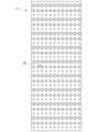
図1は、本実施形態に係るミリ波反射板1を示す模式平面図である。図1に示すように、ミリ波反射板1は、上面(一方の面)に、ミリ波を所定の方向に反射するスーパーセル10を複数有する。One embodiment of the present invention will be described with reference to FIGS. 1 to 5. FIG.
FIG. 1 is a schematic plan view showing a
図2に拡大して示すように、各スーパーセル10は、形状の異なる複数の金属パターンを有する。本実施形態において、スーパーセル10は、大きさの異なる十字型の金属パターン11、12、13の三つの金属パターンを有しており、金属パターン11、12、13が一方向に並べて配置されている。金属パターンの形状や数、配置等は、図2に示した態様に限られず適宜設定でき、環状や、特許文献1に記載されたマッシュルーム構造のような立体形状等であってもよい。
複数のスーパーセル10は、平面視四角形のミリ波反射板1において、辺に沿った二次元マトリクス状に整列して配置されている。As shown enlarged in FIG. 2, each
A plurality of
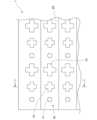
図3は、図2のI-I線における模式断面図である。スーパーセル10は、シート状の誘電体20の第一面20a上に形成されている。
誘電体20の材質は、誘電体であれば特に制限はない。誘電体20の好適な例として、ガラスクロスに合成樹脂を含浸させたものや、各種合成樹脂からなるフィルム等を挙げることができる。中でも、低損失な電気特性を有する誘電体がより好適であり、高純度ガラス(石英ガラス)、フッ素系樹脂、液晶ポリマー、ポリフェニレンエーテル、ポリエーテルケトン、ポリオレフィン、等が例示できる。これらは単体で使用してもよく複数種類を混合したり積層したりして使用してもよい。FIG. 3 is a schematic cross-sectional view taken along line II of FIG. Supercell 10 is formed on
The material of the dielectric 20 is not particularly limited as long as it is a dielectric. Suitable examples of the dielectric 20 include glass cloth impregnated with a synthetic resin, films made of various synthetic resins, and the like. Among them, dielectrics having low-loss electrical properties are more preferable, and examples thereof include high-purity glass (quartz glass), fluororesin, liquid crystal polymer, polyphenylene ether, polyetherketone, and polyolefin. These may be used alone, or may be used by mixing or laminating a plurality of types.
誘電体20において、第一面20aと反対側の第二面20bには、全面を覆う金属層30が設けられている。
このような構成のミリ波反射板1は、誘電体の両面に金属箔が接合された材料を用いて、金属箔をエッチング等でパターニングして複数のスーパーセルを形成することにより、比較的簡便に製造できる。A
The millimeter-
本実施形態において、スーパーセル10および金属層30は、銅からなるが、材質は銅には限られず、金や銀、アルミニウム等も使用できる。さらに、本実施形態における金属層は、金属を主成分としていればよく、抵抗値として10-6Ω・m以下程度の導電性を保持する範囲で金属以外の物質を含んでもよい。例えば、銀混入ペースト、銅混入ペースト、ITO等の導電性金属酸化物等も用途に応じて適用可能である。In this embodiment, the
誘電体20には、第一面20a側から複数の切込み25が設けられている。切込み25は、図2に示すように、スーパーセル10間において、複数の金属パターン11、12、13が並ぶ方向に延びている。ミリ波反射板1の上面側は、複数の切込み25により、複数の金属パターンが並ぶ方向に延びる複数の細長い領域に分割されている。各領域には、複数のスーパーセル10が、複数の金属パターンが並ぶ方向に複数並んで配置されている。 A plurality of
図3に示すように、各切込み25は、第二面20bに達しない程度であり、ミリ波反射板を厚さ方向に貫通していない。これにより、ミリ波反射板は、1枚のシート状の状態を保持している。 As shown in FIG. 3, each
上記のように構成された本実施形態に係るミリ波反射板1の使用時の動作について説明する。
ミリ波反射板1は、大面積である等の場合であっても、筒状に巻くことで、容易に運搬できる。筒状に巻く際は、形成される筒形状の軸線が切込み25と概ね同一方向に延びるように巻いていく。The operation of the
Even if the
第一面20a側を外側にしてミリ波反射板1を巻いていくと、誘電体20に曲げ応力が作用する。しかし、本実施形態の誘電体20には、切込み25が設けられているため、誘電体20が切込みに沿って折れ曲がることにより、曲げ応力は消失し、誘電体20には蓄積されにくい。その結果、ミリ波反射板1全体としては巻くことができる一方、切込み25間の領域は、巻かれた状態でも過度に湾曲せずに平坦に近い状態を保持する。したがって、切込み25間に位置する金属パターン11、12、13や、それらの集合としてのスーパーセル10に曲げ応力が作用しにくく、巻いた際に著しく折れ曲がって損傷したり、断裂したりすることを好適に抑制できる。 When the millimeter-
また、ミリ波反射板1は、切込み25に沿って容易に曲がることができるため、凹凸を有する設置面や、凹状あるいは凸状に湾曲した設置面であっても、折れ曲がることにより良好に追従できる。したがって、様々な態様の設置面に好適に追従させて取り付けることができ、設置後の浮きや剥がれ等も生じにくい。 In addition, since the millimeter-
以上説明したように、本実施形態に係るミリ波反射板1は、ハンドリング性に優れ、設置面への追従性が高い。したがって、建材、壁面、什器、車両等の多種多様な物品に取り付け、周囲の空間にミリ波を充溢させることに寄与できる。 As described above, the
本実施形態において、切込みは、金属パターンに接しないように設けられれば良く、延びる方向に特に制限はない。したがって、図4に示す変形例のように、スーパーセルの金属パターンが並ぶ方向と交差する方向に延びる切込み25Aが設けられてもよい。さらには、切込み25と切込み25Aの両方が設けられてもよい。このようにすると、ミリ波反射板を二方向に巻くことができ、ハンドリング性および設置面への追従性を向上できる。
誘電体20が高純度ガラス(石英ガラス)である場合は、金属層30を厚くし、誘電体20のみ貫通または金属層30までわずかに延びる切込みを設けることにより、上述のような巻き取りを可能とできる。In the present embodiment, the cut should be provided so as not to come into contact with the metal pattern, and there is no particular limitation on the extending direction. Therefore, as in the modification shown in FIG. 4, a
When the dielectric 20 is high-purity glass (quartz glass), the
本実施形態に係るミリ波反射板について、実施例を用いてさらに説明する。本発明に係る技術的思想は、実施例の具体的な内容のみによって何ら限定されない。 The millimeter wave reflector according to this embodiment will be further described using examples. The technical idea of the present invention is not limited at all only by the specific contents of the examples.
(実施例1)
誘電体の両面に銅箔が設けられた400mm×300mmの銅張積層板(中興化成工業社製CGP-500)を準備した。誘電体はフッ素樹脂含浸ガラスクロス(厚さ764μm)であり、銅箔の厚さはいずれも18μm、総厚は0.8mmである。(Example 1)
A 400 mm×300 mm copper-clad laminate (CGP-500 manufactured by Chuko Kasei Kogyo Co., Ltd.) having copper foils provided on both sides of a dielectric was prepared. The dielectric is a fluororesin-impregnated glass cloth (764 μm thick), and the copper foils are all 18 μm thick, with a total thickness of 0.8 mm.
銅張積層板の一方の面にエッチングを施し、二次元マトリクス状に配列されたスーパーセルを複数形成した。スーパーセルは、十字型の3つの金属パターンで構成される。小パターンは、幅1.1mm、縦横寸法1.4mmである。中パターンは、幅1.4mm、縦横寸法3.0mmである。大パターンは、幅1.4mm、縦横寸法3.7mmである。3つのパターンを小、中、大の順に等ピッチで5mm×15mmの区画内に配置し、これをスーパーセルの単位とした。このスーパーセルは、垂直に入射した28GHz帯のミリ波を、小パターンから大パターンに向かう方向に45°傾けて反射するよう設計されている。
上記構成のスーパーセルを、80行20列の二次元マトリクス状に形成した。One surface of the copper clad laminate was etched to form a plurality of super cells arranged in a two-dimensional matrix. A supercell consists of three metal patterns in the shape of a cross. The small pattern has a width of 1.1 mm and a length and width of 1.4 mm. The medium pattern has a width of 1.4 mm and a length and width of 3.0 mm. The large pattern has a width of 1.4 mm and a length and width of 3.7 mm. The three patterns were arranged in the order of small, medium, and large at equal pitches in a section of 5 mm×15 mm, which was used as a unit of supercell. This supercell is designed to reflect vertically incident 28 GHz band millimeter waves at an angle of 45° in the direction from the small pattern to the large pattern.
The supercell having the above configuration was formed in a two-dimensional matrix of 80 rows and 20 columns.
続いて、スーパーセル4行ごとに、銅張積層板の短辺と平行に延びる切込み25を形成した。切込みは、0.7mmトムソン刃を用い、銅箔が除去されて露出した誘電体20の第一面から780μmの深さで形成した。
すなわち、切込み25は、誘電体20を厚さ方向に貫通し、かつ第二面側の金属層30を貫通しない程度とされており、金属層30により1枚のシート状の状態が保持されている。
以上により、実施例1に係るミリ波反射板を得た。このミリ波反射板においては、隣り合う切込み25間に、4行20列に配列された80個のスーパーセルが配置されている。実施例1の概略態様を、図5に示す。Subsequently, cuts 25 extending parallel to the short sides of the copper-clad laminate were formed every four rows of supercells. A cut was made with a 0.7 mm Thomson blade to a depth of 780 μm from the first surface of the dielectric 20 exposed by removing the copper foil.
That is, the
As described above, a millimeter wave reflector according to Example 1 was obtained. In this millimeter wave reflector, 80 super cells arranged in 4 rows and 20 columns are arranged between
(実施例2)
実施例2は、実施例1に対して、切込みの態様のみが異なる。
実施例2では、スーパーセル2列ごとに、銅張積層板の長辺と平行に延びる切込み25を形成した。切込みの形成態様や深さは、実施例1と同様である。
以上により、実施例2に係るミリ波反射板を得た。このミリ波反射板においては、隣り合う切込み25間に、80行2列に配列された160個のスーパーセルが配置されている。(Example 2)
Example 2 differs from Example 1 only in the manner of cutting.
In Example 2, cuts 25 extending parallel to the long sides of the copper-clad laminate were formed every two rows of super cells. The formation mode and depth of the cut are the same as in the first embodiment.
As described above, a millimeter wave reflector according to Example 2 was obtained. In this millimeter wave reflector, 160 super cells arranged in 80 rows and 2 columns are arranged between
(実施例3)
実施例3も、実施例1に対して、切込みの態様のみが異なる。
実施例3では、実施例1と同様の切込みに加え、5mmごとに、銅張積層板の長辺と平行に延びる切込み25を形成した。すなわち、実施例3は、長辺方向(第一の方向)に延びる切込みと、長辺方向と交差する短辺方向(第二の方向)に延びる切込みとの2種類の切込みを有する。切込みの形成態様や深さは、いずれも実施例1と同様である。
以上により、実施例3に係るミリ波反射板を得た。このミリ波反射板においては、短辺方向に延びる切込み25間に、4行20列に配列された80個のスーパーセルが配置され、かつ各スーパーセルの金属パターン間にも切込みが形成されている。(Example 3)
Example 3 also differs from Example 1 only in the manner of cutting.
In Example 3, in addition to the same cuts as in Example 1, cuts 25 extending parallel to the long sides of the copper-clad laminate were formed every 5 mm. That is, Example 3 has two types of cuts, a cut extending in the long side direction (first direction) and a cut extending in the short side direction (second direction) intersecting the long side direction. The formation mode and depth of the cut are the same as those of the first embodiment.
As described above, a millimeter wave reflector according to Example 3 was obtained. In this millimeter-wave reflector, 80 super cells arranged in 4 rows and 20 columns are arranged between
(実施例4)
切込みの深さを500μmとした点を除き、実施例1と同様の手順で実施例4に係るミリ波反射板を得た。(Example 4)
A millimeter wave reflector according to Example 4 was obtained in the same manner as in Example 1, except that the depth of the cut was 500 μm.
各例に係るミリ波反射板に対して、以下の評価を行った。
(ハンドリング性評価)
各例のミリ波反射板を、スーパーセルを外側にして巻くことを試みた。いずれの実施例も、軸線が切込みと概ね平行に延びる筒状に、抵抗なく巻くことができた。実施例3については、2方向に抵抗なく巻くことができた。具体的には、実施例1は直径25~35mmの円筒形(略8角形)に、実施例2は直径60~70mmの円筒状(略10角形)に、実施例3は長辺方向に巻いた場合、直径25~35mmの円筒形(略8角形)、短辺方向に巻いた場合、直径25~35mmの円筒形(略14角形)とすることができ、いずれもハンドリング性が良好であった。The following evaluations were performed on the millimeter wave reflector according to each example.
(Handling evaluation)
An attempt was made to roll the millimeter-wave reflector of each example with the supercell on the outside. In any example, it was possible to wind without resistance in a cylindrical shape whose axis extends substantially parallel to the cut. As for Example 3, it could be wound in two directions without resistance. Specifically, Example 1 is a cylinder (approximately octagon) with a diameter of 25 to 35 mm, Example 2 is a cylinder (approximately 10 polygon) with a diameter of 60 to 70 mm, and Example 3 is wound in the long side direction. When rolled, it can be cylindrical (roughly octagonal) with a diameter of 25 to 35 mm, and when rolled in the direction of the short side, it can be made into a cylindrical shape (roughly 14-sided) with a diameter of 25 to 35 mm, both of which are easy to handle. rice field.
(反射特性評価)
各例のミリ波反射板を、巻かれた状態から展延し、金属層30が接するように平坦な木の板に取り付け、電波暗室環境内に固定した。
ホーンアンテナからの送信波を曲面形状の反射鏡で反射して28GHzの平面波を生成し、ミリ波反射板に対して垂直に照射した。
ミリ波反射板に対して遠方界となる位置に設置した受信アンテナで、ミリ波反射板からの反射波を計測した。この受信アンテナは、ロボット上に設置され、ミリ波反射板から一定の遠方界距離を保ったまま周回できるよう構成されており、広い角度範囲で反射波を計測できる。この評価では、設計内容である、法線に対して45°方向のRCS(レーダー反射断面積)を評価値とした。
計測の結果、45°方向のRCSは、実施例1から4において、それぞれ30.2dBsm(デシベル・スクエアメーター)、30dBsm、30.2dBsm、30.2dBsmであり、一度巻かれた後でも概ね設計通りの反射特性を示した。(Evaluation of reflection characteristics)
The millimeter wave reflector of each example was unrolled from a rolled state, attached to a flat wooden board so that the
A transmitted wave from a horn antenna was reflected by a curved reflecting mirror to generate a plane wave of 28 GHz, which was irradiated perpendicularly to a millimeter wave reflector.
We measured the reflected wave from the millimeter-wave reflector with a receiving antenna installed at a position that was in the far field with respect to the millimeter-wave reflector. This receiving antenna is installed on the robot and is configured so that it can orbit while maintaining a constant far-field distance from the millimeter-wave reflector, so that reflected waves can be measured over a wide range of angles. In this evaluation, the RCS (radar reflection cross section) in the direction of 45° with respect to the normal line, which is the design content, was used as the evaluation value.
As a result of the measurement, the RCS in the 45° direction is 30.2 dBsm (decibel square meter), 30 dBsm, 30.2 dBsm, and 30.2 dBsm in Examples 1 to 4, respectively, which is roughly as designed even after being wound once. showed the reflection characteristics of
巻いた後に再び展延し、スーパーセルの状態を目視にて確認した。いずれの実施例においても、金属パターンの折れ曲がりや断裂等は認められなかった。 After winding, the film was spread again, and the state of the supercell was visually confirmed. In any of the examples, no bending or tearing of the metal pattern was observed.
(設置面追従性評価)
各例のミリ波反射板の金属層上に接着剤を塗布し、凹凸を有する設置面上に貼り付けた。設置面は、一辺300mmの板状部材の一辺に沿って、底面が80mm×60mmの長方形かつ長さ300mmの四角柱状のモールを取り付けたパーティションとした。このパーティションのモールが取り付けられた面に、モールの外周面および板状部材に沿って、金属層上に接着剤を塗布した各例のミリ波反射板を貼り合わせた。
接着剤の乾燥後に、ミリ波反射板と設置面との間に40mm以上の浮きを認めた場合を不合格と定義したが、いずれの実施例も設置面に良好に追従し、合格であった。実施例3に係るミリ波反射板は、浮きの量が最も少なく、追従性に特に優れていた。(Installation surface followability evaluation)
An adhesive was applied onto the metal layer of the millimeter wave reflector of each example, and the plate was attached to an installation surface having unevenness. The installation surface was a partition along one side of a plate-shaped member with a side length of 300 mm, and a quadrangular prism-shaped molding having a rectangular bottom surface of 80 mm×60 mm and a length of 300 mm was attached. On the surface of the partition on which the molding was attached, the millimeter-wave reflector of each example, in which an adhesive was applied to the metal layer, was pasted along the outer peripheral surface of the molding and the plate-shaped member.
After drying the adhesive, the case where a float of 40 mm or more was observed between the millimeter wave reflector and the installation surface was defined as failure, but all examples followed the installation surface well and passed. . The millimeter-wave reflector according to Example 3 had the least floating amount and was particularly excellent in followability.
ただし、同一のスーパーセルに属する金属パターン間に切込みがあると、設置面の形状によっては、スーパーセル内における金属パターン間の位置関係が大きく変化する結果、反射波の干渉態様も変化して、反射特性に影響を与える可能性がある。したがって、想定される設置面の態様に応じて、同一のスーパーセルに属する金属パターン間に切込みを設ける態様と、同一のスーパーセルに属する金属パターン間を避けて切込みを設ける態様とを使い分けることが好ましい。 However, if there is a notch between the metal patterns belonging to the same supercell, depending on the shape of the installation surface, the positional relationship between the metal patterns in the supercell will change greatly, resulting in a change in the interference mode of the reflected waves. May affect reflection properties. Therefore, it is possible to selectively use a mode in which cuts are provided between metal patterns belonging to the same supercell and a mode in which cuts are provided while avoiding between metal patterns belonging to the same supercell, depending on the mode of the assumed installation surface. preferable.
比較対象として、切込みを設けない点を除き実施例1と同様の手順で作製したものも評価した。反射特性評価においては、実施例との間に差は認められず良好であったものの、誘電体の剛性が高いため、全く巻くことはできなかった。また、設置面にも追従しないため、貼り付けること自体ができなかった。 As a comparative object, a sample prepared by the same procedure as in Example 1 except that no cut was provided was also evaluated. In the reflection characteristic evaluation, no difference was observed between the examples and the result was good, but the dielectric material had a high rigidity, so that it could not be wound at all. In addition, since it does not follow the installation surface, it was not possible to stick it.
以上、本発明の各実施形態について説明したが、具体的な構成はこの実施形態に限られるものではなく、本発明の要旨を逸脱しない範囲の構成の変更、組み合わせなども含まれる。以下にいくつか変更を例示するが、これらはすべてではなく、それ以外の変更も可能である。これらの変更は自由に組み合わせることができる。 Although each embodiment of the present invention has been described above, the specific configuration is not limited to this embodiment, and includes modifications and combinations of configurations within the scope of the present invention. Some examples of modifications are given below, but not all of them, and other modifications are possible. These changes can be freely combined.
・本発明に係るミリ波反射板において、金属層は、必ずしも第二面上に隙間なく設けられなくてもよい。たとえば、小さな開口を有するメッシュ状であったり、スーパーセルの区画に対応した線状の欠損部位などを有したりしてもよい。ただし、金属層のない部分においては、入射したミリ波が反射されずに透過するため、金属層のない部分が多すぎると反射性能に影響する可能性があるため、金属層のない部分の最大連続長を、反射対象周波数の1/4λ未満とすることが好ましい。メッシュ状とする場合は、開口の寸法を調節することで、所定波長の電波を反射せずに透過させることも可能である。- In the millimeter wave reflector according to the present invention, the metal layer does not necessarily have to be provided on the second surface without gaps. For example, it may be mesh-like with small openings, or may have linear defect portions corresponding to supercell compartments. However, since incident millimeter waves are transmitted without being reflected in areas without a metal layer, reflection performance may be affected if there are too many areas without a metal layer. The continuous length is preferably less than 1/4λ of the frequency to be reflected. In the case of a mesh, by adjusting the dimensions of the openings, it is possible to allow radio waves of a predetermined wavelength to pass through without being reflected.
・切込みの深さは、上記実施形態や実施例で示した態様に限られず、例えば誘電体を完全に貫通し、かつ金属層に達しない程度であってもよい。また、ミリ波反射板が複数に分割されない程度であれば、切込みの一部が、金属層も含めてミリ波反射板を厚さ方向に貫通していても問題ない。
また、切込みの断面形状も、適宜変更できる。図6に示す断面形状V字状の切込み25Bのように、上部が開いた断面形状の切込みを形成すると、スーパーセル10を内側にして巻くことが容易になり、スーパーセルを保護した状態で輸送等を行える。切込み25Bのような形状は、一定値以上の厚さのトムソン刃を用いる等により、比較的簡便に形成でき、誘電体が比較的硬い等の場合に特に有効である。- The depth of the cut is not limited to the aspects shown in the above embodiments and examples, and may be such that it completely penetrates the dielectric and does not reach the metal layer, for example. Also, as long as the millimeter wave reflector is not divided into a plurality of parts, there is no problem even if a part of the cut penetrates through the millimeter wave reflector including the metal layer in the thickness direction.
Also, the cross-sectional shape of the cut can be changed as appropriate. Forming a cross-sectional cut with an open top like the
・切込みは、ミリ波反射板の平面視において完全な直線状である必要は必ずしもなく、わずかに湾曲したり、屈曲したりしていてもよい。- The notch does not necessarily have to be perfectly straight in a plan view of the millimeter wave reflector, and may be slightly curved or bent.
・切込みを設ける数に特に制限はない。例えば、切込みを一本のみ有する場合でも、ミリ波反射板を切込みに沿って二つ折りにできるため、ハンドリング性は向上する。・There is no particular limit to the number of cuts. For example, even if there is only one notch, the millimeter wave reflector can be folded in two along the notch, which improves handling.
1 ミリ波反射板
10 スーパーセル
11、12、13 金属パターン
20 誘電体
20a 第一面
20b 第二面
25、25A、25B 切込み
30 金属層1
Claims (4)
Translated fromJapanese前記誘電体の第一面上に設けられ、形状の異なる複数の金属パターンを有するスーパーセルと、
前記誘電体において、前記第一面と反対側の第二面上に設けられた金属層と、
を備え、
前記誘電体は、前記金属パターンに接しない部位に前記第一面側から設けられた切込みを有する、
ミリ波反射板。a planar dielectric;
a supercell provided on the first surface of the dielectric and having a plurality of metal patterns with different shapes;
a metal layer provided on a second surface opposite to the first surface of the dielectric;
with
The dielectric has a notch provided from the first surface side at a portion not in contact with the metal pattern,
millimeter wave reflector.
請求項1に記載のミリ波反射板。the cuts are formed avoiding between the metal patterns belonging to the same supercell;
The millimeter wave reflector according to claim 1.
請求項1に記載のミリ波反射板。The cut includes a cut extending in a first direction and a cut extending in a second direction intersecting the first direction,
The millimeter wave reflector according to claim 1.
請求項1に記載のミリ波反射板。The cut has a cross-sectional shape with an open top,
The millimeter wave reflector according to claim 1.
Priority Applications (1)
| Application Number | Priority Date | Filing Date | Title |
|---|---|---|---|
| JP2022000980AJP2023100365A (en) | 2022-01-06 | 2022-01-06 | Millimeter-wave reflector plate |
Applications Claiming Priority (1)
| Application Number | Priority Date | Filing Date | Title |
|---|---|---|---|
| JP2022000980AJP2023100365A (en) | 2022-01-06 | 2022-01-06 | Millimeter-wave reflector plate |
Publications (1)
| Publication Number | Publication Date |
|---|---|
| JP2023100365Atrue JP2023100365A (en) | 2023-07-19 |
Family
ID=87201499
Family Applications (1)
| Application Number | Title | Priority Date | Filing Date |
|---|---|---|---|
| JP2022000980APendingJP2023100365A (en) | 2022-01-06 | 2022-01-06 | Millimeter-wave reflector plate |
Country Status (1)
| Country | Link |
|---|---|
| JP (1) | JP2023100365A (en) |
- 2022
- 2022-01-06JPJP2022000980Apatent/JP2023100365A/enactivePending
Similar Documents
| Publication | Publication Date | Title |
|---|---|---|
| Encinar | Design of two-layer printed reflectarrays using patches of variable size | |
| US4724436A (en) | Depolarizing radar corner reflector | |
| US9413076B2 (en) | Electromagnetic radiation absorber | |
| JP6267219B2 (en) | A flat two-sided device with an equivalent radar cross-section that is adapted (maximized or minimized) | |
| US5103241A (en) | High Q bandpass structure for the selective transmission and reflection of high frequency radio signals | |
| CN105576381B (en) | Frequency-selective surfaces structure based on stereochemical structure | |
| KR950003960B1 (en) | Plane antenna with high-gain and antenna efficiency | |
| US6529174B2 (en) | Arrangement relating to antennas and a method of manufacturing the same | |
| JP4889180B2 (en) | Multi-band electromagnetic wave absorber | |
| JP2025506038A (en) | Radome with surface-varying refraction angle for phased array antennas. | |
| EP1900114A1 (en) | A passive repeater antenna | |
| JP2023100365A (en) | Millimeter-wave reflector plate | |
| CN211045723U (en) | Dipole antenna | |
| JP2023100370A (en) | Millimeter-wave reflector plate | |
| JP7497736B2 (en) | Millimeter wave reflective building materials | |
| CN216958520U (en) | High-Gain Filtered Antenna Based on Folded Reflect Array Antenna and Polarization-Sensitive FSS | |
| CN114759359B (en) | Novel single-layer broadband circularly polarized reflection array antenna | |
| CN120752812A (en) | Reflect array, reflect array device, and reflect array design method | |
| Russo et al. | Tunable pass-band FSS for beam steering applications | |
| JP7424406B2 (en) | Millimeter wave reflector and installation method | |
| US4437099A (en) | Polarization converter for electromagnetic waves | |
| Massaccesi et al. | Wideband bifocal dielectric transmitarray | |
| Feresidis et al. | Flat plate millimetre wave antenna based on partially reflective FSS | |
| Deguchi et al. | Broadband single-layer triple-resonance microstrip reflectarray antennas | |
| Bakhoda et al. | A Low Profile Single Layer X-band Reflectarray Antenna Using a Novel Unit Cell |