JP2023096333A - Circuit device and display device - Google Patents
Circuit device and display deviceDownload PDFInfo
- Publication number
- JP2023096333A JP2023096333AJP2021211997AJP2021211997AJP2023096333AJP 2023096333 AJP2023096333 AJP 2023096333AJP 2021211997 AJP2021211997 AJP 2021211997AJP 2021211997 AJP2021211997 AJP 2021211997AJP 2023096333 AJP2023096333 AJP 2023096333A
- Authority
- JP
- Japan
- Prior art keywords
- color
- image data
- circuit
- processing
- data
- Prior art date
- Legal status (The legal status is an assumption and is not a legal conclusion. Google has not performed a legal analysis and makes no representation as to the accuracy of the status listed.)
- Pending
Links
Images


Classifications
- G—PHYSICS
- G09—EDUCATION; CRYPTOGRAPHY; DISPLAY; ADVERTISING; SEALS
- G09G—ARRANGEMENTS OR CIRCUITS FOR CONTROL OF INDICATING DEVICES USING STATIC MEANS TO PRESENT VARIABLE INFORMATION
- G09G3/00—Control arrangements or circuits, of interest only in connection with visual indicators other than cathode-ray tubes
- G09G3/20—Control arrangements or circuits, of interest only in connection with visual indicators other than cathode-ray tubes for presentation of an assembly of a number of characters, e.g. a page, by composing the assembly by combination of individual elements arranged in a matrix no fixed position being assigned to or needed to be assigned to the individual characters or partial characters
- G09G3/2003—Display of colours
- G—PHYSICS
- G09—EDUCATION; CRYPTOGRAPHY; DISPLAY; ADVERTISING; SEALS
- G09G—ARRANGEMENTS OR CIRCUITS FOR CONTROL OF INDICATING DEVICES USING STATIC MEANS TO PRESENT VARIABLE INFORMATION
- G09G3/00—Control arrangements or circuits, of interest only in connection with visual indicators other than cathode-ray tubes
- G09G3/20—Control arrangements or circuits, of interest only in connection with visual indicators other than cathode-ray tubes for presentation of an assembly of a number of characters, e.g. a page, by composing the assembly by combination of individual elements arranged in a matrix no fixed position being assigned to or needed to be assigned to the individual characters or partial characters
- G09G3/2007—Display of intermediate tones
- G09G3/2059—Display of intermediate tones using error diffusion
- G09G3/2062—Display of intermediate tones using error diffusion using error diffusion in time
- G09G3/2066—Display of intermediate tones using error diffusion using error diffusion in time with error diffusion in both space and time
- G—PHYSICS
- G09—EDUCATION; CRYPTOGRAPHY; DISPLAY; ADVERTISING; SEALS
- G09G—ARRANGEMENTS OR CIRCUITS FOR CONTROL OF INDICATING DEVICES USING STATIC MEANS TO PRESENT VARIABLE INFORMATION
- G09G5/00—Control arrangements or circuits for visual indicators common to cathode-ray tube indicators and other visual indicators
- G09G5/003—Details of a display terminal, the details relating to the control arrangement of the display terminal and to the interfaces thereto
- G09G5/005—Adapting incoming signals to the display format of the display terminal
- G—PHYSICS
- G09—EDUCATION; CRYPTOGRAPHY; DISPLAY; ADVERTISING; SEALS
- G09G—ARRANGEMENTS OR CIRCUITS FOR CONTROL OF INDICATING DEVICES USING STATIC MEANS TO PRESENT VARIABLE INFORMATION
- G09G3/00—Control arrangements or circuits, of interest only in connection with visual indicators other than cathode-ray tubes
- G09G3/20—Control arrangements or circuits, of interest only in connection with visual indicators other than cathode-ray tubes for presentation of an assembly of a number of characters, e.g. a page, by composing the assembly by combination of individual elements arranged in a matrix no fixed position being assigned to or needed to be assigned to the individual characters or partial characters
- G09G3/22—Control arrangements or circuits, of interest only in connection with visual indicators other than cathode-ray tubes for presentation of an assembly of a number of characters, e.g. a page, by composing the assembly by combination of individual elements arranged in a matrix no fixed position being assigned to or needed to be assigned to the individual characters or partial characters using controlled light sources
- G09G3/30—Control arrangements or circuits, of interest only in connection with visual indicators other than cathode-ray tubes for presentation of an assembly of a number of characters, e.g. a page, by composing the assembly by combination of individual elements arranged in a matrix no fixed position being assigned to or needed to be assigned to the individual characters or partial characters using controlled light sources using electroluminescent panels
- G09G3/32—Control arrangements or circuits, of interest only in connection with visual indicators other than cathode-ray tubes for presentation of an assembly of a number of characters, e.g. a page, by composing the assembly by combination of individual elements arranged in a matrix no fixed position being assigned to or needed to be assigned to the individual characters or partial characters using controlled light sources using electroluminescent panels semiconductive, e.g. using light-emitting diodes [LED]
- G09G3/3208—Control arrangements or circuits, of interest only in connection with visual indicators other than cathode-ray tubes for presentation of an assembly of a number of characters, e.g. a page, by composing the assembly by combination of individual elements arranged in a matrix no fixed position being assigned to or needed to be assigned to the individual characters or partial characters using controlled light sources using electroluminescent panels semiconductive, e.g. using light-emitting diodes [LED] organic, e.g. using organic light-emitting diodes [OLED]
- G—PHYSICS
- G09—EDUCATION; CRYPTOGRAPHY; DISPLAY; ADVERTISING; SEALS
- G09G—ARRANGEMENTS OR CIRCUITS FOR CONTROL OF INDICATING DEVICES USING STATIC MEANS TO PRESENT VARIABLE INFORMATION
- G09G3/00—Control arrangements or circuits, of interest only in connection with visual indicators other than cathode-ray tubes
- G09G3/20—Control arrangements or circuits, of interest only in connection with visual indicators other than cathode-ray tubes for presentation of an assembly of a number of characters, e.g. a page, by composing the assembly by combination of individual elements arranged in a matrix no fixed position being assigned to or needed to be assigned to the individual characters or partial characters
- G09G3/34—Control arrangements or circuits, of interest only in connection with visual indicators other than cathode-ray tubes for presentation of an assembly of a number of characters, e.g. a page, by composing the assembly by combination of individual elements arranged in a matrix no fixed position being assigned to or needed to be assigned to the individual characters or partial characters by control of light from an independent source
- G09G3/36—Control arrangements or circuits, of interest only in connection with visual indicators other than cathode-ray tubes for presentation of an assembly of a number of characters, e.g. a page, by composing the assembly by combination of individual elements arranged in a matrix no fixed position being assigned to or needed to be assigned to the individual characters or partial characters by control of light from an independent source using liquid crystals
- G09G3/3607—Control arrangements or circuits, of interest only in connection with visual indicators other than cathode-ray tubes for presentation of an assembly of a number of characters, e.g. a page, by composing the assembly by combination of individual elements arranged in a matrix no fixed position being assigned to or needed to be assigned to the individual characters or partial characters by control of light from an independent source using liquid crystals for displaying colours or for displaying grey scales with a specific pixel layout, e.g. using sub-pixels
- G—PHYSICS
- G09—EDUCATION; CRYPTOGRAPHY; DISPLAY; ADVERTISING; SEALS
- G09G—ARRANGEMENTS OR CIRCUITS FOR CONTROL OF INDICATING DEVICES USING STATIC MEANS TO PRESENT VARIABLE INFORMATION
- G09G2320/00—Control of display operating conditions
- G09G2320/02—Improving the quality of display appearance
- G09G2320/0271—Adjustment of the gradation levels within the range of the gradation scale, e.g. by redistribution or clipping
- G—PHYSICS
- G09—EDUCATION; CRYPTOGRAPHY; DISPLAY; ADVERTISING; SEALS
- G09G—ARRANGEMENTS OR CIRCUITS FOR CONTROL OF INDICATING DEVICES USING STATIC MEANS TO PRESENT VARIABLE INFORMATION
- G09G2320/00—Control of display operating conditions
- G09G2320/06—Adjustment of display parameters
- G09G2320/0666—Adjustment of display parameters for control of colour parameters, e.g. colour temperature
- G—PHYSICS
- G09—EDUCATION; CRYPTOGRAPHY; DISPLAY; ADVERTISING; SEALS
- G09G—ARRANGEMENTS OR CIRCUITS FOR CONTROL OF INDICATING DEVICES USING STATIC MEANS TO PRESENT VARIABLE INFORMATION
- G09G2340/00—Aspects of display data processing
- G09G2340/04—Changes in size, position or resolution of an image
- G09G2340/0407—Resolution change, inclusive of the use of different resolutions for different screen areas
- G09G2340/0428—Gradation resolution change
- G—PHYSICS
- G09—EDUCATION; CRYPTOGRAPHY; DISPLAY; ADVERTISING; SEALS
- G09G—ARRANGEMENTS OR CIRCUITS FOR CONTROL OF INDICATING DEVICES USING STATIC MEANS TO PRESENT VARIABLE INFORMATION
- G09G2340/00—Aspects of display data processing
- G09G2340/06—Colour space transformation
- G—PHYSICS
- G09—EDUCATION; CRYPTOGRAPHY; DISPLAY; ADVERTISING; SEALS
- G09G—ARRANGEMENTS OR CIRCUITS FOR CONTROL OF INDICATING DEVICES USING STATIC MEANS TO PRESENT VARIABLE INFORMATION
- G09G2360/00—Aspects of the architecture of display systems
- G09G2360/12—Frame memory handling
- G—PHYSICS
- G09—EDUCATION; CRYPTOGRAPHY; DISPLAY; ADVERTISING; SEALS
- G09G—ARRANGEMENTS OR CIRCUITS FOR CONTROL OF INDICATING DEVICES USING STATIC MEANS TO PRESENT VARIABLE INFORMATION
- G09G2360/00—Aspects of the architecture of display systems
- G09G2360/18—Use of a frame buffer in a display terminal, inclusive of the display panel
- G—PHYSICS
- G09—EDUCATION; CRYPTOGRAPHY; DISPLAY; ADVERTISING; SEALS
- G09G—ARRANGEMENTS OR CIRCUITS FOR CONTROL OF INDICATING DEVICES USING STATIC MEANS TO PRESENT VARIABLE INFORMATION
- G09G2380/00—Specific applications
- G09G2380/10—Automotive applications
Landscapes
- Engineering & Computer Science (AREA)
- Physics & Mathematics (AREA)
- Computer Hardware Design (AREA)
- General Physics & Mathematics (AREA)
- Theoretical Computer Science (AREA)
- Chemical & Material Sciences (AREA)
- Crystallography & Structural Chemistry (AREA)
- Image Processing (AREA)
- Transforming Electric Information Into Light Information (AREA)
- Controls And Circuits For Display Device (AREA)
- Control Of Indicators Other Than Cathode Ray Tubes (AREA)
Abstract
Translated fromJapanese
Description
Translated fromJapanese本発明は、回路装置及び表示装置等に関する。 The present invention relates to circuit devices, display devices, and the like.
特許文献1には、表示データのRGB各成分を6ビットから3~5ビットに減色する疑似階調処理手段と、減色された表示データを記憶するフレームメモリーと、フレームメモリーが記憶する減色後の表示データのRGB各成分を、ビット変換テーブルを用いて6ビットに多ビット化する階調補正手段と、多ビット化された表示データを用いて、表示デバイスを駆動する駆動手段と、を含む表示装置が開示されている。
特許文献1では、表示データを減色してフレームメモリーに記憶させた後、その減色後の表示データを、ビット変換テーブルを用いて元のビット数に戻しているだけである。このため、減色において表示データのビット数を減らした分だけ単純に画質が低下してしまう。 In Japanese Patent Laid-Open No. 2002-100000, after the display data is color-reduced and stored in a frame memory, the color-reduction display data is simply returned to the original number of bits using a bit conversion table. For this reason, the image quality is simply degraded by the amount by which the number of bits of the display data is reduced in color reduction.
本開示の一態様は、画素データがmビット(mは2以上の整数)である入力画像データから、画素データがnビット(nは1以上でmより小さい整数)である減色後画像データへの減色処理を行うと共に、前記減色処理において空間方向又は時間方向への誤差拡散処理を行う減色回路と、前記減色後画像データを記憶する記憶回路と、前記記憶回路に記憶された前記減色後画像データに対するマッピング処理又はスケーリング処理の少なくとも1つである画像変換処理において、前記減色後画像データの複数の画素データから前記出力画像データの画素データを生成する補間処理を行う画像変換回路と、を含む回路装置に関係する。 One aspect of the present disclosure is from input image data whose pixel data is m bits (m is an integer of 2 or more) to color-reduction image data whose pixel data is n bits (n is an integer of 1 or more and less than m). a color reduction circuit that performs color reduction processing and performs error diffusion processing in the spatial direction or the time direction in the color reduction processing; a storage circuit that stores the color reduction image data; and the color reduction image stored in the storage circuit. an image conversion circuit that performs interpolation processing for generating pixel data of the output image data from a plurality of pixel data of the reduced-color image data in image conversion processing that is at least one of mapping processing and scaling processing for data. It relates to circuit devices.
また本開示の他の態様は、上記に記載された回路装置と、前記出力画像データに基づく画像が表示される画像表示部と、を含む表示装置に関係する。 Another aspect of the present disclosure relates to a display device including the circuit device described above and an image display section displaying an image based on the output image data.
以下、本開示の好適な実施形態について詳細に説明する。なお以下に説明する本実施形態は特許請求の範囲に記載された内容を不当に限定するものではなく、本実施形態で説明される構成の全てが必須構成要件であるとは限らない。 Preferred embodiments of the present disclosure are described in detail below. Note that the embodiments described below do not unduly limit the contents described in the claims, and not all the configurations described in the embodiments are essential constituent elements.
1.表示装置及び回路装置
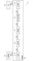
図1に、本実施形態における表示装置50及び回路装置100の構成例を示す。表示装置50は、回路装置100と処理装置200と画像表示部300とを含む。表示装置50は、一例としてはヘッドアップディスプレイ装置、或いは自動車の車載クラスターパネルに設けられたディスプレイ等である。1. 1. Display Device and Circuit Device FIG. 1 shows a configuration example of a
処理装置200は、入力画像データIMAを回路装置100に送信する。入力画像データIMAの各画素の画素データは、30ビットである。具体的には、画素データは、10ビットのR色データ、10ビットのG色データ及び10ビットのB色データを有した30ビットカラーのデータとなっている。処理装置200は、いわゆるSoCであり、例えばCPU又はマイクロコンピューター等のプロセッサーである。SoCは、System on Chipの略である。CPUは、Central Processing Unitの略である。 The
回路装置100は、入力回路105と減色回路140と記憶回路115と画像変換回路150と出力回路130とを含む。回路装置100は、例えば、半導体基板に複数の回路素子が集積された集積回路装置である。 The
入力回路105は、処理装置200から入力画像データIMAを受信する。入力回路105は、様々な通信インターフェースの受信回路であってよいが、一例としてはLVDS、DVI、ディスプレイポート、GMSL又はGVIF等の受信回路である。LVDSはLow voltage differential signalingの略であり、DVIはDigital Visual Interfaceの略であり、GMSLはGigabit Multimedia Serial Linkであり、GVIFはGigabit Video InterFaceの略である。
減色回路140は、入力画像データIMAの各画素の画素データを30ビットから24ビットに減色し、その結果を減色後画像データIMBとして出力する。具体的には、減色回路140は、各色の色データを10ビットから8ビットに減色する。減色後画像データIMBの各画素の画素データは、8ビットのR色データ、8ビットのG色データ及び8ビットのB色データを有した24ビットカラーのデータとなる。 The
また、減色回路140は、減色処理において空間方向又は時間方向の誤差拡散処理を行う。誤差拡散処理とは、減色前の30ビットの画素データと、減色後の24ビットの画素データとの間の誤差を拡散させる処理である。その誤差が拡散された範囲で減色後の画像を平均的に見たときに、減色前の色に相当する色が表現される。空間方向の誤差拡散処理とは、ある画素における減色の誤差を、その画素の周囲の画素の画素データに拡散させる処理である。時間方向の誤差拡散とは、あるフレームにおける画素の減色の誤差を、そのフレーム以降のフレームにおける画素の画素データに拡散させる処理である。 Also, the
記憶回路115は、減色後画像データIMBを一時的に記憶し、画像変換回路150が行う画像変換処理のバッファーメモリーとして機能する。記憶回路115は、例えばラインバッファーである。画像変換処理は、画素位置の移動を伴う画像変換であるが、その垂直方向における画素位置の最大移動量よりも多いライン数のラインバッファーが用いられる。或いは、記憶回路115は、1フレームの減色後画像データIMBをバッファリングするフレームメモリーであってもよい。 The
画像変換回路150は、減色後画像データIMBに対する画像変換処理を行い、その結果を出力画像データIMCとして出力する。画像変換処理は、座標変換により画像が変形又は拡大縮小される処理であり、具体的には、マッピング処理、スケーリング処理、又はそれらを組み合わせた処理である。マッピング処理は、減色後画像データIMB上の座標と出力画像データIMC上の座標との間の任意のマッピングに従って画像を変換する処理である。スケーリング処理は、画像上の基準点を中心として画像を拡大又は縮小する処理である。 The
また、画像変換回路150は、画像変換処理において補間処理を行うことで、減色後画像データIMBの複数の画素データから出力画像データIMCの画素データを生成する。出力画像データIMCの各画素の画素データは30ビットである。即ち、画像変換回路150は、補間処理において、減色後画像データIMBの8ビットのR色データから出力画像データIMCの10ビットのR色データを求め、減色後画像データIMBの8ビットのG色データから出力画像データIMCの10ビットのG色データを求め、減色後画像データIMBの8ビットのB色データから出力画像データIMCの10ビットのB色データを求める。なお、図9で後述するように、画像変換回路150は、各画素の画素データが24ビットである出力画像データIMCを出力してもよい。 Further, the
出力回路130は、出力画像データIMCを画像表示部300に送信する。出力回路130は、様々な通信インターフェースの送信回路であってよいが、一例としてはLVDS、DVI、ディスプレイポート、GMSL又はGVIF等の送信回路である。
画像表示部300は、出力画像データIMCに基づいて画像を表示する。具体的には、画像表示部300は、表示パネルと、表示タイミングを制御する表示コントローラーと、出力画像データIMC及び表示コントローラーからのタイミング制御信号に基づいて表示パネルを駆動することで表示パネルに画像を表示させる表示ドライバーと、を含む。表示パネルは液晶表示パネル又は自発光表示パネル等である。但し、画像表示部300の構成はこれに限定されず、例えば図2等で後述するHUD350であってもよい。 The
なお、以上では入力画像データIMAと出力画像データIMCを30ビットカラーとし、減色後画像データIMBを24ビットカラーとしたが、これに限定されない。mが2以上の整数であり、nが1以上でmより小さい整数であるとき、入力画像データIMAと出力画像データIMCがmビットカラーであり、減色後画像データIMBがnビットカラーであってもよい。一例として、入力画像データIMAと出力画像データIMCが24ビットカラーであり、減色後画像データIMBが18ビットカラーであってもよい。 In the above description, the input image data IMA and the output image data IMC are 30-bit color, and the reduced-color image data IMB is 24-bit color, but the present invention is not limited to this. When m is an integer of 2 or more and n is an integer of 1 or more and less than m, the input image data IMA and the output image data IMC are m-bit color, and the reduced-color image data IMB is n-bit color. good too. As an example, the input image data IMA and the output image data IMC may be 24-bit color, and the reduced-color image data IMB may be 18-bit color.
以上の本実施形態では、回路装置100は、減色回路140と記憶回路115と画像変換回路150とを含む。減色回路140は、画素データがmビットである入力画像データIMAから、画素データがnビットである減色後画像データIMBへの減色処理を行うと共に、減色処理において空間方向又は時間方向への誤差拡散処理を行う。記憶回路115は、減色後画像データIMBを記憶する。画像変換回路150は、記憶回路115に記憶された減色後画像データIMBに対する画像変換処理を行って出力画像データIMCを出力し、その画像変換処理において補間処理を行う。画像変換処理は、マッピング処理又はスケーリング処理の少なくとも1つである。補間処理は、減色後画像データIMBの複数の画素データから出力画像データIMCの画素データを生成する処理である。 In the present embodiment described above, the
本実施形態によれば、入力画像データIMAが減色された後に記憶回路115に記憶されるので、入力画像データIMAがそのまま記憶回路115に記憶される場合よりも、記憶容量が(1-24/30)×100%=20%だけ節約される。これにより、回路装置100を低コスト化できる。 According to the present embodiment, since the input image data IMA is stored in the
また、減色処理において空間方向又は時間方向への誤差拡散処理が行われることで、その誤差が拡散された範囲の平均として30ビットカラーに相当した階調情報を保ちつつ、画像データが24ビットカラーに減色される。そして、その24ビットカラーの減色後画像データIMBに対して画像変換処理が行われることで、空間方向に画素データが平均化されるので、減色後画像データIMBよりも滑らかな階調の出力画像データIMCが得られる。具体的には、画像変換処理であるマッピング処理又はスケーリング処理は、いずれも座標変換を伴うが、その座標変換において変換先の座標が画素グリッドに一致しない場合がある。そのような画素の画素データは周囲の画素の画素データから補間され、その補間処理において画素データが平均化されることになる。画素データが平均化されることで、階調が滑らかとなり、画質向上が期待できる。 In addition, by performing error diffusion processing in the spatial direction or the temporal direction in the color reduction processing, the image data can be converted to 24-bit color while maintaining gradation information corresponding to 30-bit color as the average of the range in which the error is diffused. is reduced to Image conversion processing is performed on the 24-bit color post-reduction image data IMB, so that the pixel data is averaged in the spatial direction. A data IMC is obtained. Specifically, mapping processing or scaling processing, which are image conversion processing, both involve coordinate conversion, and in that coordinate conversion, the coordinates of the conversion destination may not match the pixel grid. The pixel data of such pixels are interpolated from the pixel data of surrounding pixels, and the pixel data are averaged in the interpolation process. By averaging the pixel data, the gradation becomes smooth, and an improvement in image quality can be expected.
なお、上述した特許文献1には、表示データを減色してフレームメモリーに記憶させた後にビット数を元に戻すことが記載されているが、フレームメモリーに記憶された減色後の表示データに対して画像変換処理を行うこと、及び画像変換処理において補間処理を行うことは開示も示唆もされていない。 Incidentally, in the above-mentioned
2.第1詳細構成例
以下、表示装置50がヘッドアップディスプレイ装置であり、画像変換回路150が歪み補正回路110である場合を例に説明する。2. First Detailed Configuration Example Hereinafter, a case where the
図2に、表示装置50と回路装置100の第1詳細構成例を示す。表示装置50は、処理装置200と回路装置100とHUD350とを含む。HUDは、Head-Up Displayの略である。なお、図1の構成例と同様な部分については説明を省略する。 FIG. 2 shows a first detailed configuration example of the
HUD350は、回路装置100から受信した出力画像データIMCに基づいて、ユーザーの視界に虚像を表示する。HUD350は、表示コントローラーと表示ドライバーと表示パネルと投影光学系とを含む。表示パネルは、液晶表示パネル又はOLED表示パネル等である。OLEDは、Organic Light Emitting Diodeの略である。投影光学系は、レンズ又は反射板等を含み、表示パネルが表示する画像をスクリーンに投影させる。スクリーンは、投影光を反射する投影面を有する、透明な被投影体であればよい。例えば、スクリーンは、表示装置50が搭載される移動体のウィンドスクリーンである。
なお、HUD350の構成は上記に限定されない。例えば、HUD350は、表示パネルと投影光学系に代えて、レーザー光源と、レーザーを反射するミラーと、レーザーをスキャンするようにミラーを駆動するアクチュエーターと、を含んでもよい。或いは、HUD350は、表示パネルと投影光学系に代えて、レーザー光源とデジタルミラーデバイスとを含んでもよい。デジタルミラーデバイスは、微小ミラーのアレイと、各微小ミラーを駆動するアクチュエーターとを含む。 In addition, the structure of HUD350 is not limited above. For example, instead of the display panel and the projection optical system, the
回路装置100は、入力回路105と減色回路140と記憶回路115と歪み補正回路110と出力回路130とを含む。歪み補正回路110は、図1の画像変換回路150の一例である。
減色回路140が行う誤差拡散処理の詳細例を説明する。図3に、空間方向の誤差拡散処理の説明図を示す。 A detailed example of error diffusion processing performed by the
減色回路140は、入力画像データIMAから処理対象の画素を選択し、その画素の画素データに対して減色処理を行う。ここでは、いわゆるラスタスキャン方式で画素が順に選択されるとする。図3には、処理対象の画素をハッチングで示し、その周囲の3×3画素を示している。減色回路140は、30ビットカラーの画素データに、周囲の画素から伝播した誤差を加算し、その加算後の30ビットカラーの画素データを24ビットカラーの画素データに減色し、その差分を誤差データΔrとする。処理対象の画素の座標を(Xs,Ys)としたとき、減色回路140は、(Xs+1,Ys)の画素にΔr×C1を伝播させる。同様に、減色回路140は、(Xs-1,Ys+1)、(Xs,Ys+1)、(Xs+1,Ys+1)の画素に、Δr×C2、Δr×C3、Δr×C4を伝播させる。C1~C4は係数であり、C1+C2+C3+C4=1である。このような空間方向の誤差拡散によって、減色後画像データIMBには、減色前の30ビットカラーに相当する情報が含まれている。 The
図4に、時間方向の誤差拡散処理の一例としてFRCの説明図を示す。FRCはFrame Rate Controlの略である。FRC前の入力画像データIMAとFRC後の減色後画像データIMBのフレームレートは同じである。ここではR色データを例にとって説明するが、G色データとB色データについても同様な処理が行われる。 FIG. 4 shows an explanatory diagram of FRC as an example of error diffusion processing in the time direction. FRC is an abbreviation for Frame Rate Control. The input image data IMA before FRC and the image data after FRC after color reduction IMB have the same frame rate. Here, R color data will be described as an example, but similar processing is performed for G color data and B color data.
図4には、FRC後の4×4画素を示している。まず左上の1画素に着目して説明する。入力画像データIMAの10ビットのR色データのうち上位8ビットをRとし、下位2ビットを誤差データとする。ここでは誤差が0.25であるとする。減色回路140は、減色後画像データIMBにおけるR色データを、フレームF1においてR+1とし、フレームF2、F3及びF3においてRとする。フレームF1~F4のR色データの平均はR+0.25となり、減色後画像データIMBには、減色前の30ビットカラーに相当する情報が含まれている。 FIG. 4
他の画素についても同様に時間方向に誤差が拡散されるが、隣り合う画素では拡散のタイミングが異なる。例えば、フレームF1、F2、F3、F4において、左上の画素ではR+1、R、R、Rとなるのに対して、その1つ右隣りの画素ではR、R、R+1、Rとなっており、R+1となるタイミングが異なっている。また、その結果として各フレームにおける4×4画素の平均がR+0.25となっている。これは、フレーム単位で見たときに空間方向にも誤差が拡散されており、減色前の30ビットカラーに相当する情報が含まれているとも言える。 Errors are similarly diffused in the time direction for other pixels, but diffusion timing differs between adjacent pixels. For example, in frames F1, F2, F3, and F4, the upper left pixel is R+1, R, R, and R, while the pixel immediately to the right is R, R, R+1, and R, The timing to become R+1 is different. As a result, the average of 4×4 pixels in each frame is R+0.25. This means that errors are diffused in the spatial direction when viewed in units of frames, and it can be said that information corresponding to 30-bit color before color reduction is included.
なお、ここでは誤差が0.25の場合を例に説明したが、誤差が0.5、又は0.75の場合にも4フレームの平均が0.5、又は0.75となり且つ隣り合う画素では拡散のタイミングが異なるようにFRCが行われる。 Here, the case where the error is 0.25 has been explained as an example, but even when the error is 0.5 or 0.75, the average of the four frames is 0.5 or 0.75, and the adjacent pixels FRC is performed so that the timings of spreading are different.
次に歪み補正回路110について説明する。歪み補正回路110は、減色後画像データIMBにおける画素座標と、出力画像データIMCにおける画素座標との間の座標変換を用いて、減色後画像データIMBに対して歪み補正を行い、その結果を、出力画像データIMCとして出力する。歪み補正とは、HUD350により画像が投影されるときの画像歪みと逆の画像歪みを画像に施すことで、歪みが無い又は低減されたHUD表示にするための画像補正である。画像歪みはHUDの光学系に起因するものである。光学系に起因する画像歪みには、スクリーンの曲面による画像歪み、HUDの投影光学系による画像歪み、又はそれら両方が含まれる。 Next, the
図5に、歪み補正回路110の詳細構成例を示す。歪み補正回路110は、座標カウンター112と座標変換回路113と補間回路114とを含む。図6は、歪み補正回路110の動作を説明する図である。ここでは、歪み補正回路110がリバースワープエンジンである例を説明する。 FIG. 5 shows a detailed configuration example of the
座標カウンター112は、出力画像データIMC上の画素座標GZC=(x,y)を出力する。座標変換回路113は、画素座標(x,y)を、減色後画像データIMB上の座標である参照座標GZB=(u,v)に変換する。具体的には、座標変換回路113は、画素座標(x,y)と参照座標(u,v)との間を対応付ける多項式又はテーブルを用いて座標変換を行う。座標変換回路113は、参照座標(u,v)を、その周囲の複数の画素のリードアドレスに変換する。記憶回路115は、そのリードアドレスから複数の画素データPXDを出力する。補間回路114は、読み出された複数の画素データを補間処理することで、出力画像データIMCにおける画素座標(x,y)の画素データを求める。 The coordinate counter 112 outputs pixel coordinates GZC=(x, y) on the output image data IMC. The coordinate
図6には、参照座標(u,v)の周囲4×4画素の画素データP1~P16が読み出される例を示している。u、vが整数値であるとき参照座標(u,v)が減色後画像データIMBの画素グリッドに一致するが、u、vは実数値であり整数値とは限らない。即ち、参照座標(u,v)が減色後画像データIMBの画素グリッドに一致するとは限らない。補間回路114は、4×4画素の画素データP1~P16を補間処理することで参照座標(u,v)における画素データを求め、それを出力画像データIMCにおける画素座標(x,y)の画素データとする。 FIG. 6 shows an example in which pixel data P1 to P16 of 4×4 pixels surrounding reference coordinates (u, v) are read. When u and v are integer values, the reference coordinates (u, v) match the pixel grid of the reduced-color image data IMB, but u and v are real values and not necessarily integer values. That is, the reference coordinates (u, v) do not necessarily match the pixel grid of the reduced-color image data IMB. The
図7に、第1詳細構成例における補間処理の説明図を示す。記憶回路115から読み出された画素データP1~P16は24ビットカラーである。補間回路114は、補間処理を30ビット演算で行うことで、24ビットカラーの画素データP1~P16から30ビットカラーの画素データPC(x,y)を求める。30ビット演算は、具体的には各色データを10ビット演算するという意味である。図7の中段に補間処理の数式を示している。PC(x,y)は、出力画像データIMCにおける画素座標(x,y)の画素データである。αi(u,v)は補間係数であり、参照座標(u,v)に応じて設定される。α1+α2+・・・+α16=4である。また、α1~α16をP1~P16に対応した4×4の行列と考えたとき、各行の和は1であり、各列の和は1である。補間処理は、例えばバイリニア補間であるが、これに限定されず、バイキュービック補間等であってもよい。 FIG. 7 shows an explanatory diagram of interpolation processing in the first detailed configuration example. The pixel data P1 to P16 read from the
図8に、歪み補正前後の画像例を示す。ここでは、8ビットモノクロの入力画像を1ビットモノクロの画像に減色し、歪み補正により8ビットモノクロの画像に戻す例を示す。 FIG. 8 shows examples of images before and after distortion correction. Here, an example is shown in which an 8-bit monochrome input image is color-reduced to a 1-bit monochrome image and restored to an 8-bit monochrome image by distortion correction.
左図は、空間方向の誤差拡散が施された減色後の画像の一部領域を切り出したものである。減色前の8ビットモノクロ画像は、領域左上から右下に濃くなっていくグラデーション画像である。減色により2値化されるが、空間方向の誤差拡散によってグラデーションの情報が反映されている。即ち、領域左上から右下に黒画素の密度が高くなっている。 The left figure shows a partial region of an image after color reduction that has been subjected to error diffusion in the spatial direction. The 8-bit monochrome image before color reduction is a gradation image that becomes darker from the upper left to the lower right of the area. Although binarized by color reduction, gradation information is reflected by error diffusion in the spatial direction. That is, the density of black pixels increases from the upper left to the lower right of the area.
右図は、歪み補正後の画像から、左図に対応する一部領域を切り出したものである。但し、左図の矩形領域は歪み補正により菱形等に歪んだ領域に移るため、左図の画像と右図の画像は略同一部分の画像ではあるが完全には同一部分の画像ではない。歪み補正において、1ビットモノクロ画像から8ビットモノクロ画像が生成されるが、そのとき、補間処理によって画素データが空間方向に平均化される。これにより、減色後の画像に含まれる誤差拡散の効果を引き継ぎつつ、グラデーションが向上した歪み補正後の画像が得られる。なお、図4で説明したように、FRCにも空間方向の誤差拡散が含まれており、それによって上記と同じ効果が得られる。 The right figure is a partial area corresponding to the left figure cut out from the image after distortion correction. However, since the rectangular area in the left figure shifts to a distorted area such as a rhombus due to distortion correction, the image in the left figure and the image in the right figure are images of substantially the same part, but they are not images of the same part completely. In distortion correction, an 8-bit monochrome image is generated from a 1-bit monochrome image. At this time, pixel data is averaged in the spatial direction by interpolation processing. As a result, a distortion-corrected image with improved gradation can be obtained while inheriting the effect of error diffusion included in the image after color reduction. Note that FRC also includes spatial error diffusion, as described in FIG. 4, to achieve the same effect as above.
以上のように、減色後に歪み補正が施されることで、ラインバッファー又はフレームメモリーの記憶容量を節約すると共に、単純に減色する場合よりもグラデーションが向上した出力画像データが得られる。 As described above, by performing distortion correction after color reduction, it is possible to save the storage capacity of the line buffer or frame memory and obtain output image data with improved gradation compared to simply color reduction.
以上の本実施形態では、画像変換回路150は歪み補正回路110である。歪み補正回路110は、マッピング処理において、出力画像データIMC上の画素座標(x,y)を減色後画像データIMB上の参照座標(u,v)に変換する。歪み補正回路110は、減色後画像データIMBにおける参照座標(u,v)の周囲の複数の画素データP1~P16から、出力画像データIMCにおける画素座標(x,y)の画素データPC(x,y)を生成する。 In the present embodiment described above, the
マッピング処理において参照座標(u,v)が減色後画像データIMBの画素グリッドに一致するとは限らないので、必然的に周囲の複数の画素データから補間することが必要となる。この補間処理によって、画素データが空間方向に平均化されるので、減色後の画像に含まれる誤差拡散の効果を引き継ぎつつ、グラデーションが向上した出力画像データIMCが得られる。 Since the reference coordinates (u, v) do not necessarily match the pixel grid of the reduced-color image data IMB in the mapping process, it is necessary to interpolate from a plurality of surrounding pixel data. This interpolation process averages the pixel data in the spatial direction, so that output image data IMC with improved gradation can be obtained while inheriting the effect of error diffusion included in the image after color reduction.
また本実施形態では、歪み補正回路110は、上記のマッピング処理により減色後画像データIMBに対する歪み補正処理を行う。歪み補正処理は、出力画像データIMCに基づいて画像を投影面に投影するHUD350の光学系に起因する画像歪みを補正する処理である。 Further, in this embodiment, the
本実施形態によれば、歪み補正処理において、HUD350により画像が投影されるときの画像歪みと逆の画像歪みが画像に施される。これにより、歪み補正により画像に与えられた画像歪みによって、投影時の画像歪みがキャンセルされ、歪みが無い又は低減されたHUD表示が得られる。 According to the present embodiment, in the distortion correction process, the image is subjected to image distortion opposite to the image distortion when the image is projected by the
また本実施形態では、減色回路140は、空間方向への誤差拡散処理を行う。歪み補正回路110は、補間処理により、画素データがmビットである出力画像データIMCを生成する。 Further, in this embodiment, the
本実施形態によれば、mビットカラーの入力画像データIMAがnビットカラーの減色後画像データIMBに減色された後に記憶回路115に記憶され、補間処理によりnビットカラーの減色後画像データIMBからmビットカラーの出力画像データIMCが生成される。図8で説明したように、補間処理によりnビットカラーからmビットカラーに多階調化されることで、減色後画像データIMBに含まれる誤差拡散の効果を引き継ぎつつ、グラデーションが向上した出力画像データIMCが得られる。 According to this embodiment, the m-bit color input image data IMA is stored in the
また本実施形態では、減色回路140は、時間方向への誤差拡散処理としてフレームレートコントロール処理を行ってもよい。歪み補正回路110は、補間処理により、画素データがmビットである出力画像データIMCを生成してもよい。 In this embodiment, the
図4で説明したように、FRCにおいて時間方向だけでなく空間方向にも誤差が拡散されており、FRC後の画像データには、減色前のmビットカラーに相当する情報が含まれている。このため、補間処理によりnビットカラーからmビットカラーに多階調化されることで、減色後画像データIMBに含まれる誤差拡散の効果を引き継ぎつつ、グラデーションが向上した出力画像データIMCが得られる。 As described with reference to FIG. 4, in FRC, errors are diffused not only in the temporal direction but also in the spatial direction, and the image data after FRC contains information corresponding to m-bit color before color reduction. Therefore, by performing multi-gradation from n-bit color to m-bit color by interpolation processing, it is possible to obtain output image data IMC with improved gradation while inheriting the effect of error diffusion included in post-color reduction image data IMB. .
また本実施形態では、記憶回路115は、減色後画像データIMBの複数ラインの画像データを記憶するラインバッファー、又は減色後画像データIMBのフレーム画像データを記憶するフレームメモリーである。 In this embodiment, the
ラインバッファー又はフレームメモリーのいずれも画像メモリーであることから比較的大きな記憶容量を有する。例えば、入力画像データIMAの画素データが24ビットから30ビットに増加した場合には1.25倍の記憶容量が必要であるが、本実施形態によれば、24ビットに減色されるので、記憶容量が増加しない。或いは、入力画像データIMAの画素データが24ビットのままであっても、例えば18ビットに減色されることで、記憶容量が節約される。 Since both the line buffer and the frame memory are image memories, they have relatively large storage capacities. For example, if the pixel data of the input image data IMA is increased from 24 bits to 30 bits, 1.25 times the storage capacity is required. No increase in capacity. Alternatively, even if the pixel data of the input image data IMA is still 24 bits, the color is reduced to 18 bits, for example, to save storage capacity.
3.第2詳細構成例
図9に、表示装置50と回路装置100の第2詳細構成例を示す。第2詳細構成例では、歪み補正回路110が24ビットカラーの出力画像データIMCを出力する。なお、図1又は図2の構成例と同様な部分については説明を省略する。3. Second Detailed Configuration Example FIG. 9 shows a second detailed configuration example of the
図10に、第2詳細構成例における補間処理の第1例を示す。補間回路114は、第1詳細構成例と同様に30ビット演算により補間処理を行い、30ビットカラーの画素データPC(x,y)を求める。補間回路114は、画素データPC(x,y)の10ビットの各色データから下位2ビットを切り捨て、24ビットカラーの画素データを求める。歪み補正回路110は、この24ビットカラーの画素データを、出力画像データIMCの画素データとして出力する。 FIG. 10 shows a first example of interpolation processing in the second detailed configuration example. The
図11に、第2詳細構成例における補間処理の第2例を示す。補間回路114は、30ビット演算により画素データPiと補間係数αiの積和を求め、その30ビットの積和の結果を16で除算することで24ビットカラーの画素データPC(x,y)を求める。α1+α2+・・・+α16=4なので、積和の結果を16で除算すると各色データを4で除算することと等価になり、10ビットの各色データが8ビットに減色される。歪み補正回路110は、24ビットカラーの画素データPC(x,y)を、出力画像データIMCの画素データとして出力する。 FIG. 11 shows a second example of interpolation processing in the second detailed configuration example. The
本実施形態では、歪み補正の前後で同じ24ビットカラーであるが、歪み補正において30ビット演算で補間処理された後に24ビットに減色されている。これにより、30ビット演算の時点では、図8で説明したように、減色後の画像に含まれる誤差拡散の効果を引き継ぎつつ、グラデーションが向上した歪み補正後の画像が得られる。そして、その画像が24ビットカラーに減色されることで、減色後の画像に含まれる誤差拡散の効果が適切に歪み補正後の画像に反映され、30ビットカラーに相当した階調情報を含む歪み補正後の出力画像データIMCが得られる。 In the present embodiment, the same 24-bit color is used before and after distortion correction, but the color is reduced to 24 bits after interpolation processing by 30-bit arithmetic in distortion correction. As a result, at the time of 30-bit calculation, as described with reference to FIG. 8, a distortion-corrected image with improved gradation can be obtained while inheriting the effect of error diffusion included in the image after color reduction. Then, by reducing the color of the image to 24-bit color, the effect of error diffusion contained in the image after color reduction is properly reflected in the image after distortion correction, and the distortion including gradation information corresponding to 30-bit color is corrected. Output image data IMC after correction is obtained.
4.第3詳細構成例
図12に、表示装置50と回路装置100の第3詳細構成例を示す。第2詳細構成例では、回路装置100は更に色空間変換回路160を含む。なお、図1又は図2の構成例と同様な部分については説明を省略する。4. Third Detailed Configuration Example FIG. 12 shows a third detailed configuration example of the
処理装置200は、24ビットカラーの画像データIMDを回路装置100に送信する。入力回路105は、処理装置200から画像データIMDを受信する。 The
色空間変換回路160は、24ビットカラーの画像データIMDに対して色空間変換を行うことで、30ビットカラーの入力画像データIMAを出力する。具体的には、画像データIMDは、所定の色空間で色が表現されている。色空間変換回路160は、画像データIMDの所定の色空間をRGBの色空間に変換する。例えば、所定の色空間がYUVであるとし、画像データIMDにおける画素データのYUV成分をDDy、DDu、DDvとし、入力画像データIMAにおける画素データのRGB成分をDAr、DAg、DAbとする。色空間変換回路160は、画像データIMDの画素データ(DDy、DDu、DDv)に、色空間変換を示す3行3列の変換行列を乗算することで、入力画像データIMAの画素データ(DAr,DAg,DAb)を求める。 The color
なお、以上では画像データIMDを24ビットカラーとし、入力画像データIMAを30ビットカラーとしたが、これに限定されない。mが2以上の整数であり、kが1以上でmより小さい整数であるとき、画像データIMDがkビットカラーであり、入力画像データIMAがmビットカラーであってもよい。 Although the image data IMD is assumed to be 24-bit color and the input image data IMA is assumed to be 30-bit color, the present invention is not limited to this. When m is an integer of 2 or more and k is an integer of 1 or more and less than m, the image data IMD may be k-bit color and the input image data IMA may be m-bit color.
また本実施形態では、回路装置100は色空間変換回路160を含む。色空間変換回路160は、画素データがkビットである画像データIMDに対して色空間変換を行うことで、画素データがmビットである入力画像データIMAを生成する。 Also, in this embodiment, the
本実施形態によれば、RGB色空間でない色空間の画像データIMDが回路装置100に入力される場合であっても、その画像データIMDをRGB色空間の画像データに変換できる。また、色空間変換において画素データをkビットからmビットにビット拡張することで、色空間変換において画像データIMDの階調を出来るだけ失わずに滑らかな階調の入力画像データIMAが得られる。そして、その入力画像データIMAを一旦減色して記憶回路115に保存した後、歪み補正を行うことで、記憶回路115の記憶容量を増大させることなく、入力画像データIMAの階調情報に相当する階調情報が含まれた出力画像データIMCが得られる。 According to this embodiment, even if image data IMD in a color space other than the RGB color space is input to the
以上に説明した本実施形態の回路装置は、減色回路と記憶回路と画像変換回路とを含む。減色回路は、画素データがmビットである入力画像データから、画素データがnビットである減色後画像データへの減色処理を行うと共に、減色処理において空間方向又は時間方向への誤差拡散処理を行う。mは2以上の整数である。nは1以上でmより小さい整数である。記憶回路は、減色後画像データを記憶する。画像変換回路は、記憶回路に記憶された減色後画像データに対するマッピング処理又はスケーリング処理の少なくとも1つである画像変換処理を行って出力画像データを出力し、前記画像変換処理において、減色後画像データの複数の画素データから出力画像データの画素データを生成する補間処理を行う。 The circuit device of this embodiment described above includes a color reduction circuit, a storage circuit, and an image conversion circuit. The color reduction circuit performs color reduction processing from input image data having m-bit pixel data to color-reduction image data having n-bit pixel data, and performs error diffusion processing in the spatial or temporal direction in the color reduction processing. . m is an integer of 2 or more. n is an integer greater than or equal to 1 and smaller than m. The storage circuit stores the image data after color reduction. The image conversion circuit performs image conversion processing, which is at least one of mapping processing and scaling processing, on the color-reduced image data stored in the storage circuit, and outputs output image data. Interpolation processing is performed to generate pixel data of output image data from a plurality of pixel data.
本実施形態によれば、入力画像データが減色された後に記憶回路に記憶されるので、入力画像データがそのまま記憶回路に記憶される場合よりも、記憶容量が節約される。これにより、回路装置を低コスト化できる。また、減色処理において空間方向又は時間方向への誤差拡散処理が行われることで、その誤差が拡散された範囲の平均としてmビットカラーに相当した階調情報を保ちつつ、画像データがnビットカラーに減色される。そして、そのnビットカラーの減色後画像データに対する画像変換処理において補間処理が行われることで、空間方向に画素データが平均化されるので、減色後画像データよりも滑らかな階調の出力画像データが得られる。 According to this embodiment, since the input image data is stored in the storage circuit after the color reduction, the storage capacity can be saved as compared with the case where the input image data is stored as it is in the storage circuit. Thereby, the cost of the circuit device can be reduced. In addition, by performing error diffusion processing in the spatial direction or the temporal direction in the color reduction processing, image data can be converted to n-bit color while maintaining gradation information corresponding to m-bit color as the average of the range in which the error is diffused. is reduced to Then, by performing interpolation processing in the image conversion processing for the n-bit color color-reduction image data, the pixel data is averaged in the spatial direction. is obtained.
また本実施形態では、画像変換回路は、マッピング処理において、出力画像データ上の画素座標を減色後画像データ上の参照座標に変換してもよい。画像変換回路は、減色後画像データにおける参照座標の周囲の複数の画素データから、出力画像データにおける画素座標の画素データを生成してもよい。 In the present embodiment, the image conversion circuit may convert pixel coordinates on the output image data to reference coordinates on the reduced-color image data in the mapping process. The image conversion circuit may generate pixel data of pixel coordinates in the output image data from a plurality of pixel data around the reference coordinates in the post-color reduction image data.
マッピング処理において参照座標が減色後画像データの画素グリッドに一致するとは限らないので、必然的に周囲の複数の画素データから補間することが必要となる。この補間処理によって、画素データが空間方向に平均化されるので、減色後の画像に含まれる誤差拡散の効果を引き継ぎつつ、グラデーションが向上した出力画像データが得られる。 Since the reference coordinates in the mapping process do not necessarily match the pixel grid of the image data after color reduction, it is necessary to interpolate from a plurality of surrounding pixel data. This interpolation processing averages the pixel data in the spatial direction, so output image data with improved gradation can be obtained while inheriting the effect of error diffusion included in the image after color reduction.
また本実施形態では、画像変換回路は、マッピング処理により減色後画像データに対する歪み補正処理を行ってもよい。 Further, in the present embodiment, the image conversion circuit may perform distortion correction processing on the reduced-color image data by mapping processing.
また本実施形態では、歪み補正処理は、出力画像データに基づいて画像を投影面に投影するヘッドアップディスプレイの光学系に起因する画像歪みを補正する処理であってもよい。 Further, in the present embodiment, the distortion correction processing may be processing for correcting image distortion caused by an optical system of a head-up display that projects an image onto a projection plane based on output image data.
本実施形態によれば、歪み補正処理において、ヘッドアップディスプレイにより画像が投影されるときの画像歪みと逆の画像歪みが画像に施される。これにより、歪み補正により画像に与えられた画像歪みによって、投影時の画像歪みがキャンセルされ、歪みが無い又は低減されたヘッドアップディスプレイの表示が得られる。 According to this embodiment, in the distortion correction process, the image is subjected to image distortion opposite to the image distortion when the image is projected by the head-up display. As a result, the image distortion applied to the image by the distortion correction cancels the image distortion at the time of projection, and the display of the head-up display with no or reduced distortion is obtained.
また本実施形態では、減色回路は、空間方向への誤差拡散処理を行ってもよい。画像変換回路は、補間処理により、画素データがmビットである出力画像データを生成してもよい。 Further, in this embodiment, the color reduction circuit may perform error diffusion processing in the spatial direction. The image conversion circuit may generate output image data having m-bit pixel data by interpolation processing.
本実施形態によれば、mビットカラーの入力画像データがnビットカラーの減色後画像データに減色された後に記憶回路に記憶され、補間処理によりnビットカラーの減色後画像データからmビットカラーの出力画像データが生成される。補間処理によりnビットカラーからmビットカラーに多階調化されることで、減色後画像データに含まれる誤差拡散の効果を引き継ぎつつ、グラデーションが向上した出力画像データが得られる。 According to the present embodiment, m-bit color input image data is stored in the storage circuit after color reduction to n-bit color reduced image data, and interpolation processing is performed to convert the n-bit color reduced image data to m-bit color image data. Output image data is generated. By multi-gradation from n-bit color to m-bit color by interpolation processing, output image data with improved gradation can be obtained while inheriting the effect of error diffusion included in the image data after color reduction.
また本実施形態では、減色回路は、時間方向への誤差拡散処理としてフレームレートコントロール処理を行ってもよい。画像変換回路は、補間処理により、画素データがmビットである出力画像データを生成してもよい。 In this embodiment, the color reduction circuit may perform frame rate control processing as error diffusion processing in the time direction. The image conversion circuit may generate output image data having m-bit pixel data by interpolation processing.
フレームレートコントロール処理において時間方向だけでなく空間方向にも誤差が拡散されており、フレームレートコントロール処理後の画像データには、減色前のmビットカラーに相当する情報が含まれている。このため、補間処理によりnビットカラーからmビットカラーに多階調化されることで、減色後画像データに含まれる誤差拡散の効果を引き継ぎつつ、グラデーションが向上した出力画像データが得られる。 In the frame rate control process, errors are diffused not only in the temporal direction but also in the spatial direction, and the image data after the frame rate control process contains information corresponding to m-bit color before color reduction. Therefore, by multi-gradation from n-bit color to m-bit color by interpolation processing, output image data with improved gradation can be obtained while inheriting the effect of error diffusion included in the image data after color reduction.
また本実施形態では、回路装置は色空間変換回路を含んでもよい。色空間変換回路は、画素データがkビットである画像データに対して色空間変換を行うことで、画素データがmビットである入力画像データを生成してもよい。kは1以上でmより小さい整数である。 Also, in this embodiment, the circuit device may include a color space conversion circuit. The color space conversion circuit may generate input image data with m-bit pixel data by performing color space conversion on image data with k-bit pixel data. k is an integer greater than or equal to 1 and smaller than m.
本実施形態によれば、出力画像データの色空間とは異なる色空間の画像データが回路装置に入力される場合であっても、その画像データの色空間を、出力画像データの色空間と同じ色空間に変換できる。また、色空間変換において画素データをkビットからmビットにビット拡張することで、色空間変換において画像データの階調を出来るだけ失わずに滑らかな階調の入力画像データが得られる。そして、その入力画像データを一旦減色して記憶回路に保存した後、歪み補正を行うことで、記憶回路の記憶容量を増大させることなく、入力画像データの階調情報に相当する階調情報が含まれた出力画像データが得られる。 According to this embodiment, even when image data in a color space different from the color space of the output image data is input to the circuit device, the color space of the image data is set to the same color space as the output image data. Can be converted to color space. Further, by bit-expanding pixel data from k bits to m bits in color space conversion, it is possible to obtain input image data with smooth gradation without losing the gradation of image data in color space conversion as much as possible. Then, the input image data is temporarily reduced in color and stored in a memory circuit, and then subjected to distortion correction, so that gradation information corresponding to the gradation information of the input image data can be obtained without increasing the memory capacity of the memory circuit. Contained output image data is obtained.
また本実施形態では、記憶回路は、減色後画像データの複数ラインの画像データを記憶するラインバッファー、又は減色後画像データのフレーム画像データを記憶するフレームメモリーであってもよい。 In the present embodiment, the storage circuit may be a line buffer that stores image data of multiple lines of color-reduction image data, or a frame memory that stores frame image data of color-reduction image data.
ラインバッファー又はフレームメモリーのいずれも画像メモリーであることから比較的大きな記憶容量を有する。例えば、入力画像データの画素データが24ビットから30ビットに増加した場合には1.25倍の記憶容量が必要であるが、本実施形態によれば、24ビットに減色されるので、記憶容量が増加しない。或いは、入力画像データの画素データが24ビットのままであっても、例えば18ビットに減色されることで、記憶容量が節約される。 Since both the line buffer and the frame memory are image memories, they have relatively large storage capacities. For example, if the pixel data of the input image data is increased from 24 bits to 30 bits, 1.25 times the storage capacity is required. does not increase. Alternatively, even if the pixel data of the input image data remains 24 bits, the color is reduced to 18 bits, for example, thereby saving the storage capacity.
また本実施形態の表示装置は、回路装置と、出力画像データに基づく画像が表示される画像表示部と、を含む。 Further, the display device of the present embodiment includes a circuit device and an image display section on which an image based on output image data is displayed.
なお、上記のように本実施形態について詳細に説明したが、本開示の新規事項及び効果から実体的に逸脱しない多くの変形が可能であることは当業者には容易に理解できるであろう。従って、このような変形例はすべて本開示の範囲に含まれるものとする。例えば、明細書又は図面において、少なくとも一度、より広義又は同義な異なる用語と共に記載された用語は、明細書又は図面のいかなる箇所においても、その異なる用語に置き換えることができる。また本実施形態及び変形例の全ての組み合わせも、本開示の範囲に含まれる。また回路装置、処理装置、画像表示部及び表示装置等の構成及び動作等も、本実施形態で説明したものに限定されず、種々の変形実施が可能である。 Although the present embodiment has been described in detail as above, it will be easily understood by those skilled in the art that many modifications are possible without substantially departing from the novel matters and effects of the present disclosure. Accordingly, all such modifications are intended to be included within the scope of this disclosure. For example, a term described at least once in the specification or drawings together with a different, broader or synonymous term can be replaced with the different term anywhere in the specification or drawings. All combinations of this embodiment and modifications are also included in the scope of the present disclosure. Also, the configurations and operations of the circuit device, the processing device, the image display unit, the display device, etc. are not limited to those described in the present embodiment, and various modifications are possible.
50…表示装置、100…回路装置、105…入力回路、110…歪み補正回路、112…座標カウンター、113…座標変換回路、114…補間回路、115…記憶回路、130…出力回路、140…減色回路、150…画像変換回路、160…色空間変換回路、200…処理装置、300…画像表示部、350…HUD、GZB…参照座標、GZC…画素座標、IMA…入力画像データ、IMB…減色後画像データ、IMC…出力画像データ、IMD…画像データ、P1~P16…画素データ、PXD…画素データ50
Claims (9)
Translated fromJapanese前記減色後画像データを記憶する記憶回路と、
前記記憶回路に記憶された前記減色後画像データに対するマッピング処理又はスケーリング処理の少なくとも1つである画像変換処理を行って出力画像データを出力し、前記画像変換処理において、前記減色後画像データの複数の画素データから前記出力画像データの画素データを生成する補間処理を行う画像変換回路と、
を含むことを特徴とする回路装置。performing color reduction processing from input image data having m-bit pixel data (m is an integer of 2 or more) to post-color reduction image data having n-bit pixel data (n is an integer of 1 or more and less than m); a color reduction circuit that performs error diffusion processing in the spatial direction or the time direction in the color reduction processing;
a storage circuit for storing the color-reduced image data;
performing image conversion processing, which is at least one of mapping processing and scaling processing, on the color-reduced image data stored in the storage circuit, and outputting output image data; an image conversion circuit that performs interpolation processing to generate pixel data of the output image data from the pixel data of
A circuit device comprising:
前記画像変換回路は、
前記マッピング処理において、前記出力画像データ上の画素座標を前記減色後画像データ上の参照座標に変換し、前記減色後画像データにおける前記参照座標の周囲の前記複数の画素データから、前記出力画像データにおける前記画素座標の画素データを生成することを特徴とする回路装置。In the circuit device according to claim 1,
The image conversion circuit is
In the mapping process, pixel coordinates on the output image data are converted to reference coordinates on the reduced-color image data, and from the plurality of pixel data around the reference coordinates in the reduced-color image data, the output image data generating pixel data of the pixel coordinates in the circuit device.
前記画像変換回路は、
前記マッピング処理により前記減色後画像データに対する歪み補正処理を行うことを特徴とする回路装置。In the circuit device according to claim 1 or 2,
The image conversion circuit is
A circuit device that performs distortion correction processing on the color-reduction image data by the mapping processing.
前記歪み補正処理は、
前記出力画像データに基づいて画像を投影面に投影するヘッドアップディスプレイの光学系に起因する画像歪みを補正する処理であることを特徴とする回路装置。In the circuit device according to claim 3,
The distortion correction process is
A circuit device characterized by correcting image distortion caused by an optical system of a head-up display that projects an image onto a projection surface based on the output image data.
前記減色回路は、
前記空間方向への前記誤差拡散処理を行い、
前記画像変換回路は、
前記補間処理により、画素データがmビットである前記出力画像データを生成することを特徴とする回路装置。In the circuit device according to any one of claims 1 to 4,
The color reduction circuit is
performing the error diffusion processing in the spatial direction;
The image conversion circuit is
A circuit device according to claim 1, wherein said output image data having m-bit pixel data is generated by said interpolation processing.
前記減色回路は、
前記時間方向への前記誤差拡散処理としてフレームレートコントロール処理を行い、
前記画像変換回路は、
前記補間処理により、画素データがmビットである前記出力画像データを生成することを特徴とする回路装置。In the circuit device according to any one of claims 1 to 4,
The color reduction circuit is
performing frame rate control processing as the error diffusion processing in the time direction;
The image conversion circuit is
A circuit device according to claim 1, wherein said output image data having m-bit pixel data is generated by said interpolation processing.
画素データがkビット(kは1以上でmより小さい整数)である画像データに対して色空間変換を行うことで、画素データが前記mビットである前記入力画像データを生成する色空間変換回路を含むことを特徴とする回路装置。In the circuit device according to any one of claims 1 to 6,
A color space conversion circuit for generating the input image data with m-bit pixel data by performing color space conversion on image data with k-bit pixel data (k is an integer equal to or greater than 1 and smaller than m). A circuit device comprising:
前記記憶回路は、
前記減色後画像データの複数ラインの画像データを記憶するラインバッファー、又は前記減色後画像データのフレーム画像データを記憶するフレームメモリーであることを特徴とする回路装置。In the circuit device according to any one of claims 1 to 7,
The memory circuit is
A circuit device, comprising: a line buffer for storing image data of a plurality of lines of the color-reduction image data; or a frame memory for storing frame image data of the color-reduction image data.
前記出力画像データに基づく画像が表示される画像表示部と、
を含むことを特徴とする表示装置。a circuit device according to any one of claims 1 to 8;
an image display unit displaying an image based on the output image data;
A display device comprising:
Priority Applications (3)
| Application Number | Priority Date | Filing Date | Title |
|---|---|---|---|
| JP2021211997AJP2023096333A (en) | 2021-12-27 | 2021-12-27 | Circuit device and display device |
| US18/086,704US11887526B2 (en) | 2021-12-27 | 2022-12-22 | Circuit device having a color reduction circuit and an image conversion circuit executing interpolation processing |
| CN202211680966.5ACN116403502A (en) | 2021-12-27 | 2022-12-27 | Circuit device and display device |
Applications Claiming Priority (1)
| Application Number | Priority Date | Filing Date | Title |
|---|---|---|---|
| JP2021211997AJP2023096333A (en) | 2021-12-27 | 2021-12-27 | Circuit device and display device |
Publications (1)
| Publication Number | Publication Date |
|---|---|
| JP2023096333Atrue JP2023096333A (en) | 2023-07-07 |
Family
ID=86897004
Family Applications (1)
| Application Number | Title | Priority Date | Filing Date |
|---|---|---|---|
| JP2021211997APendingJP2023096333A (en) | 2021-12-27 | 2021-12-27 | Circuit device and display device |
Country Status (3)
| Country | Link |
|---|---|
| US (1) | US11887526B2 (en) |
| JP (1) | JP2023096333A (en) |
| CN (1) | CN116403502A (en) |
Families Citing this family (1)
| Publication number | Priority date | Publication date | Assignee | Title |
|---|---|---|---|---|
| JP7749988B2 (en)* | 2021-09-06 | 2025-10-07 | セイコーエプソン株式会社 | Circuit device and error detection method |
Citations (5)
| Publication number | Priority date | Publication date | Assignee | Title |
|---|---|---|---|---|
| JP2003029724A (en)* | 2001-07-10 | 2003-01-31 | Samsung Electronics Co Ltd | Liquid crystal display device having color correction function, driving device and driving method thereof |
| JP2009175237A (en)* | 2008-01-22 | 2009-08-06 | Nec Electronics Corp | Display device, display panel driver, and display panel driving method |
| US20140010479A1 (en)* | 2012-07-09 | 2014-01-09 | Samsung Electro-Mechanics Co., Ltd. | Bilinear interpolation circuit for image and method thereof |
| WO2014136205A1 (en)* | 2013-03-05 | 2014-09-12 | 三菱電機株式会社 | Picture signal control method and picture signal control device for display apparatus |
| US20160205282A1 (en)* | 2015-01-12 | 2016-07-14 | Intel Corporation | Rendering high quality images via micro-segmentation, error diffusion, and edge enhancement |
Family Cites Families (12)
| Publication number | Priority date | Publication date | Assignee | Title |
|---|---|---|---|---|
| JPH08317393A (en) | 1995-05-17 | 1996-11-29 | Sanyo Electric Co Ltd | Image data processor |
| JPH09101771A (en)* | 1995-10-04 | 1997-04-15 | Hitachi Ltd | Image processing device |
| CN1252672C (en) | 2000-11-21 | 2006-04-19 | 松下电器产业株式会社 | Display unit and display method |
| JP2002221950A (en) | 2000-11-21 | 2002-08-09 | Matsushita Electric Ind Co Ltd | Display device and display method |
| KR100831234B1 (en)* | 2002-04-01 | 2008-05-22 | 삼성전자주식회사 | A method for a frame rate control and a liquid crystal display for the method |
| JP2004235993A (en)* | 2003-01-30 | 2004-08-19 | Canon Inc | Image processing method |
| JP4013887B2 (en)* | 2003-10-30 | 2007-11-28 | セイコーエプソン株式会社 | Image processing circuit, image display device, and image processing method |
| EP2624247A4 (en)* | 2010-09-27 | 2014-05-07 | Jvc Kenwood Corp | Liquid crystal display device, and device and method for driving liquid crystal display elements |
| JP2013218654A (en)* | 2012-03-16 | 2013-10-24 | Panasonic Corp | Image processing device |
| JP6671101B2 (en)* | 2015-02-05 | 2020-03-25 | シナプティクス・ジャパン合同会社 | Image processing circuit, display panel driver, display device, and image processing method |
| JP6706997B2 (en)* | 2016-08-09 | 2020-06-10 | 株式会社Joled | Display device, display device correction method, display device manufacturing method, and display device display method |
| JP2020031264A (en)* | 2018-08-20 | 2020-02-27 | ソニーセミコンダクタソリューションズ株式会社 | Signal processor, imaging apparatus, signal processing method |
- 2021
- 2021-12-27JPJP2021211997Apatent/JP2023096333A/enactivePending
- 2022
- 2022-12-22USUS18/086,704patent/US11887526B2/enactiveActive
- 2022-12-27CNCN202211680966.5Apatent/CN116403502A/enactivePending
Patent Citations (5)
| Publication number | Priority date | Publication date | Assignee | Title |
|---|---|---|---|---|
| JP2003029724A (en)* | 2001-07-10 | 2003-01-31 | Samsung Electronics Co Ltd | Liquid crystal display device having color correction function, driving device and driving method thereof |
| JP2009175237A (en)* | 2008-01-22 | 2009-08-06 | Nec Electronics Corp | Display device, display panel driver, and display panel driving method |
| US20140010479A1 (en)* | 2012-07-09 | 2014-01-09 | Samsung Electro-Mechanics Co., Ltd. | Bilinear interpolation circuit for image and method thereof |
| WO2014136205A1 (en)* | 2013-03-05 | 2014-09-12 | 三菱電機株式会社 | Picture signal control method and picture signal control device for display apparatus |
| US20160205282A1 (en)* | 2015-01-12 | 2016-07-14 | Intel Corporation | Rendering high quality images via micro-segmentation, error diffusion, and edge enhancement |
Also Published As
| Publication number | Publication date |
|---|---|
| US11887526B2 (en) | 2024-01-30 |
| CN116403502A (en) | 2023-07-07 |
| US20230206814A1 (en) | 2023-06-29 |
Similar Documents
| Publication | Publication Date | Title |
|---|---|---|
| US7417649B2 (en) | Method and apparatus for nonlinear anamorphic scaling of video images | |
| US8830402B2 (en) | Image processing circuit and method thereof | |
| US20080158246A1 (en) | Digital color management method and system | |
| TW202013336A (en) | Image processing device, display device, and image processing method | |
| JP4884481B2 (en) | Image display device | |
| CN101399024A (en) | Display apparatus | |
| US20060055830A1 (en) | Display apparatus and display method | |
| JP4207064B2 (en) | Electro-optical device, image processing circuit, image processing method, and electronic apparatus | |
| JP2012203052A (en) | Liquid crystal display device and program used for the same | |
| US20080079674A1 (en) | Display device and method for driving the same | |
| US11887526B2 (en) | Circuit device having a color reduction circuit and an image conversion circuit executing interpolation processing | |
| JP2011193332A (en) | Projector and video projection method | |
| JP4834295B2 (en) | Video display device and video display method | |
| JP2009109694A (en) | Display device | |
| JP2023058464A (en) | Device and method for foveated rendering | |
| JP4672821B2 (en) | Method and apparatus using line buffer for interpolation as pixel lookup table | |
| JP2006030600A (en) | Multi-screen display system, multi-screen display method, brightness correction method, and program | |
| JP2002108298A (en) | Digital signal processing circuit, its processing method, display device, liquid crystal display device and liquid crystal projector | |
| JP5207832B2 (en) | Display device | |
| JP6939379B2 (en) | Display device drive device, liquid crystal display device, and display device drive method | |
| US7619652B2 (en) | Frame processing and frame processing method | |
| KR102423637B1 (en) | Display apparatus and method of driving the same | |
| WO2019082510A1 (en) | Display control device, head mount display, display control method, and computer program | |
| JP5141871B2 (en) | Image processing method and image display apparatus | |
| JP2012019315A (en) | Image processor and image processing method |
Legal Events
| Date | Code | Title | Description |
|---|---|---|---|
| A621 | Written request for application examination | Free format text:JAPANESE INTERMEDIATE CODE: A621 Effective date:20241112 | |
| A131 | Notification of reasons for refusal | Free format text:JAPANESE INTERMEDIATE CODE: A131 Effective date:20250603 | |
| A521 | Request for written amendment filed | Free format text:JAPANESE INTERMEDIATE CODE: A523 Effective date:20250708 |