JP2023092066A - Auxiliary power unit - Google Patents
Auxiliary power unitDownload PDFInfo
- Publication number
- JP2023092066A JP2023092066AJP2021207053AJP2021207053AJP2023092066AJP 2023092066 AJP2023092066 AJP 2023092066AJP 2021207053 AJP2021207053 AJP 2021207053AJP 2021207053 AJP2021207053 AJP 2021207053AJP 2023092066 AJP2023092066 AJP 2023092066A
- Authority
- JP
- Japan
- Prior art keywords
- current
- value
- resonance
- capacitor
- inverter
- Prior art date
- Legal status (The legal status is an assumption and is not a legal conclusion. Google has not performed a legal analysis and makes no representation as to the accuracy of the status listed.)
- Pending
Links
Images


Classifications
- H—ELECTRICITY
- H02—GENERATION; CONVERSION OR DISTRIBUTION OF ELECTRIC POWER
- H02M—APPARATUS FOR CONVERSION BETWEEN AC AND AC, BETWEEN AC AND DC, OR BETWEEN DC AND DC, AND FOR USE WITH MAINS OR SIMILAR POWER SUPPLY SYSTEMS; CONVERSION OF DC OR AC INPUT POWER INTO SURGE OUTPUT POWER; CONTROL OR REGULATION THEREOF
- H02M3/00—Conversion of DC power input into DC power output
- H02M3/22—Conversion of DC power input into DC power output with intermediate conversion into AC
- H02M3/24—Conversion of DC power input into DC power output with intermediate conversion into AC by static converters
- H02M3/28—Conversion of DC power input into DC power output with intermediate conversion into AC by static converters using discharge tubes with control electrode or semiconductor devices with control electrode to produce the intermediate AC
- H02M3/325—Conversion of DC power input into DC power output with intermediate conversion into AC by static converters using discharge tubes with control electrode or semiconductor devices with control electrode to produce the intermediate AC using devices of a triode or a transistor type requiring continuous application of a control signal
- H02M3/335—Conversion of DC power input into DC power output with intermediate conversion into AC by static converters using discharge tubes with control electrode or semiconductor devices with control electrode to produce the intermediate AC using devices of a triode or a transistor type requiring continuous application of a control signal using semiconductor devices only
- H02M3/33569—Conversion of DC power input into DC power output with intermediate conversion into AC by static converters using discharge tubes with control electrode or semiconductor devices with control electrode to produce the intermediate AC using devices of a triode or a transistor type requiring continuous application of a control signal using semiconductor devices only having several active switching elements
- H02M3/33571—Half-bridge at primary side of an isolation transformer
- H—ELECTRICITY
- H02—GENERATION; CONVERSION OR DISTRIBUTION OF ELECTRIC POWER
- H02M—APPARATUS FOR CONVERSION BETWEEN AC AND AC, BETWEEN AC AND DC, OR BETWEEN DC AND DC, AND FOR USE WITH MAINS OR SIMILAR POWER SUPPLY SYSTEMS; CONVERSION OF DC OR AC INPUT POWER INTO SURGE OUTPUT POWER; CONTROL OR REGULATION THEREOF
- H02M1/00—Details of apparatus for conversion
- H02M1/32—Means for protecting converters other than automatic disconnection
- H—ELECTRICITY
- H02—GENERATION; CONVERSION OR DISTRIBUTION OF ELECTRIC POWER
- H02M—APPARATUS FOR CONVERSION BETWEEN AC AND AC, BETWEEN AC AND DC, OR BETWEEN DC AND DC, AND FOR USE WITH MAINS OR SIMILAR POWER SUPPLY SYSTEMS; CONVERSION OF DC OR AC INPUT POWER INTO SURGE OUTPUT POWER; CONTROL OR REGULATION THEREOF
- H02M3/00—Conversion of DC power input into DC power output
- H02M3/01—Resonant DC/DC converters
- Y—GENERAL TAGGING OF NEW TECHNOLOGICAL DEVELOPMENTS; GENERAL TAGGING OF CROSS-SECTIONAL TECHNOLOGIES SPANNING OVER SEVERAL SECTIONS OF THE IPC; TECHNICAL SUBJECTS COVERED BY FORMER USPC CROSS-REFERENCE ART COLLECTIONS [XRACs] AND DIGESTS
- Y02—TECHNOLOGIES OR APPLICATIONS FOR MITIGATION OR ADAPTATION AGAINST CLIMATE CHANGE
- Y02B—CLIMATE CHANGE MITIGATION TECHNOLOGIES RELATED TO BUILDINGS, e.g. HOUSING, HOUSE APPLIANCES OR RELATED END-USER APPLICATIONS
- Y02B70/00—Technologies for an efficient end-user side electric power management and consumption
- Y02B70/10—Technologies improving the efficiency by using switched-mode power supplies [SMPS], i.e. efficient power electronics conversion e.g. power factor correction or reduction of losses in power supplies or efficient standby modes
Landscapes
- Engineering & Computer Science (AREA)
- Power Engineering (AREA)
- Inverter Devices (AREA)
- Dc-Dc Converters (AREA)
Abstract
Description
Translated fromJapanese本発明の実施形態は、補助電源装置に関する。 Embodiments of the present invention relate to auxiliary power supplies.
例えば電気車(移動体)は、高圧の電車線(例えば架空電車線、または第三軌条など)から供給される直流電圧を、負荷に応じた電圧に変換し、直流電圧を負荷に出力する電力変換装置を電源装置として備える。電気車は、電気車用電源装置として、例えば、走行用電動機の駆動用の電源装置と、照明及び空調などの他の機器に電力を供給する補助電源装置とを備える。 For example, an electric car (moving body) converts the DC voltage supplied from a high-voltage train line (such as an overhead train line or third rail) into a voltage corresponding to the load, and outputs the DC voltage to the load. A conversion device is provided as a power supply device. An electric vehicle includes, for example, a power supply for driving an electric motor for running, and an auxiliary power supply for supplying power to other devices such as lighting and air conditioning, as power supplies for electric vehicles.
補助電力変換装置は、インバータと商用周波数変圧器(絶縁トランス)の構成が一般的であるが、システムを小型化するために高周波変圧器(絶縁トランス)の適用が進んでいる。補助電源装置の1つの構成例は、高周波数の交流電流により励磁される高周波変圧器(絶縁トランス)と、電車線からの直流電圧を調整するチョッパ回路と、チョッパ回路の出力を高周波数の交流に変換し、高周波変圧器に供給するインバータと、高周波の交流を直流に変換する整流器と、を備える。以降では、インバータ、高周波変圧器、および整流器を含む構成を高周波絶縁回路と呼ぶ。
また、インバータに共振回路を適用することによって、スイッチング時の損失を大幅に低減でき、インバータの高周波スイッチングが可能となる。Auxiliary power converters generally consist of an inverter and a commercial frequency transformer (isolation transformer). One configuration example of the auxiliary power supply includes a high-frequency transformer (isolation transformer) that is excited by a high-frequency alternating current, a chopper circuit that adjusts the DC voltage from the train line, and the output of the chopper circuit to a high-frequency alternating current. , and supplies it to a high-frequency transformer, and a rectifier that converts high-frequency alternating current to direct current. Henceforth, the structure containing an inverter, a high frequency transformer, and a rectifier is called a high frequency isolation circuit.
In addition, by applying a resonance circuit to the inverter, the switching loss can be greatly reduced, and high-frequency switching of the inverter becomes possible.
しかしながら、共振回路を構成する共振コンデンサが経年劣化によって容量低減した場合、共振回路の共振周波数が上昇することでインバータが出力する交流電流のピーク値や実効値が増加し、インバータ、高周波変圧器、および、整流器における損失増加を引き起こして、温度上昇が許容値を超える恐れがあり、共振コンデンサの劣化が進むと温度異常により装置が停止する原因となり得る。 However, when the capacity of the resonant capacitor that makes up the resonant circuit decreases due to aging, the resonant frequency of the resonant circuit increases, which increases the peak value and effective value of the alternating current output by the inverter. In addition, an increase in loss in the rectifier may be caused, and the temperature rise may exceed an allowable value. If the deterioration of the resonance capacitor progresses, abnormal temperature may cause the device to stop.
共振インバータが出力する交流電流を監視していれば、電流の変化は検知可能となるが、追加の電流検出器が必要となる。またハーフブリッジ回路を用いた共振インバータにおいては、交流出力の一端を2直列接続した共振コンデンサの中点に接続する構成となるが、どちらの共振コンデンサが容量低減したかについては、交流電流による検出が難しかった。 If the alternating current output by the resonant inverter is monitored, changes in the current can be detected, but an additional current detector is required. In a resonance inverter using a half-bridge circuit, one end of the AC output is connected to the middle point of two series-connected resonance capacitors. was difficult.
本発明の実施形態は上記事情を鑑みて成されたものであって、信頼性の高い補助電源装置を提供することを目的とする。 SUMMARY OF THE INVENTION The embodiments of the present invention have been made in view of the above circumstances, and it is an object of the present invention to provide a highly reliable auxiliary power supply.
実施形態による補助電源装置は、高周波変圧器と、直流電源から供給される直流電力を変換するチョッパ回路と、前記チョッパ回路の出力電力を交流電力に変換して前記高周波変圧器に供給するインバータと、前記インバータの直流端に接続された直流コンデンサと、前記インバータのスイッチングに伴って共振動作を発生させる共振コンデンサと、前記高周波変圧器を介して前記インバータから供給される交流電力を直流電力に変換する整流器と、前記インバータの直流入力電流の値又は前記直流入力電流の値を演算するための値を検出する検出部と、前記検出部から供給される値に基づいて、前記共振コンデンサを含む共振回路の共振周波数を演算し、前記共振周波数と前記直流入力電流の値とを用いて前記共振コンデンサの容量低減を検出する制御回路と、を具備する。 An auxiliary power supply device according to an embodiment includes a high-frequency transformer, a chopper circuit that converts DC power supplied from a DC power supply, and an inverter that converts the output power of the chopper circuit into AC power and supplies it to the high-frequency transformer. , a DC capacitor connected to the DC terminal of the inverter, a resonance capacitor that generates a resonant operation with switching of the inverter, and a high-frequency transformer that converts AC power supplied from the inverter into DC power. a rectifier, a detection unit for detecting the value of the DC input current of the inverter or a value for calculating the value of the DC input current, and a resonance circuit including the resonance capacitor based on the value supplied from the detection unit. and a control circuit that calculates a resonance frequency of the circuit and detects a decrease in capacity of the resonance capacitor using the resonance frequency and the value of the DC input current.
以下、実施形態の電力変換装置について図面を参照して詳細に説明する。
(第1実施形態)
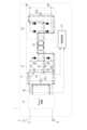
図1は、第1実施形態に係る電力変換装置の一構成例を概略的に示す図である。
ここでは、一例として電気車などの移動体に搭載される電力変換装置1について説明する。電気車用の電力変換装置1は、架空電車線または第三軌条などの電車線2から集電器3を介して直流電力を受け取り、受け取った直流電力を出力端子4P、4Nから出力する電気車用の補助電源装置である。Hereinafter, power converters according to embodiments will be described in detail with reference to the drawings.
(First embodiment)
FIG. 1 is a diagram schematically showing one configuration example of a power converter according to a first embodiment.
Here, as an example, a
本実施形態では、電気車用の電力変換装置1は、電気車の照明及び空調などの負荷に電力を供給する補助電源装置であるとして説明する。なお、電気車は、走行用電動機を駆動する為の図示されない主電源装置を備える。主電源装置は、電車線2から集電器3を介して受け取った直流電力により、走行用電動機を駆動することにより、電気車に線路5上を走行させる。 In this embodiment, the
電気車用の補助電源装置としての電力変換装置1には、走行用電動機に比べて低圧で動作する機器が接続される。この為、電気車用の電力変換装置1は、電力が入力される一次側と、電力を出力する二次側とが絶縁されている必要がある。 A
一次側と二次側との絶縁を確保するための構成の一例として、電磁結合する一対の巻線(コイル)を備える変圧器を用いて、一次側と二次側とを絶縁する変圧器がある。変圧器は、励磁周波数が低くなる程大型化する。例えば、商用電源の周波数に対応する励磁周波数が設定された変圧器では、大型になる。そこで、本実施形態の電力変換装置1では、高周波変圧器を用いることにより、一次側と二次側とを絶縁し、且つ小型化を実現している。 An example of a configuration for ensuring insulation between the primary side and the secondary side is a transformer that uses a transformer that has a pair of electromagnetically coupled windings (coils) to insulate the primary side from the secondary side. be. The transformer becomes larger as the excitation frequency becomes lower. For example, a transformer in which an excitation frequency corresponding to the frequency of a commercial power supply is set is large. Therefore, in the
電力変換装置1は、チョッパ回路31と、電力変換回路(高周波絶縁回路)11と、電流検出器32と、電圧検出器33と、制御回路41と、を備える。
チョッパ回路31は、電車線2から集電器3を介して入力された直流電力を所望の直流電力に変換する。本実施形態では、例えば電車線2が直流電源である。The
The
電流検出器32は、チョッパ回路31の出力電流を検出する。電流検出器32の検出結果は制御回路41に供給される。
電圧検出器33は、チョッパ回路31の出力電圧(第1直流コンデンサFC1の電圧)を検出する。電圧検出器33の検出結果は制御回路41に供給される。A
A
電力変換回路11は、チョッパ回路31から出力された直流電力を、高周波変圧器22を介して絶縁し、直流負荷用の電力に変換する。電力変換回路11は、例えば、共振インバータ21と、高周波変圧器22と、整流器23と、第2直流コンデンサFC2と、を有する。 The
共振インバータ21は、チョッパ回路31から供給される直流電力を用いて、高周波変圧器22に交流電力を供給するインバータ回路である。共振インバータ21は、例えば、チョッパ回路31に電気的に接続される直流端と、高周波変圧器22の一次側に電気的に接続される交流端と、を備え、共振方式単相ハーフブリッジインバータとして構成される。共振インバータ21は、第1スイッチS1、第2スイッチS2、第1直流コンデンサFC1、第1共振コンデンサC1、及び第2共振コンデンサC2、を備える。共振インバータ21の一方の交流端は、インダクタンスを介して高周波変圧器22の一次側と電気的に接続されている。
第1直流コンデンサFC1は、共振インバータ21の高電位側の直流端と低電位側の直流端との間に接続され、チョッパ回路31から供給された直流電力を平滑化する。The
The first DC capacitor FC<b>1 is connected between the high potential side DC end and the low potential side DC end of the
第1スイッチS1は、高電位側の直流端と一方の交流端との間の電気的接続を切り替える。第1スイッチS1は、例えばMOSFET(Metal-Oxide Semiconductor Field-Effect Transistors)であって、ドレインにおいて高電位側の直流端と電気的に接続され、ソースにおいて一方の交流端と電気的に接続されている。 The first switch S1 switches the electrical connection between the DC end on the high potential side and one AC end. The first switch S1 is, for example, a MOSFET (Metal-Oxide Semiconductor Field-Effect Transistor), and has a drain electrically connected to a high potential side DC terminal and a source electrically connected to one AC terminal. there is
第2スイッチS2は、低電位側の直流端と一方の交流端との間の電気的接続を切り替える。第2スイッチS2は、例えばMOSFETであって、ドレインにおいて一方の交流端と電気的に接続され、ソースにおいて低電位側の直流端と電気的に接続されている。
なお、第1スイッチS1と第2スイッチS2とはMOSFETに限定されるものではなく、例えば、バイポーラトランジスタや、IGBT(Insulated Gate Bipolar Transistor)など、他のパワー半導体素子を用いても構わない。The second switch S2 switches the electrical connection between the DC end on the low potential side and one AC end. The second switch S2 is, for example, a MOSFET, and has a drain electrically connected to one AC terminal and a source electrically connected to a low-potential DC terminal.
The first switch S1 and the second switch S2 are not limited to MOSFETs, and other power semiconductor elements such as bipolar transistors and IGBTs (Insulated Gate Bipolar Transistors) may be used.
第1共振コンデンサC1は、高電位側の直流端と他方の交流端との間に電気的に接続されている。第2共振コンデンサC2は、低電位側の直流端と他方の交流端との間に電気的に接続されている。 The first resonance capacitor C1 is electrically connected between the high potential side DC terminal and the other AC terminal. The second resonance capacitor C2 is electrically connected between the low potential side DC terminal and the other AC terminal.
すなわち、第1スイッチS1と第2スイッチS2との接続点(一方の交流端)、及び第1共振コンデンサC1と第2共振コンデンサC2との接続点(他方の交流端)には、高周波変圧器22の一次巻線が接続されている。共振インバータ21は、制御回路41により、第1スイッチS1及び第2スイッチS2のオンオフ動作を制御されることにより、高周波変圧器22の一次巻線に交流電力を供給する。なお、以下の説明において、共振インバータ21の第1スイッチS1側を、共振インバータ21の上アーム、共振インバータ21の第2スイッチS2側を、共振インバータ21の下アームと称する。 That is, a high-frequency transformer is connected to the connection point (one AC end) of the first switch S1 and the second switch S2 and the connection point (the other AC end) of the first resonance capacitor C1 and the second resonance capacitor C2. 22 primary windings are connected. The
高周波変圧器22は、磁束を発生させる一次側の巻線(一次巻線)と、一次巻線と絶縁され、且つ一次巻線に生じた磁束により励磁される二次側の巻線(二次巻線)とを有する絶縁トランスである。高周波変圧器22の一次巻線に共振インバータ21から交流電流が供給された場合、一次巻線に磁束が生じる。一次巻線に生じた磁束は、二次巻線に誘導電流を発生させる。これにより、高周波変圧器22は、一次側から入力された交流電流に応じて、二次側に電力を供給する。 The high-
整流器23は、高周波変圧器22の二次巻線に生じた電力を整流する回路であり、例えば、複数のダイオードが組み合わされた整流ブリッジ回路として構成される。
第2直流コンデンサFC2は、整流器23から供給された直流電圧を平滑化する。第3直流コンデンサFC2は、並列に接続された出力端子4P、4Nから、直流電力を出力する。出力端子4P、4Nから出力された直流電力は、図示されないインバータなどの回路により、例えば50Hzまたは60Hzの交流電力に変換される。The
A second DC capacitor FC2 smoothes the DC voltage supplied from the
制御回路41は、電流検出器32の検出値および電圧検出器33の検出値を取得して、チョッパ回路31および電力変換回路11の動作を制御する。制御回路41は、例えば、少なくとも1つのプロセッサと、プロセッサにより実行されるプログラムおよびプログラムにより用いられるデータが記憶されたメモリと、を備えた演算装置である。制御回路41は、ソフトウエアにより、若しくは、ソフトウエアとハードウエアとの組み合わせにより、チョッパ回路31および電力変換回路11を制御するための種々の機能を実現することが出来る。 The
制御回路41は、例えばパルス信号を生成する論理回路として構成され、制御回路41のプロセッサがプログラムを実行することにより、パルス信号を生成するように構成され得る。制御回路41は、パルス信号をチョッパ回路31及び電力変換回路11にそれぞれ入力することにより、チョッパ回路31及び電力変換回路11の半導体素子の動作を制御する。例えば、制御回路41は、パルス信号のオンオフデューティ比を調整するPWM制御を行う。これにより、制御回路41は、チョッパ回路31の出力及び電力変換回路11の出力をそれぞれ調整する。 The
次に、本実施形態の電力変換装置において、制御回路41が第1共振コンデンサC1と第2共振コンデンサC2との容量低減を検出する動作の一例について説明する。
図2は、図1に示す共振インバータの上アームオン時の電流経路について説明する為の図である。Next, an example of the operation of the
FIG. 2 is a diagram for explaining a current path when the upper arm of the resonant inverter shown in FIG. 1 is on.
高周波変圧器22に供給される交流電流は、上アームの第1スイッチS1から出力され、整流器23および第2直流コンデンサFC2を経由して、第1共振コンデンサC1と第2共振コンデンサC2との接続点に戻り、第1共振コンデンサC1と第2共振コンデンサC2にそれぞれ分流する。共振インバータ21の直流入力部Aには、第2共振コンデンサC2と等しい電流が流れる。 The alternating current supplied to the
図3は、図1に示す共振インバータの下アームオン時の電流経路について説明する為の図である。
高周波変圧器22には、第1共振コンデンサC1と第2共振コンデンサC2との接続点で合流した交流電流が出力される。高周波変圧器22に供給された交流電流は、整流器23および第2直流コンデンサFC2を経由して、下アームの第2スイッチS2に戻り、第2共振コンデンサC2と第1直流コンデンサFC1とに分岐して流れる。共振インバータ21の直流入力部Aには、第1共振コンデンサC1と等しい電流が流れる。FIG. 3 is a diagram for explaining current paths when the lower arm of the resonant inverter shown in FIG. 1 is on.
The AC current merged at the connection point between the first resonance capacitor C1 and the second resonance capacitor C2 is output to the
図4は、図1に示す電力変換装置において、共振コンデンサの容量低減がない場合の各電流の一例について説明する為の図である。
共振インバータ21の交流側の共振電流は、第1スイッチS1または第2スイッチS2のオン後に、第1共振コンデンサC1および第2共振コンデンサC2の並列静電容量と主回路の合計インダクタンスで決まる共振周波数の共振現象によって発生する。整流器23のダイオードにより、共振半周期で電流が遮断され、次の対向アームのオンまでは電流値はゼロ近傍(所定値以下)となる。よって、交流電流の値がゼロ近傍(所定値以下)となるタイミングの周期を検出することにより、共振の半周期を推定することができ、第1共振コンデンサC1および第2共振コンデンサC2を含む共振回路の共振周波数を推定することが可能となる。FIG. 4 is a diagram for explaining an example of each current when the capacity of the resonance capacitor is not reduced in the power converter shown in FIG.
The resonance current on the AC side of the
なお、共振コンデンサC1、C2に流れる電流は、容量の低減がない場合は第1共振コンデンサC1および第2共振コンデンサC2に均等に分流する。また、共振インバータ21の直流入力部Aには、図2および図3に記載した通り、第1共振コンデンサC1と第2共振コンデンサC2とのいずれかと同じ電流が流れる。そのため、直流入力部Aに流れる電流(直流入力電流)にも交流電流と同様に電流値がゼロ近傍(所定値以下)の期間が現れる。よって、共振インバータ21の直流入力電流の値を検知できれば、又は、直流入力電流に相当する値(例えば演算された直流入力電流値)を取得できれば、第1共振コンデンサC1および第2共振コンデンサC2を含む共振回路の共振周波数を推定することが可能である。 The currents flowing through the resonance capacitors C1 and C2 are evenly divided into the first resonance capacitor C1 and the second resonance capacitor C2 if the capacitance is not reduced. 2 and 3, the same current flows through either the first resonant capacitor C1 or the second resonant capacitor C2 in the DC input portion A of the
図5は、図1に示す電力変換装置において、共振コンデンサで容量低減があった場合の各電流の一例について説明する為の図である。
上述したように、共振周波数は共振コンデンサC1、C2の並列静電容量により決まるため、容量低減が発生した場合には共振周波数は高くなる。FIG. 5 is a diagram for explaining an example of each current when the capacity of the resonant capacitor is reduced in the power converter shown in FIG. 1 .
As described above, since the resonance frequency is determined by the parallel capacitance of the resonance capacitors C1 and C2, the resonance frequency increases when the capacitance is reduced.
また第1共振コンデンサC1に流れる電流と、第2共振コンデンサC2に流れる電流とは静電容量の比で分流するため、例えば第2共振コンデンサC2が劣化し、容量が低減すると、第1共振コンデンサC1の電流が低減し、第2共振コンデンサC2の電流が増加する。ただし、交流電流は第1共振コンデンサC1と第2共振コンデンサC2との電流の合計のため、第1共振コンデンサC1と第2共振コンデンサC2との間の電流アンバランスは交流電流に現れず、交流電流を検出してもどの共振コンデンサが容量低減したか推定することは困難である。 In addition, since the current flowing through the first resonance capacitor C1 and the current flowing through the second resonance capacitor C2 are divided according to the capacitance ratio, for example, when the second resonance capacitor C2 deteriorates and the capacitance decreases, the first resonance capacitor The current in C1 decreases and the current in the second resonant capacitor C2 increases. However, since the alternating current is the sum of the currents of the first resonant capacitor C1 and the second resonant capacitor C2, the current imbalance between the first resonant capacitor C1 and the second resonant capacitor C2 does not appear in the alternating current. Even if the current is detected, it is difficult to estimate which resonance capacitor has reduced capacity.
一方で、共振インバータ21の直流入力部Aには、図2および図3に記載した通り、第1共振コンデンサC1と第2共振コンデンサC2とのいずれかと同じ電流が流れるため、共振インバータ21の直流入力電流を検知または推定できれば、第1共振コンデンサC1および第2共振コンデンサC2を含む共振回路の共振周波数の上昇および電流ピーク値のアンバランスによって、第1共振コンデンサC1と第2共振コンデンサC2との個々の容量低減を推定可能となる。 On the other hand, as shown in FIGS. 2 and 3, the same current flows through the DC input portion A of the
図6は、第1実施形態の電力変換装置において共振コンデンサの異常を検出する動作の一例を説明するためのフローチャートである。
本実施形態の電力変換装置では、制御回路41は、電流検出器32および電圧検出器33の検出値を用いて、共振インバータ21の直流入力電流を演算する。すなわち、本実施形態において、電流検出器32および電圧検出器33は、直流入力電流を演算するための値を検出する検出部である。
電流検出器32で検出されるチョッパ出力電流をiCH(t)、電圧検出器33で検出されるチョッパ出力電圧をvDC(t)、第1直流コンデンサFC1の静電容量をCFCとすると、共振インバータ21の直流入力電流iin(t)は以下の式で求められる。
In the power converter of this embodiment, the
Let iCH (t) be the chopper output current detected by the
制御回路41は、上記数式にて演算される共振インバータ21の直流入力電流の値が、所定値以下となるタイミングの周期に基づいて、共振コンデンサC1、C2を含む共振回路の共振周波数を演算する(ステップS1)。
制御回路41は、共振回路の共振周波数が所定の閾値以上であるときに(ステップS2)、直流入力電流のピーク値を取得する。制御回路41は、直流入力電流の半周期毎のピーク値と、第1スイッチS1と第2スイッチS2のスイッチングの状態とに基づいて、第1共振コンデンサC1と第2共振コンデンサC2との個々の容量低減を検出することが出来る(ステップS3)。The
The
例えば、インバータ21の上アームがオンしているときには、直流入力部Aには第2共振コンデンサC2と同じ値の電流が流れ、下アームがオンしているときには、直流入力部Aには第1共振コンデンサC1と同じ値の電流が流れる。このことに基づいて、制御回路41は、第1スイッチS1と第2スイッチS2とのスイッチングの状態それぞれにおける、直流入力電流のピーク値を比較し、例えばピーク値の差が所定の閾値以上であるときに、第1共振コンデンサC1と第2共振コンデンサC2との個々の容量低減を検出することが可能である。 For example, when the upper arm of the
なお、例えば、制御回路41は、第1共振コンデンサC1と第2共振コンデンサC2とのどちらの容量が低減しているのか特定する必要がないときには、第1スイッチS1と第2スイッチS2とのスイッチング状態にかかわらず、半周期毎の直流入力電流のピーク値を比較し、例えばピーク値の差が所定の閾値以上であるときに、第1共振コンデンサC1と第2共振コンデンサC2とのいずれかの容量が低減していることを検出することが出来る。 Note that, for example, when it is not necessary to specify which of the first resonance capacitor C1 and the second resonance capacitor C2 has reduced capacitance, the
制御回路41は、第1共振コンデンサC1と第2共振コンデンサC2との個々の容量低減を検出したとき、若しくは、第1共振コンデンサC1と第2共振コンデンサC2とのいずれかの容量が低減していることを検出ときに異常であるとし(ステップS4)、例えば、図示しない上位制御装置へ異常を通知することができる(ステップS5)。 When the
例えば、第1共振コンデンサC1および第2コンデンサC2が経年劣化によって容量低減した場合、共振周波数が上昇することで共振インバータ21が出力する交流電流のピーク値や実効値が増加し、共振インバータ21、高周波変圧器22、および、整流器23における損失増加を引き起こして、温度上昇が許容値を超える恐れがある。すなわち、第1共振コンデンサC1および第2共振コンデンサC2の劣化が進むと、温度異常により装置が停止したり、故障したりする原因となり得る。 For example, when the capacity of the first resonance capacitor C1 and the second capacitor C2 decreases due to aging deterioration, the resonance frequency increases, and the peak value and effective value of the alternating current output by the
本実施形態の電力変換装置1では、上記のように、共振インバータ21の共振周波数と、第1共振コンデンサC1と第2共振コンデンサC2と個々(若しくはいずれか)の容量低減とを検出することにより、電力変換装置1の温度が許容範囲である間に異常の兆候を検出することが可能であり、電力変換装置1の異常停止や故障を回避することが可能となる。すなわち、本実施形態によれば、信頼性の高い補助電源装置を提供することができる。 In the
(第2の実施形態)
次に、第2実施形態の電力変換装置について図面を参照して詳細に説明する。
なお、以下の説明において、上述の第1実施形態と同様の構成については同一の符号を付して説明を省略する。(Second embodiment)
Next, the power conversion device of the second embodiment will be described in detail with reference to the drawings.
In the following description, the same reference numerals are given to the same configurations as in the above-described first embodiment, and the description thereof is omitted.
図7は、第2実施形態に係る電力変換装置の一構成例を概略的に示す図である。
本実施形態の電力変換装置1は、電流検出器32および電圧検出器33に代えて、電流検出器34を備えている点において、上述の第1実施形態と相違している。FIG. 7 is a diagram schematically showing one configuration example of a power converter according to the second embodiment.
The
電流検出器34は、共振インバータ21の直流入力部Aに流れる電流を検出し、検出結果を制御回路41へ供給する。すなわち、本実施形態において、電流検出器34は、直流入力電流値を取得する検出部である。 The
すなわち、本実施形態の電力変換装置1では、上述の第1実施形態にて数式により演算していた直流入力部Aの電流値を、電流検出器34から直接取得することが可能である。制御回路41は、電流検出器34から取得した電流値と、第1スイッチS1および第2スイッチS2のスイッチングの状態とに基づいて、1共振コンデンサC1と第2共振コンデンサC2との個々の容量低減を検出することが出来る。 That is, in the
したがって、本実施形態によれば、第1実施形態と同様の効果を得ることが出来、信頼性の高い補助電源装置を提供することができる。 Therefore, according to this embodiment, it is possible to obtain the same effects as in the first embodiment, and to provide a highly reliable auxiliary power supply device.
本発明のいくつかの実施形態を説明したが、これらの実施形態は、例として提示したものであり、発明の範囲を限定することは意図していない。これら新規な実施形態は、その他の様々な形態で実施されることが可能であり、発明の要旨を逸脱しない範囲で、種々の省略、置き換え、変更を行うことができる。これら実施形態やその変形は、発明の範囲や要旨に含まれるとともに、特許請求の範囲に記載された発明とその均等の範囲に含まれる。 While several embodiments of the invention have been described, these embodiments have been presented by way of example and are not intended to limit the scope of the invention. These novel embodiments can be implemented in various other forms, and various omissions, replacements, and modifications can be made without departing from the scope of the invention. These embodiments and modifications thereof are included in the scope and gist of the invention, and are included in the scope of the invention described in the claims and equivalents thereof.
1…電力変換装置(補助電源装置)、2…電車線、3…集電器、4P、4N…出力端子、5…線路、11…電力変換回路(高周波絶縁回路)、21…共振インバータ、22…高周波変圧器、23…整流器、31…チョッパ回路、32…電流検出器、33…電圧検出器、34…電流検出器、41…制御回路、C1…第1共振コンデンサ、C2…第2共振コンデンサ、FC1…第1直流コンデンサ、FC2…第2直流コンデンサ、S1…第1スイッチ、S2…第2スイッチ DESCRIPTION OF
Claims (6)
Translated fromJapanese直流電源から供給される直流電力を変換するチョッパ回路と、
前記チョッパ回路の出力電力を交流電力に変換して前記高周波変圧器に供給するインバータと、
前記インバータの直流端に接続された直流コンデンサと、
前記インバータのスイッチングに伴って共振動作を発生させる共振コンデンサと、
前記高周波変圧器を介して前記インバータから供給される交流電力を直流電力に変換する整流器と、
前記インバータの直流入力電流の値又は前記直流入力電流の値を演算するための値を検出する検出部と、
前記検出部から供給される値に基づいて、前記共振コンデンサを含む共振回路の共振周波数を演算し、前記共振周波数と前記直流入力電流の値とを用いて前記共振コンデンサの容量低減を検出する制御回路と、を具備する補助電源装置。a high frequency transformer;
a chopper circuit that converts DC power supplied from a DC power supply;
an inverter that converts the output power of the chopper circuit into AC power and supplies it to the high-frequency transformer;
a DC capacitor connected to the DC end of the inverter;
a resonance capacitor that generates a resonance operation with switching of the inverter;
a rectifier that converts AC power supplied from the inverter through the high-frequency transformer into DC power;
a detection unit that detects a value of the DC input current of the inverter or a value for calculating the value of the DC input current;
Control for calculating a resonance frequency of a resonance circuit including the resonance capacitor based on the value supplied from the detection unit, and detecting reduction in capacity of the resonance capacitor using the resonance frequency and the value of the DC input current. An auxiliary power supply comprising a circuit.
前記制御回路は、前記電流検出器で検出された電流値から、前記電圧検出器で検出された電圧値の微分値に前記直流コンデンサの静電容量を乗算して得られる値を引いた差を、前記直流入力電流の値とする、請求項1記載の補助電源装置。The detection unit includes a voltage detector that detects the voltage of the DC capacitor and a current detector that detects the output current of the chopper circuit,
The control circuit calculates the difference obtained by multiplying the differential value of the voltage value detected by the voltage detector by the capacitance of the DC capacitor, from the current value detected by the current detector. , the value of the DC input current.
前記制御回路は、前記共振周波数が所定の閾値以上であるとき、前記上アームのスイッチがオンであり前記下アームのスイッチがオフであるときの、前記直流入力電流の電流ピーク値と、前記上アームのスイッチがオフであり前記下アームのスイッチがオンであるときの前記電流ピーク値との差が所定値以上のときに、外部へ異常を通知する、請求項1記載の補助電源装置。The inverter includes an upper arm switch and a lower arm switch,
The control circuit controls the current peak value of the DC input current when the upper arm switch is on and the lower arm switch is off when the resonance frequency is equal to or greater than a predetermined threshold, 2. The auxiliary power supply device according to claim 1, wherein when the difference between said current peak value when said arm switch is off and said lower arm switch is on is greater than or equal to a predetermined value, an abnormality is notified to the outside.
Priority Applications (3)
| Application Number | Priority Date | Filing Date | Title |
|---|---|---|---|
| JP2021207053AJP2023092066A (en) | 2021-12-21 | 2021-12-21 | Auxiliary power unit |
| TW111147961ATWI860592B (en) | 2021-12-21 | 2022-12-14 | Auxiliary power supply |
| US18/068,689US20230198416A1 (en) | 2021-12-21 | 2022-12-20 | Auxiliary power supply device |
Applications Claiming Priority (1)
| Application Number | Priority Date | Filing Date | Title |
|---|---|---|---|
| JP2021207053AJP2023092066A (en) | 2021-12-21 | 2021-12-21 | Auxiliary power unit |
Publications (1)
| Publication Number | Publication Date |
|---|---|
| JP2023092066Atrue JP2023092066A (en) | 2023-07-03 |
Family
ID=86769161
Family Applications (1)
| Application Number | Title | Priority Date | Filing Date |
|---|---|---|---|
| JP2021207053APendingJP2023092066A (en) | 2021-12-21 | 2021-12-21 | Auxiliary power unit |
Country Status (3)
| Country | Link |
|---|---|
| US (1) | US20230198416A1 (en) |
| JP (1) | JP2023092066A (en) |
| TW (1) | TWI860592B (en) |
Citations (6)
| Publication number | Priority date | Publication date | Assignee | Title |
|---|---|---|---|---|
| JP2014233121A (en)* | 2013-05-28 | 2014-12-11 | 株式会社東芝 | Power conversion device |
| JP2017184599A (en)* | 2016-03-25 | 2017-10-05 | パナソニックIpマネジメント株式会社 | Resonant power converter and abnormality determination method |
| JP2017195664A (en)* | 2016-04-18 | 2017-10-26 | 株式会社日立産機システム | Resonant power supply |
| JP2019088043A (en)* | 2017-11-01 | 2019-06-06 | 株式会社東芝 | Electric car power supply |
| JP2019201455A (en)* | 2018-05-14 | 2019-11-21 | 住友電気工業株式会社 | Resonance-type converter and program |
| US20210215771A1 (en)* | 2020-01-09 | 2021-07-15 | Central South University | Method for diagnosing fault of llc resonant converter based on resonant capacitor voltage |
Family Cites Families (4)
| Publication number | Priority date | Publication date | Assignee | Title |
|---|---|---|---|---|
| US6975098B2 (en)* | 2002-01-31 | 2005-12-13 | Vlt, Inc. | Factorized power architecture with point of load sine amplitude converters |
| JP2005072157A (en)* | 2003-08-22 | 2005-03-17 | Mitsubishi Heavy Ind Ltd | Power converter |
| DE112013007649T5 (en)* | 2013-11-27 | 2016-10-06 | Mitsubishi Electric Corporation | Power conversion device |
| GB2536515A (en)* | 2013-11-28 | 2016-09-21 | Hitachi Ltd | Computer system, and a computer system control method |
- 2021
- 2021-12-21JPJP2021207053Apatent/JP2023092066A/enactivePending
- 2022
- 2022-12-14TWTW111147961Apatent/TWI860592B/enactive
- 2022-12-20USUS18/068,689patent/US20230198416A1/enactivePending
Patent Citations (6)
| Publication number | Priority date | Publication date | Assignee | Title |
|---|---|---|---|---|
| JP2014233121A (en)* | 2013-05-28 | 2014-12-11 | 株式会社東芝 | Power conversion device |
| JP2017184599A (en)* | 2016-03-25 | 2017-10-05 | パナソニックIpマネジメント株式会社 | Resonant power converter and abnormality determination method |
| JP2017195664A (en)* | 2016-04-18 | 2017-10-26 | 株式会社日立産機システム | Resonant power supply |
| JP2019088043A (en)* | 2017-11-01 | 2019-06-06 | 株式会社東芝 | Electric car power supply |
| JP2019201455A (en)* | 2018-05-14 | 2019-11-21 | 住友電気工業株式会社 | Resonance-type converter and program |
| US20210215771A1 (en)* | 2020-01-09 | 2021-07-15 | Central South University | Method for diagnosing fault of llc resonant converter based on resonant capacitor voltage |
Also Published As
| Publication number | Publication date |
|---|---|
| TW202337126A (en) | 2023-09-16 |
| TWI860592B (en) | 2024-11-01 |
| US20230198416A1 (en) | 2023-06-22 |
Similar Documents
| Publication | Publication Date | Title |
|---|---|---|
| US9431917B2 (en) | Switching power supply including a rectifier circuit having switching elements, and electric power converter | |
| CN105103427B (en) | Insulated gate semiconductor device | |
| US10333406B2 (en) | Electric power converter providing outputs by adjusting first rectified output voltage by chopper circuit and adjusting second rectified output voltage by DC-DC converter | |
| US20080043506A1 (en) | Dc-ac converter | |
| US8559194B2 (en) | Converter circuit and unit and system comprising such converter circuit | |
| US20150256089A1 (en) | Power conversion apparatus | |
| JP6736369B2 (en) | Power conversion system | |
| JP2014230460A (en) | Electric power conversion system | |
| JP6009027B1 (en) | Power converter | |
| JP2016123197A (en) | Power conversion device | |
| JP7273661B2 (en) | Electric vehicle power supply | |
| KR20170064076A (en) | Shared flux type of power supply device | |
| JP6467524B2 (en) | Power converter and railway vehicle | |
| JP2023092066A (en) | Auxiliary power unit | |
| JP5105819B2 (en) | DC-DC converter | |
| JPWO2007116481A1 (en) | Power supply | |
| US20120044719A1 (en) | Control device for the voltage- absent switching of a switching element of a voltage converter | |
| JP2019009848A (en) | Dc-dc converter, power supply system employing the same, and automobile employing the power supply system | |
| US20220255443A1 (en) | Power conversion apparatus | |
| KR102272131B1 (en) | Auxiliary Power Unit for Rail vehicle | |
| CN112054674B (en) | Power supply device for electric vehicle | |
| JP6838297B2 (en) | Power converter | |
| US12160176B2 (en) | Power converter | |
| JP2008193759A (en) | In-vehicle power supply system | |
| JP2021193857A (en) | Power converter |
Legal Events
| Date | Code | Title | Description |
|---|---|---|---|
| RD01 | Notification of change of attorney | Free format text:JAPANESE INTERMEDIATE CODE: A7421 Effective date:20230105 | |
| A621 | Written request for application examination | Free format text:JAPANESE INTERMEDIATE CODE: A621 Effective date:20240820 | |
| A977 | Report on retrieval | Free format text:JAPANESE INTERMEDIATE CODE: A971007 Effective date:20250513 | |
| A131 | Notification of reasons for refusal | Free format text:JAPANESE INTERMEDIATE CODE: A131 Effective date:20250520 | |
| A711 | Notification of change in applicant | Free format text:JAPANESE INTERMEDIATE CODE: A712 Effective date:20250610 | |
| A521 | Request for written amendment filed | Free format text:JAPANESE INTERMEDIATE CODE: A523 Effective date:20250715 |