JP2023085280A - Semiconductor device - Google Patents
Semiconductor deviceDownload PDFInfo
- Publication number
- JP2023085280A JP2023085280AJP2023035912AJP2023035912AJP2023085280AJP 2023085280 AJP2023085280 AJP 2023085280AJP 2023035912 AJP2023035912 AJP 2023035912AJP 2023035912 AJP2023035912 AJP 2023035912AJP 2023085280 AJP2023085280 AJP 2023085280A
- Authority
- JP
- Japan
- Prior art keywords
- light
- conductive layer
- film
- wiring
- layer
- Prior art date
- Legal status (The legal status is an assumption and is not a legal conclusion. Google has not performed a legal analysis and makes no representation as to the accuracy of the status listed.)
- Withdrawn
Links
Images


Classifications
- H—ELECTRICITY
- H10—SEMICONDUCTOR DEVICES; ELECTRIC SOLID-STATE DEVICES NOT OTHERWISE PROVIDED FOR
- H10D—INORGANIC ELECTRIC SEMICONDUCTOR DEVICES
- H10D86/00—Integrated devices formed in or on insulating or conducting substrates, e.g. formed in silicon-on-insulator [SOI] substrates or on stainless steel or glass substrates
- H10D86/40—Integrated devices formed in or on insulating or conducting substrates, e.g. formed in silicon-on-insulator [SOI] substrates or on stainless steel or glass substrates characterised by multiple TFTs
- H10D86/60—Integrated devices formed in or on insulating or conducting substrates, e.g. formed in silicon-on-insulator [SOI] substrates or on stainless steel or glass substrates characterised by multiple TFTs wherein the TFTs are in active matrices
- H—ELECTRICITY
- H10—SEMICONDUCTOR DEVICES; ELECTRIC SOLID-STATE DEVICES NOT OTHERWISE PROVIDED FOR
- H10D—INORGANIC ELECTRIC SEMICONDUCTOR DEVICES
- H10D1/00—Resistors, capacitors or inductors
- H10D1/60—Capacitors
- H10D1/68—Capacitors having no potential barriers
- H—ELECTRICITY
- H10—SEMICONDUCTOR DEVICES; ELECTRIC SOLID-STATE DEVICES NOT OTHERWISE PROVIDED FOR
- H10D—INORGANIC ELECTRIC SEMICONDUCTOR DEVICES
- H10D30/00—Field-effect transistors [FET]
- H10D30/60—Insulated-gate field-effect transistors [IGFET]
- H10D30/67—Thin-film transistors [TFT]
- H10D30/6729—Thin-film transistors [TFT] characterised by the electrodes
- H10D30/6737—Thin-film transistors [TFT] characterised by the electrodes characterised by the electrode materials
- H10D30/6739—Conductor-insulator-semiconductor electrodes
- H—ELECTRICITY
- H10—SEMICONDUCTOR DEVICES; ELECTRIC SOLID-STATE DEVICES NOT OTHERWISE PROVIDED FOR
- H10D—INORGANIC ELECTRIC SEMICONDUCTOR DEVICES
- H10D30/00—Field-effect transistors [FET]
- H10D30/60—Insulated-gate field-effect transistors [IGFET]
- H10D30/67—Thin-film transistors [TFT]
- H10D30/674—Thin-film transistors [TFT] characterised by the active materials
- H10D30/6755—Oxide semiconductors, e.g. zinc oxide, copper aluminium oxide or cadmium stannate
- H—ELECTRICITY
- H10—SEMICONDUCTOR DEVICES; ELECTRIC SOLID-STATE DEVICES NOT OTHERWISE PROVIDED FOR
- H10D—INORGANIC ELECTRIC SEMICONDUCTOR DEVICES
- H10D64/00—Electrodes of devices having potential barriers
- H10D64/60—Electrodes characterised by their materials
- H10D64/62—Electrodes ohmically coupled to a semiconductor
- H—ELECTRICITY
- H10—SEMICONDUCTOR DEVICES; ELECTRIC SOLID-STATE DEVICES NOT OTHERWISE PROVIDED FOR
- H10D—INORGANIC ELECTRIC SEMICONDUCTOR DEVICES
- H10D64/00—Electrodes of devices having potential barriers
- H10D64/60—Electrodes characterised by their materials
- H10D64/66—Electrodes having a conductor capacitively coupled to a semiconductor by an insulator, e.g. MIS electrodes
- H10D64/667—Electrodes having a conductor capacitively coupled to a semiconductor by an insulator, e.g. MIS electrodes the conductor comprising a layer of alloy material, compound material or organic material contacting the insulator, e.g. TiN workfunction layers
- H—ELECTRICITY
- H10—SEMICONDUCTOR DEVICES; ELECTRIC SOLID-STATE DEVICES NOT OTHERWISE PROVIDED FOR
- H10D—INORGANIC ELECTRIC SEMICONDUCTOR DEVICES
- H10D86/00—Integrated devices formed in or on insulating or conducting substrates, e.g. formed in silicon-on-insulator [SOI] substrates or on stainless steel or glass substrates
- H10D86/01—Manufacture or treatment
- H10D86/021—Manufacture or treatment of multiple TFTs
- H10D86/0231—Manufacture or treatment of multiple TFTs using masks, e.g. half-tone masks
- H—ELECTRICITY
- H10—SEMICONDUCTOR DEVICES; ELECTRIC SOLID-STATE DEVICES NOT OTHERWISE PROVIDED FOR
- H10D—INORGANIC ELECTRIC SEMICONDUCTOR DEVICES
- H10D86/00—Integrated devices formed in or on insulating or conducting substrates, e.g. formed in silicon-on-insulator [SOI] substrates or on stainless steel or glass substrates
- H10D86/40—Integrated devices formed in or on insulating or conducting substrates, e.g. formed in silicon-on-insulator [SOI] substrates or on stainless steel or glass substrates characterised by multiple TFTs
- H10D86/421—Integrated devices formed in or on insulating or conducting substrates, e.g. formed in silicon-on-insulator [SOI] substrates or on stainless steel or glass substrates characterised by multiple TFTs having a particular composition, shape or crystalline structure of the active layer
- H10D86/423—Integrated devices formed in or on insulating or conducting substrates, e.g. formed in silicon-on-insulator [SOI] substrates or on stainless steel or glass substrates characterised by multiple TFTs having a particular composition, shape or crystalline structure of the active layer comprising semiconductor materials not belonging to the Group IV, e.g. InGaZnO
- H—ELECTRICITY
- H10—SEMICONDUCTOR DEVICES; ELECTRIC SOLID-STATE DEVICES NOT OTHERWISE PROVIDED FOR
- H10D—INORGANIC ELECTRIC SEMICONDUCTOR DEVICES
- H10D86/00—Integrated devices formed in or on insulating or conducting substrates, e.g. formed in silicon-on-insulator [SOI] substrates or on stainless steel or glass substrates
- H10D86/40—Integrated devices formed in or on insulating or conducting substrates, e.g. formed in silicon-on-insulator [SOI] substrates or on stainless steel or glass substrates characterised by multiple TFTs
- H10D86/441—Interconnections, e.g. scanning lines
- H—ELECTRICITY
- H10—SEMICONDUCTOR DEVICES; ELECTRIC SOLID-STATE DEVICES NOT OTHERWISE PROVIDED FOR
- H10D—INORGANIC ELECTRIC SEMICONDUCTOR DEVICES
- H10D86/00—Integrated devices formed in or on insulating or conducting substrates, e.g. formed in silicon-on-insulator [SOI] substrates or on stainless steel or glass substrates
- H10D86/40—Integrated devices formed in or on insulating or conducting substrates, e.g. formed in silicon-on-insulator [SOI] substrates or on stainless steel or glass substrates characterised by multiple TFTs
- H10D86/481—Integrated devices formed in or on insulating or conducting substrates, e.g. formed in silicon-on-insulator [SOI] substrates or on stainless steel or glass substrates characterised by multiple TFTs integrated with passive devices, e.g. auxiliary capacitors
- H—ELECTRICITY
- H10—SEMICONDUCTOR DEVICES; ELECTRIC SOLID-STATE DEVICES NOT OTHERWISE PROVIDED FOR
- H10H—INORGANIC LIGHT-EMITTING SEMICONDUCTOR DEVICES HAVING POTENTIAL BARRIERS
- H10H20/00—Individual inorganic light-emitting semiconductor devices having potential barriers, e.g. light-emitting diodes [LED]
- H10H20/80—Constructional details
- H10H20/81—Bodies
- H—ELECTRICITY
- H01—ELECTRIC ELEMENTS
- H01L—SEMICONDUCTOR DEVICES NOT COVERED BY CLASS H10
- H01L2924/00—Indexing scheme for arrangements or methods for connecting or disconnecting semiconductor or solid-state bodies as covered by H01L24/00
- H01L2924/0001—Technical content checked by a classifier
- H01L2924/0002—Not covered by any one of groups H01L24/00, H01L24/00 and H01L2224/00
- H—ELECTRICITY
- H10—SEMICONDUCTOR DEVICES; ELECTRIC SOLID-STATE DEVICES NOT OTHERWISE PROVIDED FOR
- H10K—ORGANIC ELECTRIC SOLID-STATE DEVICES
- H10K59/00—Integrated devices, or assemblies of multiple devices, comprising at least one organic light-emitting element covered by group H10K50/00
- H10K59/10—OLED displays
- H10K59/12—Active-matrix OLED [AMOLED] displays
- H10K59/121—Active-matrix OLED [AMOLED] displays characterised by the geometry or disposition of pixel elements
- H10K59/1213—Active-matrix OLED [AMOLED] displays characterised by the geometry or disposition of pixel elements the pixel elements being TFTs
- H—ELECTRICITY
- H10—SEMICONDUCTOR DEVICES; ELECTRIC SOLID-STATE DEVICES NOT OTHERWISE PROVIDED FOR
- H10K—ORGANIC ELECTRIC SOLID-STATE DEVICES
- H10K59/00—Integrated devices, or assemblies of multiple devices, comprising at least one organic light-emitting element covered by group H10K50/00
- H10K59/10—OLED displays
- H10K59/12—Active-matrix OLED [AMOLED] displays
- H10K59/121—Active-matrix OLED [AMOLED] displays characterised by the geometry or disposition of pixel elements
- H10K59/1216—Active-matrix OLED [AMOLED] displays characterised by the geometry or disposition of pixel elements the pixel elements being capacitors
Landscapes
- Engineering & Computer Science (AREA)
- Geometry (AREA)
- Microelectronics & Electronic Packaging (AREA)
- Physics & Mathematics (AREA)
- Thin Film Transistor (AREA)
- Liquid Crystal (AREA)
- Power Engineering (AREA)
- Chemical & Material Sciences (AREA)
- Devices For Indicating Variable Information By Combining Individual Elements (AREA)
- Composite Materials (AREA)
- Materials Engineering (AREA)
- Internal Circuitry In Semiconductor Integrated Circuit Devices (AREA)
- Electrodes Of Semiconductors (AREA)
- Electroluminescent Light Sources (AREA)
- Recrystallisation Techniques (AREA)
- Weting (AREA)
- Semiconductor Integrated Circuits (AREA)
- Metal-Oxide And Bipolar Metal-Oxide Semiconductor Integrated Circuits (AREA)
Abstract
Description
Translated fromJapanese本発明は、半導体装置、表示装置、それらを生産する方法、または、それらを用いた方法
に関する。特に、透光性を有する半導体層を有する半導体装置、表示装置、それらを生産
する方法、または、それらを用いた方法に関する。特に、透光性を有する半導体層を有す
る液晶表示装置、その製造方法、または、それを用いた方法に関する。The present invention relates to semiconductor devices, display devices, methods of producing them, or methods of using them. In particular, the present invention relates to a semiconductor device having a light-transmitting semiconductor layer, a display device, a method for producing them, or a method using them. In particular, the present invention relates to a liquid crystal display device having a light-transmitting semiconductor layer, a manufacturing method thereof, or a method using the same.
近年、液晶ディスプレイ(LCD)などのフラットパネルディスプレイが広く普及してき
ている。特に、各画素にトランジスタを設けたアクティブマトリックス型のLCDがよく
用いられている。そのトランジスタは、半導体層として、アモルファス(非晶質)シリコ
ンやポリ(多結晶)シリコンを用いたものが多く使われている。In recent years, flat panel displays such as liquid crystal displays (LCDs) have become widespread. In particular, an active matrix type LCD in which each pixel is provided with a transistor is often used. Many of these transistors use amorphous silicon or polysilicon as a semiconductor layer.
しかしながら、そのようなシリコン材料にかわって、透光性を有する半導体層を用いたト
ランジスタが検討されており、さらに、ゲート電極やソース電極又はドレイン電極も透光
性を有する電極を用いることによって、開口率を向上させる技術が検討されている(特許
文献1、2)。However, instead of such a silicon material, a transistor using a semiconductor layer having a light-transmitting property has been studied. Techniques for improving the aperture ratio have been studied (
通常、素子と素子、例えば、トランジスタとトランジスタとを接続する配線は、ゲート電
極およびソース電極又はドレイン電極を構成する導電層をそのまま引き延ばし、同じ島(
アイランド)で形成される。したがって、トランジスタのゲートと別のトランジスタのゲ
ートとを接続する配線(ゲート配線と呼ぶ)は、トランジスタのゲート電極と同じ層構造
や同じ材料で形成されており、トランジスタのソースと別のトランジスタのソースとを接
続する配線(ソース配線と呼ぶ)は、トランジスタのソース電極と同じ層構造や同じ材料
で形成されていることが多い。したがって、ゲート電極並びにソース電極もしくはドレイ
ン電極として、透光性を有する材料を用いて形成した場合、ゲート配線およびソース配線
はゲート電極並びにソース電極もしくはドレイン電極と同様、透光性を有する材料を用い
て形成されていることが多い。In general, wiring for connecting elements, such as transistors, is formed by extending a conductive layer constituting a gate electrode and a source electrode or a drain electrode as it is and connecting the same island (
islands). Therefore, a wiring that connects the gate of a transistor and the gate of another transistor (called a gate wiring) is formed with the same layer structure and the same material as the gate electrode of the transistor, and the source of the transistor and the source of the other transistor are formed. A wiring (referred to as a source wiring) for connecting to is often formed of the same layer structure and the same material as the source electrode of the transistor. Therefore, when the gate electrode and the source or drain electrode are formed using a light-transmitting material, the gate wiring and the source wiring are formed using a light-transmitting material similarly to the gate electrode and the source or drain electrode. are often formed
しかしながら、通常、インジウムスズ酸化物(ITO)、インジウム亜鉛酸化物(IZO
)、インジウムスズ亜鉛酸化物(ITZO)などの透光性を有する導電材料は、アルミニ
ウム(Al)、モリブデン(Mo)、チタン(Ti)、タングステン(W)、ネオジム(
Nd)、銅(Cu)、銀(Ag)などの遮光性及び反射性を有する導電材料と比較して、
導電率が低い。従って、透光性を有する導電材料を用いて配線を形成すると、配線抵抗が
高くなってしまう。例えば、大型の表示装置を製造する場合、配線が長くなるため、配線
抵抗が非常に高くなってしまう。配線抵抗が高くなると、その配線を伝搬していく信号の
波形なまりが生じ、配線抵抗での電圧降下によって、供給される電圧が小さくなってしま
う。そのため、正確な電圧や電流を供給することが困難となってしまい、正常な表示や動
作を行うことが困難となってしまう。However, usually indium tin oxide (ITO), indium zinc oxide (IZO)
), indium tin zinc oxide (ITZO) and other translucent conductive materials include aluminum (Al), molybdenum (Mo), titanium (Ti), tungsten (W), neodymium (
Nd), copper (Cu), silver (Ag) and other light-shielding and reflective conductive materials,
Low electrical conductivity. Therefore, if a wiring is formed using a light-transmitting conductive material, wiring resistance increases. For example, when manufacturing a large-sized display device, the wiring becomes long, resulting in a very high wiring resistance. When the wiring resistance increases, the waveform of the signal propagating through the wiring becomes rounded, and the voltage drop due to the wiring resistance reduces the supplied voltage. Therefore, it becomes difficult to supply accurate voltage and current, and it becomes difficult to perform normal display and operation.
一方、ゲート電極並びにソース電極もしくはドレイン電極として、遮光性を有する導電材
料を用いることによって、ゲート配線およびソース配線も遮光性を有する導電材料とした
場合、配線の導電率は向上するため、信号の波形なまりは抑制することができる。しかし
ながら、ゲート電極やソース電極又はドレイン電極が遮光性を有する材料となってしまう
ため、開口率が低下し、消費電力も高くなってしまう。On the other hand, when a conductive material having a light-shielding property is used for the gate electrode and the source electrode or the drain electrode, the conductivity of the wiring is improved when the gate wiring and the source wiring are also made of a conductive material having a light-shielding property. Waveform rounding can be suppressed. However, since the gate electrode, the source electrode, or the drain electrode is made of a light-shielding material, the aperture ratio is lowered and the power consumption is increased.
また、表示性能の面から画素には大きな保持容量を持たせるとともに、高開口率化が求め
られている。各画素が高い開口率を持つことにより光利用効率が向上し、表示装置の省電
力化および小型化が達成できる。近年、画素サイズの微細化が進み、より高精細な画像が
求められている。画素サイズの微細化は1つの画素に占めるトランジスタ及び配線の形成
面積が大きくなり画素開口率を低減させている。そこで、規定の画素サイズの中で各画素
の高開口率を得るためには、画素の回路構成に必要な回路要素を効率よくレイアウトする
ことが不可欠である。In addition, from the viewpoint of display performance, pixels are required to have a large storage capacity and to have a high aperture ratio. Since each pixel has a high aperture ratio, light utilization efficiency is improved, and power saving and miniaturization of the display device can be achieved. 2. Description of the Related Art In recent years, pixel sizes have become finer, and higher-definition images are required. The miniaturization of the pixel size increases the formation area of the transistor and the wiring occupying one pixel, and reduces the pixel aperture ratio. Therefore, in order to obtain a high aperture ratio for each pixel within a prescribed pixel size, it is essential to efficiently lay out the circuit elements necessary for the pixel circuit configuration.
上記課題を鑑み本発明の一態様では、開口率の高い半導体装置又はその製造方法を提供す
ることを目的の一とする。また、消費電力の低い半導体装置又はその製造方法を提供する
ことを目的の一とする。In view of the above problems, an object of one embodiment of the present invention is to provide a semiconductor device with a high aperture ratio or a manufacturing method thereof. Another object is to provide a semiconductor device with low power consumption or a manufacturing method thereof.
上記課題を解決するため、本発明の一態様は、第1の導電膜と第2の導電膜との順で積層
されたゲート電極を含むゲート配線と、ゲート電極及びゲート配線を覆うゲート絶縁膜と
、ゲート絶縁膜を介して設けられた島状の半導体膜と、第3の導電膜と第4の導電膜との
順で積層されたソース電極を含むソース配線と、島状の半導体膜と、ソース電極を含むソ
ース配線を覆う層間絶縁膜と、層間絶縁膜の上方に設けられ、島状の半導体膜に電気的に
接続された画素電極と、容量配線とを有し、ゲート電極は、第1の導電膜で形成され、ゲ
ート配線は、第1の導電膜と第2の導電膜で形成され、ソース電極は、第3の導電膜で形
成され、ソース配線は、第3の導電膜と第4の導電膜で形成されていることを含む半導体
装置である。In order to solve the above problems, one embodiment of the present invention provides a gate wiring including a gate electrode in which a first conductive film and a second conductive film are stacked in this order, and a gate insulating film which covers the gate electrode and the gate wiring. an island-shaped semiconductor film provided with a gate insulating film interposed therebetween; a source wiring including a source electrode in which a third conductive film and a fourth conductive film are stacked in this order; and an island-shaped semiconductor film an interlayer insulating film covering the source wiring including the source electrode; a pixel electrode provided above the interlayer insulating film and electrically connected to the island-shaped semiconductor film; and a capacitor wiring, the gate electrode comprising: The gate wiring is formed of the first conductive film and the second conductive film, the source electrode is formed of the third conductive film, and the source wiring is formed of the third conductive film. and a fourth conductive film.
また、本発明の一態様は、第1の方向に延長して形成される複数のゲート配線と、ゲート
配線と交差する第2の方向に延在する複数のソース配線と、ゲート配線と前記ソース配線
とによって定義される複数の画素部と、各画素部に形成され、ゲート配線から延在するゲ
ート電極と、前記ソース配線から延在するソース電極とを含むスイッチング素子とを有し
、ゲート配線は、第1の導電膜上に第2の導電膜とで形成され、ソース配線は、第3の導
電膜上に第4の導電膜とで形成され、ゲート電極は、前記第1の導電膜で形成され、ソー
ス電極は、前記第3の導電膜で形成されることを含む半導体装置である。Further, one embodiment of the present invention includes a plurality of gate wirings extending in a first direction, a plurality of source wirings extending in a second direction intersecting with the gate wirings, the gate wirings and the sources. a plurality of pixel portions defined by a wiring; a switching element formed in each pixel portion and including a gate electrode extending from the gate wiring; and a switching element including a source electrode extending from the source wiring; is formed on a first conductive film with a second conductive film, a source wiring is formed on a third conductive film with a fourth conductive film, and a gate electrode is formed on the first conductive film and the source electrode is formed of the third conductive film.
また、本発明の一態様は、第1の導電膜及び第3の導電膜は、透光性を有することが好ま
しい。また、本発明の一態様は、第2の導電膜及び第4の導電膜は、遮光性を有すること
が好ましい。また、本発明の一態様は、第3の導電膜及び第4の導電膜は、第1の導電膜
及び第3の導電膜よりも導電率が高いことが好ましい。In one embodiment of the present invention, the first conductive film and the third conductive film preferably have a light-transmitting property. In one embodiment of the present invention, the second conductive film and the fourth conductive film preferably have a light-blocking property. In one embodiment of the present invention, the third conductive film and the fourth conductive film preferably have higher conductivity than the first conductive film and the third conductive film.
また、本発明の一態様は、第2の導電膜は、Al、Ti、Cu、Au、Ag、Mo、Ni
、Ta、Zr及びCoから選ばれる一つ又は複数の元素から形成されていることを特徴と
している。また、第4の導電膜は、Al、Ti、Cu、Au、Ag、Mo、Ni、Ta、
Zr及びCoから選ばれる一つ又は複数の元素から形成されていることを特徴としている
。In one embodiment of the present invention, the second conductive film contains Al, Ti, Cu, Au, Ag, Mo, and Ni.
, Ta, Zr and Co. Further, the fourth conductive film is composed of Al, Ti, Cu, Au, Ag, Mo, Ni, Ta,
It is characterized by being made of one or more elements selected from Zr and Co.
このような構成とすることにより、透光性を有するトランジスタ又は透光性を有する容量
素子を形成することができる。そのため、画素内にトランジスタや容量素子を配置しても
、開口率が低くなってしまうことを抑制することができる。さらに、トランジスタと素子
(例えば、別のトランジスタ)とを接続する配線、又は、容量素子と素子(例えば、別の
容量素子)とを接続する配線は、抵抗率が低く導電率が高い材料を用いて形成することが
できるため、信号の波形なまりを低減し、配線抵抗による電圧降下を低減することができ
る。With such a structure, a light-transmitting transistor or a light-transmitting capacitor can be formed. Therefore, even if a transistor or a capacitor is arranged in a pixel, it is possible to prevent the aperture ratio from being lowered. Further, a material with low resistivity and high conductivity is used for a wiring that connects a transistor and an element (e.g., another transistor) or a wiring that connects a capacitor and an element (e.g., another capacitor). Therefore, it is possible to reduce the waveform distortion of the signal and reduce the voltage drop due to the wiring resistance.
また、本発明の一態様は、半導体膜は、酸化亜鉛、酸化チタン、酸化マグネシウム亜鉛、
酸化カドミウム亜鉛、酸化カドミウム、InGaO3(ZnO)5及びIn-Ga-Zn
-O系のアモルファス酸化物半導体から選択されたいずれか一であることを含む半導体装
置である。In one embodiment of the present invention, the semiconductor film includes zinc oxide, titanium oxide, magnesium zinc oxide,
Cadmium Zinc Oxide, Cadmium Oxide, InGaO3 (ZnO)5 and In-Ga-Zn
The semiconductor device includes any one selected from -O-based amorphous oxide semiconductors.
また、本発明の一態様は、透光性を有する絶縁基板上に、第1の導電膜と第2の導電膜と
を順に形成し、多階調マスクを用いたフォトリソグラフィにより、第1の導電膜と第2の
導電膜の積層を残存させる部分と、第1の導電膜のみを残存させる部分とで、膜厚の異な
る第1のレジストマスクを形成し、第1のレジストマスクを用いて、第1の導電膜及び第
2の導電膜をエッチングし、第1のレジストマスクをアッシングして第2のレジストマス
クを形成し、第2のレジストマスクを用いて、第2の導電膜をエッチングして、第1の導
電膜の一部を露出させ、絶縁基板、第1の導電膜及び第2の導電膜を覆うように第1の絶
縁膜を形成し、第1の導電膜上に第1の絶縁膜を介して、島状の半導体膜を形成し、絶縁
膜上に、第3の導電膜と第4の導電膜とを順に形成し、多階調マスクを用いたフォトリソ
グラフィにより、第3の導電膜と第4の導電膜の積層を残存させる部分と、第1の導電膜
のみを残存させる部分とで、膜厚の異なる第3のレジストマスクを形成し、第3のレジス
トマスクを用いて、第3の導電膜及び第4の導電膜をエッチングし、第3のレジストマス
クをアッシングして第4のレジストマスクを形成し、第4のレジストマスクを用いて、第
4の導電膜をエッチングして、第3の導電膜の一部を露出させることを含む半導体装置の
作製方法である。In one embodiment of the present invention, a first conductive film and a second conductive film are sequentially formed over a light-transmitting insulating substrate, and photolithography using a multi-tone mask is performed to form the first conductive film. First resist masks with different thicknesses are formed in the portion where the stacked layer of the conductive film and the second conductive film is left and the portion where only the first conductive film is left, and the first resist mask is used. , the first conductive film and the second conductive film are etched, the first resist mask is ashed to form a second resist mask, and the second conductive film is etched using the second resist mask. Then, part of the first conductive film is exposed, a first insulating film is formed to cover the insulating substrate, the first conductive film, and the second conductive film, and a first conductive film is formed over the first conductive film. An island-shaped semiconductor film is formed with one insulating film interposed therebetween, a third conductive film and a fourth conductive film are formed in this order over the insulating film, and photolithography is performed using a multi-tone mask. A third resist mask having a different thickness is formed in a portion where the stack of the third conductive film and the fourth conductive film is left and a portion where only the first conductive film is left. is used to etch the third conductive film and the fourth conductive film, the third resist mask is ashed to form a fourth resist mask, and the fourth resist mask is used to form a fourth conductive film. The method for manufacturing a semiconductor device includes etching the film to expose part of the third conductive film.
さらに、導電層において、多階調マスクを用いることにより、1枚のマスク(レチクル)
で、透光性を有する領域(光透過率の高い領域)と、遮光性を有する領域(光透過率の低
い領域)とを形成することができる。これにより、マスク数を増加させることなく、透光
性を有する領域(光透過率の高い領域)と、遮光性を有する領域(光透過率の低い領域)
とを形成することができる。Furthermore, in the conductive layer, by using a multi-tone mask, one mask (reticle)
Thus, a light-transmitting region (a region with high light transmittance) and a light-blocking region (a region with low light transmittance) can be formed. As a result, a light-transmitting region (a region with high light transmittance) and a light-shielding region (a region with low light transmittance) can be formed without increasing the number of masks.
and can be formed.
なお、本明細書中において半導体装置とは、半導体特性を利用することで機能しうる装置
全般を指し、表示装置、半導体回路及び電子機器は全て半導体装置である。Note that a semiconductor device in this specification refers to all devices that can function by utilizing semiconductor characteristics, and display devices, semiconductor circuits, and electronic devices are all semiconductor devices.
本発明の一態様により、透光性を有するトランジスタ又は透光性を有する容量素子を形成
することができる。そのため、画素内にトランジスタや容量を配置する場合であっても、
開口率を向上させることができる。さらに、トランジスタと素子(例えば、別のトランジ
スタ)とを接続する配線、または容量素子と素子(例えば、別の容量素子)とを接続する
配線は、抵抗率が低く導電率が高い材料を用いて形成することができるため、信号の波形
なまりを低減し、配線抵抗による電圧降下を低減することができる。According to one embodiment of the present invention, a light-transmitting transistor or a light-transmitting capacitor can be formed. Therefore, even when arranging transistors and capacitors in pixels,
An aperture ratio can be improved. Further, a wiring that connects a transistor and an element (for example, another transistor) or a wiring that connects a capacitor and an element (for example, another capacitor) is made of a material with low resistivity and high conductivity. Since it can be formed, waveform rounding of a signal can be reduced, and voltage drop due to wiring resistance can be reduced.
以下、本発明の形態について図面を参照しながら説明する。但し、本発明は多くの態様で
実施することが可能であり、本発明の趣旨及びその範囲から逸脱することなくその形態お
よび詳細を様々に変更しえることは当業者であれば容易に理解される。従って、本実施の
形態の記載内容に限定して解釈されるものではない。なお、以下に説明する本発明の構成
において、同様のものを指す符号は異なる図面間で共通の符号を用いて示し、同一部分又
は同様な機能を有する部分の詳細な説明は省略する。EMBODIMENT OF THE INVENTION Hereinafter, it demonstrates, referring drawings for the form of this invention. However, it will be readily understood by those skilled in the art that the present invention may be embodied in many forms and that various changes in form and detail may be made therein without departing from the spirit and scope of the invention. be. Therefore, it should not be construed as being limited to the contents described in this embodiment. In addition, in the configuration of the present invention described below, the same reference numerals are used for the same reference numerals in different drawings, and the detailed description of the same parts or parts having similar functions will be omitted.
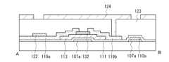
(実施の形態1)
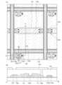
図1(A)は、本実施の形態に係る半導体装置の一例を示す上面図であり、図1(B)は
、図1(A)A-Bの断面図である。(Embodiment 1)
FIG. 1A is a top view showing an example of a semiconductor device according to this embodiment, and FIG. 1B is a cross-sectional view taken along line AB in FIG. 1A.
図1(A)に示すように、素子基板は、1の方向に配置されたゲート配線及び保持容量線
と、ゲート配線及び保持容量線と交差する2の方向に配置されたソース配線と、ゲート配
線とソース配線の交差部付近のトランジスタを有する画素部を含む。As shown in FIG. 1A, the element substrate includes gate wirings and storage capacitor lines arranged in one direction, source wirings arranged in two directions intersecting the gate wirings and the storage capacitor lines, and gate wirings. It includes a pixel portion having a transistor near the intersection of the wiring and the source wiring.
画素の開口率を向上させるために、本実施の形態に係るトランジスタは、ゲート電極とし
て機能する透光性を有する導電層と、該透光性を有する導電層上に形成されるゲート絶縁
膜と、ゲート電極として機能する透光性を有する導電層上にゲート絶縁膜を介して半導体
層と、半導体層に電気的に接続されたソース電極又はドレイン電極として機能する透光性
を有する導電層とで構成されている。In order to improve the aperture ratio of the pixel, the transistor according to this embodiment includes a light-transmitting conductive layer functioning as a gate electrode and a gate insulating film formed over the light-transmitting conductive layer. a semiconductor layer over a light-transmitting conductive layer that functions as a gate electrode with a gate insulating film interposed therebetween; and a light-transmitting conductive layer that functions as a source or drain electrode and is electrically connected to the semiconductor layer. consists of
このように、トランジスタの半導体層及び電極を、透光性を有する物質で形成することに
より、画素の開口率を向上させることができる。しかし、ゲート電極と電気的に接続され
るゲート配線と、ソース電極又はドレイン電極と電気的に接続されるソース配線とを、透
光性を有する物質で形成すると配線抵抗が高くなってしまい、消費電力も高くなってしま
う。そこで、ゲート配線及びソース配線を、透光性を有する導電層と遮光性を有する導電
層との順で積層構造で形成する。なお、トランジスタは、トップゲート型、ボトムゲート
型のいずれを用いてもよい。By forming the semiconductor layer and the electrode of the transistor using a light-transmitting substance in this manner, the aperture ratio of the pixel can be improved. However, if the gate wiring that is electrically connected to the gate electrode and the source wiring that is electrically connected to the source electrode or the drain electrode are formed of a light-transmitting material, the wiring resistance increases, resulting in increased power consumption. Electricity will also be higher. Therefore, the gate wiring and the source wiring are formed to have a layered structure in which a light-transmitting conductive layer and a light-blocking conductive layer are stacked in this order. Note that either a top-gate transistor or a bottom-gate transistor may be used.
トランジスタのゲート電極と電気的に接続されるゲート配線は、透光性を有する導電層1
07aと、遮光性を有する導電層110aとの順で積層されており、トランジスタのソー
ス電極又はドレイン電極と電気的に接続されるソース配線は、透光性を有する導電層11
9aと遮光性を有する導電層122との順で積層されている。つまり、トランジスタのゲ
ート電極は、ゲート配線を構成する透光性を有する導電層107aの一部で形成されてお
り、ソース電極又はドレイン電極は、ソース配線を構成する透光性を有する導電層119
aの一部で構成されている。A gate wiring electrically connected to a gate electrode of a transistor is formed by a light-transmitting
07a and a light-blocking
9a and a light shielding
It consists of a part of a.
ゲート配線及びソース配線を、透光性を有する導電層と遮光性を有する導電層との順で積
層することにより、配線抵抗を低減し、消費電力を低減することができる。また、ゲート
配線及びソース配線は、遮光性を有する導電層を用いて構成されているため、画素間を遮
光することができる。つまり、行方向に配置されたゲート配線と、列方向に配置されたソ
ース配線とによって、ブラックマトリクスを用いることなく画素間の隙間を遮光すること
ができる。By stacking a light-transmitting conductive layer and a light-blocking conductive layer in this order for the gate wiring and the source wiring, wiring resistance and power consumption can be reduced. In addition, since the gate wiring and the source wiring are formed using a light-shielding conductive layer, light can be shielded between pixels. That is, the gate wirings arranged in the row direction and the source wirings arranged in the column direction can shield the gaps between the pixels from light without using a black matrix.
ゲート配線上にトランジスタを作製する場合、トランジスタの大きさは、トランジスタの
ゲート配線幅に依存するが、本実施の形態では、画素内にトランジスタを形成するため、
トランジスタを大きく形成することができる。図17に示すように、ゲート配線幅よりも
大きいトランジスタを作製することができる。トランジスタを大きくすることにより、そ
の電流能力を十分上げることができ、画素への信号書き込み時間を短縮することができる
。よって、高精細な表示装置を提供することができる。When a transistor is formed over a gate wiring, the size of the transistor depends on the width of the gate wiring of the transistor.
A large transistor can be formed. As shown in FIG. 17, a transistor having a width larger than the gate wiring width can be manufactured. By enlarging the transistor, its current capability can be sufficiently increased, and the time required to write a signal to the pixel can be shortened. Therefore, a high-definition display device can be provided.
また、ゲート配線と同じ1の方向に配置された保持容量線もゲート配線と同様に、透光性
を有する導電層と遮光性を有する導電層との順で積層されている。保持容量線には保持容
量部が形成されている。保持容量部は、ゲート絶縁膜として機能する絶縁膜を誘電体とし
て、下部電極として機能する透光性を有する導電層と、上部電極として機能する透光性を
有する導電層とで構成されている。Similarly to the gate wiring, the storage capacitor line arranged in the same direction as the gate wiring also has a light-transmitting conductive layer and a light-shielding conductive layer laminated in this order. A storage capacitor portion is formed in the storage capacitor line. The storage capacitor section is composed of an insulating film functioning as a gate insulating film as a dielectric, a light-transmitting conductive layer functioning as a lower electrode, and a light-transmitting conductive layer functioning as an upper electrode. .
このようにして、保持容量部を、透光性を有する導電層で構成することにより、開口率を
向上させることができる。また、保持容量部を、透光性を有する導電層で構成することに
より、保持容量部を大きくすることもできるため、トランジスタがオフになったときでも
、画素電極の電位が保持されやすくなる。また、フィードスルー電位を小さくすることが
できる。In this manner, by forming the storage capacitor portion with the light-transmitting conductive layer, the aperture ratio can be improved. In addition, since the storage capacitor portion can be made large by forming the storage capacitor portion using a light-transmitting conductive layer, the potential of the pixel electrode can be easily held even when the transistor is turned off. Also, the feedthrough potential can be reduced.
また、図1に示す画素構造を有する素子基板を形成するために必要なマスク数を5枚とす
ることができる。すなわち、1枚目は、ゲート配線及び容量配線を形成するマスク、2枚
目は、半導体層113を形成するマスク、3枚目は、ソース配線及び保持容量部の上部電
極を形成するマスク、4枚目は、ソース配線と保持容量部の上部電極とにそれぞれ達する
コンタクトホールを形成するマスク、5枚目は、画素電極124を形成するマスクである
。Further, the number of masks necessary for forming the element substrate having the pixel structure shown in FIG. 1 can be reduced to five. That is, the first mask is for forming the gate wiring and the capacitor wiring, the second mask is for forming the
以上のように、図1に示す画素構造とした場合、少ないマスク数で開口率の高い表示装置
を実現することができる。As described above, when the pixel structure shown in FIG. 1 is used, a display device with a high aperture ratio can be realized with a small number of masks.
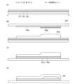
次に、図2乃至図9において、断面図を用いて本実施の形態に係る半導体装置の製造プロ
セスの一例を示す。図2乃至図9において、多階調マスクを用いた場合について説明する
が、これに限定されない。なお、図2、図4、図6及び図8は、図1のA-C断面であり
、図3、図5、図7、図9は、図1のD-E断面である。図2は図3と、図4は図5と、
図6は図7と、図8は図9とそれぞれ対応している。なお、図2、図4、図6には、ソー
ス配線部301、トランジスタ部302、ゲート配線部303、保持容量部304を示し
ており、図3、図5、図7には、トランジスタ部302、ゲート配線部303を示してい
る。Next, an example of the manufacturing process of the semiconductor device according to the present embodiment is shown using cross-sectional views in FIGS. Although the case of using a multi-tone mask will be described with reference to FIGS. 2 to 9, the present invention is not limited to this. 2, 4, 6 and 8 are cross sections taken along line AC of FIG. 1, and FIGS. 3, 5, 7 and 9 are cross sections taken along line DE of FIG. 2 is shown in FIG. 3, FIG. 4 is shown in FIG.
6 corresponds to FIG. 7, and FIG. 8 corresponds to FIG. 9, respectively. 2, 4, and 6 show the source wiring portion 301, the transistor portion 302, the gate wiring portion 303, and the storage capacitor portion 304, and FIGS. 3, 5, and 7 show the transistor portion 302. , the gate wiring portion 303 is shown.
まず、図2(A)及び図3(A)に示すように、基板101上に、導電膜102と導電膜
103をスパッタリング法により積層形成する。この工程は連続的に行われ、マルチチャ
ンバーを用いて連続スパッタリングを行うことも可能である。連続的に、導電膜102と
導電膜103とを成膜することにより、スループットが向上し、不純物やゴミの混入を抑
制することができる。First, as shown in FIGS. 2A and 3A, a
基板101は、光透過率の高い材質であることが望ましい。例えば、ガラス基板、プラス
チック基板、アクリル基板、セラミック基板などを用いることができる。The
導電膜102の光透過率は、十分に高いことが望ましい。また、導電膜102の光透過率
は、導電膜103の光透過率よりも高いことが望ましい。It is desirable that the light transmittance of the
導電膜102は、インジウム錫酸化物(ITO)、インジウム錫酸化物と酸化珪素を含む
ITSO、有機インジウム、有機スズ、酸化亜鉛、窒化チタン等を用いることができる。
また、酸化亜鉛(ZnO)を含むインジウム亜鉛酸化物(IZO(indium zin
c oxide))、酸化亜鉛(ZnO)、ZnOにガリウム(Ga)をドープしたもの
、酸化スズ(SnO2)、酸化タングステンを含むインジウム酸化物、酸化タングステン
を含むインジウム亜鉛酸化物、酸化チタンを含むインジウム酸化物、酸化チタンを含むイ
ンジウム錫酸化物なども用いてもよい。これらの材料をスパッタリング法により、単層構
造又は積層構造で形成することができる。ただし、積層構造とする場合には、複数の膜の
全ての光透過率が十分に高いことが望ましい。For the
Also, indium zinc oxide (IZO (indium zinc oxide) containing zinc oxide (ZnO)
co oxide)), zinc oxide (ZnO), ZnO doped with gallium (Ga), tin oxide (SnO2 ), indium oxide including tungsten oxide, indium zinc oxide including tungsten oxide, titanium oxide Indium oxide, indium tin oxide containing titanium oxide, and the like may also be used. These materials can be formed in a single-layer structure or a laminated structure by a sputtering method. However, in the case of a laminated structure, it is desirable that the light transmittance of all the films is sufficiently high.
導電膜103の抵抗率は十分に低く、導電率は十分に高いことが望ましい。また、導電膜
102の抵抗率は、導電膜103の抵抗率よりも低いことが望ましい。ただし、導電膜1
02は、導電層として機能するため、導電膜102の抵抗率は、絶縁層の抵抗率よりも低
いことが望ましい。It is desirable that the
02 functions as a conductive layer, the resistivity of the
導電膜103は、モリブデン、チタン、クロム、タンタル、タングステン、アルミニウム
、銅、ネオジム、スカンジウム等の金属材料又はこれらを主成分とする合金材料を用いて
、スパッタリング法又は真空蒸着法により、単層構造又は積層構造で形成することができ
る。また、導電膜103が積層構造で形成する場合には、複数の膜に透光性を有する導電
膜が含まれていても良い。The
なお、導電膜102の上に、導電膜103を形成した場合、両者の膜が反応を起こしてし
まう場合がある。例えば、導電膜102の上側の面(導電膜103と接する面)がITO
の場合において、導電膜103の下側の面(導電膜102と接する面)がアルミニウムの
場合、化学反応が起きてしまう。したがって、それを避けるために、導電膜103の下側
の面(導電膜102と接する面)には、高融点材料を用いることが望ましい。例えば、高
融点材料の例としては、モリブデン(Mo)、チタン(Ti)、タングステン(W)、ネ
オジム(Nd)などがあげられる。そして、高融点材料を用いた膜の上に、導電率の高い
材料を用いて、導電膜103を多層膜とすることは、好適である。導電率の高い材料とし
ては、アルミニウム(Al)、銅(Cu)、銀(Ag)などがあげられる。例えば、導電
膜103を積層構造で形成する場合には、1層目をモリブデン(Mo)、2層目をアルミ
ニウム(Al)、3層目をモリブデン(Mo)の積層、若しくは、1層目をモリブデン(
Mo)、2層目にネオジム(Nd)を微量に含むアルミニウム(Al)、3層目をモリブ
デン(Mo)の積層で形成することができる。Note that when the
In the case of , if the lower surface of the conductive film 103 (the surface in contact with the conductive film 102) is made of aluminum, a chemical reaction occurs. Therefore, in order to avoid this, it is desirable to use a high melting point material for the lower surface of the conductive film 103 (the surface in contact with the conductive film 102). For example, examples of refractory materials include molybdenum (Mo), titanium (Ti), tungsten (W), neodymium (Nd), and the like. It is preferable to form the
Mo), aluminum (Al) containing a small amount of neodymium (Nd) as the second layer, and molybdenum (Mo) as the third layer.
本実施の形態の構成において導電膜102は、導電膜103の下層に形成されているため
、市販されているITO(インジウム錫酸化物)付きガラスを用いて導電膜103のみを
スパッタリング法により形成することも可能である。In the structure of this embodiment mode, since the
なお、図示しないが、基板101と導電膜102との間に下地膜として、酸化珪素、窒化
珪素、酸化窒化珪素などを形成することもできる。基板101と透光性を有する導電膜と
の間に下地膜を形成することによって、基板101から素子へ可動イオンや不純物等が拡
散することを抑制し、素子の特性劣化を防止することができる。Note that although not shown, a base film of silicon oxide, silicon nitride, silicon oxynitride, or the like can be formed between the
次に、図2(B)及び図3(B)に示すように、導電膜103上にレジストマスク106
a、106bを形成する。レジストマスク106a、106bは、多階調マスクを用いる
ことにより、厚さの異なる領域を有するレジストマスクを形成することができる。多階調
マスクを用いることで、使用するフォトマスクの枚数が低減され、作製工程が減少するた
め好ましい。本実施の形態において、導電膜102及び導電膜103のパターンを形成す
る工程と、ゲート電極として機能する透光性を有する導電層を形成する工程において、多
階調マスクを用いることができる。Next, as shown in FIGS. 2B and 3B, a resist mask 106 is formed on the
a, 106b. By using a multi-tone mask for the resist
多階調マスクとは、多段階の光量で露光を行うことが可能なマスクであり、代表的には、
露光領域、半露光領域及び未露光領域の3段階の光量で露光を行う。多階調マスクを用い
ることで、一度の露光及び現像工程によって、複数(代表的には二種類)の厚さを有する
レジストマスクを形成することができる。そのため、多階調マスクを用いることで、フォ
トマスクの枚数を削減することができる。A multi-tone mask is a mask that can be exposed with multiple levels of light intensity.
Exposure is performed with three levels of light intensity, an exposed area, a semi-exposed area, and an unexposed area. By using a multi-tone mask, a resist mask having a plurality of (typically two) thicknesses can be formed through one exposure and development process. Therefore, by using a multi-tone mask, the number of photomasks can be reduced.
図13(A-1)及び図13(B-1)は、代表的な多階調マスクの断面を示す。図13
(A-1)には、グレートーンマスク180を示し、図13(B-1)にはハーフトーン
マスク185を示す。FIGS. 13A-1 and 13B-1 show cross sections of typical multi-tone masks. Figure 13
(A-1) shows a gray-
図13(A-1)に示すグレートーンマスク180は、透光性を有する基板181に遮光
層により形成された遮光部182、及び遮光層のパターンにより設けられた回折格子部1
83で構成されている。A gray-
83.
回折格子部183は、露光に用いる光の解像度限界以下の間隔で設けられたスリット、ド
ット又はメッシュ等を有することで、光の透過量を制御する。なお、回折格子部183に
設けられるスリット、ドット又はメッシュは周期的なものであってもよいし、非周期的な
ものであってもよい。The
透光性を有する基板181としては、石英等を用いることができる。遮光部182及び回
折格子部183を構成する遮光層は、金属膜を用いて形成すればよく、好ましくはクロム
又は酸化クロム等により設けられる。Quartz or the like can be used as the light-transmitting
グレートーンマスク180に露光するための光を照射した場合、図13(A-2)に示す
ように、遮光部182に重畳する領域における透光率は0%となり、遮光部182又は回
折格子部183が設けられていない領域における透光率は100%となる。また、回折格
子部183における透光率は、概ね10%~70%の範囲であり、回折格子のスリット、
ドット又はメッシュの間隔等により調節可能である。When the gray-
It can be adjusted by a dot or mesh interval or the like.
図13(B-1)に示すハーフトーンマスク185は、透光性を有する基板181上に半
透光層により形成された半透光部187及び遮光層により形成された遮光部188で構成
されている。A
半透光部187は、MoSiN、MoSi、MoSiO、MoSiON、CrSi等の層
を用いて形成することができる。遮光部188は、グレートーンマスクの遮光層と同様の
金属膜を用いて形成すればよく、好ましくはクロム又は酸化クロム等により設けられる。The
ハーフトーンマスク185に露光するための光を照射した場合、図13(B-2)に示す
ように、遮光部188に重畳する領域における透光率は0%となり、遮光部188又は半
透光部187が設けられていない領域における透光率は100%となる。また、半透光部
187における透光率は、概ね10%~70%の範囲であり、形成する材料の種類又は形
成する膜厚等により調整可能である。When the
多階調マスクを用いて露光して現像を行うことで、膜厚の異なる領域を有するレジストマ
スクを形成することができる。また、膜厚の異なるレジストマスクを形成することができ
る。By performing exposure and development using the multi-tone mask, a resist mask having regions with different thicknesses can be formed. In addition, resist masks with different thicknesses can be formed.
図2(B)及び図3(B)に示すように、ハーフトーンマスクは、光を透過する基板10
4上に半透過層105a、105c及び遮光層105bで構成されている。したがって、
導電膜103上には、後に保持容量部の下部電極及びゲート電極となる箇所には、レジス
トマスク106aの膜厚が薄い領域、薄いレジストマスク106b、後にゲート配線とな
る箇所にはレジストマスク106aの膜厚が厚い領域が形成される。As shown in FIGS. 2B and 3B, the halftone mask is a substrate 10 that transmits light.
4,
On the
次に、図2(C)及び図3(C)に示すように、レジストマスク106a、106bを用
いて導電膜102及び導電膜103にエッチングを行う。エッチングを行うことにより、
導電層107a、導電層108a、導電層107b、導電層108bを形成することがで
きる。Next, as shown in FIGS. 2C and 3C, the
A
次に、図2(D)及び図3(D)に示すように、レジストマスク106a、106bに対
して、酸素プラズマによるアッシングを行う。レジストマスク106a、106bに対し
て酸素プラズマによるアッシングを行うことにより、レジストマスク106aの膜厚が薄
い領域は除去され、その下の遮光性を有する導電層が露出する。また、レジストマスク1
06aの膜厚が厚い領域は縮小し、レジストマスク109として残存する。このように多
階調マスクで形成したレジストマスクを用いることで、追加のレジストマスクを用いるこ
とがなくなるので、工程を簡略化することができる。Next, as shown in FIGS. 2D and 3D, the resist
A thick region of 06 a is reduced and remains as a resist
次に、レジストマスク109を用いて、遮光性を有する導電層108aに対してエッチン
グを行う。その結果、導電層108aの一部は除去され、導電層107aが露出する。ま
た、導電層108aは、レジストマスク109が形成されている部分を残して除去される
。これは、レジストマスク106aがアッシング処理により縮小し、導電層108aの一
部が露出されるためである。従って、レジストマスク109からはみ出した導電層108
aの一部も同時にエッチングされる。これにより、導電層108aと導電層107aとは
、それぞれの層が有する面積が大きく異なってくる。つまり、導電層107aが有する面
積は、導電層108aが有する面積よりも大きい。または、導電層108aと導電層10
7aとは、導電層108aと導電層107aとが重なった領域と、導電層108aと導電
層107aとが重なっていない領域とを有する。Next, using the resist
A part of a is also etched at the same time. Accordingly, the areas of the
7a has a region where the
遮光性を有する導電層を除去する際に、透光性を有する導電層も一部(例えば、遮光性を
有する導電層と接していた表面部分など)が除去される場合がある。透光性を有する導電
層が、どの程度除去されるのかは、透光性を有する導電層と遮光性を有する導電層とのエ
ッチングの選択比によって決まる。そのため、例えば、導電層110aで覆われている領
域の導電層107aの膜厚は、導電層110aで覆われていない領域の導電層107aの
膜厚よりも、厚くなる場合が多い。When the light-shielding conductive layer is removed, part of the light-transmitting conductive layer (for example, a surface portion in contact with the light-shielding conductive layer) may be removed. How much of the light-transmitting conductive layer is removed depends on the etching selectivity between the light-transmitting conductive layer and the light-blocking conductive layer. Therefore, for example, the
透光性を有する導電層を残し、遮光性を有する導電層のみをウェットエッチングで除去す
る場合には、透光性を有する導電層と遮光性を有する導電層とで選択比の高いエッチング
溶液を使用する。遮光性を有する導電層として、1層目をモリブデン(Mo)、2層目を
アルミニウム(Al)、3層目をモリブデン(Mo)の積層、若しくは、1層目をモリブ
デン(Mo)、2層目にネオジム(Nd)を微量に含むアルミニウム(Al)、3層目を
モリブデン(Mo)の積層などを用いる場合には、例えばリン酸、硝酸、酢酸及び水から
成る混酸によって行うこともできる。この混酸を用いることにより、均一に良好な順テー
パー形状を与えることもできる。このようにウェットエッチングは、テーパー形状による
被覆性向上に加え、エッチング液によるエッチング、純水によるリンス、乾燥という簡単
な工程でありながらもスループットが高いので、上記遮光性を有する導電層のエッチング
に用いることが適している。In the case of removing only the light-shielding conductive layer by wet etching while leaving the light-transmitting conductive layer, an etching solution having a high selectivity between the light-transmitting conductive layer and the light-shielding conductive layer is used. use. As the light-shielding conductive layer, the first layer is molybdenum (Mo), the second layer is aluminum (Al), and the third layer is molybdenum (Mo), or the first layer is molybdenum (Mo) and two layers. When aluminum (Al) containing a small amount of neodymium (Nd) is used for the eyes and molybdenum (Mo) is used for the third layer, a mixed acid consisting of phosphoric acid, nitric acid, acetic acid, and water, for example, can be used. By using this mixed acid, it is possible to give a uniformly good forward tapered shape. In this way, wet etching is a simple process of etching with an etchant, rinsing with pure water, and drying, in addition to improving the coverage due to the tapered shape, but has a high throughput. suitable for use.
次に、図4(A)及び図5(A)に示すように、レジストマスク109を除去する。Next, as shown in FIGS. 4A and 5A, the resist
導電層110aおよび導電層107aは、主に、その一部の領域(主に導電層110aの
領域)が、ゲート配線、またはゲート配線の一部として機能し、別の一部の領域(主に導
電層107aのみがある領域)が、トランジスタのゲート電極、またはゲート電極の一部
として機能することが可能である。より好ましくは、導電層110aと導電層107aと
が重なっている領域では、導電率の高い導電層110aを有している場合があるので、ゲ
ート配線またはゲート配線の一部として機能することが望ましい。または、より好ましく
は、導電層110aが配置されていない領域における導電層107aは、光を透過させる
ことができる場合があるので、トランジスタのゲート電極、またはゲート電極の一部とし
て機能することが望ましい。
したがって、導電層110aおよび導電層107aにおいては、ゲート電極としての機能
を有する配線が、ゲート配線として機能する配線(または、ゲート配線として機能する配
線のうちの少なくとも一つの層)と、接続されている、と考えることもできる。あるいは
、導電層110aおよび導電層107aにおいては、ゲート配線が有する少なくとも一つ
の層が、ゲート配線が有する別の層よりも、面積が大きい状態で形成され、面積が大きく
なっている領域の一部は、ゲート電極として機能する、と考えることができる。または、
導電層110aおよび導電層107aにおいては、導電層107aが、導電層110aよ
りも、面積が大きい状態で形成され、面積が大きくなっている領域の一部は、ゲート電極
として機能する、と考えることができる。すなわち、ゲート配線の一部が、ゲート電極ま
たはゲート電極の一部として機能する、と考えることができる。または、ゲート電極また
はゲート電極の一部として主に機能する導電層である導電層107aの上に、ゲート配線
またはゲート配線の一部として主に機能する導電層である導電層110aが設けられてい
る、ということもできる。Therefore, in
In the
同様に、遮光性を有する導電層および導電層107bは、主に、その一部の領域(主に導
電層110bの領域)が、容量配線、または容量配線の一部として機能し、別の一部の領
域(主に導電層107bのみがある領域)が、容量素子の電極、または容量素子の電極の
一部として機能することが可能である。より好ましくは、遮光性を有する導電層と導電層
107bとが重なっている領域では、導電率の高い遮光性を有する導電層を有している場
合があるので、容量配線または容量配線の一部として機能することが望ましい。または、
より好ましくは、遮光性を有する導電層が配置されていない領域における導電層107b
は、光を透過させることができる場合があるので、容量素子の電極、または容量素子の電
極の一部として機能することが望ましい。Similarly, the light-shielding conductive layer and the
More preferably, the
can transmit light in some cases, and thus preferably functions as an electrode of a capacitor or part of an electrode of a capacitor.
したがって、遮光性を有する導電層および導電層107bにおいては、容量素子の電極と
しての機能を有する配線が、容量素子として機能する配線(または、容量配線として機能
する配線のうちの少なくとも一つの層)と、接続されている、と考えることもできる。あ
るいは、遮光性を有する導電層および導電層107bにおいては、容量配線が有する少な
くとも一つの層が、容量配線が有する別の層よりも、面積が大きい状態で形成され、面積
が大きくなっている領域の一部は、容量素子の電極として機能する、と考えることができ
る。または、遮光性を有する導電層および導電層107bにおいては、導電層107bが
、遮光性を有する導電層よりも、面積が大きい状態で形成され、面積が大きくなっている
領域の一部は、容量素子の電極として機能する、と考えることができる。すなわち、容量
配線の一部が、容量素子の電極または容量素子の電極の一部として機能する、と考えるこ
とができる。または、容量素子の電極または容量素子の電極の一部として主に機能する導
電層である導電層107bの上に、容量配線または容量配線の一部として主に機能する導
電層である導電層110bが設けられている、ということもできる。Therefore, in the light-shielding conductive layer and the
次に、図4(B)及び図5(B)に示すように、透光性を有する導電層及び遮光性を有す
る導電層を覆い、ゲート絶縁膜として機能する絶縁膜111を成膜する。その後、絶縁膜
111の上に、半導体膜112を成膜する。Next, as shown in FIGS. 4B and 5B, an insulating
絶縁膜111は、単層構造で形成しても良いし、複数の膜を積層構造にしてもよい。複数
の膜を積層構造にする場合には、全ての膜において光透過率が十分に高いことが望ましい
。同様に、半導体膜112は、単層構造で形成しても良いし、複数の膜を積層構造にして
もよい。複数の膜を積層構造にする場合には、全ての膜において光透過率が十分に高いこ
とが望ましい。The insulating
透光性を有する導電層及び遮光性を有する導電層を覆う絶縁膜111は、膜厚50~50
0nm程度形成する。絶縁膜111は、スパッタリング法やプラズマCVD法等の各種C
VD法により、珪素の酸化物または珪素の窒化物を含む膜を、単層または積層して形成す
る。具体的には、酸化珪素を含む膜(SiOx)、酸化窒化珪素を含む膜(SiOxNy
)、窒化酸化珪素を含む膜(SiNxOy)を、単層構造として形成するか、当該これら
の膜を適宜積層して形成する。The insulating
It forms about 0 nm. The insulating
A film containing silicon oxide or silicon nitride is formed in a single layer or stacked by a VD method. Specifically, a film containing silicon oxide (SiOx ), a film containing silicon oxynitride (SiOx Ny
), a film containing silicon nitride oxide (SiNx Oy ) is formed as a single layer structure, or these films are formed by stacking them as appropriate.
透光性を有する導電層及び遮光性を有する導電層に酸素、窒素、または酸素及び窒素を含
む雰囲気中で、高密度プラズマ処理を行うことにより、透光性を有する導電層及び遮光性
を有する導電層の表面を酸化または窒化して、絶縁膜を形成してもよい。高密度プラズマ
処理により形成された絶縁膜は、膜厚や膜質などの均一性に優れ、且つ緻密な膜を形成す
ることができる。酸素を含む雰囲気としては、酸素(O2)、二酸化窒素(NO2)、も
しくは一酸化二窒素(N2O)と、希ガスとの混合ガス、または、酸素(O2)、二酸化
窒素(NO2)もしくは一酸化二窒素(N2O)と、希ガスと、水素(H2)との混合ガ
スを用いることができる。また、窒素を含む雰囲気としては、窒素(N2)もしくはアン
モニア(NH3)と、希ガスとの混合ガス、または、窒素(N2)もしくはアンモニア(
NH3)と、希ガスと、水素(H2)との混合ガスを用いることができる。高密度プラズ
マにより生成された酸素ラジカル(OHラジカルを含む場合もある)や窒素ラジカル(N
Hラジカルを含む場合もある)によって、透光性を有する導電層及び遮光性を有する導電
層の表面を酸化又は窒化することができる。A light-transmitting conductive layer and a light-shielding conductive layer are subjected to high-density plasma treatment in an atmosphere containing oxygen, nitrogen, or oxygen and nitrogen to form a light-transmitting conductive layer and a light-shielding conductive layer. An insulating film may be formed by oxidizing or nitriding the surface of the conductive layer. An insulating film formed by high-density plasma treatment has excellent uniformity in film thickness and film quality, and can form a dense film. The atmosphere containing oxygen includes a mixed gas of oxygen (O2 ), nitrogen dioxide (NO2 ), or dinitrogen monoxide (N2 O) and a rare gas, or oxygen (O2 ), nitrogen dioxide ( NO2 ) or dinitrogen monoxide (N2 O), a rare gas, and a mixed gas of hydrogen (H2 ) can be used. The atmosphere containing nitrogen includes a mixed gas of nitrogen (N2 ) or ammonia (NH3 ) and a rare gas, or nitrogen (N2 ) or ammonia (
NH3 ), a rare gas, and hydrogen (H2 ) can be used. Oxygen radicals (which may include OH radicals) and nitrogen radicals (N
The surface of the light-transmitting conductive layer and the light-blocking conductive layer can be oxidized or nitrided by the light-transmitting conductive layer and the light-blocking conductive layer.
高密度プラズマ処理を行って絶縁膜111を形成する場合、1~20nm、代表的には5
~10nmの絶縁膜が透光性を有する導電層及び遮光性を有する導電層を覆うように形成
される。この場合の反応は固相反応であるため、当該絶縁膜111と透光性を有する導電
層及び遮光性を有する導電層との界面準位密度をきわめて低くすることができる。また、
透光性を有する導電層及び遮光性を有する導電層を直接酸化または窒化するため、形成さ
れる絶縁膜111の厚さを、均一にすることができる。すなわち、ここで示す高密度プラ
ズマ処理で電極の表面を固相酸化することにより、均一性が良く、界面準位密度が低い絶
縁膜を形成することができる。ここでは、タンタル(Ta)、タングステン(W)、チタ
ン(Ti)、モリブデン(Mo)、クロム(Cr)、ニオブ(Nb)等から選択された元
素またはこれらの元素を主成分とする合金材料若しくは化合物材料の酸化物が絶縁膜11
1として機能する。When the insulating
An insulating film with a thickness of up to 10 nm is formed so as to cover the light-transmitting conductive layer and the light-blocking conductive layer. Since the reaction in this case is a solid-phase reaction, the interface state density between the insulating
Since the light-transmitting conductive layer and the light-blocking conductive layer are directly oxidized or nitrided, the formed insulating
function as 1.
絶縁膜111は、高密度プラズマ処理によって形成される絶縁膜のみを用いてもよいし、
それに加えてプラズマや熱反応を利用したCVD法により酸化珪素、酸素を含む窒化珪素
、窒素を含む酸化珪素などの絶縁膜を堆積し、少なくとも一つ積層させても良い。いずれ
にしても、高密度プラズマで形成した絶縁膜がゲート絶縁膜の一部又は全部であるトラン
ジスタは、特性のばらつきを小さくすることができる。For the insulating
In addition, at least one insulating film of silicon oxide, silicon nitride containing oxygen, silicon oxide containing nitrogen, or the like may be deposited by a CVD method using plasma or thermal reaction, and at least one insulating film may be stacked. In any case, variations in characteristics can be reduced in a transistor in which an insulating film formed by high-density plasma is part or wholly of a gate insulating film.
また、絶縁膜111は、酸化物半導体膜との整合性の良好なアルミナ(Al2O3)、窒
化アルミニウム(AlN)、酸化チタン(TiO2)、ジルコニア(ZrO2)、酸化リ
チウム(Li2O)、酸化カリウム(K2O)酸化ナトリウム(Na2O)、酸化インジ
ウム(In2O3)、酸化イットリウム(Y2O3)、ジルコン酸カルシウム(CaZr
O3)又はこれらのうち少なくとも2つを含む材料を用いてもよく、単層又は2層以上積
層させて形成してもよい。Further, the insulating
O3 ) or a material containing at least two of these may be used, and may be formed by laminating a single layer or two or more layers.
絶縁膜111は、透光性を有する材料または光透過率が高い材料を有していることが望ま
しいが、導電層107a、107b、又は半導体膜112も透光性を有する材料または光
透過率が高い材料を有していることが望ましい。したがって、両者の光透過率を比較する
と、絶縁膜111のほうが、導電層107a、導電層107b、または、半導体膜112
よりも、光透過率が高いまたは同程度であることが望ましい。なぜなら、絶縁膜111は
、大面積で形成する場合があるため、光利用効率を向上させるためには、光透過率が高い
ことが望ましいからである。The insulating
It is desirable that the light transmittance is higher than or the same as that of the material. This is because the insulating
絶縁膜111は、絶縁体として機能することが望ましいため、絶縁体として適した抵抗率
を有していることが望ましい。一方、導電層107a、107bは、導体として機能させ
ることが望ましく、半導体膜112は、半導体として機能させることが望ましい。そのた
め、絶縁膜111の抵抗率は、導電層107a、107b、導電層110a、110b、
または、半導体膜112の抵抗率よりも高いことが望ましい。絶縁膜111の抵抗率が高
い場合は、導体同士を電気的に絶縁させることができるため、漏れ電流などを低減するこ
とができ、回路をよりよく動作させることが可能となるため、好適である。Since the insulating
Alternatively, it is preferably higher than the resistivity of the
次に、絶縁膜111上に半導体膜112を形成する。透光性を有する材料または光透過率
が高い材料を有して形成されることが望ましい。半導体膜112は、酸化物半導体を用い
て形成することができる。酸化物半導体として、1族元素(例えば、リチウム(Li)、
ナトリウム(Na)、カリウム(K)、ルビジウム(Rb)、セシウム(Cs))、13
族元素(例えば、ボロン(B)、ガリウム(Ga)、インジウム(In)、タリウム(T
l))、14族元素(例えば、炭素(C)、シリコン(Si)、ゲルマニウム(Ge)、
スズ(Sn)、鉛(Pb))、15族元素(例えば、窒素(N)、リン(P)、ヒ素(A
s)、アンチモン(Sb)、ビスマス(Bi))又は17族元素(例えば、フッ素(F)
、塩素(Cl)、臭素(Br)、ヨウ素(I))等の不純物元素のうち一種、又は複数種
が添加された酸化亜鉛(ZnO)の非晶質(アモルファス)状態、多結晶状態又は非晶質
状態と多結晶状態が混在する微結晶(マイクロクリスタルとも呼ばれる。)状態のもの、
又は何も不純物元素が添加されていないものを用いることができる。また、InGaO3
(ZnO)5、酸化マグネシウム亜鉛(MgxZn1-xO)又は酸化カドミウム亜鉛(
CdxZn1-xO)、酸化カドミウム(CdO)、In-Ga-Zn-O系のアモルフ
ァス酸化物半導体(a-IGZO)のうちいずれかを用いることができる。半導体膜11
2は25~200nm(好ましくは30~150nm)の厚さで0.4Paの圧力のもと
、Ar:O2=50:5sccmの流量となる条件でスパッタリング法により成膜し、そ
の後、0.05%に希釈したフッ酸を用いてエッチングにより所望の形状に形成する。半
導体膜112は、非晶質珪素膜を用いた半導体膜と比べて、酸化のおそれがなく高真空に
せずとも成膜できるため、プロセスとして安価である。なお、酸化亜鉛を有する酸化物半
導体膜はプラズマに強いため、プラズマCVD(PCVD又はPECVDともいう)法を
用いて成膜してもよい。プラズマCVD法はCVD法の中でも特に装置が簡単であり、生
産性もよい。Next, a
sodium (Na), potassium (K), rubidium (Rb), cesium (Cs)), 13
Group elements (e.g., boron (B), gallium (Ga), indium (In), thallium (T
l)), group 14 elements (e.g. carbon (C), silicon (Si), germanium (Ge),
tin (Sn), lead (Pb)), Group 15 elements (e.g., nitrogen (N), phosphorus (P), arsenic (A
s), antimony (Sb), bismuth (Bi)) or group 17 elements (e.g. fluorine (F)
, chlorine (Cl), bromine (Br), iodine (I)), one or more of the impurity elements such as zinc oxide (ZnO) in an amorphous state, polycrystalline state or non-crystalline state. Those in a microcrystalline (also called microcrystal) state in which a crystalline state and a polycrystalline state are mixed,
Alternatively, a material to which no impurity element is added can be used.InGaO3
(ZnO)5 , magnesium zinc oxide (Mgx Zn1-x O) or cadmium zinc oxide (
Cdx Zn1-x O), cadmium oxide (CdO), or an In—Ga—Zn—O-based amorphous oxide semiconductor (a-IGZO) can be used. semiconductor film 11
2 is formed by a sputtering method to a thickness of 25 to 200 nm (preferably 30 to 150 nm) under a pressure of 0.4 Pa and a flow rate of Ar:O2 =50:5 sccm. A desired shape is formed by etching using hydrofluoric acid diluted to 05%. The
また、上記酸化物半導体には、窒素が添加されていても良い。窒素を添加することにより
、酸化物半導体がn型の半導体の性質を示す場合、窒素がアクセプタ不純物として働く。
このため、窒素が添加された酸化物半導体膜を用いて作製されたトランジスタのしきい値
電圧を制御することができる。酸化物半導体にZnOを用いる場合、窒素を添加(ドープ
)しておくとよい。ZnOは本来n型の半導体の性質を示す。窒素を添加することで窒素
がZnOに対してアクセプタ不純物として働くため、結果としてしきい値電圧を制御する
ことができる。酸化物半導体膜は特に何をせずともn型を示す場合、チャネルが形成され
る酸化物半導体膜の部分に、p型の導電性を付与する不純物を添加し、極力I型(真性半
導体)に近づくようにその導電型を制御しておいてもよい。Nitrogen may be added to the oxide semiconductor. By adding nitrogen, nitrogen acts as an acceptor impurity when the oxide semiconductor exhibits n-type semiconductor properties.
Therefore, the threshold voltage of a transistor manufactured using an oxide semiconductor film to which nitrogen is added can be controlled. When ZnO is used for the oxide semiconductor, nitrogen is preferably added (doped). ZnO inherently exhibits the properties of an n-type semiconductor. By adding nitrogen, nitrogen acts as an acceptor impurity for ZnO, and as a result, the threshold voltage can be controlled. When the oxide semiconductor film exhibits n-type conductivity without doing anything in particular, an impurity imparting p-type conductivity is added to a portion of the oxide semiconductor film where a channel is formed, so that the oxide semiconductor film exhibits i-type (intrinsic) conductivity as much as possible. You may control the conductivity type so that it may approach.
半導体膜112に対して熱処理を行ってもよい。半導体膜112に対して熱処理を行うこ
とにより、半導体膜112の結晶性を高めることができる。半導体膜112の結晶化は、
少なくともトランジスタのチャネル形成領域において行われていればよい。トランジスタ
のチャネル形成領域において結晶性を高めることにより、トランジスタの特性を向上させ
ることができる。Heat treatment may be performed on the
It suffices if it is performed at least in the channel formation region of the transistor. By increasing the crystallinity of the channel formation region of the transistor, the characteristics of the transistor can be improved.
ここでの熱処理には、RTA(Rapid Thermal Anneal)装置、ハロ
ゲンランプ若しくはランプで加熱するLRTA(Lamp Rapid Thermal
Anneal)装置を用いることができる。LRTA装置では、赤外光領域、可視光領
域、紫外光領域等の波長の光を用いることができる。例えば、LRTA装置を用いる場合
、250~570℃(好ましくは300℃~400℃、より好ましくは300~350℃
)で1分~1時間、好ましくは10分~30分行うとよい。LRTAは、ハロゲンランプ
、メタルハライドランプ、キセノンアークランプ、カーボンアークランプ、高圧ナトリウ
ムランプ、高圧水銀ランプから選ばれた一種または複数種からの輻射により行う。The heat treatment here includes an RTA (Rapid Thermal Anneal) device, a halogen lamp, or an LRTA (Lamp Rapid Thermal) that heats with a lamp.
Anneal) device can be used. The LRTA device can use light with wavelengths in the infrared light region, the visible light region, the ultraviolet light region, and the like. For example, when using an LRTA apparatus, the
) for 1 minute to 1 hour, preferably 10 minutes to 30 minutes. LRTA is performed by radiation from one or more selected from halogen lamps, metal halide lamps, xenon arc lamps, carbon arc lamps, high pressure sodium lamps, and high pressure mercury lamps.
また、LRTAの代わりにレーザ光を照射して加熱処理を行ってもよく、例えば、レーザ
光として赤外光レーザ、可視光レーザ、紫外光レーザ等を用いることができる。また、L
RTA及びレーザ光照射を組み合わせて選択的に酸化物半導体膜の結晶性を改善してもよ
い。レーザ照射を用いる場合、連続発振型のレーザビーム(CWレーザビーム)やパルス
発振型のレーザビーム(パルスレーザビーム)を用いることができる。ここで用いること
ができるレーザビームは、Arレーザ、Krレーザ、エキシマレーザなどの気体レーザ、
単結晶のYAG、YVO4、フォルステライト(Mg2SiO4)、YAlO3、GdV
O4、若しくは多結晶(セラミック)のYAG、Y2O3、YVO4、YAlO3、Gd
VO4に、ドーパントとしてNd、Yb、Cr、Ti、Ho、Er、Tm、Taのうち1
種または複数種添加されているものを媒質とするレーザ、ガラスレーザ、ルビーレーザ、
アレキサンドライトレーザ、Ti:サファイアレーザ、銅蒸気レーザまたは金蒸気レーザ
のうち一種または複数種から発振されるものを用いることができる。このようなレーザビ
ームの基本波、及びこれらの基本波の第2高調波から第4高調波のレーザビームを照射す
ることで、結晶性を良好にすることができる。なお、レーザ光は酸化物半導体膜のバンド
ギャップよりもエネルギーの大きいものを用いる方が好ましい。例えば、KrF、ArF
、XeCl、又はXeFのエキシマレーザ発振器から射出されるレーザ光を用いてもよい
。Further, heat treatment may be performed by irradiating laser light instead of LRTA, and for example, an infrared light laser, a visible light laser, an ultraviolet light laser, or the like can be used as the laser light. Also, L
The crystallinity of the oxide semiconductor film may be selectively improved by combining RTA and laser light irradiation. When laser irradiation is used, a continuous wave laser beam (CW laser beam) or a pulsed wave laser beam (pulsed laser beam) can be used. Laser beams that can be used here include gas lasers such as Ar lasers, Kr lasers, excimer lasers,
Single crystal YAG,YVO4 , Forsterite (Mg2SiO4 ),YAlO3 , GdV
O4 , or polycrystalline (ceramic) YAG,Y2O3 ,YVO4 ,YAlO3 ,Gd
VO4 contains one of Nd, Yb, Cr, Ti, Ho, Er, Tm, Ta as a dopant
laser, glass laser, ruby laser,
One or more of an alexandrite laser, a Ti: sapphire laser, a copper vapor laser, or a gold vapor laser can be used. Crystallinity can be improved by irradiation with the fundamental wave of such a laser beam and the second to fourth harmonics of the fundamental wave. Note that laser light having energy higher than the bandgap of the oxide semiconductor film is preferably used. For example, KrF, ArF
, XeCl, or XeF excimer laser oscillators may be used.
半導体膜112は、透光性を有する材料または光透過率が高い材料を有していることが望
ましいが、導電層107a、107bも透光性を有する材料または光透過率が高い材料を
有していることが望ましい。したがって、両者の光透過率を比較すると、半導体膜112
よりも、導電層107a、107bのほうが、光透過率が高いまたは同程度であることが
望ましい。なぜなら、導電層107a、107bは、大きな面積で形成する場合があるた
め、光利用効率を向上させるためには、光透過率が高いことが望ましいからである。The
It is preferable that the
半導体膜112は、透光性を有する材料または光透過率が高い材料を有していることが望
ましいが、これに限定されない。光透過率が小さくても、光を透過することが可能な材料
を有していても良い。例えば、シリコン(Si)、ゲルマニウム(Ge)を有して形成す
ることも可能である。さらに、結晶状態は、単結晶(モノクリスタル)状態、多結晶(ポ
リクリスタル)、非晶質(アモルファス)、微結晶(マイクロクリスタル、ナノクリスタ
ル、セミアモルファス)状態などから選ばれた少なくとも一つの結晶状態を有しているこ
とが望ましい。非晶質の場合、低い製造温度で形成でき、または、大型な半導体装置また
は表示装置を形成することができ、または、ガラスよりも融点の低い基板を用いて形成す
ることができる、などの利点を有しており、好適である。The
半導体膜112は、半導体として機能することが望ましいため、半導体として適した抵抗
率を有していることが望ましい。一方、導電層107a、107bは、導体として機能さ
せることが望ましい。そのため、半導体膜112の抵抗率は、導電層107a、107b
の抵抗率よりも高いことが望ましい。Since the
is desirably higher than the resistivity of
次に、図4(C)、図5(C)に示すように、半導体膜112上にフォトリソグラフィ法
を用いてレジストマスクを作製し(図示せず)、レジストマスクを用いてエッチングを行
い、所望の形状に加工された半導体層113(島状半導体層ともいう)を形成する。エッ
チングには、0.05%に希釈したフッ酸、塩酸等を用いることができる。Next, as shown in FIGS. 4C and 5C, a resist mask (not shown) is formed over the
半導体層113は、トランジスタの半導体層(活性層)またはトランジスタの半導体層(
活性層)の一部として機能させることが可能である。または、半導体層113は、MOS
容量またはMOS容量の一部として機能させることが可能である。または、半導体層11
3は、配線と配線との交差部における寄生容量を小さくするための膜として機能させるこ
とが可能である。なお、図示しないが、半導体層113上にソース領域及びドレイン領域
を形成する、一導電型を付与する不純物元素を含む半導体層を形成してもよい。The
active layer). Alternatively, the
It can function as part of a capacitor or a MOS capacitor. Alternatively, the semiconductor layer 11
3 can function as a film for reducing parasitic capacitance at intersections between wirings. Although not illustrated, a semiconductor layer containing an impurity element imparting one conductivity type, which forms a source region and a drain region, may be formed over the
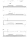
次に、図4(D)、図5(D)に示すように、半導体層113及び絶縁膜111を覆うよ
うに、導電膜114と導電膜115をスパッタリング法により積層形成する。この工程は
連続的に行われ、マルチチャンバーを用いて連続スパッタリングを行うことも可能である
。連続的に、導電膜114と導電膜115とを成膜することにより、スループットが向上
し、不純物やゴミの混入を抑制することができる。Next, as shown in FIGS. 4D and 5D, a
導電膜114の光透過率は、十分に高いことが望ましい。また、導電膜114の光透過率
は、導電膜115の光透過率よりも高いことが望ましい。It is desirable that the light transmittance of the
導電膜114は、インジウム錫酸化物(ITO)、インジウム錫酸化物と酸化珪素を含む
ITSO、有機インジウム、有機スズ、酸化亜鉛、窒化チタン等を用いることができる。
また、酸化亜鉛(ZnO)を含むインジウム亜鉛酸化物(IZO(indium zin
c oxide))、酸化亜鉛(ZnO)、ZnOにガリウム(Ga)をドープしたもの
、酸化スズ(SnO2)、酸化タングステンを含むインジウム酸化物、酸化タングステン
を含むインジウム亜鉛酸化物、酸化チタンを含むインジウム酸化物、酸化チタンを含むイ
ンジウム錫酸化物なども用いてもよい。これらの材料をスパッタリング法により、単層構
造又は積層構造で形成することができる。ただし、積層構造とする場合には、複数の膜の
全ての光透過率が十分に高いことが望ましい。For the
Also, indium zinc oxide (IZO (indium zinc oxide) containing zinc oxide (ZnO)
co oxide)), zinc oxide (ZnO), ZnO doped with gallium (Ga), tin oxide (SnO2 ), indium oxide including tungsten oxide, indium zinc oxide including tungsten oxide, titanium oxide Indium oxide, indium tin oxide containing titanium oxide, and the like may also be used. These materials can be formed in a single-layer structure or a laminated structure by a sputtering method. However, in the case of a laminated structure, it is desirable that the light transmittance of all the films is sufficiently high.
導電膜114は、導電膜102を形成した材料と概ね同じ材料を有して構成されることが
望ましい。概ね同じ材料とは、主成分の元素が同じ材料のことであり、不純物レベルでは
、含まれる元素の種類や濃度などが異なっている場合がある。このように、概ね同じ材料
を用いることにより、スパッタや蒸着などで透光性を有する導電膜を形成する場合、材料
を共有できるというメリットがある。材料を共有できると、同じ製造装置を用いることが
でき、製造工程をスムーズに流すことができ、スループットを向上させることが可能とな
り、低コスト化を実現することが可能となる。
導電膜115の抵抗率は十分に低く、導電率は十分に高いことが望ましい。また、導電膜
114の抵抗率は、導電膜115の抵抗率よりも高いことが望ましい。ただし、導電膜1
14は、導電層として機能するため、導電膜114の抵抗率は、絶縁層の抵抗率よりも低
いことが望ましい。It is desirable that the
14 functions as a conductive layer, the resistivity of the
導電膜115は、モリブデン、チタン、クロム、タンタル、タングステン、アルミニウム
、銅、ネオジム、スカンジウム等の金属材料又はこれらを主成分とする合金材料を用いて
、スパッタリング法又は真空蒸着法により、単層構造又は積層構造で形成することができ
る。また、導電膜115が積層構造で形成する場合には、複数の膜に透光性を有する導電
膜が含まれていても良い。The
また、導電膜115は、導電膜103を形成した材料とは、異なる材料を有して構成され
ることが望ましい。または、導電膜115は、遮光性を有する導電膜とは異なる積層構造
を有して構成されることが望ましい。なぜなら、製造工程において、加えられる温度が導
電膜115と導電膜103とでは異なる場合が多いからである。通常、導電膜103の方
が、高温な状態になることが多い。したがって、導電膜103の方が融点の高い材料また
は積層構造を用いることが望ましい。または、導電膜103の方が、ヒロックがおきにく
い材料又は積層構造を用いることが望ましい。または、導電膜115は、映像信号が供給
される信号線を構成する場合があるため、導電膜103よりも配線抵抗が小さい材料又は
積層構造を用いることが望ましい。Further, it is preferable that the
導電膜114の上に、導電膜115を形成した場合、両者の膜が反応を起こしてしまう場
合がある。例えば、導電膜114の上側の面(導電膜115と接する面)がITOの場合
において、導電膜115の下側の面(導電膜114と接する面)がアルミニウムの場合、
化学反応が起きてしまう。したがって、それを避けるために、導電膜115の下側の面(
導電膜114と接する面)には、高融点材料を用いることが望ましい。例えば、高融点材
料の例としては、モリブデン(Mo)、チタン(Ti)、タングステン(W)、ネオジム
(Nd)などがあげられる。そして、それらの膜の上に、導電率の高い材料を用いて、導
電膜115を多層膜とすることは、好適である。導電率の高い材料としては、アルミニウ
ム(Al)、銅(Cu)、銀(Ag)などがあげられる。これらの材料は、遮光性及び反
射性を有している。When the
A chemical reaction will occur. Therefore, in order to avoid this, the lower surface of the conductive film 115 (
A high melting point material is preferably used for the surface in contact with the
次に、図6(A)及び図7(A)に示すように、導電膜115上にレジストマスク118
a~118cを形成する。レジストマスク118a~118cは、多階調マスクを用いる
ことにより、厚さの異なる領域を有するレジストマスクである。Next, as shown in FIGS. 6A and 7A, a resist mask 118 is formed on the
a to 118c. The resist
図6(A)及び図7(A)に示すように、ハーフトーンマスクは、光を透過する基板11
6上に半透過層117b~117d及び遮光層117aで構成されている。従って、導電
膜115上には、後に保持容量部の上部電極、ソース電極又はドレイン電極となる箇所に
は薄いレジストマスク、後にソース配線となる箇所には厚いレジストマスクが形成される
。As shown in FIGS. 6A and 7A, the halftone mask is a substrate 11 that transmits light.
6,
図6(B)及び図7(B)に示すように、レジストマスク118a~118cを用いて導
電膜114及び導電膜115にエッチングを行う。エッチングを行うことにより、導電層
119a、導電層120a、導電層119b、導電層120b、導電層119c、導電層
120cを形成することができる。As shown in FIGS. 6B and 7B, the
ここで、半導体層113に対して、希釈したフッ酸を用いてエッチングを行うことにより
、チャネルの一部をエッチングすることができる。Here, by etching the
次に、図6(C)及び図7(C)に示すように、レジストマスク118a~118cに対
して、酸素プラズマによるアッシングを行う。レジストマスク118a~118cに対し
て酸素プラズマによるアッシングを行うことにより、レジストマスク118b、118c
は除去され、その下の導電層120a、120cが露出する。また、レジストマスク11
8aは縮小し、レジストマスク121として残存する。このように多階調マスクで形成し
たレジストマスクを用いることで、追加のレジストマスクを用いることなく、工程を簡略
化することができる。Next, as shown in FIGS. 6C and 7C, the resist
are removed to expose the underlying
8 a is reduced and remains as a resist
次に、図8(A)及び図9(A)に示すように、レジストマスク121を用いて、遮光性
を有する導電層に対してエッチングする。その結果、導電層120aの一部と120cは
除去され、導電層119bと119cが露出する。また、導電層119aと120aは、
レジストマスク121が形成されている部分を残して除去される。これは、レジストマス
ク118aがアッシング処理により縮小し、導電層120aが露出されるためである。従
って、レジストマスク121からはみ出した遮光性を有する導電層も同時にエッチングさ
れる。これにより、導電層122と導電層119aとは、それぞれの層が有する面積が大
きく異なってくる。つまり、導電層119aが有する面積は、導電層122が有する面積
よりも大きい。または、導電層122と導電層119aとは、導電層122と導電層11
9aとが重なった領域と、導電層122と導電層119aとが重なっていない領域とを有
する。Next, as shown in FIGS. 8A and 9A, the resist
The resist
9a and a region where the
遮光性を有する導電層を除去する際に、透光性を有する導電層も一部(例えば、遮光性を
有する導電層と接していた表面部分など)が除去される場合がある。透光性を有する導電
層が、どの程度除去されるのかは、透光性を有する導電層と遮光性を有する導電層とのエ
ッチングの選択比によって決まる。そのため、例えば、導電層122で覆われている領域
の導電層119aの膜厚は、導電層122で覆われていない領域の導電層119aの膜厚
よりも、厚くなる場合が多い。When the light-shielding conductive layer is removed, part of the light-transmitting conductive layer (for example, a surface portion in contact with the light-shielding conductive layer) may be removed. How much of the light-transmitting conductive layer is removed depends on the etching selectivity between the light-transmitting conductive layer and the light-blocking conductive layer. Therefore, for example, the thickness of the
なお、導電層122および導電層119aは、主に、その一部の領域(主に導電層122
の領域)が、ソース配線、またはソース配線の一部として機能し、別の一部の領域(主に
導電層119aのみがある領域)が、トランジスタのソース電極、またはソース電極の一
部として機能することが可能である。より好ましくは、導電層122と導電層119aと
が重なっている領域では、導電率の高い導電層122を有している場合があるので、ソー
ス配線またはソース配線の一部として機能することが望ましい。または、より好ましくは
、導電層122が配置されていない領域における導電層119aは、光を透過させること
ができる場合があるので、トランジスタのソース電極、またはソース電極の一部として機
能することが望ましい。Note that the
region) functions as the source wiring or part of the source wiring, and another part of the region (mainly the region where only the
したがって、導電層122および導電層119aにおいては、ソース電極としての機能を
有する配線が、ソース配線として機能する配線(または、ソース配線として機能する配線
のうちの少なくとも一つの層)と、接続されている、と考えることもできる。あるいは、
導電層122および導電層119aにおいては、ソース配線が有する少なくとも一つの層
が、ソース配線が有する別の層よりも、面積が大きい状態で形成され、面積が大きくなっ
ている領域の一部は、ソース電極として機能する、と考えることができる。または、導電
層122および導電層119aにおいては、導電層119aが、導電層122よりも、面
積が大きい状態で形成され、面積が大きくなっている領域の一部は、ソース電極として機
能する、と考えることができる。すなわち、ソース配線の一部が、ソース電極またはソー
ス電極の一部として機能する、と考えることができる。または、ソース電極またはソース
電極の一部として主に機能する導電層である導電層119aの上に、ソース配線またはソ
ース配線の一部として主に機能する導電層である導電層122が設けられている、という
こともできる。Therefore, in the
In the
ここで、ソース電極と述べたが、ソースとドレインとは、電圧の大小、または、トランジ
スタの極性などによって入れ替わるため、ソースは、ドレインであるとすることも可能で
ある。Here, the term "source electrode" is used, but since the source and the drain are interchanged depending on the magnitude of the voltage or the polarity of the transistor, the source can also be regarded as the drain.
また、導電層110a及び導電層107aにおいて説明したように、遮光性を有する導電
層および導電層119cは、主に、その一部の領域(主に遮光性を有する導電層の領域)
が、容量配線、または容量配線の一部として機能し、別の一部の領域(主に導電層119
cのみがある領域)が、容量素子の電極、または容量素子の電極の一部として機能するこ
とが可能である。より好ましくは、遮光性を有する導電層と導電層119cとが重なって
いる領域では、導電率の高い遮光性を有する導電層を有している場合があるので、容量配
線または容量配線の一部として機能することが望ましい。または、より好ましくは、遮光
性を有する導電層が配置されていない領域における導電層119cは、光を透過させるこ
とができる場合があるので、容量素子の電極、または容量素子の電極の一部として機能す
ることが望ましい。In addition, as described for the
functions as a capacitor wiring or a part of the capacitor wiring, and another part of the region (mainly the conductive layer 119
c) can function as an electrode of a capacitive element or part of an electrode of a capacitive element. More preferably, a region where the conductive layer having a light-shielding property and the
したがって、遮光性を有する導電層および導電層119cにおいては、容量素子の電極と
しての機能を有する配線が、容量素子として機能する配線(または、容量配線として機能
する配線のうちの少なくとも一つの層)と、接続されている、と考えることもできる。あ
るいは、遮光性を有する導電層および導電層119cにおいては、容量配線が有する少な
くとも一つの層が、容量配線が有する別の層よりも、面積が大きい状態で形成され、面積
が大きくなっている領域の一部は、容量素子の電極として機能する、と考えることができ
る。または、遮光性を有する導電層および導電層119cにおいては、導電層119cが
、遮光性を有する導電層よりも、面積が大きい状態で形成され、面積が大きくなっている
領域の一部は、容量素子の電極として機能する、と考えることができる。すなわち、容量
配線の一部が、容量素子の電極または容量素子の電極の一部として機能する、と考えるこ
とができる。または、容量素子の電極または容量素子の電極の一部として主に機能する導
電層である導電層110bの上に、容量配線または容量配線の一部として主に機能する導
電層である導電層119cが設けられている、ということもできる。Therefore, in the light-shielding conductive layer and the
次に、図8(B)及び図9(B)に示すように、レジストマスク121を除去する。以上
により、トランジスタ130、容量素子131を作製することができ、トランジスタ13
0、容量素子131を、透光性を有する素子とすることができる。Next, as shown in FIGS. 8B and 9B, the resist
0 and the
図9(B)においては、ソース電極又はドレイン電極の形成されている方向に対して、9
0°回転した向きでの断面図であるため、ソース電極又はドレイン電極が図示されていな
い。In FIG. 9B, 9
The source or drain electrodes are not shown because the cross-sectional view is at a 0° rotated orientation.
次に、図8(C)及び図9(C)に示すように、絶縁膜123を形成する。絶縁膜123
は、単層構造又は積層構造で形成することができる。積層構造で形成する場合には、それ
ぞれの膜の光透過率が十分に高いことが望ましい。絶縁膜123は、不純物などからトラ
ンジスタを保護する絶縁膜として機能する。また、絶縁膜123は、トランジスタ、容量
素子、又は配線などによる凹凸を緩和し、トランジスタ、容量素子、又は配線などが形成
された表面を平坦にする絶縁膜として機能することが可能である。つまり、絶縁膜123
は、平坦化膜として機能することが可能である。Next, as shown in FIGS. 8C and 9C, an insulating
can be formed in a single layer structure or a laminated structure. When forming with a laminated structure, it is desirable that the light transmittance of each film is sufficiently high. The insulating
can function as a planarizing film.
特に、トランジスタ130、容量素子131を、透光性を有する素子として形成すること
ができるため、それらが配置されている領域も開口領域として利用できるようにするため
、トランジスタ130、容量素子131又は配線などによる凹凸を緩和して、これらの素
子が形成された上部を平坦にすることは有益である。In particular, the
絶縁膜123は、窒化珪素を有する膜で形成されることが望ましい。窒化珪素膜は、不純
物をブロッキングする効果が高いため好適である。または、絶縁膜123は、有機材料を
有する膜で形成されることが望ましい。有機材料の例として、アクリル、ポリイミド、ポ
リアミドなどが好適である。これらの有機材料は、凹凸を平坦にする機能が高いため好適
である。したがって、絶縁膜123を窒化珪素膜と有機材料の膜とで積層構造とする場合
には、下側に窒化珪素膜を配置し、上側に有機材料の膜を配置することが好適である。The insulating
なお、絶縁膜123は、カラーフィルターとしての機能を有することが可能である。基板
101上にカラーフィルターを設けることにより、対向基板にカラーフィルターを設ける
必要がなくなり、2つの基板の位置を調整するためのマージンが必要なくなるため、パネ
ルの製造を容易にすることができる。Note that the insulating
次に、絶縁膜123、又は絶縁膜123及び絶縁膜111の一部分を除去してコンタクト
ホールを形成する。Next, part of the insulating
次に、図8(D)及び図9(D)に示すように、絶縁膜123及びコンタクトホール上に
導電膜を形成し、該導電膜の一部をエッチングすることにより、124a、124bを形
成する。導電膜は、単層構造又は積層構造で形成することができる。積層構造とする場合
には、それぞれの膜の光透過率が十分に高いことが好ましい。Next, as shown in FIGS. 8D and 9D, a conductive film is formed over the insulating
導電膜124a、124bは、画素電極として機能させることができる。又は、導電膜1
24a、124bは、容量素子の電極として機能させることができる。そのため、導電膜
124a、124bは、透光性を有する材料または光透過率の高い材料を有して構成され
ることが望ましい。The
24a and 124b can function as electrodes of a capacitive element. Therefore, the
導電膜124a、124bは、コンタクトホールを介して、ソース配線、ソース電極、ゲ
ート配線、ゲート電極、画素電極、容量配線、容量素子の電極などを互いに接続すること
が可能となる。したがって、導電膜124a、124bは、導体と導体とを接続するため
の配線として機能させることができる。The
導電膜124a、124bと、導電膜102とは、概ね同じ材料を有して構成されること
が望ましい。あるいは、導電膜124a、124b、導電膜114とは、概ね同じ材料を
有して構成されることが望ましい。このように、概ね同じ材料で形成することにより、ス
パッタや蒸着などで透光性を有する導電膜を形成する場合、材料を共有できるというメリ
ットがある。材料を共有できると、同じ製造装置を用いることができ、製造工程をスムー
ズに流すことができ、スループットを向上させることが可能となり、低コスト化を実現す
ることが可能となる。The
本実施の形態では、チャネルエッチ型のトランジスタの作製方法を示したが、本発明の一
態様はこれに限られず、チャネル保護型のトランジスタを作製することもできる。チャネ
ル保護型のトランジスタの断面図の一例を図19に示す。チャネル保護型のトランジスタ
を作製する場合には、図4(A)及び図5(A)までは、チャネルエッチ型と同様に作製
することができる。次に、図4(B)及び図5(B)において、半導体膜112を形成し
た後に、保護膜132を形成する。保護膜132は、酸化珪素、窒化珪素、酸化窒化珪素
、窒化酸化珪素などを適宜用いることができる。次に、保護膜132上にレジストマスク
を形成し、エッチングを行うことにより、保護膜を所望の形状に加工してチャネル保護層
を形成することができる。その後、図4(C)及び図5(C)以降は、チャネルの一部を
除去する工程を除いて、チャネルエッチ型の作製方法と同様に行えばよい。Although a method for manufacturing a channel-etched transistor is described in this embodiment, one embodiment of the present invention is not limited to this, and a channel-protective transistor can also be manufactured. An example of a cross-sectional view of a channel-protective transistor is shown in FIG. In the case of manufacturing a channel protective transistor, the steps up to FIGS. 4A and 5A can be manufactured in the same manner as the channel etch transistor. Next, in FIGS. 4B and 5B, after the
以上により、本発明の一態様を適用することにより、透光性を有するトランジスタ又は透
光性を有する容量素子を形成することができる。そのため、画素内にトランジスタや容量
素子を配置する場合であっても、開口率を向上させることができる。さらに、トランジス
タと素子(例えば、別のトランジスタ)とを接続する配線、または容量素子と素子(例え
ば、別の容量素子)とを接続する配線は、抵抗率が低く導電率が高い材料を用いて形成す
ることができるため、信号の波形なまりを低減し、配線抵抗による電圧降下を低減するこ
とができる。As described above, by applying one embodiment of the present invention, a light-transmitting transistor or a light-transmitting capacitor can be formed. Therefore, even when a transistor or a capacitor is arranged in a pixel, the aperture ratio can be improved. Further, a wiring that connects a transistor and an element (for example, another transistor) or a wiring that connects a capacitor and an element (for example, another capacitor) is made of a material with low resistivity and high conductivity. Since it can be formed, waveform rounding of a signal can be reduced, and voltage drop due to wiring resistance can be reduced.
次に、図1と異なる素子基板の他の一例について図10を用いて説明する。図10(A)
は、本実施の形態に係る半導体装置の上面図であり、図10(B)は、F-Gの断面図で
ある。図1と異なる点は、保持容量部の下部電極の面積を大きくし、保持容量部の上部電
極を画素電極124としている点にある。保持容量部の大きさは、画素ピッチの7割以上
、又は8割以上とすることが好ましい。以下、保持容量部及び保持容量配線以外の構成は
、図1で示した構成と同様であるため、詳細な説明は省略する。Next, another example of an element substrate different from that in FIG. 1 will be described with reference to FIG. FIG. 10(A)
10B is a top view of a semiconductor device according to this embodiment, and FIG. 10B is a cross-sectional view taken along line FG. The difference from FIG. 1 is that the area of the lower electrode of the storage capacitor is increased, and the
このような構成とすることにより、ソース配線及びソース電極又はドレイン電極を形成す
る際に、保持容量部の上部電極を形成する必要がなくなるため、透過率を高めることがで
きる。また、透過率の高い保持容量部を大きく形成することができる。保持容量部を大き
くすることによって、トランジスタがオフになったときでも、画素電極の電位が保持され
やすくなる。また、フィードスルー電位を小さくすることができる。また、保持容量部を
大きく形成した場合であっても、開口率を高めることができ消費電力を低減することがで
きる。また、絶縁膜を2層としているため、絶縁膜に形成されるピンホール等による層間
ショートを防止することができる。また、容量配線の凹凸を低減することができ、液晶の
配向乱れを抑制することができる。With such a structure, it is not necessary to form the upper electrode of the storage capacitor when forming the source wiring and the source or drain electrode, so that the transmittance can be increased. In addition, a large storage capacitor portion with high transmittance can be formed. By increasing the size of the storage capacitor, the potential of the pixel electrode can be easily retained even when the transistor is turned off. Also, the feedthrough potential can be reduced. Moreover, even when the storage capacitor is formed large, the aperture ratio can be increased and the power consumption can be reduced. In addition, since the insulating film has two layers, it is possible to prevent interlayer short-circuiting due to pinholes or the like formed in the insulating film. In addition, it is possible to reduce the unevenness of the capacitor wiring, and to suppress the alignment disorder of the liquid crystal.
次に、図1と異なる素子基板の他の一例について図11を用いて説明する。図11(A)
は、本実施の形態に係る半導体装置の上面図であり、図11(B)は、H-Iの断面図で
ある。図1と異なる点は、保持容量部の下部電極を大きくし、容量配線を透光性を有する
導電層と遮光性を有する導電層との順で積層し、保持容量部の上部電極を大きくしている
点にある。保持容量部の大きさは、画素ピッチの7割以上、又は8割以上とすることが好
ましい。以下、保持容量部以外の構成は、図1で示した構成と同様であるため、詳細な説
明は省略する。Next, another example of an element substrate different from that in FIG. 1 will be described with reference to FIG. FIG. 11(A)
11B is a top view of the semiconductor device according to this embodiment, and FIG. 11B is a cross-sectional view taken along line HI. The difference from FIG. 1 is that the lower electrode of the storage capacitor is enlarged, the capacitor wiring is laminated in order of a light-transmitting conductive layer and a light-shielding conductive layer, and the upper electrode of the storage capacitor is enlarged. in the point. The size of the storage capacitor is preferably 70% or more, or 80% or more of the pixel pitch. Since the configuration other than the storage capacitor section is the same as the configuration shown in FIG. 1, detailed description thereof will be omitted.
このような構成とすることにより、容量配線を抵抗率が低く導電率が高い材料を用いて形
成することができるため、信号の波形なまりを低減し、配線抵抗による電圧降下を低減す
ることができる。また、画素電極のコンタクトホールによる凹凸で、液晶の配向乱れがあ
ったとしても、容量配線の遮光性を有する導電層により、光漏れを防止することができる
。また、保持容量を大きくすることによって、トランジスタがオフになったときでも、画
素電極の電位が保持されやすくなる。また、フィードスルー電位を小さくすることができ
る。また、保持容量を大きく形成した場合であっても、開口率を高めることができ消費電
力を低減することができる。With such a configuration, the capacitor wiring can be formed using a material with low resistivity and high conductivity, so that signal waveform distortion can be reduced, and voltage drop due to wiring resistance can be reduced. . Further, even if the alignment of the liquid crystal is disturbed due to unevenness caused by the contact hole of the pixel electrode, light leakage can be prevented by the light-shielding conductive layer of the capacitor wiring. Further, by increasing the storage capacitor, the potential of the pixel electrode can be easily held even when the transistor is turned off. Also, the feedthrough potential can be reduced. Further, even when the storage capacitor is formed large, the aperture ratio can be increased and the power consumption can be reduced.
次に、図1と異なる素子基板の他の一例について図12を用いて説明する。図12(A)
は、本実施の形態に係る半導体装置の上面図であり、図12(B)は、J-Kの断面図で
ある。図1と異なる点は、保持容量部の下部電極として機能する透光性を有する導電層を
大きくし、保持容量部の上部電極として機能する透光性を有する導電層を大きくしている
点にある。保持容量部の大きさは、画素ピッチの7割以上、又は8割以上とすることが好
ましい。以下、保持容量部以外の構成は、図1で示した構成と同様であるため、詳細な説
明は省略する。Next, another example of an element substrate different from that in FIG. 1 will be described with reference to FIG. Fig. 12(A)
12B is a top view of the semiconductor device according to this embodiment, and FIG. 12B is a cross-sectional view taken along line JK. The difference from FIG. 1 is that the light-transmitting conductive layer functioning as the lower electrode of the storage capacitor section is enlarged, and the light-transmitting conductive layer functioning as the upper electrode of the storage capacitor section is enlarged. be. The size of the storage capacitor is preferably 70% or more, or 80% or more of the pixel pitch. Since the configuration other than the storage capacitor section is the same as the configuration shown in FIG. 1, detailed description thereof will be omitted.
このような構成とすることにより、透過率の高い保持容量を大きく形成することができる
。保持容量を大きくすることによって、トランジスタがオフになったときでも、画素電極
の電位が保持されやすくなる。また、フィードスルー電位を小さくすることができる。ま
た、保持容量を大きく形成した場合であっても、開口率を高めることができ、消費電力を
低減することができる。With such a structure, a large storage capacitor with high transmittance can be formed. By increasing the storage capacitance, the potential of the pixel electrode can be easily retained even when the transistor is turned off. Also, the feedthrough potential can be reduced. Further, even when the storage capacitor is formed large, the aperture ratio can be increased and power consumption can be reduced.
次に、本実施の形態に係る表示装置の外観及び断面について、図14を用いて説明する。
図14は、第1の基板4001上に形成された半導体層を有する薄膜トランジスタ401
0及び液晶素子4013を、第2の基板4006との間にシール材4005によって封止
した、液晶表示装置の上面図であり、図14(B)は、図14(A)のA-A’における
断面図相当する。Next, the appearance and cross section of the display device according to this embodiment will be described with reference to FIG.
FIG. 14 shows a thin film transistor 401 having a semiconductor layer formed on a
14B is a top view of a liquid crystal display device in which 0 and a
第1の基板4001上に設けられた画素部4002と、走査線駆動回路4004とを囲む
ようにして、シール材4005が設けられている。また画素部4002と、走査線駆動回
路4004の上に第2の基板4006が設けられている。よって画素部4002と、走査
線駆動回路4004とは、第1の基板4001とシール材4005と第2の基板4006
とによって、液晶4008と共に封止されている。また第1の基板4001上のシール材
4005によって囲まれている領域とは異なる領域に、別途用意された基板上に多結晶半
導体膜で形成された信号線駆動回路4003が実装されている。なお本実施の形態では、
多結晶半導体膜を用いた薄膜トランジスタを有する信号線駆動回路を、第1の基板400
1に貼り合わせる例について説明するが、単結晶半導体を用いたトランジスタで信号線駆
動回路を形成し、貼り合わせるようにしても良い。図14では、信号線駆動回路4003
に含まれる、多結晶半導体膜で形成された薄膜トランジスタ4009を例示する。A sealant 4005 is provided so as to surround a pixel portion 4002 provided over a
are sealed together with the
A signal line driver circuit having a thin film transistor using a polycrystalline semiconductor film is formed on a first substrate 400.
Although an example of bonding to 1 is described, a signal line driver circuit may be formed using a transistor using a single crystal semiconductor and bonded. In FIG. 14, the signal line driving circuit 4003
A
また第1の基板4001上に設けられた画素部4002と、走査線駆動回路4004は、
薄膜トランジスタを複数有しており、図14(B)では、画素部4002に含まれる薄膜
トランジスタ4010とを例示している。薄膜トランジスタ4010は半導体層を用いた
薄膜トランジスタに相当する。画素部4002には、保持容量部が図示されていないが、
図1、図10乃至図12に図示するような保持容量部を形成することもできる。In addition, the pixel portion 4002 and the scanning line driver circuit 4004 provided over the
A plurality of thin film transistors are included, and FIG. 14B illustrates a thin film transistor 4010 included in the pixel portion 4002 . A thin film transistor 4010 corresponds to a thin film transistor using a semiconductor layer. Although a storage capacitor portion is not illustrated in the pixel portion 4002,
It is also possible to form a holding capacitor portion as illustrated in FIGS.
上述したように、トランジスタのゲート電極と電気的に接続されるゲート配線は、透光性
を有する導電層と、遮光性を有する導電層との順で積層されており、トランジスタのソー
ス電極又はドレイン電極と電気的に接続されるソース配線は、透光性を有する導電層と遮
光性を有する導電層との順で積層されている。つまり、トランジスタのゲート電極は、ゲ
ート配線を構成する透光性を有する導電層の一部で形成されており、ソース電極又はドレ
イン電極は、ソース配線を構成する透光性を有する導電層と一部で構成されている。As described above, the gate wiring electrically connected to the gate electrode of the transistor is formed by stacking a light-transmitting conductive layer and a light-shielding conductive layer in this order. A source wiring electrically connected to an electrode is formed by stacking a light-transmitting conductive layer and a light-blocking conductive layer in this order. In other words, the gate electrode of the transistor is formed using part of a light-transmitting conductive layer forming the gate wiring, and the source electrode or the drain electrode is formed in the same manner as the light-transmitting conductive layer forming the source wiring. It is composed of parts.
ゲート配線及びソース配線を、透光性を有する導電層と遮光性を有する導電層との順で積
層することにより、配線抵抗を低減し、消費電力を低減することができる。また、ゲート
配線及びソース配線は、遮光性を有する導電層を用いて構成されているため、画素間を遮
光することができる。つまり、行方向に配置されたゲート配線と、列方向に配置されたソ
ース配線とによって、ブラックマトリクスを用いることなく画素間の隙間を遮光すること
ができる。By stacking a light-transmitting conductive layer and a light-blocking conductive layer in this order for the gate wiring and the source wiring, wiring resistance and power consumption can be reduced. In addition, since the gate wiring and the source wiring are formed using a light-shielding conductive layer, light can be shielded between pixels. That is, the gate wirings arranged in the row direction and the source wirings arranged in the column direction can shield the gaps between the pixels from light without using a black matrix.
このようにして、保持容量部を、透光性を有する導電層で構成することにより、開口率を
向上させることができる。また、保持容量部を、透光性を有する導電層で構成することに
より、保持容量部を大きくすることができるため、トランジスタがオフになったときでも
、画素電極の電位が保持されやすくなる。In this manner, by forming the storage capacitor portion with the light-transmitting conductive layer, the aperture ratio can be improved. In addition, since the storage capacitor portion can be made large by forming the storage capacitor portion using a light-transmitting conductive layer, the potential of the pixel electrode can be easily held even when the transistor is turned off.
また4013は液晶素子に相当し、液晶素子4013が有する画素電極4030は、薄膜
トランジスタ4010と配線4040を介して電気的に接続されている。そして液晶素子
4013の対向電極4031は第2の基板4006上に形成されている。画素電極403
0と対向電極4031と液晶4008とが重なっている部分が、液晶素子4013に相当
する。A pixel electrode 4030 included in the
A portion where 0, the counter electrode 4031 and the
なお、第1の基板4001、第2の基板4006としては、ガラス、金属(代表的にはス
テンレス)、セラミックス、プラスチックを用いることができる。プラスチックとしては
、FRP(Fiberglass-Reinforced Plastics)板、PV
F(ポリビニルフルオライド)フィルム、ポリエステルフィルム、またはアクリル樹脂フ
ィルムを用いることができる。また、アルミニウムホイルをPVFフィルムやポリエステ
ルフィルムで挟んだ構造のシートを用いることもできる。Note that as the
F (polyvinyl fluoride) film, polyester film, or acrylic resin film can be used. A sheet having a structure in which an aluminum foil is sandwiched between PVF films or polyester films can also be used.
また4035は球状のスペーサであり、画素電極4030と対向電極4031との間の距
離(セルギャップ)を制御するために設けられている。なお絶縁膜を選択的にエッチング
することで得られるスペーサを用いていても良い。A spherical spacer 4035 is provided to control the distance (cell gap) between the pixel electrode 4030 and the counter electrode 4031 . Note that a spacer obtained by selectively etching an insulating film may be used.
また別途形成された信号線駆動回路4003と、走査線駆動回路4004または画素部4
002に与えられる各種信号及び電位は、引き回し配線4014、4015を介して、F
PC4018から供給されている。In addition, the signal line driver circuit 4003 and the scanning line driver circuit 4004 or the pixel portion 4 are separately formed.
002, various signals and potentials are supplied to F
It is supplied from the PC4018.
本実施の形態では、接続端子4016が、液晶素子4013が有する画素電極4030と
同じ導電膜から形成されている。また、引き回し配線4014、4015は、配線404
1と同じ導電膜で形成されている。In this embodiment mode, the
It is formed of the same conductive film as 1.
接続端子4016は、FPC4018が有する端子と、異方性導電膜4019を介して電
気的に接続されている。The
なお、図示していないが、本実施の形態に示した液晶表示装置は配向膜、偏光板を有し、
更にカラーフィルターや遮蔽膜を有していても良い。Although not shown, the liquid crystal display device described in this embodiment mode has an alignment film and a polarizing plate.
Further, it may have a color filter or a shielding film.
また、図14では、信号線駆動回路4003を別途形成し、第1の基板4001に実装し
ている例を示しているが、本実施の形態はこの構成に限定されない。走査線駆動回路を別
途形成して実装しても良いし、信号線駆動回路の一部または走査線駆動回路の一部のみを
別途形成して実装しても良い。FIG. 14 shows an example in which the signal line driver circuit 4003 is separately formed and mounted over the
次に、半導体装置の一態様に相当する発光表示パネル(発光パネルともいう)の外観及び
断面について、図18を用いて説明する。図18は、第1の基板4501上に形成された
実施の形態1で示したIn-Ga-Zn-O系非単結晶膜を半導体層として含む信頼性の
高い薄膜トランジスタ4509、4510及び発光素子4511を、第2の基板4506
との間にシール材4505によって封止した、パネルの上面図であり、図18(B)は、
図18(A)のH-Iにおける断面図に相当する。Next, the appearance and cross section of a light-emitting display panel (also referred to as a light-emitting panel), which is one mode of a semiconductor device, will be described with reference to FIGS. FIG. 18 shows highly reliable
18B is a top view of a panel sealed with a sealing
This corresponds to the cross-sectional view along HI in FIG. 18(A).
第1の基板4501上に設けられた画素部4502、信号線駆動回路4503a、450
3b、及び走査線駆動回路4504a、4504bを囲むようにして、シール材4505
が設けられている。また画素部4502、信号線駆動回路4503a、4503b、及び
走査線駆動回路4504a、4504bの上に第2の基板4506が設けられている。よ
って画素部4502、信号線駆動回路4503a、4503b、及び走査線駆動回路45
04a、4504bは、第1の基板4501とシール材4505と第2の基板4506と
によって、充填材4507と共に密封されている。このように外気に曝されないように気
密性が高く、脱ガスの少ない保護フィルム(貼り合わせフィルム、紫外線硬化樹脂フィル
ム等)やカバー材でパッケージング(封入)することが好ましい。A
3b, and scanning
is provided. A
04a, 4504b are sealed together with
また第1の基板4501上に設けられた画素部4502、信号線駆動回路4503a、4
503b、及び走査線駆動回路4504a、4504bは、薄膜トランジスタを複数有し
ており、図18(B)では、画素部4502に含まれる薄膜トランジスタ4510と、信
号線駆動回路4503aに含まれる薄膜トランジスタ4509とを例示している。In addition, a
503b and the scan
薄膜トランジスタ4509、4510は、In-Ga-Zn-O系非単結晶膜を半導体層
として含む信頼性の高い実施の形態1に示す薄膜トランジスタを適用することができる。
本実施の形態において、薄膜トランジスタ4509、4510はnチャネル型薄膜トラン
ジスタである。As the
In this embodiment mode, the
また4511は発光素子に相当し、発光素子4511が有する画素電極である第1の電極
層4517は、薄膜トランジスタ4510のソース電極層またはドレイン電極層と電気的
に接続されている。なお発光素子4511の構成は、第1の電極層4517、電界発光層
4512、第2の電極層4513の積層構造であるが、本実施の形態に示した構成に限定
されない。発光素子4511から取り出す光の方向などに合わせて、発光素子4511の
構成は適宜変えることができる。A
隔壁4520は、有機樹脂膜、無機絶縁膜または有機ポリシロキサンを用いて形成する。
特に感光性の材料を用い、第1の電極層4517上に開口部を形成し、その開口部の側壁
が連続した曲率を持って形成される傾斜面となるように形成することが好ましい。The
In particular, it is preferable to use a photosensitive material, form an opening over the
電界発光層4512は、単数の層で構成されていても、複数の層が積層されるように構成
されていてもどちらでも良い。The
発光素子4511に酸素、水素、二酸化炭素、又は水分等が侵入しないように、第2の電
極層4513及び隔壁4520上に保護膜を形成してもよい。保護膜としては、窒化シリ
コン膜、窒化酸化シリコン膜、DLC膜等を形成することができる。A protective film may be formed over the
また、信号線駆動回路4503a、4503b、走査線駆動回路4504a、4504b
、または画素部4502に与えられる各種信号及び電位は、FPC4518a、4518
bから供給されている。Further, signal
, or various signals and potentials applied to the
supplied by b.
本実施の形態では、接続端子電極4515が、発光素子4511が有する第1の電極層4
517と同じ導電膜から形成され、端子電極4516は、薄膜トランジスタ4509、4
510が有するソース電極層及びドレイン電極層と同じ導電膜から形成されている。In this embodiment mode, the
The
It is formed from the same conductive film as the source electrode layer and the drain electrode layer of 510 .
接続端子電極4515は、FPC4518aが有する端子と、異方性導電膜4519を介
して電気的に接続されている。The
発光素子4511からの光の取り出し方向に位置する基板には、第2の基板は透光性でな
ければならない。その場合には、ガラス板、プラスチック板、ポリエステルフィルムまた
はアクリルフィルムのような透光性を有する材料を用いる。The second substrate in the direction in which light is extracted from the light-emitting
また、充填材4507としては窒素やアルゴンなどの不活性な気体の他に、紫外線硬化樹
脂または熱硬化樹脂を用いることができ、PVC(ポリビニルクロライド)、アクリル、
ポリイミド、エポキシ樹脂、シリコン樹脂、PVB(ポリビニルブチラル)またはEVA
(エチレンビニルアセテート)を用いることができる。本実施の形態は充填材として窒素
を用いる。As the
Polyimide, epoxy resin, silicon resin, PVB (polyvinyl butyral) or EVA
(ethylene vinyl acetate) can be used. This embodiment uses nitrogen as a filler.
また、必要であれば、発光素子の射出面に偏光板、又は円偏光板(楕円偏光板を含む)、
位相差板(λ/4板、λ/2板)、カラーフィルタなどの光学フィルムを適宜設けてもよ
い。また、偏光板又は円偏光板に反射防止膜を設けてもよい。例えば、表面の凹凸により
反射光を拡散し、映り込みを低減できるアンチグレア処理を施すことができる。In addition, if necessary, a polarizing plate or a circularly polarizing plate (including an elliptical polarizing plate) is provided on the exit surface of the light emitting element.
A retardation plate (λ/4 plate, λ/2 plate), an optical film such as a color filter may be provided as appropriate. Also, an antireflection film may be provided on the polarizing plate or the circularly polarizing plate. For example, anti-glare treatment can be applied to diffuse reflected light by unevenness of the surface and reduce glare.
信号線駆動回路4503a、4503b、及び走査線駆動回路4504a、4504bは
、別途用意された基板上に単結晶半導体膜又は多結晶半導体膜によって形成された駆動回
路で実装されていてもよい。また、信号線駆動回路のみ、或いは一部、又は走査線駆動回
路のみ、或いは一部のみを別途形成して実装しても良く、本実施の形態は図18の構成に
限定されない。The signal
以上の工程により、半導体装置として信頼性の高い発光表示装置(表示パネル)を作製す
ることができる。Through the above steps, a highly reliable light-emitting display device (display panel) as a semiconductor device can be manufactured.
以上のように、本実施の形態を適用して表示装置を製造することにより、画素部に透光性
を有するトランジスタ又は透光性を有する容量素子を形成することができる。そのため、
画素内にトランジスタや容量素子を配置した場合であっても、開口率を向上させることが
できる。したがって、高輝度の表示装置を作製することができる。さらに、トランジスタ
と素子(例えば、別のトランジスタ)とを接続する配線、又は容量素子と素子(例えば、
別の容量素子)とを接続する配線は、抵抗率が低く導電率が高い材料を用いて形成するこ
とができるため、信号の波形なまりを低減し、配線抵抗による電圧降下を低減することが
できる。As described above, by applying this embodiment mode to manufacture a display device, a light-transmitting transistor or a light-transmitting capacitor can be formed in a pixel portion. for that reason,
Even when a transistor or a capacitor is arranged in a pixel, the aperture ratio can be improved. Therefore, a high-luminance display device can be manufactured. Furthermore, a wiring that connects a transistor and an element (for example, another transistor), or a capacitor and an element (for example,
Another capacitor) can be formed using a material with low resistivity and high conductivity, so it is possible to reduce signal waveform distortion and voltage drop due to wiring resistance. .
本実施の形態は、他の実施の形態に記載した構成と組み合わせて実施することが可能であ
る。This embodiment can be implemented in combination with the structures described in other embodiments.
(実施の形態2)
本発明の一態様に係る素子基板、及びそれを用いた表示装置等によって、アクティブマト
リクス型表示装置パネルに用いることができる。即ち、それらを表示部に組み込んだ電子
機器全てに本発明の一態様を実施できる。(Embodiment 2)
An element substrate according to one embodiment of the present invention, a display device using the same, or the like can be used for an active matrix display device panel. That is, one embodiment of the present invention can be applied to all electronic devices in which they are incorporated in display portions.
その様な電子機器としては、ビデオカメラ及びデジタルカメラ等のカメラ、ヘッドマウン
トディスプレイ(ゴーグル型ディスプレイ)、カーナビゲーション、プロジェクタ、カー
ステレオ、パーソナルコンピュータ、携帯情報端末(モバイルコンピュータ、携帯電話ま
たは電子書籍等)などが挙げられる。それらの一例を図15に示す。Such electronic devices include cameras such as video cameras and digital cameras, head-mounted displays (goggle-type displays), car navigation systems, projectors, car stereos, personal computers, personal digital assistants (mobile computers, mobile phones, e-books, etc.). ) and the like. An example thereof is shown in FIG.
図15(A)はテレビジョン装置である。表示パネルを、図15(A)に示すように、筐
体に組みこんで、テレビジョン装置を完成させることができる。表示パネルにより主画面
2003が形成され、その他付属設備としてスピーカ部2009、操作スイッチなどが備
えられている。このように、テレビジョン装置を完成させることができる。FIG. 15A shows a television set. The display panel can be incorporated into a housing as shown in FIG. 15A to complete a television set. A
図15(A)に示すように、筐体2001に表示素子を利用した表示用パネル2002が
組みこまれ、受信機2005により一般のテレビ放送の受信をはじめ、モデム2004を
介して有線又は無線による通信ネットワークに接続することにより一方向(送信者から受
信者)又は双方向(送信者と受信者間、又は受信者間同士)の情報通信をすることもでき
る。テレビジョン装置の操作は、筐体に組みこまれたスイッチ又は別体のリモコン操作機
2006により行うことが可能であり、このリモコン装置にも出力する情報を表示する表
示部2007が設けられていても良い。As shown in FIG. 15A, a
また、テレビジョン装置にも、主画面2003の他にサブ画面2008を第2の表示パネ
ルで形成し、チャネルや音量などを表示する構成が付加されていても良い。この構成にお
いて、主画面2003を視野角の優れた液晶表示パネルで形成し、サブ画面を低消費電力
で表示可能な発光表示パネルで形成しても良い。また、低消費電力化を優先させるために
は、主画面2003を発光表示パネルで形成し、サブ画面を発光表示パネルで形成し、サ
ブ画面は点滅可能とする構成としても良い。Also, the television apparatus may be provided with a sub-screen 2008 formed by a second display panel in addition to the
本発明の一態様を適用することによって、開口率の高い画素を形成することができるため
、高輝度の表示装置を作製することができる。したがって、テレビジョン装置の低消費電
力化を図ることができる。By applying one embodiment of the present invention, a pixel with a high aperture ratio can be formed; therefore, a high-luminance display device can be manufactured. Therefore, it is possible to reduce the power consumption of the television apparatus.
図15(B)は携帯電話機2301の一例を示している。この携帯電話機2301は、表
示部2302、操作部2303などを含んで構成されている。表示部2302においては
、本発明の一態様を適用することによって、開口率の高い画素を形成することができるた
め、高輝度の表示装置を作製することができる。したがって、携帯電話の低消費電力化を
図ることができる。FIG. 15B shows an example of a
また、図15(C)に示す携帯型のコンピュータは、本体2401、表示部2402等を
含んでいる。表示部2402に、本発明の一態様を適用することによって、開口率の高い
画素を形成することができるため、高輝度の表示装置を作製することができる。したがっ
て、コンピュータの低消費電力化を図ることができる。A portable computer shown in FIG. 15C includes a
図16はスマートフォン携帯電話機の構成の一例を示しており、例えば表示部に、上記実
施の形態で示した薄膜トランジスタを有する素子基板及びそれを有する表示装置が適用さ
れる。図16(A)が正面図、図16(B)が背面図、図16(C)が展開図である。ス
マートフォン携帯電話機は、筐体1111及び筐体1002二つの筐体で構成されている
。スマートフォン携帯電話機は、携帯電話と携帯情報端末の双方の機能を備えており、コ
ンピュータを内蔵し、音声通話以外にも様々なデータ処理が可能であり、スマートフォン
とも呼ばれている。FIG. 16 shows an example of a structure of a smartphone mobile phone. For example, the element substrate including the thin film transistor described in the above embodiment mode and the display device including the element substrate are applied to the display portion. 16(A) is a front view, FIG. 16(B) is a rear view, and FIG. 16(C) is a developed view. A smartphone mobile phone is composed of two housings, a
携帯電話機は、筐体1111及び筐体1002の二つの筐体で構成されている。筐体11
11においては、表示部1101、スピーカ1102、マイクロフォン1103、操作キ
ー1104、ポインティングディバイス1105、表面カメラ用レンズ1106、外部接
続端子ジャック1107、イヤホン端子1008等を備え、筐体1002においては、キ
ーボード1201、外部メモリスロット1202、裏面カメラ1203、ライト1204
などにより構成されている。また、アンテナは筐体1111内部に内蔵されている。A mobile phone is composed of two housings, a
11 includes a
etc. Further, an antenna is built inside the
また、上記構成に加えて、非接触ICチップ、小型記録装置等を内蔵していてもよい。In addition to the above configuration, a non-contact IC chip, a small recording device, etc. may be incorporated.
図16(A)では筐体1111と筐体1002が重なり合っており、図16(A)の状態
から筐体1111と筐体1002がスライドし、図16(C)のように展開する。表示部
1101には、上記実施の形態に示される表示装置を組み込むことが可能であり、使用形
態に応じて表示の方向が適宜変化する。表示部1101と同一面上に及び表面カメラ用レ
ンズ1106を同一の面に備えているため、テレビ電話が可能である。また、表示部11
01をファインダーとし裏面カメラ1203及びライト1204で静止画及び動画の撮影
が可能である。In FIG. 16A, the
01 is used as a finder, and a
スピーカ1102及びマイクロフォン1103は音声通話に限らず、テレビ電話、録音、
再生等の用途に使用できる。操作キー1104では、電話の発着信、電子メール等の簡単
な情報入力、画面のスクロール、カーソル移動等が可能である。The
It can be used for purposes such as regeneration. With the
また、書類の作成、携帯情報端末としての使用等、取り扱う情報が多い場合は、キーボー
ド1201を用いると便利である。重なり合った筐体1111と筐体1002(図16(
A))はスライドでき、図16(C)のように展開して携帯情報端末として使用できる。
また、キーボード1201、ポインティングディバイス1105を用い円滑な操作でマウ
スの操作が可能である。外部接続端子ジャック1107はACアダプタ及びUSBケーブ
ル等の各種ケーブルと接続可能であり、充電及びパーソナルコンピュータ等とのデータ通
信が可能である。また、外部メモリスロット1202に記録媒体を挿入し大量のデータ保
存及び移動に対応できる。Also, when a large amount of information is handled, such as when creating documents or using the terminal as a portable information terminal, it is convenient to use the
A)) can be slid and developed as shown in FIG. 16(C) to be used as a portable information terminal.
In addition, the
筐体1002の裏面(図16(B))には、裏面カメラ1203及びライト1204を備
えており、表示部1101をファインダーとし静止画及び動画の撮影が可能である。A
また、上記機能構成に加えて、赤外線通信機能、USBポート、テレビワンセグ受信機能
、非接触ICチップ、イヤホンジャック等を備えたものであってもよい。Further, in addition to the functional configuration described above, an infrared communication function, a USB port, a television one-seg reception function, a non-contact IC chip, an earphone jack, etc. may be provided.
上記実施の形態に示す表示装置を適用することにより、画質の向上したスマートフォンを
提供することができる。By applying the display device described in any of the above embodiments, a smartphone with improved image quality can be provided.
なお、本実施の形態は、他の実施の形態と適宜組み合わせることができる。Note that this embodiment can be combined with any of the other embodiments as appropriate.
101 基板
102 導電膜
103 導電膜
104 基板
105a 半透過層
105b 遮光層
105c 半透過層
106a レジストマスク
106b レジストマスク
107a 導電層
107b 導電層
108a 導電層
108b 導電層
109 レジストマスク
110a 導電層
110b 導電層
111 絶縁膜
112 半導体膜
113 半導体層
114 導電膜
115 導電膜
116 基板
117a 遮光層
117b 半透過層
117c 半透過層
117d 半透過層
118a レジストマスク
118b レジストマスク
118c レジストマスク
119a 導電層
119b 導電層
119c 導電層
120a 導電層
120b 導電層
120c 導電層
121 レジストマスク
122 導電層
123 絶縁膜
124 画素電極
124a 導電膜
124b 導電膜
130 トランジスタ
131 容量素子
132 保護膜
180 グレートーンマスク
181 基板
182 遮光部
183 回折格子部
185 ハーフトーンマスク
186 基板
187 半透光部
188 遮光部
301 ソース配線部
302 トランジスタ部
303 ゲート配線部
304 保持容量部
1002 筐体
1101 表示部
1102 スピーカ
1103 マイクロフォン
1104 操作キー
1105 ポインティングディバイス
1106 表面カメラ用レンズ
1107 外部接続端子ジャック
1008 イヤホン端子
1111 筐体
1201 キーボード
1202 外部メモリスロット
1203 裏面カメラ
1204 ライト
2001 筐体
2002 表示用パネル
2003 主画面
2004 モデム
2005 受信機
2006 リモコン操作機
2007 表示部
2008 サブ画面
2009 スピーカ部
2301 携帯電話機
2302 表示部
2303 操作部
2401 本体
2402 表示部
4001 基板
4002 画素部
4003 信号線駆動回路
4004 走査線駆動回路
4005 シール材
4006 基板
4008 液晶
4009 薄膜トランジスタ
4010 薄膜トランジスタ
4013 液晶素子
4014 配線
4015 配線
4016 接続端子
4018 FPC
4019 異方性導電膜
4030 画素電極
4031 対向電極
4035 スペーサ
4040 配線
4041 配線
4501 基板
4502 画素部
4503a 信号線駆動回路
4503b 信号線駆動回路
4504a 走査線駆動回路
4504b 走査線駆動回路
4505 シール材
4506 基板
4507 充填材
4509 薄膜トランジスタ
4510 薄膜トランジスタ
4511 発光素子
4512 電界発光層
4513 電極層
4515 接続端子電極
4516 端子電極
4517 電極層
4518a FPC
4518b FPC
4519 異方性導電膜
4520 隔壁101 substrate 102 conductive film 103 conductive film 104 substrate 105a semi-transmissive layer 105b light-shielding layer 105c semi-transmissive layer 106a resist mask 106b resist mask 107a conductive layer 107b conductive layer 108a conductive layer 108b conductive layer 109 resist mask 110a conductive layer 110b conductive layer 111 insulating Film 112 Semiconductor film 113 Semiconductor layer 114 Conductive film 115 Conductive film 116 Substrate 117a Light shielding layer 117b Semi-transmissive layer 117c Semi-transmissive layer 117d Semi-transmissive layer 118a Resist mask 118b Resist mask 118c Resist mask 119a Conductive layer 119b Conductive layer 119c Conductive layer 120a Conductive Layer 120b Conductive layer 120c Conductive layer 121 Resist mask 122 Conductive layer 123 Insulating film 124 Pixel electrode 124a Conductive film 124b Conductive film 130 Transistor 131 Capacitive element 132 Protective film 180 Gray-tone mask 181 Substrate 182 Light-shielding portion 183 Diffraction grating portion 185 Half-tone mask 186 substrate 187 semi-transparent portion 188 light shielding portion 301 source wiring portion 302 transistor portion 303 gate wiring portion 304 holding capacitor portion 1002 housing 1101 display portion 1102 speaker 1103 microphone 1104 operation keys 1105 pointing device 1106 front camera lens 1107 external connection terminal Jack 1008 Earphone terminal 1111 Housing 1201 Keyboard 1202 External memory slot 1203 Rear camera 1204 Light 2001 Housing 2002 Display panel 2003 Main screen 2004 Modem 2005 Receiver 2006 Remote controller 2007 Display unit 2008 Sub screen 2009 Speaker unit 2301 Mobile phone 2302 Display portion 2303 Operation portion 2401 Main body 2402 Display portion 4001 Substrate 4002 Pixel portion 4003 Signal line driver circuit 4004 Scanning line driver circuit 4005 Sealing material 4006 Substrate 4008 Liquid crystal 4009 Thin film transistor 4010 Thin film transistor 4013 Liquid crystal element 4014 Wiring 4015 Wiring 4016 Connection terminal 4018 FPC
4019 Anisotropic conductive film 4030 Pixel electrode 4031 Counter electrode 4035 Spacer 4040 Wiring 4041
4518b FPC
4519 anisotropic
Claims (1)
Translated fromJapanese前記第1の導電層は、前記第1の絶縁膜を介して前記半導体層と重なる領域を有し、
前記第2の導電層は、前記半導体層と重なる領域を有し、
前記第1の配線は、前記第1の導電層に電気的に接続され、
前記第2の配線は、前記第2の導電層に電気的に接続され、
前記第3の導電層は、前記第2の導電層と電気的に接続され、
前記第1の導電層と、前記第2の導電層とは、透光性を有しており、
前記第1の配線と、前記第2の配線とは、遮光性を有しており、
前記第1の配線と、前記第2の配線とは、前記第1の絶縁膜を介して交差する、半導体装置。a first conductive layer, a second conductive layer, a third conductive layer, a first wiring, a second wiring, a first insulating film, and a semiconductor layer;
The first conductive layer has a region overlapping with the semiconductor layer with the first insulating film interposed therebetween,
The second conductive layer has a region overlapping with the semiconductor layer,
the first wiring is electrically connected to the first conductive layer;
the second wiring is electrically connected to the second conductive layer;
the third conductive layer is electrically connected to the second conductive layer;
The first conductive layer and the second conductive layer have translucency,
the first wiring and the second wiring have a light shielding property,
The semiconductor device, wherein the first wiring and the second wiring intersect with the first insulating film interposed therebetween.
Priority Applications (1)
| Application Number | Priority Date | Filing Date | Title |
|---|---|---|---|
| JP2024080712AJP2024103527A (en) | 2008-05-16 | 2024-05-17 | Liquid crystal display device |
Applications Claiming Priority (3)
| Application Number | Priority Date | Filing Date | Title |
|---|---|---|---|
| JP2008130162 | 2008-05-16 | ||
| JP2008130162 | 2008-05-16 | ||
| JP2021006914AJP7242721B2 (en) | 2008-05-16 | 2021-01-20 | liquid crystal display |
Related Parent Applications (1)
| Application Number | Title | Priority Date | Filing Date |
|---|---|---|---|
| JP2021006914ADivisionJP7242721B2 (en) | 2008-05-16 | 2021-01-20 | liquid crystal display |
Related Child Applications (1)
| Application Number | Title | Priority Date | Filing Date |
|---|---|---|---|
| JP2024080712ADivisionJP2024103527A (en) | 2008-05-16 | 2024-05-17 | Liquid crystal display device |
Publications (1)
| Publication Number | Publication Date |
|---|---|
| JP2023085280Atrue JP2023085280A (en) | 2023-06-20 |
Family
ID=41315298
Family Applications (10)
| Application Number | Title | Priority Date | Filing Date |
|---|---|---|---|
| JP2009115327AExpired - Fee RelatedJP5511218B2 (en) | 2008-05-16 | 2009-05-12 | Method for manufacturing semiconductor device |
| JP2013005118AWithdrawnJP2013153163A (en) | 2008-05-16 | 2013-01-16 | Semiconductor device, and manufacturing method of the same |
| JP2014061312AWithdrawnJP2014170942A (en) | 2008-05-16 | 2014-03-25 | Method for manufacturing semiconductor device |
| JP2016026974AActiveJP6177363B2 (en) | 2008-05-16 | 2016-02-16 | Semiconductor device |
| JP2016250491AWithdrawnJP2017073564A (en) | 2008-05-16 | 2016-12-26 | Semiconductor device manufacturing method |
| JP2017208860AExpired - Fee RelatedJP6453422B2 (en) | 2008-05-16 | 2017-10-30 | Semiconductor device |
| JP2018232228AWithdrawnJP2019054283A (en) | 2008-05-16 | 2018-12-12 | Semiconductor device |
| JP2021006914AActiveJP7242721B2 (en) | 2008-05-16 | 2021-01-20 | liquid crystal display |
| JP2023035912AWithdrawnJP2023085280A (en) | 2008-05-16 | 2023-03-08 | Semiconductor device |
| JP2024080712APendingJP2024103527A (en) | 2008-05-16 | 2024-05-17 | Liquid crystal display device |
Family Applications Before (8)
| Application Number | Title | Priority Date | Filing Date |
|---|---|---|---|
| JP2009115327AExpired - Fee RelatedJP5511218B2 (en) | 2008-05-16 | 2009-05-12 | Method for manufacturing semiconductor device |
| JP2013005118AWithdrawnJP2013153163A (en) | 2008-05-16 | 2013-01-16 | Semiconductor device, and manufacturing method of the same |
| JP2014061312AWithdrawnJP2014170942A (en) | 2008-05-16 | 2014-03-25 | Method for manufacturing semiconductor device |
| JP2016026974AActiveJP6177363B2 (en) | 2008-05-16 | 2016-02-16 | Semiconductor device |
| JP2016250491AWithdrawnJP2017073564A (en) | 2008-05-16 | 2016-12-26 | Semiconductor device manufacturing method |
| JP2017208860AExpired - Fee RelatedJP6453422B2 (en) | 2008-05-16 | 2017-10-30 | Semiconductor device |
| JP2018232228AWithdrawnJP2019054283A (en) | 2008-05-16 | 2018-12-12 | Semiconductor device |
| JP2021006914AActiveJP7242721B2 (en) | 2008-05-16 | 2021-01-20 | liquid crystal display |
Family Applications After (1)
| Application Number | Title | Priority Date | Filing Date |
|---|---|---|---|
| JP2024080712APendingJP2024103527A (en) | 2008-05-16 | 2024-05-17 | Liquid crystal display device |
Country Status (4)
| Country | Link |
|---|---|
| US (9) | US9041202B2 (en) |
| JP (10) | JP5511218B2 (en) |
| KR (5) | KR20090119705A (en) |
| TW (7) | TWI696276B (en) |
Families Citing this family (119)
| Publication number | Priority date | Publication date | Assignee | Title |
|---|---|---|---|---|
| US9041202B2 (en)* | 2008-05-16 | 2015-05-26 | Semiconductor Energy Laboratory Co., Ltd. | Semiconductor device and manufacturing method of the same |
| US20100224878A1 (en)* | 2009-03-05 | 2010-09-09 | Semiconductor Energy Laboratory Co., Ltd. | Semiconductor device |
| US8461582B2 (en) | 2009-03-05 | 2013-06-11 | Semiconductor Energy Laboratory Co., Ltd. | Semiconductor device and method for manufacturing the same |
| JP5424724B2 (en)* | 2009-06-04 | 2014-02-26 | 富士フイルム株式会社 | Field effect transistor manufacturing method, field effect transistor, display device, and electromagnetic wave detector |
| KR101857405B1 (en) | 2009-07-10 | 2018-05-11 | 가부시키가이샤 한도오따이 에네루기 켄큐쇼 | Semiconductor device and method for manufacturing the same |
| KR101739154B1 (en) | 2009-07-17 | 2017-05-23 | 가부시키가이샤 한도오따이 에네루기 켄큐쇼 | Semiconductor device and manufacturing method thereof |
| WO2011007677A1 (en)* | 2009-07-17 | 2011-01-20 | Semiconductor Energy Laboratory Co., Ltd. | Semiconductor device and method for manufacturing the same |
| CN102751295B (en) | 2009-07-18 | 2015-07-15 | 株式会社半导体能源研究所 | Semiconductor device and method for manufacturing semiconductor device |
| WO2011010541A1 (en)* | 2009-07-18 | 2011-01-27 | Semiconductor Energy Laboratory Co., Ltd. | Semiconductor device and method for manufacturing the same |
| CN105070749B (en) | 2009-07-18 | 2019-08-09 | 株式会社半导体能源研究所 | Semiconductor device and method of manufacturing semiconductor device |
| WO2011010545A1 (en) | 2009-07-18 | 2011-01-27 | Semiconductor Energy Laboratory Co., Ltd. | Semiconductor device and method for manufacturing the same |
| WO2011010542A1 (en) | 2009-07-23 | 2011-01-27 | Semiconductor Energy Laboratory Co., Ltd. | Semiconductor device and method for manufacturing the same |
| EP2284891B1 (en) | 2009-08-07 | 2019-07-24 | Semiconductor Energy Laboratory Co, Ltd. | Semiconductor device and manufacturing method thereof |
| TWI604594B (en) | 2009-08-07 | 2017-11-01 | 半導體能源研究所股份有限公司 | Semiconductor device and telephone, watch, and display device including the same |
| JP5663231B2 (en) | 2009-08-07 | 2015-02-04 | 株式会社半導体エネルギー研究所 | Light emitting device |
| TWI596741B (en) | 2009-08-07 | 2017-08-21 | 半導體能源研究所股份有限公司 | Semiconductor device and method of manufacturing same |
| TWI634642B (en) | 2009-08-07 | 2018-09-01 | 半導體能源研究所股份有限公司 | Semiconductor device and method of manufacturing same |
| US8115883B2 (en) | 2009-08-27 | 2012-02-14 | Semiconductor Energy Laboratory Co., Ltd. | Display device and method for manufacturing the same |
| CN102498570B (en) | 2009-09-04 | 2016-02-10 | 株式会社半导体能源研究所 | Light emitting device and manufacturing method thereof |
| WO2011027664A1 (en) | 2009-09-04 | 2011-03-10 | Semiconductor Energy Laboratory Co., Ltd. | Liquid crystal display device and method for manufacturing the same |
| KR101746198B1 (en) | 2009-09-04 | 2017-06-12 | 가부시키가이샤 한도오따이 에네루기 켄큐쇼 | Display device and electronic device |
| CN104681447A (en) | 2009-09-04 | 2015-06-03 | 株式会社半导体能源研究所 | Manufacturing Method Of Semiconductor Device |
| WO2011027676A1 (en) | 2009-09-04 | 2011-03-10 | Semiconductor Energy Laboratory Co., Ltd. | Semiconductor device and manufacturing method thereof |
| WO2011027656A1 (en) | 2009-09-04 | 2011-03-10 | Semiconductor Energy Laboratory Co., Ltd. | Transistor and display device |
| WO2011027702A1 (en) | 2009-09-04 | 2011-03-10 | Semiconductor Energy Laboratory Co., Ltd. | Light-emitting device and method for manufacturing the same |
| WO2011027701A1 (en) | 2009-09-04 | 2011-03-10 | Semiconductor Energy Laboratory Co., Ltd. | Light-emitting device and method for manufacturing the same |
| KR20190045396A (en) | 2009-09-16 | 2019-05-02 | 가부시키가이샤 한도오따이 에네루기 켄큐쇼 | Transistor |
| KR20120068772A (en) | 2009-09-16 | 2012-06-27 | 가부시키가이샤 한도오따이 에네루기 켄큐쇼 | Light-emitting device and manufacturing method thereof |
| KR20220127372A (en) | 2009-09-24 | 2022-09-19 | 가부시키가이샤 한도오따이 에네루기 켄큐쇼 | Oxide semiconductor film and semiconductor device |
| WO2011037050A1 (en) | 2009-09-24 | 2011-03-31 | Semiconductor Energy Laboratory Co., Ltd. | Semiconductor device and manufacturing method thereof |
| KR101424950B1 (en) | 2009-10-09 | 2014-08-01 | 가부시키가이샤 한도오따이 에네루기 켄큐쇼 | Liquid crystal display device |
| KR101759504B1 (en) | 2009-10-09 | 2017-07-19 | 가부시키가이샤 한도오따이 에네루기 켄큐쇼 | Light-emitting display device and electronic device including the same |
| KR101779349B1 (en) | 2009-10-14 | 2017-09-18 | 가부시키가이샤 한도오따이 에네루기 켄큐쇼 | Semiconductor device and manufacturing method thereof |
| KR101802406B1 (en)* | 2009-11-27 | 2017-11-28 | 가부시키가이샤 한도오따이 에네루기 켄큐쇼 | Semiconductor device and method for manufacturing the same |
| WO2011065243A1 (en) | 2009-11-28 | 2011-06-03 | Semiconductor Energy Laboratory Co., Ltd. | Semiconductor device and manufacturing method thereof |
| KR102241766B1 (en) | 2009-12-04 | 2021-04-19 | 가부시키가이샤 한도오따이 에네루기 켄큐쇼 | Semiconductor device and manufacturing method thereof |
| KR101511076B1 (en)* | 2009-12-08 | 2015-04-10 | 가부시키가이샤 한도오따이 에네루기 켄큐쇼 | Semiconductor device and manufacturing method thereof |
| WO2011070901A1 (en) | 2009-12-11 | 2011-06-16 | Semiconductor Energy Laboratory Co., Ltd. | Semiconductor device and manufacturing method thereof |
| CN102656801B (en)* | 2009-12-25 | 2016-04-27 | 株式会社半导体能源研究所 | Memory device, semiconductor device and electronic device |
| KR20250048807A (en) | 2009-12-25 | 2025-04-10 | 가부시키가이샤 한도오따이 에네루기 켄큐쇼 | Semiconductor device |
| CN105353551A (en)* | 2009-12-28 | 2016-02-24 | 株式会社半导体能源研究所 | Liquid crystal display device and electronic device |
| KR102198144B1 (en) | 2009-12-28 | 2021-01-04 | 가부시키가이샤 한도오따이 에네루기 켄큐쇼 | Memory device and semiconductor device |
| KR101701208B1 (en)* | 2010-01-15 | 2017-02-02 | 삼성디스플레이 주식회사 | Display substrate |
| US8879010B2 (en)* | 2010-01-24 | 2014-11-04 | Semiconductor Energy Laboratory Co., Ltd. | Display device |
| JP2011188733A (en)* | 2010-02-12 | 2011-09-22 | Semiconductor Energy Lab Co Ltd | Moving object, and system and method for wireless power feeding |
| JP5776192B2 (en)* | 2010-02-16 | 2015-09-09 | 株式会社リコー | Field effect transistor, display element, image display apparatus and system |
| US20120319104A1 (en)* | 2010-02-23 | 2012-12-20 | Sharp Kabushiki Kaisha | Method for producing circuit board, circuit board and display device |
| KR102420689B1 (en) | 2010-02-26 | 2022-07-15 | 가부시키가이샤 한도오따이 에네루기 켄큐쇼 | Semiconductor device |
| WO2011108382A1 (en)* | 2010-03-05 | 2011-09-09 | Semiconductor Energy Laboratory Co., Ltd. | Method for manufacturing semiconductor device |
| KR102114012B1 (en)* | 2010-03-05 | 2020-05-22 | 가부시키가이샤 한도오따이 에네루기 켄큐쇼 | Display device |
| WO2011114868A1 (en)* | 2010-03-19 | 2011-09-22 | Semiconductor Energy Laboratory Co., Ltd. | Semiconductor device |
| KR102436902B1 (en)* | 2010-04-02 | 2022-08-25 | 가부시키가이샤 한도오따이 에네루기 켄큐쇼 | Semiconductor device |
| WO2011125453A1 (en) | 2010-04-07 | 2011-10-13 | Semiconductor Energy Laboratory Co., Ltd. | Transistor |
| US8791463B2 (en) | 2010-04-21 | 2014-07-29 | Sharp Kabushiki Kaisha | Thin-film transistor substrate |
| JP5739257B2 (en) | 2010-08-05 | 2015-06-24 | 株式会社半導体エネルギー研究所 | Method for manufacturing semiconductor device |
| US8422272B2 (en) | 2010-08-06 | 2013-04-16 | Semiconductor Energy Laboratory Co., Ltd. | Semiconductor device and driving method thereof |
| JP5969745B2 (en)* | 2010-09-10 | 2016-08-17 | 株式会社半導体エネルギー研究所 | Semiconductor device |
| US9230994B2 (en)* | 2010-09-15 | 2016-01-05 | Semiconductor Energy Laboratory Co., Ltd. | Liquid crystal display device |
| US8803143B2 (en)* | 2010-10-20 | 2014-08-12 | Semiconductor Energy Laboratory Co., Ltd. | Thin film transistor including buffer layers with high resistivity |
| US8891051B2 (en)* | 2010-10-25 | 2014-11-18 | Semiconductor Energy Laboratory Co., Ltd. | Backlight and display device |
| TWI432865B (en) | 2010-12-01 | 2014-04-01 | Au Optronics Corp | Pixel structure and its making method |
| CN103500712B (en) | 2010-12-03 | 2016-05-25 | 株式会社半导体能源研究所 | Semiconductor device |
| US8730416B2 (en)* | 2010-12-17 | 2014-05-20 | Semiconductor Energy Laboratory Co., Ltd. | Liquid crystal display device |
| JP2012191008A (en)* | 2011-03-10 | 2012-10-04 | Sony Corp | Display device and electronic apparatus |
| TWI743509B (en) | 2011-05-05 | 2021-10-21 | 日商半導體能源研究所股份有限公司 | Semiconductor device and method for manufacturing the same |
| US8878176B2 (en)* | 2011-08-11 | 2014-11-04 | The Hong Kong University Of Science And Technology | Metal-oxide based thin-film transistors with fluorinated active layer |
| US9589997B2 (en)* | 2011-09-27 | 2017-03-07 | Toppan Printing Co., Ltd. | Thin film transistor and image displaying apparatus |
| KR102504604B1 (en) | 2011-09-29 | 2023-02-27 | 가부시키가이샤 한도오따이 에네루기 켄큐쇼 | Semiconductor device |
| KR20130040706A (en) | 2011-10-14 | 2013-04-24 | 가부시키가이샤 한도오따이 에네루기 켄큐쇼 | Semiconductor device and method of manufacturing semiconductor device |
| WO2013054933A1 (en) | 2011-10-14 | 2013-04-18 | Semiconductor Energy Laboratory Co., Ltd. | Semiconductor device |
| KR101976212B1 (en)* | 2011-10-24 | 2019-05-07 | 가부시키가이샤 한도오따이 에네루기 켄큐쇼 | Semiconductor device and method for manufacturing the same |
| US8969867B2 (en)* | 2012-01-18 | 2015-03-03 | Semiconductor Energy Laboratory Co., Ltd. | Semiconductor device |
| CN102544029A (en)* | 2012-02-07 | 2012-07-04 | 深圳市华星光电技术有限公司 | Thin film transistor array substrate and manufacturing method thereof |
| CN108054175A (en) | 2012-08-03 | 2018-05-18 | 株式会社半导体能源研究所 | Semiconductor device |
| JP2014199899A (en)* | 2012-08-10 | 2014-10-23 | 株式会社半導体エネルギー研究所 | Semiconductor device |
| DE102013216824B4 (en) | 2012-08-28 | 2024-10-17 | Semiconductor Energy Laboratory Co., Ltd. | semiconductor device |
| TWI611511B (en) | 2012-08-31 | 2018-01-11 | 半導體能源研究所股份有限公司 | Semiconductor device |
| CN104620390A (en) | 2012-09-13 | 2015-05-13 | 株式会社半导体能源研究所 | Semiconductor device |
| JP2014074908A (en)* | 2012-09-13 | 2014-04-24 | Semiconductor Energy Lab Co Ltd | Semiconductor device and method of driving semiconductor device |
| US8765612B2 (en)* | 2012-09-14 | 2014-07-01 | Nanya Technology Corporation | Double patterning process |
| US9905585B2 (en) | 2012-12-25 | 2018-02-27 | Semiconductor Energy Laboratory Co., Ltd. | Semiconductor device comprising capacitor |
| KR102241249B1 (en) | 2012-12-25 | 2021-04-15 | 가부시키가이샤 한도오따이 에네루기 켄큐쇼 | Resistor, display device, and electronic device |
| KR102680781B1 (en) | 2012-12-25 | 2024-07-04 | 가부시키가이샤 한도오따이 에네루기 켄큐쇼 | Semiconductor device |
| US9915848B2 (en) | 2013-04-19 | 2018-03-13 | Semiconductor Energy Laboratory Co., Ltd. | Display device and electronic device |
| US9231002B2 (en) | 2013-05-03 | 2016-01-05 | Semiconductor Energy Laboratory Co., Ltd. | Display device and electronic device |
| US9704894B2 (en) | 2013-05-10 | 2017-07-11 | Semiconductor Energy Laboratory Co., Ltd. | Display device including pixel electrode including oxide |
| TWI809474B (en) | 2013-05-16 | 2023-07-21 | 日商半導體能源研究所股份有限公司 | Semiconductor device |
| KR102081107B1 (en) | 2013-05-30 | 2020-02-25 | 엘지디스플레이 주식회사 | Thin film transistor array substrate and manufacturing method of the same |
| TWI687748B (en) | 2013-06-05 | 2020-03-11 | 日商半導體能源研究所股份有限公司 | Display device and electronic device |
| US9905169B2 (en)* | 2013-09-24 | 2018-02-27 | Sakai Display Products Corporation | Display device |
| WO2016063169A1 (en) | 2014-10-23 | 2016-04-28 | Semiconductor Energy Laboratory Co., Ltd. | Light-emitting element |
| US10680017B2 (en) | 2014-11-07 | 2020-06-09 | Semiconductor Energy Laboratory Co., Ltd. | Light-emitting element including EL layer, electrode which has high reflectance and a high work function, display device, electronic device, and lighting device |
| CN104600081A (en)* | 2014-12-31 | 2015-05-06 | 京东方科技集团股份有限公司 | Array substrate and preparation method thereof, display panel and display device |
| JP6577224B2 (en)* | 2015-04-23 | 2019-09-18 | 株式会社ジャパンディスプレイ | Display device |
| US9412590B1 (en) | 2015-08-31 | 2016-08-09 | United Microelectronics Corp. | Manufacturing method of oxide semiconductor device |
| CN105280552B (en)* | 2015-09-23 | 2019-03-19 | 京东方科技集团股份有限公司 | A kind of preparation method of array substrate, array substrate and display device |
| CN105226016B (en)* | 2015-10-14 | 2018-11-23 | 京东方科技集团股份有限公司 | Array substrate and preparation method thereof |
| JP6676990B2 (en)* | 2016-02-01 | 2020-04-08 | 株式会社リコー | Method for manufacturing field effect transistor |
| CN105742364A (en)* | 2016-04-12 | 2016-07-06 | 中山大学 | MOS transistor capable of restraining photoinduced leakage current in active channel region, and application of MOS transistor |
| WO2017222279A1 (en)* | 2016-06-20 | 2017-12-28 | 엘지이노텍 주식회사 | Semiconductor device |
| CN109906405B (en)* | 2016-11-09 | 2022-04-26 | 株式会社半导体能源研究所 | Display device, display module, electronic device, and manufacturing method of display device |
| US10790318B2 (en) | 2016-11-22 | 2020-09-29 | Semiconductor Energy Laboratory Co., Ltd. | Display device, method for manufacturing the same, and electronic device |
| KR102512925B1 (en)* | 2016-11-23 | 2023-03-21 | 가부시키가이샤 한도오따이 에네루기 켄큐쇼 | Display devices, display modules, and electronic devices |
| US10756118B2 (en) | 2016-11-30 | 2020-08-25 | Semiconductor Energy Laboratory Co., Ltd. | Display device, display module, and electronic device |
| WO2018122665A1 (en) | 2016-12-27 | 2018-07-05 | Semiconductor Energy Laboratory Co., Ltd. | Display panel, display device, input/output device, and data processing device |
| CN110337277A (en)* | 2017-02-28 | 2019-10-15 | 诺华股份有限公司 | Multi fiber multipoint mode laser microprobe with the separation of articulated type beam |
| CN109216373B (en)* | 2017-07-07 | 2021-04-09 | 京东方科技集团股份有限公司 | Array substrate and preparation method thereof |
| CN107768416B (en)* | 2017-10-31 | 2020-06-02 | 云谷(固安)科技有限公司 | Display screen, preparation method thereof and display device |
| KR102473299B1 (en) | 2017-12-12 | 2022-12-05 | 삼성디스플레이 주식회사 | Display device and method of driving the same |
| WO2019135147A1 (en) | 2018-01-05 | 2019-07-11 | 株式会社半導体エネルギー研究所 | Display device, display module, and electronic apparatus |
| KR102590433B1 (en)* | 2018-09-07 | 2023-10-18 | 삼성전자주식회사 | Display module, display apparatus including the same and method of manufacturing display module |
| US11145679B2 (en)* | 2019-03-22 | 2021-10-12 | Sharp Kabushiki Kaisha | Method for manufacturing active matrix board |
| KR20220006541A (en) | 2019-05-10 | 2022-01-17 | 가부시키가이샤 한도오따이 에네루기 켄큐쇼 | Display devices and electronic devices |
| KR102763277B1 (en) | 2019-10-11 | 2025-02-10 | 삼성디스플레이 주식회사 | Light emitting display apparatus |
| CN110854077B (en)* | 2019-10-29 | 2022-08-23 | 深圳市华星光电半导体显示技术有限公司 | Display panel and manufacturing method thereof |
| KR20210070462A (en)* | 2019-12-04 | 2021-06-15 | 삼성디스플레이 주식회사 | Display device |
| KR102409518B1 (en) | 2020-06-22 | 2022-06-17 | 조은바이오주식회사 | By storing a large amount of river water to create an artificial fish farm and at the same time to reduce the generation of fine dust, it improves the polluted air in the atmosphere, and at the same time, preferentially discharges clean water molecules with a heavy specific gravity so that the polluted river water is converted into clean river water. A nature-friendly water purification eco-friendly method that naturally purifies the water quality of reservoirs, lakes, dams, lagoons, rivers, and rivers while producing a large amount of electricity using a nature-friendly eco-friendly water storage system configured to purify |
| US11765824B2 (en)* | 2020-07-21 | 2023-09-19 | Panasonic Intellectual Property Management Co., Ltd. | Laminated ceramic sintered body board for electronic device, electronic device, chip resistor, and method for manufacturing chip resistor |
| KR102803387B1 (en)* | 2020-11-19 | 2025-05-08 | 삼성디스플레이 주식회사 | Display device and method for fabricating the same |
Citations (4)
| Publication number | Priority date | Publication date | Assignee | Title |
|---|---|---|---|---|
| JP2006173580A (en)* | 2004-11-10 | 2006-06-29 | Canon Inc | Field effect transistor |
| JP2006242987A (en)* | 2005-02-28 | 2006-09-14 | Casio Comput Co Ltd | Thin film transistor panel |
| JP2007294709A (en)* | 2006-04-26 | 2007-11-08 | Epson Imaging Devices Corp | Electro-optical device, electronic apparatus, and method of manufacturing electro-optical device |
| JP2007298627A (en)* | 2006-04-28 | 2007-11-15 | Toppan Printing Co Ltd | Display device and manufacturing method thereof |
Family Cites Families (213)
| Publication number | Priority date | Publication date | Assignee | Title |
|---|---|---|---|---|
| JPS60198861A (en) | 1984-03-23 | 1985-10-08 | Fujitsu Ltd | Thin film transistor |
| JPH0244256B2 (en) | 1987-01-28 | 1990-10-03 | Kagaku Gijutsucho Mukizaishitsu Kenkyushocho | INGAZN2O5DESHIMESARERUROTSUHOSHOKEINOSOJOKOZOOJUSURUKAGOBUTSUOYOBISONOSEIZOHO |
| JPS63210023A (en) | 1987-02-24 | 1988-08-31 | Natl Inst For Res In Inorg Mater | Compound having a hexagonal layered structure represented by InGaZn↓4O↓7 and its manufacturing method |
| JPH0244258B2 (en) | 1987-02-24 | 1990-10-03 | Kagaku Gijutsucho Mukizaishitsu Kenkyushocho | INGAZN3O6DESHIMESARERUROTSUHOSHOKEINOSOJOKOZOOJUSURUKAGOBUTSUOYOBISONOSEIZOHO |
| JPH0244260B2 (en) | 1987-02-24 | 1990-10-03 | Kagaku Gijutsucho Mukizaishitsu Kenkyushocho | INGAZN5O8DESHIMESARERUROTSUHOSHOKEINOSOJOKOZOOJUSURUKAGOBUTSUOYOBISONOSEIZOHO |
| JPH0244262B2 (en) | 1987-02-27 | 1990-10-03 | Kagaku Gijutsucho Mukizaishitsu Kenkyushocho | INGAZN6O9DESHIMESARERUROTSUHOSHOKEINOSOJOKOZOOJUSURUKAGOBUTSUOYOBISONOSEIZOHO |
| JPH0244263B2 (en) | 1987-04-22 | 1990-10-03 | Kagaku Gijutsucho Mukizaishitsu Kenkyushocho | INGAZN7O10DESHIMESARERUROTSUHOSHOKEINOSOJOKOZOOJUSURUKAGOBUTSUOYOBISONOSEIZOHO |
| JPH0272329A (en) | 1988-09-07 | 1990-03-12 | Hitachi Ltd | Liquid crystal display device |
| JPH07113726B2 (en) | 1989-01-10 | 1995-12-06 | 富士通株式会社 | Method of manufacturing thin film transistor matrix |
| JP3020568B2 (en)* | 1990-08-24 | 2000-03-15 | 株式会社日立製作所 | Liquid crystal display |
| JPH0540271A (en)* | 1991-08-06 | 1993-02-19 | Nec Corp | Active matrix type liquid crystal display element array |
| JPH05251705A (en) | 1992-03-04 | 1993-09-28 | Fuji Xerox Co Ltd | Thin-film transistor |
| JPH05323375A (en) | 1992-05-25 | 1993-12-07 | Sanyo Electric Co Ltd | Liquid crystal display device |
| JP3423380B2 (en) | 1993-11-18 | 2003-07-07 | キヤノン株式会社 | Liquid crystal display |
| DE4339721C1 (en) | 1993-11-22 | 1995-02-02 | Lueder Ernst | Method for producing a matrix of thin-film transistors |
| JP3486784B2 (en) | 1994-07-15 | 2004-01-13 | カシオ計算機株式会社 | Method for manufacturing thin film transistor |
| US5545921A (en) | 1994-11-04 | 1996-08-13 | International Business Machines, Corporation | Personalized area leadframe coining or half etching for reduced mechanical stress at device edge |
| JP3309686B2 (en) | 1995-03-17 | 2002-07-29 | セイコーエプソン株式会社 | Resin-sealed semiconductor device and method of manufacturing the same |
| JP3479375B2 (en) | 1995-03-27 | 2003-12-15 | 科学技術振興事業団 | Metal oxide semiconductor device in which a pn junction is formed with a thin film transistor made of a metal oxide semiconductor such as cuprous oxide, and methods for manufacturing the same |
| KR100394896B1 (en) | 1995-08-03 | 2003-11-28 | 코닌클리케 필립스 일렉트로닉스 엔.브이. | A semiconductor device including a transparent switching element |
| US6069370A (en) | 1997-03-26 | 2000-05-30 | Nec Corporation | Field-effect transistor and fabrication method thereof and image display apparatus |
| JPH09236826A (en)* | 1995-09-28 | 1997-09-09 | Sharp Corp | Liquid crystal display device and method of manufacturing the same |
| EP0775931B1 (en)* | 1995-11-21 | 2005-10-05 | Samsung Electronics Co., Ltd. | Method of manufacturing a liquid crystal display |
| JP3625598B2 (en) | 1995-12-30 | 2005-03-02 | 三星電子株式会社 | Manufacturing method of liquid crystal display device |
| KR100193348B1 (en) | 1996-02-12 | 1999-07-01 | 구자홍 | Fabrication method of thin film transistor for lcd |
| JP3222762B2 (en)* | 1996-04-26 | 2001-10-29 | シャープ株式会社 | Active matrix substrate and manufacturing method thereof |
| JP3410296B2 (en)* | 1996-08-02 | 2003-05-26 | シャープ株式会社 | Liquid crystal display device and manufacturing method thereof |
| JP3424891B2 (en)* | 1996-12-27 | 2003-07-07 | 三洋電機株式会社 | Method of manufacturing thin film transistor and display device |
| KR100229613B1 (en)* | 1996-12-30 | 1999-11-15 | 구자홍 | Liquid Crystal Display and Manufacturing Method |
| KR100271043B1 (en)* | 1997-11-28 | 2000-11-01 | 구본준, 론 위라하디락사 | LIQUID CRYSTAL DISPLAY AND METHOD OF MANUFACTURING THE SAME |
| US6653216B1 (en) | 1998-06-08 | 2003-11-25 | Casio Computer Co., Ltd. | Transparent electrode forming apparatus and method of fabricating active matrix substrate |
| US6678017B1 (en) | 1998-06-08 | 2004-01-13 | Casio Computer Co., Ltd. | Display panel and method of fabricating the same |
| KR100280889B1 (en)* | 1998-06-30 | 2001-02-01 | 구본준, 론 위라하디락사 | Pad part manufacturing method of liquid crystal display device and liquid crystal display device by the method |
| JP4170454B2 (en) | 1998-07-24 | 2008-10-22 | Hoya株式会社 | Article having transparent conductive oxide thin film and method for producing the same |
| JP2000101091A (en) | 1998-09-28 | 2000-04-07 | Sharp Corp | Thin film transistor |
| JP2000111945A (en)* | 1998-10-01 | 2000-04-21 | Sony Corp | Electro-optical device, drive substrate for electro-optical device, and manufacturing method thereof |
| JP2000150861A (en) | 1998-11-16 | 2000-05-30 | Tdk Corp | Oxide thin film |
| JP3276930B2 (en) | 1998-11-17 | 2002-04-22 | 科学技術振興事業団 | Transistor and semiconductor device |
| US6469317B1 (en) | 1998-12-18 | 2002-10-22 | Semiconductor Energy Laboratory Co., Ltd. | Semiconductor device and method of fabricating the same |
| JP4202502B2 (en)* | 1998-12-28 | 2008-12-24 | 株式会社半導体エネルギー研究所 | Semiconductor device |
| JP3916334B2 (en) | 1999-01-13 | 2007-05-16 | シャープ株式会社 | Thin film transistor |
| JP3518851B2 (en) | 1999-02-23 | 2004-04-12 | シャープ株式会社 | Driving method of active matrix substrate |
| US6448579B1 (en)* | 2000-12-06 | 2002-09-10 | L.G.Philips Lcd Co., Ltd. | Thin film transistor array substrate for liquid crystal display and a method for fabricating the same |
| TW460731B (en) | 1999-09-03 | 2001-10-21 | Ind Tech Res Inst | Electrode structure and production method of wide viewing angle LCD |
| KR100632216B1 (en)* | 1999-12-16 | 2006-10-09 | 엘지.필립스 엘시디 주식회사 | Array substrate for liquid crystal display device and manufacturing method thereof |
| KR100673331B1 (en)* | 2000-02-19 | 2007-01-23 | 엘지.필립스 엘시디 주식회사 | Liquid crystal display device manufacturing method and liquid crystal display device according to the manufacturing method |
| JP4065645B2 (en)* | 2000-03-30 | 2008-03-26 | シャープ株式会社 | Active matrix liquid crystal display device |
| JP2001343659A (en)* | 2000-06-02 | 2001-12-14 | Casio Comput Co Ltd | Active matrix type liquid crystal display panel and manufacturing method thereof |
| US6500701B2 (en) | 2000-04-28 | 2002-12-31 | Casio Computer Co., Ltd. | Method of manufacturing thin film transistor panel having protective film of channel region |
| JP2001332738A (en) | 2000-05-24 | 2001-11-30 | Sony Corp | Thin-film semiconductor device, liquid crystal display device and electroluminescence display device |
| JP4089858B2 (en) | 2000-09-01 | 2008-05-28 | 国立大学法人東北大学 | Semiconductor device |
| JP2002107762A (en)* | 2000-10-02 | 2002-04-10 | Sharp Corp | Manufacturing method of matrix substrate for liquid crystal |
| KR20020038482A (en) | 2000-11-15 | 2002-05-23 | 모리시타 요이찌 | Thin film transistor array, method for producing the same, and display panel using the same |
| JP4954366B2 (en) | 2000-11-28 | 2012-06-13 | 株式会社半導体エネルギー研究所 | Method for manufacturing semiconductor device |
| JP4112168B2 (en)* | 2000-12-11 | 2008-07-02 | 株式会社半導体エネルギー研究所 | Semiconductor device and manufacturing method thereof |
| JP2002303876A (en) | 2001-01-31 | 2002-10-18 | Matsushita Electric Ind Co Ltd | Active matrix liquid crystal display device |
| EP1229379A3 (en) | 2001-01-31 | 2007-02-07 | Matsushita Electric Industrial Co., Ltd. | Active matrix liquid crystal display element |
| KR100766493B1 (en)* | 2001-02-12 | 2007-10-15 | 삼성전자주식회사 | Thin Film Transistor Liquid Crystal Display |
| JP3884625B2 (en) | 2001-03-14 | 2007-02-21 | シャープ株式会社 | Liquid crystal display device and defect repair method thereof |
| JP3997731B2 (en) | 2001-03-19 | 2007-10-24 | 富士ゼロックス株式会社 | Method for forming a crystalline semiconductor thin film on a substrate |
| JP2002289859A (en) | 2001-03-23 | 2002-10-04 | Minolta Co Ltd | Thin film transistor |
| JP2002341373A (en) | 2001-05-17 | 2002-11-27 | Matsushita Electric Ind Co Ltd | Active matrix substrate |
| KR100437825B1 (en) | 2001-07-06 | 2004-06-26 | 엘지.필립스 엘시디 주식회사 | Liquid Crystal Display Device And Method For Fabricating The Same |
| JP2003037268A (en) | 2001-07-24 | 2003-02-07 | Minolta Co Ltd | Semiconductor device and method of manufacturing the same |
| JP3925839B2 (en) | 2001-09-10 | 2007-06-06 | シャープ株式会社 | Semiconductor memory device and test method thereof |
| JP4090716B2 (en) | 2001-09-10 | 2008-05-28 | 雅司 川崎 | Thin film transistor and matrix display device |
| JP4164562B2 (en) | 2002-09-11 | 2008-10-15 | 独立行政法人科学技術振興機構 | Transparent thin film field effect transistor using homologous thin film as active layer |
| WO2003040441A1 (en) | 2001-11-05 | 2003-05-15 | Japan Science And Technology Agency | Natural superlattice homologous single crystal thin film, method for preparation thereof, and device using said single crystal thin film |
| US6862052B2 (en)* | 2001-12-14 | 2005-03-01 | Samsung Electronics Co., Ltd. | Liquid crystal display, thin film transistor array panel for liquid crystal display and manufacturing method thereof |
| JP4083486B2 (en) | 2002-02-21 | 2008-04-30 | 独立行政法人科学技術振興機構 | Method for producing LnCuO (S, Se, Te) single crystal thin film |
| CN1445821A (en) | 2002-03-15 | 2003-10-01 | 三洋电机株式会社 | Forming method of ZnO film and ZnO semiconductor layer, semiconductor element and manufacturing method thereof |
| JP3933591B2 (en) | 2002-03-26 | 2007-06-20 | 淳二 城戸 | Organic electroluminescent device |
| US20030203627A1 (en) | 2002-04-30 | 2003-10-30 | Jia-Pang Pang | Method for fabricating thin film transistor |
| US7339187B2 (en) | 2002-05-21 | 2008-03-04 | State Of Oregon Acting By And Through The Oregon State Board Of Higher Education On Behalf Of Oregon State University | Transistor structures |
| CN100369267C (en)* | 2002-05-22 | 2008-02-13 | 夏普株式会社 | Semiconductor device and display device using the same |
| JP2004022625A (en) | 2002-06-13 | 2004-01-22 | Murata Mfg Co Ltd | Semiconductor device and method of manufacturing the semiconductor device |
| US7105868B2 (en) | 2002-06-24 | 2006-09-12 | Cermet, Inc. | High-electron mobility transistor with zinc oxide |
| JP4183990B2 (en) | 2002-07-11 | 2008-11-19 | シャープ株式会社 | Thin film phototransistor, active matrix substrate using the same, and image reading apparatus using the same |
| US7067843B2 (en) | 2002-10-11 | 2006-06-27 | E. I. Du Pont De Nemours And Company | Transparent oxide semiconductor thin film transistors |
| US7250930B2 (en) | 2003-02-07 | 2007-07-31 | Hewlett-Packard Development Company, L.P. | Transparent active-matrix display |
| JP4166105B2 (en) | 2003-03-06 | 2008-10-15 | シャープ株式会社 | Semiconductor device and manufacturing method thereof |
| JP2004273732A (en) | 2003-03-07 | 2004-09-30 | Sharp Corp | Active matrix substrate and manufacturing method thereof |
| JP4417072B2 (en)* | 2003-03-28 | 2010-02-17 | シャープ株式会社 | Substrate for liquid crystal display device and liquid crystal display device using the same |
| JP4108633B2 (en) | 2003-06-20 | 2008-06-25 | シャープ株式会社 | THIN FILM TRANSISTOR, MANUFACTURING METHOD THEREOF, AND ELECTRONIC DEVICE |
| US7262463B2 (en) | 2003-07-25 | 2007-08-28 | Hewlett-Packard Development Company, L.P. | Transistor including a deposited channel region having a doped portion |
| WO2005048353A1 (en) | 2003-11-14 | 2005-05-26 | Semiconductor Energy Laboratory Co., Ltd. | Method for manufacturing liquid crystal display device |
| CA2558200A1 (en)* | 2004-03-02 | 2005-09-15 | Nanotherapeutics, Inc. | Compositions for repairing bone and methods for preparing and using such compositions |
| US7282782B2 (en) | 2004-03-12 | 2007-10-16 | Hewlett-Packard Development Company, L.P. | Combined binary oxide semiconductor device |
| US7297977B2 (en) | 2004-03-12 | 2007-11-20 | Hewlett-Packard Development Company, L.P. | Semiconductor device |
| US7145174B2 (en) | 2004-03-12 | 2006-12-05 | Hewlett-Packard Development Company, Lp. | Semiconductor device |
| CN1998087B (en) | 2004-03-12 | 2014-12-31 | 独立行政法人科学技术振兴机构 | Amorphous oxide and thin film transistor |
| KR101086477B1 (en)* | 2004-05-27 | 2011-11-25 | 엘지디스플레이 주식회사 | Method for manufacturing thin film transistor substrate for display element |
| US7211825B2 (en) | 2004-06-14 | 2007-05-01 | Yi-Chi Shih | Indium oxide-based thin film transistors and circuits |
| KR101002347B1 (en) | 2004-06-24 | 2010-12-21 | 엘지디스플레이 주식회사 | Horizontal field applied thin film transistor substrate and manufacturing method thereof |
| JP2006100760A (en) | 2004-09-02 | 2006-04-13 | Casio Comput Co Ltd | Thin film transistor and manufacturing method thereof |
| US7285501B2 (en) | 2004-09-17 | 2007-10-23 | Hewlett-Packard Development Company, L.P. | Method of forming a solution processed device |
| US7427776B2 (en) | 2004-10-07 | 2008-09-23 | Hewlett-Packard Development Company, L.P. | Thin-film transistor and methods |
| US7298084B2 (en) | 2004-11-02 | 2007-11-20 | 3M Innovative Properties Company | Methods and displays utilizing integrated zinc oxide row and column drivers in conjunction with organic light emitting diodes |
| US7829444B2 (en) | 2004-11-10 | 2010-11-09 | Canon Kabushiki Kaisha | Field effect transistor manufacturing method |
| US7863611B2 (en) | 2004-11-10 | 2011-01-04 | Canon Kabushiki Kaisha | Integrated circuits utilizing amorphous oxides |
| US7791072B2 (en) | 2004-11-10 | 2010-09-07 | Canon Kabushiki Kaisha | Display |
| KR100953596B1 (en) | 2004-11-10 | 2010-04-21 | 캐논 가부시끼가이샤 | Light emitting device |
| US7453065B2 (en) | 2004-11-10 | 2008-11-18 | Canon Kabushiki Kaisha | Sensor and image pickup device |
| EP2453481B1 (en) | 2004-11-10 | 2017-01-11 | Canon Kabushiki Kaisha | Field effect transistor with amorphous oxide |
| KR101078360B1 (en)* | 2004-11-12 | 2011-10-31 | 엘지디스플레이 주식회사 | Liquid Crystal Display Panel of Poly-type and Method of Fabricating The Same |
| KR101054344B1 (en) | 2004-11-17 | 2011-08-04 | 삼성전자주식회사 | Thin film transistor array panel and manufacturing method thereof |
| KR101143005B1 (en) | 2004-12-14 | 2012-05-08 | 삼성전자주식회사 | Mask and method for manufacturing semiconductor device and thin film transistor array panel using the mask |
| US7579224B2 (en) | 2005-01-21 | 2009-08-25 | Semiconductor Energy Laboratory Co., Ltd. | Method for manufacturing a thin film semiconductor device |
| TWI445178B (en) | 2005-01-28 | 2014-07-11 | Semiconductor Energy Lab | Semiconductor device, electronic device, and method of manufacturing semiconductor device |
| TWI505473B (en) | 2005-01-28 | 2015-10-21 | Semiconductor Energy Lab | Semiconductor device, electronic device, and method of manufacturing semiconductor device |
| US7858451B2 (en) | 2005-02-03 | 2010-12-28 | Semiconductor Energy Laboratory Co., Ltd. | Electronic device, semiconductor device and manufacturing method thereof |
| US7948171B2 (en) | 2005-02-18 | 2011-05-24 | Semiconductor Energy Laboratory Co., Ltd. | Light emitting device |
| JP2006245031A (en) | 2005-02-28 | 2006-09-14 | Casio Comput Co Ltd | Thin film transistor panel |
| US20060197092A1 (en) | 2005-03-03 | 2006-09-07 | Randy Hoffman | System and method for forming conductive material on a substrate |
| US8681077B2 (en) | 2005-03-18 | 2014-03-25 | Semiconductor Energy Laboratory Co., Ltd. | Semiconductor device, and display device, driving method and electronic apparatus thereof |
| US7544967B2 (en) | 2005-03-28 | 2009-06-09 | Massachusetts Institute Of Technology | Low voltage flexible organic/transparent transistor for selective gas sensing, photodetecting and CMOS device applications |
| US7645478B2 (en) | 2005-03-31 | 2010-01-12 | 3M Innovative Properties Company | Methods of making displays |
| US8300031B2 (en) | 2005-04-20 | 2012-10-30 | Semiconductor Energy Laboratory Co., Ltd. | Semiconductor device comprising transistor having gate and drain connected through a current-voltage conversion element |
| JP2006344849A (en) | 2005-06-10 | 2006-12-21 | Casio Comput Co Ltd | Thin film transistor |
| US7691666B2 (en) | 2005-06-16 | 2010-04-06 | Eastman Kodak Company | Methods of making thin film transistors comprising zinc-oxide-based semiconductor materials and transistors made thereby |
| US7402506B2 (en) | 2005-06-16 | 2008-07-22 | Eastman Kodak Company | Methods of making thin film transistors comprising zinc-oxide-based semiconductor materials and transistors made thereby |
| US7507618B2 (en) | 2005-06-27 | 2009-03-24 | 3M Innovative Properties Company | Method for making electronic devices using metal oxide nanoparticles |
| KR100711890B1 (en) | 2005-07-28 | 2007-04-25 | 삼성에스디아이 주식회사 | OLED display and manufacturing method thereof |
| JP2007059128A (en) | 2005-08-23 | 2007-03-08 | Canon Inc | Organic EL display device and manufacturing method thereof |
| JP2007073614A (en) | 2005-09-05 | 2007-03-22 | Canon Inc | Method for manufacturing thin film transistor using oxide semiconductor |
| JP5116225B2 (en) | 2005-09-06 | 2013-01-09 | キヤノン株式会社 | Manufacturing method of oxide semiconductor device |
| JP4850457B2 (en) | 2005-09-06 | 2012-01-11 | キヤノン株式会社 | Thin film transistor and thin film diode |
| JP2007073705A (en) | 2005-09-06 | 2007-03-22 | Canon Inc | Oxide semiconductor channel thin film transistor and method for manufacturing the same |
| JP4280736B2 (en) | 2005-09-06 | 2009-06-17 | キヤノン株式会社 | Semiconductor element |
| KR100729043B1 (en) | 2005-09-14 | 2007-06-14 | 삼성에스디아이 주식회사 | Transparent thin film transistor and method for manufacturing same |
| JP5006598B2 (en) | 2005-09-16 | 2012-08-22 | キヤノン株式会社 | Field effect transistor |
| EP1770788A3 (en) | 2005-09-29 | 2011-09-21 | Semiconductor Energy Laboratory Co., Ltd. | Semiconductor device having oxide semiconductor layer and manufacturing method thereof |
| JP4537929B2 (en)* | 2005-10-04 | 2010-09-08 | エルジー ディスプレイ カンパニー リミテッド | Liquid crystal display device and method of manufacturing liquid crystal display device |
| CN101283388B (en) | 2005-10-05 | 2011-04-13 | 出光兴产株式会社 | TFT substrate and method for manufacturing TFT substrate |
| US8149346B2 (en) | 2005-10-14 | 2012-04-03 | Semiconductor Energy Laboratory Co., Ltd. | Display device and manufacturing method thereof |
| JP5105811B2 (en) | 2005-10-14 | 2012-12-26 | 株式会社半導体エネルギー研究所 | Display device |
| EP1777689B1 (en) | 2005-10-18 | 2016-08-10 | Semiconductor Energy Laboratory Co., Ltd. | Semiconductor device, and display device and electronic equipment each having the same |
| US7601566B2 (en) | 2005-10-18 | 2009-10-13 | Semiconductor Energy Laboratory Co., Ltd. | Semiconductor device and manufacturing method thereof |
| JP5416881B2 (en)* | 2005-10-18 | 2014-02-12 | 株式会社半導体エネルギー研究所 | Method for manufacturing semiconductor device |
| JP5037808B2 (en) | 2005-10-20 | 2012-10-03 | キヤノン株式会社 | Field effect transistor using amorphous oxide, and display device using the transistor |
| JP2007121804A (en)* | 2005-10-31 | 2007-05-17 | Mitsubishi Electric Corp | THIN FILM LAMINATED SUBSTRATE, ITS MANUFACTURING METHOD, AND LIQUID CRYSTAL DISPLAY DEVICE PROVIDED WITH THIN FILM LAMINATED SUBSTRATE |
| JP2007123700A (en) | 2005-10-31 | 2007-05-17 | Toppan Printing Co Ltd | Oxide semiconductor patterning method and thin film transistor manufacturing method |
| CN101577231B (en) | 2005-11-15 | 2013-01-02 | 株式会社半导体能源研究所 | Semiconductor device and method of manufacturing the same |
| JP2007142582A (en) | 2005-11-15 | 2007-06-07 | Canon Inc | Data communication apparatus, data communication method, program, and storage medium |
| US7615495B2 (en) | 2005-11-17 | 2009-11-10 | Semiconductor Energy Laboratory Co., Ltd. | Display device and manufacturing method of the same |
| JP4395659B2 (en) | 2005-12-20 | 2010-01-13 | 株式会社フューチャービジョン | Liquid crystal display device and manufacturing method thereof |
| JP5244295B2 (en) | 2005-12-21 | 2013-07-24 | 出光興産株式会社 | TFT substrate and manufacturing method of TFT substrate |
| US8212953B2 (en) | 2005-12-26 | 2012-07-03 | Semiconductor Energy Laboratory Co., Ltd. | Semiconductor device and method for manufacturing the same |
| US7821613B2 (en) | 2005-12-28 | 2010-10-26 | Semiconductor Energy Laboratory Co., Ltd. | Display device and manufacturing method thereof |
| JP2007199708A (en) | 2005-12-28 | 2007-08-09 | Semiconductor Energy Lab Co Ltd | Display device and manufacturing method thereof |
| TWI292281B (en) | 2005-12-29 | 2008-01-01 | Ind Tech Res Inst | Pixel structure of active organic light emitting diode and method of fabricating the same |
| US7867636B2 (en) | 2006-01-11 | 2011-01-11 | Murata Manufacturing Co., Ltd. | Transparent conductive film and method for manufacturing the same |
| KR20070076149A (en) | 2006-01-18 | 2007-07-24 | 삼성전자주식회사 | Thin film transistor substrate and its manufacturing method |
| JP4977478B2 (en) | 2006-01-21 | 2012-07-18 | 三星電子株式会社 | ZnO film and method of manufacturing TFT using the same |
| EP1832915B1 (en) | 2006-01-31 | 2012-04-18 | Semiconductor Energy Laboratory Co., Ltd. | Display device with improved contrast |
| WO2007088954A1 (en) | 2006-02-02 | 2007-08-09 | Semiconductor Energy Laboratory Co., Ltd. | Display device |
| US7576394B2 (en) | 2006-02-02 | 2009-08-18 | Kochi Industrial Promotion Center | Thin film transistor including low resistance conductive thin films and manufacturing method thereof |
| EP1816508A1 (en) | 2006-02-02 | 2007-08-08 | Semiconductor Energy Laboratory Co., Ltd. | Display device |
| US7977169B2 (en) | 2006-02-15 | 2011-07-12 | Kochi Industrial Promotion Center | Semiconductor device including active layer made of zinc oxide with controlled orientations and manufacturing method thereof |
| EP1826606B1 (en) | 2006-02-24 | 2012-12-26 | Semiconductor Energy Laboratory Co., Ltd. | Display device |
| EP1826605A1 (en) | 2006-02-24 | 2007-08-29 | Semiconductor Energy Laboratory Co., Ltd. | Display device |
| JP2007272203A (en) | 2006-03-06 | 2007-10-18 | Nec Corp | Display device |
| JP5369367B2 (en) | 2006-03-28 | 2013-12-18 | 凸版印刷株式会社 | Thin film transistor and manufacturing method thereof |
| KR20070101595A (en) | 2006-04-11 | 2007-10-17 | 삼성전자주식회사 | ZnO TFT |
| JP2007286150A (en) | 2006-04-13 | 2007-11-01 | Idemitsu Kosan Co Ltd | Electro-optical device, current control TFT substrate, and manufacturing method thereof |
| US20070252928A1 (en) | 2006-04-28 | 2007-11-01 | Toppan Printing Co., Ltd. | Structure, transmission type liquid crystal display, reflection type display and manufacturing method thereof |
| JP5135709B2 (en) | 2006-04-28 | 2013-02-06 | 凸版印刷株式会社 | Thin film transistor and manufacturing method thereof |
| US8115788B2 (en) | 2006-05-31 | 2012-02-14 | Semiconductor Energy Laboratory Co., Ltd. | Display device, driving method of display device, and electronic appliance |
| JP5070743B2 (en)* | 2006-06-13 | 2012-11-14 | カシオ計算機株式会社 | Thin film transistor panel and liquid crystal display device |
| JP5028033B2 (en) | 2006-06-13 | 2012-09-19 | キヤノン株式会社 | Oxide semiconductor film dry etching method |
| JP5076372B2 (en)* | 2006-06-16 | 2012-11-21 | カシオ計算機株式会社 | Thin film transistor panel and liquid crystal display device |
| KR101282893B1 (en)* | 2006-06-30 | 2013-07-05 | 엘지디스플레이 주식회사 | An array substrate for LCD and method for fabricating thereof |
| KR20080006316A (en)* | 2006-07-12 | 2008-01-16 | 삼성전자주식회사 | Organic thin film transistor and its manufacturing method |
| JP4297505B2 (en) | 2006-07-28 | 2009-07-15 | 株式会社フューチャービジョン | Liquid crystal display |
| JP4609797B2 (en) | 2006-08-09 | 2011-01-12 | Nec液晶テクノロジー株式会社 | Thin film device and manufacturing method thereof |
| JP4999400B2 (en) | 2006-08-09 | 2012-08-15 | キヤノン株式会社 | Oxide semiconductor film dry etching method |
| KR20080024278A (en)* | 2006-09-13 | 2008-03-18 | 삼성전자주식회사 | Thin film transistor array panel and liquid crystal display including the same |
| JP4332545B2 (en) | 2006-09-15 | 2009-09-16 | キヤノン株式会社 | Field effect transistor and manufacturing method thereof |
| JP5164357B2 (en) | 2006-09-27 | 2013-03-21 | キヤノン株式会社 | Semiconductor device and manufacturing method of semiconductor device |
| JP4274219B2 (en) | 2006-09-27 | 2009-06-03 | セイコーエプソン株式会社 | Electronic devices, organic electroluminescence devices, organic thin film semiconductor devices |
| JP2008107794A (en) | 2006-09-29 | 2008-05-08 | Epson Imaging Devices Corp | Electrooptic device and inspection method |
| US7622371B2 (en) | 2006-10-10 | 2009-11-24 | Hewlett-Packard Development Company, L.P. | Fused nanocrystal thin film semiconductor and method |
| JP5413549B2 (en) | 2006-11-28 | 2014-02-12 | カシオ計算機株式会社 | Thin film transistor panel and manufacturing method thereof |
| US7772021B2 (en) | 2006-11-29 | 2010-08-10 | Samsung Electronics Co., Ltd. | Flat panel displays comprising a thin-film transistor having a semiconductive oxide in its channel and methods of fabricating the same for use in flat panel displays |
| JP2008140684A (en) | 2006-12-04 | 2008-06-19 | Toppan Printing Co Ltd | Color EL display and manufacturing method thereof |
| KR101363555B1 (en)* | 2006-12-14 | 2014-02-19 | 삼성디스플레이 주식회사 | Thin film transistor substrate and method of manufacturig the same |
| KR101303578B1 (en) | 2007-01-05 | 2013-09-09 | 삼성전자주식회사 | Etching method of thin film |
| US8207063B2 (en) | 2007-01-26 | 2012-06-26 | Eastman Kodak Company | Process for atomic layer deposition |
| KR100851215B1 (en) | 2007-03-14 | 2008-08-07 | 삼성에스디아이 주식회사 | Thin film transistor and organic light emitting display device using same |
| JP2008276212A (en) | 2007-04-05 | 2008-11-13 | Fujifilm Corp | Organic electroluminescence display |
| US7795613B2 (en) | 2007-04-17 | 2010-09-14 | Toppan Printing Co., Ltd. | Structure with transistor |
| KR101325053B1 (en) | 2007-04-18 | 2013-11-05 | 삼성디스플레이 주식회사 | Thin film transistor substrate and manufacturing method thereof |
| KR20080094300A (en) | 2007-04-19 | 2008-10-23 | 삼성전자주식회사 | Thin film transistors and methods of manufacturing the same and flat panel displays comprising thin film transistors |
| KR101334181B1 (en) | 2007-04-20 | 2013-11-28 | 삼성전자주식회사 | Thin Film Transistor having selectively crystallized channel layer and method of manufacturing the same |
| CN101663762B (en) | 2007-04-25 | 2011-09-21 | 佳能株式会社 | Oxynitride semiconductor |
| KR101345376B1 (en) | 2007-05-29 | 2013-12-24 | 삼성전자주식회사 | Fabrication method of ZnO family Thin film transistor |
| KR101270172B1 (en)* | 2007-08-29 | 2013-05-31 | 삼성전자주식회사 | Oxide thin film transistor and manufacturing method for the same |
| JP2009099887A (en) | 2007-10-19 | 2009-05-07 | Hitachi Displays Ltd | Display device |
| US20110052490A1 (en) | 2007-11-29 | 2011-03-03 | Plur0Med, Inc | Endoscopic mucosal resectioning using purified inverse thermosensitive polymers |
| US8202365B2 (en) | 2007-12-17 | 2012-06-19 | Fujifilm Corporation | Process for producing oriented inorganic crystalline film, and semiconductor device using the oriented inorganic crystalline film |
| US9041202B2 (en)* | 2008-05-16 | 2015-05-26 | Semiconductor Energy Laboratory Co., Ltd. | Semiconductor device and manufacturing method of the same |
| JP4623179B2 (en) | 2008-09-18 | 2011-02-02 | ソニー株式会社 | Thin film transistor and manufacturing method thereof |
| JP5451280B2 (en) | 2008-10-09 | 2014-03-26 | キヤノン株式会社 | Wurtzite crystal growth substrate, manufacturing method thereof, and semiconductor device |
| US20100224878A1 (en) | 2009-03-05 | 2010-09-09 | Semiconductor Energy Laboratory Co., Ltd. | Semiconductor device |
| JP5240059B2 (en) | 2009-05-14 | 2013-07-17 | トヨタ自動車株式会社 | Abnormality detector for exhaust gas recirculation system |
| WO2011007677A1 (en)* | 2009-07-17 | 2011-01-20 | Semiconductor Energy Laboratory Co., Ltd. | Semiconductor device and method for manufacturing the same |
| WO2011013596A1 (en)* | 2009-07-31 | 2011-02-03 | Semiconductor Energy Laboratory Co., Ltd. | Semiconductor device and manufacturing method thereof |
| JP6108103B2 (en) | 2013-06-06 | 2017-04-05 | トヨタ自動車株式会社 | Winding device and winding method |
| JP7101049B2 (en) | 2018-06-06 | 2022-07-14 | 朋和産業株式会社 | Food packaging bag |
| JP7114059B2 (en) | 2018-06-07 | 2022-08-08 | 三甲株式会社 | tray |
| JP6594576B1 (en) | 2018-06-07 | 2019-10-23 | キヤノン株式会社 | Optical system, imaging apparatus and imaging system including the same |
| JP6991930B2 (en) | 2018-06-07 | 2022-01-13 | 相互印刷株式会社 | Press-through pack packaging |
| JP6788174B1 (en) | 2019-06-11 | 2020-11-25 | 馨 林谷 | A cutting blade with a weed adhesive liquid removal hole on the mother plate. |
- 2009
- 2009-05-04USUS12/434,948patent/US9041202B2/enactiveActive
- 2009-05-07TWTW105115817Apatent/TWI696276B/enactive
- 2009-05-07TWTW107126665Apatent/TWI688083B/enactive
- 2009-05-07TWTW113106841Apatent/TW202431618A/enunknown
- 2009-05-07TWTW110118963Apatent/TW202203439A/enunknown
- 2009-05-07TWTW109115293Apatent/TWI729800B/enactive
- 2009-05-07TWTW103146542Apatent/TWI548070B/enactive
- 2009-05-07TWTW098115149Apatent/TWI478338B/ennot_activeIP Right Cessation
- 2009-05-12KRKR20090041102Apatent/KR20090119705A/ennot_activeCeased
- 2009-05-12JPJP2009115327Apatent/JP5511218B2/ennot_activeExpired - Fee Related
- 2013
- 2013-01-16JPJP2013005118Apatent/JP2013153163A/ennot_activeWithdrawn
- 2013-02-19USUS13/769,893patent/US20130157393A1/ennot_activeAbandoned
- 2014
- 2014-03-25JPJP2014061312Apatent/JP2014170942A/ennot_activeWithdrawn
- 2014-12-29USUS14/584,013patent/US9397255B2/enactiveActive
- 2016
- 2016-01-05KRKR1020160000821Apatent/KR20160009078A/ennot_activeCeased
- 2016-02-16JPJP2016026974Apatent/JP6177363B2/enactiveActive
- 2016-06-20USUS15/186,692patent/US10580797B2/enactiveActive
- 2016-09-26KRKR1020160123029Apatent/KR20160117388A/ennot_activeCeased
- 2016-12-26JPJP2016250491Apatent/JP2017073564A/ennot_activeWithdrawn
- 2017
- 2017-01-18KRKR1020170008426Apatent/KR20170010867A/ennot_activeCeased
- 2017-08-03USUS15/667,772patent/US20170330902A1/ennot_activeAbandoned
- 2017-10-30JPJP2017208860Apatent/JP6453422B2/ennot_activeExpired - Fee Related
- 2018
- 2018-05-31KRKR1020180062440Apatent/KR20180064352A/ennot_activeCeased
- 2018-12-12JPJP2018232228Apatent/JP2019054283A/ennot_activeWithdrawn
- 2020
- 2020-01-23USUS16/750,260patent/US11133332B2/enactiveActive
- 2021
- 2021-01-20JPJP2021006914Apatent/JP7242721B2/enactiveActive
- 2021-09-21USUS17/480,507patent/US11646322B2/enactiveActive
- 2023
- 2023-03-08JPJP2023035912Apatent/JP2023085280A/ennot_activeWithdrawn
- 2023-03-23USUS18/125,365patent/US12300702B2/enactiveActive
- 2024
- 2024-05-17JPJP2024080712Apatent/JP2024103527A/enactivePending
- 2025
- 2025-01-17USUS19/027,970patent/US20250169182A1/enactivePending
Patent Citations (4)
| Publication number | Priority date | Publication date | Assignee | Title |
|---|---|---|---|---|
| JP2006173580A (en)* | 2004-11-10 | 2006-06-29 | Canon Inc | Field effect transistor |
| JP2006242987A (en)* | 2005-02-28 | 2006-09-14 | Casio Comput Co Ltd | Thin film transistor panel |
| JP2007294709A (en)* | 2006-04-26 | 2007-11-08 | Epson Imaging Devices Corp | Electro-optical device, electronic apparatus, and method of manufacturing electro-optical device |
| JP2007298627A (en)* | 2006-04-28 | 2007-11-15 | Toppan Printing Co Ltd | Display device and manufacturing method thereof |
Also Published As
Similar Documents
| Publication | Publication Date | Title |
|---|---|---|
| JP7242721B2 (en) | liquid crystal display | |
| JP6651048B1 (en) | Display device | |
| US7858455B2 (en) | Method for manufacturing semiconductor device |
Legal Events
| Date | Code | Title | Description |
|---|---|---|---|
| A621 | Written request for application examination | Free format text:JAPANESE INTERMEDIATE CODE: A621 Effective date:20230407 | |
| A131 | Notification of reasons for refusal | Free format text:JAPANESE INTERMEDIATE CODE: A131 Effective date:20231121 | |
| A977 | Report on retrieval | Free format text:JAPANESE INTERMEDIATE CODE: A971007 Effective date:20231122 | |
| A521 | Request for written amendment filed | Free format text:JAPANESE INTERMEDIATE CODE: A523 Effective date:20240116 | |
| A131 | Notification of reasons for refusal | Free format text:JAPANESE INTERMEDIATE CODE: A131 Effective date:20240319 | |
| A761 | Written withdrawal of application | Free format text:JAPANESE INTERMEDIATE CODE: A761 Effective date:20240520 |