JP2023081467A - Group III nitride laminate - Google Patents
Group III nitride laminateDownload PDFInfo
- Publication number
- JP2023081467A JP2023081467AJP2021195190AJP2021195190AJP2023081467AJP 2023081467 AJP2023081467 AJP 2023081467AJP 2021195190 AJP2021195190 AJP 2021195190AJP 2021195190 AJP2021195190 AJP 2021195190AJP 2023081467 AJP2023081467 AJP 2023081467A
- Authority
- JP
- Japan
- Prior art keywords
- layer
- concentration
- upper layer
- lower layer
- less
- Prior art date
- Legal status (The legal status is an assumption and is not a legal conclusion. Google has not performed a legal analysis and makes no representation as to the accuracy of the status listed.)
- Pending
Links
Images
Classifications
- C—CHEMISTRY; METALLURGY
- C30—CRYSTAL GROWTH
- C30B—SINGLE-CRYSTAL GROWTH; UNIDIRECTIONAL SOLIDIFICATION OF EUTECTIC MATERIAL OR UNIDIRECTIONAL DEMIXING OF EUTECTOID MATERIAL; REFINING BY ZONE-MELTING OF MATERIAL; PRODUCTION OF A HOMOGENEOUS POLYCRYSTALLINE MATERIAL WITH DEFINED STRUCTURE; SINGLE CRYSTALS OR HOMOGENEOUS POLYCRYSTALLINE MATERIAL WITH DEFINED STRUCTURE; AFTER-TREATMENT OF SINGLE CRYSTALS OR A HOMOGENEOUS POLYCRYSTALLINE MATERIAL WITH DEFINED STRUCTURE; APPARATUS THEREFOR
- C30B29/00—Single crystals or homogeneous polycrystalline material with defined structure characterised by the material or by their shape
- C30B29/10—Inorganic compounds or compositions
- C30B29/40—AIIIBV compounds wherein A is B, Al, Ga, In or Tl and B is N, P, As, Sb or Bi
- C30B29/403—AIII-nitrides
- C30B29/406—Gallium nitride
- C—CHEMISTRY; METALLURGY
- C30—CRYSTAL GROWTH
- C30B—SINGLE-CRYSTAL GROWTH; UNIDIRECTIONAL SOLIDIFICATION OF EUTECTIC MATERIAL OR UNIDIRECTIONAL DEMIXING OF EUTECTOID MATERIAL; REFINING BY ZONE-MELTING OF MATERIAL; PRODUCTION OF A HOMOGENEOUS POLYCRYSTALLINE MATERIAL WITH DEFINED STRUCTURE; SINGLE CRYSTALS OR HOMOGENEOUS POLYCRYSTALLINE MATERIAL WITH DEFINED STRUCTURE; AFTER-TREATMENT OF SINGLE CRYSTALS OR A HOMOGENEOUS POLYCRYSTALLINE MATERIAL WITH DEFINED STRUCTURE; APPARATUS THEREFOR
- C30B25/00—Single-crystal growth by chemical reaction of reactive gases, e.g. chemical vapour-deposition growth
- C30B25/02—Epitaxial-layer growth
- C30B25/18—Epitaxial-layer growth characterised by the substrate
- C30B25/183—Epitaxial-layer growth characterised by the substrate being provided with a buffer layer, e.g. a lattice matching layer
- H—ELECTRICITY
- H01—ELECTRIC ELEMENTS
- H01L—SEMICONDUCTOR DEVICES NOT COVERED BY CLASS H10
- H01L21/00—Processes or apparatus adapted for the manufacture or treatment of semiconductor or solid state devices or of parts thereof
- H01L21/02—Manufacture or treatment of semiconductor devices or of parts thereof
- H01L21/02104—Forming layers
- H01L21/02365—Forming inorganic semiconducting materials on a substrate
- H01L21/02367—Substrates
- H01L21/0237—Materials
- H01L21/02373—Group 14 semiconducting materials
- H01L21/02378—Silicon carbide
- H—ELECTRICITY
- H01—ELECTRIC ELEMENTS
- H01L—SEMICONDUCTOR DEVICES NOT COVERED BY CLASS H10
- H01L21/00—Processes or apparatus adapted for the manufacture or treatment of semiconductor or solid state devices or of parts thereof
- H01L21/02—Manufacture or treatment of semiconductor devices or of parts thereof
- H01L21/02104—Forming layers
- H01L21/02365—Forming inorganic semiconducting materials on a substrate
- H01L21/02436—Intermediate layers between substrates and deposited layers
- H01L21/02439—Materials
- H01L21/02455—Group 13/15 materials
- H01L21/02458—Nitrides
- H—ELECTRICITY
- H01—ELECTRIC ELEMENTS
- H01L—SEMICONDUCTOR DEVICES NOT COVERED BY CLASS H10
- H01L21/00—Processes or apparatus adapted for the manufacture or treatment of semiconductor or solid state devices or of parts thereof
- H01L21/02—Manufacture or treatment of semiconductor devices or of parts thereof
- H01L21/02104—Forming layers
- H01L21/02365—Forming inorganic semiconducting materials on a substrate
- H01L21/02518—Deposited layers
- H01L21/02521—Materials
- H01L21/02538—Group 13/15 materials
- H01L21/0254—Nitrides
- H—ELECTRICITY
- H01—ELECTRIC ELEMENTS
- H01L—SEMICONDUCTOR DEVICES NOT COVERED BY CLASS H10
- H01L21/00—Processes or apparatus adapted for the manufacture or treatment of semiconductor or solid state devices or of parts thereof
- H01L21/02—Manufacture or treatment of semiconductor devices or of parts thereof
- H01L21/02104—Forming layers
- H01L21/02365—Forming inorganic semiconducting materials on a substrate
- H01L21/02612—Formation types
- H01L21/02617—Deposition types
- H01L21/0262—Reduction or decomposition of gaseous compounds, e.g. CVD
- H—ELECTRICITY
- H10—SEMICONDUCTOR DEVICES; ELECTRIC SOLID-STATE DEVICES NOT OTHERWISE PROVIDED FOR
- H10D—INORGANIC ELECTRIC SEMICONDUCTOR DEVICES
- H10D30/00—Field-effect transistors [FET]
- H10D30/40—FETs having zero-dimensional [0D], one-dimensional [1D] or two-dimensional [2D] charge carrier gas channels
- H10D30/47—FETs having zero-dimensional [0D], one-dimensional [1D] or two-dimensional [2D] charge carrier gas channels having 2D charge carrier gas channels, e.g. nanoribbon FETs or high electron mobility transistors [HEMT]
- H10D30/471—High electron mobility transistors [HEMT] or high hole mobility transistors [HHMT]
- H10D30/475—High electron mobility transistors [HEMT] or high hole mobility transistors [HHMT] having wider bandgap layer formed on top of lower bandgap active layer, e.g. undoped barrier HEMTs such as i-AlGaN/GaN HEMTs
- H—ELECTRICITY
- H10—SEMICONDUCTOR DEVICES; ELECTRIC SOLID-STATE DEVICES NOT OTHERWISE PROVIDED FOR
- H10D—INORGANIC ELECTRIC SEMICONDUCTOR DEVICES
- H10D62/00—Semiconductor bodies, or regions thereof, of devices having potential barriers
- H10D62/10—Shapes, relative sizes or dispositions of the regions of the semiconductor bodies; Shapes of the semiconductor bodies
- H10D62/124—Shapes, relative sizes or dispositions of the regions of semiconductor bodies or of junctions between the regions
- H—ELECTRICITY
- H01—ELECTRIC ELEMENTS
- H01L—SEMICONDUCTOR DEVICES NOT COVERED BY CLASS H10
- H01L21/00—Processes or apparatus adapted for the manufacture or treatment of semiconductor or solid state devices or of parts thereof
- H01L21/02—Manufacture or treatment of semiconductor devices or of parts thereof
- H01L21/02104—Forming layers
- H01L21/02365—Forming inorganic semiconducting materials on a substrate
- H01L21/02436—Intermediate layers between substrates and deposited layers
- H01L21/02494—Structure
- H01L21/02496—Layer structure
- H01L21/02505—Layer structure consisting of more than two layers
- H—ELECTRICITY
- H10—SEMICONDUCTOR DEVICES; ELECTRIC SOLID-STATE DEVICES NOT OTHERWISE PROVIDED FOR
- H10D—INORGANIC ELECTRIC SEMICONDUCTOR DEVICES
- H10D62/00—Semiconductor bodies, or regions thereof, of devices having potential barriers
- H10D62/80—Semiconductor bodies, or regions thereof, of devices having potential barriers characterised by the materials
- H10D62/85—Semiconductor bodies, or regions thereof, of devices having potential barriers characterised by the materials being Group III-V materials, e.g. GaAs
- H10D62/8503—Nitride Group III-V materials, e.g. AlN or GaN
- H—ELECTRICITY
- H10—SEMICONDUCTOR DEVICES; ELECTRIC SOLID-STATE DEVICES NOT OTHERWISE PROVIDED FOR
- H10D—INORGANIC ELECTRIC SEMICONDUCTOR DEVICES
- H10D62/00—Semiconductor bodies, or regions thereof, of devices having potential barriers
- H10D62/80—Semiconductor bodies, or regions thereof, of devices having potential barriers characterised by the materials
- H10D62/85—Semiconductor bodies, or regions thereof, of devices having potential barriers characterised by the materials being Group III-V materials, e.g. GaAs
- H10D62/854—Semiconductor bodies, or regions thereof, of devices having potential barriers characterised by the materials being Group III-V materials, e.g. GaAs further characterised by the dopants
Landscapes
- Engineering & Computer Science (AREA)
- Chemical & Material Sciences (AREA)
- Materials Engineering (AREA)
- Microelectronics & Electronic Packaging (AREA)
- Condensed Matter Physics & Semiconductors (AREA)
- General Physics & Mathematics (AREA)
- Manufacturing & Machinery (AREA)
- Computer Hardware Design (AREA)
- Physics & Mathematics (AREA)
- Power Engineering (AREA)
- Metallurgy (AREA)
- Crystallography & Structural Chemistry (AREA)
- Organic Chemistry (AREA)
- Inorganic Chemistry (AREA)
- General Chemical & Material Sciences (AREA)
- Chemical Kinetics & Catalysis (AREA)
- Junction Field-Effect Transistors (AREA)
Abstract
Translated fromJapanese
Description
Translated fromJapanese本発明は、III族窒化物積層体に関する。 The present invention relates to Group III nitride laminates.
炭化シリコン基板上にIII族窒化物層を成長させたエピタキシャル基板の開発が進められている。このようなエピタキシャル基板は、例えば、高電子移動度トランジスタ(HEMT)等の半導体装置を作製するための材料として用いられる(例えば特許文献1参照)。 The development of epitaxial substrates in which Group III nitride layers are grown on silicon carbide substrates is underway. Such epitaxial substrates are used, for example, as materials for manufacturing semiconductor devices such as high electron mobility transistors (HEMTs) (see, for example, Patent Document 1).
HEMTのバッファ/チャネル層は、例えばGaNで構成される。バッファ/チャネル層における、炭素等の不純物の濃度は、HEMTの性能に影響する。 The HEMT's buffer/channel layers are made of GaN, for example. The concentration of impurities such as carbon in the buffer/channel layer affects the performance of the HEMT.
本発明の一目的は、HEMTのバッファ/チャネル層における不純物の濃度が所定範囲に制御されたIII族窒化物積層体を提供することである。 SUMMARY OF THE INVENTION It is an object of the present invention to provide a Group III nitride laminate in which the concentration of impurities in the buffer/channel layer of HEMT is controlled within a predetermined range.
本発明の一態様によれば
窒化ガリウムで構成された第1層と、
前記第1層上に形成され、窒化ガリウムよりも電子親和力の小さいIII族窒化物で構成された第2層と、
を有し、
前記第1層は、下層と、前記下層上に形成された上層と、を有し、
前記上層における炭素濃度は、前記下層における炭素濃度よりも低く、
前記上層における水素濃度は、前記下層における水素濃度よりも低く、
前記上層における炭素濃度は、5×1016cm-3以下であり、
前記上層における水素濃度は、1×1017cm-3以下である、III族窒化物積層体
が提供される。According to one aspect of the present invention, a first layer made of gallium nitride;
a second layer formed on the first layer and made of a group III nitride having a lower electron affinity than gallium nitride;
has
The first layer has a lower layer and an upper layer formed on the lower layer,
the carbon concentration in the upper layer is lower than the carbon concentration in the lower layer;
the hydrogen concentration in the upper layer is lower than the hydrogen concentration in the lower layer,
the carbon concentration in the upper layer is 5×1016 cm−3 or less;
A group III nitride laminate is provided, wherein the upper layer has a hydrogen concentration of 1×1017 cm−3 or less.
HEMTのバッファ/チャネル層(第1層)における不純物の濃度が所定範囲に制御されたIII族窒化物積層体が提供される。 A Group III nitride laminate is provided in which the concentration of impurities in the buffer/channel layer (first layer) of the HEMT is controlled within a predetermined range.
<一実施形態>
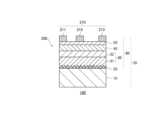
本発明の一実施形態によるIII族窒化物積層体100(以下、積層体100ともいう)について説明する。図1は、積層体100を例示する概略断面図である。積層体100は、基板10と、III族窒化物で構成され基板10上に形成されたIII族窒化物層60(以下、エピ層60ともいう)と、を有する。図1に例示するエピ層60は、核生成層20と、バッファ/チャネル層30と、バリア層40と、キャップ層50と、を有する。以下説明するように、本実施形態による積層体100は、バッファ/チャネル層30における、炭素等の不純物の濃度が、所定範囲に制御されていることを、1つの特徴とする。<One embodiment>
A Group III nitride laminate 100 (hereinafter also referred to as laminate 100) according to one embodiment of the present invention will be described. FIG. 1 is a schematic cross-sectional view illustrating a
積層体100は、例えば、基板10とエピ層60とを有するエピタキシャル基板70(以下、エピ基板70ともいう)の態様であってよい。積層体100は、また例えば、エピ基板70を材料として形成された半導体装置の態様、より具体的には、エピ層60上に電極210(ソース電極211、ゲート電極212およびドレイン電極213)が設けられることで形成された高電子移動度トランジスタ(HEMT)200の態様であってよい。図1は、HEMT200の態様の積層体100を例示する。HEMT200の態様の積層体100は、ウエハの態様であってもよいし、ウエハが分割されたチップの態様であってもよい。 The
基板10は、炭化シリコン(SiC)で構成されており、エピ層60をヘテロエピタキシャル成長させるための下地基板である。基板10を構成するSiCとして、例えば、ポリタイプ4Hまたはポリタイプ6Hの半絶縁性SiCが用いられる。ここで「半絶縁性」とは、例えば、比抵抗が105Ωcm以上である状態をいう。基板10の、エピ層60を成長させる下地となる表面は、例えば(0001)面(c面のシリコン面)である。The
基板10上に、核生成層20が形成されている。核生成層20は、窒化アルミニウム(AlN)で構成されており、バッファ/チャネル層30の結晶成長のための核を生成する核生成層として機能する。核生成層20の厚さは、例えば、1nm以上200nm以下であることが好ましい。 A
核生成層20上に、バッファ/チャネル層30が形成されている。バッファ/チャネル層30は、窒化ガリウム(GaN)で構成されている。バッファ/チャネル層30における下側の部分である下層31は、バッファ/チャネル層30における上側の部分である上層32を成長させる下地であり、上層32の結晶性を向上させるためのバッファ層として機能する。また、上層32は、HEMT200の動作時に電子が走行するチャネル層として機能する。上層32を成長させる下地として好適な結晶性を有するように、下層31の厚さは、例えば100nm以上であることが好ましい。また、上層32がチャネル層として好適に機能するように、上層32の厚さは、例えば50nm以上であることが好ましい。下層31および上層32は、過度に厚いと不要なコスト増を招くため、下層31の厚さは、例えば800nm以下であることが好ましく、上層32の厚さは、例えば300nm以下であることが好ましい。 A buffer/
バッファ/チャネル層30上に、バリア層40が形成されている。バリア層40は、バッファ/チャネル層30を構成するGaNよりも電子親和力の小さいIII族窒化物、例えば、III族元素としてアルミニウム(Al)およびガリウム(Ga)を含む窒化アルミニウムガリウム(AlGaN)で構成されている。バリア層40は、バッファ/チャネル層30の上層32に2次元電子ガス(2DEG)を生成させるとともに、2DEGを上層32内に空間的に閉じ込めるバリア層として機能する。バリア層40の厚さは、例えば、1nm以上50nm以下であることが好ましい。 A
バリア層40上に、キャップ層50が形成されている。キャップ層50は、例えばGaNで構成されており、HEMT200のデバイス特性(閾値電圧の制御性等)を向上させるために、バリア層40と電極210との間に介在する。キャップ層50は、必要に応じて形成され、省略されてもよい。 A
エピ層60上に、HEMT200の電極210として、ソース電極211、ゲート電極212およびドレイン電極213が形成されている。ゲート電極212は、例えば、ニッケル(Ni)層と金(Au)層とが積層されたNi/Au層で構成されている。なお、本明細書で、積層をX/Yと記載した場合、キャップ層50の上に(キャップ層50が省略された場合はバリア層40の上に)、X、Yの順で積層されていることを示す。ソース電極211およびドレイン電極213のそれぞれは、例えば、チタン(Ti)層とAl層とが積層されたTi/Al層で構成されている。ソース電極211およびドレイン電極213のそれぞれは、また例えば、Ti/Al層上にNi/Au層が積層されることで構成されていてもよい。 A
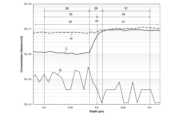
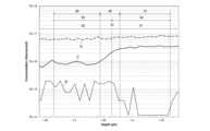
以下、さらに、バッファ/チャネル層30の下層31および上層32における不純物の濃度について説明する。図2および図3は、それぞれ、下層31および上層32における不純物の濃度として、炭素(C)濃度、水素(H)濃度およびシリコン(Si)濃度を示す2次イオン質量分析(SIMS)プロファイルである。下層31および上層32のSIMSプロファイルとして、図2に第1例を示し、図3に第2例を示す。なお、図2および図3は、下層31および上層32におけるC濃度、H濃度およびSi濃度を所定の濃度に制御する試験において作製された試料に対して測定されたSIMSプロファイルであり、これらのSIMSプロファイルにおける深さの値は、積層体100における深さの値を直接的に示すものではない。 The impurity concentration in the
下層31と、(下層31の直上に形成されている)上層32と、について、C、HおよびSiの濃度の相違を説明するため、下層31と上層32との界面近傍のSIMSプロファイルを示す。下層31と上層32との境界33から下側および上側のそれぞれに、所定厚さ(本例では100nm)の部分34、35を設定する。下側の所定厚さ部分34のうち、C濃度の変化が大きい傾斜部36の外側(下側)に配置された、C濃度の変化が小さい一定部37における、C濃度、H濃度およびSi濃度のそれぞれの平均値を、下層31におけるC濃度、H濃度およびSi濃度とする。同様に、上側の所定厚さ部分35のうち、C濃度の変化が大きい傾斜部36の外側(上側)に配置された、C濃度の変化が小さい一定部38における、C濃度、H濃度およびSi濃度のそれぞれの平均値を、上層32におけるC濃度、H濃度およびSi濃度とする。境界33は、例えば、C濃度が、下層31におけるC濃度および上層32におけるC濃度のちょうど中間(平均)となる位置に、設定される。 SIMS profiles in the vicinity of the interface between the
下側の一定部37、上側の一定部38のそれぞれにおいて、C濃度の平均値からの、C濃度の変動の目安は、例えば±25%以下であり、また例えば±20%以下である。第1例、第2例において、下側の一定部37、上側の一定部38は、いずれも、厚さ50nm以上にわたり、当該変動が±20%以下である領域となっている。 In each of the lower
第1例(図2)において、各不純物の濃度は、以下のようなものである。下層31におけるC濃度は、9.1×1016cm-3であり、上層32におけるC濃度は、1.1×1016cm-3である。下層31におけるH濃度は、1.1×1017cm-3であり、上層32におけるH濃度は、7.2×1016cm-3である。下層31におけるSi濃度は、3.6×1014cm-3であり、上層32におけるSi濃度は、1.4×1015cm-3である。In the first example (FIG. 2), the concentration of each impurity is as follows. The C concentration in the
第2例(図3)において、各不純物の濃度は、以下のようなものである。下層31におけるC濃度は、3.3×1016cm-3であり、上層32におけるC濃度は、8.9×1015cm-3である。下層31におけるH濃度は、7.7×1016cm-3であり、上層32におけるH濃度は、6.5×1016cm-3である。下層31におけるSi濃度は、2.7×1014cm-3であり、上層32におけるSi濃度は、1.2×1015cm-3である。In the second example (FIG. 3), the concentration of each impurity is as follows. The C concentration in the
第1例および第2例のSIMSプロファイルから理解されるように、下層31および上層32における、各不純物の濃度は、例えば以下のような特徴を有する。また、これにより、例えば以下のような効果を得ることができる。 As understood from the SIMS profiles of the first and second examples, the concentration of each impurity in the
上層32におけるC濃度は、下層31におけるC濃度よりも低い。上層32におけるC濃度が低いことで、上層32の結晶性を、下層31の結晶性よりも高くすることができる。上層32は、2DEGが形成されてHEMT200のチャネルとなる部分であるため、上層32の結晶性が高いことで、HEMT200の性能を高めることができる。上層32におけるC濃度は、具体的には、5×1016cm-3以下であることが好ましい。The C concentration in the
上層32におけるH濃度は、下層31におけるH濃度よりも低い。上層32におけるH濃度が低いことで、上層32が含むHのバリア層40への拡散を抑制することができ、上層32におけるH濃度の経時的な変動を抑制することができる。上層32に形成された2DEG中の電子は、水素イオン(H+イオン)に引き付けられやすいので、上層32におけるH濃度の経時的な変動が大きいと、2DEG濃度の経時的な変動が大きくなる。上層32におけるH濃度の経時的な変動が抑制されていることで、2DEG濃度の経時的な変動を抑制することができるため、HEMT200の性能の経時的な変動を抑制することができる。上層32におけるH濃度は、具体的には、1×1017cm-3以下であることが好ましい。The H concentration in the
上層32におけるC濃度は、下層31におけるC濃度よりも低く、換言すると、下層31におけるC濃度は、上層32におけるC濃度よりも高い。下層31におけるC濃度が高いことで、下層31の導電性を、上層32の導電性よりも低下させることができる。これにより、HEMT200のリーク電流を抑制することができる。下層31におけるC濃度は、具体的には、上層32におけるC濃度よりも、2×1016cm-3以上高いことが好ましい。The C concentration in the
ただし、本実施形態では、下層31におけるC濃度を抑制している。下層31におけるC濃度は、具体的には、5×1017cm-3以下であることが好ましく、1×1017cm-3以下であることがより好ましい。下層31におけるC濃度を抑制することで、下層31にCを添加しつつ、Cの添加に起因する下層31の結晶性低下を抑制することができる。これにより、バッファ層として形成する下層31を、薄くても結晶性の高いものにできる。However, in this embodiment, the C concentration in the
上層32におけるH濃度は、下層31におけるH濃度よりも低く、換言すると、下層31におけるH濃度は、上層32におけるH濃度よりも高い。後述のように、下層31の成長期間に用いるキャリアガスにおける水素ガスの比率を、(上層32の成長期間に用いるキャリアガスにおける水素ガスの比率と比べて)高くすることで、下層31にCが添加されている状況において、下層31の結晶性低下を抑制することができる。そして、これにより、下層31におけるH濃度が、上層32におけるH濃度よりも高くなる。 The H concentration in the
ただし、下層31におけるH濃度が、上層32におけるH濃度よりも過度に高いと、下層31が含むHの拡散に起因して、上層32におけるH濃度が高くなる懸念がある。このため、下層31におけるH濃度の上層32におけるH濃度に対する比率は、小さいことが好ましい。下層31におけるH濃度の上層32におけるH濃度に対する比率は、第1例では1.5倍であり、第2例では1.2倍である。下層31におけるH濃度の上層32におけるH濃度に対する比率は、例えば、5倍以下であることが好ましく、3倍以下であることがより好ましく、2倍以下であることがさらに好ましい。下層31におけるH濃度は、具体的には、1×1018cm-3以下であることが好ましく、5×1017cm-3以下であることがより好ましい。However, if the H concentration in the
その他、第1例および第2例のSIMSプロファイルから観察される、C濃度およびH濃度についての特徴として、例えば、上層32におけるC濃度が、上層32におけるH濃度よりも低いことが挙げられる。また例えば、下層31におけるC濃度が、下層31におけるH濃度よりも低いことが挙げられる。 Other features of the C concentration and H concentration observed from the SIMS profiles of the first and second examples include, for example, that the C concentration in the
上層32におけるSi濃度は、下層31におけるSi濃度よりも高い。上層32におけるSi濃度が高いことで、チャネルにおける電子トラップが補償されるため、電流コラプスを抑制することができる。また、上層32におけるSi濃度が高いことで、電子が上層32側に集まるように縦方向(厚さ方向)の電子分布が制御されるため、遮断特性を向上させることができる。上層32におけるSi濃度は、具体的には、5×1014cm-3以上であることが好ましく、1×1015cm-3以上であることがより好ましい。ただし、上層32におけるSi濃度が過度に高いと、リーク電流の増大を引き起こす。このため、上層32におけるSi濃度は、1×1016cm-3以下であることが好ましい。The Si concentration in the
上層32におけるSi濃度は、下層31におけるSi濃度よりも高く、換言すると、下層31におけるSi濃度は、上層32におけるSi濃度よりも低い。下層31におけるSi濃度が低いことで、下層31の導電性を、上層32の導電性よりも低下させることができる。これにより、HEMT200のリーク電流を抑制することができる。下層31におけるSi濃度は、具体的には、5×1014cm-3未満であることが好ましい。The Si concentration in the
第1例および第2例において、以下のような、各不純物の濃度が得られている。上層32におけるC濃度は、5×1016cm-3以下となっており、より具体的には、2×1016cm-3以下となっている。上層32におけるH濃度は、1×1017cm-3以下となっており、より具体的には、8×1016cm-3以下となっている。下層31におけるC濃度は、5×1017cm-3以下となっており、より具体的には、1×1017cm-3以下となっている。下層31におけるH濃度は、5×1017cm-3以下となっており、より具体的には、2×1017cm-3以下となっている。上層32におけるSi濃度は、(1×1016cm-3以下、より具体的には5×1015cm-3以下であって、)5×1014cm-3以上となっており、より具体的には、1×1015cm-3以上となっている。下層31におけるSi濃度は、5×1014cm-3未満となっており、より具体的には、4×1014cm-3以下となっている。In the first and second examples, the following impurity concentrations are obtained. The C concentration in the
次に、実施形態による積層体100の製造方法について説明する。ここでは、HEMT200の態様である積層体100の製造方法について例示する。まず、エピ基板70の製造方法について説明する。基板10としてSiC基板を準備する。基板10の上方に、エピ層60を構成する各層である、核生成層20、バッファ/チャネル層30、バリア層40および(必要に応じて)キャップ層50を、有機金属気相成長(MOVPE)により成長させることで、エピ基板70を形成する。 Next, a method for manufacturing the laminate 100 according to the embodiment will be described. Here, a method for manufacturing the
III族原料ガスのうちAl原料ガスとしては、例えばトリメチルアルミニウム(Al(CH3)3、TMA)ガスが用いられる。III族原料ガスのうちGa原料ガスとしては、例えばトリメチルガリウム(Ga(CH3)3、TMG)ガスが用いられる。V族原料ガスである窒素(N)原料ガスとしては、例えばアンモニア(NH3)ガスが用いられる。キャリアガスとしては、例えば、窒素ガス(N2ガス)および水素ガス(H2ガス)の少なくとも一方が用いられる。成長温度は、例えば、900℃~1400℃の範囲で選択可能であり、III族原料ガスに対するV族原料ガスの流量比であるV/III比は、例えば、10~5000の範囲で選択可能である。形成する各層の組成に応じて、各原料ガスの供給量の比率が調整される。形成する各層の厚さは、たとえば予備実験で得た成長速度から設計厚さに対応する成長時間を算出することで、成長時間により制御できる。Trimethylaluminum (Al(CH3 )3 , TMA) gas, for example, is used as the Al source gas among the Group III source gases. As the Ga source gas among III-group source gases, for example, trimethylgallium (Ga(CH3 )3 , TMG) gas is used. Ammonia (NH3 ) gas, for example, is used as the nitrogen (N) source gas, which is the group V source gas. As the carrier gas, for example, at least one of nitrogen gas (N2 gas) and hydrogen gas (H2 gas) is used. The growth temperature can be selected, for example, in the range of 900° C. to 1400° C., and the V/III ratio, which is the flow rate ratio of the group V source gas to the group III source gas, can be selected in the range of, for example, 10 to 5000. be. The ratio of the supply amount of each source gas is adjusted according to the composition of each layer to be formed. The thickness of each layer to be formed can be controlled by the growth time, for example, by calculating the growth time corresponding to the design thickness from the growth rate obtained in the preliminary experiment.
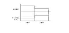
以下、特に、バッファ/チャネル層30の形成工程について説明する。図4は、バッファ/チャネル層30の下層31と上層32との成長条件の相違を模式的に例示するタイミングチャートである。下層31および上層32は、GaNで構成され、Ga原料ガスおよびN原料ガスをキャリアガスとともに供給することで成長される。下層31および上層32における各不純物の濃度を上述のように制御するために、下層31と上層32とで成長条件を変化させる。 In particular, the process of forming the buffer/
本実施形態では、図4に示すように、上層32の成長期間における上層32の成長速度を、下層31の成長期間における下層31の成長速度よりも、低く(遅く)する。具体的には例えば、下層31の成長期間よりも、上層32の成長期間において、成長温度および成長圧力を高くすることで、上層32の成長速度を、下層31の成長速度よりも、低くする。また、さらに、上層32の成長期間に用いるキャリアガスにおけるH2ガスの比率を、下層31の成長期間に用いるキャリアガスにおけるH2ガスの比率よりも、低く(少なく)する。In this embodiment, as shown in FIG. 4, the growth rate of the
例えば、下層31の成長期間では、成長温度を、所定の温度範囲内で低め(例えば900℃以上1040℃未満)にし、また、成長圧力を、所定の圧力範囲内で低め(例えば6.7kPa以上13.3kPa未満)にする。さらに、下層31の成長期間では、キャリアガスをH2ガスとN2ガスとの混合ガスとして、当該混合ガスおけるH2ガスの比率を高め(例えば、N2ガスの分圧/H2ガスの分圧が0.5以上1.0未満)にする。For example, during the growth period of the
例えば、上層32の成長期間では、成長温度を、所定の温度範囲内で高め(例えば1040℃以上1200℃以下)にし、また、成長圧力を、所定の圧力範囲内で高め(例えば13.3kPa以上66.7kPa以下)にする。さらに、上層32の成長期間では、キャリアガスをN2ガスのみとするか、キャリアガスをH2ガスとN2ガスとの混合ガスとして、当該混合ガスおけるH2ガスの比率を低め(例えば、N2ガスの分圧/H2ガスの分圧が1.0以上3.0以下)にする。For example, during the growth period of the
上層32の成長期間において、成長温度および成長圧力を高くすることで、上層32の成長速度を下層31の成長速度よりも低くすることにより、Ga原料の分解が、上層32の成長期間において相対的に促進され、下層31の成長期間において相対的に抑制される。これにより、C濃度が、上層32において相対的に低くなり、下層31において相対的に高くなる。 During the growth period of the
下層31の成長期間には、キャリアガスにおけるH2ガスの比率を高くすることで、下層31を構成するGaNの結晶性を高めることができる。これにより、下層31にCを添加しつつ、Cの添加に起因する下層31の結晶性低下を抑制することができる。一方、上層32の成長期間には、キャリアガスにおけるH2ガスの比率を低くすることで、上層32へのHの混入を抑制することができる。このようにして、H濃度が、上層32において相対的に低くなり、下層31において相対的に高くなる。また、上層32におけるH濃度を、1×1017cm-3以下とすることができる。During the growth period of the
Siは、例えば、MOVPE装置の炉壁から、一定のレートで成長層に供給される(混入する)。このため、成長速度が低いほど、成長層におけるSi濃度は高くなる。このため、上層32の成長速度を、下層31の成長速度よりも低くすることで、Si濃度が、上層32において相対的に高くなり、下層31において相対的に低くなる。 Si is supplied (incorporated) into the growth layer at a constant rate, for example, from the furnace wall of the MOVPE apparatus. Therefore, the lower the growth rate, the higher the Si concentration in the grown layer. Therefore, by making the growth rate of the
なお、各不純物について所定の濃度を得るための、下層31の成長期間、および、上層32の成長期間それぞれにおける、成長温度、成長圧力、V/III比、キャリアガスの組成、等の成長条件は、MOVPE装置等によって、適宜調整されてよい。 The growth conditions such as the growth temperature, the growth pressure, the V/III ratio, the composition of the carrier gas, etc. in the growth period of the
エピ基板70が製造された後、エピ層60上に電極210(ソース電極211、ゲート電極212およびドレイン電極213)を形成することで、HEMT200を製造する。なお、HEMT200の製造の際、必要に応じ、保護膜等の他の部材を形成してもよい。電極210、保護膜等は、公知の手法で形成されてよい。このようにして、本実施形態による積層体100が製造される。 After
以上説明したように、本実施形態によれば、HEMT200のバッファ/チャネル層30における(下層31および上層32における)不純物の濃度が所定範囲に制御された積層体100を得ることができる。例えば、上層32におけるC濃度を、下層31(バッファ層)におけるC濃度よりも低く、5×1016cm-3以下とすることで、下層31において導電性を上層32よりも低下させてリーク電流を抑制しつつ、上層32の結晶性を高めることができる。また例えば、上層32におけるH濃度を、下層31におけるH濃度よりも低く、1×1017cm-3以下とすることで、HEMT200の性能の経時的な変動を抑制することができる。As described above, according to this embodiment, it is possible to obtain the
<本発明の好ましい態様>
以下、本発明の好ましい態様について付記する。<Preferred embodiment of the present invention>
Preferred embodiments of the present invention are described below.
(付記1)
窒化ガリウムで構成された第1層と、
前記第1層上に形成され、窒化ガリウムよりも電子親和力の小さいIII族窒化物で構成された第2層と、
を有し、
前記第1層は、下層と、前記下層上に形成された上層と、を有し、
前記上層における炭素濃度は、前記下層における炭素濃度よりも低く、
前記上層における水素濃度は、前記下層における水素濃度よりも低く、
前記上層における炭素濃度は、5×1016cm-3以下であり、
前記上層における水素濃度は、1×1017cm-3以下である、III族窒化物積層体。(Appendix 1)
a first layer made of gallium nitride;
a second layer formed on the first layer and made of a group III nitride having a lower electron affinity than gallium nitride;
has
The first layer has a lower layer and an upper layer formed on the lower layer,
the carbon concentration in the upper layer is lower than the carbon concentration in the lower layer;
the hydrogen concentration in the upper layer is lower than the hydrogen concentration in the lower layer,
the carbon concentration in the upper layer is 5×1016 cm−3 or less;
The Group III nitride laminate, wherein the upper layer has a hydrogen concentration of 1×1017 cm−3 or less.
(付記2)
前記下層における炭素濃度は、前記上層における炭素濃度よりも、2×1016cm-3以上高い、付記1に記載のIII族窒化物積層体。(Appendix 2)
The Group III nitride laminate according to Appendix 1, wherein the carbon concentration in the lower layer is 2×1016 cm−3 or more higher than the carbon concentration in the upper layer.
(付記3)
前記下層における炭素濃度は、5×1017cm-3以下(より好ましくは1×1017cm-3以下)である、付記1または2に記載のIII族窒化物積層体。(Appendix 3)
3. The Group III nitride laminate according to appendix 1 or 2, wherein the lower layer has a carbon concentration of 5×1017 cm−3 or less (more preferably 1×1017 cm−3 or less).
(付記4)
前記下層における水素濃度の前記上層における水素濃度に対する比率は、5倍以下(より好ましくは3倍以下、さらに好ましくは2倍以下)である、付記1~3のいずれか1つに記載のIII族窒化物積層体。(Appendix 4)
Group III according to any one of appendices 1 to 3, wherein the ratio of the hydrogen concentration in the lower layer to the hydrogen concentration in the upper layer is 5 times or less (more preferably 3 times or less, still more preferably 2 times or less). Nitride laminate.
(付記5)
前記下層における水素濃度は、1×1018cm-3以下(より好ましくは5×1017cm-3以下)である、付記1~4のいずれか1つに記載のIII族窒化物積層体。(Appendix 5)
5. The Group III nitride laminate according to any one of Appendices 1 to 4, wherein the lower layer has a hydrogen concentration of 1×1018 cm−3 or less (more preferably 5×1017 cm−3 or less).
(付記6)
前記上層における炭素濃度は、前記上層における水素濃度よりも低い、付記1~5のいずれか1つに記載のIII族窒化物積層体。(Appendix 6)
6. The Group III nitride laminate according to any one of Appendices 1 to 5, wherein the upper layer has a carbon concentration lower than a hydrogen concentration in the upper layer.
(付記7)
前記下層における炭素濃度は、前記下層における水素濃度よりも低い、付記1~6のいずれか1つに記載のIII族窒化物積層体。(Appendix 7)
7. The Group III nitride laminate according to any one of Appendices 1 to 6, wherein the carbon concentration in the lower layer is lower than the hydrogen concentration in the lower layer.
(付記8)
前記上層におけるシリコン濃度は、前記下層におけるシリコン濃度よりも高い、付記1~7のいずれか1つに記載のIII族窒化物積層体。(Appendix 8)
8. The Group III nitride laminate according to any one of Appendices 1 to 7, wherein the silicon concentration in the upper layer is higher than the silicon concentration in the lower layer.
(付記9)
前記上層におけるシリコン濃度は、(1×1016cm-3以下であって、)5×1014cm-3以上(より好ましくは1×1015cm-3以上)である、付記1~8のいずれか1つに記載のIII族窒化物積層体。(Appendix 9)
9. The silicon concentration in the upper layer is (1×1016 cm−3 or less) 5×1014 cm−3 or more (more preferably 1×1015 cm−3 or more). The Group III nitride laminate according to any one of the above.
(付記10)
前記下層におけるシリコン濃度は、5×1014cm-3未満である、付記1~9のいずれか1つに記載のIII族窒化物積層体。(Appendix 10)
10. The III-nitride laminate according to any one of Appendices 1 to 9, wherein the silicon concentration in the underlayer is less than 5×1014 cm−3 .
10…基板、20…核生成層、30…バッファ/チャネル層、31…(バッファ/チャネル層の)下層、32…(バッファ/チャネル層の)上層、40…バリア層、50…キャップ層、60…III族窒化物層、70…エピタキシャル基板、100…III族窒化物積層体、200…HEMT、210…電極、211…ソース電極、212…ゲート電極、213…ドレイン電極DESCRIPTION OF
Claims (10)
Translated fromJapanese前記第1層上に形成され、窒化ガリウムよりも電子親和力の小さいIII族窒化物で構成された第2層と、
を有し、
前記第1層は、下層と、前記下層上に形成された上層と、を有し、
前記上層における炭素濃度は、前記下層における炭素濃度よりも低く、
前記上層における水素濃度は、前記下層における水素濃度よりも低く、
前記上層における炭素濃度は、5×1016cm-3以下であり、
前記上層における水素濃度は、1×1017cm-3以下である、III族窒化物積層体。a first layer made of gallium nitride;
a second layer formed on the first layer and made of a group III nitride having a lower electron affinity than gallium nitride;
has
The first layer has a lower layer and an upper layer formed on the lower layer,
the carbon concentration in the upper layer is lower than the carbon concentration in the lower layer;
the hydrogen concentration in the upper layer is lower than the hydrogen concentration in the lower layer,
the carbon concentration in the upper layer is 5×1016 cm−3 or less;
The Group III nitride laminate, wherein the upper layer has a hydrogen concentration of 1×1017 cm−3 or less.
Priority Applications (4)
| Application Number | Priority Date | Filing Date | Title |
|---|---|---|---|
| JP2021195190AJP2023081467A (en) | 2021-12-01 | 2021-12-01 | Group III nitride laminate |
| US17/992,880US12421625B2 (en) | 2021-12-01 | 2022-11-22 | Group III nitride stack |
| TW111145583ATW202323573A (en) | 2021-12-01 | 2022-11-29 | Group-iii nitride laminate |
| CN202211511035.2ACN116207136A (en) | 2021-12-01 | 2022-11-29 | Group III nitride laminate |
Applications Claiming Priority (1)
| Application Number | Priority Date | Filing Date | Title |
|---|---|---|---|
| JP2021195190AJP2023081467A (en) | 2021-12-01 | 2021-12-01 | Group III nitride laminate |
Publications (1)
| Publication Number | Publication Date |
|---|---|
| JP2023081467Atrue JP2023081467A (en) | 2023-06-13 |
Family
ID=86500844
Family Applications (1)
| Application Number | Title | Priority Date | Filing Date |
|---|---|---|---|
| JP2021195190APendingJP2023081467A (en) | 2021-12-01 | 2021-12-01 | Group III nitride laminate |
Country Status (4)
| Country | Link |
|---|---|
| US (1) | US12421625B2 (en) |
| JP (1) | JP2023081467A (en) |
| CN (1) | CN116207136A (en) |
| TW (1) | TW202323573A (en) |
Cited By (11)
| Publication number | Priority date | Publication date | Assignee | Title |
|---|---|---|---|---|
| JP2023053388A (en)* | 2018-03-08 | 2023-04-12 | 株式会社三洋物産 | game machine |
| JP2023053387A (en)* | 2022-02-04 | 2023-04-12 | 株式会社三洋物産 | game machine |
| JP2023054222A (en)* | 2019-03-28 | 2023-04-13 | 株式会社三洋物産 | game machine |
| JP2023054224A (en)* | 2019-04-11 | 2023-04-13 | 株式会社三洋物産 | game machine |
| JP2023054227A (en)* | 2018-02-15 | 2023-04-13 | 株式会社三洋物産 | game machine |
| JP2023054225A (en)* | 2019-04-11 | 2023-04-13 | 株式会社三洋物産 | game machine |
| JP2023054223A (en)* | 2019-03-28 | 2023-04-13 | 株式会社三洋物産 | game machine |
| JP2023060269A (en)* | 2022-04-01 | 2023-04-27 | 株式会社三洋物産 | game machine |
| JP2023060270A (en)* | 2022-04-01 | 2023-04-27 | 株式会社三洋物産 | game machine |
| JP2023063369A (en)* | 2022-01-07 | 2023-05-09 | 株式会社三洋物産 | game machine |
| JP2023071934A (en)* | 2019-02-15 | 2023-05-23 | 株式会社三洋物産 | game machine |
Citations (4)
| Publication number | Priority date | Publication date | Assignee | Title |
|---|---|---|---|---|
| JP2008277655A (en)* | 2007-05-02 | 2008-11-13 | Hitachi Cable Ltd | Semiconductor epitaxial wafer and field effect transistor |
| JP2015070085A (en)* | 2013-09-27 | 2015-04-13 | Dowaエレクトロニクス株式会社 | Epitaxial substrate for electronic device and manufacturing method thereof |
| JP2019057588A (en)* | 2017-09-20 | 2019-04-11 | 株式会社東芝 | Semiconductor substrate and semiconductor device |
| JP2020177940A (en)* | 2019-04-15 | 2020-10-29 | 株式会社東芝 | Semiconductor devices and their manufacturing methods |
Family Cites Families (3)
| Publication number | Priority date | Publication date | Assignee | Title |
|---|---|---|---|---|
| JP6030733B2 (en) | 2015-11-05 | 2016-11-24 | 住友化学株式会社 | Nitride semiconductor epitaxial wafer for transistor and nitride semiconductor field effect transistor |
| JP6917798B2 (en)* | 2017-06-20 | 2021-08-11 | 株式会社サイオクス | Nitride semiconductor epitaxial substrate and semiconductor device |
| JP7384580B2 (en)* | 2019-06-24 | 2023-11-21 | 住友化学株式会社 | Group III nitride laminate |
- 2021
- 2021-12-01JPJP2021195190Apatent/JP2023081467A/enactivePending
- 2022
- 2022-11-22USUS17/992,880patent/US12421625B2/enactiveActive
- 2022-11-29CNCN202211511035.2Apatent/CN116207136A/enactivePending
- 2022-11-29TWTW111145583Apatent/TW202323573A/enunknown
Patent Citations (4)
| Publication number | Priority date | Publication date | Assignee | Title |
|---|---|---|---|---|
| JP2008277655A (en)* | 2007-05-02 | 2008-11-13 | Hitachi Cable Ltd | Semiconductor epitaxial wafer and field effect transistor |
| JP2015070085A (en)* | 2013-09-27 | 2015-04-13 | Dowaエレクトロニクス株式会社 | Epitaxial substrate for electronic device and manufacturing method thereof |
| JP2019057588A (en)* | 2017-09-20 | 2019-04-11 | 株式会社東芝 | Semiconductor substrate and semiconductor device |
| JP2020177940A (en)* | 2019-04-15 | 2020-10-29 | 株式会社東芝 | Semiconductor devices and their manufacturing methods |
Cited By (11)
| Publication number | Priority date | Publication date | Assignee | Title |
|---|---|---|---|---|
| JP2023054227A (en)* | 2018-02-15 | 2023-04-13 | 株式会社三洋物産 | game machine |
| JP2023053388A (en)* | 2018-03-08 | 2023-04-12 | 株式会社三洋物産 | game machine |
| JP2023071934A (en)* | 2019-02-15 | 2023-05-23 | 株式会社三洋物産 | game machine |
| JP2023054222A (en)* | 2019-03-28 | 2023-04-13 | 株式会社三洋物産 | game machine |
| JP2023054223A (en)* | 2019-03-28 | 2023-04-13 | 株式会社三洋物産 | game machine |
| JP2023054224A (en)* | 2019-04-11 | 2023-04-13 | 株式会社三洋物産 | game machine |
| JP2023054225A (en)* | 2019-04-11 | 2023-04-13 | 株式会社三洋物産 | game machine |
| JP2023063369A (en)* | 2022-01-07 | 2023-05-09 | 株式会社三洋物産 | game machine |
| JP2023053387A (en)* | 2022-02-04 | 2023-04-12 | 株式会社三洋物産 | game machine |
| JP2023060269A (en)* | 2022-04-01 | 2023-04-27 | 株式会社三洋物産 | game machine |
| JP2023060270A (en)* | 2022-04-01 | 2023-04-27 | 株式会社三洋物産 | game machine |
Also Published As
| Publication number | Publication date |
|---|---|
| CN116207136A (en) | 2023-06-02 |
| TW202323573A (en) | 2023-06-16 |
| US12421625B2 (en) | 2025-09-23 |
| US20230167585A1 (en) | 2023-06-01 |
Similar Documents
| Publication | Publication Date | Title |
|---|---|---|
| JP2023081467A (en) | Group III nitride laminate | |
| JP5546514B2 (en) | Nitride semiconductor device and manufacturing method | |
| CN108140561A (en) | The manufacturing method of epitaxial substrate for semiconductor device, semiconductor element and epitaxial substrate for semiconductor device | |
| JP4577460B2 (en) | Semiconductor device and manufacturing method thereof | |
| KR20150120357A (en) | P-doping of group-iii-nitride buffer layer structure on a heterosubstrate | |
| JP7503193B2 (en) | Group III nitride stack | |
| JP7602603B2 (en) | Group III nitride stack | |
| JP5883331B2 (en) | Method of manufacturing nitride semiconductor epitaxial wafer and method of manufacturing field effect nitride transistor | |
| JP2006303475A (en) | Field effect transistor | |
| JP2009021279A (en) | Semiconductor epitaxial wafer | |
| JP6305137B2 (en) | Nitride semiconductor laminate and semiconductor device | |
| US7554132B2 (en) | Electronic device containing group-III element based nitride semiconductors | |
| JP6917798B2 (en) | Nitride semiconductor epitaxial substrate and semiconductor device | |
| JP5746927B2 (en) | Semiconductor substrate, semiconductor device, and method of manufacturing semiconductor substrate | |
| JP2006114655A (en) | Semiconductor epitaxial wafer and field effect transistor | |
| JP2014090065A (en) | Nitride-based semiconductor epitaxial wafer and nitride-based field-effect transistor | |
| JP2004289005A (en) | Epitaxial substrate, semiconductor device, and high electron mobility transistor | |
| US12334340B2 (en) | Epitaxial wafer, semiconductor device, and method for manufacturing epitaxial wafer | |
| WO2019069364A1 (en) | Nitride-based field effect transistor | |
| JP2006179861A (en) | Semiconductor epitaxial wafer and field effect transistor | |
| JP2012151234A (en) | Field-effect transistor | |
| JP2017011180A (en) | Field effect transistor and manufacturing method therefor | |
| JP2000299325A (en) | Epitaxial wafer for field effect transistors using gallium nitride based compound semiconductor | |
| JP2006114653A (en) | Semiconductor epitaxial wafer and field effect transistor | |
| JP2006013006A (en) | Semiconductor composite substrate and compound semiconductor device using the same |
Legal Events
| Date | Code | Title | Description |
|---|---|---|---|
| A711 | Notification of change in applicant | Free format text:JAPANESE INTERMEDIATE CODE: A712 Effective date:20221223 | |
| A621 | Written request for application examination | Free format text:JAPANESE INTERMEDIATE CODE: A621 Effective date:20240829 | |
| A977 | Report on retrieval | Free format text:JAPANESE INTERMEDIATE CODE: A971007 Effective date:20250716 | |
| A131 | Notification of reasons for refusal | Free format text:JAPANESE INTERMEDIATE CODE: A131 Effective date:20250729 | |
| A521 | Request for written amendment filed | Free format text:JAPANESE INTERMEDIATE CODE: A523 Effective date:20250822 |