JP2023040113A - sensing system - Google Patents
sensing systemDownload PDFInfo
- Publication number
- JP2023040113A JP2023040113AJP2022210056AJP2022210056AJP2023040113AJP 2023040113 AJP2023040113 AJP 2023040113AJP 2022210056 AJP2022210056 AJP 2022210056AJP 2022210056 AJP2022210056 AJP 2022210056AJP 2023040113 AJP2023040113 AJP 2023040113A
- Authority
- JP
- Japan
- Prior art keywords
- sensing system
- nanogenerator
- piezoelectric
- electrode
- energy
- Prior art date
- Legal status (The legal status is an assumption and is not a legal conclusion. Google has not performed a legal analysis and makes no representation as to the accuracy of the status listed.)
- Granted
Links
Images


Classifications
- G—PHYSICS
- G01—MEASURING; TESTING
- G01B—MEASURING LENGTH, THICKNESS OR SIMILAR LINEAR DIMENSIONS; MEASURING ANGLES; MEASURING AREAS; MEASURING IRREGULARITIES OF SURFACES OR CONTOURS
- G01B7/00—Measuring arrangements characterised by the use of electric or magnetic techniques
- G01B7/16—Measuring arrangements characterised by the use of electric or magnetic techniques for measuring the deformation in a solid, e.g. by resistance strain gauge
- G01B7/18—Measuring arrangements characterised by the use of electric or magnetic techniques for measuring the deformation in a solid, e.g. by resistance strain gauge using change in resistance
- H—ELECTRICITY
- H02—GENERATION; CONVERSION OR DISTRIBUTION OF ELECTRIC POWER
- H02N—ELECTRIC MACHINES NOT OTHERWISE PROVIDED FOR
- H02N2/00—Electric machines in general using piezoelectric effect, electrostriction or magnetostriction
- H02N2/18—Electric machines in general using piezoelectric effect, electrostriction or magnetostriction producing electrical output from mechanical input, e.g. generators
- B—PERFORMING OPERATIONS; TRANSPORTING
- B64—AIRCRAFT; AVIATION; COSMONAUTICS
- B64D—EQUIPMENT FOR FITTING IN OR TO AIRCRAFT; FLIGHT SUITS; PARACHUTES; ARRANGEMENT OR MOUNTING OF POWER PLANTS OR PROPULSION TRANSMISSIONS IN AIRCRAFT
- B64D43/00—Arrangements or adaptations of instruments
- B—PERFORMING OPERATIONS; TRANSPORTING
- B64—AIRCRAFT; AVIATION; COSMONAUTICS
- B64D—EQUIPMENT FOR FITTING IN OR TO AIRCRAFT; FLIGHT SUITS; PARACHUTES; ARRANGEMENT OR MOUNTING OF POWER PLANTS OR PROPULSION TRANSMISSIONS IN AIRCRAFT
- B64D45/00—Aircraft indicators or protectors not otherwise provided for
- B—PERFORMING OPERATIONS; TRANSPORTING
- B64—AIRCRAFT; AVIATION; COSMONAUTICS
- B64F—GROUND OR AIRCRAFT-CARRIER-DECK INSTALLATIONS SPECIALLY ADAPTED FOR USE IN CONNECTION WITH AIRCRAFT; DESIGNING, MANUFACTURING, ASSEMBLING, CLEANING, MAINTAINING OR REPAIRING AIRCRAFT, NOT OTHERWISE PROVIDED FOR; HANDLING, TRANSPORTING, TESTING OR INSPECTING AIRCRAFT COMPONENTS, NOT OTHERWISE PROVIDED FOR
- B64F5/00—Designing, manufacturing, assembling, cleaning, maintaining or repairing aircraft, not otherwise provided for; Handling, transporting, testing or inspecting aircraft components, not otherwise provided for
- B64F5/60—Testing or inspecting aircraft components or systems
- F—MECHANICAL ENGINEERING; LIGHTING; HEATING; WEAPONS; BLASTING
- F16—ENGINEERING ELEMENTS AND UNITS; GENERAL MEASURES FOR PRODUCING AND MAINTAINING EFFECTIVE FUNCTIONING OF MACHINES OR INSTALLATIONS; THERMAL INSULATION IN GENERAL
- F16B—DEVICES FOR FASTENING OR SECURING CONSTRUCTIONAL ELEMENTS OR MACHINE PARTS TOGETHER, e.g. NAILS, BOLTS, CIRCLIPS, CLAMPS, CLIPS OR WEDGES; JOINTS OR JOINTING
- F16B31/00—Screwed connections specially modified in view of tensile load; Break-bolts
- F16B31/02—Screwed connections specially modified in view of tensile load; Break-bolts for indicating the attainment of a particular tensile load or limiting tensile load
- F16B31/028—Screwed connections specially modified in view of tensile load; Break-bolts for indicating the attainment of a particular tensile load or limiting tensile load with a load-indicating washer or washer assembly
- F—MECHANICAL ENGINEERING; LIGHTING; HEATING; WEAPONS; BLASTING
- F16—ENGINEERING ELEMENTS AND UNITS; GENERAL MEASURES FOR PRODUCING AND MAINTAINING EFFECTIVE FUNCTIONING OF MACHINES OR INSTALLATIONS; THERMAL INSULATION IN GENERAL
- F16B—DEVICES FOR FASTENING OR SECURING CONSTRUCTIONAL ELEMENTS OR MACHINE PARTS TOGETHER, e.g. NAILS, BOLTS, CIRCLIPS, CLAMPS, CLIPS OR WEDGES; JOINTS OR JOINTING
- F16B43/00—Washers or equivalent devices; Other devices for supporting bolt-heads or nuts
- G—PHYSICS
- G01—MEASURING; TESTING
- G01B—MEASURING LENGTH, THICKNESS OR SIMILAR LINEAR DIMENSIONS; MEASURING ANGLES; MEASURING AREAS; MEASURING IRREGULARITIES OF SURFACES OR CONTOURS
- G01B1/00—Measuring instruments characterised by the selection of material therefor
- H—ELECTRICITY
- H10—SEMICONDUCTOR DEVICES; ELECTRIC SOLID-STATE DEVICES NOT OTHERWISE PROVIDED FOR
- H10N—ELECTRIC SOLID-STATE DEVICES NOT OTHERWISE PROVIDED FOR
- H10N30/00—Piezoelectric or electrostrictive devices
- H10N30/30—Piezoelectric or electrostrictive devices with mechanical input and electrical output, e.g. functioning as generators or sensors
- H—ELECTRICITY
- H10—SEMICONDUCTOR DEVICES; ELECTRIC SOLID-STATE DEVICES NOT OTHERWISE PROVIDED FOR
- H10N—ELECTRIC SOLID-STATE DEVICES NOT OTHERWISE PROVIDED FOR
- H10N30/00—Piezoelectric or electrostrictive devices
- H10N30/702—Piezoelectric or electrostrictive devices based on piezoelectric or electrostrictive fibres
- B—PERFORMING OPERATIONS; TRANSPORTING
- B64—AIRCRAFT; AVIATION; COSMONAUTICS
- B64D—EQUIPMENT FOR FITTING IN OR TO AIRCRAFT; FLIGHT SUITS; PARACHUTES; ARRANGEMENT OR MOUNTING OF POWER PLANTS OR PROPULSION TRANSMISSIONS IN AIRCRAFT
- B64D45/00—Aircraft indicators or protectors not otherwise provided for
- B64D2045/0085—Devices for aircraft health monitoring, e.g. monitoring flutter or vibration
- B—PERFORMING OPERATIONS; TRANSPORTING
- B82—NANOTECHNOLOGY
- B82Y—SPECIFIC USES OR APPLICATIONS OF NANOSTRUCTURES; MEASUREMENT OR ANALYSIS OF NANOSTRUCTURES; MANUFACTURE OR TREATMENT OF NANOSTRUCTURES
- B82Y15/00—Nanotechnology for interacting, sensing or actuating, e.g. quantum dots as markers in protein assays or molecular motors
- Y—GENERAL TAGGING OF NEW TECHNOLOGICAL DEVELOPMENTS; GENERAL TAGGING OF CROSS-SECTIONAL TECHNOLOGIES SPANNING OVER SEVERAL SECTIONS OF THE IPC; TECHNICAL SUBJECTS COVERED BY FORMER USPC CROSS-REFERENCE ART COLLECTIONS [XRACs] AND DIGESTS
- Y02—TECHNOLOGIES OR APPLICATIONS FOR MITIGATION OR ADAPTATION AGAINST CLIMATE CHANGE
- Y02T—CLIMATE CHANGE MITIGATION TECHNOLOGIES RELATED TO TRANSPORTATION
- Y02T50/00—Aeronautics or air transport
- Y02T50/50—On board measures aiming to increase energy efficiency
Landscapes
- Engineering & Computer Science (AREA)
- Aviation & Aerospace Engineering (AREA)
- General Engineering & Computer Science (AREA)
- Physics & Mathematics (AREA)
- General Physics & Mathematics (AREA)
- Mechanical Engineering (AREA)
- Manufacturing & Machinery (AREA)
- Transportation (AREA)
- Measurement Of Length, Angles, Or The Like Using Electric Or Magnetic Means (AREA)
- Arrangements For Transmission Of Measured Signals (AREA)
Abstract
Description
Translated fromJapanese[0001]本願は、2017年11月10日に出願されたカナダ特許出願第2,985,238号の米国特許法第119条(e)項に基づく利益を主張し、その内容は、参照により本明細書に組み込まれている。 [0001] This application claims benefit under 35 U.S.C. incorporated herein.
[0002]その態様の1つでは、本発明は、感知システムに関し、より詳細には、少なくとも1つのシムデバイスに結合された少なくとも1つの圧電感知デバイスを備える感知システムに関する。この感知システムは、たとえば、航空機、宇宙機など航空宇宙応用例で使用され得る。 [0002] In one of its aspects, the present invention relates to sensing systems, and more particularly to sensing systems comprising at least one piezoelectric sensing device coupled to at least one shim device. This sensing system may be used, for example, in aerospace applications such as aircraft and spacecraft.
[0003]航空旅行は、旅客および貨物の輸送の速く効率的な形態として世界中で広く使用されており、その普及は、人口増大と移動に伴って増大することが予想されている。Airbus社は、航空交通が年間5%未満で成長し続けると予想している。航空機の構造完全性は、重要性の最も高いものであり、安全な運航状態を維持することは、航空旅行に対する需要が増大するにつれて困難なものになる。 [0003] Air travel is widely used around the world as a fast and efficient form of passenger and freight transportation, and its prevalence is expected to increase with population growth and migration. Airbus expects air traffic to continue to grow at less than 5% annually. The structural integrity of an aircraft is of paramount importance, and maintaining safe operating conditions becomes more difficult as demand for air travel increases.
[0004]米国オクラホマ州の大手MRO(メンテナンス、修理、オーバーホール)機関Covington Aircraftによって言及されているように、「航空機地上滞留」またはAOGは、営業利益率を著しく減少させる可能性がある。AOGは、航空機における機械的な問題により飛行機が安全に飛行できなくなったとき航空機MRO職員によって使用される用語である。次いで、飛行機は地上滞留され、場合によっては、その会社が所有する同じ製造元およびモデルの他の飛行機もまた、地上滞留される可能性がある。2011初頭、大手の一航空会社が、飛行中、Boing737の胴体にひび割れが現れた後、約300便をキャンセルしたことが記録されている。その結果、その航空会社は79機の飛行機をAOG状態にし、これはその航空会社に400万ドルもの減収を負わせた。したがって、多くのMRO機関および航空会社によって、使用不能時間ならびに日常メンテナンスのためのターンアラウンドタイムを削減するために、メンテナンス、修理、オーバーホールを事前に計画およびスケジューリングすることができるように、リアルタイムの航空機診断および予後ヘルスモニタリング(DPHM)が開発および展開されることが非常に望まれている。 [0004] As noted by Covington Aircraft, a leading MRO (maintenance, repair, overhaul) agency in Oklahoma, USA, "aircraft hold on the ground" or AOG can significantly reduce operating margins. AOG is a term used by aircraft MRO personnel when a mechanical problem in an aircraft renders it unsafe to fly. The plane is then grounded, and possibly other planes of the same make and model owned by the company may also be grounded. In early 2011, one major airline was recorded canceling about 300 flights after cracks appeared in the fuselage of a Boing 737 during flight. As a result, the airline put 79 planes into AOG status, which cost the airline as much as $4 million in lost revenue. Therefore, many MRO agencies and airlines have implemented real-time aircraft maintenance so that maintenance, repairs, and overhauls can be planned and scheduled in advance to reduce downtime as well as turnaround time for routine maintenance. The development and deployment of diagnostic and prognostic health monitoring (DPHM) is highly desirable.
[0005]シム。航空宇宙および防衛は、それらの製造およびアセンブリにおける高度な精度を必要とする。品質尺度は、最終的な一体化および主要なサブシステム組立てが実施されるとき0.0001~0.0004インチの間に及ぶが、業界が生産する構造および構成部品-たとえば着陸装置、エンジン、機体および他のサブシステムにおいてギャップが存在する。ギャップ管理は、従来、部品同士を位置合わせし、それらを嵌め合わせ、および/または摩耗を低減するために使用されるワッシャまたは材料の薄い帯板などシム構成部品を使用することによって行われる。異なる必要、特に異なる厚さに対する必要を満たすために、剥離可能なシム部品が開発されており、これらは、接着剤によって一体化される多くの薄い層からなり、層ごとに剥離することができる。 [0005] Shim. Aerospace and defense require a high degree of precision in their manufacturing and assembly. Quality measures range between 0.0001 and 0.0004 inches when final integration and major subsystem assembly are performed, but industry produced structures and components - e.g. landing gear, engine, airframe and gaps in other subsystems. Gap management is conventionally accomplished through the use of shim components such as washers or thin strips of material used to align the parts, fit them together, and/or reduce wear. To meet different needs, especially for different thicknesses, peelable shim parts have been developed, which consist of many thin layers held together by adhesive and can be peeled off layer by layer. .
[0006]航空機診断および予後ヘルスモニタリング(DPHM)。航空機診断および予後ヘルスモニタリング(DPHM)は、先進のセンサ技術を使用する航空機の構造状態の査定である。航空機DPHMは、2つの重要な側面、すなわち負荷モニタリングおよび損傷査定を有する。負荷モニタリングは、2つの方法、すなわち直接測定のために重要な点に取り付けられた、限られた数の有線ひずみセンサを使用すること、および他の場所における負荷を推定するために飛行パラメータ(飛行時間、加速度、空気圧/密度など)をモニタすることの組合せによって実施される。損傷査定は、バードストライク、異物、およびメンテナンスに起因するものなど事故によって誘発される損傷、ならびに熱および流体暴露による金属構造の腐食、複合構造の離層、および非金属構造の劣化など環境によって引き起こされる損傷の検出/評価/モニタリングを包含する。 [0006] Aircraft diagnostic and prognostic health monitoring (DPHM). Aircraft diagnostic and prognostic health monitoring (DPHM) is an assessment of aircraft structural health using advanced sensor technology. Aircraft DPHM has two important aspects: load monitoring and damage assessment. Load monitoring can be implemented in two ways: using a limited number of wired strain sensors attached at key points for direct measurement, and flight parameters (flight time, acceleration, air pressure/density, etc.). Damage assessment includes accident-induced damage such as that caused by bird strikes, foreign objects, and maintenance, as well as environmental induced damage such as corrosion of metallic structures, delamination of composite structures, and degradation of non-metallic structures due to thermal and fluid exposure. detection/assessment/monitoring of damage caused by
[0007]エネルギーハーベスティング。現在、有線センサネットワークは、依然としてDPHMのための業界標準であり、大抵のBoing/Airbus/Bombardier/Embraer航空機で広く展開されている。有線システムは、設計自由度、多用途のDPHM機能、および最小限のノイズ干渉などの利点を提供する。しかし、有線ネットワークの設置は、著しい労力とコストを必要とする誤りを犯しやすいプロセスとなり得る。また、これは航空機に余分な重量を追加する。翼などいくつかのスポットの場合、ワイヤの設置は、航空機の構造を解体することをしばしば必要とする。別法として、ワイヤレスセンサシステムが配線問題を効果的に解消することができる。ワイヤレスシステムの場合、信頼性の高い長持ちする電源が重要になる。1つの新たに出現した技術は、周囲のエネルギー源(太陽、振動、熱)からエネルギーをハーベスティングすることである。それらのうち、航空機動作環境では機械的エネルギーが至る所で使用可能であり、これは、天候および周辺環境から独立であり、ワイヤレスセンサに給電するためにハーベスティングされ得る。 [0007] Energy harvesting. Currently, wired sensor networks remain the industry standard for DPHM and are widely deployed on most Boing/Airbus/Bombardier/Embraer aircraft. Wired systems offer advantages such as design flexibility, versatile DPHM capabilities, and minimal noise interference. However, installing a wired network can be an error-prone process that requires significant effort and cost. Also, this adds extra weight to the aircraft. For some spots, such as wings, wire installation often requires dismantling the aircraft structure. Alternatively, wireless sensor systems can effectively eliminate wiring problems. For wireless systems, a reliable and long-lasting power supply is critical. One emerging technology is the harvesting of energy from ambient energy sources (sun, vibration, heat). Among them, mechanical energy is ubiquitously available in the aircraft operating environment, which is independent of the weather and surrounding environment, and which can be harvested to power wireless sensors.
[0008]PENGおよびTENG。摩擦電気ナノ発電機および圧電ナノ発電機(TENGおよびPENG)は、再生可能、軽量、および低コストのエネルギー源の設計および応用のための有望なビルディングブロックと考えられている。摩擦電気ナノ構造と圧電ナノ構造はどちらも、機械的エネルギーを電気に変換することができる。TENGの基本作動原理は、接触帯電と静電誘導の組合せである。複数の平面内電荷分離サイクルで生じる電荷移動を通じて、連続する電流出力が得られる。TENGは、典型的には、高いエネルギー収集効率を生み出すが、その複数の層の物理的な接触および分離動作を必要とする。PENGでは、ひずみ、圧力、または外力が加えられたとき各ナノ構造の端部で圧電分極が生じる。この分極は、電荷分離をもたらし、押圧解放サイクルにおいてパルス電圧/電流出力を生み出す。 [0008] PENG and TENG. Triboelectric and piezoelectric nanogenerators (TENG and PENG) are considered promising building blocks for the design and application of renewable, lightweight, and low-cost energy sources. Both triboelectric and piezoelectric nanostructures can convert mechanical energy into electricity. The basic operating principle of TENG is a combination of contact charging and electrostatic induction. A continuous current output is obtained through charge transfer that occurs in multiple in-plane charge separation cycles. TENG typically produce high energy collection efficiencies, but require physical contact and separation operations of its multiple layers. In PENG, piezoelectric polarization occurs at the ends of each nanostructure when strain, pressure, or an external force is applied. This polarization results in charge separation and produces a pulsed voltage/current output on the press release cycle.
[0009]今日までの当技術分野における進歩にもかかわらず、航空機に対して非侵入型で影響が最小限であり、設置およびメンテナンスが容易であり、高精度な、リアルタイムのその場でのDPHMの必要が満たされていない。より具体的には、当技術分野では、リアルタイムDPHMを提供するためにロードリフティング構造(翼および着陸装置など)に容易に組み込むことができる感知システムが依然として求められている。 [0009] Despite advances in the art to date, real-time, in-situ DPHM that is non-intrusive, minimally impactful, easy to install and maintain, and highly accurate to aircraft needs are not met. More specifically, there remains a need in the art for sensing systems that can be easily incorporated into load lifting structures (such as wings and landing gear) to provide real-time DPHM.
[0010]本発明の目的は、従来技術の上述の欠点のうちの少なくとも1つを解決または軽減することである。 [0010] It is an object of the present invention to overcome or alleviate at least one of the above-mentioned drawbacks of the prior art.
[0011]本発明の別の目的は、新規の感知システムを提供することである。 [0011] Another object of the present invention is to provide a novel sensing system.
[0012]したがって、その態様の1つでは、本発明は、少なくとも1つのナノ発電機部に対して固定された少なくとも1つのシム部を備える感知システムを提供する。 [0012] Accordingly, in one of its aspects, the present invention provides a sensing system comprising at least one shim portion secured to at least one nanogenerator portion.
[0013]したがって、本発明者らは、リアルタイムDPHMを提供し、破壊的な問題を解決/軽減するために、ロードリフティング構造(翼および着陸装置など)に容易に一体化することができる感知システムを考えた。広くは、本感知システムは、少なくとも1つのシム部をTENGおよびPENGなど少なくとも1つのナノ発電機と組み合わせる。 [0013] Accordingly, we propose a sensing system that can be easily integrated into load-lifting structures (such as wings and landing gear) to provide real-time DPHM and resolve/mitigate destructive problems. thought. Broadly, the sensing system combines at least one shim with at least one nanogenerator such as TENG and PENG.
[0014]PENGは、外部ひずみに対して優れた感度を示す。PENGおよびTENGにおける最近の開発を考えると、TENGおよびPENGの両方からの利益を組み合わせることができる新規のハイブリッドデバイスは、エネルギー変換効率を向上させるだけでなく、自己給電式ひずみセンサなど新しい機能をも達成し得る本感知システムで使用するために特に好ましい。 [0014] PENG exhibits excellent sensitivity to external strains. Given recent developments in PENG and TENG, novel hybrid devices that can combine benefits from both TENG and PENG not only improve energy conversion efficiency, but also offer new capabilities such as self-powered strain sensors. It is particularly preferred for use in the present sensing system that can be achieved.
[0015]本感知システムの大きな利点は、単一の構造において、以下の機能、すなわち(a)このシステムが設置される構成部品内のギャップ管理、(b)感知システムが設置される構成部品のための測定データの収集/記憶、(c)このシステムが設置される構成部品の動作環境からエネルギーをハーベスティング/貯蔵すること(たとえば、本感知システムが航空機の構造状態の査定のために使用されるときのDPHMデータ)、および(d)このシステムが設置される構成部品のための測定データをユーザインターフェースにワイヤレス送信することを組み合わせることである。 [0015] A significant advantage of the present sensing system is that, in a single structure, it provides the following functions: (a) gap management within the component in which the system is installed; (c) harvesting/storing energy from the operating environment of the component in which the system is installed (e.g., when the sensing system is used to assess aircraft structural conditions); DPHM data at the time), and (d) wireless transmission to the user interface of the measurement data for the component on which the system is installed.
[0016]本発明者らの知る限り、特徴のそのような組合せを有する感知システムはこれまで知られていない。 [0016] To the inventors' knowledge, no sensing system with such a combination of features has heretofore been known.
[0017]本発明の好ましい実施形態の詳細な説明は、航空宇宙応用例での本感知システムの使用(航空機の構造状態の査定時にDPHMデータを取得し送信することを含むが、それだけには限らない)を参照して述べられることになるが、本感知システムは、感知システムが含まれる構成部品のためにギャップ管理と測定データの収集/記憶/送信との組合せを有することが望ましい他の応用例において適用することができることを、明確に理解されたい。 [0017] Detailed descriptions of preferred embodiments of the present invention include, but are not limited to, use of the present sensing system in aerospace applications, including but not limited to acquiring and transmitting DPHM data during assessment of aircraft structural conditions. ), but other applications where it is desirable for the present sensing system to have a combination of gap management and measurement data collection/storage/transmission for the components in which the sensing system is included. It should be clearly understood that it can be applied in
[0018]本感知システムによって測定されるデータは、ひずみデータとすることができ、感知システムの応用例に応じて多くの方法で処理/解釈することができる。それに加えて、または別法として、本感知システムは、構成部品(たとえば、航空機の翼)内に設置し、その構成部品の(許容されるパラメータ内または外の)負荷、動き、摩耗、前兆となる摩耗、および潜在的なまたは実際の故障などを測定するために使用することができる。 [0018] The data measured by the present sensing system can be strain data and can be processed/interpreted in many ways depending on the application of the sensing system. Additionally or alternatively, the sensing system may be installed within a component (e.g., an aircraft wing) to detect load, motion, wear, premonitory and can be used to measure wear, potential or actual failures, etc.
[0019]本感知システムの好ましい実施形態では、記憶および送信されることになる測定データは、ひずみセンサから測定されるひずみ信号となる。一実施形態では、元のデータは、(たとえば、ミリボルトまたはボルト単位の)アナログデータとなる。そのような実施形態では、このアナログデータは、ナノ発電機部内の制御ユニットを介してデジタルデータに変換されることになることが好ましい。測定精度要件に応じて、アナログ-デジタル変換において、8または12ビットデジタル化が実装され得る。好ましくは、データ送信は、間欠的または連続的にワイヤレスで中央データハブに送られることになる。 [0019] In a preferred embodiment of the sensing system, the measurement data to be stored and transmitted will be strain signals measured from strain sensors. In one embodiment, the original data is analog data (eg, in millivolts or volts). In such an embodiment, this analog data will preferably be converted to digital data via a control unit within the nanogenerator section. Depending on the measurement accuracy requirements, 8 or 12-bit digitization can be implemented in the analog-to-digital conversion. Preferably, data transmissions will be sent intermittently or continuously wirelessly to a central data hub.
[0020]本感知システムの潜在的な応用例は(それだけには限らないが)、ヘリコプタおよびUAVにおけるひずみ感知およびDPHM、たとえば地震またはハリケーン/台風/竜巻を受けやすいエリア内の建物についての建物の動きおよび/または振動測定、負荷限界の安全およびメンテナンスタイミングの決定のための橋梁の動き測定、製造機器における振動モニタリング、負荷限界を超えるのを防止または補正するためにエンジンスラストまたは方向を自動的に調整するためのフィードバック機構として使用されることになる航空機(ジェット戦闘機およびUAVを含む)におけるひずみ感知、自動車フレームにおけるひずみ感知、ならびに引張りまたは運搬のために設計された機器におけるひずみ感知を含む。 [0020] Potential applications of the present sensing system include (but are not limited to) strain sensing and DPHM in helicopters and UAVs, building movement for buildings in areas prone to earthquakes or hurricanes/typhoons/tornadoes, for example. and/or vibration measurements, bridge movement measurements for load limit safety and maintenance timing determinations, vibration monitoring in manufacturing equipment, automatically adjusting engine thrust or direction to prevent or compensate for exceeding load limits strain sensing in aircraft (including jet fighters and UAVs), strain sensing in automobile frames, and strain sensing in equipment designed for pulling or carrying.
[0021]本発明の実施形態について、同様の符号が同様の部分を示す添付の図面を参照して述べる。
[0022]本発明は、少なくとも1つのナノ発電機部に対して固定された少なくとも1つのシム部を備える感知システムに関する。この感知システムの好ましい実施形態は、以下の特徴のいずれかのうちの任意の1つまたは任意の2つ以上の組合せを含み得る。
・ ナノ発電機部は、圧電ナノ発電機を備える。
・ 圧電ナノ発電機は、InNナノワイヤベースのナノ発電機を備える。
・ 圧電ナノ発電機は、ZnOナノワイヤベースのナノ発電機を備える。
・ 圧電ナノ発電機は、以下の要素、すなわち
(a)基材
(b)電気絶縁バッファ層
(c)第1の電極要素
(d)機械的および/または熱エネルギーを電気エネルギーに変換するように構成された圧電要素、および
(e)第2の電極要素
を有する積層構造を備え、
ナノ発電機は、積層構造をカプセル封入するカプセル封入要素をさらに備える。
・ 基材は、ポリマーである。
・ 基材は、非ポリマー材料である。
・ 基材は、可撓性材料を備える。
・ 基材は、剛性材料を備える。
・ 基材は、ポリエチレンナフタレート(PEN)を備える。
・ 基材は、アルミニウムを備える。
・ 基材は、シリコンウェハを備える。
・ 基材は、クロムで被覆されている。
・ バッファ層は、ポリマーである。
・ バッファ層は、非ポリマー材料である。
・ バッファ層は、窒化ケイ素(SiN)を備える。
・ バッファ層は、二酸化ケイ素(SiO2)を備える。
・ バッファ層は、酸化アルミニウムを備える。
・ 第1の電極は、光透過性の第1の電極を備える。
・ 第1の電極は、アルミニウムドープの酸化亜鉛(AZO))たとえば、2重量%のAl2O3+98重量%のZnOの層を備える。
・ 第1の電極は、酸化インジウムスズ(ITO)層を備える。
・ 圧電要素は、n-pホモ接合ZnO圧電ナノ発電機要素を備える。
・ 圧電要素は、InNナノワイヤベースの圧電ナノ発電機要素を備える。
・ 太陽電池要素は、n+-i-p+ナノ結晶/アモルファスSi:H薄膜を備える。
・ 圧電要素は、ポリマーの複数の層を備える。
・ 圧電要素は、非ポリマー材料の複数の層を備える。
・ 圧電要素は、有機および/または無機材料の単一または複数の層を備える。
・ 第2の電極は、光透過性の第2の電極を備える。
・ 第2の電極は、アルミニウムドープの酸化亜鉛(AZO)たとえば、2重量%Al2O3+98重量%ZnOの層を備える、請求項1~19に記載のカスケードタイプのハイブリッド太陽および圧電(および/または摩擦電気および/または熱電)ナノ発電機。
・ 第2の電極は、酸化インジウムスズ(ITO)層を備える。
・ 第1の電極と第2の電極は同じである。
・ 第1の電極と第2の電極は異なる。
・ カプセル封入要素は、ポリマーである。
・ カプセル封入要素は、非ポリマー材料である。
・ カプセル封入要素は、ポリジメチルシロキサン(PDMS)を備える。
・ バッファ層および第1の電極の一方または両方が、物理堆積法を使用して基材上に堆積される。
・ バッファ層および第1の電極の両方が、物理堆積法を使用して基材上に堆積される。
・ 物理堆積法は、150℃での無線周波数(RF)マグネトロンスパッタリングである。
・ 圧電要素は、物理堆積法によって第1の電極上で成長される。
・ 圧電要素は、化学堆積法によって第1の電極上で成長される。
・ 圧電要素は、熱水法を使用して成長されるZnOホモ接合ナノワイヤを備えるn-pホモ接合ZnO圧電ナノ発電機要素を備える。
・ 熱水法は:n型ZnOナノワイヤを成長させるための水溶液を提供することと、ここにおいて、水溶液は、硝酸亜鉛(Zn)六水和物(25mM)、ヘキサメチレンテトラミン(25mM)、および硝酸アルミニウム(Al)九水和物の混合物を備え、混合溶液内の(Al+Zn)に対するAlの原子比は、3重量%で制御される;ドーピング剤(硝酸リチウム(Li)(75mM)など)を溶液(高濃度p型)に追加することと;ナノワイヤの成長中、88℃の実質的に一定の温度で水溶液を維持することと;成長時間(約500nm/時)によってZnOナノワイヤの長さを制御することと、ここにおいて、n型セクションのための1時間と、その直後に、Liドープのp型セクションのための追加の30分が続く、を備える。
・ ナノ発電機部は、摩擦電気ナノ発電機を備える。
・ 摩擦電気ナノ発電機は、PETベースのナノ発電機である。
・ 摩擦電気ナノ発電機は、PDMSベースのナノ発電機である。
・ 摩擦電気ナノ発電機は、PET/PDMSベースのナノ発電機である。
・ 少なくとも1つのナノ発電機部は、
(a) ひずみ感知部と、
(b) エネルギーハーベスティング部と、
(c) データ管理部とを備える。
・ エネルギーハーベスティング部は、ハーベスティングされたエネルギーを貯蔵するように構成されたエネルギー貯蔵部を備える。
・ エネルギー貯蔵部は、感知システムに給電するように構成される。
・ データ管理部は、測定データをひずみ感知部から遠隔の場所に送信するように構成される。
・データ管理部は、測定データをひずみ感知部から遠隔の場所にワイヤレスで送信するように構成される。
・ 少なくとも1つのシム部は、金属を備える。
・ 金属は、アルミニウム、鋼、ステンレス鋼、チタン、真鍮、銅、それらの複合物、およびそれらの合金からなる群から選択される。
・ 少なくとも1つのシム部は、オーステナイトニッケル-クロム系合金を備える。
・ 少なくとも1つのシム部は、リチウム-アルミニウム合金を備える。
・ 少なくとも1つのシム部は、プラスチックを備える。
・ 少なくとも1つのシム部は、ポリマーを備える。
・ 少なくとも1つのシム部は、炭素繊維材料を備える。および/または
・ 少なくとも1つのシム部は、ガラス繊維を備える。[0022] The present invention relates to a sensing system comprising at least one shim portion secured to at least one nanogenerator portion. Preferred embodiments of this sensing system may include any one or combination of any two or more of any of the following features.
- The nano-generator unit comprises a piezoelectric nano-generator.
• Piezoelectric nanogenerators comprise InN nanowire-based nanogenerators.
• Piezoelectric nanogenerators comprise ZnO nanowire-based nanogenerators.
Piezoelectric nanogenerators consist of the following elements: (a) a substrate (b) an electrically insulating buffer layer (c) a first electrode element (d) so as to convert mechanical and/or thermal energy into electrical energy a laminated structure having a structured piezoelectric element; and (e) a second electrode element;
The nanogenerator further comprises an encapsulation element that encapsulates the laminate structure.
• The substrate is a polymer.
- The substrate is a non-polymeric material.
- The substrate comprises a flexible material.
- The substrate comprises a rigid material.
- The substrate comprises polyethylene naphthalate (PEN).
- The base material comprises aluminum.
- The substrate comprises a silicon wafer.
• The substrate is coated with chromium.
- The buffer layer is a polymer.
- The buffer layer is a non-polymeric material.
- the buffer layer comprises silicon nitride (SiN);
- the buffer layer comprises silicon dioxide (SiO2 );
- the buffer layer comprises aluminum oxide;
- The first electrode comprises a light transmissive first electrode.
- The first electrode comprises a layer of aluminum-doped zinc oxide (AZO)), for example 2 wt%Al2O3 + 98 wt% ZnO.
• the first electrode comprises an indium tin oxide (ITO) layer;
• The piezoelectric element comprises an np homojunction ZnO piezoelectric nanogenerator element.
• The piezoelectric element comprises an InN nanowire-based piezoelectric nanogenerator element.
• The solar cell element comprises n+ -ip+ nanocrystalline/amorphous Si:H thin films.
• The piezoelectric element comprises multiple layers of polymer.
• The piezoelectric element comprises multiple layers of non-polymeric material.
• The piezoelectric element comprises single or multiple layers of organic and/or inorganic materials.
- The second electrode comprises a light transmissive second electrode.
A cascadetype hybrid solarand piezoelectric (and /or triboelectric and/or thermoelectric) nanogenerators.
• the second electrode comprises an indium tin oxide (ITO) layer;
• the first electrode and the second electrode are the same;
• the first electrode and the second electrode are different;
- The encapsulating element is a polymer.
- The encapsulating element is a non-polymeric material.
- The encapsulating element comprises polydimethylsiloxane (PDMS).
- One or both of the buffer layer and the first electrode are deposited on the substrate using a physical deposition method.
- Both the buffer layer and the first electrode are deposited on the substrate using a physical deposition method.
• The physical deposition method is radio frequency (RF) magnetron sputtering at 150°C.
- The piezoelectric element is grown on the first electrode by physical deposition.
- The piezoelectric element is grown on the first electrode by chemical deposition.
• The piezoelectric element comprises an np homojunction ZnO piezoelectric nanogenerator element comprising ZnO homojunction nanowires grown using a hydrothermal method.
A hydrothermal method: providing an aqueous solution for growing n-type ZnO nanowires, wherein the aqueous solution comprises zinc nitrate (Zn) hexahydrate (25 mM), hexamethylenetetramine (25 mM), and nitric acid. With a mixture of aluminum (Al) nonahydrate, the atomic ratio of Al to (Al+Zn) in the mixed solution is controlled at 3% by weight; (high concentration p-type); maintaining the aqueous solution at a substantially constant temperature of 88° C. during nanowire growth; and wherein 1 hour for the n-type section followed immediately by an additional 30 minutes for the Li-doped p-type section.
• The nanogenerator section comprises a triboelectric nanogenerator.
• A triboelectric nanogenerator is a PET-based nanogenerator.
• Triboelectric nanogenerators are PDMS-based nanogenerators.
• Triboelectric nanogenerators are PET/PDMS based nanogenerators.
- at least one nanogenerator unit comprises:
(a) a strain sensor;
(b) an energy harvesting section;
(c) a data management unit;
- The energy harvesting unit comprises an energy storage unit configured to store the harvested energy.
- The energy storage is configured to power the sensing system.
- The data manager is configured to transmit measurement data from the strain sensor to a remote location.
- The data manager is configured to wirelessly transmit measurement data from the strain sensor to a remote location.
- at least one shim portion comprises a metal;
• The metal is selected from the group consisting of aluminum, steel, stainless steel, titanium, brass, copper, composites thereof, and alloys thereof.
• at least one shim portion comprises an austenitic nickel-chromium based alloy;
• at least one shim portion comprises a lithium-aluminum alloy;
- At least one shim portion comprises plastic.
• At least one shim portion comprises a polymer.
- at least one shim portion comprises a carbon fiber material; and/or at least one shim portion comprises fiberglass.
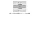
[0023]従来のシムは、重要な寸法公差を達成するために機械的なギャップを埋める機能だけを有する機械的部品である。しかし、本感知システム(本明細書では、場所により「スマートシム」とも称される)は、複数の機能 - ギャップ管理、ひずみ感知、エネルギーハーベスティング、データ送信 - をすべて、軽量で物理的な専有面積制約が小さい1つの部片に一体化する - 図1を参照されたい。 [0023] Conventional shims are mechanical parts whose sole function is to fill mechanical gaps to achieve critical dimensional tolerances. However, the present sensing system (also referred to herein as a "Smart Sim" in some places) performs multiple functions--gap management, strain sensing, energy harvesting, data transmission--all in a lightweight, physical proprietary Integrates into one piece with small area constraints - see Figure 1.
[0024]図2は、本感知システムの好ましい実施形態の異なるレイアウトを示す。 [0024] Figure 2 shows a different layout of a preferred embodiment of the present sensing system.
[0025]1つの選択肢(平行スマートシム)が図2(a)に示されており、機能ユニット - ひずみセンサ(機械的なひずみおよび変形を感知する)、エネルギーハーベスタ(周囲からエネルギーをハーベスティングし、それを電気エネルギーに変換する)、電力ユニット(AC電気エネルギーをDC電気エネルギーに変換し、それを貯蔵する)、およびデータユニット(ひずみ信号を収集し、それを遠隔の基地局に送信する) - が、同じシム層上で横方向に一体化される。 [0025] One option (parallel smart shim) is shown in FIG. , converts it into electrical energy), a power unit (converts AC electrical energy into DC electrical energy and stores it), and a data unit (collects the strain signal and transmits it to a remote base station). - are laterally integrated on the same shim layer.
[0026]図2(b)は、異なる機能ユニットが異なるシム層上に作製され、垂直方向に一体化される第2の選択肢(垂直スマートシム)を示す。 [0026] Figure 2(b) shows a second option (vertical smart shims) in which different functional units are fabricated on different shim layers and integrated vertically.
[0027]図2(c)いくつかの機能ユニットが1つのシム層上で一体化され、他の機能ユニットが別のシム層上で一体化され、次いで、これらの2つのシム層が垂直方向に共に一体化され、完全なシステムを達成する第3の選択肢(ハイブリッドスマートシム)を示す。平行スマートシム選択肢は、異なる機能ユニットを1つのシム層上で一体化することを必要とし、これはデバイス作製に対する要求が多い。一方、異なる機能ユニット間の相互接続は、1つのシム層上で行うことができる。 [0027] FIG. 2(c) Some functional units are integrated on one shim layer, other functional units are integrated on another shim layer, and then these two shim layers are vertically oriented. We show a third option (Hybrid Smart Sim) that is integrated together to achieve a complete system. The parallel smart shim option requires integrating different functional units on one shim layer, which is demanding for device fabrication. On the other hand, interconnections between different functional units can be made on one shim layer.
[0028]垂直スマートシム選択肢(図2(b))は、異なる機能ユニットを異なるシム層上に作製することができ、その結果、デバイス作製はより単純である。しかし、異なる機能ユニット間の相互接続は、より複雑である。ハイブリッドスマートシム選択肢(図3(c))は、先の2つの選択肢の利点を組み合わせる。いくつかの応用例では、ハイブリッドスマートシム選択肢が好ましい手法となり得る。 [0028] The vertical smart shim option (Fig. 2(b)) allows different functional units to be fabricated on different shim layers, resulting in simpler device fabrication. However, the interconnection between different functional units is more complicated. The Hybrid Smart Sim option (Fig. 3(c)) combines the advantages of the previous two options. For some applications, the hybrid smart sim option may be the preferred approach.
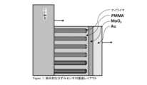
[0029]図3は、好ましいセンサシステムのレイアウトの好ましい実施形態を示す。この好ましい実施形態では、デバイスは、5つの層、すなわち(i)シム基材(下部電極としても働く、(ii)圧電ナノワイヤ(機械的なひずみを電位または電流に変換する)、(iii)ポリメチルメタクリレート(PMMA)層(ナノワイヤ間のギャップを埋め、ナノワイヤに対して機械的な支持を提供し、上部電極を下部電極から絶縁する)、(iv)MoO3層、および(v)Au層(上部電極として)からなる。他の実施形態では、MoO3層は省略される。圧電ナノワイヤ(NW)は、特に制限されない。NWは、InN NW、GaN NW、ZnOナノワイヤなどからなる群から選択されることが好ましい。ZnOナノワイヤは、電気化学的または熱化学的堆積手法のいずれかを使用することによってシム基材に成長させることができる。[0029] Figure 3 shows a preferred embodiment of a preferred sensor system layout. In this preferred embodiment, the device consists of five layers: (i) a shim substrate (which also acts as the bottom electrode), (ii) piezoelectric nanowires (which convert mechanical strain into electrical potential or current), (iii) poly A layer of methyl methacrylate (PMMA) (which fills the gaps between the nanowires, provides mechanical support for the nanowires, and insulates the top electrode from the bottom electrode), (iv) aMoO3 layer, and (v) a Au layer ( as the top electrode).In other embodiments, theMoO3 layer is omitted.Piezoelectric nanowires (NWs) are not particularly limited.The NWs are selected from the group consisting of InN NWs, GaN NWs, ZnO nanowires, etc. ZnO nanowires can be grown on the shim substrate by using either electrochemical or thermochemical deposition techniques.
[0030]ZnOナノワイヤは、白金メッシュ対電極およびAg/AgC参照電極を有する3電極構成で、電気化学的堆積を使用して成長させることができる。図の実施形態では、アルミニウムドープのZnO(AZO、2重量%Al2O3+98重量%ZnO)層が、事前洗浄されたシム基材上に無線周波数(RF)マグネトロンスパッタリングを150℃で使用して被覆された。いくつかの実施形態では、シム基材は、最初にクロムの層で被覆され、次いで、AZO層がクロム層の上部に被覆される。金または銅など他の金属が単独で、またはクロムとの組合せで、シム基材を被覆するために使用されてもよい。AZO層は、導電性電極としても後続の電気化学的堆積におけるNW成長のためのシード層としても働く。図の実施形態では、次いでフォトリソグラフィを使用し、AZO被覆されたPEN基材上にスピンオンされたフォトレジスト層内に、200μm離れた方形の窓のアレイを開いた。保持されているフォトレジストマスクは、NWが開いた窓内の露出されたシード層上だけに成長することを確実にする。[0030] ZnO nanowires can be grown using electrochemical deposition in a three-electrode configuration with a platinum mesh counter electrode and an Ag/AgC reference electrode. In the illustrated embodiment, an aluminum-doped ZnO (AZO, 2 wt%Al2O3+ 98 wt% ZnO) layer was deposited on a pre-cleaned shim substrate using radio frequency (RF) magnetron sputtering at 150°C. coated with In some embodiments, the shim substrate is first coated with a layer of chromium and then an AZO layer is coated on top of the chromium layer. Other metals such as gold or copper, alone or in combination with chromium, may be used to coat the shim substrate. The AZO layer acts both as a conductive electrode and as a seed layer for NW growth in subsequent electrochemical deposition. In the illustrated embodiment, photolithography was then used to open an array of
[0031]真性NW(n型)を成長させるための溶液は、25mMの硝酸亜鉛(Zn(NO3)2)、12.5mMのヘキサメチレンテトラミン(HMTA)、5mMのポリエチレンイミン(PEI)、および0.3Mの水酸化アンモニウムを含んでいた。p型NW(Liドープ)を得るために、異なる濃度の硝酸リチウムドーピング試薬を追加することができる。これらの濃度(25mM、50mM、および75mM)は、異なるリチウム混合比(それぞれ100%、200%、および300%)に対応し、LiドープのNWを異なるように製作した。作用電極のバイアスは、Ag/AgC参照電極に対して-0.7Vで固定された。NW長さ(約4μm)は、成長時間を真性セクション(n型)のための3時間と、その直後に続くLiドープのセクション(p型)のための別の3時間に設定することによって制御された。溶液温度は、どちらの場合にも、90℃10分間と、それに続く88℃170分間で維持された。[0031] The solution for growing intrinsic NWs (n-type) was 25 mM zinc nitrate (Zn(NO3 )2 ), 12.5 mM hexamethylenetetramine (HMTA), 5 mM polyethyleneimine (PEI), and It contained 0.3M ammonium hydroxide. Different concentrations of lithium nitrate doping reagents can be added to obtain p-type NWs (Li-doped). These concentrations (25 mM, 50 mM, and 75 mM) corresponded to different lithium mixing ratios (100%, 200%, and 300%, respectively) to fabricate Li-doped NWs differently. The bias of the working electrode was fixed at -0.7 V relative to the Ag/AgC reference electrode. The NW length (about 4 μm) is controlled by setting the growth time to 3 hours for the intrinsic section (n-type) followed immediately by another 3 hours for the Li-doped section (p-type). was done. The solution temperature was maintained at 90° C. for 10 minutes followed by 88° C. for 170 minutes in both cases.
[0032]図4は、電気化学的堆積を使用することによって成長されたZnOナノワイヤの走査電子顕微鏡(SEM)像を示す。単結晶NWが、±25°以内の傾斜角を有する垂直方向に沿って粗く位置合わせされている。それらの直径は、約2.0×109cm-2の面密度で100nmから200nmに及んだ。[0032] Figure 4 shows a scanning electron microscope (SEM) image of ZnO nanowires grown by using electrochemical deposition. A single crystal NW is roughly aligned along a vertical direction with a tilt angle within ±25°. Their diameter ranged from 100 nm to 200 nm with an areal density of about 2.0×109 cm−2 .
[0033]図5は、本感知システム(この場合、ナノワイヤベースのひずみセンサ)の好ましい実施形態を作製するプロセスステップの概略図の好ましい実施形態を示す。一辺の長さ1~10cmを有する方形または異なる形状のNWパターンを、デバイス作製において使用することができる。これらのNWは、最初にPMMAのスピンコートされた絶縁層でカプセル封入され、次いで120℃3時間で硬化される。この層は、NG動作中、NWを損傷から保護するためのポリマーマトリクスを提供し、NGの上部電極と下部電極との間の電気的短絡を防止する。その可撓性により、PMMAは、NWに外部ひずみを加えることを妨げない。 [0033] Figure 5 shows a preferred embodiment of a schematic diagram of the process steps for fabricating a preferred embodiment of the present sensing system (in this case a nanowire-based strain sensor). Square or differently shaped NW patterns with a side length of 1-10 cm can be used in device fabrication. These NWs are first encapsulated with a spin-coated insulating layer of PMMA and then cured at 120° C. for 3 hours. This layer provides a polymer matrix to protect the NW from damage during NG operation and prevents electrical shorting between the top and bottom electrodes of the NG. Due to its flexibility, PMMA does not prevent applying external strain to the NW.
[0034]界面エネルギー障壁を増大し、漏れ電流を抑制するために、シャドウマスクを使用した真空熱蒸着と、その後に続く金属カソード(アルミニウムまたは金)の堆積を使用することによって、薄い酸化モリブデン(MoO3)中間層をPMMA層の上部に堆積し、作製を完了することができる。これらのデバイスは、周囲の環境からの汚染、損傷、および水分浸透を防止するために、ポリジメチルシロキサン(PDMS)、すなわち10:1w/wの比率で硬化剤と事前混合され脱ガスされたDow Corning Sylgard(登録商標)184内にパックすることができる。[0034] To increase the interfacial energy barrier and suppress leakage current, thin molybdenum oxide ( MoO3 ) intermediate layer can be deposited on top of the PMMA layer to complete the fabrication. These devices are made of polydimethylsiloxane (PDMS), a degassed Dow resin premixed with a curing agent in a 10:1 w/w ratio to prevent contamination, damage, and moisture penetration from the surrounding environment. It can be packed in a Corning Sylgard® 184.
[0035]図6は、ZnOホモ接合NWに基づく本感知システムの好ましい実施形態の概略レイアウトを示す。ZnOホモ接合NWを使用することによって、機械的エネルギーを電気エネルギーに変換する効率を著しく向上させることができる。そのようなエネルギーハーベスティングデバイスの作製は、ZnOナノワイヤベースのひずみセンサのものと同様である。これらの2つのデバイス間の違いは、ひずみセンサは機械的なひずみに対して感度を有し、低いノイズレベルを有するべきであり、一方、エネルギーハーベスタは、機械的エネルギーを電気エネルギーに変換するうえで高い効率を有するべきであることである。ZnOナノワイヤおよびデバイス構成は、これらの2つのデバイスについて、それらの異なる技術的要件の点で異なるように最適化することができる。 [0035] Figure 6 shows a schematic layout of a preferred embodiment of the present sensing system based on ZnO homozygous NWs. By using ZnO homojunction NWs, the efficiency of converting mechanical energy into electrical energy can be significantly improved. The fabrication of such energy harvesting devices is similar to that of ZnO nanowire-based strain sensors. The difference between these two devices is that a strain sensor should be sensitive to mechanical strain and have a low noise level, while an energy harvester should convert mechanical energy into electrical energy. should have high efficiency at The ZnO nanowires and device architecture can be optimized differently for these two devices in terms of their different technical requirements.
[0036]本感知システムの好ましい実施形態で使用され得る好ましい圧電ナノ発電機についてのさらなる詳細は、共に2017年5月11日に出願された、同時係属のカナダ特許出願第2,967,004号、および米国特許仮出願第62/602,895号に見出すことができる。またG. Liu, E. Abdel-Rahman, D. Ban,「Performance optimization of p-n homojunction nanowire-based piezoelectric nanogenerators through control of doping concentration」 J. Appl. Phys., 2915, 118, 094307をも参照されたい。 [0036] Further details about preferred piezoelectric nanogenerators that may be used in preferred embodiments of the present sensing system are found in co-pending Canadian Patent Application No. 2,967,004, both filed May 11, 2017. , and in US Provisional Patent Application No. 62/602,895. Also G. Liu, E. Abdel-Rahman, D.; Ban, "Performance optimization of pn homojunction nanowire-based piezoelectric nanogenerators through control of doping concentration," J. Am. Appl. Phys. , 2915, 118, 094307.
[0037]圧電ナノ発電機がInNナノワイヤベースのものである場合、G. Liu, S. Zhao, R. D. Henderson, Z. Leonenko, E. Abdel-Rahman, Z. Mi,およびD. Ban,「Nanogenerators based on vertically aligned InN nanowires」Nanoscale, 2016, 8, 2097-2106をも参照されたい。 [0037] If the piezoelectric nanogenerator is based on InN nanowires, G. Liu, S. Zhao, R. D. Henderson, Z.; Leonenko, E. Abdel-Rahman, Z.; Mi, and D. See also Ban, "Nanogenerators based on vertically aligned InN nanowires" Nanoscale, 2016, 8, 2097-2106.
[0038]エネルギーハーベスタユニットは、摩擦電気デバイスを使用して作製することもできる。摩擦電気デバイスのエネルギー変換効率は、典型的には、デバイスの2つの電極の相対的な機械的変位に依存する。この機械的な相対変位がかなり大きなものである場合、摩擦電気エネルギーハーベスタは、圧電エネルギーハーベスタより有益なものとなり得る。 [0038] Energy harvester units can also be made using triboelectric devices. The energy conversion efficiency of triboelectric devices typically depends on the relative mechanical displacement of the two electrodes of the device. If this relative mechanical displacement is fairly large, triboelectric energy harvesters can be more beneficial than piezoelectric energy harvesters.
[0039]摩擦電気デバイスは、圧電デバイスより単純な層構造を有する。典型的には、ポリマー絶縁層によって分離された2つの金属電極層からなる。図7は、本感知システムにおける摩擦電気デバイスの好ましい実施形態を示し、この摩擦電気デバイスは、上側PMMA層と、上側電極と、ポリジメチルシロキサン(PDMS)層と、下側電極と、下側PMMA層とを備える。金属電極層は、熱蒸着によってPMMA基材上に堆積させることができる。PDMS層は、スピンコーティングによって金属電極層上に堆積させることができる。エネルギー変換効率を向上させるために、金属ナノ粒子(Auナノ粒子など)をPDMS層と下側電極層との間の界面に挿入することができる。 [0039] Triboelectric devices have a simpler layer structure than piezoelectric devices. It typically consists of two metal electrode layers separated by a polymer insulating layer. FIG. 7 shows a preferred embodiment of a triboelectric device in the present sensing system, comprising a top PMMA layer, a top electrode, a polydimethylsiloxane (PDMS) layer, a bottom electrode, and a bottom PMMA a layer; A metal electrode layer can be deposited on the PMMA substrate by thermal evaporation. A PDMS layer can be deposited on the metal electrode layer by spin coating. Metal nanoparticles (such as Au nanoparticles) can be inserted into the interface between the PDMS layer and the lower electrode layer to improve the energy conversion efficiency.
[0040]好ましい実施形態では、本感知システムで使用するための摩擦電気ナノ発電機は、以下の非限定的なプロセスを使用して製作される。
1.フォトリソグラフィを使用してシリコンウェハ(たとえば、直径5インチ)上に、モールド層がパターン形成される。
2.パターン形成されたウェハは、ドライエッチングプロセスを使用して異方性エッチングされ、陥凹した角錐が形成される。
3.アセトンイソプロパノールで洗浄後、PDMSとSiモールドとの間の接着を回避するために、Siウェハのすべてが、気相シラン化によってトリメチルクロロシラン(Sigma Aldrich)で処理される。
4.パターン形成されたポリマー膜を準備する際、PDMSエラストマーと架橋剤(Sylgard 184、Tow Corning)が混合され、次いでSiウェハ上に塗布される。
5.真空下での脱ガスプロセス後、エラストマー混合物が500rpmで60秒間スピンコートされる。
6.85℃で1時間、保温した後、均一なPDMS薄膜がSiモールドから剥離され、未硬化のPDMSが1枚の清浄なITO被覆されたPET膜上に置かれる。
7.サンドイッチ構造を形成するために、別の清浄なITO被覆されたPET膜が、準備されたPDMS-PET基材上に置かれる。
8.次いで、PETとパターン形成されたPDMS膜との間の適切な接触を確保するために、デバイスの2つの短い縁部が通常の接着テープで封止される。[0040] In a preferred embodiment, a triboelectric nanogenerator for use in the present sensing system is fabricated using the following non-limiting process.
1. A mold layer is patterned on a silicon wafer (eg, 5 inch diameter) using photolithography.
2. The patterned wafer is anisotropically etched using a dry etching process to form recessed pyramids.
3. After cleaning with acetone isopropanol, all of the Si wafers are treated with trimethylchlorosilane (Sigma Aldrich) by vapor phase silanization to avoid adhesion between PDMS and Si molds.
4. In preparing a patterned polymer film, a PDMS elastomer and a crosslinker (Sylgard 184, Tow Corning) are mixed and then applied onto a Si wafer.
5. After the degassing process under vacuum, the elastomer mixture is spin coated at 500 rpm for 60 seconds.
After incubation at 6.85° C. for 1 hour, the uniform PDMS thin film is peeled off from the Si mold and the uncured PDMS is placed on a piece of clean ITO-coated PET film.
7. Another clean ITO-coated PET film is placed on the prepared PDMS-PET substrate to form a sandwich structure.
8. Two short edges of the device are then sealed with conventional adhesive tape to ensure proper contact between the PET and the patterned PDMS film.
[0041]多くのシム基材は、金属材料製であるため、上側電極層および下側電極層として使用することができ、これは、本感知システムにおけるエネルギーハーベスタ構成部品のデバイス作製および一体化を簡素化することができる。 [0041] Since many shim substrates are made of metallic materials, they can be used as the upper and lower electrode layers, which facilitates device fabrication and integration of the energy harvester components in the present sensing system. can be simplified.
[0042]発生されるエネルギーは、調整された状態でデバイスに給電するために使用することができるように、バッテリまたはキャパシタに貯蔵されることが好ましい。発電ユニットと貯蔵ユニットとの間には、電力貯蔵効率を最大化するために、電力管理回路を実装することが好ましい。中心的な目標は、貯蔵のために、またデータユニットによって消費されるエネルギーを管理するために、ハーベスティングされたエネルギーをバッテリ層に転送するためのより効率的なエネルギーハーベスティングおよび管理回路を開発することである。 [0042] The energy generated is preferably stored in a battery or capacitor so that it can be used to power the device in a regulated manner. Power management circuitry is preferably implemented between the generation unit and the storage unit to maximize power storage efficiency. A central goal is to develop a more efficient energy harvesting and management circuit to transfer the harvested energy to the battery layer for storage and to manage the energy consumed by the data unit. It is to be.
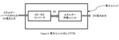
[0043]図8は、典型的には、AC電流をDC電流に変換するための電子回路と、エネルギー貯蔵ユニットとを含む、例示的な電力ユニットの基本レイアウトの好ましい実施形態を示す。エネルギーハーベスタからのAC電力は、AC-DCコンバータを介してDC電力に変換され、エネルギー貯蔵ユニットに貯蔵される。貯蔵された電力は、ひずみデータ収集および送信のために、他の構成部品(データユニットなど)をバイアスするために使用されることになる。 [0043] Figure 8 shows a preferred embodiment of the basic layout of an exemplary power unit, which typically includes electronic circuitry for converting AC current to DC current and an energy storage unit. AC power from the energy harvester is converted to DC power via an AC-DC converter and stored in an energy storage unit. The stored power will be used to bias other components (such as data units) for strain data acquisition and transmission.
[0044]4つのpn接合ダイオードと1つのキャパシタとからなる代表的なAC-DCコンバータ回路が図9に示されている。これらのpn接合ダイオードおよびキャパシタは、ASIC(アモルファスシリコン集積回路)技術を使用することによって作製することができる。エネルギー貯蔵ユニットは、スーパーキャパシタまたは薄膜ベースのリチウム再充電可能バッテリとすることができる。金属シム基材の場合、高い誘電率を有する電気絶縁層によって分離された2つの隣り合うシム層を、スーパーキャパシタの2つの電極として使用することができる。 [0044] A typical AC-DC converter circuit consisting of four pn junction diodes and one capacitor is shown in FIG. These pn junction diodes and capacitors can be made by using ASIC (amorphous silicon integrated circuit) technology. The energy storage unit can be a supercapacitor or a thin film-based lithium rechargeable battery. For metal shim substrates, two adjacent shim layers separated by an electrically insulating layer with a high dielectric constant can be used as the two electrodes of a supercapacitor.
[0045]データユニットは、ひずみ信号収集および送信のためのものである。データユニットは、スタンドアロンのユニットとすることができ、これは、Soc-Robotics.comからのRF24L01ワイヤレスコネクタなど市販のものである。それは、収集されたひずみ信号を、短い距離の範囲内にある基地局に送信することができる。別の選択肢は、ASIC技術を使用してシム基材上にデータ収集および送信回路を直接作製することである。ワイヤレス送信距離は短く、データ送信速度は低いので、データユニットの技術的要件を満たすために、そのようなASIC回路は十分なはずである。 [0045] The data unit is for strain signal acquisition and transmission. A data unit can be a stand-alone unit, which is described in Soc-Robotics. are commercially available such as the RF24L01 wireless connector from com. It can transmit the collected distorted signal to a base station within a short distance. Another option is to use ASIC technology to fabricate the data acquisition and transmission circuits directly on the shim substrate. Since the wireless transmission distance is short and the data transmission rate is low, such an ASIC circuit should be sufficient to meet the technical requirements of the data unit.
[0046]図10は、可撓性基材上に作製されたZnOナノワイヤベースの圧電エネルギーハーベスタの予備実験結果を示す。平均ピーク開回路電圧は0.7Vであり、平均ピーク短絡回路電流は42nAであり、0.03Wのピーク出力電力を生み出す。 [0046] Figure 10 shows preliminary experimental results of a ZnO nanowire-based piezoelectric energy harvester fabricated on a flexible substrate. The average peak open circuit voltage is 0.7V and the average peak short circuit current is 42nA, yielding a peak output power of 0.03W.
[0047]図11は、ワイヤレスひずみ信号送信のための概念実証セットアップを示す。ひずみセンサは、2つの市販のひずみゲージ(Vishay Precision Group)であり、機械的振動下に置いた。ひずみデータは、エネルギーハーベスティングシステムによって給電されるワイヤレスセンサノードによって収集され、近くの基地局に送信された。これらの予備実験結果は、ひずみセンサ上の加えられたひずみは、周波数3Hzで1600μsであったことを示す。 [0047] FIG. 11 shows a proof-of-concept setup for wireless distortion signal transmission. The strain sensors were two commercially available strain gauges (Vishay Precision Group) placed under mechanical vibration. Strain data were collected by wireless sensor nodes powered by the energy harvesting system and transmitted to nearby base stations. These preliminary experimental results show that the applied strain on the strain sensor was 1600 μs at a frequency of 3 Hz.
[0048]図12は、可撓性基材上に作製された作製済みのZnOナノワイヤベースの圧電エネルギーハーベスタの特性決定のためのセットアップの概略図を示す。システムは、閉ループコントローラ(VR9500 Revolution)と、リニアシェーカ(Labworks Inc.,ET-126-1)とを含む。シェーカは、特定の周波数、加速度、および力の量で機械的なひずみを提供することができる。図のセットアップを使用して、圧電エネルギーハーベスタの得られた出力開回路電圧および出力短絡回路電流は、Stanford低ノイズ電圧/電流前置増幅器(Model SR560/570)を使用して、前置増幅器の入力抵抗をそれぞれ100MΩ(SR560)および10kΩ(SR570)に設定して測定された(図10参照)。 [0048] Figure 12 shows a schematic of the setup for the characterization of pre-fabricated ZnO nanowire-based piezoelectric energy harvesters fabricated on flexible substrates. The system includes a closed-loop controller (VR9500 Revolution) and a linear shaker (Labworks Inc., ET-126-1). A shaker can provide mechanical strain at a specific frequency, acceleration, and amount of force. Using the setup in the figure, the resulting output open circuit voltage and output short circuit current of the piezoelectric energy harvester were measured using a Stanford low noise voltage/current preamplifier (Model SR560/570). Measurements were taken with the input resistance set to 100 MΩ (SR560) and 10 kΩ (SR570) respectively (see FIG. 10).
[0049]本発明について、例示的な実施形態および例を参照して述べたが、この説明は、限定的な意味で解釈されることは意図されていない。したがって、この説明を読めば、本発明のこれらの例示的な実施形態、ならびに他の実施形態の様々な修正形態が、当業者には明らかになろう。したがって、添付の特許請求の範囲は、任意のそのような修正形態または実施形態を包含することが企図されている。 [0049] While the invention has been described with reference to illustrative embodiments and examples, this description is not meant to be construed in a limiting sense. Thus, various modifications of these illustrative embodiments, as well as other embodiments of the invention, will become apparent to persons skilled in the art upon reading this description. It is therefore intended that the appended claims cover any such modifications or embodiments.
[0050]本明細書で参照されているすべての出版物、特許、および特許出願は、各個々の出版物、特許、または特許出願が具体的に個々にその全体が参照により組み込まれるものと示されているかのように同じ程度でそれらの全体が参照により組み込まれている。
背景技術参考文献のリスト
[1] G. Liu,「Semiconductor Nanowire Based Piezoelectric Energy Harvesters: Modeling, Fabrication, and Characterization」 Ph.D. thesis, 2015, University of Waterloo.
[2] M. Q. Le, J.-F. Capsal, M. Lallart, Y. Hebrard, A. Van Der Ham, N. Reffe, L. Geynet,およびP.-J. Cottinet,「Review on energy harvesting for structural health monitoring in aeronautical applications」 Prog. Aerosp. Sci., 2015, 79, 147-157.
[3] Y. HuおよびZ. L. Wang,「Recent progress in piezoelectric nanogenerators as a sustainable power source in self-powered systems and active sensors」 Nano Energy, 2015, 14, 3-14.
[4] R. Hinchet, W. Seung,およびS. W. Kim,「Recent Progress on Flexible Triboelectric Nanogenerators for SelfPowered Electronics」 ChemSusChem, 2015, 8, 2327-2344.
[5] F. R. Fan, W. Tang,およびZ. L. Wang,「Flexible Nanogenerators for Energy Harvesting and Self‐Powered Electronics」 Adv. Mater., 2016.
[6] Z. L. Wang, J. Chen,およびL. Lin,「Progress in triboelectric nanogenerators as a new energy technology and self-powered sensors」 Energy Environ. Sci., 2015, 8, 2250-2282.
[7] J. BriscoeおよびS. Dunn,「Piezoelectric nanogenerators-a review of nanostructured piezoelectric energy harvesters」 Nano Energy, 2015, 14, 15-29.
[8] S. Wang, L. Lin,およびZ. L. Wang,「Triboelectric nanogenerators as self-powered active sensors」 Nano Energy, 2015, 11, 436-462.
[9] M. Han, X.-S. Zhang, B. Meng, W. Liu, W. Tang, X. Sun, W. Wang,およびH. Zhang,「r-Shaped hybrid nanogenerator with enhanced piezoelectricity」 ACS Nano, 2013, 7, 8554-8560.
[10] X. Li, Z.-H. Lin, G. Cheng, X. Wen, Y. Liu, S. Niu,およびZ. L. Wang,「3D Fiber-Based Hybrid Nanogenerator for Energy Harvesting and as a Self-Powered Pressure Sensor」 ACS Nano, 2014, 8, 10674-10681.
[11] K. Y. Lee, M. K. Gupta,およびS.-W. Kim,「Transparent flexible stretchable piezoelectric and triboelectric nanogenerators for powering portable electronics」 Nano Energy, 2015, 14, 139-160.
[12] S.-B. Jeon, D. Kim, G.-W. Yoon, J.-B. Yoon,およびY.-K. Choi,「Self-cleaning hybrid energy harvester to generate power from raindrop and sunlight」 Nano Energy, 2015, 12, 636-645.
[13] X. Wang, S. Wang, Y. Yang,およびZ. L. Wang,「Hybridized Electromagnetic-Triboelectric Nanogenerator for Scavenging Air-Flow Energy to Sustainably Power Temperature Sensors」 ACS Nano, 2015, 9, 4553-4562.
[14] T. Quan, X. Wang, Z. L. Wang,およびY. Yang,「Hybridized Electromagnetic-Triboelectric Nanogenerator for a Self-Powered Electronic Watch」 ACS Nano, 2015, 9, 12301-12310.
[15] Y. Zi, L. Lin, J. Wang, S. Wang, J. Chen, X. Fan, P. K. Yang, F. Yi,およびZ. L. Wang,「Triboelectric-Pyroelectric-Piezoelectric Hybrid Cell for High‐Efficiency Energy‐Harvesting and Self‐Powered Sensing」 Adv. Mater., 2015, 27, 2340-2347.
[16] Y. YangおよびZ. L. Wang,「Hybrid energy cells for simultaneously harvesting multi-types of energies」 Nano Energy, 2015, 14, 245-256.
[17] S. Wang, Z. L. Wang,およびY. Yang,「A One-Structure-Based Hybridized Nanogenerator for Scavenging Mechanical and Thermal Energies by Triboelectric-Piezoelectric-Pyroelectric Effects」 Advanced materials (Deerfield Beach, Fla.), 2016.
[18] W.-S. Jung, M.-G. Kang, H. G. Moon, S.-H. Baek, S.-J. Yoon, Z.-L. Wang, S.-W. Kim,およびC.-Y. Kang,「High output piezo/triboelectric hybrid generator」 Sci. Rep., 2015, 5.
[19] S. Niu, Y. Liu, S. Wang, L. Lin, Y. S. Zhou, Y. Hu,およびZ. L. Wang,「Theoretical Investigation and Structural Optimization of Single‐Electrode Triboelectric Nanogenerators」 Adv. Funct. Mater., 2014, 24, 3332-3340.
[20] H. Jang, Y. J. Park, X. Chen, T. Das, M. S. Kim,およびJ. H. Ahn,「Graphene‐Based Flexible and Stretchable Electronics」 Adv. Mater., 2016.
[21] C. Hu, L. Song, Z. Zhang, N. Chen, Z. Feng,およびL. Qu,「Tailored graphene systems for unconventional applications in energy conversion and storage devices」 Energy Environ. Sci., 2015, 8, 31-54.
[22] B. N. Chandrashekar, B. Deng, A. S. Smitha, Y. Chen, C. Tan, H. Zhang, H. Peng,およびZ. Liu,「Roll‐to‐Roll Green Transfer of CVD Graphene onto Plastic for a Transparent and Flexible Triboelectric Nanogenerator」 Adv. Mater., 2015, 27, 5210-5216.
[23] S. Kim, M. K. Gupta, K. Y. Lee, A. Sohn, T. Y. Kim, K. S. Shin, D. Kim, S. K. Kim, K. H. Lee,およびH. J. Shin,「Transparent flexible graphene triboelectric nanogenerators」 Adv. Mater., 2014, 26, 3918-3925.
[24] L. E. Greene, M. Law, J. Goldberger, F. Kim, J. C. Johnson, Y. Zhang, R. J. Saykally,およびP. Yang,「Low‐temperature wafer‐scale production of ZnO nanowire arrays」 Angew. Chem. Int. Ed., 2003, 42, 3031-3034.
[25] D.-M. Shin, E. L. Tsege, S. H. Kang, W. Seung, S.-W. Kim, H. K. Kim, S. W. Hong,およびY.-H. Hwang,「Freestanding ZnO nanorod/graphene/ZnO nanorod epitaxial double heterostructure for improved piezoelectric nanogenerators」 Nano Energy, 2015, 12, 268-277.
[26] G. Liu, S. Zhao, R. D. Henderson, Z. Leonenko, E. Abdel-Rahman, Z. Mi,およびD. Ban,「Nanogenerators based on vertically aligned InN nanowires」 Nanoscale, 2016, 8, 2097-2106.
[27] G. Liu, E. Abdel-Rahman, D. Ban, Performance optimization of p-n homojunction nanowire-based piezoelectric nanogenerators through control of doping concentration. J. Appl. Phys., 2915, 118, 094307.
[28] R. S. Dhar, L. Li, H. Ye, S, G. Razavipour, X. Wang, R. Q. Yang, D. Ban,「Nanoscopically resolved dynamic charge carrier distribution in operating interband cascade lasers」 Laser & Photonics Review, 2015, 8, 224.
[29] R. S. Dhar, S. G. Razavipour, E. Dupont, C. Xu, S. Laframboise, Z. Wasilewski, Q. Hu, D. Ban,「 Direct Nanoscale Imaging of Evolving Electric Field Domains in Quantum Structures」 Scientific Reports, 2014, 4, 7183.
[30] S. Fathololoumi, E. Dupont, C. W. I. Chan, etc.,「Terahertz quantum cascade lasers operating up to ~200K with optimized oscillator strength and improved injection tunneling」 Optics Express, 2012, 20, 3866.
[31] Jun Chen, Dayan Ban, Michael G. Helander, Zhenghong LuおよびP. Poole,「Near-infrared inorganic/organic optical upconverter with an external efficiency of > 100%」 Advanced Materials, 2010, 22, 4900.
[32] Jun Chen, Jianchen Tao, Dayan Ban, M. G. Helander, Z. Wang, J. Qiu, Z. H. Lu,「Organic/Inorganic Hybrid Pixelless Imaging Device」 Advanced Materials, 2012, 24, 3138.
[33] Cheng-Ying Chen, Jun-Han Huang, Jinhui Song, Yusheng Zhou, Long Lin, Po-Chien Huang, Yan Zhang, Chuan-Pu Liu, Jr-Hau He,およびZhong Lin Wang,「Anisotropic Outputs of a Nanogenerator from Oblique-Aligned ZnO Nanowire Arrays」 ACS Nano, 2011, 5, 6707-6713.
[34] Nai-Jen Ku, Jun-Han Huang, Chao-Hung Wang, Hsin-Chiao Fang,およびChuan-Pu Liu,「Crystal Face-Dependent Nanopiezotronics of an Obliquely Aligned InN Nanorod Array」 Nano Letters, 2012, 12, 562-568.
[35] Ruey-Chi Wang, Hsin-Ying Lin, Chao-Hung Wang,およびChuan-Pu Liu,「Fabrication of a large-area Al-doped ZnO nanowire array photosensor with enhanced photoresponse by straining」 Advanced Functional Materials, 2012, 22, 3875-3881.
[36] Nai-Jen Ku, Chao-Hung Wang, Jun-Han Huang, Hsin-Chiao Fang, Po-Chien HuangおよびChuan-Pu Liu,「Energy Harvesting from the Obliquely Aligned InN Nanowire Array with a Surface Electron-Accumulation Layer」 Advanced Materials, 2013, 25, 861-866.
[37] Chia-Hao Tu, Waileong Chen, Hsin-Chiao Fang, Yonhua Tzeng, Chuan-Pu Liu,「Heteroepitaxial nucleation and growth of graphene nanowalls on silicon」 Carbon, 2013, 54, 234-240.
[38] Chao-Hung Wang, Wei-Shun Liao, Zong-Hong Lin, Nai-Jen Ku, Yi-Chang Li, Yen-Chih Chen, Zhong-Lin WangおよびChuan-Pu Liu,「Optimization of the Output Efficiency of GaN Nanowire Piezoelectric Nanogenerators by Tuning the Free Carrier Concentration」 Advanced Energy Materials, 2014, 4, 1400392.
[39] Chao-Hung Wang, Wei-Shun Liao, Nai-Jen Ku, Yi-Chang Li, Yen-Chih Chen, Li-Wei TuおよびChuan-Pu Liu,「Effects of Free Carriers on Piezoelectric Nanogenerators and Piezotronic Devices Made of GaN Nanowire Arrays」 Small, 2014, 10, 4718-4725.
[40] Yen-Yu Chen, Chao-Hung Wang, Giin-Shan Chen, Yi-Chang LiおよびChuan-Pu Liu,「Self-powered n-MgxZn1-xO/p-Si photodetector improved by alloying-enhanced piezopotential through piezo-phototronic effect」 Nano Energy, 2015, 11, 533-539.
[41] Chao-Hung Wang, Kun-Yu Lai, Yi-Chang Li, Yen-Chih Chen,およびChuan-Pu Liu,「Ultrasensitive Thin-Film-Based AlxGa1xN Piezotronic Strain Sensors via Alloying-Enhanced Piezoelectric Potential」 Advanced Materials, 2015, 27, 6289-6295.
[42] Dayan Ban, Guocheng Liu,共に2017年5月11日に出願された「Cascade-type hybrid energy cells for driving wireless sensors」同時係属のカナダ特許出願第2,967,004号および米国特許仮出願第62/602,895号[0050] All publications, patents, and patent applications referenced in this specification are indicated that each individual publication, patent, or patent application is specifically and individually incorporated by reference in its entirety. are incorporated by reference in their entireties to the same extent as if they had been written.
List of Background Art References [1] G. Liu, "Semiconductor Nanowire Based Piezoelectric Energy Harvesters: Modeling, Fabrication, and Characterization," Ph. D. thesis, 2015, University of Waterloo.
[2] M. Q. Le, J. -F. Capsal, M. Lallart, Y.; Hebrard, A.; Van Der Ham, N.W. Reffe, L.; Geynet, and P.S. -J. Cottinet, "Review on energy harvesting for structural health monitoring in aeronautical applications," Prog. Aerosp. Sci. , 2015, 79, 147-157.
[3] Y. Hu and Z.L. L. Wang, "Recent progress in piezoelectric nanogenerators as a sustainable power source in self-powered systems and active sensors," Nano Energy, 2015, 14, 3-14.
[4] R. Hinchet, W.; Seung, and S. W. Kim, "Recent Progress on Flexible Triboelectric Nanogenerators for Self-Powered Electronics," ChemSusChem, 2015, 8, 2327-2344.
[5]F. R. Fan, W. Tang, and Z.L. L. Wang, "Flexible Nanogenerators for Energy Harvesting and Self-Powered Electronics" Adv. Mater. , 2016.
[6] Z. L. Wang, J. Chen, and L.L. Lin, "Progress in triboelectric nanogenerators as a new energy technology and self-powered sensors," Energy Environ. Sci. , 2015, 8, 2250-2282.
[7]J. Briscoe and S. Dunn, “Piezoelectric nanogenerators—a review of nanostructured piezoelectric energy harvesters,” Nano Energy, 2015, 14, 15-29.
[8] S. Wang, L. Lin, and Z.L. L. Wang, “Triboelectric nanogenerators as self-powered active sensors,” Nano Energy, 2015, 11, 436-462.
[9] M. Han, X.; -S. Zhang, B. Meng, W.; Liu, W.; Tang, X. Sun, W.; Wang, and H. Zhang, “r-Shaped hybrid nanogenerator with enhanced piezoelectricity,” ACS Nano, 2013, 7, 8554-8560.
[10]X. Li, Z.; -H. Lin, G. Cheng, X.; Wen, Y. Liu, S. Niu, and Z. L. Wang, "3D Fiber-Based Hybrid Nanogenerator for Energy Harvesting and as a Self-Powered Pressure Sensor," ACS Nano, 2014, 8, 10674-10681.
[11] K. Y. Lee, M. K. Gupta, and S. -W. Kim, "Transparent flexible stretchable piezoelectric and triboelectric nanogenerators for powering portable electronics," Nano Energy, 2015, 14, 139-160.
[12] S. -B. Jeon, D. Kim, G. -W. Yoon, J. -B. Yoon, and Y.K. -K. Choi, “Self-cleaning hybrid energy harvester to generate power from raindrop and sunlight,” Nano Energy, 2015, 12, 636-645.
[13] X. Wang, S. Wang, Y. Yang, and Z.P. L. Wang, "Hybridized Electromagnetic-Triboelectric Nanogenerator for Scavenging Air-Flow Energy to Sustainably Power Temperature Sensors" ACS Nano, 2015, 9, 4553-4553.
[14] T. Quan, X.; Wang, Z. L. Wang, and Y. Yang, "Hybridized Electromagnetic-Triboelectric Nanogenerator for a Self-Powered Electronic Watch," ACS Nano, 2015, 9, 12301-12310.
[15] Y. Zi, L. Lin, J. Wang, S. Wang, J. Chen, X.; Fan, P. K. Yang, F. Yi, and Z.I. L. Wang, "Triboelectric-Pyroelectric-Piezoelectric Hybrid Cell for High-Efficiency Energy-Harvesting and Self-Powered Sensing" Adv. Mater. , 2015, 27, 2340-2347.
[16] Y.S. Yang and Z.L. L. Wang, "Hybrid energy cells for simultaneously harvesting multi-types of energies," Nano Energy, 2015, 14, 245-256.
[17] S. Wang, Z. L. Wang, and Y. Yang,「A One-Structure-Based Hybridized Nanogenerator for Scavenging Mechanical and Thermal Energies by Triboelectric-Piezoelectric-Pyroelectric Effects」 Advanced materials (Deerfield Beach, Fla.), 2016.
[18] W. -S. Jung, M. -G. Kang, H. G. Moon, S.; -H. Baek, S.; -J. Yoon, Z.; -L. Wang, S. -W. Kim, and C.I. -Y. Kang, "High output piezo/triboelectric hybrid generator," Sci. Rep. , 2015, 5.
[19] S. Niu, Y.; Liu, S. Wang, L. Lin, Y.; S. Zhou, Y.; Hu, and Z.L. L. Wang, "Theoretical Investigation and Structural Optimization of Single-Electrode Triboelectric Nanogenerators" Adv. Funct. Mater. , 2014, 24, 3332-3340.
[20] H. Jang, Y. J. Park, X. Chen, T. Das, M. S. Kim, and J. H. Ahn, "Graphene-Based Flexible and Stretchable Electronics" Adv. Mater. , 2016.
[21] C.I. Hu, L.; Song, Z. Zhang, N.; Chen, Z.; Feng, and L. Qu, "Tailored graphene systems for unconventional applications in energy conversion and storage devices," Energy Environ. Sci. , 2015, 8, 31-54.
[22]B. N. Chandrashekar, B.; Deng, A. S. Smitha, Y.; Chen, C. Tan, H. Zhang, H. Peng, and Z.P. Liu, "Roll-to-Roll Green Transfer of CVD Graphene onto Plastic for a Transparent and Flexible Triboelectric Nanogenerator" Adv. Mater. , 2015, 27, 5210-5216.
[23] S. Kim, M. K. Gupta, K.; Y. Lee, A. Sohn, T. Y. Kim, K. S. Shin, D. Kim, S. K. Kim, K. H. Lee, and H. J. Shin, "Transparent flexible graphene triboelectric nanogenerators" Adv. Mater. , 2014, 26, 3918-3925.
[24] L. E. Greene, M. Law,J. Goldberger, F.; Kim, J. C. Johnson, Y.; Zhang, R. J. Saykally, and P.S. Yang, "Low-temperature wafer-scale production of ZnO nanowire arrays," Angew. Chem. Int. Ed. , 2003, 42, 3031-3034.
[25]D. -M. Shin, E. L. Tsege, S.; H. Kang, W. Seung, S.; -W. Kim, H. K. Kim, S. W. Hong, and Y.K. -H. Hwang, "Freestanding ZnO nanorod/graphene/ZnO nanorod epitaxial double heterostructure for improved piezoelectric nanogenerators" Nano Energy, 2015, 12, 268-277.
[26]G. Liu, S. Zhao, R. D. Henderson, Z.; Leonenko, E. Abdel-Rahman, Z.; Mi, and D. Ban, “Nanogenerators based on vertically aligned InN nanowires,” Nanoscale, 2016, 8, 2097-2106.
[27] G. Liu, E. Abdel-Rahman, D.; Ban, Performance optimization of pn homojunction nanowire-based piezoelectric nanogenerators through control of doping concentration. J. Appl. Phys. , 2915, 118, 094307.
[28] R. S. Dhar, L.; Li, H. Ye, S, G. Razavipour, X.; Wang, R. Q. Yang, D. Ban, "Nanoscopically resolved dynamic charge carrier distribution in operating interconnect cascade lasers," Laser & Photonics Review, 2015, 8, 224.
[29] R. S. Dhar, S. G. Razavipour, E.M. Dupont, C.I. Xu, S. Laframboise, Z.; Wasilewski, Q. Hu, D. Ban, "Direct Nanoscale Imaging of Evolving Electric Field Domains in Quantum Structures," Scientific Reports, 2014, 4, 7183.
[30] S. Fathololoumi, E.; Dupont, C.I. W. I. Chan, etc. , "Terahertz quantum cascade lasers operating up to ~200K with optimized oscillator strength and improved injection tunneling," Optics Express, 2012, 20, 3866.
[31] Jun Chen, Dayan Ban, Michael G.; Helander, Zhenghong Lu and P.S. Poole, “Near-infrared inorganic/organic optical upconverter with an external efficiency of >100%,” Advanced Materials, 2010, 22, 4900.
[32] Jun Chen, Jianchen Tao, Dayan Ban, M.; G. Helander, Z.; Wang, J. Qiu, Z.; H. Lu, “Organic/Inorganic Hybrid Pixelless Imaging Devices,” Advanced Materials, 2012, 24, 3138.
[33] Cheng-Ying Chen, Jun-Han Huang, Jinhui Song, Yusheng Zhou, Long Lin, Po-Chien Huang, Yan Zhang, Chuan-Pu Liu, Jr-Hau He, and Zhong Lin Wang, “Anisotropof Nanogenerator from Oblique-Aligned ZnO Nanowire Arrays,” ACS Nano, 2011, 5, 6707-6713.
[34] Nai-Jen Ku, Jun-Han Huang, Chao-Hung Wang, Hsin-Chiao Fang,およびChuan-Pu Liu,「Crystal Face-Dependent Nanopiezotronics of an Obliquely Aligned InN Nanorod Array」 Nano Letters, 2012, 12, 562-568.
[35] Ruey-Chi Wang, Hsin-Ying Lin, Chao-Hung Wang,およびChuan-Pu Liu,「Fabrication of a large-area Al-doped ZnO nanowire array photosensor with enhanced photoresponse by straining」 Advanced Functional Materials, 2012, 22, 3875-3881.
[36] Nai-Jen Ku, Chao-Hung Wang, Jun-Han Huang, Hsin-Chiao Fang, Po-Chien HuangおよびChuan-Pu Liu,「Energy Harvesting from the Obliquely Aligned InN Nanowire Array with a Surface Electron-Accumulation Layer '' Advanced Materials, 2013, 25, 861-866.
[37] Chia-Hao Tu, Waileong Chen, Hsin-Chiao Fang, Yonhua Tzeng, Chuan-Pu Liu, "Heteroepitaxial nucleation and growth of graphene nanowalls on silicon" 32, 42, 40 Carb.
[38] Chao-Hung Wang, Wei-Shun Liao, Zong-Hong Lin, Nai-Jen Ku, Yi-Chang Li, Yen-Chih Chen, Zhong-Lin Wang and Chuan-Pu Liu, “Optimization of the GaN Nanowire Piezoelectric Nanogenerators by Tuning the Free Carrier Concentration, Advanced Energy Materials, 2014, 4, 1400392.
[39] Chao-Hung Wang, Wei-Shun Liao, Nai-Jen Ku, Yi-Chang Li, Yen-Chih Chen, Li-Wei TuおよびChuan-Pu Liu,「Effects of Free Carriers on Piezoelectric Nanogenerators and Piezotronic Devices Made of GaN Nanowire Arrays,” Small, 2014, 10, 4718-4725.
[40] Yen-Yu Chen, Chao-Hung Wang, Giin-Shan Chen, Yi-Chang Li, and Chuan-Pu Liu, “Self-powered n-MgxZn1-xO/pz-Si photodetector improved by alloying-enhanced pigment -phototronic effect” Nano Energy, 2015, 11, 533-539.
[41] Chao-Hung Wang, Kun-Yu Lai, Yi-Chang Li, Yen-Chih Chen,およびChuan-Pu Liu,「Ultrasensitive Thin-Film-Based AlxGa1xN Piezotronic Strain Sensors via Alloying-Enhanced Piezoelectric Potential」 Advanced Materials, 2015, 27, 6289-6295.
[42] Dayan Ban, Guocheng Liu, “Cascade-type hybrid energy cells for driving wireless sensors,” co-pending Canadian Patent Application No. 2,967,004 and U.S. Provisional Patent Application, both filed May 11, 2017; 62/602,895
[0049]本発明について、例示的な実施形態および例を参照して述べたが、この説明は、限定的な意味で解釈されることは意図されていない。したがって、この説明を読めば、本発明のこれらの例示的な実施形態、ならびに他の実施形態の様々な修正形態が、当業者には明らかになろう。したがって、添付の特許請求の範囲は、任意のそのような修正形態または実施形態を包含することが企図されている。
以下に、出願当初の特許請求の範囲に記載の事項を、そのまま、付記しておく。
[1] 少なくとも1つのナノ発電機部に対して固定された少なくとも1つのシム部を備える感知システム。
[2] 前記ナノ発電機部は、圧電ナノ発電機を備える、[1]に記載の感知システム。
[3] 前記圧電ナノ発電機は、InNナノワイヤベースのナノ発電機を備える、[2]に記載の感知システム。
[4] 前記圧電ナノ発電機は、ZnOナノワイヤベースのナノ発電機を備える、[2]に記載の感知システム。
[5] 前記圧電ナノ発電機は、以下の要素、すなわち
(a)基材
(b)電気絶縁バッファ層
(c)第1の電極要素
(d)機械的および/または熱エネルギーを電気エネルギーに変換するように構成された圧電要素、および
(e)第2の電極要素
を有する積層構造を備え、
前記圧電ナノ発電機は、前記積層構造をカプセル封入するカプセル封入要素をさらに備える、[2]に記載の感知システム。
[6] 前記基材は、ポリマーである、[5]に記載の感知システム。
[7] 前記基材は、非ポリマー材料である、[5]に記載の感知システム。
[8] 前記基材は、可撓性材料を含む、[5]~[7]のいずれか一項に記載の感知システム。
[9] 前記基材は、剛性材料を含む、[5]~[7]のいずれか一項に記載の感知システム。
[10] 前記基材は、ポリエチレンナフタレート(PEN)を含む、[5]~[7]のいずれか一項に記載の感知システム。
[11] 前記基材は、アルミニウムをふくむ、[5]~[7]のいずれか一項に記載の感知システム。
[12] 前記基材は、シリコンウェハを含む、[5]~[7]のいずれか一項に記載の感知システム。
[13] 前記基材は、クロムで被覆されている、[5]~[12]のいずれか一項に記載の感知システム。
[14] 前記電気絶縁バッファ層は、ポリマーである、[5]~[13]のいずれか一項に記載の感知システム。
[15] 前記電気絶縁バッファ層は、非ポリマー材料である、[5]~[13]のいずれか一項に記載の感知システム。
[16] 前記電気絶縁バッファ層は、窒化ケイ素(SiN)を含む、[5]~[13]のいずれか一項に記載の感知システム。
[17] 前記電気絶縁バッファ層は、二酸化ケイ素(SiO2)を含む、[5]~[13]のいずれか一項に記載の感知システム。
[18] 前記電気絶縁バッファ層は、酸化アルミニウムを含む、[5]~[13]のいずれか一項に記載の感知システム。
[19] 前記第1の電極要素は、光透過性の第1の電極を備える、[5]~[18]のいずれか一項に記載の感知システム。
[20] 前記第1の電極要素は、アルミニウムドープの酸化亜鉛(AZO)、たとえば、2重量%のAl2O3+98重量%のZnOの層を備える、[5]~[18]のいずれか一項に記載の感知システム。
[21] 前記第1の電極要素は、酸化インジウムスズ(ITO)層を備える、[5]~[18]のいずれか一項に記載の感知システム。
[22] 前記圧電要素は、n-pホモ接合ZnO圧電ナノ発電機要素を備える、[5]~[21]のいずれか一項に記載の感知システム。
[23] 前記圧電要素は、InNナノワイヤベースの圧電ナノ発電機要素を備える、[5]~[21]のいずれか一項に記載の感知システム。
[24] 前記圧電要素は、ポリマーの複数の層を備える、[5]~[23]のいずれか一項に記載の感知システム。
[25] 前記圧電要素は、非ポリマー材料の複数の層を備える、[5]~[23]のいずれか一項に記載の感知システム。
[26] 前記圧電要素は、有機および/または無機材料の単一または複数の層を備える、[5]~[23]のいずれか一項に記載の感知システム。
[27] 前記第2の電極要素は、光透過性の第2の電極を備える、[5]~[26]のいずれか一項に記載の感知システム。
[28] 前記第2の電極要素は、アルミニウムドープの酸化亜鉛(AZO)、たとえば、2重量%Al2O3+98重量%ZnOの層を備える、[5]~[26]のいずれか一項に記載の感知システム。
[29] 前記第2の電極要素は、酸化インジウムスズ(ITO)層を備える、[5]~[26]のいずれか一項に記載の感知システム。
[30] 前記第1の電極要素と前記第2の電極要素は同じである、[5]~[29]のいずれか一項に記載の感知システム。
[31] 前記第1の電極要素と前記第2の電極要素は異なる、[5]~[29]のいずれか一項に記載の感知システム。
[32] 前記カプセル封入要素は、ポリマーである、[5]~[31]のいずれか一項に記載の感知システム。
[33] 前記カプセル封入要素は、非ポリマー材料である、[5]~[31]のいずれか一項に記載の感知システム。
[34] 前記カプセル封入要素は、ポリジメチルシロキサン(PDMS)を含む、[5]~[31]のいずれか一項に記載の感知システム。
[35] 前記電気絶縁バッファ層および前記第1の電極要素の一方または両方が、物理堆積法を使用して前記基材上に堆積される、[5]~[34]のいずれか一項に記載の感知システム。
[36] 前記電気絶縁バッファ層および前記第1の電極要素の両方が、物理堆積法を使用して前記基材上に堆積される、[5]~[34]のいずれか一項に記載の感知システム。
[37] 前記物理堆積法は、150℃での無線周波数(RF)マグネトロンスパッタリングである、[35]または[36]に記載の感知システム。
[38] 前記圧電要素は、物理堆積法によって前記第1の電極要素上で成長される、[5]~[37]のいずれか一項に記載の感知システム。
[39] 前記圧電要素は、化学堆積法によって前記第1の電極要素上で成長される、[5]~[37]のいずれか一項に記載の感知システム。
[40] 前記圧電要素は、熱水法を使用して成長されるZnOホモ接合ナノワイヤを備えるn-pホモ接合ZnO圧電ナノ発電機要素を備える、[5]~[37]のいずれか一項に記載の感知システム。
[41] 前記熱水法は:
n型ZnOナノワイヤを成長させるための水溶液を提供することと、ここで、前記水溶液は、硝酸亜鉛(Zn)六水和物(25mM)、ヘキサメチレンテトラミン(25mM)、および硝酸アルミニウム(Al)九水和物の混合物を備え、混合溶液内の(Al+Zn)に対するAlの原子比は、3重量%で制御されるものであり;
ドーピング剤(硝酸リチウム(Li)(75mM)など)を前記水溶液(高濃度p型)に追加することと;
前記n型ZnOナノワイヤの成長中、88℃の実質的に一定の温度で前記水溶液を維持することと;
成長時間(約500nm/時)によって前記n型ZnOナノワイヤの長さを制御することと、ここで、n型セクションのための1時間と、その直後に、Liドープのp型セクションのための追加の30分が続くものであり、
を備える、[40]に記載の感知システム。
[42] 前記ナノ発電機部は、摩擦電気ナノ発電機を備える、[1]に記載の感知システム。
[43] 前記摩擦電気ナノ発電機は、PETベースのナノ発電機である、[42]に記載の感知システム。
[44] 前記摩擦電気ナノ発電機は、PDMSベースのナノ発電機である、[42]に記載の感知システム。
[45] 前記摩擦電気ナノ発電機は、PET/PDMSベースのナノ発電機である、[42]に記載の感知システム。
[46] 前記少なくとも1つのナノ発電機部は、
(a)ひずみ感知部と、
(b)エネルギーハーベスティング部と、
(c)データ管理部と
を備える、[1]~[45]のいずれか一項に記載の感知システム。
[47] 前記エネルギーハーベスティング部は、ハーベスティングされたエネルギーを貯蔵するように構成されたエネルギー貯蔵部を備える、[46]に記載の感知システム。
[48] 前記エネルギー貯蔵部は、前記感知システムに給電するように構成される、[47]に記載の感知システム。
[49] 前記データ管理部は、測定データを前記ひずみ感知部から遠隔の場所に送信するように構成される、[46]~[48]のいずれか一項に記載の感知システム。
[50] 前記データ管理部は、測定データを前記ひずみ感知部から遠隔の場所にワイヤレスで送信するように構成される、[46]~[48]のいずれか一項に記載の感知システム。
[51] 前記少なくとも1つのシム部は、金属を備える、[1]~[50]のいずれか一項に記載の感知システム。
[52] 前記金属は、アルミニウム、鋼、ステンレス鋼、チタン、真鍮、銅、それらの複合物、およびそれらの合金からなる群から選択される、[51]に記載の感知システム。
[53] 前記少なくとも1つのシム部は、オーステナイトニッケル・クロム系合金を備える、[1]~[51]のいずれか一項に記載の感知システム。
[54] 前記少なくとも1つのシム部は、リチウム・アルミニウム合金を備える、[1]~[51]のいずれか一項に記載の感知システム。
[55] 前記少なくとも1つのシム部は、プラスチックを備える、[1]~[51]のいずれか一項に記載の感知システム。
[56] 前記少なくとも1つのシム部は、ポリマーを備える、[1]~[51]のいずれか一項に記載の感知システム。
[57] 前記少なくとも1つのシム部は、炭素繊維材料を備える、[1]~[51]のいずれか一項に記載の感知システム。
[58] 前記少なくとも1つのシム部は、ガラス繊維を備える、[1]~[51]のいずれか一項に記載の感知システム。[0049] While the invention has been described with reference to illustrative embodiments and examples, this description is not meant to be construed in a limiting sense. Thus, various modifications of these illustrative embodiments, as well as other embodiments of the invention, will become apparent to persons skilled in the art upon reading this description. It is therefore intended that the appended claims cover any such modifications or embodiments.
Below, the matters described in the claims as originally filed are added as they are.
[1] A sensing system comprising at least one shim portion fixed to at least one nanogenerator portion.
[2] The sensing system of [1], wherein the nanogenerator unit comprises a piezoelectric nanogenerator.
[3] The sensing system of [2], wherein the piezoelectric nanogenerator comprises an InN nanowire-based nanogenerator.
[4] The sensing system of [2], wherein the piezoelectric nanogenerator comprises a ZnO nanowire-based nanogenerator.
[5] The piezoelectric nanogenerator includes the following elements:
(a) base material
(b) electrically insulating buffer layer
(c) a first electrode element;
(d) a piezoelectric element configured to convert mechanical and/or thermal energy into electrical energy; and
(e) a second electrode element;
comprising a laminated structure having
The sensing system of [2], wherein the piezoelectric nanogenerator further comprises an encapsulation element that encapsulates the laminated structure.
[6] The sensing system of [5], wherein the substrate is a polymer.
[7] The sensing system of [5], wherein the substrate is a non-polymeric material.
[8] The sensing system according to any one of [5] to [7], wherein the substrate comprises a flexible material.
[9] The sensing system according to any one of [5] to [7], wherein the substrate comprises a rigid material.
[10] The sensing system according to any one of [5] to [7], wherein the substrate comprises polyethylene naphthalate (PEN).
[11] The sensing system according to any one of [5] to [7], wherein the substrate contains aluminum.
[12] The sensing system according to any one of [5] to [7], wherein the substrate comprises a silicon wafer.
[13] The sensing system according to any one of [5] to [12], wherein the substrate is coated with chromium.
[14] The sensing system according to any one of [5] to [13], wherein the electrically insulating buffer layer is a polymer.
[15] The sensing system of any one of [5]-[13], wherein the electrically insulating buffer layer is a non-polymeric material.
[16] The sensing system of any one of [5]-[13], wherein the electrically insulating buffer layer comprises silicon nitride (SiN).
[17] The sensing system according to any one of [5] to [13], wherein the electrically insulating buffer layer comprises silicon dioxide (SiO2).
[18] The sensing system according to any one of [5] to [13], wherein the electrically insulating buffer layer comprises aluminum oxide.
[19] The sensing system of any one of [5]-[18], wherein the first electrode element comprises a light transmissive first electrode.
[20] The first electrode element of any one of [5] to [18], wherein the first electrode element comprises a layer of aluminum doped zinc oxide (AZO), for example 2 wt% Al2O3 + 98 wt% ZnO. sensing system.
[21] The sensing system of any one of [5]-[18], wherein the first electrode element comprises an indium tin oxide (ITO) layer.
[22] The sensing system of any one of [5]-[21], wherein the piezoelectric element comprises an np homojunction ZnO piezoelectric nanogenerator element.
[23] The sensing system of any one of [5]-[21], wherein the piezoelectric element comprises an InN nanowire-based piezoelectric nanogenerator element.
[24] The sensing system of any one of [5]-[23], wherein the piezoelectric element comprises multiple layers of polymer.
[25] The sensing system of any one of [5]-[23], wherein the piezoelectric element comprises multiple layers of non-polymeric material.
[26] The sensing system of any one of [5]-[23], wherein the piezoelectric element comprises single or multiple layers of organic and/or inorganic materials.
[27] The sensing system of any one of [5]-[26], wherein the second electrode element comprises a light transmissive second electrode.
[28] Sensing according to any one of [5] to [26], wherein the second electrode element comprises a layer of aluminum doped zinc oxide (AZO), for example 2 wt% Al2O3 + 98 wt% ZnO. system.
[29] The sensing system of any one of [5]-[26], wherein the second electrode element comprises an indium tin oxide (ITO) layer.
[30] The sensing system of any one of [5]-[29], wherein the first electrode element and the second electrode element are the same.
[31] The sensing system of any one of [5]-[29], wherein the first electrode element and the second electrode element are different.
[32] The sensing system of any one of [5]-[31], wherein the encapsulating element is a polymer.
[33] The sensing system of any one of [5]-[31], wherein the encapsulating element is a non-polymeric material.
[34] The sensing system of any one of [5]-[31], wherein the encapsulating element comprises polydimethylsiloxane (PDMS).
[35] Any one of [5]-[34], wherein one or both of the electrically insulating buffer layer and the first electrode element are deposited on the substrate using a physical deposition method. The sensing system described.
[36] The invention of any one of [5]-[34], wherein both the electrically insulating buffer layer and the first electrode element are deposited on the substrate using a physical deposition method. sensing system.
[37] The sensing system of [35] or [36], wherein the physical deposition method is radio frequency (RF) magnetron sputtering at 150°C.
[38] The sensing system of any one of [5]-[37], wherein the piezoelectric element is grown on the first electrode element by physical deposition.
[39] The sensing system of any one of [5]-[37], wherein the piezoelectric element is grown on the first electrode element by a chemical deposition method.
[40] Any one of [5]-[37], wherein the piezoelectric element comprises an np homojunction ZnO piezoelectric nanogenerator element comprising ZnO homojunction nanowires grown using a hydrothermal method. The sensing system according to .
[41] The hydrothermal method includes:
providing an aqueous solution for growing n-type ZnO nanowires, wherein the aqueous solution comprises zinc nitrate (Zn) hexahydrate (25 mM), hexamethylenetetramine (25 mM), and aluminum nitrate (Al). comprising a mixture of hydrates, wherein the atomic ratio of Al to (Al+Zn) in the mixed solution is controlled at 3% by weight;
adding a doping agent (such as lithium nitrate (Li) (75 mM)) to the aqueous solution (high concentration p-type);
maintaining the aqueous solution at a substantially constant temperature of 88° C. during the growth of the n-type ZnO nanowires;
Controlling the length of the n-type ZnO nanowires by the growth time (approximately 500 nm/hr), where 1 hour for the n-type section and immediately followed by an addition for the Li-doped p-type section. followed by 30 minutes of
The sensing system of [40], comprising:
[42] The sensing system of [1], wherein the nanogenerator portion comprises a triboelectric nanogenerator.
[43] The sensing system of [42], wherein the triboelectric nanogenerator is a PET-based nanogenerator.
[44] The sensing system of [42], wherein the triboelectric nanogenerator is a PDMS-based nanogenerator.
[45] The sensing system of [42], wherein the triboelectric nanogenerator is a PET/PDMS-based nanogenerator.
[46] The at least one nanogenerator unit comprises:
(a) a strain sensor; and
(b) an energy harvesting section;
(c) with the data management department;
The sensing system of any one of [1]-[45], comprising:
[47] The sensing system of [46], wherein the energy harvesting unit comprises an energy storage unit configured to store harvested energy.
[48] The sensing system of [47], wherein the energy reservoir is configured to power the sensing system.
[49] The sensing system of any one of [46]-[48], wherein the data manager is configured to transmit measurement data from the strain sensor to a remote location.
[50] The sensing system of any one of [46]-[48], wherein the data manager is configured to wirelessly transmit measurement data from the strain sensor to a remote location.
[51] The sensing system of any one of [1]-[50], wherein the at least one shim portion comprises metal.
[52] The sensing system of [51], wherein the metal is selected from the group consisting of aluminum, steel, stainless steel, titanium, brass, copper, composites thereof, and alloys thereof.
[53] The sensing system of any one of [1]-[51], wherein the at least one shim portion comprises an austenitic nickel-chromium based alloy.
[54] The sensing system of any one of [1]-[51], wherein the at least one shim portion comprises a lithium aluminum alloy.
[55] The sensing system of any one of [1]-[51], wherein the at least one shim portion comprises plastic.
[56] The sensing system of any one of [1]-[51], wherein the at least one shim portion comprises a polymer.
[57] The sensing system of any one of [1]-[51], wherein the at least one shim portion comprises a carbon fiber material.
[58] The sensing system of any one of [1]-[51], wherein the at least one shim portion comprises fiberglass.
Claims (58)
Translated fromJapanese(a)基材
(b)電気絶縁バッファ層
(c)第1の電極要素
(d)機械的および/または熱エネルギーを電気エネルギーに変換するように構成された圧電要素、および
(e)第2の電極要素
を有する積層構造を備え、
前記圧電ナノ発電機は、前記積層構造をカプセル封入するカプセル封入要素をさらに備える、請求項2に記載の感知システム。The piezoelectric nanogenerator comprises the following elements: (a) a substrate (b) an electrically insulating buffer layer (c) a first electrode element (d) to convert mechanical and/or thermal energy into electrical energy a laminated structure having a structured piezoelectric element; and (e) a second electrode element;
3. The sensing system of claim 2, wherein said piezoelectric nanogenerator further comprises an encapsulation element encapsulating said laminated structure.
n型ZnOナノワイヤを成長させるための水溶液を提供することと、ここで、前記水溶液は、硝酸亜鉛(Zn)六水和物(25mM)、ヘキサメチレンテトラミン(25mM)、および硝酸アルミニウム(Al)九水和物の混合物を備え、混合溶液内の(Al+Zn)に対するAlの原子比は、3重量%で制御されるものであり;
ドーピング剤(硝酸リチウム(Li)(75mM)など)を前記水溶液(高濃度p型)に追加することと;
前記n型ZnOナノワイヤの成長中、88℃の実質的に一定の温度で前記水溶液を維持することと;
成長時間(約500nm/時)によって前記n型ZnOナノワイヤの長さを制御することと、ここで、n型セクションのための1時間と、その直後に、Liドープのp型セクションのための追加の30分が続くものであり、
を備える、請求項40に記載の感知システム。Said hydrothermal method:
providing an aqueous solution for growing n-type ZnO nanowires, wherein the aqueous solution comprises zinc nitrate (Zn) hexahydrate (25 mM), hexamethylenetetramine (25 mM), and aluminum nitrate (Al). comprising a mixture of hydrates, wherein the atomic ratio of Al to (Al+Zn) in the mixed solution is controlled at 3% by weight;
adding a doping agent (such as lithium nitrate (Li) (75 mM)) to the aqueous solution (high concentration p-type);
maintaining the aqueous solution at a substantially constant temperature of 88° C. during the growth of the n-type ZnO nanowires;
Controlling the length of the n-type ZnO nanowires by the growth time (approximately 500 nm/hr), where 1 hour for the n-type section and immediately followed by an addition for the Li-doped p-type section. followed by 30 minutes of
41. The sensing system of claim 40, comprising:
(a)ひずみ感知部と、
(b)エネルギーハーベスティング部と、
(c)データ管理部と
を備える、請求項1~45のいずれか一項に記載の感知システム。The at least one nanogenerator unit comprises:
(a) a strain sensor; and
(b) an energy harvesting section;
(c) a data manager; and
Applications Claiming Priority (4)
| Application Number | Priority Date | Filing Date | Title |
|---|---|---|---|
| CA2,985,238 | 2017-11-10 | ||
| CA2985238ACA2985238A1 (en) | 2017-11-10 | 2017-11-10 | Sensing system |
| PCT/CA2018/051412WO2019090426A1 (en) | 2017-11-10 | 2018-11-08 | Sensing system |
| JP2020544078AJP7203857B2 (en) | 2017-11-10 | 2018-11-08 | sensing system |
Related Parent Applications (1)
| Application Number | Title | Priority Date | Filing Date |
|---|---|---|---|
| JP2020544078ADivisionJP7203857B2 (en) | 2017-11-10 | 2018-11-08 | sensing system |
Publications (2)
| Publication Number | Publication Date |
|---|---|
| JP2023040113Atrue JP2023040113A (en) | 2023-03-22 |
| JP7434520B2 JP7434520B2 (en) | 2024-02-20 |
Family
ID=66437148
Family Applications (2)
| Application Number | Title | Priority Date | Filing Date |
|---|---|---|---|
| JP2020544078AActiveJP7203857B2 (en) | 2017-11-10 | 2018-11-08 | sensing system |
| JP2022210056AActiveJP7434520B2 (en) | 2017-11-10 | 2022-12-27 | sensing system |
Family Applications Before (1)
| Application Number | Title | Priority Date | Filing Date |
|---|---|---|---|
| JP2020544078AActiveJP7203857B2 (en) | 2017-11-10 | 2018-11-08 | sensing system |
Country Status (7)
| Country | Link |
|---|---|
| US (1) | US11984824B2 (en) |
| EP (1) | EP3707474B1 (en) |
| JP (2) | JP7203857B2 (en) |
| CN (1) | CN111316069B (en) |
| BR (1) | BR112020009189B1 (en) |
| CA (1) | CA2985238A1 (en) |
| WO (1) | WO2019090426A1 (en) |
Families Citing this family (12)
| Publication number | Priority date | Publication date | Assignee | Title |
|---|---|---|---|---|
| CA2985238A1 (en)* | 2017-11-10 | 2019-05-10 | Shimco North America Inc. | Sensing system |
| JP7083481B2 (en)* | 2017-12-22 | 2022-06-13 | 国立研究開発法人宇宙航空研究開発機構 | Multi-layer insulation, spacecraft, damage diagnostic equipment, and detection methods for objects to be detected |
| WO2021010909A1 (en)* | 2019-07-18 | 2021-01-21 | Bren İleri̇ Teknoloji̇ Enerji̇ Anoni̇m Şi̇rketi̇ | Flexible hybrid nanogenerator |
| FR3104545B1 (en) | 2019-12-11 | 2022-01-07 | Safran Electrical & Power | Shock detection device, associated detection system and aircraft equipped with such a system |
| FR3104544B1 (en)* | 2019-12-11 | 2022-09-02 | Safran Electrical & Power | Shock detection device, associated detection system and aircraft equipped with such a system |
| CN112408313B (en)* | 2020-11-19 | 2023-10-24 | 西安交通大学 | Intelligent gasket manufacturing method based on functional micro-nano fiber micro-nano structured arrangement |
| CN114899304A (en)* | 2021-01-26 | 2022-08-12 | 中国科学院苏州纳米技术与纳米仿生研究所 | Invisible pressure sensor and manufacturing method thereof |
| FR3129663B1 (en)* | 2021-11-30 | 2023-12-08 | Airbus Operations Sas | REPAIR KIT FOR AIRCRAFT STATIC PRESSURE TAP. |
| CN114838651B (en)* | 2022-04-02 | 2023-07-25 | 北京理工大学 | Bolt looseness monitoring device based on friction nano generator principle |
| CN115247999B (en)* | 2022-07-01 | 2023-06-02 | 江南大学 | Grid sensor and method for monitoring crack growth length based on direct writing and printing |
| CN115355808B (en)* | 2022-08-24 | 2025-04-18 | 郑州轻工业大学 | A multi-directional piezoelectric driven bionic mechanical star nose flexible detection system and control method thereof |
| CN115752203B (en)* | 2022-11-23 | 2025-05-09 | 西安交通大学 | Vacuum switch displacement sensor device based on friction nano-generation |
Citations (8)
| Publication number | Priority date | Publication date | Assignee | Title |
|---|---|---|---|---|
| JP2010502893A (en)* | 2006-09-06 | 2010-01-28 | シーメンス エナジー インコーポレイテッド | Electrical assembly for monitoring conditions in the operating environment of a combustion turbine |
| US7758979B2 (en)* | 2007-05-31 | 2010-07-20 | National Institute Of Advanced Industrial Science And Technology | Piezoelectric thin film, piezoelectric material, and fabrication method of piezoelectric thin film and piezoelectric material, and piezoelectric resonator, actuator element, and physical sensor using piezoelectric thin film |
| JP2013039444A (en)* | 2005-08-23 | 2013-02-28 | Smith & Nephew Inc | Telemetric orthopaedic implant |
| US20140007687A1 (en)* | 2011-05-17 | 2014-01-09 | Georgia Tech Research Corporation | Transparent Flexible Nanogenerator as Self-Powered Sensor for Transportation Monitoring |
| CN204156752U (en)* | 2014-10-31 | 2015-02-11 | 纳米新能源(唐山)有限责任公司 | A kind of piezoelectricity and the electric hybrid generator of friction |
| US20170257040A1 (en)* | 2016-03-01 | 2017-09-07 | Vermon S.A. | Piezoelectric energy harvester system with composite shim |
| WO2017156175A2 (en)* | 2016-03-08 | 2017-09-14 | Edwards Lifesciences Corporation | Valve implant with integrated sensor and transmitter |
| JP7203857B2 (en)* | 2017-11-10 | 2023-01-13 | シムコ・ノース・アメリカ・インコーポレイテッド | sensing system |
Family Cites Families (5)
| Publication number | Priority date | Publication date | Assignee | Title |
|---|---|---|---|---|
| JP5190841B2 (en)* | 2007-05-31 | 2013-04-24 | 独立行政法人産業技術総合研究所 | Piezoelectric thin film, piezoelectric body and manufacturing method thereof, and piezoelectric resonator, actuator element, and physical sensor using the piezoelectric thin film |
| US9427534B2 (en)* | 2012-07-05 | 2016-08-30 | Clement Clarke International Ltd. | Drug delivery inhaler devices |
| CN104113268B (en) | 2013-04-22 | 2017-02-01 | 纳米新能源(唐山)有限责任公司 | Ocean power generation and solar power generation combining system adopting nanometer friction generator |
| US9719900B1 (en)* | 2016-04-26 | 2017-08-01 | Northrop Grumman Systems Corporation | Strain-gauged washer for measuring bolt preload |
| CA2967004A1 (en) | 2017-05-11 | 2018-11-11 | Dayan Ban | Cascade-type hybrid energy cells for driving wireless sensors |
- 2017
- 2017-11-10CACA2985238Apatent/CA2985238A1/enactivePending
- 2018
- 2018-11-08CNCN201880072025.9Apatent/CN111316069B/enactiveActive
- 2018-11-08WOPCT/CA2018/051412patent/WO2019090426A1/ennot_activeCeased
- 2018-11-08BRBR112020009189-8Apatent/BR112020009189B1/enactiveIP Right Grant
- 2018-11-08JPJP2020544078Apatent/JP7203857B2/enactiveActive
- 2018-11-08EPEP18875056.6Apatent/EP3707474B1/enactiveActive
- 2018-11-08USUS16/762,816patent/US11984824B2/enactiveActive
- 2022
- 2022-12-27JPJP2022210056Apatent/JP7434520B2/enactiveActive
Patent Citations (9)
| Publication number | Priority date | Publication date | Assignee | Title |
|---|---|---|---|---|
| JP2013039444A (en)* | 2005-08-23 | 2013-02-28 | Smith & Nephew Inc | Telemetric orthopaedic implant |
| JP2010502893A (en)* | 2006-09-06 | 2010-01-28 | シーメンス エナジー インコーポレイテッド | Electrical assembly for monitoring conditions in the operating environment of a combustion turbine |
| US7758979B2 (en)* | 2007-05-31 | 2010-07-20 | National Institute Of Advanced Industrial Science And Technology | Piezoelectric thin film, piezoelectric material, and fabrication method of piezoelectric thin film and piezoelectric material, and piezoelectric resonator, actuator element, and physical sensor using piezoelectric thin film |
| US20140007687A1 (en)* | 2011-05-17 | 2014-01-09 | Georgia Tech Research Corporation | Transparent Flexible Nanogenerator as Self-Powered Sensor for Transportation Monitoring |
| US9368710B2 (en)* | 2011-05-17 | 2016-06-14 | Georgia Tech Research Corporation | Transparent flexible nanogenerator as self-powered sensor for transportation monitoring |
| CN204156752U (en)* | 2014-10-31 | 2015-02-11 | 纳米新能源(唐山)有限责任公司 | A kind of piezoelectricity and the electric hybrid generator of friction |
| US20170257040A1 (en)* | 2016-03-01 | 2017-09-07 | Vermon S.A. | Piezoelectric energy harvester system with composite shim |
| WO2017156175A2 (en)* | 2016-03-08 | 2017-09-14 | Edwards Lifesciences Corporation | Valve implant with integrated sensor and transmitter |
| JP7203857B2 (en)* | 2017-11-10 | 2023-01-13 | シムコ・ノース・アメリカ・インコーポレイテッド | sensing system |
Also Published As
| Publication number | Publication date |
|---|---|
| WO2019090426A1 (en) | 2019-05-16 |
| JP2021502566A (en) | 2021-01-28 |
| US11984824B2 (en) | 2024-05-14 |
| US20210175822A1 (en) | 2021-06-10 |
| JP7203857B2 (en) | 2023-01-13 |
| BR112020009189A2 (en) | 2021-02-17 |
| EP3707474A1 (en) | 2020-09-16 |
| CN111316069A (en) | 2020-06-19 |
| BR112020009189B1 (en) | 2023-11-07 |
| EP3707474A4 (en) | 2021-07-07 |
| CN111316069B (en) | 2023-09-01 |
| CA2985238A1 (en) | 2019-05-10 |
| EP3707474B1 (en) | 2023-08-02 |
| JP7434520B2 (en) | 2024-02-20 |
Similar Documents
| Publication | Publication Date | Title |
|---|---|---|
| JP7203857B2 (en) | sensing system | |
| Hasan et al. | Hierarchical ZnO nanorods on Si micropillar arrays for performance enhancement of piezoelectric nanogenerators | |
| Saravanakumar et al. | Growth of 2D ZnO nanowall for energy harvesting application | |
| US10818817B2 (en) | Cascade-type hybrid energy cell | |
| Choi et al. | Highly surface-embossed polydimethylsiloxane-based triboelectric nanogenerators with hierarchically nanostructured conductive Ni–Cu fabrics | |
| EP3579290B1 (en) | 1d/2d hybrid piezoelectric nanogenerator and method for making same | |
| Izaki et al. | Electrodeposited ZnO Nanowire/Cu2O Photovoltaic Device with Highly Resistive ZnO Intermediate Layer | |
| Poulin-Vittrant et al. | Fabrication and characterization of ZnO nanowire-based piezoelectric nanogenerators for low frequency mechanical energy harvesting | |
| Sundriyal et al. | Energy harvesting techniques for powering wireless sensor networks in aircraft applications: A review | |
| Nour et al. | Low-frequency self-powered footstep sensor based on ZnO nanowires on paper substrate | |
| US20170345989A1 (en) | Methods of fabrication of flexible micro-thermoelectric generators | |
| US9024510B1 (en) | Compliant electrode and composite material for piezoelectric wind and mechanical energy conversions | |
| Beeby et al. | Kinetic, thermoelectric and solar energy harvesting technologies for smart textiles | |
| Chun et al. | Self-powered temperature-mapping sensors based on thermo-magneto-electric generator | |
| Pal et al. | Superior performance self-powered photodetectors utilizing the piezo-phototronic effect in SnO nanosheet/ZnO nanorod hybrid heterojunctions | |
| CN103354433A (en) | Spring type nanometer generator and self-driven dynamometer | |
| Feng et al. | A hybrid energy harvesting approach for transmission lines based on triboelectric nanogenerator and micro thermoelectric generator | |
| Mishra et al. | Review on the Hierarchical Improvement of Zinc Sulfide-Based Nanogenerator Systems and Their Various IoT Applications | |
| Praharaj et al. | Piezoelectric Technology: Materials and Applications for Green Energy Harvesting | |
| Arora et al. | A Solar, Thermal, and Piezoelectric Based Hybrid Energy Harvesting for IoT and Underwater WSN Applications | |
| Gao et al. | Research status and prospect of graphene materials in aviation | |
| Sheng et al. | A Flexible Piezoelectric Energy Harvester Simultaneously Scavenging Mechanical Energy of Fish Movement and Impact Energy of Water Flow | |
| Kang | Structural integration of silicon solar cells and lithium-ion batteries using printed electronics | |
| Adaikalam et al. | Hybrid Energy Harvesting Applications of ZnO Nanorods for Future Implantable and Wearable Devices | |
| Carvalho | CMOS indoor light energy harvesting system for wireless sensing applications |
Legal Events
| Date | Code | Title | Description |
|---|---|---|---|
| RD02 | Notification of acceptance of power of attorney | Free format text:JAPANESE INTERMEDIATE CODE: A7422 Effective date:20230106 | |
| A521 | Request for written amendment filed | Free format text:JAPANESE INTERMEDIATE CODE: A523 Effective date:20230113 | |
| A621 | Written request for application examination | Free format text:JAPANESE INTERMEDIATE CODE: A621 Effective date:20230113 | |
| A131 | Notification of reasons for refusal | Free format text:JAPANESE INTERMEDIATE CODE: A131 Effective date:20230404 | |
| A521 | Request for written amendment filed | Free format text:JAPANESE INTERMEDIATE CODE: A523 Effective date:20230628 | |
| A131 | Notification of reasons for refusal | Free format text:JAPANESE INTERMEDIATE CODE: A131 Effective date:20230919 | |
| A521 | Request for written amendment filed | Free format text:JAPANESE INTERMEDIATE CODE: A523 Effective date:20231121 | |
| TRDD | Decision of grant or rejection written | ||
| A01 | Written decision to grant a patent or to grant a registration (utility model) | Free format text:JAPANESE INTERMEDIATE CODE: A01 Effective date:20240109 | |
| A61 | First payment of annual fees (during grant procedure) | Free format text:JAPANESE INTERMEDIATE CODE: A61 Effective date:20240207 | |
| R150 | Certificate of patent or registration of utility model | Ref document number:7434520 Country of ref document:JP Free format text:JAPANESE INTERMEDIATE CODE: R150 | |
| S111 | Request for change of ownership or part of ownership | Free format text:JAPANESE INTERMEDIATE CODE: R313113 |