JP2023016719A - Substrate processing method and substrate processing apparatus - Google Patents
Substrate processing method and substrate processing apparatusDownload PDFInfo
- Publication number
- JP2023016719A JP2023016719AJP2022111391AJP2022111391AJP2023016719AJP 2023016719 AJP2023016719 AJP 2023016719AJP 2022111391 AJP2022111391 AJP 2022111391AJP 2022111391 AJP2022111391 AJP 2022111391AJP 2023016719 AJP2023016719 AJP 2023016719A
- Authority
- JP
- Japan
- Prior art keywords
- space
- plasma
- substrate
- processing
- process gas
- Prior art date
- Legal status (The legal status is an assumption and is not a legal conclusion. Google has not performed a legal analysis and makes no representation as to the accuracy of the status listed.)
- Granted
Links
Images


Classifications
- H—ELECTRICITY
- H01—ELECTRIC ELEMENTS
- H01J—ELECTRIC DISCHARGE TUBES OR DISCHARGE LAMPS
- H01J37/00—Discharge tubes with provision for introducing objects or material to be exposed to the discharge, e.g. for the purpose of examination or processing thereof
- H01J37/32—Gas-filled discharge tubes
- H01J37/32431—Constructional details of the reactor
- H01J37/3244—Gas supply means
- H—ELECTRICITY
- H01—ELECTRIC ELEMENTS
- H01L—SEMICONDUCTOR DEVICES NOT COVERED BY CLASS H10
- H01L21/00—Processes or apparatus adapted for the manufacture or treatment of semiconductor or solid state devices or of parts thereof
- H01L21/70—Manufacture or treatment of devices consisting of a plurality of solid state components formed in or on a common substrate or of parts thereof; Manufacture of integrated circuit devices or of parts thereof
- H01L21/71—Manufacture of specific parts of devices defined in group H01L21/70
- H01L21/768—Applying interconnections to be used for carrying current between separate components within a device comprising conductors and dielectrics
- H01L21/76801—Applying interconnections to be used for carrying current between separate components within a device comprising conductors and dielectrics characterised by the formation and the after-treatment of the dielectrics, e.g. smoothing
- H01L21/76802—Applying interconnections to be used for carrying current between separate components within a device comprising conductors and dielectrics characterised by the formation and the after-treatment of the dielectrics, e.g. smoothing by forming openings in dielectrics
- H01L21/76814—Applying interconnections to be used for carrying current between separate components within a device comprising conductors and dielectrics characterised by the formation and the after-treatment of the dielectrics, e.g. smoothing by forming openings in dielectrics post-treatment or after-treatment, e.g. cleaning or removal of oxides on underlying conductors
- H—ELECTRICITY
- H01—ELECTRIC ELEMENTS
- H01J—ELECTRIC DISCHARGE TUBES OR DISCHARGE LAMPS
- H01J37/00—Discharge tubes with provision for introducing objects or material to be exposed to the discharge, e.g. for the purpose of examination or processing thereof
- H01J37/32—Gas-filled discharge tubes
- H01J37/32009—Arrangements for generation of plasma specially adapted for examination or treatment of objects, e.g. plasma sources
- H01J37/32082—Radio frequency generated discharge
- H01J37/32174—Circuits specially adapted for controlling the RF discharge
- H—ELECTRICITY
- H01—ELECTRIC ELEMENTS
- H01J—ELECTRIC DISCHARGE TUBES OR DISCHARGE LAMPS
- H01J37/00—Discharge tubes with provision for introducing objects or material to be exposed to the discharge, e.g. for the purpose of examination or processing thereof
- H01J37/32—Gas-filled discharge tubes
- H01J37/32009—Arrangements for generation of plasma specially adapted for examination or treatment of objects, e.g. plasma sources
- H01J37/32422—Arrangement for selecting ions or species in the plasma
- H—ELECTRICITY
- H01—ELECTRIC ELEMENTS
- H01J—ELECTRIC DISCHARGE TUBES OR DISCHARGE LAMPS
- H01J37/00—Discharge tubes with provision for introducing objects or material to be exposed to the discharge, e.g. for the purpose of examination or processing thereof
- H01J37/32—Gas-filled discharge tubes
- H01J37/32431—Constructional details of the reactor
- H01J37/32532—Electrodes
- H01J37/32568—Relative arrangement or disposition of electrodes; moving means
- H—ELECTRICITY
- H01—ELECTRIC ELEMENTS
- H01J—ELECTRIC DISCHARGE TUBES OR DISCHARGE LAMPS
- H01J37/00—Discharge tubes with provision for introducing objects or material to be exposed to the discharge, e.g. for the purpose of examination or processing thereof
- H01J37/32—Gas-filled discharge tubes
- H01J37/32431—Constructional details of the reactor
- H01J37/32715—Workpiece holder
- H—ELECTRICITY
- H01—ELECTRIC ELEMENTS
- H01L—SEMICONDUCTOR DEVICES NOT COVERED BY CLASS H10
- H01L21/00—Processes or apparatus adapted for the manufacture or treatment of semiconductor or solid state devices or of parts thereof
- H01L21/02—Manufacture or treatment of semiconductor devices or of parts thereof
- H01L21/04—Manufacture or treatment of semiconductor devices or of parts thereof the devices having potential barriers, e.g. a PN junction, depletion layer or carrier concentration layer
- H01L21/18—Manufacture or treatment of semiconductor devices or of parts thereof the devices having potential barriers, e.g. a PN junction, depletion layer or carrier concentration layer the devices having semiconductor bodies comprising elements of Group IV of the Periodic Table or AIIIBV compounds with or without impurities, e.g. doping materials
- H01L21/30—Treatment of semiconductor bodies using processes or apparatus not provided for in groups H01L21/20 - H01L21/26
- H01L21/302—Treatment of semiconductor bodies using processes or apparatus not provided for in groups H01L21/20 - H01L21/26 to change their surface-physical characteristics or shape, e.g. etching, polishing, cutting
- H01L21/306—Chemical or electrical treatment, e.g. electrolytic etching
- H01L21/3065—Plasma etching; Reactive-ion etching
- H—ELECTRICITY
- H01—ELECTRIC ELEMENTS
- H01L—SEMICONDUCTOR DEVICES NOT COVERED BY CLASS H10
- H01L21/00—Processes or apparatus adapted for the manufacture or treatment of semiconductor or solid state devices or of parts thereof
- H01L21/02—Manufacture or treatment of semiconductor devices or of parts thereof
- H01L21/04—Manufacture or treatment of semiconductor devices or of parts thereof the devices having potential barriers, e.g. a PN junction, depletion layer or carrier concentration layer
- H01L21/18—Manufacture or treatment of semiconductor devices or of parts thereof the devices having potential barriers, e.g. a PN junction, depletion layer or carrier concentration layer the devices having semiconductor bodies comprising elements of Group IV of the Periodic Table or AIIIBV compounds with or without impurities, e.g. doping materials
- H01L21/30—Treatment of semiconductor bodies using processes or apparatus not provided for in groups H01L21/20 - H01L21/26
- H01L21/31—Treatment of semiconductor bodies using processes or apparatus not provided for in groups H01L21/20 - H01L21/26 to form insulating layers thereon, e.g. for masking or by using photolithographic techniques; After treatment of these layers; Selection of materials for these layers
- H01L21/3105—After-treatment
- H01L21/311—Etching the insulating layers by chemical or physical means
- H01L21/31105—Etching inorganic layers
- H01L21/31111—Etching inorganic layers by chemical means
- H01L21/31116—Etching inorganic layers by chemical means by dry-etching
- H—ELECTRICITY
- H01—ELECTRIC ELEMENTS
- H01L—SEMICONDUCTOR DEVICES NOT COVERED BY CLASS H10
- H01L21/00—Processes or apparatus adapted for the manufacture or treatment of semiconductor or solid state devices or of parts thereof
- H01L21/67—Apparatus specially adapted for handling semiconductor or electric solid state devices during manufacture or treatment thereof; Apparatus specially adapted for handling wafers during manufacture or treatment of semiconductor or electric solid state devices or components ; Apparatus not specifically provided for elsewhere
- H01L21/67005—Apparatus not specifically provided for elsewhere
- H01L21/67011—Apparatus for manufacture or treatment
- H01L21/67017—Apparatus for fluid treatment
- H01L21/67063—Apparatus for fluid treatment for etching
- H01L21/67069—Apparatus for fluid treatment for etching for drying etching
- H—ELECTRICITY
- H01—ELECTRIC ELEMENTS
- H01L—SEMICONDUCTOR DEVICES NOT COVERED BY CLASS H10
- H01L21/00—Processes or apparatus adapted for the manufacture or treatment of semiconductor or solid state devices or of parts thereof
- H01L21/67—Apparatus specially adapted for handling semiconductor or electric solid state devices during manufacture or treatment thereof; Apparatus specially adapted for handling wafers during manufacture or treatment of semiconductor or electric solid state devices or components ; Apparatus not specifically provided for elsewhere
- H01L21/67005—Apparatus not specifically provided for elsewhere
- H01L21/67011—Apparatus for manufacture or treatment
- H01L21/67098—Apparatus for thermal treatment
- H01L21/67103—Apparatus for thermal treatment mainly by conduction
- H—ELECTRICITY
- H01—ELECTRIC ELEMENTS
- H01L—SEMICONDUCTOR DEVICES NOT COVERED BY CLASS H10
- H01L21/00—Processes or apparatus adapted for the manufacture or treatment of semiconductor or solid state devices or of parts thereof
- H01L21/67—Apparatus specially adapted for handling semiconductor or electric solid state devices during manufacture or treatment thereof; Apparatus specially adapted for handling wafers during manufacture or treatment of semiconductor or electric solid state devices or components ; Apparatus not specifically provided for elsewhere
- H01L21/683—Apparatus specially adapted for handling semiconductor or electric solid state devices during manufacture or treatment thereof; Apparatus specially adapted for handling wafers during manufacture or treatment of semiconductor or electric solid state devices or components ; Apparatus not specifically provided for elsewhere for supporting or gripping
- H01L21/6831—Apparatus specially adapted for handling semiconductor or electric solid state devices during manufacture or treatment thereof; Apparatus specially adapted for handling wafers during manufacture or treatment of semiconductor or electric solid state devices or components ; Apparatus not specifically provided for elsewhere for supporting or gripping using electrostatic chucks
- H01L21/6833—Details of electrostatic chucks
Landscapes
- Engineering & Computer Science (AREA)
- Physics & Mathematics (AREA)
- Chemical & Material Sciences (AREA)
- Plasma & Fusion (AREA)
- Analytical Chemistry (AREA)
- Condensed Matter Physics & Semiconductors (AREA)
- General Physics & Mathematics (AREA)
- Manufacturing & Machinery (AREA)
- Computer Hardware Design (AREA)
- Microelectronics & Electronic Packaging (AREA)
- Power Engineering (AREA)
- General Chemical & Material Sciences (AREA)
- Inorganic Chemistry (AREA)
- Chemical Kinetics & Catalysis (AREA)
- Drying Of Semiconductors (AREA)
- Cleaning Or Drying Semiconductors (AREA)
Abstract
Translated fromJapanese
Description
Translated fromJapanese本発明は基板処理方法及び基板処理装置に関する。 The present invention relates to a substrate processing method and a substrate processing apparatus.
半導体素子を製造するために、基板に写真、蝕刻、アッシング、イオン注入、そして薄膜蒸着等の様々な工程を通じて望むパターンをウエハ等の基板上に形成する。各々の工程には様々な処理液処理ガスが使用され、工程進行の際にはパーティクル、そして工程副産物が発生する。 In order to manufacture a semiconductor device, a desired pattern is formed on a substrate such as a wafer through various processes such as photolithography, etching, ashing, ion implantation, and thin film deposition. Various processing gases are used in each process, and particles and process by-products are generated during the process.
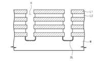
図1は処理工程が一部遂行された基板の形状を示す図面である。図1を参照すれば、処理工程が一部遂行された基板W上には第1薄膜L1、そして第2薄膜L2が互いに積層されて形成され、蝕刻等の処理を通じて第1薄膜L1及び第2薄膜L2を貫通するホールHが形成されている。第1薄膜L1及び第2薄膜L2は互いに異なる素材で提供されることができる。例えば、第1薄膜L1はSiOを含む素材で提供され、第2薄膜L2はSiNを含む素材で提供されることができる。このように互いに異なる素材である第1薄膜L1と第2薄膜L2は物理学特性が互いに異なる。したがって、処理される過程で基板W上に形成されるホールHにはラフネス(Roughness)が発生することができる。また、蝕刻等の処理過程で基板W上にはダメージ層DLが形成されることができる。ダメージ層DLはSiを含む素材で提供されることができる。 FIG. 1 illustrates the shape of a substrate partially processed. Referring to FIG. 1, a first thin film L1 and a second thin film L2 are stacked on a substrate W partially processed. A hole H is formed through the thin film L2. The first thin film L1 and the second thin film L2 may be provided with different materials. For example, the first thin film L1 may be made of a material containing SiO, and the second thin film L2 may be made of a material containing SiN. As such, the first thin film L1 and the second thin film L2, which are made of different materials, have different physical properties. Therefore, roughness may occur in the hole H formed on the substrate W during processing. Also, a damage layer DL may be formed on the substrate W during a process such as etching. The damage layer DL may be provided with a material containing Si.
一般的に、このようなホールHのラフネス(Roughness)、そしてダメージ層DLを除去するために基板W上に薬液を供給する。しかし、最近基板W上に形成されるパターンの稠密化、ホールHの縦横比(Aspect Ratio、AR)が高くなるにつれて、ホールH内に薬液が適切に浸透できず、基板W上のダメージ層DLを適切に除去できない場合が発生している。また、第1薄膜L1と第2薄膜L2は薬液に対する選択比が互いに異なるので、薬液がホールHに適切に浸透してもホールHのラフネス(Roughness)は改善されない可能性がある。 In general, a chemical solution is supplied onto the substrate W to remove the roughness of the holes H and the damaged layer DL. However, as the density of patterns formed on the substrate W increases and the aspect ratio (AR) of the holes H increases, the chemical cannot adequately penetrate into the holes H, resulting in the damage layer DL on the substrate W. may not be properly removed. In addition, since the first thin film L1 and the second thin film L2 have different selectivity ratios to the chemical, the roughness of the hole H may not be improved even if the chemical penetrates into the hole H properly.
本発明の目的は基板を効率的に処理することができる基板処理方法及び基板処理装置を提供することにある。 SUMMARY OF THE INVENTION It is an object of the present invention to provide a substrate processing method and a substrate processing apparatus capable of processing substrates efficiently.
また、本発明の目的は基板上に形成されたダメージ層を効果的に除去することができる基板処理方法及び基板処理装置を提供することにある。 Another object of the present invention is to provide a substrate processing method and substrate processing apparatus capable of effectively removing a damaged layer formed on a substrate.
また、本発明の目的は基板上に互いに異なる選択比を有する薄膜が2以上積層される場合に基板上に形成されたホールのラフネスを効果的に改善することができる基板処理方法及び基板処理装置を提供することにある。 Another object of the present invention is to provide a substrate processing method and substrate processing apparatus capable of effectively improving the roughness of a hole formed on a substrate when two or more thin films having different selection ratios are laminated on the substrate. is to provide
また、本発明の目的はイオンによる基板処理及びラジカルによる基板処理を全て遂行することができる基板処理装置を提供することにある。 Another object of the present invention is to provide a substrate processing apparatus capable of performing substrate processing using ions and substrate processing using radicals.
本発明の目的はここに制限されなく、言及されないその他の目的は下の記載から通常の技術者が明確に理解理解されるべきである。 The objects of the present invention are not limited herein, and other objects not mentioned should be clearly understood and understood by those of ordinary skill in the art from the following description.
本発明は基板処理方法を提供する。薄膜が積層され、ホールが形成された基板を処理する方法は、イオンを含む第1プラズマを利用して前記基板を処理する第1処理段階と、イオンが除去された第2プラズマを利用して前記基板を処理する第2処理段階と、を含むことができる。 The present invention provides a substrate processing method. A method of processing a substrate having thin films stacked thereon and having holes formed thereon includes a first processing step of processing the substrate using a first plasma containing ions, and a second plasma from which the ions are removed. and a second processing stage of processing the substrate.
一実施形態によれば、前記第1処理段階が遂行される少なくとも一部の時期の間に前記基板は静電気力でチャッキングされることができる。 According to one embodiment, the substrate may be electrostatically chucked during at least a portion of the time the first processing step is performed.
一実施形態によれば、前記第1処理段階には、チャンバー内第1空間に工程ガスを供給して前記第1プラズマを発生させ、前記第2処理段階には、前記第1空間と異なるチャンバー内第2空間に工程ガスを供給して前記第2プラズマを発生させることができる。 According to one embodiment, in the first processing step, a process gas is supplied to a first space in a chamber to generate the first plasma, and in the second processing step, a chamber different from the first space A process gas may be supplied to the inner second space to generate the second plasma.
一実施形態によれば、前記第1空間は前記基板が置かれる空間であり、前記第2プラズマの前記イオンの除去は、前記第1空間と前記第2空間との間に配置されたイオンブロッカーによって除去されることができる。 According to one embodiment, said first space is the space in which said substrate is placed, and the removal of said ions of said second plasma comprises an ion blocker placed between said first space and said second space. can be removed by
一実施形態によれば、前記第1処理段階は、前記第1プラズマに励起される工程ガスの供給を開始し、設定時間が経過した後、前記第1空間に電界を形成することができる。 According to one embodiment, the first process may start supplying a process gas to be excited into the first plasma, and form an electric field in the first space after a set time elapses.
一実施形態によれば、前記第2処理段階は、前記第2プラズマに励起される工程ガスの供給を開始し、設定時間が経過した後、前記第2空間に電界を形成することができる。 According to one embodiment, the second process may start supplying a process gas excited by the second plasma, and form an electric field in the second space after a set time has elapsed.
一実施形態によれば、前記第1処理段階、そして前記第2処理段階の間には、前記第1空間を排気する排気段階が遂行されることができる。 According to one embodiment, an evacuation step of evacuating the first space may be performed between the first treatment step and the second treatment step.
一実施形態によれば、前記基板が処理される間に前記基板を支持するチャックの温度は、85℃乃至130℃に制御されることができる。 According to one embodiment, the temperature of a chuck that supports the substrate while the substrate is being processed can be controlled between 85°C and 130°C.
一実施形態によれば、前記第1処理段階で前記第1空間の圧力は10mTorr乃至100mTorrに制御され、前記第2処理段階で前記第1空間の圧力は1Torr乃至10Torrに制御されることができる。 According to one embodiment, the pressure in the first space may be controlled to 10 mTorr to 100 mTorr in the first processing step, and the pressure in the first space may be controlled to 1 Torr to 10 Torr in the second processing step. .
一実施形態によれば、前記第1処理段階で前記第1空間に電界を形成する第1電極には、100W乃至1000Wが印加され、前記第2処理段階で前記第2空間に電界を形成する第2電極には、50W乃至100Wが印加されることができる。 According to one embodiment, 100 W to 1000 W is applied to the first electrode forming an electric field in the first space in the first processing step, and forming an electric field in the second space in the second processing step. 50 W to 100 W may be applied to the second electrode.
一実施形態によれば、前記第1プラズマに励起される工程ガスは水素を含み、前記第2プラズマに励起される工程ガスは弗素を含むことができる。 According to one embodiment, the process gas excited by the first plasma may include hydrogen, and the process gas excited by the second plasma may include fluorine.
一実施形態によれば、前記第1プラズマに励起される工程ガスは、100sccm乃至1000sccmで前記第1空間に供給されることができる。 According to one embodiment, the process gas excited into the first plasma may be supplied to the first space at 100 sccm to 1000 sccm.
一実施形態によれば、前記第2プラズマに励起される工程ガスは、10sccm乃至500sccmで前記第2空間に供給されることができる。 According to one embodiment, the process gas excited into the second plasma may be supplied to the second space at 10 sccm to 500 sccm.
また、本発明は基板処理方法を提供する。異なる選択比を有する薄膜が少なくとも2以上積層された基板を処理する方法は、静電気力でチャッキング(Chucking)された前記基板にイオンを含む第1プラズマを利用して前記基板を処理する第1処理段階と、前記第1処理段階の後に遂行され、イオンが除去された第2プラズマを利用して前記基板を処理する第2処理段階と、を含み、前記第1プラズマは、水素、アルゴン、又はヘリウムを含む工程ガスから励起されたプラズマであり、前記第2プラズマは、弗素を含む工程ガスから励起されたプラズマであり得る。 The present invention also provides a substrate processing method. A method for processing a substrate having at least two layers of thin films having different selection ratios includes processing the substrate chucked by electrostatic force using a first plasma containing ions. and a second processing step, performed after the first processing step, of processing the substrate using a second deionized plasma, wherein the first plasma comprises hydrogen, argon, Alternatively, the second plasma may be plasma excited from a process gas containing helium, and the second plasma may be plasma excited from a process gas containing fluorine.
一実施形態によれば、前記第1プラズマが生成される第1空間、そして前記第2プラズマが生成される第2空間は接地されたプレートによって区画されることができる。 According to one embodiment, the first space where the first plasma is generated and the second space where the second plasma is generated may be defined by a grounded plate.
一実施形態によれば、前記第2処理段階には、イオンが除去された前記第2プラズマに窒素及び水素を含む工程ガスを供給することができる。 According to one embodiment, the second process may supply a process gas including nitrogen and hydrogen to the second plasma from which ions are removed.
また、本発明は基板を処理する装置を提供する。基板処理装置は、処理空間を定義するハウジングと、前記処理空間で基板を支持するチャックと、前記チャックは前記処理空間でプラズマを発生させる下部電源と連結される下部電極が提供され、上部電源と連結される上部電極と、
前記上部電極と互いに対向されるように配置されるイオンブロッカーと、前記イオンブロッカーは前記処理空間と流体連通するプラズマ空間を区画し、前記上部電極は前記プラズマ空間でプラズマを発生し、前記処理空間又は前記プラズマ空間に工程ガスを供給するガス供給ユニットと、制御器と、を含み、前記制御器は、前記処理空間でプラズマを発生させて基板を処理した後、前記プラズマ空間でプラズマを発生させて基板を処理するように前記上部電源、前記下部電源、そして前記ガス供給ユニットを制御することができる。The invention also provides an apparatus for processing a substrate. The substrate processing apparatus includes a housing defining a processing space, a chuck supporting a substrate in the processing space, a lower electrode connected to the chuck for generating plasma in the processing space, and an upper power source. a coupled upper electrode;
an ion blocker positioned to face the upper electrode, the ion blocker defining a plasma space in fluid communication with the processing space, the upper electrode generating a plasma in the plasma space, and the processing space; or a gas supply unit supplying a process gas to the plasma space; and a controller, wherein the controller generates plasma in the plasma space after processing the substrate by generating plasma in the processing space. The upper power supply, the lower power supply, and the gas supply unit can be controlled to process the substrate using a power supply.
一実施形態によれば、前記制御器は、前記処理空間でプラズマを発生させる場合、前記処理空間に水素を含む工程ガスを供給することができる。 According to one embodiment, the controller may supply a process gas containing hydrogen to the processing space when plasma is generated in the processing space.
一実施形態によれば、前記プラズマ空間でプラズマを発生させる場合、前記プラズマ空間に弗素を含む工程ガスを供給することができる。 According to one embodiment, when plasma is generated in the plasma space, a process gas containing fluorine may be supplied to the plasma space.
一実施形態によれば、前記チャックには、基板を静電気力でチャッキングする静電電極が提供されることができる。 According to one embodiment, the chuck may be provided with an electrostatic electrode that chucks the substrate with an electrostatic force.
本発明の一実施形態によれば、基板を効率的に処理することができる。 According to one embodiment of the present invention, substrates can be efficiently processed.
また、本発明の一実施形態によれば、基板上に形成されたダメージ層を効果的に除去することができる。 Further, according to one embodiment of the present invention, the damaged layer formed on the substrate can be effectively removed.
また、本発明の一実施形態によれば、基板上に互いに異なる選択比を有する薄膜が2以上積層される場合に基板上に形成されたホールのラフネスを効果的に改善することができる。 In addition, according to an embodiment of the present invention, when two or more thin films having different selection ratios are stacked on the substrate, roughness of holes formed on the substrate can be effectively improved.
また、本発明の一実施形態によれば、イオンによる基板処理及びラジカルによる基板処理を全て遂行することができる。 In addition, according to an embodiment of the present invention, both substrate treatment using ions and substrate treatment using radicals can be performed.
本発明の効果が上述した効果によって限定されることではなく、言及されない効果は本明細書及び添付された図面から本発明が属する技術分野で通常の知識を有する者に明確に理解されるべきである。 The effects of the present invention are not limited by the effects described above, and effects not mentioned should be clearly understood by those skilled in the art to which the present invention pertains from the present specification and the accompanying drawings. be.
以下では添付した図面を参考として本発明の実施形態に対して本発明が属する技術分野で通常の知識を有する者が容易に実施できるように詳細に説明する。しかし、本発明は様々な異なる形態に具現されることができ、ここで説明する実施形態に限定されない。また、本発明の望ましい実施形態を詳細に説明することにおいて、関連された公知機能又は構成に対する具体的な説明が本発明の要旨を不必要に曖昧にすることができていると判断される場合にはその詳細な説明を省略する。また、類似な機能及び作用をする部分に対しては図面の全体に亘って同一な符号を使用する。 Hereinafter, embodiments of the present invention will be described in detail with reference to the accompanying drawings so that those skilled in the art can easily implement the present invention. This invention may, however, be embodied in many different forms and should not be construed as limited to the embodiments set forth herein. In addition, in describing the preferred embodiments of the present invention in detail, when it is determined that the detailed description of related well-known functions or configurations may unnecessarily obscure the gist of the present invention. , the detailed description is omitted. Also, the same reference numerals are used throughout the drawings for parts having similar functions and actions.
ある構成要素を‘含む’ということは、特別に反対になる記載がない限り、他の構成要素を除外することではなく、他の構成要素をさらに含むことができることを意味する。具体的に、“含む”又は“有する”等の用語は明細書上に記載された特徴、数字、段階、動作、構成要素、部品、又はこれらを組み合わせたものが存在することを指定しようとすることがであり、1つ又はそれ以上の他の特徴や数字、段階、動作、構成要素、部品、又はこれらを組み合わせたものの存在又は付加可能性を予め排除しないことと理解されなければならない。 To 'include' an element means to include other elements, not to exclude other elements, unless specifically stated to the contrary. Specifically, terms such as "including" or "having" are intended to specify that the features, numbers, steps, acts, components, parts, or combinations thereof described in the specification are present. and does not preclude the possibility of the presence or addition of one or more other features, figures, steps, acts, components, parts, or combinations thereof.
単数の表現は文脈の上に明確に異なりに表現しない限り、複数の表現を含む。また、図面で要素の形状及びサイズ等はより明確な説明のために誇張されることができる。 Singular expressions include plural expressions unless the context clearly dictates otherwise. Also, the shapes and sizes of elements in the drawings may be exaggerated for clearer description.
第1、第2等の用語は多様な構成要素を説明するために使用されることができるが、前記構成要素は前記用語によって限定されてはならない。前記用語は1つの構成要素を他の構成要素から区別する目的として使用されることができる。例えば、本発明の権利範囲から離脱されないまま、第1構成要素は第2構成要素と称されることができ、類似に第2構成要素も第1構成要素と称されることができる。 Although the terms first, second, etc. may be used to describe various components, said components should not be limited by said terms. The terms may be used to distinguish one component from another. For example, a first component could be termed a second component, and similarly a second component could be termed a first component, without departing from the scope of the present invention.
ある構成要素が他の構成要素に“連結されて”あるか、或いは“接続されて”いると言及された時には、その他の構成要素に直接的に連結されているか、又は接続されているが、中間に他の構成要素が存在することもあると理解されるべきである。反面に、ある構成要素が他の構成要素に“直接連結されて”いるか、或いは“直接接続されて”いると言及された時には、中間に他の構成要素が存在しないことと理解されるべきである。構成要素間の関係を説明する他の表現、即ち“~間に”と“すぐ~間に”又は“~に隣接する”と“~に直接隣接する“等も同様に解析されなければならない。 When a component is referred to as being “coupled” or “connected” to another component, it is directly coupled or connected to the other component, It should be understood that there may be other components in between. Conversely, when a component is referred to as being "directly coupled" or "directly connected" to another component, it should be understood that there are no other components in between. be. Other expressions describing relationships between components, ie, "between" and "immediately between" or "adjacent to" and "immediately adjacent to", etc., should be similarly analyzed.
異なりに定義されない限り、技術的であるか、或いは科学的な用語を含んで、ここで使用されるすべての用語は本発明が属する技術分野で通常の知識を有する者によって一般的に理解されることと同一な意味である。一般的に使用される事前に定義されていることと同一の用語は関連技術の文脈の上に有する意味と一致する意味であることと解析されるべきであり、本出願で明確に定義しない限り、理想的であるか、或いは過度に形式的な意味として解釈されない。 Unless otherwise defined, all terms, including technical or scientific terms, used herein are commonly understood by one of ordinary skill in the art to which this invention belongs. has the same meaning as Commonly used pre-defined terms that are identical should be interpreted to have a meaning consistent with the meaning they have on the context of the relevant art, unless explicitly defined in this application. , should not be interpreted in an ideal or overly formal sense.
以下では、図2乃至図13を参照して本発明の実施形態に対して説明する。 Hereinafter, embodiments of the present invention will be described with reference to FIGS. 2 to 13. FIG.
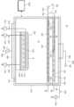
図2は本発明の一実施形態に係る基板処理装置を示す図面である。図2を参照すれば、本発明の一実施形態による基板処理装置10は基板Wを処理することができる。基板処理装置10はプラズマを利用して基板Wを処理することができる。基板処理装置10はプラズマを利用して基板W上のダメージ層DLを除去し、基板W上のホールHのラフネスを改善することができる。基板処理装置10に搬入される基板Wは処理工程が一部遂行された基板Wが搬入されることができる。例えば、基板処理装置10に搬入される基板Wは、蝕刻工程、写真工程等が遂行された基板Wが搬入されている可能性がある。例えば、基板処理装置10に搬入された処理対象である基板Wは、先に図1を参照して説明した基板Wと同一又は類似な状態に基板処理装置10に搬入されることができる。 FIG. 2 illustrates a substrate processing apparatus according to an embodiment of the present invention. Referring to FIG. 2, a
基板処理装置10は、ハウジング100、チャック200、シャワーヘッド300、加熱部材400、イオンブロッカー500、絶縁部材DR、上部電極600(第2電極の一例)、ガス供給ユニット700、800、排気ユニット900、そして制御器1000を含むことができる。 The
ハウジング100とシャワーヘッド300は互いに組み合わせて、基板Wが処理される空間である処理空間A1(第1空間の一例)を定義することができる。また、シャワーヘッド300、加熱部材400、そしてイオンブロッカー500は互いに組み合わせてイオンIが除去されたプラズマPと第1ガス供給ユニット700が供給する第1工程ガスG1を互いにミキシングする空間であるミキシング空間A3(第3空間の一例)を定義することができる。また、イオンブロッカー500、絶縁部材DR、上部電極600は互いに組み合わせて、プラズマPが発生される空間であるプラズマ空間A2(第2空間の一例)を定義することができる。また、処理空間A1、プラズマ空間A2、そしてミキシング空間A3を定義するのに関与する構成を通称してチャンバーと称することもあり得る。 The
ハウジング100は処理空間A1を定義することができる。例えば、ハウジング100は後述するシャワーヘッド300と互いに組み合わせて処理空間A1を定義することができる。ハウジング100は上部が開放された筒形状を有することができる。ハウジング100の内側壁は、後述するプラズマPによって蝕刻されことを防止することができる素材でコーティングされることができる。例えば、ハウジング100の内側壁はセラミックのような誘電体膜でコーティングされることができる。また、ハウジング100は接地されることができる。また、ハウジング100には基板Wが処理空間A1に搬入されるか、或いは処理空間A1から搬出されるように開口(図示せず)が形成されていることができる。開口はドア(図示せず)によって選択的に遮蔽されることができる。
チャック200は処理空間A1で基板Wを支持することができる。チャック200は基板Wを加熱することができる。また、チャック200は基板Wを静電気力を利用してチャッキング(Chucking)することができるESCであり得る。チャック200は支持板210、静電電極220、ヒーター230、そして下部電極240(第1電極の一例)を含むことができる。 Chuck 200 can support substrate W in processing space A1. The
支持板210は基板Wを支持することができる。支持板210は基板Wを支持する支持面を有することができる。支持板210は誘電体で提供されることができる。例えば、支持板210はセラミック素材で提供されることができる。支持板210内には静電電極220が提供されることができる。静電電極220は上部から見る時、基板Wと重畳される位置に提供されることができる。静電電極220に電力が印可されれば、静電電極220は基板Wをチャッキングさせることができる静電気力による電界を形成することができる。電界は基板Wが支持板210に向かう方向にチャッキングされるようにする引力を基板Wに伝達することができる。また、電界は、後述するイオンIが基板Wに向かって直進に流動(即ち、イオンIが異方性を有するように)するようにすることができる。 The
また、基板処理装置10、例えばチャック200は静電電極220に電力を印加する第1電源モジュール222、224を含むことができる。第1電源モジュール222、224は静電電極電源222及び静電電極スイッチ224を含むことができる。静電電極スイッチ224のオン/オフに応じて静電電極220には電力が印加されることができる。 The
ヒーター230は基板Wを加熱することができる。ヒーター230は支持板210の温度を上昇させて基板Wを加熱することができる。また、ヒーター230に電力が印可されれば、ヒーター230は熱を発生させることができる。ヒーター230はタングステンのような発熱体であり得る。しかし、ヒーター230の種類はこれに限定されることではなく、公知されたヒーター230で多様に変形されることができる。ヒーター230は基板Wが処理される間に基板Wから分離される不純物(例えば、Si-ポリマー)がホールHに再付着されることを防止できるように支持板210の温度を高めることができる。例えば、ヒーター230は支持板210の温度を85℃乃至130℃に制御することができる。 The
また、基板処理装置10、例えばチャック200はヒーター230に電力を印加する第2電源モジュール232、234を含むことができる。第2電源モジュール232、234はヒーター電源232及びヒーター電源スイッチ234を含むことができる。ヒーター電源スイッチ234のオン/オフに応じてヒーター230には電力が印加されることができる。 Also, the
下部電極240は処理空間A1でプラズマを発生させることができる。下部電極240は板形状を有することができる。下部電極240は後述するシャワーヘッド300と互いに対向される電極であり得る。下部電極240に電力が印可されれば、下部電極240は処理空間A1に電界を形成し、形成された電界は処理空間A1に流入(供給)される工程ガスG1、G2を励起させてプラズマPを発生させることができる。また、基板処理装置10、例えばチャック200は下部電極240に電力を印加する下部電源モジュール242、244を含むことができる。下部電源モジュール242、244はRFソースである下部電源242及び下部電源スイッチ244を含むことができる。下部電源スイッチ244のオン/オフに応じて下部電極240には電力が印加されることができる。 The
シャワーヘッド300はハウジング100の上部に配置されることができる。シャワーヘッド300は後述するイオンブロッカー500と処理空間A1との間に配置されることができる。シャワーヘッド300は接地されることができる。シャワーヘッド300は接地されて上述した下部電極240と互いに対向電極として機能することができる。また、シャワーヘッド300には複数のホール302が形成されることができる。ホール302はシャワーヘッド300の上面から下面まで延長されて形成されることができる。即ち、ホール302はシャワーヘッド300を貫通して形成されることができる。ホール302は処理空間A1と後述するプラズマ空間A2を互いに流体連通させることができる。また、ホール302は処理空間A1と後述するミキシング空間A3を互いに流体連通させることができる。 A
また、シャワーヘッド300にはガス注入口304が形成されることができる。ガス注入口304は後述する第2ガスライン706と連結されることができる。ガス注入口304はミキシング空間A3に向かって第1工程ガスG1を供給するように構成されることができる。ガス注入口304はミキシング空間A3の縁領域に工程ガスを供給するように構成されることができる。ガス注入口304はミキシング空間A3には通じる(また、間接的にプラズマ空間A2と通じる)が、処理空間A1には通じないように構成されることができる。 Also, a
加熱部材400はシャワーヘッド300の上部に配置されることができる。加熱部材400は上部から見る時、リング形状を有するリングヒーターであり得る。加熱部材400は熱を発生させてミキシング空間A3の温度を高めてイオンIが除去されたプラズマPと第1工程ガスG1がミキシングされることがより効果的に行われるように助けることができる。 The
イオンブロッカー500はプラズマ空間A2とミキシング空間A3を区画(さらにはプラズマ空間A2と処理空間A1を間接的に区画)することができる。イオンブロッカー500は上部電極600と処理空間A1との間に配置されることができる。 The
イオンブロッカー500は加熱部材400の上部に配置されることができる。イオンブロッカー500は接地されることができる。イオンブロッカー500は接地されて、プラズマ空間A2で発生されたプラズマPがミキシング空間A3、さらに処理空間A1に流入する時、プラズマPが含むイオンIを除去することができる。要するに、プラズマ空間A2で発生されたプラズマPは、イオンブロッカー500を経りながら、イオンIが除去されるので、実質的にラジカルRのみを含むようになることができる。 The
また、イオンブロッカー500は接地されて後述する上部電極600と互いに対向電極として機能することができる。イオンブロッカー500には複数の通孔502が形成されることができる。通孔502はイオンブロッカー500を貫通して形成されることができる。通孔502はプラズマ空間A2とミキシング空間A3を流体連通させることができる。通孔502はプラズマ空間A2と処理空間A1を流体連通させることができる。 In addition, the
また、イオンブロッカー500にはガス供給口504が形成されていることができる。ガス供給口504は後述する第1ガスライン704と連結されることができる。ガス供給口504はミキシング空間A3に工程ガスを供給するように構成されることができる。ガス供給口504はミキシング空間A3の中央領域に工程ガスを供給するように構成されることができる。ガス供給口504はミキシング空間A3とは通じる(また、間接的に処理空間A1と通じる)が、プラズマ空間A2とは通じないように構成されることができる。 Also, the
上部電極600は板形状を有することができる。上部電極600はプラズマを発生させることができる。上部電極600には、基板処理装置10が有する上部電源モジュール602、604が電力を印加することができる。上部電源モジュール602、604はRFソースである上部電源602及び下部電源スイッチ604を含むことができる。上部電源スイッチ602のオン/オフに応じて上部電極600には電力が印加されることができる。上部電極600に電力が印可されれば、対向電極として機能するイオンブロッカー500と上部電極600との間に電界が形成され、したがってプラズマ空間A2で後述する第2工程ガスG2を励起してプラズマを発生させることができる。また、上部電極600とイオンブロッカー500との間には絶縁素材で提供される絶縁部材DRが配置されることができる。絶縁部材DRは上部から見る時、リング形状を有することができる。 The
ガス供給ユニット700、800はプラズマP状態に励起される工程ガスG1、G2を供給することができる。ガス供給ユニット700、800は第1ガス供給ユニット700、そして第2ガス供給ユニット800を含むことができる。以下では、第1ガス供給ユニット700が供給する工程ガスを、第1工程ガスG1であるとし、第2ガス供給ユニット800が供給する工程ガスを、第2工程ガスG2であるとする。 The
第1ガス供給ユニット700はミキシング空間A3に工程ガスを供給することができる。第1ガス供給ユニット700はミキシング空間A3に工程ガスを注入して、処理空間A1に工程ガスを供給することができる。第1ガス供給ユニット700は第1ガス供給源701、メーンガスライン703、第1ガスライン704、及び第2ガスライン706を含むことができる。メーンガスライン703の一端は第1ガス供給源701と連結されることができ、メーンガスライン703の他端は第1ガスライン704及び第2ガスライン706に分岐されることができる。第1ガスライン704は上述したガス供給口504と連結されることができる。また、第2ガスライン706は上述したガス注入口304と連結されることができる。 The first
第1ガス供給ユニット700が供給する第1工程ガスG1はNH3、H2の中で少なくとも1つ以上であり得る。The first process gas G1 supplied by the first
第2ガス供給ユニット800はプラズマ空間A2に工程ガスを供給することができる。第2ガス供給ユニット800はプラズマ空間A2に工程ガスを注入して、ミキシング空間A2、そして処理空間A1に工程ガスを供給することができる。第2ガス供給ユニット800は第2ガス供給源801、そしてガスチャンネル803を含むことができる。ガスチャンネル803の一端は第2ガス供給源801と連結され、他端はプラズマ空間A2と連通されることができる。 The second
第2ガス供給ユニット800が供給する第2工程ガスG2はHe、Ar、Xe、N2、フルオリン(弗素)系列(例えば、NF3、F2)の中でいずれか1つであり得る。The second process gas G2 supplied by thesecond
排気ユニット900は処理空間A1に供給された工程ガスG1、G2、工程副産物等を排出することができる。排気ユニット900は処理空間A1の圧力を調節することができる。排気ユニット900は減圧部材902、そして減圧ライン904を含むことができる。減圧部材902はポンプであり得る。しかし、これに限定されることではなく、減圧を提供する公知された装置に多様に変形されることができる。 The
制御器1000は基板処理装置10、具体的に基板処理装置10が有する構成を制御することができる。例えば、制御器1000はガス供給ユニット700、800、第1電源モジュール222、224、第2電源モジュール232、234、減圧部材902、下部電源モジュール242、244、上部電源モジュール602、604等を制御することができる。制御器1000は基板処理装置10の制御を実行するマイクロプロセッサー(コンピュータ)で成されるプロセスコントローラと、オペレータが基板処理装置を管理するためにコマンド入力操作等を行うキーボードや、基板処理装置の稼動状況を可視化して表示するディスプレー等で成されるユーザインターフェイスと、基板処理装置10で実行される処理をプロセスコントローラの制御で実行するための制御プログラムや、各種データ及び処理条件に応じて各構成部で処理を実行させるためのプログラム、即ち処理レシピが格納された格納部を具備することができる。また、ユーザインターフェイス及び格納部はプロセスコントローラに接続されていることができる。処理レシピは格納部の中で記憶媒体に記憶されていることができ、記憶媒体は、ハードディスクであってもよく、CD-ROM、DVD等の可搬性ディスクや、フラッシュメモリ等の半導体メモリであってもよい。 The
以下では、本発明の一実施形態による基板処理方法に対して説明する。以下では説明する基板処理方法は、上述した基板処理装置10によって遂行されることができる。また、以下では説明する基板処理方法を遂行するために制御器1000は基板処理装置10が有する構成を制御することができる。 Hereinafter, a substrate processing method according to an embodiment of the present invention will be described. The substrate processing method described below can be performed by the
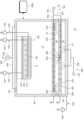
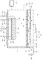
図3は本発明の一実施形態による基板処理方法を示すフローチャートであり、図4は図3の基板処理方法を遂行する時、基板処理装置の処理条件を概略的に示すグラフである。図3、そして図4を参照すれば、本発明の一実施形態による基板処理方法は、待機段階(S10)、第1処理段階(S20)、第1排気段階(S30)、第2処理段階(S40)、そして第2排気段階(S50)を含むことができる。待機段階(S10)、第1処理段階(S20)、第1排気段階(S30)、第2処理段階(S40)、そして第2排気段階(S50)は順次的に遂行されることができる。 FIG. 3 is a flow chart illustrating a substrate processing method according to an embodiment of the present invention, and FIG. 4 is a graph schematically illustrating processing conditions of a substrate processing apparatus when performing the substrate processing method of FIG. 3 and 4, a substrate processing method according to an embodiment of the present invention includes a standby step (S10), a first processing step (S20), a first exhausting step (S30), a second processing step (S30), and a second processing step (S30). S40), and a second evacuation stage (S50). The waiting step (S10), the first processing step (S20), the first exhausting step (S30), the second processing step (S40), and the second exhausting step (S50) may be sequentially performed.
以下では、第1ガス供給ユニット700が供給する工程ガスを、第1工程ガスG1であるとし、第2ガス供給ユニット800が供給する工程ガスを、第2工程ガスG2であるとする。また、処理空間A1で工程ガスが励起されて発生されるプラズマを第1プラズマP1であるとし、プラズマ空間A2で工程ガスが励起されて発生するプラズマを第2プラズマP2であるとする。プラズマ空間A2で発生される第2プラズマP2が処理空間A1に流入される場合、イオンブロッカー500によってイオンが除去されるので、第2プラズマP2はイオンが除去されたプラズマを意味することができる。また、処理空間A1で発生する第1プラズマP1はイオンブロッカー500によってイオンが除去されないので、第1プラズマP1はイオンを含むプラズマを意味することができる。 Hereinafter, the process gas supplied by the first
待機段階(S10)には処理対象である基板Wが処理空間A1に搬入するまで待機する段階である。基板Wの搬入を待機する時間(即ち、待機段階(S10)が持続される時間)が設定時間以上になる場合、基板処理装置10のコンディションが低下されることができる。したがって、必要によっては基板Wの搬入を待機する時間が設定時間以上になる場合、基板Wが処理空間A1に搬入されない状態で後述する第1処理段階(S20)、第1排気段階(S30)、第2処理段階(S40)、そして第2排気段階(S50)の中で少なくとも1つ以上を遂行することができる。 The waiting stage (S10) is a stage of waiting until the substrate W to be processed is carried into the processing space A1. If the waiting time for the loading of the substrate W (that is, the time during which the waiting step S10 is continued) is greater than or equal to the set time, the condition of the
第1処理段階(S20)は待機段階(S10)の後に遂行されることができる。第1処理段階(S20)はチャッキング-圧力安定化段階(S21)及びイオン処理段階(S22)を含むことができる。チャッキング-圧力安定化段階(S21)には支持ユニット200が基板Wを静電気力でチャッキングすることができる(図5参照)。また、この時、静電電極スイッチ224はオン(On)されることができる。したがって、静電電極電源222が印加する電力は静電電極220に伝達されることができる。静電電極220に電力が印可されれば、基板W上には下に向かう方向に引っ張る力を発生させる電界が形成されることができる。このような電界は基板Wをチャッキング(Chucking)のみならず、後述するイオンIが異方性の状態(即ち、イオンIが下に向かう方向に垂直に流動する状態)を有するようにしてもよい。 The first processing step (S20) can be performed after the waiting step (S10). The first processing step (S20) can include a chucking-pressure stabilization step (S21) and an ion processing step (S22). In the chucking-pressure stabilization step (S21), the
また、チャッキング-圧力安定化段階(S21)はイオン処理段階(S22)での基板W処理が安定的に遂行されるように処理空間A1の圧力を安定化させる段階であり得る。チャッキング-圧力安定化段階(S21)にはガス供給ユニット700、800が工程ガスG1、G2を供給することができる(図6参照)。例えば、第1ガス供給ユニット700がミキシング空間A3に供給する第1工程ガスG1はホール302を通じて処理空間A1に流入されることができる。第2ガス供給ユニット800がプラズマ空間A2に供給する第2工程ガスG2は通孔502とホール302を通じて処理空間A1に流入されることができる。処理空間A1に工程ガスG1、G2が流入されることによって、処理空間A1の圧力は設定圧力に到達及び設定圧力に一定に維持されることができる(圧力の安定化)。 Also, the chucking-pressure stabilizing step (S21) may be a step of stabilizing the pressure in the processing space A1 so as to stably process the substrate W in the ion processing step (S22).
また、チャッキング-圧力安定化段階(S21)で第1ガス供給ユニット700が供給する第1工程ガスG1はNH3、又はH2のように水素を含むガスであり得る。また、チャッキング-圧力安定化段階(S21)で第2ガス供給ユニット800が供給する第2工程ガスG2はHe、Ar、Xe、N2を含む不活性ガスであり得る。第1処理段階(S20)で供給される工程ガスG1、G2はH2、He、そしてArの中でいずれか1つを含むガスと、H及び/又はNを含むガス(例えば、NH3)を含むことができる。Also, the first process gas G1 supplied by the first
処理空間A1に工程ガスG1、G2の供給が開始し、設定時間が経過した後、イオン処理段階(S22)には下部電源モジュール242、244が下部電極240に電力を印加することができる。下部電極240に電力が印可されれば、処理空間A1には電界が形成されることができる。処理空間A1に形成される電界は、工程ガスG1、G2を励起させて第1プラズマP1を発生させることができる(図7参照)。処理空間A1で発生される第1プラズマP1はイオンブロッカー500を経なく、処理空間A1で直接的に発生するようになるので、イオンIを含むことができる。第1プラズマP1が含むイオンIは極性を有するので、静電電極220が形成する静電気力によって異方性を有するようにされることができる。したがって、図8に図示されたようにイオンIはホールH内に進入してダメージ層DLに適切に伝達されることができ、またホールHで相対的に突出された第1薄膜L1部分は第2薄膜L2部分より相対的にイオンIによる処理がさらに行われることができる。即ち、ホールHの一部はイオンIによって処理が行われ、ホールHの他の一部はイオンIによって処理が行われないことがあり得る。 After the process gases G1 and G2 are supplied to the processing space A1 and a set time has elapsed, the lower
第1処理段階(S20)が遂行される間に、チャック200の温度は50℃乃至150℃、より好ましくは85℃乃至130℃で制御されることができる。また、第1処理段階(S20)が遂行される間に、処理空間A1の圧力は排気ユニット900によって5mTorr乃至150mTorr、より好ましくは10mTorr乃至100mTorrに制御されることができる。また、第1処理段階(S20)が遂行される間に、下部電極240には50W乃至1500W、より好ましくは100W乃至1000Wが印加されることができる。また、第1処理段階(S20)が遂行される間に供給される工程ガス、例えばNH3を含む第1工程ガスG1は50sccm乃至1000sccm、より好ましくは100sccm乃至1000sccmに処理空間A1に供給されることができる。The temperature of the
第1排気段階(S30)には排気ユニット900が処理空間A1の雰囲気を排気することができる(図9参照)。第1排気段階(S30)には処理空間A1を排気して処理空間A1に残留する工程副産物、第1処理段階(S20)で供給された工程ガスG1、G2、そして第1プラズマP1を処理空間A1の外部に排気することができる。 In the first exhaust step (S30), the
第2処理段階(S40)は第1排気段階(S30)の後に遂行されることができる。第2処理段階(S40)は圧力安定化段階(S41)及びラジカル処理段階(S42)を含むことができる。圧力安定化段階(S41)はラジカル処理段階(S42)での基板W処理が安定的に遂行されるように処理空間A1の圧力を安定化させる段階であり得る。圧力安定化段階(S41)にはガス供給ユニット700、800が工程ガスG1、G2を供給することができる(図10参照)。例えば、第1ガス供給ユニット700はミキシング空間A3に第1工程ガスG1を供給することができる。第2ガス供給ユニット800はプラズマ空間A2に第2工程ガスG2を供給することができる。また、プラズマ空間A2とミキシング空間A3に供給される工程ガスG1、G2は処理空間A1に流入されて処理空間A1の圧力を安定化させることができる。 The second treatment step (S40) can be performed after the first exhaust step (S30). The second treatment step (S40) may include a pressure stabilization step (S41) and a radical treatment step (S42). The pressure stabilization step (S41) may be a step of stabilizing the pressure in the processing space A1 so that the substrate W is stably processed in the radical treatment step (S42).
また、圧力安定化段階(S41)で第1ガス供給ユニット700が供給する第1工程ガスG1はNH3、又はH2のように水素を含むガスであり得る。また、チャッキング-圧力安定化段階(S21)で第2ガス供給ユニット800が供給する第2工程ガスG2は弗素(例えば、NF3、F2)、そして不活性ガス(例えば、He、Ar、Xe、N2)を含むことができる。Also, the first process gas G1 supplied by the first
工程ガスG1、G2の供給が開始し、設定時間が経過した後、ラジカル処理段階(S42)には上部電源モジュール602、604が上部電極600に電力を印加することができる。上部電極600に電力が印可されれば、プラズマ空間A2には電界が形成されることができる。プラズマ空間A2に形成される電界は、第2工程ガスG2を励起させて第2プラズマP2を発生させることができる(図10参照)。 After the supply of the process gases G1 and G2 is started and the set time has elapsed, the upper
第2プラズマP2はイオンブロッカー500を経てミキシング空間A2に流れることができる。ミキシング空間A2に流入された第2プラズマP2はイオンブロッカー500によってイオンIが除去された状態になることができる。イオンIが除去された状態の第2プラズマP2は、ミキシング空間A2に供給される第1工程ガスG1と互いにミキシングされることができる。第1工程ガスG1とミキシングされた、イオンIが除去された第2プラズマP2は処理空間A1に流入されて、基板Wを処理することができる(図12参照)。この時、イオンIが除去されたラジカルRは、中性を有するので、等方性を有することができる。また、先の第1処理段階(S20)でイオンIによって処理された領域と、処理されない領域の間には選択比の差が発生するようになる。したがって、図12に図示されたようにホールHのラフネス改善、そしてダメージ層DLを効果的に除去することができるようになる。 The second plasma P2 can flow through the
第2処理段階(S40)が遂行される間に、チャック200の温度は50℃乃至150℃、より好ましくは85℃乃至130℃で制御されることができる。また、第2処理段階(S40)が遂行される間に、処理空間A1の圧力は排気ユニット900によって0.5Torr乃至15Torr、より好ましくは1Torr乃至10Torrに制御されることができる。また、第2処理段階(S40)が遂行される間に、上部電極600には20W乃至500W、より好ましくは50W乃至500Wが印加されることができる。また、第2処理段階(S40)が遂行される間に供給される工程ガス、例えばNH3を含む第1工程ガスG1は50sccm乃至1500sccm、より好ましくは100sccm乃至1000sccmにミキシング空間A3に供給されることができる。また、第2処理段階(S40)が遂行される間に供給される工程ガス、例えばNF3を含む第2工程ガスG2は5sccm乃至800sccm、より好ましくは10sccm乃至500sccmでプラズマ空間A3に供給されることができる。The temperature of the
また、第1処理段階(S20)と第2処理段階(S40)は繰り返して遂行されることができる。 Also, the first processing step (S20) and the second processing step (S40) may be repeatedly performed.
第2排気段階(S50)には第1排気段階(S30)と類似に、処理空間A1の雰囲気を排気ユニット900が排気することができる。 In the second exhaust step (S50), the atmosphere of the processing space A1 can be exhausted by the
以上の詳細な説明は本発明を例示するものである。また、前述した内容は本発明の好ましい実施形態を例として説明することであり、本発明は多様な他の組合、変更、及び環境で使用することができる。即ち、本明細書に開示された発明の概念の範囲、前述した開示内容と均等な範囲、及び/又は当業界の技術又は知識の範囲内で変更又は修正が可能である。前述した実施形態は本発明の技術的思想を具現するための最善の状態を説明することであり、本発明の具体的な適用分野及び用途で要求される様々な変更も可能である。したがって、以上の発明の詳細な説明は開示された実施状態に本発明を制限しようとする意図ではない。添付された請求の範囲は他の実施状態も含むことと解析されなければならない。 The foregoing detailed description illustrates the invention. In addition, the foregoing is a description of preferred embodiments of the invention as examples, and the invention can be used in various other combinations, modifications, and environments. That is, changes or modifications may be made within the scope of the inventive concept disclosed herein, the scope of equivalents of the above disclosure, and/or the skill or knowledge in the art. The above-described embodiments describe the best state for embodying the technical idea of the present invention, and various modifications required for specific application fields and uses of the present invention are possible. Accordingly, the detailed description of the invention above is not intended to limit the invention to the disclosed implementations. The appended claims should be interpreted to include other implementations as well.
W 基板
DL ダメージ層
L1 第1薄膜
L2 第2薄膜
10 基板処理装置
100 ハウジング
102 処理空間
104 排気ホール
200 チャック
210 支持板
220 静電電極
222 静電電極電源
224 静電電極スイッチ
230 ヒーター
232 ヒーター電源
234 ヒーター電源スイッチ
240 下部電極
242 下部電源
244 下部電源スイッチ
300 シャワーヘッド
302 ホール
304 ガス注入口
400 加熱部材
500 イオンブロッカー
502 通孔
504 ガス供給口
DR 絶縁部材
600 上部電極
602 上部電源
604 上部電源スイッチ
700 第1ガス供給ユニット
701 第1ガス供給源
704 第1ガスライン
706 第2ガスライン
800 第2ガス供給ユニット
801 第2ガス供給源
803 ガスチャンネル
900 排気ユニット
902 減圧部材
904 減圧ラインW substrate DL damaged layer L1 first thin film L2 second
Claims (20)
Translated fromJapaneseイオンを含む第1プラズマを利用して前記基板を処理する第1処理段階と、
イオンが除去された第2プラズマを利用して前記基板を処理する第2処理段階と、を含む基板処理方法。In a method for processing a substrate having thin films laminated and holes formed therein,
a first processing step of processing the substrate using a first plasma comprising ions;
and a second processing step of processing the substrate using a second plasma from which ions are removed.
チャンバー内の第1空間に工程ガスを供給して前記第1プラズマを発生させ、
前記第2処理段階には、
前記第1空間と異なるチャンバー内の第2空間に工程ガスを供給して前記第2プラズマを発生させる請求項1又は請求項2に記載の基板処理方法。The first processing step includes:
supplying a process gas to a first space in the chamber to generate the first plasma;
The second processing step includes:
3. The substrate processing method of claim 1, wherein the second plasma is generated by supplying a process gas to a second space in a chamber different from the first space.
前記第2プラズマの前記イオンの除去は、前記第1空間と前記第2空間との間に配置されたイオンブロッカーによって除去される請求項3に記載の基板処理方法。the first space is a space in which the substrate is placed;
4. The substrate processing method of claim 3, wherein removing the ions of the second plasma is removed by an ion blocker arranged between the first space and the second space.
前記第1プラズマに励起される工程ガスの供給を開始し、設定時間が経過した後、前記第1空間に電界を形成する請求項3に記載の基板処理方法。The first processing step includes:
4. The substrate processing method of claim 3, wherein the supply of the process gas excited by the first plasma is started, and after a set time has passed, an electric field is formed in the first space.
前記第2プラズマに励起される工程ガスの供給を開始し、設定時間が経過した後、前記第2空間に電界を形成する請求項3に記載の基板処理方法。Said second processing step comprises:
4. The substrate processing method of claim 3, wherein the supply of the process gas to be excited by the second plasma is started, and after a set time elapses, an electric field is formed in the second space.
前記第1空間を排気する排気段階が遂行される請求項3に記載の基板処理方法。Between said first treatment step and said second treatment step,
4. The substrate processing method of claim 3, further comprising performing an evacuation step of evacuating the first space.
85℃乃至130℃で制御される請求項3に記載の基板処理方法。The temperature of a chuck supporting the substrate while the substrate is being processed is
4. The substrate processing method according to claim 3, wherein the temperature is controlled at 85[deg.]C to 130[deg.]C.
前記第2処理段階で前記第1空間の圧力は1Torr乃至10Torrに制御される請求項3に記載の基板処理方法。The pressure in the first space is controlled to 10 mTorr to 100 mTorr in the first processing step,
4. The substrate processing method of claim 3, wherein the pressure in the first space is controlled to 1 Torr to 10 Torr in the second processing step.
前記第2処理段階で前記第2空間に電界を形成する第2電極には、50W乃至100Wが印加される請求項3に記載の基板処理方法。100 W to 1000 W is applied to the first electrode that forms an electric field in the first space in the first processing step;
4. The method of claim 3, wherein 50 W to 100 W is applied to the second electrode forming the electric field in the second space during the second processing.
前記第2プラズマに励起される工程ガスは、弗素を含む請求項3に記載の基板処理方法。the process gas excited into the first plasma contains hydrogen;
4. The substrate processing method of claim 3, wherein the process gas excited by the second plasma contains fluorine.
静電気力でチャッキング(Chucking)された前記基板にイオンを含む第1プラズマを利用して前記基板を処理する第1処理段階と、
前記第1処理段階の後に遂行され、イオンが除去された第2プラズマを利用して前記基板を処理する第2処理段階と、を含み、
前記第1プラズマは、
水素、アルゴン、又はヘリウムを含む工程ガスから励起されたプラズマであり、
前記第2プラズマは、
弗素を含む工程ガスから励起されたプラズマである基板処理方法。In a method for processing a substrate on which at least two thin films having different selectivity are laminated,
a first processing step of processing the substrate chucked by electrostatic force using a first plasma containing ions;
a second processing step, performed after the first processing step, of processing the substrate using a second deionized plasma;
The first plasma is
a plasma excited from a process gas containing hydrogen, argon, or helium;
The second plasma is
A substrate processing method in which plasma is excited from a fluorine-containing process gas.
イオンが除去された前記第2プラズマに窒素及び水素を含む工程ガスを供給する請求項14又は請求項15に記載の基板処理方法。The second processing step includes:
16. The substrate processing method of claim 14, wherein a process gas containing nitrogen and hydrogen is supplied to the second plasma from which ions are removed.
処理空間を定義するハウジングと、
前記処理空間で基板を支持するチャックと、
前記チャックは、前記処理空間でプラズマを発生させる下部電源と連結される下部電極が提供され、
上部電源と連結される上部電極と、
前記上部電極と互いに対向されるように配置されるイオンブロッカーと、
前記イオンブロッカーは、前記処理空間と流体連通するプラズマ空間を区画し、前記上部電極は、前記プラズマ空間でプラズマを発生させ、
前記処理空間又は前記プラズマ空間に工程ガスを供給するガス供給ユニットと、
制御器と、を含み、
前記制御器は、
前記処理空間でプラズマを発生させて基板を処理した後、前記プラズマ空間でプラズマを発生させて基板を処理するように前記上部電源、前記下部電源、そして前記ガス供給ユニットを制御する基板処理装置。In an apparatus for processing a substrate,
a housing defining a processing space;
a chuck supporting a substrate in the processing space;
the chuck is provided with a lower electrode connected to a lower power source for generating plasma in the processing space;
an upper electrode connected to an upper power supply;
an ion blocker arranged to face the upper electrode;
the ion blocker defines a plasma space in fluid communication with the processing space, the upper electrode generating a plasma in the plasma space;
a gas supply unit that supplies a process gas to the processing space or the plasma space;
a controller;
The controller is
A substrate processing apparatus for controlling the upper power source, the lower power source, and the gas supply unit to generate plasma in the processing space to process the substrate and then generate plasma in the plasma space to process the substrate.
前記処理空間でプラズマを発生させる場合、前記処理空間に水素を含む工程ガスを供給する請求項17に記載の基板処理装置。The controller is
18. The substrate processing apparatus of claim 17, wherein a process gas containing hydrogen is supplied to the processing space when plasma is generated in the processing space.
基板を静電気力でチャッキングする静電電極が提供される求項17乃至請求項19のいずれかの一項に記載の基板処理装置。The chuck has
20. The substrate processing apparatus according to any one of claims 17 to 19, further comprising an electrostatic electrode for chucking the substrate by electrostatic force.
Applications Claiming Priority (2)
| Application Number | Priority Date | Filing Date | Title |
|---|---|---|---|
| KR1020210095577AKR20230014339A (en) | 2021-07-21 | 2021-07-21 | Method and apparatus for treating substrate |
| KR10-2021-0095577 | 2021-07-21 |
Publications (2)
| Publication Number | Publication Date |
|---|---|
| JP2023016719Atrue JP2023016719A (en) | 2023-02-02 |
| JP7511608B2 JP7511608B2 (en) | 2024-07-05 |
Family
ID=84976844
Family Applications (1)
| Application Number | Title | Priority Date | Filing Date |
|---|---|---|---|
| JP2022111391AActiveJP7511608B2 (en) | 2021-07-21 | 2022-07-11 | SUBSTRATE PROCESSING METHOD AND SUBSTRATE PROCESSING APPARATUS |
Country Status (4)
| Country | Link |
|---|---|
| US (1) | US20230026796A1 (en) |
| JP (1) | JP7511608B2 (en) |
| KR (1) | KR20230014339A (en) |
| CN (1) | CN115692154A (en) |
Cited By (1)
| Publication number | Priority date | Publication date | Assignee | Title |
|---|---|---|---|---|
| JP2023098595A (en)* | 2021-12-28 | 2023-07-10 | セメス カンパニー,リミテッド | SUBSTRATE PROCESSING APPARATUS AND SUBSTRATE PROCESSING METHOD |
Families Citing this family (1)
| Publication number | Priority date | Publication date | Assignee | Title |
|---|---|---|---|---|
| KR102852461B1 (en)* | 2021-07-22 | 2025-09-01 | 세메스 주식회사 | Apparatus for treating substrate |
Citations (6)
| Publication number | Priority date | Publication date | Assignee | Title |
|---|---|---|---|---|
| JP2014204030A (en)* | 2013-04-08 | 2014-10-27 | 株式会社日立国際電気 | Substrate processing apparatus and method of manufacturing semiconductor device and program to be executed by computer |
| JP2015088751A (en)* | 2013-10-28 | 2015-05-07 | エーエスエム アイピー ホールディング ビー.ブイ. | Method for trimming carbon-containing films with reduced trimming rate |
| JP2017085161A (en)* | 2012-05-23 | 2017-05-18 | 東京エレクトロン株式会社 | Substrate processing apparatus and substrate processing method |
| JP2019035147A (en)* | 2017-08-14 | 2019-03-07 | 三星ディスプレイ株式會社Samsung Display Co.,Ltd. | Method for forming metal oxide film and plasma-enhanced chemical vapor deposition apparatus |
| JP2019176184A (en)* | 2015-05-22 | 2019-10-10 | 株式会社日立ハイテクノロジーズ | Plasma processing apparatus |
| JP2020155387A (en)* | 2019-03-22 | 2020-09-24 | 東京エレクトロン株式会社 | Plasma processing equipment and plasma processing method |
Family Cites Families (25)
| Publication number | Priority date | Publication date | Assignee | Title |
|---|---|---|---|---|
| US5013400A (en)* | 1990-01-30 | 1991-05-07 | General Signal Corporation | Dry etch process for forming champagne profiles, and dry etch apparatus |
| US6355557B2 (en)* | 1998-07-22 | 2002-03-12 | Applied Materials, Inc. | Oxide plasma etching process with a controlled wineglass shape |
| KR100827538B1 (en)* | 2006-12-28 | 2008-05-06 | 주식회사 하이닉스반도체 | Semiconductor device and method for fabricating the same |
| TW201001543A (en)* | 2008-02-08 | 2010-01-01 | Tokyo Electron Ltd | Method for modifying insulating film with plasma |
| US9793126B2 (en)* | 2010-08-04 | 2017-10-17 | Lam Research Corporation | Ion to neutral control for wafer processing with dual plasma source reactor |
| US8808563B2 (en)* | 2011-10-07 | 2014-08-19 | Applied Materials, Inc. | Selective etch of silicon by way of metastable hydrogen termination |
| US8921234B2 (en)* | 2012-12-21 | 2014-12-30 | Applied Materials, Inc. | Selective titanium nitride etching |
| US9362130B2 (en)* | 2013-03-01 | 2016-06-07 | Applied Materials, Inc. | Enhanced etching processes using remote plasma sources |
| US20140271097A1 (en)* | 2013-03-15 | 2014-09-18 | Applied Materials, Inc. | Processing systems and methods for halide scavenging |
| US20160076142A1 (en)* | 2014-03-07 | 2016-03-17 | Advanced Ion Beam Technology, Inc. | Deposition Apparatus and Deposition Method Using the Same |
| KR102247560B1 (en)* | 2014-07-14 | 2021-05-03 | 삼성전자 주식회사 | Plasma generating method in RPS(Remote Plasma Source) and method for fabricating semiconductor device comprising the same plasma generating method |
| US9576788B2 (en)* | 2015-04-24 | 2017-02-21 | Applied Materials, Inc. | Cleaning high aspect ratio vias |
| KR102577628B1 (en)* | 2016-01-05 | 2023-09-13 | 어플라이드 머티어리얼스, 인코포레이티드 | Method for fabricating nanowires for horizontal gate all-around devices for semiconductor applications |
| JP2020517103A (en)* | 2017-04-10 | 2020-06-11 | アプライド マテリアルズ インコーポレイテッドApplied Materials,Incorporated | High Deposition Rate High Quality Silicon Nitride Enabled by Remote Nitrogen Radical Source |
| US10424487B2 (en)* | 2017-10-24 | 2019-09-24 | Applied Materials, Inc. | Atomic layer etching processes |
| US10861722B2 (en)* | 2018-11-13 | 2020-12-08 | Applied Materials, Inc. | Integrated semiconductor processing |
| US11437242B2 (en)* | 2018-11-27 | 2022-09-06 | Applied Materials, Inc. | Selective removal of silicon-containing materials |
| US11715621B2 (en)* | 2018-12-17 | 2023-08-01 | Applied Materials, Inc. | Scanned angled etching apparatus and techniques providing separate co-linear radicals and ions |
| US11315787B2 (en)* | 2019-04-17 | 2022-04-26 | Applied Materials, Inc. | Multiple spacer patterning schemes |
| TW202117847A (en)* | 2019-07-17 | 2021-05-01 | 美商得昇科技股份有限公司 | Processing of workpiece using deposition process and etch process |
| US20210020405A1 (en)* | 2019-07-18 | 2021-01-21 | Tokyo Electron Limited | Equipment and methods for plasma processing |
| US11881402B2 (en)* | 2020-09-30 | 2024-01-23 | Applied Materials, Inc. | Self aligned multiple patterning |
| US20220189771A1 (en)* | 2020-12-10 | 2022-06-16 | Applied Materials, Inc. | Underlayer film for semiconductor device formation |
| WO2023027827A1 (en)* | 2021-08-24 | 2023-03-02 | Applied Materials, Inc. | Fully self aligned via integration processes |
| US20240266148A1 (en)* | 2023-02-06 | 2024-08-08 | Samsung Electronics Co., Ltd. | Semiconductor manufacturing device |
- 2021
- 2021-07-21KRKR1020210095577Apatent/KR20230014339A/enactivePending
- 2022
- 2022-07-11JPJP2022111391Apatent/JP7511608B2/enactiveActive
- 2022-07-19USUS17/868,067patent/US20230026796A1/enactivePending
- 2022-07-20CNCN202210863180.0Apatent/CN115692154A/enactivePending
Patent Citations (6)
| Publication number | Priority date | Publication date | Assignee | Title |
|---|---|---|---|---|
| JP2017085161A (en)* | 2012-05-23 | 2017-05-18 | 東京エレクトロン株式会社 | Substrate processing apparatus and substrate processing method |
| JP2014204030A (en)* | 2013-04-08 | 2014-10-27 | 株式会社日立国際電気 | Substrate processing apparatus and method of manufacturing semiconductor device and program to be executed by computer |
| JP2015088751A (en)* | 2013-10-28 | 2015-05-07 | エーエスエム アイピー ホールディング ビー.ブイ. | Method for trimming carbon-containing films with reduced trimming rate |
| JP2019176184A (en)* | 2015-05-22 | 2019-10-10 | 株式会社日立ハイテクノロジーズ | Plasma processing apparatus |
| JP2019035147A (en)* | 2017-08-14 | 2019-03-07 | 三星ディスプレイ株式會社Samsung Display Co.,Ltd. | Method for forming metal oxide film and plasma-enhanced chemical vapor deposition apparatus |
| JP2020155387A (en)* | 2019-03-22 | 2020-09-24 | 東京エレクトロン株式会社 | Plasma processing equipment and plasma processing method |
Cited By (3)
| Publication number | Priority date | Publication date | Assignee | Title |
|---|---|---|---|---|
| JP2023098595A (en)* | 2021-12-28 | 2023-07-10 | セメス カンパニー,リミテッド | SUBSTRATE PROCESSING APPARATUS AND SUBSTRATE PROCESSING METHOD |
| JP7554804B2 (en) | 2021-12-28 | 2024-09-20 | セメス カンパニー,リミテッド | SUBSTRATE PROCESSING APPARATUS AND SUBSTRATE PROCESSING METHOD |
| US12315699B2 (en) | 2021-12-28 | 2025-05-27 | Semes Co., Ltd. | Substrate treating apparatus and substrate treating method |
Also Published As
| Publication number | Publication date |
|---|---|
| CN115692154A (en) | 2023-02-03 |
| US20230026796A1 (en) | 2023-01-26 |
| JP7511608B2 (en) | 2024-07-05 |
| KR20230014339A (en) | 2023-01-30 |
Similar Documents
| Publication | Publication Date | Title |
|---|---|---|
| US8524331B2 (en) | Substrate processing method | |
| JP6339963B2 (en) | Etching method | |
| US10475659B2 (en) | Method of processing target object | |
| KR102747278B1 (en) | Plasma processing method and plasma processing apparatus | |
| JP7499806B2 (en) | SUBSTRATE PROCESSING METHOD AND SUBSTRATE PROCESSING APPARATUS | |
| US20110114113A1 (en) | Substrate processing apparatus, cleaning method thereof and storage medium storing program | |
| CN109219866B (en) | etching method | |
| US8642482B2 (en) | Plasma etching method, control program and computer storage medium | |
| JP7511608B2 (en) | SUBSTRATE PROCESSING METHOD AND SUBSTRATE PROCESSING APPARATUS | |
| JP7323330B2 (en) | Substrate processing method and substrate processing apparatus | |
| US20100218786A1 (en) | Cleaning method of plasma processing apparatus and storage medium | |
| JP2017092376A (en) | Etching method | |
| JP7513666B2 (en) | Substrate Processing Equipment | |
| US10651077B2 (en) | Etching method | |
| TW202031921A (en) | Atomic layer treatment process using metastable activated radical species | |
| US12347694B2 (en) | Method and apparatus for treating substrate | |
| US9922841B2 (en) | Plasma processing method | |
| JP7554804B2 (en) | SUBSTRATE PROCESSING APPARATUS AND SUBSTRATE PROCESSING METHOD | |
| JP2006319042A (en) | Plasma cleaning method and method for forming film | |
| KR20230103860A (en) | Apparatus for treating substrate and method for processing a substrate | |
| JP5058478B2 (en) | Semiconductor device manufacturing method, plasma processing method, semiconductor device manufacturing apparatus, control program, and computer storage medium | |
| KR20250103851A (en) | Bowl unit and substrate processing apparatus | |
| KR20230103852A (en) | Substrate processing method and substrate processing apparatus | |
| JP2015106587A (en) | Method for coating electrostatic chuck and plasma processing apparatus |
Legal Events
| Date | Code | Title | Description |
|---|---|---|---|
| A621 | Written request for application examination | Free format text:JAPANESE INTERMEDIATE CODE: A621 Effective date:20220711 | |
| A131 | Notification of reasons for refusal | Free format text:JAPANESE INTERMEDIATE CODE: A131 Effective date:20230718 | |
| A977 | Report on retrieval | Free format text:JAPANESE INTERMEDIATE CODE: A971007 Effective date:20230718 | |
| A521 | Request for written amendment filed | Free format text:JAPANESE INTERMEDIATE CODE: A523 Effective date:20231017 | |
| A02 | Decision of refusal | Free format text:JAPANESE INTERMEDIATE CODE: A02 Effective date:20231212 | |
| A521 | Request for written amendment filed | Free format text:JAPANESE INTERMEDIATE CODE: A523 Effective date:20240411 | |
| A911 | Transfer to examiner for re-examination before appeal (zenchi) | Free format text:JAPANESE INTERMEDIATE CODE: A911 Effective date:20240502 | |
| TRDD | Decision of grant or rejection written | ||
| A01 | Written decision to grant a patent or to grant a registration (utility model) | Free format text:JAPANESE INTERMEDIATE CODE: A01 Effective date:20240611 | |
| A61 | First payment of annual fees (during grant procedure) | Free format text:JAPANESE INTERMEDIATE CODE: A61 Effective date:20240625 | |
| R150 | Certificate of patent or registration of utility model | Ref document number:7511608 Country of ref document:JP Free format text:JAPANESE INTERMEDIATE CODE: R150 |