JP2023015636A - semiconductor equipment - Google Patents
semiconductor equipmentDownload PDFInfo
- Publication number
- JP2023015636A JP2023015636AJP2021119542AJP2021119542AJP2023015636AJP 2023015636 AJP2023015636 AJP 2023015636AJP 2021119542 AJP2021119542 AJP 2021119542AJP 2021119542 AJP2021119542 AJP 2021119542AJP 2023015636 AJP2023015636 AJP 2023015636A
- Authority
- JP
- Japan
- Prior art keywords
- trench
- semiconductor device
- layer
- insulating film
- fixed charge
- Prior art date
- Legal status (The legal status is an assumption and is not a legal conclusion. Google has not performed a legal analysis and makes no representation as to the accuracy of the status listed.)
- Pending
Links
Images

Classifications
- H—ELECTRICITY
- H10—SEMICONDUCTOR DEVICES; ELECTRIC SOLID-STATE DEVICES NOT OTHERWISE PROVIDED FOR
- H10D—INORGANIC ELECTRIC SEMICONDUCTOR DEVICES
- H10D30/00—Field-effect transistors [FET]
- H10D30/60—Insulated-gate field-effect transistors [IGFET]
- H10D30/64—Double-diffused metal-oxide semiconductor [DMOS] FETs
- H10D30/66—Vertical DMOS [VDMOS] FETs
- H10D30/668—Vertical DMOS [VDMOS] FETs having trench gate electrodes, e.g. UMOS transistors
- H—ELECTRICITY
- H10—SEMICONDUCTOR DEVICES; ELECTRIC SOLID-STATE DEVICES NOT OTHERWISE PROVIDED FOR
- H10D—INORGANIC ELECTRIC SEMICONDUCTOR DEVICES
- H10D30/00—Field-effect transistors [FET]
- H10D30/01—Manufacture or treatment
- H10D30/021—Manufacture or treatment of FETs having insulated gates [IGFET]
- H10D30/028—Manufacture or treatment of FETs having insulated gates [IGFET] of double-diffused metal oxide semiconductor [DMOS] FETs
- H10D30/0291—Manufacture or treatment of FETs having insulated gates [IGFET] of double-diffused metal oxide semiconductor [DMOS] FETs of vertical DMOS [VDMOS] FETs
- H10D30/0297—Manufacture or treatment of FETs having insulated gates [IGFET] of double-diffused metal oxide semiconductor [DMOS] FETs of vertical DMOS [VDMOS] FETs using recessing of the gate electrodes, e.g. to form trench gate electrodes
- H—ELECTRICITY
- H10—SEMICONDUCTOR DEVICES; ELECTRIC SOLID-STATE DEVICES NOT OTHERWISE PROVIDED FOR
- H10D—INORGANIC ELECTRIC SEMICONDUCTOR DEVICES
- H10D62/00—Semiconductor bodies, or regions thereof, of devices having potential barriers
- H10D62/01—Manufacture or treatment
- H10D62/051—Forming charge compensation regions, e.g. superjunctions
- H10D62/058—Forming charge compensation regions, e.g. superjunctions by using trenches, e.g. implanting into sidewalls of trenches or refilling trenches
- H—ELECTRICITY
- H10—SEMICONDUCTOR DEVICES; ELECTRIC SOLID-STATE DEVICES NOT OTHERWISE PROVIDED FOR
- H10D—INORGANIC ELECTRIC SEMICONDUCTOR DEVICES
- H10D62/00—Semiconductor bodies, or regions thereof, of devices having potential barriers
- H10D62/10—Shapes, relative sizes or dispositions of the regions of the semiconductor bodies; Shapes of the semiconductor bodies
- H10D62/102—Constructional design considerations for preventing surface leakage or controlling electric field concentration
- H10D62/103—Constructional design considerations for preventing surface leakage or controlling electric field concentration for increasing or controlling the breakdown voltage of reverse-biased devices
- H10D62/105—Constructional design considerations for preventing surface leakage or controlling electric field concentration for increasing or controlling the breakdown voltage of reverse-biased devices by having particular doping profiles, shapes or arrangements of PN junctions; by having supplementary regions, e.g. junction termination extension [JTE]
- H10D62/109—Reduced surface field [RESURF] PN junction structures
- H10D62/111—Multiple RESURF structures, e.g. double RESURF or 3D-RESURF structures
- H—ELECTRICITY
- H10—SEMICONDUCTOR DEVICES; ELECTRIC SOLID-STATE DEVICES NOT OTHERWISE PROVIDED FOR
- H10D—INORGANIC ELECTRIC SEMICONDUCTOR DEVICES
- H10D62/00—Semiconductor bodies, or regions thereof, of devices having potential barriers
- H10D62/10—Shapes, relative sizes or dispositions of the regions of the semiconductor bodies; Shapes of the semiconductor bodies
- H10D62/113—Isolations within a component, i.e. internal isolations
- H10D62/115—Dielectric isolations, e.g. air gaps
Landscapes
- Electrodes Of Semiconductors (AREA)
- Chemical & Material Sciences (AREA)
- Composite Materials (AREA)
Abstract
Translated fromJapanese
Description
Translated fromJapanese本発明は、半導体装置に関し、例えば、半導体基板の上面に形成されたトレンチの側面近傍に固定電荷層を有する縦型の電界効果トランジスタを備えた半導体装置に適用して有効な技術に関するものである。 The present invention relates to a semiconductor device and, for example, to a technique effectively applied to a semiconductor device having a vertical field effect transistor having a fixed charge layer near the side surface of a trench formed on the upper surface of a semiconductor substrate. .
パワーMOSFET(Metal Oxide Semiconductor Field Effect Transistor)の構造として、スーパージャンクション構造が知られている。スーパージャンクション構造は、半導体基板の上面に形成されたトレンチ内にゲート電極と、当該トレンチの下の半導体基板内のn型層と、当該n型層をp型層により挟む構造である。当該p型層の形成方法としては、半導体基板の上面にトレンチを形成した後、斜めイオン注入法により当該トレンチの側面にp型不純物を導入することで形成する方法が知られている。 A superjunction structure is known as a structure of a power MOSFET (Metal Oxide Semiconductor Field Effect Transistor). The superjunction structure is a structure in which a gate electrode is placed in a trench formed on the upper surface of a semiconductor substrate, an n-type layer in the semiconductor substrate below the trench, and the n-type layer is sandwiched between p-type layers. As a method of forming the p-type layer, there is known a method of forming a trench in the upper surface of a semiconductor substrate and then introducing a p-type impurity into the side surface of the trench by oblique ion implantation.
特許文献1(特開2017-143188号公報)には、スーパージャンクション構造を有する絶縁ゲート型電界効果トランジスタ部とスナバ部とを備える半導体装置が記載されている。 Patent Document 1 (Japanese Patent Application Laid-Open No. 2017-143188) describes a semiconductor device including an insulated gate field effect transistor portion having a superjunction structure and a snubber portion.
一般に、半導体基板の上面に形成するトレンチは、ドライエッチングを用いて形成される。このため、その側面を当該上面に対し、安定して形成する事が困難であり、当該上面に対して角度(トレンチ角)を有し、一般的にはトレンチの下端よりトレンチの上端の方が幅は広くなる。製造ばらつきによりトレンチ角にばらつきが生じている場合、複数の上記p型層を上述のように斜めイオン注入法で形成すると、トレンチ角のばらつきに起因して、p型層の注入不純物量にばらつきが生じる。このため、パワーMOSFETの特性(耐圧)ばらつきの安定化が困難である問題がある。 In general, trenches formed in the upper surface of a semiconductor substrate are formed using dry etching. Therefore, it is difficult to stably form the side surface with respect to the upper surface, and the trench has an angle (trench angle) with respect to the upper surface. Width increases. If the trench angle varies due to manufacturing variations, and the plurality of p-type layers are formed by the oblique ion implantation method as described above, the amount of implanted impurities in the p-type layers varies due to the variations in trench angle. occurs. Therefore, there is a problem that it is difficult to stabilize variations in the characteristics (breakdown voltage) of the power MOSFET.
その他の課題と新規な特徴は、本明細書の記述および添付図面から明らかになるであろう。 Other problems and novel features will become apparent from the description of the specification and the accompanying drawings.
本願において開示される実施の形態のうち、代表的なものの概要を簡単に説明すれば、次のとおりである。 A brief outline of representative embodiments among the embodiments disclosed in the present application is as follows.
一実施の形態である半導体装置は、半導体基板の上面に形成され、p型のボディ領域およびn型のドリフト層と隣接するトレンチ内に、固定電荷層を形成するものである。pカラムを構成する固定電荷層により、トレンチの側面の半導体基板内にホールを蓄積させ、ホール蓄積領域を形成する。 A semiconductor device according to one embodiment forms a fixed charge layer in a trench formed on an upper surface of a semiconductor substrate and adjacent to a p-type body region and an n-type drift layer. A fixed charge layer forming the p-column causes holes to accumulate in the semiconductor substrate on the sides of the trench to form a hole accumulation region.
一実施の形態によれば、半導体装置の信頼性を向上できる。 According to one embodiment, the reliability of the semiconductor device can be improved.
以下の実施の形態においては便宜上その必要があるときは、複数のセクションまたは実施の形態に分割して説明するが、特に明示した場合を除き、それらはお互いに無関係なものではなく、一方は他方の一部または全部の変形例、詳細、補足説明等の関係にある。また、以下の実施の形態において、要素の数等(個数、数値、量、範囲等を含む)に言及する場合、特に明示した場合および原理的に明らかに特定の数に限定される場合等を除き、その言及した数に限定されるものではなく、言及した数以上でも以下でもよい。 For the sake of convenience, the following embodiments are divided into a plurality of sections or embodiments when necessary, but unless otherwise specified, they are not independent of each other, and one There is a relationship of part or all of the modification, details, supplementary explanation, etc. In addition, in the following embodiments, when referring to the number of elements (including the number, numerical value, amount, range, etc.), when it is particularly specified, when it is clearly limited to a specific number in principle, etc. Except, it is not limited to the mentioned number, which may be more or less than the mentioned number.
さらに、以下の実施の形態において、その構成要素(要素ステップ等も含む)は、特に明示した場合および原理的に明らかに必須であると考えられる場合等を除き、必ずしも必須のものではないことはいうまでもない。同様に、以下の実施の形態において、構成要素等の形状、位置関係等に言及するときは、特に明示した場合および原理的に明らかにそうでないと考えられる場合等を除き、実質的にその形状等に近似または類似するもの等を含むものとする。このことは、上記数値および範囲についても同様である。 Furthermore, in the following embodiments, the constituent elements (including element steps, etc.) are not necessarily essential, unless otherwise specified or clearly considered essential in principle. Needless to say. Similarly, in the following embodiments, when referring to the shape, positional relationship, etc. of components, etc., unless otherwise specified or in principle clearly considered otherwise, the shape is substantially the same. It shall include things that are similar or similar to, etc. This also applies to the above numerical values and ranges.
以下、実施の形態を図面に基づいて詳細に説明する。なお、実施の形態を説明するための全図において、同一の機能を有する部材には同一の符号を付し、その繰り返しの説明は省略する。また、以下の実施の形態では、特に必要なとき以外は同一または同様な部分の説明を原則として繰り返さない。 Hereinafter, embodiments will be described in detail based on the drawings. In addition, in all the drawings for describing the embodiments, members having the same functions are denoted by the same reference numerals, and repeated description thereof will be omitted. Also, in the following embodiments, the description of the same or similar parts will not be repeated in principle unless particularly necessary.
また、「-」および「+」は、導電型がn型またはp型の相対的な不純物濃度を表記した符号であり、例えば「n--」、「n-」、「n」、「n+」、「n++」の順にn型不純物の濃度は高くなる。Also, "- " and "+ " are symbols representing the relative impurity concentration of n-type or p-type conductivity, for example, "n-- ", "n-", "n", "n+ ” and “n++ ”, the n-type impurity concentration increases in that order.
(実施の形態1)
<半導体装置の構造>
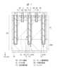
以下に、図1を用いて、本実施の形態の半導体装置の構造について説明する。本実施の形態の半導体装置は、スーパージャンクション構造を有する縦型のパワーMOSFET(MOS型電界効果トランジスタ)を有する。(Embodiment 1)
<Structure of semiconductor device>
The structure of the semiconductor device of this embodiment will be described below with reference to FIG. The semiconductor device of this embodiment has a vertical power MOSFET (MOS field effect transistor) having a superjunction structure.
図1にしめすように、本実施の形態の半導体装置は、半導体基板SBを有する。半導体基板SBは、互いに対向する上面(第1主面)および下面(第2主面)を有する。半導体基板SBの上面および下面は、互いに直交するX方向およびY方向に沿って延在する。半導体基板SBの上面の法線方向は、Z方向である。半導体基板SBは、基板領域SBRと、基板領域SBR上の半導体層SLとを含んでいる。この場合、半導体層SLの上面は半導体基板SBの上面を構成し、基板領域SBRの下面は半導体基板SBの下面を構成する。 As shown in FIG. 1, the semiconductor device of this embodiment has a semiconductor substrate SB. Semiconductor substrate SB has an upper surface (first main surface) and a lower surface (second main surface) facing each other. The upper and lower surfaces of the semiconductor substrate SB extend along the X direction and the Y direction perpendicular to each other. The normal direction of the upper surface of the semiconductor substrate SB is the Z direction. The semiconductor substrate SB includes a substrate region SBR and a semiconductor layer SL over the substrate region SBR. In this case, the upper surface of the semiconductor layer SL forms the upper surface of the semiconductor substrate SB, and the lower surface of the substrate region SBR forms the lower surface of the semiconductor substrate SB.
基板領域SBRは、n型の半導体から構成されている。基板領域SBRは、例えば、5mΩ・cm以下の電気抵抗率を有している。基板領域SBRは、例えば、n+型の単結晶シリコンから成る。半導体層SLは、主にn型の半導体領域であるドリフト層DLを有し、n型の不純物を含んでいる。半導体層SLの厚さは、パワーMOSFETの耐圧に応じて定められる。基板領域SBRは、半導体層SLよりも、相対的に低い電気抵抗率を有する。基板領域SBRにおけるn型の不純物濃度は、半導体層SLにおけるn型の不純物濃度よりも相対的に高い。Substrate region SBR is composed of an n-type semiconductor. The substrate region SBR has an electrical resistivity of, for example, 5 mΩ·cm or less. Substrate region SBR is made of, for example, n+ -type single crystal silicon. The semiconductor layer SL mainly has a drift layer DL that is an n-type semiconductor region and contains n-type impurities. The thickness of the semiconductor layer SL is determined according to the breakdown voltage of the power MOSFET. Substrate region SBR has relatively lower electrical resistivity than semiconductor layer SL. The n-type impurity concentration in substrate region SBR is relatively higher than the n-type impurity concentration in semiconductor layer SL.
本実施の形態のパワーMOSFETは、n型のドリフト層DLと、p型のボディ領域BDと、n型のソース領域SRと、ゲート絶縁膜GIと、ゲート電極GEと、ソース電極SEとを備える。つまり、当該パワーMOSFETは、n型の電界効果トランジスタである。また、基板領域SBRは、パワーMOSFETのドレイン領域を構成している。パワーMOSFETは、ドレイン電極DEと、絶縁体カラムICLMと、層間絶縁膜ILとをさらに備えている。ゲート電極GEは、半導体基板SBの上面に形成されたトレンチT1内に、ゲート絶縁膜GIを介して形成される。絶縁体カラムICLMは、半導体基板SBの上面に形成されたトレンチT2内の絶縁膜を備えている。 The power MOSFET of this embodiment includes an n-type drift layer DL, a p-type body region BD, an n-type source region SR, a gate insulating film GI, a gate electrode GE, and a source electrode SE. . That is, the power MOSFET is an n-type field effect transistor. Also, the substrate region SBR constitutes the drain region of the power MOSFET. The power MOSFET further includes a drain electrode DE, an insulator column ICLM, and an interlayer insulating film IL. The gate electrode GE is formed in the trench T1 formed in the upper surface of the semiconductor substrate SB via the gate insulating film GI. The insulator column ICLM has an insulating film in the trench T2 formed on the upper surface of the semiconductor substrate SB.
n型のドリフト層DLは、半導体基板SB内に配置される。ドリフト層DLは、基板領域SBR上に配置されている。ドリフト層DLは、基板領域SBRよりも低いn型の不純物濃度を有する。ドリフト層DLは、基板領域SBRよりも高い電気抵抗率を有する。ドリフト層DLは、例えば、n-型のシリコン層である。The n-type drift layer DL is arranged in the semiconductor substrate SB. Drift layer DL is arranged on substrate region SBR. Drift layer DL has an n-type impurity concentration lower than that of substrate region SBR. Drift layer DL has a higher electrical resistivity than substrate region SBR. The drift layer DL is, for example, an n− -type silicon layer.
p型の半導体領域であるボディ領域BDは、半導体基板SB内においてドリフト層DL上に配置される。ボディ領域BDは、例えば、p型のシリコン層である。 Body region BD, which is a p-type semiconductor region, is arranged on drift layer DL in semiconductor substrate SB. Body region BD is, for example, a p-type silicon layer.
n型の半導体領域であるソース領域SRは、半導体基板SB内においてボディ領域BD上に配置される。具体的には、ソース領域SRは、トレンチに接して半導体層SLの上面から、半導体層SLの途中深さに亘って形成されている。n型のソース領域SRは、ドリフト層DLよりも高いn型の不純物の濃度を有する。ソース領域SRは、ドリフト層DLよりも低い電気抵抗率を有する。ソース領域SRは、半導体基板SBの上面内において、X方向に沿って離散的に配置されている。ソース領域SRは、Y方向に沿って延在している。ソース領域SRは、例えば、n+型のシリコン領域である。Source region SR, which is an n-type semiconductor region, is arranged on body region BD in semiconductor substrate SB. Specifically, the source region SR is formed in contact with the trench from the upper surface of the semiconductor layer SL to the middle depth of the semiconductor layer SL. The n-type source region SR has a higher n-type impurity concentration than the drift layer DL. Source region SR has a lower electrical resistivity than drift layer DL. The source regions SR are arranged discretely along the X direction in the upper surface of the semiconductor substrate SB. Source region SR extends along the Y direction. The source region SR is, for example, an n+ -type silicon region.
トレンチT1は、半導体層SLの上面に形成された比較的浅い溝である。トレンチT1は、X方向において並ぶソース領域SRのそれぞれに挟まれる位置に形成され、それらのソース領域SRと接している。これに対し、トレンチT2は、半導体層SLの上面に形成された比較的深い溝である。トレンチT1と隣接する2つのソース領域SRのそれぞれとは、ボディ領域BDを介して離間している。トレンチT1とトレンチT2とは、X方向において交互に並んで形成されている。X方向において隣り合うトレンチT1、T2のそれぞれは、それらの間に形成された1つのボディ領域BDと接している。トレンチT1の底部はボディ領域BDの下のドリフト層DLの途中深さで終端しており、基板領域SBRには達していない。これに対し、トレンチT2の底部は基板領域SBRの途中深さに達している。ただし、トレンチT2の底部はドリフト層DL内で終端し、基板領域SBRに達していなくてもよい。 The trench T1 is a relatively shallow trench formed in the upper surface of the semiconductor layer SL. Trench T1 is formed at a position sandwiched between source regions SR aligned in the X direction, and is in contact with these source regions SR. On the other hand, the trench T2 is a relatively deep groove formed in the upper surface of the semiconductor layer SL. Trench T1 is separated from each of the two adjacent source regions SR via body region BD. The trenches T1 and trenches T2 are formed alternately in the X direction. Each of trenches T1 and T2 adjacent in the X direction is in contact with one body region BD formed therebetween. The bottom of trench T1 terminates in the middle depth of drift layer DL below body region BD and does not reach substrate region SBR. On the other hand, the bottom of trench T2 reaches the middle depth of substrate region SBR. However, the bottom of trench T2 may terminate within drift layer DL and not reach substrate region SBR.
図1に示すトレンチT2は、Z方向に沿う垂直な側面を備えているように見えるが、実際には、トレンチT2の側面は、Z方向に対して斜めに形成されており、トレンチ角を有している。トレンチT2のX方向(短手方向)の幅は、トレンチT2の底面から、トレンチT2の上端側に向かって徐々に大きくなっている。なお、トレンチT1の側面もトレンチ角を有している。 Although the trench T2 shown in FIG. 1 appears to have vertical sides along the Z direction, in reality, the sides of the trench T2 are formed obliquely with respect to the Z direction and have trench angles. are doing. The width of the trench T2 in the X direction (transverse direction) gradually increases from the bottom surface of the trench T2 toward the upper end side of the trench T2. Note that the side surface of the trench T1 also has a trench angle.
ゲート絶縁膜GIは、トレンチT1の側面および底面を連続的に覆っている。ドリフト層DLとソース領域SRとに挟まれるボディ領域BDの部分であって、トレンチT1に隣接する部分は、パワーMOSFETのオン状態において、チャネルが形成される部分である。ゲート絶縁膜GIは、ドリフト層DLとソース領域SRとに挟まれるボディ領域BDの部分上に配置されている。トレンチT1は、ボディ領域BDとn型のドリフト層DLとに亘って配置されている。ゲート絶縁膜GIは、p型のボディ領域BDおよびn型のドリフト層DLに接している。ゲート絶縁膜GIは、例えば、酸化シリコン膜である。 The gate insulating film GI continuously covers the side and bottom surfaces of the trench T1. A portion of the body region BD sandwiched between the drift layer DL and the source region SR and adjacent to the trench T1 is a portion where a channel is formed when the power MOSFET is on. Gate insulating film GI is arranged on a portion of body region BD sandwiched between drift layer DL and source region SR. The trench T1 is arranged across the body region BD and the n-type drift layer DL. The gate insulating film GI is in contact with the p-type body region BD and the n-type drift layer DL. The gate insulating film GI is, for example, a silicon oxide film.
ゲート電極GEは、ゲート絶縁膜GIを挟んで、ドリフト層DLとソース領域SRとに挟まれるボディ領域BDの部分に対向するように配置される。つまり、ゲート電極GEは、トレンチT1内にゲート絶縁膜GIを介して形成されている。ゲート電極GEは、トレンチゲート型のゲート電極GEである。なお、ゲート電極GEは、トレンチゲート型ではなく、半導体層SLの上に形成されたプレーナ型のゲート電極GEであってもよい。ゲート電極GEは、X方向に沿って離散的に配置される。ゲート電極GEは、Y方向に沿って延在する。ゲート電極GEは、Z方向における高さは、ボディ領域BDのZ方向における深さよりも大きい。ゲート電極GEは、例えば、多結晶シリコン膜である。ゲート電極GEは、コンタクトホール(図示せず)を介して、ゲート配線に電気的に接続される。 The gate electrode GE is arranged to face the portion of the body region BD sandwiched between the drift layer DL and the source region SR with the gate insulating film GI interposed therebetween. That is, the gate electrode GE is formed in the trench T1 via the gate insulating film GI. The gate electrode GE is a trench gate type gate electrode GE. The gate electrode GE may be a planar gate electrode GE formed on the semiconductor layer SL instead of the trench gate type. The gate electrodes GE are arranged discretely along the X direction. The gate electrode GE extends along the Y direction. The gate electrode GE has a height in the Z direction greater than the depth in the Z direction of the body region BD. The gate electrode GE is, for example, a polycrystalline silicon film. The gate electrode GE is electrically connected to gate wiring through a contact hole (not shown).
絶縁体カラムICLMは、トレンチT2内に配置されている。絶縁体カラムICLMは、ドリフト層DL内、ボディ領域BD内、および基板領域SBR内に配置されている。絶縁体カラムICLMは、半導体基板SBの上面側に配置されている。絶縁体カラムICLMは、ドリフト層DL内、ボディ領域BD内、および基板領域SBR内亘って形成されたトレンチT2内に配置されている。トレンチT2内には、順に絶縁膜IF1、固定電荷層FCおよび絶縁膜IF2が埋め込まれている。言い換えれば、トレンチT2の側面および底面は、絶縁膜IF1により連続的に覆われており、トレンチT2内には、絶縁膜IF1を介して固定電荷層FCが形成されている。また、トレンチT2内には、絶縁膜IF1および固定電荷層FCから成る積層膜を介して、絶縁膜IF2が完全に埋め込まれている。すなわち、トレンチT2内には、当該積層膜を介して、絶縁膜IF2が充填されている。 An insulator column ICLM is arranged in the trench T2. The insulator column ICLM is arranged in the drift layer DL, the body region BD and the substrate region SBR. The insulator column ICLM is arranged on the upper surface side of the semiconductor substrate SB. The insulator column ICLM is arranged in a trench T2 formed over the drift layer DL, the body region BD, and the substrate region SBR. Insulating film IF1, fixed charge layer FC and insulating film IF2 are buried in order in trench T2. In other words, the side and bottom surfaces of the trench T2 are continuously covered with the insulating film IF1, and the fixed charge layer FC is formed in the trench T2 via the insulating film IF1. In addition, the insulating film IF2 is completely embedded in the trench T2 via the laminated film including the insulating film IF1 and the fixed charge layer FC. That is, the trench T2 is filled with the insulating film IF2 through the laminated film.
固定電荷層は絶縁膜である。すなわち、絶縁体カラムICLMは、絶縁膜IF1、IF2および固定電荷層から成る積層絶縁膜で充填されている。固定電荷層FCは、ボディ領域BDおよびドリフト層DLと、X方向において隣り合っている。 The fixed charge layer is an insulating film. That is, the insulator column ICLM is filled with a laminated insulating film composed of the insulating films IF1 and IF2 and the fixed charge layer. Fixed charge layer FC is adjacent to body region BD and drift layer DL in the X direction.
固定電荷層FCは、ホール(正孔)を蓄積する材料から成るホール蓄積層であり、例えば、Hf(ハフニウム)を含むhigh-k膜から成る。固定電荷層FCを構成する材料としては、HfOx(酸化ハフニウム)または酸窒化ハフニウムが挙げられる。この場合、固定電荷層FCを構成する具体的な材料は、例えばHfSiO(ハフニウムシリケート)、HfSiON(窒素添加ハフニウムシリケート)、HfAlON(窒素添加ハフニウムアルミネート)である。その他、固定電荷層FCを構成するhigh-k膜は、酸化イットリウムまたは酸化アルミニウムにより構成されていてもよい。つまり、固定電荷層FCは、Y2O3(酸化イットリウム)またはAl2O3(酸化アルミニウム)により構成されていてもよい。絶縁膜IF1、IF2のそれぞれは、例えば酸化シリコン膜である。すなわち、固定電荷層FCを構成する材料は、酸化ハフニウム、酸窒化ハフニウム、酸化イットリウムおよび酸化アルミニウムから成る群から選択される少なくとも一種である。The fixed charge layer FC is a hole accumulation layer made of a material that accumulates holes, and is made of, for example, a high-k film containing Hf (hafnium). HfOx (hafnium oxide) or hafnium oxynitride is given as a material forming the fixed charge layer FC. In this case, specific materials constituting the fixed charge layer FC are, for example, HfSiO (hafnium silicate), HfSiON (nitrogen-added hafnium silicate), and HfAlON (nitrogen-added hafnium aluminate). Alternatively, the high-k film forming the fixed charge layer FC may be made of yttrium oxide or aluminum oxide. That is, the fixed charge layer FC may be made of Y2 O3 (yttrium oxide) or Al2 O3 (aluminum oxide). Each of the insulating films IF1 and IF2 is, for example, a silicon oxide film. That is, the material forming the fixed charge layer FC is at least one selected from the group consisting of hafnium oxide, hafnium oxynitride, yttrium oxide and aluminum oxide.
絶縁体カラムICLMは、Z方向からの平面視において、隣り合うゲート電極GE同士の間に配置されている。絶縁体カラムICLMは複数形成されており、隣り合う絶縁体カラムICLM同士は、Z方向からの平面視において、ゲート電極GEを挟むように配置されている。複数の絶縁体カラムICLMは、X方向において離散的に配置されている。複数の絶縁体カラムICLMのそれぞれは、Y方向に沿って延在している。 The insulator column ICLM is arranged between the adjacent gate electrodes GE in plan view from the Z direction. A plurality of insulator columns ICLM are formed, and adjacent insulator columns ICLM are arranged so as to sandwich the gate electrode GE in a plan view from the Z direction. A plurality of insulator columns ICLM are arranged discretely in the X direction. Each of the plurality of insulator columns ICLM extends along the Y direction.
high-k膜から成る固定電荷層FCをトレンチT2内に形成することで、トレンチT2の側面の近傍の半導体層SL内には、ホール蓄積領域HCが生じる。すなわち、固定電荷層FCと隣り合うトレンチT2の側面には、ホール蓄積領域HCが形成されている。図1では、ホール蓄積領域HCを破線で示している。ホール蓄積領域HCは、ホールが蓄積される領域である。すなわち、トレンチT2の側面の近傍の半導体層SL内には、high-k膜から成る固定電荷層FCの有するフェルミピニング効果により、周囲の半導体層SL内のホールが集まる。このようにホール蓄積領域HCを生じさせる絶縁体カラムICLMは、パワーMOSFETの動作時において、p+層(pカラム)とみなせる。ホール蓄積領域HCは、ボディ領域BDおよびドリフト層DLと重なり合っている。なお、n型不純物濃度が高い基板領域SBRとホール蓄積領域HCとが重なる領域では、ホール蓄積領域HCの濃度が低下する、または、ホール蓄積領域HCが形成されなくなる。By forming the fixed charge layer FC made of a high-k film in the trench T2, a hole accumulation region HC is generated in the semiconductor layer SL near the side surface of the trench T2. That is, the hole accumulation region HC is formed on the side surface of the trench T2 adjacent to the fixed charge layer FC. In FIG. 1, the hole accumulation region HC is indicated by a dashed line. The hole accumulation region HC is a region where holes are accumulated. That is, holes in the surrounding semiconductor layer SL gather in the semiconductor layer SL near the side surfaces of the trench T2 due to the Fermi pinning effect of the fixed charge layer FC made of the high-k film. The insulator column ICLM that causes the hole accumulation region HC in this way can be regarded as a p+ layer (p column) during operation of the power MOSFET. Hole accumulation region HC overlaps body region BD and drift layer DL. In a region where the substrate region SBR having a high n-type impurity concentration and the hole accumulation region HC overlap, the concentration of the hole accumulation region HC is lowered or the hole accumulation region HC is not formed.
ホール蓄積領域HCのX方向の厚さは、固定電荷層FCを所望の厚さに形成することで制御できる。つまり、固定電荷層FCの厚さを制御することで、ホールの蓄積量を制御できる。固定電荷層FCと半導体基板SBとの間には、シリコン界面の安定化(リークの低減)のために絶縁膜IF1を形成している。絶縁膜IF1は、例えば酸化法またはCVD(Chemical Vapor Deposition)法などの堆積法により形成できる。固定電荷層FCは、絶縁膜IF1形成後に、例えばCVD法などの堆積法により形成できる。絶縁膜IF2は、固定電荷層FC形成後に、例えばCVD法により形成されるTEOS(Tetra Ethyl Ortho Silicate)膜である。 The thickness of the hole accumulation region HC in the X direction can be controlled by forming the fixed charge layer FC to a desired thickness. In other words, the amount of accumulated holes can be controlled by controlling the thickness of the fixed charge layer FC. An insulating film IF1 is formed between the fixed charge layer FC and the semiconductor substrate SB to stabilize the silicon interface (reduce leakage). The insulating film IF1 can be formed by a deposition method such as an oxidation method or a CVD (Chemical Vapor Deposition) method. The fixed charge layer FC can be formed by a deposition method such as the CVD method after the insulating film IF1 is formed. The insulating film IF2 is a TEOS (Tetra Ethyl Ortho Silicate) film formed by, for example, a CVD method after forming the fixed charge layer FC.
層間絶縁膜ILは、半導体基板SBの上面上に配置される。層間絶縁膜ILは、貫通孔THを有する。層間絶縁膜ILは、例えば、酸化シリコン膜である。ソース電極SEは、半導体基板SBの上面上に配置される。ソース電極SEは、貫通孔TH内および層間絶縁膜IL上に形成される。貫通孔TH内に配置されるコンタクトホールを通じて、ソース電極SEは、ソース領域SRおよびp型のボディ領域BDに電気的に接続される。ソース電極SEは、例えば、Al(アルミニウム)膜である。 The interlayer insulating film IL is arranged on the upper surface of the semiconductor substrate SB. The interlayer insulating film IL has through holes TH. The interlayer insulating film IL is, for example, a silicon oxide film. The source electrode SE is arranged on the upper surface of the semiconductor substrate SB. The source electrode SE is formed inside the through hole TH and on the interlayer insulating film IL. Source electrode SE is electrically connected to source region SR and p-type body region BD through a contact hole arranged in through hole TH. The source electrode SE is, for example, an Al (aluminum) film.
ドレイン電極DEは、半導体基板SB(基板領域SBR)の下面上に配置されている。ドレイン電極DEは、基板領域SBRを介して、ドリフト層DLに電気的に接続されている。パワーMOSFETは、縦型構造を有するMOSFETである。ドレイン電極DEは、例えば、アルミニウム(Al)膜である。 The drain electrode DE is arranged on the lower surface of the semiconductor substrate SB (substrate region SBR). The drain electrode DE is electrically connected to the drift layer DL via the substrate region SBR. A power MOSFET is a MOSFET with a vertical structure. The drain electrode DE is, for example, an aluminum (Al) film.
本実施の形態のパワーMOSFETは、ホール蓄積領域HCを生じさせる固定電荷層FCを備えた絶縁体カラムICLM(pカラム)と、n型のドリフト層DL(nカラム)とがX方向において交互に配置されるスーパージャンクション構造を有している。 In the power MOSFET of the present embodiment, insulator columns ICLM (p columns) having fixed charge layers FC that generate hole accumulation regions HC and n-type drift layers DL (n columns) are alternately arranged in the X direction. It has a superjunction structure arranged.
<半導体装置の動作>
スーパージャンクション構造を有する本実施の形態のパワーMOSFETにおいては、ドリフト層DLにn型のドリフト層DL(nカラム)と、ホール蓄積領域HCを備えた絶縁体カラムICLM(pカラム)とが交互に並んでいる。ここで、パワーMOSFETのオフ時においてソース-ドレイン間に電圧を印加すると、ドリフト層DLと、ホール蓄積領域HCとの接合面から、空乏層がX方向に広がる。それらの空乏層同士が一体化することで、溝の深さ分の空乏層を形成する。よって、ドリフト層DLの不純物濃度を比較的高く設定しても耐圧を確保できるため、オン抵抗を小さくできる。<Operation of semiconductor device>
In the power MOSFET of the present embodiment having a superjunction structure, the drift layer DL is alternately provided with an n-type drift layer DL (n column) and an insulator column ICLM (p column) having a hole accumulation region HC. Lined up. Here, when a voltage is applied between the source and the drain while the power MOSFET is off, the depletion layer spreads in the X direction from the junction surface between the drift layer DL and the hole accumulation region HC. By integrating these depletion layers, a depletion layer corresponding to the depth of the trench is formed. Therefore, even if the impurity concentration of the drift layer DL is set relatively high, the breakdown voltage can be ensured, and the on-resistance can be reduced.
<半導体装置の効果>
図4に、比較例の半導体装置の断面図を示す。比較例の半導体装置は、イオン注入法で形成されたp+型の拡散層PDを備えたpカラムと、pカラムに隣り合うドリフト層DLから成るnカラムとを備えたスーパージャンクション構造のパワーMOSFETである。比較例のパワーMOSFETは、トレンチT2内が絶縁膜IF2により完全に埋め込まれており、固定電荷層FCが形成されていない点で、図1を用いて説明したパワーMOSFETとは異なる。また、比較例のパワーMOSFETは、トレンチT2内が絶縁膜IF2のみにより完全に埋め込まれており、固定電荷層FCが形成されていない点で、図1を用いて説明したパワーMOSFETとは異なる。pカラムである絶縁体カラムICLMは、トレンチT2内の絶縁膜IF2と、トレンチT2の側面に形成された拡散層PDを備えている。それ以外の構造は、図1を用いて説明したパワーMOSFETと同じである。<Effect of semiconductor device>
FIG. 4 shows a cross-sectional view of a semiconductor device of a comparative example. The semiconductor device of the comparative example is a power MOSFET having a super junction structure including a p column having a p+ -type diffusion layer PD formed by ion implantation and an n column having a drift layer DL adjacent to the p column. is. The power MOSFET of the comparative example is different from the power MOSFET described with reference to FIG. 1 in that the trench T2 is completely filled with the insulating film IF2 and the fixed charge layer FC is not formed. Further, the power MOSFET of the comparative example is different from the power MOSFET described with reference to FIG. 1 in that the trench T2 is completely filled with only the insulating film IF2 and the fixed charge layer FC is not formed. The insulator column ICLM, which is the p column, includes an insulating film IF2 in the trench T2 and a diffusion layer PD formed on the side surface of the trench T2. Other structures are the same as those of the power MOSFET described with reference to FIG.
比較例のトレンチT2は、図4に示すトレンチT2は、Z方向に沿う垂直な側面を備えているように見えるが、実際には、トレンチT2の側面は、Z方向に対して斜めに形成されており、トレンチ角を有している。拡散層PDを形成する工程では、斜めイオン注入法により、Z方向に対して例えば1度~10度のチルト角をつけて半導体基板SBの表面にp型イオンを打ち込む。これにより、トレンチT2の側面と接する半導体基板SB内にp+型の拡散層PDが形成される。The trench T2 of the comparative example looks like the trench T2 shown in FIG. 4 has vertical side surfaces along the Z direction, but actually the side surfaces of the trench T2 are formed obliquely with respect to the Z direction. and has a trench angle. In the step of forming the diffusion layer PD, p-type ions are implanted into the surface of the semiconductor substrate SB by oblique ion implantation with a tilt angle of, for example, 1 degree to 10 degrees with respect to the Z direction. As a result, the p+ -type diffusion layer PD is formed in the semiconductor substrate SB in contact with the side surface of the trench T2.
ここで、複数のトレンチT2のそれぞれの側面のトレンチ角には、トレンチT2毎、チップ毎、ウエーハ毎にばらつきが生じる場合が考えられる。その場合、トレンチT2の製造ばらつきにより、拡散層PDの注入不純物量がばらつく問題が生じる。拡散層PDの注入不純物量にばらつきがあると、パワーMOSFETの特性(耐圧)にばらつきが生じるため、半導体装置の信頼性が低下する。 Here, it is conceivable that the trench angles of the side surfaces of the plurality of trenches T2 may vary from trench to trench T2, chip to chip, and wafer to wafer. In that case, there arises a problem that the amount of implanted impurities in the diffusion layer PD varies due to manufacturing variations in the trenches T2. Variations in the amount of implanted impurities in the diffusion layer PD cause variations in the characteristics (breakdown voltage) of the power MOSFET, thereby degrading the reliability of the semiconductor device.
これに対し、本実施の形態では、p+型の拡散層PDをイオン注入法により形成するのではなく、トレンチT2内にhigh-k膜である固定電荷層FCを成膜している。ここでは、固定電荷層FCを形成することにより、トレンチT2の側面近傍の半導体層SL内にp+層としてホール蓄積領域HCを形成している。In contrast, in the present embodiment, the fixed charge layer FC, which is a high-k film, is formed in the trench T2 instead of forming the p+ -type diffusion layer PD by ion implantation. Here, by forming the fixed charge layer FC, the hole accumulation region HC is formed as the p+ layer in the semiconductor layer SL in the vicinity of the side surface of the trench T2.
本実施の形態では、トレンチT2内に酸化法または堆積法により絶縁膜IF1を形成した後、固定電荷層FCを堆積法により形成している。すなわち、トレンチT2の側面から一定の距離に、一定の膜厚の固定電荷層FCを形成できる。ここでは、トレンチT2内において、絶縁膜IF1および固定電荷層FCのそれぞれを一定の膜厚で形成し、トレンチT2内のそれらの絶縁膜以外の領域を絶縁膜IF2で埋め込むことにより、ホール蓄積領域HCを安定的に形成できる。 In this embodiment, after forming the insulating film IF1 in the trench T2 by the oxidation method or the deposition method, the fixed charge layer FC is formed by the deposition method. That is, the fixed charge layer FC having a constant thickness can be formed at a constant distance from the side surface of the trench T2. Here, in the trench T2, the insulating film IF1 and the fixed charge layer FC are each formed with a constant film thickness, and the insulating film IF2 is embedded in the region other than the insulating films in the trench T2, thereby forming a hole accumulation region. HC can be stably formed.
このため、トレンチT2のトレンチ角のばらつきに関わらず、各トレンチT2の側面近傍に形成されるホール蓄積領域HCの厚さおよびホール蓄積量を安定化できる。よって、トレンチT2のトレンチ角にばらつきがあったとしても、パワーMOSFETの特性(耐圧)ばらつきの発生を防げるため、半導体装置の信頼性を向上できる。 Therefore, the thickness and hole accumulation amount of the hole accumulation region HC formed in the vicinity of the side surface of each trench T2 can be stabilized regardless of variations in the trench angle of the trench T2. Therefore, even if there is variation in the trench angle of the trench T2, the occurrence of variations in the characteristics (breakdown voltage) of the power MOSFET can be prevented, and the reliability of the semiconductor device can be improved.
(実施の形態2)
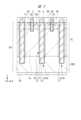
図2に、本実施の形態のパワーMOSFETの断面図を示す。本実施の形態のパワーMOSFETの構造は、トレンチT2の側面にp型の半導体領域である拡散層PDが形成されている点で、前記実施の形態1と異なる。(Embodiment 2)
FIG. 2 shows a cross-sectional view of the power MOSFET of this embodiment. The structure of the power MOSFET of this embodiment differs from that of the first embodiment in that a diffusion layer PD, which is a p-type semiconductor region, is formed on the side surface of the trench T2.
pカラムである絶縁体カラムICLMは、トレンチT2内の絶縁膜IF1、固定電荷層FCおよび絶縁膜IF2に加え、トレンチT2の側面の半導体基板SB内に形成された拡散層PDを備えている。拡散層PDは、トレンチT2の側面から、X方向において、半導体基板SB内に所定の深さで形成されている。ここでは、X方向における拡散層PDの幅は、X方向におけるホール蓄積領域HCの幅よりも大きい。なお、ここでは拡散層PDがトレンチT2の側面に接している場合について説明するが、拡散層PDはトレンチT2の側面から一定の距離だけ離れた位置の半導体基板SB内に形成されていてもよい。つまり、
拡散層PD、トレンチT2の側面から所定の距離の半導体基板SB内に形成されている。The insulator column ICLM, which is the p-column, includes an insulating film IF1, a fixed charge layer FC, and an insulating film IF2 in the trench T2, as well as a diffusion layer PD formed in the semiconductor substrate SB on the side surface of the trench T2. The diffusion layer PD is formed with a predetermined depth in the semiconductor substrate SB in the X direction from the side surface of the trench T2. Here, the width of the diffusion layer PD in the X direction is greater than the width of the hole accumulation region HC in the X direction. Here, the case where the diffusion layer PD is in contact with the side surface of the trench T2 will be described, but the diffusion layer PD may be formed in the semiconductor substrate SB at a certain distance from the side surface of the trench T2. . in short,
The diffusion layer PD is formed within the semiconductor substrate SB at a predetermined distance from the side surface of the trench T2.
拡散層PDは、トレンチT2の形成後、絶縁膜IF1の形成前にイオン注入を行うことで形成する。すなわち、拡散層PDを形成する工程では、斜めイオン注入法により、Z方向に対して例えば1度~10度のチルト角をつけて半導体基板SBの表面にp型イオンを打ち込む。これにより、トレンチT2の側面と接する半導体基板SB内にp+型の拡散層PDが形成される。The diffusion layer PD is formed by performing ion implantation after forming the trench T2 and before forming the insulating film IF1. That is, in the step of forming the diffusion layer PD, p-type ions are implanted into the surface of the semiconductor substrate SB by oblique ion implantation with a tilt angle of, for example, 1 degree to 10 degrees with respect to the Z direction. As a result, the p+ -type diffusion layer PD is formed in the semiconductor substrate SB in contact with the side surface of the trench T2.
pカラムを構成する要素が、トレンチT2内の絶縁膜IF1、IF2および固定電荷層FCのみだとpカラムのホールの蓄積量が足りない場合には、本実施の形態のように、p型の拡散層PDを形成することで、ホールの蓄積量を補える。前記実施の形態1では、図4の比較例を用い、拡散層PDを有するパワーMOSFETにおいて特性ばらつきが生じることについて説明した。これに対し、本実施の形態では絶縁体カラムICLMが固定電荷層FCを有しているため、拡散層PDの注入不純物量は、比較例の拡散層PDよりも少なくてよい。したがって、本実施の形態では、トレンチ角のばらつきに起因する拡散層PDの注入不純物量のばらつきを抑え、かつ、pカラムのホールの蓄積量を確保できる。したがって、トレンチT2のトレンチ角にばらつきがあったとしても、パワーMOSFETの特性(耐圧)ばらつきの発生を防げるため、半導体装置の信頼性を向上できる。 If the p-column is made up of only the insulating films IF1 and IF2 and the fixed charge layer FC in the trench T2 and the p-column does not accumulate enough holes, a p-type By forming the diffusion layer PD, the accumulated amount of holes can be compensated. In the first embodiment, the comparative example shown in FIG. 4 was used to explain the occurrence of characteristic variations in the power MOSFET having the diffusion layer PD. On the other hand, in the present embodiment, since the insulator column ICLM has the fixed charge layer FC, the amount of implanted impurities in the diffusion layer PD may be smaller than that in the diffusion layer PD of the comparative example. Therefore, in the present embodiment, variations in the amount of implanted impurities in the diffusion layer PD due to variations in trench angle can be suppressed, and the amount of accumulated holes in the p-column can be ensured. Therefore, even if the trench angle of the trench T2 varies, variations in the characteristics (breakdown voltage) of the power MOSFET can be prevented, and the reliability of the semiconductor device can be improved.
(実施の形態3)
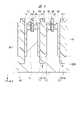
図3に、本実施の形態のパワーMOSFETの断面図を示す。本実施の形態のパワーMOSFETの構造は、トレンチT2内に絶縁膜IF2が形成されておらず、トレンチT2内に絶縁膜IF1を介して固定電荷層FCが完全に埋め込まれている点で、前記実施の形態1と異なる。(Embodiment 3)
FIG. 3 shows a cross-sectional view of the power MOSFET of this embodiment. In the structure of the power MOSFET of this embodiment, the insulating film IF2 is not formed in the trench T2, and the fixed charge layer FC is completely buried in the trench T2 via the insulating film IF1. It differs from the first embodiment.
トレンチT2の横に形成されるホール蓄積領域HCの幅およびホールの蓄積量は、トレンチT2内の固定電荷層FCの厚さによって制御できる。本実施の形態では、トレンチT2内に絶縁膜IF1を介して固定電荷層FCを充填することで、所望のホール蓄積領域HCの幅およびホールの蓄積量を得られる。したがって、トレンチ角のばらつきに関わらず、ホール蓄積領域HCを安定的に形成できるため、パワーMOSFETの耐圧を安定化できる。したがって、半導体装置の信頼性を向上できる。 The width of the hole accumulation region HC formed beside the trench T2 and the amount of accumulated holes can be controlled by the thickness of the fixed charge layer FC within the trench T2. In the present embodiment, by filling the trench T2 with the fixed charge layer FC through the insulating film IF1, the desired width of the hole accumulation region HC and the amount of accumulated holes can be obtained. Therefore, the hole accumulation region HC can be stably formed regardless of variations in trench angle, so that the breakdown voltage of the power MOSFET can be stabilized. Therefore, reliability of the semiconductor device can be improved.
以上、本発明者らによってなされた発明を実施の形態に基づき具体的に説明したが、本発明は前記実施の形態に限定されるものではなく、その要旨を逸脱しない範囲で種々変更可能であることはいうまでもない。 Although the invention made by the present inventors has been specifically described based on the embodiments, the invention is not limited to the above embodiments, and can be variously modified without departing from the gist of the invention. Needless to say.
例えば、前記実施の形態2と前記実施の形態3とを組み合わせてもよい。 For example, the second embodiment and the third embodiment may be combined.
DL ドリフト層
FC 固定電荷層
GE ゲート電極
GI ゲート絶縁膜
HC ホール蓄積領域
ICLM 絶縁体カラム
IF1、IF2 絶縁膜
IL 層間絶縁膜
SB 半導体基板
SBR 基板領域
SL 半導体層
SR ソース領域
TI、T2 トレンチDL drift layer FC fixed charge layer GE gate electrode GI gate insulating film HC hole accumulation region ICLM insulator column IF1, IF2 insulating film IL interlayer insulating film SB semiconductor substrate SBR substrate region SL semiconductor layer SR source region TI, T2 trench
Claims (7)
Translated fromJapanese前記半導体基板内に配置されたn型のドリフト層と、
前記半導体基板内において、前記ドリフト層の前記第1主面側に配置されたp型のボディ領域と、
前記半導体基板内において、前記ボディ領域の前記第1主面側に配置されたn型のソース領域と、
前記ドリフト層と前記ソース領域とに挟まれる前記ボディ領域の部分上に配置されるゲート絶縁膜と、
前記ゲート絶縁膜を挟んで前記ボディ領域の前記部分に対向するゲート電極と、
前記第1主面から前記半導体基板の途中深さに亘って形成され、側面が前記ボディ領域および前記ドリフト層に接する溝と、
前記溝内に第1絶縁膜を介して形成された固定電荷層と、
を有し、
前記溝は、前記溝の前記第1主面に沿う方向に複数並んで配置されている、半導体装置。a semiconductor substrate having a first main surface and a second main surface opposite to the first main surface;
an n-type drift layer disposed within the semiconductor substrate;
a p-type body region disposed on the first main surface side of the drift layer in the semiconductor substrate;
an n-type source region disposed on the first main surface side of the body region in the semiconductor substrate;
a gate insulating film disposed on a portion of the body region sandwiched between the drift layer and the source region;
a gate electrode facing the portion of the body region with the gate insulating film interposed therebetween;
a groove formed from the first main surface to a middle depth of the semiconductor substrate and having side surfaces in contact with the body region and the drift layer;
a fixed charge layer formed in the groove via a first insulating film;
has
The semiconductor device, wherein a plurality of the grooves are arranged side by side in a direction along the first main surface of the grooves.
前記固定電荷層を構成する材料は、酸化ハフニウム、酸窒化ハフニウム、酸化イットリウムおよび酸化アルミニウムから成る群から選択される少なくとも一種である、半導体装置。The semiconductor device according to claim 1,
A semiconductor device, wherein the material forming the fixed charge layer is at least one selected from the group consisting of hafnium oxide, hafnium oxynitride, yttrium oxide and aluminum oxide.
前記固定電荷層と隣り合う前記溝の前記側面には、ホール蓄積領域が形成される、半導体装置。The semiconductor device according to claim 1,
A semiconductor device, wherein a hole accumulation region is formed on the side surface of the groove adjacent to the fixed charge layer.
前記溝の前記側面から所定の距離の前記半導体基板内に、p型の拡散層が形成されている、半導体装置。The semiconductor device according to claim 1,
A semiconductor device, wherein a p-type diffusion layer is formed in the semiconductor substrate at a predetermined distance from the side surface of the groove.
前記溝内には、第1絶縁膜を介して前記固定電荷層が形成されている、半導体装置。The semiconductor device according to claim 1,
A semiconductor device, wherein the fixed charge layer is formed in the trench with a first insulating film interposed therebetween.
前記溝内には、前記固定電荷層を介して第2絶縁膜が充填されている、半導体装置。The semiconductor device according to claim 1,
The semiconductor device according to claim 1, wherein the trench is filled with a second insulating film via the fixed charge layer.
前記溝内には、第1絶縁膜を介して前記固定電荷層が充填されている、半導体装置。The semiconductor device according to claim 1,
The semiconductor device according to claim 1, wherein the trench is filled with the fixed charge layer via a first insulating film.
Priority Applications (2)
| Application Number | Priority Date | Filing Date | Title |
|---|---|---|---|
| JP2021119542AJP2023015636A (en) | 2021-07-20 | 2021-07-20 | semiconductor equipment |
| US17/828,349US20230029438A1 (en) | 2021-07-20 | 2022-05-31 | Semiconductor device |
Applications Claiming Priority (1)
| Application Number | Priority Date | Filing Date | Title |
|---|---|---|---|
| JP2021119542AJP2023015636A (en) | 2021-07-20 | 2021-07-20 | semiconductor equipment |
Publications (1)
| Publication Number | Publication Date |
|---|---|
| JP2023015636Atrue JP2023015636A (en) | 2023-02-01 |
Family
ID=84977183
Family Applications (1)
| Application Number | Title | Priority Date | Filing Date |
|---|---|---|---|
| JP2021119542APendingJP2023015636A (en) | 2021-07-20 | 2021-07-20 | semiconductor equipment |
Country Status (2)
| Country | Link |
|---|---|
| US (1) | US20230029438A1 (en) |
| JP (1) | JP2023015636A (en) |
Citations (3)
| Publication number | Priority date | Publication date | Assignee | Title |
|---|---|---|---|---|
| JPH10223896A (en)* | 1997-02-10 | 1998-08-21 | Mitsubishi Electric Corp | High breakdown voltage semiconductor device and method of manufacturing the same |
| JP2010516058A (en)* | 2007-01-09 | 2010-05-13 | マックスパワー・セミコンダクター・インコーポレイテッド | Semiconductor device and manufacturing method thereof |
| WO2019093479A1 (en)* | 2017-11-09 | 2019-05-16 | ソニーセミコンダクタソリューションズ株式会社 | Solid-state imaging device and electronic device |
Family Cites Families (24)
| Publication number | Priority date | Publication date | Assignee | Title |
|---|---|---|---|---|
| US4942445A (en)* | 1988-07-05 | 1990-07-17 | General Electric Company | Lateral depletion mode tyristor |
| US5448083A (en)* | 1991-08-08 | 1995-09-05 | Kabushiki Kaisha Toshiba | Insulated-gate semiconductor device |
| JP4326835B2 (en)* | 2003-05-20 | 2009-09-09 | 三菱電機株式会社 | Semiconductor device, semiconductor device manufacturing method, and semiconductor device manufacturing process evaluation method |
| JP5122762B2 (en)* | 2006-03-07 | 2013-01-16 | 株式会社東芝 | Power semiconductor device, manufacturing method thereof, and driving method thereof |
| JP2009135360A (en)* | 2007-12-03 | 2009-06-18 | Renesas Technology Corp | Semiconductor device and manufacturing method thereof |
| WO2009148695A2 (en)* | 2008-06-02 | 2009-12-10 | Maxpower Semiconductor Inc. | Edge termination for semiconductor devices |
| US7897462B2 (en)* | 2008-11-14 | 2011-03-01 | Semiconductor Components Industries, L.L.C. | Method of manufacturing semiconductor component with gate and shield electrodes in trenches |
| WO2010120704A2 (en)* | 2009-04-13 | 2010-10-21 | Maxpower Semiconductor Inc. | Power semiconductor devices, methods, and structures with embedded dielectric layers containing permanent charges |
| US8330214B2 (en)* | 2009-05-28 | 2012-12-11 | Maxpower Semiconductor, Inc. | Power semiconductor device |
| US8299494B2 (en)* | 2009-06-12 | 2012-10-30 | Alpha & Omega Semiconductor, Inc. | Nanotube semiconductor devices |
| JP2011151350A (en)* | 2009-12-22 | 2011-08-04 | Renesas Electronics Corp | Semiconductor device manufacturing method and the semiconductor device |
| US8546893B2 (en)* | 2010-01-12 | 2013-10-01 | Mohamed N. Darwish | Devices, components and methods combining trench field plates with immobile electrostatic charge |
| WO2012006261A2 (en)* | 2010-07-06 | 2012-01-12 | Maxpower Semiconductor Inc. | Power semiconductor devices, structures, and related methods |
| US8519473B2 (en)* | 2010-07-14 | 2013-08-27 | Infineon Technologies Ag | Vertical transistor component |
| JP5449094B2 (en)* | 2010-09-07 | 2014-03-19 | 株式会社東芝 | Semiconductor device |
| JP6037499B2 (en)* | 2011-06-08 | 2016-12-07 | ローム株式会社 | Semiconductor device and manufacturing method thereof |
| US9059256B2 (en)* | 2012-09-13 | 2015-06-16 | Infineon Technologies Ag | Method for producing a controllable semiconductor component |
| JP6385755B2 (en)* | 2014-08-08 | 2018-09-05 | ルネサスエレクトロニクス株式会社 | Manufacturing method of semiconductor device |
| KR20160060850A (en)* | 2014-11-20 | 2016-05-31 | 삼성전자주식회사 | Memory device and manufactureing the same |
| JP6622611B2 (en)* | 2016-02-10 | 2019-12-18 | ルネサスエレクトロニクス株式会社 | Semiconductor device and manufacturing method thereof |
| JP6869791B2 (en)* | 2017-04-21 | 2021-05-12 | 三菱電機株式会社 | Semiconductor switching elements and their manufacturing methods |
| JP2023023390A (en)* | 2021-08-05 | 2023-02-16 | ルネサスエレクトロニクス株式会社 | Semiconductor device and its manufacturing method |
| US11908928B2 (en)* | 2021-11-24 | 2024-02-20 | Infineon Technologies Austria Ag | Field plate anchoring structure for trench-based semiconductor devices |
| JPWO2023189058A1 (en)* | 2022-03-31 | 2023-10-05 |
- 2021
- 2021-07-20JPJP2021119542Apatent/JP2023015636A/enactivePending
- 2022
- 2022-05-31USUS17/828,349patent/US20230029438A1/enactivePending
Patent Citations (3)
| Publication number | Priority date | Publication date | Assignee | Title |
|---|---|---|---|---|
| JPH10223896A (en)* | 1997-02-10 | 1998-08-21 | Mitsubishi Electric Corp | High breakdown voltage semiconductor device and method of manufacturing the same |
| JP2010516058A (en)* | 2007-01-09 | 2010-05-13 | マックスパワー・セミコンダクター・インコーポレイテッド | Semiconductor device and manufacturing method thereof |
| WO2019093479A1 (en)* | 2017-11-09 | 2019-05-16 | ソニーセミコンダクタソリューションズ株式会社 | Solid-state imaging device and electronic device |
Also Published As
| Publication number | Publication date |
|---|---|
| US20230029438A1 (en) | 2023-01-26 |
Similar Documents
| Publication | Publication Date | Title |
|---|---|---|
| US10128344B2 (en) | Semiconductor device | |
| US7554155B2 (en) | Power semiconductor device and method of manufacturing the same | |
| US9214526B2 (en) | Semiconductor device | |
| JP5298432B2 (en) | Semiconductor device and manufacturing method thereof | |
| US9245995B2 (en) | Semiconductor device having power metal-oxide-semiconductor transistor | |
| US10840368B2 (en) | Semiconductor device | |
| JP2003031804A (en) | Semiconductor device | |
| US9299788B2 (en) | Multi-gate VDMOS transistor | |
| US20230378273A1 (en) | Silicon carbide trench power device | |
| US11715773B2 (en) | Semiconductor device | |
| WO2016152059A1 (en) | Semiconductor device | |
| US12356678B2 (en) | Trench-gate transistor device | |
| JP7616033B2 (en) | Semiconductor device manufacturing method | |
| JP6669628B2 (en) | Switching element | |
| JP7164497B2 (en) | semiconductor equipment | |
| JP2019176104A (en) | Switching element | |
| CN102449770B (en) | 3D channel architecture for semiconductor devices | |
| JP2023015636A (en) | semiconductor equipment | |
| JP2023140026A (en) | Semiconductor device | |
| JP7381425B2 (en) | Semiconductor device and its manufacturing method | |
| JP7471250B2 (en) | Semiconductor Device | |
| US20250022924A1 (en) | Semiconductor device | |
| JP7230477B2 (en) | Manufacturing method of trench gate type switching element | |
| JP2024135369A (en) | Semiconductor Device | |
| JP5609950B2 (en) | Semiconductor device and manufacturing method thereof |
Legal Events
| Date | Code | Title | Description |
|---|---|---|---|
| A621 | Written request for application examination | Free format text:JAPANESE INTERMEDIATE CODE: A621 Effective date:20240110 | |
| A977 | Report on retrieval | Free format text:JAPANESE INTERMEDIATE CODE: A971007 Effective date:20241017 | |
| A131 | Notification of reasons for refusal | Free format text:JAPANESE INTERMEDIATE CODE: A131 Effective date:20241022 | |
| A521 | Request for written amendment filed | Free format text:JAPANESE INTERMEDIATE CODE: A523 Effective date:20241220 | |
| A02 | Decision of refusal | Free format text:JAPANESE INTERMEDIATE CODE: A02 Effective date:20250212 |